US12170268B2 - Embedded metal lines - Google Patents
Embedded metal linesDownload PDFInfo
- Publication number
- US12170268B2 US12170268B2US18/614,310US202418614310AUS12170268B2US 12170268 B2US12170268 B2US 12170268B2US 202418614310 AUS202418614310 AUS 202418614310AUS 12170268 B2US12170268 B2US 12170268B2
- Authority
- US
- United States
- Prior art keywords
- substrate
- metal
- bls
- buried
- buried lines
- Prior art date
- Legal status (The legal status is an assumption and is not a legal conclusion. Google has not performed a legal analysis and makes no representation as to the accuracy of the status listed.)
- Active
Links
Images


Classifications
- H—ELECTRICITY
- H01—ELECTRIC ELEMENTS
- H01L—SEMICONDUCTOR DEVICES NOT COVERED BY CLASS H10
- H01L25/00—Assemblies consisting of a plurality of semiconductor or other solid state devices
- H01L25/03—Assemblies consisting of a plurality of semiconductor or other solid state devices all the devices being of a type provided for in a single subclass of subclasses H10B, H10D, H10F, H10H, H10K or H10N, e.g. assemblies of rectifier diodes
- H01L25/04—Assemblies consisting of a plurality of semiconductor or other solid state devices all the devices being of a type provided for in a single subclass of subclasses H10B, H10D, H10F, H10H, H10K or H10N, e.g. assemblies of rectifier diodes the devices not having separate containers
- H01L25/065—Assemblies consisting of a plurality of semiconductor or other solid state devices all the devices being of a type provided for in a single subclass of subclasses H10B, H10D, H10F, H10H, H10K or H10N, e.g. assemblies of rectifier diodes the devices not having separate containers the devices being of a type provided for in group H10D89/00
- H01L25/0657—Stacked arrangements of devices
- H—ELECTRICITY
- H10—SEMICONDUCTOR DEVICES; ELECTRIC SOLID-STATE DEVICES NOT OTHERWISE PROVIDED FOR
- H10D—INORGANIC ELECTRIC SEMICONDUCTOR DEVICES
- H10D88/00—Three-dimensional [3D] integrated devices
- H—ELECTRICITY
- H01—ELECTRIC ELEMENTS
- H01L—SEMICONDUCTOR DEVICES NOT COVERED BY CLASS H10
- H01L21/00—Processes or apparatus adapted for the manufacture or treatment of semiconductor or solid state devices or of parts thereof
- H01L21/02—Manufacture or treatment of semiconductor devices or of parts thereof
- H01L21/02104—Forming layers
- H01L21/02365—Forming inorganic semiconducting materials on a substrate
- H01L21/02518—Deposited layers
- H01L21/02521—Materials
- H01L21/02524—Group 14 semiconducting materials
- H01L21/02532—Silicon, silicon germanium, germanium
- H—ELECTRICITY
- H01—ELECTRIC ELEMENTS
- H01L—SEMICONDUCTOR DEVICES NOT COVERED BY CLASS H10
- H01L21/00—Processes or apparatus adapted for the manufacture or treatment of semiconductor or solid state devices or of parts thereof
- H01L21/02—Manufacture or treatment of semiconductor devices or of parts thereof
- H01L21/04—Manufacture or treatment of semiconductor devices or of parts thereof the devices having potential barriers, e.g. a PN junction, depletion layer or carrier concentration layer
- H01L21/18—Manufacture or treatment of semiconductor devices or of parts thereof the devices having potential barriers, e.g. a PN junction, depletion layer or carrier concentration layer the devices having semiconductor bodies comprising elements of Group IV of the Periodic Table or AIIIBV compounds with or without impurities, e.g. doping materials
- H01L21/30—Treatment of semiconductor bodies using processes or apparatus not provided for in groups H01L21/20 - H01L21/26
- H01L21/31—Treatment of semiconductor bodies using processes or apparatus not provided for in groups H01L21/20 - H01L21/26 to form insulating layers thereon, e.g. for masking or by using photolithographic techniques; After treatment of these layers; Selection of materials for these layers
- H01L21/3205—Deposition of non-insulating-, e.g. conductive- or resistive-, layers on insulating layers; After-treatment of these layers
- H01L21/321—After treatment
- H01L21/32115—Planarisation
- H01L21/3212—Planarisation by chemical mechanical polishing [CMP]
- H—ELECTRICITY
- H01—ELECTRIC ELEMENTS
- H01L—SEMICONDUCTOR DEVICES NOT COVERED BY CLASS H10
- H01L21/00—Processes or apparatus adapted for the manufacture or treatment of semiconductor or solid state devices or of parts thereof
- H01L21/70—Manufacture or treatment of devices consisting of a plurality of solid state components formed in or on a common substrate or of parts thereof; Manufacture of integrated circuit devices or of parts thereof
- H01L21/71—Manufacture of specific parts of devices defined in group H01L21/70
- H01L21/768—Applying interconnections to be used for carrying current between separate components within a device comprising conductors and dielectrics
- H01L21/76801—Applying interconnections to be used for carrying current between separate components within a device comprising conductors and dielectrics characterised by the formation and the after-treatment of the dielectrics, e.g. smoothing
- H01L21/76802—Applying interconnections to be used for carrying current between separate components within a device comprising conductors and dielectrics characterised by the formation and the after-treatment of the dielectrics, e.g. smoothing by forming openings in dielectrics
- H—ELECTRICITY
- H01—ELECTRIC ELEMENTS
- H01L—SEMICONDUCTOR DEVICES NOT COVERED BY CLASS H10
- H01L21/00—Processes or apparatus adapted for the manufacture or treatment of semiconductor or solid state devices or of parts thereof
- H01L21/70—Manufacture or treatment of devices consisting of a plurality of solid state components formed in or on a common substrate or of parts thereof; Manufacture of integrated circuit devices or of parts thereof
- H01L21/71—Manufacture of specific parts of devices defined in group H01L21/70
- H01L21/768—Applying interconnections to be used for carrying current between separate components within a device comprising conductors and dielectrics
- H01L21/76838—Applying interconnections to be used for carrying current between separate components within a device comprising conductors and dielectrics characterised by the formation and the after-treatment of the conductors
- H01L21/7684—Smoothing; Planarisation
- H—ELECTRICITY
- H01—ELECTRIC ELEMENTS
- H01L—SEMICONDUCTOR DEVICES NOT COVERED BY CLASS H10
- H01L21/00—Processes or apparatus adapted for the manufacture or treatment of semiconductor or solid state devices or of parts thereof
- H01L21/70—Manufacture or treatment of devices consisting of a plurality of solid state components formed in or on a common substrate or of parts thereof; Manufacture of integrated circuit devices or of parts thereof
- H01L21/71—Manufacture of specific parts of devices defined in group H01L21/70
- H01L21/768—Applying interconnections to be used for carrying current between separate components within a device comprising conductors and dielectrics
- H01L21/76838—Applying interconnections to be used for carrying current between separate components within a device comprising conductors and dielectrics characterised by the formation and the after-treatment of the conductors
- H01L21/76877—Filling of holes, grooves or trenches, e.g. vias, with conductive material
- H01L21/823418—
- H01L21/823475—
- H01L21/823481—
- H01L21/823487—
- H—ELECTRICITY
- H01—ELECTRIC ELEMENTS
- H01L—SEMICONDUCTOR DEVICES NOT COVERED BY CLASS H10
- H01L23/00—Details of semiconductor or other solid state devices
- H01L23/52—Arrangements for conducting electric current within the device in operation from one component to another, i.e. interconnections, e.g. wires, lead frames
- H01L23/522—Arrangements for conducting electric current within the device in operation from one component to another, i.e. interconnections, e.g. wires, lead frames including external interconnections consisting of a multilayer structure of conductive and insulating layers inseparably formed on the semiconductor body
- H01L23/528—Layout of the interconnection structure
- H—ELECTRICITY
- H01—ELECTRIC ELEMENTS
- H01L—SEMICONDUCTOR DEVICES NOT COVERED BY CLASS H10
- H01L25/00—Assemblies consisting of a plurality of semiconductor or other solid state devices
- H01L25/50—Multistep manufacturing processes of assemblies consisting of devices, the devices being individual devices of subclass H10D or integrated devices of class H10
- H01L29/0847—
- H01L29/45—
- H01L29/665—
- H—ELECTRICITY
- H10—SEMICONDUCTOR DEVICES; ELECTRIC SOLID-STATE DEVICES NOT OTHERWISE PROVIDED FOR
- H10B—ELECTRONIC MEMORY DEVICES
- H10B12/00—Dynamic random access memory [DRAM] devices
- H10B12/30—DRAM devices comprising one-transistor - one-capacitor [1T-1C] memory cells
- H10B12/48—Data lines or contacts therefor
- H10B12/482—Bit lines
- H—ELECTRICITY
- H10—SEMICONDUCTOR DEVICES; ELECTRIC SOLID-STATE DEVICES NOT OTHERWISE PROVIDED FOR
- H10D—INORGANIC ELECTRIC SEMICONDUCTOR DEVICES
- H10D30/00—Field-effect transistors [FET]
- H10D30/01—Manufacture or treatment
- H10D30/021—Manufacture or treatment of FETs having insulated gates [IGFET]
- H10D30/0212—Manufacture or treatment of FETs having insulated gates [IGFET] using self-aligned silicidation
- H—ELECTRICITY
- H10—SEMICONDUCTOR DEVICES; ELECTRIC SOLID-STATE DEVICES NOT OTHERWISE PROVIDED FOR
- H10D—INORGANIC ELECTRIC SEMICONDUCTOR DEVICES
- H10D62/00—Semiconductor bodies, or regions thereof, of devices having potential barriers
- H10D62/10—Shapes, relative sizes or dispositions of the regions of the semiconductor bodies; Shapes of the semiconductor bodies
- H10D62/13—Semiconductor regions connected to electrodes carrying current to be rectified, amplified or switched, e.g. source or drain regions
- H10D62/149—Source or drain regions of field-effect devices
- H10D62/151—Source or drain regions of field-effect devices of IGFETs
- H—ELECTRICITY
- H10—SEMICONDUCTOR DEVICES; ELECTRIC SOLID-STATE DEVICES NOT OTHERWISE PROVIDED FOR
- H10D—INORGANIC ELECTRIC SEMICONDUCTOR DEVICES
- H10D64/00—Electrodes of devices having potential barriers
- H10D64/60—Electrodes characterised by their materials
- H10D64/62—Electrodes ohmically coupled to a semiconductor
- H—ELECTRICITY
- H10—SEMICONDUCTOR DEVICES; ELECTRIC SOLID-STATE DEVICES NOT OTHERWISE PROVIDED FOR
- H10D—INORGANIC ELECTRIC SEMICONDUCTOR DEVICES
- H10D84/00—Integrated devices formed in or on semiconductor substrates that comprise only semiconducting layers, e.g. on Si wafers or on GaAs-on-Si wafers
- H10D84/01—Manufacture or treatment
- H10D84/0123—Integrating together multiple components covered by H10D12/00 or H10D30/00, e.g. integrating multiple IGBTs
- H10D84/0126—Integrating together multiple components covered by H10D12/00 or H10D30/00, e.g. integrating multiple IGBTs the components including insulated gates, e.g. IGFETs
- H10D84/013—Manufacturing their source or drain regions, e.g. silicided source or drain regions
- H—ELECTRICITY
- H10—SEMICONDUCTOR DEVICES; ELECTRIC SOLID-STATE DEVICES NOT OTHERWISE PROVIDED FOR
- H10D—INORGANIC ELECTRIC SEMICONDUCTOR DEVICES
- H10D84/00—Integrated devices formed in or on semiconductor substrates that comprise only semiconducting layers, e.g. on Si wafers or on GaAs-on-Si wafers
- H10D84/01—Manufacture or treatment
- H10D84/0123—Integrating together multiple components covered by H10D12/00 or H10D30/00, e.g. integrating multiple IGBTs
- H10D84/0126—Integrating together multiple components covered by H10D12/00 or H10D30/00, e.g. integrating multiple IGBTs the components including insulated gates, e.g. IGFETs
- H10D84/0149—Manufacturing their interconnections or electrodes, e.g. source or drain electrodes
- H—ELECTRICITY
- H10—SEMICONDUCTOR DEVICES; ELECTRIC SOLID-STATE DEVICES NOT OTHERWISE PROVIDED FOR
- H10D—INORGANIC ELECTRIC SEMICONDUCTOR DEVICES
- H10D84/00—Integrated devices formed in or on semiconductor substrates that comprise only semiconducting layers, e.g. on Si wafers or on GaAs-on-Si wafers
- H10D84/01—Manufacture or treatment
- H10D84/0123—Integrating together multiple components covered by H10D12/00 or H10D30/00, e.g. integrating multiple IGBTs
- H10D84/0126—Integrating together multiple components covered by H10D12/00 or H10D30/00, e.g. integrating multiple IGBTs the components including insulated gates, e.g. IGFETs
- H10D84/0151—Manufacturing their isolation regions
- H—ELECTRICITY
- H10—SEMICONDUCTOR DEVICES; ELECTRIC SOLID-STATE DEVICES NOT OTHERWISE PROVIDED FOR
- H10D—INORGANIC ELECTRIC SEMICONDUCTOR DEVICES
- H10D84/00—Integrated devices formed in or on semiconductor substrates that comprise only semiconducting layers, e.g. on Si wafers or on GaAs-on-Si wafers
- H10D84/01—Manufacture or treatment
- H10D84/0123—Integrating together multiple components covered by H10D12/00 or H10D30/00, e.g. integrating multiple IGBTs
- H10D84/0126—Integrating together multiple components covered by H10D12/00 or H10D30/00, e.g. integrating multiple IGBTs the components including insulated gates, e.g. IGFETs
- H10D84/016—Integrating together multiple components covered by H10D12/00 or H10D30/00, e.g. integrating multiple IGBTs the components including insulated gates, e.g. IGFETs the components including vertical IGFETs
- H—ELECTRICITY
- H10—SEMICONDUCTOR DEVICES; ELECTRIC SOLID-STATE DEVICES NOT OTHERWISE PROVIDED FOR
- H10D—INORGANIC ELECTRIC SEMICONDUCTOR DEVICES
- H10D84/00—Integrated devices formed in or on semiconductor substrates that comprise only semiconducting layers, e.g. on Si wafers or on GaAs-on-Si wafers
- H10D84/01—Manufacture or treatment
- H10D84/02—Manufacture or treatment characterised by using material-based technologies
- H10D84/03—Manufacture or treatment characterised by using material-based technologies using Group IV technology, e.g. silicon technology or silicon-carbide [SiC] technology
- H10D84/038—Manufacture or treatment characterised by using material-based technologies using Group IV technology, e.g. silicon technology or silicon-carbide [SiC] technology using silicon technology, e.g. SiGe
- H—ELECTRICITY
- H01—ELECTRIC ELEMENTS
- H01L—SEMICONDUCTOR DEVICES NOT COVERED BY CLASS H10
- H01L2225/00—Details relating to assemblies covered by the group H01L25/00 but not provided for in its subgroups
- H01L2225/03—All the devices being of a type provided for in the same main group of the same subclass of class H10, e.g. assemblies of rectifier diodes
- H01L2225/04—All the devices being of a type provided for in the same main group of the same subclass of class H10, e.g. assemblies of rectifier diodes the devices not having separate containers
- H01L2225/065—All the devices being of a type provided for in the same main group of the same subclass of class H10
- H01L2225/06503—Stacked arrangements of devices
- H01L2225/06541—Conductive via connections through the device, e.g. vertical interconnects, through silicon via [TSV]
- H—ELECTRICITY
- H01—ELECTRIC ELEMENTS
- H01L—SEMICONDUCTOR DEVICES NOT COVERED BY CLASS H10
- H01L2225/00—Details relating to assemblies covered by the group H01L25/00 but not provided for in its subgroups
- H01L2225/03—All the devices being of a type provided for in the same main group of the same subclass of class H10, e.g. assemblies of rectifier diodes
- H01L2225/04—All the devices being of a type provided for in the same main group of the same subclass of class H10, e.g. assemblies of rectifier diodes the devices not having separate containers
- H01L2225/065—All the devices being of a type provided for in the same main group of the same subclass of class H10
- H01L2225/06503—Stacked arrangements of devices
- H01L2225/06555—Geometry of the stack, e.g. form of the devices, geometry to facilitate stacking
- H01L2225/06565—Geometry of the stack, e.g. form of the devices, geometry to facilitate stacking the devices having the same size and there being no auxiliary carrier between the devices
Definitions
- RAMcarbon nanotube random access memory
- FRAMferroelectric RAM
- MRAMmagnetoresistive RAM
- PCMphase-change memory
- ReRAMresistive RAM
- 3D integration technologiesare used with different memory technologies to better utilize space as compared to a single layer of memory.
- 3D integration technologiesinclude two or more layers of integrated circuits (ICs) including memory that are stacked vertically, and then connected using through-silicon vias (TSV). This stacking of memory can reduce interconnect wire length, which may result in improved performance and reduced power consumption.
- ICsintegrated circuits
- TSVthrough-silicon vias
- WLswordlines
- BLsbitlines
- BLsare buried within a silicon wafer that are located beneath the transistors and memory cells. Creating buried BLs that meet the performance requirements of some memory technologies can be challenging.
- FIG. 1is a schematic diagram depicting an illustrative memory array that includes metal BLs.
- FIG. 2 Ais a schematic diagram depicting an illustrative memory array that includes a metal BL that is adjacent to transistors.
- FIG. 2 Bis a schematic diagram depicting an illustrative memory array that includes metal BLs and isolation areas between adjacent transistors.
- FIG. 3is a schematic diagram depicting an illustrative three-dimensional memory array that includes metal BLs.
- FIG. 4is a schematic diagram depicting different stages for creating metal BLs in a memory array.
- FIG. 5is a schematic diagram depicting different stages for creating metal BLs using a damascene process in a memory array.
- FIG. 6is a flow diagram illustrating aspects of a mechanism disclosed herein for creating metal BLs in a three-dimensional memory.
- metal BLsare created on a bottom surface of a wafer.
- metal BLsreduces resistance and can increase performance of memory devices as compared to using non-metal buried BLs.
- waferscan be stacked and bonded together to form three-dimensional memory structures that include metal BLs.
- waferrefers to a thin slice of semiconductor material, such as a crystalline silicon, used in electronics for the fabrication of integrated circuits.
- a waferserves as a substrate for microelectronic devices built in and over the wafer.
- the waferis an epitaxial wafer which may have different layers.
- the wafercan include different conductivity layers.
- the transistors and memory cell structures for the memoryare created within the wafer.
- trenches for defining BLs and WLscan be lithographically patterned and etched into the wafer.
- Oxide materialis deposited to provide isolation between different areas of the wafer, such as the areas between BLs and WLs.
- Chemical-mechanical polishing (CMP), or some other polishing techniquecan be used to remove the excess oxide material.
- the BLsare disposed under transistors (e.g., vertical transistors) of a transistor array and can be electrically connected to drain regions of the vertical transistors.
- the transistor arrayis positioned above the BLs and includes an array of transistors, such as vertical pillar transistors, or some other type of transistors.
- vertical pillar transistorsmay be utilized to increase the device density on the wafer as compared to transistors that are not vertical pillar transistors.
- the storage elements of memory cellsmay be positioned above the top of the transistors.
- the memory cellsmay include but are not limited to, dynamic RAM (DRAM), ferroelectric RAM (FRAM), magnetoresistive RAM (MRAM), phase-change memory (PCM), resistive RAM (ReRAM), nanotube random access memory (RAM), and the like.
- DRAMdynamic RAM
- FRAMferroelectric RAM
- MRAMmagnetoresistive RAM
- PCMphase-change memory
- ReRAMresistive RAM
- SRAMstatic RAM
- the memory cellmay include cross coupled transistors at the same level as other transistors.
- An electrical contactcan also be created that couples to one or more of the transistors or some other connector. In some instances, the electrical contact is a metal, such as tungsten.
- the metal BLsare created on the bottom surface of the wafer.
- the waferis flipped over such that the bottom surface of the wafer is on top, and the top surface of the memory cells is on the bottom. Flipping the wafer is performed to make the process of removing a portion of the bottom of the wafer easier as compared to not flipping the wafer.
- a handle wafermay be attached to the top surface of the substrate to assist with flipping and further processing.
- the substratecan be removed using a wafer thinning process. For instance, back-grinding, CMP, and/or some other wafer thinning process can performed to expose the diffused BLs.
- wafer thinningis the process of removing material from the backside of a wafer to a desired final target thickness.
- wafersPrior to back-grinding, wafers are typically laminated with UV-curable back-grinding tape, which helps protect the wafer from damage. In some configurations, all or a portion of the diffused BLs may also be removed.
- one or more processesmay be performed to increase the conductivity of the diffused BLs, or the region beneath the transistors forming BLs.
- additional doping of the diffused BLscan be performed, in-situ doped silicon may be epitaxially grown (e.g., using vapor-phase epitaxy (VPE), chemical vapor deposition (CVD), . . . ), and/or metal BLs may be created.
- the metal BLscan be created using different technologies, such as a self-aligned silicide (“salicide”) process or a damascene process.
- the salicide processmay include, for example, deposition of a thin transition metal layer over the bottom layer of the wafer. Different metals can be utilized. Some example metals include, but are not limited to titanium, cobalt, nickel, platinum, and tungsten.
- the wafermay then be heated (e.g., rapid thermal anneal (RTA), laser spike, etc.) allowing the transition metal to react with the silicon associated with the BLs created earlier to form a low-resistance transition metal silicide.
- RTArapid thermal anneal
- silicidesprovide benefits such as being low resistance, being easy to etch, providing good contacts to other materials, and being compatible with different semiconductor processes.
- any remaining transition metalis cleaned (e.g., by chemical etching).
- the metal BLscan be created using a damascene process.
- a barrier layermay be utilized to protect the other components of the wafer.
- the barrier layermay be formed on the surfaces of trenches using a process such as a chemical vapor deposition (CVD) process or a physical vapor deposition (PVD) process.
- CVDchemical vapor deposition
- PVDphysical vapor deposition
- a portion of the BL trenchesmay be etched where the metal BLs are to be located. Copper, or other electrically conductive metal, is disposed such that the metal overfills the trenches.
- CMPor other technique, can be used to remove the metal that extends above the top of the trenches such that the BLs are isolated. The metal that is located within the trenches becomes the metal BLs.
- Two or more waferscan be stacked and bonded to create three-dimensional memory structures.
- Different bonding processescan be utilized. For example, direct or fusion bonding, surface activated bonding, plasma activated bonding, glass frit bonding, adhesive bonding, and the like may be utilized.
- direct or fusion bondingmay be utilized to bond the different layers that define the three-dimensional memory structure.
- one or more additional layersmay be deposited on the wafer. For example, an oxide layer may be deposited to protect the metal BLs and/or to increase the strength of the bond, depending on the bonding process utilized.
- a vertical viais etched through the layers and then filled with a conductive material to electronically couple the different layers of the three-dimensional memory structure.
- the metal BLs on one memory layercan be connected to metal BLs on a different memory layer.
- FIGS. 1 - 6Additional details regarding the various technologies and processes described above will be presented below with regard to FIGS. 1 - 6 .
- FIG. 1is a schematic diagram depicting an illustrative memory array that includes metal BLs. As illustrated, FIG. 1 shows a schematic diagram 105 of a memory array, a cross-section 115 of a transistor array and memory cells, and a cross-section 125 that includes metal BLs disposed on a bottom surface of the wafer.
- Schematic diagram 105illustrates a memory array, such as a 4F 2 memory array that includes vertical transistors, such as a vertical pillar transistor (VPT) coupled to memory cell storage elements 110 .
- VPTvertical pillar transistor
- conventional techniquescan be used to create the memory array, such as 4F 2 memory array. While a 4F 2 memory array is illustrated, other memory arrays can be utilized.
- the memory cellsare addressable via the WLs 104 , such as WLs 104 A- 104 B), and BLs 102 , such as BLs 102 A- 102 C.
- the channel of a VPTis built on a buried BL 102 and under a memory cell storage element 110 .
- the buried BLsmay be created by doping a portion of the substrate 101 and etching through it to isolate the individual BLs, such as BLs 102 A, 102 B, and 102 C.
- the WLs 104 of the VPTsurround the silicon channel and are used to control the gate of the VPT.
- Diagram 105illustrates four WLs 104 A- 104 D, that are positioned above and perpendicular to the BLs 102 A- 102 C such that the WLs 104 and the BLs 102 intersect at each of the memory cells.
- the BLs 102are diffused BLs which are positioned above the substrate 101 .
- the diffused BLsare doped regions of the substrate such that conductivity of the BLs 102 is increased.
- Cross-section 115shows a transistor array and memory cell storage elements built on top of the transistors. Different techniques can be utilized to create the transistors that form the transistor array.
- the transistors 120 and memory cell storage elements 110form a plurality of memory cells that form a memory array.
- the memory arrayincludes a plurality of memory cells that are arranged in columns and rows. As can be seen by referring to diagram 105 , the different rows are connected to different WLs and the memory cells in different columns are connected to different WLs. The BLs and the WLs are used to address the memory cells. The gates of the transistors 120 in a row are electronically connected to the same WL. The memory cells in different columns are connected to different BLs 102 .
- the BLs and WLsmay be defined by removing portions of the wafer (e.g., by etching).
- the BLs and WLscan be created using shallow trench isolation (STI) or other techniques or procedures.
- STIshallow trench isolation
- the STI processinvolves etching a pattern of trenches in the silicon of the wafer, depositing one or more dielectric materials (such as silicon dioxide) to fill the trenches, and removing the excess material using a polishing technique such as CMP, or some other technique.
- the transistors 120may be formed.
- the WLsare etched back to remove a portion of the material from the WLs.
- the gates of the transistorscan then be created. For instance, isotropic sputtering can be used to deposit the gate material.
- the gate oxidecan be grown using a chemical vapor deposition (CVD) process, a thermal oxidation process, or some other process.
- oxidecan be deposited to cover the gate material.
- the excess gate material and oxidecan be removed using CMP, or other techniques.
- the gates of transistors 120 Aare then split by etching, or other techniques.
- the memory cell storage elements 110are then built on a top surface of the transistors.
- the memory cell storage elements 110may be built using memory technologies such as, but not limited to SRAM, DRAM, FRAM, MRAM, PCM, ReRAM, nanotube, and the like. Generally, any type of memory cell storage element 110 can be created using the techniques described herein.
- Cross-section 125illustrates metal BLs 130 disposed on a bottom surface of the wafer.
- the waferis flipped over such that the bottom surface 108 of the wafer is located on top, and the top surface of the memory cell storage elements 110 , or a material covering the memory cell storage elements 110 is located on the bottom.
- the bottom substrate layer 101 of the wafercan be removed.
- back-grindingor other technique, can be performed to remove the substrate 101 and expose the diffused BLs 102 .
- none, a portion, or all of the diffused BLs 102can be removed by further back-grinding, or some other technique.
- the metal BLs 130can be created.
- the metal BLs 130can be created using different techniques or procedures.
- metal BLs 130can be created using a salicide process.
- the salicide processmay include deposition of a thin transition metal layer over the bottom layer of the wafer.
- the wafermay then be heated (e.g., by a rapid thermal anneal (RTA) process, laser spike process, etc.) allowing the transition metal to react with the silicon to form a low-resistance transition metal silicide.
- RTArapid thermal anneal
- any remaining transition metalmay be cleaned (e.g., by chemical etching).
- Two or more waferscan be stacked and bonded to create three-dimensional memory structures.
- Different bonding processescan be utilized. For example, direct or fusion bonding, surface activated bonding, Plasma activated bonding, Glass frit bonding, adhesive bonding, and the like may be utilized.
- direct or fusion bondingmay be utilized to bond the different layers that define the three-dimensional memory structure.
- a vertical viais etched through the layers and then filled with a conductive material to electrically couple the different layers.
- the resistivity of the metal BLs 130is less compared to non-metal BLs, thereby allowing better performance and less resistance between the different layers of the three-dimensional memory structure as compared to non-metal BLs.
- the metal BLs 130can be created using a damascene process.
- a barrier layeris utilized to protect the other components of the wafer.
- a portion of the BL trenchesare etched where the metal BLs are to be located.
- Copper, or other conductive metale.g., tungsten, titanium, aluminum, titanium nitride, tantalum, tantalum nitride, cobalt, nickel, . . .
- CMPor other techniques, can be used to remove the metal that extends above the top of the trenches such that the BLs are electrically isolated.
- the metal that is located within the trenchesbecomes the metal BLs.
- the metal utilizedmay be a metal or a metal alloy material such as but not limited to copper, tungsten, cobalt, aluminum, or any other suitable metal or metal alloy fill material.
- dopingcan be performed from the backside of the wafer such that the diffused BLs 102 are more conductive.
- in-situ doped siliconmay be epitaxially grown (e.g., using vapor-phase epitaxy (VPE), chemical vapor deposition (CVD), . . . ) on the bottom portion of the diffused BLs 102 .
- VPEvapor-phase epitaxy
- CVDchemical vapor deposition
- the source regions (or drain regions) of the transistorsmay be formed or augmented. In some instances, this may reduce or eliminate certain doping steps from the top side earlier in the process thereby reducing cost and complexity. As discussed above, any combination of these approaches can be performed. More details regarding creating the metal BLs 130 are provided below with reference to FIGS. 2 - 6 .
- FIG. 2 Ais a schematic diagram depicting an illustrative memory array that includes metal BLs that are adjacent to transistors 120 associated with memory cell storage elements 110 . As illustrated, wafer 200 shows the BLs 130 located adjacent to a bottom surface of the transistors 120 .
- the thickness of the waferis reduced before creating the metal BLs 130 .
- the substrate 101 and other material covering the bottom of the transistors 120is thinned.
- the material covering the bottom of the transistors 120may be removed such that the metal BLs 130 are in direct contact with the bottom surface of the transistors 120 .
- substantially all of the material of the wafer covering the bottom of the transistors 120is removed.
- a portion of the diffused BLs 102remain.
- a timed back-grinding processcan be performed. For instance, back-grinding can be performed for a predetermined time such that a desired amount of material is consistently removed from different wafers.
- CMP processcan be performed to remove the material covering the bottom of the transistors 120 and stop at the bottom of dielectrics such as the bottom of shallow trench isolations.
- FIG. 2 Bis a schematic diagram depicting an illustrative memory array that includes metal BLs 130 and regions 210 located between adjacent transistors 120 to isolate the transistors. Isolating the transistors 120 can decrease the capacitance and increase the electrical resistance such that unwanted electrical flow of charge carriers is diminished.
- regions between adjacent areasmay be isolated by depositing a material that has different electrical properties from the material comprising the transistors.
- the material deposited within the isolation regions 210is a low-k dielectric material.
- a low-k dielectrichas a small relative dielectric constant relative to silicon dioxide. Generally, replacing the silicon dioxide with a low-k dielectric reduces parasitic capacitance.
- the isolation regionsinclude 210 A, 210 B, 210 C, 210 D, 210 E, 210 F, 210 G, 210 H, 210 I, 210 J, and 210 K.
- FIG. 3is a schematic diagram depicting an illustrative three-dimensional memory array that includes metal BLs 130 .
- 3D memory 300includes a first memory array 305 stacked on a second memory array 315 that is stacked on a third memory array 325 . While three memory arrays are shown stacked in this example, in other examples more or fewer memory arrays may be stacked and/or bonded to create 3D memory.
- the memory arrays 305 , 315 , and 325can be electronically coupled via the metal BLs 130 by vertically etching an area 310 and filling the area with a conductive material, such as Tungsten, or some other metal or material that is utilized in electrical connections.
- a conductive materialsuch as Tungsten, or some other metal or material that is utilized in electrical connections.
- the metal BLs 130can be wired together as illustrated by indicator 312 .
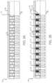
- FIG. 4is a schematic diagram depicting different stages for creating metal BLs in a memory array using a salicide process.
- the metal BLs 130can be created using different technologies.
- metal BLs 130can be created using a salicide process.
- FIG. 4includes a cross-section 405 that shows diffused BLs created during an earlier stage of the fabrication process.
- a plurality of diffused BLs 410 A, 410 B, 410 C, 410 D, and 410 Eare shown.
- trenchescan be etched into a wafer before forming the transistors 120 or building the memory cells 110 .
- the BLs 410 A, 410 B, 410 C, 410 D, and 410 Eare isolated by regions 402 A, 402 B, 402 C, 402 D, 402 E, and 402 F.
- Cross-section 415illustrates deposition of a metal layer 412 on the bottom of the wafer.
- the salicide processcan include deposition of a thin transition metal layer over all or a portion of the bottom layer of the wafer.
- Cross-section 425illustrates the wafer after applying heat to the wafer.
- the wafercan be heated using rapid thermal anneal (RTA), laser spikes, or the like.
- RTArapid thermal anneal
- the heating of the waferallows the metal layer 412 to react with the silicon of the wafer to form a low-resistance transition metal silicide.
- the transition metaldoes not react with regions 402 A, 402 B, 402 C, 402 D, 402 E, and 402 F of the wafer but does react with the diffused BLs 410 A, 410 B, 410 C, 410 D, and 410 E.
- cross-section view 425it can be seen that a portion of the metal layer has interacted with the BLs 410 A, 410 B, 410 C, 410 D, and 410 E.
- Cross-section 435illustrates the wafer after cleaning. Following the reaction of the metal with the wafer caused by the heating, any remaining transition metal is cleaned (e.g., by CMP). Metal silicide 414 A, 414 B, 414 C, 414 D, and 414 E is shown covering BLs 410 A, 410 B, 410 C, 410 D, and 410 E.
- FIG. 5is a schematic diagram depicting different stages for creating metal BLs using a damascene process in a memory array.
- FIG. 5includes a cross-section 505 that shows diffused BLs 130 created during an earlier stage of the fabrication process.
- a plurality of diffused BLs 410 A, 410 B, 410 C, 410 D, and 410 Eare shown.
- trenchescan be etched into a wafer before forming the transistors or building the memory cells.
- the BLs 410 A, 410 B, 410 C, 410 D, and 410 Eare isolated by regions 402 A, 402 B, 402 C, 402 D, 402 E, and 402 F.
- Cross-section 515shows etching a lower portion of the BLs 410 A, 410 B, 410 C, 410 D, and 410 E. As illustrated, the etching removes regions 520 A, 520 B, 520 C, 520 D, and 520 E.
- one or more processesmay be performed to increase the conductivity of the diffused BLs.
- additional doping of the diffused BLscan be performed, in-situ doped silicon may be epitaxially grown (e.g., using vapor-phase epitaxy (VPE), chemical vapor deposition (CVD), . . . ), and the like.
- VPEvapor-phase epitaxy
- CVDchemical vapor deposition
- . . .chemical vapor deposition
- Cross-section 525shows creating a barrier layer (or liner) within the BLs 410 A, 410 B, 410 C, 410 D, and 410 E before depositing metal using the damascene process.
- a silicide processis used to create the barrier layer that is between the top of the regions 520 A, 520 B, 520 C, 520 D, and 520 E and the bottom of the BLs 410 A, 410 B, 410 C, 410 D, and 410 E as illustrated by elements 530 A, 530 B, 530 C, 530 D, and 530 E.
- the barrier layermay cover the walls formed between the BLs 410 A, 410 B, 410 C, 410 D, and 410 E and the regions 402 A, 402 B, 402 C, 402 D, 402 E, and 402 F.
- a barrier layermay not be created when creating metal BLs using the process illustrated in FIG. 5 .
- Cross-section 535shows an area 540 that is filled with a metal using a damascene process.
- copper, tungsten, or other metal or alloyis disposed within area 540 such that the metal overfills the trenches.
- aluminumcan be utilized.
- Cross-section 545shows the wafer after cleaning the wafer to remove the excess metal.
- CMPor other technique, can be used to remove the metal that extends above the top of the trenches such that the metal BLs are isolated as illustrated by regions 550 A, 550 B, 550 C, 550 D, and 550 E.
- Cross-section 555shows the wafer after filling regions adjacent to the metal BLs regions with a low-k dielectric.
- regions 402 A, 402 B, 402 C, 402 D, 402 E, and 402 Fare etched. Regions 560 A, 560 B, 560 C, 560 D, and 560 E are then filled with a low-k dielectric material.
- FIG. 6is a flow diagram showing an example process 600 that illustrates aspects of creating metal BLs 130 in a three-dimensional memory in accordance with examples described herein.
- the process 600may include at 610 creating elements of the memory array.
- the transistors 120 , the memory cell storage elements 110 and the diffused BLs 102 and WLs 104can be created using, for example, shallow trench isolation (STI).
- STIshallow trench isolation
- STIincludes etching the silicon wafer to create trenches that define the BLs and WLs.
- different techniquescan be utilized depending on the type of transistors being created.
- the memory cell storage elements 110may be created using one or more different memory technologies.
- the memory cellsmay include but are not limited FRAM, MRAM, PCM, ReRAM, nanotube, DRAM, and the like.
- the memory cellsare created.
- the memory cellsmay be created using one or more different memory technologies.
- the memory cellsmay include but are not limited to SRAM, DRAM, FRAM, MRAM, PCM, ReRAM, nanotube, and the like.
- an electrical contactmay be created for the layer.
- the electrical contactmay be a metal, such as but not limited to tungsten, or some other metal.
- the metal BLs 130may be used to electrically couple the different layers of the memory array,
- the waferis flipped, and wafer thinning is performed. As discussed above, the wafer is flipped such that the top of the wafer is now the bottom of the wafer, and the bottom of the wafer closest to the bottom surface of the transistors is now the top surface. All or a portion of the material disposed below the bottom surface of the transistors can be back-grinded and/or removed using some other technique or procedure.
- one or more procedurescan be performed after thinning the backside of the wafer.
- additional doping of the diffused BLscan be performed, and/or in-situ doped silicon may be epitaxially grown (e.g., using vapor-phase epitaxy (VPE), chemical vapor deposition (CVD), . . . ).
- VPEvapor-phase epitaxy
- CVDchemical vapor deposition
- the metal BLsare created. As discussed above, the metal BLs are deposited on the bottom side of the wafer. In some examples, the metal BLs 130 are disposed using a salicide process that includes depositing a silicide metal on the bottom of the wafer, performing a heat/anneal process (e.g., using RTA, laser spike), and then removing the portion of the metal such that the BLs are exposed. In other examples, a damascene process can be utilized to create BLs of copper, or some other metal. CMP can be utilized to isolate the metal BLs.
- a salicide processthat includes depositing a silicide metal on the bottom of the wafer, performing a heat/anneal process (e.g., using RTA, laser spike), and then removing the portion of the metal such that the BLs are exposed.
- a damascene processcan be utilized to create BLs of copper, or some other metal.
- CMPcan be utilized to isolate the metal BLs.
- a liner, or barrier layermay be placed before electroplating the metal in the damascene process.
- a barrier layercan be created that includes a dielectric material, such as a low-K dielectric.
- a low-K dielectric materialis a material having a dielectric constant that is lower than the dielectric constant of silicon dioxide.
- the wafercan be bonded to another wafer.
- the wafercan be bound using a variety of different bonding techniques.
- a viais created, and then filled with a metal to electronically couple the metal contacts located on the different layers.
- the different layers of the memorycan be electronically coupled using wires that couple to the metal BLs 130 or some other element within each of the layers.
Landscapes
- Engineering & Computer Science (AREA)
- Microelectronics & Electronic Packaging (AREA)
- Physics & Mathematics (AREA)
- Power Engineering (AREA)
- Condensed Matter Physics & Semiconductors (AREA)
- General Physics & Mathematics (AREA)
- Computer Hardware Design (AREA)
- Manufacturing & Machinery (AREA)
- Geometry (AREA)
- Semiconductor Memories (AREA)
Abstract
Description
Claims (28)
Priority Applications (2)
| Application Number | Priority Date | Filing Date | Title |
|---|---|---|---|
| US18/614,310US12170268B2 (en) | 2019-03-29 | 2024-03-22 | Embedded metal lines |
| US18/911,798US20250038152A1 (en) | 2019-03-29 | 2024-10-10 | Embedded metal lines |
Applications Claiming Priority (4)
| Application Number | Priority Date | Filing Date | Title |
|---|---|---|---|
| US16/369,631US10854578B2 (en) | 2019-03-29 | 2019-03-29 | Diffused bitline replacement in stacked wafer memory |
| US17/107,710US11621246B2 (en) | 2019-03-29 | 2020-11-30 | Diffused bitline replacement in stacked wafer memory |
| US18/145,375US11978724B2 (en) | 2019-03-29 | 2022-12-22 | Diffused bitline replacement in memory |
| US18/614,310US12170268B2 (en) | 2019-03-29 | 2024-03-22 | Embedded metal lines |
Related Parent Applications (1)
| Application Number | Title | Priority Date | Filing Date |
|---|---|---|---|
| US18/145,375ContinuationUS11978724B2 (en) | 2019-03-29 | 2022-12-22 | Diffused bitline replacement in memory |
Related Child Applications (1)
| Application Number | Title | Priority Date | Filing Date |
|---|---|---|---|
| US18/911,798ContinuationUS20250038152A1 (en) | 2019-03-29 | 2024-10-10 | Embedded metal lines |
Publications (2)
| Publication Number | Publication Date |
|---|---|
| US20240266326A1 US20240266326A1 (en) | 2024-08-08 |
| US12170268B2true US12170268B2 (en) | 2024-12-17 |
Family
ID=72604869
Family Applications (5)
| Application Number | Title | Priority Date | Filing Date |
|---|---|---|---|
| US16/369,631ActiveUS10854578B2 (en) | 2019-03-29 | 2019-03-29 | Diffused bitline replacement in stacked wafer memory |
| US17/107,710Active2039-07-12US11621246B2 (en) | 2019-03-29 | 2020-11-30 | Diffused bitline replacement in stacked wafer memory |
| US18/145,375ActiveUS11978724B2 (en) | 2019-03-29 | 2022-12-22 | Diffused bitline replacement in memory |
| US18/614,310ActiveUS12170268B2 (en) | 2019-03-29 | 2024-03-22 | Embedded metal lines |
| US18/911,798PendingUS20250038152A1 (en) | 2019-03-29 | 2024-10-10 | Embedded metal lines |
Family Applications Before (3)
| Application Number | Title | Priority Date | Filing Date |
|---|---|---|---|
| US16/369,631ActiveUS10854578B2 (en) | 2019-03-29 | 2019-03-29 | Diffused bitline replacement in stacked wafer memory |
| US17/107,710Active2039-07-12US11621246B2 (en) | 2019-03-29 | 2020-11-30 | Diffused bitline replacement in stacked wafer memory |
| US18/145,375ActiveUS11978724B2 (en) | 2019-03-29 | 2022-12-22 | Diffused bitline replacement in memory |
Family Applications After (1)
| Application Number | Title | Priority Date | Filing Date |
|---|---|---|---|
| US18/911,798PendingUS20250038152A1 (en) | 2019-03-29 | 2024-10-10 | Embedded metal lines |
Country Status (1)
| Country | Link |
|---|---|
| US (5) | US10854578B2 (en) |
Families Citing this family (77)
| Publication number | Priority date | Publication date | Assignee | Title |
|---|---|---|---|---|
| US7109092B2 (en) | 2003-05-19 | 2006-09-19 | Ziptronix, Inc. | Method of room temperature covalent bonding |
| US8735219B2 (en) | 2012-08-30 | 2014-05-27 | Ziptronix, Inc. | Heterogeneous annealing method and device |
| US10886250B2 (en) | 2015-07-10 | 2021-01-05 | Invensas Corporation | Structures and methods for low temperature bonding using nanoparticles |
| US9953941B2 (en) | 2015-08-25 | 2018-04-24 | Invensas Bonding Technologies, Inc. | Conductive barrier direct hybrid bonding |
| US10204893B2 (en) | 2016-05-19 | 2019-02-12 | Invensas Bonding Technologies, Inc. | Stacked dies and methods for forming bonded structures |
| US11176450B2 (en) | 2017-08-03 | 2021-11-16 | Xcelsis Corporation | Three dimensional circuit implementing machine trained network |
| US10672663B2 (en) | 2016-10-07 | 2020-06-02 | Xcelsis Corporation | 3D chip sharing power circuit |
| US10580735B2 (en) | 2016-10-07 | 2020-03-03 | Xcelsis Corporation | Stacked IC structure with system level wiring on multiple sides of the IC die |
| TWI822659B (en) | 2016-10-27 | 2023-11-21 | 美商艾德亞半導體科技有限責任公司 | Structures and methods for low temperature bonding |
| US10002844B1 (en) | 2016-12-21 | 2018-06-19 | Invensas Bonding Technologies, Inc. | Bonded structures |
| US20180182665A1 (en) | 2016-12-28 | 2018-06-28 | Invensas Bonding Technologies, Inc. | Processed Substrate |
| CN117878055A (en) | 2016-12-28 | 2024-04-12 | 艾德亚半导体接合科技有限公司 | Stacking substrate processing |
| TWI837879B (en) | 2016-12-29 | 2024-04-01 | 美商艾德亞半導體接合科技有限公司 | Bonded structures with integrated passive component |
| WO2018169968A1 (en) | 2017-03-16 | 2018-09-20 | Invensas Corporation | Direct-bonded led arrays and applications |
| US10515913B2 (en) | 2017-03-17 | 2019-12-24 | Invensas Bonding Technologies, Inc. | Multi-metal contact structure |
| US10508030B2 (en) | 2017-03-21 | 2019-12-17 | Invensas Bonding Technologies, Inc. | Seal for microelectronic assembly |
| US10269756B2 (en) | 2017-04-21 | 2019-04-23 | Invensas Bonding Technologies, Inc. | Die processing |
| US10879212B2 (en) | 2017-05-11 | 2020-12-29 | Invensas Bonding Technologies, Inc. | Processed stacked dies |
| US10446441B2 (en) | 2017-06-05 | 2019-10-15 | Invensas Corporation | Flat metal features for microelectronics applications |
| US10217720B2 (en) | 2017-06-15 | 2019-02-26 | Invensas Corporation | Multi-chip modules formed using wafer-level processing of a reconstitute wafer |
| US10840205B2 (en) | 2017-09-24 | 2020-11-17 | Invensas Bonding Technologies, Inc. | Chemical mechanical polishing for hybrid bonding |
| US11031285B2 (en) | 2017-10-06 | 2021-06-08 | Invensas Bonding Technologies, Inc. | Diffusion barrier collar for interconnects |
| US11380597B2 (en) | 2017-12-22 | 2022-07-05 | Invensas Bonding Technologies, Inc. | Bonded structures |
| US10727219B2 (en) | 2018-02-15 | 2020-07-28 | Invensas Bonding Technologies, Inc. | Techniques for processing devices |
| US11169326B2 (en) | 2018-02-26 | 2021-11-09 | Invensas Bonding Technologies, Inc. | Integrated optical waveguides, direct-bonded waveguide interface joints, optical routing and interconnects |
| US11256004B2 (en) | 2018-03-20 | 2022-02-22 | Invensas Bonding Technologies, Inc. | Direct-bonded lamination for improved image clarity in optical devices |
| US10991804B2 (en) | 2018-03-29 | 2021-04-27 | Xcelsis Corporation | Transistor level interconnection methodologies utilizing 3D interconnects |
| US11056348B2 (en) | 2018-04-05 | 2021-07-06 | Invensas Bonding Technologies, Inc. | Bonding surfaces for microelectronics |
| US10790262B2 (en) | 2018-04-11 | 2020-09-29 | Invensas Bonding Technologies, Inc. | Low temperature bonded structures |
| US11244916B2 (en) | 2018-04-11 | 2022-02-08 | Invensas Bonding Technologies, Inc. | Low temperature bonded structures |
| US10964664B2 (en) | 2018-04-20 | 2021-03-30 | Invensas Bonding Technologies, Inc. | DBI to Si bonding for simplified handle wafer |
| US11004757B2 (en) | 2018-05-14 | 2021-05-11 | Invensas Bonding Technologies, Inc. | Bonded structures |
| US11276676B2 (en) | 2018-05-15 | 2022-03-15 | Invensas Bonding Technologies, Inc. | Stacked devices and methods of fabrication |
| US10923413B2 (en) | 2018-05-30 | 2021-02-16 | Xcelsis Corporation | Hard IP blocks with physically bidirectional passageways |
| US11393779B2 (en) | 2018-06-13 | 2022-07-19 | Invensas Bonding Technologies, Inc. | Large metal pads over TSV |
| KR20210009426A (en) | 2018-06-13 | 2021-01-26 | 인벤사스 본딩 테크놀로지스 인코포레이티드 | TV as a pad |
| US10910344B2 (en) | 2018-06-22 | 2021-02-02 | Xcelsis Corporation | Systems and methods for releveled bump planes for chiplets |
| WO2020010056A1 (en) | 2018-07-03 | 2020-01-09 | Invensas Bonding Technologies, Inc. | Techniques for joining dissimilar materials in microelectronics |
| US11158606B2 (en) | 2018-07-06 | 2021-10-26 | Invensas Bonding Technologies, Inc. | Molded direct bonded and interconnected stack |
| US11462419B2 (en) | 2018-07-06 | 2022-10-04 | Invensas Bonding Technologies, Inc. | Microelectronic assemblies |
| US12406959B2 (en) | 2018-07-26 | 2025-09-02 | Adeia Semiconductor Bonding Technologies Inc. | Post CMP processing for hybrid bonding |
| US11515291B2 (en) | 2018-08-28 | 2022-11-29 | Adeia Semiconductor Inc. | Integrated voltage regulator and passive components |
| US20200075533A1 (en) | 2018-08-29 | 2020-03-05 | Invensas Bonding Technologies, Inc. | Bond enhancement in microelectronics by trapping contaminants and arresting cracks during direct-bonding processes |
| US11011494B2 (en) | 2018-08-31 | 2021-05-18 | Invensas Bonding Technologies, Inc. | Layer structures for making direct metal-to-metal bonds at low temperatures in microelectronics |
| US11158573B2 (en) | 2018-10-22 | 2021-10-26 | Invensas Bonding Technologies, Inc. | Interconnect structures |
| US11244920B2 (en) | 2018-12-18 | 2022-02-08 | Invensas Bonding Technologies, Inc. | Method and structures for low temperature device bonding |
| CN113330557A (en) | 2019-01-14 | 2021-08-31 | 伊文萨思粘合技术公司 | Bonding structure |
| US11387202B2 (en) | 2019-03-01 | 2022-07-12 | Invensas Llc | Nanowire bonding interconnect for fine-pitch microelectronics |
| US11901281B2 (en) | 2019-03-11 | 2024-02-13 | Adeia Semiconductor Bonding Technologies Inc. | Bonded structures with integrated passive component |
| US10854578B2 (en) | 2019-03-29 | 2020-12-01 | Invensas Corporation | Diffused bitline replacement in stacked wafer memory |
| US11373963B2 (en) | 2019-04-12 | 2022-06-28 | Invensas Bonding Technologies, Inc. | Protective elements for bonded structures |
| US11205625B2 (en) | 2019-04-12 | 2021-12-21 | Invensas Bonding Technologies, Inc. | Wafer-level bonding of obstructive elements |
| US11355404B2 (en) | 2019-04-22 | 2022-06-07 | Invensas Bonding Technologies, Inc. | Mitigating surface damage of probe pads in preparation for direct bonding of a substrate |
| US11385278B2 (en) | 2019-05-23 | 2022-07-12 | Invensas Bonding Technologies, Inc. | Security circuitry for bonded structures |
| US12374641B2 (en) | 2019-06-12 | 2025-07-29 | Adeia Semiconductor Bonding Technologies Inc. | Sealed bonded structures and methods for forming the same |
| US11296053B2 (en) | 2019-06-26 | 2022-04-05 | Invensas Bonding Technologies, Inc. | Direct bonded stack structures for increased reliability and improved yield in microelectronics |
| US12080672B2 (en) | 2019-09-26 | 2024-09-03 | Adeia Semiconductor Bonding Technologies Inc. | Direct gang bonding methods including directly bonding first element to second element to form bonded structure without adhesive |
| US12113054B2 (en) | 2019-10-21 | 2024-10-08 | Adeia Semiconductor Technologies Llc | Non-volatile dynamic random access memory |
| US11862602B2 (en) | 2019-11-07 | 2024-01-02 | Adeia Semiconductor Technologies Llc | Scalable architecture for reduced cycles across SOC |
| US11762200B2 (en) | 2019-12-17 | 2023-09-19 | Adeia Semiconductor Bonding Technologies Inc. | Bonded optical devices |
| US11876076B2 (en) | 2019-12-20 | 2024-01-16 | Adeia Semiconductor Technologies Llc | Apparatus for non-volatile random access memory stacks |
| CN115088068A (en) | 2019-12-23 | 2022-09-20 | 伊文萨思粘合技术公司 | Electrical redundancy for bonded structures |
| US11721653B2 (en) | 2019-12-23 | 2023-08-08 | Adeia Semiconductor Bonding Technologies Inc. | Circuitry for electrical redundancy in bonded structures |
| WO2021188846A1 (en) | 2020-03-19 | 2021-09-23 | Invensas Bonding Technologies, Inc. | Dimension compensation control for directly bonded structures |
| US11742314B2 (en) | 2020-03-31 | 2023-08-29 | Adeia Semiconductor Bonding Technologies Inc. | Reliable hybrid bonded apparatus |
| WO2021236361A1 (en) | 2020-05-19 | 2021-11-25 | Invensas Bonding Technologies, Inc. | Laterally unconfined structure |
| US11631647B2 (en) | 2020-06-30 | 2023-04-18 | Adeia Semiconductor Bonding Technologies Inc. | Integrated device packages with integrated device die and dummy element |
| US11764177B2 (en) | 2020-09-04 | 2023-09-19 | Adeia Semiconductor Bonding Technologies Inc. | Bonded structure with interconnect structure |
| US11728273B2 (en) | 2020-09-04 | 2023-08-15 | Adeia Semiconductor Bonding Technologies Inc. | Bonded structure with interconnect structure |
| US11264357B1 (en) | 2020-10-20 | 2022-03-01 | Invensas Corporation | Mixed exposure for large die |
| KR20230097121A (en) | 2020-10-29 | 2023-06-30 | 아데이아 세미컨덕터 본딩 테크놀로지스 인코포레이티드 | Direct bonding method and structure |
| JP2024501017A (en) | 2020-12-28 | 2024-01-10 | アデイア セミコンダクター ボンディング テクノロジーズ インコーポレイテッド | Structure with through-substrate via and method for forming the same |
| JP2024501559A (en) | 2020-12-30 | 2024-01-12 | アデイア セミコンダクター ボンディング テクノロジーズ インコーポレイテッド | Structures with conductive features and methods of forming the same |
| KR20240036698A (en) | 2021-08-02 | 2024-03-20 | 아데이아 세미컨덕터 본딩 테크놀로지스 인코포레이티드 | Protective semiconductor elements for combined structures |
| KR20240074385A (en)* | 2022-11-21 | 2024-05-28 | 에스케이하이닉스 주식회사 | Semiconductor device and method for fabricating the same |
| US12341083B2 (en) | 2023-02-08 | 2025-06-24 | Adeia Semiconductor Bonding Technologies Inc. | Electronic device cooling structures bonded to semiconductor elements |
| CN119923958A (en)* | 2023-08-11 | 2025-05-02 | 长江存储科技有限责任公司 | Managing 3D semiconductor devices |
Citations (226)
| Publication number | Priority date | Publication date | Assignee | Title |
|---|---|---|---|---|
| US5753536A (en) | 1994-08-29 | 1998-05-19 | Matsushita Electric Industrial Co., Ltd. | Semiconductor device and associated fabrication method |
| US5771555A (en) | 1993-11-01 | 1998-06-30 | Matsushita Electric Industrial Co., Ltd. | Method for producing an electronic component using direct bonding |
| JP2000114490A (en) | 1998-09-24 | 2000-04-21 | Siemens Ag | Memory cell device and method of manufacturing memory cell device |
| US6080640A (en) | 1997-07-11 | 2000-06-27 | Advanced Micro Devices, Inc. | Metal attachment method and structure for attaching substrates at low temperatures |
| US6423640B1 (en) | 2000-08-09 | 2002-07-23 | Taiwan Semiconductor Manufacturing Co., Ltd. | Headless CMP process for oxide planarization |
| US6465892B1 (en) | 1999-04-13 | 2002-10-15 | Oki Electric Industry Co., Ltd. | Interconnect structure for stacked semiconductor device |
| JP2004063527A (en)* | 2002-07-25 | 2004-02-26 | Elpida Memory Inc | Semiconductor storage device and method of manufacturing the same |
| US20040084414A1 (en) | 2002-08-19 | 2004-05-06 | Kenji Sakai | Polishing method and polishing composition used for polishing |
| US6887769B2 (en) | 2002-02-06 | 2005-05-03 | Intel Corporation | Dielectric recess for wafer-to-wafer and die-to-die metal bonding and method of fabricating the same |
| WO2005043584A2 (en) | 2003-10-21 | 2005-05-12 | Ziptronix, Inc. | Single mask via method and device |
| US6908027B2 (en) | 2003-03-31 | 2005-06-21 | Intel Corporation | Complete device layer transfer without edge exclusion via direct wafer bonding and constrained bond-strengthening process |
| US20060057945A1 (en) | 2004-09-16 | 2006-03-16 | Chia-Lin Hsu | Chemical mechanical polishing process |
| US7045453B2 (en) | 2002-10-24 | 2006-05-16 | International Business Machines Corporation | Very low effective dielectric constant interconnect structures and methods for fabricating the same |
| US7105980B2 (en) | 2002-07-03 | 2006-09-12 | Sawtek, Inc. | Saw filter device and method employing normal temperature bonding for producing desirable filter production and performance characteristics |
| US7120046B1 (en) | 2005-05-13 | 2006-10-10 | Micron Technology, Inc. | Memory array with surrounding gate access transistors and capacitors with global and staggered local bit lines |
| US7193423B1 (en) | 2005-12-12 | 2007-03-20 | International Business Machines Corporation | Wafer-to-wafer alignments |
| US20070111386A1 (en) | 2002-02-20 | 2007-05-17 | Kim Sarah E | Process of vertically stacking multiple wafers supporting different active integrated circuit (IC) devices |
| US20090090950A1 (en)* | 2007-10-05 | 2009-04-09 | Micron Technology, Inc. | Semiconductor devices |
| US7750488B2 (en) | 2006-07-10 | 2010-07-06 | Tezzaron Semiconductor, Inc. | Method for bonding wafers to produce stacked integrated circuits |
| US20100200948A1 (en) | 2009-02-10 | 2010-08-12 | Hynix Semiconductor Inc. | Semiconductor device and fabrication method thereof |
| US7803693B2 (en) | 2007-02-15 | 2010-09-28 | John Trezza | Bowed wafer hybridization compensation |
| US20110079823A1 (en) | 2009-10-04 | 2011-04-07 | Nanya Technology Corporation | Vertical transistor and array of vertical transistor |
| US20120188825A1 (en) | 2011-01-21 | 2012-07-26 | Akira Goda | Memory devices having source lines directly coupled to body regions and methods |
| US20120273940A1 (en)* | 2011-04-29 | 2012-11-01 | Hynix Semiconductor Inc. | Semiconductor apparatus and method for fabricating the same |
| US8349635B1 (en) | 2008-05-20 | 2013-01-08 | Silicon Laboratories Inc. | Encapsulated MEMS device and method to form the same |
| JP2013033786A (en) | 2011-08-01 | 2013-02-14 | Sony Corp | Semiconductor device and semiconductor device manufacturing method |
| US8377798B2 (en) | 2010-11-10 | 2013-02-19 | Taiwan Semiconductor Manufacturing Co., Ltd | Method and structure for wafer to wafer bonding in semiconductor packaging |
| US8441131B2 (en) | 2011-09-12 | 2013-05-14 | Globalfoundries Inc. | Strain-compensating fill patterns for controlling semiconductor chip package interactions |
| US20130161730A1 (en) | 2011-12-23 | 2013-06-27 | Liyang Pan | Memory array structure and method for forming the same |
| US8476165B2 (en) | 2009-04-01 | 2013-07-02 | Tokyo Electron Limited | Method for thinning a bonding wafer |
| US8482132B2 (en) | 2009-10-08 | 2013-07-09 | International Business Machines Corporation | Pad bonding employing a self-aligned plated liner for adhesion enhancement |
| US8501537B2 (en) | 2011-03-31 | 2013-08-06 | Soitec | Methods for bonding semiconductor structures involving annealing processes, and bonded semiconductor structures formed using such methods |
| US8524533B2 (en) | 2003-02-07 | 2013-09-03 | Ziptronix, Inc. | Room temperature metal direct bonding |
| US8620164B2 (en) | 2011-01-20 | 2013-12-31 | Intel Corporation | Hybrid III-V silicon laser formed by direct bonding |
| US8647987B2 (en) | 2012-04-16 | 2014-02-11 | The Institute of Microelectronics, Chinese Academy of Science | Method for improving uniformity of chemical-mechanical planarization process |
| US8697493B2 (en) | 2011-07-18 | 2014-04-15 | Soitec | Bonding surfaces for direct bonding of semiconductor structures |
| US8716105B2 (en) | 2011-03-31 | 2014-05-06 | Soitec | Methods for bonding semiconductor structures involving annealing processes, and bonded semiconductor structures and intermediate structures formed using such methods |
| US20140175655A1 (en) | 2012-12-22 | 2014-06-26 | Industrial Technology Research Institute | Chip bonding structure and manufacturing method thereof |
| US8802538B1 (en) | 2013-03-15 | 2014-08-12 | Taiwan Semiconductor Manufacturing Company, Ltd. | Methods for hybrid wafer bonding |
| US8809123B2 (en) | 2012-06-05 | 2014-08-19 | Taiwan Semiconductor Manufacturing Company, Ltd. | Three dimensional integrated circuit structures and hybrid bonding methods for semiconductor wafers |
| US8841002B2 (en) | 2003-05-19 | 2014-09-23 | Ziptronix, Inc. | Method of room temperature covalent bonding |
| US9093350B2 (en) | 2010-07-09 | 2015-07-28 | Canon Kabushiki Kaisha | Member for solid-state image pickup device and method for manufacturing solid-state image pickup device having first and second wiring structures with a concave portion between first and second substrates |
| US9142517B2 (en) | 2012-06-05 | 2015-09-22 | Taiwan Semiconductor Manufacturing Company, Ltd. | Hybrid bonding mechanisms for semiconductor wafers |
| US9171756B2 (en) | 2005-08-11 | 2015-10-27 | Ziptronix, Inc. | 3D IC method and device |
| US9184125B2 (en) | 2012-08-30 | 2015-11-10 | Ziptronix, Inc. | Heterogeneous annealing method and device |
| US20150349056A1 (en) | 2014-06-02 | 2015-12-03 | Infineon Technologies Austria Ag | Semiconductor device comprising trench structures |
| US9224704B2 (en) | 2010-10-14 | 2015-12-29 | Soitec | Process for realizing a connecting structure |
| US9230941B2 (en) | 2014-03-28 | 2016-01-05 | Taiwan Semiconductor Manufacturing Company, Ltd. | Bonding structure for stacked semiconductor devices |
| US20160013129A1 (en)* | 2014-07-14 | 2016-01-14 | Kabushiki Kaisha Toshiba | Semiconductor memory device |
| US9257399B2 (en) | 2013-10-17 | 2016-02-09 | Taiwan Semiconductor Manufacturing Company, Ltd. | 3D integrated circuit and methods of forming the same |
| US9299736B2 (en) | 2014-03-28 | 2016-03-29 | Taiwan Semiconductor Manufacturing Company, Ltd. | Hybrid bonding with uniform pattern density |
| US9312229B2 (en) | 2013-03-15 | 2016-04-12 | Taiwan Semiconductor Manufacturing Company, Ltd. | Hybrid bonding with air-gap structure |
| US9331149B2 (en) | 2000-02-16 | 2016-05-03 | Ziptronix, Inc. | Method for low temperature bonding and bonded structure |
| US9337235B2 (en) | 2013-02-18 | 2016-05-10 | Taiwan Semiconductor Manufacturing Company, Ltd. | Method and apparatus for image sensor packaging |
| US9394161B2 (en) | 2014-11-14 | 2016-07-19 | Taiwan Semiconductor Manufacturing Co., Ltd. | MEMS and CMOS integration with low-temperature bonding |
| US9431368B2 (en) | 1999-10-01 | 2016-08-30 | Ziptronix, Inc. | Three dimensional device integration method and integrated device |
| US9437572B2 (en) | 2013-12-18 | 2016-09-06 | Taiwan Semiconductor Manufacturing Company, Ltd. | Conductive pad structure for hybrid bonding and methods of forming same |
| US9461007B2 (en) | 2014-07-11 | 2016-10-04 | Samsung Electronics Co., Ltd. | Wafer-to-wafer bonding structure |
| US9496239B1 (en) | 2015-12-11 | 2016-11-15 | International Business Machines Corporation | Nitride-enriched oxide-to-oxide 3D wafer bonding |
| US20160343682A1 (en) | 2013-12-11 | 2016-11-24 | Kabushiki Kaisha Toshiba | Semiconductor device |
| US9536848B2 (en) | 2014-10-16 | 2017-01-03 | Globalfoundries Inc. | Bond pad structure for low temperature flip chip bonding |
| US9559081B1 (en) | 2015-08-21 | 2017-01-31 | Apple Inc. | Independent 3D stacking |
| US9620481B2 (en) | 2013-05-30 | 2017-04-11 | Globalfoundries Inc. | Substrate bonding with diffusion barrier structures |
| US9656852B2 (en) | 2015-07-06 | 2017-05-23 | Taiwan Semiconductor Manufacturing Company Ltd. | CMOS-MEMS device structure, bonding mesa structure and associated method |
| US9666256B1 (en) | 2016-03-15 | 2017-05-30 | National Tsing Hua University | Spin-orbit torque magnetic random access memory and method of writing the same |
| US9723716B2 (en) | 2013-09-27 | 2017-08-01 | Infineon Technologies Ag | Contact pad structure, an electronic component, and a method for manufacturing a contact pad structure |
| US9728521B2 (en) | 2015-07-23 | 2017-08-08 | Taiwan Semiconductor Manufacturing Co., Ltd. | Hybrid bond using a copper alloy for yield improvement |
| US9741620B2 (en) | 2015-06-24 | 2017-08-22 | Invensas Corporation | Structures and methods for reliable packages |
| US20170287978A1 (en) | 2016-04-05 | 2017-10-05 | Globalfoundries Singapore Pte. Ltd. | Domain wall magnetic memory |
| US9799587B2 (en) | 2011-05-24 | 2017-10-24 | Sony Corporation | Semiconductor device |
| US20170358598A1 (en) | 2016-06-08 | 2017-12-14 | Micron Technology, Inc. | Memory Cells Comprising A Programmable Field Effect Transistor Having A Reversibly Programmable Gate Insulator |
| US9852988B2 (en) | 2015-12-18 | 2017-12-26 | Invensas Bonding Technologies, Inc. | Increased contact alignment tolerance for direct bonding |
| US9893004B2 (en) | 2011-07-27 | 2018-02-13 | Broadpak Corporation | Semiconductor interposer integration |
| US9899442B2 (en) | 2014-12-11 | 2018-02-20 | Invensas Corporation | Image sensor device |
| US9929050B2 (en) | 2013-07-16 | 2018-03-27 | Taiwan Semiconductor Manufacturing Company, Ltd. | Mechanisms for forming three-dimensional integrated circuit (3DIC) stacking structure |
| US9941243B2 (en) | 2016-06-09 | 2018-04-10 | Samsung Electronics Co., Ltd. | Wafer-to-wafer bonding structure |
| US9941241B2 (en) | 2016-06-30 | 2018-04-10 | International Business Machines Corporation | Method for wafer-wafer bonding |
| US9953941B2 (en) | 2015-08-25 | 2018-04-24 | Invensas Bonding Technologies, Inc. | Conductive barrier direct hybrid bonding |
| US20180145011A1 (en)* | 2013-07-16 | 2018-05-24 | Taiwan Semiconductor Manufacturing Co., Ltd. | Front-to-back bonding with through-substrate via (tsv) |
| US10002844B1 (en) | 2016-12-21 | 2018-06-19 | Invensas Bonding Technologies, Inc. | Bonded structures |
| US20180175012A1 (en) | 2016-12-15 | 2018-06-21 | Taiwan Semiconductor Manufacturing Co., Ltd. | Seal ring structures and methods of forming same |
| US20180182666A1 (en) | 2016-12-28 | 2018-06-28 | Invensas Bonding Technologies, Inc. | Microelectronic assembly from processed substrate |
| US20180182639A1 (en) | 2016-12-28 | 2018-06-28 | Invensas Bonding Technologies, Inc. | Processing Stacked Substrates |
| US20180190580A1 (en) | 2016-12-29 | 2018-07-05 | Invensas Bonding Technologies, Inc. | Bonded structures with integrated passive component |
| US20180190583A1 (en) | 2016-12-29 | 2018-07-05 | Invensas Bonding Technologies, Inc. | Bonded structures with integrated passive component |
| US10026605B2 (en) | 2014-06-04 | 2018-07-17 | Semiconductor Components Industries, Llc | Method of reducing residual contamination in singulated semiconductor die |
| US20180219038A1 (en) | 2017-02-01 | 2018-08-02 | Semiconductor Components Industries, Llc | Edge seals for semiconductor packages |
| US10075657B2 (en) | 2015-07-21 | 2018-09-11 | Fermi Research Alliance, Llc | Edgeless large area camera system |
| JP2018160519A (en) | 2017-03-22 | 2018-10-11 | 東芝メモリ株式会社 | Semiconductor device manufacturing method and semiconductor device |
| US10115770B2 (en) | 2017-02-28 | 2018-10-30 | Sandisk Technologies Llc | Methods and apparatus for three-dimensional nonvolatile memory |
| US20180323227A1 (en) | 2017-05-03 | 2018-11-08 | United Microelectronics Corp. | Wafer level packaging method |
| US20180323177A1 (en) | 2016-04-15 | 2018-11-08 | Taiwan Semiconductor Manufacturing Company, Ltd. | 3DIC Formation with Dies Bonded to Formed RDLs |
| US20180331066A1 (en) | 2017-05-11 | 2018-11-15 | Invensas Bonding Technologies, Inc. | Processed stacked dies |
| US10204893B2 (en) | 2016-05-19 | 2019-02-12 | Invensas Bonding Technologies, Inc. | Stacked dies and methods for forming bonded structures |
| US20190074277A1 (en) | 2017-09-06 | 2019-03-07 | Micron Technology, Inc. | Memory Arrays Comprising Vertically-Alternating Tiers Of Insulative Material And Memory Cells And Methods Of Forming A Memory Array |
| US20190115277A1 (en) | 2016-12-05 | 2019-04-18 | Taiwan Semiconductor Manufacturing Company, Ltd. | Package Structure for Heat Dissipation |
| US10269756B2 (en) | 2017-04-21 | 2019-04-23 | Invensas Bonding Technologies, Inc. | Die processing |
| US10276909B2 (en) | 2016-12-30 | 2019-04-30 | Invensas Bonding Technologies, Inc. | Structure comprising at least a first element bonded to a carrier having a closed metallic channel waveguide formed therein |
| US10276619B2 (en) | 2016-01-12 | 2019-04-30 | Taiwan Semiconductor Manufacturing Co., Ltd. | Semiconductor device structure with a conductive feature passing through a passivation layer |
| US20190131277A1 (en) | 2017-11-01 | 2019-05-02 | Taiwan Semiconductor Manufacturing Co., Ltd. | Die stack structure and method of fabricating the same and package |
| CN109979919A (en) | 2017-12-27 | 2019-07-05 | 华为技术有限公司 | A kind of chip and electronic equipment |
| US10418277B2 (en) | 2016-08-09 | 2019-09-17 | International Business Machines Corporation | Air gap spacer formation for nano-scale semiconductor devices |
| US10446456B2 (en) | 2014-03-12 | 2019-10-15 | Invensas Corporation | Integrated circuits protected by substrates with cavities, and methods of manufacture |
| US10446532B2 (en) | 2016-01-13 | 2019-10-15 | Invensas Bonding Technologies, Inc. | Systems and methods for efficient transfer of semiconductor elements |
| US10446487B2 (en) | 2016-09-30 | 2019-10-15 | Invensas Bonding Technologies, Inc. | Interface structures and methods for forming same |
| US20190333550A1 (en) | 2018-04-30 | 2019-10-31 | Invensas Corporation | Multi-die module with low power operation |
| US10508030B2 (en) | 2017-03-21 | 2019-12-17 | Invensas Bonding Technologies, Inc. | Seal for microelectronic assembly |
| US20190385935A1 (en) | 2018-06-13 | 2019-12-19 | Invensas Bonding Technologies, Inc. | Tsv as pad |
| US10522499B2 (en) | 2017-02-09 | 2019-12-31 | Invensas Bonding Technologies, Inc. | Bonded structures |
| US20200013765A1 (en) | 2018-07-03 | 2020-01-09 | Invensas Bonding Technologies, Inc. | Techniques for joining dissimilar materials in microelectronics |
| US20200035641A1 (en) | 2018-07-26 | 2020-01-30 | Invensas Bonding Technologies, Inc. | Post cmp processing for hybrid bonding |
| US20200075553A1 (en) | 2018-08-28 | 2020-03-05 | Xcelsis Corporation | Integrated voltage regulator and passive components |
| US20200294908A1 (en) | 2019-03-11 | 2020-09-17 | Invensas Bonding Technologies, Inc. | Bonded structures with integrated passive component |
| US10784191B2 (en) | 2017-03-31 | 2020-09-22 | Invensas Bonding Technologies, Inc. | Interface structures and methods for forming same |
| US10790262B2 (en) | 2018-04-11 | 2020-09-29 | Invensas Bonding Technologies, Inc. | Low temperature bonded structures |
| US20200328162A1 (en) | 2019-04-12 | 2020-10-15 | Invensas Bonding Technologies, Inc. | Protective elements for bonded structures |
| US10840205B2 (en) | 2017-09-24 | 2020-11-17 | Invensas Bonding Technologies, Inc. | Chemical mechanical polishing for hybrid bonding |
| US10840135B2 (en) | 2017-06-05 | 2020-11-17 | Invensas Corporation | Flat metal features for microelectronics applications |
| US10854578B2 (en) | 2019-03-29 | 2020-12-01 | Invensas Corporation | Diffused bitline replacement in stacked wafer memory |
| US20200395321A1 (en) | 2019-06-12 | 2020-12-17 | Invensas Bonding Technologies, Inc. | Sealed bonded structures and methods for forming the same |
| US20200411483A1 (en) | 2019-06-26 | 2020-12-31 | Invensas Bonding Technologies, Inc. | Direct bonded stack structures for increased reliability and improved yield in microelectronics |
| US10886177B2 (en) | 2016-10-07 | 2021-01-05 | Xcelsis Corporation | 3D chip with shared clock distribution network |
| US10892246B2 (en) | 2015-07-10 | 2021-01-12 | Invensas Corporation | Structures and methods for low temperature bonding using nanoparticles |
| US10923408B2 (en) | 2017-12-22 | 2021-02-16 | Invensas Bonding Technologies, Inc. | Cavity packages |
| US10923413B2 (en) | 2018-05-30 | 2021-02-16 | Xcelsis Corporation | Hard IP blocks with physically bidirectional passageways |
| US10950547B2 (en) | 2016-10-07 | 2021-03-16 | Xcelsis Corporation | Stacked IC structure with system level wiring on multiple sides of the IC die |
| US10964664B2 (en) | 2018-04-20 | 2021-03-30 | Invensas Bonding Technologies, Inc. | DBI to Si bonding for simplified handle wafer |
| US20210098412A1 (en) | 2019-09-26 | 2021-04-01 | Invensas Bonding Technologies, Inc. | Direct gang bonding methods and structures |
| US20210118864A1 (en) | 2019-10-21 | 2021-04-22 | Invensas Corporation | Non-Volatile Dynamic Random Access Memory |
| US10991804B2 (en) | 2018-03-29 | 2021-04-27 | Xcelsis Corporation | Transistor level interconnection methodologies utilizing 3D interconnects |
| US11004757B2 (en) | 2018-05-14 | 2021-05-11 | Invensas Bonding Technologies, Inc. | Bonded structures |
| US20210143125A1 (en) | 2019-11-07 | 2021-05-13 | Invensas Corporation | Scalable Architecture for Reduced Cycles Across SoC |
| US11011503B2 (en) | 2017-12-15 | 2021-05-18 | Invensas Bonding Technologies, Inc. | Direct-bonded optoelectronic interconnect for high-density integrated photonics |
| US11011494B2 (en) | 2018-08-31 | 2021-05-18 | Invensas Bonding Technologies, Inc. | Layer structures for making direct metal-to-metal bonds at low temperatures in microelectronics |
| US11031285B2 (en) | 2017-10-06 | 2021-06-08 | Invensas Bonding Technologies, Inc. | Diffusion barrier collar for interconnects |
| US11037919B2 (en) | 2018-02-15 | 2021-06-15 | Invensas Bonding Technologies, Inc. | Techniques for processing devices |
| US20210181510A1 (en) | 2019-12-17 | 2021-06-17 | Invensas Bonding Technologies, Inc. | Bonded optical devices |
| US20210193603A1 (en) | 2019-12-23 | 2021-06-24 | Invensas Bonding Technologies, Inc. | Circuitry for electrical redundancy in bonded structures |
| US20210193625A1 (en) | 2019-12-23 | 2021-06-24 | Invensas Bonding Technologies, Inc. | Electrical redundancy for bonded structures |
| US20210193624A1 (en) | 2019-12-20 | 2021-06-24 | Invensas Corporation | Apparatus For Non-Volatile Random Access Memory Stacks |
| US11056348B2 (en) | 2018-04-05 | 2021-07-06 | Invensas Bonding Technologies, Inc. | Bonding surfaces for microelectronics |
| US11069734B2 (en) | 2014-12-11 | 2021-07-20 | Invensas Corporation | Image sensor device |
| US20210242152A1 (en) | 2020-02-05 | 2021-08-05 | Invensas Bonding Technologies, Inc. | Selective alteration of interconnect pads for direct bonding |
| US11088099B2 (en) | 2017-03-17 | 2021-08-10 | Invensas Bonding Technologies, Inc. | Multi-metal contact structure in microelectronic component |
| US11127738B2 (en) | 2018-02-09 | 2021-09-21 | Xcelsis Corporation | Back biasing of FD-SOI circuit blocks |
| US20210296282A1 (en) | 2020-03-19 | 2021-09-23 | Invensas Bonding Technologies, Inc. | Dimension compensation control for directly bonded structures |
| US20210305202A1 (en) | 2020-03-31 | 2021-09-30 | Invensas Bonding Technologies, Inc. | Reliable hybrid bonded apparatus |
| US11158606B2 (en) | 2018-07-06 | 2021-10-26 | Invensas Bonding Technologies, Inc. | Molded direct bonded and interconnected stack |
| US11158573B2 (en) | 2018-10-22 | 2021-10-26 | Invensas Bonding Technologies, Inc. | Interconnect structures |
| US11169326B2 (en) | 2018-02-26 | 2021-11-09 | Invensas Bonding Technologies, Inc. | Integrated optical waveguides, direct-bonded waveguide interface joints, optical routing and interconnects |
| US11171117B2 (en) | 2018-06-12 | 2021-11-09 | Invensas Bonding Technologies, Inc. | Interlayer connection of stacked microelectronic components |
| US11176450B2 (en) | 2017-08-03 | 2021-11-16 | Xcelsis Corporation | Three dimensional circuit implementing machine trained network |
| US20210366820A1 (en) | 2020-05-19 | 2021-11-25 | Invensas Bonding Technologies, Inc. | Laterally unconfined structure |
| US11195748B2 (en) | 2017-09-27 | 2021-12-07 | Invensas Corporation | Interconnect structures and methods for forming same |
| US11205625B2 (en) | 2019-04-12 | 2021-12-21 | Invensas Bonding Technologies, Inc. | Wafer-level bonding of obstructive elements |
| US20210407941A1 (en) | 2020-06-30 | 2021-12-30 | Invensas Bonding Technologies, Inc. | Integrated device packages |
| US11244920B2 (en) | 2018-12-18 | 2022-02-08 | Invensas Bonding Technologies, Inc. | Method and structures for low temperature device bonding |
| US11256004B2 (en) | 2018-03-20 | 2022-02-22 | Invensas Bonding Technologies, Inc. | Direct-bonded lamination for improved image clarity in optical devices |
| US11264357B1 (en) | 2020-10-20 | 2022-03-01 | Invensas Corporation | Mixed exposure for large die |
| US20220077063A1 (en) | 2020-09-04 | 2022-03-10 | Invensas Bonding Technologies, Inc. | Bonded structure with interconnect structure |
| US20220077087A1 (en) | 2020-09-04 | 2022-03-10 | Invensas Bonding Technologies, Inc. | Bonded structure with interconnect structure |
| US11276676B2 (en) | 2018-05-15 | 2022-03-15 | Invensas Bonding Technologies, Inc. | Stacked devices and methods of fabrication |
| US11296044B2 (en) | 2018-08-29 | 2022-04-05 | Invensas Bonding Technologies, Inc. | Bond enhancement structure in microelectronics for trapping contaminants during direct-bonding processes |
| US20220139867A1 (en) | 2020-10-29 | 2022-05-05 | Invensas Bonding Technologies, Inc. | Direct bonding methods and structures |
| US20220139869A1 (en) | 2020-10-29 | 2022-05-05 | Invensas Bonding Technologies, Inc. | Direct bonding methods and structures |
| US11329034B2 (en) | 2017-03-16 | 2022-05-10 | Invensas Corporation | Direct-bonded LED structure contacts and substrate contacts |
| US11348898B2 (en) | 2018-06-22 | 2022-05-31 | Xcelsis Corporation | Systems and methods for releveled bump planes for chiplets |
| US11355443B2 (en) | 2018-05-03 | 2022-06-07 | Invensas Corporation | Dielets on flexible and stretchable packaging for microelectronics |
| US11355404B2 (en) | 2019-04-22 | 2022-06-07 | Invensas Bonding Technologies, Inc. | Mitigating surface damage of probe pads in preparation for direct bonding of a substrate |
| US11373963B2 (en) | 2019-04-12 | 2022-06-28 | Invensas Bonding Technologies, Inc. | Protective elements for bonded structures |
| US20220208723A1 (en) | 2020-12-30 | 2022-06-30 | Invensas Bonding Technologies, Inc. | Directly bonded structures |
| US20220208650A1 (en) | 2020-12-28 | 2022-06-30 | Invensas Bonding Technologies, Inc. | Structures with through-substrate vias and methods for forming the same |
| US20220208702A1 (en) | 2020-12-30 | 2022-06-30 | Invensas Bonding Technologies, Inc. | Structure with conductive feature and method of forming same |
| US11380597B2 (en) | 2017-12-22 | 2022-07-05 | Invensas Bonding Technologies, Inc. | Bonded structures |
| US11387202B2 (en) | 2019-03-01 | 2022-07-12 | Invensas Llc | Nanowire bonding interconnect for fine-pitch microelectronics |
| US11385278B2 (en) | 2019-05-23 | 2022-07-12 | Invensas Bonding Technologies, Inc. | Security circuitry for bonded structures |
| US11387214B2 (en) | 2017-06-15 | 2022-07-12 | Invensas Llc | Multi-chip modules formed using wafer-level processing of a reconstituted wafer |
| US11393779B2 (en) | 2018-06-13 | 2022-07-19 | Invensas Bonding Technologies, Inc. | Large metal pads over TSV |
| US20220246497A1 (en) | 2020-12-28 | 2022-08-04 | Invensas Bonding Technologies, Inc. | Structures with through-substrate vias and methods for forming the same |
| US20220285303A1 (en) | 2021-03-03 | 2022-09-08 | Invensas Bonding Technologies, Inc. | Contact structures for direct bonding |
| US11462419B2 (en) | 2018-07-06 | 2022-10-04 | Invensas Bonding Technologies, Inc. | Microelectronic assemblies |
| US20220320035A1 (en) | 2021-03-31 | 2022-10-06 | Invensas Bonding Technologies, Inc. | Direct bonding methods and structures |
| US20220319901A1 (en) | 2021-03-31 | 2022-10-06 | Invensas Bonding Technologies, Inc. | Direct bonding and debonding of carrier |
| US20220320036A1 (en) | 2021-03-31 | 2022-10-06 | Invensas Bonding Technologies, Inc. | Direct bonding and debonding of carrier |
| US11476213B2 (en) | 2019-01-14 | 2022-10-18 | Invensas Bonding Technologies, Inc. | Bonded structures without intervening adhesive |
| US20230005850A1 (en) | 2021-06-30 | 2023-01-05 | Invensas Bonding Technologies, Inc. | Element with routing structure in bonding layer |
| US20230019869A1 (en) | 2021-07-16 | 2023-01-19 | Invensas Bonding Technologies, Inc. | Optically occlusive protective element for bonded structures |
| US20230036441A1 (en) | 2021-08-02 | 2023-02-02 | Invensas Bonding Technologies, Inc. | Protective semiconductor elements for bonded structures |
| US20230069183A1 (en) | 2021-09-01 | 2023-03-02 | Invensas Llc | Stacked structure with interposer |
| US20230067677A1 (en) | 2021-09-01 | 2023-03-02 | Invensas Bonding Technologies, Inc. | Sequences and equipment for direct bonding |
| US20230100032A1 (en) | 2021-09-24 | 2023-03-30 | Adeia Semiconductor Bonding Technologies Inc. | Bonded structure with active interposer |
| US20230115122A1 (en) | 2021-09-14 | 2023-04-13 | Adeia Semiconductor Bonding Technologies Inc. | Method of bonding thin substrates |
| US20230123423A1 (en) | 2021-10-19 | 2023-04-20 | Adeia Semiconductor Bonding Technologies Inc | Stacked inductors in multi-die stacking |
| US20230122531A1 (en) | 2021-10-18 | 2023-04-20 | Invensas Llc | Reduced parasitic capacitance in bonded structures |
| US20230130259A1 (en) | 2021-10-22 | 2023-04-27 | Invensas Llc | Radio frequency device packages |
| US20230125395A1 (en) | 2021-10-27 | 2023-04-27 | Adeia Semiconductor Bonding Technologies Inc. | Stacked structures with capacitive coupling connections |
| US20230132632A1 (en) | 2021-10-28 | 2023-05-04 | Adeia Semiconductor Bonding Technologies Inc. | Diffusion barriers and method of forming same |
| US20230140107A1 (en) | 2021-10-28 | 2023-05-04 | Adeia Semiconductor Bonding Technologies Inc. | Direct bonding methods and structures |
| US20230142680A1 (en) | 2021-10-28 | 2023-05-11 | Adeia Semiconductor Bonding Technologies Inc. | Stacked electronic devices |
| US20230154816A1 (en) | 2021-11-17 | 2023-05-18 | Adeia Semiconductor Bonding Technologies Inc. | Thermal bypass for stacked dies |
| US20230154828A1 (en) | 2021-11-18 | 2023-05-18 | Adeia Semiconductor Bonding Technologies Inc. | Fluid cooling for die stacks |
| US20230187317A1 (en) | 2021-12-13 | 2023-06-15 | Adeia Semiconductor Bonding Technologies Inc. | Interconnect structures |
| US20230187264A1 (en) | 2021-12-13 | 2023-06-15 | Adeia Semiconductor Technologies Llc | Methods for bonding semiconductor elements |
| US20230187412A1 (en) | 2021-10-25 | 2023-06-15 | Adeia Semiconductor Bonding Technologies Inc. | Power distribution for stacked electronic devices |
| US20230197560A1 (en) | 2021-12-20 | 2023-06-22 | Adeia Semiconductor Bonding Technologies Inc. | Thermoelectric cooling in microelectronics |
| US20230197496A1 (en) | 2021-12-20 | 2023-06-22 | Adeia Semiconductor Bonding Technologies Inc. | Direct bonding and debonding of elements |
| US20230197559A1 (en) | 2021-12-20 | 2023-06-22 | Adeia Semiconductor Bonding Technologies Inc. | Thermoelectric cooling for die packages |
| US20230197655A1 (en) | 2021-12-22 | 2023-06-22 | Adeia Semiconductor Bonding Technologies Inc. | Low stress direct hybrid bonding |
| US20230197453A1 (en) | 2021-12-17 | 2023-06-22 | Adeia Semiconductor Bonding Technologies Inc. | Structure with conductive feature for direct bonding and method of forming same |
| US20230207437A1 (en) | 2021-11-05 | 2023-06-29 | Adeia Semiconductor Bonding Technologies Inc. | Multi-channel device stacking |
| US20230207402A1 (en) | 2021-12-27 | 2023-06-29 | Adeia Semiconductor Bonding Technologies Inc. | Directly bonded frame wafers |
| US20230207474A1 (en) | 2021-12-23 | 2023-06-29 | Adeia Semiconductor Bonding Technologies Inc. | Bonded structures with interconnect assemblies |
| US20230207514A1 (en) | 2021-12-23 | 2023-06-29 | Adeia Semiconductor Bonding Technologies Inc. | Apparatuses and methods for die bond control |
| US20230215836A1 (en) | 2021-12-23 | 2023-07-06 | Adeia Semiconductor Bonding Technologies Inc. | Direct bonding on package substrates |
| US20230245950A1 (en) | 2022-01-31 | 2023-08-03 | Adeia Semiconductor Bonding Technologies Inc. | Heat dissipating system for electronic devices |
| US20230268300A1 (en) | 2022-02-24 | 2023-08-24 | Adeia Semiconductor Bonding Technologies Inc. | Bonded structures |
| US20230299029A1 (en) | 2022-03-16 | 2023-09-21 | Adeia Semiconductor Bonding Technologies Inc. | Expansion control for bonding |
| US20230343734A1 (en) | 2022-04-25 | 2023-10-26 | Adeia Semiconductor Bonding Technologies Inc. | Expansion controlled structure for direct bonding and method of forming same |
| US20230361074A1 (en) | 2022-05-05 | 2023-11-09 | Adeia Semiconductor Bonding Technologies Inc. | Low temperature direct bonding |
| US20230360950A1 (en) | 2022-05-05 | 2023-11-09 | Adeia Semiconductor Bonding Technologies Inc. | Gang-flipping of dies prior to bonding |
| US20230369136A1 (en) | 2022-05-13 | 2023-11-16 | Adeia Semiconductor Bonding Technologies Inc. | Bonding surface validation on dicing tape |
| US20230375613A1 (en) | 2022-05-23 | 2023-11-23 | Adeia Semiconductor Bonding Technologies Inc. | Testing elements for bonded structures |
| US20240038702A1 (en) | 2022-07-27 | 2024-02-01 | Adeia Semiconductor Bonding Technologies Inc. | High-performance hybrid bonded interconnect systems |
| US20240055407A1 (en) | 2022-08-11 | 2024-02-15 | Adeia Semiconductor Bonding Technologies Inc. | Bonded debugging elements for integrated circuits and methods for debugging integrated circuits using same |
| US20240079376A1 (en) | 2022-09-07 | 2024-03-07 | Adeia Semiconductor Bonding Technologies Inc. | Rapid thermal processing for direct bonding |
| US20240105674A1 (en) | 2022-09-07 | 2024-03-28 | Adeia Semiconductor Bonding Technologies Inc. | Bonded structure and method of forming same |
- 2019
- 2019-03-29USUS16/369,631patent/US10854578B2/enactiveActive
- 2020
- 2020-11-30USUS17/107,710patent/US11621246B2/enactiveActive
- 2022
- 2022-12-22USUS18/145,375patent/US11978724B2/enactiveActive
- 2024
- 2024-03-22USUS18/614,310patent/US12170268B2/enactiveActive
- 2024-10-10USUS18/911,798patent/US20250038152A1/enactivePending
Patent Citations (239)
| Publication number | Priority date | Publication date | Assignee | Title |
|---|---|---|---|---|
| US5771555A (en) | 1993-11-01 | 1998-06-30 | Matsushita Electric Industrial Co., Ltd. | Method for producing an electronic component using direct bonding |
| US5753536A (en) | 1994-08-29 | 1998-05-19 | Matsushita Electric Industrial Co., Ltd. | Semiconductor device and associated fabrication method |
| US6080640A (en) | 1997-07-11 | 2000-06-27 | Advanced Micro Devices, Inc. | Metal attachment method and structure for attaching substrates at low temperatures |
| JP2000114490A (en) | 1998-09-24 | 2000-04-21 | Siemens Ag | Memory cell device and method of manufacturing memory cell device |
| US6465892B1 (en) | 1999-04-13 | 2002-10-15 | Oki Electric Industry Co., Ltd. | Interconnect structure for stacked semiconductor device |
| US9431368B2 (en) | 1999-10-01 | 2016-08-30 | Ziptronix, Inc. | Three dimensional device integration method and integrated device |
| US9331149B2 (en) | 2000-02-16 | 2016-05-03 | Ziptronix, Inc. | Method for low temperature bonding and bonded structure |
| US6423640B1 (en) | 2000-08-09 | 2002-07-23 | Taiwan Semiconductor Manufacturing Co., Ltd. | Headless CMP process for oxide planarization |
| US6887769B2 (en) | 2002-02-06 | 2005-05-03 | Intel Corporation | Dielectric recess for wafer-to-wafer and die-to-die metal bonding and method of fabricating the same |
| US20070111386A1 (en) | 2002-02-20 | 2007-05-17 | Kim Sarah E | Process of vertically stacking multiple wafers supporting different active integrated circuit (IC) devices |
| US7105980B2 (en) | 2002-07-03 | 2006-09-12 | Sawtek, Inc. | Saw filter device and method employing normal temperature bonding for producing desirable filter production and performance characteristics |
| JP2004063527A (en)* | 2002-07-25 | 2004-02-26 | Elpida Memory Inc | Semiconductor storage device and method of manufacturing the same |
| US20040084414A1 (en) | 2002-08-19 | 2004-05-06 | Kenji Sakai | Polishing method and polishing composition used for polishing |
| US7045453B2 (en) | 2002-10-24 | 2006-05-16 | International Business Machines Corporation | Very low effective dielectric constant interconnect structures and methods for fabricating the same |
| US8524533B2 (en) | 2003-02-07 | 2013-09-03 | Ziptronix, Inc. | Room temperature metal direct bonding |
| US9385024B2 (en) | 2003-02-07 | 2016-07-05 | Ziptronix, Inc. | Room temperature metal direct bonding |
| US6908027B2 (en) | 2003-03-31 | 2005-06-21 | Intel Corporation | Complete device layer transfer without edge exclusion via direct wafer bonding and constrained bond-strengthening process |
| US8841002B2 (en) | 2003-05-19 | 2014-09-23 | Ziptronix, Inc. | Method of room temperature covalent bonding |
| US20150064498A1 (en) | 2003-05-19 | 2015-03-05 | Ziptronix, Inc. | Method of room temperature covalent bonding |
| WO2005043584A2 (en) | 2003-10-21 | 2005-05-12 | Ziptronix, Inc. | Single mask via method and device |
| US20060057945A1 (en) | 2004-09-16 | 2006-03-16 | Chia-Lin Hsu | Chemical mechanical polishing process |
| US7120046B1 (en) | 2005-05-13 | 2006-10-10 | Micron Technology, Inc. | Memory array with surrounding gate access transistors and capacitors with global and staggered local bit lines |
| US9171756B2 (en) | 2005-08-11 | 2015-10-27 | Ziptronix, Inc. | 3D IC method and device |
| US7193423B1 (en) | 2005-12-12 | 2007-03-20 | International Business Machines Corporation | Wafer-to-wafer alignments |
| US8183127B2 (en) | 2006-07-10 | 2012-05-22 | Tezzaron Semiconductor, Inc. | Method for bonding wafers to produce stacked integrated circuits |
| US7750488B2 (en) | 2006-07-10 | 2010-07-06 | Tezzaron Semiconductor, Inc. | Method for bonding wafers to produce stacked integrated circuits |
| US7803693B2 (en) | 2007-02-15 | 2010-09-28 | John Trezza | Bowed wafer hybridization compensation |
| US20090090950A1 (en)* | 2007-10-05 | 2009-04-09 | Micron Technology, Inc. | Semiconductor devices |
| US8349635B1 (en) | 2008-05-20 | 2013-01-08 | Silicon Laboratories Inc. | Encapsulated MEMS device and method to form the same |
| US20100200948A1 (en) | 2009-02-10 | 2010-08-12 | Hynix Semiconductor Inc. | Semiconductor device and fabrication method thereof |
| US8476165B2 (en) | 2009-04-01 | 2013-07-02 | Tokyo Electron Limited | Method for thinning a bonding wafer |
| US20110079823A1 (en) | 2009-10-04 | 2011-04-07 | Nanya Technology Corporation | Vertical transistor and array of vertical transistor |
| US8482132B2 (en) | 2009-10-08 | 2013-07-09 | International Business Machines Corporation | Pad bonding employing a self-aligned plated liner for adhesion enhancement |
| US9093350B2 (en) | 2010-07-09 | 2015-07-28 | Canon Kabushiki Kaisha | Member for solid-state image pickup device and method for manufacturing solid-state image pickup device having first and second wiring structures with a concave portion between first and second substrates |
| US9224704B2 (en) | 2010-10-14 | 2015-12-29 | Soitec | Process for realizing a connecting structure |
| US8377798B2 (en) | 2010-11-10 | 2013-02-19 | Taiwan Semiconductor Manufacturing Co., Ltd | Method and structure for wafer to wafer bonding in semiconductor packaging |
| US8620164B2 (en) | 2011-01-20 | 2013-12-31 | Intel Corporation | Hybrid III-V silicon laser formed by direct bonding |
| US20120188825A1 (en) | 2011-01-21 | 2012-07-26 | Akira Goda | Memory devices having source lines directly coupled to body regions and methods |
| US8716105B2 (en) | 2011-03-31 | 2014-05-06 | Soitec | Methods for bonding semiconductor structures involving annealing processes, and bonded semiconductor structures and intermediate structures formed using such methods |
| US8501537B2 (en) | 2011-03-31 | 2013-08-06 | Soitec | Methods for bonding semiconductor structures involving annealing processes, and bonded semiconductor structures formed using such methods |
| US20120273940A1 (en)* | 2011-04-29 | 2012-11-01 | Hynix Semiconductor Inc. | Semiconductor apparatus and method for fabricating the same |
| US9799587B2 (en) | 2011-05-24 | 2017-10-24 | Sony Corporation | Semiconductor device |
| US8697493B2 (en) | 2011-07-18 | 2014-04-15 | Soitec | Bonding surfaces for direct bonding of semiconductor structures |
| US9893004B2 (en) | 2011-07-27 | 2018-02-13 | Broadpak Corporation | Semiconductor interposer integration |
| JP2013033786A (en) | 2011-08-01 | 2013-02-14 | Sony Corp | Semiconductor device and semiconductor device manufacturing method |
| US8441131B2 (en) | 2011-09-12 | 2013-05-14 | Globalfoundries Inc. | Strain-compensating fill patterns for controlling semiconductor chip package interactions |
| US20130161730A1 (en) | 2011-12-23 | 2013-06-27 | Liyang Pan | Memory array structure and method for forming the same |
| US8647987B2 (en) | 2012-04-16 | 2014-02-11 | The Institute of Microelectronics, Chinese Academy of Science | Method for improving uniformity of chemical-mechanical planarization process |
| US8809123B2 (en) | 2012-06-05 | 2014-08-19 | Taiwan Semiconductor Manufacturing Company, Ltd. | Three dimensional integrated circuit structures and hybrid bonding methods for semiconductor wafers |
| US9142517B2 (en) | 2012-06-05 | 2015-09-22 | Taiwan Semiconductor Manufacturing Company, Ltd. | Hybrid bonding mechanisms for semiconductor wafers |
| US9184125B2 (en) | 2012-08-30 | 2015-11-10 | Ziptronix, Inc. | Heterogeneous annealing method and device |
| US20140175655A1 (en) | 2012-12-22 | 2014-06-26 | Industrial Technology Research Institute | Chip bonding structure and manufacturing method thereof |
| US9337235B2 (en) | 2013-02-18 | 2016-05-10 | Taiwan Semiconductor Manufacturing Company, Ltd. | Method and apparatus for image sensor packaging |
| US9312229B2 (en) | 2013-03-15 | 2016-04-12 | Taiwan Semiconductor Manufacturing Company, Ltd. | Hybrid bonding with air-gap structure |
| US8802538B1 (en) | 2013-03-15 | 2014-08-12 | Taiwan Semiconductor Manufacturing Company, Ltd. | Methods for hybrid wafer bonding |
| US9443796B2 (en) | 2013-03-15 | 2016-09-13 | Taiwan Semiconductor Manufacturing Company, Ltd. | Air trench in packages incorporating hybrid bonding |
| US9960142B2 (en) | 2013-03-15 | 2018-05-01 | Taiwan Semiconductor Manufacturing Company, Ltd. | Hybrid bonding with air-gap structure |
| US9620481B2 (en) | 2013-05-30 | 2017-04-11 | Globalfoundries Inc. | Substrate bonding with diffusion barrier structures |
| US9929050B2 (en) | 2013-07-16 | 2018-03-27 | Taiwan Semiconductor Manufacturing Company, Ltd. | Mechanisms for forming three-dimensional integrated circuit (3DIC) stacking structure |
| US20180145011A1 (en)* | 2013-07-16 | 2018-05-24 | Taiwan Semiconductor Manufacturing Co., Ltd. | Front-to-back bonding with through-substrate via (tsv) |
| US9723716B2 (en) | 2013-09-27 | 2017-08-01 | Infineon Technologies Ag | Contact pad structure, an electronic component, and a method for manufacturing a contact pad structure |
| US9257399B2 (en) | 2013-10-17 | 2016-02-09 | Taiwan Semiconductor Manufacturing Company, Ltd. | 3D integrated circuit and methods of forming the same |
| US20160343682A1 (en) | 2013-12-11 | 2016-11-24 | Kabushiki Kaisha Toshiba | Semiconductor device |
| US9437572B2 (en) | 2013-12-18 | 2016-09-06 | Taiwan Semiconductor Manufacturing Company, Ltd. | Conductive pad structure for hybrid bonding and methods of forming same |
| US10446456B2 (en) | 2014-03-12 | 2019-10-15 | Invensas Corporation | Integrated circuits protected by substrates with cavities, and methods of manufacture |
| US9230941B2 (en) | 2014-03-28 | 2016-01-05 | Taiwan Semiconductor Manufacturing Company, Ltd. | Bonding structure for stacked semiconductor devices |
| US9299736B2 (en) | 2014-03-28 | 2016-03-29 | Taiwan Semiconductor Manufacturing Company, Ltd. | Hybrid bonding with uniform pattern density |
| US20150349056A1 (en) | 2014-06-02 | 2015-12-03 | Infineon Technologies Austria Ag | Semiconductor device comprising trench structures |
| US10026605B2 (en) | 2014-06-04 | 2018-07-17 | Semiconductor Components Industries, Llc | Method of reducing residual contamination in singulated semiconductor die |
| US9461007B2 (en) | 2014-07-11 | 2016-10-04 | Samsung Electronics Co., Ltd. | Wafer-to-wafer bonding structure |
| US20160013129A1 (en)* | 2014-07-14 | 2016-01-14 | Kabushiki Kaisha Toshiba | Semiconductor memory device |
| US9536848B2 (en) | 2014-10-16 | 2017-01-03 | Globalfoundries Inc. | Bond pad structure for low temperature flip chip bonding |
| US9394161B2 (en) | 2014-11-14 | 2016-07-19 | Taiwan Semiconductor Manufacturing Co., Ltd. | MEMS and CMOS integration with low-temperature bonding |
| US11069734B2 (en) | 2014-12-11 | 2021-07-20 | Invensas Corporation | Image sensor device |
| US9899442B2 (en) | 2014-12-11 | 2018-02-20 | Invensas Corporation | Image sensor device |
| US9741620B2 (en) | 2015-06-24 | 2017-08-22 | Invensas Corporation | Structures and methods for reliable packages |
| US9656852B2 (en) | 2015-07-06 | 2017-05-23 | Taiwan Semiconductor Manufacturing Company Ltd. | CMOS-MEMS device structure, bonding mesa structure and associated method |
| US10892246B2 (en) | 2015-07-10 | 2021-01-12 | Invensas Corporation | Structures and methods for low temperature bonding using nanoparticles |
| US10075657B2 (en) | 2015-07-21 | 2018-09-11 | Fermi Research Alliance, Llc | Edgeless large area camera system |
| US9728521B2 (en) | 2015-07-23 | 2017-08-08 | Taiwan Semiconductor Manufacturing Co., Ltd. | Hybrid bond using a copper alloy for yield improvement |
| US9559081B1 (en) | 2015-08-21 | 2017-01-31 | Apple Inc. | Independent 3D stacking |
| US9953941B2 (en) | 2015-08-25 | 2018-04-24 | Invensas Bonding Technologies, Inc. | Conductive barrier direct hybrid bonding |
| US9496239B1 (en) | 2015-12-11 | 2016-11-15 | International Business Machines Corporation | Nitride-enriched oxide-to-oxide 3D wafer bonding |
| US9852988B2 (en) | 2015-12-18 | 2017-12-26 | Invensas Bonding Technologies, Inc. | Increased contact alignment tolerance for direct bonding |
| US10276619B2 (en) | 2016-01-12 | 2019-04-30 | Taiwan Semiconductor Manufacturing Co., Ltd. | Semiconductor device structure with a conductive feature passing through a passivation layer |
| US10446532B2 (en) | 2016-01-13 | 2019-10-15 | Invensas Bonding Technologies, Inc. | Systems and methods for efficient transfer of semiconductor elements |
| US9666256B1 (en) | 2016-03-15 | 2017-05-30 | National Tsing Hua University | Spin-orbit torque magnetic random access memory and method of writing the same |
| US20170287978A1 (en) | 2016-04-05 | 2017-10-05 | Globalfoundries Singapore Pte. Ltd. | Domain wall magnetic memory |
| US20180323177A1 (en) | 2016-04-15 | 2018-11-08 | Taiwan Semiconductor Manufacturing Company, Ltd. | 3DIC Formation with Dies Bonded to Formed RDLs |
| US10204893B2 (en) | 2016-05-19 | 2019-02-12 | Invensas Bonding Technologies, Inc. | Stacked dies and methods for forming bonded structures |
| US20170358598A1 (en) | 2016-06-08 | 2017-12-14 | Micron Technology, Inc. | Memory Cells Comprising A Programmable Field Effect Transistor Having A Reversibly Programmable Gate Insulator |
| US9941243B2 (en) | 2016-06-09 | 2018-04-10 | Samsung Electronics Co., Ltd. | Wafer-to-wafer bonding structure |
| US9941241B2 (en) | 2016-06-30 | 2018-04-10 | International Business Machines Corporation | Method for wafer-wafer bonding |
| US10418277B2 (en) | 2016-08-09 | 2019-09-17 | International Business Machines Corporation | Air gap spacer formation for nano-scale semiconductor devices |
| US10446487B2 (en) | 2016-09-30 | 2019-10-15 | Invensas Bonding Technologies, Inc. | Interface structures and methods for forming same |
| US10886177B2 (en) | 2016-10-07 | 2021-01-05 | Xcelsis Corporation | 3D chip with shared clock distribution network |
| US10950547B2 (en) | 2016-10-07 | 2021-03-16 | Xcelsis Corporation | Stacked IC structure with system level wiring on multiple sides of the IC die |
| US20190115277A1 (en) | 2016-12-05 | 2019-04-18 | Taiwan Semiconductor Manufacturing Company, Ltd. | Package Structure for Heat Dissipation |
| US20180175012A1 (en) | 2016-12-15 | 2018-06-21 | Taiwan Semiconductor Manufacturing Co., Ltd. | Seal ring structures and methods of forming same |
| US10002844B1 (en) | 2016-12-21 | 2018-06-19 | Invensas Bonding Technologies, Inc. | Bonded structures |
| US20180182666A1 (en) | 2016-12-28 | 2018-06-28 | Invensas Bonding Technologies, Inc. | Microelectronic assembly from processed substrate |
| US20180182639A1 (en) | 2016-12-28 | 2018-06-28 | Invensas Bonding Technologies, Inc. | Processing Stacked Substrates |
| US10707087B2 (en) | 2016-12-28 | 2020-07-07 | Invensas Bonding Technologies, Inc. | Processing stacked substrates |
| US11367652B2 (en) | 2016-12-28 | 2022-06-21 | Invensas Bonding Technologies, Inc. | Microelectronic assembly from processed substrate |
| US20180190583A1 (en) | 2016-12-29 | 2018-07-05 | Invensas Bonding Technologies, Inc. | Bonded structures with integrated passive component |
| US20180190580A1 (en) | 2016-12-29 | 2018-07-05 | Invensas Bonding Technologies, Inc. | Bonded structures with integrated passive component |
| US10276909B2 (en) | 2016-12-30 | 2019-04-30 | Invensas Bonding Technologies, Inc. | Structure comprising at least a first element bonded to a carrier having a closed metallic channel waveguide formed therein |
| US20180219038A1 (en) | 2017-02-01 | 2018-08-02 | Semiconductor Components Industries, Llc | Edge seals for semiconductor packages |
| US10522499B2 (en) | 2017-02-09 | 2019-12-31 | Invensas Bonding Technologies, Inc. | Bonded structures |
| US10115770B2 (en) | 2017-02-28 | 2018-10-30 | Sandisk Technologies Llc | Methods and apparatus for three-dimensional nonvolatile memory |
| US11329034B2 (en) | 2017-03-16 | 2022-05-10 | Invensas Corporation | Direct-bonded LED structure contacts and substrate contacts |
| US11088099B2 (en) | 2017-03-17 | 2021-08-10 | Invensas Bonding Technologies, Inc. | Multi-metal contact structure in microelectronic component |
| US10508030B2 (en) | 2017-03-21 | 2019-12-17 | Invensas Bonding Technologies, Inc. | Seal for microelectronic assembly |
| JP2018160519A (en) | 2017-03-22 | 2018-10-11 | 東芝メモリ株式会社 | Semiconductor device manufacturing method and semiconductor device |
| US10784191B2 (en) | 2017-03-31 | 2020-09-22 | Invensas Bonding Technologies, Inc. | Interface structures and methods for forming same |
| US10985133B2 (en) | 2017-04-21 | 2021-04-20 | Invensas Bonding Technologies, Inc. | Die processing |
| US10269756B2 (en) | 2017-04-21 | 2019-04-23 | Invensas Bonding Technologies, Inc. | Die processing |
| US20180323227A1 (en) | 2017-05-03 | 2018-11-08 | United Microelectronics Corp. | Wafer level packaging method |
| US20180331066A1 (en) | 2017-05-11 | 2018-11-15 | Invensas Bonding Technologies, Inc. | Processed stacked dies |
| US10879212B2 (en) | 2017-05-11 | 2020-12-29 | Invensas Bonding Technologies, Inc. | Processed stacked dies |
| US10840135B2 (en) | 2017-06-05 | 2020-11-17 | Invensas Corporation | Flat metal features for microelectronics applications |
| US11387214B2 (en) | 2017-06-15 | 2022-07-12 | Invensas Llc | Multi-chip modules formed using wafer-level processing of a reconstituted wafer |
| US11176450B2 (en) | 2017-08-03 | 2021-11-16 | Xcelsis Corporation | Three dimensional circuit implementing machine trained network |
| US20190074277A1 (en) | 2017-09-06 | 2019-03-07 | Micron Technology, Inc. | Memory Arrays Comprising Vertically-Alternating Tiers Of Insulative Material And Memory Cells And Methods Of Forming A Memory Array |
| US10840205B2 (en) | 2017-09-24 | 2020-11-17 | Invensas Bonding Technologies, Inc. | Chemical mechanical polishing for hybrid bonding |
| US11195748B2 (en) | 2017-09-27 | 2021-12-07 | Invensas Corporation | Interconnect structures and methods for forming same |
| US11031285B2 (en) | 2017-10-06 | 2021-06-08 | Invensas Bonding Technologies, Inc. | Diffusion barrier collar for interconnects |
| US20190131277A1 (en) | 2017-11-01 | 2019-05-02 | Taiwan Semiconductor Manufacturing Co., Ltd. | Die stack structure and method of fabricating the same and package |
| US11011503B2 (en) | 2017-12-15 | 2021-05-18 | Invensas Bonding Technologies, Inc. | Direct-bonded optoelectronic interconnect for high-density integrated photonics |
| US11380597B2 (en) | 2017-12-22 | 2022-07-05 | Invensas Bonding Technologies, Inc. | Bonded structures |
| US10923408B2 (en) | 2017-12-22 | 2021-02-16 | Invensas Bonding Technologies, Inc. | Cavity packages |
| CN109979919A (en) | 2017-12-27 | 2019-07-05 | 华为技术有限公司 | A kind of chip and electronic equipment |
| US11127738B2 (en) | 2018-02-09 | 2021-09-21 | Xcelsis Corporation | Back biasing of FD-SOI circuit blocks |
| US11037919B2 (en) | 2018-02-15 | 2021-06-15 | Invensas Bonding Technologies, Inc. | Techniques for processing devices |
| US11169326B2 (en) | 2018-02-26 | 2021-11-09 | Invensas Bonding Technologies, Inc. | Integrated optical waveguides, direct-bonded waveguide interface joints, optical routing and interconnects |
| US11256004B2 (en) | 2018-03-20 | 2022-02-22 | Invensas Bonding Technologies, Inc. | Direct-bonded lamination for improved image clarity in optical devices |
| US10991804B2 (en) | 2018-03-29 | 2021-04-27 | Xcelsis Corporation | Transistor level interconnection methodologies utilizing 3D interconnects |
| US11056348B2 (en) | 2018-04-05 | 2021-07-06 | Invensas Bonding Technologies, Inc. | Bonding surfaces for microelectronics |
| US10790262B2 (en) | 2018-04-11 | 2020-09-29 | Invensas Bonding Technologies, Inc. | Low temperature bonded structures |
| US10964664B2 (en) | 2018-04-20 | 2021-03-30 | Invensas Bonding Technologies, Inc. | DBI to Si bonding for simplified handle wafer |
| US20190333550A1 (en) | 2018-04-30 | 2019-10-31 | Invensas Corporation | Multi-die module with low power operation |
| US11355443B2 (en) | 2018-05-03 | 2022-06-07 | Invensas Corporation | Dielets on flexible and stretchable packaging for microelectronics |
| US11004757B2 (en) | 2018-05-14 | 2021-05-11 | Invensas Bonding Technologies, Inc. | Bonded structures |
| US11276676B2 (en) | 2018-05-15 | 2022-03-15 | Invensas Bonding Technologies, Inc. | Stacked devices and methods of fabrication |
| US10923413B2 (en) | 2018-05-30 | 2021-02-16 | Xcelsis Corporation | Hard IP blocks with physically bidirectional passageways |
| US11171117B2 (en) | 2018-06-12 | 2021-11-09 | Invensas Bonding Technologies, Inc. | Interlayer connection of stacked microelectronic components |
| US11393779B2 (en) | 2018-06-13 | 2022-07-19 | Invensas Bonding Technologies, Inc. | Large metal pads over TSV |
| US20190385935A1 (en) | 2018-06-13 | 2019-12-19 | Invensas Bonding Technologies, Inc. | Tsv as pad |
| US10998292B2 (en) | 2018-06-13 | 2021-05-04 | Invensas Bonding Technologies, Inc. | Offset pads over TSV |
| US11348898B2 (en) | 2018-06-22 | 2022-05-31 | Xcelsis Corporation | Systems and methods for releveled bump planes for chiplets |
| US20200013765A1 (en) | 2018-07-03 | 2020-01-09 | Invensas Bonding Technologies, Inc. | Techniques for joining dissimilar materials in microelectronics |
| US11462419B2 (en) | 2018-07-06 | 2022-10-04 | Invensas Bonding Technologies, Inc. | Microelectronic assemblies |
| US11158606B2 (en) | 2018-07-06 | 2021-10-26 | Invensas Bonding Technologies, Inc. | Molded direct bonded and interconnected stack |
| US20200035641A1 (en) | 2018-07-26 | 2020-01-30 | Invensas Bonding Technologies, Inc. | Post cmp processing for hybrid bonding |
| US20200075553A1 (en) | 2018-08-28 | 2020-03-05 | Xcelsis Corporation | Integrated voltage regulator and passive components |
| US11296044B2 (en) | 2018-08-29 | 2022-04-05 | Invensas Bonding Technologies, Inc. | Bond enhancement structure in microelectronics for trapping contaminants during direct-bonding processes |
| US11011494B2 (en) | 2018-08-31 | 2021-05-18 | Invensas Bonding Technologies, Inc. | Layer structures for making direct metal-to-metal bonds at low temperatures in microelectronics |
| US11158573B2 (en) | 2018-10-22 | 2021-10-26 | Invensas Bonding Technologies, Inc. | Interconnect structures |
| US11244920B2 (en) | 2018-12-18 | 2022-02-08 | Invensas Bonding Technologies, Inc. | Method and structures for low temperature device bonding |
| US11476213B2 (en) | 2019-01-14 | 2022-10-18 | Invensas Bonding Technologies, Inc. | Bonded structures without intervening adhesive |
| US11387202B2 (en) | 2019-03-01 | 2022-07-12 | Invensas Llc | Nanowire bonding interconnect for fine-pitch microelectronics |
| US20200294908A1 (en) | 2019-03-11 | 2020-09-17 | Invensas Bonding Technologies, Inc. | Bonded structures with integrated passive component |
| US10854578B2 (en) | 2019-03-29 | 2020-12-01 | Invensas Corporation | Diffused bitline replacement in stacked wafer memory |
| US11621246B2 (en) | 2019-03-29 | 2023-04-04 | Adeia Semiconductor Technologies Llc | Diffused bitline replacement in stacked wafer memory |
| US20230127020A1 (en) | 2019-03-29 | 2023-04-27 | Adeia Semiconductor Technologies Llc | Diffused bitline replacement in memory |
| US20210111161A1 (en) | 2019-03-29 | 2021-04-15 | Invensas Corporation | Diffused bitline replacement in stacked wafer memory |
| US11205625B2 (en) | 2019-04-12 | 2021-12-21 | Invensas Bonding Technologies, Inc. | Wafer-level bonding of obstructive elements |
| US20200328162A1 (en) | 2019-04-12 | 2020-10-15 | Invensas Bonding Technologies, Inc. | Protective elements for bonded structures |
| US11373963B2 (en) | 2019-04-12 | 2022-06-28 | Invensas Bonding Technologies, Inc. | Protective elements for bonded structures |
| US11355404B2 (en) | 2019-04-22 | 2022-06-07 | Invensas Bonding Technologies, Inc. | Mitigating surface damage of probe pads in preparation for direct bonding of a substrate |
| US11385278B2 (en) | 2019-05-23 | 2022-07-12 | Invensas Bonding Technologies, Inc. | Security circuitry for bonded structures |
| US20200395321A1 (en) | 2019-06-12 | 2020-12-17 | Invensas Bonding Technologies, Inc. | Sealed bonded structures and methods for forming the same |
| US20200411483A1 (en) | 2019-06-26 | 2020-12-31 | Invensas Bonding Technologies, Inc. | Direct bonded stack structures for increased reliability and improved yield in microelectronics |
| US20210098412A1 (en) | 2019-09-26 | 2021-04-01 | Invensas Bonding Technologies, Inc. | Direct gang bonding methods and structures |
| US20210118864A1 (en) | 2019-10-21 | 2021-04-22 | Invensas Corporation | Non-Volatile Dynamic Random Access Memory |
| US20210143125A1 (en) | 2019-11-07 | 2021-05-13 | Invensas Corporation | Scalable Architecture for Reduced Cycles Across SoC |
| US20210181510A1 (en) | 2019-12-17 | 2021-06-17 | Invensas Bonding Technologies, Inc. | Bonded optical devices |
| US20210193624A1 (en) | 2019-12-20 | 2021-06-24 | Invensas Corporation | Apparatus For Non-Volatile Random Access Memory Stacks |
| US20210193603A1 (en) | 2019-12-23 | 2021-06-24 | Invensas Bonding Technologies, Inc. | Circuitry for electrical redundancy in bonded structures |
| US20210193625A1 (en) | 2019-12-23 | 2021-06-24 | Invensas Bonding Technologies, Inc. | Electrical redundancy for bonded structures |
| US20210242152A1 (en) | 2020-02-05 | 2021-08-05 | Invensas Bonding Technologies, Inc. | Selective alteration of interconnect pads for direct bonding |
| US20210296282A1 (en) | 2020-03-19 | 2021-09-23 | Invensas Bonding Technologies, Inc. | Dimension compensation control for directly bonded structures |
| US20210305202A1 (en) | 2020-03-31 | 2021-09-30 | Invensas Bonding Technologies, Inc. | Reliable hybrid bonded apparatus |
| US20210366820A1 (en) | 2020-05-19 | 2021-11-25 | Invensas Bonding Technologies, Inc. | Laterally unconfined structure |
| US20210407941A1 (en) | 2020-06-30 | 2021-12-30 | Invensas Bonding Technologies, Inc. | Integrated device packages |
| US20220077087A1 (en) | 2020-09-04 | 2022-03-10 | Invensas Bonding Technologies, Inc. | Bonded structure with interconnect structure |
| US20220077063A1 (en) | 2020-09-04 | 2022-03-10 | Invensas Bonding Technologies, Inc. | Bonded structure with interconnect structure |
| US11264357B1 (en) | 2020-10-20 | 2022-03-01 | Invensas Corporation | Mixed exposure for large die |
| US20220139869A1 (en) | 2020-10-29 | 2022-05-05 | Invensas Bonding Technologies, Inc. | Direct bonding methods and structures |
| US20220139867A1 (en) | 2020-10-29 | 2022-05-05 | Invensas Bonding Technologies, Inc. | Direct bonding methods and structures |
| US20220246497A1 (en) | 2020-12-28 | 2022-08-04 | Invensas Bonding Technologies, Inc. | Structures with through-substrate vias and methods for forming the same |
| US20220208650A1 (en) | 2020-12-28 | 2022-06-30 | Invensas Bonding Technologies, Inc. | Structures with through-substrate vias and methods for forming the same |
| US20220208723A1 (en) | 2020-12-30 | 2022-06-30 | Invensas Bonding Technologies, Inc. | Directly bonded structures |
| US20220208702A1 (en) | 2020-12-30 | 2022-06-30 | Invensas Bonding Technologies, Inc. | Structure with conductive feature and method of forming same |
| US20220285303A1 (en) | 2021-03-03 | 2022-09-08 | Invensas Bonding Technologies, Inc. | Contact structures for direct bonding |
| US20220320035A1 (en) | 2021-03-31 | 2022-10-06 | Invensas Bonding Technologies, Inc. | Direct bonding methods and structures |
| US20220319901A1 (en) | 2021-03-31 | 2022-10-06 | Invensas Bonding Technologies, Inc. | Direct bonding and debonding of carrier |
| US20220320036A1 (en) | 2021-03-31 | 2022-10-06 | Invensas Bonding Technologies, Inc. | Direct bonding and debonding of carrier |
| US20230005850A1 (en) | 2021-06-30 | 2023-01-05 | Invensas Bonding Technologies, Inc. | Element with routing structure in bonding layer |
| US20230019869A1 (en) | 2021-07-16 | 2023-01-19 | Invensas Bonding Technologies, Inc. | Optically occlusive protective element for bonded structures |
| US20230036441A1 (en) | 2021-08-02 | 2023-02-02 | Invensas Bonding Technologies, Inc. | Protective semiconductor elements for bonded structures |
| US20230069183A1 (en) | 2021-09-01 | 2023-03-02 | Invensas Llc | Stacked structure with interposer |
| US20230067677A1 (en) | 2021-09-01 | 2023-03-02 | Invensas Bonding Technologies, Inc. | Sequences and equipment for direct bonding |
| US20230115122A1 (en) | 2021-09-14 | 2023-04-13 | Adeia Semiconductor Bonding Technologies Inc. | Method of bonding thin substrates |
| US20230100032A1 (en) | 2021-09-24 | 2023-03-30 | Adeia Semiconductor Bonding Technologies Inc. | Bonded structure with active interposer |
| US20230122531A1 (en) | 2021-10-18 | 2023-04-20 | Invensas Llc | Reduced parasitic capacitance in bonded structures |
| US20230123423A1 (en) | 2021-10-19 | 2023-04-20 | Adeia Semiconductor Bonding Technologies Inc | Stacked inductors in multi-die stacking |
| US20230130259A1 (en) | 2021-10-22 | 2023-04-27 | Invensas Llc | Radio frequency device packages |
| US20230187412A1 (en) | 2021-10-25 | 2023-06-15 | Adeia Semiconductor Bonding Technologies Inc. | Power distribution for stacked electronic devices |
| US20230125395A1 (en) | 2021-10-27 | 2023-04-27 | Adeia Semiconductor Bonding Technologies Inc. | Stacked structures with capacitive coupling connections |
| US20230132632A1 (en) | 2021-10-28 | 2023-05-04 | Adeia Semiconductor Bonding Technologies Inc. | Diffusion barriers and method of forming same |
| US20230140107A1 (en) | 2021-10-28 | 2023-05-04 | Adeia Semiconductor Bonding Technologies Inc. | Direct bonding methods and structures |
| US20230142680A1 (en) | 2021-10-28 | 2023-05-11 | Adeia Semiconductor Bonding Technologies Inc. | Stacked electronic devices |
| US20230207437A1 (en) | 2021-11-05 | 2023-06-29 | Adeia Semiconductor Bonding Technologies Inc. | Multi-channel device stacking |
| US20230154816A1 (en) | 2021-11-17 | 2023-05-18 | Adeia Semiconductor Bonding Technologies Inc. | Thermal bypass for stacked dies |
| US20230154828A1 (en) | 2021-11-18 | 2023-05-18 | Adeia Semiconductor Bonding Technologies Inc. | Fluid cooling for die stacks |
| US20230187264A1 (en) | 2021-12-13 | 2023-06-15 | Adeia Semiconductor Technologies Llc | Methods for bonding semiconductor elements |
| US20230187317A1 (en) | 2021-12-13 | 2023-06-15 | Adeia Semiconductor Bonding Technologies Inc. | Interconnect structures |
| US20230197453A1 (en) | 2021-12-17 | 2023-06-22 | Adeia Semiconductor Bonding Technologies Inc. | Structure with conductive feature for direct bonding and method of forming same |
| US20230197560A1 (en) | 2021-12-20 | 2023-06-22 | Adeia Semiconductor Bonding Technologies Inc. | Thermoelectric cooling in microelectronics |
| US20230197496A1 (en) | 2021-12-20 | 2023-06-22 | Adeia Semiconductor Bonding Technologies Inc. | Direct bonding and debonding of elements |
| US20230197559A1 (en) | 2021-12-20 | 2023-06-22 | Adeia Semiconductor Bonding Technologies Inc. | Thermoelectric cooling for die packages |
| US20230197655A1 (en) | 2021-12-22 | 2023-06-22 | Adeia Semiconductor Bonding Technologies Inc. | Low stress direct hybrid bonding |
| US20230207474A1 (en) | 2021-12-23 | 2023-06-29 | Adeia Semiconductor Bonding Technologies Inc. | Bonded structures with interconnect assemblies |
| US20230207514A1 (en) | 2021-12-23 | 2023-06-29 | Adeia Semiconductor Bonding Technologies Inc. | Apparatuses and methods for die bond control |
| US20230215836A1 (en) | 2021-12-23 | 2023-07-06 | Adeia Semiconductor Bonding Technologies Inc. | Direct bonding on package substrates |
| US20230207402A1 (en) | 2021-12-27 | 2023-06-29 | Adeia Semiconductor Bonding Technologies Inc. | Directly bonded frame wafers |
| US20230245950A1 (en) | 2022-01-31 | 2023-08-03 | Adeia Semiconductor Bonding Technologies Inc. | Heat dissipating system for electronic devices |
| US20230268300A1 (en) | 2022-02-24 | 2023-08-24 | Adeia Semiconductor Bonding Technologies Inc. | Bonded structures |
| US20230299029A1 (en) | 2022-03-16 | 2023-09-21 | Adeia Semiconductor Bonding Technologies Inc. | Expansion control for bonding |
| US20230343734A1 (en) | 2022-04-25 | 2023-10-26 | Adeia Semiconductor Bonding Technologies Inc. | Expansion controlled structure for direct bonding and method of forming same |
| US20230361074A1 (en) | 2022-05-05 | 2023-11-09 | Adeia Semiconductor Bonding Technologies Inc. | Low temperature direct bonding |
| US20230360950A1 (en) | 2022-05-05 | 2023-11-09 | Adeia Semiconductor Bonding Technologies Inc. | Gang-flipping of dies prior to bonding |
| US20230369136A1 (en) | 2022-05-13 | 2023-11-16 | Adeia Semiconductor Bonding Technologies Inc. | Bonding surface validation on dicing tape |
| US20230375613A1 (en) | 2022-05-23 | 2023-11-23 | Adeia Semiconductor Bonding Technologies Inc. | Testing elements for bonded structures |
| US20240038702A1 (en) | 2022-07-27 | 2024-02-01 | Adeia Semiconductor Bonding Technologies Inc. | High-performance hybrid bonded interconnect systems |
| US20240055407A1 (en) | 2022-08-11 | 2024-02-15 | Adeia Semiconductor Bonding Technologies Inc. | Bonded debugging elements for integrated circuits and methods for debugging integrated circuits using same |
| US20240079376A1 (en) | 2022-09-07 | 2024-03-07 | Adeia Semiconductor Bonding Technologies Inc. | Rapid thermal processing for direct bonding |
| US20240105674A1 (en) | 2022-09-07 | 2024-03-28 | Adeia Semiconductor Bonding Technologies Inc. | Bonded structure and method of forming same |
Non-Patent Citations (10)
| Title |
|---|
| Bush, Steve, "Electronica: Automotive power modules from on Semi," ElectronicsWeekly.com, indicating an Onsemi AR0820 product was to be demonstrated at a Nov. 2018 trade show, https://www.electronicsweekly.com/news/products/power-supplies/electronica-automotive-power-modules-semi-2018-11/ (published Nov. 8, 2018; downloaded Jul. 26, 2023). |
| Chung et al., "Novel 4F2 Dram cell with vertical pillar transistor (VPT)," IEEE, vol. 7, No. 11, Oct. 2011, pp. 211-214. |
| Ker, Ming-Dou et al., "Fully process-compatible layout design on bond pad to improve wire bond reliability in CMOS Ics," IEEE Transactions on Components and Packaging Technologies, Jun. 2002, vol. 25, No. 2, pp. 309-316. |
| Moriceau, H. et al., "Overview of recent direct wafer bonding advances and applications," Adv Nat Sciences: Nanoscience and Nanotechnology, Dec. 2010;1(4):043004; 11 pages. |
| Morrison, Jim et al., "Samsung Galaxy S7 Edge Teardown," Tech Insights (posted Apr. 24, 2016), includes description of hybrid bonded Sony IMX260 dual-pixel sensor, https://www.techinsights.com/blog/samsung-galaxy-s7-edge-teardown, downloaded Jul. 11, 2023, 9 pages. |
| Nakanishi, H. et al., "Studies on SiO2-SiO2 bonding with hydrofluoric acid. Room temperature and low stress bonding technique for MEMS," Sensors and Actuators, 2000, vol. 79, pp. 237-244. |
| Oberhammer, J. et al., "Sealing of adhesive bonded devices on wafer level," Sensors and Actuators A, 2004, vol. 110, No. 1-3, pp. 407-412. |
| ONSEMI AR0820 image, cross section of a CMOS image sensor product. The part in the image was shipped on Sep. 16, 2021. Applicant makes no representation that the part in the image is identical to the part identified in the separately submitted reference BUSH, Nov. 8, 2018, ElectronicsWeekly.com ("BUSH article"); however, the imaged part and the part shown in the BUSH article share the part number "ONSEMI AR0820.". |
| Plössl, A. et al., "Wafer direct bonding: tailoring adhesion between brittle materials," Materials Science and Engineering: R: Reports. Mar. 10, 1999;25(1-2):1-88. |
| Sony IMX260 image, a first cross section of Sony product labeled IMX260, showing a hybrid bonded back side illuminated CMOS image sensor with a pad opening for a wire bond. The second image shows a second cross-section with peripheral probe and wire bond pads in the bonded structure. The part in the images was shipped in Apr. 2016. Applicant makes no representation that the part in the images is identical to the part identified in the separately submitted reference Morrison et al. (Tech Insights article dated Apr. 24, 2016), describing and showing a similar sensor product within the Samsung Galaxy S7; however the imaged part and the part shown in the Morrison et al. article share the part name "Sony IMX260 image." |
Also Published As
| Publication number | Publication date |
|---|---|
| US20250038152A1 (en) | 2025-01-30 |
| US11621246B2 (en) | 2023-04-04 |
| US11978724B2 (en) | 2024-05-07 |
| US20210111161A1 (en) | 2021-04-15 |
| US20230127020A1 (en) | 2023-04-27 |
| US20200312815A1 (en) | 2020-10-01 |
| US10854578B2 (en) | 2020-12-01 |
| US20240266326A1 (en) | 2024-08-08 |
Similar Documents
| Publication | Publication Date | Title |
|---|---|---|
| US12170268B2 (en) | Embedded metal lines | |
| US11695000B2 (en) | Three-dimensional memory devices | |
| US11991885B2 (en) | Semiconductor memory devices and methods of fabricating the same | |
| US12389611B2 (en) | Structure and method for forming capacitors for a three-dimensional NAND | |
| JP7273183B2 (en) | Method for forming three-dimensional memory device | |
| US11031282B2 (en) | Three-dimensional memory devices with deep isolation structures | |
| JP7659011B2 (en) | 3D Memory Device | |
| CN109417077B (en) | Memory Devices Using Comb Routing to Reduce Wire Loading | |
| US11729978B2 (en) | Channel hole and bitline architecture and method to improve page or block size and performance of 3D NAND | |
| US12058858B2 (en) | Three-dimensional memory devices and methods for forming the same | |
| US11963349B2 (en) | Methods for forming three-dimensional memory devices with backside source contacts | |
| US11158622B1 (en) | Three-dimensional memory devices | |
| CN110914988A (en) | Backside deep isolation structure for semiconductor device array | |
| US12048151B2 (en) | Methods for forming three-dimensional memory devices with backside source contacts | |
| US11877448B2 (en) | Methods for forming three-dimensional memory devices | |
| TWI779318B (en) | Three-dimensional memory device and method for forming the same | |
| US20250285969A1 (en) | Semiconductor memory device and method of fabricating the same |
Legal Events
| Date | Code | Title | Description |
|---|---|---|---|
| FEPP | Fee payment procedure | Free format text:ENTITY STATUS SET TO UNDISCOUNTED (ORIGINAL EVENT CODE: BIG.); ENTITY STATUS OF PATENT OWNER: LARGE ENTITY | |
| STPP | Information on status: patent application and granting procedure in general | Free format text:DOCKETED NEW CASE - READY FOR EXAMINATION | |
| STPP | Information on status: patent application and granting procedure in general | Free format text:NOTICE OF ALLOWANCE MAILED -- APPLICATION RECEIVED IN OFFICE OF PUBLICATIONS | |
| AS | Assignment | Owner name:ADEIA SEMICONDUCTOR TECHNOLOGIES LLC, CALIFORNIA Free format text:CHANGE OF NAME;ASSIGNOR:INVENSAS LLC;REEL/FRAME:069112/0957 Effective date:20220815 Owner name:INVENSAS LLC, CALIFORNIA Free format text:CHANGE OF NAME;ASSIGNOR:INVENSAS CORPORATION;REEL/FRAME:069112/0805 Effective date:20211001 Owner name:INVENSAS CORPORATION, CALIFORNIA Free format text:ASSIGNMENT OF ASSIGNORS INTEREST;ASSIGNOR:MOREIN, STEPHEN;REEL/FRAME:068786/0946 Effective date:20190517 | |
| STPP | Information on status: patent application and granting procedure in general | Free format text:PUBLICATIONS -- ISSUE FEE PAYMENT VERIFIED | |
| STCF | Information on status: patent grant | Free format text:PATENTED CASE | |
| AS | Assignment | Owner name:BANK OF AMERICA, N.A., AS COLLATERAL AGENT, ILLINOIS Free format text:SECURITY INTEREST;ASSIGNORS:ADEIA INC. (F/K/A XPERI HOLDING CORPORATION);ADEIA HOLDINGS INC.;ADEIA MEDIA HOLDINGS INC.;AND OTHERS;REEL/FRAME:071454/0343 Effective date:20250527 |