US12158612B2 - Evacuated periodic structures and methods of manufacturing - Google Patents
Evacuated periodic structures and methods of manufacturingDownload PDFInfo
- Publication number
- US12158612B2 US12158612B2US17/653,818US202217653818AUS12158612B2US 12158612 B2US12158612 B2US 12158612B2US 202217653818 AUS202217653818 AUS 202217653818AUS 12158612 B2US12158612 B2US 12158612B2
- Authority
- US
- United States
- Prior art keywords
- grating
- item
- polymer
- holographic
- liquid crystal
- Prior art date
- Legal status (The legal status is an assumption and is not a legal conclusion. Google has not performed a legal analysis and makes no representation as to the accuracy of the status listed.)
- Active, expires
Links
Images


Classifications
- G—PHYSICS
- G02—OPTICS
- G02B—OPTICAL ELEMENTS, SYSTEMS OR APPARATUS
- G02B5/00—Optical elements other than lenses
- G02B5/18—Diffraction gratings
- G02B5/1847—Manufacturing methods
- G02B5/1857—Manufacturing methods using exposure or etching means, e.g. holography, photolithography, exposure to electron or ion beams
- C—CHEMISTRY; METALLURGY
- C08—ORGANIC MACROMOLECULAR COMPOUNDS; THEIR PREPARATION OR CHEMICAL WORKING-UP; COMPOSITIONS BASED THEREON
- C08F—MACROMOLECULAR COMPOUNDS OBTAINED BY REACTIONS ONLY INVOLVING CARBON-TO-CARBON UNSATURATED BONDS
- C08F2/00—Processes of polymerisation
- C08F2/46—Polymerisation initiated by wave energy or particle radiation
- C08F2/48—Polymerisation initiated by wave energy or particle radiation by ultraviolet or visible light
- C08F2/50—Polymerisation initiated by wave energy or particle radiation by ultraviolet or visible light with sensitising agents
- G—PHYSICS
- G02—OPTICS
- G02B—OPTICAL ELEMENTS, SYSTEMS OR APPARATUS
- G02B27/00—Optical systems or apparatus not provided for by any of the groups G02B1/00 - G02B26/00, G02B30/00
- G02B27/01—Head-up displays
- G02B27/0101—Head-up displays characterised by optical features
- G—PHYSICS
- G02—OPTICS
- G02B—OPTICAL ELEMENTS, SYSTEMS OR APPARATUS
- G02B5/00—Optical elements other than lenses
- G02B5/32—Holograms used as optical elements
- G—PHYSICS
- G02—OPTICS
- G02B—OPTICAL ELEMENTS, SYSTEMS OR APPARATUS
- G02B6/00—Light guides; Structural details of arrangements comprising light guides and other optical elements, e.g. couplings
- G02B6/24—Coupling light guides
- G02B6/26—Optical coupling means
- G02B6/34—Optical coupling means utilising prism or grating
- G—PHYSICS
- G03—PHOTOGRAPHY; CINEMATOGRAPHY; ANALOGOUS TECHNIQUES USING WAVES OTHER THAN OPTICAL WAVES; ELECTROGRAPHY; HOLOGRAPHY
- G03H—HOLOGRAPHIC PROCESSES OR APPARATUS
- G03H1/00—Holographic processes or apparatus using light, infrared or ultraviolet waves for obtaining holograms or for obtaining an image from them; Details peculiar thereto
- G03H1/02—Details of features involved during the holographic process; Replication of holograms without interference recording
- G03H1/024—Hologram nature or properties
- G03H1/0244—Surface relief holograms
- G—PHYSICS
- G03—PHOTOGRAPHY; CINEMATOGRAPHY; ANALOGOUS TECHNIQUES USING WAVES OTHER THAN OPTICAL WAVES; ELECTROGRAPHY; HOLOGRAPHY
- G03H—HOLOGRAPHIC PROCESSES OR APPARATUS
- G03H1/00—Holographic processes or apparatus using light, infrared or ultraviolet waves for obtaining holograms or for obtaining an image from them; Details peculiar thereto
- G03H1/02—Details of features involved during the holographic process; Replication of holograms without interference recording
- G03H1/024—Hologram nature or properties
- G03H1/0248—Volume holograms
- G—PHYSICS
- G03—PHOTOGRAPHY; CINEMATOGRAPHY; ANALOGOUS TECHNIQUES USING WAVES OTHER THAN OPTICAL WAVES; ELECTROGRAPHY; HOLOGRAPHY
- G03H—HOLOGRAPHIC PROCESSES OR APPARATUS
- G03H1/00—Holographic processes or apparatus using light, infrared or ultraviolet waves for obtaining holograms or for obtaining an image from them; Details peculiar thereto
- G03H1/04—Processes or apparatus for producing holograms
- G03H1/0402—Recording geometries or arrangements
- G03H1/0408—Total internal reflection [TIR] holograms, e.g. edge lit or substrate mode holograms
- H—ELECTRICITY
- H10—SEMICONDUCTOR DEVICES; ELECTRIC SOLID-STATE DEVICES NOT OTHERWISE PROVIDED FOR
- H10K—ORGANIC ELECTRIC SOLID-STATE DEVICES
- H10K50/00—Organic light-emitting devices
- H10K50/80—Constructional details
- H10K50/868—Arrangements for polarized light emission
- H—ELECTRICITY
- H10—SEMICONDUCTOR DEVICES; ELECTRIC SOLID-STATE DEVICES NOT OTHERWISE PROVIDED FOR
- H10K—ORGANIC ELECTRIC SOLID-STATE DEVICES
- H10K59/00—Integrated devices, or assemblies of multiple devices, comprising at least one organic light-emitting element covered by group H10K50/00
- H10K59/80—Constructional details
- H10K59/8793—Arrangements for polarized light emission
- G—PHYSICS
- G02—OPTICS
- G02B—OPTICAL ELEMENTS, SYSTEMS OR APPARATUS
- G02B27/00—Optical systems or apparatus not provided for by any of the groups G02B1/00 - G02B26/00, G02B30/00
- G02B27/01—Head-up displays
- G—PHYSICS
- G03—PHOTOGRAPHY; CINEMATOGRAPHY; ANALOGOUS TECHNIQUES USING WAVES OTHER THAN OPTICAL WAVES; ELECTROGRAPHY; HOLOGRAPHY
- G03H—HOLOGRAPHIC PROCESSES OR APPARATUS
- G03H1/00—Holographic processes or apparatus using light, infrared or ultraviolet waves for obtaining holograms or for obtaining an image from them; Details peculiar thereto
- G03H1/02—Details of features involved during the holographic process; Replication of holograms without interference recording
- G03H2001/026—Recording materials or recording processes
- G03H2001/0264—Organic recording material
- G—PHYSICS
- G03—PHOTOGRAPHY; CINEMATOGRAPHY; ANALOGOUS TECHNIQUES USING WAVES OTHER THAN OPTICAL WAVES; ELECTROGRAPHY; HOLOGRAPHY
- G03H—HOLOGRAPHIC PROCESSES OR APPARATUS
- G03H1/00—Holographic processes or apparatus using light, infrared or ultraviolet waves for obtaining holograms or for obtaining an image from them; Details peculiar thereto
- G03H1/22—Processes or apparatus for obtaining an optical image from holograms
- G03H1/2249—Holobject properties
- G03H2001/2284—Superimposing the holobject with other visual information
- G—PHYSICS
- G03—PHOTOGRAPHY; CINEMATOGRAPHY; ANALOGOUS TECHNIQUES USING WAVES OTHER THAN OPTICAL WAVES; ELECTROGRAPHY; HOLOGRAPHY
- G03H—HOLOGRAPHIC PROCESSES OR APPARATUS
- G03H1/00—Holographic processes or apparatus using light, infrared or ultraviolet waves for obtaining holograms or for obtaining an image from them; Details peculiar thereto
- G03H1/26—Processes or apparatus specially adapted to produce multiple sub- holograms or to obtain images from them, e.g. multicolour technique
- G03H2001/2625—Nature of the sub-holograms
- G03H2001/2635—Mixed volume and surface relief holograms
- G—PHYSICS
- G03—PHOTOGRAPHY; CINEMATOGRAPHY; ANALOGOUS TECHNIQUES USING WAVES OTHER THAN OPTICAL WAVES; ELECTROGRAPHY; HOLOGRAPHY
- G03H—HOLOGRAPHIC PROCESSES OR APPARATUS
- G03H2223/00—Optical components
- G03H2223/16—Optical waveguide, e.g. optical fibre, rod
- G—PHYSICS
- G03—PHOTOGRAPHY; CINEMATOGRAPHY; ANALOGOUS TECHNIQUES USING WAVES OTHER THAN OPTICAL WAVES; ELECTROGRAPHY; HOLOGRAPHY
- G03H—HOLOGRAPHIC PROCESSES OR APPARATUS
- G03H2240/00—Hologram nature or properties
- G03H2240/20—Details of physical variations exhibited in the hologram
- G03H2240/23—Optical length variations, e.g. bleached silver halide
- G03H2240/24—Index variations only
- G—PHYSICS
- G03—PHOTOGRAPHY; CINEMATOGRAPHY; ANALOGOUS TECHNIQUES USING WAVES OTHER THAN OPTICAL WAVES; ELECTROGRAPHY; HOLOGRAPHY
- G03H—HOLOGRAPHIC PROCESSES OR APPARATUS
- G03H2260/00—Recording materials or recording processes
- G03H2260/12—Photopolymer
- G—PHYSICS
- G03—PHOTOGRAPHY; CINEMATOGRAPHY; ANALOGOUS TECHNIQUES USING WAVES OTHER THAN OPTICAL WAVES; ELECTROGRAPHY; HOLOGRAPHY
- G03H—HOLOGRAPHIC PROCESSES OR APPARATUS
- G03H2260/00—Recording materials or recording processes
- G03H2260/30—Details of photosensitive recording material not otherwise provided for
- G03H2260/33—Having dispersed compound
- G—PHYSICS
- G03—PHOTOGRAPHY; CINEMATOGRAPHY; ANALOGOUS TECHNIQUES USING WAVES OTHER THAN OPTICAL WAVES; ELECTROGRAPHY; HOLOGRAPHY
- G03H—HOLOGRAPHIC PROCESSES OR APPARATUS
- G03H2260/00—Recording materials or recording processes
- G03H2260/30—Details of photosensitive recording material not otherwise provided for
- G03H2260/34—Non uniform thickness
- G—PHYSICS
- G03—PHOTOGRAPHY; CINEMATOGRAPHY; ANALOGOUS TECHNIQUES USING WAVES OTHER THAN OPTICAL WAVES; ELECTROGRAPHY; HOLOGRAPHY
- G03H—HOLOGRAPHIC PROCESSES OR APPARATUS
- G03H2270/00—Substrate bearing the hologram
- G03H2270/10—Composition
- G03H2270/11—Crystal or glass
- G—PHYSICS
- G03—PHOTOGRAPHY; CINEMATOGRAPHY; ANALOGOUS TECHNIQUES USING WAVES OTHER THAN OPTICAL WAVES; ELECTROGRAPHY; HOLOGRAPHY
- G03H—HOLOGRAPHIC PROCESSES OR APPARATUS
- G03H2270/00—Substrate bearing the hologram
- G03H2270/10—Composition
- G03H2270/14—Plastic
Definitions
- the present inventiongenerally relates to waveguides and methods for fabricating waveguides and more specifically to waveguide displays containing gratings formed in a multi-component mixture from which one material component is removed and methods for fabricating said gratings.
- Waveguidescan be referred to as structures with the capability of confining and guiding waves (i.e., restricting the spatial region in which waves can propagate).
- One subclassincludes optical waveguides, which are structures that can guide electromagnetic waves, typically those in the visible spectrum.
- Waveguide structurescan be designed to control the propagation path of waves using a number of different mechanisms.
- planar waveguidescan be designed to utilize diffraction gratings to diffract and couple incident light into the waveguide structure such that the in-coupled light can proceed to travel within the planar structure via total internal reflection (TIR).
- TIRtotal internal reflection
- Fabrication of waveguidescan include the use of material systems that allow for the recording of holographic optical elements within or on the surface of the waveguides.
- One class of such materialincludes polymer dispersed liquid crystal (PDLC) mixtures, which are mixtures containing photopolymerizable monomers and liquid crystals.
- PDLCpolymer dispersed liquid crystal
- HPDLCholographic polymer dispersed liquid crystal
- Holographic optical elementssuch as volume phase gratings, can be recorded in such a liquid mixture by illuminating the material with two mutually coherent laser beams.
- the monomerspolymerize, and the mixture undergoes a photopolymerization-induced phase separation, creating regions densely populated by liquid crystal (LC) micro-droplets, interspersed with regions of clear polymer.
- LCliquid crystal
- Waveguide opticssuch as those described above, can be considered for a range of display and sensor applications.
- waveguides containing one or more grating layers encoding multiple optical functionscan be realized using various waveguide architectures and material systems, enabling new innovations in near-eye displays for Augmented Reality (AR) and Virtual Reality (VR), compact Heads Up Displays (HUDs) for aviation and road transport, and sensors for biometric and laser radar (LIDAR) applications.
- ARAugmented Reality
- VRVirtual Reality
- HUDscompact Heads Up Displays
- LIDARbiometric and laser radar
- Various embodimentsare directed to a method for fabricating a periodic structure, the method including: providing a holographic mixture on a base substrate; sandwiching the holographic mixture between the base substrate and a cover substrate, where the holographic mixture forms a holographic mixture layer on the base substrate; applying holographic recording beams to the holographic mixture layer to form a holographic polymer dispersed liquid crystal periodic structure comprising alternating polymer rich regions and liquid crystal rich regions; and removing the cover substrate from the holographic polymer dispersed liquid crystal periodic structure, wherein the cover substrate has different properties than the base substrate to allow for the cover substrate to adhere to the unexposed holographic mixture layer while capable of being removed from the formed holographic polymer dispersed liquid crystal periodic structure after exposure.
- various embodimentsare directed to a method for fabricating periodic structures, the method including: providing a first holographic mixture on a first base substrate; sandwiching the first holographic mixture between the first base substrate and a cover substrate, where the first holographic mixture forms a first holographic mixture layer on the first base substrate; applying holographic recording beams to the first holographic mixture layer to form a first holographic polymer dispersed liquid crystal periodic structure comprising alternating polymer rich regions and liquid crystal rich regions; removing the cover substrate from the holographic polymer dispersed liquid crystal periodic structure; providing a second holographic mixture on a second base substrate; sandwiching the second holographic mixture between the second base substrate and the cover substrate, wherein the second holographic mixture forms a second holographic mixture layer on the second base substrate; and applying holographic recording beams to the second holographic mixture layer to form a second holographic polymer dispersed liquid crystal periodic structure comprising alternating polymer rich regions and liquid crystal rich regions.
- various embodimentsare directed to a device for fabricating a deep surface relief grating (SRG) including: a holographic mixture sandwiched between a base substrate and a cover substrate, where the holographic mixture is configured to form a holographic polymer dispersed liquid crystal grating comprising alternating polymer rich regions and liquid crystal rich regions when exposed to holographic recording beams, and where the base substrate and the cover substrate have different properties to allow the cover substrate to adhere to the unexposed holographic mixture layer while capable of being removed from the formed holographic polymer dispersed liquid crystal grating after exposure.
- SRGdeep surface relief grating
- various embodimentsare directed to a waveguide device including: a waveguide supporting a polymer grating structure for diffracting light propagating in total internal reflection in said waveguide, where the polymer grating structure includes: a polymer regions; air gaps between adjacent portions of the polymer regions; and a coating disposed on the tops of the polymer regions and the tops of the waveguide.
- various embodimentsare directed to a waveguide device including: a waveguide supporting a polymer grating structure for diffracting light propagating in total internal reflection in said waveguide, where the polymer grating structure includes: a polymer regions; air gaps between adjacent portions of the polymer regions; an optical layer disposed between the polymer regions and the waveguide; and a coating disposed on the tops of the polymer regions and the tops of the optical layer.
- various embodimentsare directed to a waveguide device including: a waveguide supporting a polymer grating structure for diffracting light propagating in total internal reflection in said waveguide, where the polymer grating structure includes: a polymer regions; air gaps between adjacent portions of the polymer regions; and an optical layer disposed between the polymer regions and the waveguide.
- various embodimentsare directed to a waveguide device including: a waveguide supporting a polymer grating structure for diffracting light propagating in total internal reflection in said waveguide, where the polymer grating structure includes: a polymer regions; and air gaps between adjacent portions of the polymer regions, where the polymer regions and air gaps directly contact the waveguide.
- various embodimentsare directed to a method for fabricating a grating, the method including: providing a mixture of monomer and a nonreactive material; providing a substrate; coating a layer of the mixture on a surface of the substrate; applying holographic recording beams to the layer to form a holographic polymer dispersed grating including alternating polymer rich regions and nonreactive material rich regions; removing at least a portion of the nonreactive material in the nonreactive material rich regions to form a polymer surface relief grating including alternating polymer regions and air regions; and applying a coating to the top surfaces of the polymer regions and the top surfaces of the substrate in the air regions.
- various embodimentsare directed to a method for fabricating a grating, the method including: providing a mixture of monomer and a nonreactive material; providing a substrate; coating a layer of the mixture on a surface of the substrate; applying holographic recording beams to the layer to form a holographic polymer dispersed grating including alternating polymer rich regions and nonreactive material rich regions; removing at least a portion of the nonreactive material in the nonreactive material rich regions to form a polymer surface relief grating including alternating polymer regions and air regions, wherein an optical layer is disposed between the polymer regions and the substrate; and applying a coating to the top surfaces of the polymer regions and the top surfaces of the optical layer in the air regions.
- various embodimentsare directed to a method for fabricating a grating, the method including: providing a mixture of monomer and a nonreactive material; providing a substrate; coating a layer of the mixture on a surface of the substrate; applying holographic recording beams to the layer to form a holographic polymer dispersed grating including alternating polymer rich regions and nonreactive material rich regions; removing at least a portion of the nonreactive material in the nonreactive material rich regions to form a polymer surface relief grating including alternating polymer regions and air regions; and performing a plasma ashing process to remove at least a portion of polymer from the polymer regions.
- FIG. 1 Aconceptually illustrates a step of a method for fabricating a surface relief grating in which a mixture of monomer and liquid crystal deposited on a transparent substrate is exposed to holographic exposure beams in accordance with an embodiment of the invention.
- FIG. 1 Bconceptually illustrates a step of a method for fabricating a surface relief grating from an HPDLC grating formed on a transparent substrate in accordance with an embodiment of the invention.
- FIG. 1 Cconceptually illustrates a step of a method for fabricating a surface relief grating in which liquid crystal is removed from an HPDLC grating to form a polymer surface relief grating in accordance with an embodiment of the invention.
- FIG. 1 Dconceptually illustrates a step of a method for covering a surface relief grating with a protective layer in accordance with an embodiment of the invention.
- FIG. 2is a flow chart conceptually illustrating a method for forming a polymer surface relief grating from an HPDLC grating formed on a transparent substrate in accordance with an embodiment of the invention.
- FIG. 3 Ais an example implementation of a polymer surface relief grating or evacuated periodic structure.
- FIG. 3 Billustrates a cross sectional schematic view of a polymer-air periodic structure 3000 a in accordance with an embodiment of the invention.
- FIG. 3 Cis a graph illustrating the effect of optical layer thickness on the diffraction efficiency versus incident angle.
- FIG. 4 Aconceptually illustrates a step of a method for fabricating a surface relief grating in which a mixture of monomer and liquid crystal deposited on a transparent substrate is exposed to holographic exposure beams in accordance with an embodiment of the invention.
- FIG. 4 Bconceptually illustrates a step of a method for fabricating a surface relief grating from an HPDLC periodic structure formed on a transparent substrate in accordance with an embodiment of the invention.
- FIG. 4 Cconceptually illustrates a step of a method for fabricating a surface relief grating in which liquid crystal is removed from an HPDLC periodic structure to form a polymer surface relief grating in accordance with an embodiment of the invention.
- FIG. 4 Dconceptually illustrates a step of a method for fabricating a surface relief grating in which the surface relief grating is partially refilled with liquid crystal to form a hybrid surface relief-periodic structure in accordance with an embodiment of the invention.
- FIG. 4 Econceptually illustrates a step of a method for fabricating a surface relief grating in which a hybrid surface relief-periodic structure is covered with a protective layer in accordance with an embodiment of the invention.
- FIG. 5is a flow chart conceptually illustrating a method for forming a hybrid surface relief-periodic structure in accordance with an embodiment of the invention.
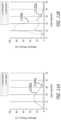
- FIG. 6is a graph showing calculated P-polarized and S-polarized diffraction efficiency versus incidence angle for a 1-micrometer thickness deep surface relief grating in accordance with an embodiment of the invention.
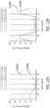
- FIG. 7is a graph showing calculated P-polarized and S-polarized diffraction efficiency versus incidence angle for a 2-micrometer thickness deep surface relief grating in accordance with an embodiment of the invention.
- FIG. 8is a graph showing calculated P-polarized and S-polarized diffraction efficiency versus incidence angle for a 3-micrometer thickness deep surface relief grating in accordance with an embodiment of the invention.
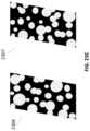
- FIGS. 9 A and 9 Billustrate scanning electron microscope images of multiple embodiments including different thiol concentrations.
- FIGS. 10 A and 10 Bare images comparing an HPDLC periodic structure and a polymer surface relief grating or evacuated periodic structure.
- FIGS. 11 A and 11 Bare two plots comparing an HPDLC periodic structure and a polymer surface relief grating or evacuated periodic structure.
- FIGS. 12 A and 12 Bare two plots of S-diffraction efficiency and P-diffraction efficiency of two example polymer surface relief gratings with different depths.
- FIGS. 13 A and 13 Bare two different plots of S-diffraction efficiency and P-diffraction efficiency of various example polymer surface relief gratings produced with different initial liquid crystal concentrations.
- FIGS. 14 A and 14 Bare two different plots of S-diffraction efficiency and P-diffraction efficiency of various example polymer surface relief gratings produced with different initial liquid crystal concentrations.
- FIG. 15is a graph of diffraction efficiency versus grating layer thickness showing the dependence of evanescent coupling on the grating layer thickness.
- FIGS. 16 A- 16 Gillustrate various stages of manufacture of a surface relief grating implementing a cover substrate in accordance with an embodiment of the invention.
- FIG. 17illustrates an example reaction forming a holographic mixture layer in accordance with an embodiment of the invention.
- FIG. 18illustrates a reaction between reagents and a base substrate in accordance with an embodiment of the invention.
- FIG. 19illustrates a reaction between release material and a cover substrate in accordance with an embodiment of the invention.
- FIGS. 20 A and 20 Billustrate various grating in accordance with an embodiment of the invention.
- FIG. 20 Cillustrates a grating in accordance with an embodiment of the invention.
- FIGS. 21 A- 21 Cconceptually illustrate three embodiments of waveguides in which evanescent coupling into a grating can occur.
- FIGS. 22 A- 22 Dillustrate various stages of manufacturing an inverse grating in accordance with an embodiment of the invention.
- FIG. 23 Aillustrates a schematic representation of a grating in accordance with an embodiment of the invention.
- FIG. 23 Billustrates a schematic representation of a grating in accordance with an embodiment of the invention.
- FIG. 23 Cillustrates a schematic representation of a grating in accordance with an embodiment of the invention.
- FIG. 24illustrates an example process flow for fabricating SRGs in accordance with an embodiment of the invention.
- FIGS. 25 A and 25 Billustrate the principles of a dual interaction grating for implementation in a waveguide.
- FIG. 26conceptually illustrates a cross section of a grating in accordance with an embodiment of the invention.
- FIG. 28illustrates an example of a partially backfilled grating in accordance with an embodiment of the invention.
- FIG. 29schematically illustrates a ray-grating interaction geometry of a TIR surface grating.
- FIG. 30conceptually illustrates a waveguide display in accordance with an embodiment of the invention.
- FIG. 32conceptually illustrates typical ray paths for a waveguide display in accordance with an embodiment of the invention.
- FIG. 33conceptually illustrates a waveguide display in which the waveguide supports a curved optical surface in accordance with an embodiment of the invention.
- FIG. 34conceptually illustrates a waveguide display in which the waveguide supports upper and lower curved optical surfaces in accordance with an embodiment of the invention.
- FIG. 35conceptually illustrates a waveguide display in which the waveguide supports a curved optical surface and an input image is provided using a pixel array predistorted to compensate for aberrations introduced by the curved optical surface in accordance with an embodiment of the invention.
- FIG. 36conceptually illustrates a waveguide display in which the waveguide supports a curved optical surface and an input image is provided using a pixel array supported by a curved substrate and predistorted to compensate for aberrations introduced by the curved optical surface in accordance with an embodiment of the invention.
- FIG. 37is a flow chart conceptually illustrating a method for projecting image light for view using a waveguide containing S-diffracting and P-diffracting gratings in accordance with an embodiment of the invention.
- FIG. 38is a flow chart conceptually illustrating a method for projecting image light for view using a waveguide supporting an optical prescription surface and containing S-diffracting and P-diffracting gratings in accordance with an embodiment of the invention.
- FIG. 39 Aconceptually illustrates a portion of a pixel pattern having rectangular elements of differing size and aspect ratio for use in an emissive display panel in accordance with an embodiment of the invention.
- FIG. 39 Bconceptually illustrates a portion of a pixel pattern having Penrose tiles for use in an emissive display panel in accordance with an embodiment of the invention.
- FIG. 39 Cconceptually illustrates a portion of a pixel pattern having hexagonal elements for use in an emissive display panel in accordance with an embodiment of the invention.
- FIG. 39 Econceptually illustrates a portion of a pixel pattern having diamond-shaped elements for use in an emissive display panel in accordance with an embodiment of the invention.
- FIG. 39 Fconceptually illustrates a portion of a pixel pattern having isosceles triangular elements for use in an emissive display panel in accordance with an embodiment of the invention.
- FIG. 39 Gconceptually illustrates a portion of a pixel pattern having hexagonal elements with horizontally biased aspect ratios for use in an emissive display panel in accordance with an embodiment of the invention.
- FIG. 39 Hconceptually illustrates a portion of a pixel pattern having rectangular elements with horizontally biased aspect ratios for use in an emissive display panel in accordance with an embodiment of the invention.
- FIG. 39 Iconceptually illustrates a portion of a pixel pattern having diamond shaped elements with horizontally biased aspect ratios for use in an emissive display panel in accordance with an embodiment of the invention.
- FIG. 39 Jconceptually illustrates a portion of a pixel pattern having triangles with horizontally biased aspect ratios for use in an emissive display panel in accordance with an embodiment of the invention.
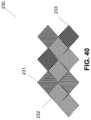
- FIG. 40conceptually illustrates a portion of a pixel pattern having diamond shaped elements in which different pixels can have different emission characteristics in accordance with an embodiment of the invention.
- periodic structuree.g. gratings
- These periodic structuremay include angle multiplexed gratings, color multiplexed gratings, fold gratings, dual interaction gratings, rolled K-vector gratings, crossed fold gratings, tessellated gratings, chirped gratings, gratings with spatially varying refractive index modulation, gratings having spatially varying grating thickness, gratings having spatially varying average refractive index, gratings with spatially varying refractive index modulation tensors, and gratings having spatially varying average refractive index tensors.
- gratings for diffraction of various polarizations of lightmay be beneficial. It would be specifically advantageous to have a grating which diffracts either S-polarized light or P-polarized light.
- Specific applications for this technologyinclude waveguide-based displays such as augmented reality displays and virtual reality displays.
- waveguide-based displayssuch as augmented reality displays and virtual reality displays.
- input gratingswhich may be used to input one or both of S-polarized light or P-polarized light into the waveguide.
- it would be advantageous to have a grating which diffracts either S-polarized light and P-polarized lightFor example, waveguide displays using unpolarized light sources such as OLED light sources produce both S-polarized and P-polarized light and thus it would be advantageous to have gratings which can diffract both S-polarized and P-polarized light.
- gratingsinclude surface relief gratings (SRGs) which may be used to diffract either P-polarized light or S-polarized light.
- SRGssurface relief gratings
- SRGssurface relief gratings
- LEDslight emitting diodes
- an S-polarization diffracting gratingcan be provided by a periodic structure formed in a holographic photopolymer.
- One periodic structureincludes a grating such as a Bragg grating.
- an S-polarization diffracting gratingcan be provided by a periodic structure formed in a holographic polymer dispersed liquid crystal (HPDLC) with birefringence altered using an alignment layer or other processes for realigning the liquid crystal (LC) directors.
- HPDLCholographic polymer dispersed liquid crystal
- an S-polarization diffracting periodic structurecan be formed using liquid crystals, monomers, and other additives that naturally organize into S-diffracting periodic structures under phase separation. In some embodiments, these HPDLC periodic structures may form deep SRGs which have superior S-polarization diffraction efficiency.
- One class of deep SRGsare polymer-air SRGs or evacuated periodic structure (EPSs) which may exhibit high S-diffraction efficiency (up to 99%) and low P-diffraction efficiency and may be implemented as input gratings for waveguides.
- the EPSsmay be evacuated Bragg gratings (EBGs).
- EBGsevacuated Bragg gratings
- Such periodic structurescan be formed by removing the liquid crystal from HPDLC periodic structures formed from holographic phase separation of a liquid crystal and monomer mixture.
- Deep SRGs formed by such a processtypically have a thickness in the range 1-3 micrometers with a fringe spacing 0.35 to 0.80 micrometers. In some embodiments, the ratio of grating depth to fringe spacing may be 1:1 to 5:1.
- such gratingscan be formed with different dimensions depending on the specific requirements of the given application. Examples of how the thickness of SRGs may yield different resultant diffraction efficiencies are described in connection with FIGS. 6 - 8 .
- the condition for a deep SRGsis characterized by a high grating depth to fringe spacing ratio.
- the condition for the formation of a deep SRGsis that the grating depth is approximately twice the grating period. Modelling such deep SRGs using the Kogelnik theory can give reasonably accurate estimates of diffraction efficiency, avoiding the need for more advanced modelling, which typically entails the numerical solution of Maxwell's equations.
- the grating depths that can be achieved using liquid crystal removal from HPDLC periodic structuresgreatly surpass those possible using conventional nanoimprint lithographic methods, which cannot achieve the conditions for deep SRGs (typically providing only 250-300 nm depth for grating periods 350-460 nm).
- deep SRGscan, as will be discussed below, provide a range of polarization response characteristics depending on the thickness of the grating prescription and, in particular, the grating depth. As such, deep SRGs can be implemented in a variety of different applications.
- Gerritsendiscusses the formation of Bragg-like SRGs in photoresist (Gerritsen H J, Thornton D K, Bolton S R; “Application of Kogelnik's two-wave theory to deep, slanted, highly efficient, relief transmission gratings” Applied Optics; Vol. 30; Issue 7; (1991); pp 807-814).
- SRGssuch as deep SRGs that can offer very significant advantages over nanoimprint lithographic process particularly for slanted gratings.
- Periodic structures of any complexitycan be made using interference or master and contact copy replication.
- the SRGscan be back filled with a material with different properties to the LC. This allows a periodic structure with modulation properties that are not limited by the grating chemistry needed for grating formation.
- the backfill materialmay not be a LC material.
- the backfill materialmay have a higher index of refraction than air which may increase the angular bandwidth of a waveguide.
- the deep SRGscan be partially backfilled with LC to provide a hybrid SRG/periodic structure.
- the refill stepcan be avoided by removing just a portion of the LC from the LC rich regions of the HPDLC to provide a hybrid SRG/periodic structure.
- the refill approachhas the advantage that a different LC can be used to form the hybrid periodic structures.
- the materialscan be deposited using an inkjet deposition process.
- Photonic crystalsmay be implemented to create a wide variety of diffracting structures including periodic structures such as Bragg gratings. Periodic structures may be used as diffraction gratings to provide functionality including but not limited to input gratings, output gratings, beam expansion gratings, diffract more than one primary color.
- a photonic crystalcan be a three-dimensional lattice structure that can have diffractive capabilities not achievable with a basic periodic structures. Photonic crystals can include many structures including all 2-D and 3-D Bravais lattices. Recording of such structures may benefit from more than two recording beams.
- waveguides incorporating photonic crystalscan be arranged in stacks of waveguides, each having a grating prescription for diffracting a unique spectral bandwidth.
- a photonic crystal formed by liquid crystal extractionprovide a deep SRG.
- a deep SRG formed using a liquid crystal extraction processcan typically have a thickness in the range 1-3 micron with a fringe spacing 0.35 micron to 0.80 micron. The fringe spacing may be a Bragg fringe spacing.
- the condition for a deep SRGis characterized by a high grating depth to fringe spacing ratio. In some embodiments the condition for the formation of a deep SRG is that the grating depth can be approximately twice the grating period.
- Deep SRGscan, as will be discussed below, provide a range of polarization response characteristics depending on the thickness of the grating prescription and, in particular, the grating depth. Deep SRGs can also be used in conjunction with conventional Bragg gratings to enhance the color, uniformity and other properties of waveguide displays.
- Deep SRGshave been fabricated in glassy monomeric azobenzene materials using laser holographic exposure (O. Sakhno, L. M. Goldenberg, M. Wegener, J. Stumpe, “Deep surface relief grating in azobenzene-containing materials using a low intensity 532 nm laser”, Optical Materials: X, 1, (2019), 100006, pp 3-7.
- the Sakhno referencealso discloses how SRGs can be recorded in a holographic photopolymer using two linearly orthogonally polarized laser beams.
- the disclosureprovides a method for making a surface relief grating that can offer very significant advantages over nanoimprint lithographic process particularly for slanted gratings.
- Periodic structures of any complexitycan be made using interference or master and contact copy replication.
- the SRGcan be back filled with a material with different properties to the LC. This allows a periodic structure with modulation properties that are not limited by the grating chemistry needed for grating formation.
- the SRGscan be partially backfilled with LC to provide a hybrid SRG/periodic structure.
- the refill stepcan be avoided by removing just a portion of the LC from the LC rich regions of the HPDLC to provide a hybrid SRG/periodic structure.
- the refill approachhas the advantage that a different LC can be used to form the hybrid grating.
- the materialscan be deposited using an inkjet process.
- the refill materialmay have a higher index of refraction than air which may increase diffraction efficiency of the periodic structure.
- any type of SRG including SRGs in which the grating depth is smaller than the grating frequencymay be fabricated as well.
- FIGS. 1 A- 1 Dillustrate a processing apparatus that can be used in a method for fabricating deep SRGs or EPSs in accordance with an embodiment.
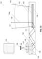
- FIG. 1 Aconceptually illustrates an apparatus 190 A that can be used in a step of a method for fabricating a surface relief grating in which a mixture 191 of monomer and liquid crystal deposited on a transparent substrate 192 is exposed to holographic exposure beams 193 , 194 , in accordance with an embodiment of the invention.
- the holographic exposure beams 193 , 194may be deep UV beams.
- the mixture 191may also include at least one of a photoinitiator, a coinitiator, a multifunctional thiol, adhesion promoter, surfactant, and/or additional additives.
- the mixture 191may include nanoparticles.
- the mixture 191may include photoacids.
- the mixture 191may be a monomer diluted with a non-reactive polymer.
- the mixture 191may include more than one monomer.
- the monomermay be isocyanate-acrylate based or thiolene based.
- the liquid crystalmay be a full liquid crystal mixture or a liquid crystal single.
- a liquid crystal singlemay only include a portion of a full liquid crystal mixture.
- liquid crystal singlesmay include one or all of cyanobiphenyls, alkyl, alkoxy, cyanobiphenyls, and/or terphenyls.
- the liquid crystal mixturemay be a cholesteric liquid crystal.
- the liquid crystal mixturemay include chiral dopants which may control the grating period.
- the liquid crystal mixturemay include photo-responsive and/or halogen bonded liquid crystals.
- liquid crystalmay be replaced with another substance that phase separates with the monomer during exposure to create polymer rich regions and substance rich regions.
- the substance and liquid crystal singlesmay be a cost-effective substitute to full liquid crystal mixtures which are removed at a later step as described below.
- the liquid crystal in the mixture 191may have a different between an extraordinary refractive index and an ordinary refractive index of less than 0.01. In some embodiments, the liquid crystal in the mixture 191 may have a different between an extraordinary refractive index and an ordinary refractive index of less than 0.025. In some embodiments, the liquid crystal in the mixture 191 may have a different between an extraordinary refractive index and an ordinary refractive index of less than 0.05.
- FIG. 1 Bconceptually illustrates an apparatus 190 B that can be used in a step of a method for fabricating a surface relief grating from an HPDLC Bragg grating 195 formed on a transparent substrate using the holographic exposure beams, in accordance with an embodiment of the invention.
- the holographic exposure beamsmay transform the monomer into a polymer in some areas.
- the holographic exposure beamsmay include intersecting recording beams and include alternating bright and dark illumination regions.
- a polymerization-driven diffusion processmay cause the diffusion of monomers and LC in opposite directions, with the monomers undergoing gelation to form polymer-rich regions (in the bright regions) and the liquid crystal becoming trapped in a polymer matrix to form liquid crystal rich regions (in the dark regions).
- FIG. 1 Cconceptually illustrates an apparatus 190 C that can be used in a step of a method for fabricating a deep polymer surface relief grating 196 or EPS in which liquid crystal is removed from an HPDLC periodic structure of FIG. 1 B to form a polymer surface relief grating in accordance with an embodiment of the invention.
- a polymer surface relief grating 196may include a large depth with a comparatively small grating period in order to form a deep SRG.
- the liquid crystalmay be removed by washing with a solvent such as isopropyl alcohol (IPA).
- IPAisopropyl alcohol
- the solventmay be strong enough to wash away the liquid crystal but weak enough to maintain the polymer.
- the solventmay be chilled below room temperature before washing the grating.
- FIG. 1 Cconceptually illustrates an apparatus 190 C that can be used in a step of a method for fabricating a deep polymer surface relief grating 196 or EPS in which liquid crystal is removed from an HPDLC periodic structure
- FIG. 1 Dconceptually illustrates an apparatus 190 D that can be used in a step of a method for fabricating a polymer surface relief grating in which the polymer surface relief grating is covered with a protective layer 197 in accordance with an embodiment of the invention.
- FIG. 2conceptually illustrates a method for forming deep SRGs from a HPDLC periodic structure formed on a transparent substrate in accordance with an embodiment of the invention.
- a method 200 of forming deep SRGs or EPSsis provided.
- the method 200includes providing ( 201 ) a mixture of at least one monomer and at least one liquid crystal.
- the at least one monomermay include an isocyanate-acrylate monomer or thiolene.
- the mixturemay include a liquid crystal and a thiolene based photopolymer.
- the mixturemay include a liquid crystal and an acrylate-based photopolymer.
- the at least one liquid crystalmay be a full liquid crystal mixture or may be a liquid crystal single which may include only a portion of the liquid crystal mixture such as a single component of the liquid crystal mixture.
- the at least one liquid crystalmay be substituted for a solution which phase separates with the monomer during exposure.
- the criteria for such a solutionmay include ability to phase separate with the monomer during exposure, ease of removal after curing and during washing, and ease of handing.
- Example substitute solutionsinclude solvents, non-reactive monomers, inorganics, and nanoparticles.
- a transparent substratecan be provided ( 202 ).
- the transparent substratemay be a glass substrate or a plastic substrate.
- the transparent substratemay be a flexible substrate to facilitate roll to roll processing.
- the EPSmay be manufactured on a flexible substrate through a roll to roll process and then peeled off and adhered to a rigid substrate.
- the EPSmay be manufactured on a flexible substrate and a second flexible release layer may be peeled off and discarded which would leave the EPS on a flexible layer. The flexible layer may be then bonded to another rigid substrate.
- a layer of the mixturecan be deposited or coated ( 203 ) onto a surface of the substrate.
- the layer of mixturemay be deposited using inkjet printing.
- the mixtureis sandwiched between the transparent substrate and another substrate using glass spacers to maintain internal dimensions.
- a non-stick coatingmay be applied to the other substrate before the mixture is sandwiched.
- the non-stick coatingmay include a fluoropolymer such as OPTOOL UD509 (produced by Daikin Chemicals), Dow Corning 2634, Fluoropel (produced by Cytonix), and EC200 (produced by PPG Industries, Inc).
- Holographic recording beamscan be applied ( 204 ) to the mixture layer.
- holographic recording beamsmay be a two-beam interference pattern which may cause phase separation of the LC and the polymer.
- the liquid monomerchanges to a solid polymer whereas the neutral, non-reactive substance (e.g. LC) diffuses during holographic exposure in response to a change in chemical potential driven by polymerization.
- LCmay be one implementation of the neutral, non-reactive substance, other substances may also be used.
- the substance and the monomermay form a miscible mixture prior to the holographic exposure and become immiscible upon holographic exposure.
- the mixturemay be cured.
- the curing processmay include leaving the mixture under low-intensity white light for a period of time until the mixture fully cures.
- the low intensity white lightmay also cause a photo-bleach dye process to occur.
- a HPDLC periodic structure having alternating polymer rich and liquid crystal rich regionscan be formed ( 205 ).
- the curing processmay occur in two hours or less.
- one of the substratesmay be removed exposing the HPDLC periodic structure.
- the non-stick coatingmay allow the other substrate to be removed while the HPDLC periodic structure remaining.
- HPDLC periodic structuremay include alternating sections of liquid crystal rich regions and polymer regions.
- the liquid crystal in the liquid crystal rich regionscan be removed ( 206 ) to form polymer surface relief gratings or EPSs which may be used as deep SRGs.
- the liquid crystalmay be removed by gently immersing the grating into a solvent such as IPA.
- the IPAmay be chilled and may be kept at a temperature lower than room temperature while the grating is immersed in the IPA.
- the periodic structuremay be then removed from the solvent and dried. In some embodiments, the periodic structure is dried using a high flow air source such as compressed air. After the LC is removed from the periodic structure, a polymer-air surface relief grating is formed.
- the formed surface relief gratingcan further be covered with a protective layer.
- the protective layermay be a moisture and oxygen barrier with scratch resistance capabilities.
- the protective layermay be a coating that does not fill in air gap regions where LC that was removed once existed.
- the coatingmay be deposited using a low temperature process.
- the protective layermay have anti-reflective (AR) properties.
- the coatingmay be a silicate or silicon nitride.
- the coating processmay be performed by a plasma assisted chemical vapor deposition (CVD) process such as a nanocoating process.
- the coatingmay be a parylene coating.
- the protective layermay be a glass layer.
- a vacuum or inert gasmay fill the gaps where LC that was removed once existed before the protective layer is applied.
- the coating processmay be integrated with the LC removal process ( 206 ).
- a coating materialmay be mixed with the solvent which is used to wash the LC from the periodic structure.
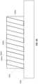
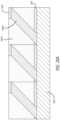
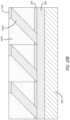
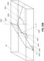
- FIG. 3 Aillustrates a cross sectional schematic view of an exemplary embodiment of a polymer-air periodic structure 3000 implemented on a waveguide 3002 .
- the polymer-air surface relief grating 3000includes periodic polymer sections 3004 a . Adjacent polymer sections 3004 a sandwich air sections 3004 b . The air sections 3004 b are sandwiched by polymer sections 3004 a . The air sections 3004 b and polymer sections 3004 a have different indexes of refraction.
- the polymer-air surface relief Bragg grating 3000may be formed with a high grating depth 3006 a to Bragg fringe spacing 3006 b ratio which may create a deep SRG.
- the polymer sections 3004 a and the air sections 3004 bextend all the way to the waveguide 3002 to directly contact the waveguide 3002 . As illustrated, there may be no bias layer between the polymer sections 3004 a and the air sections 3004 b and the waveguide 3002 . As discussed previously, deep SRGs may exhibit many beneficial qualities such as high 5-diffraction efficiency which may not be present within the typical SRGs.
- a polymer-air surface relief Bragg grating 3000may have a Bragg fringe spacing 3006 b of 0.35 ⁇ m to 0.8 ⁇ m and a grating depth of 1 ⁇ m to 3 ⁇ m.
- a grating depth of 1 ⁇ m to 3 ⁇ mmay be too thick for most EPS (with ashing and ALD) for fold and output gratings for waveguide applications, where leaky structures are needed.
- Values in the ranges of 0.1 ⁇ m to 0.5 ⁇ mmight be more suitable for leaky structures, particularly when modulation is increased with ashing and ALD.
- Input structuresmay include a depth in the range of 0.4 ⁇ m up to 1 ⁇ m.
- Structures with a depth from 1 ⁇ m to 3 ⁇ mmay be advantageous for display cases, and structures even taller may be advantageous for non-display applications. Structures with half period (e.g. a critical dimension) to height ratio of 7:1 or even 8:1 have been demonstrated with advantageous effects.
- the polymer sections 3004 amay include at least some residual liquid crystal when the liquid crystal is not completely removed during step 206 described in connection with FIG. 2 .
- the presence of residual LC within the polymer rich regionsmay increase refractive index modulation of the final polymer SRG.
- the air sections 3004 bmay include some residual liquid crystal if the liquid crystal is not completely removed during step 206 from these air sections 3004 b .
- a hybrid grating as described in connection with FIGS. 4 - 5may be created.
- an optical layer 3008may also exist between the polymer sections 3004 a and the air sections 3004 b and the waveguide 3002 .
- the optical layer 3008may be a bias layer between the polymer sections 3004 a and the air sections 3004 b and the waveguide 3002 .
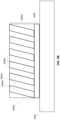
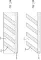
- FIG. 3 Billustrates a cross sectional schematic view of a polymer-air periodic structure 3000 a in accordance with an embodiment of the invention.
- the polymer-air periodic structure 3000 aincludes many identically numbered components with the polymer-air periodic structure 3000 of FIG. 3 A . The description of these components is applicable with the polymer-air periodic structure 3000 a described in connection with FIG. 3 B and this description will not be repeated in detail.
- an optical layer 3008is positioned between the polymer sections 3004 a and the air sections 3004 b and the waveguide 3002 .
- the waveguidemay include a substrate 3002 and an optical layer 3008 (e.g. the bias layer) sandwiched by the substrate 3002 and the polymer periodic structure and wherein the polymer periodic structure extends all the way to the optical layer to directly contact the optical layer.
- the polymer periodic structureincludes the polymer sections 3004 a and the air sections 3004 b.
- an optical layer 3008may be formed when gratings are formed using Nano Imprint Lithography (NIL).
- the grating patternmay be imprinted in a resin leaving a thin layer underneath the period structure which is a few microns thick.
- This optical layer 3008which may be a few microns in thickness, may reside between the waveguide (e.g. glass) substrate and the period grating layer and may not be removed without damaging the NIL grating structure.
- the bias layermay confine light for some field angles (furthest from TIR in the waveguide) to the high index substrate which may be analogous to cladding on an optical fiber core.
- Elimination of the bias layercan offer grating coupling from a high index substrate with a grating structure of lower index than the substrate which may not be possible with the bias layer present.
- EPSsmay deliver similar optical performance characteristics to nanoimprinted SRGs by offering taller structures albeit at lower peak refractive index. This may open up the possibility of low-cost fabrication of diffractive structures for high efficiency waveguides.
- a optical layer 3008may be present in EPSs.
- the present disclosureallows for waveguide grating devices with or without the optical layer 3008 .
- having the optical layer 3008can be an advantage as the evanescent coupling between the waveguide and the grating is a function of the indices of the gratings structure (e.g. the grating depth the angles of the faces making up the structure and the grating depth), the waveguide core, and the optical layer 3008 (if present).
- the optical layer 3008may be used as a tuning parameter for optimizing the overall waveguide design for better efficiency and bandwidth.
- a bias layer used with an EPSmay not be of the same index as the grating structure.
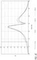
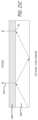
- FIG. 3 Cis a graph illustrating the effect of optical layer 3008 thickness on the diffraction efficiency versus incident angle.
- the dotted line 3052represents an incident angle of +6 degrees.
- Evanescent couplingmay begin (towards negative angles) at an angle of approximately +6 degrees.
- the various plotsrepresent different thicknesses of optical layer 3008 .
- the plotsshow that the optical layer 3008 thickness can be used to increase the diffractive coupling (e.g. for an optical layer thickness of 300 nm) over the approximate angular range from +6 degrees to +16 degrees. There may be lower coupling over the approximate angular range from 0 degrees to +6 degrees.
- the S-shaped characteristiccan be altered by replacing the 300 nm optical layer with a thicker or thinner bias layer as shown in FIG. 3 C .
- the thickness of the optical layermay be 2 ⁇ m to 3 ⁇ m, 1 ⁇ m to 2 ⁇ m, or 0.5 ⁇ m to 1 ⁇ m.
- the EPSmay be fabricated as part of a stacked grating structure. Examples of stacked grating structures are discussed in International Pub. No. WO 2022015878, entitled “Nanoparticle-based holographic photopolymer materials and related applications” and filed Jul. 14, 2021, which is hereby incorporated by reference in its entirety for all purposes.
- the EPSmay include a multilayer structure including a release layer. Release layers may be used in a grating stacking process that may reduce the number of glass layers. The release layer may be applied at each exposure step to allow the deposition of a new layer of recording material. Similar processes may also allow angular bandwidth to be increased by stacking multiple gratings with different slant angles.
- FIG. 4 Aconceptually illustrates an apparatus 210 A that can be used in a step of a method for fabricating hybrid surface relief gratings (hybrid SRGs) in which a mixture 211 of monomer and liquid crystal deposited on a transparent substrate 212 is exposed to holographic exposure beams 213 , 214 , in accordance with an embodiment of the invention.
- FIG. 4 Bconceptually illustrates an apparatus 210 B that can be used in a step of a method for fabricating hybrid SRGs from an HPDLC periodic structure 215 formed on the transparent substrate using the holographic exposure beams in accordance with an embodiment of the invention.
- FIG. 4 Aconceptually illustrates an apparatus 210 A that can be used in a step of a method for fabricating hybrid SRGs (hybrid SRGs) in which a mixture 211 of monomer and liquid crystal deposited on a transparent substrate 212 is exposed to holographic exposure beams 213 , 214 , in accordance with an embodiment of the invention.
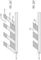
- FIGS. 4 A- 4 Cconceptually illustrates an apparatus 210 C that can be used in a step of a method for fabricating a surface relief grating in which liquid crystal is removed from an HPDLC periodic structure 215 to form polymer-air SRGs 216 in accordance with an embodiment of the invention.
- These polymer-air SRGs 216 or EPSsmay be deep SRGs. It is appreciated that the steps illustrated in and described in connection with FIGS. 4 A- 4 C roughly correspond to the steps illustrated in and described in connection with FIGS. 2 A- 2 C in the process to create a polymer-air SRG and thus the previous description will be applicable to FIGS. 4 A- 4 C .
- FIG. 4 Dconceptually illustrates an additional step which may be performed to create a hybrid grating.
- the apparatus 210 Dcan be used in a step of a method for fabricating a surface relief grating in which a surface relief grating is at least partially refilled with liquid crystal to form a hybrid SRGs 217 , in accordance with an embodiment of the invention.
- the refilled liquid crystalmay be of different consistency to the previously removed liquid crystal that was previously removed in FIG. 4 C .
- the liquid crystal removed in FIG. 3 Cmay only be partially removed in an alternative method to forming hybrid SRGs 217 .
- FIG. 3 Cmay only be partially removed in an alternative method to forming hybrid SRGs 217 .
- FIG. 3 Cmay only be partially removed in an alternative method to forming hybrid SRGs 217 .
- FIG. 4 Econceptually illustrates an apparatus 210 E can be used in a step of a method for fabricating a surface relief grating in which hybrid SRGs 217 formed in the step illustrated in FIG. 4 D is covered with a protective layer 218 , in accordance with an embodiment of the invention.
- the air sections 3004 b of FIGS. 3 A and 3 Bmay be replaced with a backfill material as discussed above.
- FIG. 5is a flowchart showing an exemplary method for forming a hybrid surface relief-periodic structure from a HPDLC periodic structure formed on a transparent substrate in accordance with an embodiment of the invention.
- the method 220 of forming hybrid surface relief-periodic structureis provided.
- method 220includes providing ( 221 ) a mixture of at least one monomer and at least one liquid crystal.
- the at least one monomermay include an isocyanate-acrylate monomer.
- Providing the mixture of the monomer and the liquid crystalmay also include mixing one or more of the following with the at least one monomer and the liquid crystal: photoinitiator, coinitiator, multifunctional thiol, and/or additional additives.
- This mixturemay be allowed to rest in order to allow the coinitiator to catalyze a reaction between the monomer and the thiol.
- the rest periodmay occur in a dark space or a space with red light (e.g. infrared light) at a cold temperature (e.g. 20° C.) for a period of approximately 8 hours.
- additional monomersmay be mixed into the monomer.
- This mixturemay be then strained or filtered through a filter with a small pore size (e.g. 0.45 ⁇ m pore size). After straining this mixture may be stored at room temperature in a dark space or a space with red light before coating.
- a transparent substratecan be provided ( 222 ).
- the transparent substratemay be a glass substrate or a plastic substrate.
- a non-stick coatingmay be applied to the transparent substrate before the mixture is coated on the substrate.
- the non-stick coatingmay be a release layer which allows the transparent substrate to easily release from the exposed periodic structure.
- release layersare discussed below.
- a layer of the mixturecan be deposited ( 223 ) onto a surface of the substrate.
- the mixtureis sandwiched between the transparent substrate and another substrate using glass spacers to maintain internal dimensions.
- Holographic recording beamscan be applied ( 224 ) to the mixture layer.
- the holographic recording beamsmay be a two-beam interference pattern which may cause phase separation of the LC and the polymer.
- the mixturemay be cured.
- the curing processmay include leaving the mixture under low-intensity white light for a period of time under the mixture fully cures.
- the low intensity white lightmay also cause a photo-bleach dye process to occur.
- an HPDLC periodic structure having alternating polymer rich and liquid crystal rich regionscan be formed ( 225 ).
- the curing processmay occur in 2 hours or less.
- one of the substratesmay be removed exposing the HPDLC periodic structure.
- the release layermay aid in allowing the one of the substrates to not stick to the exposed periodic structure.
- HPDLC gratingmay include alternating sections of liquid crystal rich regions and polymer regions.
- the liquid crystal in the liquid crystal rich regionscan be removed ( 226 ) to form polymer surface relief gratings or EPSs which is a form of deep SRGs.
- the liquid crystalmay be removed by gently immersing the exposed periodic structure into a solvent such as isopropyl alcohol (IPA).
- IPAisopropyl alcohol
- the IPAmay be kept at a lower temperature while the periodic structure is immersed in the IPA.
- the periodic structureis them removed from the solvent and dried.
- the periodic structureis dried using a high flow air source such as compressed air.
- a polymer-air surface relief periodic structureis formed.
- the resulting periodic structuremay be the periodic structure described in connection with FIGS.
- FIG. 3 A and 3 BThere may or may not be a bias layer present as illustrated in FIG. 3 A or 3 B .
- the steps 221 - 226 of FIG. 5roughly correspond to the steps described in connection with FIG. 2 in creating a polymer-air SRG and thus these descriptions are applicable to FIG. 5 .
- method 220includes at least partially refilling ( 227 ) cleared liquid crystal rich regions with liquid crystal to form hybrid SRGs.
- the refilled liquid crystalmay be of different consistency to the previously removed liquid crystal that was previously removed in step 226 .
- the liquid crystal removed in step 226may only be partially removed in an alternative method to forming hybrid SRGs.
- hybrid SRGsmay provide the ability to tailor specific beneficial characteristics of the SRGs.
- One particular characteristic that may be improved by the inclusion of at least some liquid crystal within the SRGsis a decrease in haze properties.
- the cleared liquid crystal rich regionsmay be backfilled with a different refractive material than liquid crystal.
- the backfill materialmay have a different refractive index than the remaining polymer rich regions.
- the formed surface relief gratingcan further be covered with a protective layer.
- the protective layermay be a moisture and oxygen barrier with scratch resistance capabilities.
- the protective layermay be a coating that does not fill in air gap regions where LC that was removed once existed.
- the coatingmay be deposited using a low temperature process.
- the protective layermay have anti-reflective (AR) properties.
- the coatingmay be a silicate or silicon nitride.
- the coating processmay be performed by a plasma assisted chemical vapor deposition (CVD) process such as a plasma-treat nanocoating process.
- the coatingmay be a parylene coating.
- the protective layermay be a glass layer.
- a vacuum or inert gasmay fill the gaps where LC that was removed once existed before the protective layer is implemented.
- the coating processmay be integrated with the LC removal process ( 226 ).
- a coating materialmay be mixed with the solvent which is used to wash the LC from the grating.
- the coating materialmay be a material with a lower or higher refractive index than the polymer and fill the spaces between adjacent polymer portions. The refractive index difference between the polymer and the coating material may allow the polymer SRGs to continue to diffract.
- FIGS. 1 - 5illustrate specific methods and apparatus for forming deep SRGs and hybrid surface relief/Bragg gratings
- various manufacturing methodsimplementing different steps or modifications of such steps can be utilized.
- the specific process utilizedcan depend on the specific requirements of the given application. For example, many embodiments utilize another periodic structure as a protective layer.
- Hybrid SRG/periodic structure with shallow SRG structuresmay lead to low SRG diffraction efficiencies.
- the methods disclosed in the present disclosureallows for more effective SRG structures to be formed by optimizing the depth of the liquid crystal in the liquid crystal rich regions such that the SRGs has a high depth to grating pitch ratio while allowing the periodic structure to be sufficiently thick for efficient diffraction.
- the periodic structure component of the hybrid gratingcan have a thickness in the range 1-3 micrometer.
- the SRG component of the hybrid gratingcan have a thickness in the range 0.25-3 micrometer.
- the initial HPDLC periodic structurewould have a thickness equal to the sum of the final SRG and periodic structure components.
- the thickness ratio of the two periodic structure componentscan depend on the waveguide application.
- the combination of an SRG with a periodic structuremay be used to fine-tune angular bandwidth of the periodic structure.
- the SRGcan increase the angular bandwidth of the periodic structure.
- the refill depth of the liquid crystal regions of the periodic structurecan be varied across the periodic structure to provide spatially varying relative SRG/periodic structure strengths.
- the liquid crystal in the liquid crystal rich grating regionscan be totally or partially removed.
- the liquid crystal used to refill or partially refill the liquid crystal-cleared regionscan have a different chemical composition to the liquid crystal used to form the initial HPDLC periodic structure.
- a first liquid crystal with phase separation properties compatible with the monomercan be specified to provide a HPDLC grating with optimal modulation and grating definitions while a second refill liquid crystal can be specified to provide desired index modulation properties in the final hybrid grating.
- the polymer portion of the hybrid gratingcan be switchable with electrodes applied to surfaces of the substrate and the cover layer.
- the refill liquid crystalscan contain additives which may include but are not limited to the features of improving switching voltage, switching time, polarization, transparency, and other parameters.
- a hybrid grating formed using a refill processwould have the further advantages that the LC would form a continuum (rather than an assembly of LC droplets), thereby reducing haze.
- the backfill materialmay be a material with a different refractive index than the polymer regions. The backfill material may not be a liquid crystal material.
- While deep SRGs, EPSs, and/or hybrid SRGsmay be described in the context of S-diffracting gratings and P-diffracting gratings, these periodic structures have applicability in many other periodic structure types. These include but are not limited to angle multiplexed gratings, color multiplexed gratings, fold gratings, dual interaction gratings, rolled K-vector gratings, crossed fold gratings, tessellated gratings, chirped gratings, gratings with spatially varying refractive index modulation, gratings having spatially varying grating thickness, gratings having spatially varying average refractive index, gratings with spatially varying refractive index modulation tensors, and gratings having spatially varying average refractive index tensors.
- deep SRGs, EPSs, and/or hybrid SRGsmay be switchable or non-switchable periodic structures depending on their specific implementation.
- Deep SRGs, EPSs, and/or hybrid SRGsmay be fabricated on a plastic substrate or a glass substrate. These periodic structures may also be fabricated on one substrate and transferred to another substrate.
- EPSsmay be either unslanted or slanted, or spatially varying slanted structures (e.g., rolled K-vector type with very large height to period aspect ratio, typically in the range of 2 to 12). Slanted EPSs will be illustrated in various examples below.
- the combination of controlled, repeatable, slant angles and tall aspect ratiosmay provide EPS structures Bragg properties which enable high efficiency waveguide designs.
- EPSscan be fabricated with or without bias layers. EPSs may be made using a phase separation process that can be implemented using ink jet printing processes and offers significant economic advantages in mass production over the complex wafer etching and nano imprint lithographic process used to produce some SRG display waveguides.
- EPSsmay be configured as at least one of multiplexed grating, a slanted grating, a photonic crystal, mixed modulation grating, a hybrid polymer grating structure, a sinusoidal grating (e.g. formed by plasma ashing of isotropic photopolymer gratings), a metasurface, or a grating structure combining a slanted volume grating overlaid by a surface relief grating.
- Slanted volume grating overlaid by a surface relief gratingmay include a grating structure which is substantially a volume grating with the grating thickness of the low index regions having a slight smaller grating thickness than the high index regions.
- the variation of the grating thicknessmay be tens of nanometers while the average volume grating thickness may be from 1-10 micron depending on the application.
- the configurationis equivalent to an SRG layer sitting on top of a volume grating layer.
- the SRG and volume gratingmay combine the benefit of the wider angular bandwidth of the SRG and the higher efficiency of the volume grating. This is more likely to be the case when the volume grating is thinner.
- the surface relief structurecan arise naturally as a result of non-linearity in the diffusion process at the extremities of the grating. The effect may be controlled using plasma ashing or some other type of etching processed applied to the grating.
- a combined SRG and volume gratingcan also be formed by fabricating an EPS and then partially backfilling it with another material. Such a configuration is discussed as a hybrid grating throughout the current disclosure.
- the EPSis formed using different diffusion regimes having different diffusion constants in at least two different directions.
- the spacing of the diffracting nodesmay lead to nonuniformities in the modulation of the finished grating.
- Material components with different diffusion time constantsmay allow more efficient grating formation along different directions.
- the EPSis formed to provide a photonic structure incorporating a slanted grating structure and a photonic crystal structure including diffracting nodes.
- Grating configurationsincluding regions in which the grating includes slanted (or unslanted) planar fringes and photonic crystal regions where the diffracting structures comprising diffracting nodes may include elongate elements such as cylinders which many may be tilted.
- the photonic crystal regionsmay include a 3D diffracting node structure.
- the EPSis formed to provide a photonic crystal including slanted diffracting features wherein the principle nodes of the photonic crystal are formed by multiplexed gratings wherein plasma ashing is applied along tracks parallel to principal crystal directions.
- the photonic crystalmay be formed by multiplexing two or more gratings such that the intersection regions of the bright fringes form modulation peaks.
- the regions around these peaksmay be eroded using plasma ashing applied along the low modulation tracks which are parallel to the principle crystal directions.
- the cross-section geometry of the nodesmay depend on the number of gratings and their relative orientations. For example, crossing two gratings at ninety degrees may result in square cross section nodes.
- Tilted photonic crystal nodesmay be formed using slanted gratings. This principle can be extended to three dimensional photonic crystals.
- the polymer grating structuremay be formed to provide photonic crystal formed by three-beam-recorded Bravais lattices and other structures, the process including plasma ashing. All five two dimensional Bravais lattices (e.g. square, triangular, rhombic) may be recoded using a three-beam exposure system.
- the techniques for fabricating two dimensional photonic crystalsmay also be applied to more complex three-dimensional structures, including 3D Bravais lattices and other structures. All fourteen of the Bravais lattice can be recorded using three beams or even two beams using more multiple exposure techniques. Dual-beam multiple exposure schemes may be used with the recording medium undergoing a single axis rotation between each exposure.
- deep SRGscan provide a means for controlling polarization in a waveguide.
- SBGsare normally P-polarization selective, leading to a 50% efficiency loss with unpolarized light sources such as OLEDs and LEDs.
- combining S-polarization diffracting and P-polarization diffracting periodic structurescan provide a theoretical 2 ⁇ improvement over waveguides using P-diffracting periodic structures only.
- an S-polarization diffracting periodic structurescan be provided by a periodic structure formed in a conventional holographic photopolymer.
- an S-polarization diffracting periodic structurescan be provided by a periodic structure formed in a HPDLC with birefringence altered using an alignment layer or other process for realigning the liquid crystal directors.
- an S-polarization diffracting periodic structurecan be formed using liquid crystals, monomers and other additives that naturally organize into S-diffracting periodic structures under phase separation.
- an S-polarization diffracting periodic structurescan be provided by SRGs. Using the processes described above, a deep SRG exhibiting high S-diffraction efficiency (up to 99%) and low P-diffraction efficiency can be formed by removing the liquid crystal from SBGs formed from holographic phase separation of a liquid crystal and monomer mixture.
- Deep SRGscan also provide other polarization response characteristics.
- MoharamMoharam M. G. et al. “Diffraction characteristics of photoresist surface-relief gratings”, Applied Optics, Vol. 23, page 3214, Sep. 15, 1984
- deep SRGsdemonstrate the capability of providing an S-polarization response.
- deep SRGsmay also provide other polarization response characteristics.
- deep surface relief gratings having both S and P sensitivity with S being dominantare implemented.
- the thickness of the SRGcan be adjusted to provide a variety of S and P diffraction characteristics.
- diffraction efficiencycan be high for P across a spectral bandwidth and angular bandwidth and low for S across the same spectral bandwidth and angular bandwidth. In number of embodiments, diffraction efficiency can be high for S across the spectral bandwidth and angular bandwidth and low for P across the same spectral bandwidth and angular bandwidth. In some embodiments, high efficiency for both S and P polarized light can be provided.
- a theoretical analysis of an SRG of refractive index 1.6 immersed in air (hence providing an average grating index of 1.3) of period 0.48 micron, with a 0 degrees incidence angle and 45 degree diffracted angle for a wavelength of 0.532 micronis shown in FIGS. 5 - 7 .
- FIG. 5 - 7A theoretical analysis of an SRG of refractive index 1.6 immersed in air (hence providing an average grating index of 1.3) of period 0.48 micron, with a 0 degrees incidence angle and 45 degree diffracted angle for a wavelength of 0.532 micron is
- FIG. 5is a graph showing calculated P-polarized and S-polarized diffraction efficiency versus incidence angle for a 1-micrometer thickness deep surface relief grating, demonstrating that in this case high S and P response can be achieved.
- FIG. 6is a graph showing calculated P-polarized and S-polarized diffraction efficiency versus incidence angle for a 2-micrometer thickness deep surface relief grating, demonstrating that in this case the S-polarization response is dominant over most of the angular range of the grating.
- FIG. 7is a graph showing calculated P-polarized and S-polarized diffraction efficiency versus incidence angle for a 3-micrometer thickness, demonstrating that in this case the P-polarization response is dominant over a substantial portion of the angular range of the grating.
- a photonic crystalcan be a reflection periodic structure or deep SRG formed by a LC extraction process.
- a reflection deep SRG made using phase separation followed by LC subtractioncan enable wide angular and spectral bandwidth.
- replacing the current input SBG with a reflection photonic crystalcan be used to reduce the optical path from a picture generation unit (PGU) to a waveguide.
- PGUpicture generation unit
- a PGU pupil and the waveguidecan be in contact.
- the reflection deep SRGcan be approximately 3 microns in thickness. The diffracting properties of an LC extracted periodic structure mainly result from the index gap between the polymer and air (not from the depth of the periodic structure as in the case of a typical SRG).
- FIGS. 9 A and 9 Billustrate comparative scattering electron microscopy (SEM) images of example mixtures used to fabricate polymer-air SRGs.
- the monomer within the initial mixturemay be acrylate or thiolene based. It has been discovered that with some monomers such as acrylate-based monomers, after holographic exposure, during washing, the solvent not only removes liquid crystal material but also polymer which is unideal. It has been discovered that a multifunctional thiol additive may solve this issue by strengthening the polymer and thus allowing it to be strong enough to withstand the solvent wash.
- thiol additivemay improve the mechanical strength of formulations consisting of low functionality acrylate monomers which tend to form mechanically weak polymers due to reduced cross-linking.
- Acrylate monomer formulationsmay be advantageous because they may exhibit high diffraction efficiency with lower haze.
- adding thiolcould allow Acrylate monomer formations to be a viable option in fabrication of polymer SRGs.
- Periodic structure formationmay benefit from mixtures that contain low functionality monomers that react slower, form fewer cross-linkages, and allow greater diffusion of non-reactive components (e.g. LC) during holographic exposure.
- non-reactive componentse.g. LC
- mixtures consisting of high functionality monomersmay exhibit better phase separation and polymer mechanical strength due to greater cross-linking, but may react so rapidly that the non-reactive components do not have sufficient time to diffuse and thus may exhibit lower diffraction efficiency as a result.
- the thiol additivesmay get around these limitations by reacting with acrylates or isocyanate-acrylates to form a loose scaffolding prior to holographic exposure.
- This scaffoldingmay improve the mechanical strength and uniformity of the cured polymer.
- the mechanical strengthmay be tuned through slight adjustments of the thiol functionality and concentration without significantly raising the average functionality of the monomer mixture and disrupting grating formation.
- FIG. 9 Aillustrates an initial mixture whereas FIG. 9 B illustrate a comparative mixture which includes 1.5 wt % thiol.
- a weight percentage of thiol additivemay be 1 to 4% or 1.5% to 3%.
- the multifunctional thiolmay be trimethylolpropane tris(3-mercaptopropionate).
- FIGS. 9 A and 9 Binclude polymer dense regions 902 a / 902 b and air regions 904 a / 904 b . As illustrated, the added thiol may produce a denser polymer structure within the polymer dense regions 902 a of FIG.
- FIGS. 10 A and 10 Billustrates images of comparative examples of an HPDLC grating and a polymer SRG or EPS.
- FIG. 10 Aillustrates performance for an example HPDLC periodic structure where liquid crystal has not been removed.
- the periodic structure of FIG. 10 Aincludes a 20-30% P-diffraction efficiency while exhibiting a nominal or almost 0% S-diffraction efficiency.
- FIG. 10 Billustrates performance of an example polymer-air SRG where the LC has been removed.
- the periodic structure of FIG. 10 Bincludes a 18-28% P-diffraction efficiency while exhibiting a S-diffraction efficiency of 51-77%.
- polymer-air SRGs where LC has been removeddemonstrate a comparatively high S-diffraction efficiency while maintaining a comparable P-diffraction efficiency.
- the grating of FIG. 10 Bincludes a P-diffraction haze of 0.11-0.15% and a S-diffraction haze of 0.12-0.16%.
- FIGS. 11 A and 11 Billustrates plots of comparative examples of an HPDLC periodic structure where liquid crystal has not been removed and a polymer SRG or EPS where liquid crystal has been removed.
- FIG. 11 Aillustrates the P-diffraction efficiency and S-diffraction efficiency for an HPDLC periodic structure where liquid crystal remains.
- a first line 1102 acorresponds to P-diffraction efficiency and a second line 1104 a corresponds to S-diffraction efficiency.
- FIG. 11 Billustrates the P-diffraction efficiency and S-diffraction efficiency for a polymer SRG or EPS where liquid crystal has been removed.
- a first line 1102 bcorresponds to P-diffraction efficiency and a second line 1104 b corresponds to S diffraction efficiency.
- the ratio of S-diffraction efficiency to P-diffraction efficiencymay be adjusted by using different grating periods, grating slant angles, and grating thicknesses.
- FIGS. 12 A and 12 Billustrate various comparative examples of P-diffraction and S-diffraction efficiencies with deep SRGs of various depths. Each of these plots show diffraction efficiency vs. angle.
- the deep SRGhas a depth of approximately 1.1 ⁇ m.
- the first line 1102 arepresents S-diffraction efficiency and the second line 1104 a represents P-diffraction efficiency.
- the peak S-diffraction efficiencyis approximately 58% and the peak P-diffraction efficiency is 23%.
- the haze for S-diffractionis 0.12% and haze for P-diffraction is 0.11% for this example.
- Such high diffraction efficiency with low hazemay make deep SRGs with a depth of approximately 1.1 ⁇ m particularly suitable for multiplexed gratings.
- the deep SRGhas a depth of approximately 1.8 ⁇ m.
- the first line 1102 brepresents S-diffraction efficiency and the second line 1104 b represents P-diffraction efficiency.
- the peak S-diffraction efficiencyis approximately 92% and the peak P-diffraction efficiency is 63%.
- the haze for S-diffractionis 0.34% and haze for P-diffraction is 0.40% for this example.
- both S-diffraction and P-diffraction efficiencyincrease dramatically with an increased grating depth. It is noted that haze appears to increase with the increased grating depth.
- an EPSmay be spatially variable depth for a single EPS grating.
- different EPSs on the same substratemay have different depths from each other not forgoing the modulation variation mentioned above on one or more of a multiplicity of EPS gratings on a single substrate.
- one or more EPSsmay be positioned on each side of a same substrate.
- a mixture of planar and multiplexed EPSsmay be positioned on a same waveguide.
- multiple EPSsmay be positioned on a substrate including spacially varied duty cycle, grating shape, slant, and/or ALD coating properties.
- the different ALD coating propertiesmay spatially affect modulation.
- FIGS. 13 A and 13 Billustrate the results of a comparative study of various EPSs with various initial LC concentrations in the initial mixture.
- FIG. 13 Aillustrates S-diffraction efficiency vs. angle.
- FIG. 13 Billustrates P-diffraction efficiency vs. angle.
- a first line 1202 acorresponds to 20% initial LC content
- a second line 1204 acorresponds to 30% initial LC content
- a third line 1206 acorresponds to 40% initial LC content.
- a first line 1202 bcorresponds to 20% initial LC content
- a second line 1204 bcorresponds to 30% initial LC content
- a third line 1206 bcorresponds to 40% initial LC content.
- Table 1illustrates a summary of various results of the comparative study.
- FIGS. 14 A and 14 Billustrate additional example S-diffraction and P-diffraction efficiencies for various initial LC concentrations.
- FIG. 14 Aillustrates S-diffraction efficiency for various example EPSs including various initial LC contents.
- FIG. 14 Billustrate P-diffraction efficiency for various example EPSs including various LC contents.
- sequentially from top to bottom the linesrepresent: 32% LC content, 30% LC content, 28% LC content, 26% LC content, 24% LC content, 22% LC content, and 20% LC content.
- the S-diffraction and P-diffraction efficienciesare directly related to the amount of LC content (e.g. higher LC content yields higher 5-diffraction and P-diffraction efficiencies).
- the initial LC contentrelates to the amount of phase separation between the LC and the monomer that occurs during the holographic exposure process and polymerization process.
- a higher LC contentwill increase the amount of LC rich regions which are removed to make more air regions after washing.
- the increased air regionsmake greater refractive index differences ( ⁇ n) between the air regions (formerly liquid crystal rich regions) and the polymer rich regions which increases both S-diffraction and P-diffraction efficiencies.
- the average refractive index of the polymer SRGsmay be adjusted by adjusting the initial neutral substance (e.g. LC) content, thereby either increasing or decreasing the volume of polymer after removal of the neutral substance.
- increasing the initial neutral substance contentmay impact the mechanical strength.
- an increase or decrease in mechanical strengthenersuch as thiol additive may be used to balance out the increase or decrease in mechanical strength.
- FIG. 15is a graph of diffraction efficiency versus grating layer thickness showing the dependence of evanescent coupling on the grating layer thickness.
- the duty cyclerefers to the ratio of the width of a polymer fringe to the width of the air gap between neighboring polymer fringes.
- a 90% duty cyclemeans 90% of the grating is polymer and 10% is air.
- a grating structure of index 1.7 and 1.8 with a 90% duty cycle with resulting average refractive indices of 1.63 and 1.72 respectivelyboth provide diffractive efficiency.
- a pair of substratesmay sandwich an unexposed holographic mixture.
- the pair of substratesmay include a base substrate and a cover substrate.
- the cover substratemay have different properties than the base substrate to allow for the cover substrate to adhere to the unexposed holographic mixture layer while capable of being removed from the formed holographic polymer dispersed liquid crystal periodic structure after exposure.
- the formed holographic polymer dispersed liquid crystal gratingmay remain on the base substrate after the cover substrate is removed.
- FIGS. 16 A- 16 Gillustrate an example process flow for fabricating deep SRGs in accordance with an embodiment of the invention. This process flow is similar to the process flows described in connection with FIGS. 1 A- 1 D and FIGS. 4 A- 4 E and includes many of the same references numbers the description of which is applicable to the description of FIGS. 15 A- 15 G . Further, FIGS. 15 A- 15 G also includes a cover substrate 1502 , the function of which will be described in detail below.
- a pair of substrate 212 , 1502sandwiches an unexposed holographic mixture layer 211 .
- the pair of substrate 212 , 1502may include a base substrate 212 and a cover substrate 1502 .
- the cover substrate 1502may have different properties than the base substrate 212 to allow for the cover substrate to adhere to the unexposed holographic mixture layer 211 while capable of being removed from the formed holographic polymer dispersed liquid crystal grating after exposure.
- the holographic mixture layer 211is exposed by a pair of holographic recording beams 213 , 214 .
- the holographic recording beams 213 , 214expose the holographic mixture layer 211 to form a holographic polymer dispersed liquid crystal grating 215 .
- the holographic polymer dispersed liquid crystal grating 215may include alternating polymer rich regions and liquid crystal rich regions.
- the cover substrate 1502may be removed exposing the holographic polymer dispersed liquid crystal grating 215 .
- the cover substrate 1502may have different properties than the base substrate 212 such as different materials or different surface properties.
- the base substrate 212may be made out of plastic whereas the cover substrate 1502 may be made out of glass.
- the cover substrate 1502may be removed allowing the holographic polymer dispersed liquid crystal grating 215 to remain on the base substrate without damaging the holographic polymer dispersed liquid crystal grating 215 during removal.
- the base substrate 212may be treated on the surface contacting the holographic mixture layer 211 with an adhesion promotion layer such as reagents.
- the liquid crystalmay be removed or evacuated from the liquid crystal rich regions between the polymer rich regions leaving air regions.
- the polymer rich regions and the air regionsform polymer-air SRGs 216 .
- a material of different refractive index from the polymer rich regionsmay be refilled into the air regions to form hybrid SRGs 217 .
- the materialmay be a liquid crystal material.
- the liquid crystal materialmay be different from the liquid crystal material removed or evacuated from the liquid crystal rich regions.
- a portions of the liquid crystal in the liquid crystal rich regionsmay be left between the polymer rich regions to form the hybrid SRGs 217 .
- a protective substrate 218may be positioned such that the hybrid SRGs 217 are between the protective substrate 218 and the base substrate 212 .
- the protective substrate 218may be used to protect the hybrid SRGs 217 .
- the protective substrate 218may be omitted in some instances.
- the protective substrate 218 and the cover substrate 1502may have different properties where the protective substrate 218 may add more protection when the grating is implemented into a usable device than the cover substrate 1502 .
- the polymer-air SRGs 216may be manufactured as described in connection with FIGS. 1 A- 1 D .
- the protective substrate 218may be used to protect the polymer-air SRGs 216 .
- the base substrate 212may be a glass, quartz, or silica substrate including a glass surface.
- the base substrate 212may be a plastic substrate and may be coated with a silicon oxide coating (e.g. SiO 2 ) which may act similar to a glass surface.
- the silicon oxide coating or the glass surfacemay include hydroxyl groups on the top surface.
- the adhesion promotion materialmay be coated on top of the silicon oxide coating. The hydroxyl groups may be beneficial in allowing the adhesion promotion material to adhere to the base substrate 212 .
- the base substrate 212may include a glass surface including hydroxyl groups and may be reacted with reagents such that the reagents react with the hydroxyl groups.
- FIG. 17illustrates an example reaction where the base substrate 212 is exposed to reagents 1604 in accordance with an embodiment of the invention.
- the base substrate 212may include hydroxyl groups 1608 on the surface.
- the base substrate 212is exposed to reagents 1604 and a holographic mixture material 1602 including polymer.
- the reagents 1604may be a silane coupling agent.
- the reagents 1604include (R′O) 3 —Si—R where R′O— is an alkoxy group and —R is an organofunctional group.
- the alkoxy groupsmay condense with the hydroxyl groups 1608 available on the surface resulting in surfaces decorated with organofunctional —R groups, which may promote formation of covalent bonding of the coupling agent with polymeric networks within the holographic polymer dispersed liquid crystal grating 215 .
- the reagents 1604may adhere to the hydroxyl groups 1608 and to the holographic mixture material 1602 creating improved adhesion when compared to the adhesion of the holographic mixture material 1602 without the reagents 1604 .
- the holographic mixture material 1602may form a holographic mixture layer 1610 on the surface of the base substrate 212 .
- FIG. 18illustrates an example reaction where reagents 1704 are exposed to the base substrate 212 .
- the reagents 1704may include a silane coupling agent as illustrated and may couple to hydroxyl groups on the surface of a glass surface of the base substrate 212 .
- the cover substrate 1502may be a glass, quartz, or silica substrate including a glass surface.
- the cover substrate 1502may be a plastic substrate and may be coated with a silicon oxide coating (e.g. SiO 2 ) which may act similar to a glass surface.
- a release layermay be coated on top of the glass surface.
- the cover substrate 1502may include a glass surface including hydroxyl groups and may be reacted with reactants such that the reactants bond with the hydroxyl groups to form the release layer.
- FIG. 19illustrates an example process for forming the release layer.
- the cover substrate 1502may be exposed to a release material 1804 .
- the release material 1804may include a silane based fluoropolymer or fluoro monomer reactant as illustrated.
- the release material 1804may include a fluoropolymer such as OPTOOL UD509 (produced by Daikin Chemicals), Dow Corning 2634, Fluoropel (produced by Cytonix), and EC200 (produced by PPG Industries, Inc) or a fluoro monomer.
- the release material 1804may include a polysiloxane coating. A polysiloxane coating may adhere better to materials such as plastic that do not have hydroxyl groups on the surface.
- a polysiloxane coatingmay be more robust and processable, and may be more environmentally-friendly to produce than a fluoropolymer.
- the release material 1804may be applied through vapor deposition, spin coating, or spraying.
- the cover substrate 1502may be reusable and thus after removal after holographic exposure, the cover substrate 1502 may be placed on another holographic mixture layer which may be exposed with holographic beams.
- the cover substrate 1502 and/or the base substrate 212may be a substrate that does not include SiO 2 as discussed above. In these instances, a very thin layer of SiO 2 may be applied to the surface to facilitate bonding/adhesion of the applied reagent hence enabling silane chemistry.
- any surface modification followed by bondingcan provide adhesion. Surface modification may include treating with reagents to introduce reactive functional groups including but not limited to hydroxyl groups.
- the cover substrate 1502 and/or the base substrate 212may not be a glass substrate but may still include hydroxyl groups on the surface.
- the cover substrate 1502 and/or the base substrate 212may be sapphire or silicate which may include hydroxyl groups on the surface.
- the hydroxyl groupsmay help facilitate adhesion of the reagent and thus the thin layer of SiO 2 would not be present.
- silicate substratesare manufactured by: Corning Inc. of Corning, NY, Schott AG of Mainz, Germany, Ohara Inc. of Chuo-ku, Sagamihara, Kanagawa, Japan, Hoya Inc. of Japan, AGC Inc. of Marunouchi, Chiyoda-ku, Tokyo, Japan, and CDGM Glass of Central Islip, NY.
- the cover substrate 1502 and/or the base substrate 212may include Cleartran which is a form of chemical vapor deposited (CVD) zinc sulfide. A thin layer of SiO 2 may be applied to the Cleartran substrate to facilitate bonding/adhesion of the applied reagent.
- the cover substrate 1502 and/or the base substrate 212may be a transparent ceramic such as aluminum oxynitride or magnesium aluminate. A thin layer of SiO 2 may be applied to the transparent ceramic substrate to facilitate bonding/adhesion of the applied reagent.
- the cover substrate 1502 and/or the base substrate 212may include plastic such as PMMA, acrylic, polystyrene, polycarbonate, cyclic olefin copolymer, cyclo olefin polymer, polyester.
- a thin layer of SiO 2may be applied to the plastic substrate to facilitate bonding/adhesion of the applied reagent.
- a further post treatment of the EPSsmight be used to remove more of the weak polymer network regions.
- the post treatmentmay include using a plasma ashing, to reduce or eliminate this vestigial polymer network.
- the plasma ashingmay be similar to the plasma ashing in semiconductor manufacturing for removing the photoresist from an etched wafer. Exemplary equipment and processes are supplied by Plasma Etch, Inc. incorporated in CA, USA.
- plasma ashinga monatomic (single atom) substance known as a reactive species may be generated from a plasma source and may be introduced into a vacuum chamber where it is used to oxidize or plasma ash the material to be removed.
- the reactive speciesmay include oxygen or fluorine during the plasma ashing.
- the plasma beamcan be directional.
- the plasma ashingmay be inductively coupled plasma ashing which is a process that allows independent control of chemical and physical contributions to the ashing process by forming reactive species and ions.
- a RF bias on a substrate electrodemay be used to control the acceleration of the ions to match the requirements of different surface structures. Electrons and ions in a plasma have different mobilities resulting in a direct current (DC) bias. Electrons, with their low mass, may respond quickly to RF fields, resulting in a fast electron flow to surfaces which in turn imparts a net negative dc bias to the (wafer) surface in contact with the plasma.
- DCdirect current
- the voltage difference between the plasma and the wafer surfaceaccelerates positive ions to the surface.
- the negative DC biasmay be used to fine tune many features of the ashing process, such as ashing rate, anisotropy, angular/spatial selectivity and others.
- a surface treatment of chemical additivesmay be applied to the EPS before plasma ashing which may enhance DC bias application.
- the EPSmay be placed in the presence of a gas such as a noble gas during plasma ashing.
- the noble gasmay be argon.
- the plasma ashingmay be used to adjust at least one of fringe shape and spatial variation of the polymer grating structure.
- the plasma ashing beam intensitymay be variable to provide spatially varying modulation depths. Angular variation of the intensity of the plasma ashing beam may be used for fringe shaping.
- the plasma ashingmay be applied along more than one intersecting direction for forming a photonic crystal.
- a high functionality acrylate around the edge of the diffracting featuresmay change the density of a diffracting feature of the EPS with the plasma ashing rate being controlled at a spatial resolution comparable to the EPS spatial frequency.
- the morphology of the EPSmay be modified to improve grating performance and increase the efficiency of processes such as ashing, improve the grating definition, change the surface structure to reduce haze adding materials for increasing the chemical affinity with gases present during the plasma ashing process, and/or change the effective refractive index of the grating.
- the modulation depth of the EPSmay be determined by the plasma ashing time since the greater the plasma ashing time the more material is removed.
- oxygen and/or fluorinemay be used as reactive species in the plasma ashing process.
- hydrogen plasmasmay be used in the plasma washing process.
- ashing rates in oxygen plasmamay be controlled by additives in the HPDLC mixture such as nitrogen.
- a plasma ashing process for ashing organic materialmay use a gas mixture of oxygen and NH 3 .
- An oxygen based processmay suffer from substrate surface oxidation.
- the plasma ashing processmay include oxygen free plasmas which may include mixtures of nitrogen and hydrogen to overcome surface oxidation. Such plasma mixtures may further comprise fluorine.
- post coating the EPSs with a very thin atomic layer of high index materialcan enhance the diffractive properties (e.g. the refractive index modulation) of the grating.
- the coatingmay be a metallic layer or a dielectric layer.
- Atomic Layer Depositioninvolves coating the gratings with TiO 2 or ZnO 2 or similar.
- the coatingmay provide a grating structure that is more robust against temperature variations and various other environmental conditions.
- the ALD processcan also provide a large effective index even when the grating structures are made of lower index materials.
- This techniquemay be similarly applied to the fabrication of nanoimprinted SRGs where a few nanometer thick ALD can protect the resin into which the SRG is stamped and can also improve the effective refractive index modulation.
- ALDAtomic Layer Deposition
- the use of Atomic Layer Deposition (ALD) on top of an EPSmay yield further performance improvement.
- the duty cycle of the EPSmight not be optimal for weak polymer networks. In some embodiments, the duty cycle of the EPS may be 30% polymer.
- FIGS. 3 A and 3 Billustrate various EPSs after manufacturing.
- FIGS. 20 A and 20 Billustrate various grating in accordance with an embodiment of the invention.
- the gratingincludes many identically numbered elements to those of FIGS. 3 A and 3 B .
- the description of these elements of FIGS. 3 A and 3 Bare applicable to the gratings of FIGS. 19 A and 19 B and will not be repeated in detail.
- the gratingsmay be EPSs which are manufactured using processes described in connection with FIGS. 1 A- 1 D and FIG. 2 .
- the gratingsmay also be hybrid gratings which are manufactured using processes described in connection with FIGS. 4 A- 4 E and 5 .
- the gratingmay include a coating 1902 .
- the coating 1902may be present on the horizontal surfaces such as the top of the polymer regions 3004 a and the substrate 3002 .
- FIG. 19 Bincludes an optical layer 3008 which is in direction contact with the substrate 3002 such that the optical layer 3008 is positioned between the polymer regions 3004 a and the substrate 3002 .
- the coating 1902may be positioned on the optical layer 3008 .
- the coating 1902may be deposited using a process such as ALD.
- the coating 1902may not have step coverage and thus only be deposited on the horizontal surfaces such as the top of the polymer regions 3004 a and the substrate 3002 or optical layer 3008 .
- the coating 1902may be deposited using a process that includes step coverage such that the coating 1902 is present on the sidewalls of the polymer regions 3004 a .
- the coating 1902may be TiO 2 or ZnO 2 .
- the coating 1902may be multilayered to include multiple different layered materials.
- an additional passivation coatingmay be applied to the surfaces of the polymer grating structure over the coating 1902 .
- the additional passivation coatingmay provide environmental protection (e.g. protection from moisture and/or contamination).
- the coating 1902may be present on the substrate 3002 or optical layer 3008 and not the top of the polymer regions 3004 a .
- FIG. 20 Cillustrates a grating in accordance with an embodiment of the invention. The grating includes many identically numbered elements to those of FIGS. 3 A and 3 B . The description of these elements of FIGS. 3 A and 3 B are applicable to the gratings of FIG. 20 C and will not be repeated in detail. As illustrated, the grating of FIG. 20 C includes a coating 1902 similar to FIGS. 20 A and 19 B . However, the coating 1902 is only present on the substrate 3002 and not the tops of the polymer regions 3004 a as is the case in FIGS. 20 A and 20 B .
- the coating 1902may only be present on the optical layer 3008 and not on the tops of the polymer regions 3004 a . In some embodiments, the coating 1902 may be removed off the tops of the polymer regions 3004 a or the coating 1902 may be selectively deposited on the substrate 3002 . The coating 1902 may function as a bias layer similar to the optical layer 3008 .
- the gratingsinclude slanted EPSs making up slanted gratings.
- Slanted gratingscan be configured as binary gratings, blazed gratings, and/or multilevel gratings and other structures.
- Slanted gratingsmay couple monochromatic angular light into waveguides with high diffraction efficiency. They also allow angular content to be managed more efficiency once the light is inside the waveguide.
- K-vectorsthe angular bandwidth that can be coupled into a waveguide may be increased.
- Eye glowmay include unwanted light emerging from the front face of a display waveguide (e.g. the waveguide face furthest from the eye) and originating at a reflective surface of the eye, a waveguide reflective surface and a surface of grating (due to leakage, stray light diffractions, scatter, and other effects).
- the light that is diffracted awayis commonly called “eye-glow” and poses a liability for security, privacy, and social acceptability.
- Eye glowmay refer to the phenomenon in which a user's eyes appear to glow or shine through an eye display caused by leakage of light from the display, which creates an aesthetic that can be unsettling to some people.
- eye glowcan present a different issue where, when there is sufficient clarity to the eye glow, a viewer looking at the user may be able to see the projected image intended for only the user. As such, eye glow can pose a serious security concern for many users.
- a discussion of various eyeglow suppression systemsis discussed in detail in WO 2021/242898, entitled “Eye Glow Suppression in Waveguide Based Displays” and filed May 26, 2021, which is hereby incorporated by reference in its entirety for all purposes.
- FIGS. 21 A- 21 Cconceptually illustrate three embodiments of waveguides in which evanescent coupling into a grating can occur.
- a grating layer 2004is positioned on a substrate 2002 .
- two identical substrates 2002 , 2006sandwich the grating layer 2004 .
- a thin substrate 2006 a and a thick substrate 2006sandwich the grating layer 2004 .
- a thick substrate 2002supports the grating layer 2004 without the presence of a top substrate.
- the top substrate 2006 , 2006 amay be a cover substrate or coating.
- a thin protective coatingcan be applied to the grating layer 2004 .
- each the waveguide embodimentsfaces the user's eye.
- the grating layer 2004may eject light 2010 from the waveguide towards the user's eye.
- Unwanted eyeglow light 2008may also be ejected towards the environment as illustrated in the cases of FIGS. 21 A and 21 B .
- Eyeglow and/or light leakagecan be reduced from the opposing outer surface by eliminating the top substrate as illustrated in FIG. 21 C .
- the elimination of an upper substratemay result in less eyeglow/light leakage than the other two embodiments.
- all rays shown undergoing TIRare at TIR angles that may be evanescently coupled to the grating layer 2004 .
- Zero order light raysare indicated by dashed lines.
- the evanescent grating couplingmay result in eyeside output light substantially normal to the waveguide, as shown.
- evanescent couplingmay result in at least a portion of the coupled light being converted to guided modes within at least one the grating and the eye side waveguide substrate 2006 , 2006 a .
- the evanescent coupling behaviorsmay be a function of the TIR angle, grating thickness, modulation, average index and the index and thickness of the eyeside substrate 2006 , 2006 a.
- a slanted EPSmay also provide eyeglow suppression.
- One advantage to the use of EPSs in the context of eyeglow suppression and other stray light control applications such as glint suppression,is that a variety of grating types can be implemented on a waveguide substrate to provide different types of beam angular selectivity for dealing with the stray light present in various regions of the waveguide.
- an EPSmay be configured as a Raman-Nath grating, which may have a modulation depth less than the grating pitch across at least a portion of the polymer grating structure.
- an EPSmay operate in the Bragg regime.
- FIGS. 22 A- 22 Dillustrate various stages of manufacturing an inverse grating in accordance with an embodiment of the invention.
- the various stages of manufacturingincludes many identically numbered elements to those of FIGS. 3 A, 3 B, 20 A, and 20 B .
- the description of these elements of FIGS. 3 A, 3 B, 20 A, and 20 Bare applicable to the gratings of FIG. 20 C and will not be repeated in detail.
- FIG. 22 Acorresponds to the structure created in FIG. 1 B which includes polymer regions 3004 a separated by phase separated material 2102 .
- the phase separation gratingmay be formed from a mixture of monomer and a second component deposited onto the substrate 3002 using the recording process described above.
- the second componentcan include a liquid crystal or a suspension of nanoparticles. Other materials capable of phase separation can be used. After exposure, a grating may be created including alternating fringes rich in polymer and fringes rich in the second component.
- the phase separated material 2102is removed to create air gap regions 3004 b to create an EPS.
- the EPS structure created in FIG. 22 Bcorresponds to the EPS structure in FIG. 3 A .
- the second componentcan be removed to form a polymer surface relief grating including polymer regions separated by air spaces.
- a coating 1902is applied to the surfaces of the substrate 3002 and the tops of the polymer regions 3004 a .
- the coating 1902may be applied through an ALD process.
- the structure created in FIG. 22 Ccorresponds to the structure in FIG. 19 A .
- the air regions 3004 bcan be at least partially backfilled with a material of refractive index differing from that of the polymer regions 3004 a .
- the backfillingcan be performed by applying an ALD coating similar to the one described above.
- the ALD coatingmay be higher thickness than the thin coatings described in connection with FIGS. 20 A- 20 C .
- the backfill materialcan have an index higher or lower than that of the polymer regions 3004 a , according to the intended grating application.
- the polymer surface relief gratingmay be partially filled with the backfill material as shown in FIG. 22 C . As illustrated, some of the backfill material may adhere to the top faces of the polymer regions 3004 a . Some of the backfill material may also adhere to the upper portions of the polymer regions 3004 a.
- the polymer regions 3004 aare removed.
- the coating 1902 on the tops of the polymer regions 3004 ais removed as well.
- the remaining coating 1902 disposed on the substrate 3002may be used as an inverse grating.
- the remaining coating 1902alternates with air regions 2104 .
- the polymer regions 3004 a and unwanted coating 1902can be removed using an etching process such as a plasma ashing process to reveal a slanted Bragg surface relief grating composed of the coating 1902 supported by the substrate 3002 .
- the polymer regions 3004 amay be removed through a plasma ashing technique.
- the inverse gratingmay be a thin film Bragg surface relief grating.
- FIG. 23 Aillustrates a schematic representation of a grating in accordance with an embodiment of the invention.
- the gratingmay be formed using phase separation of a starting mixture including a material A and a material B using the procedures discussed earlier.
- Material Amay be a polymer.
- component Bmay be extracted to leave a grating including high index regions containing voids 2301 embedded in polymer 2302 and low index regions containing a weak polymer structure and other residues resulting from incomplete phase separation.
- the polymer structure and other residuesmay be further removed using a process such as plasma ashing to leave air regions 2303 .
- FIG. 23 Billustrates a schematic representation of a grating in accordance with an embodiment of the invention.
- the gratingmay be manufactured with a process starting with the process described in connection of FIG. 23 A .
- the gratingis immersed in a material C which fills the voids 2304 and air regions 2305 .
- the material Cmay be cured using a process such as UV exposure.
- FIG. 23 Cillustrates a schematic representation of a grating in accordance with an embodiment of the invention.
- the gratingmay be manufactured with a process starting with the process described in connection of FIG. 23 B .
- material Cmay be removed from the gap regions by a process such as plasma ashing to leave composite polymer and material C regions 2306 separated by air gaps 2307 .
- the plasma ashing stepmay be separate from the plasma ashing step described in connection with FIG. 30 A .
- the composite materialmay have a smoother surface the polymer 2302 described in connection with FIG. 23 A .
- Material A and material Cmay provide a refractive index contrast that is low enough to minimise scattering while providing a desired refractive index modulation.
- bulk scattermay be strongly influenced by the refractive index contrast within the high index region while surface scattering may be dependent on the surface texture.
- by filling surface voids as in the process discussed in FIGS. 23 A- 23 C in combination with ashingmay result in a smoother surface structure.
- the above processmay be used to eliminate the bulk scatter contributions that may arise from voids within the polymer regions 2304 .
- FIG. 24illustrates an example process flow for fabricating SRGs in accordance with an embodiment of the invention.
- a grating structuremay be formed 2410 using a phase separation process utilizing a starting mixture including a material A and a material B. After phase separation, there may be a material A rich region and a material B rich region.
- material Bmay be extracted ( 2411 ) to leave a grating structure including high index regions containing voids embedded in polymer and index regions containing a residual polymer matrix. The material B rich regions may become an air regions after the first ashing step.
- the grating structuremay be immersed ( 2412 ) in a material C to fill the voids in the polymer rich regions and air regions.
- the material Cmay be extracted ( 2413 ), using a second ashing step, to remove material C from the previous air regions to leave a composite polymer and material C region separated by air gaps. As described previously, this may result in a lower surface roughness in the fabricated SRGs.
- the SRGsmay be deep SRGs as discussed previously.
- FIGS. 25 A and 25 Billustrate the principles of a dual interaction grating for implementation in a waveguide.
- the waveguide 30includes grating fringes 31 slanted with respect to the waveguide TIR faces and aligned at a clocking angle within the waveguide plane. In many embodiments clocking angle may be 45 degrees to provide a 90 degree beam deflection.
- a first TIR pathlies in the input propagation plane 2020 and, after diffraction in the output propagation plane 2021 .
- the gratinghas a k-vector 2022 also labelled by the symbol k.
- the tilt angle 2023 of the grating fringes relative to the waveguide surface normal 2024is also indicated.
- TIR light 2025 in the propagation plane 2001 having a TIR angle 2026 relative to the waveguide plane normal 2027strikes the grating fringe as an upward-going ray 2028 which is diffracted into the TIR direction 2029 lying inside the propagation plane 2021 .
- a second TIR path in the input propagation plane 2001 indicated by 2030has a TIR angle 2031 relative to the waveguide plane normal 2027 strikes the grating fringe as a downward-going ray 2033 which is diffracted into the TIR direction 2034 lying inside the output propagation plane 2021 . Since the upward-going and downward-going TIR rays are asymmetric in this case there may be two peaks in the output diffraction efficiency versus angle characteristics.
- FIG. 26conceptually illustrates a cross section of a grating in accordance with an embodiment of the invention.
- the gratingmay be a SRG 2100 including slanted fringes 2101 separated by air volumes 2103 .
- the gratingsmay be clocked or slanted within the waveguide plane.
- FIG. 27is a conceptual representation of beam propagation with the grating of FIG. 26 .
- the gratingis represented as a configuration 2110 which for conceptual purposes may be divided up into a deep grating portion 2111 including alternating high index fringes 2113 and low index fringes 2114 , which operates in the Bragg regime, overlaid by a thin grating portion 2112 including alternating high index regions 2115 and low index regions 2116 which operates in the Raman-Nath regime.
- the high index regions 2115are polymer and the low index regions 2116 are air.
- the grating configuration 2110supports TIR beam propagation include ray paths such as 2117 .
- the guided ray reflection as represented by the rays 2118 , 2119is represented as taking place at the interface of the volume grating portion 2111 and the thin grating portion 2112 .
- a reasonable approximation of the TIR at the thin grating portion 2112may be considered separated from the coupled wave propagation through the volume grating portion 2112 .
- the thick grating portion 2112may be partially backfilled with a different refractive index material up to the level of the thin grating portion 2112 and thick grating portion 2111 interface.
- FIG. 28illustrates an example of a partially backfilled grating 2121 in accordance with an embodiment of the invention.
- This partially backfilled grating 2121may be considered a hybrid surface relief grating/volume Bragg grating.
- the backfilled grating 2121is the grating described in connection with FIG. 27 that has been backfilled with a different refractive index material.
- the backfilled grating 2121may be considered a volume grating.
- the unfilled regions that remain after partial backfilling of the air regionsmay provide a polymer Raman-Nath surface relief grating 2802 including alternating polymer regions and air regions overlaying a Bragg grating 2804 comprising alternating polymer regions and backfilled material regions.
- the upward and downward TIR propagation directionsmay be produced by TIR at the waveguide to air interfaces.
- the dual interaction illustrated in FIGS. 25 A- 25 Bmay include upward and downward propagating TIR rays.
- one of the TIR propagation directionsresults from the reflective diffraction at the SRG taking place at an angle equal to the TIR angle.
- the SRGmay allow diffraction TIR to take place with high efficiency subject to some constraints on the ranges of incidence angles, K-vector directions, grating clock angles, grating period, and/or grating thickness.
- the SRGmay be a fold grating.
- a first TIR propagation direction 2119 produced by the surface grating and an opposing TIR propagation direction 2120 produced by reflection from the opposite face of the grating substratemay interact within the volume grating portion shown in FIG.
- this ray-grating interactionmay result in a dual interaction according to the embodiments and teachings of U.S. Pat. No. 9,632,226 which is hereby incorporated by reference in its entirety for all purposes.
- the grating diffraction efficiencymay be dependent on the at least one of the guide beam angular bandwidth, grating vector, grating thickness, and/or grating fringe spacing.
- the thick grating portion 2111may be eliminated to provide only the thin surface relief grating portion 2112 supported by a transparent substrate.
- Hybrid surface relief grating/volume Bragg grating structuresmay offer several advantages including wider cumulative angular response which, in many embodiments, may allow thicker gratings to be used for improving DE without compromising angular bandwidth. Coating the hybrid gratings with an ALD coating to increase the effective index may further enhance the angular bandwidth. In many embodiments, the hybrid surface relief grating/volume Bragg grating structures may improve the diffraction efficiency for P-polarized light. In some embodiments, a hybrid surface relief grating/volume Bragg grating structures formed by phase separating a mixture of an inorganic component and a monomer may include fully inorganic SRG after complete removal of the final polymer component from the cured grating.
- the inorganic componentmay be nanoparticles.
- a hybrid surface relief grating/volume Bragg grating structuresmay be used in at least one of a fold grating and/or an output grating to reduce haze and to reduce coupling losses in a fold grating. Reducing haze may increase contrast. Reducing coupling losses in the fold grating may be equivalent to increasing diffraction efficiency in the fold grating.
- a polymer/air SRGmay be used as an input grating with high diffraction efficiency.
- hybrid surface relief grating/volume Bragg grating structuresmay be formed by partial back filling of a grating structure to form a structure comprising a volume Bragg grating with an overlaid surface relief grating.
- Hybrid surface relief grating/volume Bragg grating structuresmay show improved angular response after an additional plasma ashing or reactive ion etch.
- hybrid surface relief grating/volume Bragg grating structuresmay be formed during holographic phase separation and curing.
- the gratingmay be formed in a cell in which the grating material is sandwiched by a base substrate and a release layer. The surface structure may be revealed when the release layer is removed.
- the surface gratingmay be formed because of polymerization induced shrinkage during to mass migration and phase separation.
- the relative depths of high and low index regionscan be adjusted by utilizing an additional plasma ashing step.
- An ALD deposited layercan be added to the grating surface to increase effective index.
- the grating thicknessmay be 1.1 microns with a grating period of 375 nm and a 22-degree slant angle (relative to the cell optical surface normal).
- the finished gratingsmay be isotropic or anisotropic depending on the system components in the initial mixture.
- FIG. 29schematically illustrates a ray-grating interaction geometry 2130 of a TIR surface grating.
- Such configurationsare commonly referred to as conical diffraction configurations.
- n Simmersed in a low index medium of index n 0 (which in many embodiments will be air) but can be any medium satisfying the relation n S >n 0
- only reflected diffracted ordersexist for rays that satisfy the relation n S /n 0 ⁇
- u incis the polar angle of the incident ray vector r inc
- ⁇ Sis the azimuth angle of the incident ray
- u diffis the polar angle of the diffracted ray vector r diff
- ⁇ Sis the azimuth angle of the grating vector
- usis the polar angle of the grating vector K.
- the dual interaction gratingis implemented in a polymer grating structure comprising alternating polymer rich and air regions.
- the grating depth of the polymer grating structureis less than the Bragg fringe spacing. In many embodiments, the grating depth of the polymer grating structure is greater than the Bragg fringe spacing.
- the total internal reflection from the polymer grating structureoccurs when the first order diffraction from the polymer grating structures has a diffraction angle equal to the TIR angle of the waveguide.
- the polymer grating structureprovides no transmitted diffraction orders. In many embodiments, the polymer grating structure is a photonic crystal.
- the polymer grating structureis configured as a Raman Nath grating having a first grating period overlaying a Bragg grating having the same grating period with the minima of the Raman Nath grating overlaying the minima of the Bragg grating.
- the polymer grating structureis a slanted grating.
- the air regions of polymer grating structuremay be at least partially backfilled with a material having a refractive index different than that of the polymer rich regions.
- OLEDOrganic Light Emitting Diode
- OLEDshave many advantages in waveguide display applications. As an emissive technology, OLEDs require no light source. OLEDs can be printed cost-effectively over large areas. Non-rectangular pixel array patterns can be printed onto curved or flexible substrates. As will be discussed below, the ability to pre-distort a pixel array and create a curved focal plane adds a new design dimension that can enable compensation for guided beam wavefront distortions caused by curved waveguides and prescription lenses supported by a waveguide.
- OLEDs with resolutions of 4K ⁇ 4K pixelsare currently available with good prospects of higher resolution in the near term, offering a faster route to high resolution, wide FOV AR displays than can be provided by technologies such as Liquid Crystal on Silicon (LCoS) and Micro Electro Mechanical Systems (MEMS) devices such as digital light processing (DLP) devices.
- LCoSLiquid Crystal on Silicon
- MEMSMicro Electro Mechanical Systems
- DLPdigital light processing
- Another significant advantage over LCoSis that OLEDs can switch in microseconds (compared with milliseconds for LC devices).
- OLEDshave certain disadvantages.
- OLEDsare Lambertian emitters, which makes efficient light collection much more challenging than with LCoS and DLP micro displays.
- the red, green, and blue spectral bandwidths of OLEDsare broader than those of Light Emitting Diodes (LEDs), presenting further light management problems in holographic waveguides.
- the most significant disadvantage of OLEDsis that in waveguides using HPDLC periodic structures such as switchable periodic structures, which tend to be P-polarization selective, half of the available light from the OLED is wasted.
- many embodiments of the inventionare directed towards waveguide displays for use with emissive unpolarized image sources that can provide high light efficiency for unpolarized light and towards related methods of manufacturing such waveguide displays.
- the term “on-axis” in relation to a ray or a beam directionrefers to propagation parallel to an axis normal to the surfaces of the optical components described in relation to the invention.
- the terms light, ray, beam, and directionmay be used interchangeably and in association with each other to indicate the direction of propagation of electromagnetic radiation along rectilinear trajectories.
- the term light and illuminationmay be used in relation to the visible and infrared bands of the electromagnetic spectrum.
- gratingmay encompass a grating comprised of a set of gratings in some embodiments.
- gratingmay encompass a grating comprised of a set of gratings in some embodiments.
- FIG. 30conceptually illustrates a waveguide display in accordance with an embodiment of the invention.
- the apparatus 100includes a waveguide 101 supporting input 102 and output 103 gratings with high diffraction efficiency for P-polarized light in a first wavelength band and input 104 and output 105 gratings with high diffraction efficiency for S-polarized light in the first wavelength band.
- the apparatus 100further includes an OLED microdisplay 106 emitting unpolarized light with an emission spectral bandwidth that includes the first wavelength band and a collimation lens 107 for projecting light from the OLED microdisplay 106 into a field of view.
- the S and P diffracting gratings 102 - 105can be layered with no air gap required. In other embodiments, the grating layers can be separated by an air gap or a transparent layer.
- the S and P diffracting gratings 102 - 105may be the deep SRGs or EPSs described above.
- FIG. 31conceptually illustrates a waveguide display in accordance with an embodiment of the invention in which the P-diffracting and S-diffracting gratings are disposed in separate air-spaced waveguide layers.
- the apparatus 110comprises upper 111 and lower 112 waveguide layers (supporting the gratings 102 , 103 and 104 , 105 , respectively) separated by an air gap 113 .
- the gratings 102 , 103 and 104 , 105may be the deep SRGs and EPSs described above.
- FIG. 32conceptually illustrates typical ray paths in a waveguide display in accordance with an embodiment of the invention.
- a microdisplay 106is configured to emit unpolarized light 121 in a first wavelength band, which is collimated and projected into a field of view by a collimator lens 107 .
- the S-polarized emission from the microdisplay 106can be coupled into a total internal reflection path in a waveguide 101 by an S-diffracting input grating 104 and extracted from the waveguide 101 by an S-diffracting output grating 105 .
- P-polarized light from the microdisplay 106can be in-coupled and extracted using P-diffracting input and output gratings 102 , 103 in a similar fashion. Dispersion can be corrected for both S and P light provided that the input and output gratings spatial frequencies are matched.
- the input and output gratings 102 , 103may be the deep SRGs or EPSs described above.
- FIGS. 23 - 25show specific waveguide display configurations, various configurations including modifications to those shown can be implemented, the specific implementation of which can depend on the specific requirements of the given application. Furthermore, such displays can be manufactured using a number of different methods. For example, in many embodiments, the two grating layers are formed using an inkjet printing process.
- the waveguideoperates in a monochrome band. In some embodiments, the waveguide operates in the green band. In several embodiments, waveguide layers operating in different spectral bands such as red, green, and blue (RGB) can be stacked to provide a three-layer waveguiding structure. In further embodiments, the layers are stacked with air gaps between the waveguide layers. In various embodiments, the waveguide layers operate in broader bands such as blue-green and green-red to provide two-waveguide layer solutions. In other embodiments, the gratings are color multiplexed to reduce the number of grating layers. Various types of gratings can be implemented. In some embodiments, at least one grating in each layer is a switchable periodic structure.
- the waveguidecan incorporate at least one of: angle multiplexed gratings, color multiplexed gratings, fold gratings, dual interaction gratings, rolled K-vector gratings, crossed fold gratings, tessellated gratings, chirped gratings, gratings with spatially varying refractive index modulation, gratings having spatially varying grating thickness, gratings having spatially varying average refractive index, gratings with spatially varying refractive index modulation tensors, and gratings having spatially varying average refractive index tensors.
- the waveguidecan incorporate at least one of: a half wave plate, a quarter wave plate, an anti-reflection coating, a beam splitting layer, an alignment layer, a photochromic back layer for glare reduction, louvre films for glare reduction
- the waveguidecan support gratings providing separate optical paths for different polarizations.
- the waveguidecan support gratings providing separate optical paths for different spectral bandwidths.
- gratings for use in the inventioncan be HPDLC gratings, switching gratings recorded in HPDLC (such switchable Bragg Gratings), Bragg gratings recorded in holographic photopolymer, or surface relief gratings.
- the EPSmay be a dual axis expansion grating for use in a display waveguide.
- dual interactioncan be understood using basic ray optics by considering upwards and downward TIR ray interactions with a fold grating, the upward and downwards rays occurring when guided light is reflected at the lower and upper waveguide TIR surfaces.
- one of the TIR interfacesis replaced by the grating.
- a SRG(and a SRG fold in particular) may allow the diffraction angle into first order to equal the incidence angle such that TIR can take place subject to some constraints on the ranges of incidence angles, K-vector directions, grating clock angles, grating depths and grating periods.
- TIRcan take place subject to some constraints on the ranges of incidence angles, K-vector directions, grating clock angles, grating depths and grating periods.
- upward and downward TIR paths through the gratingexist for SRGs.
- dual interactionmay occur in an EPS in the same way as in a volume Bragg grating.
- various embodiments of the inventionpertain to a dual interaction EPS.
- the waveguide displaycan provide an image field of view of at least 50° diagonal. In further embodiments, the waveguide display can provide an image field of view of at least 70° diagonal. In some embodiments, an OLED display can have a luminance greater than 4000 nits and a resolution of 4k ⁇ 4k pixels. In several embodiments, the waveguide can have an optical efficiency greater than 10% such that a greater than 400 nit image luminance can be provided using an OLED display of luminance 4000 nits. Waveguide displays implementing P-diffracting gratings typically have a waveguide efficiency of 5%-6.2%. Providing S-diffracting gratings as discussed above can increase the efficiency of the waveguide by a factor of 2. In various embodiments, an eyebox of greater than 10 mm with an eye relief greater than 25 mm can be provided. In many embodiments, the waveguide thickness can be between 2.0-5.0 mm.
- FIG. 33conceptually illustrates a waveguide display in accordance with an embodiment of the invention in which at least one portion of at least one of the waveguide optical surfaces is curved and the effect of the curved surface portion on the guided beam wavefronts.
- the apparatus 130includes a waveguide 131 supporting the curved surface portion 132 .
- the waveguide 131supports input 102 and output 103 gratings with high diffraction efficiency for P-polarized light in a first wavelength band and input 104 and output 105 gratings with high diffraction efficiency for S-polarized light in the first wavelength band.
- the microdisplay 106which displays a rectangular array of pixels 133 emits unpolarized light 134 in the first wavelength band, which is collimated and projected into a field of view by a collimator lens 107 .
- the P-polarized emission from the microdisplay 106can be coupled into a total internal reflection path into the waveguide by the P-diffracting input grating 102 and extracted from the waveguide by the P-diffracting output grating 103 .
- the presence of any non-planar surface in a waveguidecan distort the waterfronts of the guided light such that the output light when viewed from the eyebox exhibits defocus, geometric distortion, and other aberrations. For example, in FIG.
- FIG. 34conceptually illustrates a version 140 of the waveguide in which the waveguide substrate 141 supports two overlapping upper 142 and lower 143 curved surfaces.
- FIG. 35conceptually illustrates a waveguide display in accordance with an embodiment of the invention in which the aberrations introduced by a curved surface portion can be corrected by pre-distorting the pixel pattern of the OLED microdisplay.
- the waveguide apparatus 150is similar to the one illustrated in FIG. 25 .
- the apparatus 150includes a microdisplay 151 that supports a pre-distorted pixel pattern 152 .
- Unpolarized first wavelength light 153 emitted by the microdisplayis focused by the lens 107 , which substantially collimates the beam entering the waveguide while forming wavefronts 154 that are pre-distorted by a small amount.
- the predistorted wavefrontsare focused by the curved surface 132 to form parallel output rays 156 - 158 , which are normal to the planar output wavefront 159 .
- FIG. 36conceptually illustrates a waveguide display in accordance with an embodiment of the invention in which the aberrations introduced by a curved surface portion can be corrected by pre-distorting the pixel pattern of an OLED microdisplay formed on a curved substrate.
- the curved microdisplay substratescan help to correct focus errors field curvature, distortion, and other aberrations in association with the distorted pixel pattern.
- the waveguide apparatus 160is similar to the one illustrated in FIG. 32 . As shown, the curved substrate microdisplay 161 supports the pre-distorted pixel pattern 164 .
- Unpolarized first wavelength light 163 emitted by the microdisplayis focused by the lens 107 to form substantially collimated guided beams with slightly pre-distorted wavefronts 164 , which, after in-coupling and propagation 165 through the waveguide 131 , form parallel output rays 166 - 168 that are normal to the planar output wavefront 169 .
- FIGS. 32 - 36show specific configurations of waveguides having curved surfaces, many other different configurations and modifications can be implemented. For example, the techniques and underlying theory illustrated in such embodiments can also be applied to waveguides supporting eye prescription optical surfaces.
- prescription waveguide substratescan be custom-manufactured using similar processes to those used in the manufacture of eye prescription spectacles, with a standard baseline prescription being fine-tuned to individual user requirements.
- waveguide gratingscan be inkjet printed with a standard baseline prescription.
- the OLED displaycan be custom-printed with a pre-distorted pixel pattern formed.
- the OLED displaycan be printed onto a curved backplane substrate.
- additional refractive or diffractive pre-compensation elementscan be supported by the waveguide.
- additional correction functionscan be encoded in at least one of the input and output gratings.
- the input and output gratingsmay be the deep SRGs or EPSs or the hybrid gratings described above and may be manufactured in the methods described in connection with FIGS. 1 - 5 .
- the input and output gratingsmay also have thicknesses described in connection with FIGS. 6 - 8 .
- FIG. 37is a flow chart conceptually illustrating a method for projecting image light for view using a waveguide containing S-diffracting and P-diffracting gratings in accordance with an embodiment of the invention.
- the method 170 of forming an imageis provided.
- method 170includes providing ( 171 ) an OLED array emitting light in a first wavelength range, a collimation lens, and a waveguide supporting input and output gratings with high diffraction efficiency for S-polarized light in a first wavelength band and input and output gratings with high diffraction efficiency for P-polarized light in the first wavelength band.
- the input and output gratingsmay be the deep SRGs, EPSs, or hybrid gratings discussed previously.
- Image light emitted by the OLED arraycan be collimated ( 172 ) using the collimation lens.
- S-polarized lightcan be coupled ( 173 ) into a total internal reflection path in the waveguide using the S-diffracting input grating.
- P-polarized lightcan be coupled ( 174 ) into a total internal reflection path in the waveguide using the P-diffracting input grating.
- S-polarized lightcan be beam expanded and extracted ( 175 ) from the waveguide for viewing.
- P-polarized lightcan be beam expanded and extracted ( 176 ) from the waveguide for viewing.
- FIG. 38is a flow chart conceptually illustrating a method for projecting image light for view using a waveguide supporting an optical prescription surface and containing S-diffracting and P-diffracting gratings in accordance with an embodiment of the invention. As shown, the method 180 of forming an image is provided.
- method 180includes providing ( 181 ) an OLED array with a predistorted pixel pattern emitting light in a first wavelength range, a collimation lens, and a waveguide supporting input and output gratings with high diffraction efficiency for S-polarized light into a first wavelength band and input and output gratings with high diffraction efficiency for P-polarized light in the first wavelength band and further providing ( 182 ) a prescription optical surface supported by the waveguide.
- the input and output gratingsmay be the deep SRGs, EPSs, or hybrid gratings discussed previously.
- Image light emitted by the OLED arraycan be collimated ( 183 ) using the collimation lens.
- S-polarized lightcan be coupled ( 184 ) into a total internal reflection path in the waveguide using the S-diffracting input grating.
- P-polarized lightcan be coupled ( 185 ) into a total internal reflection path in the waveguide using the P-diffracting input grating.
- the pre-distorted wavefrontcan be reflected ( 186 ) at the prescription surface.
- a planar wavefrontcan be formed ( 187 ) from the pre-distorted wavefront using the optical power of the prescription surface.
- S-polarized lightcan be beam expanded and extracted ( 188 ) from the waveguide for viewing.
- P-polarized lightcan be beam expanded and extracted ( 189 ) from the waveguide for viewing.
- the various apparatus discussed in this disclosurecan be applied using emissive displays with input pixel arrays of many different geometries that are limited only by geometrical constraints and the practical issues in implementing the arrays.
- the pixel arraycan include pixels that are aperiodic (non-repeating).
- the asymmetry in the geometry and the distribution of the pixelscan be used to produce uniformity in the output illumination from the waveguide.
- the optimal pixel sizes and geometriescan be determined using reverse vector raytracing from the eyebox though the output and input gratings (and fold gratings, if used) onto the pixel array.
- a variety of asymmetric pixel patternscan be used in the invention. For example, FIG.
- FIG. 39 Aconceptually illustrates a portion 230 of a pixel pattern comprising rectangular elements 230 A- 230 F of differing size and aspect ratios for use in an emissive display panel in accordance with an embodiment of the invention.
- the pixels arraycan be based a non-repeating pattern based on a finite set of polygonal base elements.
- FIG. 39 Bconceptually illustrates a portion 240 of a pixel pattern having Penrose tiles 240 A- 240 J for use in an emissive display panel in accordance with an embodiment of the invention.
- the tilescan be based on the principles disclosed in U.S. Pat. No. 4,133,152 by Penrose entitled “Set of tiles for covering a surface” which is hereby incorporated by reference in its entirety. Patterns occurring in nature, of which honeycombs are well known examples, can also be used in many embodiments.
- the pixelscan include arrays of identical regular polygons.
- FIG. 39 Cconceptually illustrates a portion 250 of a pixel pattern having hexagonal elements in accordance with an embodiment of the invention.
- FIG. 39 Dconceptually illustrates a portion 260 of a pixel pattern having square elements 250 A- 250 C in accordance with an embodiment of the invention.
- FIG. 39 Econceptually illustrates a portion 270 of a pixel pattern having diamond-shaped elements 270 A- 270 D in accordance with an embodiment of the invention.
- FIG. 39 Fconceptually illustrates a portion 280 of a pixel pattern having isosceles triangle elements 280 A- 280 H in accordance with an embodiment of the invention.
- the pixelshave vertically or horizontally biased aspect ratios.
- FIG. 39 Gconceptually illustrates a portion 290 of a pixel pattern having hexagonal elements 290 A- 290 C of horizontally biased aspect ratio.
- FIG. 39 Hconceptually illustrates a portion 300 of a pixel pattern having rectangular elements 300 A- 300 D of horizontally biased aspect ratio in accordance with an embodiment of the invention.
- FIG. 39 Iconceptually illustrates a portion 310 of a pixel pattern having diamond shaped elements 310 A- 310 D of horizontally biased aspect ratio in accordance with an embodiment of the invention.
- FIG. 39 Jconceptually illustrates a portion 320 of a pixel pattern having triangular elements 320 A- 320 H of horizontally biased aspect ratio in accordance with an embodiment of the invention.
- OLEDscan be fabricated with cavity shapes and multilayer structures for shaping the spectral emission characteristics of the OLED.
- microcavity OLEDs optimized to provide narrow spectral bandwidthscan be used.
- the spectral bandwidthcan be less than 40 nm.
- spectral bandwidth of 20 nm or lesscan be provided.
- OLEDscan be made from materials that provide electroluminescent emission in a relatively narrow band centered near selected spectral regions which correspond to one of the three primary colors.
- FIG. 40conceptually illustrates a pixel pattern in which different pixels may have different emission characteristics.
- pixelsmay have differing spectral emission characteristics according to their position in the pixel array.
- pixelsmay have differing angular emission characteristics according to their position in the pixel array. In some embodiments the pixels can have both spectral and angular emission characteristics that vary spatially across the pixel array.
- the pixel patterncan be based on any of the patterns illustrated in FIGS. 39 A- 39 J . In many embodiments, pixels of different sizes and geometries can be arranged to provide a spatial emission variation for controlling uniformity in the final image.
- OLEDscan have cavity structures designed for transforming a given light distribution into a customized form. This is typically achieved by secondary optical elements, which can be bulky for wearable display application. Such designs also suffer from the problem that they limit the final light source to a single permanent operational mode, which can only be overcome by employing mechanically adjustable optical elements.
- OLEDscan enable real-time regulation of a beam shape without relying on secondary optical elements and without using any mechanical adjustment.
- an OLEDcan be continuously tuned between forward and off axis principal emission directions while maintaining high quantum efficiency in any setting as disclosed in an article by Fries (Fries F. et al, “Real-time beam shaping without additional optical elements”, Light Science & Applications, 7(1), 18, (2018)).
- microcavity OLEDmay offer potential for more controlled spectral bandwidths and emission angles in some embodiments.
- microcavity OLEDsare not yet ready for commercial exploitation.
- the diffraction efficiency of an SBGis greater than 75% over the OLED emission spectrum (between 25%-of-peak points).
- Narrower bandwidth OLEDs using deeper cavity structureswill reduce bandwidths down 40 nm. and below.
- the inventioncan use OLEDs optimized for use in the blue at 460 nm, which provides better blue contrast in daylight AR display applications than the more commonly used 440 nm OLED as well as better reliability and lifetime.
- the emissive displaycan be an OLED full color silicon backplane microdisplay similar to one developed by Kopin Corporation (Westborough, MA).
- the Kopin microdisplayprovides an image diagonal of 0.99 inch and a pixel density of 2490 pixels per inch.
- the microdisplayuses Kopin's patented PantileTM magnifying lenses to enable a compact form factor.
- the inventionhas been discussed in terms of embodiments using OLED microdisplays as an input image source, in many other embodiments, the invention can be applied with any other type of emissive microdisplay technology.
- the emissive microdisplaycan be a micro LED.
- Micro-LEDsbenefit from reduced power consumption and can operate efficiently at higher brightness than that of an OLED display.
- microLEDsare inherently monochrome Phosphors typically used for converting color in LEDs do not scale well to small size, leading to more complicated device architectures which are difficult to scale down to microdisplay applications.
- polymer periodic structureshave been discussed in terms of use within OLED array based waveguide displays, polymer periodic structures have advantageous synergetic applications with other classes of displays. Examples of these displays include image generators using a non-emissive display technology such as LCoS and MEMS based displays. While LCoS based displays typically emit polarized light which may make the polarization based advantages of polymer grating structures less applicable, polymer grating structures may provide an advantageous efficiency and manufacturing cost savings over conventional imprinted gratings. Further, polymer grating structures may be applicable in various other non-display waveguide-based implementations such as waveguide sensors and/or waveguide illumination devices.
- Item 1A method for fabricating a periodic structure, the method comprising:
- Item 2The method of Item 1, further comprising removing at least a portion of the liquid crystal in the liquid crystal rich regions to form a polymer periodic structure.
- Item 3The method of Item 2, further comprising refilling the liquid crystal rich regions with a backfill material.
- Item 4The method of Item 3, wherein the backfill material has a different refractive index than the refractive index of the remaining polymer rich regions.
- Item 5The method of Item 3, wherein the backfill material comprises a liquid crystal material.
- Item 6The method of claim 5 , wherein the liquid crystal material is different from the liquid crystal removed from the liquid crystal rich regions.
- Item 7The method of Item 2, wherein removing at least a portion of the liquid crystal comprises removing substantially all of the liquid crystal in the liquid crystal rich regions.
- Item 8The method of Item 2, wherein removing at least a portion of the liquid crystal further comprises leaving at least a portion of the liquid crystal in the liquid crystal rich regions.
- Item 9The method of Item 2, wherein removing at least a portion of liquid crystal comprises washing the holographic polymer dispersed liquid crystal grating with a solvent.
- Item 10The method of any one of the preceding items, wherein the base substrate comprises plastic.
- Item 11The method of Item 1, wherein a silicon oxide layer is deposited on the base substrate.
- Item 12The method of any one of Items 1-6, wherein the base substrate comprises glass, quartz, or silica.
- Item 13The method of any one of items 1-6, wherein the cover substrate comprises plastic.
- Item 14The method of Item 10, wherein a silicon oxide layer is deposited on the cover substrate.
- Item 15The method of any one of items 1-6, wherein the cover substrate comprises glass, quartz, or silica.
- Item 16The method of any one of the preceding Items, wherein an adhesion promotion layer is coated on top of the base substrate which promotes adhesion between the base substrate and the holographic polymer dispersed liquid crystal periodic structure.
- Item 17The method of Item 16, wherein the base substrate comprises a glass surface including hydroxyl groups and wherein a silane-based reagent bonds with the hydroxyl group and the adhesion promotion layer.
- Item 18The method of any one of the preceding items, wherein a release layer is coated on top of the cover substrate which allows the cover substrate to easily release from the holographic polymer dispersed liquid crystal periodic structure.
- Item 19The method of Item 18, wherein the cover substrate comprises a glass surface including hydroxyl groups and wherein the release layer is a silane based fluoro reactant which bonds with the hydroxyl groups.
- Item 20The method of any one of the preceding items, further comprising applying a protective substrate to the holographic polymer dispersed liquid crystal periodic structure, wherein the holographic polymer dispersed liquid crystal periodic structure is positioned between the protective substrate and the base substrate.
- Item 21A method for fabricating periodic structures, the method comprising:
- Item 22The method of Item 21, wherein the cover substrate has different properties than the first base substrate and second base substrate to allow for the cover substrate to adhere to the first and second unexposed holographic mixture layer while capable of being removed from the formed first and second holographic polymer dispersed liquid crystal periodic structure after exposure.
- Item 23The method of any one of Items 21 or 22, further comprising removing the cover substrate from the second holographic polymer dispersed liquid crystal periodic structure.
- Item 24The method of any one of Items 21-23, further comprising removing at least a portion of the liquid crystal in the liquid crystal rich regions of the first or second holographic polymer dispersed liquid crystal periodic structure to form a polymer surface relief grating.
- Item 25The method of Item 24, further comprising refilling the liquid crystal rich regions of the first or second holographic polymer dispersed liquid crystal periodic structure with a backfill material.
- Item 26The method of Item 25, wherein the backfill material has a different refractive index than the refractive index of the remaining polymer rich regions.
- Item 27The method of Item 25, wherein the backfill material comprises a liquid crystal material.
- Item 28The method of Item 27, wherein the liquid crystal material is different from the liquid crystal removed from the liquid crystal rich regions.
- Item 29The method of Item 24, wherein removing at least a portion of the liquid crystal comprises removing substantially all of the liquid crystal in the liquid crystal rich regions.
- Item 30The method of Item 24, wherein removing at least a portion of the liquid crystal further comprises leaving at least a portion of the liquid crystal in the liquid crystal rich regions.
- Item 31The method of Item 24, wherein removing at least a portion of liquid crystal comprises washing the holographic polymer dispersed liquid crystal grating with a solvent.
- Item 32The method of any one of Items 21-31, wherein the first base substrate and/or second base substrate comprises plastic.
- Item 33The method of Items 21-32, wherein a silicon oxide layer is deposited on the first base substrate and/or second base substrate.
- Item 34The method of any one of Items 21-31, wherein the first base substrate and/or second base substrate comprises glass, quartz, or silica.
- Item 35The method of any one of Items 21-31, wherein the cover substrate comprises plastic.
- Item 36The method of Item 35, wherein a silicon oxide layer is deposited on the cover substrate.
- Item 37The method of any one of Items 21-31, wherein the cover substrate comprises glass, quartz, or silica.
- Item 38The method of any one of Items 21-31, wherein an adhesion promotion layer is coated on top of the first base substrate which promotes adhesion between the first base substrate and the first holographic polymer dispersed liquid crystal grating.
- Item 39The method of Item 38, wherein the first base substrate comprises a glass surface including hydroxyl groups and wherein a silane-based reagent bonds with the hydroxyl group and the adhesion promotion layer.
- Item 40The method of Items 21-39, wherein a release layer is coated on top of the cover substrate which allows the cover substrate to easily release from the holographic polymer dispersed liquid crystal grating.
- Item 41The method of Item 40, wherein the cover substrate comprises a glass surface including hydroxyl groups and wherein the release layer is a silane based fluoro reactant which bonds with the hydroxyl groups.
- Item 42A device for fabricating a deep surface relief grating (SRG) comprising:
- Item 43The device of Item 42, wherein the base substrate comprises plastic.
- Item 44The device of Item 43, wherein a silicon oxide layer is disposed on the base substrate.
- Item 45The device of Item 42, wherein the base substrate comprises glass, quartz, or silica.
- Item 46The device of Item 45, wherein the cover substrate comprises plastic.
- Item 47The device of Item 46, wherein a silicon oxide layer is disposed on the cover substrate.
- Item 48The device of Item 42, wherein the cover substrate comprises glass, quartz, or silica.
- Item 49The device of any one of Items 42-48, wherein an adhesion promotion layer is coated on top of the first base substrate which promotes adhesion between the first base substrate and the first holographic polymer dispersed liquid crystal grating.
- Item 50The device of Item 49, wherein the first base substrate comprises a glass surface including hydroxyl groups and wherein a silane-based reagent bonds with the hydroxyl group and the adhesion promotion layer.
- Item 51The device of any one of Items 42-50, wherein a release layer is coated on top of the cover substrate which allows the cover substrate to easily release from the holographic polymer dispersed liquid crystal grating.
- Item 52The device of Item 51, wherein the cover substrate comprises a glass surface including hydroxyl groups and wherein the release layer is a silane based fluoro reactant which bonds with the hydroxyl groups.
- a waveguide devicecomprising:
- Item 54The waveguide device of Item 53, wherein the coating comprises an atomic layer deposition (ALD) deposited metallic layer or dielectric layer to enhance evanescent coupling between the waveguide and the polymer grating structure.
- ALDatomic layer deposition
- Item 55The waveguide device of Item 53, wherein the coating comprises an atomic layer deposition (ALD) deposited metallic layer or dielectric layer to enhance the effective refractive index of the polymer grating structure.
- ALDatomic layer deposition
- Item 56The waveguide device of Item 53, wherein the coating comprises an atomic layer deposition (ALD) deposited metallic layer or dielectric layer to enhance adhesion and/or perform as a bias layer.
- ALDatomic layer deposition
- Item 57The waveguide device of Item 53, wherein the coating comprises an atomic layer deposition (ALD) conformally deposited metallic layer or dielectric layer disposed over the entirety of the polymer regions and the tops of the waveguide.
- ALDatomic layer deposition
- Item 58The waveguide device of Item 53, wherein the coating comprises an atomic layer deposition (ALD) deposited metallic layer or dielectric layer disposed over one or more facets of the polymer regions including one or more of the upper, lower, or sidewall facets of the polymer regions.
- ALDatomic layer deposition
- Item 59The waveguide device of Item 53, wherein a passivation coating is applied to the surfaces of the polymer grating structure and/or the coating.
- Item 60The waveguide device of Item 53, wherein the polymer regions include a slant angle with respect to the waveguide.
- Item 61The waveguide device of Item 53, wherein the polymer grating structure further comprises an isotropic material between adjacent portions of the polymer network, wherein the isotropic material has a refractive index higher or lower than the refractive index of the polymer network.
- Item 62The waveguide device of Item 61, wherein the isotropic material occupies a space at a bottom portion of the space between adjacent portions of the polymer network and the air occupies the space from above the top surface of the isotropic material to the modulation depth.
- Item 63The waveguide device of Item 61, wherein the isotropic material comprises a birefringent crystal material.
- Item 64The waveguide device of Item 63, wherein the birefringent crystal material comprises a liquid crystal material.
- Item 65The waveguide device of Item 53, wherein the polymer grating structure has a modulation depth greater than a wavelength of visible light.
- Item 66The waveguide device of Item 53, wherein the polymer grating structure comprises a modulation depth and a grating pitch and wherein the modulation depth is greater than the grating pitch.
- Item 67The waveguide device of Item 53, wherein the waveguide comprises two substrates and the polymer grating structure is either sandwiched between the two substrates or positioned on an external surface of either substrate.
- Item 68The waveguide device of Item 53, wherein the Bragg fringe spacing of the polymer network is 0.35 ⁇ m to 0.8 ⁇ m and the grating depth of the polymer network is 1 ⁇ m to 3 ⁇ m.
- Item 69The waveguide device of Item 53, wherein the ratio of grating depth of the polymer network to the Bragg fringe spacing is 1:1 to 5:1.
- Item 70The waveguide device of Item 53, further comprising a picture generating unit, and wherein the polymer grating structure comprises a waveguide diffraction grating.
- Item 71The waveguide device of Item 70, wherein the waveguide diffraction grating is configured as a multiplexing grating.
- Item 72The waveguide device of Item 71, wherein the waveguide diffraction grating is configured to accept light from the picture generating unit which includes multiple images.
- Item 73The waveguide device of Item 70, wherein the waveguide diffraction grating is configured to outcouple light from the waveguide.
- Item 74The waveguide device of Item 70, wherein the waveguide diffraction grating is configured as a beam expander.
- Item 75The waveguide device of Item 70, wherein the waveguide diffraction grating is configured to incouple light including image data generated from the picture generating unit.
- Item 76The waveguide device of Item 75, wherein the waveguide diffraction grating is further configured to incouple S-polarized light with a high degree of efficiency.
- Item 77The waveguide device of Item 76, wherein the diffraction grating is further configured to incouple S-polarized light at an efficiency of 70% to 95% at a Bragg angle.
- Item 78The waveguide device of Item 76, wherein the diffraction grating is further configured to incouple P-polarized light at an efficiency of 25% to 50% at a Bragg angle.
- Item 79The waveguide device of Item 53, wherein the refractive index difference between the polymer network and the air gaps is 0.25 to 0.4.
- Item 80The waveguide device of Item 63, wherein the refractive index difference between the polymer network and the birefringent crystal material is 0.05 to 0.2.
- Item 81The waveguide device of Item 53, wherein the polymer grating structure comprises a two-dimensional lattice structure or a three-dimensional lattice structure.
- Item 82The waveguide device of Item 53, further comprising another grating structure.
- Item 83The waveguide device of Item 82, wherein the polymer grating structure comprises an incoupling grating and the other grating structure comprises a beam expander or an outcoupling grating.
- a waveguide devicecomprising:
- Item 85The waveguide device of Item 84, wherein the coating comprises an atomic layer deposition (ALD) deposited metallic layer or dielectric layer to enhance evanescent coupling between the waveguide and the polymer grating structure.
- ALDatomic layer deposition
- Item 86The waveguide device of Item 84, wherein the coating comprises an atomic layer deposition (ALD) deposited metallic layer or dielectric layer to enhance the effective refractive index of the polymer grating structure.
- ALDatomic layer deposition
- Item 87The waveguide device of Item 84, wherein the coating comprises an atomic layer deposition (ALD) deposited metallic layer or dielectric layer to enhance adhesion and/or perform as a bias layer.
- ALDatomic layer deposition
- Item 88The waveguide device of Item 84, wherein the coating comprises an atomic layer deposition (ALD) conformally deposited metallic layer or dielectric layer disposed over the entirety of the polymer regions and the exposed tops of the optical layer.
- ALDatomic layer deposition
- Item 89The waveguide device of Item 84, wherein the coating comprises an atomic layer deposition (ALD) deposited metallic layer or dielectric layer disposed over one or more facets of the polymer regions including one or more of the upper, lower, or sidewall facets of the polymer regions.
- ALDatomic layer deposition
- Item 90The waveguide device of Item 84, wherein a passivation coating is applied to the surfaces of the polymer grating structure.
- Item 91The waveguide device of Item 84, wherein the polymer regions include a slant angle with respect to the waveguide.
- Item 92The waveguide device of Item 84, wherein the thickness of optical layer is designed to selectively modify diffraction efficiency vs angle characteristics within a defined angular range.
- Item 93The waveguide device of Item 84, wherein the polymer grating structure further comprises an isotropic material between adjacent portions of the polymer network, wherein the isotropic material has a refractive index higher or lower than the refractive index of the polymer network.
- Item 94The waveguide device of Item 93, wherein the isotropic material occupies a space at a bottom portion of the space between adjacent portions of the polymer network and the air occupies the space from above the top surface of the isotropic material to the modulation depth.
- Item 95The waveguide device of Item 93, wherein the isotropic material comprises a birefringent crystal material.
- Item 96The waveguide device of Item 95, wherein the birefringent crystal material comprises a liquid crystal material.
- Item 97The waveguide device of Item 84, wherein the polymer grating structure has a modulation depth greater than a wavelength of visible light.
- Item 98The waveguide device of Item 84, wherein the polymer grating structure comprises a modulation depth and a grating pitch and wherein the modulation depth is greater than the grating pitch.
- Item 99The waveguide device of Item 84, wherein the waveguide comprises two substrates and the polymer grating structure is either sandwiched between the two substrates or positioned on an external surface of either substrate.
- Item 100The waveguide device of Item 84, wherein the Bragg fringe spacing of the polymer network is 0.35 ⁇ m to 0.8 ⁇ m and the grating depth of the polymer network is 1 ⁇ m to 3 ⁇ m.
- Item 101The waveguide device of Item 84, wherein the ratio of grating depth of the polymer network to the Bragg fringe spacing is 1:1 to 5:1.
- Item 102The waveguide device of Item 84, further comprising a picture generating unit, and wherein the polymer grating structure comprises a waveguide diffraction grating.
- Item 103The waveguide device of Item 102, wherein the waveguide diffraction grating is configured as a multiplexing grating.
- Item 104The waveguide device of Item 103, wherein the waveguide diffraction grating is configured to accept light from the picture generating unit which includes multiple images.
- Item 105The waveguide device of Item 104, wherein the waveguide diffraction grating is configured to outcouple light from the waveguide.
- Item 106The waveguide device of Item 102, wherein the waveguide diffraction grating is configured as a beam expander.
- Item 107The waveguide device of Item 102, wherein the waveguide diffraction grating is configured to incouple light including image data generated from the picture generating unit.
- Item 108The waveguide device of Item 107, wherein the waveguide diffraction grating is further configured to incouple S-polarized light with a high degree of efficiency.
- Item 109The waveguide device of Item 108, wherein the diffraction grating is further configured to incouple S-polarized light at an efficiency of 70% to 95% at a Bragg angle.
- Item 110The waveguide device of Item 108, wherein the diffraction grating is further configured to incouple P-polarized light at an efficiency of 25% to 50% at a Bragg angle.
- Item 111The waveguide device of Item 84, wherein the refractive index difference between the polymer network and the air gaps is 0.25 to 0.4.
- Item 112The waveguide device of Item 95, wherein the refractive index difference between the polymer network and the birefringent crystal material is 0.05 to 0.2.
- Item 113The waveguide device of Item 84, wherein the polymer grating structure comprises a two-dimensional lattice structure or a three-dimensional lattice structure.
- Item 114The waveguide device of Item 84, further comprising another grating structure.
- Item 115The waveguide device of Item 114, wherein the polymer grating structure comprises an incoupling grating and the other grating structure comprises a beam expander or an outcoupling grating.
- a waveguide devicecomprising:
- Item 117The waveguide device of Item 116, wherein the thickness of optical layer is designed to selectively modify diffraction efficiency vs angle characteristics within a defined angular range.
- Item 118The waveguide device of Item 116, wherein the polymer grating structure further comprises an isotropic material between adjacent portions of the polymer network, wherein the isotropic material has a refractive index higher or lower than the refractive index of the polymer network.
- Item 119The waveguide device of Item 118, wherein the isotropic material occupies a space at a bottom portion of the space between adjacent portions of the polymer network and the air occupies the space from above the top surface of the isotropic material to the modulation depth.
- Item 120The waveguide device of Item 118, wherein the isotropic material comprises a birefringent crystal material.
- Item 121The waveguide device of Item 120, wherein the birefringent crystal material comprises a liquid crystal material.
- Item 122The waveguide device of Item 118, wherein the polymer grating structure has a modulation depth greater than a wavelength of visible light.
- Item 123The waveguide device of Item 118, wherein the polymer grating structure comprises a modulation depth and a grating pitch and wherein the modulation depth is greater than the grating pitch.
- Item 124The waveguide device of Item 118, wherein the waveguide comprises two substrates and the polymer grating structure is either sandwiched between the two substrates or positioned on an external surface of either substrate.
- Item 125The waveguide device of Item 118, wherein the Bragg fringe spacing of the polymer network is 0.35 ⁇ m to 0.8 ⁇ m and the grating depth of the polymer network is 1 ⁇ m to 3 ⁇ m.
- Item 126The waveguide device of Item 118, wherein the ratio of grating depth of the polymer network to the Bragg fringe spacing is 1:1 to 5:1.
- Item 127The waveguide device of Item 118, further comprising a picture generating unit, and wherein the polymer grating structure comprises a waveguide diffraction grating.
- Item 128The waveguide device of Item 127, wherein the waveguide diffraction grating is configured as a multiplexing grating.
- Item 129The waveguide device of Item 128, wherein the waveguide diffraction grating is configured to accept light from the picture generating unit which includes multiple images.
- Item 130The waveguide device of Item 127, wherein the waveguide diffraction grating is configured to outcouple light from the waveguide.
- Item 131The waveguide device of Item 130, wherein the waveguide diffraction grating is configured as a beam expander.
- Item 132The waveguide device of Item 127, wherein the waveguide diffraction grating is configured to incouple light including image data generated from the picture generating unit.
- Item 133The waveguide device of Item 132, wherein the waveguide diffraction grating is further configured to incouple S-polarized light with a high degree of efficiency.
- Item 134The waveguide device of Item 133, wherein the diffraction grating is further configured to incouple S-polarized light at an efficiency of 70% to 95% at a Bragg angle.
- Item 135The waveguide device of Item 133, wherein the diffraction grating is further configured to incouple P-polarized light at an efficiency of 25% to 50% at a Bragg angle.
- Item 136The waveguide device of Item 116, wherein the refractive index difference between the polymer network and the air gaps is 0.25 to 0.4.
- Item 137The waveguide device of Item 120, wherein the refractive index difference between the polymer network and the birefringent crystal material is 0.05 to 0.2.
- Item 138The waveguide device of Item 116, wherein the polymer grating structure comprises a two-dimensional lattice structure or a three-dimensional lattice structure.
- Item 139The waveguide device of Item 116, further comprising another grating structure.
- Item 140The waveguide device of Item 139, wherein the polymer grating structure comprises an incoupling grating and the other grating structure comprises a beam expander or an outcoupling grating.
- Item 141The waveguide device of Item 116, wherein the optical is sandwiched by the waveguide and the polymer grating structure and wherein the polymer grating structure extends all the way to the optical layer to directly contact the optical layer.
- a waveguide devicecomprising:
- Item 143The waveguide device of Item 142, wherein the thickness of optical layer is designed to selectively modify diffraction efficiency vs angle characteristics within a defined angular range.
- Item 144The waveguide device of Item 142, wherein the polymer surface relief grating extends all the way to directly contact the waveguide.
- Item 145The waveguide device of claim 142, wherein there is no bias layer between the polymer surface relief grating and the substrate.
- Item 146The waveguide device of Item 142, wherein the polymer grating structure further comprises an isotropic material between adjacent portions of the polymer network, wherein the isotropic material has a refractive index higher or lower than the refractive index of the polymer network.
- Item 147The waveguide device of Item 146, wherein the isotropic material occupies a space at a bottom portion of the space between adjacent portions of the polymer network and the air occupies the space from above the top surface of the isotropic material to the modulation depth.
- Item 148The waveguide device of Item 146, wherein the isotropic material comprises a birefringent crystal material.
- Item 149The waveguide device of Item 148, wherein the birefringent crystal material comprises a liquid crystal material.
- Item 150The waveguide device of Item 142, wherein the polymer grating structure has a modulation depth greater than a wavelength of visible light.
- Item 151The waveguide device of Item 142, wherein the polymer grating structure comprises a modulation depth and a grating pitch and wherein the modulation depth is greater than the grating pitch.
- Item 152The waveguide device of Item 142, wherein the waveguide comprises two substrates and the polymer grating structure is either sandwiched between the two substrates or positioned on an external surface of either substrate.
- Item 153The waveguide device of Item 142, wherein the Bragg fringe spacing of the polymer network is 0.35 ⁇ m to 0.8 ⁇ m and the grating depth of the polymer network is 1 ⁇ m to 3 ⁇ m.
- Item 154The waveguide device of Item 142, wherein the ratio of grating depth of the polymer network to the Bragg fringe spacing is 1:1 to 5:1.
- Item 155The waveguide device of Item 142, further comprising a picture generating unit, and wherein the polymer grating structure comprises a waveguide diffraction grating.
- Item 156The waveguide device of Item 155, wherein the waveguide diffraction grating is configured as a multiplexing grating.
- Item 157The waveguide device of Item 156, wherein the waveguide diffraction grating is configured to accept light from the picture generating unit which includes multiple images.
- Item 158The waveguide device of Item 155, wherein the waveguide diffraction grating is configured to outcouple light from the waveguide.
- Item 159The waveguide device of Item 155, wherein the waveguide diffraction grating is configured as a beam expander.
- Item 160The waveguide device of Item 155, wherein the waveguide diffraction grating is configured to incouple light including image data generated from the picture generating unit.
- Item 161The waveguide device of Item 160, wherein the waveguide diffraction grating is further configured to incouple S-polarized light with a high degree of efficiency.
- Item 162The waveguide device of Item 160, wherein the waveguide diffraction grating is further configured to incouple S-polarized light at an efficiency of 70% to 95% at a Bragg angle.
- Item 163The waveguide device of Item 160, wherein the diffraction grating is further configured to incouple P-polarized light at an efficiency of 25% to 50% at a Bragg angle.
- Item 164The waveguide device of Item 142, wherein the refractive index difference between the polymer network and the air gaps is 0.25 to 0.4.
- Item 165The waveguide device of Item 164, wherein the refractive index difference between the polymer network and the birefringent crystal material is 0.05 to 0.2.
- Item 166The waveguide device of Item 142, wherein the polymer grating structure comprises a two-dimensional lattice structure or a three-dimensional lattice structure.
- Item 167The waveguide device of Item 142, further comprising another grating structure.
- Item 168The waveguide device of Item 167, wherein the polymer grating structure comprises an incoupling grating and the other grating structure comprises a beam expander or an outcoupling grating.
- Item 169A method for fabricating a grating, the method comprising:
- Item 170The method of Item 169, wherein applying the coating comprises an atomic layer deposition (ALD) process.
- ALDatomic layer deposition
- Item 171The method of Item 169, wherein the coating comprises TiO 2 or ZnO 2 .
- Item 172The method of Item 169, wherein the monomer comprises acrylates, methacrylates, vinyls, isocyanates, thiols, isocyanate-acrylate, and/or thiolene.
- Item 173The method of Item 172, wherein the mixture further comprises at least one of a photoinitiator, a coinitiator, or additional additives.
- Item 174The method of Item 172, wherein the thiols comprise thiol-vinyl-acrylate.
- Item 175The method of Item 173, wherein the photoinitiator comprises photosensitive components.
- Item 176The method of Item 175, wherein the photosensitive components comprise dyes and/or radical generators.
- Item 177The method of Item 169, wherein providing a mixture of monomer and liquid crystal comprises:
- Item 178The method of Item 169, wherein the substrate comprises a glass substrate or plastic substrate.
- Item 179The method of Item 169, wherein the substrate comprises a transparent substrate.
- Item 180The method of Item 169, further comprising sandwiching the mixture between the substrate and another substrate with one or more spacers for maintaining internal dimensions.
- Item 181The method of Item 180, further comprising applying a non-stick release layer on one surface of the other substrate.
- Item 182The method of Item 181, wherein the non-stick release layer comprises a fluoropolymer.
- Item 183The method of Item 169, further comprising refilling the liquid crystal rich regions with a liquid crystal material.
- Item 184The method of Item 183, wherein the liquid crystal material has a different molecular structure than the previously removed liquid crystal.
- Item 185The method of Item 169, wherein removing at least a portion of the liquid crystal comprises removing substantially all of the liquid crystal in the liquid crystal rich regions.
- Item 186The method of Item 169, wherein removing at least a portion of the liquid crystal further comprises leaving at least a portion of the liquid crystal in the polymer rich regions.
- Item 187The method of Item 169, further comprising applying a protective layer over the deep SRG.
- Item 188The method of Item 187, wherein the protective layer comprises an anti-reflective layer.
- Item 189The method of Item 187, wherein the protective layer comprises silicate or silicon nitride.
- Item 190The method of Item 187, wherein applying a protective layer comprises depositing the protective layer on the deep SRG.
- Item 191The method of Item 190, wherein depositing the protective layer comprises chemical vapor deposition.
- Item 192The method of Item 191, wherein the chemical vapor deposition is a nanocoating process.
- Item 193The method of Item 190, wherein the protective layer comprises a parylene coating.
- Item 194The method of Item 169, wherein the liquid crystal rich regions comprise air gaps after removing at least a portion of the liquid crystal in the liquid crystal rich regions.
- Item 195The method of Item 194, further comprising creating a vacuum in the air gaps or filling the air gaps with an inert gas.
- Item 196The method of Item 169, wherein removing at least a portion of liquid crystal comprises washing the holographic polymer dispersed liquid crystal grating with a solvent.
- Item 197The method of Item 196, wherein washing the holographic polymer dispersed liquid crystal grating comprises immersing the holographic polymer dispersed liquid crystal grating in the solvent.
- Item 198The method of Item 196, wherein the solvent comprises isopropyl alcohol.
- Item 199The method of Item 196, wherein the solvent is kept at a temperature lower than room temperature while washing the holographic polymer dispersed liquid crystal grating.
- Item 200The method of Item 196, wherein removing at least a portion of the liquid crystal further comprises drying the holographic polymer dispersed liquid crystal grating with a high flow air source.
- Item 201The method of Item 169, further comprising curing the holographic polymer dispersed liquid crystal grating.
- Item 202The method of Item 201, wherein curing the holographic polymer dispersed liquid crystal grating comprises exposing the holographic polymer dispersed liquid crystal grating to a low intensity white light for a period of about an hour.
- Item 203The method of Item 169, wherein the polymer surface relief grating is configured to incouple S-polarized light at an efficiency of 70% to 95%.
- Item 204The method of Item 203, wherein the polymer surface relief grating is further configured to incouple P-polarized light at an efficiency of 25% to 50%.
- Item 205The method of Item 169, wherein the refractive index difference between the polymer network and the air gaps is 0.25 to 0.4.
- Item 206The method of Item 183, wherein the refractive index difference between the polymer network and the liquid crystal material is 0.05 to 0.2.
- Item 207The method of Item 169, wherein the polymer surface relief grating comprises a Bragg fringe spacing of 0.35 ⁇ m to 0.8 ⁇ m and the grating depth of 1 ⁇ m to 3 ⁇ m.
- Item 208The method of Item 169, wherein the polymer surface relief grating comprises a ratio of Bragg fringe spacing to grating depth of 1:1 to 5:1.
- Item 209The method of Item 169, wherein the liquid crystal content in the mixture of monomer and liquid crystal is approximately 20% to 50%.
- Item 210The method of Item 169, wherein the liquid crystal in the mixture of monomer and liquid crystal comprises liquid crystal singles.
- Item 211The method of Item 210, wherein the liquid crystal singles comprise cyanobiphenyl and/or pentylcyanobiphenyl.
- Item 212A method for fabricating a grating, the method comprising:
- Item 213The method of Item 212, wherein applying the coating comprises an atomic layer deposition (ALD) process.
- ALDatomic layer deposition
- Item 214The method of Item 212, wherein the coating comprises TiO 2 or ZnO 2 .
- Item 215The method of Item 212, wherein the monomer comprises acrylates, methacrylates, vinyls, isocyanates, thiols, isocyanate-acrylate, and/or thiolene.
- Item 216The method of Item 215, wherein the mixture further comprises at least one of a photoinitiator, a coinitiator, or additional additives.
- Item 217The method of Item 215, wherein the thiols comprise thiol-vinyl-acrylate.
- Item 218The method of Item 216, wherein the photoinitiator comprises photosensitive components.
- Item 219The method of Item 218, wherein the photosensitive components comprise dyes and/or radical generators.
- Item 220The method of Item 212, wherein providing a mixture of monomer and liquid crystal comprises:
- Item 221The method of Item 212, wherein the substrate comprises a glass substrate or plastic substrate.
- Item 222The method of Item 212, wherein the substrate comprises a transparent substrate.
- Item 223The method of Item 212, further comprising sandwiching the mixture between the substrate and another substrate with one or more spacers for maintaining internal dimensions.
- Item 224The method of Item 223, further comprising applying a non-stick release layer on one surface of the other substrate.
- Item 225The method of Item 224, wherein the non-stick release layer comprises a fluoropolymer.
- Item 226The method of Item 212, further comprising refilling the liquid crystal rich regions with a liquid crystal material.
- Item 227The method of Item 226, wherein the liquid crystal material has a different molecular structure than the previously removed liquid crystal.
- Item 228The method of Item 212, wherein removing at least a portion of the liquid crystal comprises removing substantially all of the liquid crystal in the liquid crystal rich regions.
- Item 229The method of Item 212, wherein removing at least a portion of the liquid crystal further comprises leaving at least a portion of the liquid crystal in the polymer rich regions.
- Item 230The method of Item 212, further comprising applying a protective layer over the deep SRG.
- Item 231The method of Item 230, wherein the protective layer comprises an anti-reflective layer.
- Item 232The method of Item 230, wherein the protective layer comprises silicate or silicon nitride.
- Item 233The method of Item 230, wherein applying a protective layer comprises depositing the protective layer on the deep SRG.
- Item 234The method of Item 233, wherein depositing the protective layer comprises chemical vapor deposition.
- Item 235The method of Item 234, wherein the chemical vapor deposition is a nanocoating process.
- Item 236The method of Item 230, wherein the protective layer comprises a parylene coating.
- Item 237The method of Item 212, wherein the liquid crystal rich regions comprise air gaps after removing at least a portion of the liquid crystal in the liquid crystal rich regions.
- Item 238The method of Item 237, further comprising creating a vacuum in the air gaps or filling the air gaps with an inert gas.
- Item 239The method of Item 212, wherein removing at least a portion of liquid crystal comprises washing the holographic polymer dispersed liquid crystal grating with a solvent.
- Item 240The method of Item 239, wherein washing the holographic polymer dispersed liquid crystal grating comprises immersing the holographic polymer dispersed liquid crystal grating in the solvent.
- Item 241The method of Item 239, wherein the solvent comprises isopropyl alcohol.
- Item 242The method of Item 239, wherein the solvent is kept at a temperature lower than room temperature while washing the holographic polymer dispersed liquid crystal grating.
- Item 243The method of Item 239, wherein removing at least a portion of the liquid crystal further comprises drying the holographic polymer dispersed liquid crystal grating with a high flow air source.
- Item 244The method of Item 212, further comprising curing the holographic polymer dispersed liquid crystal grating.
- Item 245The method of Item 244, wherein curing the holographic polymer dispersed liquid crystal grating comprises exposing the holographic polymer dispersed liquid crystal grating to a low intensity white light for a period of about an hour.
- Item 246The method of Item 212, wherein the polymer surface relief grating is configured to incouple S-polarized light at an efficiency of 70% to 95%.
- Item 247The method of Item 246, wherein the polymer surface relief grating is further configured to incouple P-polarized light at an efficiency of 25% to 50%.
- Item 248The method of Item 212, wherein the refractive index difference between the polymer network and the air gaps is 0.25 to 0.4.
- Item 249The method of Item 226, wherein the refractive index difference between the polymer network and the liquid crystal material is 0.05 to 0.2.
- Item 250The method of Item 212, wherein the polymer surface relief grating comprises a Bragg fringe spacing of 0.35 ⁇ m to 0.8 ⁇ m and the grating depth of 1 ⁇ m to 3 ⁇ m.
- Item 251The method of Item 212, wherein the polymer surface relief grating comprises a ratio of Bragg fringe spacing to grating depth of 1:1 to 5:1.
- Item 252The method of Item 212, wherein the liquid crystal content in the mixture of monomer and liquid crystal is approximately 20% to 50%.
- Item 253The method of Item 212, wherein the liquid crystal in the mixture of monomer and liquid crystal comprises liquid crystal singles.
- Item 254The method of Item 253, wherein the liquid crystal singles comprise cyanobiphenyl and/or pentylcyanobiphenyl.
- Item 255A method for fabricating a grating, the method comprising:
- Item 256The method of Item 255, wherein the mixture contains chemical additives for enhancing the effectiveness of the plasma ashing process.
- Item 257The method of Item 256, wherein the plasma ashing process includes reactive species including oxygen and the mixture includes nitrogen to control the plasma ashing rate.
- Item 258The method of Item 256, wherein the plasma ashing process includes reactive species including oxygen, fluorine, and/or hydrogen.
- Item 259The method of Item 258, wherein the plasma ashing process includes a plasma mixture of nitrogen and hydrogen.
- Item 260The method of Item 259, wherein the plasma mixture further includes fluorine.
- Item 261The method of Item 255, wherein the monomer comprises acrylates, methacrylates, vinyls, isocynates, thiols, isocyanate-acrylate, and/or thioline.
- Item 262The method of Item 261, wherein the mixture further comprises at least one of a photoinitiator, a coinitiator, or additional additives.
- Item 263The method of Item 261, wherein the thiols comprise thiol-vinyl-acrylate.
- Item 264The method of Item 262, wherein the photoinitiator comprises photosensitive components.
- Item 265The method of Item 264, wherein the photosensitive components comprise dyes and/or radical generators.
- Item 266The method of Item 255, wherein providing a mixture of monomer and liquid crystal comprises:
- Item 267The method of Item 255, wherein the substrate comprises a glass substrate or plastic substrate.
- Item 268The method of Item 255, wherein the substrate comprises a transparent substrate.
- Item 269The method of Item 255, further comprising sandwiching the mixture between the substrate and another substrate with one or more spacers for maintaining internal dimensions.
- Item 270The method of Item 265, further comprising applying a non-stick release layer on one surface of the other substrate.
- Item 271The method of Item 270, wherein the non-stick release layer comprises a fluoropolymer.
- Item 272The method of Item 255, further comprising refilling the liquid crystal rich regions with a liquid crystal material.
- Item 273The method of Item 272, wherein the liquid crystal material has a different molecular structure than the previously removed liquid crystal.
- Item 274The method of Item 255, wherein removing at least a portion of the liquid crystal comprises removing substantially all of the liquid crystal in the liquid crystal rich regions.
- Item 275The method of Item 255, wherein removing at least a portion of the liquid crystal further comprises leaving at least a portion of the liquid crystal in the polymer rich regions.
- Item 276The method of Item 255, further comprising applying a protective layer over the deep SRG.
- Item 277The method of Item 276, wherein the protective layer comprises an anti-reflective layer.
- Item 278The method of Item 276, wherein the protective layer comprises silicate or silicon nitride.
- Item 279The method of Item 276, wherein applying a protective layer comprises depositing the protective layer on the deep SRG.
- Item 280The method of Item 279, wherein depositing the protective layer comprises chemical vapor deposition.
- Item 281The method of Item 280, wherein the chemical vapor deposition is a nanocoating process.
- Item 282The method of Item 276, wherein the protective layer comprises a parylene coating.
- Item 283The method of Item 255, wherein the liquid crystal rich regions comprise air gaps after removing at least a portion of the liquid crystal in the liquid crystal rich regions.
- Item 284The method of Item 283, further comprising creating a vacuum in the air gaps or filling the air gaps with an inert gas.
- Item 285The method of Item 254, wherein removing at least a portion of liquid crystal comprises washing the holographic polymer dispersed liquid crystal grating with a solvent.
- Item 286The method of Item 285, wherein washing the holographic polymer dispersed liquid crystal grating comprises immersing the holographic polymer dispersed liquid crystal grating in the solvent.
- Item 287The method of Item 285, wherein the solvent comprises isopropyl alcohol.
- Item 288The method of Item 285, wherein the solvent is kept at a temperature lower than room temperature while washing the holographic polymer dispersed liquid crystal grating.
- Item 289The method of Item 285, wherein removing at least a portion of the liquid crystal further comprises drying the holographic polymer dispersed liquid crystal grating with a high flow air source.
- Item 290The method of Item 255, further comprising curing the holographic polymer dispersed liquid crystal grating.
- Item 291The method of Item 290, wherein curing the holographic polymer dispersed liquid crystal grating comprises exposing the holographic polymer dispersed liquid crystal grating to a low intensity white light for a period of about an hour.
- Item 292The method of Item 255, wherein the polymer surface relief grating is configured to incouple S-polarized light at an efficiency of 70% to 95%.
- Item 293The method of Item 292, wherein the polymer surface relief grating is further configured to incouple P-polarized light at an efficiency of 25% to 50%.
- Item 294The method of Item 255, wherein the refractive index difference between the polymer network and the air gaps is 0.25 to 0.4.
- Item 295The method of Item 272, wherein the refractive index difference between the polymer network and the liquid crystal material is 0.05 to 0.2.
- Item 296The method of Item 255, wherein the polymer surface relief grating comprises a Bragg fringe spacing of 0.35 ⁇ m to 0.8 ⁇ m and the grating depth of 1 ⁇ m to 3 ⁇ m.
- Item 297The method of Item 255, wherein the polymer surface relief grating comprises a ratio of Bragg fringe spacing to grating depth of 1:1 to 5:1.
- Item 298The method of Item 255, wherein the liquid crystal content in the mixture of monomer and liquid crystal is approximately 20% to 50%.
- Item 299The method of Item 255, wherein the liquid crystal in the mixture of monomer and liquid crystal comprises liquid crystal singles.
- Item 300The method of Item 299, wherein the liquid crystal singles comprise cyanobiphenyl and/or pentylcynobiphenyl.
- Item 301The method of Item 255, for fabricating a grating, further comprising:
- Item 302The method of Item 301, wherein removing the refractive material in the refractive materials is performed using a plasma ashing process.
- a waveguidecomprising:
- Item 304The waveguide of Item 303, wherein the polymer grating structure is a fold grating.
- Item 305The waveguide of Item 303, wherein grating depth of the polymer grating structure is less than the fringe spacing of the polymer grating structure.
- Item 306The waveguide of Item 303, wherein grating depth of the polymer grating structure is greater than the fringe spacing of the polymer grating structure.
- Item 307The waveguide of Item 303, wherein total internal reflection from the surface relief grating formed by the polymer grating structure occurs when the reflected first order diffraction from the surface relief grating formed by the polymer grating structure has a diffraction angle equal to the TIR angle of the waveguide.
- Item 308The waveguide of Item 303, wherein the polymer grating structure provides no transmitted diffraction orders.
- Item 309The waveguide of Item 303, wherein the polymer grating structure is a photonic crystal.
- Item 310The waveguide of Item 303, wherein the polymer grating structure comprises a Raman Nath grating overlaying a Bragg grating, wherein the Raman Nath grating has the same grating period as the Bragg grating, and the minima of the Raman Nath grating overlays the minima of the Bragg grating.
- Item 311The waveguide of Item 303, wherein the polymer grating structure is a slanted grating.
- Item 312The waveguide of Item 303, wherein the polymer grating structure is an unslanted grating.
- Item 313.The waveguide of Item 303, wherein the backfill material regions have a refractive index different from that of the polymer rich regions.
- Item 314.The waveguide device of Item 313, wherein the air regions and the polymer rich regions on the same level of the air regions comprise a Raman-Nath grating.
- Item 315The waveguide device of claim 314, wherein the backfilled material regions and the polymer rich regions on the same level as the backfilled material regions comprise a volume Bragg grating.
Landscapes
- Physics & Mathematics (AREA)
- General Physics & Mathematics (AREA)
- Optics & Photonics (AREA)
- Chemical & Material Sciences (AREA)
- Engineering & Computer Science (AREA)
- Manufacturing & Machinery (AREA)
- Health & Medical Sciences (AREA)
- Chemical Kinetics & Catalysis (AREA)
- Medicinal Chemistry (AREA)
- Polymers & Plastics (AREA)
- Organic Chemistry (AREA)
- Diffracting Gratings Or Hologram Optical Elements (AREA)
Abstract
Description
| TABLE 1 | |||||
| Initial LC | Maximum | Maximum | |||
| Content | S-Diffraction | P-Diffraction | S-Diffraction | P-Diffraction | |
| in Mixture | Efficiency | Haze | Haze | ||
| 20% | 10% | 5% | 0.10% | 0.12% |
| 30% | ≥40% | 18% | 0.14% | 0.13% |
| 40% | ≥55% | 23% | 0.12% | 0.11% |
xdirection: −k nSsin(uinc)+KScos(φS)=−k nSsin(udiff)cos(φdiff);
ydirection:KSsin(φS)=k nSsin(udiff)sin(φdiff); and
zdirection:k nScos(uinc)=k nScos(udiff)+KS/tan(φS).
where uincis the polar angle of the incident ray vector rinc, φSis the azimuth angle of the incident ray, udiffis the polar angle of the diffracted ray vector rdiff, φSis the azimuth angle of the grating vector, and us is the polar angle of the grating vector K.
- providing a holographic mixture on a base substrate;
- sandwiching the holographic mixture between the base substrate and a cover substrate, wherein the holographic mixture forms a holographic mixture layer on the base substrate;
- applying holographic recording beams to the holographic mixture layer to form a holographic polymer dispersed liquid crystal periodic structure comprising alternating polymer rich regions and liquid crystal rich regions; and
- removing the cover substrate from the holographic polymer dispersed liquid crystal periodic structure, wherein the cover substrate has different properties than the base substrate to allow for the cover substrate to adhere to the unexposed holographic mixture layer while capable of being removed from the formed holographic polymer dispersed liquid crystal periodic structure after exposure.
- providing a first holographic mixture on a first base substrate;
- sandwiching the first holographic mixture between the first base substrate and a cover substrate, wherein the first holographic mixture forms a first holographic mixture layer on the first base substrate;
- applying holographic recording beams to the first holographic mixture layer to form a first holographic polymer dispersed liquid crystal periodic structure comprising alternating polymer rich regions and liquid crystal rich regions;
- removing the cover substrate from the holographic polymer dispersed liquid crystal periodic structure;
- providing a second holographic mixture on a second base substrate;
- sandwiching the second holographic mixture between the second base substrate and the cover substrate, wherein the second holographic mixture forms a second holographic mixture layer on the second base substrate; and
- applying holographic recording beams to the second holographic mixture layer to form a second holographic polymer dispersed liquid crystal periodic structure comprising alternating polymer rich regions and liquid crystal rich regions.
- a holographic mixture sandwiched between a base substrate and a cover substrate,
- wherein the holographic mixture is configured to form a holographic polymer dispersed liquid crystal grating comprising alternating polymer rich regions and liquid crystal rich regions when exposed to holographic recording beams, and
- wherein the base substrate and the cover substrate have different properties to allow the cover substrate to adhere to the unexposed holographic mixture layer while capable of being removed from the formed holographic polymer dispersed liquid crystal grating after exposure.
- a waveguide supporting a polymer grating structure for diffracting light propagating in total internal reflection in said waveguide,
- wherein the polymer grating structure comprises:
- a polymer regions;
- air gaps between adjacent portions of the polymer regions; and
- a coating disposed on the tops of the polymer regions and the tops of the waveguide.
- a waveguide supporting a polymer grating structure for diffracting light propagating in total internal reflection in said waveguide,
- wherein the polymer grating structure comprises:
- a polymer regions;
- air gaps between adjacent portions of the polymer regions;
- an optical layer disposed between the polymer regions and the waveguide; and
- a coating disposed on the tops of the polymer regions and the tops of the optical layer.
- a waveguide supporting a polymer grating structure for diffracting light propagating in total internal reflection in said waveguide,
- wherein the polymer grating structure comprises:
- a polymer regions;
- air gaps between adjacent portions of the polymer regions; and
- an optical layer disposed between the polymer regions and the waveguide.
- a waveguide supporting a polymer grating structure for diffracting light propagating in total internal reflection in said waveguide,
- wherein the polymer grating structure comprises:
- a polymer regions; and
- air gaps between adjacent portions of the polymer regions,
- wherein the polymer regions and air gaps directly contact the waveguide.
- providing a mixture of monomer and a nonreactive material;
- providing a substrate;
- coating a layer of the mixture on a surface of the substrate;
- applying holographic recording beams to the layer to form a holographic polymer dispersed grating comprising alternating polymer rich regions and nonreactive material rich regions;
- removing at least a portion of the nonreactive material in the nonreactive material rich regions to form a polymer surface relief grating including alternating polymer regions and air regions; and
- applying a coating to the top surfaces of the polymer regions and the top surfaces of the substrate in the air regions.
- mixing the monomer, liquid crystal, and at least one of a photoinitiator, a coinitiator, multifunctional thiol, or additional additives;
- storing the mixture in a location absent of light at a temperature of 22° C. or less;
- adding additional monomer;
- filtering the mixture through a filter of 0.6 μm or less; and
- storing the filtered mixture in a location absent of light.
- providing a mixture of monomer and a nonreactive material;
- providing a substrate;
- coating a layer of the mixture on a surface of the substrate;
- applying holographic recording beams to the layer to form a holographic polymer dispersed grating comprising alternating polymer rich regions and nonreactive material rich regions;
- removing at least a portion of the nonreactive material in the nonreactive material rich regions to form a polymer surface relief grating including alternating polymer regions and air regions, wherein an optical layer is disposed between the polymer regions and the substrate; and
- applying a coating to the top surfaces of the polymer regions and the top surfaces of the optical layer in the air regions.
- mixing the monomer, liquid crystal, and at least one of a photoinitiator, a coinitiator, multifunctional thiol, or additional additives;
- storing the mixture in a location absent of light at a temperature of 22° C. or less;
- adding additional monomer;
- filtering the mixture through a filter of 0.6 μm or less; and
- storing the filtered mixture in a location absent of light.
- providing a mixture of monomer and a nonreactive material;
- providing a substrate;
- coating a layer of the mixture on a surface of the substrate;
- applying holographic recording beams to the layer to form a holographic polymer dispersed grating comprising alternating polymer rich regions and nonreactive material rich regions;
- removing at least a portion of the nonreactive material in the nonreactive material rich regions to form a polymer surface relief grating including alternating polymer regions and air regions; and
- performing a plasma ashing process to remove at least a portion of polymer from the polymer regions.
- mixing the monomer, liquid crystal, and at least one of a photoinitiator, a coinitiator, multifunctional thiol, or additional additives;
- storing the mixture in a location absent of light at a temperature of 22° C. or less;
- adding additional monomer;
- filtering the mixture through a filter of 0.6 μm or less; and
- storing the filtered mixture in a location absent of light.
- immersing the grating in a refractive material to fill the air regions and voids in the polymer rich regions formed by removal of the nonreactive material to form alternating polymer regions and refractive material regions; and
- removing the refractive material in the refractive material regions to leave alternating composite polymer and second nonreactive material regions and air regions.
- an optical substrate supporting a polymer grating structure for diffracting light propagating in total internal reflection in said waveguide,
- wherein the polymer grating structure comprises:
- a polymer regions;
- air gaps between adjacent portions of the polymer regions, wherein a portion of the polymer regions on the same level as the air gaps along with the air gaps form a surface relief grating; and
- backfill material regions below the air gaps, wherein a portion of the polymer regions on the same level as the backfill material regions along with the backfill material regions form a volume grating, and
- wherein the polymer grating structure comprises a dual interaction grating in which total internal reflection light from the surface relief grating formed by the polymer grating structure interacts with the volume grating formed by the polymer grating structure to provide a first diffraction efficiency versus angle characteristic and total internal reflection light from an opposing face of the optical substrate interacts with the volume grating formed by the polymer grating structure to provide a second diffraction efficiency versus angle characteristic.
Claims (18)
Priority Applications (3)
| Application Number | Priority Date | Filing Date | Title |
|---|---|---|---|
| US17/653,818US12158612B2 (en) | 2021-03-05 | 2022-03-07 | Evacuated periodic structures and methods of manufacturing |
| US17/663,322US20220283378A1 (en) | 2021-03-05 | 2022-05-13 | Evacuated Periotic Structures and Methods of Manufacturing |
| US19/038,588US20250172728A1 (en) | 2021-03-05 | 2025-01-27 | Evacuated Periotic Structures and Methods of Manufacturing |
Applications Claiming Priority (4)
| Application Number | Priority Date | Filing Date | Title |
|---|---|---|---|
| US202163157467P | 2021-03-05 | 2021-03-05 | |
| US202163174401P | 2021-04-13 | 2021-04-13 | |
| US202163223311P | 2021-07-19 | 2021-07-19 | |
| US17/653,818US12158612B2 (en) | 2021-03-05 | 2022-03-07 | Evacuated periodic structures and methods of manufacturing |
Related Child Applications (1)
| Application Number | Title | Priority Date | Filing Date |
|---|---|---|---|
| US17/663,322ContinuationUS20220283378A1 (en) | 2021-03-05 | 2022-05-13 | Evacuated Periotic Structures and Methods of Manufacturing |
Publications (2)
| Publication Number | Publication Date |
|---|---|
| US20220283376A1 US20220283376A1 (en) | 2022-09-08 |
| US12158612B2true US12158612B2 (en) | 2024-12-03 |
Family
ID=83117037
Family Applications (3)
| Application Number | Title | Priority Date | Filing Date |
|---|---|---|---|
| US17/653,818Active2042-05-06US12158612B2 (en) | 2021-03-05 | 2022-03-07 | Evacuated periodic structures and methods of manufacturing |
| US17/663,322PendingUS20220283378A1 (en) | 2021-03-05 | 2022-05-13 | Evacuated Periotic Structures and Methods of Manufacturing |
| US19/038,588PendingUS20250172728A1 (en) | 2021-03-05 | 2025-01-27 | Evacuated Periotic Structures and Methods of Manufacturing |
Family Applications After (2)
| Application Number | Title | Priority Date | Filing Date |
|---|---|---|---|
| US17/663,322PendingUS20220283378A1 (en) | 2021-03-05 | 2022-05-13 | Evacuated Periotic Structures and Methods of Manufacturing |
| US19/038,588PendingUS20250172728A1 (en) | 2021-03-05 | 2025-01-27 | Evacuated Periotic Structures and Methods of Manufacturing |
Country Status (5)
| Country | Link |
|---|---|
| US (3) | US12158612B2 (en) |
| EP (1) | EP4288831A4 (en) |
| JP (1) | JP2024508926A (en) |
| KR (1) | KR20230153459A (en) |
| WO (1) | WO2022187870A1 (en) |
Families Citing this family (15)
| Publication number | Priority date | Publication date | Assignee | Title |
|---|---|---|---|---|
| CN113759555B (en) | 2015-10-05 | 2024-09-20 | 迪吉伦斯公司 | Waveguide Display |
| US20200225471A1 (en) | 2019-01-14 | 2020-07-16 | Digilens Inc. | Holographic Waveguide Display with Light Control Layer |
| US20220283377A1 (en) | 2019-02-15 | 2022-09-08 | Digilens Inc. | Wide Angle Waveguide Display |
| EP3980825A4 (en) | 2019-06-07 | 2023-05-03 | Digilens Inc. | WAVEGUIDES WITH TRANSMITTING AND REFLECTING GRIDS AND RELATED MANUFACTURING PROCESSES |
| KR102775783B1 (en) | 2019-08-29 | 2025-02-28 | 디지렌즈 인코포레이티드. | Vacuum grid and method for manufacturing the same |
| US11822084B2 (en)* | 2020-04-02 | 2023-11-21 | Google Llc | Direction of light propagation in wearable optical devices |
| US12158612B2 (en) | 2021-03-05 | 2024-12-03 | Digilens Inc. | Evacuated periodic structures and methods of manufacturing |
| WO2023225418A1 (en)* | 2022-05-20 | 2023-11-23 | Imagia, Inc. | Metasurface waveguide couplers |
| US12147047B1 (en)* | 2022-07-18 | 2024-11-19 | Meta Platforms, Inc. | Methods, apparatuses and computer program products for providing transmission chirped volume bragg grating based compact waveguide in-couplers for light sources |
| EP4569361A2 (en)* | 2022-09-13 | 2025-06-18 | Digilens Inc. | Waveguide-based displays incorporating evacuated periodic structures |
| JP2025532596A (en) | 2022-09-14 | 2025-10-01 | イマジア,インコーポレイテッド | Materials for metalenses, through-waveguide reflective metasurface couplers, and other metasurfaces |
| WO2024124066A1 (en)* | 2022-12-07 | 2024-06-13 | University Of Central Florida Research Foundation, Inc. | Systems and methods using a pair of rotated volume bragg gratings for spectral phase modulation |
| WO2024152051A1 (en)* | 2023-01-13 | 2024-07-18 | Digilens Inc. | High slant angle gratings for eye glow suppression in waveguide based displays |
| FI20236397A1 (en)* | 2023-12-19 | 2025-06-20 | Dispelix Oy | Display structure and display device |
| CN118818647A (en)* | 2024-08-02 | 2024-10-22 | 京东方科技集团股份有限公司 | A holographic grating and its preparation method and display device |
Citations (1644)
| Publication number | Priority date | Publication date | Assignee | Title |
|---|---|---|---|---|
| US1043938A (en) | 1911-08-17 | 1912-11-12 | Friedrich Huttenlocher | Safety device for gas-lamps. |
| US2141884A (en) | 1936-11-12 | 1938-12-27 | Zeiss Carl Fa | Photographic objective |
| US3482498A (en) | 1967-05-09 | 1969-12-09 | Trw Inc | Ridge pattern recording apparatus |
| US3620601A (en) | 1969-10-24 | 1971-11-16 | Leonard Cyril Waghorn | Head-up display apparatus |
| US3741716A (en) | 1971-03-30 | 1973-06-26 | Hoechst Ag | Heater for use in the manufacture of plastics filaments |
| US3804496A (en) | 1972-12-11 | 1974-04-16 | Stanford Research Inst | Two dimensional eye tracker and method for tracking an eye |
| US3843231A (en) | 1971-04-22 | 1974-10-22 | Commissariat Energie Atomique | Liquid crystal diffraction grating |
| US3851303A (en) | 1972-11-17 | 1974-11-26 | Sundstrand Data Control | Head up display and pitch generator |
| US3885095A (en) | 1973-04-30 | 1975-05-20 | Hughes Aircraft Co | Combined head-up multisensor display |
| US3940204A (en) | 1975-01-23 | 1976-02-24 | Hughes Aircraft Company | Optical display systems utilizing holographic lenses |
| US3965029A (en) | 1974-02-04 | 1976-06-22 | Kent State University | Liquid crystal materials |
| US3975711A (en) | 1974-08-30 | 1976-08-17 | Sperry Rand Corporation | Real time fingerprint recording terminal |
| US4028725A (en) | 1976-04-21 | 1977-06-07 | Grumman Aerospace Corporation | High-resolution vision system |
| US4035068A (en) | 1975-06-25 | 1977-07-12 | Xerox Corporation | Speckle minimization in projection displays by reducing spatial coherence of the image light |
| US4066334A (en) | 1975-01-06 | 1978-01-03 | National Research Development Corporation | Liquid crystal light deflector |
| US4082432A (en) | 1975-01-09 | 1978-04-04 | Sundstrand Data Control, Inc. | Head-up visual display system using on-axis optics with image window at the focal plane of the collimating mirror |
| US4099841A (en) | 1976-06-30 | 1978-07-11 | Elliott Brothers (London) Limited | Head up displays using optical combiner with three or more partially reflective films |
| US4133152A (en) | 1975-06-25 | 1979-01-09 | Roger Penrose | Set of tiles for covering a surface |
| US4178074A (en) | 1977-03-28 | 1979-12-11 | Elliott Brothers (London) Limited | Head-up displays |
| US4218111A (en) | 1978-07-10 | 1980-08-19 | Hughes Aircraft Company | Holographic head-up displays |
| US4232943A (en) | 1975-09-13 | 1980-11-11 | Pilkington P. E. Limited | Modified Petzval lens |
| US4248093A (en) | 1979-04-13 | 1981-02-03 | The Boeing Company | Holographic resolution of complex sound fields |
| US4251137A (en) | 1977-09-28 | 1981-02-17 | Rca Corporation | Tunable diffractive subtractive filter |
| US4309070A (en) | 1979-01-19 | 1982-01-05 | Smiths Industries Limited | Display apparatus |
| US4322163A (en) | 1977-10-25 | 1982-03-30 | Fingermatrix Inc. | Finger identification |
| JPS5789722A (en) | 1980-11-25 | 1982-06-04 | Sharp Corp | Manufacture of display cell |
| US4386361A (en) | 1980-09-26 | 1983-05-31 | S.H.E. Corporation | Thin film SQUID with low inductance |
| US4389612A (en) | 1980-06-17 | 1983-06-21 | S.H.E. Corporation | Apparatus for reducing low frequency noise in dc biased SQUIDS |
| GB2115178A (en) | 1978-12-21 | 1983-09-01 | Redifon Simulation Ltd | Projection screen for display apparatus |
| US4403189A (en) | 1980-08-25 | 1983-09-06 | S.H.E. Corporation | Superconducting quantum interference device having thin film Josephson junctions |
| US4403827A (en) | 1980-09-12 | 1983-09-13 | Mcdonnell Douglas Corporation | Process for producing a diffraction grating |
| US4418993A (en) | 1981-05-07 | 1983-12-06 | Stereographics Corp. | Stereoscopic zoom lens system for three-dimensional motion pictures and television |
| US4468420A (en)* | 1983-07-14 | 1984-08-28 | Nippon Sheet Glass Co., Ltd. | Method for making a silicon dioxide coating |
| US4472037A (en) | 1981-08-24 | 1984-09-18 | Stereographics Corporation | Additive color means for the calibration of stereoscopic projection |
| GB2140935A (en) | 1981-04-10 | 1984-12-05 | Yissum Res Dev Co | Eye testing system |
| US4523226A (en) | 1982-01-27 | 1985-06-11 | Stereographics Corporation | Stereoscopic television system |
| US4544267A (en) | 1980-11-25 | 1985-10-01 | Fingermatrix, Inc. | Finger identification |
| US4562463A (en) | 1981-05-15 | 1985-12-31 | Stereographics Corp. | Stereoscopic television system with field storage for sequential display of right and left images |
| US4566758A (en) | 1983-05-09 | 1986-01-28 | Tektronix, Inc. | Rapid starting, high-speed liquid crystal variable optical retarder |
| US4583117A (en) | 1984-07-17 | 1986-04-15 | Stereographics Corporation | Stereoscopic video camera |
| US4643515A (en) | 1985-04-01 | 1987-02-17 | Environmental Research Institute Of Michigan | Method and apparatus for recording and displaying edge-illuminated holograms |
| US4647967A (en) | 1986-01-28 | 1987-03-03 | Sundstrand Data Control, Inc. | Head-up display independent test site |
| US4688900A (en) | 1984-03-19 | 1987-08-25 | Kent State University | Light modulating material comprising a liquid crystal dispersion in a plastic matrix |
| US4711512A (en) | 1985-07-12 | 1987-12-08 | Environmental Research Institute Of Michigan | Compact head-up display |
| US4714320A (en) | 1980-08-21 | 1987-12-22 | The Secretary Of State For Defence In Her Britannic Majesty's Government Of The United Kingdom Of Great Britain And Northern Ireland | Display systems |
| US4728547A (en) | 1985-06-10 | 1988-03-01 | General Motors Corporation | Liquid crystal droplets dispersed in thin films of UV-curable polymers |
| US4729640A (en) | 1984-10-03 | 1988-03-08 | Canon Kabushiki Kaisha | Liquid crystal light modulation device |
| US4743083A (en) | 1985-12-30 | 1988-05-10 | Schimpe Robert M | Cylindrical diffraction grating couplers and distributed feedback resonators for guided wave devices |
| US4749256A (en) | 1987-02-13 | 1988-06-07 | Gec Avionics, Inc. | Mounting apparatus for head-up display |
| US4765703A (en) | 1985-08-05 | 1988-08-23 | Brother Kogyo Kabushiki Kaisha | Optical deflector |
| US4775218A (en) | 1987-04-17 | 1988-10-04 | Flight Dynamics, Inc. | Combiner alignment detector for head up display system |
| US4791788A (en) | 1987-08-24 | 1988-12-20 | Quantum Design, Inc. | Method for obtaining improved temperature regulation when using liquid helium cooling |
| US4792850A (en) | 1987-11-25 | 1988-12-20 | Sterographics Corporation | Method and system employing a push-pull liquid crystal modulator |
| US4799765A (en) | 1986-03-31 | 1989-01-24 | Hughes Aircraft Company | Integrated head-up and panel display unit |
| US4811414A (en) | 1987-02-27 | 1989-03-07 | C.F.A. Technologies, Inc. | Methods for digitally noise averaging and illumination equalizing fingerprint images |
| US4848093A (en) | 1987-08-24 | 1989-07-18 | Quantum Design | Apparatus and method for regulating temperature in a cryogenic test chamber |
| US4852988A (en) | 1988-09-12 | 1989-08-01 | Applied Science Laboratories | Visor and camera providing a parallax-free field-of-view image for a head-mounted eye movement measurement system |
| US4854688A (en) | 1988-04-14 | 1989-08-08 | Honeywell Inc. | Optical arrangement |
| US4860294A (en) | 1987-03-30 | 1989-08-22 | Siemens Aktiengesellschaft | Integrated-optical arrangement for bidirectional optical message or signal transmission |
| US4884876A (en) | 1983-10-30 | 1989-12-05 | Stereographics Corporation | Achromatic liquid crystal shutter for stereoscopic and other applications |
| US4890902A (en) | 1985-09-17 | 1990-01-02 | Kent State University | Liquid crystal light modulating materials with selectable viewing angles |
| US4928301A (en) | 1988-12-30 | 1990-05-22 | Bell Communications Research, Inc. | Teleconferencing terminal with camera behind display screen |
| US4933976A (en) | 1988-01-25 | 1990-06-12 | C.F.A. Technologies, Inc. | System for generating rolled fingerprint images |
| US4938568A (en) | 1988-01-05 | 1990-07-03 | Hughes Aircraft Company | Polymer dispersed liquid crystal film devices, and method of forming the same |
| JPH02186319A (en) | 1989-01-13 | 1990-07-20 | Fujitsu Ltd | display system |
| US4946245A (en) | 1987-10-01 | 1990-08-07 | British Telecommunications Public Limited Company | Optical filters |
| US4960311A (en) | 1989-08-31 | 1990-10-02 | Hughes Aircraft Company | Holographic exposure system for computer generated holograms |
| US4964701A (en) | 1988-10-04 | 1990-10-23 | Raytheon Company | Deflector for an optical beam |
| US4967268A (en) | 1989-07-31 | 1990-10-30 | Stereographics | Liquid crystal shutter system for stereoscopic and other applications |
| US4970129A (en) | 1986-12-19 | 1990-11-13 | Polaroid Corporation | Holograms |
| US4971719A (en) | 1989-09-22 | 1990-11-20 | General Motors Corporation | Polymer dispersed liquid crystal films formed by electron beam curing |
| US4994204A (en) | 1988-11-04 | 1991-02-19 | Kent State University | Light modulating materials comprising a liquid crystal phase dispersed in a birefringent polymeric phase |
| US5004323A (en) | 1988-08-30 | 1991-04-02 | Kent State University | Extended temperature range polymer dispersed liquid crystal light shutters |
| US5007711A (en) | 1988-11-30 | 1991-04-16 | Flight Dynamics, Inc. | Compact arrangement for head-up display components |
| US5009483A (en) | 1989-04-12 | 1991-04-23 | Rockwell Iii Marshall A | Optical waveguide display system |
| US5011624A (en) | 1987-12-30 | 1991-04-30 | Yamagishi Frederick G | Acrylate polymer-dispersed liquid crystal material and device made therefrom |
| US5016953A (en) | 1989-08-31 | 1991-05-21 | Hughes Aircraft Company | Reduction of noise in computer generated holograms |
| US5033814A (en) | 1989-04-10 | 1991-07-23 | Nilford Laboratories, Inc. | Line light source |
| US5035734A (en) | 1989-04-13 | 1991-07-30 | Oy Nokia Ab | Method of producing optical waveguides |
| US5053834A (en) | 1990-08-31 | 1991-10-01 | Quantum Magnetics, Inc. | High symmetry dc SQUID system |
| JPH03239384A (en) | 1990-02-16 | 1991-10-24 | Fujitsu Ltd | Semiconductor laser protection circuit |
| US5063441A (en) | 1990-10-11 | 1991-11-05 | Stereographics Corporation | Stereoscopic video cameras with image sensors having variable effective position |
| US5076664A (en) | 1989-05-23 | 1991-12-31 | Thomson-Csf | Optical device enabling the introduction of a collimated image in an observer's field of vision |
| US5079416A (en) | 1987-10-27 | 1992-01-07 | Night Vision General Partnership | Compact see-through night vision goggles |
| US5096282A (en) | 1988-01-05 | 1992-03-17 | Hughes Aircraft Co. | Polymer dispersed liquid crystal film devices |
| US5099343A (en) | 1989-05-25 | 1992-03-24 | Hughes Aircraft Company | Edge-illuminated liquid crystal display devices |
| US5109465A (en) | 1990-01-16 | 1992-04-28 | Summit Technology, Inc. | Beam homogenizer |
| US5110034A (en) | 1990-08-30 | 1992-05-05 | Quantum Magnetics, Inc. | Superconducting bonds for thin film devices |
| US5117302A (en) | 1990-04-13 | 1992-05-26 | Stereographics Corporation | High dynamic range electro-optical shutter for steroscopic and other applications |
| US5117285A (en) | 1991-01-15 | 1992-05-26 | Bell Communications Research | Eye contact apparatus for video conferencing |
| US5119454A (en) | 1988-05-23 | 1992-06-02 | Polaroid Corporation | Bulk optic wavelength division multiplexer |
| US5124821A (en) | 1987-03-31 | 1992-06-23 | Thomson Csf | Large-field holographic binocular helmet visor |
| US5138687A (en) | 1989-09-26 | 1992-08-11 | Omron Corporation | Rib optical waveguide and method of manufacturing the same |
| US5139192A (en) | 1990-08-30 | 1992-08-18 | Quantum Magnetics, Inc. | Superconducting bonds for thin film devices |
| US5142357A (en) | 1990-10-11 | 1992-08-25 | Stereographics Corp. | Stereoscopic video camera with image sensors having variable effective position |
| US5142644A (en) | 1991-03-08 | 1992-08-25 | General Motors Corporation | Electrical contacts for polymer dispersed liquid crystal films |
| US5148302A (en) | 1986-04-10 | 1992-09-15 | Akihiko Nagano | Optical modulation element having two-dimensional phase type diffraction grating |
| US5150234A (en) | 1988-08-08 | 1992-09-22 | Olympus Optical Co., Ltd. | Imaging apparatus having electrooptic devices comprising a variable focal length lens |
| US5151958A (en) | 1990-08-23 | 1992-09-29 | Oy Nokia Ab | Adaptor device for coupling together optical waveguides produced by k-na ion exchange with optical waveguides produced by ag-na ion exchange |
| US5153751A (en) | 1990-04-27 | 1992-10-06 | Central Glass Company, Limited | Holographic display element |
| US5159445A (en) | 1990-12-31 | 1992-10-27 | At&T Bell Laboratories | Teleconferencing video display system for improving eye contact |
| US5160523A (en) | 1990-07-10 | 1992-11-03 | Oy Nokia Ab | Method of producing optical waveguides by an ion exchange technique on a glass substrate |
| CN1066936A (en) | 1991-05-15 | 1992-12-09 | 明尼苏达州采矿制造公司 | Blue-Green Laser Diode |
| FR2677463A1 (en) | 1991-06-04 | 1992-12-11 | Thomson Csf | Collimated display having wide horizontal and vertical fields, in particular for simulators |
| US5181133A (en) | 1991-05-15 | 1993-01-19 | Stereographics Corporation | Drive method for twisted nematic liquid crystal shutters for stereoscopic and other applications |
| US5183545A (en) | 1989-04-28 | 1993-02-02 | Branca Phillip A | Electrolytic cell with composite, porous diaphragm |
| US5187597A (en) | 1990-06-29 | 1993-02-16 | Fujitsu Limited | Display unit |
| US5193000A (en) | 1991-08-28 | 1993-03-09 | Stereographics Corporation | Multiplexing technique for stereoscopic video system |
| JPH0566427A (en) | 1991-02-28 | 1993-03-19 | Raytheon Co | Beam steering method in optical-beam steering apparatus for specifying address of subaperture |
| US5198912A (en) | 1990-01-12 | 1993-03-30 | Polaroid Corporation | Volume phase hologram with liquid crystal in microvoids between fringes |
| US5200861A (en) | 1991-09-27 | 1993-04-06 | U.S. Precision Lens Incorporated | Lens systems |
| US5210624A (en) | 1989-09-19 | 1993-05-11 | Fujitsu Limited | Heads-up display |
| US5210801A (en) | 1990-04-03 | 1993-05-11 | Commissariat A L'energie Atomique | Environmentally protected integrated optical component and its production process |
| US5218480A (en) | 1991-12-03 | 1993-06-08 | U.S. Precision Lens Incorporated | Retrofocus wide angle lens |
| US5218360A (en) | 1991-05-23 | 1993-06-08 | Trw Inc. | Millimeter-wave aircraft landing and taxing system |
| US5224198A (en) | 1991-09-30 | 1993-06-29 | Motorola, Inc. | Waveguide virtual image display |
| US5239372A (en) | 1991-12-31 | 1993-08-24 | Stereographics Corporation | Stereoscopic video projection system |
| US5240636A (en) | 1988-04-11 | 1993-08-31 | Kent State University | Light modulating materials comprising a liquid crystal microdroplets dispersed in a birefringent polymeric matri method of making light modulating materials |
| US5241337A (en) | 1991-05-13 | 1993-08-31 | Eastman Kodak Company | Real image viewfinder requiring no field lens |
| JPH05224018A (en) | 1991-07-30 | 1993-09-03 | Nippondenso Co Ltd | Light guide device |
| US5242476A (en) | 1990-09-06 | 1993-09-07 | Kabelmetal Electro Gmbh | Process for the preparation of glass fiber optical waveguides with increased tensile strength |
| US5243413A (en) | 1992-09-02 | 1993-09-07 | At&T Bell Laboratories | Color parallax-free camera and display |
| US5251048A (en) | 1992-05-18 | 1993-10-05 | Kent State University | Method and apparatus for electronic switching of a reflective color display |
| US5264950A (en) | 1992-01-06 | 1993-11-23 | Kent State University | Light modulating device with polarizer and liquid crystal interspersed as spherical or randomly distorted droplets in isotropic polymer |
| US5268792A (en) | 1991-05-20 | 1993-12-07 | Eastman Kodak Company | Zoom lens |
| US5284499A (en) | 1992-05-01 | 1994-02-08 | Corning Incorporated | Method and apparatus for drawing optical fibers |
| US5289315A (en) | 1991-05-29 | 1994-02-22 | Central Glass Company, Limited | Head-up display system including a uniformly reflecting layer and a selectively reflecting layer |
| US5295208A (en) | 1992-02-26 | 1994-03-15 | The University Of Alabama In Huntsville | Multimode waveguide holograms capable of using non-coherent light |
| US5296967A (en) | 1992-03-02 | 1994-03-22 | U.S. Precision Lens Incorporated | High speed wide angle projection TV lens system |
| US5299289A (en) | 1991-06-11 | 1994-03-29 | Matsushita Electric Industrial Co., Ltd. | Polymer dispersed liquid crystal panel with diffraction grating |
| US5303085A (en) | 1992-02-07 | 1994-04-12 | Rallison Richard D | Optically corrected helmet mounted display |
| US5306923A (en) | 1991-12-04 | 1994-04-26 | France Telecom | Optoelectric device with a very low series resistance |
| US5309283A (en) | 1993-03-30 | 1994-05-03 | U.S. Precision Lens Incorporated | Hybrid, color-corrected, projection TV lens system |
| US5313330A (en) | 1992-08-31 | 1994-05-17 | U.S. Precision Lens Incorporated | Zoom projection lens systems |
| US5315419A (en) | 1992-05-19 | 1994-05-24 | Kent State University | Method of producing a homogeneously aligned chiral smectic C liquid crystal having homeotropic alignment layers |
| US5315324A (en) | 1992-12-09 | 1994-05-24 | Delphax Systems | High precision charge imaging cartridge |
| US5315440A (en) | 1991-11-04 | 1994-05-24 | Eastman Kodak Company | Zoom lens having weak front lens group |
| US5317405A (en) | 1991-03-08 | 1994-05-31 | Nippon Telegraph And Telephone Corporation | Display and image capture apparatus which enables eye contact |
| US5327269A (en) | 1992-05-13 | 1994-07-05 | Standish Industries, Inc. | Fast switching 270° twisted nematic liquid crystal device and eyewear incorporating the device |
| US5329363A (en) | 1993-06-15 | 1994-07-12 | U. S. Precision Lens Incorporated | Projection lens systems having reduced spherochromatism |
| US5341230A (en) | 1992-12-22 | 1994-08-23 | Hughes Aircraft Company | Waveguide holographic telltale display |
| US5343147A (en) | 1992-09-08 | 1994-08-30 | Quantum Magnetics, Inc. | Method and apparatus for using stochastic excitation and a superconducting quantum interference device (SAUID) to perform wideband frequency response measurements |
| US5351151A (en) | 1993-02-01 | 1994-09-27 | Levy George S | Optical filter using microlens arrays |
| JPH06294952A (en) | 1993-04-09 | 1994-10-21 | Nippon Telegr & Teleph Corp <Ntt> | Reflective color liquid crystal display |
| US5359362A (en) | 1993-03-30 | 1994-10-25 | Nec Usa, Inc. | Videoconference system using a virtual camera image |
| US5363220A (en) | 1988-06-03 | 1994-11-08 | Canon Kabushiki Kaisha | Diffraction device |
| US5369511A (en) | 1989-08-21 | 1994-11-29 | Amos; Carl R. | Methods of and apparatus for manipulating electromagnetic phenomenon |
| US5368770A (en) | 1992-06-01 | 1994-11-29 | Kent State University | Method of preparing thin liquid crystal films |
| US5371626A (en) | 1993-03-09 | 1994-12-06 | Benopcon, Inc. | Wide angle binocular system with variable power capability |
| JPH0766383A (en) | 1993-08-30 | 1995-03-10 | Nissan Motor Co Ltd | Semiconductor laser device |
| US5400069A (en) | 1993-06-16 | 1995-03-21 | Bell Communications Research, Inc. | Eye contact video-conferencing system and screen |
| JPH0798439A (en) | 1993-09-29 | 1995-04-11 | Nippon Telegr & Teleph Corp <Ntt> | 3D stereoscopic display |
| US5408346A (en) | 1993-10-20 | 1995-04-18 | Kaiser Electro-Optics, Inc. | Optical collimating device employing cholesteric liquid crystal and a non-transmissive reflector |
| US5410376A (en) | 1994-02-04 | 1995-04-25 | Pulse Medical Instruments | Eye tracking method and apparatus |
| US5410370A (en) | 1990-12-27 | 1995-04-25 | North American Philips Corporation | Single panel color projection video display improved scanning |
| US5416514A (en) | 1990-12-27 | 1995-05-16 | North American Philips Corporation | Single panel color projection video display having control circuitry for synchronizing the color illumination system with reading/writing of the light valve |
| US5416510A (en) | 1991-08-28 | 1995-05-16 | Stereographics Corporation | Camera controller for stereoscopic video system |
| US5418584A (en) | 1992-12-31 | 1995-05-23 | Honeywell Inc. | Retroreflective array virtual image projection screen |
| US5418871A (en) | 1993-02-16 | 1995-05-23 | Eastman Kodak Company | Multichannel optical waveguide page scanner with individually addressable electro-optic modulators |
| US5428480A (en) | 1993-02-16 | 1995-06-27 | Eastman Kodak Company | Zoom lens having weak plastic element |
| US5437811A (en) | 1991-05-02 | 1995-08-01 | Kent State University | Liquid crystalline light modulating device and material |
| US5438357A (en) | 1993-11-23 | 1995-08-01 | Mcnelley; Steve H. | Image manipulating teleconferencing system |
| JPH07239412A (en) | 1994-03-02 | 1995-09-12 | Dainippon Printing Co Ltd | Infrared reflector |
| US5452385A (en) | 1993-03-09 | 1995-09-19 | Sharp Kabushiki Kaisha | Optical scanning device an optical scanning type display and an image data input/output device |
| US5453863A (en) | 1991-05-02 | 1995-09-26 | Kent State University | Multistable chiral nematic displays |
| US5455713A (en) | 1993-06-23 | 1995-10-03 | Kreitzer; Melvyn H. | High performance, thermally-stabilized projection television lens systems |
| US5455693A (en) | 1992-09-24 | 1995-10-03 | Hughes Aircraft Company | Display hologram |
| US5463428A (en) | 1994-02-08 | 1995-10-31 | Stereographics Corporation | Wireless active eyewear for stereoscopic applications |
| US5462700A (en) | 1993-11-08 | 1995-10-31 | Alliedsignal Inc. | Process for making an array of tapered photopolymerized waveguides |
| US5471326A (en) | 1993-04-30 | 1995-11-28 | Northrop Grumman Corporation | Holographic laser scanner and rangefinder |
| US5473222A (en) | 1994-07-05 | 1995-12-05 | Delco Electronics Corporation | Active matrix vacuum fluorescent display with microprocessor integration |
| US5476611A (en) | 1992-03-31 | 1995-12-19 | Merck Patent Gesellschaft Mit Beschrankter Haftung | Electrooptical liquid crystal system |
| US5481321A (en) | 1991-01-29 | 1996-01-02 | Stereographics Corp. | Stereoscopic motion picture projection system |
| US5481385A (en) | 1993-07-01 | 1996-01-02 | Alliedsignal Inc. | Direct view display device with array of tapered waveguide on viewer side |
| US5485313A (en) | 1993-10-27 | 1996-01-16 | Polaroid Corporation | Zoom lens systems |
| US5493430A (en) | 1994-08-03 | 1996-02-20 | Kent Display Systems, L.P. | Color, reflective liquid crystal displays |
| US5496621A (en) | 1993-04-16 | 1996-03-05 | Central Glass Company, Limited | Glass pane with reflectance reducing coating and combiner of head-up display system |
| US5500671A (en) | 1994-10-25 | 1996-03-19 | At&T Corp. | Video conference system and method of providing parallax correction and a sense of presence |
| US5510913A (en) | 1992-07-23 | 1996-04-23 | Central Glass Company, Limited | Head-up display system where polarized light from a display impinges on a glass plate containing twisted nematic liquid crystal at the plate's Brewsters angle |
| US5515184A (en) | 1991-11-12 | 1996-05-07 | The University Of Alabama In Huntsville | Waveguide hologram illuminators |
| US5516455A (en) | 1993-05-03 | 1996-05-14 | Loctite Corporation | Polymer dispersed liquid crystals in radiation curable electron-rich alkene-thiol polymer mixtures |
| US5524272A (en) | 1993-12-22 | 1996-06-04 | Gte Airfone Incorporated | Method and apparatus for distributing program material |
| US5528720A (en) | 1992-03-23 | 1996-06-18 | Minnesota Mining And Manufacturing Co. | Tapered multilayer luminaire devices |
| US5530566A (en) | 1992-09-24 | 1996-06-25 | Kent State University | Polymer dispersed ferroelectric smectic liquid crystal formed by inducing a force during phase separation |
| US5532736A (en) | 1992-07-31 | 1996-07-02 | Nippon Telegraph And Telephone Corporation | Display and image capture apparatus |
| US5537232A (en) | 1993-10-05 | 1996-07-16 | In Focus Systems, Inc. | Reflection hologram multiple-color filter array formed by sequential exposure to a light source |
| USRE35310E (en) | 1989-09-05 | 1996-08-06 | U.S. Precision Lens Incorporated | Color corrected projection lens |
| US5543950A (en) | 1995-05-04 | 1996-08-06 | Kent State University | Liquid crystalline electrooptical device |
| US5559637A (en) | 1994-02-04 | 1996-09-24 | Corning Incorporated | Field curvature corrector |
| US5572250A (en) | 1994-10-20 | 1996-11-05 | Stereographics Corporation | Universal electronic stereoscopic display |
| US5572248A (en) | 1994-09-19 | 1996-11-05 | Teleport Corporation | Teleconferencing method and system for providing face-to-face, non-animated teleconference environment |
| US5579026A (en) | 1993-05-14 | 1996-11-26 | Olympus Optical Co., Ltd. | Image display apparatus of head mounted type |
| US5583795A (en) | 1995-03-17 | 1996-12-10 | The United States Of America As Represented By The Secretary Of The Army | Apparatus for measuring eye gaze and fixation duration, and method therefor |
| US5585035A (en) | 1993-08-06 | 1996-12-17 | Minnesota Mining And Manufacturing Company | Light modulating device having a silicon-containing matrix |
| WO1997001133A1 (en) | 1995-06-23 | 1997-01-09 | Holoplex | Multiplexed hologram copying system and method |
| US5593615A (en) | 1994-04-29 | 1997-01-14 | Minnesota Mining And Manufacturing Company | Light modulating device having a matrix prepared from acid reactants |
| US5604611A (en) | 1991-10-09 | 1997-02-18 | Nippondenso Co., Ltd. | Hologram |
| US5606433A (en) | 1994-08-31 | 1997-02-25 | Hughes Electronics | Lamination of multilayer photopolymer holograms |
| US5612733A (en) | 1994-07-18 | 1997-03-18 | C-Phone Corporation | Optics orienting arrangement for videoconferencing system |
| US5612734A (en) | 1995-11-13 | 1997-03-18 | Bell Communications Research, Inc. | Eye contact apparatus employing a directionally transmissive layer for video conferencing |
| JPH0990312A (en) | 1995-09-27 | 1997-04-04 | Olympus Optical Co Ltd | Optical device |
| US5619586A (en) | 1990-12-20 | 1997-04-08 | Thorn Emi Plc | Method and apparatus for producing a directly viewable image of a fingerprint |
| US5619254A (en) | 1995-04-11 | 1997-04-08 | Mcnelley; Steve H. | Compact teleconferencing eye contact terminal |
| US5621552A (en) | 1991-08-29 | 1997-04-15 | Merck Patent Gesellschaft Mit Beschrankter Haftung | Electrooptical liquid crystal system containing dual frequency liquid crystal mixture |
| US5621529A (en) | 1995-04-05 | 1997-04-15 | Intelligent Automation Systems, Inc. | Apparatus and method for projecting laser pattern with reduced speckle noise |
| US5625495A (en) | 1994-12-07 | 1997-04-29 | U.S. Precision Lens Inc. | Telecentric lens systems for forming an image of an object composed of pixels |
| US5629259A (en) | 1986-04-11 | 1997-05-13 | Dai Nippon Insatsu Kabushiki Kaisha | Image formation on objective bodies |
| US5631107A (en) | 1994-02-18 | 1997-05-20 | Nippondenso Co., Ltd. | Method for producing optical member |
| US5633100A (en) | 1991-11-27 | 1997-05-27 | E. I. Du Pont De Nemours And Company | Holographic imaging using filters |
| US5646785A (en) | 1993-11-04 | 1997-07-08 | Elbit Ltd. | Helmet with wind resistant visor |
| US5648857A (en) | 1994-02-18 | 1997-07-15 | Nippondenso Co., Ltd. | Manufacturing method for hologram which can prevent the formation of ghant holograms due to noise light |
| WO1997027519A1 (en) | 1996-01-29 | 1997-07-31 | Foster-Miller, Inc. | Optical components containing complex diffraction gratings and methods for the fabrication thereof |
| US5661603A (en) | 1994-09-05 | 1997-08-26 | Olympus Optical Co., Ltd. | Image display apparatus including a first and second prism array |
| US5661577A (en) | 1990-04-06 | 1997-08-26 | University Of Southern California | Incoherent/coherent double angularly multiplexed volume holographic optical elements |
| US5665494A (en) | 1991-04-17 | 1997-09-09 | Nippon Paint Company, Ltd. | Photosensitive composition for volume hologram recording |
| US5668907A (en) | 1996-01-11 | 1997-09-16 | Associated Universities, Inc. | Thin optical display panel |
| US5668614A (en) | 1995-05-01 | 1997-09-16 | Kent State University | Pixelized liquid crystal display materials including chiral material adopted to change its chirality upon photo-irradiation |
| EP0795775A2 (en) | 1996-03-15 | 1997-09-17 | Matsushita Electric Industrial Co., Ltd | Display apparatus and method for forming hologram suitable for the display apparatus |
| US5677797A (en) | 1994-02-04 | 1997-10-14 | U.S. Precision Lens Inc. | Method for correcting field curvature |
| US5680231A (en) | 1995-06-06 | 1997-10-21 | Hughes Aircraft Company | Holographic lenses with wide angular and spectral bandwidths for use in a color display device |
| US5680411A (en) | 1993-06-02 | 1997-10-21 | France Telecom Etablissement Autonome De Droit Public | Integrated monolithic laser-modulator component with multiple quantum well structure |
| US5682255A (en) | 1993-02-26 | 1997-10-28 | Yeda Research & Development Co. Ltd. | Holographic optical devices for the transmission of optical signals of a plurality of channels |
| US5686931A (en) | 1994-11-14 | 1997-11-11 | Rolic Ag | Device for displaying colors produced by controllable cholesteric color filters |
| US5686975A (en) | 1993-10-18 | 1997-11-11 | Stereographics Corporation | Polarel panel for stereoscopic displays |
| US5691795A (en) | 1991-05-02 | 1997-11-25 | Kent State University | Polymer stabilized liquid crystalline light modulating device and material |
| US5694230A (en) | 1995-06-07 | 1997-12-02 | Digital Optics Corp. | Diffractive optical elements as combiners |
| US5695682A (en) | 1991-05-02 | 1997-12-09 | Kent State University | Liquid crystalline light modulating device and material |
| JP2689851B2 (en) | 1993-05-28 | 1997-12-10 | 株式会社島津製作所 | Method of manufacturing holographic grating |
| US5701132A (en) | 1996-03-29 | 1997-12-23 | University Of Washington | Virtual retinal display with expanded exit pupil |
| US5706108A (en) | 1995-07-20 | 1998-01-06 | Nippondenso Co., Ltd. | Hologram display apparatus including a curved surface of constant curvature |
| US5706136A (en) | 1995-02-28 | 1998-01-06 | Canon Kabushiki Kaisha | Optical system, and image observing apparatus and image pickup apparatus using it |
| US5707925A (en) | 1986-04-11 | 1998-01-13 | Dai Nippon Insatsu Kabushiki Kaisha | Image formation on objective bodies |
| US5710645A (en) | 1993-01-29 | 1998-01-20 | Imedge Technology, Inc. | Grazing incidence holograms and system and method for producing the same |
| EP0822441A2 (en) | 1996-08-01 | 1998-02-04 | Sharp Kabushiki Kaisha | Optical device and directional display |
| WO1998004650A1 (en) | 1996-07-12 | 1998-02-05 | Science Applications International Corporation | Switchable volume hologram materials and devices |
| US5724189A (en) | 1995-12-15 | 1998-03-03 | Mcdonnell Douglas Corporation | Methods and apparatus for creating an aspheric optical element and the aspheric optical elements formed thereby |
| US5724463A (en) | 1994-09-09 | 1998-03-03 | Deacon Research | Projection display with electrically controlled waveguide-routing |
| US5727098A (en) | 1994-09-07 | 1998-03-10 | Jacobson; Joseph M. | Oscillating fiber optic display and imager |
| US5726782A (en) | 1991-10-09 | 1998-03-10 | Nippondenso Co., Ltd. | Hologram and method of fabricating |
| US5729242A (en) | 1996-05-08 | 1998-03-17 | Hughes Electronics | Dual PDLC-projection head-up display |
| JPH10503279A (en) | 1994-07-08 | 1998-03-24 | フォースクニングスセンター・リセー | Optical measuring method and device |
| US5731060A (en) | 1994-03-31 | 1998-03-24 | Central Glass Company, Limited | Holographic laminate |
| US5731853A (en) | 1995-02-24 | 1998-03-24 | Matsushita Electric Industrial Co., Ltd. | Display device |
| JPH1096903A (en) | 1996-09-25 | 1998-04-14 | Sumitomo Bakelite Co Ltd | Liquid crystal display element and its production |
| US5742262A (en) | 1993-06-23 | 1998-04-21 | Olympus Optical Co., Ltd. | Image display apparatus |
| JPH10105030A (en) | 1996-08-15 | 1998-04-24 | Lucent Technol Inc | Recording medium and holographic recording method |
| US5745266A (en) | 1996-10-02 | 1998-04-28 | Raytheon Company | Quarter-wave film for brightness enhancement of holographic thin taillamp |
| US5745301A (en) | 1994-12-19 | 1998-04-28 | Benopcon, Inc. | Variable power lens systems for producing small images |
| US5748277A (en) | 1995-02-17 | 1998-05-05 | Kent State University | Dynamic drive method and apparatus for a bistable liquid crystal display |
| US5748272A (en) | 1993-02-22 | 1998-05-05 | Nippon Telegraph And Telephone Corporation | Method for making an optical device using a laser beam interference pattern |
| US5757546A (en) | 1993-12-03 | 1998-05-26 | Stereographics Corporation | Electronic stereoscopic viewer |
| US5760931A (en) | 1992-12-14 | 1998-06-02 | Nippondenso Co., Ltd. | Image display unit |
| US5760960A (en) | 1995-05-19 | 1998-06-02 | Cornell Research Foundation, Inc. | Cascaded self-induced holography |
| US5764414A (en) | 1991-08-19 | 1998-06-09 | Hughes Aircraft Company | Biocular display system using binary optics |
| US5771320A (en) | 1996-04-30 | 1998-06-23 | Wavefront Research, Inc. | Optical switching and routing system |
| US5790288A (en) | 1994-04-15 | 1998-08-04 | Nokia Telecommunications Oy | Transport network with high transmission capacity for telecommunications |
| US5790314A (en) | 1997-01-31 | 1998-08-04 | Jds Fitel Inc. | Grin lensed optical device |
| US5798641A (en) | 1997-03-17 | 1998-08-25 | Quantum Design, Inc. | Torque magnetometer utilizing integrated piezoresistive levers |
| US5804609A (en) | 1992-06-10 | 1998-09-08 | Merck Patent Gesellschaft Mit Beschrankter Haftung | Liquid crystal composite layer of the dispersion type, method for the production thereof and liquid crystal materials used therein |
| US5808804A (en) | 1995-09-21 | 1998-09-15 | U.S. Precision Lens Inc. | Projection television lens system |
| US5812608A (en) | 1995-05-05 | 1998-09-22 | Nokia Technology Gmbh | Method and circuit arrangement for processing received signal |
| US5822127A (en) | 1995-05-15 | 1998-10-13 | Hughes Electronics | Low-cost light-weight head-mounted virtual-image projection display with low moments of inertia and low center of gravity |
| US5822089A (en) | 1993-01-29 | 1998-10-13 | Imedge Technology Inc. | Grazing incidence holograms and system and method for producing the same |
| US5825448A (en) | 1995-05-19 | 1998-10-20 | Kent State University | Reflective optically active diffractive device |
| US5831700A (en) | 1995-05-19 | 1998-11-03 | Kent State University | Polymer stabilized four domain twisted nematic liquid crystal display |
| US5835661A (en) | 1994-10-19 | 1998-11-10 | Tai; Ping-Kaung | Light expanding system for producing a linear or planar light beam from a point-like light source |
| US5841507A (en) | 1995-06-07 | 1998-11-24 | Barnes; Elwood E. | Light intensity reduction apparatus and method |
| US5841587A (en) | 1996-04-29 | 1998-11-24 | U.S. Precision Lens Inc. | LCD projection lens |
| US5847787A (en) | 1996-08-05 | 1998-12-08 | Motorola, Inc. | Low driving voltage polymer dispersed liquid crystal display device with conductive nanoparticles |
| US5856842A (en) | 1996-08-26 | 1999-01-05 | Kaiser Optical Systems Corporation | Apparatus facilitating eye-contact video communications |
| US5857043A (en) | 1996-08-12 | 1999-01-05 | Corning Incorporated | Variable period amplitude grating mask and method for use |
| US5867238A (en) | 1991-01-11 | 1999-02-02 | Minnesota Mining And Manufacturing Company | Polymer-dispersed liquid crystal device having an ultraviolet-polymerizable matrix and a variable optical transmission and a method for preparing same |
| US5867618A (en) | 1996-06-10 | 1999-02-02 | Sumitomo Electric Industries, Ltd. | Optical fiber grating and method of manufacturing the same |
| US5870228A (en) | 1996-05-24 | 1999-02-09 | U.S. Precision Lens Inc. | Projection lenses having larger back focal length to focal length ratios |
| US5868951A (en) | 1997-05-09 | 1999-02-09 | University Technology Corporation | Electro-optical device and method |
| US5875012A (en) | 1997-01-31 | 1999-02-23 | Xerox Corporation | Broadband reflective display, and methods of forming the same |
| WO1999009440A1 (en) | 1997-08-13 | 1999-02-25 | Foster-Miller, Inc. | Switchable optical components |
| US5877826A (en) | 1997-02-06 | 1999-03-02 | Kent State University | Dual frequency switchable cholesteric liquid crystal light shutter and driving waveform |
| JPH1164636A (en) | 1997-08-12 | 1999-03-05 | Fuji Xerox Co Ltd | Reflecting plate, method of manufacturing reflecting plate and reflection type color display device |
| US5886822A (en) | 1996-10-08 | 1999-03-23 | The Microoptical Corporation | Image combining system for eyeglasses and face masks |
| US5892599A (en) | 1995-07-07 | 1999-04-06 | Advanced Precision Technology, Inc. | Miniature fingerprint sensor using a trapezoidal prism and a holographic optical element |
| US5892598A (en) | 1994-07-15 | 1999-04-06 | Matsushita Electric Industrial Co., Ltd. | Head up display unit, liquid crystal display panel, and method of fabricating the liquid crystal display panel |
| JPH11109320A (en) | 1997-10-01 | 1999-04-23 | Nec Corp | Liquid crystal display device and its manufacture |
| US5898511A (en) | 1992-09-03 | 1999-04-27 | Nippondenso Co., Ltd. | Process for making holograms and holography device |
| US5900989A (en) | 1996-08-16 | 1999-05-04 | U.S. Precision Lens Inc. | Mini-zoom projection lenses for use with pixelized panels |
| US5900987A (en) | 1997-02-13 | 1999-05-04 | U.S. Precision Lens Inc | Zoom projection lenses for use with pixelized panels |
| US5903395A (en) | 1994-08-31 | 1999-05-11 | I-O Display Systems Llc | Personal visual display system |
| US5903396A (en) | 1997-10-17 | 1999-05-11 | I/O Display Systems, Llc | Intensified visual display |
| DE19751190A1 (en) | 1997-11-19 | 1999-05-20 | Bosch Gmbh Robert | Laser display device has a polymer-dispersed liquid crystal disk |
| US5907416A (en) | 1997-01-27 | 1999-05-25 | Raytheon Company | Wide FOV simulator heads-up display with selective holographic reflector combined |
| US5907436A (en) | 1995-09-29 | 1999-05-25 | The Regents Of The University Of California | Multilayer dielectric diffraction gratings |
| JPH11142806A (en) | 1997-11-13 | 1999-05-28 | Nippon Telegr & Teleph Corp <Ntt> | Optical device |
| WO1999031658A1 (en) | 1997-12-16 | 1999-06-24 | Daewoo Electronics Co., Ltd. | Integrated optical pickup system for use with optical disks of different thicknesses |
| US5917459A (en) | 1996-09-07 | 1999-06-29 | Korea Institute Of Science And Technology | Holographic head up display |
| US5926147A (en) | 1995-08-25 | 1999-07-20 | Nokia Telecommunications Oy | Planar antenna design |
| US5929960A (en) | 1997-10-17 | 1999-07-27 | Kent State University | Method for forming liquid crystal display cell walls using a patterned electric field |
| US5929946A (en) | 1995-05-23 | 1999-07-27 | Colorlink, Inc. | Retarder stack for preconditioning light for a modulator having modulation and isotropic states of polarization |
| US5930433A (en) | 1997-07-23 | 1999-07-27 | Hewlett-Packard Company | Waveguide array document scanner |
| US5936776A (en) | 1996-09-27 | 1999-08-10 | U.S. Precision Lens Inc. | Focusable front projection lens systems for use with large screen formats |
| US5937115A (en) | 1997-02-12 | 1999-08-10 | Foster-Miller, Inc. | Switchable optical components/structures and methods for the fabrication thereof |
| US5945893A (en) | 1996-03-29 | 1999-08-31 | Nokia Moile Phones Limited | Acoustic wave impedance element ladder filter having a reflector integral with a busbar |
| US5949508A (en) | 1997-12-10 | 1999-09-07 | Kent State University | Phase separated composite organic film and methods for the manufacture thereof |
| US5949302A (en) | 1994-09-15 | 1999-09-07 | Nokia Telecommunications Oy | Method for tuning a summing network of a base station, and a bandpass filter |
| US5956113A (en) | 1997-01-31 | 1999-09-21 | Xerox Corporation | Bistable reflective display and methods of forming the same |
| US5963375A (en) | 1996-01-31 | 1999-10-05 | U.S. Precision Lens Inc. | Athermal LCD projection lens |
| US5962147A (en) | 1996-11-26 | 1999-10-05 | General Latex And Chemical Corporation | Method of bonding with a natural rubber latex and laminate produced |
| US5966223A (en) | 1993-02-26 | 1999-10-12 | Yeda Research & Development Co., Ltd. | Planar holographic optical device |
| WO1999052002A1 (en) | 1998-04-02 | 1999-10-14 | Elop Electro-Optics Industries Ltd. | Holographic optical devices |
| US5969874A (en) | 1996-05-30 | 1999-10-19 | U.S. Precision Lens Incorporated | Long focal length projection lenses |
| US5974162A (en) | 1994-02-18 | 1999-10-26 | Imedge Technology, Inc. | Device for forming and detecting fingerprint images with valley and ridge structure |
| US5973727A (en) | 1997-05-13 | 1999-10-26 | New Light Industries, Ltd. | Video image viewing device and method |
| US5985422A (en) | 1996-08-08 | 1999-11-16 | Pelikan Produktions Ag | Thermo-transfer color ribbon for luminescent lettering |
| US5986746A (en) | 1994-02-18 | 1999-11-16 | Imedge Technology Inc. | Topographical object detection system |
| US5991087A (en) | 1993-11-12 | 1999-11-23 | I-O Display System Llc | Non-orthogonal plate in a virtual reality or heads up display |
| US5999089A (en) | 1997-05-13 | 1999-12-07 | Carlson; Lance K. | Alarm system |
| US5999314A (en) | 1996-11-20 | 1999-12-07 | Central Glass Company Limited | Optical display system having a Brewster's angle regulating film |
| US5999282A (en) | 1995-11-08 | 1999-12-07 | Victor Company Of Japan, Ltd. | Color filter and color image display apparatus employing the filter |
| JP2000056259A (en) | 1998-08-10 | 2000-02-25 | Fuji Xerox Co Ltd | Picture display device |
| WO2000016136A1 (en) | 1998-09-14 | 2000-03-23 | Digilens, Inc. | Holographic illumination system and holographic projection system |
| US6043585A (en) | 1996-03-29 | 2000-03-28 | Nokia Mobile Phones Limited | Acoustic wave filter |
| US6042947A (en) | 1995-12-25 | 2000-03-28 | Central Glass Company, Limited | Laminate including optically functioning film |
| US6046585A (en) | 1997-11-21 | 2000-04-04 | Quantum Design, Inc. | Method and apparatus for making quantitative measurements of localized accumulations of target particles having magnetic particles bound thereto |
| US6052540A (en) | 1992-09-11 | 2000-04-18 | Canon Kabushiki Kaisha | Viewfinder device for displaying photographic information relating to operation of a camera |
| WO2000023832A1 (en) | 1998-10-16 | 2000-04-27 | Digilens Inc. | Holographic display system |
| WO2000023830A1 (en) | 1998-10-16 | 2000-04-27 | Digilens Inc. | Autostereoscopic display based on electrically switchable holograms |
| WO2000023847A1 (en) | 1998-10-16 | 2000-04-27 | Digilens, Inc. | Image tiling technique based on electrically switchable holograms |
| US6061463A (en) | 1995-02-21 | 2000-05-09 | Imedge Technology, Inc. | Holographic fingerprint device |
| US6061107A (en) | 1996-05-10 | 2000-05-09 | Kent State University | Bistable polymer dispersed cholesteric liquid crystal displays |
| WO2000028369A2 (en) | 1998-11-12 | 2000-05-18 | Digilens, Inc. | Head mounted apparatus for viewing an image |
| US6069728A (en) | 1996-11-05 | 2000-05-30 | Thomson-Csf | Display device and flat television screen using this device |
| US6075626A (en) | 1997-06-25 | 2000-06-13 | Denso Corporation | Hologram |
| US6078427A (en) | 1998-12-01 | 2000-06-20 | Kaiser Electro-Optics, Inc. | Smooth transition device for area of interest head-mounted display |
| US6084998A (en) | 1998-12-30 | 2000-07-04 | Alpha And Omega Imaging, Llc | System and method for fabricating distributed Bragg reflectors with preferred properties |
| US6094311A (en) | 1996-04-29 | 2000-07-25 | U.S. Precision Lens Inc. | LCD projection lens |
| US6097551A (en) | 1996-11-29 | 2000-08-01 | U.S. Precision Lens Inc. | Lenses for electronic imaging systems |
| US6104448A (en) | 1991-05-02 | 2000-08-15 | Kent State University | Pressure sensitive liquid crystalline light modulating device and material |
| US6107943A (en) | 1999-04-16 | 2000-08-22 | Rockwell Collins, Inc. | Display symbology indicating aircraft ground motion deceleration |
| US6118908A (en) | 1994-09-09 | 2000-09-12 | Gemfire Corporation | Integrated optical device with phosphor in substrate pit |
| US6121899A (en) | 1999-04-16 | 2000-09-19 | Rockwell Collins, Inc. | Impending aircraft tail strike warning display symbology |
| JP2000261706A (en) | 1999-03-10 | 2000-09-22 | Brother Ind Ltd | Head mounted camera |
| US6124954A (en) | 1998-07-29 | 2000-09-26 | Digilens, Inc. | Projection screen based on reconfigurable holographic optics for implementation in head-mounted displays |
| JP2000267042A (en) | 1999-03-17 | 2000-09-29 | Fuji Xerox Co Ltd | Head-mounted type video display device |
| US6127066A (en) | 1992-11-27 | 2000-10-03 | Dai Nippon Printing Co., Ltd. | Hologram recording sheet, holographic optical element using said sheet, and its production process |
| US6128058A (en) | 1997-05-22 | 2000-10-03 | Sharp Kabushiki Kaisha | Liquid crystal device with patterned reactive mesogen alignment layer |
| US6133971A (en) | 1997-01-31 | 2000-10-17 | Xerox Corporation | Holographically formed reflective display, liquid crystal display and projection system and methods of forming the same |
| US6133975A (en) | 1996-05-10 | 2000-10-17 | Kent State University | Bistable liquid crystal display device using polymer stabilization |
| WO2000062104A1 (en)* | 1998-10-16 | 2000-10-19 | Digilens, Inc. | System and method for modulating light intensity |
| US6137630A (en) | 1998-07-13 | 2000-10-24 | Industrial Technology Research Institute | Thin-film multilayer systems for use in a head-up display |
| US6141154A (en) | 1997-08-22 | 2000-10-31 | U.S. Precision Lens Inc. | Focusable, color corrected, high performance projection lens systems |
| US6151142A (en) | 1993-01-29 | 2000-11-21 | Imedge Technology, Inc. | Grazing incidence holograms and system and method for producing the same |
| US6154190A (en) | 1995-02-17 | 2000-11-28 | Kent State University | Dynamic drive methods and apparatus for a bistable liquid crystal display |
| US6156243A (en) | 1997-04-25 | 2000-12-05 | Hoya Corporation | Mold and method of producing the same |
| US6167169A (en) | 1994-09-09 | 2000-12-26 | Gemfire Corporation | Scanning method and architecture for display |
| US6169636B1 (en) | 1999-05-04 | 2001-01-02 | U.S. Precision Lens Incorporated | Focus corrector for zoom projection lenses used with pixelized panels |
| US6169594B1 (en) | 1998-08-24 | 2001-01-02 | Physical Optics Corporation | Beam deflector and scanner |
| US6172792B1 (en) | 1997-01-31 | 2001-01-09 | Mary Lou Jepsen | Method and apparatus for forming optical gratings |
| US6176837B1 (en) | 1998-04-17 | 2001-01-23 | Massachusetts Institute Of Technology | Motion tracking system |
| JP2001027739A (en) | 1999-07-14 | 2001-01-30 | Sony Corp | Virtual image observation optical device |
| US6185015B1 (en) | 1997-06-12 | 2001-02-06 | Yeda Research & Development Co. Ltd | Compact planar optical correlator |
| US6185016B1 (en) | 1999-01-19 | 2001-02-06 | Digilens, Inc. | System for generating an image |
| US6188462B1 (en) | 1998-09-02 | 2001-02-13 | Kent State University | Diffraction grating with electrically controlled periodicity |
| US6191887B1 (en) | 1999-01-20 | 2001-02-20 | Tropel Corporation | Laser illumination with speckle reduction |
| US6195206B1 (en) | 1998-01-13 | 2001-02-27 | Elbit Systems Ltd. | Optical system for day and night use |
| US6204835B1 (en) | 1998-05-12 | 2001-03-20 | Kent State University | Cumulative two phase drive scheme for bistable cholesteric reflective displays |
| US6222675B1 (en) | 1998-12-01 | 2001-04-24 | Kaiser Electro-Optics, Inc. | Area of interest head-mounted display using low resolution, wide angle; high resolution, narrow angle; and see-through views |
| US6222297B1 (en) | 1999-09-24 | 2001-04-24 | Litton Systems, Inc. | Pressed V-groove pancake slip ring |
| US6222971B1 (en) | 1998-07-17 | 2001-04-24 | David Slobodin | Small inlet optical panel and a method of making a small inlet optical panel |
| US6249386B1 (en) | 1998-07-28 | 2001-06-19 | Elbit Systems Ltd. | Non-adjustable helmet mounted optical systems |
| US6259559B1 (en) | 1995-03-28 | 2001-07-10 | Central Glass Company, Limited | Glass arrangement including an outside glass plate, a polarization direction changing film and an adhesive layer therebetween, and an inside glass layer |
| US6259423B1 (en) | 1997-08-26 | 2001-07-10 | Kabushiki Kaisha Toyoto Chuo Kenkyusho | Display device using organic electroluminescent elements |
| WO2001050200A2 (en) | 1999-12-22 | 2001-07-12 | Science Applications International Corp. | Switchable polymer-dispersed liquid crystal optical elements |
| US6268839B1 (en) | 1998-05-12 | 2001-07-31 | Kent State University | Drive schemes for gray scale bistable cholesteric reflective displays |
| US6269203B1 (en) | 1999-03-17 | 2001-07-31 | Radiant Photonics | Holographic optical devices for transmission of optical signals |
| US6278429B1 (en) | 1998-09-11 | 2001-08-21 | Kent State University | Bistable reflective cholesteric liquid crystal displays utilizing super twisted nematic driver chips |
| US6285813B1 (en) | 1997-10-03 | 2001-09-04 | Georgia Tech Research Corporation | Diffractive grating coupler and method |
| US20010024177A1 (en) | 1999-12-07 | 2001-09-27 | Popovich Milan M. | Holographic display system |
| US6297860B1 (en) | 1996-04-29 | 2001-10-02 | Corning Precision Lens | Partial color-corrected projection lens system |
| US6301056B1 (en) | 1999-11-08 | 2001-10-09 | Corning Precision Lens | High speed retrofocus projection television lens systems |
| US6301057B1 (en) | 1999-02-02 | 2001-10-09 | Corning Precision Lens | Long focal length projection lenses |
| JP2001296503A (en) | 2000-04-13 | 2001-10-26 | Mitsubishi Heavy Ind Ltd | Device for reducing speckle |
| CN1320217A (en) | 1998-08-25 | 2001-10-31 | 物理光学公司 | Optical element having integral surface diffuser |
| US20010036012A1 (en) | 1997-09-10 | 2001-11-01 | Takehiko Nakai | Diffractive optical element and optical system having the same |
| US6317228B2 (en) | 1999-09-14 | 2001-11-13 | Digilens, Inc. | Holographic illumination system |
| US6317083B1 (en) | 1998-05-29 | 2001-11-13 | Nokia Mobile Phones Limited | Antenna having a feed and a shorting post connected between reference plane and planar conductor interacting to form a transmission line |
| US6317528B1 (en) | 1999-08-23 | 2001-11-13 | Corning Incorporated | Temperature compensated integrated planar bragg grating, and method of formation |
| US6320563B1 (en) | 1999-01-21 | 2001-11-20 | Kent State University | Dual frequency cholesteric display and drive scheme |
| US6321069B1 (en) | 1997-04-30 | 2001-11-20 | Nokia Telecommunications Oy | Arrangement for reducing intermodulation distortion of radio frequency signals |
| US20010043163A1 (en) | 1996-03-15 | 2001-11-22 | Jonathan David Waldern | Method of and apparatus for viewing an image |
| US6323970B1 (en) | 1999-09-29 | 2001-11-27 | Digilents, Inc. | Method of producing switchable holograms |
| US6324014B1 (en) | 1997-11-13 | 2001-11-27 | Corning Precision Lens | Wide field of view projection lenses for compact projection lens systems employing pixelized panels |
| US6323989B1 (en) | 1996-07-19 | 2001-11-27 | E Ink Corporation | Electrophoretic displays using nanoparticles |
| WO2001090822A1 (en) | 2000-05-24 | 2001-11-29 | Science Applications International Corporation | A system and method for replicating volume holograms |
| US20010046142A1 (en) | 2000-05-04 | 2001-11-29 | Helmar Van Santen | Illumination unit for a device having a multi-color reflective liquid crystal display |
| US6327089B1 (en) | 1998-09-30 | 2001-12-04 | Central Glass Company, Limited | Laminated transparent structure for reflective display |
| US6330109B1 (en) | 1998-05-13 | 2001-12-11 | Olympus Optical Co., Ltd. | Optical system comprising a diffractive optical element, and method of designing the same |
| US20010050756A1 (en) | 2000-06-07 | 2001-12-13 | Lenny Lipton | Software generated color organ for stereoscopic and planar applications |
| US6333819B1 (en) | 1999-05-26 | 2001-12-25 | Telefonaktiebolaget Lm Ericsson (Publ) | Display for head mounting |
| US6335224B1 (en) | 2000-05-16 | 2002-01-01 | Sandia Corporation | Protection of microelectronic devices during packaging |
| US20020003509A1 (en) | 2000-01-20 | 2002-01-10 | Lenny Lipton | Method for eliminating pi-cell artifacts |
| US6339486B1 (en) | 1998-10-16 | 2002-01-15 | Digilens, Inc. | Holographic technique for illumination of image displays using ambient illumination |
| US20020009299A1 (en) | 1999-12-04 | 2002-01-24 | Lenny Lipton | System for the display of stereoscopic photographs |
| US20020012064A1 (en) | 2000-03-17 | 2002-01-31 | Hiroshi Yamaguchi | Photographing device |
| US20020011969A1 (en) | 2000-06-07 | 2002-01-31 | Lenny Lipton | Autostereoscopic pixel arrangement techniques |
| US20020021407A1 (en) | 2000-08-01 | 2002-02-21 | Scott Elliott | Eye-wear video game |
| US20020021461A1 (en) | 1999-05-10 | 2002-02-21 | Asahi Glass Company, Limited | Holographic display device and method for producing a transmission diffusion hologram suitable for it |
| US6351333B2 (en) | 1997-09-16 | 2002-02-26 | Canon Kabushiki Kaisha | Optical element and optical system having the same |
| US6351273B1 (en) | 1997-04-30 | 2002-02-26 | Jerome H. Lemelson | System and methods for controlling automatic scrolling of information on a display or screen |
| US6356172B1 (en) | 1999-12-29 | 2002-03-12 | Nokia Networks Oy | Resonator structure embedded in mechanical structure |
| US6356674B1 (en) | 1994-01-21 | 2002-03-12 | Sharp Kabushiki Kaisha | Electrically controllable grating, and optical elements having an electrically controllable grating |
| US6359737B1 (en) | 2000-07-28 | 2002-03-19 | Generals Motors Corporation | Combined head-up display |
| US6359730B2 (en) | 1998-10-21 | 2002-03-19 | Nokia Network Oy | Amplification of an optical WDM signal |
| JP2002090858A (en) | 2000-09-20 | 2002-03-27 | Olympus Optical Co Ltd | In-finder display device |
| US20020036825A1 (en) | 2000-08-30 | 2002-03-28 | Lenny Lipton | Autostereoscopic lenticular screen |
| US6366281B1 (en) | 1996-12-06 | 2002-04-02 | Stereographics Corporation | Synthetic panoramagram |
| US6366369B2 (en) | 2000-05-25 | 2002-04-02 | Dai Nippon Printing Co., Ltd. | Transmission hologram fabrication process |
| US6366378B1 (en) | 1997-05-26 | 2002-04-02 | Nokia Networks Oy | Optical multiplexing and demultiplexing |
| US6377321B1 (en) | 1997-03-22 | 2002-04-23 | Kent Displays, Inc. | Stacked color liquid crystal display device |
| US6377238B1 (en) | 1993-04-28 | 2002-04-23 | Mcpheters Robert Douglas | Holographic control arrangement |
| US20020047837A1 (en) | 1996-01-17 | 2002-04-25 | Nippon Telegraph And Telephone Corporation | Optical device and three-dimensional display device |
| JP2002122906A (en) | 2000-10-17 | 2002-04-26 | Olympus Optical Co Ltd | Display device within finder |
| US6388797B1 (en) | 1998-05-29 | 2002-05-14 | Stereographics Corporation | Electrostereoscopic eyewear |
| US6392812B1 (en) | 1999-09-29 | 2002-05-21 | Bae Systems Electronics Limited | Head up displays |
| JP2002156617A (en) | 2000-11-20 | 2002-05-31 | Ricoh Co Ltd | Image display device |
| JP2002162598A (en) | 2000-11-28 | 2002-06-07 | Olympus Optical Co Ltd | Observation optical system and imaging optical system |
| US20020076154A1 (en) | 2000-01-27 | 2002-06-20 | Bernd Maisenhoelder | Waveguide plate and process for its production and microtitre plate |
| US20020075240A1 (en) | 2000-05-29 | 2002-06-20 | Vkb Inc | Virtual data entry device and method for input of alphanumeric and other data |
| US6411444B1 (en) | 1998-06-30 | 2002-06-25 | Corning Precision Lens, Incorporated | Lenses for electronic imaging systems having long wavelength filtering properties |
| US6414760B1 (en) | 1998-10-29 | 2002-07-02 | Hewlett-Packard Company | Image scanner with optical waveguide and enhanced optical sampling rate |
| US6417971B1 (en) | 1997-08-05 | 2002-07-09 | U.S. Precision Lens Incorporated | Zoom projection lens having a lens correction unit |
| JP2002520648A (en) | 1998-07-08 | 2002-07-09 | デジレンズ・インコーポレイテッド | Switchable holographic optics |
| US6421109B1 (en) | 1998-10-16 | 2002-07-16 | Digilens, Inc. | Method and system for display resolution multiplication |
| US20020093701A1 (en) | 2000-12-29 | 2002-07-18 | Xiaoxiao Zhang | Holographic multifocal lens |
| US20020110077A1 (en) | 1998-06-02 | 2002-08-15 | Saic | Multiple channel scanning device using oversampling and image processing to increase throughput |
| US6437563B1 (en) | 1997-11-21 | 2002-08-20 | Quantum Design, Inc. | Method and apparatus for making measurements of accumulations of magnetically susceptible particles combined with analytes |
| US6445512B1 (en) | 1998-06-24 | 2002-09-03 | U.S. Precision Lens Incorporated | Projection television lens systems having improved modulation transfer functions |
| US6449095B1 (en) | 1999-09-21 | 2002-09-10 | Pioneer Corporation | Optical pickup |
| US20020127497A1 (en) | 1998-09-10 | 2002-09-12 | Brown Daniel J. W. | Large diffraction grating for gas discharge laser |
| US20020126332A1 (en) | 1998-09-14 | 2002-09-12 | Popovich Milan M. | System and method for modulating light intesity |
| US20020131175A1 (en) | 2001-03-14 | 2002-09-19 | Fuji Photo Optical Co., Ltd. | Diffraction type optical pickup lens and optical pickup apparatus using the same |
| US6456584B1 (en) | 1998-05-15 | 2002-09-24 | Matsushita Electric Industrial Co., Ltd. | Optical information recording medium comprising a first layer having a phase that is reversibly changeable and a second information layer having a phase that is reversibly changeable |
| US20020150337A1 (en) | 2001-04-11 | 2002-10-17 | Makoto Fujimaki | Optical waveguide grating and method and mask for forming same |
| WO2002082168A1 (en) | 2001-04-07 | 2002-10-17 | Cambridge Flat Projection Displays Limited | Display |
| US20020150032A1 (en) | 1995-04-07 | 2002-10-17 | Matsushita Electric Industrial Co., Ltd. | Optical information recording medium and reproducing apparatus with layer identification |
| US6470132B1 (en) | 2000-09-05 | 2002-10-22 | Nokia Mobile Phones Ltd. | Optical hinge apparatus |
| JP2002311379A (en) | 2001-04-13 | 2002-10-23 | Olympus Optical Co Ltd | Observation optical system |
| US6473209B1 (en) | 1999-08-04 | 2002-10-29 | Digilens, Inc. | Apparatus for producing a three-dimensional image |
| US6476974B1 (en) | 2001-02-28 | 2002-11-05 | Corning Precision Lens Incorporated | Projection lenses for use with reflective pixelized panels |
| US20020167462A1 (en) | 1998-08-05 | 2002-11-14 | Microvision, Inc. | Personal display with vision tracking |
| US6486997B1 (en) | 1997-10-28 | 2002-11-26 | 3M Innovative Properties Company | Reflective LCD projection system using wide-angle Cartesian polarizing beam splitter |
| US20020196332A1 (en) | 2001-06-01 | 2002-12-26 | Lenny Lipton | Plano-stereoscopic DVD movie |
| US6504629B1 (en) | 1999-03-23 | 2003-01-07 | Digilens, Inc. | Method and apparatus for illuminating a display |
| US6504518B1 (en) | 1996-10-09 | 2003-01-07 | Shimadzu Corporation | Head-up display |
| US20030007070A1 (en) | 2001-03-29 | 2003-01-09 | Lenny Lipton | Above-and-below stereoscopic format with signifier |
| US6509937B1 (en) | 1997-07-11 | 2003-01-21 | U.S. Precision Lens Incorporated | High performance projection television lens systems |
| US6510263B1 (en) | 2000-01-27 | 2003-01-21 | Unaxis Balzers Aktiengesellschaft | Waveguide plate and process for its production and microtitre plate |
| US20030025881A1 (en) | 2001-07-26 | 2003-02-06 | Hwang Ju-Seong | Single-panel color image display apparatus and method thereof |
| US6518747B2 (en) | 2001-02-16 | 2003-02-11 | Quantum Design, Inc. | Method and apparatus for quantitative determination of accumulations of magnetic particles |
| US6519088B1 (en) | 2000-01-21 | 2003-02-11 | Stereographics Corporation | Method and apparatus for maximizing the viewing zone of a lenticular stereogram |
| US20030030912A1 (en) | 2000-10-20 | 2003-02-13 | Gleckman Philip Landon | Compact wide field of view imaging system |
| US6522795B1 (en) | 2000-05-17 | 2003-02-18 | Rebecca Jordan | Tunable etched grating for WDM optical communication systems |
| US6524771B2 (en) | 1992-06-30 | 2003-02-25 | Nippon Sheet Glass Co., Ltd. | Optical recording film and process for production thereof |
| US20030039442A1 (en) | 2001-08-24 | 2003-02-27 | Aaron Bond | Grating dispersion compensator and method of manufacture |
| US20030038912A1 (en) | 2000-12-14 | 2003-02-27 | Broer Dirk Jan | Liquid crystal display laminate and method of manufacturing such |
| US6529336B1 (en) | 1998-11-12 | 2003-03-04 | U.S. Precision Lens Incorporated | Color corrected projection lenses employing diffractive optical surfaces |
| JP2003066428A (en) | 2001-08-23 | 2003-03-05 | Toppan Printing Co Ltd | Projector using holographic polymer dispersed liquid crystal |
| US6534977B1 (en) | 1998-10-21 | 2003-03-18 | Paul Duncan | Methods and apparatus for optically measuring polarization rotation of optical wavefronts using rare earth iron garnets |
| US20030063042A1 (en) | 1999-07-29 | 2003-04-03 | Asher A. Friesem | Electronic utility devices incorporating a compact virtual image display |
| US20030063884A1 (en) | 2001-01-04 | 2003-04-03 | Smith Duane D. | Power scalable optical systems for generating, transporting, and delivering high power, high quality, laser beams |
| US20030067685A1 (en) | 2001-10-09 | 2003-04-10 | Planop Planar Optics Ltd. | Optical device |
| US6550949B1 (en) | 1996-06-13 | 2003-04-22 | Gentex Corporation | Systems and components for enhancing rear vision from a vehicle |
| US6552789B1 (en) | 2000-11-22 | 2003-04-22 | Rockwell Collins, Inc. | Alignment detector |
| US20030076950A1 (en) | 2001-10-19 | 2003-04-24 | Avaz Networks, Inc. | Method and system for filtering a signal and for providing echo cancellation |
| US20030076590A1 (en) | 2001-01-16 | 2003-04-24 | Kramer Charles J. | Diffraction grating-based wavelength selection unit |
| US6559813B1 (en) | 1998-07-01 | 2003-05-06 | Deluca Michael | Selective real image obstruction in a virtual reality display apparatus and method |
| US6557413B2 (en) | 2000-10-02 | 2003-05-06 | Nokia Mobile Phones Ltd. | Micromechanical structure |
| US6560019B2 (en) | 1998-02-05 | 2003-05-06 | Canon Kabushiki Kaisha | Diffractive optical element and optical system having the same |
| US20030086670A1 (en) | 2001-07-30 | 2003-05-08 | Hideya Moridaira | Single mode optical fiber, method of manufacturing the same, and apparatus for manufacturing the same |
| US6563650B2 (en) | 2001-01-17 | 2003-05-13 | 3M Innovative Properties Company | Compact, telecentric projection lenses for use with pixelized panels |
| US6567573B1 (en) | 1997-02-12 | 2003-05-20 | Digilens, Inc. | Switchable optical components |
| US6567014B1 (en) | 1998-11-05 | 2003-05-20 | Rockwell Collins, Inc. | Aircraft head up display system |
| US6577411B1 (en) | 1996-11-12 | 2003-06-10 | Planop-Planar Optics Ltd. | Optical system for alternative or simultaneous direction of light originating from two scenes to the eye of a viewer |
| US6577429B1 (en) | 2002-01-15 | 2003-06-10 | Eastman Kodak Company | Laser projection display system |
| US20030107809A1 (en) | 2001-11-30 | 2003-06-12 | Jianmin Chen | Compensated color management systems and methods |
| US6583838B1 (en) | 1996-05-10 | 2003-06-24 | Kent State University | Bistable liquid crystal display device using polymer stabilization |
| US6583873B1 (en) | 2000-09-25 | 2003-06-24 | The Carnegie Institution Of Washington | Optical devices having a wavelength-tunable dispersion assembly that has a volume dispersive diffraction grating |
| US6587619B1 (en) | 1998-08-04 | 2003-07-01 | Kabushiki Kaisha Toshiba | Optical functional devices their manufacturing method and optical communication system |
| US6594090B2 (en) | 2001-08-27 | 2003-07-15 | Eastman Kodak Company | Laser projection display system |
| US6596193B2 (en) | 1992-04-27 | 2003-07-22 | Merck Patent Gmbh | Electrooptical liquid crystal system |
| US6597475B1 (en) | 1999-03-19 | 2003-07-22 | Sony Corporation | Image recording apparatus and image recording method as well as recording medium |
| US6598987B1 (en) | 2000-06-15 | 2003-07-29 | Nokia Mobile Phones Limited | Method and apparatus for distributing light to the user interface of an electronic device |
| US6600590B2 (en) | 2001-02-20 | 2003-07-29 | Eastman Kodak Company | Speckle suppressed laser projection system using RF injection |
| US20030149346A1 (en) | 2000-03-03 | 2003-08-07 | Arnone Donald Dominic | Imaging apparatus and method |
| US6608720B1 (en) | 1997-06-02 | 2003-08-19 | Robin John Freeman | Optical instrument and optical element thereof |
| US6611253B1 (en) | 2000-09-19 | 2003-08-26 | Harel Cohen | Virtual input environment |
| US6618104B1 (en) | 1998-07-28 | 2003-09-09 | Nippon Telegraph And Telephone Corporation | Optical device having reverse mode holographic PDLC and front light guide |
| US20030175004A1 (en) | 2002-02-19 | 2003-09-18 | Garito Anthony F. | Optical polymer nanocomposites |
| US6625381B2 (en) | 2001-02-20 | 2003-09-23 | Eastman Kodak Company | Speckle suppressed laser projection system with partial beam reflection |
| EP1347641A1 (en) | 2002-03-19 | 2003-09-24 | Siemens Aktiengesellschaft | Free projection display device |
| JP2003270419A (en) | 2002-03-18 | 2003-09-25 | Sony Corp | Diffractive optical element and image display device |
| US20030184868A1 (en) | 2001-05-07 | 2003-10-02 | Geist Richard Edwin | Head-mounted virtual display apparatus with a near-eye light deflecting element in the peripheral field of view |
| WO2003081320A1 (en) | 2002-03-21 | 2003-10-02 | Lumus Ltd. | Light guide optical device |
| US20030197154A1 (en) | 2002-04-16 | 2003-10-23 | Merck Paptentgesellschaft Mit Beschrankter Haftung | Liquid-crystalline medium having high birefringence and light stability |
| US20030202247A1 (en) | 2002-04-25 | 2003-10-30 | Planop Planar Optics Ltd. | Optical device having a wide field-of-view for multicolor images |
| JP2003315540A (en) | 2002-04-19 | 2003-11-06 | Ricoh Co Ltd | Polarization diffraction element and method of manufacturing the same |
| US20030206329A1 (en) | 2000-03-23 | 2003-11-06 | Tsutomu Ikeda | Apparatus and process for producing electrophoretic device |
| US6646772B1 (en) | 1999-09-14 | 2003-11-11 | Digilens, Inc. | Holographic illumination system |
| US6646810B2 (en) | 2001-09-04 | 2003-11-11 | Delphi Technologies, Inc. | Display backlighting apparatus |
| US6661495B1 (en) | 1998-07-29 | 2003-12-09 | Digilens, Inc. | Pancake window display system employing one or more switchable holographic optical elements |
| US6661578B2 (en) | 2001-03-02 | 2003-12-09 | Innovative Solutions & Support, Inc. | Image display generator for a head-up display |
| US20030228019A1 (en) | 2002-06-11 | 2003-12-11 | Elbit Systems Ltd. | Method and system for reducing noise |
| DE10221837A1 (en) | 2002-05-16 | 2003-12-24 | Bat Cigarettenfab Gmbh | Device and method for labeling cigarette packs |
| US6674578B2 (en) | 2001-05-31 | 2004-01-06 | Yazaki Corporation | Display device for motor vehicle |
| US20040004767A1 (en) | 2002-05-13 | 2004-01-08 | Samsung Electronics Co., Ltd. | Wearable display system adjusting magnification of an image |
| JP2004021071A (en) | 2002-06-19 | 2004-01-22 | Sharp Corp | Volume hologram optical element and method of manufacturing the same |
| US20040012833A1 (en) | 2001-11-30 | 2004-01-22 | Craig Newswanger | Pulsed-laser systems and methods for producing holographic stereograms |
| US6686815B1 (en) | 1999-08-11 | 2004-02-03 | Nokia Corporation | Microwave filter |
| US6690516B2 (en) | 2000-01-31 | 2004-02-10 | Fujitsu Limited | Head mount type display device |
| US6706086B2 (en) | 2000-10-16 | 2004-03-16 | Fibermark Gressner Gmbh & Co. Kg | Dust filter bag including a highly porous backing material ply |
| WO2004023174A2 (en) | 2002-09-07 | 2004-03-18 | The University Of Manchester | Photorefractive devices |
| US6710900B1 (en)* | 2000-10-23 | 2004-03-23 | Zebra Imaging, Inc. | Holograms exposed and processed on plastic substrates |
| US20040057138A1 (en) | 2002-09-25 | 2004-03-25 | Minolta Co., Ltd. | Optical system and display apparatus |
| US20040075830A1 (en) | 2002-07-12 | 2004-04-22 | Akira Miyake | Optical measuring device |
| EP1413972A1 (en) | 2002-10-24 | 2004-04-28 | ZN Vision Technologies AG | Examination of images of persons |
| JP2004133074A (en) | 2002-10-09 | 2004-04-30 | Ricoh Co Ltd | Diffraction grating and optical pickup |
| US6731434B1 (en) | 2001-05-23 | 2004-05-04 | University Of Central Florida | Compact lens assembly for the teleportal augmented reality system |
| US6738105B1 (en) | 2000-11-02 | 2004-05-18 | Intel Corporation | Coherent light despeckling |
| US6741189B1 (en) | 1999-10-06 | 2004-05-25 | Microsoft Corporation | Keypad having optical waveguides |
| US6744478B1 (en) | 1998-12-28 | 2004-06-01 | Central Glass Company, Limited | Heads-up display system with optical rotation layers |
| JP2004157245A (en) | 2002-11-05 | 2004-06-03 | Nippon Telegr & Teleph Corp <Ntt> | Hologram drawing method and hologram |
| US6748342B1 (en) | 1999-04-20 | 2004-06-08 | Nokia Corporation | Method and monitoring device for monitoring the quality of data transmission over analog lines |
| US6747781B2 (en) | 2001-06-25 | 2004-06-08 | Silicon Light Machines, Inc. | Method, apparatus, and diffuser for reducing laser speckle |
| US20040108971A1 (en) | 1998-04-09 | 2004-06-10 | Digilens, Inc. | Method of and apparatus for viewing an image |
| US20040109234A1 (en) | 2002-09-19 | 2004-06-10 | Nokia Corporation | Electrically tunable diffractive grating element |
| US6750995B2 (en) | 2001-07-09 | 2004-06-15 | Dickson Leroy David | Enhanced volume phase grating with high dispersion, high diffraction efficiency and low polarization sensitivity |
| US6750941B2 (en) | 1999-09-27 | 2004-06-15 | Nippon Mitsubishi Oil Corporation | Complex diffraction device |
| US6750996B2 (en) | 2001-09-26 | 2004-06-15 | Koninklijke Philips Electronics N.V. | Waveguide, edge-lit illumination arrangement and display comprising such |
| US20040112862A1 (en) | 2002-12-12 | 2004-06-17 | Molecular Imprints, Inc. | Planarization composition and method of patterning a substrate using the same |
| WO2004053531A2 (en) | 2002-12-09 | 2004-06-24 | Oree, Advanced Illumination Solutions Inc. | Flexible optical device |
| US20040125454A1 (en) | 2002-10-09 | 2004-07-01 | Toshiyuki Kawasaki | Diffraction grating, method of fabricating diffraction optical element, optical pickup device, and optical disk drive |
| US20040141217A1 (en) | 2003-01-22 | 2004-07-22 | Minolta Co., Ltd. | Image display apparatus |
| US20040156008A1 (en) | 2002-01-10 | 2004-08-12 | Yurii Reznikov | Material for liquid crystal cell |
| US6776339B2 (en) | 2002-09-27 | 2004-08-17 | Nokia Corporation | Wireless communication device providing a contactless interface for a smart card reader |
| US6781701B1 (en) | 2001-04-10 | 2004-08-24 | Intel Corporation | Method and apparatus for measuring optical phase and amplitude |
| US20040174348A1 (en) | 2003-02-19 | 2004-09-09 | Yair David | Chromatic planar optic display system |
| US6791629B2 (en) | 2000-11-09 | 2004-09-14 | 3M Innovative Properties Company | Lens systems for projection televisions |
| US6791739B2 (en) | 2001-08-08 | 2004-09-14 | Eastman Kodak Company | Electro-optic despeckling modulator and method of use |
| US20040179764A1 (en) | 2003-03-14 | 2004-09-16 | Noureddine Melikechi | Interferometric analog optical modulator for single mode fibers |
| US20040184156A1 (en) | 2003-03-21 | 2004-09-23 | Luxtera, Inc. | Polarization splitting grating couplers |
| US20040188617A1 (en) | 2002-11-08 | 2004-09-30 | Devitt John W. | Methods and apparatuses for selectively limiting undesired radiation |
| US6805490B2 (en) | 2002-09-30 | 2004-10-19 | Nokia Corporation | Method and system for beam expansion in a display device |
| US20040208466A1 (en) | 2000-03-16 | 2004-10-21 | Mossberg Thomas W. | Multimode planar waveguide spectral filter |
| US20040225025A1 (en) | 2001-08-03 | 2004-11-11 | Sullivan Michael G. | Curable compositions for display devices |
| US6821457B1 (en) | 1998-07-29 | 2004-11-23 | Science Applications International Corporation | Electrically switchable polymer-dispersed liquid crystal materials including switchable optical couplers and reconfigurable optical interconnects |
| US6822713B1 (en) | 2000-11-27 | 2004-11-23 | Kent State University | Optical compensation film for liquid crystal display |
| WO2004102226A2 (en) | 2003-05-09 | 2004-11-25 | Sbg Labs, Inc. | Switchable viewfinder display |
| US6825987B2 (en) | 2002-07-17 | 2004-11-30 | C.R.F. Societa Consortile Per Azioni | Light guide for display devices of the head-mounted or head-up type |
| US6829095B2 (en) | 2000-06-05 | 2004-12-07 | Lumus, Ltd. | Substrate-guided optical beam expander |
| US6830789B2 (en) | 2000-06-09 | 2004-12-14 | Kent Displays, Inc. | Chiral additives for cholesteric displays |
| WO2004109349A2 (en) | 2003-06-10 | 2004-12-16 | Elop Electro-Optics Industries Ltd. | Method and system for displaying an informative image against a background image |
| US6836369B2 (en) | 2002-03-08 | 2004-12-28 | Denso Corporation | Head-up display |
| US20040263971A1 (en) | 2003-02-12 | 2004-12-30 | Lenny Lipton | Dual mode autosteroscopic lens sheet |
| US20040263969A1 (en) | 2002-11-25 | 2004-12-30 | Lenny Lipton | Lenticular antireflection display |
| WO2005001753A1 (en) | 2003-06-21 | 2005-01-06 | Aprilis, Inc. | Acquisition of high resolution boimetric images |
| US6842563B2 (en) | 2001-10-22 | 2005-01-11 | Oplux, Inc. | Waveguide grating-based wavelength selective switch actuated by micro-electromechanical system |
| US6844989B1 (en) | 2003-08-13 | 2005-01-18 | Samsung Electro-Mechanics Co., Ltd. | Lens system installed in mobile communication terminal |
| US6844980B2 (en) | 2001-04-23 | 2005-01-18 | Reveo, Inc. | Image display system and electrically actuatable image combiner therefor |
| WO2005006065A2 (en) | 2003-07-09 | 2005-01-20 | Consiglio Nazionale Delle Ricerche - Infm Istituto Nazionale Per La Fisica Della Materia | Holographic diffraction grating, process for its preparation and electro-optical devices including the same |
| US6847274B2 (en) | 2000-06-09 | 2005-01-25 | Nokia Corporation | Multilayer coaxial structures and resonator formed therefrom |
| US20050018304A1 (en) | 2003-04-15 | 2005-01-27 | Lenny Lipton | Neutralizing device for autostereoscopic lens sheet |
| US6850210B1 (en) | 1998-11-12 | 2005-02-01 | Stereographics Corporation | Parallax panoramagram having improved depth and sharpness |
| US6853491B1 (en) | 2003-11-26 | 2005-02-08 | Frank Ruhle | Collimating optical member for real world simulation |
| US6853493B2 (en) | 2003-01-07 | 2005-02-08 | 3M Innovative Properties Company | Folded, telecentric projection lenses for use with pixelized panels |
| US6861107B2 (en) | 2002-07-06 | 2005-03-01 | Merck Patent Gmbh | Liquid-crystalline medium |
| US20050047705A1 (en) | 1997-02-12 | 2005-03-03 | Domash Lawrence H. | Switchable optical components |
| US6864861B2 (en) | 1997-12-31 | 2005-03-08 | Brillian Corporation | Image generator having a miniature display device |
| US6864931B1 (en) | 1999-02-17 | 2005-03-08 | Kent State University | Electrically controllable liquid crystal microstructures |
| US6864927B1 (en) | 1996-12-31 | 2005-03-08 | Micron Technology, Inc. | Head up display with adjustable transparency screen |
| US6867888B2 (en) | 1996-07-12 | 2005-03-15 | Science Applications International Corporation | Switchable polymer-dispersed liquid crystal optical elements |
| US6873443B1 (en) | 1999-07-09 | 2005-03-29 | Thales | Secured document, system for manufacturing same and system for reading this document |
| US6876791B2 (en) | 2001-09-03 | 2005-04-05 | Sumitomo Electric Industries, Ltd. | Diffraction grating device |
| US20050079663A1 (en) | 2001-12-13 | 2005-04-14 | Akira Masutani | Method of forming a composite |
| US20050083564A1 (en) | 2002-03-27 | 2005-04-21 | Prakash Mallya | Switchable electro-optical laminates |
| US6885483B2 (en) | 1998-07-07 | 2005-04-26 | Denso Corporation | Hologram screen and a method of producing the same |
| EP1526709A2 (en) | 2003-10-22 | 2005-04-27 | Alps Electric Co., Ltd. | Optical image reader |
| US20050105909A1 (en) | 2003-11-18 | 2005-05-19 | Stone Thomas W. | Optical add/drop multiplexing systems |
| US6903872B2 (en) | 2001-05-03 | 2005-06-07 | Nokia Corporation | Electrically reconfigurable optical devices |
| US20050122395A1 (en) | 2003-10-02 | 2005-06-09 | Lenny Lipton | Hardware based interdigitation |
| US6909345B1 (en) | 1999-07-09 | 2005-06-21 | Nokia Corporation | Method for creating waveguides in multilayer ceramic structures and a waveguide having a core bounded by air channels |
| US20050136260A1 (en) | 2003-12-18 | 2005-06-23 | Lintec Corporation | Photochromic film material |
| US20050134404A1 (en) | 2003-12-17 | 2005-06-23 | Microsoft Corporation | Transmission line phase shifter |
| US20050135747A1 (en) | 2000-03-16 | 2005-06-23 | Greiner Christoph M. | Multiple distributed optical structures in a single optical element |
| US20050141811A1 (en) | 2003-12-26 | 2005-06-30 | Cheng-Lin Yang | Tunable filter and the method for making the same |
| US20050141066A1 (en) | 2002-07-26 | 2005-06-30 | Nikon Corporation | Image combiner and image display unit |
| US6922267B2 (en) | 2001-03-21 | 2005-07-26 | Minolta Co., Ltd. | Image display apparatus |
| US6926429B2 (en) | 2002-01-30 | 2005-08-09 | Delphi Technologies, Inc. | Eye tracking/HUD system |
| US6927694B1 (en) | 2001-08-20 | 2005-08-09 | Research Foundation Of The University Of Central Florida | Algorithm for monitoring head/eye motion for driver alertness with one camera |
| WO2005073798A1 (en) | 2004-01-29 | 2005-08-11 | Matsushita Electric Industrial Co., Ltd. | Light source device, and two-dimensional image display unit |
| US6940361B1 (en) | 2000-10-06 | 2005-09-06 | Nokia Corporation | Self-aligned transition between a transmission line and a module |
| US20050195276A1 (en) | 2003-10-02 | 2005-09-08 | Lenny Lipton | Hardware based interdigitation |
| US6943788B2 (en) | 2001-10-10 | 2005-09-13 | Samsung Electronics Co., Ltd. | Three-dimensional image display apparatus |
| US6950227B2 (en) | 2001-05-03 | 2005-09-27 | Nokia Corporation | Electrically controlled variable thickness plate |
| US6950173B1 (en) | 2003-04-08 | 2005-09-27 | Science Applications International Corporation | Optimizing performance parameters for switchable polymer dispersed liquid crystal optical elements |
| US6951393B2 (en) | 2002-07-31 | 2005-10-04 | Canon Kabushiki Kaisha | Projection type image display apparatus and image display system |
| US6952435B2 (en) | 2002-02-11 | 2005-10-04 | Ming Lai | Speckle free laser probe beam |
| US6952312B2 (en) | 2002-12-31 | 2005-10-04 | 3M Innovative Properties Company | Head-up display with polarized light source and wide-angle p-polarization reflective polarizer |
| US20050218377A1 (en) | 2004-03-31 | 2005-10-06 | Solaris Nanosciences, Inc. | Anisotropic nanoparticles and anisotropic nanostructures and pixels, displays and inks using them |
| US20050231774A1 (en) | 2004-04-14 | 2005-10-20 | Fuji Xerox Co., Ltd. | Method and apparatus for recording hologram, method and apparatus for reproducing hologram, and information retaining body |
| US20050232530A1 (en) | 2004-04-01 | 2005-10-20 | Jason Kekas | Electronically controlled volume phase grating devices, systems and fabrication methods |
| US6958868B1 (en) | 2004-03-29 | 2005-10-25 | John George Pender | Motion-free tracking solar concentrator |
| US6958662B1 (en) | 2000-10-18 | 2005-10-25 | Nokia Corporation | Waveguide to stripline transition with via forming an impedance matching fence |
| TW200535633A (en) | 2004-03-02 | 2005-11-01 | Microsoft Corp | Key-based advanced navigation techniques |
| US6963454B1 (en) | 2002-03-01 | 2005-11-08 | Research Foundation Of The University Of Central Florida | Head-mounted display by integration of phase-conjugate material |
| US20050259302A9 (en) | 1987-09-11 | 2005-11-24 | Metz Michael H | Holographic light panels and flat panel display systems and method and apparatus for making same |
| US20050259217A1 (en) | 2004-05-20 | 2005-11-24 | Alps Electric (North America), Inc. | Optical switching device using holographic polymer dispersed liquid crystals |
| US20050259944A1 (en) | 2001-04-12 | 2005-11-24 | Emilia Anderson | High index-contrast fiber waveguides and applications |
| US20050265585A1 (en) | 2004-06-01 | 2005-12-01 | Lumidigm, Inc. | Multispectral liveness determination |
| US6972788B1 (en) | 2002-01-28 | 2005-12-06 | Rockwell Collins | Projection display for a aircraft cockpit environment |
| US20050271258A1 (en) | 2004-06-01 | 2005-12-08 | Lumidigm, Inc. | Multispectral imaging biometrics |
| US20050269481A1 (en) | 2002-08-05 | 2005-12-08 | Elbit Systems Ltd. | Vehicle mounted night vision imaging system and method |
| US6975345B1 (en) | 1998-03-27 | 2005-12-13 | Stereographics Corporation | Polarizing modulator for an electronic stereoscopic display |
| US6980365B2 (en) | 2003-03-05 | 2005-12-27 | 3M Innovative Properties Company | Diffractive lens optical design |
| US20050286133A1 (en) | 2003-02-12 | 2005-12-29 | Lenny Lipton | Autostereoscopic lens sheet with planar areas |
| US20060002274A1 (en) | 2004-06-30 | 2006-01-05 | Sony Corporation | Hologram duplication method |
| WO2006002870A1 (en) | 2004-06-29 | 2006-01-12 | Fraunhofer-Gesellschaft zur Förderung der angewandten Forschung e.V. | Method for the preparation of high-efficient, tuneable and switchable optical elements based on polymer-liquid crystal composites |
| US20060013977A1 (en) | 2004-07-13 | 2006-01-19 | Duke Leslie P | Polymeric ballistic material and method of making |
| US20060012878A1 (en) | 2004-04-19 | 2006-01-19 | Lenny Lipton | Method and apparatus for optimizing the viewing distance of a lenticular stereogram |
| US6999239B1 (en) | 2001-05-23 | 2006-02-14 | Research Foundation Of The University Of Central Florida, Inc | Head-mounted display by integration of phase-conjugate material |
| US7003187B2 (en) | 2000-08-07 | 2006-02-21 | Rosemount Inc. | Optical switch with moveable holographic optical element |
| US7002753B2 (en) | 2004-06-02 | 2006-02-21 | 3M Innovative Properties Company | Color-corrected projection lenses for use with pixelized panels |
| US20060043938A1 (en) | 2004-08-24 | 2006-03-02 | O'gorman Patrick A | Automotive electrical system configuration using a two bus structure |
| US7009773B2 (en) | 2001-05-23 | 2006-03-07 | Research Foundation Of The University Of Central Florida, Inc. | Compact microlenslet arrays imager |
| US20060055993A1 (en) | 2004-09-10 | 2006-03-16 | Masanori Kobayashi | Hologram element, production method thereof, and optical header |
| US7018563B1 (en) | 2002-11-26 | 2006-03-28 | Science Applications International Corporation | Tailoring material composition for optimization of application-specific switchable holograms |
| US7018744B2 (en) | 2001-08-27 | 2006-03-28 | Dai Nippon Printing Co, Ltd | Volume type hologram recording photosensitive composition, volume type hologram recording medium using the same and method of producing volume type hologram |
| US7021777B2 (en) | 2003-09-10 | 2006-04-04 | Lumus Ltd. | Optical devices particularly for remote viewing applications |
| US7027671B2 (en) | 2002-03-18 | 2006-04-11 | Koninklijke Philips Electronics N.V. | Polarized-light-emitting waveguide, illumination arrangement and display device comprising such |
| US20060093012A1 (en) | 2004-10-29 | 2006-05-04 | Rajminder Singh | Multimode long period fiber Bragg grating machined by ultrafast laser direct writing |
| US20060093793A1 (en) | 2003-06-19 | 2006-05-04 | Nikon Corporation | Optical element |
| US7046439B2 (en) | 2003-05-22 | 2006-05-16 | Eastman Kodak Company | Optical element with nanoparticles |
| US7050674B2 (en) | 2002-11-20 | 2006-05-23 | Lg Electronics Inc. | Method for fabricating polymeric optic waveguide grating |
| US7054045B2 (en) | 2003-07-03 | 2006-05-30 | Holotouch, Inc. | Holographic human-machine interfaces |
| US7053991B2 (en) | 2000-10-03 | 2006-05-30 | Accent Optical Technologies, Inc. | Differential numerical aperture methods |
| US7058434B2 (en) | 2002-12-19 | 2006-06-06 | Nokia Corporation | Mobile communication |
| US20060119837A1 (en) | 2004-10-16 | 2006-06-08 | Raguin Daniel H | Diffractive imaging system and method for the reading and analysis of skin topology |
| US20060119916A1 (en) | 1996-07-12 | 2006-06-08 | Science Applications International Corporation | Switchable polymer-dispersed liquid crystal optical elements |
| US20060126179A1 (en) | 2004-12-13 | 2006-06-15 | Nokia Corporation | Method and system for beam expansion in a display device |
| WO2006064301A1 (en) | 2004-12-13 | 2006-06-22 | Nokia Corporation | System and method for beam expansion with near focus in a display device |
| WO2006064334A1 (en) | 2004-12-13 | 2006-06-22 | Nokia Corporation | General diffractive optics method for expanding an exit pupil |
| US7068898B2 (en) | 2002-09-05 | 2006-06-27 | Nanosys, Inc. | Nanocomposites |
| US20060142455A1 (en) | 2004-12-23 | 2006-06-29 | Naveen Agarwal | Polymer compositions, method of manufacture, and articles formed therefrom |
| US20060146422A1 (en) | 2004-10-08 | 2006-07-06 | Pioneer Corporation | Diffractive optical element, objective lens module, optical pickup, and optical information recording and reproducing apparatus |
| US7077984B1 (en)* | 1996-07-12 | 2006-07-18 | Science Applications International Corporation | Electrically switchable polymer-dispersed liquid crystal materials |
| US20060164593A1 (en) | 2005-01-21 | 2006-07-27 | Nasser Peyghambarian | Adaptive electro-active lens with variable focal length |
| US20060171647A1 (en) | 2002-12-18 | 2006-08-03 | The Regents Of The University Of Michigan | Enhancing fiber-optic sensing technique using a dual-core fiber |
| US7088457B1 (en) | 2003-10-01 | 2006-08-08 | University Of Central Florida Research Foundation, Inc. | Iterative least-squares wavefront estimation for general pupil shapes |
| US20060177180A1 (en) | 2003-11-28 | 2006-08-10 | Nhk Spring Co., Ltd. | Multichannel array waveguide diffraction grating multiplexer/demultiplexer and method of connecting array waveguide and output waveguide |
| US20060181683A1 (en) | 2005-02-14 | 2006-08-17 | Bhowmik Achintya K | Resolution multiplication technique for projection display systems |
| US7095562B1 (en) | 2004-09-27 | 2006-08-22 | Rockwell Collins, Inc. | Advanced compact head up display |
| US20060191293A1 (en) | 2005-02-28 | 2006-08-31 | Weatherford/Lamb, Inc. | Furnace and process for drawing radiation resistant optical fiber |
| US7101048B2 (en) | 2001-09-25 | 2006-09-05 | Cambridge Flat Protection Displays Limited | Flat-panel projection display |
| US7108383B1 (en) | 2004-04-22 | 2006-09-19 | Raytheon Company | Optical system with reflection-angle-selective mirror |
| US7110184B1 (en) | 2004-07-19 | 2006-09-19 | Elbit Systems Ltd. | Method and apparatus for combining an induced image with a scene image |
| US20060215976A1 (en) | 2005-03-22 | 2006-09-28 | Matsushita Electric Industrial Co., Ltd. | Multicore optical fiber with integral diffractive elements machined by ultrafast laser direct writing |
| WO2006102073A2 (en) | 2005-03-18 | 2006-09-28 | Sbg Labs, Inc. | Spatial light modulator |
| US20060215244A1 (en) | 2003-12-02 | 2006-09-28 | Jacob Yosha | Vehicle display system |
| US20060221448A1 (en) | 2005-04-04 | 2006-10-05 | Mirage Innovations Ltd. | Multi-plane optical apparatus |
| US20060221063A1 (en) | 2005-03-29 | 2006-10-05 | Canon Kabushiki Kaisha | Indicated position recognizing apparatus and information input apparatus having same |
| US7119965B1 (en) | 2003-02-24 | 2006-10-10 | University Of Central Florida Research Foundation, Inc. | Head mounted projection display with a wide field of view |
| US20060228073A1 (en) | 2004-03-29 | 2006-10-12 | Hiroshi Mukawa | Optical device and virtual image display device |
| US7123421B1 (en) | 2005-04-22 | 2006-10-17 | Panavision International, L.P. | Compact high performance zoom lens system |
| US7126418B2 (en) | 2002-12-18 | 2006-10-24 | Powerwave Technologies, Inc. | Delay mismatched feed forward amplifier system using penalties and floors for control |
| US7126583B1 (en) | 1999-12-15 | 2006-10-24 | Automotive Technologies International, Inc. | Interactive vehicle display system |
| US7139109B2 (en) | 2001-10-31 | 2006-11-21 | Sony Corporation | Transmission type laminated hologram optical element and image display device comprising this optical element |
| US20060262250A1 (en) | 2005-05-18 | 2006-11-23 | Hobbs Douglas S | Microstructured optical device for polarization and wavelength filtering |
| US20060268104A1 (en) | 2005-05-26 | 2006-11-30 | Real D | Ghost-compensation for improved stereoscopic projection |
| US20060268412A1 (en) | 2004-08-19 | 2006-11-30 | Downing Elizabeth A | Transformable, applicable material and methods for using same for optical effects |
| US7145729B2 (en) | 2004-08-04 | 2006-12-05 | 3M Innovative Properties Company | Foldable projection lenses |
| US7149385B2 (en) | 2001-04-12 | 2006-12-12 | Nokia Corporation | Optical coupling arrangement |
| WO2006132614A1 (en) | 2005-06-03 | 2006-12-14 | Nokia Corporation | General diffractive optics method for expanding and exit pupil |
| US20060279662A1 (en) | 2003-03-16 | 2006-12-14 | Explay Ltd. | Projection system and method |
| US7151246B2 (en) | 2001-07-06 | 2006-12-19 | Palantyr Research, Llc | Imaging system and methodology |
| KR20060132474A (en) | 2005-06-17 | 2006-12-21 | 소니 가부시끼 가이샤 | Optical devices and virtual display devices |
| US20060284974A1 (en) | 2005-04-08 | 2006-12-21 | Lenny Lipton | Autostereoscopic display with planar pass-through |
| US20060285205A1 (en) | 2005-06-07 | 2006-12-21 | Lenny Lipton | Controlling the angular extent of autostereoscopic viewing zones |
| CN1886680A (en) | 2003-12-24 | 2006-12-27 | 皮雷利&C.有限公司 | Tunable Resonant Grating Filters |
| US20060292493A1 (en) | 2003-12-03 | 2006-12-28 | Michiaki Shinotsuka | Optical recording medium, and recording and reproducing method and optical recording and reproducing apparatus of optical recording medium |
| US20060291052A1 (en) | 2005-06-24 | 2006-12-28 | Lenny Lipton | Autostereoscopic display with increased sharpness for non-primary viewing zones |
| US7158095B2 (en) | 2003-07-17 | 2007-01-02 | Big Buddy Performance, Inc. | Visual display system for displaying virtual images onto a field of vision |
| US20070012777A1 (en) | 1998-03-24 | 2007-01-18 | Tsikos Constantine J | Planar laser illumination and imaging (PLIIM) systems with integrated despeckling mechanisms provided therein |
| JP2007011057A (en) | 2005-06-30 | 2007-01-18 | Sony Corp | Optical device and virtual image display device |
| US7167286B2 (en) | 2003-03-10 | 2007-01-23 | Inphase Technologies, Inc. | Polytopic multiplex holography |
| US7167616B2 (en) | 2004-08-20 | 2007-01-23 | Integrated Optics Communications Corp. | Grating-based wavelength selective switch |
| US20070019297A1 (en) | 2005-07-25 | 2007-01-25 | Stewart Robert J | Universal vehicle head display (HUD) device and method for using the same |
| EP1748305A1 (en) | 2004-05-17 | 2007-01-31 | Nikon Corporation | Optical element, combiner optical system, and image display unit |
| WO2007015141A2 (en) | 2005-08-04 | 2007-02-08 | Milan Momcilo Popovich | Laser illuminator |
| US7181108B2 (en) | 2003-05-13 | 2007-02-20 | Nokia Corporation | Method and optical system for coupling light into a waveguide |
| US7181105B2 (en) | 2003-03-25 | 2007-02-20 | Fuji Photo Film Co., Ltd. | Method for adjusting alignment of laser beams in combined-laser-light source where the laser beams are incident on restricted area of light-emission end face of optical fiber |
| US20070045596A1 (en) | 2005-08-31 | 2007-03-01 | King Eric M | Photochromic article |
| US7186567B1 (en) | 2002-08-29 | 2007-03-06 | Science Applications International Corporation | Device and method for detection and identification of biological agents |
| US20070053032A1 (en) | 2005-09-08 | 2007-03-08 | Popovich Momcilo M | Polarisation converter |
| US20070052929A1 (en) | 2005-09-06 | 2007-03-08 | Stuart Allman | Light coupling system and method |
| US7190849B2 (en) | 2004-02-03 | 2007-03-13 | Seiko Epson Corporation | Display device |
| WO2007029032A1 (en) | 2005-09-07 | 2007-03-15 | Bae Systems Plc | A projection display with two plate-like, co-planar waveguides including gratings |
| US20070070476A1 (en) | 2005-09-20 | 2007-03-29 | Sony Corporation | Three-dimensional display |
| US20070070504A1 (en) | 2005-09-29 | 2007-03-29 | Katsuyuki Akutsu | Optical device and image display apparatus |
| US7199934B2 (en) | 2004-05-06 | 2007-04-03 | Olympus Corporation | Head-mounted display apparatus |
| US7205964B1 (en) | 1998-09-02 | 2007-04-17 | Seiko Epson Corporation | Light source and display device |
| US20070089625A1 (en) | 2005-10-20 | 2007-04-26 | Elbit Vision Systems Ltd. | Method and system for detecting defects during the fabrication of a printing cylinder |
| US7212175B1 (en) | 2003-09-19 | 2007-05-01 | Rockwell Collins, Inc. | Symbol position monitoring for pixelated heads-up display method and apparatus |
| US20070097502A1 (en) | 2005-10-27 | 2007-05-03 | Lenny Lipton | Temperature compensation for the differential expansion of an autostereoscopic lenticular array and display srceen |
| US7218817B2 (en) | 2003-06-02 | 2007-05-15 | Board Of Regents, The University Of Texas System | Nonlinear optical guided mode resonance filter |
| US20070109400A1 (en) | 2003-07-10 | 2007-05-17 | Ocuity Limited | Directional display apparatus |
| US20070109401A1 (en) | 2005-11-14 | 2007-05-17 | Real D | Monitor with integral interdigitation |
| US20070116409A1 (en) | 2001-05-03 | 2007-05-24 | Neophotonics Corporation | Integrated gradient index lenses |
| US20070115553A1 (en) | 2004-01-14 | 2007-05-24 | Chang-Hasnain Connie J | Ultra broadband mirror using subwavelength grating |
| US20070127348A1 (en) | 2004-07-20 | 2007-06-07 | Asahi Glass Company Limited | Liquid crystal lens element optical head device |
| US7230770B2 (en) | 2004-08-04 | 2007-06-12 | 3M Innovative Properties Company | Projection lenses having color-correcting rear lens units |
| US7230767B2 (en) | 2001-01-16 | 2007-06-12 | Ppg Industries, Inc. | Image display system utilizing light emitting material |
| US20070133983A1 (en) | 2005-12-14 | 2007-06-14 | Matilda Traff | Light-controlling element for a camera |
| US20070133920A1 (en) | 2005-12-08 | 2007-06-14 | Lee Myung H | Optical device having optical waveguide including organic bragg grating sheet |
| US20070133089A1 (en) | 2005-12-08 | 2007-06-14 | Real D | Projection screen with virtual compound curvature |
| US20070146625A1 (en) | 2004-04-30 | 2007-06-28 | Asahi Glass Company Limited | Liquid crystal lens element and optical head device |
| US20070146624A1 (en) | 2005-12-22 | 2007-06-28 | Solbeam, Inc. | Electro-optic prism assemblies |
| US20070154153A1 (en) | 2005-12-30 | 2007-07-05 | General Electric Company | System and method for fiber optic bundle-based illumination for imaging system |
| US7242527B2 (en) | 2005-03-22 | 2007-07-10 | The Microoptical Corporation | Optical system using total internal reflection images |
| US20070160325A1 (en) | 2006-01-11 | 2007-07-12 | Hyungbin Son | Angle-tunable transmissive grating |
| US7248765B2 (en) | 2005-06-03 | 2007-07-24 | Electronics And Telecommunications Research Institute | Temperature-insensitive polymeric optical AWG device and manufacturing method therefor |
| US7248128B2 (en) | 2004-02-03 | 2007-07-24 | Nokia Corporation | Reference oscillator frequency stabilization |
| DE102006003785A1 (en) | 2006-01-25 | 2007-07-26 | Adc Automotive Distance Control Systems Gmbh | Sensor with a controllable dimming device |
| WO2007085682A1 (en) | 2006-01-26 | 2007-08-02 | Nokia Corporation | Eye tracker device |
| US20070177007A1 (en) | 2006-01-27 | 2007-08-02 | Real D | Multiple mode display device |
| US20070182915A1 (en) | 2004-10-19 | 2007-08-09 | Asahi Glass Co., Ltd. | Liquid crystal diffraction lens element and optical head device |
| US20070183650A1 (en) | 2002-07-02 | 2007-08-09 | Lenny Lipton | Stereoscopic format converter |
| US20070188837A1 (en) | 2006-02-16 | 2007-08-16 | Konica Minolta Holdings, Inc. | Beam expanding optical element, beam expansion method, image display apparatus, and head-mounted display |
| US7259906B1 (en) | 2002-09-03 | 2007-08-21 | Cheetah Omni, Llc | System and method for voice control of medical devices |
| US20070195409A1 (en) | 2006-02-17 | 2007-08-23 | Hae-Young Yun | Stereoscopic image conversion panel and stereoscopic image display apparatus having the same |
| CN200944140Y (en) | 2006-09-08 | 2007-09-05 | 李伯伦 | Straight waveguide display panel |
| US20070206155A1 (en) | 2006-03-03 | 2007-09-06 | Real D | Steady state surface mode device for stereoscopic projection |
| US7268946B2 (en) | 2003-02-10 | 2007-09-11 | Jian Wang | Universal broadband polarizer, devices incorporating same, and method of making same |
| US20070211164A1 (en) | 2004-08-25 | 2007-09-13 | Olsen Richard I | Imager module optical focus and assembly method |
| US20070237456A1 (en) | 2002-09-25 | 2007-10-11 | Xponent Photonics Inc | Optical assemblies for free-space optical propagation between waveguide(s) and/or fiber(s) |
| US20070236560A1 (en) | 2006-04-07 | 2007-10-11 | Real D | Vertical surround parallax correction |
| US7285903B2 (en) | 2004-07-15 | 2007-10-23 | Honeywell International, Inc. | Display with bright backlight |
| US7286272B2 (en) | 2002-04-25 | 2007-10-23 | Sony Corporation | Image display unit |
| US20070247687A1 (en) | 2006-04-24 | 2007-10-25 | Handschy Mark A | Spatial light modulators with changeable phase masks for use in holographic data storage |
| US7289069B2 (en) | 2005-01-04 | 2007-10-30 | Nokia Corporation | Wireless device antenna |
| US20070258138A1 (en) | 2005-12-06 | 2007-11-08 | Matt Cowan | Enhanced ZScreen modulator techniques |
| US20070263169A1 (en) | 2006-05-12 | 2007-11-15 | Stereographics Corporation | 3-D eyewear |
| WO2007130130A2 (en) | 2006-04-06 | 2007-11-15 | Sbg Labs Inc. | Method and apparatus for providing a transparent display |
| WO2007141587A1 (en) | 2006-06-02 | 2007-12-13 | Nokia Corporation | Color distribution in exit pupil expanders |
| WO2007141589A1 (en) | 2006-06-02 | 2007-12-13 | Nokia Corporation | Stereoscopic exit pupil expander display |
| US7313291B2 (en) | 2002-04-26 | 2007-12-25 | Nokia Corporation | Optical modulator |
| TW200801583A (en) | 2006-06-02 | 2008-01-01 | Nokia Corp | Split exit pupil expander |
| US20080001909A1 (en) | 2006-06-30 | 2008-01-03 | Lg.Philips Lcd Co., Ltd. | Liquid crystal display device and method of driving the same |
| USD559250S1 (en) | 2006-12-28 | 2008-01-08 | Kopin Corporation | Viewing device |
| CN101103297A (en) | 2004-12-13 | 2008-01-09 | 诺基亚公司 | A Universal Diffractive Optics Method for Extending the Exit Pupil |
| US7319573B2 (en) | 2003-06-16 | 2008-01-15 | Hitachi Global Storage Technologies Japan, Ltd. | Magnetic disk drive having a suspension mounted transmission line including read and write conductors and a lower conductor |
| US7320534B2 (en) | 2004-07-23 | 2008-01-22 | Murakami Corporation | Display device |
| US20080018851A1 (en) | 2006-07-20 | 2008-01-24 | Lenny Lipton | Low-cost circular polarizing eyewear |
| WO2008011066A2 (en) | 2006-07-18 | 2008-01-24 | L-1 Identity Solutions Operating Company | Methods and apparatus for self check-in of items for transportation |
| US7323275B2 (en) | 2001-02-09 | 2008-01-29 | Dai Nippon Printing Co., Ltd | Photosensitive composition for volume hologram recording and photosensitive medium for volume hologram recording |
| US20080024598A1 (en) | 2000-07-21 | 2008-01-31 | New York University | Autostereoscopic display |
| KR100803288B1 (en) | 2006-12-20 | 2008-02-13 | 인하대학교 산학협력단 | Polymer Condensing Waveguide Grating Coupler and Optical PCC |
| DE102006036831A1 (en) | 2006-08-07 | 2008-02-14 | Friedrich-Schiller-Universität Jena | Closed, binary transmission grids |
| US7333685B2 (en) | 2003-11-24 | 2008-02-19 | Avago Technologies Fiber Ip (Singapore) Pte. Ltd. | Variable optical attenuator systems |
| US20080043334A1 (en) | 2006-08-18 | 2008-02-21 | Mirage Innovations Ltd. | Diffractive optical relay and method for manufacturing the same |
| US7336271B2 (en) | 2002-09-03 | 2008-02-26 | Optrex Corporation | Image display system |
| US20080049100A1 (en) | 2006-08-24 | 2008-02-28 | Real D | Algorithmic interaxial reduction |
| US7339737B2 (en) | 2004-04-23 | 2008-03-04 | Microvision, Inc. | Beam multiplier that can be used as an exit-pupil expander and related system and method |
| US7339742B2 (en) | 2003-09-10 | 2008-03-04 | Lumas Ltd. | High brightness optical device |
| US20080062259A1 (en) | 2006-09-12 | 2008-03-13 | Real D; | Shuttering eyewear for use with stereoscopic liquid crystal display |
| US7349612B2 (en) | 2003-01-28 | 2008-03-25 | Nippon Sheet Glass Company, Limited | Optical element, optical circuit provided with the optical element, and method for producing the optical element |
| US7356224B2 (en) | 2001-07-03 | 2008-04-08 | Brown University Research Foundation | Method and apparatus for detecting multiple optical wave lengths |
| US7356218B2 (en) | 2004-12-02 | 2008-04-08 | Sharp Kabushiki Kaisha | Variable demultiplexer |
| JP2008511702A (en) | 2004-09-03 | 2008-04-17 | フラウンホーファー・ゲゼルシャフト ツーァ フェルデルンク デァ アンゲヴァンテン フォルシュンク エー ファウ | Formation of surface relief and formation of optically anisotropic structure by irradiating thin film forming material and thin film formed of this material |
| US20080089073A1 (en) | 2004-11-25 | 2008-04-17 | Koninklijke Philips Electronics, N.V. | Dynamic Liquid Crystal Gel Holograms |
| US7369911B1 (en) | 2007-01-10 | 2008-05-06 | International Business Machines Corporation | Methods, systems, and computer program products for managing movement of work-in-process materials in an automated manufacturing environment |
| US20080106779A1 (en) | 2006-11-02 | 2008-05-08 | Infocus Corporation | Laser Despeckle Device |
| US7375870B2 (en) | 2002-06-13 | 2008-05-20 | Nokia Corporation | Enhancement electrode configuration for electrically controlled light modulators |
| US7376068B1 (en) | 2000-08-19 | 2008-05-20 | Jehad Khoury | Nano-scale resolution holographic lens and pickup device |
| JP2008517323A (en) | 2004-10-15 | 2008-05-22 | スティッチング ダッチ ポリマー インスティテュート | Waveguide with anisotropic diffractive layer |
| US20080117289A1 (en) | 2004-08-06 | 2008-05-22 | Schowengerdt Brian T | Variable Fixation Viewing Distance Scanned Light Displays |
| US20080138013A1 (en) | 2004-04-23 | 2008-06-12 | Parriaux Olivier M | High Efficiency Optical Diffraction Device |
| US20080136916A1 (en) | 2005-01-26 | 2008-06-12 | Robin Quincey Wolff | Eye tracker/head tracker/camera tracker controlled camera/weapon positioner control system |
| US20080136923A1 (en) | 2004-11-14 | 2008-06-12 | Elbit Systems, Ltd. | System And Method For Stabilizing An Image |
| US7389023B2 (en) | 2005-03-15 | 2008-06-17 | Hewlett-Packard Development Company, L.P. | Method and apparatus for forming a photonic crystal |
| US20080143965A1 (en) | 2006-10-18 | 2008-06-19 | Real D | Combining P and S rays for bright stereoscopic projection |
| US20080143964A1 (en) | 2006-10-18 | 2008-06-19 | Real D | Dual ZScreen® projection |
| US7391573B2 (en) | 2003-09-10 | 2008-06-24 | Lumus Ltd. | Substrate-guided optical devices |
| US20080151370A1 (en) | 2006-12-21 | 2008-06-26 | Real D | Method of recycling eyewear |
| US20080151379A1 (en) | 2005-02-10 | 2008-06-26 | Lumus Ltd. | Substrate-Guide Optical Device Utilizing Polarization Beam Splitters |
| US20080149517A1 (en) | 2006-12-21 | 2008-06-26 | Real D | Eyewear receptacle |
| US7394961B2 (en) | 2005-10-13 | 2008-07-01 | Pavel Kornilovich | Waveguide having low index substrate |
| US7394865B2 (en) | 2003-06-25 | 2008-07-01 | Nokia Corporation | Signal constellations for multi-carrier systems |
| US7397606B1 (en) | 2005-08-04 | 2008-07-08 | Rockwell Collins, Inc. | Meniscus head up display combiner |
| WO2008081070A1 (en) | 2006-12-28 | 2008-07-10 | Nokia Corporation | Device for expanding an exit pupil in two dimensions |
| US7401920B1 (en) | 2003-05-20 | 2008-07-22 | Elbit Systems Ltd. | Head mounted eye tracking and display system |
| US7404644B2 (en) | 2004-05-12 | 2008-07-29 | Sharp Kabushiki Kaisha | Time-sequential colour projection |
| US20080186574A1 (en) | 2007-02-01 | 2008-08-07 | Real D | Soft aperture correction for lenticular screens |
| US20080186604A1 (en) | 2005-02-10 | 2008-08-07 | Lumus Ltd | Substrate-Guided Optical Device Particularly for Vision Enhanced Optical Systems |
| US20080186573A1 (en) | 2007-02-01 | 2008-08-07 | Real D | Aperture correction for lenticular screens |
| US7411637B2 (en) | 2002-02-15 | 2008-08-12 | Elop Electro-Optics Industries Ltd. | System and method for varying the reflectance or transmittance of light |
| US7410286B2 (en) | 2001-08-02 | 2008-08-12 | Microsoft Corporation | Flat-panel display using tapered waveguide |
| US7415173B2 (en) | 2006-06-13 | 2008-08-19 | Nokia Corporation | Position sensor |
| US20080198471A1 (en) | 2004-06-17 | 2008-08-21 | Lumus Ltd. | Substrate-Guided Optical Device with Wide Aperture |
| WO2008100545A2 (en) | 2007-02-12 | 2008-08-21 | E. I. Du Pont De Nemours And Company | Production of arachidonic acid in oilseed plants |
| CN101263412A (en) | 2005-09-14 | 2008-09-10 | 米拉茨创新有限公司 | Diffractive optical device and system |
| US20080226281A1 (en) | 2007-03-13 | 2008-09-18 | Real D | Business system for three-dimensional snapshots |
| US20080225187A1 (en) | 2005-10-31 | 2008-09-18 | Olympus Corporation | Polarization switching liquid crystal element and image display apparatus having the same |
| US20080239068A1 (en) | 2007-04-02 | 2008-10-02 | Real D | Color and polarization timeplexed stereoscopic display apparatus |
| US20080239067A1 (en) | 2007-04-02 | 2008-10-02 | Real D | Optical concatenation for field sequential stereoscpoic displays |
| JP2008233226A (en) | 2007-03-16 | 2008-10-02 | Ricoh Co Ltd | Beam splitting element |
| US7436568B1 (en) | 2004-08-17 | 2008-10-14 | Kuykendall Jr Jacob L | Head mountable video display |
| US7447967B2 (en) | 2001-09-13 | 2008-11-04 | Texas Instruments Incorporated | MIMO hybrid-ARQ using basis hopping |
| US20080273081A1 (en) | 2007-03-13 | 2008-11-06 | Lenny Lipton | Business system for two and three dimensional snapshots |
| US20080278812A1 (en) | 2005-11-08 | 2008-11-13 | Lumus Ltd. | Polarizing Optical System |
| US20080285137A1 (en) | 2005-09-07 | 2008-11-20 | Bae Systems Plc | Projection Display |
| USD581447S1 (en) | 2008-05-24 | 2008-11-25 | Oakley, Inc. | Eyeglass |
| US20080297731A1 (en) | 2007-06-01 | 2008-12-04 | Microvision, Inc. | Apparent speckle reduction apparatus and method for mems laser projection system |
| US20080298649A1 (en) | 2004-06-01 | 2008-12-04 | Lumidigm, Inc. | Hygienic biometric sensors |
| US20080298740A1 (en) | 2004-05-18 | 2008-12-04 | Ciphergen Biosystems, Inc. | Integrated Optical Waveguide Sensors With Reduced Signal Modulation |
| US20080297807A1 (en) | 2005-12-22 | 2008-12-04 | Martin Feldman | High Precision Code Plates and Geophones |
| US20080304111A1 (en) | 2007-05-10 | 2008-12-11 | L-1 Identity Solutions, Inc | Identification reader |
| US20080303896A1 (en) | 2007-06-07 | 2008-12-11 | Real D | Stereoplexing for film and video applications |
| US20080303895A1 (en) | 2007-06-07 | 2008-12-11 | Real D | Stereoplexing for video and film applications |
| US7466994B2 (en) | 2004-12-31 | 2008-12-16 | Nokia Corporation | Sub-display of a mobile device |
| US20080309586A1 (en) | 2007-06-13 | 2008-12-18 | Anthony Vitale | Viewing System for Augmented Reality Head Mounted Display |
| US20080316303A1 (en) | 2007-06-08 | 2008-12-25 | Joseph Chiu | Display Device |
| US20080316375A1 (en) | 2007-06-20 | 2008-12-25 | Real D | ZScreen® modulator with wire grid polarizer for stereoscopic projection |
| US20090010135A1 (en) | 2004-07-28 | 2009-01-08 | Sumitomo Electric Industries, Ltd. | Optical Information Recording Medium, and Recording Method and Manufacturing Method Thereof |
| US20090019222A1 (en) | 2007-01-11 | 2009-01-15 | International Business Machines Corporation | Method and system for placement of logical data stores to minimize request response time |
| US20090017424A1 (en) | 2005-05-30 | 2009-01-15 | Elbit Systems Ltd. | Combined head up display |
| US7480215B2 (en) | 2002-11-27 | 2009-01-20 | Nokia Corporation | Read write device for optical memory and method therefore |
| US7483604B2 (en) | 2002-12-16 | 2009-01-27 | Nokia Corporation | Diffractive grating element for balancing diffraction efficiency |
| US7482996B2 (en) | 2004-06-28 | 2009-01-27 | Honeywell International Inc. | Head-up display |
| WO2009013597A2 (en) | 2007-07-26 | 2009-01-29 | Milan Momcilo Popovich | Laser illumination device |
| US7492512B2 (en) | 2004-07-23 | 2009-02-17 | Mirage International Ltd. | Wide field-of-view binocular device, system and kit |
| JP2009036955A (en) | 2007-08-01 | 2009-02-19 | Sony Corp | Image display device and drive method therefor |
| US7496293B2 (en) | 2004-01-14 | 2009-02-24 | Elbit Systems Ltd. | Versatile camera for various visibility conditions |
| US20090052047A1 (en) | 2006-02-14 | 2009-02-26 | Lumus Ltd. | Substrate-guided imaging lens |
| US20090052017A1 (en) | 2005-03-15 | 2009-02-26 | Fujifilm Corporation | Light transmitting electromagnetic wave shielding film, optical filter and plasma display panel |
| US7499217B2 (en) | 2006-03-03 | 2009-03-03 | University Of Central Florida Research Foundation, Inc. | Imaging systems for eyeglass-based display devices |
| US7500104B2 (en) | 2001-06-15 | 2009-03-03 | Microsoft Corporation | Networked device branding for secure interaction in trust webs on open networks |
| US20090067774A1 (en) | 2004-07-30 | 2009-03-12 | Robert Magnusson | Tunable resonant leaky-mode N/MEMS elements and uses in optical devices |
| US7511891B2 (en) | 2006-09-28 | 2009-03-31 | Grintech Gmbh | Miniaturized optically imaging system with high lateral and axial resolution |
| US7513668B1 (en) | 2005-08-04 | 2009-04-07 | Rockwell Collins, Inc. | Illumination system for a head up display |
| US20090097122A1 (en) | 2005-09-14 | 2009-04-16 | Mirage Innovations Ltd | Diffractive Optical Device and System |
| US7522344B1 (en) | 2005-12-14 | 2009-04-21 | University Of Central Florida Research Foundation, Inc. | Projection-based head-mounted display with eye-tracking capabilities |
| US7525448B1 (en) | 2006-09-28 | 2009-04-28 | Rockwell Collins, Inc. | Enhanced vision system and method for an aircraft |
| US7528385B2 (en) | 2002-03-15 | 2009-05-05 | Pd-Ld, Inc. | Fiber optic devices having volume Bragg grating elements |
| US20090116790A1 (en) | 2007-11-05 | 2009-05-07 | Mossberg Thomas W | Highly efficient optical gratings with reduced thickness requirements and impedance- matching layers |
| US20090121301A1 (en) | 2007-11-09 | 2009-05-14 | Hon Hai Precision Industry Co., Ltd. | Image capture module |
| US20090122414A1 (en) | 2005-02-10 | 2009-05-14 | Lumus Ltd. | Substrate-Guided Optical Device Utilzing Thin Transparent Layer |
| US20090122413A1 (en) | 2007-02-28 | 2009-05-14 | Joe Hoffman | Systems and methods for aiding situational awareness |
| US20090128781A1 (en) | 2006-06-13 | 2009-05-21 | Kenneth Li | LED multiplexer and recycler and micro-projector incorporating the Same |
| US20090128495A1 (en) | 2007-11-20 | 2009-05-21 | Microsoft Corporation | Optical input device |
| US20090128902A1 (en) | 2005-11-03 | 2009-05-21 | Yehuda Niv | Binocular Optical Relay Device |
| US20090136246A1 (en) | 2007-11-26 | 2009-05-28 | Kabushiki Kaisha Toshiba | Image forming apparatus having paper type detection section and paper type confirmation method of the same |
| US7542210B2 (en) | 2006-06-29 | 2009-06-02 | Chirieleison Sr Anthony | Eye tracking head mounted display |
| US20090141324A1 (en) | 2007-11-29 | 2009-06-04 | Sony Corporation | Image display device |
| US7545429B2 (en) | 2000-11-30 | 2009-06-09 | Microsoft Corporation | Flat-panel camera |
| JP2009132221A (en) | 2007-11-29 | 2009-06-18 | Nippon Seiki Co Ltd | Head-up display device |
| JP2009133999A (en) | 2007-11-29 | 2009-06-18 | Sony Corp | Image display apparatus |
| US20090153437A1 (en) | 2006-03-08 | 2009-06-18 | Lumus Ltd. | Device and method for alignment of binocular personal display |
| WO2009077803A1 (en) | 2007-12-17 | 2009-06-25 | Nokia Corporation | Exit pupil expanders with spherical and aspheric substrates |
| WO2009077802A1 (en) | 2007-12-18 | 2009-06-25 | Nokia Corporation | Exit pupil expanders with wide field-of-view |
| US20090169152A1 (en) | 2005-07-07 | 2009-07-02 | Oestergard Toni | Manufacturing of Optical Waveguides |
| US7558446B2 (en) | 2005-10-12 | 2009-07-07 | Koninklijke Philips Electronics N.V. | All polymer optical waveguide sensor |
| US7567372B2 (en) | 2003-08-29 | 2009-07-28 | Nokia Corporation | Electrical device utilizing charge recycling within a cell |
| US7570429B2 (en) | 2005-11-10 | 2009-08-04 | Elbit Systems Electro-Optics Elop Ltd. | Head up display mechanism |
| US7572555B2 (en) | 2004-09-30 | 2009-08-11 | Fujifilm Corporation | Hologram recording material, hologram recording method and optical recording medium |
| US7577326B2 (en) | 2004-08-05 | 2009-08-18 | Lumus Ltd. | Optical device for light coupling |
| WO2009101238A1 (en) | 2008-02-14 | 2009-08-20 | Nokia Corporation | Device and method for determining gaze direction |
| US20090213208A1 (en) | 2008-02-21 | 2009-08-27 | Otto Glatt | Panoramic camera |
| US7588863B2 (en) | 2003-08-25 | 2009-09-15 | Fujifilm Corporation | Hologram recording method and hologram recording material |
| US7589900B1 (en) | 2008-03-11 | 2009-09-15 | Microvision, Inc. | Eyebox shaping through virtual vignetting |
| US7589901B2 (en) | 2007-07-10 | 2009-09-15 | Microvision, Inc. | Substrate-guided relays for use with scanned beam light sources |
| JP2009211091A (en) | 2001-12-07 | 2009-09-17 | Nokia Corp | Portable multimode display device |
| US7593575B2 (en) | 2002-03-15 | 2009-09-22 | Computer Sciences Corporation | Systems and methods of capturing information using association of text representations |
| US7592988B2 (en) | 2004-02-03 | 2009-09-22 | Seiko Epson Corporation | Display device having optical waveguides and light-emitting units |
| US20090242021A1 (en) | 2008-03-31 | 2009-10-01 | Noribachi Llc | Solar cell with colorization layer |
| US7599012B2 (en) | 2005-12-08 | 2009-10-06 | Yazaki Corporation | Luminous display device |
| US7597447B2 (en) | 2004-07-14 | 2009-10-06 | Honeywell International Inc. | Color correcting contrast enhancement of displays |
| US7602552B1 (en) | 2005-05-15 | 2009-10-13 | Elbit Systems Electro-Optics Elop Ltd. | Head-up display system |
| US7600893B2 (en) | 2007-05-01 | 2009-10-13 | Exalos Ag | Display apparatus, method and light source |
| US7605774B1 (en) | 2004-07-02 | 2009-10-20 | Rockwell Collins, Inc. | Enhanced vision system (EVS) processing window tied to flight path |
| US7605719B1 (en) | 2007-07-25 | 2009-10-20 | Rockwell Collins, Inc. | System and methods for displaying a partial images and non-overlapping, shared-screen partial images acquired from vision systems |
| EP2110701A1 (en) | 2008-04-14 | 2009-10-21 | BAE Systems PLC | Improvements in or relating to waveguides |
| US7616270B2 (en) | 2006-02-21 | 2009-11-10 | Seiko Epson Corporation | Electro-optical device, and projector and electronic apparatus including the same |
| US7617022B1 (en) | 2004-07-01 | 2009-11-10 | Rockwell Collins, Inc. | Dual wavelength enhanced vision system optimized for visual landing light alignment |
| JP4367775B2 (en) | 2003-08-30 | 2009-11-18 | シャープ株式会社 | Dual view display |
| JP2009281870A (en)* | 2008-05-22 | 2009-12-03 | Mitsutoyo Corp | Optical grid and its manufacturing method, linear encoder equipped with optical grid, and optical microscope |
| US20090296218A1 (en) | 2006-02-27 | 2009-12-03 | Pasi Ryytty | Diffraction Gratings With Tunable Efficiency |
| WO2009155437A1 (en) | 2008-06-18 | 2009-12-23 | L-1 Identity Solutions | Personalizing id document images |
| US20090316246A1 (en) | 2006-06-30 | 2009-12-24 | Hoya Corporation | Photochromic film, photochromic lens comprising the same, and method of manufacturing photochromic lens |
| US7639208B1 (en) | 2004-05-21 | 2009-12-29 | University Of Central Florida Research Foundation, Inc. | Compact optical see-through head-mounted display with occlusion support |
| US7643225B1 (en) | 2008-11-20 | 2010-01-05 | Largan Precision Co., Ltd. | Optical lens system for taking image |
| US20100014312A1 (en) | 2006-10-10 | 2010-01-21 | Microsoft Corporation | Prismatic Film Backlight |
| US7656585B1 (en) | 2008-08-19 | 2010-02-02 | Microvision, Inc. | Embedded relay lens for head-up displays or the like |
| US7660047B1 (en) | 2008-09-03 | 2010-02-09 | Microsoft Corporation | Flat panel lens |
| US20100039796A1 (en) | 2008-08-18 | 2010-02-18 | Sony Corporation | Image display apparatus |
| US7672549B2 (en) | 2007-09-10 | 2010-03-02 | Banyan Energy, Inc. | Solar energy concentrator |
| WO2010023444A1 (en) | 2008-08-27 | 2010-03-04 | Milan Momcilo Popovich | Laser display incorporating speckle reduction |
| US20100053565A1 (en) | 2007-03-19 | 2010-03-04 | Tetsuro Mizushima | Laser illuminating device and image display device |
| US7675684B1 (en) | 2007-07-09 | 2010-03-09 | NVIS Inc. | Compact optical system |
| US20100060990A1 (en) | 2008-08-07 | 2010-03-11 | Elbit Systems Ltd | Wide field of view coverage head-up display system |
| US20100060551A1 (en) | 2007-09-26 | 2010-03-11 | Keiji Sugiyama | Beam scanning-type display device, method, program and integrated circuit |
| US20100065726A1 (en) | 2006-09-01 | 2010-03-18 | Pacific Biosciences Of California, Inc. | Substrates and optical systems and methods of use thereof |
| CN101688977A (en) | 2007-06-04 | 2010-03-31 | 诺基亚公司 | A diffractive beam expander and a virtual display based on a diffractive beam expander |
| US20100079841A1 (en) | 2008-09-26 | 2010-04-01 | Nokia Corporation | Device and a method for polarized illumination of a micro-display |
| US20100079865A1 (en) | 2008-09-26 | 2010-04-01 | Nokia Corporation | Near-to-eye scanning display with exit-pupil expansion |
| US20100086256A1 (en) | 2008-09-30 | 2010-04-08 | Commissariat A L' Energie Atomique | Light coupler between an optical fibre and a waveguide made on an soi substrate |
| US20100084261A1 (en) | 2008-10-07 | 2010-04-08 | China Institute Of Technology | Method for fabricating polymeric wavelength filter |
| US20100092124A1 (en) | 2004-07-30 | 2010-04-15 | University Of Connecticut | Resonant Leaky-Mode Photonic Elements and Methods for Spectral and Polarization Control |
| US20100096562A1 (en) | 2006-12-21 | 2010-04-22 | Koninklijke Philips Electronics N.V. | Wiregrid waveguide |
| US20100097820A1 (en) | 2008-10-17 | 2010-04-22 | Microsoft Corporation | Method and apparatus for directing light around an obstacle using an optical waveguide for uniform lighting of a cylindrical cavity |
| US20100103078A1 (en) | 2008-10-23 | 2010-04-29 | Sony Corporation | Head-mounted display apparatus |
| US7711228B2 (en) | 2004-08-30 | 2010-05-04 | Kyoto University | Two-dimensional photonic crystal and optical device using the crystal |
| US7710654B2 (en) | 2003-05-12 | 2010-05-04 | Elbit Systems Ltd. | Method and system for improving audiovisual communication |
| US7710622B2 (en) | 1999-04-12 | 2010-05-04 | Dai Nippon Printing Co., Ltd. | Color hologram display and its fabrication process |
| WO2010057219A1 (en) | 2008-11-17 | 2010-05-20 | Luminit Llc | Holographic substrate-guided wave-based see-through display |
| US20100135615A1 (en) | 2002-08-28 | 2010-06-03 | Seng-Tiong Ho | Apparatus for coupling light between input and output waveguides |
| US20100136319A1 (en) | 2008-12-03 | 2010-06-03 | Keio University | Method for forming mesoporous silica layer, its porous coating, anti-reflection coating, and optical member |
| US20100134534A1 (en) | 2007-05-04 | 2010-06-03 | Carl Zeiss Ag | Display unit, and displaying method for the binocular representation of a multicolor image |
| US7733571B1 (en) | 2007-07-24 | 2010-06-08 | Rockwell Collins, Inc. | Phosphor screen and displays systems |
| US7733572B1 (en) | 2008-06-09 | 2010-06-08 | Rockwell Collins, Inc. | Catadioptric system, apparatus, and method for producing images on a universal, head-up display |
| US20100141555A1 (en) | 2005-12-25 | 2010-06-10 | Elbit Systems Ltd. | Real-time image scanning and processing |
| US20100141905A1 (en) | 2008-12-05 | 2010-06-10 | Vuzix Corporation | Controllable light array for projection image display |
| EP2196729A1 (en) | 2008-12-12 | 2010-06-16 | BAE Systems PLC | Improvements in or relating to waveguides |
| US20100149073A1 (en) | 2008-11-02 | 2010-06-17 | David Chaum | Near to Eye Display System and Appliance |
| WO2010067114A1 (en) | 2008-12-12 | 2010-06-17 | Bae Systems Plc | Improvements in or relating to waveguides |
| WO2010067117A1 (en) | 2008-12-12 | 2010-06-17 | Bae Systems Plc | Improvements in or relating to waveguides |
| US7740387B2 (en) | 2006-05-24 | 2010-06-22 | 3M Innovative Properties Company | Backlight wedge with side mounted light source |
| US20100165660A1 (en) | 2007-05-20 | 2010-07-01 | Weber Michael F | Backlight and display system using same |
| US7751662B2 (en) | 2008-01-24 | 2010-07-06 | Carl Zeiss Ag | Optical display device |
| US20100171680A1 (en) | 2007-06-04 | 2010-07-08 | Lumus Ltd. | Distributed head-mounted display system |
| WO2010078856A1 (en) | 2009-01-07 | 2010-07-15 | Magnetic Autocontrol Gmbh | Apparatus for a checkpoint |
| US20100177388A1 (en) | 2006-08-23 | 2010-07-15 | Mirage Innovations Ltd. | Diffractive optical relay device with improved color uniformity |
| CN101793555A (en) | 2009-02-01 | 2010-08-04 | 复旦大学 | Bragg body grating monochromator prepared from electric tuning holographic polymer dispersed liquid crystal (HPDLC) |
| US7777819B2 (en) | 2005-11-10 | 2010-08-17 | Bae Systems Plc | Display source |
| US7778305B2 (en) | 2005-12-22 | 2010-08-17 | Université Jean-Monnet | Mirror structure and laser device comprising such a mirror structure |
| US7778508B2 (en) | 2004-12-06 | 2010-08-17 | Nikon Corporation | Image display optical system, image display unit, illuminating optical system, and liquid crystal display unit |
| US20100220293A1 (en) | 2007-09-14 | 2010-09-02 | Tetsuro Mizushima | Projector |
| US20100225876A1 (en) | 2007-04-16 | 2010-09-09 | Michael James Escuti | Low-twist chiral liquid crystal polarization gratings and related fabrication methods |
| US20100225834A1 (en) | 2009-03-06 | 2010-09-09 | The Curators Of The University Of Missouri | Adaptive lens for vision correction |
| US20100231532A1 (en) | 2009-03-12 | 2010-09-16 | Samsung Electronics Co., Ltd. | Touch sensing system and display apparatus employing the same |
| US20100231705A1 (en) | 2007-07-18 | 2010-09-16 | Elbit Systems Ltd. | Aircraft landing assistance |
| US20100232016A1 (en) | 2005-09-28 | 2010-09-16 | Mirage Innovations Ltd. | Stereoscopic Binocular System, Device and Method |
| US20100232003A1 (en) | 2009-03-13 | 2010-09-16 | Transitions Optical, Inc. | Vision enhancing optical articles |
| WO2010104692A2 (en) | 2009-03-13 | 2010-09-16 | Microsoft Corporation | Image display via multiple light guide sections |
| US20100245757A1 (en) | 2009-03-25 | 2010-09-30 | Olympus Corporation | Eyeglass-mounted type image display device |
| US20100246003A1 (en) | 2007-12-18 | 2010-09-30 | Bae Systems Plc | projection displays |
| US20100246993A1 (en) | 2008-12-12 | 2010-09-30 | Fei Company | Method for determining distortions in a particle-optical apparatus |
| US20100245756A1 (en) | 2009-03-25 | 2010-09-30 | Olympus Corporation | Eyeglass-mounted type image display device |
| US20100246004A1 (en) | 2007-12-18 | 2010-09-30 | Bae Systems Plc | display projectors |
| US20100260030A1 (en) | 2007-12-27 | 2010-10-14 | Asahi Glass Company, Limited | Liquid crystal element, optical head device, and variable optical modulation element |
| US20100265117A1 (en) | 2007-10-24 | 2010-10-21 | Elta Systems Ltd. | System and method for imaging objects |
| EP2244114A1 (en) | 2009-04-20 | 2010-10-27 | BAE Systems PLC | Surface relief grating in an optical waveguide having a reflecting surface and dielectric layer conforming to the surface |
| WO2010122330A1 (en) | 2009-04-20 | 2010-10-28 | Bae Systems Plc | Surface relief grating in an optical waveguide having a reflecting surface and dielectric layer conforming to the surface |
| WO2010125337A2 (en) | 2009-04-27 | 2010-11-04 | Milan Momcilo Popovich | Compact holographic edge illuminated wearable display |
| WO2010125926A1 (en)* | 2009-04-30 | 2010-11-04 | コニカミノルタホールディングス株式会社 | Antifouling laminate |
| US20100277803A1 (en) | 2006-12-14 | 2010-11-04 | Nokia Corporation | Display Device Having Two Operating Modes |
| CN101881936A (en) | 2010-06-04 | 2010-11-10 | 谈顺毅 | Holographical wave guide display and generation method of holographical image thereof |
| US20100284085A1 (en) | 2006-09-28 | 2010-11-11 | Nokia Corporation | Beam expansion with three-dimensional diffractive elements |
| US20100284090A1 (en) | 2007-10-18 | 2010-11-11 | Michael David Simmonds | Improvements in or relating to display systems |
| US20100284180A1 (en) | 2005-11-11 | 2010-11-11 | Sbg Labs Inc. | Compact holographic illumination device |
| JP2010256631A (en) | 2009-04-24 | 2010-11-11 | Konica Minolta Opto Inc | Hologram optical element |
| WO2010131046A1 (en) | 2009-05-13 | 2010-11-18 | The University Of Hull | Photonic crystal structure and method of formation thereof |
| US7843642B2 (en) | 2006-05-04 | 2010-11-30 | University Of Central Florida Research Foundation | Systems and methods for providing compact illumination in head mounted displays |
| US20100299814A1 (en) | 2009-06-01 | 2010-12-02 | Wilcox Industries Corp. | Helmet Mount for Viewing Device |
| US7847235B2 (en) | 2005-01-20 | 2010-12-07 | Elbit Systems Electro-Optics Elop Ltd. | Laser obstacle ranging and display |
| CN101910900A (en) | 2008-01-08 | 2010-12-08 | 朗讯科技公司 | Eyepiece device and tunable dispersion compensator using the same |
| US20100322555A1 (en) | 2009-06-22 | 2010-12-23 | Imec | Grating Structures for Simultaneous Coupling to TE and TM Waveguide Modes |
| US7864427B2 (en) | 2005-08-29 | 2011-01-04 | Panasonic Corporation | Diffractive optical element and method for manufacturing the same, and imaging apparatus using the diffractive optical element |
| US7865080B2 (en) | 2005-01-26 | 2011-01-04 | Nokia Siemens Networks Gmbh & Co. Kg | Methods for the optical transmission of polarization multiplex signals |
| US20110001895A1 (en) | 2009-07-06 | 2011-01-06 | Dahl Scott R | Driving mechanism for liquid crystal based optical device |
| US20110002143A1 (en) | 2006-12-28 | 2011-01-06 | Nokia Corporation | Light guide plate and a method of manufacturing thereof |
| US7866869B2 (en) | 2007-10-26 | 2011-01-11 | Corporation For Laser Optics Research | Laser illuminated backlight for flat panel displays |
| US7872804B2 (en) | 2002-08-20 | 2011-01-18 | Illumina, Inc. | Encoded particle having a grating with variations in the refractive index |
| US20110013423A1 (en) | 2007-12-03 | 2011-01-20 | Selbrede Martin G | Light injection system and method for uniform luminosity of waveguide-based displays |
| US20110019250A1 (en) | 2009-07-22 | 2011-01-27 | Sony Corporation | Image displaying apparatus and optical Apparatus |
| WO2011012825A1 (en) | 2009-07-31 | 2011-02-03 | Horiba Jobin Yvon Sas | Planar optical system for wide field-of-view polychromatic imaging |
| US20110026128A1 (en) | 2008-04-14 | 2011-02-03 | Bae Systems Plc | waveguides |
| US20110026774A1 (en) | 2009-02-05 | 2011-02-03 | Elbit Systems Ltd. | Controlling an imaging apparatus over a delayed communication link |
| US7884593B2 (en) | 2008-03-26 | 2011-02-08 | Quantum Design, Inc. | Differential and symmetrical current source |
| US20110032618A1 (en) | 2008-04-14 | 2011-02-10 | Bae Systems Plc | Lamination of optical substrates |
| US20110032602A1 (en) | 2009-08-07 | 2011-02-10 | Northrop Grumman Space & Mission Systems Corp. | All-fiber integrated high power coherent beam combination |
| US7887186B2 (en) | 2004-09-29 | 2011-02-15 | Brother Kogyo Kabushiki Kaisha | Retinal scanning display with exit pupil expanded by optics offset from intermediate image plane |
| JP2011505052A (en) | 2007-11-27 | 2011-02-17 | サウスボーン インヴェストメンツ エル ティ ディー | Holographic recording medium |
| US20110038024A1 (en) | 2009-08-13 | 2011-02-17 | Darwin Optical Co., Ltd. | Photochromic optical article |
| US20110050548A1 (en) | 2008-03-04 | 2011-03-03 | Elbit Systems Electro Optics Elop Ltd. | Head up display utilizing an lcd and a diffuser |
| US20110063604A1 (en) | 2009-09-11 | 2011-03-17 | Identix Incorporated | Optically based planar scanner |
| US7920787B2 (en) | 2002-04-12 | 2011-04-05 | Nokia Siemens Networks Gmbh & Co. Kg | Method for detecting a check-back signal in an optical transmission system |
| WO2011042711A2 (en) | 2009-10-09 | 2011-04-14 | Milan Momcilo Popovich | Compact edge illuminated diffractive display |
| US7928862B1 (en) | 2006-01-30 | 2011-04-19 | Rockwell Collins, Inc. | Display of hover and touchdown symbology on head-up display |
| US7936519B2 (en) | 2008-12-19 | 2011-05-03 | Sony Corporation | Head mounted display |
| US7936513B2 (en) | 2007-07-03 | 2011-05-03 | Industrial Technology Research Institute | Diffraction grating recording medium |
| US20110103762A1 (en) | 2009-10-30 | 2011-05-05 | Kun-Yi Lee | Optical filters based on polymer asymmetric bragg couplers and its method of fabrication |
| WO2011051660A1 (en) | 2009-10-27 | 2011-05-05 | Milan Momcilo Popovich | Compact holographic edge illuminated eyeglass display |
| WO2011055109A2 (en) | 2009-11-03 | 2011-05-12 | Milan Momcilo Popovich | Apparatus for reducing laser speckle |
| US7944616B2 (en) | 2008-08-21 | 2011-05-17 | Sony Corporation | Head-mounted display |
| US7944428B2 (en) | 2003-06-06 | 2011-05-17 | Microsoft Corporation | Scanning backlight for flat-panel display |
| US7949214B2 (en) | 2008-11-06 | 2011-05-24 | Microvision, Inc. | Substrate guided relay with pupil expanding input coupler |
| US7961117B1 (en) | 2008-09-16 | 2011-06-14 | Rockwell Collins, Inc. | System, module, and method for creating a variable FOV image presented on a HUD combiner unit |
| USD640310S1 (en) | 2010-12-21 | 2011-06-21 | Kabushiki Kaisha Toshiba | Glasses for 3-dimensional scenography |
| WO2011073673A1 (en) | 2009-12-17 | 2011-06-23 | Bae Systems Plc | Projector lens assembly |
| US7969657B2 (en) | 2007-10-25 | 2011-06-28 | University Of Central Florida Research Foundation, Inc. | Imaging systems for eyeglass-based display devices |
| US7970246B2 (en) | 2009-08-21 | 2011-06-28 | Microsoft Corporation | Efficient collimation of light with optical wedge |
| US7969644B2 (en) | 2008-09-02 | 2011-06-28 | Elbit Systems Of America, Llc | System and method for despeckling an image illuminated by a coherent light source |
| US20110157707A1 (en) | 2009-12-29 | 2011-06-30 | Elbit Systems Of America, Llc | System and Method for Adjusting a Projected Image |
| US20110164221A1 (en) | 2010-01-04 | 2011-07-07 | Elbit Systems Of America, Llc | System and Method for Efficiently Delivering Rays from a Light Source to Create an Image |
| US7976208B2 (en) | 2005-02-05 | 2011-07-12 | Microsoft Corporation | Flat panel lens |
| US7984884B1 (en) | 2008-08-08 | 2011-07-26 | B.I.G. Ideas, LLC | Artificial christmas tree stand |
| JP2011523452A (en) | 2008-04-16 | 2011-08-11 | スマート ホログラムズ リミテッド | Photopolymerizable composition |
| US7999982B2 (en) | 2007-05-31 | 2011-08-16 | Konica Minolta Holdings, Inc. | Hologram optical element, fabrication method thereof, and image display apparatus |
| US8000491B2 (en) | 2006-10-24 | 2011-08-16 | Nokia Corporation | Transducer device and assembly |
| JP2011158907A (en) | 2011-02-03 | 2011-08-18 | Pgt Photonics Spa | Tunable resonance grating filter |
| US8014050B2 (en) | 2007-04-02 | 2011-09-06 | Vuzix Corporation | Agile holographic optical phased array device and applications |
| US20110216255A1 (en) | 2010-03-05 | 2011-09-08 | Hitachi Maxell, Ltd. | Polarization diffraction grating, method for manufacturing the same, and optical pickup apparatus using the polarization diffraction grating |
| WO2011107831A1 (en) | 2010-03-04 | 2011-09-09 | Nokia Corporation | Optical apparatus and method for expanding an exit pupil |
| US8018579B1 (en) | 2005-10-21 | 2011-09-13 | Apple Inc. | Three-dimensional imaging and display system |
| US20110221656A1 (en) | 2010-02-28 | 2011-09-15 | Osterhout Group, Inc. | Displayed content vision correction with electrically adjustable lens |
| WO2011110821A1 (en) | 2010-03-12 | 2011-09-15 | Milan Momcilo Popovich | Biometric sensor |
| US8022942B2 (en) | 2007-01-25 | 2011-09-20 | Microsoft Corporation | Dynamic projected user interface |
| US20110238399A1 (en) | 2008-11-19 | 2011-09-29 | Elbit Systems Ltd. | System and a method for mapping a magnetic field |
| US20110235365A1 (en) | 2007-12-03 | 2011-09-29 | Mccollum Timothy A | Light injection system and method for uniform luminosity of waveguide-based displays |
| US20110235179A1 (en) | 2008-12-12 | 2011-09-29 | Bae Systems Plc | waveguides |
| US20110236803A1 (en) | 2010-03-29 | 2011-09-29 | Bayer Materialscience Ag | Photopolymer formulation for producing visible holograms |
| US20110232211A1 (en) | 2010-03-24 | 2011-09-29 | Faramarz Farahi | Waveguide assisted solar energy harvesting |
| US20110242349A1 (en) | 2010-03-31 | 2011-10-06 | Sony Corporation | Solid-state image capturing device and electronic device |
| US20110249309A1 (en) | 2010-01-07 | 2011-10-13 | Holotouch, Inc. | Compact holograhic human-machine interface |
| EP2381290A1 (en) | 2010-04-23 | 2011-10-26 | BAE Systems PLC | Optical waveguide and display device |
| WO2011131978A1 (en) | 2010-04-23 | 2011-10-27 | Bae Systems Plc | Optical waveguide and display device |
| US20110274435A1 (en) | 2010-03-10 | 2011-11-10 | Ofs Fitel, Llc. | Multicore fiber transmission systems and methods |
| US20110299075A1 (en) | 2009-10-01 | 2011-12-08 | Meade Jeffrey T | Optical slicer for improving the spectral resolution of a dispersive spectrograph |
| US8082222B2 (en) | 2009-01-14 | 2011-12-20 | Bmc Software, Inc. | CMDB federation method and management system |
| US8079713B2 (en) | 2005-09-12 | 2011-12-20 | Elbit Systems Ltd. | Near eye display system |
| US20110310356A1 (en) | 2009-02-27 | 2011-12-22 | Epicrystals Oy | Image projector and an illuminating unit suitable for use in an image projector |
| US8086030B2 (en) | 2005-07-19 | 2011-12-27 | Elbit Systems Electro-Optics Elop Ltd. | Method and system for visually presenting a high dynamic range image |
| US8089568B1 (en) | 2009-10-02 | 2012-01-03 | Rockwell Collins, Inc. | Method of and system for providing a head up display (HUD) |
| US8093451B2 (en) | 2003-04-14 | 2012-01-10 | Agriculture Victoria Services Pty Ltd | Chalcone synthase dihydroflavonol 4-reductase and leucoanthocyanidine reductase from clover, medic ryegrass or fescue |
| CN102314092A (en) | 2010-06-09 | 2012-01-11 | Asml荷兰有限公司 | Position sensor and lithographic apparatus |
| US20120007979A1 (en) | 2008-04-16 | 2012-01-12 | Elbit Systems Ltd. Advanced Technology Center | Multispectral enhanced vision system and method for aircraft landing in inclement weather conditions |
| US8098439B2 (en) | 2004-06-17 | 2012-01-17 | Lumus Ltd. | High brightness optical device |
| US8105662B2 (en) | 2003-12-04 | 2012-01-31 | Rolic Ag | Additive components for liquid crystalline materials |
| US20120027347A1 (en) | 2010-07-29 | 2012-02-02 | Mathai Sagi V | Grating coupled converter |
| US20120033306A1 (en) | 2009-04-14 | 2012-02-09 | Bae Systems Plc | Optical waveguide and display device |
| US8120848B2 (en) | 2006-12-27 | 2012-02-21 | Canon Kabushiki Kaisha | Waveplate utilizing form birefringence and waveplate manufacturing method |
| US8120548B1 (en) | 2009-09-29 | 2012-02-21 | Rockwell Collins, Inc. | System, module, and method for illuminating a target on an aircraft windshield |
| CN102360093A (en) | 2011-10-19 | 2012-02-22 | 苏州大学 | Holographic blazed grating manufacturing method |
| US20120044572A1 (en) | 2009-04-20 | 2012-02-23 | Bae Systems Plc | Optical waveguides |
| US20120044573A1 (en) | 2009-04-29 | 2012-02-23 | Bae Systems Plc | Head mounted display |
| US8134434B2 (en) | 2007-01-05 | 2012-03-13 | Quantum Design, Inc. | Superconducting quick switch |
| US8132976B2 (en) | 2007-12-05 | 2012-03-13 | Microsoft Corporation | Reduced impact keyboard with cushioned keys |
| US20120062850A1 (en) | 2010-09-15 | 2012-03-15 | Microsoft Corporation | Laser-scanning virtual image display |
| US20120062998A1 (en) | 2010-09-13 | 2012-03-15 | Vuzix Corporation | Prismatic multiple waveguide for near-eye display |
| US8136690B2 (en) | 2009-04-14 | 2012-03-20 | Microsoft Corporation | Sensing the amount of liquid in a vessel |
| US8137981B2 (en) | 2010-02-02 | 2012-03-20 | Nokia Corporation | Apparatus and associated methods |
| US8142016B2 (en) | 2008-09-04 | 2012-03-27 | Innovega, Inc. | Method and apparatus for constructing a contact lens with optics |
| US20120075168A1 (en) | 2010-09-14 | 2012-03-29 | Osterhout Group, Inc. | Eyepiece with uniformly illuminated reflective display |
| US8149086B2 (en) | 2004-06-29 | 2012-04-03 | Elbit Systems Ltd. | Security systems and methods relating to travelling vehicles |
| US8152315B2 (en) | 2006-10-02 | 2012-04-10 | Microsoft Corporation | Flat-panel optical projection apparatus with reduced distortion |
| US8152353B2 (en) | 2007-12-06 | 2012-04-10 | Sony Corporation | Surface emission apparatus, light guide, and method of manufacturing light guide |
| US8155489B2 (en) | 2006-11-02 | 2012-04-10 | Nokia Corporation | Method for coupling light into a thin planar waveguide |
| US8160409B2 (en) | 2006-09-29 | 2012-04-17 | Microsoft Corporation | Flat-panel optical projection apparatus |
| US20120092632A1 (en) | 2010-04-01 | 2012-04-19 | The Regents Of The University Of Colorado, A Body Corporate | Diffraction unlimited photolithography |
| US20120099203A1 (en) | 2009-03-05 | 2012-04-26 | Elbit Systems Electro-Optics Elop Ltd. | Optical device and method for correcting chromatic aberrations |
| WO2012052352A1 (en) | 2010-10-19 | 2012-04-26 | Bae Systems Plc | Viewing device comprising an image combiner |
| US8167173B1 (en) | 2008-07-21 | 2012-05-01 | 3Habto, Llc | Multi-stream draught beer dispensing system |
| US20120105634A1 (en) | 2009-07-08 | 2012-05-03 | Elbit Systems Ltd. | Automatic video surveillance system and method |
| US20120105740A1 (en) | 2000-06-02 | 2012-05-03 | Oakley, Inc. | Eyewear with detachable adjustable electronics module |
| USD659137S1 (en) | 2009-10-19 | 2012-05-08 | Brother Industries, Ltd. | Image display device |
| WO2012062658A1 (en) | 2010-11-08 | 2012-05-18 | Bayer Materialscience Ag | Photopolymer formulation for producing holographic media |
| US8186874B2 (en) | 2007-08-08 | 2012-05-29 | Semi-Conductor Devices—An Elbit Systems-Rafael Partnership | Thermally based system and method for detecting counterfeit drugs |
| US8189263B1 (en) | 2011-04-01 | 2012-05-29 | Google Inc. | Image waveguide with mirror arrays |
| US8188925B2 (en) | 2008-11-07 | 2012-05-29 | Microsoft Corporation | Bent monopole antenna with shared segments |
| USD661335S1 (en) | 2011-03-14 | 2012-06-05 | Lg Electronics Inc. | Glasses for 3D images |
| USD661334S1 (en) | 2011-08-05 | 2012-06-05 | Samsung Electronics Co., Ltd. | Glasses for watching 3D image |
| US8194325B2 (en) | 2009-06-30 | 2012-06-05 | Nokia Corporation | Optical apparatus and method |
| US8199803B2 (en) | 2006-07-14 | 2012-06-12 | Nokia Siemens Neworks GmbH & Co. KG | Receiver structure and method for the demodulation of a quadrature-modulated signal |
| CN102498425A (en) | 2009-07-07 | 2012-06-13 | 阿尔卡特朗讯 | Polarization-diversity grating coupler with two-dimensional grating |
| US8202405B2 (en) | 2006-02-21 | 2012-06-19 | Industrie De Nora S.P.A. | End-box for mercury cathode alkali chloride electrolysis cell |
| US20120162549A1 (en) | 2010-12-24 | 2012-06-28 | Chunyu Gao | Ergonomic Head Mounted Display Device And Optical System |
| US20120162764A1 (en) | 2010-12-24 | 2012-06-28 | Sony Corporation | Head-mounted display |
| US20120176665A1 (en) | 2011-01-11 | 2012-07-12 | Hoon Song | 3-dimensional image display apparatus |
| JP2012137616A (en) | 2010-12-27 | 2012-07-19 | Dic Corp | Birefringent lens material for stereoscopic image display device, and manufacturing method of birefringent lens for stereoscopic image display device |
| US20120183888A1 (en) | 2011-01-19 | 2012-07-19 | Oliveira Sergio Assumpcao | Photopolymer for volume holographic recording and its production process |
| US8233204B1 (en) | 2009-09-30 | 2012-07-31 | Rockwell Collins, Inc. | Optical displays |
| US20120194420A1 (en) | 2010-02-28 | 2012-08-02 | Osterhout Group, Inc. | Ar glasses with event triggered user action control of ar eyepiece facility |
| US20120200532A1 (en) | 2011-02-03 | 2012-08-09 | Microsoft Corporation | Touch-pressure sensing in a display panel |
| US20120214090A1 (en) | 2009-11-03 | 2012-08-23 | Bayer Intellectual Property Gmbh | Method for producing holographic media |
| US20120214089A1 (en) | 2009-11-03 | 2012-08-23 | Bayer Intellectual Property Gmbh | Method for producing a holographic film |
| US8253914B2 (en) | 2010-06-23 | 2012-08-28 | Microsoft Corporation | Liquid crystal display (LCD) |
| JP2012163642A (en) | 2011-02-04 | 2012-08-30 | Ricoh Co Ltd | Optical deflection element, laser device, and sensing device |
| US20120224062A1 (en) | 2009-08-07 | 2012-09-06 | Light Blue Optics Ltd | Head up displays |
| US8264498B1 (en) | 2008-04-01 | 2012-09-11 | Rockwell Collins, Inc. | System, apparatus, and method for presenting a monochrome image of terrain on a head-up display unit |
| US20120235884A1 (en) | 2010-02-28 | 2012-09-20 | Osterhout Group, Inc. | Optical imperfections in a light transmissive illumination system for see-through near-eye display glasses |
| US20120235900A1 (en) | 2010-02-28 | 2012-09-20 | Osterhout Group, Inc. | See-through near-eye display glasses with a fast response photochromic film system for quick transition from dark to clear |
| US20120235886A1 (en) | 2010-02-28 | 2012-09-20 | Osterhout Group, Inc. | See-through near-eye display glasses with a small scale image source |
| US20120242661A1 (en) | 2008-09-24 | 2012-09-27 | Kabushiki Kaisha Toshiba | Stereoscopic image display apparatus |
| WO2012136970A1 (en) | 2011-04-07 | 2012-10-11 | Milan Momcilo Popovich | Laser despeckler based on angular diversity |
| US8295710B2 (en) | 2008-07-04 | 2012-10-23 | Nokia Siemens Networks Oy | Optical I-Q-modulator |
| US8294749B2 (en) | 2005-09-16 | 2012-10-23 | Light Blue Optics Ltd. | Methods and apparatus for displaying images using holograms |
| US8301031B2 (en) | 2006-06-13 | 2012-10-30 | Nokia Siemens Networks Gmbh & Co. Kg | Method and arrangement for switching a Raman pump laser on and/or off |
| US8305577B2 (en) | 2010-11-04 | 2012-11-06 | Nokia Corporation | Method and apparatus for spectrometry |
| US8306423B2 (en) | 2008-12-08 | 2012-11-06 | Nokia Siemens Networks Oy | Method and optical network component for signal processing in an optical network and communication system |
| US20120280956A1 (en) | 2007-11-21 | 2012-11-08 | Kakuya Yamamoto | Display apparatus |
| US8310327B2 (en) | 2007-06-11 | 2012-11-13 | Moog Limited | Low-profile transformer |
| CN102782563A (en) | 2010-11-25 | 2012-11-14 | 株式会社莱特斯 | Three-dimensional video display device |
| US20120290973A1 (en) | 2003-02-25 | 2012-11-15 | Microsoft Corporation | System and method that facilitates computer desktop use via scaling of displayed objects |
| US8314819B2 (en) | 2007-06-14 | 2012-11-20 | Nokia Corporation | Displays with integrated backlighting |
| US20120294037A1 (en) | 2008-01-30 | 2012-11-22 | Qualcomm Mems Technologies, Inc. | Illumination device |
| WO2012158950A1 (en) | 2011-05-17 | 2012-11-22 | Cross Match Technologies, Inc. | Fingerprint sensors |
| FR2975506A1 (en) | 2011-05-19 | 2012-11-23 | Thales Sa | OPTICAL COMPONENT WITH STACK OF MICRO OR NANOSTRUCTURED STRUCTURES |
| US8321810B2 (en) | 2009-04-30 | 2012-11-27 | Microsoft Corporation | Configuring an adaptive input device with selected graphical images |
| US20120300311A1 (en) | 2010-01-25 | 2012-11-29 | Bae Systems Plc | Projection display |
| US8325166B2 (en) | 2008-06-10 | 2012-12-04 | Sony Corporation | Optical device and virtual image display device including volume hologram gratings |
| US8329773B2 (en) | 2009-02-17 | 2012-12-11 | Bayer Materialscience Ag | Holographic media and photopolymers |
| US8335414B2 (en) | 2008-04-29 | 2012-12-18 | Consejo Superior De Investigaciones Cientificas | Diffraction grating coupler, system and method |
| WO2012172295A1 (en) | 2011-06-16 | 2012-12-20 | Milan Momcilo Popovich | Holographic beam deflector for autostereoscopic displays |
| US20120326950A1 (en) | 2011-06-27 | 2012-12-27 | Samsung Electronics Co., Ltd. | Display panels |
| US20120328234A1 (en) | 2011-06-24 | 2012-12-27 | National Central University | Low-loss Optical Coupling Apparatus |
| USD673996S1 (en) | 2011-12-01 | 2013-01-08 | Lg Electronics Inc. | Glasses for watching 3D image |
| US8354806B2 (en) | 2009-08-21 | 2013-01-15 | Microsoft Corporation | Scanning collimation of light via flat panel lamp |
| US20130016324A1 (en) | 2011-07-11 | 2013-01-17 | Microsoft Corporation | Wide field-of-view projector |
| US20130016362A1 (en) | 2011-07-13 | 2013-01-17 | Faro Technologies, Inc. | Device and method using a spatial light modulator to find 3d coordinates of an object |
| US20130021586A1 (en) | 2010-12-07 | 2013-01-24 | Laser Light Engines | Frequency Control of Despeckling |
| US20130021392A1 (en) | 2011-07-18 | 2013-01-24 | Microsoft Corporation | Wide field-of-view virtual image projector |
| US20130027006A1 (en) | 2011-07-28 | 2013-01-31 | Rendon Holloway | Boost power converter with high-side active damping in discontinuous conduction mode |
| US20130033485A1 (en) | 2011-08-02 | 2013-02-07 | Microsoft Corporation | Changing between display device viewing modes |
| CN102928981A (en) | 2012-11-14 | 2013-02-13 | 中航华东光电有限公司 | Optical system of holographic optical waveguide helmet display |
| US20130039619A1 (en) | 2011-08-08 | 2013-02-14 | Richard H. Laughlin | Grin-lensed, tuned wedge waveguide termination and method of reducing back reflection caused thereby |
| US8376548B2 (en) | 2010-09-22 | 2013-02-19 | Vuzix Corporation | Near-eye display with on-axis symmetry |
| US8384694B2 (en) | 2009-11-17 | 2013-02-26 | Microsoft Corporation | Infrared vision with liquid crystal display device |
| US8384504B2 (en) | 2006-01-06 | 2013-02-26 | Quantum Design International, Inc. | Superconducting quick switch |
| US8384730B1 (en) | 2008-09-26 | 2013-02-26 | Rockwell Collins, Inc. | System, module, and method for generating HUD image data from synthetic vision system image data |
| US8382293B2 (en) | 2008-05-05 | 2013-02-26 | 3M Innovative Properties Company | Light source module |
| WO2013027004A1 (en) | 2011-08-24 | 2013-02-28 | Milan Momcilo Popovich | Wearable data display |
| US20130051730A1 (en) | 2011-08-23 | 2013-02-28 | Vuzix Corporation | Dynamic apertured waveguide for near-eye display |
| WO2013027006A1 (en) | 2011-08-24 | 2013-02-28 | Milan Momcilo Popovich | Improvements to holographic polymer dispersed liquid crystal materials and devices |
| WO2013033274A1 (en) | 2011-08-29 | 2013-03-07 | Vuzix Corporation | Controllable waveguide for near-eye display applications |
| US20130059233A1 (en) | 2009-04-23 | 2013-03-07 | Akonia Holographics, Llc | Photopolymer media with enhanced dynamic range |
| WO2013034879A1 (en) | 2011-09-07 | 2013-03-14 | Milan Momcilo Popovich | Method and apparatus for switching electro optical arrays |
| CN103000188A (en) | 2011-09-08 | 2013-03-27 | 希捷科技有限公司 | Gradient index optical waveguide coupler |
| US20130077049A1 (en) | 2011-09-26 | 2013-03-28 | David D. Bohn | Integrated eye tracking and display system |
| JP2013061480A (en) | 2011-09-13 | 2013-04-04 | Olympus Corp | Optical element and optical mechanism |
| CN103031557A (en) | 2012-12-12 | 2013-04-10 | 中国科学院长春光学精密机械与物理研究所 | Plasma etching method for rectangular-like holographic grating |
| US20130088637A1 (en) | 2011-10-11 | 2013-04-11 | Pelican Imaging Corporation | Lens Stack Arrays Including Adaptive Optical Elements |
| US20130093893A1 (en) | 2004-04-15 | 2013-04-18 | Donnelly Corporation | Imaging system for vehicle |
| WO2013054972A1 (en) | 2011-10-13 | 2013-04-18 | 주식회사 플렉스엘시디 | Active type stereoscopic glasses |
| US8427439B2 (en) | 2009-04-13 | 2013-04-23 | Microsoft Corporation | Avoiding optical effects of touch on liquid crystal display |
| US20130101253A1 (en) | 2011-10-19 | 2013-04-25 | Milan Momcilo Popovich | Compact wearable display |
| US8432372B2 (en) | 2007-11-30 | 2013-04-30 | Microsoft Corporation | User input using proximity sensing |
| US8432363B2 (en) | 2007-02-23 | 2013-04-30 | Nokia Corporation | Optical actuators in keypads |
| US20130107186A1 (en) | 2010-04-19 | 2013-05-02 | Tomohiro Ando | Pre-edging lens and method for manufacturing edged lens |
| US20130117377A1 (en) | 2011-10-28 | 2013-05-09 | Samuel A. Miller | System and Method for Augmented and Virtual Reality |
| US8441731B2 (en) | 2008-09-04 | 2013-05-14 | Innovega, Inc. | System and apparatus for pixel matrix see-through display panels |
| US20130125027A1 (en) | 2011-05-06 | 2013-05-16 | Magic Leap, Inc. | Massive simultaneous remote digital presence world |
| US8447365B1 (en) | 2009-08-11 | 2013-05-21 | Howard M. Imanuel | Vehicle communication system |
| US20130128230A1 (en) | 2011-11-23 | 2013-05-23 | John Graham Macnamara | Three dimensional virtual and augmented reality display system |
| US20130138275A1 (en) | 2010-03-03 | 2013-05-30 | Elbit Systems Ltd. | System for guiding an aircraft to a reference point in low visibility conditions |
| US20130141937A1 (en) | 2010-08-10 | 2013-06-06 | Sharp Kabushiki Kaisha | Light-controlling element, display device and illumination device |
| US20130143336A1 (en) | 2010-09-10 | 2013-06-06 | VerLASE TECHNOLOGIES LLC | Methods of Fabricating Optoelectronic Devices Using Layers Detached from Semiconductor Donors and Devices Made Thereby |
| US8472120B2 (en) | 2010-02-28 | 2013-06-25 | Osterhout Group, Inc. | See-through near-eye display glasses with a small scale image source |
| US8472119B1 (en) | 2011-08-12 | 2013-06-25 | Google Inc. | Image waveguide having a bend |
| US20130163089A1 (en) | 2011-12-23 | 2013-06-27 | David D. Bohn | Reflective array waveguide |
| US20130163928A1 (en) | 2010-08-04 | 2013-06-27 | Agency For Science, Technology And Research | Polymer Waveguide for Coupling with Light Transmissible Devices and Method of Fabricating the Same |
| US8477261B2 (en) | 2010-05-26 | 2013-07-02 | Microsoft Corporation | Shadow elimination in the backlight for a 3-D display |
| US20130170031A1 (en) | 2012-01-04 | 2013-07-04 | David D. Bohn | Eyebox adjustment for interpupillary distance |
| US8481130B2 (en) | 2003-08-08 | 2013-07-09 | Merck Patent Gmbh | Alignment layer with reactive mesogens for aligning liquid crystal molecules |
| US8482858B2 (en) | 2008-09-04 | 2013-07-09 | Innovega Inc. | System and apparatus for deflection optics |
| WO2013102759A2 (en) | 2012-01-06 | 2013-07-11 | Milan Momcilo Popovich | Contact image sensor using switchable bragg gratings |
| US20130176704A1 (en) | 2011-11-29 | 2013-07-11 | Douglas Lanman | Polarization fields for dynamic light field display |
| US8488246B2 (en) | 2010-02-28 | 2013-07-16 | Osterhout Group, Inc. | See-through near-eye display glasses including a curved polarizing film in the image source, a partially reflective, partially transmitting optical element and an optically flat film |
| US20130184904A1 (en) | 2012-01-18 | 2013-07-18 | John Gadzinski | Vehicle operator display and assistive mechanisms |
| US8491121B2 (en) | 2007-10-09 | 2013-07-23 | Elbit Systems Of America, Llc | Pupil scan apparatus |
| US8493662B2 (en) | 2008-09-16 | 2013-07-23 | Bae Systems Plc | Waveguides |
| US20130200710A1 (en) | 2012-02-04 | 2013-08-08 | Steven Andrew Robbins | Solar Power Module with Safety Features and Related Method of Operation |
| US20130207887A1 (en) | 2012-02-15 | 2013-08-15 | Google Inc. | Heads-up display including eye tracking |
| US8520309B2 (en) | 2008-09-04 | 2013-08-27 | Innovega Inc. | Method and apparatus to process display and non-display information |
| US20130224634A1 (en) | 2010-11-08 | 2013-08-29 | Bayer Intellectual Property Gmbh | Photopolymer formulation for producing holographic media having highly crosslinked matrix polymers |
| US20130250207A1 (en) | 2012-03-21 | 2013-09-26 | David D. Bohn | Freeform-prism eyepiece with illumination waveguide |
| US20130250430A1 (en) | 2012-03-21 | 2013-09-26 | Steve Robbins | Increasing field of view of reflective waveguide |
| US20130250380A1 (en) | 2012-03-26 | 2013-09-26 | Seiko Epson Corporation | Virtual image display apparatus |
| US20130249895A1 (en) | 2012-03-23 | 2013-09-26 | Microsoft Corporation | Light guide display and field of view |
| US20130250431A1 (en) | 2012-03-21 | 2013-09-26 | Steve Robbins | Two-dimensional exit-pupil expansion |
| JP5303928B2 (en) | 2006-12-26 | 2013-10-02 | 東レ株式会社 | Reflective polarizing plate, method for producing the same, and liquid crystal display device using the same |
| US20130257848A1 (en) | 2012-03-28 | 2013-10-03 | Microsoft Corporation | Augmented Reality Light Guide Display |
| US20130258701A1 (en) | 2012-03-28 | 2013-10-03 | Microsoft Corporation | Mobile Device Light Guide Display |
| USD691192S1 (en) | 2010-09-10 | 2013-10-08 | 3M Innovative Properties Company | Eyewear lens feature |
| US20130267309A1 (en) | 2012-04-05 | 2013-10-10 | Microsoft Corporation | Augmented reality and physical games |
| US20130271731A1 (en) | 2012-04-17 | 2013-10-17 | Milan Momcilo Popovich | Compact edge illuminated diffractive display |
| US20130277890A1 (en) | 2010-11-04 | 2013-10-24 | The Regents Of The University Of Colorado, A Body Corporate | Dual-Cure Polymer Systems |
| WO2013163347A1 (en) | 2012-04-25 | 2013-10-31 | Rockwell Collins, Inc. | Holographic wide angle display |
| US20130286053A1 (en) | 2012-04-25 | 2013-10-31 | Rod G. Fleck | Direct view augmented reality eyeglass-type display |
| US8578038B2 (en) | 2009-11-30 | 2013-11-05 | Nokia Corporation | Method and apparatus for providing access to social content |
| WO2013167864A1 (en) | 2012-05-11 | 2013-11-14 | Milan Momcilo Popovich | Apparatus for eye tracking |
| US20130300997A1 (en) | 2012-05-09 | 2013-11-14 | Milan Momcilo Popovich | Apparatus for reducing laser speckle |
| US20130301014A1 (en) | 2012-05-09 | 2013-11-14 | Microvision, Inc. | Wide Field of View Substrate Guided Relay |
| JP2013235256A (en) | 2012-04-10 | 2013-11-21 | Panasonic Corp | Computer generated hologram type display device |
| US20130305437A1 (en) | 2012-05-19 | 2013-11-21 | Skully Helmets Inc. | Augmented reality motorcycle helmet |
| USD694310S1 (en) | 2012-10-23 | 2013-11-26 | Samsung Electronics Co., Ltd. | Glasses with earphones |
| USD694311S1 (en) | 2013-04-22 | 2013-11-26 | Samsung Electronic Co., Ltd. | Earphone glasses |
| US20130314793A1 (en) | 2012-05-22 | 2013-11-28 | Steven John Robbins | Waveguide optics focus elements |
| US20130312811A1 (en) | 2012-05-02 | 2013-11-28 | Prism Solar Technologies Incorporated | Non-latitude and vertically mounted solar energy concentrators |
| US20130322810A1 (en) | 2012-06-04 | 2013-12-05 | Steven John Robbins | Multiple waveguide imaging structure |
| US20130328948A1 (en) | 2012-06-06 | 2013-12-12 | Dolby Laboratories Licensing Corporation | Combined Emissive and Reflective Dual Modulation Display System |
| US20130342525A1 (en) | 2012-06-22 | 2013-12-26 | Microsoft Corporation | Focus guidance within a three-dimensional interface |
| WO2013190257A1 (en) | 2012-06-18 | 2013-12-27 | Milan Momcilo Popovich | Apparatus for copying a hologram |
| US20140003762A1 (en) | 2012-06-11 | 2014-01-02 | Magic Leap, Inc. | Multiple depth plane three-dimensional display using a wave guide reflector array projector |
| US20140002514A1 (en) | 2011-03-14 | 2014-01-02 | Dolby Laboratories Licensing Corporation | Local Dimming of a Laser Light Source For Projectors and Other Lighting Devices Including Cinema, Entertainment Systems and Displays |
| USD697130S1 (en) | 2013-04-02 | 2014-01-07 | Pulzit AB | Sports glasses |
| US20140009809A1 (en) | 2012-07-03 | 2014-01-09 | Samsung Electronics Co., Ltd. | High speed hologram recording apparatus |
| BRPI0720469A2 (en) | 2006-12-21 | 2014-01-14 | Microsoft Corp | VIEWING AND NAVIGATING SEARCH RESULTS |
| US8633786B2 (en) | 2010-09-27 | 2014-01-21 | Nokia Corporation | Apparatus and associated methods |
| US8634139B1 (en) | 2011-09-30 | 2014-01-21 | Rockwell Collins, Inc. | System for and method of catadioptric collimation in a compact head up display (HUD) |
| US20140024159A1 (en) | 2011-04-06 | 2014-01-23 | VerLASE TECHNOLOGIES LLC | Optoelectronic Device Containing at Least One Active Device Layer Having a Wurtzite Crystal Structure, and Methods of Making Same |
| US20140027006A1 (en) | 2012-07-26 | 2014-01-30 | Brian Foley | Splash-Retarding Fluid Collection System |
| US8643948B2 (en) | 2007-04-22 | 2014-02-04 | Lumus Ltd. | Collimating optical device and system |
| US8643691B2 (en) | 2008-05-12 | 2014-02-04 | Microsoft Corporation | Gaze accurate video conferencing |
| US20140043689A1 (en) | 2011-04-18 | 2014-02-13 | Stephen Paul Mason | Projection display |
| US20140043672A1 (en) | 2012-08-10 | 2014-02-13 | Pixeloptics, Inc. | Fail-Safe Electro-Active Lenses and Methodology for Choosing Optical Materials for Fail-Safe Electro-Active Lenses |
| US8659826B1 (en) | 2010-02-04 | 2014-02-25 | Rockwell Collins, Inc. | Worn display system and method without requiring real time tracking for boresight precision |
| US20140055845A1 (en) | 2011-05-16 | 2014-02-27 | VerLASE TECHNOLOGIES LLC | Resonator-Enhanced Optoelectronic Devices and Methods of Making Same |
| US20140063055A1 (en) | 2010-02-28 | 2014-03-06 | Osterhout Group, Inc. | Ar glasses specific user interface and control interface based on a connected external device type |
| US20140064655A1 (en) | 2012-08-31 | 2014-03-06 | Ian A. Nguyen | Ned polarization system for wavelength pass-through |
| US8670029B2 (en) | 2010-06-16 | 2014-03-11 | Microsoft Corporation | Depth camera illuminator with superluminescent light-emitting diode |
| DE102012108424A1 (en) | 2012-09-10 | 2014-03-13 | Institut für Mess- und Regelungstechnik der Leibniz Universität Hannover | Optical system for endoscopic applications, has image interface that is oriented parallel to object interface with surface geometry and is oriented orthogonally to optical axis of gradient index (GRIN) lens |
| US20140071538A1 (en) | 2012-09-04 | 2014-03-13 | SoliDDD Corp. | Switchable lenticular array for autostereoscopic video display |
| USD701206S1 (en) | 2013-06-04 | 2014-03-18 | Oculus VR, Inc. | Virtual reality headset |
| US8693087B2 (en) | 2011-06-30 | 2014-04-08 | Microsoft Corporation | Passive matrix quantum dot display |
| US20140098010A1 (en) | 2012-10-05 | 2014-04-10 | Microsoft Corporation | Backlight for viewing three-dimensional images from a display from variable viewing angles |
| US8698705B2 (en) | 2009-12-04 | 2014-04-15 | Vuzix Corporation | Compact near eye display with scanned image generation |
| WO2014064427A1 (en) | 2012-10-24 | 2014-05-01 | Oxford Energy Technologies Limited | Low refractive index particles |
| US20140118647A1 (en) | 2012-10-30 | 2014-05-01 | Kabushiki Kaisha Toshiba | Liquid crystal lens device and method of driving the same |
| CN103777282A (en) | 2014-02-26 | 2014-05-07 | 华中科技大学 | Optical grating coupler and optical signal coupling method |
| US20140130132A1 (en) | 2010-06-07 | 2014-05-08 | Microsoft Corporation | Feature set differentiation by tenant and user |
| US20140126029A1 (en) | 2011-06-06 | 2014-05-08 | Seereal Technologies S.A. | Method and device for the layered production of thin volume grid stacks, and beam combiner for a holographic display |
| US8731350B1 (en) | 2012-09-11 | 2014-05-20 | The United States Of America As Represented By The Secretary Of The Navy | Planar-waveguide Bragg gratings in curved waveguides |
| EP2733517A1 (en) | 2012-11-16 | 2014-05-21 | Rockwell Collins, Inc. | Transparent waveguide display |
| US20140140653A1 (en) | 2012-11-16 | 2014-05-22 | Rockwell Collins, Inc. | Transparent waveguide display |
| US20140146394A1 (en) | 2012-11-28 | 2014-05-29 | Nigel David Tout | Peripheral display for a near-eye display device |
| WO2014080155A1 (en) | 2012-11-20 | 2014-05-30 | Milan Momcilo Popovich | Waveguide device for homogenizing illumination light |
| US8742952B1 (en) | 2012-08-14 | 2014-06-03 | Rockwell Collins, Inc. | Traffic awareness systems and methods |
| US20140152778A1 (en) | 2011-07-26 | 2014-06-05 | Magna Electronics Inc. | Imaging system for vehicle |
| US20140154614A1 (en) | 2011-07-26 | 2014-06-05 | Huazhong University Of Science And Technology | Method for preparing colorful three-dimensional hologram based on holographic polymer dispersed liquid crystal grating |
| US8749890B1 (en) | 2011-09-30 | 2014-06-10 | Rockwell Collins, Inc. | Compact head up display (HUD) for cockpits with constrained space envelopes |
| US8749886B2 (en) | 2012-03-21 | 2014-06-10 | Google Inc. | Wide-angle wide band polarizing beam splitter |
| US8746008B1 (en) | 2009-03-29 | 2014-06-10 | Montana Instruments Corporation | Low vibration cryocooled system for low temperature microscopy and spectroscopy applications |
| GB2508661A (en) | 2012-12-10 | 2014-06-11 | Bae Systems Plc | Improved display |
| US20140160576A1 (en) | 2012-12-12 | 2014-06-12 | Steve J. Robbins | Three piece prism eye-piece |
| US20140168260A1 (en) | 2012-12-13 | 2014-06-19 | Paul M. O'Brien | Waveguide spacers within an ned device |
| US20140168783A1 (en) | 2012-07-02 | 2014-06-19 | Nvidia Corporation | Near-eye microlens array displays |
| US20140168735A1 (en) | 2012-12-19 | 2014-06-19 | Sheng Yuan | Multiplexed hologram tiling in a waveguide display |
| WO2014091200A1 (en) | 2012-12-10 | 2014-06-19 | Bae Systems Plc | Display comprising an optical waveguide and switchable diffraction gratings and method of producing the same |
| WO2014090379A1 (en) | 2012-12-14 | 2014-06-19 | Merck Patent Gmbh | Birefringent rm lens |
| US20140168055A1 (en) | 2012-12-17 | 2014-06-19 | Clinton B. Smith | Method and system for the display of virtual image edits |
| US20140172296A1 (en) | 2012-07-30 | 2014-06-19 | Aleksandr Shtukater | Systems and methods for navigation |
| US20140177023A1 (en) | 2012-04-05 | 2014-06-26 | Augmented Vision Inc. | Apparatus for optical see-through head mounted display with mutual occlusion and opaqueness control capability |
| US20140176528A1 (en) | 2012-12-20 | 2014-06-26 | Microsoft Corporation | Auto-stereoscopic augmented reality display |
| US8767294B2 (en) | 2011-07-05 | 2014-07-01 | Microsoft Corporation | Optic with extruded conic profile |
| GB2509536A (en) | 2013-01-08 | 2014-07-09 | Bae Systems Plc | Diffraction grating |
| US20140198128A1 (en) | 2013-01-13 | 2014-07-17 | Qualcomm Incorporated | Dynamic zone plate augmented vision eyeglasses |
| US20140198896A1 (en) | 2011-07-04 | 2014-07-17 | Koninklijke Philips N.V. | Adapting a scan motion in an x-ray imaging apparatus |
| US8786923B2 (en) | 2002-11-22 | 2014-07-22 | Akonia Holographics, Llc | Methods and systems for recording to holographic storage media |
| WO2014113506A1 (en) | 2013-01-15 | 2014-07-24 | Magic Leap, Inc. | Ultra-high resolution scanning fiber display |
| CN103959133A (en) | 2011-10-04 | 2014-07-30 | Bae系统公共有限公司 | Optical waveguide and display device |
| US20140211322A1 (en) | 2013-01-28 | 2014-07-31 | David D. Bohn | Projection optical system for coupling image light to a near-eye display |
| US20140218801A1 (en) | 2011-08-17 | 2014-08-07 | Bae Systems Plc | Projection display |
| US8810600B2 (en) | 2012-01-23 | 2014-08-19 | Microsoft Corporation | Wearable display device calibration |
| US20140232759A1 (en) | 2011-08-26 | 2014-08-21 | Bae Systems Plc | Display |
| US8816578B1 (en) | 2012-07-16 | 2014-08-26 | Rockwell Collins, Inc. | Display assembly configured for reduced reflection |
| WO2014130383A1 (en) | 2013-02-22 | 2014-08-28 | Microsoft Corporation | Alignment-insensitive image input coupling in a near-eye display |
| US8824836B2 (en) | 2010-06-10 | 2014-09-02 | Fujitsu Optical Components Limited | Optical waveguide, optical modulator and optical coupler |
| US8830143B1 (en) | 2006-09-28 | 2014-09-09 | Rockwell Collins, Inc. | Enhanced vision system and method for an aircraft |
| US8830588B1 (en) | 2012-03-28 | 2014-09-09 | Rockwell Collins, Inc. | Reflector and cover glass for substrate guided HUD |
| CN104040308A (en) | 2011-12-28 | 2014-09-10 | 威孚莱有限公司 | Spectroscopic instrument and process for spectral analysis |
| CN104035157A (en) | 2014-05-26 | 2014-09-10 | 北京理工大学 | Waveguide display based on diffractive optical element |
| JP5588794B2 (en) | 2009-08-28 | 2014-09-10 | 株式会社フジクラ | Substrate type optical waveguide device having grating structure, chromatic dispersion compensation element, and method of manufacturing substrate type optical waveguide device |
| US20140255662A1 (en) | 2011-09-27 | 2014-09-11 | Fujifilm Corporation | Curable composition for imprint, pattern-forming method and pattern |
| US20140267420A1 (en) | 2013-03-15 | 2014-09-18 | Magic Leap, Inc. | Display system and method |
| US20140268353A1 (en) | 2013-03-14 | 2014-09-18 | Honda Motor Co., Ltd. | 3-dimensional (3-d) navigation |
| US20140268017A1 (en) | 2013-03-15 | 2014-09-18 | Ipventure, Inc. | Electronic eyewear and display |
| GB2512077A (en) | 2013-03-19 | 2014-09-24 | Univ Erasmus Medical Ct | Intravascular optical imaging system |
| CN104076424A (en) | 2014-07-28 | 2014-10-01 | 上海交通大学 | Holographic PDLC (polymer dispersed liquid crystal) raster and preparation method thereof |
| WO2014159621A1 (en) | 2013-03-14 | 2014-10-02 | Microsoft Corporation | Image correction using reconfigurable phase mask |
| WO2014164901A1 (en) | 2013-03-11 | 2014-10-09 | Magic Leap, Inc. | System and method for augmented and virtual reality |
| US20140300947A1 (en) | 2012-04-27 | 2014-10-09 | Leia Inc. | Directional pixel for use in a display screen |
| US20140300960A1 (en) | 2012-05-31 | 2014-10-09 | Leia Inc. | Directional backlight |
| US8872435B2 (en) | 2010-02-16 | 2014-10-28 | Midmark Corporation | LED light for examinations and procedures |
| CN104136952A (en) | 2011-12-09 | 2014-11-05 | Jds尤尼弗思公司 | Varying beam parameter product of a laser beam |
| WO2014179632A1 (en) | 2013-05-02 | 2014-11-06 | Microsoft Corporation | Spherical interface for binocular display |
| US20140330159A1 (en) | 2011-09-26 | 2014-11-06 | Beth Israel Deaconess Medical Center, Inc. | Quantitative methods and systems for neurological assessment |
| WO2014176695A1 (en) | 2013-04-30 | 2014-11-06 | Lensvector Inc. | Reprogrammable tuneable liquid crystal lens intraocular implant and methods therefor |
| USD718304S1 (en) | 2012-01-06 | 2014-11-25 | Google Inc. | Display device component |
| USD718366S1 (en) | 2013-05-10 | 2014-11-25 | Recon Instruments Inc. | Glasses with heads-up display and modules |
| WO2014188149A1 (en) | 2013-05-20 | 2014-11-27 | Milan Momcilo Popovich | Holographic waveguide eye tracker |
| DE102013209436A1 (en) | 2013-05-22 | 2014-11-27 | Robert Bosch Gmbh | Apparatus and method for generating a lighting pattern |
| US8903207B1 (en) | 2011-09-30 | 2014-12-02 | Rockwell Collins, Inc. | System for and method of extending vertical field of view in head up display utilizing a waveguide combiner |
| GB2514658A (en) | 2013-03-28 | 2014-12-03 | Bae Systems Plc | Improvements in and relating to displays |
| US8906088B2 (en) | 2011-12-23 | 2014-12-09 | Johnson & Johnson Vision Care, Inc. | Variable focus ophthalmic device including liquid crystal elements |
| US8913865B1 (en) | 2013-06-27 | 2014-12-16 | Microsoft Corporation | Waveguide including light turning gaps |
| US8913324B2 (en) | 2012-08-07 | 2014-12-16 | Nokia Corporation | Display illumination light guide |
| US20140367719A1 (en) | 2011-09-14 | 2014-12-18 | VerLASE TECHNOLOGIES LLC | Phosphors For Use With LEDS and Other Optoelectronic Devices |
| JP5646748B2 (en) | 2011-11-29 | 2014-12-24 | パナソニックIpマネジメント株式会社 | Light capturing sheet and rod, and light receiving device and light emitting device using the same |
| US20140375789A1 (en) | 2013-06-25 | 2014-12-25 | Xinye Lou | Eye-tracking system for head-mounted display |
| US20140375542A1 (en) | 2013-06-25 | 2014-12-25 | Steve Robbins | Adjusting a near-eye display device |
| US20140375790A1 (en) | 2013-06-25 | 2014-12-25 | Steve Robbins | Eye-tracking system for head-mounted display |
| WO2014209733A1 (en) | 2013-06-24 | 2014-12-31 | Microsoft Corporation | Active binocular alignment for near eye displays |
| WO2014210349A1 (en) | 2013-06-28 | 2014-12-31 | Microsoft Corporation | Display efficiency optimization by color filtering |
| US20150001677A1 (en) | 2013-06-28 | 2015-01-01 | Stmicroelectronics S.R.L. | Semiconductor device integrating a voltage divider and process for manufacturing a semiconductor device |
| US8929589B2 (en) | 2011-11-07 | 2015-01-06 | Eyefluence, Inc. | Systems and methods for high-resolution gaze tracking |
| US20150009550A1 (en) | 2012-03-26 | 2015-01-08 | JVC Kenwood Corporation | Image display apparatus and method for controlling image display apparatus |
| US8934743B2 (en) | 2011-11-08 | 2015-01-13 | Panasonic Corporation | Light-receiving device having light-trapping sheet |
| US20150016777A1 (en) | 2012-06-11 | 2015-01-15 | Magic Leap, Inc. | Planar waveguide apparatus with diffraction element(s) and system employing same |
| US20150015946A1 (en) | 2010-10-08 | 2015-01-15 | SoliDDD Corp. | Perceived Image Depth for Autostereoscopic Displays |
| WO2015006784A2 (en) | 2013-07-12 | 2015-01-15 | Magic Leap, Inc. | Planar waveguide apparatus with diffraction element(s) and system employing same |
| US8937772B1 (en) | 2011-09-30 | 2015-01-20 | Rockwell Collins, Inc. | System for and method of stowing HUD combiners |
| US20150035744A1 (en) | 2013-07-30 | 2015-02-05 | Steve Robbins | Near-eye optic positioning in display devices |
| WO2015015138A1 (en) | 2013-07-31 | 2015-02-05 | Milan Momcilo Popovich | Method and apparatus for contact image sensing |
| US20150036068A1 (en) | 2013-07-30 | 2015-02-05 | Leia Inc. | Multibeam diffraction grating-based backlighting |
| US8964298B2 (en) | 2010-02-28 | 2015-02-24 | Microsoft Corporation | Video display modification based on sensor input for a see-through near-to-eye display |
| US20150058791A1 (en) | 1999-04-06 | 2015-02-26 | Microsoft Corporation | Method and apparatus for providing a three-dimensional task gallery computer interface |
| US20150062675A1 (en) | 2013-01-23 | 2015-03-05 | Akonia Holographics, Llc | Dynamic aperture holography |
| JP2015053163A (en) | 2013-09-06 | 2015-03-19 | セイコーエプソン株式会社 | Optical device and image display apparatus |
| USD725102S1 (en) | 2014-03-27 | 2015-03-24 | Lg Electronics Inc. | Head mounted display device |
| US20150086907A1 (en) | 2012-04-23 | 2015-03-26 | Daicel Corporation | Photosensitive composition for volume hologram recording, volume hologram recording medium using same, method for manufacturing volume hologram recording medium, and hologram recording method |
| US20150086163A1 (en) | 2012-03-27 | 2015-03-26 | Bae Systems Plc | Optical waveguides |
| USD726180S1 (en) | 2013-04-18 | 2015-04-07 | Vuzix Corporation | Video eyewear device |
| CN104520751A (en) | 2012-08-02 | 2015-04-15 | 卡尔蔡司股份公司 | Display device |
| US20150107671A1 (en) | 2012-01-24 | 2015-04-23 | AMI Research & Development, LLC | Monolithic broadband energy collector with dichroic filters and mirrors embedded in waveguide |
| US20150109763A1 (en) | 2012-05-09 | 2015-04-23 | Sony Corporation | Illumination apparatus and display unit |
| US9025253B2 (en) | 2006-08-22 | 2015-05-05 | Lumus Ltd. | Optical device having a light transmitting substrate with external light coupling means |
| US20150125109A1 (en) | 2013-11-06 | 2015-05-07 | Steve J. Robbins | Grating configurations for a tiled waveguide display |
| CN303217936S (en) | 2015-05-20 | |||
| US20150148728A1 (en) | 2011-09-08 | 2015-05-28 | Children's Medical Center Corporation | Isolated orthosis for thumb actuation |
| WO2015081313A2 (en) | 2013-11-27 | 2015-06-04 | Magic Leap, Inc. | Virtual and augmented reality systems and methods |
| US20150160529A1 (en) | 2013-12-11 | 2015-06-11 | Sbg Labs Inc. | Holographic Waveguide Display |
| US20150167868A1 (en) | 2013-12-17 | 2015-06-18 | Scott Boncha | Maple sap vacuum collection systems with chew proof tubing |
| US20150177443A1 (en) | 2012-08-13 | 2015-06-25 | Bayer Materialscience Ag | Illumination device for a liquid crystal display |
| US20150177686A1 (en) | 2013-12-19 | 2015-06-25 | Electronics And Telecommunications Research Institute | Hologram recording apparatus and method for recording holographic element images using spatial light modulator (slm) |
| US20150185475A1 (en) | 2013-12-26 | 2015-07-02 | Pasi Saarikko | Eye tracking apparatus, method and system |
| USD733709S1 (en) | 2014-05-21 | 2015-07-07 | Kabushiki Kaisha Toshiba | Wearable image display apparatus |
| US20150211960A1 (en) | 2012-08-31 | 2015-07-30 | Nec Corporation | Optical probe, inspection device, and inspection method |
| US9097890B2 (en) | 2010-02-28 | 2015-08-04 | Microsoft Technology Licensing, Llc | Grating in a light transmissive illumination system for see-through near-eye display glasses |
| WO2015117039A1 (en) | 2014-01-31 | 2015-08-06 | Magic Leap, Inc. | Multi-focal display system and method |
| US20150219834A1 (en) | 2010-04-16 | 2015-08-06 | Flex Lighting Ii, Llc | Display with a film-based lightguide and light redirecting optical element |
| US9103978B2 (en) | 2011-11-08 | 2015-08-11 | Panasonic Intellectual Property Management Co., Ltd. | Light-trapping sheet, and light-receiving device and light-emitting device using the same |
| US20150235447A1 (en) | 2013-07-12 | 2015-08-20 | Magic Leap, Inc. | Method and system for generating map data from an image |
| US20150243068A1 (en) | 1990-12-07 | 2015-08-27 | Dennis J. Solomon | Integrated 3d-d2 visual effects dispay |
| US9122015B2 (en) | 2010-07-23 | 2015-09-01 | Nec Corporation | Optical interconnect structure |
| US20150260994A1 (en) | 2014-03-14 | 2015-09-17 | Sony Corporation | Optical device, head mounted display, assembling method for the same, holographic diffraction grating, display device, and alignment device |
| US20150262424A1 (en) | 2013-01-31 | 2015-09-17 | Google Inc. | Depth and Focus Discrimination for a Head-mountable device using a Light-Field Display System |
| US20150268399A1 (en) | 2012-10-24 | 2015-09-24 | Seereal Technologies S.A. | Illumination device |
| US20150277375A1 (en) | 2014-03-27 | 2015-10-01 | Microsoft Corporation | Optical waveguide including spatially-varying volume hologram |
| JP2015172713A (en) | 2014-03-12 | 2015-10-01 | オリンパス株式会社 | display device |
| WO2015145119A1 (en) | 2014-03-24 | 2015-10-01 | Wave Optics Ltd | Display system |
| US20150288129A1 (en) | 2012-11-28 | 2015-10-08 | VerLASE TECHNOLOGIES LLC | Optically Surface-Pumped Edge-Emitting Devices and Systems and Methods of Making Same |
| EP2929378A1 (en) | 2012-12-10 | 2015-10-14 | BAE Systems PLC | Display comprising an optical waveguide and switchable diffraction gratings and method of producing the same |
| EP2634605B1 (en) | 2012-02-29 | 2015-10-28 | Huawei Technologies Co., Ltd. | A diffractive coupling grating for perpendicular coupling |
| US9176324B1 (en) | 2013-06-25 | 2015-11-03 | Rockwell Collins, Inc. | Enhanced-image presentation system, device, and method |
| US20150316768A1 (en) | 2012-12-10 | 2015-11-05 | Bae Systems Plc | Improvements in and relating to displays |
| US9188717B2 (en) | 2010-10-04 | 2015-11-17 | Panasonic Intellectual Property Management Co., Ltd. | Light acquisition sheet and rod, and light receiving device and light emitting device each using the light acquisition sheet or rod |
| US20150338689A1 (en) | 2012-12-14 | 2015-11-26 | Lg Chem, Ltd. | Liquid crystal device |
| HK1204684A1 (en) | 2013-01-31 | 2015-11-27 | 镭亚股份有限公司 | Multiview 3d wrist watch |
| US9201270B2 (en) | 2012-06-01 | 2015-12-01 | Leia Inc. | Directional backlight with a modulation layer |
| US20150346490A1 (en) | 2014-05-30 | 2015-12-03 | Magic Leap, Inc. | Methods and systems for generating virtual content display with a virtual or augmented reality apparatus |
| US20150346495A1 (en) | 2014-05-30 | 2015-12-03 | Magic Leap, Inc. | Methods and system for creating focal planes in virtual and augmented reality |
| US20150355394A1 (en) | 2013-01-08 | 2015-12-10 | Bae Systems Plc | Diffraction gratings and the manufacture thereof |
| HK1205563A1 (en) | 2012-05-31 | 2015-12-18 | 镭亚股份有限公司 | Directional backlight |
| HK1205793A1 (en) | 2012-06-01 | 2015-12-24 | 镭亚股份有限公司 | Directional backlight with a modulation layer |
| HK1206101A1 (en) | 2012-04-27 | 2015-12-31 | 镭亚股份有限公司 | Directional pixel for use in a display screen |
| TW201600943A (en) | 2014-06-26 | 2016-01-01 | 雷亞有限公司 | Multiview 3D wrist watch |
| USD746896S1 (en) | 2014-09-23 | 2016-01-05 | Costa Del Mar, Inc. | Eyeglasses |
| US20160003847A1 (en) | 2008-04-11 | 2016-01-07 | Seattle Genetics, Inc. | Detection and Treatment of Pancreatic, Ovarian and Other CD70 Positive Cancers |
| US9239507B2 (en) | 2013-10-25 | 2016-01-19 | Forelux Inc. | Grating based optical coupler |
| US20160018673A1 (en) | 2013-05-23 | 2016-01-21 | Omnivision Technologies, Inc. | Mounting Systems For Glasses Frames |
| WO2016010289A1 (en) | 2014-07-15 | 2016-01-21 | Samsung Electronics Co., Ltd. | Holographic see-through optical device, stereoscopic imaging system, and multimedia head mounted system |
| US9244281B1 (en) | 2013-09-26 | 2016-01-26 | Rockwell Collins, Inc. | Display system and method using a detached combiner |
| US9244280B1 (en) | 2014-03-25 | 2016-01-26 | Rockwell Collins, Inc. | Near eye display system and method for display enhancement or redundancy |
| US9244275B1 (en) | 2009-07-10 | 2016-01-26 | Rockwell Collins, Inc. | Visual display system using multiple image sources and heads-up-display system using the same |
| US20160026253A1 (en) | 2014-03-11 | 2016-01-28 | Magic Leap, Inc. | Methods and systems for creating virtual and augmented reality |
| TW201604601A (en) | 2014-07-30 | 2016-02-01 | 雷亞有限公司 | Multibeam diffraction grating-based color backlighting |
| US9253359B2 (en) | 2009-12-28 | 2016-02-02 | Canon Components, Inc. | Contact image sensor unit including a detachable light guide supporting member and image reading apparatus using the same |
| US20160033705A1 (en) | 2014-07-30 | 2016-02-04 | Leia Inc. | Multibeam diffraction grating-based color backlighting |
| USD749074S1 (en) | 2014-06-24 | 2016-02-09 | Google Inc. | Wearable hinged display device |
| WO2016020630A2 (en) | 2014-08-08 | 2016-02-11 | Milan Momcilo Popovich | Waveguide laser illuminator incorporating a despeckler |
| US20160041387A1 (en) | 2013-03-28 | 2016-02-11 | Bae Systems Plc | Improvements in and relating to displays |
| WO2016020643A1 (en) | 2014-08-03 | 2016-02-11 | Wave Optics Ltd | Exit pupil expanding diffractive optical waveguiding device |
| US20160038992A1 (en) | 2013-03-15 | 2016-02-11 | Station 4 Llc | Devices and Methods for Bending a Tab on a Container |
| WO2016025350A1 (en) | 2014-08-11 | 2016-02-18 | Microsoft Technology Licensing, Llc | Waveguide eye tracking employing volume bragg grating |
| US20160055822A1 (en) | 2014-08-21 | 2016-02-25 | Cynthia Bell | Dimming Module For Augmented And Virtual Reality |
| JP2016030503A (en) | 2014-07-29 | 2016-03-07 | 日本精機株式会社 | Head-up display device |
| USD751551S1 (en) | 2014-06-06 | 2016-03-15 | Alpha Primitus, Inc. | Pair of temple arms for an eyeglass frame with mount |
| US20160077338A1 (en) | 2014-09-16 | 2016-03-17 | Steven John Robbins | Compact Projection Light Engine For A Diffractive Waveguide Display |
| USD752129S1 (en) | 2014-02-19 | 2016-03-22 | Lg Electroincs Inc. | Frame to fix portable electronic device |
| WO2016042283A1 (en) | 2014-09-19 | 2016-03-24 | Milan Momcilo Popovich | Method and apparatus for generating input images for holographic waveguide displays |
| US20160085300A1 (en) | 2014-09-24 | 2016-03-24 | Steven Robbins | Waveguide eye tracking employing switchable diffraction gratings |
| US20160085008A1 (en) | 2014-09-19 | 2016-03-24 | Toyota Motor Engineering & Manufacturing North America, Inc. | Panel with reduced glare |
| WO2016046514A1 (en) | 2014-09-26 | 2016-03-31 | LOKOVIC, Kimberly, Sun | Holographic waveguide opticaltracker |
| WO2016054092A1 (en) | 2014-09-29 | 2016-04-07 | Magic Leap, Inc. | Architectures and methods for outputting different wavelength light out of waveguides |
| US20160097959A1 (en) | 2002-09-30 | 2016-04-07 | Gentex Corporation | An electro-optic element |
| US9316786B2 (en) | 2011-11-08 | 2016-04-19 | Panasonic Intellectual Property Management Co., Ltd. | Light-trapping sheet and rod, and light-receiving device and light-emitting device using the same |
| USD754782S1 (en) | 2014-05-16 | 2016-04-26 | Kopin Corporation | Eyewear viewing device |
| US20160124223A1 (en) | 2014-10-29 | 2016-05-05 | Seiko Epson Corporation | Virtual image display apparatus |
| WO2016069606A1 (en) | 2014-10-27 | 2016-05-06 | Wichita State University | Lens mount for a wearable mobile device |
| US9335548B1 (en) | 2013-08-21 | 2016-05-10 | Google Inc. | Head-wearable display with collimated light source and beam steering mechanism |
| US20160132025A1 (en) | 2013-01-31 | 2016-05-12 | Leia Inc. | Multiview 3d wrist watch |
| US20160147067A1 (en) | 2009-09-14 | 2016-05-26 | The Arizona Board Of Regents On Behalf Of The University Of Arizona | 3-dimensional electro-optical see-through displays |
| WO2016087442A1 (en) | 2014-12-01 | 2016-06-09 | Danmarks Tekniske Universitet | Compact optical sensor for measuring physical parameters |
| US9366864B1 (en) | 2011-09-30 | 2016-06-14 | Rockwell Collins, Inc. | System for and method of displaying information without need for a combiner alignment detector |
| US9366862B2 (en) | 2010-02-28 | 2016-06-14 | Microsoft Technology Licensing, Llc | System and method for delivering content to a group of see-through near eye display eyepieces |
| US9372347B1 (en) | 2015-02-09 | 2016-06-21 | Microsoft Technology Licensing, Llc | Display system |
| US20160178901A1 (en) | 2013-08-06 | 2016-06-23 | Denso Corporation | Vehicle head-up display device |
| US9377852B1 (en) | 2013-08-29 | 2016-06-28 | Rockwell Collins, Inc. | Eye tracking as a method to improve the user interface |
| WO2016103263A1 (en) | 2014-12-25 | 2016-06-30 | Lumus Ltd. | Method for fabricating a substrate-guided optical device |
| WO2016111709A1 (en) | 2015-01-10 | 2016-07-14 | Leia Inc. | Diffraction grating-based backlighting having controlled diffractive coupling efficiency |
| WO2016111708A1 (en) | 2015-01-10 | 2016-07-14 | Leia Inc. | Two-dimensional/three-dimensional (2d/3d) switchable display backlight and electronic display |
| WO2016111707A1 (en) | 2015-01-10 | 2016-07-14 | Leia Inc. | Grating coupled light guide |
| WO2016111706A1 (en) | 2015-01-10 | 2016-07-14 | Leia Inc. | Polarization-mixing light guide and multibeam grating-based backlighting using same |
| US20160209648A1 (en) | 2010-02-28 | 2016-07-21 | Microsoft Technology Licensing, Llc | Head-worn adaptive display |
| WO2016113533A2 (en) | 2015-01-12 | 2016-07-21 | Milan Momcilo Popovich | Holographic waveguide light field displays |
| WO2016113534A1 (en) | 2015-01-12 | 2016-07-21 | Milan Momcilo Popovich | Environmentally isolated waveguide display |
| WO2016116733A1 (en) | 2015-01-20 | 2016-07-28 | Milan Momcilo Popovich | Holographic waveguide lidar |
| WO2016118107A1 (en) | 2015-01-19 | 2016-07-28 | Leia Inc. | Unidirectional grating-based backlighting employing a reflective island |
| WO2016122679A1 (en) | 2015-01-28 | 2016-08-04 | Leia Inc. | Three-dimensional (3d) electronic display |
| US20160231568A1 (en) | 2015-02-09 | 2016-08-11 | Microsoft Technology Licensing, Llc | Waveguide |
| US20160231570A1 (en) | 2015-02-09 | 2016-08-11 | Tapani Levola | Display System |
| WO2016130509A1 (en) | 2015-02-12 | 2016-08-18 | Digilens Inc. | Waveguide grating device |
| US9423360B1 (en) | 2015-02-09 | 2016-08-23 | Microsoft Technology Licensing, Llc | Optical components |
| US9429692B1 (en) | 2015-02-09 | 2016-08-30 | Microsoft Technology Licensing, Llc | Optical components |
| WO2016135434A1 (en) | 2015-02-23 | 2016-09-01 | Milan Momcilo Popovich | Electrically focus-tunable lens |
| US9435961B2 (en) | 2014-10-15 | 2016-09-06 | Huawei Technologies Co., Ltd. | Stacked photonic chip coupler for SOI chip-fiber coupling |
| US20160266398A1 (en) | 2015-03-13 | 2016-09-15 | Yarn Chee Poon | Light engine with lenticular microlenslet arrays |
| EP1402298B1 (en) | 2001-05-17 | 2016-09-21 | Cisco Technology, Inc. | Electronic semiconductor control of light in optical waveguide |
| US20160274362A1 (en) | 2015-03-20 | 2016-09-22 | Magic Leap, Inc. | Light combiner for augmented reality display systems |
| US20160274356A1 (en) | 2013-06-26 | 2016-09-22 | Bae Systems Plc | Display comprising an optical waveguide for displaying an image |
| WO2016156776A1 (en) | 2015-03-31 | 2016-10-06 | Milan Momcilo Popovich | Method and apparatus for contact image sensing |
| US20160299344A1 (en) | 2013-11-22 | 2016-10-13 | Carl Zeiss Smart Optics Gmbh | Imaging optical system as well as display device with such an imaging optical system |
| US9484482B2 (en) | 2014-06-26 | 2016-11-01 | International Business Machines Corporation | Efficient optical (light) coupling |
| US20160320536A1 (en) | 2013-12-19 | 2016-11-03 | Bae Systems Plc | Improvements in and relating to waveguides |
| US20160327705A1 (en) | 2013-12-19 | 2016-11-10 | Bae Systems Plc | Improvements in and relating to waveguides |
| WO2016181108A1 (en) | 2015-05-08 | 2016-11-17 | Bae Systems Plc | Improvements in and relating to displays |
| US20160336033A1 (en) | 2014-01-29 | 2016-11-17 | Hitachi Consumer Electronics Co., Ltd. | Optical Information Device and Optical Information Processing Method |
| US20160341964A1 (en) | 2007-08-03 | 2016-11-24 | Lumus Ltd. | Substrate-guide optical device |
| US9507150B1 (en) | 2011-09-30 | 2016-11-29 | Rockwell Collins, Inc. | Head up display (HUD) using a bent waveguide assembly |
| US9516193B2 (en) | 2012-08-10 | 2016-12-06 | Mitsubishi Electric Corporation | Contact image sensor, output correction device for contact image sensor, and output correction method for contact image sensor |
| US9519089B1 (en) | 2014-01-30 | 2016-12-13 | Rockwell Collins, Inc. | High performance volume phase gratings |
| US20160363840A1 (en) | 2015-06-09 | 2016-12-15 | Seiko Epson Corporation | Optical device and image display apparatus |
| US9523852B1 (en) | 2012-03-28 | 2016-12-20 | Rockwell Collins, Inc. | Micro collimator system and method for a head up display (HUD) |
| US20160370615A1 (en) | 2015-06-16 | 2016-12-22 | Boe Technology Group Co., Ltd. | Liquid crystal grating, method of manufacturing the same and display apparatus |
| US9535253B2 (en) | 2015-02-09 | 2017-01-03 | Microsoft Technology Licensing, Llc | Display system |
| US20170003505A1 (en) | 2015-07-02 | 2017-01-05 | Tuomas Vallius | Diffractive optical elements with asymmetric profiles |
| US9541763B1 (en) | 2015-07-29 | 2017-01-10 | Rockwell Collins, Inc. | Active HUD alignment |
| US20170010466A1 (en) | 2015-06-15 | 2017-01-12 | Magic Leap, Inc. | Display system with optical elements for in-coupling multiplexed light streams |
| US9551468B2 (en) | 2013-12-10 | 2017-01-24 | Gary W. Jones | Inverse visible spectrum light and broad spectrum light source for enhanced vision |
| US20170034435A1 (en) | 2015-07-30 | 2017-02-02 | Tuomas Vallius | Diffractive optical element using crossed grating for pupil expansion |
| US20170031171A1 (en) | 2015-07-30 | 2017-02-02 | Tuomas Vallius | Diffractive optical elements with varying direction for depth modulation |
| US20170032166A1 (en) | 2015-05-14 | 2017-02-02 | Cross Match Technologies, Inc. | Handheld biometric scanner device |
| US20170038579A1 (en) | 2015-07-20 | 2017-02-09 | Magic Leap, Inc. | Collimating fiber scanner design with inward pointing angles in virtual/augmented reality system |
| US20170052376A1 (en) | 2005-11-08 | 2017-02-23 | Lumus Ltd. | Polarizing optical system |
| US20170059759A1 (en) | 2015-08-24 | 2017-03-02 | Akonia Holographics, Llc | Skew mirrors, methods of use, and methods of manufacture |
| US20170059775A1 (en) | 2012-05-25 | 2017-03-02 | Johnson Matthey Plc | Printing of liquid crystal droplet laser resonators on a wet polymer solution and product made therewith |
| KR20170031357A (en) | 2015-09-11 | 2017-03-21 | 부산대학교 산학협력단 | Apodized Gratings for Polymeric Waveguide Tunable Wavelength Filters in the manufacturing method |
| WO2017060665A1 (en) | 2015-10-05 | 2017-04-13 | Milan Momcilo Popovich | Waveguide display |
| US20170102543A1 (en) | 2015-10-07 | 2017-04-13 | Tuomas Vallius | Diffractive optical element with integrated in-coupling, exit pupil expansion, and out-coupling |
| US9635352B1 (en) | 2014-03-11 | 2017-04-25 | Rockwell Collins, Inc. | Systems and methods for indicating improper viewing angles |
| US20170115487A1 (en) | 2015-10-23 | 2017-04-27 | Microsoft Technology Licensing, Llc | Holographic display |
| US20170123208A1 (en) | 2015-10-29 | 2017-05-04 | Tuomas Vallius | Diffractive optical element with uncoupled grating structures |
| US20170131460A1 (en) | 2015-11-06 | 2017-05-11 | Magic Leap, Inc. | Metasurfaces for redirecting light and methods for fabricating |
| US20170131551A1 (en) | 2015-11-10 | 2017-05-11 | Steven John Robbins | Waveguides with embedded components to improve intensity distributions |
| US20170131545A1 (en) | 2015-11-10 | 2017-05-11 | R. Andrew Wall | Waveguide coatings or substrates to improve intensity distributions |
| US20170131546A1 (en) | 2015-11-10 | 2017-05-11 | Scott Woltman | Waveguide gratings to improve intensity distributions |
| US20170138789A1 (en) | 2015-11-16 | 2017-05-18 | Analog Devices, Inc. | Waveguide-based integrated spectrometer |
| US9671612B2 (en) | 2014-01-29 | 2017-06-06 | Google Inc. | Dynamic lens for head mounted display |
| US9674413B1 (en) | 2013-04-17 | 2017-06-06 | Rockwell Collins, Inc. | Vision system and method having improved performance and solar mitigation |
| WO2017094129A1 (en) | 2015-12-02 | 2017-06-08 | 株式会社日立製作所 | Holographic optical information reproducing device |
| US20170160546A1 (en) | 2015-12-02 | 2017-06-08 | Rockwell Collins, Inc. | Worn display using a peripheral view |
| CN106842397A (en) | 2017-01-05 | 2017-06-13 | 苏州苏大维格光电科技股份有限公司 | A kind of resin holographical wave guide eyeglass and preparation method thereof and three-dimensional display apparatus |
| US9678345B1 (en) | 2014-08-15 | 2017-06-13 | Rockwell Collins, Inc. | Dynamic vergence correction in binocular displays |
| US20170180404A1 (en) | 2015-12-22 | 2017-06-22 | Sap Se | Efficient identification of log events in enterprise threat detection |
| US20170180408A1 (en) | 2015-12-21 | 2017-06-22 | Bank Of America Corporation | System for determining effectiveness and allocation of information security technologies |
| US20170192499A1 (en) | 2016-01-06 | 2017-07-06 | Oculus Vr, Llc | Eye tracking through illumination by head-mounted displays |
| WO2017120320A1 (en) | 2016-01-06 | 2017-07-13 | Vuzix Corporation | Two channel imaging light guide with dichroic reflectors |
| CN106950744A (en) | 2017-04-26 | 2017-07-14 | 华中科技大学 | A kind of holographic polymer dispersed liquid crystal grating and preparation method thereof |
| US9715110B1 (en) | 2014-09-25 | 2017-07-25 | Rockwell Collins, Inc. | Automotive head up display (HUD) |
| US9715067B1 (en) | 2011-09-30 | 2017-07-25 | Rockwell Collins, Inc. | Ultra-compact HUD utilizing waveguide pupil expander with surface relief gratings in high refractive index materials |
| US20170212295A1 (en) | 2011-11-22 | 2017-07-27 | Sergiy Vasylyev | Waveguide illumination system |
| USD793468S1 (en) | 2016-01-04 | 2017-08-01 | Garmin Switzerland Gmbh | Display device |
| US20170219841A1 (en) | 2011-08-24 | 2017-08-03 | Digilens, Inc. | Waveguide laser illuminator incorporating a despeckler |
| WO2017134412A1 (en) | 2016-02-04 | 2017-08-10 | Milan Momcilo Popovich | Holographic waveguide optical tracker |
| US9733475B1 (en) | 2014-09-08 | 2017-08-15 | Rockwell Collins, Inc. | Curved waveguide combiner for head-mounted and helmet-mounted displays (HMDS), a collimated virtual window, or a head up display (HUD) |
| US9739950B2 (en) | 2012-07-25 | 2017-08-22 | CSEM Centre Suisse d'Electronique et de Microtechnique SA-Recherche et Développement | Method to optimize a light coupling waveguide |
| USD795865S1 (en) | 2016-01-06 | 2017-08-29 | Vuzix Corporation | Monocular smart glasses |
| USD795866S1 (en) | 2016-01-06 | 2017-08-29 | Vuzix Corporation | Monocular smart glasses |
| US9754507B1 (en) | 2013-07-02 | 2017-09-05 | Rockwell Collins, Inc. | Virtual/live hybrid behavior to mitigate range and behavior constraints |
| US20170255257A1 (en) | 2016-03-04 | 2017-09-07 | Rockwell Collins, Inc. | Systems and methods for delivering imagery to head-worn display systems |
| WO2017160367A1 (en) | 2016-03-17 | 2017-09-21 | Google Inc. | Electro-optic beam steering for super-resolution/lightfield imagery |
| WO2017162999A1 (en) | 2016-03-24 | 2017-09-28 | Popovich Milan Momcilo | Method and apparatus for providing a polarization selective holographic waveguide device |
| US9785231B1 (en) | 2013-09-26 | 2017-10-10 | Rockwell Collins, Inc. | Head worn display integrity monitor system and methods |
| US9791694B1 (en) | 2015-08-07 | 2017-10-17 | Rockwell Collins, Inc. | Transparent film display system for vehicles |
| WO2017180403A1 (en) | 2016-04-13 | 2017-10-19 | Microsoft Technology Licensing, Llc | Waveguides with extended field of view |
| WO2017178781A1 (en) | 2016-04-11 | 2017-10-19 | GRANT, Alastair, John | Holographic waveguide apparatus for structured light projection |
| US20170299860A1 (en) | 2016-04-13 | 2017-10-19 | Richard Andrew Wall | Waveguide-Based Displays With Exit Pupil Expander |
| WO2017182771A1 (en) | 2016-04-21 | 2017-10-26 | Bae Systems Plc | Display with a waveguide coated with a meta-material |
| US9804316B2 (en) | 2013-12-20 | 2017-10-31 | Apple Inc. | Display having backlight with narrowband collimated light sources |
| US20170322426A1 (en) | 2016-05-07 | 2017-11-09 | Jani Kari Tapio Tervo | Degrees of freedom for diffraction elements in wave expander |
| WO2017203201A1 (en) | 2016-05-23 | 2017-11-30 | Bae Systems Plc | Waveguide for head-up display, including reflective output coupling structure |
| WO2017203200A1 (en) | 2016-05-23 | 2017-11-30 | Bae Systems Plc | Optical waveguide for head up display, and manufacturing method therefor |
| WO2017207987A1 (en) | 2016-06-03 | 2017-12-07 | Bae Systems Plc | Waveguide structure |
| US9874931B1 (en) | 2016-02-22 | 2018-01-23 | Rockwell Collins, Inc. | Head-tracking system and method |
| US9899800B2 (en) | 2015-11-13 | 2018-02-20 | Commissariat A L'energie Atomique Et Aux Energies Alternatives | Laser device and process for fabricating such a laser device |
| US20180052277A1 (en) | 2016-08-22 | 2018-02-22 | Magic Leap, Inc. | Multi-layer diffractive eyepiece |
| US20180059305A1 (en) | 2015-03-16 | 2018-03-01 | Digilens, Inc. | Waveguide device incorporating a light pipe |
| US20180067251A1 (en) | 2015-05-09 | 2018-03-08 | Leia Inc. | Color-scanning grating-based backlight and electronic display using same |
| US20180081190A1 (en) | 2016-09-22 | 2018-03-22 | Samsung Electronics Co., Ltd. | Directional backlight unit and three-dimensional image display apparatus including the same |
| US9939628B2 (en) | 2014-03-20 | 2018-04-10 | CSEM Centre Suisse d'Electronique et de Microtechnique SA—Recherche et Développement | Imaging system |
| US9939577B2 (en) | 2016-04-20 | 2018-04-10 | Kabushiki Kaisha Toyota Chuo Kenkyusho | Diffraction structure, diffraction grating, diffraction grating array, optical phased array, optical modulator, optical filter, laser source |
| US20180107011A1 (en) | 2016-01-08 | 2018-04-19 | Boe Technology Group Co., Ltd. | 3D Display Device and Driving Method Thereof |
| US20180112097A1 (en) | 2015-04-30 | 2018-04-26 | The Chemours Company Tt, Llc | Durable architectural coatings containing crosslinkable polymeric additives |
| US20180129060A1 (en) | 2016-11-09 | 2018-05-10 | Samsung Electronics Co., Ltd. | Backlight unit for 3d image display and method of manufacturing the backlight unit |
| US20180143438A1 (en) | 2016-11-18 | 2018-05-24 | Magic Leap, Inc. | Multilayer liquid crystal diffractive gratings for redirecting light of wide incident angle ranges |
| WO2018096359A2 (en) | 2016-11-28 | 2018-05-31 | Bae Systems Plc | Multiple waveguide structure for colour displays |
| CN108107506A (en) | 2018-02-12 | 2018-06-01 | 福州大学 | A kind of optical communicating waveband polymer waveguide grating coupler and preparation method thereof |
| WO2018102834A2 (en) | 2016-12-02 | 2018-06-07 | Digilens, Inc. | Waveguide device with uniform output illumination |
| US20180172995A1 (en) | 2016-12-20 | 2018-06-21 | Oculus Vr, Llc | Waveguide display with a small form factor, a large field of view, and a large eyebox |
| US20180188542A1 (en) | 2017-01-05 | 2018-07-05 | Digilens, Inc. | Wearable Heads Up Displays |
| US20180188691A1 (en) | 2015-09-05 | 2018-07-05 | Leia Inc. | Angular subpixel rendering multiview display using shifted multibeam diffraction gratings |
| US20180210198A1 (en) | 2017-01-26 | 2018-07-26 | Rockwell Collins, Inc. | Head up display with an angled light pipe |
| US20180210396A1 (en) | 2014-08-08 | 2018-07-26 | Digilens, Inc. | Method for holographic mastering and replication |
| WO2018150163A1 (en) | 2017-02-14 | 2018-08-23 | Bae Systems Plc | Waveguide structure |
| JP2018131608A (en) | 2017-02-16 | 2018-08-23 | ダウ グローバル テクノロジーズ エルエルシー | Polymer composites and films containing reactive additives with thiol groups for improved quantum dot dispersion and barrier properties |
| USD827641S1 (en) | 2014-12-16 | 2018-09-04 | Sony Corporation | Wearable media player |
| US20180252869A1 (en) | 2017-03-01 | 2018-09-06 | Akonia Holographics Llc | Ducted pupil expansion |
| US20180275410A1 (en) | 2017-03-22 | 2018-09-27 | Magic Leap, Inc. | Depth based foveated rendering for display systems |
| US20180275350A1 (en) | 2017-03-21 | 2018-09-27 | Magic Leap, Inc. | Stacked waveguides having different diffraction gratings for combined field of view |
| US10088686B2 (en) | 2016-12-16 | 2018-10-02 | Microsoft Technology Licensing, Llc | MEMS laser scanner having enlarged FOV |
| US10107966B1 (en) | 2017-09-06 | 2018-10-23 | International Business Machines Corporation | Single-mode polymer waveguide connector assembly |
| WO2018206487A1 (en) | 2017-05-11 | 2018-11-15 | Hettich Franke Gmbh & Co. Kg | Pivot fitting and piece of furniture |
| US20180348524A1 (en) | 2017-06-01 | 2018-12-06 | PogoTec, Inc. | Releasably attachable augmented reality system for eyewear |
| US10162181B2 (en) | 2015-12-03 | 2018-12-25 | Microsoft Technology Licensing, Llc | Display device with optics for brightness uniformity tuning having DOE optically coupled to receive light at central and peripheral regions |
| US10197804B2 (en) | 2016-04-25 | 2019-02-05 | Microsoft Technology Licensing, Llc | Refractive coating for diffractive optical elements |
| USD840454S1 (en) | 2016-07-08 | 2019-02-12 | Rockwell Collins, Inc. | Head worn display wave-guide assembly |
| US20190064735A1 (en) | 2017-08-30 | 2019-02-28 | Digilens, Inc. | Methods and Apparatus for Compensating Image Distortion and Illumination Nonuniformity in a Waveguide |
| CN208621784U (en) | 2018-03-15 | 2019-03-19 | 中国计量大学 | A grating optical waveguide device for flexible interventional medical catheter space bending detection |
| US10241332B2 (en) | 2015-10-08 | 2019-03-26 | Microsoft Technology Licensing, Llc | Reducing stray light transmission in near eye display using resonant grating filter |
| US20190094548A1 (en) | 2017-09-28 | 2019-03-28 | Thalmic Labs Inc. | Systems, devices, and methods for waveguide-based eyebox expansion in wearable heads-up displays |
| US20190114484A1 (en) | 2017-10-13 | 2019-04-18 | Corning Incorporated | Waveguide-based optical systems and methods for augmented reality systems |
| US20190113829A1 (en) | 2017-10-16 | 2019-04-18 | Digilens, Inc. | Systems and Methods for Multiplying the Image Resolution of a Pixelated Display |
| WO2019077307A1 (en) | 2017-10-19 | 2019-04-25 | Bae Systems Plc | Axially asymmetric image source for head-up displays |
| US10281725B2 (en) | 2016-02-29 | 2019-05-07 | Seiko Epson Corporation | Light flux diameter expanding element and image display device |
| EP3499278A1 (en) | 2017-12-13 | 2019-06-19 | Thomson Licensing | A diffraction grating structure comprising several grating lines |
| FI20176161A1 (en) | 2017-12-22 | 2019-06-23 | Dispelix Oy | Diffractive waveguide element and diffractive waveguide display |
| FI20176157A1 (en) | 2017-12-22 | 2019-06-23 | Dispelix Oy | Waveguide display and display element with new lattice configuration |
| WO2019122806A1 (en) | 2017-12-21 | 2019-06-27 | Bae Systems Plc | Wearable devices |
| US10345519B1 (en) | 2018-04-11 | 2019-07-09 | Microsoft Technology Licensing, Llc | Integrated optical beam steering system |
| WO2019135837A1 (en) | 2018-01-08 | 2019-07-11 | Digilens, Inc. | Systems and methods for manufacturing waveguide cells |
| US20190212698A1 (en) | 2018-01-08 | 2019-07-11 | Digilens, Inc. | Systems and Methods for High-Throughput Recording of Holographic Gratings in Waveguide Cells |
| WO2019136471A1 (en) | 2018-01-08 | 2019-07-11 | Digilens, Inc. | Liquid crystal materials and formulations |
| WO2019136473A1 (en) | 2018-01-08 | 2019-07-11 | Digilens, Inc. | Methods for fabricating optical waveguides |
| WO2019136470A1 (en) | 2018-01-08 | 2019-07-11 | Digilens, Inc. | Low haze liquid crystal materials |
| US20190212596A1 (en) | 2018-01-08 | 2019-07-11 | Digilens, Inc. | Holographic Material Systems and Waveguides Incorporating Low Functionality Monomers |
| US20190212557A1 (en) | 2018-01-08 | 2019-07-11 | Digilens, Inc. | Waveguide Architectures and Related Methods of Manufacturing |
| US20190226830A1 (en) | 2015-11-04 | 2019-07-25 | Magic Leap, Inc. | Dynamic display calibration based on eye-tracking |
| USD855687S1 (en) | 2018-03-09 | 2019-08-06 | Kopin Corporation | Eyewear viewing device |
| US20190265486A1 (en) | 2018-02-28 | 2019-08-29 | Apple Inc. | Scanning Mirror Display Devices |
| USD859510S1 (en) | 2018-01-16 | 2019-09-10 | Costa Del Mar, Inc. | Eyeglasses |
| WO2019171038A1 (en) | 2018-03-07 | 2019-09-12 | Bae Systems Plc | Waveguide structure for head up displays |
| US20190278224A1 (en) | 2016-11-17 | 2019-09-12 | Akonia Holographics Llc | Hologram recording systems and optical recording cells |
| US20190285796A1 (en) | 2018-03-16 | 2019-09-19 | Digilens Inc. | Holographic Waveguides Incorporating Birefringence Control and Methods for Their Fabrication |
| US20190293880A1 (en) | 2016-12-15 | 2019-09-26 | Panasonic Intellectual Property Management Co., Ltd. | Waveguide sheet and photoelectric conversion device |
| WO2019185977A1 (en) | 2018-03-28 | 2019-10-03 | Dispelix Oy | Waveguide element and waveguide stack for display applications |
| WO2019185976A1 (en) | 2018-03-28 | 2019-10-03 | Dispelix Oy | Waveguide element |
| WO2019185973A1 (en) | 2018-03-28 | 2019-10-03 | Dispelix Oy | Exit pupil expander |
| WO2019185975A1 (en) | 2018-03-28 | 2019-10-03 | Dispelix Oy | Diffractive grating |
| US10444510B1 (en) | 2016-10-11 | 2019-10-15 | Facebook Technologies, Llc | Opposed gratings in a waveguide display |
| US20190319426A1 (en) | 2016-12-22 | 2019-10-17 | Weihua Guo | Distributed feedback laser based on surface grating |
| CN110383117A (en) | 2017-01-26 | 2019-10-25 | 迪吉伦斯公司 | Plumbing with uniform output illumination |
| US20190339558A1 (en) | 2018-05-07 | 2019-11-07 | Digilens Inc. | Methods and Apparatuses for Copying a Diversity of Hologram Prescriptions from a Common Master |
| USD871494S1 (en) | 2017-11-24 | 2019-12-31 | Hoya Corporation | Glasses |
| USD872170S1 (en) | 2017-11-09 | 2020-01-07 | OxSight Limited | Glasses |
| US10532594B2 (en) | 2017-11-29 | 2020-01-14 | Seiko Epson Corporation | Recording apparatus |
| USD872794S1 (en) | 2017-09-08 | 2020-01-14 | Bae Systems Plc | Glasses with optical image sensor |
| WO2020023779A1 (en) | 2018-07-25 | 2020-01-30 | Digilens Inc. | Systems and methods for fabricating a multilayer optical structure |
| US20200033190A1 (en) | 2009-10-09 | 2020-01-30 | Digilens Inc. | Diffractive Waveguide Providing Structured Illumination for Object Detection |
| US20200041791A1 (en) | 2018-08-03 | 2020-02-06 | Facebook Technologies, Llc | Rainbow reduction for waveguide displays |
| US10569449B1 (en) | 2017-09-13 | 2020-02-25 | Facebook Technologies, Llc | Nanoimprint lithography system and method |
| US10578876B1 (en) | 2018-09-10 | 2020-03-03 | Facebook Technologies, Llc | Waveguide having a phase-matching region |
| US10598938B1 (en) | 2018-11-09 | 2020-03-24 | Facebook Technologies, Llc | Angular selective grating coupler for waveguide display |
| US20200103661A1 (en) | 2018-09-27 | 2020-04-02 | Seiko Epson Corporation | Head-mounted display apparatus |
| USD880575S1 (en) | 2018-09-25 | 2020-04-07 | Oakley, Inc. | Eyeglasses |
| US10613268B1 (en) | 2017-03-07 | 2020-04-07 | Facebook Technologies, Llc | High refractive index gratings for waveguide displays manufactured by self-aligned stacked process |
| CN111025657A (en) | 2019-12-31 | 2020-04-17 | 瑞声通讯科技(常州)有限公司 | Near-to-eye display device |
| US10649119B2 (en) | 2018-07-16 | 2020-05-12 | Facebook Technologies, Llc | Duty cycle, depth, and surface energy control in nano fabrication |
| US20200159023A1 (en) | 2018-11-20 | 2020-05-21 | Magic Leap, Inc. | Eyepieces for augmented reality display system |
| US20200183163A1 (en) | 2018-12-11 | 2020-06-11 | Digilens Inc. | Methods and Apparatuses for Providing a Single Grating Layer Color Holographic Waveguide Display |
| US10690831B2 (en) | 2018-11-20 | 2020-06-23 | Facebook Technologies, Llc | Anisotropically formed diffraction grating device |
| US20200201042A1 (en) | 2018-12-19 | 2020-06-25 | Apple Inc. | Modular system for head-mounted device |
| US10705281B2 (en) | 2016-10-05 | 2020-07-07 | Leia Inc. | Mode-selectable backlight, method, and display employing directional scattering features |
| US20200225471A1 (en) | 2019-01-14 | 2020-07-16 | Digilens Inc. | Holographic Waveguide Display with Light Control Layer |
| JP1664536S (en) | 2019-05-03 | 2020-07-27 | ||
| US10732351B2 (en) | 2018-04-23 | 2020-08-04 | Facebook Technologies, Llc | Gratings with variable depths formed using planarization for waveguide displays |
| US20200249568A1 (en) | 2019-02-05 | 2020-08-06 | Facebook Technologies, Llc | Curable formulation with high refractive index and its application in surface relief grating using nanoimprinting lithography |
| US20200247016A1 (en) | 2019-01-31 | 2020-08-06 | Facebook Technologies, Llc | Techniques for reducing surface adhesion during demolding in nanoimprint lithography |
| WO2020168348A1 (en) | 2019-02-15 | 2020-08-20 | Digilens Inc. | Methods and apparatuses for providing a holographic waveguide display using integrated gratings |
| WO2020172681A1 (en) | 2019-02-22 | 2020-08-27 | Digilens Inc. | Holographic polymer dispersed liquid crystal mixtures with high diffraction efficiency and low haze |
| WO2020186113A1 (en) | 2019-03-12 | 2020-09-17 | Digilens Inc. | Holographic waveguide backlight and related methods of manufacturing |
| WO2020212682A1 (en) | 2019-04-18 | 2020-10-22 | Bae Systems Plc | Optical arrangement for a display |
| US20200341194A1 (en) | 2019-04-26 | 2020-10-29 | Digilens Inc. | Holographic Waveguide Illumination Homogenizers |
| US10823887B1 (en) | 2018-01-23 | 2020-11-03 | Facebook Technologigegs, Llc | Diffraction grating with a variable refractive index using multiple resins |
| US20200348519A1 (en) | 2019-05-03 | 2020-11-05 | Digilens Inc. | Waveguide Display with Wide Angle Peripheral Field of View |
| WO2020247930A1 (en) | 2019-06-07 | 2020-12-10 | Digilens Inc. | Waveguides incorporating transmissive and reflective gratings and related methods of manufacturing |
| US20200409151A1 (en) | 2019-06-26 | 2020-12-31 | Facebook Technologies, Llc | Techniques for controlling effective refractive index of gratings |
| US20210033857A1 (en) | 2019-07-29 | 2021-02-04 | Digilens Inc. | Methods and Apparatus for Multiplying the Image Resolution and Field-of-View of a Pixelated Display |
| US20210055551A1 (en) | 2019-08-23 | 2021-02-25 | Facebook Technologies, Llc | Dispersion compensation in volume bragg grating-based waveguide display |
| WO2021032982A1 (en) | 2019-08-21 | 2021-02-25 | Bae Systems Plc | Optical waveguide |
| WO2021032983A1 (en) | 2019-08-21 | 2021-02-25 | Bae Systems Plc | Manufacture of surface relief structures |
| US20210063634A1 (en) | 2019-08-29 | 2021-03-04 | Digilens Inc. | Evacuating bragg gratings and methods of manufacturing |
| WO2021044121A1 (en) | 2019-09-06 | 2021-03-11 | Bae Systems Plc | Waveguide and method for fabricating a waveguide master grating tool |
| US20210109285A1 (en) | 2019-10-14 | 2021-04-15 | Facebook Technologies, Llc | Artificial reality system having bragg grating |
| US10983257B1 (en) | 2017-11-21 | 2021-04-20 | Facebook Technologies, Llc | Fabrication of self-aligned grating elements with high refractive index for waveguide displays |
| US20210191122A1 (en) | 2019-12-23 | 2021-06-24 | Facebook Technologies, Llc | Switchable diffractive optical element and waveguide containing the same |
| US20210199971A1 (en) | 2019-12-26 | 2021-07-01 | Facebook Technologies, Llc | Gradient refractive index grating for display leakage reduction |
| US20210199873A1 (en) | 2019-12-26 | 2021-07-01 | Facebook Technologies, Llc | Dual-side antireflection coatings for broad angular and wavelength bands |
| WO2021138607A1 (en) | 2020-01-03 | 2021-07-08 | Digilens Inc. | Modular waveguide displays and related applications |
| US20210238374A1 (en) | 2020-02-04 | 2021-08-05 | Facebook Technologies, Llc | Templated synthesis of nanovoided polymers |
| US11103892B1 (en) | 2018-09-25 | 2021-08-31 | Facebook Technologies, Llc | Initiated chemical vapor deposition method for forming nanovoided polymers |
| US11107972B2 (en) | 2018-12-11 | 2021-08-31 | Facebook Technologies, Llc | Nanovoided tunable optics |
| US11137603B2 (en) | 2019-06-20 | 2021-10-05 | Facebook Technologies, Llc | Surface-relief grating with patterned refractive index modulation |
| WO2021242898A1 (en) | 2020-05-26 | 2021-12-02 | Digilens Inc. | Eyed glow suppression in waveguide based displays |
| WO2021262759A1 (en) | 2020-06-22 | 2021-12-30 | Digilens Inc. | Systems and methods for real-time color correction of waveguide based displays |
| US20220019015A1 (en) | 2020-07-14 | 2022-01-20 | Facebook Technologies, Llc | Inorganic matrix nanoimprint lithographs and methods of making thereof |
| WO2022015878A1 (en) | 2020-07-14 | 2022-01-20 | Digilens Inc. | Nanoparticle-based holographic photopolymer materials and related applications |
| US11243333B1 (en) | 2018-10-24 | 2022-02-08 | Facebook Technologies, Llc | Nanovoided optical structures and corresponding systems and methods |
| US20220082739A1 (en) | 2020-09-17 | 2022-03-17 | Facebook Technologies, Llc | Techniques for manufacturing variable etch depth gratings using gray-tone lithography |
| US20220091323A1 (en) | 2020-09-23 | 2022-03-24 | Facebook Technologies, Llc | Device including diffractive optical element |
| US11306193B1 (en) | 2018-12-10 | 2022-04-19 | Facebook Technologies, Llc | Methods for forming ordered and disordered nanovoided composite polymers |
| US11307357B2 (en) | 2018-12-28 | 2022-04-19 | Facebook Technologies, Llc | Overcoating slanted surface-relief structures using atomic layer deposition |
| US11340386B1 (en) | 2018-12-07 | 2022-05-24 | Facebook Technologies, Llc | Index-gradient structures with nanovoided materials and corresponding systems and methods |
| US20220206232A1 (en) | 2020-12-30 | 2022-06-30 | Facebook Technologies, Llc | Layered waveguide fabrication by additive manufacturing |
| US20220204790A1 (en) | 2020-12-31 | 2022-06-30 | Facebook Technologies, Llc | High refractive index overcoat formulation and method of use with inkjet printing |
| US20220283378A1 (en) | 2021-03-05 | 2022-09-08 | Digilens Inc. | Evacuated Periotic Structures and Methods of Manufacturing |
| CN117321495A (en) | 2021-03-05 | 2023-12-29 | 迪吉伦斯公司 | Evacuation type periodic structure and manufacturing method |
| WO2024059644A2 (en) | 2022-09-13 | 2024-03-21 | Digilens Inc. | Waveguide-based displays incorporating evacuated periodic structures |
- 2022
- 2022-03-07USUS17/653,818patent/US12158612B2/enactiveActive
- 2022-03-07EPEP22764282.4Apatent/EP4288831A4/enactivePending
- 2022-03-07KRKR1020237034079Apatent/KR20230153459A/enactivePending
- 2022-03-07JPJP2023553685Apatent/JP2024508926A/enactivePending
- 2022-03-07WOPCT/US2022/071007patent/WO2022187870A1/ennot_activeCeased
- 2022-05-13USUS17/663,322patent/US20220283378A1/enactivePending
- 2025
- 2025-01-27USUS19/038,588patent/US20250172728A1/enactivePending
Patent Citations (2277)
| Publication number | Priority date | Publication date | Assignee | Title |
|---|---|---|---|---|
| CN303217936S (en) | 2015-05-20 | |||
| US6545778B2 (en) | 1909-05-10 | 2003-04-08 | Asahi Glass Company, Limited | Holographic display device and method for producing a transmission diffusion hologram suitable for it |
| US1043938A (en) | 1911-08-17 | 1912-11-12 | Friedrich Huttenlocher | Safety device for gas-lamps. |
| US2141884A (en) | 1936-11-12 | 1938-12-27 | Zeiss Carl Fa | Photographic objective |
| US3482498A (en) | 1967-05-09 | 1969-12-09 | Trw Inc | Ridge pattern recording apparatus |
| US3620601A (en) | 1969-10-24 | 1971-11-16 | Leonard Cyril Waghorn | Head-up display apparatus |
| US3741716A (en) | 1971-03-30 | 1973-06-26 | Hoechst Ag | Heater for use in the manufacture of plastics filaments |
| US3843231A (en) | 1971-04-22 | 1974-10-22 | Commissariat Energie Atomique | Liquid crystal diffraction grating |
| US3851303A (en) | 1972-11-17 | 1974-11-26 | Sundstrand Data Control | Head up display and pitch generator |
| US3804496A (en) | 1972-12-11 | 1974-04-16 | Stanford Research Inst | Two dimensional eye tracker and method for tracking an eye |
| US3885095A (en) | 1973-04-30 | 1975-05-20 | Hughes Aircraft Co | Combined head-up multisensor display |
| US3965029A (en) | 1974-02-04 | 1976-06-22 | Kent State University | Liquid crystal materials |
| US3975711A (en) | 1974-08-30 | 1976-08-17 | Sperry Rand Corporation | Real time fingerprint recording terminal |
| US4066334A (en) | 1975-01-06 | 1978-01-03 | National Research Development Corporation | Liquid crystal light deflector |
| US4082432A (en) | 1975-01-09 | 1978-04-04 | Sundstrand Data Control, Inc. | Head-up visual display system using on-axis optics with image window at the focal plane of the collimating mirror |
| US3940204A (en) | 1975-01-23 | 1976-02-24 | Hughes Aircraft Company | Optical display systems utilizing holographic lenses |
| US4035068A (en) | 1975-06-25 | 1977-07-12 | Xerox Corporation | Speckle minimization in projection displays by reducing spatial coherence of the image light |
| US4133152A (en) | 1975-06-25 | 1979-01-09 | Roger Penrose | Set of tiles for covering a surface |
| US4232943A (en) | 1975-09-13 | 1980-11-11 | Pilkington P. E. Limited | Modified Petzval lens |
| US4028725A (en) | 1976-04-21 | 1977-06-07 | Grumman Aerospace Corporation | High-resolution vision system |
| US4099841A (en) | 1976-06-30 | 1978-07-11 | Elliott Brothers (London) Limited | Head up displays using optical combiner with three or more partially reflective films |
| US4178074A (en) | 1977-03-28 | 1979-12-11 | Elliott Brothers (London) Limited | Head-up displays |
| US4251137A (en) | 1977-09-28 | 1981-02-17 | Rca Corporation | Tunable diffractive subtractive filter |
| US4322163A (en) | 1977-10-25 | 1982-03-30 | Fingermatrix Inc. | Finger identification |
| US4218111A (en) | 1978-07-10 | 1980-08-19 | Hughes Aircraft Company | Holographic head-up displays |
| GB2115178A (en) | 1978-12-21 | 1983-09-01 | Redifon Simulation Ltd | Projection screen for display apparatus |
| US4309070A (en) | 1979-01-19 | 1982-01-05 | Smiths Industries Limited | Display apparatus |
| US4248093A (en) | 1979-04-13 | 1981-02-03 | The Boeing Company | Holographic resolution of complex sound fields |
| US4389612A (en) | 1980-06-17 | 1983-06-21 | S.H.E. Corporation | Apparatus for reducing low frequency noise in dc biased SQUIDS |
| US4714320A (en) | 1980-08-21 | 1987-12-22 | The Secretary Of State For Defence In Her Britannic Majesty's Government Of The United Kingdom Of Great Britain And Northern Ireland | Display systems |
| US4403189A (en) | 1980-08-25 | 1983-09-06 | S.H.E. Corporation | Superconducting quantum interference device having thin film Josephson junctions |
| US4403827A (en) | 1980-09-12 | 1983-09-13 | Mcdonnell Douglas Corporation | Process for producing a diffraction grating |
| US4386361A (en) | 1980-09-26 | 1983-05-31 | S.H.E. Corporation | Thin film SQUID with low inductance |
| JPS5789722A (en) | 1980-11-25 | 1982-06-04 | Sharp Corp | Manufacture of display cell |
| US4544267A (en) | 1980-11-25 | 1985-10-01 | Fingermatrix, Inc. | Finger identification |
| GB2140935A (en) | 1981-04-10 | 1984-12-05 | Yissum Res Dev Co | Eye testing system |
| US4418993A (en) | 1981-05-07 | 1983-12-06 | Stereographics Corp. | Stereoscopic zoom lens system for three-dimensional motion pictures and television |
| US4562463A (en) | 1981-05-15 | 1985-12-31 | Stereographics Corp. | Stereoscopic television system with field storage for sequential display of right and left images |
| US4472037A (en) | 1981-08-24 | 1984-09-18 | Stereographics Corporation | Additive color means for the calibration of stereoscopic projection |
| US4523226A (en) | 1982-01-27 | 1985-06-11 | Stereographics Corporation | Stereoscopic television system |
| US4566758A (en) | 1983-05-09 | 1986-01-28 | Tektronix, Inc. | Rapid starting, high-speed liquid crystal variable optical retarder |
| US4468420A (en)* | 1983-07-14 | 1984-08-28 | Nippon Sheet Glass Co., Ltd. | Method for making a silicon dioxide coating |
| US4884876A (en) | 1983-10-30 | 1989-12-05 | Stereographics Corporation | Achromatic liquid crystal shutter for stereoscopic and other applications |
| US4688900A (en) | 1984-03-19 | 1987-08-25 | Kent State University | Light modulating material comprising a liquid crystal dispersion in a plastic matrix |
| US4583117A (en) | 1984-07-17 | 1986-04-15 | Stereographics Corporation | Stereoscopic video camera |
| US4729640A (en) | 1984-10-03 | 1988-03-08 | Canon Kabushiki Kaisha | Liquid crystal light modulation device |
| US4643515A (en) | 1985-04-01 | 1987-02-17 | Environmental Research Institute Of Michigan | Method and apparatus for recording and displaying edge-illuminated holograms |
| US4728547A (en) | 1985-06-10 | 1988-03-01 | General Motors Corporation | Liquid crystal droplets dispersed in thin films of UV-curable polymers |
| US4711512A (en) | 1985-07-12 | 1987-12-08 | Environmental Research Institute Of Michigan | Compact head-up display |
| US4765703A (en) | 1985-08-05 | 1988-08-23 | Brother Kogyo Kabushiki Kaisha | Optical deflector |
| US4890902A (en) | 1985-09-17 | 1990-01-02 | Kent State University | Liquid crystal light modulating materials with selectable viewing angles |
| US4743083A (en) | 1985-12-30 | 1988-05-10 | Schimpe Robert M | Cylindrical diffraction grating couplers and distributed feedback resonators for guided wave devices |
| US4647967A (en) | 1986-01-28 | 1987-03-03 | Sundstrand Data Control, Inc. | Head-up display independent test site |
| US4799765A (en) | 1986-03-31 | 1989-01-24 | Hughes Aircraft Company | Integrated head-up and panel display unit |
| US5148302A (en) | 1986-04-10 | 1992-09-15 | Akihiko Nagano | Optical modulation element having two-dimensional phase type diffraction grating |
| US6917375B2 (en) | 1986-04-11 | 2005-07-12 | Dai Nippon Insatsu Kabushiki Kaisha | Image formation on objective bodies |
| US5707925A (en) | 1986-04-11 | 1998-01-13 | Dai Nippon Insatsu Kabushiki Kaisha | Image formation on objective bodies |
| US5629259A (en) | 1986-04-11 | 1997-05-13 | Dai Nippon Insatsu Kabushiki Kaisha | Image formation on objective bodies |
| US4970129A (en) | 1986-12-19 | 1990-11-13 | Polaroid Corporation | Holograms |
| US4749256A (en) | 1987-02-13 | 1988-06-07 | Gec Avionics, Inc. | Mounting apparatus for head-up display |
| US4811414A (en) | 1987-02-27 | 1989-03-07 | C.F.A. Technologies, Inc. | Methods for digitally noise averaging and illumination equalizing fingerprint images |
| US4860294A (en) | 1987-03-30 | 1989-08-22 | Siemens Aktiengesellschaft | Integrated-optical arrangement for bidirectional optical message or signal transmission |
| US5124821A (en) | 1987-03-31 | 1992-06-23 | Thomson Csf | Large-field holographic binocular helmet visor |
| US4775218A (en) | 1987-04-17 | 1988-10-04 | Flight Dynamics, Inc. | Combiner alignment detector for head up display system |
| US4848093A (en) | 1987-08-24 | 1989-07-18 | Quantum Design | Apparatus and method for regulating temperature in a cryogenic test chamber |
| US4791788A (en) | 1987-08-24 | 1988-12-20 | Quantum Design, Inc. | Method for obtaining improved temperature regulation when using liquid helium cooling |
| US20050259302A9 (en) | 1987-09-11 | 2005-11-24 | Metz Michael H | Holographic light panels and flat panel display systems and method and apparatus for making same |
| US4946245A (en) | 1987-10-01 | 1990-08-07 | British Telecommunications Public Limited Company | Optical filters |
| US5079416A (en) | 1987-10-27 | 1992-01-07 | Night Vision General Partnership | Compact see-through night vision goggles |
| US4792850A (en) | 1987-11-25 | 1988-12-20 | Sterographics Corporation | Method and system employing a push-pull liquid crystal modulator |
| US5011624A (en) | 1987-12-30 | 1991-04-30 | Yamagishi Frederick G | Acrylate polymer-dispersed liquid crystal material and device made therefrom |
| US5096282A (en) | 1988-01-05 | 1992-03-17 | Hughes Aircraft Co. | Polymer dispersed liquid crystal film devices |
| US4938568A (en) | 1988-01-05 | 1990-07-03 | Hughes Aircraft Company | Polymer dispersed liquid crystal film devices, and method of forming the same |
| US4933976A (en) | 1988-01-25 | 1990-06-12 | C.F.A. Technologies, Inc. | System for generating rolled fingerprint images |
| US5240636A (en) | 1988-04-11 | 1993-08-31 | Kent State University | Light modulating materials comprising a liquid crystal microdroplets dispersed in a birefringent polymeric matri method of making light modulating materials |
| US4854688A (en) | 1988-04-14 | 1989-08-08 | Honeywell Inc. | Optical arrangement |
| US5119454A (en) | 1988-05-23 | 1992-06-02 | Polaroid Corporation | Bulk optic wavelength division multiplexer |
| US5363220A (en) | 1988-06-03 | 1994-11-08 | Canon Kabushiki Kaisha | Diffraction device |
| US5150234A (en) | 1988-08-08 | 1992-09-22 | Olympus Optical Co., Ltd. | Imaging apparatus having electrooptic devices comprising a variable focal length lens |
| US5004323A (en) | 1988-08-30 | 1991-04-02 | Kent State University | Extended temperature range polymer dispersed liquid crystal light shutters |
| US4852988A (en) | 1988-09-12 | 1989-08-01 | Applied Science Laboratories | Visor and camera providing a parallax-free field-of-view image for a head-mounted eye movement measurement system |
| US4964701A (en) | 1988-10-04 | 1990-10-23 | Raytheon Company | Deflector for an optical beam |
| US4994204A (en) | 1988-11-04 | 1991-02-19 | Kent State University | Light modulating materials comprising a liquid crystal phase dispersed in a birefringent polymeric phase |
| US5007711A (en) | 1988-11-30 | 1991-04-16 | Flight Dynamics, Inc. | Compact arrangement for head-up display components |
| US4928301A (en) | 1988-12-30 | 1990-05-22 | Bell Communications Research, Inc. | Teleconferencing terminal with camera behind display screen |
| JPH02186319A (en) | 1989-01-13 | 1990-07-20 | Fujitsu Ltd | display system |
| US5033814A (en) | 1989-04-10 | 1991-07-23 | Nilford Laboratories, Inc. | Line light source |
| US5009483A (en) | 1989-04-12 | 1991-04-23 | Rockwell Iii Marshall A | Optical waveguide display system |
| US5035734A (en) | 1989-04-13 | 1991-07-30 | Oy Nokia Ab | Method of producing optical waveguides |
| US5183545A (en) | 1989-04-28 | 1993-02-02 | Branca Phillip A | Electrolytic cell with composite, porous diaphragm |
| US5076664A (en) | 1989-05-23 | 1991-12-31 | Thomson-Csf | Optical device enabling the introduction of a collimated image in an observer's field of vision |
| US5099343A (en) | 1989-05-25 | 1992-03-24 | Hughes Aircraft Company | Edge-illuminated liquid crystal display devices |
| US4967268A (en) | 1989-07-31 | 1990-10-30 | Stereographics | Liquid crystal shutter system for stereoscopic and other applications |
| US5369511A (en) | 1989-08-21 | 1994-11-29 | Amos; Carl R. | Methods of and apparatus for manipulating electromagnetic phenomenon |
| US4960311A (en) | 1989-08-31 | 1990-10-02 | Hughes Aircraft Company | Holographic exposure system for computer generated holograms |
| US5016953A (en) | 1989-08-31 | 1991-05-21 | Hughes Aircraft Company | Reduction of noise in computer generated holograms |
| USRE35310E (en) | 1989-09-05 | 1996-08-06 | U.S. Precision Lens Incorporated | Color corrected projection lens |
| US5210624A (en) | 1989-09-19 | 1993-05-11 | Fujitsu Limited | Heads-up display |
| US4971719A (en) | 1989-09-22 | 1990-11-20 | General Motors Corporation | Polymer dispersed liquid crystal films formed by electron beam curing |
| US5138687A (en) | 1989-09-26 | 1992-08-11 | Omron Corporation | Rib optical waveguide and method of manufacturing the same |
| US5198912A (en) | 1990-01-12 | 1993-03-30 | Polaroid Corporation | Volume phase hologram with liquid crystal in microvoids between fringes |
| US5109465A (en) | 1990-01-16 | 1992-04-28 | Summit Technology, Inc. | Beam homogenizer |
| JPH03239384A (en) | 1990-02-16 | 1991-10-24 | Fujitsu Ltd | Semiconductor laser protection circuit |
| US5210801A (en) | 1990-04-03 | 1993-05-11 | Commissariat A L'energie Atomique | Environmentally protected integrated optical component and its production process |
| US5661577A (en) | 1990-04-06 | 1997-08-26 | University Of Southern California | Incoherent/coherent double angularly multiplexed volume holographic optical elements |
| US5117302A (en) | 1990-04-13 | 1992-05-26 | Stereographics Corporation | High dynamic range electro-optical shutter for steroscopic and other applications |
| US5153751A (en) | 1990-04-27 | 1992-10-06 | Central Glass Company, Limited | Holographic display element |
| US5187597A (en) | 1990-06-29 | 1993-02-16 | Fujitsu Limited | Display unit |
| US5187597B1 (en) | 1990-06-29 | 1996-05-14 | Fujitsu Ltd | Display unit |
| US5160523A (en) | 1990-07-10 | 1992-11-03 | Oy Nokia Ab | Method of producing optical waveguides by an ion exchange technique on a glass substrate |
| US5151958A (en) | 1990-08-23 | 1992-09-29 | Oy Nokia Ab | Adaptor device for coupling together optical waveguides produced by k-na ion exchange with optical waveguides produced by ag-na ion exchange |
| US5110034A (en) | 1990-08-30 | 1992-05-05 | Quantum Magnetics, Inc. | Superconducting bonds for thin film devices |
| US5139192A (en) | 1990-08-30 | 1992-08-18 | Quantum Magnetics, Inc. | Superconducting bonds for thin film devices |
| US5053834A (en) | 1990-08-31 | 1991-10-01 | Quantum Magnetics, Inc. | High symmetry dc SQUID system |
| US5242476A (en) | 1990-09-06 | 1993-09-07 | Kabelmetal Electro Gmbh | Process for the preparation of glass fiber optical waveguides with increased tensile strength |
| US5063441A (en) | 1990-10-11 | 1991-11-05 | Stereographics Corporation | Stereoscopic video cameras with image sensors having variable effective position |
| US5142357A (en) | 1990-10-11 | 1992-08-25 | Stereographics Corp. | Stereoscopic video camera with image sensors having variable effective position |
| US20150243068A1 (en) | 1990-12-07 | 2015-08-27 | Dennis J. Solomon | Integrated 3d-d2 visual effects dispay |
| US5619586A (en) | 1990-12-20 | 1997-04-08 | Thorn Emi Plc | Method and apparatus for producing a directly viewable image of a fingerprint |
| US5416514A (en) | 1990-12-27 | 1995-05-16 | North American Philips Corporation | Single panel color projection video display having control circuitry for synchronizing the color illumination system with reading/writing of the light valve |
| US5410370A (en) | 1990-12-27 | 1995-04-25 | North American Philips Corporation | Single panel color projection video display improved scanning |
| US5159445A (en) | 1990-12-31 | 1992-10-27 | At&T Bell Laboratories | Teleconferencing video display system for improving eye contact |
| US5867238A (en) | 1991-01-11 | 1999-02-02 | Minnesota Mining And Manufacturing Company | Polymer-dispersed liquid crystal device having an ultraviolet-polymerizable matrix and a variable optical transmission and a method for preparing same |
| US5117285A (en) | 1991-01-15 | 1992-05-26 | Bell Communications Research | Eye contact apparatus for video conferencing |
| US5481321A (en) | 1991-01-29 | 1996-01-02 | Stereographics Corp. | Stereoscopic motion picture projection system |
| JPH0566427A (en) | 1991-02-28 | 1993-03-19 | Raytheon Co | Beam steering method in optical-beam steering apparatus for specifying address of subaperture |
| US5142644A (en) | 1991-03-08 | 1992-08-25 | General Motors Corporation | Electrical contacts for polymer dispersed liquid crystal films |
| US5317405A (en) | 1991-03-08 | 1994-05-31 | Nippon Telegraph And Telephone Corporation | Display and image capture apparatus which enables eye contact |
| US5665494A (en) | 1991-04-17 | 1997-09-09 | Nippon Paint Company, Ltd. | Photosensitive composition for volume hologram recording |
| US5695682A (en) | 1991-05-02 | 1997-12-09 | Kent State University | Liquid crystalline light modulating device and material |
| US5453863A (en) | 1991-05-02 | 1995-09-26 | Kent State University | Multistable chiral nematic displays |
| US5437811A (en) | 1991-05-02 | 1995-08-01 | Kent State University | Liquid crystalline light modulating device and material |
| US6104448A (en) | 1991-05-02 | 2000-08-15 | Kent State University | Pressure sensitive liquid crystalline light modulating device and material |
| US5691795A (en) | 1991-05-02 | 1997-11-25 | Kent State University | Polymer stabilized liquid crystalline light modulating device and material |
| US5241337A (en) | 1991-05-13 | 1993-08-31 | Eastman Kodak Company | Real image viewfinder requiring no field lens |
| CN1066936A (en) | 1991-05-15 | 1992-12-09 | 明尼苏达州采矿制造公司 | Blue-Green Laser Diode |
| US5181133A (en) | 1991-05-15 | 1993-01-19 | Stereographics Corporation | Drive method for twisted nematic liquid crystal shutters for stereoscopic and other applications |
| US5268792A (en) | 1991-05-20 | 1993-12-07 | Eastman Kodak Company | Zoom lens |
| US5218360A (en) | 1991-05-23 | 1993-06-08 | Trw Inc. | Millimeter-wave aircraft landing and taxing system |
| US5289315A (en) | 1991-05-29 | 1994-02-22 | Central Glass Company, Limited | Head-up display system including a uniformly reflecting layer and a selectively reflecting layer |
| FR2677463A1 (en) | 1991-06-04 | 1992-12-11 | Thomson Csf | Collimated display having wide horizontal and vertical fields, in particular for simulators |
| US5299289A (en) | 1991-06-11 | 1994-03-29 | Matsushita Electric Industrial Co., Ltd. | Polymer dispersed liquid crystal panel with diffraction grating |
| JPH05224018A (en) | 1991-07-30 | 1993-09-03 | Nippondenso Co Ltd | Light guide device |
| US5764414A (en) | 1991-08-19 | 1998-06-09 | Hughes Aircraft Company | Biocular display system using binary optics |
| US5193000A (en) | 1991-08-28 | 1993-03-09 | Stereographics Corporation | Multiplexing technique for stereoscopic video system |
| US5416510A (en) | 1991-08-28 | 1995-05-16 | Stereographics Corporation | Camera controller for stereoscopic video system |
| US5621552A (en) | 1991-08-29 | 1997-04-15 | Merck Patent Gesellschaft Mit Beschrankter Haftung | Electrooptical liquid crystal system containing dual frequency liquid crystal mixture |
| US5200861A (en) | 1991-09-27 | 1993-04-06 | U.S. Precision Lens Incorporated | Lens systems |
| US5224198A (en) | 1991-09-30 | 1993-06-29 | Motorola, Inc. | Waveguide virtual image display |
| US5726782A (en) | 1991-10-09 | 1998-03-10 | Nippondenso Co., Ltd. | Hologram and method of fabricating |
| US5604611A (en) | 1991-10-09 | 1997-02-18 | Nippondenso Co., Ltd. | Hologram |
| US5493448A (en) | 1991-11-04 | 1996-02-20 | Eastman Kodak Company | Zoom lens having weak front lens group |
| US5315440A (en) | 1991-11-04 | 1994-05-24 | Eastman Kodak Company | Zoom lens having weak front lens group |
| US5515184A (en) | 1991-11-12 | 1996-05-07 | The University Of Alabama In Huntsville | Waveguide hologram illuminators |
| US5633100A (en) | 1991-11-27 | 1997-05-27 | E. I. Du Pont De Nemours And Company | Holographic imaging using filters |
| US5218480A (en) | 1991-12-03 | 1993-06-08 | U.S. Precision Lens Incorporated | Retrofocus wide angle lens |
| US5306923A (en) | 1991-12-04 | 1994-04-26 | France Telecom | Optoelectric device with a very low series resistance |
| US5239372A (en) | 1991-12-31 | 1993-08-24 | Stereographics Corporation | Stereoscopic video projection system |
| US5264950A (en) | 1992-01-06 | 1993-11-23 | Kent State University | Light modulating device with polarizer and liquid crystal interspersed as spherical or randomly distorted droplets in isotropic polymer |
| US5303085A (en) | 1992-02-07 | 1994-04-12 | Rallison Richard D | Optically corrected helmet mounted display |
| US5295208A (en) | 1992-02-26 | 1994-03-15 | The University Of Alabama In Huntsville | Multimode waveguide holograms capable of using non-coherent light |
| US5465311A (en) | 1992-02-26 | 1995-11-07 | The University Of Alabama In Huntsville | Side illuminated multimode waveguide |
| US5296967A (en) | 1992-03-02 | 1994-03-22 | U.S. Precision Lens Incorporated | High speed wide angle projection TV lens system |
| US5528720A (en) | 1992-03-23 | 1996-06-18 | Minnesota Mining And Manufacturing Co. | Tapered multilayer luminaire devices |
| US5476611A (en) | 1992-03-31 | 1995-12-19 | Merck Patent Gesellschaft Mit Beschrankter Haftung | Electrooptical liquid crystal system |
| US6596193B2 (en) | 1992-04-27 | 2003-07-22 | Merck Patent Gmbh | Electrooptical liquid crystal system |
| US5284499A (en) | 1992-05-01 | 1994-02-08 | Corning Incorporated | Method and apparatus for drawing optical fibers |
| US5327269A (en) | 1992-05-13 | 1994-07-05 | Standish Industries, Inc. | Fast switching 270° twisted nematic liquid crystal device and eyewear incorporating the device |
| US5251048A (en) | 1992-05-18 | 1993-10-05 | Kent State University | Method and apparatus for electronic switching of a reflective color display |
| US5315419A (en) | 1992-05-19 | 1994-05-24 | Kent State University | Method of producing a homogeneously aligned chiral smectic C liquid crystal having homeotropic alignment layers |
| US5368770A (en) | 1992-06-01 | 1994-11-29 | Kent State University | Method of preparing thin liquid crystal films |
| US5804609A (en) | 1992-06-10 | 1998-09-08 | Merck Patent Gesellschaft Mit Beschrankter Haftung | Liquid crystal composite layer of the dispersion type, method for the production thereof and liquid crystal materials used therein |
| US6524771B2 (en) | 1992-06-30 | 2003-02-25 | Nippon Sheet Glass Co., Ltd. | Optical recording film and process for production thereof |
| US5510913A (en) | 1992-07-23 | 1996-04-23 | Central Glass Company, Limited | Head-up display system where polarized light from a display impinges on a glass plate containing twisted nematic liquid crystal at the plate's Brewsters angle |
| US5532736A (en) | 1992-07-31 | 1996-07-02 | Nippon Telegraph And Telephone Corporation | Display and image capture apparatus |
| US5313330A (en) | 1992-08-31 | 1994-05-17 | U.S. Precision Lens Incorporated | Zoom projection lens systems |
| US5243413A (en) | 1992-09-02 | 1993-09-07 | At&T Bell Laboratories | Color parallax-free camera and display |
| US5898511A (en) | 1992-09-03 | 1999-04-27 | Nippondenso Co., Ltd. | Process for making holograms and holography device |
| US5343147A (en) | 1992-09-08 | 1994-08-30 | Quantum Magnetics, Inc. | Method and apparatus for using stochastic excitation and a superconducting quantum interference device (SAUID) to perform wideband frequency response measurements |
| US6052540A (en) | 1992-09-11 | 2000-04-18 | Canon Kabushiki Kaisha | Viewfinder device for displaying photographic information relating to operation of a camera |
| US5455693A (en) | 1992-09-24 | 1995-10-03 | Hughes Aircraft Company | Display hologram |
| US5530566A (en) | 1992-09-24 | 1996-06-25 | Kent State University | Polymer dispersed ferroelectric smectic liquid crystal formed by inducing a force during phase separation |
| US7618750B2 (en) | 1992-11-27 | 2009-11-17 | Dai Nippon Printing Co., Ltd. | Hologram recording sheet, holographic optical element using said sheet, and its production process |
| US6340540B1 (en) | 1992-11-27 | 2002-01-22 | Dai Nippon Printing Co., Ltd. | Hologram recording sheet holographic optical element using said sheet and its production process |
| US7132200B1 (en) | 1992-11-27 | 2006-11-07 | Dai Nippon Printing Co., Ltd. | Hologram recording sheet, holographic optical element using said sheet, and its production process |
| US7479354B2 (en) | 1992-11-27 | 2009-01-20 | Dai Nippon Printing Co., Ltd. | Hologram recording sheet, holographic optical element using said sheet, and its production process |
| US7579119B2 (en) | 1992-11-27 | 2009-08-25 | Dai Nippon Printing Co., Ltd. | Hologram recording sheet, holographic optical element using said sheet, and its production process |
| US6127066A (en) | 1992-11-27 | 2000-10-03 | Dai Nippon Printing Co., Ltd. | Hologram recording sheet, holographic optical element using said sheet, and its production process |
| US5315324A (en) | 1992-12-09 | 1994-05-24 | Delphax Systems | High precision charge imaging cartridge |
| US5760931A (en) | 1992-12-14 | 1998-06-02 | Nippondenso Co., Ltd. | Image display unit |
| US5341230A (en) | 1992-12-22 | 1994-08-23 | Hughes Aircraft Company | Waveguide holographic telltale display |
| US5418584A (en) | 1992-12-31 | 1995-05-23 | Honeywell Inc. | Retroreflective array virtual image projection screen |
| US6151142A (en) | 1993-01-29 | 2000-11-21 | Imedge Technology, Inc. | Grazing incidence holograms and system and method for producing the same |
| US5710645A (en) | 1993-01-29 | 1998-01-20 | Imedge Technology, Inc. | Grazing incidence holograms and system and method for producing the same |
| US5822089A (en) | 1993-01-29 | 1998-10-13 | Imedge Technology Inc. | Grazing incidence holograms and system and method for producing the same |
| US5351151A (en) | 1993-02-01 | 1994-09-27 | Levy George S | Optical filter using microlens arrays |
| US5418871A (en) | 1993-02-16 | 1995-05-23 | Eastman Kodak Company | Multichannel optical waveguide page scanner with individually addressable electro-optic modulators |
| US5428480A (en) | 1993-02-16 | 1995-06-27 | Eastman Kodak Company | Zoom lens having weak plastic element |
| US5748272A (en) | 1993-02-22 | 1998-05-05 | Nippon Telegraph And Telephone Corporation | Method for making an optical device using a laser beam interference pattern |
| US5751452A (en) | 1993-02-22 | 1998-05-12 | Nippon Telegraph And Telephone Corporation | Optical devices with high polymer material and method of forming the same |
| US5682255A (en) | 1993-02-26 | 1997-10-28 | Yeda Research & Development Co. Ltd. | Holographic optical devices for the transmission of optical signals of a plurality of channels |
| US5966223A (en) | 1993-02-26 | 1999-10-12 | Yeda Research & Development Co., Ltd. | Planar holographic optical device |
| US6169613B1 (en) | 1993-02-26 | 2001-01-02 | Yeda Research & Devel Co., Ltd. | Planar holographic optical device for beam expansion and display |
| US5576888A (en) | 1993-03-09 | 1996-11-19 | Benopcon, Inc. | Wide angle binocular system with variable power capability |
| US5532875A (en) | 1993-03-09 | 1996-07-02 | Benopcon, Inc. | Wide angle binocular system with variable power capability |
| US5500769A (en) | 1993-03-09 | 1996-03-19 | Benopcon, Inc. | Wide angle binocular system with variable power capability |
| US5499140A (en) | 1993-03-09 | 1996-03-12 | Benopcon, Inc. | Wide angle binocular system with variable power capability |
| US5371626A (en) | 1993-03-09 | 1994-12-06 | Benopcon, Inc. | Wide angle binocular system with variable power capability |
| US5452385A (en) | 1993-03-09 | 1995-09-19 | Sharp Kabushiki Kaisha | Optical scanning device an optical scanning type display and an image data input/output device |
| US5309283A (en) | 1993-03-30 | 1994-05-03 | U.S. Precision Lens Incorporated | Hybrid, color-corrected, projection TV lens system |
| US5359362A (en) | 1993-03-30 | 1994-10-25 | Nec Usa, Inc. | Videoconference system using a virtual camera image |
| JPH06294952A (en) | 1993-04-09 | 1994-10-21 | Nippon Telegr & Teleph Corp <Ntt> | Reflective color liquid crystal display |
| US5496621A (en) | 1993-04-16 | 1996-03-05 | Central Glass Company, Limited | Glass pane with reflectance reducing coating and combiner of head-up display system |
| US6377238B1 (en) | 1993-04-28 | 2002-04-23 | Mcpheters Robert Douglas | Holographic control arrangement |
| US5471326A (en) | 1993-04-30 | 1995-11-28 | Northrop Grumman Corporation | Holographic laser scanner and rangefinder |
| US5516455A (en) | 1993-05-03 | 1996-05-14 | Loctite Corporation | Polymer dispersed liquid crystals in radiation curable electron-rich alkene-thiol polymer mixtures |
| US5579026A (en) | 1993-05-14 | 1996-11-26 | Olympus Optical Co., Ltd. | Image display apparatus of head mounted type |
| JP2689851B2 (en) | 1993-05-28 | 1997-12-10 | 株式会社島津製作所 | Method of manufacturing holographic grating |
| US5680411A (en) | 1993-06-02 | 1997-10-21 | France Telecom Etablissement Autonome De Droit Public | Integrated monolithic laser-modulator component with multiple quantum well structure |
| US5329363A (en) | 1993-06-15 | 1994-07-12 | U. S. Precision Lens Incorporated | Projection lens systems having reduced spherochromatism |
| US5400069A (en) | 1993-06-16 | 1995-03-21 | Bell Communications Research, Inc. | Eye contact video-conferencing system and screen |
| US5742262A (en) | 1993-06-23 | 1998-04-21 | Olympus Optical Co., Ltd. | Image display apparatus |
| US5455713A (en) | 1993-06-23 | 1995-10-03 | Kreitzer; Melvyn H. | High performance, thermally-stabilized projection television lens systems |
| US5481385A (en) | 1993-07-01 | 1996-01-02 | Alliedsignal Inc. | Direct view display device with array of tapered waveguide on viewer side |
| US5585035A (en) | 1993-08-06 | 1996-12-17 | Minnesota Mining And Manufacturing Company | Light modulating device having a silicon-containing matrix |
| JPH0766383A (en) | 1993-08-30 | 1995-03-10 | Nissan Motor Co Ltd | Semiconductor laser device |
| JPH0798439A (en) | 1993-09-29 | 1995-04-11 | Nippon Telegr & Teleph Corp <Ntt> | 3D stereoscopic display |
| US5537232A (en) | 1993-10-05 | 1996-07-16 | In Focus Systems, Inc. | Reflection hologram multiple-color filter array formed by sequential exposure to a light source |
| US5686975A (en) | 1993-10-18 | 1997-11-11 | Stereographics Corporation | Polarel panel for stereoscopic displays |
| US5408346A (en) | 1993-10-20 | 1995-04-18 | Kaiser Electro-Optics, Inc. | Optical collimating device employing cholesteric liquid crystal and a non-transmissive reflector |
| US5485313A (en) | 1993-10-27 | 1996-01-16 | Polaroid Corporation | Zoom lens systems |
| US5646785A (en) | 1993-11-04 | 1997-07-08 | Elbit Ltd. | Helmet with wind resistant visor |
| US5462700A (en) | 1993-11-08 | 1995-10-31 | Alliedsignal Inc. | Process for making an array of tapered photopolymerized waveguides |
| US5991087A (en) | 1993-11-12 | 1999-11-23 | I-O Display System Llc | Non-orthogonal plate in a virtual reality or heads up display |
| US5438357A (en) | 1993-11-23 | 1995-08-01 | Mcnelley; Steve H. | Image manipulating teleconferencing system |
| US5757546A (en) | 1993-12-03 | 1998-05-26 | Stereographics Corporation | Electronic stereoscopic viewer |
| US5524272A (en) | 1993-12-22 | 1996-06-04 | Gte Airfone Incorporated | Method and apparatus for distributing program material |
| US6356674B1 (en) | 1994-01-21 | 2002-03-12 | Sharp Kabushiki Kaisha | Electrically controllable grating, and optical elements having an electrically controllable grating |
| US5559637A (en) | 1994-02-04 | 1996-09-24 | Corning Incorporated | Field curvature corrector |
| US5410376A (en) | 1994-02-04 | 1995-04-25 | Pulse Medical Instruments | Eye tracking method and apparatus |
| US5677797A (en) | 1994-02-04 | 1997-10-14 | U.S. Precision Lens Inc. | Method for correcting field curvature |
| US5463428A (en) | 1994-02-08 | 1995-10-31 | Stereographics Corporation | Wireless active eyewear for stereoscopic applications |
| US5648857A (en) | 1994-02-18 | 1997-07-15 | Nippondenso Co., Ltd. | Manufacturing method for hologram which can prevent the formation of ghant holograms due to noise light |
| US5974162A (en) | 1994-02-18 | 1999-10-26 | Imedge Technology, Inc. | Device for forming and detecting fingerprint images with valley and ridge structure |
| US5986746A (en) | 1994-02-18 | 1999-11-16 | Imedge Technology Inc. | Topographical object detection system |
| US5631107A (en) | 1994-02-18 | 1997-05-20 | Nippondenso Co., Ltd. | Method for producing optical member |
| JPH07239412A (en) | 1994-03-02 | 1995-09-12 | Dainippon Printing Co Ltd | Infrared reflector |
| US5731060A (en) | 1994-03-31 | 1998-03-24 | Central Glass Company, Limited | Holographic laminate |
| US5790288A (en) | 1994-04-15 | 1998-08-04 | Nokia Telecommunications Oy | Transport network with high transmission capacity for telecommunications |
| US5593615A (en) | 1994-04-29 | 1997-01-14 | Minnesota Mining And Manufacturing Company | Light modulating device having a matrix prepared from acid reactants |
| US5473222A (en) | 1994-07-05 | 1995-12-05 | Delco Electronics Corporation | Active matrix vacuum fluorescent display with microprocessor integration |
| JPH10503279A (en) | 1994-07-08 | 1998-03-24 | フォースクニングスセンター・リセー | Optical measuring method and device |
| US5892598A (en) | 1994-07-15 | 1999-04-06 | Matsushita Electric Industrial Co., Ltd. | Head up display unit, liquid crystal display panel, and method of fabricating the liquid crystal display panel |
| US5612733A (en) | 1994-07-18 | 1997-03-18 | C-Phone Corporation | Optics orienting arrangement for videoconferencing system |
| US5493430A (en) | 1994-08-03 | 1996-02-20 | Kent Display Systems, L.P. | Color, reflective liquid crystal displays |
| US5903395A (en) | 1994-08-31 | 1999-05-11 | I-O Display Systems Llc | Personal visual display system |
| US5606433A (en) | 1994-08-31 | 1997-02-25 | Hughes Electronics | Lamination of multilayer photopolymer holograms |
| US5661603A (en) | 1994-09-05 | 1997-08-26 | Olympus Optical Co., Ltd. | Image display apparatus including a first and second prism array |
| US5727098A (en) | 1994-09-07 | 1998-03-10 | Jacobson; Joseph M. | Oscillating fiber optic display and imager |
| US5724463A (en) | 1994-09-09 | 1998-03-03 | Deacon Research | Projection display with electrically controlled waveguide-routing |
| US6522794B1 (en) | 1994-09-09 | 2003-02-18 | Gemfire Corporation | Display panel with electrically-controlled waveguide-routing |
| US6118908A (en) | 1994-09-09 | 2000-09-12 | Gemfire Corporation | Integrated optical device with phosphor in substrate pit |
| US6167169A (en) | 1994-09-09 | 2000-12-26 | Gemfire Corporation | Scanning method and architecture for display |
| US5949302A (en) | 1994-09-15 | 1999-09-07 | Nokia Telecommunications Oy | Method for tuning a summing network of a base station, and a bandpass filter |
| US5572248A (en) | 1994-09-19 | 1996-11-05 | Teleport Corporation | Teleconferencing method and system for providing face-to-face, non-animated teleconference environment |
| US5835661A (en) | 1994-10-19 | 1998-11-10 | Tai; Ping-Kaung | Light expanding system for producing a linear or planar light beam from a point-like light source |
| US5572250A (en) | 1994-10-20 | 1996-11-05 | Stereographics Corporation | Universal electronic stereoscopic display |
| US5500671A (en) | 1994-10-25 | 1996-03-19 | At&T Corp. | Video conference system and method of providing parallax correction and a sense of presence |
| US5686931A (en) | 1994-11-14 | 1997-11-11 | Rolic Ag | Device for displaying colors produced by controllable cholesteric color filters |
| USRE39424E1 (en) | 1994-12-07 | 2006-12-12 | 3M Innovative Properties Company | Telecentric lens systems for forming an image of an object composed of pixels |
| US5625495A (en) | 1994-12-07 | 1997-04-29 | U.S. Precision Lens Inc. | Telecentric lens systems for forming an image of an object composed of pixels |
| US5745301A (en) | 1994-12-19 | 1998-04-28 | Benopcon, Inc. | Variable power lens systems for producing small images |
| US6154190A (en) | 1995-02-17 | 2000-11-28 | Kent State University | Dynamic drive methods and apparatus for a bistable liquid crystal display |
| US5748277A (en) | 1995-02-17 | 1998-05-05 | Kent State University | Dynamic drive method and apparatus for a bistable liquid crystal display |
| US6061463A (en) | 1995-02-21 | 2000-05-09 | Imedge Technology, Inc. | Holographic fingerprint device |
| US5731853A (en) | 1995-02-24 | 1998-03-24 | Matsushita Electric Industrial Co., Ltd. | Display device |
| US6014187A (en) | 1995-02-24 | 2000-01-11 | Matsushita Electric Industrial Co., Ltd. | Display device |
| US5706136A (en) | 1995-02-28 | 1998-01-06 | Canon Kabushiki Kaisha | Optical system, and image observing apparatus and image pickup apparatus using it |
| US5583795A (en) | 1995-03-17 | 1996-12-10 | The United States Of America As Represented By The Secretary Of The Army | Apparatus for measuring eye gaze and fixation duration, and method therefor |
| US6259559B1 (en) | 1995-03-28 | 2001-07-10 | Central Glass Company, Limited | Glass arrangement including an outside glass plate, a polarization direction changing film and an adhesive layer therebetween, and an inside glass layer |
| US5621529A (en) | 1995-04-05 | 1997-04-15 | Intelligent Automation Systems, Inc. | Apparatus and method for projecting laser pattern with reduced speckle noise |
| US20020150032A1 (en) | 1995-04-07 | 2002-10-17 | Matsushita Electric Industrial Co., Ltd. | Optical information recording medium and reproducing apparatus with layer identification |
| US5619254A (en) | 1995-04-11 | 1997-04-08 | Mcnelley; Steve H. | Compact teleconferencing eye contact terminal |
| US5668614A (en) | 1995-05-01 | 1997-09-16 | Kent State University | Pixelized liquid crystal display materials including chiral material adopted to change its chirality upon photo-irradiation |
| US5543950A (en) | 1995-05-04 | 1996-08-06 | Kent State University | Liquid crystalline electrooptical device |
| US5812608A (en) | 1995-05-05 | 1998-09-22 | Nokia Technology Gmbh | Method and circuit arrangement for processing received signal |
| US5822127A (en) | 1995-05-15 | 1998-10-13 | Hughes Electronics | Low-cost light-weight head-mounted virtual-image projection display with low moments of inertia and low center of gravity |
| US6141074A (en) | 1995-05-19 | 2000-10-31 | Kent State University | Four domain pixel for liquid crystalline light modulating device |
| US5825448A (en) | 1995-05-19 | 1998-10-20 | Kent State University | Reflective optically active diffractive device |
| US5760960A (en) | 1995-05-19 | 1998-06-02 | Cornell Research Foundation, Inc. | Cascaded self-induced holography |
| US5831700A (en) | 1995-05-19 | 1998-11-03 | Kent State University | Polymer stabilized four domain twisted nematic liquid crystal display |
| US5929946A (en) | 1995-05-23 | 1999-07-27 | Colorlink, Inc. | Retarder stack for preconditioning light for a modulator having modulation and isotropic states of polarization |
| US5680231A (en) | 1995-06-06 | 1997-10-21 | Hughes Aircraft Company | Holographic lenses with wide angular and spectral bandwidths for use in a color display device |
| US5694230A (en) | 1995-06-07 | 1997-12-02 | Digital Optics Corp. | Diffractive optical elements as combiners |
| US5841507A (en) | 1995-06-07 | 1998-11-24 | Barnes; Elwood E. | Light intensity reduction apparatus and method |
| WO1997001133A1 (en) | 1995-06-23 | 1997-01-09 | Holoplex | Multiplexed hologram copying system and method |
| US5892599A (en) | 1995-07-07 | 1999-04-06 | Advanced Precision Technology, Inc. | Miniature fingerprint sensor using a trapezoidal prism and a holographic optical element |
| US5706108A (en) | 1995-07-20 | 1998-01-06 | Nippondenso Co., Ltd. | Hologram display apparatus including a curved surface of constant curvature |
| US5926147A (en) | 1995-08-25 | 1999-07-20 | Nokia Telecommunications Oy | Planar antenna design |
| US5808804A (en) | 1995-09-21 | 1998-09-15 | U.S. Precision Lens Inc. | Projection television lens system |
| JPH0990312A (en) | 1995-09-27 | 1997-04-04 | Olympus Optical Co Ltd | Optical device |
| US5907436A (en) | 1995-09-29 | 1999-05-25 | The Regents Of The University Of California | Multilayer dielectric diffraction gratings |
| US5999282A (en) | 1995-11-08 | 1999-12-07 | Victor Company Of Japan, Ltd. | Color filter and color image display apparatus employing the filter |
| US5612734A (en) | 1995-11-13 | 1997-03-18 | Bell Communications Research, Inc. | Eye contact apparatus employing a directionally transmissive layer for video conferencing |
| US5724189A (en) | 1995-12-15 | 1998-03-03 | Mcdonnell Douglas Corporation | Methods and apparatus for creating an aspheric optical element and the aspheric optical elements formed thereby |
| US6042947A (en) | 1995-12-25 | 2000-03-28 | Central Glass Company, Limited | Laminate including optically functioning film |
| US5668907A (en) | 1996-01-11 | 1997-09-16 | Associated Universities, Inc. | Thin optical display panel |
| US20020047837A1 (en) | 1996-01-17 | 2002-04-25 | Nippon Telegraph And Telephone Corporation | Optical device and three-dimensional display device |
| WO1997027519A1 (en) | 1996-01-29 | 1997-07-31 | Foster-Miller, Inc. | Optical components containing complex diffraction gratings and methods for the fabrication thereof |
| US5963375A (en) | 1996-01-31 | 1999-10-05 | U.S. Precision Lens Inc. | Athermal LCD projection lens |
| US6407724B2 (en) | 1996-03-15 | 2002-06-18 | Digilens, Inc. | Method of and apparatus for viewing an image |
| EP0795775A2 (en) | 1996-03-15 | 1997-09-17 | Matsushita Electric Industrial Co., Ltd | Display apparatus and method for forming hologram suitable for the display apparatus |
| US20010043163A1 (en) | 1996-03-15 | 2001-11-22 | Jonathan David Waldern | Method of and apparatus for viewing an image |
| US6043585A (en) | 1996-03-29 | 2000-03-28 | Nokia Mobile Phones Limited | Acoustic wave filter |
| US5701132A (en) | 1996-03-29 | 1997-12-23 | University Of Washington | Virtual retinal display with expanded exit pupil |
| US5945893A (en) | 1996-03-29 | 1999-08-31 | Nokia Moile Phones Limited | Acoustic wave impedance element ladder filter having a reflector integral with a busbar |
| US6094311A (en) | 1996-04-29 | 2000-07-25 | U.S. Precision Lens Inc. | LCD projection lens |
| US6297860B1 (en) | 1996-04-29 | 2001-10-02 | Corning Precision Lens | Partial color-corrected projection lens system |
| US5841587A (en) | 1996-04-29 | 1998-11-24 | U.S. Precision Lens Inc. | LCD projection lens |
| US5771320A (en) | 1996-04-30 | 1998-06-23 | Wavefront Research, Inc. | Optical switching and routing system |
| US5729242A (en) | 1996-05-08 | 1998-03-17 | Hughes Electronics | Dual PDLC-projection head-up display |
| US6061107A (en) | 1996-05-10 | 2000-05-09 | Kent State University | Bistable polymer dispersed cholesteric liquid crystal displays |
| US6133975A (en) | 1996-05-10 | 2000-10-17 | Kent State University | Bistable liquid crystal display device using polymer stabilization |
| US6583838B1 (en) | 1996-05-10 | 2003-06-24 | Kent State University | Bistable liquid crystal display device using polymer stabilization |
| US5969876A (en) | 1996-05-24 | 1999-10-19 | U.S. Precision Lens Inc. | Projection lenses having large back focal length to focal length ratios |
| US5870228A (en) | 1996-05-24 | 1999-02-09 | U.S. Precision Lens Inc. | Projection lenses having larger back focal length to focal length ratios |
| US5969874A (en) | 1996-05-30 | 1999-10-19 | U.S. Precision Lens Incorporated | Long focal length projection lenses |
| US5867618A (en) | 1996-06-10 | 1999-02-02 | Sumitomo Electric Industries, Ltd. | Optical fiber grating and method of manufacturing the same |
| US6550949B1 (en) | 1996-06-13 | 2003-04-22 | Gentex Corporation | Systems and components for enhancing rear vision from a vehicle |
| US6692666B2 (en) | 1996-07-12 | 2004-02-17 | Science Applications International Corporation | Switchable volume hologram materials and devices |
| US7018686B2 (en) | 1996-07-12 | 2006-03-28 | Science Applications International Corporation | Switchable volume hologram materials and devices |
| US7265903B2 (en) | 1996-07-12 | 2007-09-04 | Science Applications International Corporation | Switchable polymer-dispersed liquid crystal optical elements |
| US7416818B2 (en) | 1996-07-12 | 2008-08-26 | Science Applications International Corporation | Switchable volume hologram materials and devices |
| US6699407B1 (en) | 1996-07-12 | 2004-03-02 | Science Applications International Corporation | Switchable volume hologram materials and devices |
| US7312906B2 (en) | 1996-07-12 | 2007-12-25 | Science Applications International Corporation | Switchable polymer-dispersed liquid crystal optical elements |
| JP2000515996A (en) | 1996-07-12 | 2000-11-28 | サイエンス アプリケイションズ インターナショナル コーポレイション | Switchable volume hologram materials and devices |
| US20030197157A1 (en) | 1996-07-12 | 2003-10-23 | Richard L. Sutherland | Switchable volume hologram materials and devices |
| US7077984B1 (en)* | 1996-07-12 | 2006-07-18 | Science Applications International Corporation | Electrically switchable polymer-dispersed liquid crystal materials |
| US6706451B1 (en) | 1996-07-12 | 2004-03-16 | Science Applications International Corporation | Switchable volume hologram materials and devices |
| US6878494B2 (en) | 1996-07-12 | 2005-04-12 | Science Applications International Corporation | Switchable volume hologram materials and devices |
| US6667134B1 (en) | 1996-07-12 | 2003-12-23 | Science Applications International Corporation | Electrically switchable polymer dispersed liquid crystal materials including transmissive holographic gratings |
| US7068405B2 (en) | 1996-07-12 | 2006-06-27 | Science Applications International Corporation | Switchable polymer-dispersed liquid crystal optical elements |
| US6677086B1 (en) | 1996-07-12 | 2004-01-13 | Science Applications International Corporation | Switchable volume hologram materials and devices |
| US7583423B2 (en) | 1996-07-12 | 2009-09-01 | Science Applications International Corporation | Switchable polymer-dispersed liquid crystal optical elements |
| US20060119916A1 (en) | 1996-07-12 | 2006-06-08 | Science Applications International Corporation | Switchable polymer-dispersed liquid crystal optical elements |
| US20060114564A1 (en) | 1996-07-12 | 2006-06-01 | Science Applications International Corporation | Switchable polymer-dispersed liquid crystal optical elements |
| WO1998004650A1 (en) | 1996-07-12 | 1998-02-05 | Science Applications International Corporation | Switchable volume hologram materials and devices |
| US5942157A (en) | 1996-07-12 | 1999-08-24 | Science Applications International Corporation | Switchable volume hologram materials and devices |
| US7265882B2 (en) | 1996-07-12 | 2007-09-04 | Science Applications International Corporation | Switchable polymer-dispersed liquid crystal optical elements |
| US7256915B2 (en) | 1996-07-12 | 2007-08-14 | Science Applications International Corporation | Switchable polymer-dispersed liquid crystal optical elements |
| US20040089842A1 (en) | 1996-07-12 | 2004-05-13 | Sutehrland Richard L. | Switchable volume hologram materials and devices |
| US6867888B2 (en) | 1996-07-12 | 2005-03-15 | Science Applications International Corporation | Switchable polymer-dispersed liquid crystal optical elements |
| US6323989B1 (en) | 1996-07-19 | 2001-11-27 | E Ink Corporation | Electrophoretic displays using nanoparticles |
| EP0822441A2 (en) | 1996-08-01 | 1998-02-04 | Sharp Kabushiki Kaisha | Optical device and directional display |
| US5847787A (en) | 1996-08-05 | 1998-12-08 | Motorola, Inc. | Low driving voltage polymer dispersed liquid crystal display device with conductive nanoparticles |
| US5985422A (en) | 1996-08-08 | 1999-11-16 | Pelikan Produktions Ag | Thermo-transfer color ribbon for luminescent lettering |
| US5857043A (en) | 1996-08-12 | 1999-01-05 | Corning Incorporated | Variable period amplitude grating mask and method for use |
| JPH10105030A (en) | 1996-08-15 | 1998-04-24 | Lucent Technol Inc | Recording medium and holographic recording method |
| US6023375A (en) | 1996-08-16 | 2000-02-08 | U.S. Precision Lens Inc. | Projection lenses for use with large pixelized panels |
| US5900989A (en) | 1996-08-16 | 1999-05-04 | U.S. Precision Lens Inc. | Mini-zoom projection lenses for use with pixelized panels |
| US5856842A (en) | 1996-08-26 | 1999-01-05 | Kaiser Optical Systems Corporation | Apparatus facilitating eye-contact video communications |
| US5917459A (en) | 1996-09-07 | 1999-06-29 | Korea Institute Of Science And Technology | Holographic head up display |
| JPH1096903A (en) | 1996-09-25 | 1998-04-14 | Sumitomo Bakelite Co Ltd | Liquid crystal display element and its production |
| US5936776A (en) | 1996-09-27 | 1999-08-10 | U.S. Precision Lens Inc. | Focusable front projection lens systems for use with large screen formats |
| US5745266A (en) | 1996-10-02 | 1998-04-28 | Raytheon Company | Quarter-wave film for brightness enhancement of holographic thin taillamp |
| US5886822A (en) | 1996-10-08 | 1999-03-23 | The Microoptical Corporation | Image combining system for eyeglasses and face masks |
| JP2000511306A (en) | 1996-10-08 | 2000-08-29 | ザ マイクロオプティカル コーポレイション | Image combining system for eyeglasses and face mask |
| US6504518B1 (en) | 1996-10-09 | 2003-01-07 | Shimadzu Corporation | Head-up display |
| US6069728A (en) | 1996-11-05 | 2000-05-30 | Thomson-Csf | Display device and flat television screen using this device |
| US6577411B1 (en) | 1996-11-12 | 2003-06-10 | Planop-Planar Optics Ltd. | Optical system for alternative or simultaneous direction of light originating from two scenes to the eye of a viewer |
| US5999314A (en) | 1996-11-20 | 1999-12-07 | Central Glass Company Limited | Optical display system having a Brewster's angle regulating film |
| US5962147A (en) | 1996-11-26 | 1999-10-05 | General Latex And Chemical Corporation | Method of bonding with a natural rubber latex and laminate produced |
| US6097551A (en) | 1996-11-29 | 2000-08-01 | U.S. Precision Lens Inc. | Lenses for electronic imaging systems |
| US6366281B1 (en) | 1996-12-06 | 2002-04-02 | Stereographics Corporation | Synthetic panoramagram |
| US6864927B1 (en) | 1996-12-31 | 2005-03-08 | Micron Technology, Inc. | Head up display with adjustable transparency screen |
| US5907416A (en) | 1997-01-27 | 1999-05-25 | Raytheon Company | Wide FOV simulator heads-up display with selective holographic reflector combined |
| US5875012A (en) | 1997-01-31 | 1999-02-23 | Xerox Corporation | Broadband reflective display, and methods of forming the same |
| US5956113A (en) | 1997-01-31 | 1999-09-21 | Xerox Corporation | Bistable reflective display and methods of forming the same |
| US6133971A (en) | 1997-01-31 | 2000-10-17 | Xerox Corporation | Holographically formed reflective display, liquid crystal display and projection system and methods of forming the same |
| US5790314A (en) | 1997-01-31 | 1998-08-04 | Jds Fitel Inc. | Grin lensed optical device |
| US6172792B1 (en) | 1997-01-31 | 2001-01-09 | Mary Lou Jepsen | Method and apparatus for forming optical gratings |
| US5877826A (en) | 1997-02-06 | 1999-03-02 | Kent State University | Dual frequency switchable cholesteric liquid crystal light shutter and driving waveform |
| US20050047705A1 (en) | 1997-02-12 | 2005-03-03 | Domash Lawrence H. | Switchable optical components |
| US20050254752A1 (en) | 1997-02-12 | 2005-11-17 | Domash Lawrence H | Switchable optical components |
| US5937115A (en) | 1997-02-12 | 1999-08-10 | Foster-Miller, Inc. | Switchable optical components/structures and methods for the fabrication thereof |
| US6567573B1 (en) | 1997-02-12 | 2003-05-20 | Digilens, Inc. | Switchable optical components |
| US5900987A (en) | 1997-02-13 | 1999-05-04 | U.S. Precision Lens Inc | Zoom projection lenses for use with pixelized panels |
| US5798641A (en) | 1997-03-17 | 1998-08-25 | Quantum Design, Inc. | Torque magnetometer utilizing integrated piezoresistive levers |
| US6377321B1 (en) | 1997-03-22 | 2002-04-23 | Kent Displays, Inc. | Stacked color liquid crystal display device |
| US6156243A (en) | 1997-04-25 | 2000-12-05 | Hoya Corporation | Mold and method of producing the same |
| US20040047938A1 (en) | 1997-04-25 | 2004-03-11 | Hiroyuki Kosuga | Mold and method of producing the same |
| US6351273B1 (en) | 1997-04-30 | 2002-02-26 | Jerome H. Lemelson | System and methods for controlling automatic scrolling of information on a display or screen |
| US6321069B1 (en) | 1997-04-30 | 2001-11-20 | Nokia Telecommunications Oy | Arrangement for reducing intermodulation distortion of radio frequency signals |
| US5868951A (en) | 1997-05-09 | 1999-02-09 | University Technology Corporation | Electro-optical device and method |
| US5973727A (en) | 1997-05-13 | 1999-10-26 | New Light Industries, Ltd. | Video image viewing device and method |
| US5999089A (en) | 1997-05-13 | 1999-12-07 | Carlson; Lance K. | Alarm system |
| US6128058A (en) | 1997-05-22 | 2000-10-03 | Sharp Kabushiki Kaisha | Liquid crystal device with patterned reactive mesogen alignment layer |
| US6366378B1 (en) | 1997-05-26 | 2002-04-02 | Nokia Networks Oy | Optical multiplexing and demultiplexing |
| US6608720B1 (en) | 1997-06-02 | 2003-08-19 | Robin John Freeman | Optical instrument and optical element thereof |
| US6185015B1 (en) | 1997-06-12 | 2001-02-06 | Yeda Research & Development Co. Ltd | Compact planar optical correlator |
| US6317227B1 (en) | 1997-06-25 | 2001-11-13 | Denso Corporation | Hologram |
| US6075626A (en) | 1997-06-25 | 2000-06-13 | Denso Corporation | Hologram |
| US6509937B1 (en) | 1997-07-11 | 2003-01-21 | U.S. Precision Lens Incorporated | High performance projection television lens systems |
| US5930433A (en) | 1997-07-23 | 1999-07-27 | Hewlett-Packard Company | Waveguide array document scanner |
| US6417971B1 (en) | 1997-08-05 | 2002-07-09 | U.S. Precision Lens Incorporated | Zoom projection lens having a lens correction unit |
| JPH1164636A (en) | 1997-08-12 | 1999-03-05 | Fuji Xerox Co Ltd | Reflecting plate, method of manufacturing reflecting plate and reflection type color display device |
| WO1999009440A1 (en) | 1997-08-13 | 1999-02-25 | Foster-Miller, Inc. | Switchable optical components |
| US6141154A (en) | 1997-08-22 | 2000-10-31 | U.S. Precision Lens Inc. | Focusable, color corrected, high performance projection lens systems |
| US6259423B1 (en) | 1997-08-26 | 2001-07-10 | Kabushiki Kaisha Toyoto Chuo Kenkyusho | Display device using organic electroluminescent elements |
| US20010036012A1 (en) | 1997-09-10 | 2001-11-01 | Takehiko Nakai | Diffractive optical element and optical system having the same |
| US6624943B2 (en) | 1997-09-10 | 2003-09-23 | Canon Kabushiki Kaisha | Diffractive optical element and optical system having the same |
| US6351333B2 (en) | 1997-09-16 | 2002-02-26 | Canon Kabushiki Kaisha | Optical element and optical system having the same |
| JPH11109320A (en) | 1997-10-01 | 1999-04-23 | Nec Corp | Liquid crystal display device and its manufacture |
| JP2953444B2 (en) | 1997-10-01 | 1999-09-27 | 日本電気株式会社 | Liquid crystal display device and manufacturing method thereof |
| US6285813B1 (en) | 1997-10-03 | 2001-09-04 | Georgia Tech Research Corporation | Diffractive grating coupler and method |
| US5929960A (en) | 1997-10-17 | 1999-07-27 | Kent State University | Method for forming liquid crystal display cell walls using a patterned electric field |
| US5903396A (en) | 1997-10-17 | 1999-05-11 | I/O Display Systems, Llc | Intensified visual display |
| US6721096B2 (en) | 1997-10-28 | 2004-04-13 | 3M Innovative Properties Company | Polarizing beam splitter |
| US6486997B1 (en) | 1997-10-28 | 2002-11-26 | 3M Innovative Properties Company | Reflective LCD projection system using wide-angle Cartesian polarizing beam splitter |
| JPH11142806A (en) | 1997-11-13 | 1999-05-28 | Nippon Telegr & Teleph Corp <Ntt> | Optical device |
| US6324014B1 (en) | 1997-11-13 | 2001-11-27 | Corning Precision Lens | Wide field of view projection lenses for compact projection lens systems employing pixelized panels |
| USRE39911E1 (en) | 1997-11-13 | 2007-11-06 | 3M Innovative Properties Company | Wide field of view projection lenses for compact projection lens systems employing pixelized panels |
| DE19751190A1 (en) | 1997-11-19 | 1999-05-20 | Bosch Gmbh Robert | Laser display device has a polymer-dispersed liquid crystal disk |
| US6275031B1 (en) | 1997-11-21 | 2001-08-14 | Quantum Design, Inc. | Method and apparatus for making quantitative measurements of localized accumulations of magnetic particles |
| US6046585A (en) | 1997-11-21 | 2000-04-04 | Quantum Design, Inc. | Method and apparatus for making quantitative measurements of localized accumulations of target particles having magnetic particles bound thereto |
| US6437563B1 (en) | 1997-11-21 | 2002-08-20 | Quantum Design, Inc. | Method and apparatus for making measurements of accumulations of magnetically susceptible particles combined with analytes |
| US6597176B2 (en) | 1997-11-21 | 2003-07-22 | Quantum Design, Inc. | Method and apparatus for making measurements of patterns of magnetic particles in lateral flow membranes and microfluidic systems |
| US6483303B2 (en) | 1997-11-21 | 2002-11-19 | Quantum Design, Inc. | Computer program for making measurements of accumulations of magnetic particles |
| US6927570B2 (en) | 1997-11-21 | 2005-08-09 | Quantum Design, Inc. | Method and apparatus for making measurements of accumulations of magnetically susceptible particles combined with analytes |
| US5949508A (en) | 1997-12-10 | 1999-09-07 | Kent State University | Phase separated composite organic film and methods for the manufacture thereof |
| WO1999031658A1 (en) | 1997-12-16 | 1999-06-24 | Daewoo Electronics Co., Ltd. | Integrated optical pickup system for use with optical disks of different thicknesses |
| US6864861B2 (en) | 1997-12-31 | 2005-03-08 | Brillian Corporation | Image generator having a miniature display device |
| US6195206B1 (en) | 1998-01-13 | 2001-02-27 | Elbit Systems Ltd. | Optical system for day and night use |
| US6560019B2 (en) | 1998-02-05 | 2003-05-06 | Canon Kabushiki Kaisha | Diffractive optical element and optical system having the same |
| US20070012777A1 (en) | 1998-03-24 | 2007-01-18 | Tsikos Constantine J | Planar laser illumination and imaging (PLIIM) systems with integrated despeckling mechanisms provided therein |
| US6975345B1 (en) | 1998-03-27 | 2005-12-13 | Stereographics Corporation | Polarizing modulator for an electronic stereoscopic display |
| WO1999052002A1 (en) | 1998-04-02 | 1999-10-14 | Elop Electro-Optics Industries Ltd. | Holographic optical devices |
| US6580529B1 (en) | 1998-04-02 | 2003-06-17 | Elop Electro -Optics Industries Ltd. | Holographic optical devices |
| US20040108971A1 (en) | 1998-04-09 | 2004-06-10 | Digilens, Inc. | Method of and apparatus for viewing an image |
| US6176837B1 (en) | 1998-04-17 | 2001-01-23 | Massachusetts Institute Of Technology | Motion tracking system |
| US6409687B1 (en) | 1998-04-17 | 2002-06-25 | Massachusetts Institute Of Technology | Motion tracking system |
| US7395181B2 (en) | 1998-04-17 | 2008-07-01 | Massachusetts Institute Of Technology | Motion tracking system |
| US6268839B1 (en) | 1998-05-12 | 2001-07-31 | Kent State University | Drive schemes for gray scale bistable cholesteric reflective displays |
| US6204835B1 (en) | 1998-05-12 | 2001-03-20 | Kent State University | Cumulative two phase drive scheme for bistable cholesteric reflective displays |
| US6330109B1 (en) | 1998-05-13 | 2001-12-11 | Olympus Optical Co., Ltd. | Optical system comprising a diffractive optical element, and method of designing the same |
| US6456584B1 (en) | 1998-05-15 | 2002-09-24 | Matsushita Electric Industrial Co., Ltd. | Optical information recording medium comprising a first layer having a phase that is reversibly changeable and a second information layer having a phase that is reversibly changeable |
| US6388797B1 (en) | 1998-05-29 | 2002-05-14 | Stereographics Corporation | Electrostereoscopic eyewear |
| US6317083B1 (en) | 1998-05-29 | 2001-11-13 | Nokia Mobile Phones Limited | Antenna having a feed and a shorting post connected between reference plane and planar conductor interacting to form a transmission line |
| US20020110077A1 (en) | 1998-06-02 | 2002-08-15 | Saic | Multiple channel scanning device using oversampling and image processing to increase throughput |
| US6445512B1 (en) | 1998-06-24 | 2002-09-03 | U.S. Precision Lens Incorporated | Projection television lens systems having improved modulation transfer functions |
| US6411444B1 (en) | 1998-06-30 | 2002-06-25 | Corning Precision Lens, Incorporated | Lenses for electronic imaging systems having long wavelength filtering properties |
| US6559813B1 (en) | 1998-07-01 | 2003-05-06 | Deluca Michael | Selective real image obstruction in a virtual reality display apparatus and method |
| US6885483B2 (en) | 1998-07-07 | 2005-04-26 | Denso Corporation | Hologram screen and a method of producing the same |
| JP2002520648A (en) | 1998-07-08 | 2002-07-09 | デジレンズ・インコーポレイテッド | Switchable holographic optics |
| US6137630A (en) | 1998-07-13 | 2000-10-24 | Industrial Technology Research Institute | Thin-film multilayer systems for use in a head-up display |
| US6222971B1 (en) | 1998-07-17 | 2001-04-24 | David Slobodin | Small inlet optical panel and a method of making a small inlet optical panel |
| US6249386B1 (en) | 1998-07-28 | 2001-06-19 | Elbit Systems Ltd. | Non-adjustable helmet mounted optical systems |
| US6618104B1 (en) | 1998-07-28 | 2003-09-09 | Nippon Telegraph And Telephone Corporation | Optical device having reverse mode holographic PDLC and front light guide |
| US7420733B1 (en) | 1998-07-29 | 2008-09-02 | Science Applications International Corporation | Electrically switchable polymer-dispersed liquid crystal materials including switchable optical couplers and reconfigurable optical interconnects |
| US20050007639A1 (en) | 1998-07-29 | 2005-01-13 | Natarajan Lalgudi V. | Electrically switchable polymer-dispersed liquid crystal materials including switchable optical couplers and reconfigurable optical interconnects |
| US6661495B1 (en) | 1998-07-29 | 2003-12-09 | Digilens, Inc. | Pancake window display system employing one or more switchable holographic optical elements |
| US20060159864A1 (en) | 1998-07-29 | 2006-07-20 | Science Applications International Corporation | Electrically switchable polymer-dispersed liquid crystal materials including switchable optical couplers and reconfigurable optical interconnects |
| US6821457B1 (en) | 1998-07-29 | 2004-11-23 | Science Applications International Corporation | Electrically switchable polymer-dispersed liquid crystal materials including switchable optical couplers and reconfigurable optical interconnects |
| US7198737B2 (en) | 1998-07-29 | 2007-04-03 | Science Applications International Corporation | Electrically switchable polymer-dispersed liquid crystal materials including switchable optical couplers and reconfigurable optical interconnects |
| US7413678B1 (en) | 1998-07-29 | 2008-08-19 | Science Applications International Corporation | Electrically switchable polymer-dispersed liquid crystal materials |
| US7081215B2 (en) | 1998-07-29 | 2006-07-25 | Science Applications International Corporation | Electrically switchable polymer-dispersed liquid crystal materials including switchable optical couplers and reconfigurable optical interconnects |
| US6124954A (en) | 1998-07-29 | 2000-09-26 | Digilens, Inc. | Projection screen based on reconfigurable holographic optics for implementation in head-mounted displays |
| US6587619B1 (en) | 1998-08-04 | 2003-07-01 | Kabushiki Kaisha Toshiba | Optical functional devices their manufacturing method and optical communication system |
| US20020167462A1 (en) | 1998-08-05 | 2002-11-14 | Microvision, Inc. | Personal display with vision tracking |
| JP2000056259A (en) | 1998-08-10 | 2000-02-25 | Fuji Xerox Co Ltd | Picture display device |
| US6169594B1 (en) | 1998-08-24 | 2001-01-02 | Physical Optics Corporation | Beam deflector and scanner |
| JP2002523802A (en) | 1998-08-24 | 2002-07-30 | フィジィカル オプティクス コーポレーション | Beam deflectors and scanners |
| CN1320217A (en) | 1998-08-25 | 2001-10-31 | 物理光学公司 | Optical element having integral surface diffuser |
| US6188462B1 (en) | 1998-09-02 | 2001-02-13 | Kent State University | Diffraction grating with electrically controlled periodicity |
| US7205964B1 (en) | 1998-09-02 | 2007-04-17 | Seiko Epson Corporation | Light source and display device |
| US20020127497A1 (en) | 1998-09-10 | 2002-09-12 | Brown Daniel J. W. | Large diffraction grating for gas discharge laser |
| US6278429B1 (en) | 1998-09-11 | 2001-08-21 | Kent State University | Bistable reflective cholesteric liquid crystal displays utilizing super twisted nematic driver chips |
| WO2000016136A1 (en) | 1998-09-14 | 2000-03-23 | Digilens, Inc. | Holographic illumination system and holographic projection system |
| US6211976B1 (en) | 1998-09-14 | 2001-04-03 | Digilens, Inc. | Holographic projection system |
| US20020126332A1 (en) | 1998-09-14 | 2002-09-12 | Popovich Milan M. | System and method for modulating light intesity |
| US6115152A (en) | 1998-09-14 | 2000-09-05 | Digilens, Inc. | Holographic illumination system |
| US6327089B1 (en) | 1998-09-30 | 2001-12-04 | Central Glass Company, Limited | Laminated transparent structure for reflective display |
| US6421109B1 (en) | 1998-10-16 | 2002-07-16 | Digilens, Inc. | Method and system for display resolution multiplication |
| WO2000062104A1 (en)* | 1998-10-16 | 2000-10-19 | Digilens, Inc. | System and method for modulating light intensity |
| WO2000023847A1 (en) | 1998-10-16 | 2000-04-27 | Digilens, Inc. | Image tiling technique based on electrically switchable holograms |
| WO2000023830A1 (en) | 1998-10-16 | 2000-04-27 | Digilens Inc. | Autostereoscopic display based on electrically switchable holograms |
| WO2000023832A1 (en) | 1998-10-16 | 2000-04-27 | Digilens Inc. | Holographic display system |
| US6339486B1 (en) | 1998-10-16 | 2002-01-15 | Digilens, Inc. | Holographic technique for illumination of image displays using ambient illumination |
| US6359730B2 (en) | 1998-10-21 | 2002-03-19 | Nokia Network Oy | Amplification of an optical WDM signal |
| US6534977B1 (en) | 1998-10-21 | 2003-03-18 | Paul Duncan | Methods and apparatus for optically measuring polarization rotation of optical wavefronts using rare earth iron garnets |
| US6414760B1 (en) | 1998-10-29 | 2002-07-02 | Hewlett-Packard Company | Image scanner with optical waveguide and enhanced optical sampling rate |
| US6567014B1 (en) | 1998-11-05 | 2003-05-20 | Rockwell Collins, Inc. | Aircraft head up display system |
| JP2002529790A (en) | 1998-11-12 | 2002-09-10 | デジレンズ・インコーポレイテッド | Head-mounted display device for viewing images |
| US6529336B1 (en) | 1998-11-12 | 2003-03-04 | U.S. Precision Lens Incorporated | Color corrected projection lenses employing diffractive optical surfaces |
| WO2000028369A3 (en) | 1998-11-12 | 2000-08-10 | Digilens Inc | Head mounted apparatus for viewing an image |
| US6850210B1 (en) | 1998-11-12 | 2005-02-01 | Stereographics Corporation | Parallax panoramagram having improved depth and sharpness |
| WO2000028369A2 (en) | 1998-11-12 | 2000-05-18 | Digilens, Inc. | Head mounted apparatus for viewing an image |
| US6222675B1 (en) | 1998-12-01 | 2001-04-24 | Kaiser Electro-Optics, Inc. | Area of interest head-mounted display using low resolution, wide angle; high resolution, narrow angle; and see-through views |
| US6078427A (en) | 1998-12-01 | 2000-06-20 | Kaiser Electro-Optics, Inc. | Smooth transition device for area of interest head-mounted display |
| US6744478B1 (en) | 1998-12-28 | 2004-06-01 | Central Glass Company, Limited | Heads-up display system with optical rotation layers |
| US6084998A (en) | 1998-12-30 | 2000-07-04 | Alpha And Omega Imaging, Llc | System and method for fabricating distributed Bragg reflectors with preferred properties |
| US6185016B1 (en) | 1999-01-19 | 2001-02-06 | Digilens, Inc. | System for generating an image |
| US6191887B1 (en) | 1999-01-20 | 2001-02-20 | Tropel Corporation | Laser illumination with speckle reduction |
| US6320563B1 (en) | 1999-01-21 | 2001-11-20 | Kent State University | Dual frequency cholesteric display and drive scheme |
| US6301057B1 (en) | 1999-02-02 | 2001-10-09 | Corning Precision Lens | Long focal length projection lenses |
| US6864931B1 (en) | 1999-02-17 | 2005-03-08 | Kent State University | Electrically controllable liquid crystal microstructures |
| JP2000261706A (en) | 1999-03-10 | 2000-09-22 | Brother Ind Ltd | Head mounted camera |
| JP2000267042A (en) | 1999-03-17 | 2000-09-29 | Fuji Xerox Co Ltd | Head-mounted type video display device |
| US6269203B1 (en) | 1999-03-17 | 2001-07-31 | Radiant Photonics | Holographic optical devices for transmission of optical signals |
| US6597475B1 (en) | 1999-03-19 | 2003-07-22 | Sony Corporation | Image recording apparatus and image recording method as well as recording medium |
| US6504629B1 (en) | 1999-03-23 | 2003-01-07 | Digilens, Inc. | Method and apparatus for illuminating a display |
| US20150058791A1 (en) | 1999-04-06 | 2015-02-26 | Microsoft Corporation | Method and apparatus for providing a three-dimensional task gallery computer interface |
| US7710622B2 (en) | 1999-04-12 | 2010-05-04 | Dai Nippon Printing Co., Ltd. | Color hologram display and its fabrication process |
| US6121899A (en) | 1999-04-16 | 2000-09-19 | Rockwell Collins, Inc. | Impending aircraft tail strike warning display symbology |
| US6107943A (en) | 1999-04-16 | 2000-08-22 | Rockwell Collins, Inc. | Display symbology indicating aircraft ground motion deceleration |
| US6748342B1 (en) | 1999-04-20 | 2004-06-08 | Nokia Corporation | Method and monitoring device for monitoring the quality of data transmission over analog lines |
| US6195209B1 (en) | 1999-05-04 | 2001-02-27 | U.S. Precision Lens Incorporated | Projection lenses having reduced lateral color for use with pixelized panels |
| US6169636B1 (en) | 1999-05-04 | 2001-01-02 | U.S. Precision Lens Incorporated | Focus corrector for zoom projection lenses used with pixelized panels |
| US20020021461A1 (en) | 1999-05-10 | 2002-02-21 | Asahi Glass Company, Limited | Holographic display device and method for producing a transmission diffusion hologram suitable for it |
| US6333819B1 (en) | 1999-05-26 | 2001-12-25 | Telefonaktiebolaget Lm Ericsson (Publ) | Display for head mounting |
| US6873443B1 (en) | 1999-07-09 | 2005-03-29 | Thales | Secured document, system for manufacturing same and system for reading this document |
| US6909345B1 (en) | 1999-07-09 | 2005-06-21 | Nokia Corporation | Method for creating waveguides in multilayer ceramic structures and a waveguide having a core bounded by air channels |
| JP2001027739A (en) | 1999-07-14 | 2001-01-30 | Sony Corp | Virtual image observation optical device |
| US20030063042A1 (en) | 1999-07-29 | 2003-04-03 | Asher A. Friesem | Electronic utility devices incorporating a compact virtual image display |
| US6473209B1 (en) | 1999-08-04 | 2002-10-29 | Digilens, Inc. | Apparatus for producing a three-dimensional image |
| US6686815B1 (en) | 1999-08-11 | 2004-02-03 | Nokia Corporation | Microwave filter |
| US6317528B1 (en) | 1999-08-23 | 2001-11-13 | Corning Incorporated | Temperature compensated integrated planar bragg grating, and method of formation |
| US6646772B1 (en) | 1999-09-14 | 2003-11-11 | Digilens, Inc. | Holographic illumination system |
| US6317228B2 (en) | 1999-09-14 | 2001-11-13 | Digilens, Inc. | Holographic illumination system |
| US6449095B1 (en) | 1999-09-21 | 2002-09-10 | Pioneer Corporation | Optical pickup |
| US6222297B1 (en) | 1999-09-24 | 2001-04-24 | Litton Systems, Inc. | Pressed V-groove pancake slip ring |
| US6750941B2 (en) | 1999-09-27 | 2004-06-15 | Nippon Mitsubishi Oil Corporation | Complex diffraction device |
| US6392812B1 (en) | 1999-09-29 | 2002-05-21 | Bae Systems Electronics Limited | Head up displays |
| US6323970B1 (en) | 1999-09-29 | 2001-11-27 | Digilents, Inc. | Method of producing switchable holograms |
| US6741189B1 (en) | 1999-10-06 | 2004-05-25 | Microsoft Corporation | Keypad having optical waveguides |
| US6301056B1 (en) | 1999-11-08 | 2001-10-09 | Corning Precision Lens | High speed retrofocus projection television lens systems |
| US20020009299A1 (en) | 1999-12-04 | 2002-01-24 | Lenny Lipton | System for the display of stereoscopic photographs |
| US20010024177A1 (en) | 1999-12-07 | 2001-09-27 | Popovich Milan M. | Holographic display system |
| US7126583B1 (en) | 1999-12-15 | 2006-10-24 | Automotive Technologies International, Inc. | Interactive vehicle display system |
| WO2001050200A2 (en) | 1999-12-22 | 2001-07-12 | Science Applications International Corp. | Switchable polymer-dispersed liquid crystal optical elements |
| US6356172B1 (en) | 1999-12-29 | 2002-03-12 | Nokia Networks Oy | Resonator structure embedded in mechanical structure |
| US20020003509A1 (en) | 2000-01-20 | 2002-01-10 | Lenny Lipton | Method for eliminating pi-cell artifacts |
| US6519088B1 (en) | 2000-01-21 | 2003-02-11 | Stereographics Corporation | Method and apparatus for maximizing the viewing zone of a lenticular stereogram |
| US20020076154A1 (en) | 2000-01-27 | 2002-06-20 | Bernd Maisenhoelder | Waveguide plate and process for its production and microtitre plate |
| US6510263B1 (en) | 2000-01-27 | 2003-01-21 | Unaxis Balzers Aktiengesellschaft | Waveguide plate and process for its production and microtitre plate |
| US6690516B2 (en) | 2000-01-31 | 2004-02-10 | Fujitsu Limited | Head mount type display device |
| US20030149346A1 (en) | 2000-03-03 | 2003-08-07 | Arnone Donald Dominic | Imaging apparatus and method |
| US20050135747A1 (en) | 2000-03-16 | 2005-06-23 | Greiner Christoph M. | Multiple distributed optical structures in a single optical element |
| US20040208466A1 (en) | 2000-03-16 | 2004-10-21 | Mossberg Thomas W. | Multimode planar waveguide spectral filter |
| US20020012064A1 (en) | 2000-03-17 | 2002-01-31 | Hiroshi Yamaguchi | Photographing device |
| US20030206329A1 (en) | 2000-03-23 | 2003-11-06 | Tsutomu Ikeda | Apparatus and process for producing electrophoretic device |
| US20050174321A1 (en) | 2000-03-23 | 2005-08-11 | Canon Kabushiki Kaisha | Apparatus and process for producing electrophoretic device |
| US7691248B2 (en) | 2000-03-23 | 2010-04-06 | Canon Kabushiki Kaisha | Apparatus and process for producing electrophoretic device |
| US6919003B2 (en) | 2000-03-23 | 2005-07-19 | Canon Kabushiki Kaisha | Apparatus and process for producing electrophoretic device |
| JP2001296503A (en) | 2000-04-13 | 2001-10-26 | Mitsubishi Heavy Ind Ltd | Device for reducing speckle |
| US20010046142A1 (en) | 2000-05-04 | 2001-11-29 | Helmar Van Santen | Illumination unit for a device having a multi-color reflective liquid crystal display |
| US6335224B1 (en) | 2000-05-16 | 2002-01-01 | Sandia Corporation | Protection of microelectronic devices during packaging |
| US6522795B1 (en) | 2000-05-17 | 2003-02-18 | Rebecca Jordan | Tunable etched grating for WDM optical communication systems |
| WO2001090822A1 (en) | 2000-05-24 | 2001-11-29 | Science Applications International Corporation | A system and method for replicating volume holograms |
| US20040175627A1 (en) | 2000-05-24 | 2004-09-09 | Sutherland Richard L. | System and method for replicating volume holograms |
| US6730442B1 (en) | 2000-05-24 | 2004-05-04 | Science Applications International Corporation | System and method for replicating volume holograms |
| US6366369B2 (en) | 2000-05-25 | 2002-04-02 | Dai Nippon Printing Co., Ltd. | Transmission hologram fabrication process |
| US20020075240A1 (en) | 2000-05-29 | 2002-06-20 | Vkb Inc | Virtual data entry device and method for input of alphanumeric and other data |
| US20120105740A1 (en) | 2000-06-02 | 2012-05-03 | Oakley, Inc. | Eyewear with detachable adjustable electronics module |
| US6829095B2 (en) | 2000-06-05 | 2004-12-07 | Lumus, Ltd. | Substrate-guided optical beam expander |
| US20010050756A1 (en) | 2000-06-07 | 2001-12-13 | Lenny Lipton | Software generated color organ for stereoscopic and planar applications |
| US20020011969A1 (en) | 2000-06-07 | 2002-01-31 | Lenny Lipton | Autostereoscopic pixel arrangement techniques |
| US6847274B2 (en) | 2000-06-09 | 2005-01-25 | Nokia Corporation | Multilayer coaxial structures and resonator formed therefrom |
| US6830789B2 (en) | 2000-06-09 | 2004-12-14 | Kent Displays, Inc. | Chiral additives for cholesteric displays |
| US7053735B2 (en) | 2000-06-09 | 2006-05-30 | Nokia Corporation | Waveguide in multilayer structures and resonator formed therefrom |
| US6598987B1 (en) | 2000-06-15 | 2003-07-29 | Nokia Mobile Phones Limited | Method and apparatus for distributing light to the user interface of an electronic device |
| US20080024598A1 (en) | 2000-07-21 | 2008-01-31 | New York University | Autostereoscopic display |
| US6359737B1 (en) | 2000-07-28 | 2002-03-19 | Generals Motors Corporation | Combined head-up display |
| US20020021407A1 (en) | 2000-08-01 | 2002-02-21 | Scott Elliott | Eye-wear video game |
| US7003187B2 (en) | 2000-08-07 | 2006-02-21 | Rosemount Inc. | Optical switch with moveable holographic optical element |
| US7376068B1 (en) | 2000-08-19 | 2008-05-20 | Jehad Khoury | Nano-scale resolution holographic lens and pickup device |
| US7099080B2 (en) | 2000-08-30 | 2006-08-29 | Stereo Graphics Corporation | Autostereoscopic lenticular screen |
| US20020036825A1 (en) | 2000-08-30 | 2002-03-28 | Lenny Lipton | Autostereoscopic lenticular screen |
| US6470132B1 (en) | 2000-09-05 | 2002-10-22 | Nokia Mobile Phones Ltd. | Optical hinge apparatus |
| US6611253B1 (en) | 2000-09-19 | 2003-08-26 | Harel Cohen | Virtual input environment |
| JP2002090858A (en) | 2000-09-20 | 2002-03-27 | Olympus Optical Co Ltd | In-finder display device |
| US6583873B1 (en) | 2000-09-25 | 2003-06-24 | The Carnegie Institution Of Washington | Optical devices having a wavelength-tunable dispersion assembly that has a volume dispersive diffraction grating |
| US6557413B2 (en) | 2000-10-02 | 2003-05-06 | Nokia Mobile Phones Ltd. | Micromechanical structure |
| US7053991B2 (en) | 2000-10-03 | 2006-05-30 | Accent Optical Technologies, Inc. | Differential numerical aperture methods |
| US6940361B1 (en) | 2000-10-06 | 2005-09-06 | Nokia Corporation | Self-aligned transition between a transmission line and a module |
| US6706086B2 (en) | 2000-10-16 | 2004-03-16 | Fibermark Gressner Gmbh & Co. Kg | Dust filter bag including a highly porous backing material ply |
| JP2002122906A (en) | 2000-10-17 | 2002-04-26 | Olympus Optical Co Ltd | Display device within finder |
| US6958662B1 (en) | 2000-10-18 | 2005-10-25 | Nokia Corporation | Waveguide to stripline transition with via forming an impedance matching fence |
| US20030030912A1 (en) | 2000-10-20 | 2003-02-13 | Gleckman Philip Landon | Compact wide field of view imaging system |
| US6563648B2 (en) | 2000-10-20 | 2003-05-13 | Three-Five Systems, Inc. | Compact wide field of view imaging system |
| US6710900B1 (en)* | 2000-10-23 | 2004-03-23 | Zebra Imaging, Inc. | Holograms exposed and processed on plastic substrates |
| US6738105B1 (en) | 2000-11-02 | 2004-05-18 | Intel Corporation | Coherent light despeckling |
| US7133084B2 (en) | 2000-11-09 | 2006-11-07 | 3M Innovative Properties Company | Lens systems for projection televisions |
| US6791629B2 (en) | 2000-11-09 | 2004-09-14 | 3M Innovative Properties Company | Lens systems for projection televisions |
| US7019793B2 (en) | 2000-11-09 | 2006-03-28 | 3M Innovative Properties Company | Lens systems for projection televisions |
| JP2002156617A (en) | 2000-11-20 | 2002-05-31 | Ricoh Co Ltd | Image display device |
| US6552789B1 (en) | 2000-11-22 | 2003-04-22 | Rockwell Collins, Inc. | Alignment detector |
| US6822713B1 (en) | 2000-11-27 | 2004-11-23 | Kent State University | Optical compensation film for liquid crystal display |
| JP2002162598A (en) | 2000-11-28 | 2002-06-07 | Olympus Optical Co Ltd | Observation optical system and imaging optical system |
| US7545429B2 (en) | 2000-11-30 | 2009-06-09 | Microsoft Corporation | Flat-panel camera |
| US20030038912A1 (en) | 2000-12-14 | 2003-02-27 | Broer Dirk Jan | Liquid crystal display laminate and method of manufacturing such |
| US20020093701A1 (en) | 2000-12-29 | 2002-07-18 | Xiaoxiao Zhang | Holographic multifocal lens |
| US20030063884A1 (en) | 2001-01-04 | 2003-04-03 | Smith Duane D. | Power scalable optical systems for generating, transporting, and delivering high power, high quality, laser beams |
| US7230767B2 (en) | 2001-01-16 | 2007-06-12 | Ppg Industries, Inc. | Image display system utilizing light emitting material |
| US20030076590A1 (en) | 2001-01-16 | 2003-04-24 | Kramer Charles J. | Diffraction grating-based wavelength selection unit |
| US6563650B2 (en) | 2001-01-17 | 2003-05-13 | 3M Innovative Properties Company | Compact, telecentric projection lenses for use with pixelized panels |
| US7323275B2 (en) | 2001-02-09 | 2008-01-29 | Dai Nippon Printing Co., Ltd | Photosensitive composition for volume hologram recording and photosensitive medium for volume hologram recording |
| US7629086B2 (en) | 2001-02-09 | 2009-12-08 | Dai Nippon Printing Co., Ltd. | Photosensitive composition for volume hologram recording and photosensitive medium for volume hologram recording |
| US7550234B2 (en) | 2001-02-09 | 2009-06-23 | Dai Nippon Printing Co., Ltd. | Photosensitive composition for volume hologram recording and photosensitive medium for volume hologram recording |
| US6518747B2 (en) | 2001-02-16 | 2003-02-11 | Quantum Design, Inc. | Method and apparatus for quantitative determination of accumulations of magnetic particles |
| US6625381B2 (en) | 2001-02-20 | 2003-09-23 | Eastman Kodak Company | Speckle suppressed laser projection system with partial beam reflection |
| US6600590B2 (en) | 2001-02-20 | 2003-07-29 | Eastman Kodak Company | Speckle suppressed laser projection system using RF injection |
| US6476974B1 (en) | 2001-02-28 | 2002-11-05 | Corning Precision Lens Incorporated | Projection lenses for use with reflective pixelized panels |
| US6661578B2 (en) | 2001-03-02 | 2003-12-09 | Innovative Solutions & Support, Inc. | Image display generator for a head-up display |
| US20020131175A1 (en) | 2001-03-14 | 2002-09-19 | Fuji Photo Optical Co., Ltd. | Diffraction type optical pickup lens and optical pickup apparatus using the same |
| US6922267B2 (en) | 2001-03-21 | 2005-07-26 | Minolta Co., Ltd. | Image display apparatus |
| US20030007070A1 (en) | 2001-03-29 | 2003-01-09 | Lenny Lipton | Above-and-below stereoscopic format with signifier |
| US7184002B2 (en) | 2001-03-29 | 2007-02-27 | Stereographics Corporation | Above-and-below stereoscopic format with signifier |
| WO2002082168A1 (en) | 2001-04-07 | 2002-10-17 | Cambridge Flat Projection Displays Limited | Display |
| US6847488B2 (en) | 2001-04-07 | 2005-01-25 | Cambridge Flat Projection Displays Limited | Far-field display |
| US20040130797A1 (en) | 2001-04-07 | 2004-07-08 | Leigh Travis Adrian Robert | Far-field display |
| US6781701B1 (en) | 2001-04-10 | 2004-08-24 | Intel Corporation | Method and apparatus for measuring optical phase and amplitude |
| US20020150337A1 (en) | 2001-04-11 | 2002-10-17 | Makoto Fujimaki | Optical waveguide grating and method and mask for forming same |
| US7149385B2 (en) | 2001-04-12 | 2006-12-12 | Nokia Corporation | Optical coupling arrangement |
| US20050259944A1 (en) | 2001-04-12 | 2005-11-24 | Emilia Anderson | High index-contrast fiber waveguides and applications |
| JP2002311379A (en) | 2001-04-13 | 2002-10-23 | Olympus Optical Co Ltd | Observation optical system |
| US6844980B2 (en) | 2001-04-23 | 2005-01-18 | Reveo, Inc. | Image display system and electrically actuatable image combiner therefor |
| US6903872B2 (en) | 2001-05-03 | 2005-06-07 | Nokia Corporation | Electrically reconfigurable optical devices |
| US20070116409A1 (en) | 2001-05-03 | 2007-05-24 | Neophotonics Corporation | Integrated gradient index lenses |
| US6950227B2 (en) | 2001-05-03 | 2005-09-27 | Nokia Corporation | Electrically controlled variable thickness plate |
| US20030184868A1 (en) | 2001-05-07 | 2003-10-02 | Geist Richard Edwin | Head-mounted virtual display apparatus with a near-eye light deflecting element in the peripheral field of view |
| EP1402298B1 (en) | 2001-05-17 | 2016-09-21 | Cisco Technology, Inc. | Electronic semiconductor control of light in optical waveguide |
| US6804066B1 (en) | 2001-05-23 | 2004-10-12 | University Of Central Florida | Compact lens assembly for the teleportal augmented reality system |
| US7009773B2 (en) | 2001-05-23 | 2006-03-07 | Research Foundation Of The University Of Central Florida, Inc. | Compact microlenslet arrays imager |
| US6999239B1 (en) | 2001-05-23 | 2006-02-14 | Research Foundation Of The University Of Central Florida, Inc | Head-mounted display by integration of phase-conjugate material |
| US6731434B1 (en) | 2001-05-23 | 2004-05-04 | University Of Central Florida | Compact lens assembly for the teleportal augmented reality system |
| US6674578B2 (en) | 2001-05-31 | 2004-01-06 | Yazaki Corporation | Display device for motor vehicle |
| US7002618B2 (en) | 2001-06-01 | 2006-02-21 | Stereographics Corporation | Plano-stereoscopic DVD movie |
| US20020196332A1 (en) | 2001-06-01 | 2002-12-26 | Lenny Lipton | Plano-stereoscopic DVD movie |
| US7500104B2 (en) | 2001-06-15 | 2009-03-03 | Microsoft Corporation | Networked device branding for secure interaction in trust webs on open networks |
| US6747781B2 (en) | 2001-06-25 | 2004-06-08 | Silicon Light Machines, Inc. | Method, apparatus, and diffuser for reducing laser speckle |
| US7356224B2 (en) | 2001-07-03 | 2008-04-08 | Brown University Research Foundation | Method and apparatus for detecting multiple optical wave lengths |
| US7151246B2 (en) | 2001-07-06 | 2006-12-19 | Palantyr Research, Llc | Imaging system and methodology |
| US6750995B2 (en) | 2001-07-09 | 2004-06-15 | Dickson Leroy David | Enhanced volume phase grating with high dispersion, high diffraction efficiency and low polarization sensitivity |
| US20030025881A1 (en) | 2001-07-26 | 2003-02-06 | Hwang Ju-Seong | Single-panel color image display apparatus and method thereof |
| US20030086670A1 (en) | 2001-07-30 | 2003-05-08 | Hideya Moridaira | Single mode optical fiber, method of manufacturing the same, and apparatus for manufacturing the same |
| US7410286B2 (en) | 2001-08-02 | 2008-08-12 | Microsoft Corporation | Flat-panel display using tapered waveguide |
| US20040225025A1 (en) | 2001-08-03 | 2004-11-11 | Sullivan Michael G. | Curable compositions for display devices |
| US6791739B2 (en) | 2001-08-08 | 2004-09-14 | Eastman Kodak Company | Electro-optic despeckling modulator and method of use |
| US6927694B1 (en) | 2001-08-20 | 2005-08-09 | Research Foundation Of The University Of Central Florida | Algorithm for monitoring head/eye motion for driver alertness with one camera |
| JP2003066428A (en) | 2001-08-23 | 2003-03-05 | Toppan Printing Co Ltd | Projector using holographic polymer dispersed liquid crystal |
| US20030039442A1 (en) | 2001-08-24 | 2003-02-27 | Aaron Bond | Grating dispersion compensator and method of manufacture |
| US20040208446A1 (en) | 2001-08-24 | 2004-10-21 | Aaron Bond | Grating dispersion compensator and method of manufacture |
| US6987908B2 (en) | 2001-08-24 | 2006-01-17 | T-Networks, Inc. | Grating dispersion compensator and method of manufacture |
| US6844212B2 (en) | 2001-08-24 | 2005-01-18 | T-Networks, Inc. | Grating dispersion compensator and method of manufacture |
| US6594090B2 (en) | 2001-08-27 | 2003-07-15 | Eastman Kodak Company | Laser projection display system |
| US7018744B2 (en) | 2001-08-27 | 2006-03-28 | Dai Nippon Printing Co, Ltd | Volume type hologram recording photosensitive composition, volume type hologram recording medium using the same and method of producing volume type hologram |
| US6876791B2 (en) | 2001-09-03 | 2005-04-05 | Sumitomo Electric Industries, Ltd. | Diffraction grating device |
| US6646810B2 (en) | 2001-09-04 | 2003-11-11 | Delphi Technologies, Inc. | Display backlighting apparatus |
| US7447967B2 (en) | 2001-09-13 | 2008-11-04 | Texas Instruments Incorporated | MIMO hybrid-ARQ using basis hopping |
| US7101048B2 (en) | 2001-09-25 | 2006-09-05 | Cambridge Flat Protection Displays Limited | Flat-panel projection display |
| US6750996B2 (en) | 2001-09-26 | 2004-06-15 | Koninklijke Philips Electronics N.V. | Waveguide, edge-lit illumination arrangement and display comprising such |
| US20030067685A1 (en) | 2001-10-09 | 2003-04-10 | Planop Planar Optics Ltd. | Optical device |
| US6833955B2 (en) | 2001-10-09 | 2004-12-21 | Planop Planar Optics Ltd. | Compact two-plane optical device |
| US6943788B2 (en) | 2001-10-10 | 2005-09-13 | Samsung Electronics Co., Ltd. | Three-dimensional image display apparatus |
| US20030076950A1 (en) | 2001-10-19 | 2003-04-24 | Avaz Networks, Inc. | Method and system for filtering a signal and for providing echo cancellation |
| US6842563B2 (en) | 2001-10-22 | 2005-01-11 | Oplux, Inc. | Waveguide grating-based wavelength selective switch actuated by micro-electromechanical system |
| US7139109B2 (en) | 2001-10-31 | 2006-11-21 | Sony Corporation | Transmission type laminated hologram optical element and image display device comprising this optical element |
| US20040012833A1 (en) | 2001-11-30 | 2004-01-22 | Craig Newswanger | Pulsed-laser systems and methods for producing holographic stereograms |
| US20030107809A1 (en) | 2001-11-30 | 2003-06-12 | Jianmin Chen | Compensated color management systems and methods |
| JP2009211091A (en) | 2001-12-07 | 2009-09-17 | Nokia Corp | Portable multimode display device |
| US20050079663A1 (en) | 2001-12-13 | 2005-04-14 | Akira Masutani | Method of forming a composite |
| US20040156008A1 (en) | 2002-01-10 | 2004-08-12 | Yurii Reznikov | Material for liquid crystal cell |
| US6577429B1 (en) | 2002-01-15 | 2003-06-10 | Eastman Kodak Company | Laser projection display system |
| US6972788B1 (en) | 2002-01-28 | 2005-12-06 | Rockwell Collins | Projection display for a aircraft cockpit environment |
| US6926429B2 (en) | 2002-01-30 | 2005-08-09 | Delphi Technologies, Inc. | Eye tracking/HUD system |
| US6952435B2 (en) | 2002-02-11 | 2005-10-04 | Ming Lai | Speckle free laser probe beam |
| US7411637B2 (en) | 2002-02-15 | 2008-08-12 | Elop Electro-Optics Industries Ltd. | System and method for varying the reflectance or transmittance of light |
| US20030175004A1 (en) | 2002-02-19 | 2003-09-18 | Garito Anthony F. | Optical polymer nanocomposites |
| US6963454B1 (en) | 2002-03-01 | 2005-11-08 | Research Foundation Of The University Of Central Florida | Head-mounted display by integration of phase-conjugate material |
| US6836369B2 (en) | 2002-03-08 | 2004-12-28 | Denso Corporation | Head-up display |
| US7528385B2 (en) | 2002-03-15 | 2009-05-05 | Pd-Ld, Inc. | Fiber optic devices having volume Bragg grating elements |
| US7593575B2 (en) | 2002-03-15 | 2009-09-22 | Computer Sciences Corporation | Systems and methods of capturing information using association of text representations |
| JP2003270419A (en) | 2002-03-18 | 2003-09-25 | Sony Corp | Diffractive optical element and image display device |
| US7027671B2 (en) | 2002-03-18 | 2006-04-11 | Koninklijke Philips Electronics N.V. | Polarized-light-emitting waveguide, illumination arrangement and display device comprising such |
| EP1347641A1 (en) | 2002-03-19 | 2003-09-24 | Siemens Aktiengesellschaft | Free projection display device |
| US7576916B2 (en) | 2002-03-21 | 2009-08-18 | Lumus Ltd. | Light guide optical device |
| US20050180687A1 (en) | 2002-03-21 | 2005-08-18 | Yaakov Amitai | Light guide optical device |
| US20090052046A1 (en) | 2002-03-21 | 2009-02-26 | Lumus Ltd. | Light guide optical device |
| US7724441B2 (en) | 2002-03-21 | 2010-05-25 | Lumus Ltd. | Light guide optical device |
| WO2003081320A1 (en) | 2002-03-21 | 2003-10-02 | Lumus Ltd. | Light guide optical device |
| US7457040B2 (en) | 2002-03-21 | 2008-11-25 | Lumus Ltd. | Light guide optical device |
| US20090097127A1 (en) | 2002-03-21 | 2009-04-16 | Lumus Ltd. | Light guide optical device |
| US8004765B2 (en) | 2002-03-21 | 2011-08-23 | Lumus Ltd. | Light guide optical device |
| US20050083564A1 (en) | 2002-03-27 | 2005-04-21 | Prakash Mallya | Switchable electro-optical laminates |
| US7920787B2 (en) | 2002-04-12 | 2011-04-05 | Nokia Siemens Networks Gmbh & Co. Kg | Method for detecting a check-back signal in an optical transmission system |
| US20030197154A1 (en) | 2002-04-16 | 2003-10-23 | Merck Paptentgesellschaft Mit Beschrankter Haftung | Liquid-crystalline medium having high birefringence and light stability |
| JP2003315540A (en) | 2002-04-19 | 2003-11-06 | Ricoh Co Ltd | Polarization diffraction element and method of manufacturing the same |
| US7286272B2 (en) | 2002-04-25 | 2007-10-23 | Sony Corporation | Image display unit |
| US6757105B2 (en) | 2002-04-25 | 2004-06-29 | Planop Planar Optics Ltd. | Optical device having a wide field-of-view for multicolor images |
| US20030202247A1 (en) | 2002-04-25 | 2003-10-30 | Planop Planar Optics Ltd. | Optical device having a wide field-of-view for multicolor images |
| US7313291B2 (en) | 2002-04-26 | 2007-12-25 | Nokia Corporation | Optical modulator |
| US20040004767A1 (en) | 2002-05-13 | 2004-01-08 | Samsung Electronics Co., Ltd. | Wearable display system adjusting magnification of an image |
| DE10221837A1 (en) | 2002-05-16 | 2003-12-24 | Bat Cigarettenfab Gmbh | Device and method for labeling cigarette packs |
| US20030228019A1 (en) | 2002-06-11 | 2003-12-11 | Elbit Systems Ltd. | Method and system for reducing noise |
| US7375870B2 (en) | 2002-06-13 | 2008-05-20 | Nokia Corporation | Enhancement electrode configuration for electrically controlled light modulators |
| JP2004021071A (en) | 2002-06-19 | 2004-01-22 | Sharp Corp | Volume hologram optical element and method of manufacturing the same |
| US20070183650A1 (en) | 2002-07-02 | 2007-08-09 | Lenny Lipton | Stereoscopic format converter |
| US6861107B2 (en) | 2002-07-06 | 2005-03-01 | Merck Patent Gmbh | Liquid-crystalline medium |
| US20040075830A1 (en) | 2002-07-12 | 2004-04-22 | Akira Miyake | Optical measuring device |
| US7003075B2 (en) | 2002-07-12 | 2006-02-21 | Canon Kabushiki Kaisha | Optical measuring device |
| US6825987B2 (en) | 2002-07-17 | 2004-11-30 | C.R.F. Societa Consortile Per Azioni | Light guide for display devices of the head-mounted or head-up type |
| US20050141066A1 (en) | 2002-07-26 | 2005-06-30 | Nikon Corporation | Image combiner and image display unit |
| US6951393B2 (en) | 2002-07-31 | 2005-10-04 | Canon Kabushiki Kaisha | Projection type image display apparatus and image display system |
| US20050269481A1 (en) | 2002-08-05 | 2005-12-08 | Elbit Systems Ltd. | Vehicle mounted night vision imaging system and method |
| US7872804B2 (en) | 2002-08-20 | 2011-01-18 | Illumina, Inc. | Encoded particle having a grating with variations in the refractive index |
| US20100135615A1 (en) | 2002-08-28 | 2010-06-03 | Seng-Tiong Ho | Apparatus for coupling light between input and output waveguides |
| US7619739B1 (en) | 2002-08-29 | 2009-11-17 | Science Applications International Corporation | Detection and identification of biological agents using Bragg filters |
| US7186567B1 (en) | 2002-08-29 | 2007-03-06 | Science Applications International Corporation | Device and method for detection and identification of biological agents |
| US7433116B1 (en) | 2002-09-03 | 2008-10-07 | Cheetah Omni, Llc | Infra-red light source including a raman shifter |
| US7336271B2 (en) | 2002-09-03 | 2008-02-26 | Optrex Corporation | Image display system |
| US7259906B1 (en) | 2002-09-03 | 2007-08-21 | Cheetah Omni, Llc | System and method for voice control of medical devices |
| US7068898B2 (en) | 2002-09-05 | 2006-06-27 | Nanosys, Inc. | Nanocomposites |
| WO2004023174A2 (en) | 2002-09-07 | 2004-03-18 | The University Of Manchester | Photorefractive devices |
| US20040109234A1 (en) | 2002-09-19 | 2004-06-10 | Nokia Corporation | Electrically tunable diffractive grating element |
| US7184615B2 (en) | 2002-09-19 | 2007-02-27 | Nokia Corporation | Electrically tunable diffractive grating element |
| US20040057138A1 (en) | 2002-09-25 | 2004-03-25 | Minolta Co., Ltd. | Optical system and display apparatus |
| US20070237456A1 (en) | 2002-09-25 | 2007-10-11 | Xponent Photonics Inc | Optical assemblies for free-space optical propagation between waveguide(s) and/or fiber(s) |
| US6776339B2 (en) | 2002-09-27 | 2004-08-17 | Nokia Corporation | Wireless communication device providing a contactless interface for a smart card reader |
| US7299983B2 (en) | 2002-09-27 | 2007-11-27 | Nokia Corporation | Wireless communication device providing a contactless interface for a smart card reader |
| US6805490B2 (en) | 2002-09-30 | 2004-10-19 | Nokia Corporation | Method and system for beam expansion in a display device |
| US20160097959A1 (en) | 2002-09-30 | 2016-04-07 | Gentex Corporation | An electro-optic element |
| JP2008112187A (en) | 2002-09-30 | 2008-05-15 | Nokia Corp | Beam light expanding method and system in display device |
| JP2004133074A (en) | 2002-10-09 | 2004-04-30 | Ricoh Co Ltd | Diffraction grating and optical pickup |
| US20040125454A1 (en) | 2002-10-09 | 2004-07-01 | Toshiyuki Kawasaki | Diffraction grating, method of fabricating diffraction optical element, optical pickup device, and optical disk drive |
| EP1413972A1 (en) | 2002-10-24 | 2004-04-28 | ZN Vision Technologies AG | Examination of images of persons |
| EP1413972B1 (en) | 2002-10-24 | 2008-10-22 | L-1 Identity Solutions AG | Examination of images of persons |
| JP2004157245A (en) | 2002-11-05 | 2004-06-03 | Nippon Telegr & Teleph Corp <Ntt> | Hologram drawing method and hologram |
| US20040188617A1 (en) | 2002-11-08 | 2004-09-30 | Devitt John W. | Methods and apparatuses for selectively limiting undesired radiation |
| US7050674B2 (en) | 2002-11-20 | 2006-05-23 | Lg Electronics Inc. | Method for fabricating polymeric optic waveguide grating |
| US8786923B2 (en) | 2002-11-22 | 2014-07-22 | Akonia Holographics, Llc | Methods and systems for recording to holographic storage media |
| US20040263969A1 (en) | 2002-11-25 | 2004-12-30 | Lenny Lipton | Lenticular antireflection display |
| US7413679B1 (en) | 2002-11-26 | 2008-08-19 | Science Applications International Corporation | Tailoring material composition for optimization of application-specific switchable holograms |
| US7018563B1 (en) | 2002-11-26 | 2006-03-28 | Science Applications International Corporation | Tailoring material composition for optimization of application-specific switchable holograms |
| US7175780B1 (en) | 2002-11-26 | 2007-02-13 | Science Applications International Corporation | Tailoring material composition for optimization of application-specific switchable holograms |
| US7480215B2 (en) | 2002-11-27 | 2009-01-20 | Nokia Corporation | Read write device for optical memory and method therefore |
| WO2004053531A3 (en) | 2002-12-09 | 2004-11-11 | Oree Advanced Illum Sol Inc | Flexible optical device |
| WO2004053531A2 (en) | 2002-12-09 | 2004-06-24 | Oree, Advanced Illumination Solutions Inc. | Flexible optical device |
| US20040112862A1 (en) | 2002-12-12 | 2004-06-17 | Molecular Imprints, Inc. | Planarization composition and method of patterning a substrate using the same |
| US7483604B2 (en) | 2002-12-16 | 2009-01-27 | Nokia Corporation | Diffractive grating element for balancing diffraction efficiency |
| EP1573369B1 (en) | 2002-12-16 | 2014-07-09 | Nokia Corporation | Pupil enlarging waveguide device with splitted diffractive grating for balancing diffraction efficiency |
| US7126418B2 (en) | 2002-12-18 | 2006-10-24 | Powerwave Technologies, Inc. | Delay mismatched feed forward amplifier system using penalties and floors for control |
| US20060171647A1 (en) | 2002-12-18 | 2006-08-03 | The Regents Of The University Of Michigan | Enhancing fiber-optic sensing technique using a dual-core fiber |
| US7058434B2 (en) | 2002-12-19 | 2006-06-06 | Nokia Corporation | Mobile communication |
| US7123418B2 (en) | 2002-12-31 | 2006-10-17 | 3M Innovative Properties Company | Head-up display with narrow band reflective polarizer |
| US6952312B2 (en) | 2002-12-31 | 2005-10-04 | 3M Innovative Properties Company | Head-up display with polarized light source and wide-angle p-polarization reflective polarizer |
| US6853493B2 (en) | 2003-01-07 | 2005-02-08 | 3M Innovative Properties Company | Folded, telecentric projection lenses for use with pixelized panels |
| US20040141217A1 (en) | 2003-01-22 | 2004-07-22 | Minolta Co., Ltd. | Image display apparatus |
| US6771403B1 (en) | 2003-01-22 | 2004-08-03 | Minolta Co., Ltd. | Image display apparatus |
| US7349612B2 (en) | 2003-01-28 | 2008-03-25 | Nippon Sheet Glass Company, Limited | Optical element, optical circuit provided with the optical element, and method for producing the optical element |
| US7268946B2 (en) | 2003-02-10 | 2007-09-11 | Jian Wang | Universal broadband polarizer, devices incorporating same, and method of making same |
| US20050286133A1 (en) | 2003-02-12 | 2005-12-29 | Lenny Lipton | Autostereoscopic lens sheet with planar areas |
| US20040263971A1 (en) | 2003-02-12 | 2004-12-30 | Lenny Lipton | Dual mode autosteroscopic lens sheet |
| US7088515B2 (en) | 2003-02-12 | 2006-08-08 | Stereographics Corporation | Autostereoscopic lens sheet with planar areas |
| US20040174348A1 (en) | 2003-02-19 | 2004-09-09 | Yair David | Chromatic planar optic display system |
| US7205960B2 (en) | 2003-02-19 | 2007-04-17 | Mirage Innovations Ltd. | Chromatic planar optic display system |
| USRE42992E1 (en) | 2003-02-19 | 2011-12-06 | Mirage Innovations Ltd. | Chromatic planar optic display system |
| US7119965B1 (en) | 2003-02-24 | 2006-10-10 | University Of Central Florida Research Foundation, Inc. | Head mounted projection display with a wide field of view |
| US20120290973A1 (en) | 2003-02-25 | 2012-11-15 | Microsoft Corporation | System and method that facilitates computer desktop use via scaling of displayed objects |
| US6980365B2 (en) | 2003-03-05 | 2005-12-27 | 3M Innovative Properties Company | Diffractive lens optical design |
| US7167286B2 (en) | 2003-03-10 | 2007-01-23 | Inphase Technologies, Inc. | Polytopic multiplex holography |
| US20040179764A1 (en) | 2003-03-14 | 2004-09-16 | Noureddine Melikechi | Interferometric analog optical modulator for single mode fibers |
| US20060279662A1 (en) | 2003-03-16 | 2006-12-14 | Explay Ltd. | Projection system and method |
| US20040184156A1 (en) | 2003-03-21 | 2004-09-23 | Luxtera, Inc. | Polarization splitting grating couplers |
| US7006732B2 (en) | 2003-03-21 | 2006-02-28 | Luxtera, Inc. | Polarization splitting grating couplers |
| US7181105B2 (en) | 2003-03-25 | 2007-02-20 | Fuji Photo Film Co., Ltd. | Method for adjusting alignment of laser beams in combined-laser-light source where the laser beams are incident on restricted area of light-emission end face of optical fiber |
| US7570405B1 (en) | 2003-04-08 | 2009-08-04 | Science Applications International Corporation | Optimizing performance parameters for switchable polymer dispersed liquid crystal optical elements |
| US6950173B1 (en) | 2003-04-08 | 2005-09-27 | Science Applications International Corporation | Optimizing performance parameters for switchable polymer dispersed liquid crystal optical elements |
| US20110102711A1 (en) | 2003-04-08 | 2011-05-05 | Sutherland Richard L | Optimizing Performance Parameters For Switchable Polymer Dispersed Liquid Crystal Optical Elements |
| US7872707B1 (en) | 2003-04-08 | 2011-01-18 | Science Applications International Corporation | Method for controlling an index modulation of a switchable polymer dispersed liquid crystal optical component |
| US7570322B1 (en) | 2003-04-08 | 2009-08-04 | Science Applications International Corporation | Optimizing performance parameters for switchable polymer dispersed liquid crystal optical elements |
| US7605882B1 (en) | 2003-04-08 | 2009-10-20 | Science Applications International Corporation | Optimizing performance parameters for switchable polymer dispersed liquid crystal optical elements |
| US8077274B2 (en) | 2003-04-08 | 2011-12-13 | Science Applications International Corporation | Optimizing performance parameters for switchable polymer dispersed liquid crystal optical elements |
| US7072020B1 (en) | 2003-04-08 | 2006-07-04 | Science Applications International Corporation | Controlling haze in holographically polymerized polymer dispersed liquid crystal optical elements |
| US8093451B2 (en) | 2003-04-14 | 2012-01-10 | Agriculture Victoria Services Pty Ltd | Chalcone synthase dihydroflavonol 4-reductase and leucoanthocyanidine reductase from clover, medic ryegrass or fescue |
| US6985296B2 (en) | 2003-04-15 | 2006-01-10 | Stereographics Corporation | Neutralizing device for autostereoscopic lens sheet |
| US20050018304A1 (en) | 2003-04-15 | 2005-01-27 | Lenny Lipton | Neutralizing device for autostereoscopic lens sheet |
| WO2004102226A2 (en) | 2003-05-09 | 2004-11-25 | Sbg Labs, Inc. | Switchable viewfinder display |
| US20070041684A1 (en) | 2003-05-09 | 2007-02-22 | Sbg Labs Inc. A Delaware Corporation | Switchable viewfinder display |
| US7710654B2 (en) | 2003-05-12 | 2010-05-04 | Elbit Systems Ltd. | Method and system for improving audiovisual communication |
| US7181108B2 (en) | 2003-05-13 | 2007-02-20 | Nokia Corporation | Method and optical system for coupling light into a waveguide |
| US7401920B1 (en) | 2003-05-20 | 2008-07-22 | Elbit Systems Ltd. | Head mounted eye tracking and display system |
| US7046439B2 (en) | 2003-05-22 | 2006-05-16 | Eastman Kodak Company | Optical element with nanoparticles |
| US7218817B2 (en) | 2003-06-02 | 2007-05-15 | Board Of Regents, The University Of Texas System | Nonlinear optical guided mode resonance filter |
| US7944428B2 (en) | 2003-06-06 | 2011-05-17 | Microsoft Corporation | Scanning backlight for flat-panel display |
| US8581831B2 (en) | 2003-06-06 | 2013-11-12 | Microsoft Corporation | Scanning backlight for flat-panel display |
| US20110187293A1 (en) | 2003-06-06 | 2011-08-04 | Microsoft Corporation | Scanning backlight for flat-panel display |
| US20060132914A1 (en) | 2003-06-10 | 2006-06-22 | Victor Weiss | Method and system for displaying an informative image against a background image |
| WO2004109349A2 (en) | 2003-06-10 | 2004-12-16 | Elop Electro-Optics Industries Ltd. | Method and system for displaying an informative image against a background image |
| US7319573B2 (en) | 2003-06-16 | 2008-01-15 | Hitachi Global Storage Technologies Japan, Ltd. | Magnetic disk drive having a suspension mounted transmission line including read and write conductors and a lower conductor |
| US20060093793A1 (en) | 2003-06-19 | 2006-05-04 | Nikon Corporation | Optical element |
| WO2005001753A1 (en) | 2003-06-21 | 2005-01-06 | Aprilis, Inc. | Acquisition of high resolution boimetric images |
| US7394865B2 (en) | 2003-06-25 | 2008-07-01 | Nokia Corporation | Signal constellations for multi-carrier systems |
| US7054045B2 (en) | 2003-07-03 | 2006-05-30 | Holotouch, Inc. | Holographic human-machine interfaces |
| WO2005006065A3 (en) | 2003-07-09 | 2005-02-17 | Infm | Holographic diffraction grating, process for its preparation and electro-optical devices including the same |
| WO2005006065A8 (en) | 2003-07-09 | 2005-03-24 | Infm | Holographic diffraction grating, process for its preparation and electro-optical devices including the same |
| WO2005006065A2 (en) | 2003-07-09 | 2005-01-20 | Consiglio Nazionale Delle Ricerche - Infm Istituto Nazionale Per La Fisica Della Materia | Holographic diffraction grating, process for its preparation and electro-optical devices including the same |
| US20070019152A1 (en) | 2003-07-09 | 2007-01-25 | Robert Caputo | Holographic diffraction grating, process for its preparation and opto-electronic devices incorporating it |
| US20070109400A1 (en) | 2003-07-10 | 2007-05-17 | Ocuity Limited | Directional display apparatus |
| US7158095B2 (en) | 2003-07-17 | 2007-01-02 | Big Buddy Performance, Inc. | Visual display system for displaying virtual images onto a field of vision |
| US8481130B2 (en) | 2003-08-08 | 2013-07-09 | Merck Patent Gmbh | Alignment layer with reactive mesogens for aligning liquid crystal molecules |
| US6844989B1 (en) | 2003-08-13 | 2005-01-18 | Samsung Electro-Mechanics Co., Ltd. | Lens system installed in mobile communication terminal |
| US7588863B2 (en) | 2003-08-25 | 2009-09-15 | Fujifilm Corporation | Hologram recording method and hologram recording material |
| US7567372B2 (en) | 2003-08-29 | 2009-07-28 | Nokia Corporation | Electrical device utilizing charge recycling within a cell |
| JP4367775B2 (en) | 2003-08-30 | 2009-11-18 | シャープ株式会社 | Dual view display |
| US7021777B2 (en) | 2003-09-10 | 2006-04-04 | Lumus Ltd. | Optical devices particularly for remote viewing applications |
| US20090237804A1 (en) | 2003-09-10 | 2009-09-24 | Lumus Ltd. | High brightness optical device |
| US7884985B2 (en) | 2003-09-10 | 2011-02-08 | Lumus Ltd. | High brightness optical device |
| US7391573B2 (en) | 2003-09-10 | 2008-06-24 | Lumus Ltd. | Substrate-guided optical devices |
| US7724442B2 (en) | 2003-09-10 | 2010-05-25 | Lumus Ltd. | Substrate-guided optical devices |
| US7339742B2 (en) | 2003-09-10 | 2008-03-04 | Lumas Ltd. | High brightness optical device |
| US7672055B2 (en) | 2003-09-10 | 2010-03-02 | Lumus Ltd. | Substrate-guided optical devices |
| US20080106775A1 (en) | 2003-09-10 | 2008-05-08 | Lumus Ltd. | High brightness optical device |
| US20080285140A1 (en) | 2003-09-10 | 2008-11-20 | Lumus Ltd. | Substrate-guided optical devices |
| US7212175B1 (en) | 2003-09-19 | 2007-05-01 | Rockwell Collins, Inc. | Symbol position monitoring for pixelated heads-up display method and apparatus |
| US7088457B1 (en) | 2003-10-01 | 2006-08-08 | University Of Central Florida Research Foundation, Inc. | Iterative least-squares wavefront estimation for general pupil shapes |
| US20050122395A1 (en) | 2003-10-02 | 2005-06-09 | Lenny Lipton | Hardware based interdigitation |
| US20050195276A1 (en) | 2003-10-02 | 2005-09-08 | Lenny Lipton | Hardware based interdigitation |
| EP1526709A2 (en) | 2003-10-22 | 2005-04-27 | Alps Electric Co., Ltd. | Optical image reader |
| US20050105909A1 (en) | 2003-11-18 | 2005-05-19 | Stone Thomas W. | Optical add/drop multiplexing systems |
| US7333685B2 (en) | 2003-11-24 | 2008-02-19 | Avago Technologies Fiber Ip (Singapore) Pte. Ltd. | Variable optical attenuator systems |
| US6853491B1 (en) | 2003-11-26 | 2005-02-08 | Frank Ruhle | Collimating optical member for real world simulation |
| US20060177180A1 (en) | 2003-11-28 | 2006-08-10 | Nhk Spring Co., Ltd. | Multichannel array waveguide diffraction grating multiplexer/demultiplexer and method of connecting array waveguide and output waveguide |
| US20060215244A1 (en) | 2003-12-02 | 2006-09-28 | Jacob Yosha | Vehicle display system |
| US20060292493A1 (en) | 2003-12-03 | 2006-12-28 | Michiaki Shinotsuka | Optical recording medium, and recording and reproducing method and optical recording and reproducing apparatus of optical recording medium |
| US8105662B2 (en) | 2003-12-04 | 2012-01-31 | Rolic Ag | Additive components for liquid crystalline materials |
| US7034748B2 (en) | 2003-12-17 | 2006-04-25 | Microsoft Corporation | Low-cost, steerable, phased array antenna with controllable high permittivity phase shifters |
| US7026892B2 (en) | 2003-12-17 | 2006-04-11 | Microsoft Corporation | Transmission line phase shifter with controllable high permittivity dielectric element |
| US20050134404A1 (en) | 2003-12-17 | 2005-06-23 | Microsoft Corporation | Transmission line phase shifter |
| US20050136260A1 (en) | 2003-12-18 | 2005-06-23 | Lintec Corporation | Photochromic film material |
| CN1886680A (en) | 2003-12-24 | 2006-12-27 | 皮雷利&C.有限公司 | Tunable Resonant Grating Filters |
| US20050141811A1 (en) | 2003-12-26 | 2005-06-30 | Cheng-Lin Yang | Tunable filter and the method for making the same |
| US7496293B2 (en) | 2004-01-14 | 2009-02-24 | Elbit Systems Ltd. | Versatile camera for various visibility conditions |
| US20070115553A1 (en) | 2004-01-14 | 2007-05-24 | Chang-Hasnain Connie J | Ultra broadband mirror using subwavelength grating |
| US20100097674A1 (en) | 2004-01-29 | 2010-04-22 | Panasonic Corporation | Light source device, and two-dimensional image display device |
| WO2005073798A1 (en) | 2004-01-29 | 2005-08-11 | Matsushita Electric Industrial Co., Ltd. | Light source device, and two-dimensional image display unit |
| US7248128B2 (en) | 2004-02-03 | 2007-07-24 | Nokia Corporation | Reference oscillator frequency stabilization |
| US7592988B2 (en) | 2004-02-03 | 2009-09-22 | Seiko Epson Corporation | Display device having optical waveguides and light-emitting units |
| US7190849B2 (en) | 2004-02-03 | 2007-03-13 | Seiko Epson Corporation | Display device |
| TW200535633A (en) | 2004-03-02 | 2005-11-01 | Microsoft Corp | Key-based advanced navigation techniques |
| US6958868B1 (en) | 2004-03-29 | 2005-10-25 | John George Pender | Motion-free tracking solar concentrator |
| US20060228073A1 (en) | 2004-03-29 | 2006-10-12 | Hiroshi Mukawa | Optical device and virtual image display device |
| US8073296B2 (en) | 2004-03-29 | 2011-12-06 | Sony Corporation | Optical device, and virtual image display device |
| US8213755B2 (en) | 2004-03-29 | 2012-07-03 | Sony Corporation | Optical device, and virtual image display device |
| US20120081789A1 (en) | 2004-03-29 | 2012-04-05 | Sony Corporation | Optical device, and virtual image display device |
| US8396339B2 (en) | 2004-03-29 | 2013-03-12 | Sony Corporation | Optical device, and virtual image display device |
| US7418170B2 (en) | 2004-03-29 | 2008-08-26 | Sony Corporation | Optical device and virtual image display device |
| US20110211239A1 (en) | 2004-03-29 | 2011-09-01 | Sony Corporation | Optical device, and virtual image display device |
| US8023783B2 (en) | 2004-03-29 | 2011-09-20 | Sony Corporation | Optical device, and virtual image display device |
| US20120206811A1 (en) | 2004-03-29 | 2012-08-16 | Sony Corporation | Optical device, and virtual image display device |
| US7747113B2 (en) | 2004-03-29 | 2010-06-29 | Sony Corporation | Optical device and virtual image display device |
| US20050218377A1 (en) | 2004-03-31 | 2005-10-06 | Solaris Nanosciences, Inc. | Anisotropic nanoparticles and anisotropic nanostructures and pixels, displays and inks using them |
| US20050232530A1 (en) | 2004-04-01 | 2005-10-20 | Jason Kekas | Electronically controlled volume phase grating devices, systems and fabrication methods |
| US20050231774A1 (en) | 2004-04-14 | 2005-10-20 | Fuji Xerox Co., Ltd. | Method and apparatus for recording hologram, method and apparatus for reproducing hologram, and information retaining body |
| US20130093893A1 (en) | 2004-04-15 | 2013-04-18 | Donnelly Corporation | Imaging system for vehicle |
| US7375886B2 (en) | 2004-04-19 | 2008-05-20 | Stereographics Corporation | Method and apparatus for optimizing the viewing distance of a lenticular stereogram |
| US20060012878A1 (en) | 2004-04-19 | 2006-01-19 | Lenny Lipton | Method and apparatus for optimizing the viewing distance of a lenticular stereogram |
| US7108383B1 (en) | 2004-04-22 | 2006-09-19 | Raytheon Company | Optical system with reflection-angle-selective mirror |
| US7454103B2 (en) | 2004-04-23 | 2008-11-18 | Parriaux Olivier M | High efficiency optical diffraction device |
| US7339737B2 (en) | 2004-04-23 | 2008-03-04 | Microvision, Inc. | Beam multiplier that can be used as an exit-pupil expander and related system and method |
| US20080138013A1 (en) | 2004-04-23 | 2008-06-12 | Parriaux Olivier M | High Efficiency Optical Diffraction Device |
| US20070146625A1 (en) | 2004-04-30 | 2007-06-28 | Asahi Glass Company Limited | Liquid crystal lens element and optical head device |
| US7199934B2 (en) | 2004-05-06 | 2007-04-03 | Olympus Corporation | Head-mounted display apparatus |
| US7404644B2 (en) | 2004-05-12 | 2008-07-29 | Sharp Kabushiki Kaisha | Time-sequential colour projection |
| EP1748305A1 (en) | 2004-05-17 | 2007-01-31 | Nikon Corporation | Optical element, combiner optical system, and image display unit |
| US20070070859A1 (en) | 2004-05-17 | 2007-03-29 | Nikon Corporation | Optical elements and combiner optical systems and image-display units comprising same |
| US20080298740A1 (en) | 2004-05-18 | 2008-12-04 | Ciphergen Biosystems, Inc. | Integrated Optical Waveguide Sensors With Reduced Signal Modulation |
| US7301601B2 (en) | 2004-05-20 | 2007-11-27 | Alps Electric (Usa) Inc. | Optical switching device using holographic polymer dispersed liquid crystals |
| US20050259217A1 (en) | 2004-05-20 | 2005-11-24 | Alps Electric (North America), Inc. | Optical switching device using holographic polymer dispersed liquid crystals |
| US7639208B1 (en) | 2004-05-21 | 2009-12-29 | University Of Central Florida Research Foundation, Inc. | Compact optical see-through head-mounted display with occlusion support |
| US20050265585A1 (en) | 2004-06-01 | 2005-12-01 | Lumidigm, Inc. | Multispectral liveness determination |
| US20080298649A1 (en) | 2004-06-01 | 2008-12-04 | Lumidigm, Inc. | Hygienic biometric sensors |
| US20050271258A1 (en) | 2004-06-01 | 2005-12-08 | Lumidigm, Inc. | Multispectral imaging biometrics |
| US7002753B2 (en) | 2004-06-02 | 2006-02-21 | 3M Innovative Properties Company | Color-corrected projection lenses for use with pixelized panels |
| US8098439B2 (en) | 2004-06-17 | 2012-01-17 | Lumus Ltd. | High brightness optical device |
| US20080198471A1 (en) | 2004-06-17 | 2008-08-21 | Lumus Ltd. | Substrate-Guided Optical Device with Wide Aperture |
| US7643214B2 (en) | 2004-06-17 | 2010-01-05 | Lumus Ltd. | Substrate-guided optical device with wide aperture |
| US7482996B2 (en) | 2004-06-28 | 2009-01-27 | Honeywell International Inc. | Head-up display |
| US8149086B2 (en) | 2004-06-29 | 2012-04-03 | Elbit Systems Ltd. | Security systems and methods relating to travelling vehicles |
| WO2006002870A1 (en) | 2004-06-29 | 2006-01-12 | Fraunhofer-Gesellschaft zur Förderung der angewandten Forschung e.V. | Method for the preparation of high-efficient, tuneable and switchable optical elements based on polymer-liquid crystal composites |
| US20060002274A1 (en) | 2004-06-30 | 2006-01-05 | Sony Corporation | Hologram duplication method |
| US7617022B1 (en) | 2004-07-01 | 2009-11-10 | Rockwell Collins, Inc. | Dual wavelength enhanced vision system optimized for visual landing light alignment |
| US7605774B1 (en) | 2004-07-02 | 2009-10-20 | Rockwell Collins, Inc. | Enhanced vision system (EVS) processing window tied to flight path |
| US20060013977A1 (en) | 2004-07-13 | 2006-01-19 | Duke Leslie P | Polymeric ballistic material and method of making |
| US7597447B2 (en) | 2004-07-14 | 2009-10-06 | Honeywell International Inc. | Color correcting contrast enhancement of displays |
| US7285903B2 (en) | 2004-07-15 | 2007-10-23 | Honeywell International, Inc. | Display with bright backlight |
| US7110184B1 (en) | 2004-07-19 | 2006-09-19 | Elbit Systems Ltd. | Method and apparatus for combining an induced image with a scene image |
| US20070127348A1 (en) | 2004-07-20 | 2007-06-07 | Asahi Glass Company Limited | Liquid crystal lens element optical head device |
| US7320534B2 (en) | 2004-07-23 | 2008-01-22 | Murakami Corporation | Display device |
| US7492512B2 (en) | 2004-07-23 | 2009-02-17 | Mirage International Ltd. | Wide field-of-view binocular device, system and kit |
| US20090010135A1 (en) | 2004-07-28 | 2009-01-08 | Sumitomo Electric Industries, Ltd. | Optical Information Recording Medium, and Recording Method and Manufacturing Method Thereof |
| US8938141B2 (en) | 2004-07-30 | 2015-01-20 | University Of Connecticut | Tunable resonant leaky-mode N/MEMS elements and uses in optical devices |
| US20100092124A1 (en) | 2004-07-30 | 2010-04-15 | University Of Connecticut | Resonant Leaky-Mode Photonic Elements and Methods for Spectral and Polarization Control |
| US20090067774A1 (en) | 2004-07-30 | 2009-03-12 | Robert Magnusson | Tunable resonant leaky-mode N/MEMS elements and uses in optical devices |
| US7230770B2 (en) | 2004-08-04 | 2007-06-12 | 3M Innovative Properties Company | Projection lenses having color-correcting rear lens units |
| US7145729B2 (en) | 2004-08-04 | 2006-12-05 | 3M Innovative Properties Company | Foldable projection lenses |
| US7577326B2 (en) | 2004-08-05 | 2009-08-18 | Lumus Ltd. | Optical device for light coupling |
| US20080117289A1 (en) | 2004-08-06 | 2008-05-22 | Schowengerdt Brian T | Variable Fixation Viewing Distance Scanned Light Displays |
| US7436568B1 (en) | 2004-08-17 | 2008-10-14 | Kuykendall Jr Jacob L | Head mountable video display |
| US20060268412A1 (en) | 2004-08-19 | 2006-11-30 | Downing Elizabeth A | Transformable, applicable material and methods for using same for optical effects |
| US7167616B2 (en) | 2004-08-20 | 2007-01-23 | Integrated Optics Communications Corp. | Grating-based wavelength selective switch |
| US7075273B2 (en) | 2004-08-24 | 2006-07-11 | Motorola, Inc. | Automotive electrical system configuration using a two bus structure |
| US20060043938A1 (en) | 2004-08-24 | 2006-03-02 | O'gorman Patrick A | Automotive electrical system configuration using a two bus structure |
| US20070211164A1 (en) | 2004-08-25 | 2007-09-13 | Olsen Richard I | Imager module optical focus and assembly method |
| US7711228B2 (en) | 2004-08-30 | 2010-05-04 | Kyoto University | Two-dimensional photonic crystal and optical device using the crystal |
| JP2008511702A (en) | 2004-09-03 | 2008-04-17 | フラウンホーファー・ゲゼルシャフト ツーァ フェルデルンク デァ アンゲヴァンテン フォルシュンク エー ファウ | Formation of surface relief and formation of optically anisotropic structure by irradiating thin film forming material and thin film formed of this material |
| US20090001632A1 (en) | 2004-09-03 | 2009-01-01 | Fraunhofer-Gesellschaft Zur Forderung Der Angewandten Forschung E.V. | Film Forming Material and Preparation of Surface Relief and Optically Anisotropic Structures by Irradiating a Film of the Said Material |
| US20060055993A1 (en) | 2004-09-10 | 2006-03-16 | Masanori Kobayashi | Hologram element, production method thereof, and optical header |
| US7095562B1 (en) | 2004-09-27 | 2006-08-22 | Rockwell Collins, Inc. | Advanced compact head up display |
| US7619825B1 (en) | 2004-09-27 | 2009-11-17 | Rockwell Collins, Inc. | Compact head up display with wide viewing angle |
| US7887186B2 (en) | 2004-09-29 | 2011-02-15 | Brother Kogyo Kabushiki Kaisha | Retinal scanning display with exit pupil expanded by optics offset from intermediate image plane |
| US7572555B2 (en) | 2004-09-30 | 2009-08-11 | Fujifilm Corporation | Hologram recording material, hologram recording method and optical recording medium |
| US20060146422A1 (en) | 2004-10-08 | 2006-07-06 | Pioneer Corporation | Diffractive optical element, objective lens module, optical pickup, and optical information recording and reproducing apparatus |
| US20090074356A1 (en) | 2004-10-15 | 2009-03-19 | Sanchez Carlos I | Waveguide Comprising an Anisotropic Diffracting Layer |
| JP2008517323A (en) | 2004-10-15 | 2008-05-22 | スティッチング ダッチ ポリマー インスティテュート | Waveguide with anisotropic diffractive layer |
| US20060119837A1 (en) | 2004-10-16 | 2006-06-08 | Raguin Daniel H | Diffractive imaging system and method for the reading and analysis of skin topology |
| US20070182915A1 (en) | 2004-10-19 | 2007-08-09 | Asahi Glass Co., Ltd. | Liquid crystal diffraction lens element and optical head device |
| US20080193085A1 (en) | 2004-10-29 | 2008-08-14 | Matsushita Electric Industrial Co., Ltd | Multimode long period fiber bragg grating machined by ultrafast direct writing |
| US7376307B2 (en) | 2004-10-29 | 2008-05-20 | Matsushita Electric Industrial Co., Ltd | Multimode long period fiber bragg grating machined by ultrafast laser direct writing |
| US20060093012A1 (en) | 2004-10-29 | 2006-05-04 | Rajminder Singh | Multimode long period fiber Bragg grating machined by ultrafast laser direct writing |
| US20080136923A1 (en) | 2004-11-14 | 2008-06-12 | Elbit Systems, Ltd. | System And Method For Stabilizing An Image |
| US20080089073A1 (en) | 2004-11-25 | 2008-04-17 | Koninklijke Philips Electronics, N.V. | Dynamic Liquid Crystal Gel Holograms |
| US7356218B2 (en) | 2004-12-02 | 2008-04-08 | Sharp Kabushiki Kaisha | Variable demultiplexer |
| US7778508B2 (en) | 2004-12-06 | 2010-08-17 | Nikon Corporation | Image display optical system, image display unit, illuminating optical system, and liquid crystal display unit |
| WO2006064325A1 (en) | 2004-12-13 | 2006-06-22 | Nokia Corporation | Method and system for beam expansion in a display device |
| WO2006064334A1 (en) | 2004-12-13 | 2006-06-22 | Nokia Corporation | General diffractive optics method for expanding an exit pupil |
| US20060126179A1 (en) | 2004-12-13 | 2006-06-15 | Nokia Corporation | Method and system for beam expansion in a display device |
| WO2006064301A1 (en) | 2004-12-13 | 2006-06-22 | Nokia Corporation | System and method for beam expansion with near focus in a display device |
| US7206107B2 (en) | 2004-12-13 | 2007-04-17 | Nokia Corporation | Method and system for beam expansion in a display device |
| CN100492099C (en) | 2004-12-13 | 2009-05-27 | 诺基亚公司 | Universal diffractive optics method for expanding exit pupil |
| EP1828832B1 (en) | 2004-12-13 | 2013-05-22 | Nokia Corporation | General diffractive optics method for expanding an exit pupil |
| CN101103297A (en) | 2004-12-13 | 2008-01-09 | 诺基亚公司 | A Universal Diffractive Optics Method for Extending the Exit Pupil |
| US7764413B2 (en) | 2004-12-13 | 2010-07-27 | Nokia Corporation | General diffractive optics method for expanding an exit pupil |
| US20060142455A1 (en) | 2004-12-23 | 2006-06-29 | Naveen Agarwal | Polymer compositions, method of manufacture, and articles formed therefrom |
| US7466994B2 (en) | 2004-12-31 | 2008-12-16 | Nokia Corporation | Sub-display of a mobile device |
| US7289069B2 (en) | 2005-01-04 | 2007-10-30 | Nokia Corporation | Wireless device antenna |
| US7847235B2 (en) | 2005-01-20 | 2010-12-07 | Elbit Systems Electro-Optics Elop Ltd. | Laser obstacle ranging and display |
| US20060164593A1 (en) | 2005-01-21 | 2006-07-27 | Nasser Peyghambarian | Adaptive electro-active lens with variable focal length |
| US7865080B2 (en) | 2005-01-26 | 2011-01-04 | Nokia Siemens Networks Gmbh & Co. Kg | Methods for the optical transmission of polarization multiplex signals |
| US20080136916A1 (en) | 2005-01-26 | 2008-06-12 | Robin Quincey Wolff | Eye tracker/head tracker/camera tracker controlled camera/weapon positioner control system |
| US7976208B2 (en) | 2005-02-05 | 2011-07-12 | Microsoft Corporation | Flat panel lens |
| US20090122414A1 (en) | 2005-02-10 | 2009-05-14 | Lumus Ltd. | Substrate-Guided Optical Device Utilzing Thin Transparent Layer |
| US8873150B2 (en) | 2005-02-10 | 2014-10-28 | Lumus Ltd. | Method of making a substrate-guided optical device utilizing polarization beam splitters |
| US7724443B2 (en) | 2005-02-10 | 2010-05-25 | Lumus Ltd. | Substrate-guided optical device utilizing thin transparent layer |
| US9551874B2 (en) | 2005-02-10 | 2017-01-24 | Lumus Ltd. | Substrate-guide optical device |
| US20080186604A1 (en) | 2005-02-10 | 2008-08-07 | Lumus Ltd | Substrate-Guided Optical Device Particularly for Vision Enhanced Optical Systems |
| US8432614B2 (en) | 2005-02-10 | 2013-04-30 | Lumus Ltd. | Substrate-guide optical device utilizing polarization beam splitters |
| US7751122B2 (en) | 2005-02-10 | 2010-07-06 | Lumus Ltd. | Substrate-guided optical device particularly for vision enhanced optical systems |
| US20080151379A1 (en) | 2005-02-10 | 2008-06-26 | Lumus Ltd. | Substrate-Guide Optical Device Utilizing Polarization Beam Splitters |
| US20130229717A1 (en) | 2005-02-10 | 2013-09-05 | Lumus Ltd. | Substrate-Guide Optical Device |
| US20060181683A1 (en) | 2005-02-14 | 2006-08-17 | Bhowmik Achintya K | Resolution multiplication technique for projection display systems |
| US20060191293A1 (en) | 2005-02-28 | 2006-08-31 | Weatherford/Lamb, Inc. | Furnace and process for drawing radiation resistant optical fiber |
| US7389023B2 (en) | 2005-03-15 | 2008-06-17 | Hewlett-Packard Development Company, L.P. | Method and apparatus for forming a photonic crystal |
| US20090052017A1 (en) | 2005-03-15 | 2009-02-26 | Fujifilm Corporation | Light transmitting electromagnetic wave shielding film, optical filter and plasma display panel |
| WO2006102073A2 (en) | 2005-03-18 | 2006-09-28 | Sbg Labs, Inc. | Spatial light modulator |
| WO2006102073A3 (en) | 2005-03-18 | 2007-01-04 | Sbg Labs Inc | Spatial light modulator |
| US7587110B2 (en) | 2005-03-22 | 2009-09-08 | Panasonic Corporation | Multicore optical fiber with integral diffractive elements machined by ultrafast laser direct writing |
| US7242527B2 (en) | 2005-03-22 | 2007-07-10 | The Microoptical Corporation | Optical system using total internal reflection images |
| US20060215976A1 (en) | 2005-03-22 | 2006-09-28 | Matsushita Electric Industrial Co., Ltd. | Multicore optical fiber with integral diffractive elements machined by ultrafast laser direct writing |
| US20060221063A1 (en) | 2005-03-29 | 2006-10-05 | Canon Kabushiki Kaisha | Indicated position recognizing apparatus and information input apparatus having same |
| US7573640B2 (en) | 2005-04-04 | 2009-08-11 | Mirage Innovations Ltd. | Multi-plane optical apparatus |
| US20060221448A1 (en) | 2005-04-04 | 2006-10-05 | Mirage Innovations Ltd. | Multi-plane optical apparatus |
| CN101151562A (en) | 2005-04-04 | 2008-03-26 | 米拉茨创新有限公司 | Multi-plane optical apparatus |
| US20060284974A1 (en) | 2005-04-08 | 2006-12-21 | Lenny Lipton | Autostereoscopic display with planar pass-through |
| US7123421B1 (en) | 2005-04-22 | 2006-10-17 | Panavision International, L.P. | Compact high performance zoom lens system |
| US7602552B1 (en) | 2005-05-15 | 2009-10-13 | Elbit Systems Electro-Optics Elop Ltd. | Head-up display system |
| US20060262250A1 (en) | 2005-05-18 | 2006-11-23 | Hobbs Douglas S | Microstructured optical device for polarization and wavelength filtering |
| US20060268104A1 (en) | 2005-05-26 | 2006-11-30 | Real D | Ghost-compensation for improved stereoscopic projection |
| US20070188602A1 (en) | 2005-05-26 | 2007-08-16 | Matt Cowan | Projection of stereoscopic images using linearly polarized light |
| US20090017424A1 (en) | 2005-05-30 | 2009-01-15 | Elbit Systems Ltd. | Combined head up display |
| WO2006132614A1 (en) | 2005-06-03 | 2006-12-14 | Nokia Corporation | General diffractive optics method for expanding and exit pupil |
| US20090303599A1 (en) | 2005-06-03 | 2009-12-10 | Nokia Corporation | General diffractive optics method for expanding an exit pupil |
| EP1938152A1 (en) | 2005-06-03 | 2008-07-02 | Nokia Corporation | General diffractive optics method for expanding and exit pupil |
| US7248765B2 (en) | 2005-06-03 | 2007-07-24 | Electronics And Telecommunications Research Institute | Temperature-insensitive polymeric optical AWG device and manufacturing method therefor |
| US20060285205A1 (en) | 2005-06-07 | 2006-12-21 | Lenny Lipton | Controlling the angular extent of autostereoscopic viewing zones |
| US20060291021A1 (en) | 2005-06-17 | 2006-12-28 | Hiroshi Mukawa | Optical device, and virtual image display |
| KR20060132474A (en) | 2005-06-17 | 2006-12-21 | 소니 가부시끼 가이샤 | Optical devices and virtual display devices |
| JP2006350129A (en) | 2005-06-17 | 2006-12-28 | Sony Corp | Optical apparatus and virtual image display apparatus |
| US7453612B2 (en) | 2005-06-17 | 2008-11-18 | Sony Corporation | Optical device, and virtual image display |
| US20060291052A1 (en) | 2005-06-24 | 2006-12-28 | Lenny Lipton | Autostereoscopic display with increased sharpness for non-primary viewing zones |
| JP2007011057A (en) | 2005-06-30 | 2007-01-18 | Sony Corp | Optical device and virtual image display device |
| US20090169152A1 (en) | 2005-07-07 | 2009-07-02 | Oestergard Toni | Manufacturing of Optical Waveguides |
| US7903921B2 (en) | 2005-07-07 | 2011-03-08 | Nokia Corporation | Manufacturing of optical waveguides |
| US8086030B2 (en) | 2005-07-19 | 2011-12-27 | Elbit Systems Electro-Optics Elop Ltd. | Method and system for visually presenting a high dynamic range image |
| US20070019297A1 (en) | 2005-07-25 | 2007-01-25 | Stewart Robert J | Universal vehicle head display (HUD) device and method for using the same |
| US7397606B1 (en) | 2005-08-04 | 2008-07-08 | Rockwell Collins, Inc. | Meniscus head up display combiner |
| US7513668B1 (en) | 2005-08-04 | 2009-04-07 | Rockwell Collins, Inc. | Illumination system for a head up display |
| WO2007015141A2 (en) | 2005-08-04 | 2007-02-08 | Milan Momcilo Popovich | Laser illuminator |
| US7864427B2 (en) | 2005-08-29 | 2011-01-04 | Panasonic Corporation | Diffractive optical element and method for manufacturing the same, and imaging apparatus using the diffractive optical element |
| US20070045596A1 (en) | 2005-08-31 | 2007-03-01 | King Eric M | Photochromic article |
| US20070052929A1 (en) | 2005-09-06 | 2007-03-08 | Stuart Allman | Light coupling system and method |
| US20090190222A1 (en) | 2005-09-07 | 2009-07-30 | Bae Systems Plc | Projection Display |
| US20080285137A1 (en) | 2005-09-07 | 2008-11-20 | Bae Systems Plc | Projection Display |
| US9081178B2 (en) | 2005-09-07 | 2015-07-14 | Bae Systems Plc | Projection display for displaying an image to a viewer |
| US7907342B2 (en) | 2005-09-07 | 2011-03-15 | Bae Systems Plc | Projection display |
| WO2007029032A1 (en) | 2005-09-07 | 2007-03-15 | Bae Systems Plc | A projection display with two plate-like, co-planar waveguides including gratings |
| US20070053032A1 (en) | 2005-09-08 | 2007-03-08 | Popovich Momcilo M | Polarisation converter |
| US8079713B2 (en) | 2005-09-12 | 2011-12-20 | Elbit Systems Ltd. | Near eye display system |
| US20090128911A1 (en) | 2005-09-14 | 2009-05-21 | Moti Itzkovitch | Diffraction Grating With a Spatially Varying Duty-Cycle |
| CN101263412A (en) | 2005-09-14 | 2008-09-10 | 米拉茨创新有限公司 | Diffractive optical device and system |
| US20090097122A1 (en) | 2005-09-14 | 2009-04-16 | Mirage Innovations Ltd | Diffractive Optical Device and System |
| US8294749B2 (en) | 2005-09-16 | 2012-10-23 | Light Blue Optics Ltd. | Methods and apparatus for displaying images using holograms |
| US20070070476A1 (en) | 2005-09-20 | 2007-03-29 | Sony Corporation | Three-dimensional display |
| US20100232016A1 (en) | 2005-09-28 | 2010-09-16 | Mirage Innovations Ltd. | Stereoscopic Binocular System, Device and Method |
| US20070070504A1 (en) | 2005-09-29 | 2007-03-29 | Katsuyuki Akutsu | Optical device and image display apparatus |
| JP2007094175A (en) | 2005-09-29 | 2007-04-12 | Sony Corp | Optical device and image display device |
| US7558446B2 (en) | 2005-10-12 | 2009-07-07 | Koninklijke Philips Electronics N.V. | All polymer optical waveguide sensor |
| US7394961B2 (en) | 2005-10-13 | 2008-07-01 | Pavel Kornilovich | Waveguide having low index substrate |
| US20070089625A1 (en) | 2005-10-20 | 2007-04-26 | Elbit Vision Systems Ltd. | Method and system for detecting defects during the fabrication of a printing cylinder |
| US8018579B1 (en) | 2005-10-21 | 2011-09-13 | Apple Inc. | Three-dimensional imaging and display system |
| US20070097502A1 (en) | 2005-10-27 | 2007-05-03 | Lenny Lipton | Temperature compensation for the differential expansion of an autostereoscopic lenticular array and display srceen |
| US20080225187A1 (en) | 2005-10-31 | 2008-09-18 | Olympus Corporation | Polarization switching liquid crystal element and image display apparatus having the same |
| US20090128902A1 (en) | 2005-11-03 | 2009-05-21 | Yehuda Niv | Binocular Optical Relay Device |
| JP2009515225A (en) | 2005-11-08 | 2009-04-09 | ラマス リミテッド | Polarization optics |
| US20080278812A1 (en) | 2005-11-08 | 2008-11-13 | Lumus Ltd. | Polarizing Optical System |
| US9551880B2 (en) | 2005-11-08 | 2017-01-24 | Lumus Ltd. | Polarizing optical system |
| US20170052376A1 (en) | 2005-11-08 | 2017-02-23 | Lumus Ltd. | Polarizing optical system |
| US7777819B2 (en) | 2005-11-10 | 2010-08-17 | Bae Systems Plc | Display source |
| US7570429B2 (en) | 2005-11-10 | 2009-08-04 | Elbit Systems Electro-Optics Elop Ltd. | Head up display mechanism |
| US20100284180A1 (en) | 2005-11-11 | 2010-11-11 | Sbg Labs Inc. | Compact holographic illumination device |
| US20170030550A1 (en) | 2005-11-11 | 2017-02-02 | Digilens, Inc. | Compact holographic illumination device |
| US8634120B2 (en) | 2005-11-11 | 2014-01-21 | Sbg Labs Inc. | Apparatus for condensing light from multiple sources using Bragg gratings |
| US9464779B2 (en) | 2005-11-11 | 2016-10-11 | Digilens, Inc. | Apparatus for condensing light from multiple sources using Bragg gratings |
| US20140185286A1 (en) | 2005-11-11 | 2014-07-03 | Sbg Labs Inc. | Apparatus for condensing light from multiple sources using bragg gratings |
| US20070109401A1 (en) | 2005-11-14 | 2007-05-17 | Real D | Monitor with integral interdigitation |
| US7477206B2 (en) | 2005-12-06 | 2009-01-13 | Real D | Enhanced ZScreen modulator techniques |
| US20070258138A1 (en) | 2005-12-06 | 2007-11-08 | Matt Cowan | Enhanced ZScreen modulator techniques |
| US20070133920A1 (en) | 2005-12-08 | 2007-06-14 | Lee Myung H | Optical device having optical waveguide including organic bragg grating sheet |
| US20070133089A1 (en) | 2005-12-08 | 2007-06-14 | Real D | Projection screen with virtual compound curvature |
| US7639911B2 (en) | 2005-12-08 | 2009-12-29 | Electronics And Telecommunications Research Institute | Optical device having optical waveguide including organic Bragg grating sheet |
| US7599012B2 (en) | 2005-12-08 | 2009-10-06 | Yazaki Corporation | Luminous display device |
| US20070133983A1 (en) | 2005-12-14 | 2007-06-14 | Matilda Traff | Light-controlling element for a camera |
| US7522344B1 (en) | 2005-12-14 | 2009-04-21 | University Of Central Florida Research Foundation, Inc. | Projection-based head-mounted display with eye-tracking capabilities |
| US7778305B2 (en) | 2005-12-22 | 2010-08-17 | Université Jean-Monnet | Mirror structure and laser device comprising such a mirror structure |
| US20070146624A1 (en) | 2005-12-22 | 2007-06-28 | Solbeam, Inc. | Electro-optic prism assemblies |
| US20080297807A1 (en) | 2005-12-22 | 2008-12-04 | Martin Feldman | High Precision Code Plates and Geophones |
| US20100141555A1 (en) | 2005-12-25 | 2010-06-10 | Elbit Systems Ltd. | Real-time image scanning and processing |
| US20070154153A1 (en) | 2005-12-30 | 2007-07-05 | General Electric Company | System and method for fiber optic bundle-based illumination for imaging system |
| US8384504B2 (en) | 2006-01-06 | 2013-02-26 | Quantum Design International, Inc. | Superconducting quick switch |
| US20070160325A1 (en) | 2006-01-11 | 2007-07-12 | Hyungbin Son | Angle-tunable transmissive grating |
| DE102006003785A1 (en) | 2006-01-25 | 2007-07-26 | Adc Automotive Distance Control Systems Gmbh | Sensor with a controllable dimming device |
| WO2007085682A1 (en) | 2006-01-26 | 2007-08-02 | Nokia Corporation | Eye tracker device |
| US20110109880A1 (en) | 2006-01-26 | 2011-05-12 | Ville Nummela | Eye Tracker Device |
| US20070177007A1 (en) | 2006-01-27 | 2007-08-02 | Real D | Multiple mode display device |
| US7928862B1 (en) | 2006-01-30 | 2011-04-19 | Rockwell Collins, Inc. | Display of hover and touchdown symbology on head-up display |
| US20090052047A1 (en) | 2006-02-14 | 2009-02-26 | Lumus Ltd. | Substrate-guided imaging lens |
| US8000020B2 (en) | 2006-02-14 | 2011-08-16 | Lumus Ltd. | Substrate-guided imaging lens |
| JP2007219106A (en) | 2006-02-16 | 2007-08-30 | Konica Minolta Holdings Inc | Optical device for expanding diameter of luminous flux, video display device and head mount display |
| US20070188837A1 (en) | 2006-02-16 | 2007-08-16 | Konica Minolta Holdings, Inc. | Beam expanding optical element, beam expansion method, image display apparatus, and head-mounted display |
| US20070195409A1 (en) | 2006-02-17 | 2007-08-23 | Hae-Young Yun | Stereoscopic image conversion panel and stereoscopic image display apparatus having the same |
| US7616270B2 (en) | 2006-02-21 | 2009-11-10 | Seiko Epson Corporation | Electro-optical device, and projector and electronic apparatus including the same |
| US8202405B2 (en) | 2006-02-21 | 2012-06-19 | Industrie De Nora S.P.A. | End-box for mercury cathode alkali chloride electrolysis cell |
| US20090296218A1 (en) | 2006-02-27 | 2009-12-03 | Pasi Ryytty | Diffraction Gratings With Tunable Efficiency |
| US20070206155A1 (en) | 2006-03-03 | 2007-09-06 | Real D | Steady state surface mode device for stereoscopic projection |
| US7499217B2 (en) | 2006-03-03 | 2009-03-03 | University Of Central Florida Research Foundation, Inc. | Imaging systems for eyeglass-based display devices |
| US20090153437A1 (en) | 2006-03-08 | 2009-06-18 | Lumus Ltd. | Device and method for alignment of binocular personal display |
| US20160124241A1 (en) | 2006-04-06 | 2016-05-05 | Digilens Inc. | Laser illumination device |
| WO2007130130A3 (en) | 2006-04-06 | 2009-09-03 | Sbg Labs Inc. | Method and apparatus for providing a transparent display |
| US20140037242A1 (en) | 2006-04-06 | 2014-02-06 | Sbg Labs Inc. | Laser illumination device |
| US20160377879A1 (en) | 2006-04-06 | 2016-12-29 | Digilens, Inc. | Laser illumination device |
| WO2007130130A2 (en) | 2006-04-06 | 2007-11-15 | Sbg Labs Inc. | Method and apparatus for providing a transparent display |
| US9857605B2 (en) | 2006-04-06 | 2018-01-02 | Digilens Inc. | Laser illumination device |
| US9465227B2 (en) | 2006-04-06 | 2016-10-11 | Digilens, Inc. | Laser illumination device |
| US20170192246A9 (en) | 2006-04-06 | 2017-07-06 | Sbg Labs Inc. | Laser illumination device |
| US9746688B2 (en) | 2006-04-06 | 2017-08-29 | Digilens Inc. | Laser illumination device |
| US20070236560A1 (en) | 2006-04-07 | 2007-10-11 | Real D | Vertical surround parallax correction |
| US20070247687A1 (en) | 2006-04-24 | 2007-10-25 | Handschy Mark A | Spatial light modulators with changeable phase masks for use in holographic data storage |
| US7843642B2 (en) | 2006-05-04 | 2010-11-30 | University Of Central Florida Research Foundation | Systems and methods for providing compact illumination in head mounted displays |
| US20070263169A1 (en) | 2006-05-12 | 2007-11-15 | Stereographics Corporation | 3-D eyewear |
| US7740387B2 (en) | 2006-05-24 | 2010-06-22 | 3M Innovative Properties Company | Backlight wedge with side mounted light source |
| WO2007141587A1 (en) | 2006-06-02 | 2007-12-13 | Nokia Corporation | Color distribution in exit pupil expanders |
| WO2007141589A1 (en) | 2006-06-02 | 2007-12-13 | Nokia Corporation | Stereoscopic exit pupil expander display |
| US20110096401A1 (en) | 2006-06-02 | 2011-04-28 | Tapani Levola | Split Exit Pupil Expander |
| US20100165465A1 (en) | 2006-06-02 | 2010-07-01 | Tapani Levola | Color Distribution in Exit Pupil Expanders |
| TW200801583A (en) | 2006-06-02 | 2008-01-01 | Nokia Corp | Split exit pupil expander |
| US20120320460A1 (en) | 2006-06-02 | 2012-12-20 | Nokia Corporation | Color distribution in exit pupil expanders |
| US8254031B2 (en) | 2006-06-02 | 2012-08-28 | Nokia Corporation | Color distribution in exit pupil expanders |
| US8547638B2 (en) | 2006-06-02 | 2013-10-01 | Nokia Corporation | Color distribution in exit pupil expanders |
| US20100231693A1 (en) | 2006-06-02 | 2010-09-16 | Tapani Levola | Stereoscopic Exit Pupil Expander Display |
| US8466953B2 (en) | 2006-06-02 | 2013-06-18 | Nokia Corporation | Stereoscopic exit pupil expander display |
| US8314993B2 (en) | 2006-06-02 | 2012-11-20 | Nokia Corporation | Split exit pupil expander |
| US7415173B2 (en) | 2006-06-13 | 2008-08-19 | Nokia Corporation | Position sensor |
| US20090128781A1 (en) | 2006-06-13 | 2009-05-21 | Kenneth Li | LED multiplexer and recycler and micro-projector incorporating the Same |
| US8301031B2 (en) | 2006-06-13 | 2012-10-30 | Nokia Siemens Networks Gmbh & Co. Kg | Method and arrangement for switching a Raman pump laser on and/or off |
| US7542210B2 (en) | 2006-06-29 | 2009-06-02 | Chirieleison Sr Anthony | Eye tracking head mounted display |
| US20090316246A1 (en) | 2006-06-30 | 2009-12-24 | Hoya Corporation | Photochromic film, photochromic lens comprising the same, and method of manufacturing photochromic lens |
| US20080001909A1 (en) | 2006-06-30 | 2008-01-03 | Lg.Philips Lcd Co., Ltd. | Liquid crystal display device and method of driving the same |
| US8199803B2 (en) | 2006-07-14 | 2012-06-12 | Nokia Siemens Neworks GmbH & Co. KG | Receiver structure and method for the demodulation of a quadrature-modulated signal |
| WO2008011066A2 (en) | 2006-07-18 | 2008-01-24 | L-1 Identity Solutions Operating Company | Methods and apparatus for self check-in of items for transportation |
| WO2008011066A9 (en) | 2006-07-18 | 2008-05-29 | L 1 Identity Solutions Operati | Methods and apparatus for self check-in of items for transportation |
| WO2008011066A3 (en) | 2006-07-18 | 2008-12-04 | L 1 Identity Solutions Operati | Methods and apparatus for self check-in of items for transportation |
| US20080018851A1 (en) | 2006-07-20 | 2008-01-24 | Lenny Lipton | Low-cost circular polarizing eyewear |
| DE102006036831A1 (en) | 2006-08-07 | 2008-02-14 | Friedrich-Schiller-Universität Jena | Closed, binary transmission grids |
| US20080043334A1 (en) | 2006-08-18 | 2008-02-21 | Mirage Innovations Ltd. | Diffractive optical relay and method for manufacturing the same |
| US9025253B2 (en) | 2006-08-22 | 2015-05-05 | Lumus Ltd. | Optical device having a light transmitting substrate with external light coupling means |
| US9664910B2 (en) | 2006-08-22 | 2017-05-30 | Lumus Ltd. | Optical device having a light transmitting substrate with external light coupling means |
| US20100177388A1 (en) | 2006-08-23 | 2010-07-15 | Mirage Innovations Ltd. | Diffractive optical relay device with improved color uniformity |
| US20080049100A1 (en) | 2006-08-24 | 2008-02-28 | Real D | Algorithmic interaxial reduction |
| US20100065726A1 (en) | 2006-09-01 | 2010-03-18 | Pacific Biosciences Of California, Inc. | Substrates and optical systems and methods of use thereof |
| CN200944140Y (en) | 2006-09-08 | 2007-09-05 | 李伯伦 | Straight waveguide display panel |
| US20080062259A1 (en) | 2006-09-12 | 2008-03-13 | Real D; | Shuttering eyewear for use with stereoscopic liquid crystal display |
| US7511891B2 (en) | 2006-09-28 | 2009-03-31 | Grintech Gmbh | Miniaturized optically imaging system with high lateral and axial resolution |
| US8593734B2 (en) | 2006-09-28 | 2013-11-26 | Nokia Corporation | Beam expansion with three-dimensional diffractive elements |
| US7525448B1 (en) | 2006-09-28 | 2009-04-28 | Rockwell Collins, Inc. | Enhanced vision system and method for an aircraft |
| US8830143B1 (en) | 2006-09-28 | 2014-09-09 | Rockwell Collins, Inc. | Enhanced vision system and method for an aircraft |
| US20100284085A1 (en) | 2006-09-28 | 2010-11-11 | Nokia Corporation | Beam expansion with three-dimensional diffractive elements |
| US8422840B2 (en) | 2006-09-29 | 2013-04-16 | Microsoft Corporation | Flat-panel optical projection apparatus |
| US20120207434A1 (en) | 2006-09-29 | 2012-08-16 | Microsoft Corporation | Flat-panel optical projection apparatus |
| US8160409B2 (en) | 2006-09-29 | 2012-04-17 | Microsoft Corporation | Flat-panel optical projection apparatus |
| US20120207432A1 (en) | 2006-10-02 | 2012-08-16 | Microsoft Corporation | Flat-panel optical projection apparatus with reduced distortion |
| US8152315B2 (en) | 2006-10-02 | 2012-04-10 | Microsoft Corporation | Flat-panel optical projection apparatus with reduced distortion |
| US8491136B2 (en) | 2006-10-02 | 2013-07-23 | Microsoft Corporation | Flat-panel optical projection apparatus with reduced distortion |
| US8016475B2 (en) | 2006-10-10 | 2011-09-13 | Microsoft Corporation | Prismatic film backlight |
| US20100014312A1 (en) | 2006-10-10 | 2010-01-21 | Microsoft Corporation | Prismatic Film Backlight |
| US20080143964A1 (en) | 2006-10-18 | 2008-06-19 | Real D | Dual ZScreen® projection |
| US20080143965A1 (en) | 2006-10-18 | 2008-06-19 | Real D | Combining P and S rays for bright stereoscopic projection |
| US8000491B2 (en) | 2006-10-24 | 2011-08-16 | Nokia Corporation | Transducer device and assembly |
| US8155489B2 (en) | 2006-11-02 | 2012-04-10 | Nokia Corporation | Method for coupling light into a thin planar waveguide |
| US20080106779A1 (en) | 2006-11-02 | 2008-05-08 | Infocus Corporation | Laser Despeckle Device |
| US8565560B2 (en) | 2006-11-13 | 2013-10-22 | Sbg Labs, Inc. | Laser illumination device |
| US20120281943A1 (en) | 2006-11-13 | 2012-11-08 | Sbg Labs Inc. | Laser illumination device |
| US20100277803A1 (en) | 2006-12-14 | 2010-11-04 | Nokia Corporation | Display Device Having Two Operating Modes |
| KR100803288B1 (en) | 2006-12-20 | 2008-02-13 | 인하대학교 산학협력단 | Polymer Condensing Waveguide Grating Coupler and Optical PCC |
| BRPI0720469A2 (en) | 2006-12-21 | 2014-01-14 | Microsoft Corp | VIEWING AND NAVIGATING SEARCH RESULTS |
| US20100096562A1 (en) | 2006-12-21 | 2010-04-22 | Koninklijke Philips Electronics N.V. | Wiregrid waveguide |
| US20080149517A1 (en) | 2006-12-21 | 2008-06-26 | Real D | Eyewear receptacle |
| US20080151370A1 (en) | 2006-12-21 | 2008-06-26 | Real D | Method of recycling eyewear |
| JP5303928B2 (en) | 2006-12-26 | 2013-10-02 | 東レ株式会社 | Reflective polarizing plate, method for producing the same, and liquid crystal display device using the same |
| US8120848B2 (en) | 2006-12-27 | 2012-02-21 | Canon Kabushiki Kaisha | Waveplate utilizing form birefringence and waveplate manufacturing method |
| CN101589326A (en) | 2006-12-28 | 2009-11-25 | 诺基亚公司 | Device for expanding the exit pupil in two dimensions |
| USD559250S1 (en) | 2006-12-28 | 2008-01-08 | Kopin Corporation | Viewing device |
| US20110002143A1 (en) | 2006-12-28 | 2011-01-06 | Nokia Corporation | Light guide plate and a method of manufacturing thereof |
| US8160411B2 (en) | 2006-12-28 | 2012-04-17 | Nokia Corporation | Device for expanding an exit pupil in two dimensions |
| WO2008081070A1 (en) | 2006-12-28 | 2008-07-10 | Nokia Corporation | Device for expanding an exit pupil in two dimensions |
| US20100321781A1 (en) | 2006-12-28 | 2010-12-23 | Nokia Corporation | Device for expanding an exit pupil in two dimensions |
| US8134434B2 (en) | 2007-01-05 | 2012-03-13 | Quantum Design, Inc. | Superconducting quick switch |
| US7369911B1 (en) | 2007-01-10 | 2008-05-06 | International Business Machines Corporation | Methods, systems, and computer program products for managing movement of work-in-process materials in an automated manufacturing environment |
| US20090019222A1 (en) | 2007-01-11 | 2009-01-15 | International Business Machines Corporation | Method and system for placement of logical data stores to minimize request response time |
| US8493366B2 (en) | 2007-01-25 | 2013-07-23 | Microsoft Corporation | Dynamic projected user interface |
| US8022942B2 (en) | 2007-01-25 | 2011-09-20 | Microsoft Corporation | Dynamic projected user interface |
| US20080186574A1 (en) | 2007-02-01 | 2008-08-07 | Real D | Soft aperture correction for lenticular screens |
| US20080186573A1 (en) | 2007-02-01 | 2008-08-07 | Real D | Aperture correction for lenticular screens |
| WO2008100545A2 (en) | 2007-02-12 | 2008-08-21 | E. I. Du Pont De Nemours And Company | Production of arachidonic acid in oilseed plants |
| US8432363B2 (en) | 2007-02-23 | 2013-04-30 | Nokia Corporation | Optical actuators in keypads |
| US20090122413A1 (en) | 2007-02-28 | 2009-05-14 | Joe Hoffman | Systems and methods for aiding situational awareness |
| US20080226281A1 (en) | 2007-03-13 | 2008-09-18 | Real D | Business system for three-dimensional snapshots |
| US20080273081A1 (en) | 2007-03-13 | 2008-11-06 | Lenny Lipton | Business system for two and three dimensional snapshots |
| JP2008233226A (en) | 2007-03-16 | 2008-10-02 | Ricoh Co Ltd | Beam splitting element |
| US20100053565A1 (en) | 2007-03-19 | 2010-03-04 | Tetsuro Mizushima | Laser illuminating device and image display device |
| US20080239067A1 (en) | 2007-04-02 | 2008-10-02 | Real D | Optical concatenation for field sequential stereoscpoic displays |
| US8014050B2 (en) | 2007-04-02 | 2011-09-06 | Vuzix Corporation | Agile holographic optical phased array device and applications |
| US20080239068A1 (en) | 2007-04-02 | 2008-10-02 | Real D | Color and polarization timeplexed stereoscopic display apparatus |
| US20100225876A1 (en) | 2007-04-16 | 2010-09-09 | Michael James Escuti | Low-twist chiral liquid crystal polarization gratings and related fabrication methods |
| US20140126175A1 (en) | 2007-04-22 | 2014-05-08 | Lumus Ltd. | Collimating optical device and system |
| US8810914B2 (en) | 2007-04-22 | 2014-08-19 | Lumus Ltd. | Collimating optical device and system |
| US8643948B2 (en) | 2007-04-22 | 2014-02-04 | Lumus Ltd. | Collimating optical device and system |
| US7600893B2 (en) | 2007-05-01 | 2009-10-13 | Exalos Ag | Display apparatus, method and light source |
| US20100134534A1 (en) | 2007-05-04 | 2010-06-03 | Carl Zeiss Ag | Display unit, and displaying method for the binocular representation of a multicolor image |
| US20080304111A1 (en) | 2007-05-10 | 2008-12-11 | L-1 Identity Solutions, Inc | Identification reader |
| US20100165660A1 (en) | 2007-05-20 | 2010-07-01 | Weber Michael F | Backlight and display system using same |
| US7999982B2 (en) | 2007-05-31 | 2011-08-16 | Konica Minolta Holdings, Inc. | Hologram optical element, fabrication method thereof, and image display apparatus |
| US20080297731A1 (en) | 2007-06-01 | 2008-12-04 | Microvision, Inc. | Apparent speckle reduction apparatus and method for mems laser projection system |
| US20100171680A1 (en) | 2007-06-04 | 2010-07-08 | Lumus Ltd. | Distributed head-mounted display system |
| US8320032B2 (en) | 2007-06-04 | 2012-11-27 | Nokia Corporation | Diffractive beam expander and a virtual display based on a diffractive beam expander |
| CN101688977A (en) | 2007-06-04 | 2010-03-31 | 诺基亚公司 | A diffractive beam expander and a virtual display based on a diffractive beam expander |
| US20100214659A1 (en) | 2007-06-04 | 2010-08-26 | Tapani Levola | Diffractive beam expander and a virtual display based on a diffractive beam expander |
| US20080303896A1 (en) | 2007-06-07 | 2008-12-11 | Real D | Stereoplexing for film and video applications |
| US20080303895A1 (en) | 2007-06-07 | 2008-12-11 | Real D | Stereoplexing for video and film applications |
| US20080316303A1 (en) | 2007-06-08 | 2008-12-25 | Joseph Chiu | Display Device |
| US8310327B2 (en) | 2007-06-11 | 2012-11-13 | Moog Limited | Low-profile transformer |
| US20080309586A1 (en) | 2007-06-13 | 2008-12-18 | Anthony Vitale | Viewing System for Augmented Reality Head Mounted Display |
| US8314819B2 (en) | 2007-06-14 | 2012-11-20 | Nokia Corporation | Displays with integrated backlighting |
| US20080316375A1 (en) | 2007-06-20 | 2008-12-25 | Real D | ZScreen® modulator with wire grid polarizer for stereoscopic projection |
| US7936513B2 (en) | 2007-07-03 | 2011-05-03 | Industrial Technology Research Institute | Diffraction grating recording medium |
| US7675684B1 (en) | 2007-07-09 | 2010-03-09 | NVIS Inc. | Compact optical system |
| US7589901B2 (en) | 2007-07-10 | 2009-09-15 | Microvision, Inc. | Substrate-guided relays for use with scanned beam light sources |
| US20100231705A1 (en) | 2007-07-18 | 2010-09-16 | Elbit Systems Ltd. | Aircraft landing assistance |
| US7733571B1 (en) | 2007-07-24 | 2010-06-08 | Rockwell Collins, Inc. | Phosphor screen and displays systems |
| US7605719B1 (en) | 2007-07-25 | 2009-10-20 | Rockwell Collins, Inc. | System and methods for displaying a partial images and non-overlapping, shared-screen partial images acquired from vision systems |
| US20100202725A1 (en) | 2007-07-26 | 2010-08-12 | Sbg Labs Inc. | Laser illumination device |
| WO2009013597A3 (en) | 2007-07-26 | 2009-04-09 | Milan Momcilo Popovich | Laser illumination device |
| US20180143449A1 (en) | 2007-07-26 | 2018-05-24 | Digilens, Inc. | Optical apparatus for recording a holographic device and method of recording |
| US10725312B2 (en) | 2007-07-26 | 2020-07-28 | Digilens Inc. | Laser illumination device |
| US8224133B2 (en) | 2007-07-26 | 2012-07-17 | Sbg Labs Inc. | Laser illumination device |
| WO2009013597A2 (en) | 2007-07-26 | 2009-01-29 | Milan Momcilo Popovich | Laser illumination device |
| US20200348531A1 (en) | 2007-07-26 | 2020-11-05 | Digilens Inc. | Laser Illumination Device |
| US10234696B2 (en) | 2007-07-26 | 2019-03-19 | Digilens, Inc. | Optical apparatus for recording a holographic device and method of recording |
| US20190212573A1 (en) | 2007-07-26 | 2019-07-11 | Digilens Inc. | Laser Illumination Device |
| JP2009036955A (en) | 2007-08-01 | 2009-02-19 | Sony Corp | Image display device and drive method therefor |
| US20160341964A1 (en) | 2007-08-03 | 2016-11-24 | Lumus Ltd. | Substrate-guide optical device |
| US8186874B2 (en) | 2007-08-08 | 2012-05-29 | Semi-Conductor Devices—An Elbit Systems-Rafael Partnership | Thermally based system and method for detecting counterfeit drugs |
| US7672549B2 (en) | 2007-09-10 | 2010-03-02 | Banyan Energy, Inc. | Solar energy concentrator |
| US20100220293A1 (en) | 2007-09-14 | 2010-09-02 | Tetsuro Mizushima | Projector |
| US20100060551A1 (en) | 2007-09-26 | 2010-03-11 | Keiji Sugiyama | Beam scanning-type display device, method, program and integrated circuit |
| US8403490B2 (en) | 2007-09-26 | 2013-03-26 | Panasonic Corporation | Beam scanning-type display device, method, program and integrated circuit |
| US8491121B2 (en) | 2007-10-09 | 2013-07-23 | Elbit Systems Of America, Llc | Pupil scan apparatus |
| US20100284090A1 (en) | 2007-10-18 | 2010-11-11 | Michael David Simmonds | Improvements in or relating to display systems |
| US8355610B2 (en) | 2007-10-18 | 2013-01-15 | Bae Systems Plc | Display systems |
| US20100265117A1 (en) | 2007-10-24 | 2010-10-21 | Elta Systems Ltd. | System and method for imaging objects |
| US7969657B2 (en) | 2007-10-25 | 2011-06-28 | University Of Central Florida Research Foundation, Inc. | Imaging systems for eyeglass-based display devices |
| US7866869B2 (en) | 2007-10-26 | 2011-01-11 | Corporation For Laser Optics Research | Laser illuminated backlight for flat panel displays |
| US20090116790A1 (en) | 2007-11-05 | 2009-05-07 | Mossberg Thomas W | Highly efficient optical gratings with reduced thickness requirements and impedance- matching layers |
| US20090121301A1 (en) | 2007-11-09 | 2009-05-14 | Hon Hai Precision Industry Co., Ltd. | Image capture module |
| US20090128495A1 (en) | 2007-11-20 | 2009-05-21 | Microsoft Corporation | Optical input device |
| US20120280956A1 (en) | 2007-11-21 | 2012-11-08 | Kakuya Yamamoto | Display apparatus |
| US8398242B2 (en) | 2007-11-21 | 2013-03-19 | Panasonic Corporation | Display apparatus |
| US20090136246A1 (en) | 2007-11-26 | 2009-05-28 | Kabushiki Kaisha Toshiba | Image forming apparatus having paper type detection section and paper type confirmation method of the same |
| JP2011505052A (en) | 2007-11-27 | 2011-02-17 | サウスボーン インヴェストメンツ エル ティ ディー | Holographic recording medium |
| CN102608762A (en) | 2007-11-29 | 2012-07-25 | 索尼株式会社 | Image display apparatus |
| US8213065B2 (en) | 2007-11-29 | 2012-07-03 | Sony Corporation | Image display device |
| US20090141324A1 (en) | 2007-11-29 | 2009-06-04 | Sony Corporation | Image display device |
| US8220966B2 (en) | 2007-11-29 | 2012-07-17 | Sony Corporation | Image display apparatus |
| US20110032706A1 (en) | 2007-11-29 | 2011-02-10 | Sony Corporation | Image display apparatus |
| JP2009132221A (en) | 2007-11-29 | 2009-06-18 | Nippon Seiki Co Ltd | Head-up display device |
| JP2009133999A (en) | 2007-11-29 | 2009-06-18 | Sony Corp | Image display apparatus |
| US8432372B2 (en) | 2007-11-30 | 2013-04-30 | Microsoft Corporation | User input using proximity sensing |
| US20110013423A1 (en) | 2007-12-03 | 2011-01-20 | Selbrede Martin G | Light injection system and method for uniform luminosity of waveguide-based displays |
| US20110235365A1 (en) | 2007-12-03 | 2011-09-29 | Mccollum Timothy A | Light injection system and method for uniform luminosity of waveguide-based displays |
| US8132976B2 (en) | 2007-12-05 | 2012-03-13 | Microsoft Corporation | Reduced impact keyboard with cushioned keys |
| US8152353B2 (en) | 2007-12-06 | 2012-04-10 | Sony Corporation | Surface emission apparatus, light guide, and method of manufacturing light guide |
| US8830584B2 (en) | 2007-12-17 | 2014-09-09 | Nokia Corporation | Exit pupil expanders with spherical and aspheric substrates |
| WO2009077803A1 (en) | 2007-12-17 | 2009-06-25 | Nokia Corporation | Exit pupil expanders with spherical and aspheric substrates |
| KR20100092059A (en) | 2007-12-17 | 2010-08-19 | 노키아 코포레이션 | Exit pupil expanders with spherical and aspheric substrates |
| US20100315719A1 (en) | 2007-12-17 | 2010-12-16 | Pasi Saarikko | Exit Pupil Expanders with Spherical and Aspheric Substrates |
| WO2009077802A1 (en) | 2007-12-18 | 2009-06-25 | Nokia Corporation | Exit pupil expanders with wide field-of-view |
| US8107780B2 (en) | 2007-12-18 | 2012-01-31 | Bae Systems Plc | Display projectors |
| US20100296163A1 (en) | 2007-12-18 | 2010-11-25 | Pasi Saarikko | Exit Pupil Expanders with Wide Field-of-View |
| US8107023B2 (en) | 2007-12-18 | 2012-01-31 | Bae Systems Plc | Projection displays |
| EP2225592A1 (en) | 2007-12-18 | 2010-09-08 | Nokia Corporation | Exit pupil expanders with wide field-of-view |
| US20100246003A1 (en) | 2007-12-18 | 2010-09-30 | Bae Systems Plc | projection displays |
| US8508848B2 (en) | 2007-12-18 | 2013-08-13 | Nokia Corporation | Exit pupil expanders with wide field-of-view |
| US20100246004A1 (en) | 2007-12-18 | 2010-09-30 | Bae Systems Plc | display projectors |
| US20100260030A1 (en) | 2007-12-27 | 2010-10-14 | Asahi Glass Company, Limited | Liquid crystal element, optical head device, and variable optical modulation element |
| CN101910900A (en) | 2008-01-08 | 2010-12-08 | 朗讯科技公司 | Eyepiece device and tunable dispersion compensator using the same |
| US7751662B2 (en) | 2008-01-24 | 2010-07-06 | Carl Zeiss Ag | Optical display device |
| US20120294037A1 (en) | 2008-01-30 | 2012-11-22 | Qualcomm Mems Technologies, Inc. | Illumination device |
| CN101945612A (en) | 2008-02-14 | 2011-01-12 | 诺基亚公司 | Device and method for determining gaze direction |
| WO2009101238A1 (en) | 2008-02-14 | 2009-08-20 | Nokia Corporation | Device and method for determining gaze direction |
| US8494229B2 (en) | 2008-02-14 | 2013-07-23 | Nokia Corporation | Device and method for determining gaze direction |
| US20110019874A1 (en) | 2008-02-14 | 2011-01-27 | Nokia Corporation | Device and method for determining gaze direction |
| US20090213208A1 (en) | 2008-02-21 | 2009-08-27 | Otto Glatt | Panoramic camera |
| US20110050548A1 (en) | 2008-03-04 | 2011-03-03 | Elbit Systems Electro Optics Elop Ltd. | Head up display utilizing an lcd and a diffuser |
| US7589900B1 (en) | 2008-03-11 | 2009-09-15 | Microvision, Inc. | Eyebox shaping through virtual vignetting |
| US7884593B2 (en) | 2008-03-26 | 2011-02-08 | Quantum Design, Inc. | Differential and symmetrical current source |
| US20090242021A1 (en) | 2008-03-31 | 2009-10-01 | Noribachi Llc | Solar cell with colorization layer |
| US8264498B1 (en) | 2008-04-01 | 2012-09-11 | Rockwell Collins, Inc. | System, apparatus, and method for presenting a monochrome image of terrain on a head-up display unit |
| US20160003847A1 (en) | 2008-04-11 | 2016-01-07 | Seattle Genetics, Inc. | Detection and Treatment of Pancreatic, Ovarian and Other CD70 Positive Cancers |
| US8369019B2 (en) | 2008-04-14 | 2013-02-05 | Bae Systems Plc | Waveguides |
| EP2110701A1 (en) | 2008-04-14 | 2009-10-21 | BAE Systems PLC | Improvements in or relating to waveguides |
| US20110026128A1 (en) | 2008-04-14 | 2011-02-03 | Bae Systems Plc | waveguides |
| US20110032618A1 (en) | 2008-04-14 | 2011-02-10 | Bae Systems Plc | Lamination of optical substrates |
| US20120007979A1 (en) | 2008-04-16 | 2012-01-12 | Elbit Systems Ltd. Advanced Technology Center | Multispectral enhanced vision system and method for aircraft landing in inclement weather conditions |
| JP2011523452A (en) | 2008-04-16 | 2011-08-11 | スマート ホログラムズ リミテッド | Photopolymerizable composition |
| US8335414B2 (en) | 2008-04-29 | 2012-12-18 | Consejo Superior De Investigaciones Cientificas | Diffraction grating coupler, system and method |
| US8382293B2 (en) | 2008-05-05 | 2013-02-26 | 3M Innovative Properties Company | Light source module |
| US8643691B2 (en) | 2008-05-12 | 2014-02-04 | Microsoft Corporation | Gaze accurate video conferencing |
| JP2009281870A (en)* | 2008-05-22 | 2009-12-03 | Mitsutoyo Corp | Optical grid and its manufacturing method, linear encoder equipped with optical grid, and optical microscope |
| USD581447S1 (en) | 2008-05-24 | 2008-11-25 | Oakley, Inc. | Eyeglass |
| US7733572B1 (en) | 2008-06-09 | 2010-06-08 | Rockwell Collins, Inc. | Catadioptric system, apparatus, and method for producing images on a universal, head-up display |
| US8325166B2 (en) | 2008-06-10 | 2012-12-04 | Sony Corporation | Optical device and virtual image display device including volume hologram gratings |
| WO2009155437A8 (en) | 2008-06-18 | 2010-03-04 | L-1 Identity Solutions | Personalizing id document images |
| WO2009155437A1 (en) | 2008-06-18 | 2009-12-23 | L-1 Identity Solutions | Personalizing id document images |
| US8295710B2 (en) | 2008-07-04 | 2012-10-23 | Nokia Siemens Networks Oy | Optical I-Q-modulator |
| US8167173B1 (en) | 2008-07-21 | 2012-05-01 | 3Habto, Llc | Multi-stream draught beer dispensing system |
| US20100060990A1 (en) | 2008-08-07 | 2010-03-11 | Elbit Systems Ltd | Wide field of view coverage head-up display system |
| US8159752B2 (en) | 2008-08-07 | 2012-04-17 | Elbit Systems Ltd. | Wide field of view coverage head-up display system |
| US7984884B1 (en) | 2008-08-08 | 2011-07-26 | B.I.G. Ideas, LLC | Artificial christmas tree stand |
| US20100039796A1 (en) | 2008-08-18 | 2010-02-18 | Sony Corporation | Image display apparatus |
| JP2010044326A (en) | 2008-08-18 | 2010-02-25 | Sony Corp | Image display device |
| US7656585B1 (en) | 2008-08-19 | 2010-02-02 | Microvision, Inc. | Embedded relay lens for head-up displays or the like |
| US7944616B2 (en) | 2008-08-21 | 2011-05-17 | Sony Corporation | Head-mounted display |
| WO2010023444A1 (en) | 2008-08-27 | 2010-03-04 | Milan Momcilo Popovich | Laser display incorporating speckle reduction |
| US7969644B2 (en) | 2008-09-02 | 2011-06-28 | Elbit Systems Of America, Llc | System and method for despeckling an image illuminated by a coherent light source |
| US7660047B1 (en) | 2008-09-03 | 2010-02-09 | Microsoft Corporation | Flat panel lens |
| US8441731B2 (en) | 2008-09-04 | 2013-05-14 | Innovega, Inc. | System and apparatus for pixel matrix see-through display panels |
| US8520309B2 (en) | 2008-09-04 | 2013-08-27 | Innovega Inc. | Method and apparatus to process display and non-display information |
| US8142016B2 (en) | 2008-09-04 | 2012-03-27 | Innovega, Inc. | Method and apparatus for constructing a contact lens with optics |
| US8482858B2 (en) | 2008-09-04 | 2013-07-09 | Innovega Inc. | System and apparatus for deflection optics |
| US8493662B2 (en) | 2008-09-16 | 2013-07-23 | Bae Systems Plc | Waveguides |
| US7961117B1 (en) | 2008-09-16 | 2011-06-14 | Rockwell Collins, Inc. | System, module, and method for creating a variable FOV image presented on a HUD combiner unit |
| US20120242661A1 (en) | 2008-09-24 | 2012-09-27 | Kabushiki Kaisha Toshiba | Stereoscopic image display apparatus |
| US20100079865A1 (en) | 2008-09-26 | 2010-04-01 | Nokia Corporation | Near-to-eye scanning display with exit-pupil expansion |
| US8384730B1 (en) | 2008-09-26 | 2013-02-26 | Rockwell Collins, Inc. | System, module, and method for generating HUD image data from synthetic vision system image data |
| US20100079841A1 (en) | 2008-09-26 | 2010-04-01 | Nokia Corporation | Device and a method for polarized illumination of a micro-display |
| EP2326983A1 (en) | 2008-09-26 | 2011-06-01 | Nokia Corporation | Near-to-eye scanning display with exit-pupil expansion |
| US20100086256A1 (en) | 2008-09-30 | 2010-04-08 | Commissariat A L' Energie Atomique | Light coupler between an optical fibre and a waveguide made on an soi substrate |
| US20100084261A1 (en) | 2008-10-07 | 2010-04-08 | China Institute Of Technology | Method for fabricating polymeric wavelength filter |
| US20100097820A1 (en) | 2008-10-17 | 2010-04-22 | Microsoft Corporation | Method and apparatus for directing light around an obstacle using an optical waveguide for uniform lighting of a cylindrical cavity |
| US8132948B2 (en) | 2008-10-17 | 2012-03-13 | Microsoft Corporation | Method and apparatus for directing light around an obstacle using an optical waveguide for uniform lighting of a cylindrical cavity |
| US20130069850A1 (en) | 2008-10-23 | 2013-03-21 | Sony Corporation | Head-mounted display apparatus |
| US20100103078A1 (en) | 2008-10-23 | 2010-04-29 | Sony Corporation | Head-mounted display apparatus |
| CN101726857A (en) | 2008-10-23 | 2010-06-09 | 索尼株式会社 | Head-mounted display apparatus |
| US8335040B2 (en) | 2008-10-23 | 2012-12-18 | Sony Corporation | Head-mounted display apparatus |
| US20100149073A1 (en) | 2008-11-02 | 2010-06-17 | David Chaum | Near to Eye Display System and Appliance |
| US7949214B2 (en) | 2008-11-06 | 2011-05-24 | Microvision, Inc. | Substrate guided relay with pupil expanding input coupler |
| US8188925B2 (en) | 2008-11-07 | 2012-05-29 | Microsoft Corporation | Bent monopole antenna with shared segments |
| WO2010057219A1 (en) | 2008-11-17 | 2010-05-20 | Luminit Llc | Holographic substrate-guided wave-based see-through display |
| US20110238399A1 (en) | 2008-11-19 | 2011-09-29 | Elbit Systems Ltd. | System and a method for mapping a magnetic field |
| US7643225B1 (en) | 2008-11-20 | 2010-01-05 | Largan Precision Co., Ltd. | Optical lens system for taking image |
| US20100136319A1 (en) | 2008-12-03 | 2010-06-03 | Keio University | Method for forming mesoporous silica layer, its porous coating, anti-reflection coating, and optical member |
| US20100141905A1 (en) | 2008-12-05 | 2010-06-10 | Vuzix Corporation | Controllable light array for projection image display |
| US8306423B2 (en) | 2008-12-08 | 2012-11-06 | Nokia Siemens Networks Oy | Method and optical network component for signal processing in an optical network and communication system |
| WO2010067114A1 (en) | 2008-12-12 | 2010-06-17 | Bae Systems Plc | Improvements in or relating to waveguides |
| US20110235179A1 (en) | 2008-12-12 | 2011-09-29 | Bae Systems Plc | waveguides |
| US20110242661A1 (en) | 2008-12-12 | 2011-10-06 | Bae Systems Plc | waveguides |
| US20110242670A1 (en) | 2008-12-12 | 2011-10-06 | Bae Systems Plc | Waveguides |
| US20100246993A1 (en) | 2008-12-12 | 2010-09-30 | Fei Company | Method for determining distortions in a particle-optical apparatus |
| US8965152B2 (en) | 2008-12-12 | 2015-02-24 | Bae Systems Plc | Waveguides |
| US8654420B2 (en) | 2008-12-12 | 2014-02-18 | Bae Systems Plc | Waveguides |
| US9465213B2 (en) | 2008-12-12 | 2016-10-11 | Bae Systems Plc | Waveguides |
| EP2196729A1 (en) | 2008-12-12 | 2010-06-16 | BAE Systems PLC | Improvements in or relating to waveguides |
| WO2010067117A1 (en) | 2008-12-12 | 2010-06-17 | Bae Systems Plc | Improvements in or relating to waveguides |
| US7936519B2 (en) | 2008-12-19 | 2011-05-03 | Sony Corporation | Head mounted display |
| WO2010078856A1 (en) | 2009-01-07 | 2010-07-15 | Magnetic Autocontrol Gmbh | Apparatus for a checkpoint |
| US8082222B2 (en) | 2009-01-14 | 2011-12-20 | Bmc Software, Inc. | CMDB federation method and management system |
| CN101793555A (en) | 2009-02-01 | 2010-08-04 | 复旦大学 | Bragg body grating monochromator prepared from electric tuning holographic polymer dispersed liquid crystal (HPDLC) |
| US20110026774A1 (en) | 2009-02-05 | 2011-02-03 | Elbit Systems Ltd. | Controlling an imaging apparatus over a delayed communication link |
| US8329773B2 (en) | 2009-02-17 | 2012-12-11 | Bayer Materialscience Ag | Holographic media and photopolymers |
| US20110310356A1 (en) | 2009-02-27 | 2011-12-22 | Epicrystals Oy | Image projector and an illuminating unit suitable for use in an image projector |
| US20120099203A1 (en) | 2009-03-05 | 2012-04-26 | Elbit Systems Electro-Optics Elop Ltd. | Optical device and method for correcting chromatic aberrations |
| US20100225834A1 (en) | 2009-03-06 | 2010-09-09 | The Curators Of The University Of Missouri | Adaptive lens for vision correction |
| US20100231532A1 (en) | 2009-03-12 | 2010-09-16 | Samsung Electronics Co., Ltd. | Touch sensing system and display apparatus employing the same |
| US20100232003A1 (en) | 2009-03-13 | 2010-09-16 | Transitions Optical, Inc. | Vision enhancing optical articles |
| WO2010104692A2 (en) | 2009-03-13 | 2010-09-16 | Microsoft Corporation | Image display via multiple light guide sections |
| US20100245757A1 (en) | 2009-03-25 | 2010-09-30 | Olympus Corporation | Eyeglass-mounted type image display device |
| US20100245756A1 (en) | 2009-03-25 | 2010-09-30 | Olympus Corporation | Eyeglass-mounted type image display device |
| US8746008B1 (en) | 2009-03-29 | 2014-06-10 | Montana Instruments Corporation | Low vibration cryocooled system for low temperature microscopy and spectroscopy applications |
| US8427439B2 (en) | 2009-04-13 | 2013-04-23 | Microsoft Corporation | Avoiding optical effects of touch on liquid crystal display |
| US8611014B2 (en) | 2009-04-14 | 2013-12-17 | Bae Systems Plc | Optical waveguide and display device |
| US8136690B2 (en) | 2009-04-14 | 2012-03-20 | Microsoft Corporation | Sensing the amount of liquid in a vessel |
| US20120033306A1 (en) | 2009-04-14 | 2012-02-09 | Bae Systems Plc | Optical waveguide and display device |
| WO2010122330A1 (en) | 2009-04-20 | 2010-10-28 | Bae Systems Plc | Surface relief grating in an optical waveguide having a reflecting surface and dielectric layer conforming to the surface |
| US20120120493A1 (en) | 2009-04-20 | 2012-05-17 | Bae Systems Plc | Optical waveguides |
| EP2244114A1 (en) | 2009-04-20 | 2010-10-27 | BAE Systems PLC | Surface relief grating in an optical waveguide having a reflecting surface and dielectric layer conforming to the surface |
| US9329325B2 (en) | 2009-04-20 | 2016-05-03 | Bae Systems Plc | Optical waveguides |
| US20120044572A1 (en) | 2009-04-20 | 2012-02-23 | Bae Systems Plc | Optical waveguides |
| US20130059233A1 (en) | 2009-04-23 | 2013-03-07 | Akonia Holographics, Llc | Photopolymer media with enhanced dynamic range |
| JP2010256631A (en) | 2009-04-24 | 2010-11-11 | Konica Minolta Opto Inc | Hologram optical element |
| US11175512B2 (en) | 2009-04-27 | 2021-11-16 | Digilens Inc. | Diffractive projection apparatus |
| US20190113751A9 (en) | 2009-04-27 | 2019-04-18 | Digilens, Inc. | Diffractive projection apparatus |
| WO2010125337A3 (en) | 2009-04-27 | 2010-12-23 | Milan Momcilo Popovich | Compact holographic edge illuminated wearable display |
| US20200249484A1 (en) | 2009-04-27 | 2020-08-06 | Digilens Inc. | Diffractive Projection Apparatus |
| US10678053B2 (en) | 2009-04-27 | 2020-06-09 | Digilens Inc. | Diffractive projection apparatus |
| US20170052374A1 (en) | 2009-04-27 | 2017-02-23 | Jonathan David Waldern | Diffractive projection apparatus |
| WO2010125337A2 (en) | 2009-04-27 | 2010-11-04 | Milan Momcilo Popovich | Compact holographic edge illuminated wearable display |
| US20120044573A1 (en) | 2009-04-29 | 2012-02-23 | Bae Systems Plc | Head mounted display |
| US8842368B2 (en) | 2009-04-29 | 2014-09-23 | Bae Systems Plc | Head mounted display |
| US20150062707A1 (en) | 2009-04-29 | 2015-03-05 | Bae Systems Plc | Head mounted display |
| WO2010125926A1 (en)* | 2009-04-30 | 2010-11-04 | コニカミノルタホールディングス株式会社 | Antifouling laminate |
| US8321810B2 (en) | 2009-04-30 | 2012-11-27 | Microsoft Corporation | Configuring an adaptive input device with selected graphical images |
| WO2010131046A1 (en) | 2009-05-13 | 2010-11-18 | The University Of Hull | Photonic crystal structure and method of formation thereof |
| US20100299814A1 (en) | 2009-06-01 | 2010-12-02 | Wilcox Industries Corp. | Helmet Mount for Viewing Device |
| US20100322555A1 (en) | 2009-06-22 | 2010-12-23 | Imec | Grating Structures for Simultaneous Coupling to TE and TM Waveguide Modes |
| US8194325B2 (en) | 2009-06-30 | 2012-06-05 | Nokia Corporation | Optical apparatus and method |
| US20110001895A1 (en) | 2009-07-06 | 2011-01-06 | Dahl Scott R | Driving mechanism for liquid crystal based optical device |
| JP2012533089A (en) | 2009-07-07 | 2012-12-20 | アルカテル−ルーセント | Polarization diversity diffraction grating coupler with two-dimensional diffraction grating |
| CN102498425A (en) | 2009-07-07 | 2012-06-13 | 阿尔卡特朗讯 | Polarization-diversity grating coupler with two-dimensional grating |
| US20120105634A1 (en) | 2009-07-08 | 2012-05-03 | Elbit Systems Ltd. | Automatic video surveillance system and method |
| US9244275B1 (en) | 2009-07-10 | 2016-01-26 | Rockwell Collins, Inc. | Visual display system using multiple image sources and heads-up-display system using the same |
| US20110019250A1 (en) | 2009-07-22 | 2011-01-27 | Sony Corporation | Image displaying apparatus and optical Apparatus |
| WO2011012825A1 (en) | 2009-07-31 | 2011-02-03 | Horiba Jobin Yvon Sas | Planar optical system for wide field-of-view polychromatic imaging |
| US20120127577A1 (en) | 2009-07-31 | 2012-05-24 | Horiba Jobin Yvon Sas | Planar optical system for wide field-of-view polychromatic imaging |
| US20110032602A1 (en) | 2009-08-07 | 2011-02-10 | Northrop Grumman Space & Mission Systems Corp. | All-fiber integrated high power coherent beam combination |
| US20120224062A1 (en) | 2009-08-07 | 2012-09-06 | Light Blue Optics Ltd | Head up displays |
| US8447365B1 (en) | 2009-08-11 | 2013-05-21 | Howard M. Imanuel | Vehicle communication system |
| US20110038024A1 (en) | 2009-08-13 | 2011-02-17 | Darwin Optical Co., Ltd. | Photochromic optical article |
| US8354806B2 (en) | 2009-08-21 | 2013-01-15 | Microsoft Corporation | Scanning collimation of light via flat panel lamp |
| US8189973B2 (en) | 2009-08-21 | 2012-05-29 | Microsoft Corporation | Efficient collimation of light with optical wedge |
| US20120206937A1 (en) | 2009-08-21 | 2012-08-16 | Microsoft Corporation | Efficient collimation of light with optical wedge |
| US8351744B2 (en) | 2009-08-21 | 2013-01-08 | Microsoft Corporation | Efficient collimation of light with optical wedge |
| US7970246B2 (en) | 2009-08-21 | 2011-06-28 | Microsoft Corporation | Efficient collimation of light with optical wedge |
| JP5588794B2 (en) | 2009-08-28 | 2014-09-10 | 株式会社フジクラ | Substrate type optical waveguide device having grating structure, chromatic dispersion compensation element, and method of manufacturing substrate type optical waveguide device |
| WO2011032005A2 (en) | 2009-09-11 | 2011-03-17 | Identix Corporation | Optically based planar scanner |
| US20110063604A1 (en) | 2009-09-11 | 2011-03-17 | Identix Incorporated | Optically based planar scanner |
| US8354640B2 (en) | 2009-09-11 | 2013-01-15 | Identix Incorporated | Optically based planar scanner |
| US20160147067A1 (en) | 2009-09-14 | 2016-05-26 | The Arizona Board Of Regents On Behalf Of The University Of Arizona | 3-dimensional electro-optical see-through displays |
| US8120548B1 (en) | 2009-09-29 | 2012-02-21 | Rockwell Collins, Inc. | System, module, and method for illuminating a target on an aircraft windshield |
| US8817350B1 (en) | 2009-09-30 | 2014-08-26 | Rockwell Collins, Inc. | Optical displays |
| US8233204B1 (en) | 2009-09-30 | 2012-07-31 | Rockwell Collins, Inc. | Optical displays |
| US20110299075A1 (en) | 2009-10-01 | 2011-12-08 | Meade Jeffrey T | Optical slicer for improving the spectral resolution of a dispersive spectrograph |
| US8089568B1 (en) | 2009-10-02 | 2012-01-03 | Rockwell Collins, Inc. | Method of and system for providing a head up display (HUD) |
| US20170356801A1 (en) | 2009-10-09 | 2017-12-14 | Digilens, Inc. | Diffractive waveguide providing structured illumination for object detection |
| WO2011042711A3 (en) | 2009-10-09 | 2011-06-03 | Milan Momcilo Popovich | Compact edge illuminated diffractive display |
| US20200057353A1 (en) | 2009-10-09 | 2020-02-20 | Digilens Inc. | Compact Edge Illuminated Diffractive Display |
| US20200033190A1 (en) | 2009-10-09 | 2020-01-30 | Digilens Inc. | Diffractive Waveguide Providing Structured Illumination for Object Detection |
| US20190212195A9 (en) | 2009-10-09 | 2019-07-11 | Digilens, Inc. | Diffractive waveguide providing structured illumination for object detection |
| US9726540B2 (en) | 2009-10-09 | 2017-08-08 | Digilens, Inc. | Diffractive waveguide providing structured illumination for object detection |
| WO2011042711A2 (en) | 2009-10-09 | 2011-04-14 | Milan Momcilo Popovich | Compact edge illuminated diffractive display |
| US10409144B2 (en) | 2009-10-09 | 2019-09-10 | Digilens Inc. | Diffractive waveguide providing structured illumination for object detection |
| US20150285682A1 (en) | 2009-10-09 | 2015-10-08 | Milan Momcilo Popovich | Diffractive waveguide providing structured illumination for object detection |
| USD659137S1 (en) | 2009-10-19 | 2012-05-08 | Brother Industries, Ltd. | Image display device |
| EP2494388B1 (en) | 2009-10-27 | 2018-11-21 | DigiLens Inc. | Compact holographic eyeglass display |
| WO2011051660A1 (en) | 2009-10-27 | 2011-05-05 | Milan Momcilo Popovich | Compact holographic edge illuminated eyeglass display |
| US20120218481A1 (en) | 2009-10-27 | 2012-08-30 | Milan Momcilo Popovich | Compact holographic edge illuminated eyeglass display |
| US8885112B2 (en) | 2009-10-27 | 2014-11-11 | Sbg Labs, Inc. | Compact holographic edge illuminated eyeglass display |
| US20110103762A1 (en) | 2009-10-30 | 2011-05-05 | Kun-Yi Lee | Optical filters based on polymer asymmetric bragg couplers and its method of fabrication |
| US8396341B2 (en) | 2009-10-30 | 2013-03-12 | China University Of Science And Technology | Optical filters based on polymer asymmetric bragg couplers and its method of fabrication |
| US20120214089A1 (en) | 2009-11-03 | 2012-08-23 | Bayer Intellectual Property Gmbh | Method for producing a holographic film |
| WO2011055109A2 (en) | 2009-11-03 | 2011-05-12 | Milan Momcilo Popovich | Apparatus for reducing laser speckle |
| US20120214090A1 (en) | 2009-11-03 | 2012-08-23 | Bayer Intellectual Property Gmbh | Method for producing holographic media |
| US8384694B2 (en) | 2009-11-17 | 2013-02-26 | Microsoft Corporation | Infrared vision with liquid crystal display device |
| US8578038B2 (en) | 2009-11-30 | 2013-11-05 | Nokia Corporation | Method and apparatus for providing access to social content |
| US8698705B2 (en) | 2009-12-04 | 2014-04-15 | Vuzix Corporation | Compact near eye display with scanned image generation |
| WO2011073673A1 (en) | 2009-12-17 | 2011-06-23 | Bae Systems Plc | Projector lens assembly |
| US9253359B2 (en) | 2009-12-28 | 2016-02-02 | Canon Components, Inc. | Contact image sensor unit including a detachable light guide supporting member and image reading apparatus using the same |
| US20110157707A1 (en) | 2009-12-29 | 2011-06-30 | Elbit Systems Of America, Llc | System and Method for Adjusting a Projected Image |
| US20110164221A1 (en) | 2010-01-04 | 2011-07-07 | Elbit Systems Of America, Llc | System and Method for Efficiently Delivering Rays from a Light Source to Create an Image |
| US20110249309A1 (en) | 2010-01-07 | 2011-10-13 | Holotouch, Inc. | Compact holograhic human-machine interface |
| US8810913B2 (en) | 2010-01-25 | 2014-08-19 | Bae Systems Plc | Projection display |
| US20120300311A1 (en) | 2010-01-25 | 2012-11-29 | Bae Systems Plc | Projection display |
| US8137981B2 (en) | 2010-02-02 | 2012-03-20 | Nokia Corporation | Apparatus and associated methods |
| US8659826B1 (en) | 2010-02-04 | 2014-02-25 | Rockwell Collins, Inc. | Worn display system and method without requiring real time tracking for boresight precision |
| US9274339B1 (en) | 2010-02-04 | 2016-03-01 | Rockwell Collins, Inc. | Worn display system and method without requiring real time tracking for boresight precision |
| US8872435B2 (en) | 2010-02-16 | 2014-10-28 | Midmark Corporation | LED light for examinations and procedures |
| US8472120B2 (en) | 2010-02-28 | 2013-06-25 | Osterhout Group, Inc. | See-through near-eye display glasses with a small scale image source |
| US9366862B2 (en) | 2010-02-28 | 2016-06-14 | Microsoft Technology Licensing, Llc | System and method for delivering content to a group of see-through near eye display eyepieces |
| US20120235886A1 (en) | 2010-02-28 | 2012-09-20 | Osterhout Group, Inc. | See-through near-eye display glasses with a small scale image source |
| US20120235900A1 (en) | 2010-02-28 | 2012-09-20 | Osterhout Group, Inc. | See-through near-eye display glasses with a fast response photochromic film system for quick transition from dark to clear |
| US9129295B2 (en) | 2010-02-28 | 2015-09-08 | Microsoft Technology Licensing, Llc | See-through near-eye display glasses with a fast response photochromic film system for quick transition from dark to clear |
| US20120235884A1 (en) | 2010-02-28 | 2012-09-20 | Osterhout Group, Inc. | Optical imperfections in a light transmissive illumination system for see-through near-eye display glasses |
| US20120194420A1 (en) | 2010-02-28 | 2012-08-02 | Osterhout Group, Inc. | Ar glasses with event triggered user action control of ar eyepiece facility |
| US8964298B2 (en) | 2010-02-28 | 2015-02-24 | Microsoft Corporation | Video display modification based on sensor input for a see-through near-to-eye display |
| US8814691B2 (en) | 2010-02-28 | 2014-08-26 | Microsoft Corporation | System and method for social networking gaming with an augmented reality |
| US9097890B2 (en) | 2010-02-28 | 2015-08-04 | Microsoft Technology Licensing, Llc | Grating in a light transmissive illumination system for see-through near-eye display glasses |
| US8488246B2 (en) | 2010-02-28 | 2013-07-16 | Osterhout Group, Inc. | See-through near-eye display glasses including a curved polarizing film in the image source, a partially reflective, partially transmitting optical element and an optically flat film |
| US20140063055A1 (en) | 2010-02-28 | 2014-03-06 | Osterhout Group, Inc. | Ar glasses specific user interface and control interface based on a connected external device type |
| US20110221656A1 (en) | 2010-02-28 | 2011-09-15 | Osterhout Group, Inc. | Displayed content vision correction with electrically adjustable lens |
| US20160209648A1 (en) | 2010-02-28 | 2016-07-21 | Microsoft Technology Licensing, Llc | Head-worn adaptive display |
| US20190188471A1 (en) | 2010-02-28 | 2019-06-20 | Microsoft Technology Licensing, Llc | Method and apparatus for biometric data capture |
| US20130138275A1 (en) | 2010-03-03 | 2013-05-30 | Elbit Systems Ltd. | System for guiding an aircraft to a reference point in low visibility conditions |
| WO2011107831A1 (en) | 2010-03-04 | 2011-09-09 | Nokia Corporation | Optical apparatus and method for expanding an exit pupil |
| US20130314789A1 (en) | 2010-03-04 | 2013-11-28 | Nokia Corporation | Optical Apparatus and Method for Expanding an Exit Pupil |
| JP2011187108A (en) | 2010-03-05 | 2011-09-22 | Hitachi Maxell Ltd | Polarization diffraction grating and method for manufacturing the same, and optical pickup apparatus using the polarization diffraction grating |
| US20110216255A1 (en) | 2010-03-05 | 2011-09-08 | Hitachi Maxell, Ltd. | Polarization diffraction grating, method for manufacturing the same, and optical pickup apparatus using the polarization diffraction grating |
| US20110274435A1 (en) | 2010-03-10 | 2011-11-10 | Ofs Fitel, Llc. | Multicore fiber transmission systems and methods |
| WO2011110821A1 (en) | 2010-03-12 | 2011-09-15 | Milan Momcilo Popovich | Biometric sensor |
| US20110232211A1 (en) | 2010-03-24 | 2011-09-29 | Faramarz Farahi | Waveguide assisted solar energy harvesting |
| US20110236803A1 (en) | 2010-03-29 | 2011-09-29 | Bayer Materialscience Ag | Photopolymer formulation for producing visible holograms |
| US20110242349A1 (en) | 2010-03-31 | 2011-10-06 | Sony Corporation | Solid-state image capturing device and electronic device |
| US20120092632A1 (en) | 2010-04-01 | 2012-04-19 | The Regents Of The University Of Colorado, A Body Corporate | Diffraction unlimited photolithography |
| US20150219834A1 (en) | 2010-04-16 | 2015-08-06 | Flex Lighting Ii, Llc | Display with a film-based lightguide and light redirecting optical element |
| US20130107186A1 (en) | 2010-04-19 | 2013-05-02 | Tomohiro Ando | Pre-edging lens and method for manufacturing edged lens |
| US20130044376A1 (en) | 2010-04-23 | 2013-02-21 | Bae Systems Plc | Optical waveguide and display device |
| WO2011131978A1 (en) | 2010-04-23 | 2011-10-27 | Bae Systems Plc | Optical waveguide and display device |
| EP2381290A1 (en) | 2010-04-23 | 2011-10-26 | BAE Systems PLC | Optical waveguide and display device |
| US8477261B2 (en) | 2010-05-26 | 2013-07-02 | Microsoft Corporation | Shadow elimination in the backlight for a 3-D display |
| CN101881936A (en) | 2010-06-04 | 2010-11-10 | 谈顺毅 | Holographical wave guide display and generation method of holographical image thereof |
| US20140130132A1 (en) | 2010-06-07 | 2014-05-08 | Microsoft Corporation | Feature set differentiation by tenant and user |
| CN102314092A (en) | 2010-06-09 | 2012-01-11 | Asml荷兰有限公司 | Position sensor and lithographic apparatus |
| US8824836B2 (en) | 2010-06-10 | 2014-09-02 | Fujitsu Optical Components Limited | Optical waveguide, optical modulator and optical coupler |
| US8670029B2 (en) | 2010-06-16 | 2014-03-11 | Microsoft Corporation | Depth camera illuminator with superluminescent light-emitting diode |
| US8736802B2 (en) | 2010-06-23 | 2014-05-27 | Microsoft Corporation | Liquid crystal display (LCD) |
| US8253914B2 (en) | 2010-06-23 | 2012-08-28 | Microsoft Corporation | Liquid crystal display (LCD) |
| US9122015B2 (en) | 2010-07-23 | 2015-09-01 | Nec Corporation | Optical interconnect structure |
| US20120027347A1 (en) | 2010-07-29 | 2012-02-02 | Mathai Sagi V | Grating coupled converter |
| US20130163928A1 (en) | 2010-08-04 | 2013-06-27 | Agency For Science, Technology And Research | Polymer Waveguide for Coupling with Light Transmissible Devices and Method of Fabricating the Same |
| US20130141937A1 (en) | 2010-08-10 | 2013-06-06 | Sharp Kabushiki Kaisha | Light-controlling element, display device and illumination device |
| USD691192S1 (en) | 2010-09-10 | 2013-10-08 | 3M Innovative Properties Company | Eyewear lens feature |
| US9269854B2 (en) | 2010-09-10 | 2016-02-23 | VerLASE TECHNOLOGIES LLC | Methods of fabricating optoelectronic devices using layers detached from semiconductor donors and devices made thereby |
| US20130143336A1 (en) | 2010-09-10 | 2013-06-06 | VerLASE TECHNOLOGIES LLC | Methods of Fabricating Optoelectronic Devices Using Layers Detached from Semiconductor Donors and Devices Made Thereby |
| US20120062998A1 (en) | 2010-09-13 | 2012-03-15 | Vuzix Corporation | Prismatic multiple waveguide for near-eye display |
| US8649099B2 (en) | 2010-09-13 | 2014-02-11 | Vuzix Corporation | Prismatic multiple waveguide for near-eye display |
| US20120075168A1 (en) | 2010-09-14 | 2012-03-29 | Osterhout Group, Inc. | Eyepiece with uniformly illuminated reflective display |
| US8582206B2 (en) | 2010-09-15 | 2013-11-12 | Microsoft Corporation | Laser-scanning virtual image display |
| US20120062850A1 (en) | 2010-09-15 | 2012-03-15 | Microsoft Corporation | Laser-scanning virtual image display |
| US8376548B2 (en) | 2010-09-22 | 2013-02-19 | Vuzix Corporation | Near-eye display with on-axis symmetry |
| US8633786B2 (en) | 2010-09-27 | 2014-01-21 | Nokia Corporation | Apparatus and associated methods |
| US9188717B2 (en) | 2010-10-04 | 2015-11-17 | Panasonic Intellectual Property Management Co., Ltd. | Light acquisition sheet and rod, and light receiving device and light emitting device each using the light acquisition sheet or rod |
| US20150015946A1 (en) | 2010-10-08 | 2015-01-15 | SoliDDD Corp. | Perceived Image Depth for Autostereoscopic Displays |
| WO2012052352A1 (en) | 2010-10-19 | 2012-04-26 | Bae Systems Plc | Viewing device comprising an image combiner |
| US20130277890A1 (en) | 2010-11-04 | 2013-10-24 | The Regents Of The University Of Colorado, A Body Corporate | Dual-Cure Polymer Systems |
| US8305577B2 (en) | 2010-11-04 | 2012-11-06 | Nokia Corporation | Method and apparatus for spectrometry |
| WO2012062658A1 (en) | 2010-11-08 | 2012-05-18 | Bayer Materialscience Ag | Photopolymer formulation for producing holographic media |
| US20130224634A1 (en) | 2010-11-08 | 2013-08-29 | Bayer Intellectual Property Gmbh | Photopolymer formulation for producing holographic media having highly crosslinked matrix polymers |
| CN102782563A (en) | 2010-11-25 | 2012-11-14 | 株式会社莱特斯 | Three-dimensional video display device |
| US20130021586A1 (en) | 2010-12-07 | 2013-01-24 | Laser Light Engines | Frequency Control of Despeckling |
| USD640310S1 (en) | 2010-12-21 | 2011-06-21 | Kabushiki Kaisha Toshiba | Glasses for 3-dimensional scenography |
| US20120162549A1 (en) | 2010-12-24 | 2012-06-28 | Chunyu Gao | Ergonomic Head Mounted Display Device And Optical System |
| US20120162764A1 (en) | 2010-12-24 | 2012-06-28 | Sony Corporation | Head-mounted display |
| JP2012137616A (en) | 2010-12-27 | 2012-07-19 | Dic Corp | Birefringent lens material for stereoscopic image display device, and manufacturing method of birefringent lens for stereoscopic image display device |
| US20120176665A1 (en) | 2011-01-11 | 2012-07-12 | Hoon Song | 3-dimensional image display apparatus |
| US20120183888A1 (en) | 2011-01-19 | 2012-07-19 | Oliveira Sergio Assumpcao | Photopolymer for volume holographic recording and its production process |
| JP2011158907A (en) | 2011-02-03 | 2011-08-18 | Pgt Photonics Spa | Tunable resonance grating filter |
| US8619062B2 (en) | 2011-02-03 | 2013-12-31 | Microsoft Corporation | Touch-pressure sensing in a display panel |
| US20120200532A1 (en) | 2011-02-03 | 2012-08-09 | Microsoft Corporation | Touch-pressure sensing in a display panel |
| JP2012163642A (en) | 2011-02-04 | 2012-08-30 | Ricoh Co Ltd | Optical deflection element, laser device, and sensing device |
| US20140002514A1 (en) | 2011-03-14 | 2014-01-02 | Dolby Laboratories Licensing Corporation | Local Dimming of a Laser Light Source For Projectors and Other Lighting Devices Including Cinema, Entertainment Systems and Displays |
| USD661335S1 (en) | 2011-03-14 | 2012-06-05 | Lg Electronics Inc. | Glasses for 3D images |
| US8189263B1 (en) | 2011-04-01 | 2012-05-29 | Google Inc. | Image waveguide with mirror arrays |
| US9431794B2 (en) | 2011-04-06 | 2016-08-30 | VerLASE TECHNOLOGIES LLC | Optoelectronic device containing at least one active device layer having a wurtzite crystal structure, and methods of making same |
| US20140024159A1 (en) | 2011-04-06 | 2014-01-23 | VerLASE TECHNOLOGIES LLC | Optoelectronic Device Containing at Least One Active Device Layer Having a Wurtzite Crystal Structure, and Methods of Making Same |
| US8859412B2 (en) | 2011-04-06 | 2014-10-14 | VerLASE TECHNOLOGIES LLC | Optoelectronic device containing at least one active device layer having a wurtzite crystal structure, and methods of making same |
| US20210247620A1 (en) | 2011-04-07 | 2021-08-12 | Digilens Inc. | Laser Despeckler Based on Angular Diversity |
| US20160170226A1 (en) | 2011-04-07 | 2016-06-16 | Milan Momcilo Popovich | Laser despeckler based on angular diversity |
| US20140022616A1 (en) | 2011-04-07 | 2014-01-23 | Milan Momcilo Popovich | Laser despeckler based on angular diversity |
| US10185154B2 (en) | 2011-04-07 | 2019-01-22 | Digilens, Inc. | Laser despeckler based on angular diversity |
| US9274349B2 (en) | 2011-04-07 | 2016-03-01 | Digilens Inc. | Laser despeckler based on angular diversity |
| US20190171031A1 (en) | 2011-04-07 | 2019-06-06 | Digilens, Inc. | Laser Despeckler Based on Angular Diversity |
| WO2012136970A1 (en) | 2011-04-07 | 2012-10-11 | Milan Momcilo Popovich | Laser despeckler based on angular diversity |
| US20140043689A1 (en) | 2011-04-18 | 2014-02-13 | Stephen Paul Mason | Projection display |
| US20130125027A1 (en) | 2011-05-06 | 2013-05-16 | Magic Leap, Inc. | Massive simultaneous remote digital presence world |
| US9354366B2 (en) | 2011-05-16 | 2016-05-31 | VerLASE TECHNOLOGIES LLC | Resonator-enhanced optoelectronic devices and methods of making same |
| US20140055845A1 (en) | 2011-05-16 | 2014-02-27 | VerLASE TECHNOLOGIES LLC | Resonator-Enhanced Optoelectronic Devices and Methods of Making Same |
| US9019595B2 (en) | 2011-05-16 | 2015-04-28 | VerLASE TECHNOLOGIES LLC | Resonator-enhanced optoelectronic devices and methods of making same |
| WO2012158950A1 (en) | 2011-05-17 | 2012-11-22 | Cross Match Technologies, Inc. | Fingerprint sensors |
| FR2975506A1 (en) | 2011-05-19 | 2012-11-23 | Thales Sa | OPTICAL COMPONENT WITH STACK OF MICRO OR NANOSTRUCTURED STRUCTURES |
| US20140126029A1 (en) | 2011-06-06 | 2014-05-08 | Seereal Technologies S.A. | Method and device for the layered production of thin volume grid stacks, and beam combiner for a holographic display |
| WO2012172295A1 (en) | 2011-06-16 | 2012-12-20 | Milan Momcilo Popovich | Holographic beam deflector for autostereoscopic displays |
| US20120328234A1 (en) | 2011-06-24 | 2012-12-27 | National Central University | Low-loss Optical Coupling Apparatus |
| US20120326950A1 (en) | 2011-06-27 | 2012-12-27 | Samsung Electronics Co., Ltd. | Display panels |
| US8693087B2 (en) | 2011-06-30 | 2014-04-08 | Microsoft Corporation | Passive matrix quantum dot display |
| US20140198896A1 (en) | 2011-07-04 | 2014-07-17 | Koninklijke Philips N.V. | Adapting a scan motion in an x-ray imaging apparatus |
| US8767294B2 (en) | 2011-07-05 | 2014-07-01 | Microsoft Corporation | Optic with extruded conic profile |
| US20130016324A1 (en) | 2011-07-11 | 2013-01-17 | Microsoft Corporation | Wide field-of-view projector |
| US20130016362A1 (en) | 2011-07-13 | 2013-01-17 | Faro Technologies, Inc. | Device and method using a spatial light modulator to find 3d coordinates of an object |
| US20130021392A1 (en) | 2011-07-18 | 2013-01-24 | Microsoft Corporation | Wide field-of-view virtual image projector |
| US20140154614A1 (en) | 2011-07-26 | 2014-06-05 | Huazhong University Of Science And Technology | Method for preparing colorful three-dimensional hologram based on holographic polymer dispersed liquid crystal grating |
| US20140152778A1 (en) | 2011-07-26 | 2014-06-05 | Magna Electronics Inc. | Imaging system for vehicle |
| US20130027006A1 (en) | 2011-07-28 | 2013-01-31 | Rendon Holloway | Boost power converter with high-side active damping in discontinuous conduction mode |
| US20130033485A1 (en) | 2011-08-02 | 2013-02-07 | Microsoft Corporation | Changing between display device viewing modes |
| USD661334S1 (en) | 2011-08-05 | 2012-06-05 | Samsung Electronics Co., Ltd. | Glasses for watching 3D image |
| US20130039619A1 (en) | 2011-08-08 | 2013-02-14 | Richard H. Laughlin | Grin-lensed, tuned wedge waveguide termination and method of reducing back reflection caused thereby |
| US8472119B1 (en) | 2011-08-12 | 2013-06-25 | Google Inc. | Image waveguide having a bend |
| US20140218801A1 (en) | 2011-08-17 | 2014-08-07 | Bae Systems Plc | Projection display |
| US8548290B2 (en) | 2011-08-23 | 2013-10-01 | Vuzix Corporation | Dynamic apertured waveguide for near-eye display |
| US20130051730A1 (en) | 2011-08-23 | 2013-02-28 | Vuzix Corporation | Dynamic apertured waveguide for near-eye display |
| EP2995986A1 (en) | 2011-08-24 | 2016-03-16 | Rockwell Collins, Inc. | Data display |
| WO2013027006A1 (en) | 2011-08-24 | 2013-02-28 | Milan Momcilo Popovich | Improvements to holographic polymer dispersed liquid crystal materials and devices |
| US20160004090A1 (en) | 2011-08-24 | 2016-01-07 | Milan Momcilo Popovich | Wearable data display |
| WO2013027004A1 (en) | 2011-08-24 | 2013-02-28 | Milan Momcilo Popovich | Wearable data display |
| US20200249491A1 (en) | 2011-08-24 | 2020-08-06 | Digilens Inc. | Wearable Data Display |
| US20140204455A1 (en) | 2011-08-24 | 2014-07-24 | Milan Momcilo Popovich | Wearable data display |
| EP2748670B1 (en) | 2011-08-24 | 2015-11-18 | Rockwell Collins, Inc. | Wearable data display |
| EP2995986B1 (en) | 2011-08-24 | 2017-04-12 | Rockwell Collins, Inc. | Data display |
| EP2748670A1 (en) | 2011-08-24 | 2014-07-02 | Popovich, Milan Momcilo | Wearable data display |
| US10670876B2 (en) | 2011-08-24 | 2020-06-02 | Digilens Inc. | Waveguide laser illuminator incorporating a despeckler |
| US20170219841A1 (en) | 2011-08-24 | 2017-08-03 | Digilens, Inc. | Waveguide laser illuminator incorporating a despeckler |
| US10642058B2 (en) | 2011-08-24 | 2020-05-05 | Digilens Inc. | Wearable data display |
| US20140232759A1 (en) | 2011-08-26 | 2014-08-21 | Bae Systems Plc | Display |
| US20140300966A1 (en) | 2011-08-29 | 2014-10-09 | Vuzix Corporation | Controllable waveguide for near-eye display applications |
| US9400395B2 (en) | 2011-08-29 | 2016-07-26 | Vuzix Corporation | Controllable waveguide for near-eye display applications |
| WO2013033274A1 (en) | 2011-08-29 | 2013-03-07 | Vuzix Corporation | Controllable waveguide for near-eye display applications |
| CN104040410A (en) | 2011-08-29 | 2014-09-10 | 伊奎蒂公司 | Controllable waveguide for near-eye display applications |
| WO2013034879A1 (en) | 2011-09-07 | 2013-03-14 | Milan Momcilo Popovich | Method and apparatus for switching electro optical arrays |
| US20150148728A1 (en) | 2011-09-08 | 2015-05-28 | Children's Medical Center Corporation | Isolated orthosis for thumb actuation |
| CN103000188A (en) | 2011-09-08 | 2013-03-27 | 希捷科技有限公司 | Gradient index optical waveguide coupler |
| JP2013061480A (en) | 2011-09-13 | 2013-04-04 | Olympus Corp | Optical element and optical mechanism |
| US20140367719A1 (en) | 2011-09-14 | 2014-12-18 | VerLASE TECHNOLOGIES LLC | Phosphors For Use With LEDS and Other Optoelectronic Devices |
| US9035344B2 (en) | 2011-09-14 | 2015-05-19 | VerLASE TECHNOLOGIES LLC | Phosphors for use with LEDs and other optoelectronic devices |
| WO2013049012A1 (en) | 2011-09-26 | 2013-04-04 | Bohn David D | Integrated eye tracking and display system |
| US20130077049A1 (en) | 2011-09-26 | 2013-03-28 | David D. Bohn | Integrated eye tracking and display system |
| US20140330159A1 (en) | 2011-09-26 | 2014-11-06 | Beth Israel Deaconess Medical Center, Inc. | Quantitative methods and systems for neurological assessment |
| TW201314263A (en) | 2011-09-26 | 2013-04-01 | Microsoft Corp | Integrated eye tracking and display system |
| US8933144B2 (en) | 2011-09-27 | 2015-01-13 | Fujifilm Corporation | Curable composition for imprint, pattern-forming method and pattern |
| US20140255662A1 (en) | 2011-09-27 | 2014-09-11 | Fujifilm Corporation | Curable composition for imprint, pattern-forming method and pattern |
| US8749890B1 (en) | 2011-09-30 | 2014-06-10 | Rockwell Collins, Inc. | Compact head up display (HUD) for cockpits with constrained space envelopes |
| US9599813B1 (en) | 2011-09-30 | 2017-03-21 | Rockwell Collins, Inc. | Waveguide combiner system and method with less susceptibility to glare |
| US8634139B1 (en) | 2011-09-30 | 2014-01-21 | Rockwell Collins, Inc. | System for and method of catadioptric collimation in a compact head up display (HUD) |
| US9977247B1 (en) | 2011-09-30 | 2018-05-22 | Rockwell Collins, Inc. | System for and method of displaying information without need for a combiner alignment detector |
| US9715067B1 (en) | 2011-09-30 | 2017-07-25 | Rockwell Collins, Inc. | Ultra-compact HUD utilizing waveguide pupil expander with surface relief gratings in high refractive index materials |
| US8937772B1 (en) | 2011-09-30 | 2015-01-20 | Rockwell Collins, Inc. | System for and method of stowing HUD combiners |
| US9366864B1 (en) | 2011-09-30 | 2016-06-14 | Rockwell Collins, Inc. | System for and method of displaying information without need for a combiner alignment detector |
| US8903207B1 (en) | 2011-09-30 | 2014-12-02 | Rockwell Collins, Inc. | System for and method of extending vertical field of view in head up display utilizing a waveguide combiner |
| US9507150B1 (en) | 2011-09-30 | 2016-11-29 | Rockwell Collins, Inc. | Head up display (HUD) using a bent waveguide assembly |
| US20140240834A1 (en) | 2011-10-04 | 2014-08-28 | Bae Systems Plc | Optical waveguide and display device |
| CN103959133A (en) | 2011-10-04 | 2014-07-30 | Bae系统公共有限公司 | Optical waveguide and display device |
| US20130088637A1 (en) | 2011-10-11 | 2013-04-11 | Pelican Imaging Corporation | Lens Stack Arrays Including Adaptive Optical Elements |
| WO2013054972A1 (en) | 2011-10-13 | 2013-04-18 | 주식회사 플렉스엘시디 | Active type stereoscopic glasses |
| US20130101253A1 (en) | 2011-10-19 | 2013-04-25 | Milan Momcilo Popovich | Compact wearable display |
| CN102360093A (en) | 2011-10-19 | 2012-02-22 | 苏州大学 | Holographic blazed grating manufacturing method |
| US8639072B2 (en) | 2011-10-19 | 2014-01-28 | Milan Momcilo Popovich | Compact wearable display |
| US20130117377A1 (en) | 2011-10-28 | 2013-05-09 | Samuel A. Miller | System and Method for Augmented and Virtual Reality |
| US9215293B2 (en) | 2011-10-28 | 2015-12-15 | Magic Leap, Inc. | System and method for augmented and virtual reality |
| US8929589B2 (en) | 2011-11-07 | 2015-01-06 | Eyefluence, Inc. | Systems and methods for high-resolution gaze tracking |
| US9103978B2 (en) | 2011-11-08 | 2015-08-11 | Panasonic Intellectual Property Management Co., Ltd. | Light-trapping sheet, and light-receiving device and light-emitting device using the same |
| US9316786B2 (en) | 2011-11-08 | 2016-04-19 | Panasonic Intellectual Property Management Co., Ltd. | Light-trapping sheet and rod, and light-receiving device and light-emitting device using the same |
| US8934743B2 (en) | 2011-11-08 | 2015-01-13 | Panasonic Corporation | Light-receiving device having light-trapping sheet |
| US20170212295A1 (en) | 2011-11-22 | 2017-07-27 | Sergiy Vasylyev | Waveguide illumination system |
| US8950867B2 (en) | 2011-11-23 | 2015-02-10 | Magic Leap, Inc. | Three dimensional virtual and augmented reality display system |
| US20130128230A1 (en) | 2011-11-23 | 2013-05-23 | John Graham Macnamara | Three dimensional virtual and augmented reality display system |
| US20130176704A1 (en) | 2011-11-29 | 2013-07-11 | Douglas Lanman | Polarization fields for dynamic light field display |
| JP5646748B2 (en) | 2011-11-29 | 2014-12-24 | パナソニックIpマネジメント株式会社 | Light capturing sheet and rod, and light receiving device and light emitting device using the same |
| USD673996S1 (en) | 2011-12-01 | 2013-01-08 | Lg Electronics Inc. | Glasses for watching 3D image |
| CN104136952A (en) | 2011-12-09 | 2014-11-05 | Jds尤尼弗思公司 | Varying beam parameter product of a laser beam |
| US20130163089A1 (en) | 2011-12-23 | 2013-06-27 | David D. Bohn | Reflective array waveguide |
| US8917453B2 (en) | 2011-12-23 | 2014-12-23 | Microsoft Corporation | Reflective array waveguide |
| US8906088B2 (en) | 2011-12-23 | 2014-12-09 | Johnson & Johnson Vision Care, Inc. | Variable focus ophthalmic device including liquid crystal elements |
| CN104040308A (en) | 2011-12-28 | 2014-09-10 | 威孚莱有限公司 | Spectroscopic instrument and process for spectral analysis |
| US20140104685A1 (en) | 2012-01-04 | 2014-04-17 | David D. Bohn | Eyebox adjustment for interpupillary distance |
| US20130170031A1 (en) | 2012-01-04 | 2013-07-04 | David D. Bohn | Eyebox adjustment for interpupillary distance |
| WO2013102759A2 (en) | 2012-01-06 | 2013-07-11 | Milan Momcilo Popovich | Contact image sensor using switchable bragg gratings |
| US10216061B2 (en) | 2012-01-06 | 2019-02-26 | Digilens, Inc. | Contact image sensor using switchable bragg gratings |
| USD718304S1 (en) | 2012-01-06 | 2014-11-25 | Google Inc. | Display device component |
| US20190187538A1 (en) | 2012-01-06 | 2019-06-20 | Digilens Inc. | Contact Image Sensor Using Switchable Bragg Gratings |
| US10459311B2 (en) | 2012-01-06 | 2019-10-29 | Digilens Inc. | Contact image sensor using switchable Bragg gratings |
| US20180120669A1 (en) | 2012-01-06 | 2018-05-03 | Digilens, Inc. | Contact image sensor using switchable bragg gratings |
| US20150010265A1 (en) | 2012-01-06 | 2015-01-08 | Milan, Momcilo POPOVICH | Contact image sensor using switchable bragg gratings |
| US20200081317A1 (en) | 2012-01-06 | 2020-03-12 | Digilens Inc. | Contact Image Sensor Using Switchable Bragg Gratings |
| US20130184904A1 (en) | 2012-01-18 | 2013-07-18 | John Gadzinski | Vehicle operator display and assistive mechanisms |
| US8810600B2 (en) | 2012-01-23 | 2014-08-19 | Microsoft Corporation | Wearable display device calibration |
| US20150107671A1 (en) | 2012-01-24 | 2015-04-23 | AMI Research & Development, LLC | Monolithic broadband energy collector with dichroic filters and mirrors embedded in waveguide |
| US20130200710A1 (en) | 2012-02-04 | 2013-08-08 | Steven Andrew Robbins | Solar Power Module with Safety Features and Related Method of Operation |
| US20130207887A1 (en) | 2012-02-15 | 2013-08-15 | Google Inc. | Heads-up display including eye tracking |
| EP2634605B1 (en) | 2012-02-29 | 2015-10-28 | Huawei Technologies Co., Ltd. | A diffractive coupling grating for perpendicular coupling |
| US8985803B2 (en) | 2012-03-21 | 2015-03-24 | Microsoft Technology Licensing, Llc | Freeform-prism eyepiece with illumination waveguide |
| US8736963B2 (en) | 2012-03-21 | 2014-05-27 | Microsoft Corporation | Two-dimensional exit-pupil expansion |
| US9274338B2 (en) | 2012-03-21 | 2016-03-01 | Microsoft Technology Licensing, Llc | Increasing field of view of reflective waveguide |
| US8749886B2 (en) | 2012-03-21 | 2014-06-10 | Google Inc. | Wide-angle wide band polarizing beam splitter |
| US20130250431A1 (en) | 2012-03-21 | 2013-09-26 | Steve Robbins | Two-dimensional exit-pupil expansion |
| US20130250430A1 (en) | 2012-03-21 | 2013-09-26 | Steve Robbins | Increasing field of view of reflective waveguide |
| US20130250207A1 (en) | 2012-03-21 | 2013-09-26 | David D. Bohn | Freeform-prism eyepiece with illumination waveguide |
| US20130249895A1 (en) | 2012-03-23 | 2013-09-26 | Microsoft Corporation | Light guide display and field of view |
| KR20140140063A (en) | 2012-03-23 | 2014-12-08 | 마이크로소프트 코포레이션 | Light Guide Display and Field of View |
| US20150009550A1 (en) | 2012-03-26 | 2015-01-08 | JVC Kenwood Corporation | Image display apparatus and method for controlling image display apparatus |
| US20130250380A1 (en) | 2012-03-26 | 2013-09-26 | Seiko Epson Corporation | Virtual image display apparatus |
| US9310566B2 (en) | 2012-03-27 | 2016-04-12 | Bae Systems Plc | Optical waveguides |
| US20150086163A1 (en) | 2012-03-27 | 2015-03-26 | Bae Systems Plc | Optical waveguides |
| US9523852B1 (en) | 2012-03-28 | 2016-12-20 | Rockwell Collins, Inc. | Micro collimator system and method for a head up display (HUD) |
| US20130258701A1 (en) | 2012-03-28 | 2013-10-03 | Microsoft Corporation | Mobile Device Light Guide Display |
| CN104204901A (en) | 2012-03-28 | 2014-12-10 | 微软公司 | Mobile device light guide display |
| KR20140142337A (en) | 2012-03-28 | 2014-12-11 | 마이크로소프트 코포레이션 | Augmented reality light guide display |
| US8830588B1 (en) | 2012-03-28 | 2014-09-09 | Rockwell Collins, Inc. | Reflector and cover glass for substrate guided HUD |
| US20130257848A1 (en) | 2012-03-28 | 2013-10-03 | Microsoft Corporation | Augmented Reality Light Guide Display |
| US20140177023A1 (en) | 2012-04-05 | 2014-06-26 | Augmented Vision Inc. | Apparatus for optical see-through head mounted display with mutual occlusion and opaqueness control capability |
| US20130267309A1 (en) | 2012-04-05 | 2013-10-10 | Microsoft Corporation | Augmented reality and physical games |
| US20140218468A1 (en) | 2012-04-05 | 2014-08-07 | Augmented Vision Inc. | Wide-field of view (fov) imaging devices with active foveation capability |
| US9547174B2 (en) | 2012-04-05 | 2017-01-17 | Magic Leap, Inc. | Apparatus for optical see-through head mounted display with mutual occlusion and opaqueness control capability |
| JP2013235256A (en) | 2012-04-10 | 2013-11-21 | Panasonic Corp | Computer generated hologram type display device |
| US20130271731A1 (en) | 2012-04-17 | 2013-10-17 | Milan Momcilo Popovich | Compact edge illuminated diffractive display |
| US9075184B2 (en) | 2012-04-17 | 2015-07-07 | Milan Momcilo Popovich | Compact edge illuminated diffractive display |
| US20150086907A1 (en) | 2012-04-23 | 2015-03-26 | Daicel Corporation | Photosensitive composition for volume hologram recording, volume hologram recording medium using same, method for manufacturing volume hologram recording medium, and hologram recording method |
| US20140104665A1 (en) | 2012-04-25 | 2014-04-17 | Milan Momcilo Popovich | Holographic wide angle display |
| US20160291328A1 (en) | 2012-04-25 | 2016-10-06 | Rockwell Collins, Inc. | Holographic wide angle display |
| US9341846B2 (en) | 2012-04-25 | 2016-05-17 | Rockwell Collins Inc. | Holographic wide angle display |
| CN103562802A (en) | 2012-04-25 | 2014-02-05 | 罗克韦尔柯林斯公司 | Holographic wide-angle display |
| US20200241304A1 (en) | 2012-04-25 | 2020-07-30 | Rockwell Collins, Inc. | Holographic wide angle display |
| WO2013163347A1 (en) | 2012-04-25 | 2013-10-31 | Rockwell Collins, Inc. | Holographic wide angle display |
| US10690915B2 (en) | 2012-04-25 | 2020-06-23 | Rockwell Collins, Inc. | Holographic wide angle display |
| US20130286053A1 (en) | 2012-04-25 | 2013-10-31 | Rod G. Fleck | Direct view augmented reality eyeglass-type display |
| EP2842003B1 (en) | 2012-04-25 | 2019-02-27 | Rockwell Collins, Inc. | Holographic wide angle display |
| JP2015523586A (en) | 2012-04-25 | 2015-08-13 | ロックウェル・コリンズ・インコーポレーテッド | Holographic wide-angle display |
| CN106125308A (en) | 2012-04-25 | 2016-11-16 | 罗克韦尔柯林斯公司 | For showing the apparatus and method of image |
| HK1206101A1 (en) | 2012-04-27 | 2015-12-31 | 镭亚股份有限公司 | Directional pixel for use in a display screen |
| US20140300947A1 (en) | 2012-04-27 | 2014-10-09 | Leia Inc. | Directional pixel for use in a display screen |
| US9389415B2 (en) | 2012-04-27 | 2016-07-12 | Leia Inc. | Directional pixel for use in a display screen |
| US20130312811A1 (en) | 2012-05-02 | 2013-11-28 | Prism Solar Technologies Incorporated | Non-latitude and vertically mounted solar energy concentrators |
| US20150109763A1 (en) | 2012-05-09 | 2015-04-23 | Sony Corporation | Illumination apparatus and display unit |
| US20130301014A1 (en) | 2012-05-09 | 2013-11-14 | Microvision, Inc. | Wide Field of View Substrate Guided Relay |
| US20130300997A1 (en) | 2012-05-09 | 2013-11-14 | Milan Momcilo Popovich | Apparatus for reducing laser speckle |
| US20170031160A1 (en) | 2012-05-11 | 2017-02-02 | Digilens, Inc. | Apparatus for eye tracking |
| US20200041787A1 (en) | 2012-05-11 | 2020-02-06 | Digilens Inc. | Apparatus for Eye Tracking |
| WO2013167864A1 (en) | 2012-05-11 | 2013-11-14 | Milan Momcilo Popovich | Apparatus for eye tracking |
| US9804389B2 (en) | 2012-05-11 | 2017-10-31 | Digilens, Inc. | Apparatus for eye tracking |
| US20180113303A1 (en) | 2012-05-11 | 2018-04-26 | Digilens, Inc. | Apparatus for eye tracking |
| US9456744B2 (en) | 2012-05-11 | 2016-10-04 | Digilens, Inc. | Apparatus for eye tracking |
| US11009699B2 (en) | 2012-05-11 | 2021-05-18 | Digilens Inc. | Apparatus for eye tracking |
| US10437051B2 (en) | 2012-05-11 | 2019-10-08 | Digilens Inc. | Apparatus for eye tracking |
| US20150289762A1 (en) | 2012-05-11 | 2015-10-15 | Milan Momcilo Popovich | Apparatus for eye tracking |
| US20130305437A1 (en) | 2012-05-19 | 2013-11-21 | Skully Helmets Inc. | Augmented reality motorcycle helmet |
| US20130314793A1 (en) | 2012-05-22 | 2013-11-28 | Steven John Robbins | Waveguide optics focus elements |
| US20170059775A1 (en) | 2012-05-25 | 2017-03-02 | Johnson Matthey Plc | Printing of liquid crystal droplet laser resonators on a wet polymer solution and product made therewith |
| HK1205563A1 (en) | 2012-05-31 | 2015-12-18 | 镭亚股份有限公司 | Directional backlight |
| US20140300960A1 (en) | 2012-05-31 | 2014-10-09 | Leia Inc. | Directional backlight |
| HK1205793A1 (en) | 2012-06-01 | 2015-12-24 | 镭亚股份有限公司 | Directional backlight with a modulation layer |
| US20160033706A1 (en) | 2012-06-01 | 2016-02-04 | Leia Inc. | Directional backlight with a modulation layer |
| US9201270B2 (en) | 2012-06-01 | 2015-12-01 | Leia Inc. | Directional backlight with a modulation layer |
| US8989535B2 (en) | 2012-06-04 | 2015-03-24 | Microsoft Technology Licensing, Llc | Multiple waveguide imaging structure |
| US20130322810A1 (en) | 2012-06-04 | 2013-12-05 | Steven John Robbins | Multiple waveguide imaging structure |
| US20130328948A1 (en) | 2012-06-06 | 2013-12-12 | Dolby Laboratories Licensing Corporation | Combined Emissive and Reflective Dual Modulation Display System |
| US20140003762A1 (en) | 2012-06-11 | 2014-01-02 | Magic Leap, Inc. | Multiple depth plane three-dimensional display using a wave guide reflector array projector |
| US20150016777A1 (en) | 2012-06-11 | 2015-01-15 | Magic Leap, Inc. | Planar waveguide apparatus with diffraction element(s) and system employing same |
| WO2013190257A1 (en) | 2012-06-18 | 2013-12-27 | Milan Momcilo Popovich | Apparatus for copying a hologram |
| US20150177688A1 (en) | 2012-06-18 | 2015-06-25 | Milan Momcilo Popovich | Apparatus for copying a hologram |
| US20130342525A1 (en) | 2012-06-22 | 2013-12-26 | Microsoft Corporation | Focus guidance within a three-dimensional interface |
| US20140168783A1 (en) | 2012-07-02 | 2014-06-19 | Nvidia Corporation | Near-eye microlens array displays |
| US20140009809A1 (en) | 2012-07-03 | 2014-01-09 | Samsung Electronics Co., Ltd. | High speed hologram recording apparatus |
| US8816578B1 (en) | 2012-07-16 | 2014-08-26 | Rockwell Collins, Inc. | Display assembly configured for reduced reflection |
| US9739950B2 (en) | 2012-07-25 | 2017-08-22 | CSEM Centre Suisse d'Electronique et de Microtechnique SA-Recherche et Développement | Method to optimize a light coupling waveguide |
| US20140027006A1 (en) | 2012-07-26 | 2014-01-30 | Brian Foley | Splash-Retarding Fluid Collection System |
| US20140172296A1 (en) | 2012-07-30 | 2014-06-19 | Aleksandr Shtukater | Systems and methods for navigation |
| CN104520751A (en) | 2012-08-02 | 2015-04-15 | 卡尔蔡司股份公司 | Display device |
| US8913324B2 (en) | 2012-08-07 | 2014-12-16 | Nokia Corporation | Display illumination light guide |
| US20140043672A1 (en) | 2012-08-10 | 2014-02-13 | Pixeloptics, Inc. | Fail-Safe Electro-Active Lenses and Methodology for Choosing Optical Materials for Fail-Safe Electro-Active Lenses |
| US9516193B2 (en) | 2012-08-10 | 2016-12-06 | Mitsubishi Electric Corporation | Contact image sensor, output correction device for contact image sensor, and output correction method for contact image sensor |
| US20150177443A1 (en) | 2012-08-13 | 2015-06-25 | Bayer Materialscience Ag | Illumination device for a liquid crystal display |
| US8742952B1 (en) | 2012-08-14 | 2014-06-03 | Rockwell Collins, Inc. | Traffic awareness systems and methods |
| US8885997B2 (en) | 2012-08-31 | 2014-11-11 | Microsoft Corporation | NED polarization system for wavelength pass-through |
| US20140064655A1 (en) | 2012-08-31 | 2014-03-06 | Ian A. Nguyen | Ned polarization system for wavelength pass-through |
| US20150211960A1 (en) | 2012-08-31 | 2015-07-30 | Nec Corporation | Optical probe, inspection device, and inspection method |
| US20140071538A1 (en) | 2012-09-04 | 2014-03-13 | SoliDDD Corp. | Switchable lenticular array for autostereoscopic video display |
| DE102012108424A1 (en) | 2012-09-10 | 2014-03-13 | Institut für Mess- und Regelungstechnik der Leibniz Universität Hannover | Optical system for endoscopic applications, has image interface that is oriented parallel to object interface with surface geometry and is oriented orthogonally to optical axis of gradient index (GRIN) lens |
| US8731350B1 (en) | 2012-09-11 | 2014-05-20 | The United States Of America As Represented By The Secretary Of The Navy | Planar-waveguide Bragg gratings in curved waveguides |
| US20140098010A1 (en) | 2012-10-05 | 2014-04-10 | Microsoft Corporation | Backlight for viewing three-dimensional images from a display from variable viewing angles |
| USD694310S1 (en) | 2012-10-23 | 2013-11-26 | Samsung Electronics Co., Ltd. | Glasses with earphones |
| WO2014064427A1 (en) | 2012-10-24 | 2014-05-01 | Oxford Energy Technologies Limited | Low refractive index particles |
| US20150268399A1 (en) | 2012-10-24 | 2015-09-24 | Seereal Technologies S.A. | Illumination device |
| US20140118647A1 (en) | 2012-10-30 | 2014-05-01 | Kabushiki Kaisha Toshiba | Liquid crystal lens device and method of driving the same |
| CN102928981A (en) | 2012-11-14 | 2013-02-13 | 中航华东光电有限公司 | Optical system of holographic optical waveguide helmet display |
| CN103823267A (en) | 2012-11-16 | 2014-05-28 | 罗克韦尔柯林斯公司 | Transparent waveguide display |
| US20210278739A1 (en) | 2012-11-16 | 2021-09-09 | Digilens Inc. | Transparent Waveguide Display |
| US20140140654A1 (en) | 2012-11-16 | 2014-05-22 | Sbg Labs, Inc. | Transparent waveguide display |
| US20180373115A1 (en) | 2012-11-16 | 2018-12-27 | Digilens, Inc. | Transparent Waveguide Display |
| US20140140653A1 (en) | 2012-11-16 | 2014-05-22 | Rockwell Collins, Inc. | Transparent waveguide display |
| EP2733517A1 (en) | 2012-11-16 | 2014-05-21 | Rockwell Collins, Inc. | Transparent waveguide display |
| CN103823267B (en) | 2012-11-16 | 2019-05-07 | 罗克韦尔柯林斯公司 | Transparent waveguide display device |
| JP2014132328A (en) | 2012-11-16 | 2014-07-17 | Rockwell Collins Inc | Transparent waveguide display |
| US9933684B2 (en) | 2012-11-16 | 2018-04-03 | Rockwell Collins, Inc. | Transparent waveguide display providing upper and lower fields of view having a specific light output aperture configuration |
| WO2014080155A1 (en) | 2012-11-20 | 2014-05-30 | Milan Momcilo Popovich | Waveguide device for homogenizing illumination light |
| WO2014085734A1 (en) | 2012-11-28 | 2014-06-05 | Microsoft Corporation | Peripheral display for a near-eye display device |
| CN104956252A (en) | 2012-11-28 | 2015-09-30 | 微软公司 | Peripheral display for a near-eye display device |
| US20150288129A1 (en) | 2012-11-28 | 2015-10-08 | VerLASE TECHNOLOGIES LLC | Optically Surface-Pumped Edge-Emitting Devices and Systems and Methods of Making Same |
| US20140146394A1 (en) | 2012-11-28 | 2014-05-29 | Nigel David Tout | Peripheral display for a near-eye display device |
| US20150316768A1 (en) | 2012-12-10 | 2015-11-05 | Bae Systems Plc | Improvements in and relating to displays |
| WO2014091200A1 (en) | 2012-12-10 | 2014-06-19 | Bae Systems Plc | Display comprising an optical waveguide and switchable diffraction gratings and method of producing the same |
| US9664824B2 (en) | 2012-12-10 | 2017-05-30 | Bae Systems Plc | Display comprising an optical waveguide and switchable diffraction gratings and method of producing the same |
| EP2929378A1 (en) | 2012-12-10 | 2015-10-14 | BAE Systems PLC | Display comprising an optical waveguide and switchable diffraction gratings and method of producing the same |
| GB2508661A (en) | 2012-12-10 | 2014-06-11 | Bae Systems Plc | Improved display |
| US20140160576A1 (en) | 2012-12-12 | 2014-06-12 | Steve J. Robbins | Three piece prism eye-piece |
| CN103031557A (en) | 2012-12-12 | 2013-04-10 | 中国科学院长春光学精密机械与物理研究所 | Plasma etching method for rectangular-like holographic grating |
| CN105074537A (en) | 2012-12-12 | 2015-11-18 | 微软技术许可有限责任公司 | Three piece prism eye-piece |
| US8937771B2 (en) | 2012-12-12 | 2015-01-20 | Microsoft Corporation | Three piece prism eye-piece |
| WO2014093601A1 (en) | 2012-12-13 | 2014-06-19 | Microsoft Corporation | Waveguide spacers within an ned device |
| US20140168260A1 (en) | 2012-12-13 | 2014-06-19 | Paul M. O'Brien | Waveguide spacers within an ned device |
| US20150338689A1 (en) | 2012-12-14 | 2015-11-26 | Lg Chem, Ltd. | Liquid crystal device |
| WO2014090379A1 (en) | 2012-12-14 | 2014-06-19 | Merck Patent Gmbh | Birefringent rm lens |
| US20140168055A1 (en) | 2012-12-17 | 2014-06-19 | Clinton B. Smith | Method and system for the display of virtual image edits |
| WO2014100182A1 (en) | 2012-12-19 | 2014-06-26 | Microsoft Corporation | Multiplexed hologram tiling in a waveguide display |
| US20140168735A1 (en) | 2012-12-19 | 2014-06-19 | Sheng Yuan | Multiplexed hologram tiling in a waveguide display |
| CN105190407A (en) | 2012-12-19 | 2015-12-23 | 微软技术许可有限责任公司 | Multiplexed hologram tiling in a waveguide display |
| CA2889727A1 (en) | 2012-12-20 | 2014-06-26 | Microsoft Technology Licensing, Llc | Auto-stereoscopic augmented reality display |
| US20140176528A1 (en) | 2012-12-20 | 2014-06-26 | Microsoft Corporation | Auto-stereoscopic augmented reality display |
| GB2509536A (en) | 2013-01-08 | 2014-07-09 | Bae Systems Plc | Diffraction grating |
| US20150355394A1 (en) | 2013-01-08 | 2015-12-10 | Bae Systems Plc | Diffraction gratings and the manufacture thereof |
| US20140198128A1 (en) | 2013-01-13 | 2014-07-17 | Qualcomm Incorporated | Dynamic zone plate augmented vision eyeglasses |
| US20150268415A1 (en) | 2013-01-15 | 2015-09-24 | Magic Leap, Inc. | Ultra-high resolution scanning fiber display |
| WO2014113506A1 (en) | 2013-01-15 | 2014-07-24 | Magic Leap, Inc. | Ultra-high resolution scanning fiber display |
| US20150062675A1 (en) | 2013-01-23 | 2015-03-05 | Akonia Holographics, Llc | Dynamic aperture holography |
| US20140211322A1 (en) | 2013-01-28 | 2014-07-31 | David D. Bohn | Projection optical system for coupling image light to a near-eye display |
| US8873149B2 (en) | 2013-01-28 | 2014-10-28 | David D. Bohn | Projection optical system for coupling image light to a near-eye display |
| WO2014116615A1 (en) | 2013-01-28 | 2014-07-31 | Microsoft Corporation | Projection optical system for coupling image light to a near-eye display |
| CN105229514A (en) | 2013-01-28 | 2016-01-06 | 微软技术许可有限责任公司 | For image light being coupled to the projection optical system of near-to-eye |
| US20160132025A1 (en) | 2013-01-31 | 2016-05-12 | Leia Inc. | Multiview 3d wrist watch |
| US20150262424A1 (en) | 2013-01-31 | 2015-09-17 | Google Inc. | Depth and Focus Discrimination for a Head-mountable device using a Light-Field Display System |
| HK1204684A1 (en) | 2013-01-31 | 2015-11-27 | 镭亚股份有限公司 | Multiview 3d wrist watch |
| CN105074539A (en) | 2013-02-22 | 2015-11-18 | 微软公司 | Alignment-insensitive image input coupling in a near-eye display |
| WO2014130383A1 (en) | 2013-02-22 | 2014-08-28 | Microsoft Corporation | Alignment-insensitive image input coupling in a near-eye display |
| US20140240842A1 (en) | 2013-02-22 | 2014-08-28 | Ian Nguyen | Alignment-insensitive image input coupling |
| WO2014164901A1 (en) | 2013-03-11 | 2014-10-09 | Magic Leap, Inc. | System and method for augmented and virtual reality |
| US20140268353A1 (en) | 2013-03-14 | 2014-09-18 | Honda Motor Co., Ltd. | 3-dimensional (3-d) navigation |
| WO2014159621A1 (en) | 2013-03-14 | 2014-10-02 | Microsoft Corporation | Image correction using reconfigurable phase mask |
| US20140268017A1 (en) | 2013-03-15 | 2014-09-18 | Ipventure, Inc. | Electronic eyewear and display |
| WO2014144526A2 (en) | 2013-03-15 | 2014-09-18 | Magic Leap, Inc. | Display system and method |
| US20160038992A1 (en) | 2013-03-15 | 2016-02-11 | Station 4 Llc | Devices and Methods for Bending a Tab on a Container |
| US20140267420A1 (en) | 2013-03-15 | 2014-09-18 | Magic Leap, Inc. | Display system and method |
| GB2512077A (en) | 2013-03-19 | 2014-09-24 | Univ Erasmus Medical Ct | Intravascular optical imaging system |
| GB2514658A (en) | 2013-03-28 | 2014-12-03 | Bae Systems Plc | Improvements in and relating to displays |
| US20160041387A1 (en) | 2013-03-28 | 2016-02-11 | Bae Systems Plc | Improvements in and relating to displays |
| USD697130S1 (en) | 2013-04-02 | 2014-01-07 | Pulzit AB | Sports glasses |
| US9679367B1 (en) | 2013-04-17 | 2017-06-13 | Rockwell Collins, Inc. | HUD system and method with dynamic light exclusion |
| US9674413B1 (en) | 2013-04-17 | 2017-06-06 | Rockwell Collins, Inc. | Vision system and method having improved performance and solar mitigation |
| USD726180S1 (en) | 2013-04-18 | 2015-04-07 | Vuzix Corporation | Video eyewear device |
| USD694311S1 (en) | 2013-04-22 | 2013-11-26 | Samsung Electronic Co., Ltd. | Earphone glasses |
| WO2014176695A1 (en) | 2013-04-30 | 2014-11-06 | Lensvector Inc. | Reprogrammable tuneable liquid crystal lens intraocular implant and methods therefor |
| WO2014179632A1 (en) | 2013-05-02 | 2014-11-06 | Microsoft Corporation | Spherical interface for binocular display |
| US20140327970A1 (en) | 2013-05-02 | 2014-11-06 | David D. Bohn | Spherical interface for binocular display |
| CN105408803A (en) | 2013-05-02 | 2016-03-16 | 微软技术许可有限责任公司 | Spherical interface for binocular display |
| USD718366S1 (en) | 2013-05-10 | 2014-11-25 | Recon Instruments Inc. | Glasses with heads-up display and modules |
| US20190179153A1 (en) | 2013-05-20 | 2019-06-13 | Digilens, Inc. | Holographic Waveguide Eye Tracker |
| WO2014188149A1 (en) | 2013-05-20 | 2014-11-27 | Milan Momcilo Popovich | Holographic waveguide eye tracker |
| US20160209657A1 (en) | 2013-05-20 | 2016-07-21 | Digilens, Inc. | Holographic waveguide eye tracker |
| US20200333606A1 (en) | 2013-05-20 | 2020-10-22 | Digilens Inc. | Holographic Waveguide Eye Tracker |
| US10209517B2 (en) | 2013-05-20 | 2019-02-19 | Digilens, Inc. | Holographic waveguide eye tracker |
| US10712571B2 (en) | 2013-05-20 | 2020-07-14 | Digilens Inc. | Holograghic waveguide eye tracker |
| DE102013209436A1 (en) | 2013-05-22 | 2014-11-27 | Robert Bosch Gmbh | Apparatus and method for generating a lighting pattern |
| US20160018673A1 (en) | 2013-05-23 | 2016-01-21 | Omnivision Technologies, Inc. | Mounting Systems For Glasses Frames |
| USD701206S1 (en) | 2013-06-04 | 2014-03-18 | Oculus VR, Inc. | Virtual reality headset |
| US9612403B2 (en) | 2013-06-11 | 2017-04-04 | Magic Leap, Inc. | Planar waveguide apparatus with diffraction element(s) and system employing same |
| US20150309264A1 (en) | 2013-06-11 | 2015-10-29 | Magic Leap, Inc. | Planar waveguide apparatus with diffraction element(s) and system employing same |
| WO2014209733A1 (en) | 2013-06-24 | 2014-12-31 | Microsoft Corporation | Active binocular alignment for near eye displays |
| US20140375789A1 (en) | 2013-06-25 | 2014-12-25 | Xinye Lou | Eye-tracking system for head-mounted display |
| US20140375542A1 (en) | 2013-06-25 | 2014-12-25 | Steve Robbins | Adjusting a near-eye display device |
| US20140375790A1 (en) | 2013-06-25 | 2014-12-25 | Steve Robbins | Eye-tracking system for head-mounted display |
| CN105393159A (en) | 2013-06-25 | 2016-03-09 | 微软技术许可有限责任公司 | Adjusting a near-eye display device |
| WO2014209821A1 (en) | 2013-06-25 | 2014-12-31 | Microsoft Corporation | Eye-tracking system for head-mounted display |
| CN105408801A (en) | 2013-06-25 | 2016-03-16 | 微软技术许可有限责任公司 | Eye-tracking system for head-mounted display |
| WO2014209819A1 (en) | 2013-06-25 | 2014-12-31 | Microsoft Corporation | Eye-tracking system for head-mounted display |
| WO2014209820A1 (en) | 2013-06-25 | 2014-12-31 | Microsoft Corporation | Adjusting a near-eye display device |
| CN105408802A (en) | 2013-06-25 | 2016-03-16 | 微软技术许可有限责任公司 | Eye-tracking system for head-mounted display |
| US9176324B1 (en) | 2013-06-25 | 2015-11-03 | Rockwell Collins, Inc. | Enhanced-image presentation system, device, and method |
| US20160274356A1 (en) | 2013-06-26 | 2016-09-22 | Bae Systems Plc | Display comprising an optical waveguide for displaying an image |
| US8913865B1 (en) | 2013-06-27 | 2014-12-16 | Microsoft Corporation | Waveguide including light turning gaps |
| US20150003796A1 (en) | 2013-06-27 | 2015-01-01 | John Grant Bennett | Waveguide including light turning gaps |
| US20150001677A1 (en) | 2013-06-28 | 2015-01-01 | Stmicroelectronics S.R.L. | Semiconductor device integrating a voltage divider and process for manufacturing a semiconductor device |
| WO2014210349A1 (en) | 2013-06-28 | 2014-12-31 | Microsoft Corporation | Display efficiency optimization by color filtering |
| US9754507B1 (en) | 2013-07-02 | 2017-09-05 | Rockwell Collins, Inc. | Virtual/live hybrid behavior to mitigate range and behavior constraints |
| US20150235447A1 (en) | 2013-07-12 | 2015-08-20 | Magic Leap, Inc. | Method and system for generating map data from an image |
| US9651368B2 (en) | 2013-07-12 | 2017-05-16 | Magic Leap, Inc. | Planar waveguide apparatus configured to return light therethrough |
| US9541383B2 (en) | 2013-07-12 | 2017-01-10 | Magic Leap, Inc. | Optical system having a return planar waveguide |
| WO2015006784A2 (en) | 2013-07-12 | 2015-01-15 | Magic Leap, Inc. | Planar waveguide apparatus with diffraction element(s) and system employing same |
| US20150247975A1 (en) | 2013-07-12 | 2015-09-03 | Magic Leap, Inc. | Optical system having a return planar waveguide |
| WO2015017291A1 (en) | 2013-07-30 | 2015-02-05 | Microsoft Corporation | Near-eye optic positioning in display devices |
| US9128226B2 (en) | 2013-07-30 | 2015-09-08 | Leia Inc. | Multibeam diffraction grating-based backlighting |
| US20150035744A1 (en) | 2013-07-30 | 2015-02-05 | Steve Robbins | Near-eye optic positioning in display devices |
| US20150036068A1 (en) | 2013-07-30 | 2015-02-05 | Leia Inc. | Multibeam diffraction grating-based backlighting |
| US20160195664A1 (en) | 2013-07-30 | 2016-07-07 | Leia Inc. | Multibeam diffraction grating-based backlighting |
| CN105531716A (en) | 2013-07-30 | 2016-04-27 | 微软技术许可有限责任公司 | Near-eye optical positioning in display devices |
| US10423813B2 (en) | 2013-07-31 | 2019-09-24 | Digilens Inc. | Method and apparatus for contact image sensing |
| US20160283773A1 (en) | 2013-07-31 | 2016-09-29 | Milan Momcilo Popovich | Method and apparatus for contact image sensing |
| US20190042827A1 (en) | 2013-07-31 | 2019-02-07 | Digilens, Inc. | Method and Apparatus for Contact Image Sensing |
| US20170357841A1 (en) | 2013-07-31 | 2017-12-14 | Digilens, Inc. | Method and apparatus for contact image sensing |
| US9727772B2 (en) | 2013-07-31 | 2017-08-08 | Digilens, Inc. | Method and apparatus for contact image sensing |
| WO2015015138A1 (en) | 2013-07-31 | 2015-02-05 | Milan Momcilo Popovich | Method and apparatus for contact image sensing |
| US10089516B2 (en) | 2013-07-31 | 2018-10-02 | Digilens, Inc. | Method and apparatus for contact image sensing |
| US20160178901A1 (en) | 2013-08-06 | 2016-06-23 | Denso Corporation | Vehicle head-up display device |
| US9335548B1 (en) | 2013-08-21 | 2016-05-10 | Google Inc. | Head-wearable display with collimated light source and beam steering mechanism |
| US9377852B1 (en) | 2013-08-29 | 2016-06-28 | Rockwell Collins, Inc. | Eye tracking as a method to improve the user interface |
| JP2015053163A (en) | 2013-09-06 | 2015-03-19 | セイコーエプソン株式会社 | Optical device and image display apparatus |
| US9785231B1 (en) | 2013-09-26 | 2017-10-10 | Rockwell Collins, Inc. | Head worn display integrity monitor system and methods |
| US9244281B1 (en) | 2013-09-26 | 2016-01-26 | Rockwell Collins, Inc. | Display system and method using a detached combiner |
| US9239507B2 (en) | 2013-10-25 | 2016-01-19 | Forelux Inc. | Grating based optical coupler |
| US9164290B2 (en) | 2013-11-06 | 2015-10-20 | Microsoft Corporation | Grating configurations for a tiled waveguide display |
| CN105705981A (en) | 2013-11-06 | 2016-06-22 | 微软技术许可有限责任公司 | Grating configurations for a tiled waveguide display |
| US20150125109A1 (en) | 2013-11-06 | 2015-05-07 | Steve J. Robbins | Grating configurations for a tiled waveguide display |
| WO2015069553A1 (en) | 2013-11-06 | 2015-05-14 | Microsoft Technology Licensing, Llc | Grating configurations for a tiled waveguide display |
| US20160299344A1 (en) | 2013-11-22 | 2016-10-13 | Carl Zeiss Smart Optics Gmbh | Imaging optical system as well as display device with such an imaging optical system |
| US20150235448A1 (en) | 2013-11-27 | 2015-08-20 | Magic Leap, Inc. | Using multiple exit pupils to transmit light into a user's pupil for augmented or virtual reality |
| WO2015081313A2 (en) | 2013-11-27 | 2015-06-04 | Magic Leap, Inc. | Virtual and augmented reality systems and methods |
| US9551468B2 (en) | 2013-12-10 | 2017-01-24 | Gary W. Jones | Inverse visible spectrum light and broad spectrum light source for enhanced vision |
| US9335604B2 (en) | 2013-12-11 | 2016-05-10 | Milan Momcilo Popovich | Holographic waveguide display |
| US20150160529A1 (en) | 2013-12-11 | 2015-06-11 | Sbg Labs Inc. | Holographic Waveguide Display |
| US20150167868A1 (en) | 2013-12-17 | 2015-06-18 | Scott Boncha | Maple sap vacuum collection systems with chew proof tubing |
| US20160327705A1 (en) | 2013-12-19 | 2016-11-10 | Bae Systems Plc | Improvements in and relating to waveguides |
| US20160320536A1 (en) | 2013-12-19 | 2016-11-03 | Bae Systems Plc | Improvements in and relating to waveguides |
| US20150177686A1 (en) | 2013-12-19 | 2015-06-25 | Electronics And Telecommunications Research Institute | Hologram recording apparatus and method for recording holographic element images using spatial light modulator (slm) |
| US9804316B2 (en) | 2013-12-20 | 2017-10-31 | Apple Inc. | Display having backlight with narrowband collimated light sources |
| US9459451B2 (en) | 2013-12-26 | 2016-10-04 | Microsoft Technology Licensing, Llc | Eye tracking apparatus, method and system |
| US20150185475A1 (en) | 2013-12-26 | 2015-07-02 | Pasi Saarikko | Eye tracking apparatus, method and system |
| US20160336033A1 (en) | 2014-01-29 | 2016-11-17 | Hitachi Consumer Electronics Co., Ltd. | Optical Information Device and Optical Information Processing Method |
| US9671612B2 (en) | 2014-01-29 | 2017-06-06 | Google Inc. | Dynamic lens for head mounted display |
| US9519089B1 (en) | 2014-01-30 | 2016-12-13 | Rockwell Collins, Inc. | High performance volume phase gratings |
| WO2015117039A1 (en) | 2014-01-31 | 2015-08-06 | Magic Leap, Inc. | Multi-focal display system and method |
| USD752129S1 (en) | 2014-02-19 | 2016-03-22 | Lg Electroincs Inc. | Frame to fix portable electronic device |
| CN103777282A (en) | 2014-02-26 | 2014-05-07 | 华中科技大学 | Optical grating coupler and optical signal coupling method |
| US9635352B1 (en) | 2014-03-11 | 2017-04-25 | Rockwell Collins, Inc. | Systems and methods for indicating improper viewing angles |
| US9762895B1 (en) | 2014-03-11 | 2017-09-12 | Rockwell Collins, Inc. | Dual simultaneous image presentation for a three-dimensional aviation display |
| US20160026253A1 (en) | 2014-03-11 | 2016-01-28 | Magic Leap, Inc. | Methods and systems for creating virtual and augmented reality |
| US9648313B1 (en) | 2014-03-11 | 2017-05-09 | Rockwell Collins, Inc. | Aviation display system and method |
| JP2015172713A (en) | 2014-03-12 | 2015-10-01 | オリンパス株式会社 | display device |
| US20150260994A1 (en) | 2014-03-14 | 2015-09-17 | Sony Corporation | Optical device, head mounted display, assembling method for the same, holographic diffraction grating, display device, and alignment device |
| US9939628B2 (en) | 2014-03-20 | 2018-04-10 | CSEM Centre Suisse d'Electronique et de Microtechnique SA—Recherche et Développement | Imaging system |
| WO2015145119A1 (en) | 2014-03-24 | 2015-10-01 | Wave Optics Ltd | Display system |
| US9766465B1 (en) | 2014-03-25 | 2017-09-19 | Rockwell Collins, Inc. | Near eye display system and method for display enhancement or redundancy |
| US9244280B1 (en) | 2014-03-25 | 2016-01-26 | Rockwell Collins, Inc. | Near eye display system and method for display enhancement or redundancy |
| USD725102S1 (en) | 2014-03-27 | 2015-03-24 | Lg Electronics Inc. | Head mounted display device |
| US20150277375A1 (en) | 2014-03-27 | 2015-10-01 | Microsoft Corporation | Optical waveguide including spatially-varying volume hologram |
| USD754782S1 (en) | 2014-05-16 | 2016-04-26 | Kopin Corporation | Eyewear viewing device |
| USD733709S1 (en) | 2014-05-21 | 2015-07-07 | Kabushiki Kaisha Toshiba | Wearable image display apparatus |
| CN104035157A (en) | 2014-05-26 | 2014-09-10 | 北京理工大学 | Waveguide display based on diffractive optical element |
| US20150346495A1 (en) | 2014-05-30 | 2015-12-03 | Magic Leap, Inc. | Methods and system for creating focal planes in virtual and augmented reality |
| US20150346490A1 (en) | 2014-05-30 | 2015-12-03 | Magic Leap, Inc. | Methods and systems for generating virtual content display with a virtual or augmented reality apparatus |
| USD751551S1 (en) | 2014-06-06 | 2016-03-15 | Alpha Primitus, Inc. | Pair of temple arms for an eyeglass frame with mount |
| USD749074S1 (en) | 2014-06-24 | 2016-02-09 | Google Inc. | Wearable hinged display device |
| TW201600943A (en) | 2014-06-26 | 2016-01-01 | 雷亞有限公司 | Multiview 3D wrist watch |
| US9484482B2 (en) | 2014-06-26 | 2016-11-01 | International Business Machines Corporation | Efficient optical (light) coupling |
| WO2016010289A1 (en) | 2014-07-15 | 2016-01-21 | Samsung Electronics Co., Ltd. | Holographic see-through optical device, stereoscopic imaging system, and multimedia head mounted system |
| CN104076424A (en) | 2014-07-28 | 2014-10-01 | 上海交通大学 | Holographic PDLC (polymer dispersed liquid crystal) raster and preparation method thereof |
| JP2016030503A (en) | 2014-07-29 | 2016-03-07 | 日本精機株式会社 | Head-up display device |
| TW201604601A (en) | 2014-07-30 | 2016-02-01 | 雷亞有限公司 | Multibeam diffraction grating-based color backlighting |
| US20160033705A1 (en) | 2014-07-30 | 2016-02-04 | Leia Inc. | Multibeam diffraction grating-based color backlighting |
| US10114220B2 (en) | 2014-08-03 | 2018-10-30 | Wave Optics Ltd | Exit pupil expanding diffractive optical waveguiding device |
| WO2016020643A1 (en) | 2014-08-03 | 2016-02-11 | Wave Optics Ltd | Exit pupil expanding diffractive optical waveguiding device |
| US10359635B2 (en) | 2014-08-03 | 2019-07-23 | Wave Optics Ltd. | Exit pupil expanding diffractive optical waveguiding device |
| US20210349328A1 (en) | 2014-08-08 | 2021-11-11 | Digilens Inc. | Waveguide Laser Illuminator Incorporating a Despeckler |
| US20180210396A1 (en) | 2014-08-08 | 2018-07-26 | Digilens, Inc. | Method for holographic mastering and replication |
| US20200292840A1 (en) | 2014-08-08 | 2020-09-17 | Digilens Inc. | Waveguide Laser Illuminator Incorporating a Despeckler |
| WO2016020630A3 (en) | 2014-08-08 | 2016-03-31 | Milan Momcilo Popovich | Waveguide laser illuminator incorporating a despeckler |
| US20200033802A1 (en) | 2014-08-08 | 2020-01-30 | Digilens Inc. | Method for Holographic Mastering and Replication |
| US11106048B2 (en) | 2014-08-08 | 2021-08-31 | Digilens Inc. | Waveguide laser illuminator incorporating a despeckler |
| US10359736B2 (en) | 2014-08-08 | 2019-07-23 | Digilens Inc. | Method for holographic mastering and replication |
| WO2016020630A2 (en) | 2014-08-08 | 2016-02-11 | Milan Momcilo Popovich | Waveguide laser illuminator incorporating a despeckler |
| US9377623B2 (en) | 2014-08-11 | 2016-06-28 | Microsoft Technology Licensing, Llc | Waveguide eye tracking employing volume Bragg grating |
| WO2016025350A1 (en) | 2014-08-11 | 2016-02-18 | Microsoft Technology Licensing, Llc | Waveguide eye tracking employing volume bragg grating |
| US9678345B1 (en) | 2014-08-15 | 2017-06-13 | Rockwell Collins, Inc. | Dynamic vergence correction in binocular displays |
| US20160055822A1 (en) | 2014-08-21 | 2016-02-25 | Cynthia Bell | Dimming Module For Augmented And Virtual Reality |
| US9733475B1 (en) | 2014-09-08 | 2017-08-15 | Rockwell Collins, Inc. | Curved waveguide combiner for head-mounted and helmet-mounted displays (HMDS), a collimated virtual window, or a head up display (HUD) |
| US20160077338A1 (en) | 2014-09-16 | 2016-03-17 | Steven John Robbins | Compact Projection Light Engine For A Diffractive Waveguide Display |
| WO2016044193A1 (en) | 2014-09-16 | 2016-03-24 | Microsoft Technology Licensing, Llc | Compact projection light engine for a diffractive waveguide display |
| WO2016042283A1 (en) | 2014-09-19 | 2016-03-24 | Milan Momcilo Popovich | Method and apparatus for generating input images for holographic waveguide displays |
| US20210405365A1 (en) | 2014-09-19 | 2021-12-30 | Digilens Inc. | Method and Apparatus for Generating Input Images for Holographic Waveguide Displays |
| US10241330B2 (en) | 2014-09-19 | 2019-03-26 | Digilens, Inc. | Method and apparatus for generating input images for holographic waveguide displays |
| US20170276940A1 (en) | 2014-09-19 | 2017-09-28 | Digilens, Inc. | Method and apparatus for generating input images for holographic waveguide displays |
| US20190219822A1 (en) | 2014-09-19 | 2019-07-18 | Digilens Inc. | Method and Apparatus for Generating Input Images for Holographic Waveguide Displays |
| US20160085008A1 (en) | 2014-09-19 | 2016-03-24 | Toyota Motor Engineering & Manufacturing North America, Inc. | Panel with reduced glare |
| USD746896S1 (en) | 2014-09-23 | 2016-01-05 | Costa Del Mar, Inc. | Eyeglasses |
| WO2016048729A1 (en) | 2014-09-24 | 2016-03-31 | Microsoft Technology Licensing, Llc | Waveguide eye tracking employing switchable diffraction gratings |
| US9494799B2 (en) | 2014-09-24 | 2016-11-15 | Microsoft Technology Licensing, Llc | Waveguide eye tracking employing switchable diffraction gratings |
| US20160085300A1 (en) | 2014-09-24 | 2016-03-24 | Steven Robbins | Waveguide eye tracking employing switchable diffraction gratings |
| CN106716223A (en) | 2014-09-24 | 2017-05-24 | 微软技术许可有限责任公司 | Waveguide eye tracking employing switchable diffraction gratings |
| US9715110B1 (en) | 2014-09-25 | 2017-07-25 | Rockwell Collins, Inc. | Automotive head up display (HUD) |
| EP3198192A1 (en) | 2014-09-26 | 2017-08-02 | Milan Momcilo Popovich | Holographic waveguide opticaltracker |
| US10423222B2 (en) | 2014-09-26 | 2019-09-24 | Digilens Inc. | Holographic waveguide optical tracker |
| WO2016046514A8 (en) | 2014-09-26 | 2017-04-20 | Milan Momcilo Popovich | Holographic waveguide opticaltracker |
| US20180232048A1 (en) | 2014-09-26 | 2018-08-16 | Digilens, Inc. | Holographic waveguide optical tracker |
| US20200089319A1 (en) | 2014-09-26 | 2020-03-19 | Digilens Inc. | Holographic Waveguide Optical Tracker |
| WO2016046514A1 (en) | 2014-09-26 | 2016-03-31 | LOKOVIC, Kimberly, Sun | Holographic waveguide opticaltracker |
| US20190243142A1 (en) | 2014-09-29 | 2019-08-08 | Magic Leap, Inc. | Architectures and methods for outputting different wavelength light out of waveguides |
| WO2016054092A1 (en) | 2014-09-29 | 2016-04-07 | Magic Leap, Inc. | Architectures and methods for outputting different wavelength light out of waveguides |
| US20160116739A1 (en) | 2014-09-29 | 2016-04-28 | Magic Leap, Inc. | Architectures and methods for outputting different wavelength light out of waveguides |
| US9435961B2 (en) | 2014-10-15 | 2016-09-06 | Huawei Technologies Co., Ltd. | Stacked photonic chip coupler for SOI chip-fiber coupling |
| WO2016069606A1 (en) | 2014-10-27 | 2016-05-06 | Wichita State University | Lens mount for a wearable mobile device |
| US20160124223A1 (en) | 2014-10-29 | 2016-05-05 | Seiko Epson Corporation | Virtual image display apparatus |
| WO2016087442A1 (en) | 2014-12-01 | 2016-06-09 | Danmarks Tekniske Universitet | Compact optical sensor for measuring physical parameters |
| USD827641S1 (en) | 2014-12-16 | 2018-09-04 | Sony Corporation | Wearable media player |
| WO2016103263A1 (en) | 2014-12-25 | 2016-06-30 | Lumus Ltd. | Method for fabricating a substrate-guided optical device |
| US20170299793A1 (en) | 2015-01-10 | 2017-10-19 | Leia Inc. | Diffraction grating-based backlighting having controlled diffractive coupling efficiency |
| WO2016111709A1 (en) | 2015-01-10 | 2016-07-14 | Leia Inc. | Diffraction grating-based backlighting having controlled diffractive coupling efficiency |
| WO2016111708A1 (en) | 2015-01-10 | 2016-07-14 | Leia Inc. | Two-dimensional/three-dimensional (2d/3d) switchable display backlight and electronic display |
| WO2016111707A1 (en) | 2015-01-10 | 2016-07-14 | Leia Inc. | Grating coupled light guide |
| US20170299794A1 (en) | 2015-01-10 | 2017-10-19 | Leia Inc. | Grating coupled light guide |
| WO2016111706A1 (en) | 2015-01-10 | 2016-07-14 | Leia Inc. | Polarization-mixing light guide and multibeam grating-based backlighting using same |
| US20200341272A1 (en) | 2015-01-12 | 2020-10-29 | Digilens Inc. | Holographic Waveguide Light Field Displays |
| US20200064637A1 (en) | 2015-01-12 | 2020-02-27 | Digilens Inc. | Environmentally Isolated Waveguide Display |
| EP3245551A2 (en) | 2015-01-12 | 2017-11-22 | Milan Momcilo Popovich | Holographic waveguide light field displays |
| EP3245444A1 (en) | 2015-01-12 | 2017-11-22 | Milan Momcilo Popovich | Environmentally isolated waveguide display |
| WO2016113533A2 (en) | 2015-01-12 | 2016-07-21 | Milan Momcilo Popovich | Holographic waveguide light field displays |
| US20210255463A1 (en) | 2015-01-12 | 2021-08-19 | Digilens Inc. | Environmentally Isolated Waveguide Display |
| CN107873086A (en) | 2015-01-12 | 2018-04-03 | 迪吉伦斯公司 | Environmentally Isolated Waveguide Displays |
| EP3245444B1 (en) | 2015-01-12 | 2021-09-08 | DigiLens Inc. | Environmentally isolated waveguide display |
| CN107873086B (en) | 2015-01-12 | 2020-03-20 | 迪吉伦斯公司 | Environmentally isolated waveguide display |
| US20180275402A1 (en) | 2015-01-12 | 2018-09-27 | Digilens, Inc. | Holographic waveguide light field displays |
| WO2016113534A1 (en) | 2015-01-12 | 2016-07-21 | Milan Momcilo Popovich | Environmentally isolated waveguide display |
| US11194159B2 (en) | 2015-01-12 | 2021-12-07 | Digilens Inc. | Environmentally isolated waveguide display |
| WO2016113533A3 (en) | 2015-01-12 | 2016-10-06 | Milan Momcilo Popovich | Holographic waveguide light field displays |
| CN111323867A (en) | 2015-01-12 | 2020-06-23 | 迪吉伦斯公司 | Environmentally isolated waveguide display |
| EP3245551B1 (en) | 2015-01-12 | 2019-09-18 | DigiLens Inc. | Waveguide light field displays |
| US20180011324A1 (en) | 2015-01-12 | 2018-01-11 | Digilens, Inc. | Environmentally isolated waveguide display |
| US10437064B2 (en) | 2015-01-12 | 2019-10-08 | Digilens Inc. | Environmentally isolated waveguide display |
| WO2016118107A1 (en) | 2015-01-19 | 2016-07-28 | Leia Inc. | Unidirectional grating-based backlighting employing a reflective island |
| US20170307800A1 (en) | 2015-01-19 | 2017-10-26 | Leia Inc. | Unidirectional grating-based backlighting employing a reflective island |
| CN107533137A (en) | 2015-01-20 | 2018-01-02 | 迪吉伦斯公司 | Holographical wave guide laser radar |
| US10330777B2 (en) | 2015-01-20 | 2019-06-25 | Digilens Inc. | Holographic waveguide lidar |
| US20190361096A1 (en) | 2015-01-20 | 2019-11-28 | Digilens Inc. | Holographic Waveguide LIDAR |
| JP2018512562A (en) | 2015-01-20 | 2018-05-17 | ディジレンズ・インコーポレイテッド | Holographic waveguide rider |
| US20180003805A1 (en) | 2015-01-20 | 2018-01-04 | Digilens, Inc. | Holographic waveguide lidar |
| EP3248026A1 (en) | 2015-01-20 | 2017-11-29 | DigiLens Inc. | Holographic waveguide lidar |
| WO2016116733A1 (en) | 2015-01-20 | 2016-07-28 | Milan Momcilo Popovich | Holographic waveguide lidar |
| WO2016122679A1 (en) | 2015-01-28 | 2016-08-04 | Leia Inc. | Three-dimensional (3d) electronic display |
| US9535253B2 (en) | 2015-02-09 | 2017-01-03 | Microsoft Technology Licensing, Llc | Display system |
| US9429692B1 (en) | 2015-02-09 | 2016-08-30 | Microsoft Technology Licensing, Llc | Optical components |
| US9423360B1 (en) | 2015-02-09 | 2016-08-23 | Microsoft Technology Licensing, Llc | Optical components |
| US9513480B2 (en) | 2015-02-09 | 2016-12-06 | Microsoft Technology Licensing, Llc | Waveguide |
| US20160231568A1 (en) | 2015-02-09 | 2016-08-11 | Microsoft Technology Licensing, Llc | Waveguide |
| US9372347B1 (en) | 2015-02-09 | 2016-06-21 | Microsoft Technology Licensing, Llc | Display system |
| US20160231570A1 (en) | 2015-02-09 | 2016-08-11 | Tapani Levola | Display System |
| US20160238772A1 (en) | 2015-02-12 | 2016-08-18 | Digilens Inc. | Waveguide grating device |
| WO2016130509A1 (en) | 2015-02-12 | 2016-08-18 | Digilens Inc. | Waveguide grating device |
| US20170199333A1 (en) | 2015-02-12 | 2017-07-13 | Digilens Inc. | Waveguide grating device |
| US10156681B2 (en) | 2015-02-12 | 2018-12-18 | Digilens Inc. | Waveguide grating device |
| US11194098B2 (en) | 2015-02-12 | 2021-12-07 | Digilens Inc. | Waveguide grating device |
| US10527797B2 (en) | 2015-02-12 | 2020-01-07 | Digilens Inc. | Waveguide grating device |
| EP3256888A1 (en) | 2015-02-12 | 2017-12-20 | DigiLens Inc. | Waveguide grating device |
| US20180074265A1 (en) | 2015-02-12 | 2018-03-15 | Digilens Inc. | Waveguide grating device |
| CN107466372A (en) | 2015-02-12 | 2017-12-12 | 迪吉伦斯公司 | Waveguide grating device |
| US9632226B2 (en) | 2015-02-12 | 2017-04-25 | Digilens Inc. | Waveguide grating device |
| US9823423B2 (en) | 2015-02-12 | 2017-11-21 | Digilens Inc. | Waveguide grating device |
| US20190072723A1 (en) | 2015-02-12 | 2019-03-07 | Digilens, Inc. | Waveguide Grating Device |
| US20200142131A1 (en) | 2015-02-12 | 2020-05-07 | Digilens Inc. | Waveguide Grating Device |
| JP2018508037A (en) | 2015-02-12 | 2018-03-22 | デジレンズ インコーポレイテッドDigiLens,Inc. | Waveguide diffraction grating device |
| JP6680793B2 (en) | 2015-02-12 | 2020-04-15 | デジレンズ インコーポレイテッドDigiLens,Inc. | Waveguide diffraction grating device |
| CN107466372B (en) | 2015-02-12 | 2021-01-08 | 迪吉伦斯公司 | waveguide grating device |
| US20180246354A1 (en) | 2015-02-23 | 2018-08-30 | Digilens, Inc. | Electrically focus-tunable lens |
| WO2016135434A1 (en) | 2015-02-23 | 2016-09-01 | Milan Momcilo Popovich | Electrically focus-tunable lens |
| US20160266398A1 (en) | 2015-03-13 | 2016-09-15 | Yarn Chee Poon | Light engine with lenticular microlenslet arrays |
| US20180059305A1 (en) | 2015-03-16 | 2018-03-01 | Digilens, Inc. | Waveguide device incorporating a light pipe |
| US10459145B2 (en) | 2015-03-16 | 2019-10-29 | Digilens Inc. | Waveguide device incorporating a light pipe |
| US20160274362A1 (en) | 2015-03-20 | 2016-09-22 | Magic Leap, Inc. | Light combiner for augmented reality display systems |
| WO2016156776A1 (en) | 2015-03-31 | 2016-10-06 | Milan Momcilo Popovich | Method and apparatus for contact image sensing |
| US20180074352A1 (en) | 2015-03-31 | 2018-03-15 | Digilens, Inc. | Method and apparatus for contact image sensing |
| US20180112097A1 (en) | 2015-04-30 | 2018-04-26 | The Chemours Company Tt, Llc | Durable architectural coatings containing crosslinkable polymeric additives |
| WO2016181108A1 (en) | 2015-05-08 | 2016-11-17 | Bae Systems Plc | Improvements in and relating to displays |
| US20180067251A1 (en) | 2015-05-09 | 2018-03-08 | Leia Inc. | Color-scanning grating-based backlight and electronic display using same |
| US20170032166A1 (en) | 2015-05-14 | 2017-02-02 | Cross Match Technologies, Inc. | Handheld biometric scanner device |
| US20160363840A1 (en) | 2015-06-09 | 2016-12-15 | Seiko Epson Corporation | Optical device and image display apparatus |
| US20170010488A1 (en) | 2015-06-15 | 2017-01-12 | Magic Leap, Inc. | Virtual and augmented reality systems and methods |
| US20170010466A1 (en) | 2015-06-15 | 2017-01-12 | Magic Leap, Inc. | Display system with optical elements for in-coupling multiplexed light streams |
| US20160370615A1 (en) | 2015-06-16 | 2016-12-22 | Boe Technology Group Co., Ltd. | Liquid crystal grating, method of manufacturing the same and display apparatus |
| US20170003505A1 (en) | 2015-07-02 | 2017-01-05 | Tuomas Vallius | Diffractive optical elements with asymmetric profiles |
| US20170038579A1 (en) | 2015-07-20 | 2017-02-09 | Magic Leap, Inc. | Collimating fiber scanner design with inward pointing angles in virtual/augmented reality system |
| US9541763B1 (en) | 2015-07-29 | 2017-01-10 | Rockwell Collins, Inc. | Active HUD alignment |
| US20170034435A1 (en) | 2015-07-30 | 2017-02-02 | Tuomas Vallius | Diffractive optical element using crossed grating for pupil expansion |
| US20170031171A1 (en) | 2015-07-30 | 2017-02-02 | Tuomas Vallius | Diffractive optical elements with varying direction for depth modulation |
| US9791694B1 (en) | 2015-08-07 | 2017-10-17 | Rockwell Collins, Inc. | Transparent film display system for vehicles |
| US20170059759A1 (en) | 2015-08-24 | 2017-03-02 | Akonia Holographics, Llc | Skew mirrors, methods of use, and methods of manufacture |
| US20180188691A1 (en) | 2015-09-05 | 2018-07-05 | Leia Inc. | Angular subpixel rendering multiview display using shifted multibeam diffraction gratings |
| KR20170031357A (en) | 2015-09-11 | 2017-03-21 | 부산대학교 산학협력단 | Apodized Gratings for Polymeric Waveguide Tunable Wavelength Filters in the manufacturing method |
| CN108474945A (en) | 2015-10-05 | 2018-08-31 | 迪吉伦斯公司 | Waveguide display |
| CN113759555A (en) | 2015-10-05 | 2021-12-07 | 迪吉伦斯公司 | waveguide display |
| WO2017060665A1 (en) | 2015-10-05 | 2017-04-13 | Milan Momcilo Popovich | Waveguide display |
| CN108474945B (en) | 2015-10-05 | 2021-10-01 | 迪吉伦斯公司 | waveguide display |
| JP6598269B2 (en) | 2015-10-05 | 2019-10-30 | ディジレンズ インコーポレイテッド | Waveguide display |
| US20210239984A1 (en) | 2015-10-05 | 2021-08-05 | Digilens Inc. | Apparatus for Providing Waveguide Displays with Two-Dimensional Pupil Expansion |
| US10690916B2 (en) | 2015-10-05 | 2020-06-23 | Digilens Inc. | Apparatus for providing waveguide displays with two-dimensional pupil expansion |
| JP2018533069A (en) | 2015-10-05 | 2018-11-08 | ディジレンズ・インコーポレイテッド | Waveguide display |
| US11281013B2 (en) | 2015-10-05 | 2022-03-22 | Digilens Inc. | Apparatus for providing waveguide displays with two-dimensional pupil expansion |
| US20180284440A1 (en) | 2015-10-05 | 2018-10-04 | Digilens, Inc. | Waveguide Display |
| US20200201051A1 (en) | 2015-10-05 | 2020-06-25 | Digilens Inc. | Apparatus for Providing Waveguide Displays with Two-Dimensional Pupil Expansion |
| EP3359999A1 (en) | 2015-10-05 | 2018-08-15 | Popovich, Milan Momcilo | Waveguide display |
| US20170102543A1 (en) | 2015-10-07 | 2017-04-13 | Tuomas Vallius | Diffractive optical element with integrated in-coupling, exit pupil expansion, and out-coupling |
| US10241332B2 (en) | 2015-10-08 | 2019-03-26 | Microsoft Technology Licensing, Llc | Reducing stray light transmission in near eye display using resonant grating filter |
| US20170115487A1 (en) | 2015-10-23 | 2017-04-27 | Microsoft Technology Licensing, Llc | Holographic display |
| US20170123208A1 (en) | 2015-10-29 | 2017-05-04 | Tuomas Vallius | Diffractive optical element with uncoupled grating structures |
| US20190226830A1 (en) | 2015-11-04 | 2019-07-25 | Magic Leap, Inc. | Dynamic display calibration based on eye-tracking |
| US20170131460A1 (en) | 2015-11-06 | 2017-05-11 | Magic Leap, Inc. | Metasurfaces for redirecting light and methods for fabricating |
| US9915825B2 (en) | 2015-11-10 | 2018-03-13 | Microsoft Technology Licensing, Llc | Waveguides with embedded components to improve intensity distributions |
| US20170131546A1 (en) | 2015-11-10 | 2017-05-11 | Scott Woltman | Waveguide gratings to improve intensity distributions |
| US20170131551A1 (en) | 2015-11-10 | 2017-05-11 | Steven John Robbins | Waveguides with embedded components to improve intensity distributions |
| US9791696B2 (en) | 2015-11-10 | 2017-10-17 | Microsoft Technology Licensing, Llc | Waveguide gratings to improve intensity distributions |
| US20170131545A1 (en) | 2015-11-10 | 2017-05-11 | R. Andrew Wall | Waveguide coatings or substrates to improve intensity distributions |
| US9899800B2 (en) | 2015-11-13 | 2018-02-20 | Commissariat A L'energie Atomique Et Aux Energies Alternatives | Laser device and process for fabricating such a laser device |
| US20170138789A1 (en) | 2015-11-16 | 2017-05-18 | Analog Devices, Inc. | Waveguide-based integrated spectrometer |
| WO2017094129A1 (en) | 2015-12-02 | 2017-06-08 | 株式会社日立製作所 | Holographic optical information reproducing device |
| US20170160546A1 (en) | 2015-12-02 | 2017-06-08 | Rockwell Collins, Inc. | Worn display using a peripheral view |
| US10162181B2 (en) | 2015-12-03 | 2018-12-25 | Microsoft Technology Licensing, Llc | Display device with optics for brightness uniformity tuning having DOE optically coupled to receive light at central and peripheral regions |
| US20170180408A1 (en) | 2015-12-21 | 2017-06-22 | Bank Of America Corporation | System for determining effectiveness and allocation of information security technologies |
| US20170180404A1 (en) | 2015-12-22 | 2017-06-22 | Sap Se | Efficient identification of log events in enterprise threat detection |
| USD793468S1 (en) | 2016-01-04 | 2017-08-01 | Garmin Switzerland Gmbh | Display device |
| WO2017120320A1 (en) | 2016-01-06 | 2017-07-13 | Vuzix Corporation | Two channel imaging light guide with dichroic reflectors |
| USD795866S1 (en) | 2016-01-06 | 2017-08-29 | Vuzix Corporation | Monocular smart glasses |
| US20170192499A1 (en) | 2016-01-06 | 2017-07-06 | Oculus Vr, Llc | Eye tracking through illumination by head-mounted displays |
| USD795865S1 (en) | 2016-01-06 | 2017-08-29 | Vuzix Corporation | Monocular smart glasses |
| US20180107011A1 (en) | 2016-01-08 | 2018-04-19 | Boe Technology Group Co., Ltd. | 3D Display Device and Driving Method Thereof |
| US10983340B2 (en) | 2016-02-04 | 2021-04-20 | Digilens Inc. | Holographic waveguide optical tracker |
| EP3398007A1 (en) | 2016-02-04 | 2018-11-07 | DigiLens, Inc. | Holographic waveguide optical tracker |
| WO2017134412A1 (en) | 2016-02-04 | 2017-08-10 | Milan Momcilo Popovich | Holographic waveguide optical tracker |
| US20190041634A1 (en) | 2016-02-04 | 2019-02-07 | Digilens, Inc. | Holographic Waveguide Optical Tracker |
| CN109073889B (en) | 2016-02-04 | 2021-04-27 | 迪吉伦斯公司 | Holographic waveguide optical tracker |
| CN109073889A (en) | 2016-02-04 | 2018-12-21 | 迪吉伦斯公司 | Holographical wave guide optical tracker |
| US9874931B1 (en) | 2016-02-22 | 2018-01-23 | Rockwell Collins, Inc. | Head-tracking system and method |
| US10281725B2 (en) | 2016-02-29 | 2019-05-07 | Seiko Epson Corporation | Light flux diameter expanding element and image display device |
| US20170255257A1 (en) | 2016-03-04 | 2017-09-07 | Rockwell Collins, Inc. | Systems and methods for delivering imagery to head-worn display systems |
| WO2017160367A1 (en) | 2016-03-17 | 2017-09-21 | Google Inc. | Electro-optic beam steering for super-resolution/lightfield imagery |
| JP6895451B2 (en) | 2016-03-24 | 2021-06-30 | ディジレンズ インコーポレイテッド | Methods and Devices for Providing Polarized Selective Holography Waveguide Devices |
| WO2017162999A8 (en) | 2016-03-24 | 2018-09-13 | Popovich Milan Momcilo | Method and apparatus for providing a polarization selective holographic waveguide device |
| US20190121027A1 (en) | 2016-03-24 | 2019-04-25 | Digilens, Inc. | Method and Apparatus for Providing a Polarization Selective Holographic Waveguide Device |
| EP3433659A1 (en) | 2016-03-24 | 2019-01-30 | DigiLens, Inc. | Method and apparatus for providing a polarization selective holographic waveguide device |
| CN108780224B (en) | 2016-03-24 | 2021-08-03 | 迪吉伦斯公司 | Method and apparatus for providing a polarization selective holographic waveguide device |
| CN108780224A (en) | 2016-03-24 | 2018-11-09 | 迪吉伦斯公司 | Method and apparatus for providing polarization selectivity holographical wave guide device |
| US20210231874A1 (en) | 2016-03-24 | 2021-07-29 | Digilens Inc. | Method and Apparatus for Providing a Polarization Selective Holographic Waveguide Device |
| JP2019512745A (en) | 2016-03-24 | 2019-05-16 | ディジレンズ・インコーポレイテッド | Method and apparatus for providing polarization selective holographic waveguide device |
| US10859768B2 (en) | 2016-03-24 | 2020-12-08 | Digilens Inc. | Method and apparatus for providing a polarization selective holographic waveguide device |
| WO2017162999A1 (en) | 2016-03-24 | 2017-09-28 | Popovich Milan Momcilo | Method and apparatus for providing a polarization selective holographic waveguide device |
| US20190129085A1 (en) | 2016-04-11 | 2019-05-02 | Digilens, Inc. | Holographic Waveguide Apparatus for Structured Light Projection |
| EP3433658A1 (en) | 2016-04-11 | 2019-01-30 | DigiLens, Inc. | Holographic waveguide apparatus for structured light projection |
| US10890707B2 (en) | 2016-04-11 | 2021-01-12 | Digilens Inc. | Holographic waveguide apparatus for structured light projection |
| CN109154717A (en) | 2016-04-11 | 2019-01-04 | 迪吉伦斯公司 | Holographic waveguide device for project structured light |
| JP2019520595A (en) | 2016-04-11 | 2019-07-18 | ディジレンズ・インコーポレイテッド | Holographic waveguide device for structured light projection |
| WO2017178781A1 (en) | 2016-04-11 | 2017-10-19 | GRANT, Alastair, John | Holographic waveguide apparatus for structured light projection |
| JP6734933B2 (en) | 2016-04-11 | 2020-08-05 | ディジレンズ インコーポレイテッド | Holographic Waveguide Device for Structured Light Projection |
| WO2017180403A1 (en) | 2016-04-13 | 2017-10-19 | Microsoft Technology Licensing, Llc | Waveguides with extended field of view |
| US20170299860A1 (en) | 2016-04-13 | 2017-10-19 | Richard Andrew Wall | Waveguide-Based Displays With Exit Pupil Expander |
| US9939577B2 (en) | 2016-04-20 | 2018-04-10 | Kabushiki Kaisha Toyota Chuo Kenkyusho | Diffraction structure, diffraction grating, diffraction grating array, optical phased array, optical modulator, optical filter, laser source |
| WO2017182771A1 (en) | 2016-04-21 | 2017-10-26 | Bae Systems Plc | Display with a waveguide coated with a meta-material |
| US10197804B2 (en) | 2016-04-25 | 2019-02-05 | Microsoft Technology Licensing, Llc | Refractive coating for diffractive optical elements |
| US20170322426A1 (en) | 2016-05-07 | 2017-11-09 | Jani Kari Tapio Tervo | Degrees of freedom for diffraction elements in wave expander |
| US20190162963A1 (en) | 2016-05-23 | 2019-05-30 | Bae Systems Plc | Waveguide for head-up display, including reflective output coupling structure |
| WO2017203200A1 (en) | 2016-05-23 | 2017-11-30 | Bae Systems Plc | Optical waveguide for head up display, and manufacturing method therefor |
| WO2017203201A1 (en) | 2016-05-23 | 2017-11-30 | Bae Systems Plc | Waveguide for head-up display, including reflective output coupling structure |
| US20190162962A1 (en) | 2016-05-23 | 2019-05-30 | Bae Systems Plc | Optical waveguide for head up display, and manufacturing method therefor |
| WO2017207987A1 (en) | 2016-06-03 | 2017-12-07 | Bae Systems Plc | Waveguide structure |
| USD840454S1 (en) | 2016-07-08 | 2019-02-12 | Rockwell Collins, Inc. | Head worn display wave-guide assembly |
| US20180052277A1 (en) | 2016-08-22 | 2018-02-22 | Magic Leap, Inc. | Multi-layer diffractive eyepiece |
| US20180081190A1 (en) | 2016-09-22 | 2018-03-22 | Samsung Electronics Co., Ltd. | Directional backlight unit and three-dimensional image display apparatus including the same |
| US10705281B2 (en) | 2016-10-05 | 2020-07-07 | Leia Inc. | Mode-selectable backlight, method, and display employing directional scattering features |
| US10444510B1 (en) | 2016-10-11 | 2019-10-15 | Facebook Technologies, Llc | Opposed gratings in a waveguide display |
| US20180129060A1 (en) | 2016-11-09 | 2018-05-10 | Samsung Electronics Co., Ltd. | Backlight unit for 3d image display and method of manufacturing the backlight unit |
| US20190278224A1 (en) | 2016-11-17 | 2019-09-12 | Akonia Holographics Llc | Hologram recording systems and optical recording cells |
| US20180143438A1 (en) | 2016-11-18 | 2018-05-24 | Magic Leap, Inc. | Multilayer liquid crystal diffractive gratings for redirecting light of wide incident angle ranges |
| WO2018096359A3 (en) | 2016-11-28 | 2018-07-26 | Bae Systems Plc | Multiple waveguide structure for colour displays |
| WO2018096359A2 (en) | 2016-11-28 | 2018-05-31 | Bae Systems Plc | Multiple waveguide structure for colour displays |
| EP3548939A2 (en) | 2016-12-02 | 2019-10-09 | DigiLens Inc. | Waveguide device with uniform output illumination |
| US20200026074A1 (en) | 2016-12-02 | 2020-01-23 | Digilens Inc. | Waveguide Device with Uniform Output Illumination |
| WO2018102834A2 (en) | 2016-12-02 | 2018-06-07 | Digilens, Inc. | Waveguide device with uniform output illumination |
| WO2018102834A3 (en) | 2016-12-02 | 2018-11-15 | Digilens, Inc. | Waveguide device with uniform output illumination |
| US20190293880A1 (en) | 2016-12-15 | 2019-09-26 | Panasonic Intellectual Property Management Co., Ltd. | Waveguide sheet and photoelectric conversion device |
| US10088686B2 (en) | 2016-12-16 | 2018-10-02 | Microsoft Technology Licensing, Llc | MEMS laser scanner having enlarged FOV |
| US20180172995A1 (en) | 2016-12-20 | 2018-06-21 | Oculus Vr, Llc | Waveguide display with a small form factor, a large field of view, and a large eyebox |
| US20190319426A1 (en) | 2016-12-22 | 2019-10-17 | Weihua Guo | Distributed feedback laser based on surface grating |
| US11194162B2 (en) | 2017-01-05 | 2021-12-07 | Digilens Inc. | Wearable heads up displays |
| US20180188542A1 (en) | 2017-01-05 | 2018-07-05 | Digilens, Inc. | Wearable Heads Up Displays |
| WO2018129398A1 (en) | 2017-01-05 | 2018-07-12 | Digilens, Inc. | Wearable heads up displays |
| US20210231955A1 (en) | 2017-01-05 | 2021-07-29 | Digilens Inc. | Wearable Heads Up Displays |
| US10545346B2 (en) | 2017-01-05 | 2020-01-28 | Digilens Inc. | Wearable heads up displays |
| US20200159026A1 (en) | 2017-01-05 | 2020-05-21 | Digilens Inc. | Wearable Heads Up Displays |
| CN106842397A (en) | 2017-01-05 | 2017-06-13 | 苏州苏大维格光电科技股份有限公司 | A kind of resin holographical wave guide eyeglass and preparation method thereof and three-dimensional display apparatus |
| JP2020514783A (en) | 2017-01-26 | 2020-05-21 | ディジレンズ インコーポレイテッド | Waveguide with uniform output illumination |
| CN110383117A (en) | 2017-01-26 | 2019-10-25 | 迪吉伦斯公司 | Plumbing with uniform output illumination |
| US20180210198A1 (en) | 2017-01-26 | 2018-07-26 | Rockwell Collins, Inc. | Head up display with an angled light pipe |
| WO2018150163A1 (en) | 2017-02-14 | 2018-08-23 | Bae Systems Plc | Waveguide structure |
| JP2018131608A (en) | 2017-02-16 | 2018-08-23 | ダウ グローバル テクノロジーズ エルエルシー | Polymer composites and films containing reactive additives with thiol groups for improved quantum dot dispersion and barrier properties |
| US20180265774A1 (en) | 2017-02-16 | 2018-09-20 | Dow Global Technologies Llc | Polymer composites and films comprising reactive additives having thiol groups for improved quantum dot dispersion and barrier properties |
| US20180252869A1 (en) | 2017-03-01 | 2018-09-06 | Akonia Holographics Llc | Ducted pupil expansion |
| US10613268B1 (en) | 2017-03-07 | 2020-04-07 | Facebook Technologies, Llc | High refractive index gratings for waveguide displays manufactured by self-aligned stacked process |
| JP2020512578A (en) | 2017-03-21 | 2020-04-23 | マジック リープ, インコーポレイテッドMagic Leap,Inc. | Stacked waveguides with different diffraction gratings for combined field of view |
| US20180275350A1 (en) | 2017-03-21 | 2018-09-27 | Magic Leap, Inc. | Stacked waveguides having different diffraction gratings for combined field of view |
| US20180275410A1 (en) | 2017-03-22 | 2018-09-27 | Magic Leap, Inc. | Depth based foveated rendering for display systems |
| CN106950744A (en) | 2017-04-26 | 2017-07-14 | 华中科技大学 | A kind of holographic polymer dispersed liquid crystal grating and preparation method thereof |
| WO2018206487A1 (en) | 2017-05-11 | 2018-11-15 | Hettich Franke Gmbh & Co. Kg | Pivot fitting and piece of furniture |
| US20180348524A1 (en) | 2017-06-01 | 2018-12-06 | PogoTec, Inc. | Releasably attachable augmented reality system for eyewear |
| US20190064735A1 (en) | 2017-08-30 | 2019-02-28 | Digilens, Inc. | Methods and Apparatus for Compensating Image Distortion and Illumination Nonuniformity in a Waveguide |
| WO2019046649A1 (en) | 2017-08-30 | 2019-03-07 | Digilens, Inc. | Methods and apparatus for compensating image distortion and illumination nonuniform ity in a waveguide |
| WO2019046649A8 (en) | 2017-08-30 | 2019-05-16 | Digilens, Inc. | Methods and apparatus for compensating image distortion and illumination nonuniformity in a waveguide |
| US10107966B1 (en) | 2017-09-06 | 2018-10-23 | International Business Machines Corporation | Single-mode polymer waveguide connector assembly |
| USD872794S1 (en) | 2017-09-08 | 2020-01-14 | Bae Systems Plc | Glasses with optical image sensor |
| US10569449B1 (en) | 2017-09-13 | 2020-02-25 | Facebook Technologies, Llc | Nanoimprint lithography system and method |
| US20190094548A1 (en) | 2017-09-28 | 2019-03-28 | Thalmic Labs Inc. | Systems, devices, and methods for waveguide-based eyebox expansion in wearable heads-up displays |
| US20190114484A1 (en) | 2017-10-13 | 2019-04-18 | Corning Incorporated | Waveguide-based optical systems and methods for augmented reality systems |
| US10942430B2 (en) | 2017-10-16 | 2021-03-09 | Digilens Inc. | Systems and methods for multiplying the image resolution of a pixelated display |
| US20210405514A1 (en) | 2017-10-16 | 2021-12-30 | Digilens Inc. | Systems and Methods for Multiplying the Image Resolution of a Pixelated Display |
| US20190113829A1 (en) | 2017-10-16 | 2019-04-18 | Digilens, Inc. | Systems and Methods for Multiplying the Image Resolution of a Pixelated Display |
| EP3698214A2 (en) | 2017-10-16 | 2020-08-26 | Digilens Inc. | Systems and methods for multiplying the image resolution of a pixelated display |
| WO2019079350A2 (en) | 2017-10-16 | 2019-04-25 | Digilens, Inc. | Systems and methods for multiplying the image resolution of a pixelated display |
| CN111386495A (en) | 2017-10-16 | 2020-07-07 | 迪吉伦斯公司 | System and method for multiplying image resolution of a pixelated display |
| JP2020537187A (en) | 2017-10-16 | 2020-12-17 | ディジレンズ インコーポレイテッド | Systems and methods for doubling the image resolution of pixelated displays |
| WO2019079350A3 (en) | 2017-10-16 | 2020-01-09 | Digilens Inc. | Systems and methods for multiplying the image resolution of a pixelated display |
| WO2019077307A1 (en) | 2017-10-19 | 2019-04-25 | Bae Systems Plc | Axially asymmetric image source for head-up displays |
| USD872170S1 (en) | 2017-11-09 | 2020-01-07 | OxSight Limited | Glasses |
| US10983257B1 (en) | 2017-11-21 | 2021-04-20 | Facebook Technologies, Llc | Fabrication of self-aligned grating elements with high refractive index for waveguide displays |
| USD871494S1 (en) | 2017-11-24 | 2019-12-31 | Hoya Corporation | Glasses |
| US10532594B2 (en) | 2017-11-29 | 2020-01-14 | Seiko Epson Corporation | Recording apparatus |
| US20210088705A1 (en) | 2017-12-13 | 2021-03-25 | Interdigital Ce Patent Holdings,Sas | A diffraction grating structure comprising several grating lines |
| EP3499278A1 (en) | 2017-12-13 | 2019-06-19 | Thomson Licensing | A diffraction grating structure comprising several grating lines |
| WO2019122806A1 (en) | 2017-12-21 | 2019-06-27 | Bae Systems Plc | Wearable devices |
| FI20176157A1 (en) | 2017-12-22 | 2019-06-23 | Dispelix Oy | Waveguide display and display element with new lattice configuration |
| FI20176161A1 (en) | 2017-12-22 | 2019-06-23 | Dispelix Oy | Diffractive waveguide element and diffractive waveguide display |
| KR20200104402A (en) | 2018-01-08 | 2020-09-03 | 디지렌즈 인코포레이티드. | Systems and methods for manufacturing waveguide cells |
| JP2021509736A (en) | 2018-01-08 | 2021-04-01 | ディジレンズ インコーポレイテッド | Methods for processing optical waveguides |
| EP3710887A1 (en) | 2018-01-08 | 2020-09-23 | Digilens Inc. | Holographic material systems and waveguides incorporating low functionality monomers |
| WO2019135837A1 (en) | 2018-01-08 | 2019-07-11 | Digilens, Inc. | Systems and methods for manufacturing waveguide cells |
| US20190212698A1 (en) | 2018-01-08 | 2019-07-11 | Digilens, Inc. | Systems and Methods for High-Throughput Recording of Holographic Gratings in Waveguide Cells |
| WO2019136471A1 (en) | 2018-01-08 | 2019-07-11 | Digilens, Inc. | Liquid crystal materials and formulations |
| US10732569B2 (en) | 2018-01-08 | 2020-08-04 | Digilens Inc. | Systems and methods for high-throughput recording of holographic gratings in waveguide cells |
| US20190212588A1 (en) | 2018-01-08 | 2019-07-11 | Digilens, Inc. | Systems and Methods for Manufacturing Waveguide Cells |
| WO2019136473A1 (en) | 2018-01-08 | 2019-07-11 | Digilens, Inc. | Methods for fabricating optical waveguides |
| US20190212589A1 (en) | 2018-01-08 | 2019-07-11 | Digilens, Inc. | Liquid Crystal Materials and Formulations |
| WO2019136470A1 (en) | 2018-01-08 | 2019-07-11 | Digilens, Inc. | Low haze liquid crystal materials |
| US20210216040A1 (en) | 2018-01-08 | 2021-07-15 | Digilens Inc. | Methods for Fabricating Optical Waveguides |
| US20190212596A1 (en) | 2018-01-08 | 2019-07-11 | Digilens, Inc. | Holographic Material Systems and Waveguides Incorporating Low Functionality Monomers |
| WO2019135784A1 (en) | 2018-01-08 | 2019-07-11 | Digilens, Inc. | Holographic material systems and waveguides incorporating low functionality monomers |
| US20190212699A1 (en) | 2018-01-08 | 2019-07-11 | Digilens, Inc. | Methods for Fabricating Optical Waveguides |
| CN111566571A (en) | 2018-01-08 | 2020-08-21 | 迪吉伦斯公司 | Systems and methods for high-throughput recording of holographic gratings in waveguide cells |
| US20190212557A1 (en) | 2018-01-08 | 2019-07-11 | Digilens, Inc. | Waveguide Architectures and Related Methods of Manufacturing |
| EP3710893A1 (en) | 2018-01-08 | 2020-09-23 | Digilens Inc. | Systems and methods for high-throughput recording of holographic gratings in waveguide cells |
| JP2021509488A (en) | 2018-01-08 | 2021-03-25 | ディジレンズ インコーポレイテッド | Systems and methods for manufacturing waveguide cells |
| CN111615655A (en) | 2018-01-08 | 2020-09-01 | 迪吉伦斯公司 | System and method for making a waveguide unit |
| WO2019135796A1 (en) | 2018-01-08 | 2019-07-11 | Digilens, Inc. | Systems and methods for high-throughput recording of holographic gratings in waveguide cells |
| KR20200106170A (en) | 2018-01-08 | 2020-09-11 | 디지렌즈 인코포레이티드. | Holographic material system and waveguide incorporating low functional monomers |
| KR20200106932A (en) | 2018-01-08 | 2020-09-15 | 디지렌즈 인코포레이티드. | Manufacturing method of optical waveguide |
| KR20200108030A (en) | 2018-01-08 | 2020-09-16 | 디지렌즈 인코포레이티드. | System and method for high throughput recording of holographic gratings in waveguide cells |
| US20190212597A1 (en)* | 2018-01-08 | 2019-07-11 | Digilens, Inc. | Low Haze Liquid Crystal Materials |
| US20200363771A1 (en) | 2018-01-08 | 2020-11-19 | Digilens Inc. | Systems and Methods for High-Throughput Recording of Holographic Gratings in Waveguide Cells |
| CN111902768A (en) | 2018-01-08 | 2020-11-06 | 迪吉伦斯公司 | Holographic material systems and waveguides incorporating low functionality monomers |
| CN111684362A (en) | 2018-01-08 | 2020-09-18 | 迪吉伦斯公司 | Method for manufacturing an optical waveguide |
| EP3710876A1 (en) | 2018-01-08 | 2020-09-23 | DigiLens Inc. | Systems and methods for manufacturing waveguide cells |
| EP3710894A1 (en) | 2018-01-08 | 2020-09-23 | Digilens Inc. | Methods for fabricating optical waveguides |
| USD859510S1 (en) | 2018-01-16 | 2019-09-10 | Costa Del Mar, Inc. | Eyeglasses |
| US10823887B1 (en) | 2018-01-23 | 2020-11-03 | Facebook Technologigegs, Llc | Diffraction grating with a variable refractive index using multiple resins |
| CN108107506A (en) | 2018-02-12 | 2018-06-01 | 福州大学 | A kind of optical communicating waveband polymer waveguide grating coupler and preparation method thereof |
| US20190265486A1 (en) | 2018-02-28 | 2019-08-29 | Apple Inc. | Scanning Mirror Display Devices |
| WO2019171038A1 (en) | 2018-03-07 | 2019-09-12 | Bae Systems Plc | Waveguide structure for head up displays |
| USD855687S1 (en) | 2018-03-09 | 2019-08-06 | Kopin Corporation | Eyewear viewing device |
| CN208621784U (en) | 2018-03-15 | 2019-03-19 | 中国计量大学 | A grating optical waveguide device for flexible interventional medical catheter space bending detection |
| US20190285796A1 (en) | 2018-03-16 | 2019-09-19 | Digilens Inc. | Holographic Waveguides Incorporating Birefringence Control and Methods for Their Fabrication |
| WO2019185976A1 (en) | 2018-03-28 | 2019-10-03 | Dispelix Oy | Waveguide element |
| WO2019185975A1 (en) | 2018-03-28 | 2019-10-03 | Dispelix Oy | Diffractive grating |
| WO2019185977A1 (en) | 2018-03-28 | 2019-10-03 | Dispelix Oy | Waveguide element and waveguide stack for display applications |
| WO2019185973A1 (en) | 2018-03-28 | 2019-10-03 | Dispelix Oy | Exit pupil expander |
| US10345519B1 (en) | 2018-04-11 | 2019-07-09 | Microsoft Technology Licensing, Llc | Integrated optical beam steering system |
| US10732351B2 (en) | 2018-04-23 | 2020-08-04 | Facebook Technologies, Llc | Gratings with variable depths formed using planarization for waveguide displays |
| US20190339558A1 (en) | 2018-05-07 | 2019-11-07 | Digilens Inc. | Methods and Apparatuses for Copying a Diversity of Hologram Prescriptions from a Common Master |
| WO2019217453A1 (en) | 2018-05-07 | 2019-11-14 | Digilens Inc. | Methods and apparatuses for copying a diversity of hologram prescriptions from a common master |
| US10649119B2 (en) | 2018-07-16 | 2020-05-12 | Facebook Technologies, Llc | Duty cycle, depth, and surface energy control in nano fabrication |
| WO2020023779A1 (en) | 2018-07-25 | 2020-01-30 | Digilens Inc. | Systems and methods for fabricating a multilayer optical structure |
| US20200033801A1 (en) | 2018-07-25 | 2020-01-30 | Digilens Inc. | Systems and Methods for Fabricating a Multilayer Optical Structure |
| US20200041791A1 (en) | 2018-08-03 | 2020-02-06 | Facebook Technologies, Llc | Rainbow reduction for waveguide displays |
| US10578876B1 (en) | 2018-09-10 | 2020-03-03 | Facebook Technologies, Llc | Waveguide having a phase-matching region |
| US11103892B1 (en) | 2018-09-25 | 2021-08-31 | Facebook Technologies, Llc | Initiated chemical vapor deposition method for forming nanovoided polymers |
| USD880575S1 (en) | 2018-09-25 | 2020-04-07 | Oakley, Inc. | Eyeglasses |
| US20200103661A1 (en) | 2018-09-27 | 2020-04-02 | Seiko Epson Corporation | Head-mounted display apparatus |
| US11243333B1 (en) | 2018-10-24 | 2022-02-08 | Facebook Technologies, Llc | Nanovoided optical structures and corresponding systems and methods |
| US10598938B1 (en) | 2018-11-09 | 2020-03-24 | Facebook Technologies, Llc | Angular selective grating coupler for waveguide display |
| US20200159023A1 (en) | 2018-11-20 | 2020-05-21 | Magic Leap, Inc. | Eyepieces for augmented reality display system |
| US10690831B2 (en) | 2018-11-20 | 2020-06-23 | Facebook Technologies, Llc | Anisotropically formed diffraction grating device |
| US11340386B1 (en) | 2018-12-07 | 2022-05-24 | Facebook Technologies, Llc | Index-gradient structures with nanovoided materials and corresponding systems and methods |
| US11306193B1 (en) | 2018-12-10 | 2022-04-19 | Facebook Technologies, Llc | Methods for forming ordered and disordered nanovoided composite polymers |
| JP2022513896A (en) | 2018-12-11 | 2022-02-09 | ディジレンズ インコーポレイテッド | Methods and Devices for Providing a Single Lattice Layer Color Holographic Waveguide Display |
| KR20210100174A (en) | 2018-12-11 | 2021-08-13 | 디지렌즈 인코포레이티드. | Method and apparatus for providing a single grating layer color holographic waveguide display |
| EP3894938A1 (en) | 2018-12-11 | 2021-10-20 | Digilens Inc. | Methods and apparatuses for providing a single grating layer color holographic waveguide display |
| WO2020123506A1 (en) | 2018-12-11 | 2020-06-18 | Digilens Inc. | Methods and apparatuses for providing a single grating layer color holographic waveguide display |
| CN113424095A (en) | 2018-12-11 | 2021-09-21 | 迪吉伦斯公司 | Method and apparatus for providing a single grating layer color holographic waveguide display |
| US20200183163A1 (en) | 2018-12-11 | 2020-06-11 | Digilens Inc. | Methods and Apparatuses for Providing a Single Grating Layer Color Holographic Waveguide Display |
| US11107972B2 (en) | 2018-12-11 | 2021-08-31 | Facebook Technologies, Llc | Nanovoided tunable optics |
| US20200201042A1 (en) | 2018-12-19 | 2020-06-25 | Apple Inc. | Modular system for head-mounted device |
| US11307357B2 (en) | 2018-12-28 | 2022-04-19 | Facebook Technologies, Llc | Overcoating slanted surface-relief structures using atomic layer deposition |
| US20200225471A1 (en) | 2019-01-14 | 2020-07-16 | Digilens Inc. | Holographic Waveguide Display with Light Control Layer |
| WO2020149956A1 (en) | 2019-01-14 | 2020-07-23 | Digilens Inc. | Holographic waveguide display with light control layer |
| US20200247016A1 (en) | 2019-01-31 | 2020-08-06 | Facebook Technologies, Llc | Techniques for reducing surface adhesion during demolding in nanoimprint lithography |
| US20200249568A1 (en) | 2019-02-05 | 2020-08-06 | Facebook Technologies, Llc | Curable formulation with high refractive index and its application in surface relief grating using nanoimprinting lithography |
| US20200264378A1 (en) | 2019-02-15 | 2020-08-20 | Digilens Inc. | Methods and Apparatuses for Providing a Holographic Waveguide Display Using Integrated Gratings |
| US20210405299A1 (en) | 2019-02-15 | 2021-12-30 | Digilens Inc. | Methods and Apparatuses for Providing a Holographic Waveguide Display Using Integrated Gratings |
| CN113692544A (en) | 2019-02-15 | 2021-11-23 | 迪吉伦斯公司 | Method and apparatus for providing holographic waveguide display using integrated grating |
| KR20210138609A (en) | 2019-02-15 | 2021-11-19 | 디지렌즈 인코포레이티드. | Method and apparatus for providing a holographic waveguide display using an integral grating |
| EP3924759A1 (en) | 2019-02-15 | 2021-12-22 | Digilens Inc. | Methods and apparatuses for providing a holographic waveguide display using integrated gratings |
| WO2020168348A1 (en) | 2019-02-15 | 2020-08-20 | Digilens Inc. | Methods and apparatuses for providing a holographic waveguide display using integrated gratings |
| US20200271973A1 (en) | 2019-02-22 | 2020-08-27 | Digilens Inc. | Holographic Polymer Dispersed Liquid Crystal Mixtures with High Diffraction Efficiency and Low Haze |
| WO2020172681A1 (en) | 2019-02-22 | 2020-08-27 | Digilens Inc. | Holographic polymer dispersed liquid crystal mixtures with high diffraction efficiency and low haze |
| US20200292745A1 (en) | 2019-03-12 | 2020-09-17 | Digilens Inc. | Holographic Waveguide Backlight and Related Methods of Manufacturing |
| WO2020186113A1 (en) | 2019-03-12 | 2020-09-17 | Digilens Inc. | Holographic waveguide backlight and related methods of manufacturing |
| WO2020212682A1 (en) | 2019-04-18 | 2020-10-22 | Bae Systems Plc | Optical arrangement for a display |
| WO2020219092A1 (en) | 2019-04-26 | 2020-10-29 | Digilens Inc. | Holographic waveguide illumination homogenizers |
| US20200341194A1 (en) | 2019-04-26 | 2020-10-29 | Digilens Inc. | Holographic Waveguide Illumination Homogenizers |
| JP1664536S (en) | 2019-05-03 | 2020-07-27 | ||
| WO2020227236A1 (en) | 2019-05-03 | 2020-11-12 | Digilens Inc. | Waveguide displays with wide angle peripheral field-of-view |
| US20200348519A1 (en) | 2019-05-03 | 2020-11-05 | Digilens Inc. | Waveguide Display with Wide Angle Peripheral Field of View |
| US20200386947A1 (en) | 2019-06-07 | 2020-12-10 | Digilens Inc. | Waveguides Incorporating Transmissive and Reflective Gratings and Related Methods of Manufacturing |
| WO2020247930A1 (en) | 2019-06-07 | 2020-12-10 | Digilens Inc. | Waveguides incorporating transmissive and reflective gratings and related methods of manufacturing |
| US11137603B2 (en) | 2019-06-20 | 2021-10-05 | Facebook Technologies, Llc | Surface-relief grating with patterned refractive index modulation |
| US20200409151A1 (en) | 2019-06-26 | 2020-12-31 | Facebook Technologies, Llc | Techniques for controlling effective refractive index of gratings |
| US11391950B2 (en) | 2019-06-26 | 2022-07-19 | Meta Platforms Technologies, Llc | Techniques for controlling effective refractive index of gratings |
| US20210033857A1 (en) | 2019-07-29 | 2021-02-04 | Digilens Inc. | Methods and Apparatus for Multiplying the Image Resolution and Field-of-View of a Pixelated Display |
| WO2021021926A1 (en) | 2019-07-29 | 2021-02-04 | Digilens Inc. | Methods and apparatus for multiplying the image resolution and field-of-view of a pixelated display |
| WO2021032982A1 (en) | 2019-08-21 | 2021-02-25 | Bae Systems Plc | Optical waveguide |
| WO2021032983A1 (en) | 2019-08-21 | 2021-02-25 | Bae Systems Plc | Manufacture of surface relief structures |
| US20210055551A1 (en) | 2019-08-23 | 2021-02-25 | Facebook Technologies, Llc | Dispersion compensation in volume bragg grating-based waveguide display |
| US20220155623A1 (en) | 2019-08-29 | 2022-05-19 | Digilens Inc. | Evacuated Gratings and Methods of Manufacturing |
| US20230078253A1 (en) | 2019-08-29 | 2023-03-16 | Digilens Inc. | Evacuated Gratings and Methods of Manufacturing |
| US11592614B2 (en) | 2019-08-29 | 2023-02-28 | Digilens Inc. | Evacuated gratings and methods of manufacturing |
| US11442222B2 (en) | 2019-08-29 | 2022-09-13 | Digilens Inc. | Evacuated gratings and methods of manufacturing |
| US20210063634A1 (en) | 2019-08-29 | 2021-03-04 | Digilens Inc. | Evacuating bragg gratings and methods of manufacturing |
| JP2022546413A (en) | 2019-08-29 | 2022-11-04 | ディジレンズ インコーポレイテッド | Vacuum grating and manufacturing method |
| CN114450608A (en) | 2019-08-29 | 2022-05-06 | 迪吉伦斯公司 | Vacuum Bragg Grating and Manufacturing Method |
| WO2021041949A1 (en) | 2019-08-29 | 2021-03-04 | Digilens Inc. | Evacuating bragg gratings and methods of manufacturing |
| KR20220054386A (en) | 2019-08-29 | 2022-05-02 | 디지렌즈 인코포레이티드. | Vacuum Bragg grating and manufacturing method thereof |
| EP4022370A1 (en) | 2019-08-29 | 2022-07-06 | Digilens Inc. | Evacuating bragg gratings and methods of manufacturing |
| US11899238B2 (en) | 2019-08-29 | 2024-02-13 | Digilens Inc. | Evacuated gratings and methods of manufacturing |
| WO2021044121A1 (en) | 2019-09-06 | 2021-03-11 | Bae Systems Plc | Waveguide and method for fabricating a waveguide master grating tool |
| US20210109285A1 (en) | 2019-10-14 | 2021-04-15 | Facebook Technologies, Llc | Artificial reality system having bragg grating |
| US20210191122A1 (en) | 2019-12-23 | 2021-06-24 | Facebook Technologies, Llc | Switchable diffractive optical element and waveguide containing the same |
| US20210199971A1 (en) | 2019-12-26 | 2021-07-01 | Facebook Technologies, Llc | Gradient refractive index grating for display leakage reduction |
| US20210199873A1 (en) | 2019-12-26 | 2021-07-01 | Facebook Technologies, Llc | Dual-side antireflection coatings for broad angular and wavelength bands |
| CN111025657A (en) | 2019-12-31 | 2020-04-17 | 瑞声通讯科技(常州)有限公司 | Near-to-eye display device |
| WO2021138607A1 (en) | 2020-01-03 | 2021-07-08 | Digilens Inc. | Modular waveguide displays and related applications |
| US20210238374A1 (en) | 2020-02-04 | 2021-08-05 | Facebook Technologies, Llc | Templated synthesis of nanovoided polymers |
| WO2021242898A1 (en) | 2020-05-26 | 2021-12-02 | Digilens Inc. | Eyed glow suppression in waveguide based displays |
| WO2021262759A1 (en) | 2020-06-22 | 2021-12-30 | Digilens Inc. | Systems and methods for real-time color correction of waveguide based displays |
| WO2022015878A1 (en) | 2020-07-14 | 2022-01-20 | Digilens Inc. | Nanoparticle-based holographic photopolymer materials and related applications |
| US20220019015A1 (en) | 2020-07-14 | 2022-01-20 | Facebook Technologies, Llc | Inorganic matrix nanoimprint lithographs and methods of making thereof |
| US20220082739A1 (en) | 2020-09-17 | 2022-03-17 | Facebook Technologies, Llc | Techniques for manufacturing variable etch depth gratings using gray-tone lithography |
| US20220091323A1 (en) | 2020-09-23 | 2022-03-24 | Facebook Technologies, Llc | Device including diffractive optical element |
| US20220206232A1 (en) | 2020-12-30 | 2022-06-30 | Facebook Technologies, Llc | Layered waveguide fabrication by additive manufacturing |
| US20220204790A1 (en) | 2020-12-31 | 2022-06-30 | Facebook Technologies, Llc | High refractive index overcoat formulation and method of use with inkjet printing |
| WO2022187870A1 (en) | 2021-03-05 | 2022-09-09 | Digilens Inc. | Evacuated periotic structures and methods of manufacturing |
| WO2022187870A9 (en) | 2021-03-05 | 2022-10-20 | Digilens Inc. | Evacuated periodic structures and methods of manufacturing |
| US20220283378A1 (en) | 2021-03-05 | 2022-09-08 | Digilens Inc. | Evacuated Periotic Structures and Methods of Manufacturing |
| KR20230153459A (en) | 2021-03-05 | 2023-11-06 | 디지렌즈 인코포레이티드. | Vacuum periodic structure and manufacturing method |
| EP4288831A1 (en) | 2021-03-05 | 2023-12-13 | Digilens Inc. | Evacuated periodic structures and methods of manufacturing |
| CN117321495A (en) | 2021-03-05 | 2023-12-29 | 迪吉伦斯公司 | Evacuation type periodic structure and manufacturing method |
| WO2024059644A2 (en) | 2022-09-13 | 2024-03-21 | Digilens Inc. | Waveguide-based displays incorporating evacuated periodic structures |
Non-Patent Citations (484)
| Title |
|---|
| "Agilent ADNS-2051 Optical Mouse Sensor: Data Sheet", Agilent Technologies, Jan. 9, 2002, 40 pgs. |
| "Application Note AN16: Optical Considerations for Bridgelux LED Arrays", BridgeLux, Jul. 31, 2010, 23 pgs. |
| "Application Note: Variable Attenuator for Lasers", Technology and Applications Center, Newport Corporation, www.newport.com, 2006, DS-08067, 6 pgs. |
| "Application Note—Moxtek ProFlux Polarizer use with LCOS displays", CRL Opto Limited, http://www.crlopto.com, 2003, 6 pgs. |
| "Bae Systems to Unveil Q-Sight Family of Helmet-Mounted Display at AUSA Symposium", Released on Tuesday, Oct. 9, 2007, 1 pg. |
| "Beam Steering Using Liquid Crystals", Boulder Nonlinear Systems, Inc., info@bnonlinear.com, May 8, 2001, 4 pgs. |
| "BragGrate—Deflector: Transmitting Volume Bragg Grating for angular selection and magnification", 2015, www.OptiGrate.com. |
| "Cree XLamp XP-E LEDs", Cree, Inc., Retrieved from www.cree.com/Xlamp, CLD-DS18 Rev 17, 2013, 17 pgs. |
| "Desmodur N 3900", Bayer MaterialScience AG, Mar. 18, 2013, www.bayercoatings.com, 4 pgs. |
| "Digilens—Innovative Augmented Reality Display and Sensor Solutions for OEMs", Jun. 6, 2017, 31 pgs. |
| "Exotic Optical Components", Building Electro-Optical Systems, Making It All Work, Chapter 7, John Wiley & Sons, Inc., pp. 233-261. |
| "FHS Lenses Series", Fraen Corporation, www.fraen.com, Jun. 16, 2003, 10 pgs. |
| "FLP Lens Series for Luxeontm Rebel and Rebel ES LEDs", Fraen Corporation, www.fraensrl.com, Aug. 7, 2015, 8 pgs. |
| "Head-up Displays, See-through display for military aviation", BAE Systems, 2016, 3 pgs. |
| "Holder for Luxeon Rebel—Part No. 180", Polymer Optics Ltd., 2008, 12 pgs. |
| "LED 7-Segment Displays", Lumex, uk.digikey.com, 2003, UK031, 36 pgs. |
| "LED325W UVTOP UV LED with Window", Thorlabs, Specifications and Documentation, 21978-S01 Rev. A, Apr. 8, 2011, 5 pgs. |
| "Liquid Crystal Phases", Phases of Liquid Crystals, http://plc.cwru.edu/tutorial/enhanced/files/lc/phase, Retrieved on Sep. 21, 2004, 6 pgs. |
| "LiteHUD Head-up display infographic", BAE Systems, 2017, 2 pgs. |
| "LiteHUD Head-up display", BAE Systems, 2016, 2 pgs. |
| "Luxeon C: Power Light Source", Philips Lumileds, www.philipslumileds.com, 2012, 18 pgs. |
| "Luxeon Rebel ES: Leading efficacy and light output, maximum design flexibility", Luxeon Rebel ES Datasheet DS61 20130221, www.philipslumileds.com, 2013, 33 pgs. |
| "Mobile Display Report", Insight Media, LLC, Apr. 2012, vol. 7, No. 4, 72 pgs. |
| "Molecular Imprints Imprio 55", Engineering at Illinois, Micro + Nanotechnology Lab, Retrieved from https://mntl.illinois.edu/facilities/cleanrooms/equipment/Nano-Imprint.asp, Dec. 28, 2015, 2 pgs. |
| "Navy awards SGB Labs a contract for HMDs for simulation and training", Press releases, DigiLens, Oct. 2012, pp. 1-2. |
| "Optical measurements of retinal flow", Industrial Research Limited, Feb. 2012, 18 pgs. |
| "Osterhout Design Group Develops Next-Generation, Fully-integrated Smart Glasses Using Qualcomm Technologies", ODG, www.osterhoutgroup.com, Sep. 18, 2014, 2 pgs. |
| "Plastic has replaced glass in photochromic lens", www.plastemart.com, 2003, 1 page. |
| "Range Finding Using Pulse Lasers", Osram, Opto Semiconductors, Sep. 10, 2004, 7 pgs. |
| "Response time in Liquid-Crystal Variable Retarders", Meadowlark Optics, Inc., 2005, 4 pgs. |
| "Secondary Optics Design Considerations for SuperFlux LEDs", Lumileds, application brief AB20-5, Sep. 2002, 23 pgs. |
| "Solid-State Optical Mouse Sensor with Quadrature Outputs", IC Datasheet, UniqueICs, Jul. 15, 2004, 11 pgs. |
| "SVGA TransparentVLSITM Microdisplay Evaluation Kit", Radiant Images, Inc., Product Data Sheet, 2003, 3 pgs. |
| "Technical Data Sheet LPR1", Luminus Devices, Inc., Luminus Projection Chipset, Release 1, Preliminary, Revision B, Sep. 21, 2004, 9 pgs. |
| "The Next Generation of TV", SID Information Display, Nov./Dec. 2014, vol. 30, No. 6, 56 pgs. |
| "Thermal Management Considerations for SuperFlux LEDs", Lumileds, application brief AB20-4, Sep. 2002, 14 pgs. |
| "USAF Awards SBG Labs an SBIR Contract for Wide Field of View HUD", Press Release, SBG Labs DigiLens, Apr. 2014, 2 pgs. |
| "UVTOP240", Roithner LaserTechnik GmbH, v 2.0, Jun. 24, 2013, 6 pgs. |
| "UVTOP310", Roithner LaserTechnik GmbH, v 2.0, Jun. 24, 2013, 6 pgs. |
| "Velodyne's HDL-64E: A High Definition Lidar Sensor for 3-D Applications", High Definition Lidar, white paper, Oct. 2007, 7 pgs. |
| "VerLASE Gets Patent for Breakthrough Color Conversion Technology That Enables Full Color MicroLED Arrays for Near Eye Displays", Cision PRweb, Apr. 28, 2015, Retrieved from the Internet http://www.prweb.com/releases/2015/04/prweb12681038.htm, 3 pgs. |
| "Webster's Third New International Dictionary 433", (1986), 3 pages. |
| "X-Cubes—Revisited for LCOS", Basid, RAF Electronics Corp. Rawson Optics, Inc., Oct. 24, 2002, 16 pgs. |
| Aachen, "Design of plastic optics for LED applications", Optics Colloquium 2009, Mar. 19, 2009, 30 pgs. |
| Abbate et al., "Characterization of LC-polymer composites for opto-electronic application", Proceedings of OPTOEL'03, Leganes-Madrid, Spain, Jul. 14-16, 2003, 4 pgs. |
| Ahmadi et al., "Influence of an Al2O3 surface coating on the response of polymeric waveguide sensors", Optics Exp, Oct. 16, 2017, vol. 25, No. 21, pp. 25102-25112. |
| Al-Kalbani et al., "Ocular Microtremor laser speckle metrology", Proc. of SPIE, 2009, vol. 7176 717606-1, 12 pgs., doi:10.1117/12.808855. |
| Almanza-Workman et al., "Planarization coating for polyimide substrates used in roll-to-roll fabrication of active matrix backplanes for flexible displays", HP Laboratories, HPL-2012-23, Feb. 6, 2012, 12 pgs. |
| Amitai et al., "Visor-display design based on planar holographic optics", Applied Optics, vol. 34, No. 8, Mar. 10, 1995, pp. 1352-1356. |
| Amundson et al., "Morphology and electro-optic properties of polymer-dispersed liquid-crystal films", Physical Review E, Feb. 1997, vol. 55. No. 2, pp. 1646-1654. |
| An et al., "Speckle suppression in laser display using several partially coherent beams", Optics Express, Jan. 5, 2009, vol. 17, No. 1, pp. 92-103, first published Dec. 22, 2008. |
| Apter et al., "Electrooptical Wide-Angle Beam Deflector Based on Fringing-Field-Induced Refractive Inhomogeneity in a Liquid Crystal Layer", 23rd IEEE Convention of Electrical and Electronics Engineers in Israel, Sep. 6-7, 2004, pp. 240-243. |
| Arnold et al., "52.3: An Improved Polarizing Beamsplitter LCOS Projection Display Based on Wire-Grid Polarizers", Society for Information Display, Jun. 2001, pp. 1282-1285. |
| Ayras et al., "Exit pupil expander with a large field of view based on diffractive optics", Journal of the Society for Information Display, May 18, 2009, vol. 17, No. 8, pp. 659-664, DOI: 10.1889/JSID17.8.659. |
| Baets et al., "Resonant-Cavity Light-Emitting Diodes: a review", Proceedings of SPIE, 2003, vol. 4996, pp. 74-86. |
| Bayer et al., "Introduction to Helmet-Mounted Displays", 2016, pp. 47-108. |
| Beckel et al., "Electro-optic properties of thiol-ene polymer stabilized ferroelectric liquid crystals", Liquid Crystals, vol. 30, No. 11, Nov. 2003, pp. 1343-1350, DOI: 10.1080/02678290310001605910. |
| Bergkvist, "Biospeckle-based Study of the Line Profile of Light Scattered in Strawberries", Master Thesis, Lund Reports on Atomic Physics, LRAP-220, Lund 1997, pp. 1-62. |
| Bernards et al., "Nanoscale porosity in polymer films: fabrication and therapeutic applications", Soft Matter, Jan. 1, 2010, vol. 6, No. 8, pp. 1621-1631, doi:10.1039/B922303G. |
| Bhuvaneshwaran et al., "Spectral response of Bragg gratings in multimode polymer waveguides", Applied Optics, Dec. 1, 2017, vol. 56. No. 34, pp. 9573-9582, doi: 10.1364/AO.56.009573. |
| Bleha et al., "Binocular Holographic Waveguide Visor Display", SID Symposium Digest of Technical Papers, Holoeye Systems Inc., Jun. 2014, San Diego, CA, 4 pgs. |
| Bleha et al., "D-ILA Technology for High Resolution Projection Displays", Sep. 10, 2003, Proceedings, vol. 5080, 11 pgs., doi: 10.1117/12.497532. |
| Bone, "Design Obstacles for LCOS Displays in Projection Applications "Optics architectures for LCOS are still evolving"", Aurora Systems Inc., Bay Area SID Seminar, Mar. 27, 2001, 22 pgs. |
| Born et al., "Optics of Crystals", Principles of Optics 5th Edition 1975, pp. 705-707. |
| Bourzac, "Magic Leap Needs to Engineer a Miracle", Intelligent Machines, Jun. 11, 2015, 7 pgs. |
| Bowen et al., "Optimisation of interdigitated electrodes for piezoelectric actuators and active fibre composites", J Electroceram, Jul. 2006, vol. 16, pp. 263-269, DOI 10.1007/s10832-006-9862-8. |
| Bowley et al., "Variable-wavelength switchable Bragg gratings formed in polymer-dispersed liquid crystals", Applied Physics Letters, Jul. 2, 2001, vol. 79, No. 1, pp. 9-11, DOI: 10.1063/1.1383566. |
| Bronnikov et al., "Polymer-Dispersed Liquid Crystals: Progress in Preparation, Investigation and Application", Journal of Macromolecular Science Part B, published online Sep. 30, 2013, vol. 52, pp. 1718-1738, DOI: 10.1080/00222348.2013.808926. |
| Brown, "Waveguide Displays", Rockwell Collins, 2015, 11 pgs. |
| Bruzzone et al., "Compact, high-brightness LED illumination for projection systems", Journal of the Society for Information Display, vol. 17, No. 12, Dec. 2009, pp. 1043-1049, DOI: 10.1189/JSID17.12.1043. |
| Buckley et al., "Full colour holographic laser projector HUD", Light Blue Optics Ltd., Aug. 10, 2015, 5 pgs. |
| Buckley et al., "Rear-view virtual image displays", in Proc. SID Conference 16th Annual Symposium on Vehicle Displays, Jan. 2009, 5 pgs. |
| Buckley, "Colour holographic laser projection technology for heads-up and instrument cluster displays", Conference: Proc. SID Conference 14th Annual Symposium on Vehicle Displays, Jan. 2007, 5 pgs. |
| Buckley, "Pixtronix DMS technology for head-up displays", Pixtronix, Inc., Jan. 2011, 4 pgs. |
| Bunning et al., "Effect of gel-point versus conversion on the real-time dynamics of holographic polymer-dispersed liquid crystal (HPDLC) formation", Proceedings of SPIE—vol. 5213, Liquid Crystals VII, Iam-Choon Khoo, Editor, Dec. 2003, pp. 123-129. |
| Bunning et al., "Electro-optical photonic crystals formed in H-PDLCs by thiol-ene photopolymerization", American Physical Society, Annual APS, Mar. 3-7, 2003, abstract #R1.135. |
| Bunning et al., "Holographic Polymer-Dispersed Liquid Crystals (H-PDLCs)1", Annual Review of Material Science, 2000, vol. 30, pp. 83-115. |
| Bunning et al., "Morphology of Anisotropic Polymer Dispersed Liquid Crystals and the Effect of Monomer Functionality", Journal of Polymer Science: Part B: Polymer Physics, Jul. 30, 1997, vol. 35, pp. 2825-2833. |
| Busbee et al., "SiO2 Nanoparticle Sequestration via Reactive Functionalization in Holographic Polymer-Dispersed Liquid Crystals", Advanced Materials, Sep. 2009, vol. 21, pp. 3659-3662, DOI: 10.1002/adma.200900298. |
| Butler et al., "Diffractive Properties of Highly Birefringent Volume Gratings: Investigation", Journal of Optical Society of America, Feb. 2002, vol. 19, No. 2, pp. 183-189. |
| Cai et al., "Recent advances in antireflective surfaces based on nanostructure arrays", Materials Horizons, 2015, vol. 2, pp. 37-53, DOI: 10.1038/c4mh00140k. |
| Cameron, "Optical Waveguide Technology & Its Application in Head Mounted Displays", Proc. of SPIE, May 22, 2012, vol. 8383, pp. 83830E-1-83830E-11, doi: 10.1117/12.923660. |
| Cameron, "The Application of Holographic Optical Waveguide Technology to Q-Sight™ Family of Helmet Mounted Displays", Proc. of SPIE, 2009, vol. 7326, 11 pages, doi:10.1117/12.818581. |
| Caputo et al., "Policryps Composite Materials: Features and Applications", Advances in Composite Materials—Analysis of Natural and Man-Made Materials, www.intechopen.com, Sep. 2011, pp. 93-118. |
| Caputo et al., "Policryps Switchable Holographic Grating: A Promising Grating Electro-Optical Pixel for High Resolution Display Application", Journal of Display Technology, Mar. 2006, vol. 2, No. 1, pp. 38-51, DOI: 10.1109/JDT.2005.864156. |
| Caputo et al., "Policryps: a liquid crystal composed nano/microstructure with a wide range of optical and electro-optical applications", Journal of Optics A: Pure and Applied Optics, Jan. 15, 2009, vol. 11, No. 2, 13 pgs., doi:10.1088/1464-4258/11/2/024017. |
| Carclo Optics, "Guide to choosing secondary optics", Carclo Optics, Dec. 15, 2014, www.carclo-optics.com, 48 pgs. |
| Carothers, "Polymers and polyfunctionality", Transactions of the Faraday Society, Jan. 1, 1936, vol. 32, pp. 39-49, doi:10.1039/TF9363200039. |
| Chen et al, "Polarization rotators fabricated by thermally-switched liquid crystal alignments based on rubbed poly(N-vinyl carbazole) films", Optics Express, Apr. 11, 2011, vol. 19, No. 8, pp. 7553-7558, first published Apr. 5, 2011. |
| Cheng et al., "Design of an ultra-thin near-eye display with geometrical waveguide and freeform optics", Optics Express, Aug. 2014, 16 pgs., DOI:10.1364/OE.22.020705. |
| Chi et al., "Ultralow-refractive-index optical thin films through nanoscale etching of ordered mesoporous silica films", Optic Letters, May 1, 2012, vol. 37, No. 9, pp. 1406-1408, first published Apr. 19, 2012. |
| Chigrinov et al., "Photo-aligning by azo-dyes: Physics and applications", Liquid Crystals Today, Sep. 6, 2006, http://www.tandfonline.com/action/journalInformation?journalCode=tlcy20, 15 pgs. |
| Cho et al., "Electro-optic Properties of CO2 Fixed Polymer/Nematic LC Composite Films", Journal of Applied Polymer Science, Nov. 5, 2000, vol. 81, Issue 11, pp. 2744-2753. |
| Cho et al., "Optimization of Holographic Polymer Dispersed Liquid Crystals for Ternary Monomers", Polymer International, Nov. 1999, vol. 48, pp. 1085-1090. |
| Colegrove et al., "P-59: Technology of Stacking HPDLC for Higher Reflectance", SID 00 Digest, May 2000, pp. 770-773. |
| Crawford, "Electrically Switchable Bragg Gratings", Optics & Photonics News, Apr. 2003, pp. 54-59. |
| Cruz-Arreola et al., "Diffraction of beams by infinite or finite amplitude-phase gratings", Investigacio′ N Revista Mexicana De Fi'sica, Feb. 2011, vol. 57, No. 1, pp. 6-16. |
| Dabrowski, "High Birefringence Liquid Crystals", Crystals, Sep. 3, 2013, vol. 3, No. 3, pp. 443-482, doi:10.3390/cryst3030443. |
| Dainty, "Some statistical properties of random speckle patterns in coherent and partially coherent illumination", Optica Acta, Mar. 12, 1970, vol. 17, No. 10, pp. 761-772. |
| Date et al., "52.3: Direct-viewing Display Using Alignment-controlled PDLC and Holographic PDLC", Society for Information Display Digest, May 2000, pp. 1184-1187, DOI: 10.1889/1.1832877. |
| Date et al., "Full-color reflective display device using holographically fabricated polymer-dispersed liquid crystal (HPDLC)", Journal of the SID, 1999, vol. 7, No. 1, pp. 17-22. |
| Date, "Alignment Control in Holographic Polymer Dispersed Liquid Crystal", Journal of Photopolymer Science and Technology, Nov. 2, 2000, vol. 13, No. 2, pp. 289-294. |
| De Bitetto, "White light viewing of surface holograms by simple dispersion compensation", Applied Physics Letters, Dec. 15, 1966, vol. 9, No. 12, pp. 417-418. |
| De Sarkar et al., "Effect of Monomer Functionality on the Morphology and Performance of Holographic Transmission Gratings Recorded on Polymer Dispersed Liquid Crystals", Macromolecules, 2003, vol. 36, No. 3, pp. 630-638. |
| Developer World, "Create customized augmented reality solutions", printed Oct. 19, 2017, LMX-001 holographic waveguide display, Sony Developer World, 3 pgs. |
| Dhar et al., "Recording media that exhibit high dynamic range for digital holographic data storage", Optics Letters, Apr. 1, 1999, vol. 24, No. 7, pp. 487-489. |
| Digi Lens: Waveguides, announced unknown, [online], [site visited Nov. 6, 2020]. Available from Internet, <URL: https://www.digilens.com/technology/waveguides/> (Year: 2020). |
| Domash et al., "Applications of switchable Polaroid holograms", SPIE Proceedings, vol. 2152, Diffractive and Holographic Optics Technology, Jan. 23-29, 1994, Los Angeles, CA, pp. 127-138, ISBN: 0-8194-1447-6. |
| Doolittle, "Studies in Newtonian Flow. II. The Dependence of the Viscosity of Liquids on Free-Space", Journal of Applied Physics, 1951, vol. 22, Issue 12, pp. 1471-1475, published online Apr. 29, 2004, https://doi.org/10.1063/1.1699894. |
| Drake et al., "Waveguide Hologram Fingerprint Entry Device", Optical Engineering, Sep. 1996, vol. 35, No. 9, pp. 2499-2505. |
| Drevensek-Olenik et al., "In-Plane Switching of Holographic Polymer-Dispersed Liquid Crystal Transmission Gratings", Mol. Cryst. Liq. Cryst., 2008, vol. 495, pp. 177/[529]-185/[537], DOI: 10.1080/15421400802432584. |
| Drevensek-Olenik et al., "Optical diffraction gratings from polymer-dispersed liquid crystals switched by interdigitated electrodes", Journal of Applied Physics, Dec. 1, 2004, vol. 96, No. 11, pp. 6207-6212, DOI: 10.1063/1.1807027. |
| Ducharme, "Microlens diffusers for efficient laser speckle generation", Optics Express, Oct. 29, 2007, vol. 15, No. 22, pp. 14573-14579. |
| Duong et al., "Centrifugal Deposition of Iron Oxide Magnetic Nanorods for Hyperthermia Application", Journal of Thermal Engineering, Yildiz Technical University Press, Istanbul, Turkey, Apr. 2015, vol. 1, No. 2, pp. 99-103. |
| Emoto et al., "Formation of Positive and Negative Anisotropic Holographic Gratings Depending on Recording Energy in Photoreactive Liquid Crystalline Copolymer Films", Applied Physics B ; Lasers and Optics, Mar. 31, 2012, vol. 107, No. 3, pp. 741-748, XP035071884, ISSN: 1432-0649, DOI:10.1007/S00340-012-4977-X. |
| Escuti et al., "Holographic photonic crystals", Society of Photo-Optical Instrumentation Engineers, Sep. 2004, vol. 43, No. 9, pp. 1973-1987, DOI: 10.1117/1.1773773. |
| Extended European Search Report for EP Application No. 13192383.1, dated Apr. 2, 2014, 7 pgs. |
| Extended European Search Report for European Application No. 13765610.4 dated Feb. 16, 2016, 6 pgs. |
| Extended European Search Report for European Application No. 15187491.4, search completed Jan. 15, 2016, mailed Jan. 28, 2016, 5 pgs. |
| Extended European Search Report for European Application No. 18727645.6, Search completed Oct. 14, 2020, Mailed Oct. 23, 2020, 13 pgs. |
| Extended European Search Report for European Application No. 18867522.7, Search completed Sep. 15, 2021, Mailed Sep. 24, 2021, 9 pgs. |
| Extended European Search Report for European Application No. 19736108.2, Search completed Sep. 15, 2021, Mailed Sep. 27, 2021, 8 pgs. |
| Extended European Search Report for European Application No. 20856729.7, Search completed Jul. 18, 2023, Mailed Jul. 28, 2023, 11 pgs. |
| Fattal et al., "A multi directional backlight for a wide-angle glasses-free three-dimensional display", Nature, Mar. 21, 2012, vol. 495, pp. 348-351. |
| Flory, "Molecular size distribution in three-dimensional polymers. I. Gelation", J. Am. Chem. Soc., Nov. 1941, vol. 63, pp. 3083-3090. |
| Fontecchio et al., "Spatially Pixelated Reflective Arrays from Holographic Polymer Dispersed Liquid Crystals", SID 00 Digest, May 2000, pp. 774-776. |
| Forman et al., "Materials development for PhotoINhibited SuperResolution (PINSR) lithography", Proc. of SPIE, 2012, vol. 8249, pp. 824904-1-824904-9, doi: 10.1117/12.908512. |
| Forman et al., "Radical diffusion limits to photoinhibited superresolution lithography", Phys. Chem. Chem. Phys., May 31, 2013, vol. 15, pp. 14862-14867, DOI: 10.1039/c3cp51512. |
| Friedrich-Schiller, "Spatial Noise and Speckle", Version 1.12.2011, Dec. 2011, Abbe School of Photonics, Jena, Germany, 27 pgs. |
| Fries et al., "Real-time beam shaping without additional optical elements", Light Science & Applications, Jun. 20, 2018, vol. 7, No. 18, doi: 10.1038/s41377-018-0014-0. |
| Fuh et al., "Thermally and Electrically Switchable Gratings Based Upon the Polymer-Balls Type Polymer-Dispersed Liquid Crystal Films", Appl. Phys. vol. 41, No. 22, Aug. 1, 2002, pp. 4585-4589. |
| Fujii et al., "Nanoparticle-polymer-composite volume gratings incorporating chain-transfer agents for holography and slow-neutron optics", Optics Letters, Apr. 25, 2014, vol. 39, Issue 12, 5 pgs. |
| Funayama et al., "Proposal of a new type thin film light-waveguide display device using", The International Conference on Electrical Engineering, 2008, No. P-044, 5 pgs. |
| Gabor, "Laser Speckle and its Elimination", BM Research and Development, Eliminating Speckle Noise, Sep. 1970, vol. 14, No. 5, pp. 509-514. |
| Gardiner et al., "Bistable liquid-crystals reduce power consumption for high-efficiency smart glazing", SPIE, 2009, 10.1117/2.1200904.1596, 2 pgs. |
| Gerritsen et al., "Application of Kogelnik's two-wave theory to deep, slanted, highly efficient, relief transmission gratings", Applied Optics, Mar. 1, 1991, vol. 30; No. 7, pp. 807-814. |
| Giancola, "Holographic Diffuser, Makes Light Work of Screen Tests", Photonics Spectra, 1996, vol. 30, No. 8, pp. 121-122. |
| Golub et al., "Bragg properties of efficient surface relief gratings in the resonance domain", Optics Communications, Feb. 24, 2004, vol. 235, pp. 261-267, doi: 10.1016/j.optcom.2004.02.069. |
| Goodman et al., "Speckle Reduction by a Moving Diffuser in Laser Projection Displays", The Optical Society of America, 2000, 15 pgs. |
| Goodman, "Introduction to Fourier Optics", Second Edition, Jan. 1996, 457 pgs. |
| Goodman, "Some fundamental properties of speckle", J. Opt. Soc. Am., Nov. 1976, vol. 66, No. 11, pp. 1145-1150. |
| Goodman, "Statistical Properties of Laser Speckle Patterns", Applied Physics, 1975, vol. 9, Chapter 2, Laser Speckle and Related Phenomena, pp. 9-75. |
| Google search: "digilens waveguide" [site visited Sep. 14, 2020], https://www.google.com/search?q=digilens+waveguide&sxsrf=ALeKk02RFwZAZ0vrlxVH0M_2fiXFkhW1 FA:1604777621684&source=Inms&tbm=isch&sa=X&ved=2ah UKEwjjyNXAlvHsAh U Rh HI EHTufCvsQ_AUoAnoECBwQBA&biw=1200&bih= 1777. |
| Google search: "eyewear display devices" [site visited Sep. 14, 2020], https://www.google.com/search?q=eyewear+display+devices&sxsrf=ALeKk01 WWfnOAgsQR_bhydJaYK3e37r J Lg: 1604779001617&source=Inms&tbm=isch&sa=X&ved=2ah U KEwi99txSm_HsAhVaoH IEHawtD8QQ_AUoAnoECC8QBA&biw= 1200&bih= 1777. |
| Google search: "smart glasses" [site visited Sep. 14, 2020], https://www.google.com/search?q=smart+glasses&sxsrf=ALeKk01 KN 1wj23-NqP -KCnrcsUpCgxyKA:1604779046920&source=Inms&tbm=isch&sa=X&ved=2ah U KEwipkqPom_HsAhVKhXI EHQGFBp8Q_AUoBHoECCgQBg&biw= 1200&bih= 1777. |
| Guldin et al., "Self-Cleaning Antireflective Optical Coatings", Nano Letters, Oct. 14, 2013, vol. 13, pp. 5329-5335. |
| Guo et al., "Analysis of the effects of viscosity, volume, and temperature in photopolymer material for holographic applications", Proc. SPIE, May 2013, vol. 8776, pp. 87760J-1-87760-J15, DOI:10.1117/12.2018330. |
| Guo et al., "Review Article: A Review of the Optimisation of Photopolymer Materials for Holographic Data Storage", Physics Research International, vol. 2012, Article ID 803439, Academic Editor: Sergi Gallego, 16 pages, http://dx.doi.org/10.1155/2012/803439, May 4, 2012. |
| Han et al., "Study of Holographic Waveguide Display System", Advanced Photonics for Communications, 2014, 4 pgs. |
| Harbers et al., "I-15.3: LED Backlighting for LCD-HDTV", Journal of the Society for Information Display, 2002, vol. 10, No. 4, pp. 347-350. |
| Harbers et al., "Performance of High Power LED Illuminators in Color Sequential Projection Displays", Lumileds Lighting, 2007, 4 pgs. |
| Harbers et al., "Performance of High Power LED Illuminators in Color Sequential Projection Displays", Lumileds, Aug. 7, 2001, 11 pgs. |
| Harbers et al., "Performance of High-Power LED illuminators in Projection Displays", Proc. Int. Disp. Workshops, Japan. vol. 10, 2003, pp. 1585-1588. |
| Harding et al., "Reactive Liquid Crystal Materials for Optically Anisotropic Patterned Retarders", Merck, Iicrivue, 2008, ME-GR-RH-08-010, 20 pgs. |
| Harding et al., "Reactive Liquid Crystal Materials for Optically Anisotropic Patterned Retarders", SPIE Lithography Asia—Taiwan, 2008, Proceedings vol. 7140, Lithography Asia 2008; 71402J, doi: 10.1117/12.805378. |
| Hariharan, "Optical Holography: Principles, techniques and applications", Cambridge University Press, 1996, pp. 231-233. |
| Harris, "Photonic Devices", EE 216 Principals and Models of Semiconductor Devices, Autumn 2002, 20 pgs. |
| Harrold et al., "3D Display Systems Hardware Research at Sharp Laboratories of Europe: an update", Sharp Laboratories of Europe, Ltd., received May 21, 1999, 7 pgs. |
| Harthong et al., "Speckle phase averaging in high-resolution color holography", J. Opt. Soc. Am. A, vol. 14, No. 2, Feb. 1997, pp. 405-409. |
| Hasan et al., "Tunable-focus lens for adaptive eyeglasses", Optics Express, Jan. 23, 2017, vol. 25, No. 2, 1221, 13 pgs. |
| Hasman et al., "Diffractive Optics: Design, Realization, and Applications", Fiber and Integrated Optics, vol. 16, 1997, pp. 1-25. |
| Hata et al., "Holographic nanoparticle-polymer composites based on step-growth thiol-ene photopolymerization", Optical Materials Express, vol. 1, No. 2, Jun. 1, 2011, pp. 207-222. |
| He et al., "Dynamics of peristrophic multiplexing in holographic polymer-dispersed liquid crystal", Liquid Crystals, Mar. 26, 2014, vol. 41, No. 5, pp. 673-684. |
| He et al., "Holographic 3D display based on polymer-dispersed liquid-crystal thin films", Proceedings of China Display/Asia Display 2011, pp. 158-160. |
| He et al., "Properties of Volume Holograms Recording in Photopolymer Films with Various Pulse Exposures Repetition Frequencies", Proceedings of SPIE vol. 5636, Bellingham, WA, 2005, pp. 842-848, doi: 10.1117/12.580978. |
| He et al., "Transmission Holographic Gratings Using Siloxane Containing Liquid Crystalline Compounds, Importance of Chemical Structure of Polymer Matrix Components", Polymer Journal, Jun. 9, 2006, vol. 38, No. 7, pp. 678-685. |
| Herman et al., "Production and Uses of Diffractionless Beams", J. Opt. Soc. Am. A., Jun. 1991, vol. 8, No. 6, pp. 932-942. |
| Hisano, "Alignment layer-free molecular ordering induced by masked photopolymerization with nonpolarized light", Appl. Phys. Express 9, Jun. 6, 2016, pp. 072601-1-072601-4. |
| Hoepfner et al., "LED Front Projection Goes Mainstream", Luminus Devices, Inc., Projection Summit, 2008, 18 pgs. |
| Holmes et al., "Controlling the Anisotropy of Holographic Polymer-Dispersed Liquid-Crystal Gratings", Physical Review E, Jun. 11, 2002, vol. 65, 066603-1-066603-4. |
| Hoyle et al., "Advances in the Polymerization of Thiol-Ene Formulations", Heraeus Noblelight Fusion UV Inc., 2003 Conference, 6 pgs. |
| Hua, "Sunglass-like displays become a reality with free-form optical technology", Illumination & Displays 3D Visualization and Imaging Systems Laboratory (3DVIS) College of Optical Sciences University of Arizona Tucson, AZ. 2014, 3 pgs. |
| Huang et al., "Diffraction properties of substrate guided-wave holograms", Optical Engineering, Oct. 1995, vol. 34, No. 10, pp. 2891-2899. |
| Huang et al., "Theory and characteristics of holographic polymer dispersed liquid crystal transmission grating with scaffolding morphology", Applied Optics, Jun. 20, 2012, vol. 51, No. 18, pp. 4013-4020. |
| Iannacchione et al., "Deuterium NMR and morphology study of copolymer-dispersed liquid-crystal Bragg gratings", Europhysics Letters, 1996, vol. 36, No. 6, pp. 425-430. |
| International Preliminary Report on Patentability for International Application No. PCT/GB2010/000835, issued Nov. 1, 2011, mailed Nov. 10, 2011, 9 pgs. |
| International Preliminary Report on Patentability for International Application No. PCT/GB2010/001920, issued Apr. 11, 2012, mailed Apr. 19, 2012, 10 pgs. |
| International Preliminary Report on Patentability for International Application No. PCT/GB2010/001982, report issued May 1, 2012, mailed May 10, 2012, 7 pgs. |
| International Preliminary Report on Patentability for International Application No. PCT/GB2013/000273, issued Dec. 23, 2014, mailed Dec. 31, 2014, 8 pgs. |
| International Preliminary Report on Patentability for International Application No. PCT/GB2015/000203, issued Mar. 21, 2017, mailed Mar. 30, 2017, 8 pgs. |
| International Preliminary Report on Patentability for International Application No. PCT/GB2016/000005, Report issued Jul. 18, 2017, Mailed Jul. 27, 2017, 7 pgs. |
| International Preliminary Report on Patentability for International Application No. PCT/GB2016/000036, issued Aug. 29, 2017, mailed Sep. 8, 2017, 8 pgs. |
| International Preliminary Report on Patentability for International Application No. PCT/GB2016/000051, Report issued Sep. 19, 2017, Mailed Sep. 28, 2017, 7 Pgs. |
| International Preliminary Report on Patentability for International Application No. PCT/GB2016/000065, issued Oct. 3, 2017, mailed Oct. 12, 2017, 8 pgs. |
| International Preliminary Report on Patentability for International Application No. PCT/IB2008/001909, Report issued Jan. 26, 2010, Mailed Jan. 26, 2010, 5 Pgs. |
| International Preliminary Report on Patentability for International Application No. PCT/US2018/012227, Report issued Jul. 30, 2019, Mailed Aug. 8, 2019, 7 Pgs. |
| International Preliminary Report on Patentability for International Application No. PCT/US2018/037410, Report issued Jul. 14, 2020, Mailed Jul. 23, 2020, 7 Pgs. |
| International Preliminary Report on Patentability for International Application No. PCT/US2018/048636, Report issued Jul. 14, 2020, Mailed Jul. 23, 2020, 9 Pgs. |
| International Preliminary Report on Patentability for International Application No. PCT/US2018/062835, Report issued Jul. 14, 2020, Mailed Jul. 23, 2020, 7 Pgs. |
| International Preliminary Report on Patentability for International Application No. PCT/US2019/012758, Report issued Jul. 14, 2020, Mailed Jul. 23, 2020, 4 Pgs. |
| International Preliminary Report on Patentability for International Application No. PCT/US2019/012759, Report issued Jul. 14, 2020, Mailed Jul. 23, 2020, 6 Pgs. |
| International Preliminary Report on Patentability for International Application No. PCT/US2022/071007, Report issued Aug. 29, 2023, Mailed Sep. 14, 2023, 06 pgs. |
| International Preliminary Report on Patentability for International Application PCT /US2018/015553, Report issued Jun. 4, 2019, Mailed Jun. 13, 2019, 6 pgs. |
| International Preliminary Report on Patentability for International Application PCT/GB2009/051676, issued Jun. 14, 2011, mailed Jun. 23, 2011, 6 pgs. |
| International Preliminary Report on Patentability for International Application PCT/GB2011/000349, issued Sep. 18, 2012, mailed Sep. 27, 2012, 10 pgs. |
| International Preliminary Report on Patentability for International Application PCT/GB2012/000331, issued Oct. 8, 2013, mailed Oct. 17, 2013, 8 pgs. |
| International Preliminary Report on Patentability for International Application PCT/GB2012/000677, issued Feb. 25, 2014, mailed Mar. 6, 2014, 5 pgs. |
| International Preliminary Report on Patentability for International Application PCT/GB2013/000005, issued Jul. 8, 2014, mailed Jul. 17, 2014, 12 pgs. |
| International Preliminary Report on Patentability for International Application PCT/GB2013/000210, issued Nov. 11, 2014, Mailed Nov. 20, 2014, 6 pgs. |
| International Preliminary Report on Patentability for International Application PCT/GB2014/000197, issued Nov. 24, 2015, mailed Dec. 3, 2015, 7 pgs. |
| International Preliminary Report on Patentability for International Application PCT/GB2014/000295, issued Feb. 2, 2016, mailed Feb. 11, 2016, 4 pgs. |
| International Preliminary Report on Patentability for International Application PCT/GB2015/000225, issued Feb. 14, 2017, mailed Feb. 23, 2017, 8 pgs. |
| International Preliminary Report on Patentability for International Application PCT/GB2015/000228, issued Feb. 14, 2017, mailed Feb. 23, 2017, 11 pgs. |
| International Preliminary Report on Patentability for International Application PCT/GB2015/000274, Issued Mar. 28, 2017, mailed Apr. 6, 2017, 8 pgs. |
| International Preliminary Report on Patentability for International Application PCT/GB2016/000003, issued Jul. 18, 2017, mailed Jul. 27, 2017, 11 Pgs. |
| International Preliminary Report on Patentability for International Application PCT/GB2016/000014, issued Jul. 25, 2017, mailed Aug. 3, 2017, 7 pgs. |
| International Preliminary Report on Patentability for International Application PCT/GB2017/000015, Report Completed Aug. 7, 2018, Mailed Aug. 16, 2018, 7 pgs. |
| International Preliminary Report on Patentability for International Application PCT/GB2017/000040, Report issued Sep. 25, 2018, Mailed Oct. 4, 2018, 7 pgs. |
| International Preliminary Report on Patentability for International Application PCT/GB2017/000055, issued Oct. 16, 2018, Mailed Oct. 25, 2018, 9 pgs. |
| International Preliminary Report on Patentability for International Application PCT/US2014/011736, issued Jul. 21, 2015, mailed Jul. 30, 2015, 9 pgs. |
| International Preliminary Report on Patentability for International Application PCT/US2016/017091, issued Aug. 15, 2017, mailed Aug. 24, 2017, 5 pgs. |
| International Preliminary Report on Patentability for International Application PCT/US2018/012691, issued Jul. 9, 2019, Mailed Jul. 18, 2019, 10 pgs. |
| International Preliminary Report on Patentability for International Application PCT/US2018/048960, Report issued on Mar. 3, 2020, Mailed on Mar. 12, 2020, 7 pgs. |
| International Preliminary Report on Patentability for International Application PCT/US2018/056150, Report Issued on Apr. 21, 2020, Mailed on Apr. 30, 2020, 6 pgs. |
| International Preliminary Report on Patentability for International Application PCT/US2019/012764, Report issued Jul. 14, 2020, Mailed Jul. 23, 2020, 5 pgs. |
| International Preliminary Report on Patentability for International Application PCT/US2019/031163, Report issued Nov. 10, 2020, Mailed Nov. 19, 2020, 6 pgs. |
| International Preliminary Report on Patentability for International Application PCT/US2019/047097 issued Sep. 28, 2021, Mailed on Nov. 4, 2021, 7 pgs. |
| International Preliminary Report on Patentability for International Application PCT/US2019/064765, Report issued Oct. 19, 2020, Mailed Oct. 28, 2020, 27 Pgs. |
| International Preliminary Report on Patentability for International Application PCT/US2019/065478, Report issued Jun. 8, 2021, Mailed on Jun. 24, 2021, 9 Pgs. |
| International Preliminary Report on Patentability for International Application PCT/US2020/018686, Report issued Aug. 10, 2021, Mailed on Aug. 26, 2021, 6 Pgs. |
| International Preliminary Report on Patentability for International Application PCT/US2020/031363, issued Nov. 2, 2021, Mailed Nov. 18, 2021, 7 pgs. |
| International Preliminary Report on Patentability for International Application PCT/US2020/036654, Report issued Dec. 7, 2021, Mailed Dec. 16, 2021, 9 Pgs. |
| International Preliminary Report on Patentability for International Application PCT/US2020/048590, Report issued Mar. 1, 2022, Mailed on Mar. 10, 2022, 12 Pgs. |
| International Preliminary Report on Patentability for PCT Application No. PCT/US2013/038070, dated Oct. 28, 2014, 6 pgs. |
| International Search Report and Written Opinion for International Application No. PCT/GB2010/000835, completed Oct. 26, 2010, mailed Nov. 8, 2010, 12 pgs. |
| International Search Report and Written Opinion for International Application No. PCT/GB2010/001920, completed Mar. 29, 2011, mailed Apr. 6, 2011, 15 pgs. |
| International Search Report and Written Opinion for International Application No. PCT/GB2015/000228, Search completed May 4, 2011, Mailed Jul. 15, 2011, 15 Pgs. |
| International Search Report and Written Opinion for International Application No. PCT/GB2016/000036, completed Jul. 4, 2016, mailed Jul. 13, 2016, 10 pgs. |
| International Search Report and Written Opinion for International Application No. PCT/GB2016/000065, completed Jul. 14, 2016, mailed Jul. 27, 2016, 10 pgs. |
| International Search Report and Written Opinion for International Application No. PCT/GB2017/000015, Search completed Apr. 25, 2017, Mailed May 8, 2017, 10 pgs. |
| International Search Report and Written Opinion for International Application No. PCT/GB2017/000055, Search completed Jul. 19, 2017, Mailed Jul. 26, 2017, 12 pgs. |
| International Search Report and Written Opinion for International Application No. PCT/IB2008/001909, Search completed Feb. 4, 2009, Mailed Feb. 17, 2009, 6 Pgs. |
| International Search Report and Written Opinion for International Application No. PCT/US2013/038070, completed Aug. 12, 2013, mailed Aug. 14, 2013, 12 pgs. |
| International Search Report and Written Opinion for International Application No. PCT/US2014/011736, completed Apr. 18, 2014, mailed May 8, 2014, 10 pgs. |
| International Search Report and Written Opinion for International Application No. PCT/US2018/012227, Search completed Feb. 28, 2018, Mailed Mar. 14, 2018, 8 Pgs. |
| International Search Report and Written Opinion for International Application No. PCT/US2018/012691, completed Mar. 10, 2018, mailed Mar. 28, 2018, 16 pgs. |
| International Search Report and Written Opinion for International Application No. PCT/US2018/015553, completed Aug. 6, 2018, Mailed Sep. 19, 2018, 12 pgs. |
| International Search Report and Written Opinion for International Application No. PCT/US2018/037410, Search completed Aug. 16, 2018, Mailed Aug. 30, 2018, 11 pgs. |
| International Search Report and Written Opinion for International Application No. PCT/US2018/048636, Search completed Nov. 1, 2018, Mailed Nov. 15, 2018, 16 pgs. |
| International Search Report and Written Opinion for International Application No. PCT/US2018/048960, Search completed Dec. 14, 2018, Mailed Jan. 8, 2019, 14 pgs. |
| International Search Report and Written Opinion for International Application No. PCT/US2018/056150, Search completed Dec. 4, 2018, Mailed Dec. 26, 2018, 10 pgs. |
| International Search Report and Written Opinion for International Application No. PCT/US2018/062835, Search completed Jan. 14, 2019, Mailed Jan. 31, 2019, 14 pgs. |
| International Search Report and Written Opinion for International Application No. PCT/US2019/012758, completed Mar. 12, 2019, mailed Mar. 27, 2019, 9 pgs. |
| International Search Report and Written Opinion for International Application No. PCT/US2019/012764, completed Mar. 1, 2019, mailed Mar. 18, 2019, 9 pgs. |
| International Search Report and Written Opinion for International Application No. PCT/US2019/031163, Search completed Jul. 9, 2019, Mailed Jul. 29, 2019, 11 pgs. |
| International Search Report and Written Opinion for International Application No. PCT/US2019/043496, Search completed Sep. 28, 2019, Mailed Nov. 14, 2019, 12 pgs. |
| International Search Report and Written Opinion for International Application No. PCT/US2019/064765, Search completed Feb. 3, 2020, Mailed Mar. 18, 2020, 11 Pgs. |
| International Search Report and Written Opinion for International Application No. PCT/US2019/065478, Search completed Jan. 29, 2020, Mailed Feb. 11. 2020, 14 pgs. |
| International Search Report and Written Opinion for International Application No. PCT/US2020/018686, Search completed Apr. 25, 2020, Mailed May 22, 2020, 11 Pgs. |
| International Search Report and Written Opinion for International Application No. PCT/US2020/019549, Search completed Apr. 14, 2020, Mailed May 22, 2020, 12 pgs. |
| International Search Report and Written Opinion for International Application No. PCT/US2020/022482, Search completed May 12, 2020, Mailed Jun. 9, 2020, 11 pgs. |
| International Search Report and Written Opinion for International Application No. PCT/US2020/031363, completed May 28, 2020, Mailed Jun. 10, 2020, 8 pgs. |
| International Search Report and Written Opinion for International Application No. PCT/US2020/036654, Search completed Aug. 21, 2020, Mailed Sep. 4, 2020, 14 Pgs. |
| International Search Report and Written Opinion for International Application No. PCT/US2020/043107, Search completed Sep. 28, 2020, Mailed Oct. 15, 2020, 12 pgs. |
| International Search Report and Written Opinion for International Application No. PCT/US2020/044060, Search completed Oct. 9, 2020, Mailed Nov. 9, 2020, 12 pgs. |
| International Search Report and Written Opinion for International Application No. PCT/US2020/048590, Search completed Dec. 7, 2020, Mailed Jan. 11, 2021, 19 pgs. |
| International Search Report and Written Opinion for International Application No. PCT/US2020/067737, Search completed Mar. 3, 2021, Mailed Mar. 25, 2021, 12 pgs. |
| International Search Report and Written Opinion for International Application No. PCT/US2021/038542, search Completed Sep. 21, 2021, Mailed Oct. 20, 2021 16 pgs. |
| International Search Report and Written Opinion for International Application No. PCT/US2021/072548, Search completed Jan. 25, 2022, Mailed Feb. 8, 2022, 15 Pgs. |
| International Search Report and Written Opinion for International Application No. PCT/US2022/071007, Search completed May 2, 2022, Mailed May 23, 2022, 13 pgs. |
| International Search Report and Written Opinion for International Application No. PCT/US2023/074088, Search completed Jan. 17, 2024, Mailed Mar. 1, 2024, 9 Pgs. |
| International Search Report and Written Opinion for International Application PCT/GB2009/051676, completed May 10, 2010, mailed May 18, 2010, 7 pgs. |
| International Search Report and Written Opinion for International Application PCT/GB2016/000181, completed Dec. 21, 2016, mailed Feb. 27, 2017, 21 pgs. |
| International Search Report and Written Opinion for International Application PCT/US2016/017091, completed by the European Patent Office on Apr. 20, 2016, 7 pgs. |
| International Search Report and Written Opinion for International Application PCT/US2019/012759, completed Mar. 14, 2019, mailed Apr. 15, 2019, 12 pgs. |
| International Search Report and Written Opinion for International Application PCT/US2019/047097, completed Nov. 22, 2015, mailed Dec. 16, 2019, 10 pgs. |
| International Search Report for International Application PCT/GB2014/000295, completed Nov. 18, 2014, mailed Jan. 5, 2015, 4 pgs. |
| International Search Report for International Application PCT/GB2017/000040, mailed Jul. 18, 2017, completed Jul. 10, 2017, 3 pgs. |
| International Search Report for PCT/GB2010/001982, completed by the European Patent Office on Feb. 24, 2011, 4 pgs. |
| International Search Report for PCT/GB2011/000349, completed by the European Patent Office on Aug. 17, 2011, 4 pgs. |
| International Search Report for PCT/GB2012/000331, completed by the European Patent Office on Aug. 29, 2012, 4 pgs. |
| International Search Report for PCT/GB2012/000677, completed by the European Patent Office on Dec. 10, 2012, 4 pgs. |
| International Search Report for PCT/GB2013/000005, completed by the European Patent Office on Jul. 16, 2013, 3 pgs. |
| International Search Report for PCT/GB2013/000210, completed by the European Patent Office on Aug. 12, 2013, 3 pgs. |
| International Search Report for PCT/GB2013/000273, completed by the European Patent Office on Aug. 30, 2013, 4 pgs. |
| International Search Report for PCT/GB2014/000197, Completed by the European Patent Office on Jul. 31, 2014, 3 pgs. |
| International Search Report for PCT/GB2015/000203, completed by the European Patent Office on Oct. 9, 2015, 4 pgs. |
| International Search Report for PCT/GB2015/000225, completed by the European Patent Office on Nov. 10, 2015, mailed Dec. 2, 2016, 5 pgs. |
| International Search Report for PCT/GB2015/000274, completed by the European Patent Office on Jan. 7, 2016, 4 pgs. |
| International Search Report for PCT/GB2016/000003, Completed by the European Patent Office May 31, 2016, 6 pgs. |
| International Search Report for PCT/GB2016/000005, completed by the European Patent Office on May 27, 2016, 4 pgs. |
| International Search Report for PCT/GB2016/000014, completed by the European Patent Office on Jun. 27, 2016, 4 pgs. |
| International Search Report for PCT/GB2016/000051, Completed Aug. 11, 2016, 3 Pgs. |
| Irie, "Photochromic diarylethenes for photonic devices", Pure and Applied Chemistry, 1996, pp. 1367-1371, vol. 68, No. 7, IUPAC. |
| Jang et al., "Low Driving Voltage Holographic Polymer Dispersed Liquid Crystals with Chemically Incorporated Graphene Oxide", Journal of Materials Chemistry, 2011, vol. 21, pp. 19226-19232, doi.10.1039/1jm13827h. |
| Jeng et al., "Aligning liquid crystal molecules", SPIE, 2012, 10.1117/2.1201203.004148, 2 pgs. |
| Jeong et al., "Memory Effect of Polymer Dispersed Liquid Crystal by Hybridization with Nanoclay", express Polymer Letters, vol. 4, No. 1, 2010, pp. 39-46, DOI: 10.3144/expresspolymlett.2010.7. |
| Jo et al., "Control of Liquid Crystal Pretilt Angle using Polymerization of Reactive Mesogen", IMID 2009 Digest, P1-25, 2009, pp. 604-606. |
| Juhl et al., "Holographically Directed Assembly of Polymer Nanocomposites", ACS Nano, Oct. 7, 2010, vol. 4, No. 10, pp. 5953-5961. |
| Juhl, "Interference Lithography for Optical Devices and Coatings", Dissertation, University of Illinois at Urbana-Champaign, 2010. |
| Jurbergs et al., "New recording materials for the holographic industry", Proc. of SPIE, 2009 vol. 7233, pp. 72330K-1-72330L-10, doi: 10.1117/12.809579. |
| Kahn et al., "Private Line Report on Large Area Display", Kahn International, Jan. 7, 2003, vol. 8, No. 10, 9 pgs. |
| Kakiuchida et al., "Multiple Bragg Diffractions with Different Wavelengths and Polarizations Composed of Liquid Crystal/Polymer Periodic Phases", ACS Omega, Sep. 22, 2017, pp. 6081-6090, doi: 10.1021/acsomega.7b01149. |
| Karasawa et al., "Effects of Material Systems on the Polarization Behavior of Holographic Polymer Dispersed Liquid Crystal Gratings", Japanese Journal of Applied Physics, Oct. 1997, vol. 36, No. 10, pp. 6388-6392. |
| Karp et al., "Planar micro-optic solar concentration using multiple imaging lenses into a common slab waveguide", Proc. of SPIE vol. 7407, 2009 SPIE, pp. 74070D-1-74070D-11, CCC code: 0277-786X/09, doi: 10.1117/12.826531. |
| Karp et al., "Planar micro-optic solar concentrator", Optics Express, Jan. 18, 2010, vol. 18, No. 2, pp. 1122-1133. |
| Kato et al., "Alignment-Controlled Holographic Polymer Dispersed Liquid Crystal (HPDLC) for Reflective Display Devices", SPIE,1998, vol. 3297, pp. 52-57. |
| Kawatsuki et al., "Surface Relief Formation with Molecular Orientation in Photoreactive Liquid Crystalline Polymer Film", Journal of Photopolymer Science and Technology, Aug. 15, 2006, vol. 19, No. 2, pp. 151-156, XP093064657, ISSN: 0914-9244, DOI: 10.2494/photopolymer.19.151. |
| Kessler, "Optics of Near to Eye Displays (NEDs)", Oasis 2013, Tel Aviv, Feb. 19, 2013, 37 pgs. |
| Keuper et al., "26.1: RGB LED Illuminator for Pocket-Sized Projectors", SID 04 Digest, 2004, ISSN/0004-0966X/04/3502, pp. 943-945. |
| Keuper et al., "P-126: Ultra-Compact LED based Image Projector for Portable Applications", SID 03 Digest, 2003, ISSN/0003-0966X/03/3401-0713, pp. 713-715. |
| Kim et al., "Effect of Polymer Structure on the Morphology and Electro optic Properties of UV Curable PNLCs", Polymer, Feb. 2000, vol. 41, pp. 1325-1335. |
| Kim et al., "Enhancement of electro-optical properties in holographic polymer-dispersed liquid crystal films by incorporation of multiwalled carbon nanotubes into a polyurethane acrylate matrix", Polym. Int., Jun. 16, 2010, vol. 59, pp. 1289-1295. |
| Kim et al., "Fabrication of Reflective Holographic PDLC for Blue", Molecular Crystals and Liquid Crystals Science, 2001, vol. 368, pp. 3845-3853. |
| Kim et al., "Optimization of Holographic PDLC for Green", Mol. Cryst. Liq. Cryst., vol. 368, 2001, pp. 3855-3864. |
| Klein, "Optical Efficiency for Different Liquid Crystal Colour Displays", Digital Media Department, HPL-2000-83, Jun. 29, 2000, 18 pgs. |
| Kogelnik, "Coupled Wave Theory for Thick Hologram Gratings", The Bell System Technical Journal, vol. 48, No. 9, Nov. 1969, pp. 2909-2945. |
| Kotakonda et al., "Electro-optical Switching of the Holographic Polymer-dispersed Liquid Crystal Diffraction Gratings", Journal of Optics A: Pure and Applied Optics, Jan. 1, 2009, vol. 11, No. 2, 11 pgs. |
| Kress et al., "Diffractive and Holographic Optics as Optical Combiners in Head Mounted Displays", UbiComp '13, Sep. 9-12, 2013, Session: Wearable Systems for Industrial Augmented Reality Applications, pp. 1479-1482. |
| Kwon et al., "Polymer waveguide notch filter using two stacked thermooptic long-period gratings", IEEE Photonics Technology Letters, Apr. 4, 2005, vol. 17, Issue 4, pp. 792-794, DOI: 10.1109/LPT.2005.844008. |
| Lauret et al., "Solving the Optics Equation for Effective LED Applications", Gaggione North America, LLFY System Design Workshop 2010, Oct. 28, 2010, 26 pgs. |
| Lee, "Patents Shows Widespread Augmented Reality Innovation", PatentVue, May 26, 2015, 5 pgs. |
| Levin et al., "A Closed Form Solution to Natural Image Matting", Illumination & Displays 3D Visualization and Imaging Systems Laboratory (3DVIS) College of Optical Sciences University of Arizona Tucson, 2014, 8 pgs. |
| Levola et al., "Near-to-eye display with diffractive exit pupil expander having chevron design", Journal of the SID, 2008, 16/8, pp. 857-862. |
| Levola et al., "Replicated slanted gratings with a high refractive index material for in and outcoupling of light", Optics Express, vol. 15, Issue 5, 2007, pp. 2067-2074. |
| Levola, "Diffractive optics for virtual reality displays", Journal of the SID, 2006, 14/5, pp. 467-475. |
| Li et al., "A low cost, label-free biosensor based on a novel double-sided grating waveguide coupler with sub-surface cavities", Sensors and Actuators B: Chemical, Jan. 2015, vol. 206, pp. 371-380, https://doi.org/10.1016/j.snb.2014.09.065. |
| Li et al., "Design and Optimization of Tapered Light Pipes", Proceedings vol. 5529, Nonimaging Optics and Efficient Illumination Systems, Sep. 29, 2004, doi: 10.1117/12.559844, 10 pgs. |
| Li et al., "Dual Paraboloid Reflector and Polarization Recycling Systems for Projection Display", Proceedings vol. 5002, Projection Displays IX, Mar. 28, 2003, doi: 10.1117/12.479585, 12 pgs. |
| Li et al., "Light Pipe Based Optical Train and its Applications", Proceedings vol. 5524, Novel Optical Systems Design and Optimization VII, Oct. 24, 2004, doi: 10.1117/12.559833, 10 pgs. |
| Li et al., "Novel Projection Engine with Dual Paraboloid Reflector and Polarization Recovery Systems", Wavien Inc., SPIE EI 5289-38, Jan. 21, 2004, 49 pgs. |
| Li et al., "Polymer crystallization/melting induced thermal switching in a series of holographically patterned Bragg reflectors", Soft Matter, Jul. 11, 2005, vol. 1, pp. 238-242. |
| Lin et al., "Ionic Liquids in Photopolymerizable Holographic Materials", in book: Holograms—Recording Materials and Applications, Nov. 9, 2011, 21 pgs. |
| Liu et al., "Effect of Surfactant on the Electro-Optical Properties of Holographic Polymer Dispersed Liquid Crystal Bragg Gratings", Optical Materials, 2005, vol. 27, pp. 1451-1455, available online Dec. 25, 2004, doi: 10.1016/j.optmat.2004.10.010. |
| Liu et al., "Holographic Polymer Dispersed Liquid Crystals" Materials, Formation and Applications, Advances in OptoElectronics, Nov. 30, 2008, vol. 2008, Article ID 684349, 52 pgs. |
| Liu et al., "Realization and Optimization of Holographic Waveguide Display System", Acta Optica Sinica, vol. 37, Issue 5, Issuing date—May 10, 2017, pp. 310-317. |
| Lorek, "Experts Say Mass Adoption of augmented and Virtual Reality is Many Years Away", Siliconhills, Sep. 9, 2017, 4 pgs. |
| Lougnot et al., "Polymers for holographic recording: VI. Some basic ideas for modelling the kinetics of the recording process", Pure and Applied Optics: Journal of the European Optical Society Part A, 1997, vol. 6, No. 2, pp. 225-245, https://doi.org/10.1088/0963-9659/6/2/007. |
| Lowenthal et al., "Speckle Removal by a Slowly Moving Diffuser Associated with a Motionless Diffuser", Journal of the Optical Society of America, Jul. 1971, vol. 61, No. 7, pp. 847-851. |
| Lu et al., "Polarization switch using thick holographic polymer-dispersed liquid crystal grating", Journal of Applied Physics, vol. 95, No. 3, Feb. 1, 2004, pp. 810-815. |
| Lu et al., "The Mechanism of electric-field-induced segregation of additives in a liquid-crystal host", Phys Rev E Stat Nonlin Soft Matter Phys., Nov. 27, 2012, 14 pgs. |
| Ma et al., "Holographic Reversed-Mode Polymer-Stabilized Liquid Crystal Grating", Chinese Phys. Lett., 2005, vol. 22, No. 1, pp. 103-106. |
| Mach et al., "Switchable Bragg diffraction from liquid crystal in colloid-templated structures", Europhysics Letters, Jun. 1, 2002, vol. 58, No. 5, pp. 679-685. |
| Magarinos et al., "Wide Angle Color Holographic infinity optics display", Air Force Systems Command, Brooks Air Force Base, Texas, AFHRL-TR-80-53, Mar. 1981, 100 pgs. |
| Marino et al., "Dynamical Behaviour of Policryps Gratings", Electronic-Liquid Crystal Communications, Feb. 5, 2004, 10 pgs. |
| Massenot et al., "Multiplexed holographic transmission gratings recorded in holographic polymer-dispersed liquid crystals: static and dynamic studies", Applied Optics, 2005, vol. 44, Issue 25, pp. 5273-5280. |
| Matay et al., "Planarization of Microelectronic Structures by Using Polyimides", Journal of Electrical Engineering, 2002, vol. 53, No. 3-4, pp. 86-90. |
| Mathews, "The LED FAQ Pages", Jan. 31, 2002, 23 pgs. |
| Matic, "Blazed phase liquid crystal beam steering", Proc. of the SPIE, 1994, vol. 2120, pp. 194-205. |
| Mcleod, "Axicons and Their Uses", Journal of the Optical Society of America, Feb. 1960, vol. 50, No. 2, pp. 166-169. |
| Mcmanamon et al., "A Review of Phased Array Steering for Narrow-Band Electrooptical Systems", Proceedings of the IEEE, Jun. 2009, vol. 97, No. 6, pp. 1078-1096. |
| Mcmanamon et al., "Optical Phased Array Technology", Proceedings of the IEEE, Feb. 1996, vol. 84, Issue 2, pp. 268-298. |
| Miller, "Coupled Wave Theory and Waveguide Applications", The Bell System Technical Journal, Short Hills, NJ, Feb. 2, 1954, 166 pgs. |
| Missinne et al., "Flexible thin polymer waveguide Bragg grating sensor foils for strain sensing", Proc. SPIE, 10101, Organic Photonic Materials and Devices, Feb. 16, 2017, https://doi.org/10.1117/12.2250823. |
| Moffitt, "Head-Mounted Display Image Configurations", retrieved from the internet on Dec. 19, 2014, dated May 2008, 25 pgs. |
| Moharam et al., "Diffraction characteristics of photoresist surface-relief gratings", Applied Optics, Sep. 15, 1984, vol. 23, pp. 3214-3220. |
| Mulik, "Adhesion Enhancement of Polymeric Films on Glass Surfaces by a Silane Derivative of Azobisisobutyronitrile (AIBN).", Polymer Preprints, American Chemical Society (ACS), Jan. 2008, 3 pgs. |
| Nair et al., "Enhanced Two-Stage Reactive Polymer Network Forming Systems", Polymer (Guildf). May 25, 2012, vol. 53, No. 12, pp. 2429-2434, doi:10.1016/j.polymer.2012.04.007. |
| Nair et al., "Two-Stage Reactive Polymer Network Forming Systems", Advanced Functional Materials, 2012, pp. 1-9, DOI: 10.1002/adfm.201102742. |
| Naqvi et al., "Concentration-dependent toxicity of iron oxide nanoparticles mediated by increased oxidative stress", International Journal of Nanomedicine, Dovepress, Nov. 13, 2010, vol. 5, pp. 983-989. |
| Natarajan et al., "Electro Optical Switching Characteristics of Volume Holograms in Polymer Dispersed Liquid Crystals", Journal of Nonlinear Optical Physics and Materials, 1997, vol. 5, No. 1, pp. 666-668. |
| Natarajan et al., "Electro-Optical Switching Characteristics of Volume Holograms in Polymer Dispersed Liquid Crystals", Journal of Nonlinear Optical Physics and Materials, Jan. 1996, vol. 5, No. 1, pp. 89-98. |
| Natarajan et al., "Holographic polymer dispersed liquid crystal reflection gratings formed by visible light initiated thiol-ene photopolymerization", Polymer, vol. 47, May 8, 2006, pp. 4411-4420. |
| Naydenova et al., "Low-scattering Volume Holographic Material", DIT PhD Project, http://www.dit.ie/ieo/, Oct. 2017, 2 pgs. |
| Neipp et al., "Non-local polymerization driven diffusion based model: general dependence of the polymerization rate to the exposure intensity", Optics Express, Aug. 11, 2003, vol. 11, No. 16, pp. 1876-1886. |
| Nielsen et al., "Grating Couplers for Fiber-to-Fiber Characterizations of Stand-Alone Dielectric Loaded Surface Plasmon Waveguide Components", Journal of Lightwave Technology, Oct. 1, 2012, vol. 30, No. 19, pp. 3118-3125, DOI: 10.1109/JLT.2012.2212418. |
| Nishikawa et al., "Mechanically and Light Induced Anchoring of Liquid Crystal on Polyimide Film", Mol. Cryst. Liq. Cryst., Aug. 1999, vol. 329, 8 pgs. |
| Nishikawa et al., "Mechanism of Unidirectional Liquid-Crystal Alignment on Polyimides with Linearly Polarized Ultraviolet Light Exposure", Applied Physics Letters, May 11, 1998, vol. 72, No. 19, 4 pgs. |
| Nordin et al., "Diffraction Properties of Stratified Volume Holographic Optical Elements", Journal of the Optical Society of America A., vol. 9, No. 12, Dec. 1992, pp. 2206-2217. |
| Ogiwara et al., "Temperature Dependence of Anisotropic Diffraction in Holographic Polymer-Dispersed Liquid Crystal Memory", Applied Optics, Sep. 10, 2013, vol. 52, No. 26, pp. 6529-6536. |
| Ogiwara et al., "Thermo-Driven Light Controller by Using Thermal Modulation of Diffraction Wavelength in Holographic Polymer Dispersed Liquid Crystal Grating", Proc. SPIE, Feb. 19, 2014, 9004, Article 90040Q, 8 pgs., doi: 10.1117/12.2039104. |
| Oh et al., "Achromatic diffraction from polarization gratings with high efficiency", Optic Letters, Oct. 15, 2008, vol. 33, No. 20, pp. 2287-2289. |
| Olson et al., "Templating Nanoporous Polymers with Ordered Block Copolymers", Chemistry of Materials, Web publication Nov. 27, 2007, vol. 20, pp. 869-890. |
| Ondax, Inc., "Volume Holographic Gratings (VHG)", 2005, 7 pgs. |
| Orcutt, "Coming Soon: Smart Glasses That Look Like Regular Spectacles", Intelligent Machines, Jan. 9, 2014, 4 pgs. |
| Osredkar et al., "Planarization methods in IC fabrication technologies", Informacije MIDEM, 2002, vol. 32, 3, ISSN0352-9045, 5 pgs. |
| Osredkar, "A study of the limits of spin-on-glass planarization process", Informacije MIDEM, 2001, vol. 31, 2, ISSN0352-9045, pp. 102-105. |
| Ou et al., "A Simple LCOS Optical System (Late News)", Industrial Technology Research Institute/OES Lab. Q100/Q200, SID 2002, Boston, USA, 2 pgs. |
| Paolini et al., "High-Power LED Illuminators in Projection Displays", Lumileds, Aug. 7, 2001, 19 pgs. |
| Park et al., "Aligned Single-Wall Carbon Nanotube Polymer Composites Using an Electric Field", Journal of Polymer Science: Part B: Polymer Physics, Mar. 24, 2006, DOI 10.1002/polb.20823, pp. 1751-1762. |
| Park et al., "Fabrication of Reflective Holographic Gratings with Polyurethane Acrylates (PUA)", Current Applied Physics, Jun. 2002, vol. 2, pp. 249-252. |
| Peng et al., "Low Voltage Driven and Highly Diffractive Holographic Polymer Dispersed Liquid Crystals with Spherical Morphology", RSC Advances, 2017, vol. 7, pp. 51847-51857, doi: 10.1039/c7ra08949. |
| Pierantoni et al., "Efficient modeling of 3-D photonic crystals for integrated optical devices", IEEE Photonics Technology Letters, Feb. 2006, vol. 18, No. 2, pp. 319-321, DOI: 10.1109/LPT.2005.861991. |
| Plawsky et al., "Engineered nanoporous and nanostructured films", Materials Today, Jun. 2009, vol. 12, No. 6, pp. 36-45. |
| Pogue et al., "Electrically Switchable Bragg Gratings from Liquid Crystal/Polymer Composites", Applied Spectroscopy, 2000, vol. 54, Issue 1, pp. 12A-28A. |
| Potenza, "These smart glasses automatically focus on what you're looking at", The Verge, Voc Media, Inc., Jan. 29, 2017, https://www.theverge.com/2017/1/29/14403924/smart-glasses-automatic-focus-presbyopia-ces-2017, 6 pgs. |
| Presnyakov et al., "Electrically tunable polymer stabilized liquid-crystal lens", Journal of Applied Physics, Apr. 29, 2005, vol. 97, pp. 103101-1-103101-6. |
| Prokop et al., "Air-Suspended SU-8 Polymer Waveguide Grating Couplers", Journal of Lightwave Technology, Sep. 1, 2016, vol. 34, No. 17, pp. 3966-3971, DOI: 10.1109/JLT.2016.2593025. |
| Qi et al., "P-111: Reflective Display Based on Total Internal Reflection and Grating-Grating Coupling", Society for Information Display Digest, May 2003, pp. 648-651, DOI: 10.1889/1.1832359. |
| RAMóN, "Formation of 3D micro- and nanostructures using liquid crystals as a template", Technische Universiteit Eindhoven, Apr. 17, 2008, Thesis, 117 pgs., DOI:http://dx.doi.org/10.6100/IR634422. |
| Ramsey et al., "Holographically recorded reverse-mode transmission gratings in polymer-dispersed liquid crystal cells", Applied Physics B: Laser and Optics, Sep. 10, 2008, vol. 93, Nos. 2-3, pp. 481-489. |
| Ramsey, "Holographic Patterning of Polymer Dispersed Liquid Crystal Materials for Diffractive Optical Elements", Thesis, The University of Texas at Arlington, Dec. 2006, 166 pgs. |
| Reid, "Thin film silica nanocomposites for anti-reflection coatings", Oxford Advance Surfaces, www.oxfordsurfaces.com, Oct. 18, 2012, 23 pgs. |
| Riechert, "Speckle Reduction in Projection Systems", Dissertation, University Karlsruhe, 2009, 178 pgs. |
| Rossi et al., "Diffractive Optical Elements for Passive Infrared Detectors", Submitted to OSA Topical Meeting "Diffractive Optics and Micro-Optics", Quebec, Jun. 18-22, 2000, 3 pgs. |
| Roussel et al., "Photopolymerization Kinetics and Phase Behavior of Acrylate Based Polymers Dispersed Liquid Crystals", Liquid Crystals, 1998, vol. 24, Issue 4, pp. 555-561. |
| Sabel et al., "Simultaneous formation of holographic surface relief gratings and volume phase gratings in photosensitive polymer", Materials Research Letters, May 30, 2019, vol. 7, No. 10, pp. 405-411, doi: 10.1080/21663831.2019.1621956. |
| Sagan et al., "Electrically Switchable Bragg Grating Technology for Projection Displays", Proc. SPIE. vol. 4294, Jan. 24, 2001, pp. 75-83. |
| Sakhno et al., "Deep surface relief grating in azobenzene-containing materials using a low-intensity 532 nm laser", Optical Materials: X, Jan. 23, 2019, 100006, pp. 3-7, doi: 10.1016/j.omx.2019.100006. |
| Saleh et al., "Fourier Optics: 4.1 Propagation of light in free space, 4.2 Optical Fourier Transform, 4.3 Diffraction of Light, 4.4 Image Formation, 4.5 Holography", Fundamentals of Photonics 1991, Chapter 4, pp. 108-143. |
| Saraswat, "Deposition & Planarization", EE 311 Notes, Aug. 29, 2017, 28 pgs. |
| Schechter et al., "Compact beam expander with linear gratings", Applied Optics, vol. 41, No. 7, Mar. 1, 2002, pp. 1236-1240. |
| Schreiber et al., "Laser display with single-mirror MEMS scanner", Journal of the SID 17/7, 2009, pp. 591-595. |
| Seiberle et al., "Photo-aligned anisotropic optical thin films", Journal of the SID 12/1, 2004, 6 pgs. |
| Serebriakov et al., "Correction of the phase retardation caused by intrinsic birefringence in deep UV lithography", Proc. of SPIE, May 21, 2010, vol. 5754, pp. 1780-1791. |
| Shi et al., "Design considerations for high efficiency liquid crystal decentered microlens arrays for steering light", Applied Optics, vol. 49, No. 3, Jan. 20, 2010, pp. 409-421. |
| Shriyan et al., "Analysis of effects of oxidized multiwalled carbon nanotubes on electro-optic polymer/liquid crystal thin film gratings", Optics Express, Nov. 12, 2010, vol. 18, No. 24, pp. 24842-24852. |
| Simonite, "How Magic Leap's Augmented Reality Works", Intelligent Machines, Oct. 23, 2014, 7 pgs. |
| Smith et al., "RM-Plus—Overview", Licrivue, Nov. 5, 2013, 16 pgs. |
| Sony Global, "Sony Releases the Transparent Lens Eyewear ‘SmartEyeglass Developer Edition’", printed Oct. 19, 2017, Sony Global—News Releases, 5 pgs. |
| Steranka et al., "High-Power LEDs—Technology Status and Market Applications", Lumileds, Jul. 2002, 23 pgs. |
| Stumpe et al., "Active and Passive LC Based Polarization Elements", Mol. Cryst. Liq. Cryst., 2014, vol. 594: pp. 140-149. |
| Stumpe et al., "New type of polymer-LC electrically switchable diffractive devices—POLIPHEM", May 19, 2015, p. 97. |
| Subbarayappa et al., "Bistable Nematic Liquid Crystal Device", Jul. 30, 2009, 14 pgs. |
| Sun et al., "Effects of multiwalled carbon nanotube on holographic polymer dispersed liquid crystal", Polymers Advanced Technologies, Feb. 19, 2010, DOI: 10.1002/pat.1708, 8 pgs. |
| Sun et al., "Low-birefringence lens design for polarization sensitive optical systems", Proceedings of SPIE, 2006, vol. 6289, pp. 6289DH-1-6289DH-10, doi: 10.1117/12.679416. |
| Sun et al., "Transflective multiplexing of holographic polymer dispersed liquid crystal using Si additives", eXPRESS Polymer Letters, 2011, vol. 5, No. 1, pp. 73-81. |
| Supplementary Partial European Search Report for European Application No. 18727645.6, Search completed Jul. 2, 2020, Mailed Jul. 13, 2020, 13 pgs. |
| Sutherland et al., "Bragg Gratings in an Acrylate Polymer Consisting of Periodic Polymer-Dispersed Liquid-Crystal Planes", Chem. Mater., 1993, vol. 5, pp. 1533-1538. |
| Sutherland et al., "Electrically switchable volume gratings in polymer-dispersed liquid crystals", Applied Physics Letters, Feb. 28, 1994, vol. 64, No. 9, pp. 1074-1076. |
| Sutherland et al., "Enhancing the electro-optical properties of liquid crystal nanodroplets for switchable Bragg gratings", Proc. of SPIE, 2008, vol. 7050, pp. 705003-1-705003-9, doi: 10.1117/12.792629. |
| Sutherland et al., "Liquid crystal bragg gratings: dynamic optical elements for spatial light modulators", Hardened Materials Branch, Hardened Materials Branch, AFRL-ML-WP-TP-2007-514, Jan. 2007, Wright-Patterson Air Force Base, OH, 18 pgs. |
| Sutherland et al., "Phenomenological model of anisotropic volume hologram formation in liquid-crystal-photopolymer mixtures", Journal of Applied Physics, Jun. 30, 2004, vol. 96, No. 2, pp. 951-965, https://doi.org/10.1063/1.1762713. |
| Sutherland et al., "The physics of photopolymer liquid crystal composite holographic gratings", presented at SPIE: Diffractive and Holographic Optics Technology San Jose, CA, 1996, SPIE, vol. 2689, pp. 158-169. |
| Sweatt, "Achromatic triplet using holographic optical elements", Applied Optics, May 1977, vol. 16, No. 5, pp. 1390-1391. |
| Tahata et al., "Effects of Polymer Matrix on Electro-Optic Properties of Liquid Crystal Mixed With Polymer", Proc SPIE, Mar. 11, 1996, vol. 2651, pp. 101-106, doi: 10.1117/12.235342. |
| Talukdar, "Technology Forecast: Augmented reality", Changing the economics of Smartglasses, Issue 2, 2016, 5 pgs. |
| Tao et al., "TiO2 nanocomposites with high refractive index and transparency", J. Mater. Chem., Oct. 4, 2011, vol. 21, pp. 18623-18629. |
| Titus et al., "Efficient, Accurate Liquid Crystal Digital Light Deflector", Proc. SPIE 3633, Diffractive and Holographic Technologies, Systems, and Spatial Light Modulators VI, 1 Jun. 1, 1999, doi: 10.1117/12.349334, 10 pgs. |
| Tiziani, "Physical Properties of Speckles", Speckle Metrology, Chapter 2, Academic Press, Inc., 1978, pp. 5-9. |
| Tominaga et al., "Fabrication of holographic polymer dispersed liquid crystals doped with gold nanoparticles", 2010 Japanese Liquid Crystal Society Annual Meeting, 2 pgs. |
| Tomita, "Holographic assembly of nanoparticles in photopolymers for photonic applications", The International Society for Optical Engineering, SPIE Newsroom, 2006, 3 pgs., doi: 10.1117/2.1200612.0475. |
| Tondiglia et al., "Holographic Formation of Electro-Optical Polymer-Liquid Crystal Photonic Crystals", Advanced Materials, 2002, Published Online Nov. 8, 2001, vol. 14, No. 3, pp. 187-191. |
| Trisnadi, "Hadamard Speckle Contrast Reduction", Optics Letters, Jan. 1, 2004, vol. 29, No. 1, pp. 11-13. |
| Trisnadi, "Speckle contrast reduction in laser projection displays", Proc. SPIE 4657, 2002, 7 pgs. |
| Tzeng et al., "Axially symmetric polarization converters based on photo-aligned liquid crystal films", Optics Express, Mar. 17, 2008, vol. 16, No. 6, pp. 3768-3775. |
| Upatnieks et al., "Color Holograms for white light reconstruction", Applied Physics Letters, Jun. 1, 1996, vol. 8, No. 11, pp. 286-287. |
| Urey, "Diffractive exit pupil expander for display applications", Applied Optics, Nov. 10, 2001, vol. 40, Issue 32, pp. 5840-5851. |
| Ushenko, "The Vector Structure of Laser Biospeckle Fields and Polarization Diagnostics of Collagen Skin Structures", Laser Physics, 2000, vol. 10, No. 5, pp. 1143-1149. |
| Valoriani, "Mixed Reality: Dalle demo a un prodotto", Disruptive Technologies Conference, Sep. 23, 2016, 67 pgs. |
| Van Gerwen et al., "Nanoscaled interdigitated electrode arrays for biochemical sensors", Sensors and Actuators, Mar. 3, 1998, vol. B 49, pp. 73-80. |
| Vecchi, "Studi Esr Di Sistemi Complessi Basati Su Cristalli Liquidi", Thesis, University of Bologna, Department of Physical and Inorganic Chemistry, 2004-2006, 110 pgs. |
| Veltri et al., "Model for the photoinduced formation of diffraction gratings in liquid-crystalline composite materials", Applied Physics Letters, May 3, 2004, vol. 84, No. 18, pp. 3492-3494. |
| Vita, "Switchable Bragg Gratings", Thesis, Universita degli Studi di Napoli Federico II, Nov. 2005, 103 pgs. |
| Vuzix, "M3000 Smart Glasses, Advanced Waveguide Optics", brochure, Jan. 1, 2017, 2 pgs. |
| Waldern et al., "Waveguide Optics for All Day Wearable Displays", Jun. 20, 2017, 35 pgs. |
| Wang et al., "Liquid-crystal blazed-grating beam deflector", Applied Optics, Dec. 10, 2000, vol. 39, No. 35, pp. 6545-6555. |
| Wang et al., "Optical Design of Waveguide Holographic Binocular Display for Machine Vision", Applied Mechanics and Materials, Sep. 27, 2013, vols. 427-429, pp. 763-769. |
| Wang et al., "Speckle reduction in laser projection systems by diffractive optical elements", Applied Optics, Apr. 1, 1998, vol. 37, No. 10, pp. 1770-1775. |
| Weber et al., "Giant Birefringent Optics in Multilayer Polymer Mirrors", Science, Mar. 31, 2000, vol. 287, pp. 2451-2456. |
| Wei AN, "Industrial Applications of Speckle Techniques", Doctoral Thesis, Royal Institute of Technology, Department of Production Engineering, Chair of Industrial Metrology & Optics, Stockholm, Sweden 2002, 76 pgs. |
| Welde et al., "Investigation of methods for speckle contrast reduction", Master of Science in Electronics, Jul. 2010, Norwegian University of Science and Technology, Department of Electronics and Telecommunications, 127 pgs. |
| White, "Influence of thiol-ene polymer evolution on the formation and performance of holographic polymer dispersed liquid crystals", The 232nd ACS National Meeting, San Francisco, CA, Sep. 10-14, 2006, 1 pg. |
| Wicht et al., "Nanoporous Films with Low Refractive Index for Large-Surface Broad-Band Anti-Reflection Coatings", Macromol. Mater. Eng., 2010, 295, DOI: 10.1002/mame.201000045, 9 pgs. |
| Wilderbeek et al., "Photoinitiated Bulk Polymerization of Liquid Crystalline Thiolene Monomers", Macromolecules, 2002, vol. 35, pp. 8962-8969. |
| Wilderbeek et al., "Photo-Initiated Polymerization of Liquid Crystalline Thiol-Ene Monomers in Isotropic and Anisotropic Solvents", J. Phys. Chem. B, 2002, vol. 106, No. 50, pp. 12874-12883. |
| Wisely, "Head up and head mounted display performance improvements through advanced techniques in the manipulation of light", Proc. of SPIE, 2009, 10 pages, vol. 7327. |
| Wofford et al., "Liquid crystal bragg gratings: dynamic optical elements for spatial light modulators", Hardened Materials Branch, Survivability and Sensor Materials Division, AFRL-ML-WP-TP-2007-551, Air Force Research Laboratory, Jan. 2007, Wright-Patterson Air Force Base, OH, 17 pgs. |
| Written Opinion for International Application No. PCT/GB2010/001982, search completed Feb. 24, 2011, mailed Mar. 8, 2011, 6 pgs. |
| Written Opinion for International Application No. PCT/GB2011/000349, completed Aug. 17, 2011, mailed Aug. 25, 2011, 9 pgs. |
| Written Opinion for International Application No. PCT/GB2012/000331, completed Aug. 29, 2012, mailed Sep. 6, 2012, 7 pgs. |
| Written Opinion for International Application No. PCT/GB2012/000677, completed Dec. 10, 2012, mailed Dec. 17, 2012, 4 pgs. |
| Written Opinion for International Application No. PCT/GB2013/000005, search completed Jul. 16, 2013, mailed Jul. 24, 2013, 11 pgs. |
| Written Opinion for International Application No. PCT/GB2013/000273, completed Aug. 30, 2013, mailed Sep. 9, 2013, 7 pgs. |
| Written Opinion for International Application No. PCT/GB2014/000197, Search completed Jul. 31, 2014, Mailed Aug. 7, 2014, 6 Pgs. |
| Written Opinion for International Application No. PCT/GB2014/000295, search completed Nov. 18, 2014, mailed Jan. 5, 2015, 3 pgs. |
| Written Opinion for International Application No. PCT/GB2015/000203, completed Oct. 29, 2015, mailed Nov. 16, 2015, 7 pgs. |
| Written Opinion for International Application No. PCT/GB2015/000225, search completed Nov. 10, 2015, mailed Feb. 4, 2016, 7 pgs. |
| Written Opinion for International Application No. PCT/GB2015/000274, search completed Jan. 7, 2016, mailed Jan. 19, 2016, 7 pgs. |
| Written Opinion for International Application No. PCT/GB2016/000014, search completed Jun. 27, 2016, mailed Jul. 7, 2016, 6 pgs. |
| Written Opinion for International Application No. PCT/GB2016/000051, Search completed Aug. 11, 2016, Mailed Aug. 22, 2016, 6 Pgs. |
| Written Opinion for International Application No. PCT/GB2017/000040, search completed Jul. 10, 2017, mailed Jul. 18, 2017, 6 pgs. |
| Written Opinion for International Application PCT/GB2013/000210, completed Aug. 12, 2013, Mailed Aug. 20, 2013, 5 pgs. |
| Written Opinion for International Application PCT/GB2016/000003, completed May 31, 2016, mailed Aug. 12, 2016, 10 pgs. |
| Written Opinion for International Application PCT/GB2016/000005, search completed May 27, 2016, mailed Jun. 6, 2016, 6 pgs. |
| Yang et al., "Robust and Accurate Surface Measurement Using Structured Light", IEEE, Apr. 30, 2008, vol. 57, Issue 6, pp. 1275-1280, DOI:10.1109/TIM.2007.915103. |
| Yaqoob et al., "High-speed two-dimensional laser scanner based on Bragg grating stored in photothermorefractive glass", Applied Optics, Sep. 10, 2003, vol. 42, No. 26, pp. 5251-5262. |
| Yaroshchuk et al., "Stabilization of liquid crystal photoaligning layers by reactive mesogens", Applied Physics Letters, Jul. 14, 2009, vol. 95, pp. 021902-1-021902-3. |
| Ye, "Three-dimensional Gradient Index Optics Fabricated in Diffusive Photopolymers", Thesis, Department of Electrical, Computer and Energy Engineering, University of Colorado, 2012, 224 pgs. |
| Yemtsova et al., "Determination of liquid crystal orientation in holographic polymer dispersed liquid crystals by linear and nonlinear optics", Journal of Applied Physics, Oct. 13, 2008, vol. 104, pp. 073115-1-073115-4. |
| Yeralan et al., "Switchable Bragg grating devices for telecommunications applications", Opt. Eng., Aug. 2012, vol. 41, No. 8, pp. 1774-1779. |
| Yokomori, "Dielectric surface-relief gratings with high diffraction efficiency", Applied Optics, Jul. 15, 1984, vol. 23; No. 14, pp. 2303-2310. |
| Yoshida et al., "Nanoparticle-Dispersed Liquid Crystals Fabricated by Sputter Doping", Adv. Mater., 2010, vol. 22, pp. 622-626. |
| Youcef et al., "Phase Behavior of Poly(N-Butyl Acrylate) and Poly(2-Ethylhexyl Acrylate) in Nematic Liquid Crystal E7", Macromol. Symp. 2011, vol. 303, pp. 10-16, doi: 10.1002/masy.201150502. |
| Zeller et al., "Laminated Air Structured and Fluid Infiltrated Polymer Waveguides", in IEEE Photonics Technology Letters, Nov. 2, 2011, vol. 23, Issue: 21, pp. 1564-1566, first published Aug. 12, 2011, DOI: 10.1109/LPT.2011.2164396. |
| Zhang et al., "Dynamic Holographic Gratings Recorded by Photopolymerization of Liquid Crystalline Monomers", J. Am. Chem. Soc., 1994, vol. 116, pp. 7055-7063. |
| Zhang et al., "Switchable Liquid Crystalline Photopolymer Media for Holography", J. Am. Chem. Soc., 1992, vol. 114, pp. 1506-1507. |
| Zhao et al., "Designing Nanostructures by Glancing Angle Deposition", Proc. of SPIE, Oct. 27, 2003, vol. 5219, pp. 59-73. |
| Zhao et al., "Diffusion Model of Hologram Formation in Dry Photopolymer Materials", Journal of Modern Optics, 1994. vol. 41, No. 10, pp. 1929-1939, https://doi.org/10.1080/09500349414551831. |
| Zhao et al., "Extension of a diffusion model for holographic photopolymers", Journal of Modern Optics, 1995, vol. 42, No. 12, pp. 2571-2573, https://doi.org/10.1080/713824349. |
| Zheng et al., "Holographic Polymer-Dispersed Liquid Crystal Grating with Low Scattering Losses", Liquid Crystals, Mar. 2012, vol. 39, Issue 3, pp. 387-391, , http://dx.doi.org/10.1080/02678292.2012.656716. |
| Zlȩbacz, "Dynamics of nano and micro objects in complex liquids", Ph.D. dissertation, Institute of Physical Chemistry of the Polish Academy of Sciences, Warsaw 2011, 133 pgs. |
| Zou et al., "Functionalized nano interdigitated electrodes arrays on polymer with integrated microfluidics for direct bio-affinity sensing using impedimetric measurement", Sensors and Actuators A, Jan. 16, 2007, vol. 136, pp. 518-526, doi:10.1016/j.sna.2006.12.006. |
| Zyga, "Liquid crystals controlled by magnetic fields may lead to new optical applications", Nanotechnology, Nanophysics, Retrieved from http://phys.org/news/2014-07-liquid-crystals-magnetic-fields-optical.html, Jul. 9, 2014, 3 pgs. |
Also Published As
| Publication number | Publication date |
|---|---|
| EP4288831A1 (en) | 2023-12-13 |
| US20250172728A1 (en) | 2025-05-29 |
| WO2022187870A1 (en) | 2022-09-09 |
| US20220283376A1 (en) | 2022-09-08 |
| JP2024508926A (en) | 2024-02-28 |
| WO2022187870A9 (en) | 2022-10-20 |
| EP4288831A4 (en) | 2025-01-15 |
| KR20230153459A (en) | 2023-11-06 |
| US20220283378A1 (en) | 2022-09-08 |
Similar Documents
| Publication | Publication Date | Title |
|---|---|---|
| US12158612B2 (en) | Evacuated periodic structures and methods of manufacturing | |
| US11899238B2 (en) | Evacuated gratings and methods of manufacturing | |
| US12271035B2 (en) | Waveguides incorporating transmissive and reflective gratings and related methods of manufacturing | |
| US20230266512A1 (en) | Nanoparticle-Based Holographic Photopolymer Materials and Related Applications | |
| US11543594B2 (en) | Methods and apparatuses for providing a holographic waveguide display using integrated gratings | |
| US12399326B2 (en) | Grating structures for color waveguides | |
| KR20220038452A (en) | Method and apparatus for multiplying the image resolution and field of view of a pixelated display | |
| KR20250065701A (en) | Waveguide-based display including vacuum periodic structures | |
| CN117321495A (en) | Evacuation type periodic structure and manufacturing method |
Legal Events
| Date | Code | Title | Description |
|---|---|---|---|
| FEPP | Fee payment procedure | Free format text:ENTITY STATUS SET TO UNDISCOUNTED (ORIGINAL EVENT CODE: BIG.); ENTITY STATUS OF PATENT OWNER: LARGE ENTITY | |
| STPP | Information on status: patent application and granting procedure in general | Free format text:DOCKETED NEW CASE - READY FOR EXAMINATION | |
| AS | Assignment | Owner name:DIGILENS INC., CALIFORNIA Free format text:ASSIGNMENT OF ASSIGNORS INTEREST;ASSIGNORS:WALDERN, JONATHAN DAVID;GRANT, ALASTAIR JOHN;POPOVICH, MILAN MOMCILO;AND OTHERS;SIGNING DATES FROM 20220510 TO 20220712;REEL/FRAME:060629/0306 | |
| STPP | Information on status: patent application and granting procedure in general | Free format text:NON FINAL ACTION MAILED | |
| STPP | Information on status: patent application and granting procedure in general | Free format text:RESPONSE TO NON-FINAL OFFICE ACTION ENTERED AND FORWARDED TO EXAMINER | |
| STPP | Information on status: patent application and granting procedure in general | Free format text:NOTICE OF ALLOWANCE MAILED -- APPLICATION RECEIVED IN OFFICE OF PUBLICATIONS | |
| STPP | Information on status: patent application and granting procedure in general | Free format text:NOTICE OF ALLOWANCE MAILED -- APPLICATION RECEIVED IN OFFICE OF PUBLICATIONS | |
| STCF | Information on status: patent grant | Free format text:PATENTED CASE |