US12157945B2 - Thermal atomic layer deposition of silicon-containing films - Google Patents
Thermal atomic layer deposition of silicon-containing filmsDownload PDFInfo
- Publication number
- US12157945B2 US12157945B2US17/632,074US202017632074AUS12157945B2US 12157945 B2US12157945 B2US 12157945B2US 202017632074 AUS202017632074 AUS 202017632074AUS 12157945 B2US12157945 B2US 12157945B2
- Authority
- US
- United States
- Prior art keywords
- substrate
- oxygen
- processing chamber
- plasma
- plasma processing
- Prior art date
- Legal status (The legal status is an assumption and is not a legal conclusion. Google has not performed a legal analysis and makes no representation as to the accuracy of the status listed.)
- Active
Links
- 238000000231atomic layer depositionMethods0.000titleclaimsabstractdescription193
- XUIMIQQOPSSXEZ-UHFFFAOYSA-NSiliconChemical group[Si]XUIMIQQOPSSXEZ-UHFFFAOYSA-N0.000titleclaimsabstractdescription131
- 229910052710siliconInorganic materials0.000titleclaimsabstractdescription131
- 239000010703siliconSubstances0.000titleclaimsabstractdescription129
- 239000000758substrateSubstances0.000claimsabstractdescription259
- 239000001301oxygenSubstances0.000claimsabstractdescription182
- 229910052760oxygenInorganic materials0.000claimsabstractdescription182
- QVGXLLKOCUKJST-UHFFFAOYSA-Natomic oxygenChemical compound[O]QVGXLLKOCUKJST-UHFFFAOYSA-N0.000claimsabstractdescription172
- 239000000376reactantSubstances0.000claimsabstractdescription170
- 238000000151depositionMethods0.000claimsabstractdescription114
- 239000001257hydrogenSubstances0.000claimsabstractdescription112
- 229910052739hydrogenInorganic materials0.000claimsabstractdescription112
- UFHFLCQGNIYNRP-UHFFFAOYSA-NHydrogenChemical compound[H][H]UFHFLCQGNIYNRP-UHFFFAOYSA-N0.000claimsabstractdescription102
- 238000007254oxidation reactionMethods0.000claimsabstractdescription71
- 230000003647oxidationEffects0.000claimsabstractdescription70
- 238000006243chemical reactionMethods0.000claimsabstractdescription44
- 229910052581Si3N4Inorganic materials0.000claimsabstractdescription15
- HQVNEWCFYHHQES-UHFFFAOYSA-Nsilicon nitrideChemical compoundN12[Si]34N5[Si]62N3[Si]51N64HQVNEWCFYHHQES-UHFFFAOYSA-N0.000claimsabstractdescription15
- 230000015572biosynthetic processEffects0.000claimsabstractdescription7
- 238000012545processingMethods0.000claimsdescription189
- 238000000034methodMethods0.000claimsdescription170
- 230000008569processEffects0.000claimsdescription134
- 239000002243precursorSubstances0.000claimsdescription98
- 238000010926purgeMethods0.000claimsdescription59
- 238000002230thermal chemical vapour depositionMethods0.000claimsdescription20
- FZHAPNGMFPVSLP-UHFFFAOYSA-NsilanamineChemical compound[SiH3]NFZHAPNGMFPVSLP-UHFFFAOYSA-N0.000claimsdescription16
- 238000011065in-situ storageMethods0.000claimsdescription14
- 150000002431hydrogenChemical class0.000claimsdescription13
- 238000010438heat treatmentMethods0.000claimsdescription12
- CBENFWSGALASAD-UHFFFAOYSA-NOzoneChemical compound[O-][O+]=OCBENFWSGALASAD-UHFFFAOYSA-N0.000claimsdescription8
- QJGQUHMNIGDVPM-UHFFFAOYSA-Nnitrogen groupChemical group[N]QJGQUHMNIGDVPM-UHFFFAOYSA-N0.000claimsdescription8
- XLYOFNOQVPJJNP-UHFFFAOYSA-NwaterSubstancesOXLYOFNOQVPJJNP-UHFFFAOYSA-N0.000claimsdescription8
- MHAJPDPJQMAIIY-UHFFFAOYSA-NHydrogen peroxideChemical compoundOOMHAJPDPJQMAIIY-UHFFFAOYSA-N0.000claimsdescription3
- VYPSYNLAJGMNEJ-UHFFFAOYSA-NSilicium dioxideChemical compoundO=[Si]=OVYPSYNLAJGMNEJ-UHFFFAOYSA-N0.000abstractdescription131
- 229910052814silicon oxideInorganic materials0.000abstractdescription129
- 239000007789gasSubstances0.000abstractdescription67
- 230000008021depositionEffects0.000abstractdescription59
- 239000012071phaseSubstances0.000description151
- 239000010408filmSubstances0.000description122
- 235000012431wafersNutrition0.000description32
- 238000010586diagramMethods0.000description26
- 239000007788liquidSubstances0.000description16
- 239000012159carrier gasSubstances0.000description15
- 239000004065semiconductorSubstances0.000description15
- 239000000463materialSubstances0.000description14
- 150000003254radicalsChemical class0.000description14
- 238000004519manufacturing processMethods0.000description13
- 238000002156mixingMethods0.000description13
- 238000012546transferMethods0.000description12
- 238000005229chemical vapour depositionMethods0.000description11
- 230000001276controlling effectEffects0.000description11
- -1oxygen radicalsChemical class0.000description11
- 230000008016vaporizationEffects0.000description10
- 238000009834vaporizationMethods0.000description9
- 150000004767nitridesChemical class0.000description8
- 229910052751metalInorganic materials0.000description7
- 239000002184metalSubstances0.000description7
- 238000006557surface reactionMethods0.000description7
- 238000005452bendingMethods0.000description6
- 150000002739metalsChemical class0.000description6
- 238000011112process operationMethods0.000description6
- 239000010409thin filmSubstances0.000description6
- IJGRMHOSHXDMSA-UHFFFAOYSA-NAtomic nitrogenChemical compoundN#NIJGRMHOSHXDMSA-UHFFFAOYSA-N0.000description5
- 150000002500ionsChemical class0.000description5
- 239000000203mixtureSubstances0.000description5
- 238000000623plasma-assisted chemical vapour depositionMethods0.000description5
- 241000894007speciesSpecies0.000description5
- QGZKDVFQNNGYKY-UHFFFAOYSA-NAmmoniaChemical compoundNQGZKDVFQNNGYKY-UHFFFAOYSA-N0.000description4
- MYMOFIZGZYHOMD-UHFFFAOYSA-NDioxygenChemical compoundO=OMYMOFIZGZYHOMD-UHFFFAOYSA-N0.000description4
- 229910000577Silicon-germaniumInorganic materials0.000description4
- 230000008901benefitEffects0.000description4
- 239000010949copperSubstances0.000description4
- 229910001882dioxygenInorganic materials0.000description4
- 230000007246mechanismEffects0.000description4
- 229910052757nitrogenInorganic materials0.000description4
- 239000010948rhodiumSubstances0.000description4
- 238000011144upstream manufacturingMethods0.000description4
- 239000012808vapor phaseSubstances0.000description4
- OKTJSMMVPCPJKN-UHFFFAOYSA-NCarbonChemical compound[C]OKTJSMMVPCPJKN-UHFFFAOYSA-N0.000description3
- RYGMFSIKBFXOCR-UHFFFAOYSA-NCopperChemical compound[Cu]RYGMFSIKBFXOCR-UHFFFAOYSA-N0.000description3
- ZOKXTWBITQBERF-UHFFFAOYSA-NMolybdenumChemical compound[Mo]ZOKXTWBITQBERF-UHFFFAOYSA-N0.000description3
- KJTLSVCANCCWHF-UHFFFAOYSA-NRutheniumChemical compound[Ru]KJTLSVCANCCWHF-UHFFFAOYSA-N0.000description3
- BLRPTPMANUNPDV-UHFFFAOYSA-NSilaneChemical compound[SiH4]BLRPTPMANUNPDV-UHFFFAOYSA-N0.000description3
- LEVVHYCKPQWKOP-UHFFFAOYSA-N[Si].[Ge]Chemical compound[Si].[Ge]LEVVHYCKPQWKOP-UHFFFAOYSA-N0.000description3
- 238000000137annealingMethods0.000description3
- 238000001636atomic emission spectroscopyMethods0.000description3
- 230000004888barrier functionEffects0.000description3
- 229910052799carbonInorganic materials0.000description3
- 238000004140cleaningMethods0.000description3
- 229910017052cobaltInorganic materials0.000description3
- 239000010941cobaltSubstances0.000description3
- GUTLYIVDDKVIGB-UHFFFAOYSA-Ncobalt atomChemical compound[Co]GUTLYIVDDKVIGB-UHFFFAOYSA-N0.000description3
- 230000003750conditioning effectEffects0.000description3
- 229910052802copperInorganic materials0.000description3
- 238000005137deposition processMethods0.000description3
- 230000000694effectsEffects0.000description3
- 229910052732germaniumInorganic materials0.000description3
- GNPVGFCGXDBREM-UHFFFAOYSA-Ngermanium atomChemical compound[Ge]GNPVGFCGXDBREM-UHFFFAOYSA-N0.000description3
- 229910052741iridiumInorganic materials0.000description3
- GKOZUEZYRPOHIO-UHFFFAOYSA-Niridium atomChemical compound[Ir]GKOZUEZYRPOHIO-UHFFFAOYSA-N0.000description3
- 229910052750molybdenumInorganic materials0.000description3
- 239000011733molybdenumSubstances0.000description3
- VYIRVGYSUZPNLF-UHFFFAOYSA-Nn-(tert-butylamino)silyl-2-methylpropan-2-amineChemical compoundCC(C)(C)N[SiH2]NC(C)(C)CVYIRVGYSUZPNLF-UHFFFAOYSA-N0.000description3
- NJPPVKZQTLUDBO-UHFFFAOYSA-NnovaluronChemical compoundC1=C(Cl)C(OC(F)(F)C(OC(F)(F)F)F)=CC=C1NC(=O)NC(=O)C1=C(F)C=CC=C1FNJPPVKZQTLUDBO-UHFFFAOYSA-N0.000description3
- 229910052703rhodiumInorganic materials0.000description3
- MHOVAHRLVXNVSD-UHFFFAOYSA-Nrhodium atomChemical compound[Rh]MHOVAHRLVXNVSD-UHFFFAOYSA-N0.000description3
- 229910052707rutheniumInorganic materials0.000description3
- 238000005389semiconductor device fabricationMethods0.000description3
- 229910000077silaneInorganic materials0.000description3
- 238000003860storageMethods0.000description3
- 238000010301surface-oxidation reactionMethods0.000description3
- WFKWXMTUELFFGS-UHFFFAOYSA-NtungstenChemical compound[W]WFKWXMTUELFFGS-UHFFFAOYSA-N0.000description3
- 229910052721tungstenInorganic materials0.000description3
- 239000010937tungstenSubstances0.000description3
- XKRFYHLGVUSROY-UHFFFAOYSA-NArgonChemical compound[Ar]XKRFYHLGVUSROY-UHFFFAOYSA-N0.000description2
- GWEVSGVZZGPLCZ-UHFFFAOYSA-NTitan oxideChemical compoundO=[Ti]=OGWEVSGVZZGPLCZ-UHFFFAOYSA-N0.000description2
- 239000012707chemical precursorSubstances0.000description2
- 238000002485combustion reactionMethods0.000description2
- 238000004891communicationMethods0.000description2
- 239000004020conductorSubstances0.000description2
- PMHQVHHXPFUNSP-UHFFFAOYSA-Mcopper(1+);methylsulfanylmethane;bromideChemical compoundBr[Cu].CSCPMHQVHHXPFUNSP-UHFFFAOYSA-M0.000description2
- 239000003989dielectric materialSubstances0.000description2
- 238000009792diffusion processMethods0.000description2
- 238000009826distributionMethods0.000description2
- 238000005530etchingMethods0.000description2
- 229910052736halogenInorganic materials0.000description2
- 150000002367halogensChemical class0.000description2
- 125000004435hydrogen atomChemical group[H]*0.000description2
- 238000005259measurementMethods0.000description2
- OWKFQWAGPHVFRF-UHFFFAOYSA-Nn-(diethylaminosilyl)-n-ethylethanamineChemical compoundCCN(CC)[SiH2]N(CC)CCOWKFQWAGPHVFRF-UHFFFAOYSA-N0.000description2
- 125000004433nitrogen atomChemical groupN*0.000description2
- 229910000069nitrogen hydrideInorganic materials0.000description2
- TWNQGVIAIRXVLR-UHFFFAOYSA-Noxo(oxoalumanyloxy)alumaneChemical compoundO=[Al]O[Al]=OTWNQGVIAIRXVLR-UHFFFAOYSA-N0.000description2
- 238000005240physical vapour depositionMethods0.000description2
- 238000009832plasma treatmentMethods0.000description2
- 230000009257reactivityEffects0.000description2
- 230000002829reductive effectEffects0.000description2
- 238000012163sequencing techniqueMethods0.000description2
- 238000002791soakingMethods0.000description2
- 239000000126substanceSubstances0.000description2
- OGIDPMRJRNCKJF-UHFFFAOYSA-Ntitanium oxideInorganic materials[Ti]=OOGIDPMRJRNCKJF-UHFFFAOYSA-N0.000description2
- 241001493498Ipomoea jalapaSpecies0.000description1
- 229910020776SixNyInorganic materials0.000description1
- 229910021529ammoniaInorganic materials0.000description1
- 229910052786argonInorganic materials0.000description1
- 238000003491arrayMethods0.000description1
- 239000006227byproductSubstances0.000description1
- 230000008859changeEffects0.000description1
- 239000007795chemical reaction productSubstances0.000description1
- 238000011109contaminationMethods0.000description1
- 238000007796conventional methodMethods0.000description1
- 238000001816coolingMethods0.000description1
- 125000004122cyclic groupChemical group0.000description1
- 238000013461designMethods0.000description1
- 238000005538encapsulationMethods0.000description1
- 239000012530fluidSubstances0.000description1
- 238000010574gas phase reactionMethods0.000description1
- 230000005484gravityEffects0.000description1
- 239000001307heliumSubstances0.000description1
- 229910052734heliumInorganic materials0.000description1
- SWQJXJOGLNCZEY-UHFFFAOYSA-Nhelium atomChemical compound[He]SWQJXJOGLNCZEY-UHFFFAOYSA-N0.000description1
- 238000010348incorporationMethods0.000description1
- 238000009616inductively coupled plasmaMethods0.000description1
- 238000002347injectionMethods0.000description1
- 239000007924injectionSubstances0.000description1
- 239000012212insulatorSubstances0.000description1
- 238000005468ion implantationMethods0.000description1
- 239000010410layerSubstances0.000description1
- 230000000670limiting effectEffects0.000description1
- 239000012705liquid precursorSubstances0.000description1
- 238000001459lithographyMethods0.000description1
- 238000012986modificationMethods0.000description1
- 230000004048modificationEffects0.000description1
- 238000012544monitoring processMethods0.000description1
- SSCVMVQLICADPI-UHFFFAOYSA-Nn-methyl-n-[tris(dimethylamino)silyl]methanamineChemical compoundCN(C)[Si](N(C)C)(N(C)C)N(C)CSSCVMVQLICADPI-UHFFFAOYSA-N0.000description1
- 230000007935neutral effectEffects0.000description1
- 230000006911nucleationEffects0.000description1
- 238000010899nucleationMethods0.000description1
- 239000007800oxidant agentSubstances0.000description1
- 230000001590oxidative effectEffects0.000description1
- 230000036961partial effectEffects0.000description1
- 239000002245particleSubstances0.000description1
- 238000000678plasma activationMethods0.000description1
- 238000007747platingMethods0.000description1
- 230000001681protective effectEffects0.000description1
- 238000000197pyrolysisMethods0.000description1
- 230000001105regulatory effectEffects0.000description1
- 238000011160researchMethods0.000description1
- 230000000284resting effectEffects0.000description1
- 239000000523sampleSubstances0.000description1
- 235000012239silicon dioxideNutrition0.000description1
- 239000000377silicon dioxideSubstances0.000description1
- 238000001179sorption measurementMethods0.000description1
- 125000006850spacer groupChemical group0.000description1
- GIRKRMUMWJFNRI-UHFFFAOYSA-Ntris(dimethylamino)siliconChemical compoundCN(C)[Si](N(C)C)N(C)CGIRKRMUMWJFNRI-UHFFFAOYSA-N0.000description1
- 239000006200vaporizerSubstances0.000description1
Images


Classifications
- C—CHEMISTRY; METALLURGY
- C23—COATING METALLIC MATERIAL; COATING MATERIAL WITH METALLIC MATERIAL; CHEMICAL SURFACE TREATMENT; DIFFUSION TREATMENT OF METALLIC MATERIAL; COATING BY VACUUM EVAPORATION, BY SPUTTERING, BY ION IMPLANTATION OR BY CHEMICAL VAPOUR DEPOSITION, IN GENERAL; INHIBITING CORROSION OF METALLIC MATERIAL OR INCRUSTATION IN GENERAL
- C23C—COATING METALLIC MATERIAL; COATING MATERIAL WITH METALLIC MATERIAL; SURFACE TREATMENT OF METALLIC MATERIAL BY DIFFUSION INTO THE SURFACE, BY CHEMICAL CONVERSION OR SUBSTITUTION; COATING BY VACUUM EVAPORATION, BY SPUTTERING, BY ION IMPLANTATION OR BY CHEMICAL VAPOUR DEPOSITION, IN GENERAL
- C23C16/00—Chemical coating by decomposition of gaseous compounds, without leaving reaction products of surface material in the coating, i.e. chemical vapour deposition [CVD] processes
- C23C16/44—Chemical coating by decomposition of gaseous compounds, without leaving reaction products of surface material in the coating, i.e. chemical vapour deposition [CVD] processes characterised by the method of coating
- C23C16/50—Chemical coating by decomposition of gaseous compounds, without leaving reaction products of surface material in the coating, i.e. chemical vapour deposition [CVD] processes characterised by the method of coating using electric discharges
- C—CHEMISTRY; METALLURGY
- C23—COATING METALLIC MATERIAL; COATING MATERIAL WITH METALLIC MATERIAL; CHEMICAL SURFACE TREATMENT; DIFFUSION TREATMENT OF METALLIC MATERIAL; COATING BY VACUUM EVAPORATION, BY SPUTTERING, BY ION IMPLANTATION OR BY CHEMICAL VAPOUR DEPOSITION, IN GENERAL; INHIBITING CORROSION OF METALLIC MATERIAL OR INCRUSTATION IN GENERAL
- C23C—COATING METALLIC MATERIAL; COATING MATERIAL WITH METALLIC MATERIAL; SURFACE TREATMENT OF METALLIC MATERIAL BY DIFFUSION INTO THE SURFACE, BY CHEMICAL CONVERSION OR SUBSTITUTION; COATING BY VACUUM EVAPORATION, BY SPUTTERING, BY ION IMPLANTATION OR BY CHEMICAL VAPOUR DEPOSITION, IN GENERAL
- C23C16/00—Chemical coating by decomposition of gaseous compounds, without leaving reaction products of surface material in the coating, i.e. chemical vapour deposition [CVD] processes
- C23C16/04—Coating on selected surface areas, e.g. using masks
- C23C16/045—Coating cavities or hollow spaces, e.g. interior of tubes; Infiltration of porous substrates
- C—CHEMISTRY; METALLURGY
- C23—COATING METALLIC MATERIAL; COATING MATERIAL WITH METALLIC MATERIAL; CHEMICAL SURFACE TREATMENT; DIFFUSION TREATMENT OF METALLIC MATERIAL; COATING BY VACUUM EVAPORATION, BY SPUTTERING, BY ION IMPLANTATION OR BY CHEMICAL VAPOUR DEPOSITION, IN GENERAL; INHIBITING CORROSION OF METALLIC MATERIAL OR INCRUSTATION IN GENERAL
- C23C—COATING METALLIC MATERIAL; COATING MATERIAL WITH METALLIC MATERIAL; SURFACE TREATMENT OF METALLIC MATERIAL BY DIFFUSION INTO THE SURFACE, BY CHEMICAL CONVERSION OR SUBSTITUTION; COATING BY VACUUM EVAPORATION, BY SPUTTERING, BY ION IMPLANTATION OR BY CHEMICAL VAPOUR DEPOSITION, IN GENERAL
- C23C16/00—Chemical coating by decomposition of gaseous compounds, without leaving reaction products of surface material in the coating, i.e. chemical vapour deposition [CVD] processes
- C23C16/22—Chemical coating by decomposition of gaseous compounds, without leaving reaction products of surface material in the coating, i.e. chemical vapour deposition [CVD] processes characterised by the deposition of inorganic material, other than metallic material
- C23C16/30—Deposition of compounds, mixtures or solid solutions, e.g. borides, carbides, nitrides
- C23C16/308—Oxynitrides
- C—CHEMISTRY; METALLURGY
- C23—COATING METALLIC MATERIAL; COATING MATERIAL WITH METALLIC MATERIAL; CHEMICAL SURFACE TREATMENT; DIFFUSION TREATMENT OF METALLIC MATERIAL; COATING BY VACUUM EVAPORATION, BY SPUTTERING, BY ION IMPLANTATION OR BY CHEMICAL VAPOUR DEPOSITION, IN GENERAL; INHIBITING CORROSION OF METALLIC MATERIAL OR INCRUSTATION IN GENERAL
- C23C—COATING METALLIC MATERIAL; COATING MATERIAL WITH METALLIC MATERIAL; SURFACE TREATMENT OF METALLIC MATERIAL BY DIFFUSION INTO THE SURFACE, BY CHEMICAL CONVERSION OR SUBSTITUTION; COATING BY VACUUM EVAPORATION, BY SPUTTERING, BY ION IMPLANTATION OR BY CHEMICAL VAPOUR DEPOSITION, IN GENERAL
- C23C16/00—Chemical coating by decomposition of gaseous compounds, without leaving reaction products of surface material in the coating, i.e. chemical vapour deposition [CVD] processes
- C23C16/22—Chemical coating by decomposition of gaseous compounds, without leaving reaction products of surface material in the coating, i.e. chemical vapour deposition [CVD] processes characterised by the deposition of inorganic material, other than metallic material
- C23C16/30—Deposition of compounds, mixtures or solid solutions, e.g. borides, carbides, nitrides
- C23C16/40—Oxides
- C23C16/401—Oxides containing silicon
- C23C16/402—Silicon dioxide
- C—CHEMISTRY; METALLURGY
- C23—COATING METALLIC MATERIAL; COATING MATERIAL WITH METALLIC MATERIAL; CHEMICAL SURFACE TREATMENT; DIFFUSION TREATMENT OF METALLIC MATERIAL; COATING BY VACUUM EVAPORATION, BY SPUTTERING, BY ION IMPLANTATION OR BY CHEMICAL VAPOUR DEPOSITION, IN GENERAL; INHIBITING CORROSION OF METALLIC MATERIAL OR INCRUSTATION IN GENERAL
- C23C—COATING METALLIC MATERIAL; COATING MATERIAL WITH METALLIC MATERIAL; SURFACE TREATMENT OF METALLIC MATERIAL BY DIFFUSION INTO THE SURFACE, BY CHEMICAL CONVERSION OR SUBSTITUTION; COATING BY VACUUM EVAPORATION, BY SPUTTERING, BY ION IMPLANTATION OR BY CHEMICAL VAPOUR DEPOSITION, IN GENERAL
- C23C16/00—Chemical coating by decomposition of gaseous compounds, without leaving reaction products of surface material in the coating, i.e. chemical vapour deposition [CVD] processes
- C23C16/44—Chemical coating by decomposition of gaseous compounds, without leaving reaction products of surface material in the coating, i.e. chemical vapour deposition [CVD] processes characterised by the method of coating
- C23C16/455—Chemical coating by decomposition of gaseous compounds, without leaving reaction products of surface material in the coating, i.e. chemical vapour deposition [CVD] processes characterised by the method of coating characterised by the method used for introducing gases into reaction chamber or for modifying gas flows in reaction chamber
- C23C16/45523—Pulsed gas flow or change of composition over time
- C23C16/45525—Atomic layer deposition [ALD]
- C23C16/45527—Atomic layer deposition [ALD] characterized by the ALD cycle, e.g. different flows or temperatures during half-reactions, unusual pulsing sequence, use of precursor mixtures or auxiliary reactants or activations
- C23C16/45531—Atomic layer deposition [ALD] characterized by the ALD cycle, e.g. different flows or temperatures during half-reactions, unusual pulsing sequence, use of precursor mixtures or auxiliary reactants or activations specially adapted for making ternary or higher compositions
- C—CHEMISTRY; METALLURGY
- C23—COATING METALLIC MATERIAL; COATING MATERIAL WITH METALLIC MATERIAL; CHEMICAL SURFACE TREATMENT; DIFFUSION TREATMENT OF METALLIC MATERIAL; COATING BY VACUUM EVAPORATION, BY SPUTTERING, BY ION IMPLANTATION OR BY CHEMICAL VAPOUR DEPOSITION, IN GENERAL; INHIBITING CORROSION OF METALLIC MATERIAL OR INCRUSTATION IN GENERAL
- C23C—COATING METALLIC MATERIAL; COATING MATERIAL WITH METALLIC MATERIAL; SURFACE TREATMENT OF METALLIC MATERIAL BY DIFFUSION INTO THE SURFACE, BY CHEMICAL CONVERSION OR SUBSTITUTION; COATING BY VACUUM EVAPORATION, BY SPUTTERING, BY ION IMPLANTATION OR BY CHEMICAL VAPOUR DEPOSITION, IN GENERAL
- C23C16/00—Chemical coating by decomposition of gaseous compounds, without leaving reaction products of surface material in the coating, i.e. chemical vapour deposition [CVD] processes
- C23C16/44—Chemical coating by decomposition of gaseous compounds, without leaving reaction products of surface material in the coating, i.e. chemical vapour deposition [CVD] processes characterised by the method of coating
- C23C16/455—Chemical coating by decomposition of gaseous compounds, without leaving reaction products of surface material in the coating, i.e. chemical vapour deposition [CVD] processes characterised by the method of coating characterised by the method used for introducing gases into reaction chamber or for modifying gas flows in reaction chamber
- C23C16/45523—Pulsed gas flow or change of composition over time
- C23C16/45525—Atomic layer deposition [ALD]
- C23C16/45527—Atomic layer deposition [ALD] characterized by the ALD cycle, e.g. different flows or temperatures during half-reactions, unusual pulsing sequence, use of precursor mixtures or auxiliary reactants or activations
- C23C16/45534—Use of auxiliary reactants other than used for contributing to the composition of the main film, e.g. catalysts, activators or scavengers
- C—CHEMISTRY; METALLURGY
- C23—COATING METALLIC MATERIAL; COATING MATERIAL WITH METALLIC MATERIAL; CHEMICAL SURFACE TREATMENT; DIFFUSION TREATMENT OF METALLIC MATERIAL; COATING BY VACUUM EVAPORATION, BY SPUTTERING, BY ION IMPLANTATION OR BY CHEMICAL VAPOUR DEPOSITION, IN GENERAL; INHIBITING CORROSION OF METALLIC MATERIAL OR INCRUSTATION IN GENERAL
- C23C—COATING METALLIC MATERIAL; COATING MATERIAL WITH METALLIC MATERIAL; SURFACE TREATMENT OF METALLIC MATERIAL BY DIFFUSION INTO THE SURFACE, BY CHEMICAL CONVERSION OR SUBSTITUTION; COATING BY VACUUM EVAPORATION, BY SPUTTERING, BY ION IMPLANTATION OR BY CHEMICAL VAPOUR DEPOSITION, IN GENERAL
- C23C16/00—Chemical coating by decomposition of gaseous compounds, without leaving reaction products of surface material in the coating, i.e. chemical vapour deposition [CVD] processes
- C23C16/44—Chemical coating by decomposition of gaseous compounds, without leaving reaction products of surface material in the coating, i.e. chemical vapour deposition [CVD] processes characterised by the method of coating
- C23C16/455—Chemical coating by decomposition of gaseous compounds, without leaving reaction products of surface material in the coating, i.e. chemical vapour deposition [CVD] processes characterised by the method of coating characterised by the method used for introducing gases into reaction chamber or for modifying gas flows in reaction chamber
- C23C16/45523—Pulsed gas flow or change of composition over time
- C23C16/45525—Atomic layer deposition [ALD]
- C23C16/45527—Atomic layer deposition [ALD] characterized by the ALD cycle, e.g. different flows or temperatures during half-reactions, unusual pulsing sequence, use of precursor mixtures or auxiliary reactants or activations
- C23C16/45536—Use of plasma, radiation or electromagnetic fields
- C23C16/45542—Plasma being used non-continuously during the ALD reactions
- C—CHEMISTRY; METALLURGY
- C23—COATING METALLIC MATERIAL; COATING MATERIAL WITH METALLIC MATERIAL; CHEMICAL SURFACE TREATMENT; DIFFUSION TREATMENT OF METALLIC MATERIAL; COATING BY VACUUM EVAPORATION, BY SPUTTERING, BY ION IMPLANTATION OR BY CHEMICAL VAPOUR DEPOSITION, IN GENERAL; INHIBITING CORROSION OF METALLIC MATERIAL OR INCRUSTATION IN GENERAL
- C23C—COATING METALLIC MATERIAL; COATING MATERIAL WITH METALLIC MATERIAL; SURFACE TREATMENT OF METALLIC MATERIAL BY DIFFUSION INTO THE SURFACE, BY CHEMICAL CONVERSION OR SUBSTITUTION; COATING BY VACUUM EVAPORATION, BY SPUTTERING, BY ION IMPLANTATION OR BY CHEMICAL VAPOUR DEPOSITION, IN GENERAL
- C23C16/00—Chemical coating by decomposition of gaseous compounds, without leaving reaction products of surface material in the coating, i.e. chemical vapour deposition [CVD] processes
- C23C16/44—Chemical coating by decomposition of gaseous compounds, without leaving reaction products of surface material in the coating, i.e. chemical vapour deposition [CVD] processes characterised by the method of coating
- C23C16/46—Chemical coating by decomposition of gaseous compounds, without leaving reaction products of surface material in the coating, i.e. chemical vapour deposition [CVD] processes characterised by the method of coating characterised by the method used for heating the substrate
- C—CHEMISTRY; METALLURGY
- C23—COATING METALLIC MATERIAL; COATING MATERIAL WITH METALLIC MATERIAL; CHEMICAL SURFACE TREATMENT; DIFFUSION TREATMENT OF METALLIC MATERIAL; COATING BY VACUUM EVAPORATION, BY SPUTTERING, BY ION IMPLANTATION OR BY CHEMICAL VAPOUR DEPOSITION, IN GENERAL; INHIBITING CORROSION OF METALLIC MATERIAL OR INCRUSTATION IN GENERAL
- C23C—COATING METALLIC MATERIAL; COATING MATERIAL WITH METALLIC MATERIAL; SURFACE TREATMENT OF METALLIC MATERIAL BY DIFFUSION INTO THE SURFACE, BY CHEMICAL CONVERSION OR SUBSTITUTION; COATING BY VACUUM EVAPORATION, BY SPUTTERING, BY ION IMPLANTATION OR BY CHEMICAL VAPOUR DEPOSITION, IN GENERAL
- C23C16/00—Chemical coating by decomposition of gaseous compounds, without leaving reaction products of surface material in the coating, i.e. chemical vapour deposition [CVD] processes
- C23C16/44—Chemical coating by decomposition of gaseous compounds, without leaving reaction products of surface material in the coating, i.e. chemical vapour deposition [CVD] processes characterised by the method of coating
- C23C16/50—Chemical coating by decomposition of gaseous compounds, without leaving reaction products of surface material in the coating, i.e. chemical vapour deposition [CVD] processes characterised by the method of coating using electric discharges
- C23C16/505—Chemical coating by decomposition of gaseous compounds, without leaving reaction products of surface material in the coating, i.e. chemical vapour deposition [CVD] processes characterised by the method of coating using electric discharges using radio frequency discharges
- C—CHEMISTRY; METALLURGY
- C23—COATING METALLIC MATERIAL; COATING MATERIAL WITH METALLIC MATERIAL; CHEMICAL SURFACE TREATMENT; DIFFUSION TREATMENT OF METALLIC MATERIAL; COATING BY VACUUM EVAPORATION, BY SPUTTERING, BY ION IMPLANTATION OR BY CHEMICAL VAPOUR DEPOSITION, IN GENERAL; INHIBITING CORROSION OF METALLIC MATERIAL OR INCRUSTATION IN GENERAL
- C23C—COATING METALLIC MATERIAL; COATING MATERIAL WITH METALLIC MATERIAL; SURFACE TREATMENT OF METALLIC MATERIAL BY DIFFUSION INTO THE SURFACE, BY CHEMICAL CONVERSION OR SUBSTITUTION; COATING BY VACUUM EVAPORATION, BY SPUTTERING, BY ION IMPLANTATION OR BY CHEMICAL VAPOUR DEPOSITION, IN GENERAL
- C23C16/00—Chemical coating by decomposition of gaseous compounds, without leaving reaction products of surface material in the coating, i.e. chemical vapour deposition [CVD] processes
- C23C16/44—Chemical coating by decomposition of gaseous compounds, without leaving reaction products of surface material in the coating, i.e. chemical vapour deposition [CVD] processes characterised by the method of coating
- C23C16/52—Controlling or regulating the coating process
- C—CHEMISTRY; METALLURGY
- C23—COATING METALLIC MATERIAL; COATING MATERIAL WITH METALLIC MATERIAL; CHEMICAL SURFACE TREATMENT; DIFFUSION TREATMENT OF METALLIC MATERIAL; COATING BY VACUUM EVAPORATION, BY SPUTTERING, BY ION IMPLANTATION OR BY CHEMICAL VAPOUR DEPOSITION, IN GENERAL; INHIBITING CORROSION OF METALLIC MATERIAL OR INCRUSTATION IN GENERAL
- C23C—COATING METALLIC MATERIAL; COATING MATERIAL WITH METALLIC MATERIAL; SURFACE TREATMENT OF METALLIC MATERIAL BY DIFFUSION INTO THE SURFACE, BY CHEMICAL CONVERSION OR SUBSTITUTION; COATING BY VACUUM EVAPORATION, BY SPUTTERING, BY ION IMPLANTATION OR BY CHEMICAL VAPOUR DEPOSITION, IN GENERAL
- C23C16/00—Chemical coating by decomposition of gaseous compounds, without leaving reaction products of surface material in the coating, i.e. chemical vapour deposition [CVD] processes
- C23C16/56—After-treatment
Definitions
- Semiconductor device fabricationincludes fabrication of microprocessors, logic, and memory devices.
- Semiconductor device fabricationmay involve deposition of oxide and/or nitride films. As device and features size continue to shrink in the semiconductor industry, and also as 3-D device structures become more prevalent in integrated circuit (IC) design, the capability of depositing conformal films will continue to gain importance.
- Semiconductor device fabricationmay involve deposition of nitride films.
- Atomic layer deposition (ALD)is a film forming technique which is well-suited to the deposition of conformal films. ALD processes may include thermal ALD and plasma-enhanced ALD.
- One aspect of the disclosurerelates to a method of depositing a silicon oxide film.
- the methodincludes providing a substrate in a plasma processing chamber, depositing a first silicon oxide layer on a substrate via thermal atomic layer deposition (thermal ALD) in the plasma processing chamber, and depositing a second silicon oxide layer on the substrate via plasma-enhanced atomic layer deposition (PEALD) in the plasma processing chamber.
- thermal ALDthermal atomic layer deposition
- PEALDplasma-enhanced atomic layer deposition
- depositing the first silicon oxide layer by thermal ALDcomprises heating the substrate to an elevated temperature, exposing the substrate to a silicon-containing precursor to adsorb onto a surface of the substrate, and posing the substrate to an oxygen-containing reactant while the substrate is heated to the elevated temperature to drive a reaction between the oxygen-containing reactant and the silicon-containing precursor to form the first silicon oxide layer.
- the elevated temperatureis between about 500° C. and about 750° C.
- the oxygen-containing reactantincludes oxygen (O 2 ), ozone (O 3 ), hydrogen peroxide (H 2 O 2 ), water (H 2 O), or combinations thereof.
- the silicon-containing precursorincludes an aminosilane.
- a chamber pressure in the plasma processing chamberis equal to or greater than about 7 Torr.
- depositing the first silicon oxide layer by thermal ALDcomprises heating the substrate to an elevated temperature, exposing the substrate to a silicon-containing precursor to adsorb onto a surface of the substrate, and flowing hydrogen (H 2 ) and oxygen (O 2 ) towards the substrate in the plasma processing chamber while the substrate is heated at the elevated temperature, where the hydrogen and oxygen react within the plasma processing chamber, where the first silicon oxide layer is formed on the substrate.
- depositing the second silicon oxide layer by PEALDcomprises exposing the substrate to a second silicon-containing precursor to adsorb onto a surface of the substrate, and exposing the substrate to plasma generated from a second oxygen-containing reactant, where the plasma drives a reaction between reactive species of the second oxygen-containing reactant and the second silicon-containing precursor to form the second silicon oxide layer.
- the methodincludes heating a substrate to an elevated temperature, exposing the substrate to a silicon-containing precursor to adsorb onto a surface of the substrate in a plasma processing chamber, and flowing hydrogen (H 2 ) and an oxygen-containing reactant towards the substrate in the plasma processing chamber, where the hydrogen and the oxygen-containing reactant react within the plasma processing chamber, where a layer of a silicon oxide film is formed on the substrate.
- the hydrogen and the oxygen-containing reactantreact in situ with one another within the plasma processing chamber in an exothermic reaction and drive formation of the layer of the silicon oxide film.
- the elevated temperatureis between about 500° C. and about 650° C.
- a chamber pressure of the plasma processing chamberis equal to or greater than about 7 Torr.
- the oxygen-containing reactantincludes oxygen (O 2 ) or ozone (O 3 ).
- the methodfurther includes applying plasma power to the plasma processing chamber to ignite plasma generated from the hydrogen and oxygen-containing reactant in the plasma processing chamber.
- flowing the hydrogen and the oxygen-containing reactantcomprises flowing the oxygen-containing reactant continuously into the plasma processing chamber, and pulsing the hydrogen at regular intervals into the plasma processing chamber.
- (i) exposing the substrate to the silicon-containing precursor and (ii) flowing the hydrogen and oxygen-containing reactantare performed cyclically in a thermal atomic layer deposition (thermal ALD) process.
- (i) exposing the substrate to the silicon-containing precursor and (ii) flowing the hydrogen and oxygen-containing reactantare performed continuously in a thermal chemical vapor deposition (thermal CVD) process.
- the methodfurther includes depositing one or more additional layers the silicon oxide film on the substrate via PEALD in the plasma processing chamber.
- the plasma apparatusincludes a plasma processing chamber, a substrate support in the plasma processing chamber for supporting a substrate, where the substrate support is configured to be heated to an elevated temperature, a showerhead fluidly coupled to the plasma processing chamber for delivery of precursors and reactants into the plasma processing chamber, an RF power supply configured to power plasma in the plasma processing chamber, and a controller.
- the controlleris configured with instructions for performing the following operations: heat the substrate to an elevated temperature, expose the substrate to a silicon-containing precursor to adsorb onto a surface of the substrate in the plasma processing chamber, and flow hydrogen (H 2 ) and an oxygen-containing reactant towards the substrate in the plasma processing chamber, where the hydrogen and oxygen-containing reactant react within the plasma processing chamber, where a layer of a silicon oxide film is formed on the substrate.
- the controlleris further configured with instructions for performing the following operation: apply plasma power to the plasma processing chamber to ignite plasma generated from the hydrogen and oxygen-containing reactant in the plasma processing chamber. In some implementations, the controller is further configured with instructions for performing the following operations: deposit one or more additional layers of the silicon oxide film on the substrate via PEALD in the plasma processing chamber.
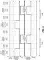
- FIG. 1shows a schematic diagram of an example thermal atomic layer deposition (thermal ALD) furnace reactor for depositing various films.
- thermal ALDthermal atomic layer deposition
- FIG. 2shows a schematic diagram of an example plasma reactor configured to perform plasma-enhanced atomic layer deposition (PEALD) for depositing various films.
- PEALDplasma-enhanced atomic layer deposition
- FIG. 3 Ashows a flow diagram of an example process for depositing a silicon oxide film using thermal ALD and PEALD according to some implementations.
- FIG. 3 Bshows a flow diagram of an example process for depositing a silicon oxide film using thermal ALD according to some implementations.
- FIG. 4illustrates an example timing sequence diagram showing a thermal ALD cycle and a PEALD cycle for depositing a silicon oxide film according to some implementations.
- FIG. 5illustrates an example timing sequence diagram showing thermal ALD cycles for depositing a silicon oxide film with co-flowed hydrogen and an oxygen-containing reactant according to some implementations.
- FIG. 6illustrates an example timing sequence diagram showing thermal ALD cycles for depositing a silicon oxide film with low RF plasma power according to some implementations.
- FIG. 7illustrates an example timing sequence diagram showing thermal ALD cycles for depositing a silicon oxide film with pulsing hydrogen flow during oxidation according to some implementations.
- FIG. 8illustrates an example timing sequence diagram showing thermal ALD cycles for depositing a silicon oxide film with oxygen radicals generated from a remote plasma source during oxidation according to some implementations.
- FIG. 9illustrates an example timing sequence diagram showing a thermal ALD cycle with co-flowed hydrogen and oxygen followed by a PEALD cycle with plasma oxidation/nitridation for depositing a silicon oxide film according to some implementations.
- FIG. 10illustrates an example timing sequence diagram showing thermal CVD with co-flowed silicon-containing precursor, hydrogen, and oxygen-containing reactant for depositing a silicon oxide film according to some implementations.
- FIG. 11is a schematic diagram of an example plasma processing apparatus for depositing a silicon oxide film using thermal ALD according to some implementations.
- FIG. 12is a schematic diagram of an example process tool for performing the disclosed implementations.
- FIG. 13shows an image of silicon oxide film deposited on fin structures by thermal ALD using several ALD cycles.
- semiconductor wafersemiconductor wafer
- wafersemiconductor wafer
- substratesubstrate
- wafer substratesemiconductor substrate
- partially fabricated integrated circuitcan refer to a silicon wafer during any of many stages of integrated circuit fabrication.
- a wafer or substrate used in the semiconductor device industrytypically has a diameter of 200 mm, or 300 mm, or 450 mm.
- the following detailed descriptionassumes the present disclosure is implemented on a wafer. However, the present disclosure is not so limited.
- the work piecemay be of various shapes, sizes, and materials.
- other work pieces that may take advantage of the present disclosureinclude various articles such as printed circuit boards and the like.
- Silicon-containing filmshave various physical, chemical, and mechanical properties and are often used in semiconductor fabrication processes.
- silicon nitride, silicon oxide, or silicon oxynitride filmsmay be used as diffusion barriers, gate insulators, sidewall spacers, etch stop layers, dielectric films, and encapsulation layers.
- silicon oxide filmsmay be used as a low-k dielectric film in a semiconductor device.
- silicon-containing filmsare deposited by chemical vapor deposition (CVD) or atomic layer deposition (ALD). In various implementations, the silicon-containing films are deposited conformally onto features of a substrate.
- ALDis a technique that deposits thin layers of material using sequential self-limiting reactions.
- an ALD cycleincludes operations to deliver and adsorb at least one precursor to the substrate surface, and then react the adsorbed precursor with one or more reactants to form the partial layer of film. Purge steps are ordinarily carried out between delivery of the precursor and delivery of the one or more reactants.
- Thermal ALDuses heat to cause a reaction between the adsorbed precursor and the one or more reactants. While thermal ALD may work well to deposit certain types of materials, thermal ALD often has a slow deposition rate due to long reaction completion times. Thermal ALD is often performed at very high temperatures, but many chemical precursors or reactants may decompose (e.g., pyrolysis) at such elevated temperatures.
- PEALDuses plasma to promote reaction between the adsorbed precursor and reactant radicals within the plasma. Reactant plasma is pulsed into a deposition chamber to react with the adsorbed precursor and form deposited material. PEALD may have a higher deposition rate and may operate at lower temperatures than thermal ALD. While PEALD processes may overcome some of the shortcomings of thermal ALD, PEALD processes may have some limitations. For example, PEALD may cause plasma damage to a substrate (e.g., etching, oxidations), and such plasma damage may occur on sensitive substrate materials such as silicon, germanium, silicon-germanium, carbon, and metals like molybdenum, tungsten, copper, cobalt, ruthenium, rhodium, and iridium. Additionally, PEALD may be incompatible with certain chemical precursors.
- furnace reactorsConventional methods for depositing films by thermal ALD are accomplished using furnace reactors or batch reactors.
- Some furnace reactorscan be hot wall systems, which have the advantage of more uniform temperature distributions and reduced convection effects.
- FIG. 1shows a schematic diagram of an example thermal atomic layer deposition furnace reactor for depositing various films.
- the thermal ALD furnace reactor 100can also be substituted as a thermal CVD reactor.
- the thermal ALD furnace reactor 100can include a plurality of heaters 110 surrounding a wall 102 of the thermal ALD furnace reactor 100 .
- the plurality of heaters 110can provide multiple heating zones that allow for some control of the axial temperature along the thermal ALD furnace reactor 100 .
- the temperature range of the thermal ALD furnace reactor 100is controlled to be between about 650° C. and about 1150° C.
- the implementation of the thermal ALD furnace reactor 100 in FIG. 1is a hot wall system.
- the thermal ALD furnace reactor 100can include a plurality of wafers 106 stacked over one another. Each of the wafers 106 may be supported by a wafer support 104 and held by gravity. The wafer-to-wafer spacing along the vertical direction of the thermal ALD furnace reactor 100 can be uniform. This allows for tens or hundreds of wafers 106 to be batch processed in a single run through the thermal ALD furnace reactor 100 .
- the thermal ALD furnace reactor 100is shown holding wafers 106 in a vertically-separated manner, though it will be understood that the thermal ALD furnace reactor 100 can hold wafers 106 in a horizontally-separated manner.
- Reactant gases 130enter the thermal ALD furnace reactor 100 by flowing through a gas inlet 122 .
- the reactant gases 130can include precursors for adsorption followed by reactant species to react with the adsorbed precursors.
- the timing and rate of flow of the reactant gases 130can be controlled by, e.g., valves and mass flow controllers, as known in the art.
- the reactant gases 130circulate through the thermal ALD furnace reactor 100 by convection and flow towards the wafers 106 by diffusion.
- the thermal ALD furnace reactor 100can be reduced to a low pressure and heated to a desirable deposition temperature, such as a temperature greater than about 700° C., or between about 700° C.
- the high temperaturedrives a chemical reaction between the reactant gases 130 to form thin films on each of the wafers 106 , where the reactant gases 130 may be delivered sequentially in pulses.
- the reactant gases 130are delivered through the gas inlet 122 and diffuse towards each of the wafers 106 . Excess reactant gases 130 may exit the thermal ALD furnace reactor 100 via gas outlet 124 .
- the deposition temperaturemust remain high to achieve a sufficient deposition rate for sufficient throughput.
- oxides and nitridessuch as silicon oxide, silicon nitride, aluminum nitride, aluminum oxide, and titanium oxide, may be deposited using a thermal ALD reactor like the thermal ALD furnace reactor 100 of FIG. 1 .
- the deposition of such oxides and nitrides in the thermal ALD reactormay require a high thermal budget.
- processing temperaturesmay be greater than 700° C. for thermal ALD.
- the thermal ALD reactormay suffer from chemical depletion effects, resulting in thickness variations across each wafer surface and through the thermal ALD reactor from the top of the reactor to the bottom of the reactor.
- subsequent wafer processing in plasma reactorsmay require transfers between different tools and platforms, increasing processing time, processing steps, cost, and the likelihood of unwanted materials or particles coming into contact with the wafers.
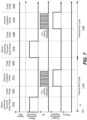
- FIG. 2shows a schematic diagram of an example plasma reactor configured to perform plasma-enhanced atomic layer deposition for depositing various films.
- the plasma reactor 200includes a plasma processing chamber 210 having a substrate support 230 configured to support a substrate 232 .
- a first gas 242may be delivered into the plasma processing chamber 210 through a first gas inlet 252 coupled to the plasma processing chamber 210 , where the first gas 242 may include precursors for adsorbing onto a surface of the substrate 232 .
- a second gas 244may be delivered into the plasma processing chamber 210 through a second gas inlet or showerhead 254 coupled to the plasma processing chamber 210 , where the second gas 244 may include gas reactants for plasma generation.
- the first gas 242may be delivered into the plasma processing chamber 210 through the showerhead 254 .
- Unreacted gas or byproducts 246may exit the plasma processing chamber 210 through a gas outlet or pump 256 .
- the plasma reactor 200includes a power source 240 coupled to the plasma processing chamber 210 and configured to generate plasma 250 in the plasma processing chamber 210 .
- the power source 240may be coupled to either the showerhead 254 or the substrate support 230 .
- An RF voltagemay be applied to an electrode of the showerhead 254 , where the plasma 250 may be generated between two electrodes spaced apart.
- the plasma 250may be generated at relatively low pressure. The use of the plasma 250 reduces the temperature for growth/formation of films on the substrate 232 due to the high reactivity of radicals in the plasma 250 .
- oxides and nitridessuch as silicon oxide, silicon nitride, aluminum nitride, aluminum oxide, and titanium oxide, may be deposited using a plasma reactor like the plasma reactor 200 of FIG. 2 .
- Low deposition temperature and high reactivity of radicals in PEALD processesmay result in many chemical reaction schemes that are difficult or impossible with thermal ALD processes.
- PEALD processesmay cause substrate damage such as plasma damage or plasma oxidation on sensitive substrates.
- the present disclosurerelates to deposition of oxide and/or nitride films on a substrate using thermal ALD in a single wafer plasma reactor.
- the oxide and/or nitride filmsmay be silicon-containing films, where the silicon-containing films may be silicon oxide (SiO x ), silicon nitride (Si x N y ), or silicon oxynitride (SiO x N y ). While such silicon-containing films may ordinarily be deposited by PEALD processes, such silicon-containing films may be deposited by thermal ALD within the same plasma reactor used for PEALD processes.
- the thermal ALD performed within the same plasma reactor as the PEALD processesmay drive thermal oxidation/nitridation at an elevated temperature that is less than the high temperatures used in conventional thermal ALD furnace reactors.
- the elevated temperaturemay be between about 500° C. and about 750° C. or between about 500° C. and about 650° C.
- Thermal ALD performed within the same plasma reactor as PEALD processesmay enable deposition of silicon-containing films with high conformality, high deposition rate, limited surface oxidation, limited bending of substrate features (e.g., pillars, fins), and uniform wet etch rate along the depth of the structure, among other advantages.
- highly conformal filmsmay be deposited by thermal ALD in a plasma processing chamber with little to no damage/oxidation to the substrate.
- thermal ALD of silicon-containing films in a plasma processing chambermay be achieved using a silicon-containing precursor and multiple gas reactants that react with one another in situ.
- thermal ALD of a silicon oxide film in a plasma processing chambermay be achieved using a silicon-containing precursor and hydrogen (H 2 ) and oxygen (O 2 ) that react in situ over a substrate to cause an exothermic reaction.
- the exothermic reactionmay provide energy to drive oxide formation for improved deposition rate.
- low RF powermay be applied to the plasma processing chamber to ignite plasma while flowing hydrogen and oxygen during thermal ALD.
- silicon-containing filmsmay be deposited in a plasma processing chamber using thermal CVD instead of thermal ALD.
- silicon-containing filmsmay be deposited in a plasma processing chamber using thermal ALD followed by PEALD. In some implementations of the present disclosure, silicon-containing films may be deposited in a plasma processing chamber using PEALD followed by thermal ALD.
- Deposition of silicon-containing films by thermal ALD in a plasma processing chamberreduces damage that may otherwise be caused by deposition of silicon-containing films by PEALD. This can be due in part to the low presence of radicals and ionic species in thermal ALD. Moreover, thermal ALD in the plasma processing chamber of the present disclosure reduces damage on substrates that may otherwise be caused by deposition of silicon-containing films using conventional thermal ALD reactors operating at high thermal budgets.
- the silicon-containing films deposited by thermal ALD in the plasma processing chamber of the present disclosuremay be deposited at a comparable deposition rate as PEALD and may provide as high quality film as films deposited by PEALD.
- thermal ALDthermal ALD
- thermal CVDreaction mechanisms for thermal ALD reactions occurring cyclically and reaction mechanisms for thermal CVD reactions occurring continuously.
- present disclosureis largely described with reference to deposition of silicon oxide films, the present disclosure can encompass deposition of any oxide or nitride films using thermal ALD.
- FIG. 3 Ashows a flow diagram of an example process for depositing a silicon oxide film using thermal ALD and PEALD according to some implementations.
- the term “silicon oxide film”may refer to undoped silicon oxide (e.g., SiO x ) films as well as doped silicon oxide (e.g., SiO x N y ) films.
- the operations in a process 300 a of FIG. 3 Amay be performed in different orders and/or with different, fewer, or additional operations.
- the operations in the process 300 amay be performed by a plasma processing apparatus shown in FIG. 11 and/or the process tool shown in FIG. 12 .
- the operations of the process 300 amay be implemented, at least in part, according to software stored in one or more non-transitory computer readable media.
- FIGS. 3 A and 4may be described together below.
- a substrateis provided in a plasma processing chamber.
- the plasma processing chambermay be a single wafer plasma reactor configured to perform thermal ALD processes, PEALD processes, or combinations thereof.
- the substratemay be a silicon substrate, such as a 200-mm, 300-mm, or 450-mm substrate, including substrates having one or more layers of material, such as dielectric, conducting, or semiconducting material.
- the substrate on which silicon oxide films are depositedmay include a material that is sensitive to plasma damage/oxidation by PEALD.
- the materialmay include but is not limited to silicon (Si), germanium (Ge), silicon-germanium (Si—Ge), carbon (C), and metals, where example metals include molybdenum (Mo), tungsten (W), copper (Cu), cobalt (Co), ruthenium (Ru), rhodium (Rh), and iridium (Ir).
- the substrate on which the silicon oxide films are depositedmay include one or more features, which may refer to non-planar structures of a substrate.
- the one or more featuresmay include vertical structures such as fins or pillars.
- the one or more featuresmay include an under-layer such as a barrier layer, liner layer, or adhesion layer.
- a first silicon oxide layeris deposited via thermal ALD in the plasma processing chamber.
- Any suitable number of thermal ALD cyclesmay be performed at block 320 prior to performing PEALD.
- Each thermal ALD cyclemay be broken down into a series of phases, including a dose phase, a first purge phase, a thermal oxidation phase, and a second purge phase. It will be understood that one or both of the first purge phase and the second purge phase may be optionally performed in each thermal ALD cycle.
- Depositing a thin film via thermal ALDincludes: heating the substrate to an elevated temperature, exposing the substrate to a precursor to adsorb onto a surface of the substrate, and exposing the substrate to one or more gas reactants to drive a surface reaction between the one or more gas reactants and the precursor, thereby forming the thin film via thermal ALD.
- depositing the first silicon oxide layer via thermal ALDincludes: heating the substrate to an elevated temperature, exposing the substrate to a silicon-containing precursor to adsorb onto a surface of the substrate, and exposing the substrate to an oxygen-containing reactant to drive a reaction between the oxygen-containing reactant and the silicon-containing precursor, thereby forming the first silicon oxide layer via thermal ALD.
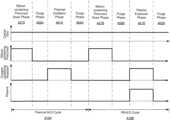
- FIG. 4illustrates an example timing sequence diagram showing a thermal ALD cycle and a PEALD cycle for depositing a silicon oxide film according to some implementations.
- FIG. 4shows phases in a thermal ALD cycle 410 A followed by phases in a PEALD cycle 410 B. However, it will be understood that phases in the PEALD cycle 410 B may be followed by phases in the thermal ALD cycle 410 A.
- FIG. 4shows various process parameters, such as carrier gas or purge gas flow, plasma, silicon-containing precursor flow, and oxygen-containing reactant flow. The lines indicate when the flow is turned on/off, or when plasma is turned on/off. As shown in FIG. 4 , during the thermal ALD cycle 410 A, the substrate is exposed to a silicon-containing precursor during a dose phase 457 A.
- the silicon-containing precursorincludes a silane, such as an aminosilane.
- An aminosilaneincludes at least one nitrogen atom bonded to a silicon atom, but may also contain hydrogens, oxygens, halogens and carbons.
- Examples of aminosilanesmay include bis(tert-butylamino)silane (BTBAS), N-(diethylaminosilyl)-N-ethylethanamine (SAM-24), tris(dimethylamino)silane (3DMAS), and tetrakis(dimethylamino)silane (4DMAS).
- the substratemay be heated to an elevated temperature during the dose phase 457 A.
- the substratemay be exposed to the silicon-containing precursor during the dose phase 457 A for a duration between about 0.1 seconds and about 60 seconds, between about 0.2 seconds and about 6 seconds, or between about 0.3 seconds and about 2 seconds, such as about 0.75 seconds, depending on the flow rate and substrate surface area.
- the silicon-containing precursoradsorbs onto the surface of the substrate in a self-limiting manner such that once active sites are occupied by the silicon-containing precursor, little or no additional silicon-containing precursor will be adsorbed on the surface of the substrate.
- the silicon-containing precursoradsorbs onto active sites of the surface of the substrate, a thin layer of the silicon-containing precursor forms on the surface. Unlike a CVD or CVD-like process, the silicon-containing precursor does not decompose to form a silicon layer.
- the plasma processing chambermay be purged between operations of exposing the substrate to the silicon-containing precursor and exposing the substrate to the oxygen-containing reactant.
- the plasma processing chambermay be purged after exposing the substrate to the oxygen-containing reactant.
- Purgingmay involve a sweep gas, which may be a carrier gas used in other operations/phases or a different gas. Purging may remove excess species in the vapor phase that did not adsorb or react on the surface of the substrate.
- the plasma processing chamberundergoes purging during purge phases 459 A and 463 A. Silicon-containing precursor flow is turned off, plasma is turned off, and oxygen-containing reactant flow is turned off. However, the carrier gas may continue to flow towards the substrate.
- the purge phases 459 A and 463 Amay each include one or more evacuation sub-phases for evacuating the plasma processing chamber. Alternatively, it will be appreciated that each of the purge phases 459 A and 463 A may be omitted in some implementations. Each purge phase 459 A and 463 A may have a suitable duration, such as between about 0 seconds and about 60 seconds or between about 0.01 seconds and about 6 seconds.
- the substratemay be exposed to the oxygen-containing reactant and the elevated temperature during a thermal oxidation phase 461 A.
- Process conditions during the thermal oxidation phase 461 Amay be tuned to promote deposition of the first silicon oxide layer by thermal ALD at an appreciable or adequate deposition rate.
- the deposition rate of the first silicon oxide layer by thermal ALDcan be equal to or greater than about 0.2 ⁇ /cycle, equal to or greater than about 0.3 ⁇ /cycle, equal to or greater than about 0.5 ⁇ /cycle, or equal to or greater than about 0.75 ⁇ /cycle. This may be an appreciable deposition rate when the first silicon oxide layer is used to protect a surface against oxidation/damage.
- the oxygen-containing reactantcan include an oxidant gas such as oxygen (O 2 ), ozone (O 3 ), hydrogen peroxide (H 2 O 2 ), water (H 2 O), or combinations thereof.
- exposing the substrate to the oxygen-containing reactantincludes flowing hydrogen and oxygen to the substrate to react in situ within the plasma processing chamber to cause an exothermic reaction.
- watermay be formed in situ by a reaction between the hydrogen and oxygen. Water vapor is not flowed into the plasma processing chamber as a starting reactant, but may or may not be formed in situ within the plasma processing chamber.
- flowing “hydrogen”refers to flowing molecular hydrogen and flowing “oxygen” refers to flowing molecular oxygen.
- the hydrogen and oxygenmay be flowed towards the substrate in the plasma processing chamber simultaneously.
- the exothermic reaction involving hydrogen and oxygenmay release energy for driving a surface reaction with the adsorbed silicon-containing precursor to form the first silicon oxide layer.
- a flow rate of hydrogen during the thermal oxidation phase 461 Amay be between about 0 slm and about 20 slm, between about 1 slm and about 10 slm, between about 2 slm and about 6 slm, greater than about 3 slm, such as about 4 slm.
- a flow rate of oxygen during the thermal oxidation phase 461 Amay be between about 0.5 slm and about 20 slm, between about 1 slm and about 10 slm, or between about 2 slm and about 8 slm, such as about 5 slm.
- a flow rate ratio between hydrogen and oxygenmay be equal to or less than about 1.2:1, such as between about 0.5:1 and about 1.2:1.
- the substratemay be exposed to the oxygen-containing reactant and exposed to an elevated temperature for a suitable duration during the thermal oxidation phase 461 A.
- thermal oxidation in furnace or batch reactors in thermal ALD/CVD chambersmay last at least 10 seconds to obtain an appreciable deposition rate, particularly for silicon oxide films.
- the duration of thermal oxidation in the plasma processing chamber of the present disclosuremay be less than about 10 seconds.
- the duration of thermal oxidation in the thermal oxidation phase 361 Amay be between about 0.1 seconds and about 6 seconds, between about 0.2 seconds and about 4 seconds, or between about 0.5 seconds and about 3 seconds.
- the substratemay be exposed to an elevated temperature during the thermal oxidation phase 461 A and/or prior to the thermal oxidation phase 461 A.
- the substratemay be operating at the elevated temperature simultaneously with exposing the substrate to the oxygen-containing reactant.
- the elevated temperaturemay be between about 500° C. and about 750° C., between about 500° C. and about 700° C., between about 500° C. and about 650° C., or between about 550° C. and about 650° C.
- temperatures in furnace or batch reactors in thermal ALD/CVD chambersmay be greater than 700° C. in driving surface reactions for deposition of silicon oxide films. However, temperatures may be equal to or less than about 700° C.
- thermal ALDin driving surface reactions for deposition of silicon oxide films by thermal ALD in a plasma processing chamber of the present disclosure.
- many conventional plasma processing chambers for PEALDdo not operate at temperatures equal to or greater than about 400° C.
- Deposition by thermal ALD in the plasma processing chamber at the elevated temperaturemay be equal to or greater than about 0.2 ⁇ /cycle.
- the substratemay be exposed to increased chamber pressure during the thermal oxidation phase 461 A.
- Increased chamber pressuremay increase deposition rate and drive the surface reaction between the silicon-containing precursor and the oxygen-containing reactant.
- the chamber pressure of the plasma processing chambermay be equal to or greater than about 7 Torr, equal to or greater than about 10 Torr, equal to or greater than about 12 Torr, or between about 10 Torr and about 20 Torr.
- a pressure in a furnace or batch reactor in thermal ALD/CVD chambersmay be less than about 5 Torr.
- chamber pressuremay be equal to or greater than about 5 Torr for deposition by thermal ALD in the plasma processing chamber of the present disclosure.
- some conventional plasma processing chambers for PEALDdo not typically operate at pressures equal to or greater than 5 Torr.
- the process conditions to achieve an appreciable deposition ratemay be different during the thermal oxidation phase 461 A depending on the selected gas reactants.
- the gas reactantconsists of oxygen
- a deposition rate greater than about 0.2 ⁇ /cyclemay be achieved at temperatures between about 550° C. and about 700° C. and chamber pressures equal to or greater than about 12 Torr.
- Such implementationsmay be referred to as an oxygen-only flow.
- a deposition rate equal to or greater than about 0.7 ⁇ /cyclemay be achieved at temperatures between about 500° C. and about 700° C. and chamber pressures equal to or greater than about 7 Torr.
- Such implementationsmay be referred to as a co-flow of hydrogen and oxygen (H 2 /O 2 ).
- the co-flow of hydrogen and oxygenmay enable higher deposition rates even at lower temperatures and pressures in the plasma processing chamber. Specifically, thermal oxidation may occur at a faster rate using the co-flow of hydrogen and oxygen compared to an oxygen-only flow.
- a plurality of thermal ALD cycles 410 Amay be performed to form the first silicon oxide layer on the substrate.
- the first silicon oxide layer deposited by thermal ALDmay serve as a liner layer prior to deposition by PEALD.
- the liner layermay protect underlying layers from substrate damage and/or provide a high quality liner in high aspect ratio structures.
- the first silicon oxide layermay be relatively thin and be between about 1 ⁇ and about 100 ⁇ , such as between about 10 ⁇ and about 100 ⁇ .
- the number of thermal ALD cyclesmay be between about between about 5 cycles and about 50 cycles, between about 5 cycles and about 20 cycles, or between about 5 cycles and about 10 cycles.
- the first silicon oxide layer deposited by the plurality of thermal ALD cycles 410 Amay cause little to no damage to the substrate and little to no oxidation to the substrate.
- an amount of silicon substrate oxidationmay be between about 1 ⁇ and about 3 ⁇ when using oxygen-only flow of thermal ALD process, whereas a typical PEALD process results in silicon substrate oxidation between about 15 ⁇ and about 35 ⁇ .
- the first silicon oxide layeris deposited on vertical structures of the substrate, little to no bending occur on the vertical structures.
- the wet etch rate of the first silicon oxide layer along the depth of the vertical structuresis uniform.
- a step coverage of the first silicon oxide layeris highly conformal.
- the step coverage of the first silicon oxide layermay be equal to or greater than about 85%, equal to or greater than about 90%, or equal to or greater than about 95%.
- FIG. 13shows an image of silicon oxide film deposited on fin structures at 650° C. using thermal ALD, where the deposited silicon oxide film exhibits high conformality and limited bending of the fin structures.
- a second silicon oxide layeris deposited on the substrate via PEALD in the plasma processing chamber.
- the thermal ALD operation at block 320 and the PEALD operation at block 330are performed in the same plasma processing chamber. Any suitable number of PEALD cycles may be performed at block 330 after performing thermal ALD.
- Each PEALD cyclemay be broken down into a series of phases, including a dose phase, a first purge phase, a plasma exposure phase, and a second purge phase. It will be understood that one or both of the first purge phase and the second purge phase may be optionally performed in each PEALD cycle.
- Depositing a thin film via PEALDincludes: exposing the substrate to a precursor to adsorb onto a surface of the substrate, and exposing the substrate to plasma generated from one or more gas reactants, where the plasma drives a reaction between reactive species of the one or more gas reactants and the precursor, thereby forming the thin film via PEALD.
- depositing the second silicon oxide layer by PEALDincludes: exposing the substrate to a silicon-containing precursor to adsorb onto the surface of the substrate, and exposing the substrate to plasma generated from an oxygen-containing reactant, where the plasma drives a reaction between reactive species of the oxygen-containing reactant and the silicon-containing precursor, thereby forming the second silicon oxide layer via PEALD.
- the silicon-containing precursor in the PEALD cyclesmay or may not be the same as the silicon-containing precursor in the thermal ALD cycles.
- the oxygen-containing reactant in the PEALD cyclesmay or may not be the same as the oxygen-containing reactant in the thermal ALD cycles.
- the oxygen-containing reactantmay include oxygen, ozone, or combinations thereof.
- the substrateis exposed to a silicon-containing precursor during a dose phase 457 B.
- the silicon-containing precursorincludes a silane, such as an aminosilane.
- plasmais turned off, oxygen-containing reactant flow is turned off, and a carrier gas may be flowed towards the substrate.
- the silicon-containing precursoradsorbs onto the surface of the substrate in a self-limiting manner such that once active sites are occupied by the silicon-containing precursor, little or no additional silicon-containing precursor will be adsorbed on the surface of the substrate.
- the plasma processing chambermay be purged between operations of exposing the substrate to the silicon-containing precursor and exposing the substrate to an oxygen-containing reactant.
- the plasma processing chambermay be purged after exposing the substrate to the oxygen-containing reactant.
- Purgingmay involve a sweep gas, which may be a carrier gas used in other operations/phases or a different gas. Purging may remove excess species in the vapor phase that did not adsorb or react onto the surface of the substrate.
- the plasma processing chamberundergoes purging during purge phases 459 B and 463 B. Silicon-containing precursor flow is turned off, plasma is turned off, and oxygen-containing reactant flow is turned off. However, the carrier gas may continue to flow towards the substrate.
- the purge phases 459 B and 463 Bmay each include one or more evacuation sub-phases for evacuating the plasma processing chamber. Alternatively, it will be appreciated that each of the purge phases 459 B and 463 B may be omitted in some implementations.
- the substratemay be exposed to the plasma generated from the oxygen-containing reactant during a plasma exposure phase 461 B.
- An oxygen plasmamay be ignited during the plasma exposure phase 461 B.
- the plasmamay include ions, radicals, charged neutrals, and other reactive species generated from the oxygen-containing reactant.
- the reactive species from the oxygen-containing reactantmay react with the adsorbed silicon-containing precursor to form the second silicon oxide layer over the first silicon oxide layer.
- the plasmamay be generated in situ or remotely. Flow of the silicon-containing precursor is turned off while flow of the oxygen-containing reactant is turned on during the plasma exposure phase 461 B.
- Process conditions in the plasma processing chambermay vary for the oxygen plasma during the plasma exposure phase 461 B.
- the substrate temperaturemay be maintained between about 0° C. and about 750° C. or between about 20° and about 200° C.
- the chamber pressure in the plasma processing chambermay be relatively low and between about 10 mTorr and about 200 mTorr, or may be relatively high and between about 1 Torr and about 7 Torr.
- An RF fieldis applied to the plasma processing chamber to generate ions and radicals of the oxygen-containing reactant.
- the RF frequency used to generate the plasmamay be at least about 13.56 MHz, at least about 27 MHz, at least about 40 MHz, or at least about 60 MHz, though other frequencies may also be used.
- the RF powermay be a few hundred Watts, for example about 500 W or less, about 400 W or less, or about 300 W or less, though it will be understood that other RF powers may be applied depending on substrate area.
- the duration of the plasma exposure phase 461 Bmay be between about 0.1 seconds and about 120 seconds or between about 1 second and about 60 seconds.
- a plurality of PEALD cycles 410 Bmay be performed to form the second silicon oxide layer on the first silicon oxide layer.
- the first silicon oxide layer deposited by thermal ALD cycles 410 Amay provide a liner layer of silicon oxide film to protect underlying layers.
- the liner layermay be relatively thin and between about 10 ⁇ and about 100 ⁇ thick.
- the liner layermay serve as a protective liner on soft layers to eliminate or otherwise reduce substrate damage.
- the liner layermay serve as a high quality liner on high aspect ratio structures.
- Such high aspect ratio structuresmay include fins and pillars. The high aspect ratio structures may be prone to bending/damage when exposed to only PEALD operations.
- first silicon oxide layer deposited by thermal ALD prior to the second silicon oxide layerprovides high conformality, high deposition rate, limited surface oxidation, limited bending of substrate features (e.g., pillars, fins), and uniform wet etch rate on sidewalls.
- the second silicon oxide layer deposited by PEALD cycles 410 Bmay follow as bulk deposition of silicon oxide film on the liner layer. Accordingly, in various implementations, nucleation of silicon oxide film may be performed by thermal ALD and bulk deposition may be performed by PEALD in the same plasma processing chamber.
- the process 300 afurther includes exposing the substrate to plasma generated from a nitrogen-containing reactant in the plasma processing chamber, where the plasma drives a reaction between reactive species of the nitrogen-containing reactant and at least the second silicon oxide layer, thereby converting at least the second silicon oxide layer to a silicon oxynitride layer.
- the nitrogen-containing reactantmay include nitrogen (N 2 ), ammonia (NH 3 ), or combinations thereof.
- a nitrogen plasmamay cause nitridation of one or both of the first and second silicon oxide layer to form the silicon oxynitride layer.
- the process 300 amay include depositing a silicon nitride layer on the first and second silicon oxide layer by thermal ALD or PEALD in the plasma processing chamber.
- the combination of the first silicon oxide layer, the second silicon oxide layer, and the silicon nitride layercollectively form a silicon oxynitride film.
- silicon oxide and silicon nitride layersmay be deposited in alternating fashion to form nanolaminates of silicon oxide/silicon nitride.
- the process 300 afurther includes annealing the substrate to form the silicon oxynitride film from the first silicon oxide layer, the second silicon oxide layer, and the silicon nitride layer.
- FIG. 3 Bshows a flow diagram of an example process for depositing a silicon oxide film using thermal ALD according to some implementations.
- the operations in a process 300 b of FIG. 3 Bmay be performed in different orders and/or with different, fewer, or additional operations.
- the operations in the process 300 bmay be performed by a plasma processing apparatus shown in FIG. 11 and/or the process tool shown in FIG. 12 .
- the operations of the process 300 bmay be implemented, at least in part, according to software stored in one or more non-transitory computer readable media.
- FIGS. 3 B and 5 - 10may be described together below.
- a substrateis heated to an elevated temperature.
- the substratemay be heated to the elevated temperature before and during thermal ALD. This allows the substrate to be heated to the elevated temperature to drive surface reactions between precursors and reactants in thermal ALD.
- the elevated temperature applied to the substratemay be between about 500° C. and about 750° C., between about 500° C. and about 700° C., between about 500° C. and about 650° C., or between about 550° C. and about 650° C.
- a pressure of a plasma processing chambermay be equal to or greater than about 7 Torr, equal to or greater than about 10 Torr, or equal to or greater than about 12 Torr. Chamber pressure may provide a further knob to control the deposition rate of the layer of silicon oxide film.
- the substrateprior to heating the substrate to the elevated temperature, the substrate may be provided into the plasma processing chamber.
- the plasma processing chambermay be a single wafer plasma reactor configured to perform thermal ALD processes, PEALD processes, or combinations thereof.
- the substratemay be a silicon substrate, such as a 200-mm, 300-mm, or 450-mm substrate, including substrates having one or more layers of material, such as dielectric, conducting, or semiconducting material.
- the substrate on which silicon oxide films are depositedmay include a material that is sensitive to plasma damage by PEALD.
- the materialmay include but is not limited to silicon, germanium, silicon-germanium, carbon, and metals, where example metals may include molybdenum, tungsten, copper, cobalt, ruthenium, rhodium, and iridium.
- the substrate on which the silicon oxide films are depositedmay include one or more features such as fins or pillars.
- the one or more featuresmay include an under-layer such as a barrier layer, liner layer, or adhesion layer.
- the substrateis exposed to a silicon-containing precursor to adsorb onto a surface of the substrate in the plasma processing chamber.
- the silicon-containing precursorincludes a silane, such as an aminosilane.
- An aminosilaneincludes at least one nitrogen atom bonded to a silicon atom, but may also contain hydrogens, oxygens, halogens and carbons. Examples of aminosilanes may include BTBAS, N-SAM-24, 3DMAS, and 4DMAS.
- the substrateis exposed to the silicon-containing precursor while the substrate is heated to the elevated temperature.
- FIG. 5illustrates an example timing sequence diagram showing thermal ALD cycles for depositing a silicon oxide film with co-flowed hydrogen and an oxygen-containing reactant according to some implementations.
- a first thermal ALD cycle 510 Amay include a dose phase 557 A, followed by a first purge phase 559 A, followed by a thermal oxidation phase 561 A, and followed by a second purge phase 563 A.
- a second thermal ALD cycle 510 Bmay include a dose phase 557 B, followed by a first purge phase 559 B, followed by a thermal oxidation phase 561 B, and followed by a second purge phase 563 B. As shown in FIG.
- the substratemay be exposed to the silicon-containing precursor during the dose phase 557 A/ 557 B of the thermal ALD cycle 510 A/ 510 B, where a duration of the dose phase 557 A/ 557 B may be between about 0.1 seconds and about 60 seconds, between about 0.2 seconds and about 6 seconds, or between about 0.3 seconds and about 2 seconds, such as about 0.75 seconds, depending on the flow rate and the substrate surface area.
- the silicon-containing precursoradsorbs onto the surface of the substrate in a self-limiting manner such that once active sites are occupied by the silicon-containing precursor, little or no additional silicon-containing precursor will be adsorbed on the surface of the substrate.
- plasmais turned off, no oxygen-containing reactant is flowed to the substrate, and a carrier gas may be flowed towards the substrate.
- the plasma processing chambermay be purged between operations of exposing the substrate to the silicon-containing precursor and flowing hydrogen and an oxygen-containing reactant into the plasma processing chamber.
- the plasma processing chambermay be purged after the flow of hydrogen and oxygen-containing reactant has ceased.
- Purgingmay involve a sweep gas, which may be a carrier gas used in other operations/phases or a different gas. Purging may remove excess species in the vapor phase that did not adsorb or react on the surface of the substrate. As shown in FIG. 5 , the plasma processing chamber undergoes purging during purge phases 559 A, 563 A, 559 B, and 563 B.
- the purge phases 559 A, 563 A, 559 B, and 563 Bmay each include one or more evacuation sub-phases for evacuating the plasma processing chamber. Alternatively, it will be appreciated that each of the purge phases 559 A, 563 A, 559 B, and 563 B may be omitted in some implementations. Each purge phase 559 A, 563 A, 559 B, and 563 B may have a suitable duration, such as between about 0 seconds and about 60 seconds or between about 0.01 seconds and about 6 seconds.
- hydrogen and oxygen-containing reactantare flowed towards the substrate in the plasma processing chamber.
- the hydrogen and the oxygen-containing reactantreact within the plasma processing chamber, where a layer of a silicon oxide film is formed on the substrate.
- the hydrogen and oxygen-containing reactantmay be flowed simultaneously into the plasma processing chamber.
- the oxygen-containing reactantincludes oxygen or ozone.
- the oxygen-containing reactantincludes oxygen, thereby providing a co-flow of hydrogen and oxygen (H 2 /O 2 ).
- the hydrogen and the oxygen-containing reactantreact in situ with one another within the plasma processing chamber in an exothermic reaction.
- the reaction between the hydrogen and the oxygen-containing reactantforms water in the exothermic reaction.
- the exothermic reactionreleases energy that may drive the thermal oxidation of the adsorbed silicon-containing precursor to form silicon oxide film.
- the flow rate of hydrogen and the flow rate of the oxygen-containing reactantmay be controlled according to a desired flow rate ratio to promote thermal oxidation.
- a flow rate ratio between hydrogen and the oxygen-containing reactantmay be equal to or less than about 1.2:1, such as between about 0.5:1 and about 1.2:1.
- a flow rate of hydrogenmay be between about 0 slm and about 20 slm, between about 1 slm and about 10 slm, between about 2 slm and about 6 slm, greater than about 3 slm, such as about 4 slm.
- a flow rate of oxygen-containing reactantmay be between about 0.5 slm and about 20 slm, between about 1 slm and about 10 slm, or between about 2 slm and about 8 slm, such as about 5 slm.
- the substrateis maintained at the elevated temperature.
- the substrateis at the elevated temperature while the hydrogen and oxygen-containing reactant are flowing towards the substrate to drive a reaction with the adsorbed silicon-containing precursor in the plasma processing chamber, thereby forming the layer of the silicon oxide film.
- the elevated temperaturemay promote formation of the layer of the silicon oxide film at an appreciable deposition rate.
- the in situ exothermic reaction between hydrogen and the oxygen-containing reactant along with the heated substrate at the elevated temperaturemay provide sufficient energy to drive the formation of the layer of the silicon oxide film at an appreciable deposition rate.
- the deposition rate of the layer of the silicon oxide film using co-flowed hydrogen and oxygen-containing reactantmay be equal to or greater than about 0.7 ⁇ /cycle.
- hydrogen and oxygen-containing reactantmay be flowed towards the substrate while the substrate is heated at the elevated temperature during a thermal oxidation phase 561 A/ 561 B of the thermal ALD cycle 510 A/ 510 B.
- the in situ exothermic reaction between the hydrogen and oxygen-containing reactant combined with the substrate heated at the elevated temperaturemay provide energy for driving oxidation during the thermal oxidation phase 561 A/ 561 B.
- temperature and pressure in the plasma processing chambermay be controlled to enable the deposition of the layer of the silicon oxide film at a deposition rate equal to or greater than about 0.7 ⁇ /cycle during the thermal oxidation phase 561 A/ 561 B.
- a duration of the thermal oxidation phase 561 A/ 561 Bmay be between about 0.1 seconds and about 6 seconds, between about 0.2 seconds and about 4 seconds, or between about 0.5 seconds and about 3 seconds.
- the duration of the thermal oxidation phase 561 A/ 561 B with co-flowed hydrogen and oxygen-containing reactantmay be between about 0.5 seconds and about 1 second, such as about 0.8 seconds.
- plasmais turned off and silicon-containing precursor flow is turned off.
- carrier gas, hydrogen, and oxygen-containing reactant flowmay be turned on.
- Example process times and process conditionsare shown in Table 1 for co-flowed hydrogen and oxygen in thermal ALD.
- the process 300 bfurther includes applying plasma power to the plasma processing chamber to ignite plasma generated from the hydrogen and oxygen-containing reactant in the plasma processing chamber.
- the plasmamay include ions, radicals, and other reactive species of hydrogen and oxygen (e.g., H* and O*).
- the plasmamay further include ions, radicals, and other reactive species of the carrier gas (e.g., Art).
- the plasma power applied to the plasma processing chambermay be relatively small.
- the plasma power applied to the plasma processing chamberis equal to or less than about 300 W, equal to or less than about 200 W, or between about 10 W and about 200 W. That way, the plasma may include more radicals and fewer ions.
- the RF frequency used to generate the plasmamay be at least about 13.56 MHz, at least about 27 MHz, at least about 40 MHz, or at least about 60 MHz, though other frequencies may also be used.
- low RF powermay ignite low RF plasma with energy from the exothermic reaction between the hydrogen and the oxygen-containing reactant. Without an in situ exothermic reaction between hydrogen and the oxygen-containing reactant, plasma may not be ignited at relatively low RF powers. In other words, a combustion reaction of hydrogen and the oxygen-containing reactant may contribute to generating low RF plasma in the plasma processing chamber. A stable plasma may be maintained at relatively low RF powers.
- the low RF plasmamay limit damage to the substrate and particularly limit damage to any sensitive substrate.
- the low RF plasmamay enhance or at least modulate deposition and properties of the layer of silicon oxide film. In some implementations, the low RF plasma may modulate deposition rate and provide higher wet etch rates. In some implementations, the low RF plasma may provide more conformal films, lower operating temperatures, and/or higher deposition rates.
- FIG. 6illustrates an example timing sequence diagram showing thermal ALD cycles for depositing a silicon oxide film with low RF plasma power according to some implementations.
- FIG. 6shows a first thermal ALD cycle 610 A that includes a dose phase 657 A, first purge phase 659 A, thermal oxidation phase 661 A, and second purge phase 663 A.
- FIG. 6also shows a second thermal ALD cycle 610 B that includes a dose phase 657 B, first purge phase 659 B, thermal oxidation phase 661 B, and second purge phase 663 B.
- Aspects of the phases for each of the thermal ALD cycles 610 A/ 610 B of FIG. 6can be described in the thermal ALD cycles 510 A/ 510 B of FIG. 5 .
- the plasma powercan be a low RF plasma power that is equal to or less than about 300 W, equal to or less than about 200 W, or between about 10 W and about 200 W.
- Application of the low RF plasma poweroccurs while hydrogen and oxygen-containing reactant are being flowed toward the substrate and while the substrate is heated at the elevated temperature.
- Reactive species in the plasmasuch as radicals of oxygen may react with the adsorbed silicon-containing precursor to form silicon oxide.
- flowing hydrogen and oxygen-containing reactant towards the substratemay include flowing the oxygen-containing reactant continuously into the plasma processing chamber and pulsing hydrogen at regular intervals into the plasma processing chamber.
- the hydrogenmay be pulsed at regular intervals while the oxygen-containing reactant is simultaneously and continuously flowed towards the substrate.
- a constant oxygen flowmay be combined with pulsed hydrogen flow into the plasma processing chamber.
- pulses of hydrogenmay be introduced into the plasma processing chamber at regular intervals that last between about 0.1 seconds and about 1 second, between about 0.1 seconds and about 0.8 seconds, or between about 0.2 seconds and about 0.6 seconds. Pulsing hydrogen may facilitate combustion reactions of hydrogen and oxygen-containing reactant that occur in pulses rather than continuously.
- Pulsing hydrogenmay affect the deposition and properties of the layer of silicon oxide film.
- the duration of the thermal oxidation phasemay be longer. Without being limited by any theory, this permits pulsed exothermic reaction(s) to proceed for as long as desired to drive film properties.
- FIG. 7illustrates an example timing sequence diagram showing thermal ALD cycles for depositing a silicon oxide film with pulsing hydrogen flow during oxidation according to some implementations.
- FIG. 7shows a first thermal ALD cycle 710 A that includes a dose phase 757 A, first purge phase 759 A, thermal oxidation phase 761 A, and second purge phase 763 A.
- FIG. 7also shows a second thermal ALD cycle 710 B that includes a dose phase 757 B, first purge phase 759 B, thermal oxidation phase 761 B, and second purge phase 763 B.
- Aspects of the phases for each of the thermal ALD cycles 710 A/ 710 B of FIG. 7can be described in the thermal ALD cycles 510 A/ 510 B of FIG. 5 .
- pulses in the pulsed hydrogen flowcan be in the form of a square waveform.
- the pulses in the pulsed hydrogen flowcan occur in regular intervals, where each of the regular intervals can last between about 0.1 seconds and about 1 second, between about 0.1 seconds and about 0.8 seconds, or between about 0.2 seconds and about 0.6 seconds.
- a total duration of the thermal oxidation phase 761 A/ 761 Bmay be equal to or greater than 0.5 seconds, equal to or greater than 1 second, or between about 1 second and about 30 seconds.
- the duty cycle of the pulsed hydrogen flowcan be between about 1% and about 99%, between about 5% and about 95%, between about 15% and about 90%, or between about 25% and about 75%.
- flowing hydrogen and oxygen-containing reactant towards the substratemay include generating oxygen radicals from the oxygen-containing reactant in a remote plasma source, introducing the radicals of oxygen into the plasma processing chamber, and flowing the hydrogen into the plasma processing chamber.
- the radicals of oxygenmay provide more reactive species to react with the hydrogen and the adsorbed silicon-containing precursor.
- the radicals of oxygenmay react with hydrogen to form hydroxyl radicals or water, where the hydroxyl radicals or water may promote oxidation of the adsorbed silicon-containing precursor.
- the oxygen radicalsare generated from oxygen gas or ozone.
- remote plasma sourceis located upstream of the plasma processing chamber, where the remote plasma source can be any suitable plasma generator such as an inductively-coupled plasma generator or capacitively-coupled plasma generator.
- FIG. 8illustrates an example timing sequence diagram showing thermal ALD cycles for depositing a silicon oxide film with oxygen radicals generated from a remote plasma source during oxidation according to some implementations.
- FIG. 8shows a first thermal ALD cycle 810 A that includes a dose phase 857 A, first purge phase 859 A, thermal oxidation phase 861 A, and second purge phase 863 A.
- FIG. 8also shows a second thermal ALD cycle 810 B that includes a dose phase 857 B, first purge phase 859 B, thermal oxidation phase 861 B, and second purge phase 863 B.
- Aspects of the phases for each of the thermal ALD cycles 810 A/ 810 B of FIG. 8can be described in the thermal ALD cycles 510 A/ 510 B of FIG. 5 .
- oxygen radicalsare introduced into the plasma processing chamber instead of pure oxygen gas. Hydrogen flow may be continuous and simultaneous with the flow of oxygen radicals into the plasma processing chamber. However, it will be understood that in some implementations, hydrogen flow may be pulsed.
- remote plasma poweris turned on rather than off. RF power may be applied to a remote plasma source to generate the oxygen radicals upstream from the plasma processing chamber.
- the process 300 bfurther includes performing PEALD in the plasma processing chamber.
- the process 300 bcan include depositing one or more additional layers of the silicon oxide film on the substrate via PEALD in the plasma processing chamber.
- the process 300 bcan include depositing one or more layers of a silicon nitride film on the layer of the silicon oxide film by thermal ALD or PEALD in the plasma processing chamber to ultimately form a silicon oxynitride film.
- a PEALD cyclecan include exposing the substrate to plasma of a nitrogen-containing reactant to convert the layer of the silicon oxide film to a silicon oxynitride film during a plasma exposure phase.
- the layer of silicon oxide film deposited by thermal ALDmay serve as a liner layer protecting underlying layers of the substrate, and subsequent layers of silicon oxide and/or silicon nitride may be deposited in bulk over the liner layer.
- the layer of silicon oxide film deposited by thermal ALDmay exhibit high conformality, high deposition rate, limited surface oxidation, limited bending of substrate features (e.g., pillars, fins), and uniform wet etch rate on sidewalls.
- performing PEALD in the plasma processing chambermay occur before thermal ALD in the plasma processing chamber.
- layers of silicon oxide filmmay be deposited by PEALD and followed by additional layers of silicon oxide film deposited by thermal ALD.
- FIG. 9illustrates an example timing sequence diagram showing a thermal ALD cycle with co-flowed hydrogen and oxygen followed by a PEALD cycle with plasma oxidation/nitridation for depositing a silicon-containing film according to some implementations.
- the PEALD cyclemay be performed prior to the thermal ALD cycle in some implementations.
- FIG. 9shows a thermal ALD cycle 910 A that includes a dose phase 957 A, a first purge phase 959 A, a thermal oxidation phase 961 A, and a second purge phase 963 A.
- FIG. 9shows a thermal ALD cycle 910 A that includes a dose phase 957 A, a first purge phase 959 A, a thermal oxidation phase 961 A, and a second purge phase 963 A.
- FIG. 9also shows a PEALD cycle 910 B that includes a dose phase 957 B, first purge phase 959 B, plasma oxidation/nitridation phase 961 B, and second purge phase 963 B.
- a PEALD cycle 910 Bthat includes a dose phase 957 B, first purge phase 959 B, plasma oxidation/nitridation phase 961 B, and second purge phase 963 B.
- Aspects of the phases for the thermal ALD cycle 910 A of FIG. 9can be described in the thermal ALD cycle 510 A/ 510 B of FIG. 5 .
- Aspects of the phases for the PEALD cycle 910 B of FIG. 9can be described in the PEALD cycle 410 B of FIG. 4 .
- the substratemay be exposed to an oxygen plasma or nitrogen plasma. If plasma nitridation takes place, one or more nitrogen-containing reactants may be flowed towards the substrate and plasma turned on.
- the one or more nitrogen-containing reactantsmay include N 2 /NH 3 .
- the plasma nitridationmay deposit a layer of silicon nitride film over the layer of silicon oxide film. In some implementations, the plasma nitridation may convert silicon oxide to silicon oxynitride.
- one or more oxygen-containing reactantsmay be flowed towards the substrate and plasma turned on. For example, the one or more oxygen-containing reactants may include O 2 .
- the plasma oxidationmay deposit an additional layer of silicon oxide film over the layer of silicon oxide film.
- exposing the substrate to the silicon-containing precursor and flowing the hydrogen and oxygen-containing reactantmay occur in a continuous manner rather than in a cyclic manner Specifically, exposing the substrate to the silicon-containing precursor and flowing the hydrogen and oxygen-containing reactant occurs in a thermal CVD process instead of a thermal ALD process.
- thermal ALD reactionsinvolve cyclically performing (a) delivery of precursor to form an adsorbed precursor layer, (b) optional purge operation, (c) delivery of reactant(s) on a heated substrate, (d) optional purge operation, and (e) repeating operations (a)-(d) until the film reaches a desired thickness.
- thermal CVD reactionsinvolve delivering the precursor and reactant(s) continuously while the substrate is heated.
- CVD reactionsare gas phase reactions, which deposition reaction products on the substrate surface.
- the reaction mechanism of the present disclosuremay involve thermal CVD using silicon-containing precursor, hydrogen, and oxygen-containing reactant being delivered continuously rather than cyclically in thermal ALD.
- FIG. 10illustrates an example timing sequence diagram showing thermal CVD with co-flowed silicon-containing precursor, hydrogen, and oxygen-containing reactant for depositing a silicon-containing film according to some implementations.
- a thermal CVD process 1010is not broken down into a series of phases in cycles. Carrier gas is continuously flowed to the substrate, silicon-containing precursor is continuously flowed to the substrate, hydrogen gas is continuously flowed to the substrate, and oxygen-containing reactant is continuously flowed to the substrate. Delivery of the silicon-containing precursor, delivery of hydrogen, and delivery of the oxygen-containing reactant do not occur sequentially and do not occur in separate phases. Plasma is turned off during the thermal CVD process 1010 .
- any of the foregoing techniques described in FIGS. 4 - 10may be mixed together in a series of ALD cycles and/or CVD reactions.
- deposition of a silicon-containing film by thermal ALDmay involve one or more cycles with pulsed hydrogen flow, one or more cycles with co-flowed hydrogen and oxygen-containing reactant, one or more cycles with application of low RF power, one or more cycles with oxygen radicals, one or more PEALD cycles for plasma oxidation/nitridation, and one or more periods of thermal CVD reactions with a silicon-containing precursor, hydrogen, and oxygen-containing reactant.
- Such techniquesmay be applied in any sequence when depositing the silicon-containing film.
- a suitable apparatusincludes hardware for accomplishing the process operations and a system controller having instructions for controlling process operations in accordance with the present disclosure.
- the hardwaremay include one or more process stations included in a process tool.
- the thermal ALD/CVD and PEALD/PECVDmay be performed in a single station/chamber.
- FIG. 11is a schematic diagram of an example plasma processing apparatus for depositing a silicon-containing film using thermal ALD according to some implementations.
- the plasma apparatus or process station 1100 aincludes a plasma processing chamber 1102 for maintaining a low-pressure environment.
- a plurality of plasma apparatuses or process stations 1100 amay be included in a common low-pressure process tool environment.
- FIG. 12depicts an implementation of a multi-station processing tool 1200 .
- one or more hardware parameters of the plasma apparatus or process station 1100 a including those discussed in detail belowmay be adjusted programmatically by one or more system controllers 1150 .
- the plasma apparatus or process station 1100 acan be configured to perform thermal ALD and PEALD, thermal CVD and PEALD, thermal ALD and PECVD, or thermal CVD and PECVD. In some implementations, the plasma apparatus or process station 1100 a can be configured to perform one or more PEALD cycles and one or more thermal ALD cycles to deposit a silicon oxide film on a substrate 1112 .
- the apparatus or process station 1100 afluidly communicates with reactant delivery system 1101 a for delivering process gases to a distribution showerhead 1106 .
- Reactant delivery system 1101 aincludes a mixing vessel 1104 for blending and/or conditioning process gases, such as a silicon-containing precursor in the vapor phase, for delivery to showerhead 1106 .
- the reactant delivery system 1101 aincludes a mixing vessel 1104 for blending and/or conditioning an oxygen-containing reactant (e.g., oxygen) for delivery to the showerhead 1106 .
- the reactant delivery system 1101 aincludes a mixing vessel 1104 for blending and/or conditioning hydrogen and an oxygen-containing reactant (e.g., oxygen) for delivery to the showerhead 1106 .
- One or more mixing vessel inlet valves 1120may control introduction of process gases to mixing vessel 1104 .
- Plasma of the oxygen-containing reactantmay also be delivered to the showerhead 1106 or may be generated in the plasma apparatus or process station 1100 a .
- the showerhead 1106may be fluidly coupled to the plasma processing chamber 1102 for delivery of silicon-containing precursors and reactants into the plasma processing chamber 1102 .
- the implementation of FIG. 11includes a vaporization point 1103 for vaporizing liquid reactant to be supplied to the mixing vessel 1104 .
- vaporization point 1103may be a heated vaporizer.
- delivery piping downstream of vaporization point 1103may be heat traced.
- the mixing vessel 1104may also be heat traced.
- piping downstream of vaporization point 1103has an increasing temperature profile extending from approximately 100° C. to approximately 150° C. at the mixing vessel 1104 .
- liquid precursor or liquid reactantmay be vaporized at a liquid injector.
- a liquid injectormay inject pulses of a liquid reactant into a carrier gas stream upstream of the mixing vessel 1104 .
- a liquid injectormay vaporize the reactant by flashing the liquid from a higher pressure to a lower pressure.
- a liquid injectormay atomize the liquid into dispersed microdroplets that are subsequently vaporized in a heated delivery pipe. Smaller droplets may vaporize faster than larger droplets, reducing a delay between liquid injection and complete vaporization. Faster vaporization may reduce a length of piping downstream from vaporization point 1103 .
- a liquid injectormay be mounted directly to mixing vessel 1104 .
- a liquid injectormay be mounted directly to showerhead 1106 .
- a liquid flow controller (LFC) upstream of vaporization point 1103may be provided for controlling a mass flow of liquid for vaporization and delivery to the plasma apparatus or process station 1100 a .
- the LFCmay include a thermal mass flow meter (MFM) located downstream of the LFC.
- a plunger valve of the LFCmay then be adjusted responsive to feedback control signals provided by a proportional-integral-derivative (PID) controller in electrical communication with the MFM.
- PIDproportional-integral-derivative
- the LFCmay be dynamically switched between a feedback control mode and a direct control mode. In some implementations, this may be performed by disabling a sense tube of the LFC and the PID controller.
- the showerhead 1106distributes process gases toward a substrate 1112 .
- the substrate 1112is located beneath the showerhead 1106 and is shown resting on a substrate support 1108 , where the substrate support 1108 is configured to support the substrate 1112 .
- the substrate support 1108may include a chuck, a fork, or lift pins (not shown) to hold and transfer the substrate 1112 during and between the deposition operations.
- the chuckmay be an electrostatic chuck, a mechanical chuck, or various other types of chuck as are available for use in the industry and/or for research.
- the showerhead 1106may have any suitable shape, and may have any suitable number and arrangement of ports for distributing process gases to the substrate 1112 .
- the substrate support 1108may be raised or lowered to expose the substrate 1112 to a volume between the substrate 1112 and the showerhead 1106 . It will be appreciated that, in some implementations, substrate support height may be adjusted programmatically by a suitable system controller 1150 .
- adjusting a height of the substrate support 1108may allow a plasma density to be varied during plasma activation cycles included in the process.
- the substrate support 1108may be lowered during another substrate transfer phase to allow removal of the substrate 1112 from the substrate support 1108 .
- the substrate support 1108may be configured to be heated to an elevated temperature via a heater 1110 .
- the substrate support 1108may be heated to a temperature less than about 700° C., such as about between about 500° C. and about 750° C. or between about 500° C. and about 650° C., during deposition of silicon oxide films as described in the disclosed implementations.
- pressure control for the apparatus or process station 700 amay be provided by a butterfly valve 1118 . As shown in the implementation of FIG. 11 , the butterfly valve 1118 throttles a vacuum provided by a downstream vacuum pump (not shown). However, in some implementations, pressure control of the plasma processing chamber 1102 may also be adjusted by varying a flow rate of one or more gases introduced to the plasma processing chamber 1102 .
- the pressure in the plasma processing chamber 1102may be controlled to be equal to or greater than about 7 Torr, equal to or greater than about 10 Torr, or equal to or greater than about 12 Torr during deposition of silicon oxide films as described in the disclosed implementations.
- a position of the showerhead 1106may be adjusted relative to the substrate support 1108 to vary a volume between the substrate 1112 and the showerhead 1106 . Further, it will be appreciated that a vertical position of substrate support 1108 and/or showerhead 1106 may be varied by any suitable mechanism within the scope of the present disclosure.
- the substrate support 1108may include a rotational axis for rotating an orientation of the substrate 1112 . It will be appreciated that, in some implementations, one or more of these example adjustments may be performed programmatically by one or more suitable system controllers 1150 .
- showerhead 1106 and substrate support 1108electrically communicate with a radio frequency (RF) power supply 1114 and matching network 1116 for powering a plasma in the plasma processing chamber 1102 .
- the plasma energymay be controlled by controlling one or more of a process station pressure, a gas concentration, an RF source power, an RF source frequency, and a plasma power pulse timing.
- RF power supply 1114 and matching network 1116may be operated at any suitable power to form a plasma having a desired composition of radical species.
- the RF power supply 1114 and matching network 1116may be operated to apply plasma power to the plasma processing chamber 1102 to ignite plasma generated from hydrogen and oxygen-containing reactant in the plasma processing chamber 1102 .
- Example plasma powers applied by the RF power supply 1114may be equal to or less than about 300 W, equal to or less than about 200 W, or between about 10 W and about 200 W. Likewise, RF power supply 1114 may provide RF power of any suitable frequency. In some implementations, RF power supply 1114 may be configured to control high- and low-frequency RF power sources independently of one another.
- Example low-frequency RF frequenciesmay include, but are not limited to, frequencies between 0 kHz and 500 kHz.
- Example high-frequency RF frequenciesmay include, but are not limited to, frequencies between 1.8 MHz and 2.45 GHz, or at least about 13.56 MHz, or at least about 27 MHz, or at least about 40 MHz, or at least about 60 MHz. It will be appreciated that any suitable parameters may be modulated discretely or continuously to provide plasma energy for the surface reactions.
- the plasmamay be monitored in-situ by one or more plasma monitors.
- plasma powermay be monitored by one or more voltage, current sensors (e.g., VI probes).
- plasma density and/or process gas concentrationmay be measured by one or more optical emission spectroscopy sensors (OES).
- OESoptical emission spectroscopy sensors
- one or more plasma parametersmay be programmatically adjusted based on measurements from such in situ plasma monitors.
- an OES sensormay be used in a feedback loop for providing programmatic control of plasma power.
- other monitorsmay be used to monitor the plasma and other process characteristics. Such monitors may include, but are not limited to, infrared (IR) monitors, acoustic monitors, and pressure transducers.
- instructions for a controller 1150may be provided via input/output control (IOC) sequencing instructions.
- the instructions for setting conditions for a process phasemay be included in a corresponding recipe phase of a process recipe.
- process recipe phasesmay be sequentially arranged, so that all instructions for a process phase are executed concurrently with that process phase.
- instructions for setting one or more reactor parametersmay be included in a recipe phase.
- a first recipe phasemay include instructions for setting a flow rate of an inert and/or a precursor gas (e.g., the silicon-containing precursor), instructions for setting a flow rate of a carrier gas (such as argon), and time delay instructions for the first recipe phase.
- a second, subsequent recipe phasemay include instructions for modulating or stopping a flow rate of an inert and/or a precursor gas, and instructions for modulating a flow rate of a carrier or purge gas and time delay instructions for the second recipe phase.
- a third recipe phasemay include instructions for modulating a flow rate of an oxygen-containing reactant gas such as oxygen, instructions for modulating a flow rate of hydrogen gas, instructions for modulating the flow rate of a carrier or purge gas, and time delay instructions for the third recipe phase.
- a fourth, subsequent recipe phasemay include instructions for modulating or stopping a flow rate of an inert and/or a reactant gas, and instructions for modulating a flow rate of a carrier or purge gas and time delay instructions for the fourth recipe phase.
- the fourth recipein some implementations, may include instructions for igniting plasma of the oxygen-containing reactant. It will be appreciated that these recipe phases may be further subdivided and/or iterated in any suitable way within the scope of the disclosed implementations.
- the controller 1150has instructions to perform the operations described in the present disclosure.
- the controller 1150may be configured with instructions to perform the following operations: expose a substrate 1112 to a silicon-containing precursor to adsorb onto a surface of the substrate 1112 in the plasma processing chamber 1102 , flow hydrogen and oxygen-containing reactant towards the substrate 1112 in the plasma processing chamber 1102 , and heat the substrate 1112 to an elevated temperature, where the hydrogen and oxygen-containing reactant react with one another in the plasma processing chamber 1102 , where a layer of silicon oxide film is formed on the substrate 1112 .
- the elevated temperatureis between about 500° C. and about 650° C. and the oxygen-containing reactant is oxygen.
- the controller 1150is further configured with instructions to perform the following operation: deposit one or more additional layers of the silicon oxide film on the substrate 1112 via PEALD in the plasma processing chamber 1102 .
- the controller 1150 configured with instructions for flowing the hydrogen and oxygen-containing reactantis configured with instructions for performing the following operations: flow the oxygen-containing reactant continuously into the plasma processing chamber 1102 , and pulse hydrogen at regular intervals into the plasma processing chamber 1102 .
- the controller 1150may include any of the features described below with respect to system controller 1250 of FIG. 12 .
- FIG. 12is a schematic diagram of an example process tool for performing the disclosed implementations.
- a multi-station processing tool 1200may include a transfer module 1203 .
- the transfer module 1203provides a clean, pressurized environment to minimize the risk of contamination of substrates being processed as they are moved between various reactor modules.
- Mounted on the transfer module 1203are multi-station reactors 1207 , 1208 , and 1209 , referred to in this context as processing chambers or reactors or tool modules or modules.
- Each reactoris capable of performing deposition processes such as PEALD, thermal ALD, PECVD, or thermal CVD.
- One or more of the reactors 1207 , 1208 , and 1209may be capable of performing soaking/cleaning, plasma treatment, etching, annealing, or other operations.
- the reactors 1207 , 1208 , and 1209may include multiple stations 1211 , 1213 , 1215 , and 1217 that may sequentially or non-sequentially perform operations in accordance with the disclosed implementations. While a depicted reactor 1207 , 1208 , or 1209 is depicted with four stations, it will be understood that a reactor according to the present disclosure may have any suitable number of stations. For example, in some implementations, a reactor may have five or more stations, while in other implementations, a reactor may have three or fewer stations. Each station may be configured for deposition by PEALD, thermal ALD, PECVD, or thermal CVD, or configured for different phases of a deposition process. Each station may include a substrate support configured to be heated to an elevated temperature as well as a showerhead or gas inlets for delivering gases.
- the multi-station processing tool 1200also includes one or more substrate source modules 1201 where substrates are stored before and after processing.
- An atmospheric robot 1204 in the atmospheric transfer chamber 1219first removes substrates from the one or more substrate source modules 1201 to load locks 1221 . While the implementation depicted includes load locks 1221 , it will be appreciated that, in some implementations, direct entry of a substrate into a process station may be provided.
- a substrate transfer device 1205such as a robot arm unit, in the transfer module 1203 moves the substrates from the load locks 1221 to and among the reactors 1207 , 1208 , and 1209 . This can be done in a pressurized (e.g., vacuum) environment.
- the multi-station processing tool 1200may perform one or more of the processes described in the present disclosure as well as other operations such as soaking/cleaning, plasma treatment, annealing, etc. Such processes may be performed in the multi-station processing tool 1200 without introducing a vacuum break.
- FIG. 12may also include a system controller 1250 employed to control process conditions and hardware states of multi-station processing tool 1200 .
- System controller 1250may include one or more memory devices, one or more mass storage devices, and one or more processors.
- Processormay include a CPU or computer, analog and/or digital input/output connections, stepper motor controller boards, etc.
- a controlleris part of a system, which may be part of the above-described examples.
- Such systemscan comprise semiconductor processing equipment, including a processing tool or tools, chamber or chambers, a platform or platforms for processing, and/or specific processing components (a wafer pedestal, a gas flow system, etc.).
- These systemsmay be integrated with electronics for controlling their operation before, during, and after processing of a semiconductor wafer or substrate.
- the electronicsmay be referred to as the “controller,” which may control various components or subparts of the system or systems.
- the controllermay be programmed to control any of the processes disclosed herein, including the delivery of processing gases, temperature settings (e.g., heating and/or cooling), pressure settings, vacuum settings, power settings, radio frequency (RF) generator settings, RF matching circuit settings, frequency settings, flow rate settings, fluid delivery settings, positional and operation settings, wafer transfers into and out of a tool and other transfer tools and/or load locks connected to or interfaced with a specific system.
- temperature settingse.g., heating and/or cooling
- RFradio frequency
- the controllermay be defined as electronics having various integrated circuits, logic, memory, and/or software that receive instructions, issue instructions, control operation, enable cleaning operations, enable endpoint measurements, and the like.
- the integrated circuitsmay include chips in the form of firmware that store program instructions, digital signal processors (DSPs), chips defined as application specific integrated circuits (ASICs), and/or one or more microprocessors, or microcontrollers that execute program instructions (e.g., software).
- Program instructionsmay be instructions communicated to the controller in the form of various individual settings (or program files), defining operational parameters for carrying out a particular process on or for a semiconductor wafer or to a system.
- the operational parametersmay, in some implementations, be part of a recipe defined by process engineers to accomplish one or more processing operations during the fabrication of one or more layers, materials, metals, oxides, silicon, silicon dioxide, surfaces, circuits, and/or dies of a wafer.
- the controllermay be a part of or coupled to a computer that is integrated with, coupled to the system, otherwise networked to the system, or a combination thereof.
- the controllermay be in the “cloud” or all or a part of a fab host computer system, which can allow for remote access of the wafer processing.
- the computermay enable remote access to the system to monitor current progress of fabrication operations, examine a history of past fabrication operations, examine trends or performance metrics from a plurality of fabrication operations, to change parameters of current processing, to set processing operations to follow a current processing, or to start a new process.
- a remote computere.g. a server
- the remote computermay include a user interface that enables entry or programming of parameters and/or settings, which are then communicated to the system from the remote computer.
- the controllerreceives instructions in the form of data, which specify parameters for each of the processing operations to be performed during one or more operations. It should be understood that the parameters may be specific to the type of process to be performed and the type of tool that the controller is configured to interface with or control.
- the controllermay be distributed, such as by comprising one or more discrete controllers that are networked together and working towards a common purpose, such as the processes and controls described herein.
- An example of a distributed controller for such purposeswould be one or more integrated circuits on a chamber in communication with one or more integrated circuits located remotely (such as at the platform level or as part of a remote computer) that combine to control a process on the chamber.
- example systemsmay include a plasma etch chamber or module, a deposition chamber or module, a spin-rinse chamber or module, a metal plating chamber or module, a clean chamber or module, a bevel edge etch chamber or module, a physical vapor deposition (PVD) chamber or module, a chemical vapor deposition (CVD) chamber or module, an atomic layer deposition (ALD) chamber or module, an atomic layer etch (ALE) chamber or module, an ion implantation chamber or module, a track chamber or module, and any other semiconductor processing systems that may be associated or used in the fabrication and/or manufacturing of semiconductor wafers.
- PVDphysical vapor deposition
- CVDchemical vapor deposition
- ALDatomic layer deposition
- ALEatomic layer etch
- the controllermight communicate with one or more of other tool circuits or modules, other tool components, cluster tools, other tool interfaces, adjacent tools, neighboring tools, tools located throughout a factory, a main computer, another controller, or tools used in material transport that bring containers of wafers to and from tool locations and/or load ports in a semiconductor manufacturing factory.
- system controller 1250controls all of the activities of multi-station processing tool 1200 .
- System controller 1250executes system control software stored in mass storage device, loaded into memory device, and executed on processor.
- the control logicmay be hard coded in the controller 1250 .
- Applications Specific Integrated Circuits, Programmable Logic Devicese.g., field-programmable gate arrays, or FPGAs
- FPGAsfield-programmable gate arrays
- System control software 1258may include instructions for controlling the timing, mixture of gases, chamber and/or station pressure, chamber and/or station temperature, wafer temperature, target power levels, RF power levels, RF exposure time, substrate pedestal, chuck and/or susceptor position, and other parameters of a particular process performed by multi-station processing tool 1200 .
- System control softwaremay be configured in any suitable way. For example, various process tool component subroutines or control objects may be written to control operation of the process tool components necessary to carry out various process tool processes.
- System control softwaremay be coded in any suitable computer readable programming language.
- system control softwaremay include input/output control (IOC) sequencing instructions for controlling the various parameters described above.
- IOCinput/output control
- each phase of a thermal ALD cycle or each phase of a PEALD cyclemay include one or more instructions for execution by system controller 1250 .
- the instructions for setting process conditions for an ALD process phasemay be included in a corresponding ALD recipe phase.
- the ALD recipe phasesmay be sequentially arranged, so that all instructions for an ALD process phase are executed concurrently with that process phase.
- system controller 1250may be employed in some implementations. Examples of programs or sections of programs for this purpose include a substrate positioning program, a process gas control program, a pressure control program, a heater control program, and a plasma control program.
- a substrate positioning programmay include program code for process tool components that are used to load the substrate onto pedestal and to control the spacing between the substrate and other parts of multi-station processing tool 1200 .
- a process gas control programmay include code for controlling gas composition and flow rates and optionally for flowing gas into one or more process stations prior to deposition in order to stabilize the pressure in the process station.
- the controllerincludes instructions for depositing a first silicon oxide layer by thermal ALD in a plasma processing chamber, and depositing a second silicon oxide layer by PEALD in the same plasma processing chamber.
- the controllerincludes instructions for depositing a layer of silicon oxide by delivering silicon-containing precursor to a substrate in a dose phase and co-flowing hydrogen and oxygen towards the substrate in a thermal oxidation phase.
- a pressure control programmay include code for controlling the pressure in the process station by regulating, for example, a throttle valve in the exhaust system of the process station, a gas flow into the process station, etc.
- the controllerincludes instructions for providing a chamber pressure in the plasma processing chamber to be at least about 7 Torr prior to performing thermal ALD of silicon oxide layer.
- a heater control programmay include code for controlling the current to a heating unit that is used to heat the substrate.
- the heater control programmay control delivery of a heat transfer gas (such as helium) to the substrate.
- the controllerincludes instructions for heating the substrate to an elevated temperature during a thermal oxidation phase of a thermal ALD cycle, where the elevated temperature is between about 500° C. and about 650° C.
- a plasma control programmay include code for setting RF power levels and exposure times in one or more process stations in accordance with the implementations herein.
- the controllerincludes instructions for igniting plasma at an RF power level between about 10 W and about 200 W during a thermal oxidation phase of a thermal ALD cycle when hydrogen and oxygen are being co-flowed.
- the user interfacemay include a display screen, graphical software displays of the apparatus and/or process conditions, and user input devices such as pointing devices, keyboards, touch screens, microphones, etc.
- parameters adjusted by system controller 1250may relate to process conditions.
- process conditionsinclude process gas composition and flow rates, temperature, pressure, plasma conditions (such as RF power levels and exposure times), etc. These parameters may be provided to the user in the form of a recipe, which may be entered utilizing the user interface.
- Signals for monitoring the processmay be provided by analog and/or digital input connections of system controller 1250 from various process tool sensors.
- the signals for controlling the processmay be output on the analog and digital output connections of multi-station processing tool 1200 .
- process tool sensorsthat may be monitored include mass flow controllers, pressure sensors (such as manometers), thermocouples, etc. Appropriately programmed feedback and control algorithms may be used with data from these sensors to maintain process conditions.
- System controller 1250may provide program instructions for implementing the above-described deposition processes.
- the program instructionsmay control a variety of process parameters, such as DC power level, RF bias power level, pressure, temperature, gas flow composition, flow rates, etc.
- the instructionsmay control the parameters to operate thermal ALD or thermal CVD of silicon oxide film according to various implementations described herein.
- the system controller 1250will typically include one or more memory devices and one or more processors configured to execute the instructions so that the apparatus will perform a method in accordance with the disclosed implementations.
- Machine-readable, non-transitory media containing instructions for controlling process operations in accordance with the disclosed implementationsmay be coupled to the system controller.
Landscapes
- Chemical & Material Sciences (AREA)
- Engineering & Computer Science (AREA)
- Metallurgy (AREA)
- Chemical Kinetics & Catalysis (AREA)
- Materials Engineering (AREA)
- Mechanical Engineering (AREA)
- General Chemical & Material Sciences (AREA)
- Organic Chemistry (AREA)
- Inorganic Chemistry (AREA)
- Physics & Mathematics (AREA)
- Plasma & Fusion (AREA)
- Electromagnetism (AREA)
- Chemical Vapour Deposition (AREA)
- Formation Of Insulating Films (AREA)
Abstract
Description
| TABLE 1 | |||||
| Process | Dose | 0.2-2 | seconds | ||
| Times | Post-Dose Purge | 0.15-2 | seconds | ||
| Conversion Time | 0.5-2 | seconds | |||
| Post-Oxidation Time | 0-1 | second | |||
| Process | Silicon-Containing | 1500 | sccm | ||
| Conditions | Precursor Flow | ||||
| Purge Gas Flow | 25000-65000 | sccm | |||
| O2 Flow | 2000-5000 | sccm | |||
| H2 flow | 2000-5000 | sccm | |||
| Pressure | 9 Torr-17.5 Torr | ||
| Temperature | 500° C.-750° C. | ||
| Purge Gas | Ar and/or N2 | ||
Claims (21)
Priority Applications (1)
| Application Number | Priority Date | Filing Date | Title |
|---|---|---|---|
| US17/632,074US12157945B2 (en) | 2019-08-06 | 2020-07-24 | Thermal atomic layer deposition of silicon-containing films |
Applications Claiming Priority (3)
| Application Number | Priority Date | Filing Date | Title |
|---|---|---|---|
| US201962883556P | 2019-08-06 | 2019-08-06 | |
| PCT/US2020/043459WO2021025874A1 (en) | 2019-08-06 | 2020-07-24 | Thermal atomic layer deposition of silicon-containing films |
| US17/632,074US12157945B2 (en) | 2019-08-06 | 2020-07-24 | Thermal atomic layer deposition of silicon-containing films |
Publications (2)
| Publication Number | Publication Date |
|---|---|
| US20220275510A1 US20220275510A1 (en) | 2022-09-01 |
| US12157945B2true US12157945B2 (en) | 2024-12-03 |
Family
ID=74503958
Family Applications (1)
| Application Number | Title | Priority Date | Filing Date |
|---|---|---|---|
| US17/632,074ActiveUS12157945B2 (en) | 2019-08-06 | 2020-07-24 | Thermal atomic layer deposition of silicon-containing films |
Country Status (5)
| Country | Link |
|---|---|
| US (1) | US12157945B2 (en) |
| JP (1) | JP2022544104A (en) |
| KR (1) | KR20220042442A (en) |
| CN (1) | CN114207184A (en) |
| WO (1) | WO2021025874A1 (en) |
Families Citing this family (10)
| Publication number | Priority date | Publication date | Assignee | Title |
|---|---|---|---|---|
| CN114207184A (en) | 2019-08-06 | 2022-03-18 | 朗姆研究公司 | Thermal Atomic Layer Deposition of Silicon-Containing Films |
| CN115735261A (en) | 2020-07-28 | 2023-03-03 | 朗姆研究公司 | Impurity reduction in silicon-containing films |
| CN113363405B (en)* | 2021-06-29 | 2022-06-03 | 昆山梦显电子科技有限公司 | Preparation method of display panel, display panel and display device |
| KR20240032126A (en)* | 2021-07-09 | 2024-03-08 | 램 리써치 코포레이션 | Plasma-enhanced atomic layer deposition of silicon-containing films |
| KR20240127378A (en)* | 2021-12-17 | 2024-08-22 | 램 리써치 코포레이션 | Engineering Atomic Layer Deposition Pulse Sequences for Improved Conformality for Low Temperature Precursors |
| TW202348830A (en)* | 2022-02-22 | 2023-12-16 | 美商蘭姆研究公司 | Thermal film deposition |
| US20240145230A1 (en)* | 2022-10-28 | 2024-05-02 | Applied Materials, Inc. | Semiconductor cleaning using plasma-free precursors |
| CN115976492A (en)* | 2022-11-30 | 2023-04-18 | 拓荆科技股份有限公司 | Film deposition method |
| US20250201548A1 (en)* | 2023-12-15 | 2025-06-19 | Applied Materials, Inc. | Methods of depositing silicon-containing dielectric layers for semiconductor devices |
| CN117646191A (en)* | 2023-12-27 | 2024-03-05 | 拓荆科技(上海)有限公司 | Reactive precursor vaporizer and atomic layer deposition system containing same |
Citations (379)
| Publication number | Priority date | Publication date | Assignee | Title |
|---|---|---|---|---|
| GB1181559A (en) | 1965-10-11 | 1970-02-18 | Ibm | Improvements in or relating to the Deposition of Insulating Films of Silicon Nitride. |
| US4158717A (en) | 1977-02-14 | 1979-06-19 | Varian Associates, Inc. | Silicon nitride film and method of deposition |
| US4419809A (en) | 1981-12-30 | 1983-12-13 | International Business Machines Corporation | Fabrication process of sub-micrometer channel length MOSFETs |
| US4500563A (en) | 1982-12-15 | 1985-02-19 | Pacific Western Systems, Inc. | Independently variably controlled pulsed R.F. plasma chemical vapor processing |
| US4575921A (en) | 1983-11-04 | 1986-03-18 | General Motors Corporation | Silicon nitride formation and use in self-aligned semiconductor device manufacturing method |
| EP0277766A2 (en) | 1987-02-02 | 1988-08-10 | AT&T Corp. | Process for producing devices containing silicon nitride films |
| US4869781A (en) | 1987-10-30 | 1989-09-26 | International Business Machines Corporation | Method for fabricating a semiconductor integrated circuit structure having a submicrometer length device element |
| US5091332A (en) | 1990-11-19 | 1992-02-25 | Intel Corporation | Semiconductor field oxidation process |
| US5202272A (en) | 1991-03-25 | 1993-04-13 | International Business Machines Corporation | Field effect transistor formed with deep-submicron gate |
| US5230929A (en) | 1992-07-20 | 1993-07-27 | Dow Corning Corporation | Plasma-activated chemical vapor deposition of fluoridated cyclic siloxanes |
| US5314724A (en) | 1991-01-08 | 1994-05-24 | Fujitsu Limited | Process for forming silicon oxide film |
| US5459099A (en) | 1990-09-28 | 1995-10-17 | The United States Of America As Represented By The Secretary Of The Navy | Method of fabricating sub-half-micron trenches and holes |
| US5496608A (en) | 1993-09-22 | 1996-03-05 | Brother Kogyo Kabushiki Kaisha | Optical recording medium |
| US5528719A (en) | 1993-10-26 | 1996-06-18 | Sumitomo Metal Mining Company Limited | Optical fiber guide structure and method of fabricating same |
| US5670432A (en) | 1996-08-01 | 1997-09-23 | Taiwan Semiconductor Manufacturing Company, Ltd. | Thermal treatment to form a void free aluminum metal layer for a semiconductor device |
| US5731235A (en) | 1996-10-30 | 1998-03-24 | Micron Technology, Inc. | Methods of forming a silicon nitrite film, a capacitor dielectric layer and a capacitor |
| US5854105A (en) | 1997-11-05 | 1998-12-29 | Vanguard International Semiconductor Corporation | Method for making dynamic random access memory cells having double-crown stacked capacitors with center posts |
| US5856003A (en) | 1997-11-17 | 1999-01-05 | Taiwan Semiconductor Manufacturing Company, Ltd. | Method for forming pseudo buried layer for sub-micron bipolar or BiCMOS device |
| US5891805A (en) | 1996-12-13 | 1999-04-06 | Intel Corporation | Method of forming contacts |
| US5976990A (en) | 1998-01-09 | 1999-11-02 | Micron Technology, Inc. | Method for optimization of thin film deposition |
| US6039834A (en) | 1997-03-05 | 2000-03-21 | Applied Materials, Inc. | Apparatus and methods for upgraded substrate processing system with microwave plasma source |
| US6080676A (en) | 1998-09-17 | 2000-06-27 | Advanced Micro Devices, Inc. | Device and method for etching spacers formed upon an integrated circuit gate conductor |
| US6153519A (en) | 1997-03-31 | 2000-11-28 | Motorola, Inc. | Method of forming a barrier layer |
| US6197701B1 (en) | 1998-10-23 | 2001-03-06 | Taiwan Semiconductor Manufacturing Company | Lightly nitridation surface for preparing thin-gate oxides |
| US6225175B1 (en) | 1997-06-20 | 2001-05-01 | Texas Instruments Incorporated | Process for defining ultra-thin geometries |
| US6228779B1 (en) | 1998-11-06 | 2001-05-08 | Novellus Systems, Inc. | Ultra thin oxynitride and nitride/oxide stacked gate dielectrics fabricated by high pressure technology |
| US20010028922A1 (en) | 1995-06-07 | 2001-10-11 | Sandhu Gurtej S. | High throughput ILD fill process for high aspect ratio gap fill |
| US6326322B1 (en) | 1999-10-29 | 2001-12-04 | Samsung Electronics Co., Ltd. | Method for depositing a silicon nitride layer |
| US20020001929A1 (en) | 2000-04-25 | 2002-01-03 | Biberger Maximilian A. | Method of depositing metal film and metal deposition cluster tool including supercritical drying/cleaning module |
| US20020001889A1 (en) | 2000-06-28 | 2002-01-03 | Kim Ji-Soo | Methods for forming conductive contact body for integrated circuits using dummy dielectric layer |
| TW483103B (en) | 1999-09-03 | 2002-04-11 | Applied Materials Inc | Cleaning contact with successive fluorine and hydrogen plasmas |
| US6380056B1 (en) | 1998-10-23 | 2002-04-30 | Taiwan Semiconductor Manufacturing Company | Lightly nitridation surface for preparing thin-gate oxides |
| US6395652B2 (en) | 1999-12-31 | 2002-05-28 | Lg. Philips Lcd Co., Ltd. | Method of manufacturing thin film transistor |
| US20020068466A1 (en) | 2000-12-06 | 2002-06-06 | Seung-Hwan Lee | Methods of forming thin films by atomic layer deposition |
| US6403416B1 (en) | 1999-01-07 | 2002-06-11 | Taiwan Semiconductor Manufacturing Company | Method for making a double-cylinder-capacitor structure for dynamic random access memory (DRAM) |
| US6416822B1 (en) | 2000-12-06 | 2002-07-09 | Angstrom Systems, Inc. | Continuous method for depositing a film by modulated ion-induced atomic layer deposition (MII-ALD) |
| US6428859B1 (en) | 2000-12-06 | 2002-08-06 | Angstron Systems, Inc. | Sequential method for depositing a film by modulated ion-induced atomic layer deposition (MII-ALD) |
| US6448192B1 (en) | 2001-04-16 | 2002-09-10 | Motorola, Inc. | Method for forming a high dielectric constant material |
| US6518167B1 (en) | 2002-04-16 | 2003-02-11 | Advanced Micro Devices, Inc. | Method of forming a metal or metal nitride interface layer between silicon nitride and copper |
| US20030034244A1 (en) | 2001-05-04 | 2003-02-20 | Tugrul Yasar | Ionized PVD with sequential deposition and etching |
| US6534395B2 (en) | 2000-03-07 | 2003-03-18 | Asm Microchemistry Oy | Method of forming graded thin films using alternating pulses of vapor phase reactants |
| US6548368B1 (en) | 2000-08-23 | 2003-04-15 | Applied Materials, Inc. | Method of forming a MIS capacitor |
| US20030092280A1 (en) | 2001-11-09 | 2003-05-15 | Applied Materials, Inc. | Method for etching tungsten using NF3 and Cl2 |
| US20030116421A1 (en) | 2001-12-13 | 2003-06-26 | Chongying Xu | Method for removal of impurities in cyclic siloxanes useful as precursors for low dielectric constant thin films |
| US20030143841A1 (en) | 2002-01-26 | 2003-07-31 | Yang Michael X. | Integration of titanium and titanium nitride layers |
| US6632741B1 (en) | 2000-07-19 | 2003-10-14 | International Business Machines Corporation | Self-trimming method on looped patterns |
| US6632478B2 (en) | 2001-02-22 | 2003-10-14 | Applied Materials, Inc. | Process for forming a low dielectric constant carbon-containing film |
| US6638879B2 (en) | 2001-12-06 | 2003-10-28 | Macronix International Co., Ltd. | Method for forming nitride spacer by using atomic layer deposition |
| US6645574B1 (en) | 1999-04-06 | 2003-11-11 | Genitech, Inc. | Method of forming a thin film |
| US20040043570A1 (en) | 2001-04-26 | 2004-03-04 | Hitachi, Ltd. | Semiconductor device and process for producing the same |
| US6709928B1 (en) | 2001-07-31 | 2004-03-23 | Cypress Semiconductor Corporation | Semiconductor device having silicon-rich layer and method of manufacturing such a device |
| US20040077184A1 (en) | 2002-10-17 | 2004-04-22 | Applied Materials, Inc. | Apparatuses and methods for depositing an oxide film |
| US6730614B1 (en) | 2002-11-29 | 2004-05-04 | Electronics And Telecommunications Research Institute | Method of forming a thin film in a semiconductor device |
| US20040096582A1 (en) | 2002-11-14 | 2004-05-20 | Ziyun Wang | Composition and method for low temperature deposition of silicon-containing films such as films including silicon nitride, silicon dioxide and/or silicon-oxynitride |
| US6794284B2 (en) | 2002-08-28 | 2004-09-21 | Micron Technology, Inc. | Systems and methods for forming refractory metal nitride layers using disilazanes |
| JP2005011904A (en) | 2003-06-17 | 2005-01-13 | Tokyo Electron Ltd | Film formation method |
| US20050025885A1 (en) | 2003-07-30 | 2005-02-03 | Mcswiney Michael L. | Low-temperature silicon nitride deposition |
| US20050042865A1 (en) | 2003-08-19 | 2005-02-24 | International Business Machines Corporation | Atomic layer deposition of metallic contacts, gates and diffusion barriers |
| US20050100670A1 (en) | 2002-09-25 | 2005-05-12 | Christian Dussarrat | Methods for producing silicon nitride films and silicon oxynitride films by thermal chemical vapor deposition |
| JP2005136300A (en) | 2003-10-31 | 2005-05-26 | Matsushita Electric Ind Co Ltd | Semiconductor device and manufacturing method thereof |
| US20050109276A1 (en) | 2003-11-25 | 2005-05-26 | Applied Materials, Inc. | Thermal chemical vapor deposition of silicon nitride using BTBAS bis(tertiary-butylamino silane) in a single wafer chamber |
| US20050118837A1 (en) | 2002-07-19 | 2005-06-02 | Todd Michael A. | Method to form ultra high quality silicon-containing compound layers |
| US20050123690A1 (en) | 2003-12-09 | 2005-06-09 | Derderian Garo J. | Atomic layer deposition method of depositing an oxide on a substrate |
| JP2005163084A (en) | 2003-12-01 | 2005-06-23 | Mitsui Chemicals Inc | Method of depositing silicon thin film |
| US20050142878A1 (en) | 2003-12-24 | 2005-06-30 | Hynix Semiconductor Inc. | Method for detecting end-point of chemical mechanical polishing process |
| US20050159017A1 (en) | 2004-01-08 | 2005-07-21 | Jin-Gyun Kim | Nitrogenous compositions for forming silicon nitride layers and methods of forming silicon nitride layers using the same |
| US20050158983A1 (en) | 2003-12-25 | 2005-07-21 | Takeshi Hoshi | Method for producing silicon nitride films and process for fabricating semiconductor devices using said method |
| US20050170104A1 (en) | 2004-01-29 | 2005-08-04 | Applied Materials, Inc. | Stress-tuned, single-layer silicon nitride film |
| US6926798B2 (en) | 1999-11-02 | 2005-08-09 | Tokyo Electron Limited | Apparatus for supercritical processing of a workpiece |
| US6933245B2 (en) | 2002-06-05 | 2005-08-23 | Samsung Electronics Co., Ltd. | Method of forming a thin film with a low hydrogen content on a semiconductor device |
| US20050196977A1 (en) | 2004-03-02 | 2005-09-08 | Semiconductor Leading Edge Technologies, Inc. | Method of forming silicon nitride film and method of manufacturing semiconductor device |
| US20050227017A1 (en) | 2003-10-31 | 2005-10-13 | Yoshihide Senzaki | Low temperature deposition of silicon nitride |
| US6967159B2 (en) | 2002-08-28 | 2005-11-22 | Micron Technology, Inc. | Systems and methods for forming refractory metal nitride layers using organic amines |
| US20050287309A1 (en) | 2004-06-25 | 2005-12-29 | Guardian Industries Corp., | Coated article with ion treated underlayer and corresponding method |
| US20050287775A1 (en) | 2004-06-28 | 2005-12-29 | Kazuhide Hasebe | Film formation apparatus and method for semiconductor process |
| US20060008656A1 (en) | 2004-06-25 | 2006-01-12 | Guardian Industries Corp. | Coated article with ion treated overcoat layer and corresponding method |
| CN1732288A (en) | 2002-12-20 | 2006-02-08 | 应用材料有限公司 | Method and apparatus for forming high-quality low-temperature silicon nitride layer |
| US20060032443A1 (en) | 2004-07-28 | 2006-02-16 | Kazuhide Hasebe | Film formation method and apparatus for semiconductor process |
| US20060032442A1 (en) | 2004-07-15 | 2006-02-16 | Kazuhide Hasebe | Method and apparatus for forming silicon oxide film |
| WO2006018441A1 (en) | 2004-08-20 | 2006-02-23 | L'air Liquide Societe Anonyme A Directoire Et Conseil De Surveillance Pour L'etude Et L'exploitation Des Procedes Georges Claude | Method for producing silicon nitride films |
| WO2006026350A2 (en) | 2004-08-27 | 2006-03-09 | Asm International N.V. | Low temperature silicon compound deposition |
| KR20060023137A (en) | 2003-06-04 | 2006-03-13 | 어플라이드 머티어리얼스, 인코포레이티드 | HDP-CDHD Multistage Gap Filling Process |
| JP2006080359A (en) | 2004-09-10 | 2006-03-23 | Toppan Printing Co Ltd | Manufacturing method of silicon nitride film and pattern forming method using silicon nitride film |
| US7019159B2 (en) | 2001-11-30 | 2006-03-28 | L'air Liquide Societe Anonyme A Directoire Et Conseil De Surveillance Pour L'etude Et L'exploitation Des Procedes Georges Claude | Hexakis(monohydrocarbylamino) disilanes and method for the preparation thereof |
| US20060084283A1 (en) | 2004-10-20 | 2006-04-20 | Paranjpe Ajit P | Low temperature sin deposition methods |
| US20060088985A1 (en) | 2002-07-19 | 2006-04-27 | Ruben Haverkort | Low temperature silicon compound deposition |
| US7041335B2 (en) | 2002-06-04 | 2006-05-09 | Applied Materials, Inc. | Titanium tantalum nitride silicide layer |
| US20060119248A1 (en) | 2004-12-07 | 2006-06-08 | Howard Emmett M | Field emission display with electron trajectory field shaping |
| US20060199357A1 (en) | 2005-03-07 | 2006-09-07 | Wan Yuet M | High stress nitride film and method for formation thereof |
| CN1841676A (en) | 2005-03-28 | 2006-10-04 | 东京毅力科创株式会社 | Formation of silicon nitride film by using atomic layer deposition method |
| US20060263699A1 (en) | 2005-05-23 | 2006-11-23 | Mirzafer Abatchev | Methods for forming arrays of a small, closely spaced features |
| US20060273456A1 (en) | 2005-06-02 | 2006-12-07 | Micron Technology, Inc., A Corporation | Multiple spacer steps for pitch multiplication |
| US20060286776A1 (en) | 2005-06-21 | 2006-12-21 | Applied Materials, Inc. | Method for forming silicon-containing materials during a photoexcitation deposition process |
| US20060289385A1 (en) | 2005-06-22 | 2006-12-28 | Tokyo Electron Limited | Plasma etching method and apparatus, control program and computer-readable storage medium storing the control program |
| US7169704B2 (en) | 2002-06-21 | 2007-01-30 | Samsung Electronics Co., Ltd. | Method of cleaning a surface of a water in connection with forming a barrier layer of a semiconductor device |
| US7172792B2 (en) | 2002-12-20 | 2007-02-06 | Applied Materials, Inc. | Method for forming a high quality low temperature silicon nitride film |
| US20070032047A1 (en) | 2005-08-02 | 2007-02-08 | Kazuhide Hasebe | Method and apparatus for forming silicon-containing insulating film |
| US7211525B1 (en) | 2005-03-16 | 2007-05-01 | Novellus Systems, Inc. | Hydrogen treatment enhanced gap fill |
| US20070099431A1 (en) | 2005-11-01 | 2007-05-03 | Micron Technology, Inc. | Process for increasing feature density during the manufacture of a semiconductor device |
| US20070137572A1 (en) | 2003-05-19 | 2007-06-21 | Tokyo Electron Limited | Plasma processing apparatus |
| US20070148968A1 (en) | 2005-12-26 | 2007-06-28 | Samsung Electronics Co., Ltd. | Method of forming self-aligned double pattern |
| US20070148350A1 (en) | 2005-10-27 | 2007-06-28 | Antti Rahtu | Enhanced thin film deposition |
| US20070167028A1 (en) | 2006-01-16 | 2007-07-19 | Pao-Hwa Chou | Film formation method and apparatus for semiconductor process |
| US20070190782A1 (en) | 2006-02-15 | 2007-08-16 | Hyung-Sang Park | Method of depositing Ru films having high density |
| US20070212850A1 (en) | 2002-09-19 | 2007-09-13 | Applied Materials, Inc. | Gap-fill depositions in the formation of silicon containing dielectric materials |
| US20070218661A1 (en) | 2006-03-15 | 2007-09-20 | Shroff Mehul D | Undoped gate poly integration for improved gate patterning and cobalt silicide extendibility |
| US20070238301A1 (en) | 2006-03-28 | 2007-10-11 | Cabral Stephen H | Batch processing system and method for performing chemical oxide removal |
| US20070238299A1 (en) | 2006-04-07 | 2007-10-11 | Micron Technology, Inc. | Simplified pitch doubling process flow |
| US20070238316A1 (en) | 2006-04-06 | 2007-10-11 | Elpida Memory Inc. | Method for manufacturing a semiconductor device having a nitrogen-containing gate insulating film |
| US20070251444A1 (en) | 2006-04-25 | 2007-11-01 | Stmicroelectronics S.A. | PEALD Deposition of a Silicon-Based Material |
| US7301210B2 (en) | 2006-01-12 | 2007-11-27 | International Business Machines Corporation | Method and structure to process thick and thin fins and variable fin to fin spacing |
| US20070298585A1 (en) | 2006-06-22 | 2007-12-27 | Applied Materials, Inc. | Dielectric deposition and etch back processes for bottom up gapfill |
| US20080063791A1 (en) | 2006-09-01 | 2008-03-13 | Kazuhide Hasebe | Film formation method and apparatus for semiconductor process |
| US7351668B2 (en) | 2005-03-09 | 2008-04-01 | Tokyo Electron Limited | Film formation method and apparatus for semiconductor process |
| US20080081470A1 (en) | 2006-09-29 | 2008-04-03 | Tokyo Electron Limited | Method for forming strained silicon nitride films and a device containing such films |
| US20080119057A1 (en) | 2006-11-20 | 2008-05-22 | Applied Materials,Inc. | Method of clustering sequential processing for a gate stack structure |
| US20080124946A1 (en) | 2006-11-28 | 2008-05-29 | Air Products And Chemicals, Inc. | Organosilane compounds for modifying dielectrical properties of silicon oxide and silicon nitride films |
| US20080139003A1 (en) | 2006-10-26 | 2008-06-12 | Shahid Pirzada | Barrier coating deposition for thin film devices using plasma enhanced chemical vapor deposition process |
| US20080138996A1 (en) | 2004-11-29 | 2008-06-12 | Tetsuya Nishizuka | Etching Method and Etching Apparatus |
| US20080142483A1 (en) | 2006-12-07 | 2008-06-19 | Applied Materials, Inc. | Multi-step dep-etch-dep high density plasma chemical vapor deposition processes for dielectric gapfills |
| CN101255548A (en) | 2007-02-27 | 2008-09-03 | 气体产品与化学公司 | Plasma Enhanced Periodic Chemical Vapor Deposition of Silicon-Containing Films |
| US20080213479A1 (en) | 2007-02-16 | 2008-09-04 | Tokyo Electron Limited | SiCN film formation method and apparatus |
| US20080242116A1 (en) | 2007-03-30 | 2008-10-02 | Tokyo Electron Limited | Method for forming strained silicon nitride films and a device containing such films |
| US20080237726A1 (en) | 2007-03-28 | 2008-10-02 | International Business Machines Corporation | Structure and methods for stress concentrating spacer |
| US20080274302A1 (en) | 2005-03-11 | 2008-11-06 | Kazuhide Hasebe | Film formation method and apparatus for semiconductor process |
| US7465669B2 (en) | 2005-11-12 | 2008-12-16 | Applied Materials, Inc. | Method of fabricating a silicon nitride stack |
| US20080311760A1 (en) | 2007-06-11 | 2008-12-18 | Nobutake Nodera | Film formation method and apparatus for semiconductor process |
| CN101328578A (en) | 2007-06-19 | 2008-12-24 | 气体产品与化学公司 | Plasma reinforcement cyclic deposition method for depositing a metal silicon nitride film |
| US20090018668A1 (en) | 2003-12-09 | 2009-01-15 | Separation Design Group, Llc | Sorption method, device, and system |
| JP2009010318A (en) | 2007-06-27 | 2009-01-15 | Hynix Semiconductor Inc | Capacitor manufacturing method |
| US7482247B1 (en) | 2004-12-30 | 2009-01-27 | Novellus Systems, Inc. | Conformal nanolaminate dielectric deposition and etch bag gap fill process |
| US20090035665A1 (en) | 2007-07-31 | 2009-02-05 | Micron Technology, Inc. | Process of semiconductor fabrication with mask overlay on pitch multiplied features and associated structures |
| CN101378007A (en) | 2007-08-31 | 2009-03-04 | 东京毅力科创株式会社 | Plasma processing apparatus |
| US20090075490A1 (en) | 2007-09-18 | 2009-03-19 | L'air Liquite Societe Anonyme Pour L'etude Et L'exploitation Des Procedes Georges Claude | Method of forming silicon-containing films |
| US7514366B2 (en) | 2004-08-24 | 2009-04-07 | Micron Technology, Inc. | Methods for forming shallow trench isolation |
| US20090148625A1 (en) | 2005-02-16 | 2009-06-11 | Hynix Semiconductor Inc. | Method for forming thin film |
| US20090146322A1 (en) | 2007-12-07 | 2009-06-11 | Milind Weling | Method of eliminating a lithography operation |
| US20090155606A1 (en) | 2007-12-13 | 2009-06-18 | Asm Genitech Korea Ltd. | Methods of depositing a silicon nitride film |
| US20090163041A1 (en) | 2007-12-21 | 2009-06-25 | Applied Materials, Inc. | Low wet etch rate silicon nitride film |
| KR20090080019A (en) | 2008-01-19 | 2009-07-23 | 도쿄엘렉트론가부시키가이샤 | Film forming method and apparatus for semiconductor processing |
| CN101506955A (en) | 2006-09-21 | 2009-08-12 | 英特尔公司 | Dielectric spacers for metal interconnects and method to form the same |
| US7611980B2 (en) | 2006-08-30 | 2009-11-03 | Micron Technology, Inc. | Single spacer process for multiplying pitch by a factor greater than two and related intermediate IC structures |
| US20090286381A1 (en) | 2008-05-16 | 2009-11-19 | Novellus Systems Inc. | Protective Layer To Enable Damage Free Gap Fill |
| US7622369B1 (en) | 2008-05-30 | 2009-11-24 | Asm Japan K.K. | Device isolation technology on semiconductor substrate |
| US7625820B1 (en) | 2006-06-21 | 2009-12-01 | Novellus Systems, Inc. | Method of selective coverage of high aspect ratio structures with a conformal film |
| KR20090131821A (en) | 2008-06-19 | 2009-12-30 | 삼성전자주식회사 | How to form a fine pattern |
| US20100003797A1 (en) | 2008-07-03 | 2010-01-07 | Micron Technology, Inc. | Method for forming transistor with high breakdown voltage |
| JP2010010497A (en) | 2008-06-29 | 2010-01-14 | Tokyo Electron Ltd | Film forming method, film forming device, and recording medium |
| US7651959B2 (en) | 2007-12-03 | 2010-01-26 | Asm Japan K.K. | Method for forming silazane-based dielectric film |
| US20100038727A1 (en) | 2007-03-29 | 2010-02-18 | Texas Instruments Incorporated | Carbon-Doped Epitaxial SiGe |
| KR20100027062A (en) | 2008-08-29 | 2010-03-10 | 도쿄엘렉트론가부시키가이샤 | Activated gas injector, film formation apparatus and film formation method |
| US7682657B2 (en) | 1996-08-16 | 2010-03-23 | Asm International N.V. | Sequential chemical vapor deposition |
| JP2010087187A (en) | 2008-09-30 | 2010-04-15 | Tokyo Electron Ltd | Silicon oxide film and method of forming the same, computer-readable storage, and plasma cvd apparatus |
| US20100099271A1 (en) | 2008-10-17 | 2010-04-22 | Novellus Systems, Inc. | Method for improving process control and film conformality of pecvd film |
| US20100102407A1 (en) | 2008-10-23 | 2010-04-29 | Kabushiki Kaisha Toshiba | Magnetoresistive element and method of manufacturing the same |
| US7713592B2 (en) | 2003-02-04 | 2010-05-11 | Tegal Corporation | Nanolayer deposition process |
| US20100124618A1 (en) | 2008-11-14 | 2010-05-20 | Asm Japan K.K. | Method of Forming Insulation Film Using Plasma Treatment Cycles |
| US20100124621A1 (en) | 2008-11-14 | 2010-05-20 | Asm Japan K.K. | Method of Forming Insulation Film by Modified PEALD |
| US20100136313A1 (en) | 2008-12-01 | 2010-06-03 | Asm Japan K.K. | Process for forming high resistivity thin metallic film |
| US20100136260A1 (en) | 2008-10-04 | 2010-06-03 | Tokyo Electron Limited | Film formation method in vertical batch cvd apparatus |
| US20100151681A1 (en) | 2008-12-11 | 2010-06-17 | Asm International N.V. | Titanium silicon nitride deposition |
| US20100221925A1 (en) | 2009-01-21 | 2010-09-02 | Asm Japan K.K. | METHOD OF FORMING CONFORMAL DIELECTRIC FILM HAVING Si-N BONDS BY PECVD |
| US7790633B1 (en) | 2004-10-26 | 2010-09-07 | Novellus Systems, Inc. | Sequential deposition/anneal film densification method |
| TW201033739A (en) | 2009-01-07 | 2010-09-16 | Brewer Science Inc | Spin-on spacer materials for double-and triple-patterning lithography |
| US7807578B2 (en) | 2007-06-01 | 2010-10-05 | Applied Materials, Inc. | Frequency doubling using spacer mask |
| JP2010232214A (en) | 2009-03-25 | 2010-10-14 | Toshiba Corp | Nonvolatile memory device and method of manufacturing nonvolatile memory device |
| US20100267238A1 (en) | 2009-04-20 | 2010-10-21 | Advanced Micro Devices, Inc. | Methods for fabricating finfet semiconductor devices using planarized spacers |
| US7825039B2 (en) | 2006-04-05 | 2010-11-02 | Tokyo Electron Limited | Vertical plasma processing method for forming silicon containing film |
| US20100304047A1 (en) | 2008-06-02 | 2010-12-02 | Air Products And Chemicals, Inc. | Low Temperature Deposition of Silicon-Containing Films |
| KR20100128863A (en) | 2009-05-29 | 2010-12-08 | 주식회사 케이씨텍 | Atomic Layer Deposition Apparatus and Method |
| US20100310791A1 (en) | 2008-01-28 | 2010-12-09 | Mitsubishi Heavy Industries, Ltd. | Plasma processing method and plasma processing system |
| JP2010283388A (en) | 2002-04-11 | 2010-12-16 | Hitachi Kokusai Electric Inc | Manufacturing method of semiconductor device |
| US20110003477A1 (en) | 2009-07-01 | 2011-01-06 | Young-Lim Park | Methods of forming a semiconductor device including a metal silicon nitride layer |
| US20110014795A1 (en) | 2009-07-15 | 2011-01-20 | Asm Japan K.K. | Method of Forming Stress-Tuned Dielectric Film Having Si-N Bonds by Modified PEALD |
| EP2278046A1 (en) | 2005-05-16 | 2011-01-26 | Air Products and Chemicals, Inc. | Precursors for cvd silicon carbo-nitride films |
| US20110021010A1 (en) | 2009-07-27 | 2011-01-27 | International Business Machines Corporation | Method for double pattern density |
| US7910497B2 (en) | 2007-07-30 | 2011-03-22 | Applied Materials, Inc. | Method of forming dielectric layers on a substrate and apparatus therefor |
| US7910288B2 (en) | 2004-09-01 | 2011-03-22 | Micron Technology, Inc. | Mask material conversion |
| US7919416B2 (en) | 2009-01-21 | 2011-04-05 | Asm Japan K.K. | Method of forming conformal dielectric film having Si-N bonds by PECVD |
| US20110086516A1 (en) | 2009-10-14 | 2011-04-14 | Asm Japan K.K. | METHOD OF DEPOSITING DIELECTRIC FILM HAVING Si-N BONDS BY MODIFIED PEALD METHOD |
| US20110127582A1 (en) | 2009-12-01 | 2011-06-02 | International Business Machines Corporation | Multiplying pattern density by single sidewall imaging transfer |
| US20110129978A1 (en) | 2009-12-01 | 2011-06-02 | Kangguo Cheng | Method and structure for forming finfets with multiple doping regions on a same chip |
| US20110151142A1 (en) | 2009-12-22 | 2011-06-23 | Applied Materials, Inc. | Pecvd multi-step processing with continuous plasma |
| US20110159673A1 (en) | 2008-02-08 | 2011-06-30 | Hiroji Hanawa | Novel method for conformal plasma immersed ion implantation assisted by atomic layer deposition |
| US7989365B2 (en) | 2009-08-18 | 2011-08-02 | Applied Materials, Inc. | Remote plasma source seasoning |
| US20110223769A1 (en) | 2010-03-15 | 2011-09-15 | Ko Nikka | Method of fabricating a semiconductor device |
| US20110244142A1 (en) | 2010-03-30 | 2011-10-06 | Applied Materials, Inc. | Nitrogen doped amorphous carbon hardmask |
| US8034673B2 (en) | 2008-04-18 | 2011-10-11 | Tokyo Electron Limited | Film formation method and apparatus for forming silicon-containing insulating film doped with metal |
| CN102224573A (en) | 2008-11-24 | 2011-10-19 | 应用材料股份有限公司 | Method and apparatus for trench and via profile modification |
| WO2011130397A2 (en) | 2010-04-15 | 2011-10-20 | Novellus Systems, Inc. | Improved silicon nitride films and methods |
| US20110262642A1 (en) | 2006-05-23 | 2011-10-27 | Air Products And Chemicals, Inc. | Process for Producing Silicon and Oxide Films from Organoaminosilane Precursors |
| US8084088B2 (en) | 2003-07-31 | 2011-12-27 | Globalfoundries Inc. | Method of improving the wafer-to-wafer thickness uniformity of silicon nitride layers |
| US20120009802A1 (en) | 2010-04-15 | 2012-01-12 | Adrien Lavoie | Plasma activated conformal dielectric film deposition |
| US20120009803A1 (en) | 2005-01-22 | 2012-01-12 | Applied Materials, Inc. | Mixing Energized and Non-Energized Gases for Silicon Nitride Deposition |
| US20120011889A1 (en) | 2009-03-26 | 2012-01-19 | Heraeus Quarzglas Gmbh & Co. Kg | Drawing method for producing cylindrical-shaped components from quartz glass |
| US20120028469A1 (en) | 2010-07-30 | 2012-02-02 | Asm Japan K.K. | METHOD OF TAILORING CONFORMALITY OF Si-CONTAINING FILM |
| US8119544B2 (en) | 2008-01-12 | 2012-02-21 | Tokyo Electron Limited | Film formation method and apparatus for semiconductor process |
| US8129555B2 (en) | 2008-08-12 | 2012-03-06 | Air Products And Chemicals, Inc. | Precursors for depositing silicon-containing films and methods for making and using same |
| US20120058282A1 (en) | 2010-09-03 | 2012-03-08 | Asm Japan K.K. | Method of Forming Conformal Film Having Si-N Bonds on High-Aspect Ratio Pattern |
| US20120068347A1 (en) | 2010-09-20 | 2012-03-22 | Toshiba America Electronic Components, Inc. | Method for processing semiconductor structure and device based on the same |
| US20120088369A1 (en) | 2010-10-06 | 2012-04-12 | Applied Materials, Inc. | Atomic Layer Deposition Of Photoresist Materials And Hard Mask Precursors |
| JP2012084707A (en) | 2010-10-13 | 2012-04-26 | Mitsubishi Heavy Ind Ltd | Apparatus and method of silicon nitride film formation |
| US20120104347A1 (en) | 2010-11-02 | 2012-05-03 | Micron Technology, Inc. | Method of forming a chalcogenide material, methods of forming a resistive random access memory device including a chalcogenide material, and random access memory devices including a chalcogenide material |
| US20120108079A1 (en) | 2010-10-29 | 2012-05-03 | Applied Materials, Inc. | Atomic Layer Deposition Film With Tunable Refractive Index And Absorption Coefficient And Methods Of Making |
| US20120115074A1 (en) | 2010-11-05 | 2012-05-10 | Zishu Zhang | Methods Of Forming Patterned Masks |
| WO2012061593A2 (en) | 2010-11-03 | 2012-05-10 | Applied Materials, Inc. | Apparatus and methods for deposition of silicon carbide and silicon carbonitride films |
| CN102471885A (en) | 2010-04-01 | 2012-05-23 | 乔治洛德方法研究和开发液化空气有限公司 | Metal nitride-containing thin film deposition using an amino metal in combination with a halogenated metal precursor |
| CN102479672A (en) | 2010-11-22 | 2012-05-30 | 中芯国际集成电路制造(上海)有限公司 | Method for forming silicon oxynitride layer |
| US20120142194A1 (en) | 2010-12-06 | 2012-06-07 | Hynix Semiconductor Inc. | Method of forming semiconductor memory device |
| US20120156882A1 (en) | 2010-12-16 | 2012-06-21 | Lg Innotek Co., Ltd. | Method for fabricating large-area nanoscale pattern |
| US20120156888A1 (en) | 2010-12-20 | 2012-06-21 | Tokyo Electron Limited | Slimming method of carbon-containing thin film and oxidation apparatus |
| US20120164846A1 (en) | 2010-12-28 | 2012-06-28 | Asm Japan K.K. | Method of Forming Metal Oxide Hardmask |
| US20120171846A1 (en) | 2010-12-30 | 2012-07-05 | Eui-Seong Hwang | Method for fabricating semiconductor device with buried bit lines |
| US20120177841A1 (en) | 2010-09-24 | 2012-07-12 | Applied Materials, Inc. | Low Temperature Silicon Carbide Deposition Process |
| US8227032B2 (en) | 2005-03-17 | 2012-07-24 | L'air Liquide Societe Anonyme Pour L'etude Et L'exploitation Des Procedes Georges Claude | Method of forming silicon oxide containing films |
| US20120213940A1 (en) | 2010-10-04 | 2012-08-23 | Applied Materials, Inc. | Atomic layer deposition of silicon nitride using dual-source precursor and interleaved plasma |
| KR20120098448A (en) | 2011-02-28 | 2012-09-05 | 가부시키가이샤 히다치 고쿠사이 덴키 | Method of manufacturing semiconductor device and method of processing substrate and substrate processing apparatus |
| JP2012169408A (en) | 2011-02-14 | 2012-09-06 | Taiyo Nippon Sanso Corp | Material for mask, method for forming mask, method for forming pattern, and etching protection film |
| US20120244711A1 (en) | 2011-03-23 | 2012-09-27 | International Business Machines Corporation | Sidewall image transfer process |
| US20120264305A1 (en) | 2011-04-13 | 2012-10-18 | Asm Japan K.K. | Footing Reduction Using Etch-Selective Layer |
| US8298954B1 (en) | 2011-05-06 | 2012-10-30 | International Business Machines Corporation | Sidewall image transfer process employing a cap material layer for a metal nitride layer |
| US20120315394A1 (en) | 2010-03-19 | 2012-12-13 | Tokyo Electron Limited | Film forming apparatus, film forming method, method for optimizing rotational speed, and storage medium |
| CN102906305A (en) | 2010-04-15 | 2013-01-30 | 诺发系统公司 | Gas and liquid injection methods and apparatus |
| US8366953B2 (en) | 2006-09-19 | 2013-02-05 | Tokyo Electron Limited | Plasma cleaning method and plasma CVD method |
| US8383525B2 (en) | 2008-04-25 | 2013-02-26 | Asm America, Inc. | Plasma-enhanced deposition process for forming a metal oxide thin film and related structures |
| US20130065404A1 (en) | 2011-09-13 | 2013-03-14 | Applied Materials, Inc. | Carbosilane Precursors For Low Temperature Film Deposition |
| US20130071580A1 (en) | 2011-09-13 | 2013-03-21 | Applied Materials, Inc. | Activated Silicon Precursors For Low Temperature Deposition |
| WO2013043330A1 (en) | 2011-09-23 | 2013-03-28 | Novellus Systems, Inc. | Plasma activated conformal dielectric film deposition |
| US20130084688A1 (en) | 2011-09-30 | 2013-04-04 | Tokyo Electron Limited | Multi-layer pattern for alternate ald processes |
| US20130115783A1 (en) | 2010-08-02 | 2013-05-09 | Eugene Technology Co., Ltd. | Method for depositing cyclic thin film |
| US20130113073A1 (en) | 2011-11-04 | 2013-05-09 | Taiwan Semiconductor Manufacturing Company, Ltd. | Integrated Circuit having a MOM Capacitor and Method of Making Same |
| WO2013066667A1 (en) | 2011-11-04 | 2013-05-10 | Applied Materials, Inc. | Dry etch processes |
| US20130129940A1 (en) | 2011-05-24 | 2013-05-23 | Air Products And Chemicals, Inc. | Organoaminosilane precursors and methods for making and using same |
| JP5225081B2 (en) | 2005-06-24 | 2013-07-03 | アプライド マテリアルズ インコーポレイテッド | Gap filling using deposition and etching sequences |
| US20130189854A1 (en) | 2012-01-20 | 2013-07-25 | Dennis Hausmann | Method for depositing a chlorine-free conformal sin film |
| US20130189845A1 (en) | 2012-01-19 | 2013-07-25 | Applied Materials, Inc. | Conformal amorphous carbon for spacer and spacer protection applications |
| US20130196082A1 (en) | 2012-01-27 | 2013-08-01 | Air Products And Chemicals, Inc. | Alkoxyaminosilane compounds and applications thereof |
| US20130200384A1 (en) | 2008-07-02 | 2013-08-08 | Semiconductor Manufacturing International (Shanghai) Corporation | Atomic layer deposition epitaxial silicon growth for tft flash memory cell |
| US20130210236A1 (en) | 2012-02-14 | 2013-08-15 | Shin-Etsu Chemical Co., Ltd. | Silicon-containing surface modifier, resist underlayer film composition containing this, and patterning process |
| JP2013182951A (en) | 2012-02-29 | 2013-09-12 | Sumitomo Electric Device Innovations Inc | Method for manufacturing semiconductor device |
| WO2013137115A1 (en) | 2012-03-15 | 2013-09-19 | 東京エレクトロン株式会社 | Film forming process and film forming apparatus |
| US20130252437A1 (en) | 2012-03-21 | 2013-09-26 | Hitachi Kokusai Electric Inc. | Method of manufacturing semiconductor device, method of processing substrate, substrate processing apparatus, and recording medium |
| WO2013148880A1 (en) | 2012-03-27 | 2013-10-03 | Novellus Systems, Inc. | Tungsten feature fill |
| US20130273704A1 (en) | 2012-04-13 | 2013-10-17 | Jung-Geun Jee | Methods of forming a polysilicon layer and methods of manufacturing semiconductor devices |
| US8580699B2 (en) | 2010-09-10 | 2013-11-12 | Applied Materials, Inc. | Embedded catalyst for atomic layer deposition of silicon oxide |
| CN103403847A (en) | 2011-02-24 | 2013-11-20 | 东京毅力科创株式会社 | Silicon nitride film deposition method, organic electronic device manufacturing method, and silicon nitride film deposition device |
| KR20130135087A (en) | 2012-05-31 | 2013-12-10 | 에이에스엠 아이피 홀딩 비.브이. | Processes and structures for dopant profile control in epitaxial trench fill |
| US20130327636A1 (en) | 2012-06-01 | 2013-12-12 | Carnegie Mellon University | Pattern Transfer With Self-assembled Nanoparticle Assemblies |
| US20130344248A1 (en) | 2012-06-22 | 2013-12-26 | Tokyo Electron Limited | Method for depositing dielectric films |
| US8623770B1 (en) | 2013-02-21 | 2014-01-07 | HGST Netherlands B.V. | Method for sidewall spacer line doubling using atomic layer deposition of a titanium oxide |
| CN103515197A (en) | 2012-06-26 | 2014-01-15 | 中芯国际集成电路制造(上海)有限公司 | Self-aligned multi-patterning mask layer and formation method thereof |
| US20140023794A1 (en) | 2012-07-23 | 2014-01-23 | Maitreyee Mahajani | Method And Apparatus For Low Temperature ALD Deposition |
| JP2014038968A (en) | 2012-08-17 | 2014-02-27 | Ps4 Luxco S A R L | Semiconductor device manufacturing method |
| WO2014030393A1 (en) | 2012-08-20 | 2014-02-27 | 日本電気株式会社 | Resistance changing element, and method for manufacturing resistance changing element |
| CN103635605A (en) | 2011-04-07 | 2014-03-12 | 皮考逊公司 | Atomic layer deposition with plasma source |
| US8703578B2 (en) | 2012-05-29 | 2014-04-22 | Globalfoundries Singapore Pte. Ltd. | Middle in-situ doped SiGe junctions for PMOS devices on 28 nm low power/high performance technologies using a silicon oxide encapsulation, early halo and extension implantations |
| US20140113457A1 (en) | 2010-04-15 | 2014-04-24 | Lam Research Corporation | Plasma enhanced atomic layer deposition with pulsed plasma exposure |
| US20140113455A1 (en) | 2012-10-19 | 2014-04-24 | Globalfoundries Inc. | Method of forming a semiconductor structure including a wet etch process for removing silicon nitride |
| US20140120737A1 (en) | 2012-10-23 | 2014-05-01 | Lam Research Corporation | Sub-saturated atomic layer deposition and conformal film deposition |
| US20140134812A1 (en) | 2012-11-13 | 2014-05-15 | Dong-chan Kim | Method of fabricating semiconductor device |
| US8728955B2 (en) | 2012-02-14 | 2014-05-20 | Novellus Systems, Inc. | Method of plasma activated deposition of a conformal film on a substrate surface |
| US20140141625A1 (en) | 2012-11-16 | 2014-05-22 | Asm Ip Holding B.V. | Method for Forming Insulation Film Using Non-Halide Precursor Having Four or More Silicons |
| US20140158580A1 (en) | 2012-12-11 | 2014-06-12 | Air Products And Chemicals, Inc. | Alkoxysilylamine compounds and applications thereof |
| US8753984B2 (en) | 2010-12-21 | 2014-06-17 | Tokyo Electron Limited | Method and apparatus for forming silicon nitride film |
| US20140170853A1 (en) | 2012-12-14 | 2014-06-19 | Lam Research Corporation | Image reversal with ahm gap fill for multiple patterning |
| CN103918068A (en) | 2011-11-09 | 2014-07-09 | 高通股份有限公司 | Low-K dielectric protection spacer for patterning through-board vias through low-K wiring layers |
| US20140193983A1 (en) | 2013-01-10 | 2014-07-10 | Adrien Lavoie | APPARATUSES AND METHODS FOR DEPOSITING SiC/SiCN FILMS VIA CROSS-METATHESIS REACTIONS WITH ORGANOMETALLIC CO-REACTANTS |
| US8791034B2 (en) | 2009-06-26 | 2014-07-29 | Cornell University | Chemical vapor deposition process for aluminum silicon nitride |
| TW201430951A (en) | 2012-11-08 | 2014-08-01 | Novellus Systems Inc | Conformal film deposition for gapfill |
| US20140216337A1 (en) | 2010-04-15 | 2014-08-07 | Novellus Systems, Inc. | Plasma activated conformal dielectric film deposition |
| US8802882B2 (en) | 2003-10-10 | 2014-08-12 | Advanced Technology Materials, Inc. | Composition and method for low temperature chemical vapor deposition of silicon-containing films including silicon carbonitride and silicon oxycarbonitride films |
| CN104046955A (en) | 2013-03-14 | 2014-09-17 | Asmip控股有限公司 | Si precursors for deposition of SiN at low temperature |
| US20140262038A1 (en) | 2013-03-15 | 2014-09-18 | Applied Materials, Inc. | Processing systems and methods for halide scavenging |
| US20140273477A1 (en) | 2013-03-14 | 2014-09-18 | Asm Ip Holding B.V. | Si PRECURSORS FOR DEPOSITION OF SiN AT LOW TEMPERATURES |
| US20140273530A1 (en) | 2013-03-15 | 2014-09-18 | Victor Nguyen | Post-Deposition Treatment Methods For Silicon Nitride |
| US20140273529A1 (en) | 2013-03-15 | 2014-09-18 | Victor Nguyen | PEALD of Films Comprising Silicon Nitride |
| US20140273531A1 (en) | 2013-03-14 | 2014-09-18 | Asm Ip Holding B.V. | Si PRECURSORS FOR DEPOSITION OF SiN AT LOW TEMPERATURES |
| US8846484B2 (en) | 2012-02-15 | 2014-09-30 | Intermolecular, Inc. | ReRAM stacks preparation by using single ALD or PVD chamber |
| US20140302686A1 (en) | 2013-04-08 | 2014-10-09 | Heng Pan | Apparatus and Method for Conformal Treatment of Dielectric Films Using Inductively Coupled Plasma |
| KR20140126241A (en) | 2013-04-22 | 2014-10-30 | 가부시키가이샤 히다치 고쿠사이 덴키 | Method of manufacturing semiconductor device, substrate processing apparatus, and recording medium |
| US8936977B2 (en) | 2012-05-29 | 2015-01-20 | Globalfoundries Singapore Pte. Ltd. | Late in-situ doped SiGe junctions for PMOS devices on 28 nm low power/high performance technologies using a silicon oxide encapsulation, early halo and extension implantations |
| US20150021712A1 (en) | 2013-07-19 | 2015-01-22 | Globalfoundries Inc. | Highly conformal extension doping in advanced multi-gate devices |
| JP2015029097A (en) | 2013-07-25 | 2015-02-12 | ラム リサーチ コーポレーションLam Research Corporation | Void free tungsten fill in different sized features |
| KR20150025224A (en) | 2013-08-28 | 2015-03-10 | 삼성전자주식회사 | Semiconductor Memory Device And Method Of Fabricating The Same |
| CN104517892A (en) | 2013-09-30 | 2015-04-15 | 朗姆研究公司 | Gap filling of variable aspect ratio features using composite PEALD and PECVD methods |
| CN104576506A (en) | 2013-10-22 | 2015-04-29 | 中微半导体设备(上海)有限公司 | Method for etching silicon through hole |
| US9023693B1 (en) | 2013-11-27 | 2015-05-05 | Industrial Technology Research Institute | Multi-mode thin film deposition apparatus and method of depositing a thin film |
| US9023737B2 (en) | 2012-07-11 | 2015-05-05 | Asm Ip Holding B.V. | Method for forming conformal, homogeneous dielectric film by cyclic deposition and heat treatment |
| US20150126042A1 (en) | 2013-11-07 | 2015-05-07 | Novellus Systems, Inc. | Soft landing nanolaminates for advanced patterning |
| US20150132965A1 (en) | 2013-11-08 | 2015-05-14 | Tokyo Electron Limited | Method for Using Post-Processing Methods for Accelerating EUV Lithography |
| US20150137061A1 (en) | 2013-11-21 | 2015-05-21 | Micron Technology, Inc. | Cross-point memory and methods for fabrication of same |
| US20150155198A1 (en) | 2013-12-04 | 2015-06-04 | Taiwan Semiconductor Manufacturing Company, Ltd. | Self-Aligned Double Spacer Patterning Process |
| US20150162416A1 (en) | 2013-12-05 | 2015-06-11 | Taiwan Semiconductor Manufacturing Company, Ltd. | Spacers with Rectangular Profile and Methods of Forming the Same |
| US20150167163A1 (en) | 2012-07-11 | 2015-06-18 | Tokyo Electron Limited | Method of forming a pattern and substrate processing system |
| US20150200110A1 (en) | 2014-01-13 | 2015-07-16 | Applied Materials, Inc. | Self-Aligned Double Patterning With Spatial Atomic Layer Deposition |
| US20150243708A1 (en) | 2014-02-25 | 2015-08-27 | Micron Technology, Inc. | Cross-point memory and methods for fabrication of same |
| US20150249153A1 (en) | 2014-02-28 | 2015-09-03 | Stmicroelectronics, Inc. | Method to form localized relaxed substrate by using condensation |
| JP2015159335A (en) | 2006-05-23 | 2015-09-03 | エア プロダクツ アンド ケミカルズ インコーポレイテッドAir Products And Chemicals Incorporated | Silicon oxide and silicon oxynitride film, and forming method thereof, and composition for chemical vapor deposition |
| US20150251917A1 (en) | 2013-10-21 | 2015-09-10 | Qualcomm Mems Technologies, Inc. | Method of patterning pillars |
| KR20150103642A (en) | 2014-03-03 | 2015-09-11 | 램 리써치 코포레이션 | Rf cycle purging to reduce surface roughness in metal oxide and metal nitride films |
| US9214333B1 (en) | 2014-09-24 | 2015-12-15 | Lam Research Corporation | Methods and apparatuses for uniform reduction of the in-feature wet etch rate of a silicon nitride film formed by ALD |
| US20160020092A1 (en) | 2010-09-23 | 2016-01-21 | Lam Research Corporation | Methods for depositing silicon oxide |
| US20160042950A1 (en) | 2014-08-08 | 2016-02-11 | Applied Materials, Inc. | Multi materials and selective removal enabled reserve tone process |
| TW201606855A (en) | 2014-07-24 | 2016-02-16 | 應用材料股份有限公司 | Single platform, multiple cycle spacer deposition and etch |
| US20160049307A1 (en) | 2014-08-15 | 2016-02-18 | Yijian Chen | Patterning method for IC fabrication using 2-D layout decomposition and synthesis techniques |
| US20160046501A1 (en) | 2013-02-19 | 2016-02-18 | Nanotech Industrial Solutions, Inc. | Applications for inorganic fullerene-like particles |
| US20160064224A1 (en) | 2014-08-27 | 2016-03-03 | United Microelectronics Corp. | Method for fabricating semiconductor device |
| US20160079054A1 (en) | 2014-09-17 | 2016-03-17 | Asm Ip Holding B.V. | Deposition of SiN |
| US20160093484A1 (en) | 2014-09-25 | 2016-03-31 | Micron Technology, Inc. | Methods of Forming and Using Materials Containing Silicon and Nitrogen |
| US20160099143A1 (en) | 2014-10-03 | 2016-04-07 | Applied Materials, Inc. | High Temperature Silicon Oxide Atomic Layer Deposition Technology |
| CN205164805U (en) | 2015-11-26 | 2016-04-20 | 醴陵市三塘瓷业有限公司 | Domestic ceramics stock mixes smashes all -in -one |
| US20160109804A1 (en) | 2014-10-16 | 2016-04-21 | Tokyo Electron Limited | Euv resist etch durability improvement and pattern collapse mitigation |
| US20160111297A1 (en) | 2014-10-17 | 2016-04-21 | Taiwan Semiconductor Manufacturing Company, Ltd. | Iterative self-aligned patterning |
| CN105609471A (en) | 2014-11-14 | 2016-05-25 | 朗姆研究公司 | Plated metal hard mask for vertical NAND hole etch |
| US20160148806A1 (en) | 2014-11-24 | 2016-05-26 | Lam Research Corporation | Method of depositing ammonia free and chlorine free conformal silicon nitride film |
| US20160148800A1 (en) | 2014-11-24 | 2016-05-26 | Lam Research Corporation | Selective inhibition in atomic layer deposition of silicon-containing films |
| US20160155739A1 (en) | 2014-12-01 | 2016-06-02 | Taiwan Semiconductor Manufacturing Company, Ltd. | Finfets and methods of forming finfets |
| US20160172194A1 (en) | 2014-12-15 | 2016-06-16 | Imec Vzw | Method for blocking a trench portion |
| US9379210B2 (en) | 2014-09-08 | 2016-06-28 | Lam Research Corporation | Sacrificial pre-metal dielectric for self-aligned contact scheme |
| CN105789027A (en) | 2015-01-12 | 2016-07-20 | 朗姆研究公司 | Integrated atomic-level processes: ALD (Atomic Layer Deposition) and ALE (Atomic Layer Etching) |
| US9406693B1 (en) | 2015-04-20 | 2016-08-02 | Sandisk Technologies Llc | Selective removal of charge-trapping layer for select gate transistors and dummy memory cells in 3D stacked memory |
| US20160225640A1 (en) | 2015-02-02 | 2016-08-04 | Tokyo Electron Limited | Method for increasing pattern density in self-aligned patterning integration schemes |
| US20160247680A1 (en) | 2015-02-20 | 2016-08-25 | Tokyo Electron Limited | Material processing to achieve sub-10nm patterning |
| US20160247678A1 (en) | 2015-02-24 | 2016-08-25 | United Microelectronics Corp. | Method of forming a semiconductor structure |
| CN105977141A (en) | 2016-05-10 | 2016-09-28 | 上海格易电子有限公司 | Auto-aligning double patterning method |
| US20160284567A1 (en) | 2015-03-18 | 2016-09-29 | Applied Materials, Inc. | Pulsed nitride encapsulation |
| US20160293398A1 (en) | 2015-04-03 | 2016-10-06 | Lam Research Corporation | Deposition of conformal films by atomic layer deposition and atomic layer etch |
| US20160300718A1 (en) | 2015-04-08 | 2016-10-13 | Tokyo Electron Limited | Method for increasing pattern density in self-aligned patterning schemes without using hard masks |
| US9472506B2 (en) | 2015-02-25 | 2016-10-18 | International Business Machines Corporation | Registration mark formation during sidewall image transfer process |
| US20160329238A1 (en) | 2014-02-26 | 2016-11-10 | Lam Research Corporation | Inhibitor plasma mediated atomic layer deposition for seamless feature fill |
| US20160336187A1 (en) | 2015-05-15 | 2016-11-17 | United Microelectronics Corp. | Method of forming semiconductor structure |
| US20160336178A1 (en) | 2010-04-15 | 2016-11-17 | Lam Research Corporation | Plasma assisted atomic layer deposition of multi-layer films for patterning applications |
| US9502234B2 (en) | 2010-02-04 | 2016-11-22 | Air Products And Chemicals, Inc. | Methods to prepare silicon-containing films |
| US20160343580A1 (en) | 2014-12-04 | 2016-11-24 | Lam Research Corporation | Technique to deposit sidewall passivation for high aspect ratio cylinder etch |
| US9508604B1 (en) | 2016-04-29 | 2016-11-29 | Globalfoundries Inc. | Methods of forming punch through stop regions on FinFET devices on CMOS-based IC products using doped spacers |
| US20160365425A1 (en) | 2015-06-15 | 2016-12-15 | International Business Machines Corporation | Freestanding spacer having sub-lithographic lateral dimension and method of forming same |
| US20160372334A1 (en) | 2015-06-18 | 2016-12-22 | International Business Machines Corporation | SiARC REMOVAL WITH PLASMA ETCH AND FLUORINATED WET CHEMICAL SOLUTION COMBINATION |
| US9530663B1 (en) | 2015-06-23 | 2016-12-27 | Nanya Technology Corp. | Method for forming a pattern |
| US9576817B1 (en) | 2015-12-03 | 2017-02-21 | International Business Machines Corporation | Pattern decomposition for directed self assembly patterns templated by sidewall image transfer |
| CN106449360A (en) | 2015-08-07 | 2017-02-22 | 朗姆研究公司 | Atomic layer etching of tungsten for enhanced tungsten deposition fill |
| US20170069510A1 (en) | 2015-09-03 | 2017-03-09 | Tokyo Electron Limited | Method and system for selective spacer etch for multi-patterning schemes |
| US9601693B1 (en) | 2015-09-24 | 2017-03-21 | Lam Research Corporation | Method for encapsulating a chalcogenide material |
| US20170092496A1 (en) | 2015-09-24 | 2017-03-30 | Tokyo Electron Limited | Methods of Forming Etch Masks for Sub-Resolution Substrate Patterning |
| US20170110550A1 (en) | 2015-10-20 | 2017-04-20 | Taiwan Semiconductor Manufacturing Co., Ltd. | Gate structure, semiconductor device and the method of forming semiconductor device |
| US20170148637A1 (en) | 2015-11-20 | 2017-05-25 | Tokyo Electron Limited | Methods of Forming Etch Masks for Sub-Resolution Substrate Patterning |
| US20170170026A1 (en) | 2014-12-04 | 2017-06-15 | Lam Research Corporation | Technique to deposit metal-containing sidewall passivation for high aspect ratio cylinder etch |
| US20170207082A1 (en) | 2016-01-20 | 2017-07-20 | Versum Materials Us, Llc | High Temperature Atomic Layer Deposition of Silicon-Containing Films |
| US9721784B2 (en) | 2013-03-15 | 2017-08-01 | Applied Materials, Inc. | Ultra-conformal carbon film deposition |
| US20170323803A1 (en) | 2016-05-06 | 2017-11-09 | Lam Research Corporation | Methods of encapsulation |
| US20170358450A1 (en) | 2016-06-08 | 2017-12-14 | Tokyo Electron Limited | Organic Mandrel Protection Process |
| US20180005814A1 (en) | 2016-07-01 | 2018-01-04 | Lam Research Corporation | Selective atomic layer deposition with post-dose treatment |
| US20180033622A1 (en) | 2016-07-29 | 2018-02-01 | Lam Research Corporation | Doped ald films for semiconductor patterning applications |
| US9892933B2 (en) | 2013-10-25 | 2018-02-13 | Taiwan Semiconductor Manufacturing Company, Ltd. | Lithography using multilayer spacer for reduced spacer footing |
| US9905415B2 (en) | 2013-10-03 | 2018-02-27 | Versum Materials Us, Llc | Methods for depositing silicon nitride films |
| US20180061650A1 (en) | 2016-08-31 | 2018-03-01 | Lam Research Corporation | High dry etch rate materials for semiconductor patterning applications |
| US20180061628A1 (en) | 2016-08-31 | 2018-03-01 | Lam Research Corporation | Selective atomic layer deposition for gapfill using sacrificial underlayer |
| US20180138040A1 (en) | 2016-11-11 | 2018-05-17 | Lam Research Corporation | Self-aligned multi-patterning process flow with ald gapfill spacer mask |
| US20180138036A1 (en) | 2016-11-14 | 2018-05-17 | Lam Research Corporation | Method for high modulus ald sio2 spacer |
| US20180138405A1 (en) | 2016-11-11 | 2018-05-17 | Lam Research Corporation | Method for reducing the wet etch rate of a sin film without damaging the underlying substrate |
| KR101884555B1 (en) | 2017-02-07 | 2018-08-01 | 연세대학교 산학협력단 | Method of forming a metal oxide by plasma enhanced atomic layer deposition |
| US20180223429A1 (en)* | 2017-02-09 | 2018-08-09 | Asm Ip Holding B.V. | Method for depositing oxide film by thermal ald and peald |
| US20180308695A1 (en) | 2017-04-24 | 2018-10-25 | Lam Research Corporation | Atomic layer etch, reactive precursors and energetic sources for patterning applications |
| US20190027362A1 (en) | 2017-07-24 | 2019-01-24 | Applied Materials, Inc. | Pre-treatment approach to improve continuity of ultra-thin amorphous silicon film on silicon oxide |
| US20190041756A1 (en) | 2008-09-29 | 2019-02-07 | Tokyo Electron Limited | Mask pattern forming method, fine pattern forming method, and film deposition apparatus |
| US20190055645A1 (en) | 2016-02-26 | 2019-02-21 | Versum Materials Us, Llc | Compositions and methods using same for deposition of silicon-containing film |
| US20190080903A1 (en) | 2017-09-13 | 2019-03-14 | Lam Research Corporation | Dielectric gapfill of high aspect ratio features utilizing a sacrificial etch cap layer |
| CN109791875A (en) | 2016-10-06 | 2019-05-21 | 圆益Ips股份有限公司 | Compound film manufacturing method |
| US10410872B2 (en) | 2016-09-13 | 2019-09-10 | Applied Materials, Inc. | Borane mediated dehydrogenation process from silane and alkylsilane species for spacer and hardmask application |
| US20190279866A1 (en) | 2013-12-11 | 2019-09-12 | Asm Ip Holding B.V. | Atomic layer deposition of silicon carbon nitride based materials |
| US20190284694A1 (en) | 2018-03-19 | 2019-09-19 | Applied Materials, Inc. | Methods of protecting metallic components against corrosion using chromium-containing thin films |
| US20190333753A1 (en) | 2018-04-30 | 2019-10-31 | Asm Ip Holding B.V. | PLASMA ENHANCED ATOMIC LAYER DEPOSITION (PEALD) OF SiN USING SILICON-HYDROHALIDE PRECURSORS |
| US20200105509A1 (en) | 2018-09-28 | 2020-04-02 | Lam Research Corporation | Vacuum pump protection against deposition byproduct buildup |
| WO2020131635A1 (en) | 2018-12-21 | 2020-06-25 | K.K. Air Liquide Laboratories | PRECURSORS AND PROCESSES FOR DEPOSITION OF SI-CONTAINING FILMS USING ALD AT TEMPERATURE OF 550ºC OR HIGHER |
| US20200227314A1 (en) | 2019-01-10 | 2020-07-16 | Samsung Electronics Co., Ltd. | Methods of fabricating semiconductor devices |
| KR20210014483A (en) | 2019-07-30 | 2021-02-09 | 주식회사 원익아이피에스 | Method of fabricating amorphous silicon layer |
| WO2021025874A1 (en) | 2019-08-06 | 2021-02-11 | Lam Research Corporation | Thermal atomic layer deposition of silicon-containing films |
| US20210301400A1 (en) | 2020-03-31 | 2021-09-30 | Entegris, Inc. | Precursors and methods for preparing silicon-containing films |
| US20230220544A1 (en) | 2020-06-03 | 2023-07-13 | Lam Research Corporation | In-feature wet etch rate ratio reduction |
| US20230317449A1 (en) | 2020-07-28 | 2023-10-05 | Lam Research Corporation | Impurity reduction in silicon-containing films |
- 2020
- 2020-07-24CNCN202080055912.2Apatent/CN114207184A/enactivePending
- 2020-07-24JPJP2022507323Apatent/JP2022544104A/enactivePending
- 2020-07-24WOPCT/US2020/043459patent/WO2021025874A1/ennot_activeCeased
- 2020-07-24USUS17/632,074patent/US12157945B2/enactiveActive
- 2020-07-24KRKR1020227007516Apatent/KR20220042442A/enactivePending
Patent Citations (489)
| Publication number | Priority date | Publication date | Assignee | Title |
|---|---|---|---|---|
| GB1181559A (en) | 1965-10-11 | 1970-02-18 | Ibm | Improvements in or relating to the Deposition of Insulating Films of Silicon Nitride. |
| US4158717A (en) | 1977-02-14 | 1979-06-19 | Varian Associates, Inc. | Silicon nitride film and method of deposition |
| US4419809A (en) | 1981-12-30 | 1983-12-13 | International Business Machines Corporation | Fabrication process of sub-micrometer channel length MOSFETs |
| US4500563A (en) | 1982-12-15 | 1985-02-19 | Pacific Western Systems, Inc. | Independently variably controlled pulsed R.F. plasma chemical vapor processing |
| US4575921A (en) | 1983-11-04 | 1986-03-18 | General Motors Corporation | Silicon nitride formation and use in self-aligned semiconductor device manufacturing method |
| EP0277766A2 (en) | 1987-02-02 | 1988-08-10 | AT&T Corp. | Process for producing devices containing silicon nitride films |
| US4869781A (en) | 1987-10-30 | 1989-09-26 | International Business Machines Corporation | Method for fabricating a semiconductor integrated circuit structure having a submicrometer length device element |
| US5459099A (en) | 1990-09-28 | 1995-10-17 | The United States Of America As Represented By The Secretary Of The Navy | Method of fabricating sub-half-micron trenches and holes |
| US5091332A (en) | 1990-11-19 | 1992-02-25 | Intel Corporation | Semiconductor field oxidation process |
| US5314724A (en) | 1991-01-08 | 1994-05-24 | Fujitsu Limited | Process for forming silicon oxide film |
| US5202272A (en) | 1991-03-25 | 1993-04-13 | International Business Machines Corporation | Field effect transistor formed with deep-submicron gate |
| US5230929A (en) | 1992-07-20 | 1993-07-27 | Dow Corning Corporation | Plasma-activated chemical vapor deposition of fluoridated cyclic siloxanes |
| US5496608A (en) | 1993-09-22 | 1996-03-05 | Brother Kogyo Kabushiki Kaisha | Optical recording medium |
| US5528719A (en) | 1993-10-26 | 1996-06-18 | Sumitomo Metal Mining Company Limited | Optical fiber guide structure and method of fabricating same |
| US20010028922A1 (en) | 1995-06-07 | 2001-10-11 | Sandhu Gurtej S. | High throughput ILD fill process for high aspect ratio gap fill |
| US5670432A (en) | 1996-08-01 | 1997-09-23 | Taiwan Semiconductor Manufacturing Company, Ltd. | Thermal treatment to form a void free aluminum metal layer for a semiconductor device |
| US7682657B2 (en) | 1996-08-16 | 2010-03-23 | Asm International N.V. | Sequential chemical vapor deposition |
| US5731235A (en) | 1996-10-30 | 1998-03-24 | Micron Technology, Inc. | Methods of forming a silicon nitrite film, a capacitor dielectric layer and a capacitor |
| US5891805A (en) | 1996-12-13 | 1999-04-06 | Intel Corporation | Method of forming contacts |
| US6039834A (en) | 1997-03-05 | 2000-03-21 | Applied Materials, Inc. | Apparatus and methods for upgraded substrate processing system with microwave plasma source |
| US6153519A (en) | 1997-03-31 | 2000-11-28 | Motorola, Inc. | Method of forming a barrier layer |
| US6225175B1 (en) | 1997-06-20 | 2001-05-01 | Texas Instruments Incorporated | Process for defining ultra-thin geometries |
| US5854105A (en) | 1997-11-05 | 1998-12-29 | Vanguard International Semiconductor Corporation | Method for making dynamic random access memory cells having double-crown stacked capacitors with center posts |
| US5856003A (en) | 1997-11-17 | 1999-01-05 | Taiwan Semiconductor Manufacturing Company, Ltd. | Method for forming pseudo buried layer for sub-micron bipolar or BiCMOS device |
| US5976990A (en) | 1998-01-09 | 1999-11-02 | Micron Technology, Inc. | Method for optimization of thin film deposition |
| KR20010075177A (en) | 1998-09-17 | 2001-08-09 | 토토라노 제이. 빈센트 | Device and method for etching spacers formed upon an integrated circuit gate conductor |
| US6080676A (en) | 1998-09-17 | 2000-06-27 | Advanced Micro Devices, Inc. | Device and method for etching spacers formed upon an integrated circuit gate conductor |
| US6380056B1 (en) | 1998-10-23 | 2002-04-30 | Taiwan Semiconductor Manufacturing Company | Lightly nitridation surface for preparing thin-gate oxides |
| US6197701B1 (en) | 1998-10-23 | 2001-03-06 | Taiwan Semiconductor Manufacturing Company | Lightly nitridation surface for preparing thin-gate oxides |
| US6228779B1 (en) | 1998-11-06 | 2001-05-08 | Novellus Systems, Inc. | Ultra thin oxynitride and nitride/oxide stacked gate dielectrics fabricated by high pressure technology |
| US6403416B1 (en) | 1999-01-07 | 2002-06-11 | Taiwan Semiconductor Manufacturing Company | Method for making a double-cylinder-capacitor structure for dynamic random access memory (DRAM) |
| US6645574B1 (en) | 1999-04-06 | 2003-11-11 | Genitech, Inc. | Method of forming a thin film |
| TW483103B (en) | 1999-09-03 | 2002-04-11 | Applied Materials Inc | Cleaning contact with successive fluorine and hydrogen plasmas |
| US6326322B1 (en) | 1999-10-29 | 2001-12-04 | Samsung Electronics Co., Ltd. | Method for depositing a silicon nitride layer |
| US6926798B2 (en) | 1999-11-02 | 2005-08-09 | Tokyo Electron Limited | Apparatus for supercritical processing of a workpiece |
| US6395652B2 (en) | 1999-12-31 | 2002-05-28 | Lg. Philips Lcd Co., Ltd. | Method of manufacturing thin film transistor |
| US6534395B2 (en) | 2000-03-07 | 2003-03-18 | Asm Microchemistry Oy | Method of forming graded thin films using alternating pulses of vapor phase reactants |
| US20020001929A1 (en) | 2000-04-25 | 2002-01-03 | Biberger Maximilian A. | Method of depositing metal film and metal deposition cluster tool including supercritical drying/cleaning module |
| US20020001889A1 (en) | 2000-06-28 | 2002-01-03 | Kim Ji-Soo | Methods for forming conductive contact body for integrated circuits using dummy dielectric layer |
| US6632741B1 (en) | 2000-07-19 | 2003-10-14 | International Business Machines Corporation | Self-trimming method on looped patterns |
| US6548368B1 (en) | 2000-08-23 | 2003-04-15 | Applied Materials, Inc. | Method of forming a MIS capacitor |
| US20020068466A1 (en) | 2000-12-06 | 2002-06-06 | Seung-Hwan Lee | Methods of forming thin films by atomic layer deposition |
| US6416822B1 (en) | 2000-12-06 | 2002-07-09 | Angstrom Systems, Inc. | Continuous method for depositing a film by modulated ion-induced atomic layer deposition (MII-ALD) |
| US6428859B1 (en) | 2000-12-06 | 2002-08-06 | Angstron Systems, Inc. | Sequential method for depositing a film by modulated ion-induced atomic layer deposition (MII-ALD) |
| US6632478B2 (en) | 2001-02-22 | 2003-10-14 | Applied Materials, Inc. | Process for forming a low dielectric constant carbon-containing film |
| US6448192B1 (en) | 2001-04-16 | 2002-09-10 | Motorola, Inc. | Method for forming a high dielectric constant material |
| US20040043570A1 (en) | 2001-04-26 | 2004-03-04 | Hitachi, Ltd. | Semiconductor device and process for producing the same |
| US20030034244A1 (en) | 2001-05-04 | 2003-02-20 | Tugrul Yasar | Ionized PVD with sequential deposition and etching |
| US6709928B1 (en) | 2001-07-31 | 2004-03-23 | Cypress Semiconductor Corporation | Semiconductor device having silicon-rich layer and method of manufacturing such a device |
| US20030092280A1 (en) | 2001-11-09 | 2003-05-15 | Applied Materials, Inc. | Method for etching tungsten using NF3 and Cl2 |
| US7019159B2 (en) | 2001-11-30 | 2006-03-28 | L'air Liquide Societe Anonyme A Directoire Et Conseil De Surveillance Pour L'etude Et L'exploitation Des Procedes Georges Claude | Hexakis(monohydrocarbylamino) disilanes and method for the preparation thereof |
| US6638879B2 (en) | 2001-12-06 | 2003-10-28 | Macronix International Co., Ltd. | Method for forming nitride spacer by using atomic layer deposition |
| US20030116421A1 (en) | 2001-12-13 | 2003-06-26 | Chongying Xu | Method for removal of impurities in cyclic siloxanes useful as precursors for low dielectric constant thin films |
| US20030143841A1 (en) | 2002-01-26 | 2003-07-31 | Yang Michael X. | Integration of titanium and titanium nitride layers |
| US20110176967A1 (en) | 2002-04-11 | 2011-07-21 | Kazuyuki Okuda | Vertical type semiconductor device producing apparatus |
| JP2010283388A (en) | 2002-04-11 | 2010-12-16 | Hitachi Kokusai Electric Inc | Manufacturing method of semiconductor device |
| US6518167B1 (en) | 2002-04-16 | 2003-02-11 | Advanced Micro Devices, Inc. | Method of forming a metal or metal nitride interface layer between silicon nitride and copper |
| US7041335B2 (en) | 2002-06-04 | 2006-05-09 | Applied Materials, Inc. | Titanium tantalum nitride silicide layer |
| US6933245B2 (en) | 2002-06-05 | 2005-08-23 | Samsung Electronics Co., Ltd. | Method of forming a thin film with a low hydrogen content on a semiconductor device |
| US7169704B2 (en) | 2002-06-21 | 2007-01-30 | Samsung Electronics Co., Ltd. | Method of cleaning a surface of a water in connection with forming a barrier layer of a semiconductor device |
| US7964513B2 (en) | 2002-07-19 | 2011-06-21 | Asm America, Inc. | Method to form ultra high quality silicon-containing compound layers |
| US20060088985A1 (en) | 2002-07-19 | 2006-04-27 | Ruben Haverkort | Low temperature silicon compound deposition |
| US20050118837A1 (en) | 2002-07-19 | 2005-06-02 | Todd Michael A. | Method to form ultra high quality silicon-containing compound layers |
| US7651953B2 (en) | 2002-07-19 | 2010-01-26 | Asm America, Inc. | Method to form ultra high quality silicon-containing compound layers |
| US7297641B2 (en) | 2002-07-19 | 2007-11-20 | Asm America, Inc. | Method to form ultra high quality silicon-containing compound layers |
| US20080038936A1 (en) | 2002-07-19 | 2008-02-14 | Asm America, Inc. | Method to form ultra high quality silicon-containing compound layers |
| US6794284B2 (en) | 2002-08-28 | 2004-09-21 | Micron Technology, Inc. | Systems and methods for forming refractory metal nitride layers using disilazanes |
| US6967159B2 (en) | 2002-08-28 | 2005-11-22 | Micron Technology, Inc. | Systems and methods for forming refractory metal nitride layers using organic amines |
| US20070212850A1 (en) | 2002-09-19 | 2007-09-13 | Applied Materials, Inc. | Gap-fill depositions in the formation of silicon containing dielectric materials |
| US20050100670A1 (en) | 2002-09-25 | 2005-05-12 | Christian Dussarrat | Methods for producing silicon nitride films and silicon oxynitride films by thermal chemical vapor deposition |
| US20040077184A1 (en) | 2002-10-17 | 2004-04-22 | Applied Materials, Inc. | Apparatuses and methods for depositing an oxide film |
| US20040096582A1 (en) | 2002-11-14 | 2004-05-20 | Ziyun Wang | Composition and method for low temperature deposition of silicon-containing films such as films including silicon nitride, silicon dioxide and/or silicon-oxynitride |
| US20110183528A1 (en) | 2002-11-14 | 2011-07-28 | Advanced Technology Materials, Inc. | Composition and method for low temperature deposition of silicon-containing films such as films including silicon, silicon nitride, silicon dioxide and/or silicon-oxynitride |
| US6730614B1 (en) | 2002-11-29 | 2004-05-04 | Electronics And Telecommunications Research Institute | Method of forming a thin film in a semiconductor device |
| US7172792B2 (en) | 2002-12-20 | 2007-02-06 | Applied Materials, Inc. | Method for forming a high quality low temperature silicon nitride film |
| CN1732288A (en) | 2002-12-20 | 2006-02-08 | 应用材料有限公司 | Method and apparatus for forming high-quality low-temperature silicon nitride layer |
| US7713592B2 (en) | 2003-02-04 | 2010-05-11 | Tegal Corporation | Nanolayer deposition process |
| US20070137572A1 (en) | 2003-05-19 | 2007-06-21 | Tokyo Electron Limited | Plasma processing apparatus |
| KR20060023137A (en) | 2003-06-04 | 2006-03-13 | 어플라이드 머티어리얼스, 인코포레이티드 | HDP-CDHD Multistage Gap Filling Process |
| JP2005011904A (en) | 2003-06-17 | 2005-01-13 | Tokyo Electron Ltd | Film formation method |
| US20050025885A1 (en) | 2003-07-30 | 2005-02-03 | Mcswiney Michael L. | Low-temperature silicon nitride deposition |
| US8084088B2 (en) | 2003-07-31 | 2011-12-27 | Globalfoundries Inc. | Method of improving the wafer-to-wafer thickness uniformity of silicon nitride layers |
| US20050042865A1 (en) | 2003-08-19 | 2005-02-24 | International Business Machines Corporation | Atomic layer deposition of metallic contacts, gates and diffusion barriers |
| US20060003557A1 (en) | 2003-08-19 | 2006-01-05 | International Business Machines Corporation | Atomic layer deposition metallic contacts, gates and diffusion barriers |
| US8802882B2 (en) | 2003-10-10 | 2014-08-12 | Advanced Technology Materials, Inc. | Composition and method for low temperature chemical vapor deposition of silicon-containing films including silicon carbonitride and silicon oxycarbonitride films |
| US20050227017A1 (en) | 2003-10-31 | 2005-10-13 | Yoshihide Senzaki | Low temperature deposition of silicon nitride |
| JP2005136300A (en) | 2003-10-31 | 2005-05-26 | Matsushita Electric Ind Co Ltd | Semiconductor device and manufacturing method thereof |
| US20050109276A1 (en) | 2003-11-25 | 2005-05-26 | Applied Materials, Inc. | Thermal chemical vapor deposition of silicon nitride using BTBAS bis(tertiary-butylamino silane) in a single wafer chamber |
| JP2005163084A (en) | 2003-12-01 | 2005-06-23 | Mitsui Chemicals Inc | Method of depositing silicon thin film |
| US20050123690A1 (en) | 2003-12-09 | 2005-06-09 | Derderian Garo J. | Atomic layer deposition method of depositing an oxide on a substrate |
| US20090018668A1 (en) | 2003-12-09 | 2009-01-15 | Separation Design Group, Llc | Sorption method, device, and system |
| US20050142878A1 (en) | 2003-12-24 | 2005-06-30 | Hynix Semiconductor Inc. | Method for detecting end-point of chemical mechanical polishing process |
| JP2005210076A (en) | 2003-12-25 | 2005-08-04 | Semiconductor Leading Edge Technologies Inc | Method for forming silicon nitride film and method for manufacturing semiconductor device using this method |
| US20050158983A1 (en) | 2003-12-25 | 2005-07-21 | Takeshi Hoshi | Method for producing silicon nitride films and process for fabricating semiconductor devices using said method |
| US20050159017A1 (en) | 2004-01-08 | 2005-07-21 | Jin-Gyun Kim | Nitrogenous compositions for forming silicon nitride layers and methods of forming silicon nitride layers using the same |
| US20050170104A1 (en) | 2004-01-29 | 2005-08-04 | Applied Materials, Inc. | Stress-tuned, single-layer silicon nitride film |
| US20050196977A1 (en) | 2004-03-02 | 2005-09-08 | Semiconductor Leading Edge Technologies, Inc. | Method of forming silicon nitride film and method of manufacturing semiconductor device |
| US7510984B2 (en) | 2004-03-02 | 2009-03-31 | Ulvac, Inc. | Method of forming silicon nitride film and method of manufacturing semiconductor device |
| US20050287309A1 (en) | 2004-06-25 | 2005-12-29 | Guardian Industries Corp., | Coated article with ion treated underlayer and corresponding method |
| US20060008656A1 (en) | 2004-06-25 | 2006-01-12 | Guardian Industries Corp. | Coated article with ion treated overcoat layer and corresponding method |
| US20050287775A1 (en) | 2004-06-28 | 2005-12-29 | Kazuhide Hasebe | Film formation apparatus and method for semiconductor process |
| US7300885B2 (en) | 2004-06-28 | 2007-11-27 | Tokyo Electron Limited | Film formation apparatus and method for semiconductor process |
| KR100861851B1 (en) | 2004-07-15 | 2008-10-07 | 도쿄엘렉트론가부시키가이샤 | Method and apparatus for forming silicon oxide film |
| US7651730B2 (en) | 2004-07-15 | 2010-01-26 | Tokyo Electron Limited | Method and apparatus for forming silicon oxide film |
| US20060032442A1 (en) | 2004-07-15 | 2006-02-16 | Kazuhide Hasebe | Method and apparatus for forming silicon oxide film |
| US20060032443A1 (en) | 2004-07-28 | 2006-02-16 | Kazuhide Hasebe | Film formation method and apparatus for semiconductor process |
| US7462571B2 (en) | 2004-07-28 | 2008-12-09 | Tokyo Electron Limited | Film formation method and apparatus for semiconductor process for forming a silicon nitride film |
| CN101006195A (en) | 2004-08-20 | 2007-07-25 | 乔治洛德方法研究和开发液化空气有限公司 | Method for producing silicon nitride films |
| JP2006060091A (en) | 2004-08-20 | 2006-03-02 | Toshiba Corp | Method for manufacturing silicon nitride film |
| US20080260969A1 (en) | 2004-08-20 | 2008-10-23 | Christian Dussarrat | Method for Producing Silicon Nitride Films |
| WO2006018441A1 (en) | 2004-08-20 | 2006-02-23 | L'air Liquide Societe Anonyme A Directoire Et Conseil De Surveillance Pour L'etude Et L'exploitation Des Procedes Georges Claude | Method for producing silicon nitride films |
| US7514366B2 (en) | 2004-08-24 | 2009-04-07 | Micron Technology, Inc. | Methods for forming shallow trench isolation |
| WO2006026350A2 (en) | 2004-08-27 | 2006-03-09 | Asm International N.V. | Low temperature silicon compound deposition |
| US7910288B2 (en) | 2004-09-01 | 2011-03-22 | Micron Technology, Inc. | Mask material conversion |
| JP2006080359A (en) | 2004-09-10 | 2006-03-23 | Toppan Printing Co Ltd | Manufacturing method of silicon nitride film and pattern forming method using silicon nitride film |
| JP2008517479A (en) | 2004-10-20 | 2008-05-22 | アプライド マテリアルズ インコーポレイテッド | SiN low temperature deposition method |
| US20060084283A1 (en) | 2004-10-20 | 2006-04-20 | Paranjpe Ajit P | Low temperature sin deposition methods |
| US7790633B1 (en) | 2004-10-26 | 2010-09-07 | Novellus Systems, Inc. | Sequential deposition/anneal film densification method |
| US20080138996A1 (en) | 2004-11-29 | 2008-06-12 | Tetsuya Nishizuka | Etching Method and Etching Apparatus |
| US20060119248A1 (en) | 2004-12-07 | 2006-06-08 | Howard Emmett M | Field emission display with electron trajectory field shaping |
| US7482247B1 (en) | 2004-12-30 | 2009-01-27 | Novellus Systems, Inc. | Conformal nanolaminate dielectric deposition and etch bag gap fill process |
| US20120009803A1 (en) | 2005-01-22 | 2012-01-12 | Applied Materials, Inc. | Mixing Energized and Non-Energized Gases for Silicon Nitride Deposition |
| US20090148625A1 (en) | 2005-02-16 | 2009-06-11 | Hynix Semiconductor Inc. | Method for forming thin film |
| US20060199357A1 (en) | 2005-03-07 | 2006-09-07 | Wan Yuet M | High stress nitride film and method for formation thereof |
| US7629267B2 (en) | 2005-03-07 | 2009-12-08 | Asm International N.V. | High stress nitride film and method for formation thereof |
| US7351668B2 (en) | 2005-03-09 | 2008-04-01 | Tokyo Electron Limited | Film formation method and apparatus for semiconductor process |
| US20080274302A1 (en) | 2005-03-11 | 2008-11-06 | Kazuhide Hasebe | Film formation method and apparatus for semiconductor process |
| US7211525B1 (en) | 2005-03-16 | 2007-05-01 | Novellus Systems, Inc. | Hydrogen treatment enhanced gap fill |
| US8227032B2 (en) | 2005-03-17 | 2012-07-24 | L'air Liquide Societe Anonyme Pour L'etude Et L'exploitation Des Procedes Georges Claude | Method of forming silicon oxide containing films |
| CN1841676A (en) | 2005-03-28 | 2006-10-04 | 东京毅力科创株式会社 | Formation of silicon nitride film by using atomic layer deposition method |
| EP2278046A1 (en) | 2005-05-16 | 2011-01-26 | Air Products and Chemicals, Inc. | Precursors for cvd silicon carbo-nitride films |
| US20060263699A1 (en) | 2005-05-23 | 2006-11-23 | Mirzafer Abatchev | Methods for forming arrays of a small, closely spaced features |
| US20060273456A1 (en) | 2005-06-02 | 2006-12-07 | Micron Technology, Inc., A Corporation | Multiple spacer steps for pitch multiplication |
| US20060286776A1 (en) | 2005-06-21 | 2006-12-21 | Applied Materials, Inc. | Method for forming silicon-containing materials during a photoexcitation deposition process |
| US7700492B2 (en) | 2005-06-22 | 2010-04-20 | Tokyo Electron Limited | Plasma etching method and apparatus, control program and computer-readable storage medium storing the control program |
| US20060289385A1 (en) | 2005-06-22 | 2006-12-28 | Tokyo Electron Limited | Plasma etching method and apparatus, control program and computer-readable storage medium storing the control program |
| JP5225081B2 (en) | 2005-06-24 | 2013-07-03 | アプライド マテリアルズ インコーポレイテッド | Gap filling using deposition and etching sequences |
| US7758920B2 (en) | 2005-08-02 | 2010-07-20 | Tokyo Electron Limited | Method and apparatus for forming silicon-containing insulating film |
| US20070032047A1 (en) | 2005-08-02 | 2007-02-08 | Kazuhide Hasebe | Method and apparatus for forming silicon-containing insulating film |
| US20070148350A1 (en) | 2005-10-27 | 2007-06-28 | Antti Rahtu | Enhanced thin film deposition |
| US20070099431A1 (en) | 2005-11-01 | 2007-05-03 | Micron Technology, Inc. | Process for increasing feature density during the manufacture of a semiconductor device |
| US7465669B2 (en) | 2005-11-12 | 2008-12-16 | Applied Materials, Inc. | Method of fabricating a silicon nitride stack |
| US20070148968A1 (en) | 2005-12-26 | 2007-06-28 | Samsung Electronics Co., Ltd. | Method of forming self-aligned double pattern |
| US7301210B2 (en) | 2006-01-12 | 2007-11-27 | International Business Machines Corporation | Method and structure to process thick and thin fins and variable fin to fin spacing |
| US7507676B2 (en) | 2006-01-16 | 2009-03-24 | Tokyo Electron Limited | Film formation method and apparatus for semiconductor process |
| US20070167028A1 (en) | 2006-01-16 | 2007-07-19 | Pao-Hwa Chou | Film formation method and apparatus for semiconductor process |
| US20070190782A1 (en) | 2006-02-15 | 2007-08-16 | Hyung-Sang Park | Method of depositing Ru films having high density |
| US20070218661A1 (en) | 2006-03-15 | 2007-09-20 | Shroff Mehul D | Undoped gate poly integration for improved gate patterning and cobalt silicide extendibility |
| US20070238301A1 (en) | 2006-03-28 | 2007-10-11 | Cabral Stephen H | Batch processing system and method for performing chemical oxide removal |
| US7825039B2 (en) | 2006-04-05 | 2010-11-02 | Tokyo Electron Limited | Vertical plasma processing method for forming silicon containing film |
| US20070238316A1 (en) | 2006-04-06 | 2007-10-11 | Elpida Memory Inc. | Method for manufacturing a semiconductor device having a nitrogen-containing gate insulating film |
| JP2007281181A (en) | 2006-04-06 | 2007-10-25 | Elpida Memory Inc | Manufacturing method of semiconductor device |
| JP2010527138A (en) | 2006-04-07 | 2010-08-05 | マイクロン テクノロジー, インク. | Simplified pitch doubling process |
| US7732343B2 (en) | 2006-04-07 | 2010-06-08 | Micron Technology, Inc. | Simplified pitch doubling process flow |
| US20070238299A1 (en) | 2006-04-07 | 2007-10-11 | Micron Technology, Inc. | Simplified pitch doubling process flow |
| US20070251444A1 (en) | 2006-04-25 | 2007-11-01 | Stmicroelectronics S.A. | PEALD Deposition of a Silicon-Based Material |
| US20110262642A1 (en) | 2006-05-23 | 2011-10-27 | Air Products And Chemicals, Inc. | Process for Producing Silicon and Oxide Films from Organoaminosilane Precursors |
| JP2015159335A (en) | 2006-05-23 | 2015-09-03 | エア プロダクツ アンド ケミカルズ インコーポレイテッドAir Products And Chemicals Incorporated | Silicon oxide and silicon oxynitride film, and forming method thereof, and composition for chemical vapor deposition |
| US7625820B1 (en) | 2006-06-21 | 2009-12-01 | Novellus Systems, Inc. | Method of selective coverage of high aspect ratio structures with a conformal film |
| US20070298585A1 (en) | 2006-06-22 | 2007-12-27 | Applied Materials, Inc. | Dielectric deposition and etch back processes for bottom up gapfill |
| US7611980B2 (en) | 2006-08-30 | 2009-11-03 | Micron Technology, Inc. | Single spacer process for multiplying pitch by a factor greater than two and related intermediate IC structures |
| US20080063791A1 (en) | 2006-09-01 | 2008-03-13 | Kazuhide Hasebe | Film formation method and apparatus for semiconductor process |
| US7964241B2 (en) | 2006-09-01 | 2011-06-21 | Tokyo Electron Limited | Film formation method and apparatus for semiconductor process |
| US8366953B2 (en) | 2006-09-19 | 2013-02-05 | Tokyo Electron Limited | Plasma cleaning method and plasma CVD method |
| CN101506955A (en) | 2006-09-21 | 2009-08-12 | 英特尔公司 | Dielectric spacers for metal interconnects and method to form the same |
| US20080081470A1 (en) | 2006-09-29 | 2008-04-03 | Tokyo Electron Limited | Method for forming strained silicon nitride films and a device containing such films |
| US7939455B2 (en) | 2006-09-29 | 2011-05-10 | Tokyo Electron Limited | Method for forming strained silicon nitride films and a device containing such films |
| US20080139003A1 (en) | 2006-10-26 | 2008-06-12 | Shahid Pirzada | Barrier coating deposition for thin film devices using plasma enhanced chemical vapor deposition process |
| US20080119057A1 (en) | 2006-11-20 | 2008-05-22 | Applied Materials,Inc. | Method of clustering sequential processing for a gate stack structure |
| US20080124946A1 (en) | 2006-11-28 | 2008-05-29 | Air Products And Chemicals, Inc. | Organosilane compounds for modifying dielectrical properties of silicon oxide and silicon nitride films |
| US20080142483A1 (en) | 2006-12-07 | 2008-06-19 | Applied Materials, Inc. | Multi-step dep-etch-dep high density plasma chemical vapor deposition processes for dielectric gapfills |
| US20080213479A1 (en) | 2007-02-16 | 2008-09-04 | Tokyo Electron Limited | SiCN film formation method and apparatus |
| US20120282418A1 (en) | 2007-02-16 | 2012-11-08 | Tokyo Electron Limited | SiCN FILM FORMATION METHOD AND APPARATUS |
| CN101255548A (en) | 2007-02-27 | 2008-09-03 | 气体产品与化学公司 | Plasma Enhanced Periodic Chemical Vapor Deposition of Silicon-Containing Films |
| US20080237726A1 (en) | 2007-03-28 | 2008-10-02 | International Business Machines Corporation | Structure and methods for stress concentrating spacer |
| US20100038727A1 (en) | 2007-03-29 | 2010-02-18 | Texas Instruments Incorporated | Carbon-Doped Epitaxial SiGe |
| US20080242116A1 (en) | 2007-03-30 | 2008-10-02 | Tokyo Electron Limited | Method for forming strained silicon nitride films and a device containing such films |
| US7807578B2 (en) | 2007-06-01 | 2010-10-05 | Applied Materials, Inc. | Frequency doubling using spacer mask |
| US20100304574A1 (en) | 2007-06-11 | 2010-12-02 | Tokyo Electron Limited | Film formation method and apparatus for semiconductor process |
| US8178448B2 (en) | 2007-06-11 | 2012-05-15 | Tokyo Electron Limited | Film formation method and apparatus for semiconductor process |
| JP2008306093A (en) | 2007-06-11 | 2008-12-18 | Tokyo Electron Ltd | Film forming method and film forming apparatus |
| US20080311760A1 (en) | 2007-06-11 | 2008-12-18 | Nobutake Nodera | Film formation method and apparatus for semiconductor process |
| US20080318443A1 (en) | 2007-06-19 | 2008-12-25 | Air Products And Chemicals, Inc. | Plasma enhanced cyclic deposition method of metal silicon nitride film |
| CN101328578A (en) | 2007-06-19 | 2008-12-24 | 气体产品与化学公司 | Plasma reinforcement cyclic deposition method for depositing a metal silicon nitride film |
| JP2009010318A (en) | 2007-06-27 | 2009-01-15 | Hynix Semiconductor Inc | Capacitor manufacturing method |
| US7910497B2 (en) | 2007-07-30 | 2011-03-22 | Applied Materials, Inc. | Method of forming dielectric layers on a substrate and apparatus therefor |
| US20090035665A1 (en) | 2007-07-31 | 2009-02-05 | Micron Technology, Inc. | Process of semiconductor fabrication with mask overlay on pitch multiplied features and associated structures |
| CN101378007A (en) | 2007-08-31 | 2009-03-04 | 东京毅力科创株式会社 | Plasma processing apparatus |
| US20090075490A1 (en) | 2007-09-18 | 2009-03-19 | L'air Liquite Societe Anonyme Pour L'etude Et L'exploitation Des Procedes Georges Claude | Method of forming silicon-containing films |
| US7651959B2 (en) | 2007-12-03 | 2010-01-26 | Asm Japan K.K. | Method for forming silazane-based dielectric film |
| US20090146322A1 (en) | 2007-12-07 | 2009-06-11 | Milind Weling | Method of eliminating a lithography operation |
| US20090155606A1 (en) | 2007-12-13 | 2009-06-18 | Asm Genitech Korea Ltd. | Methods of depositing a silicon nitride film |
| CN101981225A (en) | 2007-12-21 | 2011-02-23 | 应用材料股份有限公司 | Silicon nitride film with low wet etch rate |
| US20090163041A1 (en) | 2007-12-21 | 2009-06-25 | Applied Materials, Inc. | Low wet etch rate silicon nitride film |
| US8119544B2 (en) | 2008-01-12 | 2012-02-21 | Tokyo Electron Limited | Film formation method and apparatus for semiconductor process |
| US20090191722A1 (en) | 2008-01-19 | 2009-07-30 | Tokyo Electron Limited | Film formation method and apparatus for semiconductor process |
| JP2009170823A (en) | 2008-01-19 | 2009-07-30 | Tokyo Electron Ltd | Film forming method and film forming apparatus |
| US8080290B2 (en) | 2008-01-19 | 2011-12-20 | Tokyo Electron Limited | Film formation method and apparatus for semiconductor process |
| KR20090080019A (en) | 2008-01-19 | 2009-07-23 | 도쿄엘렉트론가부시키가이샤 | Film forming method and apparatus for semiconductor processing |
| US20100310791A1 (en) | 2008-01-28 | 2010-12-09 | Mitsubishi Heavy Industries, Ltd. | Plasma processing method and plasma processing system |
| US20110159673A1 (en) | 2008-02-08 | 2011-06-30 | Hiroji Hanawa | Novel method for conformal plasma immersed ion implantation assisted by atomic layer deposition |
| US8034673B2 (en) | 2008-04-18 | 2011-10-11 | Tokyo Electron Limited | Film formation method and apparatus for forming silicon-containing insulating film doped with metal |
| US8383525B2 (en) | 2008-04-25 | 2013-02-26 | Asm America, Inc. | Plasma-enhanced deposition process for forming a metal oxide thin film and related structures |
| US20090286381A1 (en) | 2008-05-16 | 2009-11-19 | Novellus Systems Inc. | Protective Layer To Enable Damage Free Gap Fill |
| US7622369B1 (en) | 2008-05-30 | 2009-11-24 | Asm Japan K.K. | Device isolation technology on semiconductor substrate |
| US20100304047A1 (en) | 2008-06-02 | 2010-12-02 | Air Products And Chemicals, Inc. | Low Temperature Deposition of Silicon-Containing Films |
| US8298628B2 (en) | 2008-06-02 | 2012-10-30 | Air Products And Chemicals, Inc. | Low temperature deposition of silicon-containing films |
| CN103632955A (en) | 2008-06-02 | 2014-03-12 | 气体产品与化学公司 | Low temperature deposition of silicon-containing films |
| KR20090131821A (en) | 2008-06-19 | 2009-12-30 | 삼성전자주식회사 | How to form a fine pattern |
| JP2010010497A (en) | 2008-06-29 | 2010-01-14 | Tokyo Electron Ltd | Film forming method, film forming device, and recording medium |
| US20130200384A1 (en) | 2008-07-02 | 2013-08-08 | Semiconductor Manufacturing International (Shanghai) Corporation | Atomic layer deposition epitaxial silicon growth for tft flash memory cell |
| US20100003797A1 (en) | 2008-07-03 | 2010-01-07 | Micron Technology, Inc. | Method for forming transistor with high breakdown voltage |
| US8129555B2 (en) | 2008-08-12 | 2012-03-06 | Air Products And Chemicals, Inc. | Precursors for depositing silicon-containing films and methods for making and using same |
| JP2010239103A (en) | 2008-08-29 | 2010-10-21 | Tokyo Electron Ltd | Activated gas injector, film forming apparatus and film forming method |
| KR20100027062A (en) | 2008-08-29 | 2010-03-10 | 도쿄엘렉트론가부시키가이샤 | Activated gas injector, film formation apparatus and film formation method |
| US20190041756A1 (en) | 2008-09-29 | 2019-02-07 | Tokyo Electron Limited | Mask pattern forming method, fine pattern forming method, and film deposition apparatus |
| JP2010087187A (en) | 2008-09-30 | 2010-04-15 | Tokyo Electron Ltd | Silicon oxide film and method of forming the same, computer-readable storage, and plasma cvd apparatus |
| US8257789B2 (en) | 2008-10-04 | 2012-09-04 | Tokyo Electron Limited | Film formation method in vertical batch CVD apparatus |
| US20100136260A1 (en) | 2008-10-04 | 2010-06-03 | Tokyo Electron Limited | Film formation method in vertical batch cvd apparatus |
| US20100099271A1 (en) | 2008-10-17 | 2010-04-22 | Novellus Systems, Inc. | Method for improving process control and film conformality of pecvd film |
| US20100102407A1 (en) | 2008-10-23 | 2010-04-29 | Kabushiki Kaisha Toshiba | Magnetoresistive element and method of manufacturing the same |
| US20100124618A1 (en) | 2008-11-14 | 2010-05-20 | Asm Japan K.K. | Method of Forming Insulation Film Using Plasma Treatment Cycles |
| US20100124621A1 (en) | 2008-11-14 | 2010-05-20 | Asm Japan K.K. | Method of Forming Insulation Film by Modified PEALD |
| CN102224573A (en) | 2008-11-24 | 2011-10-19 | 应用材料股份有限公司 | Method and apparatus for trench and via profile modification |
| US20100136313A1 (en) | 2008-12-01 | 2010-06-03 | Asm Japan K.K. | Process for forming high resistivity thin metallic film |
| US20100151681A1 (en) | 2008-12-11 | 2010-06-17 | Asm International N.V. | Titanium silicon nitride deposition |
| TW201033739A (en) | 2009-01-07 | 2010-09-16 | Brewer Science Inc | Spin-on spacer materials for double-and triple-patterning lithography |
| US20100221925A1 (en) | 2009-01-21 | 2010-09-02 | Asm Japan K.K. | METHOD OF FORMING CONFORMAL DIELECTRIC FILM HAVING Si-N BONDS BY PECVD |
| US7919416B2 (en) | 2009-01-21 | 2011-04-05 | Asm Japan K.K. | Method of forming conformal dielectric film having Si-N bonds by PECVD |
| JP2010232214A (en) | 2009-03-25 | 2010-10-14 | Toshiba Corp | Nonvolatile memory device and method of manufacturing nonvolatile memory device |
| US20120011889A1 (en) | 2009-03-26 | 2012-01-19 | Heraeus Quarzglas Gmbh & Co. Kg | Drawing method for producing cylindrical-shaped components from quartz glass |
| US20100267238A1 (en) | 2009-04-20 | 2010-10-21 | Advanced Micro Devices, Inc. | Methods for fabricating finfet semiconductor devices using planarized spacers |
| KR20100128863A (en) | 2009-05-29 | 2010-12-08 | 주식회사 케이씨텍 | Atomic Layer Deposition Apparatus and Method |
| US8791034B2 (en) | 2009-06-26 | 2014-07-29 | Cornell University | Chemical vapor deposition process for aluminum silicon nitride |
| US20110003477A1 (en) | 2009-07-01 | 2011-01-06 | Young-Lim Park | Methods of forming a semiconductor device including a metal silicon nitride layer |
| US20110014795A1 (en) | 2009-07-15 | 2011-01-20 | Asm Japan K.K. | Method of Forming Stress-Tuned Dielectric Film Having Si-N Bonds by Modified PEALD |
| US20110021010A1 (en) | 2009-07-27 | 2011-01-27 | International Business Machines Corporation | Method for double pattern density |
| US8105901B2 (en) | 2009-07-27 | 2012-01-31 | International Business Machines Corporation | Method for double pattern density |
| US20130302980A1 (en) | 2009-08-04 | 2013-11-14 | Anand Chandrashekar | Tungsten feature fill |
| US7989365B2 (en) | 2009-08-18 | 2011-08-02 | Applied Materials, Inc. | Remote plasma source seasoning |
| US20110086516A1 (en) | 2009-10-14 | 2011-04-14 | Asm Japan K.K. | METHOD OF DEPOSITING DIELECTRIC FILM HAVING Si-N BONDS BY MODIFIED PEALD METHOD |
| US20110129978A1 (en) | 2009-12-01 | 2011-06-02 | Kangguo Cheng | Method and structure for forming finfets with multiple doping regions on a same chip |
| US20110127582A1 (en) | 2009-12-01 | 2011-06-02 | International Business Machines Corporation | Multiplying pattern density by single sidewall imaging transfer |
| US20110151142A1 (en) | 2009-12-22 | 2011-06-23 | Applied Materials, Inc. | Pecvd multi-step processing with continuous plasma |
| US9502234B2 (en) | 2010-02-04 | 2016-11-22 | Air Products And Chemicals, Inc. | Methods to prepare silicon-containing films |
| JP2011192776A (en) | 2010-03-15 | 2011-09-29 | Toshiba Corp | Method of manufacturing semiconductor device |
| US20110223769A1 (en) | 2010-03-15 | 2011-09-15 | Ko Nikka | Method of fabricating a semiconductor device |
| US20120315394A1 (en) | 2010-03-19 | 2012-12-13 | Tokyo Electron Limited | Film forming apparatus, film forming method, method for optimizing rotational speed, and storage medium |
| US20110244142A1 (en) | 2010-03-30 | 2011-10-06 | Applied Materials, Inc. | Nitrogen doped amorphous carbon hardmask |
| CN102471885A (en) | 2010-04-01 | 2012-05-23 | 乔治洛德方法研究和开发液化空气有限公司 | Metal nitride-containing thin film deposition using an amino metal in combination with a halogenated metal precursor |
| US20140113457A1 (en) | 2010-04-15 | 2014-04-24 | Lam Research Corporation | Plasma enhanced atomic layer deposition with pulsed plasma exposure |
| KR20130062256A (en) | 2010-04-15 | 2013-06-12 | 노벨러스 시스템즈, 인코포레이티드 | Plasma activated conformal film deposition |
| CN102906305A (en) | 2010-04-15 | 2013-01-30 | 诺发系统公司 | Gas and liquid injection methods and apparatus |
| US9611544B2 (en) | 2010-04-15 | 2017-04-04 | Novellus Systems, Inc. | Plasma activated conformal dielectric film deposition |
| US20110256734A1 (en) | 2010-04-15 | 2011-10-20 | Hausmann Dennis M | Silicon nitride films and methods |
| US20140216337A1 (en) | 2010-04-15 | 2014-08-07 | Novellus Systems, Inc. | Plasma activated conformal dielectric film deposition |
| US20160336178A1 (en) | 2010-04-15 | 2016-11-17 | Lam Research Corporation | Plasma assisted atomic layer deposition of multi-layer films for patterning applications |
| US8728956B2 (en) | 2010-04-15 | 2014-05-20 | Novellus Systems, Inc. | Plasma activated conformal film deposition |
| US20120009802A1 (en) | 2010-04-15 | 2012-01-12 | Adrien Lavoie | Plasma activated conformal dielectric film deposition |
| WO2011130397A2 (en) | 2010-04-15 | 2011-10-20 | Novellus Systems, Inc. | Improved silicon nitride films and methods |
| US20120028469A1 (en) | 2010-07-30 | 2012-02-02 | Asm Japan K.K. | METHOD OF TAILORING CONFORMALITY OF Si-CONTAINING FILM |
| US8669185B2 (en) | 2010-07-30 | 2014-03-11 | Asm Japan K.K. | Method of tailoring conformality of Si-containing film |
| US20130115783A1 (en) | 2010-08-02 | 2013-05-09 | Eugene Technology Co., Ltd. | Method for depositing cyclic thin film |
| US8394466B2 (en) | 2010-09-03 | 2013-03-12 | Asm Japan K.K. | Method of forming conformal film having si-N bonds on high-aspect ratio pattern |
| US20120058282A1 (en) | 2010-09-03 | 2012-03-08 | Asm Japan K.K. | Method of Forming Conformal Film Having Si-N Bonds on High-Aspect Ratio Pattern |
| US8580699B2 (en) | 2010-09-10 | 2013-11-12 | Applied Materials, Inc. | Embedded catalyst for atomic layer deposition of silicon oxide |
| US20120068347A1 (en) | 2010-09-20 | 2012-03-22 | Toshiba America Electronic Components, Inc. | Method for processing semiconductor structure and device based on the same |
| US20160020092A1 (en) | 2010-09-23 | 2016-01-21 | Lam Research Corporation | Methods for depositing silicon oxide |
| US20120177841A1 (en) | 2010-09-24 | 2012-07-12 | Applied Materials, Inc. | Low Temperature Silicon Carbide Deposition Process |
| US20120213940A1 (en) | 2010-10-04 | 2012-08-23 | Applied Materials, Inc. | Atomic layer deposition of silicon nitride using dual-source precursor and interleaved plasma |
| US20120088369A1 (en) | 2010-10-06 | 2012-04-12 | Applied Materials, Inc. | Atomic Layer Deposition Of Photoresist Materials And Hard Mask Precursors |
| JP2012084707A (en) | 2010-10-13 | 2012-04-26 | Mitsubishi Heavy Ind Ltd | Apparatus and method of silicon nitride film formation |
| US20120108079A1 (en) | 2010-10-29 | 2012-05-03 | Applied Materials, Inc. | Atomic Layer Deposition Film With Tunable Refractive Index And Absorption Coefficient And Methods Of Making |
| US20120104347A1 (en) | 2010-11-02 | 2012-05-03 | Micron Technology, Inc. | Method of forming a chalcogenide material, methods of forming a resistive random access memory device including a chalcogenide material, and random access memory devices including a chalcogenide material |
| WO2012061593A2 (en) | 2010-11-03 | 2012-05-10 | Applied Materials, Inc. | Apparatus and methods for deposition of silicon carbide and silicon carbonitride films |
| CN103168344A (en) | 2010-11-03 | 2013-06-19 | 应用材料公司 | Apparatus and methods for depositing silicon carbide and silicon carbonitride films |
| US20120115074A1 (en) | 2010-11-05 | 2012-05-10 | Zishu Zhang | Methods Of Forming Patterned Masks |
| CN102479672A (en) | 2010-11-22 | 2012-05-30 | 中芯国际集成电路制造(上海)有限公司 | Method for forming silicon oxynitride layer |
| US20120142194A1 (en) | 2010-12-06 | 2012-06-07 | Hynix Semiconductor Inc. | Method of forming semiconductor memory device |
| US20120156882A1 (en) | 2010-12-16 | 2012-06-21 | Lg Innotek Co., Ltd. | Method for fabricating large-area nanoscale pattern |
| US20120156888A1 (en) | 2010-12-20 | 2012-06-21 | Tokyo Electron Limited | Slimming method of carbon-containing thin film and oxidation apparatus |
| US8753984B2 (en) | 2010-12-21 | 2014-06-17 | Tokyo Electron Limited | Method and apparatus for forming silicon nitride film |
| US20150056540A1 (en) | 2010-12-28 | 2015-02-26 | Asm Japan K.K. | Method of Forming Metal Oxide Hardmask |
| JP2012142574A (en) | 2010-12-28 | 2012-07-26 | Asm Japan Kk | Method of forming hard mask of metal oxide |
| US20120164846A1 (en) | 2010-12-28 | 2012-06-28 | Asm Japan K.K. | Method of Forming Metal Oxide Hardmask |
| US20120171846A1 (en) | 2010-12-30 | 2012-07-05 | Eui-Seong Hwang | Method for fabricating semiconductor device with buried bit lines |
| JP2012169408A (en) | 2011-02-14 | 2012-09-06 | Taiyo Nippon Sanso Corp | Material for mask, method for forming mask, method for forming pattern, and etching protection film |
| CN103403847A (en) | 2011-02-24 | 2013-11-20 | 东京毅力科创株式会社 | Silicon nitride film deposition method, organic electronic device manufacturing method, and silicon nitride film deposition device |
| KR20120098448A (en) | 2011-02-28 | 2012-09-05 | 가부시키가이샤 히다치 고쿠사이 덴키 | Method of manufacturing semiconductor device and method of processing substrate and substrate processing apparatus |
| US20120244711A1 (en) | 2011-03-23 | 2012-09-27 | International Business Machines Corporation | Sidewall image transfer process |
| CN103635605A (en) | 2011-04-07 | 2014-03-12 | 皮考逊公司 | Atomic layer deposition with plasma source |
| US9095869B2 (en) | 2011-04-07 | 2015-08-04 | Picosun Oy | Atomic layer deposition with plasma source |
| US20120264305A1 (en) | 2011-04-13 | 2012-10-18 | Asm Japan K.K. | Footing Reduction Using Etch-Selective Layer |
| US8298954B1 (en) | 2011-05-06 | 2012-10-30 | International Business Machines Corporation | Sidewall image transfer process employing a cap material layer for a metal nitride layer |
| US20130129940A1 (en) | 2011-05-24 | 2013-05-23 | Air Products And Chemicals, Inc. | Organoaminosilane precursors and methods for making and using same |
| US20130065404A1 (en) | 2011-09-13 | 2013-03-14 | Applied Materials, Inc. | Carbosilane Precursors For Low Temperature Film Deposition |
| US20130071580A1 (en) | 2011-09-13 | 2013-03-21 | Applied Materials, Inc. | Activated Silicon Precursors For Low Temperature Deposition |
| WO2013043330A1 (en) | 2011-09-23 | 2013-03-28 | Novellus Systems, Inc. | Plasma activated conformal dielectric film deposition |
| JP2014532304A (en) | 2011-09-23 | 2014-12-04 | ノベラス・システムズ・インコーポレーテッドNovellus Systems Incorporated | Plasma activated conformal dielectric films |
| KR20140079431A (en) | 2011-09-23 | 2014-06-26 | 노벨러스 시스템즈, 인코포레이티드 | Plasma activated conformal dielectric film deposition |
| KR20140069326A (en) | 2011-09-30 | 2014-06-09 | 도쿄엘렉트론가부시키가이샤 | Multi-layer pattern from alternate ald processes |
| US20130084688A1 (en) | 2011-09-30 | 2013-04-04 | Tokyo Electron Limited | Multi-layer pattern for alternate ald processes |
| US20130113073A1 (en) | 2011-11-04 | 2013-05-09 | Taiwan Semiconductor Manufacturing Company, Ltd. | Integrated Circuit having a MOM Capacitor and Method of Making Same |
| WO2013066667A1 (en) | 2011-11-04 | 2013-05-10 | Applied Materials, Inc. | Dry etch processes |
| CN103918068A (en) | 2011-11-09 | 2014-07-09 | 高通股份有限公司 | Low-K dielectric protection spacer for patterning through-board vias through low-K wiring layers |
| US20170170015A1 (en) | 2012-01-19 | 2017-06-15 | Applied Materials, Inc. | Conformal amorphous carbon for spacer and spacer protection applications |
| US20130189845A1 (en) | 2012-01-19 | 2013-07-25 | Applied Materials, Inc. | Conformal amorphous carbon for spacer and spacer protection applications |
| US20150259791A1 (en) | 2012-01-20 | 2015-09-17 | Novellus Systems, Inc. | Method for depositing a chlorine-free conformal sin film |
| US8592328B2 (en) | 2012-01-20 | 2013-11-26 | Novellus Systems, Inc. | Method for depositing a chlorine-free conformal sin film |
| US20130189854A1 (en) | 2012-01-20 | 2013-07-25 | Dennis Hausmann | Method for depositing a chlorine-free conformal sin film |
| US9070555B2 (en) | 2012-01-20 | 2015-06-30 | Novellus Systems, Inc. | Method for depositing a chlorine-free conformal sin film |
| CN103225071A (en) | 2012-01-20 | 2013-07-31 | 诺发系统公司 | Method for depositing a chlorine-free conformal SiN film |
| US9670579B2 (en) | 2012-01-20 | 2017-06-06 | Novellus Systems, Inc. | Method for depositing a chlorine-free conformal SiN film |
| US20140141626A1 (en) | 2012-01-20 | 2014-05-22 | Novellus Systems, Inc. | Method for depositing a chlorine-free conformal sin film |
| JP2013153164A (en) | 2012-01-20 | 2013-08-08 | Novellus Systems Incorporated | METHOD FOR DEPOSITING A CHLORINE-FREE CONFORMAL SiN FILM |
| US20130196082A1 (en) | 2012-01-27 | 2013-08-01 | Air Products And Chemicals, Inc. | Alkoxyaminosilane compounds and applications thereof |
| US8728955B2 (en) | 2012-02-14 | 2014-05-20 | Novellus Systems, Inc. | Method of plasma activated deposition of a conformal film on a substrate surface |
| US20130210236A1 (en) | 2012-02-14 | 2013-08-15 | Shin-Etsu Chemical Co., Ltd. | Silicon-containing surface modifier, resist underlayer film composition containing this, and patterning process |
| US8846484B2 (en) | 2012-02-15 | 2014-09-30 | Intermolecular, Inc. | ReRAM stacks preparation by using single ALD or PVD chamber |
| JP2013182951A (en) | 2012-02-29 | 2013-09-12 | Sumitomo Electric Device Innovations Inc | Method for manufacturing semiconductor device |
| WO2013137115A1 (en) | 2012-03-15 | 2013-09-19 | 東京エレクトロン株式会社 | Film forming process and film forming apparatus |
| US20150031218A1 (en) | 2012-03-15 | 2015-01-29 | Tokyo Electron Limited | Film forming process and film forming apparatus |
| US20130252437A1 (en) | 2012-03-21 | 2013-09-26 | Hitachi Kokusai Electric Inc. | Method of manufacturing semiconductor device, method of processing substrate, substrate processing apparatus, and recording medium |
| JP2013225655A (en) | 2012-03-21 | 2013-10-31 | Hitachi Kokusai Electric Inc | Semiconductor device manufacturing method, substrate processing method, substrate processing device and program |
| KR20140141686A (en) | 2012-03-27 | 2014-12-10 | 노벨러스 시스템즈, 인코포레이티드 | Tungsten feature fill |
| WO2013148880A1 (en) | 2012-03-27 | 2013-10-03 | Novellus Systems, Inc. | Tungsten feature fill |
| US20160190008A1 (en) | 2012-03-27 | 2016-06-30 | Novellus Systems, Inc. | Tungsten feature fill |
| CN104272441A (en) | 2012-03-27 | 2015-01-07 | 诺发系统公司 | Tungsten feature fill |
| JP2015512568A (en) | 2012-03-27 | 2015-04-27 | ノベラス・システムズ・インコーポレーテッドNovellus Systems Incorporated | Feature filling with tungsten |
| US20130273704A1 (en) | 2012-04-13 | 2013-10-17 | Jung-Geun Jee | Methods of forming a polysilicon layer and methods of manufacturing semiconductor devices |
| US8703578B2 (en) | 2012-05-29 | 2014-04-22 | Globalfoundries Singapore Pte. Ltd. | Middle in-situ doped SiGe junctions for PMOS devices on 28 nm low power/high performance technologies using a silicon oxide encapsulation, early halo and extension implantations |
| US8936977B2 (en) | 2012-05-29 | 2015-01-20 | Globalfoundries Singapore Pte. Ltd. | Late in-situ doped SiGe junctions for PMOS devices on 28 nm low power/high performance technologies using a silicon oxide encapsulation, early halo and extension implantations |
| US8975704B2 (en) | 2012-05-29 | 2015-03-10 | Globalfoundries Singapore Pte. Ltd. | Middle in-situ doped SiGe junctions for PMOS devices on 28 nm low power/high performance technologies using a silicon oxide encapsulation, early halo and extension implantations |
| KR20130135087A (en) | 2012-05-31 | 2013-12-10 | 에이에스엠 아이피 홀딩 비.브이. | Processes and structures for dopant profile control in epitaxial trench fill |
| US20130327636A1 (en) | 2012-06-01 | 2013-12-12 | Carnegie Mellon University | Pattern Transfer With Self-assembled Nanoparticle Assemblies |
| US20130344248A1 (en) | 2012-06-22 | 2013-12-26 | Tokyo Electron Limited | Method for depositing dielectric films |
| CN103515197A (en) | 2012-06-26 | 2014-01-15 | 中芯国际集成电路制造(上海)有限公司 | Self-aligned multi-patterning mask layer and formation method thereof |
| US9023737B2 (en) | 2012-07-11 | 2015-05-05 | Asm Ip Holding B.V. | Method for forming conformal, homogeneous dielectric film by cyclic deposition and heat treatment |
| US20150167163A1 (en) | 2012-07-11 | 2015-06-18 | Tokyo Electron Limited | Method of forming a pattern and substrate processing system |
| US20140023794A1 (en) | 2012-07-23 | 2014-01-23 | Maitreyee Mahajani | Method And Apparatus For Low Temperature ALD Deposition |
| JP2014038968A (en) | 2012-08-17 | 2014-02-27 | Ps4 Luxco S A R L | Semiconductor device manufacturing method |
| WO2014030393A1 (en) | 2012-08-20 | 2014-02-27 | 日本電気株式会社 | Resistance changing element, and method for manufacturing resistance changing element |
| US20140113455A1 (en) | 2012-10-19 | 2014-04-24 | Globalfoundries Inc. | Method of forming a semiconductor structure including a wet etch process for removing silicon nitride |
| US20140120737A1 (en) | 2012-10-23 | 2014-05-01 | Lam Research Corporation | Sub-saturated atomic layer deposition and conformal film deposition |
| US9355839B2 (en) | 2012-10-23 | 2016-05-31 | Lam Research Corporation | Sub-saturated atomic layer deposition and conformal film deposition |
| TW201430951A (en) | 2012-11-08 | 2014-08-01 | Novellus Systems Inc | Conformal film deposition for gapfill |
| US20140134812A1 (en) | 2012-11-13 | 2014-05-15 | Dong-chan Kim | Method of fabricating semiconductor device |
| US20140141625A1 (en) | 2012-11-16 | 2014-05-22 | Asm Ip Holding B.V. | Method for Forming Insulation Film Using Non-Halide Precursor Having Four or More Silicons |
| US20140158580A1 (en) | 2012-12-11 | 2014-06-12 | Air Products And Chemicals, Inc. | Alkoxysilylamine compounds and applications thereof |
| US20140170853A1 (en) | 2012-12-14 | 2014-06-19 | Lam Research Corporation | Image reversal with ahm gap fill for multiple patterning |
| US20160254171A1 (en) | 2012-12-14 | 2016-09-01 | Lam Research Corporation | Image reversal with ahm gap fill for multiple patterning |
| US20140193983A1 (en) | 2013-01-10 | 2014-07-10 | Adrien Lavoie | APPARATUSES AND METHODS FOR DEPOSITING SiC/SiCN FILMS VIA CROSS-METATHESIS REACTIONS WITH ORGANOMETALLIC CO-REACTANTS |
| US20160046501A1 (en) | 2013-02-19 | 2016-02-18 | Nanotech Industrial Solutions, Inc. | Applications for inorganic fullerene-like particles |
| US8623770B1 (en) | 2013-02-21 | 2014-01-07 | HGST Netherlands B.V. | Method for sidewall spacer line doubling using atomic layer deposition of a titanium oxide |
| US20140273477A1 (en) | 2013-03-14 | 2014-09-18 | Asm Ip Holding B.V. | Si PRECURSORS FOR DEPOSITION OF SiN AT LOW TEMPERATURES |
| TW201439105A (en) | 2013-03-14 | 2014-10-16 | Asm Ip Holding Bv | Si precursor for low temperature SiN deposition |
| CN104046955A (en) | 2013-03-14 | 2014-09-17 | Asmip控股有限公司 | Si precursors for deposition of SiN at low temperature |
| JP2014179607A (en) | 2013-03-14 | 2014-09-25 | Asm Ip Holding B V | Si precursor for deposition of SiN at low temperature |
| US20140273528A1 (en) | 2013-03-14 | 2014-09-18 | Asm Ip Holding B.V. | Si PRECURSORS FOR DEPOSITION OF SiN AT LOW TEMPERATURES |
| US20140273531A1 (en) | 2013-03-14 | 2014-09-18 | Asm Ip Holding B.V. | Si PRECURSORS FOR DEPOSITION OF SiN AT LOW TEMPERATURES |
| US20140273529A1 (en) | 2013-03-15 | 2014-09-18 | Victor Nguyen | PEALD of Films Comprising Silicon Nitride |
| US20140273530A1 (en) | 2013-03-15 | 2014-09-18 | Victor Nguyen | Post-Deposition Treatment Methods For Silicon Nitride |
| US9721784B2 (en) | 2013-03-15 | 2017-08-01 | Applied Materials, Inc. | Ultra-conformal carbon film deposition |
| US20140262038A1 (en) | 2013-03-15 | 2014-09-18 | Applied Materials, Inc. | Processing systems and methods for halide scavenging |
| US20140302686A1 (en) | 2013-04-08 | 2014-10-09 | Heng Pan | Apparatus and Method for Conformal Treatment of Dielectric Films Using Inductively Coupled Plasma |
| KR20140126241A (en) | 2013-04-22 | 2014-10-30 | 가부시키가이샤 히다치 고쿠사이 덴키 | Method of manufacturing semiconductor device, substrate processing apparatus, and recording medium |
| US20150021712A1 (en) | 2013-07-19 | 2015-01-22 | Globalfoundries Inc. | Highly conformal extension doping in advanced multi-gate devices |
| JP2015029097A (en) | 2013-07-25 | 2015-02-12 | ラム リサーチ コーポレーションLam Research Corporation | Void free tungsten fill in different sized features |
| KR20150025224A (en) | 2013-08-28 | 2015-03-10 | 삼성전자주식회사 | Semiconductor Memory Device And Method Of Fabricating The Same |
| CN104517892A (en) | 2013-09-30 | 2015-04-15 | 朗姆研究公司 | Gap filling of variable aspect ratio features using composite PEALD and PECVD methods |
| US9905415B2 (en) | 2013-10-03 | 2018-02-27 | Versum Materials Us, Llc | Methods for depositing silicon nitride films |
| US20150251917A1 (en) | 2013-10-21 | 2015-09-10 | Qualcomm Mems Technologies, Inc. | Method of patterning pillars |
| CN104576506A (en) | 2013-10-22 | 2015-04-29 | 中微半导体设备(上海)有限公司 | Method for etching silicon through hole |
| US9892933B2 (en) | 2013-10-25 | 2018-02-13 | Taiwan Semiconductor Manufacturing Company, Ltd. | Lithography using multilayer spacer for reduced spacer footing |
| US9390909B2 (en) | 2013-11-07 | 2016-07-12 | Novellus Systems, Inc. | Soft landing nanolaminates for advanced patterning |
| US20150126042A1 (en) | 2013-11-07 | 2015-05-07 | Novellus Systems, Inc. | Soft landing nanolaminates for advanced patterning |
| CN104752199A (en) | 2013-11-07 | 2015-07-01 | 诺发系统公司 | Soft-landing nanolaminate layers for advanced patterning |
| US20160293418A1 (en) | 2013-11-07 | 2016-10-06 | Novellus Systems, Inc. | Soft landing nanolaminates for advanced patterning |
| KR20150053253A (en) | 2013-11-07 | 2015-05-15 | 노벨러스 시스템즈, 인코포레이티드 | Soft landing nanolaminates for advanced patterning |
| US20150132965A1 (en) | 2013-11-08 | 2015-05-14 | Tokyo Electron Limited | Method for Using Post-Processing Methods for Accelerating EUV Lithography |
| US20150137061A1 (en) | 2013-11-21 | 2015-05-21 | Micron Technology, Inc. | Cross-point memory and methods for fabrication of same |
| US9023693B1 (en) | 2013-11-27 | 2015-05-05 | Industrial Technology Research Institute | Multi-mode thin film deposition apparatus and method of depositing a thin film |
| US20150155198A1 (en) | 2013-12-04 | 2015-06-04 | Taiwan Semiconductor Manufacturing Company, Ltd. | Self-Aligned Double Spacer Patterning Process |
| US20150162416A1 (en) | 2013-12-05 | 2015-06-11 | Taiwan Semiconductor Manufacturing Company, Ltd. | Spacers with Rectangular Profile and Methods of Forming the Same |
| US20190279866A1 (en) | 2013-12-11 | 2019-09-12 | Asm Ip Holding B.V. | Atomic layer deposition of silicon carbon nitride based materials |
| CN105917445A (en) | 2014-01-13 | 2016-08-31 | 应用材料公司 | Self-aligned double patterning with spatial atomic layer deposition |
| US20150200110A1 (en) | 2014-01-13 | 2015-07-16 | Applied Materials, Inc. | Self-Aligned Double Patterning With Spatial Atomic Layer Deposition |
| US20150243708A1 (en) | 2014-02-25 | 2015-08-27 | Micron Technology, Inc. | Cross-point memory and methods for fabrication of same |
| US20160329238A1 (en) | 2014-02-26 | 2016-11-10 | Lam Research Corporation | Inhibitor plasma mediated atomic layer deposition for seamless feature fill |
| US20150249153A1 (en) | 2014-02-28 | 2015-09-03 | Stmicroelectronics, Inc. | Method to form localized relaxed substrate by using condensation |
| KR20150103642A (en) | 2014-03-03 | 2015-09-11 | 램 리써치 코포레이션 | Rf cycle purging to reduce surface roughness in metal oxide and metal nitride films |
| TW201606855A (en) | 2014-07-24 | 2016-02-16 | 應用材料股份有限公司 | Single platform, multiple cycle spacer deposition and etch |
| US20160042950A1 (en) | 2014-08-08 | 2016-02-11 | Applied Materials, Inc. | Multi materials and selective removal enabled reserve tone process |
| US20160049307A1 (en) | 2014-08-15 | 2016-02-18 | Yijian Chen | Patterning method for IC fabrication using 2-D layout decomposition and synthesis techniques |
| US20160064224A1 (en) | 2014-08-27 | 2016-03-03 | United Microelectronics Corp. | Method for fabricating semiconductor device |
| US9379210B2 (en) | 2014-09-08 | 2016-06-28 | Lam Research Corporation | Sacrificial pre-metal dielectric for self-aligned contact scheme |
| KR20160033057A (en) | 2014-09-17 | 2016-03-25 | 에이에스엠 아이피 홀딩 비.브이. | Method of forming a SiN thin film |
| US20160079054A1 (en) | 2014-09-17 | 2016-03-17 | Asm Ip Holding B.V. | Deposition of SiN |
| CN105448701A (en) | 2014-09-24 | 2016-03-30 | 朗姆研究公司 | Method and apparatus for uniformly reducing the characteristic wet etch rate of a silicon nitride film |
| US9214333B1 (en) | 2014-09-24 | 2015-12-15 | Lam Research Corporation | Methods and apparatuses for uniform reduction of the in-feature wet etch rate of a silicon nitride film formed by ALD |
| US20160093484A1 (en) | 2014-09-25 | 2016-03-31 | Micron Technology, Inc. | Methods of Forming and Using Materials Containing Silicon and Nitrogen |
| US20180076023A1 (en) | 2014-10-03 | 2018-03-15 | Applied Materials, Inc. | High Temperature Silicon Oxide Atomic Layer Deposition Technology |
| US20160099143A1 (en) | 2014-10-03 | 2016-04-07 | Applied Materials, Inc. | High Temperature Silicon Oxide Atomic Layer Deposition Technology |
| US20160109804A1 (en) | 2014-10-16 | 2016-04-21 | Tokyo Electron Limited | Euv resist etch durability improvement and pattern collapse mitigation |
| US20160111297A1 (en) | 2014-10-17 | 2016-04-21 | Taiwan Semiconductor Manufacturing Company, Ltd. | Iterative self-aligned patterning |
| KR20160045527A (en) | 2014-10-17 | 2016-04-27 | 타이완 세미콘덕터 매뉴팩쳐링 컴퍼니 리미티드 | Iterative self-aligned patterning |
| CN105609471A (en) | 2014-11-14 | 2016-05-25 | 朗姆研究公司 | Plated metal hard mask for vertical NAND hole etch |
| US20180138028A1 (en) | 2014-11-24 | 2018-05-17 | Lam Research Corporation | Selective inhibition in atomic layer deposition of silicon-containing films |
| US10804099B2 (en) | 2014-11-24 | 2020-10-13 | Lam Research Corporation | Selective inhibition in atomic layer deposition of silicon-containing films |
| US20160148806A1 (en) | 2014-11-24 | 2016-05-26 | Lam Research Corporation | Method of depositing ammonia free and chlorine free conformal silicon nitride film |
| US9875891B2 (en) | 2014-11-24 | 2018-01-23 | Lam Research Corporation | Selective inhibition in atomic layer deposition of silicon-containing films |
| US9564312B2 (en) | 2014-11-24 | 2017-02-07 | Lam Research Corporation | Selective inhibition in atomic layer deposition of silicon-containing films |
| US20170117134A1 (en) | 2014-11-24 | 2017-04-27 | Lam Research Corporation | Selective inhibition in atomic layer deposition of silicon-containing films |
| US20160148800A1 (en) | 2014-11-24 | 2016-05-26 | Lam Research Corporation | Selective inhibition in atomic layer deposition of silicon-containing films |
| US9589790B2 (en) | 2014-11-24 | 2017-03-07 | Lam Research Corporation | Method of depositing ammonia free and chlorine free conformal silicon nitride film |
| US20160155739A1 (en) | 2014-12-01 | 2016-06-02 | Taiwan Semiconductor Manufacturing Company, Ltd. | Finfets and methods of forming finfets |
| US20170170026A1 (en) | 2014-12-04 | 2017-06-15 | Lam Research Corporation | Technique to deposit metal-containing sidewall passivation for high aspect ratio cylinder etch |
| US20160343580A1 (en) | 2014-12-04 | 2016-11-24 | Lam Research Corporation | Technique to deposit sidewall passivation for high aspect ratio cylinder etch |
| US20160172194A1 (en) | 2014-12-15 | 2016-06-16 | Imec Vzw | Method for blocking a trench portion |
| CN105789027A (en) | 2015-01-12 | 2016-07-20 | 朗姆研究公司 | Integrated atomic-level processes: ALD (Atomic Layer Deposition) and ALE (Atomic Layer Etching) |
| US20160225640A1 (en) | 2015-02-02 | 2016-08-04 | Tokyo Electron Limited | Method for increasing pattern density in self-aligned patterning integration schemes |
| US20160247680A1 (en) | 2015-02-20 | 2016-08-25 | Tokyo Electron Limited | Material processing to achieve sub-10nm patterning |
| US9443731B1 (en) | 2015-02-20 | 2016-09-13 | Tokyo Electron Limited | Material processing to achieve sub-10nm patterning |
| US20160247678A1 (en) | 2015-02-24 | 2016-08-25 | United Microelectronics Corp. | Method of forming a semiconductor structure |
| US9472506B2 (en) | 2015-02-25 | 2016-10-18 | International Business Machines Corporation | Registration mark formation during sidewall image transfer process |
| US20160284567A1 (en) | 2015-03-18 | 2016-09-29 | Applied Materials, Inc. | Pulsed nitride encapsulation |
| CN106057637A (en) | 2015-04-03 | 2016-10-26 | 朗姆研究公司 | Deposition of conformal films by atomic layer deposition and atomic layer etch |
| US9502238B2 (en) | 2015-04-03 | 2016-11-22 | Lam Research Corporation | Deposition of conformal films by atomic layer deposition and atomic layer etch |
| US20160293398A1 (en) | 2015-04-03 | 2016-10-06 | Lam Research Corporation | Deposition of conformal films by atomic layer deposition and atomic layer etch |
| US20160300718A1 (en) | 2015-04-08 | 2016-10-13 | Tokyo Electron Limited | Method for increasing pattern density in self-aligned patterning schemes without using hard masks |
| US9406693B1 (en) | 2015-04-20 | 2016-08-02 | Sandisk Technologies Llc | Selective removal of charge-trapping layer for select gate transistors and dummy memory cells in 3D stacked memory |
| US20160336187A1 (en) | 2015-05-15 | 2016-11-17 | United Microelectronics Corp. | Method of forming semiconductor structure |
| US20160365425A1 (en) | 2015-06-15 | 2016-12-15 | International Business Machines Corporation | Freestanding spacer having sub-lithographic lateral dimension and method of forming same |
| US20160372334A1 (en) | 2015-06-18 | 2016-12-22 | International Business Machines Corporation | SiARC REMOVAL WITH PLASMA ETCH AND FLUORINATED WET CHEMICAL SOLUTION COMBINATION |
| US9530663B1 (en) | 2015-06-23 | 2016-12-27 | Nanya Technology Corp. | Method for forming a pattern |
| CN106449360A (en) | 2015-08-07 | 2017-02-22 | 朗姆研究公司 | Atomic layer etching of tungsten for enhanced tungsten deposition fill |
| US20170069510A1 (en) | 2015-09-03 | 2017-03-09 | Tokyo Electron Limited | Method and system for selective spacer etch for multi-patterning schemes |
| US20170092857A1 (en) | 2015-09-24 | 2017-03-30 | Lam Research Corporation | Bromine containing silicon precursors for encapsulation layers |
| US9865815B2 (en) | 2015-09-24 | 2018-01-09 | Lam Research Coporation | Bromine containing silicon precursors for encapsulation layers |
| US10141505B2 (en) | 2015-09-24 | 2018-11-27 | Lam Research Corporation | Bromine containing silicon precursors for encapsulation layers |
| US20180114903A1 (en) | 2015-09-24 | 2018-04-26 | Lam Research Corporation | Bromine containing silicon precursors for encapsulation layers |
| US9601693B1 (en) | 2015-09-24 | 2017-03-21 | Lam Research Corporation | Method for encapsulating a chalcogenide material |
| US20170092496A1 (en) | 2015-09-24 | 2017-03-30 | Tokyo Electron Limited | Methods of Forming Etch Masks for Sub-Resolution Substrate Patterning |
| US20170110550A1 (en) | 2015-10-20 | 2017-04-20 | Taiwan Semiconductor Manufacturing Co., Ltd. | Gate structure, semiconductor device and the method of forming semiconductor device |
| US20170148637A1 (en) | 2015-11-20 | 2017-05-25 | Tokyo Electron Limited | Methods of Forming Etch Masks for Sub-Resolution Substrate Patterning |
| CN205164805U (en) | 2015-11-26 | 2016-04-20 | 醴陵市三塘瓷业有限公司 | Domestic ceramics stock mixes smashes all -in -one |
| US9576817B1 (en) | 2015-12-03 | 2017-02-21 | International Business Machines Corporation | Pattern decomposition for directed self assembly patterns templated by sidewall image transfer |
| US20170207082A1 (en) | 2016-01-20 | 2017-07-20 | Versum Materials Us, Llc | High Temperature Atomic Layer Deposition of Silicon-Containing Films |
| US20190055645A1 (en) | 2016-02-26 | 2019-02-21 | Versum Materials Us, Llc | Compositions and methods using same for deposition of silicon-containing film |
| US9508604B1 (en) | 2016-04-29 | 2016-11-29 | Globalfoundries Inc. | Methods of forming punch through stop regions on FinFET devices on CMOS-based IC products using doped spacers |
| US20170323785A1 (en) | 2016-05-06 | 2017-11-09 | Lam Research Corporation | Method to deposit conformal and low wet etch rate encapsulation layer using pecvd |
| US20170323803A1 (en) | 2016-05-06 | 2017-11-09 | Lam Research Corporation | Methods of encapsulation |
| CN105977141A (en) | 2016-05-10 | 2016-09-28 | 上海格易电子有限公司 | Auto-aligning double patterning method |
| US20170358450A1 (en) | 2016-06-08 | 2017-12-14 | Tokyo Electron Limited | Organic Mandrel Protection Process |
| US20180005814A1 (en) | 2016-07-01 | 2018-01-04 | Lam Research Corporation | Selective atomic layer deposition with post-dose treatment |
| US10629435B2 (en) | 2016-07-29 | 2020-04-21 | Lam Research Corporation | Doped ALD films for semiconductor patterning applications |
| US20180033622A1 (en) | 2016-07-29 | 2018-02-01 | Lam Research Corporation | Doped ald films for semiconductor patterning applications |
| US10074543B2 (en) | 2016-08-31 | 2018-09-11 | Lam Research Corporation | High dry etch rate materials for semiconductor patterning applications |
| US20180061628A1 (en) | 2016-08-31 | 2018-03-01 | Lam Research Corporation | Selective atomic layer deposition for gapfill using sacrificial underlayer |
| US20180061650A1 (en) | 2016-08-31 | 2018-03-01 | Lam Research Corporation | High dry etch rate materials for semiconductor patterning applications |
| US10410872B2 (en) | 2016-09-13 | 2019-09-10 | Applied Materials, Inc. | Borane mediated dehydrogenation process from silane and alkylsilane species for spacer and hardmask application |
| CN109791875A (en) | 2016-10-06 | 2019-05-21 | 圆益Ips股份有限公司 | Compound film manufacturing method |
| US10454029B2 (en) | 2016-11-11 | 2019-10-22 | Lam Research Corporation | Method for reducing the wet etch rate of a sin film without damaging the underlying substrate |
| US20180138405A1 (en) | 2016-11-11 | 2018-05-17 | Lam Research Corporation | Method for reducing the wet etch rate of a sin film without damaging the underlying substrate |
| US10832908B2 (en) | 2016-11-11 | 2020-11-10 | Lam Research Corporation | Self-aligned multi-patterning process flow with ALD gapfill spacer mask |
| US20180138040A1 (en) | 2016-11-11 | 2018-05-17 | Lam Research Corporation | Self-aligned multi-patterning process flow with ald gapfill spacer mask |
| US10134579B2 (en) | 2016-11-14 | 2018-11-20 | Lam Research Corporation | Method for high modulus ALD SiO2 spacer |
| KR102407031B1 (en) | 2016-11-14 | 2022-06-08 | 램 리써치 코포레이션 | Method for high modulus ALD SIO2 spacers |
| US20180138036A1 (en) | 2016-11-14 | 2018-05-17 | Lam Research Corporation | Method for high modulus ald sio2 spacer |
| KR101884555B1 (en) | 2017-02-07 | 2018-08-01 | 연세대학교 산학협력단 | Method of forming a metal oxide by plasma enhanced atomic layer deposition |
| US20180223429A1 (en)* | 2017-02-09 | 2018-08-09 | Asm Ip Holding B.V. | Method for depositing oxide film by thermal ald and peald |
| CN108411281A (en) | 2017-02-09 | 2018-08-17 | Asm Ip控股有限公司 | Pass through the method for hot ALD and PEALD deposition oxides film |
| US20180308695A1 (en) | 2017-04-24 | 2018-10-25 | Lam Research Corporation | Atomic layer etch, reactive precursors and energetic sources for patterning applications |
| US10559465B2 (en) | 2017-07-24 | 2020-02-11 | Applied Materials, Inc. | Pre-treatment approach to improve continuity of ultra-thin amorphous silicon film on silicon oxide |
| US20190027362A1 (en) | 2017-07-24 | 2019-01-24 | Applied Materials, Inc. | Pre-treatment approach to improve continuity of ultra-thin amorphous silicon film on silicon oxide |
| US20190206677A1 (en) | 2017-09-13 | 2019-07-04 | Lam Research Corporation | Dielectric gapfill of high aspect ratio features utilizing a sacrificial etch cap layer |
| US10269559B2 (en) | 2017-09-13 | 2019-04-23 | Lam Research Corporation | Dielectric gapfill of high aspect ratio features utilizing a sacrificial etch cap layer |
| US10658172B2 (en) | 2017-09-13 | 2020-05-19 | Lam Research Corporation | Dielectric gapfill of high aspect ratio features utilizing a sacrificial etch cap layer |
| US20190080903A1 (en) | 2017-09-13 | 2019-03-14 | Lam Research Corporation | Dielectric gapfill of high aspect ratio features utilizing a sacrificial etch cap layer |
| US20190284694A1 (en) | 2018-03-19 | 2019-09-19 | Applied Materials, Inc. | Methods of protecting metallic components against corrosion using chromium-containing thin films |
| US20190333753A1 (en) | 2018-04-30 | 2019-10-31 | Asm Ip Holding B.V. | PLASMA ENHANCED ATOMIC LAYER DEPOSITION (PEALD) OF SiN USING SILICON-HYDROHALIDE PRECURSORS |
| US20200105509A1 (en) | 2018-09-28 | 2020-04-02 | Lam Research Corporation | Vacuum pump protection against deposition byproduct buildup |
| WO2020131635A1 (en) | 2018-12-21 | 2020-06-25 | K.K. Air Liquide Laboratories | PRECURSORS AND PROCESSES FOR DEPOSITION OF SI-CONTAINING FILMS USING ALD AT TEMPERATURE OF 550ºC OR HIGHER |
| US20200227314A1 (en) | 2019-01-10 | 2020-07-16 | Samsung Electronics Co., Ltd. | Methods of fabricating semiconductor devices |
| KR20210014483A (en) | 2019-07-30 | 2021-02-09 | 주식회사 원익아이피에스 | Method of fabricating amorphous silicon layer |
| WO2021025874A1 (en) | 2019-08-06 | 2021-02-11 | Lam Research Corporation | Thermal atomic layer deposition of silicon-containing films |
| US20210301400A1 (en) | 2020-03-31 | 2021-09-30 | Entegris, Inc. | Precursors and methods for preparing silicon-containing films |
| US20230220544A1 (en) | 2020-06-03 | 2023-07-13 | Lam Research Corporation | In-feature wet etch rate ratio reduction |
| US20230317449A1 (en) | 2020-07-28 | 2023-10-05 | Lam Research Corporation | Impurity reduction in silicon-containing films |
Non-Patent Citations (168)
| Title |
|---|
| "PlasmaProTM NGP®80 Range," Oxford Instruments (2010), 8 pages. |
| Aboaf, J.A. (1969) "Some Properties of Vapor Deposited Silicon Nitride Films Obtained by the Reaction of SiBr4 and NH 3," Journal of the Electrochemical Society, 116(12):1736-1740. |
| Becker, F.S. and Rohl, S. (Nov. 1987) "Low Pressure Deposition of Doped SiO2 by Pyrolysis of Tetraethylorthosilicate (TEOS)," J. Electrochem. Soc.: Solid-State Science and Technology, 134(11):2923-2931. |
| Cecchi et al., (2007) "Ultra-thin conformal pore-sealing of low-k materials by plasma-assisted ALD," University of New Mexico, Albuquerque, NM, Sandia National Labs, Albuquerque, NM, 1 page. |
| Chinese First Office Action dated Apr. 12, 2021 issued in Application No. CN 201711112653.9. |
| Chinese First Office Action dated Jul. 31, 2020 issued in Application No. CN 201710636255.0. |
| Chinese First Office Action dated Jun. 23, 2020 issued in Application No. CN 201811075877.1. |
| Chinese First Office Action dated Mar. 30, 2018 issued in Application No. CN 201610206201.6. |
| Chinese First Office Action dated May 19, 2016 issued in Application No. CN 201310021460.8. |
| Chinese First Office Action dated Nov. 13, 2020 issued in Application No. CN 201710772400.8. |
| Chinese First Office Action dated Nov. 8, 2017 issued in Application No. CN 201510615853.0. |
| Chinese Fourt Office Action dated May 16, 2018 issued in Application No. CN 201310021460.8. |
| Chinese Notification of Reexamination dated Apr. 17, 2020 issued in Application No. CN 201310021460.8. |
| Chinese Second Office Action dated Apr. 13, 2017 issued in Application No. CN 201310021460.8. |
| Chinese Second Office Action dated Jan. 24, 2019 issued in Application No. CN 201610206201.6. |
| Chinese Second Office Action dated Mar. 15, 2021 issued in Application No. CN 201811075877.1. |
| Chinese Third Office Action dated Oct. 17, 2017 issued in Application No. CN 201310021460.8. |
| CN Office Action dated Dec. 6, 2023, in CN Application No. 202080055912.2, with English translation. |
| CN Office Action dated Jun. 29, 2023 in Application No. CN201780070122.X with English Translation. |
| CN Office Action dated Mar. 15, 2023 in Application No. CN201780070122.X with English Translation. |
| CN Office Action dated Mar. 30, 2023, in Application No. CN201880073124.9 with English translation. |
| CN Office Action dated Mar. 7, 2022, in Application No. CN201711112653.9 with English translation. |
| CN Office Action dated Nov. 19, 2021, in application No. CN201711112653 with English translation. |
| CN Office Action dated Oct. 8, 2022 in Application No. CN201780070122.X with English Translation. |
| CN Office Action dated Sep. 11, 2024 in CN Application No. 202080055912.2 with English translation. |
| CN Office Action dated Sep. 16, 2022, in Application No. CN201780070305.1 with English translation. |
| CN Office Action dated Sep. 2, 2021, in application No. CN201811075877.1 with English translation. |
| CN Office Action dated Sep. 21, 2023, in Application No. CN201880073124.9 with English translation. |
| European Examination Report dated Dec. 11, 2017 issued in Application No. EP 13 15 2046. |
| European Extended Search Report dated Apr. 14, 2014 issued in Application No. EP13152046.2. |
| Huang et al. (2017) "Design of efficient mono-aminosilane precursors for atomic layer deposition of SiO2 thin films," Royal Society of Chemistry Adv. 2017, 7:22672-22678. |
| International Preliminary Report on Patentability and Written Opinion dated Jan. 18, 2024 in PCT Application No. PCT/US2022/036026. |
| International Preliminary Report on Patentability and Written Opinion dated Jul. 18, 2024 in PCT Application No. PCT/US2022/082624. |
| International Preliminary Report on Patentability and Written Opinion dated Jul. 4, 2024 in PCT Application No. PCT/US2022/081972. |
| International Preliminary Report on Patentability and Written Opinion dated Mar. 7, 2024 in PCT Application No. PCT/US2022/075296. |
| International Preliminary Report on Patentability dated Dec. 15, 2022 from PCT/US2021/035269. |
| International Preliminary Report on Patentability dated Feb. 17, 2022 in PCT Application No. PCT/US2020/043459. |
| International Preliminary Report on Patentability dated Feb. 9, 2023 in PCT Application No. PCT/US2021/070988. |
| International Preliminary Report on Patentability dated Mar. 26, 2020 issued in Application No. PCT/US2018/050049. |
| International Preliminary Report on Patentability dated May 23, 2019 issued in Application No. PCT/US17/60692. |
| International Preliminary Report on Patentability dated May 23, 2019 issued in Application No. PCT/US2017/060240. |
| International Search Report and Written Opinion dated Apr. 14, 2023 in PCT Application No. PCT/US2022/080683. |
| International Search Report and Written Opinion dated Apr. 28, 2023, in Application No. PCT/US2022/081972. |
| International Search Report and Written Opinion dated Dec. 2, 2022 in PCT Application No. PCT/US2022/075296. |
| International Search Report and Written Opinion dated Dec. 26, 2023 in PCT Application No. PCT/US2023/031873. |
| International Search Report and Written Opinion dated Feb. 13, 2018 issued in Application No. PCT/US2017/060692. |
| International Search Report and Written Opinion dated Feb. 21, 2018 issued in Application No. PCT/US2017/060240. |
| International Search Report and Written Opinion dated Feb. 25, 2019 issued in Application No. PCT/US2018/050049. |
| International Search Report and Written Opinion dated Nov. 11, 2020 issued in Application No. PCT/US2020/043459. |
| International Search Report and Written Opinion dated Nov. 17, 2021, in PCT Application No. PCT/US2021/070988. |
| International Search Report and Written Opinion dated Oct. 28, 2022 in PCT Application No. PCT/US2022/036026. |
| International Search Report and Written Opinion dated Sep. 23, 2021 in PCT Application No. PCT/US2021/035269. |
| Japanese Decision of Rejection dated Jan. 9, 2018 issued in Application No. JP 2013-007612. |
| Japanese First Office Action dated Dec. 1, 2020 issued in Application No. JP 2016-185454. |
| Japanese First Office Action dated May 28, 2019 issued in Application No. JP 2017-143195. |
| Japanese First Office Action dated May 29, 2019 issued in Application No. JP 2018-090402. |
| Japanese First Office Action dated Oct. 8, 2019 issued in Application No. JP 2015-184688. |
| Japanese Notice of Allowance Apr. 28, 2020 issued in Application No. JP 2015-184688. |
| Japanese Office Action dated Jan. 10, 2017 issued in Application No. JP 2013-007612. |
| Japanese Reason for Refusal dated Apr. 2, 2019 issued in Application No. JP 2013-007612. |
| Japanese Second Office Action [Decision of Rejection] dated Jan. 14, 2020 issued in Application No. JP 2018-090402. |
| Japanese Second Office Action dated Dec. 24, 2019 issued in Application No. JP 2017-143195. |
| Japanese Third Office Action dated Aug. 25, 2020 issued in Application No. JP 2017-143195. |
| JP Office Action dated Oct. 18, 2022, in Application No. JP2020-514992 with English translation. |
| King, Sean W., (Jul./Aug. 2011) "Plasma enhanced atomic layer deposition of SiNx:H and SiO2," J. Vac. Sci. Technol. A29(4):041501-1 through 041501-9 (9 pages). |
| Korean Decision from the Patent Tribunal of the KIPO (description) dated May 26, 2015 issued in Application No. KR 10-2012-0043797. |
| Korean Final Office Action dated Aug. 18, 2014 issued in Application No. KR 10-2012-0043797. |
| Korean First Office Action dated Nov. 27, 2019 issued in Application No. KR 10-2017-0093932. |
| Korean Notice of Provisional Rejection dated Dec. 6, 2013 issued in Application No. KR 10-2012-0043797. |
| Korean Second Office Action dated Oct. 27, 2020 issued in Application No. KR 10-2017-0093932. |
| KR office action dated Apr. 24, 2022 in Application No. KR10-2015-0133942 with English Translation. |
| KR Office Action dated Aug. 17, 2023, in application No. KR10-2016-0039946 with English translation. |
| KR Office Action dated Aug. 30, 2023, in Application No. KR10-2020-7010492 with English Translation. |
| KR Office action dated Aug. 8, 2022 in KR Application No. KR10-2015-0162556 with English translation. |
| KR Office action dated Feb. 24, 2023 in KR Application No. KR10-2015-0162556 with English translation. |
| KR Office Action dated Feb. 5, 2024 in KR Application No. 10-2023-0184996, with English Translation. |
| KR Office Action dated Jan. 12, 2022 in Application No. KR1020150163065 with English translation. |
| KR Office Action dated Jan. 26, 2022, in Application No. 10-2019-7016749 with English translation. |
| KR Office Action dated Jan. 5, 2023 in Application No. KR10-2016-0039946 with English translation. |
| KR Office Action dated Jul. 12, 2022 in Application No. KR20197016749 With English translation. |
| KR Office Action dated Jul. 14, 2023, in application No. KR10-2022-7018901 with English translation. |
| KR Office Action dated Jul. 20, 2022, in Application No. KR10-2017-0147904 with English translation. |
| KR Office Action dated Jul. 5, 2022 in Application No. KR10-2015-0163065 with English translation. |
| KR Office Action dated Jun. 10, 2022, in Application No. KR1020170109223 with English translation. |
| KR Office Action dated Jun. 7, 2022 in Application No. KR20210086044 with English translation. |
| KR Office Action dated Mar. 31, 2023, in Application No. KR10-2016-0122046 with English translation. |
| KR Office Action dated Mar. 4, 2022, in Application No. KR10-2019-7017087 with English Translation. |
| KR Office Action dated Nov. 30, 2021 in Application No. KR10-2019-7017087 with English Translation. |
| KR Office Action dated Nov. 4, 2022 in Application No. KR10-2022-7018901 with English translation. |
| KR Office Action dated Oct. 6, 2022, in Application No. KR10-2015-0133942 with English Translation. |
| KR Office Action dated Sep. 27, 2021, in application No. KR20210086044 with English translation. |
| KR Office Action dated Sep. 29, 2021, in application No. KR1020170109223 with English translation. |
| KR Office Action dated Sep. 6, 2022, in Application No. KR10-2017-0109223 with English translation. |
| Kunnen, E. et al., "A way to integrate multiple block layers for middle of line contact patterning", in Advanced Etch Technology for Nanopatterning IV, Edited by Qinghuam Lin and Sebastian Engelmann, Mar. 17, 2015, Proc. of SPIE, vol. 9428, 94280W1-8, 8 pages. [Downloaded on Jun. 27, 2017 from http://proceedings.spiedigitallibrary.org ]. |
| Lin et al., (1998) "Silicon Nitride Films Deposited by Atmospheric Pressure Chemical Vapor Deposition," Materials Research Society Symposium Proceedings vol. 495, Chemical Aspects of Electronic Ceramics Processing, Symposium held Nov. 30-Dec. 4, 1997, Boston, Massachusetts, U.S.A., 8 pages. |
| PCT International Preliminary Report on Patentability and Written Opinion, dated Oct. 26, 2012, issued in PCT/US2011/032303. |
| PCT International Search Report and Written Opinion, dated Feb. 20, 2012, issued in PCT/US2011/032303. |
| PCT Invitation to Pay Additional Fees; Communication Re Partial International Search, dated Dec. 16, 2011, issued in Application No. PCT/US2011/032303. |
| Plasma Enhanced Atomic Layer Deposition (PEALD), Website: http://www.asm.com/index.php?option=com_content&task=view&id=19&Itemid=161 (2010), 1 page. |
| SG Written Opinion dated Jan. 17, 2024 in SG Application No. 11202201069Y. |
| Singapore Notice of Eligibility for Grant and Supplemental Examination Report dated Jan. 20, 2020 issued in Application No. SG 10201507848X. |
| Taiwan Examination Report dated Mar. 29, 2017 issued in Application No. TW 102102054. |
| Taiwan First Office Action dated Feb. 27, 2019, issued in Application No. TW 106124691. |
| Taiwan First Office Action dated Oct. 16, 2019 issued in Application No. TW 105109955. |
| Taiwanese First Decision of Refusal dated Dec. 22, 2020 issued in Application No. TW 1051305401. |
| Taiwanese First Office Action dated Apr. 25, 2019 issued in Application No. TW 104131344. |
| Taiwanese First Office Action dated Jun. 13, 2019 issued in Application No. TW 104138370. |
| Taiwanese First Office Action dated Mar. 25, 2020 issued in Application No. TW 105130541. |
| Taiwanese Notice of Allowance dated Feb. 17, 2019 issued in Application No. TW 104138370. |
| TW Office Action dated Jun. 17, 2022 in Application No. TW107131673 With English Translation. |
| U.S. Advisory Action dated May 20, 2019 issued in U.S. Appl. No. 15/349,746. |
| U.S. Appl. No. 16/852,261, inventors Abel et al., filed on Apr. 17, 2020. |
| U.S. Appl. No. 18/000,562, inventors Gupta et al., filed on Dec. 2, 2022. |
| U.S. Appl. No. 18/003,133, inventors Gupta et al., filed on Dec. 22, 2022. |
| U.S. Appl. No. 18/577,681, inventors Kumar; Ravi, et al., filed on Jan. 8, 2024. |
| U.S. Appl. No. 18/684,591, inventors Yang N, et al., filed on Feb. 16, 2024. |
| U.S. Appl. No. 18/727,030, inventors Gupta A, et al., filed on Jul. 5, 2024. |
| U.S. Final Office Action dated Apr. 20, 2018 issued in U.S. Appl. No. 15/349,753. |
| U.S. Final Office Action dated Apr. 25, 2013 issued in U.S. Appl. No. 13/084,305. |
| U.S. Final Office Action dated Apr. 9, 2018 issued in U.S. Appl. No. 15/279,312. |
| U.S. Final Office Action dated Dec. 21, 2018 issued in U.S. Appl. No. 15/349,746. |
| U.S. Final Office Action dated Feb. 5, 2020 issued in U.S. Appl. No. 15/349,746. |
| U.S. Final Office Action dated Jan. 18, 2018 issued in U.S. Appl. No. 15/349,746. |
| U.S. Final Office Action dated Jan. 2, 2018 issued in U.S. Appl. No. 15/351,221. |
| U.S. Final Office Action dated Jan. 21, 2020 issued in U.S. Appl. No. 15/847,744. |
| U.S. Final Office Action dated Nov. 14, 2014 issued in U.S. Appl. No. 14/065,334. |
| U.S. Final Office Action dated Oct. 19, 2017 issued in U.S. Appl. No. 15/279,314. |
| U.S. Non-Final Office Action dated Jul. 5, 2017 issued in U.S. Appl. No. 15/351,221. |
| U.S. Notice of Allowance dated Apr. 25, 2018 issued in U.S. Appl. No. 15/253,546. |
| U.S. Notice of Allowance dated Aug. 18, 2015 issued in U.S. Appl. No. 14/494,914. |
| U.S. Notice of Allowance dated Dec. 11, 2019 issued in U.S. Appl. No. 15/279,312. |
| U.S. Notice of Allowance dated Dec. 5, 2018 issued in U.S. Appl. No. 15/703,917. |
| U.S. Notice of Allowance dated Feb. 1, 2016 issued in U.S. Appl. No. 14/552,245. |
| U.S. Notice of Allowance dated Feb. 17, 2015 issued in U.S. Appl. No. 14/065,334. |
| U.S. Notice of Allowance dated Feb. 8, 2017 issued in U.S. Appl. No. 14/713,639. |
| U.S. Notice of Allowance dated Jan. 15, 2020 issued in U.S. Appl. No. 16/294,783. |
| U.S. Notice of Allowance dated Jul. 1, 2020 issued in U.S. Appl. No. 15/349,746. |
| U.S. Notice of Allowance dated Jul. 15, 2016 issued in U.S. Appl. No. 14/678,736. |
| U.S. Notice of Allowance dated Jul. 16, 2018 issued in U.S. Appl. No. 15/351,221. |
| U.S. Notice of Allowance dated Jul. 26, 2013, issued U.S. Appl. No. 13/414,619. |
| U.S. Notice of Allowance dated Jul. 26, 2018 issued in U.S. Appl. No. 15/829,702. |
| U.S. Notice of Allowance dated Jun. 17, 2019 issued in U.S. Appl. No. 15/349,753. |
| U.S. Notice of Allowance dated May 28, 2020 issued in U.S. Appl. No. 15/847,744. |
| U.S. Notice of Allowance dated Oct. 26, 2016 issued in U.S. Appl. No. 14/552,245. |
| U.S. Notice of Allowance dated Sep. 1, 2017 issued in U.S. Appl. No. 15/272,222. |
| U.S. Notice of Allowance dated Sep. 19, 2016 issued in U.S. Appl. No. 14/935,317. |
| U.S. Notice of Allowance dated Sep. 26, 2016 issued in U.S. Appl. No. 14/552,011. |
| U.S. Notice of Allowance dated Sep. 28, 2017 issued in U.S. Appl. No. 15/399,637. |
| U.S. Office Action dated Apr. 11, 2014 issued in U.S. Appl. No. 14/065,334. |
| U.S. Office Action dated Apr. 18, 2016 issued in U.S. Appl. No. 14/935,317. |
| U.S. Office Action dated Apr. 18, 2019 issued in U.S. Appl. No. 15/279,312. |
| U.S. Office Action dated Apr. 7, 2017 issued in U.S. Appl. No. 15/279,314. |
| U.S. Office Action dated Jul. 14, 2017 issued in U.S. Appl. No. 15/349,746. |
| U.S. Office Action dated Jul. 18, 2018 issued in U.S. Appl. No. 15/703,917. |
| U.S. Office Action dated Jul. 30, 2019 issued in U.S. Appl. No. 15/847,744. |
| U.S. Office Action dated Jun. 14, 2019 issued in U.S. Appl. No. 15/349,746. |
| U.S. Office Action dated Jun. 29, 2017 issued in U.S. Appl. No. 15/279,312. |
| U.S. Office Action dated Jun. 29, 2018 issued in U.S. Appl. No. 15/349,746. |
| U.S. Office Action dated Jun. 7, 2013 issued U.S. Appl. No. 13/414,619. |
| U.S. Office Action dated May 19, 2017 issued in U.S. Appl. No. 15/272,222. |
| U.S. Office Action dated May 24, 2016 issued in U.S. Appl. No. 14/552,245. |
| U.S. Office Action dated May 25, 2016 issued in U.S. Appl. No. 14/552,011. |
| U.S. Office Action dated Oct. 1, 2015 issued in U.S. Appl. No. 14/552,245. |
| U.S. Office Action dated Oct. 23, 2017 issued in U.S. Appl. No. 15/349,753. |
| U.S. Office Action dated Oct. 6, 2017 issued in U.S. Appl. No. 15/253,546. |
| U.S. Office Action dated Sep. 14, 2012 issued in U.S. Appl. No. 13/084,305. |
| U.S. Office Action dated Sep. 28, 2018 issued in U.S. Appl. No. 15/349,753. |
| Wikipedia, The Free Encyclopedia, Definition of "Silicon Nitride," Archived from Apr. 9, 2015, 1 page [Downloaded on Oct. 12, 2017 from https://web.archive.org/web/20150409055521/https://en.wikipedia.org/wiki/Silicon_nitride]. |
Also Published As
| Publication number | Publication date |
|---|---|
| CN114207184A (en) | 2022-03-18 |
| US20220275510A1 (en) | 2022-09-01 |
| KR20220042442A (en) | 2022-04-05 |
| WO2021025874A1 (en) | 2021-02-11 |
| JP2022544104A (en) | 2022-10-17 |
Similar Documents
| Publication | Publication Date | Title |
|---|---|---|
| KR102757602B1 (en) | Selective inhibition in atomic layer deposition of silicon-containing films | |
| US12157945B2 (en) | Thermal atomic layer deposition of silicon-containing films | |
| US10903071B2 (en) | Selective deposition of silicon oxide | |
| KR102542125B1 (en) | Selective deposition of silicon nitride on silicon oxide using catalytic control | |
| US10679848B2 (en) | Selective atomic layer deposition with post-dose treatment | |
| US10490413B2 (en) | Selective growth of silicon nitride | |
| US10199212B2 (en) | Selective growth of silicon oxide or silicon nitride on silicon surfaces in the presence of silicon oxide | |
| US9589790B2 (en) | Method of depositing ammonia free and chlorine free conformal silicon nitride film | |
| US12431349B2 (en) | In-situ control of film properties during atomic layer deposition | |
| US20230220544A1 (en) | In-feature wet etch rate ratio reduction |
Legal Events
| Date | Code | Title | Description |
|---|---|---|---|
| FEPP | Fee payment procedure | Free format text:ENTITY STATUS SET TO UNDISCOUNTED (ORIGINAL EVENT CODE: BIG.); ENTITY STATUS OF PATENT OWNER: LARGE ENTITY | |
| STPP | Information on status: patent application and granting procedure in general | Free format text:DOCKETED NEW CASE - READY FOR EXAMINATION | |
| AS | Assignment | Owner name:LAM RESEARCH CORPORATION, CALIFORNIA Free format text:ASSIGNMENT OF ASSIGNORS INTEREST;ASSIGNORS:GUPTA, AWNISH;MIAO, TENGFEI;LAVOIE, ADRIEN;AND OTHERS;SIGNING DATES FROM 20200727 TO 20200730;REEL/FRAME:060499/0268 | |
| STPP | Information on status: patent application and granting procedure in general | Free format text:RESPONSE TO NON-FINAL OFFICE ACTION ENTERED AND FORWARDED TO EXAMINER | |
| STPP | Information on status: patent application and granting procedure in general | Free format text:NON FINAL ACTION MAILED | |
| STPP | Information on status: patent application and granting procedure in general | Free format text:RESPONSE TO NON-FINAL OFFICE ACTION ENTERED AND FORWARDED TO EXAMINER | |
| STPP | Information on status: patent application and granting procedure in general | Free format text:FINAL REJECTION MAILED | |
| STPP | Information on status: patent application and granting procedure in general | Free format text:RESPONSE AFTER FINAL ACTION FORWARDED TO EXAMINER | |
| STPP | Information on status: patent application and granting procedure in general | Free format text:NOTICE OF ALLOWANCE MAILED -- APPLICATION RECEIVED IN OFFICE OF PUBLICATIONS | |
| ZAAB | Notice of allowance mailed | Free format text:ORIGINAL CODE: MN/=. | |
| STPP | Information on status: patent application and granting procedure in general | Free format text:NOTICE OF ALLOWANCE MAILED -- APPLICATION RECEIVED IN OFFICE OF PUBLICATIONS | |
| STPP | Information on status: patent application and granting procedure in general | Free format text:AWAITING TC RESP, ISSUE FEE PAYMENT VERIFIED | |
| STCF | Information on status: patent grant | Free format text:PATENTED CASE |