US12149065B2 - Over voltage protection for a wireless power transfer system - Google Patents
Over voltage protection for a wireless power transfer systemDownload PDFInfo
- Publication number
- US12149065B2 US12149065B2US16/884,338US202016884338AUS12149065B2US 12149065 B2US12149065 B2US 12149065B2US 202016884338 AUS202016884338 AUS 202016884338AUS 12149065 B2US12149065 B2US 12149065B2
- Authority
- US
- United States
- Prior art keywords
- voltage
- output
- electric load
- unit
- power transfer
- Prior art date
- Legal status (The legal status is an assumption and is not a legal conclusion. Google has not performed a legal analysis and makes no representation as to the accuracy of the status listed.)
- Active
Links
Images


Classifications
- H—ELECTRICITY
- H02—GENERATION; CONVERSION OR DISTRIBUTION OF ELECTRIC POWER
- H02H—EMERGENCY PROTECTIVE CIRCUIT ARRANGEMENTS
- H02H3/00—Emergency protective circuit arrangements for automatic disconnection directly responsive to an undesired change from normal electric working condition with or without subsequent reconnection ; integrated protection
- H02H3/20—Emergency protective circuit arrangements for automatic disconnection directly responsive to an undesired change from normal electric working condition with or without subsequent reconnection ; integrated protection responsive to excess voltage
- H02H3/202—Emergency protective circuit arrangements for automatic disconnection directly responsive to an undesired change from normal electric working condition with or without subsequent reconnection ; integrated protection responsive to excess voltage for DC systems
- H—ELECTRICITY
- H02—GENERATION; CONVERSION OR DISTRIBUTION OF ELECTRIC POWER
- H02H—EMERGENCY PROTECTIVE CIRCUIT ARRANGEMENTS
- H02H3/00—Emergency protective circuit arrangements for automatic disconnection directly responsive to an undesired change from normal electric working condition with or without subsequent reconnection ; integrated protection
- H02H3/20—Emergency protective circuit arrangements for automatic disconnection directly responsive to an undesired change from normal electric working condition with or without subsequent reconnection ; integrated protection responsive to excess voltage
- H—ELECTRICITY
- H02—GENERATION; CONVERSION OR DISTRIBUTION OF ELECTRIC POWER
- H02H—EMERGENCY PROTECTIVE CIRCUIT ARRANGEMENTS
- H02H1/00—Details of emergency protective circuit arrangements
- H02H1/0007—Details of emergency protective circuit arrangements concerning the detecting means
- H—ELECTRICITY
- H02—GENERATION; CONVERSION OR DISTRIBUTION OF ELECTRIC POWER
- H02H—EMERGENCY PROTECTIVE CIRCUIT ARRANGEMENTS
- H02H7/00—Emergency protective circuit arrangements specially adapted for specific types of electric machines or apparatus or for sectionalised protection of cable or line systems, and effecting automatic switching in the event of an undesired change from normal working conditions
- H02H7/22—Emergency protective circuit arrangements specially adapted for specific types of electric machines or apparatus or for sectionalised protection of cable or line systems, and effecting automatic switching in the event of an undesired change from normal working conditions for distribution gear, e.g. bus-bar systems; for switching devices
- H—ELECTRICITY
- H02—GENERATION; CONVERSION OR DISTRIBUTION OF ELECTRIC POWER
- H02J—CIRCUIT ARRANGEMENTS OR SYSTEMS FOR SUPPLYING OR DISTRIBUTING ELECTRIC POWER; SYSTEMS FOR STORING ELECTRIC ENERGY
- H02J50/00—Circuit arrangements or systems for wireless supply or distribution of electric power
- H02J50/10—Circuit arrangements or systems for wireless supply or distribution of electric power using inductive coupling
- H—ELECTRICITY
- H02—GENERATION; CONVERSION OR DISTRIBUTION OF ELECTRIC POWER
- H02J—CIRCUIT ARRANGEMENTS OR SYSTEMS FOR SUPPLYING OR DISTRIBUTING ELECTRIC POWER; SYSTEMS FOR STORING ELECTRIC ENERGY
- H02J50/00—Circuit arrangements or systems for wireless supply or distribution of electric power
- H02J50/80—Circuit arrangements or systems for wireless supply or distribution of electric power involving the exchange of data, concerning supply or distribution of electric power, between transmitting devices and receiving devices
- H—ELECTRICITY
- H02—GENERATION; CONVERSION OR DISTRIBUTION OF ELECTRIC POWER
- H02M—APPARATUS FOR CONVERSION BETWEEN AC AND AC, BETWEEN AC AND DC, OR BETWEEN DC AND DC, AND FOR USE WITH MAINS OR SIMILAR POWER SUPPLY SYSTEMS; CONVERSION OF DC OR AC INPUT POWER INTO SURGE OUTPUT POWER; CONTROL OR REGULATION THEREOF
- H02M3/00—Conversion of DC power input into DC power output
- H02M3/22—Conversion of DC power input into DC power output with intermediate conversion into AC
- H02M3/24—Conversion of DC power input into DC power output with intermediate conversion into AC by static converters
- H02M3/28—Conversion of DC power input into DC power output with intermediate conversion into AC by static converters using discharge tubes with control electrode or semiconductor devices with control electrode to produce the intermediate AC
- H02M3/325—Conversion of DC power input into DC power output with intermediate conversion into AC by static converters using discharge tubes with control electrode or semiconductor devices with control electrode to produce the intermediate AC using devices of a triode or a transistor type requiring continuous application of a control signal
- H02M3/335—Conversion of DC power input into DC power output with intermediate conversion into AC by static converters using discharge tubes with control electrode or semiconductor devices with control electrode to produce the intermediate AC using devices of a triode or a transistor type requiring continuous application of a control signal using semiconductor devices only
- H—ELECTRICITY
- H02—GENERATION; CONVERSION OR DISTRIBUTION OF ELECTRIC POWER
- H02J—CIRCUIT ARRANGEMENTS OR SYSTEMS FOR SUPPLYING OR DISTRIBUTING ELECTRIC POWER; SYSTEMS FOR STORING ELECTRIC ENERGY
- H02J50/00—Circuit arrangements or systems for wireless supply or distribution of electric power
- H02J50/10—Circuit arrangements or systems for wireless supply or distribution of electric power using inductive coupling
- H02J50/12—Circuit arrangements or systems for wireless supply or distribution of electric power using inductive coupling of the resonant type
- H—ELECTRICITY
- H02—GENERATION; CONVERSION OR DISTRIBUTION OF ELECTRIC POWER
- H02M—APPARATUS FOR CONVERSION BETWEEN AC AND AC, BETWEEN AC AND DC, OR BETWEEN DC AND DC, AND FOR USE WITH MAINS OR SIMILAR POWER SUPPLY SYSTEMS; CONVERSION OF DC OR AC INPUT POWER INTO SURGE OUTPUT POWER; CONTROL OR REGULATION THEREOF
- H02M1/00—Details of apparatus for conversion
- H02M1/0083—Converters characterised by their input or output configuration
- H02M1/0085—Partially controlled bridges
- H—ELECTRICITY
- H02—GENERATION; CONVERSION OR DISTRIBUTION OF ELECTRIC POWER
- H02M—APPARATUS FOR CONVERSION BETWEEN AC AND AC, BETWEEN AC AND DC, OR BETWEEN DC AND DC, AND FOR USE WITH MAINS OR SIMILAR POWER SUPPLY SYSTEMS; CONVERSION OF DC OR AC INPUT POWER INTO SURGE OUTPUT POWER; CONTROL OR REGULATION THEREOF
- H02M3/00—Conversion of DC power input into DC power output
- H02M3/22—Conversion of DC power input into DC power output with intermediate conversion into AC
- H02M3/24—Conversion of DC power input into DC power output with intermediate conversion into AC by static converters
- H02M3/28—Conversion of DC power input into DC power output with intermediate conversion into AC by static converters using discharge tubes with control electrode or semiconductor devices with control electrode to produce the intermediate AC
- H02M3/325—Conversion of DC power input into DC power output with intermediate conversion into AC by static converters using discharge tubes with control electrode or semiconductor devices with control electrode to produce the intermediate AC using devices of a triode or a transistor type requiring continuous application of a control signal
- H02M3/335—Conversion of DC power input into DC power output with intermediate conversion into AC by static converters using discharge tubes with control electrode or semiconductor devices with control electrode to produce the intermediate AC using devices of a triode or a transistor type requiring continuous application of a control signal using semiconductor devices only
- H02M3/33569—Conversion of DC power input into DC power output with intermediate conversion into AC by static converters using discharge tubes with control electrode or semiconductor devices with control electrode to produce the intermediate AC using devices of a triode or a transistor type requiring continuous application of a control signal using semiconductor devices only having several active switching elements
- H02M3/33576—Conversion of DC power input into DC power output with intermediate conversion into AC by static converters using discharge tubes with control electrode or semiconductor devices with control electrode to produce the intermediate AC using devices of a triode or a transistor type requiring continuous application of a control signal using semiconductor devices only having several active switching elements having at least one active switching element at the secondary side of an isolation transformer
Definitions
- Embodiments of the present disclosurerelate generally to wireless power transfer systems and more particularly relate to over voltage protection for a wireless power transfer system.
- an electric vehicle or a hybrid vehicleincludes one or more batteries that supply electrical power to drive the vehicle.
- the batteriessupply energy to an electric motor to drive a shaft in the vehicle, which in turn drives the vehicle.
- the batteriesare used for supplying the power and hence may be drained and need to be charged from an external power source.
- power transfer systemsare widely used to transfer power from a power source to one or more electric loads, such as for example, the batteries in the vehicle.
- the power transfer systemsmay be contact based power transfer systems or contactless power transfer systems.
- componentssuch as plug, socket connectors, and wires are physically coupled to the batteries for charging the batteries.
- connectors and wiresmay be damaged or corroded.
- high currents and voltagesare used for charging the batteries.
- establishing a physical connection between the power source and the batteries in the vehiclemay involve cumbersome safety measures.
- this power transfer systemmay become bulkier and heavier compared to the contactless power transfer system.
- power convertersare used to convert an input power to a transferrable power, which is further transmitted to the electric load, such as the batteries in the vehicle.
- the power converterincludes switches which are operated at a particular switching frequency to convert the input power to the transferrable power.
- the switching frequency of the power converteris changed to regulate or control an output voltage of the power transfer system.
- the output voltage of the power transfer systemmay attain a very high value in a very short time period. Such a sudden increase in the output voltage may lead to failure of operation and may also damage one or more components in the power transfer system.
- a wireless power transfer systemincludes a first converting unit configured to convert a first DC voltage of an input power to an AC voltage. Further, the wireless power transfer system includes a contactless power transfer unit communicatively coupled to the first converting unit and configured to receive the input power having the AC voltage from the first converting unit and transmit the input power having the AC voltage. Also, the wireless power transfer system includes a second converting unit communicatively coupled to the contactless power transfer unit and configured to receive the input power having the AC voltage from the contactless power transfer unit, convert the AC voltage of the input power to a second DC voltage, and transmit the input power having the second DC voltage to an electric load.
- the wireless power transfer systemincludes a switching unit including a first switch electrically coupled in parallel to a first diode in a first branch of the second converting unit, a second switch electrically coupled in parallel to a second diode in a second branch of the second converting unit, and a controller electrically coupled to the first switch and the second switch and configured to activate the first switch and the second switch to decouple the electric load from the contactless power transfer unit if the second DC voltage across the electric load is greater than a first threshold value.
- a method for operating a wireless power transfer systemincludes converting, by a first converting unit, a first DC voltage of an input power to an AC voltage. Further, the method includes receiving from the first converting unit and transmitting, by a contactless power transfer unit, the input power having the AC voltage. Also, the method includes converting, by a second converting unit, the AC voltage of the input power to a second DC voltage. In addition, the method includes transmitting the input power having the second DC voltage from the second converting unit to an electric load. Furthermore, the method includes decoupling, by a switching unit, the electric load from the contactless power transfer unit if the second DC voltage across the electric load is greater than a first threshold value.
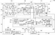
- FIG. 1is a block diagram representation of a wireless power transfer system having a switching unit in accordance with an embodiment.
- FIG. 2is a schematic representation of a wireless power transfer system in accordance with an embodiment.
- FIG. 3is a schematic representation of a wireless power transfer system in accordance with another embodiment.
- FIG. 4is a flow chart illustrating a method for protecting a wireless power transfer system in accordance with an embodiment.
- FIG. 5is a flow chart illustrating a method for decoupling and coupling a converting unit in a wireless power transfer system in accordance with an embodiment.
- FIG. 6is a schematic representation of a wireless power transfer system in accordance with another embodiment.
- various embodiments of a system and method for protecting a wireless power transfer systemare disclosed.
- various embodiments of a system and method for regulating an output voltage of the wireless power transfer systemare disclosed.
- the system and method disclosed hereinemploy a switching unit to protect one or more components of the wireless power transfer system. More specifically, the switching unit decouples the one or more components in the system if an output voltage of the wireless power transfer system increases to an undesirable value. Further, the switching unit is configured to control the output voltage of the wireless power transfer system even if magnitude of an electric load coupled to the wireless power transfer system changes substantially.
- FIG. 1is a diagrammatical representation of a wireless power transfer system 100 in accordance with an embodiment of the present disclosure.
- the wireless power transfer system 100is used to transmit an electrical power from a power source 102 to one or more electric loads 132 such as batteries, mobile devices such as cell phones, laptops, HVAC systems, and the like.
- an electric vehicle or a hybrid vehicleincludes one or more batteries that supply electrical power to drive the vehicle. Such batteries may be electrically charged from the power source 102 via the wireless power transfer system 100 .
- the wireless power transfer system 100may also be referred to as a contactless power transfer system.
- the wireless power transfer system 100includes a first converting unit 104 (inverter), a control unit 106 , a contactless power transfer unit 108 , and a second converting unit 110 (rectifier).
- the first converting unit 104is electrically coupled to the power source 102 and the control unit 106 .
- the power source 102is configured to supply an input power having a first DC voltage 112 to the first converting unit 104 .
- the input powermay be in a range from about 100 W to about 6.6 kW.
- the power source 102may be a part of the wireless power transfer system 100 .
- the power source 102may be positioned external to the wireless power transfer system 100 .
- the first converting unit 104is configured to receive the input power having the first DC voltage 112 from the power source 102 . Further, the first converting unit 104 is configured to operate at a determined switching frequency to convert the first DC voltage 112 of the input power to an AC voltage 114 . Particularly, the control unit 106 may determine the switching frequency of the first converting unit 104 based on the electric load 132 . In one embodiment, the control unit 106 may include a digital circuit or a processor that performs one or more functions based on pre-stored instructions or programs. Upon converting the first DC voltage 112 of the input power to the AC voltage 114 , the first converting unit 104 is further configured to transmit the input power having the AC voltage 114 to the contactless power transfer unit 108 .
- the contactless power transfer unit 108includes two or more coils or an array of coils 116 that are magnetically coupled to each other.
- the coils 116are used for wirelessly transmitting the input power having the AC voltage 114 from the first converting unit 104 to the second converting unit 110 .
- the details pertaining to transmitting the power using the coils 116are explained in greater detail below with reference to FIG. 2 .
- the second converting unit 110is electrically coupled to the contactless power transfer unit 108 via a switching unit 130 . Upon receiving the power having the AC voltage 114 from the contactless power transfer unit 108 , the second converting unit 110 is configured to convert the AC voltage 114 of the input power to a second DC voltage 118 . Further, the second converting unit 110 is configured to transmit the input power having the second DC voltage 118 to the electric load 132 . In one embodiment, the input power having the second DC voltage may be used for charging the electric load including one or more batteries that are coupled to the wireless power transfer system 100 .
- the wireless power transfer system 100includes a voltage sensor 120 , a first transceiver 122 , and a second transceiver 124 that together form a feedback loop 126 .
- the voltage sensor 120is used to sense the second DC voltage (output voltage) 118 .
- the feedback loop 126is used to transmit a voltage signal (V o ) 128 representative of the second DC voltage 118 from the voltage sensor 120 to the control unit 106 via the first transceiver 122 and the second transceiver 124 .
- the control unit 106is used to adjust the switching frequency of the first converting unit 104 based on the received voltage signal (V o ) 128 to control or regulate the second DC voltage 118 across the electric load 132 .
- the control unit 106may receive the voltage signal (V o ) 128 after a certain time delay.
- the delaymay be in a range from about 1 millisecond to about 5 milliseconds.
- the control unit 106may not be able to timely control the second DC voltage 118 across the electric load 132 due to the delay in communicating the voltage signal (V o ) 128 .
- the second DC voltage 118may increase above a critical value, which in turn may affect the second converting unit 110 and/or other components in the wireless power transfer system 100 .
- the critical valuemay be a voltage value above which the components in the wireless power transfer system 100 may be affected. In one embodiment, the critical value may be in a range from about 400V to about 500V.
- the exemplary wireless power transfer system 100includes the switching unit 130 to protect the second converting unit 110 or other components in the wireless power transfer system 100 from being affected.
- the switching unit 130is electrically coupled to the contactless power transfer unit 108 and the second converting unit 110 .
- the switching unit 130is configured to decouple the electric load 132 from the contactless power transfer unit 108 if the second DC voltage 118 is greater than a first threshold value (V o Max).
- the first threshold value (V o Max)is less than the critical value.
- the first threshold value (V o Max)may be in a range from about 300V to about 400V.
- the input poweris not transmitted to the electric load 132 by decoupling the electric load 132 from the contactless power transfer unit 108 .
- the second DC voltage 118 across the electric load 132is reduced to less than the first threshold value (V o Max).
- the protection of the second converting unit 110is described in greater detail with reference to FIG. 2 .
- the switching unit 130may be used to regulate or control the second DC voltage 118 across the electric load 132 . If a difference between the second DC voltage 118 and a voltage reference value (V o ref) is above a predefined value, the switching unit 130 is configured to regulate or control the second DC voltage 118 without decoupling the electric load 132 from the contactless power transfer unit 108 . Such a regulation of the second DC voltage 118 is described in greater detail with reference to FIG. 3 .
- the first converting unit 104includes a plurality of switches 220 and diodes 222 that are electrically coupled between an input terminal 219 and an output terminal 221 .
- the switches 220may include electronic switches, such as MOSFETs or IGBTs.
- the switches 220are activated and deactivated based on a switching frequency of the first converting unit 104 to convert the first DC voltage 112 of the input power to the AC voltage 114 .
- the control unit 106is configured to determine the switching frequency of the first converting unit 104 based on the electric load 132 .
- control unit 106is configured to send one or more gate signals 226 that are representative of the switching frequency to the plurality of switches 220 to convert the first DC voltage 112 of the input power to the AC voltage 114 .
- the input power having the AC voltage 114is transmitted from the first converting unit 104 to the contactless power transfer unit 108 .
- the contactless power transfer unit 108includes a primary coil 116 a and a secondary coil 116 b .
- the primary coil 116 ais electrically coupled to the first converting unit 104 .
- the secondary coil 116 bis electrically coupled to the second converting unit 110 .
- the primary coil 116 a and the secondary coil 116 bare magnetically coupled to each other.
- the contactless power transfer unit 108includes a field focusing coil 116 c and a compensation coil 116 d .
- the field focusing coil 116 cis positioned between the primary coil 116 a and the secondary coil 116 b .
- the field focusing coil 116 cis magnetically coupled to the primary coil 116 a and the secondary coil 116 b .
- the compensation coil 116 dis magnetically coupled to the secondary coil 116 b.
- the input power having the AC voltage 114is used to excite the primary coil 116 a and the field focusing coil 116 c simultaneously.
- a primary current corresponding to the AC voltage 114flows through the primary coil 116 a resulting in excitation of the primary coil 116 a , which in turn generates a magnetic field that excites the field focusing coil 116 c .
- the magnetic field generated by the primary coil 116 ais focused towards the secondary coil 116 b via the field focusing coil 116 c .
- the secondary coil 116 bis configured to receive the magnetic field and convert the magnetic field to the input power having the AC voltage 114 .
- the secondary coil 116 bWhen the secondary coil 116 b receives the magnetic field, a secondary current corresponding to the AC voltage 114 flows through the secondary coil 116 b . Further, the input power having the AC voltage 114 is then transmitted from the secondary coil 116 b to the second converting unit 110 .
- the field focusing coil 116 cis electrically coupled to one or more resonators which are excited simultaneously by the input power to enhance the magnetic coupling between the primary coil 116 a and the secondary coil 116 b .
- the compensation coil 116 dis configured to match an impedance of the contactless power transfer unit 108 with the second converting unit 110 .
- the second converting unit 110includes a first branch 268 and a second branch 270 that are electrically coupled between the input terminal 271 and the output terminal 273 .
- the first branch 268includes a pair of first diodes 272 , 274 and the second branch 270 includes a pair of second diodes 276 , 278 .
- the second converting unit 110may be configured using electronic switches, such as MOSFETs, IGBTs along with diodes or without using diodes.
- the voltage sensor 120is electrically coupled to the output terminal of the second converting unit 110 to determine the second DC voltage 118 across the electric load 132 .
- the first transceiver 122includes an antenna 248 configured to transmit the voltage signal (V o ) 128 to an antenna 250 of the second transceiver 124 .
- the first transceiver 122is positioned proximate to the electric load 132 and the second transceiver 124 is positioned proximate to the first converting unit 104 or the power source 102 .
- control unit 106is configured to determine a change in the electric load 132 based on the voltage signal (V o ) 128 representative of the second DC voltage 118 .
- the control unit 106is configured to determine or adjust the switching frequency of the first converting unit 104 .
- the control unit 106is configured to send gate signals 226 that are representative of the switching frequency to the first converting unit 104 to control the AC voltage 114 of the first converting unit 104 , which in turn controls the second DC voltage 118 across the electric load 132 .
- the control unit 106is configured to control or regulate the second DC voltage 118 of the wireless power transfer system 100 based on the voltage signal (V o ) 128 received via the feedback loop 126 .
- the switching unit 130includes a first switch 280 , a second switch 282 , and a controller 254 .
- the controller 254is electrically coupled to the first switch 280 , the second switch 282 , and the sensor 120 .
- the first switch 280 and the second switch 282may include one or more electronic switches such as MOSFETs, IGBTs, and the like.
- the first switch 280is electrically coupled across the first diode 272 in the first branch 268 of the second converting unit 110 .
- the second switch 282is electrically coupled across the second diode 276 in the second branch 270 of the second converting unit 110 . If the second DC voltage 118 across the electric load 132 is greater than a first threshold value, the first switch 280 and the second switch 282 are operated in a protection mode to decouple the electric load 132 from other components in the wireless power transfer system 100 . Particularly, the first switch 280 and the second switch 282 are activated to short-circuit the secondary coil 116 b of the contactless power transfer unit 108 . As a result, the electric load 132 is decoupled from the contactless power transfer unit 108 .
- the first switch 280 and the second switch 282are operated in a normal mode to couple the electric load 132 to the components of the wireless power transfer system 100 .
- the first switch 280 and the second switch 282are activated and deactivated based on switching signals received from the controller 254 to couple the electric load 132 to the contactless power transfer unit 108 .
- the first switch 280 and the second switch 282are activated and deactivated to convert the AC voltage 114 to the second DC voltage 118 .
- the switching signalsinclude switching pulses corresponding to the secondary current of the contactless power transfer unit 108 .
- the controller 254includes a first voltage comparator 256 , a second voltage comparator 258 , a flip-flop unit 260 , a current comparator 284 , a NOT gate 286 , a first OR gate 288 , and a second OR gate 290 .
- the first comparator 256 and the second comparator 258are electrically coupled to an input terminal of the flip-flop unit 260 . Further, an output terminal of the flip-flop unit 260 is coupled to input terminals of the first OR gate 288 and the second OR gate 290 .
- An input terminal of the current comparator 284is electrically coupled to a current sensor 292 that is coupled to the secondary coil 116 b of the contactless power transfer unit 108 .
- the current sensor 292is used to sense the secondary current of the contactless power transfer unit 108 and transmit a current signal to the current comparator 284 .
- an output terminal of the current comparator 284is directly coupled to the input terminal of the first OR gate 288 .
- the output terminal of the current comparator 284is coupled to the input terminal of the second OR gate 290 via the NOT gate 286 .
- an output terminal of the first OR gate 288is coupled to the first switch 280 and an output terminal of the second OR gate 290 is coupled to the second switch 282 .
- the controller 254is configured to receive the voltage signal (V o ) 128 that is representative of the second DC voltage 118 from the sensor 120 . Further, the received voltage signal (V o ) 128 is transmitted to the first comparator 256 and the second comparator 258 .
- the first comparator 256is configured to compare the second DC voltage 118 with a first threshold value (V o Max). If the second DC voltage 118 is greater than the first threshold value (V o Max), the first comparator 256 is configured to trigger the flip-flop unit 260 to generate a first control signal 261 at the output terminal of the flip-flop unit 260 .
- the first control signal 261is representative of binary ‘1’.
- the first control signal 261is transmitted to the first OR gate 288 to generate a first switching signal 265 .
- the first control signal 261is transmitted to the second OR gate 290 to generate a second switching signal 267 .
- the first OR gate 288 and the second OR gate 290generates the first and second switching signals 265 , 267 to operate the first and second switches 280 , 282 in the protection mode.
- the flip-flop unit 260generates the first control signal 261
- the first OR gate 288generates the first switching signal 265 that is same as the first control signal 261 .
- the second OR gate 290generates the second switching signal 267 that is same as the first control signal 261 .
- the first and second switching signals 265 , 267are representative of binary ‘1’. Further, the first switching signal 265 is transmitted to the first switch 280 to activate the first switch 280 , and the second switching signal 267 is transmitted to the second switch 282 to activate the second switch 282 .
- the secondary coil 116 b of the contactless power transfer unit 108is short-circuited. As a result, the electric load 132 is decoupled from the contactless power transfer unit 108 . Further, second DC voltage 118 across the electric load 132 is reduced to below the first threshold value.
- the second comparator 258is configured to receive the voltage signal (V o ) 128 that is representative of the second DC voltage 118 .
- the second comparator 258is configured to compare the received second DC voltage 118 with a second threshold value (V o Min). It should be noted herein that the second threshold value (V o Min) is less than the first threshold value (V o Max). If the second DC voltage 118 is less than the second threshold value (V o Min), the second comparator 258 is configured to trigger the flip-flop unit 260 to generate a second control signal 263 at the output terminal of the flip-flop unit 260 .
- the second control signal 263is representative of binary ‘0’.
- the second control signal 263is transmitted to the first OR gate 288 and the second OR gate 290 .
- the first OR gate 288 and the second OR gate 290generates switching signals to operate the first and second switches 280 , 282 in the normal mode.
- the switching signalsare generated based on the secondary current of the contactless power transfer unit 108 . More specifically, the current comparator 284 compares the secondary current of the contactless power transfer unit 108 with a zero value to trigger the first OR gate 288 to generate a third switching signal 269 and the second OR gate 290 to generate a fourth switching signal 275 .
- the third switching signal 269 and the fourth switching signal 275are complimentary to each other.
- the third switching signal 269 and the fourth switching signal 275include switching pulses that correspond to the secondary current of the contactless power transfer unit 108 . Further, the third switching signal 269 is transmitted to the first switch 280 and the fourth switching signal 275 is transmitted to the second switch 282 to convert the AC voltage 114 of the input power to the second DC voltage 118 .
- the first switch 280 and the second switch 282are activated and deactivated based on the third and fourth switching signals 269 , 275 to couple the electric load 132 to the contactless power transfer unit 208 and convert the AC voltage 114 of the input power to the second DC voltage 118 .
- the controller 254sends the third and fourth switching signals 269 , 275 to operate the first and second switches 280 , 282 in the normal mode.
- the second DC voltage 118 across the load 132may increase above the first threshold value (V o Max).
- the sensor 120determines and sends the voltage signal (V o ) 128 that is representative of this second DC voltage 118 to the controller 254 and the first transceiver 122 .
- the first comparator 256compares the second DC voltage 118 with the first threshold value (V o Max).
- the first comparator 256triggers the flip-flop unit 260 to generate the first control signal 261 which is transmitted to the first OR gate 288 and the second OR gate 290 to generate the first switching signal 265 and the second switching signal 267 . Further, the first and second switching signals 265 , 267 are transmitted to activate the first and second switches 280 , 282 . As a result, the electric load 132 is decoupled from the contactless power transfer unit 108 .
- the first control signal 261is transmitted from the controller 254 to the first transceiver 122 . Further, the first transceiver 122 transmits the voltage signal (V o ) 128 received from the sensor 120 and the first control signal 261 received from the controller 254 to the second transceiver 124 . The voltage signal (V o ) 128 and the first control signal 261 are further transmitted to the control unit 106 .
- the control unit 106Upon receiving the voltage signal (V o ) 128 and the first control signal 261 , the control unit 106 determines that the first and second switches 280 , 282 are activated. As a result, the control unit 106 deactivates the first converting unit 104 . Specifically, the control unit 106 sends the gate signals 226 to the switches 220 to deactivate or open the switches 220 . As a result, the first converting unit 104 is deactivated from transmitting the power to the contactless power transfer unit 108 and the second converting unit 110 .
- the control unit 106sends a reset signal 262 to the second transceiver 124 , which is further transmitted to the first transceiver 122 .
- the first transceiver 122sends the reset signal 262 to the flip-flop unit 260 .
- the flip-flop unit 260resets and generates the second control signal 263 at the output terminal of the controller 254 .
- the generated second control signal 263is further transmitted to the first OR gate 288 and the second OR gate 290 to generate the third switching signal 269 and the fourth switching signal 275 that include switching pulses corresponding to the secondary current of the contactless power transfer unit 108 .
- the third and fourth switching signals 269 , 275are transmitted to the first and second switches 280 , 282 to convert the AC voltage 114 of the input power to the second DC voltage 118 .
- the electric load 132is coupled to the contactless power transfer unit 108 via the second converting unit 110 to receive the converted second DC voltage 118 .
- the generated second control signal 263is transmitted from the controller 254 to the first transceiver 122 .
- the first transceiver 122receives the voltage signal (V o ) 128 representative of the second DC voltage 118 across the load 132 . Further, the first transceiver 122 transmits the voltage signal (V o ) 128 and the second control signal 263 to the second transceiver 124 , which is further transmitted to the control unit 106 .
- the control unit 106Upon receiving the voltage signal (V o ) 128 and the second control signal 263 from the second transceiver 124 , the control unit 106 determines whether the second DC voltage 118 is less than or equal to the first threshold value (V o Max). If the second DC voltage 118 is less than or equal to the first threshold value (V o Max), the control unit 106 sends the gate signals 226 to the switches 220 to activate the first converting unit 104 . Further, the control unit 206 adjusts the switching frequency of the first converting unit 104 based on the second DC voltage 118 across the electric load 132 . In one embodiment, the control unit 106 adjusts the switching frequency of the first converting unit 104 to regulate the second DC voltage 118 across the electric load 132 .
- the control unit 106waits for the predetermined time period to send another reset signal to the controller 254 . If the second DC voltage 118 continues to be greater than the first threshold value (V o Max) after transmitting a determined number of reset signals, the control unit 106 deactivates the electric load 132 from the contactless power transfer unit 108 . In one embodiment, the control unit 106 may shut down or deactivate the power transfer system.
- the switching unit 130 and the control unit 106are employed to prevent the second DC voltage 118 from increasing to greater than the critical value.
- the second converting unit 110is protected from damage even if the electric load 132 is decoupled from the contactless power transfer unit 108 .
- FIG. 3a schematic representation of a wireless power transfer system 300 in accordance with another embodiment of the present disclosure is depicted.
- the wireless power transfer system 300is similar to the wireless power transfer system 100 of FIG. 2 except that a controller 302 of a switching unit 312 is configured to regulate or control the second DC voltage 118 (output voltage) of the second converting unit 110 .
- the second DC voltage 118 across the electric load 132may vary substantially from a voltage reference value (V o ref).
- the second DC voltage 118may increase or decrease below the voltage reference value (V o ref).
- difference between the second DC voltage 118 and the voltage reference value (V o ref)may increase above a predefined value.
- the voltage reference value (V o ref)is less than the critical value.
- the sensor 120transmits the voltage signal (V o ) 128 representative of the second DC voltage 118 to the controller 302 .
- a voltage comparator 306 of the controller 302is configured to compare the second DC voltage 118 with the voltage reference value (V o ref). If a difference between the second DC voltage 118 and the voltage reference value (V o ref) is above the predefined value, the voltage comparator 306 generates a third control signal 304 having a determined duty cycle at an output terminal.
- the controller 302may determine or select the duty cycle using a look-up table. For example, if the second DC voltage 118 is 90 volts, a duty cycle of 0.75 is selected from the look-up table.
- the third control signal 304includes switching pulses corresponding to the determined duty cycle.
- the voltage comparator 306transmits the third control signal 304 having the determined duty cycle to the first OR gate 288 and the second OR gate 290 .
- the current comparator 284transmits signals corresponding to the secondary current to the first OR gate 288 and the second OR gate 290 .
- the first OR gate 288generates the fifth switching signal 277 and the second OR gate 290 generates the sixth switching signal 279 based on the third control signal 304 and the secondary current of the contactless power transmitting unit 108 .
- the fifth switching signal 277 and the sixth switching signal 279are complimentary to each other.
- the fifth switching signal 277 and the sixth switching signal 279include switching pulses corresponding to the third control signal 304 and the secondary current of the contactless power transfer unit 108 .
- the fifth switching signal 277is transmitted to the first switch 280 and the sixth switching signal 279 is transmitted to the second switch 282 to regulate the second DC voltage 118 across the load 132 .
- the fifth switching signal 277 and the sixth switching signal 279are transmitted to first switch 280 and the second switch 282 respectively, to activate and deactivate the first and second switches 280 , 282 .
- the fifth and sixth switching signals 277 , 279include switching pulses corresponding to the switching pulses of the third control signal 304 .
- the fifth switching signal 277 and the sixth switching signal 279are transmitted to the first and second switches 280 , 282 to activate and deactivate the first and second switches 280 , 282 .
- the fifth and sixth switching signals 277 , 279include switching pulses corresponding to the secondary current of the contactless power transfer unit 108 .
- the second converting unit 210converts the AC voltage 114 of the input power to the second DC voltage 118 and supplies the converted second DC voltage 118 to the electric load 132 .
- the voltage signal (V o ) 128is transmitted from the sensor 120 to the first transceiver 122 . Further, the first transceiver 122 transmits the voltage signal (V o ) 128 to the second transceiver 124 , which in turn is transmitted to the control unit 206 .
- the control unit 106generates gate signals 226 based on the second DC voltage 118 . Further, the control unit 106 transmits the gate signals 226 to the switches 220 to adjust the switching frequency of the first converting unit 104 . As a result, the AC voltage 114 is regulated, which in turn controls the second DC voltage 118 across the load 132 . However, the regulation of the second DC voltage 118 , using the control unit 106 , occurs after the regulation of the second DC voltage, using the controller 302 . Hence, the controller 302 performs faster regulation of the second DC voltage 118 compared to the regulation of the second DC voltage 118 by the control unit 106 .
- a flow chart illustrating a method 400 for protecting the wireless power transfer system in accordance with an embodiment of the present disclosureis depicted.
- a first DC voltage of an input poweris converted to an AC voltage by a first converting unit.
- the first converting unitis operated at a determined switching frequency to convert the first DC voltage of the input power to the AC voltage.
- the methodincludes receiving and transmitting the input power having the AC voltage by a contactless power transfer unit.
- the contactless power transfer unittransmits the input power having the first AC voltage to a second converting unit.
- the AC voltage of the input poweris converted to a second DC voltage by a second converting unit.
- the input power having the second DC voltageis transmitted from the second converting unit to an electric load.
- the electric loadmay be one or more batteries that are electrically charged using the input power having the second DC voltage received from the second converting unit.
- the electric loadis decoupled from the contactless power transfer unit if the second DC voltage across the electric load is greater than a first threshold value (V o Max).
- a switching unitis used to decouple the electric load from the contactless power transfer unit.
- the second DC voltage across the electric loadis reduced to less than the first threshold value (V o Max), thereby protecting the second converting unit from being affected due to over voltage.
- the switching unitcouples the electric load to the contactless power transfer unit to continue supplying power having the second DC voltage to the electric load.
- a flow chart illustration a method for decoupling and coupling a second converting unit in a wireless power transfer system in accordance with an embodiment of the present disclosureis depicted.
- a voltage signal (V o ) representative of a second DC voltage across an electric loadis transmitted by a sensor. More specifically, the sensor transmits the voltage signal (V o ) to a controller of a switching unit. Further, the sensor transmits the voltage signal (V o ) to a control unit via a first transceiver and a second transceiver.
- the controllerdetermines whether the voltage signal (V o ) representative of the second DC voltage is greater than a first threshold value (V o Max). If the voltage signal (V o ) representative of the second DC voltage is greater than the first threshold value (V o Max), the controller transmits a first switching signal to a first switch and a second switching signal to a second switch to activate or close the first and second switches as depicted in step 506 . As a result, the electric load is decoupled from the contactless power transfer unit and thereby the second DC voltage across the load is reduced to less than the first threshold value (V o Max). More specifically, the second DC voltage is prevented from attaining a critical value that is greater than the first threshold value (V o Max). The critical value is a voltage value greater than which the second converting unit may be affected. Concurrently, the controller sends a first control signal to the control unit via the first transceiver and the second transceiver.
- the controllerdetermines whether the voltage signal (V o ) representative of the second DC voltage is less than a second threshold value (V o Min). If the voltage signal (V o ) representative of the second DC voltage is less than the second threshold value (V o Min), the controller sends a third switching signal to the first switch and a fourth switching signal to the second switch to activate and deactivate the first and second switches. As a result, the electric load is coupled to the contactless power transfer unit and the AC voltage is converted to the second DC voltage which is supplied to the electric load as depicted in step 510 .
- the control unitreceives the voltage signal (V o ) and the first control signal. Specifically, the control unit receives the voltage signal (V o ) from the sensor via the first transceiver and the second transceiver. The control unit receives the first control signal from the controller via the first transceiver and the second transceiver.
- the control unitdeactivates the first converting unit if the first control signal is received from the controller.
- the first converting unitis deactivated to prevent the supply of input power to the second converting unit.
- the control unittransmits a reset signal to the controller via the first transceiver and the second transceiver after a predetermined time period.
- the controllerIn response to receiving the reset signal, the controller generates the third and fourth switching signals. Further, the controller sends the third and fourth switching signals to operate the first and second switches in the normal mode. As a result, the electric load is coupled to the contactless power transfer unit to receive the power via the second converting unit.
- the controllertransmits the second control signal to the control unit via the first transceiver and the second transceiver. Further, at step 518 , the sensor transmits the voltage signal (V o ) to the control unit via the first transceiver and the second transceiver.
- the control unitdetermines whether the voltage signal (V o ) representative of the second DC voltage is less than or equal to the first threshold value (V o Max). If the second DC voltage is less than or equal to the first threshold value (V o Max), the control unit transmits gate signals to activate the first converting unit. As a result, the input power is supplied to the second converting unit via the contactless power transfer unit.
- the electric loadreceives the power having the second DC voltage from the second converting unit.
- the control unitcontinues to deactivate the first converting unit and sends another reset signal after the predetermined time period to verify whether the second DC voltage is less than or equal to the first threshold value (V o Max). If the second DC voltage is greater than the first threshold value (V o Max) after sending a determined number of reset signals, the control unit may shut down or deactivate the power transfer system.
- the exemplary system and methodfacilitate to protect one or more components in the wireless power transfer system when the load is disconnected. Further, the exemplary system and method facilitate to control or regulate the output voltage when the load is disconnected. As a result, one or more components in the system are protected without decoupling the components from each other in the system.
- FIG. 6a schematic representation of a wireless power transfer system 300 in accordance with one embodiment of the present disclosure is depicted.
- the wireless power transfer system 600is similar to the wireless power transfer system 300 of FIG. 3 except that a controller 622 of a switching unit 612 is configured to regulate or control the second DC voltage 118 (output voltage) and electrical current 604 (output current) of the second converting unit 110 .
- a battery 602may be coupled across the second converting unit 110 as an electric load. The battery 602 may be charged by the second DC voltage 118 provided by the second converting unit 110 .
- the controller 622may control or regulate output current 604 provided to the battery 602 along with the second DC voltage 118 while charging the battery 602 .
- the controller 622may first regulate the output current 604 until the battery is charged to a predefined value. Further, the controller 622 may regulate the second DC voltage 118 until the battery is fully charged.
- the battery 602is considered as the lead acid battery in the below description.
- the controller 622may monitor the output current 604 along with the second DC voltage 118 while charging the battery 602 . If the electrical charge in the battery 602 is below or equal to a predetermined value, the controller 622 may control or regulate the electrical current so that a constant output current 604 is provided to the battery 602 for charging the battery 602 .
- the predetermined valuemay be 80% of battery's full charge capacity.
- the controller 622may receive a signal representative of the output current 604 from a current sensor 606 . Further, the controller 622 may compare the output current 604 with a current reference value (Io ref) to generate switching signals S 1 and S 2 608 . 610 having corresponding switching pulses. These switching signals S 1 and S 2 608 , 610 are provided to the switches 280 , 282 to regulate the output current 604 that is used for charging the battery 602 .
- Io refcurrent reference value
- the controller 622may control or regulate the second DC voltage 118 so that a constant second DC voltage is provided for charging the battery 602 .
- the controller 622may receive a signal representative of the second DC voltage 118 from the voltage sensor 120 .
- the controller 622may compare the second DC voltage 118 with a voltage reference value (V o ref) to generate switching signals S 1 and S 2 608 , 610 having corresponding switching pulses. These switching signals S 1 and S 2 608 , 610 are provided to the switches 280 , 282 to regulate the second DC voltage 118 that is provided for charging the battery 602 .
- the controller 622may regulate voltage and/or current based on a type of the battery that is coupled to the second converting unit 110 .
- the controller 622may first regulate the second DC voltage 118 until the battery is charged to the predetermined value. Further, the controller 622 may regulate the output current 604 until the battery is fully charged.
Landscapes
- Engineering & Computer Science (AREA)
- Power Engineering (AREA)
- Computer Networks & Wireless Communication (AREA)
- Charge And Discharge Circuits For Batteries Or The Like (AREA)
- Electric Propulsion And Braking For Vehicles (AREA)
Abstract
Description
Claims (26)
Priority Applications (2)
| Application Number | Priority Date | Filing Date | Title |
|---|---|---|---|
| US16/884,338US12149065B2 (en) | 2016-09-30 | 2020-05-27 | Over voltage protection for a wireless power transfer system |
| US18/821,079US20240421587A1 (en) | 2016-09-30 | 2024-08-30 | Over voltage protection for a wireless power transfer system |
Applications Claiming Priority (4)
| Application Number | Priority Date | Filing Date | Title |
|---|---|---|---|
| IN201641033404 | 2016-09-30 | ||
| IN201641033404 | 2016-09-30 | ||
| US15/717,855US10700510B2 (en) | 2016-09-30 | 2017-09-27 | Over voltage protection for a wireless power transfer system |
| US16/884,338US12149065B2 (en) | 2016-09-30 | 2020-05-27 | Over voltage protection for a wireless power transfer system |
Related Parent Applications (1)
| Application Number | Title | Priority Date | Filing Date |
|---|---|---|---|
| US15/717,855ContinuationUS10700510B2 (en) | 2016-09-30 | 2017-09-27 | Over voltage protection for a wireless power transfer system |
Related Child Applications (1)
| Application Number | Title | Priority Date | Filing Date |
|---|---|---|---|
| US18/821,079ContinuationUS20240421587A1 (en) | 2016-09-30 | 2024-08-30 | Over voltage protection for a wireless power transfer system |
Publications (2)
| Publication Number | Publication Date |
|---|---|
| US20200287375A1 US20200287375A1 (en) | 2020-09-10 |
| US12149065B2true US12149065B2 (en) | 2024-11-19 |
Family
ID=61759164
Family Applications (3)
| Application Number | Title | Priority Date | Filing Date |
|---|---|---|---|
| US15/717,855Active2038-03-02US10700510B2 (en) | 2016-09-30 | 2017-09-27 | Over voltage protection for a wireless power transfer system |
| US16/884,338ActiveUS12149065B2 (en) | 2016-09-30 | 2020-05-27 | Over voltage protection for a wireless power transfer system |
| US18/821,079PendingUS20240421587A1 (en) | 2016-09-30 | 2024-08-30 | Over voltage protection for a wireless power transfer system |
Family Applications Before (1)
| Application Number | Title | Priority Date | Filing Date |
|---|---|---|---|
| US15/717,855Active2038-03-02US10700510B2 (en) | 2016-09-30 | 2017-09-27 | Over voltage protection for a wireless power transfer system |
Family Applications After (1)
| Application Number | Title | Priority Date | Filing Date |
|---|---|---|---|
| US18/821,079PendingUS20240421587A1 (en) | 2016-09-30 | 2024-08-30 | Over voltage protection for a wireless power transfer system |
Country Status (3)
| Country | Link |
|---|---|
| US (3) | US10700510B2 (en) |
| CN (2) | CN107887984B (en) |
| SG (1) | SG10201707385XA (en) |
Families Citing this family (7)
| Publication number | Priority date | Publication date | Assignee | Title |
|---|---|---|---|---|
| EP3748812A1 (en) | 2016-02-03 | 2020-12-09 | General Electric Company | Method and system for protecting a wireless power transfer system |
| SG10201700633QA (en) | 2016-02-03 | 2017-09-28 | Gen Electric | System and method for protecting a wireless power transfer system |
| SG10201707385XA (en) | 2016-09-30 | 2018-04-27 | Gen Electric | Over voltage protection for a wireless power transfer system |
| US12348050B2 (en)* | 2017-07-26 | 2025-07-01 | The Regents Of The University Of Colorado, A Body Corporate | Variable compensation inverter circuit and related techniques |
| CN113196613B (en)* | 2018-12-19 | 2023-08-29 | 三菱电机株式会社 | Contactless power supply system and power receiving device |
| CN114144960B (en)* | 2019-05-24 | 2024-05-14 | 韦特里西提公司 | Protection circuit for wireless power receiver |
| JP7706962B2 (en)* | 2021-07-06 | 2025-07-14 | キヤノン株式会社 | CONTROL SYSTEM AND CONTROL METHOD FOR CONTROL SYSTEM |
Citations (61)
| Publication number | Priority date | Publication date | Assignee | Title |
|---|---|---|---|---|
| US6037745A (en) | 1997-07-03 | 2000-03-14 | Kabushiki Kaisha Toyoda Jidoshokki | Battery charger with monitor and protection circuits |
| JP2006074848A (en) | 2004-08-31 | 2006-03-16 | Hokushin Denki Kk | Non-contact power transmission system |
| US20080068868A1 (en) | 2005-11-29 | 2008-03-20 | Advanced Analogic Technologies, Inc. | Power MESFET Rectifier |
| US20090096413A1 (en) | 2006-01-31 | 2009-04-16 | Mojo Mobility, Inc. | System and method for inductive charging of portable devices |
| US7595569B2 (en) | 2004-02-17 | 2009-09-29 | Agere Systems Inc. | Versatile and intelligent power controller |
| US20100109445A1 (en) | 2008-09-27 | 2010-05-06 | Kurs Andre B | Wireless energy transfer systems |
| US20100110741A1 (en) | 2008-10-31 | 2010-05-06 | University Of Florida Research Foundation, Inc. | Miniature high voltage/current ac switch using low voltage single supply control |
| US8004235B2 (en) | 2006-09-29 | 2011-08-23 | Access Business Group International Llc | System and method for inductively charging a battery |
| US8060011B2 (en) | 2007-02-20 | 2011-11-15 | Seiko Epson Corporation | Power transmission control device, power transmission device, electronic instrument, and non-contact power transmission system |
| US20110285349A1 (en) | 2010-05-19 | 2011-11-24 | Qualcomm Incorporated | Adaptive wireless energy transfer system |
| US8129864B2 (en) | 2008-01-07 | 2012-03-06 | Access Business Group International Llc | Inductive power supply with duty cycle control |
| WO2012091209A1 (en) | 2010-12-30 | 2012-07-05 | 전자부품연구원 | Multi-node wireless power transmission system using magnetic resonance induction and wireless charging device |
| US8232829B2 (en) | 2006-12-11 | 2012-07-31 | John Joseph Robinson | Active rectifier |
| US20120306286A1 (en) | 2011-06-01 | 2012-12-06 | Nam Yun Kim | Method and apparatus for controlling wireless power transmission |
| WO2013042570A1 (en) | 2011-09-22 | 2013-03-28 | Necトーキン株式会社 | Power transmitting device, power receiving device, non-contact power transmission system, and method for controlling transmission power in non-contact power transmission system |
| US20130176653A1 (en) | 2012-01-11 | 2013-07-11 | Samsung Electronics Co., Ltd. | Over-voltage protection device for resonant wireless power reception device and method for controlling the over-voltage protection device |
| US20130214611A1 (en) | 2012-02-21 | 2013-08-22 | Lg Innotek Co., Ltd. | Wireless power receiver and method of managing power thereof |
| US20130271069A1 (en) | 2012-03-21 | 2013-10-17 | Mojo Mobility, Inc. | Systems and methods for wireless power transfer |
| US20140152114A1 (en)* | 2012-12-03 | 2014-06-05 | Ls Cable & System Ltd. | Wireless power transmission system, wireless power receiving apparatus, and wireless power receiving method |
| JP2014171278A (en) | 2013-03-01 | 2014-09-18 | Nec Tokin Corp | Non-contact power transmission system |
| CN104079079A (en) | 2014-07-14 | 2014-10-01 | 南京矽力杰半导体技术有限公司 | Resonance type non-contact power supply device, integrated circuit and constant voltage control method |
| US20140346888A1 (en)* | 2011-07-07 | 2014-11-27 | Samsung Electronics Co., Ltd. | Wireless power transmitting and charging system, and method for controlling communication and power in the wireless power transmitting and charging system |
| US20140361628A1 (en) | 2013-06-07 | 2014-12-11 | Qualcomm Incorporated | Primary power supply tuning network for two coil device and method of operation |
| US20150035374A1 (en) | 2013-08-01 | 2015-02-05 | Soongsil University Foundation of University- Industry Cooperation | Wireless transceiver circuit, wireless power transmission circuit, wireless power reception circuit, and wireless power transmission/reception system including the same |
| US20150051109A1 (en) | 2012-03-07 | 2015-02-19 | Fondazione Istituto Italiano Di Tecnologia | Process and device for the determination of alterations in neuronal connectivity and/or morphology |
| US20150054349A1 (en) | 2012-02-17 | 2015-02-26 | Keio University | Wireless power supply device |
| WO2015037949A1 (en) | 2013-09-13 | 2015-03-19 | 엘지이노텍 주식회사 | Charging control device, charging control method and wireless power receiving device equipped with same |
| US20150084428A1 (en) | 2013-09-26 | 2015-03-26 | Fairchild Korea Semiconductor Ltd | Wireless power transfer system and driving method thereof |
| JP2015089267A (en) | 2013-10-31 | 2015-05-07 | 船井電機株式会社 | Device and system for non-contact power supply |
| US20150137611A1 (en) | 2013-11-18 | 2015-05-21 | Richtek Technology Corp | Power management unit and wireless power system using the same |
| CN104795903A (en) | 2015-04-16 | 2015-07-22 | 刘晓明 | Magnetic coupling dual-mode wireless power transmission device and control method thereof |
| WO2015115285A1 (en) | 2014-01-30 | 2015-08-06 | ソニー株式会社 | Power reception apparatus, power reception control method, non-contact power supply system, and electronic apparatus |
| US20150229225A1 (en) | 2014-02-12 | 2015-08-13 | Delta Electronics, Inc. | Resonant converters and control methods thereof |
| US20150229139A1 (en) | 2014-02-07 | 2015-08-13 | Advanced Neuromodulation Systems, Inc. D/B/A St. Jude Medical Neuromodulation Division | System and method for controlling charging energy delivered to an implantable medical device |
| US9124113B2 (en)* | 2008-07-07 | 2015-09-01 | Powerbyproxi Limited | Inductively coupled power receiver and method of operation |
| US20150263511A1 (en) | 2014-03-13 | 2015-09-17 | Infineon Technologies Ag | Overvoltage protection for a synchronous power rectifier |
| US20150280455A1 (en)* | 2014-03-31 | 2015-10-01 | Abb Technology Ag | Inductive power transfer system and method for operating an inductive power transfer system |
| US9153998B2 (en) | 2013-12-02 | 2015-10-06 | Qualcomm Incorporated | Wireless power orthogonal polarization antenna array |
| US20150326143A1 (en) | 2014-05-07 | 2015-11-12 | Energous Corporation | Synchronous Rectifier Design for Wireless Power Receiver |
| US20150341087A1 (en) | 2011-01-20 | 2015-11-26 | Triune Ip, Llc | Multi-use wireless power and data system |
| US20150349538A1 (en)* | 2014-05-30 | 2015-12-03 | Infineon Technologies Austria Ag | Active rectifier for efficient wireless power transfer |
| US20150372622A1 (en) | 2014-06-18 | 2015-12-24 | Raytheon Company | Method and integrated motor drive power electronics system with improved efficiency |
| US20160006356A1 (en) | 2014-07-03 | 2016-01-07 | Cooper Industries Holdings (Ireland) | Wireless power transfer systems using load feedback |
| EP2985846A1 (en) | 2014-08-14 | 2016-02-17 | Nxp B.V. | Wireless power transmission |
| US9269489B2 (en) | 2012-01-23 | 2016-02-23 | Utah State University | Wireless power transfer system |
| US20160072398A1 (en) | 2014-09-08 | 2016-03-10 | Infineon Technologies Austria Ag | Multi-cell power conversion method and multi-cell power converter |
| CN105493375A (en) | 2013-09-06 | 2016-04-13 | 罗伯特·博世有限公司 | Device for inductively transmitting energy and method for operating a device for inductively transmitting energy |
| US20160214488A1 (en)* | 2013-09-26 | 2016-07-28 | Nissan Motor Co., Ltd. | Wireless power supply system and power transmission device |
| US20160254659A1 (en) | 2015-02-26 | 2016-09-01 | Ut-Battelle, Llc | Overvoltage protection system for wireless power transfer systems |
| US20170025885A1 (en) | 2015-04-10 | 2017-01-26 | Enovate Medical, Llc | Proximity wireless power system using a bidirectional power converter |
| US20170063161A1 (en)* | 2015-08-28 | 2017-03-02 | Toyota Jidosha Kabushiki Kaisha | Contactless power transfer system and power transmission device |
| US20170093225A1 (en) | 2014-07-03 | 2017-03-30 | Ihi Corporation | Power-receiving device, wireless power-transmitting system, and power-transmission device |
| US20170104368A1 (en) | 2015-10-12 | 2017-04-13 | Broadcom Corporation | Wireless power receiver voltage control enabling simultaneous communications to transmitter in over-voltage state |
| US20170207657A1 (en)* | 2016-01-19 | 2017-07-20 | Daihen Corporation | Contactless power supply system and power receiver |
| US20170222479A1 (en) | 2016-02-03 | 2017-08-03 | General Electric Company | System and method for protecting a wireless power transfer system |
| US20170222480A1 (en) | 2016-02-03 | 2017-08-03 | General Electric Company | Method and system for protecting a wireless power transfer system |
| US20170317524A1 (en) | 2015-01-19 | 2017-11-02 | Jageson Electronic Technology (ShenZhen) Co.Ltd. | Digitalized double-excitation uninterrupted switching power supply |
| US20180090995A1 (en) | 2015-03-31 | 2018-03-29 | Tdk Corporation | Wireless Power Receiving Device and Wireless Power Transmission Device |
| US20180097351A1 (en) | 2016-09-30 | 2018-04-05 | General Electric Company | Over voltage protection for a wireless power transfer system |
| US20180287500A1 (en)* | 2015-10-14 | 2018-10-04 | Autonetworks Technologies, Ltd. | Dc-dc converter |
| US10381877B2 (en) | 2015-12-23 | 2019-08-13 | Ningbo Weie Electronic Technology Co., Ltd. | Electrical energy receiving end capable of overvoltage protection and wireless electrical energy transmission device |
Family Cites Families (6)
| Publication number | Priority date | Publication date | Assignee | Title |
|---|---|---|---|---|
| CN102084442B (en)* | 2008-03-17 | 2013-12-04 | 鲍尔马特技术有限公司 | Inductive transmission system |
| KR101313662B1 (en) | 2010-08-27 | 2013-10-02 | 한양대학교 산학협력단 | Active rectifier with delay locked loop, Wireless power receiving apparatus including active rectifier |
| CN102780273A (en)* | 2012-07-11 | 2012-11-14 | 华北电力大学 | High-voltage wire magnetic field induction energy taking device for high-voltage transmission line online monitoring |
| JP5978905B2 (en)* | 2012-10-11 | 2016-08-24 | Tdk株式会社 | Non-contact power receiving apparatus and non-contact power transmission system |
| US9438064B2 (en)* | 2013-08-30 | 2016-09-06 | Qualcomm Incorporated | System and method for alignment and compatibility detection for a wireless power transfer system |
| CN104918394A (en)* | 2014-03-11 | 2015-09-16 | 通用电气公司 | Ballast, and arc protection apparatus and method |
- 2017
- 2017-09-11SGSG10201707385XApatent/SG10201707385XA/enunknown
- 2017-09-27USUS15/717,855patent/US10700510B2/enactiveActive
- 2017-09-29CNCN201710913768.1Apatent/CN107887984B/enactiveActive
- 2017-09-29CNCN202311869669.XApatent/CN117996681A/enactivePending
- 2020
- 2020-05-27USUS16/884,338patent/US12149065B2/enactiveActive
- 2024
- 2024-08-30USUS18/821,079patent/US20240421587A1/enactivePending
Patent Citations (79)
| Publication number | Priority date | Publication date | Assignee | Title |
|---|---|---|---|---|
| US6037745A (en) | 1997-07-03 | 2000-03-14 | Kabushiki Kaisha Toyoda Jidoshokki | Battery charger with monitor and protection circuits |
| US7595569B2 (en) | 2004-02-17 | 2009-09-29 | Agere Systems Inc. | Versatile and intelligent power controller |
| JP2006074848A (en) | 2004-08-31 | 2006-03-16 | Hokushin Denki Kk | Non-contact power transmission system |
| US20080068868A1 (en) | 2005-11-29 | 2008-03-20 | Advanced Analogic Technologies, Inc. | Power MESFET Rectifier |
| US20090096413A1 (en) | 2006-01-31 | 2009-04-16 | Mojo Mobility, Inc. | System and method for inductive charging of portable devices |
| US8004235B2 (en) | 2006-09-29 | 2011-08-23 | Access Business Group International Llc | System and method for inductively charging a battery |
| US8232829B2 (en) | 2006-12-11 | 2012-07-31 | John Joseph Robinson | Active rectifier |
| US8060011B2 (en) | 2007-02-20 | 2011-11-15 | Seiko Epson Corporation | Power transmission control device, power transmission device, electronic instrument, and non-contact power transmission system |
| US8129864B2 (en) | 2008-01-07 | 2012-03-06 | Access Business Group International Llc | Inductive power supply with duty cycle control |
| US9124113B2 (en)* | 2008-07-07 | 2015-09-01 | Powerbyproxi Limited | Inductively coupled power receiver and method of operation |
| US20100109445A1 (en) | 2008-09-27 | 2010-05-06 | Kurs Andre B | Wireless energy transfer systems |
| US20100110741A1 (en) | 2008-10-31 | 2010-05-06 | University Of Florida Research Foundation, Inc. | Miniature high voltage/current ac switch using low voltage single supply control |
| US20110285349A1 (en) | 2010-05-19 | 2011-11-24 | Qualcomm Incorporated | Adaptive wireless energy transfer system |
| WO2012091209A1 (en) | 2010-12-30 | 2012-07-05 | 전자부품연구원 | Multi-node wireless power transmission system using magnetic resonance induction and wireless charging device |
| US20150341087A1 (en) | 2011-01-20 | 2015-11-26 | Triune Ip, Llc | Multi-use wireless power and data system |
| US20120306286A1 (en) | 2011-06-01 | 2012-12-06 | Nam Yun Kim | Method and apparatus for controlling wireless power transmission |
| US20140346888A1 (en)* | 2011-07-07 | 2014-11-27 | Samsung Electronics Co., Ltd. | Wireless power transmitting and charging system, and method for controlling communication and power in the wireless power transmitting and charging system |
| WO2013042570A1 (en) | 2011-09-22 | 2013-03-28 | Necトーキン株式会社 | Power transmitting device, power receiving device, non-contact power transmission system, and method for controlling transmission power in non-contact power transmission system |
| US20130176653A1 (en) | 2012-01-11 | 2013-07-11 | Samsung Electronics Co., Ltd. | Over-voltage protection device for resonant wireless power reception device and method for controlling the over-voltage protection device |
| US8929043B2 (en) | 2012-01-11 | 2015-01-06 | Samsung Electronics Co., Ltd | Over-voltage protection device for resonant wireless power reception device and method for controlling the over-voltage protection device |
| US9269489B2 (en) | 2012-01-23 | 2016-02-23 | Utah State University | Wireless power transfer system |
| US20150054349A1 (en) | 2012-02-17 | 2015-02-26 | Keio University | Wireless power supply device |
| EP2632014A1 (en) | 2012-02-21 | 2013-08-28 | LG Innotek Co., Ltd. | Wireless power receiver and method of managing power thereof |
| US20130214611A1 (en) | 2012-02-21 | 2013-08-22 | Lg Innotek Co., Ltd. | Wireless power receiver and method of managing power thereof |
| US20150051109A1 (en) | 2012-03-07 | 2015-02-19 | Fondazione Istituto Italiano Di Tecnologia | Process and device for the determination of alterations in neuronal connectivity and/or morphology |
| US20130271069A1 (en) | 2012-03-21 | 2013-10-17 | Mojo Mobility, Inc. | Systems and methods for wireless power transfer |
| US20140152114A1 (en)* | 2012-12-03 | 2014-06-05 | Ls Cable & System Ltd. | Wireless power transmission system, wireless power receiving apparatus, and wireless power receiving method |
| JP2014171278A (en) | 2013-03-01 | 2014-09-18 | Nec Tokin Corp | Non-contact power transmission system |
| US20140361628A1 (en) | 2013-06-07 | 2014-12-11 | Qualcomm Incorporated | Primary power supply tuning network for two coil device and method of operation |
| US20150035374A1 (en) | 2013-08-01 | 2015-02-05 | Soongsil University Foundation of University- Industry Cooperation | Wireless transceiver circuit, wireless power transmission circuit, wireless power reception circuit, and wireless power transmission/reception system including the same |
| CN105493375A (en) | 2013-09-06 | 2016-04-13 | 罗伯特·博世有限公司 | Device for inductively transmitting energy and method for operating a device for inductively transmitting energy |
| WO2015037949A1 (en) | 2013-09-13 | 2015-03-19 | 엘지이노텍 주식회사 | Charging control device, charging control method and wireless power receiving device equipped with same |
| EP3046220A1 (en) | 2013-09-13 | 2016-07-20 | LG Innotek Co., Ltd. | Charging control device, charging control method and wireless power receiving device equipped with same |
| US20150084428A1 (en) | 2013-09-26 | 2015-03-26 | Fairchild Korea Semiconductor Ltd | Wireless power transfer system and driving method thereof |
| US20160214488A1 (en)* | 2013-09-26 | 2016-07-28 | Nissan Motor Co., Ltd. | Wireless power supply system and power transmission device |
| US10236720B2 (en) | 2013-09-26 | 2019-03-19 | Semiconductor Components Industries, Llc | Wireless power transfer system and driving method thereof |
| JP2015089267A (en) | 2013-10-31 | 2015-05-07 | 船井電機株式会社 | Device and system for non-contact power supply |
| US20150137611A1 (en) | 2013-11-18 | 2015-05-21 | Richtek Technology Corp | Power management unit and wireless power system using the same |
| US9153998B2 (en) | 2013-12-02 | 2015-10-06 | Qualcomm Incorporated | Wireless power orthogonal polarization antenna array |
| WO2015115285A1 (en) | 2014-01-30 | 2015-08-06 | ソニー株式会社 | Power reception apparatus, power reception control method, non-contact power supply system, and electronic apparatus |
| US20150229139A1 (en) | 2014-02-07 | 2015-08-13 | Advanced Neuromodulation Systems, Inc. D/B/A St. Jude Medical Neuromodulation Division | System and method for controlling charging energy delivered to an implantable medical device |
| US20150229225A1 (en) | 2014-02-12 | 2015-08-13 | Delta Electronics, Inc. | Resonant converters and control methods thereof |
| US20150263511A1 (en) | 2014-03-13 | 2015-09-17 | Infineon Technologies Ag | Overvoltage protection for a synchronous power rectifier |
| EP2928038A1 (en) | 2014-03-31 | 2015-10-07 | ABB Technology AG | Inductive power transfer system and method for operating an inductive power transfer system |
| US20150280455A1 (en)* | 2014-03-31 | 2015-10-01 | Abb Technology Ag | Inductive power transfer system and method for operating an inductive power transfer system |
| US20150326143A1 (en) | 2014-05-07 | 2015-11-12 | Energous Corporation | Synchronous Rectifier Design for Wireless Power Receiver |
| US20150349538A1 (en)* | 2014-05-30 | 2015-12-03 | Infineon Technologies Austria Ag | Active rectifier for efficient wireless power transfer |
| US20150372622A1 (en) | 2014-06-18 | 2015-12-24 | Raytheon Company | Method and integrated motor drive power electronics system with improved efficiency |
| US20160006356A1 (en) | 2014-07-03 | 2016-01-07 | Cooper Industries Holdings (Ireland) | Wireless power transfer systems using load feedback |
| US20170093225A1 (en) | 2014-07-03 | 2017-03-30 | Ihi Corporation | Power-receiving device, wireless power-transmitting system, and power-transmission device |
| US10601248B2 (en)* | 2014-07-14 | 2020-03-24 | Silergy Semiconductor Technology (Hangzhou) Ltd. | Resonance-type contactless power supply, integrated circuit and constant voltage controlling method therefor |
| US20160013663A1 (en) | 2014-07-14 | 2016-01-14 | Silergy Semiconductor Technology (Hangzhou) Ltd. | Resonance-type contactless power supply, integrated circuit and constant voltage controlling method therefor |
| CN104079079A (en) | 2014-07-14 | 2014-10-01 | 南京矽力杰半导体技术有限公司 | Resonance type non-contact power supply device, integrated circuit and constant voltage control method |
| EP2985846A1 (en) | 2014-08-14 | 2016-02-17 | Nxp B.V. | Wireless power transmission |
| US20160072398A1 (en) | 2014-09-08 | 2016-03-10 | Infineon Technologies Austria Ag | Multi-cell power conversion method and multi-cell power converter |
| US20170317524A1 (en) | 2015-01-19 | 2017-11-02 | Jageson Electronic Technology (ShenZhen) Co.Ltd. | Digitalized double-excitation uninterrupted switching power supply |
| US20160254659A1 (en) | 2015-02-26 | 2016-09-01 | Ut-Battelle, Llc | Overvoltage protection system for wireless power transfer systems |
| US20180090995A1 (en) | 2015-03-31 | 2018-03-29 | Tdk Corporation | Wireless Power Receiving Device and Wireless Power Transmission Device |
| US20170025885A1 (en) | 2015-04-10 | 2017-01-26 | Enovate Medical, Llc | Proximity wireless power system using a bidirectional power converter |
| CN104795903A (en) | 2015-04-16 | 2015-07-22 | 刘晓明 | Magnetic coupling dual-mode wireless power transmission device and control method thereof |
| US20170063161A1 (en)* | 2015-08-28 | 2017-03-02 | Toyota Jidosha Kabushiki Kaisha | Contactless power transfer system and power transmission device |
| US10263472B2 (en) | 2015-08-28 | 2019-04-16 | Toyota Jidosha Kabushiki Kaisha | Contactless power transfer system and power transmission device |
| US20170104368A1 (en) | 2015-10-12 | 2017-04-13 | Broadcom Corporation | Wireless power receiver voltage control enabling simultaneous communications to transmitter in over-voltage state |
| US20180287500A1 (en)* | 2015-10-14 | 2018-10-04 | Autonetworks Technologies, Ltd. | Dc-dc converter |
| US10381877B2 (en) | 2015-12-23 | 2019-08-13 | Ningbo Weie Electronic Technology Co., Ltd. | Electrical energy receiving end capable of overvoltage protection and wireless electrical energy transmission device |
| US20170207657A1 (en)* | 2016-01-19 | 2017-07-20 | Daihen Corporation | Contactless power supply system and power receiver |
| US20200287418A1 (en) | 2016-02-03 | 2020-09-10 | General Electric Company | System and method for protecting a wireless power transfer system |
| US20170222480A1 (en) | 2016-02-03 | 2017-08-03 | General Electric Company | Method and system for protecting a wireless power transfer system |
| US20170222479A1 (en) | 2016-02-03 | 2017-08-03 | General Electric Company | System and method for protecting a wireless power transfer system |
| EP3203606A1 (en) | 2016-02-03 | 2017-08-09 | General Electric Company | Method and system for protecting a wireless power transfer system |
| EP3203605A1 (en) | 2016-02-03 | 2017-08-09 | General Electric Company | System and method for protecting a wireless power transfer system |
| US10673275B2 (en)* | 2016-02-03 | 2020-06-02 | General Electric Company | Method and system for protecting a wireless power transfer system |
| US10700550B2 (en)* | 2016-02-03 | 2020-06-30 | General Electric Company | System and method for protecting a wireless power transfer system |
| US20200251931A1 (en) | 2016-02-03 | 2020-08-06 | General Electric Company | Method and system for protecting a wireless power transfer system |
| US11394239B2 (en) | 2016-02-03 | 2022-07-19 | General Electric Company | Method and system for protecting a wireless power transfer system |
| US20220344974A1 (en) | 2016-02-03 | 2022-10-27 | General Electric Company | Method and system for protecting a wireless power transfer system |
| US11949240B2 (en) | 2016-02-03 | 2024-04-02 | General Electric Company | Method and system for protecting a wireless power transfer system |
| US10700510B2 (en) | 2016-09-30 | 2020-06-30 | General Electric Company | Over voltage protection for a wireless power transfer system |
| US20180097351A1 (en) | 2016-09-30 | 2018-04-05 | General Electric Company | Over voltage protection for a wireless power transfer system |
Non-Patent Citations (49)
Also Published As
| Publication number | Publication date |
|---|---|
| CN107887984A (en) | 2018-04-06 |
| CN117996681A (en) | 2024-05-07 |
| US20200287375A1 (en) | 2020-09-10 |
| SG10201707385XA (en) | 2018-04-27 |
| US20180097351A1 (en) | 2018-04-05 |
| CN107887984B (en) | 2024-01-23 |
| US10700510B2 (en) | 2020-06-30 |
| US20240421587A1 (en) | 2024-12-19 |
Similar Documents
| Publication | Publication Date | Title |
|---|---|---|
| US12149065B2 (en) | Over voltage protection for a wireless power transfer system | |
| US11955805B2 (en) | System and method for protecting a wireless power transfer system | |
| US11949240B2 (en) | Method and system for protecting a wireless power transfer system | |
| US11018533B2 (en) | Calibration device and method for determining an optimal operating frequency of a power transfer system | |
| US11075545B2 (en) | System and method for actively controlling output voltage of a wireless power transfer system |
Legal Events
| Date | Code | Title | Description |
|---|---|---|---|
| FEPP | Fee payment procedure | Free format text:ENTITY STATUS SET TO UNDISCOUNTED (ORIGINAL EVENT CODE: BIG.); ENTITY STATUS OF PATENT OWNER: LARGE ENTITY | |
| STPP | Information on status: patent application and granting procedure in general | Free format text:APPLICATION DISPATCHED FROM PREEXAM, NOT YET DOCKETED | |
| AS | Assignment | Owner name:GENERAL ELECTRIC COMPANY, NEW YORK Free format text:ASSIGNMENT OF ASSIGNORS INTEREST;ASSIGNORS:JHA, KAPIL;TIWARI, ARVIND KUMAR;SINGH, YASH VEER;AND OTHERS;SIGNING DATES FROM 20161014 TO 20161025;REEL/FRAME:053618/0306 | |
| STPP | Information on status: patent application and granting procedure in general | Free format text:DOCKETED NEW CASE - READY FOR EXAMINATION | |
| STPP | Information on status: patent application and granting procedure in general | Free format text:NON FINAL ACTION MAILED | |
| STPP | Information on status: patent application and granting procedure in general | Free format text:RESPONSE TO NON-FINAL OFFICE ACTION ENTERED AND FORWARDED TO EXAMINER | |
| STPP | Information on status: patent application and granting procedure in general | Free format text:FINAL REJECTION MAILED | |
| STPP | Information on status: patent application and granting procedure in general | Free format text:ADVISORY ACTION MAILED | |
| STPP | Information on status: patent application and granting procedure in general | Free format text:DOCKETED NEW CASE - READY FOR EXAMINATION | |
| STPP | Information on status: patent application and granting procedure in general | Free format text:RESPONSE TO NON-FINAL OFFICE ACTION ENTERED AND FORWARDED TO EXAMINER | |
| STPP | Information on status: patent application and granting procedure in general | Free format text:FINAL REJECTION MAILED | |
| STPP | Information on status: patent application and granting procedure in general | Free format text:DOCKETED NEW CASE - READY FOR EXAMINATION | |
| STPP | Information on status: patent application and granting procedure in general | Free format text:NON FINAL ACTION MAILED | |
| STPP | Information on status: patent application and granting procedure in general | Free format text:RESPONSE TO NON-FINAL OFFICE ACTION ENTERED AND FORWARDED TO EXAMINER | |
| STPP | Information on status: patent application and granting procedure in general | Free format text:NOTICE OF ALLOWANCE MAILED -- APPLICATION RECEIVED IN OFFICE OF PUBLICATIONS | |
| ZAAA | Notice of allowance and fees due | Free format text:ORIGINAL CODE: NOA | |
| ZAAB | Notice of allowance mailed | Free format text:ORIGINAL CODE: MN/=. | |
| STPP | Information on status: patent application and granting procedure in general | Free format text:NOTICE OF ALLOWANCE MAILED -- APPLICATION RECEIVED IN OFFICE OF PUBLICATIONS | |
| ZAAA | Notice of allowance and fees due | Free format text:ORIGINAL CODE: NOA | |
| STPP | Information on status: patent application and granting procedure in general | Free format text:PUBLICATIONS -- ISSUE FEE PAYMENT VERIFIED | |
| AS | Assignment | Owner name:GE INTELLECTUAL PROPERTY LICENSING, LLC, NEW YORK Free format text:ASSIGNMENT OF ASSIGNORS INTEREST;ASSIGNOR:GENERAL ELECTRIC COMPANY;REEL/FRAME:067987/0269 Effective date:20240630 | |
| STPP | Information on status: patent application and granting procedure in general | Free format text:WITHDRAW FROM ISSUE AWAITING ACTION | |
| STPP | Information on status: patent application and granting procedure in general | Free format text:DOCKETED NEW CASE - READY FOR EXAMINATION | |
| STPP | Information on status: patent application and granting procedure in general | Free format text:NOTICE OF ALLOWANCE MAILED -- APPLICATION RECEIVED IN OFFICE OF PUBLICATIONS | |
| ZAAB | Notice of allowance mailed | Free format text:ORIGINAL CODE: MN/=. | |
| STPP | Information on status: patent application and granting procedure in general | Free format text:PUBLICATIONS -- ISSUE FEE PAYMENT RECEIVED | |
| STPP | Information on status: patent application and granting procedure in general | Free format text:PUBLICATIONS -- ISSUE FEE PAYMENT VERIFIED | |
| STCF | Information on status: patent grant | Free format text:PATENTED CASE |