US12142711B2 - Light emitting diodes, components and related methods - Google Patents
Light emitting diodes, components and related methodsDownload PDFInfo
- Publication number
- US12142711B2 US12142711B2US17/116,576US202017116576AUS12142711B2US 12142711 B2US12142711 B2US 12142711B2US 202017116576 AUS202017116576 AUS 202017116576AUS 12142711 B2US12142711 B2US 12142711B2
- Authority
- US
- United States
- Prior art keywords
- light
- substrate
- submount
- phosphor
- wavelength conversion
- Prior art date
- Legal status (The legal status is an assumption and is not a legal conclusion. Google has not performed a legal analysis and makes no representation as to the accuracy of the status listed.)
- Active, expires
Links
Images


Classifications
- H01L33/507—
- H—ELECTRICITY
- H10—SEMICONDUCTOR DEVICES; ELECTRIC SOLID-STATE DEVICES NOT OTHERWISE PROVIDED FOR
- H10H—INORGANIC LIGHT-EMITTING SEMICONDUCTOR DEVICES HAVING POTENTIAL BARRIERS
- H10H20/00—Individual inorganic light-emitting semiconductor devices having potential barriers, e.g. light-emitting diodes [LED]
- H10H20/80—Constructional details
- H10H20/85—Packages
- H10H20/851—Wavelength conversion means
- H10H20/8515—Wavelength conversion means not being in contact with the bodies
- H—ELECTRICITY
- H01—ELECTRIC ELEMENTS
- H01L—SEMICONDUCTOR DEVICES NOT COVERED BY CLASS H10
- H01L25/00—Assemblies consisting of a plurality of semiconductor or other solid state devices
- H01L25/03—Assemblies consisting of a plurality of semiconductor or other solid state devices all the devices being of a type provided for in a single subclass of subclasses H10B, H10D, H10F, H10H, H10K or H10N, e.g. assemblies of rectifier diodes
- H01L25/04—Assemblies consisting of a plurality of semiconductor or other solid state devices all the devices being of a type provided for in a single subclass of subclasses H10B, H10D, H10F, H10H, H10K or H10N, e.g. assemblies of rectifier diodes the devices not having separate containers
- H01L25/075—Assemblies consisting of a plurality of semiconductor or other solid state devices all the devices being of a type provided for in a single subclass of subclasses H10B, H10D, H10F, H10H, H10K or H10N, e.g. assemblies of rectifier diodes the devices not having separate containers the devices being of a type provided for in group H10H20/00
- H01L25/0753—Assemblies consisting of a plurality of semiconductor or other solid state devices all the devices being of a type provided for in a single subclass of subclasses H10B, H10D, H10F, H10H, H10K or H10N, e.g. assemblies of rectifier diodes the devices not having separate containers the devices being of a type provided for in group H10H20/00 the devices being arranged next to each other
- H01L33/502—
- H01L33/505—
- H01L33/60—
- H01L33/62—
- H—ELECTRICITY
- H10—SEMICONDUCTOR DEVICES; ELECTRIC SOLID-STATE DEVICES NOT OTHERWISE PROVIDED FOR
- H10H—INORGANIC LIGHT-EMITTING SEMICONDUCTOR DEVICES HAVING POTENTIAL BARRIERS
- H10H20/00—Individual inorganic light-emitting semiconductor devices having potential barriers, e.g. light-emitting diodes [LED]
- H10H20/80—Constructional details
- H10H20/85—Packages
- H10H20/851—Wavelength conversion means
- H10H20/8511—Wavelength conversion means characterised by their material, e.g. binder
- H10H20/8512—Wavelength conversion materials
- H—ELECTRICITY
- H10—SEMICONDUCTOR DEVICES; ELECTRIC SOLID-STATE DEVICES NOT OTHERWISE PROVIDED FOR
- H10H—INORGANIC LIGHT-EMITTING SEMICONDUCTOR DEVICES HAVING POTENTIAL BARRIERS
- H10H20/00—Individual inorganic light-emitting semiconductor devices having potential barriers, e.g. light-emitting diodes [LED]
- H10H20/80—Constructional details
- H10H20/85—Packages
- H10H20/851—Wavelength conversion means
- H10H20/8514—Wavelength conversion means characterised by their shape, e.g. plate or foil
- H—ELECTRICITY
- H10—SEMICONDUCTOR DEVICES; ELECTRIC SOLID-STATE DEVICES NOT OTHERWISE PROVIDED FOR
- H10H—INORGANIC LIGHT-EMITTING SEMICONDUCTOR DEVICES HAVING POTENTIAL BARRIERS
- H10H20/00—Individual inorganic light-emitting semiconductor devices having potential barriers, e.g. light-emitting diodes [LED]
- H10H20/80—Constructional details
- H10H20/85—Packages
- H10H20/855—Optical field-shaping means, e.g. lenses
- H10H20/856—Reflecting means
- H—ELECTRICITY
- H10—SEMICONDUCTOR DEVICES; ELECTRIC SOLID-STATE DEVICES NOT OTHERWISE PROVIDED FOR
- H10H—INORGANIC LIGHT-EMITTING SEMICONDUCTOR DEVICES HAVING POTENTIAL BARRIERS
- H10H20/00—Individual inorganic light-emitting semiconductor devices having potential barriers, e.g. light-emitting diodes [LED]
- H10H20/80—Constructional details
- H10H20/85—Packages
- H10H20/857—Interconnections, e.g. lead-frames, bond wires or solder balls
- H—ELECTRICITY
- H01—ELECTRIC ELEMENTS
- H01L—SEMICONDUCTOR DEVICES NOT COVERED BY CLASS H10
- H01L2224/00—Indexing scheme for arrangements for connecting or disconnecting semiconductor or solid-state bodies and methods related thereto as covered by H01L24/00
- H01L2224/01—Means for bonding being attached to, or being formed on, the surface to be connected, e.g. chip-to-package, die-attach, "first-level" interconnects; Manufacturing methods related thereto
- H01L2224/10—Bump connectors; Manufacturing methods related thereto
- H01L2224/15—Structure, shape, material or disposition of the bump connectors after the connecting process
- H01L2224/16—Structure, shape, material or disposition of the bump connectors after the connecting process of an individual bump connector
- H01L2224/161—Disposition
- H01L2224/16151—Disposition the bump connector connecting between a semiconductor or solid-state body and an item not being a semiconductor or solid-state body, e.g. chip-to-substrate, chip-to-passive
- H01L2224/16221—Disposition the bump connector connecting between a semiconductor or solid-state body and an item not being a semiconductor or solid-state body, e.g. chip-to-substrate, chip-to-passive the body and the item being stacked
- H01L2224/16225—Disposition the bump connector connecting between a semiconductor or solid-state body and an item not being a semiconductor or solid-state body, e.g. chip-to-substrate, chip-to-passive the body and the item being stacked the item being non-metallic, e.g. insulating substrate with or without metallisation
- H01L2933/0041—
- H01L2933/005—
- H01L2933/0058—
- H01L2933/0091—
- H01L33/501—
- H01L33/54—
- H01L33/56—
- H01L33/58—
- H—ELECTRICITY
- H10—SEMICONDUCTOR DEVICES; ELECTRIC SOLID-STATE DEVICES NOT OTHERWISE PROVIDED FOR
- H10H—INORGANIC LIGHT-EMITTING SEMICONDUCTOR DEVICES HAVING POTENTIAL BARRIERS
- H10H20/00—Individual inorganic light-emitting semiconductor devices having potential barriers, e.g. light-emitting diodes [LED]
- H10H20/01—Manufacture or treatment
- H10H20/036—Manufacture or treatment of packages
- H10H20/0361—Manufacture or treatment of packages of wavelength conversion means
- H—ELECTRICITY
- H10—SEMICONDUCTOR DEVICES; ELECTRIC SOLID-STATE DEVICES NOT OTHERWISE PROVIDED FOR
- H10H—INORGANIC LIGHT-EMITTING SEMICONDUCTOR DEVICES HAVING POTENTIAL BARRIERS
- H10H20/00—Individual inorganic light-emitting semiconductor devices having potential barriers, e.g. light-emitting diodes [LED]
- H10H20/01—Manufacture or treatment
- H10H20/036—Manufacture or treatment of packages
- H10H20/0362—Manufacture or treatment of packages of encapsulations
- H—ELECTRICITY
- H10—SEMICONDUCTOR DEVICES; ELECTRIC SOLID-STATE DEVICES NOT OTHERWISE PROVIDED FOR
- H10H—INORGANIC LIGHT-EMITTING SEMICONDUCTOR DEVICES HAVING POTENTIAL BARRIERS
- H10H20/00—Individual inorganic light-emitting semiconductor devices having potential barriers, e.g. light-emitting diodes [LED]
- H10H20/01—Manufacture or treatment
- H10H20/036—Manufacture or treatment of packages
- H10H20/0363—Manufacture or treatment of packages of optical field-shaping means
- H—ELECTRICITY
- H10—SEMICONDUCTOR DEVICES; ELECTRIC SOLID-STATE DEVICES NOT OTHERWISE PROVIDED FOR
- H10H—INORGANIC LIGHT-EMITTING SEMICONDUCTOR DEVICES HAVING POTENTIAL BARRIERS
- H10H20/00—Individual inorganic light-emitting semiconductor devices having potential barriers, e.g. light-emitting diodes [LED]
- H10H20/80—Constructional details
- H10H20/85—Packages
- H10H20/851—Wavelength conversion means
- H10H20/8511—Wavelength conversion means characterised by their material, e.g. binder
- H—ELECTRICITY
- H10—SEMICONDUCTOR DEVICES; ELECTRIC SOLID-STATE DEVICES NOT OTHERWISE PROVIDED FOR
- H10H—INORGANIC LIGHT-EMITTING SEMICONDUCTOR DEVICES HAVING POTENTIAL BARRIERS
- H10H20/00—Individual inorganic light-emitting semiconductor devices having potential barriers, e.g. light-emitting diodes [LED]
- H10H20/80—Constructional details
- H10H20/85—Packages
- H10H20/852—Encapsulations
- H10H20/853—Encapsulations characterised by their shape
- H—ELECTRICITY
- H10—SEMICONDUCTOR DEVICES; ELECTRIC SOLID-STATE DEVICES NOT OTHERWISE PROVIDED FOR
- H10H—INORGANIC LIGHT-EMITTING SEMICONDUCTOR DEVICES HAVING POTENTIAL BARRIERS
- H10H20/00—Individual inorganic light-emitting semiconductor devices having potential barriers, e.g. light-emitting diodes [LED]
- H10H20/80—Constructional details
- H10H20/85—Packages
- H10H20/852—Encapsulations
- H10H20/854—Encapsulations characterised by their material, e.g. epoxy or silicone resins
- H—ELECTRICITY
- H10—SEMICONDUCTOR DEVICES; ELECTRIC SOLID-STATE DEVICES NOT OTHERWISE PROVIDED FOR
- H10H—INORGANIC LIGHT-EMITTING SEMICONDUCTOR DEVICES HAVING POTENTIAL BARRIERS
- H10H20/00—Individual inorganic light-emitting semiconductor devices having potential barriers, e.g. light-emitting diodes [LED]
- H10H20/80—Constructional details
- H10H20/85—Packages
- H10H20/855—Optical field-shaping means, e.g. lenses
- H—ELECTRICITY
- H10—SEMICONDUCTOR DEVICES; ELECTRIC SOLID-STATE DEVICES NOT OTHERWISE PROVIDED FOR
- H10H—INORGANIC LIGHT-EMITTING SEMICONDUCTOR DEVICES HAVING POTENTIAL BARRIERS
- H10H20/00—Individual inorganic light-emitting semiconductor devices having potential barriers, e.g. light-emitting diodes [LED]
- H10H20/80—Constructional details
- H10H20/882—Scattering means
Definitions
- the subject matter disclosed hereinrelates generally to light emitting diodes (LEDs), components, and related methods. More particularly, the subject matter disclosed herein relates to devices, components and methods to improve emitting performance of LEDs.
- Light emitting diodes or LED chipsare solid state devices that convert electrical energy into light. LED chips can be utilized in light emitter devices or components for providing different colors and patterns of light useful in various lighting and optoelectronic applications.
- Light emitter devicescan include surface mount devices (SMDs) which can be mounted directly onto the surface of an underlying circuit component or heat sink, such as a printed circuit board (PCB) or metal core printed circuit board (MCPCB). SMDs can comprise bottom electrical contacts or leads configured to directly mount to the underlying circuit component. SMDs can be used in various LED light bulb and light fixture applications and are developing as replacements for incandescent, fluorescent, and metal halide high-intensity discharge (HID) lighting applications.
- SMDssurface mount devices
- PCBprinted circuit board
- MCPCBmetal core printed circuit board
- LED lighting productsare constantly seeking ways to reduce their cost in order to provide a lower initial cost to customers, and encourage the adoption of LED products.
- Devices and components incorporating fewer raw materials at sustained or increased brightness levelsare desired.
- LEDs that produce light at optimal outputs and under enhance performance, particularly while using the same or less power,are becoming more desirable.
- substrate based LEDs, components, and related methodshaving improved manufacturability and customization are provided and described herein.
- Devices, components, and methods described hereincan advantageously exhibit improved processing times, ease of manufacture, and/or lower processing costs.
- Devices, components, and related methods described hereincan be well suited for a variety of applications such as personal, industrial, and commercial lighting applications including, for example, light bulbs and light fixture products and/or applications.
- devices, components, and related methods described hereincan comprise improved (e.g., less expensive and more efficient) manufacturing processes and/or improved optical properties including consistent color targeting and improved reflection.
- An example apparatuscan comprise, for example: a substrate; a plurality of electrically conductive traces disposed over the substrate; one or more LEDs each electrically connected to at least two of the electrically conductive traces; a reflective material and/or a phosphor or other color conversion component.
- FIGS. 1 A through 1 Care various illustrations of example wavelength conversion components
- FIGS. 2 A through 2 Eare various illustrations of example LED devices
- FIGS. 3 A through 3 Dare various illustrations of example LED devices
- FIGS. 4 A through 4 Dare various illustrations of example LED devices
- FIG. 5is a perspective view of an example LED device
- FIGS. 6 A through 6 Eare various illustrations of example LED devices
- FIG. 7is a plan view illustrating traces of an LED device
- FIGS. 8 A and 8 Bare various illustrations of example LED components.
- FIG. 9is an illustration of an example LED device.
- solid state lighting apparatuses and methods described hereincan comprise various solid state light emitter electrical configurations, color combinations, and/or circuitry components for providing solid state lighting apparatuses having improved efficiency, improved color mixing, and/or improved color rendering. Apparatuses and methods such as those disclosed herein advantageously cost less, are more efficient, vivid, and/or brighter than some other solutions.
- electrically activated emitter(s) and “emitter(s)” as used hereinare synonymous terms and refer to any device capable of producing visible or near visible (e.g., from infrared to ultraviolet) wavelength radiation, including for example but not limited to, xenon lamps, mercury lamps, sodium lamps, incandescent lamps, and solid state emitters, including LEDs or LED chips, organic light emitting diodes (OLEDs), and lasers.
- xenon lampsmercury lamps, sodium lamps, incandescent lamps, and solid state emitters, including LEDs or LED chips, organic light emitting diodes (OLEDs), and lasers.
- OLEDsorganic light emitting diodes
- solid state light emitter(s)solid state emitter(s)
- solid state emitter(s)solid state emitter(s)
- light emitter(s)are synonymous terms and refer to an LED chip, a laser diode, an organic
- LED chipand/or any other semiconductor device preferably arranged as a semiconductor chip that comprises one or more semiconductor layers, which can comprise silicon, silicon carbide, gallium nitride and/or other semiconductor materials, a substrate which can comprise sapphire, silicon, silicon carbide and/or other microelectronic substrates, and one or more contact layers which can comprise metal and/or other conductive materials.
- semiconductor layerswhich can comprise silicon, silicon carbide, gallium nitride and/or other semiconductor materials
- substratewhich can comprise sapphire, silicon, silicon carbide and/or other microelectronic substrates
- contact layerswhich can comprise metal and/or other conductive materials.
- groups“segments”, “strings”, and “sets” as used herein are synonymous terms. As used herein, these terms generally describe how multiple LED chips are electrically connected, such as in series, in parallel, in mixed series/parallel, in common anode, or in common anode configurations among mutually exclusive groups/segments/sets.
- the segments of LED chipscan be configured in a number of different ways and may have circuits of varying functionality associated therewith (e.g.
- targetrefers to configurations of LED chip segments that are configured to provide a pre-defined lighting characteristic that is a specified parameter for the lighting apparatus.
- the targeted spectral power distributioncan describe the characteristic of the light that is generated at a particular power, current, or voltage level.
- Apparatuses, systems, and methods as disclosed hereincan utilize red chips, green chips, and blue chips.
- chips for use in blue-shifted yellow light (BSY) devicescan target different bins as set forth in Table 1 of commonly owned U.S. Pat. No. 8,866,410, the disclosure of which is incorporated by reference herein in the entirety.
- Apparatuses, systems, and methods hereincan utilize, for example, ultraviolet (UV) chips, cyan chips, blue chips, green chips, red chips, amber chips, and/or infrared chips.
- UVultraviolet
- substraterefers to a mounting member or element on which, in which, or over which, multiple solid state light emitters (e.g., LED chips) can be arranged, supported, and/or mounted.
- a substratecan be, e.g., a component substrate, a chip substrate (e.g., an LED substrate), or a sub-panel substrate.
- Exemplary substrates useful with lighting apparatuses as described hereincan for example comprise printed circuit boards PCBs and/or related components (e.g., including but not limited to metal core printed circuit boards (MCPCBs), flexible circuit boards, dielectric laminates, ceramic based substrates, and the like, or ceramic boards having FR4 and/or electrical traces arranged on one or multiple surfaces thereof, high reflectivity ceramics (e.g., alumina) support panels, and/or mounting elements of various materials and conformations arranged to receive, support, and/or conduct electrical power to solid state emitters.
- Electrical traces described hereinprovide electrical power to the emitters for electrically activating and illuminating the emitters. Electrical traces may be visible and/or covered via a reflective covering, such as a solder mask material, Ag, or other suitable reflector.
- a single, unitary substratecan be used to support multiple groups of solid state light emitters in addition to at least some other circuits and/or circuit elements, such as a power or current driving components and/or current switching components.
- two or more substratese.g., at least a primary substrate and one or more secondary substrate or substrates
- the first and second (e.g., primary and secondary) substratescan be disposed above and/or below each other and along different planes, adjacent (e.g., side-by-side) to each other, have one or more co-planar surfaces disposed adjacent each other, arranged vertically, arranged horizontally, and/or arranged in any other orientation with respect to each other.
- Solid state lighting apparatusescan comprise III-V nitride (e.g., gallium nitride) based LED chips or laser chips fabricated on a silicon, silicon carbide, sapphire, or III-V nitride growth substrate, including (for example) chips manufactured and sold by Cree, Inc. of Durham, N.C.
- III-V nitridee.g., gallium nitride
- Such LED chips and/or laserscan be configured to operate such that light emission occurs through the substrate in a so-called “flip chip” orientation.
- Such LED and/or laser chipscan also be devoid of growth substrates (e.g., following growth substrate removal).
- LED chipscan comprise red—III-V chips, but not nitride such as InGaAIP, GaAsP, and the like.
- LED chips useable with lighting apparatuses as disclosed hereincan comprise horizontal structures (with both electrical contacts on a same side of the LED chip) and/or vertical structures (with electrical contacts on opposite sides of the LED chip).
- a horizontally structured chip(with or without the growth substrate), for example, can be flip chip bonded (e.g., using solder) to a carrier substrate or printed circuit board (PCB), or wire bonded.
- a vertically structured chip(without or without the growth substrate) can have a first terminal solder bonded to a carrier substrate, mounting pad, or printed circuit board (PCB), and have a second terminal wire bonded to the carrier substrate, electrical element, or PCB.
- Electrically activated light emitterssuch as solid state emitters, can be used individually or in groups to emit light to stimulate emissions of one or more lumiphoric materials (e.g., phosphors, scintillators, lumiphoric inks, quantum dots), and generate light at one or more peak wavelengths, or of at least one desired perceived color (including combinations of colors that can be perceived as white).
- lumiphoricalso called ‘luminescent’
- lumiphoricalso called ‘luminescent’
- Apparatuses and methods as disclosed hereincan comprise LED chips of different colors, one or more of which can be white emitting (e.g., including at least one LED chip with one or more lumiphoric materials).
- one or more short wavelength solid state emitterscan be used to stimulate emissions from a mixture of lumiphoric materials, or discrete layers of lumiphoric material, including red, yellow, and green lumiphoric materials.
- LED chips of different wavelengthscan be present in the same group of solid state emitters, or can be provided in different groups of solid state emitters.
- a wide variety of wavelength conversion materialse.g., luminescent materials, also known as lumiphors or lumiphoric media, e.g., as disclosed in U.S. Pat. No. 6,600,175 and U.S. Pat. No. 8,018,135, each disclosure of which is hereby incorporated by reference herein in the entirety, are well-known and available to persons of skill in the art.
- lighting apparatuses and systems as described hereincomprise multiple sets of solid state light emitters targeting different colors (e.g., one set targeting a first color and at least a second set targeting a second color that is different than the first color.
- each set of the multiple setscomprises at least two solid state light emitters of a same color (e.g., the peak wavelengths coincide).
- each set of the multiple sets of solid state emittersis adapted to emit one or more different color(s) of light.
- each set of the multiple sets of solid state emittersis adapted to emit one or more color(s) of light that differ relative to one another (e.g., with each set of solid state emitters emitting at least one peak wavelength that is not emitted by another set of solid state emitters).
- Aspects of targeting and selective activating sets of solid state emitters according to the present subject mattermay be provided using the circuitry and/or techniques described in commonly assigned U.S. Patent Application Publication No. 2015/0257211, the disclosure of which was previously incorporated hereinabove by reference.
- colorin reference to a solid state emitter refers to the color and/or wavelength of light that is emitted by the chip upon passage of electrical current therethrough.
- Some embodiments of the present subject mattermay use solid state emitters, emitter packages, fixtures, luminescent materials/elements, power supply elements, control elements, and/or methods such as described in U.S. Pat. Nos. 9,793,247; 9,159,888; 9,024,349; 8,563,339; 8,337,071; 8,264,138; 8,125,137; 8,044,418; 8,018,135; 7,999,283; 7,960,819; 7,952,544; 7,821,023; 7,802,901; 7,655,957; 7,564,180; 7,456,499; 7,213,940; 7,095,056; 6,958,497; 6,853,010; 6,791,119; 6,600,175, 6,201,262; 6,187,606; 6,120,600; 5,912,477; 5,739,554; 5,631,190; 5,604,135; 5,523,589; 5,416,342; 5,393,993; 5,359,345; 5,
- a lighting apparatuscan be a device or apparatus that illuminates an area or volume, e.g., a structure, a swimming pool or spa, a room, a warehouse, an indicator, a road, a parking lot, a vehicle, signage, e.g., road signs, a billboard, a ship, a toy, a mirror, a vessel, an electronic device, a boat, an aircraft, a stadium, a computer, a remote audio device, a remote video device, a cell phone, a tree, a window, an LCD display, a cave, a tunnel, a yard, a lamppost, or a device or array of devices that illuminate an enclosure, or a device that is used for edge or back-lighting (e.g., backlight poster, signage, LCD displays), light bulbs, bulb replacements (e.g., for replacing AC incand
- the LED devices provided hereincan comprise one or more wavelength conversion components, wavelength conversion materials, color conversion components and/or light converting elements.
- Such wavelength conversion componentscan comprise any suitable lumiphoric or phosphoric material, such as phosphors P, configured to emit a desired wavelength or light color, such as for example yellow, green, blue, red, and/or white, upon activation or impingement with light emitted by one or more LED chips of solid state light emitters.
- phosphors Pany suitable lumiphoric or phosphoric material, such as phosphors P, configured to emit a desired wavelength or light color, such as for example yellow, green, blue, red, and/or white, upon activation or impingement with light emitted by one or more LED chips of solid state light emitters.
- a wide variety of wavelength conversion materials or luminescent materials, also known as lumiphors or lumiphoric mediaare disclosed in U.S. Pat. No. 6,600,175 and U.S. Pat. No. 8,018,135, each disclosure of which is hereby incorporated
- Phosphor and phosphor compounds as disclosed hereincan comprise one or more of a wide variety of wavelength conversion materials or color conversion components including luminescent materials.
- luminescent materialsinclude phosphors, Cerium-doped Yttrium Aluminum Garnet (YAG), e.g. LuAG:Ce, Nitrides, Oxy-Nitrides, scintillators, day glow tapes, nanophosphors, quantum dots (e.g., such as provided by NNCrystal US Corp. (Fayetteville, Arkansas), and inks that glow in the visible spectrum upon illumination with (e.g., ultraviolet) light.
- lumiphors in wavelength conversion components, or related components as disclosed herein, in conjunction with solid state light emitters and LEDscan be accomplished by providing layers (e.g., coatings) of such materials over solid state emitters and/or by dispersing luminescent materials to a clear encapsulant (e.g., epoxy-based or silicone-based curable resin or other polymeric matrix) arranged to cover one or more solid state light emitters.
- a clear encapsulante.g., epoxy-based or silicone-based curable resin or other polymeric matrix
- One or more luminescent materials useable in devices as described hereinmay be down-converting or up-converting, or can include a combination of both types.
- Wavelength conversion materialscan provide benefits including, for example, improved long term reliability (e.g., improved properties at around 1000 hours or more and 85° C., 105° C., and/or 125° C.), decreased bubbling around solid state light emitters, a larger viewing angle, lower dCCT color spread, cooler phosphor temperatures, brighter light emission, improved sulfur resistance, and/or a smaller color point spread, including all or any combination of such features.
- improved long term reliabilitye.g., improved properties at around 1000 hours or more and 85° C., 105° C., and/or 125° C.
- decreased bubbling around solid state light emitterse.g., a larger viewing angle, lower dCCT color spread, cooler phosphor temperatures, brighter light emission, improved sulfur resistance, and/or a smaller color point spread, including all or any combination of such features.
- one or more LED chipscan be at least partially covered with a wavelength conversion component comprising one or more phosphors and/or one or more layers of phosphors on a clear substrate, such as for example sapphire.
- a wavelength conversion componentcomprising one or more phosphors and/or one or more layers of phosphors on a clear substrate, such as for example sapphire.
- such wavelength conversion componentscan be referred to as a phosphor-sapphire hat, or Phos hat.
- Phosphorscan be adapted to emit blue light, yellow light, green light, red light, or any combination(s) thereof upon being impinged with light emitted via one or more LED chips.
- one or more phosphors in the Phos hatcan absorb a portion of light emitted by the LED chip and in-turn reemit the absorbed light at a different wavelength such that the light emitter device or component emits a combination of light from each of the LED chip(s) and the phosphor(s).
- the light emitter devices and components described hereincan emit what is perceived as white light resulting from a combination of light emission from the LED chip and the Phos hat.
- white emitting devices and componentscan consist of an LED chip that emits light in the blue wavelength spectrum and a phosphor in the Phos hat that absorbs some of the blue light and re-emits light in the green, yellow, and/or red wavelength spectrum.
- the devices and componentscan therefore emit a white light combination across the visible spectrum of light.
- the LED chips with a wavelength conversion componente.g. a Phos hat
- LED chips emitting red light or LED chips covered by a phosphor of a Phos hat that absorbs LED light and emits a red lightis also contemplated herein.
- Wavelength conversion components or Phos hats used in some embodiments with the disclosed LED components and devicescan be made or assembled in any suitable manner.
- such wavelength conversion componentsare produced by applying phosphor only on one surface of the Phos hat so that in assembly of an LED device or component the light affecting material (i.e., heavy scatterer to turn light) is right against or substantially adjacent to the Sapphire or Phos hat substrate, giving a clean edge for meniscus control.
- such wavelength conversion componentsare produced by spraying a substrate, e.g. LED chip, singulated on tape or other release material in a slightly spaced manner, which can allow for some phosphor to be applied on the sidewall of the substrate to form a Phos hat.
- a substratee.g. LED chip
- This approachcan in some aspects be useful where white-TiO 2 light affecting material is not used or is applied prior to placing of the Phos hat, which can in some embodiments avoid blue light escaping from sides of a Phos hat.
- substrate waferscan be sprayed, either above room temperature, i.e. hot, or at room temperature, to make the Phos hats. In some aspects it is suitable to spray the wafer at room temperature, followed by curing and then singulating of the die on the wafer.
- wavelength conversion materialse.g., phosphor, P
- wavelength conversion componentsinclude, for example, improved far field images (e.g., thereby promoting a very uniform color appearance in the far field with a larger viewing angle), lower color shifts (lower dCCT), improved long term reliability (e.g., improved brightness maintenance (optics) at approximately 1000 hours or more), higher product ratings, cooler phosphor operating temperatures, and/or a lower color point spread, including all or any combination of such features.
- Phosphorsare one known class of luminescent materials.
- a phosphormay refer to any material that absorbs light at one wavelength and re-emits light at a different wavelength in the visible spectrum, regardless of the delay between absorption and re-emission and regardless of the wavelengths involved. Accordingly, the term “phosphor” may be used herein to refer to materials that are sometimes called fluorescent and/or phosphorescent. In general, phosphors may absorb light having first wavelengths and re-emit light having second wavelengths that are different from the first wavelengths.
- Phosphorscan in some embodiments be included in an encapsulant used on an LED device.
- the phosphorcan emit radiation in the visible spectrum having lower energy than the radiation emitted by a light emitter and does so in response to the wavelength emitted by the emitter.
- Combinations of phosphorscan be used in conjunction with the blue or UV-emitting chip/LED to create white light; e.g. blue and yellow, blue and green and red, and blue and green and yellow and red.
- Using three or more colorscan provide an opportunity to select a particular white point and a better color rendering. It is also expected that LEDs with more than one emission peak will be useful in exciting one or more phosphors to produce white light.
- Phosphors and/or phosphor compoundscan be selectively added and/or applied in any desired amount or quantity to clear or substantially clear substrates, wafers or sheets of material.
- Application of the phosphor and/or phosphor compoundscan be achieved via any suitable method including, for example, spraying, gravity sedimentation, centrifugation, addition of a solvent, screen printing, evaporation (sputter, e-beam, thermal, CVD, electrostatic and/or electrophoretic deposition), dipping, spin coating, direct dispensing, and/or vibration, including for example as described in U.S. Pat. No. 8,410,679 to Ibbetson et al., and U.S. Pat. No.
- the phosphor compound applied to a clear substrateis conformal to the shape and/or surface of the clear substrate. That is, a conformal layer of phosphor or phosphor compound can, for example, have an at least substantially uniform thickness.
- the thickness of phosphor compound and/or phosphor layer on the clear substratecan, for example, range between approximately 2 ⁇ m and approximately 100 ⁇ m, however, any thickness of phosphor compound on the wavelength conversion component can be provided as desired.
- the thickness that is usedmay be selected to reduce or minimize blue light conversion in a planar surface, self-absorption and/or scattering, and may depend on the coating process, the density of the phosphor, other components in the phosphor compound, e.g. silicone, and/or the desired application.
- the disclosed wavelength conversion componentscan provide advantages over existing color changing elements used with solid state LEDs.
- the presently disclosed subject matterand particularly the Phos hats solve or significantly improve the problem of blue light conversion in a planar surface.
- coupling the blueTiO 2 processing, as discussed herein, with Phos hatscan achieve top emitting performance from a bottom emitter die.
- PiGsare phosphor particles mixed with glass frit, pressed into wafer shapes, fired/sintered in high temperature ovens to become PiG-wafers that are then cut to size.
- CPPis a single crystal YAG phosphor boule that is grown and that is then wafered and sawn into desired size.
- Phos hatsutilize much simpler more readily available technology to achieve similar or improved results.
- Phos hatscan comprise a sapphire wafer which can be sprayed with a phosphor compound, such as a phosphor/silicone mixture, to coat phosphor of the desired colorpoint onto a sapphire wafer/hat.
- a phosphor compoundsuch as a phosphor/silicone mixture
- Such Phos hatscan in some embodiments have significant advantages, including for example cost, quick turn, very low capital, and sharper corners and flatter surfaces than sintered PiGs.
- there are fewer or no voids or mixing problemsas is common with PiGs.
- PiGshave shrinkage during sintering causing uneven thicknesses and thus uneven color conversion.
- PiGsare subject to extreme brittleness so therefore are limited to minimum thicknesses for handling.
- Phos hatscan be relatively thin ( ⁇ 80 um) as sapphire wafers are very durable.
- CPPsare inherently expensive to make, such as for example an order of magnitude more expensive.
- Phos hatsare tunable or adjustable. For example, when spraying, or other appropriate application technique as discussed herein, phosphor compounds on a pre-singulated sapphire wafer, this allows the ability to check color within minutes. Post initial spray a Phos hat can be plucked off, tested, and if needed the remaining PhoS wafer can be quick-sprayed to add more phosphor or phosphor compound as needed to tune in the color point.
- the disclosed wavelength conversion components, or Phos hatscan comprise a glass or other suitable substrate, i.e. a clear or substantially clear substrate, for light extraction such as sapphire, acrylic, etc.
- Phos hatscan be made on large substrates, including large sapphire wafers, for example, with larger surface areas as compared to exiting options. Moreover, they can be made uniformly across the wide area, thus they can be matched to die wavelengths to achieve tight color control on product.
- PiGs and CPPsare made in much smaller wafer sizes. Because in some embodiments a spray application is used, scattering particles and different phosphors can be mixed together to achieve an array of diffusion and color/CRI points. CPP cannot do this. Moreover, PiGs may not be able to do this as the temperatures required may breakdown some components that would work with Phos hats.
- all flip chip diecan benefit from the disclosed wavelength conversion components by turning a 3D phosphor emission plane into a 2D emission plane. Additionally, an advantage is that EZ die can be made into “WZ-like” die with this lower cost method.
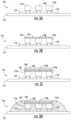
- FIGS. 1 A through 1 Care various illustrations of example wavelength conversion components 100 , also referred to as a color conversion components and/or light converting element. In some embodiments, particularly when comprised of phosphor on sapphire, such components can be referred to herein as Phos hats.
- FIG. 1 Ais a side view illustration of a wavelength conversion components 100 comprising a clear substrate 102 , or transparent substrate, and a phosphor compound 104 applied thereto.
- Phospor compound 104can be applied to a top T or upper surface of clear substrate 102 , as illustrated in FIG. 1 A , or can be applied to a bottom B or lower surface of clear substrate 102 , or in some embodiments on both top T and bottom B.
- wavelength conversion components 100can comprise a substantially planar or wafer structure comprising a clear substrate 102 with a phosphor compound 104 applied to a surface thereof, such as for example top surface T.
- Clear substrate 102can in some embodiments comprise a sapphire wafer, or other suitable clear or transparent material, such as for example glass of any kind, acrylic, soda lime, borosilicate, quartz/SiO 2 , MgF 2 .
- clear substrate 102can comprise a rigid or flexible clear substrate as well as a clear cure silicone sheet, which can provide the ability to shape a phosphor layer.
- Phosphor sheetscan comprise phosphor mixed into a silicone matrix and squeegeed flat and frozen to be used to lay onto a panel populated with die.
- Such a configurationcan provide a flexible Phos hat where the substrate can comprise for example a soft methyl.
- Such a configurationcan in some embodiments be vacuum attached and the soft silicone could conform and seal to a wet attach layer.
- the phosphor compound 104can comprise phosphor, and/or a mixture of phosphor and another material, such as for example silicone, silicon (fumed silica), fused silica, TiO 2 , and other generic diffusers. Any scatterer, e.g. fused silica, can be added to the mixture for packing and homogeneity of emission. TiO 2 in small concentrations can in some embodiments be used effectively.
- the mixture of phosphor and siliconecomprises a ratio of about 1:1 to about 6:1, including about 1:1, about 2.5:1, about 3:1, about 4:1. about 4.5:1 and/or about 5:1.
- the concentration and/or particle size of the phosphor in the phosphor compoundis adjustable, wherein the concentration and/or particle size of the phosphor alters a color produced by a wavelength passing through the wavelength conversion component.
- Application A of the phosphor and/or phosphor compounds 104 to clear substrate 102can be achieved via any suitable method including, for example, spraying, gravity sedimentation, centrifuge, addition of a solvent, screen printing, evaporation (sputter, e-beam, thermal, CVD, electrostatic and/or electrophoretic deposition), dipping, spin coating, direct dispensing, and/or vibration, as discussed further herein.
- the phosphor compound 104is substantially uniformly applied to the transparent substrate 102 and/or is conformal to the transparent substrate 102 .
- Wavelength conversion component 100 as shown in FIGS. 1 A through 1 Cis configured to alter a wavelength of a light emitted from a light source when positioned proximate to the light source, such as for example a LED.
- component 100is configured to be positioned on or proximate to a light source, such as an LED.
- wavelength conversion component 100can comprise any suitable size or configuration as needed for application to, on or near a light source such as an LED.
- width W, length L and height Hcan be configured as desired, e.g.
- a wavelength conversion component 100can be 40 um to 10 mm long and 5 um to 10 mm wide, or more, to achieve a wavelength conversion component 100 having an area of about 200 um 2 to about 5 mm 2 .
- a wavelength conversion component 100can be about 50 mm 2 or more.
- a wavelength conversion componentcan be any desirable size and/or shape, such as about 30 ⁇ 30 mm, which is an advantage not available in PiGs and CPPs.
- phosphor compound 104can be applied A to substrate 102 and then the wafer can be cut C into desired dimensions.
- substrate 102can in some embodiments be cut or singulated into clear substrates 102 S prior to application A of phosphor compound 104 .
- phosphor compound 104can in some embodiments be applied to top surface T as well as along some edges or sides of clear substrate 102 .
- wavelength conversion componentscan be made by providing a transparent substrate having an upper surface and a lower surface, applying a phosphor compound to the upper surface and/or lower surface of the transparent substrate, and curing the transparent substrate with applied phosphor compound.
- the resulting wavelength conversion componentcan in some embodiments be configured to alter a wavelength of a light emitted from a light source when positioned proximate to the light source.
- the transparent substratecan comprise a sapphire wafer, and the phosphor compound can comprise a mixture of phosphor and silicone.
- making the disclosed wavelength conversion components, or Phos hatscan further comprise using a stealth laser to cause an internal damage layer in the transparent substrate. Is some embodiments using the stealth laser to pitch can occur prior to application of the phosphor compound.
- phosphor and/or phosphor compounds to the clear or transparent substratecan be achieved via any suitable method including, for example, spraying, gravity sedimentation, centrifuge, addition of a solvent, screen printing, evaporation (sputter, e-beam, thermal, CVD, electrostatic and/or electrophoretic deposition), dipping, spin coating, direct dispensing, and/or vibration.
- the phosphor compoundcan be substantially uniformly applied to the transparent substrate such that it is conformal to the transparent substrate.
- a silicone compound and/or layercan be applied on the phosphor compound that is applied to the upper surface and/or lower surface of the transparent substrate.
- FIGS. 2 A through 2 Eare various illustrations of example LED devices as provided herein. In some embodiments FIGS. 2 A through 2 E can be viewed as steps for making/assembling a LED device as provided herein, although variations in the order of the steps and omission/addition of some steps is not precluded.
- FIG. 2 Adepicts a light emitter device 110 comprising a submount 112 and one or more light emitters 114 a, 114 b, and 114 c disposed on submount 112 . Any number of light emitters 114 a - c, or LEDs, can be disposed on or applied to submount 112 . Additionally, LEDs 114 a - c can each have a different targeted color. Although three LEDs are illustrated, device 110 can include a different number of LEDs, e.g., one or more LEDs.
- a submount 112can comprise electronic traces 116 , or conductive traces, but in some examples, device 110 could be based on a leadframe construction where no traces are on top, or any other appropriate construction.
- die attach material 118or solder bumps, can be provided to create an electrical contact between light emitters 114 a - c and electronic traces 116 .
- FIG. 2 Adepicts a light emitter device 110 comprising a submount 112 comprising an upper surface and a bottom surface and one or more light emitters 114 a - c disposed on the upper surface of submount 112 .
- the one or more light emitters 114 a - ceach comprise an upper surface, a lower surface adjacent to the upper surface of submount 112 , and one or more sides.
- a light affecting material 120can be applied to device 110 .
- light affecting material 120can comprise a reflective material, such as for example TiO 2 (also referred to as titania and/or blue TiO 2 ), A 1203 , Boron nitride, microcellular polyethylene terephthalate (McPET) and/or Barium sulfate (sphere material).
- light affecting material 120is applied to device 110 so at to surround the one or more light emitters 114 a - c disposed on submount 112 .
- light affecting material 120can be disposed on the upper surface of submount 112 and/or adjacent to the one or more sides of the one or more light emitters 114 a - c.
- light affecting material 120is applied at a depth or height substantially similar to a height of light emitters 114 a - c such that each side of light emitters 114 a - c are surrounded by light affecting material 120 on one or more sides of light emitters 114 a - c
- Light emitters 114 a - ccan comprise any suitable chip size, shape, and/or thickness.
- the thickness or heightcan be approximately 0.25 mm or more, 0.3 mm or more, 0.4 mm or more, or 0.5 mm or more.
- FIG. 2 Cdepicts light emitter device 110 with a clear layer 122 applied to light emitters 114 a - c.
- a clear layer 122in some embodiments comprising a silicone and/or an adhesive, and optionally a scatter compound, can be applied to an upper surface of one or more of light emitters 114 a - c.
- Clear or silicone layer 122can in some embodiments be configured to adhere the wavelength conversion component (see FIG. 2 D ) to the upper surface of the one or more light emitters 114 a - c.
- the scatter compoundcan comprise fumed silica, fused silica, and/or TiO 2 . In some aspects, TiO 2 in small percentages can be used for the scattering compound.
- the percentage of TiO 2can be from around, about or approximately 0.1% to 5.0%. In some aspects, the percentage of TiO 2 can for example be around, about or approximately 1%.
- Clear or silicone layer 122can be applied to the LEDs such that it substantially or completely covers the upper surface thereof. In some embodiments the clear layer can be administered such that it extends to the edges of the upper surface of the one or more LEDs on the device, without extending past the edges.
- the wavelength conversion componentcan be applied to device 110 by placing the clear substrate 102 with phosphor layer 104 directly above light emitters 114 a - c.
- the Phos hatcan affect the light output from the LEDs, including improving the uniformity of color produced by device 110 .
- the Phos hatcan be applied with the phosphor 104 side down as depicted in FIG. 2 D .
- Clear layer 122can in some embodiments act as an adhesive to adhere substrate 102 with phosphor layer 104 onto light emitters 114 a - c.
- a second application of light affecting material 124can be applied to device 110 .
- light affecting material 124can comprise a reflective material, such as for example TiO 2 (also referred to as titania and/or blue TiO 2 ), and can be the same as light affecting material 120 .
- light affecting material 124is applied to device 110 so at to surround the Phos hat (substrate 102 and phosphor layer 104 ) on top of LEDs 114 a - c.
- light affecting material 124can be disposed on previously applied light affecting material 120 and adjacent to the one or more sides of the Phos hat (substrate 102 and phosphor layer 104 ) on top of LEDs 114 a - c.
- light affecting material 124is applied at a depth or height substantially similar to a height the Phos hat such that each side of it is surrounded by light affecting material 124 .
- device 110can be cured at an appropriate temperature, such as for example 150° C.
- FIGS. 3 A through 3 Dvarious examples of LED devices as provided herein are illustrated.
- FIGS. 3 A through 3 Dcan be viewed as steps for making/assembling a LED device as provided herein, although variations in the order of the steps and omission/addition of some steps is not precluded.
- FIG. 3 Adepicts a light emitter device 110 comprising a submount 112 and one or more light emitters 114 a, 114 b, and 114 c disposed on submount 112 . Any number of light emitters 114 a - c, or LEDs, can be disposed on or applied to submount 112 . Additionally, LEDs 114 a - c can each have a different targeted color. Although three LEDs are illustrated, device 110 can include a different number of LEDs, e.g., one or more LEDs.
- a submount 112can comprise electronic traces 116 , or conductive traces, but in some examples, device 110 could be based on a leadframe construction where no traces are on top, or any other appropriate construction.
- die attach material 118or solder bumps, can be provided to create an electrical contact between light emitters 114 a - c and electronic traces 116 .
- FIG. 3 Adepicts a light emitter device 110 comprising a submount 112 comprising an upper surface and a bottom surface and one or more light emitters 114 a - c disposed on the upper surface of submount 112 .
- the one or more light emitters 114 a - ceach comprise an upper surface, a lower surface adjacent to the upper surface of submount 112 , and one or more sides.
- FIG. 3 Bdepicts light emitter device 110 with a clear layer 122 applied to light emitters 114 a - c.
- a clear layer 122in some embodiments comprising a silicone and/or an adhesive, and optionally a scatter compound, can be applied to an upper surface of one or more of light emitters 114 a - c.
- Clear or silicone layer 122can in some embodiments be configured to adhere the wavelength conversion component (see FIG. 3 C ) to the upper surface of the one or more light emitters 114 a - c.
- the scatter compoundcan comprise fumed and/or fused silica.
- Clear or silicone layer 122can be applied to the LEDs such that it substantially or completely covers the upper surface thereof. In some embodiments the clear layer can be administered such that it extends to the edges of the upper surface of the one or more LEDs on the device, without extending past the edges.
- the wavelength conversion componentcan be applied to device 110 by placing the clear substrate 102 with phosphor layer 104 directly above light emitters 114 a - c.
- the Phos hatcan affect the light output from the LEDs, including improving the uniformity of color produced by device 110 .
- the Phos hatcan be applied with the phosphor 104 side down as depicted in FIG. 3 C .
- Clear layer 122can in some embodiments act as an adhesive to adhere substrate 102 with phosphor layer 104 onto light emitters 114 a - c.
- a light affecting material 120can be applied to device 110 .
- light affecting material 120can comprise a reflective material, such as for example TiO 2 .
- light affecting material 120is applied to device 110 so at to surround the one or more light emitters 114 a - c disposed on submount 112 , as well as the Phos hat (substrate 102 and phosphor layer 104 ) on top of LEDs 114 a - c. That is, in some embodiments light affecting material 120 can be disposed on the upper surface of submount 112 and/or adjacent to the one or more sides of the one or more light emitters 114 a - c.
- light affecting material 120is applied at a depth or height substantially similar to a height of light emitters 114 a - c, including the height of the Phos hat (substrate 102 and phosphor layer 104 ) on top of LEDs 114 a - c, such that each side of light emitters 114 a - c is surrounded by light affecting material 120 .
- FIGS. 4 A through 4 Dvarious examples of LED devices as provided herein are illustrated.
- FIGS. 4 A through 4 Dcan be viewed as steps for making/assembling a LED device as provided herein, although variations in the order of the steps and omission/addition of some steps is not precluded.
- FIG. 4 Adepicts a light emitter device 110 comprising a submount 112 and one or more light emitters 114 a, 114 b, and 114 c disposed on submount 112 . Any number of light emitters 114 a - c, or LEDs, can be disposed on or applied to submount 112 . Additionally, LEDs 114 a - c can each have a different targeted color. Although three LEDs are illustrated, device 110 can include a different number of LEDs, e.g., one or more LEDs.
- a submount 112can comprise electronic traces 116 , or conductive traces, but in some examples, device 110 could be based on a leadframe construction where no traces are on top, or any other appropriate construction.
- die attach material 118or solder bumps, can be provided to create an electrical contact between light emitters 114 a - c and electronic traces 116 .
- FIG. 4 Adepicts a light emitter device 110 comprising a submount 112 comprising an upper surface and a bottom surface and one or more light emitters 114 a - c disposed on the upper surface of submount 112 .
- the one or more light emitters 114 a - ceach comprise an upper surface, a lower surface adjacent to the upper surface of submount 112 , and one or more sides.
- FIG. 4 Bdepicts light emitter device 110 with a clear layer 122 applied to light emitters 114 a - c.
- a clear layer 122in some embodiments comprising a silicone and/or an adhesive, and optionally a scatter compound, can be applied to an upper surface of one or more of light emitters 114 a - c.
- Clear or silicone layer 122can in some embodiments be configured to adhere the wavelength conversion component (see FIG. 4 C ) to the upper surface of the one or more light emitters 114 a - c.
- the scatter compoundcan comprise fumed and/or fused silica.
- Clear or silicone layer 122can be applied to the LEDs such that it substantially or completely covers the upper surface thereof. In some embodiments the clear layer can be administered such that it extends to the edges of the upper surface of the one or more LEDs on the device, without extending past the edges.
- the wavelength conversion componentcan be applied to device 110 by placing the clear substrate 102 with phosphor layer 104 directly above light emitters 114 a - c.
- the Phos hatcan affect the light output from the LEDs, including improving the uniformity of color produced by device 110 .
- the Phos hatcan be applied with the phosphor 104 side down as depicted in FIG. 4 C .
- Clear layer 122can in some embodiments act as an adhesive to adhere substrate 102 with phosphor layer 104 onto light emitters 114 a - c.
- a light affecting material 120can be applied to device 110 .
- light affecting material 120can comprise a reflective material, such as for example TiO 2 .
- light affecting material 120is applied to device 110 so at to surround the one or more light emitters 114 a - c disposed on submount 112 , as well as the Phos hat (substrate 102 and phosphor layer 104 ) on top of LEDs 114 a - c. That is, in some embodiments light affecting material 120 can be disposed on the upper surface of submount 112 and/or adjacent to the one or more sides of the one or more light emitters 114 a - c.
- light affecting material 120is applied at a depth or height substantially similar to a height of light emitters 114 a - c, including the height of the Phos hat (substrate 102 and phosphor layer 104 ) on top of LEDs 114 a - c, such that each side of light emitters 114 a - c is surrounded by light affecting material 120 .
- a dam material 130can be provided/applied by any suitable technique, e.g. molded, dispensed, etc., around a periphery of submount 112 .
- Dam material 130can be configured to contain light affecting material 120 on the upper surface of submount 112 and/or adjacent to the one or more sides of the one or more light emitters 114 a - c whereby the one or more light emitters is surrounded by the light affecting material. In some embodiments, and as depicted in FIG.
- dam material 130can in some embodiments be configured to extend above the upper surface of submount 112 to a height substantially similar to a height of the one or more sides of the one or more light emitters 114 a - c, such that dam material 130 is configured to contain enough light affecting material 120 to surround the one or more light emitters 114 a - c at a depth substantially similar to the height of the one or more sides of the one or more light emitters 114 a - c.
- dam material 130can be more viscous than light affecting material 120 .
- an upper surface of the light affecting material 120 encapsulating the one or more light emitters 114 a - cis substantially planar to the upper surface of the one or more light emitters. That is, in the configuration depicted in FIG. 4 D the light affecting material 120 can be applied in such a manner as to create a squared off or substantially squared profile with an upper surface substantially planar to the upper surface of the LEDs/Phos hat, with an outer edge that is substantially vertical. In some embodiments dam material 130 can be removed after application, and in some embodiments, curing of light affecting material 120 .
- dam material 130can be configured as a high angle light reflector, such as for when light affecting material 120 , or fill material, is clear. Dam material 130 can serve as a reflector of high angle light to make light more useful for application intent, especially when light affecting material 120 is a substantially transparent fill material.
- molded domescan be coupled with dam material 130 for light reflection to increase brightness, i.e. useful light. Such a configuration can be used with or without a wavelength conversion component or Phos hat as described herein.
- Dam material 130can in some embodiments comprise a mix of Si 5 with 50% TiO 2 , 50% 705F fused silica (roughly phosphor sized glass beads), and 5% A604 fumed silica. In some embodiments dam material 130 can comprise a mix of Si 4 , OE6370 silicone, 75% TiO 2 , 50% fused silica, and 7.5% fumed Silica.
- FIG. 5is a perspective view of an example LED device 140 , or LED chip, as disclosed herein.
- LED device 140can in some embodiments be the final product of the examples and steps depicted in FIGS. 2 A- 2 E, 3 A- 3 D and/or 4 A- 4 D .
- LED device 140can in some embodiments comprise a submount 112 and one or more light emitters 114 a, 114 b, and 114 c disposed on submount 112 .
- Wavelength conversion component 100(or Phos hat comprising substrate 102 and phosphor layer 104 as depicted in FIGS. 2 D, 3 C and 4 C ) can be disposed directly above LEDs 114 a - c.
- Light emitters 114 a, 114 b, and 114 c and wavelength conversion component 100can be surrounded by light affecting material 120 .
- One or more contacts 128can be provided on substrate 112 , and in some embodiments can extend under LEDs 114 a - c and/or can be in electrical connection to electronic traces 116 (see FIGS. 2 A, 3 A and/or 4 A ) to provide electrical connections to LEDs 114 a - c.
- Contacts 128can comprise one cathode and one anode.
- LED device 140can comprise a quick response code QR, or other bar code configured to contain information about the device.
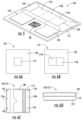
- FIGS. 6 A and 6 Bare top plan views of example LED devices 170 and 172 , respectively.
- LED devices 170 and 172can in some embodiments comprise one light emitter 114 as depicted in FIG. 6 A , or one or more light emitters, such as for example two light emitters 114 a / 114 b as depicted in FIG. 6 B , or more.
- a wavelength conversion component, or Phos hat, as disclosed hereincan be disposed over the one or more light emitters.
- Light emitters 114 or 114 a / 114 b and the wavelength conversion componentcan be surrounded by light affecting material 120 .
- FIG. 6 Cdepicts a bottom plan view of an example LED device 170 / 172 .
- the light emitterssuch as light emitters 114 in FIG. 6 A
- the light emitterscan be arranged for mounting using surface mount technology and having internal conductive paths, comprising first and second surface mount pads 176 a and 176 b, respectively, that can be formed on back surface 174 of submount 112 .
- Conductive vias 178can be formed through submount 112 such that when a signal is applied to one or both of first and second surface mount pads 176 a and 176 b it is conducted to one or more electronic traces on the top surface of submount 112 , such as electronic traces 116 depicted in FIGS. 2 A, 3 A and/or 4 A .
- first and second mounting pads 176 a and 176 bcan allow for surface mounting of the LED devices 170 / 172 with the electrical signal to be applied to the LED devices 170 / 172 applied across the first and second mounting pads 176 a and 176 b.
- the mounting pads 176 a and 176 b, and vias 178can be arranged in many different ways and can have many different shapes and sizes. It is also understood that instead of vias, one or more conductive traces can be provided on the surface of the submount between the mounting pads and contact pads, such as along the side surface of the submount.
- the LED device 170 / 172can further comprise a metallized area 180 on the back surface 174 of submount 112 , between the first and second mounting pads 176 a and 176 b, respectively.
- Metallized area 180is preferably made of a heat conductive material and is preferably in at least partial vertical alignment the one or more LEDs 114 ( FIG. 6 A ) or 114 a, 114 b ( FIG. 6 B ). In one embodiment, the metallized area 180 is not in electrical contact with the elements on top surface of the submount 112 or the first and second mounting pads 176 a and 176 b on the back surface 174 of the submount 112 .
- the metallized areacan assist with this dissipation by allowing this heat to spread into the metallized area where it can dissipate more readily. It is also noted that the heat can conduct from the top surface of the submount 112 , through the vias 178 , where the heat can spread into the first and second mounting pads 176 a and 176 b where it can also dissipate.
- the thickness of the metallized area 180 and the first and second pads 176 a and 176 bshould be approximately the same such that all three make contact to a lateral surface such as a PCB.
- FIG. 6 Dis a side view of LED device 170 / 172 , and illustrating an optical area, including light affecting material 120 near an upper surface, mounted on submount 112 , with one or more copper traces 212 (or other conductive material such as Ni, Pd or Au) thereunder.
- FIG. 6 Eis a top plan view of an example LED device 174 .
- LED device 174can in some embodiments comprise one or more light emitters 114 c and 114 d, as depicted in FIG. 6 E .
- a wavelength conversion component, or Phos hat, as disclosed hereincan be disposed over the one or more light emitters.
- Light emitters 114 c / 114 d and the wavelength conversion componentcan be surrounded by light affecting material 120 .
- different phosphor regions, areas or zonescan be disposed over emitters 114 c / 114 d.
- Emitters 114 c / 114 dcan be any desired color, such as for example both emitters 114 c / 114 d can comprise blue LEDs.
- the color emitted by the emitter or LEDcan be color shifted for example by the phosphor region or zone.
- U.S. Pat. No. 8,998,444incorporated herein by reference and commonly owned herewith, discloses blue-shifted yellow and/or green plus (+) blue-shifted red.
- two or more zonescan be helpful where the emission spectrum of one phosphor overlaps with the activation (or excitation) spectrum of another phosphor.
- phosphors and phosphor colorscan be layered on each other and on a wavelength conversion component disposed over an emitter to produced different colors and/or color intensities.
- phosphorscan be optimally layered in one or more layers to achieve a light effect or desired wavelength. See, e.g., US Patent Application Publication No. 2009/0039375, incorporated herein by reference and commonly owned herewith.
- a first layercan comprise a red phosphor and a second layer a yellow phosphor, or vice versa.
- a green phosphorcan be layered on a yellow phosphor that is layered on a red phosphor, for example.
- emitterssuch as emitters 114 c / 114 d in FIG. 6 E , with different phosphor colors thereon can be separately controllable such that they can be turned on at the same time or at different times.
- FIG. 7is a plan view illustrating a metal trace configuration of an example LED device 150 .
- the metalized trace depicted in FIG. 6can comprise a metalized trace corresponding to LED device 140 of FIG. 5 .
- LED device 150can comprise a substrate 126 (in some embodiments similar to substrate 112 of FIG. 5 ) and one or more contacts 128 , including one cathode and one anode.
- Connected to contacts 128can be one or more electronic traces 154 and/or contact pads 152 , which can be configured to allow electric current to flow into and out of the solid state light emitters thereby illuminating the solid state light emitters.
- Solid state light emitterscan be electrically connected only in parallel, only in series, or in an arrangement comprising a combination of parallel and series.
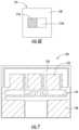
- FIGS. 8 A and 8 Bare various illustrations of example LED components 200 and 202 , respectively.
- Each of components 200 and 202can in some embodiments comprise a substrate 210 , such as an aluminum nitride substrate, and one or more copper traces 212 on substrate 210 .
- a gold interface 216can be disposed on and/or above one or more copper traces 212 .
- An aluminum pad 220 configured for wire bonding W an LEDcan be disposed on a portion of gold interface 216 , with a layer of titanium 218 between aluminum pad 220 and gold interface 216 .
- the layer of titanium 218can be configured to substantially prevent, or significantly reduce, galvanic action between aluminum pad 220 and gold interface 216 .
- a light emitter 114can be disposed on gold interface 216 .
- the layer of titanium 218 and aluminum pad 220can be substantially aligned vertically such that titanium 218 is substantially and directly below aluminum pad 220 .
- aluminum pad 220can be disposed on top of a layer of titanium 218 that extends past the edges of aluminum pad 220 .
- titanium 218is configured to extend beyond an outer periphery of aluminum pad 220 and provide an additional insulting effect against galvanic action between the aluminum pad and gold interface.
- FIG. 8 Bshowing a top plan view of titanium 218 and aluminum pad 220 , titanium 218 is configured to extend beyond an outer periphery of aluminum pad 220 .
- a light emitter 114can for example be disposed on gold interface 216 , and a wire W for wire bonding can for example extend from aluminum pad 220 for connecting to other structure.
- Such methodscan comprise providing an aluminum nitride substrate, providing one or more copper traces on the aluminum nitride substrate, providing a gold interface on the one or more copper traces, applying a first photo mask to create an opening on the gold interface and applying a layer of titanium thereon, and applying a second photo mask to create an opening on the layer of titanium and applying an aluminum pad configured for wire bonding the LED.
- Such a methodprovides an LED component as depicted in FIG. 8 B having a layer of titanium between the aluminum pad and gold interface, wherein the layer of titanium is configured to substantially prevent galvanic action between the aluminum pad and gold interface.
- FIG. 9is an illustration of an example LED device 160 .
- FIG. 9depicts an LED device, such as that depicted in any of FIGS. 2 A- 2 E, 3 A- 3 D, 4 A- 4 D and/or 5 , enclosed in a lens 162 .
- LED device 160can comprise a submount 112 and one or more light emitters 114 disposed on submount 112 . Any number of light emitters 114 or LEDs can be disposed on or applied to submount 112 .
- a submount 112 , or substratecan comprise electronic traces 116 , or conductive traces, but in some examples, device 110 could be based on a leadframe construction where no traces are on top, or any other appropriate construction.
- die attach material 118can be provided to create an electrical contact between light emitters 114 and electronic traces 116 .
- a clear layer 122such as silicone, can be applied to light emitters 114 on top of which a wavelength conversion component (Phos hat), comprising clear substrate 102 with phosphor layer 104 directly, can be applied.
- a light affecting material 120can be applied to device 110 so at to surround the one or more light emitters 114 .
- a lens 162can be adhered to or otherwise affixed to substrate 112 and enclose light emitter 114 , wavelength conversion component 102 / 104 , and light affecting material 120 .
- Lens 162can provide a protective element to the LED and related components, and/or alter light emitted therefrom.
- LEDs used in the devices and components hereincan have different targeted colors selected so that devices can operate as a pixel and produce a range of colors within its color gamut by energizing different combinations of LEDs.
- LEDscan include UV, blue or green LED chips, such as a group III nitride based LED chip comprising negatively doped (n-type) epitaxial layer(s) of gallium nitride or its alloys and positively doped (p-type) epitaxial layers of gallium nitride or its alloys surrounding a light emitting active region; a red LED chip, such as an AlInGaP based red LED chip; a white LED chip (e.g., blue LED chip with phosphor(s) layer(s)), and/or a non-white phosphor based LED chip.
- group III nitride based LED chipcomprising negatively doped (n-type) epitaxial layer(s) of gallium nitride or its alloys and positively doped (p-type
- Traces, electrical contacts, leads and contact pads, as described herein,can comprise any suitable electrically conductive material, e.g., Cu, finished with electroless Ag, Ni—Ag, ENIG, ENIPIG, HASL, OSP, or the like. Traces can be applied over one or more surfaces of a substrate via plating (e.g., via electroplating or electroless plating), depositing (e.g., physical, chemical, and/or plasma deposition, CVD, PECVD, etc.), sputtering, or via any other suitable technique.
- platinge.g., via electroplating or electroless plating
- depositinge.g., physical, chemical, and/or plasma deposition, CVD, PECVD, etc.
- sputteringe.g., physical, chemical, and/or plasma deposition, CVD, PECVD, etc.
- tracescan comprise a metal or metal alloy which may contain (in whole or part) copper (Cu), silver (Ag), gold (Au), titanium (Ti), palladium (Pd), aluminum (Al), tin (Sn), combinations thereof, and/or any other suitable conductor.
- substratessuch as substrate 112 of FIGS. 2 - 5
- such substratescan comprise one or more materials arranged to provide desired electrical isolation and high thermal conductivity.
- at least a portion of such substratesmay comprise a dielectric to provide the desired electrical isolation between electrical traces and/or sets of solid state emitters.
- such substratescan comprise ceramic such as alumina (Al 2 O 3 ), aluminum nitride (AlN), silicon carbide (SiC), silicon, or a plastic or polymeric material such as polyimide, polyester etc.
- such substratescomprises a flexible circuit board, which can allow the substrate to take a non-planar or curved shape allowing for providing directional light emission with the solid state emitters also being arranged in a non-planar manner.
- LEDs 102 a - ccan be horizontally structured so that LEDs 102 a - c can be electrically connected to traces 108 a - b without the use of wire bonding.
- each of LEDs 102 a - ccan be a horizontally structured device where each electrical contact (e.g., the anode and cathode) can be disposed on a bottom surface of the LED 102 a - c.
- Apparatus 100includes die attach material 130 , e.g., solder bumps. Die attaching LEDs 102 a - c using any suitable material and/or technique (e.g., solder attachment, preform attachment, flux or no-flux eutectic attachment, silicone epoxy attachment, metal epoxy attachment, thermal compression attachment, bump bonding, and/or combinations thereof) can directly electrically connect LEDs 102 a - c to traces 108 a - b without requiring wire bonds.
- each of LEDs 114 a - ccan be a device that does not comprise angled or beveled surfaces.
- each of LEDs 114 a - ccan be an LED device that comprises coplanar electrical contacts on one side of the LED (bottom side) with the majority of the light emitting or transmitting surface being located on the opposite side (upper side), also know as a “flip-chip”.
- LEDs 114 a - ccan be bump bonded to traces using bumps of solder (or other appropriate conductive material) and force, energy (e.g., ultrasonic), and/or heat.
- LED devices 110 , 140 and 160can optionally include diffuse layers for optics, lenses, polarizers, anti-reflective (AR) coating, anti glare, micro lenses, light steering, parallax barrier, lenticular arrays, and so on.
- diffuse layersfor optics, lenses, polarizers, anti-reflective (AR) coating, anti glare, micro lenses, light steering, parallax barrier, lenticular arrays, and so on.
- ARanti-reflective
- a method for making a wavelength conversion componentcomprises: providing a transparent substrate having an upper surface and a lower surface; applying a phosphor compound to the upper surface and/or lower surface of the transparent substrate; and curing the transparent substrate with applied phosphor compound, wherein the wavelength conversion component is configured to alter a wavelength of a light emitted from a light source when positioned proximate to the light source.
- the transparent substratecan comprise a sapphire wafer
- the phosphor compoundcan comprise a mixture of phosphor and silicone.
- the mixture of phosphor and siliconecan comprise a ratio of about 1:1 to about 5:1.
- Applying a phosphor compound to the upper surface and/or lower surface of the transparent substrateresults in a substantially uniformly applied phosphor compound to the transparent substrate such that the phosphor compound is conformal to the transparent substrate.
- a lasercan be used to cause an internal damage layer in the transparent substrate.
- the methodcan comprise singulating the transparent substrate after application of the phosphor compound to provide a wavelength conversion component of a desired size, and the singulation can comprise singulating the transparent substrate prior to application of the phosphor compound to provide a wavelength conversion component of a desired size.
- Applying a phosphor compound to the upper surface and/or lower surface of the transparent substratecan comprise spraying, screen printing and/or dispensing.
- a silicone compound on the phosphor compoundcan be applied to the upper surface and/or lower surface of the transparent substrate.
- a method in some aspectscan comprise: providing a submount comprising an upper surface and a bottom surface; attaching one or more light emitters on the upper surface of the submount, the one or more light emitters comprising an upper surface, a lower surface, and one or more sides; applying a light affecting material to the upper surface of the submount and adjacent to the one or more sides of the one or more light emitters; and applying a wavelength conversion component on the upper surface of the one or more light emitters.
- the light affecting materialcan comprise a reflective material.
- the light affecting materialcan comprise TiO 2 .
- the light affecting materialcan surround the sides of the one or more light emitters disposed on the upper surface of the submount.
- Applying a light affecting materialcan further comprise applying a dam material on the upper surface of the submount prior to applying the light affecting material, wherein the dam material is configured to contain the light affecting material on the upper surface of the submount and adjacent to the one or more sides of the one or more light emitters after application of the light affecting material, whereby the one or more light emitters are surrounded by the light affecting material.
- the dam materialcan be applied on the upper surface of the submount to a height substantially similar to a height of the one or more sides of the one or more light emitters, wherein the dam material is configured to contain enough light affecting material to surround the one or more light emitters at a depth substantially similar to the height of the one or more sides of the one or more light emitters.
- the wavelength conversion componentcan comprise a transparent substrate comprising an upper and lower surface, and a phosphor compound disposed on at least one or both of the upper and/or lower surface.
- the transparent substratecan comprise a sapphire wafer.
- the phosphor compoundcan comprise a mixture of phosphor and silicone.
- the wavelength conversion componentcan be applied to the upper surface of the one or more light emitters with the phosphor compound facing down and adjacent to the upper surface of the one or more light emitters. Applying a wavelength conversion component on the upper surface of the one or more light emitters further can comprise adding a silicone layer to the upper surface of the one or more light emitters prior to applying the wavelength conversion component.
- the silicone layercan further comprise fumed or fused silica.
- Applying the light affecting materialcan occur prior to applying the wavelength conversion component. Applying the wavelength conversion component can occur prior to applying the light affecting material.
- a methodcan further comprise making the wavelength conversion component, comprising: providing a sapphire wafer having an upper surface and a lower surface; applying a phosphor compound to the upper surface and/or lower surface of the transparent substrate; and curing the transparent substrate with applied phosphor compound, wherein the wavelength conversion component is configured to alter a wavelength of a light emitted from a light source when positioned proximate to the light source.
- a light emitting diode (LED) componentcan comprise: a substrate for a light emitting diode (LED); one or more copper traces on the substrate; a gold interface on the one or more copper traces; an aluminum pad configured for electrically connecting with the LED; and a layer of titanium between the aluminum pad and gold interface, wherein the layer of titanium is configured to prevent, substantially prevent, or minimize galvanic action between the aluminum pad and gold interface.
- the layer of titaniumcan be configured to extend beyond an outer periphery of the aluminum pad.
- the substratecan be aluminum nitride.
- a method of making a light emitting diode (LED) componentcomprises: providing a substrate for a LED; providing one or more copper traces on the substrate; providing a gold interface on the one or more copper traces; applying a first photo mask to create an opening on the gold interface and applying a layer of titanium; and applying a second photo mask to create an opening on the layer of titanium and applying an aluminum pad configured for electrically connecting with the LED, wherein a layer of titanium is provided between the aluminum pad and gold interface, wherein the layer of titanium is configured to prevent, substantially prevent, or minimize galvanic action between the aluminum pad and gold interface.
- the layer of titaniumcan be configured to extend beyond an outer periphery of the aluminum pad.
- the substratecan be aluminum nitride.
- aspects disclosed hereincan, for example and without limitation, provide one or more of the following beneficial technical effects: reduced cost of providing solid state lighting apparatuses; reduced size, volume, or footprint of solid state lighting apparatuses; improved efficiency; improved color rendering; improved thermal management; simplified circuitry; improved contrast, improved viewing angle; improved color mixing; improved reliability; and/or simplified DC or AC operability.
Landscapes
- Engineering & Computer Science (AREA)
- Power Engineering (AREA)
- Microelectronics & Electronic Packaging (AREA)
- Physics & Mathematics (AREA)
- Condensed Matter Physics & Semiconductors (AREA)
- General Physics & Mathematics (AREA)
- Computer Hardware Design (AREA)
- Led Device Packages (AREA)
Abstract
Description
Claims (22)
Priority Applications (1)
| Application Number | Priority Date | Filing Date | Title |
|---|---|---|---|
| US17/116,576US12142711B2 (en) | 2016-07-26 | 2020-12-09 | Light emitting diodes, components and related methods |
Applications Claiming Priority (5)
| Application Number | Priority Date | Filing Date | Title |
|---|---|---|---|
| US201662366961P | 2016-07-26 | 2016-07-26 | |
| US15/657,027US10290777B2 (en) | 2016-07-26 | 2017-07-21 | Light emitting diodes, components and related methods |
| US16/380,400US10964858B2 (en) | 2016-07-26 | 2019-04-10 | Light emitting diodes, components and related methods |
| US16/797,173US10879435B2 (en) | 2016-07-26 | 2020-02-21 | Light emitting diodes, components and related methods |
| US17/116,576US12142711B2 (en) | 2016-07-26 | 2020-12-09 | Light emitting diodes, components and related methods |
Related Parent Applications (1)
| Application Number | Title | Priority Date | Filing Date |
|---|---|---|---|
| US16/797,173ContinuationUS10879435B2 (en) | 2016-07-26 | 2020-02-21 | Light emitting diodes, components and related methods |
Publications (2)
| Publication Number | Publication Date |
|---|---|
| US20210119090A1 US20210119090A1 (en) | 2021-04-22 |
| US12142711B2true US12142711B2 (en) | 2024-11-12 |
Family
ID=59523255
Family Applications (4)
| Application Number | Title | Priority Date | Filing Date |
|---|---|---|---|
| US15/657,027ActiveUS10290777B2 (en) | 2016-07-26 | 2017-07-21 | Light emitting diodes, components and related methods |
| US16/380,400ActiveUS10964858B2 (en) | 2016-07-26 | 2019-04-10 | Light emitting diodes, components and related methods |
| US16/797,173ActiveUS10879435B2 (en) | 2016-07-26 | 2020-02-21 | Light emitting diodes, components and related methods |
| US17/116,576Active2039-05-17US12142711B2 (en) | 2016-07-26 | 2020-12-09 | Light emitting diodes, components and related methods |
Family Applications Before (3)
| Application Number | Title | Priority Date | Filing Date |
|---|---|---|---|
| US15/657,027ActiveUS10290777B2 (en) | 2016-07-26 | 2017-07-21 | Light emitting diodes, components and related methods |
| US16/380,400ActiveUS10964858B2 (en) | 2016-07-26 | 2019-04-10 | Light emitting diodes, components and related methods |
| US16/797,173ActiveUS10879435B2 (en) | 2016-07-26 | 2020-02-21 | Light emitting diodes, components and related methods |
Country Status (4)
| Country | Link |
|---|---|
| US (4) | US10290777B2 (en) |
| EP (1) | EP3491679B1 (en) |
| CN (1) | CN109791968A (en) |
| WO (1) | WO2018022456A1 (en) |
Families Citing this family (46)
| Publication number | Priority date | Publication date | Assignee | Title |
|---|---|---|---|---|
| EP3491679B1 (en) | 2016-07-26 | 2023-02-22 | CreeLED, Inc. | Light emitting diodes, components and related methods |
| JP6724634B2 (en)* | 2016-07-28 | 2020-07-15 | 日亜化学工業株式会社 | Method for manufacturing light emitting device |
| JP6769248B2 (en)* | 2016-11-09 | 2020-10-14 | 日亜化学工業株式会社 | Light emitting device |
| FR3069378B1 (en)* | 2017-07-21 | 2019-08-23 | Aledia | OPTOELECTRONIC DEVICE |
| US10242891B2 (en) | 2017-08-24 | 2019-03-26 | Cerebras Systems Inc. | Apparatus and method for securing components of an integrated circuit |
| JP6665872B2 (en) | 2018-01-15 | 2020-03-13 | 日亜化学工業株式会社 | Light emitting device and method of manufacturing light emitting device |
| CN110176529B (en)* | 2018-02-20 | 2022-03-08 | 晶元光电股份有限公司 | Light-emitting element and method of making the same |
| US20190267525A1 (en) | 2018-02-26 | 2019-08-29 | Semicon Light Co., Ltd. | Semiconductor Light Emitting Devices And Method Of Manufacturing The Same |
| EP3785307A1 (en) | 2018-04-23 | 2021-03-03 | Cree, Inc. | Semiconductor light emitting devices including superstrates with patterned surfaces |
| US11121298B2 (en) | 2018-05-25 | 2021-09-14 | Creeled, Inc. | Light-emitting diode packages with individually controllable light-emitting diode chips |
| DE102018119323A1 (en)* | 2018-08-08 | 2020-02-13 | Osram Opto Semiconductors Gmbh | Method for producing conversion elements, conversion elements, method for producing a light-emitting semiconductor component and light-emitting semiconductor component |
| TWI676851B (en)* | 2018-08-22 | 2019-11-11 | 隆達電子股份有限公司 | Pixel array package structure and display panel |
| US11233183B2 (en) | 2018-08-31 | 2022-01-25 | Creeled, Inc. | Light-emitting diodes, light-emitting diode arrays and related devices |
| USD902448S1 (en) | 2018-08-31 | 2020-11-17 | Cree, Inc. | Light emitting diode package |
| US11335833B2 (en) | 2018-08-31 | 2022-05-17 | Creeled, Inc. | Light-emitting diodes, light-emitting diode arrays and related devices |
| CN111009603A (en)* | 2018-10-04 | 2020-04-14 | 日亚化学工业株式会社 | light-emitting device |
| JP6959548B2 (en)* | 2018-10-04 | 2021-11-02 | 日亜化学工業株式会社 | Light emitting device and its manufacturing method |
| US10971401B2 (en) | 2018-10-16 | 2021-04-06 | Cerebras Systems Inc. | Systems and methods for precision fabrication of an orifice within an integrated circuit |
| JP7157327B2 (en)* | 2018-10-30 | 2022-10-20 | 日亜化学工業株式会社 | light emitting device |
| JP6940776B2 (en)* | 2018-11-05 | 2021-09-29 | 日亜化学工業株式会社 | Light emitting device and its manufacturing method |
| TWI686651B (en)* | 2018-11-23 | 2020-03-01 | 友達光電股份有限公司 | Backlight module |
| TWI695212B (en)* | 2018-11-23 | 2020-06-01 | 友達光電股份有限公司 | Backlight module |
| US11437551B2 (en) | 2019-03-19 | 2022-09-06 | Seoul Viosys Co., Ltd. | Light emitting device package and application thereof |
| KR102723703B1 (en)* | 2019-05-28 | 2024-10-31 | 삼성디스플레이 주식회사 | Display device and manufacturing method for display device |
| US11101411B2 (en) | 2019-06-26 | 2021-08-24 | Creeled, Inc. | Solid-state light emitting devices including light emitting diodes in package structures |
| JP6849139B1 (en)* | 2019-08-02 | 2021-03-24 | 日亜化学工業株式会社 | Light emitting device and surface emitting light source |
| JP7189446B2 (en)* | 2019-08-08 | 2022-12-14 | 日亜化学工業株式会社 | Light-emitting device and method for manufacturing light-emitting device |
| JP7339518B2 (en)* | 2019-09-18 | 2023-09-06 | 日亜化学工業株式会社 | Method for manufacturing light-emitting module |
| US11083059B2 (en) | 2019-10-03 | 2021-08-03 | Creeled, Inc. | Lumiphoric arrangements for light emitting diode packages |
| US11145530B2 (en)* | 2019-11-08 | 2021-10-12 | Cerebras Systems Inc. | System and method for alignment of an integrated circuit |
| US11837684B2 (en) | 2019-11-21 | 2023-12-05 | Creeled, Inc. | Submount structures for light emitting diode packages |
| JP7405662B2 (en)* | 2020-03-24 | 2023-12-26 | スタンレー電気株式会社 | light emitting device |
| US11655947B2 (en)* | 2020-04-08 | 2023-05-23 | Nichia Corporation | Light emitting device, light emitting module, and method of manufacturing light emitting module |
| US11688832B2 (en) | 2020-04-16 | 2023-06-27 | Creeled, Inc. | Light-altering material arrangements for light-emitting devices |
| US20210330836A1 (en)* | 2020-04-25 | 2021-10-28 | Manaflex, Llc | Led light fixture with germicidal effect |
| US11367810B2 (en) | 2020-08-14 | 2022-06-21 | Creeled, Inc. | Light-altering particle arrangements for light-emitting devices |
| US11705542B2 (en) | 2020-08-25 | 2023-07-18 | Creeled, Inc. | Binder materials for light-emitting devices |
| US20220165923A1 (en) | 2020-11-24 | 2022-05-26 | Creeled, Inc. | Cover structure arrangements for light emitting diode packages |
| US11791441B2 (en) | 2020-12-16 | 2023-10-17 | Creeled, Inc. | Support structures for light emitting diode packages |
| US20220254962A1 (en)* | 2021-02-11 | 2022-08-11 | Creeled, Inc. | Optical arrangements in cover structures for light emitting diode packages and related methods |
| US12176471B2 (en)* | 2021-10-29 | 2024-12-24 | Creeled, Inc. | Polarization structures for light-emitting diodes |
| US20230317686A1 (en)* | 2022-03-30 | 2023-10-05 | Creeled, Inc. | Light-emitting diode packages with directional emission intensity and color uniformity |
| CN117917782A (en)* | 2022-10-20 | 2024-04-23 | 福建中科芯源光电科技有限公司 | New packaged RGB three-color LED device and its preparation method and application |
| US20240154076A1 (en)* | 2022-11-08 | 2024-05-09 | Creeled, Inc. | Lumiphoric material structures for light-emitting diode packages and related methods |
| US20240234642A1 (en) | 2023-01-05 | 2024-07-11 | Creeled, Inc. | Sidewall arrangements for light-emitting diode devices and related methods |
| US20250140760A1 (en)* | 2023-10-30 | 2025-05-01 | Shaohua Huang | Articles and methods related to circular polarized leds |
Citations (216)
| Publication number | Priority date | Publication date | Assignee | Title |
|---|---|---|---|---|
| US2857541A (en) | 1954-03-29 | 1958-10-21 | Westinghouse Electric Corp | Thin sheet of phosphor embedded glass and method of preparing |
| JPS54105772A (en) | 1978-02-08 | 1979-08-20 | Hitachi Ltd | Method of forming electrode of thin film circuit |
| JPH0294524A (en) | 1988-09-30 | 1990-04-05 | Toshiba Corp | Manufacture of semiconductor device |
| US4918497A (en) | 1988-12-14 | 1990-04-17 | Cree Research, Inc. | Blue light emitting diode formed in silicon carbide |
| US4966862A (en) | 1989-08-28 | 1990-10-30 | Cree Research, Inc. | Method of production of light emitting diodes |
| US5027168A (en) | 1988-12-14 | 1991-06-25 | Cree Research, Inc. | Blue light emitting diode formed in silicon carbide |
| US5177500A (en) | 1991-09-11 | 1993-01-05 | Eastman Kodak Company | LED array printhead with thermally coupled arrays |
| US5210051A (en) | 1990-03-27 | 1993-05-11 | Cree Research, Inc. | High efficiency light emitting diodes from bipolar gallium nitride |
| US5338944A (en) | 1993-09-22 | 1994-08-16 | Cree Research, Inc. | Blue light-emitting diode with degenerate junction structure |
| US5359345A (en) | 1992-08-05 | 1994-10-25 | Cree Research, Inc. | Shuttered and cycled light emitting diode display and method of producing the same |
| US5393993A (en) | 1993-12-13 | 1995-02-28 | Cree Research, Inc. | Buffer structure between silicon carbide and gallium nitride and resulting semiconductor devices |
| US5416342A (en) | 1993-06-23 | 1995-05-16 | Cree Research, Inc. | Blue light-emitting diode with high external quantum efficiency |
| US5523589A (en) | 1994-09-20 | 1996-06-04 | Cree Research, Inc. | Vertical geometry light emitting diode with group III nitride active layer and extended lifetime |
| US5604135A (en) | 1994-08-12 | 1997-02-18 | Cree Research, Inc. | Method of forming green light emitting diode in silicon carbide |
| US5631190A (en) | 1994-10-07 | 1997-05-20 | Cree Research, Inc. | Method for producing high efficiency light-emitting diodes and resulting diode structures |
| US5739554A (en) | 1995-05-08 | 1998-04-14 | Cree Research, Inc. | Double heterojunction light emitting diode with gallium nitride active layer |
| US6034422A (en) | 1995-09-29 | 2000-03-07 | Dai Nippon Printing Co., Ltd. | Lead frame, method for partial noble plating of said lead frame and semiconductor device having said lead frame |
| US6187606B1 (en) | 1997-10-07 | 2001-02-13 | Cree, Inc. | Group III nitride photonic devices on silicon carbide substrates with conductive buffer interlayer structure |
| US6274399B1 (en) | 1998-06-05 | 2001-08-14 | Lumileds Lighting, U.S. Llc | Method of strain engineering and impurity control in III-V nitride semiconductor films and optoelectronic devices |
| US20020123164A1 (en) | 2001-02-01 | 2002-09-05 | Slater David B. | Light emitting diodes including modifications for light extraction and manufacturing methods therefor |
| US20030006418A1 (en) | 2001-05-30 | 2003-01-09 | Emerson David Todd | Group III nitride based light emitting diode structures with a quantum well and superlattice, group III nitride based quantum well structures and group III nitride based superlattice structures |
| US6600175B1 (en) | 1996-03-26 | 2003-07-29 | Advanced Technology Materials, Inc. | Solid state white light emitter and display using same |
| US6646330B2 (en) | 2000-09-21 | 2003-11-11 | Matsushita Electric Industrial Co., Ltd. | Lead frame for semiconductor device, process for producing the same and semiconductor device using the same |
| US6649440B1 (en) | 1999-06-08 | 2003-11-18 | Lumileds Lighting U.S., Llc | Aluminum indium gallium nitride-based LED having thick epitaxial layer for improved light extraction |
| US20040048219A1 (en) | 2002-09-11 | 2004-03-11 | Chang-Ju Yun | Baking apparatus for manufacturing a semiconductor device |
| US20040056260A1 (en) | 2002-09-19 | 2004-03-25 | Slater David B. | Phosphor-coated light emitting diodes including tapered sidewalls, and fabrication methods therefor |
| US20050127385A1 (en) | 1996-06-26 | 2005-06-16 | Osram Opto Semiconductors Gmbh & Co., Ohg, A Germany Corporation | Light-radiating semiconductor component with a luminescence conversion element |
| US20050127381A1 (en) | 2003-12-10 | 2005-06-16 | Pranciskus Vitta | White light emitting device and method |
| US20050269582A1 (en) | 2004-06-03 | 2005-12-08 | Lumileds Lighting, U.S., Llc | Luminescent ceramic for a light emitting device |
| US20050269587A1 (en) | 2004-06-04 | 2005-12-08 | Loh Ban P | Power light emitting die package with reflecting lens and the method of making the same |
| US20060105485A1 (en) | 2004-11-15 | 2006-05-18 | Lumileds Lighting U.S., Llc | Overmolded lens over LED die |
| US20060152140A1 (en) | 2005-01-10 | 2006-07-13 | Brandes George R | Light emission device |
| US20060221272A1 (en) | 2005-04-04 | 2006-10-05 | Negley Gerald H | Light emitting diode backlighting systems and methods that use more colors than display picture elements |
| EP1710846A1 (en) | 2005-04-08 | 2006-10-11 | Sharp Kabushiki Kaisha | Light-emitting diode |
| US20060281203A1 (en) | 2005-06-09 | 2006-12-14 | Lumileds Lighting U.S, Llc | Method of removing the growth substrate of a semiconductor light emitting device |
| US20070029569A1 (en) | 2005-08-04 | 2007-02-08 | Peter Andrews | Packages for semiconductor light emitting devices utilizing dispensed encapsulants and methods of packaging the same |
| WO2007034367A1 (en) | 2005-09-19 | 2007-03-29 | Koninklijke Philips Electronics N.V. | Variable color light emitting device and method for controlling the same |
| US7213940B1 (en) | 2005-12-21 | 2007-05-08 | Led Lighting Fixtures, Inc. | Lighting device and lighting method |
| US20070104828A1 (en) | 2005-11-04 | 2007-05-10 | Fornaguera Joan F | Center-filled confectionery product and method |
| US20070139923A1 (en) | 2005-12-21 | 2007-06-21 | Led Lighting Fixtures, Inc. | Lighting device |
| US20070158668A1 (en) | 2005-08-25 | 2007-07-12 | Cree, Inc. | Close loop electrophoretic deposition of semiconductor devices |
| US20070170447A1 (en) | 2006-01-20 | 2007-07-26 | Led Lighting Fixtures, Inc. | Shifting spectral content in solid state light emitters by spatially separating lumiphor films |
| US20070223219A1 (en) | 2005-01-10 | 2007-09-27 | Cree, Inc. | Multi-chip light emitting device lamps for providing high-cri warm white light and light fixtures including the same |
| US20070241666A1 (en) | 2006-04-17 | 2007-10-18 | Ho-Seong Jang | Yellow light emitting Ce3+-activated silicate phosphor with new composition, manufacturing method thereof and white LEDs including phosphor |
| US20070241661A1 (en) | 2006-04-12 | 2007-10-18 | Yin Chua B | High light output lamps having a phosphor embedded glass/ceramic layer |
| US20070253209A1 (en) | 2006-04-27 | 2007-11-01 | Cree, Inc. | Submounts for semiconductor light emitting device packages and semiconductor light emitting device packages including the same |
| US20080012036A1 (en) | 2006-07-13 | 2008-01-17 | Loh Ban P | Leadframe-based packages for solid state light emitting devices and methods of forming leadframe-based packages for solid state light emitting devices |
| US20080036940A1 (en) | 2006-08-09 | 2008-02-14 | Samsung Electronics Co., Ltd. | Backlight unit and display device having the same |
| US20080054279A1 (en) | 2006-09-01 | 2008-03-06 | Hussell Christopher P | Phosphor Position in Light Emitting Diodes |
| US20080121921A1 (en) | 2006-07-13 | 2008-05-29 | Cree, Inc. | Leadframe-based packages for solid state light emitting devices and methods of forming leadframe-based packages for solid state light emitting devices |
| USD572387S1 (en) | 2006-06-20 | 2008-07-01 | Matsushita Electric Industrial Co., Ltd. | Lighting apparatus |
| USD573731S1 (en) | 2006-06-20 | 2008-07-22 | Matsushita Electric Industrial Co., Ltd. | Lighting apparatus |
| US20080173884A1 (en) | 2007-01-22 | 2008-07-24 | Cree, Inc. | Wafer level phosphor coating method and devices fabricated utilizing method |
| US20080179611A1 (en) | 2007-01-22 | 2008-07-31 | Cree, Inc. | Wafer level phosphor coating method and devices fabricated utilizing method |
| US20080198112A1 (en) | 2007-02-15 | 2008-08-21 | Cree, Inc. | Partially filterless liquid crystal display devices and methods of operating the same |
| US20080258130A1 (en) | 2007-04-23 | 2008-10-23 | Bergmann Michael J | Beveled LED Chip with Transparent Substrate |
| US20080308825A1 (en) | 2007-06-14 | 2008-12-18 | Cree, Inc. | Encapsulant with scatterer to tailor spatial emission pattern and color uniformity in light emitting diodes |
| US20090001490A1 (en) | 2004-07-26 | 2009-01-01 | Georg Bogner | Optoelectronic Component that Emits Electromagnetic Radiation and Illumination Module |
| US20090021841A1 (en) | 2007-07-17 | 2009-01-22 | Cree Led Lighting Solutions, Inc. | Optical elements with internal optical features and methods of fabricating same |
| US20090039375A1 (en) | 2007-08-07 | 2009-02-12 | Cree, Inc. | Semiconductor light emitting devices with separated wavelength conversion materials and methods of forming the same |
| US7495387B2 (en) | 2001-02-05 | 2009-02-24 | Samsung Sdi Co., Ltd. | Organic electroluminescent element and organic electroluminescent device including the same |
| US20090050907A1 (en) | 2005-01-10 | 2009-02-26 | Cree, Inc. | Solid state lighting component |
| US20090051022A1 (en) | 2007-08-24 | 2009-02-26 | Denso Corporation | Lead frame structure |
| US20090050908A1 (en) | 2005-01-10 | 2009-02-26 | Cree, Inc. | Solid state lighting component |
| US20090057690A1 (en) | 2007-01-22 | 2009-03-05 | Cree, Inc. | Wafer level phosphor coating technique for warm light emitting diodes |
| US20090080185A1 (en) | 2007-09-25 | 2009-03-26 | Cree, Inc. | LED multi-chip lighting units and related methods |
| US20090160363A1 (en) | 2007-11-28 | 2009-06-25 | Cree Led Lighting Solutions, Inc. | Solid state lighting devices and methods of manufacturing the same |
| US20090166665A1 (en) | 2007-12-31 | 2009-07-02 | Lumination Llc | Encapsulated optoelectronic device |
| US20090179213A1 (en) | 2008-01-15 | 2009-07-16 | Cree, Inc. | Phosphor coating systems and methods for light emitting structures and packaged light emitting diodes including phosphor coating |
| US20090184616A1 (en) | 2007-10-10 | 2009-07-23 | Cree Led Lighting Solutions, Inc. | Lighting device and method of making |
| USD597502S1 (en) | 2007-06-14 | 2009-08-04 | Panasonic Corporation | Light source of light emitting diode |
| US20090261708A1 (en) | 2008-04-21 | 2009-10-22 | Motorola, Inc. | Glass-phosphor capping structure for leds |
| US20090267090A1 (en) | 2008-04-25 | 2009-10-29 | Advanced Optoelectronic Technology, Inc. | Color mixing light emitting diode device |
| US20090316409A1 (en) | 2008-06-24 | 2009-12-24 | Yu-Sik Kim | Sub-mount, light emitting device including sub-mount and methods of manufacturing such sub-mount and/or light emitting device |
| USD611628S1 (en) | 2006-06-20 | 2010-03-09 | Panasonic Corporation | Lighting apparatus |
| US20100079059A1 (en) | 2006-04-18 | 2010-04-01 | John Roberts | Solid State Lighting Devices Including Light Mixtures |
| US20100090233A1 (en) | 2006-04-24 | 2010-04-15 | Cree, Inc. | Side-view surface mount white led |
| US20100091499A1 (en) | 2008-10-14 | 2010-04-15 | Ledengin, Inc. | Total Internal Reflection Lens and Mechanical Retention and Locating Device |
| US20100154035A1 (en) | 2007-03-06 | 2010-06-17 | Ayodele Damola | Personalized Interaction Using Codes |
| US20100155763A1 (en) | 2008-01-15 | 2010-06-24 | Cree, Inc. | Systems and methods for application of optical materials to optical elements |
| EP2216834A1 (en) | 2007-11-29 | 2010-08-11 | Nichia Corporation | Light-emitting device and its manufacturing method |
| US7791061B2 (en) | 2004-05-18 | 2010-09-07 | Cree, Inc. | External extraction light emitting diode based upon crystallographic faceted surfaces |
| US20100244060A1 (en) | 2004-12-14 | 2010-09-30 | Seoul Opto Device Co., Ltd. | Light emitting device having a plurality of light emitting cells and package mounting the same |
| US20100259930A1 (en) | 2009-04-08 | 2010-10-14 | Ledengin, Inc. | Package for multiple light emitting diodes |
| JP2010267857A (en) | 2009-05-15 | 2010-11-25 | Panasonic Electric Works Co Ltd | LED light source device and illumination device |
| US7847303B2 (en) | 2008-07-29 | 2010-12-07 | Seoul Semiconductor Co., Ltd. | Warm white light emitting apparatus and back light module comprising the same |
| US20100320928A1 (en) | 2008-02-13 | 2010-12-23 | Canon Components, Inc. | White light emitting apparatus and line illuminator using the same in image reading apparatus |
| WO2011007275A1 (en) | 2009-07-16 | 2011-01-20 | Philips Lumileds Lighting Company, Llc | Reflective substrate for leds |
| US20110018017A1 (en) | 2009-07-23 | 2011-01-27 | Koninklijke Philips Electronics N.V. | Led with molded reflective sidewall coating |
| US20110031516A1 (en) | 2009-08-07 | 2011-02-10 | Koninklijke Philips Electronics N.V. | Led with silicone layer and laminated remote phosphor layer |
| US20110049545A1 (en) | 2009-09-02 | 2011-03-03 | Koninklijke Philips Electronics N.V. | Led package with phosphor plate and reflective substrate |
| US20110068702A1 (en) | 2009-09-24 | 2011-03-24 | Cree Led Lighting Solutions, Inc. | Solid state lighting apparatus with controllable bypass circuits and methods of operation thereof |
| US20110096526A1 (en)* | 2007-12-26 | 2011-04-28 | Kyocera Corporation | Light Emitting Device and Illumination Device |
| JP2011129772A (en) | 2009-12-18 | 2011-06-30 | Fujikura Ltd | Printed wiring board |
| US20110169033A1 (en) | 2008-12-25 | 2011-07-14 | Takahiro Fukunaga | Lead, wiring member, package part, metal part provided with resin and resin-sealed semiconductor device, and methods for producing same |
| US20110180822A1 (en) | 2002-06-28 | 2011-07-28 | Osram Opto Semiconductors Gmbh | Optoelectronic Component |
| WO2011097137A1 (en) | 2010-02-04 | 2011-08-11 | Nitto Denko Corporation | Light emissive ceramic laminate and method of making same |
| WO2011112914A2 (en) | 2010-03-11 | 2011-09-15 | Rensselaer Polytechnic Institute | Scattered-photon extraction-based light fixtures |
| CN102214651A (en) | 2011-05-25 | 2011-10-12 | 映瑞光电科技(上海)有限公司 | LED (light emitting diode) pixel unit device structure and preparation method thereof |
| US20110254022A1 (en) | 2010-04-16 | 2011-10-20 | Haruaki Sasano | Light emitting device |
| US20110309388A1 (en) | 2010-06-16 | 2011-12-22 | Ito Kosaburo | Semiconductor light-emitting device and manufacturing method |
| US20120018754A1 (en)* | 2010-07-23 | 2012-01-26 | Cree, Inc. | Light transmission control for masking appearance of solid state light sources |
| US20120061692A1 (en) | 2010-09-10 | 2012-03-15 | Advanced Optoelectronic Technology, Inc. | Light emitting diode package having interconnection structures |
| US20120068594A1 (en) | 2010-09-21 | 2012-03-22 | James Ibbetson | Semiconductor Light Emitting Devices with Densely Packed Phosphor Layer at Light Emitting Surface |
| US20120086023A1 (en) | 2010-10-08 | 2012-04-12 | Guardian Industries Corp. | Insulating glass (IG) or vacuum insulating glass (VIG) unit including light source, and/or methods of making the same |
| WO2012058040A1 (en) | 2010-10-28 | 2012-05-03 | Corning Incorporated | Phosphor containing glass frit materials for led lighting applications |
| US20120104452A1 (en) | 2010-10-29 | 2012-05-03 | Nichia Corporation | Light emitting apparatus and production method thereof |
| US20120193651A1 (en) | 2010-11-22 | 2012-08-02 | Edmond John A | Light emitting devices, systems, and methods |
| JP2012199416A (en) | 2011-03-22 | 2012-10-18 | Stanley Electric Co Ltd | Light emitting device, manufacturing method thereof, substrate with conductive pattern, and electronic circuit device |
| US20120286669A1 (en) | 2011-05-12 | 2012-11-15 | Ledengin, Inc. | Tuning of emitter with multiple leds to a single color bin |
| US20120305949A1 (en) | 2011-01-31 | 2012-12-06 | Matthew Donofrio | Light Emitting Diode (LED) Arrays Including Direct Die Attach And Related Assemblies |
| US20120306355A1 (en) | 2011-06-03 | 2012-12-06 | Seibel Ii Harry A | Methods of determining and making red nitride compositions |
| US20120313131A1 (en) | 2010-03-30 | 2012-12-13 | Dai Nippon Printing Co., Ltd. | Led leadframe or led substrate, semiconductor device, and method for manufacturing led leadframe or led substrate |
| WO2013003627A1 (en) | 2011-06-28 | 2013-01-03 | Cree, Inc. | Compact high efficiency remote led module |
| US20130033169A1 (en) | 2011-08-05 | 2013-02-07 | Ito Kosaburo | Light emitting device and method for manufacturing the same |
| US20130057593A1 (en) | 2011-09-05 | 2013-03-07 | Canon Kabushiki Kaisha | Lighting apparatus |
| US20130069535A1 (en) | 2011-09-16 | 2013-03-21 | Cree, Inc. | Solid-state lighting apparatus and methods using energy storage |
| US20130069536A1 (en) | 2011-09-16 | 2013-03-21 | Cree, Inc. | Solid-state lighting apparatus and methods using current diversion controlled by lighting device bias states |
| US20130069781A1 (en) | 2011-09-15 | 2013-03-21 | Kevin Terwilliger | Multidimensional Barcodes For Information Handling System Manufacture, Assembly And Service |
| US20130077299A1 (en) | 2011-02-16 | 2013-03-28 | Cree, Inc. | High voltage array light emitting diode (led) devices, fixtures and methods |
| US20130092960A1 (en) | 2007-10-31 | 2013-04-18 | Ruud Lighting, Inc. | Multi-Die LED Package |
| JP2013153157A (en) | 2011-12-28 | 2013-08-08 | Nichia Chem Ind Ltd | Package molding for light emitting device |
| US20130221509A1 (en) | 2010-11-02 | 2013-08-29 | Dai Nippon Printing Co., Ltd. | Lead frame for mounting led elements, lead frame with resin, method for manufacturing semiconductor devices, and lead frame for mounting semiconductor elements |
| US20130256710A1 (en) | 2007-10-31 | 2013-10-03 | Cree, Inc. | Multi-chip light emitter packages and related methods |
| US20130256711A1 (en) | 2012-03-30 | 2013-10-03 | Cree, Inc. | Substrate based light emitter devices, components, and related methods |
| US20130264589A1 (en) | 2012-04-09 | 2013-10-10 | Cree, Inc. | Wafer level packaging of light emitting diodes (leds) |
| US20130271991A1 (en) | 2012-04-13 | 2013-10-17 | Cree, Inc. | Led lamp |
| WO2013154818A1 (en) | 2012-04-09 | 2013-10-17 | Cree, Inc. | Wafer level packaging of multiple light emitting diodes (leds) on a single carrier die |
| US20130301257A1 (en) | 2012-05-14 | 2013-11-14 | Cree, Inc. | Light emitting devices including multiple anodes and cathodes |
| WO2013188189A2 (en) | 2012-06-11 | 2013-12-19 | Cree, Inc. | Led package with encapsulant having planar surfaces |
| WO2014024108A1 (en) | 2012-08-07 | 2014-02-13 | Koninklijke Philips N.V. | Led package and manufacturing method |
| USD703841S1 (en) | 2012-04-11 | 2014-04-29 | Osram Gmbh | LED lighting module |
| US20140138725A1 (en) | 2012-11-12 | 2014-05-22 | Citizen Electronics Co., Ltd. | Semiconductor light-emitting device and producing method thereof |
| CN103864302A (en) | 2014-04-02 | 2014-06-18 | 福建鸿博光电科技有限公司 | Glass phosphor and preparation method thereof |
| US20140217443A1 (en) | 2013-02-05 | 2014-08-07 | Cree, Inc. | Chip with integrated phosphor |
| US20140217325A1 (en) | 2011-09-05 | 2014-08-07 | Merck Patent Gmbh | Liquid-crystalline medium and high-frequency components comprising same |
| US20140217435A1 (en) | 2011-01-21 | 2014-08-07 | Cree, Inc. | Light Emitting Diodes with Low Junction Temperature and Solid State Backlight Components Including Light Emitting Diodes with Low Junction Temperature |
| US20140217436A1 (en) | 2013-02-05 | 2014-08-07 | Cree, Inc. | Submount-free light emitting diode (led) components and methods of fabricating same |
| EP2768037A1 (en) | 2011-10-11 | 2014-08-20 | Panasonic Corporation | Light-emission device, and illumination device using same |
| US20140232289A1 (en) | 2013-02-15 | 2014-08-21 | Cree, Inc. | Solid state lighting apparatuses and related methods |
| US20140232288A1 (en) | 2013-02-15 | 2014-08-21 | Cree, Inc. | Solid state lighting apparatuses and related methods |
| WO2014133294A1 (en) | 2013-02-26 | 2014-09-04 | 포항공과대학교 산학협력단 | Glass-phosphor composite containing rare-earth ion and light-emitting diode including same |
| WO2014159894A1 (en) | 2013-03-14 | 2014-10-02 | Corning Incorporated | Led lighting devices |
| EP2804225A1 (en) | 2013-05-13 | 2014-11-19 | Nichia Corporation | Light emitting device and method for manufacturing same |
| US20140367713A1 (en) | 2011-02-16 | 2014-12-18 | Cree, Inc. | Multi-layer conversion material for down conversion in solid state lighting |
| EP2819191A1 (en) | 2012-02-20 | 2014-12-31 | Sharp Kabushiki Kaisha | Light emission device and illumination device |
| CN204088306U (en) | 2014-01-15 | 2015-01-07 | 四川新力光源股份有限公司 | A kind of white light LEDs module |
| US20150028372A1 (en) | 2013-07-26 | 2015-01-29 | Shinko Electric Industries Co., Ltd. | Light emitting device package and package for mounting light emitting device |
| WO2015026033A1 (en) | 2013-08-20 | 2015-02-26 | Lg Electronics Inc. | Display device using semiconductor light emitting device |
| US20150062915A1 (en) | 2013-09-05 | 2015-03-05 | Cree, Inc. | Light emitting diode devices and methods with reflective material for increased light output |
| US20150155447A1 (en) | 2013-11-29 | 2015-06-04 | Nichia Corporation | Method of manufacturing light emitting device, and light emitting device |
| US20150207045A1 (en) | 2014-01-21 | 2015-07-23 | Toyoda Gosei Co., Ltd. | Light-Emitting Device and Method of Manufacturing the Same |
| US20150204525A1 (en) | 2013-03-11 | 2015-07-23 | Yi Shen | High-Definition LED Display Screen and Surface-Mounted LED Composite Lamp with Ultra-Small Point Distance Thereof |
| US20150249196A1 (en) | 2011-06-24 | 2015-09-03 | Cree, Inc. | High voltage monolithic led chip with improved reliability |
| US20150257211A1 (en) | 2014-03-05 | 2015-09-10 | Cree, Inc. | Solid state lighting apparatuses and related methods |
| US20150263247A1 (en) | 2014-03-17 | 2015-09-17 | Toyoda Gosei Co., Ltd. | Light Emitting Device |
| US20150262987A1 (en) | 2014-03-12 | 2015-09-17 | Toyoda Gosei Co., Ltd. | Light Emitting Device And Method For Manufacturing The Same |
| US20150267906A1 (en) | 2014-03-24 | 2015-09-24 | Cree, Inc. | Multiple voltage light emitter packages, systems, and related methods |
| EP2927970A1 (en) | 2012-12-03 | 2015-10-07 | Citizen Holdings Co., Ltd. | Led module |
| US9192013B1 (en) | 2014-06-06 | 2015-11-17 | Cree, Inc. | Lighting devices with variable gamut |
| US20150349218A1 (en) | 2014-05-30 | 2015-12-03 | Cree, Inc. | Submount based light emitter components and methods |
| US20150364660A1 (en) | 2014-06-12 | 2015-12-17 | Genesis Photonics Inc. | Light emitting component |
| US20150380322A1 (en)* | 2014-06-26 | 2015-12-31 | Toyoda Gosei Co., Ltd. | Method for manufacturing light emitting device |
| US20160064623A1 (en) | 2014-09-03 | 2016-03-03 | Cree, Inc. | Light emitting diode (led) component comprising a phosphor with improved excitation properties |
| US20160079486A1 (en) | 2013-04-17 | 2016-03-17 | Nichia Corporation | Light emitting device |
| US20160074833A1 (en) | 2014-09-12 | 2016-03-17 | Paul Gregory O'BRIEN | Nanostructured solar selective catalytic supports |
| US20160093777A1 (en) | 2014-09-30 | 2016-03-31 | Nichia Corporation | Light emitting device and method of manufacturing the same |
| US9310026B2 (en) | 2006-12-04 | 2016-04-12 | Cree, Inc. | Lighting assembly and lighting method |
| US20160111600A1 (en) | 2013-07-29 | 2016-04-21 | Seoul Viosys Co., Ltd. | Light emitting diode, method of fabricating the same and led module having the same |
| US20160126434A1 (en) | 2014-10-31 | 2016-05-05 | Nichia Corporation | Light emitting device and adaptive driving beam headlamp system |
| US20160126010A1 (en) | 2011-06-15 | 2016-05-05 | James Jen-Ho Wang | Flexible circuit assembly and method therof |
| USD756547S1 (en) | 2014-06-05 | 2016-05-17 | Osram Gmbh | Lighting device |
| US20160161098A1 (en) | 2010-11-22 | 2016-06-09 | Cree, Inc. | Solid state lighting apparatuses, systems, and related methods for improved heat distribution |
| US9461222B1 (en) | 2015-06-30 | 2016-10-04 | Epistar Corporation | Light-emitting element and the light-emitting module thereof |
| US20160293811A1 (en) | 2015-03-31 | 2016-10-06 | Cree, Inc. | Light emitting diodes and methods with encapsulation |
| US20160341402A1 (en) | 2011-05-12 | 2016-11-24 | Ledengin, Inc. | Method and system for forming led light emitters |
| US20160351846A1 (en) | 2015-05-28 | 2016-12-01 | Lg Display Co., Ltd. | Organic light emitting display apparatus and method of manufacturing the same |
| US20170018687A1 (en) | 2010-11-08 | 2017-01-19 | Bridgelux, Inc. | LED-Based Light Source Utilizing Asymmetric Conductors |
| US20170040183A1 (en) | 2015-08-07 | 2017-02-09 | Shinko Electric Industries Co., Ltd. | Lead frame and semiconductor device |
| US20170092820A1 (en) | 2015-09-30 | 2017-03-30 | Samsung Electronics Co., Ltd. | Light emitting device package |
| US20170098746A1 (en) | 2015-10-01 | 2017-04-06 | Cree, Inc. | Low optical loss flip chip solid state lighting device |
| US20170155022A1 (en) | 2015-11-30 | 2017-06-01 | Nichia Corporation | Light emitting device |
| US20170154880A1 (en) | 2015-11-30 | 2017-06-01 | Nichia Corporation | Method of manufacturing light emitting device |
| JP2017108091A (en) | 2015-11-30 | 2017-06-15 | 日亜化学工業株式会社 | Light emitting device |
| US20170207202A1 (en) | 2014-07-18 | 2017-07-20 | Koninklijke Philips N.V. | Light emitting diodes and reflector |
| USD797321S1 (en) | 2016-02-19 | 2017-09-12 | Epistar Corporation | Light emitting unit |
| US20170263828A1 (en) | 2016-03-14 | 2017-09-14 | Innolux Corporation | Display device |
| US20170294417A1 (en) | 2016-04-12 | 2017-10-12 | Cree, Inc. | High density pixelated led and devices and methods thereof |
| US20170299798A1 (en) | 2016-04-15 | 2017-10-19 | Lg Innotek Co., Ltd. | Light-Emitting Apparatus and Illumination Apparatus Including the Same |
| US20170301832A1 (en) | 2014-01-07 | 2017-10-19 | Koninklijke Philips N.V. | Glueless light emitting device with phosphor converter |
| US20170345985A1 (en) | 2016-05-31 | 2017-11-30 | Nichia Corporation | Light emitting device |
| US20170358624A1 (en) | 2016-06-13 | 2017-12-14 | Seoul Semiconductor Co., Ltd. | Display apparatus and manufacturing method thereof |
| US20170358724A1 (en) | 2016-06-14 | 2017-12-14 | Nichia Corporation | Light emitting device |
| US20170373225A1 (en) | 2015-07-23 | 2017-12-28 | Nichia Corporation | Method of manufacturing light emitting device |
| US20180012949A1 (en) | 2016-07-06 | 2018-01-11 | Seoul Semiconductor Co., Ltd. | Display apparatus |
| US20180033924A1 (en) | 2016-07-26 | 2018-02-01 | Cree, Inc. | Light emitting diodes, components and related methods |
| US20180043178A1 (en) | 2015-02-26 | 2018-02-15 | Sharp Kabushiki Kaisha | Light irradiation substrate |
| US20180076368A1 (en) | 2015-03-31 | 2018-03-15 | Cree, Inc. | Light emitting diodes and methods |
| US20180103513A1 (en) | 2016-10-12 | 2018-04-12 | Everlight Electronics Co., Ltd. | Light emitting device and led package structure |
| US20180102348A1 (en) | 2016-10-06 | 2018-04-12 | Osram Opto Semiconductors Gmbh | Optoelectronic component and method of producing an optoelectronic component |
| US20180102449A1 (en) | 2016-10-12 | 2018-04-12 | Kateeva, Inc. | Display Devices Utilizing Quantum Dots and Inkjet Printing Techniques Thereof |
| US20180130776A1 (en) | 2016-11-09 | 2018-05-10 | Nichia Corporation | Light emitting device |
| US20180190881A1 (en) | 2016-12-30 | 2018-07-05 | Lite-On Opto Technology (Changzhou) Co., Ltd. | Phosphor plate assembly, led package structure, and method for manufacturing led package structure |
| US20180190885A1 (en) | 2016-12-30 | 2018-07-05 | Lite-On Technology Corporation | Led package structure and chip-scale light emitting unit |
| US20180190880A1 (en) | 2016-12-30 | 2018-07-05 | Lumileds Llc | Phosphor deposition system for leds |
| US10057983B1 (en) | 2014-06-13 | 2018-08-21 | Verily Life Sciences Llc | Fabrication methods for bio-compatible devices using an etch stop and/or a coating |
| US20190122592A1 (en) | 2017-10-25 | 2019-04-25 | Samsung Electronics Co., Ltd. | Led panel and display apparatus having the same |
| US20190148346A1 (en) | 2016-05-06 | 2019-05-16 | Epcos Ag | Multi-led system |
| US20190165231A1 (en) | 2017-11-08 | 2019-05-30 | SemiLEDs Optoelectronics Co., Ltd. | Method For Making Light Emitting Device LED Arrays |
| USD851790S1 (en) | 2017-09-08 | 2019-06-18 | Cree, Inc. | Light emitting device |
| US20190312187A1 (en) | 2018-04-04 | 2019-10-10 | Stanley Electric Co., Ltd. | Semiconductor light-emitting apparatus having light reflection adjusting member of gray resin and its manufacturing method |
| US20190363223A1 (en) | 2018-05-25 | 2019-11-28 | Cree, Inc. | Light-emitting diode packages |
| US20200075822A1 (en) | 2018-08-31 | 2020-03-05 | Cree, Inc. | Light-emitting diodes, light-emitting diode arrays and related devices |
| US20200075813A1 (en) | 2018-08-31 | 2020-03-05 | Cree, Inc. | Light-emitting diodes, light-emitting diode arrays and related devices |
| US10651351B1 (en) | 2018-11-13 | 2020-05-12 | Cree, Inc. | Light emitting diode packages |
| US10651353B2 (en) | 2015-07-22 | 2020-05-12 | Panasonic Intellectual Property Management Co., Ltd. | Light-emitting device including a reflective element |
Family Cites Families (5)
| Publication number | Priority date | Publication date | Assignee | Title |
|---|---|---|---|---|
| US3232564A (en) | 1964-07-31 | 1966-02-01 | Joseph L Benson | Launching device for model airplanes |
| US8558069B2 (en)* | 2007-02-26 | 2013-10-15 | Hollar Seeds | Inbred Cucurbita pepo pumpkin HSPMR7B1 having a mutant allele for powdery mildew resistance |
| EP2465051A1 (en)* | 2009-08-12 | 2012-06-20 | Google, Inc. | Objective and subjective ranking of comments |
| US8729790B2 (en) | 2011-06-03 | 2014-05-20 | Cree, Inc. | Coated phosphors and light emitting devices including the same |
| US8803109B1 (en)* | 2013-03-15 | 2014-08-12 | Shawn Crawford Mcpherson | Energy efficient multi-spectrum screen exposure system |
- 2017
- 2017-07-21EPEP17748998.6Apatent/EP3491679B1/enactiveActive
- 2017-07-21CNCN201780058518.2Apatent/CN109791968A/enactivePending
- 2017-07-21USUS15/657,027patent/US10290777B2/enactiveActive
- 2017-07-21WOPCT/US2017/043316patent/WO2018022456A1/ennot_activeCeased
- 2019
- 2019-04-10USUS16/380,400patent/US10964858B2/enactiveActive
- 2020
- 2020-02-21USUS16/797,173patent/US10879435B2/enactiveActive
- 2020-12-09USUS17/116,576patent/US12142711B2/enactiveActive
Patent Citations (310)
| Publication number | Priority date | Publication date | Assignee | Title |
|---|---|---|---|---|
| US2857541A (en) | 1954-03-29 | 1958-10-21 | Westinghouse Electric Corp | Thin sheet of phosphor embedded glass and method of preparing |
| JPS54105772A (en) | 1978-02-08 | 1979-08-20 | Hitachi Ltd | Method of forming electrode of thin film circuit |
| JPH0294524A (en) | 1988-09-30 | 1990-04-05 | Toshiba Corp | Manufacture of semiconductor device |
| US4918497A (en) | 1988-12-14 | 1990-04-17 | Cree Research, Inc. | Blue light emitting diode formed in silicon carbide |
| US5027168A (en) | 1988-12-14 | 1991-06-25 | Cree Research, Inc. | Blue light emitting diode formed in silicon carbide |
| US4966862A (en) | 1989-08-28 | 1990-10-30 | Cree Research, Inc. | Method of production of light emitting diodes |
| US5210051A (en) | 1990-03-27 | 1993-05-11 | Cree Research, Inc. | High efficiency light emitting diodes from bipolar gallium nitride |
| US5177500A (en) | 1991-09-11 | 1993-01-05 | Eastman Kodak Company | LED array printhead with thermally coupled arrays |
| US5359345A (en) | 1992-08-05 | 1994-10-25 | Cree Research, Inc. | Shuttered and cycled light emitting diode display and method of producing the same |
| US5416342A (en) | 1993-06-23 | 1995-05-16 | Cree Research, Inc. | Blue light-emitting diode with high external quantum efficiency |
| US5338944A (en) | 1993-09-22 | 1994-08-16 | Cree Research, Inc. | Blue light-emitting diode with degenerate junction structure |
| US5393993A (en) | 1993-12-13 | 1995-02-28 | Cree Research, Inc. | Buffer structure between silicon carbide and gallium nitride and resulting semiconductor devices |
| US5604135A (en) | 1994-08-12 | 1997-02-18 | Cree Research, Inc. | Method of forming green light emitting diode in silicon carbide |
| US5523589A (en) | 1994-09-20 | 1996-06-04 | Cree Research, Inc. | Vertical geometry light emitting diode with group III nitride active layer and extended lifetime |
| US5631190A (en) | 1994-10-07 | 1997-05-20 | Cree Research, Inc. | Method for producing high efficiency light-emitting diodes and resulting diode structures |
| US5912477A (en) | 1994-10-07 | 1999-06-15 | Cree Research, Inc. | High efficiency light emitting diodes |
| US5739554A (en) | 1995-05-08 | 1998-04-14 | Cree Research, Inc. | Double heterojunction light emitting diode with gallium nitride active layer |
| US6120600A (en) | 1995-05-08 | 2000-09-19 | Cree, Inc. | Double heterojunction light emitting diode with gallium nitride active layer |
| US6034422A (en) | 1995-09-29 | 2000-03-07 | Dai Nippon Printing Co., Ltd. | Lead frame, method for partial noble plating of said lead frame and semiconductor device having said lead frame |
| US6600175B1 (en) | 1996-03-26 | 2003-07-29 | Advanced Technology Materials, Inc. | Solid state white light emitter and display using same |
| US20050127385A1 (en) | 1996-06-26 | 2005-06-16 | Osram Opto Semiconductors Gmbh & Co., Ohg, A Germany Corporation | Light-radiating semiconductor component with a luminescence conversion element |
| US6187606B1 (en) | 1997-10-07 | 2001-02-13 | Cree, Inc. | Group III nitride photonic devices on silicon carbide substrates with conductive buffer interlayer structure |
| US6201262B1 (en) | 1997-10-07 | 2001-03-13 | Cree, Inc. | Group III nitride photonic devices on silicon carbide substrates with conductive buffer interlay structure |
| US6274399B1 (en) | 1998-06-05 | 2001-08-14 | Lumileds Lighting, U.S. Llc | Method of strain engineering and impurity control in III-V nitride semiconductor films and optoelectronic devices |
| US6649440B1 (en) | 1999-06-08 | 2003-11-18 | Lumileds Lighting U.S., Llc | Aluminum indium gallium nitride-based LED having thick epitaxial layer for improved light extraction |
| US6646330B2 (en) | 2000-09-21 | 2003-11-11 | Matsushita Electric Industrial Co., Ltd. | Lead frame for semiconductor device, process for producing the same and semiconductor device using the same |
| US20020123164A1 (en) | 2001-02-01 | 2002-09-05 | Slater David B. | Light emitting diodes including modifications for light extraction and manufacturing methods therefor |
| US6791119B2 (en) | 2001-02-01 | 2004-09-14 | Cree, Inc. | Light emitting diodes including modifications for light extraction |
| US7495387B2 (en) | 2001-02-05 | 2009-02-24 | Samsung Sdi Co., Ltd. | Organic electroluminescent element and organic electroluminescent device including the same |
| US20030006418A1 (en) | 2001-05-30 | 2003-01-09 | Emerson David Todd | Group III nitride based light emitting diode structures with a quantum well and superlattice, group III nitride based quantum well structures and group III nitride based superlattice structures |
| US6958497B2 (en) | 2001-05-30 | 2005-10-25 | Cree, Inc. | Group III nitride based light emitting diode structures with a quantum well and superlattice, group III nitride based quantum well structures and group III nitride based superlattice structures |
| US20110180822A1 (en) | 2002-06-28 | 2011-07-28 | Osram Opto Semiconductors Gmbh | Optoelectronic Component |
| US6808391B2 (en) | 2002-09-11 | 2004-10-26 | Samsung Electronics Co., Ltd. | Baking apparatus for manufacturing a semiconductor device |
| US20040048219A1 (en) | 2002-09-11 | 2004-03-11 | Chang-Ju Yun | Baking apparatus for manufacturing a semiconductor device |
| US20040056260A1 (en) | 2002-09-19 | 2004-03-25 | Slater David B. | Phosphor-coated light emitting diodes including tapered sidewalls, and fabrication methods therefor |
| US6853010B2 (en)* | 2002-09-19 | 2005-02-08 | Cree, Inc. | Phosphor-coated light emitting diodes including tapered sidewalls, and fabrication methods therefor |
| US20050127381A1 (en) | 2003-12-10 | 2005-06-16 | Pranciskus Vitta | White light emitting device and method |
| US7095056B2 (en) | 2003-12-10 | 2006-08-22 | Sensor Electronic Technology, Inc. | White light emitting device and method |
| US7791061B2 (en) | 2004-05-18 | 2010-09-07 | Cree, Inc. | External extraction light emitting diode based upon crystallographic faceted surfaces |
| US20050269582A1 (en) | 2004-06-03 | 2005-12-08 | Lumileds Lighting, U.S., Llc | Luminescent ceramic for a light emitting device |
| US7361938B2 (en) | 2004-06-03 | 2008-04-22 | Philips Lumileds Lighting Company Llc | Luminescent ceramic for a light emitting device |
| US20050269587A1 (en) | 2004-06-04 | 2005-12-08 | Loh Ban P | Power light emitting die package with reflecting lens and the method of making the same |
| US7456499B2 (en) | 2004-06-04 | 2008-11-25 | Cree, Inc. | Power light emitting die package with reflecting lens and the method of making the same |
| US20090001490A1 (en) | 2004-07-26 | 2009-01-01 | Georg Bogner | Optoelectronic Component that Emits Electromagnetic Radiation and Illumination Module |
| US20060105485A1 (en) | 2004-11-15 | 2006-05-18 | Lumileds Lighting U.S., Llc | Overmolded lens over LED die |
| US7344902B2 (en) | 2004-11-15 | 2008-03-18 | Philips Lumileds Lighting Company, Llc | Overmolded lens over LED die |
| US20100244060A1 (en) | 2004-12-14 | 2010-09-30 | Seoul Opto Device Co., Ltd. | Light emitting device having a plurality of light emitting cells and package mounting the same |
| US7821023B2 (en) | 2005-01-10 | 2010-10-26 | Cree, Inc. | Solid state lighting component |
| US9793247B2 (en) | 2005-01-10 | 2017-10-17 | Cree, Inc. | Solid state lighting component |
| US7564180B2 (en) | 2005-01-10 | 2009-07-21 | Cree, Inc. | Light emission device and method utilizing multiple emitters and multiple phosphors |
| US20070223219A1 (en) | 2005-01-10 | 2007-09-27 | Cree, Inc. | Multi-chip light emitting device lamps for providing high-cri warm white light and light fixtures including the same |
| US20060152140A1 (en) | 2005-01-10 | 2006-07-13 | Brandes George R | Light emission device |
| US20090050908A1 (en) | 2005-01-10 | 2009-02-26 | Cree, Inc. | Solid state lighting component |
| US20090050907A1 (en) | 2005-01-10 | 2009-02-26 | Cree, Inc. | Solid state lighting component |
| US8125137B2 (en) | 2005-01-10 | 2012-02-28 | Cree, Inc. | Multi-chip light emitting device lamps for providing high-CRI warm white light and light fixtures including the same |
| US20060221272A1 (en) | 2005-04-04 | 2006-10-05 | Negley Gerald H | Light emitting diode backlighting systems and methods that use more colors than display picture elements |
| EP1710846A1 (en) | 2005-04-08 | 2006-10-11 | Sharp Kabushiki Kaisha | Light-emitting diode |
| US7754507B2 (en) | 2005-06-09 | 2010-07-13 | Philips Lumileds Lighting Company, Llc | Method of removing the growth substrate of a semiconductor light emitting device |
| US20060281203A1 (en) | 2005-06-09 | 2006-12-14 | Lumileds Lighting U.S, Llc | Method of removing the growth substrate of a semiconductor light emitting device |
| US20070029569A1 (en) | 2005-08-04 | 2007-02-08 | Peter Andrews | Packages for semiconductor light emitting devices utilizing dispensed encapsulants and methods of packaging the same |
| US8563339B2 (en) | 2005-08-25 | 2013-10-22 | Cree, Inc. | System for and method for closed loop electrophoretic deposition of phosphor materials on semiconductor devices |
| US20070158668A1 (en) | 2005-08-25 | 2007-07-12 | Cree, Inc. | Close loop electrophoretic deposition of semiconductor devices |
| WO2007034367A1 (en) | 2005-09-19 | 2007-03-29 | Koninklijke Philips Electronics N.V. | Variable color light emitting device and method for controlling the same |
| US20070104828A1 (en) | 2005-11-04 | 2007-05-10 | Fornaguera Joan F | Center-filled confectionery product and method |
| US8337071B2 (en) | 2005-12-21 | 2012-12-25 | Cree, Inc. | Lighting device |
| US7213940B1 (en) | 2005-12-21 | 2007-05-08 | Led Lighting Fixtures, Inc. | Lighting device and lighting method |
| US20070139923A1 (en) | 2005-12-21 | 2007-06-21 | Led Lighting Fixtures, Inc. | Lighting device |
| US20070170447A1 (en) | 2006-01-20 | 2007-07-26 | Led Lighting Fixtures, Inc. | Shifting spectral content in solid state light emitters by spatially separating lumiphor films |
| US8264138B2 (en) | 2006-01-20 | 2012-09-11 | Cree, Inc. | Shifting spectral content in solid state light emitters by spatially separating lumiphor films |
| US20070241661A1 (en) | 2006-04-12 | 2007-10-18 | Yin Chua B | High light output lamps having a phosphor embedded glass/ceramic layer |
| US20070241666A1 (en) | 2006-04-17 | 2007-10-18 | Ho-Seong Jang | Yellow light emitting Ce3+-activated silicate phosphor with new composition, manufacturing method thereof and white LEDs including phosphor |
| US7928648B2 (en) | 2006-04-17 | 2011-04-19 | Korea Advanced Institute Of Science And Technology | Yellow light emitting Ce3+-activated silicate phosphor with new composition, manufacturing method thereof and white LEDs including phosphor |
| US20100079059A1 (en) | 2006-04-18 | 2010-04-01 | John Roberts | Solid State Lighting Devices Including Light Mixtures |
| US8998444B2 (en) | 2006-04-18 | 2015-04-07 | Cree, Inc. | Solid state lighting devices including light mixtures |
| US8390022B2 (en) | 2006-04-24 | 2013-03-05 | Cree, Inc. | Side view surface mount LED |
| US8362512B2 (en) | 2006-04-24 | 2013-01-29 | Cree, Inc. | Side-view surface mount white LED |
| US20100090233A1 (en) | 2006-04-24 | 2010-04-15 | Cree, Inc. | Side-view surface mount white led |
| US20120104428A1 (en) | 2006-04-24 | 2012-05-03 | Cree Inc. | Side view surface mount led |
| US20070253209A1 (en) | 2006-04-27 | 2007-11-01 | Cree, Inc. | Submounts for semiconductor light emitting device packages and semiconductor light emitting device packages including the same |
| US7655957B2 (en) | 2006-04-27 | 2010-02-02 | Cree, Inc. | Submounts for semiconductor light emitting device packages and semiconductor light emitting device packages including the same |
| USD572387S1 (en) | 2006-06-20 | 2008-07-01 | Matsushita Electric Industrial Co., Ltd. | Lighting apparatus |
| USD612958S1 (en) | 2006-06-20 | 2010-03-30 | Panasonic Corporation | Lighting apparatus |
| USD611628S1 (en) | 2006-06-20 | 2010-03-09 | Panasonic Corporation | Lighting apparatus |
| USD573731S1 (en) | 2006-06-20 | 2008-07-22 | Matsushita Electric Industrial Co., Ltd. | Lighting apparatus |
| US20080012036A1 (en) | 2006-07-13 | 2008-01-17 | Loh Ban P | Leadframe-based packages for solid state light emitting devices and methods of forming leadframe-based packages for solid state light emitting devices |
| US20080121921A1 (en) | 2006-07-13 | 2008-05-29 | Cree, Inc. | Leadframe-based packages for solid state light emitting devices and methods of forming leadframe-based packages for solid state light emitting devices |
| US7960819B2 (en) | 2006-07-13 | 2011-06-14 | Cree, Inc. | Leadframe-based packages for solid state emitting devices |
| US8044418B2 (en) | 2006-07-13 | 2011-10-25 | Cree, Inc. | Leadframe-based packages for solid state light emitting devices |
| US20080036940A1 (en) | 2006-08-09 | 2008-02-14 | Samsung Electronics Co., Ltd. | Backlight unit and display device having the same |
| US20080054279A1 (en) | 2006-09-01 | 2008-03-06 | Hussell Christopher P | Phosphor Position in Light Emitting Diodes |
| US8425271B2 (en) | 2006-09-01 | 2013-04-23 | Cree, Inc. | Phosphor position in light emitting diodes |
| US9310026B2 (en) | 2006-12-04 | 2016-04-12 | Cree, Inc. | Lighting assembly and lighting method |
| US20090057690A1 (en) | 2007-01-22 | 2009-03-05 | Cree, Inc. | Wafer level phosphor coating technique for warm light emitting diodes |
| US9024349B2 (en) | 2007-01-22 | 2015-05-05 | Cree, Inc. | Wafer level phosphor coating method and devices fabricated utilizing method |
| US9159888B2 (en) | 2007-01-22 | 2015-10-13 | Cree, Inc. | Wafer level phosphor coating method and devices fabricated utilizing method |
| US8232564B2 (en) | 2007-01-22 | 2012-07-31 | Cree, Inc. | Wafer level phosphor coating technique for warm light emitting diodes |
| US20080173884A1 (en) | 2007-01-22 | 2008-07-24 | Cree, Inc. | Wafer level phosphor coating method and devices fabricated utilizing method |
| US20080179611A1 (en) | 2007-01-22 | 2008-07-31 | Cree, Inc. | Wafer level phosphor coating method and devices fabricated utilizing method |
| US20080198112A1 (en) | 2007-02-15 | 2008-08-21 | Cree, Inc. | Partially filterless liquid crystal display devices and methods of operating the same |
| US7952544B2 (en) | 2007-02-15 | 2011-05-31 | Cree, Inc. | Partially filterless liquid crystal display devices and methods of operating the same |
| US20100154035A1 (en) | 2007-03-06 | 2010-06-17 | Ayodele Damola | Personalized Interaction Using Codes |
| US8671440B2 (en) | 2007-03-06 | 2014-03-11 | Telefonaktiebolaget L M Ericsson (Publ) | Personalized interaction using codes |
| US20080258130A1 (en) | 2007-04-23 | 2008-10-23 | Bergmann Michael J | Beveled LED Chip with Transparent Substrate |
| US7999283B2 (en) | 2007-06-14 | 2011-08-16 | Cree, Inc. | Encapsulant with scatterer to tailor spatial emission pattern and color uniformity in light emitting diodes |
| US20080308825A1 (en) | 2007-06-14 | 2008-12-18 | Cree, Inc. | Encapsulant with scatterer to tailor spatial emission pattern and color uniformity in light emitting diodes |
| USD597502S1 (en) | 2007-06-14 | 2009-08-04 | Panasonic Corporation | Light source of light emitting diode |
| US20090021841A1 (en) | 2007-07-17 | 2009-01-22 | Cree Led Lighting Solutions, Inc. | Optical elements with internal optical features and methods of fabricating same |
| US8123384B2 (en) | 2007-07-17 | 2012-02-28 | Cree, Inc. | Optical elements with internal optical features and methods of fabricating same |
| US20120111471A1 (en) | 2007-07-17 | 2012-05-10 | Cree, Inc. | Optical elements with internal optical features and methods of fabricating same |
| US20090039375A1 (en) | 2007-08-07 | 2009-02-12 | Cree, Inc. | Semiconductor light emitting devices with separated wavelength conversion materials and methods of forming the same |
| US20090051022A1 (en) | 2007-08-24 | 2009-02-26 | Denso Corporation | Lead frame structure |
| US7802901B2 (en) | 2007-09-25 | 2010-09-28 | Cree, Inc. | LED multi-chip lighting units and related methods |
| US20090080185A1 (en) | 2007-09-25 | 2009-03-26 | Cree, Inc. | LED multi-chip lighting units and related methods |
| US8018135B2 (en) | 2007-10-10 | 2011-09-13 | Cree, Inc. | Lighting device and method of making |
| US20090184616A1 (en) | 2007-10-10 | 2009-07-23 | Cree Led Lighting Solutions, Inc. | Lighting device and method of making |
| US20130092960A1 (en) | 2007-10-31 | 2013-04-18 | Ruud Lighting, Inc. | Multi-Die LED Package |
| US20130256710A1 (en) | 2007-10-31 | 2013-10-03 | Cree, Inc. | Multi-chip light emitter packages and related methods |
| US9082921B2 (en) | 2007-10-31 | 2015-07-14 | Cree, Inc. | Multi-die LED package |
| US9172012B2 (en) | 2007-10-31 | 2015-10-27 | Cree, Inc. | Multi-chip light emitter packages and related methods |
| US20090160363A1 (en) | 2007-11-28 | 2009-06-25 | Cree Led Lighting Solutions, Inc. | Solid state lighting devices and methods of manufacturing the same |
| US8866410B2 (en) | 2007-11-28 | 2014-10-21 | Cree, Inc. | Solid state lighting devices and methods of manufacturing the same |
| EP2216834A1 (en) | 2007-11-29 | 2010-08-11 | Nichia Corporation | Light-emitting device and its manufacturing method |
| US10522727B2 (en) | 2007-11-29 | 2019-12-31 | Nichia Corporation | Light emitting apparatus and method for producing the same |
| US20180069164A1 (en) | 2007-11-29 | 2018-03-08 | Nichia Corporation | Light emitting apparatus and method for producing the same |
| US20100320479A1 (en) | 2007-11-29 | 2010-12-23 | Nichia Corporation | Light emitting apparatus and method for producing the same |
| US9024340B2 (en) | 2007-11-29 | 2015-05-05 | Nichia Corporation | Light emitting apparatus and method for producing the same |
| US20110096526A1 (en)* | 2007-12-26 | 2011-04-28 | Kyocera Corporation | Light Emitting Device and Illumination Device |
| US20090166665A1 (en) | 2007-12-31 | 2009-07-02 | Lumination Llc | Encapsulated optoelectronic device |
| US8058088B2 (en) | 2008-01-15 | 2011-11-15 | Cree, Inc. | Phosphor coating systems and methods for light emitting structures and packaged light emitting diodes including phosphor coating |
| US8940561B2 (en) | 2008-01-15 | 2015-01-27 | Cree, Inc. | Systems and methods for application of optical materials to optical elements |
| US20090179213A1 (en) | 2008-01-15 | 2009-07-16 | Cree, Inc. | Phosphor coating systems and methods for light emitting structures and packaged light emitting diodes including phosphor coating |
| US20100155763A1 (en) | 2008-01-15 | 2010-06-24 | Cree, Inc. | Systems and methods for application of optical materials to optical elements |
| US20100320928A1 (en) | 2008-02-13 | 2010-12-23 | Canon Components, Inc. | White light emitting apparatus and line illuminator using the same in image reading apparatus |
| US20090261708A1 (en) | 2008-04-21 | 2009-10-22 | Motorola, Inc. | Glass-phosphor capping structure for leds |
| US20090267090A1 (en) | 2008-04-25 | 2009-10-29 | Advanced Optoelectronic Technology, Inc. | Color mixing light emitting diode device |
| US20090316409A1 (en) | 2008-06-24 | 2009-12-24 | Yu-Sik Kim | Sub-mount, light emitting device including sub-mount and methods of manufacturing such sub-mount and/or light emitting device |
| US7847303B2 (en) | 2008-07-29 | 2010-12-07 | Seoul Semiconductor Co., Ltd. | Warm white light emitting apparatus and back light module comprising the same |
| US20100091499A1 (en) | 2008-10-14 | 2010-04-15 | Ledengin, Inc. | Total Internal Reflection Lens and Mechanical Retention and Locating Device |
| US8075165B2 (en) | 2008-10-14 | 2011-12-13 | Ledengin, Inc. | Total internal reflection lens and mechanical retention and locating device |
| US20110169033A1 (en) | 2008-12-25 | 2011-07-14 | Takahiro Fukunaga | Lead, wiring member, package part, metal part provided with resin and resin-sealed semiconductor device, and methods for producing same |
| US20100259930A1 (en) | 2009-04-08 | 2010-10-14 | Ledengin, Inc. | Package for multiple light emitting diodes |
| US8384097B2 (en) | 2009-04-08 | 2013-02-26 | Ledengin, Inc. | Package for multiple light emitting diodes |
| JP2010267857A (en) | 2009-05-15 | 2010-11-25 | Panasonic Electric Works Co Ltd | LED light source device and illumination device |
| WO2011007275A1 (en) | 2009-07-16 | 2011-01-20 | Philips Lumileds Lighting Company, Llc | Reflective substrate for leds |
| US20110018017A1 (en) | 2009-07-23 | 2011-01-27 | Koninklijke Philips Electronics N.V. | Led with molded reflective sidewall coating |
| US8097894B2 (en) | 2009-07-23 | 2012-01-17 | Koninklijke Philips Electronics N.V. | LED with molded reflective sidewall coating |
| US20110031516A1 (en) | 2009-08-07 | 2011-02-10 | Koninklijke Philips Electronics N.V. | Led with silicone layer and laminated remote phosphor layer |
| US20110049545A1 (en) | 2009-09-02 | 2011-03-03 | Koninklijke Philips Electronics N.V. | Led package with phosphor plate and reflective substrate |
| US9713211B2 (en) | 2009-09-24 | 2017-07-18 | Cree, Inc. | Solid state lighting apparatus with controllable bypass circuits and methods of operation thereof |
| US20110068702A1 (en) | 2009-09-24 | 2011-03-24 | Cree Led Lighting Solutions, Inc. | Solid state lighting apparatus with controllable bypass circuits and methods of operation thereof |
| JP2011129772A (en) | 2009-12-18 | 2011-06-30 | Fujikura Ltd | Printed wiring board |
| WO2011097137A1 (en) | 2010-02-04 | 2011-08-11 | Nitto Denko Corporation | Light emissive ceramic laminate and method of making same |
| WO2011112914A2 (en) | 2010-03-11 | 2011-09-15 | Rensselaer Polytechnic Institute | Scattered-photon extraction-based light fixtures |
| US20120313131A1 (en) | 2010-03-30 | 2012-12-13 | Dai Nippon Printing Co., Ltd. | Led leadframe or led substrate, semiconductor device, and method for manufacturing led leadframe or led substrate |
| US20110254022A1 (en) | 2010-04-16 | 2011-10-20 | Haruaki Sasano | Light emitting device |
| US20110309388A1 (en) | 2010-06-16 | 2011-12-22 | Ito Kosaburo | Semiconductor light-emitting device and manufacturing method |
| US8461610B2 (en) | 2010-06-16 | 2013-06-11 | Stanley Electric Co., Ltd. | Semiconductor light emitting device having a reflective material with a side slant surface and method of manufacturing |
| US20120018754A1 (en)* | 2010-07-23 | 2012-01-26 | Cree, Inc. | Light transmission control for masking appearance of solid state light sources |
| US20120061692A1 (en) | 2010-09-10 | 2012-03-15 | Advanced Optoelectronic Technology, Inc. | Light emitting diode package having interconnection structures |
| US20120068594A1 (en) | 2010-09-21 | 2012-03-22 | James Ibbetson | Semiconductor Light Emitting Devices with Densely Packed Phosphor Layer at Light Emitting Surface |
| US8410679B2 (en) | 2010-09-21 | 2013-04-02 | Cree, Inc. | Semiconductor light emitting devices with densely packed phosphor layer at light emitting surface |
| US20120086023A1 (en) | 2010-10-08 | 2012-04-12 | Guardian Industries Corp. | Insulating glass (IG) or vacuum insulating glass (VIG) unit including light source, and/or methods of making the same |
| US8492788B2 (en) | 2010-10-08 | 2013-07-23 | Guardian Industries Corp. | Insulating glass (IG) or vacuum insulating glass (VIG) unit including light source, and/or methods of making the same |
| US20120107622A1 (en) | 2010-10-28 | 2012-05-03 | Nicholas Francis Borrelli | Phosphor containing glass frit materials for led lighting applications |
| US8822032B2 (en) | 2010-10-28 | 2014-09-02 | Corning Incorporated | Phosphor containing glass frit materials for LED lighting applications |
| WO2012058040A1 (en) | 2010-10-28 | 2012-05-03 | Corning Incorporated | Phosphor containing glass frit materials for led lighting applications |
| US8759124B2 (en) | 2010-10-29 | 2014-06-24 | Nichia Corporation | Light emitting apparatus and production method thereof |
| US20140239320A1 (en) | 2010-10-29 | 2014-08-28 | Nichia Corporation | Light emitting apparatus and production method thereof |
| US20120104452A1 (en) | 2010-10-29 | 2012-05-03 | Nichia Corporation | Light emitting apparatus and production method thereof |
| US20130221509A1 (en) | 2010-11-02 | 2013-08-29 | Dai Nippon Printing Co., Ltd. | Lead frame for mounting led elements, lead frame with resin, method for manufacturing semiconductor devices, and lead frame for mounting semiconductor elements |
| US9893243B2 (en) | 2010-11-08 | 2018-02-13 | Bridgelux, Inc. | LED-based light source utilizing asymmetric conductors |
| US20170018687A1 (en) | 2010-11-08 | 2017-01-19 | Bridgelux, Inc. | LED-Based Light Source Utilizing Asymmetric Conductors |
| US20120193651A1 (en) | 2010-11-22 | 2012-08-02 | Edmond John A | Light emitting devices, systems, and methods |
| US20160161098A1 (en) | 2010-11-22 | 2016-06-09 | Cree, Inc. | Solid state lighting apparatuses, systems, and related methods for improved heat distribution |
| US10267506B2 (en) | 2010-11-22 | 2019-04-23 | Cree, Inc. | Solid state lighting apparatuses with non-uniformly spaced emitters for improved heat distribution, system having the same, and methods having the same |
| US20140217435A1 (en) | 2011-01-21 | 2014-08-07 | Cree, Inc. | Light Emitting Diodes with Low Junction Temperature and Solid State Backlight Components Including Light Emitting Diodes with Low Junction Temperature |
| US9053958B2 (en) | 2011-01-31 | 2015-06-09 | Cree, Inc. | Light emitting diode (LED) arrays including direct die attach and related assemblies |
| US20120305949A1 (en) | 2011-01-31 | 2012-12-06 | Matthew Donofrio | Light Emitting Diode (LED) Arrays Including Direct Die Attach And Related Assemblies |
| US20140367713A1 (en) | 2011-02-16 | 2014-12-18 | Cree, Inc. | Multi-layer conversion material for down conversion in solid state lighting |
| US8729589B2 (en) | 2011-02-16 | 2014-05-20 | Cree, Inc. | High voltage array light emitting diode (LED) devices and fixtures |
| US20130077299A1 (en) | 2011-02-16 | 2013-03-28 | Cree, Inc. | High voltage array light emitting diode (led) devices, fixtures and methods |
| JP2012199416A (en) | 2011-03-22 | 2012-10-18 | Stanley Electric Co Ltd | Light emitting device, manufacturing method thereof, substrate with conductive pattern, and electronic circuit device |
| US9816691B2 (en) | 2011-05-12 | 2017-11-14 | Ledengin, Inc. | Method and system for forming LED light emitters |
| US20120286669A1 (en) | 2011-05-12 | 2012-11-15 | Ledengin, Inc. | Tuning of emitter with multiple leds to a single color bin |
| US20160341402A1 (en) | 2011-05-12 | 2016-11-24 | Ledengin, Inc. | Method and system for forming led light emitters |
| US8598793B2 (en) | 2011-05-12 | 2013-12-03 | Ledengin, Inc. | Tuning of emitter with multiple LEDs to a single color bin |
| CN102214651A (en) | 2011-05-25 | 2011-10-12 | 映瑞光电科技(上海)有限公司 | LED (light emitting diode) pixel unit device structure and preparation method thereof |
| US20120306355A1 (en) | 2011-06-03 | 2012-12-06 | Seibel Ii Harry A | Methods of determining and making red nitride compositions |
| US20160126010A1 (en) | 2011-06-15 | 2016-05-05 | James Jen-Ho Wang | Flexible circuit assembly and method therof |
| US20150249196A1 (en) | 2011-06-24 | 2015-09-03 | Cree, Inc. | High voltage monolithic led chip with improved reliability |
| WO2013003627A1 (en) | 2011-06-28 | 2013-01-03 | Cree, Inc. | Compact high efficiency remote led module |
| US20130033169A1 (en) | 2011-08-05 | 2013-02-07 | Ito Kosaburo | Light emitting device and method for manufacturing the same |
| US20140217325A1 (en) | 2011-09-05 | 2014-08-07 | Merck Patent Gmbh | Liquid-crystalline medium and high-frequency components comprising same |
| US20130057593A1 (en) | 2011-09-05 | 2013-03-07 | Canon Kabushiki Kaisha | Lighting apparatus |
| US8833661B2 (en) | 2011-09-15 | 2014-09-16 | Dell Products L.P. | Multidimensional barcodes for information handling system manufacture, assembly and service |
| US20130069781A1 (en) | 2011-09-15 | 2013-03-21 | Kevin Terwilliger | Multidimensional Barcodes For Information Handling System Manufacture, Assembly And Service |
| US20130069535A1 (en) | 2011-09-16 | 2013-03-21 | Cree, Inc. | Solid-state lighting apparatus and methods using energy storage |
| US9131561B2 (en) | 2011-09-16 | 2015-09-08 | Cree, Inc. | Solid-state lighting apparatus and methods using energy storage |
| US9277605B2 (en) | 2011-09-16 | 2016-03-01 | Cree, Inc. | Solid-state lighting apparatus and methods using current diversion controlled by lighting device bias states |
| US20130069536A1 (en) | 2011-09-16 | 2013-03-21 | Cree, Inc. | Solid-state lighting apparatus and methods using current diversion controlled by lighting device bias states |
| EP2768037A1 (en) | 2011-10-11 | 2014-08-20 | Panasonic Corporation | Light-emission device, and illumination device using same |
| JP2013153157A (en) | 2011-12-28 | 2013-08-08 | Nichia Chem Ind Ltd | Package molding for light emitting device |
| EP2819191A1 (en) | 2012-02-20 | 2014-12-31 | Sharp Kabushiki Kaisha | Light emission device and illumination device |
| US20130256711A1 (en) | 2012-03-30 | 2013-10-03 | Cree, Inc. | Substrate based light emitter devices, components, and related methods |
| US9735198B2 (en) | 2012-03-30 | 2017-08-15 | Cree, Inc. | Substrate based light emitter devices, components, and related methods |
| US9653643B2 (en) | 2012-04-09 | 2017-05-16 | Cree, Inc. | Wafer level packaging of light emitting diodes (LEDs) |
| US20130264589A1 (en) | 2012-04-09 | 2013-10-10 | Cree, Inc. | Wafer level packaging of light emitting diodes (leds) |
| WO2013154818A1 (en) | 2012-04-09 | 2013-10-17 | Cree, Inc. | Wafer level packaging of multiple light emitting diodes (leds) on a single carrier die |
| USD703841S1 (en) | 2012-04-11 | 2014-04-29 | Osram Gmbh | LED lighting module |
| US20130271991A1 (en) | 2012-04-13 | 2013-10-17 | Cree, Inc. | Led lamp |
| US20130301257A1 (en) | 2012-05-14 | 2013-11-14 | Cree, Inc. | Light emitting devices including multiple anodes and cathodes |
| WO2013188189A2 (en) | 2012-06-11 | 2013-12-19 | Cree, Inc. | Led package with encapsulant having planar surfaces |
| WO2014024108A1 (en) | 2012-08-07 | 2014-02-13 | Koninklijke Philips N.V. | Led package and manufacturing method |
| US20140138725A1 (en) | 2012-11-12 | 2014-05-22 | Citizen Electronics Co., Ltd. | Semiconductor light-emitting device and producing method thereof |
| EP2927970A1 (en) | 2012-12-03 | 2015-10-07 | Citizen Holdings Co., Ltd. | Led module |
| US10439107B2 (en) | 2013-02-05 | 2019-10-08 | Cree, Inc. | Chip with integrated phosphor |
| US20140217443A1 (en) | 2013-02-05 | 2014-08-07 | Cree, Inc. | Chip with integrated phosphor |
| US9318674B2 (en) | 2013-02-05 | 2016-04-19 | Cree, Inc. | Submount-free light emitting diode (LED) components and methods of fabricating same |
| US20140217436A1 (en) | 2013-02-05 | 2014-08-07 | Cree, Inc. | Submount-free light emitting diode (led) components and methods of fabricating same |
| US20140232288A1 (en) | 2013-02-15 | 2014-08-21 | Cree, Inc. | Solid state lighting apparatuses and related methods |
| US9414454B2 (en) | 2013-02-15 | 2016-08-09 | Cree, Inc. | Solid state lighting apparatuses and related methods |
| US8970131B2 (en) | 2013-02-15 | 2015-03-03 | Cree, Inc. | Solid state lighting apparatuses and related methods |
| US20140232289A1 (en) | 2013-02-15 | 2014-08-21 | Cree, Inc. | Solid state lighting apparatuses and related methods |
| WO2014133294A1 (en) | 2013-02-26 | 2014-09-04 | 포항공과대학교 산학협력단 | Glass-phosphor composite containing rare-earth ion and light-emitting diode including same |
| US20150204525A1 (en) | 2013-03-11 | 2015-07-23 | Yi Shen | High-Definition LED Display Screen and Surface-Mounted LED Composite Lamp with Ultra-Small Point Distance Thereof |
| WO2014159894A1 (en) | 2013-03-14 | 2014-10-02 | Corning Incorporated | Led lighting devices |
| US20160079486A1 (en) | 2013-04-17 | 2016-03-17 | Nichia Corporation | Light emitting device |
| US9496465B2 (en) | 2013-04-17 | 2016-11-15 | Nichia Corporation | Light emitting device |
| EP2804225A1 (en) | 2013-05-13 | 2014-11-19 | Nichia Corporation | Light emitting device and method for manufacturing same |
| US20150028372A1 (en) | 2013-07-26 | 2015-01-29 | Shinko Electric Industries Co., Ltd. | Light emitting device package and package for mounting light emitting device |
| US20160111600A1 (en) | 2013-07-29 | 2016-04-21 | Seoul Viosys Co., Ltd. | Light emitting diode, method of fabricating the same and led module having the same |
| WO2015026033A1 (en) | 2013-08-20 | 2015-02-26 | Lg Electronics Inc. | Display device using semiconductor light emitting device |
| US20150062915A1 (en) | 2013-09-05 | 2015-03-05 | Cree, Inc. | Light emitting diode devices and methods with reflective material for increased light output |
| US9461214B2 (en) | 2013-11-29 | 2016-10-04 | Nichia Corporation | Light emitting device with phosphor layer |
| US20150155447A1 (en) | 2013-11-29 | 2015-06-04 | Nichia Corporation | Method of manufacturing light emitting device, and light emitting device |
| US20170301832A1 (en) | 2014-01-07 | 2017-10-19 | Koninklijke Philips N.V. | Glueless light emitting device with phosphor converter |
| CN204088306U (en) | 2014-01-15 | 2015-01-07 | 四川新力光源股份有限公司 | A kind of white light LEDs module |
| US20150207045A1 (en) | 2014-01-21 | 2015-07-23 | Toyoda Gosei Co., Ltd. | Light-Emitting Device and Method of Manufacturing the Same |
| US9583682B2 (en) | 2014-01-21 | 2017-02-28 | Toyoda Gosei Co., Ltd. | Light-emitting device and method of manufacturing the same |
| US20150257211A1 (en) | 2014-03-05 | 2015-09-10 | Cree, Inc. | Solid state lighting apparatuses and related methods |
| US20150262987A1 (en) | 2014-03-12 | 2015-09-17 | Toyoda Gosei Co., Ltd. | Light Emitting Device And Method For Manufacturing The Same |
| US9379094B2 (en) | 2014-03-12 | 2016-06-28 | Toyoda Gosei Co., Ltd. | Light emitting device and method for manufacturing the same including a light-reflective resin |
| US20150263247A1 (en) | 2014-03-17 | 2015-09-17 | Toyoda Gosei Co., Ltd. | Light Emitting Device |
| US9941449B2 (en) | 2014-03-17 | 2018-04-10 | Toyoda Gosei Co., Ltd. | Light emitting device |
| US20150267906A1 (en) | 2014-03-24 | 2015-09-24 | Cree, Inc. | Multiple voltage light emitter packages, systems, and related methods |
| CN103864302A (en) | 2014-04-02 | 2014-06-18 | 福建鸿博光电科技有限公司 | Glass phosphor and preparation method thereof |
| US20150349218A1 (en) | 2014-05-30 | 2015-12-03 | Cree, Inc. | Submount based light emitter components and methods |
| USD756547S1 (en) | 2014-06-05 | 2016-05-17 | Osram Gmbh | Lighting device |
| US9192013B1 (en) | 2014-06-06 | 2015-11-17 | Cree, Inc. | Lighting devices with variable gamut |
| US20150359050A1 (en) | 2014-06-06 | 2015-12-10 | Cree, Inc. | Lighting devices with variable gamut |
| US20150364660A1 (en) | 2014-06-12 | 2015-12-17 | Genesis Photonics Inc. | Light emitting component |
| US10057983B1 (en) | 2014-06-13 | 2018-08-21 | Verily Life Sciences Llc | Fabrication methods for bio-compatible devices using an etch stop and/or a coating |
| US20150380322A1 (en)* | 2014-06-26 | 2015-12-31 | Toyoda Gosei Co., Ltd. | Method for manufacturing light emitting device |
| US20170207202A1 (en) | 2014-07-18 | 2017-07-20 | Koninklijke Philips N.V. | Light emitting diodes and reflector |
| US10211187B2 (en) | 2014-07-18 | 2019-02-19 | Koninklijke Philips N.V. | Light emitting diodes and reflector |
| US20160064623A1 (en) | 2014-09-03 | 2016-03-03 | Cree, Inc. | Light emitting diode (led) component comprising a phosphor with improved excitation properties |
| US9331253B2 (en) | 2014-09-03 | 2016-05-03 | Cree, Inc. | Light emitting diode (LED) component comprising a phosphor with improved excitation properties |
| US20160074833A1 (en) | 2014-09-12 | 2016-03-17 | Paul Gregory O'BRIEN | Nanostructured solar selective catalytic supports |
| US20160093777A1 (en) | 2014-09-30 | 2016-03-31 | Nichia Corporation | Light emitting device and method of manufacturing the same |
| US20160126434A1 (en) | 2014-10-31 | 2016-05-05 | Nichia Corporation | Light emitting device and adaptive driving beam headlamp system |
| US20180043178A1 (en) | 2015-02-26 | 2018-02-15 | Sharp Kabushiki Kaisha | Light irradiation substrate |
| US20160293811A1 (en) | 2015-03-31 | 2016-10-06 | Cree, Inc. | Light emitting diodes and methods with encapsulation |
| US20180076368A1 (en) | 2015-03-31 | 2018-03-15 | Cree, Inc. | Light emitting diodes and methods |
| US9620733B2 (en) | 2015-05-28 | 2017-04-11 | Lg Display Co., Ltd. | Organic light emitting display apparatus and method of manufacturing the same |
| US20160351846A1 (en) | 2015-05-28 | 2016-12-01 | Lg Display Co., Ltd. | Organic light emitting display apparatus and method of manufacturing the same |
| US9461222B1 (en) | 2015-06-30 | 2016-10-04 | Epistar Corporation | Light-emitting element and the light-emitting module thereof |
| US10651353B2 (en) | 2015-07-22 | 2020-05-12 | Panasonic Intellectual Property Management Co., Ltd. | Light-emitting device including a reflective element |
| US10186633B2 (en) | 2015-07-23 | 2019-01-22 | Nichia Corporation | Method of manufacturing light emitting device |
| US20170373225A1 (en) | 2015-07-23 | 2017-12-28 | Nichia Corporation | Method of manufacturing light emitting device |
| US20170040183A1 (en) | 2015-08-07 | 2017-02-09 | Shinko Electric Industries Co., Ltd. | Lead frame and semiconductor device |
| US9779966B2 (en) | 2015-08-07 | 2017-10-03 | Shinko Electric Industries Co., Ltd. | Lead frame and semiconductor device |
| US20170092820A1 (en) | 2015-09-30 | 2017-03-30 | Samsung Electronics Co., Ltd. | Light emitting device package |
| US20170098746A1 (en) | 2015-10-01 | 2017-04-06 | Cree, Inc. | Low optical loss flip chip solid state lighting device |
| US20170155022A1 (en) | 2015-11-30 | 2017-06-01 | Nichia Corporation | Light emitting device |
| US20170154880A1 (en) | 2015-11-30 | 2017-06-01 | Nichia Corporation | Method of manufacturing light emitting device |
| JP2017108091A (en) | 2015-11-30 | 2017-06-15 | 日亜化学工業株式会社 | Light emitting device |
| USD797321S1 (en) | 2016-02-19 | 2017-09-12 | Epistar Corporation | Light emitting unit |
| US20170263828A1 (en) | 2016-03-14 | 2017-09-14 | Innolux Corporation | Display device |
| US10529696B2 (en) | 2016-04-12 | 2020-01-07 | Cree, Inc. | High density pixelated LED and devices and methods thereof |
| US20170294417A1 (en) | 2016-04-12 | 2017-10-12 | Cree, Inc. | High density pixelated led and devices and methods thereof |
| US20170299798A1 (en) | 2016-04-15 | 2017-10-19 | Lg Innotek Co., Ltd. | Light-Emitting Apparatus and Illumination Apparatus Including the Same |
| US20190148346A1 (en) | 2016-05-06 | 2019-05-16 | Epcos Ag | Multi-led system |
| US20170345985A1 (en) | 2016-05-31 | 2017-11-30 | Nichia Corporation | Light emitting device |
| US20170358624A1 (en) | 2016-06-13 | 2017-12-14 | Seoul Semiconductor Co., Ltd. | Display apparatus and manufacturing method thereof |
| US20170358724A1 (en) | 2016-06-14 | 2017-12-14 | Nichia Corporation | Light emitting device |
| US20180012949A1 (en) | 2016-07-06 | 2018-01-11 | Seoul Semiconductor Co., Ltd. | Display apparatus |
| WO2018022456A1 (en) | 2016-07-26 | 2018-02-01 | Cree, Inc. | Light emitting diodes, components and related methods |
| US20190237638A1 (en) | 2016-07-26 | 2019-08-01 | Cree, Inc. | Light emitting diodes, components and related methods |
| US20180033924A1 (en) | 2016-07-26 | 2018-02-01 | Cree, Inc. | Light emitting diodes, components and related methods |
| US10290777B2 (en) | 2016-07-26 | 2019-05-14 | Cree, Inc. | Light emitting diodes, components and related methods |
| US20180102348A1 (en) | 2016-10-06 | 2018-04-12 | Osram Opto Semiconductors Gmbh | Optoelectronic component and method of producing an optoelectronic component |
| US10588184B2 (en) | 2016-10-12 | 2020-03-10 | Everlight Electronics Co., Ltd. | Light emitting device and LED package structure |
| US20180103513A1 (en) | 2016-10-12 | 2018-04-12 | Everlight Electronics Co., Ltd. | Light emitting device and led package structure |
| US20180102449A1 (en) | 2016-10-12 | 2018-04-12 | Kateeva, Inc. | Display Devices Utilizing Quantum Dots and Inkjet Printing Techniques Thereof |
| US10109615B2 (en) | 2016-11-09 | 2018-10-23 | Nichia Corporation | Light emitting device |
| US20180130776A1 (en) | 2016-11-09 | 2018-05-10 | Nichia Corporation | Light emitting device |
| US20180190885A1 (en) | 2016-12-30 | 2018-07-05 | Lite-On Technology Corporation | Led package structure and chip-scale light emitting unit |
| US20180190881A1 (en) | 2016-12-30 | 2018-07-05 | Lite-On Opto Technology (Changzhou) Co., Ltd. | Phosphor plate assembly, led package structure, and method for manufacturing led package structure |
| US20180190880A1 (en) | 2016-12-30 | 2018-07-05 | Lumileds Llc | Phosphor deposition system for leds |
| US10128420B2 (en) | 2016-12-30 | 2018-11-13 | Lite-On Technology Corporation | LED package structure and chip-scale light emitting unit |
| USD851790S1 (en) | 2017-09-08 | 2019-06-18 | Cree, Inc. | Light emitting device |
| US20190122592A1 (en) | 2017-10-25 | 2019-04-25 | Samsung Electronics Co., Ltd. | Led panel and display apparatus having the same |
| US20190165231A1 (en) | 2017-11-08 | 2019-05-30 | SemiLEDs Optoelectronics Co., Ltd. | Method For Making Light Emitting Device LED Arrays |
| US20190312187A1 (en) | 2018-04-04 | 2019-10-10 | Stanley Electric Co., Ltd. | Semiconductor light-emitting apparatus having light reflection adjusting member of gray resin and its manufacturing method |
| US20190363232A1 (en) | 2018-05-25 | 2019-11-28 | Cree, Inc. | Light-emitting diode packages with individually controllable light-emitting diode chips |
| US20190363223A1 (en) | 2018-05-25 | 2019-11-28 | Cree, Inc. | Light-emitting diode packages |
| US20200075822A1 (en) | 2018-08-31 | 2020-03-05 | Cree, Inc. | Light-emitting diodes, light-emitting diode arrays and related devices |
| US20200075813A1 (en) | 2018-08-31 | 2020-03-05 | Cree, Inc. | Light-emitting diodes, light-emitting diode arrays and related devices |
| US10651351B1 (en) | 2018-11-13 | 2020-05-12 | Cree, Inc. | Light emitting diode packages |
| US20200152840A1 (en) | 2018-11-13 | 2020-05-14 | Cree, Inc. | Light emitting diode packages |
Non-Patent Citations (78)
| Title |
|---|
| Advisory Action and Applicant-Initiated Interview Summary for U.S. Appl. No. 16/118,747, mailed Aug. 24, 2020, 5 pages. |
| Advisory Action and Applicant-Initiated Interview Summary for U.S. Appl. No. 16/118,762, mailed Mar. 22, 2021, 5 pages. |
| Advisory Action and Applicant-Initiated Interview Summary for U.S. Appl. No. 16/118,779, mailed Nov. 20, 2020, 5 pages. |
| Advisory Action and Applicant-Initiated Interview Summary for U.S. Appl. No. 16/545,357, mailed Mar. 3, 2021, 4 pages. |
| Advisory Action for U.S. Appl. No. 16/118,747, mailed Aug. 18, 2020, 3 pages. |
| Advisory Action for U.S. Appl. No. 16/118,779, mailed Sep. 23, 2021, 3 pages. |
| Advisory Action, Applicant-Initiated Interview Summary, and AFCP 2.0 Decision for U.S. Appl. No. 16/118,762, mailed Apr. 24, 2020, 9 pages. |
| Author Unknown, "Black Silicon," Wikipedia [online], <https://web.archive.org/web/20150401161824/http://en.wikipedia.org/wiki/Black_Silicon> Apr. 1, 2015, 1 page. |
| Corrected Notice of Allowability for U.S. Appl. No. 16/453,447, mailed Jun. 23, 2021, 6 pages. |
| Decision of Reexamination for Chinese Patent Application No. 201780058518.2, mailed Apr. 7, 2023, 39 pages. |
| Decision of Rejection for Chinese Patent Application No. 2017800585182, mailed Apr. 6, 2022, 13 pages. |
| DuPont, "DuPont™ Ti-Pure® titanium dioxide: Titanium Dioxide for Coatings," Product Brochure H-65969-2, Jun. 2007, 28 pages. |
| Examination Report for European Patent Application No. 17748998.6, mailed Feb. 4, 2021, 6 pages. |
| Examination Report for European Patent Application No. 17748998.6, mailed Jan. 3, 2020, 7 pages. |
| Examination Report for European Patent Application No. 17748998.6, mailed Jun. 25, 2020, 7 pages. |
| Examination Report for European Patent Application No. 19727151.3, mailed Apr. 21, 2023, 4 pages. |
| Examination Report for European Patent Application No. 19727151.3, mailed Mar. 30, 2022, 5 pages. |
| Examination Report for European Patent Application No. 19727152.1, mailed Apr. 8, 2022, 6 pages. |
| Final Office Action for U.S. Appl. No. 15/657,027, mailed Oct. 19, 2018, 17 pages. |
| Final Office Action for U.S. Appl. No. 16/118,747, mailed Jun. 9, 2020, 43 pages. |
| Final Office Action for U.S. Appl. No. 16/118,762, mailed Feb. 14, 2020, 44 pages. |
| Final Office Action for U.S. Appl. No. 16/118,762, mailed Jan. 4, 2021, 20 pages. |
| Final Office Action for U.S. Appl. No. 16/118,779, mailed Jul. 15, 2021, 25 pages. |
| Final Office Action for U.S. Appl. No. 16/118,779, mailed Jul. 16, 2020, 35 pages. |
| Final Office Action for U.S. Appl. No. 16/545,357, mailed Dec. 7, 2020, 41 pages. |
| First Office Action for Chinese Patent Application No. 2017800585182, mailed Jan. 27, 2021, 15 pages. |
| First Office Action for Chinese Patent Application No. 2019800351475, mailed Aug. 22, 2023, 19 pages. |
| Intention to Grant for European Patent Application No. 17748998.6, mailed Mar. 23, 2022, 9 pages. |
| International Preliminary Report on Patentability for International Patent Application No. PCT/US2017/043316, mailed Feb. 7, 2019, 9 pages. |
| International Preliminary Report on Patentability for International Patent Application No. PCT/US2019/028704, mailed Dec. 10, 2020, 11 pages. |
| International Preliminary Report on Patentability for International Patent Application No. PCT/US2019/028708, mailed Dec. 10, 2020, 12 pages. |
| International Search Report and Written Opinion for International Patent Application No. PCT/US2017/043316, mailed Sep. 1, 2017, 13 pages. |
| International Search Report and Written Opinion for International Patent Application No. PCT/US2019/028704, mailed Sep. 9, 2019, 18 pages. |
| International Search Report and Written Opinion for International Patent Application No. PCT/US2019/028708, mailed Sep. 9, 2019, 20 pages. |
| International Search Report and Written Opinion for International Patent Application No. PCT/US2020/038960, mailed Aug. 11, 2020, 17 pages. |
| Invitation to Pay Additional Fees and Partial International Search for International Patent Application No. PCT/US2019/028704, mailed Jul. 17, 2019, 14 pages. |
| Invitation to Pay Additional Fees and Partial International Search for International Patent Application No. PCT/US2019/028708, mailed Jul. 17, 2019, 17 pages. |
| Nichia Corporation, "NC2W321AT: Specifications for White LED," Nichia STS-DA1-4323A <Cat.No.160711>, [online], [retrieved on May 21, 2018] Retrieved from Nichia Corporation using Internet <URL: http://www.nichia.co.jp/en/product/led.html>, 16 pages. |
| Nichia Corporation, "NC3W321AT: Specifications for White LED," Nichia STS-DA1-4281A <Cat.No. 160603>, [online], [retrieved on May 21, 2018] Retrieved from Nichia Corporation using Internet <URL: http://www.nichia.co.jp/en/product/led.html>, 16 pages. |
| Nichia Corporation, "NC4W321AT: Specifications for White LED," Nichia STS-DA1-4325A <Cat.No. 160711>, [online], [retrieved on May 21, 2018] Retrieved from Nichia Corporation using Internet <URL: http://www.nichia.co.jp/en/product/led.html>, 16 pages. |
| Non-Final Office Action for U.S. Appl. No. 15/657,027, mailed Apr. 10, 2018, 11 pages. |
| Non-Final Office Action for U.S. Appl. No. 16/118,747, mailed Jan. 29, 2020, 28 pages. |
| Non-Final Office Action for U.S. Appl. No. 16/118,747, mailed Sep. 8, 2020, 32 pages. |
| Non-Final Office Action for U.S. Appl. No. 16/118,762, mailed May 26, 2020, 25 pages. |
| Non-Final Office Action for U.S. Appl. No. 16/118,762, mailed Oct. 1, 2019, 36 pages. |
| Non-Final Office Action for U.S. Appl. No. 16/118,779, mailed Jan. 10, 2020, 27 pages. |
| Non-Final Office Action for U.S. Appl. No. 16/118,779, mailed Jan. 22, 2021, 27 pages. |
| Non-Final Office Action for U.S. Appl. No. 16/380,400, mailed Jul. 27, 2020, 12 pages. |
| Non-Final Office Action for U.S. Appl. No. 16/380,400, mailed Sep. 9, 2019, 13 pages. |
| Non-Final Office Action for U.S. Appl. No. 16/453,447, mailed Dec. 22, 2020, 19 pages. |
| Non-Final Office Action for U.S. Appl. No. 16/545,357, mailed Jun. 24, 2020, 33 pages. |
| Non-Final Office Action for U.S. Appl. No. 16/545,357, mailed Mar. 15, 2021, 28 pages. |
| Notice of Allowance for U.S. Appl. No. 15/657,027, mailed Dec. 28, 2018, 9 pages. |
| Notice of Allowance for U.S. Appl. No. 16/118,747, mailed Jan. 6, 2021, 8 pages. |
| Notice of Allowance for U.S. Appl. No. 16/118,762, mailed Apr. 16, 2021, 8 pages. |
| Notice of Allowance for U.S. Appl. No. 16/118,779, mailed Oct. 27, 2021, 8 pages. |
| Notice of Allowance for U.S. Appl. No. 16/380,400, mailed Mar. 17, 2020, 8 pages. |
| Notice of Allowance for U.S. Appl. No. 16/380,400, mailed Nov. 27, 2019, 8 pages. |
| Notice of Allowance for U.S. Appl. No. 16/380,400, mailed Oct. 28, 2020, 9 pages. |
| Notice of Allowance for U.S. Appl. No. 16/453,447, mailed May 14, 2021, 9 pages. |
| Notice of Allowance for U.S. Appl. No. 16/545,357, mailed Sep. 27, 2021, 8 pages. |
| Notice of Allowance for U.S. Appl. No. 16/797,173, mailed Aug. 24, 2020, 9 pages. |
| Notice of Allowance for U.S. Appl. No. 16/797,173, mailed Jun. 22, 2020, 10 pages. |
| Notice of Allowance for U.S. Appl. No. 17/238,934, mailed Aug. 29, 2024, 8 pages. |
| Notice of Allowance for U.S. Appl. No. 17/238,934, mailed Oct. 23, 2023, 8 pages. |
| Notice of Allowance for U.S. Appl. No. 29/661,900, mailed Apr. 29, 2020, 6 pages. |
| Notice of Preliminary Rejection for Korean Patent Application No. 10-2020-7037027, mailed Aug. 3, 2022, 10 pages. |
| Notice of Reason for Rejection for Japanese Patent Application No. 2021-516523, mailed Aug. 12, 2022, 14 pages. |
| Notice of Reason for Rejection for Japanese Patent Application No. 2021-516523, mailed Feb. 2, 2022, 9 pages. |
| Notice of Reasons for Refusal for Japanese Patent Application No. 2021-516523, mailed Feb. 28, 2023, 8 pages. |
| Notification of Reexamination for Chinese Patent Application No. 2017800585182, mailed Dec. 14, 2022, 7 pages. |
| Notification to Grant for Chinese Patent Application No. 201980035067.X, mailed Feb. 9, 2024, 4 pages. |
| Notification to Grant for Chinese Patent Application No. 201980035147.5, mailed Feb. 9, 2024, 4 pages. |
| Restriction Requirement for U.S. Appl. No. 29/661,900, mailed Nov. 25, 2019, 6 pages. |
| Result of Consultation for European Patent Application No. 17748998.6, mailed Feb. 18, 2022, 5 pages. |
| Second Office Action for Chinese Patent Application No. 2017800585182, mailed Dec. 16, 2021, 9 pages. |
| Summons to Attend Oral Proceedings for European Patent Application No. 17748998.6, mailed Oct. 6, 2021, 10 pages. |
| Written Decision on Registration for Korean Patent Application No. 10-2020-7037027, mailed Jan. 19, 2023, 7 pages. |
Also Published As
| Publication number | Publication date |
|---|---|
| US20200194636A1 (en) | 2020-06-18 |
| EP3491679A1 (en) | 2019-06-05 |
| US10964858B2 (en) | 2021-03-30 |
| EP3491679B1 (en) | 2023-02-22 |
| US20190237638A1 (en) | 2019-08-01 |
| US20180033924A1 (en) | 2018-02-01 |
| US10879435B2 (en) | 2020-12-29 |
| US20210119090A1 (en) | 2021-04-22 |
| WO2018022456A1 (en) | 2018-02-01 |
| CN109791968A (en) | 2019-05-21 |
| US10290777B2 (en) | 2019-05-14 |
Similar Documents
| Publication | Publication Date | Title |
|---|---|---|
| US12142711B2 (en) | Light emitting diodes, components and related methods | |
| CN112166508B (en) | LED device and method | |
| US12364074B2 (en) | Light emitting diodes and methods | |
| US11101410B2 (en) | LED systems, apparatuses, and methods | |
| US10361349B2 (en) | Light emitting diodes, components and related methods | |
| US10431568B2 (en) | Light emitting diodes, components and related methods | |
| CN112236875B (en) | LED device and method | |
| US20140361317A1 (en) | Solid state lighting component package with reflective layer | |
| US11101248B2 (en) | Light emitting diodes, components and related methods | |
| US11107857B2 (en) | Light emitting diodes, components and related methods | |
| US11430769B2 (en) | Tunable integrated optics LED components and methods | |
| WO2018052902A1 (en) | Light emitting diodes, components and related methods |
Legal Events
| Date | Code | Title | Description |
|---|---|---|---|
| FEPP | Fee payment procedure | Free format text:ENTITY STATUS SET TO UNDISCOUNTED (ORIGINAL EVENT CODE: BIG.); ENTITY STATUS OF PATENT OWNER: LARGE ENTITY | |
| STPP | Information on status: patent application and granting procedure in general | Free format text:APPLICATION DISPATCHED FROM PREEXAM, NOT YET DOCKETED | |
| AS | Assignment | Owner name:CREE, INC., NORTH CAROLINA Free format text:ASSIGNMENT OF ASSIGNORS INTEREST;ASSIGNORS:ANDREWS, PETER SCOTT;REIHERZER, JESSE COLIN;ABARE, AMBER C.;SIGNING DATES FROM 20180118 TO 20190122;REEL/FRAME:056870/0792 | |
| AS | Assignment | Owner name:CREELED, INC., NORTH CAROLINA Free format text:ASSIGNMENT OF ASSIGNORS INTEREST;ASSIGNOR:CREE, INC.;REEL/FRAME:057017/0311 Effective date:20210301 | |
| STPP | Information on status: patent application and granting procedure in general | Free format text:DOCKETED NEW CASE - READY FOR EXAMINATION | |
| AS | Assignment | Owner name:CITIZENS BANK, N.A., MASSACHUSETTS Free format text:SECURITY INTEREST;ASSIGNORS:SMART MODULAR TECHNOLOGIES, INC.;SMART HIGH RELIABILITY SOLUTIONS, LLC;SMART EMBEDDED COMPUTING, INC.;AND OTHERS;REEL/FRAME:058983/0001 Effective date:20220207 | |
| STPP | Information on status: patent application and granting procedure in general | Free format text:NON FINAL ACTION MAILED | |
| STPP | Information on status: patent application and granting procedure in general | Free format text:RESPONSE TO NON-FINAL OFFICE ACTION ENTERED AND FORWARDED TO EXAMINER | |
| STPP | Information on status: patent application and granting procedure in general | Free format text:FINAL REJECTION MAILED | |
| STPP | Information on status: patent application and granting procedure in general | Free format text:RESPONSE AFTER FINAL ACTION FORWARDED TO EXAMINER | |
| STPP | Information on status: patent application and granting procedure in general | Free format text:NON FINAL ACTION MAILED | |
| STPP | Information on status: patent application and granting procedure in general | Free format text:RESPONSE TO NON-FINAL OFFICE ACTION ENTERED AND FORWARDED TO EXAMINER | |
| STPP | Information on status: patent application and granting procedure in general | Free format text:NOTICE OF ALLOWANCE MAILED -- APPLICATION RECEIVED IN OFFICE OF PUBLICATIONS | |
| ZAAB | Notice of allowance mailed | Free format text:ORIGINAL CODE: MN/=. | |
| STPP | Information on status: patent application and granting procedure in general | Free format text:NOTICE OF ALLOWANCE MAILED -- APPLICATION RECEIVED IN OFFICE OF PUBLICATIONS | |
| STPP | Information on status: patent application and granting procedure in general | Free format text:PUBLICATIONS -- ISSUE FEE PAYMENT VERIFIED | |
| STCF | Information on status: patent grant | Free format text:PATENTED CASE | |
| AS | Assignment | Owner name:SMART MODULAR TECHNOLOGIES, INC., CALIFORNIA Free format text:RELEASE OF PATENT SECURITY INTEREST RECORDED AT R/F 058983/0001;ASSIGNOR:CITIZENS BANK, N.A.;REEL/FRAME:071725/0207 Effective date:20250624 Owner name:SMART EMBEDDED COMPUTING, INC., ARIZONA Free format text:RELEASE OF PATENT SECURITY INTEREST RECORDED AT R/F 058983/0001;ASSIGNOR:CITIZENS BANK, N.A.;REEL/FRAME:071725/0207 Effective date:20250624 Owner name:SMART HIGH RELIABILITY SOLUTIONS LLC, CALIFORNIA Free format text:RELEASE OF PATENT SECURITY INTEREST RECORDED AT R/F 058983/0001;ASSIGNOR:CITIZENS BANK, N.A.;REEL/FRAME:071725/0207 Effective date:20250624 Owner name:CREELED, INC., CALIFORNIA Free format text:RELEASE OF PATENT SECURITY INTEREST RECORDED AT R/F 058983/0001;ASSIGNOR:CITIZENS BANK, N.A.;REEL/FRAME:071725/0207 Effective date:20250624 | |
| AS | Assignment | Owner name:JPMORGAN CHASE BANK, N.A., ILLINOIS Free format text:PATENT SECURITY AGREEMENT;ASSIGNORS:CREELED, INC.;PENGUIN SOLUTIONS CORPORATION (DE);SMART EMBEDDED COMPUTING, INC.;AND OTHERS;REEL/FRAME:071755/0001 Effective date:20250624 |