US12141351B2 - Eye gesture tracking - Google Patents
Eye gesture trackingDownload PDFInfo
- Publication number
- US12141351B2 US12141351B2US18/225,059US202318225059AUS12141351B2US 12141351 B2US12141351 B2US 12141351B2US 202318225059 AUS202318225059 AUS 202318225059AUS 12141351 B2US12141351 B2US 12141351B2
- Authority
- US
- United States
- Prior art keywords
- eye
- user
- machine
- gaze
- gesture tracking
- Prior art date
- Legal status (The legal status is an assumption and is not a legal conclusion. Google has not performed a legal analysis and makes no representation as to the accuracy of the status listed.)
- Active
Links
Images


Classifications
- G—PHYSICS
- G06—COMPUTING OR CALCULATING; COUNTING
- G06F—ELECTRIC DIGITAL DATA PROCESSING
- G06F3/00—Input arrangements for transferring data to be processed into a form capable of being handled by the computer; Output arrangements for transferring data from processing unit to output unit, e.g. interface arrangements
- G06F3/01—Input arrangements or combined input and output arrangements for interaction between user and computer
- G06F3/011—Arrangements for interaction with the human body, e.g. for user immersion in virtual reality
- G06F3/013—Eye tracking input arrangements
- G—PHYSICS
- G06—COMPUTING OR CALCULATING; COUNTING
- G06T—IMAGE DATA PROCESSING OR GENERATION, IN GENERAL
- G06T7/00—Image analysis
- G06T7/50—Depth or shape recovery
- G06T7/514—Depth or shape recovery from specularities
- G—PHYSICS
- G06—COMPUTING OR CALCULATING; COUNTING
- G06T—IMAGE DATA PROCESSING OR GENERATION, IN GENERAL
- G06T7/00—Image analysis
- G06T7/70—Determining position or orientation of objects or cameras
- G06T7/73—Determining position or orientation of objects or cameras using feature-based methods
- G06T7/74—Determining position or orientation of objects or cameras using feature-based methods involving reference images or patches
- G—PHYSICS
- G06—COMPUTING OR CALCULATING; COUNTING
- G06V—IMAGE OR VIDEO RECOGNITION OR UNDERSTANDING
- G06V40/00—Recognition of biometric, human-related or animal-related patterns in image or video data
- G06V40/10—Human or animal bodies, e.g. vehicle occupants or pedestrians; Body parts, e.g. hands
- G06V40/18—Eye characteristics, e.g. of the iris
- G06V40/193—Preprocessing; Feature extraction
- H01L27/14605—
- H01L27/14621—
- H01L27/14627—
- H01L27/1463—
- H01L27/14636—
- H01L27/14645—
- H01L27/14649—
- H01L27/14685—
- H01L27/14687—
- H01L27/14689—
- H—ELECTRICITY
- H10—SEMICONDUCTOR DEVICES; ELECTRIC SOLID-STATE DEVICES NOT OTHERWISE PROVIDED FOR
- H10F—INORGANIC SEMICONDUCTOR DEVICES SENSITIVE TO INFRARED RADIATION, LIGHT, ELECTROMAGNETIC RADIATION OF SHORTER WAVELENGTH OR CORPUSCULAR RADIATION
- H10F39/00—Integrated devices, or assemblies of multiple devices, comprising at least one element covered by group H10F30/00, e.g. radiation detectors comprising photodiode arrays
- H10F39/011—Manufacture or treatment of image sensors covered by group H10F39/12
- H10F39/014—Manufacture or treatment of image sensors covered by group H10F39/12 of CMOS image sensors
- H—ELECTRICITY
- H10—SEMICONDUCTOR DEVICES; ELECTRIC SOLID-STATE DEVICES NOT OTHERWISE PROVIDED FOR
- H10F—INORGANIC SEMICONDUCTOR DEVICES SENSITIVE TO INFRARED RADIATION, LIGHT, ELECTROMAGNETIC RADIATION OF SHORTER WAVELENGTH OR CORPUSCULAR RADIATION
- H10F39/00—Integrated devices, or assemblies of multiple devices, comprising at least one element covered by group H10F30/00, e.g. radiation detectors comprising photodiode arrays
- H10F39/011—Manufacture or treatment of image sensors covered by group H10F39/12
- H10F39/024—Manufacture or treatment of image sensors covered by group H10F39/12 of coatings or optical elements
- H—ELECTRICITY
- H10—SEMICONDUCTOR DEVICES; ELECTRIC SOLID-STATE DEVICES NOT OTHERWISE PROVIDED FOR
- H10F—INORGANIC SEMICONDUCTOR DEVICES SENSITIVE TO INFRARED RADIATION, LIGHT, ELECTROMAGNETIC RADIATION OF SHORTER WAVELENGTH OR CORPUSCULAR RADIATION
- H10F39/00—Integrated devices, or assemblies of multiple devices, comprising at least one element covered by group H10F30/00, e.g. radiation detectors comprising photodiode arrays
- H10F39/011—Manufacture or treatment of image sensors covered by group H10F39/12
- H10F39/026—Wafer-level processing
- H—ELECTRICITY
- H10—SEMICONDUCTOR DEVICES; ELECTRIC SOLID-STATE DEVICES NOT OTHERWISE PROVIDED FOR
- H10F—INORGANIC SEMICONDUCTOR DEVICES SENSITIVE TO INFRARED RADIATION, LIGHT, ELECTROMAGNETIC RADIATION OF SHORTER WAVELENGTH OR CORPUSCULAR RADIATION
- H10F39/00—Integrated devices, or assemblies of multiple devices, comprising at least one element covered by group H10F30/00, e.g. radiation detectors comprising photodiode arrays
- H10F39/10—Integrated devices
- H10F39/12—Image sensors
- H10F39/18—Complementary metal-oxide-semiconductor [CMOS] image sensors; Photodiode array image sensors
- H10F39/182—Colour image sensors
- H—ELECTRICITY
- H10—SEMICONDUCTOR DEVICES; ELECTRIC SOLID-STATE DEVICES NOT OTHERWISE PROVIDED FOR
- H10F—INORGANIC SEMICONDUCTOR DEVICES SENSITIVE TO INFRARED RADIATION, LIGHT, ELECTROMAGNETIC RADIATION OF SHORTER WAVELENGTH OR CORPUSCULAR RADIATION
- H10F39/00—Integrated devices, or assemblies of multiple devices, comprising at least one element covered by group H10F30/00, e.g. radiation detectors comprising photodiode arrays
- H10F39/10—Integrated devices
- H10F39/12—Image sensors
- H10F39/18—Complementary metal-oxide-semiconductor [CMOS] image sensors; Photodiode array image sensors
- H10F39/184—Infrared image sensors
- H—ELECTRICITY
- H10—SEMICONDUCTOR DEVICES; ELECTRIC SOLID-STATE DEVICES NOT OTHERWISE PROVIDED FOR
- H10F—INORGANIC SEMICONDUCTOR DEVICES SENSITIVE TO INFRARED RADIATION, LIGHT, ELECTROMAGNETIC RADIATION OF SHORTER WAVELENGTH OR CORPUSCULAR RADIATION
- H10F39/00—Integrated devices, or assemblies of multiple devices, comprising at least one element covered by group H10F30/00, e.g. radiation detectors comprising photodiode arrays
- H10F39/80—Constructional details of image sensors
- H10F39/802—Geometry or disposition of elements in pixels, e.g. address-lines or gate electrodes
- H10F39/8023—Disposition of the elements in pixels, e.g. smaller elements in the centre of the imager compared to larger elements at the periphery
- H—ELECTRICITY
- H10—SEMICONDUCTOR DEVICES; ELECTRIC SOLID-STATE DEVICES NOT OTHERWISE PROVIDED FOR
- H10F—INORGANIC SEMICONDUCTOR DEVICES SENSITIVE TO INFRARED RADIATION, LIGHT, ELECTROMAGNETIC RADIATION OF SHORTER WAVELENGTH OR CORPUSCULAR RADIATION
- H10F39/00—Integrated devices, or assemblies of multiple devices, comprising at least one element covered by group H10F30/00, e.g. radiation detectors comprising photodiode arrays
- H10F39/80—Constructional details of image sensors
- H10F39/805—Coatings
- H10F39/8053—Colour filters
- H—ELECTRICITY
- H10—SEMICONDUCTOR DEVICES; ELECTRIC SOLID-STATE DEVICES NOT OTHERWISE PROVIDED FOR
- H10F—INORGANIC SEMICONDUCTOR DEVICES SENSITIVE TO INFRARED RADIATION, LIGHT, ELECTROMAGNETIC RADIATION OF SHORTER WAVELENGTH OR CORPUSCULAR RADIATION
- H10F39/00—Integrated devices, or assemblies of multiple devices, comprising at least one element covered by group H10F30/00, e.g. radiation detectors comprising photodiode arrays
- H10F39/80—Constructional details of image sensors
- H10F39/806—Optical elements or arrangements associated with the image sensors
- H10F39/8063—Microlenses
- H—ELECTRICITY
- H10—SEMICONDUCTOR DEVICES; ELECTRIC SOLID-STATE DEVICES NOT OTHERWISE PROVIDED FOR
- H10F—INORGANIC SEMICONDUCTOR DEVICES SENSITIVE TO INFRARED RADIATION, LIGHT, ELECTROMAGNETIC RADIATION OF SHORTER WAVELENGTH OR CORPUSCULAR RADIATION
- H10F39/00—Integrated devices, or assemblies of multiple devices, comprising at least one element covered by group H10F30/00, e.g. radiation detectors comprising photodiode arrays
- H10F39/80—Constructional details of image sensors
- H10F39/807—Pixel isolation structures
- H—ELECTRICITY
- H10—SEMICONDUCTOR DEVICES; ELECTRIC SOLID-STATE DEVICES NOT OTHERWISE PROVIDED FOR
- H10F—INORGANIC SEMICONDUCTOR DEVICES SENSITIVE TO INFRARED RADIATION, LIGHT, ELECTROMAGNETIC RADIATION OF SHORTER WAVELENGTH OR CORPUSCULAR RADIATION
- H10F39/00—Integrated devices, or assemblies of multiple devices, comprising at least one element covered by group H10F30/00, e.g. radiation detectors comprising photodiode arrays
- H10F39/80—Constructional details of image sensors
- H10F39/811—Interconnections
- G—PHYSICS
- G06—COMPUTING OR CALCULATING; COUNTING
- G06T—IMAGE DATA PROCESSING OR GENERATION, IN GENERAL
- G06T2207/00—Indexing scheme for image analysis or image enhancement
- G06T2207/30—Subject of image; Context of image processing
- G06T2207/30196—Human being; Person
- G06T2207/30201—Face
Definitions
- the present specificationrelates generally to eye gesture tracking.
- Lightcan be directed towards an eye and reflected light may be observed.
- the reflected lightcan be processed to determine information pertaining to the eye.
- a method of eye gesture trackingcan be used to determine gaze information of an eye.
- the method of eye gesture trackingcan include a demodulation of modulated optical signals that are reflected from the eye.
- the demodulated signalscan be processed to generate a depth map of the eye and further determine the gaze information of the eye.
- the gaze information of the eyecan include information representing, e.g., a pupil or an iris of the eye, which, in turn, can be used for various applications such as determining user preference data, controlling human-machine interaction apparatuses visually, providing cross-platform peripheral control, and the like.
- corresponding eye gaze informationcan be used to refocus tunable optical elements in real time to alter light incident on the eye, creating for example nausea-free viewing experiences.
- the method of eye gesture trackingcan also be used on various platforms to provide enhanced viewing experiences via dynamically refocused optical elements, providing for example three-dimensional (3D) foveated imaging.
- One innovative aspect of the subject matter described in this specificationis embodied in methods that include the actions of obtaining an electrical signal that represents a measurement, by a photodetector, of an optical signal reflected from an eye and determining a depth map of the eye based on phase differences between the electrical signal generated by the photodetector and a reference signal. Further, the methods can include the actions of determining a gaze information that represents a gaze of the eye based on the depth map and providing output data representing the gaze information.
- implementations of this and other aspectsinclude corresponding systems, apparatus, and computer programs, configured to perform the actions of the methods, encoded on computer storage devices.
- Implementationsmay each optionally include one or more of the following features.
- the methodscan include providing one or more filters to the optical signal reflected from the eye to remove non-target wavelength signals. Additionally, the methods can include providing one or more lenses to the optical signal reflected from the eye to focus the optical signal to the photodetector.
- the depth mapcan include one or more data sets of 3D information.
- the gaze informationcan include one or more of an identification of a particular region of the eye, an identification of a pupil of the eye, an identification of an iris of the eye, or an identification of a physiological structure of the eye.
- providing output data representing the gaze informationincludes providing the output data representing the gaze information as input data to another device, machine or system.
- the methodscan include determining an eye gesture based on the gaze information and providing output data representing the eye gesture.
- the eye gesturescan include one or more of a movement of the eye, a rotation of the eye, a steady state of the eye, a duration of the steady state of the eye, a closed state of the eye, a duration of the closed state of the eye, an open state of the eye, a duration of the open state of the eye, a blinking state of the eye, a duration of the blinking state of the eye, or a frequency of the blinking state of the eye.
- providing output data representing the eye gesturecan include providing the output data representing the gaze information as input data to another device, machine, or system.
- the optical signal reflected from the eyeis generated by one or more optical sources that are biased by a modulated signal, the modulated signal being in sync with the reference signal.
- the methodscan include generating an iris vector normal to a plane that is tangential to the eye and determining gaze information that represents a gaze of the eye based on the depth map and the iris vector.
- the methodscan also include generating a pupil position of the eye on a plane that is tangential to the eye and determining gaze information the represents a gaze of the eye based on the depth map and the pupil position.
- the systemcan also include a device including circuitry configured to obtain an electrical signal that represents a measurement, by a photodetector, of an optical signal reflected from an eye.
- the circuitrycan further be configured to determine a depth map of the eye based on phase differences between a reference signal and the electrical signal generated by the photodetector, and determine a gaze information that represents a gaze of the eye based on the depth map.
- the systemcan include one or more processors in communication with the machine and the device, the one or more processors including one or more storage devices storing instructions that are operable, when executed by the one or more processors, to cause the one or more processors to perform the operations including receiving, from the device, output data representing the gaze information and determining the gaze information representing the gaze of the eye in relation to the display of the machine.
- the operationscan further include determining a particular position on the display that the eye is focused on, the particular position being based on the gaze information representing the gaze of the eye in relation to the display and providing an indication at the particular position on the display.
- the operationscan include determining a particular position on the display that the eye is focused on, the particular position being based on the gaze information representing the gaze of the eye in relation to the display and providing a foveated image at the particular area on the display.
- the plurality of tunable optical elementscan include tunable elements or tunable mirrors. In this instance, a tuning of a subset of the plurality of tunable optical elements is activated based on the gaze information representing the gaze of the eye in relation to the display. Further, the tuning of the subset of the plurality of tunable optical elements can include dynamically refocusing light incident on the subset of the plurality of tunable optical elements.
- the systemcan include a wearable coupled to the machine, the device, and the one or more processors to form an integrated hardware package, the display of the machine being opaque in which visual images are shown on the display by one or more of an array of light sources.
- the systemcan include a wearable coupled to the machine and the device to form an integrated hardware package, the display of the machine being opaque in which visual images are shown on the display by one or more of an array of light sources, and the one or more processors located at a remote location and in communication with the integrated hardware package via a wireless or wired connection.
- the systemcan include a wearable coupled to the machine, the device, and the one or more processors to form an integrated hardware package, the display of the machine being at least partly transparent to images projected towards the display, whereby a property of the images projected towards the display is modified by one or more of the plurality of tunable optical elements of the display.
- the systemcan include a wearable coupled to the machine and the device to form an integrated hardware package, the display of the machine being at least partly transparent to images projected towards the display, whereby a property of the images projected towards the display is modified by one or more of the plurality of tunable optical elements of the display, and the one or more processors located at a remote location and in communication with the integrated hardware package via a wireless or wired connection.
- the systemcan also include a pluggable coupled to the device and the one or more processors to form an integrated hardware package and the machine located at a remote location and in communication with the integrated hardware package via a wireless or wired connection, the display of the machine being opaque in which visual images are shown on the display by one or more of an array of light sources.
- the systemcan include a wearable coupled to the device and the one or more processors to form an integrated hardware package and the machine located at a remote location and in communication with the integrated hardware package via a wireless or wired connection, the display of the machine being opaque in which visual image are shown on the display by one or more of an array of light sources.
- the operationscan further include determining a particular position on the display that the eye is focused on, the particular position being based on the gaze information representing the gaze of the eye in relation to the display and providing an indication at the particular position on the display.
- the optical signal reflected from the eyeis generated by an optical source that is biased by a modulated signal, the modulated signal being in sync with the reference signal.
- the wearable devicecan also include one or more processors including one or more storage devices storing instructions that are operable, when executed by the one or more processors, to cause the one or more processors to perform operations including, obtaining an electrical signal that represents a measurement, by a photodetector, of an optical signal reflected from an eye and determining a depth map of the eye based on phase differences between a reference signal and the electrical signal generated by the photodetector.
- the operationscan further include determining gaze information that represents a gaze of the eye based on the depth map, the gaze information representing the gaze of the eye in relation to a display of a remote device and activating a tuning of a subset of the plurality of tunable optical elements based on the gaze information.
- the eye gesture tracking methods of the present disclosurecan be used to provide cross-platform peripheral control.
- the cross-platform peripheral controlcan be used to exchange information between multiple devices.
- the exchanged informationcan include eye gesture information, commands that correspond to the eye gesture information, gaze positions of an eye, and the like.
- This cross-platform peripheral controlcan be utilized to extend the operation regions in comparison to traditional eye tracking schemes.
- the eye gesture tracking methods of the present disclosureprovide greater operation regions that are not constrained as the traditional eye tracking schemes are, due to limited detection regions and localization of the traditional eye tracking schemes to only a specific device.
- more than one usermay apply the cross-platform peripheral control to the multiple devices at the same time, so that a user-to-user interaction can be effectively created.
- the eye gesture tracking methods of the present disclosurecan be used to provide nausea-free viewing experiences.
- the eye gesture tracking informationcan be used in optical systems that utilize tunable optical elements to refocus images according to the eye gesture tracking information and a known distance information.
- the tunable optical elementsadjust angles of eye-incident light to provide real-time focusing.
- the real-time focusing based on the eye gesture tracking methods of the present disclosurecan reduce feelings of nausea by maintaining consistent depth perception between the user's eye and brain.
- the eye gesture tracking informationmay be used to control a subset of the tunable optical elements creating a foveated focusing, where focal lengths for various regions in an image that is presented to a viewer may be controlled to be different.
- the foveated focusing of the present disclosureprovides a natural 3D effect via simple tunable optics, unlike the traditional foveated rendering providing an artificial 3D effect via complicated computational algorithms.
- FIG. 1 Ais an exemplary illustration of an eye gesture tracking system.
- FIG. 1 Bis an exemplary illustration of a time-of-flight device.
- FIG. 1 Cis an exemplary illustration of a time-of-flight device.
- FIGS. 1 D and 1 Eare example techniques for determining characteristics of a user's eye.
- FIG. 1 Fis an exemplary illustration of phases for charge collection.
- FIG. 1 Gis an exemplary illustration of light emission, detection and charge collection.
- FIG. 1 His an exemplary illustration of signal voltage during charge collection
- FIG. 1 Iis an exemplary illustration of shifted phases for charge collection.
- FIG. 1 Jis an exemplary illustration of light emission, detection and phase-shifted charge collection.
- FIG. 1 Kis an exemplary illustration of signal voltage during phase-shifted charge collection.
- FIG. 1 Lis an exemplary illustration of a time-of-flight device.
- FIG. 2 Ais an exemplary illustration of a cross-platform peripheral control system using eye gesture tracking.
- FIG. 2 Bis an exemplary illustration of a cross-platform peripheral control system using eye gesture tracking.
- FIG. 3 Ais an exemplary illustration of a wearable device using eye gesture tracking.
- FIG. 3 Bis an exemplary illustration of an optical image-refocusing system using a lens.
- FIG. 3 Cis an exemplary illustration of an optical image-refocusing system using a mirror.
- FIG. 4is an exemplary illustration of a wearable device using eye gesture tracking.
- FIG. 5 Ais an exemplary illustration of a stand-alone eye gesture tracking device attached to a machine.
- FIG. 5 Bis an exemplary illustration of an embedded eye gesture tracking device enclosed in a machine.
- FIG. 6is a flow chart illustrating a process for eye gesture tracking.
- FIG. 7is a flow chart illustrating a process for tuning optical elements based on eye gesture tracking.
- FIG. 8is an exemplary illustration of a computer device and a mobile computer device.
- Methods of eye gesture trackingcan be used to determine gaze information pertaining to a tracked eye.
- the methodscan include illuminating an eye and detecting reflected optical signals from the eye, to track a gaze direction and a focus of the eye. Determination of the gaze direction and the focus of the eye can be useful in communicating with another device.
- the gaze information of the eyecan be used to provide one or more commands to another device.
- the gaze information and/or other information like hand gesturescan be detected by the system described herein embedded in a cell phone, and the cell phone can be used as a remote control that receives the commands from the user and connects to other devices such as tablet, television and etc. to execute the commands.
- the gaze informationcan include gestures of the eye.
- eye gesturessuch as eye movement, eye rotation, eye state, and the like, can be used to indicate certain commands to be provided to another device.
- the gaze information of the eyecan be used to determine the location of the eye's focus, such as where the eye is focused at a particular display.
- the location of the eye's focus with respect to the displaycan be used to gather information indicating a user's interests. For example, if an advertisement is provided at the display, the focus of the user's eye with respect to the location of the advertisement being provided at the display can be used to determine what the user is interested in.
- the location of an eye gazeand for example the length of time the eye holds that particular gaze, can be helpful in determining the user's interest levels for contents being provided at the particular display.
- the methods of eye gesture trackingcan be integrated into wearables and/or peripheral devices.
- a wearable devicecan be used to provide illumination at an eye, and detect the reflected optical signals of the eye.
- the wearable devicecan include components such as an accelerometer, a gyroscope, or both, to aid in the tracking of the eye and the focus of the eye at a particular display so that the eye gestures can be tracked efficiently and persistently.
- the wearable devicecan further include tunable optical elements for light path adjustments.
- the tunable optical elementscan include mirrors and/or lenses that are adjusted based on the movement, or lack thereof, of the tracked eye.
- the tunable optical elementscan be used to provide dynamic focusing and defocusing in real time to aid in the eye's viewing of a particular object or display.
- the tunable optical elementscan be used to solve inconsistencies between accommodation and vergence when viewing images at a virtual reality (VR) or augmented reality (AR) display.
- the components of the wearable devicecan be implemented externally in a remote device that is separate from the wearable device.
- the methods of eye trackingcan be used to provide data particular to the eye gaze as output and use this output to provide commands at remote devices and/or tunable optical elements to aid in various viewing experiences.
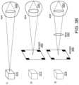
- FIG. 1 Ais an exemplary illustration of an eye gesture tracking system 100 .
- the eye gesture tracking system 100can be used to process information of a user's eye in response to generating a depth map of the eye.
- the eye gesture tracking system 100includes an eye gesture tracking device 110 for tracking movement of a user's eye 120 , a graphical display 130 , a signal processing unit 140 for processing eye data detected at the eye gesture tracking device 110 , and optionally a console 170 providing additional user input to the system depending on the nature of the application.
- the user's eye 120can include one or both eyes of a user that is viewing the graphical display 130 .
- the graphical display 130can be one or more graphical displays on a computer, laptop, desktop, television, smart phone, tablet and the like.
- the graphical display 130can include a liquid crystal display (LCD), a light emitting diode (LED) display, an organic light emitting diode (OLED) display, a head mounted display (HMD) and the like.
- the graphical display 130can include tunable optical elements such as a mirror and/or a tunable lens. In this instance, the tunable optical elements of the graphical display 130 can be configured to adjust focusing as well as defocusing in real time to aid the user's eye 120 in viewing the graphical display 130 .
- the eye gesture tracking device 110can include one or more eye gesture tracking devices in communication with the signal processing unit 140 .
- the eye gesture tracking device 110can provide illumination at the user's eye 120 and receive reflected optical signals of the user's eye 120 .
- the eye gesture tracking device 110can include a modulated optical source that illuminates the user's eye 120 at one or more selected wavelengths.
- the modulated optical sourcecan include a single optical emitter or multiple optical emitters modulated by a radio-wave frequency (RF) or a microwave frequency voltage source providing the illumination.
- RFradio-wave frequency
- the optical emitterscan be used to illuminate the entirety of the user's eye 120 .
- the optical emitterscan be used to illuminate selected portions of the user's eye 120 .
- the one or more wavelengths used in the eye gesture tracking system 100can be predetermined based on various criteria, for example, non-pervasiveness to the human eye, low solar irradiance at sea level, eye safety, and the like.
- the eye gesture tracking device 110can include one or more photodetectors for receiving the reflected optical signals of the user's eye 120 .
- the reflected optical signals of the user's eye 120can be reflections of the modulated optical signals provided by the eye gesture tracking device 110 .
- the eye gesture tracking device 110can detect the reflected, modulated optical signals by the one or more photodetectors.
- the photodetectorsmay be implemented by the techniques described in U.S. patent application Ser. No. 15/338,660 titled “High-Speed Light Sensing Apparatus,” filed October 31, and U.S. patent application Ser. No. 15/228,282, entitled “GERMANIUM-SILICON LIGHT SENSING APPARATUS,” filed Aug. 4, 2016.
- the signal processing unit 140can include one or more signal processing units in communication with the graphical display 130 and the eye gesture tracking device 110 .
- the signal processing unit 140can be configured to determine gaze information 150 of the user's eye 120 via data corresponding to the eye gesture tracking device 110 and the graphical display 130 .
- the eye gesture tracking device 110can be configured to demodulate the reflected, modulated optical signals.
- the eye gesture tracking device 110can be configured to create a depth map of the illuminated portions of the user's eye 120 .
- the depth mapcan correspond to the reflected optical signals that are detected by the photodetectors of the eye gesture tracking device 110 .
- the depth mapcan provide two-dimensional (2D) and three-dimensional (3D) information pertaining to the user's eye 120 .
- the signal processing unit 140can process the depth map according to data representing the time-of-flight information of the reflected optical signals.
- the depth mapcan be based on phase differences between the reflected optical signals and a reference signal.
- the eye gesture tracking device 110can provide a comparison between the reflected optical signals and a reference signal, and can be used to determine the depth map of the user's eye 120 .
- the depth mapcan further include a 3D model representing the user's eye 120 . As such, the 3D eye model can be generated and constructed, thereby allowing the signal processing unit 140 to determine the gaze information 150 of the user's eye 120 .
- the signal processing unit 140can be located near the user's eye 120 .
- the signal processing unit 140 and the eye gesture tracking device 110can be implemented in a single wearable device located at a nearby location close to the user's eye 120 .
- the signal processing unit 140 and the eye gesture tracking device 110can also be implemented in a single peripheral device located at a remote location away from the user's eye 120 .
- the signal processing unit 140can be located separately from the eye gesture tracking device 110 .
- the signal processing unit 140can be located at the graphical display 130 and be in communication with the eye gesture tracking device 110 implemented in a single wearable or peripheral device.
- the gaze information 150can include information such as the user's eye gaze direction and focus.
- the gaze information 150can be determined by the signal processing unit 140 with respect to the optical signals received by the eye gesture tracking device 110 .
- the gaze information 150can be used to analyze the user's eye behavior. Further, the gaze information 150 can be used to identify a location of the user's eye's 120 focus with respect to the display 130 . In this instance, the gaze information 150 can be used to determine particular items displayed at the display 130 that the user's eye 120 is focused at. Thus, a user's interests can be determined without the need for physical actuation of a particular device.
- ad providerscan determine the interests of a user based exclusively on the user's eye 120 , without the need for activation/detection via a computer mouse, computer trackpad, touch screen, or the like.
- physical actuation of particular devicesmay be used to perform certain functions of the user and system interaction. Utilizing such devices may become advantageous for the efficiency as the complexity of the interaction between the system and the user increases.
- fighter jet pilotsmay utilize eye gaze information 150 to identify/select targets of interest on the display 130 and use console 170 to perform tasks on the target of interest such as target acquisition, target priority assignment, weapons selection, and etc.
- the gaze information 150can be used to indicate commands to be provided to another device.
- the gaze information 150can include eye gestures such as eye movement, eye rotation, a closed-state of the eye, an open-state of the eye, any duration thereof, and the like.
- the device that receives the gaze information 150may analyze the gaze information 150 in real time to determine a command as the user's eye 120 is being dynamically tracked by the eye gesture tracking device 110 .
- the eye gesture tracking device 110 , the graphical display 130 , and the signal processing unit 140can be independent structures, or coupled together in an integrated hardware package.
- the eye gesture tracking device 110 , the graphical display 130 , and the signal processing unit 140can be integrated in a single hardware package in which the display of the graphical display 130 is opaque and visual images are shown on the display by an array of light-emitting diodes generating visible light, liquid crystals filtering white light, or any other array of light sources.
- the display of the graphical display 130is at least partly transparent and visual images are projected to the display by optical refraction, diffraction, reflection, guiding or other optical means.
- the eye gesture tracking device 110 and the signal processing unit 140can be integrated in a single hardware package such as a wearable device.
- a wearable devicemay be a headset, a pair of glasses, or any other suitable wearable device.
- the wearable devicecommunicates with a main frame or a machine in which the graphical display 130 is embedded. Further, the main frame or the machine containing the graphical display 130 can be in communication with the wearable device via a wireless or wired connection.
- the eye gesture tracking device 110 and the signal processing unit 140can be integrated in a single hardware package such as a pluggable device.
- a pluggable devicemay be a game box, a camcorder, or any other suitable pluggable device.
- the pluggable devicecommunicates with a main frame or a machine in which the graphical display 130 is embedded. Further, the main frame or the machine containing the graphical display 130 can be in communication with the pluggable device via a wireless or wired connection.
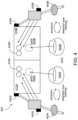
- FIG. 1 Bis an exemplary illustration of a time-of-flight device.
- the time-of-flight devicecan be integrated into the eye gesture tracking device 110 and can be used to determine the depth map of the user's eye 120 .
- the time-of-flight device of FIG. 1 Bincludes a time-of-flight (TOF) pixel 160 and two sets of transistors. As illustrated in FIG. 1 B , each set of the transistors can include three switch transistors (3T), i.e., a reset transistor 162 a or 162 b , a source-follower transistor 164 a or 164 b , and a selection transistor 166 a or 166 b . In some other implementations, other arrangements of transistors may be used to achieve similar functionalities.
- 3Tswitch transistors
- the TOF pixel 160can be one or more TOF pixels that are used to detect light. As light is detected by the TOF pixel 160 , the TOF pixel determines whether charge should be processed by the first set of transistors or the second set of transistors. In some aspects, a received light signal may be out of phase with respect to an emitted light signal. In this instance, the TOF pixel can be designed to be a dual switching TOF pixel so that one switch is modulated in phase and the other switch is modulated 180 degrees out of phase with respect to the emitted light signal to accommodate the received, out of phase, light signal. The dual switching TOF pixel may be implemented by the techniques described in U.S. patent application Ser. No.
- the two sets of transistorscan be fabricated with the TOF pixel 160 on a single wafer.
- the two sets of transistorsmay share and occupy the same light illumination area as the TOF pixel 160 does, thereby reducing an active fill factor of the TOF device.
- the two sets of transistorsmay be implemented by NMOS gates. NMOS gates are utilized to reduce the size of the transistors and so the TOF device.
- the two sets of transistorsmay also be implemented by PMOS gates. PMOS gates are utilized to increase certain operation parameters such as providing a greater usable voltage headroom. The PMOS and NMOS implementations of the sets of transistors will be discussed further herein.
- FIG. 1 Cis an exemplary illustration of a time-of-flight device.
- the TOF device of FIG. 1 Cincludes a first wafer and a second wafer that are bonded together via die or wafer bonding 167 .
- the first wafercan include a TOF pixel 165 that is fabricated on the first wafer.
- the TOF pixel 165can be used to detect light pulse information.
- the second wafercan be a circuit wafer 169 that includes two sets of transistors.
- the circuit wafer 169can be used to process charge as light pulse information is detected at the TOF pixel 165 .
- the transistors of the circuit wafer 169do not occupy the light illumination area, thereby increasing the active fill factor of the TOF device.
- the two sets of transistorscan be implemented by NMOS or PMOS gates.
- each of the two set of transistorscan be implemented by NMOS gates with a threshold voltage of 0.7 Volts.
- a maximum source voltage of about 2.6 Voltscan be obtained while the NMOS gate is on. Consequently, when NMOS is used as a reset transistor, the reset voltage applied to the TOF pixel can only be as high as 2.6 Volts that results into a smaller voltage headroom.
- another examplemay include each of the two set of transistors implemented by PMOS gate with a negative threshold voltage of ⁇ 0.8 Volts.
- the gate voltagewhen the gate voltage is supplied with 0 Volts, a maximum source voltage of about 3.3 Volts can be obtain while the PMOS gate is on. Consequently, when PMOS is used as a reset transistor, the reset voltage applied to the TOF pixel can be as high as 3.3 Volts that results into a larger voltage headroom.
- the two sets of transistorscan yield a greater usable voltage headroom when implemented by PMOS gates.
- This aspect of the PMOS implementationcan be attributed in part to the negative threshold voltage.
- the PMOS implementationcan yield a smaller impedance when it turns on as a switch and passes a voltage that its value is close to a supply voltage.
- the PMOS implementation of the two sets of transistorsprovide operation benefits of the TOF device, however, the physical area of the PMOS gate is larger than that of the NMOS gate and so the PMOS implementation requires a physically larger TOF device to provide such implementation. This issue can be resolved, as shown in FIG.
- the TOF pixel as shown in FIGS. 1 B and 1 Cmay include a light absorption layer including germanium.
- the TOF pixel as shown in FIGS. 1 B and 1 Cfurther includes a demodulation function implemented by dual switching transistors or multiple PN junctions to achieve the demodulation function.
- the dual switching TOF pixelmay be implemented by the techniques described in U.S. patent application Ser. No. 15/338,660 titled “High-Speed Light Sensing Apparatus,” filed October 31, and U.S. patent application Ser. No. 15/228,282, entitled “GERMANIUM-SILICON LIGHT SENSING APPARATUS,” filed Aug. 4, 2016.
- FIG. 1 Dshows one example technique for determining characteristics of the user's eye 120 .
- the eye gesture tracking device 110may emit light pulses modulated at a frequency f m with a duty cycle of 50%.
- the eye gesture tracking device 110may receive reflected light pulses having a phase difference ⁇ .
- a photodiode arraymay be controlled such that a readout circuit 1 reads the collected charge Q 1 in a phase synchronized with the emitted light pulses, and a readout circuit 2 reads the collected charge Q 2 in an opposite phase with the emitted light pulses.
- the distance, D, between the eye gesture tracking device 110 and one point of the user's eye 120may be derived using the equation
- the eye gesture tracking device 110may scan the user's eye 120 to obtain a depth profile of the user's eye 120 .
- FIG. 1 Eshows another example technique for determining characteristics of the user's eye 120 .
- the eye gesture tracking device 110may emit light pulses modulated at a frequency f m with a duty cycle of less than 50%.
- the duty cycle of the optical pulsesBy reducing the duty cycle of the optical pulses by a factor of N, but increasing the intensity of the optical pulses by a factor of N at the same time, the signal-to-noise ratio of the received reflected light pulses may be improved while maintaining substantially the same power consumption for the eye gesture tracking device 110 . This is made possible when the device bandwidth is increased so that the duty cycle of the optical pulses can be decreased without distorting the pulse shape.
- the eye gesture tracking device 110may receive reflected light pulses having a phase difference ⁇ .
- the photodiode diodemay be controlled such that a readout circuit 1 reads the collected charge Q 1 ′ in a phase synchronized with the emitted light pulses, and a readout circuit 2 reads the collected charge Q 2 ′ in a delayed phase with the emitted light pulses.
- the distance, D, between the eye gesture tracking device 110 and a point of the user's eye 120may be derived using the equation
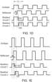
- FIG. 1 Fis an exemplary illustration of phases for charge collection.
- the phases for charge collectionrepresent phases in which light pulses are emitted and electrical charge are collected by the eye gesture tracking device 110 .
- the phases for charge collectioninclude a 0 degree phase, a 90 degree phase, a 180 degree phase, and a 270 degree phase, and a controllable phase shift ⁇ .
- the phase difference ⁇may be observed between light pulses emitted by the eye gesture tracking device 110 and light pulses received by the eye gesture tracking device 110 .
- the phase difference ⁇occurs due to a distance between the user's eye 120 and the eye gesture reading device 110 .
- a small phase differencecan make it difficult for the eye gesture tracking device 110 to efficiently detect a gesture recognition of the user's eye 120 , a mapping of the user's eye 120 , and the like. As such, it can be beneficial to add a phase shift ⁇ to the collected charge so that the eye gesture recognition can be performed efficiently.
- FIG. 1 Gis an exemplary illustration of light detection and charge collection.
- the light detection and charge collectionincludes time steps of light emission, light detection, and charge collection at the eye gesture reading device 110 .
- dataare collected to represent the received light, the charge collected at the 0 degree phase, the charge collected at the 90 degree phase, the charge collected at the 180 degree phase, and the charge collected at the 270 degree phase.
- the collection of charge at each phasecan indicate an amount of collected charge at each of the received phases. In this instance, the amount of collected charge at each time step of each phase can impact an accuracy of the eye gesture reading device 110 in mapping the user's eye 120 .
- the eye gesture tracking device 110may emit light pulses modulated at a frequency f m with a duty cycle of 50%.
- the eye gesture tracking device 110may receive reflected light pulses having a phase difference ⁇ .
- the TOF pixelscan be controlled such that a first readout circuit of the eye gesture tracking device 110 reads the collected charge, Q0, at a phase that is synchronization with the emitted light pulses, thus corresponding to the 0 degree phase.
- the eye gesture tracking device 110can also include a second readout circuit that reads the collected charge, Q180, at an opposite phase of the emitted light pulses, such as the 180 degree phase.
- the TOF pixelsare controlled such that first readout circuit reads the collected charge, Q90, in a quadrature phase with respect to the emitted light pulses, such as the 90 degree phase.
- the second readout circuitcan read the collected charge, Q270, in the other quadrature phase with respect to the emitted light pulses, such as the 270 degree phase.
- the distance between the eye gesture tracking device 110 and the user's eye 120may be derived using the following two equations:
- the charge collection at the 0 degree phaseis the greatest over the provided time steps, and the charge collection at the 180 degree phase is the lowest over the provided time steps.
- Such a large difference in charge collectioncan impact the accuracy of the charge collection as a whole.
- introducing phase shift ⁇can be helpful in eye gesture detection by reducing the differences in charge collection at each phase to enable a more accurate depth map of the user's eye 120 .
- FIG. 1 His an exemplary illustration of signal voltage during charge collection.
- the signal voltage during charge collectionillustrates the change in signal voltage of multiple phases over time.
- FIG. 1 Hillustrates the change in signal voltage for the 0 degree phase, the 90 degree phase, the 180 degree phase, and the 270 degree phase.
- the decrease in signal voltage of each phase over timerepresents an amount of charge that is stored for a particular phase over an interval of time.
- the signal voltage of the 180 degree phaseis much higher than the signal voltage of the 0 degree phase.
- the 180 degree phaseincludes a lower rate of charge storage than that of the 0 degree phase.
- the accuracy of detection of the user's eye 120 by the eye gesture tracking device 110can be negatively impacted due to the differences between the rates of charge storage across the different phases.
- FIG. 1 Iis an exemplary illustration of shifted phases for charge collection.
- the shifted phases for charge collectioninclude a 45 degree phase, a 135 degree phase, a 225 degree phase, and a 315 degree phase.
- the phase difference ⁇may be observed between light pulses emitted by the eye gesture tracking device 110 and light pulses received by the eye gesture tracking device 110 .
- the phase difference ⁇occurs due to a distance between the user's eye 120 and the eye gesture reading device 110 .
- a small phase differencecan make it difficult for the eye gesture tracking device 110 to efficiently detect a gesture recognition of the user's eye 120 , a mapping of the user's eye 120 , and the like.
- a phase shift ⁇ of 45 degreeis illustrated in FIG. 1 I to the collected charge so that all phases may be offset by the same phase shift ⁇ of 45 degree.
- FIG. 1 Jis an exemplary illustration of light detection and phase-shifted charge collection.
- the light detection and phase-shifted charge collectionincludes time steps of light emission, light detection, and charge collection at the eye gesture reading device 110 .
- datais collected to represent the received light, the charge collected at the 45 degree phase, the charge collected at the 135 degree phase, the charge collected at the 225 degree phase, and the charge collected at the 335 degree phase.
- the collection of charge at each phasecan indicate an amount of collected charge at each of the received phases. In this instance, the amount of collected charge at each time step of each phase can impact an accuracy of the eye gesture reading device 110 in mapping the user's eye 120 .
- the eye gesture tracking device 110may emit light pulses modulated at a frequency f m with a duty cycle of 50%.
- the eye gesture tracking device 110may receive reflected light pulses having a phase difference ⁇ .
- the TOF pixelscan be controlled such that a first readout circuit of the eye gesture tracking device 110 reads the collected charge, Q45, at a shifted-phase with respect to the emitted light pulses, such as the 45 degree phase.
- the eye gesture tracking device 110can also include a second readout circuit that reads the collected charge, Q225, at a shifted-phase with respect to the emitted light pulses, such as the 225 degree phase.
- the TOF pixelsare controlled such that first readout circuit reads the collected charge, Q135, in the phase shift of 135 degrees with respect to the emitted light pulses.
- the second readout circuitcan read the collected charge, Q315, in the phase shift of 315 degrees with respect to the emitted light pulses.
- the distance between the eye gesture reading device 110 and the user's eye 120may be derived using the following two equations:
- the charge collected at the 45 degree phase and at the 225 degree phaseare closer over the provided time steps.
- the phase-shifted charge collection of FIG. 1 Jprovides greater eye mapping performance due to a lower difference in charge collection at each phase in comparison. As differences in charge collection can impact the accuracy of the charge collection as a whole, phase shifts can be helpful in eye gesture detection by reducing the difference in charge collection at each phase to enable a more accurate depth map of the user's eye 120 .
- FIG. 1 Kis an exemplary illustration of signal voltage during phase-shifted charge collection.
- the signal voltage during phase-shifted charge collectionillustrates the change in signal voltage of multiple phases over time.
- FIG. 1 Killustrates the change in signal voltage for the 45 degree shifted-phase, the 135 degree shifted-phase, the 225 degree shifted-phase, and the 315 degree shifted-phase.
- the decrease in signal voltage of each phase over timerepresents an amount of charge that is stored for a particular phase over an interval of time.
- the signal voltage of the shifted phasesincludes a more similar average rate of the signal voltage drop, compared to a more different average rate of the signal voltage drop shown in FIG. 1 H .
- the similarity in drop rates of the signal voltage of the shifted phasescan enable a greater accuracy of eye gesture detection and mapping of the user's eye. As such, it may be beneficial to include a phase shift ⁇ to the charge collection to aid in the charge collection so that a more accurate reading of the user's eye 120 may be performed.
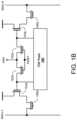
- FIG. 1 Lis an exemplary illustration of a TOF device.
- the TOF deviceincludes a TOF pixel 190 , two capacitors 192 a and 192 b , and two sets of transistors 194 and 196 .
- Each set of the transistorscan include five switch transistors (5T). In some other implementations, other arrangements of transistors may be used to achieve similar functionalities.
- the TOF pixel 190can be one or more TOF pixels that are used to detect light.
- the charge generated by the TOF pixel 190can be collected by the two capacitors 192 a and 192 b .
- Transistors M 1 -M 4which may be implemented by NMOS, PMOS, or any combination of NMOS and PMOS, are used to redistribute the collected charge by resetting the common-mode charge and connect the common-mode voltage to VREF.
- the voltage VREFmay be the operation voltage of the TOF device 190 or a predetermined voltage depending on design constraints.
- Transistors M 5 and M 6which may be implemented by NMOS, PMOS, or any combination of NMOS and PMOS, are used to reset the collected charge and connect them to VREF 2 .
- the voltage VREF 2may be the same voltage as VREF, the operation voltage of the TOF device 190 , or a predetermined voltage depending on design constraints.
- FIG. 2 Ais an exemplary illustration of a cross-platform peripheral control system using eye gesture tracking.
- the cross-platform peripheral control system using eye gesture trackingcan include a wearable device such as a headset 201 , and a connected device such as a phone 220 , a tablet 230 , a computing device 240 , and/or a television 250 , in communication with the headset 201 .
- the headset 201can be used by a pair of user's eyes 216 A and/or 216 B for viewing a connected device such as the phone 220 , the tablet 230 , the computing device 240 , and/or the television 250 .
- the headset 201can include an eye tracking gesture device and a signal processing unit implemented in an eye-tracking module 213 for tracking gestures of one of the user's first and second eyes 216 A and 216 B, an accelerometer 211 and gyroscope 212 for determining a head position of the user, a wireless communication unit 214 for communicating with a connected device such as the phone 220 and/or the tablet 230 and/or the computing device 240 and/or the television 250 , and a transparent lens 218 .
- the transparent lens 218may include one or more tunable elements for adjustment based on the tracking of the user's eyes 216 A and/or 216 B.
- the eye-tracking module 213can be used to illuminate the user's eye 216 A with optical signals, and detect optical signals that are reflected from the user's eye 216 A.
- the detected optical signalscan be used to determine gaze information pertaining to the user's eye 216 A.
- the gaze informationcan include the user's gaze with respect to the displays of the connected device.
- the gaze informationcan also include commands corresponding to gestures of the user's eye 216 A.
- the eye gesture commandscan be provided as input commands to the connected device.
- the eye-tracking module 213can be used to illuminate both of the user's eyes 216 A and 216 B with optical signals, and detect optical signals that are reflected from the user's eyes 216 A and 216 B to determine gaze information of both eyes 216 A and 216 B.
- the accelerometer 211 and gyroscope 212can be used to detect an orientation of the user's head.
- the orientation of the user's headcan be used in effectively determining the gaze information.
- the accelerometer 211 and the gyroscope 212can be used to track movements of the user's head. Thus, any potential head movements of the user can be identified so that the gaze information is not misrepresented according to movements of the user's head.
- the wireless communication unit 214can be used to establish a connection between the headset 201 , the phone 220 , the tablet 230 , the computing device 244 , and/or the television 254 via a network.
- the networkcan include Wi-Fi, BLUETOOTH, BLUTETOOTH LOW ENERGY (BLE), a local area network (LAN), and the like.
- the transparent lens 218can be used to aid the user's eyes 216 A and 216 B in viewing the displays of the phone 220 , the tablet 230 , the computing device 240 , and/or the television 250 .
- the transparent lens 218can include tunable optical elements that can be tuned based on the determined gaze information representing the tracking of the user's eyes 216 A and 216 B.
- the entirety of the transparent lens 218can be tuned based on the gaze information.
- selected portions of the transparent lens 218can be tuned based on the gaze information.
- the selected portions of the tunable optical elements of the transparent lens 218can be tuned to provide foveated images of particular locations at the display of the phone 220 , the particular locations at the phone 220 being based on locations at the display that the gaze of the user's eyes 216 A and 216 B are directed to.
- the phone 220can include an accelerometer 221 and gyroscope 222 for determining the orientation of the phone 220 , as well as a wireless communication unit 224 for communicating with the headset 201 .
- the accelerometer 221 and the gyroscope 222 of the phone 220can aid in tracking the location as well as the movement of the phone 220 .
- the headset 201can effectively determine the gaze information of the user's eyes 216 A and 216 B when comparing the user's focus to the location of the phone 220 .
- the location and the movement of the phone 220can be transmitted from the phone 220 to the headset 201 via the wireless communication device 224 .
- the tablet 230can include an accelerometer 231 and a gyroscope 232 for determining the orientation of the tablet 230 , and a wireless communication unit 234 for communicating with the headset 201 .
- the accelerometer 231 and the gyroscope 232 of the tablet 230can aid in tracking the location and the movement of the tablet 230 .
- the headset 201can effectively determine a reference gaze point 236 of the user's eye 216 A.
- the location and the movement of the tablet 230can be transmitted from the tablet 230 to the headset 201 via the wireless communication unit 234 .
- the computing device 240can include a wireless communication unit 244 for communicating with the headset 201 .
- the television 250can include a wireless communication unit 254 for communication with the headset 201 .
- FIG. 2 Bis an exemplary illustration of a cross-platform peripheral control system using eye gesture tracking.
- the cross-platform peripheral control systemcan include a wearable device such as a headset 202 , and a connected device such as a phone 220 , a tablet 230 , a computing device 240 , and/or a television 250 , in communication with the headset 202 .
- the headset 202can be used by a user's eyes 216 A and 216 B for viewing the connected device.
- the headset 202can include two eye tracking gesture device and signal processing unit pairs, the first pair implemented in a first eye-tracking module 213 A and the second pair implemented in a second eye-tracking module 213 B, for tracking gestures of the user's eyes 216 A and 216 B, an accelerometer 211 and gyroscope 212 for determining a head position of the user, a wireless communication unit 214 for communicating with the connected device, a first transparent lens 218 A including one or more tunable elements, and a second transparent lens 218 B including one or more tunable elements.
- the first eye-tracking module 213 Acan be used to illuminate the first user's eye 216 A with optical signals, and detect optical signals that are reflected from the first user's eye 216 A.
- the detected optical signalscan be used to determine gaze information pertaining to the first user's eye 216 A.
- the gaze informationcan include the gaze of the user's first eye with respect to the displays of connected device such as 220 , 230 , 240 and 250 .
- the gaze informationcan also include commands corresponding to gestures of the first user's eye 216 A.
- the eye gesture commandscan be provided as input commands to the connected device.
- the second eye-tracking module 213 Bcan be used to illuminate the second user's eye 216 B and detect optical signals that are reflected from the second user's eye 216 B.
- the detected optical signalscan be used to determine gaze information pertaining to the second user's eye 216 B.
- the gaze informationcan include the gaze of the second user's eye 216 B with respect to the displays of the connected device.
- the gaze informationcan also include commands corresponding to gestures of the second user's eye 216 B.
- the eye gesture commandscan be provided as input commands to the connected device.
- the first transparent lens 218 Acan be used to aid the first user's eye 216 A in viewing the displays of the connected device.
- the first transparent lens 218 Acan include tunable elements that can be tuned based on the determined gaze information representing the tracking of the first user's eye 216 A.
- the entirety of the first transparent lens 218 Acan be tuned based on the gaze information.
- selected portions of the first transparent lens 218 Acan be tuned based on the gaze information.
- the selected portions of tunable optical elements of the first transparent lens 218 Acan be tuned to foveated images of particular locations at the display of the computing device 240 , the particular locations at the computing device 240 being based on locations at the display that the first user's eye 216 A is focused on.
- the second transparent lens 218 Bcan be used to aid the second user's eye 216 B in viewing the connected device.
- the second transparent lens 218 Bcan include tunable optical elements that are tuned based on the determined gaze information representing the tracking of the second user's eye 216 B.
- the entirety of the second transparent lens 218 Bcan be tuned based on the gaze information.
- selected portions of the second transparent lens 218 Bcan be tuned based on the gaze information.
- the selected portions of tunable elements of the second transparent lens 218 Bcan be tuned to provide enhanced focus of viewing of particular locations at the display of the computing device 240 , the particular locations at the computing device 240 being based on locations that the second user's eye 216 B is focused on.
- the first user's eye 216 A and the second user's eye 216 Bcan be focused at a single location.
- the user's eyes 216 A and 216 Bcan include a reference gaze 246 located at the display of the computing device 240 such as a laptop or desktop.
- the reference gaze 246may be directed towards a single point at the display of the laptop or desktop, the tunable optical elements of each of the first transparent lens 218 A and the second transparent lens 218 B can be tuned independently based on the determined gaze information of the first and second user's eyes 216 A and 216 B.
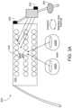
- FIG. 3 Ais an exemplary illustration of a wearable device 300 using eye gesture tracking.
- the wearable device 300can include a mono-vision wearable device that provides light path adjustments based on eye gesture tracking.
- the wearable device 300includes a transparent or an opaque screen 310 that a user can look through or look at, tunable optical elements 330 for adjusting a light path at the transparent or the opaque screen 310 , a wireless communication unit 340 for communicating with remote devices, an image projector 350 for projecting 2D visuals through or at the transparent or the opaque screen 310 , and an eye gesture tracking module 360 for tracking eye gestures of the user's eyes 320 A and 320 B and determining depth maps corresponding to each of the user's eyes 320 A and 320 B.
- the gaze 325 of the user's eyes 320 A and 320 Bcan be determined by the eye gesture tracking module 360 . In certain implementations, only certain portions of the transparent or the opaque screen 310 are tuned according to the gaze 325 of the user's eyes 320 A and 320 B.
- the gaze information corresponding to the gaze 325can be used by the eye gesture tracking module 360 to tune a selected portion of the transparent or the opaque screen 310 such as the multiple tunable optical elements 330 .
- the tunable optical elements 330can be tuned to adjust the focusing/defocusing of a particular light path passing through the particular portion of the transparent or the opaque screen 310 .
- the tunable optical elements 330can include tunable mirrors, tunable lenses, tunable gratings or any other suitable tunable optical elements and any combination thereof.
- the tunable optical elements 330can be adjusted based on the gaze information corresponding to the gaze 325 so that real time focusing/defocusing can be provided at the wearable device 300 .
- the real-time focusing/defocusing of the tunable optical elements 330can be used to solve inconsistencies between accommodation and vergence when viewing displays.
- traditional VR experiencescan cause feelings of nausea due to inconsistent depth perception mechanisms.
- One inconsistent depth perception mechanismarises when the focus of a user's eyes (accommodation) feels that images are at the same distance of a display, while the images are simultaneously felt at different depths by the convergence of the user's eyes (vergence). These conflicting feelings that are perceived by the user can cause feelings of sickness due to the inconsistency between accommodation and vergence.
- the present method of eye trackingcan be implemented in a wearable device such as the wearable device 300 .
- the wearable device 300can refocus light based on eye gaze information to adjust the angle of eye-incident light passing through or at selected portions of the transparent or the opaque screen 310 .
- the tunable optical elements 330 of the transparent or the opaque screen 310can be configured to refocus light based on the determined gaze information of the user's eyes 320 A and 320 B, thereby providing a solution to the inconsistencies that can arise between accommodation and vergence during certain viewing experiences.
- FIG. 3 Bis an exemplary illustration of an optical image-refocusing system using a lens.
- the optical image-refocusing system using a lensillustrates the use of a lens to refocus an object illusion according to gaze information of a user's eye.
- the user's eye 320is viewing the object 370 through a medium such as air without using a screen such as a VR display.
- the user's eye 320may not be viewing the object 370 through a transparent lens. Further, the user's eye 320 is viewing the real object 370 , rather than a virtual representation of the object.
- the user's eye 320is viewing the object illusion 375 through the screen 380 .
- an image projectormay be projecting a virtual representation of the object 370 as the object illusion 375 through the screen 380 .
- the user's eye 320may be experiencing an inconsistency between accommodation and vergence.
- the user's eye 320is viewing the object illusion 375 through a lens 330 situated between the user's eye 320 and the screen 380 .
- the lens 330can be a fixed lens that is used to refocus the object illusion 375 .
- the lens 330can be a tunable lens that is used to dynamically refocus the object illusion 375 through the screen 380 in real time. In this instance, the lens 330 can be tuned based on determined gaze information of the user's eye 320 .
- FIG. 3 Cis an exemplary illustration of an optical image-refocusing system using a mirror.
- the optical image-refocusing system using a mirrorillustrates the use of a mirror to refocus an object illusion according to gaze information of a user's eye.
- the user's eye 320is viewing the object 370 through a medium such as air without using a screen such as a VR display.
- the user's eye 320may not be viewing the object 370 through a transparent lens. Further, the user's eye 320 is viewing the real object 370 , rather than a virtual representation of the object.
- the user's eye 320is viewing the object illusion 376 through the screen 380 .
- an image projectormay be projecting a virtual representation of the object 370 as the object illusion 376 through the screen 380 .
- the user's eye 320may be experiencing an inconsistency between accommodation and vergence.
- the user's eye 320is viewing the object illusion 376 through a screen 380 that includes a mirror 385 .
- the mirror 385can be a fixed mirror that is used to refocus the object illusion 376 .
- the mirror 385can be a tunable mirror that is used to dynamically refocus the object illusion 376 through the screen 380 that includes the mirror 385 in real time. In this instance, the mirror 385 can be tuned based on determined gaze information of the user's eye 320 .
- FIG. 4is an exemplary illustration of a wearable device 400 using eye gesture tracking.
- the wearable device 400 using eye gesture trackingcan include a stereo-vision wearable device that provides light path adjustments based on eye gesture tracking.
- the wearable device 400includes a first transparent or opaque screen 410 A and a second transparent or opaque screen 410 B that the user can look through or look at, a first set of tunable optical elements 430 A located for adjusting a light path at the first transparent or opaque screen 410 A and a second set of tunable optical elements 430 B for adjusting a light path at the second transparent or opaque screen 410 B.
- the wearable device 400may further include a first wireless communication unit 440 A for communicating with remote devices or a second wireless communication unit 440 B for communication with the remote devices, a first image projector 450 A for projecting 2D visuals through or at the first transparent or opaque screen 410 A, a second image projector 450 B for projecting 2D visuals through or at the second transparent or opaque screen 410 B, a first eye gesture tracking module 460 A for tracking eye gestures of the first user's eye 420 A and determining a depth map corresponding to the first user's eye 420 A, and a second eye gesture tracking module 460 B for tracking eye gestures of the second user's eye 420 B and determining a depth map corresponding to the second user's eye 420 B.
- a first wireless communication unit 440 Afor communicating with remote devices or a second wireless communication unit 440 B for communication with the remote devices
- a first image projector 450 Afor projecting 2D visuals through or at the first transparent or opaque screen 410 A
- the wearable device 400may further include one continuous or two separate transparent or opaque screens 410 A and 410 B which enable two distinct gaze points 425 A and 425 B to be determined.
- the first and second optical elements 430 A and 430 Bcan be tuned independent from one another.
- each of the image projectors 450 A and 450 Bcan operate independently. As such, a portion can be selected at each of the transparent or opaque screens 410 A and 410 B to refocus light incident on each of the user's eyes 420 A and 420 B.
- 3D projectionscan be interpreted by the user's eyes 420 A and 420 B via the simultaneous projection of multiple images through or at both of the transparent or opaque screens 410 A and 410 B.
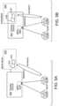
- FIG. 5 Ais an exemplary illustration of a stand-alone eye gesture tracking device attached to a machine.
- the stand-alone eye gesture tracking deviceis implemented as a stand-alone peripheral device 530 located in proximity of a machine such as a display device 520 .
- the stand-alone eye gesture tracking device attached to a machineincludes a display device 520 in communication with a stand-alone peripheral device 530 that is located at a remote location away from a user's eyes 510 A and 510 B.
- the stand-alone peripheral device 530includes a mechanical module 532 to control the direction of light emission and detection from an eye gesture tracking module 534 , so that the user's eyes are always located by the stand-alone peripheral device 530 .
- the eye gesture tracking module 534tracks the eye gestures of the user's eyes 510 A and 510 B and determines gaze information corresponding to the user's eyes 510 A and 510 B.
- the display device 520can include a gaze reference point 515 corresponding to a focus of the user's eyes 510 A and 510 B with respect to the display device 520 .
- the gaze reference point 515can be determined by the eye gesture tracking module 534 of the stand-alone peripheral device 530 .
- the display device 520can include tunable optical elements that are tuned based on the gaze reference point 515 .
- the tunable optical elementscan include tunable mirrors located at the display device 520 .
- the display device 520can include fixed optical elements such as fixed mirrors for light path refocusing.
- the eye gesture tracking module 530can be configured to provide output data to the display device 520 .
- the output datacan include gaze information of the user's eyes 510 A and 510 B.
- the gaze informationcan be used by the display device 520 to render an image at a particular portion of the display corresponding to the gaze reference point 515 of the user.
- the rendered imagecan be shown at the display of the display device 520 by an array of light-emitting diodes generating visible light, liquid crystals filtering white light, or any other array of light sources located at the display of the display device 520 . Further, the rendered image can be shown at the display of the display device 520 by optical refraction, diffraction, reflection, guiding, or any other optical techniques.
- FIG. 5 Bis an exemplary illustration of an eye gesture tracking device embedded in a machine.
- the eye gesture tracking device embedded in a machineincludes an embedded peripheral device 545 integrated into a machine such as a display device 540 .
- the embedded peripheral device 545can include a mechanical module 546 to control the direction of light emission and detection from an eye gesture tracking module 547 , so that the user's eyes are always located by the embedded peripheral device 545 .
- the eye gesture tracking module 547tracks the eye gestures of the user's eyes 510 A and 510 B and determines gaze information corresponding to the user's eyes 510 A and 510 B.
- the display device 540can further include a gaze reference point 555 representing the location at the display device 540 in which the user's eyes 510 A and 510 B are focused at.
- the display device 540can include tunable optical elements that are tuned based on the gaze reference point 555 .
- the tunable optical elementscan include tunable mirrors located at the display device 540 .
- the display device 540can include fixed optical elements such as fixed mirrors.
- the distance between the eye 510 A or 510 B and the eye tracking module 534 and 547can be determined based on TOF concept or by other methods such as imaging processing or tri-angulation.
- the optical emission powercan be adjusted accordingly based on the distance between the eye 510 A or 510 B and the eye tracking module 534 and 547 .
- the optical emission powercan be dynamically lowered to reduce the exposure of the eye 510 A or 510 B to the optical emission given a close distance between the eye 510 A or 510 B and the eye tracking module 534 and 547 .
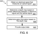
- FIG. 6is a flow chart illustrating a process 600 for eye gesture tracking, according to certain exemplary implementations.
- the process 600 for eye gesture trackingdescribes a process of monitoring the movement of an eye based on a generated depth map of the eye.
- an electrical signalis obtained that represents a measurement of an optical signal reflected from an eye.
- the optical signalcan be provided by an optical source.
- the optical sourcecan be biased by a modulated voltage signal that is in sync with a predetermined reference signal. As such, the optical source can provide an optical signal in the direction of the eye, to be reflected back from the eye.
- the reflected optical signalcan be received by one or more photodetectors.
- the received optical signalcan be filtered to remove certain wavelengths.
- one or more filterscan be provided to filter the optical signal so that only target wavelengths remain in the filtered optical signal.
- one or more lensescan be provided to focus the optical signal before it is received by the photodetector.
- the lensescan be transparent lenses, fixed lenses, tunable lenses, lenses based on photonic gratings, and the like.
- a depth mapis determined based on phase differences between the received optical signal and the reference signal.
- the received optical signalcan be compared to the reference signal as it is received.
- the received optical signalcan be filtered and then a comparison can be provided between the filtered optical signal and the reference signal.
- the depth mapcan include one or more data sets of 3D information corresponding to the eye.
- a 3D representation of the eyecan be generated according to the 3D information of the depth map.
- the depth mapcan be determined persistently in real time.
- the depth mapcan also be determined and updated at predetermined points in time. For example, the depth map can be determined and updated every micro-second, millisecond, every second, or the like.
- gaze informationis determined based on the depth map.
- the gaze informationcan represent a gaze of the eye based on the depth map.
- the gaze informationcan be determined based on the provided comparison between the reference signal and the reflected optical signal.
- the gaze informationcan include one or more of an identification of a particular region of the eye, an identification of a pupil of the eye, an identification of an iris of the eye, or an identification of a physiological structure of the eye.
- eye gestures of the eyecan be determined from the gaze information.
- the eye gesture informationcan include one or more of a movement of the eye, a rotation of the eye, a steady state of the eye, a duration of the steady state of the eye, a closed state of the eye, a duration of the closed state of the eye, an open state of the eye, a duration of the open state of the eye, a blinking state of the eye, a duration of the blinking state of the eye, or a frequency of the blinking state of the eye.
- the depth mapcan be used to generate an iris vector normal to a plane that is tangential to the eye.
- the gaze informationcan be determined based on the iris vector and the depth map.
- the depth mapcan also be used to generate a pupil position of the eye on a plane that is tangential to the eye. In this instance, the gaze information can be determined based on the pupil position of the eye and the depth map.
- the gaze information of the eyeis provided as output data.
- the output data representing the gaze informationcan be transmitted to a device, a machine, a system, and the like.
- the gaze informationcan be transmitted as input data to the device, machine, or system.
- eye gestures determined from the gaze informationcan be provided as output data.
- the eye gesturescan be used to provide commands to or interact with devices, machines, or systems. For example, if the eye is tracked to have blinked three times in quick succession, this may indicate a command to be provided to a remote device such as a television. As such, the television may be configured to turn off if the eye is tracked to blink several times in rapid succession.
- FIG. 7is a flow chart illustrating a process 700 for tuning optical elements based on eye gesture tracking, according to certain exemplary implementations.
- the process 700 for tuning optical elements based on eye gesture trackingdescribes a process of monitoring the movement of an eye and tuning optical elements based on the eye movement.
- an electrical signalis obtained that represents a measurement of an optical signal reflected from an eye.
- the optical signalcan be provided by an optical source.
- the optical sourcecan be biased by a modulated voltage signal that is in sync with a predetermined reference signal. As such, the optical source can provide an optical signal in the direction of the eye, to be reflected back from the eye.
- the reflected optical signalcan be received by one or more photodetectors.
- the received optical signalcan be filtered to remove certain wavelengths.
- one or more filterscan be provided to filter the optical signal so that only target wavelengths remain in the filtered optical signal.
- one or more lensescan be provided to focus the optical signal before it is received by the photodetector.
- the lensescan be transparent lenses, fixed lenses, tunable lenses, lenses based on photonic grating, and the like.
- a depth mapis determined based on phase differences between the received optical signal and the reference signal.
- the received optical signalcan be compared to the reference signal as it is received.
- the received optical signalcan be filtered and then a comparison can be provided between the filtered optical signal and the reference signal.
- the depth mapcan include one or more data sets of 3D information corresponding to the eye.
- a 3D representation of the eyecan be generated according to the 3D information of the depth map.
- the depth mapcan be determined persistently in real time.
- the depth mapcan also be determined and updated at predetermined points in time. For example, the depth map can be determined and updated every micro-second, millisecond, every second, or the like.
- gaze informationis determined based on the depth map.
- the gaze informationcan represent a gaze of the eye based on the depth map.
- the gaze informationcan include one or more of an identification of a particular region of the eye, an identification of a pupil of the eye, an identification of an iris of the eye, or an identification of a physiological structure of the eye.
- eye gestures of the eyecan be determined from the gaze information.
- the eye gesture informationcan include one or more of a movement of the eye, a rotation of the eye, a steady state of the eye, a duration of the steady state of the eye, a closed state of the eye, a duration of the closed state of the eye, an open state of the eye, a duration of the open state of the eye, a blinking state of the eye, a duration of the blinking state of the eye, or a frequency of the blinking state of the eye.
- the depth mapcan further be used to generate an iris vector normal to a plane that is tangential to the eye.
- the gaze informationcan be determined based on the iris vector and the depth map.
- the depth mapcan also be used to generate a pupil position of the eye on a plane that is tangential to the eye. In this instance, the gaze information can be determined based on the pupil position of the eye and the depth map.
- tuning of tunable optical elementsis activated based on the determined gaze information.
- the gaze informationcan be used to tune particular tunable optical elements.
- the gaze informationcan include a focus of the eye with respect to a particular display.
- the focus of the eyecan be directed through a tunable optical element such as a tunable lens or mirror.
- the tunable lens or mirrorcan be activated, or tuned, to refocus light pathing through the lens or mirror.
- the tunable optical elementscan be located at a display. In this instance, the tunable optical elements can be activated or tuned at the display in real time as the eye is tracked.
- the tunable optical elementscan include one or more lenses, mirrors, or any combination thereof.
- the tunable optical elementscan be adjusted based on the movement, or lack thereof, of the tracked eye.
- the tunable optical elementscan be used to provide dynamic focusing and defocusing in real time.
- the tunable optical elementscan be used to solve inconsistencies between accommodation and vergence when viewing images at a VR or AR display.
- FIG. 8shows an example of a generic computer device 800 and a generic mobile computer device 850 , which may be used with the techniques described here.
- Computing device 800is intended to represent various forms of digital computers, such as laptops, desktops, workstations, personal digital assistants, servers, blade servers, mainframes, and other appropriate computers.
- Computing device 850is intended to represent various forms of mobile devices, such as personal digital assistants, cellular telephones, smartphones, and other similar computing devices.
- the components shown here, their connections and relationships, and their functions,are meant to be exemplary only, and are not meant to limit implementations of the inventions described and/or claimed in this document.
- Computing device 800includes a processor 802 , memory 804 , a storage device 806 , a high-speed interface 808 connecting to memory 804 and high-speed expansion ports 810 , and a low speed interface 812 connecting to low speed bus 814 and storage device 806 .
- Each of the components 802 , 804 , 806 , 808 , 810 , and 812are interconnected using various busses, and may be mounted on a common motherboard or in other manners as appropriate.
- the processor 802may process instructions for execution within the computing device 800 , including instructions stored in the memory 804 or on the storage device 806 to display graphical information for a GUI on an external input/output device, such as display 816 coupled to high speed interface 808 .
- multiple processors and/or multiple busesmay be used, as appropriate, along with multiple memories and types of memory.
- multiple computing devices 800may be connected, with each device providing portions of the necessary operations (e.g., as a server bank, a group of blade servers, or a multi-processor system).
- the memory 804stores information within the computing device 800 .
- the memory 804is a volatile memory unit or units.
- the memory 804is a non-volatile memory unit or units.
- the memory 804may also be another form of computer-readable medium, such as a magnetic or optical disk.
- the storage device 806is capable of providing mass storage for the computing device 800 .
- the storage device 806may be or contain a computer-readable medium, such as a floppy disk device, a hard disk device, an optical disk device, or a tape device, a flash memory or other similar solid state memory device, or an array of devices, including devices in a storage area network or other configurations.
- a computer program productmay be tangibly embodied in an information carrier.
- the computer program productmay also contain instructions that, when executed, perform one or more methods, such as those described above.
- the information carrieris a computer- or machine-readable medium, such as the memory 804 , the storage device 806 , or a memory on processor 802 .
- the high speed controller 808manages bandwidth-intensive operations for the computing device 800 , while the low speed controller 812 manages lower bandwidth-intensive operations.
- the high-speed controller 808is coupled to memory 804 , display 816 (e.g., through a graphics processor or accelerator), and to high-speed expansion ports 810 , which may accept various expansion cards (not shown).
- low-speed controller 812is coupled to storage device 806 and low-speed expansion port 814 .
- the low-speed expansion portwhich may include various communication ports (e.g., USB, Bluetooth, Ethernet, wireless Ethernet) may be coupled to one or more input/output devices, such as a keyboard, a pointing device, a scanner, or a networking device such as a switch or router, e.g., through a network adapter.
- input/output devicessuch as a keyboard, a pointing device, a scanner, or a networking device such as a switch or router, e.g., through a network adapter.
- the computing device 800may be implemented in a number of different forms, as shown in the figure. For example, it may be implemented as a standard server 820 , or multiple times in a group of such servers. It may also be implemented as part of a rack server system 824 . In addition, it may be implemented in a personal computer such as a laptop computer 822 . Alternatively, components from computing device 800 may be combined with other components in a mobile device (not shown), such as device 850 . Each of such devices may contain one or more of computing device 800 , 850 , and an entire system may be made up of multiple computing devices 800 , 850 communicating with each other.
- Computing device 850includes a processor 852 , memory 864 , an input/output device such as a display 854 , a communication interface 866 , and a transceiver 868 , among other components.
- the device 850may also be provided with a storage device, such as a microdrive or other device, to provide additional storage.
- a storage devicesuch as a microdrive or other device, to provide additional storage.
- Each of the components 850 , 852 , 864 , 854 , 866 , and 868are interconnected using various buses, and several of the components may be mounted on a common motherboard or in other manners as appropriate.
- the processor 852may execute instructions within the computing device 840 , including instructions stored in the memory 864 .
- the processormay be implemented as a chipset of chips that include separate and multiple analog and digital processors.
- the processormay provide, for example, for coordination of the other components of the device 850 , such as control of user interfaces, applications run by device 850 , and wireless communication by device 850 .
- Processor 852may communicate with a user through control interface 848 and display interface 856 coupled to a display 854 .
- the display 854may be, for example, a TFT LCD (Thin-Film-Transistor Liquid Crystal Display) or an OLED (Organic Light Emitting Diode) display, or other appropriate display technology.
- the display interface 856may comprise appropriate circuitry for driving the display 854 to present graphical and other information to a user.
- the control interface 858may receive commands from a user and convert them for submission to the processor 852 .
- an external interface 862may be provide in communication with processor 852 , so as to enable near area communication of device 850 with other devices. External interface 862 may provide, for example, for wired communication in some implementations, or for wireless communication in other implementations, and multiple interfaces may also be used.
- the memory 864stores information within the computing device 850 .
- the memory 864may be implemented as one or more of a computer-readable medium or media, a volatile memory unit or units, or a non-volatile memory unit or units.
- Expansion memory 854may also be provided and connected to device 850 through expansion interface 852 , which may include, for example, a SIMM (Single In Line Memory Module) card interface.
- SIMMSingle In Line Memory Module
- expansion memory 854may provide extra storage space for device 850 , or may also store applications or other information for device 850 .
- expansion memory 854may include instructions to carry out or supplement the processes described above, and may include secure information also.
- expansion memory 854may be provide as a security module for device 850 , and may be programmed with instructions that permit secure use of device 850 .
- secure applicationsmay be provided via the SIMM cards, along with additional information, such as placing identifying information on the SIMM card in a non-hackable manner.
- the memorymay include, for example, flash memory and/or NVRAM memory, as discussed below.
- a computer program productis tangibly embodied in an information carrier.
- the computer program productcontains instructions that, when executed, perform one or more methods, such as those described above.
- the information carrieris a computer- or machine-readable medium, such as the memory 864 , expansion memory 854 , memory on processor 852 , or a propagated signal that may be received, for example, over transceiver 868 or external interface 862 .
- Device 850may communicate wirelessly through communication interface 866 , which may include digital signal processing circuitry where necessary. Communication interface 866 may provide for communications under various modes or protocols, such as GSM voice calls, SMS, EMS, or MMS messaging, CDMA, TDMA, PDC, WCDMA, CDMA2000, or GPRS, among others. Such communication may occur, for example, through radio-frequency transceiver 868 . In addition, short-range communication may occur, such as using a Bluetooth, WiFi, or other such transceiver (not shown). In addition, GPS (Global Positioning System) receiver module 850 may provide additional navigation- and location-related wireless data to device 850 , which may be used as appropriate by applications running on device 850 .
- GPSGlobal Positioning System
- Device 850may also communicate audibly using audio codec 860 , which may receive spoken information from a user and convert it to usable digital information. Audio codec 860 may likewise generate audible sound for a user, such as through a speaker, e.g., in a handset of device 850 . Such sound may include sound from voice telephone calls, may include recorded sound (e.g., voice messages, music files, etc.) and may also include sound generated by applications operating on device 850 .
- Audio codec 860may receive spoken information from a user and convert it to usable digital information. Audio codec 860 may likewise generate audible sound for a user, such as through a speaker, e.g., in a handset of device 850 . Such sound may include sound from voice telephone calls, may include recorded sound (e.g., voice messages, music files, etc.) and may also include sound generated by applications operating on device 850 .
- the computing device 850may be implemented in a number of different forms, as shown in the figure. For example, it may be implemented as a cellular telephone 880 . It may also be implemented as part of a smartphone 882 , personal digital assistant, or other similar mobile device.
- the TOF pixel as shown in FIGS. 1 B and 1 Ccan also be used to detect the user's facial characteristic, with the option to include eye gesture tracking, for facial recognition or emotion detection.
- the eye gesture tracking based on the implementations described hereincan be used to replace or supplement mouse to locate where the user's interest or focus at the display.
- the eye gesture tracking based on the implementations described hereincan be used for more accurate advertisement targeting or to predict user behavior.
- machine learning with artificial neuro-networkcan be used to learn and recognize the user behavior based on the where the user looks at the display.
- Different weightingscan be given for different contents based on different user behaviors, such as (1) not looking (2) looking but do not choose (3) look and choose, where the weighting could be from small to large.
- the duration of the user's focus on a particular contentcan also be used to record the user's interest level, for example, the longer the duration, the higher the weighting.
- displaying advertisement on a websitecan result in different charge to the payer of the advertisement based on the interest level received from the users, rather than the conventional click or no-click behaviors.
- the eye gesture tracking based on the implementations described hereincan also be used for gaming.
- a car racing or aircraft flying gamemay be played by a user on the mobile phone 224 , or the tablet 230 .
- Changes of user's eye gaze over timemay be used to control a movement (e.g., direction) of a car indicating where the user wants to go.
- data collected by the accelerometer 211 , the gyroscope 212 , and the eye-tracking modulemay be used to track movements of both the user's head movement and eye gaze.
- a separate buttonmay be included to control the speed and another optional button may further be included to control an extra action such as shooting or switching gear.
- the information of the head movement and the information of the eye gazemay be used by a game running on the mobile phone or the tablet to determine an action of a user, and the game may then respond accordingly.
- a combination of a vector representing a turning position of the user's head and a vector representing a gaze of the user's eyemay be used to determine the angle of the gaze with respect to the head, which may be used by the game to interpret an action or a state of mind of the user.
- Embodiments of the invention and all of the functional operations described in this specificationcan be implemented in digital electronic circuitry, or in computer software, firmware, or hardware, including the structures disclosed in this specification and their structural equivalents, or in combinations of one or more of them.
- Embodiments of the inventioncan be implemented as one or more computer program products, e.g., one or more modules of computer program instructions encoded on a computer readable medium for execution by, or to control the operation of, data processing apparatus.
- the computer readable mediumcan be a machine-readable storage device, a machine-readable storage substrate, a memory device, a composition of matter effecting a machine-readable propagated signal, or a combination of one or more of them.
- data processing apparatusencompasses all apparatus, devices, and machines for processing data, including by way of example a programmable processor, a computer, or multiple processors or computers.
- the apparatuscan include, in addition to hardware, code that creates an execution environment for the computer program in question, e.g., code that constitutes processor firmware, a protocol stack, a database management system, an operating system, or a combination of one or more of them.
- a propagated signalis an artificially generated signal, e.g., a machine-generated electrical, optical, or electromagnetic signal that is generated to encode information for transmission to suitable receiver apparatus.
- a computer program(also known as a program, software, software application, script, or code) can be written in any form of programming language, including compiled or interpreted languages, and it can be deployed in any form, including as a stand alone program or as a module, component, subroutine, or other unit suitable for use in a computing environment.
- a computer programdoes not necessarily correspond to a file in a file system.
- a programcan be stored in a portion of a file that holds other programs or data (e.g., one or more scripts stored in a markup language document), in a single file dedicated to the program in question, or in multiple coordinated files (e.g., files that store one or more modules, sub programs, or portions of code).
- a computer programcan be deployed to be executed on one computer or on multiple computers that are located at one site or distributed across multiple sites and interconnected by a communication network.
- the processes and logic flows described in this specificationcan be performed by one or more programmable processors executing one or more computer programs to perform functions by operating on input data and generating output.
- the processes and logic flowscan also be performed by, and apparatus can also be implemented as, special purpose logic circuitry, e.g., an FPGA (field programmable gate array) or an ASIC (application specific integrated circuit).
- processors suitable for the execution of a computer programinclude, by way of example, both general and special purpose microprocessors, and any one or more processors of any kind of digital computer.
- a processorwill receive instructions and data from a read only memory or a random access memory or both.
- the essential elements of a computerare a processor for performing instructions and one or more memory devices for storing instructions and data.
- a computerwill also include, or be operatively coupled to receive data from or transfer data to, or both, one or more mass storage devices for storing data, e.g., magnetic, magneto optical disks, or optical disks.
- mass storage devicesfor storing data, e.g., magnetic, magneto optical disks, or optical disks.
- a computerneed not have such devices.
- a computercan be embedded in another device, e.g., a tablet computer, a mobile telephone, a personal digital assistant (PDA), a mobile audio player, a Global Positioning System (GPS) receiver, to name just a few.
- Computer readable media suitable for storing computer program instructions and datainclude all forms of non volatile memory, media and memory devices, including by way of example semiconductor memory devices, e.g., EPROM, EEPROM, and flash memory devices; magnetic disks, e.g., internal hard disks or removable disks; magneto optical disks; and CD ROM and DVD-ROM disks.
- the processor and the memorycan be supplemented by, or incorporated in, special purpose logic circuitry.
- embodiments of the inventioncan be implemented on a computer having a display device, e.g., a CRT (cathode ray tube) or LCD (liquid crystal display) monitor, for displaying information to the user and a keyboard and a pointing device, e.g., a mouse or a trackball, by which the user can provide input to the computer.
- a display devicee.g., a CRT (cathode ray tube) or LCD (liquid crystal display) monitor
- keyboard and a pointing devicee.g., a mouse or a trackball
- Other kinds of devicescan be used to provide for interaction with a user as well; for example, feedback provided to the user can be any form of sensory feedback, e.g., visual feedback, auditory feedback, or tactile feedback; and input from the user can be received in any form, including acoustic, speech, or tactile input.
- Embodiments of the inventioncan be implemented in a computing system that includes a back end component, e.g., as a data server, or that includes a middleware component, e.g., an application server, or that includes a front end component, e.g., a client computer having a graphical user interface or a Web browser through which a user can interact with an implementation of the invention, or any combination of one or more such back end, middleware, or front end components.
- the components of the systemcan be interconnected by any form or medium of digital data communication, e.g., a communication network. Examples of communication networks include a local area network (“LAN”) and a wide area network (“WAN”), e.g., the Internet.
- LANlocal area network
- WANwide area network
- the computing systemcan include clients and servers.
- a client and serverare generally remote from each other and typically interact through a communication network.
- the relationship of client and serverarises by virtue of computer programs running on the respective computers and having a client-server relationship to each other.
- HTML fileIn each instance where an HTML file is mentioned, other file types or formats may be substituted. For instance, an HTML file may be replaced by an XML, JSON, plain text, or other types of files. Moreover, where a table or hash table is mentioned, other data structures (such as spreadsheets, relational databases, or structured files) may be used.
Landscapes
- Engineering & Computer Science (AREA)
- Theoretical Computer Science (AREA)
- Physics & Mathematics (AREA)
- General Physics & Mathematics (AREA)
- Computer Vision & Pattern Recognition (AREA)
- General Engineering & Computer Science (AREA)
- Human Computer Interaction (AREA)
- General Health & Medical Sciences (AREA)
- Ophthalmology & Optometry (AREA)
- Health & Medical Sciences (AREA)
- Multimedia (AREA)
- User Interface Of Digital Computer (AREA)
- Position Input By Displaying (AREA)
Abstract
Description
where c is the speed of light. The eye
Claims (19)
Priority Applications (2)
| Application Number | Priority Date | Filing Date | Title |
|---|---|---|---|
| US18/225,059US12141351B2 (en) | 2015-08-04 | 2023-07-21 | Eye gesture tracking |
| US18/913,247US20250036200A1 (en) | 2015-08-04 | 2024-10-11 | Eye gesture tracking |
Applications Claiming Priority (13)
| Application Number | Priority Date | Filing Date | Title |
|---|---|---|---|
| US201562200652P | 2015-08-04 | 2015-08-04 | |
| US201562209349P | 2015-08-25 | 2015-08-25 | |
| US201562210946P | 2015-08-27 | 2015-08-27 | |
| US201562211004P | 2015-08-28 | 2015-08-28 | |
| US201562210991P | 2015-08-28 | 2015-08-28 | |
| US201562217031P | 2015-09-11 | 2015-09-11 | |
| US201562251691P | 2015-11-06 | 2015-11-06 | |
| US201562271386P | 2015-12-28 | 2015-12-28 | |
| US201662363179P | 2016-07-15 | 2016-07-15 | |
| US15/228,282US9954016B2 (en) | 2015-08-04 | 2016-08-04 | Germanium-silicon light sensing apparatus |
| US15/359,460US10761599B2 (en) | 2015-08-04 | 2016-11-22 | Eye gesture tracking |
| US17/007,958US11755104B2 (en) | 2015-08-04 | 2020-08-31 | Eye gesture tracking |
| US18/225,059US12141351B2 (en) | 2015-08-04 | 2023-07-21 | Eye gesture tracking |
Related Parent Applications (1)
| Application Number | Title | Priority Date | Filing Date |
|---|---|---|---|
| US17/007,958ContinuationUS11755104B2 (en) | 2015-08-04 | 2020-08-31 | Eye gesture tracking |
Related Child Applications (1)
| Application Number | Title | Priority Date | Filing Date |
|---|---|---|---|
| US18/913,247ContinuationUS20250036200A1 (en) | 2015-08-04 | 2024-10-11 | Eye gesture tracking |
Publications (2)
| Publication Number | Publication Date |
|---|---|
| US20240004463A1 US20240004463A1 (en) | 2024-01-04 |
| US12141351B2true US12141351B2 (en) | 2024-11-12 |
Family
ID=58236846
Family Applications (5)
| Application Number | Title | Priority Date | Filing Date |
|---|---|---|---|
| US15/359,460ActiveUS10761599B2 (en) | 2015-08-04 | 2016-11-22 | Eye gesture tracking |
| US16/118,312ActiveUS10564718B2 (en) | 2015-08-04 | 2018-08-30 | Eye gesture tracking |
| US17/007,958Active2037-06-14US11755104B2 (en) | 2015-08-04 | 2020-08-31 | Eye gesture tracking |
| US18/225,059ActiveUS12141351B2 (en) | 2015-08-04 | 2023-07-21 | Eye gesture tracking |
| US18/913,247PendingUS20250036200A1 (en) | 2015-08-04 | 2024-10-11 | Eye gesture tracking |
Family Applications Before (3)
| Application Number | Title | Priority Date | Filing Date |
|---|---|---|---|
| US15/359,460ActiveUS10761599B2 (en) | 2015-08-04 | 2016-11-22 | Eye gesture tracking |
| US16/118,312ActiveUS10564718B2 (en) | 2015-08-04 | 2018-08-30 | Eye gesture tracking |
| US17/007,958Active2037-06-14US11755104B2 (en) | 2015-08-04 | 2020-08-31 | Eye gesture tracking |
Family Applications After (1)
| Application Number | Title | Priority Date | Filing Date |
|---|---|---|---|
| US18/913,247PendingUS20250036200A1 (en) | 2015-08-04 | 2024-10-11 | Eye gesture tracking |
Country Status (1)
| Country | Link |
|---|---|
| US (5) | US10761599B2 (en) |
Families Citing this family (44)
| Publication number | Priority date | Publication date | Assignee | Title |
|---|---|---|---|---|
| TWI694604B (en) | 2015-07-23 | 2020-05-21 | 光澄科技股份有限公司 | Light detector |
| US10552676B2 (en)* | 2015-08-03 | 2020-02-04 | Facebook Technologies, Llc | Methods and devices for eye tracking based on depth sensing |
| US10297180B2 (en) | 2015-08-03 | 2019-05-21 | Facebook Technologies, Llc | Compensation of chromatic dispersion in a tunable beam steering device for improved display |
| US10338451B2 (en) | 2015-08-03 | 2019-07-02 | Facebook Technologies, Llc | Devices and methods for removing zeroth order leakage in beam steering devices |
| US10459305B2 (en) | 2015-08-03 | 2019-10-29 | Facebook Technologies, Llc | Time-domain adjustment of phase retardation in a liquid crystal grating for a color display |
| US9989765B2 (en) | 2015-08-03 | 2018-06-05 | Oculus Vr, Llc | Tile array for near-ocular display |
| CN108028258B (en) | 2015-08-04 | 2022-06-21 | 光程研创股份有限公司 | Germanium-silicon photosensitive equipment |
| US10707260B2 (en) | 2015-08-04 | 2020-07-07 | Artilux, Inc. | Circuit for operating a multi-gate VIS/IR photodiode |
| US10861888B2 (en) | 2015-08-04 | 2020-12-08 | Artilux, Inc. | Silicon germanium imager with photodiode in trench |
| US10761599B2 (en) | 2015-08-04 | 2020-09-01 | Artilux, Inc. | Eye gesture tracking |
| EP3783656B1 (en) | 2015-08-27 | 2023-08-23 | Artilux Inc. | Wide spectrum optical sensor |
| US10416454B2 (en) | 2015-10-25 | 2019-09-17 | Facebook Technologies, Llc | Combination prism array for focusing light |
| US10247858B2 (en) | 2015-10-25 | 2019-04-02 | Facebook Technologies, Llc | Liquid crystal half-wave plate lens |
| US10739443B2 (en) | 2015-11-06 | 2020-08-11 | Artilux, Inc. | High-speed light sensing apparatus II |
| US10741598B2 (en) | 2015-11-06 | 2020-08-11 | Atrilux, Inc. | High-speed light sensing apparatus II |
| US10886309B2 (en) | 2015-11-06 | 2021-01-05 | Artilux, Inc. | High-speed light sensing apparatus II |
| US10418407B2 (en) | 2015-11-06 | 2019-09-17 | Artilux, Inc. | High-speed light sensing apparatus III |
| US10254389B2 (en) | 2015-11-06 | 2019-04-09 | Artilux Corporation | High-speed light sensing apparatus |
| US10203566B2 (en) | 2015-12-21 | 2019-02-12 | Facebook Technologies, Llc | Enhanced spatial resolution using a segmented electrode array |
| US10664049B2 (en) | 2016-12-09 | 2020-05-26 | Nvidia Corporation | Systems and methods for gaze tracking |
| US10853775B1 (en)* | 2016-12-29 | 2020-12-01 | Wells Fargo Bank, N.A. | Computing systems for proximity-based fees |
| US11527321B2 (en)* | 2017-01-17 | 2022-12-13 | Koninklijke Philips N.V. | Augmented reality for predictive workflow in an operating room |
| CN109996015B (en)* | 2017-12-29 | 2022-04-08 | 索尼半导体解决方案公司 | Electronic device and method |
| US11105928B2 (en) | 2018-02-23 | 2021-08-31 | Artilux, Inc. | Light-sensing apparatus and light-sensing method thereof |
| US10777692B2 (en) | 2018-02-23 | 2020-09-15 | Artilux, Inc. | Photo-detecting apparatus and photo-detecting method thereof |
| CN114335030A (en) | 2018-04-08 | 2022-04-12 | 奥特逻科公司 | Optical detection device |
| US10854770B2 (en) | 2018-05-07 | 2020-12-01 | Artilux, Inc. | Avalanche photo-transistor |
| US10969877B2 (en) | 2018-05-08 | 2021-04-06 | Artilux, Inc. | Display apparatus |
| JP7341166B2 (en)* | 2018-05-22 | 2023-09-08 | マジック リープ, インコーポレイテッド | Transmode input fusion for wearable systems |
| US10867538B1 (en)* | 2019-03-05 | 2020-12-15 | Facebook Technologies, Llc | Systems and methods for transferring an image to an array of emissive sub pixels |
| WO2020209491A1 (en)* | 2019-04-11 | 2020-10-15 | Samsung Electronics Co., Ltd. | Head-mounted display device and operating method of the same |
| US11435820B1 (en)* | 2019-05-16 | 2022-09-06 | Facebook Technologies, Llc | Gaze detection pipeline in an artificial reality system |
| US10860098B1 (en) | 2019-12-30 | 2020-12-08 | Hulu, LLC | Gesture-based eye tracking |
| EP3859491A1 (en)* | 2020-01-29 | 2021-08-04 | Irisbond Crowdbonding, S.L. | Eye-tracker, system comprising eye-tracker and computer device and method for connection between eye-tracker and computer device |
| CN113325948B (en)* | 2020-02-28 | 2023-02-07 | 华为技术有限公司 | Air-isolated gesture adjusting method and terminal |
| CN113815623B (en)* | 2020-06-11 | 2023-08-08 | 广州汽车集团股份有限公司 | A method for visually tracking the gaze point of human eyes, a vehicle early warning method and device |
| CN113138664A (en)* | 2021-03-30 | 2021-07-20 | 青岛小鸟看看科技有限公司 | Eyeball tracking system and method based on light field perception |
| US12092820B2 (en)* | 2021-04-16 | 2024-09-17 | Nvidia Corporation | Holographic virtual reality display |
| WO2022246741A1 (en)* | 2021-05-27 | 2022-12-01 | 京东方科技集团股份有限公司 | Wearable display device |
| US11852825B1 (en)* | 2022-03-08 | 2023-12-26 | Meta Platforms Technologies, Llc | Selective notifications from eye measurements |
| US12352975B1 (en) | 2022-09-02 | 2025-07-08 | Apple Inc. | Electronic device with adjustable compensation frequency |
| TWI872759B (en)* | 2022-11-04 | 2025-02-11 | 大陸商廣州印芯半導體技術有限公司 | Display device capable of in-display sensing |
| US12299237B2 (en)* | 2023-03-13 | 2025-05-13 | Synaptics Incorporated | Adaptive proximity sensing delay |
| US12190768B1 (en)* | 2023-08-27 | 2025-01-07 | Yi-Jang Hsu | Method for ambient light detection, proximity sensing, and ambient light charging applied to display panel |
Citations (184)
| Publication number | Priority date | Publication date | Assignee | Title |
|---|---|---|---|---|
| US3621466A (en) | 1969-12-10 | 1971-11-16 | Bell Telephone Labor Inc | Negative resistance avalanche diode structures |
| US4341918A (en) | 1980-12-24 | 1982-07-27 | The United States Of America As Represented By The Administrator Of The National Aeronautics And Space Administration | High voltage planar multijunction solar cell |
| US4604527A (en) | 1982-11-17 | 1986-08-05 | Commissariat A L'energie Atomique | Apparatus for point-by-point reading of documents using photodetector matrix |
| US4607168A (en) | 1982-07-09 | 1986-08-19 | Hitachi, Ltd. | Photosensor array devices |
| US4767936A (en) | 1985-07-16 | 1988-08-30 | Fuji-Xerox Company Ltd. | Electronic device of element row type and wiring method of its electrode pattern |
| US4782376A (en) | 1983-09-21 | 1988-11-01 | General Electric Company | Photovoltaic device with increased open circuit voltage |
| US4926231A (en) | 1988-08-05 | 1990-05-15 | Motorola Inc. | Integrated pin photo-detector |
| JPH0548139A (en) | 1991-08-07 | 1993-02-26 | Seiko Instr Inc | Semiconductor image sensor device |
| US5453611A (en) | 1993-01-01 | 1995-09-26 | Canon Kabushiki Kaisha | Solid-state image pickup device with a plurality of photoelectric conversion elements on a common semiconductor chip |
| US5673284A (en) | 1994-05-25 | 1997-09-30 | Texas Instruments Incorporated | Integrated laser and coupled waveguide |
| US5965875A (en) | 1998-04-24 | 1999-10-12 | Foveon, Inc. | Color separation in an active pixel cell imaging array using a triple-well structure |
| JP2000133791A (en) | 1998-10-26 | 2000-05-12 | Sony Corp | Solid-state image-pickup device |
| US6384462B1 (en) | 2000-12-06 | 2002-05-07 | Nova Crystals, Inc. | Planar hetero-interface photodetector |
| US6483130B1 (en) | 1999-03-24 | 2002-11-19 | Honeywell International Inc. | Back-illuminated heterojunction photodiode |
| US20030042500A1 (en) | 2001-08-30 | 2003-03-06 | Rhodes Howard E. | CMOS imager and method of formation |
| JP2003225207A (en) | 2002-02-04 | 2003-08-12 | Minolta Co Ltd | Visual axis detector |
| US20030189159A1 (en) | 2002-04-05 | 2003-10-09 | Shunsuke Inoue | Photoelectric conversion device and gate voltage control |
| JP2004103964A (en) | 2002-09-12 | 2004-04-02 | Foundation For Nara Institute Of Science & Technology | Solid-state imaging device and imaging device using the device |
| US20040121507A1 (en) | 2002-12-18 | 2004-06-24 | Bude Jeffrey Devin | Semiconductor devices with reduced active region deffects and unique contacting schemes |
| JP2004309701A (en) | 2003-04-04 | 2004-11-04 | Olympus Corp | Range-finding/photometric sensor and camera |
| US20050077588A1 (en) | 2001-10-03 | 2005-04-14 | Takashi Kasuga | Solid-state imaging device and method for manufacturing solid-state imaging device |
| WO2005036647A1 (en) | 2003-09-18 | 2005-04-21 | Ic-Haus Gmbh | Optoelectronic sensor and device for 3d distance measurement |
| JP2005123674A (en) | 2003-10-14 | 2005-05-12 | Konica Minolta Holdings Inc | Image pickup apparatus and image pickup system |
| US6894267B2 (en) | 2000-10-27 | 2005-05-17 | Oki Electric Industry Co., Ltd. | Photodetector device having stacked structure with improved response rate |
| US20050167709A1 (en) | 2002-09-19 | 2005-08-04 | Augusto Carlos J. | Light-sensing device |
| US20050186759A1 (en) | 2004-02-25 | 2005-08-25 | Daniel So | Manufacturing of monolithically integrated pin structures |
| US20050233495A1 (en) | 2004-04-14 | 2005-10-20 | Witty Mate Corporation | Novel technique to grow high quality ZnSe epitaxy layer on Si substrate |
| US6958194B1 (en) | 2003-10-21 | 2005-10-25 | Foveon, Inc. | Imager with improved sensitivity |
| US20060110844A1 (en) | 2004-11-19 | 2006-05-25 | Sharp Laboratories Of America, Inc. | Fabrication of thin film germanium infrared sensor by bonding to silicon wafer |
| US7090133B2 (en) | 1999-06-07 | 2006-08-15 | Metrologic Instruments, Inc. | Method of and apparatus for producing a digital image of an object with reduced speckle-pattern noise, by consecutively capturing, buffering and processing a series of digital images of the object over a series of consecutively different photo-integration time periods |
| US20060289957A1 (en) | 2005-06-28 | 2006-12-28 | Morse Michael T | Germanium/silicon avalanche photodetector with separate absorption and multiplication regions |
| US20070038142A1 (en)* | 2005-03-30 | 2007-02-15 | Todd David P | Method and device for delivering visual stimuli with head mounted display during vision training |
| US20070187796A1 (en) | 2006-02-10 | 2007-08-16 | Noble Device Technologies Corp. | Semiconductor photonic devices with enhanced responsivity and reduced stray light |
| US20070218580A1 (en) | 2006-03-17 | 2007-09-20 | Sheng Teng Hsu | Triple-junction filterless CMOS imager cell |
| US20070218578A1 (en) | 2006-03-17 | 2007-09-20 | Sharp Laboratories Of America, Inc. | Real-time CMOS imager having stacked photodiodes fabricated on SOI wafer |
| US20080121866A1 (en) | 2006-11-27 | 2008-05-29 | Ping Yuan | Avalanche photodiode detector |
| US20080157254A1 (en) | 2006-12-28 | 2008-07-03 | Dongbu Hitek Co., Ltd. | Compound semiconductor image sensor |
| US20080181452A1 (en) | 2006-07-25 | 2008-07-31 | Yong-Moo Kwon | System and method for Three-dimensional interaction based on gaze and system and method for tracking Three-dimensional gaze |
| US7411265B2 (en) | 2005-08-09 | 2008-08-12 | Rohm Co., Ltd. | Photodiode and phototransistor |
| US7456874B1 (en) | 1999-06-04 | 2008-11-25 | Fujifilm Corporation | Image selecting apparatus, camera, and method of selecting image |
| US20080303058A1 (en) | 2007-06-07 | 2008-12-11 | Mitsuyoshi Mori | Solid state imaging device and method for fabricating the same |
| JP2009025225A (en) | 2007-07-23 | 2009-02-05 | Fujifilm Corp | Stereoscopic imaging device, stereoscopic imaging device control method, and program |
| US20090050891A1 (en) | 2005-05-31 | 2009-02-26 | Hiromi Katoh | Photodiode and display device |
| JP2009047658A (en) | 2007-08-22 | 2009-03-05 | Hamamatsu Photonics Kk | Ranging sensor and ranging device |
| US20090152604A1 (en) | 2007-12-13 | 2009-06-18 | Semiconductor Manufacturing International (Shanghai) Corporation | System and method for sensing image on CMOS |
| US20090166684A1 (en) | 2007-12-26 | 2009-07-02 | 3Dv Systems Ltd. | Photogate cmos pixel for 3d cameras having reduced intra-pixel cross talk |
| US7557368B2 (en) | 2002-03-01 | 2009-07-07 | The Provost, Fellows And Scholars Of The College Of The Holy And Undivided Trinity Of Queen Elizabeth Near Dublin | Semiconductor photodetector |
| US20090200589A1 (en) | 2008-02-08 | 2009-08-13 | Omnivision Technologies, Inc. | Backside illuminated imaging sensor with improved infrared sensitivity |
| US20090237770A1 (en) | 2006-07-28 | 2009-09-24 | Electronics And Telecommunications Research Institute | Optical device including gate insulator with modulated thickness |
| US20090242935A1 (en) | 2005-11-01 | 2009-10-01 | Massachusetts Institute Of Technology | Monolithically integrated photodetectors |
| US20100078680A1 (en) | 2008-09-24 | 2010-04-01 | Amberwave Systems Corporation | Semiconductor sensor structures with reduced dislocation defect densities and related methods for the same |
| US20100102409A1 (en) | 2008-10-28 | 2010-04-29 | Sony Ericsson Mobile Communications Ab | Image sensor element and image sensor |
| US7750958B1 (en) | 2005-03-28 | 2010-07-06 | Cypress Semiconductor Corporation | Pixel structure |
| US20100184246A1 (en) | 2009-01-20 | 2010-07-22 | Sony Corporation | Method for manufacturing solid-state image pick-up device |
| EP2224319A2 (en) | 2009-02-27 | 2010-09-01 | Sony Corporation | Image input device, image input-output device and electronic unit |
| US7826058B1 (en) | 2006-05-19 | 2010-11-02 | Bowling Green State University | All optical and hybrid reflection switch at a semiconductor/glass interface due to laser beam intersection |
| US7884310B2 (en) | 2005-10-19 | 2011-02-08 | Mesa Imaging Ag | Device and method for the demodulation electromagnetic wave fields having separated detection and demodulation regions |
| US20110031578A1 (en) | 2009-08-07 | 2011-02-10 | Hitachi, Ltd. | Semiconductor photodiode device and manufacturing method thereof |
| JP2011066097A (en) | 2009-09-16 | 2011-03-31 | Nec Corp | Rear incidence type photo-detector and method for manufacturing the same |
| US20110102553A1 (en) | 2007-02-28 | 2011-05-05 | Tessera Technologies Ireland Limited | Enhanced real-time face models from stereo imaging |
| US20110109880A1 (en) | 2006-01-26 | 2011-05-12 | Ville Nummela | Eye Tracker Device |
| US20110128430A1 (en) | 2009-12-02 | 2011-06-02 | Eric Fossum | Image Sensors Having Multiple Photoelectric Conversion Devices Therein |
| EP2330637A2 (en) | 2009-10-14 | 2011-06-08 | Optrima NV | Photonic mixer and use thereof |
| US7961301B2 (en) | 2008-05-09 | 2011-06-14 | Ball Aerospace & Technologies Corp. | Flash LADAR system |
| JP2011128024A (en) | 2009-12-17 | 2011-06-30 | Sharp Corp | Three-dimensional imaging device |
| US20110155893A1 (en) | 2009-12-26 | 2011-06-30 | Canon Kabushiki Kaisha | Solid-state image pickup apparatus and image pickup system |
| US7972885B1 (en) | 2008-09-25 | 2011-07-05 | Banpil Photonics, Inc. | Broadband imaging device and manufacturing thereof |
| US20110181591A1 (en) | 2006-11-20 | 2011-07-28 | Ana Belen Benitez | System and method for compositing 3d images |
| US20110188780A1 (en) | 2010-02-04 | 2011-08-04 | Sony Corporation | 2D to 3D Image Conversion Based on Image Content |
| US20110304696A1 (en) | 2010-06-09 | 2011-12-15 | Thomson Licensing | Time-of-flight imager |
| US20120080726A1 (en) | 2010-10-04 | 2012-04-05 | Sony Corporation | Solid-state imaging device, method of manufacturing the same, and electronic device |
| US8183510B2 (en) | 2008-02-12 | 2012-05-22 | Omnivision Technologies, Inc. | Image sensor with buried self aligned focusing element |
| US20120133922A1 (en) | 1999-07-26 | 2012-05-31 | Attofemto, Inc. | Holographic condition assessment system for a structure including a semiconductor material |
| JP2012146920A (en) | 2011-01-14 | 2012-08-02 | Toshiba Information Systems (Japan) Corp | Solid state imaging device |
| US20120241769A1 (en) | 2009-11-27 | 2012-09-27 | Sharp Kabushiki Kaisha | Photodiode and manufacturing method for same, substrate for display panel, and display device |
| US20120248514A1 (en) | 2011-03-31 | 2012-10-04 | Honda Motor Co., Ltd. | Solid-state image sensing device |
| US20120287085A1 (en) | 2010-02-26 | 2012-11-15 | Sharp Kabushiki Kaisha | Display device having optical sensors |
| US20120307232A1 (en) | 2007-07-03 | 2012-12-06 | Hamamatsu Photonics K.K. | Back-illuminated distance measuring sensor and distance measuring device |
| US20130026548A1 (en) | 2011-07-29 | 2013-01-31 | Mccarten John P | Image sensor with controllable vertically integrated photodetectors |
| US20130062663A1 (en) | 2011-09-13 | 2013-03-14 | Ping Yuan | Dichromatic photodiodes |
| US20130062506A1 (en) | 2010-06-01 | 2013-03-14 | Boly Media Communications (Shenzen) Co., Ltd. | Multi-spectrum photosensitive device |
| US20130062522A1 (en) | 2011-03-10 | 2013-03-14 | Sionyx, Inc. | Three dimensional sensors, systems, and associated methods |
| US20130075607A1 (en) | 2011-09-22 | 2013-03-28 | Manoj Bikumandla | Image sensors having stacked photodetector arrays |
| US20130083003A1 (en) | 2011-09-30 | 2013-04-04 | Kathryn Stone Perez | Personal audio/visual system |
| US20130119234A1 (en) | 2011-11-14 | 2013-05-16 | Samsung Electronics Co., Ltd. | Unit pixel and three-dimensional image sensor including the same |
| US20130128070A1 (en) | 2011-11-21 | 2013-05-23 | Sony Corporation | Information processing apparatus, imaging apparatus, information processing method, and program |
| US20130154918A1 (en) | 2011-12-20 | 2013-06-20 | Benjamin Isaac Vaught | Enhanced user eye gaze estimation |
| WO2013104718A2 (en) | 2012-01-10 | 2013-07-18 | Softkinetic Sensors Nv | Color and non-visible light e.g. ir sensor, namely a multispectral sensor |
| KR20130100735A (en) | 2012-03-01 | 2013-09-11 | 옴니비전 테크놀러지즈 인코포레이티드 | Circuit configuration and method for time of flight sensor |
| US20130248865A1 (en) | 2012-03-23 | 2013-09-26 | Shuichi Toriyama | Solid-state imaging device |
| US20130280879A1 (en) | 2012-04-20 | 2013-10-24 | Infineon Technologies Austria Ag | Method for Producing a Conductor Line |
| US20130278631A1 (en) | 2010-02-28 | 2013-10-24 | Osterhout Group, Inc. | 3d positioning of augmented reality information |
| US20130283213A1 (en) | 2012-03-26 | 2013-10-24 | Primesense Ltd. | Enhanced virtual touchpad |
| US20130321271A1 (en) | 2011-02-09 | 2013-12-05 | Primesense Ltd | Pointing-based display interaction |
| US20140002700A1 (en) | 2012-06-29 | 2014-01-02 | Kabushiki Kaisha Toshiba | Solid-state image sensor |
| US20140043227A1 (en) | 2012-08-09 | 2014-02-13 | Tobii Technology Ab | Fast wake-up in a gaze tracking system |
| US20140054736A1 (en) | 2012-08-21 | 2014-02-27 | Roy Meade | Method and apparatus for reducing signal loss in a photo detector |
| US20140054444A1 (en) | 2012-08-21 | 2014-02-27 | Hiroki Sasaki | Solid state imaging device and method of manufacturing solid state imaging device |
| US20140111664A1 (en) | 2012-10-22 | 2014-04-24 | Canon Kabushiki Kaisha | Image capturing apparatus, manufacturing method thereof, and camera |
| US20140117428A1 (en) | 2012-10-31 | 2014-05-01 | Ju Il Lee | Image Sensor |
| WO2014085789A1 (en) | 2012-11-30 | 2014-06-05 | Microsoft Corporation | Direct hologram manipulation using imu |
| US20140159129A1 (en) | 2012-12-10 | 2014-06-12 | Fudan University | Near-infrared-visible light adjustable image sensor |
| US8754829B2 (en)* | 2012-08-04 | 2014-06-17 | Paul Lapstun | Scanning light field camera and display |
| US20140184496A1 (en) | 2013-01-03 | 2014-07-03 | Meta Company | Extramissive spatial imaging digital eye glass apparatuses, methods and systems for virtual or augmediated vision, manipulation, creation, or interaction with objects, materials, or other entities |
| US20140183549A1 (en) | 2012-12-27 | 2014-07-03 | Seoul Viosys Co., Ltd. | Photo detection device, photo detection package including the photo detection device, and portable device including the photo detection package |
| US20140206443A1 (en) | 2013-01-24 | 2014-07-24 | Microsoft Corporation | Camera pose estimation for 3d reconstruction |
| US8824779B1 (en) | 2011-12-20 | 2014-09-02 | Christopher Charles Smyth | Apparatus and method for determining eye gaze from stereo-optic views |
| US20140252437A1 (en) | 2013-03-11 | 2014-09-11 | Min-Seok Oh | Depth pixel included in three-dimensional image sensor and three-dimensional image sensor including the same |
| US20140285404A1 (en) | 2013-03-25 | 2014-09-25 | Seiko Epson Corporation | Head-mounted display device and method of controlling head-mounted display device |
| US20140285641A1 (en) | 2012-10-09 | 2014-09-25 | Panasonic Corporation | Three-dimensional display device, three-dimensional image processing device, and three-dimensional display method |
| US20140285420A1 (en) | 2013-03-22 | 2014-09-25 | Fujitsu Limited | Imaging device, displaying device, mobile terminal device, and camera module |
| US8860083B1 (en) | 2013-05-13 | 2014-10-14 | Sensors Unlimited, Inc. | Low noise hybridized detector using charge transfer |
| US20140312206A1 (en) | 2011-06-10 | 2014-10-23 | ActLight S.A. | Proximity sensor systems and methods of operating same |
| WO2014197226A1 (en) | 2013-06-07 | 2014-12-11 | Sony Computer Entertainment Inc. | Image rendering responsive to user actions in head mounted display |
| US20140368613A1 (en) | 2013-06-14 | 2014-12-18 | Microsoft Corporation | Depth map correction using lookup tables |
| US20150014661A1 (en) | 2013-07-09 | 2015-01-15 | Samsung Display Co., Ltd. | Organic light emitting display device and method of manufacturing an organic light emitting display device |
| US20150022435A1 (en) | 2013-07-19 | 2015-01-22 | Nvidia Corporation | Gaze-tracking eye illumination from display |
| US20150041761A1 (en) | 2013-08-09 | 2015-02-12 | Taiwan Semiconductor Manufacturing Company, Ltd . | Backside Illuminated Photo-Sensitive Device with Gradated Buffer Layer |
| US20150043826A1 (en) | 2013-08-07 | 2015-02-12 | Sony Corporation | Image processing apparatus, image processing method, and program |
| US8975668B2 (en) | 2011-10-28 | 2015-03-10 | Intevac, Inc. | Backside-thinned image sensor using Al2 O3 surface passivation |
| US20150084864A1 (en)* | 2012-01-09 | 2015-03-26 | Google Inc. | Input Method |
| US20150092983A1 (en) | 2012-04-02 | 2015-04-02 | Thomson Licensing | Method for calibration free gaze tracking using low cost camera |
| US20150109191A1 (en)* | 2012-02-16 | 2015-04-23 | Google Inc. | Speech Recognition |
| US20150171146A1 (en) | 2012-07-24 | 2015-06-18 | Sony Corporation | Imaging element, electronic device, and information processing device |
| US20150169055A1 (en)* | 2012-08-30 | 2015-06-18 | Bayerische Motoren Werke Aktiengesellschaft | Providing an Input for an Operating Element |
| US20150193938A1 (en) | 2014-01-06 | 2015-07-09 | Microsoft Corporation | Fast general multipath correction in time-of-flight imaging |
| WO2015104307A1 (en) | 2014-01-13 | 2015-07-16 | Softkinetic Sensors Nv | A method for driving a time-of-flight system |
| US20150281618A1 (en) | 2014-04-01 | 2015-10-01 | Canon Kabushiki Kaisha | Image capturing apparatus and control method thereof, and storage medium |
| US20150286340A1 (en) | 2013-08-19 | 2015-10-08 | Basf Se | Optical detector |
| JP2015194838A (en) | 2014-03-31 | 2015-11-05 | 株式会社国際電気通信基礎技術研究所 | Gaze direction estimation apparatus and gaze direction estimation method |
| US20150331508A1 (en) | 2014-05-16 | 2015-11-19 | Apple Inc. | Integrated silicon-oled display and touch sensor panel |
| US9239626B1 (en) | 2013-07-02 | 2016-01-19 | Google Inc. | Input system |
| US20160027837A1 (en) | 2014-07-25 | 2016-01-28 | Omnivision Technologies, Inc. | Visible and infrared image sensor |
| US20160049476A1 (en) | 2012-12-17 | 2016-02-18 | Intel Corporation | Semiconductor devices with germanium-rich active layers & doped transition layers |
| WO2016038416A2 (en) | 2013-07-05 | 2016-03-17 | ActLight S.A. | Proximity sensor systems and methods of operating same |
| US20160141329A1 (en) | 2014-11-13 | 2016-05-19 | Artilux Inc. | Light absorption apparatus |
| US20160150174A1 (en) | 2014-11-25 | 2016-05-26 | Semiconductor Components Industries, Llc | Image sensor pixels having built-in variable gain feedback amplifier circuitry |
| US20160155883A1 (en) | 2014-02-21 | 2016-06-02 | Sifotonics Technologies Co., Ltd. | Ge/Si Avalanche Photodiode With Integrated Heater And Fabrication Method Thereof |
| US20160161599A1 (en) | 2014-12-03 | 2016-06-09 | Melexis Technologies Nv | Semiconductor pixel unit for sensing near-infrared light, optionally simultaneously with visible light, and a semiconductor sensor comprising same |
| US20160172393A1 (en) | 2014-12-15 | 2016-06-16 | SK Hynix Inc. | Curved image sensor, method for fabricating the same, and electronic device having the same |
| US20160190304A1 (en) | 2014-12-31 | 2016-06-30 | Stmicroelectronics, Inc. | Defect-free strain relaxed buffer layer |
| US20160187976A1 (en) | 2014-12-29 | 2016-06-30 | Immersion Corporation | Systems and methods for generating haptic effects based on eye tracking |
| US20160225922A1 (en) | 2015-02-03 | 2016-08-04 | Microsoft Technology Licensing, Llc | Quantum-efficiency-enhanced time-of-flight detector |
| US20160239974A1 (en) | 2015-02-13 | 2016-08-18 | Tae-Shick Wang | Image generating device for generating depth map with phase detection pixel |
| US20160284750A1 (en) | 2015-03-27 | 2016-09-29 | Ecole polytechnique fédérale de Lausanne (EPFL) | One Transistor Active Pixel Sensor with Tunnel FET |
| US9472588B1 (en) | 2015-06-19 | 2016-10-18 | International Business Machines Corporation | Monolithic visible-infrared focal plane array on silicon |
| US9477317B1 (en)* | 2014-04-22 | 2016-10-25 | sigmund lindsay clements | Sanitarily operating a multiuser device using a touch free display |
| US20160316159A1 (en) | 2015-04-22 | 2016-10-27 | Semiconductor Energy Laboratory Co., Ltd. | Imaging device, method for driving imaging device, and electronic device |
| US20160335475A1 (en) | 2014-02-04 | 2016-11-17 | Fraunhofer-Gesellschaft Zur Foerderung Der Angewandten Forschung E.V. | 3d image analyzer for determining the gaze direction |
| WO2016187566A2 (en) | 2015-05-20 | 2016-11-24 | Quantum-Si Incorporated | Optical sources for fluorescent lifetime analysis |
| WO2016208215A1 (en) | 2015-06-24 | 2016-12-29 | 株式会社村田製作所 | Distance sensor and user interface device |
| US20160381789A1 (en) | 2004-06-04 | 2016-12-29 | The Board Of Trustees Of The University Of Illinois | Controlled Buckling Structures in Semiconductor Interconnects and Nanomembranes for Stretchable Electronics |
| WO2017015580A1 (en) | 2015-07-23 | 2017-01-26 | Artilux Corporation | High efficiency wide spectrum sensor |
| WO2017018477A1 (en) | 2015-07-30 | 2017-02-02 | 技術研究組合光電子融合基盤技術研究所 | Optical device |
| WO2017024121A1 (en) | 2015-08-04 | 2017-02-09 | Artilux Corporation | Germanium-silicon light sensing apparatus |
| US20170040361A1 (en) | 2015-08-07 | 2017-02-09 | Canon Kabushiki Kaisha | Photoelectric conversion device, ranging apparatus, and information processing system |
| WO2017035447A1 (en) | 2015-08-27 | 2017-03-02 | Artilux Corporation | Wide spectrum optical sensor |
| US20170068319A1 (en) | 2015-09-08 | 2017-03-09 | Microvision, Inc. | Mixed-Mode Depth Detection |
| US20170084648A1 (en) | 2014-04-09 | 2017-03-23 | Su Zhou Oriental Semiconductor Co., Ltd. | Semiconductor photosensitive unit and semiconductor photosensitive unit array thereof |
| US9635351B2 (en) | 2013-11-20 | 2017-04-25 | Infineon Technologies Ag | Integrated reference pixel |
| US20170123233A1 (en) | 2015-11-02 | 2017-05-04 | Focure, Inc. | Continuous Autofocusing Eyewear |
| US20170131389A1 (en) | 2015-11-06 | 2017-05-11 | Artilux Corporation | High-speed light sensing apparatus |
| US20170142362A1 (en) | 2015-11-16 | 2017-05-18 | Taiwan Semiconductor Manufacturing Co., Ltd. | Image sensor |
| US20170177075A1 (en) | 2015-12-16 | 2017-06-22 | Google Inc. | In-cell gaze tracking for near-eye display |
| US20170196451A1 (en) | 2016-01-11 | 2017-07-13 | Heptagon Micro Optics Pte. Ltd. | Compact remote eye tracking system including depth sensing capacity |
| US20170221212A1 (en) | 2016-02-03 | 2017-08-03 | Microsoft Technology Licensing, Llc | Temporal time-of-flight |
| US20170223339A1 (en) | 2014-12-01 | 2017-08-03 | Sony Corporation | Image processing apparatus and image processing method |
| US20170237911A1 (en) | 2014-11-06 | 2017-08-17 | Siliconfile Technologies Inc. | Image sensor having improved spectral characteristics |
| US20170244949A1 (en) | 2016-02-18 | 2017-08-24 | Craig Peterson | 3d system including a marker mode |
| US9748429B1 (en) | 2013-06-11 | 2017-08-29 | National Technology & Engineering Solutions Of Sandia, Llc | Avalanche diode having reduced dark current and method for its manufacture |
| US20180007255A1 (en) | 2016-06-30 | 2018-01-04 | Thalmic Labs Inc. | Image capture systems, devices, and methods that autofocus based on eye-tracking |
| US20180137610A1 (en) | 2015-05-18 | 2018-05-17 | Nokia Technologies Oy | Filtering depth map image |
| US20180151732A1 (en) | 2015-06-19 | 2018-05-31 | Intel Corporation | Resistance reduction in transistors having epitaxially grown source/drain regions |
| US20180175095A1 (en) | 2013-03-15 | 2018-06-21 | ActLight SA | Photo detector systems and methods of operating same |
| US20180190702A1 (en) | 2015-11-06 | 2018-07-05 | Artilux Corporation | High-speed light sensing apparatus ii |
| US20180190698A1 (en) | 2015-11-06 | 2018-07-05 | Artilux Corporation | High-speed light sensing apparatus ii |
| US20180188356A1 (en) | 2015-11-06 | 2018-07-05 | Artilux Corporation | High-speed light sensing apparatus ii |
| US20180233521A1 (en) | 2015-08-04 | 2018-08-16 | Artilux Corporation | Germanium-silicon light sensing apparatus ii |
| US20180233528A1 (en) | 2015-08-04 | 2018-08-16 | Artilux Corporation | Germanium-silicon light sensing apparatus ii |
| US20180247968A1 (en) | 2015-11-06 | 2018-08-30 | Artilux Corporation | High-speed light sensing apparatus iii |
| US20190081095A1 (en) | 2017-09-08 | 2019-03-14 | Sony Semiconductor Solutions Corporation | Pixel-level background light subtraction |
| US10436883B2 (en) | 2014-07-28 | 2019-10-08 | PMD Technologies AG | Light propagation time sensor with a charge compensation device |
| US10564718B2 (en) | 2015-08-04 | 2020-02-18 | Artilux, Inc. | Eye gesture tracking |
| US10908681B2 (en)* | 2015-02-20 | 2021-02-02 | Covidien Lp | Operating room and surgical site awareness |
- 2016
- 2016-11-22USUS15/359,460patent/US10761599B2/enactiveActive
- 2018
- 2018-08-30USUS16/118,312patent/US10564718B2/enactiveActive
- 2020
- 2020-08-31USUS17/007,958patent/US11755104B2/enactiveActive
- 2023
- 2023-07-21USUS18/225,059patent/US12141351B2/enactiveActive
- 2024
- 2024-10-11USUS18/913,247patent/US20250036200A1/enactivePending
Patent Citations (208)
| Publication number | Priority date | Publication date | Assignee | Title |
|---|---|---|---|---|
| US3621466A (en) | 1969-12-10 | 1971-11-16 | Bell Telephone Labor Inc | Negative resistance avalanche diode structures |
| US4341918A (en) | 1980-12-24 | 1982-07-27 | The United States Of America As Represented By The Administrator Of The National Aeronautics And Space Administration | High voltage planar multijunction solar cell |
| US4607168A (en) | 1982-07-09 | 1986-08-19 | Hitachi, Ltd. | Photosensor array devices |
| US4604527A (en) | 1982-11-17 | 1986-08-05 | Commissariat A L'energie Atomique | Apparatus for point-by-point reading of documents using photodetector matrix |
| US4782376A (en) | 1983-09-21 | 1988-11-01 | General Electric Company | Photovoltaic device with increased open circuit voltage |
| US4767936A (en) | 1985-07-16 | 1988-08-30 | Fuji-Xerox Company Ltd. | Electronic device of element row type and wiring method of its electrode pattern |
| US4926231A (en) | 1988-08-05 | 1990-05-15 | Motorola Inc. | Integrated pin photo-detector |
| JPH0548139A (en) | 1991-08-07 | 1993-02-26 | Seiko Instr Inc | Semiconductor image sensor device |
| US5453611A (en) | 1993-01-01 | 1995-09-26 | Canon Kabushiki Kaisha | Solid-state image pickup device with a plurality of photoelectric conversion elements on a common semiconductor chip |
| US5673284A (en) | 1994-05-25 | 1997-09-30 | Texas Instruments Incorporated | Integrated laser and coupled waveguide |
| US5965875A (en) | 1998-04-24 | 1999-10-12 | Foveon, Inc. | Color separation in an active pixel cell imaging array using a triple-well structure |
| JP2000133791A (en) | 1998-10-26 | 2000-05-12 | Sony Corp | Solid-state image-pickup device |
| US6483130B1 (en) | 1999-03-24 | 2002-11-19 | Honeywell International Inc. | Back-illuminated heterojunction photodiode |
| US7456874B1 (en) | 1999-06-04 | 2008-11-25 | Fujifilm Corporation | Image selecting apparatus, camera, and method of selecting image |
| US7090133B2 (en) | 1999-06-07 | 2006-08-15 | Metrologic Instruments, Inc. | Method of and apparatus for producing a digital image of an object with reduced speckle-pattern noise, by consecutively capturing, buffering and processing a series of digital images of the object over a series of consecutively different photo-integration time periods |
| US20120133922A1 (en) | 1999-07-26 | 2012-05-31 | Attofemto, Inc. | Holographic condition assessment system for a structure including a semiconductor material |
| US8405823B2 (en) | 1999-07-26 | 2013-03-26 | Attofemto, Inc. | Optical to optical infrared imaging detection system |
| US6894267B2 (en) | 2000-10-27 | 2005-05-17 | Oki Electric Industry Co., Ltd. | Photodetector device having stacked structure with improved response rate |
| US6384462B1 (en) | 2000-12-06 | 2002-05-07 | Nova Crystals, Inc. | Planar hetero-interface photodetector |
| US20030042500A1 (en) | 2001-08-30 | 2003-03-06 | Rhodes Howard E. | CMOS imager and method of formation |
| US20050077588A1 (en) | 2001-10-03 | 2005-04-14 | Takashi Kasuga | Solid-state imaging device and method for manufacturing solid-state imaging device |
| JP2003225207A (en) | 2002-02-04 | 2003-08-12 | Minolta Co Ltd | Visual axis detector |
| US7557368B2 (en) | 2002-03-01 | 2009-07-07 | The Provost, Fellows And Scholars Of The College Of The Holy And Undivided Trinity Of Queen Elizabeth Near Dublin | Semiconductor photodetector |
| US20030189159A1 (en) | 2002-04-05 | 2003-10-09 | Shunsuke Inoue | Photoelectric conversion device and gate voltage control |
| JP2004103964A (en) | 2002-09-12 | 2004-04-02 | Foundation For Nara Institute Of Science & Technology | Solid-state imaging device and imaging device using the device |
| US20050167709A1 (en) | 2002-09-19 | 2005-08-04 | Augusto Carlos J. | Light-sensing device |
| US20040121507A1 (en) | 2002-12-18 | 2004-06-24 | Bude Jeffrey Devin | Semiconductor devices with reduced active region deffects and unique contacting schemes |
| JP2004309701A (en) | 2003-04-04 | 2004-11-04 | Olympus Corp | Range-finding/photometric sensor and camera |
| US20070164767A1 (en) | 2003-09-18 | 2007-07-19 | Manfred Herz | Optoelectronic sensor and device for 3d distance measurement |
| US8129813B2 (en) | 2003-09-18 | 2012-03-06 | Ic-Haus Gmbh | Optoelectronic sensor and device for 3D distance measurement |
| WO2005036647A1 (en) | 2003-09-18 | 2005-04-21 | Ic-Haus Gmbh | Optoelectronic sensor and device for 3d distance measurement |
| JP2005123674A (en) | 2003-10-14 | 2005-05-12 | Konica Minolta Holdings Inc | Image pickup apparatus and image pickup system |
| US6958194B1 (en) | 2003-10-21 | 2005-10-25 | Foveon, Inc. | Imager with improved sensitivity |
| US20050186759A1 (en) | 2004-02-25 | 2005-08-25 | Daniel So | Manufacturing of monolithically integrated pin structures |
| US20050233495A1 (en) | 2004-04-14 | 2005-10-20 | Witty Mate Corporation | Novel technique to grow high quality ZnSe epitaxy layer on Si substrate |
| US20160381789A1 (en) | 2004-06-04 | 2016-12-29 | The Board Of Trustees Of The University Of Illinois | Controlled Buckling Structures in Semiconductor Interconnects and Nanomembranes for Stretchable Electronics |
| US20060110844A1 (en) | 2004-11-19 | 2006-05-25 | Sharp Laboratories Of America, Inc. | Fabrication of thin film germanium infrared sensor by bonding to silicon wafer |
| US7750958B1 (en) | 2005-03-28 | 2010-07-06 | Cypress Semiconductor Corporation | Pixel structure |
| US20070038142A1 (en)* | 2005-03-30 | 2007-02-15 | Todd David P | Method and device for delivering visual stimuli with head mounted display during vision training |
| US20090050891A1 (en) | 2005-05-31 | 2009-02-26 | Hiromi Katoh | Photodiode and display device |
| US20060289957A1 (en) | 2005-06-28 | 2006-12-28 | Morse Michael T | Germanium/silicon avalanche photodetector with separate absorption and multiplication regions |
| US20140367740A1 (en) | 2005-06-28 | 2014-12-18 | Micheal T. Morse | Germanium/silicon avalanche photodetector with separate absorption and multiplication regions |
| US7411265B2 (en) | 2005-08-09 | 2008-08-12 | Rohm Co., Ltd. | Photodiode and phototransistor |
| US7884310B2 (en) | 2005-10-19 | 2011-02-08 | Mesa Imaging Ag | Device and method for the demodulation electromagnetic wave fields having separated detection and demodulation regions |
| US20090242935A1 (en) | 2005-11-01 | 2009-10-01 | Massachusetts Institute Of Technology | Monolithically integrated photodetectors |
| US20110109880A1 (en) | 2006-01-26 | 2011-05-12 | Ville Nummela | Eye Tracker Device |
| US20070187796A1 (en) | 2006-02-10 | 2007-08-16 | Noble Device Technologies Corp. | Semiconductor photonic devices with enhanced responsivity and reduced stray light |
| US7629661B2 (en) | 2006-02-10 | 2009-12-08 | Noble Peak Vision Corp. | Semiconductor devices with photoresponsive components and metal silicide light blocking structures |
| US20070218578A1 (en) | 2006-03-17 | 2007-09-20 | Sharp Laboratories Of America, Inc. | Real-time CMOS imager having stacked photodiodes fabricated on SOI wafer |
| US20070218580A1 (en) | 2006-03-17 | 2007-09-20 | Sheng Teng Hsu | Triple-junction filterless CMOS imager cell |
| US7826058B1 (en) | 2006-05-19 | 2010-11-02 | Bowling Green State University | All optical and hybrid reflection switch at a semiconductor/glass interface due to laser beam intersection |
| US20080181452A1 (en) | 2006-07-25 | 2008-07-31 | Yong-Moo Kwon | System and method for Three-dimensional interaction based on gaze and system and method for tracking Three-dimensional gaze |
| US20090237770A1 (en) | 2006-07-28 | 2009-09-24 | Electronics And Telecommunications Research Institute | Optical device including gate insulator with modulated thickness |
| US20110181591A1 (en) | 2006-11-20 | 2011-07-28 | Ana Belen Benitez | System and method for compositing 3d images |
| US20080121866A1 (en) | 2006-11-27 | 2008-05-29 | Ping Yuan | Avalanche photodiode detector |
| US20080157254A1 (en) | 2006-12-28 | 2008-07-03 | Dongbu Hitek Co., Ltd. | Compound semiconductor image sensor |
| US20110102553A1 (en) | 2007-02-28 | 2011-05-05 | Tessera Technologies Ireland Limited | Enhanced real-time face models from stereo imaging |
| US20080303058A1 (en) | 2007-06-07 | 2008-12-11 | Mitsuyoshi Mori | Solid state imaging device and method for fabricating the same |
| US20120307232A1 (en) | 2007-07-03 | 2012-12-06 | Hamamatsu Photonics K.K. | Back-illuminated distance measuring sensor and distance measuring device |
| JP2009025225A (en) | 2007-07-23 | 2009-02-05 | Fujifilm Corp | Stereoscopic imaging device, stereoscopic imaging device control method, and program |
| JP2009047658A (en) | 2007-08-22 | 2009-03-05 | Hamamatsu Photonics Kk | Ranging sensor and ranging device |
| US20090152604A1 (en) | 2007-12-13 | 2009-06-18 | Semiconductor Manufacturing International (Shanghai) Corporation | System and method for sensing image on CMOS |
| US20090166684A1 (en) | 2007-12-26 | 2009-07-02 | 3Dv Systems Ltd. | Photogate cmos pixel for 3d cameras having reduced intra-pixel cross talk |
| US20090200589A1 (en) | 2008-02-08 | 2009-08-13 | Omnivision Technologies, Inc. | Backside illuminated imaging sensor with improved infrared sensitivity |
| US8183510B2 (en) | 2008-02-12 | 2012-05-22 | Omnivision Technologies, Inc. | Image sensor with buried self aligned focusing element |
| US7961301B2 (en) | 2008-05-09 | 2011-06-14 | Ball Aerospace & Technologies Corp. | Flash LADAR system |
| US20100078680A1 (en) | 2008-09-24 | 2010-04-01 | Amberwave Systems Corporation | Semiconductor sensor structures with reduced dislocation defect densities and related methods for the same |
| US7972885B1 (en) | 2008-09-25 | 2011-07-05 | Banpil Photonics, Inc. | Broadband imaging device and manufacturing thereof |
| US20100102409A1 (en) | 2008-10-28 | 2010-04-29 | Sony Ericsson Mobile Communications Ab | Image sensor element and image sensor |
| US20100184246A1 (en) | 2009-01-20 | 2010-07-22 | Sony Corporation | Method for manufacturing solid-state image pick-up device |
| EP2224319A2 (en) | 2009-02-27 | 2010-09-01 | Sony Corporation | Image input device, image input-output device and electronic unit |
| US20110031578A1 (en) | 2009-08-07 | 2011-02-10 | Hitachi, Ltd. | Semiconductor photodiode device and manufacturing method thereof |
| JP2011066097A (en) | 2009-09-16 | 2011-03-31 | Nec Corp | Rear incidence type photo-detector and method for manufacturing the same |
| US20110255071A1 (en) | 2009-10-14 | 2011-10-20 | Ward Van Der Tempel | Photonic mixer and use thereof |
| EP2330637A2 (en) | 2009-10-14 | 2011-06-08 | Optrima NV | Photonic mixer and use thereof |
| US20120241769A1 (en) | 2009-11-27 | 2012-09-27 | Sharp Kabushiki Kaisha | Photodiode and manufacturing method for same, substrate for display panel, and display device |
| US20110128430A1 (en) | 2009-12-02 | 2011-06-02 | Eric Fossum | Image Sensors Having Multiple Photoelectric Conversion Devices Therein |
| JP2011128024A (en) | 2009-12-17 | 2011-06-30 | Sharp Corp | Three-dimensional imaging device |
| US20110155893A1 (en) | 2009-12-26 | 2011-06-30 | Canon Kabushiki Kaisha | Solid-state image pickup apparatus and image pickup system |
| US20110188780A1 (en) | 2010-02-04 | 2011-08-04 | Sony Corporation | 2D to 3D Image Conversion Based on Image Content |
| US20120287085A1 (en) | 2010-02-26 | 2012-11-15 | Sharp Kabushiki Kaisha | Display device having optical sensors |
| US20130278631A1 (en) | 2010-02-28 | 2013-10-24 | Osterhout Group, Inc. | 3d positioning of augmented reality information |
| US20130062506A1 (en) | 2010-06-01 | 2013-03-14 | Boly Media Communications (Shenzen) Co., Ltd. | Multi-spectrum photosensitive device |
| US20110304696A1 (en) | 2010-06-09 | 2011-12-15 | Thomson Licensing | Time-of-flight imager |
| US20120080726A1 (en) | 2010-10-04 | 2012-04-05 | Sony Corporation | Solid-state imaging device, method of manufacturing the same, and electronic device |
| JP2012146920A (en) | 2011-01-14 | 2012-08-02 | Toshiba Information Systems (Japan) Corp | Solid state imaging device |
| US20130321271A1 (en) | 2011-02-09 | 2013-12-05 | Primesense Ltd | Pointing-based display interaction |
| US20130062522A1 (en) | 2011-03-10 | 2013-03-14 | Sionyx, Inc. | Three dimensional sensors, systems, and associated methods |
| US20120248514A1 (en) | 2011-03-31 | 2012-10-04 | Honda Motor Co., Ltd. | Solid-state image sensing device |
| US20140312206A1 (en) | 2011-06-10 | 2014-10-23 | ActLight S.A. | Proximity sensor systems and methods of operating same |
| US9236520B2 (en) | 2011-06-10 | 2016-01-12 | ActLight S.A. | Proximity sensor systems and methods of operating same |
| US20130026548A1 (en) | 2011-07-29 | 2013-01-31 | Mccarten John P | Image sensor with controllable vertically integrated photodetectors |
| US20130062663A1 (en) | 2011-09-13 | 2013-03-14 | Ping Yuan | Dichromatic photodiodes |
| US20130075607A1 (en) | 2011-09-22 | 2013-03-28 | Manoj Bikumandla | Image sensors having stacked photodetector arrays |
| US20130083003A1 (en) | 2011-09-30 | 2013-04-04 | Kathryn Stone Perez | Personal audio/visual system |
| US8975668B2 (en) | 2011-10-28 | 2015-03-10 | Intevac, Inc. | Backside-thinned image sensor using Al2 O3 surface passivation |
| US20130119234A1 (en) | 2011-11-14 | 2013-05-16 | Samsung Electronics Co., Ltd. | Unit pixel and three-dimensional image sensor including the same |
| US20130128070A1 (en) | 2011-11-21 | 2013-05-23 | Sony Corporation | Information processing apparatus, imaging apparatus, information processing method, and program |
| US8824779B1 (en) | 2011-12-20 | 2014-09-02 | Christopher Charles Smyth | Apparatus and method for determining eye gaze from stereo-optic views |
| US20130154918A1 (en) | 2011-12-20 | 2013-06-20 | Benjamin Isaac Vaught | Enhanced user eye gaze estimation |
| US20150084864A1 (en)* | 2012-01-09 | 2015-03-26 | Google Inc. | Input Method |
| WO2013104718A2 (en) | 2012-01-10 | 2013-07-18 | Softkinetic Sensors Nv | Color and non-visible light e.g. ir sensor, namely a multispectral sensor |
| US20150001664A1 (en) | 2012-01-10 | 2015-01-01 | Softkinetic Sensors Nv | Multispectral sensor |
| US20150109191A1 (en)* | 2012-02-16 | 2015-04-23 | Google Inc. | Speech Recognition |
| KR20130100735A (en) | 2012-03-01 | 2013-09-11 | 옴니비전 테크놀러지즈 인코포레이티드 | Circuit configuration and method for time of flight sensor |
| US20130248865A1 (en) | 2012-03-23 | 2013-09-26 | Shuichi Toriyama | Solid-state imaging device |
| US20130283213A1 (en) | 2012-03-26 | 2013-10-24 | Primesense Ltd. | Enhanced virtual touchpad |
| US20150092983A1 (en) | 2012-04-02 | 2015-04-02 | Thomson Licensing | Method for calibration free gaze tracking using low cost camera |
| US20130280879A1 (en) | 2012-04-20 | 2013-10-24 | Infineon Technologies Austria Ag | Method for Producing a Conductor Line |
| US20140002700A1 (en) | 2012-06-29 | 2014-01-02 | Kabushiki Kaisha Toshiba | Solid-state image sensor |
| US20150171146A1 (en) | 2012-07-24 | 2015-06-18 | Sony Corporation | Imaging element, electronic device, and information processing device |
| US8754829B2 (en)* | 2012-08-04 | 2014-06-17 | Paul Lapstun | Scanning light field camera and display |
| US20140043227A1 (en) | 2012-08-09 | 2014-02-13 | Tobii Technology Ab | Fast wake-up in a gaze tracking system |
| US20140054444A1 (en) | 2012-08-21 | 2014-02-27 | Hiroki Sasaki | Solid state imaging device and method of manufacturing solid state imaging device |
| US20140054736A1 (en) | 2012-08-21 | 2014-02-27 | Roy Meade | Method and apparatus for reducing signal loss in a photo detector |
| US20150169055A1 (en)* | 2012-08-30 | 2015-06-18 | Bayerische Motoren Werke Aktiengesellschaft | Providing an Input for an Operating Element |
| US20140285641A1 (en) | 2012-10-09 | 2014-09-25 | Panasonic Corporation | Three-dimensional display device, three-dimensional image processing device, and three-dimensional display method |
| US20140111664A1 (en) | 2012-10-22 | 2014-04-24 | Canon Kabushiki Kaisha | Image capturing apparatus, manufacturing method thereof, and camera |
| US20140117428A1 (en) | 2012-10-31 | 2014-05-01 | Ju Il Lee | Image Sensor |
| WO2014085789A1 (en) | 2012-11-30 | 2014-06-05 | Microsoft Corporation | Direct hologram manipulation using imu |
| US20140159129A1 (en) | 2012-12-10 | 2014-06-12 | Fudan University | Near-infrared-visible light adjustable image sensor |
| US20160049476A1 (en) | 2012-12-17 | 2016-02-18 | Intel Corporation | Semiconductor devices with germanium-rich active layers & doped transition layers |
| US20140183549A1 (en) | 2012-12-27 | 2014-07-03 | Seoul Viosys Co., Ltd. | Photo detection device, photo detection package including the photo detection device, and portable device including the photo detection package |
| US20140184496A1 (en) | 2013-01-03 | 2014-07-03 | Meta Company | Extramissive spatial imaging digital eye glass apparatuses, methods and systems for virtual or augmediated vision, manipulation, creation, or interaction with objects, materials, or other entities |
| US20140206443A1 (en) | 2013-01-24 | 2014-07-24 | Microsoft Corporation | Camera pose estimation for 3d reconstruction |
| US20140252437A1 (en) | 2013-03-11 | 2014-09-11 | Min-Seok Oh | Depth pixel included in three-dimensional image sensor and three-dimensional image sensor including the same |
| US20180175095A1 (en) | 2013-03-15 | 2018-06-21 | ActLight SA | Photo detector systems and methods of operating same |
| US20140285420A1 (en) | 2013-03-22 | 2014-09-25 | Fujitsu Limited | Imaging device, displaying device, mobile terminal device, and camera module |
| US20140285404A1 (en) | 2013-03-25 | 2014-09-25 | Seiko Epson Corporation | Head-mounted display device and method of controlling head-mounted display device |
| US8860083B1 (en) | 2013-05-13 | 2014-10-14 | Sensors Unlimited, Inc. | Low noise hybridized detector using charge transfer |
| WO2014197226A1 (en) | 2013-06-07 | 2014-12-11 | Sony Computer Entertainment Inc. | Image rendering responsive to user actions in head mounted display |
| US9748429B1 (en) | 2013-06-11 | 2017-08-29 | National Technology & Engineering Solutions Of Sandia, Llc | Avalanche diode having reduced dark current and method for its manufacture |
| US20140368613A1 (en) | 2013-06-14 | 2014-12-18 | Microsoft Corporation | Depth map correction using lookup tables |
| US9239626B1 (en) | 2013-07-02 | 2016-01-19 | Google Inc. | Input system |
| WO2016038416A2 (en) | 2013-07-05 | 2016-03-17 | ActLight S.A. | Proximity sensor systems and methods of operating same |
| US20150014661A1 (en) | 2013-07-09 | 2015-01-15 | Samsung Display Co., Ltd. | Organic light emitting display device and method of manufacturing an organic light emitting display device |
| US20150022435A1 (en) | 2013-07-19 | 2015-01-22 | Nvidia Corporation | Gaze-tracking eye illumination from display |
| US20150043826A1 (en) | 2013-08-07 | 2015-02-12 | Sony Corporation | Image processing apparatus, image processing method, and program |
| US20150041761A1 (en) | 2013-08-09 | 2015-02-12 | Taiwan Semiconductor Manufacturing Company, Ltd . | Backside Illuminated Photo-Sensitive Device with Gradated Buffer Layer |
| US20150286340A1 (en) | 2013-08-19 | 2015-10-08 | Basf Se | Optical detector |
| US9635351B2 (en) | 2013-11-20 | 2017-04-25 | Infineon Technologies Ag | Integrated reference pixel |
| US20150193938A1 (en) | 2014-01-06 | 2015-07-09 | Microsoft Corporation | Fast general multipath correction in time-of-flight imaging |
| WO2015104307A1 (en) | 2014-01-13 | 2015-07-16 | Softkinetic Sensors Nv | A method for driving a time-of-flight system |
| US20160335475A1 (en) | 2014-02-04 | 2016-11-17 | Fraunhofer-Gesellschaft Zur Foerderung Der Angewandten Forschung E.V. | 3d image analyzer for determining the gaze direction |
| US20160155883A1 (en) | 2014-02-21 | 2016-06-02 | Sifotonics Technologies Co., Ltd. | Ge/Si Avalanche Photodiode With Integrated Heater And Fabrication Method Thereof |
| JP2015194838A (en) | 2014-03-31 | 2015-11-05 | 株式会社国際電気通信基礎技術研究所 | Gaze direction estimation apparatus and gaze direction estimation method |
| US20150281618A1 (en) | 2014-04-01 | 2015-10-01 | Canon Kabushiki Kaisha | Image capturing apparatus and control method thereof, and storage medium |
| US20170084648A1 (en) | 2014-04-09 | 2017-03-23 | Su Zhou Oriental Semiconductor Co., Ltd. | Semiconductor photosensitive unit and semiconductor photosensitive unit array thereof |
| US9477317B1 (en)* | 2014-04-22 | 2016-10-25 | sigmund lindsay clements | Sanitarily operating a multiuser device using a touch free display |
| US20150331508A1 (en) | 2014-05-16 | 2015-11-19 | Apple Inc. | Integrated silicon-oled display and touch sensor panel |
| US20160027837A1 (en) | 2014-07-25 | 2016-01-28 | Omnivision Technologies, Inc. | Visible and infrared image sensor |
| US10436883B2 (en) | 2014-07-28 | 2019-10-08 | PMD Technologies AG | Light propagation time sensor with a charge compensation device |
| US20170237911A1 (en) | 2014-11-06 | 2017-08-17 | Siliconfile Technologies Inc. | Image sensor having improved spectral characteristics |
| WO2016077791A1 (en) | 2014-11-13 | 2016-05-19 | Artilux Inc. | Light absorption apparatus |
| US20160141329A1 (en) | 2014-11-13 | 2016-05-19 | Artilux Inc. | Light absorption apparatus |
| US20160150174A1 (en) | 2014-11-25 | 2016-05-26 | Semiconductor Components Industries, Llc | Image sensor pixels having built-in variable gain feedback amplifier circuitry |
| US20170223339A1 (en) | 2014-12-01 | 2017-08-03 | Sony Corporation | Image processing apparatus and image processing method |
| US20160161599A1 (en) | 2014-12-03 | 2016-06-09 | Melexis Technologies Nv | Semiconductor pixel unit for sensing near-infrared light, optionally simultaneously with visible light, and a semiconductor sensor comprising same |
| US20160172393A1 (en) | 2014-12-15 | 2016-06-16 | SK Hynix Inc. | Curved image sensor, method for fabricating the same, and electronic device having the same |
| US20160187976A1 (en) | 2014-12-29 | 2016-06-30 | Immersion Corporation | Systems and methods for generating haptic effects based on eye tracking |
| US20160190304A1 (en) | 2014-12-31 | 2016-06-30 | Stmicroelectronics, Inc. | Defect-free strain relaxed buffer layer |
| US20160225922A1 (en) | 2015-02-03 | 2016-08-04 | Microsoft Technology Licensing, Llc | Quantum-efficiency-enhanced time-of-flight detector |
| US20160239974A1 (en) | 2015-02-13 | 2016-08-18 | Tae-Shick Wang | Image generating device for generating depth map with phase detection pixel |
| US10908681B2 (en)* | 2015-02-20 | 2021-02-02 | Covidien Lp | Operating room and surgical site awareness |
| US20160284750A1 (en) | 2015-03-27 | 2016-09-29 | Ecole polytechnique fédérale de Lausanne (EPFL) | One Transistor Active Pixel Sensor with Tunnel FET |
| US20160316159A1 (en) | 2015-04-22 | 2016-10-27 | Semiconductor Energy Laboratory Co., Ltd. | Imaging device, method for driving imaging device, and electronic device |
| US20180137610A1 (en) | 2015-05-18 | 2018-05-17 | Nokia Technologies Oy | Filtering depth map image |
| WO2016187566A2 (en) | 2015-05-20 | 2016-11-24 | Quantum-Si Incorporated | Optical sources for fluorescent lifetime analysis |
| US9472588B1 (en) | 2015-06-19 | 2016-10-18 | International Business Machines Corporation | Monolithic visible-infrared focal plane array on silicon |
| US20180151732A1 (en) | 2015-06-19 | 2018-05-31 | Intel Corporation | Resistance reduction in transistors having epitaxially grown source/drain regions |
| US20160372502A1 (en) | 2015-06-19 | 2016-12-22 | International Business Machines Corporation | Monolithic visible-infrared focal plane array on silicon |
| WO2016208215A1 (en) | 2015-06-24 | 2016-12-29 | 株式会社村田製作所 | Distance sensor and user interface device |
| WO2017015580A1 (en) | 2015-07-23 | 2017-01-26 | Artilux Corporation | High efficiency wide spectrum sensor |
| US20180006081A1 (en) | 2015-07-23 | 2018-01-04 | Artilux Corporation | High Efficiency Wide Spectrum Sensor |
| US20180261645A1 (en) | 2015-07-23 | 2018-09-13 | Artilux Corporation | High efficiency wide spectrum sensor |
| WO2017018477A1 (en) | 2015-07-30 | 2017-02-02 | 技術研究組合光電子融合基盤技術研究所 | Optical device |
| US20180269239A1 (en) | 2015-08-04 | 2018-09-20 | Artilux Corporation | Germanium-silicon light sensing apparatus |
| US20180233528A1 (en) | 2015-08-04 | 2018-08-16 | Artilux Corporation | Germanium-silicon light sensing apparatus ii |
| WO2017024121A1 (en) | 2015-08-04 | 2017-02-09 | Artilux Corporation | Germanium-silicon light sensing apparatus |
| US10564718B2 (en) | 2015-08-04 | 2020-02-18 | Artilux, Inc. | Eye gesture tracking |
| US20170040362A1 (en) | 2015-08-04 | 2017-02-09 | Artilux Corporation | Germanium-silicon light sensing apparatus |
| US20180233521A1 (en) | 2015-08-04 | 2018-08-16 | Artilux Corporation | Germanium-silicon light sensing apparatus ii |
| US20180175084A1 (en) | 2015-08-04 | 2018-06-21 | Artilux Corporation | Germanium-silicon light sensing apparatus |
| US20180012917A1 (en) | 2015-08-04 | 2018-01-11 | Artilux Corporation | Germanium-silicon light sensing apparatus |
| US20180012916A1 (en) | 2015-08-04 | 2018-01-11 | Artilux Corporation | Germanium-silicon light sensing apparatus |
| US20180012918A1 (en) | 2015-08-04 | 2018-01-11 | Artilux Corporation | Germanium-silicon light sensing apparatus |
| US20170040361A1 (en) | 2015-08-07 | 2017-02-09 | Canon Kabushiki Kaisha | Photoelectric conversion device, ranging apparatus, and information processing system |
| US20190103435A1 (en) | 2015-08-27 | 2019-04-04 | Artilux Corporation | Wide spectrum optical sensor |
| US20180061883A1 (en) | 2015-08-27 | 2018-03-01 | Artilux Corporation | Wide spectrum optical sensor |
| US9893112B2 (en) | 2015-08-27 | 2018-02-13 | Artilux Corporation | Wide spectrum optical sensor |
| US20170062508A1 (en) | 2015-08-27 | 2017-03-02 | Artilux Corporation | Wide spectrum optical sensor |
| WO2017035447A1 (en) | 2015-08-27 | 2017-03-02 | Artilux Corporation | Wide spectrum optical sensor |
| US20170068319A1 (en) | 2015-09-08 | 2017-03-09 | Microvision, Inc. | Mixed-Mode Depth Detection |
| US20170123233A1 (en) | 2015-11-02 | 2017-05-04 | Focure, Inc. | Continuous Autofocusing Eyewear |
| US20180190702A1 (en) | 2015-11-06 | 2018-07-05 | Artilux Corporation | High-speed light sensing apparatus ii |
| US20190049564A1 (en) | 2015-11-06 | 2019-02-14 | Artilux Corporation | High-speed light sensing apparatus |
| US20180190698A1 (en) | 2015-11-06 | 2018-07-05 | Artilux Corporation | High-speed light sensing apparatus ii |
| US10418407B2 (en) | 2015-11-06 | 2019-09-17 | Artilux, Inc. | High-speed light sensing apparatus III |
| US20180247968A1 (en) | 2015-11-06 | 2018-08-30 | Artilux Corporation | High-speed light sensing apparatus iii |
| US20170131389A1 (en) | 2015-11-06 | 2017-05-11 | Artilux Corporation | High-speed light sensing apparatus |
| US20180188356A1 (en) | 2015-11-06 | 2018-07-05 | Artilux Corporation | High-speed light sensing apparatus ii |
| US20170142362A1 (en) | 2015-11-16 | 2017-05-18 | Taiwan Semiconductor Manufacturing Co., Ltd. | Image sensor |
| US20170177075A1 (en) | 2015-12-16 | 2017-06-22 | Google Inc. | In-cell gaze tracking for near-eye display |
| US20170196451A1 (en) | 2016-01-11 | 2017-07-13 | Heptagon Micro Optics Pte. Ltd. | Compact remote eye tracking system including depth sensing capacity |
| US20170221212A1 (en) | 2016-02-03 | 2017-08-03 | Microsoft Technology Licensing, Llc | Temporal time-of-flight |
| US20170244949A1 (en) | 2016-02-18 | 2017-08-24 | Craig Peterson | 3d system including a marker mode |
| US20180007255A1 (en) | 2016-06-30 | 2018-01-04 | Thalmic Labs Inc. | Image capture systems, devices, and methods that autofocus based on eye-tracking |
| US20190081095A1 (en) | 2017-09-08 | 2019-03-14 | Sony Semiconductor Solutions Corporation | Pixel-level background light subtraction |
Non-Patent Citations (59)
| Title |
|---|
| Alsam et al: "What the Eye Did Not See—A Fusion Approach to Image Coding", Advances in Visual Computing, dated Jan. 1, 2012, pp. 199-208 (with partial english translation). |
| Bamji et al., "A 0.13 μm CMOS System-on-Chip for a 512×424 Time-of-Flight Image Sensor With Multi-Frequency Photo-Demodulation up to 130 MHz and 2 GS/s ADC," IEEE J. Solid-State Circuits, Jan. 2015, 50(1):303-319. |
| Bianco et al., "A Comparative Analysis between Active and Passive Techniques for Underwater 3D Reconstruction of Close-Range Objects," Sensors, Aug. 20, 2013, 13(8):11007-11031. |
| Chen et al., "Self-Aligned Microbonded Germanium Metal-Semiconductor-Metal Photodetectors Butt-Coupled to Si Waveguides," IEEE J. Sel. Top. Quant. Electron. Nov. 2014, 20(6):3800605, 5 pages. |
| Dalla Betta et al., "Design and Characterization of Current-Assisted Photonic Demodulators in 0.18-μm CMOS Technology," IEEE Trans. Electron. Dev., Jun. 2011, 58(6):1702-1709. |
| EP Search Report in European Application No. EP18189000, dated Jan. 9, 2019, 17 pages. |
| Extended European Search Report in European Application No. 16828622, Dated Sep. 7, 2018, 6 pages. |
| Extended European Search Report in European Application No. 16833863, Dated Jul. 18, 2018, 6 pages. |
| Extended European Search Report in European Application No. 16840192.5, dated Mar. 19, 2019, 7 pages. |
| Extended European Search Report in European Application No. 168630325, Dated Aug. 23, 2018, 5 pages. |
| Extended European Search Report in European Application No. 181602004, Dated Jul. 18, 2018, 6 pages. |
| Extended European Search Report in European Application No. 181602053, Dated Jul. 18, 2018, 6 pages. |
| Extended European Search Report in European Application No. 181760315, Dated Aug. 27, 2018, 6 pages. |
| Extended European Search Report in European Application No. 18189000.5. dated Apr. 2, 2019, 14 pages. |
| Fang et al., "An Integration PIN/MISS OEIC for High Current Photoreceiver Applications," IEEE Transactions on Electron Devices, Jan. 1997, 44(1):34-38. |
| Feng et al., "Vertical p-i-n germanium photodetector with high external responsivity integrated with large core Si waveguides," Optics Express, Jan. 4, 2010, 18(1):96-101. |
| Foix et al., "Lock-in Time-of-Flight (ToF) Cameras: A Survey," IEEE Sensors J., Sep. 2011, 11(9):1917-1926. |
| Fossum et al., "A Review of the Pinned Photodiode for CCD and CMOS Image Sensors," IEEE J. Electron Devices Soc. May 1, 2014, 2(3):33-43. |
| Geng, "Structured-light 3D surface imaging: a tutorial," Advances in Optics and Photonics, Jun. 30, 2011, 3(2):128-160. |
| Gulden et al., "Novel optical distance sensor based on MSM technology." IEEE Sensors Journal. Oct. 2004, 4(5):612-8. |
| Hutchinson et al., "High-Resolution Aliasing-Free Optical Beam Steering," Optica, vol. 3, No. 8, dated Aug. 5, 2016, 4 pages. |
| International Preliminary Report on Patentability in International Application No. PCT/US2016/043609, issued date Jan. 23, 2018, 12 pages. |
| International Preliminary Report on Patentability in International Application No. PCT/US2016/045526, issued date Feb. 6, 2018, 10 pages. |
| International Preliminary Report on Patentability in International Application No. PCT/US2016/048915, issued date Feb. 27, 2018, 8 pages. |
| International Preliminary Report on Patentability in International Application No. PCT/US2016/060493, issued date May 8, 2018, 11 pages. |
| International Preliminary Report on Patentability in International Application No. PCT/US2016/066073, issued date Jul. 12, 2018, 7 pages. |
| International Search Report and Written Opinion in International Application No. PCT/US2016/043609, mailed Nov. 1, 2016, 21 pages. |
| International Search Report and Written Opinion in International Application No. PCT/US2016/045526, mailed Nov. 22, 2016, 15 pages. |
| International Search Report and Written Opinion in International Application No. PCT/US2016/048915, mailed Nov. 22, 2016, 17 pages. |
| International Search Report and Written Opinion in International Application No. PCT/US2016/060493, mailed Jan. 10, 2017, 20 pages. |
| International Search Report and Written Opinion in International Application No. PCT/US2016/066073, mailed May 6, 2018, 16 pages. |
| International Search Report and Written Opinion in International Application No. PCT/US2018/020262, mailed Jun. 6, 2018, 14 pages. |
| International Search Report and Written Opinion in International Application No. PCT/US2018/025949, mailed Jul. 10, 2018, 14 pages. |
| International Search Report and Written Opinion in International Application No. PCT/US2018/027369, mailed Jul. 31, 2018, 14 pages. |
| Joo et al., "High-sensitivity 10 Gbps Ge-on-Si photoreceiver operating at λ˜1.55 μm," Optics Express, Aug. 2, 2010, 18(16):16474-16479. |
| Kato et al., "320×240 Back-Illuminated 10-um CAPD Pixels for High-Speed Modulation Time-of-Flight CMOS Image Sensor," IEEE J. Solid-State Circuits Apr. 2018, 53(4):1071-1078. |
| Kawahito et al., "A CMOS Time-of-Flight Range Image Sensor With Gates-on-Field-Oxide Structure," IEEE Sensors J. Dec. 2007, 7(12):1578-1586. |
| Kim et al., "A Three-Dimensional Time-of-Flight CMOS Image Sensor With Pinned-Photodiode Pixel Structure," IEEE Electron. Dev. Lett., Nov. 2010, 31(11):1272-1274. |
| Koester et al., "Ge-on-SOI-Detector/Si-CMOS-Amplifier Receivers for High-Performance Optical-Communication Applications," J. Lightw. Technol., Jan. 2001, 25(1):46-57. |
| Lange et al., "Solid-State Time-of-Flight Range Camera," IEEE J. Quant. Electron. Mar. 2001, 37(3):390-397. |
| Li et al., "High-Bandwidth and High-Responsivity Top-Illuminated Germanium Photodiodes for Optical Interconnection," IEEE Trans. Electron Dev., Mar. 2013, 60(3):1183-1187. |
| Lischke et al., "High bandwidth, high responsivity waveguide-coupled germanium p-i-n photodiode," Optics Express, Oct. 19, 2015, 23(21):27213-27220. |
| Liu et al., "Backside-incidence critically coupled Ge on SOI photodetector," Proc. SPIE 10100, Optical Components and Materials, Feb. 16, 2017, XIV, 101001X, 6 pages. |
| Michel et al., "High-performance Ge-on-Si photodetectors," Nature Photon. Jul. 30, 2010, 4:527-534. |
| Morse et al., "Performance of Ge-on-Si p-i-n Photodetectors for Standard Receiver Modules," IEEE Photon. Technol. Lett., Dec. 1, 2006, 18(23):2442-2444. |
| PCT International Search Report and Written Opinion in International Appln. PCT/US19/19167, dated May 14, 2019, 15 pages. |
| Perenzoni et al., "Compact SPAD-Based Pixel Architectures for Time-Resolved Image Sensors," Sensors, May 23, 2016, 16(5):745, 12 pages. |
| Place et al., "Rad tolerant CMOS image sensor based on hole collection 4T pixel pinned photodiode." IEEE Transactions on Nuclear Science. Dec. 6, 2012, 59(6):2888-93. |
| Rafferty et a., "Monolithic germanium SWIR imaging array," 2008 IEEE Conference on Technologies for Homeland Security, Waltham, MA, May 12, 2008, p. 577-582. |
| Ramirez et al, "Recent progress on the quantum-dot avalanche photodiode," 22nd Annual Meeting of the IEEE Lasers and Electro-optics Society, Oct. 4, 2009, 2 pages. |
| Ringbeck et al., "Multidimensional measurement by using 3-D PMD sensors," Adv. Radio Sci., Jan. 1, 2007, 5:135-146. |
| Tseng et al., "A self-assembled microbonded germanium/silicon heterojunction photodiode for 25 Gb/s high-speed optical interconnects," Sci. Rep. Nov. 15, 2013, 3:3225, 6 pages. |
| Tseng et al., "High-performance silicon-on-insulator grating coupler with completely vertical emission," Sep. 21, 2015, 23(19):24433-9. |
| Van Der Tempel et al., "Lock-in Pixel Using a Current-Assisted Photonic Demodulator Implemented in 0.6 μm Standard Complementary Metal-Oxide-Semiconductor," Jpn. J. Appl. Phys., Apr. 24, 2017, 46(4B):2377-2380. |
| Van Nieuwenhove et al., "Photonic Demodulator With Sensitivity Control," IEEE Sensors J. Mar. 2007, 7(3):317-318. |
| Wu et al., "A critically coupled Germanium photodetector under vertical illumination," Opt. Express, Dec. 31, 2012, 20(28):29338-29346. |
| Yin et al., "31GHz Ge n-i-p waveguide photodetectors on Silicon-on-Insulator substrate," Optics Express Oct. 17, 2007, 15(21):13965-13971. |
| Yokogawa et al., "IR sensitivity enhancement of CMOS Image Sensor with diffractive light trapping pixels," Sci. Rep. Jun. 19, 2017, 7(1):3832, 9 pages. |
| Zanuttigh et al., "ToF Depth Camera Components", Time-of-Flight and Structured Light Depth Cameras: Technology and Applications, dated May 24, 2016, pp. 31-33. |
Also Published As
| Publication number | Publication date |
|---|---|
| US10761599B2 (en) | 2020-09-01 |
| US20200401221A1 (en) | 2020-12-24 |
| US20240004463A1 (en) | 2024-01-04 |
| US11755104B2 (en) | 2023-09-12 |
| US20250036200A1 (en) | 2025-01-30 |
| US10564718B2 (en) | 2020-02-18 |
| US20170075421A1 (en) | 2017-03-16 |
| US20190011984A1 (en) | 2019-01-10 |
Similar Documents
| Publication | Publication Date | Title |
|---|---|---|
| US12141351B2 (en) | Eye gesture tracking | |
| EP3438882B1 (en) | Eye gesture tracking | |
| Koulieris et al. | Near‐eye display and tracking technologies for virtual and augmented reality | |
| US9035970B2 (en) | Constraint based information inference | |
| TWI743148B (en) | Eye gesture tracking computer implement method, eye gesture tracking systems and apparatus | |
| US9105210B2 (en) | Multi-node poster location | |
| US11934572B2 (en) | Dynamic content presentation for extended reality systems | |
| US8576276B2 (en) | Head-mounted display device which provides surround video | |
| US9165381B2 (en) | Augmented books in a mixed reality environment | |
| US9342610B2 (en) | Portals: registered objects as virtualized, personalized displays | |
| US20140372944A1 (en) | User focus controlled directional user input | |
| CN118339824A (en) | System and method for determining image capture settings | |
| EP4288797A1 (en) | High-resolution time-of-flight depth imaging | |
| Peddie et al. | Technology issues | |
| US12055835B2 (en) | Apparatus and method of focusing light | |
| US12189121B2 (en) | Ultrafast illumination for structured light based eye tracking | |
| US20250104581A1 (en) | Brightness and power efficiency in augmented reality (ar) display devices | |
| US20240420606A1 (en) | Adjustable light field for extended reality | |
| CN116107083A (en) | A display method and display device |
Legal Events
| Date | Code | Title | Description |
|---|---|---|---|
| FEPP | Fee payment procedure | Free format text:ENTITY STATUS SET TO UNDISCOUNTED (ORIGINAL EVENT CODE: BIG.); ENTITY STATUS OF PATENT OWNER: SMALL ENTITY | |
| FEPP | Fee payment procedure | Free format text:ENTITY STATUS SET TO SMALL (ORIGINAL EVENT CODE: SMAL); ENTITY STATUS OF PATENT OWNER: SMALL ENTITY | |
| AS | Assignment | Owner name:ARTILUX CORPORATION, CAYMAN ISLANDS Free format text:ASSIGNMENT OF ASSIGNORS INTEREST;ASSIGNORS:NA, YUN-CHUNG;CHEN, CHIEN-LUNG;LIU, HAN-DIN;AND OTHERS;REEL/FRAME:064997/0453 Effective date:20161207 Owner name:ARTILUX, INC., CALIFORNIA Free format text:ASSIGNMENT OF ASSIGNORS INTEREST;ASSIGNORS:NA, YUN-CHUNG;CHEN, CHIEN-LUNG;LIU, HAN-DIN;AND OTHERS;REEL/FRAME:064997/0453 Effective date:20161207 Owner name:ARTILUX, INC., CALIFORNIA Free format text:ASSIGNMENT OF ASSIGNORS INTEREST;ASSIGNOR:ARTILUX CORPORATION;REEL/FRAME:064997/0639 Effective date:20190621 | |
| STPP | Information on status: patent application and granting procedure in general | Free format text:DOCKETED NEW CASE - READY FOR EXAMINATION | |
| STPP | Information on status: patent application and granting procedure in general | Free format text:NON FINAL ACTION MAILED | |
| STPP | Information on status: patent application and granting procedure in general | Free format text:RESPONSE TO NON-FINAL OFFICE ACTION ENTERED AND FORWARDED TO EXAMINER | |
| STPP | Information on status: patent application and granting procedure in general | Free format text:NOTICE OF ALLOWANCE MAILED -- APPLICATION RECEIVED IN OFFICE OF PUBLICATIONS | |
| STPP | Information on status: patent application and granting procedure in general | Free format text:PUBLICATIONS -- ISSUE FEE PAYMENT VERIFIED | |
| STCF | Information on status: patent grant | Free format text:PATENTED CASE |