US12138068B2 - Techniques for characterizing a nonlinearity of a time-to-digital converter in an optical measurement system - Google Patents
Techniques for characterizing a nonlinearity of a time-to-digital converter in an optical measurement systemDownload PDFInfo
- Publication number
- US12138068B2 US12138068B2US17/202,588US202117202588AUS12138068B2US 12138068 B2US12138068 B2US 12138068B2US 202117202588 AUS202117202588 AUS 202117202588AUS 12138068 B2US12138068 B2US 12138068B2
- Authority
- US
- United States
- Prior art keywords
- optical measurement
- measurement system
- tdc
- processing unit
- signal
- Prior art date
- Legal status (The legal status is an assumption and is not a legal conclusion. Google has not performed a legal analysis and makes no representation as to the accuracy of the status listed.)
- Active, expires
Links
Images


Classifications
- A—HUMAN NECESSITIES
- A61—MEDICAL OR VETERINARY SCIENCE; HYGIENE
- A61B—DIAGNOSIS; SURGERY; IDENTIFICATION
- A61B5/00—Measuring for diagnostic purposes; Identification of persons
- A61B5/16—Devices for psychotechnics; Testing reaction times ; Devices for evaluating the psychological state
- A61B5/165—Evaluating the state of mind, e.g. depression, anxiety
- A—HUMAN NECESSITIES
- A61—MEDICAL OR VETERINARY SCIENCE; HYGIENE
- A61B—DIAGNOSIS; SURGERY; IDENTIFICATION
- A61B5/00—Measuring for diagnostic purposes; Identification of persons
- A61B5/0059—Measuring for diagnostic purposes; Identification of persons using light, e.g. diagnosis by transillumination, diascopy, fluorescence
- A61B5/0082—Measuring for diagnostic purposes; Identification of persons using light, e.g. diagnosis by transillumination, diascopy, fluorescence adapted for particular medical purposes
- A—HUMAN NECESSITIES
- A61—MEDICAL OR VETERINARY SCIENCE; HYGIENE
- A61B—DIAGNOSIS; SURGERY; IDENTIFICATION
- A61B5/00—Measuring for diagnostic purposes; Identification of persons
- A61B5/02—Detecting, measuring or recording for evaluating the cardiovascular system, e.g. pulse, heart rate, blood pressure or blood flow
- A61B5/026—Measuring blood flow
- A61B5/0261—Measuring blood flow using optical means, e.g. infrared light
- A—HUMAN NECESSITIES
- A61—MEDICAL OR VETERINARY SCIENCE; HYGIENE
- A61B—DIAGNOSIS; SURGERY; IDENTIFICATION
- A61B5/00—Measuring for diagnostic purposes; Identification of persons
- A61B5/40—Detecting, measuring or recording for evaluating the nervous system
- A61B5/4058—Detecting, measuring or recording for evaluating the nervous system for evaluating the central nervous system
- A61B5/4064—Evaluating the brain
- A—HUMAN NECESSITIES
- A61—MEDICAL OR VETERINARY SCIENCE; HYGIENE
- A61B—DIAGNOSIS; SURGERY; IDENTIFICATION
- A61B5/00—Measuring for diagnostic purposes; Identification of persons
- A61B5/68—Arrangements of detecting, measuring or recording means, e.g. sensors, in relation to patient
- A61B5/6801—Arrangements of detecting, measuring or recording means, e.g. sensors, in relation to patient specially adapted to be attached to or worn on the body surface
- A61B5/6802—Sensor mounted on worn items
- A61B5/6803—Head-worn items, e.g. helmets, masks, headphones or goggles
- A—HUMAN NECESSITIES
- A61—MEDICAL OR VETERINARY SCIENCE; HYGIENE
- A61B—DIAGNOSIS; SURGERY; IDENTIFICATION
- A61B5/00—Measuring for diagnostic purposes; Identification of persons
- A61B5/72—Signal processing specially adapted for physiological signals or for diagnostic purposes
- A61B5/7225—Details of analogue processing, e.g. isolation amplifier, gain or sensitivity adjustment, filtering, baseline or drift compensation
- G—PHYSICS
- G04—HOROLOGY
- G04F—TIME-INTERVAL MEASURING
- G04F10/00—Apparatus for measuring unknown time intervals by electric means
- G04F10/005—Time-to-digital converters [TDC]
- G—PHYSICS
- G06—COMPUTING OR CALCULATING; COUNTING
- G06F—ELECTRIC DIGITAL DATA PROCESSING
- G06F3/00—Input arrangements for transferring data to be processed into a form capable of being handled by the computer; Output arrangements for transferring data from processing unit to output unit, e.g. interface arrangements
- G06F3/01—Input arrangements or combined input and output arrangements for interaction between user and computer
- G06F3/011—Arrangements for interaction with the human body, e.g. for user immersion in virtual reality
- G06F3/015—Input arrangements based on nervous system activity detection, e.g. brain waves [EEG] detection, electromyograms [EMG] detection, electrodermal response detection
- A—HUMAN NECESSITIES
- A61—MEDICAL OR VETERINARY SCIENCE; HYGIENE
- A61B—DIAGNOSIS; SURGERY; IDENTIFICATION
- A61B2562/00—Details of sensors; Constructional details of sensor housings or probes; Accessories for sensors
- A61B2562/02—Details of sensors specially adapted for in-vivo measurements
- A61B2562/0233—Special features of optical sensors or probes classified in A61B5/00
- A—HUMAN NECESSITIES
- A61—MEDICAL OR VETERINARY SCIENCE; HYGIENE
- A61B—DIAGNOSIS; SURGERY; IDENTIFICATION
- A61B2562/00—Details of sensors; Constructional details of sensor housings or probes; Accessories for sensors
- A61B2562/04—Arrangements of multiple sensors of the same type
- A61B2562/046—Arrangements of multiple sensors of the same type in a matrix array
- G—PHYSICS
- G01—MEASURING; TESTING
- G01J—MEASUREMENT OF INTENSITY, VELOCITY, SPECTRAL CONTENT, POLARISATION, PHASE OR PULSE CHARACTERISTICS OF INFRARED, VISIBLE OR ULTRAVIOLET LIGHT; COLORIMETRY; RADIATION PYROMETRY
- G01J1/00—Photometry, e.g. photographic exposure meter
- G01J1/42—Photometry, e.g. photographic exposure meter using electric radiation detectors
- G01J1/44—Electric circuits
- H—ELECTRICITY
- H03—ELECTRONIC CIRCUITRY
- H03M—CODING; DECODING; CODE CONVERSION IN GENERAL
- H03M1/00—Analogue/digital conversion; Digital/analogue conversion
- H03M1/12—Analogue/digital converters
- H03M1/50—Analogue/digital converters with intermediate conversion to time interval
Definitions
- Detecting neural activity in the brainis useful for medical diagnostics, imaging, neuroengineering, brain-computer interfacing, and a variety of other diagnostic and consumer-related applications. For example, it may be desirable to detect neural activity in the brain of a user to determine if a particular region of the brain has been impacted by reduced blood irrigation, a hemorrhage, or any other type of damage. As another example, it may be desirable to detect neural activity in the brain of a user and computationally decode the detected neural activity into commands that can be used to control various types of consumer electronics (e.g., by controlling a cursor on a computer screen, changing channels on a television, turning lights on, etc.).
- Neural activity and other attributes of the brainmay be determined or inferred by measuring responses of tissue within the brain to light pulses.
- One technique to measure such responsesis time-correlated single-photon counting (TCSPC).
- Time-correlated single-photon countingdetects single photons and measures a time of arrival of the photons with respect to a reference signal (e.g., a light source).
- a reference signale.g., a light source
- TCSPCmay accumulate a sufficient number of photon events to statistically determine a histogram representing the distribution of detected photons. Based on the histogram of photon distribution, the response of tissue to light pulses may be determined in order to study the detected neural activity and/or other attributes of the brain.
- a photodetector capable of detecting a single photonis an example of a non-invasive detector that can be used in an optical measurement system to detect neural activity within the brain.
- An exemplary photodetectoris implemented by a semiconductor-based single-photon avalanche diode (SPAD), which is capable of capturing individual photons with very high time-of-arrival resolution (a few tens of picoseconds).
- SPADsemiconductor-based single-photon avalanche diode
- FIG. 1shows an exemplary optical measurement system.
- FIG. 2illustrates an exemplary detector architecture
- FIG. 3illustrates an exemplary timing diagram for performing an optical measurement operation using an optical measurement system.
- FIG. 4illustrates a graph of an exemplary temporal point spread function that may be generated by an optical measurement system in response to a light pulse.
- FIG. 5shows an exemplary non-invasive wearable brain interface system.
- FIG. 6shows an exemplary optical measurement system.
- FIG. 7shows an illustrative modular assembly.
- FIGS. 8 A- 8 Bshow an exemplary implementation of the modular assembly of FIG. 7 .
- FIG. 9shows an exemplary implementation of any of the optical measurement systems described herein.
- FIG. 10illustrates an exemplary processing unit.
- FIG. 11shows histograms that may be generated by a processing unit.
- FIG. 12shows an exemplary configuration that may be used to characterize a nonlinearity of a time-to-digital converter.
- FIG. 13shows an exemplary implementation of the configuration shown in FIG. 12 .
- FIG. 14illustrates an exemplary implementation of a phase locked loop circuit based architecture.
- FIG. 15shows another exemplary implementation of the configuration of FIG. 12 .
- FIG. 16shows a configuration in which a processing unit is configured to characterize a nonlinearity of a time-to-digital converter.
- FIGS. 17 - 22illustrate embodiments of a wearable device that includes elements of the optical detection systems described herein.
- FIG. 23illustrates an exemplary computing device.
- FIGS. 24 - 25illustrate exemplary methods.
- An exemplary optical measurement systemmay include an array of photodetectors and a corresponding array of time-to-digital converters (TDCs). Each photodetector is configured to detect photons of light after the light is directed to and scattered by a target (e.g., the brain). Each TDC corresponds to a different photodetector and is configured to record timestamp symbols representative of times at which the photons arrive at the photodetectors.
- TDCstime-to-digital converters
- each TDC in an array of TDCsmay have its own nonlinearity characteristics, such as differential nonlinearity (DNL) and integral nonlinearity (INL) characteristics.
- DNSdifferential nonlinearity
- INLintegral nonlinearity
- These nonlinearitiesmay be systematic (e.g., caused by manufacturing process variations, etc.) and/or random, and may skew or otherwise adversely affect measurement operations (e.g., histogram outputs) performed by the optical measurement system. As described herein, these nonlinearities may adversely affect a histogram and/or other measurements generated by the optical measurement system.
- the systems, circuits, and methods described hereinmay be configured to characterize a nonlinearity of a TDC and, in some cases, compensate for the nonlinearity.
- measurement resultse.g., histograms
- Thismay make photon detection operation of the optical measurement system more accurate and effective.
- FIG. 1shows an exemplary optical measurement system 100 configured to perform an optical measurement operation with respect to a body 102 .
- Optical measurement system 100may, in some examples, be portable and/or wearable by a user.
- Optical measurement systemsthat may be used in connection with the embodiments described herein are described more fully in U.S. patent application Ser. No. 17/176,315, filed Feb. 16, 2021; U.S. patent application Ser. No. 17/176,309, filed Feb. 16, 2021; U.S. patent application Ser. No. 17/176,460, filed Feb. 16, 2021; U.S. patent application Ser. No. 17/176,470, filed Feb. 16, 2021; U.S. patent application Ser. No. 17/176,487, filed Feb.
- optical measurement operations performed by optical measurement system 100are associated with a time domain-based optical measurement technique.
- Example time domain-based optical measurement techniquesinclude, but are not limited to, TCSPC, time domain near infrared spectroscopy (TD-NIRS), time domain diffusive correlation spectroscopy (TD-DCS), and time domain Digital Optical Tomography (TD-DOT).
- optical measurement system 100includes a detector 104 that includes a plurality of individual photodetectors (e.g., photodetector 106 ), a processor 108 coupled to detector 104 , a light source 110 , a controller 112 , and optical conduits 114 and 116 (e.g., light pipes).
- a detector 104that includes a plurality of individual photodetectors (e.g., photodetector 106 ), a processor 108 coupled to detector 104 , a light source 110 , a controller 112 , and optical conduits 114 and 116 (e.g., light pipes).
- one or more of these componentsmay not, in certain embodiments, be considered to be a part of optical measurement system 100 .
- processor 108 and/or controller 112may in some embodiments be separate from optical measurement system 100 and not configured to be worn by the user.
- Detector 104may include any number of photodetectors 106 as may serve a particular implementation, such as 2 n photodetectors (e.g., 256, 512, . . . , 16384, etc.), where n is an integer greater than or equal to one (e.g., 4, 5, 8, 10, 11, 14, etc.). Photodetectors 106 may be arranged in any suitable manner.
- 2 n photodetectorse.g., 256, 512, . . . , 16384, etc.
- nis an integer greater than or equal to one (e.g., 4, 5, 8, 10, 11, 14, etc.).
- Photodetectors 106may be arranged in any suitable manner.
- Photodetectors 106may each be implemented by any suitable circuit configured to detect individual photons of light incident upon photodetectors 106 .
- each photodetector 106may be implemented by a single photon avalanche diode (SPAD) circuit and/or other circuitry as may serve a particular implementation.
- SPADphoton avalanche diode
- Processor 108may be implemented by one or more physical processing (e.g., computing) devices. In some examples, processor 108 may execute instructions (e.g., software) configured to perform one or more of the operations described herein.
- instructionse.g., software
- Light source 110may be implemented by any suitable component configured to generate and emit light.
- light source 110may be implemented by one or more laser diodes, distributed feedback (DFB) lasers, super luminescent diodes (SLDs), light emitting diodes (LEDs), diode-pumped solid-state (DPSS) lasers, super luminescent light emitting diodes (sLEDs), vertical-cavity surface-emitting lasers (VCSELs), titanium sapphire lasers, micro light emitting diodes (mLEDs), and/or any other suitable laser or light source.
- the light emitted by light source 110is high coherence light (e.g., light that has a coherence length of at least 5 centimeters) at a predetermined center wavelength.
- Light source 110is controlled by controller 112 , which may be implemented by any suitable computing device (e.g., processor 108 ), integrated circuit, and/or combination of hardware and/or software as may serve a particular implementation.
- controller 112is configured to control light source 110 by turning light source 110 on and off and/or setting an intensity of light generated by light source 110 .
- Controller 112may be manually operated by a user, or may be programmed to control light source 110 automatically.
- Light emitted by light source 110may travel via an optical conduit 114 (e.g., a light pipe, a light guide, a waveguide, a single-mode optical fiber, and/or or a multi-mode optical fiber) to body 102 of a subject.
- an optical conduit 114e.g., a light pipe, a light guide, a waveguide, a single-mode optical fiber, and/or or a multi-mode optical fiber
- the light guidemay be spring loaded and/or have a cantilever mechanism to allow for conformably pressing the light guide firmly against body 102 .
- Body 102may include any suitable turbid medium.
- body 102is a head or any other body part of a human or other animal.
- body 102may be a non-living object.
- body 102is a human head.
- the light emitted by light source 110enters body 102 at a first location 122 on body 102 .
- a distal end of optical conduit 114may be positioned at (e.g., right above, in physical contact with, or physically attached to) first location 122 (e.g., to a scalp of the subject).
- the lightmay emerge from optical conduit 114 and spread out to a certain spot size on body 102 to fall under a predetermined safety limit. At least a portion of the light indicated by arrow 120 may be scattered within body 102 .
- distalmeans nearer, along the optical path of the light emitted by light source 110 or the light received by detector 104 , to the target (e.g., within body 102 ) than to light source 110 or detector 104 .
- distal end of optical conduit 114is nearer to body 102 than to light source 110
- distal end of optical conduit 116is nearer to body 102 than to detector 104 .
- proximalmeans nearer, along the optical path of the light emitted by light source 110 or the light received by detector 104 , to light source 110 or detector 104 than to body 102 .
- the proximal end of optical conduit 114is nearer to light source 110 than to body 102
- the proximal end of optical conduit 116is nearer to detector 104 than to body 102 .
- optical conduit 116e.g., a light pipe, a light guide, a waveguide, a single-mode optical fiber, and/or a multi-mode optical fiber
- optical conduit 116may collect at least a portion of the scattered light (indicated as light 124 ) as it exits body 102 at location 126 and carry light 124 to detector 104 .
- Light 124may pass through one or more lenses and/or other optical elements (not shown) that direct light 124 onto each of the photodetectors 106 included in detector 104 .
- Photodetectors 106may be connected in parallel in detector 104 . An output of each of photodetectors 106 may be accumulated to generate an accumulated output of detector 104 . Processor 108 may receive the accumulated output and determine, based on the accumulated output, a temporal distribution of photons detected by photodetectors 106 . Processor 108 may then generate, based on the temporal distribution, a histogram representing a light pulse response of a target (e.g., brain tissue, blood flow, etc.) in body 102 . Example embodiments of accumulated outputs are described herein.
- a targete.g., brain tissue, blood flow, etc.
- FIG. 2illustrates an exemplary detector architecture 200 that may be used in accordance with the systems and methods described herein.
- architecture 200includes a SPAD circuit 202 that implements photodetector 106 , a control circuit 204 , a time-to-digital converter (TDC) 206 , and a signal processing circuit 208 .
- TDCtime-to-digital converter
- Architecture 200may include additional or alternative components as may serve a particular implementation.
- SPAD circuit 202includes a SPAD and a fast gating circuit configured to operate together to detect a photon incident upon the SPAD. As described herein, SPAD circuit 202 may generate an output when SPAD circuit 202 detects a photon.
- the fast gating circuit included in SPAD circuit 202may be implemented in any suitable manner.
- the fast gating circuitmay include a capacitor that is pre-charged with a bias voltage before a command is provided to arm the SPAD.
- Gating the SPAD with a capacitor instead of with an active voltage sourcehas a number of advantages and benefits.
- a SPAD that is gated with a capacitormay be armed practically instantaneously compared to a SPAD that is gated with an active voltage source. This is because the capacitor is already charged with the bias voltage when a command is provided to arm the SPAD. This is described more fully in U.S. Pat. Nos. 10,158,038 and 10,424,683, which are incorporated herein by reference in their respective entireties.
- SPAD circuit 202does not include a fast gating circuit.
- the SPAD included in SPAD circuit 202may be gated in any suitable manner or be configured to operate in a free running mode with passive quenching.
- Control circuit 204may be implemented by an application specific integrated circuit (ASIC) or any other suitable circuit configured to control an operation of various components within SPAD circuit 202 .
- control circuit 204may output control logic that puts the SPAD included in SPAD circuit 202 in either an armed or a disarmed state.
- ASICapplication specific integrated circuit
- control circuit 204may control a gate delay, which specifies a predetermined amount of time control circuit 204 is to wait after an occurrence of a light pulse (e.g., a laser pulse) to put the SPAD in the armed state.
- control circuit 204may receive light pulse timing information, which indicates a time at which a light pulse occurs (e.g., a time at which the light pulse is applied to body 102 ).
- Control circuit 204may also control a programmable gate width, which specifies how long the SPAD is kept in the armed state before being disarmed.
- Control circuit 204is further configured to control signal processing circuit 208 .
- control circuit 204may provide histogram parameters (e.g., time bins, number of light pulses, type of histogram, etc.) to signal processing circuit 208 .
- Signal processing circuit 208may generate histogram data in accordance with the histogram parameters.
- control circuit 204is at least partially implemented by controller 112 .
- TDC 206is configured to measure a time difference between an occurrence of an output pulse generated by SPAD circuit 202 and an occurrence of a light pulse. To this end, TDC 206 may also receive the same light pulse timing information that control circuit 204 receives. TDC 206 may be implemented by any suitable circuitry as may serve a particular implementation.
- Signal processing circuit 208is configured to perform one or more signal processing operations on data output by TDC 206 .
- signal processing circuit 208may generate histogram data based on the data output by TDC 206 and in accordance with histogram parameters provided by control circuit 204 .
- signal processing circuit 208may generate, store, transmit, compress, analyze, decode, and/or otherwise process histograms based on the data output by TDC 206 .
- signal processing circuit 208may provide processed data to control circuit 204 , which may use the processed data in any suitable manner.
- signal processing circuit 208is at least partially implemented by processor 108 .
- each photodetector 106may have a dedicated TDC 206 associated therewith.
- TDC 206may be associated with multiple photodetectors 106 .
- control circuit 204 and a single signal processing circuit 208may be provided for a one or more photodetectors 106 and/or TDCs 206 .
- FIG. 3illustrates an exemplary timing diagram 300 for performing an optical measurement operation using optical measurement system 100 .
- Optical measurement system 100may be configured to perform the optical measurement operation by directing light pulses (e.g., laser pulses) toward a target within a body (e.g., body 102 ).
- the light pulsesmay be short (e.g., 10-2000 picoseconds (ps)) and repeated at a high frequency (e.g., between 100,000 hertz (Hz) and 100 megahertz (MHZ)).
- the light pulsesmay be scattered by the target and then detected by optical measurement system 100 .
- Optical measurement system 100may measure a time relative to the light pulse for each detected photon.
- optical measurement system 100may generate a histogram that represents a light pulse response of the target (e.g., a temporal point spread function (TPSF)).
- TPSFtemporal point spread function
- timing diagram 300shows a sequence of light pulses 302 (e.g., light pulses 302 - 1 and 302 - 2 ) that may be applied to the target (e.g., tissue within a brain of a user, blood flow, a fluorescent material used as a probe in a body of a user, etc.).
- the targete.g., tissue within a brain of a user, blood flow, a fluorescent material used as a probe in a body of a user, etc.
- Timing diagram 300also shows a pulse wave 304 representing predetermined gated time windows (also referred as gated time periods) during which photodetectors 106 are gated ON to detect photons.
- predetermined gated time windowsalso referred as gated time periods
- Photodetectors 106may be armed at time t 1 , enabling photodetectors 106 to detect photons scattered by the target during the predetermined gated time window.
- time t 1is set to be at a certain time after time to, which may minimize photons detected directly from the laser pulse, before the laser pulse reaches the target.
- time t 1is set to be equal to time to.
- the predetermined gated time windowends.
- photodetectors 106may be disarmed at time t 2 .
- photodetectors 106may be reset (e.g., disarmed and re-armed) at time t 2 or at a time subsequent to time t 2 .
- photodetectors 106may detect photons scattered by the target.
- Photodetectors 106may be configured to remain armed during the predetermined gated time window such that photodetectors 106 maintain an output upon detecting a photon during the predetermined gated time window.
- a photodetector 106may detect a photon at a time t 3 , which is during the predetermined gated time window between times t 1 and t 2 .
- the photodetector 106may be configured to provide an output indicating that the photodetector 106 has detected a photon.
- the photodetector 106may be configured to continue providing the output until time t 2 , when the photodetector may be disarmed and/or reset.
- Optical measurement system 100may generate an accumulated output from the plurality of photodetectors. Optical measurement system 100 may sample the accumulated output to determine times at which photons are detected by photodetectors 106 to generate a TPSF.
- photodetector 106may be configured to operate in a free-running mode such that photodetector 106 is not actively armed and disarmed (e.g., at the end of each predetermined gated time window represented by pulse wave 304 ).
- photodetector 106may be configured to reset within a configurable time period after an occurrence of a photon detection event (i.e., after photodetector 106 detects a photon) and immediately begin detecting new photons.
- a desired time windowe.g., during each gated time window represented by pulse wave 304
- FIG. 4illustrates a graph 400 of an exemplary TPSF 402 that may be generated by optical measurement system 100 in response to a light pulse 404 (which, in practice, represents a plurality of light pulses).
- Graph 400shows a normalized count of photons on a y-axis and time bins on an x-axis.
- TPSF 402is delayed with respect to a temporal occurrence of light pulse 404 .
- the number of photons detected in each time bin subsequent to each occurrence of light pulse 404may be aggregated (e.g., integrated) to generate TPSF 402 .
- TPSF 402may be analyzed and/or processed in any suitable manner to determine or infer detected neural activity.
- Optical measurement system 100may be implemented by or included in any suitable device.
- optical measurement system 100may be included, in whole or in part, in a non-invasive wearable device (e.g., a headpiece) that a user may wear to perform one or more diagnostic, imaging, analytical, and/or consumer-related operations.
- the non-invasive wearable devicemay be placed on a user's head or other part of the user to detect neural activity.
- neural activitymay be used to make behavioral and mental state analysis, awareness and predictions for the user.
- Mental state described hereinrefers to the measured neural activity related to physiological brain states and/or mental brain states, e.g., joy, excitement, relaxation, surprise, fear, stress, anxiety, sadness, anger, disgust, contempt, contentment, calmness, focus, attention, approval, creativity, positive or negative reflections/attitude on experiences or the use of objects, etc. Further details on the methods and systems related to a predicted brain state, behavior, preferences, or attitude of the user, and the creation, training, and use of neuromes can be found in U.S. Provisional Patent Application No. 63/047,991, filed Jul. 3, 2020. Exemplary measurement systems and methods using biofeedback for awareness and modulation of mental state are described in more detail in U.S. patent application Ser. No. 16/364,338, filed Mar.
- Exemplary measurement systems and methods used for detecting and modulating the mental state of a user using entertainment selections, e.g., music, film/video,are described in more detail in U.S. patent application Ser. No. 16/835,972, filed Mar. 31, 2020, published as US2020/0315510A1.
- Exemplary measurement systems and methods used for detecting and modulating the mental state of a user using product formulation from, e.g., beverages, food, selective food/drink ingredients, fragrances, and assessment based on product-elicited brain state measurementsare described in more detail in U.S. patent application Ser. No. 16/853,614, filed Apr. 20, 2020, published as US2020/0337624A1.
- FIG. 5shows an exemplary non-invasive wearable brain interface system 500 (“brain interface system 500 ”) that implements optical measurement system 100 (shown in FIG. 1 ).
- brain interface system 500includes a head-mountable component 502 configured to be attached to a user's head.
- Head-mountable component 502may be implemented by a cap shape that is worn on a head of a user.
- Alternative implementations of head-mountable component 502include helmets, beanies, headbands, other hat shapes, or other forms conformable to be worn on a user's head, etc.
- Head-mountable component 502may be made out of any suitable cloth, soft polymer, plastic, hard shell, and/or any other suitable material as may serve a particular implementation. Examples of headgears used with wearable brain interface systems are described more fully in U.S. Pat. No. 10,340,408, incorporated herein by reference in its entirety.
- Head-mountable component 502includes a plurality of detectors 504 , which may implement or be similar to detector 104 , and a plurality of light sources 506 , which may be implemented by or be similar to light source 110 . It will be recognized that in some alternative embodiments, head-mountable component 502 may include a single detector 504 and/or a single light source 506 .
- Brain interface system 500may be used for controlling an optical path to the brain and for transforming photodetector measurements into an intensity value that represents an optical property of a target within the brain.
- Brain interface system 500allows optical detection of deep anatomical locations beyond skin and bone (e.g., skull) by extracting data from photons originating from light source 506 and emitted to a target location within the user's brain, in contrast to conventional imaging systems and methods (e.g., optical coherence tomography (OCT)), which only image superficial tissue structures or through optically transparent structures.
- OCToptical coherence tomography
- Brain interface system 500may further include a processor 508 configured to communicate with (e.g., control and/or receive signals from) detectors 504 and light sources 506 by way of a communication link 510 .
- Communication link 510may include any suitable wired and/or wireless communication link.
- Processor 508may include any suitable housing and may be located on the user's scalp, neck, shoulders, chest, or arm, as may be desirable. In some variations, processor 508 may be integrated in the same assembly housing as detectors 504 and light sources 506 .
- brain interface system 500may optionally include a remote processor 512 in communication with processor 508 .
- remote processor 512may store measured data from detectors 504 and/or processor 508 from previous detection sessions and/or from multiple brain interface systems (not shown).
- Power for detectors 504 , light sources 506 , and/or processor 508may be provided via a wearable battery (not shown).
- processor 508 and the batterymay be enclosed in a single housing, and wires carrying power signals from processor 508 and the battery may extend to detectors 504 and light sources 506 .
- powermay be provided wirelessly (e.g., by induction).
- head mountable component 502does not include individual light sources. Instead, a light source configured to generate the light that is detected by detector 504 may be included elsewhere in brain interface system 500 . For example, a light source may be included in processor 508 and coupled to head mountable component 502 through optical connections.
- Optical measurement system 100may alternatively be included in a non-wearable device (e.g., a medical device and/or consumer device that is placed near the head or other body part of a user to perform one or more diagnostic, imaging, and/or consumer-related operations).
- Optical measurement system 100may alternatively be included in a sub-assembly enclosure of a wearable invasive device (e.g., an implantable medical device for brain recording and imaging).
- Optical measurement system 100may be modular in that one or more components of optical measurement system 100 may be removed, changed out, or otherwise modified as may serve a particular implementation. Additionally or alternatively, optical measurement system 100 may be modular such that one or more components of optical measurement system 100 may be housed in a separate housing (e.g., module) and/or may be movable relative to other components. Exemplary modular multimodal measurement systems are described in more detail in U.S. patent application Ser. No. 17/176,460, filed Feb. 16, 2021, U.S. patent application Ser. No. 17/176,470, filed Feb. 16, 2021, U.S. patent application Ser. No. 17/176,487, filed Feb. 16, 2021, U.S. Provisional Patent Application No. 63/038,481, filed Jun. 12, 2020, and U.S. patent application Ser. No. 17/176,560, filed Feb. 16, 2021, which applications are incorporated herein by reference in their respective entireties.
- FIG. 6shows an exemplary optical measurement system 600 in accordance with the principles described herein.
- Optical measurement system 600may be an implementation of optical measurement system 100 and, as shown, includes a wearable assembly 602 , which includes N light sources 604 (e.g., light sources 604 - 1 through 604 -N) and M detectors 606 (e.g., detectors 606 - 1 through 606 -M).
- Optical measurement system 600may include any of the other components of optical measurement system 100 as may serve a particular implementation.
- N and Mmay each be any suitable value (i.e., there may be any number of light sources 604 and detectors 606 included in optical measurement system 600 as may serve a particular implementation).
- Light sources 604are each configured to emit light (e.g., a sequence of light pulses) and may be implemented by any of the light sources described herein.
- Detectors 606may each be configured to detect arrival times for photons of the light emitted by one or more light sources 604 after the light is scattered by the target.
- a detector 606may include a photodetector configured to generate a photodetector output pulse in response to detecting a photon of the light and a TDC configured to record a timestamp symbol in response to an occurrence of the photodetector output pulse, the timestamp symbol representative of an arrival time for the photon (i.e., when the photon is detected by the photodetector).
- Wearable assembly 602may be implemented by any of the wearable devices, modular assemblies, and/or wearable units described herein.
- wearable assembly 602may be implemented by a wearable device (e.g., headgear) configured to be worn on a user's head.
- Wearable assembly 602may additionally or alternatively be configured to be worn on any other part of a user's body.
- Optical measurement system 600may be modular in that one or more components of optical measurement system 600 may be removed, changed out, or otherwise modified as may serve a particular implementation. As such, optical measurement system 600 may be configured to conform to three-dimensional surface geometries, such as a user's head. Exemplary modular optical measurement systems comprising a plurality of wearable modules are described in more detail in U.S. Provisional Patent Application No. 62/992,550, filed Mar. 20, 2020, U.S. Provisional Patent Application No. 63/038,459, filed Jun. 12, 2020, and U.S. Provisional Patent Application No. 63/038,468, filed Jun. 12, 2020, which applications are incorporated herein by reference in their respective entireties.
- FIG. 7shows an illustrative modular assembly 700 that may implement optical measurement system 600 .
- Modular assembly 700is illustrative of the many different implementations of optical measurement system 600 that may be realized in accordance with the principles described herein.
- modular assembly 700includes a plurality of modules 702 (e.g., modules 702 - 1 through 702 - 3 ). While three modules 702 are shown to be included in modular assembly 700 , in alternative configurations, any number of modules 702 (e.g., a single module up to sixteen or more modules) may be included in modular assembly 700 .
- Each module 702includes a light source (e.g., light source 704 - 1 of module 702 - 1 and light source 704 - 2 of module 702 - 2 ) and a plurality of detectors (e.g., detectors 706 - 1 through 706 - 6 of module 702 - 1 ).
- each module 702includes a single light source and six detectors. Each light source is labeled “S” and each detector is labeled “D”.
- Each light source depicted in FIG. 7may be implemented by one or more light sources similar to light source 110 and may be configured to emit light directed at a target (e.g., the brain).
- a targete.g., the brain
- Each light source depicted in FIG. 7may be located at a center region of a surface of the light source's corresponding module.
- light source 704 - 1is located at a center region of a surface 708 of module 702 - 1 .
- a light source of a modulemay be located away from a center region of the module.
- Each detector depicted in FIG. 7may implement or be similar to detector 104 and may include a plurality of photodetectors (e.g., SPADs) as well as other circuitry (e.g., TDCs), and may be configured to detect arrival times for photons of the light emitted by one or more light sources after the light is scattered by the target.
- SPADsphotodetectors
- TDCsother circuitry
- the detectors of a modulemay be distributed around the light source of the module.
- detectors 706 of module 702 - 1are distributed around light source 704 - 1 on surface 708 of module 702 - 1 .
- detectors 706may be configured to detect photon arrival times for photons included in light pulses emitted by light source 704 - 1 .
- one or more detectors 706may be close enough to other light sources to detect photon arrival times for photons included in light pulses emitted by the other light sources.
- detector 706 - 3may be configured to detect photon arrival times for photons included in light pulses emitted by light source 704 - 2 (in addition to detecting photon arrival times for photons included in light pulses emitted by light source 704 - 1 ).
- the detectors of a modulemay all be equidistant from the light source of the same module.
- the spacing between a light source (i.e., a distal end portion of a light source optical conduit) and the detectors (i.e., distal end portions of optical conduits for each detector)are maintained at the same fixed distance on each module to ensure homogeneous coverage over specific areas and to facilitate processing of the detected signals.
- the fixed spacingalso provides consistent spatial (lateral and depth) resolution across the target area of interest, e.g., brain tissue.
- Detectors of a modulemay be alternatively disposed on the module as may serve a particular implementation.
- modules 702are shown to be adjacent to and touching one another. Modules 702 may alternatively be spaced apart from one another.
- FIGS. 8 A- 8 Bshow an exemplary implementation of modular assembly 700 in which modules 702 are configured to be inserted into individual slots 802 (e.g., slots 802 - 1 through 802 - 3 , also referred to as cutouts) of a wearable assembly 804 .
- FIG. 8 Ashows the individual slots 802 of the wearable assembly 804 before modules 702 have been inserted into respective slots 802
- FIG. 8 Bshows wearable assembly 804 with individual modules 702 inserted into respective individual slots 802 .
- Wearable assembly 804may implement wearable assembly 602 and may be configured as headgear and/or any other type of device configured to be worn by a user.
- each slot 802is surrounded by a wall (e.g., wall 806 ) such that when modules 702 are inserted into their respective individual slots 802 , the walls physically separate modules 702 one from another.
- a modulee.g., module 702 - 1
- a neighboring modulee.g., module 702 - 2
- Each of the modules described hereinmay be inserted into appropriately shaped slots or cutouts of a wearable assembly, as described in connection with FIGS. 8 A- 8 B .
- wearable assembliesare not shown in the figures.
- modules 702may have a hexagonal shape. Modules 702 may alternatively have any other suitable geometry (e.g., in the shape of a pentagon, octagon, square, rectangular, circular, triangular, free-form, etc.).
- time of flightmeasures the time taken of an object or wave to travel a distance through a diffuse medium.
- a light pulseis applied to a diffuse medium (also referred to herein as a target). After the light pulse is scattered by the diffuse medium, a detector similar to any of the detectors described herein may detect photons of the light pulse.
- a TDCis used to record timestamp symbols representative of times at which the photon detection events occur.
- FIG. 9shows an exemplary implementation 900 of any of the optical measurement systems described herein.
- a light source 902emits a light pulse (represented by line 904 ), which is directed towards a diffuse medium 906 (e.g., a biological sample, such as the brain and/or any other target within a user).
- the diffuse medium 906scatters the light pulse such that some of the photons of the light pulse are directed towards a photodetector array 908 .
- Photodetector array 908may include any suitable plurality of photodetectors and may be configured to detect photon arrivals with respect to the light pulse emitted by light source 902 .
- a TDC array 910is configured to convert these photon arrival events into timestamps representing the difference in time between the light pulse and the detection of the photons.
- a processing unit 912may be configured to receive output signals from TDC array 910 .
- Processing unit 912may be configured to use the output signals to generate a histogram 914 , e.g., by integrating photon detection events from many photodetectors and over many light pulses.
- Processing unit 912may be implemented by processor 108 , controller 112 , control circuit 204 , and/or any other suitable processing and/or computing device or circuit.
- FIG. 10illustrates an exemplary implementation of processing unit 912 in which processing unit 912 includes a memory 1002 and a processor 1004 configured to be selectively and communicatively coupled to one another.
- memory 1002 and processor 1004may be distributed between multiple devices and/or multiple locations as may serve a particular implementation.
- Memory 1002may be implemented by any suitable non-transitory computer-readable medium and/or non-transitory processor-readable medium, such as any combination of non-volatile storage media and/or volatile storage media.
- Exemplary non-volatile storage mediainclude, but are not limited to, read-only memory, flash memory, a solid-state drive, a magnetic storage device (e.g., a hard drive), ferroelectric random-access memory (“RAM”), and an optical disc.
- Exemplary volatile storage mediainclude, but are not limited to, RAM (e.g., dynamic RAM).
- Memory 1002may maintain (e.g., store) executable data used by processor 1004 to perform one or more of the operations described herein.
- memory 1002may store instructions 1006 that may be executed by processor 1004 to perform any of the operations described herein.
- Instructions 1006may be implemented by any suitable application, program (e.g., sound processing program), software, code, and/or other executable data instance.
- Memory 1002may also maintain any data received, generated, managed, used, and/or transmitted by processor 1004 .
- Processor 1004may be configured to perform (e.g., execute instructions 1006 stored in memory 1002 to perform) various operations described herein.
- processor 1004may be configured to perform any of the operations described herein as being performed by processing unit 912 .
- TDC of TDC array 910may distort the histogram 914 generated by processing unit 912 . Such distortions may show up as deviations in histogram 914 .
- FIG. 11shows an ideal histogram 1102 - 1 that may be generated by processing unit 912 based on output signals from TDCs (e.g., TDCs included in TDC array 910 ) that do not have nonlinearities.
- FIG. 11also shows an actual histogram 1102 - 2 that that may be generated by processing unit 912 based on output signals from TDCs (e.g., TDCs included in TDC array 910 ) that do have nonlinearities.
- histogram 1102 - 2includes deviations with respect to histogram 1102 - 1 for all time bins. These deviations are caused by the nonlinearities of the TDCs.
- FIG. 12shows an exemplary configuration 1200 that may be used to characterize a nonlinearity of a TDC 1202 (e.g., any of the TDCs described herein) included in an optical measurement system (e.g., any of the optical measurement systems described herein.
- configuration 1200may include a signal generator 1204 and processing unit 912 in communication with one another.
- signal generator 1204 and/or processing unit 912are include in a wearable assembly (e.g., wearable assembly 602 of FIG. 6 ) configured to be worn by a user.
- processing unit 912may be configured to transmit a command to signal generator 1204 that directs signal generator 1204 to apply a signal to TDC 1202 .
- TDC 1202may be configured to record timestamp symbols in response to the applied signal.
- Processing unit 912may generate, based on the timestamp symbols recorded by TDC 1202 in response to the signal, characterization data representative of a nonlinearity of TDC 1202 . Based on the characterization data, processing unit 912 may, in some cases, perform an action associated with TDC 1202 . Examples of this are described herein.
- Signal generator 1204may be implemented by any suitable circuitry configured to generate a signal (e.g., an electrical signal or an optical signal) that may be applied to TDC 1202 . Illustrative implementations of signal generator 1204 will now be described.
- signal generator 1204may be implemented by a precision timing circuit configured to generate output pulses having either programmable delays or programmable pulse widths.
- the signal output by signal generator 1204may include a sequence of these output pulses and processing unit 912 may be configured to direct signal generator 1204 to apply the signal to TDC 1202 by directing the precision timing circuit to sweep the output pulses across either a plurality of delays or a plurality of pulse widths.
- TDC 1202may be configured to record timestamp symbols as the output pulses are swept across the plurality of delays or the plurality of pulse widths.
- FIG. 13shows an exemplary implementation 1300 of configuration 1200 in which signal generator 1204 is implemented by a phase locked loop (PLL) circuit 1304 and a precision timing circuit 1306 .
- PLL circuit 1304 and precision timing circuit 1306together constitute a PLL circuit based architecture 1308 .
- Implementation 1300further includes a photodetector 1310 corresponding to TDC 1202 , a multiplexer 1312 , and an output buffer 1314 .
- Multiplexer 1312is configured to selectively pass, to TDC 1202 (e.g., by way of output buffer 1314 ), output pulses generated by precision timing circuit 1306 or a photodetector output pulse output by photodetector 1310 .
- Processing unit 912may control multiplexer 1312 by providing a MUX selector command to multiplexer 1312 .
- the MUX selector commandmay cause multiplexer 1312 to selectively pass the output pulses generated by precision timing circuit 1306 to TDC 1202 when it is desired to characterize a nonlinearity of TDC 1202 (e.g., during a calibration mode).
- processing unit 912may electrically bypass photodetector 1310 .
- implementation 1300may be referred to as an electrical bypass implementation.
- output buffer 1314is in series with an output of multiplexer 1312 .
- the output of multiplexer 1312is passed to TDC 1202 by way of output buffer 1314 .
- output buffer 1314is omitted such that the output of multiplexer 1312 is passed directly to TDC 1202 .
- PLL circuit 1304is configured to have a PLL feedback period.
- the output pulses generated by precision timing circuit 1306may have programmable delays (also referred to as programmable temporal positions) and/or programmable pulse widths within the PLL feedback period. These programmable delays or pulse widths may be specified by a timing command provided by processing unit 912 . In this manner, as described herein, the output pulses may be used to characterize a nonlinearity TDC 1202 .
- FIG. 14illustrates an exemplary implementation of PLL circuit based architecture 1308 .
- PLL circuit based architecture 1308may be configured to generate and set a temporal position (e.g., of a rising edge and/or of a falling edge) of a timing pulse that may be used to set a delay and/or pulse width of one or more output pulses described herein.
- architecture 1308includes PLL circuit 1304 communicatively coupled to precision timing circuit 1306 .
- PLL circuit 1304includes a VCO 1406 , a feedback divider 1408 , a phase detector 1410 , a charge pump 1412 , and a loop filter 1414 connected in a feedback loop configuration.
- Phase detector 1410may receive a reference clock as an input such that PLL circuit 1304 has a PLL feedback period defined by the reference clock.
- the reference clockmay have any suitable frequency, such as any frequency between 1 MHz and 200 MHz.
- VCO 1406may be implemented by any suitable combination of circuitry (e.g., a differential multi-stage gated ring oscillator (GRO) circuit) and is configured to lock to the reference clock (i.e., to a multiple of a frequency of the reference clock).
- VCO 1406may include a plurality of stages configured to output a plurality of fine phase signals each having a different phase and uniformly distributed in time. In some examples, each stage may output two fine phase signals that have complimentary phases.
- VCO 1406may include any suitable number of stages configured to output any suitable number of fine phase signals (e.g., eight stages that output sixteen fine phase signals). The duration of a fine phase signal pulse depends on the oscillator frequency of VCO 1406 and the total number of fine phase signals.
- these fine phase signalsmay provide precision timing circuit 1306 with the ability to adjust a phase (i.e., temporal position) of a timing pulse with relatively fine resolution.
- Feedback divider 1408is configured to be clocked by a single fine phase signal included in the plurality of fine phase signals output by VCO 1406 and have a plurality of feedback divider states during the PLL feedback period.
- the number of feedback divider statesdepends on the oscillator frequency of VCO 1406 and the frequency of the reference clock. For example, if the oscillator frequency is 1 gigahertz (GHz) and the reference clock has a frequency of 50 MHz, the number of feedback divider states is equal to 1 GHz/50 MHZ, which is equal to 20 feedback divider states.
- these feedback divider statesmay provide precision timing circuit 1306 with the ability to adjust a phase (i.e., temporal position) of a timing pulse with relatively course resolution.
- Feedback divider 1408may be implemented by any suitable circuitry. In some alternative examples, feedback divider 1408 is at least partially integrated into precision timing circuit 1306 .
- Precision timing circuit 1306may be configured to generate a timing pulse and set, based on a combination of one of the fine phase signals and one of the feedback dividers states, a temporal position of the timing pulse within the PLL feedback period. For example, if there are N total fine phase signals and M total feedback divider states, precision timing circuit 1306 may set the temporal position of the timing pulse to be one of N times M possible temporal positions within the PLL feedback period. To illustrate, if N is 16 and M is 20, and if the duration of a pulse included in a fine phase signal is 62.5 ps, the temporal position of the timing pulse may be set to be one of 320 possible positions in 62.5 ps steps.
- the timing pulse generated by precision timing circuit 1306may be used within any of the optical measurement systems described herein in any suitable manner.
- the timing pulsemay be configured to trigger a start (e.g., a rising edge) of an output pulse used by a component within an optical measurement system.
- the timing pulsemay be configured to trigger an end (e.g., a falling edge) of an output pulse used by a component within an optical measurement system.
- the timing pulseitself may be provided for use as an output pulse used by a component within an optical measurement system.
- precision timing circuit 1306may generate multiple timing pulses each used for a different purpose within an optical measurement system.
- PLL circuit based architecture 1308is described in more detail in U.S. Provisional Patent Application No. 63/027,011, filed May 19, 2020, and incorporated herein by reference in its entirety.
- processing unit 912may use the output pulses generated by precision timing circuit 1306 to characterize one or more nonlinearities of TDC 1202 . This may be performed in any suitable manner.
- processing unit 912may direct precision timing circuit 1306 to apply the output pulses to TDC 1202 by directing multiplexer 1312 to pass the output pulses to TDC 1202 by way of output buffer 1314 and by directing precision timing circuit 1306 to sweep the output pulses across either a plurality of delays or a plurality of pulse widths within the PLL feedback period.
- Processing unit 912may generate, based on timestamp symbols recorded by TDC 1202 as the output pulses are being swept across the delays or pulse widths, characterization data representative of a nonlinearity of TDC 1202 . Exemplary manners in which processing unit 912 may generate the characterization data are described herein.
- FIGS. 13 - 14show an example in which signal generator 1204 is implemented by a precision timing circuit 1306 configured to generate output pulses
- signal generator 1204may alternatively be implemented by any other suitable component configured to generate output pulses that have programmable delays and/or pulse widths.
- signal generator 1204may be implemented by a delay locked loop (DLL)-based circuit, an on-chip precision delay generator, and/or a pulse generator external to an optical measurement system of which TDC 1202 is a part.
- DLLdelay locked loop
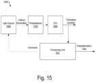
- FIG. 15shows another exemplary implementation 1500 of configuration 1200 in which signal generator 1204 is implemented by a light source 1502 .
- light source 1502may be implemented by any suitable light source configured to emit temporally uniform illumination (e.g., overhead light or any other type of light that is relatively uniform or constant over time).
- Light source 1502may be included in or external to an optical measurement system of which TDC 1202 is a part.
- processing unit 912may be configured to provide a command to light source 1502 to begin emitting the uniform illumination.
- processing unit 912may not be in communication with light source 1502 .
- light source 1502may be controlled by an external controller and/or manually controlled.
- implementation 1500further includes the photodetector 1310 that corresponds to TDC 1202 .
- photodetector 1310is configured to detect photons from the uniform illumination.
- TDC 1202is configured to record timestamp symbols corresponding to arrival times for the photons at photodetector 1310 . Over time, this may create a uniform probability distribution for triggering photodetector 1310 through the range of TDC 1202 with respect to a reference clock.
- processing unit 912may generate characterization data representative of a nonlinearity of TDC 1202 . It will be recognized that in this uniform illumination approach, the characterization data is further representative of nonlinearities of photodetector 1310 and the communication path between photodetector 1310 and TDC 1202 .
- FIG. 16shows an alternative configuration 1600 in which processing unit 912 is configured to characterize a nonlinearity of TDC 1202 based on dark counts (e.g., when photodetector 1310 fires even though there is no illumination being applied to photodetector 1310 ).
- configuration 1600is similar to implementation 1500 , except that configuration 1600 does not include a light source.
- configuration 1600may include a light source, but processing unit 912 may be configured to prevent the light source from outputting light while the characterization data is generated.
- photodetector 1310may fire without any light source due to thermal noise, etc. These dark counts may, over time, create a uniform probability distribution similar to that created in implementation 1500 .
- processing unit 912may generate characterization data representative of a nonlinearity of TDC 1202 . It will be recognized that in this dark count approach, the characterization data is further representative of nonlinearities of photodetector 1310 and the communication path between photodetector 1310 and TDC 1202 .
- processing unit 912may generate characterization data representative of a nonlinearity of TDC 1202 in any suitable manner. For example, processing unit 912 may generate the characterization data by generating a histogram of the timestamp symbols recorded by TDC 1202 and determining a code density metric for each time bin of the histogram.
- the code density metricis representative of a density of timestamp symbols at each time bin of the histogram, as “code” is another term for timestamp symbol.
- Processing unit 912may generate a histogram of the timestamp symbols recorded by TDC 1202 in any suitable manner. For example, processing unit 912 may record a total number of counts (e.g., recorded timestamp symbols) that occur during each of a plurality of time bins. The time bins may have any suitable temporal resolution.
- Processing unit 912may be configured to generate the code density metric for each time bin of the histogram in any suitable manner.
- processing unit 912may be configured to generate the code density metric for each time bin of the histogram in accordance with following equation:
- Code density[i]is the code density metric
- iis an index for each time bin of the histogram
- hist_bin[i]represents a value in the histogram at each time bin i
- B totalrepresents a total number of time bins in the histogram
- ⁇ all bins hist_bin [i]represents a sum of all the values in the histogram.
- the characterization data generated by processing unit 912may further include a nonlinearity metric (e.g., a metric representative of DNL and/or INL) for TDC 1202 .
- DNL[i]represents a nonlinearity metric for each time bin i.
- the normalizationis performed by subtracting a value of 1 from the code density metric for each time bin i.
- Processing unit 912may use the code density metric of Equation 1 and/or the nonlinearity metric of Equation 2 to compensate for a nonlinearity of TDC 1202 . This may be performed in any suitable manner. For example, processing unit 912 may compensate for a nonlinearity of TDC 1202 by using the code density metric of Equation 1 to normalize (e.g., linearize and/or calibrate) a transfer function of TDC 1202 . This, in turn, can remove at least some of the variations in a histogram generated by processing unit 912 that are caused by the nonlinearity.
- processing unit 912may normalize a transfer function of TDC 1202 in accordance with the following equation:
- hist_bin ⁇ _norm [ i ]hist_bin [ i ] code ⁇ density [ i ] . ( Equation ⁇ 3 )
- hist_bin_norm[i]represents the normalized transfer function
- hist_bin [i]represents a value in the histogram at each time bin i
- code density[i]is the code density metric of Equation 1.
- processing unit 912may generate a histogram that looks like histogram 1102 - 1 ( FIG. 11 ) when the transfer function of TDC 1202 is normalized in accordance with Equation 3 or in any other suitable manner.
- Processing unit 912may perform any other suitable action based on the characterization data for TDC 1202 .
- processing unit 912may rate TDC 1202 based on the characterization data. This rating may be compared to other TDCs (e.g., in the same TDC array).
- the rating of TDC 1202is outside a predetermined range of values (e.g., if the rating value deviates too much from a range of rating values for other TDCs in the same TDC array), thereby indicating that TDC 1202 has a relatively poor impulse response function, TDC 1202 and its corresponding photodetector may be disabled so as to not skew an overall histogram generated by optical measurement system 100 .
- TDC 1202 and its corresponding photodetectormay be disabled in any suitable manner.
- processing unit 912may disable a power supply for TDC 1202 and/or its corresponding photodetector, transmit a control signal to TDC 1202 and/or its corresponding photodetector that turns off or disables TDC 1202 and/or its corresponding photodetector, and/or abstain from transmitting a gate on pulse to the photodetector.
- processing unit 912may be configured to isolate each TDC/photodetector pair so that only one TDC/photodetector pair is active at any given time. This may allow a nonlinearity of each individual TDC and/or DCT/photodetector pair to be characterized. For example, while processing unit 912 characterizes a nonlinearity of TDC 1202 , processing unit 912 may disable other TDCs within an array of TDCs (e.g., TDC array 910 ) of which TDC 1202 . This may be performed in any suitable manner.
- Processing unit 912may generate characterization data for TDC 1202 at any suitable time. For example, processing unit 912 may generate characterization data for TDC 1202 in response to an event occurring within an optical measurement system of which TDC 1202 is a part. For example, processing unit 912 may generate characterization data for TDC 1202 at startup (e.g., a powering on) of the optical measurement system. As another example, processing unit 912 may be configured to place the optical measurement system in a calibration mode (e.g., during a startup procedure for the optical measurement system) and generate the characterization data while the optical measurement system is in the calibration mode.
- a calibration modee.g., during a startup procedure for the optical measurement system
- optical measurement system 100may be at least partially wearable by a user.
- optical measurement system 100may be implemented by a wearable device configured to be worn by a user (e.g., a head-mountable component configured to be worn on a head of the user).
- the wearable devicemay include one or more photodetectors, modules, and/or any of the other components described herein.
- one or more componentse.g., processing unit 912 , processor 108 , controller 112 , etc.
- one or more communication interfacese.g., cables, wireless interfaces, etc.
- FIGS. 17 - 22illustrate embodiments of a wearable device 1700 that includes elements of the optical detection systems described herein.
- the wearable devices 1700 shown in FIGS. 17 - 22include a plurality of modules 1702 , similar to the modules described herein.
- each module 1702may include a light source (e.g., light source 704 - 1 ) and a plurality of detectors (e.g., detectors 706 - 1 through 706 - 6 ).
- the wearable devices 1700may each also include a controller (e.g., controller 112 ) and a processor (e.g., processor 108 or processing unit 912 ) and/or be communicatively connected to a controller and processor.
- a controllere.g., controller 112
- a processore.g., processor 108 or processing unit 912
- wearable device 1700may be implemented by any suitable headgear and/or clothing article configured to be worn by a user.
- the headgear and/or clothing articlemay include batteries, cables, and/or other peripherals for the components of the optical measurement systems described herein.
- FIG. 17illustrates an embodiment of a wearable device 1700 in the form of a helmet with a handle 1704 .
- a cable 1706extends from the wearable device 1700 for attachment to a battery or hub (with components such as a processor or the like).
- FIG. 18illustrates another embodiment of a wearable device 1700 in the form of a helmet showing a back view.
- FIG. 19illustrates a third embodiment of a wearable device 1700 in the form of a helmet with the cable 1706 leading to a wearable garment 1708 (such as a vest or partial vest) that can include a battery or a hub.
- the wearable device 1700can include a crest 1710 or other protrusion for placement of the hub or battery.
- FIG. 20illustrates another embodiment of a wearable device 1700 in the form of a cap with a wearable garment 1708 in the form of a scarf that may contain or conceal a cable, battery, and/or hub.
- FIG. 21illustrates additional embodiments of a wearable device 1700 in the form of a helmet with a one-piece scarf 1708 or two-piece scarf 1708 - 1 .
- FIG. 22illustrates an embodiment of a wearable device 1700 that includes a hood 1710 and a beanie 1712 which contains the modules 1702 , as well as a wearable garment 1708 that may contain a battery or hub.
- a non-transitory computer-readable medium storing computer-readable instructionsmay be provided in accordance with the principles described herein.
- the instructionswhen executed by a processor of a computing device, may direct the processor and/or computing device to perform one or more operations, including one or more of the operations described herein.
- Such instructionsmay be stored and/or transmitted using any of a variety of known computer-readable media.
- a non-transitory computer-readable medium as referred to hereinmay include any non-transitory storage medium that participates in providing data (e.g., instructions) that may be read and/or executed by a computing device (e.g., by a processor of a computing device).
- a non-transitory computer-readable mediummay include, but is not limited to, any combination of non-volatile storage media and/or volatile storage media.
- Exemplary non-volatile storage mediainclude, but are not limited to, read-only memory, flash memory, a solid-state drive, a magnetic storage device (e.g.
- RAMferroelectric random-access memory
- optical disce.g., a compact disc, a digital video disc, a Blu-ray disc, etc.
- RAMe.g., dynamic RAM
- FIG. 23illustrates an exemplary computing device 2300 that may be specifically configured to perform one or more of the processes described herein. Any of the systems, units, computing devices, and/or other components described herein may be implemented by computing device 2300 .
- computing device 2300may include a communication interface 2302 , a processor 2304 , a storage device 2306 , and an input/output (“I/O”) module 2308 communicatively connected one to another via a communication infrastructure 2310 . While an exemplary computing device 2300 is shown in FIG. 23 , the components illustrated in FIG. 23 are not intended to be limiting. Additional or alternative components may be used in other embodiments. Components of computing device 2300 shown in FIG. 23 will now be described in additional detail.
- Communication interface 2302may be configured to communicate with one or more computing devices.
- Examples of communication interface 2302include, without limitation, a wired network interface (such as a network interface card), a wireless network interface (such as a wireless network interface card), a modem, an audio/video connection, and any other suitable interface.
- Processor 2304generally represents any type or form of processing unit capable of processing data and/or interpreting, executing, and/or directing execution of one or more of the instructions, processes, and/or operations described herein.
- Processor 2304may perform operations by executing computer-executable instructions 2312 (e.g., an application, software, code, and/or other executable data instance) stored in storage device 2306 .
- computer-executable instructions 2312e.g., an application, software, code, and/or other executable data instance
- Storage device 2306may include one or more data storage media, devices, or configurations and may employ any type, form, and combination of data storage media and/or device.
- storage device 2306may include, but is not limited to, any combination of the non-volatile media and/or volatile media described herein.
- Electronic data, including data described herein,may be temporarily and/or permanently stored in storage device 2306 .
- data representative of computer-executable instructions 2312 configured to direct processor 2304 to perform any of the operations described hereinmay be stored within storage device 2306 .
- datamay be arranged in one or more databases residing within storage device 2306 .
- I/O module 2308may include one or more I/O modules configured to receive user input and provide user output.
- I/O module 2308may include any hardware, firmware, software, or combination thereof supportive of input and output capabilities.
- I/O module 2308may include hardware and/or software for capturing user input, including, but not limited to, a keyboard or keypad, a touchscreen component (e.g., touchscreen display), a receiver (e.g., an RF or infrared receiver), motion sensors, and/or one or more input buttons.
- I/O module 2308may include one or more devices for presenting output to a user, including, but not limited to, a graphics engine, a display (e.g., a display screen), one or more output drivers (e.g., display drivers), one or more audio speakers, and one or more audio drivers.
- I/O module 2308is configured to provide graphical data to a display for presentation to a user.
- the graphical datamay be representative of one or more graphical user interfaces and/or any other graphical content as may serve a particular implementation.
- FIG. 24illustrates an exemplary method 2400 that may be performed by a processing unit as described herein. While FIG. 24 illustrates exemplary operations according to one embodiment, other embodiments may omit, add to, reorder, and/or modify any of the operations shown in FIG. 24 . Each of the operations shown in FIG. 24 may be performed in any of the ways described herein.
- a processing unitdirects a signal generator to apply a signal to a TDC included in an optical measurement system.
- the processing unitIn operation 2404 , the processing unit generates, based on timestamp symbols recorded by the TDC in response to the signal, characterization data representative of a nonlinearity of the TDC.
- FIG. 25illustrates an exemplary method 2500 that may be performed by a processing unit as described herein. While FIG. 25 illustrates exemplary operations according to one embodiment, other embodiments may omit, add to, reorder, and/or modify any of the operations shown in FIG. 25 . Each of the operations shown in FIG. 25 may be performed in any of the ways described herein.
- a processing unitprevents a signal generator from applying a signal to a TDC included in an optical measurement system for a time period.
- the processing unitIn operation 2504 , the processing unit generates, based on timestamp symbols recorded by the TDC in response to dark count events during the time period, characterization data representative of a nonlinearity of the TDC.
- An illustrative optical measurement systemincludes a signal generator configured to generate a signal and a processing unit configured to direct the signal generator to apply the signal to a TDC included in the optical measurement system and generate, based on timestamp symbols recorded by the TDC in response to the signal, characterization data representative of a nonlinearity of the TDC.
- An illustrative systemincludes a memory storing instructions and a processor communicatively coupled to the memory and configured to execute the instructions to direct a signal generator to apply a signal to a TDC included in an optical measurement system, and generate, based on timestamp symbols recorded by the TDC in response to the signal, characterization data representative of a nonlinearity of the TDC.
- Another illustrative systemincludes a memory storing instructions and a processor communicatively coupled to the memory and configured to execute the instructions to prevent a signal generator from applying a signal to a TDC included in an optical measurement system for a time period, and generate, based on timestamp symbols recorded by the TDC in response to dark count events during the time period, characterization data representative of a nonlinearity of the TDC.
Landscapes
- Health & Medical Sciences (AREA)
- Life Sciences & Earth Sciences (AREA)
- Engineering & Computer Science (AREA)
- Physics & Mathematics (AREA)
- Biomedical Technology (AREA)
- General Health & Medical Sciences (AREA)
- Surgery (AREA)
- Veterinary Medicine (AREA)
- Public Health (AREA)
- Animal Behavior & Ethology (AREA)
- Molecular Biology (AREA)
- Medical Informatics (AREA)
- Heart & Thoracic Surgery (AREA)
- Biophysics (AREA)
- Pathology (AREA)
- Neurology (AREA)
- Physiology (AREA)
- Signal Processing (AREA)
- Psychiatry (AREA)
- Psychology (AREA)
- Neurosurgery (AREA)
- Artificial Intelligence (AREA)
- Power Engineering (AREA)
- General Physics & Mathematics (AREA)
- Computer Vision & Pattern Recognition (AREA)
- General Engineering & Computer Science (AREA)
- Theoretical Computer Science (AREA)
- Hematology (AREA)
- Cardiology (AREA)
- Human Computer Interaction (AREA)
- Social Psychology (AREA)
- Hospice & Palliative Care (AREA)
- Educational Technology (AREA)
- Developmental Disabilities (AREA)
- Child & Adolescent Psychology (AREA)
- Dermatology (AREA)
- Measurement Of The Respiration, Hearing Ability, Form, And Blood Characteristics Of Living Organisms (AREA)
- Biodiversity & Conservation Biology (AREA)
Abstract
Description
DNL[i]=Code density[i]−1 (Equation 2).
Claims (18)
Priority Applications (1)
| Application Number | Priority Date | Filing Date | Title |
|---|---|---|---|
| US17/202,588US12138068B2 (en) | 2020-03-20 | 2021-03-16 | Techniques for characterizing a nonlinearity of a time-to-digital converter in an optical measurement system |
Applications Claiming Priority (3)
| Application Number | Priority Date | Filing Date | Title |
|---|---|---|---|
| US202062992502P | 2020-03-20 | 2020-03-20 | |
| US202063059382P | 2020-07-31 | 2020-07-31 | |
| US17/202,588US12138068B2 (en) | 2020-03-20 | 2021-03-16 | Techniques for characterizing a nonlinearity of a time-to-digital converter in an optical measurement system |
Publications (2)
| Publication Number | Publication Date |
|---|---|
| US20210290146A1 US20210290146A1 (en) | 2021-09-23 |
| US12138068B2true US12138068B2 (en) | 2024-11-12 |
Family
ID=77747106
Family Applications (1)
| Application Number | Title | Priority Date | Filing Date |
|---|---|---|---|
| US17/202,588Active2043-08-13US12138068B2 (en) | 2020-03-20 | 2021-03-16 | Techniques for characterizing a nonlinearity of a time-to-digital converter in an optical measurement system |
Country Status (1)
| Country | Link |
|---|---|
| US (1) | US12138068B2 (en) |
Families Citing this family (2)
| Publication number | Priority date | Publication date | Assignee | Title |
|---|---|---|---|---|
| US12078531B2 (en)* | 2021-07-28 | 2024-09-03 | Hi Llc | Devices, systems, and methods for calibrating an optical measurement device |
| US11876523B1 (en)* | 2022-12-12 | 2024-01-16 | Xilinx, Inc. | DPLL timing normalization |
Citations (354)
| Publication number | Priority date | Publication date | Assignee | Title |
|---|---|---|---|---|
| US4018534A (en) | 1975-05-21 | 1977-04-19 | The United States Of America As Represented By The Secretary Of The Army | Aerosol average-density determining system |
| US4207892A (en) | 1977-09-13 | 1980-06-17 | Arnold Binder | Method and apparatus for the diagnosis of tissue samples |
| US4281645A (en) | 1977-06-28 | 1981-08-04 | Duke University, Inc. | Method and apparatus for monitoring metabolism in body organs |
| US4515165A (en) | 1980-02-04 | 1985-05-07 | Energy Conversion Devices, Inc. | Apparatus and method for detecting tumors |
| US4655225A (en) | 1985-04-18 | 1987-04-07 | Kurabo Industries Ltd. | Spectrophotometric method and apparatus for the non-invasive |
| WO1988004034A2 (en) | 1986-11-25 | 1988-06-02 | The Secretary Of State For Defence In Her Britanni | Avalanche photodiode quenching circuit |
| US4928248A (en) | 1988-05-07 | 1990-05-22 | Hamamatsu Photonics Kabushiki Kaisha | Light source driving device |
| US4963727A (en) | 1988-10-20 | 1990-10-16 | Consiglio Nazionale Delle Ricerche | Active quenching circuit for avalanche photodiodes |
| US4995044A (en) | 1990-03-23 | 1991-02-19 | Tektronix, Inc. | Laser diode impulse circuit |
| US5088493A (en) | 1984-08-07 | 1992-02-18 | Sclavo, S.P.A. | Multiple wavelength light photometer for non-invasive monitoring |
| US5090415A (en) | 1989-02-14 | 1992-02-25 | Hamamatsu Photonics Kabushiki Kaisha | Examination apparatus |
| US5218962A (en) | 1991-04-15 | 1993-06-15 | Nellcor Incorporated | Multiple region pulse oximetry probe and oximeter |
| US5309458A (en) | 1992-03-02 | 1994-05-03 | Ecrm Trust | Method and apparatus for stabilizing laser diode energy output |
| US5386827A (en) | 1993-03-30 | 1995-02-07 | Nim Incorporated | Quantitative and qualitative in vivo tissue examination using time resolved spectroscopy |
| EP0656536A1 (en) | 1993-12-01 | 1995-06-07 | Hamamatsu Photonics K.K. | Method and apparatus for measuring scattering medium |
| US5528365A (en) | 1994-03-01 | 1996-06-18 | The Trustees Of The University Of Pennsylvania | Methods and apparatus for imaging with diffuse light |
| US5625458A (en) | 1994-11-10 | 1997-04-29 | Research Foundation Of City College Of New York | Method and system for imaging objects in turbid media using diffusive fermat photons |
| US5761230A (en) | 1995-05-22 | 1998-06-02 | Nec Corporation | Laser-diode driving circuit with temperature compensation |
| US5853370A (en) | 1996-09-13 | 1998-12-29 | Non-Invasive Technology, Inc. | Optical system and method for non-invasive imaging of biological tissue |
| US5895984A (en) | 1995-12-13 | 1999-04-20 | Leica Geosystems Ag | Circuit arrangement for feeding a pulse output stage |
| US5924982A (en) | 1997-07-30 | 1999-07-20 | Nellcor Puritan Bennett Incorporated | Oximeter sensor with user-modifiable color surface |
| US5929982A (en) | 1997-02-04 | 1999-07-27 | Tektronix, Inc. | Active APD gain control for an optical receiver |
| WO1999053577A1 (en) | 1998-04-14 | 1999-10-21 | Optobahn Corporation | Temperature compensation of laser diodes |
| US5983120A (en) | 1995-10-23 | 1999-11-09 | Cytometrics, Inc. | Method and apparatus for reflected imaging analysis |
| US5987045A (en) | 1997-04-02 | 1999-11-16 | The United States Of America As Represented By The Secretary Of The Navy | High power narrow pulse laser diode circuit |
| US6163715A (en) | 1996-07-17 | 2000-12-19 | Criticare Systems, Inc. | Direct to digital oximeter and method for calculating oxygenation levels |
| US6195580B1 (en) | 1995-07-10 | 2001-02-27 | Richard J. Grable | Diagnostic tomographic laser imaging apparatus |
| US6240309B1 (en) | 1995-10-06 | 2001-05-29 | Hitachi, Ltd. | Optical measurement instrument for living body |
| US6291824B1 (en) | 1998-04-13 | 2001-09-18 | Board Of Supervisors Of Louisiana State University And Agricultural And Mechanical College | Apparatus and method for high-bandwidth optical tomography |
| US6291842B1 (en) | 1998-03-12 | 2001-09-18 | Nec Corporation | Field effect transistor |
| US20020033454A1 (en) | 2000-08-04 | 2002-03-21 | Xuefeng Cheng | Optical imaging system with direct image construction |
| US6384663B2 (en) | 2000-03-09 | 2002-05-07 | Politecnico De Milano | Circuit for high precision detection of the time of arrival of photons falling on single photon avalanche diodes |
| US20020195545A1 (en) | 2001-06-20 | 2002-12-26 | Nishimura Ken A. | Avalanche photodiode array biasing device and avalanche photodiode structure |
| US6541752B2 (en) | 2000-03-09 | 2003-04-01 | Politecnico Di Milano | Monolithic circuit of active quenching and active reset for avalanche photodiodes |
| US6542763B1 (en) | 1999-10-28 | 2003-04-01 | Hitachi, Ltd. | Optical measurement equipment and recording medium and optical measurement method |
| US6618614B1 (en) | 1995-01-03 | 2003-09-09 | Non-Invasive Technology, Inc. | Optical examination device, system and method |
| US6683294B1 (en) | 1998-12-18 | 2004-01-27 | Qinetiq Limited | Avalanche photo-diodes |
| US20040057478A1 (en) | 2002-09-20 | 2004-03-25 | Alps Electric Co., Ltd. | Control circuit for constantly setting optical output of semiconductor laser |
| US20040064052A1 (en) | 1996-01-02 | 2004-04-01 | Britton Chance | Non-invasive imaging of biological tissue |
| US20040078216A1 (en) | 2002-02-01 | 2004-04-22 | Gregory Toto | Clinical trial process improvement method and system |
| US6748254B2 (en) | 2001-10-12 | 2004-06-08 | Nellcor Puritan Bennett Incorporated | Stacked adhesive optical sensor |
| US20040160996A1 (en) | 2003-01-02 | 2004-08-19 | Giorgi David M. | Apparatus and method for driving a pulsed laser diode |
| US20050038344A1 (en) | 1998-02-13 | 2005-02-17 | Britton Chance | Transabdominal examination, monitoring and imaging of tissue |
| US20050059869A1 (en) | 2003-09-15 | 2005-03-17 | John Scharf | Physiological monitoring system and improved sensor device |
| US20050061986A1 (en) | 2003-07-15 | 2005-03-24 | Kabushiki Kaisha Toshiba | Circuit for a single photon detector |
| US20050124863A1 (en) | 2001-06-28 | 2005-06-09 | Cook Daniel R. | Drug profiling apparatus and method |
| US20050228291A1 (en) | 1998-02-11 | 2005-10-13 | Britton Chance | Imaging and characterization of brain tissue |
| US6992772B2 (en) | 2003-06-19 | 2006-01-31 | Optix Lp | Method and apparatus for optical sampling to reduce interfering variances |
| US20060171845A1 (en) | 2005-01-31 | 2006-08-03 | Dakota Technologies, Inc. | Sensors for measuring analytes |
| US7095491B2 (en) | 2002-03-27 | 2006-08-22 | MCC Gesellschaft für Diagnosesysteme in Medizin und Technik mbH & Co. KG | Device and method for measuring constituents in blood |
| US20060197452A1 (en) | 2005-03-02 | 2006-09-07 | Bin Zhang | Apparatus and method for generating an output signal that tracks the temperature coefficient of a light source |
| US20060264722A1 (en) | 2003-06-25 | 2006-11-23 | Don Hannula | Hat-based oximeter sensor |
| US20070038116A1 (en) | 2003-07-29 | 2007-02-15 | Hamamatsu Photonics K.K. | Device and method for measuring scattering absorber |
| US20070083097A1 (en) | 2003-09-19 | 2007-04-12 | Michiyuki Fujiwara | Living body information signal processing system combining living body optical measurement apparatus and brain wave measurement apparatus and probe device used for the same |
| CN200950235Y (en) | 2006-09-25 | 2007-09-19 | 深圳飞通光电子技术有限公司 | Temperature compensation bias circuit of avalanche photodiode |
| US20080021341A1 (en) | 2006-06-23 | 2008-01-24 | Neurovista Corporation A Delware Corporation | Methods and Systems for Facilitating Clinical Trials |
| US7356365B2 (en) | 2003-07-09 | 2008-04-08 | Glucolight Corporation | Method and apparatus for tissue oximetry |
| WO2008144831A1 (en) | 2007-05-30 | 2008-12-04 | Invision Medical Technologies Pty Ltd | Method and apparatus for inspecting tissue |
| US20090012402A1 (en) | 2006-03-20 | 2009-01-08 | Mintz Frederick W | Mobile in vivo infra red data collection and diagnoses comparison system |
| US20090054789A1 (en) | 2007-08-21 | 2009-02-26 | Hitachi, Ltd. | Head-coupled holder for living body optical measurement |
| US7507596B2 (en) | 2003-09-24 | 2009-03-24 | Taiwan Semiconductor Manufacturing Co., Ltd. | Method of fabricating a high quantum efficiency photodiode |
| US7547872B2 (en) | 2005-02-14 | 2009-06-16 | Ecole Polytechnique Federale De Lausanne | Integrated circuit comprising an array of single photon avalanche diodes |
| US20090163775A1 (en) | 2007-12-21 | 2009-06-25 | Barrett Bruce J | Physiological sensor |
| US7613504B2 (en) | 2001-06-05 | 2009-11-03 | Lumidigm, Inc. | Spectroscopic cross-channel method and apparatus for improved optical measurements of tissue |
| US20090313048A1 (en) | 2000-05-31 | 2009-12-17 | Medidata Ft, Inc. | Clinical trials management system and method |
| US20100007413A1 (en) | 2006-11-10 | 2010-01-14 | Koninklijke Philips Electronics N.V. | Ecg electrode contact quality measurement system |
| US7667400B1 (en) | 2006-06-09 | 2010-02-23 | Array Optronix, Inc. | Back-illuminated Si photomultipliers: structure and fabrication methods |
| US7705284B2 (en) | 2006-03-06 | 2010-04-27 | Nihon University | High-speed single-photon detector in telecommunication wavelength band |
| US7714292B2 (en) | 2006-02-01 | 2010-05-11 | Koninklijke Philips Electronics N.V. | Geiger mode avalanche photodiode |
| US20100188649A1 (en) | 2009-01-23 | 2010-07-29 | Scott Prahl | Distance measurement device and method of use thereof |
| US20100210952A1 (en) | 2008-05-02 | 2010-08-19 | Olympus Corporation | Optical inspection device, electromagnetic wave detection method, electromagnetic wave detection device, organism observation method, microscope, endoscope, and optical tomographic image generation device |
| US20100249557A1 (en) | 2009-03-31 | 2010-09-30 | Nellcor Puritan Bennett Llc | Medical sensor with flexible components and technique for using the same |
| US20100301194A1 (en) | 2009-05-26 | 2010-12-02 | Princeton Lightwave, Inc. | Optical Receiver Comprising Breakdown-Voltage Compensation |
| US7888973B1 (en)* | 2007-06-05 | 2011-02-15 | Marvell International Ltd. | Matrix time-to-digital conversion frequency synthesizer |
| US7899506B2 (en) | 2002-11-04 | 2011-03-01 | Tianjin Sunshine Optics Technolies Co. Ltd. | Composite spectral measurement method and its spectral detection instrument |
| WO2011083563A1 (en) | 2010-01-05 | 2011-07-14 | 株式会社島津製作所 | Holder and photobiological measuring device using same |
| US20110208675A1 (en) | 2009-08-03 | 2011-08-25 | Colorado Seminary, Which Owns And Operates The University Of Denver | Brain imaging system and methods for direct prosthesis control |
| US8026471B2 (en) | 2008-07-23 | 2011-09-27 | Princeton Lightwave, Inc. | Single-photon avalanche detector-based focal plane array |
| US20110248175A1 (en) | 2008-12-15 | 2011-10-13 | Koninklijke Philips Electronics N.V. | Temperature compensation circuit for silicon photomultipliers and other single photon counters |
| US8078250B2 (en) | 2002-07-26 | 2011-12-13 | Cas Medical Systems, Inc. | Method for spectrophotometric blood oxygenation monitoring |
| US8082015B2 (en) | 2004-04-13 | 2011-12-20 | The Trustees Of The University Of Pennsylvania | Optical measurement of tissue blood flow, hemodynamics and oxygenation |
| US20120016635A1 (en) | 2010-07-13 | 2012-01-19 | At&T Intellectual Property I, L.P. | Characterization of Single-Photon Detectors Using a Continuous Wave Laser Source |
| US20120029304A1 (en) | 2010-07-29 | 2012-02-02 | Nellcor Puritan Bennett Llc | Configurable patient monitoring system |
| US8115170B2 (en) | 2007-01-09 | 2012-02-14 | International Business Machines Corporation | Method and apparatus for creating time-resolved emission images of integrated circuits using a single-point single-photon detector and a scanning system |
| US20120083673A1 (en) | 2010-09-28 | 2012-04-05 | Ammar Al-Ali | Depth of consciousness monitor including oximeter |
| US20120101838A1 (en) | 2010-10-20 | 2012-04-26 | Helen Mary Lingard | Systems and Processes for Managing and Supporting Regulatory Submissions in Clinical Trials |
| JP2012125370A (en) | 2010-12-15 | 2012-07-05 | Hitachi Ltd | Biological measurement apparatus |
| US8269563B2 (en)* | 2008-06-10 | 2012-09-18 | Qualcomm Incorporated | Dithering a digitally-controlled oscillator output in a phase-locked loop |
| WO2012135068A1 (en) | 2011-03-25 | 2012-10-04 | Drexel University | Functional near infrared spectrocopy based brain computer interface |
| US8352012B2 (en) | 2009-10-28 | 2013-01-08 | Board Of Governors For Higher Education, State Of Rhode Island And Providence Plantations | Biomedical electrode for detecting localized electrical signals and providing electrical stimulation |
| US20130015331A1 (en) | 2011-07-12 | 2013-01-17 | Leica Microsystems Cms Gmbh | Device and method for detecting light |
| US20130030267A1 (en) | 2011-07-29 | 2013-01-31 | Nellcor Puritan Bennett Llc | Multi-purpose sensor system |
| US20130030270A1 (en) | 2011-07-26 | 2013-01-31 | National Chiao Tung University | Physiological signal collection unit and detector thereof |
| US20130032713A1 (en) | 2011-08-05 | 2013-02-07 | Barbi Nicholas C | Electron detector including one or more intimately-coupled scintillator-photomultiplier combinations, and electron microscope employing same |
| WO2013034770A2 (en) | 2011-09-08 | 2013-03-14 | Borowski, André | Time-to-digital converter, 3d imager using same, method for time-to-digital conversion and method for 3d imaging |
| US20130090541A1 (en) | 2011-03-02 | 2013-04-11 | Board Of Regents, The University Of Texas System | Functional Near Infrared Spectroscopy Imaging System and Method |
| WO2013066959A1 (en) | 2011-10-31 | 2013-05-10 | The Trustees Of Columbia University In The City Of New York | Systems and methods for imaging using single photon avalanche diodes |
| US20130144644A1 (en) | 2010-04-09 | 2013-06-06 | Biogenerics IP Development Pty Ltd. | Clinical trial management systems and methods |
| US20130153754A1 (en) | 2011-12-20 | 2013-06-20 | Stmicroelectronics (Grenoble 2) Sas | Device having spad photodiodes for detecting an object |
| US20130221221A1 (en) | 2011-06-28 | 2013-08-29 | Korea Institute Of Science And Technology | Single photon detector in the near infrared using an ingaas/inp avalanche photodiode operated with a bipolar rectangular gating signal |
| US20130225953A1 (en) | 2010-02-26 | 2013-08-29 | Fundacion Hospital Nacional De Paraplejicos | Concurrent stimulation effect detection |
| US20130300838A1 (en)* | 2010-12-23 | 2013-11-14 | Fastree3D S.A. | Methods and devices for generating a representation of a 3d scene at very high speed |
| US20130342835A1 (en) | 2012-06-25 | 2013-12-26 | California Institute Of Technology | Time resolved laser raman spectroscopy using a single photon avalanche diode array |
| US8633431B2 (en) | 2008-07-25 | 2014-01-21 | Samsung Electronics Co., Ltd. | Image method and apparatus |
| US8637875B2 (en) | 2008-07-11 | 2014-01-28 | The Regents Of The University Of California | Single photon IR detectors and their integration with silicon detectors |
| US20140028211A1 (en) | 2012-07-26 | 2014-01-30 | Osram Sylvania Inc. | Flyback ac-to-dc converter |
| US20140027607A1 (en) | 2012-05-04 | 2014-01-30 | Princeton Lightwave, Inc. | High-Repetition-Rate Single-Photon Receiver and Method Therefor |
| US20140055181A1 (en) | 2011-05-06 | 2014-02-27 | Fujitsu Limited | Clock generating circuit |
| US20140066783A1 (en) | 2008-07-03 | 2014-03-06 | Cercacor Laboratories, Inc. | Noise shielding for a noninvaise device |
| US8754378B2 (en) | 2007-08-08 | 2014-06-17 | Koninklijke Philips N.V. | Silicon photomultiplier readout circuitry |
| US20140171757A1 (en) | 2011-11-08 | 2014-06-19 | Advanced Telecommunications Research Institute International | Apparatus and method for supporting brain function enhancement |
| US20140185643A1 (en) | 2012-12-31 | 2014-07-03 | Nlight Photonics Corporation | Pulsed bias current for gain switched semiconductor lasers for amplified spontaneous emission reduction |
| US20140191115A1 (en) | 2013-01-09 | 2014-07-10 | The University Court Of The Uniersity Of Edinburgh | Spad sensor circuit with biasing circuit |
| US20140211194A1 (en) | 2013-01-27 | 2014-07-31 | Quanergy Systems, Inc. | Cost-effective lidar sensor for multi-signal detection, weak signal detection and signal disambiguation and method of using same |
| US8817257B2 (en) | 2011-12-16 | 2014-08-26 | Commissariat à l'Energie Atomique et aux Energies Alternatives | Method for reconstructing the optical properties of a medium using a combination of a plurality of mellin-laplace transforms of a magnitude comprising a time distribution of a received signal, and associated reconstruction system |
| US20140275891A1 (en) | 2013-03-13 | 2014-09-18 | Cephalogics, LLC | Optical tomography sensor and related apparatus and methods |
| US20140289001A1 (en) | 1996-02-17 | 2014-09-25 | Robert Shelton | System and method for recruiting subjects for research studies and clinical trials over the internet |
| US20140291481A1 (en) | 2013-04-01 | 2014-10-02 | Omnivision Technologies, Inc. | Enhanced photon detection device with biased deep trench isolation |
| US20150011848A1 (en) | 2012-07-16 | 2015-01-08 | Timothy Ruchti | Multiplexed pathlength resolved noninvasive analyzer apparatus and method of use thereof |
| US8937509B2 (en) | 2010-10-15 | 2015-01-20 | Imec | Multi-channel biopotential signal acquisition systems |
| US20150038811A1 (en) | 2012-03-29 | 2015-02-05 | Hitachi Medical Corporation | Living body optical measurement apparatus, living body optical measurement method, and engagement member for mobile position sensor |
| US20150041625A1 (en) | 2013-08-06 | 2015-02-12 | Stmicroelectronics (Research & Development) Limited | Time to digital converter and applications thereof |
| US20150041627A1 (en) | 2013-08-12 | 2015-02-12 | Omnivision Technologies, Inc. | Partitioned silicon photomultiplier with delay equalization |
| US20150054111A1 (en) | 2013-08-23 | 2015-02-26 | Kabushiki Kaisha Toyota Chuo Kenkyusho | Single photon avalanche diode |
| US20150057511A1 (en) | 2012-03-28 | 2015-02-26 | Wayne State University | Sensor and method for continuous health monitoring |
| US20150077279A1 (en) | 2013-09-17 | 2015-03-19 | Qualcomm Incorporated | Time-to-digital converter |
| US8986207B2 (en) | 2009-11-12 | 2015-03-24 | Covidien Lp | Systems and methods for providing sensor arrays for detecting physiological characteristics |
| US20150094552A1 (en) | 2012-10-07 | 2015-04-02 | Rhythm Diagnostics Systems, Inc. | Health monitoring systems and methods |
| WO2015052523A1 (en) | 2013-10-10 | 2015-04-16 | The University Court Of The University Of Glasgow | Endoscopy capsule with spad array for detecting fluorescence emitted by biological tissue |
| FR3011932A1 (en) | 2013-10-10 | 2015-04-17 | Univ Strasbourg | TIME-RESOLVED FLUORESCENCE MEASUREMENT DEVICE AND METHOD FOR HIGH-SPEED SAMPLE SCREENING |
| US9012860B2 (en) | 2012-05-15 | 2015-04-21 | Princeton Lightwave, Inc. | Dual-SPAD-based single-photon receiver |
| US9041136B2 (en) | 2011-10-20 | 2015-05-26 | Agency For Science, Technology And Research | Avalanche photodiode |
| US20150150505A1 (en) | 2013-12-03 | 2015-06-04 | Qualcomm Incorporated | Method, Devices and Systems for Sensor with Removable Nodes |
| US20150157435A1 (en) | 2013-12-06 | 2015-06-11 | PegaSense, Inc. | Equine fitness monitor |
| US20150157262A1 (en) | 2013-12-11 | 2015-06-11 | Samsung Electronics, Ltd. | Self-aligning sensor array |
| US9058081B2 (en) | 2010-11-30 | 2015-06-16 | Stmicroelectronics (Research & Development) Limited | Application using a single photon avalanche diode (SPAD) |
| US20150182136A1 (en) | 2013-12-26 | 2015-07-02 | Fundacio Institut De Ciencies Fotoniques | Speckle contrast optical tomography |
| US9076707B2 (en) | 2013-04-19 | 2015-07-07 | Lightspin Technologies, Inc. | Integrated avalanche photodiode arrays |
| US20150192677A1 (en) | 2014-01-03 | 2015-07-09 | Quanergy Systems, Inc. | Distributed lidar sensing system for wide field of view three dimensional mapping and method of using same |
| US20150200222A1 (en) | 2014-01-15 | 2015-07-16 | Omnivision Technologies, Inc. | Single photon avalanche diode imaging sensor for complementary metal oxide semiconductor stacked chip applications |
| US20150201841A1 (en) | 2012-07-27 | 2015-07-23 | Shimadzu Corporation | Optical biological measurement device and analysis method using the same |
| WO2015109005A1 (en) | 2014-01-14 | 2015-07-23 | Canon U.S.A., Inc. | Near-infrared spectroscopy and diffuse correlation spectroscopy device and methods |
| US9101279B2 (en) | 2006-02-15 | 2015-08-11 | Virtual Video Reality By Ritchey, Llc | Mobile user borne brain activity data and surrounding environment data correlation system |
| US9131861B2 (en) | 2004-11-30 | 2015-09-15 | Academisch Medisch Centrum | Pulsed lighting imaging systems and methods |
| US9157858B2 (en) | 2006-11-21 | 2015-10-13 | Ricardo J. Claps | Time-resolved spectroscopy system and methods for multiple-species analysis in fluorescence and cavity-ringdown applications |
| US20150293224A1 (en) | 2013-05-09 | 2015-10-15 | Quanergy Systems, Inc. | Solid state optical phased array lidar and method of using same |
| US9178100B2 (en) | 2010-09-08 | 2015-11-03 | Stmicroelectronics (Research & Development) Limited | Single photon avalanche diode for CMOS circuits |
| US9176241B2 (en) | 2011-08-03 | 2015-11-03 | Koninklijke Philips N.V. | Position-sensitive readout modes for digital silicon photomultiplier arrays |
| US9190552B2 (en) | 2012-06-13 | 2015-11-17 | Stmicroelectronics (Grenoble 2) Sas | Method and device for adjusting the bias voltage of a SPAD photodiode |
| US20150327777A1 (en) | 2014-05-14 | 2015-11-19 | Stryker Corporation | Tissue monitoring apparatus and system |
| US20150333095A1 (en) | 2014-05-13 | 2015-11-19 | Stmicroelectronics S.R.L. | Solid state photomultipliers array of enhanced fill factor and simplified packaging |
| US9201138B2 (en) | 2009-09-11 | 2015-12-01 | Robert Bosch Gmbh | Photon detector with a paralyzable photon-sensitive element, in particular SPAD, and distance measuring device comprising said type of photon detector |
| US9209320B1 (en) | 2014-08-07 | 2015-12-08 | Omnivision Technologies, Inc. | Method of fabricating a single photon avalanche diode imaging sensor |
| US20150355019A1 (en) | 2014-06-09 | 2015-12-10 | Kiskeya Microsystems Llc | Systems and methods for readout of event-driven pixels |
| US20150364635A1 (en) | 2013-01-31 | 2015-12-17 | Malvern Instruments Limited | Single photon counting |
| US9257523B2 (en) | 2008-01-21 | 2016-02-09 | Infineon Technologies Ag | Avalanche diode having an enhanced defect concentration level and method of making the same |
| US20160049765A1 (en) | 2014-08-15 | 2016-02-18 | Quanergy Systems, Inc. | Three-dimensional-mapping two-dimensional-scanning lidar based on one-dimensional-steering optical phased arrays and method of using same |
| US20160057369A1 (en) | 2014-08-20 | 2016-02-25 | Seek Thermal, Inc. | Adaptive adjustment of the operating bias of an imaging system |
| US9299873B2 (en) | 2013-05-16 | 2016-03-29 | Stmicroelectronics S.R.L. | Avalanche photodiode operating in geiger mode including a structure for electro-optical confinement for crosstalk reduction, and array of photodiodes |
| US9299732B2 (en) | 2013-10-28 | 2016-03-29 | Omnivision Technologies, Inc. | Stacked chip SPAD image sensor |
| US20160099371A1 (en) | 2014-10-03 | 2016-04-07 | Omnivision Technologies, Inc. | Back side illuminated image sensor with guard ring region reflecting structure |
| US9316735B2 (en) | 2010-11-30 | 2016-04-19 | Stmicroelectronics (Research & Development) Limited | Proximity detection apparatus and associated methods having single photon avalanche diodes for determining a quality metric based upon the number of events |
| US20160119983A1 (en) | 2010-11-30 | 2016-04-28 | STMicroelectronics (Research & Development ) Limited | Application using a single photon avalanche diode (spad) |
| US9331116B2 (en) | 2014-01-15 | 2016-05-03 | Omnivision Technologies, Inc. | Back side illuminated single photon avalanche diode imaging sensor with high short wavelength detection efficiency |
| US20160150963A1 (en) | 2011-09-26 | 2016-06-02 | Michael Lee Roukes | One-photon integrated neurophotonic systems |
| US20160161600A1 (en) | 2013-08-19 | 2016-06-09 | Quanergy Systems, Inc. | Optical phased array lidar system and method of using same |
| US9368487B1 (en) | 2015-01-28 | 2016-06-14 | Taiwan Semiconductor Manufacturing Company Limited | Semiconductor device with dynamic low voltage triggering mechanism |
| US20160182902A1 (en) | 2014-12-18 | 2016-06-23 | General Electric Company | Silicon photomultipliers with internal calibration circuitry |
| US20160181302A1 (en) | 2014-12-19 | 2016-06-23 | Sensl Technologies Ltd | Semiconductor photomultiplier |
| US9401448B2 (en) | 2013-11-19 | 2016-07-26 | National Institute Of Standards And Technology | Photon detector and process for detecting a single photon |
| US20160218236A1 (en) | 2015-01-27 | 2016-07-28 | Voxtel, Inc. | Clamped Avalanche Photodiode |
| US9407796B2 (en) | 2011-12-23 | 2016-08-02 | Commissariat á l'énergie atomique et aux énergies alternatives | System for reconstructing optical properties in a diffusing medium, comprising a pulsed radiation source and at least two detectors of two different types, and associated reconstruction method |
| US20160247301A1 (en) | 2015-02-25 | 2016-08-25 | National Chiao Tung University | Light detection apparatus and image reconstruction method using the same |
| US9431439B2 (en) | 2012-10-16 | 2016-08-30 | Kabushiki Kaisha Toyota Chuo Kenkyusho | Light detector |
| US9442201B2 (en) | 2013-09-12 | 2016-09-13 | Siemens Medical Solutions Usa, Inc. | CMOS SPAD array with mixed timing pick-off for time-of-flight positron emission tomography |
| US9449377B2 (en) | 2012-10-09 | 2016-09-20 | The United States Of America As Represented By The Secretary Of The Department Of Health And Human Services | Imaging methods and computer-readable media |
| US9450007B1 (en) | 2015-05-28 | 2016-09-20 | Stmicroelectronics S.R.L. | Integrated circuit with reflective material in trenches and related methods |
| US20160278715A1 (en) | 2015-03-23 | 2016-09-29 | University Of Kentucky Research Foundation | Noncontact Three-dimensional Diffuse Optical Imaging of Deep Tissue Blood Flow Distribution |
| US20160287107A1 (en) | 2014-01-30 | 2016-10-06 | Intel Corporation | Intelligent photoplethysmograph signal-to-noise ratio control for recovery of biosignals during times of motion |
| US20160296168A1 (en) | 2015-04-09 | 2016-10-13 | Geelux Holdings, Ltd. | Device configured to be supported on a human body, to measure a biological parameter of the human body, and to control a characteristic of the human body |
| WO2016166002A1 (en) | 2015-04-15 | 2016-10-20 | Ams Ag | Avalanche diode arrangement and method for providing a detection signal |
| US9478579B2 (en) | 2012-10-16 | 2016-10-25 | Omnivision Technologies, Inc. | Stacked chip image sensor with light-sensitive circuit elements on the bottom chip |
| US9476979B2 (en) | 2013-11-28 | 2016-10-25 | Stmicroelectronics (Grenoble 2) Sas | Method for evaluating position and motion using time of flight detectors |
| US20160341656A1 (en) | 2015-05-22 | 2016-11-24 | Taiwan Semiconductor Manufacturing Co., Ltd. | Optical biosensor device |
| US20160349368A1 (en)* | 2015-05-29 | 2016-12-01 | Hexagon Technology Center Gmbh | Time measurement circuit and optoelectronic distance meter having such a time measurement circuit |
| US20160356718A1 (en) | 2015-06-08 | 2016-12-08 | The Regents Of The University Of Michigan | Pixel circuit and method for optical sensing |
| US20160357260A1 (en) | 2015-06-03 | 2016-12-08 | Stmicroelectronics (Research & Development) Limited | Distance independent gesture detection |
| US9529079B1 (en) | 2015-03-26 | 2016-12-27 | Google Inc. | Multiplexed multichannel photodetector |
| US9535157B2 (en) | 2013-09-24 | 2017-01-03 | Stmicroelectronics (Research & Development) Limited | Proximity sensor including reference detector for stray radiation detection |
| WO2017004663A1 (en) | 2015-07-08 | 2017-01-12 | The Commonwealth Of Australia | Spad array structures and methods of operation |
| US9554738B1 (en)* | 2016-03-30 | 2017-01-31 | Zyomed Corp. | Spectroscopic tomography systems and methods for noninvasive detection and measurement of analytes using collision computing |
| US20170030769A1 (en) | 2015-07-27 | 2017-02-02 | Sick Ag | Light Receiver with Avalanche Photo Diodes in a Geiger Mode |
| US9574936B2 (en) | 2015-03-24 | 2017-02-21 | Sharper Shape Oy | Planar imaging sensor having plural photo detector groups with different detection windows |
| US20170052065A1 (en) | 2015-08-20 | 2017-02-23 | Apple Inc. | SPAD array with gated histogram construction |
| US20170085547A1 (en) | 2015-09-22 | 2017-03-23 | International Business Machines Corporation | Storing, indexing and recalling data based on brain activity |
| US9625580B2 (en) | 2014-01-03 | 2017-04-18 | Princeton Lightwave, Inc. | LiDAR system comprising a single-photon detector |
| US9634826B1 (en) | 2015-11-30 | 2017-04-25 | Intel Corporation | Apparatus and method for automatic bandwidth calibration for phase locked loop |
| US20170118423A1 (en) | 2006-10-06 | 2017-04-27 | California Institute Of Technology | Glare suppression through fog by optical phase conjugation assisted active cancellation |
| US9640704B2 (en) | 2015-05-29 | 2017-05-02 | Commissariat à l'énergie atomique et aux énergies alternatives | High quantum efficiency photodetector |
| US20170124713A1 (en) | 2015-10-30 | 2017-05-04 | Snapchat, Inc. | Image based tracking in augmented reality systems |
| US20170131143A1 (en) | 2014-07-02 | 2017-05-11 | Andreas G. Andreou | Photodetection circuit and operating method thereof |
| US20170139041A1 (en) | 2015-11-16 | 2017-05-18 | Stmicroelectronics (Grenoble 2) Sas | Ranging device with imaging capability |
| WO2017083826A1 (en) | 2015-11-13 | 2017-05-18 | Neurolutions, Inc. | Eeg headsets with precise and consistent electrode positioning |
| US20170141100A1 (en) | 2015-11-16 | 2017-05-18 | Taiwan Semiconductor Manufacturing Co., Ltd. | Esd hard backend structures in nanometer dimension |
| US9658158B2 (en) | 2012-06-08 | 2017-05-23 | Stmicroelectronics S.R.L. | Diagnostic device with integrated photodetector, and diagnostic system including the same |
| US9659980B2 (en) | 2014-12-19 | 2017-05-23 | Sensl Technologies Ltd | Semiconductor photomultiplier |
| US9671284B1 (en) | 2016-01-14 | 2017-06-06 | Kiskeya Microsystems Llc | Single-photon avalanche diode circuit with variable hold-off time and dual delay regime |
| US20170164857A1 (en) | 2015-12-09 | 2017-06-15 | Rythm | Method and device for bioelectric physiological signal acquisition and processing |
| US9681844B2 (en) | 2013-06-27 | 2017-06-20 | Imec Vzw | Biopotential signal acquisition system and method |
| US20170176596A1 (en) | 2010-08-11 | 2017-06-22 | Apple Inc. | Time-of-flight detector with single-axis scan |
| US20170176579A1 (en) | 2015-12-20 | 2017-06-22 | Apple Inc. | Light detection and ranging sensor |
| US20170172447A1 (en) | 2015-12-22 | 2017-06-22 | Imec Vzw | Sensor, System, and Holder Arrangement for Biosignal Activity Measurement |
| US20170179173A1 (en) | 2015-12-20 | 2017-06-22 | Apple Inc. | Spad array with pixel-level bias control |
| US20170186798A1 (en) | 2015-12-28 | 2017-06-29 | Taiwan Semiconductor Manufacturing Co., Ltd. | Stacked spad image sensor |
| US20170202518A1 (en) | 2016-01-14 | 2017-07-20 | Technion Research And Development Foundation Ltd. | System and method for brain state classification |
| KR20170087639A (en) | 2016-01-21 | 2017-07-31 | 서강대학교산학협력단 | Quenching bias circuit with current mirror for Single Photon Avalanche Photodiodes |
| WO2017130682A1 (en) | 2016-01-29 | 2017-08-03 | パナソニック・タワージャズセミコンダクター株式会社 | Solid-state image capture device |
| US9728659B2 (en) | 2013-06-21 | 2017-08-08 | Stmicroelectronics (Research & Development) Limited | SPAD device with radiation blocking rings and vias and related arrays and methods |
| US9741879B2 (en) | 2015-06-11 | 2017-08-22 | Commissariat A L'energie Atomique Et Aux Energies Alternatives | SPAD photodiode covered with a network |
| US9753351B2 (en) | 2014-06-30 | 2017-09-05 | Quanergy Systems, Inc. | Planar beam forming and steering optical phased array chip and method of using same |
| WO2017150146A1 (en) | 2016-02-29 | 2017-09-08 | パナソニック・タワージャズセミコンダクター株式会社 | Semiconductor device and method for manufacturing same |
| US9767246B2 (en) | 2015-06-17 | 2017-09-19 | General Electric Company | Adjustment and compensation of delays in photo sensor microcells |
| US9768211B2 (en) | 2015-05-06 | 2017-09-19 | LightSpin Technologies Inc. | Integrated avalanche photodiode arrays |
| US20170265822A1 (en) | 2015-10-30 | 2017-09-21 | Shanghai United Imaging Healthcare Co., Ltd. | Anti-scatter grid for radiation detector |
| US20170276545A1 (en) | 2014-08-21 | 2017-09-28 | Totalfoersvarets Forskningsinstitut | An imaging system parallelizing compressive sensing imaging |
| US20170281086A1 (en) | 2016-04-01 | 2017-10-05 | Thomas Alan Donaldson | Sensors to determine neuronal activity of an organism to facilitate a human-machine interface |
| US20170299700A1 (en) | 2014-10-20 | 2017-10-19 | Quanergy Systems, Inc. | Three-dimensional lidar sensor based on two-dimensional scanning of one-dimensional optical emitter and method of using same |
| US20170303789A1 (en) | 2016-04-26 | 2017-10-26 | Illinois Institute Of Technology | Apparatus and method for enhanced early photon detection in optical projection tomography |
| US9804092B2 (en) | 2013-02-14 | 2017-10-31 | British Columbia Cancer Agency Branch | Integrated spectral probe for raman, reflectance and fluorescence spectral measurements |
| US20170314989A1 (en) | 2016-04-28 | 2017-11-02 | Stmicroelectronics S.R.L. | Semiconductor device for detecting ultraviolet and infrared radiation and related manufacturing process |
| US20170338969A1 (en) | 2016-05-19 | 2017-11-23 | Linear Technology Corporation | MAINTAIN POWER SIGNATURE CONTROLLER AT POWER INTERFACE OF PoE OR PoDL SYSTEM |
| WO2017203936A1 (en) | 2016-05-25 | 2017-11-30 | パナソニック・タワージャズセミコンダクター株式会社 | Solid-state imaging element |
| US20170363467A1 (en) | 2016-06-17 | 2017-12-21 | Sick Ag | Light receiver having geiger-mode avalanche photodiodes and method for reading out |
| US9851302B2 (en) | 2015-12-18 | 2017-12-26 | Stmicroelectronics (Research & Development) Limited | Apparatus for use in luminescence applications |
| US20170367650A1 (en) | 2014-11-21 | 2017-12-28 | Centre Hospitalier Universitaire | Device for measuring the brain activity signals of an individual |
| US20180003821A1 (en) | 2016-07-01 | 2018-01-04 | Shigeaki Imai | Object detector, sensing device, and mobile apparatus |
| US9867250B1 (en) | 2015-04-20 | 2018-01-09 | The Arizona Board Of Regents On Behalf Of The University Of Arizona | System having a configurable pico-second pulsed LED driver circuit and photomultiplier tube biasing and gating circuits for real-time, time-resolved transient recording of fluorescence |
| WO2018007829A1 (en) | 2016-07-07 | 2018-01-11 | The University Court Of The University Of Edinburgh | Imaging method and apparatus |
| US20180014741A1 (en) | 2015-01-26 | 2018-01-18 | Chang-An Chou | Wearable physiological monitoring device |
| US20180019268A1 (en) | 2016-07-18 | 2018-01-18 | Omnivision Technologies, Inc. | Stacked-chip backside-illuminated spad sensor with high fill-factor |
| US20180027196A1 (en) | 2016-07-20 | 2018-01-25 | Omnivision Technologies, Inc. | High dynamic range image sensor with virtual high-low sensitivity pixels |
| US20180026147A1 (en) | 2016-07-21 | 2018-01-25 | Omnivision Technologies, Inc. | Vertical gate guard ring for single photon avalanche diode pitch minimization |
| US20180020960A1 (en) | 2016-07-25 | 2018-01-25 | Biobeat Technologies Ltd | Method and device for optical measurement of biological properties |
| US9882003B1 (en) | 2016-07-11 | 2018-01-30 | Tower Semiconductor Ltd. | Device and system of a silicon controlled rectifier (SCR) |
| US9881963B1 (en) | 2016-09-13 | 2018-01-30 | Omnivision Technologies, Inc. | Horizontal avalanche photodiode |
| US20180033895A1 (en) | 2016-07-27 | 2018-02-01 | Stmicroelectronics S.R.L. | Array of geiger-mode avalanche photodiodes for detecting infrared radiation |
| US9886095B2 (en) | 2015-09-24 | 2018-02-06 | Stmicroelectronics Sa | Device and method for recognizing hand gestures using time-of-flight sensing |
| US20180039053A1 (en) | 2015-02-24 | 2018-02-08 | Leica Microsystems Cms Gmbh | Device and method for detecting light |
| US20180045816A1 (en) | 2016-08-11 | 2018-02-15 | Qualcomm Incorporated | System and method for measuring reference and returned light beams in an optical system |
| WO2018033751A1 (en) | 2016-08-19 | 2018-02-22 | Gowerlabs Limited | Measuring apparatus and device for measuring changes in chromophore concentration |
| US20180062345A1 (en) | 2016-08-30 | 2018-03-01 | Apple Inc. | Radiation source with a small-angle scanning array |
| US20180066986A1 (en) | 2015-04-03 | 2018-03-08 | Hitachi High-Technologies Corporation | Light amount detection device, immune analyzing apparatus and charged particle beam apparatus that each use the light amount detection device |
| US20180069043A1 (en) | 2016-09-05 | 2018-03-08 | Taiwan Semiconductor Manufacturing Co., Ltd. | Semiconductor device structure and manufacturing process thereof |
| US20180070830A1 (en) | 2015-04-09 | 2018-03-15 | The General Hospital Corporation | Systems and methods for time-resolved diffuse correlation spectroscopy |
| US20180070831A1 (en) | 2015-04-09 | 2018-03-15 | The General Hospital Corporation | System and method for monitoring absolute blood flow |
| US20180081061A1 (en) | 2016-09-22 | 2018-03-22 | Apple Inc. | Adaptive transmission power control for a LIDAR |
| US20180090536A1 (en) | 2016-09-23 | 2018-03-29 | Apple Inc. | Stacked Backside Illuminated SPAD Array |
| US20180089531A1 (en) | 2015-06-03 | 2018-03-29 | Innereye Ltd. | Image classification by brain computer interface |
| US20180089848A1 (en) | 2016-09-28 | 2018-03-29 | Stmicroelectronics (Research & Development) Limited | Image capturing apparatus, system and method |
| CN107865635A (en) | 2016-09-28 | 2018-04-03 | 首都儿科研究所 | A combined sensor |
| US9939536B2 (en) | 2016-02-19 | 2018-04-10 | Sensi Technologies Ltd. | Semiconductor photomultiplier with baseline restoration for a fast terminal signal output including output loads to correct an overshoot of an output signal (as amended) |
| US9939316B2 (en) | 2015-09-30 | 2018-04-10 | Stmicroelectronics (Research & Development) Limited | Sensing apparatus having a light sensitive detector field |
| US20180103528A1 (en) | 2016-10-12 | 2018-04-12 | Stmicroelectronics (Research & Development) Limited | Apparatus for controlling driver current for illumination source |
| US20180102442A1 (en) | 2013-05-22 | 2018-04-12 | W&Wsens, Devices Inc. | Microstructure enhanced absorption photosensitive devices |
| US20180117331A1 (en) | 2016-11-03 | 2018-05-03 | New York University | Minimally Invasive Subgaleal Extra-Cranial Electroencephalography EEG Monitoring Device |
| US20180122560A1 (en) | 2015-07-17 | 2018-05-03 | Fdk Corporation | Multilayer inductor and method for manufacturing multilayer inductor |
| USD817553S1 (en) | 2016-10-31 | 2018-05-08 | Smith Optics, Inc. | Helmet |
| US9983670B2 (en) | 2012-09-14 | 2018-05-29 | Interaxon Inc. | Systems and methods for collecting, analyzing, and sharing bio-signal and non-bio-signal data |
| US20180156660A1 (en) | 2012-06-22 | 2018-06-07 | Fitbit, Inc. | Ambient light determination using physiological metric sensor data |
| US20180167606A1 (en) | 2016-12-12 | 2018-06-14 | Commissariat à l'Energie Atomique et aux Energies Alternatives | Image sensor for capturing 2d image and depth |
| US20180175230A1 (en) | 2016-12-19 | 2018-06-21 | Waymo Llc | Hybrid integration of photodetector array with digital front end |
| US20180180473A1 (en) | 2016-12-22 | 2018-06-28 | Sick Ag | Light Receiver Having a Plurality of Avalanche Photodiode Elements and Method for Supplying a Bias Voltage |
| WO2018122560A1 (en) | 2016-12-30 | 2018-07-05 | The University Court Of The University Of Edinburgh | Photon sensor apparatus |
| US20180185667A1 (en) | 2017-01-03 | 2018-07-05 | Li-Da Huang | Method and apparatus for brain function enhancement |
| US10016137B1 (en) | 2017-11-22 | 2018-07-10 | Hi Llc | System and method for simultaneously detecting phase modulated optical signals |
| US20180192931A1 (en) | 2017-01-09 | 2018-07-12 | Kurt J. Linden | Cerebral oximetry using time-gated direct sequence spread spectrum |
| US20180217261A1 (en) | 2017-01-27 | 2018-08-02 | Samsung Electronics Co., Ltd. | Apparatus and method for range measurement |
| USD825112S1 (en) | 2017-01-06 | 2018-08-07 | Manuel Saez | Programmable electronic helmet design |
| US10056415B2 (en) | 2015-08-04 | 2018-08-21 | Artilux Corporation | Germanium-silicon light sensing apparatus |
| US10103513B1 (en) | 2017-06-23 | 2018-10-16 | Google Llc | Common cathode laser driving circuit |
| US20180296094A1 (en) | 2016-03-24 | 2018-10-18 | Hitachi, Ltd. | Optical Scanning Device, Imaging Device, and TOF Type Analyzer |
| US10154815B2 (en) | 2014-10-07 | 2018-12-18 | Masimo Corporation | Modular physiological sensors |
| US10158038B1 (en) | 2018-05-17 | 2018-12-18 | Hi Llc | Fast-gated photodetector architectures comprising dual voltage sources with a switch configuration |
| US10157954B2 (en) | 2015-08-27 | 2018-12-18 | Artilux Corporation | Wide spectrum optical sensor |
| EP3419168A1 (en) | 2017-06-23 | 2018-12-26 | ams AG | Avalanche diode arrangement and method for controlling an avalanche diode arrangement |
| US20190006399A1 (en) | 2016-10-18 | 2019-01-03 | Sony Semiconductor Solutions Corporation | Photodetector |
| US20190026849A1 (en) | 2010-06-16 | 2019-01-24 | Parexel International Corporation | Integrated clinical trial workflow system |
| US20190025406A1 (en) | 2015-08-13 | 2019-01-24 | Brightway Vision Ltd. | Pulsed light illuminator for various uses |
| US10219700B1 (en) | 2017-12-15 | 2019-03-05 | Hi Llc | Systems and methods for quasi-ballistic photon optical coherence tomography in diffusive scattering media using a lock-in camera detector |
| US20190091483A1 (en) | 2016-03-15 | 2019-03-28 | Leibniz-Institut Fuer Neurobiologie Magdeburg | Micro-electrode array and method for producing a micro-electrode array |
| US20190113385A1 (en) | 2017-10-13 | 2019-04-18 | Canon Kabushiki Kaisha | Photo-detection device, imaging apparatus, and imaging system |
| US20190120975A1 (en) | 2016-04-14 | 2019-04-25 | Commissariat à I'énergie atomique et aux énergies alternatives | Device for counting particles for a radiation detector |
| EP3487072A1 (en) | 2017-11-21 | 2019-05-22 | Sick Ag | Pulse generation device |
| US20190167211A1 (en) | 2017-04-20 | 2019-06-06 | Gmeci, Llc | Systems and methods for measuring physiological parameters |
| US20190192031A1 (en) | 2017-12-27 | 2019-06-27 | X Development Llc | Sub-Dermally Implanted Electroencephalogram Sensor |
| US10340408B1 (en) | 2018-05-17 | 2019-07-02 | Hi Llc | Non-invasive wearable brain interface systems including a headgear and a plurality of self-contained photodetector units configured to removably attach to the headgear |
| US20190200888A1 (en) | 2017-12-31 | 2019-07-04 | Neuroenhancement Lab, LLC | Method and apparatus for neuroenhancement to enhance emotional response |
| US20190209012A1 (en) | 2016-09-05 | 2019-07-11 | Hamamatsu Photonics K.K. | Biological measurement device and biological measurement method |
| US20190239753A1 (en) | 2018-02-06 | 2019-08-08 | Kendall Research Systems, LLC | Interleaved photon detection array for optically measuring a physical sample |
| US20190261869A1 (en) | 2016-11-14 | 2019-08-29 | The General Hospital Corporation | Systems and methods for multi-distance, multi-wavelength diffuse correlation spectroscopy |
| US20190343395A1 (en) | 2017-01-10 | 2019-11-14 | Braindex S.A.S | Physiological sensor for a near-infrared spectroscopy at different depths |
| WO2019221784A1 (en) | 2018-05-17 | 2019-11-21 | Hi Llc | Non-invasive wearable brain interface systems |
| US20190355773A1 (en) | 2018-05-17 | 2019-11-21 | Hi Llc | Stacked Photodetector Assemblies |
| US20190388018A1 (en) | 2018-06-20 | 2019-12-26 | Hi Llc | Spatial and Temporal-based Diffusive Correlation Spectroscopy Systems and Methods |
| US20190391213A1 (en) | 2018-06-25 | 2019-12-26 | Hi Llc | Magnetic field measurement systems and methods of making and using |
| US10541660B2 (en) | 2016-10-25 | 2020-01-21 | Jefferson Science Associates, Llc | Passive bias temperature compensation circuit module |
| US20200022581A1 (en) | 2018-07-23 | 2020-01-23 | Northeastern University | Optically Monitoring Brain Activities Using 3D-Aware Head-Probe |
| US20200041727A1 (en) | 2018-08-03 | 2020-02-06 | Fujitsu Limited | Wavelength multiplexing optical module, wavelength demultiplexing optical module, and optical module |
| US20200044098A1 (en) | 2017-03-31 | 2020-02-06 | Denso Corporation | Light detector |
| US10558171B2 (en) | 2017-03-17 | 2020-02-11 | Kabushiki Kaisha Toshiba | Time measuring circuitry and distance measuring apparatus |
| US20200057115A1 (en) | 2018-08-20 | 2020-02-20 | Hi Llc | Magnetic field shaping components for magnetic field measurement systems and methods for making and using |
| US20200057146A1 (en) | 2018-08-17 | 2020-02-20 | Sick Ag | Detecting light using a plurality of avalanche photodiode elements |
| US20200057116A1 (en) | 2018-08-17 | 2020-02-20 | Hi Llc | Integrated gas cell and optical components for atomic magnetometry and methods for making and using |
| US20200056263A1 (en) | 2018-08-17 | 2020-02-20 | Hi Llc | Dispensing of alkali metals mediated by zero oxidation state gold surfaces |
| US20200060542A1 (en) | 2018-08-23 | 2020-02-27 | Hi Llc | Time-of-flight optical measurement and decoding of fast-optical signals |
| US20200088811A1 (en) | 2018-09-18 | 2020-03-19 | Hi Llc | Dynamic magnetic shielding and beamforming using ferrofluid for compact magnetoencephalography (meg) |
| US20200109481A1 (en) | 2018-10-09 | 2020-04-09 | Hi Llc | Dispensing of alkali metals via electrodeposition using alkali metal salts in ionic liquids |
| US10627460B2 (en) | 2018-08-28 | 2020-04-21 | Hi Llc | Systems and methods including multi-mode operation of optically pumped magnetometer(s) |
| US20200123416A1 (en) | 2018-10-19 | 2020-04-23 | Hi Llc | Methods and systems using molecular glue for covalent bonding of solid substrates |
| US20200136632A1 (en) | 2018-10-29 | 2020-04-30 | Taiwan Semiconductor Manufacturing Co., Ltd. | Apparatus, circuits and methods for calibrating a time to digital converter |
| US20200191883A1 (en) | 2018-12-18 | 2020-06-18 | Hi Llc | Covalently-bound anti-relaxation surface coatings and application in magnetometers |
| US20200188030A1 (en) | 2017-02-08 | 2020-06-18 | Duke University | Augmented Reality-Based Navigation for Use in Surgical and Non-Surgical Procedures |
| US20200196932A1 (en) | 2018-12-21 | 2020-06-25 | Hi Llc | Biofeedback for awareness and modulation of mental state using a non-invasive brain interface system and method |
| US10695167B2 (en) | 2012-04-23 | 2020-06-30 | E-Vision Smart Optics, Inc. | Systems, devices, and/or methods for managing implantable devices |
| US20200241094A1 (en) | 2019-01-25 | 2020-07-30 | Hi Llc | Magnetic field measurement system with amplitude-selective magnetic shield |
| US20200253479A1 (en) | 2019-02-12 | 2020-08-13 | Brown University | High spatiotemporal resolution brain imaging |
| US20200256929A1 (en) | 2019-02-12 | 2020-08-13 | Hi Llc | Neural feedback loop filters for enhanced dynamic range magnetoencephalography (meg) systems and methods |
| US20200309873A1 (en) | 2019-03-29 | 2020-10-01 | Hi Llc | Integrated magnetometer arrays for magnetoencephalography (meg) detection systems and methods |
| US20200315510A1 (en) | 2019-04-04 | 2020-10-08 | Hi Llc | Modulation of mental state of a user using a non-invasive brain interface system and method |
| US10809796B2 (en) | 2017-09-29 | 2020-10-20 | Apple Inc. | Monitoring a user of a head-wearable electronic device |
| US20200334559A1 (en) | 2019-04-19 | 2020-10-22 | Hi Llc | Systems and methods for suppression of interferences in magnetoencephalography (meg) and other magnetometer measurements |
| US20200341081A1 (en) | 2019-04-23 | 2020-10-29 | Hi Llc | Compact optically pumped magnetometers with pump and probe configuration and systems and methods |
| US20200337624A1 (en) | 2019-04-26 | 2020-10-29 | Hi Llc | Non-invasive system and method for product formulation assessment based on product-elicited brain state measurements |
| US20200348368A1 (en) | 2019-05-03 | 2020-11-05 | Hi Llc | Interface configurations for a wearable sensor unit that includes one or more magnetometers |
| US20200379095A1 (en)* | 2018-01-31 | 2020-12-03 | Ams Ag | Time-of-flight arrangement and method for a time-of-flight measurement |
| US20200381128A1 (en) | 2019-05-31 | 2020-12-03 | Hi Llc | Magnetoencephalography (meg) phantoms for simulating neural activity |
| US20200390358A1 (en) | 2019-06-11 | 2020-12-17 | Hi Llc | Non-invasive systems and methods for the detection and modulation of a user's mental state through awareness of priming effects |
| US20200393902A1 (en) | 2019-06-11 | 2020-12-17 | Blueberry X Technologies Inc. | Wearable closed loop ai with light based brain sensing: technology at the boundary between self and environs |
| US20200400763A1 (en) | 2019-06-21 | 2020-12-24 | Hi Llc | Systems and methods with angled input beams for an optically pumped magnetometer |
| US20210013974A1 (en) | 2019-07-10 | 2021-01-14 | Industrial Technology Research Institute | Mimo wideband receiver and transmitter, and method thereof |
| US20210011094A1 (en) | 2019-07-12 | 2021-01-14 | Hi Llc | Detachable arrangement for on-scalp magnetoencephalography (meg) calibration |
| US20210015385A1 (en) | 2019-07-16 | 2021-01-21 | Hi Llc | Systems and methods for frequency and wide-band tagging of magnetoencephalograpy (meg) signals |
| US20210041512A1 (en) | 2019-08-06 | 2021-02-11 | Hi Llc | Systems and methods for multiplexed or interleaved operation of magnetometers |
| US20210063510A1 (en) | 2019-09-03 | 2021-03-04 | Hi Llc | Methods and systems for fast field zeroing for magnetoencephalography (meg) |
| US10976386B2 (en) | 2018-07-17 | 2021-04-13 | Hi Llc | Magnetic field measurement system and method of using variable dynamic range optical magnetometers |
| US10996293B2 (en) | 2019-08-06 | 2021-05-04 | Hi Llc | Systems and methods having an optical magnetometer array with beam splitters |
| US20210139742A1 (en) | 2019-11-08 | 2021-05-13 | Hi Llc | Methods and systems for homogenous optically-pumped vapor cell array assembly from discrete vapor cells |
| US20210186138A1 (en) | 2018-05-30 | 2021-06-24 | Schuberth Gmbh | Protective helmet |
| US20210223098A1 (en) | 2020-01-21 | 2021-07-22 | Semiconductor Components Industries, Llc | System with a spad-based semiconductor device having dark pixels for monitoring sensor parameters |
| US20210265512A1 (en) | 2020-02-26 | 2021-08-26 | Commissariat à I'énergie atomique et aux énergies alternatives | Spad photodiode control circuit |
| US20210294996A1 (en) | 2020-03-20 | 2021-09-23 | Hi Llc | Phase Lock Loop Circuit Based Adjustment of a Measurement Time Window in an Optical Measurement System |
| US20210290064A1 (en) | 2020-03-20 | 2021-09-23 | Hi Llc | Temporal Resolution Control for Temporal Point Spread Function Generation in an Optical Measurement System |
| US11137283B2 (en) | 2019-05-03 | 2021-10-05 | Intel Corporation | Photonic apparatus with bias control to provide substantially constant responsivity of a photodetector |
| US11630310B2 (en) | 2020-02-21 | 2023-04-18 | Hi Llc | Wearable devices and wearable assemblies with adjustable positioning for use in an optical measurement system |
- 2021
- 2021-03-16USUS17/202,588patent/US12138068B2/enactiveActive
Patent Citations (406)
| Publication number | Priority date | Publication date | Assignee | Title |
|---|---|---|---|---|
| US4018534A (en) | 1975-05-21 | 1977-04-19 | The United States Of America As Represented By The Secretary Of The Army | Aerosol average-density determining system |
| US4281645A (en) | 1977-06-28 | 1981-08-04 | Duke University, Inc. | Method and apparatus for monitoring metabolism in body organs |
| US4321930A (en) | 1977-06-28 | 1982-03-30 | Duke University, Inc. | Apparatus for monitoring metabolism in body organs |
| US4207892A (en) | 1977-09-13 | 1980-06-17 | Arnold Binder | Method and apparatus for the diagnosis of tissue samples |
| US4515165A (en) | 1980-02-04 | 1985-05-07 | Energy Conversion Devices, Inc. | Apparatus and method for detecting tumors |
| US5088493A (en) | 1984-08-07 | 1992-02-18 | Sclavo, S.P.A. | Multiple wavelength light photometer for non-invasive monitoring |
| US4655225A (en) | 1985-04-18 | 1987-04-07 | Kurabo Industries Ltd. | Spectrophotometric method and apparatus for the non-invasive |
| WO1988004034A2 (en) | 1986-11-25 | 1988-06-02 | The Secretary Of State For Defence In Her Britanni | Avalanche photodiode quenching circuit |
| US4928248A (en) | 1988-05-07 | 1990-05-22 | Hamamatsu Photonics Kabushiki Kaisha | Light source driving device |
| US4963727A (en) | 1988-10-20 | 1990-10-16 | Consiglio Nazionale Delle Ricerche | Active quenching circuit for avalanche photodiodes |
| US5090415A (en) | 1989-02-14 | 1992-02-25 | Hamamatsu Photonics Kabushiki Kaisha | Examination apparatus |
| US4995044A (en) | 1990-03-23 | 1991-02-19 | Tektronix, Inc. | Laser diode impulse circuit |
| US5218962A (en) | 1991-04-15 | 1993-06-15 | Nellcor Incorporated | Multiple region pulse oximetry probe and oximeter |
| US5309458A (en) | 1992-03-02 | 1994-05-03 | Ecrm Trust | Method and apparatus for stabilizing laser diode energy output |
| US5386827A (en) | 1993-03-30 | 1995-02-07 | Nim Incorporated | Quantitative and qualitative in vivo tissue examination using time resolved spectroscopy |
| EP0656536A1 (en) | 1993-12-01 | 1995-06-07 | Hamamatsu Photonics K.K. | Method and apparatus for measuring scattering medium |
| US5528365A (en) | 1994-03-01 | 1996-06-18 | The Trustees Of The University Of Pennsylvania | Methods and apparatus for imaging with diffuse light |
| US5625458A (en) | 1994-11-10 | 1997-04-29 | Research Foundation Of City College Of New York | Method and system for imaging objects in turbid media using diffusive fermat photons |
| US6618614B1 (en) | 1995-01-03 | 2003-09-09 | Non-Invasive Technology, Inc. | Optical examination device, system and method |
| US5761230A (en) | 1995-05-22 | 1998-06-02 | Nec Corporation | Laser-diode driving circuit with temperature compensation |
| US6195580B1 (en) | 1995-07-10 | 2001-02-27 | Richard J. Grable | Diagnostic tomographic laser imaging apparatus |
| US6240309B1 (en) | 1995-10-06 | 2001-05-29 | Hitachi, Ltd. | Optical measurement instrument for living body |
| US7774047B2 (en) | 1995-10-06 | 2010-08-10 | Hitachi, Ltd. | Optical measurement instrument for living body |
| US6640133B2 (en) | 1995-10-06 | 2003-10-28 | Hitachi, Ltd. | Optical measurement instrument for living body |
| US5983120A (en) | 1995-10-23 | 1999-11-09 | Cytometrics, Inc. | Method and apparatus for reflected imaging analysis |
| US5895984A (en) | 1995-12-13 | 1999-04-20 | Leica Geosystems Ag | Circuit arrangement for feeding a pulse output stage |
| US20040064052A1 (en) | 1996-01-02 | 2004-04-01 | Britton Chance | Non-invasive imaging of biological tissue |
| US20140289001A1 (en) | 1996-02-17 | 2014-09-25 | Robert Shelton | System and method for recruiting subjects for research studies and clinical trials over the internet |
| US6163715A (en) | 1996-07-17 | 2000-12-19 | Criticare Systems, Inc. | Direct to digital oximeter and method for calculating oxygenation levels |
| US5853370A (en) | 1996-09-13 | 1998-12-29 | Non-Invasive Technology, Inc. | Optical system and method for non-invasive imaging of biological tissue |
| US5929982A (en) | 1997-02-04 | 1999-07-27 | Tektronix, Inc. | Active APD gain control for an optical receiver |
| US5987045A (en) | 1997-04-02 | 1999-11-16 | The United States Of America As Represented By The Secretary Of The Navy | High power narrow pulse laser diode circuit |
| US5924982A (en) | 1997-07-30 | 1999-07-20 | Nellcor Puritan Bennett Incorporated | Oximeter sensor with user-modifiable color surface |
| US20050228291A1 (en) | 1998-02-11 | 2005-10-13 | Britton Chance | Imaging and characterization of brain tissue |
| US20050038344A1 (en) | 1998-02-13 | 2005-02-17 | Britton Chance | Transabdominal examination, monitoring and imaging of tissue |
| US6291842B1 (en) | 1998-03-12 | 2001-09-18 | Nec Corporation | Field effect transistor |
| US6291824B1 (en) | 1998-04-13 | 2001-09-18 | Board Of Supervisors Of Louisiana State University And Agricultural And Mechanical College | Apparatus and method for high-bandwidth optical tomography |
| WO1999053577A1 (en) | 1998-04-14 | 1999-10-21 | Optobahn Corporation | Temperature compensation of laser diodes |
| US6683294B1 (en) | 1998-12-18 | 2004-01-27 | Qinetiq Limited | Avalanche photo-diodes |
| US6542763B1 (en) | 1999-10-28 | 2003-04-01 | Hitachi, Ltd. | Optical measurement equipment and recording medium and optical measurement method |
| US6384663B2 (en) | 2000-03-09 | 2002-05-07 | Politecnico De Milano | Circuit for high precision detection of the time of arrival of photons falling on single photon avalanche diodes |
| US6541752B2 (en) | 2000-03-09 | 2003-04-01 | Politecnico Di Milano | Monolithic circuit of active quenching and active reset for avalanche photodiodes |
| US20090313048A1 (en) | 2000-05-31 | 2009-12-17 | Medidata Ft, Inc. | Clinical trials management system and method |
| US20020033454A1 (en) | 2000-08-04 | 2002-03-21 | Xuefeng Cheng | Optical imaging system with direct image construction |
| US7613504B2 (en) | 2001-06-05 | 2009-11-03 | Lumidigm, Inc. | Spectroscopic cross-channel method and apparatus for improved optical measurements of tissue |
| US20020195545A1 (en) | 2001-06-20 | 2002-12-26 | Nishimura Ken A. | Avalanche photodiode array biasing device and avalanche photodiode structure |
| US20050124863A1 (en) | 2001-06-28 | 2005-06-09 | Cook Daniel R. | Drug profiling apparatus and method |
| US6748254B2 (en) | 2001-10-12 | 2004-06-08 | Nellcor Puritan Bennett Incorporated | Stacked adhesive optical sensor |
| EP2294973A2 (en) | 2001-10-12 | 2011-03-16 | Nellcor Puritan Bennett LLC | Stacked adhesive optical sensor |
| US20040078216A1 (en) | 2002-02-01 | 2004-04-22 | Gregory Toto | Clinical trial process improvement method and system |
| US7095491B2 (en) | 2002-03-27 | 2006-08-22 | MCC Gesellschaft für Diagnosesysteme in Medizin und Technik mbH & Co. KG | Device and method for measuring constituents in blood |
| US8078250B2 (en) | 2002-07-26 | 2011-12-13 | Cas Medical Systems, Inc. | Method for spectrophotometric blood oxygenation monitoring |
| US20040057478A1 (en) | 2002-09-20 | 2004-03-25 | Alps Electric Co., Ltd. | Control circuit for constantly setting optical output of semiconductor laser |
| US7899506B2 (en) | 2002-11-04 | 2011-03-01 | Tianjin Sunshine Optics Technolies Co. Ltd. | Composite spectral measurement method and its spectral detection instrument |
| US20040160996A1 (en) | 2003-01-02 | 2004-08-19 | Giorgi David M. | Apparatus and method for driving a pulsed laser diode |
| US6992772B2 (en) | 2003-06-19 | 2006-01-31 | Optix Lp | Method and apparatus for optical sampling to reduce interfering variances |
| US20060264722A1 (en) | 2003-06-25 | 2006-11-23 | Don Hannula | Hat-based oximeter sensor |
| US7356365B2 (en) | 2003-07-09 | 2008-04-08 | Glucolight Corporation | Method and apparatus for tissue oximetry |
| US20050061986A1 (en) | 2003-07-15 | 2005-03-24 | Kabushiki Kaisha Toshiba | Circuit for a single photon detector |
| US20070038116A1 (en) | 2003-07-29 | 2007-02-15 | Hamamatsu Photonics K.K. | Device and method for measuring scattering absorber |
| US20050059869A1 (en) | 2003-09-15 | 2005-03-17 | John Scharf | Physiological monitoring system and improved sensor device |
| US20070083097A1 (en) | 2003-09-19 | 2007-04-12 | Michiyuki Fujiwara | Living body information signal processing system combining living body optical measurement apparatus and brain wave measurement apparatus and probe device used for the same |
| US7507596B2 (en) | 2003-09-24 | 2009-03-24 | Taiwan Semiconductor Manufacturing Co., Ltd. | Method of fabricating a high quantum efficiency photodiode |
| US8082015B2 (en) | 2004-04-13 | 2011-12-20 | The Trustees Of The University Of Pennsylvania | Optical measurement of tissue blood flow, hemodynamics and oxygenation |
| US9131861B2 (en) | 2004-11-30 | 2015-09-15 | Academisch Medisch Centrum | Pulsed lighting imaging systems and methods |
| US20060171845A1 (en) | 2005-01-31 | 2006-08-03 | Dakota Technologies, Inc. | Sensors for measuring analytes |
| US7547872B2 (en) | 2005-02-14 | 2009-06-16 | Ecole Polytechnique Federale De Lausanne | Integrated circuit comprising an array of single photon avalanche diodes |
| US8168934B2 (en) | 2005-02-14 | 2012-05-01 | Ecole Polytechnique Federale De Lausanne | Integrated circuit comprising an array of single photon avalanche diodes |
| US20060197452A1 (en) | 2005-03-02 | 2006-09-07 | Bin Zhang | Apparatus and method for generating an output signal that tracks the temperature coefficient of a light source |
| US7714292B2 (en) | 2006-02-01 | 2010-05-11 | Koninklijke Philips Electronics N.V. | Geiger mode avalanche photodiode |
| US9101279B2 (en) | 2006-02-15 | 2015-08-11 | Virtual Video Reality By Ritchey, Llc | Mobile user borne brain activity data and surrounding environment data correlation system |
| US7705284B2 (en) | 2006-03-06 | 2010-04-27 | Nihon University | High-speed single-photon detector in telecommunication wavelength band |
| US20090012402A1 (en) | 2006-03-20 | 2009-01-08 | Mintz Frederick W | Mobile in vivo infra red data collection and diagnoses comparison system |
| US7667400B1 (en) | 2006-06-09 | 2010-02-23 | Array Optronix, Inc. | Back-illuminated Si photomultipliers: structure and fabrication methods |
| US20080021341A1 (en) | 2006-06-23 | 2008-01-24 | Neurovista Corporation A Delware Corporation | Methods and Systems for Facilitating Clinical Trials |
| CN200950235Y (en) | 2006-09-25 | 2007-09-19 | 深圳飞通光电子技术有限公司 | Temperature compensation bias circuit of avalanche photodiode |
| US20170118423A1 (en) | 2006-10-06 | 2017-04-27 | California Institute Of Technology | Glare suppression through fog by optical phase conjugation assisted active cancellation |
| US20100007413A1 (en) | 2006-11-10 | 2010-01-14 | Koninklijke Philips Electronics N.V. | Ecg electrode contact quality measurement system |
| US9157858B2 (en) | 2006-11-21 | 2015-10-13 | Ricardo J. Claps | Time-resolved spectroscopy system and methods for multiple-species analysis in fluorescence and cavity-ringdown applications |
| US8115170B2 (en) | 2007-01-09 | 2012-02-14 | International Business Machines Corporation | Method and apparatus for creating time-resolved emission images of integrated circuits using a single-point single-photon detector and a scanning system |
| WO2008144831A1 (en) | 2007-05-30 | 2008-12-04 | Invision Medical Technologies Pty Ltd | Method and apparatus for inspecting tissue |
| US7888973B1 (en)* | 2007-06-05 | 2011-02-15 | Marvell International Ltd. | Matrix time-to-digital conversion frequency synthesizer |
| US8754378B2 (en) | 2007-08-08 | 2014-06-17 | Koninklijke Philips N.V. | Silicon photomultiplier readout circuitry |
| US20090054789A1 (en) | 2007-08-21 | 2009-02-26 | Hitachi, Ltd. | Head-coupled holder for living body optical measurement |
| US20090163775A1 (en) | 2007-12-21 | 2009-06-25 | Barrett Bruce J | Physiological sensor |
| US9812438B2 (en) | 2008-01-21 | 2017-11-07 | Infineon Technologies Ag | Avalanche diode having an enhanced defect concentration level and method of making the same |
| US9257523B2 (en) | 2008-01-21 | 2016-02-09 | Infineon Technologies Ag | Avalanche diode having an enhanced defect concentration level and method of making the same |
| US20100210952A1 (en) | 2008-05-02 | 2010-08-19 | Olympus Corporation | Optical inspection device, electromagnetic wave detection method, electromagnetic wave detection device, organism observation method, microscope, endoscope, and optical tomographic image generation device |
| US8269563B2 (en)* | 2008-06-10 | 2012-09-18 | Qualcomm Incorporated | Dithering a digitally-controlled oscillator output in a phase-locked loop |
| US20140066783A1 (en) | 2008-07-03 | 2014-03-06 | Cercacor Laboratories, Inc. | Noise shielding for a noninvaise device |
| US8637875B2 (en) | 2008-07-11 | 2014-01-28 | The Regents Of The University Of California | Single photon IR detectors and their integration with silicon detectors |
| US8026471B2 (en) | 2008-07-23 | 2011-09-27 | Princeton Lightwave, Inc. | Single-photon avalanche detector-based focal plane array |
| US8633431B2 (en) | 2008-07-25 | 2014-01-21 | Samsung Electronics Co., Ltd. | Image method and apparatus |
| US20110248175A1 (en) | 2008-12-15 | 2011-10-13 | Koninklijke Philips Electronics N.V. | Temperature compensation circuit for silicon photomultipliers and other single photon counters |
| US20100188649A1 (en) | 2009-01-23 | 2010-07-29 | Scott Prahl | Distance measurement device and method of use thereof |
| US20100249557A1 (en) | 2009-03-31 | 2010-09-30 | Nellcor Puritan Bennett Llc | Medical sensor with flexible components and technique for using the same |
| US20100301194A1 (en) | 2009-05-26 | 2010-12-02 | Princeton Lightwave, Inc. | Optical Receiver Comprising Breakdown-Voltage Compensation |
| US20110208675A1 (en) | 2009-08-03 | 2011-08-25 | Colorado Seminary, Which Owns And Operates The University Of Denver | Brain imaging system and methods for direct prosthesis control |
| US9201138B2 (en) | 2009-09-11 | 2015-12-01 | Robert Bosch Gmbh | Photon detector with a paralyzable photon-sensitive element, in particular SPAD, and distance measuring device comprising said type of photon detector |
| US8352012B2 (en) | 2009-10-28 | 2013-01-08 | Board Of Governors For Higher Education, State Of Rhode Island And Providence Plantations | Biomedical electrode for detecting localized electrical signals and providing electrical stimulation |
| US8986207B2 (en) | 2009-11-12 | 2015-03-24 | Covidien Lp | Systems and methods for providing sensor arrays for detecting physiological characteristics |
| WO2011083563A1 (en) | 2010-01-05 | 2011-07-14 | 株式会社島津製作所 | Holder and photobiological measuring device using same |
| US20130225953A1 (en) | 2010-02-26 | 2013-08-29 | Fundacion Hospital Nacional De Paraplejicos | Concurrent stimulation effect detection |
| US20130144644A1 (en) | 2010-04-09 | 2013-06-06 | Biogenerics IP Development Pty Ltd. | Clinical trial management systems and methods |
| US20190026849A1 (en) | 2010-06-16 | 2019-01-24 | Parexel International Corporation | Integrated clinical trial workflow system |
| US20120016635A1 (en) | 2010-07-13 | 2012-01-19 | At&T Intellectual Property I, L.P. | Characterization of Single-Photon Detectors Using a Continuous Wave Laser Source |
| US20120029304A1 (en) | 2010-07-29 | 2012-02-02 | Nellcor Puritan Bennett Llc | Configurable patient monitoring system |
| US20170176596A1 (en) | 2010-08-11 | 2017-06-22 | Apple Inc. | Time-of-flight detector with single-axis scan |
| US9178100B2 (en) | 2010-09-08 | 2015-11-03 | Stmicroelectronics (Research & Development) Limited | Single photon avalanche diode for CMOS circuits |
| US20120083673A1 (en) | 2010-09-28 | 2012-04-05 | Ammar Al-Ali | Depth of consciousness monitor including oximeter |
| US8937509B2 (en) | 2010-10-15 | 2015-01-20 | Imec | Multi-channel biopotential signal acquisition systems |
| US20120101838A1 (en) | 2010-10-20 | 2012-04-26 | Helen Mary Lingard | Systems and Processes for Managing and Supporting Regulatory Submissions in Clinical Trials |
| US9316735B2 (en) | 2010-11-30 | 2016-04-19 | Stmicroelectronics (Research & Development) Limited | Proximity detection apparatus and associated methods having single photon avalanche diodes for determining a quality metric based upon the number of events |
| US20160119983A1 (en) | 2010-11-30 | 2016-04-28 | STMicroelectronics (Research & Development ) Limited | Application using a single photon avalanche diode (spad) |
| US9058081B2 (en) | 2010-11-30 | 2015-06-16 | Stmicroelectronics (Research & Development) Limited | Application using a single photon avalanche diode (SPAD) |
| JP2012125370A (en) | 2010-12-15 | 2012-07-05 | Hitachi Ltd | Biological measurement apparatus |
| US20130300838A1 (en)* | 2010-12-23 | 2013-11-14 | Fastree3D S.A. | Methods and devices for generating a representation of a 3d scene at very high speed |
| US20130090541A1 (en) | 2011-03-02 | 2013-04-11 | Board Of Regents, The University Of Texas System | Functional Near Infrared Spectroscopy Imaging System and Method |
| WO2012135068A1 (en) | 2011-03-25 | 2012-10-04 | Drexel University | Functional near infrared spectrocopy based brain computer interface |
| US9946344B2 (en) | 2011-03-25 | 2018-04-17 | Drexel University | Functional near infrared spectroscopy based brain computer interface |
| US20150038812A1 (en) | 2011-03-25 | 2015-02-05 | Drexel University | Functional near infrared spectrocopy based brain computer interface |
| US20140055181A1 (en) | 2011-05-06 | 2014-02-27 | Fujitsu Limited | Clock generating circuit |
| US20130221221A1 (en) | 2011-06-28 | 2013-08-29 | Korea Institute Of Science And Technology | Single photon detector in the near infrared using an ingaas/inp avalanche photodiode operated with a bipolar rectangular gating signal |
| US20130015331A1 (en) | 2011-07-12 | 2013-01-17 | Leica Microsystems Cms Gmbh | Device and method for detecting light |
| US20130030270A1 (en) | 2011-07-26 | 2013-01-31 | National Chiao Tung University | Physiological signal collection unit and detector thereof |
| US20130030267A1 (en) | 2011-07-29 | 2013-01-31 | Nellcor Puritan Bennett Llc | Multi-purpose sensor system |
| US9176241B2 (en) | 2011-08-03 | 2015-11-03 | Koninklijke Philips N.V. | Position-sensitive readout modes for digital silicon photomultiplier arrays |
| US20130032713A1 (en) | 2011-08-05 | 2013-02-07 | Barbi Nicholas C | Electron detector including one or more intimately-coupled scintillator-photomultiplier combinations, and electron microscope employing same |
| US9419635B2 (en) | 2011-09-08 | 2016-08-16 | Fastree 3D Bv | Time-to-digital converter and method therefor |
| WO2013034770A2 (en) | 2011-09-08 | 2013-03-14 | Borowski, André | Time-to-digital converter, 3d imager using same, method for time-to-digital conversion and method for 3d imaging |
| US20160150963A1 (en) | 2011-09-26 | 2016-06-02 | Michael Lee Roukes | One-photon integrated neurophotonic systems |
| US9041136B2 (en) | 2011-10-20 | 2015-05-26 | Agency For Science, Technology And Research | Avalanche photodiode |
| WO2013066959A1 (en) | 2011-10-31 | 2013-05-10 | The Trustees Of Columbia University In The City Of New York | Systems and methods for imaging using single photon avalanche diodes |
| US9831283B2 (en) | 2011-10-31 | 2017-11-28 | The Trustees Of Columbia University In The City Of New York | Systems and methods for imaging using single photon avalanche diodes |
| US20140217264A1 (en) | 2011-10-31 | 2014-08-07 | The Trustees Of Columbia University In The City Of New York | Systems and methods for imaging using single photon avalanche diodes |
| US20140171757A1 (en) | 2011-11-08 | 2014-06-19 | Advanced Telecommunications Research Institute International | Apparatus and method for supporting brain function enhancement |
| US8817257B2 (en) | 2011-12-16 | 2014-08-26 | Commissariat à l'Energie Atomique et aux Energies Alternatives | Method for reconstructing the optical properties of a medium using a combination of a plurality of mellin-laplace transforms of a magnitude comprising a time distribution of a received signal, and associated reconstruction system |
| US20130153754A1 (en) | 2011-12-20 | 2013-06-20 | Stmicroelectronics (Grenoble 2) Sas | Device having spad photodiodes for detecting an object |
| US9407796B2 (en) | 2011-12-23 | 2016-08-02 | Commissariat á l'énergie atomique et aux énergies alternatives | System for reconstructing optical properties in a diffusing medium, comprising a pulsed radiation source and at least two detectors of two different types, and associated reconstruction method |
| US20150057511A1 (en) | 2012-03-28 | 2015-02-26 | Wayne State University | Sensor and method for continuous health monitoring |
| US20150038811A1 (en) | 2012-03-29 | 2015-02-05 | Hitachi Medical Corporation | Living body optical measurement apparatus, living body optical measurement method, and engagement member for mobile position sensor |
| US10695167B2 (en) | 2012-04-23 | 2020-06-30 | E-Vision Smart Optics, Inc. | Systems, devices, and/or methods for managing implantable devices |
| US20140027607A1 (en) | 2012-05-04 | 2014-01-30 | Princeton Lightwave, Inc. | High-Repetition-Rate Single-Photon Receiver and Method Therefor |
| US9012860B2 (en) | 2012-05-15 | 2015-04-21 | Princeton Lightwave, Inc. | Dual-SPAD-based single-photon receiver |
| US9658158B2 (en) | 2012-06-08 | 2017-05-23 | Stmicroelectronics S.R.L. | Diagnostic device with integrated photodetector, and diagnostic system including the same |
| US9190552B2 (en) | 2012-06-13 | 2015-11-17 | Stmicroelectronics (Grenoble 2) Sas | Method and device for adjusting the bias voltage of a SPAD photodiode |
| US20180156660A1 (en) | 2012-06-22 | 2018-06-07 | Fitbit, Inc. | Ambient light determination using physiological metric sensor data |
| US20130342835A1 (en) | 2012-06-25 | 2013-12-26 | California Institute Of Technology | Time resolved laser raman spectroscopy using a single photon avalanche diode array |
| US20150011848A1 (en) | 2012-07-16 | 2015-01-08 | Timothy Ruchti | Multiplexed pathlength resolved noninvasive analyzer apparatus and method of use thereof |
| US20140028211A1 (en) | 2012-07-26 | 2014-01-30 | Osram Sylvania Inc. | Flyback ac-to-dc converter |
| US20150201841A1 (en) | 2012-07-27 | 2015-07-23 | Shimadzu Corporation | Optical biological measurement device and analysis method using the same |
| US9983670B2 (en) | 2012-09-14 | 2018-05-29 | Interaxon Inc. | Systems and methods for collecting, analyzing, and sharing bio-signal and non-bio-signal data |
| US20150094552A1 (en) | 2012-10-07 | 2015-04-02 | Rhythm Diagnostics Systems, Inc. | Health monitoring systems and methods |
| US9449377B2 (en) | 2012-10-09 | 2016-09-20 | The United States Of America As Represented By The Secretary Of The Department Of Health And Human Services | Imaging methods and computer-readable media |
| US9478579B2 (en) | 2012-10-16 | 2016-10-25 | Omnivision Technologies, Inc. | Stacked chip image sensor with light-sensitive circuit elements on the bottom chip |
| US9431439B2 (en) | 2012-10-16 | 2016-08-30 | Kabushiki Kaisha Toyota Chuo Kenkyusho | Light detector |
| US20140185643A1 (en) | 2012-12-31 | 2014-07-03 | Nlight Photonics Corporation | Pulsed bias current for gain switched semiconductor lasers for amplified spontaneous emission reduction |
| US20140191115A1 (en) | 2013-01-09 | 2014-07-10 | The University Court Of The Uniersity Of Edinburgh | Spad sensor circuit with biasing circuit |
| US20140211194A1 (en) | 2013-01-27 | 2014-07-31 | Quanergy Systems, Inc. | Cost-effective lidar sensor for multi-signal detection, weak signal detection and signal disambiguation and method of using same |
| US20150364635A1 (en) | 2013-01-31 | 2015-12-17 | Malvern Instruments Limited | Single photon counting |
| US9804092B2 (en) | 2013-02-14 | 2017-10-31 | British Columbia Cancer Agency Branch | Integrated spectral probe for raman, reflectance and fluorescence spectral measurements |
| US20140275891A1 (en) | 2013-03-13 | 2014-09-18 | Cephalogics, LLC | Optical tomography sensor and related apparatus and methods |
| US20140291481A1 (en) | 2013-04-01 | 2014-10-02 | Omnivision Technologies, Inc. | Enhanced photon detection device with biased deep trench isolation |
| US9160949B2 (en) | 2013-04-01 | 2015-10-13 | Omnivision Technologies, Inc. | Enhanced photon detection device with biased deep trench isolation |
| US9076707B2 (en) | 2013-04-19 | 2015-07-07 | Lightspin Technologies, Inc. | Integrated avalanche photodiode arrays |
| US9627569B2 (en) | 2013-04-19 | 2017-04-18 | Lightspin Technologies, Inc. | Integrated Avalanche Photodiode arrays |
| US20150293224A1 (en) | 2013-05-09 | 2015-10-15 | Quanergy Systems, Inc. | Solid state optical phased array lidar and method of using same |
| US9899557B2 (en) | 2013-05-16 | 2018-02-20 | Stmicroelectronics S.R.L. | Avalanche photodiode operating in geiger mode including a structure for electro-optical confinement for crosstalk reduction, and array of photodiodes |
| US9299873B2 (en) | 2013-05-16 | 2016-03-29 | Stmicroelectronics S.R.L. | Avalanche photodiode operating in geiger mode including a structure for electro-optical confinement for crosstalk reduction, and array of photodiodes |
| US20180102442A1 (en) | 2013-05-22 | 2018-04-12 | W&Wsens, Devices Inc. | Microstructure enhanced absorption photosensitive devices |
| US9728659B2 (en) | 2013-06-21 | 2017-08-08 | Stmicroelectronics (Research & Development) Limited | SPAD device with radiation blocking rings and vias and related arrays and methods |
| US9681844B2 (en) | 2013-06-27 | 2017-06-20 | Imec Vzw | Biopotential signal acquisition system and method |
| US20150041625A1 (en) | 2013-08-06 | 2015-02-12 | Stmicroelectronics (Research & Development) Limited | Time to digital converter and applications thereof |
| US9639063B2 (en) | 2013-08-06 | 2017-05-02 | Stmicroelectronics (Research & Development) Limited | Time to digital converter and applications thereof |
| US20150041627A1 (en) | 2013-08-12 | 2015-02-12 | Omnivision Technologies, Inc. | Partitioned silicon photomultiplier with delay equalization |
| US20160161600A1 (en) | 2013-08-19 | 2016-06-09 | Quanergy Systems, Inc. | Optical phased array lidar system and method of using same |
| US20150054111A1 (en) | 2013-08-23 | 2015-02-26 | Kabushiki Kaisha Toyota Chuo Kenkyusho | Single photon avalanche diode |
| US9257589B2 (en) | 2013-08-23 | 2016-02-09 | Kabushiki Kaisha Toyota Chuo Kenkyusho | Single photon avalanche diode with second semiconductor layer burried in epitaxial layer |
| US9442201B2 (en) | 2013-09-12 | 2016-09-13 | Siemens Medical Solutions Usa, Inc. | CMOS SPAD array with mixed timing pick-off for time-of-flight positron emission tomography |
| US20150077279A1 (en) | 2013-09-17 | 2015-03-19 | Qualcomm Incorporated | Time-to-digital converter |
| US9535157B2 (en) | 2013-09-24 | 2017-01-03 | Stmicroelectronics (Research & Development) Limited | Proximity sensor including reference detector for stray radiation detection |
| WO2015052523A1 (en) | 2013-10-10 | 2015-04-16 | The University Court Of The University Of Glasgow | Endoscopy capsule with spad array for detecting fluorescence emitted by biological tissue |
| FR3011932A1 (en) | 2013-10-10 | 2015-04-17 | Univ Strasbourg | TIME-RESOLVED FLUORESCENCE MEASUREMENT DEVICE AND METHOD FOR HIGH-SPEED SAMPLE SCREENING |
| US9299732B2 (en) | 2013-10-28 | 2016-03-29 | Omnivision Technologies, Inc. | Stacked chip SPAD image sensor |
| US9401448B2 (en) | 2013-11-19 | 2016-07-26 | National Institute Of Standards And Technology | Photon detector and process for detecting a single photon |
| US9476979B2 (en) | 2013-11-28 | 2016-10-25 | Stmicroelectronics (Grenoble 2) Sas | Method for evaluating position and motion using time of flight detectors |
| US20150150505A1 (en) | 2013-12-03 | 2015-06-04 | Qualcomm Incorporated | Method, Devices and Systems for Sensor with Removable Nodes |
| US20150157435A1 (en) | 2013-12-06 | 2015-06-11 | PegaSense, Inc. | Equine fitness monitor |
| US20150157262A1 (en) | 2013-12-11 | 2015-06-11 | Samsung Electronics, Ltd. | Self-aligning sensor array |
| US20150182136A1 (en) | 2013-12-26 | 2015-07-02 | Fundacio Institut De Ciencies Fotoniques | Speckle contrast optical tomography |
| US20150192677A1 (en) | 2014-01-03 | 2015-07-09 | Quanergy Systems, Inc. | Distributed lidar sensing system for wide field of view three dimensional mapping and method of using same |
| US9625580B2 (en) | 2014-01-03 | 2017-04-18 | Princeton Lightwave, Inc. | LiDAR system comprising a single-photon detector |
| US20160345880A1 (en) | 2014-01-14 | 2016-12-01 | Haruo Nakaji | Near-infrared spectroscopy and diffuse correlation spectroscopy device and methods |
| WO2015109005A1 (en) | 2014-01-14 | 2015-07-23 | Canon U.S.A., Inc. | Near-infrared spectroscopy and diffuse correlation spectroscopy device and methods |
| US10912504B2 (en) | 2014-01-14 | 2021-02-09 | Canon U.S.A., Inc. | Near-infrared spectroscopy and diffuse correlation spectroscopy device and methods |
| US20150200222A1 (en) | 2014-01-15 | 2015-07-16 | Omnivision Technologies, Inc. | Single photon avalanche diode imaging sensor for complementary metal oxide semiconductor stacked chip applications |
| US9312401B2 (en) | 2014-01-15 | 2016-04-12 | Omnivision Technologies, Inc. | Single photon avalanche diode imaging sensor for complementary metal oxide semiconductor stacked chip applications |
| US9331116B2 (en) | 2014-01-15 | 2016-05-03 | Omnivision Technologies, Inc. | Back side illuminated single photon avalanche diode imaging sensor with high short wavelength detection efficiency |
| US20160287107A1 (en) | 2014-01-30 | 2016-10-06 | Intel Corporation | Intelligent photoplethysmograph signal-to-noise ratio control for recovery of biosignals during times of motion |
| US9466631B2 (en) | 2014-05-13 | 2016-10-11 | Stmicroelectronics S.R.L. | Solid state photomultipliers array of enhanced fill factor and simplified packaging |
| US20150333095A1 (en) | 2014-05-13 | 2015-11-19 | Stmicroelectronics S.R.L. | Solid state photomultipliers array of enhanced fill factor and simplified packaging |
| US20150327777A1 (en) | 2014-05-14 | 2015-11-19 | Stryker Corporation | Tissue monitoring apparatus and system |
| US20150355019A1 (en) | 2014-06-09 | 2015-12-10 | Kiskeya Microsystems Llc | Systems and methods for readout of event-driven pixels |
| US9702758B2 (en) | 2014-06-09 | 2017-07-11 | Kiskeya Microsystems Llc | Systems and methods for readout of event-driven pixels |
| US9753351B2 (en) | 2014-06-30 | 2017-09-05 | Quanergy Systems, Inc. | Planar beam forming and steering optical phased array chip and method of using same |
| US20170131143A1 (en) | 2014-07-02 | 2017-05-11 | Andreas G. Andreou | Photodetection circuit and operating method thereof |
| US9209320B1 (en) | 2014-08-07 | 2015-12-08 | Omnivision Technologies, Inc. | Method of fabricating a single photon avalanche diode imaging sensor |
| US9869753B2 (en) | 2014-08-15 | 2018-01-16 | Quanergy Systems, Inc. | Three-dimensional-mapping two-dimensional-scanning lidar based on one-dimensional-steering optical phased arrays and method of using same |
| US20160049765A1 (en) | 2014-08-15 | 2016-02-18 | Quanergy Systems, Inc. | Three-dimensional-mapping two-dimensional-scanning lidar based on one-dimensional-steering optical phased arrays and method of using same |
| US20160057369A1 (en) | 2014-08-20 | 2016-02-25 | Seek Thermal, Inc. | Adaptive adjustment of the operating bias of an imaging system |
| US20170276545A1 (en) | 2014-08-21 | 2017-09-28 | Totalfoersvarets Forskningsinstitut | An imaging system parallelizing compressive sensing imaging |
| US20160099371A1 (en) | 2014-10-03 | 2016-04-07 | Omnivision Technologies, Inc. | Back side illuminated image sensor with guard ring region reflecting structure |
| US9685576B2 (en) | 2014-10-03 | 2017-06-20 | Omnivision Technologies, Inc. | Back side illuminated image sensor with guard ring region reflecting structure |
| US10154815B2 (en) | 2014-10-07 | 2018-12-18 | Masimo Corporation | Modular physiological sensors |
| US20170299700A1 (en) | 2014-10-20 | 2017-10-19 | Quanergy Systems, Inc. | Three-dimensional lidar sensor based on two-dimensional scanning of one-dimensional optical emitter and method of using same |
| US20170367650A1 (en) | 2014-11-21 | 2017-12-28 | Centre Hospitalier Universitaire | Device for measuring the brain activity signals of an individual |
| US20160182902A1 (en) | 2014-12-18 | 2016-06-23 | General Electric Company | Silicon photomultipliers with internal calibration circuitry |
| US9659980B2 (en) | 2014-12-19 | 2017-05-23 | Sensl Technologies Ltd | Semiconductor photomultiplier |
| US20170047372A1 (en) | 2014-12-19 | 2017-02-16 | Sensl Technologies Ltd | Semiconductor Photomultiplier |
| US20160181302A1 (en) | 2014-12-19 | 2016-06-23 | Sensl Technologies Ltd | Semiconductor photomultiplier |
| US20180014741A1 (en) | 2015-01-26 | 2018-01-18 | Chang-An Chou | Wearable physiological monitoring device |
| US20160218236A1 (en) | 2015-01-27 | 2016-07-28 | Voxtel, Inc. | Clamped Avalanche Photodiode |
| US9368487B1 (en) | 2015-01-28 | 2016-06-14 | Taiwan Semiconductor Manufacturing Company Limited | Semiconductor device with dynamic low voltage triggering mechanism |
| US20180039053A1 (en) | 2015-02-24 | 2018-02-08 | Leica Microsystems Cms Gmbh | Device and method for detecting light |
| US20160247301A1 (en) | 2015-02-25 | 2016-08-25 | National Chiao Tung University | Light detection apparatus and image reconstruction method using the same |
| US20160278715A1 (en) | 2015-03-23 | 2016-09-29 | University Of Kentucky Research Foundation | Noncontact Three-dimensional Diffuse Optical Imaging of Deep Tissue Blood Flow Distribution |
| US9574936B2 (en) | 2015-03-24 | 2017-02-21 | Sharper Shape Oy | Planar imaging sensor having plural photo detector groups with different detection windows |
| US9529079B1 (en) | 2015-03-26 | 2016-12-27 | Google Inc. | Multiplexed multichannel photodetector |
| US20180066986A1 (en) | 2015-04-03 | 2018-03-08 | Hitachi High-Technologies Corporation | Light amount detection device, immune analyzing apparatus and charged particle beam apparatus that each use the light amount detection device |
| US20180070830A1 (en) | 2015-04-09 | 2018-03-15 | The General Hospital Corporation | Systems and methods for time-resolved diffuse correlation spectroscopy |
| US20180070831A1 (en) | 2015-04-09 | 2018-03-15 | The General Hospital Corporation | System and method for monitoring absolute blood flow |
| US20160296168A1 (en) | 2015-04-09 | 2016-10-13 | Geelux Holdings, Ltd. | Device configured to be supported on a human body, to measure a biological parameter of the human body, and to control a characteristic of the human body |
| US20180103861A1 (en) | 2015-04-09 | 2018-04-19 | The General Hospital Corporation | System and method for non-invasively monitoring intracranial pressure |
| US20180120152A1 (en) | 2015-04-15 | 2018-05-03 | Ams Ag | Avalanche diode arrangement and method for providing a detection signal |
| WO2016166002A1 (en) | 2015-04-15 | 2016-10-20 | Ams Ag | Avalanche diode arrangement and method for providing a detection signal |
| US10533893B2 (en) | 2015-04-15 | 2020-01-14 | Ams Ag | Avalanche diode arrangement and method for providing a detection signal |
| US9867250B1 (en) | 2015-04-20 | 2018-01-09 | The Arizona Board Of Regents On Behalf Of The University Of Arizona | System having a configurable pico-second pulsed LED driver circuit and photomultiplier tube biasing and gating circuits for real-time, time-resolved transient recording of fluorescence |
| US9768211B2 (en) | 2015-05-06 | 2017-09-19 | LightSpin Technologies Inc. | Integrated avalanche photodiode arrays |
| US20160341656A1 (en) | 2015-05-22 | 2016-11-24 | Taiwan Semiconductor Manufacturing Co., Ltd. | Optical biosensor device |
| US9773930B2 (en) | 2015-05-28 | 2017-09-26 | Stmicroelectronics S.R.L. | Integrated circuit with reflective material in trenches and related methods |
| US9450007B1 (en) | 2015-05-28 | 2016-09-20 | Stmicroelectronics S.R.L. | Integrated circuit with reflective material in trenches and related methods |
| US20160349368A1 (en)* | 2015-05-29 | 2016-12-01 | Hexagon Technology Center Gmbh | Time measurement circuit and optoelectronic distance meter having such a time measurement circuit |
| US9640704B2 (en) | 2015-05-29 | 2017-05-02 | Commissariat à l'énergie atomique et aux énergies alternatives | High quantum efficiency photodetector |
| US20160357260A1 (en) | 2015-06-03 | 2016-12-08 | Stmicroelectronics (Research & Development) Limited | Distance independent gesture detection |
| US20180089531A1 (en) | 2015-06-03 | 2018-03-29 | Innereye Ltd. | Image classification by brain computer interface |
| US20160356718A1 (en) | 2015-06-08 | 2016-12-08 | The Regents Of The University Of Michigan | Pixel circuit and method for optical sensing |
| US9741879B2 (en) | 2015-06-11 | 2017-08-22 | Commissariat A L'energie Atomique Et Aux Energies Alternatives | SPAD photodiode covered with a network |
| US9767246B2 (en) | 2015-06-17 | 2017-09-19 | General Electric Company | Adjustment and compensation of delays in photo sensor microcells |
| WO2017004663A1 (en) | 2015-07-08 | 2017-01-12 | The Commonwealth Of Australia | Spad array structures and methods of operation |
| US10697829B2 (en) | 2015-07-08 | 2020-06-30 | The Commonwealth Of Australia | SPAD array structures and methods of operation |
| US20180122560A1 (en) | 2015-07-17 | 2018-05-03 | Fdk Corporation | Multilayer inductor and method for manufacturing multilayer inductor |
| US20170030769A1 (en) | 2015-07-27 | 2017-02-02 | Sick Ag | Light Receiver with Avalanche Photo Diodes in a Geiger Mode |
| US10256264B2 (en) | 2015-08-04 | 2019-04-09 | Artilux Corporation | Germanium-silicon light sensing apparatus |
| US10056415B2 (en) | 2015-08-04 | 2018-08-21 | Artilux Corporation | Germanium-silicon light sensing apparatus |
| US20190025406A1 (en) | 2015-08-13 | 2019-01-24 | Brightway Vision Ltd. | Pulsed light illuminator for various uses |
| US20170052065A1 (en) | 2015-08-20 | 2017-02-23 | Apple Inc. | SPAD array with gated histogram construction |
| US10157954B2 (en) | 2015-08-27 | 2018-12-18 | Artilux Corporation | Wide spectrum optical sensor |
| US20170085547A1 (en) | 2015-09-22 | 2017-03-23 | International Business Machines Corporation | Storing, indexing and recalling data based on brain activity |
| US9886095B2 (en) | 2015-09-24 | 2018-02-06 | Stmicroelectronics Sa | Device and method for recognizing hand gestures using time-of-flight sensing |
| US9939316B2 (en) | 2015-09-30 | 2018-04-10 | Stmicroelectronics (Research & Development) Limited | Sensing apparatus having a light sensitive detector field |
| US20170265822A1 (en) | 2015-10-30 | 2017-09-21 | Shanghai United Imaging Healthcare Co., Ltd. | Anti-scatter grid for radiation detector |
| US20170124713A1 (en) | 2015-10-30 | 2017-05-04 | Snapchat, Inc. | Image based tracking in augmented reality systems |
| WO2017083826A1 (en) | 2015-11-13 | 2017-05-18 | Neurolutions, Inc. | Eeg headsets with precise and consistent electrode positioning |
| US20170139041A1 (en) | 2015-11-16 | 2017-05-18 | Stmicroelectronics (Grenoble 2) Sas | Ranging device with imaging capability |
| US20170141100A1 (en) | 2015-11-16 | 2017-05-18 | Taiwan Semiconductor Manufacturing Co., Ltd. | Esd hard backend structures in nanometer dimension |
| US9634826B1 (en) | 2015-11-30 | 2017-04-25 | Intel Corporation | Apparatus and method for automatic bandwidth calibration for phase locked loop |
| US20170164857A1 (en) | 2015-12-09 | 2017-06-15 | Rythm | Method and device for bioelectric physiological signal acquisition and processing |
| US9851302B2 (en) | 2015-12-18 | 2017-12-26 | Stmicroelectronics (Research & Development) Limited | Apparatus for use in luminescence applications |
| US9997551B2 (en) | 2015-12-20 | 2018-06-12 | Apple Inc. | Spad array with pixel-level bias control |
| US20170176579A1 (en) | 2015-12-20 | 2017-06-22 | Apple Inc. | Light detection and ranging sensor |
| US20170179173A1 (en) | 2015-12-20 | 2017-06-22 | Apple Inc. | Spad array with pixel-level bias control |
| US20170172447A1 (en) | 2015-12-22 | 2017-06-22 | Imec Vzw | Sensor, System, and Holder Arrangement for Biosignal Activity Measurement |
| US20170186798A1 (en) | 2015-12-28 | 2017-06-29 | Taiwan Semiconductor Manufacturing Co., Ltd. | Stacked spad image sensor |
| US20170202518A1 (en) | 2016-01-14 | 2017-07-20 | Technion Research And Development Foundation Ltd. | System and method for brain state classification |
| US9671284B1 (en) | 2016-01-14 | 2017-06-06 | Kiskeya Microsystems Llc | Single-photon avalanche diode circuit with variable hold-off time and dual delay regime |
| US10594306B2 (en) | 2016-01-14 | 2020-03-17 | Kiskeya Microsystems Llc | Delay circuit with dual delay resolution regime |
| KR20170087639A (en) | 2016-01-21 | 2017-07-31 | 서강대학교산학협력단 | Quenching bias circuit with current mirror for Single Photon Avalanche Photodiodes |
| WO2017130682A1 (en) | 2016-01-29 | 2017-08-03 | パナソニック・タワージャズセミコンダクター株式会社 | Solid-state image capture device |
| US9939536B2 (en) | 2016-02-19 | 2018-04-10 | Sensi Technologies Ltd. | Semiconductor photomultiplier with baseline restoration for a fast terminal signal output including output loads to correct an overshoot of an output signal (as amended) |
| WO2017150146A1 (en) | 2016-02-29 | 2017-09-08 | パナソニック・タワージャズセミコンダクター株式会社 | Semiconductor device and method for manufacturing same |
| US10483125B2 (en) | 2016-02-29 | 2019-11-19 | Towerjazz Panasonic Semiconductor Co., Ltd. | Semiconductor device and method for manufacturing same |
| US20180366342A1 (en) | 2016-02-29 | 2018-12-20 | Towerjazz Panasonic Semiconductor Co., Ltd. | Semiconductor device and method for manufacturing same |
| US20190091483A1 (en) | 2016-03-15 | 2019-03-28 | Leibniz-Institut Fuer Neurobiologie Magdeburg | Micro-electrode array and method for producing a micro-electrode array |
| US20180296094A1 (en) | 2016-03-24 | 2018-10-18 | Hitachi, Ltd. | Optical Scanning Device, Imaging Device, and TOF Type Analyzer |
| US9554738B1 (en)* | 2016-03-30 | 2017-01-31 | Zyomed Corp. | Spectroscopic tomography systems and methods for noninvasive detection and measurement of analytes using collision computing |
| US20170281086A1 (en) | 2016-04-01 | 2017-10-05 | Thomas Alan Donaldson | Sensors to determine neuronal activity of an organism to facilitate a human-machine interface |
| US10772561B2 (en) | 2016-04-01 | 2020-09-15 | Thomas Alan Donaldson | Sensors to determine neuronal activity of an organism to facilitate a human-machine interface |
| US20190120975A1 (en) | 2016-04-14 | 2019-04-25 | Commissariat à I'énergie atomique et aux énergies alternatives | Device for counting particles for a radiation detector |
| US20170303789A1 (en) | 2016-04-26 | 2017-10-26 | Illinois Institute Of Technology | Apparatus and method for enhanced early photon detection in optical projection tomography |
| US20170314989A1 (en) | 2016-04-28 | 2017-11-02 | Stmicroelectronics S.R.L. | Semiconductor device for detecting ultraviolet and infrared radiation and related manufacturing process |
| US20170338969A1 (en) | 2016-05-19 | 2017-11-23 | Linear Technology Corporation | MAINTAIN POWER SIGNATURE CONTROLLER AT POWER INTERFACE OF PoE OR PoDL SYSTEM |
| US20190088697A1 (en) | 2016-05-25 | 2019-03-21 | Towerjazz Panasonic Semiconductor Co., Ltd. | Solid-state imaging element |
| US10825847B2 (en) | 2016-05-25 | 2020-11-03 | Tower Partners Semiconductor Co., Ltd. | Solid-state imaging element |
| WO2017203936A1 (en) | 2016-05-25 | 2017-11-30 | パナソニック・タワージャズセミコンダクター株式会社 | Solid-state imaging element |
| US20170363467A1 (en) | 2016-06-17 | 2017-12-21 | Sick Ag | Light receiver having geiger-mode avalanche photodiodes and method for reading out |
| US20180003821A1 (en) | 2016-07-01 | 2018-01-04 | Shigeaki Imai | Object detector, sensing device, and mobile apparatus |
| US20190298158A1 (en) | 2016-07-07 | 2019-10-03 | The University Court Of The University Of Edinburg | Imaging method and apparatus |
| WO2018007829A1 (en) | 2016-07-07 | 2018-01-11 | The University Court Of The University Of Edinburgh | Imaging method and apparatus |
| US9882003B1 (en) | 2016-07-11 | 2018-01-30 | Tower Semiconductor Ltd. | Device and system of a silicon controlled rectifier (SCR) |
| US20180019268A1 (en) | 2016-07-18 | 2018-01-18 | Omnivision Technologies, Inc. | Stacked-chip backside-illuminated spad sensor with high fill-factor |
| US20180027196A1 (en) | 2016-07-20 | 2018-01-25 | Omnivision Technologies, Inc. | High dynamic range image sensor with virtual high-low sensitivity pixels |
| US10141458B2 (en) | 2016-07-21 | 2018-11-27 | Omnivision Technologies, Inc. | Vertical gate guard ring for single photon avalanche diode pitch minimization |
| US20180026147A1 (en) | 2016-07-21 | 2018-01-25 | Omnivision Technologies, Inc. | Vertical gate guard ring for single photon avalanche diode pitch minimization |
| US20180020960A1 (en) | 2016-07-25 | 2018-01-25 | Biobeat Technologies Ltd | Method and device for optical measurement of biological properties |
| US20180033895A1 (en) | 2016-07-27 | 2018-02-01 | Stmicroelectronics S.R.L. | Array of geiger-mode avalanche photodiodes for detecting infrared radiation |
| US9899544B1 (en) | 2016-07-27 | 2018-02-20 | Stmicroelectronics S.R.L. | Array of geiger-mode avalanche photodiodes for detecting infrared radiation |
| US20180045816A1 (en) | 2016-08-11 | 2018-02-15 | Qualcomm Incorporated | System and method for measuring reference and returned light beams in an optical system |
| WO2018033751A1 (en) | 2016-08-19 | 2018-02-22 | Gowerlabs Limited | Measuring apparatus and device for measuring changes in chromophore concentration |
| US20190175068A1 (en) | 2016-08-19 | 2019-06-13 | Gowerlabs Limited | Measuring Apparatus and Device for Measuring Changes in Chromophore Concentration |
| US20180062345A1 (en) | 2016-08-30 | 2018-03-01 | Apple Inc. | Radiation source with a small-angle scanning array |
| US20180069043A1 (en) | 2016-09-05 | 2018-03-08 | Taiwan Semiconductor Manufacturing Co., Ltd. | Semiconductor device structure and manufacturing process thereof |
| US20190209012A1 (en) | 2016-09-05 | 2019-07-11 | Hamamatsu Photonics K.K. | Biological measurement device and biological measurement method |
| US9881963B1 (en) | 2016-09-13 | 2018-01-30 | Omnivision Technologies, Inc. | Horizontal avalanche photodiode |
| US20180081061A1 (en) | 2016-09-22 | 2018-03-22 | Apple Inc. | Adaptive transmission power control for a LIDAR |
| US20180090526A1 (en) | 2016-09-23 | 2018-03-29 | Apple Inc. | Stacked Backside Illuminated SPAD Array |
| US20180090536A1 (en) | 2016-09-23 | 2018-03-29 | Apple Inc. | Stacked Backside Illuminated SPAD Array |
| US20180089848A1 (en) | 2016-09-28 | 2018-03-29 | Stmicroelectronics (Research & Development) Limited | Image capturing apparatus, system and method |
| CN107865635A (en) | 2016-09-28 | 2018-04-03 | 首都儿科研究所 | A combined sensor |
| US20180103528A1 (en) | 2016-10-12 | 2018-04-12 | Stmicroelectronics (Research & Development) Limited | Apparatus for controlling driver current for illumination source |
| US20190006399A1 (en) | 2016-10-18 | 2019-01-03 | Sony Semiconductor Solutions Corporation | Photodetector |
| US10541660B2 (en) | 2016-10-25 | 2020-01-21 | Jefferson Science Associates, Llc | Passive bias temperature compensation circuit module |
| USD817553S1 (en) | 2016-10-31 | 2018-05-08 | Smith Optics, Inc. | Helmet |
| US20180117331A1 (en) | 2016-11-03 | 2018-05-03 | New York University | Minimally Invasive Subgaleal Extra-Cranial Electroencephalography EEG Monitoring Device |
| US20190261869A1 (en) | 2016-11-14 | 2019-08-29 | The General Hospital Corporation | Systems and methods for multi-distance, multi-wavelength diffuse correlation spectroscopy |
| US20180167606A1 (en) | 2016-12-12 | 2018-06-14 | Commissariat à l'Energie Atomique et aux Energies Alternatives | Image sensor for capturing 2d image and depth |
| US20180175230A1 (en) | 2016-12-19 | 2018-06-21 | Waymo Llc | Hybrid integration of photodetector array with digital front end |
| US20180180473A1 (en) | 2016-12-22 | 2018-06-28 | Sick Ag | Light Receiver Having a Plurality of Avalanche Photodiode Elements and Method for Supplying a Bias Voltage |
| WO2018122560A1 (en) | 2016-12-30 | 2018-07-05 | The University Court Of The University Of Edinburgh | Photon sensor apparatus |
| US20180185667A1 (en) | 2017-01-03 | 2018-07-05 | Li-Da Huang | Method and apparatus for brain function enhancement |
| USD825112S1 (en) | 2017-01-06 | 2018-08-07 | Manuel Saez | Programmable electronic helmet design |
| US20180192931A1 (en) | 2017-01-09 | 2018-07-12 | Kurt J. Linden | Cerebral oximetry using time-gated direct sequence spread spectrum |
| US20190343395A1 (en) | 2017-01-10 | 2019-11-14 | Braindex S.A.S | Physiological sensor for a near-infrared spectroscopy at different depths |
| US20180217261A1 (en) | 2017-01-27 | 2018-08-02 | Samsung Electronics Co., Ltd. | Apparatus and method for range measurement |
| US20200188030A1 (en) | 2017-02-08 | 2020-06-18 | Duke University | Augmented Reality-Based Navigation for Use in Surgical and Non-Surgical Procedures |
| US10558171B2 (en) | 2017-03-17 | 2020-02-11 | Kabushiki Kaisha Toshiba | Time measuring circuitry and distance measuring apparatus |
| US20200044098A1 (en) | 2017-03-31 | 2020-02-06 | Denso Corporation | Light detector |
| US20190167211A1 (en) | 2017-04-20 | 2019-06-06 | Gmeci, Llc | Systems and methods for measuring physiological parameters |
| US20200182692A1 (en) | 2017-06-23 | 2020-06-11 | Ams Ag | Avalanche diode arrangement and method for controlling an avalanche diode arrangement |
| EP3419168A1 (en) | 2017-06-23 | 2018-12-26 | ams AG | Avalanche diode arrangement and method for controlling an avalanche diode arrangement |
| US10103513B1 (en) | 2017-06-23 | 2018-10-16 | Google Llc | Common cathode laser driving circuit |
| US10809796B2 (en) | 2017-09-29 | 2020-10-20 | Apple Inc. | Monitoring a user of a head-wearable electronic device |
| US20190113385A1 (en) | 2017-10-13 | 2019-04-18 | Canon Kabushiki Kaisha | Photo-detection device, imaging apparatus, and imaging system |
| EP3487072A1 (en) | 2017-11-21 | 2019-05-22 | Sick Ag | Pulse generation device |
| US10016137B1 (en) | 2017-11-22 | 2018-07-10 | Hi Llc | System and method for simultaneously detecting phase modulated optical signals |
| US10219700B1 (en) | 2017-12-15 | 2019-03-05 | Hi Llc | Systems and methods for quasi-ballistic photon optical coherence tomography in diffusive scattering media using a lock-in camera detector |
| US20190192031A1 (en) | 2017-12-27 | 2019-06-27 | X Development Llc | Sub-Dermally Implanted Electroencephalogram Sensor |
| US20190200888A1 (en) | 2017-12-31 | 2019-07-04 | Neuroenhancement Lab, LLC | Method and apparatus for neuroenhancement to enhance emotional response |
| US20200379095A1 (en)* | 2018-01-31 | 2020-12-03 | Ams Ag | Time-of-flight arrangement and method for a time-of-flight measurement |
| US20190239753A1 (en) | 2018-02-06 | 2019-08-08 | Kendall Research Systems, LLC | Interleaved photon detection array for optically measuring a physical sample |
| WO2019221784A1 (en) | 2018-05-17 | 2019-11-21 | Hi Llc | Non-invasive wearable brain interface systems |
| US20190363210A1 (en) | 2018-05-17 | 2019-11-28 | Hi Llc | Wearable Systems with Fast-Gated Photodetector Architectures |
| US20190355773A1 (en) | 2018-05-17 | 2019-11-21 | Hi Llc | Stacked Photodetector Assemblies |
| US20190378869A1 (en) | 2018-05-17 | 2019-12-12 | Hi Llc | Wearable Systems with Stacked Photodetector Assemblies |
| US10158038B1 (en) | 2018-05-17 | 2018-12-18 | Hi Llc | Fast-gated photodetector architectures comprising dual voltage sources with a switch configuration |
| US10424683B1 (en) | 2018-05-17 | 2019-09-24 | Hi Llc | Photodetector comprising a single photon avalanche diode and a capacitor |
| US20190355861A1 (en) | 2018-05-17 | 2019-11-21 | Hi Llc | Non-invasive Wearable Brain Interface Systems Including a Headgear and a Plurality of Self-contained Photodetector Units |
| US10340408B1 (en) | 2018-05-17 | 2019-07-02 | Hi Llc | Non-invasive wearable brain interface systems including a headgear and a plurality of self-contained photodetector units configured to removably attach to the headgear |
| US10515993B2 (en) | 2018-05-17 | 2019-12-24 | Hi Llc | Stacked photodetector assemblies |
| US20210186138A1 (en) | 2018-05-30 | 2021-06-24 | Schuberth Gmbh | Protective helmet |
| US11213245B2 (en) | 2018-06-20 | 2022-01-04 | Hi Llc | Spatial and temporal-based diffusive correlation spectroscopy systems and methods |
| US20190388018A1 (en) | 2018-06-20 | 2019-12-26 | Hi Llc | Spatial and Temporal-based Diffusive Correlation Spectroscopy Systems and Methods |
| US20190391213A1 (en) | 2018-06-25 | 2019-12-26 | Hi Llc | Magnetic field measurement systems and methods of making and using |
| US10976386B2 (en) | 2018-07-17 | 2021-04-13 | Hi Llc | Magnetic field measurement system and method of using variable dynamic range optical magnetometers |
| US20200022581A1 (en) | 2018-07-23 | 2020-01-23 | Northeastern University | Optically Monitoring Brain Activities Using 3D-Aware Head-Probe |
| US20200041727A1 (en) | 2018-08-03 | 2020-02-06 | Fujitsu Limited | Wavelength multiplexing optical module, wavelength demultiplexing optical module, and optical module |
| US20200056263A1 (en) | 2018-08-17 | 2020-02-20 | Hi Llc | Dispensing of alkali metals mediated by zero oxidation state gold surfaces |
| US20200057146A1 (en) | 2018-08-17 | 2020-02-20 | Sick Ag | Detecting light using a plurality of avalanche photodiode elements |
| US20200057116A1 (en) | 2018-08-17 | 2020-02-20 | Hi Llc | Integrated gas cell and optical components for atomic magnetometry and methods for making and using |
| US10983177B2 (en) | 2018-08-20 | 2021-04-20 | Hi Llc | Magnetic field shaping components for magnetic field measurement systems and methods for making and using |
| US20200057115A1 (en) | 2018-08-20 | 2020-02-20 | Hi Llc | Magnetic field shaping components for magnetic field measurement systems and methods for making and using |
| US20200060542A1 (en) | 2018-08-23 | 2020-02-27 | Hi Llc | Time-of-flight optical measurement and decoding of fast-optical signals |
| US10627460B2 (en) | 2018-08-28 | 2020-04-21 | Hi Llc | Systems and methods including multi-mode operation of optically pumped magnetometer(s) |
| US20200088811A1 (en) | 2018-09-18 | 2020-03-19 | Hi Llc | Dynamic magnetic shielding and beamforming using ferrofluid for compact magnetoencephalography (meg) |
| US20200109481A1 (en) | 2018-10-09 | 2020-04-09 | Hi Llc | Dispensing of alkali metals via electrodeposition using alkali metal salts in ionic liquids |
| US20200123416A1 (en) | 2018-10-19 | 2020-04-23 | Hi Llc | Methods and systems using molecular glue for covalent bonding of solid substrates |
| US20200136632A1 (en) | 2018-10-29 | 2020-04-30 | Taiwan Semiconductor Manufacturing Co., Ltd. | Apparatus, circuits and methods for calibrating a time to digital converter |
| US20200191883A1 (en) | 2018-12-18 | 2020-06-18 | Hi Llc | Covalently-bound anti-relaxation surface coatings and application in magnetometers |
| US20200196932A1 (en) | 2018-12-21 | 2020-06-25 | Hi Llc | Biofeedback for awareness and modulation of mental state using a non-invasive brain interface system and method |
| US11006876B2 (en) | 2018-12-21 | 2021-05-18 | Hi Llc | Biofeedback for awareness and modulation of mental state using a non-invasive brain interface system and method |
| US20200241094A1 (en) | 2019-01-25 | 2020-07-30 | Hi Llc | Magnetic field measurement system with amplitude-selective magnetic shield |
| US20200253479A1 (en) | 2019-02-12 | 2020-08-13 | Brown University | High spatiotemporal resolution brain imaging |
| US20200256929A1 (en) | 2019-02-12 | 2020-08-13 | Hi Llc | Neural feedback loop filters for enhanced dynamic range magnetoencephalography (meg) systems and methods |
| US20200309873A1 (en) | 2019-03-29 | 2020-10-01 | Hi Llc | Integrated magnetometer arrays for magnetoencephalography (meg) detection systems and methods |
| US20200315510A1 (en) | 2019-04-04 | 2020-10-08 | Hi Llc | Modulation of mental state of a user using a non-invasive brain interface system and method |
| US11006878B2 (en) | 2019-04-04 | 2021-05-18 | Hi Llc | Modulation of mental state of a user using a non-invasive brain interface system and method |
| US20200334559A1 (en) | 2019-04-19 | 2020-10-22 | Hi Llc | Systems and methods for suppression of interferences in magnetoencephalography (meg) and other magnetometer measurements |
| US20200341081A1 (en) | 2019-04-23 | 2020-10-29 | Hi Llc | Compact optically pumped magnetometers with pump and probe configuration and systems and methods |
| US20200337624A1 (en) | 2019-04-26 | 2020-10-29 | Hi Llc | Non-invasive system and method for product formulation assessment based on product-elicited brain state measurements |
| US11137283B2 (en) | 2019-05-03 | 2021-10-05 | Intel Corporation | Photonic apparatus with bias control to provide substantially constant responsivity of a photodetector |
| US20200348368A1 (en) | 2019-05-03 | 2020-11-05 | Hi Llc | Interface configurations for a wearable sensor unit that includes one or more magnetometers |
| US20200381128A1 (en) | 2019-05-31 | 2020-12-03 | Hi Llc | Magnetoencephalography (meg) phantoms for simulating neural activity |
| US20200393902A1 (en) | 2019-06-11 | 2020-12-17 | Blueberry X Technologies Inc. | Wearable closed loop ai with light based brain sensing: technology at the boundary between self and environs |
| US20200390358A1 (en) | 2019-06-11 | 2020-12-17 | Hi Llc | Non-invasive systems and methods for the detection and modulation of a user's mental state through awareness of priming effects |
| US20200400763A1 (en) | 2019-06-21 | 2020-12-24 | Hi Llc | Systems and methods with angled input beams for an optically pumped magnetometer |
| US20210013974A1 (en) | 2019-07-10 | 2021-01-14 | Industrial Technology Research Institute | Mimo wideband receiver and transmitter, and method thereof |
| US20210011094A1 (en) | 2019-07-12 | 2021-01-14 | Hi Llc | Detachable arrangement for on-scalp magnetoencephalography (meg) calibration |
| US20210015385A1 (en) | 2019-07-16 | 2021-01-21 | Hi Llc | Systems and methods for frequency and wide-band tagging of magnetoencephalograpy (meg) signals |
| US10996293B2 (en) | 2019-08-06 | 2021-05-04 | Hi Llc | Systems and methods having an optical magnetometer array with beam splitters |
| US20210041512A1 (en) | 2019-08-06 | 2021-02-11 | Hi Llc | Systems and methods for multiplexed or interleaved operation of magnetometers |
| US20210063510A1 (en) | 2019-09-03 | 2021-03-04 | Hi Llc | Methods and systems for fast field zeroing for magnetoencephalography (meg) |
| US20210139742A1 (en) | 2019-11-08 | 2021-05-13 | Hi Llc | Methods and systems for homogenous optically-pumped vapor cell array assembly from discrete vapor cells |
| US20210223098A1 (en) | 2020-01-21 | 2021-07-22 | Semiconductor Components Industries, Llc | System with a spad-based semiconductor device having dark pixels for monitoring sensor parameters |
| US11630310B2 (en) | 2020-02-21 | 2023-04-18 | Hi Llc | Wearable devices and wearable assemblies with adjustable positioning for use in an optical measurement system |
| US20210265512A1 (en) | 2020-02-26 | 2021-08-26 | Commissariat à I'énergie atomique et aux énergies alternatives | Spad photodiode control circuit |
| US20210294996A1 (en) | 2020-03-20 | 2021-09-23 | Hi Llc | Phase Lock Loop Circuit Based Adjustment of a Measurement Time Window in an Optical Measurement System |
| US20210290064A1 (en) | 2020-03-20 | 2021-09-23 | Hi Llc | Temporal Resolution Control for Temporal Point Spread Function Generation in an Optical Measurement System |
Non-Patent Citations (80)
| Title |
|---|
| "emojipedia.org", https://emojipedia.org (accessed May 27, 2021). |
| "International Search Report and Written Opinion received in International Application No. PCT/2021/018188". |
| "International Search Report and Written Opinion received in International Application No. PCT/US2021/018155". |
| "International Search Report and Written Opinion received in International Application No. PCT/US2021/018187". |
| "International Search Report and Written Opinion received in International Application No. PCT/US2021/018190". |
| "scienceofpeople.com/emojis", https://www.scienceofpeople.com/emojis/ (accessed May 27, 2021). |
| "What are the advantages of multiplexing," Blog, FiberWDM, Mar. 28, 2023. Retrieved on May 9, 2014 from https://www.fiberwdm.com/blog/what-are-the-advantages-of-multiplexing_b101. |
| Alayed, et al., "Characterization of a Time-Resolved Diffuse Optical Spectroscopy Prototype Using Low-Cost, Compact Single Photon Avalanche Detectors for Tissue Optics Applications," Sensors 2018, 18, 3680; doi:10.3390/s18113680, Oct. 29, 2018. |
| Bellis, et al., "Photon counting imaging: the DigitalAPD," Society of Photo-Optical Instrumentation Engineers (SPIE) Conference Series, Feb. 2006, vol. 6066, pp. 111-120. |
| Blair, Seraphine. "Multiplexing in modern communication: what it is & advantages," Blog, JAK Electronics, Mar. 12, 2024. Retrieved on May 9, 2024 from https://www.jakelectronics.com/blog/multiplexing. |
| Blutman, et al.,"A 0.1 pJ Freeze Vernier Time-to-Digital Converter in 65nm CMOS," 2014 International Symposium on Circuits and Systems (ISCAS), Melbourne, Australia, Jun. 1-5, 2014. |
| Cambie, et al.,"Every photon counts: understanding and optimizing photon paths in luminescent solar concentrator-based photomicroreactors (LSC-PMs)," React. Chem. Eng., 2017, 2, 561-566. |
| Chen, et al., "A PVT Insensitive Field Programmable Gate Array Time-to-digital Converter", 2013 IEEE Nordic-Mediterranean Workshop on Time-To-Digital Converters. Oct. 3, 2013. |
| Contini, et al., "Photon migration through a turbid slab described by a model based on diffusion approximation. I. Theory," Appl. Opt. 36(19), 4587 (1997). |
| Dalla Mora, et al., "Fast-Gated Single-Photon Avalanche Diode for Wide Dynamic Range Near Infrared Spectroscopy," IEEE Journal of Selected Topics in Quantum Electronics, vol. 16, No. 4, Jul./Aug. 2010. |
| Dalla Mora, et al., "Memory effect in silicon time-gated single-photon avalanche diodes," http://dx.doi.org/10.1063/1.4915332, Journal of Applied Physics 117, 114501, 2015. |
| De Heyn, et al., "A fast start-up 3GHz-10GHz digitally controlled oscillator for UWB impulse radio in 90nm CMOS," 2007 European Solid-State Circuits Conference—(ESSCIRC), Munich, Germany, pp. 484-487, Sep. 11-13, 2007. |
| Di Sieno, et al., "Probe-hosted large area silicon photomultiplier and high-throughput timing electronics for enhanced performance time-domain functional near-infrared spectroscopy," Biomed. Opt. Express 11(11), 6389 (2020). |
| Doernberg, et al., "Full-Speed Testing of A/D Converters," IEEE Journal of Solid-State Circuits, vol. SC-19, No. 6, Dec. 1984. |
| Dutton, et al., "A Time-Correlated Single-Photon-Counting Sensor with 14GS/s Histogramming Time-to-Digital Converter," 2015 IEEE International Solid-State Circuits Conference ISSCC 2015 / Session 11 / Sensors and Imagers for Life Sciences / 11.5, Feb. 22-26, 2015. |
| Field, et al., "A 100-fps, Time-Correlated Single-PhotonCounting-Based Fluorescence-Lifetime Imager in 130-nm CMOS", IEEE Journal of Solid-State Circuits, vol. 49, No. 4, Apr. 2014. |
| Fishburn, et al., "Temporal Derivative Distribution Repair (TDDR): A motion correction method for fNIRS," Neuroimage. Jan. 1, 2019: 184: 171-179. doi:10.1016/j.neuroimage.2018.09.025. |
| Fisher, et al., "A Reconfigurable Single-Photon-Counting Integrating Receiver for Optical Communications," IEEE Journal of Solid-State Circuits, vol. 48, No. 7, Jul. 2013, https://www.researchgate.net/publication/260626902. |
| Gallivanoni, et al., "Progress in Quenching Circuits for Single Photon Avalanche Diodes," IEEE Transactions on Nuclear Science, vol. 57, No. 6, Dec. 2010. |
| Ginetti, et al., "Reliability of Code Density Test for High Resolution ADCs," Electronics Letters, Nov. 1991, vol. 27, No. 24. |
| Gnecchi, et al., "A 1×16 SIPM Array for Automotive 3D Imaging LIDAR Systems.", Proceedings of the 2017 International Image Sensor Workshop (IISW), Hiroshima, Japan (2017). |
| Harmon, et al., "Compound Semiconductor SPAD Arrays," LightSpin Technologies, http://www.lightspintech.com/publications.html (2013). |
| Hebert, et al., "Spatiotemporal image correlation spectroscopy (STICS) theory, verification, and application to protein velocity mapping in living CHO cells", Biophysical journal 88, No. 5 (2005): 3601-3614. |
| Henderson, et al., "A 192 × 128 Time Correlated SPAD Image Sensor in 40-nm CMOS Technology," IEEE Journal of Solid-State Circuits, 2019. |
| Henderson, et al., "A 256×256 40nm/90nm CMOS 3D-Stacked 120dB Dynamic-Range Reconfigurable Time-Resolved SPAD Imager," 2019 IEEE International Solid- State Circuits Conference—(ISSCC), San Francisco, CA, USA, 2019, pp. 106-108. doi: 10.1109/ISSCC.2019.8662355. |
| Huppert, et al., "HomER: a review of time-series analysis methods for near-infrared spectroscopy of the brain," Appl. Opt. 48(10), D280 (2009). |
| International Search Report and Written Opinion received in International Application No. PCT/2020/027537, dated Sep. 7, 2020. |
| International Search Report and Written Opinion received in International Application No. PCT/2020/028820, dated Aug. 26, 2020. |
| International Search Report and Written Opinion received in International Application No. PCT/US20/34062, dated Aug. 26, 2020. |
| International Search Report and Written Opinion received in International Application No. PCT/US2018/058580, dated Feb. 12, 2019. |
| International Search Report and Written Opinion received in International Application No. PCT/US2018/062777, dated Feb. 13, 2019. |
| International Search Report and Written Opinion received in International Application No. PCT/US2019/019317, dated May 28, 2019. |
| Kheng, et al., "Image Processing", https://www.comp.nus.edu.sg/˜cs4243/lecture/imageproc.pdf, Mar. 9, 2014. |
| Kienle, et al., "Improved solutions of the steady-state and the time-resolved diffusion equations for reflectance from a semi-infinite turbid medium," J. Opt. Soc. Am. A 14(1), 246 (1997). |
| Konugolu, et al., "Broadband (600-1350 nm) Time-Resolved Diffuse Optical Spectrometer for Clinical Use," IEEE Journal of Selected Topics in Quantum Electronics, vol. 22, No. 3, May/Jun. 2016. |
| Lacerenza, et al., "Wearable and wireless time-domain near-infrared spectroscopy system for brain and muscle hemodynamic monitoring," Biomed. Opt. Express 11(10), 5934 (2020). |
| Lange, et al.,"Clinical Brain Monitoring with Time Domain NIRS: A Review and Future Perspectives," Applied Sciences 9(8), 1612 (2019). |
| Lange, et al.,"MAESTROS: A Multiwavelength Time-Domain NIRS System to Monitor Changes in Oxygenation and Oxidation State of Cytochrome-C-Oxidase," IEEE J. Select. Topics Quantum Electron. 25(1), 1-12 (2019). |
| Lebid, et al., "Multi-Timescale Measurements of Brain Responses in Visual Cortex During Functional Stimulation Using Time-Resolved Spectroscopy", SPIE vol. 5826. Dec. 31, 2005. p. 609, last paragraph—p. 610, paragraph 1. |
| Lee, et al., "High-Performance Back-Illuminated Three-Dimensional Stacked Single-Photon Avalanche Diode Implemented in 45-nm CMOS Technology," IEEE Journal of Selected Topics in Quantum Electronics 6, 1-9 (2018). |
| Mandai, et al., "A 4 × 4 × 416 digital SiPM array with 192 TDCs for multiple high-resolution timestamp acquisition," 2013 JINST 8 PO5024, May 31, 2013. |
| Martelli, et al.,"Optimal estimation reconstruction of the optical properties of a two-layered tissue phantom from time-resolved single-distance measurements," Journal of Biomedical Optics 20(11), 115001 (Nov. 2015). |
| Maruyama, et al., "A 1024 × 8, 700-ps Time-Gated SPAD Line Sensor for Planetary Surface Exploration With Laser Raman Spectroscopy and Libs," IEEE Journal of Solid-State Circuits, vol. 49, No. 1, Jan. 2014. |
| Mita, et al., "High-Speed and Compact Quenching Circuit for Single-Photon Avalanche Diodes," IEEE Transactions on Instrumentation and Measurement, vol. 57, No. 3, Mar. 2008. pp. 543-547. |
| Mora, et al., "Fast silicon photomultiplier improves signal harvesting and reduces complexity in time-domain diffuse optics," Opt. Express 23(11), 13937 (2015). |
| Mora, et al., "Fast-Gated Single-Photon Avalanche Diode for Wide Dynamic Range Near Infrared Spectroscopy," IEEE Journal of Selected Topics in Quantum Electronics, vol. 16, No. 4, pp. 1023-1030, Jul./Aug. 2010. |
| Nandalal, et al., "Multiplexing," IntechOpen, Sep. 4, 2019. Retrieved on May 9, 2014 from https://www.jakelectronics.com/blog/multiplexing. |
| Non-Final Office Action received in U.S. Appl. No. 16/177,351, dated Apr. 1, 2019. |
| Non-Final Office Action received in U.S. Appl. No. 16/283,730, dated May 16, 2019. |
| Non-Final Office Action received in U.S. Appl. No. 16/370,991, dated Feb. 10, 2020. |
| Non-Final Office Action received in U.S. Appl. No. 16/537,360, dated Feb. 25, 2020. |
| Non-Final Office Action received in U.S. Appl. No. 16/544,850, dated Jun. 25, 2020. |
| Non-Final Office Action received in U.S. Appl. No. 16/856,524, dated Dec. 1, 2020. |
| Parmesan, et al., "A 256 × 256 SPAD array with in-pixel Time to Amplitude Conversion for Fluorescence Lifetime Imaging Microscopy,", Memory 900.M4, 2015. |
| Partial Search Report received in International Application No. PCT/2020/028820, dated Jul. 1, 2020. |
| Partial Search Report received in International Application No. PCT/US2020/027537, dated Jul. 17, 2020. |
| Pifferi, et al., "Performance assessment of photon migration instruments: the MEDPHOT protocol," Applied Optics, 44(11), 2104-2114 (2005). |
| Prahl, et al., "Optical Absorption of Hemoglobin," http://omlc.ogi.edu/spectra/hemoglobin/index.html (1999). |
| Puszka, et al., "Time-resolved diffuse optical tomography using fast-gated single-photon avalanche diodes," Biomedical optics express, 2013, vol. 4, No. 8, pp. 1351-1365 (Year: 2013). |
| Re, et al., "Multi-channel medical device for time domain functional near infrared spectroscopy based on wavelength space multiplexing," Biomed. Opt. Express 4(10), 2231 (2013). |
| Renna, et al., "Eight-Wavelength, Dual Detection Channel Instrument for Near-Infrared Time-Resolved Diffuse Optical Spectroscopy," IEEE J. Select. Topics Quantum Electron. 25(1), 1-11 (2019). |
| Richardson, et al.,"A 32×32 50ps resolution 10 bit time to digital converter array in 130nm CMOS for time correlated imaging," CICC 2009 Proceedings of the IEEE 2009 Custom Integrated Circuits Conference. IEEE Society, San Jose, U.S.A., pp. 77-80, CICC 2009, San Jose, U.S.A., Sep. 13, 2009. https://doi.org/doi:10.1109/CICC.2009.5280890. |
| Sneha, et al., "Understanding Correlation", https://www.allaboutcircuits.com/technical-articles/understanding-correlation/, Jan. 4, 2017. |
| Takai, et al., "Single-Photon Avalanche Diode with Enhanced NIR-Sensitivity for Automotive LIDAR Systems," Sensors, 2016, 16(4): 459, pp. 1-9 (Year: 2016). |
| Ting, et al., "A Histogram-Based Testing Method for Estimating A/D Converter Performance," IEEE Transactions on Instrumentation and Measurement, vol. 57, No. 2, Feb. 2008. |
| Torricelli, et al., "Time domain functional NIRS imaging for human brain mapping," Neurolmage 85, 28-50 (2014). |
| Wabnitz, et al., "Depth-selective data analysis for time-domain fNIRS: moments vs. time windows," Biomed. Opt. Express 11(8), 4224 (2020). |
| Wabnitz, et al., "Performance assessment of time-domain optical brain imagers, part 1: basic instrumental performance protocol," Journal of Biomedical Optics 19(8), 086010 (Aug. 2014). |
| Wabnitz, et al., "Performance assessment of time-domain optical brain imagers, part 2: nEUROPt protocol," Journal of Biomedical Optics 19(8), 086012 (Aug. 2014). |
| Wojtkiewicz, et al., "Self-calibrating time-resolved near infrared spectroscopy," Biomed. Opt. Express 10(5), 2657 (2019). |
| Xu, et al.,"A 655 μW Silicon Photomultiplier-Based NIRS/EEG/EIT Monitoring ASIC for Wearable Functional Brain Imaging", IEEE Transactions on Biomedical Circuits and Systems, IEEE, US, vol. 12, No. 6, Dec. 1, 2018. |
| Zhang, et al., "A CMOS SPAD Imager with Collision Detection and 128 Dynamically Reallocating TDCs for Single-Photon Counting and 3D Time-of-Flight Imaging," Sensors (Basel, Switzerland), 18(11), 4016. doi:10.3390/s18114016 Nov. 17, 2018. |
| Zheng, et al., "An Integrated Bias Voltage Control Method for SPAD Arrays", Oct. 1, 2018, IEEE Service Center. |
| Zucchelli, et al., "Method for the discrimination of superficial and deep absorption variations by time domain fNIRS," 2013 OSA Dec. 1, 2013 | vol. 4, No. 12 | DOI:10.1364/BOE.4.002893 | Biomedical Optics Express 2893. |
| Zucconi, et al.,"The Autocorrelation Function", https://www.alanzucconi.com/2016/06/06/autocorrelation-function/, Jun. 6, 2016. |
Also Published As
| Publication number | Publication date |
|---|---|
| US20210290146A1 (en) | 2021-09-23 |
Similar Documents
| Publication | Publication Date | Title |
|---|---|---|
| US11607132B2 (en) | Temporal resolution control for temporal point spread function generation in an optical measurement system | |
| US12147870B2 (en) | Phase lock loop circuit based adjustment of a measurement time window in an optical measurement system | |
| US12213765B2 (en) | Photodetector calibration of an optical measurement system | |
| US12433543B2 (en) | Techniques for determining a timing uncertainty of a component of an optical measurement system | |
| US11575382B2 (en) | Phase lock loop circuit based signal generation in an optical measurement system | |
| US11656119B2 (en) | High density optical measurement systems with minimal number of light sources | |
| US20210290066A1 (en) | Dynamic Range Optimization in an Optical Measurement System | |
| US12226187B2 (en) | Estimation of source-detector separation in an optical measurement system | |
| US12138068B2 (en) | Techniques for characterizing a nonlinearity of a time-to-digital converter in an optical measurement system | |
| US12059270B2 (en) | Systems and methods for noise removal in an optical measurement system | |
| US20210259583A1 (en) | Multiplexing techniques for interference reduction in time-correlated single photon counting | |
| US20210290168A1 (en) | Compensation for Delays in an Optical Measurement System | |
| US12436280B2 (en) | Maintaining consistent photodetector sensitivity in an optical measurement system | |
| US12097010B2 (en) | Maintaining consistent photodetector sensitivity in an optical measurement system | |
| US12059262B2 (en) | Maintaining consistent photodetector sensitivity in an optical measurement system | |
| US12085789B2 (en) | Bias voltage generation in an optical measurement system | |
| US20210374458A1 (en) | Systems and Methods for Data Representation in an Optical Measurement System |
Legal Events
| Date | Code | Title | Description |
|---|---|---|---|
| FEPP | Fee payment procedure | Free format text:ENTITY STATUS SET TO UNDISCOUNTED (ORIGINAL EVENT CODE: BIG.); ENTITY STATUS OF PATENT OWNER: SMALL ENTITY | |
| FEPP | Fee payment procedure | Free format text:ENTITY STATUS SET TO SMALL (ORIGINAL EVENT CODE: SMAL); ENTITY STATUS OF PATENT OWNER: SMALL ENTITY | |
| AS | Assignment | Owner name:HI LLC, CALIFORNIA Free format text:ASSIGNMENT OF ASSIGNORS INTEREST;ASSIGNORS:SORGENFREI, SEBASTIAN;AMBALAPUZHA GOPALAKRISHNAN, VISWANATH;PERDUE, KATHERINE;AND OTHERS;REEL/FRAME:055717/0269 Effective date:20210318 | |
| AS | Assignment | Owner name:TRIPLEPOINT PRIVATE VENTURE CREDIT INC., CALIFORNIA Free format text:SECURITY INTEREST;ASSIGNOR:HI LLC;REEL/FRAME:057047/0328 Effective date:20210701 | |
| STPP | Information on status: patent application and granting procedure in general | Free format text:DOCKETED NEW CASE - READY FOR EXAMINATION | |
| STPP | Information on status: patent application and granting procedure in general | Free format text:NON FINAL ACTION MAILED | |
| STPP | Information on status: patent application and granting procedure in general | Free format text:RESPONSE TO NON-FINAL OFFICE ACTION ENTERED AND FORWARDED TO EXAMINER | |
| STPP | Information on status: patent application and granting procedure in general | Free format text:NOTICE OF ALLOWANCE MAILED -- APPLICATION RECEIVED IN OFFICE OF PUBLICATIONS | |
| ZAAB | Notice of allowance mailed | Free format text:ORIGINAL CODE: MN/=. | |
| STPP | Information on status: patent application and granting procedure in general | Free format text:PUBLICATIONS -- ISSUE FEE PAYMENT VERIFIED | |
| STCF | Information on status: patent grant | Free format text:PATENTED CASE |