US12124667B2 - Redundant resistive touch panel - Google Patents
Redundant resistive touch panelDownload PDFInfo
- Publication number
- US12124667B2 US12124667B2US17/984,592US202217984592AUS12124667B2US 12124667 B2US12124667 B2US 12124667B2US 202217984592 AUS202217984592 AUS 202217984592AUS 12124667 B2US12124667 B2US 12124667B2
- Authority
- US
- United States
- Prior art keywords
- assembly
- display
- touch panel
- input
- grid
- Prior art date
- Legal status (The legal status is an assumption and is not a legal conclusion. Google has not performed a legal analysis and makes no representation as to the accuracy of the status listed.)
- Active
Links
Images


Classifications
- G—PHYSICS
- G06—COMPUTING OR CALCULATING; COUNTING
- G06F—ELECTRIC DIGITAL DATA PROCESSING
- G06F3/00—Input arrangements for transferring data to be processed into a form capable of being handled by the computer; Output arrangements for transferring data from processing unit to output unit, e.g. interface arrangements
- G06F3/01—Input arrangements or combined input and output arrangements for interaction between user and computer
- G06F3/03—Arrangements for converting the position or the displacement of a member into a coded form
- G06F3/041—Digitisers, e.g. for touch screens or touch pads, characterised by the transducing means
- G06F3/045—Digitisers, e.g. for touch screens or touch pads, characterised by the transducing means using resistive elements, e.g. a single continuous surface or two parallel surfaces put in contact
- G—PHYSICS
- G06—COMPUTING OR CALCULATING; COUNTING
- G06F—ELECTRIC DIGITAL DATA PROCESSING
- G06F3/00—Input arrangements for transferring data to be processed into a form capable of being handled by the computer; Output arrangements for transferring data from processing unit to output unit, e.g. interface arrangements
- G06F3/01—Input arrangements or combined input and output arrangements for interaction between user and computer
- G06F3/03—Arrangements for converting the position or the displacement of a member into a coded form
- G06F3/041—Digitisers, e.g. for touch screens or touch pads, characterised by the transducing means
- G06F3/0416—Control or interface arrangements specially adapted for digitisers
- G06F3/04166—Details of scanning methods, e.g. sampling time, grouping of sub areas or time sharing with display driving
- G—PHYSICS
- G06—COMPUTING OR CALCULATING; COUNTING
- G06F—ELECTRIC DIGITAL DATA PROCESSING
- G06F3/00—Input arrangements for transferring data to be processed into a form capable of being handled by the computer; Output arrangements for transferring data from processing unit to output unit, e.g. interface arrangements
- G06F3/01—Input arrangements or combined input and output arrangements for interaction between user and computer
- G06F3/03—Arrangements for converting the position or the displacement of a member into a coded form
- G06F3/041—Digitisers, e.g. for touch screens or touch pads, characterised by the transducing means
- G06F3/044—Digitisers, e.g. for touch screens or touch pads, characterised by the transducing means by capacitive means
- G06F3/0444—Digitisers, e.g. for touch screens or touch pads, characterised by the transducing means by capacitive means using a single conductive element covering the whole sensing surface, e.g. by sensing the electrical current flowing at the corners
- G—PHYSICS
- G06—COMPUTING OR CALCULATING; COUNTING
- G06F—ELECTRIC DIGITAL DATA PROCESSING
- G06F2203/00—Indexing scheme relating to G06F3/00 - G06F3/048
- G06F2203/041—Indexing scheme relating to G06F3/041 - G06F3/045
- G06F2203/04107—Shielding in digitiser, i.e. guard or shielding arrangements, mostly for capacitive touchscreens, e.g. driven shields, driven grounds
Definitions
- Embodiments of the present inventiongenerally relate to touch screen displays.
- Electronic touch panel displaysare used in many commercial applications including ATMs, automobiles, informational displays, personal computers, cell phones, and the like. Such displays are advantageous as the content may be easily changed and the displays are interactive. In many applications having an electronic touch panel display is desirable, but in some applications the need for redundancy has slowed the use of such displays.
- Examples of such applicationsinclude, but are not limited to, commercial aviation, space flight, and military applications, where redundancy measures are demanded to ensure continued performance of equipment in the event of a partial failure.
- redundancy measuresare demanded to ensure continued performance of equipment in the event of a partial failure.
- Such stringent requirementsare demanded because of the possible consequences of failure. Therefore, it is desirable to provide an electronic touch panel display meeting visibility requirements and having redundancy measures.
- EMIelectromagnetic interference
- EMCelectrostatic touch panel display
- Exemplary embodiments of the present inventionmay comprise an electronic display housed in a sealed gasket with a resistive touch panel having redundant sensors and input/output devices.
- the gasketmay prevent the display from being compromised by harsh environmental conditions.
- the displaymay additionally be comprised of multiple layers adapted to withstand high solar loading and remain visible in high ambient sunlight environments, such as by use of an active matrix liquid crystal display (AMLCD). This display may provide one large, contiguous video image or may provide multiple, independent video images.
- AMLCDactive matrix liquid crystal display
- the touch panelmay comprise circuitry configured to limit EMI and improve EMC.
- the assemblymay additionally comprise shielding between layers of the display and in the channels associated with the display, which also limits EMI and improves EMC.
- At least two seamless, adjoining grid sections and corresponding touch sensors capable of determining touch screen inputare utilized, thus providing a seamless display and interaction experience when viewed and utilized.
- Thisalso makes the touch panel redundant.
- the displaymay automatically shift to display images only on the portion of the display covered by the remaining operable grid/sensor.
- at least two input/output devicesare utilized to ensure that each portion of the display and touch panel can be driven independently from either input/output device. These two measures provide redundancy and preserve the operability of the display under partial failure.
- the displaymay be made such that it is adapted to comply with military specifications for use in military applications, such as aviation.
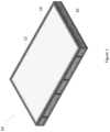
- FIG. 1is a top perspective view of an exemplary embodiment of the present invention
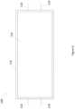
- FIG. 2is a top view of the device of FIG. 1 ;
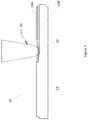
- FIG. 3is a side view of the device of FIG. 1 , additionally indicating Detail A;
- FIG. 4is a detailed side view of Detail A of FIG. 3 ;
- FIG. 5is a detailed side view of the device of FIG. 1 , illustrated with a stylus contacting the touch panel;
- FIG. 6is a top view of another exemplary embodiment of the present invention.
- FIG. 7is a side view of the device of FIG. 6 , also indicating Detail B;
- FIG. 8is a detailed side view of Detail B as indicated in FIG. 7 ;
- FIG. 9is a top view of an exemplary embodiment of the touch panel in accordance the present invention.
- FIG. 10is an exploded detailed side sectional view of an exemplary embodiment of a display panel in accordance with the present invention.
- FIG. 11is a plan view of an exemplary circuit in accordance with the present invention.
- Embodiments of the inventionare described herein with reference to illustrations that are schematic illustrations of idealized embodiments (and intermediate structures) of the invention. As such, variations from the shapes of the illustrations as a result, for example, of manufacturing techniques and/or tolerances, are to be expected. Thus, embodiments of the invention should not be construed as limited to the particular shapes of regions illustrated herein but are to include deviations in shapes that result, for example, from manufacturing.
- FIG. 1 through FIG. 5illustrates an exemplary embodiment of the present invention.
- An electronic display and touch screen assembly 10(hereinafter the “assembly”) is comprised of a touch panel 14 located immediately above and extending in parallel with an electronic display 16 .
- the electronic display 16is a normally black liquid crystal display (LCD), such as the AMLCD.
- LCDliquid crystal display
- Other electronic displays 16such as plasma, Light Emitting Diode (LED), Cathode Ray Tube (CRT), and the like are contemplated.
- the assembly 10 and related componentsincluding but not limited to the electronic display 16 , support 2560 ⁇ 1024 pixels resolution.
- the touch panel 14is a resistive touch panel.
- the touch panel 14may be wet laminated to the electronic display 16 and a gasket 12 may be provided that frames the two layers and creates a seal between the touch panel 14 and the electronic display 16 . Thereby protecting the assembly 10 from harsh environmental conditions and providing durability. Other known methods of joining the touch panel 14 and the electronic display 16 are contemplated.
- the assembly 10may include a heating device (not shown) for the electronic display 16 that permits the assembly 10 to operate in extreme conditions such as cold weather environments.
- the touch panel 14may be in electronic communication with the electronic display 16 by flexible circuit, or the like.
- the assembly 10may additionally comprise a channel 18 .
- the channel 18may extend from any side of the assembly 10 or from the back thereof.
- the channel 18may be adapted to house a pair of independent input/output devices (not shown).
- eachmay provide input/output signals for a respective portion of the electronic display 16 .
- each input/output devicecontrols substantially half of the electronic display 16 . This provides a redundancy measure. Should one input/output device fail, the remaining operable input/output device may provide input/output signals for the remaining portion of the electronic display 16 and thus maintain the operability of the assembly 10 .
- each input/output deviceis capable of providing input/output for the entire electronic display 16 .
- the touch panel 14may be comprised of two spaced apart surfaces where a top circuit layer 14 A is spaced apart from a bottom circuit layer 14 B.
- the two layersextend over the same surface and are substantially parallel. They may be spaced apart by their placement within a housing, such as the gasket 12 .
- the top 14 A and bottom circuit layers 14 Bmay be spaced apart by individual spacer elements (not shown).
- the top circuit layer 14 Ais sufficiently flexible such when contacted under sufficient force by a stylus 20 , the top circuit layer 14 A flexes to contact the bottom circuit layer 14 B. Such exemplary operation is illustrated at a contact point 22 .
- the top circuit layer 14 Amay be sufficiently elastic, however, to return to its original position after the force of the stylus 20 is removed.
- the stylus 20may be a human finger, including a gloved hand, or an artificial device.
- FIG. 6 through FIG. 8illustrate another exemplary embodiment of an electronic display and touch screen assembly 100 (hereinafter the “assembly”) in accordance with the present invention.
- the assembly 100may be comprised of a touch panel 114 located immediately above and extending in parallel with an electronic display 112 .
- the touch panel 114is a multi-touch resistive touch panel.
- the touch panel 114may be comprised of a top circuit layer 118 and a bottom circuit layer 120 .
- the top and bottom circuit layers 118 and 120may be spaced apart or immediately adjacent to one another. Additionally, the top and bottom circuit layers 118 and 120 may be located spaced apart from or immediately adjacent to the electronic display 112 .
- the touch panel 114may be wet laminated to the electronic display 112 and a gasket 12 may be provided that frames the two layers and creates a seal between the touch panel 114 and the electronic display 112 . Thereby protecting the assembly 100 from harsh environmental conditions and providing durability. Other known methods of joining the touch panel 114 and the electronic display 112 are contemplated.
- the assembly 100may include a heating device (not shown) that permits the assembly 100 to operate in extreme conditions such as cold weather environments.
- the touch panel 114may be in electronic communication with the electronic display 112 by flexible circuit, or the like.
- the assembly 100may additionally comprise a series of channels 116 .
- the channels 116may comprise shielding configured to reduce or eliminate EMI and promote EMC.
- the assembly 100comprises four channels 116 , a pair of which each extend from the left and right sides of the assembly, respectively. However, any number of channels 116 extending from any part of the assembly 100 is contemplated.
- the channel 116may be adapted to house a pair of independent input/output devices (not shown), each extending though one of the channels 116 . When both input/output devices are operable, each may provide input/output signals for a respective portion of the assembly 100 . In exemplary embodiments of the present invention, each input/output devices controls substantially half of the assembly 100 .
- each input/output deviceis capable of providing input/output for the entire assembly 100 . This provides a redundancy measure. In such an embodiment, if one input/output device fails, the remaining operable input/output device may provide input/output signals for the assembly 100 and thus maintain operability.
- the assembly 100 and related componentsare configured to remain operable in atmospheric pressure conditions ranging from sea level to 55,000 feet altitude, including with a rate of change up to 120 feet per second. Similarly, the assembly 100 and related components are configured to withstand 95% humidity, temperature changes between 55 and 90 degrees Celsius (C) at a rate of 40 degrees C. per minute with a maximum operating temperature of ⁇ 45 degrees C. to 71 degrees C. and prolonged storage temperatures of ⁇ 55 degrees C. to over 90 degrees C. All coatings and materials in the assembly 100 may be configured to withstand, without degradation, commonly used solvents such as water, acetone, lacquer thinner, optical adhesive, and the like. Similarly, all coatings and materials in the assembly 100 may be configured to withstand, without degradation, commonly used cleaners such as ammonia, detergent, soap, and the like.
- FIG. 9is a front view of an exemplary touch panel 200 in accordance with the present invention.
- the touch panel 200may comprise a grid 216 of vertically and horizontally extending electrodes.
- the grid 216may be comprised of two adjoining, seamless 8 ⁇ 10 sections formed by the vertically and horizontally extending electrodes, effectively providing an 8 ⁇ 20 grid and defining a first and a second grid section.
- Each of the first and second grid sectionsmay be operated by an independent input/output device.
- each of the first and the second grid sectionscorresponds to substantially half of the touch panel 200 . It is notable, however, that any size grid 216 having any number of vertically and horizontally extending electrodes and corresponding grid sections are contemplated.
- the grid 216may be surrounded by a series of receivers 210 , 212 , 214 , 218 , 220 , and 222 .
- the pair of receivers 214 and 222may extend along the right and left edges of the grid 216 , respectively.
- the pair receivers 210 and 212may extend along the left and the right portions of the upper edge of the grid 216 , respectively.
- the pair of receivers 220 and 218may extend along the left and the right portions of the lower edge of the grid 216 , respectively.
- the receivers 210 , 220 , and 222may be placed to receive signals generated by touching the first grid section.
- the receivers 212 , 214 , and 218may be placed to receive signals generated by touching the second grid section.
- the grid 216is sized to cover the entirety of the electronic display 16 .
- the vertically extending receivers 222 and 214may be configured to receive input regarding the vertical (Y) position of the input.
- the horizontally extending receivers 210 , 212 , 218 , and 220may be configured to receive input regarding the horizontal (X) position of the input.
- each of the vertically extending receivers 222 and 214may be capable of receiving input signals regarding the Y position of the input from both the first and second grid section.
- the horizontally extending receivers 210 and 220may be capable of receiving input signals regarding the X position of the input from the first grid section.
- the horizontally extending receivers 212 and 218may be capable of receiving input signals regarding the X position of the input from the second grid section.
- the grid 216 and the receivers 210 , 212 , 214 , 218 , 220 , and 222may be configured to respond to a stylus, a human finger, or a gloved hand.
- the grid 216 and the receivers 210 , 212 , 214 , 218 , 220 , and 222may be configured to respond to an activation pressure of under 0.8 N and may allow for multiple touch inputs to be measured simultaneously.
- the first and second grid sections and corresponding receiversprovides a redundancy measure.
- the entire touch panel 200may be utilized.
- the remaining operable grid sectionmay accept touch input for the portion of the grid 212 that it controls.
- the image that was being shown on the electronic display 112may be shifted onto just the portion of the electronic display 112 corresponding to the remaining operable first or second grid sections such that the assembly 100 remains fully functional, albeit over a smaller area.
- half of the assembly 100may remain operable and the image may not be shifted.
- touch panel 200may be described in terms of operating with a particular embodiment described herein, it is contemplated that the touch panel 200 may be utilized with any of the embodiments described herein.
- the touch panel 200may be utilized in conjunction with a bottom glass layer 320 of an exemplary display panel 300 illustrated in FIG. 10 , and each line of the touch panel 200 grid 216 may comprise an exemplary circuit 400 , such as the one illustrated in FIG. 11 .
- the touch panel active areamay be 506.88 mm ⁇ 202.75 mm and the activation force needed may be in the range of 0.05 N-0.8 N and may provide a minimum of two point multi-touch, and may have an operating life of over 1 million hits. In other embodiments of the present invention all of the above dimensions and values may change to the desire of the user or manufacturer.
- FIG. 10is an exploded detailed side sectional view of the exemplary display panel 300 in accordance with the present invention, such for use with the electronic display 16 .
- a cover glass 310may form the top layer of the display panel 300 .
- the cover glass 310may comprise an anti-smudge, anti-reflective coating.
- a linear polarizer 312 followed by a quarter wave retarder 314may be located below the cover glass 310 and above a top glass 316 .
- the quarter wave retarder 314may be configured to withstand high temperatures.
- An optically clear adhesive (OCA) layer 318may be placed between the top glass 316 and the bottom glass 320 .
- OCAoptically clear adhesive
- the bottom glass 320may be located below the top glass 316 but above an indium tin oxide (ITO) layer 322 .
- ITOindium tin oxide
- the touch panel 200will be located in the bottom glass 320 layer.
- the ITO layer 322may be located immediately below and be affixed to the bottom glass 320 .
- the ITO layer 322may act as an EMI shielding layer, thus promoting EMC.
- the ITO layer 322may extend beyond the bottom glass 320 by 3 mm on all sides.
- a final quarter wave retarder 324may form the bottom layer of the display 300 .
- the final quarter wave retarder 324may have a smaller area than the previous layers, which may all have substantially the same surface area.
- the display panel 300permits the display panel 300 to be visible in high ambient light conditions and operable under high levels of solar loading.
- the display panel 300 , the assembly 100 , and other related componentsshall be configured to withstand prolonged exposure to solar radiation with a normal flux of 260 BTU/ft 2 at sea level atmospheric pressure and 55 degrees C.
- each of these layersmay extend in parallel with the other layers. Each of these layers may also be spaced apart from one another and be of various thicknesses. In exemplary embodiments of the present invention, the layers may be immediately adjacent to, secured to, or integrally formed with one another.
- the cover glass 310may be a 0.15 mm micro sheet. In other embodiments, the cover glass 310 may be 0.5 mm thick.
- the top glass 316may also be 0.15 mm thick, while the bottom glass may be 1.1 mm thick.
- the ITO layer 322may be 3 mm thick. While these thicknesses are exemplary, they are not intended to be limiting, any functional thicknesses are contemplated. It is also notable that adhesive layers may be placed between any of the layers of the display panel 300 .
- exemplary display panel 300may be described in terms of operating with a particular embodiment described herein, it is contemplated that the display panel 300 may be utilized with any of the embodiments described herein.
- FIG. 11illustrates an exemplary circuit 400 in accordance with the present invention.
- the exemplary circuit 400is configured to minimize EMI and maximize EMC.
- Each line of the grid 216 of the touch panel 220may be comprised of the circuit 400 . Therefore, it is contemplated that any number of the circuits 400 may be utilized in communication with one another.
- the circuit 400may be used with the assembly 10 or the assembly 100 in conjunction with the touch panels 14 and 114 , respectively. It is notable that while exemplary circuit 400 may be described in terms of operating with a particular embodiment described herein, it is contemplated that the circuit 400 may be utilized with any of the embodiments described herein.
- the circuit 400may comprise a pair of zener diodes 410 in parallel with and located on either side of a series of capacitors 412 .
- An inductor 416may be placed in series between each capacitor 412 .
- three capacitors 412are placed in parallel, and an inductor 416 is placed in series between each of said capacitors 412 .
- Other arrangementsare contemplated.
Landscapes
- Engineering & Computer Science (AREA)
- General Engineering & Computer Science (AREA)
- Theoretical Computer Science (AREA)
- Human Computer Interaction (AREA)
- Physics & Mathematics (AREA)
- General Physics & Mathematics (AREA)
- Liquid Crystal (AREA)
- Devices For Indicating Variable Information By Combining Individual Elements (AREA)
- Position Input By Displaying (AREA)
Abstract
Description
Claims (16)
Priority Applications (1)
| Application Number | Priority Date | Filing Date | Title |
|---|---|---|---|
| US17/984,592US12124667B2 (en) | 2015-10-06 | 2022-11-10 | Redundant resistive touch panel |
Applications Claiming Priority (4)
| Application Number | Priority Date | Filing Date | Title |
|---|---|---|---|
| US14/876,382US10558314B2 (en) | 2015-10-06 | 2015-10-06 | Redundant resistive touch panel |
| US16/547,657US10788945B2 (en) | 2015-10-06 | 2019-08-22 | Redundant resistive touch panel |
| US16/915,367US11507242B2 (en) | 2015-10-06 | 2020-06-29 | Redundant resistive touch panel |
| US17/984,592US12124667B2 (en) | 2015-10-06 | 2022-11-10 | Redundant resistive touch panel |
Related Parent Applications (1)
| Application Number | Title | Priority Date | Filing Date |
|---|---|---|---|
| US16/915,367ContinuationUS11507242B2 (en) | 2015-10-06 | 2020-06-29 | Redundant resistive touch panel |
Publications (2)
| Publication Number | Publication Date |
|---|---|
| US20230072810A1 US20230072810A1 (en) | 2023-03-09 |
| US12124667B2true US12124667B2 (en) | 2024-10-22 |
Family
ID=58447927
Family Applications (4)
| Application Number | Title | Priority Date | Filing Date |
|---|---|---|---|
| US14/876,382Active2035-11-07US10558314B2 (en) | 2015-10-06 | 2015-10-06 | Redundant resistive touch panel |
| US16/547,657ActiveUS10788945B2 (en) | 2015-10-06 | 2019-08-22 | Redundant resistive touch panel |
| US16/915,367Active2036-03-12US11507242B2 (en) | 2015-10-06 | 2020-06-29 | Redundant resistive touch panel |
| US17/984,592ActiveUS12124667B2 (en) | 2015-10-06 | 2022-11-10 | Redundant resistive touch panel |
Family Applications Before (3)
| Application Number | Title | Priority Date | Filing Date |
|---|---|---|---|
| US14/876,382Active2035-11-07US10558314B2 (en) | 2015-10-06 | 2015-10-06 | Redundant resistive touch panel |
| US16/547,657ActiveUS10788945B2 (en) | 2015-10-06 | 2019-08-22 | Redundant resistive touch panel |
| US16/915,367Active2036-03-12US11507242B2 (en) | 2015-10-06 | 2020-06-29 | Redundant resistive touch panel |
Country Status (1)
| Country | Link |
|---|---|
| US (4) | US10558314B2 (en) |
Families Citing this family (1)
| Publication number | Priority date | Publication date | Assignee | Title |
|---|---|---|---|---|
| US9971444B2 (en)* | 2016-05-11 | 2018-05-15 | Rockwell Collins, Inc. | Touch sensor with electrically isolated touch regions |
Citations (39)
| Publication number | Priority date | Publication date | Assignee | Title |
|---|---|---|---|---|
| US6088069A (en) | 1997-10-21 | 2000-07-11 | Reptron Acquisition, Inc. | Shatter resistant flat panel display and method of manufacturing the same |
| US20040268037A1 (en) | 2003-06-26 | 2004-12-30 | International Business Machines Corporation | Apparatus method and system for alternate control of a RAID array |
| US6842672B1 (en) | 2002-02-28 | 2005-01-11 | Garmin International, Inc. | Cockpit instrument panel systems and methods with redundant flight data display |
| US20050110765A1 (en) | 2003-11-21 | 2005-05-26 | Baeza Daniel M. | Apparatus and method for capturing site data while scuba diving |
| US20060013967A1 (en) | 2002-12-20 | 2006-01-19 | Hitoshi Mikoshiba | Transparent conductive laminate, touch panel and liquid crystal display unit with touch panel |
| US20060038635A1 (en) | 2004-08-17 | 2006-02-23 | Dominick Richiuso | Integrated passive filter incorporating inductors and ESD protectors |
| US20080122376A1 (en) | 2006-11-10 | 2008-05-29 | Philips Solid-State Lighting Solutions | Methods and apparatus for controlling series-connected leds |
| US20080158468A1 (en) | 2006-12-29 | 2008-07-03 | Lg Philips Lcd Co., Ltd. | Backlight unit and display device having the same |
| US20080204419A1 (en) | 2007-02-28 | 2008-08-28 | Honeywell International, Inc. | Stimuli-sensitive display screen with consolidated control functions |
| US20080218492A1 (en) | 2007-03-09 | 2008-09-11 | Fujitsu Component Limited | Touch panel |
| US20080261057A1 (en) | 2007-04-20 | 2008-10-23 | White Electronic Designs Corp. | Bezelless display system |
| US20080291686A1 (en) | 2005-01-14 | 2008-11-27 | Cull Brian D | Extended avionics lcd backlight |
| US20100039366A1 (en) | 2008-08-18 | 2010-02-18 | Rody Hardy | Backlight display and method for a vehicle |
| US20100060349A1 (en) | 2008-09-11 | 2010-03-11 | Etter Steven M | Method of forming an integrated semiconductor device and structure therefor |
| US20100156795A1 (en) | 2008-12-23 | 2010-06-24 | Samsung Electronics Co., Ltd. | Large size capacitive touch screen panel |
| US20100271324A1 (en) | 2009-04-22 | 2010-10-28 | Gregory Hayes | Capacitive Touch Panel Label |
| US20110050617A1 (en) | 2009-08-25 | 2011-03-03 | Avago Technologies Ecbu (Singapore) Pte. Ltd. | Method and Apparatus for Detecting Defective Traces in a Mutual Capacitance Touch Sensing Device |
| US20110095999A1 (en)* | 2009-10-23 | 2011-04-28 | Plastic Logic Limited | Electronic document reading devices |
| US20120105774A1 (en) | 2010-11-03 | 2012-05-03 | Research In Motion Limited | Display devices containing a circular polarizing system and methods related thereto |
| US20120173859A1 (en) | 2010-12-29 | 2012-07-05 | Brocade Communications Systems, Inc. | Techniques for stopping rolling reboots |
| US20130015906A1 (en) | 2011-07-13 | 2013-01-17 | Silicon Integrated Systems Corp. | Touch Panel Device |
| US20130100037A1 (en)* | 2011-10-20 | 2013-04-25 | Garmin International, Inc. | Adaptive touchscreen system |
| US20130127790A1 (en) | 2011-07-13 | 2013-05-23 | Flatfrog Laboratories Ab | Touch-sensing display panel |
| US20130154994A1 (en) | 2011-12-15 | 2013-06-20 | Kai-Ti Yang | Transparent capacitive touch panel with electromagnetic shielding effect |
| US20130265282A1 (en) | 2010-12-08 | 2013-10-10 | Sharp Kabushiki Kaisha | Touch panel and display device with touch panel |
| US20140002176A1 (en) | 2012-06-28 | 2014-01-02 | David Brent GUARD | Complex adhesive boundaries for touch sensors |
| US20140160365A1 (en) | 2012-12-11 | 2014-06-12 | Wah Yiu Kwong | Display for Electronic Device |
| US20140198417A1 (en) | 2013-01-15 | 2014-07-17 | Citruscom Corporation | Integrated emi filter circuit with esd protection and incorporating capacitors |
| US20140218642A1 (en) | 2011-10-05 | 2014-08-07 | Fujifilm Corporation | Conductive sheet, touch panel, display device, method for producing conductive sheet, and recording medium |
| GB2510600A (en) | 2013-02-08 | 2014-08-13 | R & D Core Ltd | Calibration of contact sensor |
| US20140320437A1 (en) | 2013-04-26 | 2014-10-30 | Samsung Electronics Co., Ltd. | Method for displaying and electronic device thereof |
| WO2014185599A1 (en) | 2013-05-15 | 2014-11-20 | 전북대학교산학협력단 | Esd-emi common mode semiconductor filter element and method for manufacturing same |
| US20150049041A1 (en) | 2013-08-15 | 2015-02-19 | Apple Inc. | Display/touch temporal separation |
| US20150077370A1 (en) | 2013-09-17 | 2015-03-19 | Lg Display Co., Ltd. | Display device integrated with touch screen and driving method thereof |
| US20150193074A1 (en) | 2014-01-07 | 2015-07-09 | Lenovo Enterprise Solutions (Singapore) Pte. Ltd. | System and method for altering interactive element placement based around damaged regions on a touchscreen device |
| US9141329B1 (en) | 2012-07-27 | 2015-09-22 | D.R. Systems, Inc. | Combining electronic displays |
| US20150379964A1 (en) | 2014-06-25 | 2015-12-31 | Lg Electronics Inc. | Mobile terminal and method for controlling the same |
| US20160300549A1 (en) | 2015-04-10 | 2016-10-13 | Boe Technology Group Co., Ltd. | Splicer, splicing display system and splicing display method |
| US20170083151A1 (en) | 2015-09-21 | 2017-03-23 | Synaptics Incorporated | Input device having anti-static layer bypass |
- 2015
- 2015-10-06USUS14/876,382patent/US10558314B2/enactiveActive
- 2019
- 2019-08-22USUS16/547,657patent/US10788945B2/enactiveActive
- 2020
- 2020-06-29USUS16/915,367patent/US11507242B2/enactiveActive
- 2022
- 2022-11-10USUS17/984,592patent/US12124667B2/enactiveActive
Patent Citations (39)
| Publication number | Priority date | Publication date | Assignee | Title |
|---|---|---|---|---|
| US6088069A (en) | 1997-10-21 | 2000-07-11 | Reptron Acquisition, Inc. | Shatter resistant flat panel display and method of manufacturing the same |
| US6842672B1 (en) | 2002-02-28 | 2005-01-11 | Garmin International, Inc. | Cockpit instrument panel systems and methods with redundant flight data display |
| US20060013967A1 (en) | 2002-12-20 | 2006-01-19 | Hitoshi Mikoshiba | Transparent conductive laminate, touch panel and liquid crystal display unit with touch panel |
| US20040268037A1 (en) | 2003-06-26 | 2004-12-30 | International Business Machines Corporation | Apparatus method and system for alternate control of a RAID array |
| US20050110765A1 (en) | 2003-11-21 | 2005-05-26 | Baeza Daniel M. | Apparatus and method for capturing site data while scuba diving |
| US20060038635A1 (en) | 2004-08-17 | 2006-02-23 | Dominick Richiuso | Integrated passive filter incorporating inductors and ESD protectors |
| US20080291686A1 (en) | 2005-01-14 | 2008-11-27 | Cull Brian D | Extended avionics lcd backlight |
| US20080122376A1 (en) | 2006-11-10 | 2008-05-29 | Philips Solid-State Lighting Solutions | Methods and apparatus for controlling series-connected leds |
| US20080158468A1 (en) | 2006-12-29 | 2008-07-03 | Lg Philips Lcd Co., Ltd. | Backlight unit and display device having the same |
| US20080204419A1 (en) | 2007-02-28 | 2008-08-28 | Honeywell International, Inc. | Stimuli-sensitive display screen with consolidated control functions |
| US20080218492A1 (en) | 2007-03-09 | 2008-09-11 | Fujitsu Component Limited | Touch panel |
| US20080261057A1 (en) | 2007-04-20 | 2008-10-23 | White Electronic Designs Corp. | Bezelless display system |
| US20100039366A1 (en) | 2008-08-18 | 2010-02-18 | Rody Hardy | Backlight display and method for a vehicle |
| US20100060349A1 (en) | 2008-09-11 | 2010-03-11 | Etter Steven M | Method of forming an integrated semiconductor device and structure therefor |
| US20100156795A1 (en) | 2008-12-23 | 2010-06-24 | Samsung Electronics Co., Ltd. | Large size capacitive touch screen panel |
| US20100271324A1 (en) | 2009-04-22 | 2010-10-28 | Gregory Hayes | Capacitive Touch Panel Label |
| US20110050617A1 (en) | 2009-08-25 | 2011-03-03 | Avago Technologies Ecbu (Singapore) Pte. Ltd. | Method and Apparatus for Detecting Defective Traces in a Mutual Capacitance Touch Sensing Device |
| US20110095999A1 (en)* | 2009-10-23 | 2011-04-28 | Plastic Logic Limited | Electronic document reading devices |
| US20120105774A1 (en) | 2010-11-03 | 2012-05-03 | Research In Motion Limited | Display devices containing a circular polarizing system and methods related thereto |
| US20130265282A1 (en) | 2010-12-08 | 2013-10-10 | Sharp Kabushiki Kaisha | Touch panel and display device with touch panel |
| US20120173859A1 (en) | 2010-12-29 | 2012-07-05 | Brocade Communications Systems, Inc. | Techniques for stopping rolling reboots |
| US20130015906A1 (en) | 2011-07-13 | 2013-01-17 | Silicon Integrated Systems Corp. | Touch Panel Device |
| US20130127790A1 (en) | 2011-07-13 | 2013-05-23 | Flatfrog Laboratories Ab | Touch-sensing display panel |
| US20140218642A1 (en) | 2011-10-05 | 2014-08-07 | Fujifilm Corporation | Conductive sheet, touch panel, display device, method for producing conductive sheet, and recording medium |
| US20130100037A1 (en)* | 2011-10-20 | 2013-04-25 | Garmin International, Inc. | Adaptive touchscreen system |
| US20130154994A1 (en) | 2011-12-15 | 2013-06-20 | Kai-Ti Yang | Transparent capacitive touch panel with electromagnetic shielding effect |
| US20140002176A1 (en) | 2012-06-28 | 2014-01-02 | David Brent GUARD | Complex adhesive boundaries for touch sensors |
| US9141329B1 (en) | 2012-07-27 | 2015-09-22 | D.R. Systems, Inc. | Combining electronic displays |
| US20140160365A1 (en) | 2012-12-11 | 2014-06-12 | Wah Yiu Kwong | Display for Electronic Device |
| US20140198417A1 (en) | 2013-01-15 | 2014-07-17 | Citruscom Corporation | Integrated emi filter circuit with esd protection and incorporating capacitors |
| GB2510600A (en) | 2013-02-08 | 2014-08-13 | R & D Core Ltd | Calibration of contact sensor |
| US20140320437A1 (en) | 2013-04-26 | 2014-10-30 | Samsung Electronics Co., Ltd. | Method for displaying and electronic device thereof |
| WO2014185599A1 (en) | 2013-05-15 | 2014-11-20 | 전북대학교산학협력단 | Esd-emi common mode semiconductor filter element and method for manufacturing same |
| US20150049041A1 (en) | 2013-08-15 | 2015-02-19 | Apple Inc. | Display/touch temporal separation |
| US20150077370A1 (en) | 2013-09-17 | 2015-03-19 | Lg Display Co., Ltd. | Display device integrated with touch screen and driving method thereof |
| US20150193074A1 (en) | 2014-01-07 | 2015-07-09 | Lenovo Enterprise Solutions (Singapore) Pte. Ltd. | System and method for altering interactive element placement based around damaged regions on a touchscreen device |
| US20150379964A1 (en) | 2014-06-25 | 2015-12-31 | Lg Electronics Inc. | Mobile terminal and method for controlling the same |
| US20160300549A1 (en) | 2015-04-10 | 2016-10-13 | Boe Technology Group Co., Ltd. | Splicer, splicing display system and splicing display method |
| US20170083151A1 (en) | 2015-09-21 | 2017-03-23 | Synaptics Incorporated | Input device having anti-static layer bypass |
Also Published As
| Publication number | Publication date |
|---|---|
| US20190377441A1 (en) | 2019-12-12 |
| US10558314B2 (en) | 2020-02-11 |
| US11507242B2 (en) | 2022-11-22 |
| US20170097706A1 (en) | 2017-04-06 |
| US10788945B2 (en) | 2020-09-29 |
| US20200326798A1 (en) | 2020-10-15 |
| US20230072810A1 (en) | 2023-03-09 |
Similar Documents
| Publication | Publication Date | Title |
|---|---|---|
| JP6196652B2 (en) | smartphone | |
| US20110032207A1 (en) | Capacitive touch sensor | |
| US9158400B2 (en) | Touch panel having virtual function button, method of manufacturing the same, and method of identifying touch conflict on the same | |
| JP2016035736A (en) | Touch input device | |
| CN110557963A (en) | Touch input device capable of detecting pressure suitable for display noise compensation | |
| US20170177107A1 (en) | Infrared Touch Screen, Touch Detection Method and Display Apparatus | |
| KR20150055339A (en) | Touch panel | |
| US11175773B2 (en) | Redundant projected capacitive touch panel | |
| TWI628533B (en) | Electronic device | |
| US12124667B2 (en) | Redundant resistive touch panel | |
| AU2019203576B2 (en) | Redundant touch panel | |
| JP3182585U (en) | Touch display device | |
| KR102174008B1 (en) | Electrode sheet and touch input device | |
| CN104793789A (en) | Touch display device | |
| BR112018006120B1 (en) | TOUCH PANEL ASSEMBLY FOR DISPLAYING IMAGES | |
| JP2015084148A (en) | Touch type information input image display device and information equipment | |
| KR20100108492A (en) | Touch screen device | |
| KR20140137953A (en) | flexible display panel and the display apparatus comprising the flexible display panel |
Legal Events
| Date | Code | Title | Description |
|---|---|---|---|
| AS | Assignment | Owner name:MERCURY MISSION SYSTEMS, LLC, MASSACHUSETTS Free format text:MERGER;ASSIGNOR:AMERICAN PANEL CORPORATION;REEL/FRAME:061720/0710 Effective date:20201029 Owner name:AMERICAN PANEL CORPORATION, GEORGIA Free format text:ASSIGNMENT OF ASSIGNORS INTEREST;ASSIGNOR:MAHDI, KEN;REEL/FRAME:061720/0632 Effective date:20160822 | |
| FEPP | Fee payment procedure | Free format text:ENTITY STATUS SET TO UNDISCOUNTED (ORIGINAL EVENT CODE: BIG.); ENTITY STATUS OF PATENT OWNER: LARGE ENTITY | |
| STPP | Information on status: patent application and granting procedure in general | Free format text:DOCKETED NEW CASE - READY FOR EXAMINATION | |
| STPP | Information on status: patent application and granting procedure in general | Free format text:NON FINAL ACTION MAILED | |
| STPP | Information on status: patent application and granting procedure in general | Free format text:RESPONSE TO NON-FINAL OFFICE ACTION ENTERED AND FORWARDED TO EXAMINER | |
| STPP | Information on status: patent application and granting procedure in general | Free format text:NOTICE OF ALLOWANCE MAILED -- APPLICATION RECEIVED IN OFFICE OF PUBLICATIONS | |
| STPP | Information on status: patent application and granting procedure in general | Free format text:PUBLICATIONS -- ISSUE FEE PAYMENT VERIFIED | |
| STCF | Information on status: patent grant | Free format text:PATENTED CASE | |
| AS | Assignment | Owner name:BANK OF AMERICA, N.A., AS COLLATERAL AGENT, ILLINOIS Free format text:SECURITY INTEREST;ASSIGNOR:MERCURY MISSION SYSTEMS, LLC;REEL/FRAME:070262/0772 Effective date:20250108 |