US12124037B2 - Compound light-guide optical elements - Google Patents
Compound light-guide optical elementsDownload PDFInfo
- Publication number
- US12124037B2 US12124037B2US17/794,966US202117794966AUS12124037B2US 12124037 B2US12124037 B2US 12124037B2US 202117794966 AUS202117794966 AUS 202117794966AUS 12124037 B2US12124037 B2US 12124037B2
- Authority
- US
- United States
- Prior art keywords
- partially
- loe
- region
- reflecting surfaces
- thickness
- Prior art date
- Legal status (The legal status is an assumption and is not a legal conclusion. Google has not performed a legal analysis and makes no representation as to the accuracy of the status listed.)
- Active, expires
Links
Images


Classifications
- G—PHYSICS
- G02—OPTICS
- G02B—OPTICAL ELEMENTS, SYSTEMS OR APPARATUS
- G02B27/00—Optical systems or apparatus not provided for by any of the groups G02B1/00 - G02B26/00, G02B30/00
- G02B27/0081—Optical systems or apparatus not provided for by any of the groups G02B1/00 - G02B26/00, G02B30/00 with means for altering, e.g. enlarging, the entrance or exit pupil
- G—PHYSICS
- G02—OPTICS
- G02B—OPTICAL ELEMENTS, SYSTEMS OR APPARATUS
- G02B27/00—Optical systems or apparatus not provided for by any of the groups G02B1/00 - G02B26/00, G02B30/00
- G02B27/01—Head-up displays
- G02B27/017—Head mounted
- G02B27/0172—Head mounted characterised by optical features
- G—PHYSICS
- G02—OPTICS
- G02B—OPTICAL ELEMENTS, SYSTEMS OR APPARATUS
- G02B6/00—Light guides; Structural details of arrangements comprising light guides and other optical elements, e.g. couplings
- G—PHYSICS
- G02—OPTICS
- G02B—OPTICAL ELEMENTS, SYSTEMS OR APPARATUS
- G02B6/00—Light guides; Structural details of arrangements comprising light guides and other optical elements, e.g. couplings
- G02B6/0001—Light guides; Structural details of arrangements comprising light guides and other optical elements, e.g. couplings specially adapted for lighting devices or systems
- G02B6/0011—Light guides; Structural details of arrangements comprising light guides and other optical elements, e.g. couplings specially adapted for lighting devices or systems the light guides being planar or of plate-like form
- G02B6/0013—Means for improving the coupling-in of light from the light source into the light guide
- G02B6/0015—Means for improving the coupling-in of light from the light source into the light guide provided on the surface of the light guide or in the bulk of it
- G—PHYSICS
- G02—OPTICS
- G02B—OPTICAL ELEMENTS, SYSTEMS OR APPARATUS
- G02B6/00—Light guides; Structural details of arrangements comprising light guides and other optical elements, e.g. couplings
- G02B6/0001—Light guides; Structural details of arrangements comprising light guides and other optical elements, e.g. couplings specially adapted for lighting devices or systems
- G02B6/0011—Light guides; Structural details of arrangements comprising light guides and other optical elements, e.g. couplings specially adapted for lighting devices or systems the light guides being planar or of plate-like form
- G02B6/0033—Means for improving the coupling-out of light from the light guide
- G02B6/0035—Means for improving the coupling-out of light from the light guide provided on the surface of the light guide or in the bulk of it
- G—PHYSICS
- G02—OPTICS
- G02B—OPTICAL ELEMENTS, SYSTEMS OR APPARATUS
- G02B27/00—Optical systems or apparatus not provided for by any of the groups G02B1/00 - G02B26/00, G02B30/00
- G02B27/01—Head-up displays
- G02B27/0101—Head-up displays characterised by optical features
- G02B2027/0123—Head-up displays characterised by optical features comprising devices increasing the field of view
- G02B2027/0125—Field-of-view increase by wavefront division
- G—PHYSICS
- G02—OPTICS
- G02B—OPTICAL ELEMENTS, SYSTEMS OR APPARATUS
- G02B27/00—Optical systems or apparatus not provided for by any of the groups G02B1/00 - G02B26/00, G02B30/00
- G02B27/01—Head-up displays
- G02B27/017—Head mounted
- G02B2027/0178—Eyeglass type
Definitions
- the present inventionrelates to optical systems and, in particular, it concerns an optical system including a light-guide optical element (LOE) for achieving optical aperture expansion.
- LOElight-guide optical element
- LOEsCompound Light-Guide Optical Elements
- two-dimensional expansion waveguideshave been described in previous publications by Lumus Ltd. (Israel). Examples of such compound LOEs may be found, for example, in PCT publication no. WO 2020/049542.
- these compound LOEsemploy two regions, each of which is a parallel-faced block of transparent material for supporting propagation of light carrying a collimated image by internal reflection at major surfaces, and includes a set of mutually-parallel, internal, partially-reflecting surfaces or “facets”, which progressively redirect part of the collimated image and achieve expansion of the optical aperture.
- facetsmutually-parallel, internal, partially-reflecting surfaces
- the light-guide optical element (LOE) region responsible for a first stage of expansion within the compound elementis referred to as the “first LOE” or “LOE1”, while the LOE region responsible for coupling out of the once-deflected image towards the observer is referred to herein as the “second LOE” or “LOE2”.
- the present inventionis an optical system for directing image illumination injected at a coupling-in region towards a user for viewing.
- an optical system for directing image illumination injected at a coupling-in region towards a user for viewingcomprising a light-guide optical element (LOE) formed from transparent material, the LOE comprising: (a) a first region containing a first set of planar, mutually-parallel, partially-reflecting surfaces having a first orientation; (b) a second region containing a second set of planar, mutually-parallel, partially-reflecting surfaces having a second orientation non-parallel to the first orientation; and (c) a set of mutually-parallel major external surfaces, the major external surfaces extending across the first and second regions such that both the first set of partially-reflecting surfaces and the second set of partially-reflecting surfaces are located between the major external surfaces, wherein the second set of partially-reflecting surfaces are at an oblique angle to the major external surfaces so that a part of image illumination propagating within the LOE by internal reflection at the
- the second set of partially-reflecting surfacesare excluded from surface layers of both of the major external surfaces in the second region.
- a total thickness of the at least one surface layer of the second region from which the second set of partially-reflecting surfaces are excludedis between 6 percent and 33 percent of the thickness.
- a spacing between adjacent surfaces of the second set of partially-reflecting surfaces in a direction parallel to the major external surfacesis at least 1 mm, and wherein a total thickness of the at least one surface layer of the second region from which the second set of partially-reflecting surfaces are excluded is at least 10 percent of the thickness.
- the first set of partially-reflecting surfacesextend across at least 96 percent of the thickness.
- the first set of partially-reflecting surfacesextend across at least 98 percent of the thickness.
- the first set of partially-reflecting surfacesextend across an entirety of the thickness.
- the first orientation of the first set of partially-reflecting surfacesis orthogonal to the major external surfaces.
- FIGS. 1 A and 1 Bare schematic isometric views of an optical system implemented using a light-guide optical element (LOE), constructed and operative according to the teachings of the present invention, illustrating a top-down and a side-injection configuration, respectively;
- LOElight-guide optical element
- FIGS. 2 A and 2 Bare enlarged schematic isometric views of an LOE from FIG. 1 A or 1 B showing ray paths for two extreme fields of an image;
- FIG. 3is a schematic front view of the LOE of FIGS. 2 A and 2 B showing the path of a principal ray propagating through the LOE and undergoing a first redirection within the LOE, and a second redirection for coupling out of the LOE towards a viewer;
- FIGS. 4 A and 4 Bare partial schematic cross-sectional views taken along the line IV-IV in FIG. 3 , showing ray paths for a ray propagating within a second region of the LOE and encountering an internal partially-reflecting surface which does, or does not, span the thickness of the LOE, respectively;
- FIGS. 5 A, 5 B and 5 Care partial schematic cross-sectional views taken along the line V-V in FIG. 3 , showing ray paths for a ray propagating within a first region of the LOE and encountering an internal partially-reflecting surface which fully spans the thickness of the LOE, or is spaced from both major surfaces, or from just one major surface, respectively;
- FIG. 6 Ais a schematic side views of the LOE of FIGS. 2 A and 2 B in an implementation in which both the first and second regions of the LOE have surface layers from which the partially-reflecting internal surfaces are excluded, i.e., cover plates;
- FIG. 6 Bis a view similar to FIG. 6 A in an implementation in which only the second region of the LOE has cover plates;
- FIG. 6 Cis a view similar to FIG. 6 A in which the second region of the LOE has cover plates, and the first region of the LOE has cover plates thinner than those of the second region;
- FIG. 6 Dis a view similar to FIG. 6 C in which only one side of the first region of the LOE is provided with a cover plate;
- FIG. 7is a schematic graph illustrating a relationship between a spatial density of LOE partially-reflecting surfaces and a preferred minimum thickness of a cover plate of the second region of LOE;
- FIGS. 8 A and 8 Bare a side view and an isometric view, respectively, of an intermediate work product during a manufacturing process for an LOE according to certain embodiments of the present invention.
- FIG. 9 Ais a schematic side view illustrating a stage of a production process in which a thin cover plate is applied across the entirety of an LOE in which the first region was initially formed without a cover plate and the second region was formed with a cover plate having only part of the desired cover plate thickness;
- FIG. 9 Bis a schematic side view illustrating the structure resulting from the production process of FIG. 9 A .
- the present inventionis an optical system for directing image illumination injected at a coupling-in region towards a user for viewing.
- Certain embodiments of the present inventionprovide an optical system including a light-guide optical element (LOE) for achieving optical aperture expansion for the purpose of a head-up display, and most preferably a near-eye display, which may be a virtual reality display, or more preferably an augmented reality display.
- LOElight-guide optical element
- FIGS. 1 A and 1 BAn exemplary implementation of a device in the form of a near-eye display, generally designated 10 , employing an LOE 12 according to the teachings of an embodiment of the present invention, is illustrated schematically in FIGS. 1 A and 1 B .
- the near-eye display 10employs a compact image projector (or “POD”) 14 optically coupled so as to inject an image into LOE (interchangeably referred to as a “waveguide,” a “substrate” or a “slab”) 12 within which the image light is trapped in one dimension by internal reflection at a set of mutually-parallel planar external surfaces.
- PODcompact image projector
- the light impinges of a set of partially-reflecting surfacesthat are parallel to each other, and inclined obliquely to the direction of propagation of the image light, with each successive facet deflecting a proportion of the image light into a deflected direction, also trapped/guided by internal reflection within the substrate.
- This first set of facetsare not illustrated individually in FIGS. 1 A and 1 B , but are located in a first region of the LOE designated 16 . This partial reflection at successive facets achieves a first dimension of optical aperture expansion.
- the aforementioned set of facetsare orthogonal to the major external surfaces of the substrate.
- both the injected image and its conjugate undergoing internal reflection as it propagates within region 16are deflected and become conjugate images propagating in a deflected direction.
- the first set of partially-reflecting surfacesare obliquely angled relative to the major external surfaces of the LOE.
- either the injected image or its conjugateforms the desired deflected image propagating within the LOE, while the other reflection may be minimized, for example, by employing angularly-selective coatings on the facets which render them relatively transparent to the range of incident angles presented by the image whose reflection is not needed.
- the first set of partially-reflecting surfacesdeflect the image illumination from a first direction of propagation trapped by total internal reflection (TIR) within the substrate to a second direction of propagation, also trapped by TIR within the substrate.
- TIRtotal internal reflection
- the deflected image illuminationthen passes into a second substrate region 18 , which may be implemented as an adjacent distinct substrate or as a continuation of a single substrate, in which a coupling-out arrangement (typically a further set of partially reflective facets) progressively couples out a proportion of the image illumination towards the eye of an observer located within a region defined as the eye-motion box (EMB), thereby achieving a second dimension of optical aperture expansion.
- the overall devicemay be implemented separately for each eye, and is preferably supported relative to the head of a user with the each LOE 12 facing a corresponding eye of the user.
- a support arrangementis implemented as an eye glasses frame with sides 20 for supporting the device relative to ears of the user. Other forms of support arrangement may also be used, including but not limited to, head bands, visors or devices suspended from helmets.
- FIG. 1 AReference is made herein in the drawings and claims to an X axis which extends horizontally ( FIG. 1 A ) or vertically ( FIG. 1 B ), in the general extensional direction of the first region of the LOE, and a Y axis which extends perpendicular thereto, i.e., vertically in FIG. 1 A and horizontally in FIG. 1 B .
- the first LOE, or first region 16 of LOE 12may be considered to achieve aperture expansion in the X direction while the second LOE, or second region 18 of LOE 12 , achieves aperture expansion in the Y direction.
- the details of the spread of angular directions in which different parts of the field of view propagatewill be addressed more precisely below.
- the orientation as illustrated in FIG. 1 Amay be regarded as a “top-down” implementation, where the image illumination entering the main (second region) of the LOE enters from the top edge
- the orientation illustrated in FIG. 1 Bmay be regarded as a “side-injection” implementation, where the axis referred to here as the Y axis is deployed horizontally.
- the POD employed with the devices of the present inventionis preferably configured to generate a collimated image, i.e., in which the light of each image pixel is a parallel beam, collimated to infinity, with an angular direction corresponding to the pixel position.
- the image illuminationthus spans a range of angles corresponding to an angular field of view in two dimensions.
- Image projector 14includes at least one light source, typically deployed to illuminate a spatial light modulator, such as an LCOS chip.
- the spatial light modulatormodulates the projected intensity of each pixel of the image, thereby generating an image.
- the image projectormay include a scanning arrangement, typically implemented using a fast-scanning mirror, which scans illumination from a laser light source across an image plane of the projector while the intensity of the beam is varied synchronously with the motion on a pixel-by-pixel basis, thereby projecting a desired intensity for each pixel.
- collimating opticsare provided to generate an output projected image which is collimated to infinity.
- Some or all of the above componentsare typically arranged on surfaces of one or more polarizing beam-splitter (PBS) cube or other prism arrangement, as is well known in the art.
- PBSpolarizing beam-splitter
- Optical coupling of image projector 14 to LOE 12may be achieved by any suitable optical coupling, such as for example via a coupling prism with an obliquely angled input surface, or via a reflective coupling arrangement, via a side edge and/or one of the major external surfaces of the LOE. Details of the coupling-in configuration are not critical to the invention, and are shown here schematically as a non-limiting example of a wedge prism 15 applied to one of the major external surfaces of the LOE.
- the near-eye display 10includes various additional components, typically including a controller 22 for actuating the image projector 14 , typically employing electrical power from a small onboard battery (not shown) or some other suitable power source. It will be appreciated that controller 22 includes all necessary electronic components such as at least one processor or processing circuitry to drive the image projector, all as is known in the art.
- FIGS. 2 A and 2 Bthe optical properties of an implementation of the near-eye display are illustrated in more detail.
- a light-guide optical element (LOE) 12formed from transparent material, including a first region 16 , also referred to herein as “LOE1”, containing a first set of planar, mutually-parallel, partially-reflecting surfaces 17 having a first orientation, and a second region 18 , also referred to herein as “LOE2”, containing a second set of planar, mutually-parallel, partially-reflecting surfaces 19 having a second orientation non-parallel to the first orientation.
- LOElight-guide optical element
- a set of mutually-parallel major external surfaces 24extend across the first and second regions 16 and 18 such that both the first set of partially-reflecting surfaces 17 and the second set of partially-reflecting surfaces 19 are located between the major external surfaces 24 .
- the set of major external surfaces 24are a pair of surfaces which are each continuous across the entirety of first and second regions 16 and 18 , although the option of having a set down or a step up in thickness between the regions 16 and 18 also falls within the scope of the present invention.
- Regions 16 and 18may be immediately juxtaposed so that they meet at a boundary, which may be a straight boundary or some other form of boundary, or there may be one or more additional LOE region interposed between those regions, to provide various additional optical or mechanical function, depending upon the particular application.
- particularly high quality major external surfacesare achieved by employing continuous external plates between which the separately formed regions 16 and 18 are sandwiched to form the compound LOE structure. Considerations regarding this option, and the thickness of these plates, will be discussed further below.
- the optical properties of the LOEmay be understood by tracing the image illumination paths backwards.
- the second set of partially-reflecting surfaces 19are at an oblique angle to the major external surfaces 24 so that a part of image illumination propagating within the LOE 12 by internal reflection at the major external surfaces from the first region 16 into the second region 18 is coupled out of the LOE towards an eye-motion box 26 .
- the first set of partially-reflecting surfaces 17are oriented so that a part of image illumination propagating within the LOE 12 by internal reflection at the major external surfaces from the coupling-in region (coupling prism 15 ) is deflected towards the second region 18 .
- FIG. 2 AOne dimension of the angular spread of the projected image from image projector 14 is represented in FIG. 2 A by the cone of illumination spreading from the POD aperture on the right side of the LOE towards the left side of the LOE.
- the central optical axis of the PODdefines a direction of propagation within the LOE aligned with the X axis, and the angular spread (within the LOE) is roughly ⁇ 16°.
- the angular FOVbecomes larger in air due to the change in refractive index.
- the first set of partially-reflecting surfaces 17are illustrated in first region 16
- the second set of partially-reflecting surfaces 19are illustrated in second region 18 .
- the near-eye displayis designed to provide a full field-of-view of the projected image to an eye of the user that is located at some position within the permitted range of positions designated by an “eye-motion box” (EMB) 26 (that is, a shape, typically represented as a rectangle, spaced away from the plane of the LOE from which the pupil of the eye will view the projected image).
- EMBeye-motion box
- each point in the EMBmust receive the entire angular range of the image from the LOE. Tracing back the field-of-view from the EMB indicates a larger rectangle 28 from which relevant illumination is coupled-out of the LOE towards the EMB.
- FIG. 2 Aillustrates a first extremity of the field of view, corresponding to the bottom-left pixel of the projected image.
- a beam of a width corresponding to the optical aperture of the projector as coupled into the LOEis shown propagating leftwards and upwards from the POD and being partially reflected from a series of partially-reflecting surfaces 17 .
- only a subset of the facetsgenerate reflections that are useful for providing the corresponding pixel in the image viewed by the user, and only a sub-region of those facets contributes to the observed image of this pixel.
- FIG. 2 Billustrates the same configuration as FIG. 2 A , but here shows the rays corresponding to the bottom-right pixel of the field-of-view reaching the four corners of the EMB, again with the relevant regions of the relevant partially-reflecting surfaces 17 denoted by a heavy line.
- the in-plane extent of the facetsmay be truncated to cover only the imaging area.
- additional (e.g., third) sets of partially-reflecting internal surfacesare discussed in detail in prior publications by Lumus Ltd. (Israel), particularly in the aforementioned PCT publication no. WO 2020/049542, as well as PCT publication no. WO 2020/152688 and PCT application number PCT/IL2020/051354, both of which were unpublished as of the priority date of this application, and are not considered prior art.
- the first set of partially-reflecting surfaces 17extend across at least 95 percent of a thickness of the LOE, while the second set of partially-reflecting surfaces 19 in the second region 18 are contained within a subsection of the thickness spanning less than 95 percent of the thickness, so that the second set of partially-reflecting surfaces 19 are excluded from at least one surface layer of the second region 18 .
- cover plateis used herein to refer generically to any implementation of a layer of a certain depth adjacent to one or both of the major surfaces of an LOE from which the sets of internal partially-reflecting surfaces of the LOE are excluded.
- One approach to forming such a layeris by attachment of a sheet of transparent material, i.e., a physically-distinct cover plate, to the LOE component.
- other production techniquesare also possible, such as by generating the LOE structure from a stack of plates in which the partially-reflecting coating is applied only in regions corresponding to the active LOE layer, and the regions which will be adjacent to the major external surfaces of the LOE are joined with index-matched adhesive without reflective coatings.
- cover plateis used independent of the production technique to refer to the functional structure in which a surface layer functions as a cover plate, without facets, no matter how that layer is formed.
- thisillustrates the path of a single ray 30 , here the principal ray corresponding to the center of field of the image in the X dimension, as it traverses part of LOE1, is redirected by reflection at one of the partially-reflecting surfaces 17 towards LOE2 (ray 30 ′), and is redirected and coupled-out by reflection at one of the partially-reflecting surfaces 19 towards the viewer (ray 30 ′′).
- FIGS. 4 A and 4 Billustrate the geometry of the second redirection/coupling-out in cases without and with face plates added to the LOE, while FIGS. 5 A and 5 B illustrate the geometry of the first redirection.
- LOE2region 18 from which the image is coupled-out towards the viewer
- facetsare inclined (for example at 25 degrees to the major external surfaces)
- rayscan be reflected twice from the same facet as illustrated in FIG. 4 A .
- a darker areais generated by the second reflection.
- the dark stripesthen appear on the waveguide exit pupil. For a viewer, this will result in a dark stripe on the far field image.
- FIG. 4 Billustrates how this double reflection can be avoided by adding a cover plate 32 to the waveguide on one or both external faces, resulting in the facets effectively being spaced away from the external surfaces of the waveguide. In this manner, after being reflected once by a facet, the transmitted portion of the rays will jump over or under it, propagating directly to the next facet, thereby resulting in enhanced image uniformity.
- FIG. 6 AThe overall result of providing the structure with cover plates over the entirety of both regions 16 and 18 is illustrated schematically in FIG. 6 A , where a uniformly illuminated input aperture 34 from the image projector propagates through the LOE and is coupled out towards the eye-motion box (EMB) 26 as image regions 36 disrupted by dark lines 38 in the output.
- EMBeye-motion box
- FIG. 6 Bemploys cover plates only on LOE2 18 , while the facets of LOE1 16 extend to the major external surfaces of the device.
- a uniform injected image 34 from the image projectorpreferably results in a relatively uniform image 36 as perceived by the viewer.
- cover plates in the LOE1 region 16adversely impacts output image quality, there may be practical considerations that favor the use of a cover plate on one or both major surfaces of the LOE1 region 16 .
- the absence of any glued joints extending to the external surfacemay make it easier to achieve a high-quality planar outer surface of the waveguide.
- the presence of cover platesmay be acceptable if they are sufficiently thin that any resulting disruption of the image is non-troubling to the human eye ( FIG. 6 C ).
- a thin cover platewill generate thin dark stripes where the output image is missing. The spatial frequency and the width of the dark stripes determine their visibility and impact on the image as perceived by the human eye.
- the thickness range for a cover plate for LOE1 regionshould be from 1 to 100 microns, most preferably less than 50 microns.
- the total thickness of the cover platesis preferably less than 5% of the thickness, preferably no more than 4% of the thickness, and most preferably no more than 2% of the thickness.
- the dark stripe issuecan be ameliorated by using a cover plate on only one side of LOE1 region 16 , as illustrated schematically in FIG. 6 D .
- the first set of partially-reflecting surfaces 17extend across an entirety of the thickness of LOE1 16 , i.e., with no cover plate, as illustrated schematically in FIG. 6 B .
- the cover plates in this regioncontribute to a reduction in non-uniformity of illumination, thereby improving the quality of the viewed image.
- the second set of partially-reflecting surfaces 19are preferably excluded from surface layers of both of the major external surfaces in the second region, meaning that both major faces have “cover plates”.
- the total thickness of the surface layers of second region 18 from which the second set of partially-reflecting surfaces 19 are excludedis preferably between 6 percent and 33 percent of the total thickness of the LOE2.
- FIG. 7illustrates a preferred minimum cover plate thickness (total sum of the cover plate thicknesses as a percentage of the total LOE2 thickness) for various facet densities, defined here as the number of facets overlapping a pupil diameter, which is taken here to be roughly 3 millimeters.
- the total thickness of the surface layer(s) of the second region from which the second set of partially-reflecting surfaces are excludedis preferably at least 10 percent of the total thickness.
- Each LOE regionis typically formed by bonding together a stack of thin plates which have been coated on one or both faces (typically all coated on one face, or alternate plates coated on both sides) to provide the desired partially-reflecting properties for each interface.
- the partially-reflecting propertiesare typically provided by multi-layer dielectric coatings, which can offer angularly-selective reflectivity, as is well-known in the art. These stacks are then sliced at the required angle so as to produce an LOE section/region with correctly oriented internal partially-reflecting surfaces. Cover plates of appropriate thickness are then added to each region, where required, and edge surfaces of the LOE sections are polished and then bonded together to form the final compound LOE.
- LOE2where a cover plate is to be provided on one or both major surfaces of the LOE1, it may be advantageous to produce LOE2 with cover plates of partial thickness, corresponding to the desired final cover plate thickness minus the cover plate thickness required for LOE1.
- a single continuous cover platecan then be added during assembly of the compound LOE, which provides the total desired cover plate thickness for LOE1 and supplements the cover plate thickness for LOE2 up to the desired thickness. This option is addressed further below with reference to FIGS. 9 A and 9 B .
- a stepped cover platewhich has a first part of a first thickness suited to LOE1 and a second part with a (larger) second thickness suited to LOE2.
- the step between the two partscan then be used as an alignment feature for assembly of the two LOE sections.
- FIGS. 8 A and 8 BA further option for manufacture of the compound LOE of the present invention is illustrated schematically in FIGS. 8 A and 8 B .
- a stack of plates for forming LOE1is cut to form a block 80 of dimensions corresponding to multiple LOEs.
- a second block 82is formed by combining a plurality of active layers 84 of LOE2 (i.e., the section of the LOE which contains the partially-reflecting surfaces) bonded together with intermediate transparent plates 86 .
- First and second blocks 80 and 82are then bonded together to form an intermediate work product 81 , as illustrated in FIGS.
- FIGS. 8 A and 8 Bare discussed in further detail in a co-pending PCT application entitled “Method of Fabrication of Compound Light-Guide Optical Elements”, filed on the same day as this application, taking priority from U.S. provisional patent application No. 63/029,500 that was filed 24 May 2020.
- cover plate 32 a of region 18is smaller than the desired thickness by an amount equal to the thickness desired for region 16 , as shown in FIG. 9 A .
- Both cover platescan then be brought to their intended total thickness by addition of a uniform-thickness plate 32 b bonded to the waveguide across the entire structure, thereby producing the final structure as illustrated in FIG. 9 B .
Landscapes
- Physics & Mathematics (AREA)
- General Physics & Mathematics (AREA)
- Optics & Photonics (AREA)
- Optical Elements Other Than Lenses (AREA)
- Optical Couplings Of Light Guides (AREA)
Abstract
Description
The present invention relates to optical systems and, in particular, it concerns an optical system including a light-guide optical element (LOE) for achieving optical aperture expansion.
Compound Light-Guide Optical Elements (LOEs) or “two-dimensional expansion waveguides” have been described in previous publications by Lumus Ltd. (Israel). Examples of such compound LOEs may be found, for example, in PCT publication no. WO 2020/049542. In general terms, these compound LOEs employ two regions, each of which is a parallel-faced block of transparent material for supporting propagation of light carrying a collimated image by internal reflection at major surfaces, and includes a set of mutually-parallel, internal, partially-reflecting surfaces or “facets”, which progressively redirect part of the collimated image and achieve expansion of the optical aperture. By combining two such elements with different facet orientations, it is possible to achieve two-dimensional expansion of an optical aperture within a single element, thereby expanding an input image from an image projector and outputting it over a larger area towards the eye of an observer.
For convenience of reference, the light-guide optical element (LOE) region responsible for a first stage of expansion within the compound element is referred to as the “first LOE” or “LOE1”, while the LOE region responsible for coupling out of the once-deflected image towards the observer is referred to herein as the “second LOE” or “LOE2”.
The present invention is an optical system for directing image illumination injected at a coupling-in region towards a user for viewing.
According to the teachings of an embodiment of the present invention there is provided, an optical system for directing image illumination injected at a coupling-in region towards a user for viewing, the optical system comprising a light-guide optical element (LOE) formed from transparent material, the LOE comprising: (a) a first region containing a first set of planar, mutually-parallel, partially-reflecting surfaces having a first orientation; (b) a second region containing a second set of planar, mutually-parallel, partially-reflecting surfaces having a second orientation non-parallel to the first orientation; and (c) a set of mutually-parallel major external surfaces, the major external surfaces extending across the first and second regions such that both the first set of partially-reflecting surfaces and the second set of partially-reflecting surfaces are located between the major external surfaces, wherein the second set of partially-reflecting surfaces are at an oblique angle to the major external surfaces so that a part of image illumination propagating within the LOE by internal reflection at the major external surfaces from the first region into the second region is coupled out of the LOE towards the user, and wherein the first set of partially-reflecting surfaces are oriented so that a part of image illumination propagating within the LOE by internal reflection at the major external surfaces from the coupling-in region is deflected towards the second region, wherein the LOE has a thickness between the major external surfaces, and wherein the first set of partially-reflecting surfaces extend across at least 95 percent of the thickness, and the second set of partially-reflecting surfaces in the second region are contained within a subsection of the thickness spanning less than 95 percent of the thickness so that the second set of partially-reflecting surfaces are excluded from at least one surface layer of the second region.
According to a further feature of an embodiment of the present invention, the second set of partially-reflecting surfaces are excluded from surface layers of both of the major external surfaces in the second region.
According to a further feature of an embodiment of the present invention, a total thickness of the at least one surface layer of the second region from which the second set of partially-reflecting surfaces are excluded is between 6 percent and 33 percent of the thickness.
According to a further feature of an embodiment of the present invention, a spacing between adjacent surfaces of the second set of partially-reflecting surfaces in a direction parallel to the major external surfaces is at least 1 mm, and wherein a total thickness of the at least one surface layer of the second region from which the second set of partially-reflecting surfaces are excluded is at least 10 percent of the thickness.
According to a further feature of an embodiment of the present invention, the first set of partially-reflecting surfaces extend across at least 96 percent of the thickness.
According to a further feature of an embodiment of the present invention, the first set of partially-reflecting surfaces extend across at least 98 percent of the thickness.
According to a further feature of an embodiment of the present invention, the first set of partially-reflecting surfaces extend across an entirety of the thickness.
According to a further feature of an embodiment of the present invention, the first orientation of the first set of partially-reflecting surfaces is orthogonal to the major external surfaces.
The invention is herein described, by way of example only, with reference to the accompanying drawings, wherein:
The present invention is an optical system for directing image illumination injected at a coupling-in region towards a user for viewing.
Certain embodiments of the present invention provide an optical system including a light-guide optical element (LOE) for achieving optical aperture expansion for the purpose of a head-up display, and most preferably a near-eye display, which may be a virtual reality display, or more preferably an augmented reality display.
An exemplary implementation of a device in the form of a near-eye display, generally designated10, employing anLOE 12 according to the teachings of an embodiment of the present invention, is illustrated schematically inFIGS.1A and1B . The near-eye display 10 employs a compact image projector (or “POD”)14 optically coupled so as to inject an image into LOE (interchangeably referred to as a “waveguide,” a “substrate” or a “slab”)12 within which the image light is trapped in one dimension by internal reflection at a set of mutually-parallel planar external surfaces. The light impinges of a set of partially-reflecting surfaces (interchangeably referred to as “facets”) that are parallel to each other, and inclined obliquely to the direction of propagation of the image light, with each successive facet deflecting a proportion of the image light into a deflected direction, also trapped/guided by internal reflection within the substrate. This first set of facets are not illustrated individually inFIGS.1A and1B , but are located in a first region of the LOE designated16. This partial reflection at successive facets achieves a first dimension of optical aperture expansion.
In a first set of preferred but non-limiting examples of the present invention, the aforementioned set of facets are orthogonal to the major external surfaces of the substrate. In this case, both the injected image and its conjugate undergoing internal reflection as it propagates withinregion 16 are deflected and become conjugate images propagating in a deflected direction. In an alternative set of preferred but non-limiting examples, the first set of partially-reflecting surfaces are obliquely angled relative to the major external surfaces of the LOE. In the latter case, either the injected image or its conjugate forms the desired deflected image propagating within the LOE, while the other reflection may be minimized, for example, by employing angularly-selective coatings on the facets which render them relatively transparent to the range of incident angles presented by the image whose reflection is not needed.
The first set of partially-reflecting surfaces deflect the image illumination from a first direction of propagation trapped by total internal reflection (TIR) within the substrate to a second direction of propagation, also trapped by TIR within the substrate.
The deflected image illumination then passes into asecond substrate region 18, which may be implemented as an adjacent distinct substrate or as a continuation of a single substrate, in which a coupling-out arrangement (typically a further set of partially reflective facets) progressively couples out a proportion of the image illumination towards the eye of an observer located within a region defined as the eye-motion box (EMB), thereby achieving a second dimension of optical aperture expansion. The overall device may be implemented separately for each eye, and is preferably supported relative to the head of a user with the eachLOE 12 facing a corresponding eye of the user. In one particularly preferred option as illustrated here, a support arrangement is implemented as an eye glasses frame withsides 20 for supporting the device relative to ears of the user. Other forms of support arrangement may also be used, including but not limited to, head bands, visors or devices suspended from helmets.
Reference is made herein in the drawings and claims to an X axis which extends horizontally (FIG.1A ) or vertically (FIG.1B ), in the general extensional direction of the first region of the LOE, and a Y axis which extends perpendicular thereto, i.e., vertically inFIG.1A and horizontally inFIG.1B .
In very approximate terms, the first LOE, orfirst region 16 ofLOE 12, may be considered to achieve aperture expansion in the X direction while the second LOE, orsecond region 18 ofLOE 12, achieves aperture expansion in the Y direction. The details of the spread of angular directions in which different parts of the field of view propagate will be addressed more precisely below. It should be noted that the orientation as illustrated inFIG.1A may be regarded as a “top-down” implementation, where the image illumination entering the main (second region) of the LOE enters from the top edge, whereas the orientation illustrated inFIG.1B may be regarded as a “side-injection” implementation, where the axis referred to here as the Y axis is deployed horizontally. In the remaining drawings, the various features of certain embodiments of the present invention will be illustrated in the context of a “top-down” orientation, similar toFIG.1A . However, it should be appreciated that all of those features are equally applicable to side-injection implementations, which also fall within the scope of the invention. In certain cases, other intermediate orientations are also applicable, and are included within the scope of the present invention except where explicitly excluded.
The POD employed with the devices of the present invention is preferably configured to generate a collimated image, i.e., in which the light of each image pixel is a parallel beam, collimated to infinity, with an angular direction corresponding to the pixel position. The image illumination thus spans a range of angles corresponding to an angular field of view in two dimensions.
Optical coupling ofimage projector 14 toLOE 12 may be achieved by any suitable optical coupling, such as for example via a coupling prism with an obliquely angled input surface, or via a reflective coupling arrangement, via a side edge and/or one of the major external surfaces of the LOE. Details of the coupling-in configuration are not critical to the invention, and are shown here schematically as a non-limiting example of awedge prism 15 applied to one of the major external surfaces of the LOE.
It will be appreciated that the near-eye display 10 includes various additional components, typically including acontroller 22 for actuating theimage projector 14, typically employing electrical power from a small onboard battery (not shown) or some other suitable power source. It will be appreciated thatcontroller 22 includes all necessary electronic components such as at least one processor or processing circuitry to drive the image projector, all as is known in the art.
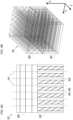
Turning now toFIGS.2A and2B , the optical properties of an implementation of the near-eye display are illustrated in more detail. Specifically, there is shown a more detailed view of a light-guide optical element (LOE)12 formed from transparent material, including afirst region 16, also referred to herein as “LOE1”, containing a first set of planar, mutually-parallel, partially-reflectingsurfaces 17 having a first orientation, and asecond region 18, also referred to herein as “LOE2”, containing a second set of planar, mutually-parallel, partially-reflectingsurfaces 19 having a second orientation non-parallel to the first orientation. A set of mutually-parallel majorexternal surfaces 24 extend across the first andsecond regions surfaces 17 and the second set of partially-reflectingsurfaces 19 are located between the majorexternal surfaces 24. Most preferably, the set of majorexternal surfaces 24 are a pair of surfaces which are each continuous across the entirety of first andsecond regions regions Regions regions
The optical properties of the LOE may be understood by tracing the image illumination paths backwards. The second set of partially-reflectingsurfaces 19 are at an oblique angle to the majorexternal surfaces 24 so that a part of image illumination propagating within theLOE 12 by internal reflection at the major external surfaces from thefirst region 16 into thesecond region 18 is coupled out of the LOE towards an eye-motion box 26. The first set of partially-reflectingsurfaces 17 are oriented so that a part of image illumination propagating within theLOE 12 by internal reflection at the major external surfaces from the coupling-in region (coupling prism15) is deflected towards thesecond region 18.
One dimension of the angular spread of the projected image fromimage projector 14 is represented inFIG.2A by the cone of illumination spreading from the POD aperture on the right side of the LOE towards the left side of the LOE. In the non-limiting example illustrated here, the central optical axis of the POD defines a direction of propagation within the LOE aligned with the X axis, and the angular spread (within the LOE) is roughly ±16°. (It should be noted that the angular FOV becomes larger in air due to the change in refractive index.) The first set of partially-reflectingsurfaces 17 are illustrated infirst region 16, and the second set of partially-reflectingsurfaces 19 are illustrated insecond region 18.
The near-eye display is designed to provide a full field-of-view of the projected image to an eye of the user that is located at some position within the permitted range of positions designated by an “eye-motion box” (EMB)26 (that is, a shape, typically represented as a rectangle, spaced away from the plane of the LOE from which the pupil of the eye will view the projected image). In order to reach the eye-motion box, light must be coupled-out from thesecond region 18 by the second set of partially-reflectingsurfaces 19 towards theEMB 26. In order to provide the full image field-of-view, each point in the EMB must receive the entire angular range of the image from the LOE. Tracing back the field-of-view from the EMB indicates alarger rectangle 28 from which relevant illumination is coupled-out of the LOE towards the EMB.
It will be apparent that, by additionally tracing correspond ray paths for all fields (directions or pixels) of the image reaching all regions of the EMB, it is possible to map out an envelope of all ray paths from the coupling-in region propagating within the LOE, deflected by one of the first set of partially-reflecting surfaces and coupled out by one of the second set of partially-reflecting surfaces in a direction reaching the eye-motion box, and this envelope defines an “imaging area” of eachfacet 17 which is needed for deflecting part of the image illumination which contributes to the image reaching the EMB, while the remainder of thefacet 17 lying outside the envelope is a “non-imaging area” which does not contribute to the required image. Optionally, the in-plane extent of the facets may be truncated to cover only the imaging area. This and other variant embodiments, employing differing imaging injection locations and geometries, non-uniform facet spacing, or introducing additional (e.g., third) sets of partially-reflecting internal surfaces, are discussed in detail in prior publications by Lumus Ltd. (Israel), particularly in the aforementioned PCT publication no. WO 2020/049542, as well as PCT publication no. WO 2020/152688 and PCT application number PCT/IL2020/051354, both of which were unpublished as of the priority date of this application, and are not considered prior art. These additional features may all be implemented in the context of the present invention, but for conciseness, they will not be addressed here in detail.
It is a particularly preferred feature of certain embodiments of the present invention that the first set of partially-reflectingsurfaces 17 extend across at least 95 percent of a thickness of the LOE, while the second set of partially-reflectingsurfaces 19 in thesecond region 18 are contained within a subsection of the thickness spanning less than 95 percent of the thickness, so that the second set of partially-reflectingsurfaces 19 are excluded from at least one surface layer of thesecond region 18. The advantages of this combination will now be presented.
In a matter of terminology, the term “cover plate” is used herein to refer generically to any implementation of a layer of a certain depth adjacent to one or both of the major surfaces of an LOE from which the sets of internal partially-reflecting surfaces of the LOE are excluded. One approach to forming such a layer is by attachment of a sheet of transparent material, i.e., a physically-distinct cover plate, to the LOE component. However, other production techniques are also possible, such as by generating the LOE structure from a stack of plates in which the partially-reflecting coating is applied only in regions corresponding to the active LOE layer, and the regions which will be adjacent to the major external surfaces of the LOE are joined with index-matched adhesive without reflective coatings. The term “cover plate” is used independent of the production technique to refer to the functional structure in which a surface layer functions as a cover plate, without facets, no matter how that layer is formed.
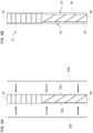
Referring toFIG.3 , this illustrates the path of asingle ray 30, here the principal ray corresponding to the center of field of the image in the X dimension, as it traverses part of LOE1, is redirected by reflection at one of the partially-reflectingsurfaces 17 towards LOE2 (ray 30′), and is redirected and coupled-out by reflection at one of the partially-reflectingsurfaces 19 towards the viewer (ray 30″).FIGS.4A and4B illustrate the geometry of the second redirection/coupling-out in cases without and with face plates added to the LOE, whileFIGS.5A and5B illustrate the geometry of the first redirection.
In LOE2 (region18) from which the image is coupled-out towards the viewer, obliquely inclined facets are used. When facets are inclined (for example at 25 degrees to the major external surfaces), rays can be reflected twice from the same facet as illustrated inFIG.4A . This results in a non-uniform beam exiting the waveguide. A darker area is generated by the second reflection. The dark stripes then appear on the waveguide exit pupil. For a viewer, this will result in a dark stripe on the far field image.
It has been found, however, that the considerations for achieving image uniformity in LOE1 are significantly different from those of LOE2 regarding the use of a cover plate. Since the partially-reflecting surfaces used for redirecting the image illumination from one direction guided within the waveguide to another guided direction are necessarily much steeper, and in some embodiments orthogonal to the major external surfaces of the waveguide, the rays are not reflected twice by a single facet. In this case, optimal image uniformity would be achieved by use of facets which span the entirety of the thickness of the substrate (FIG.5A ), whereas facets which fall short of the surfaces have been found to allow certain rays to skip a facet altogether (FIG.5B ), resulting in dark lines in the output image. The overall result of providing the structure with cover plates over the entirety of bothregions FIG.6A , where a uniformly illuminatedinput aperture 34 from the image projector propagates through the LOE and is coupled out towards the eye-motion box (EMB)26 asimage regions 36 disrupted bydark lines 38 in the output. In contrast, the structure ofFIG.6B employs cover plates only onLOE2 18, while the facets of LOE116 extend to the major external surfaces of the device. In this case, a uniform injectedimage 34 from the image projector preferably results in a relativelyuniform image 36 as perceived by the viewer.
Although the presence of cover plates in theLOE1 region 16 adversely impacts output image quality, there may be practical considerations that favor the use of a cover plate on one or both major surfaces of theLOE1 region 16. For example, the absence of any glued joints extending to the external surface may make it easier to achieve a high-quality planar outer surface of the waveguide. The presence of cover plates may be acceptable if they are sufficiently thin that any resulting disruption of the image is non-troubling to the human eye (FIG.6C ). A thin cover plate will generate thin dark stripes where the output image is missing. The spatial frequency and the width of the dark stripes determine their visibility and impact on the image as perceived by the human eye. To correctly evaluate the severity of the unfilled stripes for the human eye, a convolution of the human eye pupil over the waveguide exiting pupil shows us what cover plate thickness should be allowed. If the spatial frequency of the dark stripes is significantly higher than the diameter of the pupil of the eye, the variations will inherently be averaged out by the eye. If the spatial frequency is lower, the stripes may still be acceptable if they are narrow enough that the intensity averaged over the pupil size does not vary greatly.
Practically, the thickness range for a cover plate for LOE1 region, if present, should be from 1 to 100 microns, most preferably less than 50 microns. As a proportion of the thickness of the LOE, the total thickness of the cover plates is preferably less than 5% of the thickness, preferably no more than 4% of the thickness, and most preferably no more than 2% of the thickness. This corresponds to the first set of partially-reflecting surfaces extend across (spanning) at least 95 percent of the thickness, more preferably at least 96 percent of the thickness, and most preferably at least 98 percent of the thickness. The dark stripe issue can be ameliorated by using a cover plate on only one side ofLOE1 region 16, as illustrated schematically inFIG.6D .
Notwithstanding the possible advantages of employing cover plates, in certain particularly preferred implementations of the present invention, the first set of partially-reflectingsurfaces 17 extend across an entirety of the thickness ofLOE1 16, i.e., with no cover plate, as illustrated schematically inFIG.6B .
Regarding LOE2 inregion 18, as discussed above, the cover plates in this region contribute to a reduction in non-uniformity of illumination, thereby improving the quality of the viewed image. The second set of partially-reflectingsurfaces 19 are preferably excluded from surface layers of both of the major external surfaces in the second region, meaning that both major faces have “cover plates”. The total thickness of the surface layers ofsecond region 18 from which the second set of partially-reflectingsurfaces 19 are excluded is preferably between 6 percent and 33 percent of the total thickness of the LOE2.
Here too, the extent to which non-uniformities in the illumination are perceived by the human eye is dependent on the spatial frequency of the intensity variations, their dynamic range and their width, which in turn dictates the preferred thickness of the cover plates that will be effective to ameliorate those variations. In the case of the coupling-outfacets 19, the spatial frequency results directly from the spacing between adjacent surfaces of the second set of partially-reflectingsurfaces 19 in a direction parallel to the major external surfaces.FIG.7 illustrates a preferred minimum cover plate thickness (total sum of the cover plate thicknesses as a percentage of the total LOE2 thickness) for various facet densities, defined here as the number of facets overlapping a pupil diameter, which is taken here to be roughly 3 millimeters. It can be seen that, for high facet density, a relatively thin cover plate is sufficient, since the intensity variations are inherently averaged over the pupil area and are therefore perceived less by the viewer. As the facet spacing increases, the spatial frequency of the intensity variations is reduced, and a thicker cover plate is required to compensate for these variations.
As a useful point of reference, indicated by a horizontal dashed line inFIG.7 , when the spacing between adjacent surfaces of the second set of partially-reflectingsurfaces 19 in a direction parallel to the major external surfaces is at least 1 mm (corresponding to a density of 3 facets per 3 millimeter pupil diameter), the total thickness of the surface layer(s) of the second region from which the second set of partially-reflecting surfaces are excluded is preferably at least 10 percent of the total thickness.
The optical systems according to the present invention may be produced by various processes based on standard manufacturing techniques employed in this field, as will be clear to a person ordinarily skilled in the art. Each LOE region is typically formed by bonding together a stack of thin plates which have been coated on one or both faces (typically all coated on one face, or alternate plates coated on both sides) to provide the desired partially-reflecting properties for each interface. The partially-reflecting properties are typically provided by multi-layer dielectric coatings, which can offer angularly-selective reflectivity, as is well-known in the art. These stacks are then sliced at the required angle so as to produce an LOE section/region with correctly oriented internal partially-reflecting surfaces. Cover plates of appropriate thickness are then added to each region, where required, and edge surfaces of the LOE sections are polished and then bonded together to form the final compound LOE.
Optionally, where a cover plate is to be provided on one or both major surfaces of the LOE1, it may be advantageous to produce LOE2 with cover plates of partial thickness, corresponding to the desired final cover plate thickness minus the cover plate thickness required for LOE1. A single continuous cover plate can then be added during assembly of the compound LOE, which provides the total desired cover plate thickness for LOE1 and supplements the cover plate thickness for LOE2 up to the desired thickness. This option is addressed further below with reference toFIGS.9A and9B .
Alternatively, in some cases, it may be desirable to produce a stepped cover plate which has a first part of a first thickness suited to LOE1 and a second part with a (larger) second thickness suited to LOE2. The step between the two parts can then be used as an alignment feature for assembly of the two LOE sections.
A further option for manufacture of the compound LOE of the present invention is illustrated schematically inFIGS.8A and8B . In this case, a stack of plates for forming LOE1 is cut to form ablock 80 of dimensions corresponding to multiple LOEs. Asecond block 82 is formed by combining a plurality ofactive layers 84 of LOE2 (i.e., the section of the LOE which contains the partially-reflecting surfaces) bonded together with intermediatetransparent plates 86. First andsecond blocks intermediate work product 81, as illustrated inFIGS.8A and8B , which can be sliced along slicingplanes 88 and polished to generate a plurality of compound LOEs, where a part of the thickness of intermediatetransparent plates 86 becomes a cover sheet for thesecond LOE region 18 of each compound LOE.
The manufacturing technique ofFIGS.8A and8B , and variants thereof, are discussed in further detail in a co-pending PCT application entitled “Method of Fabrication of Compound Light-Guide Optical Elements”, filed on the same day as this application, taking priority from U.S. provisional patent application No. 63/029,500 that was filed 24 May 2020.
Here too, if it is desired to have a cover plate also onfirst LOE region 16, it may be advantageous to generate the compound LOE structure according toFIGS.8A and8B where thecover plate 32aofregion 18 is smaller than the desired thickness by an amount equal to the thickness desired forregion 16, as shown inFIG.9A . Both cover plates can then be brought to their intended total thickness by addition of a uniform-thickness plate 32bbonded to the waveguide across the entire structure, thereby producing the final structure as illustrated inFIG.9B .
It will be appreciated that the above descriptions are intended only to serve as examples, and that many other embodiments are possible within the scope of the present invention as defined in the appended claims.
Claims (7)
1. An optical system for directing image illumination injected at a coupling-in region towards a user for viewing, the optical system comprising a light-guide optical element, LOE, formed from transparent material, said LOE comprising:
(a) a first region containing a first set of planar, mutually-parallel, partially-reflecting surfaces having a first orientation;
(b) a second region containing a second set of planar, mutually-parallel, partially-reflecting surfaces having a second orientation non-parallel to said first orientation;
(c) a pair of mutually-parallel planar major external surfaces, said major planar external surfaces extending across said first and second regions such that both said first set of partially-reflecting surfaces and said second set of partially-reflecting surfaces are located between said planar major external surfaces and
wherein said first orientation of said first set of partially-reflecting surfaces is orthogonal to said planar major external surfaces,
wherein said second set of partially-reflecting surfaces are at an oblique angle to said planar major external surfaces so that a part of image illumination propagating within said LOE by internal reflection at said planar major external surfaces from said first region into said second region is coupled out of said LOE towards the user, and wherein said first set of partially-reflecting surfaces are oriented so that a part of image illumination propagating within said LOE by internal reflection at said planar major external surfaces from said coupling-in region is deflected towards said second region,
wherein said LOE has a thickness between said planar major external surfaces, and wherein said first set of partially-reflecting surfaces extend across at least 95 percent of said thickness, and said second set of partially-reflecting surfaces in said second region are contained within a subsection of said thickness spanning less than 95 percent of said thickness so that said second set of partially-reflecting surfaces are excluded from at least one surface layer of said second region.
2. The optical system ofclaim 1 , wherein said second set of partially-reflecting surfaces are excluded from surface layers of both of said planar major external surfaces in said second region.
3. The optical system ofclaim 1 , wherein a total thickness of said at least one surface layer of said second region from which said second set of partially-reflecting surfaces are excluded is between 6 percent and 33 percent of said thickness.
4. The optical system ofclaim 1 , wherein a spacing between adjacent surfaces of said second set of partially-reflecting surfaces in a direction parallel to said planar major external surfaces is at least 1 mm, and wherein a total thickness of said at least one surface layer of said second region from which said second set of partially-reflecting surfaces are excluded is at least 10 percent of said thickness.
5. The optical system ofclaim 1 , wherein said first set of partially-reflecting surfaces extend across at least 96 percent of said thickness.
6. The optical system ofclaim 1 , wherein said first set of partially-reflecting surfaces extend across at least 98 percent of said thickness.
7. The optical system ofclaim 1 , wherein said first set of partially-reflecting surfaces extend across an entirety of said thickness.
Priority Applications (1)
| Application Number | Priority Date | Filing Date | Title |
|---|---|---|---|
| US17/794,966US12124037B2 (en) | 2020-05-24 | 2021-05-24 | Compound light-guide optical elements |
Applications Claiming Priority (3)
| Application Number | Priority Date | Filing Date | Title |
|---|---|---|---|
| US202063029496P | 2020-05-24 | 2020-05-24 | |
| PCT/IL2021/050608WO2021240513A1 (en) | 2020-05-24 | 2021-05-24 | Compound light-guide optical elements |
| US17/794,966US12124037B2 (en) | 2020-05-24 | 2021-05-24 | Compound light-guide optical elements |
Related Parent Applications (1)
| Application Number | Title | Priority Date | Filing Date |
|---|---|---|---|
| PCT/IL2021/050608A-371-Of-InternationalWO2021240513A1 (en) | 2020-05-24 | 2021-05-24 | Compound light-guide optical elements |
Related Child Applications (1)
| Application Number | Title | Priority Date | Filing Date |
|---|---|---|---|
| US18/909,978ContinuationUS20250028177A1 (en) | 2020-05-24 | 2024-10-09 | Compound Light-Guide Optical Elements |
Publications (2)
| Publication Number | Publication Date |
|---|---|
| US20220390747A1 US20220390747A1 (en) | 2022-12-08 |
| US12124037B2true US12124037B2 (en) | 2024-10-22 |
Family
ID=78744284
Family Applications (2)
| Application Number | Title | Priority Date | Filing Date |
|---|---|---|---|
| US17/794,966Active2042-01-07US12124037B2 (en) | 2020-05-24 | 2021-05-24 | Compound light-guide optical elements |
| US18/909,978PendingUS20250028177A1 (en) | 2020-05-24 | 2024-10-09 | Compound Light-Guide Optical Elements |
Family Applications After (1)
| Application Number | Title | Priority Date | Filing Date |
|---|---|---|---|
| US18/909,978PendingUS20250028177A1 (en) | 2020-05-24 | 2024-10-09 | Compound Light-Guide Optical Elements |
Country Status (7)
| Country | Link |
|---|---|
| US (2) | US12124037B2 (en) |
| EP (1) | EP4085287A4 (en) |
| JP (1) | JP7730564B2 (en) |
| KR (1) | KR20230011924A (en) |
| CN (2) | CN115176190B (en) |
| IL (1) | IL298411A (en) |
| WO (1) | WO2021240513A1 (en) |
Cited By (1)
| Publication number | Priority date | Publication date | Assignee | Title |
|---|---|---|---|---|
| US12352974B2 (en) | 2022-01-07 | 2025-07-08 | Lumus Ltd. | Optical system for directing an image for viewing |
Families Citing this family (3)
| Publication number | Priority date | Publication date | Assignee | Title |
|---|---|---|---|---|
| KR20240046489A (en) | 2021-08-23 | 2024-04-09 | 루머스 리미티드 | Method for manufacturing composite light guiding optical elements with embedded coupling-in reflector |
| US20250298247A1 (en)* | 2022-05-10 | 2025-09-25 | Google Llc | Lateral offset reflector for reflective waveguides |
| JP2024146219A (en)* | 2023-03-31 | 2024-10-15 | 日東電工株式会社 | Light guiding film and method for producing same |
Citations (302)
| Publication number | Priority date | Publication date | Assignee | Title |
|---|---|---|---|---|
| US2748659A (en) | 1951-02-26 | 1956-06-05 | Jenaer Glaswerk Schott & Gen | Light source, searchlight or the like for polarized light |
| US2795069A (en) | 1956-02-07 | 1957-06-11 | George K C Hardesty | Laminated metal-plastic illuminable panel |
| US2886911A (en) | 1953-07-23 | 1959-05-19 | George K C Hardesty | Duo-panel edge illumination system |
| US3491245A (en) | 1967-04-10 | 1970-01-20 | George K C Hardesty | Guided light display panel |
| DE1422172B1 (en) | 1961-12-07 | 1970-11-12 | Kopperschmidt & Co Carl W | periscope |
| US3626394A (en) | 1970-04-09 | 1971-12-07 | Magnavox Co | Magneto-optical system |
| US3667621A (en) | 1970-10-20 | 1972-06-06 | Wisconsin Foundry And Machine | Fluid power system for a self-contained unloading unit |
| US3677621A (en) | 1969-11-24 | 1972-07-18 | Vickers Ltd | Optical field flattening devices |
| US3737212A (en) | 1970-12-14 | 1973-06-05 | Gen Electric | Diffraction optics head up display |
| US3802763A (en) | 1971-09-01 | 1974-04-09 | Rank Organisation Ltd | Beam splitting prisms |
| US3829197A (en) | 1971-10-20 | 1974-08-13 | Balzers Patent Beteilig Ag | Antireflective multilayer coating on a highly refractive substrate |
| US3857109A (en) | 1973-11-21 | 1974-12-24 | Us Navy | Longitudinally-pumped two-wavelength lasers |
| US3873209A (en) | 1973-12-10 | 1975-03-25 | Bell Telephone Labor Inc | Measurement of thin films by optical waveguiding technique |
| US3940204A (en) | 1975-01-23 | 1976-02-24 | Hughes Aircraft Company | Optical display systems utilizing holographic lenses |
| US4084883A (en) | 1977-02-28 | 1978-04-18 | The University Of Rochester | Reflective polarization retarder and laser apparatus utilizing same |
| GB1514977A (en) | 1975-12-02 | 1978-06-21 | Standard Telephones Cables Ltd | Detecting oil in water |
| US4191446A (en) | 1974-12-16 | 1980-03-04 | U.S. Philips Corporation | Directional coupling-device for multi-mode optical fibres |
| US4309070A (en) | 1979-01-19 | 1982-01-05 | Smiths Industries Limited | Display apparatus |
| US4331387A (en) | 1980-07-03 | 1982-05-25 | Westinghouse Electric Corp. | Electro-optical modulator for randomly polarized light |
| FR2496905A1 (en) | 1980-12-24 | 1982-06-25 | France Etat | EPISCOPE WITH MULTIMODES REFLECTIONS |
| US4516828A (en) | 1982-05-03 | 1985-05-14 | General Motors Corporation | Duplex communication on a single optical fiber |
| US4613216A (en) | 1984-03-27 | 1986-09-23 | L'etat Francais | Device for observation through a wall in two opposite directions |
| US4711512A (en) | 1985-07-12 | 1987-12-08 | Environmental Research Institute Of Michigan | Compact head-up display |
| US4715684A (en) | 1984-06-20 | 1987-12-29 | Hughes Aircraft Company | Optical system for three color liquid crystal light valve image projection system |
| US4720189A (en) | 1986-01-07 | 1988-01-19 | Northern Telecom Limited | Eye-position sensor |
| US4775217A (en) | 1981-10-14 | 1988-10-04 | Gec Avionics Limited | Night vision viewing system |
| US4798448A (en) | 1988-02-16 | 1989-01-17 | General Electric Company | High efficiency illumination system for display devices |
| US4805988A (en) | 1987-07-24 | 1989-02-21 | Nelson Dones | Personal video viewing device |
| GB2220081A (en) | 1988-06-21 | 1989-12-28 | Hall & Watts Defence Optics Lt | Periscope apparatus |
| FR2638242A1 (en) | 1988-10-21 | 1990-04-27 | Thomson Csf | Optical collimation system, especially for a helmet display |
| US4932743A (en) | 1988-04-18 | 1990-06-12 | Ricoh Company, Ltd. | Optical waveguide device |
| JPH02182447A (en) | 1989-01-09 | 1990-07-17 | Mitsubishi Electric Corp | Dielectric multilayer reflective film |
| EP0380035A2 (en) | 1989-01-23 | 1990-08-01 | Hughes Optical Products, Inc. | Helmet mounted display system |
| EP0399865A1 (en) | 1989-05-23 | 1990-11-28 | Thomson-Csf | Optical device for introduction of a collimated image into the field of view of an observer and helmet comprising such a device |
| US4978952A (en) | 1989-02-24 | 1990-12-18 | Collimated Displays Incorporated | Flat screen color video display |
| US5033828A (en) | 1988-12-02 | 1991-07-23 | Mitsui Petrochemical Industries, Ltd. | Optical output controlling method and apparatus |
| US5096520A (en) | 1990-08-01 | 1992-03-17 | Faris Sades M | Method for producing high efficiency polarizing filters |
| US5157526A (en) | 1990-07-06 | 1992-10-20 | Hitachi, Ltd. | Unabsorbing type polarizer, method for manufacturing the same, polarized light source using the same, and apparatus for liquid crystal display using the same |
| US5208800A (en) | 1990-04-13 | 1993-05-04 | Ricoh Company, Ltd. | Mode splitter and magneto-optical signal detection device |
| EP0543718A1 (en) | 1991-11-19 | 1993-05-26 | Thomson-Csf | Constituent material for sighting glasses and gun using these sighting glasses |
| US5231642A (en) | 1992-05-08 | 1993-07-27 | Spectra Diode Laboratories, Inc. | Semiconductor ring and folded cavity lasers |
| US5235589A (en) | 1990-05-21 | 1993-08-10 | Ricoh Company, Ltd. | Apparatus for recording and reproducing optical information and prism coupler |
| EP0566004A2 (en) | 1992-04-07 | 1993-10-20 | Hughes Aircraft Company | Virtual image display having a high efficiency grid beamsplitter |
| US5301067A (en) | 1992-05-06 | 1994-04-05 | Plx Inc. | High accuracy periscope assembly |
| GB2272980A (en) | 1992-11-26 | 1994-06-01 | Electro Optics Ind Ltd | Optical beam splitting lens |
| US5341230A (en) | 1992-12-22 | 1994-08-23 | Hughes Aircraft Company | Waveguide holographic telltale display |
| US5367399A (en) | 1992-02-13 | 1994-11-22 | Holotek Ltd. | Rotationally symmetric dual reflection optical beam scanner and system using same |
| GB2278222A (en) | 1993-05-20 | 1994-11-23 | Sharp Kk | Spatial light modulator |
| US5369415A (en) | 1992-06-29 | 1994-11-29 | Motorola, Inc. | Direct retinal scan display with planar imager |
| GB2278888A (en) | 1993-06-07 | 1994-12-14 | Ford Motor Co | A fuel pump with curved vapour channel |
| US5430505A (en) | 1992-01-30 | 1995-07-04 | Mak Technologies, Inc. | High speed eye tracking device and method |
| US5453877A (en) | 1988-10-21 | 1995-09-26 | Thomson-Csf | Optical system of collimation notably for helmet display unit |
| FR2721872A1 (en) | 1994-07-01 | 1996-01-05 | Renault Nationale Usines | DEVICE FOR IMPROVING THE VISION OF A ROAD SCENE |
| JPH0870782A (en) | 1994-09-08 | 1996-03-19 | Kanebo Foods Ltd | Ice cream its preparation |
| US5543877A (en) | 1992-10-23 | 1996-08-06 | Olympus Optical Co., Ltd. | Means for controlling driving of a driving fork and take-up spool for automatic feeding and rewinding of a film in a camera |
| US5555329A (en) | 1993-11-05 | 1996-09-10 | Alliesignal Inc. | Light directing optical structure |
| JPH08313843A (en) | 1995-05-16 | 1996-11-29 | Agency Of Ind Science & Technol | Wide visual field and high resolution video presentation device in line of sight followup system |
| US5619601A (en) | 1993-12-28 | 1997-04-08 | Fujitsu Limited | Optical switch and optical distributor using polarization control and partial reflection |
| EP0770818A2 (en) | 1995-10-24 | 1997-05-02 | SHARP Corporation | Illuminator |
| US5650873A (en) | 1995-01-30 | 1997-07-22 | Lockheed Missiles & Space Company, Inc. | Micropolarization apparatus |
| US5680209A (en) | 1992-08-13 | 1997-10-21 | Maechler; Meinrad | Spectroscopic systems for the analysis of small and very small quantities of substances |
| US5708449A (en) | 1993-10-07 | 1998-01-13 | Virtual Vision, Inc. | Binocular head mounted display system |
| US5712694A (en) | 1994-09-16 | 1998-01-27 | Kabushiki Kaisha Toshiba | LCD comprising a light separating element including a cholesteric liquid crystal sheet |
| US5724163A (en) | 1996-11-12 | 1998-03-03 | Yariv Ben-Yehuda | Optical system for alternative or simultaneous direction of light originating from two scenes to the eye of a viewer |
| US5751480A (en) | 1991-04-09 | 1998-05-12 | Canon Kabushiki Kaisha | Plate-like polarizing element, a polarizing conversion unit provided with the element, and a projector provided with the unit |
| US5764412A (en) | 1994-10-15 | 1998-06-09 | Fujitsu Limited | Polarization separation/conversion device for polarized lighting apparatus and projection display unit |
| US5829854A (en) | 1996-09-26 | 1998-11-03 | Raychem Corporation | Angled color dispersement and recombination prism |
| DE19725262A1 (en) | 1997-06-13 | 1998-12-24 | Vitaly Dr Lissotschenko | Optical beam transformation apparatus |
| US5883684A (en) | 1997-06-19 | 1999-03-16 | Three-Five Systems, Inc. | Diffusively reflecting shield optically, coupled to backlit lightguide, containing LED's completely surrounded by the shield |
| US5896232A (en) | 1997-08-07 | 1999-04-20 | International Business Machines Corporation | Highly efficient and compact frontlighting for polarization-based reflection light valves |
| US5919601A (en) | 1996-11-12 | 1999-07-06 | Kodak Polychrome Graphics, Llc | Radiation-sensitive compositions and printing plates |
| US5930046A (en) | 1997-02-13 | 1999-07-27 | Optical Coating Laboratory, Inc. | Low net stress multilayer thin film coatings |
| US5966223A (en) | 1993-02-26 | 1999-10-12 | Yeda Research & Development Co., Ltd. | Planar holographic optical device |
| US5982536A (en) | 1995-10-17 | 1999-11-09 | Barr & Stroud Limited | Display system |
| WO2000004407A1 (en) | 1998-07-17 | 2000-01-27 | Brookhaven Science Associates | Small inlet optical panel and a method of making a small inlet optical panel |
| US6021239A (en) | 1996-10-31 | 2000-02-01 | Sharp Kabushiki Kaisha | Photocoupler and method for producing the same |
| US6023372A (en) | 1997-10-30 | 2000-02-08 | The Microoptical Corporation | Light weight, compact remountable electronic display device for eyeglasses or other head-borne eyewear frames |
| US6052500A (en) | 1996-12-03 | 2000-04-18 | Mitsubishi Gas Chemical Company, Inc. | Optical waveguide device for connections without optical axis adjustment |
| US6091548A (en) | 1997-10-01 | 2000-07-18 | Raytheon Company | Optical system with two-stage aberration correction |
| WO2000063738A1 (en) | 1999-04-21 | 2000-10-26 | U.S. Precision Lens Incorporated | Optical systems for reflective lcd's |
| US6144347A (en) | 1992-10-09 | 2000-11-07 | Sony Corporation | Head-mounted image display apparatus |
| US6154321A (en) | 1998-01-20 | 2000-11-28 | University Of Washington | Virtual retinal display with eye tracking |
| US20010000124A1 (en) | 1996-03-29 | 2001-04-05 | Kollin Joel S. | Scanning display with expanded exit pupil |
| US6222677B1 (en) | 1999-04-12 | 2001-04-24 | International Business Machines Corporation | Compact optical system for use in virtual display applications |
| US6222676B1 (en) | 1998-12-22 | 2001-04-24 | Olympus Optical Co., Ltd. | Image display apparatus |
| US6239092B1 (en) | 1997-09-30 | 2001-05-29 | Reckitt Benckiser Inc. | Thickened acidic, hard surface cleaning and disinfecting compositions particularly useful for ceramic surfaces |
| US6264328B1 (en) | 1999-10-21 | 2001-07-24 | University Of Rochester | Wavefront sensor with off-axis illumination |
| US6324330B1 (en) | 2000-07-10 | 2001-11-27 | Ultratech Stepper, Inc. | Folded light tunnel apparatus and method |
| US6322256B1 (en) | 1998-11-24 | 2001-11-27 | Nippon Electric Glass Co., Ltd. | Optical fiber holding capillary tube |
| WO2001095025A1 (en) | 2000-06-08 | 2001-12-13 | Three-Five Systems, Inc. | Liquid crystal display element having a precisely controlled cell gap and method of making same |
| US20020015233A1 (en) | 2000-07-31 | 2002-02-07 | Daeyang E&C Co., Ltd. | Optical system for head mounted display |
| US6349001B1 (en) | 1997-10-30 | 2002-02-19 | The Microoptical Corporation | Eyeglass interface system |
| EP1180711A1 (en) | 2000-01-28 | 2002-02-20 | Seiko Epson Corporation | Optical reflection polarizer and projector comprising the same |
| US6362861B1 (en) | 2000-05-02 | 2002-03-26 | Agilent Technologies, Inc. | Microdisplay system |
| US6384982B1 (en) | 1996-10-08 | 2002-05-07 | The Microoptical Corporation | Compact image display system for eyeglasses or other head-borne frames |
| US6388814B2 (en) | 1999-12-28 | 2002-05-14 | Rohm Co., Ltd. | Head mounted display |
| US6404550B1 (en) | 1996-07-25 | 2002-06-11 | Seiko Epson Corporation | Optical element suitable for projection display apparatus |
| US6404947B1 (en) | 1999-11-16 | 2002-06-11 | Matsushita Electric Industrial Co., Ltd. | Demultiplexer and demultiplexer-receiver |
| US6490104B1 (en) | 2000-09-15 | 2002-12-03 | Three-Five Systems, Inc. | Illumination system for a micro display |
| US20020191297A1 (en) | 2000-10-20 | 2002-12-19 | Gleckman Philip L. | Compact near-eye illumination system |
| US20030007157A1 (en) | 2001-07-03 | 2003-01-09 | Hulse Charles Andrew | Rhomb interleaver |
| US6509982B2 (en) | 2000-01-07 | 2003-01-21 | Honeywell International Inc. | Holographic diffusers |
| US20030020006A1 (en) | 2001-07-24 | 2003-01-30 | Janeczko Donald John | Planar diffractive relay |
| US6519400B2 (en) | 1998-08-31 | 2003-02-11 | Brookhaven Science Associates | Ultrathin optical panel and a method of making an ultrathin optical panel |
| US20030063042A1 (en) | 1999-07-29 | 2003-04-03 | Asher A. Friesem | Electronic utility devices incorporating a compact virtual image display |
| US6556282B2 (en) | 2001-09-04 | 2003-04-29 | Rosemount Aerospace, Inc. | Combined LOAS and LIDAR system |
| JP2003140081A (en) | 2001-11-06 | 2003-05-14 | Nikon Corp | Hologram combiner optical system |
| US20030090439A1 (en) | 2001-09-07 | 2003-05-15 | Spitzer Mark B. | Light weight, compact, remountable face-supported electronic display |
| US6577411B1 (en) | 1996-11-12 | 2003-06-10 | Planop-Planar Optics Ltd. | Optical system for alternative or simultaneous direction of light originating from two scenes to the eye of a viewer |
| US6580529B1 (en) | 1998-04-02 | 2003-06-17 | Elop Electro -Optics Industries Ltd. | Holographic optical devices |
| EP1326102A1 (en) | 2000-07-24 | 2003-07-09 | Mitsubishi Rayon Co., Ltd. | Surface illuminant device and prism sheet used therefor |
| US20030165017A1 (en) | 2000-06-05 | 2003-09-04 | Yaakov Amitai | Substrate-guided optical beam expander |
| US20030197938A1 (en) | 2002-04-12 | 2003-10-23 | Dietrich Schmidt | Arrangement for polarization of light |
| US20030218718A1 (en) | 2002-01-11 | 2003-11-27 | Renaud Moliton | Ophthalmic lens having a projection insert |
| US6671100B1 (en) | 1999-10-14 | 2003-12-30 | Stratos Product Development Llc | Virtual imaging system |
| EP1385023A1 (en) | 2002-07-17 | 2004-01-28 | C.R.F. Società Consortile per Azioni | A light guide for display devices of the head-mounted or head-up type |
| US6710902B2 (en) | 2001-04-13 | 2004-03-23 | Olympus Corporation | Observation optical system |
| US6762801B2 (en) | 2000-05-21 | 2004-07-13 | Elop Electro-Optics Industries Ltd. | Varying light transmittance through a display panel |
| US20040137189A1 (en) | 2002-11-08 | 2004-07-15 | Tellini Serena R. P. | Optical device and light guide system comprising it |
| US6775432B2 (en) | 2001-10-19 | 2004-08-10 | Santanu Basu | Method and apparatus for optical wavelength demultiplexing, multiplexing and routing |
| JP2004527801A (en) | 2001-05-26 | 2004-09-09 | テイリズ オプティクス リミテッド | Optical device using polarizing bees splitter |
| US6798579B2 (en) | 1999-04-27 | 2004-09-28 | Optical Products Development Corp. | Real imaging system with reduced ghost imaging |
| US6805490B2 (en) | 2002-09-30 | 2004-10-19 | Nokia Corporation | Method and system for beam expansion in a display device |
| US6847488B2 (en) | 2001-04-07 | 2005-01-25 | Cambridge Flat Projection Displays Limited | Far-field display |
| US20050018308A1 (en) | 2003-05-22 | 2005-01-27 | Cassarly William J. | Light distribution apparatus and methods for illuminating optical systems |
| US20050024849A1 (en) | 1999-02-23 | 2005-02-03 | Parker Jeffery R. | Methods of cutting or forming cavities in a substrate for use in making optical films, components or wave guides |
| JP2005084522A (en) | 2003-09-10 | 2005-03-31 | Nikon Corp | Combiner optics |
| US20050084210A1 (en) | 2003-10-17 | 2005-04-21 | Samsung Electronics Co., Ltd. | Light tunnel, uniform light illuminating device and projector employing the same |
| US6927694B1 (en) | 2001-08-20 | 2005-08-09 | Research Foundation Of The University Of Central Florida | Algorithm for monitoring head/eye motion for driver alertness with one camera |
| US20050174658A1 (en) | 2004-02-05 | 2005-08-11 | Michael Long | Systems and methods for integrating light |
| US20050174641A1 (en) | 2002-11-26 | 2005-08-11 | Jds Uniphase Corporation | Polarization conversion light integrator |
| US6942925B1 (en) | 1997-08-11 | 2005-09-13 | Optiva, Inc. | Dichroic polarizer |
| WO2005093493A1 (en) | 2004-03-29 | 2005-10-06 | Sony Corporation | Optical device and virtual image display device |
| US20050265044A1 (en) | 2004-05-28 | 2005-12-01 | Yi-Ming Chen | Planar light-emitting device |
| US7016113B2 (en) | 1997-05-28 | 2006-03-21 | Lg.Philips Lcd Co., Ltd. | Large scale polarizer and polarizer system employing it |
| US7021777B2 (en) | 2003-09-10 | 2006-04-04 | Lumus Ltd. | Optical devices particularly for remote viewing applications |
| US20060126182A1 (en) | 2004-12-13 | 2006-06-15 | Nokia Corporation | General diffractive optics method for expanding an exit pupil |
| US20060132914A1 (en) | 2003-06-10 | 2006-06-22 | Victor Weiss | Method and system for displaying an informative image against a background image |
| US7088664B2 (en) | 2001-04-30 | 2006-08-08 | Samsung Electronics Co., Ltd. | Reflection type compound prism and optical pickup apparatus employing the same |
| WO2006098097A1 (en) | 2005-03-14 | 2006-09-21 | Nikon Corporation | Image display optical system and image display |
| WO2006098809A2 (en) | 2005-03-11 | 2006-09-21 | Brown Paul W | In situ formation of chloride sequestering compounds |
| US20060221448A1 (en) | 2005-04-04 | 2006-10-05 | Mirage Innovations Ltd. | Multi-plane optical apparatus |
| US20060268421A1 (en) | 2005-05-30 | 2006-11-30 | Konic Minolta Holdings, Inc. | Image display apparatus and head mount display |
| US20070007085A1 (en) | 2005-06-15 | 2007-01-11 | Chiu Nan Wang | Elevator escape device with improved ventilation system |
| US20070015967A1 (en) | 2003-04-01 | 2007-01-18 | Boston Scientific Scimed, Inc. | Autosteering vision endoscope |
| US7175304B2 (en) | 2003-01-30 | 2007-02-13 | Touchsensor Technologies, Llc | Integrated low profile display |
| US20070035707A1 (en) | 2005-06-20 | 2007-02-15 | Digital Display Innovations, Llc | Field sequential light source modulation for a digital display system |
| US20070070859A1 (en) | 2004-05-17 | 2007-03-29 | Nikon Corporation | Optical elements and combiner optical systems and image-display units comprising same |
| US7205960B2 (en) | 2003-02-19 | 2007-04-17 | Mirage Innovations Ltd. | Chromatic planar optic display system |
| WO2007054928A1 (en) | 2005-11-08 | 2007-05-18 | Lumus Ltd. | Polarizing optical system |
| US20070165192A1 (en) | 2006-01-13 | 2007-07-19 | Silicon Optix Inc. | Reduced field angle projection display system |
| US7355795B1 (en) | 1994-06-13 | 2008-04-08 | Canon Kabushiki Kaisha | Head-up display device with curved optical surface having total reflection |
| US20080094586A1 (en) | 2004-12-06 | 2008-04-24 | Yoshikazu Hirayama | Image Display Optical System, Image Display Unit, Illuminating Optical System, And Liquid Crystal Display Unit |
| US7391573B2 (en) | 2003-09-10 | 2008-06-24 | Lumus Ltd. | Substrate-guided optical devices |
| US20080151379A1 (en)* | 2005-02-10 | 2008-06-26 | Lumus Ltd. | Substrate-Guide Optical Device Utilizing Polarization Beam Splitters |
| US20080151375A1 (en) | 2006-12-26 | 2008-06-26 | Ching-Bin Lin | Light guide means as dually effected by light concentrating and light diffusing |
| US7430355B2 (en) | 2003-12-08 | 2008-09-30 | University Of Cincinnati | Light emissive signage devices based on lightwave coupling |
| US7448170B2 (en) | 2002-01-16 | 2008-11-11 | Mara-Institut D.O.O. | Indirectly prestressed, concrete, roof-ceiling construction with flat soffit |
| US20090003406A1 (en) | 2007-06-27 | 2009-01-01 | Fluke Corporation | Thermal switch calibration apparatus and methods |
| US20090034069A1 (en) | 2007-08-03 | 2009-02-05 | Hon Hai Precision Industry Co., Ltd. | Polarization conversion device and projector using same |
| US20090059380A1 (en) | 2005-03-10 | 2009-03-05 | Renaud Moliton | Optical Imager for Producing an Optical Display |
| WO2009074638A2 (en) | 2007-12-13 | 2009-06-18 | Optinvent | Optical guide and ocular vision optical system |
| US20090190222A1 (en) | 2005-09-07 | 2009-07-30 | Bae Systems Plc | Projection Display |
| US7570859B1 (en) | 2008-07-03 | 2009-08-04 | Microvision, Inc. | Optical substrate guided relay with input homogenizer |
| US7589901B2 (en) | 2007-07-10 | 2009-09-15 | Microvision, Inc. | Substrate-guided relays for use with scanned beam light sources |
| CN101542346A (en) | 2006-11-28 | 2009-09-23 | 康宁光缆系统有限公司 | Fiber optic cable having a dry insert and methods of making the same |
| US7613373B1 (en) | 2008-07-03 | 2009-11-03 | Microvision, Inc. | Substrate guided relay with homogenizing input relay |
| US7653268B1 (en) | 2008-07-03 | 2010-01-26 | Microvision, Inc. | Substrate guided relay with polarization rotating apparatus |
| US20100027289A1 (en) | 2008-08-01 | 2010-02-04 | Sony Corporation | Illumination optical device and virtual image display |
| JP2010044172A (en) | 2008-08-11 | 2010-02-25 | Sony Corp | Virtual image display device |
| US20100053148A1 (en) | 2008-09-02 | 2010-03-04 | Qualcomm Mems Technologies, Inc. | Light turning device with prismatic light turning features |
| US7724443B2 (en) | 2005-02-10 | 2010-05-25 | Lumus Ltd. | Substrate-guided optical device utilizing thin transparent layer |
| US20100202128A1 (en) | 2008-12-11 | 2010-08-12 | Robert Saccomanno | Non-invasive injection of light into a transparent substrate, such as a window pane through its face |
| US20100201953A1 (en) | 2005-11-21 | 2010-08-12 | Microvision, Inc. | Substrate-Guided Display Having Polarization Selective Input Structure |
| US20100214635A1 (en) | 2007-11-22 | 2010-08-26 | Kabushiki Kaisha Toshiba | Display device, display method and head-up display |
| US20100278480A1 (en) | 2009-04-21 | 2010-11-04 | Vasylyev Sergiy V | Light collection and illumination systems employing planar waveguide |
| US20100291489A1 (en) | 2009-05-15 | 2010-11-18 | Api Nanofabrication And Research Corp. | Exposure methods for forming patterned layers and apparatus for performing the same |
| US20110096566A1 (en) | 2009-10-28 | 2011-04-28 | Coretronic Corporation | Backlight module |
| US20110109880A1 (en) | 2006-01-26 | 2011-05-12 | Ville Nummela | Eye Tracker Device |
| US7949214B2 (en) | 2008-11-06 | 2011-05-24 | Microvision, Inc. | Substrate guided relay with pupil expanding input coupler |
| US20110176218A1 (en) | 2008-09-16 | 2011-07-21 | Louahab Noui | waveguides |
| US7995275B2 (en) | 2005-08-18 | 2011-08-09 | Ricoh Company, Ltd. | Polarization conversion element, polarization conversion optical system and image projecting apparatus |
| US20110210202A1 (en) | 2008-10-31 | 2011-09-01 | Deutsches Zentrum Fur Luft- Und Raumfahrt E.V. | Reducing Circulation in a Wake Turbulence Behind an Airplane Flying at Low Altitude |
| US8035872B2 (en) | 2004-06-29 | 2011-10-11 | Nikon Corporation | Image combiner and image display device |
| WO2011130720A2 (en) | 2010-04-16 | 2011-10-20 | Flex Lighting Ii, Llc | Sign comprising a film-based lightguide |
| US20120039576A1 (en) | 2009-04-08 | 2012-02-16 | International Business Machines Corporation | Optical waveguide with embedded light-reflecting feature and method for fabricating the same |
| US20120044572A1 (en) | 2009-04-20 | 2012-02-23 | Bae Systems Plc | Optical waveguides |
| JP2012058404A (en) | 2010-09-07 | 2012-03-22 | Shimadzu Corp | Optical component and display device using the same |
| US8187481B1 (en) | 2005-05-05 | 2012-05-29 | Coho Holdings, Llc | Random texture anti-reflection optical surface treatment |
| US20120147361A1 (en) | 2010-12-13 | 2012-06-14 | Mitsubishi Electric Corporation | Wavelength monitor |
| JP2012123936A (en) | 2010-12-06 | 2012-06-28 | Omron Corp | Plane light source device, and three-dimensional display device |
| EP2530510A2 (en) | 2011-06-01 | 2012-12-05 | Sony Corporation | Display apparatus |
| US20130025043A1 (en) | 2011-07-25 | 2013-01-31 | Hui Wing-Kin | Device for facilitating interchangeability of pool applicances for above ground pools |
| US8369019B2 (en) | 2008-04-14 | 2013-02-05 | Bae Systems Plc | Waveguides |
| US8391668B2 (en) | 2011-01-13 | 2013-03-05 | Microvision, Inc. | Substrate guided relay having an absorbing edge to reduce alignment constraints |
| WO2013065656A1 (en) | 2011-10-31 | 2013-05-10 | シャープ株式会社 | Pseudo-solar radiation device |
| US20130135749A1 (en) | 2011-11-30 | 2013-05-30 | Sony Corporation | Light reflecting member, light beam extension device, image display device, and optical device |
| US20130150431A1 (en) | 2010-08-27 | 2013-06-13 | New York University | Mir-33 inhibitors and uses thereof |
| US20130150430A1 (en) | 2010-08-04 | 2013-06-13 | The Ohio State University | Methods for Impairing the P53/HDM2 Auto-Regulatory Loop in Multiple Myeloma Development Using mIR-192, mIR-194 and mIR-215 |
| US8472119B1 (en) | 2011-08-12 | 2013-06-25 | Google Inc. | Image waveguide having a bend |
| US20130163089A1 (en) | 2011-12-23 | 2013-06-27 | David D. Bohn | Reflective array waveguide |
| US20130208362A1 (en) | 2012-02-15 | 2013-08-15 | David D. Bohn | Laser illumination scanning |
| US8531773B2 (en) | 2011-01-10 | 2013-09-10 | Microvision, Inc. | Substrate guided relay having a homogenizing layer |
| US20130242392A1 (en) | 2012-03-15 | 2013-09-19 | Google Inc. | Near-to-eye display with diffractive lens |
| US20130250431A1 (en) | 2012-03-21 | 2013-09-26 | Steve Robbins | Two-dimensional exit-pupil expansion |
| US20130250430A1 (en) | 2012-03-21 | 2013-09-26 | Steve Robbins | Increasing field of view of reflective waveguide |
| US8548290B2 (en) | 2011-08-23 | 2013-10-01 | Vuzix Corporation | Dynamic apertured waveguide for near-eye display |
| US20130321432A1 (en) | 2012-06-01 | 2013-12-05 | QUALCOMM MEMES Technologies, Inc. | Light guide with embedded fresnel reflectors |
| US20130334504A1 (en) | 2008-08-19 | 2013-12-19 | Plextronics, Inc. | Organic light emitting diode lighting devices |
| US20140003762A1 (en) | 2012-06-11 | 2014-01-02 | Magic Leap, Inc. | Multiple depth plane three-dimensional display using a wave guide reflector array projector |
| US20140019801A1 (en) | 2012-07-12 | 2014-01-16 | International Business Machines Corporation | Multiple hyperswap replication sessions |
| US8649099B2 (en) | 2010-09-13 | 2014-02-11 | Vuzix Corporation | Prismatic multiple waveguide for near-eye display |
| US20140043688A1 (en) | 2012-08-07 | 2014-02-13 | Nokia Corporation | Display Illumination Light Guide |
| US8655178B2 (en) | 2007-05-08 | 2014-02-18 | The Boeing Company | Method and apparatus for clearing an optical channel |
| US8666208B1 (en) | 2010-11-05 | 2014-03-04 | Google Inc. | Moldable waveguide with embedded micro structures |
| US8665178B1 (en) | 2012-03-01 | 2014-03-04 | Google, Inc. | Partially-reflective waveguide stack and heads-up display using same |
| US8743464B1 (en) | 2010-11-03 | 2014-06-03 | Google Inc. | Waveguide with embedded mirrors |
| CN103837988A (en) | 2014-03-05 | 2014-06-04 | 杭州科汀光学技术有限公司 | Minitype near-to-eye display optical system |
| US20140185142A1 (en) | 2013-01-02 | 2014-07-03 | Google Inc. | Optical combiner for near-eye display |
| US20140192418A1 (en) | 2011-09-13 | 2014-07-10 | Olympus Corporation | Optical Element and Optical Mechanism |
| US20140226215A1 (en) | 2013-02-13 | 2014-08-14 | Seiko Epson Corporation | Virtual image display device |
| US8913865B1 (en) | 2013-06-27 | 2014-12-16 | Microsoft Corporation | Waveguide including light turning gaps |
| DE102013106392A1 (en) | 2013-06-19 | 2014-12-24 | Fraunhofer-Gesellschaft zur Förderung der angewandten Forschung e.V. | Process for producing an antireflection coating |
| US20150016777A1 (en) | 2012-06-11 | 2015-01-15 | Magic Leap, Inc. | Planar waveguide apparatus with diffraction element(s) and system employing same |
| WO2015012280A1 (en) | 2013-07-24 | 2015-01-29 | コニカミノルタ株式会社 | Sight line detection device |
| US20150081313A1 (en) | 2013-09-16 | 2015-03-19 | Sunedison Llc | Methods and systems for photovoltaic site installation, commissioining, and provisioning |
| US20150138646A1 (en) | 2013-11-15 | 2015-05-21 | Seiko Epson Corporation | Optical element, image display device and method for manufacturing same |
| WO2015081313A2 (en) | 2013-11-27 | 2015-06-04 | Magic Leap, Inc. | Virtual and augmented reality systems and methods |
| US20150160529A1 (en) | 2013-12-11 | 2015-06-11 | Sbg Labs Inc. | Holographic Waveguide Display |
| JP2015121647A (en) | 2013-12-24 | 2015-07-02 | セイコーエプソン株式会社 | Light guide device, virtual image display device, and light guide device manufacturing method |
| US20150182348A1 (en) | 2010-07-15 | 2015-07-02 | Nlt Spine Ltd | Laterally Deflectable Implant |
| US20150219834A1 (en) | 2010-04-16 | 2015-08-06 | Flex Lighting Ii, Llc | Display with a film-based lightguide and light redirecting optical element |
| US20150289762A1 (en) | 2012-05-11 | 2015-10-15 | Milan Momcilo Popovich | Apparatus for eye tracking |
| US20150338655A1 (en) | 2014-05-21 | 2015-11-26 | Kabushiki Kaisha Toshiba | Display device |
| US20160031456A1 (en) | 2011-08-18 | 2016-02-04 | Wfk & Associates, Llc | Transitional Mode High Speed Rail Systems |
| JP2016028275A (en) | 2014-07-09 | 2016-02-25 | 恵和株式会社 | Optical sheet, edge light type backlight unit, and method for manufacturing optical sheet |
| JP2016033867A (en) | 2014-07-31 | 2016-03-10 | ソニー株式会社 | Optical member, illumination unit, wearable display, and image display apparatus |
| US20160234485A1 (en) | 2015-02-09 | 2016-08-11 | Steven John Robbins | Display System |
| US20160313567A1 (en) | 2013-12-13 | 2016-10-27 | Dai Nippon Printing Co., Ltd. | Optical scanning device, illumination device, projection apparatus and optical device |
| CN205787362U (en) | 2016-02-26 | 2016-12-07 | 中国航空工业集团公司洛阳电光设备研究所 | Optical waveguide components, two-dimensional expansion fiber waveguide device, head-up display and illuminator |
| US20160370589A1 (en) | 2015-06-18 | 2016-12-22 | Coretronic Corporation | Image display apparatus |
| US20170003504A1 (en) | 2015-06-30 | 2017-01-05 | Tuomas Vallius | Diffractive optical elements with graded edges |
| US20170023761A1 (en) | 2013-09-27 | 2017-01-26 | Trustees Of Princeton University | Anodically bonded cells with optical elements |
| US20170045743A1 (en) | 2014-04-17 | 2017-02-16 | Carl Zeiss Smart Optics Gmbh | Spectacle lens for a display device that can be fitted on the head of a user and generates an image, and display device with such a spectacle lens |
| US20170122725A1 (en) | 2015-11-04 | 2017-05-04 | Magic Leap, Inc. | Light field display metrology |
| WO2017106873A1 (en) | 2015-12-18 | 2017-06-22 | Ostendo Technologies, Inc. | Systems and methods for augmented near-eye wearable displays |
| US20170242249A1 (en) | 2016-02-19 | 2017-08-24 | Richard Andrew Wall | Waveguide Pupil Relay |
| US20170255012A1 (en) | 2016-03-04 | 2017-09-07 | Sharp Kabushiki Kaisha | Head mounted display using spatial light modulator to move the viewing zone |
| US20170276947A1 (en) | 2016-03-23 | 2017-09-28 | Seiko Epson Corporation | Image display apparatus and optical element |
| US20170285346A1 (en) | 2016-03-30 | 2017-10-05 | Coretronic Corporation | Optical waveguide device and head-mounted display apparatus using the same |
| CN107238928A (en) | 2017-06-09 | 2017-10-10 | 京东方科技集团股份有限公司 | A kind of Waveguide array |
| US9791703B1 (en) | 2016-04-13 | 2017-10-17 | Microsoft Technology Licensing, Llc | Waveguides with extended field of view |
| US9798061B2 (en) | 2012-07-26 | 2017-10-24 | Young Lighting Technology Inc. | Hybrid light guide plate and display device |
| US9805633B2 (en) | 2014-03-31 | 2017-10-31 | Lenovo (Beijing) Co., Ltd. | Display device and electronic apparatus |
| US20170343822A1 (en) | 2016-05-24 | 2017-11-30 | Osterhout Group, Inc. | Robust optics for a head-worn display |
| US20170353714A1 (en) | 2016-06-06 | 2017-12-07 | Navid Poulad | Self-calibrating display system |
| US20170371160A1 (en) | 2015-01-06 | 2017-12-28 | Vuzix Corporation | Head mounted imaging apparatus with optical coupling |
| WO2018013307A1 (en) | 2016-06-21 | 2018-01-18 | Ntt Docomo, Inc. | An illuminator for a wearable display |
| US20180101087A1 (en) | 2016-02-24 | 2018-04-12 | Omron Corporation | Display device |
| US20180210202A1 (en)* | 2016-10-09 | 2018-07-26 | Lumus Ltd. | Aperture multiplier using a rectangular waveguide |
| US20180246335A1 (en) | 2014-04-09 | 2018-08-30 | Alexey Leonidovich Ushakov | Smart glasses with a fixed frame and a rotatable frame |
| US20180267309A1 (en) | 2015-05-04 | 2018-09-20 | Magic Leap, Inc. | Separated pupil optical systems for virtual and augmented reality and methods for displaying images using same |
| US20180275409A1 (en) | 2017-03-21 | 2018-09-27 | Magic Leap, Inc. | Eye-imaging apparatus using diffractive optical elements |
| US20180284448A1 (en) | 2017-03-28 | 2018-10-04 | Seiko Epson Corporation | Light guide device and display device |
| US20180284443A1 (en) | 2017-03-28 | 2018-10-04 | Seiko Epson Corporation | Display apparatus |
| WO2018200913A1 (en) | 2017-04-27 | 2018-11-01 | Corning Incorporated | Apparatus and method for edge processing of glass for light coupling |
| US10222535B2 (en) | 2013-07-02 | 2019-03-05 | 3M Innovative Properties Company | Flat light guide |
| US20190086674A1 (en) | 2017-09-21 | 2019-03-21 | Magic Leap, Inc. | Augmented reality display with waveguide configured to capture images of eye and/or environment |
| CN109613644A (en) | 2019-02-14 | 2019-04-12 | 京东方科技集团股份有限公司 | A light guide device and its manufacturing method, and a display device |
| US20190137818A1 (en) | 2016-06-22 | 2019-05-09 | Fujifilm Corporation | Light guide member and liquid crystal display device |
| US10302957B2 (en) | 2016-02-24 | 2019-05-28 | Magic Leap, Inc. | Polarizing beam splitter with low light leakage |
| US10317679B2 (en) | 2016-04-04 | 2019-06-11 | Akonia Holographics, Llc | Light homogenization |
| US10330938B2 (en) | 2017-02-24 | 2019-06-25 | Beijing Ned+Ar Display Technology Co., Ltd. | Waveguide optical element and near-eye display apparatus |
| US20190212487A1 (en) | 2017-03-22 | 2019-07-11 | Lumus Ltd. | Overlapping facets |
| US20190227215A1 (en) | 2018-01-21 | 2019-07-25 | Lumus Ltd. | Light-guide optical element with multiple-axis internal aperture expansion |
| US20190293838A1 (en) | 2018-03-20 | 2019-09-26 | Invensas Bonding Technologies, Inc. | Direct-bonded lamination for improved image clarity in optical devices |
| US10437068B2 (en) | 2017-02-16 | 2019-10-08 | Coretronic Corporation | Optical waveguide element and display device |
| WO2019195193A1 (en) | 2018-04-02 | 2019-10-10 | Magic Leap, Inc. | Waveguides having integrated spacers, waveguides having edge absorbers, and methods for making the same |
| US10444481B2 (en) | 2015-05-11 | 2019-10-15 | Olympus Corporation | Prism optical system, prism optical system-incorporated image display apparatus, and prism optical system-incorporated imaging apparatus |
| US20200034127A1 (en) | 2018-07-28 | 2020-01-30 | Box, Inc. | Static asset containers |
| US10571699B1 (en) | 2017-06-14 | 2020-02-25 | Facebook Technologies, Llc | Multi-layered substrates for waveguide displays |
| US20200066215A1 (en) | 2018-08-22 | 2020-02-27 | Samsung Display Co., Ltd. | Liquid crystal display device and method of driving the same |
| US10678055B2 (en) | 2016-11-30 | 2020-06-09 | Magic Leap, Inc. | Method and system for high resolution digitized display |
| US20200192089A1 (en) | 2010-02-28 | 2020-06-18 | Microsoft Technology Licensing, Llc | Head-worn adaptive display |
| US20200225476A1 (en) | 2017-10-16 | 2020-07-16 | Akonia Holographics Llc | Two-dimensional light homogenization |
| US10725291B2 (en) | 2018-10-15 | 2020-07-28 | Facebook Technologies, Llc | Waveguide including volume Bragg gratings |
| US10732461B2 (en) | 2017-05-31 | 2020-08-04 | Seiko Epson Corporation | Display device and illumination device |
| US20200284967A1 (en) | 2016-08-22 | 2020-09-10 | Magic Leap, Inc. | Multi-layer diffractive eyepiece |
| US20210033774A1 (en) | 2018-01-31 | 2021-02-04 | Shimadzu Corporation | Image display device |
| US10962787B1 (en) | 2019-11-25 | 2021-03-30 | Shanghai North Ocean Photonics Co., Ltd. | Waveguide display device |
| US11009704B2 (en) | 2016-06-20 | 2021-05-18 | Akonia Holographies LLC | Pupil expansion |
| US11054581B2 (en) | 2017-03-01 | 2021-07-06 | Akonia Holographics Llc | Ducted pupil expansion |
| US11061335B2 (en) | 2018-06-29 | 2021-07-13 | Canon Kabushiki Kaisha | Information processing apparatus, storage medium, lithography apparatus, lithography system, and article manufacturing method |
| WO2021220267A1 (en) | 2020-04-30 | 2021-11-04 | Lumus Ltd. | Optical sample characterization |
| WO2021229563A1 (en) | 2020-05-12 | 2021-11-18 | Lumus Ltd. | Rotatable lightpipe |
| US20220004007A1 (en) | 2019-09-19 | 2022-01-06 | Apple Inc. | Optical Systems with Reflective Prism Input Couplers |
| US11262564B2 (en) | 2016-01-18 | 2022-03-01 | Shimadzu Corporation | Optical element, display device using same, and photoreceptor device |
| US20220099885A1 (en) | 2019-07-04 | 2022-03-31 | Lumus Ltd. | Image Waveguide with Symmetric Beam Multiplication |
| US11378391B2 (en) | 2020-02-14 | 2022-07-05 | Toyota Motor Engineering & Manufacturing North America, Inc. | Closed spray testing container for spray measurement verification |
| US20220357498A1 (en) | 2020-02-02 | 2022-11-10 | Lumus Ltd. | Method for Producing Light-Guide Optical Elements |
| US11531201B2 (en) | 2015-02-19 | 2022-12-20 | Lumus Ltd. | Compact head-mounted display system having uniform image |
| US11561335B2 (en) | 2019-12-05 | 2023-01-24 | Lumus Ltd. | Light-guide optical element employing complementary coated partial reflectors, and light-guide optical element having reduced light scattering |
Family Cites Families (11)
| Publication number | Priority date | Publication date | Assignee | Title |
|---|---|---|---|---|
| GB2438440B (en)* | 2006-05-26 | 2008-04-23 | Design Led Products Ltd | A composite light guiding device |
| CN101657745B (en)* | 2007-04-12 | 2013-02-06 | 皇家飞利浦电子股份有限公司 | Improved light guide and light output device |
| EP3572863B1 (en) | 2017-01-20 | 2024-10-09 | Sony Group Corporation | Optical device and display device |
| IL251645B (en)* | 2017-04-06 | 2018-08-30 | Lumus Ltd | Light-guide optical element and method of its manufacture |
| DE112018002804B4 (en) | 2017-05-30 | 2022-10-20 | Sony Corporation | OPTICAL DEVICE, IMAGE DISPLAY DEVICE AND DISPLAY DEVICE |
| JP6875542B2 (en)* | 2017-10-30 | 2021-05-26 | 株式会社日立エルジーデータストレージ | Light guide plate and video display device |
| KR102752134B1 (en)* | 2018-05-14 | 2025-01-08 | 루머스 리미티드 | Projector configuration with sub-optical aperture for near-eye display and corresponding optical system |
| EP3822694B1 (en) | 2018-07-10 | 2024-01-31 | Shimadzu Corporation | Image display device |
| CN116184666A (en)* | 2018-09-09 | 2023-05-30 | 鲁姆斯有限公司 | Optical system comprising a light-guiding optical element with two-dimensional expansion |
| US10890770B2 (en) | 2018-11-15 | 2021-01-12 | Facebook Technologies, Llc | Waveguide having partial reflector |
| MX2021008808A (en)* | 2019-01-24 | 2021-08-24 | Lumus Ltd | Optical systems including loe with three stage expansion. |
- 2021
- 2021-05-24CNCN202180016487.0Apatent/CN115176190B/enactiveActive
- 2021-05-24CNCN202410777936.9Apatent/CN118605021A/enactivePending
- 2021-05-24ILIL298411Apatent/IL298411A/enunknown
- 2021-05-24USUS17/794,966patent/US12124037B2/enactiveActive
- 2021-05-24EPEP21813121.7Apatent/EP4085287A4/enactivePending
- 2021-05-24WOPCT/IL2021/050608patent/WO2021240513A1/ennot_activeCeased
- 2021-05-24KRKR1020227036710Apatent/KR20230011924A/enactivePending
- 2021-05-24JPJP2022560222Apatent/JP7730564B2/enactiveActive
- 2024
- 2024-10-09USUS18/909,978patent/US20250028177A1/enactivePending
Patent Citations (327)
| Publication number | Priority date | Publication date | Assignee | Title |
|---|---|---|---|---|
| US2748659A (en) | 1951-02-26 | 1956-06-05 | Jenaer Glaswerk Schott & Gen | Light source, searchlight or the like for polarized light |
| US2886911A (en) | 1953-07-23 | 1959-05-19 | George K C Hardesty | Duo-panel edge illumination system |
| US2795069A (en) | 1956-02-07 | 1957-06-11 | George K C Hardesty | Laminated metal-plastic illuminable panel |
| DE1422172B1 (en) | 1961-12-07 | 1970-11-12 | Kopperschmidt & Co Carl W | periscope |
| US3491245A (en) | 1967-04-10 | 1970-01-20 | George K C Hardesty | Guided light display panel |
| US3677621A (en) | 1969-11-24 | 1972-07-18 | Vickers Ltd | Optical field flattening devices |
| US3626394A (en) | 1970-04-09 | 1971-12-07 | Magnavox Co | Magneto-optical system |
| US3667621A (en) | 1970-10-20 | 1972-06-06 | Wisconsin Foundry And Machine | Fluid power system for a self-contained unloading unit |
| US3737212A (en) | 1970-12-14 | 1973-06-05 | Gen Electric | Diffraction optics head up display |
| US3802763A (en) | 1971-09-01 | 1974-04-09 | Rank Organisation Ltd | Beam splitting prisms |
| US3829197A (en) | 1971-10-20 | 1974-08-13 | Balzers Patent Beteilig Ag | Antireflective multilayer coating on a highly refractive substrate |
| US3857109A (en) | 1973-11-21 | 1974-12-24 | Us Navy | Longitudinally-pumped two-wavelength lasers |
| US3873209A (en) | 1973-12-10 | 1975-03-25 | Bell Telephone Labor Inc | Measurement of thin films by optical waveguiding technique |
| US4191446A (en) | 1974-12-16 | 1980-03-04 | U.S. Philips Corporation | Directional coupling-device for multi-mode optical fibres |
| US3940204A (en) | 1975-01-23 | 1976-02-24 | Hughes Aircraft Company | Optical display systems utilizing holographic lenses |
| GB1514977A (en) | 1975-12-02 | 1978-06-21 | Standard Telephones Cables Ltd | Detecting oil in water |
| US4084883A (en) | 1977-02-28 | 1978-04-18 | The University Of Rochester | Reflective polarization retarder and laser apparatus utilizing same |
| US4309070A (en) | 1979-01-19 | 1982-01-05 | Smiths Industries Limited | Display apparatus |
| US4331387A (en) | 1980-07-03 | 1982-05-25 | Westinghouse Electric Corp. | Electro-optical modulator for randomly polarized light |
| FR2496905A1 (en) | 1980-12-24 | 1982-06-25 | France Etat | EPISCOPE WITH MULTIMODES REFLECTIONS |
| US4775217A (en) | 1981-10-14 | 1988-10-04 | Gec Avionics Limited | Night vision viewing system |
| US4516828A (en) | 1982-05-03 | 1985-05-14 | General Motors Corporation | Duplex communication on a single optical fiber |
| US4613216A (en) | 1984-03-27 | 1986-09-23 | L'etat Francais | Device for observation through a wall in two opposite directions |
| US4715684A (en) | 1984-06-20 | 1987-12-29 | Hughes Aircraft Company | Optical system for three color liquid crystal light valve image projection system |
| US4711512A (en) | 1985-07-12 | 1987-12-08 | Environmental Research Institute Of Michigan | Compact head-up display |
| US4720189A (en) | 1986-01-07 | 1988-01-19 | Northern Telecom Limited | Eye-position sensor |
| US4805988A (en) | 1987-07-24 | 1989-02-21 | Nelson Dones | Personal video viewing device |
| US4798448A (en) | 1988-02-16 | 1989-01-17 | General Electric Company | High efficiency illumination system for display devices |
| US4932743A (en) | 1988-04-18 | 1990-06-12 | Ricoh Company, Ltd. | Optical waveguide device |
| GB2220081A (en) | 1988-06-21 | 1989-12-28 | Hall & Watts Defence Optics Lt | Periscope apparatus |
| FR2638242A1 (en) | 1988-10-21 | 1990-04-27 | Thomson Csf | Optical collimation system, especially for a helmet display |
| US5453877A (en) | 1988-10-21 | 1995-09-26 | Thomson-Csf | Optical system of collimation notably for helmet display unit |
| US5033828A (en) | 1988-12-02 | 1991-07-23 | Mitsui Petrochemical Industries, Ltd. | Optical output controlling method and apparatus |
| JPH02182447A (en) | 1989-01-09 | 1990-07-17 | Mitsubishi Electric Corp | Dielectric multilayer reflective film |
| EP0380035A2 (en) | 1989-01-23 | 1990-08-01 | Hughes Optical Products, Inc. | Helmet mounted display system |
| US4978952A (en) | 1989-02-24 | 1990-12-18 | Collimated Displays Incorporated | Flat screen color video display |
| US5076664A (en) | 1989-05-23 | 1991-12-31 | Thomson-Csf | Optical device enabling the introduction of a collimated image in an observer's field of vision |
| EP0399865A1 (en) | 1989-05-23 | 1990-11-28 | Thomson-Csf | Optical device for introduction of a collimated image into the field of view of an observer and helmet comprising such a device |
| US5208800A (en) | 1990-04-13 | 1993-05-04 | Ricoh Company, Ltd. | Mode splitter and magneto-optical signal detection device |
| US5235589A (en) | 1990-05-21 | 1993-08-10 | Ricoh Company, Ltd. | Apparatus for recording and reproducing optical information and prism coupler |
| US5157526A (en) | 1990-07-06 | 1992-10-20 | Hitachi, Ltd. | Unabsorbing type polarizer, method for manufacturing the same, polarized light source using the same, and apparatus for liquid crystal display using the same |
| US5096520A (en) | 1990-08-01 | 1992-03-17 | Faris Sades M | Method for producing high efficiency polarizing filters |
| US5751480A (en) | 1991-04-09 | 1998-05-12 | Canon Kabushiki Kaisha | Plate-like polarizing element, a polarizing conversion unit provided with the element, and a projector provided with the unit |
| EP0543718A1 (en) | 1991-11-19 | 1993-05-26 | Thomson-Csf | Constituent material for sighting glasses and gun using these sighting glasses |
| US5353134A (en) | 1991-11-19 | 1994-10-04 | Thomson-Csf | Weapon aiming device |
| US5430505A (en) | 1992-01-30 | 1995-07-04 | Mak Technologies, Inc. | High speed eye tracking device and method |
| US5367399A (en) | 1992-02-13 | 1994-11-22 | Holotek Ltd. | Rotationally symmetric dual reflection optical beam scanner and system using same |
| EP0566004A2 (en) | 1992-04-07 | 1993-10-20 | Hughes Aircraft Company | Virtual image display having a high efficiency grid beamsplitter |
| US5301067A (en) | 1992-05-06 | 1994-04-05 | Plx Inc. | High accuracy periscope assembly |
| US5231642A (en) | 1992-05-08 | 1993-07-27 | Spectra Diode Laboratories, Inc. | Semiconductor ring and folded cavity lasers |
| US5369415A (en) | 1992-06-29 | 1994-11-29 | Motorola, Inc. | Direct retinal scan display with planar imager |
| US5680209A (en) | 1992-08-13 | 1997-10-21 | Maechler; Meinrad | Spectroscopic systems for the analysis of small and very small quantities of substances |
| US6144347A (en) | 1992-10-09 | 2000-11-07 | Sony Corporation | Head-mounted image display apparatus |
| US5543877A (en) | 1992-10-23 | 1996-08-06 | Olympus Optical Co., Ltd. | Means for controlling driving of a driving fork and take-up spool for automatic feeding and rewinding of a film in a camera |
| GB2272980A (en) | 1992-11-26 | 1994-06-01 | Electro Optics Ind Ltd | Optical beam splitting lens |
| US5341230A (en) | 1992-12-22 | 1994-08-23 | Hughes Aircraft Company | Waveguide holographic telltale display |
| US5966223A (en) | 1993-02-26 | 1999-10-12 | Yeda Research & Development Co., Ltd. | Planar holographic optical device |
| GB2278222A (en) | 1993-05-20 | 1994-11-23 | Sharp Kk | Spatial light modulator |
| GB2278888A (en) | 1993-06-07 | 1994-12-14 | Ford Motor Co | A fuel pump with curved vapour channel |
| US5708449A (en) | 1993-10-07 | 1998-01-13 | Virtual Vision, Inc. | Binocular head mounted display system |
| US5555329A (en) | 1993-11-05 | 1996-09-10 | Alliesignal Inc. | Light directing optical structure |
| US5619601A (en) | 1993-12-28 | 1997-04-08 | Fujitsu Limited | Optical switch and optical distributor using polarization control and partial reflection |
| US7355795B1 (en) | 1994-06-13 | 2008-04-08 | Canon Kabushiki Kaisha | Head-up display device with curved optical surface having total reflection |
| FR2721872A1 (en) | 1994-07-01 | 1996-01-05 | Renault Nationale Usines | DEVICE FOR IMPROVING THE VISION OF A ROAD SCENE |
| JPH0870782A (en) | 1994-09-08 | 1996-03-19 | Kanebo Foods Ltd | Ice cream its preparation |
| US5712694A (en) | 1994-09-16 | 1998-01-27 | Kabushiki Kaisha Toshiba | LCD comprising a light separating element including a cholesteric liquid crystal sheet |
| US5764412A (en) | 1994-10-15 | 1998-06-09 | Fujitsu Limited | Polarization separation/conversion device for polarized lighting apparatus and projection display unit |
| US5650873A (en) | 1995-01-30 | 1997-07-22 | Lockheed Missiles & Space Company, Inc. | Micropolarization apparatus |
| JPH08313843A (en) | 1995-05-16 | 1996-11-29 | Agency Of Ind Science & Technol | Wide visual field and high resolution video presentation device in line of sight followup system |
| US5982536A (en) | 1995-10-17 | 1999-11-09 | Barr & Stroud Limited | Display system |
| EP0770818A2 (en) | 1995-10-24 | 1997-05-02 | SHARP Corporation | Illuminator |
| US20010000124A1 (en) | 1996-03-29 | 2001-04-05 | Kollin Joel S. | Scanning display with expanded exit pupil |
| US6404550B1 (en) | 1996-07-25 | 2002-06-11 | Seiko Epson Corporation | Optical element suitable for projection display apparatus |
| US20020080487A1 (en) | 1996-07-25 | 2002-06-27 | Seiko Epson Corporation | Optical element suitable for projection display apparatus |
| US5829854A (en) | 1996-09-26 | 1998-11-03 | Raychem Corporation | Angled color dispersement and recombination prism |
| US6384982B1 (en) | 1996-10-08 | 2002-05-07 | The Microoptical Corporation | Compact image display system for eyeglasses or other head-borne frames |
| US6021239A (en) | 1996-10-31 | 2000-02-01 | Sharp Kabushiki Kaisha | Photocoupler and method for producing the same |
| US5724163A (en) | 1996-11-12 | 1998-03-03 | Yariv Ben-Yehuda | Optical system for alternative or simultaneous direction of light originating from two scenes to the eye of a viewer |
| US5919601A (en) | 1996-11-12 | 1999-07-06 | Kodak Polychrome Graphics, Llc | Radiation-sensitive compositions and printing plates |
| US6577411B1 (en) | 1996-11-12 | 2003-06-10 | Planop-Planar Optics Ltd. | Optical system for alternative or simultaneous direction of light originating from two scenes to the eye of a viewer |
| US6052500A (en) | 1996-12-03 | 2000-04-18 | Mitsubishi Gas Chemical Company, Inc. | Optical waveguide device for connections without optical axis adjustment |
| US5930046A (en) | 1997-02-13 | 1999-07-27 | Optical Coating Laboratory, Inc. | Low net stress multilayer thin film coatings |
| US7016113B2 (en) | 1997-05-28 | 2006-03-21 | Lg.Philips Lcd Co., Ltd. | Large scale polarizer and polarizer system employing it |
| DE19725262A1 (en) | 1997-06-13 | 1998-12-24 | Vitaly Dr Lissotschenko | Optical beam transformation apparatus |
| US5883684A (en) | 1997-06-19 | 1999-03-16 | Three-Five Systems, Inc. | Diffusively reflecting shield optically, coupled to backlit lightguide, containing LED's completely surrounded by the shield |
| US5896232A (en) | 1997-08-07 | 1999-04-20 | International Business Machines Corporation | Highly efficient and compact frontlighting for polarization-based reflection light valves |
| US6942925B1 (en) | 1997-08-11 | 2005-09-13 | Optiva, Inc. | Dichroic polarizer |
| US6239092B1 (en) | 1997-09-30 | 2001-05-29 | Reckitt Benckiser Inc. | Thickened acidic, hard surface cleaning and disinfecting compositions particularly useful for ceramic surfaces |
| US6091548A (en) | 1997-10-01 | 2000-07-18 | Raytheon Company | Optical system with two-stage aberration correction |
| US6349001B1 (en) | 1997-10-30 | 2002-02-19 | The Microoptical Corporation | Eyeglass interface system |
| US6023372A (en) | 1997-10-30 | 2000-02-08 | The Microoptical Corporation | Light weight, compact remountable electronic display device for eyeglasses or other head-borne eyewear frames |
| US6154321A (en) | 1998-01-20 | 2000-11-28 | University Of Washington | Virtual retinal display with eye tracking |
| US6580529B1 (en) | 1998-04-02 | 2003-06-17 | Elop Electro -Optics Industries Ltd. | Holographic optical devices |
| WO2000004407A1 (en) | 1998-07-17 | 2000-01-27 | Brookhaven Science Associates | Small inlet optical panel and a method of making a small inlet optical panel |
| US6519400B2 (en) | 1998-08-31 | 2003-02-11 | Brookhaven Science Associates | Ultrathin optical panel and a method of making an ultrathin optical panel |
| US6322256B1 (en) | 1998-11-24 | 2001-11-27 | Nippon Electric Glass Co., Ltd. | Optical fiber holding capillary tube |
| US6222676B1 (en) | 1998-12-22 | 2001-04-24 | Olympus Optical Co., Ltd. | Image display apparatus |
| US20050024849A1 (en) | 1999-02-23 | 2005-02-03 | Parker Jeffery R. | Methods of cutting or forming cavities in a substrate for use in making optical films, components or wave guides |
| JP2002539498A (en) | 1999-03-17 | 2002-11-19 | ザ マイクロオプティカル コーポレイション | Eyeglasses and other head / bone / frame compact image display systems |
| US6222677B1 (en) | 1999-04-12 | 2001-04-24 | International Business Machines Corporation | Compact optical system for use in virtual display applications |
| WO2000063738A1 (en) | 1999-04-21 | 2000-10-26 | U.S. Precision Lens Incorporated | Optical systems for reflective lcd's |
| US6798579B2 (en) | 1999-04-27 | 2004-09-28 | Optical Products Development Corp. | Real imaging system with reduced ghost imaging |
| US20030063042A1 (en) | 1999-07-29 | 2003-04-03 | Asher A. Friesem | Electronic utility devices incorporating a compact virtual image display |
| US6671100B1 (en) | 1999-10-14 | 2003-12-30 | Stratos Product Development Llc | Virtual imaging system |
| US6264328B1 (en) | 1999-10-21 | 2001-07-24 | University Of Rochester | Wavefront sensor with off-axis illumination |
| US6404947B1 (en) | 1999-11-16 | 2002-06-11 | Matsushita Electric Industrial Co., Ltd. | Demultiplexer and demultiplexer-receiver |
| US6388814B2 (en) | 1999-12-28 | 2002-05-14 | Rohm Co., Ltd. | Head mounted display |
| US6509982B2 (en) | 2000-01-07 | 2003-01-21 | Honeywell International Inc. | Holographic diffusers |
| EP1180711A1 (en) | 2000-01-28 | 2002-02-20 | Seiko Epson Corporation | Optical reflection polarizer and projector comprising the same |
| US6362861B1 (en) | 2000-05-02 | 2002-03-26 | Agilent Technologies, Inc. | Microdisplay system |
| US6762801B2 (en) | 2000-05-21 | 2004-07-13 | Elop Electro-Optics Industries Ltd. | Varying light transmittance through a display panel |
| US6829095B2 (en) | 2000-06-05 | 2004-12-07 | Lumus, Ltd. | Substrate-guided optical beam expander |
| US20030165017A1 (en) | 2000-06-05 | 2003-09-04 | Yaakov Amitai | Substrate-guided optical beam expander |
| WO2001095025A1 (en) | 2000-06-08 | 2001-12-13 | Three-Five Systems, Inc. | Liquid crystal display element having a precisely controlled cell gap and method of making same |
| US6324330B1 (en) | 2000-07-10 | 2001-11-27 | Ultratech Stepper, Inc. | Folded light tunnel apparatus and method |
| US6799859B1 (en) | 2000-07-24 | 2004-10-05 | Mitsubishi Rayon Co., Ltd. | Surface illuminant device and prism sheet used therefor |
| EP1326102A1 (en) | 2000-07-24 | 2003-07-09 | Mitsubishi Rayon Co., Ltd. | Surface illuminant device and prism sheet used therefor |
| US20020015233A1 (en) | 2000-07-31 | 2002-02-07 | Daeyang E&C Co., Ltd. | Optical system for head mounted display |
| US6490104B1 (en) | 2000-09-15 | 2002-12-03 | Three-Five Systems, Inc. | Illumination system for a micro display |
| US20020191297A1 (en) | 2000-10-20 | 2002-12-19 | Gleckman Philip L. | Compact near-eye illumination system |
| US6542307B2 (en) | 2000-10-20 | 2003-04-01 | Three-Five Systems, Inc. | Compact near-eye illumination system |
| US6847488B2 (en) | 2001-04-07 | 2005-01-25 | Cambridge Flat Projection Displays Limited | Far-field display |
| US6710902B2 (en) | 2001-04-13 | 2004-03-23 | Olympus Corporation | Observation optical system |
| US7088664B2 (en) | 2001-04-30 | 2006-08-08 | Samsung Electronics Co., Ltd. | Reflection type compound prism and optical pickup apparatus employing the same |
| JP2004527801A (en) | 2001-05-26 | 2004-09-09 | テイリズ オプティクス リミテッド | Optical device using polarizing bees splitter |
| US20030007157A1 (en) | 2001-07-03 | 2003-01-09 | Hulse Charles Andrew | Rhomb interleaver |
| US6690513B2 (en) | 2001-07-03 | 2004-02-10 | Jds Uniphase Corporation | Rhomb interleaver |
| US6791760B2 (en) | 2001-07-24 | 2004-09-14 | Itt Manufacturing Enterprises, Inc. | Planar diffractive relay |
| US20030020006A1 (en) | 2001-07-24 | 2003-01-30 | Janeczko Donald John | Planar diffractive relay |
| US6927694B1 (en) | 2001-08-20 | 2005-08-09 | Research Foundation Of The University Of Central Florida | Algorithm for monitoring head/eye motion for driver alertness with one camera |
| US6556282B2 (en) | 2001-09-04 | 2003-04-29 | Rosemount Aerospace, Inc. | Combined LOAS and LIDAR system |
| US20030090439A1 (en) | 2001-09-07 | 2003-05-15 | Spitzer Mark B. | Light weight, compact, remountable face-supported electronic display |
| US6775432B2 (en) | 2001-10-19 | 2004-08-10 | Santanu Basu | Method and apparatus for optical wavelength demultiplexing, multiplexing and routing |
| JP2003140081A (en) | 2001-11-06 | 2003-05-14 | Nikon Corp | Hologram combiner optical system |
| US20030218718A1 (en) | 2002-01-11 | 2003-11-27 | Renaud Moliton | Ophthalmic lens having a projection insert |
| US6880931B2 (en) | 2002-01-11 | 2005-04-19 | Essilor International | Ophthalmic lens having a projection insert |
| US7448170B2 (en) | 2002-01-16 | 2008-11-11 | Mara-Institut D.O.O. | Indirectly prestressed, concrete, roof-ceiling construction with flat soffit |
| US20030197938A1 (en) | 2002-04-12 | 2003-10-23 | Dietrich Schmidt | Arrangement for polarization of light |
| EP1385023A1 (en) | 2002-07-17 | 2004-01-28 | C.R.F. Società Consortile per Azioni | A light guide for display devices of the head-mounted or head-up type |
| US20040085649A1 (en) | 2002-07-17 | 2004-05-06 | C.R.F. Societa Consortile Per Azioni | Light guide for display devices of the head-mounted or head-up type |
| US6805490B2 (en) | 2002-09-30 | 2004-10-19 | Nokia Corporation | Method and system for beam expansion in a display device |
| US20040137189A1 (en) | 2002-11-08 | 2004-07-15 | Tellini Serena R. P. | Optical device and light guide system comprising it |
| US20050174641A1 (en) | 2002-11-26 | 2005-08-11 | Jds Uniphase Corporation | Polarization conversion light integrator |
| US7175304B2 (en) | 2003-01-30 | 2007-02-13 | Touchsensor Technologies, Llc | Integrated low profile display |
| US7205960B2 (en) | 2003-02-19 | 2007-04-17 | Mirage Innovations Ltd. | Chromatic planar optic display system |
| US20070015967A1 (en) | 2003-04-01 | 2007-01-18 | Boston Scientific Scimed, Inc. | Autosteering vision endoscope |
| US20050018308A1 (en) | 2003-05-22 | 2005-01-27 | Cassarly William J. | Light distribution apparatus and methods for illuminating optical systems |
| US20060132914A1 (en) | 2003-06-10 | 2006-06-22 | Victor Weiss | Method and system for displaying an informative image against a background image |
| US7021777B2 (en) | 2003-09-10 | 2006-04-04 | Lumus Ltd. | Optical devices particularly for remote viewing applications |
| US7391573B2 (en) | 2003-09-10 | 2008-06-24 | Lumus Ltd. | Substrate-guided optical devices |
| JP2005084522A (en) | 2003-09-10 | 2005-03-31 | Nikon Corp | Combiner optics |
| US20050084210A1 (en) | 2003-10-17 | 2005-04-21 | Samsung Electronics Co., Ltd. | Light tunnel, uniform light illuminating device and projector employing the same |
| US7430355B2 (en) | 2003-12-08 | 2008-09-30 | University Of Cincinnati | Light emissive signage devices based on lightwave coupling |
| US20050174658A1 (en) | 2004-02-05 | 2005-08-11 | Michael Long | Systems and methods for integrating light |
| US20100220295A1 (en) | 2004-03-29 | 2010-09-02 | Sony Corporation | Optical device, and virtual image display device |
| US20120206811A1 (en) | 2004-03-29 | 2012-08-16 | Sony Corporation | Optical device, and virtual image display device |
| US7418170B2 (en) | 2004-03-29 | 2008-08-26 | Sony Corporation | Optical device and virtual image display device |
| US9541762B2 (en) | 2004-03-29 | 2017-01-10 | Sony Corporation | Optical device, and virtual image display |
| WO2005093493A1 (en) | 2004-03-29 | 2005-10-06 | Sony Corporation | Optical device and virtual image display device |
| US20070070859A1 (en) | 2004-05-17 | 2007-03-29 | Nikon Corporation | Optical elements and combiner optical systems and image-display units comprising same |
| US20050265044A1 (en) | 2004-05-28 | 2005-12-01 | Yi-Ming Chen | Planar light-emitting device |
| US8035872B2 (en) | 2004-06-29 | 2011-10-11 | Nikon Corporation | Image combiner and image display device |
| US20080094586A1 (en) | 2004-12-06 | 2008-04-24 | Yoshikazu Hirayama | Image Display Optical System, Image Display Unit, Illuminating Optical System, And Liquid Crystal Display Unit |
| US7778508B2 (en) | 2004-12-06 | 2010-08-17 | Nikon Corporation | Image display optical system, image display unit, illuminating optical system, and liquid crystal display unit |
| US20060126182A1 (en) | 2004-12-13 | 2006-06-15 | Nokia Corporation | General diffractive optics method for expanding an exit pupil |
| US20080151379A1 (en)* | 2005-02-10 | 2008-06-26 | Lumus Ltd. | Substrate-Guide Optical Device Utilizing Polarization Beam Splitters |
| US7724443B2 (en) | 2005-02-10 | 2010-05-25 | Lumus Ltd. | Substrate-guided optical device utilizing thin transparent layer |
| US8432614B2 (en) | 2005-02-10 | 2013-04-30 | Lumus Ltd. | Substrate-guide optical device utilizing polarization beam splitters |
| US20090059380A1 (en) | 2005-03-10 | 2009-03-05 | Renaud Moliton | Optical Imager for Producing an Optical Display |
| WO2006098809A2 (en) | 2005-03-11 | 2006-09-21 | Brown Paul W | In situ formation of chloride sequestering compounds |
| WO2006098097A1 (en) | 2005-03-14 | 2006-09-21 | Nikon Corporation | Image display optical system and image display |
| US20060221448A1 (en) | 2005-04-04 | 2006-10-05 | Mirage Innovations Ltd. | Multi-plane optical apparatus |
| US8187481B1 (en) | 2005-05-05 | 2012-05-29 | Coho Holdings, Llc | Random texture anti-reflection optical surface treatment |
| US20060268421A1 (en) | 2005-05-30 | 2006-11-30 | Konic Minolta Holdings, Inc. | Image display apparatus and head mount display |
| US20070007085A1 (en) | 2005-06-15 | 2007-01-11 | Chiu Nan Wang | Elevator escape device with improved ventilation system |
| US20070035707A1 (en) | 2005-06-20 | 2007-02-15 | Digital Display Innovations, Llc | Field sequential light source modulation for a digital display system |
| US7995275B2 (en) | 2005-08-18 | 2011-08-09 | Ricoh Company, Ltd. | Polarization conversion element, polarization conversion optical system and image projecting apparatus |
| US20090190222A1 (en) | 2005-09-07 | 2009-07-30 | Bae Systems Plc | Projection Display |
| US9551880B2 (en) | 2005-11-08 | 2017-01-24 | Lumus Ltd. | Polarizing optical system |
| WO2007054928A1 (en) | 2005-11-08 | 2007-05-18 | Lumus Ltd. | Polarizing optical system |
| US20100201953A1 (en) | 2005-11-21 | 2010-08-12 | Microvision, Inc. | Substrate-Guided Display Having Polarization Selective Input Structure |
| US20070165192A1 (en) | 2006-01-13 | 2007-07-19 | Silicon Optix Inc. | Reduced field angle projection display system |
| US20110109880A1 (en) | 2006-01-26 | 2011-05-12 | Ville Nummela | Eye Tracker Device |
| CN101542346A (en) | 2006-11-28 | 2009-09-23 | 康宁光缆系统有限公司 | Fiber optic cable having a dry insert and methods of making the same |
| US20080151375A1 (en) | 2006-12-26 | 2008-06-26 | Ching-Bin Lin | Light guide means as dually effected by light concentrating and light diffusing |
| US8655178B2 (en) | 2007-05-08 | 2014-02-18 | The Boeing Company | Method and apparatus for clearing an optical channel |
| US20090003406A1 (en) | 2007-06-27 | 2009-01-01 | Fluke Corporation | Thermal switch calibration apparatus and methods |
| US7839575B2 (en) | 2007-07-10 | 2010-11-23 | Microvision, Inc. | Optical device for use with scanned beam light sources |
| US7589901B2 (en) | 2007-07-10 | 2009-09-15 | Microvision, Inc. | Substrate-guided relays for use with scanned beam light sources |
| US20090034069A1 (en) | 2007-08-03 | 2009-02-05 | Hon Hai Precision Industry Co., Ltd. | Polarization conversion device and projector using same |
| US20100214635A1 (en) | 2007-11-22 | 2010-08-26 | Kabushiki Kaisha Toshiba | Display device, display method and head-up display |
| WO2009074638A2 (en) | 2007-12-13 | 2009-06-18 | Optinvent | Optical guide and ocular vision optical system |
| US8369019B2 (en) | 2008-04-14 | 2013-02-05 | Bae Systems Plc | Waveguides |
| US7653268B1 (en) | 2008-07-03 | 2010-01-26 | Microvision, Inc. | Substrate guided relay with polarization rotating apparatus |
| US7570859B1 (en) | 2008-07-03 | 2009-08-04 | Microvision, Inc. | Optical substrate guided relay with input homogenizer |
| US7613373B1 (en) | 2008-07-03 | 2009-11-03 | Microvision, Inc. | Substrate guided relay with homogenizing input relay |
| US20100027289A1 (en) | 2008-08-01 | 2010-02-04 | Sony Corporation | Illumination optical device and virtual image display |
| JP2010044172A (en) | 2008-08-11 | 2010-02-25 | Sony Corp | Virtual image display device |
| US20130334504A1 (en) | 2008-08-19 | 2013-12-19 | Plextronics, Inc. | Organic light emitting diode lighting devices |
| US20100053148A1 (en) | 2008-09-02 | 2010-03-04 | Qualcomm Mems Technologies, Inc. | Light turning device with prismatic light turning features |
| US20110176218A1 (en) | 2008-09-16 | 2011-07-21 | Louahab Noui | waveguides |
| US20110210202A1 (en) | 2008-10-31 | 2011-09-01 | Deutsches Zentrum Fur Luft- Und Raumfahrt E.V. | Reducing Circulation in a Wake Turbulence Behind an Airplane Flying at Low Altitude |
| US7949214B2 (en) | 2008-11-06 | 2011-05-24 | Microvision, Inc. | Substrate guided relay with pupil expanding input coupler |
| US20100202128A1 (en) | 2008-12-11 | 2010-08-12 | Robert Saccomanno | Non-invasive injection of light into a transparent substrate, such as a window pane through its face |
| US20120039576A1 (en) | 2009-04-08 | 2012-02-16 | International Business Machines Corporation | Optical waveguide with embedded light-reflecting feature and method for fabricating the same |
| US20120044572A1 (en) | 2009-04-20 | 2012-02-23 | Bae Systems Plc | Optical waveguides |
| US20100278480A1 (en) | 2009-04-21 | 2010-11-04 | Vasylyev Sergiy V | Light collection and illumination systems employing planar waveguide |
| US20100291489A1 (en) | 2009-05-15 | 2010-11-18 | Api Nanofabrication And Research Corp. | Exposure methods for forming patterned layers and apparatus for performing the same |
| US20110096566A1 (en) | 2009-10-28 | 2011-04-28 | Coretronic Corporation | Backlight module |
| US20200192089A1 (en) | 2010-02-28 | 2020-06-18 | Microsoft Technology Licensing, Llc | Head-worn adaptive display |
| US20150219834A1 (en) | 2010-04-16 | 2015-08-06 | Flex Lighting Ii, Llc | Display with a film-based lightguide and light redirecting optical element |
| WO2011130720A2 (en) | 2010-04-16 | 2011-10-20 | Flex Lighting Ii, Llc | Sign comprising a film-based lightguide |
| US20150182348A1 (en) | 2010-07-15 | 2015-07-02 | Nlt Spine Ltd | Laterally Deflectable Implant |
| US20130150430A1 (en) | 2010-08-04 | 2013-06-13 | The Ohio State University | Methods for Impairing the P53/HDM2 Auto-Regulatory Loop in Multiple Myeloma Development Using mIR-192, mIR-194 and mIR-215 |
| US20130150431A1 (en) | 2010-08-27 | 2013-06-13 | New York University | Mir-33 inhibitors and uses thereof |
| JP2012058404A (en) | 2010-09-07 | 2012-03-22 | Shimadzu Corp | Optical component and display device using the same |
| US8649099B2 (en) | 2010-09-13 | 2014-02-11 | Vuzix Corporation | Prismatic multiple waveguide for near-eye display |
| US8743464B1 (en) | 2010-11-03 | 2014-06-03 | Google Inc. | Waveguide with embedded mirrors |
| US8666208B1 (en) | 2010-11-05 | 2014-03-04 | Google Inc. | Moldable waveguide with embedded micro structures |
| JP2012123936A (en) | 2010-12-06 | 2012-06-28 | Omron Corp | Plane light source device, and three-dimensional display device |
| US20120147361A1 (en) | 2010-12-13 | 2012-06-14 | Mitsubishi Electric Corporation | Wavelength monitor |
| US8531773B2 (en) | 2011-01-10 | 2013-09-10 | Microvision, Inc. | Substrate guided relay having a homogenizing layer |
| US8391668B2 (en) | 2011-01-13 | 2013-03-05 | Microvision, Inc. | Substrate guided relay having an absorbing edge to reduce alignment constraints |
| EP2530510A2 (en) | 2011-06-01 | 2012-12-05 | Sony Corporation | Display apparatus |
| US20130025043A1 (en) | 2011-07-25 | 2013-01-31 | Hui Wing-Kin | Device for facilitating interchangeability of pool applicances for above ground pools |
| US8472119B1 (en) | 2011-08-12 | 2013-06-25 | Google Inc. | Image waveguide having a bend |
| US20160031456A1 (en) | 2011-08-18 | 2016-02-04 | Wfk & Associates, Llc | Transitional Mode High Speed Rail Systems |
| US8548290B2 (en) | 2011-08-23 | 2013-10-01 | Vuzix Corporation | Dynamic apertured waveguide for near-eye display |
| US20140192418A1 (en) | 2011-09-13 | 2014-07-10 | Olympus Corporation | Optical Element and Optical Mechanism |
| WO2013065656A1 (en) | 2011-10-31 | 2013-05-10 | シャープ株式会社 | Pseudo-solar radiation device |
| US20130135749A1 (en) | 2011-11-30 | 2013-05-30 | Sony Corporation | Light reflecting member, light beam extension device, image display device, and optical device |
| US20130163089A1 (en) | 2011-12-23 | 2013-06-27 | David D. Bohn | Reflective array waveguide |
| US20130208362A1 (en) | 2012-02-15 | 2013-08-15 | David D. Bohn | Laser illumination scanning |
| US8665178B1 (en) | 2012-03-01 | 2014-03-04 | Google, Inc. | Partially-reflective waveguide stack and heads-up display using same |
| US8848289B2 (en) | 2012-03-15 | 2014-09-30 | Google Inc. | Near-to-eye display with diffractive lens |
| US20130242392A1 (en) | 2012-03-15 | 2013-09-19 | Google Inc. | Near-to-eye display with diffractive lens |
| US8736963B2 (en) | 2012-03-21 | 2014-05-27 | Microsoft Corporation | Two-dimensional exit-pupil expansion |
| US20130250431A1 (en) | 2012-03-21 | 2013-09-26 | Steve Robbins | Two-dimensional exit-pupil expansion |
| US20130250430A1 (en) | 2012-03-21 | 2013-09-26 | Steve Robbins | Increasing field of view of reflective waveguide |
| US20150289762A1 (en) | 2012-05-11 | 2015-10-15 | Milan Momcilo Popovich | Apparatus for eye tracking |
| US20130321432A1 (en) | 2012-06-01 | 2013-12-05 | QUALCOMM MEMES Technologies, Inc. | Light guide with embedded fresnel reflectors |
| US20140003762A1 (en) | 2012-06-11 | 2014-01-02 | Magic Leap, Inc. | Multiple depth plane three-dimensional display using a wave guide reflector array projector |
| US20150016777A1 (en) | 2012-06-11 | 2015-01-15 | Magic Leap, Inc. | Planar waveguide apparatus with diffraction element(s) and system employing same |
| US20140019801A1 (en) | 2012-07-12 | 2014-01-16 | International Business Machines Corporation | Multiple hyperswap replication sessions |
| US9798061B2 (en) | 2012-07-26 | 2017-10-24 | Young Lighting Technology Inc. | Hybrid light guide plate and display device |
| US20140043688A1 (en) | 2012-08-07 | 2014-02-13 | Nokia Corporation | Display Illumination Light Guide |
| US20140185142A1 (en) | 2013-01-02 | 2014-07-03 | Google Inc. | Optical combiner for near-eye display |
| US20140226215A1 (en) | 2013-02-13 | 2014-08-14 | Seiko Epson Corporation | Virtual image display device |
| DE102013106392A1 (en) | 2013-06-19 | 2014-12-24 | Fraunhofer-Gesellschaft zur Förderung der angewandten Forschung e.V. | Process for producing an antireflection coating |
| US8913865B1 (en) | 2013-06-27 | 2014-12-16 | Microsoft Corporation | Waveguide including light turning gaps |
| US10222535B2 (en) | 2013-07-02 | 2019-03-05 | 3M Innovative Properties Company | Flat light guide |
| WO2015012280A1 (en) | 2013-07-24 | 2015-01-29 | コニカミノルタ株式会社 | Sight line detection device |
| US20150081313A1 (en) | 2013-09-16 | 2015-03-19 | Sunedison Llc | Methods and systems for photovoltaic site installation, commissioining, and provisioning |
| US20170023761A1 (en) | 2013-09-27 | 2017-01-26 | Trustees Of Princeton University | Anodically bonded cells with optical elements |
| US20150138646A1 (en) | 2013-11-15 | 2015-05-21 | Seiko Epson Corporation | Optical element, image display device and method for manufacturing same |
| WO2015081313A2 (en) | 2013-11-27 | 2015-06-04 | Magic Leap, Inc. | Virtual and augmented reality systems and methods |
| US20150160529A1 (en) | 2013-12-11 | 2015-06-11 | Sbg Labs Inc. | Holographic Waveguide Display |
| US20160313567A1 (en) | 2013-12-13 | 2016-10-27 | Dai Nippon Printing Co., Ltd. | Optical scanning device, illumination device, projection apparatus and optical device |
| JP2015121647A (en) | 2013-12-24 | 2015-07-02 | セイコーエプソン株式会社 | Light guide device, virtual image display device, and light guide device manufacturing method |
| CN103837988A (en) | 2014-03-05 | 2014-06-04 | 杭州科汀光学技术有限公司 | Minitype near-to-eye display optical system |
| US9805633B2 (en) | 2014-03-31 | 2017-10-31 | Lenovo (Beijing) Co., Ltd. | Display device and electronic apparatus |
| US20180246335A1 (en) | 2014-04-09 | 2018-08-30 | Alexey Leonidovich Ushakov | Smart glasses with a fixed frame and a rotatable frame |
| US20170045743A1 (en) | 2014-04-17 | 2017-02-16 | Carl Zeiss Smart Optics Gmbh | Spectacle lens for a display device that can be fitted on the head of a user and generates an image, and display device with such a spectacle lens |
| US20150338655A1 (en) | 2014-05-21 | 2015-11-26 | Kabushiki Kaisha Toshiba | Display device |
| JP2016028275A (en) | 2014-07-09 | 2016-02-25 | 恵和株式会社 | Optical sheet, edge light type backlight unit, and method for manufacturing optical sheet |
| JP2016033867A (en) | 2014-07-31 | 2016-03-10 | ソニー株式会社 | Optical member, illumination unit, wearable display, and image display apparatus |
| US20170371160A1 (en) | 2015-01-06 | 2017-12-28 | Vuzix Corporation | Head mounted imaging apparatus with optical coupling |
| US20160234485A1 (en) | 2015-02-09 | 2016-08-11 | Steven John Robbins | Display System |
| US11531201B2 (en) | 2015-02-19 | 2022-12-20 | Lumus Ltd. | Compact head-mounted display system having uniform image |
| US20180267309A1 (en) | 2015-05-04 | 2018-09-20 | Magic Leap, Inc. | Separated pupil optical systems for virtual and augmented reality and methods for displaying images using same |
| US10444481B2 (en) | 2015-05-11 | 2019-10-15 | Olympus Corporation | Prism optical system, prism optical system-incorporated image display apparatus, and prism optical system-incorporated imaging apparatus |
| US20160370589A1 (en) | 2015-06-18 | 2016-12-22 | Coretronic Corporation | Image display apparatus |
| US20170003504A1 (en) | 2015-06-30 | 2017-01-05 | Tuomas Vallius | Diffractive optical elements with graded edges |
| US20170122725A1 (en) | 2015-11-04 | 2017-05-04 | Magic Leap, Inc. | Light field display metrology |
| WO2017106873A1 (en) | 2015-12-18 | 2017-06-22 | Ostendo Technologies, Inc. | Systems and methods for augmented near-eye wearable displays |
| US11262564B2 (en) | 2016-01-18 | 2022-03-01 | Shimadzu Corporation | Optical element, display device using same, and photoreceptor device |
| US20170242249A1 (en) | 2016-02-19 | 2017-08-24 | Richard Andrew Wall | Waveguide Pupil Relay |
| US10302957B2 (en) | 2016-02-24 | 2019-05-28 | Magic Leap, Inc. | Polarizing beam splitter with low light leakage |
| US20180101087A1 (en) | 2016-02-24 | 2018-04-12 | Omron Corporation | Display device |
| CN205787362U (en) | 2016-02-26 | 2016-12-07 | 中国航空工业集团公司洛阳电光设备研究所 | Optical waveguide components, two-dimensional expansion fiber waveguide device, head-up display and illuminator |
| US20170255012A1 (en) | 2016-03-04 | 2017-09-07 | Sharp Kabushiki Kaisha | Head mounted display using spatial light modulator to move the viewing zone |
| US20170276947A1 (en) | 2016-03-23 | 2017-09-28 | Seiko Epson Corporation | Image display apparatus and optical element |
| US10558044B2 (en) | 2016-03-30 | 2020-02-11 | Coretronic Corporation | Optical waveguide device and head-mounted display apparatus using the same |
| US20170285346A1 (en) | 2016-03-30 | 2017-10-05 | Coretronic Corporation | Optical waveguide device and head-mounted display apparatus using the same |
| US10317679B2 (en) | 2016-04-04 | 2019-06-11 | Akonia Holographics, Llc | Light homogenization |
| US9791703B1 (en) | 2016-04-13 | 2017-10-17 | Microsoft Technology Licensing, Llc | Waveguides with extended field of view |
| US20170343822A1 (en) | 2016-05-24 | 2017-11-30 | Osterhout Group, Inc. | Robust optics for a head-worn display |
| US20170353714A1 (en) | 2016-06-06 | 2017-12-07 | Navid Poulad | Self-calibrating display system |
| US11009704B2 (en) | 2016-06-20 | 2021-05-18 | Akonia Holographies LLC | Pupil expansion |
| WO2018013307A1 (en) | 2016-06-21 | 2018-01-18 | Ntt Docomo, Inc. | An illuminator for a wearable display |
| US20190137818A1 (en) | 2016-06-22 | 2019-05-09 | Fujifilm Corporation | Light guide member and liquid crystal display device |
| US20200284967A1 (en) | 2016-08-22 | 2020-09-10 | Magic Leap, Inc. | Multi-layer diffractive eyepiece |
| US20180210202A1 (en)* | 2016-10-09 | 2018-07-26 | Lumus Ltd. | Aperture multiplier using a rectangular waveguide |
| US10133070B2 (en) | 2016-10-09 | 2018-11-20 | Lumus Ltd. | Aperture multiplier using a rectangular waveguide |
| US10678055B2 (en) | 2016-11-30 | 2020-06-09 | Magic Leap, Inc. | Method and system for high resolution digitized display |
| US10437068B2 (en) | 2017-02-16 | 2019-10-08 | Coretronic Corporation | Optical waveguide element and display device |
| US10330938B2 (en) | 2017-02-24 | 2019-06-25 | Beijing Ned+Ar Display Technology Co., Ltd. | Waveguide optical element and near-eye display apparatus |
| US11054581B2 (en) | 2017-03-01 | 2021-07-06 | Akonia Holographics Llc | Ducted pupil expansion |
| US20180275409A1 (en) | 2017-03-21 | 2018-09-27 | Magic Leap, Inc. | Eye-imaging apparatus using diffractive optical elements |
| US20190212487A1 (en) | 2017-03-22 | 2019-07-11 | Lumus Ltd. | Overlapping facets |
| US20180284443A1 (en) | 2017-03-28 | 2018-10-04 | Seiko Epson Corporation | Display apparatus |
| US20180284448A1 (en) | 2017-03-28 | 2018-10-04 | Seiko Epson Corporation | Light guide device and display device |
| US20210101245A1 (en) | 2017-04-27 | 2021-04-08 | Corning Incorporated | Apparatus and method for edge processing of glass for light coupling |
| WO2018200913A1 (en) | 2017-04-27 | 2018-11-01 | Corning Incorporated | Apparatus and method for edge processing of glass for light coupling |
| US10732461B2 (en) | 2017-05-31 | 2020-08-04 | Seiko Epson Corporation | Display device and illumination device |
| CN107238928A (en) | 2017-06-09 | 2017-10-10 | 京东方科技集团股份有限公司 | A kind of Waveguide array |
| US10571699B1 (en) | 2017-06-14 | 2020-02-25 | Facebook Technologies, Llc | Multi-layered substrates for waveguide displays |
| US20190086674A1 (en) | 2017-09-21 | 2019-03-21 | Magic Leap, Inc. | Augmented reality display with waveguide configured to capture images of eye and/or environment |
| US20200225476A1 (en) | 2017-10-16 | 2020-07-16 | Akonia Holographics Llc | Two-dimensional light homogenization |
| US11187902B2 (en) | 2017-10-16 | 2021-11-30 | Akonia Holographics Llc | Two-dimensional light homogenization |
| US20190227215A1 (en) | 2018-01-21 | 2019-07-25 | Lumus Ltd. | Light-guide optical element with multiple-axis internal aperture expansion |
| US20210033774A1 (en) | 2018-01-31 | 2021-02-04 | Shimadzu Corporation | Image display device |
| US20190293838A1 (en) | 2018-03-20 | 2019-09-26 | Invensas Bonding Technologies, Inc. | Direct-bonded lamination for improved image clarity in optical devices |
| WO2019195193A1 (en) | 2018-04-02 | 2019-10-10 | Magic Leap, Inc. | Waveguides having integrated spacers, waveguides having edge absorbers, and methods for making the same |
| US11061335B2 (en) | 2018-06-29 | 2021-07-13 | Canon Kabushiki Kaisha | Information processing apparatus, storage medium, lithography apparatus, lithography system, and article manufacturing method |
| US20200034127A1 (en) | 2018-07-28 | 2020-01-30 | Box, Inc. | Static asset containers |
| US20200066215A1 (en) | 2018-08-22 | 2020-02-27 | Samsung Display Co., Ltd. | Liquid crystal display device and method of driving the same |
| US10725291B2 (en) | 2018-10-15 | 2020-07-28 | Facebook Technologies, Llc | Waveguide including volume Bragg gratings |
| CN109613644A (en) | 2019-02-14 | 2019-04-12 | 京东方科技集团股份有限公司 | A light guide device and its manufacturing method, and a display device |
| US20220099885A1 (en) | 2019-07-04 | 2022-03-31 | Lumus Ltd. | Image Waveguide with Symmetric Beam Multiplication |
| US20220004007A1 (en) | 2019-09-19 | 2022-01-06 | Apple Inc. | Optical Systems with Reflective Prism Input Couplers |
| US10962787B1 (en) | 2019-11-25 | 2021-03-30 | Shanghai North Ocean Photonics Co., Ltd. | Waveguide display device |
| US11561335B2 (en) | 2019-12-05 | 2023-01-24 | Lumus Ltd. | Light-guide optical element employing complementary coated partial reflectors, and light-guide optical element having reduced light scattering |
| US20220357498A1 (en) | 2020-02-02 | 2022-11-10 | Lumus Ltd. | Method for Producing Light-Guide Optical Elements |
| US11378391B2 (en) | 2020-02-14 | 2022-07-05 | Toyota Motor Engineering & Manufacturing North America, Inc. | Closed spray testing container for spray measurement verification |
| WO2021220267A1 (en) | 2020-04-30 | 2021-11-04 | Lumus Ltd. | Optical sample characterization |
| WO2021229563A1 (en) | 2020-05-12 | 2021-11-18 | Lumus Ltd. | Rotatable lightpipe |
Non-Patent Citations (8)
| Title |
|---|
| Chin-Hao Chang el al: "Nanostrulured gradient-index anlireflection diffractive optics", Optics Letters, vol. 36, No. 12, Jun. 5, 2011, p. 2354. |
| Chin-Ho Chang el al: "Nanoslrulured gradient-index anlireflection diffractive optics", Optics Letters, vol. 36, No. 12, Jun. 5, 2011, p. 2354. |
| Da-Yong et al., "A Continuous Membrance Micro Deformable Mirror Based on Anodic Bonding of SOI to Glass Water", Microsystem Technologies, Micro and Nanosystems Information Storage and Processing Systems, vol. 16, No. 10, May 20, 2010 pp. 1765-1769. |
| Petros Stavroulakis et al: Suppression of backscattered diffraction from sub-wavelenght "moth-eyearrays References and Links/ Optics Express 1", Endeavour Nanotechnology Zoolog_ Sci_ Philos_ Trans_ J_ Mod_ Opt Appl ppt. Opt. Acta {Lond.) Appl. Opt. Appl. Opt. Opt. Lett. Jpn.□Appl. Pjys. J. Ceram. Soc. Jpn. Opt. Commun. App;. Opt ppt. Lett. Nanotechno, Jan. 1, 1967, pp. 79-84. |
| Piaoyin Yang et al: "Antireflection effects at nanostructured material interfaces and the suppression of thin-film nterference", Nanotechnology, vol. 24, No. 23, May 15, 2013, p. 235202. |
| R.. J_ Weiblen el al: "Optimized moth-eye anti-reflective structures for as_2S_3 chalcogenlide optical fibers", Optics 5 Express vol. 24, Issue 10, pp. 10172-10187 (2016) ⋅https://doi.org/10.1364/OE.24.010172. |
| R.. J_ Weiblen el al: "Optimized moth-eye anti-reflective structures for as_2S_3 chalcogenlide optical fibers", Optics Express vol. 24, Issue 10, p. 10172-10187 (2016) ⋅https://doi.org/10.1364/OE.24.010172. |
| S.Chattopadhyay el al: "Anti-reflecting and pholonic nanostructures", Materials Science and Engineering: R: Repots, ol. 69, No. 1-3, Jun. 20, 2010, pp. 1-35. |
Cited By (1)
| Publication number | Priority date | Publication date | Assignee | Title |
|---|---|---|---|---|
| US12352974B2 (en) | 2022-01-07 | 2025-07-08 | Lumus Ltd. | Optical system for directing an image for viewing |
Also Published As
| Publication number | Publication date |
|---|---|
| EP4085287A1 (en) | 2022-11-09 |
| CN115176190B (en) | 2024-07-09 |
| CN115176190A (en) | 2022-10-11 |
| EP4085287A4 (en) | 2023-07-12 |
| JP7730564B2 (en) | 2025-08-28 |
| TW202201074A (en) | 2022-01-01 |
| US20250028177A1 (en) | 2025-01-23 |
| IL298411A (en) | 2023-01-01 |
| WO2021240513A1 (en) | 2021-12-02 |
| US20220390747A1 (en) | 2022-12-08 |
| KR20230011924A (en) | 2023-01-25 |
| CN118605021A (en) | 2024-09-06 |
| JP2023528564A (en) | 2023-07-05 |
Similar Documents
| Publication | Publication Date | Title |
|---|---|---|
| US11934002B2 (en) | Optical systems including light-guide optical elements with two-dimensional expansion | |
| US20250155631A1 (en) | Optical Systems including Light-Guide Optical Elements with Two-Dimensional Expansion | |
| US12124037B2 (en) | Compound light-guide optical elements | |
| US11933985B2 (en) | Method for producing light-guide optical elements | |
| US12352974B2 (en) | Optical system for directing an image for viewing | |
| US20230266593A1 (en) | Optical element for compensation of chromatic aberration | |
| TWI893122B (en) | Compound light-guide optical elements | |
| WO2025099718A1 (en) | Optical systems having light-guide optical element and homogenizing arrangement |
Legal Events
| Date | Code | Title | Description |
|---|---|---|---|
| AS | Assignment | Owner name:LUMUS LTD., ISRAEL Free format text:ASSIGNMENT OF ASSIGNORS INTEREST;ASSIGNOR:EISENFELD, TSION;REEL/FRAME:060600/0708 Effective date:20210426 | |
| FEPP | Fee payment procedure | Free format text:ENTITY STATUS SET TO UNDISCOUNTED (ORIGINAL EVENT CODE: BIG.); ENTITY STATUS OF PATENT OWNER: LARGE ENTITY | |
| STPP | Information on status: patent application and granting procedure in general | Free format text:DOCKETED NEW CASE - READY FOR EXAMINATION | |
| STPP | Information on status: patent application and granting procedure in general | Free format text:NON FINAL ACTION MAILED | |
| STPP | Information on status: patent application and granting procedure in general | Free format text:RESPONSE TO NON-FINAL OFFICE ACTION ENTERED AND FORWARDED TO EXAMINER | |
| STPP | Information on status: patent application and granting procedure in general | Free format text:NOTICE OF ALLOWANCE MAILED -- APPLICATION RECEIVED IN OFFICE OF PUBLICATIONS | |
| STPP | Information on status: patent application and granting procedure in general | Free format text:PUBLICATIONS -- ISSUE FEE PAYMENT VERIFIED | |
| STCF | Information on status: patent grant | Free format text:PATENTED CASE |