US12118056B2 - Methods and apparatus for performing matrix transformations within a memory array - Google Patents
Methods and apparatus for performing matrix transformations within a memory arrayDownload PDFInfo
- Publication number
- US12118056B2 US12118056B2US16/403,245US201916403245AUS12118056B2US 12118056 B2US12118056 B2US 12118056B2US 201916403245 AUS201916403245 AUS 201916403245AUS 12118056 B2US12118056 B2US 12118056B2
- Authority
- US
- United States
- Prior art keywords
- matrix
- memory
- analog
- bank
- mmu
- Prior art date
- Legal status (The legal status is an assumption and is not a legal conclusion. Google has not performed a legal analysis and makes no representation as to the accuracy of the status listed.)
- Active, expires
Links
Images


Classifications
- G—PHYSICS
- G06—COMPUTING OR CALCULATING; COUNTING
- G06F—ELECTRIC DIGITAL DATA PROCESSING
- G06F17/00—Digital computing or data processing equipment or methods, specially adapted for specific functions
- G06F17/10—Complex mathematical operations
- G06F17/16—Matrix or vector computation, e.g. matrix-matrix or matrix-vector multiplication, matrix factorization
- G—PHYSICS
- G06—COMPUTING OR CALCULATING; COUNTING
- G06F—ELECTRIC DIGITAL DATA PROCESSING
- G06F15/00—Digital computers in general; Data processing equipment in general
- G06F15/76—Architectures of general purpose stored program computers
- G06F15/80—Architectures of general purpose stored program computers comprising an array of processing units with common control, e.g. single instruction multiple data processors
- G06F15/8053—Vector processors
- G06F15/8061—Details on data memory access
- G—PHYSICS
- G06—COMPUTING OR CALCULATING; COUNTING
- G06F—ELECTRIC DIGITAL DATA PROCESSING
- G06F15/00—Digital computers in general; Data processing equipment in general
- G06F15/76—Architectures of general purpose stored program computers
- G06F15/80—Architectures of general purpose stored program computers comprising an array of processing units with common control, e.g. single instruction multiple data processors
- G06F15/8053—Vector processors
- G06F15/8092—Array of vector units
- G—PHYSICS
- G06—COMPUTING OR CALCULATING; COUNTING
- G06F—ELECTRIC DIGITAL DATA PROCESSING
- G06F17/00—Digital computing or data processing equipment or methods, specially adapted for specific functions
- G06F17/10—Complex mathematical operations
- G06F17/14—Fourier, Walsh or analogous domain transformations, e.g. Laplace, Hilbert, Karhunen-Loeve, transforms
- G06F17/141—Discrete Fourier transforms
- G06F17/142—Fast Fourier transforms, e.g. using a Cooley-Tukey type algorithm
- G—PHYSICS
- G06—COMPUTING OR CALCULATING; COUNTING
- G06F—ELECTRIC DIGITAL DATA PROCESSING
- G06F7/00—Methods or arrangements for processing data by operating upon the order or content of the data handled
- G06F7/38—Methods or arrangements for performing computations using exclusively denominational number representation, e.g. using binary, ternary, decimal representation
- G06F7/48—Methods or arrangements for performing computations using exclusively denominational number representation, e.g. using binary, ternary, decimal representation using non-contact-making devices, e.g. tube, solid state device; using unspecified devices
- G06F7/544—Methods or arrangements for performing computations using exclusively denominational number representation, e.g. using binary, ternary, decimal representation using non-contact-making devices, e.g. tube, solid state device; using unspecified devices for evaluating functions by calculation
- G06F7/5443—Sum of products
- G—PHYSICS
- G06—COMPUTING OR CALCULATING; COUNTING
- G06F—ELECTRIC DIGITAL DATA PROCESSING
- G06F9/00—Arrangements for program control, e.g. control units
- G06F9/06—Arrangements for program control, e.g. control units using stored programs, i.e. using an internal store of processing equipment to receive or retain programs
- G06F9/30—Arrangements for executing machine instructions, e.g. instruction decode
- G06F9/30003—Arrangements for executing specific machine instructions
- G06F9/30007—Arrangements for executing specific machine instructions to perform operations on data operands
- G06F9/30032—Movement instructions, e.g. MOVE, SHIFT, ROTATE, SHUFFLE
- G—PHYSICS
- G06—COMPUTING OR CALCULATING; COUNTING
- G06F—ELECTRIC DIGITAL DATA PROCESSING
- G06F9/00—Arrangements for program control, e.g. control units
- G06F9/06—Arrangements for program control, e.g. control units using stored programs, i.e. using an internal store of processing equipment to receive or retain programs
- G06F9/30—Arrangements for executing machine instructions, e.g. instruction decode
- G06F9/30003—Arrangements for executing specific machine instructions
- G06F9/30007—Arrangements for executing specific machine instructions to perform operations on data operands
- G06F9/30036—Instructions to perform operations on packed data, e.g. vector, tile or matrix operations
- G—PHYSICS
- G06—COMPUTING OR CALCULATING; COUNTING
- G06F—ELECTRIC DIGITAL DATA PROCESSING
- G06F9/00—Arrangements for program control, e.g. control units
- G06F9/06—Arrangements for program control, e.g. control units using stored programs, i.e. using an internal store of processing equipment to receive or retain programs
- G06F9/30—Arrangements for executing machine instructions, e.g. instruction decode
- G06F9/30003—Arrangements for executing specific machine instructions
- G06F9/3004—Arrangements for executing specific machine instructions to perform operations on memory
- G—PHYSICS
- G11—INFORMATION STORAGE
- G11C—STATIC STORES
- G11C13/00—Digital stores characterised by the use of storage elements not covered by groups G11C11/00, G11C23/00, or G11C25/00
- G11C13/0002—Digital stores characterised by the use of storage elements not covered by groups G11C11/00, G11C23/00, or G11C25/00 using resistive RAM [RRAM] elements
- G11C13/0021—Auxiliary circuits
- G11C13/004—Reading or sensing circuits or methods
- G—PHYSICS
- G11—INFORMATION STORAGE
- G11C—STATIC STORES
- G11C13/00—Digital stores characterised by the use of storage elements not covered by groups G11C11/00, G11C23/00, or G11C25/00
- G11C13/0002—Digital stores characterised by the use of storage elements not covered by groups G11C11/00, G11C23/00, or G11C25/00 using resistive RAM [RRAM] elements
- G11C13/0021—Auxiliary circuits
- G11C13/0069—Writing or programming circuits or methods
- G—PHYSICS
- G11—INFORMATION STORAGE
- G11C—STATIC STORES
- G11C7/00—Arrangements for writing information into, or reading information out from, a digital store
- G11C7/12—Bit line control circuits, e.g. drivers, boosters, pull-up circuits, pull-down circuits, precharging circuits, equalising circuits, for bit lines
- G—PHYSICS
- G11—INFORMATION STORAGE
- G11C—STATIC STORES
- G11C8/00—Arrangements for selecting an address in a digital store
- G11C8/08—Word line control circuits, e.g. drivers, boosters, pull-up circuits, pull-down circuits, precharging circuits, for word lines
Definitions
- the followingrelates generally to the field of data processing and device architectures. Specifically, a processor-memory architecture that converts a memory array into a matrix fabric for matrix transformations and performing matrix operations therein is disclosed.
- Memory devicesare widely used to store information in various electronic devices such as computers, wireless communication devices, cameras, digital displays, and the like.
- Informationis stored by programing different states of a memory device.
- binary deviceshave two states, often denoted by a logical “1” or a logical “0.”
- the memory devicemay read (or sense) the stored state in the memory device.
- the memory devicemay write (or program) the state in the memory device.
- So-called volatile memory devicesmay require power to maintain this stored information, while non-volatile memory devices may persistently store information even after the memory device itself has, for example, been power cycled.
- Different memory fabrication methods and constructionsenable different capabilities. For example, dynamic random access memory (DRAM) offers high density volatile storage inexpensively. Incipient research is directed to resistive random access memory (ReRAM) which promises non-volatile performance similar to DRAM.
- DRAMdynamic random access memory
- ReRAMresistive random access memory
- Processor devicesare commonly used in conjunction with memory devices to perform a myriad of different tasks and functionality.
- a processorexecutes computer readable instructions (commonly referred to as “software”) from memory.
- the computer readable instructionsdefine basic arithmetic, logic, controlling, input/output (I/O) operations, etc.
- I/Oinput/output
- relatively basic computer readable instructionscan perform a variety of complex behaviors when sequentially combined.
- Processorstend to emphasize circuit constructions and fabrication technologies that differ from memory devices. For example, processing performance is generally related to clock rates, thus most processor fabrication methods and constructions emphasize very high rate transistor switching structures, etc.
- processors and memoryhave increased in speed and power consumption. Typically, these improvements are a result of shrinking device sizes because electrical signaling is physically limited by the dielectric of the transmission medium and distance.
- processors and memoriesare manufactured with different fabrication materials and techniques. Consequently, even though processors and memory continue to improve, the physical interface between processors and memories is a “bottleneck” to the overall system performance. More directly, no matter how fast a processor or memory can work in isolation, the combined system of processor and memory is performance limited to the rate of transfer allowed by the interface. This phenomenon has several common names e.g., the “processor-memory wall”, the “von Neumann Bottleneck Effect”, etc.
- the present disclosureprovides, inter alia, methods and apparatus for converting a memory array into a matrix fabric for matrix transformations and performing matrix operations therein.
- a non-transitory computer readable mediumincludes: an array of memory cells, where each memory cell of the array of memory cells is configured to store a digital value as an analog value in an analog medium; a memory sense component, where the memory sense component is configured to read the analog value of a first memory cell as a first digital value; and logic.
- the logicis further configured to: receive a surjective opcode; operate the array of memory cells as a matrix multiplication unit (MMU) based on the matrix transformation opcode; wherein each memory cell of the MMU modifies the analog value in the analog medium in accordance with the matrix transformation opcode and a matrix transformation operand; configure the memory sense component to convert the analog value of the first memory cell into a second digital value in accordance with the matrix transformation opcode and the matrix transformation operand; and responsive to reading the matrix transformation operand into the MMU, write a matrix transformation result based on the second digital value.
- MMUmatrix multiplication unit
- the matrix transformation opcodeindicates a size of the MMU. In one such variant, the matrix transformation opcode corresponds to a frequency domain transform operation. In one exemplary variant, the frequency domain transform operation spans at least one other MMU.
- the matrix transformation opcodeidentifies one or more analog values corresponding to one or more memory cells.
- the one or more analog values corresponding to the one or more memory cellsare stored within a look-up-table (LUT) data structure.
- each memory cell of the MMUcomprises resistive random access memory (ReRAM) cells; and each memory cell of the MMU multiplies the analog value in the analog medium in accordance with the matrix transformation opcode and the matrix transformation operand.
- ReRAMresistive random access memory
- each memory cell of the MMUfurther accumulates the analog value in the analog medium with a previous analog value.
- the first digital valueis characterized by a first radix of two (2); and the second digital value is characterized by a second radix greater than two (2).
- a devicein one aspect of the present disclosure, includes a processor coupled to a non-transitory computer readable medium; where the non-transitory computer readable medium includes one or more instructions which, when executed by the processor, cause the processor to: write a matrix transformation opcode and a matrix transformation operand to the non-transitory computer readable medium; wherein the matrix transformation opcode causes the non-transitory computer readable medium to operate an array of memory cells as a matrix structure; wherein the matrix transformation operand modifies one or more analog values of the matrix structure; and read a matrix transformation result from the matrix structure.
- the non-transitory computer readable mediumfurther comprises one or more instructions which, when executed by the processor, cause the processor to: capture image data comprising one or more captured color values; and wherein the matrix transformation operand comprises the one or more captured color values and the matrix transformation result comprises one or more shifted color values.
- non-transitory computer readable mediumfurther comprises one or more instructions which, when executed by the processor, cause the processor to:
- the matrix transformation operandcomprises the one or more image blocks and the matrix transformation result comprises one or more frequency domain image coefficients; and wherein the one or more analog values of the matrix structure accumulate the one or more frequency domain image coefficients from video data over time.
- the matrix transformation opcodecauses the non-transitory computer readable medium to operate another array of memory cells as another matrix structure; and the matrix transformation result associated with the matrix structure and another matrix transformation result associated with another matrix structure are logically combined.
- the one or more analog values of the matrix structureare stored within a look-up-table (LUT) data structure.
- LUTlook-up-table
- a method to perform transformation matrix operationsincludes: receiving a matrix transformation opcode; configuring an array of memory cells of a memory into a matrix structure, based on the matrix transformation opcode; configuring a memory sense component based on the matrix transformation opcode; and responsive to reading a matrix transformation operand into the matrix structure, writing a matrix transformation result from the memory sense component.
- configuring the array of memory cellsincludes connecting a plurality of word lines and a plurality of bit lines corresponding to a row dimension and a column dimension associated with the matrix structure.
- the methodalso includes determining the row dimension and the column dimension from the matrix transformation opcode.
- configuring the array of memory cellsincludes setting one or more analog values of the matrix structure based on a look-up-table (LUT) data structure.
- LUTlook-up-table
- the methodincludes identifying an entry from the LUT data structure based on the matrix transformation opcode.
- configuring the memory sense componentenables matrix transformation results having a radix greater than two (2).
- an apparatusconfigured to configure a memory device into a matrix fabric.
- the apparatusincludes: a memory; a processor configured to access the memory; pre-processor logic configured to allocate one or more memory portions for use as a matrix fabric.
- a computerized image processing device apparatusconfigured to dynamically configure a memory into a matrix fabric.
- the computerized image processing deviceincludes: a camera interface; digital processor apparatus in data communication with the camera interface; and a memory in data communication with the digital processor apparatus and including at least one computer program.
- a computerized video processing device apparatusconfigured to dynamically configure a memory into a matrix fabric.
- the computerized video processing deviceincludes: a camera interface; digital processor apparatus in data communication with the camera interface; and a memory in data communication with the digital processor apparatus and including at least one computer program.
- a computerized wireless access node apparatusconfigured to dynamically configure a memory into a matrix fabric.
- the computerized wireless access nodeincludes: a wireless interface configured to transmit and receive RF waveforms in the spectrum portion; digital processor apparatus in data communication with the wireless interface; and a memory in data communication with the digital processor apparatus and including at least one computer program.
- the apparatusincludes a storage medium configured to store one or more computer programs within or in conjunction with characterized memory.
- the apparatusincludes a program memory or HDD or SDD on a computerized controller device.
- the apparatusincludes a program memory, HDD or SSD on a computerized access node.
- a computerized apparatusincludes: control logic configured to, when operated: receive one or more instructions for an input transformation from a processor apparatus; cause configuration of a plurality of memory elements of a memory as a matrix multiplication unit (MMU) based at least on the received one or more instructions; cause a memory sense component to convert an analog value associated with a memory element of the MMU into a digital value based at least on the received one or more instructions; and based at least on the converted digital value, obtain an output result from the memory sense component.
- MMUmatrix multiplication unit
- FIG. 1 Ais a diagram of processor-memory architecture and a graphical depiction of an associated matrix operation.
- FIG. 1 Bis a diagram of processor-PIM architecture and a graphical depiction of an associated matrix operation.
- FIG. 2is a logical block diagram of one exemplary implementation of a memory device in accordance with various principles of the present disclosure.
- FIG. 3is an exemplary side-by-side illustration of a first memory device configuration and a second memory device configuration.
- FIG. 4is a graphical depiction of a matrix operation performed in accordance with the principles of the present disclosure.
- FIG. 5 Ais a logical block diagram of one exemplary implementation of processor-memory architecture.
- FIG. 5 Bis a logical flow diagram of one exemplary set of matrix operations, performed in accordance with the principles of the present disclosure.
- FIG. 5 Cis an alternate logical flow diagram of one exemplary set of matrix operations, performed in accordance with the principles of the present disclosure.
- FIG. 6is a block diagram of one exemplary method of converting a memory array into a matrix fabric and performing matrix operations therein.
- the term “application”refers generally and without limitation to a unit of executable software that implements a certain functionality or theme.
- the themes of applicationsvary broadly across any number of disciplines and functions (such as on-demand content management, e-commerce transactions, brokerage transactions, home entertainment, calculator etc.), and one application may have more than one theme.
- the unit of executable softwaregenerally runs in a predetermined environment; for example, the unit could include a downloadable application that runs within an operating system environment.
- ⁇As used herein, the term “computer program” or “software” is meant to include any sequence or human or machine cognizable steps which perform a function.
- Such programmay be rendered in virtually any programming language or environment including, for example, C/C++, Fortran, COBOL, PASCAL, assembly language, markup languages (e.g., HTML, SGML, XML, VoXML), and the like, as well as object-oriented environments such as the Common Object Request Broker Architecture (CORBA), JavaTM (including J2ME, Java Beans, etc.), Register Transfer Language (RTL), VHSIC (Very High Speed Integrated Circuit) Hardware Description Language (VHDL), Verilog, and the like.
- CORBACommon Object Request Broker Architecture
- JavaTMincluding J2ME, Java Beans, etc.
- RTLRegister Transfer Language
- VHSICVery High Speed Integrated Circuit
- VerilogVerilog
- a decentralized networkrefers without limitation to a configuration or network architecture involving multiple computerized devices that are able to perform data communication with one another, rather than requiring a given device to communicate through a designated (e.g., central) network entity, such as a server device.
- a decentralized networkenables direct peer-to-peer data communication among multiple UEs (e.g., wireless user devices) making up the network.
- DUdistributed unit
- a DUrefers without limitation to a distributed logical node within a wireless network infrastructure.
- a DUmight be embodied as a next-generation Node B (gNB) DU (gNB-DU) that is controlled by a gNB CU described above.
- gNB-DUnext-generation Node B
- One gNB-DUmay support one or multiple cells; a given cell is supported by only one gNB-DU.
- Internetand “internet” are used interchangeably to refer to inter-networks including, without limitation, the Internet.
- Other common examplesinclude but are not limited to: a network of external servers, “cloud” entities (such as memory or storage not local to a device, storage generally accessible at any time via a network connection, and the like), service nodes, access points, controller devices, client devices, etc.
- 5G-servicing core networks and network componentse.g., DU, CU, gNB, small cells or femto cells, 5G-capable external nodes
- residing in the backhaul, fronthaul, crosshaul, or an “edge” thereof proximate to residences, businesses and other occupied areasmay be included in “the Internet.”
- the term “memory”includes any type of integrated circuit or other storage device adapted for storing digital data including, without limitation, random access memory (RAM), pseudostatic RAM (PSRAM), dynamic RAM (DRAM), synchronous dynamic RAM (SDRAM) including double data rate (DDR) class memory and graphics DDR (GDDR) and variants thereof, ferroelectric RAM (FeRAM), magnetic RAM (MRAM), resistive RAM (ReRAM), read-only memory (ROM), programmable ROM (PROM), electrically erasable PROM (EEPROM or EPROM), DDR/2 SDRAM, EDO/FPMS, reduced-latency DRAM (RLDRAM), static RAM (SRAM), “flash” memory (e.g., NAND/NOR), phase change memory (PCM), 3-dimensional cross-point memory (3D Xpoint), and magnetoresistive RANI (MRAM), such as spin torque transfer RANI (STT RAM).
- RAMrandom access memory
- PSRAMpseudostatic RAM
- DRAMdynamic RAM
- SDRAMsynchronous dynamic RAM
- FeRAMferroelectric RAM
- microprocessorand “processor” or “digital processor” are meant generally to include all types of digital processing devices including, without limitation, digital signal processors (DSPs), reduced instruction set computers (RISC), general-purpose processors (GPP), microprocessors, gate arrays (e.g., FPGAs), PLDs, reconfigurable computer fabrics (RCFs), array processors, secure microprocessors, and application-specific integrated circuits (ASICs).
- DSPsdigital signal processors
- RISCreduced instruction set computers
- GPSgeneral-purpose processors
- microprocessorsgate arrays (e.g., FPGAs), PLDs, reconfigurable computer fabrics (RCFs), array processors, secure microprocessors, and application-specific integrated circuits (ASICs).
- DSPsdigital signal processors
- RISCreduced instruction set computers
- GPSgeneral-purpose processors
- microprocessorsgate arrays (e.g., FPGAs), PLDs, reconfigurable computer fabrics (RCFs), array processors,
- serverrefers to any computerized component, system or entity regardless of form which is adapted to provide data, files, applications, content, or other services to one or more other devices or entities on a computer network.
- the term “storage”refers to without limitation computer hard drives (e.g., hard disk drives (HDD), solid state drives (SDD)), Flash drives, DVR device, memory, RAID devices or arrays, optical media (e.g., CD-ROMs, Laserdiscs, Blu-Ray, etc.), or any other devices or media capable of storing content or other information, including semiconductor devices (e.g., those described herein as memory) capable of maintaining data in the absence of a power source.
- HDDhard disk drives
- SDDsolid state drives
- Flash drivesDVR device
- memoryRAID devices or arrays
- optical mediae.g., CD-ROMs, Laserdiscs, Blu-Ray, etc.
- semiconductor devicese.g., those described herein as memory
- memory devicesthat are used for storage include, without limitation: ReRAM, DRAM (e.g., SDRAM, DDR SDRAM, DDR2 SDRAM, DDR3 SDRAM, DDR4 SDRAM, GDDR, RLDRAM, LPDRAM, etc.), DRAM modules (e.g., RDIMM, VLP RDIMM, UDIMM, VLP UDIMM, SODIMM, SORDIMM, Mini-DIMM, VLP Mini-DIMM, LRDIMM, NVDIMM, etc.), managed NAND, NAND Flash (e.g., SLC NAND, MLC NAND, TLS NAND, Serial NAND, 3D NAND, etc.), NOR Flash (e.g., Parallel NOR, Serial NOR, etc.), multichip packages, hybrid memory cube, memory cards, solid state storage (SSS), and any number of other memory devices.
- DRAMe.g., SDRAM, DDR SDRAM, DDR2 SDRAM, DDR3 SDRAM, DDR
- Wi-Firefers to, without limitation and as applicable, any of the variants of IEEE Std. 802.11 or related standards including 802.11 a/b/g/n/s/v/ac or 802.11-2012/2013, 802.11-2016, as well as Wi-Fi Direct (including inter alia, the “Wi-Fi Peer-to-Peer (P2P) Specification”, incorporated herein by reference in its entirety).
- Wi-Firefers to, without limitation and as applicable, any of the variants of IEEE Std. 802.11 or related standards including 802.11 a/b/g/n/s/v/ac or 802.11-2012/2013, 802.11-2016, as well as Wi-Fi Direct (including inter alia, the “Wi-Fi Peer-to-Peer (P2P) Specification”, incorporated herein by reference in its entirety).
- P2PWi-Fi Peer-to-Peer
- wirelessmeans any wireless signal, data, communication, or other interface including without limitation Wi-Fi, Bluetooth/BLE, 3G (3GPP/3GPP2), HSDPA/HSUPA, TDMA, CBRS, CDMA (e.g., IS-95A, WCDMA, etc.), FHSS, DSSS, GSM, PAN/802.15, WiMAX (802.16), 802.20, Zigbee®, Z-wave, narrowband/FDMA, OFDM, PCS/DCS, LTE/LTE-A/LTE-U/LTE-LAA, analog cellular, CDPD, satellite systems, millimeter wave or microwave systems, acoustic, and infrared (i.e., IrDA).
- processor-memory wallperformance limitations can be egregious where a processor-memory architecture repeats similar operations over a large data set. Under such circumstances, the processor-memory architecture has to individually transfer, manipulate, and store for each element of the data set, iteratively. For example, a matrix multiplication of 4 ⁇ 4 (sixteen (16) elements) takes four (4) times as long as a matrix multiplication of 2 ⁇ 2 (four (4) elements). In other words, matrix operations exponentially scale as a function of the matrix size.
- Various embodiments of the present disclosureare directed to converting a memory array into a matrix fabric for matrix transformations and performing matrix operations therein.
- Matrix transformationsare commonly used in many different applications and can take a disproportionate amount of processing and/or memory bandwidth.
- ISPimage signal processing
- Video compressionuses e.g., the discrete cosine transform (DCT) to identify video image data that can be removed with minimum fidelity loss.
- DCTdiscrete cosine transform
- Many communication technologiesemploy fast Fourier transforms (FFTs) and matrix multiplication for beamforming and/or massive multiple input multiple output (MIMO) channel processing.
- FFTsfast Fourier transforms
- MIMOmassive multiple input multiple output
- Exemplary embodiments described hereinperform matrix transformations within a memory device that includes a matrix fabric and matrix multiplication unit (MMU).
- the matrix fabricuses a “crossbar” construction of resistive elements. Each resistive element stores a level of impedance that represents the corresponding matrix coefficient value.
- the crossbar connectivitycan be driven with an electrical signal representing the input vector as an analog voltage.
- the resulting signalscan be converted from analog voltages to a digital values by an MMU to yield a vector-matrix product.
- the MMUmay additionally perform various other logical operations within the digital domain.
- the crossbar matrix fabric described hereinaftercomputes multiple elements of the matrix “atomically” i.e., in a single processing cycle. For example, at least a portion of a vector-matrix product may be calculated in parallel.
- the “atomicity” of matrix fabric based computationsyields significant processing improvements over iterative alternatives.
- iterative techniquesgrow as a function of matrix size, atomic matrix fabric computations are independent of matrix dimensions. In other words, an N ⁇ N vector-matrix product can be completed in a single atomic instruction.
- Various embodiments of the present disclosureinternally derive and/or use matrix coefficient values to further minimize interface transactions.
- many useful matrix transformationsmay be characterized by “structurally defined dimensions” and performed with “structurally defined coefficients.”
- Structurally definitionrefers to those aspects of a matrix computation that are defined for a specific matrix structure (e.g., the rank and/or size of the matrix); in other words, the matrix coefficients can be inferred from the matrix structure and need not be explicitly provided via the processor-memory interface.
- the various coefficients for mathematical transformsare a function of the matrix size.
- ISP filtering and/or massive MIMO channel coding techniquesmay use e.g., predefined matrixes and/or codebooks of matrixes having known structures and weighting.
- a first matrix fabric and/or MMUmay be used to calculate a positive vector-matrix product and a second matrix fabric and/or MMU may be used to calculate a negative vector-matrix product.
- the positive and negative vector-matrix productcan be summed to determine the net vector-matrix product.
- multiple simple matrix transformationscan be used to implement a larger matrix transformation. For example, the first stage of FFT processing for an FFT of size N may be decomposed into M FFTs of size N/M.
- the first stage of a 64-point FFTcan be decomposed into thirty two (32) 2-point FFTs, sixteen (16) 4-point FFTs, and/or eight (8) 8-point FFTs, depending on a variety of factors (e.g., precision, speed, cost, power consumption, etc.)
- Handling FFT butterfly transformations in matrix fabriccan also be further sequenced or parallelized in accordance with any number of other design considerations.
- Other examples of logical matrix operationscan be substituted with equivalent success (e.g., decomposition, common matrix multiplication, etc.) given the contents of the present disclosure.
- Certain applicationscan save a significant amount of power by turning off system components when not in use. For example, video compression may benefit from “sleep” during video blanking intervals (when no video data is active), etc.
- the sleep procedureoften requires a processor and/or memory to shuttle data from operational volatile memory to non-volatile storage memory such that the data is not lost while powered down.
- Wake-up proceduresare also needed to retrieve the stored information from the non-volatile storage memory.
- Shuttling data back and forth between memoriesis an inefficient use of processor-memory bandwidth. Consequently, various embodiments disclosed herein leverage the “non-volatile” nature of the matrix fabric. In such embodiments, the matrix fabric can retain its matrix coefficient values even when the memory has no power. More directly, the non-volatile nature of the matrix fabric enables a processor and memory to transition into sleep/low power modes or to perform other tasks without shuffling data from volatile memory to non-volatile memory and vice versa.
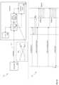
- FIG. 1 Aillustrates one common processor-memory architecture 100 useful for illustrating matrix operations.
- a processor 102is connected to a memory 104 via an interface 106 .
- the processormultiplies the elements of an input vector a against a matrix M to calculate the vector-matrix product b.
- the input vector ais treated as a single column matrix having a number of elements equivalent to the number of rows in the matrix M.
- the processorIn order to calculate the first element of the vector-matrix product b 0 , the processor must iterate through each permutation of input vector a elements for each element within a row of the matrix M. During the first iteration, the first element of the input vector a 0 is read, the current value of the vector-matrix product b 0 is read and the corresponding matrix coefficient value M 0,0 is read. The three (3) read values are used in a multiply-accumulate operation to generate an “intermediary” vector-matrix product b 0 . Specifically, the multiply-accumulate operation calculates: (a 0 ⁇ M 0,0 )+b 0 and writes the result value back to b 0 . Notably, b 0 is an “intermediary value.” After the first iteration but before the second iteration, the intermediary value of b 0 may not correspond to the final value of the vector-matrix product b 0 .
- the second element of the input vector a 1is read, the previously calculated intermediary value b 0 is retrieved, and a second matrix coefficient value M 1,0 is read.
- the three (3) read valuesare used in a multiply-accumulate operation to generate the first element of the vector-matrix product b 0 .
- the second iterationcompletes the computation of b 0 .
- the iterative process described aboveis also performed to generate the second element of the vector-matrix product b 1 .
- the foregoing exampleis a 2 ⁇ 2 vector-matrix product
- the techniques described thereinare commonly extended to support vector-matrix computations of any size. For example, a 3 ⁇ 3 vector-matrix product calculation iterates over an input vector of three (3) elements for each of the three (3) rows of the matrix; thus, requiring nine (9) iterations. A matrix operation of 1024 ⁇ 1024 (which is not uncommon for many applications) would require more than one million iterations. More directly, the aforementioned iterative process exponentially scales as a function of the matrix dimension.
- a matrix-matrix productcan be performed as a series of vector-matrix products. For example, a first vector-matrix product corresponding to the first single column matrix of the input vector is calculated, a second vector-matrix product corresponding to the second single column matrix of the input vector is calculated, etc.
- interface 106the “processor-memory wall”. Even though the processor and the memory may have internal buses with very high bandwidths, the processor-memory system can only communicate as fast as the interface 106 can support electrical signaling (based on the dielectric properties of the materials used in the interface 106 (typically copper) and the transmission distance ( ⁇ 1-2 centimeters)). Moreover, the interface 106 may also include a variety of additional signal conditioning, amplification, noise correction, error correction, parity computations, and/or other interface based logic that further reduces transaction times.
- the local processor cachetakes processor die space, and has a much higher cost-per-bit to manufacture than e.g., comparable memory devices.
- the processor's local cache sizeis usually much smaller (e.g., a few megabytes) than its memory (which can be many gigabytes). From a practical aspect, the smaller local cache is a hard limitation on the maximum amount of matrix operations that can be performed locally within the processor.
- FIG. 1 Billustrates one such processor-PIM architecture 150 .
- a processor 152is connected to a memory 154 via an interface 156 .
- the memory 154further includes a PIM 162 and a memory array 164 ; the PIM 162 is tightly coupled to the memory array 164 via an internal interface 166 .
- the processor-PIM architecture 150 of FIG. 1 Bmultiplies the elements of an input vector a against a matrix M to calculate the vector-matrix product b.
- the PIM 162reads, multiply-accumulates, and writes to the memory 164 internally via the internal interface 166 .
- the internal interface 166in much shorter than the external interface 156 ; additionally, the internal interface 166 can operate natively without e.g., signal conditioning, amplification, noise correction, error correction, parity computations, etc.
- the processor-PIM architecture 150yields substantial improvements in performance over e.g., the processor-memory architecture 100
- the processor-PIM architecture 150may have other drawbacks.
- the fabrication techniques(“silicon process”) are substantially different between processor and memory devices because each silicon process is optimized for different design criteria.
- the processor silicon processmay use thinner transistor structures than memory silicon processes; thinner transistor structures offer faster switching (which improves performance) but suffer greater leakage (which is undesirable for memory retention).
- manufacturing a PIM 162 and memory array 164 in the same waferresults in at least one of them being implemented in a sub-optimal silicon process.
- the PIM 162 and memory array 164may be implemented within separate dies and joined together; die-to-die communication typically increases manufacturing costs and complexity and may suffer from various other detriments (e.g., introduced by process discontinuities, etc.)
- the PIM 162 and the memory array 164are “hardened” components; a PIM 162 cannot store data, nor can the memory 164 perform computations.
- the memory 154once the memory 154 is manufactured, it cannot be altered to e.g., store more data and/or increase/decrease PIM performance/power consumption.
- Such memory devicesare often tailored specifically for their application; this is both costly to design and modify, in many cases they are “proprietary” and/or customer/manufacturer specific. Moreover, since technology changes at a very rapid pace, these devices are quickly obsoleted.
- FIG. 2is a logical block diagram of one exemplary implementation of a memory device 200 manufactured in accordance with the various principles of the present disclosure.
- the memory device 200may include a plurality of partitioned memory cell arrays 220 .
- each of the partitioned memory cell arrays 220may be partitioned at the time of device manufacture.
- the partitioned memory cell arrays 220may be partitioned dynamically (i.e., subsequent to the time of device manufacture).
- the memory cell arrays 220may each include a plurality of banks, each bank including a plurality of word lines, a plurality of bit lines, and a plurality of memory cells arranged at, for example, intersections of the plurality of word lines and the plurality of bit lines.
- the selection of the word linemay be performed by a row decoder 216 and the selection of the bit line may be performed by a column decoder 218 .
- the plurality of external terminals included in the memory device 200may include address terminals 260 , command terminals 262 , clock terminals 264 , data terminals 240 and power supply terminals 250 .
- the address terminals 260may be supplied with an address signal and a bank address signal.
- the address signal and the bank address signal supplied to the address terminals 260are transferred via an address input circuit 202 to an address decoder 204 .
- the address decoder 204receives, for example, the address signal and supplies a decoded row address signal to the row decoder 216 , and a decoded column address signal to the column decoder 218 .
- the address decoder 204may also receive the bank address signal and supply the bank address signal to the row decoder 216 and the column decoder 218 .
- the command terminals 262are supplied with a command signal to a command input circuit 206 .
- the command terminals 262may include one or more separate signals such as e.g., row address strobe (RAS), column address strobe (CAS), read/write (R/W).
- the command signal input to the command terminals 262is provided to the command decoder 208 via the command input circuit 206 .
- the command decoder 208may decode the command signal 262 to generate various control signals.
- the RAScan be asserted to specify the row where data is to be read/written
- the CAScan be asserted to specify where data is to be read/written.
- the R/W command signaldetermines whether or not the contents of the data terminal 240 are written to memory cells 220 , or read therefrom.
- the read datamay be output externally from the data terminals 240 via a read/write amplifier 222 and an input/output circuit 224 .
- a write data commandmay be supplied to the data terminals 240 .
- the write data commandmay be supplied via the input/output circuit 224 and the read/write amplifier 222 to a given memory cell array 220 and written in the memory cell designated by the row address and the column address.
- the input/output circuit 224may include input buffers, in accordance with some implementations.
- the clock terminals 264may be supplied with external clock signals for synchronous operation.
- the clock signalis a single ended signal; in other variants, the external clock signals may be complementary (differential signaling) to one another and are supplied to a clock input circuit 210 .
- the clock input circuit 210receives the external clock signals and conditions the clock signal to ensure that the resulting internal clock signal has sufficient amplitude and/or frequency for subsequent locked loop operation.
- the conditioned internal clock signalis supplied to feedback mechanism (internal clock generator 212 ) provide a stable clock for internal memory logic.
- Common examples of internal clock generation logic 212includes without limitation: digital or analog phase locked loop (PLL), delay locked loop (DLL), and/or frequency locked loop (FLL) operation.
- the memory device 200may rely on external clocking (i.e., with no internal clock of its own).
- a phase controlled clock signalmay be externally supplied to the input/output (IO) circuit 224 .
- This external clockcan be used to clock in written data, and clock out data reads.
- IO circuit 224provides a clock signal to each of the corresponding logical blocks (e.g., address input circuit 202 , address decoder 204 , command input circuit 206 , command decoder 208 , etc.).
- the power supply terminals 250may be supplied with power supply potentials. In some variants (not shown), these power supply potentials may be supplied via the input/output (I/O) circuit 224 . In some embodiments, the power supply potentials may be isolated from the I/O circuit 224 so that power supply noise generated by the IO circuit 224 does not propagate to the other circuit blocks. These power supply potentials are conditioned via an internal power supply circuit 230 . For example, the internal power supply circuit 230 may generate various internal potentials that e.g., remove noise and/or spurious activity, as well as boost or buck potentials, provided from the power supply potentials.
- the internal potentialsmay be used in e.g., the address circuitry ( 202 , 204 ), the command circuitry ( 206 , 208 ), the row and column decoders ( 216 , 218 ), the RW amplifier 222 , and/or any various other circuit blocks.
- a power-on-reset circuit (PON) 228provides a power on signal when the internal power supply circuit 230 can sufficiently supply internal voltages for a power-on sequence.
- a temperature sensor 226may sense a temperature of the memory device 200 and provides a temperature signal; the temperature of the memory device 200 may affect some memory operations.
- the memory arrays 220may be controlled via one or more configuration registers.
- the use of these configuration registersselectively configure one or more memory arrays 220 into one or more matrix fabrics and/or matrix multiplication units (MMUs) described in greater detail herein.
- MMUsmatrix multiplication units
- the configuration registersmay enable the memory cell architectures within the memory arrays to dynamically change both e.g., their structure, operation, and functionality.
- FIG. 3provides a more detailed side-by-side illustration of the memory array and matrix fabric circuitry configurations.
- the memory array and matrix fabric circuitry configurations of FIG. 3both use the same array of memory cells, where each memory cell 15 is composed of a resistive element 302 that is coupled to a word-line 304 and a bit-line 306 , and optionally accumulation circuitry 307 .
- the memory array circuitryis configured to operate as a row decoder 316 , a column decoder 318 , and an array of memory cells 320 .
- the matrix fabric circuitryis configured to operate as a row driver 317 , a matrix multiplication unit (MMU) 319 , and an analog crossbar fabric (matrix fabric) 321 .
- MMUmatrix multiplication unit
- matrix fabricmatrix fabric
- a look-up-table (LUT) and associated logic 315can be used to store and configure different matrix multiplication unit coefficient values.
- the memory array circuitryis configured to operate as a row decoder 316 , a column decoder 318 , and an array of memory cells 320 .
- the matrix fabric circuitryis configured to operate as a row driver 317 , a matrix multiplication unit (MMU) 319 , and an analog crossbar fabric (matrix fabric) 321 .
- MMUmatrix multiplication unit
- matrix fabricanalog crossbar fabric
- a look-up-table (LUT) and associated logic 315can be used to store and configure different matrix multiplication unit coefficient values.
- the memory array 320is composed of a resistive random access memory (ReRAM).
- ReRAMis a non-volatile memory that changes the resistance of memory cells across a dielectric solid-state material, sometimes referred to as a “memristor.”
- Current ReRAM technologymay be implemented within a two-dimensional (2D) layer or a three-dimensional (3D) stack of layers; however higher order dimensions may be used in future iterations.
- CMOScomplementary metal oxide semiconductor
- a crossbar ReRAM arraymay be formed in a one transistor/one resistor (1T1R) configuration and/or in a configuration with one transistor driving n resistive memory cells (1TNR), among other possible configurations.
- phase change chalcogenidese.g., Ge 2 Sb 2 Te 5 , AgInSbTe, among others
- binary transition metal oxidese.g., NiO, TiO 2 , among others
- perovskitese.g., Sr(ZR)TrO 3 , PCMO, among others
- solid state electrolytese.g., GeS, GeSe, SiO x , Cu 2 S, among others
- organic charge transfer complexese.g., Cu tetracynaoquinodimethane (TCNQ), among others
- organic charge acceptor systemse.g., Al amino-dicyanoimidazole (AIDCN), among others
- 2D (layered) insulating materialse.g., hexagonal BN, among others
- the resistive element 302is a non-linear passive two-terminal electrical component that can change its electrical resistance based on a history (e.g., hysteresis or memory) of current application.
- the resistive element 302may form or destroy a conductive filament responsive to the application of different polarities of currents to the first terminal (connected to the word-line 304 ) and the second terminal (connected to the bit-line 306 ). The presence or absence of the conductive filament between the two terminals changes the conductance between the terminals.
- variable impedancee.g., resistance and/or reactance
- Variable impedancemay be effectuated by a variety of linear and/or non-linear elements (e.g., resistors, capacitors, inductors, diodes, transistors, thyristors, etc.)
- a memory “write”may be effectuated by application of a current to the memory cell corresponding to the row and column of the memory array.
- the row decoder 316can selectively drive various ones of the row terminals so as to select a specific row of the memory array circuitry 320 .
- the column decoder 318can selectively sense/drive various ones of the column terminals so as to “read” and/or “write” to the corresponding memory cell that is uniquely identified by the selected row and column (as emphasized in FIG. 3 by the heavier line width and blackened cell element).
- a low resistance state(ON-state) is used to represent the logical “1” and a high resistance state (OFF-state) is used to represent a logical “0”.
- a first currentwith specific polarity, magnitude, and duration is applied to the dielectric solid-state material.
- a memory “read”may be effectuated by application of a second current to the resistive element and sensing whether the resistive element is in the ON-state or the OFF-state based on the corresponding impedance. Memory reads may or may not be destructive (e.g., the second current may or may not be sufficient to form or destroy the conductive filament.)
- the second configuration 350uses the memory cells as an analog crossbar fabric (matrix fabric) 321 to perform matrix multiplication operations.
- matrix fabricmatrix fabric
- FIG. 3corresponds to a 2 ⁇ 4 matrix multiplication unit (MMU)
- MMUmatrix multiplication unit
- DACdigital-analog-conversion
- ADCanalog-to-digital
- each of the row terminalsis concurrently driven by an analog input signal, and each of the column terminals is concurrently sensed for the analog output (which is an analog summation of the voltage potentials across the corresponding resistive elements for each row/column combination).
- the ReRAM crossbar fabric (matrix fabric) 321uses the matrix fabric structure to perform an “analog computation” that calculates a vector-matrix product (or scalar-matrix product, matrix-matrix product, etc.)
- the concurrent vector-matrix product calculation within the crossbar fabricis atomic.
- the analog computation of vector-matrix productscan complete in a single access cycle.
- an atomic operationis immune to data race conditions.
- the vector-matrix product calculationperforms calculations on all rows and all columns of the matrix operation concurrently; in other words, the vector-matrix product calculation does not scale in complexity as a function of matrix dimension. While fabrication constraints (e.g., ADC/DAC granularity, manufacturing tolerance, etc.) may limit the amount of precision and complexity that a single matrix fabric can produce, multiple matrix operations may be mathematically combined together to provide much higher precisions and complexities.
- inputsare converted to the analog domain by the DAC 308 for analog computation, but may also be converted back to the digital domain by the ADC 310 for subsequent digital and/or logical manipulation.
- the arithmetic logic unit 312can enable sophisticated numeric manipulation of matrix fabric 321 output. Such capabilities may be used where the analog domain cannot implement the required computation due to practical implementation limitations (e.g., manufacturing cost, etc.)
- This simple FFT butterfly 400 of EQN. 1can be decomposed into two distinct matrices representing the positive and negative coefficients (EQN. 2 and EQN. 3):
- EQN. 2 and EQN. 3can be implemented as analog computations with the matrix fabric circuitry. Once calculated, the resulting analog values may be converted back to the digital domain via the aforementioned ADC. Existing ALU operations may be used to perform subtraction in the digital domain (EQN. 4):
- a 2 ⁇ 2 matrixcan be further subdivided into a 2 ⁇ 2 positive matrix and a 2 ⁇ 2 negative matrix.
- the ALUcan add/subtract the results of the 2 ⁇ 2 positive matrix and a 2 ⁇ 2 negative matrix to generate a single 2 ⁇ 2 matrix.
- Artisans of ordinary skill in the related artswill readily appreciate the wide variety and/or capabilities enabled by ALUs.
- ALUsmay provide arithmetic operations (e.g., add, subtract, add with carry, subtract with borrow, negate, increment, decrement, pass through, etc.), bit-wise operations (e.g., AND, OR, XOR, complement), bit-shift operations (e.g., arithmetic shift, logical shift, rotate, rotate through carry, etc.) to enable e.g., multiple-precision arithmetic, complex number operations, and/or any extend MMU capabilities to any degree of precision, size, and/or complexity.
- arithmetic operationse.g., add, subtract, add with carry, subtract with borrow, negate, increment, decrement, pass through, etc.
- bit-wise operationse.g., AND, OR, XOR, complement
- bit-shift operationse.g., arithmetic shift, logical shift, rotate, rotate through carry, etc.
- digital and/or “logical” within the context of computationrefers to processing logic that uses quantized values (e.g., “0” and “1”) to represent symbolic values (e.g., “ON-state”, “OFF-state”).
- analogwithin the context of computation refers to processing logic that uses the continuously changeable aspects of physical signaling phenomena such as electrical, chemical, and/or mechanical quantities to perform a computation.
- Various embodiments of the present disclosure representmay represent analog input and/or output signals as a continuous electrical signal. For example, a voltage potential may have different possible values (e.g., any value between a minimum voltage (0V) and a maximum voltage (1.8V) etc.).
- DACsdigital-to-analog converters
- ADCsanalog-digital-converters
- ALUsarithmetic logic units
- each of the resistive elementsmay be written with a corresponding matrix coefficient value.
- the second configuration 350may write varying degrees of impedance (representing a coefficient value) into each ReRAM cell using an amount of current having a polarity, magnitude, and duration selected to set a specific conductance. In other words, by forming/destroying conductive filaments of varying conductivity, a plurality of different conductivity states can be established.
- applying a first magnitudemay result in a first conductance
- applying a second magnitudemay result in a second conductance
- applying the first magnitude for a longer durationmay result in a third conductance
- the varying conductancecan use a multiplicity of states (e.g., three (3), four (4), eight (8), etc.) to represent a continuous range of values and/or ranges of values (e.g., [0, 0.33, 0.66, 1], [0, 0.25, 0.50, 0.75, 1], [0, 0.125, 0.250, . . . , 1], etc.).
- a multiplicity of statese.g., three (3), four (4), eight (8), etc.
- the matrix coefficient valuesare stored ahead of time within a look-up-table (LUT) and configured by associated control logic 315 .
- LUTlook-up-table
- the matrix fabric 321is written with matrix coefficient values from the LUT via control logic 315 .
- certain memory technologiesmay also enable write-once-use-many operation. For example, even though forming (or destroying) a conductive filament for a ReRAM cell may require a specific duration, magnitude, polarity, and/or direction of current; subsequent usage of the memory cell can be repeated many times (so long as the conductive filament is not substantially formed nor destroyed over the usage lifetime). In other words, subsequent usages of the same matrix fabric 321 configuration can be used to defray initial configuration times.
- certain memory technologiesare non-volatile.
- matrix fabric circuitryonce matrix fabric circuitry is programmed, it may enter a low power state (or even powered off) to save power when not in use.
- the non-volatility of the matrix fabricmay be leveraged to further improve power consumption.
- the exemplary matrix fabriccan store the matrix coefficient values even when the memory device is powered off. On subsequent wake-up, the matrix fabric can be directly used.
- the matrix coefficient valuesmay be derived according to the nature of the matrix operation. For example, the coefficients for certain matrix operations can be derived ahead of time based on the “size” (or other structurally defined parameter) and stored within the LUT. As but two such examples, the fast Fourier transform (EQN. 5) and the discrete cosine transform (DCT) (EQN. 6) are reproduced infra:
- the matrix coefficient valuesare determined according to the size of the transform.
- the coefficients for an 8-point FFTare:
- ⁇ ⁇ ⁇ k N(where k is 0, 1, 2, 3 . . . 7) can be set a priori.
- the coefficients for larger FFTsinclude the coefficients for smaller FFTs.
- a 64-point FFThas 64 coefficient values, which include all 32 coefficients used in a 32-point FFT, and all 16 coefficients for a 16-point FFT, etc. More directly, a single LUT may contain all the coefficients to support any number of different transforms.
- the matrix coefficient valuesmay be stored ahead of time.
- the coefficients for certain matrix multiplication operationsmay be known or otherwise defined by e.g., an application or user.
- image processing computationssuch as are described in co-owned and co-pending U.S. patent application Ser. No. 16/002,644 filed Jun. 7, 2018 and entitled “AN IMAGE PROCESSOR FORMED IN AN ARRAY OF MEMORY CELLS”, previously incorporated supra, may define a variety of different matrix coefficient values so as to effect e.g., defect correction, color interpolation, white balance, color adjustment, gamma lightness, contrast adjustment, color conversion, down-sampling, and/or other image signal processing operations.
- the coefficients for certain matrix multiplication operationsmay be determined or otherwise defined by e.g., user considerations, environmental considerations, other devices, and/or other network entities.
- wireless devicesoften experience different multipath effects that can interfere with operation.
- Various embodiments of the present disclosuredetermine multipath effects and correct for them with matrix multiplication.
- the wireless devicemay calculate each of the independent different channel effects based on degradation of known signaling. The differences between an expected and an actual reference channel signal can be used to determine the noise effects that it experienced (e.g., attenuation over specific frequency ranges, reflections, scattering, and/or other noise effects).
- a wireless devicemay be instructed to use a predetermined “codebook” of beamforming configurations.
- the codebook of beamforming coefficientsmay be less accurate but may be preferable for other reasons (e.g., speed, simplicity, etc.).
- the matrix coefficient valuesare stored ahead of time within a look-up-table (LUT) and configured by associated control logic 315 .
- the matrix fabricmay be configured via dedicated hardware logic.
- Such internal hardware logicmay not be limited by processor word size; thus matrix coefficient values of any dimension may be concurrently configurable (e.g., a 4 ⁇ 4, 8 ⁇ 8, 16 ⁇ 16, etc.) While the present disclosure is presented in the context of internal control logic 315 , external implementations may be substituted with equivalent success.
- the logicincludes internal processor-in-memory (PIM) that can set the matrix coefficient values based on LUT values in a series of reads and writes.
- PIMprocessor-in-memory
- an external processorcan perform the LUT and/or logic functionality.
- FIG. 5 Ais a logical block diagram of one exemplary implementation of a processor-memory architecture 500 in accordance with the various principles described herein.
- a processor 502is coupled to a memory 504 ; the memory includes a look-up-table (LUT) 506 , a control logic 508 , a matrix fabric and corresponding matrix multiplication unit (MMU) 510 , and a memory array 512 .
- LUTlook-up-table
- MMUmatrix multiplication unit
- the LUT 506stores a plurality of matrix value coefficients, dimensions, and/or other parameters, associated with different matrix operations.
- the LUT 506stores a plurality of fast Fourier transform (FFT) “twiddle factors”; where various subsets of the twiddle factors are associated with different FFT dimensions.
- FFTfast Fourier transform
- a LUT 506 that stores the twiddle factors for a 64-point FFThas 64 coefficient values, which include all 32 coefficients used in a 32-point FFT, and all 16 coefficients for a 16-point FFT, etc.
- the LUT 506stores a plurality of discrete cosine transform (DCT) “twiddle factors” associated with different DCT dimensions.
- DCTdiscrete cosine transform
- the LUT 506stores a plurality of different matrix coefficient values for image signal processing (ISP) e.g., defect correction, color interpolation, white balance, color adjustment, gamma lightness, contrast adjustment, color conversion, down-sampling, and/or other image signal processing operations.
- ISPimage signal processing
- the LUT 506may include various channel matrix codebooks that may be predefined and/or empirically determined based on radio channel measurements.
- control logic 508controls operation of the matrix fabric and MMU 510 based on instructions received from the processor 502 .
- the control logic 508can form/destroy conductive filaments of varying conductivity within each of the memory cells of a matrix fabric in accordance with the aforementioned matrix dimensions and/or matrix value coefficients provided by the LUT 506 .
- the control logic 508can configure a corresponding MMU to perform any additional arithmetic and/or logical manipulations of the matrix fabric.
- control logic 508may select one or more digital vectors to drive the matrix fabric, and one or more digital vectors to store the logical outputs of the MMU.
- an “instruction”generally includes different types of “instruction syllables”: e.g., opcodes, operands, and/or other associated data structures (e.g., registers, scalars, vectors).
- opcodeoperation code refers to an instruction that can be interpreted by a processor logic, memory logic, or other logical circuitry to effectuate an operation. More directly, the opcode identifies an operation to be performed on one or more operands (inputs) to generate one or more results (outputs). Both operands and results may be embodied as data structures. Common examples of data structures include without limitation: scalars, vectors, arrays, lists, records, unions, objects, graphs, trees, and/or any number of other form of data. Some data structures may include, in whole or in part, referential data (data that “points” to other data). Common examples of referential data structures include e.g., pointers, indexes, and/or descriptors.
- the opcodemay identify one or more of: a matrix operation, the dimensions of the matrix operation, and/or the row and/or column of the memory cells.
- an operandis a coded identifier that specifies the one or more digital vectors that are to be operated upon. For example, an instruction to process a 64-point FFT on an input digital vector, and store the results in an output digital vector might include the opcode and operands: FFT64 ($input, $output), where: FFT64 identifies the size and nature of the 64-point FFT operation, $input identifies an input digital vector base address, and $output identifies an output digital vector base address.
- the 64-point FFTmay be split into two distinct atomic operations e.g., FFT64($address) that converts the memory array at the $address into a 64-point matrix fabric, and MULT($address, $input, $output) that stores the vector-matrix product of the $input and the matrix fabric at $address to $output.
- FFT64($address)that converts the memory array at the $address into a 64-point matrix fabric
- MULT($address, $input, $output)that stores the vector-matrix product of the $input and the matrix fabric at $address to $output.
- FIG. 5 Aillustrates an instruction interface that is functionally separate and distinct from the input/output (I/O) memory interface.
- the instruction interfacemay be physically distinct (e.g., having different pins and/or connectivity).
- the instruction interfacemay be multiplexed with the I/O memory interface (e.g., sharing the same control signaling, and address and/or data bus but in a distinct communication mode).
- the instruction interfacemay be virtually accessible via the I/O memory interface (e.g., as registers located within address space that is addressable via the I/O interface). Still other variants may be substituted by artisans of ordinary skill, given the contents of the present disclosure.
- the matrix fabric and MMU 510are tightly coupled to a memory array 512 to read and write digital vectors (operands).
- the operandsare identified for dedicated data transfer hardware (e.g., a direct memory access (DMA)) into and out of the matrix fabric and MMU 510 .
- the digital vectors of datamay be of any dimension, and are not limited by processor word size.
- an operandmay specify an operand of N-bits (e.g., 2, 4, 8, 16, etc.).
- the control logic 508e.g., DMA logic
- the control logic 508e.g., DMA logic
- FIG. 5 Bprovides a logical flow diagram of one exemplary set of matrix operations 550 within the context of the exemplary embodiment 500 described in FIG. 5 A .
- the processor 502writes an instruction to the memory 504 through interface 507 that specifies an opcode (e.g., characterized by a matrix M x,y ) and the operands (e.g., digital vectors a, b).
- an opcodee.g., characterized by a matrix M x,y
- the operandse.g., digital vectors a, b.
- the control logic 508determines whether or not the matrix fabric and/or matrix multiplication unit (MMU) should be configured/reconfigured. For example, a section of the memory array is converted into one or more matrix fabrics and weighted with the associated matrix coefficient values defined by the matrix M x,y . Digital-to-analog (DAC) row drivers and analog-to-digital (ADC) sense amps associated with the matrix fabric may need to be adjusted for dynamic range and/or amplification. Additionally, one or more MMU ALU components may be coupled to the one or more matrix fabrics.
- MMUmatrix multiplication unit
- the input operand ais read by the digital-to-analog (DAC) and applied to the matrix fabric M x,y for analog computation.
- the analog resultmay additionally be converted with analog-to-digital (ADC) conversion for subsequent logical manipulation by the MMU ALUs.
- the outputis written into the output operand b.
- FIG. 5 Cprovides an alternative logical flow diagram of one exemplary set of matrix operations 560 within the context of the exemplary embodiment 500 described in FIG. 5 A .
- the system of FIG. 5 Cuses an explicit instruction to convert the memory array into a matrix fabric. Providing further degrees of atomicity in instruction behaviors can enable a variety of related benefits including for example, pipeline design and/or reduced instruction set complexity.
- matrix operationsmay be efficiently repeated.
- image processing computationssuch as are described in co-owned and co-pending U.S. patent application Ser. No. 16/002,644 filed Jun. 7, 2018 and entitled “AN IMAGE PROCESSOR FORMED IN AN ARRAY OF MEMORY CELLS”, previously incorporated supra, may configure a number of matrix fabric and MMU processing elements so as to pipeline e.g., defect correction, color interpolation, white balance, color adjustment, gamma lightness, contrast adjustment, color conversion, down-sampling, and/or other image signal processing operations.
- Each one of the pipeline stagesmay be configured once, and repeatedly used for each pixel (or group of pixels) of the image.
- the white balance pipeline stagemay operate on each pixel of data using the same matrix fabric with the matrix coefficient values set for white balance; the color adjustment pipeline stage may operate on each pixel of data using the same matrix fabric with the matrix coefficient values set for color adjustment, etc.
- the first stage of a 64-point FFTcan be handled in thirty two (32) atomic MMU computations (thirty two (32) 2-point FFTs) using the same FFT “twiddle factors” (described supra).
- a 64-point FFThas 64 coefficient values, which include all 32 coefficients used in a 32-point FFT.
- a matrix fabric that is configured for 64-point operationcould be reused for 32-point operation with the appropriate application of the 32-point input operand a on the appropriate rows of the 64-point FFT matrix fabric.
- FFT twiddle factorsare a superset of discrete cosine transform (DCT) twiddle factors; thus, an FFT matrix fabric could also be used (with appropriate application of input operand a) to calculate DCT results.
- DCTdiscrete cosine transform
- FIG. 6a logical flow diagram of one exemplary method 600 converting a memory array into a matrix fabric for matrix transformations and performing matrix operations therein is presented.
- a memory devicereceives one or more instructions.
- the memory devicereceives the instruction from a processor.
- the processoris an application processor (AP) commonly used in consumer electronics.
- the processoris a baseband processor (BB) commonly used in wireless devices.
- APapplication processor
- BBbaseband processor
- OSoperating system
- firmwarefirmware
- peripheral accesse.g., a file transfer protocol, a file transfer protocol, and the like.
- a so-called “baseband processor”is a processor that is configured to communicate with a wireless network via a communication protocol stack.
- the term “communication protocol stack”refers to the software and hardware components that control and manage access to the wireless network resources.
- a communication protocol stackcommonly includes without limitation: physical layer protocols, data link layer protocols, medium access control protocols, network and/or transport protocols, etc.
- server devicesoften include multiple processors sharing a common memory resource.
- processorssuch as graphics engine, or digital signal processor (DSP)
- graphics processing unitsGPUs
- VPUsvideo processing units
- TPUstensor processing units
- NPUsneural network processing units
- DSPsdigital signal processors
- ISPsimage signal processors
- the memory devicereceives the instruction from an application specific integrated circuit (ASIC) or other forms of processing logic e.g., field programmable gate arrays (FPGAs), programmable logic devices (PLDs), camera sensors, audio/video processors, and/or media codecs (e.g., image, video, audio, and/or any combination thereof).
- ASICapplication specific integrated circuit
- FPGAsfield programmable gate arrays
- PLDsprogrammable logic devices
- camera sensorse.g., a camera sensors, audio/video processors, and/or media codecs (e.g., image, video, audio, and/or any combination thereof).
- media codecse.g., image, video, audio, and/or any combination thereof.
- the memory deviceis a resistive random access memory (ReRAM) arranged in a “crossbar” row-column configuration.
- ReRAMresistive random access memory
- the various embodiments described hereinassume a specific memory technology and specific memory structure, artisans of ordinary skill in the related arts given the contents of the present disclosure will readily appreciate that the principles described herein may be broadly extended to other technologies and/or structures.
- certain programmable logic structurese.g., commonly used in field programmable gate arrays (FPGAs) and programmable logic devices (PLDs)
- FPGAsfield programmable gate arrays
- PLDsprogrammable logic devices
- processor and/or other memory technologiesmay vary resistance, capacitance, and/or inductance; in such cases, varying impedance properties may be used to perform analog computations.
- crossbarbased construction provides a physical structure that is well adapted to two-dimensional (2D) matrix structures, other topologies may be well adapted to higher order mathematical operations (e.g., matrix-matrix products via three-dimensional (3D) memory stacking, etc.)
- the memory devicefurther includes a controller.
- the controllerreceives the one or more instructions and parses each instruction into one or more instruction components (also commonly referred to as “instruction syllables”).
- the instruction syllablesinclude at least one opcode and one or more operands. For example, an instruction may be parsed into an opcode, a first source operand, and a destination operand.
- instruction componentsmay include without limitation, a second source operand (for binary operations), a shift amount, an absolute/relative address, a register (or other reference to a data structure), an immediate data structure (i.e., a data structure provided within the instruction itself), a subordinate function, and/or branch/link values (e.g., to be executed depending on whether an instruction completes or fails).
- each received instructioncorresponds to an atomic memory controller operation.
- an “atomic” instructionis an instruction that completes within a single access cycle.
- a “non-atomic” instructionis an instruction that may or may not complete within a single access cycle. Even though non-atomic instructions might complete in a single cycle, they must be treated as non-atomic to prevent data race conditions.
- a race conditionoccurs where data that is being accessed by a processor instruction (either a read or write) may be accessed by another processor instruction before the first processor instruction has a chance to complete; the race condition may unpredictably result in data read/write errors.
- an atomic instructionguarantees that the data cannot be observed in an incomplete state.
- an atomic instructionmay identify a portion of the memory array to be converted to a matrix fabric.
- the atomic instructionmay identify characteristic properties of the matrix fabric.
- the atomic instructionmay identify the portion of the memory array on the basis of e.g., location within the memory array (e.g., via offset, row, column), size (number of rows, number of columns, and/or other dimensional parameters), granularity (e.g., the precision and/or sensitivity).
- atomic instructionsmay offer very fine grained control over memory device operation; this may be desirable where the memory device operation can be optimized in view of various application specific considerations.
- a non-atomic instructionmay specify portions of the memory array that are to be converted into a matrix fabric.
- the non-atomic instructionmay specify various requirements and/or constraints for the matrix fabric.
- the memory controllermay internally allocate resources so as to accommodate the requirements and/or constraints.
- the memory controllermay additionally prioritize and/or de-prioritize instructions based on the current memory usage, memory resources, controller bandwidth, and/or other considerations. Such implementations may be particularly useful where memory device management is unnecessary and would otherwise burden the processor.
- the instructionspecifies a matrix operation.
- the matrix operationmay be a vector-matrix product.
- the matrix operationmay be a matrix-matrix product.
- Still other variantsmay be substituted by artisans of ordinary skill in the related arts, given the contents of the present disclosure.
- Such variantsmay include e.g., scalar-matrix products, higher order matrix products, and/or other transformations including e.g., linear shifts, rotations, reflections, and translations.
- transformationrefers to a mathematical operation that converts an input from a first domain into a second domain. Transformations can be “injective” (every element of the first domain has a unique element in the second domain), “surjective” (every element of the second domain has a unique element in the first domain), or “bijective” (a unique one-to-one mapping of elements from the first domain to the second domain).
- More complex mathematically defined transformationsthat are regularly used in the computing arts include Fourier transforms (and its derivatives, such as the discrete cosine transform (DCT)), Hilbert transforms, Laplace transforms, and Legendre transforms.
- matrix coefficient values for mathematically defined transformationscan be calculated ahead of time and stored within a look-up-table (LUT) or other data structure. For example, twiddle factors for the fast Fourier transform (FFT) and/or DCT can be calculated and stored within a LUT.
- matrix coefficient values for mathematically defined transformationscan be calculated by the memory controller during (or in preparation for) the matrix fabric conversion process.
- transformationsmay not be based on a mathematical definition per se, but may instead by defined based on e.g., an application, another device, and/or a network entity. Such transformations may be commonly used in encryption, decryption, geometric modeling, mathematical modeling, neural networks, network management, and/or other graph theory based applications.
- wireless networksmay use a codebook of predetermined antenna weighting matrixes so as to signal the most commonly used beamforming configurations.
- certain types of encryptionmay agree upon and/or negotiate between different encryption matrices. In such embodiments, the codebook or matrix coefficient values may be agreed ahead of time, exchanged in an out-of-band manner, exchanged in-band, or even arbitrarily determined or negotiated.
- Empirically determined transformationsmay also be substituted with equivalent success given the contents of the present disclosure.
- empirically derived transformationsthat are regularly used in the computing arts include radio channel coding, image signal processing, and/or other mathematically modeled environmental effects.
- a multi-path radio environmentcan be characterized by measuring channel effects on e.g., reference signals.
- the resulting channel matrixcan be used to constructively interfere with signal reception (e.g., improving signal strength) while simultaneously destructively interfering with interference (e.g., reducing noise).
- an image that has a skewed huecan be assessed for overall color balance, and mathematically corrected.
- an imagemay be intentionally skewed based on e.g., user input, so as to impart an aesthetic “warmth” to an image.
- Various embodiments of the present disclosuremay implement “unary” operations within a memory device. Other embodiments may implement “binary”, or even higher order “N-ary” matrix operations.
- the terms “unary”, “binary”, and “N-ary”refer to operations that take one, two, or N input data structures, respectively.
- binary and/or N-ary operationsmay be subdivided into one or more unary matrix in-place operators.
- an “in-place” operatorrefers to a matrix operation that stores or translates its result its own state (e.g., its own matrix coefficient values). For example, a binary operation may be decomposed into two (2) unary operations;
- Still other embodimentsmay serialize and/or parallelize matrix operations based on a variety of considerations. For example, sequentially related operations may be performed in a “serial” pipeline.
- image processing computationssuch as are described in co-owned and co-pending U.S. patent application Ser. No. 16/002,644 filed Jun. 7, 2018 and entitled “AN IMAGE PROCESSOR FORMED IN AN ARRAY OF MEMORY CELLS”, previously incorporated supra, configures a number of matrix fabric and MMU processing elements to pipeline e.g., defect correction, color interpolation, white balance, color adjustment, gamma lightness, contrast adjustment, color conversion, down-sampling, etc.
- Pipelined processingcan often produce very high throughput data with minimal matrix fabric resources.
- unrelated operationsmay be performed in “parallel” with separate resources.
- the first stage of a 64-point FFTcan be handled with thirty two (32) separate matrix fabrics operating configured as 2-point FFTs.
- Highly parallelized operationcan greatly reduce latency; however the overall memory fabric resource utilization may be very high.
- the instructionis received from a processor via a dedicated interface.
- Dedicated interfacesmay be particularly useful where the matrix computation fabric is treated akin to a co-processor or a hardware accelerator. Notably, dedicated interfaces do not require arbitration, and can be operated at very high speeds (in some cases, at the native processor speed).
- the instructionis received via a shared interface.
- the shared interfacemay be multiplexed in time, resource (e.g., lanes, channels, etc.), or other manner with other concurrently active memory interface functionality.
- memory interface functionalityinclude without limitation: data input/output, memory configuration, processor-in-memory (PIM) communication, direct memory access, and/or any other form of blocking memory access.
- the shared interfacemay include one or more queuing and/or pipelining mechanisms. For example, some memory technologies may implement a pipelined interface so as to maximize memory throughput.
- the instructionsmay be received from any entity having access to the memory interface.
- a camera co-processorimage signal processor (ISP)
- ISPimage signal processor
- the camera co-processormay be able offload its processing tasks to a matrix fabric of the memory device.
- the ISPmay accelerate/offload/parallelize e.g., color interpolation, white balance, color correction, color conversion, etc.
- BBbaseband co-processor
- BBbaseband co-processor
- the BB processormay be able to offload e.g., FFT/IFFT, channel estimation, beamforming calculations, and/or any number of other networking tasks to a matrix fabric of a memory device.
- FFT/IFFTFast Fourier transform
- IFFTIFFT-IFFT
- channel estimatione.g., channel estimation
- beamforming calculationse.g., beamforming calculations
- any number of other networking taskse.g., channel estimation, beamforming calculations, and/or any number of other networking tasks.
- video and/or audio codecsoften utilize DCT/IDCT transformations, and would benefit from matrix fabric operations. Still other variants of the foregoing will be readily appreciated by artisans of ordinary skill in the related arts, given the contents of the present disclosure.
- Various implementations of the present disclosuremay support a queue of multiple instructions.
- matrix operationsmay be queued together.
- multiple vector-matrix multiplicationsmay be queued together in order to effectuate a matrix multiplication.
- a higher order transforme.g., FFT1024
- a lower order constituent transforme.g., FFT512, etc.
- ISP processing for an imagemay include multiple iterations over the iteration space (each iteration may be queued in advance). Still other queuing schemes may be readily substituted by artisans of ordinary skill in the related arts with equal success, given the contents of the present disclosure.
- matrix operationsmay be cascaded together to achieve matrix operations of a higher rank.
- a higher order FFTe.g., 1024 ⁇ 1024
- can be decomposed into multiple iterations of lower rank FFTse.g., four (4) iterations of 512 ⁇ 512 FFTs, sixteen (16) iterations of 256 ⁇ 256 FFTs, etc.
- arbitrarily sized N-point DFTse.g., that is not a power of 2
- cascading DFTsof other sizes.
- the ReRAM's non-volatile natureretains memory contents even when the ReRAM is unpowered.
- certain variants of the processor-memory architecturemay enable one or more processors to independently power the memory.
- the processormay power the memory when the processor is inactive (e.g., keeping the memory active while the processor is in low power).
- Independent power management of the memorymay be particularly useful for e.g., performing matrix operations in memory, even while the processor is asleep.
- the memorymay receive a plurality of instructions to execute; the processor can transition into a sleep mode until the plurality of instructions have been completed.
- Still other implementationsmay use the non-volatile nature of ReRAM to hold memory contents while the memory is powered off; for example, certain video and/or image processing computations may be held within ReRAM during inactivity.
- a memory array(or portion thereof) may be converted into a matrix fabric based on the instruction.
- matrix fabricrefers to a plurality of memory cells having a configurable impedance that, when driven with an input vector, yield an output vector and/or matrix.
- the matrix fabricmay be associated with a portion of the memory map.
- the portionis configurable in terms of its size and/or location. For example, a configurable memory register may determine whether a bank is configured as a memory or as a matrix fabric.
- the matrix fabricmay reuse and/or even block memory interface operation.
- the memory devicemay allow the memory interface may be GPIO based (e.g., in one configuration, the pins of the memory interface may selectively operate as ADDR/DATA during normal operation, or e.g., FFT16, etc. during matrix operation.)
- the memory interfacemay be GPIO based (e.g., in one configuration, the pins of the memory interface may selectively operate as ADDR/DATA during normal operation, or e.g., FFT16, etc. during matrix operation.)
- the instructionidentifies a matrix fabric characterized by structurally defined coefficients.
- a matrix fabriccontains the coefficients for a structurally defined matrix operation.
- a matrix fabric for an 8 ⁇ 8 FFTis an 8 ⁇ 8 matrix fabric that has been pre-populated with structurally defined coefficients for an FFT.
- the matrix fabricmay be pre-populated with coefficients of a particular sign (positive, negative) or of a particular radix (the most significant bits, least significant bits, or intermediary bits).
- structurally defined coefficientsrefer to the fact that the coefficients of the matrix multiplication are defined by the matrix structure (e.g., the size of the matrix), not the nature of the operation (e.g., multiplying operands).
- a structurally defined matrix operationmay be identified by e.g., a row and column designation (e.g., 8 ⁇ 8, 16 ⁇ 16, 32 ⁇ 32, 64 ⁇ 64, 128 ⁇ 128, 256 ⁇ 256, etc.) While the foregoing discussions are presented in the context of full rank matrix operations, deficient matrix operators may be substituted with equivalent success.
- a matrix operationmay have asymmetric columns and/or rows (e.g., 8 ⁇ 16, 16 ⁇ 8, etc.)
- many vector-based operationsmay be treated as a row with a single column, or a column with a single row (e.g., 8 ⁇ 1, 1 ⁇ 8).
- controlling logicmay determine whether resources exist to provide the matrix fabric.
- a matrix operationmay be evaluated by a pre-processor to determine whether or not it should be handled within software or within dedicated matrix fabric. For example, if the existing memory and/or matrix fabric usage consumes all of the memory device resources, then the matrix operation may need to be handled within software rather than via the matrix fabric. Under such circumstances, the instruction may be returned incomplete (resulting in traditional matrix operations via processor instructions). In another such example, configuring a temporary matrix fabric to handle a simple matrix operation may yield such little return, that the matrix operation should be handled within software.
- memory managementmay allocate portions of the memory array for memory and/or matrix fabric.
- portions of the memory arraymay be statically allocated. Static allocations may be preferable to reduce memory management overhead and/or simplify operational overhead (wear leveling, etc.).
- portions of the memory arraymay be dynamically allocated. For example, wear-leveling may be needed to ensure that a memory uniformly degrades in performance (rather than wearing out high usage areas).
- Still other variantsmay statically and/or dynamically allocate different portions; for example, a subset of the memory and/or matrix fabric portions may be dynamically and/or statically allocated.
- wear leveling memory cellscan be performed in any discrete amount of memory (e.g., a bank of memory, a chunk of memory, etc.)
- Wear leveling matrix fabricmay use similar techniques; e.g., in one variant, wear leveling matrix fabric portions may require that the entire matrix fabric is moved in aggregate (the crossbar structure cannot be moved in pieces).
- wear leveling matrix fabric portionsmay be performed by first decomposing the matrix fabric into constituent matrix computations and dispersing the constituent matrix computations to other locations. More directly, matrix fabric wear leveling may indirectly benefit from the “logical” matrix manipulations that are used in other matrix operations (e.g., decomposition, cascading, parallelization, etc.). In particular, decomposing a matrix fabric into its constituent matrix fabrics may enable better wear leveling management with only marginally more complex operation (e.g., the additional step of logical combination via MMU).
- conversionincludes reconfiguring the row decoder to operate as a matrix fabric driver that variably drives multiple rows of the memory array.
- the row driverconverts a digital value to an analog signal.
- digital-to-analog conversionincludes varying a conductance associated with a memory cell in accordance with a matrix coefficient value.
- conversionmay include reconfiguring the column decoder to perform analog decoding.
- the column decoderis reconfigured to sense analog signals corresponding to a column of varying conductance cells that are driven by corresponding rows of varying signaling. The column decoder converts an analog signal to a digital value. While the foregoing construction is presented in one particular row-column configuration, other implementations may be substituted with equal success.
- a column drivermay convert a digital value to an analog signal
- a row decodermay convert an analog signal to a digital value
- a three-dimension (3D) row-column-depth memorymay implement 2D matrices in any permutation (e.g., row-driver/column-decoder, row-driver/depth-decoder, column-driver/depth-decoder, etc.) and/or 3D matrix permutations (e.g., row-driver/column-decoder-driver/depth-decoder).
- the matrix coefficient valuescorrespond to a structurally determined value.
- Structurally determined valuesmay be based on the nature of the operation. For example, a fast Fourier transform (FFT) transform on a vector of length N (where N is a power of 2) can be performed with FFT butterfly operations (of 2 ⁇ 2) or some higher order of butterfly (e.g., 4 ⁇ 4, 8 ⁇ 8, 16 ⁇ 16, etc.)
- FFTfast Fourier transform
- the intermediate constituent FFT butterfly operation weightingis defined as a function of the unit circle
- n and kare determined from the FFT vector length N; in other words, the FFT butterfly weighting operations are structurally defined according to the length of vector of length N.
- the discrete Fourier transform (DFT) and discrete cosine transform (DCT)both use structurally defined coefficients.
- the matrix fabricitself has structurally determined dimensions. Structurally determined dimensions may be based on the nature of the operation; for example, an ISP white balance processing may use a 3 ⁇ 3 matrix (corresponding to different values of Red (R), Green (G), Blue (B), Luminance (Y), Chrominance Red (Cr), Chrominance Blue (Cb), etc.)
- channel matrix estimations and/or beamforming codebooksare often defined in terms of the number of multiple-input-multiple-output (MIMO) paths. For example, a 2 ⁇ 2 MIMO channel has a corresponding 2 ⁇ 2 channel matrix and a corresponding 2 ⁇ 2 beamforming weighting.
- MIMOmultiple-input-multiple-output
- a matrix fabricmay include only a portion of the matrix coefficient values (to perform only a portion of the matrix operation). For example, performing signed operation and/or higher level radix computations may require levels of manufacturing tolerance that are prohibitively expensive.
- Signed matrix operationmay be split into positive and negative matrix operations (which are later summed by a matrix multiplication unit (MMU) described elsewhere herein).
- MMUmatrix multiplication unit
- high radix matrix operationmay be split into e.g., a most significant bit (MSB) portion, a least significant bit (LSB) portion, and/or any intermediary bits (which may be bit shifted and summed by the aforementioned MMU).
- MSBmost significant bit
- LSBleast significant bit
- the matrix coefficient valuesare determined ahead of time and stored in a look-up-table for later reference.
- a matrix operationthat has both structurally determined dimensions and structurally determined values may be stored ahead of time.
- an FFT of eight (8) elementshas structurally determined dimensions (8 ⁇ 8) and structurally determine values
- a FFT8 instructionmay result in the configuration of an 8 ⁇ 8 matrix fabric that is pre-populated with the corresponding FFT8 structurally determined values.
- antenna beamforming coefficientsare often defined ahead of time within a codebook; a wireless network may identify a corresponding index within the codebook to configure antenna beamforming.
- a MIMO codebookmay identify the possible configurations for a 4 ⁇ 4 MIMO system; during operation, the selected configuration can be retrieved from a codebook based an index thereto.
- one or more matrix multiplication unitsmay be configured on the basis of the instruction.
- certain matrix fabricsmay implement logical (mathematical identities) to handle a single stage of a matrix operation; however, multiple stages of matrix fabrics may be cascaded together to achieve more complex matrix operations.
- a first matrixis used to calculate positive products of a matrix operation and a second matrix is used to calculate the negative products of a matrix operation.
- the resulting positive and negative productscan be compiled within an MMU to provide a signed matrix multiplication.
- a first matrixis used to calculate a first radix portion of a matrix operation and a second matrix is used to calculate a second radix portion of a matrix operation.
- the resulting radix portionscan be bit shifted and/or summed within an MMU to provide a larger radix product.
- logical matrix operationsare distinguished from analog matrix operations.
- the exemplary matrix fabricconverts analog voltages or current into digital values that are read by the matrix multiplication unit (MMU).
- Logical operationscan manipulate digital values via mathematical properties (e.g., via matrix decomposition, etc.); analog voltages or current cannot be manipulated in this manner.
- matricescan be decomposed or factorized into one or more constituent matrices.
- multiple constituent matricescan be aggregated or combined into a single matrix.
- matricesmay be expanded in row and/or column to create a deficient matrix of larger dimension (but identical rank).
- Such logicmay be used to implement many higher order matrix operations. For example, multiplying two matrices together may be decomposed as a number of vector-matrix multiplications. These vector-matrix multiplications may be further implemented as multiply-accumulate logic within a matrix multiplication unit (MMU).
- MMUmatrix multiplication unit
- MMUsmatrix multiplication units
- MMU operationmay be selectively switched for connectivity to various rows and/or columns. Not all matrix fabrics may be used concurrently; thus, depending on the current processing and/or memory usage, matrix fabrics may be selectively connected to MMUs. For example, a single MMU may be dynamically connected to different matrix fabrics.
- controlling logicmay determine whether resources exist to provide the MMU manipulations within e.g., column decoder or elsewhere. For example, the current MMU load may be evaluated by a pre-processor to determine whether or not an MMU may be heavily loaded.
- the MMUis primarily used for logical manipulations, thus any processing entity with equivalent logical functionality may assist with the MMU's tasks. For example, a processor-in-memory (PIM) may offload MMU manipulations. Similarly, matrix fabric results may be directly provided to the host processor (which can perform logical manipulations in software).
- PIMprocessor-in-memory
- various embodiments of the present disclosurecontemplate sharing MMU logic among multiple different matrix fabrics.
- the sharingmay be based on e.g., a time sharing scheme.
- the MMUmay be assigned to a first matrix fabric during one time slot, and a second matrix fabric during another time slot.
- the MMUperforms logical operations that can be scheduled, subdivided, allocated, reserved, and/or partitioned in any number of ways.
- various embodiments of the matrix fabricare based on memory and non-volatile. As a result, the matrix fabric may be configured in advance, and read from when needed; the non-volatile nature ensures that the matrix fabric retains contents without requiring processing overhead even if e.g., the memory device is powered off.
- the matrix fabricis driven based on the instruction and a logical result is calculated with the one or more matrix multiplication units at step 610 .
- one or more operandsare converted into an electrical signal for analog computation via the matrix fabric.
- the analog computationresults from driving an electrical signal through the matrix fabric elements; for example, the voltage drop is a function of a coefficient of the matrix fabric.
- the analog computation resultis sensed and converted back to a digital domain signal. Thereafter, the one or more digital domain values are manipulated with the one or more matrix multiplication units (MMUs) to create a logical result.
- Information and signals described hereinmay be represented using any of a variety of different technologies and techniques.
- data, instructions, commands, information, signals, bits, symbols, and chipsthat may be referenced throughout the above description may be represented by voltages, currents, electromagnetic waves, magnetic fields or particles, optical fields or particles, or any combination thereof.
- the functions described hereinmay be implemented in hardware, software executed by a processor, firmware, or any combination thereof. If implemented in software executed by a processor, the functions may be stored on or transmitted over as one or more instructions or code on a computer-readable apparatus (e.g., storage medium).
- Computer-readable mediainclude both non-transitory computer storage media and communication media including any medium that facilitates transfer of a computer program from one place to another.
- a non-transitory storage mediummay be any available medium that can be accessed by a general purpose or special purpose computer. Also, any connection is properly termed a computer-readable medium.
- Disk and discinclude CD, laser disc, optical disc, digital versatile disc (DVD), floppy disk and Blu-ray disc where disks usually reproduce data magnetically, while discs reproduce data optically with lasers. Combinations of the above are also included within the scope of computer-readable media.
Landscapes
- Engineering & Computer Science (AREA)
- Physics & Mathematics (AREA)
- Theoretical Computer Science (AREA)
- General Physics & Mathematics (AREA)
- Mathematical Physics (AREA)
- Software Systems (AREA)
- General Engineering & Computer Science (AREA)
- Mathematical Optimization (AREA)
- Mathematical Analysis (AREA)
- Computational Mathematics (AREA)
- Pure & Applied Mathematics (AREA)
- Data Mining & Analysis (AREA)
- Computing Systems (AREA)
- Databases & Information Systems (AREA)
- Algebra (AREA)
- Computer Hardware Design (AREA)
- Discrete Mathematics (AREA)
- Microelectronics & Electronic Packaging (AREA)
- Image Processing (AREA)
- Semiconductor Memories (AREA)
- Memory System (AREA)
Abstract
Description
etc. In other words, once the size of the FFT is known, the values for
(where k is 0, 1, 2, 3 . . . 7) can be set a priori. In fact, the coefficients for larger FFTs include the coefficients for smaller FFTs. For example, a 64-point FFT has 64 coefficient values, which include all 32 coefficients used in a 32-point FFT, and all 16 coefficients for a 16-point FFT, etc. More directly, a single LUT may contain all the coefficients to support any number of different transforms.
- a first in-place unary operation is executed (the result is stored “in-place”). Thereafter, a second unary operation can be performed on the matrix fabric to yield the binary result (for example, a multiply-accumulate operation).
where both n and k are determined from the FFT vector length N; in other words, the FFT butterfly weighting operations are structurally defined according to the length of vector of length N. As a practical matter, a variety of different transformations are similar in this regard. For example, the discrete Fourier transform (DFT) and discrete cosine transform (DCT), both use structurally defined coefficients.
A FFT8 instruction may result in the configuration of an 8×8 matrix fabric that is pre-populated with the corresponding FFT8 structurally determined values. As another such example, antenna beamforming coefficients are often defined ahead of time within a codebook; a wireless network may identify a corresponding index within the codebook to configure antenna beamforming. For example, a MIMO codebook may identify the possible configurations for a 4×4 MIMO system; during operation, the selected configuration can be retrieved from a codebook based an index thereto.
Claims (23)
Priority Applications (6)
| Application Number | Priority Date | Filing Date | Title |
|---|---|---|---|
| US16/403,245US12118056B2 (en) | 2019-05-03 | 2019-05-03 | Methods and apparatus for performing matrix transformations within a memory array |
| EP20802085.9AEP3963483A4 (en) | 2019-05-03 | 2020-05-01 | METHODS AND APPARATUS FOR PERFORMING MATRIX TRANSFORMATIONS IN A MEMORY NETWORK |
| PCT/US2020/031165WO2020227145A1 (en) | 2019-05-03 | 2020-05-01 | Methods and apparatus for performing matrix transformations within a memory array |
| CN202080032712.5ACN113767436A (en) | 2019-05-03 | 2020-05-01 | Method and apparatus for performing matrix transformation within a memory array |
| KR1020217035251AKR20210134081A (en) | 2019-05-03 | 2020-05-01 | Method and apparatus for performing matrix transformation in a memory array |
| US18/913,524US20250036718A1 (en) | 2019-05-03 | 2024-10-11 | Methods and apparatus for performing matrix transformations within a memory array |
Applications Claiming Priority (1)
| Application Number | Priority Date | Filing Date | Title |
|---|---|---|---|
| US16/403,245US12118056B2 (en) | 2019-05-03 | 2019-05-03 | Methods and apparatus for performing matrix transformations within a memory array |
Related Child Applications (1)
| Application Number | Title | Priority Date | Filing Date |
|---|---|---|---|
| US18/913,524DivisionUS20250036718A1 (en) | 2019-05-03 | 2024-10-11 | Methods and apparatus for performing matrix transformations within a memory array |
Publications (2)
| Publication Number | Publication Date |
|---|---|
| US20200349217A1 US20200349217A1 (en) | 2020-11-05 |
| US12118056B2true US12118056B2 (en) | 2024-10-15 |
Family
ID=73017530
Family Applications (2)
| Application Number | Title | Priority Date | Filing Date |
|---|---|---|---|
| US16/403,245Active2039-05-27US12118056B2 (en) | 2019-05-03 | 2019-05-03 | Methods and apparatus for performing matrix transformations within a memory array |
| US18/913,524PendingUS20250036718A1 (en) | 2019-05-03 | 2024-10-11 | Methods and apparatus for performing matrix transformations within a memory array |
Family Applications After (1)
| Application Number | Title | Priority Date | Filing Date |
|---|---|---|---|
| US18/913,524PendingUS20250036718A1 (en) | 2019-05-03 | 2024-10-11 | Methods and apparatus for performing matrix transformations within a memory array |
Country Status (5)
| Country | Link |
|---|---|
| US (2) | US12118056B2 (en) |
| EP (1) | EP3963483A4 (en) |
| KR (1) | KR20210134081A (en) |
| CN (1) | CN113767436A (en) |
| WO (1) | WO2020227145A1 (en) |
Cited By (1)
| Publication number | Priority date | Publication date | Assignee | Title |
|---|---|---|---|---|
| US12353505B2 (en) | 2019-12-05 | 2025-07-08 | Micron Technology, Inc. | Methods and apparatus for performing diversity matrix operations within a memory array |
Families Citing this family (16)
| Publication number | Priority date | Publication date | Assignee | Title |
|---|---|---|---|---|
| US11256778B2 (en) | 2019-02-14 | 2022-02-22 | Micron Technology, Inc. | Methods and apparatus for checking the results of characterized memory searches |
| US12118056B2 (en) | 2019-05-03 | 2024-10-15 | Micron Technology, Inc. | Methods and apparatus for performing matrix transformations within a memory array |
| KR20210001574A (en)* | 2019-06-28 | 2021-01-06 | 에스케이하이닉스 주식회사 | Computation circuit for vector-matrix multiplication and semiconductor device including the computation circuit |
| US10867655B1 (en) | 2019-07-08 | 2020-12-15 | Micron Technology, Inc. | Methods and apparatus for dynamically adjusting performance of partitioned memory |
| KR20210033757A (en)* | 2019-09-19 | 2021-03-29 | 삼성전자주식회사 | Memory device and operation method thereof |
| US11449577B2 (en) | 2019-11-20 | 2022-09-20 | Micron Technology, Inc. | Methods and apparatus for performing video processing matrix operations within a memory array |
| US11568523B1 (en)* | 2020-03-03 | 2023-01-31 | Nvidia Corporation | Techniques to perform fast fourier transform |
| US20220043883A1 (en)* | 2020-08-10 | 2022-02-10 | Arris Enterprises Llc | Hardware implementation of discrete fourier transform |
| DE102020214359A1 (en) | 2020-11-16 | 2022-05-19 | Robert Bosch Gesellschaft mit beschränkter Haftung | Analog to digital converter and matrix circuitry |
| CN112543025B (en)* | 2020-12-08 | 2023-03-14 | 成都天奥信息科技有限公司 | High-speed serial AD sampling and data processing system and method based on matrixing |
| KR102795915B1 (en)* | 2021-04-29 | 2025-04-16 | 삼성전자주식회사 | Neuromorphic computing device and method of designing the same |
| KR20230012882A (en) | 2021-07-16 | 2023-01-26 | 삼성전자주식회사 | Processing apparatus including magnetic resistor |
| WO2023089610A1 (en)* | 2021-11-18 | 2023-05-25 | Deci.Ai Ltd. | System and method for optimizing calculation of butterfly transforms by a processing unit |
| KR102609481B1 (en)* | 2023-04-12 | 2023-12-04 | 주식회사 하이퍼엑셀 | Latency processing unit |
| CN117391007B (en)* | 2023-10-23 | 2024-06-21 | 上海合见工业软件集团有限公司 | Method for acquiring truth table of simulation node, electronic equipment and storage medium |
| US20250173397A1 (en)* | 2023-11-28 | 2025-05-29 | Anaflash Inc. | Computing device having a non-volatile weight memory |
Citations (489)
| Publication number | Priority date | Publication date | Assignee | Title |
|---|---|---|---|---|
| US4380046A (en) | 1979-05-21 | 1983-04-12 | Nasa | Massively parallel processor computer |
| US4435793A (en) | 1979-07-26 | 1984-03-06 | Tokyo Shibaura Denki Kabushiki Kaisha | Semiconductor memory device with dummy word line/sense amplifier activation |
| US4435792A (en) | 1982-06-30 | 1984-03-06 | Sun Microsystems, Inc. | Raster memory manipulation apparatus |
| EP0214718A2 (en) | 1985-07-22 | 1987-03-18 | Alliant Computer Systems Corporation | Digital computer |
| US4727474A (en) | 1983-02-18 | 1988-02-23 | Loral Corporation | Staging memory for massively parallel processor |
| US4843264A (en) | 1987-11-25 | 1989-06-27 | Visic, Inc. | Dynamic sense amplifier for CMOS static RAM |
| US4958378A (en) | 1989-04-26 | 1990-09-18 | Sun Microsystems, Inc. | Method and apparatus for detecting changes in raster data |
| US4977542A (en) | 1988-08-30 | 1990-12-11 | Mitsubishi Denki Kabushiki Kaisha | Dynamic semiconductor memory device of a twisted bit line system having improved reliability of readout |
| US5023838A (en) | 1988-12-02 | 1991-06-11 | Ncr Corporation | Random access memory device with integral logic capability |
| US5034636A (en) | 1990-06-04 | 1991-07-23 | Motorola, Inc. | Sense amplifier with an integral logic function |
| US5201039A (en) | 1987-09-30 | 1993-04-06 | Mitsubishi Denki Kabushiki Kaisha | Multiple address-space data processor with addressable register and context switching |
| US5210850A (en) | 1990-06-15 | 1993-05-11 | Compaq Computer Corporation | Memory address space determination using programmable limit registers with single-ended comparators |
| US5253308A (en) | 1989-06-21 | 1993-10-12 | Amber Engineering, Inc. | Massively parallel digital image data processor using pixel-mapped input/output and relative indexed addressing |
| US5276643A (en) | 1988-08-11 | 1994-01-04 | Siemens Aktiengesellschaft | Integrated semiconductor circuit |
| US5325519A (en) | 1991-10-18 | 1994-06-28 | Texas Microsystems, Inc. | Fault tolerant computer with archival rollback capabilities |
| US5367488A (en) | 1992-03-18 | 1994-11-22 | Goldstar Electron Co., Ltd. | DRAM having bidirectional global bit lines |
| US5379257A (en) | 1990-11-16 | 1995-01-03 | Mitsubishi Denki Kabushiki Kaisha | Semiconductor integrated circuit device having a memory and an operational unit integrated therein |
| US5386379A (en) | 1992-01-03 | 1995-01-31 | France Telecom, Establissement Autonome De Droit Public | Memory cell for associative memory |
| US5398213A (en) | 1992-10-08 | 1995-03-14 | Samsung Electronics Co., Ltd. | Access time speed-up circuit for a semiconductor memory device |
| US5440482A (en) | 1993-03-25 | 1995-08-08 | Taligent, Inc. | Forward and reverse Boyer-Moore string searching of multilingual text having a defined collation order |
| US5446690A (en) | 1993-08-10 | 1995-08-29 | Hitachi, Ltd. | Semiconductor nonvolatile memory device |
| US5473576A (en) | 1993-07-27 | 1995-12-05 | Nec Corporation | Dynamic random access memory device with low-power consumption column selector |
| US5481500A (en) | 1994-07-22 | 1996-01-02 | International Business Machines Corporation | Precharged bit decoder and sense amplifier with integrated latch usable in pipelined memories |
| US5485373A (en) | 1993-03-25 | 1996-01-16 | Taligent, Inc. | Language-sensitive text searching system with modified Boyer-Moore process |
| JPH0831168A (en) | 1994-07-13 | 1996-02-02 | Hitachi Ltd | Semiconductor memory device |
| US5506811A (en) | 1993-04-20 | 1996-04-09 | Micron Technology Inc. | Dynamic memory with isolated digit lines |
| CN1142162A (en) | 1995-01-28 | 1997-02-05 | 大宇电子株式会社 | Two-dimension back-discrete cosine inverting circuit |
| US5615404A (en) | 1994-10-31 | 1997-03-25 | Intel Corporation | System having independently addressable bus interfaces coupled to serially connected multi-ported signal distributors generating and maintaining frame based polling schedule favoring isochronous peripherals |
| US5638317A (en) | 1990-08-22 | 1997-06-10 | Texas Instruments Incorporated | Hierarchical DRAM array with grouped I/O lines and high speed sensing circuit |
| US5638128A (en) | 1994-11-08 | 1997-06-10 | General Instrument Corporation Of Delaware | Pixel interpolation filters for video decompression processor |
| US5654936A (en) | 1995-05-25 | 1997-08-05 | Samsung Electronics Co., Ltd. | Control circuit and method for controlling a data line switching circuit in a semiconductor memory device |
| US5678021A (en) | 1992-08-25 | 1997-10-14 | Texas Instruments Incorporated | Apparatus and method for a memory unit with a processor integrated therein |
| US5724291A (en) | 1995-11-30 | 1998-03-03 | Nec Corporation | Semiconductor memory device with reduced chip area |
| US5724366A (en) | 1995-05-16 | 1998-03-03 | Mitsubishi Denki Kabushiki Kaisha | Semiconductor memory device |
| US5751987A (en) | 1990-03-16 | 1998-05-12 | Texas Instruments Incorporated | Distributed processing memory chip with embedded logic having both data memory and broadcast memory |
| US5787458A (en) | 1995-08-31 | 1998-07-28 | Nec Corporation | Content addressable memory of a simple construction capable of retrieving a variable word length data |
| US5854636A (en) | 1994-04-11 | 1998-12-29 | Hitachi, Ltd. | Semiconductor IC with a plurality of processing circuits which receive parallel data via a parallel data transfer circuit |
| US5867429A (en) | 1997-11-19 | 1999-02-02 | Sandisk Corporation | High density non-volatile flash memory without adverse effects of electric field coupling between adjacent floating gates |
| US5870504A (en) | 1996-02-29 | 1999-02-09 | International Business Machines Corporation | High speed outline smoothing method and apparatus including the operation of shifting bits of the current, preceding, and succeeding lines left and right |
| US5915084A (en) | 1996-09-30 | 1999-06-22 | Advanced Micro Devices, Inc. | Scannable sense amplifier circuit |
| US5935263A (en) | 1997-07-01 | 1999-08-10 | Micron Technology, Inc. | Method and apparatus for memory array compressed data testing |
| US5986942A (en) | 1998-01-20 | 1999-11-16 | Nec Corporation | Semiconductor memory device |
| US5991209A (en) | 1997-04-11 | 1999-11-23 | Raytheon Company | Split sense amplifier and staging buffer for wide memory architecture |
| US5991785A (en) | 1997-11-13 | 1999-11-23 | Lucent Technologies Inc. | Determining an extremum value and its index in an array using a dual-accumulation processor |
| US6005799A (en) | 1998-08-06 | 1999-12-21 | Silicon Aquarius | Methods and circuits for single-memory dynamic cell multivalue data storage |
| US6009020A (en) | 1998-03-13 | 1999-12-28 | Nec Corporation | Semiconductor memory device having dynamic data amplifier circuit capable of reducing power dissipation |
| US6092186A (en) | 1996-05-07 | 2000-07-18 | Lucent Technologies Inc. | Apparatus and method for aborting un-needed instruction fetches in a digital microprocessor device |
| US6122211A (en) | 1993-04-20 | 2000-09-19 | Micron Technology, Inc. | Fast, low power, write scheme for memory circuits using pulsed off isolation device |
| US6125071A (en) | 1998-04-22 | 2000-09-26 | Kabushiki Kaisha Toshiba | Semiconductor memory device with high data read rate |
| US6134164A (en) | 1999-04-22 | 2000-10-17 | International Business Machines Corp. | Sensing circuit for a memory cell array |
| US6147514A (en) | 1997-12-11 | 2000-11-14 | Kabushiki Kaisha Toshiba | Sense amplifier circuit |
| US6151244A (en) | 1998-03-17 | 2000-11-21 | Mitsubishi Denki Kabushiki Kaisha | Dynamic semiconductor memory device |
| US6157578A (en) | 1999-07-15 | 2000-12-05 | Stmicroelectronics, Inc. | Method and apparatus for accessing a memory device |
| US6163862A (en) | 1997-12-01 | 2000-12-19 | International Business Machines Corporation | On-chip test circuit for evaluating an on-chip signal using an external test signal |
| US6166942A (en) | 1998-08-21 | 2000-12-26 | Micron Technology, Inc. | Embedded DRAM architecture with local data drivers and programmable number of data read and data write lines |
| US6172918B1 (en) | 1998-12-08 | 2001-01-09 | Mitsubishi Denki Kabushiki Kaisha | Semiconductor memory device allowing high-speed operation of internal data buses |
| US6175514B1 (en) | 1999-01-15 | 2001-01-16 | Fast-Chip, Inc. | Content addressable memory device |
| US6181698B1 (en) | 1997-07-09 | 2001-01-30 | Yoichi Hariguchi | Network routing table using content addressable memory |
| US6208544B1 (en) | 1999-09-09 | 2001-03-27 | Harris Corporation | Content addressable memory cell providing simultaneous read and compare capability |
| US6226215B1 (en) | 1998-12-30 | 2001-05-01 | Hyundai Electronics Industries Co., Ltd. | Semiconductor memory device having reduced data access time and improve speed |
| US20010007112A1 (en) | 1997-07-02 | 2001-07-05 | Porterfield A. Kent | System for implementing a graphic address remapping table as a virtual register file in system memory |
| US20010008492A1 (en) | 2000-01-18 | 2001-07-19 | Fujitsu Limited | Semiconductor memory and method for controlling the same |
| US20010010057A1 (en) | 1997-06-24 | 2001-07-26 | Matsushita Electronics Corporation | Semiconductor integrated circuit, computer system, data processor and data processing method |
| WO2001065359A2 (en) | 2000-02-29 | 2001-09-07 | Peter Petrov | Method and apparatus for building a memory image |
| US6301164B1 (en) | 2000-08-25 | 2001-10-09 | Micron Technology, Inc. | Antifuse method to repair columns in a prefetched output memory architecture |
| US6301153B1 (en) | 1997-04-30 | 2001-10-09 | Kabushiki Kaisha Toshiba | Nonvolatile semiconductor memory device |
| US20010028584A1 (en) | 2000-03-28 | 2001-10-11 | Kabushiki Kaisha Toshiba | Semiconductor memory device having replacing defective columns with redundant columns |
| US6304477B1 (en) | 2001-01-31 | 2001-10-16 | Motorola, Inc. | Content addressable magnetic random access memory |
| US20010043089A1 (en) | 1999-05-26 | 2001-11-22 | Leonard Forbes | Dram sense amplifier for low voltages |
| US6389507B1 (en) | 1999-01-15 | 2002-05-14 | Gigabus, Inc. | Memory device search system and method |
| US20020059355A1 (en) | 1995-08-31 | 2002-05-16 | Intel Corporation | Method and apparatus for performing multiply-add operations on packed data |
| US6418498B1 (en) | 1999-12-30 | 2002-07-09 | Intel Corporation | Integrated system management memory for system management interrupt handler independent of BIOS and operating system |
| US6466499B1 (en) | 2000-07-11 | 2002-10-15 | Micron Technology, Inc. | DRAM sense amplifier having pre-charged transistor body nodes |
| US6510098B1 (en) | 1997-05-28 | 2003-01-21 | Cirrus Logic, Inc. | Method and apparatus for transferring data in a dual port memory |
| US6563754B1 (en) | 2001-02-08 | 2003-05-13 | Integrated Device Technology, Inc. | DRAM circuit with separate refresh memory |
| US6578058B1 (en) | 1999-10-06 | 2003-06-10 | Agilent Technologies, Inc. | System and method for comparing values from target systems |
| US20030167426A1 (en) | 2001-12-20 | 2003-09-04 | Richard Slobodnik | Method and apparatus for memory self testing |
| CN1452396A (en) | 2002-04-12 | 2003-10-29 | 精工爱普生株式会社 | Method and apparatus for storage of effective compression domain video processing and compensation of fast reverse motion |
| US20030216964A1 (en) | 2002-04-02 | 2003-11-20 | Maclean Trevor Robert | Apparatus and method of distributing and tracking the distribution of incentive points |
| US20030222879A1 (en) | 2002-04-09 | 2003-12-04 | University Of Rochester | Multiplier-based processor-in-memory architectures for image and graphics processing |
| US20040003337A1 (en) | 2002-06-28 | 2004-01-01 | Cypher Robert E. | Error detection/correction code which detects and corrects component failure and which provides single bit error correction subsequent to component failure |
| US20040073773A1 (en) | 2002-02-06 | 2004-04-15 | Victor Demjanenko | Vector processor architecture and methods performed therein |
| US20040073592A1 (en) | 2002-06-10 | 2004-04-15 | International Business Machines Corporation | Sense-amp based adder with source follower evaluation tree |
| US6731542B1 (en) | 2002-12-05 | 2004-05-04 | Advanced Micro Devices, Inc. | Circuit for accurate memory read operations |
| US20040085840A1 (en) | 2001-08-29 | 2004-05-06 | Micron Technology, Inc. | High voltage low power sensing device for flash memory |
| US20040095826A1 (en) | 2002-11-19 | 2004-05-20 | Frederick Perner | System and method for sensing memory cells of an array of memory cells |
| US6754746B1 (en) | 1994-07-05 | 2004-06-22 | Monolithic System Technology, Inc. | Memory array with read/write methods |
| US6768679B1 (en) | 2003-02-10 | 2004-07-27 | Advanced Micro Devices, Inc. | Selection circuit for accurate memory read operations |
| US20040154002A1 (en) | 2003-02-04 | 2004-08-05 | Ball Michael S. | System & method of linking separately compiled simulations |
| US20040205289A1 (en) | 2003-04-11 | 2004-10-14 | Sujaya Srinivasan | Reclaiming blocks in a block-alterable memory |
| US6807614B2 (en) | 2001-07-19 | 2004-10-19 | Shine C. Chung | Method and apparatus for using smart memories in computing |
| US20040211260A1 (en) | 2003-04-28 | 2004-10-28 | Doron Girmonsky | Methods and devices for determining the resonance frequency of passive mechanical resonators |
| US6816422B2 (en) | 2002-05-13 | 2004-11-09 | Renesas Technology Corp. | Semiconductor memory device having multi-bit testing function |
| US6819612B1 (en) | 2003-03-13 | 2004-11-16 | Advanced Micro Devices, Inc. | Apparatus and method for a sense amplifier circuit that samples and holds a reference voltage |
| US20040240251A1 (en) | 2003-05-27 | 2004-12-02 | Rohm Co., Ltd. | Memory device with function to perform operation, and method of performing operation and storage |
| US20050015557A1 (en) | 2002-12-27 | 2005-01-20 | Chih-Hung Wang | Nonvolatile memory unit with specific cache |
| US20050078514A1 (en) | 2003-09-30 | 2005-04-14 | Scheuerlein Roy E. | Multiple twin cell non-volatile memory array and logic block structure and method therefor |
| US20050097417A1 (en) | 2003-11-04 | 2005-05-05 | Agrawal Ghasi R. | Novel bisr mode to test the redundant elements and regular functional memory to avoid test escapes |
| US6894549B2 (en) | 2001-02-21 | 2005-05-17 | Ramtron International Corporation | Ferroelectric non-volatile logic elements |
| US20050125477A1 (en) | 2003-12-04 | 2005-06-09 | Genov Roman A. | High-precision matrix-vector multiplication on a charge-mode array with embedded dynamic memory and stochastic method thereof |
| US20050154271A1 (en) | 2003-11-19 | 2005-07-14 | Andrew Rasdal | Integrated receiver for continuous analyte sensor |
| US20050160311A1 (en) | 2003-12-31 | 2005-07-21 | Hartwell David W. | Restoring access to a failed data storage device in a redundant memory system |
| US6943579B1 (en) | 2002-12-20 | 2005-09-13 | Altera Corporation | Variable fixed multipliers using memory blocks |
| US6948056B1 (en) | 2000-09-28 | 2005-09-20 | Intel Corporation | Maintaining even and odd array pointers to extreme values by searching and comparing multiple elements concurrently where a pointer is adjusted after processing to account for a number of pipeline stages |
| US6950771B1 (en) | 2003-12-09 | 2005-09-27 | Xilinx, Inc. | Correlation of electrical test data with physical defect data |
| US6950898B2 (en) | 2000-08-31 | 2005-09-27 | Micron Technology, Inc. | Data amplifier having reduced data lines and/or higher data rates |
| US6956770B2 (en) | 2003-09-17 | 2005-10-18 | Sandisk Corporation | Non-volatile memory and method with bit line compensation dependent on neighboring operating modes |
| US6961272B2 (en) | 2002-02-15 | 2005-11-01 | Micron Technology, Inc. | Physically alternating sense amplifier activation |
| US6965648B1 (en) | 2000-05-04 | 2005-11-15 | Sun Microsystems, Inc. | Source synchronous link integrity validation |
| US20050286282A1 (en) | 2002-05-30 | 2005-12-29 | Terminus Technology Limited | Associative memory having a mask function for use in a network router |
| US6985394B2 (en) | 2002-12-05 | 2006-01-10 | Samsung Electronics Co., Ltd | Integrated circuit devices including input/output line pairs and precharge circuits and related memory devices |
| US6987693B2 (en) | 2002-09-24 | 2006-01-17 | Sandisk Corporation | Non-volatile memory and method with reduced neighboring field errors |
| US20060047937A1 (en) | 2004-08-30 | 2006-03-02 | Ati Technologies Inc. | SIMD processor and addressing method |
| US7020017B2 (en) | 2004-04-06 | 2006-03-28 | Sandisk Corporation | Variable programming of non-volatile memory |
| US7020740B2 (en) | 1999-12-06 | 2006-03-28 | Sun Microsystems, Inc. | Computer arrangement using non-refreshed DRAM |
| US20060069849A1 (en) | 2004-09-30 | 2006-03-30 | Rudelic John C | Methods and apparatus to update information in a memory |
| US7028170B2 (en) | 2000-03-08 | 2006-04-11 | Sun Microsystems, Inc. | Processing architecture having a compare capability |
| US7045834B2 (en) | 1997-08-22 | 2006-05-16 | Micron Technology, Inc. | Memory cell arrays |
| US7054178B1 (en) | 2002-09-06 | 2006-05-30 | Etron Technology, Inc. | Datapath architecture for high area efficiency |
| US7061817B2 (en) | 2004-06-30 | 2006-06-13 | Micron Technology, Inc. | Data path having grounded precharge operation and test compression capability |
| US20060146623A1 (en) | 2000-02-04 | 2006-07-06 | Renesas Technology Corp. | Semiconductor device |
| US20060149804A1 (en) | 2004-11-30 | 2006-07-06 | International Business Machines Corporation | Multiply-sum dot product instruction with mask and splat |
| US7079407B1 (en) | 2002-10-18 | 2006-07-18 | Netlogic Microsystems, Inc. | Content addressable memory (CAM) device including match line sensing |
| US20060181917A1 (en) | 2005-01-28 | 2006-08-17 | Kang Hee-Bok | Semiconductor memory device for low voltage |
| US7103598B1 (en) | 2000-03-03 | 2006-09-05 | Micron Technology, Inc | Software distribution method and apparatus |
| US20060215432A1 (en) | 2005-03-28 | 2006-09-28 | Wickeraad John A | TCAM BIST with redundancy |
| US20060225072A1 (en) | 2004-05-18 | 2006-10-05 | Oracle International Corporation | Packaging multiple groups of read-only files of an application's components into multiple shared libraries |
| US7133999B2 (en) | 2002-04-09 | 2006-11-07 | Micron Technology,Inc. | Method and system for local memory addressing in single instruction, multiple data computer system |
| US20060294172A1 (en) | 2004-03-04 | 2006-12-28 | Sheng Zhong | Method and system for high fidelity IDCT and DCT algorithms |
| US20060291282A1 (en) | 2004-05-07 | 2006-12-28 | Zhizheng Liu | Flash memory cell and methods for programming and erasing |
| US7173857B2 (en) | 2002-05-23 | 2007-02-06 | Renesas Technology Corp. | Nonvolatile semiconductor memory device capable of uniformly inputting/outputting data |
| US7187585B2 (en) | 2005-04-05 | 2007-03-06 | Sandisk Corporation | Read operation for non-volatile storage that includes compensation for coupling |
| US7196928B2 (en) | 2005-04-05 | 2007-03-27 | Sandisk Corporation | Compensating for coupling during read operations of non-volatile memory |
| US20070171747A1 (en) | 2006-01-23 | 2007-07-26 | Freescale Semiconductor, Inc. | Memory and method for sensing data in a memory using complementary sensing scheme |
| US20070180006A1 (en) | 2006-01-31 | 2007-08-02 | Renesas Technology Corp. | Parallel operational processing device |
| US20070180184A1 (en) | 2005-12-13 | 2007-08-02 | Mototada Sakashita | Semiconductor device and control method therefor |
| US7260672B2 (en) | 2001-09-07 | 2007-08-21 | Intel Corporation | Using data stored in a destructive-read memory |
| US7260565B2 (en) | 2000-03-09 | 2007-08-21 | Broadcom Corporation | Method and apparatus for high speed table search |
| US20070195602A1 (en) | 2004-12-23 | 2007-08-23 | Yupin Fong | Reducing floating gate to floating gate coupling effect |
| US20070261043A1 (en) | 2006-05-04 | 2007-11-08 | Ho Wing H | Attributing memory usage by individual software components |
| US20070285131A1 (en) | 2006-04-28 | 2007-12-13 | Young-Soo Sohn | Sense amplifier circuit and sense amplifier-based flip-flop having the same |
| US20070285979A1 (en) | 2004-03-10 | 2007-12-13 | Altera Corporation | Dynamic ram storage techniques |
| US20070291532A1 (en) | 2004-02-23 | 2007-12-20 | Renesas Technology Corp. | Semiconductor integrated circuit device and magnetic memory device capable of maintaining data integrity |
| US20080019209A1 (en) | 2006-07-23 | 2008-01-24 | Solid State System Co., Ltd. | Access time adjusting circuit and method for non-volatile memory |
| US20080025073A1 (en) | 2006-07-14 | 2008-01-31 | Igor Arsovski | Self-Referenced Match-Line Sense Amplifier For Content Addressable Memories |
| US20080037333A1 (en) | 2006-04-17 | 2008-02-14 | Kyoung Ho Kim | Memory device with separate read and write gate voltage controls |
| US20080052711A1 (en) | 1998-09-09 | 2008-02-28 | Microsoft Corporation | Highly componentized system architecture with loadable virtual memory manager |
| US20080071939A1 (en) | 2006-09-15 | 2008-03-20 | Tsuyoshi Tanaka | System and method for performance monitoring and reconfiguring computer system with hardware monitor |
| US7372715B2 (en) | 2006-06-14 | 2008-05-13 | Micron Technology, Inc. | Architecture and method for NAND flash memory |
| US20080137388A1 (en) | 2006-12-08 | 2008-06-12 | Krishnan Rengarajan S | Novel match mismatch emulation scheme for an addressed location in a cam |
| US20080165601A1 (en) | 2007-01-05 | 2008-07-10 | International Business Machines Corporation | eDRAM HIERARCHICAL DIFFERENTIAL SENSE AMP |
| US7400532B2 (en) | 2006-02-16 | 2008-07-15 | Micron Technology, Inc. | Programming method to reduce gate coupling interference for non-volatile memory |
| US20080178053A1 (en) | 2004-01-29 | 2008-07-24 | Gorman Kevin W | Hybrid built-in self test (bist) architecture for embedded memory arrays and an associated method |
| US7406494B2 (en) | 2002-05-14 | 2008-07-29 | Texas Instruments Incorporated | Method of generating a cycle-efficient bit-reverse index array for a wireless communication system |
| US20080215937A1 (en) | 2004-01-29 | 2008-09-04 | International Business Machines Corporation | Remote bist for high speed test and redundancy calculation |
| US20080235560A1 (en) | 2005-07-15 | 2008-09-25 | Gs Ip Limited Liability Company | Flash Error Correction |
| US20080234047A1 (en) | 2007-03-21 | 2008-09-25 | Igt | Wager game license management in a game table |
| US7447720B2 (en) | 2003-04-23 | 2008-11-04 | Micron Technology, Inc. | Method for finding global extrema of a set of bytes distributed across an array of parallel processing elements |
| US7454451B2 (en) | 2003-04-23 | 2008-11-18 | Micron Technology, Inc. | Method for finding local extrema of a set of values for a parallel processing element |
| US7457181B2 (en) | 2005-11-17 | 2008-11-25 | Samsung Electronics Co., Ltd. | Memory device and method of operating the same |
| CN101330616A (en) | 2008-07-31 | 2008-12-24 | 上海交通大学 | Device and method for hardware implementation of inverse discrete cosine transform in video decoding process |
| US20090006900A1 (en) | 2007-06-28 | 2009-01-01 | International Business Machines Corporation | System and method for providing a high fault tolerant memory system |
| US7480792B2 (en) | 2004-04-01 | 2009-01-20 | Micron Technology, Inc. | Memory modules having accurate operating parameters stored thereon and methods for fabricating and implementing such devices |
| EP2026209A2 (en) | 2007-08-14 | 2009-02-18 | Dell Products, L.P. | System and method for using a memory mapping function to map memory defects |
| US20090067218A1 (en) | 2007-09-06 | 2009-03-12 | Philippe Graber | Sense amplifier circuitry for integrated circuit having memory cell array, and method of operating same |
| US7529888B2 (en) | 2004-11-19 | 2009-05-05 | Intel Corporation | Software caching with bounded-error delayed update |
| US7535769B2 (en) | 2005-06-20 | 2009-05-19 | Sandisk Corporation | Time-dependent compensation currents in non-volatile memory read operations |
| US20090129586A1 (en) | 2007-09-28 | 2009-05-21 | Shingo Miyazaki | Cryptographic module management apparatus, method, and program |
| US7546438B2 (en) | 2001-07-19 | 2009-06-09 | Chung Shine C | Algorithm mapping, specialized instructions and architecture features for smart memory computing |
| US20090154273A1 (en) | 2007-12-17 | 2009-06-18 | Stmicroelectronics Sa | Memory including a performance test circuit |
| US20090154238A1 (en) | 2007-07-25 | 2009-06-18 | Micron Technology, Inc. | Programming multilevel cell memory arrays |
| US7562198B2 (en) | 2004-06-09 | 2009-07-14 | Renesas Technology Corp. | Semiconductor device and semiconductor signal processing apparatus |
| US7574466B2 (en) | 2003-04-23 | 2009-08-11 | Micron Technology, Inc. | Method for finding global extrema of a set of shorts distributed across an array of parallel processing elements |
| US20090221890A1 (en) | 2008-02-28 | 2009-09-03 | Daniel Saffer | Diabetes Management System |
| US20090254697A1 (en) | 2008-04-02 | 2009-10-08 | Zikbit Ltd. | Memory with embedded associative section for computations |
| US7602647B2 (en) | 2006-07-20 | 2009-10-13 | Sandisk Corporation | System that compensates for coupling based on sensing a neighbor using coupling |
| US7613060B2 (en) | 2007-05-21 | 2009-11-03 | Micron Technology, Inc. | Methods, circuits, and systems to select memory regions |
| JP2009259193A (en) | 2008-02-20 | 2009-11-05 | Renesas Technology Corp | Semiconductor signal processor |
| US7663928B2 (en) | 2007-10-09 | 2010-02-16 | Ememory Technology Inc. | Sense amplifier circuit having current mirror architecture |
| US20100067296A1 (en) | 2006-07-20 | 2010-03-18 | Yan Li | Compensating for coupling during programming |
| US7685365B2 (en) | 2004-09-30 | 2010-03-23 | Intel Corporation | Transactional memory execution utilizing virtual memory |
| US7692466B2 (en) | 2006-08-18 | 2010-04-06 | Ati Technologies Ulc | Sense amplifier based flip-flop |
| US20100091582A1 (en) | 2008-10-09 | 2010-04-15 | Micron Technology, Inc. | Architecture and method for memory programming |
| US7752417B2 (en) | 2006-06-05 | 2010-07-06 | Oracle America, Inc. | Dynamic selection of memory virtualization techniques |
| US20100172190A1 (en) | 2007-09-18 | 2010-07-08 | Zikbit, Inc. | Processor Arrays Made of Standard Memory Cells |
| WO2010079451A1 (en) | 2009-01-08 | 2010-07-15 | Zikbit Ltd. | Memory with smaller, faster, and/or less complex storage cells |
| US20100191999A1 (en) | 2009-01-23 | 2010-07-29 | Micron Technology, Inc. | Memory device power managers and methods |
| US20100210076A1 (en) | 2003-04-29 | 2010-08-19 | Infineon Technologies Ag | Memory circuit arrangement and method for the production thereof |
| US20100226183A1 (en) | 2007-03-07 | 2010-09-09 | Mosaid Technologies Incorporated | Partial block erase architecture for flash memory |
| US7796453B2 (en) | 2007-06-29 | 2010-09-14 | Elpida Memory, Inc. | Semiconductor device |
| US7805587B1 (en) | 2006-11-01 | 2010-09-28 | Nvidia Corporation | Memory addressing controlled by PTE fields |
| US7808854B2 (en) | 2008-02-19 | 2010-10-05 | Kabushiki Kaisha Toshiba | Systems and methods for data transfers between memory cells |
| US7827372B2 (en) | 2003-09-04 | 2010-11-02 | Nxp B.V. | Intergrated circuit and a method of cache remapping |
| KR20100134235A (en) | 2009-06-15 | 2010-12-23 | 삼성전자주식회사 | Semiconductor memory device |
| US20100332895A1 (en) | 2009-06-30 | 2010-12-30 | Gurkirat Billing | Non-volatile memory to store memory remap information |
| US7869273B2 (en) | 2007-09-04 | 2011-01-11 | Sandisk Corporation | Reducing the impact of interference during programming |
| US7898864B2 (en) | 2009-06-24 | 2011-03-01 | Sandisk Corporation | Read operation for memory with compensation for coupling based on write-erase cycles |
| US20110051523A1 (en) | 2009-09-02 | 2011-03-03 | Micron Technology, Inc. | Small unit internal verify read in a memory device |
| US20110063919A1 (en) | 2009-09-14 | 2011-03-17 | Micron Technology, Inc. | Memory kink checking |
| WO2011031260A1 (en) | 2009-09-10 | 2011-03-17 | Hewlett-Packard Development Company, L.P. | Memory subsystem having a first portion to store data with error correction code information and a second portion to store data without error correction code information |
| US7924628B2 (en) | 2007-11-14 | 2011-04-12 | Spansion Israel Ltd | Operation of a non-volatile memory array |
| US20110093662A1 (en) | 2009-10-21 | 2011-04-21 | Micron Technology, Inc. | Memory having internal processors and data communication methods in memory |
| US20110099216A1 (en) | 2008-04-18 | 2011-04-28 | Nxp B.V. | System and method for configurable mixed radix fft architecture for multimode device |
| US7937535B2 (en) | 2007-02-22 | 2011-05-03 | Arm Limited | Managing cache coherency in a data processing apparatus |
| US20110103151A1 (en) | 2009-11-03 | 2011-05-05 | Samsung Electronics Co., Ltd. | Methods of Programming Semiconductor Memory Devices |
| US20110119467A1 (en) | 2009-11-13 | 2011-05-19 | Nec Laboratories America, Inc. | Massively parallel, smart memory based accelerator |
| US20110122695A1 (en) | 2009-11-24 | 2011-05-26 | Yan Li | Programming memory with bit line floating to reduce channel-to-floating gate coupling |
| US7957206B2 (en) | 2008-04-04 | 2011-06-07 | Micron Technology, Inc. | Read circuitry for an integrated circuit having memory cells and/or a memory cell array, and method of operating same |
| US20110140741A1 (en) | 1999-10-19 | 2011-06-16 | Zerbe Jared L | Integrating receiver with precharge circuitry |
| US7979667B2 (en) | 2007-12-10 | 2011-07-12 | Spansion Llc | Memory array search engine |
| CN102141905A (en) | 2010-01-29 | 2011-08-03 | 上海芯豪微电子有限公司 | Processor system structure |
| US7996749B2 (en) | 2007-07-03 | 2011-08-09 | Altera Corporation | Signal loss detector for high-speed serial interface of a programmable logic device |
| US20110219260A1 (en) | 2007-01-22 | 2011-09-08 | Micron Technology, Inc. | Defective memory block remapping method and system, and memory device and processor-based system using same |
| US8042082B2 (en) | 2007-09-12 | 2011-10-18 | Neal Solomon | Three dimensional memory in a system on a chip |
| US8045391B2 (en) | 2007-06-07 | 2011-10-25 | Sandisk Technologies Inc. | Non-volatile memory and method with improved sensing having bit-line lockout control |
| US20110267883A1 (en) | 2010-05-03 | 2011-11-03 | Peter Wung Lee | Dram-like nvm memory array and sense amplifier design for high temperature and high endurance operation |
| US8059438B2 (en) | 2009-08-28 | 2011-11-15 | International Business Machines Corporation | Content addressable memory array programmed to perform logic operations |
| US20110317496A1 (en) | 2010-06-23 | 2011-12-29 | International Business Machines Corporation | Jam latch for latching memory array output data |
| US20120005397A1 (en) | 2010-07-02 | 2012-01-05 | Hynix Semiconductor Inc. | Sense amplifier and semiconductor apparatus including the same |
| US8095825B2 (en) | 2006-01-16 | 2012-01-10 | Renesas Electronics Corporation | Error correction method with instruction level rollback |
| US20120017039A1 (en) | 2010-07-16 | 2012-01-19 | Plx Technology, Inc. | Caching using virtual memory |
| US20120023281A1 (en) | 1993-09-17 | 2012-01-26 | Shumpei Kawasaki | Single-chip microcomputer |
| US8117462B2 (en) | 2000-08-21 | 2012-02-14 | United States Postal Service | Delivery point validation system |
| US8164942B2 (en) | 2010-02-01 | 2012-04-24 | International Business Machines Corporation | High performance eDRAM sense amplifier |
| US20120120705A1 (en) | 2010-11-11 | 2012-05-17 | Elpida Memory, Inc. | Semiconductor device having bit lines and local i/o lines |
| US20120131079A1 (en) | 2008-09-10 | 2012-05-24 | Ngoc Vinh Vu | Method and device for computing matrices for discrete fourier transform (dft) coefficients |
| US20120134216A1 (en) | 2006-06-26 | 2012-05-31 | Micron Technology, Inc. | Integrated circuit having memory array including ecc and column redundancy, and method of operating same |
| US20120134226A1 (en) | 2010-11-29 | 2012-05-31 | Chow Daniel C | Sense amplifier and sense amplifier latch having common control |
| US20120140540A1 (en) | 2009-07-16 | 2012-06-07 | Agam Oren | Charge sharing in a tcam array |
| US20120148044A1 (en) | 2009-08-21 | 2012-06-14 | Huawei Device Co.,Ltd. | Method and device for negotiating encryption information |
| US8213248B2 (en) | 2009-03-06 | 2012-07-03 | Samsung Electronics Co., Ltd. | Semiconductor memory device having improved local input/output line precharge scheme |
| US8223568B2 (en) | 2008-12-19 | 2012-07-17 | Samsung Electronics Co., Ltd. | Semiconductor memory device adopting improved local input/output line precharging scheme |
| US20120182798A1 (en) | 2000-03-08 | 2012-07-19 | Kabushiki Kaisha Toshiba | Non-Volatile Semiconductor Memory |
| US20120198310A1 (en) | 2010-09-28 | 2012-08-02 | Texas Instruments Incorporated | Configurable source based/requestor based error detection and correction for soft errors in multi-level cache memory to minimize cpu interrupt service routines |
| US8238173B2 (en) | 2009-07-16 | 2012-08-07 | Zikbit Ltd | Using storage cells to perform computation |
| US8250342B1 (en) | 2008-01-09 | 2012-08-21 | Xilinx, Inc. | Digital signal processing engine |
| US20120239991A1 (en) | 2010-07-02 | 2012-09-20 | Stec, Inc. | Apparatus and method for determining an operating condition of a memory cell based on cycle information |
| US20120246380A1 (en) | 2009-10-21 | 2012-09-27 | Avidan Akerib | Neighborhood operations for parallel processing |
| US8279683B2 (en) | 2004-07-15 | 2012-10-02 | Micron Technology, Inc. | Digit line comparison circuits |
| US20120265964A1 (en) | 2011-02-22 | 2012-10-18 | Renesas Electronics Corporation | Data processing device and data processing method thereof |
| US20120281486A1 (en) | 2008-08-18 | 2012-11-08 | Elpida Memory, Inc | Semiconductor memory device and method with auxiliary i/o line assist circuit and functionality |
| US8310884B2 (en) | 2009-08-06 | 2012-11-13 | Kabushiki Kaisha Toshiba | Semiconductor memory device |
| US20120303627A1 (en) | 2011-05-23 | 2012-11-29 | Kimberly Keeton | Responding to a query in a data processing system |
| US8332367B2 (en) | 2010-10-20 | 2012-12-11 | International Business Machines Corporation | Parallel data redundancy removal |
| US8339883B2 (en) | 2009-11-18 | 2012-12-25 | Samsung Electronics Co., Ltd. | Semiconductor memory device |
| US8339824B2 (en) | 2008-07-02 | 2012-12-25 | Cooke Laurence H | Nearest neighbor serial content addressable memory |
| US8347154B2 (en) | 2010-09-21 | 2013-01-01 | International Business Machines Corporation | Use of hashing function to distinguish random and repeat errors in a memory system |
| US8351292B2 (en) | 2010-01-15 | 2013-01-08 | Elpida Memory, Inc. | Semiconductor device and data processing system |
| WO2013005267A1 (en) | 2011-07-01 | 2013-01-10 | パナソニック株式会社 | Delta sigma modulator, as well as receiver device and wireless communication device provided with same |
| US8356144B2 (en) | 2005-02-10 | 2013-01-15 | Richard Hessel | Vector processor system |
| US20130061006A1 (en) | 2011-09-01 | 2013-03-07 | Elpida Memory, Inc. | Data mask encoding in data bit inversion scheme |
| US8417921B2 (en) | 2008-08-15 | 2013-04-09 | Apple Inc. | Running-min and running-max instructions for processing vectors using a base value from a key element of an input vector |
| WO2013062596A1 (en) | 2011-10-28 | 2013-05-02 | Hewlett-Packard Development Company, L.P. | Row shifting shiftable memory |
| US20130107623A1 (en) | 2011-11-01 | 2013-05-02 | Micron Technology, Inc. | Memory cell sensing |
| US20130117541A1 (en) | 2011-11-04 | 2013-05-09 | Jack Hilaire Choquette | Speculative execution and rollback |
| KR20130049421A (en) | 2011-11-04 | 2013-05-14 | 에스케이하이닉스 주식회사 | Semiconductor memory apparatus and test circuit therefor |
| US20130124783A1 (en) | 2011-11-14 | 2013-05-16 | Samsung Electronics Co., Ltd. | Method of operating nonvolatile memory devices storing randomized data generated by copyback operation |
| US20130132702A1 (en) | 2011-11-22 | 2013-05-23 | Mips Technologies, Inc. | Processor with Kernel Mode Access to User Space Virtual Addresses |
| US20130138646A1 (en) | 2010-04-27 | 2013-05-30 | Emin Gun Sirer | System and methods for mapping and searching objects in multidimensional space |
| WO2013081588A1 (en) | 2011-11-30 | 2013-06-06 | Intel Corporation | Instruction and logic to provide vector horizontal compare functionality |
| US8462532B1 (en) | 2010-08-31 | 2013-06-11 | Netlogic Microsystems, Inc. | Fast quaternary content addressable memory cell |
| US20130163362A1 (en) | 2011-12-22 | 2013-06-27 | SK Hynix Inc. | Precharge circuit and non-volatile memory device |
| WO2013095592A1 (en) | 2011-12-22 | 2013-06-27 | Intel Corporation | Apparatus and method for vector compute and accumulate |
| US20130173888A1 (en) | 1998-08-24 | 2013-07-04 | Microunity Systems Engineering, Inc. | Processor for Executing Wide Operand Operations Using a Control Register and a Results Register |
| US8484276B2 (en) | 2009-03-18 | 2013-07-09 | International Business Machines Corporation | Processing array data on SIMD multi-core processor architectures |
| US8495438B2 (en) | 2007-12-28 | 2013-07-23 | Texas Instruments Incorporated | Technique for memory imprint reliability improvement |
| US8503250B2 (en) | 2000-07-07 | 2013-08-06 | Mosaid Technologies Incorporated | High speed DRAM architecture with uniform access latency |
| US20130205114A1 (en) | 2006-12-06 | 2013-08-08 | Fusion-Io | Object-based memory storage |
| US20130219112A1 (en) | 2007-10-19 | 2013-08-22 | Virident Systems Inc. | Managing memory systems containing components with asymmetric characteristics |
| US20130227361A1 (en) | 2009-06-30 | 2013-08-29 | Micro Technology, Inc. | Hardwired remapped memory |
| US8526239B2 (en) | 2010-04-29 | 2013-09-03 | Hynix Semiconductor Inc. | Semiconductor memory device and method of operating the same |
| US8533245B1 (en) | 2010-03-03 | 2013-09-10 | Altera Corporation | Multipliers with a reduced number of memory blocks |
| US8555037B2 (en) | 2008-08-15 | 2013-10-08 | Apple Inc. | Processing vectors using wrapping minima and maxima instructions in the macroscalar architecture |
| US20130283122A1 (en) | 2009-10-15 | 2013-10-24 | Apple Inc. | Error Correction Coding Over Multiple Memory Pages |
| US20130286705A1 (en) | 2012-04-26 | 2013-10-31 | David B. Grover | Low power content addressable memory hitline precharge and sensing circuit |
| US8588803B2 (en) | 2010-06-18 | 2013-11-19 | Nokia Corporation | Method and apparatus for resource scheduling for network controlled D2D communications |
| US8599613B2 (en) | 2011-03-29 | 2013-12-03 | Kabushiki Kaisha Toshiba | Nonvolatile semiconductor memory |
| US20130326154A1 (en) | 2012-05-31 | 2013-12-05 | Samsung Electronics Co., Ltd. | Cache system optimized for cache miss detection |
| US20130321207A1 (en) | 2012-05-31 | 2013-12-05 | Alcatel-Lucent Usa Inc. | Transforming precoded signals for wireless communication |
| US8605015B2 (en) | 2009-12-23 | 2013-12-10 | Syndiant, Inc. | Spatial light modulator with masking-comparators |
| US20130332799A1 (en) | 2012-06-06 | 2013-12-12 | University Of Pittsburgh Of The Commonwealth Systems Of Higher Education | Recursively determined invertible set approach to correct multiple stuck-at faults in rewritable memory |
| US20130332707A1 (en) | 2012-06-07 | 2013-12-12 | Intel Corporation | Speed up big-number multiplication using single instruction multiple data (simd) architectures |
| US8625376B2 (en) | 2010-11-02 | 2014-01-07 | Hynix Semiconductor Inc. | Semiconductor memory device and method of operation the same |
| US8644101B2 (en) | 2011-02-01 | 2014-02-04 | Samsung Electronics Co., Ltd. | Local sense amplifier circuit and semiconductor memory device including the same |
| US8650232B2 (en) | 2009-10-26 | 2014-02-11 | Via Technologies, Inc. | System and method for determination of a horizontal minimum of digital values |
| US20140089725A1 (en) | 2012-09-27 | 2014-03-27 | International Business Machines Corporation | Physical memory fault mitigation in a computing environment |
| US20140101519A1 (en) | 2012-10-08 | 2014-04-10 | Samsung Electronics Co., Ltd. | Non-volatile memory device having adjustable read voltage, memory system comprising same, and method of operating same |
| US20140143630A1 (en) | 2012-11-16 | 2014-05-22 | Fuchen Mu | Dynamic read scheme for high reliability high performance flash memory |
| US20140172937A1 (en) | 2012-12-19 | 2014-06-19 | United States Of America As Represented By The Secretary Of The Air Force | Apparatus for performing matrix vector multiplication approximation using crossbar arrays of resistive memory devices |
| US20140185395A1 (en) | 2013-01-03 | 2014-07-03 | Seong-young Seo | Methods of copying a page in a memory device and methods of managing pages in a memory system |
| US20140215185A1 (en) | 2013-01-29 | 2014-07-31 | Atmel Norway | Fetching instructions of a loop routine |
| US20140219003A1 (en) | 2013-02-07 | 2014-08-07 | Seagate Technology Llc | Temperature Based Logic Profile for Variable Resistance Memory Cells |
| US20140245105A1 (en) | 2013-02-26 | 2014-08-28 | Hoi-Ju CHUNG | Semiconductor memory devices including error correction circuits and methods of operating the semiconductor memory devices |
| US20140250279A1 (en) | 2013-03-04 | 2014-09-04 | Micron Technology, Inc. | Apparatuses and methods for performing logical operations using sensing circuitry |
| US20140258646A1 (en) | 2013-03-07 | 2014-09-11 | Seagate Technology Llc | Forming a characterization parameter of a resistive memory element |
| US20140344934A1 (en) | 2013-05-17 | 2014-11-20 | Hewlett-Packard Development Company, L.P. | Bloom filter with memory element |
| US20140365548A1 (en) | 2013-06-11 | 2014-12-11 | Analog Devices Technology | Vector matrix product accelerator for microprocessor integration |
| US20150016191A1 (en) | 2013-07-11 | 2015-01-15 | Via Technologies, Inc. | Data storage device and flash memory control method |
| US20150039960A1 (en) | 2011-04-08 | 2015-02-05 | Micron Technology, Inc. | Encoding and decoding techniques using low-density parity check codes |
| US8964496B2 (en) | 2013-07-26 | 2015-02-24 | Micron Technology, Inc. | Apparatuses and methods for performing compare operations using sensing circuitry |
| US8971124B1 (en) | 2013-08-08 | 2015-03-03 | Micron Technology, Inc. | Apparatuses and methods for performing logical operations using sensing circuitry |
| US20150063052A1 (en) | 2013-08-30 | 2015-03-05 | Micron Technology, Inc. | Independently addressable memory array address spaces |
| US20150070979A1 (en) | 2013-09-09 | 2015-03-12 | Qualcomm Incorporated | Physically unclonable function based on programming voltage of magnetoresistive random-access memory |
| US20150078108A1 (en) | 2013-09-19 | 2015-03-19 | Micron Technology, Inc. | Data shifting via a number of isolation devices |
| US9015390B2 (en) | 2003-04-25 | 2015-04-21 | Micron Technology, Inc. | Active memory data compression system and method |
| US20150120987A1 (en) | 2013-10-31 | 2015-04-30 | Micron Technology, Inc. | Apparatuses and methods for identifying an extremum value stored in an array of memory cells |
| US20150134713A1 (en) | 2013-11-08 | 2015-05-14 | Micron Technology, Inc. | Divsion operations for memory |
| US20150185799A1 (en) | 2013-12-30 | 2015-07-02 | Netapp, Inc. | Power management techniques for computer-readable storage devices |
| US20150270015A1 (en) | 2014-03-19 | 2015-09-24 | Micron Technology, Inc. | Memory mapping |
| US20150279466A1 (en) | 2014-03-31 | 2015-10-01 | Micron Technology, Inc. | Apparatuses and methods for comparing data patterns in memory |
| US20150288710A1 (en) | 2014-04-08 | 2015-10-08 | Guardicore Ltd. | Application-aware signature-based intrusion detection for virtualized data centers |
| US9165023B2 (en) | 2011-01-31 | 2015-10-20 | Freescale Semiconductor, Inc. | Integrated circuit device and method for determining an index of an extreme value within an array of values |
| US20150325272A1 (en) | 2014-05-08 | 2015-11-12 | Richard C. Murphy | In-memory lightweight coherency |
| US20150324290A1 (en) | 2014-05-08 | 2015-11-12 | John Leidel | Hybrid memory cube system interconnect directory-based cache coherence methodology |
| US20150340080A1 (en) | 2012-04-04 | 2015-11-26 | Jean Baptiste Maurice Queru | Refreshing Dynamic Memory |
| US20150357020A1 (en) | 2014-06-05 | 2015-12-10 | Micron Technology, Inc. | Apparatuses and methods for performing an exclusive or operation using sensing circuitry |
| US20150357019A1 (en) | 2014-06-05 | 2015-12-10 | Micron Technology, Inc. | Comparison operations in memory |
| US20150357047A1 (en) | 2014-06-05 | 2015-12-10 | Micron Technology, Inc. | Comparison operations in memory |
| US20150357022A1 (en) | 2014-06-05 | 2015-12-10 | Micron Technology, Inc. | Performing logical operations using sensing circuitry |
| US20150357007A1 (en) | 2014-06-05 | 2015-12-10 | Micron Technology, Inc. | Apparatuses and methods for parity determination using sensing circuitry |
| US20150357023A1 (en) | 2014-06-05 | 2015-12-10 | Micron Technology, Inc. | Performing logical operations using sensing circuitry |
| US20150357027A1 (en) | 2014-06-05 | 2015-12-10 | Gsi Technology, Inc. | Systems and Methods Involving Multi-Bank Memory Circuitry |
| US20150356022A1 (en) | 2014-06-05 | 2015-12-10 | Micron Technology, Inc. | Virtual address table |
| US20150357024A1 (en) | 2014-06-05 | 2015-12-10 | Micron Technology, Inc. | Apparatuses and methods for performing logical operations using sensing circuitry |
| US20150357021A1 (en) | 2014-06-05 | 2015-12-10 | Micron Technology, Inc. | Performing logical operations using sensing circuitry |
| US20150357008A1 (en) | 2014-06-05 | 2015-12-10 | Micron Technology, Inc. | Apparatuses and methods for performing logical operations using sensing circuitry |
| US20150356009A1 (en) | 2014-06-05 | 2015-12-10 | Micron Technology, Inc. | Data storage layout |
| US20160062672A1 (en) | 2014-09-03 | 2016-03-03 | Micron Technology, Inc. | Swap operations in memory |
| US20160063284A1 (en) | 2014-09-03 | 2016-03-03 | Micron Technology, Inc. | Multiplication operations in memory |
| US20160062673A1 (en) | 2014-09-03 | 2016-03-03 | Micron Technology, Inc. | Division operations in memory |
| US20160062733A1 (en) | 2014-09-03 | 2016-03-03 | Micron Technology, Inc. | Multiplication operations in memory |
| US20160064045A1 (en) | 2014-09-03 | 2016-03-03 | Micron Technology, Inc. | Apparatuses and methods for storing a data value in multiple columns |
| US20160062692A1 (en) | 2014-09-03 | 2016-03-03 | Micron Technology, Inc. | Apparatuses and methods for determining population count |
| US20160064047A1 (en) | 2014-09-03 | 2016-03-03 | Micron Technology, Inc. | Comparison operations in memory |
| US20160098208A1 (en) | 2014-10-03 | 2016-04-07 | Micron Technology, Inc. | Computing reduction and prefix sum operations in memory |
| US20160098209A1 (en) | 2014-10-03 | 2016-04-07 | Micron Technology, Inc. | Multidimensional contiguous memory allocation |
| US20160110135A1 (en) | 2014-10-16 | 2016-04-21 | Micron Technology, Inc. | Multiple endianness compatibility |
| US20160118137A1 (en) | 2013-08-30 | 2016-04-28 | Empire Technology Development, Llc | Reduction of power consumption in flash memory |
| US20160125919A1 (en) | 2014-10-29 | 2016-05-05 | Micron Technology, Inc. | Apparatuses and methods for performing logical operations using sensing circuitry |
| US9343155B1 (en) | 2012-02-23 | 2016-05-17 | Micron Technology, Inc. | Memory as a programmable logic device |
| US20160154596A1 (en) | 2014-12-01 | 2016-06-02 | Micron Technology, Inc. | Multiple endianness compatibility |
| US20160155482A1 (en) | 2014-12-01 | 2016-06-02 | Micron Technology, Inc. | Apparatuses and methods for converting a mask to an index |
| US20160188250A1 (en) | 2014-10-24 | 2016-06-30 | Micron Technology, Inc. | Sort operation in memory |
| US20160196142A1 (en) | 2015-01-07 | 2016-07-07 | Micron Technology, Inc. | Generating and executing a control flow |
| US20160196856A1 (en) | 2015-01-07 | 2016-07-07 | Micron Technology, Inc. | Longest element length determination in memory |
| US20160225422A1 (en) | 2015-02-03 | 2016-08-04 | Micron Technology, Inc. | Loop structure for operations in memory |
| US20160231935A1 (en) | 2015-02-10 | 2016-08-11 | Advanced Micro Devices, Inc. | Memory Configuration Operations for a Computing Device |
| US9430735B1 (en) | 2012-02-23 | 2016-08-30 | Micron Technology, Inc. | Neural network in a memory device |
| US20160255502A1 (en) | 2013-10-30 | 2016-09-01 | Samsung Electronics Co., Ltd. | Method and apparatus to perform device to device communication in wireless communication network |
| US9436402B1 (en) | 2011-04-18 | 2016-09-06 | Micron Technology, Inc. | Methods and apparatus for pattern matching |
| US20160266899A1 (en) | 2015-03-13 | 2016-09-15 | Micron Technology, Inc. | Vector population count determination in memory |
| US20160267951A1 (en) | 2015-03-11 | 2016-09-15 | Micron Technology, Inc. | Data shift by elements of a vector in memory |
| US20160266873A1 (en) | 2015-03-11 | 2016-09-15 | Micron Technology, Inc. | Division operations on variable length elements in memory |
| US20160292080A1 (en) | 2015-04-01 | 2016-10-06 | Micron Technology, Inc. | Virtual register file |
| US20160306584A1 (en) | 2015-04-16 | 2016-10-20 | Micron Technology, Inc. | Apparatuses and methods to reverse data stored in memory |
| US20160306614A1 (en) | 2015-04-14 | 2016-10-20 | Micron Technology, Inc. | Target architecture determination |
| US20160350230A1 (en) | 2015-05-28 | 2016-12-01 | Micron Technology, Inc. | Apparatuses and methods for compute enabled cache |
| US20160365129A1 (en) | 2015-06-12 | 2016-12-15 | Micron Technology, Inc. | Simulating access lines |
| US20160371033A1 (en) | 2015-06-22 | 2016-12-22 | Micron Technology, Inc. | Apparatuses and methods for data transfer from sensing circuitry to a controller |
| US20160375360A1 (en) | 2015-06-24 | 2016-12-29 | Intel Corporation | Methods, apparatuses, and systems for remote play |
| US20160379115A1 (en)* | 2015-06-29 | 2016-12-29 | Microsoft Technology Licensing, Llc | Deep neural network processing on hardware accelerators with stacked memory |
| US20170026185A1 (en) | 2015-07-21 | 2017-01-26 | Entrust, Inc. | Method and apparatus for providing secure communication among constrained devices |
| US20170052906A1 (en) | 2015-08-17 | 2017-02-23 | Micron Technology, Inc. | Encryption of executables in computational memory |
| US9659605B1 (en) | 2016-04-20 | 2017-05-23 | Micron Technology, Inc. | Apparatuses and methods for performing corner turn operations using sensing circuitry |
| US9659610B1 (en) | 2016-05-18 | 2017-05-23 | Micron Technology, Inc. | Apparatuses and methods for shifting data |
| US20170178701A1 (en) | 2015-12-21 | 2017-06-22 | Micron Technology, Inc. | Control lines to sensing components |
| US20170188030A1 (en) | 2011-05-20 | 2017-06-29 | Sony Corporation | Image processing device and image processing method |
| US9697876B1 (en) | 2016-03-01 | 2017-07-04 | Micron Technology, Inc. | Vertical bit vector shift in memory |
| US20170192844A1 (en) | 2016-01-06 | 2017-07-06 | Micron Technology, Inc. | Error code calculation on sensing circuitry |
| US20170192691A1 (en) | 2014-07-21 | 2017-07-06 | Rensselae Polytechnic Institute | Error tolerant memory system |
| US20170192936A1 (en)* | 2015-12-31 | 2017-07-06 | Cavium, Inc. | Methods and Apparatus for Providing a Programmable Mixed-Radix DFT/IDFT Processor Using Vector Engines |
| US20170213597A1 (en) | 2016-01-27 | 2017-07-27 | Microsemi Storage Solutions (Us), Inc. | Nonvolatile memory system with program step manager and method for program step management |
| US20170220526A1 (en)* | 2015-04-16 | 2017-08-03 | Hewlett Packard Enterprise Development Lp | Resistive memory arrays for performing multiply-accumulate operations |
| US20170228192A1 (en) | 2016-02-10 | 2017-08-10 | Micron Technology, Inc. | Apparatuses and methods for partitioned parallel data movement |
| US20170236564A1 (en) | 2016-02-12 | 2017-08-17 | Micron Technology, Inc. | Data gathering in memory |
| US20170235515A1 (en) | 2016-02-17 | 2017-08-17 | Micron Technology, Inc. | Apparatuses and methods for data movement |
| WO2017137888A1 (en) | 2016-02-10 | 2017-08-17 | Zhou Dylan | Systems and methods for messaging, calling, digital multimedia capture, payment transactions, global digital ledger, and national currency world digital token |
| US20170242902A1 (en) | 2016-02-19 | 2017-08-24 | Micron Technology, Inc. | Data transfer with a bit vector operation device |
| US20170243623A1 (en) | 2016-02-19 | 2017-08-24 | Micron Technology, Inc. | Modified decode for corner turn |
| US9761300B1 (en) | 2016-11-22 | 2017-09-12 | Micron Technology, Inc. | Data shift apparatuses and methods |
| US20170263306A1 (en) | 2016-03-10 | 2017-09-14 | Micron Technology, Inc. | Apparatuses and methods for logic/memory devices |
| US20170262369A1 (en) | 2016-03-10 | 2017-09-14 | Micron Technology, Inc. | Apparatuses and methods for cache invalidate |
| US20170269865A1 (en) | 2016-03-16 | 2017-09-21 | Micron Technology, Inc. | Apparatuses and methods for operations using compressed and decompressed data |
| US20170269903A1 (en) | 2016-03-17 | 2017-09-21 | Micron Technology, Inc. | Signed division in memory |
| US20170277440A1 (en) | 2016-03-28 | 2017-09-28 | Micron Technology, Inc. | Apparatuses and methods to determine timing of operations |
| US20170277581A1 (en) | 2016-03-22 | 2017-09-28 | Micron Technology, Inc. | Apparatus and methods for debugging on a memory device |
| US20170278559A1 (en) | 2016-03-28 | 2017-09-28 | Micron Technology, Inc. | Apparatuses and methods for data movement |
| US20170277637A1 (en) | 2016-03-25 | 2017-09-28 | Micron Technology, Inc. | Apparatuses and methods for cache operations |
| US20170278584A1 (en) | 2016-03-22 | 2017-09-28 | Micron Technology, Inc. | Apparatus and methods for debugging on a host and memory device |
| US20170277433A1 (en) | 2016-03-25 | 2017-09-28 | Micron Technology, Inc. | Mask patterns generated in memory from seed vectors |
| US20170285988A1 (en) | 2016-04-04 | 2017-10-05 | Micron Technology, Inc. | Memory power coordination |
| US20170293434A1 (en) | 2016-04-07 | 2017-10-12 | Micron Technology, Inc. | Span mask generation |
| US20170293912A1 (en) | 2016-04-12 | 2017-10-12 | Digicash Pty Ltd. | Secure transaction controller for value token exchange systems |
| US20170301379A1 (en) | 2016-04-19 | 2017-10-19 | Micron Technology, Inc. | Invert operations using sensing circuitry |
| US20170309314A1 (en) | 2016-04-20 | 2017-10-26 | Micron Technology, Inc. | Apparatuses and methods for performing corner turn operations using sensing circuitry |
| US20170308328A1 (en) | 2016-04-20 | 2017-10-26 | Samsung Electronics Co., Ltd. | Computing system, nonvolatile memory module and method of storage device |
| US20170329577A1 (en) | 2016-05-11 | 2017-11-16 | Micron Technology, Inc. | Signed division in memory |
| US20170337126A1 (en) | 2015-02-06 | 2017-11-23 | Micron Technology, Inc. | Apparatuses and methods for memory device as a store for program instructions |
| US20170336989A1 (en) | 2015-02-06 | 2017-11-23 | Micron Technology, Inc. | Apparatuses and methods for parallel writing to multiple memory device structures |
| US20170337953A1 (en) | 2015-02-06 | 2017-11-23 | Micron Technology, Inc. | Apparatuses and methods for scatter and gather |
| US20170352391A1 (en) | 2016-06-03 | 2017-12-07 | Micron Technology, Inc. | Shifting data |
| US20170371539A1 (en) | 2016-06-22 | 2017-12-28 | Micron Technology, Inc. | Bank to bank data transfer |
| WO2017220115A1 (en) | 2016-06-20 | 2017-12-28 | Rwe International Se | Software defined networking system |
| US20180012636A1 (en) | 2016-07-08 | 2018-01-11 | Micron Technology, Inc. | Scan chain operation in sensing circuitry |
| US20180018559A1 (en)* | 2016-07-14 | 2018-01-18 | University Of Dayton | Analog neuromorphic circuits for dot-product operation implementing resistive memories |
| US20180025759A1 (en) | 2016-07-21 | 2018-01-25 | Micron Technology, Inc. | Shifting data in sensing circuitry |
| US20180025768A1 (en) | 2016-07-19 | 2018-01-25 | Micron Technology, Inc. | Utilization of data stored in an edge section of an array |
| US20180024926A1 (en) | 2016-07-20 | 2018-01-25 | Micron Technology, Inc. | Apparatuses and methods for transferring data |
| US20180024769A1 (en) | 2016-07-20 | 2018-01-25 | Micron Technology, Inc. | Apparatuses and methods for write address tracking |
| US20180033478A1 (en) | 2016-07-29 | 2018-02-01 | Kabushiki Kaisha Toshiba | Semiconductor memory device |
| US20180032458A1 (en) | 2016-07-26 | 2018-02-01 | Micron Technology, Inc. | Accessing status information |
| US20180039484A1 (en) | 2016-08-03 | 2018-02-08 | Micron Technology, Inc. | Apparatuses and methods for random number generation |
| US20180046405A1 (en) | 2015-03-12 | 2018-02-15 | Micron Technology, Inc. | Apparatuses and methods for data movement |
| US20180046461A1 (en) | 2016-08-15 | 2018-02-15 | Micron Technology, Inc. | Smallest or largest value element determination |
| US20180060069A1 (en) | 2016-08-24 | 2018-03-01 | Micron Technology, Inc. | Apparatus and methods related to microcode instructions |
| US20180067802A1 (en) | 2016-09-07 | 2018-03-08 | SK Hynix Inc. | Controller and operating method thereof |
| US20180075926A1 (en) | 2016-08-02 | 2018-03-15 | Apple Inc. | Classifying Memory Cells to Multiple Impairment Profiles Based on Readout Bit-Flip Counts |
| US20180075899A1 (en) | 2015-03-10 | 2018-03-15 | Micron Technology, Inc. | Apparatuses and methods for shift decisions |
| US20180074754A1 (en) | 2016-09-15 | 2018-03-15 | Micron Technology, Inc. | Updating a register in memory |
| US20180088850A1 (en) | 2016-09-29 | 2018-03-29 | Micron Technology, Inc. | Apparatuses and methods to change data category values |
| US20180102147A1 (en) | 2016-10-06 | 2018-04-12 | Micron Technology, Inc. | Shifting data in sensing circuitry |
| US9947401B1 (en) | 2016-12-22 | 2018-04-17 | Sandisk Technologies Llc | Peak current management in non-volatile storage |
| US20180108397A1 (en) | 2016-10-13 | 2018-04-19 | Micron Technology, Inc. | Apparatuses and methods to perform logical operations using sensing circuitry |
| US20180129558A1 (en) | 2014-12-31 | 2018-05-10 | Sandisk Technologies Llc | Optimizing reclaimed flash memory |
| US20180130515A1 (en) | 2016-11-08 | 2018-05-10 | Micron Technology, Inc. | Apparatuses and methods for compute components formed over an array of memory cells |
| US20180136871A1 (en) | 2016-11-11 | 2018-05-17 | Micron Technology, Inc. | Apparatuses and methods for memory alignment |
| US20180242190A1 (en) | 2015-09-24 | 2018-08-23 | Intel Corporation | Congestion control for vehicular-to-anything services |
| US20180301189A1 (en) | 2015-08-07 | 2018-10-18 | Hewlett Packard Enterprise Development Lp | Crossbar arrays for calculating matrix multiplication |
| US20180309451A1 (en) | 2017-04-24 | 2018-10-25 | The Regents Of The University Of Michigan | Sparse Coding With Memristor Networks |
| US20180314590A1 (en) | 2017-04-27 | 2018-11-01 | Texas Instruments Incorporated | Accessing Error Statistics from Dram Memories Having Integrated Error Correction |
| US20180321942A1 (en) | 2016-01-18 | 2018-11-08 | Huawei Technologies Co.,Ltd. | Memory device, and data processing method based on multi-layer rram crossbar array |
| US20180336552A1 (en) | 2017-05-17 | 2018-11-22 | Nec Europe Ltd. | Method and system for providing a robust blockchain with an integrated proof of storage |
| US20180350433A1 (en)* | 2015-09-25 | 2018-12-06 | Hewlett Packard Enterprise Development Lp | Crossbar arrays for calculating matrix multiplication |
| CN108960418A (en) | 2018-08-08 | 2018-12-07 | 上海寒武纪信息科技有限公司 | Processing with Neural Network device and its method for executing matrix-vector multiplication instruction |
| US20180364785A1 (en) | 2015-12-18 | 2018-12-20 | Hewlett Packard Enterprise Development Lp | Memristor crossbar arrays to activate processors |
| US20180373902A1 (en) | 2016-01-21 | 2018-12-27 | Hewlett Packard Enterprise Development Lp | Analog sub-matrix computing from input matrixes |
| US20180373675A1 (en) | 2016-01-28 | 2018-12-27 | Hewlett Packard Enterprise Development Lp | Memristor crossbar array for performing a fourier transformation |
| CN109117416A (en) | 2018-09-27 | 2019-01-01 | 贵州华芯通半导体技术有限公司 | The method and apparatus and multicomputer system of Data Migration or exchange between slot |
| US20190036772A1 (en) | 2017-12-28 | 2019-01-31 | Intel Corporation | Intelligent wireless configuration for iot devices |
| US20190066780A1 (en) | 2016-02-19 | 2019-02-28 | Hewlett Packard Enterprise Development Lp | Linear transformation accelerators |
| US20190080108A1 (en) | 2017-09-14 | 2019-03-14 | International Business Machines Corporation | Automatic and dynamic selection of cryptographic modules for different security contexts within a computer network |
| US10243773B1 (en) | 2017-06-30 | 2019-03-26 | Genghiscomm Holdings, LLC | Efficient peak-to-average-power reduction for OFDM and MIMO-OFDM |
| US20190180839A1 (en) | 2017-12-12 | 2019-06-13 | SK Hynix Inc. | Semiconductor systems |
| US20190179869A1 (en)* | 2017-12-12 | 2019-06-13 | Facebook, Inc. | Hardware accelerator pre-configured with coefficients for matrix-transform operations |
| US10340947B2 (en) | 2016-10-12 | 2019-07-02 | Samsung Electronics Co., Ltd. | Methods of controlling reclaim of nonvolatile memory devices, methods of operating storage devices, and storage devices |
| US20190205741A1 (en) | 2017-12-29 | 2019-07-04 | Spero Devices, Inc. | Digital Architecture Supporting Analog Co-Processor |
| US20190246418A1 (en) | 2014-03-21 | 2019-08-08 | Sun Patent Trust | Scheduling request procedure for d2d communication |
| US20190295680A1 (en) | 2018-03-23 | 2019-09-26 | Kabushiki Kaisha Toshiba | Semiconductor integrated circuit |
| US10430493B1 (en)* | 2018-04-05 | 2019-10-01 | Rain Neuromorphics Inc. | Systems and methods for efficient matrix multiplication |
| US20190304056A1 (en) | 2018-03-28 | 2019-10-03 | Intel Corporation | Graphics processor register data re-use mechanism |
| US10440341B1 (en) | 2018-06-07 | 2019-10-08 | Micron Technology, Inc. | Image processor formed in an array of memory cells |
| US20190333056A1 (en) | 2018-04-25 | 2019-10-31 | Freeformers Holdings Limited | Data processing system utilising distributed ledger technology |
| US20190349426A1 (en) | 2016-12-30 | 2019-11-14 | Intel Corporation | The internet of things |
| US20190347039A1 (en) | 2018-05-09 | 2019-11-14 | Western Digital Technologies, Inc. | Round Robin System with Interleaved Weighted and Priority Arbiters to Serve On-Demand Bandwidth of a Storage System |
| US20190354421A1 (en) | 2018-05-17 | 2019-11-21 | Micron Technology, Inc. | Adaptive scan frequency for detecting errors in a memory system |
| US20190391829A1 (en) | 2017-01-31 | 2019-12-26 | Sony Corporation | Apparatus and method for providing a virtual device |
| US20200004583A1 (en) | 2018-06-27 | 2020-01-02 | Optum Services (Ireland) Limited | Machine-learning for state determination and prediction |
| US20200012563A1 (en) | 2017-01-17 | 2020-01-09 | SK Hynix Inc. | Memory system and operation method thereof |
| US20200020393A1 (en)* | 2018-07-11 | 2020-01-16 | Sandisk Technologies Llc | Neural network matrix multiplication in memory cells |
| US20200027079A1 (en) | 2018-02-13 | 2020-01-23 | Bank Of America Corporation | Multi-Tiered Digital Wallet Security |
| US20200034528A1 (en) | 2018-07-27 | 2020-01-30 | BicDroid Inc. | Personalized and cryptographically secure access control in trusted execution environment |
| US10558518B2 (en) | 2017-11-13 | 2020-02-11 | International Business Machines Corporation | Dynamic adjustments within memory systems |
| US20200051628A1 (en) | 2018-08-07 | 2020-02-13 | Samsung Electronics Co., Ltd. | Methods and systems for detecting degradation of resistive memory devices |
| US20200065029A1 (en) | 2018-08-21 | 2020-02-27 | Samsung Electronics Co., Ltd. | Storage device and operating method thereof |
| US20200065650A1 (en)* | 2018-08-21 | 2020-02-27 | Silicon Storage Technology, lnc. | Analog neural memory system for deep learning neural network comprising multiple vector-by-matrix multiplication arrays and shared components |
| US20200097359A1 (en) | 2018-09-26 | 2020-03-26 | International Business Machines Corporation | Common high and low random bit error correction logic |
| US10621038B2 (en) | 2017-08-08 | 2020-04-14 | Silicon Motion, Inc. | Decoding method, associated flash memory controller and electronic device |
| US20200143470A1 (en) | 2018-11-01 | 2020-05-07 | OMNY, Inc. | Private Currency and Trade Engine |
| WO2020118047A1 (en) | 2018-12-05 | 2020-06-11 | Micron Technology, Inc. | Methods and apparatus for incentivizing participation in fog networks |
| US20200193280A1 (en) | 2018-12-12 | 2020-06-18 | Gyrfalcon Technology Inc. | Adaptation of memory cell structure and fabrication process to binary data asymmetry and bit-inversion tolerance asymmetry in deep learning models |
| US20200201697A1 (en) | 2018-12-21 | 2020-06-25 | Gyrfalcon Technology Inc. | Effective chip yield for artificial intelligence integrated circuit with embedded memory |
| US20200210516A1 (en)* | 2018-12-29 | 2020-07-02 | Intel Corporation | Apparatuses, methods, and systems for fast fourier transform configuration and computation instructions |
| US20200213091A1 (en) | 2018-12-28 | 2020-07-02 | ePIC Blockchain Technologies Inc. | Circuit and method for overcoming memory bottleneck of asic-resistant cryptographic algorithms |
| US20200221518A1 (en) | 2019-01-08 | 2020-07-09 | Micron Technology, Inc. | Methods and apparatus for routine based fog networking |
| US20200226233A1 (en) | 2019-01-11 | 2020-07-16 | Combined Conditional Access Development And Support, Llc | Distributed ledger-based digital content piracy deterrence |
| US10719296B2 (en)* | 2018-01-17 | 2020-07-21 | Macronix International Co., Ltd. | Sum-of-products accelerator array |
| US20200257552A1 (en) | 2019-02-12 | 2020-08-13 | Samsung Electronics Co., Ltd. | Memory controller and method controlling suspend mode |
| WO2020168114A1 (en) | 2019-02-14 | 2020-08-20 | Micron Technology, Inc. | Methods and apparatus for characterizing memory devices |
| US20200265915A1 (en) | 2019-02-14 | 2020-08-20 | Micron Technology, Inc. | Methods and apparatus for maintaining characterized memory devices |
| US20200264689A1 (en) | 2019-02-14 | 2020-08-20 | Micron Technology, Inc. | Methods and apparatus for checking the results of characterized memory searches |
| US20200279012A1 (en)* | 2019-03-01 | 2020-09-03 | International Business Machines Corporation | Resistive Memory Device For Matrix-Vector Multiplications |
| WO2020227145A1 (en) | 2019-05-03 | 2020-11-12 | Micron Technology, Inc. | Methods and apparatus for performing matrix transformations within a memory array |
| US20200381057A1 (en) | 2019-06-03 | 2020-12-03 | SK Hynix Inc. | Memory device and operating method thereof |
| US10867655B1 (en) | 2019-07-08 | 2020-12-15 | Micron Technology, Inc. | Methods and apparatus for dynamically adjusting performance of partitioned memory |
| US10878317B2 (en) | 2017-09-11 | 2020-12-29 | Samsung Electronics Co., Ltd. | Method and system for performing analog complex vector-matrix multiplication |
| US10896715B2 (en) | 2018-06-15 | 2021-01-19 | Micron Technology, Inc. | Dynamic memory refresh interval to reduce bandwidth penalty |
| US20210149984A1 (en)* | 2019-11-20 | 2021-05-20 | Micron Technology, Inc. | Methods and apparatus for performing video processing matrix operations within a memory array |
| US20210173893A1 (en) | 2019-12-05 | 2021-06-10 | Micron Technology, Inc. | Methods and apparatus for performing diversity matrix operations within a memory array |
| US11074318B2 (en) | 2018-12-14 | 2021-07-27 | Western Digital Technologies, Inc. | Hardware accelerated discretized neural network |
Family Cites Families (3)
| Publication number | Priority date | Publication date | Assignee | Title |
|---|---|---|---|---|
| US7668040B2 (en)* | 2006-12-22 | 2010-02-23 | Fujitsu Microelectronics Limited | Memory device, memory controller and memory system |
| WO2012059121A1 (en)* | 2010-11-01 | 2012-05-10 | Telefonaktiebolaget L M Ericsson (Publ) | Memory arrangement for accessing matrices |
| US10997275B2 (en)* | 2016-03-23 | 2021-05-04 | Gsi Technology Inc. | In memory matrix multiplication and its usage in neural networks |
- 2019
- 2019-05-03USUS16/403,245patent/US12118056B2/enactiveActive
- 2020
- 2020-05-01CNCN202080032712.5Apatent/CN113767436A/enactivePending
- 2020-05-01EPEP20802085.9Apatent/EP3963483A4/ennot_activeWithdrawn
- 2020-05-01WOPCT/US2020/031165patent/WO2020227145A1/ennot_activeCeased
- 2020-05-01KRKR1020217035251Apatent/KR20210134081A/ennot_activeCeased
- 2024
- 2024-10-11USUS18/913,524patent/US20250036718A1/enactivePending
Patent Citations (514)
| Publication number | Priority date | Publication date | Assignee | Title |
|---|---|---|---|---|
| US4380046A (en) | 1979-05-21 | 1983-04-12 | Nasa | Massively parallel processor computer |
| US4435793A (en) | 1979-07-26 | 1984-03-06 | Tokyo Shibaura Denki Kabushiki Kaisha | Semiconductor memory device with dummy word line/sense amplifier activation |
| US4435792A (en) | 1982-06-30 | 1984-03-06 | Sun Microsystems, Inc. | Raster memory manipulation apparatus |
| US4727474A (en) | 1983-02-18 | 1988-02-23 | Loral Corporation | Staging memory for massively parallel processor |
| EP0214718A2 (en) | 1985-07-22 | 1987-03-18 | Alliant Computer Systems Corporation | Digital computer |
| US5201039A (en) | 1987-09-30 | 1993-04-06 | Mitsubishi Denki Kabushiki Kaisha | Multiple address-space data processor with addressable register and context switching |
| US4843264A (en) | 1987-11-25 | 1989-06-27 | Visic, Inc. | Dynamic sense amplifier for CMOS static RAM |
| US5276643A (en) | 1988-08-11 | 1994-01-04 | Siemens Aktiengesellschaft | Integrated semiconductor circuit |
| US4977542A (en) | 1988-08-30 | 1990-12-11 | Mitsubishi Denki Kabushiki Kaisha | Dynamic semiconductor memory device of a twisted bit line system having improved reliability of readout |
| US5023838A (en) | 1988-12-02 | 1991-06-11 | Ncr Corporation | Random access memory device with integral logic capability |
| US4958378A (en) | 1989-04-26 | 1990-09-18 | Sun Microsystems, Inc. | Method and apparatus for detecting changes in raster data |
| US5253308A (en) | 1989-06-21 | 1993-10-12 | Amber Engineering, Inc. | Massively parallel digital image data processor using pixel-mapped input/output and relative indexed addressing |
| US5751987A (en) | 1990-03-16 | 1998-05-12 | Texas Instruments Incorporated | Distributed processing memory chip with embedded logic having both data memory and broadcast memory |
| US5034636A (en) | 1990-06-04 | 1991-07-23 | Motorola, Inc. | Sense amplifier with an integral logic function |
| US5210850A (en) | 1990-06-15 | 1993-05-11 | Compaq Computer Corporation | Memory address space determination using programmable limit registers with single-ended comparators |
| US5638317A (en) | 1990-08-22 | 1997-06-10 | Texas Instruments Incorporated | Hierarchical DRAM array with grouped I/O lines and high speed sensing circuit |
| US5379257A (en) | 1990-11-16 | 1995-01-03 | Mitsubishi Denki Kabushiki Kaisha | Semiconductor integrated circuit device having a memory and an operational unit integrated therein |
| US5325519A (en) | 1991-10-18 | 1994-06-28 | Texas Microsystems, Inc. | Fault tolerant computer with archival rollback capabilities |
| US5386379A (en) | 1992-01-03 | 1995-01-31 | France Telecom, Establissement Autonome De Droit Public | Memory cell for associative memory |
| US5367488A (en) | 1992-03-18 | 1994-11-22 | Goldstar Electron Co., Ltd. | DRAM having bidirectional global bit lines |
| US5678021A (en) | 1992-08-25 | 1997-10-14 | Texas Instruments Incorporated | Apparatus and method for a memory unit with a processor integrated therein |
| US5398213A (en) | 1992-10-08 | 1995-03-14 | Samsung Electronics Co., Ltd. | Access time speed-up circuit for a semiconductor memory device |
| US5440482A (en) | 1993-03-25 | 1995-08-08 | Taligent, Inc. | Forward and reverse Boyer-Moore string searching of multilingual text having a defined collation order |
| US5485373A (en) | 1993-03-25 | 1996-01-16 | Taligent, Inc. | Language-sensitive text searching system with modified Boyer-Moore process |
| US6122211A (en) | 1993-04-20 | 2000-09-19 | Micron Technology, Inc. | Fast, low power, write scheme for memory circuits using pulsed off isolation device |
| US5506811A (en) | 1993-04-20 | 1996-04-09 | Micron Technology Inc. | Dynamic memory with isolated digit lines |
| US5473576A (en) | 1993-07-27 | 1995-12-05 | Nec Corporation | Dynamic random access memory device with low-power consumption column selector |
| US5446690A (en) | 1993-08-10 | 1995-08-29 | Hitachi, Ltd. | Semiconductor nonvolatile memory device |
| US20120023281A1 (en) | 1993-09-17 | 2012-01-26 | Shumpei Kawasaki | Single-chip microcomputer |
| US5854636A (en) | 1994-04-11 | 1998-12-29 | Hitachi, Ltd. | Semiconductor IC with a plurality of processing circuits which receive parallel data via a parallel data transfer circuit |
| US6754746B1 (en) | 1994-07-05 | 2004-06-22 | Monolithic System Technology, Inc. | Memory array with read/write methods |
| JPH0831168A (en) | 1994-07-13 | 1996-02-02 | Hitachi Ltd | Semiconductor memory device |
| US5481500A (en) | 1994-07-22 | 1996-01-02 | International Business Machines Corporation | Precharged bit decoder and sense amplifier with integrated latch usable in pipelined memories |
| US5615404A (en) | 1994-10-31 | 1997-03-25 | Intel Corporation | System having independently addressable bus interfaces coupled to serially connected multi-ported signal distributors generating and maintaining frame based polling schedule favoring isochronous peripherals |
| US5638128A (en) | 1994-11-08 | 1997-06-10 | General Instrument Corporation Of Delaware | Pixel interpolation filters for video decompression processor |
| CN1142162A (en) | 1995-01-28 | 1997-02-05 | 大宇电子株式会社 | Two-dimension back-discrete cosine inverting circuit |
| US5724366A (en) | 1995-05-16 | 1998-03-03 | Mitsubishi Denki Kabushiki Kaisha | Semiconductor memory device |
| US5654936A (en) | 1995-05-25 | 1997-08-05 | Samsung Electronics Co., Ltd. | Control circuit and method for controlling a data line switching circuit in a semiconductor memory device |
| US5787458A (en) | 1995-08-31 | 1998-07-28 | Nec Corporation | Content addressable memory of a simple construction capable of retrieving a variable word length data |
| US20020059355A1 (en) | 1995-08-31 | 2002-05-16 | Intel Corporation | Method and apparatus for performing multiply-add operations on packed data |
| US5724291A (en) | 1995-11-30 | 1998-03-03 | Nec Corporation | Semiconductor memory device with reduced chip area |
| KR100211482B1 (en) | 1995-11-30 | 1999-08-02 | 가네꼬 히사시 | Semiconductor memory device with reduced chip area |
| US5870504A (en) | 1996-02-29 | 1999-02-09 | International Business Machines Corporation | High speed outline smoothing method and apparatus including the operation of shifting bits of the current, preceding, and succeeding lines left and right |
| US6092186A (en) | 1996-05-07 | 2000-07-18 | Lucent Technologies Inc. | Apparatus and method for aborting un-needed instruction fetches in a digital microprocessor device |
| US5915084A (en) | 1996-09-30 | 1999-06-22 | Advanced Micro Devices, Inc. | Scannable sense amplifier circuit |
| US5991209A (en) | 1997-04-11 | 1999-11-23 | Raytheon Company | Split sense amplifier and staging buffer for wide memory architecture |
| US6301153B1 (en) | 1997-04-30 | 2001-10-09 | Kabushiki Kaisha Toshiba | Nonvolatile semiconductor memory device |
| US6510098B1 (en) | 1997-05-28 | 2003-01-21 | Cirrus Logic, Inc. | Method and apparatus for transferring data in a dual port memory |
| US20010010057A1 (en) | 1997-06-24 | 2001-07-26 | Matsushita Electronics Corporation | Semiconductor integrated circuit, computer system, data processor and data processing method |
| US5935263A (en) | 1997-07-01 | 1999-08-10 | Micron Technology, Inc. | Method and apparatus for memory array compressed data testing |
| US20010007112A1 (en) | 1997-07-02 | 2001-07-05 | Porterfield A. Kent | System for implementing a graphic address remapping table as a virtual register file in system memory |
| US6181698B1 (en) | 1997-07-09 | 2001-01-30 | Yoichi Hariguchi | Network routing table using content addressable memory |
| US7045834B2 (en) | 1997-08-22 | 2006-05-16 | Micron Technology, Inc. | Memory cell arrays |
| US5991785A (en) | 1997-11-13 | 1999-11-23 | Lucent Technologies Inc. | Determining an extremum value and its index in an array using a dual-accumulation processor |
| US5867429A (en) | 1997-11-19 | 1999-02-02 | Sandisk Corporation | High density non-volatile flash memory without adverse effects of electric field coupling between adjacent floating gates |
| US6163862A (en) | 1997-12-01 | 2000-12-19 | International Business Machines Corporation | On-chip test circuit for evaluating an on-chip signal using an external test signal |
| US6147514A (en) | 1997-12-11 | 2000-11-14 | Kabushiki Kaisha Toshiba | Sense amplifier circuit |
| US5986942A (en) | 1998-01-20 | 1999-11-16 | Nec Corporation | Semiconductor memory device |
| US6009020A (en) | 1998-03-13 | 1999-12-28 | Nec Corporation | Semiconductor memory device having dynamic data amplifier circuit capable of reducing power dissipation |
| US6151244A (en) | 1998-03-17 | 2000-11-21 | Mitsubishi Denki Kabushiki Kaisha | Dynamic semiconductor memory device |
| US6125071A (en) | 1998-04-22 | 2000-09-26 | Kabushiki Kaisha Toshiba | Semiconductor memory device with high data read rate |
| US6005799A (en) | 1998-08-06 | 1999-12-21 | Silicon Aquarius | Methods and circuits for single-memory dynamic cell multivalue data storage |
| US6166942A (en) | 1998-08-21 | 2000-12-26 | Micron Technology, Inc. | Embedded DRAM architecture with local data drivers and programmable number of data read and data write lines |
| US20130173888A1 (en) | 1998-08-24 | 2013-07-04 | Microunity Systems Engineering, Inc. | Processor for Executing Wide Operand Operations Using a Control Register and a Results Register |
| US20080052711A1 (en) | 1998-09-09 | 2008-02-28 | Microsoft Corporation | Highly componentized system architecture with loadable virtual memory manager |
| US6172918B1 (en) | 1998-12-08 | 2001-01-09 | Mitsubishi Denki Kabushiki Kaisha | Semiconductor memory device allowing high-speed operation of internal data buses |
| US6226215B1 (en) | 1998-12-30 | 2001-05-01 | Hyundai Electronics Industries Co., Ltd. | Semiconductor memory device having reduced data access time and improve speed |
| US6175514B1 (en) | 1999-01-15 | 2001-01-16 | Fast-Chip, Inc. | Content addressable memory device |
| US6389507B1 (en) | 1999-01-15 | 2002-05-14 | Gigabus, Inc. | Memory device search system and method |
| US6134164A (en) | 1999-04-22 | 2000-10-17 | International Business Machines Corp. | Sensing circuit for a memory cell array |
| US20010043089A1 (en) | 1999-05-26 | 2001-11-22 | Leonard Forbes | Dram sense amplifier for low voltages |
| US6157578A (en) | 1999-07-15 | 2000-12-05 | Stmicroelectronics, Inc. | Method and apparatus for accessing a memory device |
| US6208544B1 (en) | 1999-09-09 | 2001-03-27 | Harris Corporation | Content addressable memory cell providing simultaneous read and compare capability |
| US6578058B1 (en) | 1999-10-06 | 2003-06-10 | Agilent Technologies, Inc. | System and method for comparing values from target systems |
| US20110140741A1 (en) | 1999-10-19 | 2011-06-16 | Zerbe Jared L | Integrating receiver with precharge circuitry |
| US7020740B2 (en) | 1999-12-06 | 2006-03-28 | Sun Microsystems, Inc. | Computer arrangement using non-refreshed DRAM |
| US6418498B1 (en) | 1999-12-30 | 2002-07-09 | Intel Corporation | Integrated system management memory for system management interrupt handler independent of BIOS and operating system |
| US20010008492A1 (en) | 2000-01-18 | 2001-07-19 | Fujitsu Limited | Semiconductor memory and method for controlling the same |
| US20060146623A1 (en) | 2000-02-04 | 2006-07-06 | Renesas Technology Corp. | Semiconductor device |
| WO2001065359A2 (en) | 2000-02-29 | 2001-09-07 | Peter Petrov | Method and apparatus for building a memory image |
| US7103598B1 (en) | 2000-03-03 | 2006-09-05 | Micron Technology, Inc | Software distribution method and apparatus |
| US20120182798A1 (en) | 2000-03-08 | 2012-07-19 | Kabushiki Kaisha Toshiba | Non-Volatile Semiconductor Memory |
| US7028170B2 (en) | 2000-03-08 | 2006-04-11 | Sun Microsystems, Inc. | Processing architecture having a compare capability |
| US7260565B2 (en) | 2000-03-09 | 2007-08-21 | Broadcom Corporation | Method and apparatus for high speed table search |
| US20010028584A1 (en) | 2000-03-28 | 2001-10-11 | Kabushiki Kaisha Toshiba | Semiconductor memory device having replacing defective columns with redundant columns |
| US6965648B1 (en) | 2000-05-04 | 2005-11-15 | Sun Microsystems, Inc. | Source synchronous link integrity validation |
| US8503250B2 (en) | 2000-07-07 | 2013-08-06 | Mosaid Technologies Incorporated | High speed DRAM architecture with uniform access latency |
| US6466499B1 (en) | 2000-07-11 | 2002-10-15 | Micron Technology, Inc. | DRAM sense amplifier having pre-charged transistor body nodes |
| US8117462B2 (en) | 2000-08-21 | 2012-02-14 | United States Postal Service | Delivery point validation system |
| US6301164B1 (en) | 2000-08-25 | 2001-10-09 | Micron Technology, Inc. | Antifuse method to repair columns in a prefetched output memory architecture |
| US6950898B2 (en) | 2000-08-31 | 2005-09-27 | Micron Technology, Inc. | Data amplifier having reduced data lines and/or higher data rates |
| US6948056B1 (en) | 2000-09-28 | 2005-09-20 | Intel Corporation | Maintaining even and odd array pointers to extreme values by searching and comparing multiple elements concurrently where a pointer is adjusted after processing to account for a number of pipeline stages |
| US6304477B1 (en) | 2001-01-31 | 2001-10-16 | Motorola, Inc. | Content addressable magnetic random access memory |
| US6563754B1 (en) | 2001-02-08 | 2003-05-13 | Integrated Device Technology, Inc. | DRAM circuit with separate refresh memory |
| US6894549B2 (en) | 2001-02-21 | 2005-05-17 | Ramtron International Corporation | Ferroelectric non-volatile logic elements |
| US6807614B2 (en) | 2001-07-19 | 2004-10-19 | Shine C. Chung | Method and apparatus for using smart memories in computing |
| US7546438B2 (en) | 2001-07-19 | 2009-06-09 | Chung Shine C | Algorithm mapping, specialized instructions and architecture features for smart memory computing |
| US20040085840A1 (en) | 2001-08-29 | 2004-05-06 | Micron Technology, Inc. | High voltage low power sensing device for flash memory |
| US7260672B2 (en) | 2001-09-07 | 2007-08-21 | Intel Corporation | Using data stored in a destructive-read memory |
| US20030167426A1 (en) | 2001-12-20 | 2003-09-04 | Richard Slobodnik | Method and apparatus for memory self testing |
| US20040073773A1 (en) | 2002-02-06 | 2004-04-15 | Victor Demjanenko | Vector processor architecture and methods performed therein |
| US6961272B2 (en) | 2002-02-15 | 2005-11-01 | Micron Technology, Inc. | Physically alternating sense amplifier activation |
| US20030216964A1 (en) | 2002-04-02 | 2003-11-20 | Maclean Trevor Robert | Apparatus and method of distributing and tracking the distribution of incentive points |
| US7490190B2 (en) | 2002-04-09 | 2009-02-10 | Micron Technology, Inc. | Method and system for local memory addressing in single instruction, multiple data computer system |
| US7133999B2 (en) | 2002-04-09 | 2006-11-07 | Micron Technology,Inc. | Method and system for local memory addressing in single instruction, multiple data computer system |
| US7805561B2 (en) | 2002-04-09 | 2010-09-28 | Micron Technology, Inc. | Method and system for local memory addressing in single instruction, multiple data computer system |
| US20030222879A1 (en) | 2002-04-09 | 2003-12-04 | University Of Rochester | Multiplier-based processor-in-memory architectures for image and graphics processing |
| CN1452396A (en) | 2002-04-12 | 2003-10-29 | 精工爱普生株式会社 | Method and apparatus for storage of effective compression domain video processing and compensation of fast reverse motion |
| US6816422B2 (en) | 2002-05-13 | 2004-11-09 | Renesas Technology Corp. | Semiconductor memory device having multi-bit testing function |
| US7406494B2 (en) | 2002-05-14 | 2008-07-29 | Texas Instruments Incorporated | Method of generating a cycle-efficient bit-reverse index array for a wireless communication system |
| US7173857B2 (en) | 2002-05-23 | 2007-02-06 | Renesas Technology Corp. | Nonvolatile semiconductor memory device capable of uniformly inputting/outputting data |
| US20050286282A1 (en) | 2002-05-30 | 2005-12-29 | Terminus Technology Limited | Associative memory having a mask function for use in a network router |
| US20040073592A1 (en) | 2002-06-10 | 2004-04-15 | International Business Machines Corporation | Sense-amp based adder with source follower evaluation tree |
| US20040003337A1 (en) | 2002-06-28 | 2004-01-01 | Cypher Robert E. | Error detection/correction code which detects and corrects component failure and which provides single bit error correction subsequent to component failure |
| US7054178B1 (en) | 2002-09-06 | 2006-05-30 | Etron Technology, Inc. | Datapath architecture for high area efficiency |
| US6987693B2 (en) | 2002-09-24 | 2006-01-17 | Sandisk Corporation | Non-volatile memory and method with reduced neighboring field errors |
| US7079407B1 (en) | 2002-10-18 | 2006-07-18 | Netlogic Microsystems, Inc. | Content addressable memory (CAM) device including match line sensing |
| US20040095826A1 (en) | 2002-11-19 | 2004-05-20 | Frederick Perner | System and method for sensing memory cells of an array of memory cells |
| US6985394B2 (en) | 2002-12-05 | 2006-01-10 | Samsung Electronics Co., Ltd | Integrated circuit devices including input/output line pairs and precharge circuits and related memory devices |
| US6731542B1 (en) | 2002-12-05 | 2004-05-04 | Advanced Micro Devices, Inc. | Circuit for accurate memory read operations |
| US6943579B1 (en) | 2002-12-20 | 2005-09-13 | Altera Corporation | Variable fixed multipliers using memory blocks |
| US20050015557A1 (en) | 2002-12-27 | 2005-01-20 | Chih-Hung Wang | Nonvolatile memory unit with specific cache |
| US20040154002A1 (en) | 2003-02-04 | 2004-08-05 | Ball Michael S. | System & method of linking separately compiled simulations |
| US6768679B1 (en) | 2003-02-10 | 2004-07-27 | Advanced Micro Devices, Inc. | Selection circuit for accurate memory read operations |
| US6819612B1 (en) | 2003-03-13 | 2004-11-16 | Advanced Micro Devices, Inc. | Apparatus and method for a sense amplifier circuit that samples and holds a reference voltage |
| US20040205289A1 (en) | 2003-04-11 | 2004-10-14 | Sujaya Srinivasan | Reclaiming blocks in a block-alterable memory |
| US7454451B2 (en) | 2003-04-23 | 2008-11-18 | Micron Technology, Inc. | Method for finding local extrema of a set of values for a parallel processing element |
| US7574466B2 (en) | 2003-04-23 | 2009-08-11 | Micron Technology, Inc. | Method for finding global extrema of a set of shorts distributed across an array of parallel processing elements |
| US7447720B2 (en) | 2003-04-23 | 2008-11-04 | Micron Technology, Inc. | Method for finding global extrema of a set of bytes distributed across an array of parallel processing elements |
| US9015390B2 (en) | 2003-04-25 | 2015-04-21 | Micron Technology, Inc. | Active memory data compression system and method |
| US20040211260A1 (en) | 2003-04-28 | 2004-10-28 | Doron Girmonsky | Methods and devices for determining the resonance frequency of passive mechanical resonators |
| US20100210076A1 (en) | 2003-04-29 | 2010-08-19 | Infineon Technologies Ag | Memory circuit arrangement and method for the production thereof |
| US20040240251A1 (en) | 2003-05-27 | 2004-12-02 | Rohm Co., Ltd. | Memory device with function to perform operation, and method of performing operation and storage |
| US7827372B2 (en) | 2003-09-04 | 2010-11-02 | Nxp B.V. | Intergrated circuit and a method of cache remapping |
| US6956770B2 (en) | 2003-09-17 | 2005-10-18 | Sandisk Corporation | Non-volatile memory and method with bit line compensation dependent on neighboring operating modes |
| US20050078514A1 (en) | 2003-09-30 | 2005-04-14 | Scheuerlein Roy E. | Multiple twin cell non-volatile memory array and logic block structure and method therefor |
| US20050097417A1 (en) | 2003-11-04 | 2005-05-05 | Agrawal Ghasi R. | Novel bisr mode to test the redundant elements and regular functional memory to avoid test escapes |
| US20050154271A1 (en) | 2003-11-19 | 2005-07-14 | Andrew Rasdal | Integrated receiver for continuous analyte sensor |
| US20050125477A1 (en) | 2003-12-04 | 2005-06-09 | Genov Roman A. | High-precision matrix-vector multiplication on a charge-mode array with embedded dynamic memory and stochastic method thereof |
| US6950771B1 (en) | 2003-12-09 | 2005-09-27 | Xilinx, Inc. | Correlation of electrical test data with physical defect data |
| US20050160311A1 (en) | 2003-12-31 | 2005-07-21 | Hartwell David W. | Restoring access to a failed data storage device in a redundant memory system |
| US20080215937A1 (en) | 2004-01-29 | 2008-09-04 | International Business Machines Corporation | Remote bist for high speed test and redundancy calculation |
| US20080178053A1 (en) | 2004-01-29 | 2008-07-24 | Gorman Kevin W | Hybrid built-in self test (bist) architecture for embedded memory arrays and an associated method |
| US20070291532A1 (en) | 2004-02-23 | 2007-12-20 | Renesas Technology Corp. | Semiconductor integrated circuit device and magnetic memory device capable of maintaining data integrity |
| US20060294172A1 (en) | 2004-03-04 | 2006-12-28 | Sheng Zhong | Method and system for high fidelity IDCT and DCT algorithms |
| US20070285979A1 (en) | 2004-03-10 | 2007-12-13 | Altera Corporation | Dynamic ram storage techniques |
| US7480792B2 (en) | 2004-04-01 | 2009-01-20 | Micron Technology, Inc. | Memory modules having accurate operating parameters stored thereon and methods for fabricating and implementing such devices |
| US7020017B2 (en) | 2004-04-06 | 2006-03-28 | Sandisk Corporation | Variable programming of non-volatile memory |
| US20060291282A1 (en) | 2004-05-07 | 2006-12-28 | Zhizheng Liu | Flash memory cell and methods for programming and erasing |
| US20060225072A1 (en) | 2004-05-18 | 2006-10-05 | Oracle International Corporation | Packaging multiple groups of read-only files of an application's components into multiple shared libraries |
| US20100308858A1 (en) | 2004-06-09 | 2010-12-09 | Renesas Technology Corp. | Semiconductor device and semiconductor signal processing apparatus |
| US7791962B2 (en) | 2004-06-09 | 2010-09-07 | Renesas Technology Corp. | Semiconductor device and semiconductor signal processing apparatus |
| US7562198B2 (en) | 2004-06-09 | 2009-07-14 | Renesas Technology Corp. | Semiconductor device and semiconductor signal processing apparatus |
| US7061817B2 (en) | 2004-06-30 | 2006-06-13 | Micron Technology, Inc. | Data path having grounded precharge operation and test compression capability |
| US20130003467A1 (en) | 2004-07-15 | 2013-01-03 | Micron Technology, Inc. | Digit line comparison circuits |
| US8279683B2 (en) | 2004-07-15 | 2012-10-02 | Micron Technology, Inc. | Digit line comparison circuits |
| US20060047937A1 (en) | 2004-08-30 | 2006-03-02 | Ati Technologies Inc. | SIMD processor and addressing method |
| US7685365B2 (en) | 2004-09-30 | 2010-03-23 | Intel Corporation | Transactional memory execution utilizing virtual memory |
| US20060069849A1 (en) | 2004-09-30 | 2006-03-30 | Rudelic John C | Methods and apparatus to update information in a memory |
| US7529888B2 (en) | 2004-11-19 | 2009-05-05 | Intel Corporation | Software caching with bounded-error delayed update |
| US20060149804A1 (en) | 2004-11-30 | 2006-07-06 | International Business Machines Corporation | Multiply-sum dot product instruction with mask and splat |
| US20070195602A1 (en) | 2004-12-23 | 2007-08-23 | Yupin Fong | Reducing floating gate to floating gate coupling effect |
| US20060181917A1 (en) | 2005-01-28 | 2006-08-17 | Kang Hee-Bok | Semiconductor memory device for low voltage |
| US8356144B2 (en) | 2005-02-10 | 2013-01-15 | Richard Hessel | Vector processor system |
| US20060215432A1 (en) | 2005-03-28 | 2006-09-28 | Wickeraad John A | TCAM BIST with redundancy |
| US7187585B2 (en) | 2005-04-05 | 2007-03-06 | Sandisk Corporation | Read operation for non-volatile storage that includes compensation for coupling |
| US20070103986A1 (en) | 2005-04-05 | 2007-05-10 | Jian Chen | Compensating for coupling during read operations of non-volatile memory |
| US7196928B2 (en) | 2005-04-05 | 2007-03-27 | Sandisk Corporation | Compensating for coupling during read operations of non-volatile memory |
| US7535769B2 (en) | 2005-06-20 | 2009-05-19 | Sandisk Corporation | Time-dependent compensation currents in non-volatile memory read operations |
| US20080235560A1 (en) | 2005-07-15 | 2008-09-25 | Gs Ip Limited Liability Company | Flash Error Correction |
| US7457181B2 (en) | 2005-11-17 | 2008-11-25 | Samsung Electronics Co., Ltd. | Memory device and method of operating the same |
| US20070180184A1 (en) | 2005-12-13 | 2007-08-02 | Mototada Sakashita | Semiconductor device and control method therefor |
| US8095825B2 (en) | 2006-01-16 | 2012-01-10 | Renesas Electronics Corporation | Error correction method with instruction level rollback |
| US20070171747A1 (en) | 2006-01-23 | 2007-07-26 | Freescale Semiconductor, Inc. | Memory and method for sensing data in a memory using complementary sensing scheme |
| US20070180006A1 (en) | 2006-01-31 | 2007-08-02 | Renesas Technology Corp. | Parallel operational processing device |
| US7400532B2 (en) | 2006-02-16 | 2008-07-15 | Micron Technology, Inc. | Programming method to reduce gate coupling interference for non-volatile memory |
| US20080037333A1 (en) | 2006-04-17 | 2008-02-14 | Kyoung Ho Kim | Memory device with separate read and write gate voltage controls |
| US20070285131A1 (en) | 2006-04-28 | 2007-12-13 | Young-Soo Sohn | Sense amplifier circuit and sense amplifier-based flip-flop having the same |
| US20070261043A1 (en) | 2006-05-04 | 2007-11-08 | Ho Wing H | Attributing memory usage by individual software components |
| US7752417B2 (en) | 2006-06-05 | 2010-07-06 | Oracle America, Inc. | Dynamic selection of memory virtualization techniques |
| US7372715B2 (en) | 2006-06-14 | 2008-05-13 | Micron Technology, Inc. | Architecture and method for NAND flash memory |
| US20120134216A1 (en) | 2006-06-26 | 2012-05-31 | Micron Technology, Inc. | Integrated circuit having memory array including ecc and column redundancy, and method of operating same |
| US20080025073A1 (en) | 2006-07-14 | 2008-01-31 | Igor Arsovski | Self-Referenced Match-Line Sense Amplifier For Content Addressable Memories |
| US20100067296A1 (en) | 2006-07-20 | 2010-03-18 | Yan Li | Compensating for coupling during programming |
| US7602647B2 (en) | 2006-07-20 | 2009-10-13 | Sandisk Corporation | System that compensates for coupling based on sensing a neighbor using coupling |
| US20080019209A1 (en) | 2006-07-23 | 2008-01-24 | Solid State System Co., Ltd. | Access time adjusting circuit and method for non-volatile memory |
| US7692466B2 (en) | 2006-08-18 | 2010-04-06 | Ati Technologies Ulc | Sense amplifier based flip-flop |
| US20080071939A1 (en) | 2006-09-15 | 2008-03-20 | Tsuyoshi Tanaka | System and method for performance monitoring and reconfiguring computer system with hardware monitor |
| US7805587B1 (en) | 2006-11-01 | 2010-09-28 | Nvidia Corporation | Memory addressing controlled by PTE fields |
| US20130205114A1 (en) | 2006-12-06 | 2013-08-08 | Fusion-Io | Object-based memory storage |
| US20080137388A1 (en) | 2006-12-08 | 2008-06-12 | Krishnan Rengarajan S | Novel match mismatch emulation scheme for an addressed location in a cam |
| US20080165601A1 (en) | 2007-01-05 | 2008-07-10 | International Business Machines Corporation | eDRAM HIERARCHICAL DIFFERENTIAL SENSE AMP |
| US20110219260A1 (en) | 2007-01-22 | 2011-09-08 | Micron Technology, Inc. | Defective memory block remapping method and system, and memory device and processor-based system using same |
| US7937535B2 (en) | 2007-02-22 | 2011-05-03 | Arm Limited | Managing cache coherency in a data processing apparatus |
| US20100226183A1 (en) | 2007-03-07 | 2010-09-09 | Mosaid Technologies Incorporated | Partial block erase architecture for flash memory |
| US20080234047A1 (en) | 2007-03-21 | 2008-09-25 | Igt | Wager game license management in a game table |
| US7613060B2 (en) | 2007-05-21 | 2009-11-03 | Micron Technology, Inc. | Methods, circuits, and systems to select memory regions |
| US8045391B2 (en) | 2007-06-07 | 2011-10-25 | Sandisk Technologies Inc. | Non-volatile memory and method with improved sensing having bit-line lockout control |
| US20090006900A1 (en) | 2007-06-28 | 2009-01-01 | International Business Machines Corporation | System and method for providing a high fault tolerant memory system |
| US7796453B2 (en) | 2007-06-29 | 2010-09-14 | Elpida Memory, Inc. | Semiconductor device |
| US7996749B2 (en) | 2007-07-03 | 2011-08-09 | Altera Corporation | Signal loss detector for high-speed serial interface of a programmable logic device |
| US20090154238A1 (en) | 2007-07-25 | 2009-06-18 | Micron Technology, Inc. | Programming multilevel cell memory arrays |
| EP2026209A2 (en) | 2007-08-14 | 2009-02-18 | Dell Products, L.P. | System and method for using a memory mapping function to map memory defects |
| US7869273B2 (en) | 2007-09-04 | 2011-01-11 | Sandisk Corporation | Reducing the impact of interference during programming |
| US20090067218A1 (en) | 2007-09-06 | 2009-03-12 | Philippe Graber | Sense amplifier circuitry for integrated circuit having memory cell array, and method of operating same |
| US8042082B2 (en) | 2007-09-12 | 2011-10-18 | Neal Solomon | Three dimensional memory in a system on a chip |
| US20100172190A1 (en) | 2007-09-18 | 2010-07-08 | Zikbit, Inc. | Processor Arrays Made of Standard Memory Cells |
| US20090129586A1 (en) | 2007-09-28 | 2009-05-21 | Shingo Miyazaki | Cryptographic module management apparatus, method, and program |
| US7663928B2 (en) | 2007-10-09 | 2010-02-16 | Ememory Technology Inc. | Sense amplifier circuit having current mirror architecture |
| US20130219112A1 (en) | 2007-10-19 | 2013-08-22 | Virident Systems Inc. | Managing memory systems containing components with asymmetric characteristics |
| US7924628B2 (en) | 2007-11-14 | 2011-04-12 | Spansion Israel Ltd | Operation of a non-volatile memory array |
| US7979667B2 (en) | 2007-12-10 | 2011-07-12 | Spansion Llc | Memory array search engine |
| US20090154273A1 (en) | 2007-12-17 | 2009-06-18 | Stmicroelectronics Sa | Memory including a performance test circuit |
| US8495438B2 (en) | 2007-12-28 | 2013-07-23 | Texas Instruments Incorporated | Technique for memory imprint reliability improvement |
| US8250342B1 (en) | 2008-01-09 | 2012-08-21 | Xilinx, Inc. | Digital signal processing engine |
| US7808854B2 (en) | 2008-02-19 | 2010-10-05 | Kabushiki Kaisha Toshiba | Systems and methods for data transfers between memory cells |
| US8274841B2 (en) | 2008-02-20 | 2012-09-25 | Renesas Electronics Corporation | Semiconductor signal processing device |
| JP2009259193A (en) | 2008-02-20 | 2009-11-05 | Renesas Technology Corp | Semiconductor signal processor |
| US20090221890A1 (en) | 2008-02-28 | 2009-09-03 | Daniel Saffer | Diabetes Management System |
| US20090254697A1 (en) | 2008-04-02 | 2009-10-08 | Zikbit Ltd. | Memory with embedded associative section for computations |
| US7957206B2 (en) | 2008-04-04 | 2011-06-07 | Micron Technology, Inc. | Read circuitry for an integrated circuit having memory cells and/or a memory cell array, and method of operating same |
| US20110099216A1 (en) | 2008-04-18 | 2011-04-28 | Nxp B.V. | System and method for configurable mixed radix fft architecture for multimode device |
| US8339824B2 (en) | 2008-07-02 | 2012-12-25 | Cooke Laurence H | Nearest neighbor serial content addressable memory |
| CN101330616A (en) | 2008-07-31 | 2008-12-24 | 上海交通大学 | Device and method for hardware implementation of inverse discrete cosine transform in video decoding process |
| US8417921B2 (en) | 2008-08-15 | 2013-04-09 | Apple Inc. | Running-min and running-max instructions for processing vectors using a base value from a key element of an input vector |
| US8555037B2 (en) | 2008-08-15 | 2013-10-08 | Apple Inc. | Processing vectors using wrapping minima and maxima instructions in the macroscalar architecture |
| US20120281486A1 (en) | 2008-08-18 | 2012-11-08 | Elpida Memory, Inc | Semiconductor memory device and method with auxiliary i/o line assist circuit and functionality |
| US20120131079A1 (en) | 2008-09-10 | 2012-05-24 | Ngoc Vinh Vu | Method and device for computing matrices for discrete fourier transform (dft) coefficients |
| US20100091582A1 (en) | 2008-10-09 | 2010-04-15 | Micron Technology, Inc. | Architecture and method for memory programming |
| US8223568B2 (en) | 2008-12-19 | 2012-07-17 | Samsung Electronics Co., Ltd. | Semiconductor memory device adopting improved local input/output line precharging scheme |
| WO2010079451A1 (en) | 2009-01-08 | 2010-07-15 | Zikbit Ltd. | Memory with smaller, faster, and/or less complex storage cells |
| US20100191999A1 (en) | 2009-01-23 | 2010-07-29 | Micron Technology, Inc. | Memory device power managers and methods |
| US8213248B2 (en) | 2009-03-06 | 2012-07-03 | Samsung Electronics Co., Ltd. | Semiconductor memory device having improved local input/output line precharge scheme |
| US8484276B2 (en) | 2009-03-18 | 2013-07-09 | International Business Machines Corporation | Processing array data on SIMD multi-core processor architectures |
| KR20100134235A (en) | 2009-06-15 | 2010-12-23 | 삼성전자주식회사 | Semiconductor memory device |
| US8208328B2 (en) | 2009-06-15 | 2012-06-26 | Samsung Electronics Co., Ltd. | Semiconductor memory device |
| US7898864B2 (en) | 2009-06-24 | 2011-03-01 | Sandisk Corporation | Read operation for memory with compensation for coupling based on write-erase cycles |
| US20100332895A1 (en) | 2009-06-30 | 2010-12-30 | Gurkirat Billing | Non-volatile memory to store memory remap information |
| US20130227361A1 (en) | 2009-06-30 | 2013-08-29 | Micro Technology, Inc. | Hardwired remapped memory |
| US20120140540A1 (en) | 2009-07-16 | 2012-06-07 | Agam Oren | Charge sharing in a tcam array |
| US8238173B2 (en) | 2009-07-16 | 2012-08-07 | Zikbit Ltd | Using storage cells to perform computation |
| US8310884B2 (en) | 2009-08-06 | 2012-11-13 | Kabushiki Kaisha Toshiba | Semiconductor memory device |
| US20120148044A1 (en) | 2009-08-21 | 2012-06-14 | Huawei Device Co.,Ltd. | Method and device for negotiating encryption information |
| US8059438B2 (en) | 2009-08-28 | 2011-11-15 | International Business Machines Corporation | Content addressable memory array programmed to perform logic operations |
| US20110051523A1 (en) | 2009-09-02 | 2011-03-03 | Micron Technology, Inc. | Small unit internal verify read in a memory device |
| WO2011031260A1 (en) | 2009-09-10 | 2011-03-17 | Hewlett-Packard Development Company, L.P. | Memory subsystem having a first portion to store data with error correction code information and a second portion to store data without error correction code information |
| US20110063919A1 (en) | 2009-09-14 | 2011-03-17 | Micron Technology, Inc. | Memory kink checking |
| US20130283122A1 (en) | 2009-10-15 | 2013-10-24 | Apple Inc. | Error Correction Coding Over Multiple Memory Pages |
| US20120246380A1 (en) | 2009-10-21 | 2012-09-27 | Avidan Akerib | Neighborhood operations for parallel processing |
| US20110093662A1 (en) | 2009-10-21 | 2011-04-21 | Micron Technology, Inc. | Memory having internal processors and data communication methods in memory |
| US8650232B2 (en) | 2009-10-26 | 2014-02-11 | Via Technologies, Inc. | System and method for determination of a horizontal minimum of digital values |
| US20110103151A1 (en) | 2009-11-03 | 2011-05-05 | Samsung Electronics Co., Ltd. | Methods of Programming Semiconductor Memory Devices |
| US20110119467A1 (en) | 2009-11-13 | 2011-05-19 | Nec Laboratories America, Inc. | Massively parallel, smart memory based accelerator |
| US8339883B2 (en) | 2009-11-18 | 2012-12-25 | Samsung Electronics Co., Ltd. | Semiconductor memory device |
| US20110122695A1 (en) | 2009-11-24 | 2011-05-26 | Yan Li | Programming memory with bit line floating to reduce channel-to-floating gate coupling |
| US8605015B2 (en) | 2009-12-23 | 2013-12-10 | Syndiant, Inc. | Spatial light modulator with masking-comparators |
| US8351292B2 (en) | 2010-01-15 | 2013-01-08 | Elpida Memory, Inc. | Semiconductor device and data processing system |
| CN102141905A (en) | 2010-01-29 | 2011-08-03 | 上海芯豪微电子有限公司 | Processor system structure |
| US9047193B2 (en) | 2010-01-29 | 2015-06-02 | Shanghai Xin Hao Micro Electronics Co. Ltd. | Processor-cache system and method |
| US8164942B2 (en) | 2010-02-01 | 2012-04-24 | International Business Machines Corporation | High performance eDRAM sense amplifier |
| US8533245B1 (en) | 2010-03-03 | 2013-09-10 | Altera Corporation | Multipliers with a reduced number of memory blocks |
| US20130138646A1 (en) | 2010-04-27 | 2013-05-30 | Emin Gun Sirer | System and methods for mapping and searching objects in multidimensional space |
| US8526239B2 (en) | 2010-04-29 | 2013-09-03 | Hynix Semiconductor Inc. | Semiconductor memory device and method of operating the same |
| US20110267883A1 (en) | 2010-05-03 | 2011-11-03 | Peter Wung Lee | Dram-like nvm memory array and sense amplifier design for high temperature and high endurance operation |
| US8588803B2 (en) | 2010-06-18 | 2013-11-19 | Nokia Corporation | Method and apparatus for resource scheduling for network controlled D2D communications |
| US20110317496A1 (en) | 2010-06-23 | 2011-12-29 | International Business Machines Corporation | Jam latch for latching memory array output data |
| US20120005397A1 (en) | 2010-07-02 | 2012-01-05 | Hynix Semiconductor Inc. | Sense amplifier and semiconductor apparatus including the same |
| US20120239991A1 (en) | 2010-07-02 | 2012-09-20 | Stec, Inc. | Apparatus and method for determining an operating condition of a memory cell based on cycle information |
| US20120017039A1 (en) | 2010-07-16 | 2012-01-19 | Plx Technology, Inc. | Caching using virtual memory |
| US8462532B1 (en) | 2010-08-31 | 2013-06-11 | Netlogic Microsystems, Inc. | Fast quaternary content addressable memory cell |
| US8347154B2 (en) | 2010-09-21 | 2013-01-01 | International Business Machines Corporation | Use of hashing function to distinguish random and repeat errors in a memory system |
| US20120198310A1 (en) | 2010-09-28 | 2012-08-02 | Texas Instruments Incorporated | Configurable source based/requestor based error detection and correction for soft errors in multi-level cache memory to minimize cpu interrupt service routines |
| US8332367B2 (en) | 2010-10-20 | 2012-12-11 | International Business Machines Corporation | Parallel data redundancy removal |
| US8625376B2 (en) | 2010-11-02 | 2014-01-07 | Hynix Semiconductor Inc. | Semiconductor memory device and method of operation the same |
| US20120120705A1 (en) | 2010-11-11 | 2012-05-17 | Elpida Memory, Inc. | Semiconductor device having bit lines and local i/o lines |
| US20120134225A1 (en) | 2010-11-29 | 2012-05-31 | Chow Daniel C | Sense amplifier latch with integrated test data multiplexer |
| US20120134226A1 (en) | 2010-11-29 | 2012-05-31 | Chow Daniel C | Sense amplifier and sense amplifier latch having common control |
| US9165023B2 (en) | 2011-01-31 | 2015-10-20 | Freescale Semiconductor, Inc. | Integrated circuit device and method for determining an index of an extreme value within an array of values |
| US8644101B2 (en) | 2011-02-01 | 2014-02-04 | Samsung Electronics Co., Ltd. | Local sense amplifier circuit and semiconductor memory device including the same |
| US20120265964A1 (en) | 2011-02-22 | 2012-10-18 | Renesas Electronics Corporation | Data processing device and data processing method thereof |
| US8599613B2 (en) | 2011-03-29 | 2013-12-03 | Kabushiki Kaisha Toshiba | Nonvolatile semiconductor memory |
| US20150039960A1 (en) | 2011-04-08 | 2015-02-05 | Micron Technology, Inc. | Encoding and decoding techniques using low-density parity check codes |
| US9436402B1 (en) | 2011-04-18 | 2016-09-06 | Micron Technology, Inc. | Methods and apparatus for pattern matching |
| US20170188030A1 (en) | 2011-05-20 | 2017-06-29 | Sony Corporation | Image processing device and image processing method |
| US20120303627A1 (en) | 2011-05-23 | 2012-11-29 | Kimberly Keeton | Responding to a query in a data processing system |
| WO2013005267A1 (en) | 2011-07-01 | 2013-01-10 | パナソニック株式会社 | Delta sigma modulator, as well as receiver device and wireless communication device provided with same |
| US20130061006A1 (en) | 2011-09-01 | 2013-03-07 | Elpida Memory, Inc. | Data mask encoding in data bit inversion scheme |
| WO2013062596A1 (en) | 2011-10-28 | 2013-05-02 | Hewlett-Packard Development Company, L.P. | Row shifting shiftable memory |
| US20130107623A1 (en) | 2011-11-01 | 2013-05-02 | Micron Technology, Inc. | Memory cell sensing |
| US20130117541A1 (en) | 2011-11-04 | 2013-05-09 | Jack Hilaire Choquette | Speculative execution and rollback |
| KR20130049421A (en) | 2011-11-04 | 2013-05-14 | 에스케이하이닉스 주식회사 | Semiconductor memory apparatus and test circuit therefor |
| US8873272B2 (en) | 2011-11-04 | 2014-10-28 | SK Hynix Inc. | Semiconductor memory apparatus and test circuit therefor |
| US20130124783A1 (en) | 2011-11-14 | 2013-05-16 | Samsung Electronics Co., Ltd. | Method of operating nonvolatile memory devices storing randomized data generated by copyback operation |
| US20130132702A1 (en) | 2011-11-22 | 2013-05-23 | Mips Technologies, Inc. | Processor with Kernel Mode Access to User Space Virtual Addresses |
| WO2013081588A1 (en) | 2011-11-30 | 2013-06-06 | Intel Corporation | Instruction and logic to provide vector horizontal compare functionality |
| US20130163362A1 (en) | 2011-12-22 | 2013-06-27 | SK Hynix Inc. | Precharge circuit and non-volatile memory device |
| WO2013095592A1 (en) | 2011-12-22 | 2013-06-27 | Intel Corporation | Apparatus and method for vector compute and accumulate |
| US9343155B1 (en) | 2012-02-23 | 2016-05-17 | Micron Technology, Inc. | Memory as a programmable logic device |
| US9430735B1 (en) | 2012-02-23 | 2016-08-30 | Micron Technology, Inc. | Neural network in a memory device |
| US20150340080A1 (en) | 2012-04-04 | 2015-11-26 | Jean Baptiste Maurice Queru | Refreshing Dynamic Memory |
| US20130286705A1 (en) | 2012-04-26 | 2013-10-31 | David B. Grover | Low power content addressable memory hitline precharge and sensing circuit |
| US20130321207A1 (en) | 2012-05-31 | 2013-12-05 | Alcatel-Lucent Usa Inc. | Transforming precoded signals for wireless communication |
| US20130326154A1 (en) | 2012-05-31 | 2013-12-05 | Samsung Electronics Co., Ltd. | Cache system optimized for cache miss detection |
| US20130332799A1 (en) | 2012-06-06 | 2013-12-12 | University Of Pittsburgh Of The Commonwealth Systems Of Higher Education | Recursively determined invertible set approach to correct multiple stuck-at faults in rewritable memory |
| US20130332707A1 (en) | 2012-06-07 | 2013-12-12 | Intel Corporation | Speed up big-number multiplication using single instruction multiple data (simd) architectures |
| US20140089725A1 (en) | 2012-09-27 | 2014-03-27 | International Business Machines Corporation | Physical memory fault mitigation in a computing environment |
| US20140101519A1 (en) | 2012-10-08 | 2014-04-10 | Samsung Electronics Co., Ltd. | Non-volatile memory device having adjustable read voltage, memory system comprising same, and method of operating same |
| US20140143630A1 (en) | 2012-11-16 | 2014-05-22 | Fuchen Mu | Dynamic read scheme for high reliability high performance flash memory |
| US20140172937A1 (en) | 2012-12-19 | 2014-06-19 | United States Of America As Represented By The Secretary Of The Air Force | Apparatus for performing matrix vector multiplication approximation using crossbar arrays of resistive memory devices |
| US20140185395A1 (en) | 2013-01-03 | 2014-07-03 | Seong-young Seo | Methods of copying a page in a memory device and methods of managing pages in a memory system |
| US20140215185A1 (en) | 2013-01-29 | 2014-07-31 | Atmel Norway | Fetching instructions of a loop routine |
| US20140219003A1 (en) | 2013-02-07 | 2014-08-07 | Seagate Technology Llc | Temperature Based Logic Profile for Variable Resistance Memory Cells |
| US20140245105A1 (en) | 2013-02-26 | 2014-08-28 | Hoi-Ju CHUNG | Semiconductor memory devices including error correction circuits and methods of operating the semiconductor memory devices |
| US20140250279A1 (en) | 2013-03-04 | 2014-09-04 | Micron Technology, Inc. | Apparatuses and methods for performing logical operations using sensing circuitry |
| US20140258646A1 (en) | 2013-03-07 | 2014-09-11 | Seagate Technology Llc | Forming a characterization parameter of a resistive memory element |
| US20140344934A1 (en) | 2013-05-17 | 2014-11-20 | Hewlett-Packard Development Company, L.P. | Bloom filter with memory element |
| US20140365548A1 (en) | 2013-06-11 | 2014-12-11 | Analog Devices Technology | Vector matrix product accelerator for microprocessor integration |
| US20150016191A1 (en) | 2013-07-11 | 2015-01-15 | Via Technologies, Inc. | Data storage device and flash memory control method |
| US8964496B2 (en) | 2013-07-26 | 2015-02-24 | Micron Technology, Inc. | Apparatuses and methods for performing compare operations using sensing circuitry |
| US8971124B1 (en) | 2013-08-08 | 2015-03-03 | Micron Technology, Inc. | Apparatuses and methods for performing logical operations using sensing circuitry |
| US20160118137A1 (en) | 2013-08-30 | 2016-04-28 | Empire Technology Development, Llc | Reduction of power consumption in flash memory |
| US20150063052A1 (en) | 2013-08-30 | 2015-03-05 | Micron Technology, Inc. | Independently addressable memory array address spaces |
| US20150070979A1 (en) | 2013-09-09 | 2015-03-12 | Qualcomm Incorporated | Physically unclonable function based on programming voltage of magnetoresistive random-access memory |
| US20150078108A1 (en) | 2013-09-19 | 2015-03-19 | Micron Technology, Inc. | Data shifting via a number of isolation devices |
| US20160255502A1 (en) | 2013-10-30 | 2016-09-01 | Samsung Electronics Co., Ltd. | Method and apparatus to perform device to device communication in wireless communication network |
| US20150120987A1 (en) | 2013-10-31 | 2015-04-30 | Micron Technology, Inc. | Apparatuses and methods for identifying an extremum value stored in an array of memory cells |
| US20150134713A1 (en) | 2013-11-08 | 2015-05-14 | Micron Technology, Inc. | Divsion operations for memory |
| US20150185799A1 (en) | 2013-12-30 | 2015-07-02 | Netapp, Inc. | Power management techniques for computer-readable storage devices |
| US20150270015A1 (en) | 2014-03-19 | 2015-09-24 | Micron Technology, Inc. | Memory mapping |
| US20190246418A1 (en) | 2014-03-21 | 2019-08-08 | Sun Patent Trust | Scheduling request procedure for d2d communication |
| US20150279466A1 (en) | 2014-03-31 | 2015-10-01 | Micron Technology, Inc. | Apparatuses and methods for comparing data patterns in memory |
| US20150288710A1 (en) | 2014-04-08 | 2015-10-08 | Guardicore Ltd. | Application-aware signature-based intrusion detection for virtualized data centers |
| US20150325272A1 (en) | 2014-05-08 | 2015-11-12 | Richard C. Murphy | In-memory lightweight coherency |
| US20150324290A1 (en) | 2014-05-08 | 2015-11-12 | John Leidel | Hybrid memory cube system interconnect directory-based cache coherence methodology |
| US20150357020A1 (en) | 2014-06-05 | 2015-12-10 | Micron Technology, Inc. | Apparatuses and methods for performing an exclusive or operation using sensing circuitry |
| US20150356022A1 (en) | 2014-06-05 | 2015-12-10 | Micron Technology, Inc. | Virtual address table |
| US20150357021A1 (en) | 2014-06-05 | 2015-12-10 | Micron Technology, Inc. | Performing logical operations using sensing circuitry |
| US20150357008A1 (en) | 2014-06-05 | 2015-12-10 | Micron Technology, Inc. | Apparatuses and methods for performing logical operations using sensing circuitry |
| US20150356009A1 (en) | 2014-06-05 | 2015-12-10 | Micron Technology, Inc. | Data storage layout |
| US20150357007A1 (en) | 2014-06-05 | 2015-12-10 | Micron Technology, Inc. | Apparatuses and methods for parity determination using sensing circuitry |
| US20150357022A1 (en) | 2014-06-05 | 2015-12-10 | Micron Technology, Inc. | Performing logical operations using sensing circuitry |
| US20150357023A1 (en) | 2014-06-05 | 2015-12-10 | Micron Technology, Inc. | Performing logical operations using sensing circuitry |
| US20150357024A1 (en) | 2014-06-05 | 2015-12-10 | Micron Technology, Inc. | Apparatuses and methods for performing logical operations using sensing circuitry |
| US20150357047A1 (en) | 2014-06-05 | 2015-12-10 | Micron Technology, Inc. | Comparison operations in memory |
| US20150357019A1 (en) | 2014-06-05 | 2015-12-10 | Micron Technology, Inc. | Comparison operations in memory |
| US20150357027A1 (en) | 2014-06-05 | 2015-12-10 | Gsi Technology, Inc. | Systems and Methods Involving Multi-Bank Memory Circuitry |
| US20170192691A1 (en) | 2014-07-21 | 2017-07-06 | Rensselae Polytechnic Institute | Error tolerant memory system |
| US20160062673A1 (en) | 2014-09-03 | 2016-03-03 | Micron Technology, Inc. | Division operations in memory |
| US20160064047A1 (en) | 2014-09-03 | 2016-03-03 | Micron Technology, Inc. | Comparison operations in memory |
| US20160062692A1 (en) | 2014-09-03 | 2016-03-03 | Micron Technology, Inc. | Apparatuses and methods for determining population count |
| US20160064045A1 (en) | 2014-09-03 | 2016-03-03 | Micron Technology, Inc. | Apparatuses and methods for storing a data value in multiple columns |
| US20160062733A1 (en) | 2014-09-03 | 2016-03-03 | Micron Technology, Inc. | Multiplication operations in memory |
| US20160063284A1 (en) | 2014-09-03 | 2016-03-03 | Micron Technology, Inc. | Multiplication operations in memory |
| US20160062672A1 (en) | 2014-09-03 | 2016-03-03 | Micron Technology, Inc. | Swap operations in memory |
| US20160098209A1 (en) | 2014-10-03 | 2016-04-07 | Micron Technology, Inc. | Multidimensional contiguous memory allocation |
| US20160098208A1 (en) | 2014-10-03 | 2016-04-07 | Micron Technology, Inc. | Computing reduction and prefix sum operations in memory |
| US20160110135A1 (en) | 2014-10-16 | 2016-04-21 | Micron Technology, Inc. | Multiple endianness compatibility |
| US20160188250A1 (en) | 2014-10-24 | 2016-06-30 | Micron Technology, Inc. | Sort operation in memory |
| US20160125919A1 (en) | 2014-10-29 | 2016-05-05 | Micron Technology, Inc. | Apparatuses and methods for performing logical operations using sensing circuitry |
| US20160155482A1 (en) | 2014-12-01 | 2016-06-02 | Micron Technology, Inc. | Apparatuses and methods for converting a mask to an index |
| US20160154596A1 (en) | 2014-12-01 | 2016-06-02 | Micron Technology, Inc. | Multiple endianness compatibility |
| US20180129558A1 (en) | 2014-12-31 | 2018-05-10 | Sandisk Technologies Llc | Optimizing reclaimed flash memory |
| US20160196142A1 (en) | 2015-01-07 | 2016-07-07 | Micron Technology, Inc. | Generating and executing a control flow |
| US20160196856A1 (en) | 2015-01-07 | 2016-07-07 | Micron Technology, Inc. | Longest element length determination in memory |
| US20160225422A1 (en) | 2015-02-03 | 2016-08-04 | Micron Technology, Inc. | Loop structure for operations in memory |
| US20170337126A1 (en) | 2015-02-06 | 2017-11-23 | Micron Technology, Inc. | Apparatuses and methods for memory device as a store for program instructions |
| US20170336989A1 (en) | 2015-02-06 | 2017-11-23 | Micron Technology, Inc. | Apparatuses and methods for parallel writing to multiple memory device structures |
| US20170337953A1 (en) | 2015-02-06 | 2017-11-23 | Micron Technology, Inc. | Apparatuses and methods for scatter and gather |
| US20160231935A1 (en) | 2015-02-10 | 2016-08-11 | Advanced Micro Devices, Inc. | Memory Configuration Operations for a Computing Device |
| US20180075899A1 (en) | 2015-03-10 | 2018-03-15 | Micron Technology, Inc. | Apparatuses and methods for shift decisions |
| US20160266873A1 (en) | 2015-03-11 | 2016-09-15 | Micron Technology, Inc. | Division operations on variable length elements in memory |
| US20160267951A1 (en) | 2015-03-11 | 2016-09-15 | Micron Technology, Inc. | Data shift by elements of a vector in memory |
| US20180046405A1 (en) | 2015-03-12 | 2018-02-15 | Micron Technology, Inc. | Apparatuses and methods for data movement |
| US20160266899A1 (en) | 2015-03-13 | 2016-09-15 | Micron Technology, Inc. | Vector population count determination in memory |
| US20160292080A1 (en) | 2015-04-01 | 2016-10-06 | Micron Technology, Inc. | Virtual register file |
| US20160306614A1 (en) | 2015-04-14 | 2016-10-20 | Micron Technology, Inc. | Target architecture determination |
| US20170220526A1 (en)* | 2015-04-16 | 2017-08-03 | Hewlett Packard Enterprise Development Lp | Resistive memory arrays for performing multiply-accumulate operations |
| US20160306584A1 (en) | 2015-04-16 | 2016-10-20 | Micron Technology, Inc. | Apparatuses and methods to reverse data stored in memory |
| US20160350230A1 (en) | 2015-05-28 | 2016-12-01 | Micron Technology, Inc. | Apparatuses and methods for compute enabled cache |
| US20160365129A1 (en) | 2015-06-12 | 2016-12-15 | Micron Technology, Inc. | Simulating access lines |
| US20160371033A1 (en) | 2015-06-22 | 2016-12-22 | Micron Technology, Inc. | Apparatuses and methods for data transfer from sensing circuitry to a controller |
| US20160375360A1 (en) | 2015-06-24 | 2016-12-29 | Intel Corporation | Methods, apparatuses, and systems for remote play |
| US20160379115A1 (en)* | 2015-06-29 | 2016-12-29 | Microsoft Technology Licensing, Llc | Deep neural network processing on hardware accelerators with stacked memory |
| US20170026185A1 (en) | 2015-07-21 | 2017-01-26 | Entrust, Inc. | Method and apparatus for providing secure communication among constrained devices |
| US20180301189A1 (en) | 2015-08-07 | 2018-10-18 | Hewlett Packard Enterprise Development Lp | Crossbar arrays for calculating matrix multiplication |
| US20170052906A1 (en) | 2015-08-17 | 2017-02-23 | Micron Technology, Inc. | Encryption of executables in computational memory |
| US20180242190A1 (en) | 2015-09-24 | 2018-08-23 | Intel Corporation | Congestion control for vehicular-to-anything services |
| US20180350433A1 (en)* | 2015-09-25 | 2018-12-06 | Hewlett Packard Enterprise Development Lp | Crossbar arrays for calculating matrix multiplication |
| US20180364785A1 (en) | 2015-12-18 | 2018-12-20 | Hewlett Packard Enterprise Development Lp | Memristor crossbar arrays to activate processors |
| US20170178701A1 (en) | 2015-12-21 | 2017-06-22 | Micron Technology, Inc. | Control lines to sensing components |
| US20170192936A1 (en)* | 2015-12-31 | 2017-07-06 | Cavium, Inc. | Methods and Apparatus for Providing a Programmable Mixed-Radix DFT/IDFT Processor Using Vector Engines |
| US20170192844A1 (en) | 2016-01-06 | 2017-07-06 | Micron Technology, Inc. | Error code calculation on sensing circuitry |
| US20180321942A1 (en) | 2016-01-18 | 2018-11-08 | Huawei Technologies Co.,Ltd. | Memory device, and data processing method based on multi-layer rram crossbar array |
| US20180373902A1 (en) | 2016-01-21 | 2018-12-27 | Hewlett Packard Enterprise Development Lp | Analog sub-matrix computing from input matrixes |
| US20170213597A1 (en) | 2016-01-27 | 2017-07-27 | Microsemi Storage Solutions (Us), Inc. | Nonvolatile memory system with program step manager and method for program step management |
| US10621267B2 (en)* | 2016-01-28 | 2020-04-14 | Hewlett Packard Enterprise Development Lp | Memristor crossbar array for performing a fourier transformation |
| US20180373675A1 (en) | 2016-01-28 | 2018-12-27 | Hewlett Packard Enterprise Development Lp | Memristor crossbar array for performing a fourier transformation |
| US20170228192A1 (en) | 2016-02-10 | 2017-08-10 | Micron Technology, Inc. | Apparatuses and methods for partitioned parallel data movement |
| WO2017137888A1 (en) | 2016-02-10 | 2017-08-17 | Zhou Dylan | Systems and methods for messaging, calling, digital multimedia capture, payment transactions, global digital ledger, and national currency world digital token |
| US20170236564A1 (en) | 2016-02-12 | 2017-08-17 | Micron Technology, Inc. | Data gathering in memory |
| US20170235515A1 (en) | 2016-02-17 | 2017-08-17 | Micron Technology, Inc. | Apparatuses and methods for data movement |
| US20170243623A1 (en) | 2016-02-19 | 2017-08-24 | Micron Technology, Inc. | Modified decode for corner turn |
| US20170242902A1 (en) | 2016-02-19 | 2017-08-24 | Micron Technology, Inc. | Data transfer with a bit vector operation device |
| US20190066780A1 (en) | 2016-02-19 | 2019-02-28 | Hewlett Packard Enterprise Development Lp | Linear transformation accelerators |
| US9697876B1 (en) | 2016-03-01 | 2017-07-04 | Micron Technology, Inc. | Vertical bit vector shift in memory |
| US20170262369A1 (en) | 2016-03-10 | 2017-09-14 | Micron Technology, Inc. | Apparatuses and methods for cache invalidate |
| US20170263306A1 (en) | 2016-03-10 | 2017-09-14 | Micron Technology, Inc. | Apparatuses and methods for logic/memory devices |
| US20170269865A1 (en) | 2016-03-16 | 2017-09-21 | Micron Technology, Inc. | Apparatuses and methods for operations using compressed and decompressed data |
| US20170269903A1 (en) | 2016-03-17 | 2017-09-21 | Micron Technology, Inc. | Signed division in memory |
| US20170277581A1 (en) | 2016-03-22 | 2017-09-28 | Micron Technology, Inc. | Apparatus and methods for debugging on a memory device |
| US20170278584A1 (en) | 2016-03-22 | 2017-09-28 | Micron Technology, Inc. | Apparatus and methods for debugging on a host and memory device |
| US20170277433A1 (en) | 2016-03-25 | 2017-09-28 | Micron Technology, Inc. | Mask patterns generated in memory from seed vectors |
| US20170277637A1 (en) | 2016-03-25 | 2017-09-28 | Micron Technology, Inc. | Apparatuses and methods for cache operations |
| US20170277440A1 (en) | 2016-03-28 | 2017-09-28 | Micron Technology, Inc. | Apparatuses and methods to determine timing of operations |
| US20170278559A1 (en) | 2016-03-28 | 2017-09-28 | Micron Technology, Inc. | Apparatuses and methods for data movement |
| US20170285988A1 (en) | 2016-04-04 | 2017-10-05 | Micron Technology, Inc. | Memory power coordination |
| US20170293434A1 (en) | 2016-04-07 | 2017-10-12 | Micron Technology, Inc. | Span mask generation |
| US20170293912A1 (en) | 2016-04-12 | 2017-10-12 | Digicash Pty Ltd. | Secure transaction controller for value token exchange systems |
| US20170301379A1 (en) | 2016-04-19 | 2017-10-19 | Micron Technology, Inc. | Invert operations using sensing circuitry |
| US9659605B1 (en) | 2016-04-20 | 2017-05-23 | Micron Technology, Inc. | Apparatuses and methods for performing corner turn operations using sensing circuitry |
| US20170308328A1 (en) | 2016-04-20 | 2017-10-26 | Samsung Electronics Co., Ltd. | Computing system, nonvolatile memory module and method of storage device |
| US20170309314A1 (en) | 2016-04-20 | 2017-10-26 | Micron Technology, Inc. | Apparatuses and methods for performing corner turn operations using sensing circuitry |
| US20170329577A1 (en) | 2016-05-11 | 2017-11-16 | Micron Technology, Inc. | Signed division in memory |
| US9659610B1 (en) | 2016-05-18 | 2017-05-23 | Micron Technology, Inc. | Apparatuses and methods for shifting data |
| US20170352391A1 (en) | 2016-06-03 | 2017-12-07 | Micron Technology, Inc. | Shifting data |
| WO2017220115A1 (en) | 2016-06-20 | 2017-12-28 | Rwe International Se | Software defined networking system |
| US20170371539A1 (en) | 2016-06-22 | 2017-12-28 | Micron Technology, Inc. | Bank to bank data transfer |
| US20180012636A1 (en) | 2016-07-08 | 2018-01-11 | Micron Technology, Inc. | Scan chain operation in sensing circuitry |
| US20180018559A1 (en)* | 2016-07-14 | 2018-01-18 | University Of Dayton | Analog neuromorphic circuits for dot-product operation implementing resistive memories |
| US20180025768A1 (en) | 2016-07-19 | 2018-01-25 | Micron Technology, Inc. | Utilization of data stored in an edge section of an array |
| US20180024926A1 (en) | 2016-07-20 | 2018-01-25 | Micron Technology, Inc. | Apparatuses and methods for transferring data |
| US20180024769A1 (en) | 2016-07-20 | 2018-01-25 | Micron Technology, Inc. | Apparatuses and methods for write address tracking |
| US20180025759A1 (en) | 2016-07-21 | 2018-01-25 | Micron Technology, Inc. | Shifting data in sensing circuitry |
| US20180032458A1 (en) | 2016-07-26 | 2018-02-01 | Micron Technology, Inc. | Accessing status information |
| US20180033478A1 (en) | 2016-07-29 | 2018-02-01 | Kabushiki Kaisha Toshiba | Semiconductor memory device |
| US20180075926A1 (en) | 2016-08-02 | 2018-03-15 | Apple Inc. | Classifying Memory Cells to Multiple Impairment Profiles Based on Readout Bit-Flip Counts |
| US20180039484A1 (en) | 2016-08-03 | 2018-02-08 | Micron Technology, Inc. | Apparatuses and methods for random number generation |
| US20180046461A1 (en) | 2016-08-15 | 2018-02-15 | Micron Technology, Inc. | Smallest or largest value element determination |
| US20180060069A1 (en) | 2016-08-24 | 2018-03-01 | Micron Technology, Inc. | Apparatus and methods related to microcode instructions |
| US20180067802A1 (en) | 2016-09-07 | 2018-03-08 | SK Hynix Inc. | Controller and operating method thereof |
| US20180074754A1 (en) | 2016-09-15 | 2018-03-15 | Micron Technology, Inc. | Updating a register in memory |
| US20180088850A1 (en) | 2016-09-29 | 2018-03-29 | Micron Technology, Inc. | Apparatuses and methods to change data category values |
| US20180102147A1 (en) | 2016-10-06 | 2018-04-12 | Micron Technology, Inc. | Shifting data in sensing circuitry |
| US10340947B2 (en) | 2016-10-12 | 2019-07-02 | Samsung Electronics Co., Ltd. | Methods of controlling reclaim of nonvolatile memory devices, methods of operating storage devices, and storage devices |
| US20180108397A1 (en) | 2016-10-13 | 2018-04-19 | Micron Technology, Inc. | Apparatuses and methods to perform logical operations using sensing circuitry |
| US20180130515A1 (en) | 2016-11-08 | 2018-05-10 | Micron Technology, Inc. | Apparatuses and methods for compute components formed over an array of memory cells |
| US20180136871A1 (en) | 2016-11-11 | 2018-05-17 | Micron Technology, Inc. | Apparatuses and methods for memory alignment |
| US9761300B1 (en) | 2016-11-22 | 2017-09-12 | Micron Technology, Inc. | Data shift apparatuses and methods |
| US9947401B1 (en) | 2016-12-22 | 2018-04-17 | Sandisk Technologies Llc | Peak current management in non-volatile storage |
| US20190349426A1 (en) | 2016-12-30 | 2019-11-14 | Intel Corporation | The internet of things |
| US20200012563A1 (en) | 2017-01-17 | 2020-01-09 | SK Hynix Inc. | Memory system and operation method thereof |
| US20190391829A1 (en) | 2017-01-31 | 2019-12-26 | Sony Corporation | Apparatus and method for providing a virtual device |
| US20180309451A1 (en) | 2017-04-24 | 2018-10-25 | The Regents Of The University Of Michigan | Sparse Coding With Memristor Networks |
| US20180314590A1 (en) | 2017-04-27 | 2018-11-01 | Texas Instruments Incorporated | Accessing Error Statistics from Dram Memories Having Integrated Error Correction |
| US20180336552A1 (en) | 2017-05-17 | 2018-11-22 | Nec Europe Ltd. | Method and system for providing a robust blockchain with an integrated proof of storage |
| US10243773B1 (en) | 2017-06-30 | 2019-03-26 | Genghiscomm Holdings, LLC | Efficient peak-to-average-power reduction for OFDM and MIMO-OFDM |
| US10621038B2 (en) | 2017-08-08 | 2020-04-14 | Silicon Motion, Inc. | Decoding method, associated flash memory controller and electronic device |
| US10878317B2 (en) | 2017-09-11 | 2020-12-29 | Samsung Electronics Co., Ltd. | Method and system for performing analog complex vector-matrix multiplication |
| US20190080108A1 (en) | 2017-09-14 | 2019-03-14 | International Business Machines Corporation | Automatic and dynamic selection of cryptographic modules for different security contexts within a computer network |
| US10558518B2 (en) | 2017-11-13 | 2020-02-11 | International Business Machines Corporation | Dynamic adjustments within memory systems |
| US20190179869A1 (en)* | 2017-12-12 | 2019-06-13 | Facebook, Inc. | Hardware accelerator pre-configured with coefficients for matrix-transform operations |
| US20190180839A1 (en) | 2017-12-12 | 2019-06-13 | SK Hynix Inc. | Semiconductor systems |
| US20190036772A1 (en) | 2017-12-28 | 2019-01-31 | Intel Corporation | Intelligent wireless configuration for iot devices |
| US20190205741A1 (en) | 2017-12-29 | 2019-07-04 | Spero Devices, Inc. | Digital Architecture Supporting Analog Co-Processor |
| US10719296B2 (en)* | 2018-01-17 | 2020-07-21 | Macronix International Co., Ltd. | Sum-of-products accelerator array |
| US20200027079A1 (en) | 2018-02-13 | 2020-01-23 | Bank Of America Corporation | Multi-Tiered Digital Wallet Security |
| US20190295680A1 (en) | 2018-03-23 | 2019-09-26 | Kabushiki Kaisha Toshiba | Semiconductor integrated circuit |
| US20190304056A1 (en) | 2018-03-28 | 2019-10-03 | Intel Corporation | Graphics processor register data re-use mechanism |
| US10430493B1 (en)* | 2018-04-05 | 2019-10-01 | Rain Neuromorphics Inc. | Systems and methods for efficient matrix multiplication |
| US20190333056A1 (en) | 2018-04-25 | 2019-10-31 | Freeformers Holdings Limited | Data processing system utilising distributed ledger technology |
| US20190347039A1 (en) | 2018-05-09 | 2019-11-14 | Western Digital Technologies, Inc. | Round Robin System with Interleaved Weighted and Priority Arbiters to Serve On-Demand Bandwidth of a Storage System |
| US20190354421A1 (en) | 2018-05-17 | 2019-11-21 | Micron Technology, Inc. | Adaptive scan frequency for detecting errors in a memory system |
| US10440341B1 (en) | 2018-06-07 | 2019-10-08 | Micron Technology, Inc. | Image processor formed in an array of memory cells |
| US10896715B2 (en) | 2018-06-15 | 2021-01-19 | Micron Technology, Inc. | Dynamic memory refresh interval to reduce bandwidth penalty |
| US20200004583A1 (en) | 2018-06-27 | 2020-01-02 | Optum Services (Ireland) Limited | Machine-learning for state determination and prediction |
| US20200020393A1 (en)* | 2018-07-11 | 2020-01-16 | Sandisk Technologies Llc | Neural network matrix multiplication in memory cells |
| US20200034528A1 (en) | 2018-07-27 | 2020-01-30 | BicDroid Inc. | Personalized and cryptographically secure access control in trusted execution environment |
| US20200051628A1 (en) | 2018-08-07 | 2020-02-13 | Samsung Electronics Co., Ltd. | Methods and systems for detecting degradation of resistive memory devices |
| CN108960418A (en) | 2018-08-08 | 2018-12-07 | 上海寒武纪信息科技有限公司 | Processing with Neural Network device and its method for executing matrix-vector multiplication instruction |
| US20200065029A1 (en) | 2018-08-21 | 2020-02-27 | Samsung Electronics Co., Ltd. | Storage device and operating method thereof |
| US20200065650A1 (en)* | 2018-08-21 | 2020-02-27 | Silicon Storage Technology, lnc. | Analog neural memory system for deep learning neural network comprising multiple vector-by-matrix multiplication arrays and shared components |
| US20200097359A1 (en) | 2018-09-26 | 2020-03-26 | International Business Machines Corporation | Common high and low random bit error correction logic |
| CN109117416A (en) | 2018-09-27 | 2019-01-01 | 贵州华芯通半导体技术有限公司 | The method and apparatus and multicomputer system of Data Migration or exchange between slot |
| US20200143470A1 (en) | 2018-11-01 | 2020-05-07 | OMNY, Inc. | Private Currency and Trade Engine |
| WO2020118047A1 (en) | 2018-12-05 | 2020-06-11 | Micron Technology, Inc. | Methods and apparatus for incentivizing participation in fog networks |
| US20200186607A1 (en) | 2018-12-05 | 2020-06-11 | Micron Technology, Inc. | Methods and apparatus for incentivizing participation in fog networks |
| US20200193280A1 (en) | 2018-12-12 | 2020-06-18 | Gyrfalcon Technology Inc. | Adaptation of memory cell structure and fabrication process to binary data asymmetry and bit-inversion tolerance asymmetry in deep learning models |
| US11074318B2 (en) | 2018-12-14 | 2021-07-27 | Western Digital Technologies, Inc. | Hardware accelerated discretized neural network |
| US20200201697A1 (en) | 2018-12-21 | 2020-06-25 | Gyrfalcon Technology Inc. | Effective chip yield for artificial intelligence integrated circuit with embedded memory |
| US20200213091A1 (en) | 2018-12-28 | 2020-07-02 | ePIC Blockchain Technologies Inc. | Circuit and method for overcoming memory bottleneck of asic-resistant cryptographic algorithms |
| US20200210516A1 (en)* | 2018-12-29 | 2020-07-02 | Intel Corporation | Apparatuses, methods, and systems for fast fourier transform configuration and computation instructions |
| US20200221518A1 (en) | 2019-01-08 | 2020-07-09 | Micron Technology, Inc. | Methods and apparatus for routine based fog networking |
| WO2020146417A1 (en) | 2019-01-08 | 2020-07-16 | Micron Technology, Inc. | Methods and apparatus for routine based fog networking |
| US20210274581A1 (en) | 2019-01-08 | 2021-09-02 | Micron Technology, Inc. | Methods and apparatus for routine based fog networking |
| US20200226233A1 (en) | 2019-01-11 | 2020-07-16 | Combined Conditional Access Development And Support, Llc | Distributed ledger-based digital content piracy deterrence |
| US20200257552A1 (en) | 2019-02-12 | 2020-08-13 | Samsung Electronics Co., Ltd. | Memory controller and method controlling suspend mode |
| US20200264689A1 (en) | 2019-02-14 | 2020-08-20 | Micron Technology, Inc. | Methods and apparatus for checking the results of characterized memory searches |
| US20200264688A1 (en) | 2019-02-14 | 2020-08-20 | Micron Technology, Inc. | Methods and apparatus for characterizing memory devices |
| WO2020168114A1 (en) | 2019-02-14 | 2020-08-20 | Micron Technology, Inc. | Methods and apparatus for characterizing memory devices |
| US20200265915A1 (en) | 2019-02-14 | 2020-08-20 | Micron Technology, Inc. | Methods and apparatus for maintaining characterized memory devices |
| US20200279012A1 (en)* | 2019-03-01 | 2020-09-03 | International Business Machines Corporation | Resistive Memory Device For Matrix-Vector Multiplications |
| WO2020227145A1 (en) | 2019-05-03 | 2020-11-12 | Micron Technology, Inc. | Methods and apparatus for performing matrix transformations within a memory array |
| CN113767436A (en) | 2019-05-03 | 2021-12-07 | 美光科技公司 | Method and apparatus for performing matrix transformation within a memory array |
| US20200381057A1 (en) | 2019-06-03 | 2020-12-03 | SK Hynix Inc. | Memory device and operating method thereof |
| US10867655B1 (en) | 2019-07-08 | 2020-12-15 | Micron Technology, Inc. | Methods and apparatus for dynamically adjusting performance of partitioned memory |
| US20210098047A1 (en) | 2019-07-08 | 2021-04-01 | Micron Technology, Inc. | Methods and apparatus for dynamically adjusting performance of partitioned memory |
| CN112201287A (en) | 2019-07-08 | 2021-01-08 | 美光科技公司 | Method and apparatus for dynamically adjusting performance of partitioned memory |
| US20210149984A1 (en)* | 2019-11-20 | 2021-05-20 | Micron Technology, Inc. | Methods and apparatus for performing video processing matrix operations within a memory array |
| US11449577B2 (en) | 2019-11-20 | 2022-09-20 | Micron Technology, Inc. | Methods and apparatus for performing video processing matrix operations within a memory array |
| US20230014169A1 (en) | 2019-11-20 | 2023-01-19 | Micron Technology, Inc. | Methods and apparatus for performing video processing matrix operations within a memory array |
| US11928177B2 (en) | 2019-11-20 | 2024-03-12 | Micron Technology, Inc. | Methods and apparatus for performing video processing matrix operations within a memory array |
| US20210173893A1 (en) | 2019-12-05 | 2021-06-10 | Micron Technology, Inc. | Methods and apparatus for performing diversity matrix operations within a memory array |
| US11853385B2 (en) | 2019-12-05 | 2023-12-26 | Micron Technology, Inc. | Methods and apparatus for performing diversity matrix operations within a memory array |
| US20240078286A1 (en) | 2019-12-05 | 2024-03-07 | Micron Technology, Inc. | Methods and Apparatus for Performing Diversity Matrix Operations Within a Memory Array |
Non-Patent Citations (33)
| Title |
|---|
| Adibi J., et al., "Processing-In-Memory Technology for Knowledge Discovery Algorithms," Proceeding of the Second International Workshop on Data Management on New Hardware, Jun. 25, 2006, 10 pages, Retrieved from the internet URL: http://www.cs.cmu.edu/˜damon2006/pdf/adibi06inmemory.pdf. |
| Athreyas, Nihar, et al., "Memristor-CMOS Analog Coprocessor for Acceleration of High-Performance Computing Applications." ACM Journal on Emerging Technologies in Computing Systems, vol. 14 No. 3, Nov. 1, 2018. |
| Athreyas, Nihard, et al., "Memristor-CMOS Analog Coprocessor for Acceleration of High-Performance Computing Applications." ACM Journal on Emerging Technologies in Computing Systems (JETC), ACM, Nov. 1, 2018. |
| Boyd S. W., et al., "On the General Applicability of Instruction-Set Randomization," IEEE Transactions on Dependable and Secure Computing, 2010, vol. 7 (3), 14 pages. |
| Cardarilli G.C., et al., "Design of a Fault Tolerant Solid State Mass Memory," IEEE Transactions on Reliability, Dec. 2003, vol. 52(4), pp. 476-491. |
| Co-pending U.S. Appl. No. 13/449,082, entitled, "Methods and Apparatus for Pattern Matching," filed Apr. 17, 2012, 37 pages. |
| Co-pending U.S. Appl. No. 13/743,686, entitled, "Weighted Search and Compare in a Memory Device," filed Jan. 17, 2013, 25 pages. |
| Co-pending U.S. Appl. No. 13/774,553, entitled, "Neural Network in a Memory Device," filed Feb. 22, 2013, 63 pages. |
| Co-pending U.S. Appl. No. 13/774,636, entitled, "Memory as a Programmable Logic Device," filed Feb. 22, 2013, 30 pages. |
| Co-pending U.S. Appl. No. 13/796,189, entitled, "Performing Complex Arithmetic Functions in a Memory Device," filed Mar. 12, 2013, 23 pages. |
| Debnath B., et al., "Bloomflash: Bloom Filter on Flash-Based Storage," 31st Annual Conference on Distributed Computing Systems, Jun. 20-24, 2011, 10 pages. |
| Derby J. H., et al., "A High-Performance Embedded DSP Core with Novel SIMD Features," IEEE International Conference on Acoustics, Speech, and Signal Processing, Apr. 6-10, 2003, vol. 2, pp. 301-304. |
| Draper J., et al., "The Architecture of the DIVA Processing-In-Memory Chip," International Conference on Supercomputing, Jun. 22-26, 2002, 12 pages, Retrieved from the internet URL: http://www.isi.edu/˜draper/papers/ics02.pdf. |
| Dybdahl H., et al., "Destructive-Read in Embedded DRAM, Impact on Power Consumption," Journal of Embedded Computing-Issues in Embedded Single-chip Multicore Architectures, Apr. 2006, vol. 2 (2), 10 pages. |
| Elliott D. G., et al., "Computational RAM: Implementing Processors in Memory," IEEE Design and Test of Computers Magazine, Jan.-Mar. 1999, vol. 16 (1), 10 pages. |
| Extended European Search Report, EP 20802085.9, mailed on May 19, 2023. |
| International Search Report and Written Opinion for PCT Application No. PCT/US2013/043702, mailed Sep. 26, 2013, 11 pages. |
| Kogge P. M., et al., "Processing In Memory: Chips to Petaflops," May 23, 1997, 8 pages, Retrieved from the internet URL: http://www.cs_ucf.edu/courses/cda5106/summer02/papers/kogge97PIM.pdf. |
| L. Hongxia and H. Shitan, "High Performance Algorithm for Twiddle Factor of Variable-size FFT Processor and its Implementation," 2012 International Conference on Industrial Control and Electronics Engineering, 2012, pp. 1078-1081, doi: 10.1109/ICICEE.2012.285. (Year: 2012).* |
| M. Hu and J. P. Strachan, "Accelerating Discrete Fourier Transforms with dot-product engine," 2016 IEEE International Conference on Rebooting Computing (ICRC), Nov. 10, 2016, pp. 1-5, doi: 10.1109/ICRC.2016.7738682. (Year: 2016).* |
| Message Passing Interface Forum 1.1 "4.9.3 MINLOC and MAXLOC", Jun. 12, 1995, 5 pages, Retrieved from the internet [URL: https://www.mpi-forum.org/docs/mpi-1.1/mpi-11-html/node79.html]. |
| Methods and Apparatus for Performing Diversity Matrix Operations Within a Memory Array, U.S. Appl. No. 16/705,096, filed Dec. 5, 2019, Inventor: Fa-Long Luo, Status: Docketed New Case—Ready for Examination, Status Date: Jan. 10, 2020. |
| Methods and Apparatus for Performing Video Processing Matrix Operations Within a Memory Array, U.S. Appl. No. 16/689,981, filed Nov. 20, 2019, Inventor: Fa-Long Luo, Status: Notice of Allowance Mailed—Application Received in Office of Publications, Status Date: Jun. 29, 2021. |
| Methods and Apparatus for Performing Video Processing Matrix Operations Within a Memory Array, U.S. Appl. No. 17/948,126, filed Sep. 19, 2022, Inventor: Fa-Long Luo, Status: Application Undergoing Preexam Processing, Status Date: Sep. 19, 2022. |
| Mittal, S. A Survey of ReRAM-Based Architectures for Processing-In-Memory and Neural Networks. Mach. Learn. Knowl. Extr. Jan. 2019, 75-114. https://doi.org/10.3390/make1010005 (Year: 2018).* |
| Nunez-Yanez, J., Amiri, S., Hosseinabady, M. et al. Simultaneous multiprocessing in a software-defined heterogeneous FPGA. J Supercomput 75, 4078-4095 (2019). https://doi.org/10.1007/s11227-018-2367-9 (Year: 2018).* |
| P. Chi et al., "PRIME: A Novel Processing-in-Memory Architecture for Neural Network Computation in ReRAM-Based Main Memory,"2016 ACM/IEEE 43rd Annual International Symposium on Computer Architecture (ISCA), 2016, pp. 27-39, doi: 10.1109/ISCA 2016.13. (Year: 2016).* |
| Pagiamtzis K., "Content-Addressable Memory Introduction", Jun. 25, 2007, 6 pages, Retrieved from the internet [URL: http://www.pagiamtzis.com/cam/camintro]. |
| Pagiamtzis K., et al., "Content-Addressable Memory (CAM) Circuits and Architectures: A Tutorial and Survey," IEEE Journal of Solid-State Circuits, Mar. 2006, vol. 41 (3), 16 pages. |
| R. Cai, A. Ren, Y. Wang and B. Yuan, "Memristor-Based Discrete Fourier Transform for Improving Performance and Energy Efficiency," 2016 IEEE Computer Society Annual Symposium on VLSI (ISVLSI), 2016, pp. 643-648, doi: 10.1109/ISVLSI.2016.124. (Year: 2016).* |
| S. Liu, Y. Wang, M. Fardad and P. K. Varshney, "A Memristor-Based Optimization Framework for Artificial Intelligence Applications," in IEEE Circuits and Systems Magazine, vol. 18, No. 1, pp. 29-44, Firstquarter 2018, doi: 10.1109/MCAS.2017.2785421. (Year: 2018).* |
| Stojmenovic I, "Multiplicative Circulant Networks Topological Properties and Communication Algorithms," Discrete Applied Mathematics, 1997, vol. 77, pp. 281-305. |
| Yuhao Wang et al., "Optimizing Boolean embedding matrix for compressive sensing in RRAM crossbar," 2015 IEEE/ACM International Symposium on Low Power Electronics and Design (ISLPED), 2015, pp. 13-18, doi: 10.1109/ISLPED.2015.7273483. (Year: 2015).* |
Cited By (1)
| Publication number | Priority date | Publication date | Assignee | Title |
|---|---|---|---|---|
| US12353505B2 (en) | 2019-12-05 | 2025-07-08 | Micron Technology, Inc. | Methods and apparatus for performing diversity matrix operations within a memory array |
Also Published As
| Publication number | Publication date |
|---|---|
| WO2020227145A1 (en) | 2020-11-12 |
| US20250036718A1 (en) | 2025-01-30 |
| KR20210134081A (en) | 2021-11-08 |
| US20200349217A1 (en) | 2020-11-05 |
| EP3963483A1 (en) | 2022-03-09 |
| EP3963483A4 (en) | 2023-06-21 |
| CN113767436A (en) | 2021-12-07 |
Similar Documents
| Publication | Publication Date | Title |
|---|---|---|
| US11928177B2 (en) | Methods and apparatus for performing video processing matrix operations within a memory array | |
| US20250036718A1 (en) | Methods and apparatus for performing matrix transformations within a memory array | |
| US12353505B2 (en) | Methods and apparatus for performing diversity matrix operations within a memory array | |
| Zabihi et al. | In-memory processing on the spintronic CRAM: From hardware design to application mapping | |
| Karunaratne et al. | Robust high-dimensional memory-augmented neural networks | |
| US10346347B2 (en) | Field-programmable crossbar array for reconfigurable computing | |
| Chen et al. | Multiply accumulate operations in memristor crossbar arrays for analog computing | |
| US11182667B2 (en) | Minimizing memory reads and increasing performance by leveraging aligned blob data in a processing unit of a neural network environment | |
| KR102813592B1 (en) | Oscillator state manipulation technique for quantum information processing and related systems and methods | |
| DE112019003066T5 (en) | Computing in memory circuits with multi-Vdd arrays and / or analog multipliers | |
| US20180188972A1 (en) | Matrix storage using data shifting memory | |
| WO2017127086A1 (en) | Analog sub-matrix computing from input matrixes | |
| Singh et al. | Low-power memristor-based computing for edge-AI applications | |
| Yu et al. | Energy efficient in-memory machine learning for data intensive image-processing by non-volatile domain-wall memory | |
| CN108182959B (en) | A Method of Realizing Logic Computing Based on Interleaved Array Structure of Resistive Devices | |
| JP7561906B2 (en) | MEMORY SYSTEM AND METHOD FOR OPERATING A MEMORY SYSTEM - Patent application | |
| Yan et al. | iCELIA: A full-stack framework for STT-MRAM-based deep learning acceleration | |
| Angizi et al. | Pisa: A binary-weight processing-in-sensor accelerator for edge image processing | |
| Liu et al. | Era-bs: Boosting the efficiency of reram-based pim accelerator with fine-grained bit-level sparsity | |
| Wang et al. | Enabling energy-efficient deployment of large language models on memristor crossbar: A synergy of large and small | |
| Luo et al. | SpinCIM: Spin orbit torque memory for ternary neural networks based on the computing-in-memory architecture | |
| Mohseni et al. | OML-PCM: optical multi-level phase change memory architecture for embedded computing systems | |
| JP2022163000A (en) | Multi-bit cell, multi-bit operation apparatus, and method thereof | |
| CN114694712A (en) | A multi-resistance non-volatile memory device and its Boolean logic implementation method | |
| Balasubramonian | Making the case for feature-rich memory systems: The march toward specialized systems |
Legal Events
| Date | Code | Title | Description |
|---|---|---|---|
| FEPP | Fee payment procedure | Free format text:ENTITY STATUS SET TO UNDISCOUNTED (ORIGINAL EVENT CODE: BIG.); ENTITY STATUS OF PATENT OWNER: LARGE ENTITY | |
| AS | Assignment | Owner name:MICRON TECHNOLOGY, INC., IDAHO Free format text:ASSIGNMENT OF ASSIGNORS INTEREST;ASSIGNOR:LUO, FA-LONG;REEL/FRAME:049903/0905 Effective date:20190501 | |
| STPP | Information on status: patent application and granting procedure in general | Free format text:NON FINAL ACTION MAILED | |
| STPP | Information on status: patent application and granting procedure in general | Free format text:RESPONSE TO NON-FINAL OFFICE ACTION ENTERED AND FORWARDED TO EXAMINER | |
| STPP | Information on status: patent application and granting procedure in general | Free format text:FINAL REJECTION MAILED | |
| STPP | Information on status: patent application and granting procedure in general | Free format text:DOCKETED NEW CASE - READY FOR EXAMINATION | |
| STPP | Information on status: patent application and granting procedure in general | Free format text:NON FINAL ACTION MAILED | |
| STPP | Information on status: patent application and granting procedure in general | Free format text:RESPONSE TO NON-FINAL OFFICE ACTION ENTERED AND FORWARDED TO EXAMINER | |
| STPP | Information on status: patent application and granting procedure in general | Free format text:FINAL REJECTION MAILED | |
| STPP | Information on status: patent application and granting procedure in general | Free format text:ADVISORY ACTION MAILED | |
| STPP | Information on status: patent application and granting procedure in general | Free format text:DOCKETED NEW CASE - READY FOR EXAMINATION | |
| STPP | Information on status: patent application and granting procedure in general | Free format text:NOTICE OF ALLOWANCE MAILED -- APPLICATION RECEIVED IN OFFICE OF PUBLICATIONS | |
| ZAAA | Notice of allowance and fees due | Free format text:ORIGINAL CODE: NOA | |
| ZAAB | Notice of allowance mailed | Free format text:ORIGINAL CODE: MN/=. | |
| STPP | Information on status: patent application and granting procedure in general | Free format text:PUBLICATIONS -- ISSUE FEE PAYMENT VERIFIED | |
| STCF | Information on status: patent grant | Free format text:PATENTED CASE |