US12117286B2 - Depth sensing using a sparse array of pulsed beams - Google Patents
Depth sensing using a sparse array of pulsed beamsDownload PDFInfo
- Publication number
- US12117286B2 US12117286B2US16/532,513US201916532513AUS12117286B2US 12117286 B2US12117286 B2US 12117286B2US 201916532513 AUS201916532513 AUS 201916532513AUS 12117286 B2US12117286 B2US 12117286B2
- Authority
- US
- United States
- Prior art keywords
- array
- sensing elements
- signals
- emitters
- pixels
- Prior art date
- Legal status (The legal status is an assumption and is not a legal conclusion. Google has not performed a legal analysis and makes no representation as to the accuracy of the status listed.)
- Active, expires
Links
- 238000012545processingMethods0.000claimsabstractdescription79
- 230000003287optical effectEffects0.000claimsabstractdescription39
- 230000005855radiationEffects0.000claimsabstractdescription34
- 238000000034methodMethods0.000claimsdescription57
- 230000008569processEffects0.000claimsdescription29
- 239000000758substrateSubstances0.000claimsdescription5
- 238000013507mappingMethods0.000description28
- 238000001514detection methodMethods0.000description6
- 238000003491arrayMethods0.000description5
- 238000009826distributionMethods0.000description5
- 238000005259measurementMethods0.000description5
- 238000013461designMethods0.000description4
- 230000006870functionEffects0.000description3
- 230000035939shockEffects0.000description3
- 230000004913activationEffects0.000description2
- 238000013459approachMethods0.000description2
- 230000008901benefitEffects0.000description2
- 238000010586diagramMethods0.000description2
- 230000000694effectsEffects0.000description2
- 238000010304firingMethods0.000description2
- 238000005286illuminationMethods0.000description2
- 230000003068static effectEffects0.000description2
- 230000001360synchronised effectEffects0.000description2
- 108091081062Repeated sequence (DNA)Proteins0.000description1
- XUIMIQQOPSSXEZ-UHFFFAOYSA-NSiliconChemical compound[Si]XUIMIQQOPSSXEZ-UHFFFAOYSA-N0.000description1
- 230000003213activating effectEffects0.000description1
- 230000003321amplificationEffects0.000description1
- 230000009286beneficial effectEffects0.000description1
- 238000004364calculation methodMethods0.000description1
- 230000015556catabolic processEffects0.000description1
- 230000008859changeEffects0.000description1
- 239000011248coating agentSubstances0.000description1
- 238000000576coating methodMethods0.000description1
- 230000008878couplingEffects0.000description1
- 238000010168coupling processMethods0.000description1
- 238000005859coupling reactionMethods0.000description1
- 230000001934delayEffects0.000description1
- 229910003460diamondInorganic materials0.000description1
- 239000010432diamondSubstances0.000description1
- 230000002708enhancing effectEffects0.000description1
- 238000003384imaging methodMethods0.000description1
- 230000001788irregularEffects0.000description1
- 238000012804iterative processMethods0.000description1
- 238000004519manufacturing processMethods0.000description1
- 239000011159matrix materialSubstances0.000description1
- 238000012986modificationMethods0.000description1
- 230000004048modificationEffects0.000description1
- 238000003199nucleic acid amplification methodMethods0.000description1
- 230000004044responseEffects0.000description1
- 239000004065semiconductorSubstances0.000description1
- 238000000926separation methodMethods0.000description1
- 229910052710siliconInorganic materials0.000description1
- 239000010703siliconSubstances0.000description1
- 238000004088simulationMethods0.000description1
- 238000000638solvent extractionMethods0.000description1
- 230000009466transformationEffects0.000description1
Images


Classifications
- G—PHYSICS
- G01—MEASURING; TESTING
- G01B—MEASURING LENGTH, THICKNESS OR SIMILAR LINEAR DIMENSIONS; MEASURING ANGLES; MEASURING AREAS; MEASURING IRREGULARITIES OF SURFACES OR CONTOURS
- G01B11/00—Measuring arrangements characterised by the use of optical techniques
- G01B11/22—Measuring arrangements characterised by the use of optical techniques for measuring depth
- G—PHYSICS
- G01—MEASURING; TESTING
- G01S—RADIO DIRECTION-FINDING; RADIO NAVIGATION; DETERMINING DISTANCE OR VELOCITY BY USE OF RADIO WAVES; LOCATING OR PRESENCE-DETECTING BY USE OF THE REFLECTION OR RERADIATION OF RADIO WAVES; ANALOGOUS ARRANGEMENTS USING OTHER WAVES
- G01S7/00—Details of systems according to groups G01S13/00, G01S15/00, G01S17/00
- G01S7/48—Details of systems according to groups G01S13/00, G01S15/00, G01S17/00 of systems according to group G01S17/00
- G01S7/483—Details of pulse systems
- G01S7/486—Receivers
- G01S7/4861—Circuits for detection, sampling, integration or read-out
- G01S7/4863—Detector arrays, e.g. charge-transfer gates
- G—PHYSICS
- G01—MEASURING; TESTING
- G01S—RADIO DIRECTION-FINDING; RADIO NAVIGATION; DETERMINING DISTANCE OR VELOCITY BY USE OF RADIO WAVES; LOCATING OR PRESENCE-DETECTING BY USE OF THE REFLECTION OR RERADIATION OF RADIO WAVES; ANALOGOUS ARRANGEMENTS USING OTHER WAVES
- G01S17/00—Systems using the reflection or reradiation of electromagnetic waves other than radio waves, e.g. lidar systems
- G01S17/02—Systems using the reflection of electromagnetic waves other than radio waves
- G01S17/06—Systems determining position data of a target
- G01S17/08—Systems determining position data of a target for measuring distance only
- G01S17/10—Systems determining position data of a target for measuring distance only using transmission of interrupted, pulse-modulated waves
- G—PHYSICS
- G01—MEASURING; TESTING
- G01S—RADIO DIRECTION-FINDING; RADIO NAVIGATION; DETERMINING DISTANCE OR VELOCITY BY USE OF RADIO WAVES; LOCATING OR PRESENCE-DETECTING BY USE OF THE REFLECTION OR RERADIATION OF RADIO WAVES; ANALOGOUS ARRANGEMENTS USING OTHER WAVES
- G01S17/00—Systems using the reflection or reradiation of electromagnetic waves other than radio waves, e.g. lidar systems
- G01S17/88—Lidar systems specially adapted for specific applications
- G01S17/89—Lidar systems specially adapted for specific applications for mapping or imaging
- G01S17/894—3D imaging with simultaneous measurement of time-of-flight at a 2D array of receiver pixels, e.g. time-of-flight cameras or flash lidar
- G—PHYSICS
- G01—MEASURING; TESTING
- G01S—RADIO DIRECTION-FINDING; RADIO NAVIGATION; DETERMINING DISTANCE OR VELOCITY BY USE OF RADIO WAVES; LOCATING OR PRESENCE-DETECTING BY USE OF THE REFLECTION OR RERADIATION OF RADIO WAVES; ANALOGOUS ARRANGEMENTS USING OTHER WAVES
- G01S7/00—Details of systems according to groups G01S13/00, G01S15/00, G01S17/00
- G01S7/48—Details of systems according to groups G01S13/00, G01S15/00, G01S17/00 of systems according to group G01S17/00
- G01S7/481—Constructional features, e.g. arrangements of optical elements
- G01S7/4814—Constructional features, e.g. arrangements of optical elements of transmitters alone
- G01S7/4815—Constructional features, e.g. arrangements of optical elements of transmitters alone using multiple transmitters
- G—PHYSICS
- G01—MEASURING; TESTING
- G01S—RADIO DIRECTION-FINDING; RADIO NAVIGATION; DETERMINING DISTANCE OR VELOCITY BY USE OF RADIO WAVES; LOCATING OR PRESENCE-DETECTING BY USE OF THE REFLECTION OR RERADIATION OF RADIO WAVES; ANALOGOUS ARRANGEMENTS USING OTHER WAVES
- G01S7/00—Details of systems according to groups G01S13/00, G01S15/00, G01S17/00
- G01S7/48—Details of systems according to groups G01S13/00, G01S15/00, G01S17/00 of systems according to group G01S17/00
- G01S7/481—Constructional features, e.g. arrangements of optical elements
- G01S7/4816—Constructional features, e.g. arrangements of optical elements of receivers alone
- G—PHYSICS
- G01—MEASURING; TESTING
- G01S—RADIO DIRECTION-FINDING; RADIO NAVIGATION; DETERMINING DISTANCE OR VELOCITY BY USE OF RADIO WAVES; LOCATING OR PRESENCE-DETECTING BY USE OF THE REFLECTION OR RERADIATION OF RADIO WAVES; ANALOGOUS ARRANGEMENTS USING OTHER WAVES
- G01S7/00—Details of systems according to groups G01S13/00, G01S15/00, G01S17/00
- G01S7/48—Details of systems according to groups G01S13/00, G01S15/00, G01S17/00 of systems according to group G01S17/00
- G01S7/481—Constructional features, e.g. arrangements of optical elements
- G01S7/4817—Constructional features, e.g. arrangements of optical elements relating to scanning
- G—PHYSICS
- G01—MEASURING; TESTING
- G01S—RADIO DIRECTION-FINDING; RADIO NAVIGATION; DETERMINING DISTANCE OR VELOCITY BY USE OF RADIO WAVES; LOCATING OR PRESENCE-DETECTING BY USE OF THE REFLECTION OR RERADIATION OF RADIO WAVES; ANALOGOUS ARRANGEMENTS USING OTHER WAVES
- G01S7/00—Details of systems according to groups G01S13/00, G01S15/00, G01S17/00
- G01S7/48—Details of systems according to groups G01S13/00, G01S15/00, G01S17/00 of systems according to group G01S17/00
- G01S7/483—Details of pulse systems
- G01S7/484—Transmitters
- G—PHYSICS
- G01—MEASURING; TESTING
- G01S—RADIO DIRECTION-FINDING; RADIO NAVIGATION; DETERMINING DISTANCE OR VELOCITY BY USE OF RADIO WAVES; LOCATING OR PRESENCE-DETECTING BY USE OF THE REFLECTION OR RERADIATION OF RADIO WAVES; ANALOGOUS ARRANGEMENTS USING OTHER WAVES
- G01S7/00—Details of systems according to groups G01S13/00, G01S15/00, G01S17/00
- G01S7/48—Details of systems according to groups G01S13/00, G01S15/00, G01S17/00 of systems according to group G01S17/00
- G01S7/483—Details of pulse systems
- G01S7/486—Receivers
- G01S7/4865—Time delay measurement, e.g. time-of-flight measurement, time of arrival measurement or determining the exact position of a peak
- G—PHYSICS
- G01—MEASURING; TESTING
- G01S—RADIO DIRECTION-FINDING; RADIO NAVIGATION; DETERMINING DISTANCE OR VELOCITY BY USE OF RADIO WAVES; LOCATING OR PRESENCE-DETECTING BY USE OF THE REFLECTION OR RERADIATION OF RADIO WAVES; ANALOGOUS ARRANGEMENTS USING OTHER WAVES
- G01S7/00—Details of systems according to groups G01S13/00, G01S15/00, G01S17/00
- G01S7/48—Details of systems according to groups G01S13/00, G01S15/00, G01S17/00 of systems according to group G01S17/00
- G01S7/497—Means for monitoring or calibrating
- H01L31/107—
- H—ELECTRICITY
- H01—ELECTRIC ELEMENTS
- H01S—DEVICES USING THE PROCESS OF LIGHT AMPLIFICATION BY STIMULATED EMISSION OF RADIATION [LASER] TO AMPLIFY OR GENERATE LIGHT; DEVICES USING STIMULATED EMISSION OF ELECTROMAGNETIC RADIATION IN WAVE RANGES OTHER THAN OPTICAL
- H01S5/00—Semiconductor lasers
- H01S5/10—Construction or shape of the optical resonator, e.g. extended or external cavity, coupled cavities, bent-guide, varying width, thickness or composition of the active region
- H01S5/18—Surface-emitting [SE] lasers, e.g. having both horizontal and vertical cavities
- H01S5/183—Surface-emitting [SE] lasers, e.g. having both horizontal and vertical cavities having only vertical cavities, e.g. vertical cavity surface-emitting lasers [VCSEL]
- H—ELECTRICITY
- H10—SEMICONDUCTOR DEVICES; ELECTRIC SOLID-STATE DEVICES NOT OTHERWISE PROVIDED FOR
- H10F—INORGANIC SEMICONDUCTOR DEVICES SENSITIVE TO INFRARED RADIATION, LIGHT, ELECTROMAGNETIC RADIATION OF SHORTER WAVELENGTH OR CORPUSCULAR RADIATION
- H10F30/00—Individual radiation-sensitive semiconductor devices in which radiation controls the flow of current through the devices, e.g. photodetectors
- H10F30/20—Individual radiation-sensitive semiconductor devices in which radiation controls the flow of current through the devices, e.g. photodetectors the devices having potential barriers, e.g. phototransistors
- H10F30/21—Individual radiation-sensitive semiconductor devices in which radiation controls the flow of current through the devices, e.g. photodetectors the devices having potential barriers, e.g. phototransistors the devices being sensitive to infrared, visible or ultraviolet radiation
- H10F30/22—Individual radiation-sensitive semiconductor devices in which radiation controls the flow of current through the devices, e.g. photodetectors the devices having potential barriers, e.g. phototransistors the devices being sensitive to infrared, visible or ultraviolet radiation the devices having only one potential barrier, e.g. photodiodes
- H10F30/225—Individual radiation-sensitive semiconductor devices in which radiation controls the flow of current through the devices, e.g. photodetectors the devices having potential barriers, e.g. phototransistors the devices being sensitive to infrared, visible or ultraviolet radiation the devices having only one potential barrier, e.g. photodiodes the potential barrier working in avalanche mode, e.g. avalanche photodiodes
- H—ELECTRICITY
- H01—ELECTRIC ELEMENTS
- H01S—DEVICES USING THE PROCESS OF LIGHT AMPLIFICATION BY STIMULATED EMISSION OF RADIATION [LASER] TO AMPLIFY OR GENERATE LIGHT; DEVICES USING STIMULATED EMISSION OF ELECTROMAGNETIC RADIATION IN WAVE RANGES OTHER THAN OPTICAL
- H01S5/00—Semiconductor lasers
- H01S5/30—Structure or shape of the active region; Materials used for the active region
- H01S5/32—Structure or shape of the active region; Materials used for the active region comprising PN junctions, e.g. hetero- or double- heterostructures
Definitions
- the present inventionrelates generally to systems and methods for depth mapping, and particularly to beam sources and sensor arrays used in time-of-flight sensing.
- Imaging devicesalso known as depth sensors, depth mappers, or light detection and ranging (LiDAR) sensors
- target scene depthBy illuminating the target scene with an optical beam and analyzing the reflected optical signal.
- a commonly-used technique to determine the distance to each point on the target sceneinvolves transmitting one or more pulsed optical beams towards the target scene, followed by the measurement of the round-trip time, i.e. time-of-flight (ToF), taken by the optical beams as they travel from the source to the target scene and back to a detector array adjacent to the source.
- TOFtime-of-flight
- SFDssingle-photon avalanche diodes
- GPDsGeiger-mode avalanche photodiodes
- a bias control circuitis coupled to set the bias voltage in different ones of the sensing elements to different, respective values.
- an electro-optical deviceincludes a laser light source, which emits at least one beam of light pulses, a beam steering device, which transmits and scans the at least one beam across a target scene, and an array of sensing elements.
- Each sensing elementoutputs a signal indicative of a time of incidence of a single photon on the sensing element.
- Each sensing element in such an arrayis also referred to as a “pixel.”
- Light collection opticsimage the target scene scanned by the transmitted beam onto the array. Circuitry is coupled to actuate the sensing elements only in a selected region of the array and to sweep the selected region over the array in synchronization with scanning of the at least one beam.
- Embodiments of the present inventionthat are described hereinbelow provide improved depth mapping systems and methods for operating such systems.
- depth sensing apparatusincluding a radiation source, which includes a first array of emitters arranged in multiple banks, which are configured to emit a first plurality of pulsed beams of optical radiation toward a target scene.
- a second plurality of sensing elementsare arranged in a second array and are configured to output signals indicative of respective times of incidence of photons on the sensing elements, wherein the second plurality exceeds the first plurality.
- Objective opticsare configured to form an image of the target scene on the array of sensing elements.
- Processing and control circuitryis coupled to actuate the multiple banks in alternation to emit the pulsed beams and is coupled to receive the signals from the sensing elements, and is configured to identify, responsively to the signals, areas of the second array on which the pulses of optical radiation reflected from corresponding regions of the target scene are incident, and to process the signals from the sensing elements in the identified areas in order measure depth coordinates of the corresponding regions of the target scene based on the times of incidence.
- the emitters in the arrayinclude vertical-cavity surface-emitting lasers (VCSELs).
- VCSELsvertical-cavity surface-emitting lasers
- the multiple banksinclude at least four banks, each bank containing at least four of the emitters.
- the radiation sourceincludes a diffractive optical element (DOE) which is configured to split the optical radiation emitted by each of the emitters into multiple ones of the pulsed beams.
- the at least four banksinclude at least eight banks. Each bank may contain at least twenty of the emitters.
- the banks of emittersare interleaved on a substrate.
- the sensing elementsinclude single-photon avalanche diodes (SPADs).
- SPADssingle-photon avalanche diodes
- the processing and control circuitryis configured to group the sensing elements in each of the identified areas together to define super-pixels, and to process together the signals from the sensing elements in each of the super-pixels in order to measure the depth coordinates.
- the processing and control circuitryincludes multiple processing units, wherein each of the processing units is coupled to process the signals from a respective one of the super-pixels. Additionally or alternatively, each of the processing units is configured to construct a histogram of the times of incidence of the photons on the sensing elements in each of the super-pixels.
- the pulses of the optical radiation emitted from the multiple banks of the emittersare incident, after reflection from the target scene, on different, respective sets of the identified areas of the second array, and the processing and control circuitry is configured to receive and process the signals from the sensing elements in the respective sets in synchronization with actuation of the multiple banks.
- the processing and control circuitrywhen any given bank of the emitters is actuated, is configured to read and process the signals only from the sensing elements in a corresponding set of the identified areas of the second array, while the remaining sensing elements in the array are inactive.
- a method for depth sensingwhich includes driving a first array of emitters arranged in multiple banks to emit a first plurality of pulsed beams of optical radiation toward a target scene, while actuating the multiple banks in alternation to emit the pulsed beams.
- An image of the target sceneis formed on a second plurality of sensing elements, which are arranged in a second array and are configured to output signals indicative of respective times of incidence of photons on the sensing elements, wherein the second plurality exceeds the first plurality.
- areas of the second arrayare identified on which the pulses of optical radiation reflected from corresponding regions of the target scene are incident.
- the signals from the sensing elements in the identified areasare processed in order measure depth coordinates of the corresponding regions of the target scene based on the times of incidence.
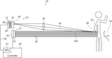
- FIG. 1is a schematic side view of a depth mapping system, in accordance with an embodiment of the invention.
- FIG. 2 Ais a schematic side view of a radiation source used in the depth mapping system of FIG. 1 , in accordance with an embodiment of the invention
- FIG. 2 Bis a schematic frontal view of an array of emitters used in the radiation source of FIG. 2 A , in accordance with an embodiment of the invention
- FIG. 2 Cis a schematic frontal view of an array of emitters that can be used in the radiation source of FIG. 2 A , in accordance with another embodiment of the invention.
- FIG. 3 Ais a schematic representation of a pattern of spots projected onto a target scene, in accordance with an embodiment of the invention
- FIG. 3 Bis a schematic frontal view of a ToF sensing array, in accordance with an embodiment of the invention.
- FIG. 3 Cis a schematic detail view of a part of the ToF sensing array of FIG. 3 B , onto which images of the spots in a region of the target scene of FIG. 3 A are cast, in accordance with an embodiment of the invention
- FIGS. 4 A and 4 Bare schematic frontal views of a ToF sensing array showing sets of super-pixels that are selected for activation and readout in two different time periods, in accordance with an embodiment of the invention
- FIG. 5is a block diagram that schematically illustrates circuitry for processing of signals from a super-pixel, in accordance with an embodiment of the invention
- FIG. 6is a flowchart that schematically illustrates a method for identifying the pixels on a SPAD array that receive laser spots, in accordance with an embodiment of the invention.
- FIG. 7is a flowchart that schematically illustrates a method for identifying the pixels on a SPAD array that receive laser spots, in accordance with another embodiment of the invention.
- a depth mapping system of this sortOne issue to be resolved in a depth mapping system of this sort is the sizes and locations of the super-pixels to be used.
- the super-pixelsFor accurate depth mapping, with high signal/background ratio, it is important that the super-pixels contain the detector elements onto which most of the energy of the reflected beams is imaged, while the sensing elements that do not receive reflected beams remain inactive. Even when a static array of emitters is used, however, the locations of the reflected beams on the detector array can change, for example due to thermal and mechanical changes over time, as well as optical effects, such as parallax.
- some embodiments of the present inventionprovide methods for calibrating the locations of the laser spots on the SPAD array.
- processing and control circuitryreceives timing signals from the array and searches over the sensing elements in order to identify the respective regions of the array on which the light pulses reflected from the target scene are incident.
- Detailed knowledge of the depth mapping systemmay be used in order to pre-compute likely regions of the reflected laser spots to be imaged onto the SPAD array. A random search in these regions will converge rapidly to the correct locations of the laser spots on the array.
- a small subset of the locations of laser spotscan be identified in an initialization stage. These locations can be used in subsequent iterative stages to predict and verify the positions of further laser spots until a sufficient number of laser spots have been located.
- ancillary image datacan be used to identify areas of the scene that are problematic in terms of depth mapping, and to recalibrate the super-pixel locations when necessary.
- This ancillary image datacan be provided, for example, by a color image sensor, which captures two-dimensional (2D) images in registration with the SPAD array.
- the emitter arrays used in the embodiments described beloware “sparse,” in the sense that the number of pulsed beams of optical radiation that are emitted toward a target scene is substantially less than the number of pixels (i.e., SPADs or other sensing elements) in the array that receives the radiation reflected from the scene.
- the illumination power available from the emitter arrayis projected onto a correspondingly sparse grid of spots in the scene.
- the processing and control circuitry in the apparatusthen receives and processes signals only from the pixels onto which these spots are imaged in order to measure depth coordinates.
- the pixels onto which the spots are imagedare referred to herein as the “active pixels,” and the “super-pixels” are made up of groups of adjacent active pixels, for example 2 ⁇ 2 groups.
- the pixels in the array that fall between the active pixelsare ignored, and need not be actuated or read out at all, as they do not contribute to the depth measurement and only increase the background level and noise.
- a different numbersuch as one, two, three or more pixels, may be included in a super-pixel.
- the group of SPAD pixels in a super-pixelmay have a different shape, such as, for example, diamond shape, triangular, circular, or irregular.
- the exact location of the spot within the SPAD pixelsvaries slightly depending on the distance to the scene due to a small amount of parallax.
- the signals from the SPAD pixels of the super-pixelare processed together in measuring for a given laser spot both its strength (intensity) and its time of flight. Additionally, the signals from the SPAD pixels may be processed as individual signals for determining the location of the laser spot within the super-pixel.
- An advantage of using a sparse emitter arrayis that the available power budget can be concentrated in the small number of projected spots, rather than being spread over the entire field of view of the sensing array. As a result of this concentration of optical power in a small number of spots, the signal levels from the corresponding active pixels—and thus the accuracy of ToF measurement by these pixels—are enhanced. This signal enhancement is particularly beneficial for long-range depth measurements and for depth mapping in conditions of strong ambient light, such as outdoors.
- the concentration of optical power in a sparse array of spotscan be further enhanced by arranging the emitters in multiple banks, and actuating these banks in alternation.
- the laser beams generated by the emittersare typically collimated by a collimating lens and may be replicated by a diffractive optical element (DOE) in order to increase the number of projected spots.
- DOEdiffractive optical element
- the pulses of optical radiation emitted from the different banks of the emittersare incident, after reflection from the target scene, on different, respective sets of the active pixels.
- the processing and control circuitrycan then receive and process the signals from the active pixels in these respective sets in synchronization with actuation of the corresponding banks of emitters.
- the processing and control circuitryneed receive and process the signals only from one active set of sensing elements, while all other sets remain inactive.
- This sort of multi-bank, synchronized operationmakes it possible to time-multiplex processing resources among the different sets of sensing elements, and thus reduce circuit complexity and power consumption.
- the number of possible super-pixelsis much larger than the number of laser spots, and only a small fraction of the total number of pixels in the SPAD array should be active at any given time and coupled to a processing unit for the purpose of measuring time-of-flight. Therefore, information is required as to which of the SPAD super-pixels to activate at any given time.
- a mapping of SPAD pixels to processing unitsi.e., the assignment of SPAD pixels to super-pixels, may be determined initially during a factory calibration.
- the embodiments of the present inventionthat are described herein address these problems by providing improved methods for calibrating the locations of the laser spots on the SPAD array.
- These methodscan be applied not only in the sorts of arrays that are shown in the figures and described hereinbelow, but also in other SPAD-based systems, such as systems comprising multiple banks of SPADs, as well as SPADs of various sizes, and systems using various sorts of emitters and emitter arrays, including emitters whose beams are replicated by a DOE.
- the present methodscan then be extended, mutatis mutandis, to multi-bank systems, by activating the SPAD pixels and performing the calibration bank by bank.
- depth mapping systemIn a disclosed embodiment, detailed knowledge of the depth mapping system is utilized to pre-compute likely regions of the reflected laser spots to be imaged onto the SPAD array. A search in these regions, for example a random search, will converge rapidly to the correct locations of the laser spots on the array.
- Another disclosed embodimentuses a two-stage solution: in an initialization stage, a small subset of the locations of laser spots is identified, and in a subsequent iterative stage, the positions of further laser spots are predicted by a model and verified. Iterative steps of spot detection are utilized to refine the model and add locations, until a sufficient number of laser spots have been located.
- FIG. 1is a schematic side view of a depth mapping system 20 , in accordance with an embodiment of the invention.
- Depth mapping system 20comprises a radiation source 21 , which emits M individual beams (for example, M may be on the order of 500).
- the radiation sourcecomprises multiple banks of emitters arranged in a two-dimensional array 22 (as shown in detail in FIG. 2 B ), together with beam optics 37 .
- the emitterstypically comprises solid-state devices, such as vertical-cavity surface-emission lasers (VCSELs) or other sorts of lasers or light-emitting diodes (LEDs).
- VCSELsvertical-cavity surface-emission lasers
- LEDslight-emitting diodes
- the beam opticstypically comprise a collimating lens and may comprise a diffractive optical element (DOE, not shown), which replicates the actual beams emitted by array 22 to create the M beams that are projected onto the scene 32 .
- DOEdiffractive optical element
- an array of four banks of pixels with 16 VCSELs in a 4 ⁇ 4 arrangement in each bankmay be used to create 8 ⁇ 8 beams, and a DOE may split each beam into 3 ⁇ 3 replicas to give a total of 24 ⁇ 24 beams.
- these internal elements of beam optics 37are not shown.
- a receiver 23 in system 20comprises a two-dimensional SPAD array 24 , together with J processing units 28 and select lines 31 for coupling the processing units to the SPADs, along with a combining unit 35 and a controller 26 .
- SPAD array 24comprises a number of detector elements N that is much larger than M, for example, 100 ⁇ 100 pixels or 200 ⁇ 200 pixels.
- the number J of processing units 28depends on the number of pixels of SPAD array 24 to which each processing unit is coupled, as will be further described with reference to FIG. 4 .
- Array 22together with beam optics 37 , emits M pulsed beams of light 30 towards a target scene 32 .
- beams 30are depicted in FIG. 1 as parallel beams of constant width, each beam diverges as dictated by diffraction. Furthermore, beams 30 diverge from each other so as to cover a required area of scene 32 .
- Scene 32reflects or otherwise scatters those beams 30 that impinge on the scene.
- the reflected and scattered beamsare collected by objective optics 34 , represented by a lens in FIG. 1 , which form an image of scene 32 on array 24 .
- a small region 36 on scene 32on which a beam 30 a has impinged, is imaged onto a small area 38 on SPAD array 24 .
- a Cartesian coordinate system 33defines the orientation of depth mapping system 20 and scene 32 .
- the x-axis and the y-axisare oriented in the plane of SPAD array 24 .
- the z-axisis perpendicular to the array and points to scene 32 that is imaged onto SPAD array 24 .
- processing units 28are shown as if separate from SPAD array 24 , but they are commonly integrated with the SPAD array.
- combining unit 35is commonly integrated with SPAD array 24 .
- Processing units 28 , together with combining unit 35comprise hardware amplification and logic circuits, which sense and record pulses output by the SPADs in respective super-pixels, and thus measure the times of arrival of the photons that gave rise to the pulses, as well as the strengths of the optical pulses impinging on SPAD array 24 .
- processing units 28 together with combining unit 35may assemble histograms of the times of arrival of multiple pulses emitted by array 22 , and thus output signals that are indicative of the distance to respective points in scene 32 , as well as of signal strength. Circuitry that can be used for this purpose is described, for example, in the above-mentioned U.S. Patent Application Publication 2017/0176579. Alternatively or additionally, some or all of the components of processing units 28 and combining unit 35 may be separate from SPAD array 24 and may, for example, be integrated with controller 26 . For the sake of generality, controller 26 , processing units 28 and combining unit 35 are collectively referred to herein as “processing and control circuitry.”
- Controller 26is coupled to both radiation source 21 and receiver 23 . Controller 26 actuates the banks of emitters in array 22 in alternation to emit the pulsed beams. The controller also provides to the processing and combining units in receiver 23 an external control signal 29 , and receives output signals from the processing and combining units. The output signals may comprise histogram data, and may be used by controller 26 to derive both times of incidence and signal strengths, as well as a precise location of each laser spot that is imaged onto SPAD array 24 .
- controller 26identifies the respective areas of SPAD array 24 on which the pulses of optical radiation reflected from corresponding regions of target scene 32 are imaged by lens 34 , and chooses the super-pixels to correspond to these areas.
- the signals output by sensing elements outside these areasare not used, and these sensing elements may thus be deactivated, for example by reducing or turning off the bias voltage to these sensing elements.
- External control signal 29controls select lines 31 so that each processing unit 28 is coupled to a respective super-pixel, comprising four SPAD pixels, for example.
- the control signalselects the super-pixels from which the output signals are to be received in synchronization with the actuation of the corresponding banks of emitters.
- processing units 28 and combining unit 35read and process the signals only from the sensing elements in the areas of SPAD array 24 that receive the reflected pulses from scene 32 , while the remaining sensing elements in the array are inactive.
- the processing of the signals from SPAD array 24is further described in reference to FIG. 4 .
- the detailed structures of emitter array 22 and SPAD array 24are not shown in FIG. 1 .
- emitter array 22 and SPAD array 24have been exaggerated in FIG. 1 relative to scene 32 .
- the lateral separation of emitter array 22 and SPAD array 24referred to as the “baseline,” is in reality much smaller than the distance from emitter array 22 to scene 32 . Consequently a chief ray 40 (a ray passing through the center of objective optics 34 ) from scene 32 to SPAD array 24 is nearly parallel to rays 30 , leading to only a small amount of parallax.
- controller 26will receive signals indicating times of arrival and signal strengths from only m processing units 28 . Controller 26 calculates from the timing of the emission of beams 30 by VCSEL array 22 and from the times of arrival measured by the m processing units 28 the time-of-flight of the m beams, and thus maps the distance to the corresponding m points on scene 32 .
- Controller 26typically comprises a programmable processor, which is programmed in software and/or firmware to carry out the functions that are described herein. Alternatively or additionally, controller 26 comprises hard-wired and/or programmable hardware logic circuits, which carry out at least some of the functions of the controller. Although controller 26 is shown in the figure, for the sake of simplicity, as a single, monolithic functional block, in practice the controller may comprise a single chip or a set of two or more chips, with suitable interfaces for receiving and outputting the signals that are illustrated in the figure and are described in the text.
- controller 26One of the functional units of controller 26 is a depth processing unit (DPU) 27 , which processes signals from both processing units 28 and combining unit 35 , as will be further described below.
- DPU 27calculates the times of flight of the photons in each of beams 30 , and thus maps the distance to the corresponding points in target scene 32 . This mapping is based on the timing of the emission of beams 30 by emitter array 22 and from the times of arrival (i.e., times of incidence of reflected photons) measured by processing units 28 .
- Controller 26typically stores the depth coordinates in a memory, and may output the corresponding depth map for display and/or further processing.
- FIG. 2 Ais a schematic side view of radiation source 21 , in accordance with an embodiment of the invention.
- VCSEL array 22comprises an integrated circuit chip on which multiple banks of VCSELs are formed (as shown in FIG. 2 B , for example).
- the VCSELsemit respective beams 30 toward optics 37 , which collimate and project the beams toward the target scene.
- Optics 37optionally comprise a diffractive optical element (DOE), which splits the optical radiation emitted by each of the VCSELs into multiple beams 30 , for example a 3 ⁇ 3 array of beams.
- DOEdiffractive optical element
- array 22is mounted on a driver chip 50 , for example, a silicon chip with CMOS circuits for selecting and driving the individual VCSELs or banks of VCSELs.
- the banks of VCSELSin this case may be physically separated, for ease of fabrication and control, or they may be interleaved on the VCSEL chip, with suitable connections to driver chip 50 to enable actuating the banks in alternation.
- beams 30likewise irradiate the target scene in a time-multiplexed pattern, with different sets of the beams impinging on the respective regions of the scene at different times.
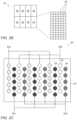
- FIG. 2 Bis a schematic frontal view of array 22 used in beam source 21 , in accordance with an embodiment of the invention.
- Array 22 in this examplecomprises eight banks 52 , with seventy-two emitters 54 , such as VCSELs, in each bank. In this case, array 22 generates 578 beams.
- FIG. 2 Cis a schematic frontal view of an array 60 of vertical emitters 54 that can be used in beam source 21 in place of array 22 , in accordance with another embodiment of the invention.
- four banks 62 a , 62 b , 62 c and 62 d of emitters 54are interleaved as alternating vertical stripes on a substrate 64 , such as a semiconductor chip:
- Each bankcomprises a number of stripes that alternate on the substrate with the stripes in the other banks.
- other interleaving schemesmay be used.
- array 22may comprise a larger or smaller number of banks and emitters.
- array 22comprises at least four banks 52 or 62 , with at least four emitters 54 in each bank, and possibly with a DOE for splitting the radiation emitted by each of the emitters.
- array 22comprises at least eight banks 52 or 62 , with twenty emitters 54 or more in each bank. These options enhance the flexibility of system 20 in terms of time-multiplexing of the optical and electrical power budgets, as well as processing resources.
- FIG. 3 Ais a schematic representation of a pattern of spots 70 of optical radiation that are projected onto target scene 32 , in accordance with an embodiment of the invention.
- Each spot 70is cast by a corresponding beam 30 ( FIG. 1 ).
- different groups of spots 70are projected onto scene 32 in alternation, corresponding to the alternating actuation of the corresponding banks 52 of emitters 54 ( FIG. 2 B ).
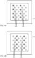
- FIG. 3 Bis a schematic frontal view of SPAD array 24 onto which target scene 32 is imaged, in accordance with an embodiment of the invention.
- the sensing elements, such as SPADs, in array 24are too small to be seen in this figure. Rather, FIG. 3 B shows the locations of spots 72 that are reflected from target scene 70 and imaged onto array 24 by lens 34 .
- each spot 72is the image on array 24 of a corresponding spot 70 that is projected onto scene 32 by emitter array 22 .
- Lens 34images a region 74 of target scene 32 ( FIG. 3 A ), including spots 70 that the area contains, onto a corresponding area 76 on array 24 .
- FIG. 3 Cis a schematic detail view of area 76 of array 24 , showing the locations of spots 72 that are imaged onto the array, in accordance with an embodiment of the invention. These spots 72 may be imaged at the same time, if they originate from the same bank of emitters, or at different, alternating times if they are from different banks.
- array 24comprises a matrix of sensing elements 78 , such as SPADs. (As noted earlier, sensing elements 78 in an array are also referred to as “pixels.”) Controller 26 assigns each processing unit 28 to a super-pixel 80 comprising a 2 ⁇ 2 group of the sensing elements 78 .
- Controller 26thus selected the sensing elements 78 to assign to each super-pixel 80 so as to maximize the overlap between the corresponding spot 72 and the super-pixel, and thus maximize the signal received from each super-pixel.
- spots 72shifted to new locations 72 b on array 24 . This shift may have occurred, for example, due to mechanical shock or thermal effects or due to other causes. Spots 72 at locations 72 b no longer overlap with super-pixels 80 in area 76 , or overlap only minimally with the super-pixels. Sensing elements 78 on which the spots are now imaged, however, are inactive and are not connected to any of processing units 28 . To rectify this situation, controller 26 may recalibrate the locations of super-pixels 80 , as described in the above-mentioned provisional patent applications.
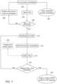
- FIGS. 4 A and 4 Bare schematic frontal views of SPAD array 24 showing sets of super-pixels 80 a and 80 b that are selected for activation and readout in two different time periods, in accordance with an embodiment of the invention.
- the selection of the set of super-pixelsis synchronized with the selection of banks of emitters. Specifically, assuming array 60 ( FIG. 2 C ) is used for generating the spots on the target scene, super-pixels 80 a will be used when bank 62 a is actuated, and super-pixels 80 b will be used when bank 62 b is actuated (and so forth for banks 62 c and 62 d ).
- processing units 28serve only the one active set of super-pixels 80 , while all other sets remain inactive, in an integrated time-multiplexing scheme.
- FIG. 5is a block diagram that schematically illustrates the processing of signals from a super-pixel 80 , in accordance with an embodiment of the invention.
- super-pixel 80comprises four sensing elements 78 of SPAD array 24 .
- Each processing unit 28comprises one or more time-to-digital converters (TDC) 143 , wherein the TDCs are hardware elements translating the avalanche events (signals from a SPAD pixel due to a detected photon) from each sensing element 78 to time-of-arrival information.
- TDCtime-to-digital converters
- Each processing unit 28further comprises, for each TDC 143 , a weight 144 , and may comprise a histogram unit (not shown), wherein the time-of-arrival information is aggregated into histograms, generally over thousands of pulses from VCSEL array 22 . In the present embodiment, however, the histograms are aggregated centrally for super-pixel, without individual histogram units in processing units 28 .
- each processing unit 28is coupled to a single sensing element 78 , thus requiring one TDC 143 .
- processing units 28may be switched among different sensing elements 78 , which are activated at different, alternating times, in synchronization with the alternating actuation of the corresponding banks 52 of emitters 54 ( FIG. 2 B ).
- the time-of-arrival information from the four processing units 28is aggregated by combining unit 35 , using weights 144 , to yield a single histogram 146 for super-pixel 80 .
- This combined histogram 146is sent to DPU 27 , which in turn detects, based on histogram 146 , whether any object or structure was detected in scene 32 by super-pixel 80 and, if so, reports its depth information based on time-of-flight data.
- the respective numbers of events reported by the four processing units 28may be separately summed in combining unit 35 over a predefined interval of arrival times to yield an indication of the received signal strength for that interval for each sensing element 78 .
- the intervalis configured to start after the end of a so-called “stray pulse” and continue to the end of the histogram.
- a stray pulseis a pulse that is generated within system 20 as a result of, for example, an imperfect coating of an optical surface, which causes a reflection of the pulses emitted by VCSEL array 22 directly back into the optical path to SPAD array 24 . It is typically an undesired pulse, but one that is very difficult to eliminate altogether.
- the stray pulsemay be utilized for calibrating the timing signals as follows: A time of arrival of a stray pulse is recorded and subtracted from a subsequent timing signal due to a laser pulse that has been reflected by scene 32 . This subtraction yields a relative time-of-flight for the received laser pulse, and compensates for any random firing delays of VCSEL array 22 , as well as for most of the VCSEL and SPAD drifts related to temperature changes.
- DPU 27In conjunction with combined histogram 146 , The indicators may be used by DPU 27 to determine a precise location of the spot on sensing elements 78 .
- the four units of TDC 143reside in the same chip as SPAD array 24 , while the rest of signal processing, including DPU 27 , resides in separate controller 26 .
- a major reason for generating single combined histogram 146 for super-pixel 80is to reduce the information that is transferred from SPAD array 24 to DPU 27 and to controller 26 .
- the partitioning into two separate unitsreflects the fact that SPAD array 24 and the associated units perform primarily optical and analog functions, while controller 26 performs mostly digital and software-driven operations.
- FIG. 6is a flowchart that schematically illustrates a method for identifying the pixels in a sensing array that receive laser spots, in accordance with an embodiment of the invention. This method is described, for the sake of convenience and clarity, with reference to SPAD array 24 and the other elements of system 20 ( FIG. 1 ). The method can be performed, for example, each time system 20 is turned on. Alternatively, the method can be carried out prior to an initial use of system 20 , and the results can be stored for future use. The method can then be repeated periodically and/or when system performance indicates that recalibration may be required.
- VCSEL array 22could be replaced by a single laser (or a small number of lasers), with a beamsplitting element, such as a diffractive optical element (DOE), to split the laser output into multiple beams.
- DOEdiffractive optical element
- other types of sensing arrays, comprising other sorts of detector elementscould be used in place of SPADs.
- the method of FIG. 7is similarly applicable not only to system 20 , but to other depth mapping systems, as well.
- a nominal design value step 150provides the nominal system design values for depth mapping system 20 ( FIG. 1 ); assembly tolerance step 152 provides the assembly tolerances of the depth mapping system; and operational tolerance step 154 provides expected operational tolerances, such as variations of ambient temperature and the effects of a mechanical shock on the depth mapping system.
- the above inputsinclude multiple parameters.
- a typical focal length of collection lens 34has a nominal value of 2 mm, an assembly tolerance of 0.1 mm and an operational tolerance of 0.05 mm. Each tolerance is normally distributed around zero, with a standard deviation equal to the above tolerance.
- the probability distribution of the focal lengthis a normal distribution combined from the two normal distributions and centered at the nominal value of 2 mm.
- An additional example of a parameteris the baseline between VCSEL array 22 and SPAD array 24 .
- the multiple parameterssuch as the two examples described above, allow controller 26 to model accurately the optical path taken by the laser pulses and thus calculate the locations where the spots impinge on SPAD array 24 .
- controller 26calculates a search region for each of the M laser spots expected on SPAD array 24 ( FIG. 1 ), in a pre-computation step 156 .
- Each search regionincludes a group of pixels for which a probability of receiving a laser beam reflected from scene 32 is estimated to be higher than a preset threshold, such as 99.9%.
- a preset thresholdsuch as 99.9%.
- an increase of 1% in the focal length of collection lens 34magnifies the image on SPAD array 24 by 1%, thus shifting the spots in an outward radial direction.
- the probability distribution of this parameter and all other parameters of the inputtranslates to a region around each of the nominal spot locations on SPAD array 24 in which there is a probability higher than 99.9% to find the spot.
- controller 26in a random iterative search step 158 , fires a succession of pulses of beams 32 from VCSEL array 22 ( FIG. 1 ), and at the same time performs random searches within the search regions to identify the M super-pixels that receive the pulsed beams.
- controller 26may apply other search strategies, not necessarily random, within the search regions.
- each processing unit 28is coupled to receive signals from a different pixel following each laser pulse or sequence of multiple pulses, and controller 26 checks, using DPU 27 , which pixels have output signals due to an incident photon, and which have not. Based on the results, controller 26 selects the pixels to include in each super-pixel as those on which the photons were found to be incident. In simulations, the search was found to converge within a succession of 8-10 repeated sequences of pulsed beams 32 and thus identify the M super-pixels of SPAD array 24 that receive the M beams.
- controller 26finishes the search and assigns, in an assignment step 160 , these super-pixels for use in 3D mapping of scene 32 by depth mapping system 20 .
- FIG. 7is a flowchart that schematically illustrates a two-stage method for identifying the super-pixels in SPAD array 24 ( FIG. 1 ) that receive laser spots, in accordance with another embodiment of the invention.
- the first stagestarts by providing, in an input step 200 , a small number m 0 of potential process candidates, wherein, in this context, the term “process candidate” is used for those SPAD super-pixels likely to receive laser spots.
- These potential process candidatesmay be obtained, for example, from a previous use of depth mapping system 20 .
- controller 26fires a sequence of pulses of beams 32 from VCSEL array 22 and queries processing units 28 and combining unit 35 to find out how many of the m 0 process candidates on SPAD array 24 reported “hits,” i.e., output signals indicating that they had received photons.
- controller 26checks whether the number of reported hits in first detection step 204 exceeds a first preset threshold, for example 8% of M (if initially 10% of M were selected as process candidates).
- controller 26searches, in a search step 208 , for hits in the areas around the process candidates by firing successive pulsed beams 32 from VCSEL array 22 and performing a single pixel search around the candidates. After new hits have been identified, the previous process candidates in process candidate step 202 are replaced by the new hits, and steps 204 and 206 are repeated until the number of detected hits in first comparison step 206 exceeds the first preset threshold.
- the detected hits in first comparison step 206are used by controller 26 to build a model in a modeling step 210 .
- the modelexpresses the deviation of the locations of the hits in SPAD array 24 relative to their nominal locations, i.e., the locations where the reflected laser beams were expected to be incident on SPAD array 24 according to the design geometry of system 20 , for example.
- the modelmay be a quadratic model, a simplified pinhole camera model, or a homographic model, for example, and it may take into account system tolerances as previously described.
- the coordinates x and yrefer to Cartesian coordinate system 33 of FIG. 1 .
- Such a modelrepresents the correct spot locations on SPAD array 24 in a case where scene 34 comprises a plane (for instance, a wall).
- x uf ⁇ X Z + c x
- ⁇ y uf ⁇ Y Z + c y
- x dc x +( x u ⁇ c x ) ⁇ p ( r )
- y dy +( y u ⁇ c y ) ⁇ p ( r )
- r⁇ square root over (( x u ⁇ c x ) 2 +( y u ⁇ c y ) 2 ) ⁇
- the parameters of the modelare, therefore, the following constants: f, c x , c y , k 1 , k 2 , k 3 (see G. Bradski and A. Kaehler, Learning OpenCV, 1 st edition, O'Reilly Media, Inc., Sebastopol, California, 2008).
- controller 26predicts the locations of a number of new process candidates, by applying the model to the nominal locations of a number of additional pixels where other reflected laser beams were expected to be incident, in a candidate addition step 212 , making now up a total of m 1 process candidates. Typically, m 1 increases in each iteration at candidate addition step 212 .
- controller 26fires an additional sequence of pulses of beams 30 from VCSEL array 22 and queries how many of the m 1 process candidates on SPAD array 24 have reported hits.
- controller 26compares the relative number of hits (the ratio between the hits and the total number M of pulsed beams 30 ) to a second preset threshold.
- This latter thresholdis typically set to a high value, corresponding to a situation in which the large majority of beams 30 are successfully received by corresponding super-pixels. If the relative number of hits is less than the second preset threshold, controller 26 adjusts the model in modeling step 210 based on the detected hits. The adjustment of the model includes recalculating the model coefficients, as well as, where required, an increase in the complexity of the model.
- controller 26adds new process candidates based on the model in candidate addition step 212 , queries hits in second detection step 214 , and compares their relative number to the second preset threshold in second comparison step 216 . As long as the relative number of hits does not exceed the second preset threshold, controller 26 keeps looping back to model step 210 , improving the model based on the new hits.
- controller 26finishes the search and assigns, in an assignment step 218 , the detected hits for use in 3D mapping of scene 32 by depth mapping system 20 .
- controller 26may initiate a single-pixel offset search in an offset search step 222 .
- offset search step 222a search for the yet undetected laser spots is performed with a single-pixel offset around their expected locations.
Landscapes
- Engineering & Computer Science (AREA)
- Physics & Mathematics (AREA)
- General Physics & Mathematics (AREA)
- Computer Networks & Wireless Communication (AREA)
- Radar, Positioning & Navigation (AREA)
- Remote Sensing (AREA)
- Electromagnetism (AREA)
- Condensed Matter Physics & Semiconductors (AREA)
- Optics & Photonics (AREA)
- Optical Radar Systems And Details Thereof (AREA)
- Measurement Of Optical Distance (AREA)
Abstract
Description
- Some laser spots may not fall on objects in the scene or may fall on objects that absorb the laser wavelength, thus returning no pulse. Therefore a search may not always be successful.
- As the distribution of laser spots is very sparse when compared to the number of pixels of the SPAD array, exhaustive search will require a large number of exposures and will take a long time.
- 1. The calibration of
SPAD array 24, i.e., the choice of the M super-pixels, and - 2. The number of
laser beams 30 that are actually reflected fromscene 32.
The value M may correspond to the total number of emitters when all of the emitters are actuated together, or to the number of emitters in each bank when the banks are actuated in alternation, as in the present embodiments.
- 1. The calibration of
x′=a1+b1x+c1y+d1x2+e1y2+f1xy
y′=a2+b2x+c2y+d2x2+e2y2+f2xy
We then apply a distortion operation to obtain the final image coordinates:
xd=cx+(xu−cx)·p(r),yd=y+(yu−cy)·p(r),
where
r=√{square root over ((xu−cx)2+(yu−cy)2)}
and p(r)=1+k1r2+k2r4+k3r6is a distortion polynomial. The parameters of the model are, therefore, the following constants: f, cx, cy, k1, k2, k3(see G. Bradski and A. Kaehler,Learning OpenCV,1stedition, O'Reilly Media, Inc., Sebastopol, California, 2008).
Claims (20)
Priority Applications (1)
| Application Number | Priority Date | Filing Date | Title |
|---|---|---|---|
| US16/532,513US12117286B2 (en) | 2019-02-11 | 2019-08-06 | Depth sensing using a sparse array of pulsed beams |
Applications Claiming Priority (3)
| Application Number | Priority Date | Filing Date | Title |
|---|---|---|---|
| US201962803612P | 2019-02-11 | 2019-02-11 | |
| US201962809647P | 2019-02-24 | 2019-02-24 | |
| US16/532,513US12117286B2 (en) | 2019-02-11 | 2019-08-06 | Depth sensing using a sparse array of pulsed beams |
Publications (2)
| Publication Number | Publication Date |
|---|---|
| US20200256993A1 US20200256993A1 (en) | 2020-08-13 |
| US12117286B2true US12117286B2 (en) | 2024-10-15 |
Family
ID=67777399
Family Applications (3)
| Application Number | Title | Priority Date | Filing Date |
|---|---|---|---|
| US16/532,517ActiveUS10955234B2 (en) | 2019-02-11 | 2019-08-06 | Calibration of depth sensing using a sparse array of pulsed beams |
| US16/532,513Active2043-05-19US12117286B2 (en) | 2019-02-11 | 2019-08-06 | Depth sensing using a sparse array of pulsed beams |
| US17/175,714ActiveUS11371833B2 (en) | 2019-02-11 | 2021-02-15 | Calibration of depth sensing using a sparse array of pulsed beams |
Family Applications Before (1)
| Application Number | Title | Priority Date | Filing Date |
|---|---|---|---|
| US16/532,517ActiveUS10955234B2 (en) | 2019-02-11 | 2019-08-06 | Calibration of depth sensing using a sparse array of pulsed beams |
Family Applications After (1)
| Application Number | Title | Priority Date | Filing Date |
|---|---|---|---|
| US17/175,714ActiveUS11371833B2 (en) | 2019-02-11 | 2021-02-15 | Calibration of depth sensing using a sparse array of pulsed beams |
Country Status (7)
| Country | Link |
|---|---|
| US (3) | US10955234B2 (en) |
| EP (1) | EP3887852B1 (en) |
| KR (1) | KR102604902B1 (en) |
| CN (2) | CN113330328B (en) |
| AU (1) | AU2019429696B2 (en) |
| DE (1) | DE112019006845T5 (en) |
| WO (2) | WO2020167338A1 (en) |
Families Citing this family (33)
| Publication number | Priority date | Publication date | Assignee | Title |
|---|---|---|---|---|
| US11105925B2 (en) | 2017-03-01 | 2021-08-31 | Ouster, Inc. | Accurate photo detector measurements for LIDAR |
| US11112494B2 (en)* | 2017-05-18 | 2021-09-07 | Sharp Kabushiki Kaisha | Photodetector and portable electronic equipment |
| WO2019110447A1 (en)* | 2017-12-04 | 2019-06-13 | Ams International Ag | Distance time-of-flight modules |
| KR102403544B1 (en) | 2017-12-18 | 2022-05-30 | 애플 인크. | Time-of-flight sensing using an addressable array of emitters |
| EP3887852B1 (en)* | 2019-02-11 | 2025-07-30 | Apple Inc. | Depth sensing using a sparse array of pulsed beams |
| WO2020181136A1 (en) | 2019-03-05 | 2020-09-10 | Physmodo, Inc. | System and method for human motion detection and tracking |
| US11331006B2 (en) | 2019-03-05 | 2022-05-17 | Physmodo, Inc. | System and method for human motion detection and tracking |
| US11500094B2 (en)* | 2019-06-10 | 2022-11-15 | Apple Inc. | Selection of pulse repetition intervals for sensing time of flight |
| US11671691B2 (en)* | 2019-06-20 | 2023-06-06 | Cilag Gmbh International | Image rotation in an endoscopic laser mapping imaging system |
| US11877065B2 (en) | 2019-06-20 | 2024-01-16 | Cilag Gmbh International | Image rotation in an endoscopic hyperspectral imaging system |
| US11134832B2 (en) | 2019-06-20 | 2021-10-05 | Cilag Gmbh International | Image rotation in an endoscopic hyperspectral, fluorescence, and laser mapping imaging system |
| US11733359B2 (en) | 2019-12-03 | 2023-08-22 | Apple Inc. | Configurable array of single-photon detectors |
| US20220099814A1 (en)* | 2020-09-30 | 2022-03-31 | Sense Photonics, Inc. | Power-efficient direct time of flight lidar |
| WO2022166583A1 (en)* | 2021-02-08 | 2022-08-11 | 深圳市灵明光子科技有限公司 | Projection device, three-dimensional imaging system, three-dimensional imaging method, and electronic product |
| CN112817010A (en)* | 2021-02-08 | 2021-05-18 | 深圳市灵明光子科技有限公司 | Projection device, three-dimensional imaging system, three-dimensional imaging method and electronic product |
| CN113176579B (en)* | 2021-03-01 | 2024-08-23 | 奥比中光科技集团股份有限公司 | Light spot position self-adaptive searching method, time flight ranging system and ranging method |
| US12196860B2 (en) | 2021-03-02 | 2025-01-14 | Apple Inc. | Depth sensor calibration using internal reflections |
| WO2022217564A1 (en)* | 2021-04-16 | 2022-10-20 | 睿镞科技(北京)有限责任公司 | Laser radar system, and spatial measurement device and method |
| JP2022168740A (en) | 2021-04-26 | 2022-11-08 | キヤノン株式会社 | Projector unit and distance measuring device using the same |
| KR20220149348A (en) | 2021-04-30 | 2022-11-08 | 삼성전자주식회사 | Augmented reality device obtaining depth information of the object and method for operating the same |
| KR20220151477A (en)* | 2021-05-06 | 2022-11-15 | 삼성전자주식회사 | LiDAR device and electronic apparatus including the same |
| CN115267728A (en)* | 2021-05-24 | 2022-11-01 | 深圳阜时科技有限公司 | Optical sensing device and sensing method thereof, optical receiver and electronic device |
| US11681028B2 (en) | 2021-07-18 | 2023-06-20 | Apple Inc. | Close-range measurement of time of flight using parallax shift |
| CN117957419A (en) | 2021-09-20 | 2024-04-30 | 特里纳米克斯股份有限公司 | Emitter array with two or more independently driven regions |
| KR20230049902A (en)* | 2021-10-07 | 2023-04-14 | 삼성전자주식회사 | Electronic device comprising range sensor and method for measuring distace |
| CN113960569A (en)* | 2021-10-19 | 2022-01-21 | 深圳奥锐达科技有限公司 | Distance measuring system and distance measuring method |
| CN114185057B (en)* | 2021-11-10 | 2024-05-17 | 华为技术有限公司 | A detection method, device and terminal |
| CN115575967B (en)* | 2022-11-02 | 2024-07-19 | 北京摩尔芯光半导体技术有限公司 | Laser radar chip and laser radar |
| DE102022131100B3 (en) | 2022-11-24 | 2024-03-21 | Elmos Semiconductor Se | Driver chip with multiple driver blocks for a lighting system |
| CN115825971A (en)* | 2022-11-29 | 2023-03-21 | 深圳奥锐达科技有限公司 | A scanning laser radar based on SPAD chip |
| CN115986556A (en)* | 2023-02-02 | 2023-04-18 | 绍兴埃瓦科技有限公司 | VCSEL array drive device and binocular TOF depth perception system |
| US12335613B2 (en)* | 2023-05-30 | 2025-06-17 | Apple Inc. | Detection of close-range specular targets |
| WO2025202122A1 (en)* | 2024-03-28 | 2025-10-02 | Sony Semiconductor Solutions Corporation | Electronic device, method and computer program |
Citations (239)
| Publication number | Priority date | Publication date | Assignee | Title |
|---|---|---|---|---|
| US4623237A (en) | 1984-07-07 | 1986-11-18 | Canon Kabushiki Kaisha | Automatic focusing device |
| US4757200A (en) | 1986-07-28 | 1988-07-12 | Visidyne, Inc. | Pulsed radiation detection system |
| WO1990008946A1 (en) | 1989-01-31 | 1990-08-09 | York Limited | Optical detection apparatus for counting optical photons |
| JPH02287113A (en) | 1989-04-27 | 1990-11-27 | Asahi Optical Co Ltd | Distance measuring instrument |
| US5164823A (en) | 1990-12-21 | 1992-11-17 | Kaman Aerospace Corporation | Imaging lidar system employing multipulse single and multiple gating for single and stacked frames |
| JPH0567195A (en) | 1991-09-05 | 1993-03-19 | Matsushita Electric Ind Co Ltd | Shape measuring instrument |
| US5270780A (en) | 1991-09-13 | 1993-12-14 | Science Applications International Corporation | Dual detector lidar system and method |
| US5373148A (en) | 1989-10-30 | 1994-12-13 | Symbol Technologies, Inc. | Optical scanners with scan motion damping and orientation of astigmantic laser generator to optimize reading of two-dimensionally coded indicia |
| JPH09197045A (en) | 1996-01-24 | 1997-07-31 | Nissan Motor Co Ltd | Radar equipment for vehicles |
| US5699149A (en) | 1994-06-09 | 1997-12-16 | Hitachi, Ltd. | Distance measurement apparatus for vehicle |
| JPH10170637A (en) | 1996-12-16 | 1998-06-26 | Omron Corp | Light scanner |
| JPH1163920A (en) | 1997-08-26 | 1999-03-05 | Matsushita Electric Works Ltd | Optically scanning system displacement measuring equipment |
| US20010020673A1 (en) | 2000-03-09 | 2001-09-13 | Franco Zappa | Monolithic circuit of active quenching and active reset for avalanche photodiodes |
| US6301003B1 (en) | 1998-08-05 | 2001-10-09 | Denso Corporation | Optical distance measuring apparatus selectively activating a matrix of light sensitive cells |
| US6384903B1 (en) | 1977-02-28 | 2002-05-07 | Bae Systems Information And Electronic Systems Integration, Inc. | Range gated remote measurement utilizing two-photon absorption |
| US20020071126A1 (en) | 2000-12-12 | 2002-06-13 | Noriaki Shirai | Distance measurement apparatus |
| US20020131035A1 (en) | 2001-03-14 | 2002-09-19 | Takamoto Watanabe | Time measurement apparatus, distance measurement apparatus, and clock signal generating apparatus usable therein |
| US20020154054A1 (en) | 2001-04-18 | 2002-10-24 | Small James G. | Sparse frequency waveform radar system and method |
| US20020186362A1 (en) | 2001-06-11 | 2002-12-12 | Noriaki Shirai | Distance measurement apparatus |
| US20040051859A1 (en) | 2002-09-12 | 2004-03-18 | Flockencier Stuart W. | Programmable pulse capture device with automatic gain control |
| US20040135992A1 (en) | 2002-11-26 | 2004-07-15 | Munro James F. | Apparatus for high accuracy distance and velocity measurement and methods thereof |
| US20040212863A1 (en) | 2001-07-19 | 2004-10-28 | Holger Schanz | Method and apparatus for optically scanning a scene |
| US20050018200A1 (en) | 2002-01-11 | 2005-01-27 | Guillermo Tearney J. | Apparatus for low coherence ranging |
| US20060044546A1 (en) | 2002-11-11 | 2006-03-02 | Qinetiq Limited | Ranging apparatus |
| US20060106317A1 (en) | 2002-09-16 | 2006-05-18 | Joule Microsystems Canada Inc. | Optical system and use thereof for detecting patterns in biological tissue |
| US20060176469A1 (en) | 2005-02-08 | 2006-08-10 | Canesta, Inc. | Method and system to correct motion blur and reduce signal transients in time-of-flight sensor systems |
| US7126218B1 (en) | 2001-08-07 | 2006-10-24 | Amkor Technology, Inc. | Embedded heat spreader ball grid array |
| US7193690B2 (en) | 2003-12-29 | 2007-03-20 | Faro Technologies, Inc. | Laser scanner and method for optically scanning an environment |
| US20070145136A1 (en) | 2003-07-29 | 2007-06-28 | Microvision, Inc. | Apparatus and method for projecting a variable pattern of electromagnetic energy |
| US20070164004A1 (en) | 2006-01-17 | 2007-07-19 | Yasushi Matsuda | Fiber laser beam processing apparatus |
| US7303005B2 (en) | 2005-11-04 | 2007-12-04 | Graftech International Holdings Inc. | Heat spreaders with vias |
| WO2007144565A2 (en) | 2006-06-14 | 2007-12-21 | Oerlikon Balzers Coating (Uk) Limited | Process for laser scribing |
| CN201054040Y (en) | 2007-05-21 | 2008-04-30 | 一品光学工业股份有限公司 | Micro-electromechanical swinging laser scanning device |
| US7405812B1 (en) | 2006-05-18 | 2008-07-29 | Canesta, Inc. | Method and system to avoid inter-system interference for phase-based time-of-flight systems |
| US20080231498A1 (en) | 2004-11-15 | 2008-09-25 | Lars Menzer | Symmetrical Multi-Path Method For Determining the Distance Between Two Transmitter-Receivers |
| CA2605339C (en) | 1993-04-12 | 2008-09-30 | The Regents Of The University Of California | Ultra-wideband radar motion sensor |
| US20090009747A1 (en) | 2006-03-23 | 2009-01-08 | Peter Wolf | Device for Optically Measuring Distance and Method for Operating Said Type of Device |
| US7508496B2 (en) | 2004-11-16 | 2009-03-24 | Z+F Zoller & Froelich Gmbh | Method for driving a laser scanner |
| CN101401107A (en) | 2005-06-13 | 2009-04-01 | 数据逻辑扫描公司 | System and method for data reading using raster scanning |
| US20090262760A1 (en) | 2005-01-20 | 2009-10-22 | Vladimir Krupkin | Laser Obstacle Ranging and Display |
| US20090273770A1 (en) | 2008-04-30 | 2009-11-05 | Honeywell International Inc. | Systems and methods for safe laser imaging, detection and ranging (lidar) operation |
| US20090275841A1 (en) | 2008-04-30 | 2009-11-05 | Board Of Regents, The University Of Texas System | Multi-wavelength diagnostic imager |
| US20100019128A1 (en) | 2008-07-23 | 2010-01-28 | Princeton Lightwave, Inc. | Focal Plane Array Imager |
| EP2157445A2 (en) | 2008-08-19 | 2010-02-24 | Rosemount Aerospace Inc. | Lidar system using a pseudo-random pulse sequence |
| US20100096459A1 (en) | 2008-10-16 | 2010-04-22 | Vladimir Gurevich | Electro-optical reader with extended working range |
| US20100121577A1 (en) | 2008-04-24 | 2010-05-13 | Gm Global Technology Operations, Inc. | Three-dimensional lidar-based clear path detection |
| US7800067B1 (en) | 2007-10-08 | 2010-09-21 | Hrl Laboratories, Llc | Electronically tunable and reconfigurable hyperspectral photon detector |
| US7800739B2 (en) | 2006-05-23 | 2010-09-21 | Leica Geosystems Ag | Distance measuring method and distance measuring element for detecting the spatial dimension of a target |
| US20100250189A1 (en) | 2009-03-31 | 2010-09-30 | Brown Jerry G | Method and System for Determination of Detection Probability or a Target Object Based on a Range |
| US7812301B2 (en) | 2005-10-28 | 2010-10-12 | Sony Corporation | Solid-state imaging device, method of driving solid-state imaging device and imaging apparatus |
| US20100286516A1 (en) | 2008-09-29 | 2010-11-11 | Liexiang Fan | High pulse repetition frequency for detection of tissue mechanical property with ultrasound |
| US20100309288A1 (en) | 2009-05-20 | 2010-12-09 | Roger Stettner | 3-dimensional hybrid camera and production system |
| WO2010149593A1 (en) | 2009-06-22 | 2010-12-29 | Toyota Motor Europe Nv/Sa | Pulsed light optical rangefinder |
| US20110006190A1 (en) | 2009-07-10 | 2011-01-13 | Motorola, Inc. | Devices and Methods for Adjusting Proximity Detectors |
| JP2011089874A (en) | 2009-10-22 | 2011-05-06 | Toyota Central R&D Labs Inc | Distance image data acquisition device |
| EP2322953A1 (en) | 2008-07-30 | 2011-05-18 | National University Corporation Shizuoka University | Distance image sensor and method for generating image signal by time-of-flight method |
| US20110128524A1 (en) | 2009-11-30 | 2011-06-02 | General Electric Company | Light detection and ranging system |
| US7969558B2 (en) | 2006-07-13 | 2011-06-28 | Velodyne Acoustics Inc. | High definition lidar system |
| US20110181864A1 (en) | 2008-07-04 | 2011-07-28 | Eads Deutschland Gmbh | Lidar method for measuring speeds and lidar device with time-controlled detection |
| US20110279366A1 (en) | 2009-01-27 | 2011-11-17 | Xyz Interactive Technologies Inc. | Method and apparatus for ranging finding, orienting, and/or positioning of single and/or multiple devices |
| JP2011237215A (en) | 2010-05-07 | 2011-11-24 | Nikon Corp | Depth map output device |
| US20120038904A1 (en) | 2010-08-11 | 2012-02-16 | Fossum Eric R | Unit pixel, photo-detection device and method of measuring a distance using the same |
| US20120132636A1 (en) | 2010-11-30 | 2012-05-31 | Stmicroelectronics (Research & Development) Limited | Application using a single photon avalanche diode (spad) |
| US20120154542A1 (en) | 2010-12-20 | 2012-06-21 | Microsoft Corporation | Plural detector time-of-flight depth mapping |
| US20120153120A1 (en) | 2010-11-30 | 2012-06-21 | Stmicroelectronics (Research & Development) Limited | Proximity sensor and associated method, computer readable medium and firmware |
| EP2469297A1 (en) | 2010-12-21 | 2012-06-27 | Riegl Laser Measurement Systems GmbH | Method for measuring distance by means of laser impulses |
| US20120176476A1 (en) | 2011-01-12 | 2012-07-12 | Sony Corporation | 3d time-of-flight camera and method |
| US8259293B2 (en) | 2007-03-15 | 2012-09-04 | Johns Hopkins University | Deep submicron and nano CMOS single photon photodetector pixel with event based circuits for readout data-rate reduction communication system |
| US8275270B2 (en) | 2002-07-30 | 2012-09-25 | Amplification Technologies Inc. | High-sensitivity, high-resolution detector devices and arrays |
| US8279418B2 (en) | 2010-03-17 | 2012-10-02 | Microsoft Corporation | Raster scanning for depth detection |
| US20120249998A1 (en) | 2009-09-11 | 2012-10-04 | Robert Bosch Gmbh | Optical Distance Measuring Device |
| US20120287242A1 (en) | 2011-05-12 | 2012-11-15 | Microsoft Corporation | Adaptive high dynamic range camera |
| WO2012154356A1 (en) | 2011-04-15 | 2012-11-15 | Faro Technologies, Inc. | Absolute distance meter based on an undersampling method |
| US20120294422A1 (en) | 2010-10-01 | 2012-11-22 | Stephen Wah-Kwan Cheung | Systems and methods for cargo scanning and radiotherapy using a traveling wave linear accelerator based x-ray source using current to modulate pulse-to-pulse dosage |
| US8355117B2 (en) | 2005-12-21 | 2013-01-15 | Ecole Polytechnique Federale De Lausanne | Method and arrangement for measuring the distance to an object |
| US20130015331A1 (en) | 2011-07-12 | 2013-01-17 | Leica Microsystems Cms Gmbh | Device and method for detecting light |
| WO2013028691A1 (en) | 2011-08-25 | 2013-02-28 | Georgia Tech Research Corporation | Gas sensors and methods of preparation thereof |
| US8405020B2 (en) | 2009-06-10 | 2013-03-26 | Saint-Gobain Ceramics & Plastics, Inc. | Scintillator and detector assembly including a single photon avalanche diode and a device of a quenching circuit having a same wide band-gap semiconductor material |
| US20130079639A1 (en) | 2011-09-28 | 2013-03-28 | General Electric Company | System and method for ultrasound imaging |
| US20130092846A1 (en) | 2011-10-18 | 2013-04-18 | Uwm Research Foundation, Inc. | Fiber-optic sensors for real-time monitoring |
| US20130107016A1 (en) | 2010-05-17 | 2013-05-02 | Iee International Electronics & Engineering S.A. | Scanning 3d imager |
| JP2013113669A (en) | 2011-11-28 | 2013-06-10 | Mitsubishi Electric Corp | Laser radar device |
| US20130208258A1 (en) | 2010-04-12 | 2013-08-15 | Robert Bosch Gmbh | Distance Measuring Device having Homogenizing Measurement Evaluation |
| US20130236171A1 (en) | 2012-03-06 | 2013-09-12 | Oliver W. Saunders | Multiple sensor optical communication systems and methods |
| US20130258099A1 (en) | 2012-03-29 | 2013-10-03 | Samsung Electronics Co., Ltd. | Depth Estimation Device And Operating Method Using The Depth Estimation Device |
| KR101318951B1 (en) | 2011-02-28 | 2013-10-17 | 한국과학기술원 | Scanning three-dimensional imaging pulsed laser radar System and Method using dual Geiger-mode avalanche photodiodes |
| US20130278917A1 (en) | 2012-03-21 | 2013-10-24 | Honda Motor Co., Ltd. | Distance measuring system |
| US20130300838A1 (en) | 2010-12-23 | 2013-11-14 | Fastree3D S.A. | Methods and devices for generating a representation of a 3d scene at very high speed |
| US20130342835A1 (en) | 2012-06-25 | 2013-12-26 | California Institute Of Technology | Time resolved laser raman spectroscopy using a single photon avalanche diode array |
| US20140027606A1 (en) | 2012-07-24 | 2014-01-30 | Stmicroelectronics (Research & Development) Limited | Module for proximity and gesture sensing |
| DE202013101039U1 (en) | 2013-03-11 | 2014-03-12 | Sick Ag | Optoelectronic sensor for distance measurement |
| US20140071433A1 (en) | 2011-03-17 | 2014-03-13 | Robert Bosch Gmbh | Measurement Device for Measuring a Distance between the Measurement Device and a Target Object using an Optical Measurement Beam |
| US8675181B2 (en) | 2009-06-02 | 2014-03-18 | Velodyne Acoustics, Inc. | Color LiDAR scanner |
| US20140077086A1 (en) | 2011-04-25 | 2014-03-20 | Eduard BATKILIN | System and method for linearization of multi-camera flat panel x-ray detectors |
| US20140078491A1 (en) | 2011-03-18 | 2014-03-20 | Robert Bosch Gmbh | Measuring Apparatus and Measuring Device for Measuring a Target Object in a Multidimensional Manner |
| JP2014059301A (en) | 2012-09-18 | 2014-04-03 | Sick Ag | Photoelectric sensor and depth map detection method |
| CN103763485A (en) | 2014-02-17 | 2014-04-30 | 苏州超锐微电子有限公司 | Single-photon level resolution ratio image capturing chip front-end circuit module for intelligent image sensor |
| US8736818B2 (en) | 2010-08-16 | 2014-05-27 | Ball Aerospace & Technologies Corp. | Electronically steered flash LIDAR |
| US20140162714A1 (en) | 2012-12-06 | 2014-06-12 | Samsung Electronics Co., Ltd. | Information exchange method and apparatus for d2d communication |
| US8766808B2 (en) | 2010-03-09 | 2014-07-01 | Flir Systems, Inc. | Imager with multiple sensor arrays |
| US8766164B2 (en) | 2008-12-17 | 2014-07-01 | Stmicroelectronics S.R.L. | Geiger-mode photodiode with integrated and adjustable quenching resistor and surrounding biasing conductor |
| US20140191115A1 (en) | 2013-01-09 | 2014-07-10 | The University Court Of The Uniersity Of Edinburgh | Spad sensor circuit with biasing circuit |
| US20140198198A1 (en) | 2011-06-14 | 2014-07-17 | Ecole Polytechnique Federale De Lausanne (Epfl) | Cumulant microscopy |
| CN103983979A (en) | 2014-05-27 | 2014-08-13 | 中国科学院上海光学精密机械研究所 | Synthetic aperture laser imaging radar based on M sequence phase encoding and cross-polarization multiplexing |
| US20140231630A1 (en) | 2013-02-18 | 2014-08-21 | Stmicroelectronics (Research & Development) Limited | Method and apparatus for image sensor calibration |
| US20140240317A1 (en) | 2013-02-28 | 2014-08-28 | Lg Electronics Inc. | Distance detecting device capable of increasing power of output light and image processing apparatus including the same |
| US20140240691A1 (en) | 2012-06-14 | 2014-08-28 | Electronics And Telecommunications Research Institute | Laser radar system and method for acquiring 3-d image of target |
| US20140268127A1 (en) | 2013-03-14 | 2014-09-18 | Sciaps, Inc. | Wide spectral range spectrometer |
| US20140300907A1 (en) | 2011-10-17 | 2014-10-09 | Zebadiah M. Kimmel | Method and apparatus for sizing and fitting an individual for apparel, accessories, or prosthetics |
| US20140321862A1 (en) | 2013-04-26 | 2014-10-30 | Kabushiki Kaisha Toshiba | Photon detector and a photon detection method |
| US20140353471A1 (en) | 2013-05-29 | 2014-12-04 | Stmicroelectronics (Research & Development) Limited | Dark current calibration for a photosensitive device |
| US8925814B1 (en) | 2013-10-09 | 2015-01-06 | Symbol Technologies, Inc. | Apparatus for and method of monitoring output power of a laser beam during reading of targets |
| EP2827175A2 (en) | 2013-07-12 | 2015-01-21 | Princeton Optronics, Inc. | 2-D planar VCSEL source for 3-D imaging |
| US20150041625A1 (en) | 2013-08-06 | 2015-02-12 | Stmicroelectronics (Research & Development) Limited | Time to digital converter and applications thereof |
| US8963069B2 (en) | 2011-12-20 | 2015-02-24 | Stmicroelectronics (Grenoble 2) Sas | Device having SPAD photodiodes for detecting an object with a selection of a number of photodiodes to be reversed biased |
| US20150062558A1 (en) | 2013-09-05 | 2015-03-05 | Texas Instruments Incorporated | Time-of-Flight (TOF) Assisted Structured Light Imaging |
| US9002511B1 (en) | 2005-10-21 | 2015-04-07 | Irobot Corporation | Methods and systems for obstacle detection using structured light |
| US9016849B2 (en) | 2011-02-01 | 2015-04-28 | Seiko Epson Corporation | Electromagnetic wave irradiation device and image formation apparatus |
| US9024246B2 (en) | 2011-12-19 | 2015-05-05 | Princeton Lightwave, Inc. | Two-state negative feedback avalanche diode having a control element for determining load state |
| US20150131080A1 (en) | 2013-11-12 | 2015-05-14 | Facet Technology Corp. | Methods and Apparatus for Array Based Lidar Systems with Reduced Interference |
| US9052356B2 (en) | 2012-02-15 | 2015-06-09 | International Business Machines Corporation | Embedded photon emission calibration (EPEC) |
| US20150163429A1 (en) | 2013-12-09 | 2015-06-11 | Omnivision Technologies, Inc. | Low power imaging system with single photon avalanche diode photon counters and ghost image reduction |
| CN104730535A (en) | 2015-03-20 | 2015-06-24 | 武汉科技大学 | Vehicle-mounted Doppler laser radar distance measuring method |
| US9076707B2 (en) | 2013-04-19 | 2015-07-07 | Lightspin Technologies, Inc. | Integrated avalanche photodiode arrays |
| US20150192676A1 (en) | 2014-01-03 | 2015-07-09 | Princeton Lightwave, Inc. | LiDAR System Comprising A Single-Photon Detector |
| US20150200222A1 (en) | 2014-01-15 | 2015-07-16 | Omnivision Technologies, Inc. | Single photon avalanche diode imaging sensor for complementary metal oxide semiconductor stacked chip applications |
| US20150200314A1 (en) | 2014-01-15 | 2015-07-16 | Omnivision Technologies, Inc. | Back side illuminated single photon avalanche diode imaging sensor with high short wavelength detection efficiency |
| US20150204978A1 (en) | 2014-01-22 | 2015-07-23 | Sick Ag | Distance Measuring Sensor and Method for the Detection and Distance Determination of Objects |
| US20150229912A1 (en)* | 2014-02-10 | 2015-08-13 | Microsoft Corporation | Vcsel array for a depth camera |
| CN104914446A (en) | 2015-06-19 | 2015-09-16 | 南京理工大学 | Three-dimensional distance image time domain real-time denoising method based on photon counting |
| US20150285625A1 (en) | 2014-04-07 | 2015-10-08 | Samsung Electronics Co., Ltd. | High resolution, high frame rate, low power image sensor |
| US20150362585A1 (en) | 2013-07-12 | 2015-12-17 | Princeton Optronics Inc. | 2-D Planar VCSEL Source for 3-D Imaging |
| US20150373322A1 (en) | 2014-06-20 | 2015-12-24 | Qualcomm Incorporated | Automatic multiple depth cameras synchronization using time sharing |
| WO2015199615A1 (en) | 2014-06-27 | 2015-12-30 | Heptagon Micro Optics Pte. Ltd. | Structured light imaging system and method |
| US20160003944A1 (en) | 2014-07-02 | 2016-01-07 | Robert Bosch Gmbh | Distance Measuring Device |
| US20160041266A1 (en) | 2014-08-11 | 2016-02-11 | Gerard Dirk Smits | Three-dimensional triangulation and time-of-flight based tracking systems and methods |
| WO2016034408A1 (en) | 2014-09-03 | 2016-03-10 | Basler Ag | Method and device for the simplified detection of a depth image |
| US20160072258A1 (en) | 2014-09-10 | 2016-03-10 | Princeton Optronics Inc. | High Resolution Structured Light Source |
| US20160080709A1 (en) | 2014-09-11 | 2016-03-17 | Microvision, Inc. | Scanning Laser Planarity Detection |
| US9335220B2 (en) | 2012-03-22 | 2016-05-10 | Apple Inc. | Calibration of time-of-flight measurement using stray reflections |
| US9354332B2 (en) | 2011-04-05 | 2016-05-31 | Koninklijke Philips N.V. | Detector array with time-to-digital conversion having improved temporal accuracy |
| US20160182101A1 (en) | 2014-12-18 | 2016-06-23 | Intel IP Corporation | Apparatus and method for generating a transmit signal |
| US20160259038A1 (en) | 2015-03-05 | 2016-09-08 | Facet Technology Corp. | Methods and Apparatus for Increased Precision and Improved Range in a Multiple Detector LiDAR Array |
| US20160259057A1 (en) | 2013-11-20 | 2016-09-08 | Panasonic Intellectual Property Management Co., Ltd. | Range imaging system and solid-state imaging device |
| US20160274222A1 (en) | 2015-03-20 | 2016-09-22 | MSOTEK Co., Ltd | LIDAR Apparatus |
| US9465111B2 (en) | 2011-08-25 | 2016-10-11 | Ifm Electronic Gmbh | Time-of-flight camera with signal path monitoring |
| US20160334508A1 (en) | 2015-05-17 | 2016-11-17 | Microsoft Technology Licensing, Llc. | Gated time of flight camera |
| US20160344965A1 (en) | 2012-04-18 | 2016-11-24 | Brightway Vision Ltd. | Controllable gated sensor |
| US9516248B2 (en) | 2013-03-15 | 2016-12-06 | Microsoft Technology Licensing, Llc | Photosensor having enhanced sensitivity |
| US20170006278A1 (en) | 2015-06-30 | 2017-01-05 | Thomson Licensing | Plenoptic foveated camera |
| US20170038459A1 (en) | 2014-03-14 | 2017-02-09 | Heptogaon Micro Optics Pte Ltd. | Optoelectronic modules operable to recognize spurious reflections and to compensate for errors caused by spurious reflections |
| CN106405572A (en) | 2016-11-10 | 2017-02-15 | 西安交通大学 | Long distance high resolution laser active imaging device and method based on spatial coding |
| US20170052065A1 (en) | 2015-08-20 | 2017-02-23 | Apple Inc. | SPAD array with gated histogram construction |
| US20170067734A1 (en) | 2015-09-09 | 2017-03-09 | Faro Technologies, Inc. | Aerial device that cooperates with an external projector to measure three-dimensional coordinates |
| US20170068393A1 (en) | 2015-09-04 | 2017-03-09 | Microvision, Inc. | Hybrid Data Acquisition in Scanned Beam Display |
| DE102015013710A1 (en) | 2015-10-23 | 2017-04-27 | Wabco Gmbh | Sensor device for detecting environmental information |
| US20170131388A1 (en) | 2015-11-05 | 2017-05-11 | Luminar Technologies, Inc. | Lidar system with improved scanning speed for high-resolution depth mapping |
| US20170131718A1 (en) | 2014-07-16 | 2017-05-11 | Ricoh Company, Ltd. | System, machine, and control method |
| US20170139041A1 (en) | 2015-11-16 | 2017-05-18 | Stmicroelectronics (Grenoble 2) Sas | Ranging device with imaging capability |
| US20170179173A1 (en) | 2015-12-20 | 2017-06-22 | Apple Inc. | Spad array with pixel-level bias control |
| US20170176577A1 (en) | 2015-12-18 | 2017-06-22 | Stmicroelectronics (Research & Development) Limited | Ranging apparatus |
| US20170176579A1 (en)* | 2015-12-20 | 2017-06-22 | Apple Inc. | Light detection and ranging sensor |
| WO2017106875A1 (en) | 2015-12-18 | 2017-06-22 | Gerard Dirk Smits | Real time position sensing of objects |
| US20170184704A1 (en) | 2015-12-23 | 2017-06-29 | Stmicroelectronics (Research & Development) Limited | Apparatus for making a distance determination |
| US20170184709A1 (en) | 2015-12-23 | 2017-06-29 | Sick Ag | Optoelectronic Sensor and Method for Measuring a Distance |
| US20170188016A1 (en) | 2013-10-09 | 2017-06-29 | Microsoft Technology Licensing, Llc | Illumination modules that emit structured light |
| US20170184450A1 (en) | 2015-12-26 | 2017-06-29 | Intel Corporation | Low power, high resolution solid state lidar circuit |
| US9709678B2 (en) | 2014-01-17 | 2017-07-18 | Omron Automotive Electronics Co., Ltd. | Laser radar device, object detecting method |
| US20170219695A1 (en) | 2016-01-31 | 2017-08-03 | Velodyne Lidar, Inc. | Multiple Pulse, LIDAR Based 3-D Imaging |
| US9736459B2 (en) | 2010-02-02 | 2017-08-15 | Apple Inc. | Generation of patterned radiation |
| US9739881B1 (en) | 2016-03-24 | 2017-08-22 | RFNAV, Inc. | Low cost 3D radar imaging and 3D association method from low count linear arrays for all weather autonomous vehicle navigation |
| US20170242102A1 (en) | 2016-02-18 | 2017-08-24 | Aeye, Inc. | Ladar System with Dichroic Photodetector for Tracking the Targeting of a Scanning Ladar Transmitter |
| US20170242108A1 (en) | 2016-02-18 | 2017-08-24 | Aeye, Inc. | Method and Apparatus for an Adaptive Ladar Receiver |
| US20170257617A1 (en) | 2016-03-03 | 2017-09-07 | Facet Technology Corp. | Methods and apparatus for an active pulsed 4d camera for image acquisition and analysis |
| US9761049B2 (en) | 2014-03-28 | 2017-09-12 | Intel Corporation | Determination of mobile display position and orientation using micropower impulse radar |
| US20170269209A1 (en) | 2016-03-21 | 2017-09-21 | Velodyne Lidar, Inc. | LIDAR Based 3-D Imaging With Varying Pulse Repetition |
| US9786701B2 (en) | 2015-03-23 | 2017-10-10 | Stmicroelectronics (Research & Development) Limited | Circuit and method for controlling a SPAD array based on a measured count rate |
| US20170303789A1 (en) | 2016-04-26 | 2017-10-26 | Illinois Institute Of Technology | Apparatus and method for enhanced early photon detection in optical projection tomography |
| US9810777B2 (en) | 2014-08-22 | 2017-11-07 | Voxtel, Inc. | Asynchronous LADAR and imaging array |
| US20170329010A1 (en) | 2016-05-10 | 2017-11-16 | Texas Instruments Incorporated | Methods and apparatus for lidar operation with pulse position modulation |
| US20170343675A1 (en) | 2014-12-02 | 2017-11-30 | Heptagon Micro Optics Pte. Ltd. | Depth sensor module and depth sensing method |
| US20170356796A1 (en) | 2016-06-10 | 2017-12-14 | Takuei NISHIO | Object detector, sensing device, and mobile apparatus |
| US20170356981A1 (en) | 2016-06-14 | 2017-12-14 | Stmicroelectronics, Inc. | Adaptive laser power and ranging limit for time of flight sensor |
| US9874635B1 (en) | 2015-11-30 | 2018-01-23 | Luminar Technologies, Inc. | Lidar system |
| US20180045816A1 (en) | 2016-08-11 | 2018-02-15 | Qualcomm Incorporated | System and method for measuring reference and returned light beams in an optical system |
| EP3285087A1 (en) | 2016-08-19 | 2018-02-21 | ams AG | Sensor arrangement and method for determining time-of-flight |
| US20180062345A1 (en) | 2016-08-30 | 2018-03-01 | Apple Inc. | Radiation source with a small-angle scanning array |
| US20180059220A1 (en) | 2016-08-30 | 2018-03-01 | Qualcomm Incorporated | Laser ranging device with beam signature and signature recognition |
| US20180081041A1 (en) | 2016-09-22 | 2018-03-22 | Apple Inc. | LiDAR with irregular pulse sequence |
| US20180081030A1 (en) | 2015-04-20 | 2018-03-22 | Resmed Sensor Technologies Limited | Multi sensor radio frequency detection |
| US20180081032A1 (en) | 2014-10-02 | 2018-03-22 | The Johns Hopkins University | Optical detection system |
| US20180115762A1 (en) | 2016-10-25 | 2018-04-26 | Omnivision Technologies, Inc. | Time of flight photosensor |
| EP3318895A1 (en) | 2016-10-26 | 2018-05-09 | Robert Bosch GmbH | Device and method for receiving a reflecting light pulse in a lidar system |
| US20180131449A1 (en) | 2015-05-18 | 2018-05-10 | Lasermotive, Inc. | Multi-layered safety system |
| US20180167602A1 (en) | 2015-09-24 | 2018-06-14 | Ouster, Inc. | Optical system for collecting distance information within a field |
| WO2018122560A1 (en) | 2016-12-30 | 2018-07-05 | The University Court Of The University Of Edinburgh | Photon sensor apparatus |
| US20180203247A1 (en) | 2015-10-21 | 2018-07-19 | Princeton Optronics, Inc. | Generation of coded structured light patterns using vcsel arrays |
| US20180205943A1 (en) | 2017-01-17 | 2018-07-19 | Oculus Vr, Llc | Time-of-flight depth sensing for eye tracking |
| US20180209846A1 (en) | 2017-01-25 | 2018-07-26 | Apple Inc. | SPAD Detector Having Modulated Sensitivity |
| US10063844B2 (en) | 2013-10-17 | 2018-08-28 | Microsoft Technology Licensing, Llc. | Determining distances by probabilistic time of flight imaging |
| US10067224B2 (en) | 2015-10-22 | 2018-09-04 | Stmicroelectronics (Research & Development) Limited | Time to digital converter (TDC) with synchronous output and related methods |
| EP3370080A1 (en) | 2017-03-01 | 2018-09-05 | STMicroelectronics (Grenoble 2) SAS | Range and parameter extraction using processed histograms generated from a time of flight sensor - parameter extraction |
| US20180259645A1 (en) | 2017-03-01 | 2018-09-13 | Ouster, Inc. | Accurate photo detector measurements for lidar |
| US20180299554A1 (en) | 2015-10-23 | 2018-10-18 | Xenomatix Nv | System and method for determining a distance to an object |
| US10132616B2 (en) | 2015-04-20 | 2018-11-20 | Samsung Electronics Co., Ltd. | CMOS image sensor for 2D imaging and depth measurement with ambient light rejection |
| US20180341009A1 (en) | 2016-06-23 | 2018-11-29 | Apple Inc. | Multi-range time of flight sensing |
| US20190004156A1 (en) | 2017-06-29 | 2019-01-03 | Apple Inc. | Time-of-flight depth mapping with parallax compensation |
| US20190011567A1 (en) | 2017-07-05 | 2019-01-10 | Ouster, Inc. | Light ranging device with mems scanned emitter array and synchronized electronically scanned sensor array |
| US20190018117A1 (en) | 2017-07-11 | 2019-01-17 | Fondanzione Bruno Kessler | Optoelectronic sensor and method for measuring a distance |
| US20190018118A1 (en) | 2017-07-11 | 2019-01-17 | Fondanzione Bruno Kessler | Device for measuring a distance and method for measuring said distance |
| US20190018143A1 (en) | 2011-06-30 | 2019-01-17 | The Regents Of The University Of Colorado, A Body Corporate | Remote measurement of shallow depths in semi-transparent media |
| US20190018119A1 (en) | 2017-07-13 | 2019-01-17 | Apple Inc. | Early-late pulse counting for light emitting depth sensors |
| US20190037120A1 (en) | 2016-04-22 | 2019-01-31 | Sony Corporation | Imaging apparatus and electronic apparatus |
| US20190056497A1 (en) | 2017-03-01 | 2019-02-21 | Ouster, Inc. | Accurate photo detector measurements for lidar |
| US20190094364A1 (en) | 2017-09-27 | 2019-03-28 | Apple Inc. | Waveform design for a LiDAR system with closely-spaced pulses |
| US10269104B2 (en) | 2013-04-29 | 2019-04-23 | Nokia Technologies Oy | Method and apparatus for fusing distance data from a distance sensing camera with an image |
| US20190170855A1 (en) | 2016-08-12 | 2019-06-06 | Fastree3D Sa | Method and device for measuring a distance to a target in a multi-user environment by means of at least one detector |
| US20190178995A1 (en) | 2017-12-08 | 2019-06-13 | Industrial Technology Research Institute | Ranging device and method thereof |
| EP3521856A1 (en) | 2018-01-31 | 2019-08-07 | ams AG | Time-of-flight arrangement and method for a time-of-flight measurement |
| US10386487B1 (en) | 2015-12-30 | 2019-08-20 | Argo AI, LLC | Geiger-mode LiDAR system having improved signal-to-noise ratio |
| US20190257950A1 (en) | 2018-02-22 | 2019-08-22 | Stmicroelectronics (Research & Development) Limited | Time-of-flight imaging device, system and method |
| US20190277952A1 (en) | 2018-03-08 | 2019-09-12 | Zf Friedrichshafen Ag | Receiver arrangement for the reception of light impulses, lidar module and method for receiving light impulses |
| US10424683B1 (en) | 2018-05-17 | 2019-09-24 | Hi Llc | Photodetector comprising a single photon avalanche diode and a capacitor |
| US20190361404A1 (en) | 2017-01-25 | 2019-11-28 | Ams Ag | Method for calibrating a time-to-digital converter system and time-to-digital converter system |
| CN110609293A (en) | 2019-09-19 | 2019-12-24 | 深圳奥锐达科技有限公司 | Distance detection system and method based on flight time |
| US10613203B1 (en) | 2019-07-01 | 2020-04-07 | Velodyne Lidar, Inc. | Interference mitigation for light detection and ranging |
| US20200142033A1 (en) | 2018-11-01 | 2020-05-07 | Waymo Llc | Shot Reordering in Lidar Systems |
| WO2020101576A1 (en) | 2018-11-16 | 2020-05-22 | Ams Sensors Singapore Pte. Ltd. | Depth sensing using optical time-of-flight techniques through a transmissive cover |
| WO2020109378A1 (en) | 2018-11-30 | 2020-06-04 | Zf Friedrichshafen Ag | Analogue-to-digital converter |
| US20200233068A1 (en) | 2019-01-18 | 2020-07-23 | The University Court Of The University Of Edinburgh | Digital pixels and operating methods thereof |
| US20200249324A1 (en) | 2017-09-26 | 2020-08-06 | Innoviz Technologies Ltd | Distributing lidar system components |
| US20200314294A1 (en) | 2019-03-27 | 2020-10-01 | Infineon Technologies Ag | Methods and Apparatuses for Compensating Light Reflections from a Cover of a Time-of-Flight Camera |
| WO2020201452A1 (en) | 2019-04-02 | 2020-10-08 | Ams International Ag | Method of measuring optical crosstalk in a time of flight sensor and corresponding time of flight sensor |
| JP2020197457A (en) | 2019-06-03 | 2020-12-10 | ソニーセミコンダクタソリューションズ株式会社 | Distance measuring device and signal processing circuit |
| US20220146647A1 (en) | 2019-03-27 | 2022-05-12 | Sony Semiconductor Solutions Corporation | Light receiving device, method of evaluating the same, and method of driving the same |
| WO2022244322A1 (en) | 2021-05-17 | 2022-11-24 | ソニーセミコンダクタソリューションズ株式会社 | Light detection device and light detection system |
| US11693102B2 (en) | 2019-06-07 | 2023-07-04 | Infineon Technologies Ag | Transmitter and receiver calibration in 1D scanning LIDAR |
| TW202343020A (en) | 2022-04-28 | 2023-11-01 | 奧地利商Ams歐斯朗股份公司 | Spad-based dithering generator and tof sensor comprising the same |
| JP7383558B2 (en) | 2019-07-16 | 2023-11-20 | ソニーセミコンダクタソリューションズ株式会社 | Measuring device, measuring method, and program |
Family Cites Families (2)
| Publication number | Priority date | Publication date | Assignee | Title |
|---|---|---|---|---|
| JP6644892B2 (en)* | 2015-12-20 | 2020-02-12 | アップル インコーポレイテッドApple Inc. | Light detection distance measuring sensor |
| EP3887852B1 (en)* | 2019-02-11 | 2025-07-30 | Apple Inc. | Depth sensing using a sparse array of pulsed beams |
- 2019
- 2019-08-06EPEP19759782.6Apatent/EP3887852B1/enactiveActive
- 2019-08-06KRKR1020217025136Apatent/KR102604902B1/enactiveActive
- 2019-08-06WOPCT/US2019/045188patent/WO2020167338A1/ennot_activeCeased
- 2019-08-06USUS16/532,517patent/US10955234B2/enactiveActive
- 2019-08-06USUS16/532,513patent/US12117286B2/enactiveActive
- 2019-08-06CNCN201980090098.5Apatent/CN113330328B/enactiveActive
- 2019-09-04DEDE112019006845.8Tpatent/DE112019006845T5/enactivePending
- 2019-09-04WOPCT/US2019/045187patent/WO2020167337A1/ennot_activeCeased
- 2019-09-04CNCN201980090030.7Apatent/CN113330327B/enactiveActive
- 2019-09-04AUAU2019429696Apatent/AU2019429696B2/enactiveActive
- 2021
- 2021-02-15USUS17/175,714patent/US11371833B2/enactiveActive
Patent Citations (250)
| Publication number | Priority date | Publication date | Assignee | Title |
|---|---|---|---|---|
| US6384903B1 (en) | 1977-02-28 | 2002-05-07 | Bae Systems Information And Electronic Systems Integration, Inc. | Range gated remote measurement utilizing two-photon absorption |
| US4623237A (en) | 1984-07-07 | 1986-11-18 | Canon Kabushiki Kaisha | Automatic focusing device |
| US4757200A (en) | 1986-07-28 | 1988-07-12 | Visidyne, Inc. | Pulsed radiation detection system |
| WO1990008946A1 (en) | 1989-01-31 | 1990-08-09 | York Limited | Optical detection apparatus for counting optical photons |
| JPH02287113A (en) | 1989-04-27 | 1990-11-27 | Asahi Optical Co Ltd | Distance measuring instrument |
| US5373148A (en) | 1989-10-30 | 1994-12-13 | Symbol Technologies, Inc. | Optical scanners with scan motion damping and orientation of astigmantic laser generator to optimize reading of two-dimensionally coded indicia |
| US5164823A (en) | 1990-12-21 | 1992-11-17 | Kaman Aerospace Corporation | Imaging lidar system employing multipulse single and multiple gating for single and stacked frames |
| JPH0567195A (en) | 1991-09-05 | 1993-03-19 | Matsushita Electric Ind Co Ltd | Shape measuring instrument |
| US5270780A (en) | 1991-09-13 | 1993-12-14 | Science Applications International Corporation | Dual detector lidar system and method |
| CA2605339C (en) | 1993-04-12 | 2008-09-30 | The Regents Of The University Of California | Ultra-wideband radar motion sensor |
| US5699149A (en) | 1994-06-09 | 1997-12-16 | Hitachi, Ltd. | Distance measurement apparatus for vehicle |
| JPH09197045A (en) | 1996-01-24 | 1997-07-31 | Nissan Motor Co Ltd | Radar equipment for vehicles |
| JPH10170637A (en) | 1996-12-16 | 1998-06-26 | Omron Corp | Light scanner |
| JPH1163920A (en) | 1997-08-26 | 1999-03-05 | Matsushita Electric Works Ltd | Optically scanning system displacement measuring equipment |
| US6301003B1 (en) | 1998-08-05 | 2001-10-09 | Denso Corporation | Optical distance measuring apparatus selectively activating a matrix of light sensitive cells |
| US20010020673A1 (en) | 2000-03-09 | 2001-09-13 | Franco Zappa | Monolithic circuit of active quenching and active reset for avalanche photodiodes |
| US6710859B2 (en) | 2000-12-12 | 2004-03-23 | Denso Corporation | Distance measurement apparatus |
| US20020071126A1 (en) | 2000-12-12 | 2002-06-13 | Noriaki Shirai | Distance measurement apparatus |
| US20020131035A1 (en) | 2001-03-14 | 2002-09-19 | Takamoto Watanabe | Time measurement apparatus, distance measurement apparatus, and clock signal generating apparatus usable therein |
| US20020154054A1 (en) | 2001-04-18 | 2002-10-24 | Small James G. | Sparse frequency waveform radar system and method |
| US20020186362A1 (en) | 2001-06-11 | 2002-12-12 | Noriaki Shirai | Distance measurement apparatus |
| US20040212863A1 (en) | 2001-07-19 | 2004-10-28 | Holger Schanz | Method and apparatus for optically scanning a scene |
| US7126218B1 (en) | 2001-08-07 | 2006-10-24 | Amkor Technology, Inc. | Embedded heat spreader ball grid array |
| US20050018200A1 (en) | 2002-01-11 | 2005-01-27 | Guillermo Tearney J. | Apparatus for low coherence ranging |
| US8275270B2 (en) | 2002-07-30 | 2012-09-25 | Amplification Technologies Inc. | High-sensitivity, high-resolution detector devices and arrays |
| US20040051859A1 (en) | 2002-09-12 | 2004-03-18 | Flockencier Stuart W. | Programmable pulse capture device with automatic gain control |
| US20060106317A1 (en) | 2002-09-16 | 2006-05-18 | Joule Microsystems Canada Inc. | Optical system and use thereof for detecting patterns in biological tissue |
| US20060044546A1 (en) | 2002-11-11 | 2006-03-02 | Qinetiq Limited | Ranging apparatus |
| US20040135992A1 (en) | 2002-11-26 | 2004-07-15 | Munro James F. | Apparatus for high accuracy distance and velocity measurement and methods thereof |
| US20070145136A1 (en) | 2003-07-29 | 2007-06-28 | Microvision, Inc. | Apparatus and method for projecting a variable pattern of electromagnetic energy |
| US7193690B2 (en) | 2003-12-29 | 2007-03-20 | Faro Technologies, Inc. | Laser scanner and method for optically scanning an environment |
| US20080231498A1 (en) | 2004-11-15 | 2008-09-25 | Lars Menzer | Symmetrical Multi-Path Method For Determining the Distance Between Two Transmitter-Receivers |
| US7508496B2 (en) | 2004-11-16 | 2009-03-24 | Z+F Zoller & Froelich Gmbh | Method for driving a laser scanner |
| US20090262760A1 (en) | 2005-01-20 | 2009-10-22 | Vladimir Krupkin | Laser Obstacle Ranging and Display |
| US20060176469A1 (en) | 2005-02-08 | 2006-08-10 | Canesta, Inc. | Method and system to correct motion blur and reduce signal transients in time-of-flight sensor systems |
| CN101401107A (en) | 2005-06-13 | 2009-04-01 | 数据逻辑扫描公司 | System and method for data reading using raster scanning |
| US9002511B1 (en) | 2005-10-21 | 2015-04-07 | Irobot Corporation | Methods and systems for obstacle detection using structured light |
| US7812301B2 (en) | 2005-10-28 | 2010-10-12 | Sony Corporation | Solid-state imaging device, method of driving solid-state imaging device and imaging apparatus |
| US7303005B2 (en) | 2005-11-04 | 2007-12-04 | Graftech International Holdings Inc. | Heat spreaders with vias |
| US8355117B2 (en) | 2005-12-21 | 2013-01-15 | Ecole Polytechnique Federale De Lausanne | Method and arrangement for measuring the distance to an object |
| US20070164004A1 (en) | 2006-01-17 | 2007-07-19 | Yasushi Matsuda | Fiber laser beam processing apparatus |
| US20090009747A1 (en) | 2006-03-23 | 2009-01-08 | Peter Wolf | Device for Optically Measuring Distance and Method for Operating Said Type of Device |
| US7405812B1 (en) | 2006-05-18 | 2008-07-29 | Canesta, Inc. | Method and system to avoid inter-system interference for phase-based time-of-flight systems |
| US7800739B2 (en) | 2006-05-23 | 2010-09-21 | Leica Geosystems Ag | Distance measuring method and distance measuring element for detecting the spatial dimension of a target |
| WO2007144565A2 (en) | 2006-06-14 | 2007-12-21 | Oerlikon Balzers Coating (Uk) Limited | Process for laser scribing |
| US7969558B2 (en) | 2006-07-13 | 2011-06-28 | Velodyne Acoustics Inc. | High definition lidar system |
| US8259293B2 (en) | 2007-03-15 | 2012-09-04 | Johns Hopkins University | Deep submicron and nano CMOS single photon photodetector pixel with event based circuits for readout data-rate reduction communication system |
| CN201054040Y (en) | 2007-05-21 | 2008-04-30 | 一品光学工业股份有限公司 | Micro-electromechanical swinging laser scanning device |
| US7800067B1 (en) | 2007-10-08 | 2010-09-21 | Hrl Laboratories, Llc | Electronically tunable and reconfigurable hyperspectral photon detector |
| US20100121577A1 (en) | 2008-04-24 | 2010-05-13 | Gm Global Technology Operations, Inc. | Three-dimensional lidar-based clear path detection |
| US20090273770A1 (en) | 2008-04-30 | 2009-11-05 | Honeywell International Inc. | Systems and methods for safe laser imaging, detection and ranging (lidar) operation |
| US20090275841A1 (en) | 2008-04-30 | 2009-11-05 | Board Of Regents, The University Of Texas System | Multi-wavelength diagnostic imager |
| US20110181864A1 (en) | 2008-07-04 | 2011-07-28 | Eads Deutschland Gmbh | Lidar method for measuring speeds and lidar device with time-controlled detection |
| US20100019128A1 (en) | 2008-07-23 | 2010-01-28 | Princeton Lightwave, Inc. | Focal Plane Array Imager |
| US8193482B2 (en) | 2008-07-23 | 2012-06-05 | Princeton Lightwave, Inc. | Negative-feedback avalanche photodetector-based focal-plane-array sensor |
| EP2322953A1 (en) | 2008-07-30 | 2011-05-18 | National University Corporation Shizuoka University | Distance image sensor and method for generating image signal by time-of-flight method |
| US20100045965A1 (en) | 2008-08-19 | 2010-02-25 | Rosemount Aerospace Inc. | Lidar system using a pseudo-random pulse sequence |
| EP2157445A2 (en) | 2008-08-19 | 2010-02-24 | Rosemount Aerospace Inc. | Lidar system using a pseudo-random pulse sequence |
| US20100286516A1 (en) | 2008-09-29 | 2010-11-11 | Liexiang Fan | High pulse repetition frequency for detection of tissue mechanical property with ultrasound |
| US20100096459A1 (en) | 2008-10-16 | 2010-04-22 | Vladimir Gurevich | Electro-optical reader with extended working range |
| US8766164B2 (en) | 2008-12-17 | 2014-07-01 | Stmicroelectronics S.R.L. | Geiger-mode photodiode with integrated and adjustable quenching resistor and surrounding biasing conductor |
| US20110279366A1 (en) | 2009-01-27 | 2011-11-17 | Xyz Interactive Technologies Inc. | Method and apparatus for ranging finding, orienting, and/or positioning of single and/or multiple devices |
| US20100250189A1 (en) | 2009-03-31 | 2010-09-30 | Brown Jerry G | Method and System for Determination of Detection Probability or a Target Object Based on a Range |
| US20100309288A1 (en) | 2009-05-20 | 2010-12-09 | Roger Stettner | 3-dimensional hybrid camera and production system |
| US8675181B2 (en) | 2009-06-02 | 2014-03-18 | Velodyne Acoustics, Inc. | Color LiDAR scanner |
| US8405020B2 (en) | 2009-06-10 | 2013-03-26 | Saint-Gobain Ceramics & Plastics, Inc. | Scintillator and detector assembly including a single photon avalanche diode and a device of a quenching circuit having a same wide band-gap semiconductor material |
| US20120075615A1 (en) | 2009-06-22 | 2012-03-29 | Toyota Motor Europe Nv/Sa | Pulsed light optical rangefinder |
| WO2010149593A1 (en) | 2009-06-22 | 2010-12-29 | Toyota Motor Europe Nv/Sa | Pulsed light optical rangefinder |
| US20110006190A1 (en) | 2009-07-10 | 2011-01-13 | Motorola, Inc. | Devices and Methods for Adjusting Proximity Detectors |
| US20120249998A1 (en) | 2009-09-11 | 2012-10-04 | Robert Bosch Gmbh | Optical Distance Measuring Device |
| JP2011089874A (en) | 2009-10-22 | 2011-05-06 | Toyota Central R&D Labs Inc | Distance image data acquisition device |
| US20110128524A1 (en) | 2009-11-30 | 2011-06-02 | General Electric Company | Light detection and ranging system |
| US9736459B2 (en) | 2010-02-02 | 2017-08-15 | Apple Inc. | Generation of patterned radiation |
| US8766808B2 (en) | 2010-03-09 | 2014-07-01 | Flir Systems, Inc. | Imager with multiple sensor arrays |
| US8279418B2 (en) | 2010-03-17 | 2012-10-02 | Microsoft Corporation | Raster scanning for depth detection |
| US20130208258A1 (en) | 2010-04-12 | 2013-08-15 | Robert Bosch Gmbh | Distance Measuring Device having Homogenizing Measurement Evaluation |
| JP2011237215A (en) | 2010-05-07 | 2011-11-24 | Nikon Corp | Depth map output device |
| US20130107016A1 (en) | 2010-05-17 | 2013-05-02 | Iee International Electronics & Engineering S.A. | Scanning 3d imager |
| US20120038904A1 (en) | 2010-08-11 | 2012-02-16 | Fossum Eric R | Unit pixel, photo-detection device and method of measuring a distance using the same |
| US8736818B2 (en) | 2010-08-16 | 2014-05-27 | Ball Aerospace & Technologies Corp. | Electronically steered flash LIDAR |
| US20120294422A1 (en) | 2010-10-01 | 2012-11-22 | Stephen Wah-Kwan Cheung | Systems and methods for cargo scanning and radiotherapy using a traveling wave linear accelerator based x-ray source using current to modulate pulse-to-pulse dosage |
| US20120153120A1 (en) | 2010-11-30 | 2012-06-21 | Stmicroelectronics (Research & Development) Limited | Proximity sensor and associated method, computer readable medium and firmware |
| US20120132636A1 (en) | 2010-11-30 | 2012-05-31 | Stmicroelectronics (Research & Development) Limited | Application using a single photon avalanche diode (spad) |
| US20120154542A1 (en) | 2010-12-20 | 2012-06-21 | Microsoft Corporation | Plural detector time-of-flight depth mapping |
| EP2469297A1 (en) | 2010-12-21 | 2012-06-27 | Riegl Laser Measurement Systems GmbH | Method for measuring distance by means of laser impulses |
| US20130300838A1 (en) | 2010-12-23 | 2013-11-14 | Fastree3D S.A. | Methods and devices for generating a representation of a 3d scene at very high speed |
| US20120176476A1 (en) | 2011-01-12 | 2012-07-12 | Sony Corporation | 3d time-of-flight camera and method |
| EP2477043A1 (en) | 2011-01-12 | 2012-07-18 | Sony Corporation | 3D time-of-flight camera and method |
| US9016849B2 (en) | 2011-02-01 | 2015-04-28 | Seiko Epson Corporation | Electromagnetic wave irradiation device and image formation apparatus |
| KR101318951B1 (en) | 2011-02-28 | 2013-10-17 | 한국과학기술원 | Scanning three-dimensional imaging pulsed laser radar System and Method using dual Geiger-mode avalanche photodiodes |
| US20140071433A1 (en) | 2011-03-17 | 2014-03-13 | Robert Bosch Gmbh | Measurement Device for Measuring a Distance between the Measurement Device and a Target Object using an Optical Measurement Beam |
| US20140078491A1 (en) | 2011-03-18 | 2014-03-20 | Robert Bosch Gmbh | Measuring Apparatus and Measuring Device for Measuring a Target Object in a Multidimensional Manner |
| US9354332B2 (en) | 2011-04-05 | 2016-05-31 | Koninklijke Philips N.V. | Detector array with time-to-digital conversion having improved temporal accuracy |
| WO2012154356A1 (en) | 2011-04-15 | 2012-11-15 | Faro Technologies, Inc. | Absolute distance meter based on an undersampling method |
| US20140077086A1 (en) | 2011-04-25 | 2014-03-20 | Eduard BATKILIN | System and method for linearization of multi-camera flat panel x-ray detectors |
| US20120287242A1 (en) | 2011-05-12 | 2012-11-15 | Microsoft Corporation | Adaptive high dynamic range camera |
| US20140198198A1 (en) | 2011-06-14 | 2014-07-17 | Ecole Polytechnique Federale De Lausanne (Epfl) | Cumulant microscopy |
| US20190018143A1 (en) | 2011-06-30 | 2019-01-17 | The Regents Of The University Of Colorado, A Body Corporate | Remote measurement of shallow depths in semi-transparent media |
| US20130015331A1 (en) | 2011-07-12 | 2013-01-17 | Leica Microsystems Cms Gmbh | Device and method for detecting light |
| WO2013028691A1 (en) | 2011-08-25 | 2013-02-28 | Georgia Tech Research Corporation | Gas sensors and methods of preparation thereof |
| US9465111B2 (en) | 2011-08-25 | 2016-10-11 | Ifm Electronic Gmbh | Time-of-flight camera with signal path monitoring |
| US20130079639A1 (en) | 2011-09-28 | 2013-03-28 | General Electric Company | System and method for ultrasound imaging |
| US20140300907A1 (en) | 2011-10-17 | 2014-10-09 | Zebadiah M. Kimmel | Method and apparatus for sizing and fitting an individual for apparel, accessories, or prosthetics |
| US20130092846A1 (en) | 2011-10-18 | 2013-04-18 | Uwm Research Foundation, Inc. | Fiber-optic sensors for real-time monitoring |
| JP2013113669A (en) | 2011-11-28 | 2013-06-10 | Mitsubishi Electric Corp | Laser radar device |
| US9024246B2 (en) | 2011-12-19 | 2015-05-05 | Princeton Lightwave, Inc. | Two-state negative feedback avalanche diode having a control element for determining load state |
| US8963069B2 (en) | 2011-12-20 | 2015-02-24 | Stmicroelectronics (Grenoble 2) Sas | Device having SPAD photodiodes for detecting an object with a selection of a number of photodiodes to be reversed biased |
| US9052356B2 (en) | 2012-02-15 | 2015-06-09 | International Business Machines Corporation | Embedded photon emission calibration (EPEC) |
| US20130236171A1 (en) | 2012-03-06 | 2013-09-12 | Oliver W. Saunders | Multiple sensor optical communication systems and methods |
| US20130278917A1 (en) | 2012-03-21 | 2013-10-24 | Honda Motor Co., Ltd. | Distance measuring system |
| US9335220B2 (en) | 2012-03-22 | 2016-05-10 | Apple Inc. | Calibration of time-of-flight measurement using stray reflections |
| US20130258099A1 (en) | 2012-03-29 | 2013-10-03 | Samsung Electronics Co., Ltd. | Depth Estimation Device And Operating Method Using The Depth Estimation Device |
| US20160344965A1 (en) | 2012-04-18 | 2016-11-24 | Brightway Vision Ltd. | Controllable gated sensor |
| US20140240691A1 (en) | 2012-06-14 | 2014-08-28 | Electronics And Telecommunications Research Institute | Laser radar system and method for acquiring 3-d image of target |
| US20130342835A1 (en) | 2012-06-25 | 2013-12-26 | California Institute Of Technology | Time resolved laser raman spectroscopy using a single photon avalanche diode array |
| US20140027606A1 (en) | 2012-07-24 | 2014-01-30 | Stmicroelectronics (Research & Development) Limited | Module for proximity and gesture sensing |
| JP2014059301A (en) | 2012-09-18 | 2014-04-03 | Sick Ag | Photoelectric sensor and depth map detection method |
| US20140162714A1 (en) | 2012-12-06 | 2014-06-12 | Samsung Electronics Co., Ltd. | Information exchange method and apparatus for d2d communication |
| US20140191115A1 (en) | 2013-01-09 | 2014-07-10 | The University Court Of The Uniersity Of Edinburgh | Spad sensor circuit with biasing circuit |
| US20140231630A1 (en) | 2013-02-18 | 2014-08-21 | Stmicroelectronics (Research & Development) Limited | Method and apparatus for image sensor calibration |
| US20140240317A1 (en) | 2013-02-28 | 2014-08-28 | Lg Electronics Inc. | Distance detecting device capable of increasing power of output light and image processing apparatus including the same |
| DE202013101039U1 (en) | 2013-03-11 | 2014-03-12 | Sick Ag | Optoelectronic sensor for distance measurement |
| US20140268127A1 (en) | 2013-03-14 | 2014-09-18 | Sciaps, Inc. | Wide spectral range spectrometer |
| US9516248B2 (en) | 2013-03-15 | 2016-12-06 | Microsoft Technology Licensing, Llc | Photosensor having enhanced sensitivity |
| US9076707B2 (en) | 2013-04-19 | 2015-07-07 | Lightspin Technologies, Inc. | Integrated avalanche photodiode arrays |
| US20140321862A1 (en) | 2013-04-26 | 2014-10-30 | Kabushiki Kaisha Toshiba | Photon detector and a photon detection method |
| US10269104B2 (en) | 2013-04-29 | 2019-04-23 | Nokia Technologies Oy | Method and apparatus for fusing distance data from a distance sensing camera with an image |
| US20140353471A1 (en) | 2013-05-29 | 2014-12-04 | Stmicroelectronics (Research & Development) Limited | Dark current calibration for a photosensitive device |
| US20150260830A1 (en) | 2013-07-12 | 2015-09-17 | Princeton Optronics Inc. | 2-D Planar VCSEL Source for 3-D Imaging |
| US20150362585A1 (en) | 2013-07-12 | 2015-12-17 | Princeton Optronics Inc. | 2-D Planar VCSEL Source for 3-D Imaging |
| EP2827175A2 (en) | 2013-07-12 | 2015-01-21 | Princeton Optronics, Inc. | 2-D planar VCSEL source for 3-D imaging |
| US20150041625A1 (en) | 2013-08-06 | 2015-02-12 | Stmicroelectronics (Research & Development) Limited | Time to digital converter and applications thereof |
| US20150062558A1 (en) | 2013-09-05 | 2015-03-05 | Texas Instruments Incorporated | Time-of-Flight (TOF) Assisted Structured Light Imaging |
| US8925814B1 (en) | 2013-10-09 | 2015-01-06 | Symbol Technologies, Inc. | Apparatus for and method of monitoring output power of a laser beam during reading of targets |
| US20170188016A1 (en) | 2013-10-09 | 2017-06-29 | Microsoft Technology Licensing, Llc | Illumination modules that emit structured light |
| US10063844B2 (en) | 2013-10-17 | 2018-08-28 | Microsoft Technology Licensing, Llc. | Determining distances by probabilistic time of flight imaging |
| US20150131080A1 (en) | 2013-11-12 | 2015-05-14 | Facet Technology Corp. | Methods and Apparatus for Array Based Lidar Systems with Reduced Interference |
| US20160259057A1 (en) | 2013-11-20 | 2016-09-08 | Panasonic Intellectual Property Management Co., Ltd. | Range imaging system and solid-state imaging device |
| US20150163429A1 (en) | 2013-12-09 | 2015-06-11 | Omnivision Technologies, Inc. | Low power imaging system with single photon avalanche diode photon counters and ghost image reduction |
| US20150192676A1 (en) | 2014-01-03 | 2015-07-09 | Princeton Lightwave, Inc. | LiDAR System Comprising A Single-Photon Detector |
| US20150200314A1 (en) | 2014-01-15 | 2015-07-16 | Omnivision Technologies, Inc. | Back side illuminated single photon avalanche diode imaging sensor with high short wavelength detection efficiency |
| US20150200222A1 (en) | 2014-01-15 | 2015-07-16 | Omnivision Technologies, Inc. | Single photon avalanche diode imaging sensor for complementary metal oxide semiconductor stacked chip applications |
| US9709678B2 (en) | 2014-01-17 | 2017-07-18 | Omron Automotive Electronics Co., Ltd. | Laser radar device, object detecting method |
| US20150204978A1 (en) | 2014-01-22 | 2015-07-23 | Sick Ag | Distance Measuring Sensor and Method for the Detection and Distance Determination of Objects |
| CN105992960A (en) | 2014-02-10 | 2016-10-05 | 微软技术许可有限责任公司 | VCSEL array for a depth camera |
| US20150229912A1 (en)* | 2014-02-10 | 2015-08-13 | Microsoft Corporation | Vcsel array for a depth camera |
| CN103763485A (en) | 2014-02-17 | 2014-04-30 | 苏州超锐微电子有限公司 | Single-photon level resolution ratio image capturing chip front-end circuit module for intelligent image sensor |
| US20170038459A1 (en) | 2014-03-14 | 2017-02-09 | Heptogaon Micro Optics Pte Ltd. | Optoelectronic modules operable to recognize spurious reflections and to compensate for errors caused by spurious reflections |
| US9761049B2 (en) | 2014-03-28 | 2017-09-12 | Intel Corporation | Determination of mobile display position and orientation using micropower impulse radar |
| US20150285625A1 (en) | 2014-04-07 | 2015-10-08 | Samsung Electronics Co., Ltd. | High resolution, high frame rate, low power image sensor |
| CN103983979A (en) | 2014-05-27 | 2014-08-13 | 中国科学院上海光学精密机械研究所 | Synthetic aperture laser imaging radar based on M sequence phase encoding and cross-polarization multiplexing |
| US20150373322A1 (en) | 2014-06-20 | 2015-12-24 | Qualcomm Incorporated | Automatic multiple depth cameras synchronization using time sharing |
| WO2015199615A1 (en) | 2014-06-27 | 2015-12-30 | Heptagon Micro Optics Pte. Ltd. | Structured light imaging system and method |
| US20160003944A1 (en) | 2014-07-02 | 2016-01-07 | Robert Bosch Gmbh | Distance Measuring Device |
| US20170131718A1 (en) | 2014-07-16 | 2017-05-11 | Ricoh Company, Ltd. | System, machine, and control method |
| US20160041266A1 (en) | 2014-08-11 | 2016-02-11 | Gerard Dirk Smits | Three-dimensional triangulation and time-of-flight based tracking systems and methods |
| US9810777B2 (en) | 2014-08-22 | 2017-11-07 | Voxtel, Inc. | Asynchronous LADAR and imaging array |
| WO2016034408A1 (en) | 2014-09-03 | 2016-03-10 | Basler Ag | Method and device for the simplified detection of a depth image |
| US20160072258A1 (en) | 2014-09-10 | 2016-03-10 | Princeton Optronics Inc. | High Resolution Structured Light Source |
| US20160080709A1 (en) | 2014-09-11 | 2016-03-17 | Microvision, Inc. | Scanning Laser Planarity Detection |
| US20180081032A1 (en) | 2014-10-02 | 2018-03-22 | The Johns Hopkins University | Optical detection system |
| US10215857B2 (en) | 2014-12-02 | 2019-02-26 | Ams Sensors Singapore Pte. Ltd. | Depth sensor module and depth sensing method |
| US20170343675A1 (en) | 2014-12-02 | 2017-11-30 | Heptagon Micro Optics Pte. Ltd. | Depth sensor module and depth sensing method |
| US20160182101A1 (en) | 2014-12-18 | 2016-06-23 | Intel IP Corporation | Apparatus and method for generating a transmit signal |
| US20160259038A1 (en) | 2015-03-05 | 2016-09-08 | Facet Technology Corp. | Methods and Apparatus for Increased Precision and Improved Range in a Multiple Detector LiDAR Array |
| US20160274222A1 (en) | 2015-03-20 | 2016-09-22 | MSOTEK Co., Ltd | LIDAR Apparatus |
| CN104730535A (en) | 2015-03-20 | 2015-06-24 | 武汉科技大学 | Vehicle-mounted Doppler laser radar distance measuring method |
| US9786701B2 (en) | 2015-03-23 | 2017-10-10 | Stmicroelectronics (Research & Development) Limited | Circuit and method for controlling a SPAD array based on a measured count rate |
| US10132616B2 (en) | 2015-04-20 | 2018-11-20 | Samsung Electronics Co., Ltd. | CMOS image sensor for 2D imaging and depth measurement with ambient light rejection |
| US20180081030A1 (en) | 2015-04-20 | 2018-03-22 | Resmed Sensor Technologies Limited | Multi sensor radio frequency detection |
| US20160334508A1 (en) | 2015-05-17 | 2016-11-17 | Microsoft Technology Licensing, Llc. | Gated time of flight camera |
| US20180131449A1 (en) | 2015-05-18 | 2018-05-10 | Lasermotive, Inc. | Multi-layered safety system |
| CN104914446A (en) | 2015-06-19 | 2015-09-16 | 南京理工大学 | Three-dimensional distance image time domain real-time denoising method based on photon counting |
| US20170006278A1 (en) | 2015-06-30 | 2017-01-05 | Thomson Licensing | Plenoptic foveated camera |
| US20170052065A1 (en) | 2015-08-20 | 2017-02-23 | Apple Inc. | SPAD array with gated histogram construction |
| US20170068393A1 (en) | 2015-09-04 | 2017-03-09 | Microvision, Inc. | Hybrid Data Acquisition in Scanned Beam Display |
| US20170067734A1 (en) | 2015-09-09 | 2017-03-09 | Faro Technologies, Inc. | Aerial device that cooperates with an external projector to measure three-dimensional coordinates |
| US20180167602A1 (en) | 2015-09-24 | 2018-06-14 | Ouster, Inc. | Optical system for collecting distance information within a field |
| US20180203247A1 (en) | 2015-10-21 | 2018-07-19 | Princeton Optronics, Inc. | Generation of coded structured light patterns using vcsel arrays |
| US10067224B2 (en) | 2015-10-22 | 2018-09-04 | Stmicroelectronics (Research & Development) Limited | Time to digital converter (TDC) with synchronous output and related methods |
| US20180299554A1 (en) | 2015-10-23 | 2018-10-18 | Xenomatix Nv | System and method for determining a distance to an object |
| DE102015013710A1 (en) | 2015-10-23 | 2017-04-27 | Wabco Gmbh | Sensor device for detecting environmental information |
| US20170131388A1 (en) | 2015-11-05 | 2017-05-11 | Luminar Technologies, Inc. | Lidar system with improved scanning speed for high-resolution depth mapping |
| US20170139041A1 (en) | 2015-11-16 | 2017-05-18 | Stmicroelectronics (Grenoble 2) Sas | Ranging device with imaging capability |
| US9874635B1 (en) | 2015-11-30 | 2018-01-23 | Luminar Technologies, Inc. | Lidar system |
| WO2017106875A1 (en) | 2015-12-18 | 2017-06-22 | Gerard Dirk Smits | Real time position sensing of objects |
| US20170176577A1 (en) | 2015-12-18 | 2017-06-22 | Stmicroelectronics (Research & Development) Limited | Ranging apparatus |
| US20170176579A1 (en)* | 2015-12-20 | 2017-06-22 | Apple Inc. | Light detection and ranging sensor |
| US20170179173A1 (en) | 2015-12-20 | 2017-06-22 | Apple Inc. | Spad array with pixel-level bias control |
| US9997551B2 (en)* | 2015-12-20 | 2018-06-12 | Apple Inc. | Spad array with pixel-level bias control |
| US20170184704A1 (en) | 2015-12-23 | 2017-06-29 | Stmicroelectronics (Research & Development) Limited | Apparatus for making a distance determination |
| US20170184709A1 (en) | 2015-12-23 | 2017-06-29 | Sick Ag | Optoelectronic Sensor and Method for Measuring a Distance |
| US20170184450A1 (en) | 2015-12-26 | 2017-06-29 | Intel Corporation | Low power, high resolution solid state lidar circuit |
| US10386487B1 (en) | 2015-12-30 | 2019-08-20 | Argo AI, LLC | Geiger-mode LiDAR system having improved signal-to-noise ratio |
| US20170219695A1 (en) | 2016-01-31 | 2017-08-03 | Velodyne Lidar, Inc. | Multiple Pulse, LIDAR Based 3-D Imaging |
| US20170242108A1 (en) | 2016-02-18 | 2017-08-24 | Aeye, Inc. | Method and Apparatus for an Adaptive Ladar Receiver |
| US20170242102A1 (en) | 2016-02-18 | 2017-08-24 | Aeye, Inc. | Ladar System with Dichroic Photodetector for Tracking the Targeting of a Scanning Ladar Transmitter |
| US10782393B2 (en) | 2016-02-18 | 2020-09-22 | Aeye, Inc. | Ladar receiver range measurement using distinct optical path for reference light |
| US20170257617A1 (en) | 2016-03-03 | 2017-09-07 | Facet Technology Corp. | Methods and apparatus for an active pulsed 4d camera for image acquisition and analysis |
| US20170269209A1 (en) | 2016-03-21 | 2017-09-21 | Velodyne Lidar, Inc. | LIDAR Based 3-D Imaging With Varying Pulse Repetition |
| US9739881B1 (en) | 2016-03-24 | 2017-08-22 | RFNAV, Inc. | Low cost 3D radar imaging and 3D association method from low count linear arrays for all weather autonomous vehicle navigation |
| US20190037120A1 (en) | 2016-04-22 | 2019-01-31 | Sony Corporation | Imaging apparatus and electronic apparatus |
| US20170303789A1 (en) | 2016-04-26 | 2017-10-26 | Illinois Institute Of Technology | Apparatus and method for enhanced early photon detection in optical projection tomography |
| US20170329010A1 (en) | 2016-05-10 | 2017-11-16 | Texas Instruments Incorporated | Methods and apparatus for lidar operation with pulse position modulation |
| US20170356796A1 (en) | 2016-06-10 | 2017-12-14 | Takuei NISHIO | Object detector, sensing device, and mobile apparatus |
| US20170356981A1 (en) | 2016-06-14 | 2017-12-14 | Stmicroelectronics, Inc. | Adaptive laser power and ranging limit for time of flight sensor |
| US20180341009A1 (en) | 2016-06-23 | 2018-11-29 | Apple Inc. | Multi-range time of flight sensing |
| US20180045816A1 (en) | 2016-08-11 | 2018-02-15 | Qualcomm Incorporated | System and method for measuring reference and returned light beams in an optical system |
| US20190170855A1 (en) | 2016-08-12 | 2019-06-06 | Fastree3D Sa | Method and device for measuring a distance to a target in a multi-user environment by means of at least one detector |
| EP3285087A1 (en) | 2016-08-19 | 2018-02-21 | ams AG | Sensor arrangement and method for determining time-of-flight |
| US20180062345A1 (en) | 2016-08-30 | 2018-03-01 | Apple Inc. | Radiation source with a small-angle scanning array |
| US20180059220A1 (en) | 2016-08-30 | 2018-03-01 | Qualcomm Incorporated | Laser ranging device with beam signature and signature recognition |
| US20180081041A1 (en) | 2016-09-22 | 2018-03-22 | Apple Inc. | LiDAR with irregular pulse sequence |
| US20180115762A1 (en) | 2016-10-25 | 2018-04-26 | Omnivision Technologies, Inc. | Time of flight photosensor |
| EP3318895A1 (en) | 2016-10-26 | 2018-05-09 | Robert Bosch GmbH | Device and method for receiving a reflecting light pulse in a lidar system |
| CN106405572A (en) | 2016-11-10 | 2017-02-15 | 西安交通大学 | Long distance high resolution laser active imaging device and method based on spatial coding |
| WO2018122560A1 (en) | 2016-12-30 | 2018-07-05 | The University Court Of The University Of Edinburgh | Photon sensor apparatus |
| US20180205943A1 (en) | 2017-01-17 | 2018-07-19 | Oculus Vr, Llc | Time-of-flight depth sensing for eye tracking |
| US20180209846A1 (en) | 2017-01-25 | 2018-07-26 | Apple Inc. | SPAD Detector Having Modulated Sensitivity |
| US20190361404A1 (en) | 2017-01-25 | 2019-11-28 | Ams Ag | Method for calibrating a time-to-digital converter system and time-to-digital converter system |
| EP3370080A1 (en) | 2017-03-01 | 2018-09-05 | STMicroelectronics (Grenoble 2) SAS | Range and parameter extraction using processed histograms generated from a time of flight sensor - parameter extraction |
| US20190056497A1 (en) | 2017-03-01 | 2019-02-21 | Ouster, Inc. | Accurate photo detector measurements for lidar |
| US20180259645A1 (en) | 2017-03-01 | 2018-09-13 | Ouster, Inc. | Accurate photo detector measurements for lidar |
| US20190004156A1 (en) | 2017-06-29 | 2019-01-03 | Apple Inc. | Time-of-flight depth mapping with parallax compensation |
| US20190011567A1 (en) | 2017-07-05 | 2019-01-10 | Ouster, Inc. | Light ranging device with mems scanned emitter array and synchronized electronically scanned sensor array |
| US20190011556A1 (en) | 2017-07-05 | 2019-01-10 | Ouster, Inc. | Light ranging device with electronically scanned emitter array and synchronized sensor array |
| US20190018117A1 (en) | 2017-07-11 | 2019-01-17 | Fondanzione Bruno Kessler | Optoelectronic sensor and method for measuring a distance |
| US20190018118A1 (en) | 2017-07-11 | 2019-01-17 | Fondanzione Bruno Kessler | Device for measuring a distance and method for measuring said distance |
| US20190018119A1 (en) | 2017-07-13 | 2019-01-17 | Apple Inc. | Early-late pulse counting for light emitting depth sensors |
| US20200249324A1 (en) | 2017-09-26 | 2020-08-06 | Innoviz Technologies Ltd | Distributing lidar system components |
| US20190094364A1 (en) | 2017-09-27 | 2019-03-28 | Apple Inc. | Waveform design for a LiDAR system with closely-spaced pulses |
| US20190178995A1 (en) | 2017-12-08 | 2019-06-13 | Industrial Technology Research Institute | Ranging device and method thereof |
| EP3521856A1 (en) | 2018-01-31 | 2019-08-07 | ams AG | Time-of-flight arrangement and method for a time-of-flight measurement |
| US20190257950A1 (en) | 2018-02-22 | 2019-08-22 | Stmicroelectronics (Research & Development) Limited | Time-of-flight imaging device, system and method |
| US20190277952A1 (en) | 2018-03-08 | 2019-09-12 | Zf Friedrichshafen Ag | Receiver arrangement for the reception of light impulses, lidar module and method for receiving light impulses |
| US10424683B1 (en) | 2018-05-17 | 2019-09-24 | Hi Llc | Photodetector comprising a single photon avalanche diode and a capacitor |
| US20200142033A1 (en) | 2018-11-01 | 2020-05-07 | Waymo Llc | Shot Reordering in Lidar Systems |
| WO2020101576A1 (en) | 2018-11-16 | 2020-05-22 | Ams Sensors Singapore Pte. Ltd. | Depth sensing using optical time-of-flight techniques through a transmissive cover |
| WO2020109378A1 (en) | 2018-11-30 | 2020-06-04 | Zf Friedrichshafen Ag | Analogue-to-digital converter |
| US20200233068A1 (en) | 2019-01-18 | 2020-07-23 | The University Court Of The University Of Edinburgh | Digital pixels and operating methods thereof |
| US20200314294A1 (en) | 2019-03-27 | 2020-10-01 | Infineon Technologies Ag | Methods and Apparatuses for Compensating Light Reflections from a Cover of a Time-of-Flight Camera |
| US20220146647A1 (en) | 2019-03-27 | 2022-05-12 | Sony Semiconductor Solutions Corporation | Light receiving device, method of evaluating the same, and method of driving the same |
| WO2020201452A1 (en) | 2019-04-02 | 2020-10-08 | Ams International Ag | Method of measuring optical crosstalk in a time of flight sensor and corresponding time of flight sensor |
| JP2020197457A (en) | 2019-06-03 | 2020-12-10 | ソニーセミコンダクタソリューションズ株式会社 | Distance measuring device and signal processing circuit |
| US11693102B2 (en) | 2019-06-07 | 2023-07-04 | Infineon Technologies Ag | Transmitter and receiver calibration in 1D scanning LIDAR |
| US10613203B1 (en) | 2019-07-01 | 2020-04-07 | Velodyne Lidar, Inc. | Interference mitigation for light detection and ranging |
| JP7383558B2 (en) | 2019-07-16 | 2023-11-20 | ソニーセミコンダクタソリューションズ株式会社 | Measuring device, measuring method, and program |
| CN110609293A (en) | 2019-09-19 | 2019-12-24 | 深圳奥锐达科技有限公司 | Distance detection system and method based on flight time |
| WO2022244322A1 (en) | 2021-05-17 | 2022-11-24 | ソニーセミコンダクタソリューションズ株式会社 | Light detection device and light detection system |
| TW202343020A (en) | 2022-04-28 | 2023-11-01 | 奧地利商Ams歐斯朗股份公司 | Spad-based dithering generator and tof sensor comprising the same |
Non-Patent Citations (59)
| Title |
|---|
| Al et al., "High-resolution random-modulation cw lidar", Applied Optics, vol. 50, issue 22, pp. 4478-4488, Jul. 28, 2011. |
| Bradski et al., "Learning OpenCV", first edition, pp. 1-50, O'Reilly Media, Inc, California, USA, year 2008. |
| Buttgen et al., "Pseudonoise Optical Modulation for Real-Time 3-D Imaging With Minimum Interference", IEEE Transactions on Circuits and Systems I: Regular Papers, vol. 54, Issue10, pp. 2109-2119, Oct. 1, 2007. |
| Charbon et al., "SPAD-Based Sensors", TOF Range-Imaging Cameras, Springer-Verlag, pp. 11-38, year 2013. |
| Chung et al., "Optical orthogonal codes: design, analysis and applications", IEEE Transactions on Information Theory, vol. 35, issue 3, pp. 595-604, May 1989. |
| CN Application # 201680074428.8 Office Action dated Jun. 23, 2021. |
| CN Application # 201780058088.4 Office Action dated Aug. 23, 2022. |
| CN Application # 201780097602.5 Office Action dated Mar. 15, 2023. |
| CN Application # 201810571820.4 Office Action dated Sep. 9, 2022. |
| CN Application # 201980090030.7 Office Action dated Jan. 5, 2024. |
| CN Application # 201980090098.5 Office Action dated Dec. 4, 2023. |
| CN Application # 202010063812.6 Office Action dated Aug. 1, 2023. |
| CN Application # 202010063812.6 Office Action dated Mar. 18, 2023. |
| CN Application # 202010521767.4 Office Action dated Dec. 8, 2023. |
| CN Utility Model Patent # 201520865151.7 UMPER report dated Oct. 9, 2019. |
| EP Application # 17737420.4 Office Action dated Oct. 28, 2021. |
| EP Application # 20177707.5 Search Report dated Nov. 12, 2020. |
| EP Application # 22167103.5 Search Report dated Jul. 11, 2022. |
| EP Application No. 20177707 Search Report dated Sep. 29, 2020. |
| IN Application # 202117028974 Office Action dated Mar. 2, 2022. |
| IN Application # 202117028974 Summons to Hearing dated Dec. 8, 2023. |
| IN Application # 202117029897 Office Action dated Mar. 10, 2022. |
| International Application # PCT/US2019/45187 search report dated Nov. 15, 2019. |
| International Application # PCT/US2020/058760 Search Report dated Feb. 9, 2021. |
| International application PCT/US2019/45188 Search report dated Oct. 21, 2019. |
| Ionescu et al., "A 3D NIR Camera for Gesture Control of Video Game Consoles," Conference Paper, 2014 IEEE International Conference on Computational Intelligence and Virtual Environments for Measurement Systems and Applications (CIVEMSA), pp. 1-5, year 2014. |
| JP Application # 2020001203 Office Action dated Feb. 4, 2021. |
| Kota et al., "System Design and Performance Characterization of a MEMS-Based Laser Scanning Time-of-Flight Sensor Based on a 256 × 64-pixel Single-Photon Imager", IEEE Photonics Journal, vol. 5, issue 2, pp. 1-15, Apr. 2013. |
| KR Application # 1020200068248 Office Action dated Nov. 12, 2021. |
| KR Application # 1020207015906 Office Action dated Oct. 13, 2021. |
| KR Application # 1020217025136 Office Action dated Apr. 4, 2023. |
| KR Application # 1020220101419 Office Action dated Sep. 28, 2022. |
| Lin et al., "Chaotic lidar", IEEE Journal of Selected Topics in Quantum Electronics, vol. 10, issue 5, pp. 991-997, Sep.-Oct. 2004. |
| Morbi et al., "Short range spectral lidar using mid-infrared semiconductor laser with code-division multiplexing technique", Technical Digest, CLEO 2001, pp. 491-492 pages, May 2001. |
| Niclass et al., "A 0.18 um CMOS SoC for a 100m range, 10 fps 200×96 pixel Time of Flight depth sensor", IEEE International Solid- State Circuits Conference- (ISSCC), Session 27, Image Sensors, 27.6, pp. 488-490, Feb. 20, 2013. |
| Niclass et al., "Design and characterization of a 256×64-pixel single-photon imager in CMOS for a MEMS-based laser scanning time-of-flight sensor", Optics Express, vol. 20, issue 11, pp. 11863-11881, May 21, 2012. |
| Roth et al., U.S. Appl. No. 16/532,517, filed Aug. 6, 2019. |
| TW Application # 109119267 Office Action dated Mar. 10, 2021. |
| U.S. Appl. No. 15/586,286 office action dated Dec. 2, 2019. |
| U.S. Appl. No. 15/586,286 office action dated Feb. 24, 2020. |
| U.S. Appl. No. 15/844,665 office action dated Jun. 1, 2020. |
| U.S. Appl. No. 15/950,186 office action dated Jun. 23, 2020. |
| U.S. Appl. No. 16/532,517 Office Action dated Oct. 14, 2020. |
| U.S. Appl. No. 16/679,360 Office Action dated Jun. 29, 2022. |
| U.S. Appl. No. 16/752,653 Office Action dated Apr. 5, 2021. |
| U.S. Appl. No. 16/752,653 Office Action dated Feb. 4, 2021. |
| U.S. Appl. No. 16/752,653 Office Action dated Oct. 1, 2021. |
| U.S. Appl. No. 16/769,346 Office Action dated Aug. 3, 2023. |
| U.S. Appl. No. 16/885,316 Office Action dated Jun. 30, 2022. |
| U.S. Appl. No. 17/026,365 Office Action dated Jan. 26, 2023. |
| U.S. Appl. No. 17/026,365 Office Action dated Nov. 7, 2022. |
| U.S. Appl. No. 17/079,548 Office Action dated Mar. 3, 2023. |
| U.S. Appl. No. 17/189,300 Office Action dated Jun. 4, 2024. |
| Walker et al., "A 128×96 pixel event-driven phase-domain ΔΣ-based fully digital 3D camera in 0.13μm CMOS imaging technology", IEEE International Solid- State Circuits Conference—(ISSCC), Session 23, Image Sensors, 23.6, pp. 410-412, Feb. 23, 2011. |
| Webster et al., "A silicon photomultiplier with >30% detection efficiency from 450-750nm and 11.6μm pitch NMOS-only pixel with 21.6% fill factor in 130nm CMOS", Proceedings of the European Solid-State Device Research Conference (ESSDERC) , pp. 238-241, Sep. 7-21, 2012. |
| Yang, "The Study of Phase-Demodulation Range-Finding Techniques Based o SPAD," Chinese Master's Thesis Full-text Database, Engineering Science and Technology, Xiangtan University, pp. 1-63, May 2016. |
| Zhang, "Structured Light Based Fast and High Accuracy Depth Sensing," China Doctoral Dissertations Full-text Database, Information Science and Technology, University of Science and Technology of China, pp. 1-110, Apr. 2015. |
| Zhu et al., "Measurement Method for Real-Time Transmission of Optical Signal Based on Single Photon Detection," Chinese Journal of Lasers, vol. 43, No. 2, pp. 1-6, year 2016. |
| Zhu Jian, "Research of Simulation of Super-Resolution Reconstruction of Infrared Image", abstract page, Master's Thesis, p. 1, Nov. 15, 2005. |
Also Published As
| Publication number | Publication date |
|---|---|
| CN113330327B (en) | 2024-10-18 |
| US20200256993A1 (en) | 2020-08-13 |
| AU2019429696B2 (en) | 2022-06-23 |
| EP3887852B1 (en) | 2025-07-30 |
| US11371833B2 (en) | 2022-06-28 |
| CN113330328B (en) | 2024-06-14 |
| US20210164776A1 (en) | 2021-06-03 |
| CN113330327A (en) | 2021-08-31 |
| AU2019429696A1 (en) | 2021-07-22 |
| EP3887852A1 (en) | 2021-10-06 |
| KR20210113312A (en) | 2021-09-15 |
| DE112019006845T5 (en) | 2021-10-28 |
| WO2020167338A1 (en) | 2020-08-20 |
| KR102604902B1 (en) | 2023-11-21 |
| CN113330328A (en) | 2021-08-31 |
| US20200256669A1 (en) | 2020-08-13 |
| US10955234B2 (en) | 2021-03-23 |
| WO2020167337A1 (en) | 2020-08-20 |
Similar Documents
| Publication | Publication Date | Title |
|---|---|---|
| US11371833B2 (en) | Calibration of depth sensing using a sparse array of pulsed beams | |
| US11914078B2 (en) | Calibration of a depth sensing array using color image data | |
| US12196889B2 (en) | LIDAR signal acquisition | |
| US11808891B2 (en) | Integrated LIDAR illumination power control | |
| US11796648B2 (en) | Multi-channel lidar illumination driver | |
| CN110687541B (en) | Distance measurement system and method | |
| KR102403544B1 (en) | Time-of-flight sensing using an addressable array of emitters | |
| CN110927734B (en) | Laser radar system and anti-interference method thereof | |
| CN110824490B (en) | Dynamic distance measuring system and method | |
| CN111796295B (en) | Collector, manufacturing method of collector and distance measuring system | |
| CN114690155A (en) | A photoelectric detection device and electronic equipment | |
| CN114355384B (en) | Time-of-flight TOF system and electronic device | |
| US12196860B2 (en) | Depth sensor calibration using internal reflections | |
| KR20250051072A (en) | Lidar system with fly-eye array |
Legal Events
| Date | Code | Title | Description |
|---|---|---|---|
| FEPP | Fee payment procedure | Free format text:ENTITY STATUS SET TO UNDISCOUNTED (ORIGINAL EVENT CODE: BIG.); ENTITY STATUS OF PATENT OWNER: LARGE ENTITY | |
| STPP | Information on status: patent application and granting procedure in general | Free format text:NON FINAL ACTION MAILED | |
| STPP | Information on status: patent application and granting procedure in general | Free format text:RESPONSE TO NON-FINAL OFFICE ACTION ENTERED AND FORWARDED TO EXAMINER | |
| STPP | Information on status: patent application and granting procedure in general | Free format text:FINAL REJECTION MAILED | |
| STPP | Information on status: patent application and granting procedure in general | Free format text:RESPONSE AFTER FINAL ACTION FORWARDED TO EXAMINER | |
| STPP | Information on status: patent application and granting procedure in general | Free format text:ADVISORY ACTION MAILED | |
| STCV | Information on status: appeal procedure | Free format text:ON APPEAL -- AWAITING DECISION BY THE BOARD OF APPEALS | |
| STCV | Information on status: appeal procedure | Free format text:BOARD OF APPEALS DECISION RENDERED | |
| STPP | Information on status: patent application and granting procedure in general | Free format text:NOTICE OF ALLOWANCE MAILED -- APPLICATION RECEIVED IN OFFICE OF PUBLICATIONS | |
| ZAAA | Notice of allowance and fees due | Free format text:ORIGINAL CODE: NOA | |
| ZAAB | Notice of allowance mailed | Free format text:ORIGINAL CODE: MN/=. | |
| STPP | Information on status: patent application and granting procedure in general | Free format text:NOTICE OF ALLOWANCE MAILED -- APPLICATION RECEIVED IN OFFICE OF PUBLICATIONS | |
| STPP | Information on status: patent application and granting procedure in general | Free format text:AWAITING TC RESP., ISSUE FEE NOT PAID | |
| STPP | Information on status: patent application and granting procedure in general | Free format text:PUBLICATIONS -- ISSUE FEE PAYMENT VERIFIED | |
| STCF | Information on status: patent grant | Free format text:PATENTED CASE |