US12107196B2 - Phosphor substrate, light emitting substrate, and lighting device - Google Patents
Phosphor substrate, light emitting substrate, and lighting deviceDownload PDFInfo
- Publication number
- US12107196B2 US12107196B2US17/415,373US201917415373AUS12107196B2US 12107196 B2US12107196 B2US 12107196B2US 201917415373 AUS201917415373 AUS 201917415373AUS 12107196 B2US12107196 B2US 12107196B2
- Authority
- US
- United States
- Prior art keywords
- phosphor
- light emitting
- substrate
- light
- layer
- Prior art date
- Legal status (The legal status is an assumption and is not a legal conclusion. Google has not performed a legal analysis and makes no representation as to the accuracy of the status listed.)
- Active, expires
Links
Images


Classifications
- H—ELECTRICITY
- H10—SEMICONDUCTOR DEVICES; ELECTRIC SOLID-STATE DEVICES NOT OTHERWISE PROVIDED FOR
- H10H—INORGANIC LIGHT-EMITTING SEMICONDUCTOR DEVICES HAVING POTENTIAL BARRIERS
- H10H20/00—Individual inorganic light-emitting semiconductor devices having potential barriers, e.g. light-emitting diodes [LED]
- H10H20/80—Constructional details
- H10H20/85—Packages
- H10H20/851—Wavelength conversion means
- H10H20/8511—Wavelength conversion means characterised by their material, e.g. binder
- H10H20/8512—Wavelength conversion materials
- H—ELECTRICITY
- H10—SEMICONDUCTOR DEVICES; ELECTRIC SOLID-STATE DEVICES NOT OTHERWISE PROVIDED FOR
- H10H—INORGANIC LIGHT-EMITTING SEMICONDUCTOR DEVICES HAVING POTENTIAL BARRIERS
- H10H20/00—Individual inorganic light-emitting semiconductor devices having potential barriers, e.g. light-emitting diodes [LED]
- H10H20/80—Constructional details
- H10H20/85—Packages
- H10H20/851—Wavelength conversion means
- H10H20/8514—Wavelength conversion means characterised by their shape, e.g. plate or foil
- H01L33/502—
- F—MECHANICAL ENGINEERING; LIGHTING; HEATING; WEAPONS; BLASTING
- F21—LIGHTING
- F21V—FUNCTIONAL FEATURES OR DETAILS OF LIGHTING DEVICES OR SYSTEMS THEREOF; STRUCTURAL COMBINATIONS OF LIGHTING DEVICES WITH OTHER ARTICLES, NOT OTHERWISE PROVIDED FOR
- F21V9/00—Elements for modifying spectral properties, polarisation or intensity of the light emitted, e.g. filters
- F21V9/30—Elements containing photoluminescent material distinct from or spaced from the light source
- H—ELECTRICITY
- H01—ELECTRIC ELEMENTS
- H01L—SEMICONDUCTOR DEVICES NOT COVERED BY CLASS H10
- H01L25/00—Assemblies consisting of a plurality of semiconductor or other solid state devices
- H01L25/03—Assemblies consisting of a plurality of semiconductor or other solid state devices all the devices being of a type provided for in a single subclass of subclasses H10B, H10D, H10F, H10H, H10K or H10N, e.g. assemblies of rectifier diodes
- H01L25/04—Assemblies consisting of a plurality of semiconductor or other solid state devices all the devices being of a type provided for in a single subclass of subclasses H10B, H10D, H10F, H10H, H10K or H10N, e.g. assemblies of rectifier diodes the devices not having separate containers
- H01L25/075—Assemblies consisting of a plurality of semiconductor or other solid state devices all the devices being of a type provided for in a single subclass of subclasses H10B, H10D, H10F, H10H, H10K or H10N, e.g. assemblies of rectifier diodes the devices not having separate containers the devices being of a type provided for in group H10H20/00
- H01L25/0753—Assemblies consisting of a plurality of semiconductor or other solid state devices all the devices being of a type provided for in a single subclass of subclasses H10B, H10D, H10F, H10H, H10K or H10N, e.g. assemblies of rectifier diodes the devices not having separate containers the devices being of a type provided for in group H10H20/00 the devices being arranged next to each other
- H01L27/156—
- H01L33/382—
- H01L33/62—
- H—ELECTRICITY
- H05—ELECTRIC TECHNIQUES NOT OTHERWISE PROVIDED FOR
- H05K—PRINTED CIRCUITS; CASINGS OR CONSTRUCTIONAL DETAILS OF ELECTRIC APPARATUS; MANUFACTURE OF ASSEMBLAGES OF ELECTRICAL COMPONENTS
- H05K1/00—Printed circuits
- H05K1/02—Details
- H05K1/0274—Optical details, e.g. printed circuits comprising integral optical means
- H—ELECTRICITY
- H05—ELECTRIC TECHNIQUES NOT OTHERWISE PROVIDED FOR
- H05K—PRINTED CIRCUITS; CASINGS OR CONSTRUCTIONAL DETAILS OF ELECTRIC APPARATUS; MANUFACTURE OF ASSEMBLAGES OF ELECTRICAL COMPONENTS
- H05K3/00—Apparatus or processes for manufacturing printed circuits
- H05K3/22—Secondary treatment of printed circuits
- H05K3/28—Applying non-metallic protective coatings
- H—ELECTRICITY
- H10—SEMICONDUCTOR DEVICES; ELECTRIC SOLID-STATE DEVICES NOT OTHERWISE PROVIDED FOR
- H10H—INORGANIC LIGHT-EMITTING SEMICONDUCTOR DEVICES HAVING POTENTIAL BARRIERS
- H10H20/00—Individual inorganic light-emitting semiconductor devices having potential barriers, e.g. light-emitting diodes [LED]
- H10H20/80—Constructional details
- H10H20/83—Electrodes
- H10H20/831—Electrodes characterised by their shape
- H10H20/8312—Electrodes characterised by their shape extending at least partially through the bodies
- H—ELECTRICITY
- H10—SEMICONDUCTOR DEVICES; ELECTRIC SOLID-STATE DEVICES NOT OTHERWISE PROVIDED FOR
- H10H—INORGANIC LIGHT-EMITTING SEMICONDUCTOR DEVICES HAVING POTENTIAL BARRIERS
- H10H20/00—Individual inorganic light-emitting semiconductor devices having potential barriers, e.g. light-emitting diodes [LED]
- H10H20/80—Constructional details
- H10H20/85—Packages
- H10H20/8506—Containers
- H—ELECTRICITY
- H10—SEMICONDUCTOR DEVICES; ELECTRIC SOLID-STATE DEVICES NOT OTHERWISE PROVIDED FOR
- H10H—INORGANIC LIGHT-EMITTING SEMICONDUCTOR DEVICES HAVING POTENTIAL BARRIERS
- H10H20/00—Individual inorganic light-emitting semiconductor devices having potential barriers, e.g. light-emitting diodes [LED]
- H10H20/80—Constructional details
- H10H20/85—Packages
- H10H20/857—Interconnections, e.g. lead-frames, bond wires or solder balls
- H—ELECTRICITY
- H10—SEMICONDUCTOR DEVICES; ELECTRIC SOLID-STATE DEVICES NOT OTHERWISE PROVIDED FOR
- H10H—INORGANIC LIGHT-EMITTING SEMICONDUCTOR DEVICES HAVING POTENTIAL BARRIERS
- H10H29/00—Integrated devices, or assemblies of multiple devices, comprising at least one light-emitting semiconductor element covered by group H10H20/00
- H10H29/10—Integrated devices comprising at least one light-emitting semiconductor component covered by group H10H20/00
- H10H29/14—Integrated devices comprising at least one light-emitting semiconductor component covered by group H10H20/00 comprising multiple light-emitting semiconductor components
- H10H29/142—Two-dimensional arrangements, e.g. asymmetric LED layout
- H—ELECTRICITY
- H05—ELECTRIC TECHNIQUES NOT OTHERWISE PROVIDED FOR
- H05K—PRINTED CIRCUITS; CASINGS OR CONSTRUCTIONAL DETAILS OF ELECTRIC APPARATUS; MANUFACTURE OF ASSEMBLAGES OF ELECTRICAL COMPONENTS
- H05K1/00—Printed circuits
- H05K1/02—Details
- H05K1/11—Printed elements for providing electric connections to or between printed circuits
- H05K1/111—Pads for surface mounting, e.g. lay-out
- H—ELECTRICITY
- H05—ELECTRIC TECHNIQUES NOT OTHERWISE PROVIDED FOR
- H05K—PRINTED CIRCUITS; CASINGS OR CONSTRUCTIONAL DETAILS OF ELECTRIC APPARATUS; MANUFACTURE OF ASSEMBLAGES OF ELECTRICAL COMPONENTS
- H05K2201/00—Indexing scheme relating to printed circuits covered by H05K1/00
- H05K2201/10—Details of components or other objects attached to or integrated in a printed circuit board
- H05K2201/10007—Types of components
- H05K2201/10106—Light emitting diode [LED]
Definitions
- the present inventionrelates to a phosphor substrate, a light emitting substrate, and a lighting device.
- Patent Document 1discloses an LED lighting equipment including a substrate on which a light emitting element (LED element) is mounted.
- LED elementlight emitting element
- a reflective materialis provided on a surface of the substrate to improve light emitting efficiency.
- Patent Document 1Chinese Patent Publication No. 106163113
- An object of the present inventionis to provide a phosphor substrate capable of adjusting light emitted from the phosphor substrate, in a case where a light emitting element is mounted, to light having an emission color different from light emitted by the light emitting element.
- a phosphor substrateis a phosphor substrate having at least one light emitting element mounted on one surface, and includes an insulating substrate, at least one pair of electrode pair which is disposed on one surface of the insulating substrate and bonded to the light emitting element, and a phosphor layer which is disposed on one surface of the insulating substrate and includes a phosphor in which a light emission peak wavelength, in a case where light emitted by the light emitting element is used as excitation light, is in a visible light region.
- a phosphor substrate according to a second aspect of the present inventionis a phosphor substrate having a plurality of light emitting elements mounted on one surface, and includes an insulating substrate, a plurality of electrode pairs which are disposed on one surface of the insulating substrate and bonded to the plurality of light emitting elements, and a phosphor layer which is disposed on one surface of the insulating substrate and includes a phosphor in which a light emission peak wavelength, in a case where light emitted by the plurality of light emitting element is used as excitation light, is in a visible light region.
- each of the plurality of electrode pairsis a part of an electrode layer disposed on one surface of the insulating substrate, and a region of the one surface of the insulating substrate, where the electrode layer is disposed is a region which is equal to or more than 60% of the one surface of the insulating substrate.
- the phosphor substrate according to a fourth aspect of the present inventionaccording to the phosphor substrate according to the third aspect, at least a part of the phosphor layer is disposed in a region other than a region of the one surface of the insulating substrate where the plurality of electrode pairs are disposed.
- the phosphor substrate according to a fifth aspect of the present inventionaccording to the phosphor substrate according to the third or fourth aspect, at least a part of the phosphor layer is disposed in a region of the electrode layer other than the plurality of electrode pairs.
- a region of the one surface of the insulating substrate, where the phosphor layer is disposedis a region that is equal to or more than 80% of the one surface of the insulating substrate.
- the phosphor layeris a CASN phosphor containing Eu, and at least a surface of the at least one electrode pair is formed to contain copper.
- the light emitting elementis formed as a chip sized package (CSP) in which an LED is incorporated.
- CSPchip sized package
- a correlated color temperature of the phosphoris set to a correlated color temperature which is different from a correlated color temperature of a phosphor contained in the CSP.
- the “correlated color temperature of the phosphor”means a correlated color temperature of the light emission color of the phosphor (hereinafter, the same applies).
- a correlated color temperature of the phosphoris set to a correlated color temperature which is the same as a correlated color temperature of a phosphor contained in the CSP.
- Alight emitting substrate according to the first aspect of the present inventionincludes the phosphor substrate according to any one aspect of the first to tenth aspects, and at least one light emitting element bonded to the at least one electrode pair.
- the light emitting elementis formed as a chip sized package (CSP) in which an LED is incorporated.
- CSPchip sized package
- a correlated color temperature of the phosphoris set to a correlated color temperature which is different from a correlated color temperature of a phosphor contained in the CSP.
- a correlated color temperature of the phosphoris set to a correlated color temperature which is the same as a correlated color temperature of a phosphor contained in the CSP.
- a lighting device of the present inventionincludes the light emitting substrate according to any one of the first to fourth aspects, and a power source which supplies electric power for causing the light emitting element to emit light.
- the phosphor substrate according to the first and seventh aspects of the present inventionit is possible to adjust light emitted from the phosphor substrate, in a case where a light emitting element is mounted, to light having an emission color different from light emitted by the light emitting element.
- the phosphor substrate according to the second to tenth aspects of the present inventionit is possible to reduce glare while adjusting light emitted from the phosphor substrate, in a case where a light emitting element is mounted, to light having an emission color different from light emitted by the light emitting element. Further, the phosphor substrate according to the tenth aspect of the present invention can also exhibit an effect of alleviating a chromaticity variation of the mounted light emitting element by the phosphor layer.
- the light emitting substrate of the present inventionit is possible to adjust light emitted from the phosphor substrate to light having an emission color different from light emitted by the light emitting element.
- FIG. 1 Ais a plan view of a light emitting substrate of the present embodiment.
- FIG. 1 Bis a bottom view of the light emitting substrate of the present embodiment.
- FIG. 1 Cis a partial cross-sectional view of the light emitting substrate taken along a cutting line 1 C- 1 C of FIG. 1 A .
- FIG. 2 Ais a plan view of a phosphor substrate of the present embodiment (the phosphor layer is not shown).
- FIG. 2 Bis a plan view of the phosphor substrate of the present embodiment.
- FIG. 3 Ais an explanatory diagram of a first step in a method for manufacturing the light emitting substrate of the present embodiment.
- FIG. 3 Bis an explanatory diagram of a second step in the method for manufacturing the light emitting substrate of the present embodiment.
- FIG. 3 Cis an explanatory diagram of a third step in the method for manufacturing the light emitting substrate of the present embodiment.
- FIG. 3 Dis an explanatory diagram of a fourth step in the method for manufacturing the light emitting substrate according to the present embodiment.
- FIG. 3 Eis an explanatory diagram of a fifth step in the method for manufacturing the light emitting substrate according to the present embodiment.
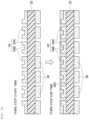
- FIG. 4is a diagram for explaining a light emitting operation of the light emitting substrate of the present embodiment.
- FIG. 5is a diagram for explaining a light emitting operation of a light emitting substrate of a comparative embodiment.
- FIG. 6is a graph showing a result of a first test of a correlated color temperature of the light emitting substrate of the present embodiment.
- FIG. 7is a graph showing a result of a second test of the correlated color temperature of the light emitting substrate of the present embodiment.
- FIGS. 1 A to 1 C, 2 A, and 2 Ba configuration and function of a light emitting substrate 10 of the present embodiment will be described with reference to FIGS. 1 A to 1 C, 2 A, and 2 B .
- a method for manufacturing the light emitting substrate 10 of the present embodimentwill be described with reference to FIGS. 3 A to 3 E .
- a light emitting operation of the light emitting substrate 10 of the present embodimentwill be described with reference to FIG. 4 .
- effects of the present embodimentwill be described with reference to FIGS. 4 to 7 and the like.
- the same reference numeralsare used for the same constituent elements and the description thereof will not be repeated.
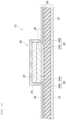
- FIG. 1 Ais a plan view of the light emitting substrate 10 of the present embodiment (view seen from a front surface 31 ), and FIG. 1 B is a bottom view of the light emitting substrate 10 of the present embodiment (view seen from a rear surface 33 ).
- FIG. 1 Cis a partial cross-sectional view of the light emitting substrate 10 taken along a cutting line 1 C- 1 C of FIG. 1 A .
- the light emitting substrate 10 of the present embodimentis rectangular as an example, when seen from the front surface 31 and the rear surface 33 .
- the light emitting substrate 10 of the present embodimentincludes a plurality of light emitting elements 20 , a phosphor substrate 30 , and electronic components (not shown) such as a connector, a driver IC, and the like. That is, in the light emitting substrate 10 of the present embodiment, the plurality of light emitting elements 20 and the electronic components are mounted on the phosphor substrate 30 .
- the light emitting substrate 10 of the present embodimenthas a function of emitting light, in a case where power is supplied from an external power source (not shown) by directly attaching a lead wire or through a connector. Accordingly, the light emitting substrate 10 of the present embodiment is used as a main optical component in, for example, a lighting device (not shown).
- each of the plurality of light emitting elements 20is formed as a Chip Scale Package (CSP) in which a flip chip LED 22 (hereinafter, referred to as an LED 22 ) is incorporated (see FIG. 1 C ).
- CSPChip Scale Package
- FIG. 1 Cit is preferable that the entire circumference (five surfaces) except a bottom surface of the LED 22 is covered with a phosphor sealing layer 24 .
- the phosphor sealing layer 24contains a phosphor, and light of the LED 22 is color-converted by the phosphor of the phosphor sealing layer 24 and emitted to the outside.
- FIG. 1 CChip Scale Package
- the plurality of light emitting elements 20are mounted on the phosphor substrate 30 in a state of being regularly arranged on the front surface 31 (an example of one surface) of the phosphor substrate 30 over the entire front surface 31 .
- a correlated color temperature of the light emitted by each light emitting element 20 of the present embodimentis set to 3,018K as an example.
- the plurality of light emitting elements 20use a heat sink (not shown) and a cooling fan (not shown) during the light emitting operation to dissipate heat (cool) the phosphor substrate 30 to be, for example, room temperature to 50° C. to 100° C.
- to supplement the meaning of “to” used in the numerical range in the present specificationfor example, “50° C.
- to 100° C.”means “equal to or higher than 50° C. and equal to or lower than 100° C.”.
- “to” used in the numerical range in this specificationmeans “equal to or more than the description part before “to” and equal to or less than the description part after “to”.
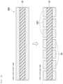
- FIG. 2 Ais a view of the phosphor substrate 30 of the present embodiment and is a plan view (seen from the front surface 31 ) in which the phosphor layer 36 omitted.
- FIG. 2 Bis a plan view (seen from the front surface 31 ) of the phosphor substrate 30 of the present embodiment.
- the bottom view of the phosphor substrate 30 of the present embodimentis the same as the view of the light emitting substrate 10 seen from the rear surface 33 .
- the partial cross-sectional view of the phosphor substrate 30 of the present embodimentis the same as the view when the light emitting element 20 is removed from the partial cross-sectional view of FIG. 1 C . That is, the phosphor substrate 30 of the present embodiment is rectangular as an example, when seen from the front surface 31 and the rear surface 33 .
- the phosphor substrate 30 of the present embodimentincludes an insulating layer 32 (an example of an insulating substrate), an electrode layer 34 , a phosphor layer 36 , and a rear surface pattern layer 38 (see FIGS. 1 B, 1 C, and 2 A, and 2 B ).
- the phosphor layer 36is not shown in FIG. 2 A , the phosphor layer 36 is, for example, disposed on a portion of the front surface 31 of the insulating layer 32 and the electrode layer 34 , other than a plurality of electrode pairs 34 A which will be described later, as shown in FIG. 2 B .
- the phosphor substrate 30is formed with six through holes 39 at four portions near the four corners and two portions near the center.
- the six through holes 39are used as positioning holes during the manufacturing of the phosphor substrate 30 and the light emitting substrate 10 .
- the six through holes 39are used as mounting screw holes for ensuring a heat-drawing effect (preventing warping and floating of the substrate) of a (light emitting) lamp housing.
- the phosphor substrate 30 of the present embodimentis manufactured by processing (etching or the like) a double-sided plate (hereinafter, referred to as a motherboard MB. see FIG. 3 A ) in which copper foil layers are provided on both sides of an insulating plate, and CS-3305A manufactured by Risho Kogyo Co., Ltd. is used as an example of the motherboard MB.
- a shape thereofis, for example, rectangular when seen from the front surface 31 and the rear surface 33 .
- a material thereofis, for example, an insulating material containing a bismaleimide resin and a glass cloth.
- a thickness thereofis, for example, 100 ⁇ m to 200 ⁇ m.
- Coefficients of thermal expansion (CTE) thereof in a vertical direction and a horizontal directionare, for example, equal to or less than 10 ppm/° C. in a range of 50° C. to 100° C., respectively.
- each of the coefficients of thermal expansion (CTE) in the vertical direction and the horizontal directionis, for example, 6 ppm/K. This value is substantially the same as that of the light emitting element 20 of the present embodiment (90% to 110%, that is, within ⁇ 10%).
- a glass transition temperature thereofis, for example, higher than 300° C.
- a storage elastic modulusis, for example, greater than 1.0 ⁇ 10 10 Pa and smaller than 1.0 ⁇ 10 11 Pa in a range of 100° C. to 300° C.
- the electrode layer 34 of the present embodimentis a metal layer provided on the front surface 31 side of the insulating layer 32 .
- the electrode layer 34 of this embodimentis, for example, a copper foil layer (a layer formed of Cu). In other words, the electrode layer 34 of the present embodiment is formed so that at least the surface thereof contains copper.
- the electrode layer 34has a pattern provided on the insulating layer 32 , and is electrically connected to a terminal (not shown) to which a connector (not shown) is bonded.
- the electrode layer 34supplies electric power supplied from an external power source (not shown) through the connector to the plurality of light emitting elements 20 at the time of configuring the light emitting substrate 10 .
- a part of the electrode layer 34is the plurality of electrode pairs 34 A to which the plurality of light emitting elements 20 are bonded.
- the plurality of electrode pairs 34 Aare also arranged over the entire front surface 31 (see FIG. 2 A ).
- a portion of the electrode layer 34 other than the plurality of electrode pairs 34 Ais referred to as a wiring portion 34 B.
- the plurality of electrode pairs 34 Aprotrude outward from the wiring portion 34 B in a thickness direction of the insulating layer 32 (phosphor substrate 30 ).
- a region of the front surface 31 of the insulating layer 32 where the electrode layer 34 is disposedis, for example, a region (area) that is equal to or more than 60% of the front surface 31 of the insulating layer 32 (see FIG. 2 A ).
- the phosphor layer 36 of the present embodimentis, for example, disposed on a portion of the front surface 31 of the insulating layer 32 and the electrode layer 34 , other than the plurality of electrode pairs 34 A. That is, the phosphor layer 36 is disposed in a region of the electrode layer 34 other than the plurality of electrode pairs 34 A.
- the region of the front surface 31 of the insulating layer 32 where the phosphor layer 36 is disposedis, for example, a region that is equal to or more than 80% of the front surface 31 of the insulating layer 32 .
- the phosphor layer 36 of the present embodimentis, for example, an insulating layer containing a phosphor and a binder, which will be described later.
- the phosphor contained in the phosphor layer 36is fine particles held in a state of being dispersed in a binder, and has a property of exciting the light emitted from the LED 22 of each light emitting element 20 as excitation light.
- the phosphor of the present embodimenthas a property that the light emission peak wavelength when the light emitted by the light emitting element 20 is used as excitation light is in a visible light region.
- the bindermay be, for example, an epoxy-based binder, an acrylate-based binder, or a silicone-based binder, and may have an insulating property equivalent to that of the binder contained in a solder resist.
- the phosphor contained in the phosphor layer 36 of the present embodimentis, for example, at least one or more phosphors selected from the group consisting of an ⁇ -type sialon phosphor containing Eu, a ⁇ -type sialon phosphor containing Eu, a CASN phosphor containing Eu, and a SCASN phosphor containing Eu.
- the phosphor described aboveis an example of the present embodiment, and may be a phosphor other than the phosphor described above, such as YAG, LuAG, BOS, and other visible light-excited phosphors.
- the ⁇ -type sialon phosphor containing Euis represented by general formula: M x Eu y Si 12 ⁇ (m+n) Al (m+n) O n N 16 ⁇ n .
- examples of a nitride phosphorinclude a CASN phosphor containing Eu, a SCASN phosphor containing Eu, and the like.
- the CASN phosphor containing Euis, for example, a red phosphor which is represented by the formula CaAlSiN 3 :Eu 2+ in which Eu 2+ is used as an activator and a crystal formed of alkaline earth silicate is used as a base.
- the SCASN phosphor containing Euis excluded.
- the SCASN phosphor containing Euis, for example, a red phosphor which is represented by the formula (Sr, Ca)AlSiN 3 :Eu 2+ in which Eu 2+ is used as an activator and a crystal formed of alkaline earth silicate is used as a base.
- the rear surface pattern layer 38 of the present embodimentis a metal layer provided on the rear surface 33 side of the insulating layer 32 .
- the rear surface pattern layer 38 of this embodimentis, for example, a copper foil layer (a layer formed of Cu).
- the rear surface pattern layer 38is a layer in which a plurality of rectangular blocks arranged linearly along a longitudinal direction of the insulating layer 32 are arranged to be adjacent to each other by shifting phase in a short direction.
- the rear surface pattern layer 38is, for example, an independent floating layer. In addition, the rear surface pattern layer 38 overlaps with the region that is equal to or more than 80% of the electrode layer 34 disposed on the front surface 31 , for example, in a thickness direction of the insulating layer 32 (phosphor substrate 30 ).
- the method for manufacturing the light emitting substrate 10 of the present embodimentincludes a first step, a second step, a third step, a fourth step, and a fifth step, and each step is performed in this order.
- FIG. 3 Ais a diagram showing a start time and an end time of the first step.
- the first stepis a step of forming a pattern 34 C that is the same as the electrode layer 34 , when seen from the thickness direction, on the front surface 31 of the motherboard MB, and the rear surface pattern layer 38 on the rear surface 33 .
- This stepis performed, for example, by etching using a mask pattern (not shown).
- FIG. 3 Bis a diagram showing a start time and an end time of the second step.
- the second stepis a step of half-etching (etching halfway in the thickness direction) of a part of the pattern 34 C. In a case where this step ends, as a result, the electrode layer 34 including the plurality of electrode pairs 34 A and the wiring portion 34 B is formed. This step is performed, for example, by etching using a mask pattern (not shown).
- FIG. 3 Cis a diagram showing a start time and an end time of the third step.
- the third stepis a step of applying a phosphor coating material 36 C to the entire surface of the front surface 31 of the insulating layer 32 , that is, the surface on which the electrode layer 34 is formed.
- the phosphor coating material 36 Cis applied by printing.
- the phosphor coating material 36 Cis applied thicker than all of the electrode pairs 34 A.
- FIG. 3 Dis a diagram showing a start time and an end time of the fourth step.
- the fourth stepis a step of removing a part of the phosphor layer 36 obtained by curing the phosphor coating material 36 C and exposing an upper surface of all of the electrode pairs 34 A.
- the binder of the phosphor coating material 36 Cis, for example, a thermosetting resin
- the phosphor coating material 36 Cis cured by heating and then the surface of the phosphor layer 36 is polished.
- the binder of the phosphor coating material 36 Cis, for example, a UV curable resin (photosensitive resin)
- a mask patternis applied to a portion (coating material opening) overlapping each bonded surface 34 A 1 to expose UV light, the portion other than the mask pattern is UV-cured, and a non-exposed portion (uncured portion) is removed with a resin removing liquid to expose each bonded surface 34 A 1 .
- after-curingis performed by applying heat (photo development method).
- the phosphor substrate 30 of the present embodimentis manufactured.
- FIG. 3 Eis a diagram showing a start time and an end time of the fifth step.
- the fifth stepis a step of mounting a plurality of light emitting elements 20 on the phosphor substrate 30 .
- a solder paste SPis printed on each upper surface of the plurality of electrode pairs 34 A of the phosphor substrate 30 , and the solder paste SP is melted in a state where each electrode of the plurality of light emitting elements 20 is positioned on each upper surface of the plurality of electrode pairs 34 A.
- each light emitting element 20is bonded to each electrode pair 34 A. That is, this step is performed by, for example, a reflow step.
- FIG. 4is a diagram for explaining the light emitting operation of the light emitting substrate 10 of the present embodiment.
- the power supplyis started from the external power source (not shown) to the electrode layer 34 through the connector (not shown), the plurality of light emitting elements 20 emit light L radially, and some light L reaches the front surface 31 of the phosphor substrate 30 .
- the behavior of the light Lwill be described separately according to a traveling direction of the emitted light L.
- Some light L emitted from each light emitting element 20is emitted to the outside without being incident to the phosphor layer 36 .
- a wavelength of the light Lremains as the same as the wavelength of the light L, in a case of being emitted from each light emitting element 20 .
- the light of the LED 22 itself in some light L emitted from each light emitting element 20is incident to the phosphor layer 36 .
- the “light of the LED 22 itself in some light L” described aboveis light of the emitted light L that is not color-converted by the phosphor (phosphor sealing layer 24 ) of each light emitting element 20 (CSP itself), that is, light of the LED 22 itself (for example, blue (wavelength is approximately 470 nm) color).
- the phosphorexcites and emits excitation light.
- the reason why the phosphor is excitedis that the phosphor dispersed in the phosphor layer 36 uses a phosphor (visible light excited phosphor) having an excitation peak in blue light. Along with this, a part of the energy of the light L is used for exciting the phosphor, so that the light L loses a part of the energy. As a result, the wavelength of the light L is converted (wavelength conversion is performed). For example, depending on the type of phosphor in the phosphor layer 36 (for example, in a case where a red CASN is used as the phosphor), the wavelength of light L becomes longer (for example, 650 nm or the like).
- the excitation light in the phosphor layer 36may be emitted from the phosphor layer 36 as it is, but some of the excitation light goes to the lower electrode layer 34 . Then, some of the excitation light is emitted to the outside by reflection on the electrode layer 34 .
- the wavelength of the excitation light by the phosphor of the phosphor layer 36is equal to or more than 600 nm, the reflection effect can be expected, even if the electrode layer 34 is formed of Cu.
- the wavelength of the light Ldiffers from the above example depending on the type of the phosphor in the phosphor layer 36 , but in any case, the wavelength conversion of the light L is performed.
- a reflection effectcan be expected, if the electrode layer 34 or its surface is formed of, for example, Ag (plating).
- a white reflective layermay be provided on the lower side (insulating layer 32 side) of the phosphor layer 36 .
- the reflective layeris provided with, for example, a white coating material such as a titanium oxide filler.
- the light L emitted by each light emitting element 20(the light L emitted radially by each light emitting element 20 ) is irradiated to the outside together with the excitation light through a plurality of optical paths as described above. Therefore, in a case where a light emission wavelength of the phosphor contained in the phosphor layer 36 and a light emission wavelength of the phosphor (phosphor sealing layer 24 ) that seals (or covers) the LED 22 of the light emitting element 20 (CSP) are different from each other, the light emitting substrate 10 of the present embodiment emits a bundle of the light L, in a case of being emitted by each light emitting element 20 , by setting it as a bundle of the light L containing the light L at a wavelength different from the wavelength of the light L, in a case of being emitted by each light emitting element 20 , together with the excitation light.
- the light emitting substrate 10 of the present embodimentemits a bundle of the light L, in a case of being emitted by each light emitting element 20 , by setting it as a bundle of the light L containing the light L at a wavelength longer than the wavelength of the light L, in a case of being emitted by each light emitting element 20 , together with the excitation light.
- the light emitting substrate 10 of the present embodimentemits a bundle of the light L, in a case of being emitted by each light emitting element 20 , by setting it as a bundle of the light L containing the light L at a wavelength same as the wavelength of the light L, in a case of being emitted by each light emitting element 20 , together with the excitation light.
- FIG. 5is a diagram for explaining a light emitting operation of a light emitting substrate 10 A of a comparative embodiment.
- the light emitting substrate 10 A of the comparative embodiment(a substrate 30 A on which the plurality of light emitting elements 20 are mounted) has the same configuration as the light emitting substrate 10 (phosphor substrate 30 ) of the present embodiment except that the phosphor layer 36 is not provided.
- the light L emitted from each light emitting element 20 and incident to the front surface 31 of the substrate 30 Ais reflected or scattered without converting the wavelength. Accordingly, in the case of the substrate 30 A of the comparative embodiment, it is not possible to adjust the light to light having light emission color different from the light emitted by the light emitting element 20 , in a case where the light emitting element 20 is mounted. That is, in a case of the light emitting substrate 10 A of the comparative embodiment, it is not possible to adjust the light to light having light emission color different from the light emitted by the light emitting element 20 .
- the phosphor layer 36is provided on the front surface 31 of the insulating layer 32 . Accordingly, some of the light L emitted from each light emitting element 20 is incident to the phosphor layer 36 , wavelength-converted by the phosphor layer 36 , and irradiated to the outside. In this case, some of the light L radially emitted from each light emitting element 20 is incident to the phosphor layer 36 to excite the phosphor contained in the phosphor layer 36 and generate the excitation light.
- FIG. 6is a graph showing a result of a first test of the correlated color temperature of the light emitting substrate 10 of the present embodiment.
- FIG. 7is a graph showing a result of the second test of the correlated color temperature of the light emitting substrate 10 of the present embodiment.
- the first testis a test to obtain a result by investigating a relationship between a current (mA) and a correlated color temperature (K) of the plurality of light emitting elements 20 , in a case where the power is supplied to the light emitting substrate 10 including the plurality of light emitting elements 20 having the correlated color temperature approximately at 2200 K to 2300 K to generate light.
- HE ( 1 ) and HE ( 2 )indicate a case where the structure of the electrode layer 34 is the same as that of the present embodiment
- FLT ( 1 ) and FLT ( 2 )indicate a case where thicknesses of the pair of electrode pair 34 A and the wiring portion 34 B of the electrode layer 34 are the same (modification example).
- the correlated color temperature of the light L emitted by the light emitting substrate 10is lower than the correlated color temperature of the plurality of light emitting elements 20 . That is, in the case of the present embodiment (including the modification example described above), the correlated color temperature could be shifted by providing the phosphor layer 36 .
- the second testis a test to obtain a result by investigating a relationship between a current (mA) and a correlated color temperature (K) of the plurality of light emitting elements 20 , in a case where the power is supplied to the light emitting substrate 10 including the plurality of light emitting elements 20 having the correlated color temperature approximately at 2900 K to 3000 K to generate light.
- HE ( 1 )indicates a case where the structure of the electrode layer 34 is the same structure as that of the present embodiment
- FLT ( 1 ) and FLT ( 2 )indicate a case where thicknesses of the pair of electrode pair 34 A and the wiring portion 34 B of the electrode layer 34 are the same (modification example).
- the correlated color temperature of the light L emitted by the light emitting substrate 10is lower than the correlated color temperature of the plurality of light emitting elements 20 . That is, in the case of the present embodiment (including the modification example described above), the correlated color temperature could be shifted by providing the phosphor layer 36 .
- the phosphor substrate 30 of the present embodimentin a case where the light emitting element 20 is mounted, it is possible to adjust the light L emitted from the phosphor substrate 30 to light having a light emission color different from the light L emitted by the light emitting element 20 .
- the light emitting substrate 10 of the present embodimentit is possible to adjust the light L emitted from the phosphor substrate 30 to the light L having a light emission color different from the light L emitted by the light emitting element 20 .
- the light emitting substrate 10 of the present embodimentit is possible to irradiate the outside with light L having a light emission color different from the light L emitted by the light emitting element 20 .
- the light emitting substrate 10 of the present embodimentemits a bundle of the light L, in a case of being emitted by each light emitting element 20 , by setting it as a bundle of the light L containing the light L at a wavelength same as the wavelength of the light L, in a case of being emitted by each light emitting element 20 , together with the excitation light. In this case, it is possible to exhibit the effect of alleviating a chromaticity variation of the mounted light emitting element 20 by the phosphor layer 36 .
- spotsare generated in the light L irradiated to the outside due to an arrangement interval of each light emitting element 20 .
- the larger the spot of light Lthe larger the glare.
- the phosphor layer 36is provided between the adjacent light emitting elements 20 . Accordingly, the excitation light is also emitted from the phosphor layer 36 .
- this effectis effective, in a case where the phosphor layer 36 is provided over the entire surface of the insulating layer 32 , specifically, in a case where a region of the front surface 31 of the insulating layer 32 where the phosphor layer 36 is disposed is a region that is 80% or more of the front surface 31 .
- the phosphor layer 36is provided between the adjacent light emitting elements 20 (see FIG. 2 B ).
- the binder of the phosphor layer 36has an insulating property equivalent to that of the binder contained in, for example, a solder resist. That is, in a case of the present embodiment, the phosphor layer 36 functions as a solder resist.
- the phosphor contained in the phosphor layer 36is a CASN phosphor containing Eu, and the phosphor layer 36 is provided on the wiring portion 34 B formed of Cu. Accordingly, for example, in a case where each light emitting element 20 emits white light L, the excitation light from the CASN phosphor contained in the phosphor layer 36 has an improved light emission efficiency due to reflection by Cu constituting a lower layer electrode (in the configuration of the present embodiment, there is a light reflection effect of Cu). Then, in the present embodiment, by the effect, it is possible to adjust the white light L to a warmer color light (color in which the correlated color temperature is shifted to the lower temperature side) (see FIGS. 6 and 7 ). In this case, it is possible to add warm color light to the white light of the light emitting element 20 , and increase a special color rendering index R 9 value. This effect is particularly effective for pseudo-white using YAG-based white light (yellow phosphor).
- the plurality of light emitting elements 20use a heat sink (not shown) and a cooling fan (not shown) during the light emitting operation to dissipate heat (cool) the phosphor substrate 30 to be, for example, room temperature to 50° C. to 100° C. Accordingly, the heat generated in a case of light emission of the LED 22 is diffused to the entire substrate to enhance the heat-drawing effect on the housing.
- a region of the front surface 31 of the insulating layer 32 where the electrode layer 34 is disposedis, for example, a region (area) that is equal to or more than 60% of the front surface 31 of the insulating layer 32 (see FIG. 2 A ).
- the electrode layer 34 (wiring portion 34 B) of the present embodimentfunctions as a heat radiating plate for heat generated from the plurality of light emitting elements 20 , in addition to the function as an electric path for power supply. Therefore, the light emitting element 20 (LED 22 ) can stably emit light L in a situation where it is not easily affected by heat.
- an example of the light emitting element 20is a CSP.
- an example of the light emitting element 20may be other than the CSP.
- itmay simply be equipped with a flip chip.
- itcan also be applied to the substrate itself of a COB device.
- the plurality of light emitting elements 20are mounted on the phosphor substrate 30 and the light emitting substrate 10 includes the plurality of light emitting elements 20 (see FIG. 1 A ).
- the number of light emitting elements 20 mounted on the phosphor substrate 30may be at least one or more.
- the number of light emitting elements 20 mounted on the light emitting substrate 10may be at least one or more.
- the rear surface pattern layer 38is provided on the rear surface 33 of the phosphor substrate 30 (see FIG. 1 B ).
- the first effectis exhibited even if the rear surface 33 of the phosphor substrate 30 is not provided with the rear surface pattern layer 38 . Therefore, even if the embodiment is different from the phosphor substrate 30 and the light emitting substrate 10 of the present embodiment only in that the rear surface 33 is not provided with the rear surface pattern layer 38 , it can be said that this embodiment belongs to the technical scope of the present invention.
- the phosphor layer 36is, for example, disposed on a portion of the front surface 31 of the insulating layer 32 and the electrode layer 34 , other than the plurality of electrode pairs 34 A (see FIG. 2 B ).
- the first effectis exhibited, even if the phosphor layer is not disposed over the entire region of the portion of the front surface 31 of the phosphor substrate 30 other than the plurality of electrode pair 34 A.
- CS-3305A manufactured by Risho Kogyo Co., Ltd.is used as the motherboard MB in manufacturing the phosphor substrate 30 and the light emitting substrate 10 .
- thisis merely an example, and different motherboard MBs may be used.
- the light emitting substrate 10 of the present embodiment(including the modification example thereof) can be applied to a lighting device in combination with other constituent elements.
- Other constituent elements in this caseare a power source that supplies electric power for causing the light emitting element 20 of the light emitting substrate 10 to emit light, and the like.
Landscapes
- Engineering & Computer Science (AREA)
- Microelectronics & Electronic Packaging (AREA)
- Physics & Mathematics (AREA)
- Spectroscopy & Molecular Physics (AREA)
- Power Engineering (AREA)
- General Engineering & Computer Science (AREA)
- Manufacturing & Machinery (AREA)
- Condensed Matter Physics & Semiconductors (AREA)
- General Physics & Mathematics (AREA)
- Computer Hardware Design (AREA)
- Led Device Packages (AREA)
- Arrangement Of Elements, Cooling, Sealing, Or The Like Of Lighting Devices (AREA)
- Non-Metallic Protective Coatings For Printed Circuits (AREA)
Abstract
Description
Claims (16)
Applications Claiming Priority (3)
| Application Number | Priority Date | Filing Date | Title |
|---|---|---|---|
| JP2018244542 | 2018-12-27 | ||
| JP2018-244542 | 2018-12-27 | ||
| PCT/JP2019/049687WO2020137760A1 (en) | 2018-12-27 | 2019-12-18 | Phosphor substrate, light-emitting substrate, and lighting device |
Publications (2)
| Publication Number | Publication Date |
|---|---|
| US20220059730A1 US20220059730A1 (en) | 2022-02-24 |
| US12107196B2true US12107196B2 (en) | 2024-10-01 |
Family
ID=71129754
Family Applications (1)
| Application Number | Title | Priority Date | Filing Date |
|---|---|---|---|
| US17/415,373Active2041-05-18US12107196B2 (en) | 2018-12-27 | 2019-12-18 | Phosphor substrate, light emitting substrate, and lighting device |
Country Status (7)
| Country | Link |
|---|---|
| US (1) | US12107196B2 (en) |
| EP (1) | EP3905348B1 (en) |
| JP (1) | JP7491849B2 (en) |
| KR (1) | KR102854327B1 (en) |
| CN (1) | CN113228314B (en) |
| TW (1) | TWI849023B (en) |
| WO (1) | WO2020137760A1 (en) |
Families Citing this family (1)
| Publication number | Priority date | Publication date | Assignee | Title |
|---|---|---|---|---|
| US12040436B2 (en)* | 2018-12-27 | 2024-07-16 | Denka Company Limited | Phosphor substrate, light emitting substrate, and lighting device |
Citations (83)
| Publication number | Priority date | Publication date | Assignee | Title |
|---|---|---|---|---|
| JPH10151794A (en) | 1996-11-22 | 1998-06-09 | Nichia Chem Ind Ltd | Light emitting device and method for forming the same |
| JP2000011953A (en) | 1998-06-25 | 2000-01-14 | Nec Corp | Fluorescent lamp formed from multi-tube |
| JP2001148509A (en) | 1999-11-18 | 2001-05-29 | Matsushita Electric Works Ltd | Illuminating light source |
| JP2001148512A (en) | 1999-11-18 | 2001-05-29 | Matsushita Electric Works Ltd | Illuminating light source |
| JP2003258311A (en) | 2002-03-01 | 2003-09-12 | Citizen Electronics Co Ltd | Light emitting device and its manufacturing method |
| US20050139851A1 (en) | 2003-12-26 | 2005-06-30 | Hiroyuki Sato | Semiconductor light-emitting apparatus having wavelength conversion portion and method of fabricating the same |
| JP2006049799A (en) | 2004-04-27 | 2006-02-16 | Matsushita Electric Ind Co Ltd | Light emitting device |
| JP2006261688A (en) | 2006-05-08 | 2006-09-28 | Toshiba Electronic Engineering Corp | Light emitting device |
| US20070064131A1 (en) | 2005-09-13 | 2007-03-22 | Sumita Optical Glass, Inc. | Solid-state element device and light-emitting apparatus using same |
| CN1967888A (en) | 2005-11-02 | 2007-05-23 | 株式会社托里昂 | Light emitting diode mounting substrate |
| US20070259206A1 (en) | 2004-04-27 | 2007-11-08 | Matsushita Electric Industrial Co., Ltd. | Phosphor Composition and Method for Producing the Same, and Light-Emitting Device Using the Same |
| JP2008066691A (en) | 2006-03-10 | 2008-03-21 | Toshiba Lighting & Technology Corp | Lighting device |
| TW200903843A (en) | 2007-07-06 | 2009-01-16 | Formosa Epitaxy Inc | Light-blending light-emitting diode |
| US20090050909A1 (en) | 2007-08-20 | 2009-02-26 | Delta Electronics, Inc. | Light-emitting diode apparatus and manufacturing method thereof |
| US20090072256A1 (en) | 2007-09-17 | 2009-03-19 | Samsung Electro-Mechanics Co., Ltd. | Light emitting diode package and method of manufacturing the same |
| US20090217970A1 (en) | 2008-03-01 | 2009-09-03 | Goldeneye, Inc. | Fixtures for large area directional and isotropic solid state lighting panels |
| JP2009267289A (en) | 2008-04-30 | 2009-11-12 | Citizen Electronics Co Ltd | Light-emitting device |
| CN101606247A (en)* | 2006-10-31 | 2009-12-16 | 克里公司 | Integrated heat sink for LEDs and related components |
| US20090315057A1 (en) | 2008-06-24 | 2009-12-24 | Sharp Kabushiki Kaisha | Light-emitting apparatus, surface light source, and method for manufacturing package for light-emitting apparatus |
| US20100238648A1 (en) | 2007-12-07 | 2010-09-23 | Sony Corporation | Illumination apparatus and display apparatus |
| WO2010150880A1 (en) | 2009-06-26 | 2010-12-29 | 株式会社朝日ラバー | White color reflecting material and process for production thereof |
| US20110089805A1 (en) | 2009-10-21 | 2011-04-21 | Toshiba Lighting & Technology Corporation | Light-emitting apparatus and luminaire |
| CN102074558A (en) | 2009-10-21 | 2011-05-25 | 东芝照明技术株式会社 | Lighting device and lighting fixture |
| TW201214786A (en) | 2010-09-30 | 2012-04-01 | Everlight Electronics Co Ltd | Light emitting diode package structure and manufacturing method thereof |
| JP2012094578A (en) | 2010-10-25 | 2012-05-17 | Citizen Holdings Co Ltd | Manufacturing method of semiconductor light emitting device |
| JP2012146942A (en) | 2010-12-24 | 2012-08-02 | Citizen Holdings Co Ltd | Semiconductor light emitting device and manufacturing method of the same |
| JP2012186274A (en) | 2011-03-04 | 2012-09-27 | Sharp Corp | Light-emitting device, led chip, led wafer and package substrate |
| US20130011617A1 (en) | 2010-03-23 | 2013-01-10 | Asahi Rubber Inc. | Silicone resin reflective substrate, manufacturing method for same, and base material composition used in reflective substrate |
| JP2013012607A (en) | 2011-06-29 | 2013-01-17 | Toyoda Gosei Co Ltd | Light-emitting device |
| JP2013115368A (en) | 2011-11-30 | 2013-06-10 | Rohm Co Ltd | Led module |
| US20130161662A1 (en)* | 2011-12-26 | 2013-06-27 | Citizen Holdings Co., Ltd. | Lighting device |
| KR20130104975A (en) | 2012-03-16 | 2013-09-25 | 삼성전자주식회사 | Light emitting device |
| CN103346241A (en) | 2013-07-03 | 2013-10-09 | 梁栌伊 | Packaging structure of white LED lamp |
| WO2013153739A1 (en) | 2012-04-11 | 2013-10-17 | パナソニック株式会社 | Light-emitting device, and lamp |
| JP2014003065A (en) | 2012-06-15 | 2014-01-09 | Konica Minolta Inc | Led device and method for manufacturing the same |
| CN103579480A (en) | 2012-07-27 | 2014-02-12 | 华夏光股份有限公司 | Thermoelectric separated semiconductor device and method for manufacturing the same |
| CN103904072A (en) | 2014-03-28 | 2014-07-02 | 中山市鸿宝电业有限公司 | High-power LED chip integrated packaging structure |
| CN203839375U (en) | 2014-03-28 | 2014-09-17 | 中山市鸿宝电业有限公司 | Large-power LED chip integrated packaging structure |
| WO2014181757A1 (en) | 2013-05-09 | 2014-11-13 | 日東電工株式会社 | Circuit board, optical semiconductor device and manufacturing method for same |
| US20150001563A1 (en)* | 2013-06-27 | 2015-01-01 | Nichia Corporation | Light emitting device and method of manufacturing the same |
| US20150008462A1 (en) | 2013-07-08 | 2015-01-08 | Lite-On Electronics (Guangzhou) Limited | Flip-chip light emitting diode package module and manufacturing method thereof |
| US20150021642A1 (en) | 2013-07-19 | 2015-01-22 | Nichia Corporation | Light emitting device and method of manufacturing the same |
| US20150049481A1 (en) | 2013-08-16 | 2015-02-19 | Citizen Electronics Co., Ltd. | Lighting device |
| JP2015038963A (en) | 2013-07-19 | 2015-02-26 | 日亜化学工業株式会社 | Light emitting device and manufacturing method thereof |
| TWM496850U (en) | 2014-10-23 | 2015-03-01 | Genesis Photonics Inc | LED package structure |
| US20150060911A1 (en) | 2013-09-05 | 2015-03-05 | Unistars Corporation | Optoelectronic semiconductor device and fabricating method thereof |
| US9006006B2 (en) | 2011-11-29 | 2015-04-14 | Sharp Kabushiki Kaisha | Manufacturing method for light-emitting device comprising multi-step cured silicon resin |
| US20150155441A1 (en)* | 2012-06-15 | 2015-06-04 | Andrei Alexeev | LED package and method for producing the same |
| JP2015103632A (en) | 2013-11-22 | 2015-06-04 | 日亜化学工業株式会社 | Light emitting device, method of manufacturing the same, and illumination device equipped with this light emitting device |
| US20150185137A1 (en) | 2013-12-27 | 2015-07-02 | Nichia Corporation | Aggregate board, light emitting device, and method for testing light emitting element |
| US20150228869A1 (en) | 2014-02-11 | 2015-08-13 | Samsung Electronics Co., Ltd. | Light source package and display device including the same |
| US20150276152A1 (en) | 2014-04-01 | 2015-10-01 | Huga Optotech, Inc. | Led assembly and led bulb using the same |
| JP2015216139A (en) | 2014-05-07 | 2015-12-03 | 株式会社小糸製作所 | Light emitting module |
| US20160005939A1 (en) | 2014-07-07 | 2016-01-07 | Cree, Inc. | Light emitting diode (led) components including contact expansion frame and methods of fabricating same |
| JP2016069401A (en) | 2014-09-26 | 2016-05-09 | 住友ベークライト株式会社 | Prepreg, resin board, metal-clad laminate, printed wiring board, and semiconductor device |
| US20160161067A1 (en) | 2013-08-01 | 2016-06-09 | Koninklijke Philips N.V. | Light emitting arrangement with adapted output spectrum |
| US20160190408A1 (en) | 2014-12-24 | 2016-06-30 | Nichia Corporation | Light emitting device |
| US20160219690A1 (en) | 2015-01-26 | 2016-07-28 | KYOCERA Circuit Solutions, Inc. | Wiring board |
| JP2016525798A (en) | 2013-07-10 | 2016-08-25 | ゴールデンアイ,インコーポレイテッド | Self-cooling light source |
| CN106163113A (en) | 2015-03-23 | 2016-11-23 | 李玉俊 | LED installs lamp bead circuit board light-reflection layer processing technology |
| CN106356439A (en) | 2016-11-21 | 2017-01-25 | 中山市立体光电科技有限公司 | An LED packaging structure with adjustable color temperature |
| US20170025582A1 (en) | 2015-06-01 | 2017-01-26 | Intematix Corporation | Photoluminescence material coating of led chips |
| US20170054063A1 (en) | 2015-08-19 | 2017-02-23 | Bright Led Electronics Corp. | Light-emitting diode structure |
| JP2017041621A (en) | 2015-08-23 | 2017-02-23 | 久豊技研株式会社 | LED light emitting device |
| US20170084799A1 (en) | 2014-06-02 | 2017-03-23 | 3M Innovative Properties Company | Led with remote phosphor and shell reflector |
| JP2017058635A (en) | 2015-09-18 | 2017-03-23 | 大日本印刷株式会社 | Led information display panel with snow-melting function and led information display device |
| US20170196060A1 (en)* | 2015-12-25 | 2017-07-06 | Citizen Electronics Co., Ltd. | Light-emitting apparatus and color-matching apparatus |
| US20170229621A1 (en) | 2016-02-05 | 2017-08-10 | Maven Optronics Co., Ltd. | Light emitting device with beam shaping structure and manufacturing method of the same |
| JP2017175118A (en) | 2016-02-05 | 2017-09-28 | マブン オプトロニックス カンパニー リミテッドMaven Optronics Co., Ltd. | Light emitting element with beam shaping structure and manufacturing method of the same |
| US20170317250A1 (en) | 2014-10-28 | 2017-11-02 | Sharp Kabushiki Kaisha | Substrate, light-emitting device, and illuminating apparatus |
| US20180033929A1 (en) | 2016-07-28 | 2018-02-01 | Nichia Corporation | Method of manufacturing light emitting device |
| WO2018059599A1 (en) | 2016-09-30 | 2018-04-05 | 深圳市玲涛光电科技有限公司 | Strip-shaped light source, manufacturing method therefor, and electronic device |
| JP2018082027A (en) | 2016-11-16 | 2018-05-24 | 豊田合成株式会社 | Light-emitting device and method for manufacturing the same |
| JP2018191006A (en) | 2013-10-23 | 2018-11-29 | 株式会社光波 | Light emitting device |
| CN109075131A (en) | 2016-03-31 | 2018-12-21 | 株式会社村田制作所 | circuit module |
| JP2019093339A (en) | 2017-11-22 | 2019-06-20 | 帝人フロンティア株式会社 | Moisture permeable filter medium |
| US20190227672A1 (en) | 2017-01-23 | 2019-07-25 | Nissha Co., Ltd. | Capacitive touch panel |
| EP3546895A1 (en) | 2018-03-28 | 2019-10-02 | E+E Elektronik Ges.M.B.H. | Device and method for operating a heatable sensor, in particular in an explosive atmosphere |
| US20200091384A1 (en) | 2013-07-19 | 2020-03-19 | Nichia Corporation | Method of manufacturing light emitting device |
| US20200092994A1 (en) | 2016-10-05 | 2020-03-19 | Panasonic Intellectual Property Management Co., Ltd. | Multilayer printed wiring board and method for producing multilayer printed wiring board |
| US10755856B2 (en) | 2018-10-10 | 2020-08-25 | Samsung Electro-Mechanics Co., Ltd. | Multilayer ceramic electronic component |
| US20220052233A1 (en)* | 2018-12-27 | 2022-02-17 | Denka Company Limited | Phosphor substrate, light emitting substrate, and lighting device |
| US20220085253A1 (en)* | 2018-12-27 | 2022-03-17 | Denka Company Limited | Phosphor substrate, light emitting substrate, and lighting device |
Family Cites Families (3)
| Publication number | Priority date | Publication date | Assignee | Title |
|---|---|---|---|---|
| US6340824B1 (en) | 1997-09-01 | 2002-01-22 | Kabushiki Kaisha Toshiba | Semiconductor light emitting device including a fluorescent material |
| US20110215348A1 (en) | 2010-02-03 | 2011-09-08 | Soraa, Inc. | Reflection Mode Package for Optical Devices Using Gallium and Nitrogen Containing Materials |
| JP5877487B1 (en) | 2014-12-26 | 2016-03-08 | パナソニックIpマネジメント株式会社 | Light emitting device |
- 2019
- 2019-12-18CNCN201980085491.5Apatent/CN113228314B/enactiveActive
- 2019-12-18JPJP2020563141Apatent/JP7491849B2/enactiveActive
- 2019-12-18EPEP19905139.2Apatent/EP3905348B1/enactiveActive
- 2019-12-18KRKR1020217018336Apatent/KR102854327B1/enactiveActive
- 2019-12-18WOPCT/JP2019/049687patent/WO2020137760A1/ennot_activeCeased
- 2019-12-18USUS17/415,373patent/US12107196B2/enactiveActive
- 2019-12-23TWTW108147166Apatent/TWI849023B/enactive
Patent Citations (143)
| Publication number | Priority date | Publication date | Assignee | Title |
|---|---|---|---|---|
| JPH10151794A (en) | 1996-11-22 | 1998-06-09 | Nichia Chem Ind Ltd | Light emitting device and method for forming the same |
| JP2000011953A (en) | 1998-06-25 | 2000-01-14 | Nec Corp | Fluorescent lamp formed from multi-tube |
| JP2001148509A (en) | 1999-11-18 | 2001-05-29 | Matsushita Electric Works Ltd | Illuminating light source |
| JP2001148512A (en) | 1999-11-18 | 2001-05-29 | Matsushita Electric Works Ltd | Illuminating light source |
| JP2003258311A (en) | 2002-03-01 | 2003-09-12 | Citizen Electronics Co Ltd | Light emitting device and its manufacturing method |
| US20050139851A1 (en) | 2003-12-26 | 2005-06-30 | Hiroyuki Sato | Semiconductor light-emitting apparatus having wavelength conversion portion and method of fabricating the same |
| JP2006049799A (en) | 2004-04-27 | 2006-02-16 | Matsushita Electric Ind Co Ltd | Light emitting device |
| US20070259206A1 (en) | 2004-04-27 | 2007-11-08 | Matsushita Electric Industrial Co., Ltd. | Phosphor Composition and Method for Producing the Same, and Light-Emitting Device Using the Same |
| US7391060B2 (en) | 2004-04-27 | 2008-06-24 | Matsushita Electric Industrial Co., Ltd. | Phosphor composition and method for producing the same, and light-emitting device using the same |
| US20070064131A1 (en) | 2005-09-13 | 2007-03-22 | Sumita Optical Glass, Inc. | Solid-state element device and light-emitting apparatus using same |
| JP2007080994A (en) | 2005-09-13 | 2007-03-29 | Sumita Optical Glass Inc | Solid element device and light emitting device using the same |
| US7825575B2 (en) | 2005-09-13 | 2010-11-02 | Sumita Optical Glass, Inc. | Solid-state element device and light-emitting apparatus using same |
| CN1967888A (en) | 2005-11-02 | 2007-05-23 | 株式会社托里昂 | Light emitting diode mounting substrate |
| JP2008066691A (en) | 2006-03-10 | 2008-03-21 | Toshiba Lighting & Technology Corp | Lighting device |
| JP2006261688A (en) | 2006-05-08 | 2006-09-28 | Toshiba Electronic Engineering Corp | Light emitting device |
| CN101606247A (en)* | 2006-10-31 | 2009-12-16 | 克里公司 | Integrated heat sink for LEDs and related components |
| TW200903843A (en) | 2007-07-06 | 2009-01-16 | Formosa Epitaxy Inc | Light-blending light-emitting diode |
| TW200910630A (en) | 2007-08-20 | 2009-03-01 | Delta Electronics Inc | Light-emitting diode apparatus and manufacturing method thereof |
| US20090050909A1 (en) | 2007-08-20 | 2009-02-26 | Delta Electronics, Inc. | Light-emitting diode apparatus and manufacturing method thereof |
| US20090072256A1 (en) | 2007-09-17 | 2009-03-19 | Samsung Electro-Mechanics Co., Ltd. | Light emitting diode package and method of manufacturing the same |
| JP2009071264A (en) | 2007-09-17 | 2009-04-02 | Samsung Electro Mech Co Ltd | Light emitting diode package and manufacturing method thereof |
| US8143634B2 (en) | 2007-09-17 | 2012-03-27 | Samsung Led Co., Ltd. | Light emitting diode package with a phosphor substrate |
| US8563338B2 (en) | 2007-09-17 | 2013-10-22 | Samsung Electronics Co., Ltd. | Light emitting diode package having an LED chip mounted on a phosphor substrate |
| US20120142127A1 (en) | 2007-09-17 | 2012-06-07 | Samsung Led Co., Ltd. | Light emitting diode package with a phosphor substrate |
| US20100238648A1 (en) | 2007-12-07 | 2010-09-23 | Sony Corporation | Illumination apparatus and display apparatus |
| US20090217970A1 (en) | 2008-03-01 | 2009-09-03 | Goldeneye, Inc. | Fixtures for large area directional and isotropic solid state lighting panels |
| US8558438B2 (en) | 2008-03-01 | 2013-10-15 | Goldeneye, Inc. | Fixtures for large area directional and isotropic solid state lighting panels |
| JP2009267289A (en) | 2008-04-30 | 2009-11-12 | Citizen Electronics Co Ltd | Light-emitting device |
| US9960332B2 (en) | 2008-06-24 | 2018-05-01 | Sharp Kabushiki Kaisha | Light-emitting apparatus |
| US9461224B2 (en) | 2008-06-24 | 2016-10-04 | Sharp Kabushiki Kaisha | Light-emitting apparatus |
| US20090315057A1 (en) | 2008-06-24 | 2009-12-24 | Sharp Kabushiki Kaisha | Light-emitting apparatus, surface light source, and method for manufacturing package for light-emitting apparatus |
| US9178125B2 (en) | 2008-06-24 | 2015-11-03 | Sharp Kabushiki Kaisha | Light-emitting apparatus |
| US20160013387A1 (en) | 2008-06-24 | 2016-01-14 | Sharp Kabushiki Kaisha | Light-emitting apparatus |
| US20140361331A1 (en) | 2008-06-24 | 2014-12-11 | Sharp Kabushiki Kaisha | Light-emitting apparatus, surface light source, and method for manufacturing package for light-emitting apparatus |
| JP2010034487A (en) | 2008-06-24 | 2010-02-12 | Sharp Corp | Light-emitting apparatus, surface light source, and method for manufacturing package for light-emitting apparatus |
| US8680546B2 (en) | 2008-06-24 | 2014-03-25 | Sharp Kabushiki Kaisha | Light-emitting apparatus, surface light source, and method for manufacturing package for light-emitting apparatus |
| US20140159092A1 (en) | 2008-06-24 | 2014-06-12 | Sharp Kabushiki Kaisha | Light-emitting apparatus |
| US8835970B2 (en) | 2008-06-24 | 2014-09-16 | Sharp Kabushiki Kaisha | Light-emitting apparatus |
| US20160359095A1 (en) | 2008-06-24 | 2016-12-08 | Sharp Kabushiki Kaisha | Light-emitting apparatus |
| WO2010150880A1 (en) | 2009-06-26 | 2010-12-29 | 株式会社朝日ラバー | White color reflecting material and process for production thereof |
| US8704258B2 (en) | 2009-06-26 | 2014-04-22 | Asahi Rubber Inc. | White color reflecting material and process for production thereof |
| US20120138997A1 (en) | 2009-06-26 | 2012-06-07 | Asahi Rubber Inc. | White color reflecting material and process for production thereof |
| CN102074558A (en) | 2009-10-21 | 2011-05-25 | 东芝照明技术株式会社 | Lighting device and lighting fixture |
| US8232709B2 (en) | 2009-10-21 | 2012-07-31 | Toshiba Lighting & Technology Corporation | Light-emitting apparatus and luminaire |
| US20110089805A1 (en) | 2009-10-21 | 2011-04-21 | Toshiba Lighting & Technology Corporation | Light-emitting apparatus and luminaire |
| US20170114226A1 (en) | 2010-03-23 | 2017-04-27 | Asahi Rubber Inc. | Silicone resin reflective substrate, manufacturing method for same, and base material composition used in reflective substrate |
| US9574050B2 (en) | 2010-03-23 | 2017-02-21 | Asahi Rubber Inc. | Silicone resin reflective substrate, manufacturing method for same, and base material composition used in reflective substrate |
| US20200095430A1 (en) | 2010-03-23 | 2020-03-26 | Asahi Rubber Inc. | Silicone resin reflective substrate, manufacturing method for same, and base material composition used in reflective substrate |
| US10533094B2 (en) | 2010-03-23 | 2020-01-14 | Asahi Rubber Inc. | Silicone resin reflective substrate, manufacturing method for same, and base material composition used in reflective substrate |
| US20130011617A1 (en) | 2010-03-23 | 2013-01-10 | Asahi Rubber Inc. | Silicone resin reflective substrate, manufacturing method for same, and base material composition used in reflective substrate |
| TW201214786A (en) | 2010-09-30 | 2012-04-01 | Everlight Electronics Co Ltd | Light emitting diode package structure and manufacturing method thereof |
| US20120080703A1 (en) | 2010-09-30 | 2012-04-05 | Everlight Electronics Co., Ltd. | Light Emitting Diode Package Structure and Manufacturing Method Thereof |
| US20120080702A1 (en) | 2010-09-30 | 2012-04-05 | Everlight Electronics Co., Ltd. | Light Emitting Diode Package Structure and Manufacturing Method Thereof |
| US8772807B2 (en) | 2010-09-30 | 2014-07-08 | Everlight Electronics Co., Ltd. | Light emitting diode package structure and manufacturing method thereof |
| US8796713B2 (en) | 2010-09-30 | 2014-08-05 | Everlight Electronics Co., Ltd. | Light emitting diode package structure and manufacturing method thereof |
| JP2012094578A (en) | 2010-10-25 | 2012-05-17 | Citizen Holdings Co Ltd | Manufacturing method of semiconductor light emitting device |
| JP2012146942A (en) | 2010-12-24 | 2012-08-02 | Citizen Holdings Co Ltd | Semiconductor light emitting device and manufacturing method of the same |
| JP2012186274A (en) | 2011-03-04 | 2012-09-27 | Sharp Corp | Light-emitting device, led chip, led wafer and package substrate |
| JP2013012607A (en) | 2011-06-29 | 2013-01-17 | Toyoda Gosei Co Ltd | Light-emitting device |
| US9006006B2 (en) | 2011-11-29 | 2015-04-14 | Sharp Kabushiki Kaisha | Manufacturing method for light-emitting device comprising multi-step cured silicon resin |
| JP2013115368A (en) | 2011-11-30 | 2013-06-10 | Rohm Co Ltd | Led module |
| US20130161662A1 (en)* | 2011-12-26 | 2013-06-27 | Citizen Holdings Co., Ltd. | Lighting device |
| KR20130104975A (en) | 2012-03-16 | 2013-09-25 | 삼성전자주식회사 | Light emitting device |
| WO2013153739A1 (en) | 2012-04-11 | 2013-10-17 | パナソニック株式会社 | Light-emitting device, and lamp |
| US20150155441A1 (en)* | 2012-06-15 | 2015-06-04 | Andrei Alexeev | LED package and method for producing the same |
| JP2014003065A (en) | 2012-06-15 | 2014-01-09 | Konica Minolta Inc | Led device and method for manufacturing the same |
| CN103579480A (en) | 2012-07-27 | 2014-02-12 | 华夏光股份有限公司 | Thermoelectric separated semiconductor device and method for manufacturing the same |
| WO2014181757A1 (en) | 2013-05-09 | 2014-11-13 | 日東電工株式会社 | Circuit board, optical semiconductor device and manufacturing method for same |
| JP2014220431A (en) | 2013-05-09 | 2014-11-20 | 日東電工株式会社 | Circuit board, optical semiconductor device and method of manufacturing the same |
| US20160064628A1 (en) | 2013-05-09 | 2016-03-03 | Nitto Denko Corporation | Circuit board, optical semiconductor device, and producing method thereof |
| US20150001563A1 (en)* | 2013-06-27 | 2015-01-01 | Nichia Corporation | Light emitting device and method of manufacturing the same |
| CN103346241A (en) | 2013-07-03 | 2013-10-09 | 梁栌伊 | Packaging structure of white LED lamp |
| US20150008462A1 (en) | 2013-07-08 | 2015-01-08 | Lite-On Electronics (Guangzhou) Limited | Flip-chip light emitting diode package module and manufacturing method thereof |
| US9978915B2 (en) | 2013-07-08 | 2018-05-22 | Lite-On Electronics (Guangzhou) Limited | Manufacturing method of a flip-chip light emitting diode package module |
| US20170025588A1 (en) | 2013-07-08 | 2017-01-26 | Lite-On Electronics (Guangzhou) Limited | Manufacturing method of a flip-chip light emitting diode package module |
| JP2016525798A (en) | 2013-07-10 | 2016-08-25 | ゴールデンアイ,インコーポレイテッド | Self-cooling light source |
| US20190081222A1 (en) | 2013-07-19 | 2019-03-14 | Nichia Corporation | Light emitting device |
| US10128421B2 (en) | 2013-07-19 | 2018-11-13 | Nichia Corporation | Light emitting device |
| US10522729B2 (en) | 2013-07-19 | 2019-12-31 | Nichia Corporation | Light emitting device |
| US9673364B2 (en) | 2013-07-19 | 2017-06-06 | Nichia Corporation | Light emitting device and method of manufacturing the same |
| JP2015038963A (en) | 2013-07-19 | 2015-02-26 | 日亜化学工業株式会社 | Light emitting device and manufacturing method thereof |
| US20200091384A1 (en) | 2013-07-19 | 2020-03-19 | Nichia Corporation | Method of manufacturing light emitting device |
| US20170236981A1 (en) | 2013-07-19 | 2017-08-17 | Nichia Corporation | Light emitting device and method of manufacturing the same |
| US20150021642A1 (en) | 2013-07-19 | 2015-01-22 | Nichia Corporation | Light emitting device and method of manufacturing the same |
| US20160161067A1 (en) | 2013-08-01 | 2016-06-09 | Koninklijke Philips N.V. | Light emitting arrangement with adapted output spectrum |
| US20150049481A1 (en) | 2013-08-16 | 2015-02-19 | Citizen Electronics Co., Ltd. | Lighting device |
| US9681502B2 (en) | 2013-08-16 | 2017-06-13 | Citizen Electronics Co., Ltd. | Lighting device |
| JP2015037170A (en) | 2013-08-16 | 2015-02-23 | シチズン電子株式会社 | LED light emitting device |
| US20150060911A1 (en) | 2013-09-05 | 2015-03-05 | Unistars Corporation | Optoelectronic semiconductor device and fabricating method thereof |
| JP2018191006A (en) | 2013-10-23 | 2018-11-29 | 株式会社光波 | Light emitting device |
| JP2015103632A (en) | 2013-11-22 | 2015-06-04 | 日亜化学工業株式会社 | Light emitting device, method of manufacturing the same, and illumination device equipped with this light emitting device |
| US9341563B2 (en) | 2013-12-27 | 2016-05-17 | Nichia Corporation | Aggregate board, light emitting device, and method for testing light emitting element |
| US20150185137A1 (en) | 2013-12-27 | 2015-07-02 | Nichia Corporation | Aggregate board, light emitting device, and method for testing light emitting element |
| TW201532304A (en) | 2013-12-27 | 2015-08-16 | Nichia Corp | Collecting substrate, illuminating device and detecting method of illuminating element |
| US20150228869A1 (en) | 2014-02-11 | 2015-08-13 | Samsung Electronics Co., Ltd. | Light source package and display device including the same |
| CN103904072A (en) | 2014-03-28 | 2014-07-02 | 中山市鸿宝电业有限公司 | High-power LED chip integrated packaging structure |
| CN203839375U (en) | 2014-03-28 | 2014-09-17 | 中山市鸿宝电业有限公司 | Large-power LED chip integrated packaging structure |
| JP2015198252A (en) | 2014-04-01 | 2015-11-09 | 廣▲ジャー▼光電股▲ふん▼有限公司 | Led assembly and led bulb using led assembly |
| US20150276152A1 (en) | 2014-04-01 | 2015-10-01 | Huga Optotech, Inc. | Led assembly and led bulb using the same |
| US9874318B2 (en) | 2014-04-01 | 2018-01-23 | Epistar Corporation | LED assembly and LED bulb using the same |
| JP2015216139A (en) | 2014-05-07 | 2015-12-03 | 株式会社小糸製作所 | Light emitting module |
| US20170084799A1 (en) | 2014-06-02 | 2017-03-23 | 3M Innovative Properties Company | Led with remote phosphor and shell reflector |
| US20160005939A1 (en) | 2014-07-07 | 2016-01-07 | Cree, Inc. | Light emitting diode (led) components including contact expansion frame and methods of fabricating same |
| JP2016069401A (en) | 2014-09-26 | 2016-05-09 | 住友ベークライト株式会社 | Prepreg, resin board, metal-clad laminate, printed wiring board, and semiconductor device |
| TWM496850U (en) | 2014-10-23 | 2015-03-01 | Genesis Photonics Inc | LED package structure |
| US20170317250A1 (en) | 2014-10-28 | 2017-11-02 | Sharp Kabushiki Kaisha | Substrate, light-emitting device, and illuminating apparatus |
| US9553245B2 (en) | 2014-12-24 | 2017-01-24 | Nichia Corporation | Light emitting device |
| US20160190408A1 (en) | 2014-12-24 | 2016-06-30 | Nichia Corporation | Light emitting device |
| JP2016122693A (en) | 2014-12-24 | 2016-07-07 | 日亜化学工業株式会社 | Light emission device |
| US20160219690A1 (en) | 2015-01-26 | 2016-07-28 | KYOCERA Circuit Solutions, Inc. | Wiring board |
| JP2016139632A (en) | 2015-01-26 | 2016-08-04 | 京セラ株式会社 | Wiring board |
| CN106163113A (en) | 2015-03-23 | 2016-11-23 | 李玉俊 | LED installs lamp bead circuit board light-reflection layer processing technology |
| US10347798B2 (en) | 2015-06-01 | 2019-07-09 | Intematix Corporation | Photoluminescence material coating of LED chips |
| US20170025582A1 (en) | 2015-06-01 | 2017-01-26 | Intematix Corporation | Photoluminescence material coating of led chips |
| TW201709563A (en) | 2015-08-19 | 2017-03-01 | Bright Led Electronics Corp | Light-emitting diode structure |
| US20170054063A1 (en) | 2015-08-19 | 2017-02-23 | Bright Led Electronics Corp. | Light-emitting diode structure |
| US9728691B2 (en) | 2015-08-19 | 2017-08-08 | Bright Led Electronics Corp. | Light-emitting diode structure |
| JP2017041621A (en) | 2015-08-23 | 2017-02-23 | 久豊技研株式会社 | LED light emitting device |
| JP2017058635A (en) | 2015-09-18 | 2017-03-23 | 大日本印刷株式会社 | Led information display panel with snow-melting function and led information display device |
| US20170196060A1 (en)* | 2015-12-25 | 2017-07-06 | Citizen Electronics Co., Ltd. | Light-emitting apparatus and color-matching apparatus |
| JP2017175118A (en) | 2016-02-05 | 2017-09-28 | マブン オプトロニックス カンパニー リミテッドMaven Optronics Co., Ltd. | Light emitting element with beam shaping structure and manufacturing method of the same |
| US20170229621A1 (en) | 2016-02-05 | 2017-08-10 | Maven Optronics Co., Ltd. | Light emitting device with beam shaping structure and manufacturing method of the same |
| US10797209B2 (en) | 2016-02-05 | 2020-10-06 | Maven Optronics Co., Ltd. | Light emitting device with beam shaping structure and manufacturing method of the same |
| CN109075131A (en) | 2016-03-31 | 2018-12-21 | 株式会社村田制作所 | circuit module |
| US20190035716A1 (en) | 2016-03-31 | 2019-01-31 | Murata Manufacturing Co., Ltd. | Circuit module |
| US10916496B2 (en) | 2016-03-31 | 2021-02-09 | Murata Manufacturing Co., Ltd. | Circuit module |
| JP2018018979A (en) | 2016-07-28 | 2018-02-01 | 日亜化学工業株式会社 | Method for manufacturing light emitting device |
| US10825695B2 (en) | 2016-07-28 | 2020-11-03 | Nichia Corporation | Method of manufacturing light emitting device |
| US20190172989A1 (en) | 2016-07-28 | 2019-06-06 | Nichia Corporation | Method of manufacturing light emitting device |
| US10230032B2 (en) | 2016-07-28 | 2019-03-12 | Nichia Corporation | Method of manufacturing light emitting device |
| US20180033929A1 (en) | 2016-07-28 | 2018-02-01 | Nichia Corporation | Method of manufacturing light emitting device |
| EP3546825A1 (en) | 2016-09-30 | 2019-10-02 | Shenzhen LT Optoelectronics Co., Ltd. | Strip-shaped light source, manufacturing method therefor, and electronic device |
| WO2018059599A1 (en) | 2016-09-30 | 2018-04-05 | 深圳市玲涛光电科技有限公司 | Strip-shaped light source, manufacturing method therefor, and electronic device |
| US20200092994A1 (en) | 2016-10-05 | 2020-03-19 | Panasonic Intellectual Property Management Co., Ltd. | Multilayer printed wiring board and method for producing multilayer printed wiring board |
| JP2018082027A (en) | 2016-11-16 | 2018-05-24 | 豊田合成株式会社 | Light-emitting device and method for manufacturing the same |
| CN106356439A (en) | 2016-11-21 | 2017-01-25 | 中山市立体光电科技有限公司 | An LED packaging structure with adjustable color temperature |
| US20190227672A1 (en) | 2017-01-23 | 2019-07-25 | Nissha Co., Ltd. | Capacitive touch panel |
| JP2019093339A (en) | 2017-11-22 | 2019-06-20 | 帝人フロンティア株式会社 | Moisture permeable filter medium |
| EP3546895A1 (en) | 2018-03-28 | 2019-10-02 | E+E Elektronik Ges.M.B.H. | Device and method for operating a heatable sensor, in particular in an explosive atmosphere |
| US10755856B2 (en) | 2018-10-10 | 2020-08-25 | Samsung Electro-Mechanics Co., Ltd. | Multilayer ceramic electronic component |
| US20200350122A1 (en) | 2018-10-10 | 2020-11-05 | Samsung Electro-Mechanics Co., Ltd. | Multilayer ceramic electronic component |
| US20220052233A1 (en)* | 2018-12-27 | 2022-02-17 | Denka Company Limited | Phosphor substrate, light emitting substrate, and lighting device |
| US20220085253A1 (en)* | 2018-12-27 | 2022-03-17 | Denka Company Limited | Phosphor substrate, light emitting substrate, and lighting device |
Non-Patent Citations (35)
| Title |
|---|
| Apr. 1, 2024 Notice of Allowance issued in U.S. Appl. No. 17/415,443. |
| Apr. 15, 2024 Corrected Notice of Allowability issued in U.S. Appl. No. 17/415,443. |
| Apr. 25, 2024 Notice of Allowance received in U.S. Appl. No. 17/414,643. |
| Dec. 22, 2023 Office Action issued in Chinese Patent Application No. 201980083426.9. |
| Dec. 28, 2023 Office Action issued in U.S. Appl. No. 17/414,643. |
| Dec. 5, 2023 Notice of Allowance issued in Japanese Patent Application No. 2020-563143. |
| Feb. 5, 2024 Office Action issued in Chinese Patent Application No. 201980085497.2. |
| Jan. 18, 2022 extended Search Report issued in European Patent Application No. 19901970.4. |
| Jan. 18, 2022 extended Search Report issued in European Patent Application No. 19904664.0. |
| Jan. 18, 2022 extended Search Report issued in European Patent Application No. 19904987.5. |
| Jan. 19, 2022 extended Search Report issued in European Patent Application No. 19905946.0. |
| Jan. 19, 2024 Office Action issued in Taiwanese Patent Application No. 108147166. |
| Jul. 18, 2023 Office Action Issued in Japanese Patent Application No. 2020-563143. |
| Kuboyama et al.; "An approach to the thermal expansion coefficient of IC chips and excellent cost performace;" Rishio News; 2014; pp. 7-9; No. 192. |
| Mar. 1, 2024 Office Action issued in Taiwanese Patent Application No. 108147178. |
| Mar. 11, 2022 Extended European Search Report issued in European Application No. 19905139.2. |
| Mar. 17, 2020 Search Report issued in International Patent Application No. PCT/JP2019/049687. |
| Mar. 17, 2020 Search Report issued in International Patent Application No. PCT/JP2019/049688. |
| Mar. 17, 2020 Search Report issued in International Patent Application No. PCT/JP2019/049689. |
| Mar. 24, 2020 Search Report issued in International Patent Application No. PCT/JP2019/049691. |
| Mar. 3, 2020 Search Report issued in International Patent Application No. PCT/JP2019/049690. |
| Mar. 30, 2023 Office Action and Search Report issued in Taiwanese Patent Application No. 108147182. |
| Mar. 6, 2023 Office Action and Search Report issued in Taiwanese Patent Application No. 108147178. |
| May 7, 2024 Notice of Allowance issued in Japanese Patent Application No. 2020-563141. |
| Nov. 1, 2023 Office Action issued U.S. Appl. No. 17/415,448. |
| Oct. 14, 2022 Search Report issued in European Patent Application No. 19901970.4. |
| Oct. 18, 2023 Office Action issued in U.S. Appl. No. 17/415,443. |
| Oct. 31, 2023 Office Action issued in Japanese Patent Application No. 2020-563142. |
| Oct. 31, 2023 Office Action issued in Japanese Patent Application No. 2020-563145. |
| Sep. 26, 2023 Notice of Allowance issued in U.S. Appl. No. 17/415,433. |
| Tang An et al., "White LED Study on the luminescence properties of red phosphor", Intellectual Property Publishing House, Aug. 31, 2016, pp. 2-6. |
| U.S. Appl. No. 17/414,643, filed Jun. 16, 2021 in the name of Konishi. |
| U.S. Appl. No. 17/415,433, filed Jun. 17, 2021 in the name of Konishi. |
| U.S. Appl. No. 17/415,443, filed Jun. 17, 2021 in the name of Konishi. |
| U.S. Appl. No. 17/415,448, filed Jun. 17, 2021 in the name of Konishi. |
Also Published As
| Publication number | Publication date |
|---|---|
| JP7491849B2 (en) | 2024-05-28 |
| EP3905348A1 (en) | 2021-11-03 |
| TW202039790A (en) | 2020-11-01 |
| US20220059730A1 (en) | 2022-02-24 |
| TWI849023B (en) | 2024-07-21 |
| JPWO2020137760A1 (en) | 2021-11-11 |
| CN113228314B (en) | 2025-02-18 |
| KR20210105891A (en) | 2021-08-27 |
| KR102854327B1 (en) | 2025-09-04 |
| WO2020137760A1 (en) | 2020-07-02 |
| CN113228314A (en) | 2021-08-06 |
| EP3905348A4 (en) | 2022-05-11 |
| EP3905348B1 (en) | 2024-01-24 |
Similar Documents
| Publication | Publication Date | Title |
|---|---|---|
| US12100788B2 (en) | Phosphor substrate, light emitting substrate, and lighting device | |
| US12040436B2 (en) | Phosphor substrate, light emitting substrate, and lighting device | |
| US20230361254A1 (en) | Phosphor board manufacturing method and light-emitting substrate manufacturing method | |
| US12068438B2 (en) | Phosphor substrate, light emitting substrate, and lighting device | |
| US12107196B2 (en) | Phosphor substrate, light emitting substrate, and lighting device | |
| US12027652B2 (en) | Phosphor substrate, light emitting substrate, and lighting device | |
| KR102871935B1 (en) | Phosphor substrate, light-emitting substrate and lighting device | |
| KR102872849B1 (en) | Phosphor substrate, light-emitting substrate and lighting device | |
| US20230335685A1 (en) | Phosphor board, light-emitting substrate, and lighting apparatus | |
| KR102872847B1 (en) | Phosphor substrate, light-emitting substrate and lighting device |
Legal Events
| Date | Code | Title | Description |
|---|---|---|---|
| AS | Assignment | Owner name:DENKA COMPANY LIMITED, JAPAN Free format text:ASSIGNMENT OF ASSIGNORS INTEREST;ASSIGNOR:KONISHI, MASAHIRO;REEL/FRAME:056576/0687 Effective date:20210511 | |
| FEPP | Fee payment procedure | Free format text:ENTITY STATUS SET TO UNDISCOUNTED (ORIGINAL EVENT CODE: BIG.); ENTITY STATUS OF PATENT OWNER: LARGE ENTITY | |
| STPP | Information on status: patent application and granting procedure in general | Free format text:DOCKETED NEW CASE - READY FOR EXAMINATION | |
| STPP | Information on status: patent application and granting procedure in general | Free format text:NON FINAL ACTION MAILED | |
| STPP | Information on status: patent application and granting procedure in general | Free format text:RESPONSE TO NON-FINAL OFFICE ACTION ENTERED AND FORWARDED TO EXAMINER | |
| STPP | Information on status: patent application and granting procedure in general | Free format text:FINAL REJECTION MAILED | |
| STPP | Information on status: patent application and granting procedure in general | Free format text:RESPONSE AFTER FINAL ACTION FORWARDED TO EXAMINER | |
| STPP | Information on status: patent application and granting procedure in general | Free format text:NOTICE OF ALLOWANCE MAILED -- APPLICATION RECEIVED IN OFFICE OF PUBLICATIONS | |
| ZAAB | Notice of allowance mailed | Free format text:ORIGINAL CODE: MN/=. | |
| STPP | Information on status: patent application and granting procedure in general | Free format text:PUBLICATIONS -- ISSUE FEE PAYMENT VERIFIED | |
| STCF | Information on status: patent grant | Free format text:PATENTED CASE |