US12107132B2 - Source/drain contact positioning under power rail - Google Patents
Source/drain contact positioning under power railDownload PDFInfo
- Publication number
- US12107132B2 US12107132B2US17/491,408US202117491408AUS12107132B2US 12107132 B2US12107132 B2US 12107132B2US 202117491408 AUS202117491408 AUS 202117491408AUS 12107132 B2US12107132 B2US 12107132B2
- Authority
- US
- United States
- Prior art keywords
- semiconductor structure
- contact
- liner
- source
- gate cut
- Prior art date
- Legal status (The legal status is an assumption and is not a legal conclusion. Google has not performed a legal analysis and makes no representation as to the accuracy of the status listed.)
- Active, expires
Links
- 239000004065semiconductorSubstances0.000claimsabstractdescription75
- 239000000463materialSubstances0.000claimsdescription16
- 229910052751metalInorganic materials0.000claimsdescription16
- 239000002184metalSubstances0.000claimsdescription16
- 238000002955isolationMethods0.000claimsdescription3
- 239000011229interlayerSubstances0.000claimsdescription2
- 239000011162core materialSubstances0.000claims10
- KRHYYFGTRYWZRS-UHFFFAOYSA-NFluoraneChemical compoundFKRHYYFGTRYWZRS-UHFFFAOYSA-N0.000claims4
- 238000004519manufacturing processMethods0.000description21
- 238000003672processing methodMethods0.000description16
- 238000000034methodMethods0.000description15
- 239000002135nanosheetSubstances0.000description12
- 239000010410layerSubstances0.000description10
- 125000006850spacer groupChemical group0.000description6
- 239000000758substrateSubstances0.000description5
- VYPSYNLAJGMNEJ-UHFFFAOYSA-NSilicium dioxideChemical compoundO=[Si]=OVYPSYNLAJGMNEJ-UHFFFAOYSA-N0.000description4
- 238000000151depositionMethods0.000description4
- 230000008021depositionEffects0.000description4
- 238000005530etchingMethods0.000description3
- 238000000059patterningMethods0.000description3
- XUIMIQQOPSSXEZ-UHFFFAOYSA-NSiliconChemical group[Si]XUIMIQQOPSSXEZ-UHFFFAOYSA-N0.000description2
- 239000012212insulatorSubstances0.000description2
- 238000001465metallisationMethods0.000description2
- 229910021421monocrystalline siliconInorganic materials0.000description2
- 229910052814silicon oxideInorganic materials0.000description2
- 229910017107AlOxInorganic materials0.000description1
- 208000029523Interstitial Lung diseaseDiseases0.000description1
- ATJFFYVFTNAWJD-UHFFFAOYSA-NTinChemical compound[Sn]ATJFFYVFTNAWJD-UHFFFAOYSA-N0.000description1
- 230000015572biosynthetic processEffects0.000description1
- 230000015556catabolic processEffects0.000description1
- 239000000919ceramicSubstances0.000description1
- 239000007795chemical reaction productSubstances0.000description1
- 229910052681coesiteInorganic materials0.000description1
- 230000000295complement effectEffects0.000description1
- 239000004020conductorSubstances0.000description1
- 229910052906cristobaliteInorganic materials0.000description1
- 238000005520cutting processMethods0.000description1
- 238000005137deposition processMethods0.000description1
- 230000001627detrimental effectEffects0.000description1
- 230000009977dual effectEffects0.000description1
- 238000005516engineering processMethods0.000description1
- 230000005669field effectEffects0.000description1
- 229910000449hafnium oxideInorganic materials0.000description1
- WIHZLLGSGQNAGK-UHFFFAOYSA-Nhafnium(4+);oxygen(2-)Chemical compound[O-2].[O-2].[Hf+4]WIHZLLGSGQNAGK-UHFFFAOYSA-N0.000description1
- 238000011065in-situ storageMethods0.000description1
- 238000009413insulationMethods0.000description1
- 239000013067intermediate productSubstances0.000description1
- 238000005468ion implantationMethods0.000description1
- 150000002500ionsChemical class0.000description1
- 238000001459lithographyMethods0.000description1
- 229910044991metal oxideInorganic materials0.000description1
- 150000004706metal oxidesChemical class0.000description1
- 150000002739metalsChemical class0.000description1
- 238000012986modificationMethods0.000description1
- 230000004048modificationEffects0.000description1
- 239000002070nanowireSubstances0.000description1
- 229910052759nickelInorganic materials0.000description1
- 229910052707rutheniumInorganic materials0.000description1
- 229910021332silicideInorganic materials0.000description1
- FVBUAEGBCNSCDD-UHFFFAOYSA-Nsilicide(4-)Chemical compound[Si-4]FVBUAEGBCNSCDD-UHFFFAOYSA-N0.000description1
- 229910052710siliconInorganic materials0.000description1
- 239000010703siliconSubstances0.000description1
- 239000000377silicon dioxideSubstances0.000description1
- 235000012239silicon dioxideNutrition0.000description1
- 229910052682stishoviteInorganic materials0.000description1
- 229910052905tridymiteInorganic materials0.000description1
- 229910052721tungstenInorganic materials0.000description1
Images


Classifications
- H—ELECTRICITY
- H10—SEMICONDUCTOR DEVICES; ELECTRIC SOLID-STATE DEVICES NOT OTHERWISE PROVIDED FOR
- H10D—INORGANIC ELECTRIC SEMICONDUCTOR DEVICES
- H10D64/00—Electrodes of devices having potential barriers
- H10D64/20—Electrodes characterised by their shapes, relative sizes or dispositions
- H10D64/23—Electrodes carrying the current to be rectified, amplified, oscillated or switched, e.g. sources, drains, anodes or cathodes
- H10D64/251—Source or drain electrodes for field-effect devices
- H10D64/258—Source or drain electrodes for field-effect devices characterised by the relative positions of the source or drain electrodes with respect to the gate electrode
- H01L29/41775—
- H—ELECTRICITY
- H01—ELECTRIC ELEMENTS
- H01L—SEMICONDUCTOR DEVICES NOT COVERED BY CLASS H10
- H01L21/00—Processes or apparatus adapted for the manufacture or treatment of semiconductor or solid state devices or of parts thereof
- H01L21/70—Manufacture or treatment of devices consisting of a plurality of solid state components formed in or on a common substrate or of parts thereof; Manufacture of integrated circuit devices or of parts thereof
- H01L21/71—Manufacture of specific parts of devices defined in group H01L21/70
- H01L21/768—Applying interconnections to be used for carrying current between separate components within a device comprising conductors and dielectrics
- H01L21/76897—Formation of self-aligned vias or contact plugs, i.e. involving a lithographically uncritical step
- H01L21/823475—
- H—ELECTRICITY
- H01—ELECTRIC ELEMENTS
- H01L—SEMICONDUCTOR DEVICES NOT COVERED BY CLASS H10
- H01L23/00—Details of semiconductor or other solid state devices
- H01L23/52—Arrangements for conducting electric current within the device in operation from one component to another, i.e. interconnections, e.g. wires, lead frames
- H01L23/522—Arrangements for conducting electric current within the device in operation from one component to another, i.e. interconnections, e.g. wires, lead frames including external interconnections consisting of a multilayer structure of conductive and insulating layers inseparably formed on the semiconductor body
- H01L23/528—Layout of the interconnection structure
- H01L23/5286—Arrangements of power or ground buses
- H01L27/088—
- H01L27/0922—
- H01L29/401—
- H01L29/41725—
- H01L29/42392—
- H01L29/78696—
- H—ELECTRICITY
- H10—SEMICONDUCTOR DEVICES; ELECTRIC SOLID-STATE DEVICES NOT OTHERWISE PROVIDED FOR
- H10D—INORGANIC ELECTRIC SEMICONDUCTOR DEVICES
- H10D30/00—Field-effect transistors [FET]
- H10D30/01—Manufacture or treatment
- H10D30/014—Manufacture or treatment of FETs having zero-dimensional [0D] or one-dimensional [1D] channels, e.g. quantum wire FETs, single-electron transistors [SET] or Coulomb blockade transistors
- H—ELECTRICITY
- H10—SEMICONDUCTOR DEVICES; ELECTRIC SOLID-STATE DEVICES NOT OTHERWISE PROVIDED FOR
- H10D—INORGANIC ELECTRIC SEMICONDUCTOR DEVICES
- H10D30/00—Field-effect transistors [FET]
- H10D30/40—FETs having zero-dimensional [0D], one-dimensional [1D] or two-dimensional [2D] charge carrier gas channels
- H10D30/43—FETs having zero-dimensional [0D], one-dimensional [1D] or two-dimensional [2D] charge carrier gas channels having 1D charge carrier gas channels, e.g. quantum wire FETs or transistors having 1D quantum-confined channels
- H—ELECTRICITY
- H10—SEMICONDUCTOR DEVICES; ELECTRIC SOLID-STATE DEVICES NOT OTHERWISE PROVIDED FOR
- H10D—INORGANIC ELECTRIC SEMICONDUCTOR DEVICES
- H10D30/00—Field-effect transistors [FET]
- H10D30/60—Insulated-gate field-effect transistors [IGFET]
- H10D30/67—Thin-film transistors [TFT]
- H10D30/6729—Thin-film transistors [TFT] characterised by the electrodes
- H10D30/673—Thin-film transistors [TFT] characterised by the electrodes characterised by the shapes, relative sizes or dispositions of the gate electrodes
- H10D30/6735—Thin-film transistors [TFT] characterised by the electrodes characterised by the shapes, relative sizes or dispositions of the gate electrodes having gates fully surrounding the channels, e.g. gate-all-around
- H—ELECTRICITY
- H10—SEMICONDUCTOR DEVICES; ELECTRIC SOLID-STATE DEVICES NOT OTHERWISE PROVIDED FOR
- H10D—INORGANIC ELECTRIC SEMICONDUCTOR DEVICES
- H10D30/00—Field-effect transistors [FET]
- H10D30/60—Insulated-gate field-effect transistors [IGFET]
- H10D30/67—Thin-film transistors [TFT]
- H10D30/6757—Thin-film transistors [TFT] characterised by the structure of the channel, e.g. transverse or longitudinal shape or doping profile
- H—ELECTRICITY
- H10—SEMICONDUCTOR DEVICES; ELECTRIC SOLID-STATE DEVICES NOT OTHERWISE PROVIDED FOR
- H10D—INORGANIC ELECTRIC SEMICONDUCTOR DEVICES
- H10D62/00—Semiconductor bodies, or regions thereof, of devices having potential barriers
- H10D62/10—Shapes, relative sizes or dispositions of the regions of the semiconductor bodies; Shapes of the semiconductor bodies
- H10D62/117—Shapes of semiconductor bodies
- H10D62/118—Nanostructure semiconductor bodies
- H10D62/119—Nanowire, nanosheet or nanotube semiconductor bodies
- H10D62/121—Nanowire, nanosheet or nanotube semiconductor bodies oriented parallel to substrates
- H—ELECTRICITY
- H10—SEMICONDUCTOR DEVICES; ELECTRIC SOLID-STATE DEVICES NOT OTHERWISE PROVIDED FOR
- H10D—INORGANIC ELECTRIC SEMICONDUCTOR DEVICES
- H10D64/00—Electrodes of devices having potential barriers
- H10D64/01—Manufacture or treatment
- H—ELECTRICITY
- H10—SEMICONDUCTOR DEVICES; ELECTRIC SOLID-STATE DEVICES NOT OTHERWISE PROVIDED FOR
- H10D—INORGANIC ELECTRIC SEMICONDUCTOR DEVICES
- H10D64/00—Electrodes of devices having potential barriers
- H10D64/20—Electrodes characterised by their shapes, relative sizes or dispositions
- H10D64/23—Electrodes carrying the current to be rectified, amplified, oscillated or switched, e.g. sources, drains, anodes or cathodes
- H10D64/251—Source or drain electrodes for field-effect devices
- H—ELECTRICITY
- H10—SEMICONDUCTOR DEVICES; ELECTRIC SOLID-STATE DEVICES NOT OTHERWISE PROVIDED FOR
- H10D—INORGANIC ELECTRIC SEMICONDUCTOR DEVICES
- H10D84/00—Integrated devices formed in or on semiconductor substrates that comprise only semiconducting layers, e.g. on Si wafers or on GaAs-on-Si wafers
- H10D84/01—Manufacture or treatment
- H10D84/0123—Integrating together multiple components covered by H10D12/00 or H10D30/00, e.g. integrating multiple IGBTs
- H10D84/0126—Integrating together multiple components covered by H10D12/00 or H10D30/00, e.g. integrating multiple IGBTs the components including insulated gates, e.g. IGFETs
- H10D84/0149—Manufacturing their interconnections or electrodes, e.g. source or drain electrodes
- H—ELECTRICITY
- H10—SEMICONDUCTOR DEVICES; ELECTRIC SOLID-STATE DEVICES NOT OTHERWISE PROVIDED FOR
- H10D—INORGANIC ELECTRIC SEMICONDUCTOR DEVICES
- H10D84/00—Integrated devices formed in or on semiconductor substrates that comprise only semiconducting layers, e.g. on Si wafers or on GaAs-on-Si wafers
- H10D84/01—Manufacture or treatment
- H10D84/02—Manufacture or treatment characterised by using material-based technologies
- H10D84/03—Manufacture or treatment characterised by using material-based technologies using Group IV technology, e.g. silicon technology or silicon-carbide [SiC] technology
- H10D84/038—Manufacture or treatment characterised by using material-based technologies using Group IV technology, e.g. silicon technology or silicon-carbide [SiC] technology using silicon technology, e.g. SiGe
- H—ELECTRICITY
- H10—SEMICONDUCTOR DEVICES; ELECTRIC SOLID-STATE DEVICES NOT OTHERWISE PROVIDED FOR
- H10D—INORGANIC ELECTRIC SEMICONDUCTOR DEVICES
- H10D84/00—Integrated devices formed in or on semiconductor substrates that comprise only semiconducting layers, e.g. on Si wafers or on GaAs-on-Si wafers
- H10D84/80—Integrated devices formed in or on semiconductor substrates that comprise only semiconducting layers, e.g. on Si wafers or on GaAs-on-Si wafers characterised by the integration of at least one component covered by groups H10D12/00 or H10D30/00, e.g. integration of IGFETs
- H10D84/82—Integrated devices formed in or on semiconductor substrates that comprise only semiconducting layers, e.g. on Si wafers or on GaAs-on-Si wafers characterised by the integration of at least one component covered by groups H10D12/00 or H10D30/00, e.g. integration of IGFETs of only field-effect components
- H10D84/83—Integrated devices formed in or on semiconductor substrates that comprise only semiconducting layers, e.g. on Si wafers or on GaAs-on-Si wafers characterised by the integration of at least one component covered by groups H10D12/00 or H10D30/00, e.g. integration of IGFETs of only field-effect components of only insulated-gate FETs [IGFET]
- H10D84/85—Complementary IGFETs, e.g. CMOS
- H10D84/856—Complementary IGFETs, e.g. CMOS the complementary IGFETs having different architectures than each other, e.g. high-voltage and low-voltage CMOS
- B—PERFORMING OPERATIONS; TRANSPORTING
- B82—NANOTECHNOLOGY
- B82Y—SPECIFIC USES OR APPLICATIONS OF NANOSTRUCTURES; MEASUREMENT OR ANALYSIS OF NANOSTRUCTURES; MANUFACTURE OR TREATMENT OF NANOSTRUCTURES
- B82Y10/00—Nanotechnology for information processing, storage or transmission, e.g. quantum computing or single electron logic
- H—ELECTRICITY
- H10—SEMICONDUCTOR DEVICES; ELECTRIC SOLID-STATE DEVICES NOT OTHERWISE PROVIDED FOR
- H10D—INORGANIC ELECTRIC SEMICONDUCTOR DEVICES
- H10D30/00—Field-effect transistors [FET]
- H10D30/60—Insulated-gate field-effect transistors [IGFET]
- H10D30/67—Thin-film transistors [TFT]
- H10D30/6704—Thin-film transistors [TFT] having supplementary regions or layers in the thin films or in the insulated bulk substrates for controlling properties of the device
- H10D30/6713—Thin-film transistors [TFT] having supplementary regions or layers in the thin films or in the insulated bulk substrates for controlling properties of the device characterised by the properties of the source or drain regions, e.g. compositions or sectional shapes
- H—ELECTRICITY
- H10—SEMICONDUCTOR DEVICES; ELECTRIC SOLID-STATE DEVICES NOT OTHERWISE PROVIDED FOR
- H10D—INORGANIC ELECTRIC SEMICONDUCTOR DEVICES
- H10D84/00—Integrated devices formed in or on semiconductor substrates that comprise only semiconducting layers, e.g. on Si wafers or on GaAs-on-Si wafers
- H10D84/01—Manufacture or treatment
- H10D84/0123—Integrating together multiple components covered by H10D12/00 or H10D30/00, e.g. integrating multiple IGBTs
- H10D84/0126—Integrating together multiple components covered by H10D12/00 or H10D30/00, e.g. integrating multiple IGBTs the components including insulated gates, e.g. IGFETs
- H10D84/0151—Manufacturing their isolation regions
Definitions
- the present inventionrelates generally to the field of semiconductor device manufacturing, and more particularly to fabricating a semiconductor structure with a consistent and accurate location for source/drain contacts.
- MOSFETsMetal oxide field effect transistors
- FETsfield effect transistors
- a FETis a device that typically includes a source/drain regions, a channel region that is positioned between the source region and the drain region, and a gate electrode positioned above the channel region.
- Semiconductor nanosheetsare seen as a feasible option for reducing the gate length in semiconductor devices. Vertically stacked semiconductor nanosheets provide area efficiency and can provide increased drive current within a given layout.
- the semiconductor structuremay include a gate cut region with a liner and a dielectric core confined within a first lateral side of the liner and a second lateral side of the liner.
- the semiconductor structuremay also include a first source/drain (S/D) contact overlapping the first lateral side and the dielectric core.
- the first S/Dmay include a line-end that contacts the second lateral side of the liner.
- aspects of an embodiment of the present inventioninclude methods of fabricating a semiconductor structure.
- the methodmay include forming a gate cut, lining the gate cut with a liner comprising a first lateral side and a second lateral side, forming a dielectric core between the first lateral side and the second lateral side, cutting a source/drain contact region through the first lateral side and at least partially into the dielectric core, selectively etching the dielectric core to remove the dielectric core cleanly from the liner on the second lateral side, and forming a source/drain contact within the source/drain contact region, wherein a line-end contacts the second lateral side.
- aspects of an embodiment of the present inventioninclude a semiconductor structure with a first source/drain (S/D) contact electrically connected between a first source/drain (S/D) and a power rail.
- the semiconductor structuremay also include a second S/D contact electrically connected between a second S/D and a signal rail and a gate cut region between the first S/D contact and the second S/D contact.
- the gate cut regionmay include a liner and a dielectric core.
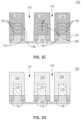
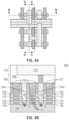
- FIGS. 1 A, 1 B, 1 C, and 1 Ddepict the semiconductor structure 100 at a fabrication stage of the processing method, in accordance with one embodiment of the present invention.
- FIG. 1 Adepicts a top down view of the semiconductor structure 100
- FIGS. 1 B, 1 C, and 1 Ddepicting cross-sectional side views at the locations indicated in FIG. 1 A .
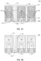
- FIGS. 2 A, 2 B, 2 C, and 2 Ddepict the semiconductor structure 100 at a subsequent fabrication stage of the processing method, in accordance with one embodiment of the present invention.
- FIG. 2 Adepicts a top down view of the semiconductor structure 100
- FIGS. 2 B, 2 C, and 2 Ddepicting cross-sectional side views at the locations indicated in FIG. 2 A .
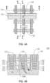
- FIGS. 3 A, 3 B, 3 C, and 3 Ddepict the semiconductor structure 100 at a subsequent fabrication stage of the processing method, in accordance with one embodiment of the present invention.
- FIG. 3 Adepicts a top down view of the semiconductor structure 100
- FIGS. 3 B, 3 C, and 3 Ddepicting cross-sectional side views at the locations indicated in FIG. 3 A .
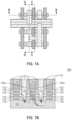
- FIGS. 4 A, 4 B, 4 C, and 4 Ddepict the semiconductor structure 100 at a subsequent fabrication stage of the processing method, in accordance with one embodiment of the present invention.
- FIG. 4 Adepicts a top down view of the semiconductor structure 100
- FIGS. 4 B, 4 C, and 4 Ddepicting cross-sectional side views at the locations indicated in FIG. 4 A .
- FIGS. 5 A, 5 B, 5 C, and 5 Ddepict the semiconductor structure 100 at a subsequent fabrication stage of the processing method, in accordance with one embodiment of the present invention.
- FIG. 5 Adepicts a top down view of the semiconductor structure 100
- FIGS. 5 B, 5 C, and 5 Ddepicting cross-sectional side views at the locations indicated in FIG. 5 A .
- FIGS. 6 A, 6 B, 6 C, and 6 Ddepict the semiconductor structure 100 at a subsequent fabrication stage of the processing method, in accordance with one embodiment of the present invention.
- FIG. 6 Adepicts a top down view of the semiconductor structure 100
- FIGS. 6 B, 6 C, and 6 Ddepicting cross-sectional side views at the locations indicated in FIG. 6 A .
- FIGS. 7 A, 7 B, 7 C, and 7 Ddepict the semiconductor structure 100 at a subsequent fabrication stage of the processing method, in accordance with one embodiment of the present invention.
- FIG. 7 Adepicts a top down view of the semiconductor structure 100
- FIGS. 7 B, 7 C, and 7 Ddepicting cross-sectional side views at the locations indicated in FIG. 7 A .
- FIGS. 8 A, 8 B, 8 C, and 8 Ddepict the semiconductor structure 100 at a subsequent fabrication stage of the processing method, in accordance with one embodiment of the present invention.
- FIG. 8 Adepicts a top down view of the semiconductor structure 100
- FIGS. 8 B, 8 C, and 8 Ddepicting cross-sectional side views at the locations indicated in FIG. 8 A .
- major surfacerefers to that surface of the semiconductor layer in and about which a plurality of transistors are fabricated, e.g., in a planar process.
- terms such as “above,” “below,” “under,” and “over” that have a vertical connotationmean substantially orthogonal with respect to the major surface, while terms such as “laterally,” “adjacent,” and “beside,” that have a horizontal connotation mean substantially parallel to the major surface.
- the major surfaceis along a plane of a monocrystalline silicon layer on which transistor devices are fabricated.
- S/Dsource/drain
- This inventionteaches a unique method and structure to accurately control the S/D contact position under the power rail region (at cell boundaries) to ensure good S/D contact to via connection without contact tip-to-tip shorts.
- Improvements in the design of transistor deviceshave enabled feature sizes to enter into deep submicron and nanometer regime. These smaller feature sizes, however, can cause otherwise minor issues to have more detrimental effect on the operation of the transistor device. For example, shorting (i.e., unintended electric flow) and weak bonding with a via can result when the dimensions of a semiconductor component, such as a source/drain (S/D) contact, are not perfectly aligned in the design and fabrication of the semiconductor device. This may be a particularly difficult problem for S/D contacts connecting to power rail vias since the power rail via can be located closer to an adjacent signal via than the signal vias are to each other. Therefore, the embodiments disclosed herein provide a gate cut region with a liner and a dielectric core that provides self-aligning during formation of S/D contacts, and insulation during operation of S/D contacts that connect to power rails.
- FIGS. 1 A, 1 B, 1 C, and 1 Ddepict a semiconductor structure 100 at a fabrication stage of the processing method, in accordance with one embodiment of the present invention.
- the illustrated embodimentsshow the semiconductor structure 100 as a nanosheet device, but in certain embodiments the semiconductor structure 100 described below may be used to connect source/drains and power rails in a variety of types of transistors, including FinFET, nanowire, planar transistor, or others.
- FIG. 1 Adepicts a top down view of the semiconductor structure 100 , with FIGS. 1 B, 1 C, and 1 D depicting cross-sectional side views at the locations indicated in FIG. 1 A :
- FIG. 1 Bis the view at line B-B, FIG.
- FIG. 1 Cis the view at line C-C
- FIG. 1 Dis the view at line D-D.
- FIG. 1 Adoes not illustrate all features, but is included mainly to show the grid pattern of rows of active nanosheets 102 and columns of high-k metal gate (HKMG) 104 structures.
- HKMGhigh-k metal gate
- the nanosheets 102 and HKMG 104are formed in an alternating series as a vertical layer stack 106 on a substrate 108 .
- the stacks 106are divided from one another in an x-direction 110 by source/drains (S/D) 114 , and divided from one another in a y-direction 112 by shallow trench isolation (STI) 116 .
- the stacks 106also include inner spacer 118 to insulate the nanosheets 102 from each other, and insulate the S/Ds 114 from the HKMG 104 .
- the semiconductor structure 100includes interlayer dielectric (ILD) 120 and spacers 122 to isolate the conductive and semiconductive structures.
- ILDinterlayer dielectric
- the nanosheets 102 , HKMG 104 , S/Ds 114 , and spacers 118 , 122may be formed by known methods of deposition, patterning, and etching.
- the nanosheets 102may be formed using epitaxial growth followed by nanosheet patterning processes, while the S/Ds 114 may be formed by in-situ doped epitaxially growth or by ion implantation.
- the S/Ds 114may be n-type or p-type doped (i.e., PFET source/drain or NFET source/drain)
- the substrate 108may include a monocrystalline silicon structure with the shallow trench isolation (STI) 116 .
- the substrate 108may include a starting wafer having a semiconductor-on-insulator (SOI) substrate, in which STI is not needed.
- the nanosheets 102may also be composed of a semiconductor material, such as silicon (Si).
- the HKMG 104may include materials with dielectric constants that are relatively higher than silicon oxide (SiOx), such as hafnium oxide. The number of nanosheets 102 and HKMG 104 layers may differ (more layers or fewer layers) from the number depicted in the representative embodiment.
- FIGS. 2 A, 2 B, 2 C, and 2 Ddepict the semiconductor structure 100 at a subsequent fabrication stage of the processing method, in accordance with one embodiment of the present invention.
- FIG. 2 Adepicts a top down view of the semiconductor structure 100
- These figuresshow a gate cut 130 that may be formed using a reactive ion etch (RIE).
- RIEreactive ion etch
- the gate cut 130which is located at cell boundary (i.e., between NFET and NFET, or between PFET and PFET) is etched between the stacks 106 , so that the nanosheets 102 , inner spacers 118 , and S/Ds 114 are unaffected.
- the gate cut 130does, however, cut through the HKMG 104 outside of the stack 106 , and cuts through the ILD 120 , spacer 122 , and optionally into or through the STI 116 to the substrate 108 .
- the gate cut 130may be approximately 25 to 70 nm meters, or typically around 30 nanometers in the y direction 112 , but in the x direction the gate cut 130 may extend potentially through all the columns of the HKMG 104 of the semiconductor structure 100 .
- the semiconductor structure 100also includes a narrow gate cut 132 that is narrower in the y direction 112 (e.g., 10 to 22 nm, or approximately 18 nanometers) and significantly shorter in the x direction 110 .
- the narrow gate cut 132is located within a complementary metal-oxide-semiconductor (CMOS) cell (between NFET and PFET), it only etches one row or a few rows of HKMG 104 , rather than forming a long trench line (or all of the rows of HKMG 104 ) that are etched by the gate cut 130 .
- CMOScomplementary metal-oxide-semiconductor
- Gate cut 132 and 130can be formed together in any known lithography and etch process.
- FIGS. 3 A, 3 B, 3 C, and 3 Ddepict the semiconductor structure 100 at a subsequent fabrication stage of the processing method, in accordance with one embodiment of the present invention.
- FIG. 3 Adepicts a top down view of the semiconductor structure 100
- These figuresshow a liner 134 lining the gate cut 130 .
- the liner 134is formed using a blanket deposition process whereby the exposed surfaces of the semiconductor structure 100 are lined with the liner 134 .
- the exposed surfacesinclude a top surface 140 of the semiconductor structure 100 , the gate cut 130 , and the narrow gate cut 132 .
- the liner 134includes a first lateral side 136 and a second lateral side 138 within the gate cut 130 . Within the narrow gate cut 132 , however, the liner 134 from the lateral sides connects, so that the narrow gate cut 132 is fully filled with the material of the liner 134 .
- the material of the first lineris different than ILD layer 120 .
- the liner 134may include SiN, SiOC, SiC, SiBCN, SiOCN, AlOx, AlNx, etc.
- the thickness of the liner 134ranges from 5 nm to 15 nm.
- FIGS. 4 A, 4 B, 4 C, and 4 Ddepict the semiconductor structure 100 at a subsequent fabrication stage of the processing method, in accordance with one embodiment of the present invention.
- FIG. 4 Adepicts a top down view of the semiconductor structure 100
- These figuresshow a dielectric core 142 confined within the gate cut 130 between the first lateral side 136 and the second lateral side 138 .
- the dielectric core 142may be formed as a blanket structure of dielectric deposition followed by etch back or chemical-mechanical planarization (CMP).
- CMPchemical-mechanical planarization
- the liner 134may also be planarized so that the top surface 140 including the HKMG 104 and the ILD 120 is exposed.
- the liner materialcould be with the same or similar material as ILD 120 , such as SiO2.
- the liner 134 and dielectric core 142together form a gate cut region 144 that insulates a first stack 106 a from a second stack 106 b , and enables accurate S/D contact position between the device with first stack 106 a and a power rail, as explained in detail below.
- FIGS. 5 A, 5 B, 5 C, and 5 Ddepict the semiconductor structure 100 at a subsequent fabrication stage of the processing method, in accordance with one embodiment of the present invention.
- FIG. 5 Adepicts a top down view of the semiconductor structure 100
- S/Dsource/drain
- FIGS. 5 B, 5 C, and 5 Ddepicting cross-sectional side views at the locations indicated in FIG. 5 A .
- S/Dsource/drain
- a first S/D contact region 146 ais cut through the first lateral side 136 and at least partially into the dielectric core 142 of the gate cut region 144 .
- the S/D contact regions 146may be formed/cut using a non-selective etch process, such as RIE, that etches the oxide of the ILD 120 and the liner 134 .
- FIGS. 6 A, 6 B, 6 C, and 6 Ddepict the semiconductor structure 100 at a subsequent fabrication stage of the processing method, in accordance with one embodiment of the present invention.
- FIG. 6 Adepicts a top down view of the semiconductor structure 100
- FIGS. 6 B, 6 C, and 6 Ddepicting cross-sectional side views at the locations indicated in FIG. 6 A .
- These figuresshow a selective isotropic etch of the dielectric core 142 with respect to the liner 134 .
- the term “selective,” in reference to a material removal processdenotes that the material removal rate (i.e., etch rate) for the targeted material is greater than the removal rate for at least another material exposed to the material removal process, with an appropriate etchant choice.
- the etch process used to selectively etch the dielectric core 142may include DHF or SiConi, which does not etch the liner 134 , which could be made of SiN.
- the dielectric core 142is removed until the liner 134 , the spacers 118 , and the S/Ds 114 are exposed with no covering from the dielectric core 142 or ILD 120 .
- This selective etch stopping over liner 134means that the initial position of the S/D contact region 146 is not required to be very accurate, since the S/D contact region 146 will be precisely expanded to the liner 134 by lateral dielectric etch as long as the cut of the initial S/D contact 146 includes the dielectric core 142 .
- the selective etchmeans that the lateral edge of the S/D contact region will always end at the second lateral side 138 of the liner 134 . Additionally, as shown in FIG. 6 D , a bottom edge of the clean up regions 148 is etched into the dielectric core 142 and the ILD 120 lower than a top edge of the first lateral side 136 .
- FIGS. 7 A, 7 B, 7 C, and 7 Ddepict the semiconductor structure 100 at a subsequent fabrication stage of the processing method, in accordance with one embodiment of the present invention.
- FIG. 7 Adepicts a top down view of the semiconductor structure 100
- These figuresshow source/drain (S/D) contacts 150 formed within the S/D contact regions 146 .
- the S/D contacts 150include a first S/D contact 150 a that has a line-end 152 that contacts the second lateral side 138 of the liner 134 .
- the first S/D contact 150 aforms into the dielectric core 142 and the ILD 120 such that a bottom edge of the first S/D contact 150 a is lower than a top edge of the first lateral side 136 .
- the first S/D contact 150 athus laterally overlaps the first lateral side 136 and the dielectric core 142 .
- the semiconductor structure 100also includes a second S/D contact 150 b located on an opposite side of the liner 134 from the first S/D contact 150 a .
- the contact metalsmay include a silicide liner (e.g., Ti, Ni, NiPt), an adhesion metal liner such as TiN, and conductive metal fills, such as Co, W, Ru, etc. After metal deposition, and chemical-mechanical planarization (CMP) process is done to remove excessive metal and ILDs over the top surface of the gate.
- CMPchemical-mechanical planarization
- FIGS. 8 A, 8 B, 8 C, and 8 Ddepict the semiconductor structure 100 at a subsequent fabrication stage of the processing method, in accordance with one embodiment of the present invention.
- FIG. 8 Adepicts a top down view of the semiconductor structure 100
- FIGS. 8 B, 8 C, and 8 Ddepicting cross-sectional side views at the locations indicated in FIG. 8 A .
- These figuresshow a via level 160 and a first metal level 170 that connect the S/D contacts 150 to subsequent metal levels (not shown) of the semiconductor structure 100 .
- the via level 160includes: (i) signal vias 162 coupled between the S/D contacts 150 and signal rails 172 in the first metal level 170 ; and (ii) a power rail via 164 coupled between the first S/D contact 150 a and a power rail 174 in the first metal level 170 .
- Metal layer dielectric 180surrounds the vias 162 , 164 and the rails 172 , 174 so that the vias 162 , 164 and the rails 172 , 174 remain insulated.
- the metal layer dielectric 180 , the vias 162 , 164 , and the rails 172 , 174may be formed using known techniques of deposition, patterning, and etch.
- the metal layer dielectric 180may be formed, and then holes for the vias 162 , 164 formed and filled with conductive material such as metal. Similar steps may be taken to form the rails 172 , 174 . Or both vias and metal lines can be formed first then forming metallization together using Cu dual damascene process.
- Benefits of the disclosed embodimentsinclude accurate positioning of the first S/D contact 150 a and in particular the location of the line-end 152 . That is, the line-end 152 is positioned so that the first S/D contact 150 a has a robust electrical connection with the power rail via 164 but does not short to the second S/D contact 150 b due to being too close.
- the liner 134may also define a minimum insulator between contact 150 a and 150 b such that failures like shorts, breakdown, or leakage can be prevented by carefully choosing the material and thickness of liner 134 .
- the line-end 152may drift too close to the second S/D contact 150 b due to lithographical misalignment, causing a short; or may drift too far from the second S/D contact 150 b , causing the power rail via 164 to connect only to part of the first S/D contact 150 a.
- the methods as described aboveare used in the fabrication of integrated circuit chips.
- the resulting integrated circuit chipscan be distributed by the fabricator in raw wafer form (e.g., as a single wafer that has multiple unpackaged chips), as a bare die, or in a packaged form.
- the chipis mounted in a single chip package (e.g., a plastic carrier, with leads that are affixed to a motherboard or other higher level carrier) or in a multichip package (e.g., a ceramic carrier that has either or both surface interconnections or buried interconnections).
- the chipmay be integrated with other chips, discrete circuit elements, and/or other signal processing devices as part of either an intermediate product or an end product.
Landscapes
- Physics & Mathematics (AREA)
- Engineering & Computer Science (AREA)
- Condensed Matter Physics & Semiconductors (AREA)
- General Physics & Mathematics (AREA)
- Computer Hardware Design (AREA)
- Microelectronics & Electronic Packaging (AREA)
- Power Engineering (AREA)
- Geometry (AREA)
- Manufacturing & Machinery (AREA)
- Electrodes Of Semiconductors (AREA)
- Insulated Gate Type Field-Effect Transistor (AREA)
- Metal-Oxide And Bipolar Metal-Oxide Semiconductor Integrated Circuits (AREA)
Abstract
Description
Claims (15)
Priority Applications (5)
| Application Number | Priority Date | Filing Date | Title |
|---|---|---|---|
| US17/491,408US12107132B2 (en) | 2021-09-30 | 2021-09-30 | Source/drain contact positioning under power rail |
| CN202280064991.2ACN118140302A (en) | 2021-09-30 | 2022-09-16 | Source/drain contact positioning under power rail |
| PCT/EP2022/075844WO2023052157A1 (en) | 2021-09-30 | 2022-09-16 | Source/drain contact positioning under power rail |
| EP22789886.3AEP4409627A1 (en) | 2021-09-30 | 2022-09-16 | Source/drain contact positioning under power rail |
| JP2022151893AJP2023051808A (en) | 2021-09-30 | 2022-09-22 | Semiconductor structures and methods of manufacturing semiconductor structures (positioning of source/drain contacts under power rails) |
Applications Claiming Priority (1)
| Application Number | Priority Date | Filing Date | Title |
|---|---|---|---|
| US17/491,408US12107132B2 (en) | 2021-09-30 | 2021-09-30 | Source/drain contact positioning under power rail |
Publications (2)
| Publication Number | Publication Date |
|---|---|
| US20230095508A1 US20230095508A1 (en) | 2023-03-30 |
| US12107132B2true US12107132B2 (en) | 2024-10-01 |
Family
ID=83692870
Family Applications (1)
| Application Number | Title | Priority Date | Filing Date |
|---|---|---|---|
| US17/491,408Active2042-01-21US12107132B2 (en) | 2021-09-30 | 2021-09-30 | Source/drain contact positioning under power rail |
Country Status (5)
| Country | Link |
|---|---|
| US (1) | US12107132B2 (en) |
| EP (1) | EP4409627A1 (en) |
| JP (1) | JP2023051808A (en) |
| CN (1) | CN118140302A (en) |
| WO (1) | WO2023052157A1 (en) |
Citations (21)
| Publication number | Priority date | Publication date | Assignee | Title |
|---|---|---|---|---|
| US20090166745A1 (en)* | 2007-12-28 | 2009-07-02 | Renesas Technology Corp. | Semiconductor device and photomask |
| WO2013095548A1 (en) | 2011-12-22 | 2013-06-27 | Intel Corporation | Gate aligned contact and method to fabricate same |
| US8975712B2 (en) | 2013-05-14 | 2015-03-10 | Globalfoundries Inc. | Densely packed standard cells for integrated circuit products, and methods of making same |
| US8987816B2 (en) | 2013-03-04 | 2015-03-24 | Globalfoundries Inc. | Contact power rail |
| US9461143B2 (en) | 2012-09-19 | 2016-10-04 | Intel Corporation | Gate contact structure over active gate and method to fabricate same |
| US20170162568A1 (en)* | 2015-12-07 | 2017-06-08 | Samsung Electronics Co., Ltd. | Semiconductor device |
| US20180069000A1 (en)* | 2016-09-07 | 2018-03-08 | International Business Machines Corporation | Gate cut with integrated etch stop layer |
| US20190067131A1 (en)* | 2017-08-30 | 2019-02-28 | Taiwan Semiconductor Manufacturing Co., Ltd. | Interconnect Structure For Fin-Like Field Effect Transistor |
| US10269787B2 (en) | 2017-06-29 | 2019-04-23 | Taiwan Semiconductor Manufacturing Co., Ltd. | Metal gate structure cutting process |
| US10319581B1 (en) | 2017-11-30 | 2019-06-11 | Taiwan Semiconductor Manufacturing Co., Ltd. | Cut metal gate process for reducing transistor spacing |
| US20190259670A1 (en) | 2018-02-20 | 2019-08-22 | Globalfoundries Inc. | Methods of performing fin cut etch processes for finfet semiconductor devices |
| US20190363085A1 (en)* | 2018-05-25 | 2019-11-28 | Samsung Electronics Co., Ltd. | Semiconductor device and method for fabricating the same |
| US20200006075A1 (en) | 2018-06-29 | 2020-01-02 | Taiwan Semiconductor Manufacturing Co., Ltd. | Method for Metal Gate Cut and Structure Thereof |
| US10529833B2 (en) | 2017-08-28 | 2020-01-07 | Taiwan Semiconductor Manufacturing Co., Ltd. | Integrated circuit with a fin and gate structure and method making the same |
| US20200135575A1 (en) | 2018-10-26 | 2020-04-30 | International Business Machines Corporation | Gate cut critical dimension shrink and active gate defect healing using selective deposition |
| US10692720B2 (en) | 2017-11-29 | 2020-06-23 | Taiwan Semiconductor Manufacturing Co., Ltd. | Methods for controlling an end-to-end distance in semiconductor device |
| US20210111028A1 (en)* | 2019-10-10 | 2021-04-15 | International Business Machines Corporation | Replacement gate cross-couple for static random-access memory scaling |
| US20210193683A1 (en)* | 2019-12-20 | 2021-06-24 | Samsung Electronics Co., Ltd. | Integrated circuit including integrated standard cell structure |
| US20210226023A1 (en) | 2015-11-30 | 2021-07-22 | Taiwan Semiconductor Manufacturing Co., Ltd. | Semiconductor device and a method for fabricating the same |
| CN113380794A (en) | 2020-05-29 | 2021-09-10 | 台湾积体电路制造股份有限公司 | Semiconductor device and method of forming the same |
| US20210343713A1 (en)* | 2020-04-30 | 2021-11-04 | Taiwan Semiconductor Manufacturing Co., Ltd. | Gate Isolation for Multigate Device |
- 2021
- 2021-09-30USUS17/491,408patent/US12107132B2/enactiveActive
- 2022
- 2022-09-16EPEP22789886.3Apatent/EP4409627A1/enactivePending
- 2022-09-16WOPCT/EP2022/075844patent/WO2023052157A1/ennot_activeCeased
- 2022-09-16CNCN202280064991.2Apatent/CN118140302A/enactivePending
- 2022-09-22JPJP2022151893Apatent/JP2023051808A/enactivePending
Patent Citations (22)
| Publication number | Priority date | Publication date | Assignee | Title |
|---|---|---|---|---|
| US20090166745A1 (en)* | 2007-12-28 | 2009-07-02 | Renesas Technology Corp. | Semiconductor device and photomask |
| WO2013095548A1 (en) | 2011-12-22 | 2013-06-27 | Intel Corporation | Gate aligned contact and method to fabricate same |
| US9461143B2 (en) | 2012-09-19 | 2016-10-04 | Intel Corporation | Gate contact structure over active gate and method to fabricate same |
| US8987816B2 (en) | 2013-03-04 | 2015-03-24 | Globalfoundries Inc. | Contact power rail |
| US8975712B2 (en) | 2013-05-14 | 2015-03-10 | Globalfoundries Inc. | Densely packed standard cells for integrated circuit products, and methods of making same |
| US20210226023A1 (en) | 2015-11-30 | 2021-07-22 | Taiwan Semiconductor Manufacturing Co., Ltd. | Semiconductor device and a method for fabricating the same |
| US20170162568A1 (en)* | 2015-12-07 | 2017-06-08 | Samsung Electronics Co., Ltd. | Semiconductor device |
| US20180069000A1 (en)* | 2016-09-07 | 2018-03-08 | International Business Machines Corporation | Gate cut with integrated etch stop layer |
| US10998314B2 (en) | 2016-09-07 | 2021-05-04 | Tessera, Inc. | Gate cut with integrated etch stop layer |
| US10269787B2 (en) | 2017-06-29 | 2019-04-23 | Taiwan Semiconductor Manufacturing Co., Ltd. | Metal gate structure cutting process |
| US10529833B2 (en) | 2017-08-28 | 2020-01-07 | Taiwan Semiconductor Manufacturing Co., Ltd. | Integrated circuit with a fin and gate structure and method making the same |
| US20190067131A1 (en)* | 2017-08-30 | 2019-02-28 | Taiwan Semiconductor Manufacturing Co., Ltd. | Interconnect Structure For Fin-Like Field Effect Transistor |
| US10692720B2 (en) | 2017-11-29 | 2020-06-23 | Taiwan Semiconductor Manufacturing Co., Ltd. | Methods for controlling an end-to-end distance in semiconductor device |
| US10319581B1 (en) | 2017-11-30 | 2019-06-11 | Taiwan Semiconductor Manufacturing Co., Ltd. | Cut metal gate process for reducing transistor spacing |
| US20190259670A1 (en) | 2018-02-20 | 2019-08-22 | Globalfoundries Inc. | Methods of performing fin cut etch processes for finfet semiconductor devices |
| US20190363085A1 (en)* | 2018-05-25 | 2019-11-28 | Samsung Electronics Co., Ltd. | Semiconductor device and method for fabricating the same |
| US20200006075A1 (en) | 2018-06-29 | 2020-01-02 | Taiwan Semiconductor Manufacturing Co., Ltd. | Method for Metal Gate Cut and Structure Thereof |
| US20200135575A1 (en) | 2018-10-26 | 2020-04-30 | International Business Machines Corporation | Gate cut critical dimension shrink and active gate defect healing using selective deposition |
| US20210111028A1 (en)* | 2019-10-10 | 2021-04-15 | International Business Machines Corporation | Replacement gate cross-couple for static random-access memory scaling |
| US20210193683A1 (en)* | 2019-12-20 | 2021-06-24 | Samsung Electronics Co., Ltd. | Integrated circuit including integrated standard cell structure |
| US20210343713A1 (en)* | 2020-04-30 | 2021-11-04 | Taiwan Semiconductor Manufacturing Co., Ltd. | Gate Isolation for Multigate Device |
| CN113380794A (en) | 2020-05-29 | 2021-09-10 | 台湾积体电路制造股份有限公司 | Semiconductor device and method of forming the same |
Non-Patent Citations (2)
| Title |
|---|
| International Searching Authority, "Notification of Transmittal of the International Search Report and the Written Opinion of the International Searching Authority, or the Declaration", International application No. PCT/EP2022/075844, International Filing Date Sep. 16, 2022, Mailed on Jan. 16, 2023, 13 pages. |
| Lee et al., "Ultra High Density Logic Designs Using Transistor-Level Monolithic 3D Integration," IEEE/ACM International Conference on Computer-Aided Design (ICCAD), Nov. 5-8, 2012, San Jose, California, 8 pages. |
Also Published As
| Publication number | Publication date |
|---|---|
| CN118140302A (en) | 2024-06-04 |
| EP4409627A1 (en) | 2024-08-07 |
| JP2023051808A (en) | 2023-04-11 |
| WO2023052157A1 (en) | 2023-04-06 |
| US20230095508A1 (en) | 2023-03-30 |
Similar Documents
| Publication | Publication Date | Title |
|---|---|---|
| US10998313B2 (en) | Source/drain regions in fin field effect transistors (finFETs) and methods of forming same | |
| US20240363626A1 (en) | Self-Aligned Etch in Semiconductor Devices | |
| US11251308B2 (en) | Semiconductor device and method | |
| US20240379781A1 (en) | Backside Source/Drain Contacts and Methods of Forming the Same | |
| US11862561B2 (en) | Semiconductor devices with backside routing and method of forming same | |
| US12057469B2 (en) | Semiconductor device and a method of fabricating the same | |
| KR102568602B1 (en) | Semiconductor device and method | |
| US11107836B2 (en) | Semiconductor device structure and method for forming the same | |
| US9177956B2 (en) | Field effect transistor (FET) with self-aligned contacts, integrated circuit (IC) chip and method of manufacture | |
| US20230369218A1 (en) | Interlevel via for stacked field-effect transistor device | |
| US12268022B2 (en) | Semiconductor device including air gap regions below source/drain regions | |
| US20240072133A1 (en) | Backside and frontside contacts for semiconductor device | |
| US20230106015A1 (en) | Semiconductor devices | |
| US20240096805A1 (en) | Semiconductor devices with backside routing and method of forming same | |
| US11621332B2 (en) | Wraparound contact to a buried power rail | |
| US20240222229A1 (en) | Back side contacts for semiconductor devices | |
| US12107132B2 (en) | Source/drain contact positioning under power rail | |
| US20240063121A1 (en) | Backside contact for semiconductor device | |
| US20240021708A1 (en) | Structure and formation method of semiconductor device with power rail | |
| TWI713143B (en) | Semiconductor structure and fabricating method thereof | |
| US20250318237A1 (en) | Self aligned backside contacts compatible with passive devices | |
| US20240332293A1 (en) | Gate contacts for semiconductor devices | |
| US20250248099A1 (en) | Semiconductor device | |
| US20240096701A1 (en) | Device with through via and related methods | |
| US20240105521A1 (en) | Semiconductor device structure with isolation layer and method for forming the same |
Legal Events
| Date | Code | Title | Description |
|---|---|---|---|
| AS | Assignment | Owner name:INTERNATIONAL BUSINESS MACHINES CORPORATION, NEW YORK Free format text:ASSIGNMENT OF ASSIGNORS INTEREST;ASSIGNORS:XIE, RUILONG;SESHADRI, INDIRA;MILLER, ERIC;AND OTHERS;REEL/FRAME:057663/0184 Effective date:20210930 | |
| FEPP | Fee payment procedure | Free format text:ENTITY STATUS SET TO UNDISCOUNTED (ORIGINAL EVENT CODE: BIG.); ENTITY STATUS OF PATENT OWNER: LARGE ENTITY | |
| STPP | Information on status: patent application and granting procedure in general | Free format text:RESPONSE TO NON-FINAL OFFICE ACTION ENTERED AND FORWARDED TO EXAMINER | |
| STPP | Information on status: patent application and granting procedure in general | Free format text:NON FINAL ACTION MAILED | |
| STPP | Information on status: patent application and granting procedure in general | Free format text:RESPONSE TO NON-FINAL OFFICE ACTION ENTERED AND FORWARDED TO EXAMINER | |
| STPP | Information on status: patent application and granting procedure in general | Free format text:FINAL REJECTION MAILED | |
| STPP | Information on status: patent application and granting procedure in general | Free format text:ADVISORY ACTION MAILED | |
| STPP | Information on status: patent application and granting procedure in general | Free format text:DOCKETED NEW CASE - READY FOR EXAMINATION | |
| STPP | Information on status: patent application and granting procedure in general | Free format text:NOTICE OF ALLOWANCE MAILED -- APPLICATION RECEIVED IN OFFICE OF PUBLICATIONS | |
| ZAAB | Notice of allowance mailed | Free format text:ORIGINAL CODE: MN/=. | |
| STPP | Information on status: patent application and granting procedure in general | Free format text:PUBLICATIONS -- ISSUE FEE PAYMENT VERIFIED | |
| STCF | Information on status: patent grant | Free format text:PATENTED CASE |