US12106943B2 - Substrate halo arrangement for improved process uniformity - Google Patents
Substrate halo arrangement for improved process uniformityDownload PDFInfo
- Publication number
- US12106943B2 US12106943B2US17/329,883US202117329883AUS12106943B2US 12106943 B2US12106943 B2US 12106943B2US 202117329883 AUS202117329883 AUS 202117329883AUS 12106943 B2US12106943 B2US 12106943B2
- Authority
- US
- United States
- Prior art keywords
- halo
- ring
- substrate
- disposed
- aperture
- Prior art date
- Legal status (The legal status is an assumption and is not a legal conclusion. Google has not performed a legal analysis and makes no representation as to the accuracy of the status listed.)
- Active, expires
Links
Images


Classifications
- H—ELECTRICITY
- H01—ELECTRIC ELEMENTS
- H01J—ELECTRIC DISCHARGE TUBES OR DISCHARGE LAMPS
- H01J37/00—Discharge tubes with provision for introducing objects or material to be exposed to the discharge, e.g. for the purpose of examination or processing thereof
- H01J37/32—Gas-filled discharge tubes
- H01J37/32431—Constructional details of the reactor
- H01J37/32458—Vessel
- H01J37/32467—Material
- H—ELECTRICITY
- H01—ELECTRIC ELEMENTS
- H01J—ELECTRIC DISCHARGE TUBES OR DISCHARGE LAMPS
- H01J37/00—Discharge tubes with provision for introducing objects or material to be exposed to the discharge, e.g. for the purpose of examination or processing thereof
- H01J37/32—Gas-filled discharge tubes
- H01J37/32431—Constructional details of the reactor
- H01J37/32623—Mechanical discharge control means
- H01J37/32642—Focus rings
- H—ELECTRICITY
- H01—ELECTRIC ELEMENTS
- H01J—ELECTRIC DISCHARGE TUBES OR DISCHARGE LAMPS
- H01J37/00—Discharge tubes with provision for introducing objects or material to be exposed to the discharge, e.g. for the purpose of examination or processing thereof
- H01J37/32—Gas-filled discharge tubes
- H01J37/32431—Constructional details of the reactor
- H01J37/32715—Workpiece holder
- H01J37/32724—Temperature
Definitions
- Embodiments of the present disclosurerelate to semiconductor workpiece processing and, more particularly, to semiconductor workpiece processing using a substrate halo for process uniformity.
- a goalis often to generate process uniformity across a substrate.
- Substratessuch as semiconductor wafers, are often positioned to be surrounded by hardware, such as halos, to protect a process chamber, substrate, or other components not designed to receive a plasma or ion beam treatment. While a large portion of a substrate may receive relatively uniform treatment, a frequent observation is the presence of edge effects near the periphery of a substrate, where the edge effects may include non-uniform process results, as well as contamination, particle generation, and other unwanted results.
- a substrate assemblymay include an outer halo, the outer halo comprising a first material, and defining a first aperture.
- the substrate holdermay include a halo ring, where the halo ring includes a second material and is disposed at least partially within the first aperture.
- the halo ringmay define a second aperture, concentrically positioned within the first aperture, wherein the halo ring is coupled to accommodate a substrate therein.
- a substrate assembly in accordance with an exemplary embodiment of the present disclosuremay include an outer halo defining a first aperture and a halo ring disposed at least partially within the first aperture, the halo ring defining a second aperture, concentrically positioned within the first aperture, wherein the halo ring is coupled to accommodate a substrate therein, wherein the outer halo and the halo ring are formed at least partially of one of silicon, silicon carbide, doped silicon, quartz, and ceramic.
- a substrate holder assembly in accordance with an exemplary embodiment of the present disclosuremay include a substrate platen, the substrate platen disposed to support a substrate at a substrate position, a halo ring, the halo ring being disposed around the substrate position, and an outer halo being disposed around the halo ring and defining a first aperture, wherein the outer halo is disposed to engage the halo ring, the halo ring being disposed at least partially within the first aperture, the halo ring defining a second aperture, concentrically positioned within the first aperture, wherein the outer halo and the halo ring are formed at least partially of silicon, silicon carbide, doped silicon, quartz, and ceramic.
- a processing apparatus in accordance with an exemplary embodiment of the present disclosuremay include a process chamber, and a substrate holder assembly, disposed in the process chamber, the substrate holder assembly including a substrate platen, the substrate platen disposed to support a substrate at a substrate position, a halo ring, the halo ring being disposed around the substrate position, and an outer halo disposed around the halo ring and configured to engage the halo ring, wherein the outer halo and the halo ring are formed at least partially of silicon, silicon carbide, doped silicon, quartz, and ceramic.
- FIG. 1 Ais a schematic view illustrating a side view of a processing apparatus in accordance with embodiments of the present disclosure
- FIG. 1 Bis a schematic view illustrating face on view of a substrate holder assembly in accordance with embodiments of the present disclosure
- FIG. 1 Cis a schematic view illustrating a side view of another processing apparatus in accordance with embodiments of the present disclosure
- FIG. 2 Ais a front perspective view of another substrate holder assembly in accordance with embodiments of the present disclosure.
- FIG. 2 Bis a sectional view along the cut A-A of FIG. 2 A ;
- FIG. 2 Cis a sectional view of a fastener in accordance with the present disclosure.
- FIG. 3is a perspective, cutaway view of an additional substrate holder assembly in accordance with embodiments of the present disclosure.
- an element or operation recited in the singular and proceeded with the word “a” or “an”are understood as possibly including plural elements or operations, except as otherwise indicated.
- various embodiments hereinhave been described in the context of one or more elements or components.
- An element or componentmay comprise any structure arranged to perform certain operations.
- an embodimentmay be described with a limited number of elements in a certain topology by way of example, the embodiment may include more or less elements in alternate topologies as desired for a given implementation.
- any reference to “one embodiment” or “an embodiment”means a particular feature, structure, or characteristic described in connection with the embodiment is included in at least one embodiment.
- the appearances of the phrases “in one embodiment,” “in some embodiments,” and “in various embodiments” in various places in the specificationare not necessarily all referring to the same embodiment.
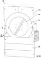
- the processing apparatus 100includes a process chamber 102 .
- the process chamber 102includes a substrate holder assembly 106 , where the structure and function of the substrate holder assembly 106 is detailed below.
- the substrate holder assembly 106may include a substrate platen 108 , disposed to hold a substrate 110 , an outer halo 112 , and a halo ring 114 .
- the outer halo 112 and halo ring 114may be removable fastened to a halo base 115 (as further described below) and may function as a substrate assembly 116 , to adjust and improve processing of substrates.
- the process chamber 102may include processing species 104 , used to process a substrate 110 , disposed in the substrate assembly 116 .
- the outer halo 112defines a first aperture, whose edges are shown by A 1
- the halo ring 114defines a second aperture, whose edges are shown by A 2 , where the second aperture is concentrically positioned within the first aperture.
- the halo ring 114may be coupled to accommodate a substrate 110 within the second aperture.
- the processing apparatus 100may be an etching tool, to perform etching operations on the substrate 110 , a deposition tool, or a combination of etching and deposition tool.
- the processing apparatus 100may be an implanting tool to introduce implanted species into the substrate 110 .
- the processing apparatus 100may be a plasma-based tool, including a plasma etching tool such as a reactive ion etching tool, a plasma doping (PLAD) apparatus, a plasma assisted chemical vapor deposition (PECVD) tool, an ion beam tool, a reactive ion beam etching tool, or other tool.
- the processing apparatus 100may generate and contain processing species 104 , where the processing species 104 may represent the appropriate species to perform substrate processing of substrate 110 .
- the processing speciesmay include ions, reactive ions, reactive neutrals, implanting species, and so forth.
- the processing species 104are shown as contained within the process chamber 102 , in various embodiments, the processing apparatus 100 may include a plurality of chambers, including ion sources, plasma sources, separate from the process chamber 102 . In other embodiments, the process chamber 102 may be a plasma chamber. The embodiments are not limited in this context.
- FIG. 1 Bthere is shown a face-on view, illustrating one embodiment of the substrate assembly 116 .
- the processing species 104are configured as an elongated ion beam or ribbon beam, shown in cross-section within the X-Y plane of the illustrated Cartesian coordinate system.
- the ribbon beammay be provided from a plasma chamber through an extraction plate as in known apparatus.
- FIG. 1 Ca processing apparatus 150 is shown, where the processing apparatus 150 includes a plasma chamber 152 , adjacent the above-described process chamber 102 .
- the processing species 104are extracted as a ribbon beam from a plasma 154 in the plasma chamber 152 as in known apparatus.
- the substrate holder assembly 106may be scanned in some embodiments, along a direction parallel to the Y-axis of the illustrated Cartesian coordinate system, as shown by the arrows.
- the ribbon beam containing the processing species 104may be characterized by a width W, where the width W exceeds the substrate diameter Ds. In this manner, the entirety of the substrate 110 may be treated with the processing species 104 .
- the outer halo 112may be formed of a first material, such as any suitable material (e.g., silicon, silicon carbide, doped silicon, quartz, ceramic, etc.).
- the outer halo 112may be formed of a plurality of tiles (as further described below), for example.
- the halo ring 114may be formed of a second material, where the second material may be the same as the first material (e.g., silicon, silicon carbide, doped silicon, quartz, ceramic, etc.) or may differ from the first material.
- the halo ring 114may be coupled to the outer halo 112 in a reversibly detachable manner, as detailed below.
- the halo ring 114may accordingly represent any number of different halo rings, where the material of the halo ring 114 may be selected according to a particular application.
- one halo ring 114may be substituted for another halo ring, allowing for replacement due to wear or damage.
- a first halo ring made of a first halo ring materialmay be substituted for a second halo ring made of a different, second halo ring material, when appropriate.
- a swap of halo ring 114 for another halo ringmay be appropriate.
- the substrate assembly 116is to effectively extend the diameter of the substrate 110 , in the sense where the halo ring 114 may mimic certain properties of the substrate 110 .
- the halo ring 114may be composed of a similar material, such as silicon, silicon carbide, doped silicon, quartz, or ceramic (e.g., yttria/zirconia blend).
- edge effects otherwise generated near the edges of the substrate 110 by the process species 104may be reduced or eliminated, because the substrate 110 and halo ring 114 “appear” to the processing species 104 as a substrate having the diameter D H .
- the width Wmay exceed the diameter of the substrate Ds, any edge effects may occur at the outer edges of the ribbon beam defined by the processing species 104 or the outer edge of the halo ring 114 .
- the halomay be a monolithic piece, formed of a metal, such as titanium to provide mechanical and thermal robustness under treatment by an ion beam or plasma.
- a metalsuch as titanium
- edge effects near the region where the substrate meets the halomay be generated, at least in part due to the differences in material between substrate and halo.
- the diameter D Hmay exceed the width W, wherein during scanning, the outer edges of the ribbon beam defined by the process species 104 are scanned over material of the halo ring 114 , at the widest part.
- the diameter D Hmay exceed 300 mm, and in some cases, may be in the range of 450 mm.
- a width W R of the halo ring 114may in the order of 15 mm to 75 mm. The embodiments are not limited in this context.
- the halo ring 114may have an annular first notch or shoulder 120 (hereinafter “the first shoulder 120 ”) formed in a radially outermost edge of a front surface thereof, and an annular second notch or shoulder 122 (hereinafter “the second shoulder 122 ”) formed in a radially innermost edge of the front surface thereof.
- the outer halo 112may have an annular notch or shoulder 124 (hereinafter “the shoulder 124 ”) formed in a radially innermost edge of a rear surface thereof, wherein the shoulder 124 of the outer halo 112 is disposed in confronting, mating abutment with the first shoulder 120 of the halo ring 114 , with the front surface of the halo ring 114 coplanar with a front surface of the outer halo 112 .
- the second shoulder 122 of the halo ring 114may have a depth equal to a thickness of the substrate 110 and may define a counterbore for receiving the substrate 110 , with the front surface of the substrate 110 coplanar with the front surface of the halo ring 114 as depicted.
- a substrate assembly in accordance with the present disclosuremay further include a fastener assembly, where the fastener assembly is adapted to reversibly attach the outer halo 112 and the halo ring 114 to the halo base 115 (see FIG. 1 A ).
- a substrate assembly 200 in accordance with the present disclosuremay include an upper halo 112 A and a lower halo 112 B, where a halo ring 114 is arranged concentrically within the upper halo 112 A.
- the upper halo 112 Ais formed of a plurality of tiles and the lower halo 112 B is formed of a plurality of tiles.
- the upper halo 112 Amay be formed of a single tile and/or the lower halo 112 B may be formed of a single tile.
- the substrate assembly 200further includes a fastener assembly, arranged as a plurality of fasteners 206 , coupling the halo ring 114 , the upper halo 112 A, and the lower halo 112 B to the halo base 115 .
- the fasteners 206may include studs 214 , where the studs 214 may be formed of a ceramic or a coated material.
- the studs 214may include head portions 214 A disposed in flat engagement with front surfaces of the outer halo 112 and the halo ring 114 (and optionally disposed within counterbores formed therein, as shown), and shank portions 214 B extending from the head portions 214 A through the outer halo 112 or the halo ring 114 and through the halo base 115 .
- the shank portions 214 Bmay define respective shoulders 214 C facing, and spaced apart from, the backside of the halo base 115 .
- the fasteners 206may further include generally U-shaped retaining clips 216 formed of resilient material (e.g., spring steel, plastic, composite, etc.).
- the retaining clips 216may include first and second fingers 216 A, 216 B having respective notches 218 A, 218 B formed therein. When the retaining clips 216 are operatively installed as shown in FIG.
- the shank portions 214 B of the studs 214may be disposed within the notches 218 A, 218 B, and the first and second fingers 216 A, 216 B may be held in compression (i.e., compressed toward one another) between the shoulders 214 C of the shank portions 214 B and rear surface of the halo base 115 .
- the retaining clips 216may exert a rearwardly-directed force on the shank portions 214 B of the studs 214 , pulling the head portions 214 A of the studs 214 toward the front surface of the halo base 115 to hold the outer halo 112 and the halo ring 114 in secure engagement therewith.
- the maximum holding force generated by the fastener 206may be 1 lb. to 1.5 lbs. This limitation of clamping force aids in ensuring the outer halo 112 and halo ring 114 do not break under the stress of the holding force, especially in embodiments where outer halo 112 and halo ring 114 are made of a brittle material, such as silicon.
- FIG. 2 Ca cross-sectional view illustrating an alternative fastener 306 is shown.
- the fastener 306may be substituted for one or more of the fasteners 206 .
- the fastener 306may include a stud 314 formed of a ceramic or a coated material.
- the stud 314may include a head portion 314 A disposed in flat engagement with front surfaces of the outer halo 112 and the halo ring 114 (and optionally disposed within counterbores formed therein, as shown), and a shank portion 314 B extending from the head portion 314 A through the outer halo 112 or the halo ring 114 and through the halo base 115 .
- the shank portion 314 Bmay have a threaded end 314 C disposed proximate the backside of the halo base 115 .
- the fastener 306may further include a coil spring 316 disposed in a counterbore 318 in the backside of the halo base 115 and surrounding the shank portion 314 B of the stud 314 .
- the fastener 306may further include a nut 320 threadedly engaging the threaded end 314 C of the stud 314 and compressing the coil spring 316 between the nut 320 and a rear surface 322 of the halo base 115 within the counterbore 318 .
- the maximum holding force generated by the fastener 306may be 1 lb. to 1.5 lbs. This limitation of clamping force aids in ensuring the outer halo 112 and halo ring 114 do not break under the stress of the holding force, especially in embodiments where outer halo 112 and halo ring 114 are made of a brittle material, such as silicon.
- a halo ring 402comprises an outer ring 406 and an inner ring 404 , disposed within the outer ring 406 .
- the inner ring 404may define the second aperture as described above.
- the outer ring 406 and inner ring 404may be separated from one another or electrically isolated from one another by a gap or spacer, shown as a spacer 408 .
- the outer ring 406comprises a first ring material
- the inner ring 404comprises a second ring material, different from the first ring material.
- the inner ring 404may be electrically biased, or the outer ring 406 may be electrically biased, while in some embodiments the inner ring 404 and outer ring 406 may be individually coupled to receive different electrical biases, as shown by the voltage source 410 and voltage source 412 , respectively.
- the substrate platen 108may also be coupled to a voltage source 420 , while the outer halo 112 is separately coupled to a voltage source 422 . Accordingly, during operation, voltages applied to the inner ring 404 and outer ring 406 may be the same or may differ from one another.
- the inner ring 404 and/or the outer ring 406may be biased at a same voltage as a voltage applied to the substrate platen 108 , or a different voltage from the voltage applied to substrate platen 108 .
- the outer halo 112may be coupled to receive the same or different voltage from the voltage applied to any of the inner ring 404 , outer ring 406 , and substrate platen 108 .
- the inner ring 404 , outer ring 406 , or the twomay be configured to receive heating, separately from any heating provided to the substrate 110 , as shown by the heater 416 and heater 418 , respectively.
- the outer ring 406 and inner ring 404may be coupled to receive different temperatures from one another.
- the substrate platen 108 or substrate 110may be coupled to a heater 424 to be separately heated from inner ring 404 and outer ring 406 , while the outer halo 112 is independently coupled to a heater 426 .
- these componentsmay be heated to a same or different temperature as the temperature for other components of substrate assembly 400 .
- a halo ringsuch as halo ring 402
- the local environment near the periphery of a substratemay be carefully adjusted or controlled to account for edge effects and to improve process uniformity.
- etch rate variation across the waferwas improved from 5% non-uniformity when no halo ring was used, to 1% uniformity with the use of a halo ring.
- embodiments described hereinprovide at least the following technical advantages.
- the present embodimentsprovide flexibility in reducing edge effects by providing detachable halo rings, where the material of the halo ring may be changed to accommodate substrate changes or process changes.
- the use of a narrow insert as a halo ringallows materials to be easily replaced to accommodate for wear.
Landscapes
- Physics & Mathematics (AREA)
- Engineering & Computer Science (AREA)
- Plasma & Fusion (AREA)
- Chemical & Material Sciences (AREA)
- Analytical Chemistry (AREA)
- Container, Conveyance, Adherence, Positioning, Of Wafer (AREA)
- Drying Of Semiconductors (AREA)
- Chemical Vapour Deposition (AREA)
Abstract
Description
Claims (9)
Priority Applications (6)
| Application Number | Priority Date | Filing Date | Title |
|---|---|---|---|
| US17/329,883US12106943B2 (en) | 2021-05-25 | 2021-05-25 | Substrate halo arrangement for improved process uniformity |
| TW111117941ATWI881222B (en) | 2021-05-25 | 2022-05-13 | Substrate assembly, substrate holder assembly, and processing apparatus |
| JP2023571797AJP7717845B2 (en) | 2021-05-25 | 2022-05-20 | Substrate halo placement for improved process uniformity |
| CN202280036243.3ACN117337484A (en) | 2021-05-25 | 2022-05-20 | Substrate halo configuration for improved process uniformity |
| PCT/US2022/030354WO2022251074A1 (en) | 2021-05-25 | 2022-05-20 | Substrate halo arrangement for improved process uniformity |
| KR1020237044042AKR102845744B1 (en) | 2021-05-25 | 2022-05-20 | Substrate halo array for improved process uniformity |
Applications Claiming Priority (1)
| Application Number | Priority Date | Filing Date | Title |
|---|---|---|---|
| US17/329,883US12106943B2 (en) | 2021-05-25 | 2021-05-25 | Substrate halo arrangement for improved process uniformity |
Publications (2)
| Publication Number | Publication Date |
|---|---|
| US20220384156A1 US20220384156A1 (en) | 2022-12-01 |
| US12106943B2true US12106943B2 (en) | 2024-10-01 |
Family
ID=84194246
Family Applications (1)
| Application Number | Title | Priority Date | Filing Date |
|---|---|---|---|
| US17/329,883Active2042-12-11US12106943B2 (en) | 2021-05-25 | 2021-05-25 | Substrate halo arrangement for improved process uniformity |
Country Status (6)
| Country | Link |
|---|---|
| US (1) | US12106943B2 (en) |
| JP (1) | JP7717845B2 (en) |
| KR (1) | KR102845744B1 (en) |
| CN (1) | CN117337484A (en) |
| TW (1) | TWI881222B (en) |
| WO (1) | WO2022251074A1 (en) |
Citations (32)
| Publication number | Priority date | Publication date | Assignee | Title |
|---|---|---|---|---|
| US2831520A (en) | 1954-07-20 | 1958-04-22 | Northrop Aircraft Inc | Telescoping captive screw holder with stop means for screw |
| US4944860A (en) | 1988-11-04 | 1990-07-31 | Eaton Corporation | Platen assembly for a vacuum processing system |
| US5063861A (en)* | 1989-08-11 | 1991-11-12 | Ngk Insulators, Ltd. | Ceramic fiber furnace |
| US5556500A (en) | 1994-03-03 | 1996-09-17 | Tokyo Electron Limited | Plasma etching apparatus |
| US5740009A (en) | 1996-11-29 | 1998-04-14 | Applied Materials, Inc. | Apparatus for improving wafer and chuck edge protection |
| US5748434A (en) | 1996-06-14 | 1998-05-05 | Applied Materials, Inc. | Shield for an electrostatic chuck |
| US6344105B1 (en) | 1999-06-30 | 2002-02-05 | Lam Research Corporation | Techniques for improving etch rate uniformity |
| US20020038691A1 (en) | 2000-09-29 | 2002-04-04 | Tokyo Electron Limited | Plasma processing system |
| US6423642B1 (en) | 1998-03-13 | 2002-07-23 | Semitool, Inc. | Reactor for processing a semiconductor wafer |
| US20030106646A1 (en) | 2001-12-11 | 2003-06-12 | Applied Materials, Inc. | Plasma chamber insert ring |
| US20040003780A1 (en) | 1999-12-10 | 2004-01-08 | Applied Materials, Inc. | Self aligning non contact shadow ring process kit |
| US20040129226A1 (en) | 2002-12-20 | 2004-07-08 | Tokyo Electron Limited | Method and apparatus for an improved focus ring in a plasma processing system |
| US6949165B2 (en) | 2001-01-25 | 2005-09-27 | Tokyo Electron Limited | Plasma processing apparatus |
| CN1790659A (en) | 2004-11-03 | 2006-06-21 | 应用材料有限公司 | Support ring assembly |
| KR100607094B1 (en) | 2005-05-02 | 2006-08-01 | 김재문 | Hot Chuck for Wafer Prober Station with Heat Strain Resistant Coupling |
| US20060272774A1 (en)* | 2005-06-03 | 2006-12-07 | Applied Materials, Inc. | Substrate support with clamping electrical connector |
| KR20070036215A (en) | 2005-09-29 | 2007-04-03 | 주식회사 하이닉스반도체 | Dry etching device for semiconductor device manufacturing |
| CN101083223A (en) | 2006-05-30 | 2007-12-05 | 应用材料股份有限公司 | Ring assembly for substrate processing chamber |
| KR101002748B1 (en) | 2009-11-17 | 2010-12-21 | (주)앤피에스 | Susceptor unit and substrate heat treatment apparatus having the same |
| JP2011176228A (en) | 2010-02-25 | 2011-09-08 | Oki Semiconductor Co Ltd | Plasma processing apparatus and focus ring |
| US20120055403A1 (en) | 2009-03-03 | 2012-03-08 | Tokyo Electron Limited | Mounting table structure, film forming apparatus and raw material recovery method |
| US20120175063A1 (en)* | 2011-01-07 | 2012-07-12 | Tokyo Electron Limited | Substrate processing apparatus |
| US20130186858A1 (en) | 2010-01-22 | 2013-07-25 | Tokyo Electron Limited | Etching method, etching apparatus, and ring member |
| US8702903B2 (en) | 2007-03-27 | 2014-04-22 | Tokyo Electron Limited | Thermally conductive sheet and substrate mounting device including same |
| CN103765573A (en) | 2011-08-26 | 2014-04-30 | Lg矽得荣株式会社 | Susceptor |
| JP2016065276A (en) | 2014-09-24 | 2016-04-28 | 東京エレクトロン株式会社 | Substrate processing apparatus, and method of manufacturing substrate mounting unit |
| US20170069519A1 (en) | 2015-09-03 | 2017-03-09 | Shinko Electric Industries Co., Ltd. | Electrostatic chuck device |
| US20170092472A1 (en) | 2015-09-25 | 2017-03-30 | Tokyo Electron Limited | Mounting table and plasma processing apparatus |
| TW201803127A (en) | 2012-11-22 | 2018-01-16 | 三星電子股份有限公司 | Semiconductor device including a stress member in a recess and a method of forming the same (3) |
| US20190272983A1 (en)* | 2018-03-01 | 2019-09-05 | Varian Semiconductor Equipment Associates, Inc. | Substrate halo arrangement for improved process uniformity |
| JP2020053538A (en) | 2018-09-26 | 2020-04-02 | 東京エレクトロン株式会社 | Plasma processing equipment |
| KR102111504B1 (en) | 2018-10-15 | 2020-05-18 | 세메스 주식회사 | Substrate processing apparatus and method |
Family Cites Families (4)
| Publication number | Priority date | Publication date | Assignee | Title |
|---|---|---|---|---|
| TW323387B (en)* | 1995-06-07 | 1997-12-21 | Tokyo Electron Co Ltd | |
| JP3162955B2 (en)* | 1995-06-13 | 2001-05-08 | 東京エレクトロン株式会社 | Plasma processing equipment |
| JP5989593B2 (en) | 2012-04-27 | 2016-09-07 | 日本碍子株式会社 | Components for semiconductor manufacturing equipment |
| US11171007B2 (en)* | 2018-06-22 | 2021-11-09 | Tokyo Electron Limited | Plasma processing apparatus and plasma etching method |
- 2021
- 2021-05-25USUS17/329,883patent/US12106943B2/enactiveActive
- 2022
- 2022-05-13TWTW111117941Apatent/TWI881222B/enactive
- 2022-05-20KRKR1020237044042Apatent/KR102845744B1/enactiveActive
- 2022-05-20JPJP2023571797Apatent/JP7717845B2/enactiveActive
- 2022-05-20CNCN202280036243.3Apatent/CN117337484A/enactivePending
- 2022-05-20WOPCT/US2022/030354patent/WO2022251074A1/ennot_activeCeased
Patent Citations (33)
| Publication number | Priority date | Publication date | Assignee | Title |
|---|---|---|---|---|
| US2831520A (en) | 1954-07-20 | 1958-04-22 | Northrop Aircraft Inc | Telescoping captive screw holder with stop means for screw |
| US4944860A (en) | 1988-11-04 | 1990-07-31 | Eaton Corporation | Platen assembly for a vacuum processing system |
| US5063861A (en)* | 1989-08-11 | 1991-11-12 | Ngk Insulators, Ltd. | Ceramic fiber furnace |
| US5556500A (en) | 1994-03-03 | 1996-09-17 | Tokyo Electron Limited | Plasma etching apparatus |
| US5748434A (en) | 1996-06-14 | 1998-05-05 | Applied Materials, Inc. | Shield for an electrostatic chuck |
| US5740009A (en) | 1996-11-29 | 1998-04-14 | Applied Materials, Inc. | Apparatus for improving wafer and chuck edge protection |
| US6423642B1 (en) | 1998-03-13 | 2002-07-23 | Semitool, Inc. | Reactor for processing a semiconductor wafer |
| US6344105B1 (en) | 1999-06-30 | 2002-02-05 | Lam Research Corporation | Techniques for improving etch rate uniformity |
| US20040003780A1 (en) | 1999-12-10 | 2004-01-08 | Applied Materials, Inc. | Self aligning non contact shadow ring process kit |
| US20020038691A1 (en) | 2000-09-29 | 2002-04-04 | Tokyo Electron Limited | Plasma processing system |
| US6949165B2 (en) | 2001-01-25 | 2005-09-27 | Tokyo Electron Limited | Plasma processing apparatus |
| US20030106646A1 (en) | 2001-12-11 | 2003-06-12 | Applied Materials, Inc. | Plasma chamber insert ring |
| US20040129226A1 (en) | 2002-12-20 | 2004-07-08 | Tokyo Electron Limited | Method and apparatus for an improved focus ring in a plasma processing system |
| CN1790659A (en) | 2004-11-03 | 2006-06-21 | 应用材料有限公司 | Support ring assembly |
| KR100607094B1 (en) | 2005-05-02 | 2006-08-01 | 김재문 | Hot Chuck for Wafer Prober Station with Heat Strain Resistant Coupling |
| US20060272774A1 (en)* | 2005-06-03 | 2006-12-07 | Applied Materials, Inc. | Substrate support with clamping electrical connector |
| KR20070036215A (en) | 2005-09-29 | 2007-04-03 | 주식회사 하이닉스반도체 | Dry etching device for semiconductor device manufacturing |
| CN101083223A (en) | 2006-05-30 | 2007-12-05 | 应用材料股份有限公司 | Ring assembly for substrate processing chamber |
| US8702903B2 (en) | 2007-03-27 | 2014-04-22 | Tokyo Electron Limited | Thermally conductive sheet and substrate mounting device including same |
| US20120055403A1 (en) | 2009-03-03 | 2012-03-08 | Tokyo Electron Limited | Mounting table structure, film forming apparatus and raw material recovery method |
| KR101002748B1 (en) | 2009-11-17 | 2010-12-21 | (주)앤피에스 | Susceptor unit and substrate heat treatment apparatus having the same |
| US20130186858A1 (en) | 2010-01-22 | 2013-07-25 | Tokyo Electron Limited | Etching method, etching apparatus, and ring member |
| JP2011176228A (en) | 2010-02-25 | 2011-09-08 | Oki Semiconductor Co Ltd | Plasma processing apparatus and focus ring |
| US20120175063A1 (en)* | 2011-01-07 | 2012-07-12 | Tokyo Electron Limited | Substrate processing apparatus |
| CN103765573B (en) | 2011-08-26 | 2016-11-09 | Lg矽得荣株式会社 | foil |
| CN103765573A (en) | 2011-08-26 | 2014-04-30 | Lg矽得荣株式会社 | Susceptor |
| TW201803127A (en) | 2012-11-22 | 2018-01-16 | 三星電子股份有限公司 | Semiconductor device including a stress member in a recess and a method of forming the same (3) |
| JP2016065276A (en) | 2014-09-24 | 2016-04-28 | 東京エレクトロン株式会社 | Substrate processing apparatus, and method of manufacturing substrate mounting unit |
| US20170069519A1 (en) | 2015-09-03 | 2017-03-09 | Shinko Electric Industries Co., Ltd. | Electrostatic chuck device |
| US20170092472A1 (en) | 2015-09-25 | 2017-03-30 | Tokyo Electron Limited | Mounting table and plasma processing apparatus |
| US20190272983A1 (en)* | 2018-03-01 | 2019-09-05 | Varian Semiconductor Equipment Associates, Inc. | Substrate halo arrangement for improved process uniformity |
| JP2020053538A (en) | 2018-09-26 | 2020-04-02 | 東京エレクトロン株式会社 | Plasma processing equipment |
| KR102111504B1 (en) | 2018-10-15 | 2020-05-18 | 세메스 주식회사 | Substrate processing apparatus and method |
Non-Patent Citations (2)
| Title |
|---|
| International Search Report and Written Opinion dated Sep. 14, 2022, for the International Patent Application No. PCT/US2022/030354 filed on May 20, 2022, 9 pages. |
| International Search Report and Written Opinion mailed May 15, 2019 for PCT/US2019/015150 filed Jan. 25, 2019; 15 pages. |
Also Published As
| Publication number | Publication date |
|---|---|
| JP2024519890A (en) | 2024-05-21 |
| KR20240012485A (en) | 2024-01-29 |
| TW202303726A (en) | 2023-01-16 |
| TWI881222B (en) | 2025-04-21 |
| CN117337484A (en) | 2024-01-02 |
| US20220384156A1 (en) | 2022-12-01 |
| JP7717845B2 (en) | 2025-08-04 |
| WO2022251074A1 (en) | 2022-12-01 |
| KR102845744B1 (en) | 2025-08-13 |
Similar Documents
| Publication | Publication Date | Title |
|---|---|---|
| US8470127B2 (en) | Cam-locked showerhead electrode and assembly | |
| CN1103113C (en) | Electrode assembly, method of assembling the same, and method of processing wafers with the electrode assembly | |
| CN107481962B (en) | Showerhead with removable high resistivity gas distribution plate | |
| US9905402B2 (en) | Plasma processing chamber with a grounded electrode assembly | |
| US5039548A (en) | Plasma chemical vapor reaction method employing cyclotron resonance | |
| CN101419907B (en) | High temperature cathode for plasma etching | |
| US9490150B2 (en) | Substrate support for substrate backside contamination control | |
| US20140150246A1 (en) | Apparatus and Method for Carrying Substrates | |
| US20190272983A1 (en) | Substrate halo arrangement for improved process uniformity | |
| US7495241B2 (en) | Ion beam irradiation apparatus and insulating spacer for the same | |
| US12106943B2 (en) | Substrate halo arrangement for improved process uniformity | |
| US8057146B2 (en) | Fastening apparatus | |
| JP7446335B2 (en) | Ground strap assembly | |
| KR102512803B1 (en) | Plasma processing system | |
| US12387912B2 (en) | Shield ring mounting using compliant hardware | |
| US9870893B2 (en) | Multi-piece electrode aperture | |
| US20190252230A1 (en) | Plasma resistant electrostatic clamp | |
| US20250266233A1 (en) | Electrostatic chuck for ion beam deposition systems | |
| US20230187250A1 (en) | Wafer to baseplate arc prevention using textured dielectric | |
| US20240266143A1 (en) | Systems and methods for aluminum ion beam generation source technology | |
| US20180127878A1 (en) | Coating device of component for semiconductor manufacturing apparatus and coating method thereof |
Legal Events
| Date | Code | Title | Description |
|---|---|---|---|
| FEPP | Fee payment procedure | Free format text:ENTITY STATUS SET TO UNDISCOUNTED (ORIGINAL EVENT CODE: BIG.); ENTITY STATUS OF PATENT OWNER: LARGE ENTITY | |
| AS | Assignment | Owner name:APPLIED MATERIALS, INC., CALIFORNIA Free format text:ASSIGNMENT OF ASSIGNORS INTEREST;ASSIGNORS:WALLACE, JAY R.;RUFFELL, SIMON;ANGLIN, KEVIN R.;AND OTHERS;SIGNING DATES FROM 20210526 TO 20210615;REEL/FRAME:056547/0467 | |
| STPP | Information on status: patent application and granting procedure in general | Free format text:DOCKETED NEW CASE - READY FOR EXAMINATION | |
| STPP | Information on status: patent application and granting procedure in general | Free format text:NON FINAL ACTION MAILED | |
| STPP | Information on status: patent application and granting procedure in general | Free format text:RESPONSE TO NON-FINAL OFFICE ACTION ENTERED AND FORWARDED TO EXAMINER | |
| STPP | Information on status: patent application and granting procedure in general | Free format text:NOTICE OF ALLOWANCE MAILED -- APPLICATION RECEIVED IN OFFICE OF PUBLICATIONS | |
| ZAAA | Notice of allowance and fees due | Free format text:ORIGINAL CODE: NOA | |
| ZAAB | Notice of allowance mailed | Free format text:ORIGINAL CODE: MN/=. | |
| STPP | Information on status: patent application and granting procedure in general | Free format text:PUBLICATIONS -- ISSUE FEE PAYMENT VERIFIED | |
| STCF | Information on status: patent grant | Free format text:PATENTED CASE |