US12095496B2 - Self-diagnostic systems and method for a transceiver - Google Patents
Self-diagnostic systems and method for a transceiverDownload PDFInfo
- Publication number
- US12095496B2 US12095496B2US17/503,745US202117503745AUS12095496B2US 12095496 B2US12095496 B2US 12095496B2US 202117503745 AUS202117503745 AUS 202117503745AUS 12095496 B2US12095496 B2US 12095496B2
- Authority
- US
- United States
- Prior art keywords
- transceiver
- transmitter
- receiver
- communication device
- controller
- Prior art date
- Legal status (The legal status is an assumption and is not a legal conclusion. Google has not performed a legal analysis and makes no representation as to the accuracy of the status listed.)
- Active, expires
Links
Images


Classifications
- H—ELECTRICITY
- H04—ELECTRIC COMMUNICATION TECHNIQUE
- H04B—TRANSMISSION
- H04B1/00—Details of transmission systems, not covered by a single one of groups H04B3/00 - H04B13/00; Details of transmission systems not characterised by the medium used for transmission
- H04B1/38—Transceivers, i.e. devices in which transmitter and receiver form a structural unit and in which at least one part is used for functions of transmitting and receiving
- H04B1/40—Circuits
- H04B1/44—Transmit/receive switching
- H—ELECTRICITY
- H04—ELECTRIC COMMUNICATION TECHNIQUE
- H04L—TRANSMISSION OF DIGITAL INFORMATION, e.g. TELEGRAPHIC COMMUNICATION
- H04L5/00—Arrangements affording multiple use of the transmission path
- H04L5/14—Two-way operation using the same type of signal, i.e. duplex
Definitions
- the present applicationgenerally relates to a transceiver for a communication system. More specifically, the present application is directed to a self-diagnostic system and method for a full-duplex transceiver.
- a communication devicemay incorporate a transceiver for communication with the other communication devices in a communication system.
- the transceivercan include a transmitter to send signals to the other communication devices and a receiver to receive signals from the other communication devices.
- One type of transceiveris a full-duplex transceiver (e.g., a transceiver in a smartphone) where the transmitter and the receiver can work simultaneously (i.e., at the same time) such that the transceiver is able to send and receive signals concurrently.
- the other type of transceiveris a half-duplex transceiver (e.g., a transceiver in a two-way radio) where the transmitter and the receiver do not operate at the same time and have to alternate between transmitting and receiving signals.
- test equipment used to perform diagnostics on a communication devicecan often be expensive because the test equipment has to be designed to handle the full output power of the transceiver. Due to the time and expense involved with performing diagnostics on a transceiver of a communication device, maintenance on the transceiver is often delayed until there is a failure of the transceiver or the communication device, which can result in interruptions to the operation of the communication system.
- the present applicationis directed to systems and methods for performing self-diagnostics in a full-duplex transceiver.
- the transceivercan be connected to switching circuitry that either connects the transmitter and receiver of the transceiver to an antenna system for communications or to each other (i.e., the transmitter is connected to the receiver) for diagnostics.
- the switching circuitrycan be automatically controlled to connect the transmitter to the receiver when diagnostic procedures are required for the transceiver. Once the switching circuitry is in the proper position, the diagnostic procedures at the transceiver can then be automatically performed without any user input being needed. For example, a diagnostic procedure can be performed each time the transceiver (or the communication device incorporating the transceiver) is transitioned from a sleep state or an “off” state.
- the results of the diagnostic procedurescan then be compared to predetermined threshold values (or threshold ranges) to determine if the transceiver is operating properly. For example, if the results of the diagnostic procedures are within a tolerance for a threshold value or within a predetermined threshold range, then the transceiver is determined to be operating properly. However, if the results of the diagnostic procedures are not within a tolerance for the threshold value or are outside of the predetermined threshold range, the transceiver is determined to be not operating properly and a remedial action can be taken (e.g., an alarm can be provided to a user).
- a remedial actioncan be taken (e.g., an alarm can be provided to a user).
- the transmittercan be controlled to output a signal having a preselected frequency and preselected amplitude (or voltage).
- the receivercan then receive the output signal from the transmitter since the transceiver is a full-duplex transceiver.
- numerous parameterssuch as voltages, currents, power levels, etc. can be measured and recorded for components of the transmitter and/or receiver of the transceiver.
- the processcan be repeated with the transmitter outputting additional signals having different preselected frequencies and/or preselected amplitudes.
- the measured parameterscan then be compared to the corresponding threshold values or ranges for the parameters.
- the present applicationis also directed to a self-diagnostic system for a transceiver.
- the self-diagnostic systemincludes a controller and switching circuitry.
- the switching circuitryis connected to the transceiver and has two positions. The first position of the switching circuitry connects the transmitter and receiver of the transceiver to an antenna system and the second position of the switching circuitry connects the transmitter (of the transceiver) to the receiver (of the transceiver) via a power attenuator.
- the controllerinitiates a diagnostic procedure by sending a signal to the transceiver.
- the transceiverUpon receipt of the signal from the controller, the transceiver initiates the diagnostic procedure by having the transmitter send a preselected output signal to the receiver via the switching circuitry. During the diagnostic procedure, parameters of interest are measured and reported to the controller.
- One advantage of the present applicationis that it enables diagnostic procedures to be performed on a transceiver without having a technician travel to the location of the transceiver and connect equipment to the transceiver.
- Another advantage of the present applicationis that it can detect a reduction in performance of the transceiver prior to a fault occurring at the transceiver.
- Still another advantage of the present applicationis that diagnostic procedures can be automatically performed on a transceiver without user involvement.
- a further advantage of the present applicationis that the performance of diagnostic procedures on a transceiver does not cause interference with other communication devices using the same frequency band because the transceiver is disconnected from the antenna during the diagnostic procedure.
- FIG. 1is a block diagram showing an embodiment of a communication network.
- FIG. 4is a circuit diagram of an embodiment of the switch arrangement from FIGS. 2 - 3 arranged for operation of the transceiver in diagnostic mode.
- FIG. 5is a block diagram showing an embodiment of the controller of FIGS. 2 - 3 .
- FIG. 6is a flowchart showing an embodiment of a process for performing diagnostics in a transceiver.
- FIG. 1shows an embodiment of a communication network 10 .
- the network 10can include a local network 20 in communication with a communications hub 30 via a network 40 .
- the network 40can be a public switched telephone network (PSTN).
- PSTNpublic switched telephone network
- the network 40can be the Internet and use the transmission control protocol/Internet protocol (TCP/IP) for communication, a cellular network, a local area network (LAN), a wide area network (WAN) or any other type of communication network using one or more communication protocols.
- TCP/IPtransmission control protocol/Internet protocol
- the local network 20can have one or more interface devices 25 and a plurality of communication devices 27 in communication with the interface device(s) 25 using RF (radio frequency) or microwave communications. In other embodiments, other frequencies (e.g., infrared frequencies) can be used for communications.
- the interface device 25can be a portable communication system as described in more detail in U.S. Pat. No. 10,361,737, which is incorporated herein by reference.
- the interface device 25can be used as a wireline repeater and base station, a back to back cross band repeater or a standalone repeater.
- the interface device 25can be connected to the communications hub 30 by network 40 to provide the communications hub 30 access to digital conventional RF channels in local network 20 and support most digital conventional services and site features provided by the communications hub 30 .
- the interface device 25can be used to relay signals from one interface device 25 to another interface device 25 .
- the interface device 25can also be used as a standalone repeater to provide full-duplex, local repeat capabilities on the configured channel of the local network 20 .
- the interface device 25as a standalone repeater, can repeat one or more of voice, supplementary data services or packet data services between communication devices 27 in local network 20 .
- the interface device 25can communicate with communication devices 27 using any suitable RF or microwave channel, band or frequency such as a HF (high frequency) band (e.g., 3-30 MHz), a VHF (very high frequency) band (e.g., 30-300 MHz including 136 MHz to 174 MHz), a UHF (ultra high frequency) band (e.g., 300-3,000 MHz including 380 MHz to 430 MHz, 450 MHz to 470 MHz, 470 MHz to 512 MHz, 764 MHz to 776 MHz, 794 MHz to 806 MHz, 806 MHz to 824 MHz or 851 MHz to 869 MHz) or a SHF (super high frequency) band (e.g., 3-30 GHz).
- a HFhigh frequency
- VHFvery high frequency
- UHFultra high frequency band
- SHFsuper high frequency
- the transmissions between the interface device 25 and the communication devices 27can use the Project 25 (P25) Common Air interface (CAI) standard that specifies the type and content of signals transmitted by the communication devices 27 for digital radio communications.
- P25Project 25
- CAICommon Air interface
- the P25 standardcan be used by public services personnel to communicate with each other during emergency situations and in the course of performing their duties.
- the communications between the communication devices 27 and the interface device 25can use other suitable standards or communication protocols.
- the communication devices 27can be 2-way radios configured to communicate with the interface device 25 .
- the communication devices 27can be any device capable of RF (or microwave) communications such as smartphones, tablet computers and laptop computers.
- the interface device 25can be connected to the network 40 (and the communications hub 30 ) using an interface 29 .
- the interface 29can be a V.24 wireline interface (an ITU standard that defines the functions of all circuits for the RS-232 interface).
- the interface 29can use other wired or wireless interfaces to connect the interface device 25 and the network 40 .
- the communications hub 30can be located at a remote location from the local network 20 and can include a system infrastructure such that fixed-end equipment (e.g., data interfaces such as conventional channel gateway (CCGVV) or digital unit interface (DIU), consoles, voting/comparator system, etc.) and data/software applications (e.g., dispatch applications, location services applications, safety applications, security applications, etc.) at the communication hub 30 can have access to and communicate with the local network 20 and the communication devices 27 .
- the communications hub 30can use a digital communication system such as ASTRO® 25 by Motorola Solutions.
- FIGS. 2 and 3show different embodiments of the interface device 25 .
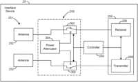
- the interface device 25can include an antenna system 251 (with one or more antennas 252 ), a controller 254 , switching circuitry 255 and at least one transceiver 250 (with a receiver 256 and a transmitter 258 ).
- the transceiver 250can be configured for full-duplex operation such that the receiver 256 and the transmitter 258 can transmit and receive signals simultaneously (i.e., at the same time).
- the controller 254is shown separate from the transceiver 250 in FIGS. 2 and 3 , the controller 254 can be incorporated in the transceiver 250 in other embodiments.
- the switching circuitry 255can be used to connect a first antenna 252 (of the antenna system 251 ) to the receiver 256 (of the transceiver 250 ) and a second antenna 252 (of the antenna system 251 ) to the transmitter 258 (of the transceiver 250 ) such that the interface device 25 has separate antennas 252 for the receiver 256 and the transmitter 258 .
- the transceiver 250can send and receive signals at the same frequency (in addition to at the same time).
- antenna system 251has a single antenna 252 for the receiver 256 and the antenna 258 . Similar to the embodiment in FIG.
- the switching circuitry 255is connected to the receiver 256 and the transmitter 258 , but instead of being connected to separate antennas 252 (as shown in FIG. 2 ), the switching circuitry 255 is connected to a duplexer 260 (of the antenna system 251 ), which duplexer 260 is then connected to the antenna 252 .
- the duplexer 260provides a frequency division between the signals for the receiver 256 and the transmitter 258 such that the transmit and receive frequencies for the transmitter 258 and the receiver 256 are different.
- the switching circuitry 255can be arranged for operation of the transceiver 250 in either a communication mode or a diagnostic mode.
- the switching circuitry 255provides paths between the receiver 256 and the transmitter 258 and the antenna system 251 (either the separate antennas for the receiver 256 and the transmitter 258 (as shown in FIG. 2 ) or the duplexer 260 and the single antenna for the receiver 256 and the transmitter 258 (as shown in FIG. 3 )).
- the switching circuitry 255is arranged for operation of the transceiver 250 in the diagnostic mode (as shown in FIG.
- the switching circuitry 255connects the receiver 256 to the transmitter 258 (and disconnects the receiver 256 and transmitter 258 from the antenna system 251 ) to permit diagnostics to be performed on the receiver 256 and the transmitter 258 of the transceiver 250 .
- diagnosticsare able to be performed on the transmitter 258 and receiver 256 without causing interference (as a result of test signals not reaching the antenna system 251 ) to other communication devices 27 or interface devices 25 in the local network 20 .
- the switching circuitryincludes two switches 302 , with a first switch 302 being connected to the receiver 256 (of the transceiver 250 ) and a second switch 302 being connected to the transmitter 258 (of the transceiver 250 ).
- the switches 302can be PIN diode switches as described in more detail in U.S. patent application Ser. No. 17/340,880 entitled “Reducing Insertion Loss in a Switch for a Communication Device,” which application is incorporated herein by reference.
- the switches 302may be any suitable single-pole, double-throw (SPDT) switch arrangement.
- the switches 302can have a first position (as shown in FIGS.
- the switches 302can also have a second position (as shown in FIG. 4 ) that connects the receiver 256 to the transmitter 258 via a power attenuator 304 .
- the power attenuator 304can be used to dissipate power and lower the voltage (amplitude) of a signal sent by the transmitter 258 and received by the receiver 256 such that damage to the receiver 256 (and its corresponding components) can be avoided.
- the power attenuator 304can also be used as a proper termination (e.g., 50 ⁇ ) for the transmitter 258 .
- the power attenuator 304can have three resistors R 1 -R 3 connected in a “pi” arrangement.
- the resistors R 1 and R 3can have the same value when the transmitter 258 and the receiver 256 have the same impedance (e.g., 50 ⁇ ).
- R 1 and R 3can each have a resistance of 51 ⁇ and R 2 can have a resistance of 2500 ⁇ .
- the power attenuator 304can have a power rating that is less than the output power for the transmitter 258 .
- resistor R 2can be rated by the manufacturer for 1.5 W, but resistor R 2 can be able to accommodate a pulse power of 9 W (per the manufacturer) for a single pulse duration of 1 second.
- the power rating of the power attenuator 304can be less than the output power of the transmitter 258 (as shown in the above example) because the diagnostic procedures performed on transceiver 250 are able to be completed before damage can occur to the components of the power attenuator 304 (e.g., from overheating).
- the controller 254can program the receiver 256 and the transmitter 258 to the desired settings (e.g., a few bytes at high bit rate) at the beginning of the diagnostic mode. Then, the controller 254 permits the test signal to pass through the transmitter 258 and the receiver 256 for the time needed (e.g., the millisecond range in one embodiment) to capture (or catch) the “reading” data from all of the transceiver sensors.
- the communication channel between the controller 254 and an external test device, when performing diagnostics,is less reliable and slower than the internal connection for diagnostics described herein.
- the lower power rating for the power attenuator 304enables lower cost parts to be used in the power attenuator 304 .
- the controller 254controls the switches 302 of the switching circuitry 255 to operate the transceiver 250 in either the communication mode (i.e., the transmitter 258 and the receiver 256 can send and receive signals with other communication devices 27 ) or the diagnostic mode (i.e., the transmitter 258 is connected to the receiver 256 to perform diagnostic procedures on the transmitter 258 and/or the receiver 256 ).
- the controller 254can provide signals to the switches 302 of the switching circuitry 255 to position the switches 302 in a first position that provides a connection to the antenna system 251 to operate the transceiver 250 in the communication mode.
- the controller 254can provide signals to the switches 302 of the switching circuitry 255 to position the switches 302 in a second position that provides a connection between the transmitter 258 and the receiver 256 via the power attenuator 304 to operate the transceiver 250 in diagnostic mode.
- the switching circuitry 255connects the transmitter 258 to the receiver 256 (via the power attenuator 304 ) to permit the transmitter 258 to be used to perform diagnostics on the receiver 256 and to permit the receiver 256 to be used to perform diagnostics on the transmitter 258 .
- the transceiver 250can be a full-duplex transceiver such that the receiver 256 and the transmitter 258 have the capability to process signals at the same time when performing diagnostics on the transceiver 250 (e.g., a signal provided by the transmitter 258 can be processed by the receiver 256 ).
- the interface device 25 shown in FIGS. 2 and 3show a particular arrangement of components (e.g., antenna system 251 , controller 254 , switching circuitry 255 and transceiver 250 ), it is to be understood that in other embodiments, the interface device 25 may include more than one of some (or all) of the components shown in FIGS. 2 and 3 or may omit some of the components shown in FIGS. 2 and 3 .
- the interface device 25may include additional components (e.g., filtering circuits, signal processing circuits, etc.), which have been omitted from FIGS. 2 and 3 for simplicity.
- FIG. 5shows an embodiment of the controller 254 .
- the controller 254 shown by FIG. 5can include logic 172 , referred to herein as “control logic,” for generally controlling the operation of the controller 254 .
- the control logic 172 of the controller 254can also control the operation of the transceiver 250 and/or the interface device 25 .
- the controller 254also includes logic 174 , referred to herein as “diagnostic logic,” and logic 176 , referred to herein as “switching logic.”
- the diagnostic logic 174can be used for performing diagnostic procedures on the receiver 256 and/or the transmitter 258 and for evaluating the results of the diagnostic procedures when the transceiver 250 is operated in diagnostic mode.
- the switching logic 176can be used to control the switches 302 of the switching circuitry 255 for the intended mode of operation of the transceiver 250 (i.e., communication mode or diagnostic mode). In other embodiments, the diagnostic logic 174 and/or the switching logic 176 can be combined with the control logic 172 or with one another.
- the control logic 172 , the diagnostic logic 174 and the switching logic 176may be implemented in software, firmware, hardware, or any combination thereof. In FIG. 5 , control logic 172 , the diagnostic logic 174 and the switching logic 176 are implemented in software and stored in memory 170 . However, other configurations of the control logic 172 , the diagnostic logic 174 and the switching logic 176 are possible in other embodiments.
- control logic 172when implemented in software, can be stored and transported on any computer-readable medium for use by or in connection with an instruction execution apparatus that can fetch and execute instructions.
- a “computer-readable medium”can be any non-transitory means that can contain or store code for use by or in connection with the instruction execution apparatus.
- the controller 254may include at least one conventional processor 110 , which includes processing hardware for executing instructions stored in the memory 170 .
- the processor 110may include a central processing unit (CPU) or a digital signal processor (DSP).
- the processor 110communicates to and drives the other elements within the controller 254 via a local interface 120 , which can include at least one bus.
- the control logic 172 , the diagnostic logic 174 and the switching logic 176are implemented in software, the processor 110 may execute instructions of the control logic 172 , the diagnostic logic 174 and the switching logic 176 to perform the functions ascribed herein to the control logic 172 , the diagnostic logic 174 and the switching logic 176 .
- the controller 254can have a communication interface 130 (which may be similar to interface 29 ) for connecting the interface device 25 to the network 40 (and the communications hub 30 ) or to other interface devices 25 .
- the communication interface 130may include a radio or other device for communicating wirelessly and/or corresponding connection ports for wired communications.
- the controller 254can also have a power supply 140 , which provides electrical power to the components of the controller 254 and possibly, in an embodiment, to components of the interface device 25 (e.g., the transceiver 250 , the switching circuitry 255 and/or the antenna system 251 ).
- the power supply 140has an interface that allows it to plug into or otherwise interface with an external component, such as a wall outlet or battery, and receive electrical power from such external component. If desired, the power supply 140 may incorporate one or more batteries to permit the controller 254 to be independent of the external power component.
- the controller 254can include a transceiver interface 150 and a switch interface 160 .
- the transceiver interface 150 and the switch interface 160may be combined into a single interface.
- the transceiver interface 150enables the controller 254 to exchange (e.g., send and receive) signals and data with one or both of the transmitter 258 and the receiver 256 of the transceiver 250 .
- the transmitter 258 and the receiver 256can provide diagnostic data to the controller 254 , which is then stored in diagnostic data 182 .
- the switch interface 160enables the controller 254 to provide signals to the switches 302 of the switching circuitry 255 to control the position of switches 302 for operation of the transceiver 250 in either communication mode or diagnostic mode.
- Each of the transceiver interface 150 and the sensor interface 160may include any suitable interfaces for providing signals and/or data between processor 110 and the corresponding component connected to the interface.
- FIG. 6is directed to an embodiment of a process for performing diagnostics on a transceiver 250 of the interface device 25 .
- the processbegins by moving the switches 302 of switching circuitry 255 for operation of the transceiver 250 in the diagnostic mode (step 602 ).
- the controller 254can send signals to the switches 302 of the switching circuitry 255 to place the switches 302 in the second position to connect the transmitter 258 to the receiver 256 via the power attenuator 304 .
- the controller 254can program the components (e.g., the transmitter 258 and the receiver 256 ) of the transceiver 250 to evaluate certain parameters or settings (e.g., frequency, amplitude, modulation, bandwidth, etc.) associated with the test signal used for the diagnostic procedure prior to adjusting the switches 302 for operation of the transceiver 250 in diagnostic mode.
- the diagnostic logic 174 of the controller 254can make the determination as to when diagnostics on the transceiver 250 are to be performed and then send signals/instructions to the switching logic 176 of the controller 254 to position the switching circuitry 255 accordingly.
- the diagnostic logic 174can perform diagnostics on the transceiver 250 each time the interface device 25 is readied for operation (e.g., on “start-up” of the interface device 25 either from a sleep state or an “off” state). In other embodiments, the diagnostic logic 174 can perform diagnostics on the transceiver 250 of the interface device 25 at regular or preselected intervals (e.g., hourly, daily, weekly, etc.) or in response to the occurrence of preselected “trigger events” (e.g., the generation of an alert or alarm for the interface device 25 ). In still other embodiments, the controller 254 of the interface device 25 can receive instructions from the communication hub 30 to perform diagnostics on the transceiver 250 .
- the diagnostic logic 174can initiate one or more diagnostic tests and/or procedures for the transmitter 258 and/or the receiver 256 (step 604 ).
- the diagnostic logic 174can perform diagnostic procedures and tests to evaluate one or more components, sections or sub-systems of the receiver 256 and/or transmitter 258 such as modulators/demodulators, analog-to-digital converters (ADC)/digital-to-analog converters (DAC), filters, amplifiers, mixers, frequency synthesizers, power components, etc.
- ADCanalog-to-digital converters
- DACdigital-to-analog converters
- one diagnostic procedureinvolves the diagnostic logic 174 providing a signal or instruction to the transceiver 250 such that the transmitter 258 outputs a signal (i.e., a test signal) having a preselected frequency and/or amplitude (or power level) that is then received by the receiver 256 .
- the signal output from the transmitter 258passes through the power attenuator 304 (which reduces the power level of the signal) and is received at the receiver 256 .
- datacan be collected regarding the operation and/or performance of the components or sub-systems (e.g., modulator/demodulator, power amplifier/low noise amplifier, intermediate stages, mixers, etc.) of the transmitter 258 and the receiver 256 (step 606 ).
- the components or sub-systemse.g., modulator/demodulator, power amplifier/low noise amplifier, intermediate stages, mixers, etc.
- datacan be collected for the output transistor current (of the transmitter 258 ), the rectified RF voltage from the output coupler of the power amplifier (PA) (of the transmitter 258 ), the Received Signal Strength Indicator (RSSI) voltage (of the receiver 256 ), etc.
- PApower amplifier
- RSSIReceived Signal Strength Indicator
- one or more sensorscan be located in the transceiver 250 and used to collect the data for the components or sub-systems.
- the digital data (from the sensors) associated with the transmission of the test signalcan be collected if Digital Signal Processing (DSP) techniques are used.
- DSPDigital Signal Processing
- the controller 254can apply a test mode-ON configuration (sometimes referred to as a Push-To-Talk (PTT) mode) to the transceiver 250 while the test signal is being communicated.
- a test mode-ON configurationsometimes referred to as a Push-To-Talk (PTT) mode
- the sensors of the transceiver 250know that diagnostics on the transceiver 250 are being performed (as opposed to routine monitoring functions for the transceiver 250 ). The data collected during the application of the test mode configuration can then be used for diagnostic purposes.
- the controller 254can apply a test mode-OFF configuration to the transceiver 250 .
- the sensors of the transceiver 250When in the test mode-OFF configuration, the sensors of the transceiver 250 perform their normal routine monitoring functions for the transceiver 250 .
- the controller 254can provide additional signals or instructions to the transceiver 250 resulting in a test signal having different frequencies and/or amplitudes to evaluate other parameters or settings. In other words, steps 604 and 606 can be repeated for different test signals that evaluate different parameters or settings of the transceiver 250 .
- the results of the procedures or testscan be provided to the diagnostic logic 174 of the controller 254 and stored in diagnostic data 182 .
- the stored diagnostic data 182can then be processed to evaluate the performance of the transmitter 258 and/or the receiver 256 of the transceiver 250 (step 608 ).
- the evaluation of the diagnostic data 182can be performed locally (e.g., by the diagnostic logic 174 of the controller 254 ), remotely (e.g., by the communication hub 30 ), or in some combination of locally and remotely.
- the evaluation of the stored diagnostic data 182can be performed by comparing the results of a diagnostic procedure to corresponding reference data or threshold values or ranges, which reference data can be stored either in diagnostic data 182 , memory 170 or elsewhere (e.g., in memory at the communication hub 30 ).
- the reference datacan be previously obtained by performing the diagnostic procedure on a transceiver 250 , which may or may not be the transceiver 250 undergoing the diagnostic procedure, known to be operating properly.
- the reference datacan be obtained from the transceiver 250 undergoing the diagnostic procedure as part of the initialization of the interface device 25 into the local network 20 .
- remedial procedures or actionscan be performed. Some examples of remedial procedures or actions may be the issuance of an alarm, the disabling of the transmitter 258 or receiver 256 , or the performance of the diagnostic procedure or test a second time.
- the results of the diagnostic procedurecan also be evaluated either by the diagnostic logic 174 or the communications hub 30 to identify possible trends in the results. For example, the current results of a diagnostic procedure can be compared to a preselected number of prior results (e.g., 5 to 10 prior results) to determine if a trend, such as an increasing or decreasing value, is forming in the results even if the results are within the corresponding predefined tolerance. If a trend is identified in the results, a remedial action or procedure may be taken before the failure of the transceiver 250 or an out-of-tolerance determination is made.
- a preselected number of prior resultse.g., 5 to 10 prior results
- the transceiver 250enter the communication mode (step 610 ).
- the controller 254can send signals to the switches 302 of the switching circuitry 255 to place the switches 302 in the first position to connect the transmitter 258 and the receiver 256 to the antenna system 251 .
- the diagnostic logic 174 of the controller 254can determine when diagnostics on the transceiver 250 has been completed and send signals/instructions to the switching logic 176 to arrange the switching circuitry 255 accordingly.
Landscapes
- Engineering & Computer Science (AREA)
- Signal Processing (AREA)
- Computer Networks & Wireless Communication (AREA)
- Transceivers (AREA)
- Mobile Radio Communication Systems (AREA)
Abstract
Description
Claims (15)
Priority Applications (3)
| Application Number | Priority Date | Filing Date | Title |
|---|---|---|---|
| US17/503,745US12095496B2 (en) | 2021-10-18 | 2021-10-18 | Self-diagnostic systems and method for a transceiver |
| AU2021266228AAU2021266228B2 (en) | 2021-10-18 | 2021-11-09 | Self-diagnostic system and method for a transceiver |
| CA3139700ACA3139700A1 (en) | 2021-10-18 | 2021-11-22 | Self-diagnostic system and method for a transceiver |
Applications Claiming Priority (1)
| Application Number | Priority Date | Filing Date | Title |
|---|---|---|---|
| US17/503,745US12095496B2 (en) | 2021-10-18 | 2021-10-18 | Self-diagnostic systems and method for a transceiver |
Publications (2)
| Publication Number | Publication Date |
|---|---|
| US20230121099A1 US20230121099A1 (en) | 2023-04-20 |
| US12095496B2true US12095496B2 (en) | 2024-09-17 |
Family
ID=85982356
Family Applications (1)
| Application Number | Title | Priority Date | Filing Date |
|---|---|---|---|
| US17/503,745Active2042-01-17US12095496B2 (en) | 2021-10-18 | 2021-10-18 | Self-diagnostic systems and method for a transceiver |
Country Status (3)
| Country | Link |
|---|---|
| US (1) | US12095496B2 (en) |
| AU (1) | AU2021266228B2 (en) |
| CA (1) | CA3139700A1 (en) |
Families Citing this family (1)
| Publication number | Priority date | Publication date | Assignee | Title |
|---|---|---|---|---|
| US12044773B2 (en)* | 2022-01-06 | 2024-07-23 | The Boeing Company | Multimode electronically steerable monopulse radar |
Citations (75)
| Publication number | Priority date | Publication date | Assignee | Title |
|---|---|---|---|---|
| US1584220A (en) | 1923-05-21 | 1926-05-11 | Farkouh Henry | Portable radio receiving set |
| US2486536A (en) | 1945-12-22 | 1949-11-01 | Olson Arvilla Nathalyn | Radio receiver unit mounted in a suitcase |
| US3475700A (en) | 1966-12-30 | 1969-10-28 | Texas Instruments Inc | Monolithic microwave duplexer switch |
| US3711793A (en) | 1970-12-24 | 1973-01-16 | Rca Corp | High power microwave switch including a plurality of diodes and conductive rods |
| US4480338A (en) | 1982-03-01 | 1984-10-30 | Zenith Electronics Corporation | Lowpass-highpass electronic switch |
| US4817200A (en) | 1987-02-26 | 1989-03-28 | Hewlett-Packard Company | Tracking YIG tuned filter-mixer |
| US5533097A (en) | 1992-02-26 | 1996-07-02 | Motorola, Inc. | Portable communication system comprising a local and wide area communication units which can store a communication when the wide area communication system is not available |
| US5590022A (en) | 1995-05-19 | 1996-12-31 | The I.D.E.A. Corporation | Shielded modular portable computer work station having cable routing means |
| US5594394A (en) | 1993-08-31 | 1997-01-14 | Matsushita Electric Industrial Co., Ltd. | Antenna diversity switching device with switching circuits between the receiver terminal and each antenna |
| US5634200A (en) | 1993-03-30 | 1997-05-27 | Sony Corporation | Antenna duplexer and transmitting/receiving apparatus using the same |
| US5770940A (en) | 1995-08-09 | 1998-06-23 | Switch Power, Inc. | Switching regulator |
| US5781563A (en) | 1994-08-31 | 1998-07-14 | Siemens Aktiengesellschaft | Substitute circuit for a plurality of functional units |
| US5789995A (en) | 1996-09-20 | 1998-08-04 | Motorola, Inc. | Low loss electronic radio frequency switch |
| US5903548A (en) | 1996-12-19 | 1999-05-11 | Itronix Corporation | Portable electronic communications device having switchable LAN/WAN wireless communications features |
| US5914544A (en) | 1997-05-02 | 1999-06-22 | Fujitsu Limited | High-frequency switching circuit |
| US6134105A (en) | 1998-01-06 | 2000-10-17 | Lueker; Mark David | Portable command center |
| US6198288B1 (en) | 1998-11-25 | 2001-03-06 | Picker International, Inc. | High power, multiple-frequency transmit-receive switch in magnetic resonance imaging |
| US20020100970A1 (en) | 2000-12-27 | 2002-08-01 | Shoichi Kitazawa | High frequency switch, two-band type high frequency switch, three-band type high frequency switch, and mobile communication equipment |
| US20020137471A1 (en) | 1999-12-14 | 2002-09-26 | Yuki Satoh | High-frequency composite switch component |
| US6496083B1 (en) | 1997-06-03 | 2002-12-17 | Matsushita Electric Industrial Co., Ltd. | Diode compensation circuit including two series and one parallel resonance points |
| US6560444B1 (en) | 1998-12-22 | 2003-05-06 | Telefonaktiebolaget Lm Ericsson (Publ) | Antenna switch module |
| US20040032706A1 (en) | 2000-11-01 | 2004-02-19 | Shigeru Kemmochi | High-frequency switch module |
| US20040061578A1 (en) | 2002-09-30 | 2004-04-01 | Vice Michael Wendell | Switching system |
| US20040092285A1 (en) | 2001-02-27 | 2004-05-13 | Walter Kodim | Multiband r f switching device |
| US20040127182A1 (en) | 2002-09-17 | 2004-07-01 | Hitachi Metals, Ltd. | High-frequency device, high-frequency module and communications device comprising them |
| US20040157579A1 (en) | 2001-09-14 | 2004-08-12 | Yasuaki Namura | High-frequency switch |
| US20040242165A1 (en) | 2001-09-18 | 2004-12-02 | Jedeloo Pieter Willem | RF signal switch for a wireless communication device |
| US20040266378A1 (en) | 2001-08-10 | 2004-12-30 | Keisuke Fukamachi | Bypass filter, multi-band antenna switch circuit, and layered module composite part and communication device using them |
| US20050035824A1 (en) | 2003-08-15 | 2005-02-17 | Tdk Corporation | Antenna switching circuit |
| US20050048927A1 (en) | 2002-01-31 | 2005-03-03 | Shigeru Kemmochi | Switch circuit and composite high-frequency part |
| US20050077980A1 (en) | 2000-03-15 | 2005-04-14 | Hitachi Metals, Ltd. | High-frequency composite part and wireless communications device comprising it |
| US20060017607A1 (en) | 2004-07-26 | 2006-01-26 | Kyocera Corporation | Amplitude modulator, selector switch, high frequency transmitting/receiving apparatus including the same, and radar apparatus, and radar apparatus-mounting vehicle and radar apparatus-mounting small ship |
| US20060035601A1 (en)* | 2004-08-12 | 2006-02-16 | Samsung Electronics Co., Ltd. | TDD transceiver for utilizing a transmission mode and a reception mode simultaneously, and a self-diagnostic method therefor |
| US20060170516A1 (en) | 2005-02-01 | 2006-08-03 | Marion Donald G | Method of increasing the operating frequency in a series-shunt configured PIN diode switch |
| US20060245382A1 (en) | 2004-06-07 | 2006-11-02 | Kenji Hayashi | High-frequency switching module and its control method |
| US20070018753A1 (en) | 2005-07-22 | 2007-01-25 | Stmicroelectronics S.A. | Antenna switch module |
| US20070026836A1 (en) | 2005-07-27 | 2007-02-01 | Chow Yut H | Method and apparatus for selectively blocking radio frequency (RF) signals in a radio frequency (RF) switching circuit |
| US20070086349A1 (en)* | 2005-10-18 | 2007-04-19 | Arcadyan Technology Corporation | Network apparatus, method of self-testing network connectivity, and method of analyzing frequency spectrum |
| US20070232228A1 (en) | 2006-04-04 | 2007-10-04 | Mckay David L Sr | Wireless repeater with universal server base unit and modular donor antenna options |
| US20070241155A1 (en) | 2005-09-08 | 2007-10-18 | Norsat International Inc. | Case for portable satellite terminal |
| EP1916738A1 (en) | 2006-10-23 | 2008-04-30 | Gilat Satellite Networks Ltd. | Quick deployed antenna system |
| US7391283B2 (en) | 2005-11-29 | 2008-06-24 | Tdk Corporation | RF switch |
| US20080181282A1 (en) | 2007-01-25 | 2008-07-31 | Adc Telecommunications, Inc. | Modular wireless communications platform |
| US20090077608A1 (en) | 2007-09-14 | 2009-03-19 | Romerein Robert L | Constant input port impedance for CATV amplifier with passive modem port |
| US20100222012A1 (en)* | 2009-03-02 | 2010-09-02 | Fujitsu Limited | Wireless communication apparatus and method |
| US20100289597A1 (en) | 2009-05-18 | 2010-11-18 | Lockheed Martin | High power uhf single-pole multi-throw switch |
| US20120068899A1 (en) | 2004-04-26 | 2012-03-22 | Ayotte Keith | Compact portable antenna positioner system and method |
| US20120195207A1 (en)* | 2011-01-31 | 2012-08-02 | Infineon Technologies Ag | Communication terminal, communication device, method for measuring a signal and method for requesting a measurement |
| CA2736083A1 (en) | 2011-03-31 | 2012-09-30 | Jt Technology Canada Ltd. | Emergency and rescue response system |
| US8428573B2 (en) | 2009-11-09 | 2013-04-23 | Harris Corporation | Remote control of mobile radio system through portable radio system |
| US8583065B2 (en) | 2007-06-07 | 2013-11-12 | Vishay Intertechnology, Inc. | Digitally controlled antenna tuning circuit for radio frequency receivers |
| US8594611B2 (en) | 2011-06-22 | 2013-11-26 | Harris Corporation | Intrinsically safe portable radio architecture |
| US8593358B2 (en) | 2008-08-14 | 2013-11-26 | Theodore S. Rappaport | Active antennas for multiple bands in wireless portable devices |
| US20140120968A1 (en) | 2012-10-31 | 2014-05-01 | Raytheon Company | Frequency Tunable Transmit/Receive (Tx/Rx) Antenna Switch |
| US20140125545A1 (en) | 2012-11-06 | 2014-05-08 | Rohde & Schwarz Gmbh & Co. Kg | Limiter for broadband high-frequency signals |
| US20140124908A1 (en) | 2011-05-27 | 2014-05-08 | Mitsubishi Electric Corporation | High frequency switch |
| US8937816B2 (en) | 2013-01-24 | 2015-01-20 | Marc Trombino | Carrying case with multi-frequency shielding |
| US9026041B2 (en) | 2011-11-10 | 2015-05-05 | Avery Dennison Corporation | Portable radio-frequency repeater |
| US9293808B1 (en) | 2015-05-29 | 2016-03-22 | Tech 21 Licensing Limited | Radio frequency properties of a case for a communications device |
| US20160261267A1 (en) | 2015-03-06 | 2016-09-08 | Skyworks Solutions, Inc. | Apparatus and methods for radio frequency pin diode switches |
| US20170040996A1 (en) | 2015-08-07 | 2017-02-09 | Huan Zhao | Single-pole-single-throw (spst) switch and its derivative single-pole-double-throw (spdt) and single-pole-multiple-throw (spmt) switches |
| US20170126262A1 (en)* | 2015-10-30 | 2017-05-04 | Afero, Inc. | Apparatus and method for filtering wireless signals |
| US20170302269A1 (en) | 2016-04-15 | 2017-10-19 | Rohde & Schwarz Gmbh & Co. Kg | Electronically switchable diplexer |
| US20170345620A1 (en) | 2016-05-24 | 2017-11-30 | Mks Instruments, Inc. | Solid-state impedance matching systems including a hybrid tuning network with a switchable coarse tuning network and a varactor fine tuning network |
| US20180013425A1 (en) | 2016-07-06 | 2018-01-11 | Macom Technology Solutions Holdings, Inc. | Low power consumption diode switch |
| US10115510B2 (en) | 2013-07-17 | 2018-10-30 | Rohde & Schwarz Gmbh & Co. Kg | Coil for a switching device with a high-frequency power |
| US20190074857A1 (en) | 2017-09-07 | 2019-03-07 | Futurecom Systems Group, ULC | Portable communication system having modular components |
| US20190110021A1 (en) | 2017-10-06 | 2019-04-11 | Ppc Broadband, Inc. | Network interface device |
| US10629972B2 (en) | 2017-11-08 | 2020-04-21 | Pegatron Corporation | Radio-frequency switching circuit |
| US20200144032A1 (en) | 2015-06-29 | 2020-05-07 | Reno Technologies, Inc. | Switching circuit with voltage bias |
| US20200279844A1 (en) | 2019-02-28 | 2020-09-03 | Macom Technology Solutions Holdings, Inc. | Monolithic multi-i region diode switches |
| US20210013922A1 (en)* | 2018-03-28 | 2021-01-14 | Denso Corporation | Communication device |
| US20210135326A1 (en) | 2019-10-31 | 2021-05-06 | Skyworks Solutions, Inc. | Dc bias configuration for pin diode spdt switch |
| US20210152208A1 (en) | 2019-11-19 | 2021-05-20 | Skyworks Solutions, Inc. | High-power hybrid spdt switch |
| US11323147B1 (en) | 2021-06-07 | 2022-05-03 | Futurecom Systems Group, ULC | Reducing insertion loss in a switch for a communication device |
- 2021
- 2021-10-18USUS17/503,745patent/US12095496B2/enactiveActive
- 2021-11-09AUAU2021266228Apatent/AU2021266228B2/enactiveActive
- 2021-11-22CACA3139700Apatent/CA3139700A1/enactivePending
Patent Citations (78)
| Publication number | Priority date | Publication date | Assignee | Title |
|---|---|---|---|---|
| US1584220A (en) | 1923-05-21 | 1926-05-11 | Farkouh Henry | Portable radio receiving set |
| US2486536A (en) | 1945-12-22 | 1949-11-01 | Olson Arvilla Nathalyn | Radio receiver unit mounted in a suitcase |
| US3475700A (en) | 1966-12-30 | 1969-10-28 | Texas Instruments Inc | Monolithic microwave duplexer switch |
| US3711793A (en) | 1970-12-24 | 1973-01-16 | Rca Corp | High power microwave switch including a plurality of diodes and conductive rods |
| US4480338A (en) | 1982-03-01 | 1984-10-30 | Zenith Electronics Corporation | Lowpass-highpass electronic switch |
| US4817200A (en) | 1987-02-26 | 1989-03-28 | Hewlett-Packard Company | Tracking YIG tuned filter-mixer |
| US5533097A (en) | 1992-02-26 | 1996-07-02 | Motorola, Inc. | Portable communication system comprising a local and wide area communication units which can store a communication when the wide area communication system is not available |
| US5634200A (en) | 1993-03-30 | 1997-05-27 | Sony Corporation | Antenna duplexer and transmitting/receiving apparatus using the same |
| US5594394A (en) | 1993-08-31 | 1997-01-14 | Matsushita Electric Industrial Co., Ltd. | Antenna diversity switching device with switching circuits between the receiver terminal and each antenna |
| US5781563A (en) | 1994-08-31 | 1998-07-14 | Siemens Aktiengesellschaft | Substitute circuit for a plurality of functional units |
| US5590022A (en) | 1995-05-19 | 1996-12-31 | The I.D.E.A. Corporation | Shielded modular portable computer work station having cable routing means |
| US5770940A (en) | 1995-08-09 | 1998-06-23 | Switch Power, Inc. | Switching regulator |
| US5789995A (en) | 1996-09-20 | 1998-08-04 | Motorola, Inc. | Low loss electronic radio frequency switch |
| US5903548A (en) | 1996-12-19 | 1999-05-11 | Itronix Corporation | Portable electronic communications device having switchable LAN/WAN wireless communications features |
| US5914544A (en) | 1997-05-02 | 1999-06-22 | Fujitsu Limited | High-frequency switching circuit |
| US6496083B1 (en) | 1997-06-03 | 2002-12-17 | Matsushita Electric Industrial Co., Ltd. | Diode compensation circuit including two series and one parallel resonance points |
| US6134105A (en) | 1998-01-06 | 2000-10-17 | Lueker; Mark David | Portable command center |
| US6198288B1 (en) | 1998-11-25 | 2001-03-06 | Picker International, Inc. | High power, multiple-frequency transmit-receive switch in magnetic resonance imaging |
| US6560444B1 (en) | 1998-12-22 | 2003-05-06 | Telefonaktiebolaget Lm Ericsson (Publ) | Antenna switch module |
| US20020137471A1 (en) | 1999-12-14 | 2002-09-26 | Yuki Satoh | High-frequency composite switch component |
| US20050077980A1 (en) | 2000-03-15 | 2005-04-14 | Hitachi Metals, Ltd. | High-frequency composite part and wireless communications device comprising it |
| US20040032706A1 (en) | 2000-11-01 | 2004-02-19 | Shigeru Kemmochi | High-frequency switch module |
| US20020100970A1 (en) | 2000-12-27 | 2002-08-01 | Shoichi Kitazawa | High frequency switch, two-band type high frequency switch, three-band type high frequency switch, and mobile communication equipment |
| US20040092285A1 (en) | 2001-02-27 | 2004-05-13 | Walter Kodim | Multiband r f switching device |
| US20040266378A1 (en) | 2001-08-10 | 2004-12-30 | Keisuke Fukamachi | Bypass filter, multi-band antenna switch circuit, and layered module composite part and communication device using them |
| US20040157579A1 (en) | 2001-09-14 | 2004-08-12 | Yasuaki Namura | High-frequency switch |
| US20040242165A1 (en) | 2001-09-18 | 2004-12-02 | Jedeloo Pieter Willem | RF signal switch for a wireless communication device |
| US20050048927A1 (en) | 2002-01-31 | 2005-03-03 | Shigeru Kemmochi | Switch circuit and composite high-frequency part |
| US20040127182A1 (en) | 2002-09-17 | 2004-07-01 | Hitachi Metals, Ltd. | High-frequency device, high-frequency module and communications device comprising them |
| US20040061578A1 (en) | 2002-09-30 | 2004-04-01 | Vice Michael Wendell | Switching system |
| US20050035824A1 (en) | 2003-08-15 | 2005-02-17 | Tdk Corporation | Antenna switching circuit |
| US20120068899A1 (en) | 2004-04-26 | 2012-03-22 | Ayotte Keith | Compact portable antenna positioner system and method |
| US20060245382A1 (en) | 2004-06-07 | 2006-11-02 | Kenji Hayashi | High-frequency switching module and its control method |
| US20060017607A1 (en) | 2004-07-26 | 2006-01-26 | Kyocera Corporation | Amplitude modulator, selector switch, high frequency transmitting/receiving apparatus including the same, and radar apparatus, and radar apparatus-mounting vehicle and radar apparatus-mounting small ship |
| US20060035601A1 (en)* | 2004-08-12 | 2006-02-16 | Samsung Electronics Co., Ltd. | TDD transceiver for utilizing a transmission mode and a reception mode simultaneously, and a self-diagnostic method therefor |
| US20060170516A1 (en) | 2005-02-01 | 2006-08-03 | Marion Donald G | Method of increasing the operating frequency in a series-shunt configured PIN diode switch |
| US7129805B2 (en) | 2005-02-01 | 2006-10-31 | Continental Microwave & Tool Company, Inc. | Method of increasing the operating frequency in a series-shunt configured PIN diode switch |
| US20070018753A1 (en) | 2005-07-22 | 2007-01-25 | Stmicroelectronics S.A. | Antenna switch module |
| US20070026836A1 (en) | 2005-07-27 | 2007-02-01 | Chow Yut H | Method and apparatus for selectively blocking radio frequency (RF) signals in a radio frequency (RF) switching circuit |
| US20070241155A1 (en) | 2005-09-08 | 2007-10-18 | Norsat International Inc. | Case for portable satellite terminal |
| US20070086349A1 (en)* | 2005-10-18 | 2007-04-19 | Arcadyan Technology Corporation | Network apparatus, method of self-testing network connectivity, and method of analyzing frequency spectrum |
| US7391283B2 (en) | 2005-11-29 | 2008-06-24 | Tdk Corporation | RF switch |
| US20070232228A1 (en) | 2006-04-04 | 2007-10-04 | Mckay David L Sr | Wireless repeater with universal server base unit and modular donor antenna options |
| EP1916738A1 (en) | 2006-10-23 | 2008-04-30 | Gilat Satellite Networks Ltd. | Quick deployed antenna system |
| US20080181282A1 (en) | 2007-01-25 | 2008-07-31 | Adc Telecommunications, Inc. | Modular wireless communications platform |
| US8583065B2 (en) | 2007-06-07 | 2013-11-12 | Vishay Intertechnology, Inc. | Digitally controlled antenna tuning circuit for radio frequency receivers |
| US20090077608A1 (en) | 2007-09-14 | 2009-03-19 | Romerein Robert L | Constant input port impedance for CATV amplifier with passive modem port |
| US8593358B2 (en) | 2008-08-14 | 2013-11-26 | Theodore S. Rappaport | Active antennas for multiple bands in wireless portable devices |
| US20100222012A1 (en)* | 2009-03-02 | 2010-09-02 | Fujitsu Limited | Wireless communication apparatus and method |
| US20100289597A1 (en) | 2009-05-18 | 2010-11-18 | Lockheed Martin | High power uhf single-pole multi-throw switch |
| US8428573B2 (en) | 2009-11-09 | 2013-04-23 | Harris Corporation | Remote control of mobile radio system through portable radio system |
| US20120195207A1 (en)* | 2011-01-31 | 2012-08-02 | Infineon Technologies Ag | Communication terminal, communication device, method for measuring a signal and method for requesting a measurement |
| CA2736083A1 (en) | 2011-03-31 | 2012-09-30 | Jt Technology Canada Ltd. | Emergency and rescue response system |
| US20140124908A1 (en) | 2011-05-27 | 2014-05-08 | Mitsubishi Electric Corporation | High frequency switch |
| US8594611B2 (en) | 2011-06-22 | 2013-11-26 | Harris Corporation | Intrinsically safe portable radio architecture |
| US9026041B2 (en) | 2011-11-10 | 2015-05-05 | Avery Dennison Corporation | Portable radio-frequency repeater |
| US20140120968A1 (en) | 2012-10-31 | 2014-05-01 | Raytheon Company | Frequency Tunable Transmit/Receive (Tx/Rx) Antenna Switch |
| US20140125545A1 (en) | 2012-11-06 | 2014-05-08 | Rohde & Schwarz Gmbh & Co. Kg | Limiter for broadband high-frequency signals |
| US8937816B2 (en) | 2013-01-24 | 2015-01-20 | Marc Trombino | Carrying case with multi-frequency shielding |
| US10115510B2 (en) | 2013-07-17 | 2018-10-30 | Rohde & Schwarz Gmbh & Co. Kg | Coil for a switching device with a high-frequency power |
| US20160261267A1 (en) | 2015-03-06 | 2016-09-08 | Skyworks Solutions, Inc. | Apparatus and methods for radio frequency pin diode switches |
| US9293808B1 (en) | 2015-05-29 | 2016-03-22 | Tech 21 Licensing Limited | Radio frequency properties of a case for a communications device |
| US20200144032A1 (en) | 2015-06-29 | 2020-05-07 | Reno Technologies, Inc. | Switching circuit with voltage bias |
| US20170040996A1 (en) | 2015-08-07 | 2017-02-09 | Huan Zhao | Single-pole-single-throw (spst) switch and its derivative single-pole-double-throw (spdt) and single-pole-multiple-throw (spmt) switches |
| US20170126262A1 (en)* | 2015-10-30 | 2017-05-04 | Afero, Inc. | Apparatus and method for filtering wireless signals |
| US20170302269A1 (en) | 2016-04-15 | 2017-10-19 | Rohde & Schwarz Gmbh & Co. Kg | Electronically switchable diplexer |
| US10200031B2 (en) | 2016-04-15 | 2019-02-05 | Rohde & Schwarz Gmbh & Co. Kg | Electronically switchable diplexer |
| US20170345620A1 (en) | 2016-05-24 | 2017-11-30 | Mks Instruments, Inc. | Solid-state impedance matching systems including a hybrid tuning network with a switchable coarse tuning network and a varactor fine tuning network |
| US20180013425A1 (en) | 2016-07-06 | 2018-01-11 | Macom Technology Solutions Holdings, Inc. | Low power consumption diode switch |
| US10505574B2 (en) | 2017-09-07 | 2019-12-10 | Futurecom Systems Group, ULC | Portable communication system having modular components |
| US20190074857A1 (en) | 2017-09-07 | 2019-03-07 | Futurecom Systems Group, ULC | Portable communication system having modular components |
| US20190110021A1 (en) | 2017-10-06 | 2019-04-11 | Ppc Broadband, Inc. | Network interface device |
| US10629972B2 (en) | 2017-11-08 | 2020-04-21 | Pegatron Corporation | Radio-frequency switching circuit |
| US20210013922A1 (en)* | 2018-03-28 | 2021-01-14 | Denso Corporation | Communication device |
| US20200279844A1 (en) | 2019-02-28 | 2020-09-03 | Macom Technology Solutions Holdings, Inc. | Monolithic multi-i region diode switches |
| US20210135326A1 (en) | 2019-10-31 | 2021-05-06 | Skyworks Solutions, Inc. | Dc bias configuration for pin diode spdt switch |
| US20210152208A1 (en) | 2019-11-19 | 2021-05-20 | Skyworks Solutions, Inc. | High-power hybrid spdt switch |
| US11323147B1 (en) | 2021-06-07 | 2022-05-03 | Futurecom Systems Group, ULC | Reducing insertion loss in a switch for a communication device |
Non-Patent Citations (2)
| Title |
|---|
| Stratus Lite Repeater, Jun. 2017, 2 pages, Issue 2, 12-20314-EN, Codan Radio Communications. |
| Stratus Product White Paper P25 & LTE: The best of both worlds, 17 pages, Codan Radio Communications. |
Also Published As
| Publication number | Publication date |
|---|---|
| AU2021266228A1 (en) | 2023-05-04 |
| US20230121099A1 (en) | 2023-04-20 |
| CA3139700A1 (en) | 2023-04-18 |
| AU2021266228B2 (en) | 2025-04-17 |
Similar Documents
| Publication | Publication Date | Title |
|---|---|---|
| JP4732963B2 (en) | Wireless base station test equipment | |
| US7519112B2 (en) | Testing device and method for providing receiver overload protection during transceiver testing | |
| CN106912069B (en) | Distributed antenna system remote terminal and uplink signal link detection method and device thereof | |
| US6188876B1 (en) | System and method for remote monitoring of RF units in base station of wireless communication network | |
| US20030152046A1 (en) | Communication apparatus, communication system and communication frequency setting method | |
| EP1528763B1 (en) | Mobile terminal with self performance diagnosis function and method thereof | |
| US12095496B2 (en) | Self-diagnostic systems and method for a transceiver | |
| US20030067869A1 (en) | Integrated RF loopback test apparatus for redundant data radio transceiver system | |
| US7965991B2 (en) | Phase calibration for multiple transmitter systems | |
| CN106804044B (en) | Communication fault detection method and device and radio remote unit | |
| CN108075846B (en) | Base station interference detection method and device | |
| JP4373361B2 (en) | base station | |
| JP2008118428A (en) | Wireless base station equipment | |
| US7715345B2 (en) | Radio communication system | |
| JP2013110605A (en) | Wireless base station and system for detecting failure in wireless base station | |
| KR19980702084A (en) | Method and apparatus for waiting for combiner filter and activating other combiner filter in wireless base station | |
| CN112583500B (en) | Fault detection system and method based on microwave radio frequency loopback | |
| JP3781543B2 (en) | Wireless terminal, wireless base station apparatus and wireless system using the same | |
| GB2390262A (en) | Method and apparatus for fault detection in a radio transceiver | |
| KR20000052156A (en) | Method for self testing of base station in cellular system | |
| CN110138405B (en) | Communication apparatus and method | |
| KR100834613B1 (en) | Method and apparatus for measuring transmission power in a base station transceiver subsystem | |
| KR20130116469A (en) | Second harmonic measurement device of integrated fiber repeater system | |
| JP2912253B2 (en) | Antenna failure detection circuit | |
| JP4425964B2 (en) | Receiving apparatus and receiver fault diagnosis method |
Legal Events
| Date | Code | Title | Description |
|---|---|---|---|
| AS | Assignment | Owner name:FUTURECOM SYSTEMS GROUP, ULC, CANADA Free format text:ASSIGNMENT OF ASSIGNORS INTEREST;ASSIGNOR:GOSTYUZHEV, SERGEY;REEL/FRAME:057820/0840 Effective date:20211015 | |
| FEPP | Fee payment procedure | Free format text:ENTITY STATUS SET TO UNDISCOUNTED (ORIGINAL EVENT CODE: BIG.); ENTITY STATUS OF PATENT OWNER: LARGE ENTITY | |
| STPP | Information on status: patent application and granting procedure in general | Free format text:RESPONSE TO NON-FINAL OFFICE ACTION ENTERED AND FORWARDED TO EXAMINER | |
| STPP | Information on status: patent application and granting procedure in general | Free format text:NON FINAL ACTION MAILED | |
| STPP | Information on status: patent application and granting procedure in general | Free format text:RESPONSE TO NON-FINAL OFFICE ACTION ENTERED AND FORWARDED TO EXAMINER | |
| STPP | Information on status: patent application and granting procedure in general | Free format text:FINAL REJECTION MAILED | |
| STPP | Information on status: patent application and granting procedure in general | Free format text:DOCKETED NEW CASE - READY FOR EXAMINATION | |
| STPP | Information on status: patent application and granting procedure in general | Free format text:NOTICE OF ALLOWANCE MAILED -- APPLICATION RECEIVED IN OFFICE OF PUBLICATIONS | |
| STPP | Information on status: patent application and granting procedure in general | Free format text:PUBLICATIONS -- ISSUE FEE PAYMENT RECEIVED | |
| STPP | Information on status: patent application and granting procedure in general | Free format text:PUBLICATIONS -- ISSUE FEE PAYMENT VERIFIED | |
| STCF | Information on status: patent grant | Free format text:PATENTED CASE | |
| AS | Assignment | Owner name:MOTOROLA SOLUTIONS, INC., ILLINOIS Free format text:ASSIGNMENT OF ASSIGNORS INTEREST;ASSIGNOR:FUTURECOM SYSTEMS GROUP, ULC;REEL/FRAME:072374/0535 Effective date:20250910 |