US12088281B2 - Transversely-excited film bulk acoustic resonator with multi-mark interdigital transducer - Google Patents
Transversely-excited film bulk acoustic resonator with multi-mark interdigital transducerDownload PDFInfo
- Publication number
- US12088281B2 US12088281B2US17/388,745US202117388745AUS12088281B2US 12088281 B2US12088281 B2US 12088281B2US 202117388745 AUS202117388745 AUS 202117388745AUS 12088281 B2US12088281 B2US 12088281B2
- Authority
- US
- United States
- Prior art keywords
- idt
- mark
- fingers
- piezoelectric plate
- acoustic
- Prior art date
- Legal status (The legal status is an assumption and is not a legal conclusion. Google has not performed a legal analysis and makes no representation as to the accuracy of the status listed.)
- Active, expires
Links
- 239000000758substrateSubstances0.000claimsabstractdescription22
- 239000004020conductorSubstances0.000claimsabstractdescription10
- 230000005684electric fieldEffects0.000claimsdescription8
- 239000010410layerSubstances0.000description30
- 239000000463materialSubstances0.000description19
- 238000004891communicationMethods0.000description14
- 239000010408filmSubstances0.000description7
- 238000013461designMethods0.000description6
- 238000000034methodMethods0.000description6
- VYPSYNLAJGMNEJ-UHFFFAOYSA-Nsilicon dioxideInorganic materialsO=[Si]=OVYPSYNLAJGMNEJ-UHFFFAOYSA-N0.000description6
- 229910052782aluminiumInorganic materials0.000description5
- XAGFODPZIPBFFR-UHFFFAOYSA-NaluminiumChemical compound[Al]XAGFODPZIPBFFR-UHFFFAOYSA-N0.000description5
- RYGMFSIKBFXOCR-UHFFFAOYSA-NCopperChemical compound[Cu]RYGMFSIKBFXOCR-UHFFFAOYSA-N0.000description4
- 229910052802copperInorganic materials0.000description4
- 239000010949copperSubstances0.000description4
- 230000033001locomotionEffects0.000description4
- 230000008859changeEffects0.000description3
- 230000008878couplingEffects0.000description3
- 238000010168coupling processMethods0.000description3
- 238000005859coupling reactionMethods0.000description3
- 230000000694effectsEffects0.000description3
- 238000005516engineering processMethods0.000description3
- 229910052751metalInorganic materials0.000description3
- 239000002184metalSubstances0.000description3
- 230000009467reductionEffects0.000description3
- 235000012239silicon dioxideNutrition0.000description3
- 239000007787solidSubstances0.000description3
- VYZAMTAEIAYCRO-UHFFFAOYSA-NChromiumChemical compound[Cr]VYZAMTAEIAYCRO-UHFFFAOYSA-N0.000description2
- 229910052581Si3N4Inorganic materials0.000description2
- RTAQQCXQSZGOHL-UHFFFAOYSA-NTitaniumChemical compound[Ti]RTAQQCXQSZGOHL-UHFFFAOYSA-N0.000description2
- 229910045601alloyInorganic materials0.000description2
- 239000000956alloySubstances0.000description2
- PMHQVHHXPFUNSP-UHFFFAOYSA-Mcopper(1+);methylsulfanylmethane;bromideChemical compoundBr[Cu].CSCPMHQVHHXPFUNSP-UHFFFAOYSA-M0.000description2
- 239000013078crystalSubstances0.000description2
- 230000007423decreaseEffects0.000description2
- 239000003989dielectric materialSubstances0.000description2
- 238000003780insertionMethods0.000description2
- 230000037431insertionEffects0.000description2
- 239000000377silicon dioxideSubstances0.000description2
- HQVNEWCFYHHQES-UHFFFAOYSA-Nsilicon nitrideChemical compoundN12[Si]34N5[Si]62N3[Si]51N64HQVNEWCFYHHQES-UHFFFAOYSA-N0.000description2
- 238000010897surface acoustic wave methodMethods0.000description2
- 229910052719titaniumInorganic materials0.000description2
- 239000010936titaniumSubstances0.000description2
- 238000012546transferMethods0.000description2
- WSMQKESQZFQMFW-UHFFFAOYSA-N5-methyl-pyrazole-3-carboxylic acidChemical compoundCC1=CC(C(O)=O)=NN1WSMQKESQZFQMFW-UHFFFAOYSA-N0.000description1
- 229910000838Al alloyInorganic materials0.000description1
- OKTJSMMVPCPJKN-UHFFFAOYSA-NCarbonChemical compound[C]OKTJSMMVPCPJKN-UHFFFAOYSA-N0.000description1
- 229910000881Cu alloyInorganic materials0.000description1
- 229910002601GaNInorganic materials0.000description1
- GYHNNYVSQQEPJS-UHFFFAOYSA-NGalliumChemical compound[Ga]GYHNNYVSQQEPJS-UHFFFAOYSA-N0.000description1
- JMASRVWKEDWRBT-UHFFFAOYSA-NGallium nitrideChemical compound[Ga]#NJMASRVWKEDWRBT-UHFFFAOYSA-N0.000description1
- ZOKXTWBITQBERF-UHFFFAOYSA-NMolybdenumChemical compound[Mo]ZOKXTWBITQBERF-UHFFFAOYSA-N0.000description1
- BPQQTUXANYXVAA-UHFFFAOYSA-NOrthosilicateChemical compound[O-][Si]([O-])([O-])[O-]BPQQTUXANYXVAA-UHFFFAOYSA-N0.000description1
- 229920000265PolyparaphenylenePolymers0.000description1
- 230000008901benefitEffects0.000description1
- 229910052790berylliumInorganic materials0.000description1
- ATBAMAFKBVZNFJ-UHFFFAOYSA-Nberyllium atomChemical compound[Be]ATBAMAFKBVZNFJ-UHFFFAOYSA-N0.000description1
- 230000005540biological transmissionEffects0.000description1
- 229910052799carbonInorganic materials0.000description1
- 230000001413cellular effectEffects0.000description1
- 229910052804chromiumInorganic materials0.000description1
- 239000011651chromiumSubstances0.000description1
- -1chromium or titaniumChemical class0.000description1
- 238000003870depth resolved spectroscopyMethods0.000description1
- 230000001066destructive effectEffects0.000description1
- 239000010432diamondSubstances0.000description1
- 229910003460diamondInorganic materials0.000description1
- 208000009743drug hypersensitivity syndromeDiseases0.000description1
- 238000005530etchingMethods0.000description1
- 238000007667floatingMethods0.000description1
- 229910052733galliumInorganic materials0.000description1
- PCHJSUWPFVWCPO-UHFFFAOYSA-NgoldChemical compound[Au]PCHJSUWPFVWCPO-UHFFFAOYSA-N0.000description1
- 229910052737goldInorganic materials0.000description1
- 239000010931goldSubstances0.000description1
- 229910000449hafnium oxideInorganic materials0.000description1
- WIHZLLGSGQNAGK-UHFFFAOYSA-Nhafnium(4+);oxygen(2-)Chemical compound[O-2].[O-2].[Hf+4]WIHZLLGSGQNAGK-UHFFFAOYSA-N0.000description1
- 230000001788irregularEffects0.000description1
- 238000002955isolationMethods0.000description1
- 229910052746lanthanumInorganic materials0.000description1
- FZLIPJUXYLNCLC-UHFFFAOYSA-Nlanthanum atomChemical compound[La]FZLIPJUXYLNCLC-UHFFFAOYSA-N0.000description1
- 238000012886linear functionMethods0.000description1
- GQYHUHYESMUTHG-UHFFFAOYSA-Nlithium niobateChemical compound[Li+].[O-][Nb](=O)=OGQYHUHYESMUTHG-UHFFFAOYSA-N0.000description1
- 238000004519manufacturing processMethods0.000description1
- 239000011159matrix materialSubstances0.000description1
- 150000002739metalsChemical class0.000description1
- 229910052750molybdenumInorganic materials0.000description1
- 239000011733molybdenumSubstances0.000description1
- 229920003023plasticPolymers0.000description1
- 239000004033plasticSubstances0.000description1
- 230000010287polarizationEffects0.000description1
- 230000008569processEffects0.000description1
- 230000001902propagating effectEffects0.000description1
- 239000010453quartzSubstances0.000description1
- 229910052594sapphireInorganic materials0.000description1
- 239000010980sapphireSubstances0.000description1
- 238000000926separation methodMethods0.000description1
- 229910052710siliconInorganic materials0.000description1
- 239000010703siliconSubstances0.000description1
- HBMJWWWQQXIZIP-UHFFFAOYSA-Nsilicon carbideChemical compound[Si+]#[C-]HBMJWWWQQXIZIP-UHFFFAOYSA-N0.000description1
- 229910010271silicon carbideInorganic materials0.000description1
- 229910052814silicon oxideInorganic materials0.000description1
- 238000004088simulationMethods0.000description1
- 239000002356single layerSubstances0.000description1
- 230000001629suppressionEffects0.000description1
- 230000002123temporal effectEffects0.000description1
- 239000010409thin filmSubstances0.000description1
- WFKWXMTUELFFGS-UHFFFAOYSA-NtungstenChemical compound[W]WFKWXMTUELFFGS-UHFFFAOYSA-N0.000description1
- 229910052721tungstenInorganic materials0.000description1
- 239000010937tungstenSubstances0.000description1
- 238000012800visualizationMethods0.000description1
Images


Classifications
- H—ELECTRICITY
- H03—ELECTRONIC CIRCUITRY
- H03H—IMPEDANCE NETWORKS, e.g. RESONANT CIRCUITS; RESONATORS
- H03H9/00—Networks comprising electromechanical or electro-acoustic elements; Electromechanical resonators
- H03H9/15—Constructional features of resonators consisting of piezoelectric or electrostrictive material
- H03H9/17—Constructional features of resonators consisting of piezoelectric or electrostrictive material having a single resonator
- H03H9/171—Constructional features of resonators consisting of piezoelectric or electrostrictive material having a single resonator implemented with thin-film techniques, i.e. of the film bulk acoustic resonator [FBAR] type
- H03H9/172—Means for mounting on a substrate, i.e. means constituting the material interface confining the waves to a volume
- H—ELECTRICITY
- H03—ELECTRONIC CIRCUITRY
- H03H—IMPEDANCE NETWORKS, e.g. RESONANT CIRCUITS; RESONATORS
- H03H9/00—Networks comprising electromechanical or electro-acoustic elements; Electromechanical resonators
- H03H9/02—Details
- H03H9/02228—Guided bulk acoustic wave devices or Lamb wave devices having interdigital transducers situated in parallel planes on either side of a piezoelectric layer
- H—ELECTRICITY
- H03—ELECTRONIC CIRCUITRY
- H03H—IMPEDANCE NETWORKS, e.g. RESONANT CIRCUITS; RESONATORS
- H03H9/00—Networks comprising electromechanical or electro-acoustic elements; Electromechanical resonators
- H03H9/46—Filters
- H03H9/54—Filters comprising resonators of piezoelectric or electrostrictive material
- H03H9/56—Monolithic crystal filters
- H—ELECTRICITY
- H03—ELECTRONIC CIRCUITRY
- H03H—IMPEDANCE NETWORKS, e.g. RESONANT CIRCUITS; RESONATORS
- H03H9/00—Networks comprising electromechanical or electro-acoustic elements; Electromechanical resonators
- H03H9/02—Details
- H03H9/125—Driving means, e.g. electrodes, coils
- H03H9/13—Driving means, e.g. electrodes, coils for networks consisting of piezoelectric or electrostrictive materials
- H03H9/132—Driving means, e.g. electrodes, coils for networks consisting of piezoelectric or electrostrictive materials characterized by a particular shape
- H—ELECTRICITY
- H03—ELECTRONIC CIRCUITRY
- H03H—IMPEDANCE NETWORKS, e.g. RESONANT CIRCUITS; RESONATORS
- H03H9/00—Networks comprising electromechanical or electro-acoustic elements; Electromechanical resonators
- H03H9/15—Constructional features of resonators consisting of piezoelectric or electrostrictive material
- H03H9/17—Constructional features of resonators consisting of piezoelectric or electrostrictive material having a single resonator
- H03H9/171—Constructional features of resonators consisting of piezoelectric or electrostrictive material having a single resonator implemented with thin-film techniques, i.e. of the film bulk acoustic resonator [FBAR] type
- H03H9/172—Means for mounting on a substrate, i.e. means constituting the material interface confining the waves to a volume
- H03H9/174—Membranes
- H—ELECTRICITY
- H03—ELECTRONIC CIRCUITRY
- H03H—IMPEDANCE NETWORKS, e.g. RESONANT CIRCUITS; RESONATORS
- H03H9/00—Networks comprising electromechanical or electro-acoustic elements; Electromechanical resonators
- H03H9/15—Constructional features of resonators consisting of piezoelectric or electrostrictive material
- H03H9/17—Constructional features of resonators consisting of piezoelectric or electrostrictive material having a single resonator
- H03H9/171—Constructional features of resonators consisting of piezoelectric or electrostrictive material having a single resonator implemented with thin-film techniques, i.e. of the film bulk acoustic resonator [FBAR] type
- H03H9/172—Means for mounting on a substrate, i.e. means constituting the material interface confining the waves to a volume
- H03H9/175—Acoustic mirrors
- H—ELECTRICITY
- H03—ELECTRONIC CIRCUITRY
- H03H—IMPEDANCE NETWORKS, e.g. RESONANT CIRCUITS; RESONATORS
- H03H9/00—Networks comprising electromechanical or electro-acoustic elements; Electromechanical resonators
- H03H9/46—Filters
- H03H9/54—Filters comprising resonators of piezoelectric or electrostrictive material
Definitions
- This disclosurerelates to radio frequency filters using acoustic wave resonators, and specifically to filters for use in communications equipment.
- a radio frequency (RF) filteris a two-port device configured to pass some frequencies and to stop other frequencies, where “pass” means transmit with relatively low signal loss and “stop” means block or substantially attenuate.
- the range of frequencies passed by a filteris referred to as the “pass-band” of the filter.
- the range of frequencies stopped by such a filteris referred to as the “stop-band” of the filter.
- a typical RF filterhas at least one pass-band and at least one stop-band. Specific requirements on a pass-band or stop-band depend on the specific application.
- a “pass-band”may be defined as a frequency range where the insertion loss of a filter is better than a defined value such as 1 dB, 2 dB, or 3 dB.
- a “stop-band”may be defined as a frequency range where the rejection of a filter is greater than a defined value such as 20 dB, 30 dB, 40 dB, or greater depending on application.
- RF filtersare used in communications systems where information is transmitted over wireless links.
- RF filtersmay be found in the RF front-ends of cellular base stations, mobile telephone and computing devices, satellite transceivers and ground stations, IoT (Internet of Things) devices, laptop computers and tablets, fixed point radio links, and other communications systems.
- IoTInternet of Things
- RF filtersare also used in radar and electronic and information warfare systems.
- RF filterstypically require many design trade-offs to achieve, for each specific application, the best compromise between performance parameters such as insertion loss, rejection, isolation, power handling, linearity, size and cost. Specific design and manufacturing methods and enhancements can benefit simultaneously one or several of these requirements.
- Performance enhancements to the RF filters in a wireless systemcan have broad impact to system performance. Improvements in RF filters can be leveraged to provide system performance improvements such as larger cell size, longer battery life, higher data rates, greater network capacity, lower cost, enhanced security, higher reliability, etc. These improvements can be realized at many levels of the wireless system both separately and in combination, for example at the RF module, RF transceiver, mobile or fixed sub-system, or network levels.
- High performance RF filters for present communication systemscommonly incorporate acoustic wave resonators including surface acoustic wave (SAW) resonators, bulk acoustic wave (BAW) resonators, film bulk acoustic wave resonators (FBAR), and other types of acoustic resonators.
- SAWsurface acoustic wave
- BAWbulk acoustic wave
- FBARfilm bulk acoustic wave resonators
- these existing technologiesare not well-suited for use at the higher frequencies and bandwidths proposed for future communications networks.
- Radio access technology for mobile telephone networkshas been standardized by the 3GPP (3 rd Generation Partnership Project).
- Radio access technology for 5 th generation mobile networksis defined in the 5G NR (new radio) standard.
- the 5G NR standarddefines several new communications bands. Two of these new communications bands are n77, which uses the frequency range from 3300 MHz to 4200 MHz, and n79, which uses the frequency range from 4400 MHz to 5000 MHz.
- Both band n77 and band n79use time-division duplexing (TDD), such that a communications device operating in band n77 and/or band n79 use the same frequencies for both uplink and downlink transmissions.
- TDDtime-division duplexing
- Bandpass filters for bands n77 and n79must be capable of handling the transmit power of the communications device.
- WiFi bands at 5 GHz and 6 GHzalso require high frequency and wide bandwidth.
- the 5G NR standardalso defines millimeter wave communication bands with frequencies between 24.25 GHz and 40 GHz.
- the Transversely-Excited Film Bulk Acoustic Resonatoris an acoustic resonator structure for use in microwave filters.
- the XBARis described in patent U.S. Pat. No. 10,491,291, titled TRANSVERSELY EXCITED FILM BULK ACOUSTIC RESONATOR.
- An XBAR resonatorcomprises an interdigital transducer (IDT) formed on a thin floating layer, or diaphragm, of a single-crystal piezoelectric material.
- the IDTincludes a first set of parallel fingers, extending from a first busbar and a second set of parallel fingers extending from a second busbar. The first and second sets of parallel fingers are interleaved.
- XBAR resonatorsprovide very high electromechanical coupling and high frequency capability.
- XBAR resonatorsmay be used in a variety of RF filters including band-reject filters, band-pass filters, duplexers, and multiplexers.
- XBARsare well suited for use in filters for communications bands with frequencies above 3 GHz.
- Matrix XBAR filtersare also suited for frequencies between 1 GHz and 3 GHz.
- FIG. 1includes a schematic plan view, two schematic cross-sectional views, and a detail view of a transversely-excited film bulk acoustic resonator (XBAR).
- XBARtransversely-excited film bulk acoustic resonator
- FIG. 2is an alternative schematic cross-sectional view of an XBAR.
- FIG. 3is a graphic illustrating a shear horizontal acoustic mode in an XBAR.
- FIG. 4is a plan view of a multi-mark interdigital transducer (IDT).
- IDTinterdigital transducer
- FIG. 5is a plan view of another multi-mark IDT.
- FIG. 6is a graph of mark as a function of position along the length of the IDT for a conventional IDT and another multi-mark IDT.
- FIG. 7is a graph of the magnitude of an input transfer function as a function of frequency for a filter with XBARs with a conventional IDT and a filter with XBARs multi-mark IDTs.
- FIG. 8is an expanded portion of the graph of FIG. 7 .
- FIG. 9is a plan view of a multi-mark multi-pitch IDT.
- FIG. 10is a plan view of another multi-mark multi-pitch IDT.
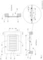
- FIG. 1shows a simplified schematic top view, orthogonal cross-sectional views, and a detailed cross-sectional view of a transversely-excited film bulk acoustic resonator (XBAR) 100 .
- XBAR resonatorssuch as the resonator 100 may be used in a variety of RF filters including band-reject filters, band-pass filters, duplexers, and multiplexers.
- XBARsare particularly suited for use in filters for communications bands with frequencies above 3 GHz.
- the XBAR 100is made up of a thin film conductor pattern formed on a surface of a piezoelectric plate 110 having parallel front and back surfaces 112 , 114 , respectively.
- the piezoelectric plateis a thin single-crystal layer of a piezoelectric material such as lithium niobate, lithium tantalate, lanthanum gallium silicate, gallium nitride, or aluminum nitride.
- the piezoelectric plateis cut such that the orientation of the X, Y, and Z crystalline axes with respect to the front and back surfaces is known and consistent.
- the piezoelectric platesare Z-cut, which is to say the Z axis is normal to the front and back surfaces 112 , 114 .
- XBARsmay be fabricated on piezoelectric plates with other crystallographic orientations.
- the back surface 114 of the piezoelectric plate 110is attached to a surface of the substrate 120 except for a portion of the piezoelectric plate 110 that forms a diaphragm 115 spanning a cavity 140 formed in the substrate.
- the portion of the piezoelectric plate that spans the cavityis referred to herein as the “diaphragm” 115 due to its physical resemblance to the diaphragm of a microphone.
- the diaphragm 115is contiguous with the rest of the piezoelectric plate 110 around all of a perimeter 145 of the cavity 140 .
- “contiguous”means “continuously connected without any intervening item”.
- the diaphragm 115may be contiguous with the piezoelectric plate around at least 50% of the perimeter 145 of the cavity 140 .
- the substrate 120provides mechanical support to the piezoelectric plate 110 .
- the substrate 120may be, for example, silicon, sapphire, quartz, or some other material or combination of materials.
- the back surface 114 of the piezoelectric plate 110may be bonded to the substrate 120 using a wafer bonding process.
- the piezoelectric plate 110may be grown on the substrate 120 or attached to the substrate in some other manner.
- the piezoelectric plate 110may be attached directly to the substrate or may be attached to the substrate 120 via one or more intermediate material layers (not shown in FIG. 1 ).
- the cavity 140has its conventional meaning of “an empty space within a solid body.”
- the cavity 140may be a hole completely through the substrate 120 (as shown in Section A-A and Section B-B) or a recess in the substrate 120 under the diaphragm 115 .
- the cavity 140may be formed, for example, by selective etching of the substrate 120 before or after the piezoelectric plate 110 and the substrate 120 are attached.
- the conductor pattern of the XBAR 100includes an interdigital transducer (IDT) 130 .
- the IDT 130includes a first plurality of parallel fingers, such as finger 136 , extending from a first busbar 132 and a second plurality of fingers extending from a second busbar 134 .
- the first and second pluralities of parallel fingersare interleaved.
- the interleaved fingersoverlap for a distance AP, commonly referred to as the “aperture” of the IDT.
- the center-to-center distance L between the outermost fingers of the IDT 130is the “length” of the IDT.
- the first and second busbars 132 , 134serve as the terminals of the XBAR 100 .
- a radio frequency or microwave signal applied between the two busbars 132 , 134 of the IDT 130excites a primary acoustic mode within the piezoelectric plate 110 .
- the primary acoustic modeis a bulk shear mode where acoustic energy propagates along a direction substantially orthogonal to the surface of the piezoelectric plate 110 , which is also normal, or transverse, to the direction of the electric field created by the IDT fingers.
- the XBARis considered a transversely-excited film bulk wave resonator.
- the IDT 130is positioned on the piezoelectric plate 110 such that at least the fingers of the IDT 130 are disposed on the diaphragm 115 of the piezoelectric plate which spans, or is suspended over, the cavity 140 .
- the cavity 140has a rectangular shape with an extent greater than the aperture AP and length L of the IDT 130 .
- a cavity of an XBARmay have a different shape, such as a regular or irregular polygon.
- the cavity of an XBARmay have more or fewer than four sides, which may be straight or curved.
- the geometric pitch and width of the IDT fingersis greatly exaggerated with respect to the length (dimension L) and aperture (dimension AP) of the XBAR.
- a typical XBARhas more than ten parallel fingers in the IDT 110 .
- An XBARmay have hundreds of parallel fingers in the IDT 110 .
- the thickness of the fingers in the cross-sectional viewsis greatly exaggerated.
- a front-side dielectric layer 150may optionally be formed on the front side of the piezoelectric plate 110 .
- the “front side” of the XBARis, by definition, the surface facing away from the substrate.
- the front-side dielectric layer 150may be formed only between the IDT fingers (e.g. IDT finger 138 b ) or may be deposited as a blanket layer such that the dielectric layer is formed both between and over the IDT fingers (e.g. IDT finger 138 a ).
- the front-side dielectric layer 150may be a non-piezoelectric dielectric material, such as silicon dioxide or silicon nitride.
- the thickness of the front side dielectric layeris typically less than or equal to the thickness of the piezoelectric plate.
- the front-side dielectric layer 150may be formed of multiple layers of two or more materials.
- the IDT fingers 138 a and 138 bmay be aluminum, an aluminum alloy, copper, a copper alloy, beryllium, gold, tungsten, molybdenum or some other conductive material.
- the IDT fingersare considered to be “substantially aluminum” if they are formed from aluminum or an alloy comprising at least 50% aluminum.
- the IDT fingersare considered to be “substantially copper” if they are formed from copper or an alloy comprising at least 50% copper.
- Thin (relative to the total thickness of the conductors) layers of other metals, such as chromium or titanium,may be formed under and/or over and/or as layers within the fingers to improve adhesion between the fingers and the piezoelectric plate 110 and/or to passivate or encapsulate the fingers and/or to improve power handling.
- the busbars 132 , 134 of the IDTmay be made of the same or different materials as the fingers.
- Dimension pis the center-to-center spacing or “pitch” of the IDT fingers, which may be referred to as the pitch of the IDT and/or the pitch of the XBAR.
- Dimension wis the width or “mark” of the IDT fingers.
- FIG. 2shows a detailed schematic cross-sectional view of a solidly mounted XBAR (SM XBAR) 200 .
- SM XBARsare first described in patent U.S. Pat. No. 10,601,392.
- the SM XBAR 200includes a piezoelectric plate 110 and an IDT (of which only fingers 230 and 235 are visible).
- the piezoelectric layer 110has parallel front and back surfaces 112 , 114 .
- Dimension tpis the thickness of the piezoelectric plate 110 .
- the width (or mark) of the IDT fingers 230 , 235is dimension m
- thickness of the IDT fingersis dimension tm
- the IDT pitchis dimension p.
- an acoustic Bragg reflector 240is between a surface 222 of a substrate 220 and the back surface 114 of the piezoelectric plate 110 .
- the acoustic Bragg reflector 240is both disposed between and mechanically attached to a surface 222 of the substrate 220 and the back surface 114 of the piezoelectric plate 110 .
- thin layers of additional materialsmay be disposed between the acoustic Bragg reflector 240 and the surface 222 of the substrate 220 and/or between the Bragg reflector 240 and the back surface 114 of the piezoelectric plate 110 .
- additional material layersmay be present, for example, to facilitate bonding the piezoelectric plate 110 , the acoustic Bragg reflector 240 , and the substrate 220 .
- the acoustic Bragg reflector 240includes multiple dielectric layers that alternate between materials having high acoustic impedance and materials have low acoustic impedance. “High” and “low” are relative terms. For each layer, the standard for comparison is the adjacent layers. Each “high” acoustic impedance layer has an acoustic impedance higher than that of both the adjacent low acoustic impedance layers. Each “low” acoustic impedance layer has an acoustic impedance lower than that of both the adjacent high acoustic impedance layers.
- the primary acoustic mode in the piezoelectric plate of an XBARis a shear bulk wave.
- Each of the layers of the acoustic Bragg reflector 240has a thickness equal to, or about, one-fourth of the wavelength of a shear bulk wave having the same polarization as the primary acoustic mode at or near a resonance frequency of the SM XBAR 200 .
- Dielectric materials having comparatively low acoustic impedanceinclude silicon dioxide, carbon-containing silicon oxide, and certain plastics such as cross-linked polyphenylene polymers.
- Materials having comparatively high acoustic impedanceinclude hafnium oxide, silicon nitride, aluminum nitride, silicon carbide, and diamond.
- All of the high acoustic impedance layers of the acoustic Bragg reflector 240are not necessarily the same material, and all of the low acoustic impedance layers are not necessarily the same material.
- the acoustic Bragg reflector 240has a total of six layers.
- An acoustic Bragg reflectormay have more than, or less than, six layers.
- the IDT fingers 230 , 235have rectangular cross-sections.
- the IDT fingers 230 , 235may have some other cross-section, such as trapezoidal, T-shaped, or stepped.
- the IDT fingers 230 , 235are shown as single layer structures which may be aluminum or some other metal.
- IDT fingersmay include multiple layers of materials, which may be selected to have different acoustic loss and/or different acoustic impedance. When multiple material layers are used, the cross-sectional shapes of the layers may be different.
- a thin adhesion layer of another material, such as titanium or chromemay be formed between the IDT fingers 230 , 235 and the piezoelectric plate 110 .
- some or all IDT fingersmay be disposed in grooves or slots extending partially or completely through the piezoelectric plate 110 .
- FIG. 3is a graphical illustration of the primary acoustic mode of interest in an XBAR.
- FIG. 3shows a small portion of an XBAR 300 including a piezoelectric plate 310 and three interleaved IDT fingers 330 which alternate in electrical polarity from finger to finger.
- An RF voltageis applied to the interleaved fingers 330 .
- This voltagecreates a time-varying electric field between the fingers.
- the direction of the electric fieldis predominantly lateral, or parallel to the surface of the piezoelectric plate 310 , as indicated by the arrows labeled “electric field”. Due to the high dielectric constant of the piezoelectric plate, the RF electric energy is highly concentrated inside the plate relative to the air.
- shear deformationwhich couples strongly to a shear primary acoustic mode (at a resonance frequency defined by the acoustic cavity formed by the volume between the two surfaces of the piezoelectric plate) in the piezoelectric plate 310 .
- shear deformationis defined as deformation in which parallel planes in a material remain predominantly parallel and maintain constant separation while translating (within their respective planes) relative to each other.
- a “shear acoustic mode”is defined as an acoustic vibration mode in a medium that results in shear deformation of the medium.
- the shear deformations in the XBAR 300are represented by the curves 360 , with the adjacent small arrows providing a schematic indication of the direction and relative magnitude of atomic motion at the resonance frequency.
- the degree of atomic motion, as well as the thickness of the piezoelectric plate 310have been greatly exaggerated for ease of visualization. While the atomic motions are predominantly lateral (i.e. horizontal as shown in FIG. 3 ), the direction of acoustic energy flow of the excited primary acoustic mode is substantially orthogonal to the surface of the piezoelectric plate, as indicated by the arrow 365 .
- An acoustic resonator based on shear acoustic wave resonancescan achieve better performance than current state-of-the art film-bulk-acoustic-resonators (FBAR) and solidly-mounted-resonator bulk-acoustic-wave (SMR BAW) devices where the electric field is applied in the thickness direction.
- FBARfilm-bulk-acoustic-resonators
- SMR BAWsolidly-mounted-resonator bulk-acoustic-wave
- the piezoelectric coupling for shear wave XBAR resonancescan be high (>20%) compared to other acoustic resonators. High piezoelectric coupling enables the design and implementation of microwave and millimeter-wave filters with appreciable bandwidth.
- the XBAR primary acoustic modeis mostly bulk in nature, which can result in weak frequency dependence on mark and pitch.
- chirping (or variance) of mark, or mark and pitch, in the IDT of the XBARcan potentially suppress undesirable spurious modes that depend upon mark and/or pitch, such as metal and propagating modes, with only slight broadening of the primary mode resonance.
- FIG. 4is a plan view of an exemplary multi-mark IDT 400 .
- a “multi-mark IDT”is an IDT where the mark of the IDT fingers varies along the length of the IDT. At any given point along the length, the mark may not vary across the aperture of the IDT. Further, the pitch, can be constant over the entire IDT.
- the multi-mark IDT 400may be a portion of an XBAR such as the XBAR 100 of FIG. 1 .
- the multi-mark IDT 400includes a first busbar 432 , and a second busbar 434 , and a plurality of interleaved fingers such as finger 436 .
- the interleaved fingersextend alternately from the first and second busbars 432 , 434 .
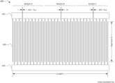
- the multi-mark IDT 400is divided into three sections, identified as Section A, Section B, and Section C, along the length L of the IDT. Each of Sections A, B, and C includes 20 fingers, for a total of 60 fingers in the multi-mark IDT 400 .
- the use of three sections and 60 fingersis exemplary.
- An IDTmay have more than or fewer than 60 total fingers.
- An IDTmay be divided along its length into two or more sections, each of which includes a plurality of adjacent fingers.
- the total number of fingersmay be divided essentially equally between the two or more sections.
- “essentially”means “as close as possible.”
- an IDT with 100 fingers divided into three sections with 33, 34, and 33 fingersis considered to be divided essentially equally.
- the total number of fingersmay be divided unequally between the two or more sections.
- the fingers in Section Bhave mark m, which is the nominal mark of the IDT.
- the finger of Section Ahave a mark of m(1 ⁇ m ), and the fingers of Section C have a mark of m(1+ ⁇ m ).
- ⁇ mis greater than 0 and less than or equal to 0.05.
- ⁇ mmay typically be less than 0.01.
- ⁇ mmay be selected during a filter design to achieve the most effective reduction of spurious modes.
- the markis constant across the aperture A.
- the pitch of the IDT fingersis constant and the same in all sections. When an IDT is divided into two sections or more than three sections, the maximum mark may be m(1+ ⁇ m ) and the minimum mark may be m(1 ⁇ m ).
- the markincreases monotonically from left (as seen in the figure) to right. This is not necessarily the case in all multi-mark IDTs.
- the sections of a multi-mark IDTmay be arranged in some other order.
- the change in mark between adjacent sectionsis constant. This is also not necessarily the case in all multi-mark IDTs.
- the change in mark between adjacent sectionsmay be the same or different.
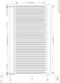
- FIG. 5is a plan view of another multi-mark IDT 500 with continuously varying mark.
- the IDT 500includes a first busbar 532 , and second busbar 534 , and a plurality of interleaved fingers such as finger 536 .
- the interleaved fingersextend alternately from the first and second busbars 532 , 534 .
- the IDT 500is not divided into sections, but rather has a continuous change in mark for the fingers 536 along its length L.
- the IDT 500has 60 fingers, which is exemplary. An IDT may have more than or fewer than 60 total fingers.
- the multi-mark IDT 500may be a portion of an XBAR such as the XBAR 100 of FIG. 1 .
- the mark at the left edge of the IDT 500is m(1 ⁇ m ), and the mark at the right edge of the IDT 500 is m(1+ ⁇ m ).
- the markvaries continuously between these two extremes.
- the variation in markmay typically, but not necessarily, be a linear function of position along the length L of the IDT.
- ⁇ mis greater than 0, less than or equal to 0.05, and typically less than 0.01.
- ⁇ mmay be selected during a filter design to achieve the most effective reduction of spurious modes.
- the markis constant across the aperture A.
- the pitch of the IDT fingersis constant over the entire IDT.
- FIG. 6is a graph 600 of mark as a function of position along the length of the IDT for a conventional IDT and another exemplary multi-mark IDT.
- Dashed line 610shows mark as a function of position along the length of the IDT for a conventional IDT where mark is not chirped.
- Solid line 620shows mark as a function of position along the length of the IDT for a multi-mark IDT with chirped mark.
- a linear gradientis applied to the mark of the multi-mark IDT, such that the chirp has a triangular profile.
- There is a difference of 0.5 nm in the mark of each sequential fingersuch that a mark of a widest finger is 20 nm more than a width of the narrowest finger.
- Dot dashed line 630shows mark as a function of position along the length of the IDT for another multi-mark IDT with chirped mark where a linear gradient is applied to the mark of the multi-mark IDT.
- Other exemplary IDTscan have other differences in the mark between sequential fingers, e.g., differences in a range from 0.1 nm to 0.9 nm, and a difference between the widest finger and the narrowest finger can be other values, e.g., in a range from 1 nm to 100 nm.
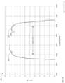
- FIG. 7is a graph 700 of the magnitude of S2,1, the input/output transfer function, for two bandpass filters implemented with XBAR devices.
- the S2,1 datawas determined by simulation of the two filters using a finite element method.
- the dashed curve 710is a plot of S2,1 for a first filter using XBARs with conventional IDTs.
- the solid curve 720is a plot of S2,1 for a second bandpass filter that has multi-mark IDTs but is otherwise identical the first bandpass filter. Comparison of the curves 710 and 720 shows the passbands of the two filters are very similar. Compared to the first filter, the second filter with multi-mark IDTs exhibits reduced peak admittance of spurious modes.
- FIG. 8is an expanded view of a portion of the graph of FIG. 7 .
- the dashed curve 810is a plot of the S21 versus frequency for the filter with the conventional IDTs.
- the solid curve 820is a plot of the of the S21 versus frequency of the filter with the multi-mark IDTs.
- the filter with multi-mark IDTshas reduced spurious modes within the Band N79 passband as compared to the filter with conventional IDTs, which can result in less loss.
- the chirped mark of the multi-mark IDThas a negligible effect on the resonance and anti-resonance frequencies of the shear primary acoustic mode of the XBAR.
- the filters used to generate the data shown in FIGS. 7 and 8include 4 series resonators and 4 shunt resonators in a ladder filter circuit. All resonators are XBARs. These filters are exemplary.
- a filtermay have less or more resonators, and more or less series resonators and shunt resonators.
- Multi-mark IDTsmay be divided into two sections or more than three sections, or may be continuous. The number of sections may not be the same for all resonators in a filter, and a filter may include both sectioned and continuous multi-mark IDTs. The value of ⁇ m may be different for some or all of the resonators.
- a filtermay contain a combination of resonators with uniform mark and multi-mark resonators.
- FIG. 9is a plan view of an exemplary multi-pitch multi-mark IDT 900 .
- a “multi-pitch IDT”is an IDT where the pitch of the IDT fingers varies along the length of the IDT. At any given point along the length, the pitch may not vary across the aperture of the IDT. Further, the mark can also vary along the length of the IDT, as described above, such that the IDT is a multi-mark multi-pitch IDT.
- the multi-pitch multi-mark IDT 900may be a portion of an XBAR such as the XBAR 100 of FIG. 1 .
- the multi-pitch multi-mark IDT 900includes a first busbar 932 , and a second busbar 934 , and a plurality of interleaved fingers such as finger 936 .
- the interleaved fingersextend alternately from the first and second busbars 932 , 934 .
- the multi-pitch multi-mark IDT 900can be divided into three sections, identified as Section A, Section B, and Section C, along the length L of the IDT.
- Each of Sections A, B, and Cincludes 20 fingers, for a total of 60 fingers in the multi-pitch multi-mark IDT 900 .
- the use of three sections and 60 fingersis exemplary.
- An IDTmay have more than or fewer than 60 total fingers.
- An IDTmay be divided along its length into two or more sections, each of which includes a plurality of adjacent fingers.
- the total number of fingersmay be divided essentially equally between the two or more sections.
- “essentially”means “as close as possible.”
- an IDT with 100 fingers divided into three sections with 33, 34, and 33 fingersis considered to be divided essentially equally.
- the total number of fingersmay be divided unequally between the two or more sections.
- the divisionscan be the same or different from the divisions for the chirping of the mark.
- the fingers in Section Bhave pitch p, which is the nominal pitch of the IDT.
- the finger of Section Ahave a pitch of p(1 ⁇ p ), and the fingers of Section C have a pitch of p(1+ ⁇ p ).
- ⁇ pis greater than 0 and less than or equal to 0.05.
- ⁇ pmay typically be less than 0.01.
- ⁇ pmay be selected during a filter design to achieve the most effective reduction of spurious modes.
- the pitchis constant across the aperture A.
- the mark of the IDT fingersalso varies by sections, similar to the variation by section of IDT 400 shown in FIG. 4 .
- the markcan vary by the same section as the pitch or by different sections of the pitch. Alternatively, the mark can vary continuously, similar to the continuous variation of mark shown in FIG. 5 .
- FIG. 10is a plan view of another exemplary multi-pitch multi-mark IDT 1000 .
- the multi-pitch multi-mark IDT 900may be a portion of an XBAR such as the XBAR 100 of FIG. 1 .
- the multi-pitch multi-mark IDT 1000includes a first busbar 1032 , and a second busbar 1034 , and a plurality of interleaved fingers such as finger 1036 .
- the interleaved fingersextend alternately from the first and second busbars 1032 , 1034 .
- the markvaries continuously, similar to the continuous variation of mark shown in FIG. 5 .
- the pitchalso varies continuously, similar to the mark. As shown in FIG. 10 , the mark and pitch both increase continuously from left to right, as oriented in the figure. Alternatively, the either the mark or pitch could increase continuously from left to right, while the other of mark or pitch decreases continuously from left to right.
- the pitch of the IDTcan vary continuously, similar to the continuous variation of mark shown in FIG. 5 .
- the pitchmay vary as the mark varies, or may vary at a different rate.
- the pitch and markmay both vary continuously.
- the pitch and/or the markmay vary between multiple maxima and minima along the length of the IDT.
- the markmay vary by section while the pitch varies continuously, or pitch may vary by section while the mark varies continuously.
- the markmay increase in one direction along the length of the IDT (either continuously or by section), while the pitch decreases in the same direction (either continuously or by section).
- Variation of mark and pitchcan be optimized with respect to one another, and variation of mark and pitch can be different from one resonator to another, such that greatest suppression of spurious modes is achieved for best performance of the filter.
- “plurality”means two or more. As used herein, a “set” of items may include one or more of such items.
- the terms “comprising”, “including”, “carrying”, “having”, “containing”, “involving”, and the likeare to be understood to be open-ended, i.e., to mean including but not limited to. Only the transitional phrases “consisting of” and “consisting essentially of”, respectively, are closed or semi-closed transitional phrases with respect to claims.
Landscapes
- Physics & Mathematics (AREA)
- Acoustics & Sound (AREA)
- Chemical & Material Sciences (AREA)
- Crystallography & Structural Chemistry (AREA)
- Surface Acoustic Wave Elements And Circuit Networks Thereof (AREA)
- Piezo-Electric Or Mechanical Vibrators, Or Delay Or Filter Circuits (AREA)
- Micromachines (AREA)
Abstract
Description
Claims (7)
Priority Applications (17)
| Application Number | Priority Date | Filing Date | Title |
|---|---|---|---|
| US17/388,745US12088281B2 (en) | 2021-02-03 | 2021-07-29 | Transversely-excited film bulk acoustic resonator with multi-mark interdigital transducer |
| US17/560,889US12237826B2 (en) | 2018-06-15 | 2021-12-23 | Transversely-excited film bulk acoustic resonator with optimized electrode thickness, mark, and pitch |
| US17/561,714US11929731B2 (en) | 2018-02-18 | 2021-12-24 | Transversely-excited film bulk acoustic resonator with optimized electrode mark, and pitch |
| US17/563,384US12021502B2 (en) | 2018-06-15 | 2021-12-28 | Transversely-excited film bulk acoustic resonator with multi-mark electrodes and optimized electrode thickness |
| US17/563,360US11824520B2 (en) | 2018-06-15 | 2021-12-28 | Transversely-excited film bulk acoustic resonator with optimized electrode thickness, mark, and pitch |
| US17/565,720US20220131525A1 (en) | 2018-06-15 | 2021-12-30 | Transversely-excited film bulk acoustic resonator with optimized piezoelectric plate thickness |
| US17/565,762US12021503B2 (en) | 2018-06-15 | 2021-12-30 | Transversely-excited film bulk acoustic resonator with optimized piezoelectric plate thickness and having multiple pitches and marks |
| US17/565,695US20220123723A1 (en) | 2018-06-15 | 2021-12-30 | Transversely-excited film bulk acoustic resonator with optimized piezoelectric plate thickness and electrode mark and pitch |
| US17/584,396US12021504B2 (en) | 2018-06-15 | 2022-01-26 | Transversely-excited film bulk acoustic resonator with a front-side dielectric layer and optimized pitch and mark |
| DE102022102263.3ADE102022102263A1 (en) | 2021-02-03 | 2022-02-01 | TRANSVERSAL EXCITED FILM VOLUME ACOUSTIC RESONATOR WITH MULTI-BRAND INTERDIGITAL CONVERTER |
| JP2022014153AJP7476912B2 (en) | 2021-02-03 | 2022-02-01 | Acoustic resonator and filter device |
| CN202210120097.4ACN114866061A (en) | 2021-02-03 | 2022-02-07 | Transverse excitation film bulk acoustic resonator with multi-mark interdigital transducer |
| US17/696,105US11942922B2 (en) | 2018-06-15 | 2022-03-16 | Transversely-excited film bulk acoustic resonator with optimized electrode thickness, mark, and pitch |
| US17/950,019US20230019694A1 (en) | 2021-02-03 | 2022-09-21 | Transversely-excited film bulk acoustic resonator with multi-mark, multi-pitch interdigital transducer |
| US18/478,406US12095446B2 (en) | 2018-06-15 | 2023-09-29 | Transversely-excited film bulk acoustic resonator with optimized electrode thickness, mark, and pitch |
| JP2024067671AJP2024129000A (en) | 2021-02-03 | 2024-04-18 | Acoustic resonator and filter device |
| US19/030,388US20250247073A1 (en) | 2018-06-15 | 2025-01-17 | Transversely-excited film bulk acoustic resonator with optimized piezoelectric plate thickness |
Applications Claiming Priority (2)
| Application Number | Priority Date | Filing Date | Title |
|---|---|---|---|
| US202163144977P | 2021-02-03 | 2021-02-03 | |
| US17/388,745US12088281B2 (en) | 2021-02-03 | 2021-07-29 | Transversely-excited film bulk acoustic resonator with multi-mark interdigital transducer |
Related Parent Applications (2)
| Application Number | Title | Priority Date | Filing Date |
|---|---|---|---|
| US17/122,977Continuation-In-PartUS11509279B2 (en) | 2018-02-18 | 2020-12-15 | Acoustic resonators and filters with reduced temperature coefficient of frequency |
| US17/351,204Continuation-In-PartUS11929727B2 (en) | 2018-02-18 | 2021-06-17 | Transversely-excited film bulk acoustic resonator with reduced spurious modes |
Related Child Applications (4)
| Application Number | Title | Priority Date | Filing Date |
|---|---|---|---|
| US16/805,471Continuation-In-PartUS11206009B2 (en) | 2018-02-18 | 2020-02-28 | Transversely-excited film bulk acoustic resonator with interdigital transducer with varied mark and pitch |
| US17/460,737Continuation-In-PartUS12009804B2 (en) | 2018-02-18 | 2021-08-30 | Transversely-excited film bulk acoustic resonator with interdigital transducer with varied mark and pitch |
| US17/560,889Continuation-In-PartUS12237826B2 (en) | 2018-02-18 | 2021-12-23 | Transversely-excited film bulk acoustic resonator with optimized electrode thickness, mark, and pitch |
| US17/950,019ContinuationUS20230019694A1 (en) | 2021-02-03 | 2022-09-21 | Transversely-excited film bulk acoustic resonator with multi-mark, multi-pitch interdigital transducer |
Publications (2)
| Publication Number | Publication Date |
|---|---|
| US20220247384A1 US20220247384A1 (en) | 2022-08-04 |
| US12088281B2true US12088281B2 (en) | 2024-09-10 |
Family
ID=82402843
Family Applications (2)
| Application Number | Title | Priority Date | Filing Date |
|---|---|---|---|
| US17/388,745Active2043-01-04US12088281B2 (en) | 2018-02-18 | 2021-07-29 | Transversely-excited film bulk acoustic resonator with multi-mark interdigital transducer |
| US17/950,019PendingUS20230019694A1 (en) | 2021-02-03 | 2022-09-21 | Transversely-excited film bulk acoustic resonator with multi-mark, multi-pitch interdigital transducer |
Family Applications After (1)
| Application Number | Title | Priority Date | Filing Date |
|---|---|---|---|
| US17/950,019PendingUS20230019694A1 (en) | 2021-02-03 | 2022-09-21 | Transversely-excited film bulk acoustic resonator with multi-mark, multi-pitch interdigital transducer |
Country Status (4)
| Country | Link |
|---|---|
| US (2) | US12088281B2 (en) |
| JP (2) | JP7476912B2 (en) |
| CN (1) | CN114866061A (en) |
| DE (1) | DE102022102263A1 (en) |
Cited By (1)
| Publication number | Priority date | Publication date | Assignee | Title |
|---|---|---|---|---|
| US20210273629A1 (en)* | 2020-02-28 | 2021-09-02 | Resonant Inc. | Transversely-excited film bulk acoustic resonator with multi-pitch interdigital transducer |
Families Citing this family (1)
| Publication number | Priority date | Publication date | Assignee | Title |
|---|---|---|---|---|
| WO2024257838A1 (en)* | 2023-06-13 | 2024-12-19 | 株式会社村田製作所 | Elastic wave device and elastic wave filter device |
Citations (195)
| Publication number | Priority date | Publication date | Assignee | Title |
|---|---|---|---|---|
| US5446330A (en) | 1993-03-15 | 1995-08-29 | Matsushita Electric Industrial Co., Ltd. | Surface acoustic wave device having a lamination structure |
| US5552655A (en) | 1994-05-04 | 1996-09-03 | Trw Inc. | Low frequency mechanical resonator |
| US5631515A (en) | 1994-03-17 | 1997-05-20 | Fujitsu Limited | Surface acoustic wave device |
| US5726610A (en) | 1995-06-19 | 1998-03-10 | Motorola Inc. | Saw filter device for radio tranceiver utilizing different coupling coefficient ratios |
| JPH10209804A (en) | 1997-01-27 | 1998-08-07 | Oki Electric Ind Co Ltd | Surface acoustic wave resonator and surface acoustic wave filter |
| US5853601A (en) | 1997-04-03 | 1998-12-29 | Northrop Grumman Corporation | Top-via etch technique for forming dielectric membranes |
| JP2001244785A (en) | 2000-02-29 | 2001-09-07 | Kyocera Corp | Surface acoustic wave device |
| US6377140B1 (en) | 1999-07-09 | 2002-04-23 | Oki Electric Industry Co., Ltd. | Saw resonator filter with bridged-T configuration |
| US20020079986A1 (en) | 2000-12-21 | 2002-06-27 | Ruby Richard C. | Bulk acoustic resonator perimeter reflection system |
| JP2002300003A (en) | 2001-03-29 | 2002-10-11 | Kyocera Corp | Elastic wave filter |
| US20020158714A1 (en) | 2001-04-27 | 2002-10-31 | Nokia Corporation | Method and system for wafer-level tuning of bulk acoustic wave resonators and filters by reducing thickness non-uniformity |
| US20020189062A1 (en) | 2001-06-15 | 2002-12-19 | Asia Pacific Microsystems, Inc. | Manufacturing method for a high quality film bulk acoustic wave device |
| US6516503B1 (en) | 1999-05-26 | 2003-02-11 | Murata Manufacturing Co., Ltd. | Method of making surface acoustic wave device |
| JP2003078389A (en) | 2001-08-31 | 2003-03-14 | Matsushita Electric Ind Co Ltd | Surface acoustic wave device and method of manufacturing the same |
| US6540827B1 (en) | 1998-02-17 | 2003-04-01 | Trustees Of Columbia University In The City Of New York | Slicing of single-crystal films using ion implantation |
| US20030080831A1 (en) | 2001-10-25 | 2003-05-01 | Naumenko Natalya F. | Surface acoustic wave devices using optimized cuts of lithium niobate (LiNbO3) |
| US6570470B2 (en) | 2000-06-30 | 2003-05-27 | Kyocera Corporation | Surface acoustic wave ladder filter utilizing parallel resonators with different resonant frequencies |
| US20030199105A1 (en) | 2002-04-22 | 2003-10-23 | Kub Francis J. | Method for making piezoelectric resonator and surface acoustic wave device using hydrogen implant layer splitting |
| US6670866B2 (en) | 2002-01-09 | 2003-12-30 | Nokia Corporation | Bulk acoustic wave resonator with two piezoelectric layers as balun in filters and duplexers |
| US20040041496A1 (en) | 2002-09-04 | 2004-03-04 | Fujitsu Media Devices Limited | Surface acoustic wave device, filter device and method of producing the surface acoustic wave device |
| US6707229B1 (en) | 1999-06-03 | 2004-03-16 | Tele Filter Zweigniederlassung Der Dover Germany Gmbh | Surface acoustic wave filter |
| JP2004129222A (en) | 2002-07-31 | 2004-04-22 | Murata Mfg Co Ltd | Piezoelectric component and method of manufacturing the same |
| US20040100164A1 (en) | 2002-11-26 | 2004-05-27 | Murata Manufacturing Co., Ltd. | Manufacturing method of electronic device |
| US20040207485A1 (en) | 2003-03-31 | 2004-10-21 | Osamu Kawachi | Surface acoustic wave device and method of fabricating the same |
| US20040261250A1 (en) | 2000-09-06 | 2004-12-30 | Murata Manufacturing Co., Ltd. | Method for adjusting a frequency characteristic of an edge reflection type surface acoustic wave device and method for producing an- edge reflection type surface acoustic wave device |
| US20050099091A1 (en) | 2003-11-12 | 2005-05-12 | Fujitsu Media Devices Limited | Elastic boundary wave device and method of manufacturing the same |
| US20050185026A1 (en) | 2004-01-26 | 2005-08-25 | Motohisa Noguchi | Piezoelectric element, piezoelectric actuator, ink jet recording head, ink jet printer, surface acoustic wave element, frequency filter, oscillator, electronic circuit, thin film piezoelectric resonator, and electronic apparatus |
| US20050218488A1 (en) | 2004-03-31 | 2005-10-06 | Mie Matsuo | Electronic component having micro-electrical mechanical system |
| US20050264136A1 (en) | 2004-05-31 | 2005-12-01 | Jun Tsutsumi | Surface acoustic wave device |
| US7042132B2 (en) | 2001-03-13 | 2006-05-09 | Epcos Ag | Transducer structure that operates with acoustic waves |
| US20060131731A1 (en) | 2004-11-22 | 2006-06-22 | Takao Sato | Midair semiconductor device and manufacturing method of the same |
| US20060152107A1 (en) | 2005-01-07 | 2006-07-13 | Seiko Epson Corporation | Lamb-wave high-frequency resonator |
| US20060179642A1 (en) | 2005-02-03 | 2006-08-17 | Kabushiki Kaisha Toshiba | Method for manufacturing a film bulk acoustic resonator |
| US20070090898A1 (en) | 2003-12-16 | 2007-04-26 | Murata Manufacturing Co., Ltd. | Boundary acoustic wave device |
| US20070115079A1 (en) | 2004-07-20 | 2007-05-24 | Murata Manufacturing Co., Ltd. | Piezoelectric filter |
| US20070182510A1 (en) | 2006-02-06 | 2007-08-09 | Samsung Electronics Co., Ltd. | Multi-band filter module and method of fabricating the same |
| US20070188047A1 (en) | 2006-02-16 | 2007-08-16 | Seiko Epson Corporation | Lamb wave type frequency device and method thereof |
| US20070194863A1 (en) | 2006-02-17 | 2007-08-23 | Kabushiki Kaisha Toshiba | Film bulk acoustic resonator and method of manufacturing same |
| US20070267942A1 (en) | 2006-05-19 | 2007-11-22 | Hisanori Matsumoto | Piezoelectric film resonator, radio-frequency filter using them, and radio-frequency module using them |
| US20070278898A1 (en) | 2006-06-06 | 2007-12-06 | Fujitsu Media Devices Limited | Acoustic boundary wave device, resonator and filter |
| US20070296304A1 (en) | 2006-06-22 | 2007-12-27 | Seiko Epson Corporation | Acoustic wave device and method of manufacturing acoustic wave device |
| US20080018414A1 (en) | 2006-07-24 | 2008-01-24 | Fujitsu Media Devices Limited | Elastic wave device and manufacturing method of the same |
| US7345400B2 (en) | 2003-01-27 | 2008-03-18 | Murata Manufacturing Co., Ltd. | Surface acoustic wave device |
| US20080246559A1 (en) | 2007-01-19 | 2008-10-09 | Farrokh Ayazi | Lithographically-defined multi-standard multi-frequency high-Q tunable micromechanical resonators |
| US20080297280A1 (en) | 2007-05-31 | 2008-12-04 | Robert Thalhammer | Integrated Coupled Resonator Filter and Bulk Acoustic Wave Devices |
| US7463118B2 (en) | 2006-06-09 | 2008-12-09 | Texas Instruments Incorporated | Piezoelectric resonator with an efficient all-dielectric Bragg reflector |
| US7535152B2 (en) | 2005-10-19 | 2009-05-19 | Murata Manufacturing Co., Ltd. | Lamb wave device |
| US7554427B2 (en) | 2007-01-15 | 2009-06-30 | Hitachi Media Electronics Co., Ltd. | Thin film bulk acoustic wave resonator and filter, and radio frequency module using them |
| US20090273415A1 (en) | 2008-04-30 | 2009-11-05 | Avago Technologies Wireless Ip (Singapore) Pte. Ltd. | Bulk acoustic resonator electrical impedance transformers |
| US20090315640A1 (en) | 2008-06-24 | 2009-12-24 | Murata Manufacturing Co., Ltd. | Duplexer |
| JP2010062816A (en) | 2008-09-03 | 2010-03-18 | Murata Mfg Co Ltd | Acoustic wave filter |
| US7684109B2 (en) | 2007-02-28 | 2010-03-23 | Maxim Integrated Products, Inc. | Bragg mirror optimized for shear waves |
| US20100123367A1 (en) | 2008-11-19 | 2010-05-20 | Ngk Insulators, Ltd. | Lamb wave device |
| US20100223999A1 (en) | 2009-03-03 | 2010-09-09 | Nihon Dempa Kogyo Co., Ltd. | Elastic wave device and electronic component |
| US20100301703A1 (en) | 2009-03-31 | 2010-12-02 | Sand9, Inc. | Integration of piezoelectric materials with substrates |
| US7868519B2 (en) | 2007-09-06 | 2011-01-11 | Murata Manufacturing Co., Ltd. | Piezoelectric resonator including an acoustic reflector portion |
| US20110018389A1 (en) | 2008-01-30 | 2011-01-27 | Kyocera Corporation | Acoustic Wave Device and Method for Production of Same |
| US20110018654A1 (en) | 2009-07-27 | 2011-01-27 | Avago Technologies Wireless Ip (Singapore) Pte. Ltd. | Resonator filter with multiple cross-couplings |
| US20110102107A1 (en) | 2008-02-05 | 2011-05-05 | Nihon Dempa Kogyo Co., Ltd. | Filter, portable terminal and electronic component |
| US7941103B2 (en) | 2005-11-15 | 2011-05-10 | Taiyo Yuden Co., Ltd. | Duplexer |
| US7939987B1 (en) | 2008-10-23 | 2011-05-10 | Triquint Semiconductor, Inc. | Acoustic wave device employing reflective elements for confining elastic energy |
| US20110109196A1 (en) | 2008-07-11 | 2011-05-12 | Goto Rei | Plate wave element and electronic equipment using same |
| US20110199163A1 (en)* | 2008-10-24 | 2011-08-18 | Epson Toyocom Corporation | Surface acoustic wave resonator, surface acoustic wave oscillator, and surface acoustic wave module unit |
| US20110278993A1 (en) | 2010-05-17 | 2011-11-17 | Murata Manufacturing Co., Ltd. | Method for manufacturing composite piezoelectric substrate and piezoelectric device |
| US8278802B1 (en) | 2008-04-24 | 2012-10-02 | Rf Micro Devices, Inc. | Planarized sacrificial layer for MEMS fabrication |
| US8294330B1 (en) | 2009-03-31 | 2012-10-23 | Triquint Semiconductor, Inc. | High coupling, low loss saw filter and associated method |
| US20120286900A1 (en) | 2010-01-28 | 2012-11-15 | Murata Manufacturing Co., Ltd. | Tunable filter |
| US20130057360A1 (en) | 2010-04-23 | 2013-03-07 | Teknologian Tutkimuskeskus Vtt | Wide-band acoustically coupled thin-film baw filter |
| US20130207747A1 (en) | 2010-12-28 | 2013-08-15 | Kyocera Corporation | Acoustic wave element and acoustic wave device using same |
| US20130234805A1 (en) | 2012-03-07 | 2013-09-12 | Taiyo Yuden Co., Ltd. | Resonator, frequency filter, duplexer, electronic device, and method of manufacturing resonator |
| US20130271238A1 (en) | 2012-04-13 | 2013-10-17 | Taiyo Yuden Co., Ltd. | Filter device, manufacturing method for filter device, and duplexer |
| US20130278609A1 (en) | 2012-04-19 | 2013-10-24 | Qualcomm Mems Technologies, Inc. | Isotropically-etched cavities for evanescent-mode electromagnetic-wave cavity resonators |
| US20130321100A1 (en) | 2012-06-05 | 2013-12-05 | Avago Technologies Wireless Ip (Singapore) Pte. Ltd. | Laterally-coupled acoustic resonators |
| US20140009032A1 (en) | 2012-07-04 | 2014-01-09 | Taiyo Yuden Co., Ltd. | Lamb wave device and manufacturing method thereof |
| US20140009247A1 (en) | 2012-07-03 | 2014-01-09 | Taiyo Yuden Co., Ltd. | Duplexer |
| US20140113571A1 (en) | 2012-10-18 | 2014-04-24 | Panasonic Corporation | Electronic device including filter |
| US20140130319A1 (en) | 2010-09-28 | 2014-05-15 | Murata Manufacturing Co., Ltd. | Method for manufacturing piezoelectric device |
| US20140145556A1 (en) | 2011-08-08 | 2014-05-29 | Murata Manufacturing Co., Ltd. | Elastic wave device |
| US20140151151A1 (en) | 2010-10-15 | 2014-06-05 | Commissariat A L'energie Atomique Et Aux Energies Alternatives | Heterogenous acoustic structure formed from a homogeneous material |
| US20140152145A1 (en) | 2010-11-30 | 2014-06-05 | Murata Manufacturing Co., Ltd. | Elastic wave device and manufacturing method for same |
| US20140173862A1 (en) | 2007-12-25 | 2014-06-26 | Murata Manufacturing Co., Ltd. | Method for manufacturing composite piezoelectric substrate |
| US8816567B2 (en) | 2011-07-19 | 2014-08-26 | Qualcomm Mems Technologies, Inc. | Piezoelectric laterally vibrating resonator structure geometries for spurious frequency suppression |
| US8829766B2 (en) | 2008-08-01 | 2014-09-09 | Epcos Ag | Piezoelectric resonator operating in thickness shear mode |
| US20140312994A1 (en) | 2011-11-11 | 2014-10-23 | Teknologian tutkimuskeskut VTT | Laterally coupled bulk acoustic wave filter with improved passband characteristics |
| US8932686B2 (en) | 2008-10-31 | 2015-01-13 | Murata Manufacturing Co., Ltd. | Method for producing piezoelectric composite substrate |
| US20150042417A1 (en) | 2013-08-06 | 2015-02-12 | Murata Manufacturing Co., Ltd. | High-frequency module |
| JP2015054986A (en) | 2013-09-11 | 2015-03-23 | 太陽誘電株式会社 | Aluminum nitride film forming method, acoustic wave device manufacturing method, and aluminum nitride film manufacturing apparatus |
| WO2015098694A1 (en) | 2013-12-26 | 2015-07-02 | 株式会社村田製作所 | Elastic wave device, and production method therefor |
| US20150244149A1 (en) | 2012-05-30 | 2015-08-27 | Euphoenix B.V. | Tunable Semiconductor Device And Method For Making Tunable Semiconductor Device |
| US9130145B2 (en) | 2012-03-29 | 2015-09-08 | Vectron International Gmbh | Surface acoustic wave component |
| US9154111B2 (en) | 2011-05-20 | 2015-10-06 | Avago Technologies General Ip (Singapore) Pte. Ltd. | Double bulk acoustic resonator comprising aluminum scandium nitride |
| US20150319537A1 (en) | 2012-12-12 | 2015-11-05 | Epcos Ag | Electroacoustic Components and Methods Thereof |
| JP2016001923A (en) | 2013-02-27 | 2016-01-07 | 京セラ株式会社 | Elastic wave device, duplexer and communication module |
| US9240768B2 (en) | 2011-11-22 | 2016-01-19 | Taiyo Yuden Co., Ltd. | Duplexer with transmission and reception filters each including resonators formed on different chips |
| US20160028367A1 (en) | 2014-07-25 | 2016-01-28 | Akoustis, Inc. | Single crystal acoustic resonator and bulk acoustic wave filter |
| WO2016017104A1 (en) | 2014-07-31 | 2016-02-04 | Skyworks Panasonic Filter Solutions Japan Co., Ltd. | Acoustic wave filters and duplexers using same |
| US9276557B1 (en) | 2013-07-01 | 2016-03-01 | Sandia Corporation | Programmable electroacoustic filter apparatus and method for its manufacture |
| US20160079958A1 (en) | 2014-05-30 | 2016-03-17 | Avago Technologies General Ip (Singapore) Pte. Ltd. | Acoustic resonator comprising vertically extended acoustic cavity |
| WO2016052129A1 (en) | 2014-09-30 | 2016-04-07 | 株式会社村田製作所 | Acoustic wave device and method for manufacturing same |
| US9369105B1 (en) | 2007-08-31 | 2016-06-14 | Rf Micro Devices, Inc. | Method for manufacturing a vibrating MEMS circuit |
| US20160182009A1 (en) | 2014-12-17 | 2016-06-23 | Rf Micro Devices, Inc. | Plate wave devices with wave confinement structures and fabrication methods |
| US9425765B2 (en) | 2013-04-22 | 2016-08-23 | Northeastern University | Nano- and micro-electromechanical resonators |
| WO2016147687A1 (en) | 2015-03-13 | 2016-09-22 | 株式会社村田製作所 | Elastic wave device and production method for same |
| US20160301382A1 (en) | 2013-12-25 | 2016-10-13 | Murata Manufacturing Co., Ltd. | Electronic component module |
| US9525398B1 (en) | 2014-05-27 | 2016-12-20 | Sandia Corporation | Single crystal micromechanical resonator and fabrication methods thereof |
| US20170063332A1 (en) | 2015-08-25 | 2017-03-02 | Avago Technologies General Ip (Singapore) Pte. Ltd. | Surface acoustic wave (saw) resonator having trap-rich region |
| US20170104470A1 (en) | 2015-10-09 | 2017-04-13 | Avago Technologies General Ip (Singapore) Pte. Ltd. | Interdigitated transducers and reflectors for surface acoustic wave devices with non-uniformly spaced elements |
| US9640750B2 (en) | 2011-03-25 | 2017-05-02 | Skyworks Filter Solutions Japan Co., Ltd. | Acoustic wave device with suppressed higher order transverse modes |
| CN106788318A (en) | 2016-11-22 | 2017-05-31 | 山东科技大学 | A kind of method for manufacturing FBAR on a flexible substrate |
| US20170179225A1 (en) | 2011-05-25 | 2017-06-22 | Semiconductor Components Industries, Llc | Semiconductor device having a super junction structure and method of manufacturing the same |
| US20170179928A1 (en) | 2015-11-13 | 2017-06-22 | Resonant Inc. | Acoustic wave filter with enhanced rejection |
| US20170201232A1 (en) | 2016-01-07 | 2017-07-13 | Taiyo Yuden Co., Ltd. | Acoustic wave device and method of fabricating the same |
| US20170214381A1 (en) | 2016-01-22 | 2017-07-27 | Rf Micro Devices, Inc. | Guided wave devices with selectively thinned piezoelectric layers |
| US20170214387A1 (en) | 2016-01-26 | 2017-07-27 | Avago Technologies General Ip (Singapore) Pte. Ltd. | Bulk acoustic wave resonator with piezoelectric layer comprising lithium niobate or lithium tantalate |
| US20170222622A1 (en) | 2016-01-28 | 2017-08-03 | Triquint Semiconductor, Inc. | Surface acoustic wave device having a piezoelectric layer on a quartz substrate and methods of manufacturing thereof |
| US20170222617A1 (en) | 2014-10-16 | 2017-08-03 | Murata Manufacturing Co., Ltd. | High-frequency module |
| US9762202B2 (en) | 2008-12-17 | 2017-09-12 | Analog Devices, Inc. | Method of manufacturing a mechanical resonating structure |
| US20170264266A1 (en) | 2014-12-25 | 2017-09-14 | Murata Manufacturing Co., Ltd. | Acoustic wave device and manufacturing method for same |
| US9780759B2 (en) | 2010-12-24 | 2017-10-03 | Murata Manufacturing Co., Ltd. | Elastic wave device and method for manufacturing the same |
| US20170290160A1 (en) | 2016-04-01 | 2017-10-05 | Skyworks Filter Solutions Japan Co., Ltd. | Electronic package including cavity defined by resin and method of forming same |
| WO2017188342A1 (en) | 2016-04-27 | 2017-11-02 | 京セラ株式会社 | Elastic wave element and communication device |
| US9837984B2 (en) | 2014-12-24 | 2017-12-05 | Qorvo Us, Inc. | RF ladder filter with simplified acoustic RF resonator parallel capacitance compensation |
| US20170370791A1 (en) | 2016-06-28 | 2017-12-28 | Taiyo Yuden Co., Ltd. | Method of fabricating acoustic wave device and acoustic wave device |
| WO2018003273A1 (en) | 2016-06-28 | 2018-01-04 | 株式会社村田製作所 | Multiplexer, high-frequency front end circuit, and communication device |
| US20180005950A1 (en) | 2016-06-29 | 2018-01-04 | Murata Manufacturing Co., Ltd. | Electronic component device, method of mounting electronic component device on circuit board, and mounting structure of electronic component device on circuit board |
| WO2018003268A1 (en) | 2016-06-28 | 2018-01-04 | 株式会社村田製作所 | Elastic wave filter device, multiplexer, high-frequency front end circuit, and communication device |
| US20180013405A1 (en) | 2015-04-30 | 2018-01-11 | Murata Manufacturing Co., Ltd. | Ladder filter and duplexer |
| US20180013400A1 (en) | 2016-07-05 | 2018-01-11 | Taiyo Yuden Co., Ltd. | Acoustic wave device |
| US20180026603A1 (en) | 2015-05-22 | 2018-01-25 | Murata Manufacturing Co., Ltd. | Electronic component |
| US20180033952A1 (en) | 2016-07-28 | 2018-02-01 | Taiyo Yuden Co., Ltd. | Electronic device and method of fabricating the same |
| US20180062615A1 (en) | 2015-05-08 | 2018-03-01 | Murata Manufacturing Co., Ltd. | High frequency module |
| US20180062617A1 (en) | 2016-08-25 | 2018-03-01 | Qualcomm Incorporated | Single-chip multi-frequency film bulk acoustic-wave resonators |
| US20180123016A1 (en) | 2012-06-15 | 2018-05-03 | Carnegie Mellon University | Microelectronic structures with suspended lithium-based thin films |
| JP2018093487A (en) | 2016-11-30 | 2018-06-14 | スカイワークス ソリューションズ, インコーポレイテッドSkyworks Solutions, Inc. | Saw filter that comprises piezoelectric substrate having stepwise cross section |
| US20180191322A1 (en) | 2017-01-03 | 2018-07-05 | Win Semiconductors Corp. | Method for fabricating bulk acoustic wave resonator with mass adjustment structure |
| US20180212589A1 (en) | 2010-10-14 | 2018-07-26 | Teknologian Tutkimuskeskus Vtt Oy | Wide-band acoustically coupled thin-film baw filter |
| WO2018163860A1 (en) | 2017-03-06 | 2018-09-13 | 株式会社村田製作所 | Elastic wave device, high-frequency front end circuit, communication device and method for manufacturing elastic wave device |
| US10079414B2 (en) | 2015-03-17 | 2018-09-18 | The United States Of America, As Represented By The Secretary Of The Navy | Switched multiplexer with flat group delay and channelized limiting |
| JP2018166259A (en) | 2017-03-28 | 2018-10-25 | 京セラ株式会社 | Elastic wave element |
| JP2018207144A (en) | 2017-05-30 | 2018-12-27 | 太陽誘電株式会社 | Elastic wave device |
| US20190007022A1 (en) | 2017-03-31 | 2019-01-03 | Ngk Insulators, Ltd. | Bonded bodies and acoustic wave devices |
| US10187039B2 (en) | 2016-06-07 | 2019-01-22 | Skyworks Filter Solutions Japan Co., Ltd. | Filter devices having reduced spurious emissions from lamb waves |
| US10200013B2 (en) | 2016-02-18 | 2019-02-05 | X-Celeprint Limited | Micro-transfer-printed acoustic wave filter device |
| US20190068164A1 (en) | 2016-03-11 | 2019-02-28 | Akoustis, Inc. | 5G BAND n79 ACOUSTIC WAVE RESONATOR RF FILTER CIRCUIT |
| US20190068155A1 (en) | 2016-06-07 | 2019-02-28 | Murata Manufacturing Co., Ltd. | Elastic wave device and method for producing the same |
| US20190131953A1 (en) | 2017-10-31 | 2019-05-02 | The Board Of Trustees Of The University Of Illinois | Interdigital transducers on a piezoelectric thin-film for signal compression |
| US10284176B1 (en) | 2015-06-03 | 2019-05-07 | Qorvo Us, Inc. | Temperature compensated surface acoustic wave device and methods of manufacturing the same |
| US20190148621A1 (en) | 2016-03-11 | 2019-05-16 | Akoustis, Inc. | Method of manufacture for single crystal acoustic resonator devices using micro-vias |
| US20190181833A1 (en) | 2016-08-26 | 2019-06-13 | Murata Manufacturing Co., Ltd. | Acoustic wave filter device, multiplexer, radio frequency front-end circuit, and communication device |
| US20190181825A1 (en) | 2017-12-07 | 2019-06-13 | Infineon Technologies Ag | System and method for a radio frequency filter |
| US20190207583A1 (en) | 2017-12-28 | 2019-07-04 | Taiyo Yuden Co., Ltd. | Acoustic wave device, filter, and multiplexer |
| WO2019138810A1 (en) | 2018-01-12 | 2019-07-18 | 株式会社村田製作所 | Elastic wave device, multiplexer, high-frequency front end circuit, and communication device |
| US20190245518A1 (en) | 2016-10-28 | 2019-08-08 | Kyocera Corporation | Acoustic wave filter, acoustic wave device, multiplexer, and communication apparatus |
| US10389391B2 (en) | 2016-01-29 | 2019-08-20 | Kyocera Corporation | Acoustic wave resonator, acoustic wave filter, multiplexer, and communication apparatus |
| US20190273480A1 (en) | 2018-03-02 | 2019-09-05 | Skyworks Solutions, Inc. | Lamb wave loop circuit for acoustic wave filter |
| US20190305746A1 (en) | 2016-12-26 | 2019-10-03 | Murata Manufacturing Co., Ltd. | Surface acoustic wave device and surface acoustic wave filter |
| CN110417373A (en) | 2019-07-25 | 2019-11-05 | 华南理工大学 | A frequency-tunable transverse field-excited film bulk acoustic resonator and its preparation method |
| US20190348966A1 (en) | 2018-05-10 | 2019-11-14 | Globalfoundries Singapore Pte. Ltd. | Acoustic wave filter formed on a v-groove topography and method for producing the same |
| US10491192B1 (en) | 2018-06-15 | 2019-11-26 | Resonant Inc. | Transversely-excited film bulk acoustic resonator |
| US20190386633A1 (en) | 2018-06-15 | 2019-12-19 | Resonant Inc. | Transversely excited film bulk acoustic resonator using rotated z-cut lithium niobate |
| US20200007110A1 (en) | 2017-03-15 | 2020-01-02 | Murata Manufacturing Co., Ltd. | Acoustic wave element, acoustic wave filter device, and multiplexer |
| US20200021272A1 (en) | 2018-07-10 | 2020-01-16 | Texas Instruments Incorporated | Laterally Vibrating Bulk Acoustic Wave Resonator |
| US20200021271A1 (en) | 2018-06-15 | 2020-01-16 | Resonant Inc. | Transversely-excited film bulk acoustic resonators for high power applications |
| US20200036357A1 (en) | 2017-04-26 | 2020-01-30 | Murata Manufacturing Co., Ltd. | Acoustic wave device |
| US10601392B2 (en) | 2018-06-15 | 2020-03-24 | Resonant Inc. | Solidly-mounted transversely-excited film bulk acoustic resonator |
| CN210431367U (en) | 2019-07-25 | 2020-04-28 | 华南理工大学 | A Frequency Tunable Transverse Field Excited Thin Film Bulk Acoustic Resonator |
| WO2020100744A1 (en) | 2018-11-16 | 2020-05-22 | 株式会社村田製作所 | Elastic wave device |
| US20200228087A1 (en) | 2019-01-16 | 2020-07-16 | Murata Manufacturing Co., Ltd. | Acoustic wave device |
| US20200235719A1 (en) | 2018-06-15 | 2020-07-23 | Resonant Inc. | Xbar resonators with non-rectangular diaphragms |
| US10756697B2 (en) | 2018-06-15 | 2020-08-25 | Resonant Inc. | Transversely-excited film bulk acoustic resonator |
| US20200295729A1 (en) | 2019-03-14 | 2020-09-17 | Resonant Inc. | Transversely-excited film bulk acoustic resonator with partial bragg reflectors |
| US20200304091A1 (en) | 2018-06-15 | 2020-09-24 | Resonant Inc. | Solidly-mounted transversely-excited film bulk acoustic resonator with diamond layers in bragg reflector stack |
| US10790802B2 (en) | 2018-06-15 | 2020-09-29 | Resonant Inc. | Transversely excited film bulk acoustic resonator using rotated Y-X cut lithium niobate |
| US10819309B1 (en) | 2019-04-05 | 2020-10-27 | Resonant Inc. | Transversely-excited film bulk acoustic resonator package and method |
| US10819319B1 (en) | 2018-11-20 | 2020-10-27 | Impinj, Inc. | Level shifter circuit with self-gated transition amplifier |
| US10826462B2 (en) | 2018-06-15 | 2020-11-03 | Resonant Inc. | Transversely-excited film bulk acoustic resonators with molybdenum conductors |
| US10868513B2 (en) | 2018-06-15 | 2020-12-15 | Resonant Inc. | Transversely-excited film bulk acoustic filters with symmetric layout |
| US10868510B2 (en) | 2018-06-15 | 2020-12-15 | Resonant Inc. | Transversely-excited film bulk acoustic resonator with half-lambda dielectric layer |
| US10911021B2 (en) | 2019-06-27 | 2021-02-02 | Resonant Inc. | Transversely-excited film bulk acoustic resonator with lateral etch stop |
| US10911023B2 (en) | 2018-06-15 | 2021-02-02 | Resonant Inc. | Transversely-excited film bulk acoustic resonator with etch-stop layer |
| US10917072B2 (en) | 2019-06-24 | 2021-02-09 | Resonant Inc. | Split ladder acoustic wave filters |
| US10985728B2 (en) | 2018-06-15 | 2021-04-20 | Resonant Inc. | Transversely-excited film bulk acoustic resonator and filter with a uniform-thickness dielectric overlayer |
| US10992282B1 (en) | 2020-06-18 | 2021-04-27 | Resonant Inc. | Transversely-excited film bulk acoustic resonators with electrodes having a second layer of variable width |
| US10992284B2 (en) | 2018-06-15 | 2021-04-27 | Resonant Inc. | Filter using transversely-excited film bulk acoustic resonators with multiple frequency setting layers |
| US10992283B2 (en) | 2018-06-15 | 2021-04-27 | Resonant Inc. | High power transversely-excited film bulk acoustic resonators on rotated Z-cut lithium niobate |
| US10998877B2 (en) | 2018-06-15 | 2021-05-04 | Resonant Inc. | Film bulk acoustic resonator fabrication method with frequency trimming based on electric measurements prior to cavity etch |
| US11003971B2 (en) | 2017-11-07 | 2021-05-11 | Resonant Inc. | Ultra-wide-band saw sensor with hyperbolically frequency-modulated etched reflector |
| US20210273631A1 (en) | 2020-02-28 | 2021-09-02 | Resonant Inc. | Split-ladder band n77 filter using transversely-excited film bulk acoustic resonators |
| US20210328575A1 (en) | 2018-06-15 | 2021-10-21 | Resonant Inc. | Film bulk acoustic resonator fabrication method |
| US11201601B2 (en) | 2018-06-15 | 2021-12-14 | Resonant Inc. | Transversely-excited film bulk acoustic resonator with multiple diaphragm thicknesses and fabrication method |
| US20220103160A1 (en) | 2020-02-28 | 2022-03-31 | Resonant Inc. | Filter using transversely-excited film bulk acoustic resonators with inductively coupled sub-resonators |
| US11323089B2 (en) | 2018-06-15 | 2022-05-03 | Resonant Inc. | Filter using piezoelectric film bonded to high resistivity silicon substrate with trap-rich layer |
| US20220149808A1 (en) | 2020-11-11 | 2022-05-12 | Resonant Inc. | Transversely-excited film bulk acoustic resonator with low thermal impedance |
| US11368139B2 (en) | 2020-04-20 | 2022-06-21 | Resonant Inc. | Small transversely-excited film bulk acoustic resonators with enhanced Q-factor |
| US20220200567A1 (en) | 2018-06-15 | 2022-06-23 | Resonant Inc. | Transversely-excited film bulk acoustic resonator using yx-cut lithium niobate for high power applications |
Family Cites Families (7)
| Publication number | Priority date | Publication date | Assignee | Title |
|---|---|---|---|---|
| JP5239741B2 (en) | 2008-10-24 | 2013-07-17 | セイコーエプソン株式会社 | Surface acoustic wave resonator, surface acoustic wave oscillator, and surface acoustic wave module device |
| US10491291B2 (en) | 2017-05-19 | 2019-11-26 | Honeywell International Inc. | System and method for multi-channel vehicle communications |
| WO2019111664A1 (en)* | 2017-12-08 | 2019-06-13 | 株式会社村田製作所 | Acoustic wave device |
| JP6791403B2 (en) | 2017-12-12 | 2020-11-25 | 株式会社村田製作所 | Multiplexers, high frequency front-end circuits and communication equipment |
| US20200373907A1 (en) | 2018-06-15 | 2020-11-26 | Resonant Inc. | Transversely-excited film bulk acoustic resonator with multi-pitch interdigital transducer |
| WO2020092414A2 (en) | 2018-10-31 | 2020-05-07 | Resonant Inc. | Solidly-mounted transversely-excited film bulk acoustic resonator |
| US11437976B2 (en)* | 2019-05-06 | 2022-09-06 | Skyworks Solutions, Inc. | Acoustic wave filter with shunt resonator having multiple resonant frequencies |
- 2021
- 2021-07-29USUS17/388,745patent/US12088281B2/enactiveActive
- 2022
- 2022-02-01DEDE102022102263.3Apatent/DE102022102263A1/enactivePending
- 2022-02-01JPJP2022014153Apatent/JP7476912B2/enactiveActive
- 2022-02-07CNCN202210120097.4Apatent/CN114866061A/enactivePending
- 2022-09-21USUS17/950,019patent/US20230019694A1/enactivePending
- 2024
- 2024-04-18JPJP2024067671Apatent/JP2024129000A/enactivePending
Patent Citations (231)
| Publication number | Priority date | Publication date | Assignee | Title |
|---|---|---|---|---|
| US5446330A (en) | 1993-03-15 | 1995-08-29 | Matsushita Electric Industrial Co., Ltd. | Surface acoustic wave device having a lamination structure |
| US5631515A (en) | 1994-03-17 | 1997-05-20 | Fujitsu Limited | Surface acoustic wave device |
| US5552655A (en) | 1994-05-04 | 1996-09-03 | Trw Inc. | Low frequency mechanical resonator |
| US5726610A (en) | 1995-06-19 | 1998-03-10 | Motorola Inc. | Saw filter device for radio tranceiver utilizing different coupling coefficient ratios |
| JPH10209804A (en) | 1997-01-27 | 1998-08-07 | Oki Electric Ind Co Ltd | Surface acoustic wave resonator and surface acoustic wave filter |
| US5853601A (en) | 1997-04-03 | 1998-12-29 | Northrop Grumman Corporation | Top-via etch technique for forming dielectric membranes |
| US6540827B1 (en) | 1998-02-17 | 2003-04-01 | Trustees Of Columbia University In The City Of New York | Slicing of single-crystal films using ion implantation |
| US6710514B2 (en) | 1999-05-26 | 2004-03-23 | Murata Manufacturing Co., Ltd. | Surface acoustic wave device |
| US6516503B1 (en) | 1999-05-26 | 2003-02-11 | Murata Manufacturing Co., Ltd. | Method of making surface acoustic wave device |
| US6707229B1 (en) | 1999-06-03 | 2004-03-16 | Tele Filter Zweigniederlassung Der Dover Germany Gmbh | Surface acoustic wave filter |
| US6377140B1 (en) | 1999-07-09 | 2002-04-23 | Oki Electric Industry Co., Ltd. | Saw resonator filter with bridged-T configuration |
| JP2001244785A (en) | 2000-02-29 | 2001-09-07 | Kyocera Corp | Surface acoustic wave device |
| US6570470B2 (en) | 2000-06-30 | 2003-05-27 | Kyocera Corporation | Surface acoustic wave ladder filter utilizing parallel resonators with different resonant frequencies |
| US20040261250A1 (en) | 2000-09-06 | 2004-12-30 | Murata Manufacturing Co., Ltd. | Method for adjusting a frequency characteristic of an edge reflection type surface acoustic wave device and method for producing an- edge reflection type surface acoustic wave device |
| US20020079986A1 (en) | 2000-12-21 | 2002-06-27 | Ruby Richard C. | Bulk acoustic resonator perimeter reflection system |
| US7042132B2 (en) | 2001-03-13 | 2006-05-09 | Epcos Ag | Transducer structure that operates with acoustic waves |
| JP2002300003A (en) | 2001-03-29 | 2002-10-11 | Kyocera Corp | Elastic wave filter |
| US20020158714A1 (en) | 2001-04-27 | 2002-10-31 | Nokia Corporation | Method and system for wafer-level tuning of bulk acoustic wave resonators and filters by reducing thickness non-uniformity |
| US20020189062A1 (en) | 2001-06-15 | 2002-12-19 | Asia Pacific Microsystems, Inc. | Manufacturing method for a high quality film bulk acoustic wave device |
| JP2003078389A (en) | 2001-08-31 | 2003-03-14 | Matsushita Electric Ind Co Ltd | Surface acoustic wave device and method of manufacturing the same |
| US20030080831A1 (en) | 2001-10-25 | 2003-05-01 | Naumenko Natalya F. | Surface acoustic wave devices using optimized cuts of lithium niobate (LiNbO3) |
| US6670866B2 (en) | 2002-01-09 | 2003-12-30 | Nokia Corporation | Bulk acoustic wave resonator with two piezoelectric layers as balun in filters and duplexers |
| US20030199105A1 (en) | 2002-04-22 | 2003-10-23 | Kub Francis J. | Method for making piezoelectric resonator and surface acoustic wave device using hydrogen implant layer splitting |
| JP2004129222A (en) | 2002-07-31 | 2004-04-22 | Murata Mfg Co Ltd | Piezoelectric component and method of manufacturing the same |
| US20040207033A1 (en) | 2002-07-31 | 2004-10-21 | Yoshihiro Koshido | Piezoelectric component and production method therefor |
| JP2004096677A (en) | 2002-09-04 | 2004-03-25 | Fujitsu Media Device Kk | Surface acoustic wave device, filter device and method of manufacturing the same |
| US20040041496A1 (en) | 2002-09-04 | 2004-03-04 | Fujitsu Media Devices Limited | Surface acoustic wave device, filter device and method of producing the surface acoustic wave device |
| US20040100164A1 (en) | 2002-11-26 | 2004-05-27 | Murata Manufacturing Co., Ltd. | Manufacturing method of electronic device |
| US7345400B2 (en) | 2003-01-27 | 2008-03-18 | Murata Manufacturing Co., Ltd. | Surface acoustic wave device |
| JP2004304622A (en) | 2003-03-31 | 2004-10-28 | Fujitsu Media Device Kk | Surface acoustic wave device and method of manufacturing the same |
| US20040207485A1 (en) | 2003-03-31 | 2004-10-21 | Osamu Kawachi | Surface acoustic wave device and method of fabricating the same |
| US20050099091A1 (en) | 2003-11-12 | 2005-05-12 | Fujitsu Media Devices Limited | Elastic boundary wave device and method of manufacturing the same |
| US20070090898A1 (en) | 2003-12-16 | 2007-04-26 | Murata Manufacturing Co., Ltd. | Boundary acoustic wave device |
| US20050185026A1 (en) | 2004-01-26 | 2005-08-25 | Motohisa Noguchi | Piezoelectric element, piezoelectric actuator, ink jet recording head, ink jet printer, surface acoustic wave element, frequency filter, oscillator, electronic circuit, thin film piezoelectric resonator, and electronic apparatus |
| US20050218488A1 (en) | 2004-03-31 | 2005-10-06 | Mie Matsuo | Electronic component having micro-electrical mechanical system |
| US20050264136A1 (en) | 2004-05-31 | 2005-12-01 | Jun Tsutsumi | Surface acoustic wave device |
| US20070115079A1 (en) | 2004-07-20 | 2007-05-24 | Murata Manufacturing Co., Ltd. | Piezoelectric filter |
| JP2006173557A (en) | 2004-11-22 | 2006-06-29 | Toshiba Corp | Hollow semiconductor device and manufacturing method thereof |
| US20060131731A1 (en) | 2004-11-22 | 2006-06-22 | Takao Sato | Midair semiconductor device and manufacturing method of the same |
| US20060152107A1 (en) | 2005-01-07 | 2006-07-13 | Seiko Epson Corporation | Lamb-wave high-frequency resonator |
| US20060179642A1 (en) | 2005-02-03 | 2006-08-17 | Kabushiki Kaisha Toshiba | Method for manufacturing a film bulk acoustic resonator |
| US7535152B2 (en) | 2005-10-19 | 2009-05-19 | Murata Manufacturing Co., Ltd. | Lamb wave device |
| US7941103B2 (en) | 2005-11-15 | 2011-05-10 | Taiyo Yuden Co., Ltd. | Duplexer |
| US20070182510A1 (en) | 2006-02-06 | 2007-08-09 | Samsung Electronics Co., Ltd. | Multi-band filter module and method of fabricating the same |
| US7728483B2 (en) | 2006-02-16 | 2010-06-01 | Seiko Epson Corporation | Lamb wave type frequency device and method thereof |
| JP2007251910A (en) | 2006-02-16 | 2007-09-27 | Seiko Epson Corp | Lamb wave type high frequency device, manufacturing method of lamb wave type high frequency device |
| US20100064492A1 (en) | 2006-02-16 | 2010-03-18 | Seiko Epson Corporation | Lamb wave type frequency device and method thereof |
| US20070188047A1 (en) | 2006-02-16 | 2007-08-16 | Seiko Epson Corporation | Lamb wave type frequency device and method thereof |
| US20070194863A1 (en) | 2006-02-17 | 2007-08-23 | Kabushiki Kaisha Toshiba | Film bulk acoustic resonator and method of manufacturing same |
| US20070267942A1 (en) | 2006-05-19 | 2007-11-22 | Hisanori Matsumoto | Piezoelectric film resonator, radio-frequency filter using them, and radio-frequency module using them |
| JP2007329584A (en) | 2006-06-06 | 2007-12-20 | Fujitsu Media Device Kk | Boundary acoustic wave element, resonator and filter |
| US20070278898A1 (en) | 2006-06-06 | 2007-12-06 | Fujitsu Media Devices Limited | Acoustic boundary wave device, resonator and filter |
| US7463118B2 (en) | 2006-06-09 | 2008-12-09 | Texas Instruments Incorporated | Piezoelectric resonator with an efficient all-dielectric Bragg reflector |
| US20070296304A1 (en) | 2006-06-22 | 2007-12-27 | Seiko Epson Corporation | Acoustic wave device and method of manufacturing acoustic wave device |
| US20080018414A1 (en) | 2006-07-24 | 2008-01-24 | Fujitsu Media Devices Limited | Elastic wave device and manufacturing method of the same |
| US7554427B2 (en) | 2007-01-15 | 2009-06-30 | Hitachi Media Electronics Co., Ltd. | Thin film bulk acoustic wave resonator and filter, and radio frequency module using them |
| US20080246559A1 (en) | 2007-01-19 | 2008-10-09 | Farrokh Ayazi | Lithographically-defined multi-standard multi-frequency high-Q tunable micromechanical resonators |
| US7684109B2 (en) | 2007-02-28 | 2010-03-23 | Maxim Integrated Products, Inc. | Bragg mirror optimized for shear waves |
| US20080297280A1 (en) | 2007-05-31 | 2008-12-04 | Robert Thalhammer | Integrated Coupled Resonator Filter and Bulk Acoustic Wave Devices |
| US9369105B1 (en) | 2007-08-31 | 2016-06-14 | Rf Micro Devices, Inc. | Method for manufacturing a vibrating MEMS circuit |
| US7868519B2 (en) | 2007-09-06 | 2011-01-11 | Murata Manufacturing Co., Ltd. | Piezoelectric resonator including an acoustic reflector portion |
| US20140173862A1 (en) | 2007-12-25 | 2014-06-26 | Murata Manufacturing Co., Ltd. | Method for manufacturing composite piezoelectric substrate |
| US20110018389A1 (en) | 2008-01-30 | 2011-01-27 | Kyocera Corporation | Acoustic Wave Device and Method for Production of Same |
| US20110102107A1 (en) | 2008-02-05 | 2011-05-05 | Nihon Dempa Kogyo Co., Ltd. | Filter, portable terminal and electronic component |
| US8278802B1 (en) | 2008-04-24 | 2012-10-02 | Rf Micro Devices, Inc. | Planarized sacrificial layer for MEMS fabrication |
| US20090273415A1 (en) | 2008-04-30 | 2009-11-05 | Avago Technologies Wireless Ip (Singapore) Pte. Ltd. | Bulk acoustic resonator electrical impedance transformers |
| US20090315640A1 (en) | 2008-06-24 | 2009-12-24 | Murata Manufacturing Co., Ltd. | Duplexer |
| US20110109196A1 (en) | 2008-07-11 | 2011-05-12 | Goto Rei | Plate wave element and electronic equipment using same |
| US8829766B2 (en) | 2008-08-01 | 2014-09-09 | Epcos Ag | Piezoelectric resonator operating in thickness shear mode |
| JP2010062816A (en) | 2008-09-03 | 2010-03-18 | Murata Mfg Co Ltd | Acoustic wave filter |
| US7939987B1 (en) | 2008-10-23 | 2011-05-10 | Triquint Semiconductor, Inc. | Acoustic wave device employing reflective elements for confining elastic energy |
| US8344815B2 (en) | 2008-10-24 | 2013-01-01 | Seiko Epson Corporation | Surface acoustic wave resonator, surface acoustic wave oscillator, and surface acoustic wave module unit |
| US20110199163A1 (en)* | 2008-10-24 | 2011-08-18 | Epson Toyocom Corporation | Surface acoustic wave resonator, surface acoustic wave oscillator, and surface acoustic wave module unit |
| US8932686B2 (en) | 2008-10-31 | 2015-01-13 | Murata Manufacturing Co., Ltd. | Method for producing piezoelectric composite substrate |
| US7965015B2 (en) | 2008-11-19 | 2011-06-21 | Ngk Insulators, Ltd. | Lamb wave device |
| US20100123367A1 (en) | 2008-11-19 | 2010-05-20 | Ngk Insulators, Ltd. | Lamb wave device |
| US9762202B2 (en) | 2008-12-17 | 2017-09-12 | Analog Devices, Inc. | Method of manufacturing a mechanical resonating structure |
| US20100223999A1 (en) | 2009-03-03 | 2010-09-09 | Nihon Dempa Kogyo Co., Ltd. | Elastic wave device and electronic component |
| JP2010233210A (en) | 2009-03-03 | 2010-10-14 | Nippon Dempa Kogyo Co Ltd | Elastic wave device and electronic component |
| US8294330B1 (en) | 2009-03-31 | 2012-10-23 | Triquint Semiconductor, Inc. | High coupling, low loss saw filter and associated method |
| US20100301703A1 (en) | 2009-03-31 | 2010-12-02 | Sand9, Inc. | Integration of piezoelectric materials with substrates |
| US20110018654A1 (en) | 2009-07-27 | 2011-01-27 | Avago Technologies Wireless Ip (Singapore) Pte. Ltd. | Resonator filter with multiple cross-couplings |
| US20120286900A1 (en) | 2010-01-28 | 2012-11-15 | Murata Manufacturing Co., Ltd. | Tunable filter |
| JP2013528996A (en) | 2010-04-23 | 2013-07-11 | テクノロジアン テュトキムスケスクス ヴェーテーテー | Broadband acoustic coupling thin film BAW filter |
| US20150333730A1 (en) | 2010-04-23 | 2015-11-19 | Teknologian Tutkimuskeskus Vtt Oy | Wide-band acoustically coupled thin-film BAW filter |
| US20130057360A1 (en) | 2010-04-23 | 2013-03-07 | Teknologian Tutkimuskeskus Vtt | Wide-band acoustically coupled thin-film baw filter |
| US20110278993A1 (en) | 2010-05-17 | 2011-11-17 | Murata Manufacturing Co., Ltd. | Method for manufacturing composite piezoelectric substrate and piezoelectric device |
| US20140130319A1 (en) | 2010-09-28 | 2014-05-15 | Murata Manufacturing Co., Ltd. | Method for manufacturing piezoelectric device |
| US20180212589A1 (en) | 2010-10-14 | 2018-07-26 | Teknologian Tutkimuskeskus Vtt Oy | Wide-band acoustically coupled thin-film baw filter |
| US20140151151A1 (en) | 2010-10-15 | 2014-06-05 | Commissariat A L'energie Atomique Et Aux Energies Alternatives | Heterogenous acoustic structure formed from a homogeneous material |
| US20140152145A1 (en) | 2010-11-30 | 2014-06-05 | Murata Manufacturing Co., Ltd. | Elastic wave device and manufacturing method for same |
| US9748923B2 (en) | 2010-11-30 | 2017-08-29 | Murata Manufacturing Co., Ltd. | Elastic wave device and manufacturing method for same |
| US9780759B2 (en) | 2010-12-24 | 2017-10-03 | Murata Manufacturing Co., Ltd. | Elastic wave device and method for manufacturing the same |
| US20130207747A1 (en) | 2010-12-28 | 2013-08-15 | Kyocera Corporation | Acoustic wave element and acoustic wave device using same |
| US9640750B2 (en) | 2011-03-25 | 2017-05-02 | Skyworks Filter Solutions Japan Co., Ltd. | Acoustic wave device with suppressed higher order transverse modes |
| US9154111B2 (en) | 2011-05-20 | 2015-10-06 | Avago Technologies General Ip (Singapore) Pte. Ltd. | Double bulk acoustic resonator comprising aluminum scandium nitride |
| US20170179225A1 (en) | 2011-05-25 | 2017-06-22 | Semiconductor Components Industries, Llc | Semiconductor device having a super junction structure and method of manufacturing the same |
| US8816567B2 (en) | 2011-07-19 | 2014-08-26 | Qualcomm Mems Technologies, Inc. | Piezoelectric laterally vibrating resonator structure geometries for spurious frequency suppression |
| US20140145556A1 (en) | 2011-08-08 | 2014-05-29 | Murata Manufacturing Co., Ltd. | Elastic wave device |
| US9219466B2 (en) | 2011-11-11 | 2015-12-22 | Teknologian Tutkimuskeskus Vtt Oy | Laterally coupled bulk acoustic wave filter with improved passband characteristics |
| US20140312994A1 (en) | 2011-11-11 | 2014-10-23 | Teknologian tutkimuskeskut VTT | Laterally coupled bulk acoustic wave filter with improved passband characteristics |
| US9240768B2 (en) | 2011-11-22 | 2016-01-19 | Taiyo Yuden Co., Ltd. | Duplexer with transmission and reception filters each including resonators formed on different chips |
| US9112134B2 (en) | 2012-03-07 | 2015-08-18 | Taiyo Yuden Co., Ltd. | Resonator, frequency filter, duplexer, electronic device, and method of manufacturing resonator |
| US20130234805A1 (en) | 2012-03-07 | 2013-09-12 | Taiyo Yuden Co., Ltd. | Resonator, frequency filter, duplexer, electronic device, and method of manufacturing resonator |
| JP2013214954A (en) | 2012-03-07 | 2013-10-17 | Taiyo Yuden Co Ltd | Resonator, frequency filter, duplexer, electronic device, and method for manufacturing resonator |
| US9130145B2 (en) | 2012-03-29 | 2015-09-08 | Vectron International Gmbh | Surface acoustic wave component |
| US20130271238A1 (en) | 2012-04-13 | 2013-10-17 | Taiyo Yuden Co., Ltd. | Filter device, manufacturing method for filter device, and duplexer |
| US20130278609A1 (en) | 2012-04-19 | 2013-10-24 | Qualcomm Mems Technologies, Inc. | Isotropically-etched cavities for evanescent-mode electromagnetic-wave cavity resonators |
| US20150244149A1 (en) | 2012-05-30 | 2015-08-27 | Euphoenix B.V. | Tunable Semiconductor Device And Method For Making Tunable Semiconductor Device |
| US9093979B2 (en) | 2012-06-05 | 2015-07-28 | Avago Technologies General Ip (Singapore) Pte. Ltd. | Laterally-coupled acoustic resonators |
| US20130321100A1 (en) | 2012-06-05 | 2013-12-05 | Avago Technologies Wireless Ip (Singapore) Pte. Ltd. | Laterally-coupled acoustic resonators |
| US20180123016A1 (en) | 2012-06-15 | 2018-05-03 | Carnegie Mellon University | Microelectronic structures with suspended lithium-based thin films |
| US20140009247A1 (en) | 2012-07-03 | 2014-01-09 | Taiyo Yuden Co., Ltd. | Duplexer |
| US20140009032A1 (en) | 2012-07-04 | 2014-01-09 | Taiyo Yuden Co., Ltd. | Lamb wave device and manufacturing method thereof |
| US20140113571A1 (en) | 2012-10-18 | 2014-04-24 | Panasonic Corporation | Electronic device including filter |
| US20150319537A1 (en) | 2012-12-12 | 2015-11-05 | Epcos Ag | Electroacoustic Components and Methods Thereof |
| JP2016001923A (en) | 2013-02-27 | 2016-01-07 | 京セラ株式会社 | Elastic wave device, duplexer and communication module |
| US20160049920A1 (en) | 2013-02-27 | 2016-02-18 | Kyocera Corporation | Acoustic wave element, duplexer, and communication module |
| US9425765B2 (en) | 2013-04-22 | 2016-08-23 | Northeastern University | Nano- and micro-electromechanical resonators |
| US9276557B1 (en) | 2013-07-01 | 2016-03-01 | Sandia Corporation | Programmable electroacoustic filter apparatus and method for its manufacture |
| US20150042417A1 (en) | 2013-08-06 | 2015-02-12 | Murata Manufacturing Co., Ltd. | High-frequency module |
| JP2015054986A (en) | 2013-09-11 | 2015-03-23 | 太陽誘電株式会社 | Aluminum nitride film forming method, acoustic wave device manufacturing method, and aluminum nitride film manufacturing apparatus |
| US20160301382A1 (en) | 2013-12-25 | 2016-10-13 | Murata Manufacturing Co., Ltd. | Electronic component module |
| US20160285430A1 (en) | 2013-12-26 | 2016-09-29 | Murata Manufacturing Co., Ltd. | Elastic wave device and fabrication method thereof |
| WO2015098694A1 (en) | 2013-12-26 | 2015-07-02 | 株式会社村田製作所 | Elastic wave device, and production method therefor |
| US9525398B1 (en) | 2014-05-27 | 2016-12-20 | Sandia Corporation | Single crystal micromechanical resonator and fabrication methods thereof |
| US20160079958A1 (en) | 2014-05-30 | 2016-03-17 | Avago Technologies General Ip (Singapore) Pte. Ltd. | Acoustic resonator comprising vertically extended acoustic cavity |
| US20160028367A1 (en) | 2014-07-25 | 2016-01-28 | Akoustis, Inc. | Single crystal acoustic resonator and bulk acoustic wave filter |
| WO2016017104A1 (en) | 2014-07-31 | 2016-02-04 | Skyworks Panasonic Filter Solutions Japan Co., Ltd. | Acoustic wave filters and duplexers using same |
| WO2016052129A1 (en) | 2014-09-30 | 2016-04-07 | 株式会社村田製作所 | Acoustic wave device and method for manufacturing same |
| US20170187352A1 (en) | 2014-09-30 | 2017-06-29 | Murata Manufacturing Co., Ltd. | Elastic wave device and manufacturing method therefor |
| US20170222617A1 (en) | 2014-10-16 | 2017-08-03 | Murata Manufacturing Co., Ltd. | High-frequency module |
| US20160182009A1 (en) | 2014-12-17 | 2016-06-23 | Rf Micro Devices, Inc. | Plate wave devices with wave confinement structures and fabrication methods |
| US9837984B2 (en) | 2014-12-24 | 2017-12-05 | Qorvo Us, Inc. | RF ladder filter with simplified acoustic RF resonator parallel capacitance compensation |
| US20170264266A1 (en) | 2014-12-25 | 2017-09-14 | Murata Manufacturing Co., Ltd. | Acoustic wave device and manufacturing method for same |
| WO2016147687A1 (en) | 2015-03-13 | 2016-09-22 | 株式会社村田製作所 | Elastic wave device and production method for same |
| US10079414B2 (en) | 2015-03-17 | 2018-09-18 | The United States Of America, As Represented By The Secretary Of The Navy | Switched multiplexer with flat group delay and channelized limiting |
| US20180013405A1 (en) | 2015-04-30 | 2018-01-11 | Murata Manufacturing Co., Ltd. | Ladder filter and duplexer |
| US20180062615A1 (en) | 2015-05-08 | 2018-03-01 | Murata Manufacturing Co., Ltd. | High frequency module |
| US20180026603A1 (en) | 2015-05-22 | 2018-01-25 | Murata Manufacturing Co., Ltd. | Electronic component |
| US10284176B1 (en) | 2015-06-03 | 2019-05-07 | Qorvo Us, Inc. | Temperature compensated surface acoustic wave device and methods of manufacturing the same |
| US20170063332A1 (en) | 2015-08-25 | 2017-03-02 | Avago Technologies General Ip (Singapore) Pte. Ltd. | Surface acoustic wave (saw) resonator having trap-rich region |
| US20170104470A1 (en) | 2015-10-09 | 2017-04-13 | Avago Technologies General Ip (Singapore) Pte. Ltd. | Interdigitated transducers and reflectors for surface acoustic wave devices with non-uniformly spaced elements |
| US20170179928A1 (en) | 2015-11-13 | 2017-06-22 | Resonant Inc. | Acoustic wave filter with enhanced rejection |
| US20170201232A1 (en) | 2016-01-07 | 2017-07-13 | Taiyo Yuden Co., Ltd. | Acoustic wave device and method of fabricating the same |
| US20170214381A1 (en) | 2016-01-22 | 2017-07-27 | Rf Micro Devices, Inc. | Guided wave devices with selectively thinned piezoelectric layers |
| US10211806B2 (en) | 2016-01-22 | 2019-02-19 | Qorvo Us, Inc. | Guided wave devices with embedded electrodes and non-embedded electrodes |
| US20170214387A1 (en) | 2016-01-26 | 2017-07-27 | Avago Technologies General Ip (Singapore) Pte. Ltd. | Bulk acoustic wave resonator with piezoelectric layer comprising lithium niobate or lithium tantalate |
| US20170222622A1 (en) | 2016-01-28 | 2017-08-03 | Triquint Semiconductor, Inc. | Surface acoustic wave device having a piezoelectric layer on a quartz substrate and methods of manufacturing thereof |
| US10389391B2 (en) | 2016-01-29 | 2019-08-20 | Kyocera Corporation | Acoustic wave resonator, acoustic wave filter, multiplexer, and communication apparatus |
| US10200013B2 (en) | 2016-02-18 | 2019-02-05 | X-Celeprint Limited | Micro-transfer-printed acoustic wave filter device |
| US20190148621A1 (en) | 2016-03-11 | 2019-05-16 | Akoustis, Inc. | Method of manufacture for single crystal acoustic resonator devices using micro-vias |
| US20190068164A1 (en) | 2016-03-11 | 2019-02-28 | Akoustis, Inc. | 5G BAND n79 ACOUSTIC WAVE RESONATOR RF FILTER CIRCUIT |
| US20170290160A1 (en) | 2016-04-01 | 2017-10-05 | Skyworks Filter Solutions Japan Co., Ltd. | Electronic package including cavity defined by resin and method of forming same |
| WO2017188342A1 (en) | 2016-04-27 | 2017-11-02 | 京セラ株式会社 | Elastic wave element and communication device |
| US20190068155A1 (en) | 2016-06-07 | 2019-02-28 | Murata Manufacturing Co., Ltd. | Elastic wave device and method for producing the same |
| US10187039B2 (en) | 2016-06-07 | 2019-01-22 | Skyworks Filter Solutions Japan Co., Ltd. | Filter devices having reduced spurious emissions from lamb waves |
| WO2018003268A1 (en) | 2016-06-28 | 2018-01-04 | 株式会社村田製作所 | Elastic wave filter device, multiplexer, high-frequency front end circuit, and communication device |
| WO2018003273A1 (en) | 2016-06-28 | 2018-01-04 | 株式会社村田製作所 | Multiplexer, high-frequency front end circuit, and communication device |
| US10644674B2 (en) | 2016-06-28 | 2020-05-05 | Murata Manufacturing Co., Ltd. | Multiplexer, radio-frequency front-end circuit, and communication device |
| US20190123721A1 (en) | 2016-06-28 | 2019-04-25 | Murata Manufacturing Co., Ltd. | Multiplexer, radio-frequency front-end circuit, and communication device |
| US20170370791A1 (en) | 2016-06-28 | 2017-12-28 | Taiyo Yuden Co., Ltd. | Method of fabricating acoustic wave device and acoustic wave device |
| US20180005950A1 (en) | 2016-06-29 | 2018-01-04 | Murata Manufacturing Co., Ltd. | Electronic component device, method of mounting electronic component device on circuit board, and mounting structure of electronic component device on circuit board |
| US20180013400A1 (en) | 2016-07-05 | 2018-01-11 | Taiyo Yuden Co., Ltd. | Acoustic wave device |
| US20180033952A1 (en) | 2016-07-28 | 2018-02-01 | Taiyo Yuden Co., Ltd. | Electronic device and method of fabricating the same |
| US20180062617A1 (en) | 2016-08-25 | 2018-03-01 | Qualcomm Incorporated | Single-chip multi-frequency film bulk acoustic-wave resonators |
| US20190181833A1 (en) | 2016-08-26 | 2019-06-13 | Murata Manufacturing Co., Ltd. | Acoustic wave filter device, multiplexer, radio frequency front-end circuit, and communication device |
| US20190245518A1 (en) | 2016-10-28 | 2019-08-08 | Kyocera Corporation | Acoustic wave filter, acoustic wave device, multiplexer, and communication apparatus |
| CN106788318A (en) | 2016-11-22 | 2017-05-31 | 山东科技大学 | A kind of method for manufacturing FBAR on a flexible substrate |
| JP2018093487A (en) | 2016-11-30 | 2018-06-14 | スカイワークス ソリューションズ, インコーポレイテッドSkyworks Solutions, Inc. | Saw filter that comprises piezoelectric substrate having stepwise cross section |
| US20190305746A1 (en) | 2016-12-26 | 2019-10-03 | Murata Manufacturing Co., Ltd. | Surface acoustic wave device and surface acoustic wave filter |
| US20180191322A1 (en) | 2017-01-03 | 2018-07-05 | Win Semiconductors Corp. | Method for fabricating bulk acoustic wave resonator with mass adjustment structure |
| US20190386638A1 (en) | 2017-03-06 | 2019-12-19 | Murata Manufacturing Co., Ltd. | Acoustic wave device, high frequency front end circuit, communication apparatus, and manufacturing method for acoustic wave device |
| WO2018163860A1 (en) | 2017-03-06 | 2018-09-13 | 株式会社村田製作所 | Elastic wave device, high-frequency front end circuit, communication device and method for manufacturing elastic wave device |
| US20200007110A1 (en) | 2017-03-15 | 2020-01-02 | Murata Manufacturing Co., Ltd. | Acoustic wave element, acoustic wave filter device, and multiplexer |
| JP2018166259A (en) | 2017-03-28 | 2018-10-25 | 京セラ株式会社 | Elastic wave element |
| US20190007022A1 (en) | 2017-03-31 | 2019-01-03 | Ngk Insulators, Ltd. | Bonded bodies and acoustic wave devices |
| US20200036357A1 (en) | 2017-04-26 | 2020-01-30 | Murata Manufacturing Co., Ltd. | Acoustic wave device |
| JP2018207144A (en) | 2017-05-30 | 2018-12-27 | 太陽誘電株式会社 | Elastic wave device |
| US20190131953A1 (en) | 2017-10-31 | 2019-05-02 | The Board Of Trustees Of The University Of Illinois | Interdigital transducers on a piezoelectric thin-film for signal compression |
| US11003971B2 (en) | 2017-11-07 | 2021-05-11 | Resonant Inc. | Ultra-wide-band saw sensor with hyperbolically frequency-modulated etched reflector |
| US20190181825A1 (en) | 2017-12-07 | 2019-06-13 | Infineon Technologies Ag | System and method for a radio frequency filter |
| US20190207583A1 (en) | 2017-12-28 | 2019-07-04 | Taiyo Yuden Co., Ltd. | Acoustic wave device, filter, and multiplexer |
| WO2019138810A1 (en) | 2018-01-12 | 2019-07-18 | 株式会社村田製作所 | Elastic wave device, multiplexer, high-frequency front end circuit, and communication device |
| US20190273480A1 (en) | 2018-03-02 | 2019-09-05 | Skyworks Solutions, Inc. | Lamb wave loop circuit for acoustic wave filter |
| US20190348966A1 (en) | 2018-05-10 | 2019-11-14 | Globalfoundries Singapore Pte. Ltd. | Acoustic wave filter formed on a v-groove topography and method for producing the same |
| US10992283B2 (en) | 2018-06-15 | 2021-04-27 | Resonant Inc. | High power transversely-excited film bulk acoustic resonators on rotated Z-cut lithium niobate |
| US10790802B2 (en) | 2018-06-15 | 2020-09-29 | Resonant Inc. | Transversely excited film bulk acoustic resonator using rotated Y-X cut lithium niobate |
| US20200021271A1 (en) | 2018-06-15 | 2020-01-16 | Resonant Inc. | Transversely-excited film bulk acoustic resonators for high power applications |
| US20220200567A1 (en) | 2018-06-15 | 2022-06-23 | Resonant Inc. | Transversely-excited film bulk acoustic resonator using yx-cut lithium niobate for high power applications |
| US10601392B2 (en) | 2018-06-15 | 2020-03-24 | Resonant Inc. | Solidly-mounted transversely-excited film bulk acoustic resonator |
| US10637438B2 (en) | 2018-06-15 | 2020-04-28 | Resonant Inc. | Transversely-excited film bulk acoustic resonators for high power applications |
| US11323089B2 (en) | 2018-06-15 | 2022-05-03 | Resonant Inc. | Filter using piezoelectric film bonded to high resistivity silicon substrate with trap-rich layer |
| US10491192B1 (en) | 2018-06-15 | 2019-11-26 | Resonant Inc. | Transversely-excited film bulk acoustic resonator |
| US11201601B2 (en) | 2018-06-15 | 2021-12-14 | Resonant Inc. | Transversely-excited film bulk acoustic resonator with multiple diaphragm thicknesses and fabrication method |
| US20210328575A1 (en) | 2018-06-15 | 2021-10-21 | Resonant Inc. | Film bulk acoustic resonator fabrication method |
| US20200235719A1 (en) | 2018-06-15 | 2020-07-23 | Resonant Inc. | Xbar resonators with non-rectangular diaphragms |
| US20190386633A1 (en) | 2018-06-15 | 2019-12-19 | Resonant Inc. | Transversely excited film bulk acoustic resonator using rotated z-cut lithium niobate |
| US10756697B2 (en) | 2018-06-15 | 2020-08-25 | Resonant Inc. | Transversely-excited film bulk acoustic resonator |
| US10998882B2 (en) | 2018-06-15 | 2021-05-04 | Resonant Inc. | XBAR resonators with non-rectangular diaphragms |
| US20200304091A1 (en) | 2018-06-15 | 2020-09-24 | Resonant Inc. | Solidly-mounted transversely-excited film bulk acoustic resonator with diamond layers in bragg reflector stack |
| US10911017B2 (en) | 2018-06-15 | 2021-02-02 | Resonant Inc. | Solidly mounted transversely excited film bulk acoustic resonator using rotated Z-cut lithium niobate |
| US10797675B2 (en) | 2018-06-15 | 2020-10-06 | Resonant Inc. | Transversely excited film bulk acoustic resonator using rotated z-cut lithium niobate |
| US10998877B2 (en) | 2018-06-15 | 2021-05-04 | Resonant Inc. | Film bulk acoustic resonator fabrication method with frequency trimming based on electric measurements prior to cavity etch |
| US20190386635A1 (en)* | 2018-06-15 | 2019-12-19 | Resonant Inc. | Transversely-excited film bulk acoustic resonator |
| US10826462B2 (en) | 2018-06-15 | 2020-11-03 | Resonant Inc. | Transversely-excited film bulk acoustic resonators with molybdenum conductors |
| US10868513B2 (en) | 2018-06-15 | 2020-12-15 | Resonant Inc. | Transversely-excited film bulk acoustic filters with symmetric layout |
| US10868512B2 (en) | 2018-06-15 | 2020-12-15 | Resonant Inc. | High power transversely-excited film bulk acoustic resonators on Z-cut lithium niobate |
| US10992284B2 (en) | 2018-06-15 | 2021-04-27 | Resonant Inc. | Filter using transversely-excited film bulk acoustic resonators with multiple frequency setting layers |
| US10868510B2 (en) | 2018-06-15 | 2020-12-15 | Resonant Inc. | Transversely-excited film bulk acoustic resonator with half-lambda dielectric layer |
| US10985726B2 (en) | 2018-06-15 | 2021-04-20 | Resonant Inc. | Transversely excited film bulk acoustic resonator with recessed interdigital transducer fingers |
| US10911023B2 (en) | 2018-06-15 | 2021-02-02 | Resonant Inc. | Transversely-excited film bulk acoustic resonator with etch-stop layer |
| US10917070B2 (en) | 2018-06-15 | 2021-02-09 | Resonant Inc. | Bandpass filter with frequency separation between shunt and series resonators set by dielectric layer thickness |
| US10985728B2 (en) | 2018-06-15 | 2021-04-20 | Resonant Inc. | Transversely-excited film bulk acoustic resonator and filter with a uniform-thickness dielectric overlayer |
| US10985730B2 (en) | 2018-06-15 | 2021-04-20 | Resonant Inc. | Filter devices having high power transversely-excited film bulk acoustic resonators |
| US20200021272A1 (en) | 2018-07-10 | 2020-01-16 | Texas Instruments Incorporated | Laterally Vibrating Bulk Acoustic Wave Resonator |
| WO2020100744A1 (en) | 2018-11-16 | 2020-05-22 | 株式会社村田製作所 | Elastic wave device |
| US10819319B1 (en) | 2018-11-20 | 2020-10-27 | Impinj, Inc. | Level shifter circuit with self-gated transition amplifier |
| JP2020113939A (en) | 2019-01-16 | 2020-07-27 | 株式会社村田製作所 | Elastic wave device |
| US20200228087A1 (en) | 2019-01-16 | 2020-07-16 | Murata Manufacturing Co., Ltd. | Acoustic wave device |
| US20200295729A1 (en) | 2019-03-14 | 2020-09-17 | Resonant Inc. | Transversely-excited film bulk acoustic resonator with partial bragg reflectors |
| US10819309B1 (en) | 2019-04-05 | 2020-10-27 | Resonant Inc. | Transversely-excited film bulk acoustic resonator package and method |
| US10917072B2 (en) | 2019-06-24 | 2021-02-09 | Resonant Inc. | Split ladder acoustic wave filters |
| US10911021B2 (en) | 2019-06-27 | 2021-02-02 | Resonant Inc. | Transversely-excited film bulk acoustic resonator with lateral etch stop |
| CN210431367U (en) | 2019-07-25 | 2020-04-28 | 华南理工大学 | A Frequency Tunable Transverse Field Excited Thin Film Bulk Acoustic Resonator |
| CN110417373A (en) | 2019-07-25 | 2019-11-05 | 华南理工大学 | A frequency-tunable transverse field-excited film bulk acoustic resonator and its preparation method |
| US20210273631A1 (en) | 2020-02-28 | 2021-09-02 | Resonant Inc. | Split-ladder band n77 filter using transversely-excited film bulk acoustic resonators |
| US20220103160A1 (en) | 2020-02-28 | 2022-03-31 | Resonant Inc. | Filter using transversely-excited film bulk acoustic resonators with inductively coupled sub-resonators |
| US11368139B2 (en) | 2020-04-20 | 2022-06-21 | Resonant Inc. | Small transversely-excited film bulk acoustic resonators with enhanced Q-factor |
| US10992282B1 (en) | 2020-06-18 | 2021-04-27 | Resonant Inc. | Transversely-excited film bulk acoustic resonators with electrodes having a second layer of variable width |
| US20220149808A1 (en) | 2020-11-11 | 2022-05-12 | Resonant Inc. | Transversely-excited film bulk acoustic resonator with low thermal impedance |
Non-Patent Citations (33)
| Title |
|---|
| A. C. Guyette, "Theory and Design of Intrinsically Switched Multiplexers With Optimum Phase Linearity," in IEEE Transactions on Microwave Theory and Techniques, vol. 61, No. 9, pp. 3254-3264, Sep. 2013, doi: 10.1109/TMTT.2013.2274963. |
| Acoustic Properties of Solids ONDA Corporation 592 Weddell Drive, Sunnyvale, CA 94089, Apr. 11, 2003, pp. 5 (Year 2003). |
| Bahreyni, B. Fabrication and Design of Resonant Microdevices Andrew William, Inc. 2018, NY (Year 2008). |
| Buchanan "Ceramic Materials for Electronics" 3rd Edition, first published in 2004 by Marcel Dekker, Inc. pp. 496 (Year 2004). |
| Ekeom, D. & Dubus, Bertrand & Volatier, A., Solidly mounted resonator (SMR) FEM-BEM simulation, 2006, 1474-1477, 10.1109/ULTSYM.2006.371. |
| G. Manohar, "Investigation of Various Surface Acoustic Wave Design Configurations for Improved Sensitivity." Doctoral dissertation, University of South Florida, USA, Jan. 2012, 7 pages. |
| Gorisse et al., "Lateral Field Excitation of membrane-based Aluminum Nitride resonators," Joint Conference of the IEEE International Frequency Control and the European Frequency and Time Forum (FCS), May 2011, 5 pages. |
| International Search Report and Written Opinion in PCT/US2022/081068, mailed Apr. 18, 2023, 17 pages. |
| Kadota et al. "5.4 Ghz Lamb Wave Resonator on LiNbO3 Thin Crystal Plate and Its Application," published in Japanese Journal of Applied Physics 50 (2011) 07HD11. (Year: 2011). |
| M. Kadota, S. Tanaka, "Wideband acoustic wave resonators composed of hetero acoustic layer structure," Japanese Journal of Applied Physics, vol. 57, No. 7S1. Published Jun. 5, 2018. 5 pages. |
| Material Properties of Tibtech Innovations, © 2018 TIBTECH Innovations (Year 2018). |
| Merriam Webster, dictionary meaning of the word "diaphragm", since 1828, Merriam Webster (Year: 1828). |
| Mizutaui, K. and Toda, K., "Analysis of lamb wave propagation characteristics in rotated Y-cut X-propagation LiNbO3 plates." Electron. Comm. Jpn. Pt. I, 69, No. 4 (1986): 47-55. doi:10.1002/ecja.4410690406. |
| Moussa et al. Review on Triggered Liposomal Drug Delivery with a Focus on Ultrasound 2015, Bentham Science Publishers, pp. 16 (Year 2005). |
| Namdeo et al. "Simulation on Effects of Electrical Loading due to Interdigital Transducers in Surface Acoustic Wave Resonator", published in Procedia Engineering 64 ( 2013) of Science Direct pp. 322-330 (Year: 2013). |
| Naumenko et al., "Optimal orientations of Lithium Niobate for resonator SAW filters", 2003 IEEE Ultrasonics Symposium—pp. 2110-2113. (Year: 2003). |
| Office Action in JP2021175220, mailed Apr. 25, 2023, 10 pages. |
| Pang et al., "Self-Aligned Lateral Field Excitation Film Acoustic Resonator with Very Large Electromechanical Coupling," IEEE International Ultrasonics, Ferroelectrics, and Frequency Control Joint 50th Anniversary Conference, Aug. 2004, pp. 558-561. |
| R. Olsson III, K. Hattar et al. "A high electromechanical coupling coefficient SHO Lamb wave lithiumniobate micromechanical resonator and a method for fabrication" Sensors and Actuators A: Physical, vol. 209, Mar. 1, 2014, pp. 183-190. |
| Rodriguez-Madrid et al., "Super-High-Frequency SAW Resonators on AIN/Diamond", IEEE Electron Device Letters, vol. 33, No. 4, Apr. 2012, pp. 495-497. Year: 2012). |
| Safari et al. "Piezoelectric for Transducer Applications" published by Elsevier Science Ltd., pp. 4 (Year: 2000). |
| Santosh, G. , Surface acoustic wave devices on silicon using patterned and thin film ZnO, Ph.D. thesis, Feb. 2016, Indian Institute of technology Guwahati, Assam, India. |
| Sorokin et al. "Study of Microwave Acoustic Attenuation in a Multi-frequency Bulk Acoustic Resonator Based on a Synthetic Diamond Single Crystal," Published in Acoustical Physics, vol. 61, No. 6, 2015 pp. 675 (Year 2015). |
| T. Takai, H. Iwamoto, et al., "I.H.P.Saw Technology and its Application to Microacoustic Components (Invited)." 2017 IEEE International Ultrasonics Symposium, Sep. 6-9, 2017. pp. 1-8. |
| USPTO/ISA, International Search Report and Written Opinion for PCT Application No. PCT/US2019/036433 dated Aug. 29, 2019. |
| USPTO/ISA, International Search Report and Written Opinion for PCT Application No. PCT/US2019/058632 dated Jan. 17, 2020. |
| USPTO/ISA, International Search Report and Written Opinion for PCT Application No. PCT/US2020/45654 dated Oct. 29, 2020. |
| Y. Yang, A. Gao et al. "5 GHZ Lithium Niobate MEMS Resonators With High FOM of 153", 2017 IEEE 30th International Conference in Micro Electro Mechanical Systems (MEMS). Jan. 22-26, 2017. pp. 942-945. |
| Y. Yang, R. Lu et al. "Towards Ka Band Acoustics: Lithium Niobat Asymmetrical Mode Piezoelectric MEMS Resonators", Department of Electrical and Computer Engineering University of Illinois at Urbana-Champaign, May 2018. pp. 1-2. |
| Yandrapalli et al., "Toward Band n78 Shear Bulk Acoustic Resonators Using Crystalline Y-Cut Lithium Niobate Films With Spurious Suppression," Journal of Microelectromechanical System, Aug. 2023, vol. 32, No. 4, pp. 327-334. |
| Yanson Yang, Ruochen Lu, Songbin Gong, High Q Antisymmetric Mode Lithium Niobate MEMS Resonators With Spurious Mitigation, Journal of Microelectromechanical Systems, vol. 29, No. 2, Apr. 2020. |
| Yu-Po Wong, Luyan Qiu, Naoto Matsuoka, Ken-ya Hashimoto, Broadband Piston Mode Operation for First-order Antisymmetric Mode Resonators, 2020 IEEE International Ultrasonics Symposium, Sep. 2020. |
| Zou, Jie "High-Performance Aluminum Nitride Lamb Wave Resonators for RF Front-End Technology" University of California, Berkeley, Summer 2015, pp. 63 (Year 2015). |
Cited By (1)
| Publication number | Priority date | Publication date | Assignee | Title |
|---|---|---|---|---|
| US20210273629A1 (en)* | 2020-02-28 | 2021-09-02 | Resonant Inc. | Transversely-excited film bulk acoustic resonator with multi-pitch interdigital transducer |
Also Published As
| Publication number | Publication date |
|---|---|
| US20230019694A1 (en) | 2023-01-19 |
| JP7476912B2 (en) | 2024-05-01 |
| JP2022119204A (en) | 2022-08-16 |
| US20220247384A1 (en) | 2022-08-04 |
| DE102022102263A1 (en) | 2022-08-04 |
| JP2024129000A (en) | 2024-09-26 |
| CN114866061A (en) | 2022-08-05 |
Similar Documents
| Publication | Publication Date | Title |
|---|---|---|
| US11418167B2 (en) | Transversely-excited film bulk acoustic resonator with multi-pitch interdigital transducer | |
| US20200373907A1 (en) | Transversely-excited film bulk acoustic resonator with multi-pitch interdigital transducer | |
| US12255605B2 (en) | Transversely-excited film bulk acoustic resonators with electrodes having a second layer of variable width | |
| US11870424B2 (en) | Filters using transversly-excited film bulk acoustic resonators with frequency-setting dielectric layers | |
| US12088272B2 (en) | Solidly-mounted transversely-excited film bulk acoustic resonator | |
| US11114996B2 (en) | Transversely-excited film bulk acoustic resonators with molybdenum conductors | |
| US12028040B2 (en) | Acoustic resonators and filters with reduced temperature coefficient of frequency | |
| US11632096B2 (en) | Transversely-excited film bulk acoustic resonator comprising small cells | |
| US20230019694A1 (en) | Transversely-excited film bulk acoustic resonator with multi-mark, multi-pitch interdigital transducer | |
| US20230246631A1 (en) | Transversely-excited film bulk acoustic resonator for reduced yx-cut piezoelectric coupling | |
| US11901878B2 (en) | Transversely-excited film bulk acoustic resonators with two-layer electrodes with a wider top layer | |
| US12431856B2 (en) | Transversely-excited film bulk acoustic resonator with reduced loss in the aperture direction | |
| US12155371B2 (en) | Layout of xbars with multiple sub-resonators in series | |
| CN113328721A (en) | Transverse-excitation film bulk acoustic resonator with multi-pitch interdigital transducer |
Legal Events
| Date | Code | Title | Description |
|---|---|---|---|
| AS | Assignment | Owner name:RESONANT INC., TEXAS Free format text:ASSIGNMENT OF ASSIGNORS INTEREST;ASSIGNORS:DYER, GREG;GARCIA, BRYANT;KOSKELA, JULIUS;REEL/FRAME:057024/0303 Effective date:20210726 | |
| FEPP | Fee payment procedure | Free format text:ENTITY STATUS SET TO UNDISCOUNTED (ORIGINAL EVENT CODE: BIG.); ENTITY STATUS OF PATENT OWNER: LARGE ENTITY | |
| STPP | Information on status: patent application and granting procedure in general | Free format text:DOCKETED NEW CASE - READY FOR EXAMINATION | |
| AS | Assignment | Owner name:MURATA MANUFACTURING CO., LTD, JAPAN Free format text:ASSIGNMENT OF ASSIGNORS INTEREST;ASSIGNOR:RESONANT INC.;REEL/FRAME:061966/0748 Effective date:20221117 | |
| STPP | Information on status: patent application and granting procedure in general | Free format text:NON FINAL ACTION MAILED | |
| STPP | Information on status: patent application and granting procedure in general | Free format text:RESPONSE TO NON-FINAL OFFICE ACTION ENTERED AND FORWARDED TO EXAMINER | |
| STPP | Information on status: patent application and granting procedure in general | Free format text:NOTICE OF ALLOWANCE MAILED -- APPLICATION RECEIVED IN OFFICE OF PUBLICATIONS | |
| STPP | Information on status: patent application and granting procedure in general | Free format text:PUBLICATIONS -- ISSUE FEE PAYMENT VERIFIED | |
| STCF | Information on status: patent grant | Free format text:PATENTED CASE |