US12080349B2 - Content addressable memory device having electrically floating body transistor - Google Patents
Content addressable memory device having electrically floating body transistorDownload PDFInfo
- Publication number
- US12080349B2 US12080349B2US18/367,117US202318367117AUS12080349B2US 12080349 B2US12080349 B2US 12080349B2US 202318367117 AUS202318367117 AUS 202318367117AUS 12080349 B2US12080349 B2US 12080349B2
- Authority
- US
- United States
- Prior art keywords
- floating body
- transistor
- cell
- match
- region
- Prior art date
- Legal status (The legal status is an assumption and is not a legal conclusion. Google has not performed a legal analysis and makes no representation as to the accuracy of the status listed.)
- Active
Links
- 238000007667floatingMethods0.000titleclaimsabstractdescription388
- 230000015654memoryEffects0.000claimsabstractdescription435
- 230000000295complement effectEffects0.000claimsabstractdescription31
- 239000012212insulatorSubstances0.000claimsdescription9
- 210000004027cellAnatomy0.000description583
- 210000000746body regionAnatomy0.000description82
- 239000000758substrateSubstances0.000description53
- 238000000034methodMethods0.000description48
- 239000003990capacitorSubstances0.000description44
- 230000009977dual effectEffects0.000description27
- 239000004065semiconductorSubstances0.000description21
- 230000008569processEffects0.000description18
- 230000002441reversible effectEffects0.000description18
- 239000000463materialSubstances0.000description15
- 238000010586diagramMethods0.000description13
- 230000006870functionEffects0.000description11
- 230000005641tunnelingEffects0.000description11
- 230000000670limiting effectEffects0.000description10
- 230000006399behaviorEffects0.000description9
- 230000000873masking effectEffects0.000description9
- XUIMIQQOPSSXEZ-UHFFFAOYSA-NSiliconChemical compound[Si]XUIMIQQOPSSXEZ-UHFFFAOYSA-N0.000description8
- 238000013461designMethods0.000description8
- 238000002513implantationMethods0.000description8
- 230000007246mechanismEffects0.000description8
- 229910052710siliconInorganic materials0.000description8
- 239000010703siliconSubstances0.000description8
- 230000004888barrier functionEffects0.000description6
- 238000009792diffusion processMethods0.000description6
- 230000005684electric fieldEffects0.000description6
- 238000005516engineering processMethods0.000description6
- 239000007787solidSubstances0.000description6
- 238000003491arrayMethods0.000description5
- VYPSYNLAJGMNEJ-UHFFFAOYSA-NSilicium dioxideChemical compoundO=[Si]=OVYPSYNLAJGMNEJ-UHFFFAOYSA-N0.000description4
- 239000013590bulk materialSubstances0.000description4
- 239000003989dielectric materialSubstances0.000description4
- 230000000694effectsEffects0.000description4
- 239000007943implantSubstances0.000description4
- 238000005182potential energy surfaceMethods0.000description4
- 229910052814silicon oxideInorganic materials0.000description4
- 229910052715tantalumInorganic materials0.000description4
- 229910052581Si3N4Inorganic materials0.000description3
- RTAQQCXQSZGOHL-UHFFFAOYSA-NTitaniumChemical compound[Ti]RTAQQCXQSZGOHL-UHFFFAOYSA-N0.000description3
- 230000008901benefitEffects0.000description3
- 230000008878couplingEffects0.000description3
- 238000010168coupling processMethods0.000description3
- 238000005859coupling reactionMethods0.000description3
- 238000001514detection methodMethods0.000description3
- 238000002955isolationMethods0.000description3
- 229910052751metalInorganic materials0.000description3
- 239000002184metalSubstances0.000description3
- 239000002159nanocrystalSubstances0.000description3
- 229910021420polycrystalline siliconInorganic materials0.000description3
- 229920005591polysiliconPolymers0.000description3
- 238000005036potential barrierMethods0.000description3
- 239000002096quantum dotSubstances0.000description3
- 230000006798recombinationEffects0.000description3
- 238000005215recombinationMethods0.000description3
- 230000011218segmentationEffects0.000description3
- HQVNEWCFYHHQES-UHFFFAOYSA-Nsilicon nitrideChemical compoundN12[Si]34N5[Si]62N3[Si]51N64HQVNEWCFYHHQES-UHFFFAOYSA-N0.000description3
- 230000003068static effectEffects0.000description3
- JBRZTFJDHDCESZ-UHFFFAOYSA-NAsGaChemical compound[As]#[Ga]JBRZTFJDHDCESZ-UHFFFAOYSA-N0.000description2
- OKTJSMMVPCPJKN-UHFFFAOYSA-NCarbonChemical compound[C]OKTJSMMVPCPJKN-UHFFFAOYSA-N0.000description2
- 229910001218Gallium arsenideInorganic materials0.000description2
- 229910000577Silicon-germaniumInorganic materials0.000description2
- GWEVSGVZZGPLCZ-UHFFFAOYSA-NTitan oxideChemical compoundO=[Ti]=OGWEVSGVZZGPLCZ-UHFFFAOYSA-N0.000description2
- LEVVHYCKPQWKOP-UHFFFAOYSA-N[Si].[Ge]Chemical compound[Si].[Ge]LEVVHYCKPQWKOP-UHFFFAOYSA-N0.000description2
- 230000000903blocking effectEffects0.000description2
- 239000002041carbon nanotubeSubstances0.000description2
- 229910021393carbon nanotubeInorganic materials0.000description2
- 230000008859changeEffects0.000description2
- 238000013500data storageMethods0.000description2
- 238000011156evaluationMethods0.000description2
- 229910052732germaniumInorganic materials0.000description2
- GNPVGFCGXDBREM-UHFFFAOYSA-Ngermanium atomChemical compound[Ge]GNPVGFCGXDBREM-UHFFFAOYSA-N0.000description2
- 229910000449hafnium oxideInorganic materials0.000description2
- WIHZLLGSGQNAGK-UHFFFAOYSA-Nhafnium(4+);oxygen(2-)Chemical compound[O-2].[O-2].[Hf+4]WIHZLLGSGQNAGK-UHFFFAOYSA-N0.000description2
- 239000002784hot electronSubstances0.000description2
- 238000002347injectionMethods0.000description2
- 239000007924injectionSubstances0.000description2
- 239000011810insulating materialSubstances0.000description2
- 238000005468ion implantationMethods0.000description2
- 230000014759maintenance of locationEffects0.000description2
- 230000003446memory effectEffects0.000description2
- 238000012986modificationMethods0.000description2
- 230000004048modificationEffects0.000description2
- 239000002070nanowireSubstances0.000description2
- 150000004767nitridesChemical class0.000description2
- TWNQGVIAIRXVLR-UHFFFAOYSA-Noxo(oxoalumanyloxy)alumaneChemical compoundO=[Al]O[Al]=OTWNQGVIAIRXVLR-UHFFFAOYSA-N0.000description2
- RVTZCBVAJQQJTK-UHFFFAOYSA-Noxygen(2-);zirconium(4+)Chemical compound[O-2].[O-2].[Zr+4]RVTZCBVAJQQJTK-UHFFFAOYSA-N0.000description2
- 230000009024positive feedback mechanismEffects0.000description2
- 238000006467substitution reactionMethods0.000description2
- GUVRBAGPIYLISA-UHFFFAOYSA-Ntantalum atomChemical compound[Ta]GUVRBAGPIYLISA-UHFFFAOYSA-N0.000description2
- -1tantalum peroxideChemical class0.000description2
- 229910052719titaniumInorganic materials0.000description2
- 239000010936titaniumSubstances0.000description2
- OGIDPMRJRNCKJF-UHFFFAOYSA-Ntitanium oxideInorganic materials[Ti]=OOGIDPMRJRNCKJF-UHFFFAOYSA-N0.000description2
- WFKWXMTUELFFGS-UHFFFAOYSA-NtungstenChemical compound[W]WFKWXMTUELFFGS-UHFFFAOYSA-N0.000description2
- 229910052721tungstenInorganic materials0.000description2
- 239000010937tungstenSubstances0.000description2
- 229910001928zirconium oxideInorganic materials0.000description2
- 230000009471actionEffects0.000description1
- 238000013459approachMethods0.000description1
- 238000005452bendingMethods0.000description1
- 230000005540biological transmissionEffects0.000description1
- 239000000969carrierSubstances0.000description1
- 230000015556catabolic processEffects0.000description1
- 230000001808coupling effectEffects0.000description1
- 230000001419dependent effectEffects0.000description1
- 238000003708edge detectionMethods0.000description1
- 229910044991metal oxideInorganic materials0.000description1
- 150000004706metal oxidesChemical class0.000description1
- 239000000203mixtureSubstances0.000description1
- 238000005457optimizationMethods0.000description1
- 230000036961partial effectEffects0.000description1
- 230000000737periodic effectEffects0.000description1
- 238000011084recoveryMethods0.000description1
- 230000002829reductive effectEffects0.000description1
- 230000004044responseEffects0.000description1
- 238000000926separation methodMethods0.000description1
- 230000008054signal transmissionEffects0.000description1
- 238000004088simulationMethods0.000description1
- 125000006850spacer groupChemical group0.000description1
- 238000012360testing methodMethods0.000description1
Images


Classifications
- G—PHYSICS
- G11—INFORMATION STORAGE
- G11C—STATIC STORES
- G11C15/00—Digital stores in which information comprising one or more characteristic parts is written into the store and in which information is read-out by searching for one or more of these characteristic parts, i.e. associative or content-addressed stores
- G11C15/04—Digital stores in which information comprising one or more characteristic parts is written into the store and in which information is read-out by searching for one or more of these characteristic parts, i.e. associative or content-addressed stores using semiconductor elements
- G11C15/046—Digital stores in which information comprising one or more characteristic parts is written into the store and in which information is read-out by searching for one or more of these characteristic parts, i.e. associative or content-addressed stores using semiconductor elements using non-volatile storage elements
- H—ELECTRICITY
- H10—SEMICONDUCTOR DEVICES; ELECTRIC SOLID-STATE DEVICES NOT OTHERWISE PROVIDED FOR
- H10B—ELECTRONIC MEMORY DEVICES
- H10B12/00—Dynamic random access memory [DRAM] devices
- H10B12/20—DRAM devices comprising floating-body transistors, e.g. floating-body cells
- G—PHYSICS
- G11—INFORMATION STORAGE
- G11C—STATIC STORES
- G11C11/00—Digital stores characterised by the use of particular electric or magnetic storage elements; Storage elements therefor
- G11C11/21—Digital stores characterised by the use of particular electric or magnetic storage elements; Storage elements therefor using electric elements
- G11C11/34—Digital stores characterised by the use of particular electric or magnetic storage elements; Storage elements therefor using electric elements using semiconductor devices
- G11C11/40—Digital stores characterised by the use of particular electric or magnetic storage elements; Storage elements therefor using electric elements using semiconductor devices using transistors
- G11C11/401—Digital stores characterised by the use of particular electric or magnetic storage elements; Storage elements therefor using electric elements using semiconductor devices using transistors forming cells needing refreshing or charge regeneration, i.e. dynamic cells
- G11C11/403—Digital stores characterised by the use of particular electric or magnetic storage elements; Storage elements therefor using electric elements using semiconductor devices using transistors forming cells needing refreshing or charge regeneration, i.e. dynamic cells with charge regeneration common to a multiplicity of memory cells, i.e. external refresh
- G11C11/404—Digital stores characterised by the use of particular electric or magnetic storage elements; Storage elements therefor using electric elements using semiconductor devices using transistors forming cells needing refreshing or charge regeneration, i.e. dynamic cells with charge regeneration common to a multiplicity of memory cells, i.e. external refresh with one charge-transfer gate, e.g. MOS transistor, per cell
- G—PHYSICS
- G11—INFORMATION STORAGE
- G11C—STATIC STORES
- G11C16/00—Erasable programmable read-only memories
- G11C16/02—Erasable programmable read-only memories electrically programmable
- G11C16/04—Erasable programmable read-only memories electrically programmable using variable threshold transistors, e.g. FAMOS
- G11C16/0408—Erasable programmable read-only memories electrically programmable using variable threshold transistors, e.g. FAMOS comprising cells containing floating gate transistors
- G11C16/0441—Erasable programmable read-only memories electrically programmable using variable threshold transistors, e.g. FAMOS comprising cells containing floating gate transistors comprising cells containing multiple floating gate devices, e.g. separate read-and-write FAMOS transistors with connected floating gates
- G11C16/0458—Erasable programmable read-only memories electrically programmable using variable threshold transistors, e.g. FAMOS comprising cells containing floating gate transistors comprising cells containing multiple floating gate devices, e.g. separate read-and-write FAMOS transistors with connected floating gates comprising two or more independent floating gates which store independent data
- G—PHYSICS
- G11—INFORMATION STORAGE
- G11C—STATIC STORES
- G11C16/00—Erasable programmable read-only memories
- G11C16/02—Erasable programmable read-only memories electrically programmable
- G11C16/04—Erasable programmable read-only memories electrically programmable using variable threshold transistors, e.g. FAMOS
- G11C16/0466—Erasable programmable read-only memories electrically programmable using variable threshold transistors, e.g. FAMOS comprising cells with charge storage in an insulating layer, e.g. metal-nitride-oxide-silicon [MNOS], silicon-oxide-nitride-oxide-silicon [SONOS]
- G11C16/0475—Erasable programmable read-only memories electrically programmable using variable threshold transistors, e.g. FAMOS comprising cells with charge storage in an insulating layer, e.g. metal-nitride-oxide-silicon [MNOS], silicon-oxide-nitride-oxide-silicon [SONOS] comprising two or more independent storage sites which store independent data
- G—PHYSICS
- G11—INFORMATION STORAGE
- G11C—STATIC STORES
- G11C2211/00—Indexing scheme relating to digital stores characterized by the use of particular electric or magnetic storage elements; Storage elements therefor
- G11C2211/401—Indexing scheme relating to cells needing refreshing or charge regeneration, i.e. dynamic cells
- G11C2211/4013—Memory devices with multiple cells per bit, e.g. twin-cells
- G—PHYSICS
- G11—INFORMATION STORAGE
- G11C—STATIC STORES
- G11C2211/00—Indexing scheme relating to digital stores characterized by the use of particular electric or magnetic storage elements; Storage elements therefor
- G11C2211/401—Indexing scheme relating to cells needing refreshing or charge regeneration, i.e. dynamic cells
- G11C2211/4016—Memory devices with silicon-on-insulator cells
Definitions
- the present inventionrelates to semiconductor memory technology. More specifically, the present invention relates to a semiconductor memory device having an electrically floating body transistor.
- Volatile memory devicessuch as static random access memory (SRAM) and dynamic random access memory (DRAM) lose data that is stored therein when power is not continuously supplied thereto.
- SRAMstatic random access memory
- DRAMdynamic random access memory
- a DRAM cell without a capacitorhas been investigated previously.
- Such memoryeliminates the capacitor used in the conventional 1T/1C memory cell, and thus is easier to scale to smaller feature size.
- such memoryallows for a smaller cell size compared to the conventional 1T/1C memory cell.
- Chatterjee et al.have proposed a Taper Isolated DRAM cell concept in “Taper Isolated Dynamic Gain RAM Cell”, P. K. Chatterjee et al., pp. 698-699, International Electron Devices Meeting, 1978 (“Chatterjee-1”), “Circuit Optimization of the Taper Isolated Dynamic Gain RAM Cell for VLSI Memories”, P. K. Chatterjee et al., pp.
- the holesare stored in a local potential minimum, which looks like a bowling alley, where a potential barrier for stored holes is provided.
- the channel region of the Taper Isolated DRAM cellcontains a deep n-type implant and a shallow p-type implant.
- the deep n-type implantisolates the shallow p-type implant and connects the n-type source and drain regions.
- Terada et al.have proposed a Capacitance Coupling (CC) cell in “A New VLSI Memory Cell Using Capacitance Coupling (CC) Cell”, K. Terada et al., pp. 1319-1324, IEEE Transactions on Electron Devices, vol. ED-31, no. 9, September 1984 (“Terada”), while Erb has proposed Stratified Charge Memory in “Stratified Charge Memory”, D. M. Erb, pp. 24-25, IEEE International Solid-State Circuits Conference, February 1978 (“Erb”), both of which are hereby incorporated herein, in their entireties, by reference thereto.
- CCCapacitance Coupling
- DRAM based on the electrically floating body effecthas been proposed both in silicon-on-insulator (SDI) substrate (see for example “The Multistable Charge-Controlled Memory Effect in SDI Transistors at Low Temperatures”, Tack et al., pp. 1373-1382, IEEE Transactions on Electron Devices, vol. 37, May 1990 (“Tack”), “A Capacitor-less 1T-DRAM Cell”, S. Okhonin et al., pp. 85-87, IEEE Electron Device Letters, vol. 23, no. 2, February 2002 and “Memory Design Using One-Transistor Gain Cell on SOI”, T. Ohsawa et al., pp. 152-153, Tech.
- SDIsilicon-on-insulator
- Widjaja and Or-Bachdescribes a bi-stable SRAM cell incorporating a floating body transistor, where more than one stable state exists for each memory cell (for example as described in U.S. Pat. No. 8,130,548 to Widjaja et al., titled “Semiconductor Memory Having Floating Body Transistor and Method of Operating” (“Widjaja-1”), U.S. Pat. No. 8,077,536, “Method of Operating Semiconductor Memory Device with Floating Body Transistor Using Silicon Controlled Rectifier Principle” (“Widjaja-2”), U.S. Patent Application Publication No.
- CAMsContent addressable memories
- CAMsare used in high speed search applications and typically require significant number s of transistors and resources to implement.
- CAMsare different from typical memory devices in which the user typically supplies an address and the memory device will return the data stored at that address.
- the user or systemwill provide the memory device a set of data.
- the CAMwill then search through its contents to see if any data matches the data being provided by the user/system. If matching data can be found, the CAM returns the address(es) upon which the matching data was found.
- a CAMtypically may consume a significant amount of area since it is a traditional SRAM memory with logic added to implement high speed searching capabilities.
- a typical CAM cellwill include a SRAM memory bit in addition to matching logic required to indicate whether or not this cell has matched the provided data.
- a Ternary Content Addressable Memoryis a modified Content Addressable Memory which allows it to support an additional “don't care” or “x” state beyond traditional “1” and “0” states supported in other memories including normal CAMs.
- the “x” stateis used as a “don't care.” If this state is selected for a data bit, the compare logic of the TCAM bit should ignore any matching data and always allow this single bit to pass.
- the user or systemshould also have the ability to mask or apply a “don't care” state when applying match data to the TCAM memory.
- TCAMsare typically significantly larger that CAM memories since the don't care state is usually stored in a second SRAM cell per TCAM bit. Thus each TCAM cell usually includes 2 SRAM bits, and additional matching logic typically costing a footprint of 16-24 transistors per TCAM cell.
- TCAMsare typically significantly larger that CAM memories since the don't care state is usually stored in a second SRAM cell per TCAM bit. Thus each TCAM cell usually includes 2 SRAM bits, and additional matching logic typically costing a footprint of 16-24 transistors per TCAM cell.
- a content addressable memory cellcomprising: a first floating body transistor; and a second floating body transistor; wherein the first floating body transistor and said second floating body transistor are electrically connected in series through a common node; and wherein the first floating body transistor and the second floating body transistor store complementary data.
- the first floating body transistor and the second floating body transistorcomprise a buried well region.
- the first floating body transistor and the second floating body transistorcomprise a buried insulator region.
- the first floating body transistorcomprises a first gate region and the second floating body transistor comprises a second gate region.
- the content addressable memoryincludes a third transistor.
- the first floating body transistorcomprises a first conductivity type and the third transistor comprises the first conductivity type.
- the first floating body transistorcomprises a first conductivity type and the third transistor comprises a second conductivity type different from the first conductivity type.
- the content addressable memoryfurther includes a third floating body transistor.
- a content addressable memoryincludes: a first bi-stable floating body transistor; and a second bi-stable floating body transistor; wherein the first bi-stable floating body transistor and the second bi-stable floating body transistor are electrically connected in series through a common node; and wherein the first floating body transistor and the second floating body transistor store complementary data.
- the first bi-stable floating body transistor and the second bi-stable floating body transistorcomprise a buried well region.
- the first bi-stable floating body transistor and the second bi-stable floating body transistorcomprise a buried insulator region.
- the first bi-stable floating body transistorcomprises a first gate region and the second bi-stable floating body transistor comprises a second gate region.
- the content addressable memoryincludes an additional transistor.
- the first floating bodycomprises a first conductivity type and the additional transistor comprises the first conductivity type.
- the first floating body transistorcomprises a first conductivity type and the additional transistor comprises a second conductivity type different from the first conductivity type.
- the content addressable memory offurther includes a third bi-stable floating body transistor.
- a content addressable memory cellincludes: a first transistor having a first floating body; a second transistor having a second floating body; a first drain region contacting the first floating body; a second drain region contacting the second floating body; a first source region contacting the first floating body, spaced apart from the first drain region; and a second source region contacting the second floating body, spaced apart from the second drain region; wherein the first and second drain regions are electrically connected to each other; and wherein the first floating body and the second floating body stores complementary charge states.
- the first transistor and the second transistorcomprise a buried well region.
- the first transistor and the second transistorcomprise a buried insulator region.
- the first transistorcomprises a first gate region and the second transistor comprises a second gate region.
- the content addressable memoryfurther includes a third transistor.
- the first transistorcomprises a first conductivity type and the third transistor comprises the first conductivity type.
- the first transistorcomprises a first conductivity type and the third transistor comprises a second conductivity type different from the first conductivity type.
- the content addressable memoryfurther includes a fourth transistor, having a third floating body.
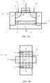
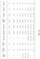
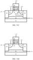
- FIG. 1is a schematic, cross-sectional illustration of a memory cell according to an embodiment of the present invention.
- FIG. 2is a schematic, cross-sectional illustration of a memory cell according to another embodiment of the present invention.
- FIG. 3 Ais a schematic, cross-sectional illustration of a memory cell according to another embodiment of the present invention.
- FIG. 3 Bis a schematic, top-view illustration of the memory cell shown in FIG. 3 A .
- FIG. 4schematically illustrates an equivalent circuit representation of the memory cells shown in FIGS. 1 - 3 .
- FIG. 5schematically illustrates a bipolar device inherent in memory devices of any one of FIGS. 1 - 3 .
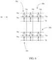
- FIG. 6schematically illustrates multiple cells of the type shown in any one of FIGS. 1 - 3 joined to make a memory array.
- FIG. 7schematically illustrates a holding operation performed on a memory array according to an embodiment of the present invention.
- FIG. 8illustrates exemplary bias conditions applied on the terminals of a memory cell of the array of FIG. 7 .
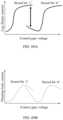
- FIG. 9 Ashows an energy band diagram characterizing an intrinsic bipolar device when a floating body region is positively charged and a positive bias is applied to a buried well region of a memory cell according to an embodiment of the present invention.
- FIG. 9 Bshows an energy band diagram of an intrinsic bipolar device when a floating body region is neutrally charged and a positive bias is applied to a buried well region of a memory cell according to an embodiment of the present invention.
- FIG. 10shows a graph of the net current “I” flowing into or out of a floating body region as a function of the potential “V” of the floating body, according to an embodiment of the present invention.
- FIG. 11shows a schematic curve of a potential energy surface (PES) of a memory cell according to an embodiment of the present invention.
- PESpotential energy surface
- FIG. 12illustrates a charge stored in a floating body region of a memory cell as a function of a potential applied to a buried well region, connected to a BW terminal, according to an embodiment of the present invention.
- FIG. 13schematically illustrates a write logic-0 operation performed on a memory array according to an embodiment of the present invention.
- FIG. 14illustrates bias conditions applied on the terminals of a memory cell to perform a write logic-0 operation according to an embodiment of the present invention.
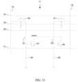
- FIGS. 15 A and 15 Billustrate an equivalent circuit representation and a schematic cross-sectional view, respectively, of a content addressable memory (CAM) cell according to an embodiment of the present invention.
- CAMcontent addressable memory
- FIGS. 16 A and 16 Billustrate various voltage states applied to terminals of a memory cell or plurality of memory cells, to carry out match operations according to various embodiments of the present invention.
- FIG. 17illustrates multiple cells of the type shown by the equivalent circuit representation in FIG. 15 A joined to make a memory array.
- FIG. 18illustrates multiple cells of the type shown by the equivalent circuit representation in FIG. 15 A joined to make a memory array comprising a pull-up and a pull-down device.
- FIG. 19illustrates exemplary bias conditions applied to a plurality of content addressable memory cells according to an embodiment of the present invention, resulting in a match condition.
- FIG. 20illustrates exemplary bias conditions applied to a plurality of content addressable memory cells according to an embodiment of the present invention, resulting in a mismatch condition.
- FIG. 21illustrates an equivalent circuit representation of a content addressable memory cell comprising a capacitor, according to an embodiment of the present invention.
- FIG. 22illustrates an equivalent circuit representation of a content addressable memory cell comprising a transistor to precondition the match node, according to an embodiment of the present invention.
- FIG. 23illustrates an equivalent circuit representation of content addressable memory cell comprising a holding capacitor and a transistor to precondition the match node, according to an embodiment of the present invention.
- FIG. 24illustrates an equivalent circuit representation of a ternary content addressable memory (TCAM) cell according to an embodiment of the present invention.
- TCAMternary content addressable memory
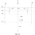
- FIG. 25illustrates exemplary bias conditions applied to a CAM cell illustrated in any one of FIGS. 21 - 23 .
- FIG. 26illustrates exemplary bias conditions applied to the TCAM cell illustrated in FIG. 24 .
- FIG. 27is a schematic illustration of a floating body content addressable memory cell according to another embodiment of the present invention.
- the cell of FIG. 27includes a split match node and capacitors to hold charge on the match nodes.
- This embodimentmay also be used as a ternary content addressable memory.
- FIG. 28is a schematic illustration of a floating body content addressable memory cell with a wide fan OR match string, according to another embodiment of the present invention.
- FIG. 29is a schematic illustration of a floating body content addressable memory cell with a wide fan OR match string and a capacitor to hold charge on the match node, according to another embodiment of the present invention.
- FIG. 30shows a set of exemplary bias conditions for FIG. 28 .
- FIG. 31is a schematic illustration of a floating body content addressable memory cell containing a split match node and a wide fan OR match string, according to another embodiment of the present invention. This embodiment may also be used as a ternary content addressable memory
- FIG. 32shows a set of exemplary bias conditions for FIG. 31 .
- FIG. 33is a schematic illustration of a floating body content addressable memory cell utilizing a split match node, wide fan OR match string and capacitors to hold charge, according to another embodiment of the present invention. This embodiment may also be used as a ternary content addressable memory.
- FIG. 34is a schematic illustration of a floating body content addressable memory cell utilizing a boost capacitor to increase the pass voltage on the NAND match string, according to another embodiment of the present invention. This embodiment also includes a transistor to precondition the match node.
- FIG. 35is a schematic illustration of a floating body content addressable memory cell utilizing a boost capacitor to increase the pass voltage on the NAND match string, according to another embodiment of the present invention.
- FIG. 36is a schematic illustration of a floating body content addressable memory cell including a split match node, and match node boost capacitors, according to another embodiment of the present invention. This embodiment may also be used for a ternary content addressable memory.
- FIG. 37is a schematic illustration of a floating body ternary content addressable memory according to another embodiment of the present invention, where the don't care node is separated from the match node.
- FIG. 38shows a set of exemplary bias conditions for FIG. 37 .
- FIG. 39is a schematic illustration of a floating body ternary content addressable memory cell with holding capacitors on the match node and don't care node.
- FIG. 40is a schematic illustration of a floating body ternary content addressable memory cell with preconditioning transistors attached to the match and don't care nodes, according to another embodiment of the present invention.
- FIG. 41is a schematic illustration of a floating body ternary content addressable memory cell with preconditioning transistors attached to the match node and don't care nodes, according to another embodiment of the present invention. Additionally, this embodiment includes capacitors attached to the match node and don't care node.
- FIG. 42is a schematic illustration of a floating body ternary content addressable memory cell with a split match node, according to another embodiment of the present invention.
- FIG. 43shows a set of exemplary bias conditions for the cell of FIG. 42 .
- FIG. 44is a schematic illustration of a floating body ternary content addressable memory cell with a split match node and capacitors attached to each individual match node, according to another embodiment of the present invention. A capacitor is also attached to the don't care storage node.
- FIG. 45is a schematic illustration of a floating body ternary content addressable memory cell with a wide fan OR match string, according to another embodiment of the present invention.
- FIG. 46shows a set of exemplary bias conditions for the cell of FIG. 45 .
- FIG. 47is a schematic illustration of a floating body ternary content addressable memory cell with a wide fan OR match string and capacitors attached to the match and don't care nodes, according to another embodiment of the present invention.
- FIG. 48is a schematic illustration of a floating body ternary content addressable memory cell with split match nodes and a wide fan OR match string, according to another embodiment of the present invention.
- FIG. 49shows a set of exemplary bias conditions for the cell of FIG. 48 .
- FIG. 50is a schematic illustration of a floating body ternary content addressable memory cell with split match nodes, a wide fan OR match string and capacitors attached to each match node as well as the don't care node, according to another embodiment of the present invention.
- FIG. 51is a schematic illustration of a floating body ternary content addressable memory cell with boost capacitors attached to the match and don't care nodes, according to another embodiment of the present invention. Precondition transistors are also attached to both match and don't care nodes.
- FIG. 52is a schematic illustration of a floating body ternary content addressable memory cell with boost capacitors attached to the match and don't care nodes, according to another embodiment of the present invention.
- FIG. 53is a schematic illustration of a floating body ternary content addressable memory cell with split matched nodes and boost capacitors attached to each match node as well as the don't care storage node, according to another embodiment of the present invention.
- FIG. 54is a schematic illustration of a floating body content addressable memory cell with a PMOS (p-type metal-oxide semiconductor) match string gate, according to another embodiment of the present invention.
- PMOSp-type metal-oxide semiconductor
- FIG. 55shows a set of exemplary bias conditions for the cell of FIG. 54 indicating an inversion being applied to the writing of the floating boy (FB) CAM bit.
- FIG. 56shows a set of exemplary bias conditions for the cell of FIG. 54 , indicating an inversion being applied to the search data being input to the FB CAM bit.
- FIG. 57is a schematic illustration of a floating body content addressable memory cell with a diode connected to the match node, according to another embodiment of the present invention.
- FIG. 58shows a set of exemplary bias conditions for the cell of FIG. 57 .
- FIG. 59is a schematic illustration of a floating body content addressable memory cell with a diode connected to the match node, according to another embodiment of the present invention.
- FIG. 60shows a set of exemplary bias conditions for the cell of FIG. 59 .
- FIG. 61is a schematic representation of a dual port floating body memory.
- FIG. 62is a schematic illustration showing how a dual port floating body memory cell can be used in a floating body content addressable memory.
- FIG. 63is a schematic illustration of a dual ported floating body memory used in the split gate content addressable memory configuration according to an embodiment of the present invention. Note this can also be used as a ternary content addressable memory.
- FIG. 64is a schematic illustration showing the use of a two transistor floating body memory device configured as a floating body content addressable memory.
- FIG. 65 Ais a schematic illustration showing an example of how a flash memory may be used in substitution of the floating body memory cells through all the embodiments of the present invention.
- FIG. 65 Bis a schematic cross-sectional view showing an example of how an electrically floating body DRAM may be used in substitution of the floating body memory cells through all the embodiments of the present invention.
- FIG. 66is a block diagram showing an example of how other various memory cells can be used in replacement of the floating body memory cell for the embodiments of the present invention.
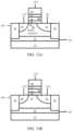
- FIG. 67 Ais a schematic, cross-sectional illustration of a memory cell according to an embodiment of the present invention.
- FIG. 67 Bis a schematic, cross-sectional illustration of a memory cell according to another embodiment of the present invention.
- FIG. 67 Cis a schematic, cross-sectional illustration of a memory cell according to another embodiment of the present invention.
- FIG. 67 Dis a schematic, top-view illustration of the memory cell shown in FIG. 67 C .
- FIGS. 68 A and 68 Billustrate stored charges of floating gate transistor for stored bit ‘1’ and ‘0’, respectively, according to an embodiment of the present invention.
- FIG. 69 A and FIG. 69 Billustrate resultant current-voltage characteristics of the floating gate transistor of FIGS. 68 A- 68 B for stored bit ‘1’ and ‘0’.
- FIG. 70schematically illustrates a read or search operation performed on a memory array according to an embodiment of the present invention.
- FIG. 71 Aschematically illustrates a mismatch condition, where the stored data is ‘1’ and the input data is ‘0’, according to an embodiment of the present invention.
- FIG. 71 Bschematically illustrates a matching condition, where the stored data is ‘1’ and the input data is ‘1’, according to an embodiment of the present invention.
- FIG. 71 Cschematically illustrates a mismatch condition, where the stored data is ‘0’ and the input data is ‘1’, according to an embodiment of the present invention.
- FIG. 71 Dschematically illustrates a matching condition, where the stored data is ‘0’ and the input data is ‘0’, according to an embodiment of the present invention.
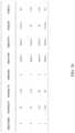
- FIG. 71 Esummarizes the matching and mismatch conditions described in FIGS. 71 A- 71 D , according to an embodiment of the present invention.
- FIG. 72A schematically illustrates a mismatch condition, where the stored data is ‘1’ and the input data is ‘0’, according to an embodiment of the present invention.
- FIG. 72 Bschematically illustrates a matching condition, where the stored data is ‘1’ and the input data is ‘1’, according to an embodiment of the present invention.
- FIG. 72 Cschematically illustrates a mismatch condition, where the stored data is ‘0’ and the input data is ‘1’, according to an embodiment of the present invention.
- FIG. 72 Dschematically illustrates a matching condition, where the stored data is ‘0’ and the input data is ‘0’, according to an embodiment of the present invention.
- FIG. 72 Esummarizes the matching and mismatch conditions described in FIGS. 72 A- 72 D , according to an embodiment of the present invention.
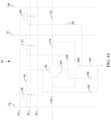
- FIG. 73schematically illustrates an exemplary embodiment of a CAM memory array comprising of CAM memory cells arranged in rows and columns, according to an embodiment of the present invention.
- FIGS. 74 A and 74 Bschematically illustrate cross-sectional views of memory cells joined to make a memory array, according to an embodiment of the present invention.
- FIGS. 75 A and 75 Bschematically illustrate cross-sectional views of memory cells joined to make a memory array according to another embodiment of the present invention.
- FIG. 76schematically illustrates a illustrates a CAM memory cell according to an embodiment of the present invention.
- FIG. 77 Ashows an energy band diagram characterizing an intrinsic bipolar device when a floating body region is positively charged and a positive bias is applied to a buried well region of a memory cell according to an embodiment of the present invention.
- FIG. 77 Bshows an energy band diagram of an intrinsic bipolar device when a floating body region is neutrally charged and a positive bias is applied to a buried well region of a memory cell according to an embodiment of the present invention.
- FIGS. 78 A and 78 Bschematically illustrate cross-sectional views of memory cells joined to make a memory array, according to an embodiment of the present invention.
- FIGS. 79 A and 79 Bschematically illustrate cross-sectional views of memory cells joined to make a memory array according to another embodiment of the present invention.
- FIG. 80is a schematic, cross-sectional illustration of a differential content addressable memory cell according to an embodiment of the present invention.
- FIG. 81is a schematic illustration of a plurality of differential content addressable memory cells connected to form a memory array, according to an embodiment of the present invention.
- FIGS. 82 A- 82 Eare schematic illustrations of content addressable memory cells according to various embodiment of the present invention.
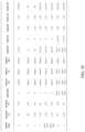
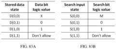
- FIG. 83 Aillustrates the data states and the corresponding data bit logic values of a content addressable memory cell according to an embodiment of the present invention.
- FIG. 83 Billustrates the input states and the corresponding search bit logic values of a content addressable memory cell according to an embodiment of the present invention.
- FIGS. 83 C- 83 Fillustrate forward and reverse current flows for different data states of a content addressable memory cell according to an embodiment of the present invention.
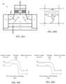
- FIGS. 84 A- 84 Hillustrate search/matching operation conditions for different possible data states and the search inputs, according to an embodiment of the present invention.
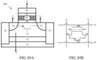
- FIG. 85A schematically illustrates a content addressable memory cell according to an embodiment of the present invention.
- FIG. 85 Billustrates an equivalent circuit representing the content addressable memory cell illustrated in FIG. 85 A .
- FIG. 86A schematically illustrates a content addressable memory cell according another embodiment of the present invention.
- FIG. 86 Bshows an equivalent circuit representing the cell of FIG. 85 A .
- FIGS. 86 C- 86 Dillustrate energy band diagrams characterizing an intrinsic bipolar device when a positive bias is applied to a buried layer region of the content addressable memory cell of FIG. 86 A , according to an embodiment of the present invention.
- FIGS. 87 A and 87 Bschematically illustrate cross-sectional views of a content addressable memory array according to an embodiment of the present invention.
- FIGS. 88 A and 88 Bschematically illustrate cross-sectional views of a content addressable memory array according to another embodiment of the present invention.
- FIGS. 89 A and 89 Bschematically illustrate cross-sectional views of a content addressable memory array according to another embodiment of the present invention.
- FIGS. 90 A and 90 Bschematically illustrate cross-sectional views of a content addressable memory array according to another embodiment of the present invention.
- FIG. 91schematically illustrates an exemplary search/matching operation performed on a content addressable memory array according to an embodiment of the present invention.
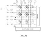
- FIG. 92schematically illustrates bias conditions during an exemplary search/matching operation performed on a content addressable memory array according to an embodiment of the present invention.
- CAMsare memories used in high speed search applications. CAMs are different from typical memory devices in which the user typically supplies an address and the memory device will return the data stored at that address. In a CAM, the user or system will provide the memory device a set of data. The CAM will then search through its contents to see if any data matches the data being provided by the user/system. If matching data can be found, the CAM returns the address(es) upon which the matching data was found.
- a Ternary Content Addressable Memoryis a modified content addressable memory (CAM) which allows it to support an additional “don't care” or “x” state beyond traditional “1” and “0” states supported in other memories including normal CAMs.
- the “x” stateis used as a “don't care.” If this state is selected for a data bit, the compare logic of the TCAM bit ignores any matching data and always allows this single bit to pass.
- the user or systemshould also have the ability to mask or apply a “don't care” state when applying match data to the TCAM memory.
- a “pass operation” also known as a “match operation”is the operation where the data applied by the user matches the data stored within the CAM or TCAM cell.
- User datais typically applied in a complementary manner, “10” for data “1” or “01” for data“0”. If user data is not applied in a complementary manner, it can be easily converted by use of an inverter.
- a “match string”refers to a method and construct by which the CAM or TCAM memory cell communicates with other CAM or TCAM cells in order to determine whether a plurality of CAM or TCAM cells has collectively matched or passed the users applied data.
- Common approacheswhich will be easily understood by those versed in the art include but are not limited to wide fan OR and wide fan AND gates.
- the present inventiondescribes content addressable memories (CAMs) comprising floating body memory cells.
- Content addressable memoriesare used in high speed search applications and typically require significant number s of transistors and resources to implement.
- CAMsare different from typical memory devices in which the user typically supplies an address and the memory device will return the data stored at that address.
- the user or systemwill provide the memory device a set of data.
- the CAMwill then search through its contents to see if any data matches the data being provided by the user/system. If matching data can be found, the CAM returns the address(es) upon which the matching data was found.
- a CAMtypically may consume a significant amount of area since it is a traditional SRAM memory with logic added to implement high speed searching capabilities.
- a typical CAM cellwill include a SRAM memory bit in addition to matching logic required to indicate whether or not this cell has matched the provided data.
- a Ternary Content Addressable Memoryis a modified Content Addressable Memory which allows it to support an additional “don't care” or “x” state beyond traditional “1” and “0” states supported in other memories including normal CAMs.
- the “x” stateis used as a “don't care.” If this state is selected for a data bit, the compare logic of the TCAM bit should ignore any matching data and always allow this single bit to pass.
- the user or systemshould also have the ability to mask or apply a “don't care” state when applying match data to the TCAM memory.
- TCAMsare typically significantly larger that CAM memories since the don't care state is usually stored in a second SRAM cell per TCAM bit. Thus each TCAM cell usually includes 2 SRAM bits, and additional matching logic typically costing a footprint of 16-24 transistors per TCAM cell.
- floating body transistorsare utilized to implement a content addressable memory (CAM) bit with significantly lower resources consumed. Additionally, a ternary content addressable memory (TCAM) bit having electrically floating body transistors is also described.
- CAMcontent addressable memory
- TCAMternary content addressable memory
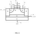
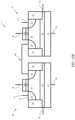
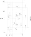
- Memory cell 50includes a substrate 12 of a first conductivity type such as p-type, for example.
- substrate 12is typically made of silicon, but may also comprise, for example, germanium, silicon germanium, gallium arsenide, carbon nanotubes, and/or other semiconductor materials.
- substrate 12can be the bulk material of the semiconductor wafer.
- substrate 12 A of a first conductivity type(for example, p-type) can be a well of the first conductivity type embedded in a well 29 of the second conductivity type, such as n-type.
- the well 29in turn can be another well inside substrate 12 B of the first conductivity type (for example, p-type).
- well 12 Acan be embedded inside the bulk of the semiconductor wafer of the second conductivity type (for example, n-type). These arrangements allow for segmentation of the substrate terminal, which is connected to region 12 A.
- the substrate 12will usually be drawn as the semiconductor bulk material as it is in FIG. 1 .
- Memory cell 50also includes a buried layer region 22 of a second conductivity type, such as n-type, for example; a floating body region 24 of the first conductivity type, such as p-type, for example; and source/drain regions 16 and 18 of the second conductivity type, such as n-type, for example.
- a second conductivity typesuch as n-type
- a floating body region 24 of the first conductivity typesuch as p-type, for example
- source/drain regions 16 and 18 of the second conductivity typesuch as n-type, for example.
- Buried layer 22may be formed by an ion implantation process on the material of substrate 12 .
- buried layer 22can be grown epitaxially on top of substrate 12 or formed through a solid state diffusion process.
- the floating body region 24 of the first conductivity typeis bounded on top by source line region 16 , drain region 18 , and insulating layer 62 (or by surface 14 in general), on the sides by insulating layer 26 , and on the bottom by buried layer 22 .
- Floating body 24may be the portion of the original substrate 12 above buried layer 22 if buried layer 22 is implanted. Alternatively, floating body 24 may be epitaxially grown. Depending on how buried layer 22 and floating body 24 are formed, floating body 24 may have the same doping as substrate 12 in some embodiments or a different doping, if desired in other embodiments.
- a source line region 16 having a second conductivity type, such as n-type, for example,is provided in floating body region 24 , so as to bound a portion of the top of the floating body region in a manner discussed above, and is exposed at surface 14 .
- Source line region 16may be formed by an implantation process on the material making up substrate 12 , according to any implantation process known and typically used in the art. Alternatively, a solid state diffusion or a selective epitaxial growth process could be used to form source line region 16 .
- a bit line region 18also referred to as drain region 18 , having a second conductivity type, such as n-type, for example, is also provided in floating body region 24 , so as to bound a portion of the top of the floating body region in a manner discussed above, and is exposed at cell surface 14 .
- Bit line region 18may be formed by an implantation process on the material making up substrate 12 , according to any implantation process known and typically used in the art. Alternatively, a solid state diffusion or a selective epitaxial growth process could be used to form bit line region 18 .
- a gate 60is positioned in between the source line region 16 and the drain region 18 , above the floating body region 24 .
- the gate 60is insulated from the floating body region 24 by an insulating layer 62 .
- Insulating layer 62may be made of silicon oxide and/or other dielectric materials, including high-K dielectric materials, such as, but not limited to, tantalum peroxide, titanium oxide, zirconium oxide, hafnium oxide, and/or aluminum oxide.
- the gate 60may be made of, for example, polysilicon material or metal gate electrode, such as tungsten, tantalum, titanium and their nitrides.
- Insulating layers 26may be made of silicon oxide, for example, though other insulating materials may be used. Insulating layers 26 insulate memory cell 50 from adjacent memory cell 50 .
- the bottom of insulating layer 26may reside inside the buried region 22 allowing buried region 22 to be continuous as shown in FIGS. 1 and 2 .
- the bottom of insulating layer 26may reside below the buried region 22 as in FIGS. 3 A and 3 B (shown better in FIG. 3 A ).
- This requires a shallower insulating layer 28which insulates the floating body region 24 , but allows the buried layer 22 to be continuous in the perpendicular direction of the cross-sectional view shown in FIG. 3 A .
- only memory cell 50 with continuous buried region 22 in all directionswill be shown from hereon.
- Cell 50includes several terminals: word line (WL) terminal 70 electrically connected to gate 60 , bit line (BL) terminal 74 electrically connected to bit line region 18 , source line (SL) terminal 72 electrically connected to source line region 16 , buried well (BW) terminal 76 electrically connected to buried layer 22 , and substrate terminal 78 electrically connected to the substrate 12 .
- WLword line
- BLbit line
- SLsource line
- BWburied well
- substrate terminal 78electrically connected to the substrate 12 .
- the SL terminal 72may be electrically connected to region 18
- BL terminal 74may be electrically connected to region 16 .
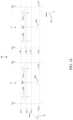
- FIG. 4illustrates an equivalent circuit representation of memory cell 50 according to an embodiment of the present invention.
- Inherent in memory cell 50are metal-oxide-semiconductor (MOS) transistor 20 , formed by source line region 16 , gate 60 , bit line region 18 , and floating body region 24 , and bipolar devices 30 a and 30 b , formed by buried well region 22 , floating body region 24 , and source line region 16 or bit line region 18 , respectively.
- MOSmetal-oxide-semiconductor
- bipolar device 30 cformed by source line region 16 , floating body 24 , and bit line region 18 .
- bipolar device 30 cis shown separately in FIG. 5 .
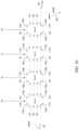
- FIG. 6schematically illustrates an exemplary embodiment of a memory array of memory cells 50 (four exemplary instances of memory cell 50 being labeled as 50 a , 50 b , 50 c and 50 d ) arranged in rows and columns, according to an embodiment of the present invention.
- representative memory cell 50 awill be representative of a “selected” memory cell 50 when the operation being described has one (or more in some embodiments) selected memory cell(s) 50 .
- representative memory cell 50 bwill be representative of an unselected memory cell 50 sharing the same row as selected representative memory cell 50 a
- representative memory cell 50 cwill be representative of an unselected memory cell 50 sharing the same column as selected representative memory cell 50 a
- representative memory cell 50 dwill be representative of an unselected memory cell 50 sharing neither a row nor a column with selected representative memory cell 50 a.
- word lines 70 a through 70 nare word lines 70 a through 70 n , source lines 72 a through 72 n , bit lines 74 a through 74 p , buried well terminals 76 a through 76 n , and substrate terminal 78 .
- Representation of the lines/terminal with letters a-n or a through pincludes not only embodiments which include literally twelve lines/terminals (i.e., a,b,c,d,e,f,g,h,i,j,k,l,m,n,o,p) or fourteen lines/terminals (i.e., a,b,c,d,e,f,g,h,i,j,k,l,m,n,o,p), but is meant to more generically represent a plurality of such line terminals, which can be less than twelve (i.e., as low as one given that there is a plurality of cells and at least one row and at least one column) or greater than twelve, thirteen or fourteen (much greater than fourteen up to any positive integer practical)).
- Each of the source lines 72 a through 72 nis associated with a single row of memory cells 50 and is coupled to the source line region 18 of each memory cell 50 in that row.
- Each of the bit lines 74 a through 74 pis associated with a single column of memory cells 50 and is coupled to the bit line region 16 of each memory cell 50 in that column.
- Substrate 12is present at all locations under array 80 .
- substrate terminals 78may be present in one or more locations.
- array 80is shown in FIG. 6 as a single continuous array, many other organizations and layouts are possible.
- word linesmay be segmented or buffered
- bit linesmay be segmented or buffered
- source linesmay be segmented or buffered
- the array 80may be broken into two or more sub-arrays
- control circuitssuch as word decoders, column decoders, segmentation devices, sense amplifiers, write amplifiers may be arrayed around array 80 or inserted between sub-arrays of array 80 .
- the present inventionis not limited to the exemplary embodiments, features, design options, etc., shown and described.
- memory cell 50such as holding, read, write logic-1 and write logic-0 operations, and have been described in U.S. Pat. No. 8,130,548 to Widjaja et al., titled “Semiconductor Memory Having Floating Body Transistor and Method of Operating” (“Widjaja-1”) and U.S. Pat. No. 8,077,536, “Method of Operating Semiconductor Memory Device with Floating Body Transistor Using Silicon Controlled Rectifier Principle” (“Widjaja-2”), which are both hereby incorporated herein, in their entireties, by reference thereto.
- FIG. 7schematically illustrates performance of a holding operation on memory array 80
- FIG. 8shows the bias applied on the terminals of a memory cell 50 during the holding operation, according to an exemplary, non-limiting embodiment.
- the holding operationis performed by applying a positive back bias to the BW terminal 76 , zero or negative bias on the WL terminal 70 , zero bias on the BL terminal 74 , SL terminal 72 , and substrate terminal 78 .
- the substrate terminal 78may be left floating.
- one of the SL terminal 72 or BL terminal 74may be left floating.
- the positive back bias applied to the buried layer region 22 connected to the BW terminal 76will maintain the state of the memory cell 50 that it is connected to.
- the positive bias applied to the BW terminal 76needs to generate an electric field sufficient to trigger an impact ionization mechanism when the floating body region 24 is positively charged, as will be described with reference to the band diagram shown in FIGS. 9 A and 9 B .
- the impact ionization rate as a function of the electric fieldis for example described in “Physics of Semiconductor Devices”, Sze S.M. and Ng K.K., which is hereby incorporated herein, in its entirety, by reference thereto.
- the bias conditions for the holding operation on memory cell 50are: 0 volts is applied to WL terminal 70 , 0 volts is applied to BL terminal 74 , 0 volts is applied to SL terminal 72 , a positive voltage, for example, +1.2 volts is applied to BW terminal 76 , and 0 volts is applied to the substrate terminal 78 .
- different voltagesmay be applied to the various terminals of memory cell 50 and the exemplary voltages described are not limiting.
- FIG. 9 Ashows an energy band diagram characterizing the intrinsic n-p-n bipolar device 30 b when the floating body region 24 is positively charged and a positive bias voltage is applied to the buried well region 22 .
- the vertical dashed linesmark the different regions of the bipolar device 30 b .
- the energy band diagram of the intrinsic n-p-n bipolar device 30 acan be constructed in a similar manner, with the source line region 16 (connected to the SL terminal 72 ) in place of the bit line region 18 (connected to the BL terminal 74 ).
- the horizontal dashed linesindicate the Fermi levels in the various regions of the n-p-n transistor 30 b .
- the Fermi levelis located in the band gap between the solid line 27 indicating the top of the valence band (the bottom of the band gap) and the solid line 29 indicating the bottom of the conduction band (the top of the band gap) as is well known in the art.
- the bipolar transistors 30 a and 30 bwill be turned on as the positive charge in the floating body region lowers the energy barrier of electron flow (from the source line region 16 or bit line region 18 ) into the base region (floating body region 24 ).
- the electronsOnce injected into the floating body region 24 , the electrons will be swept into the buried well region 22 (connected to BW terminal 76 ) due to the positive bias applied to the buried well region 22 .
- the electronsare accelerated and create additional hot carriers (hot hole and hot electron pairs) through an impact ionization mechanism.
- the resulting hot electronsflow into the BW terminal 76 while the resulting hot holes will subsequently flow into the floating body region 24 .
- the amount of holes injected into the floating body region 24can compensate for the charge lost due to p-n junction forward bias current between the floating body region 24 and the source line region 16 or bit line region 18 and due to holes recombination. This process maintains the charge (i.e. holes) stored in the floating body region 24 which will keep the n-p-n bipolar transistors 30 a and 30 b on for as long as a positive bias is applied to the buried well region 22 through BW terminal 76 .
- ⁇ (M ⁇ 1) ⁇ 1where ⁇ is the forward common-emitter current gain of the bipolar transistors and M is the impact ionization coefficient—the positive feedback mechanism is initiated.
- the collector voltage satisfying the condition ⁇ (M ⁇ 1) ⁇ 1may be referred to as the trigger voltage.
- biristori.e. bi-stable resistor
- J.-W. Han and Y.-K. Choipp. 171-172, 2010 Symposium on VLSI Technology, Digest of Technical Papers, 2010 “(“J.-W. Han”), which is hereby incorporated herein, in its entirety, by reference thereto.
- a refresh operationis still required.
- J.-W. Handescribes a 200 ms data retention for the silicon nanowire biristor memory.
- the state of the memory cellis maintained due to the vertical bipolar transistors 30 a and 30 b , while the remaining cell operations (i.e. read and write operations) are governed by the lateral bipolar transistor 30 c and MOS transistor 20 . Hence, the holding operation does not require any interruptions to the memory cell access.
- FIG. 9 Bshows an energy band diagram of the intrinsic bipolar device 30 a when the floating body region 24 is neutrally charged and a bias voltage is applied to the buried well region 22 .
- the energy level of the band gap bounded by solid lines 27 A and 29 Ais different in the various regions of n-p-n bipolar device 30 a .
- Solid line 23indicates, for reference purposes, the energy barrier between the bit line region 18 and the floating body region 24 .
- the energy barrierprevents electron flow from the bit line region 18 (connected to BL terminal 74 ) to the floating body region 24 .
- the n-p-n bipolar devices 30 a and 30 bwill remain off.
- Sakui-1 and Sakui-2describe a memory cell based on the reverse base current effect, where the base of a n-p-n bipolar transistor is connected to a p-type MOS transistor.
- Reischdescribes the challenges with the memory cell described in Sakui-1 and Sakui-2, which includes the requirement for the current of the p-type MOS transistor.
- the collector terminal of the bipolar transistoralso serves as the channel of the p-type MOS transistor, any changes in operating conditions or process conditions will affect both the bipolar transistor and the p-type MOS transistor. For example, increasing the doping level of the collector region will improve the impact ionization efficiency. However, it will also increase the doping level of the p-type MOS transistor channel region, and reduce the drive current of the p-type MOS transistor.
- memory cell 50In memory cell 50 , more than one stable state is achieved because of the vertical bipolar transistors 30 a and 30 b .
- the read and write operations of the memory cell 50are governed by the lateral bipolar transistor 30 c and MOS transistor 20 . Hence, the holding operation does not require any interruptions to the memory cell 50 access.
- the holding operation described with regard to FIG. 7there is no individually selected memory cell. Rather the holding operation will be performed at all cells connected to the same buried well terminal 76 . In addition, the holding operation does not interrupt read or write access to the memory cell 50 .
- FIG. 10shows a graph of the net current I flowing into or out of the floating body region 24 as a function of the potential V of the floating body 24 (not drawn to scale).
- a negative currentindicates a net current flowing into the floating body region 24
- a positive currentindicates a net current flowing out of the floating body region 24 .
- the net currentis flowing into the floating body region 24 as a result of the p-n diode formed by the floating body region 24 and the buried well region 22 being reverse biased. If the value of the floating body 24 potential is between V FB0 and V TS , the current will switch direction, resulting in a net current flowing out of the floating body region 24 .
- FIG. 11shows a schematic curve of a potential energy surface (PES) of the memory cell 50 , which shows another representation of the two stable states resulting from applying a back bias to the BW terminal 76 (connected to the buried well region 22 ).
- PESpotential energy surface
- V FB0 , V FB1 , and V TScan be modulated by the potential applied to the BW terminal 76 . These values are also temperature dependent.
- the holding/standby operationalso results in a larger memory window by increasing the amount of charge that can be stored in the floating body 24 .
- the maximum potential that can be stored in the floating body 24is limited to the flat band voltage V FB as the junction leakage current to regions 16 and 18 increases exponentially at floating body potential greater than V FB .
- the bipolar actionresults in a hole current flowing into the floating body 24 , compensating for the junction leakage current between floating body 24 and regions 16 and 18 .
- the maximum charge V MC stored in floating body 24can be increased by applying a positive bias to the substrate terminal 78 as shown in FIG. 12 .
- the increase in the maximum charge stored in the floating body 24results in a larger memory window.
- Floating body DRAM cells described in Ranica-1, Ranica-2, Villaret, and Pulicanionly exhibit one stable state, which is often assigned as logic-0 state.
- Villaretdescribes the intrinsic bipolar transistors enhance the data retention of logic-1 state, by drawing the electrons which otherwise would recombine with the holes stored in the floating body region.
- only one stable stateis observed because there is no hole injection into the floating body region to compensate for the charge leakage and recombination.
- the operation range to satisfy the trigger operation condition for self-latching (or positive feedback) mechanism ⁇ (M ⁇ 1) ⁇ 1is low ⁇ and high M to high 13 and low M.
- the low ⁇ , high M conditionis preferred as it results in a lower power for the holding operation since the current flow (from the collector (BW terminal 76 ) to the emitter (source line region 16 or bit line region 18 ) is proportional to ⁇ . Therefore, the lower the common-emitter gain ⁇ (i.e. the closer ⁇ is to 1), the lower the current consumed during the holding operation is (a common value of ⁇ would be between 20 and 500).
- the read and write operations of the memory cellhave been described, for example, in Widjaja-1, Widjaja-2 and Widjaja-3.
- a write logic-0 operationmay be performed by applying the following bias conditions as shown in FIGS. 13 and 14 : a negative voltage is applied to the selected BL terminal 74 a , a positive voltage is applied to the selected SL terminal 72 a , zero or negative voltage is applied to the selected WL terminal 70 a , zero or positive voltage is applied to the BW terminal 76 , and zero voltage is applied to the substrate terminal 78 ; while zero voltage is applied to the unselected BL terminal 74 , zero voltage is applied to the unselected SL terminal 72 , zero or negative voltage is applied to the unselected WL terminal 70 , zero or positive voltage is applied to the unselected BW terminal 76 .
- about ⁇ 0.3 voltsis applied to the selected BL terminal 74 a
- about +1.2 voltsis applied to selected SL terminal 72 a
- about 0.0 voltsis applied to WL terminal 70 a
- about 0.0 volts or +1.2 voltsis applied to BW terminal 76 a
- about 0.0 voltsis applied to substrate terminal 78 a .
- These voltage levelsare exemplary only may vary from embodiment to embodiment.
- the vertical n-p-n bipolar transistor formed by the buried well 22 , the floating body region 24 , and the source line junction 16 of the selected memory cell 50 ais now turned off.
- the p-n junction between the floating body 24 and selected BL junction 18 of the selected cell 50is forward-biased. As a result, holes stored in the floating body region 24 are now evacuated.
- the vertical n-p-n bipolar transistor formed by the buried well 22 , the floating body region 24 , and the bit line region 18will maintain the data stored in the unselected cells.
- the vertical n-p-n bipolar transistor formed by the buried well 22 , the floating body region 24 , and the source line region 16will maintain the data stored in the unselected cells.
- FIGS. 15 A and 15 Billustrate a Content Addressable Memory (CAM) cell 1 having an electrically floating body transistor according to an embodiment of the present invention.
- Two memory cells 50 and 51are configured with one n-type transistor (NMOS) 52 to form CAM cell 1 .
- NMOSn-type transistor
- FIG. 15 Athe memory cells 50 and 51 having electrically floating body transistors are represented by a transistor and two diodes
- FIG. 15 Billustrates a schematic, cross-sectional view of memory cells 50 and 51 electrically connected to each other to node 60 (which subsequently drives the gate of transistor 52 ) to form CAM cell 1 .
- the numerals in FIG. 15 Bfollow the numerals shown in FIG. 1 .
- Memory cells 50 and 51 and their method of operationhave been described above as well as in, for example, Widjaja-1, Widjaja-2, and Widjaja-3.
- Each of the memory cells 50 and 51has two distinct stable states, which are referred to as logic-0 state and logic-1 state.
- Logic-1 stateis defined as the stable state where a positive charge, such as for example +0.6V, is stored in the floating body region and logic-0 state is defined as a stable state where the floating body potential is low, such as for example +0.1V.
- memory cell 50 in logic-1 statewill have a higher conductance than that in logic-0 state.
- terminal 70represents the word line (WL) terminal of the memory cell 1 , and as shown in FIG. 17 , typically connects a plurality of memory cells 1 in the same row in a memory array 2 .
- the WL terminalis connected to the gates of the memory cells 50 and 51 .
- DNWL terminal 76represents the connection to the buried well region 22 of the memory cells 50 and 51 .
- Substrate terminal 78is connected to the substrate region 12 of the memory cells 50 and 51 .
- Search terminals (SL) 74 and 75are connected to the drain junction ( 18 in FIG. 1 ) of the memory cells 50 and 51 , while the source junction 16 is connected together to form match node 60 .
- Match node 60is then connected to the gate of the NMOS transistor 52 .
- the NMOS transistor 52is used as a wide fan gate in a NAND configuration.
- complementary datawill be stored in the memory cells 50 and 51 .
- memory cell 50stores a logic-0 data
- memory cell 51will store a logic-1 data.
- Data for the CAM searcheswill then be applied to SL 74 and 75 .
- Search datamay come in as a complementary pair, or the user/system may choose to provide a single bit of data for searching and complementary data may be generated with additional logic, which will be understood by those skilled in the art. If CAM cell 1 is selected, a positive voltage is applied to the WL terminal to turn on memory cell 50 that is in logic-1 state.
- the potential of the match node 60will be driven to the corresponding value.
- the floating body memory cell 50 that is in logic-1 statewill couple the potential of its drain junction (i.e. the search data).
- Match node 60will then be driven to a have a positive potential, e.g. +1.2V minus the transistor threshold voltage (Vt). Floating body memory cell 51 is not conducting since it is in logic-0 state.
- An example of a mismatch situationis SL terminal 74 at a low potential, for example about 0.0V, and floating body memory cell 50 is in logic-1 state. In this case, floating body memory cell 50 will pass 0.0V to the match node 60 .
- Match node 60then provides the match or mismatch status. Based on the potential of the match node 60 , the NMOS transistor 52 will either pass the data from node 71 a to node 71 b . If there is match condition, match node 60 will be high (at a positive voltage), turning on the NMOS transistor 52 and pass the data from node 71 a to node 71 b . If there is a mismatch condition, match node 60 will be low (at about zero potential), turning off NMOS device 52 , and effectively blocking the data between node 71 a and node 71 b . Terminals 71 a and 71 b are the method by which the match data is passed from one CAM cell 1 to another and will be called the match line or string.
- FIG. 16 Aillustrates an example of the bias conditions described above.
- the bias conditions shown in FIG. 16 Aassume a preconditioning of match node 60 to low potential, for example about 0.0 volts.
- match node 60may be preconditioned to a high potential, for example about +1.2 volts, prior to a match operation.
- FIG. 16 Billustrates an example of the bias conditions of the CAM cell 1 with the match node 60 being preconditioned to a high potential.
- FIG. 17illustrates a memory array 2 comprising a plurality of memory cells 1 arranged in a plurality of rows and columns.
- the first CAM cell 1 in each rowmay have a pull up device 91 or power source attached to its respective terminal 71 a as shown in FIG. 18 .
- FIG. 18is an example of a possible memory array 2 comprising a pull up device 91 and a pull down device 92 .
- Terminal 71 z at the end of the rowwill be the match detection node. This node may be preconditioned low or a weak passive pull down device 92 may also be employed.
- the data in the CAM cell 1is compared to the search data being provided by the user on the SL 74 and 75 .
- the results of the comparisonis stored on to node 60 , which in turn will cause transistor 52 to turn on or off based on the results of the CAM bit comparison. If a match occurs, match node 60 will be driven high causing transistor 52 to turn on, which in turn causes the contents of terminal 71 a to propagate to terminal 71 b . This repeats for every CAM cell 1 within the row.
- FIG. 19A schematic illustration of the matching operation performed within a row of memory array 2 resulting in a match condition is shown in FIG. 19 , while a schematic illustration of the compare operation resulting in a mismatch condition is provided on FIG. 20 .
- the third bit stored in CAM cell 1 c in this rowstores a logic-1 state while the data being searched for by the user or system is logic-0 as represented by the “01” input to the SL 74 c and 75 c terminals.
- the status of the match line output 71 ecan be detected with various means including but not limited to voltage detection, current detection, edge detection, etc.
- both memory cells 50 and 51are written to logic-0 state. This can be achieved by setting search lines (SL) 74 and 75 to a negative voltage such as about ⁇ 0.5 volts. This causes the p-n junction between the floating body region 24 and the drain junction 18 to be forward biased, extracting holes stored in the floating body region 24 , and thus setting the memory cells 50 and 51 to logic-0 state. All memory cells connected to the selected SLs will be written to logic-0 state. This bias condition may be repeated for all columns within a CAM array 2 to perform a chip erase/reset operation.
- a selective erase/reset operationmay be performed. This is achieved by setting search lines (SL) 74 and 75 to a slightly negative voltage, for example about ⁇ 0.3 volts, that will not allow the p-n junction between the floating body region 24 and the drain junction 18 to be forward biased.
- the potential applied to the WL 70will be raised from a low voltage, such as about 0.0 volts, to a high positive voltage, such as about +1.2 volts. This will couple the floating body positively. This coupling will allow for the p-n junction between the floating body region 24 and the drain junction 18 to forward bias, thus evacuating holes from only the selected memory cell 50 , thus placing the selected memory cell 50 to the logic-0 state.
- one of the two memory cells having floating body transistors 50 or 51must be set to a logic-1 state, thus resulting in a complementary data state between memory cells 50 and 51 .
- a positive voltagesuch as about +1.2 volts
- the other SL, SL 75 in this exampleis set to a low voltage, such as about 0.0 volts.
- the WL terminal 70is then set to a positive voltage, such as +1.2 volts. This will cause impact ionization at memory cell 50 in the vicinity of the drain junction ( 18 in FIG. 1 ) where the positive voltage is applied to.
- the impact ionizationresults in holes injection to the floating body region 24 of the memory cell 50 , and thus placing it to a logic-1 state.
- the memory cell 51will not be written to because the source and drain junctions of the memory cell 51 are at low potential, and no sufficient electric field is present to result in impact ionization.
- the opposite operationcan be performed where a write logic-1 operation can be performed to memory cell 51 , which will set the memory cells 50 and 51 to logic-01 state, which is defined as the logic-0 state of the CAM cell 1 .
- about +1.2 voltsis applied to the SL 74
- about 0.0 voltsis applied to the SL 75
- about +1.2 voltsis applied to the WL terminal 70
- about +1.2 voltsis applied to the BW terminal 76
- about 0.0 voltsis applied to the substrate terminal 78 .
- An alternate method to setting of the memory cells 50 or 51is by using a band-to-band tunneling mechanism, which is also referred to as the Gate Induced Drain Leakage (GIDL).
- the write operationcan be performed by applying the following bias conditions: a positive potential is applied to one of the SL terminal (for example, SL 74 ) and zero potential is applied to the other SL terminal (for example SL 75 ).
- the WL terminal 70is then driven from about 0.0 volts to a negative voltage such as about ⁇ 1.2 volts.
- the combination of the positive voltage applied to the drain junction and the negative voltage applied to the gate electrodewill cause band-to-band tunneling and inject holes into the floating body region 24 of this device.
- about +1.2 voltsis applied to the SL 74
- about 0.0 voltsis applied to the SL 75
- about ⁇ 1.2 voltsis applied to the WL terminal 70
- about +1.2 voltsis applied to the BW terminal 76
- about 0.0 voltsis applied to the substrate terminal 78 .
- both memory cells 50 and 51may be initially set to logic-1 states, and then one of the memory cells 50 or 51 may be selectively set to logic-0 state to arrive at a complementary data state within CAM cell 1 .
- the first stepis to clear any charge that may be stored within the NAND match string by passing a low voltage such as ground or about 0.0 volts through the entire match string.
- both SL terminals 74 and 75are set to a positive voltage, for example about +1.2 volts. Care must be taken to ensure that the voltage conditions used on the CAM cell 1 do not result in unintended over write or disturb of the state of the memory cells 50 or 51 .
- the WL terminalsare then driven to a read voltage which would then pass a positive voltage, such as about +1.2 volts, minus a transistor threshold voltage drop (Vt-drop) onto the match node 60 .
- Vt-droptransistor threshold voltage drop
- a preconditioning voltagesuch as about 0.0 volts may be applied to either node 71 a or 71 b .
- a preconditioning voltagesuch as about 0.0 volts may be simultaneously driven from the node 71 a or the first CAM cell 1 within the row and the terminal 71 b of the last CAM cell 1 within the row in order to speed up the preconditioning process.
- a further step of preconditioning the CAM cell 1involves removing the charge stored on the match node 60 , for example as a result of the previous search operation.
- the WL terminalsmay be held or driven to a positive potential, for example about +1.2 volts, and then the SL terminals 74 and 75 may be driven to low potential, for example about 0.0 volts. This operation will set the match node to about 0.0 volts.
- the level used in the preconditioning stepis meant as an example.
- a positive voltagemay also be used as the preconditioning value.
- the step of preconditioningis meant to arrive at a consistent bias point prior to any operation to provide a common starting point for all cells being evaluated. It is also possible with appropriate margins of cell operation that the preconditioning steps may be skipped for performance purposes.
- Device 52is shown in FIG. 15 as an NMOS device but is not meant to limit the scope of this invention.
- a p-channel MOS (PMOS) devicemay be used in replacement of NMOS device 52 .
- the complementary search data provided by the user or systemis driven to SL terminals 74 and 75 .
- the complementary match datamay be written into memory cells 50 and 51 prior to any search operation.
- the WL terminal 70 of the CAM cell 1is set to a read voltage that will allow memory cell 50 set at logic-1 state to conduct strongly while minimizing the sub-threshold or off current of memory cell 50 in logic-0 state.
- the read voltagewill also need to be low enough to prevent unintended writing or disturb of the memory cells 50 and 51 .
- a matchoccurs when the search data on the SL terminal matches the data stored in the memory cell 50 connected to that SL terminal. For example, a positive potential is applied to SL terminal 74 connected to memory cell 50 that stores logic-1 state.
- the memory cell 50 or 51 in logic-1 statewill allow the potential of the SL terminal 74 or 75 connected thereto to pass through to the match node 60 .
- a mismatchoccurs when a memory cell 50 in logic-1 state is connected to a SL terminal at low potential, for example about 0.0 volts. This will set the match node 60 to low potential, for example ground potential or about 0.0 volts. There is a sub-threshold leakage current flowing through memory cell 50 in logic-0 state, when connected to a SL terminal having a positive potential. This may cause the match node 60 to move higher above the ground potential and may cause some current consumption.
- the CAM search operationmay also be performed by utilizing the lateral bipolar current of the memory cells 50 to charge the match node 60 .
- about +1.2 voltsis applied to one of the SL terminal 74 and about 0.0 volts is applied to the other SL terminal 75
- about 0.0 voltsis applied to the WL terminal 70
- about +1.2 voltsis applied to the BW terminal 76
- about 0.0 voltsis applied to the substrate terminal 78 .
- the floating body region 24acts as an open base region of the lateral bipolar device. If the floating body region 24 is positively charged, this will turn on the lateral bipolar device and charge the match node 60 to a positive potential.
- the match conditionis similar when the search data on the SL terminal 74 matches the data stored in the memory cell 50 connected to SL terminal 74 .
- An example of a CAM cell 1 match condition where the search operation utilizes the bipolar methodis when memory cell 50 is in logic-1 state and memory cell 51 is in logic-0 state.
- the userthen applies a search data of logic-1 or logic-10 to the CAM cell 1 by applying a positive potential, such as about +1.2 volts, to SL terminal 74 and low potential, such as about 0.0 volts, to SL terminal 75 .
- the memory cell 50is in logic-1 state having a positively charged floating body region 24 , which will turn on the lateral n-p-n bipolar device between the SL terminal 74 and match node 60 . This will pass the voltage of the SL terminal 74 to match node 60 which will in response turn on transistor 52 indicating a match condition.
- mismatch conditionis as follows: if the user applies a search data of logic-0 state or logic-01 state, SL terminal 74 would be at a low potential such as about 0.0 volts and SL terminal 75 would be at a positive potential such as about +1.2 volts. In this case memory cell 50 would be off since the collector of the lateral n-p-n is at a low potential. Memory cell 51 would also be off since it has a logic-0 state stored. In this case, match node 60 will remain at about 0.0 volts which would leave transistor 52 off indicating a mismatch.
- a capacitor 90may be added to the match node 60 as shown in FIG. 21 . This allows for the match node 60 to hold its contents for a longer period of time to conserve power. Power may be consumed when a positive potential is applied to the SL terminals, depending on the magnitude of the sub-threshold leakage current of the memory cell in logic-0 state. By using a capacitor 90 , the time required to actively drive SL terminals 74 and 75 may be reduced. Alternatively, to increase the capacitance on the match node 60 , the width and length of device 52 may also be increased to add additional capacitance to match node 60 . Capacitor 90 may also be implemented using floating body capacitor devices.
- a transistor 53may be added to precondition the match node as shown in FIG. 22 . This may reduce the time and steps necessary to precondition the match node 60 and NAND match string (from node 71 a to node 71 b ) at the cost of an added transistor.
- the gate of the transistor 53is connected to node 73 and may be driven to a positive potential and node 77 may be driven to a positive potential to precondition the NAND match string (from node 71 a to node 71 b ) to ground or about 0.0 volts.
- node 77may be driven to a low potential to precondition the match node 60 .
- Transistor 53is shown to be an NMOS device, however this may also be realized by other devices such as a PMOS or a transmission gate. Additionally, a capacitor 90 may also be added to hold the charge at the match node 60 as shown in FIG. 23 .
- the match nodemay be split as shown in FIG. 24 .
- the match nodeis now split into two separate nodes: nodes 61 and 62 .
- an additional match transistor 54is added.
- the operation of the CAM cell 6is similar to the previous embodiments, in that in the case of a match operation, a positive SL terminal is adjacent to the memory cell 50 storing a logic-1 state and in turn will charge the corresponding match node (node 61 or 62 ) to Vcc-Vt.
- the memory cell 50 storing logic-0 stateis connected to a SL terminal biased at low potential, such as ground, so the memory cell 50 storing logic-0 state will not turn on and the corresponding match node will remain at low potential ensuring the other match transistor (transistor 52 or 54 ) remains off.
- the memory cell 50 storing logic-1 stateis connected to the SL terminal 74 or 75 with a low voltage, such as about 0.0 volts. In this case, the memory cell 50 will drive the low voltage to its respective match node 61 or 62 . The NMOS match line transistor 52 or 54 will not turn on.
- the memory cell 50 storing logic-0 statewill be connected to a SL terminal being driven to a positive voltage, such as about +1.2 volts. In this case, the pre-charged match node 61 or 62 will be charged to low potential, such as 0.0 volts, although it will slowly charge up due to the sub-threshold leakage current of the memory cell storing logic-0 state.
- capacitorsmay be added (capacitors 93 and 94 ) as shown in FIG. 27 .
- Transistors 52 and 54may also have their width and length increased in order to maximize capacitance of the match nodes 61 and 62 .
- Preconditioning transistorsare not shown, but may also be added to nodes 61 and 62 in order to improve performance or to avoid any potential undesired write, similar to the descriptions in FIGS. 21 - 23 .
- the source of each preconditioning transistorcan be either separate signals or holding capacitors may also be used, but these are not shown in FIG. 27 .
- FIG. 25illustrates exemplary bias conditions on the CAM cells illustrated in FIGS. 21 - 23 .
- the CAM cell 6 illustrated in FIG. 24may also be utilized as a Ternary Content Addressable Memory (TCAM).
- TCAMTernary Content Addressable Memory
- a TCAM memory cellprovides the same functionality as a CAM (or sometimes referred to as Binary CAM) and also allows for an additional “don't care” state.
- the “don't care” statemay be stored by setting both memory cells 50 and 51 to logic-1 state.
- the TCAM cell 6is guaranteed to match (since it will always have a memory cell 50 connected to a SL terminal 74 or/SL terminal 75 having a positive voltage applied to it).
- the user or systemmay also input a “don't care” state in the search data.
- a “don't care” in the search data input for the TCAM cell 6 having electrically floating body transistorthe user or system may apply a positive voltage, such as about +1.2 volts, to both SL terminal 74 and/SL terminal 75 . Since one or both of the memory cells 50 and 51 store(s) a logic-1 state (memory cells 50 and 51 will store complementary data or both will store logic-1 states if storing “don't care”), one of the match nodes 61 or 62 will thus be positive, passing the TCAM cell 6 regardless of the state of the TCAM cell 6 .
- FIG. 26illustrates exemplary bias conditions on the TCAM cell 6 illustrated in FIG. 24 .
- FIG. 28illustrates a CAM cell 8 according to another embodiment of the present invention.
- the match stringis now in a wide-fan OR configuration with a pull up PMOS device 55 . This simplifies the preconditioning of the match node 71 by removing the serial string of NMOS devices. It also improves the performance of the match string by avoiding the Vt drop associated with passing through NMOS transistors, in addition to avoiding the serial propagation delay required when passing data through each of the CAM cells 8 within the string.
- match node 71requiring either a passive pull down device or a method to measure current or voltage after the external search data has been applied to SL terminal 74 and/SL terminal 75 .
- a low voltage or current on match node 71indicates a successful match condition, where a positive voltage or current state will indicate a mismatch condition.
- the match node 60will be driven high (i.e. to a positive voltage) if there is a match between the search data and the data stored in the CAM cell 8 . If match node 60 is high (i.e. positive voltage, such as about +1.2 volts), it will turn off the PMOS device 55 and prevent this CAM cell 8 from acting upon the match line 71 . If the contents of the entire row of CAM cells 8 match the data being applied to the search lines, there will be no active pull up on node 71 and node 71 can be easily driven to ground.
- the match nodeIn a mismatch condition, the match node will be driven to a low voltage due to the memory cell 50 storing a logic-1 state being connected to the SL terminal having a low voltage, such as about 0.0 volts, thus causing the PMOS device 55 to turn on and indicating a mismatch has occurred. Voltage or current sensing methods may be used to detect the match or mismatch status. If the voltage or current on match line (ML) 71 is low, for example about 0.0 volts, it indicates a matching condition. A capacitor 93 may be added to the TCAM cell 8 to extend the length of time for which the match data can be held, for example as illustrated by TCAM cell 9 in FIG. 29 .
- the match node 60may be preconditioned high to a positive voltage such as +1.2 volts, shutting of all the PMOS devices in the string. Mismatched bits will cause the match node 60 to go low, for example to about 0.0 volts, which will turn on PMOS device 55 and cause ML line 71 to go high.
- FIG. 30illustrates exemplary bias conditions on the CAM cells 8 , 9 illustrated in FIGS. 28 - 29 .
- FIG. 31illustrates CAM cell 10 according to another embodiment of the present invention, where an OR match string may be used with split match nodes.
- the CAM cell 10may function as both CAM and TCAM.
- the circuit design and the memory cell structureis the same in both cases.
- the data that is written to the celldetermines whether it functions as a TCAM cell or a CAM cell.
- the 0.0 data instance(where both cells 50 and 51 store logic-0 states) is an illegal instance.
- the 0,0 data instanceis a “don't care” instance.
- Match nodes 61 and 62are preconditioned high to a positive voltage, such as about +1.2 volts, to initially turn off PMOS devices 57 and 58 .
- match nodes 61 and 62will remain high since one of the match nodes will directly drive to Vcc-Vt, while the opposite match node will float or slowly leak down to low voltage, such as about 0.0 volts, due to the subthreshold leakage current.
- Match line 71will initially be at low potential, such as about 0.0 volts.
- the ML 71needs to be measured or sensed before the subthreshold leakage can turn on one of the PMOS devices 57 or 58 and pull up the ML 71 high to a positive voltage, resulting in an incorrect search/match result.
- one of the match nodes 61 or 62will be driven to low voltage, such as ground or about 0.0 volts, since the low voltage on the SL 74 or /SL 75 terminal will be connected to a memory cell 50 storing a logic-1 state. This will cause one of the PMOS devices 57 or 58 to turn on and pull ML 71 high, indicating a mismatch result.
- FIG. 32illustrates exemplary bias conditions on the CAM or TCAM cell 10 illustrated in FIG. 31 .
- the “don't care” state for the TCAM cell 10may be implemented by storing logic-0 states in both memory cells 50 and 51 .
- the match nodes 61 and 62will be preconditioned high to turn off the PMOS devices 57 and 58 prior to a search/match operation.
- memory cells 50 and 51are effectively turned off for all CAM searches. This will cause both PMOS devices 57 and 58 to remain off and ML 71 will stay low, indicating a match condition for the TCAM cell 10 regardless of the data applied to the SL 74 and 75 .
- a “don't care” search datamay also be applied to the TCAM cell 10 by applying a positive voltage to both SL terminal 74 and/SL terminal 75 . Since nodes 61 and 62 are initially high, the applied bias to the SL 74 and/SL 75 terminals will ensure that match nodes 61 and 62 are high, turning off PMOS devices 57 and 58 , regardless of the states of the memory cells 50 and 51 .
- FIG. 33illustrates a CAM or TCAM cell 11 according to another embodiment of the present invention, where holding capacitors 94 and 95 are added. Preconditioning transistors may also be added to match nodes 61 and 62 to improve performance and to prevent potential disturb conditions.
- FIG. 34illustrates a CAM cell 12 according to another embodiment of the present invention, which adds a boost capacitor 96 .
- Node 79may be clocked or quickly transitioned from a low voltage such as about 0.0 volts to a positive voltage such as about +0.3 volts after the search data has been applied to SL and/SL terminals 74 and 75 .
- the potential change on node 79will cause match node 60 to be boosted by a proportional amount, in this example, by approximately 0.3 volts. This coupling effect can be used to restore the voltage drop due to the Vt drop of the n-type memory cells 50 or 51 .
- the maximum voltage allowed on node 79must be limited so that it does not inadvertently turn on match transistor 52 in a non-matching data condition. For example, if the voltage on node 79 pumps from 0V to 1.0V, the match node will either be at 0V+1.0V or Vcc ⁇ Vt+1.0V. In this example, the minimum voltage on the match node is above the turn on point for transistor 52 . Transistor 52 cannot be turned off which prevents proper operation of this CAM cell. Instead a low voltage such as 0.3V should be used. In this case the match node would either be at 0V+0.3V or Vcc-Vt+0.3V.
- this CAM cell 12would work properly but now with the boosted voltage, when node 60 is high, indicating a match condition the voltage on this node will be higher than in the original embodiment and provide for a smaller Vt drop between nodes 71 a and 71 b during a match condition.
- FIG. 35adds an additional preconditioning transistor 53 to cell 12 , shown as CAM cell 13 in this embodiment, to improve the time required to precondition the match node or avoid potential disturb conditions.
- FIG. 36indicates a CAM or TCAM cell 14 according to another embodiment of the present invention having a split match node 61 , 62 .
- Boost capacitors 97 and 98are added to respective nodes 61 and 62 .
- Boost node 79is then driven from a low potential such as ground to a higher potential such as 0.3V. This will allow for at least partial recovery of any voltage lost due to a threshold drop passing across the NMOS transistors 52 and/or 54 .
- Preconditioning transistors for each match nodecan also be used in FIG. 36 to improve performance or avoid disturb conditions but are not shown here.
- FIG. 37shows a ternary content addressable memory (TCAM) 15 according to another embodiment of the present invention.
- An additional memory cell having electrically floating body 200 and NMOS pass gate 201are added to the CAM memory cell 1 shown in FIG. 15 (shown inside dotted line).
- the memory cell 200will store the “don't care” state.
- the “don't care” node 63is pre-charged to a low voltage such as 0V before every operation.
- the don't care search line 80is set to a high voltage such as 1.2V or Vdd.
- memory cell 200If memory cell 200 is set to state “1”, memory cell 200 will pass the contents of search line 80 which will turn on pass gate 201 allowing the match string data to propagate regardless of the contents of the original CAM cell 1 . If the memory cell 200 is set to state “0”, the “don't care” node 63 will be remain low, turning off transistor 201 and making the behavior of TCAM cell 15 similar to the CAM memory cell 1 listed in FIG. 15 . Care must be taken to ensure that the match line measure occurs before the sub-threshold leakage of the memory cell 200 at state “0” has time to leak into the match line 63 to incorrectly turn on transistor 201 .
- the user or systemcan also apply a “don't care” state when applying their search data, thereby ignoring or masking the contents of memory cells 50 and 51 .
- the user or systemcan apply a high search data such as 1.2V to both search lines 74 and 75 . Since memory cells 50 and 51 contain complementary data, it is guaranteed that at least one memory cell 50 , 51 will turn on to drive match node 60 to a high potential. This turns on match transistor 52 to pass node 71 a to node 71 b .
- a table of the exemplary conditions mentioned aboveis provided in FIG. 38 . Those skilled in the art will appreciate that this table is for exemplary purposes only and not meant to limit the scope or range of this invention.
- the user or systemcan bypass or disable the “don't care” operation by setting the search line 80 to a low voltage, such as 0V.
- Setting search line 80 to a low voltagewill ensure that node 63 will always be at a low potential regardless of the condition of memory cell 200 . This ensures that transistor 201 will always be off making the behavior now similar to the CAM cell 1 . This provides the user the option to disable the “don't care” functionality at any given time.
- Write logic-0 and logic-1 operating conditions for the “don't care” memory cell 200are identical to the writing conditions of those of memory cells 50 and 51 .
- Either impact ionization or GIDLcan be used as methods to program memory cell 200 based on the status of search line 80 .
- the system or usercan either directly drive search line 80 or additional logic can be provided when writing to the TCAM cell 16 to translate a non-complementary input or a tri-state input to correctly program memory cell 200 .
- FIG. 39illustrates a TCAM cell 16 according to another embodiment of the present invention, which extends TCAM cell 15 by adding holding capacitors 99 and 100 to hold the match node and “don't care” node data to reduce the power consumed when search lines are actively being driven.
- FIG. 40illustrates a TCAM cell 17 according to another embodiment of the present invention, which adds preconditioning transistors 202 and 203 .
- the operation of TCAM cell 17is identical to that of CAM cell 4 illustrated in FIG. 22 , with the addition of “don't care” memory cell 200 .
- Both the match node 60 and the “don't care” node 63are required to have their separate preconditioning transistors ( 202 and 203 ) so that the nodes remain independent.
- FIG. 41shows TCAM cell 18 according to another embodiment of the present invention, which includes preconditioning transistors 202 and 203 in addition to holding capacitors 101 and 102 .
- the behavior of this TCAM cell 18is identical to that of CAM cell 5 found in FIG. 23 with the addition of the “don't care” cell 200 .
- FIG. 42shows a CAM/TCAM cell 19 according to another embodiment of the present invention.
- CAM/TCAM cell 19adds a memory cell having electrically floating body 200 and match transistor 202 to the CAM cell 6 illustrated in FIG. 24 .
- the operation of the CAM/TCAM cell 19is similar to that of CAM cell 6 with the addition of the “don't care” cell 200 .
- the “don't care” transistorworks independently from CAM/TCAM cell 6 but has the option to override the contents of CAM/TCAM cell 6 which matches the expected “don't care” behavior.
- FIG. 43A detailed example of potential bias conditions is provided in FIG. 43 . Those versed in the art will understand that this table is meant for exemplary purposes only and not meant to limit the scope or range of this invention.
- FIG. 44shows a TCAM cell 20 according to another embodiment of the present invention, which adds holding capacitors 103 , 104 and 105 to the TCAM cell 19 . Operation of these memory cells 19 and 20 matches the operation of the CAM cells 6 and 7 with the addition of the “don't care” memory cell 200 . Preconditioning transistors can also be employed at nodes 62 , 64 and 66 to improve performance or avoid potential floating body memory cell disturb issues. These preconditioning transistors are not shown in FIG. 44 , but have been shown and described previously.
- FIG. 45shows a TCAM cell 21 with an OR match line.
- the behavior of the TCAM cell 21is similar to that of CAM cell 8 with the addition of the “don't care” memory cell 200 and a serial PMOS device 206 .
- search line 80Prior to every search operation, search line 80 is set to high and the match line 71 is preconditioned to ground and should also contain either a passive pull down or a pull down activated during evaluation of the match line. If memory cell 200 is set to state “1’, it will pass a high voltage to node 63 thus turning off PMOS 206 and blocking any potential current from Vcc preventing this bit from participating in the match operation and effectively causing this bit to always pass.
- FIG. 46illustrates a possible set of bias conditions for the TCAM 21 and is provided for exemplary purposes. Those versed in the art will appreciate that this table is meant for exemplary purposes only and not meant to limit the scope or range of this invention.
- FIG. 47shows a TCAM cell 22 according to another embodiment of the present invention, which adds holding capacitors 106 and 107 to the TCAM cell 21 illustrated in FIG. 45 .
- Preconditioning transistors for nodes 60 and 63are not shown but can also be provided to improve preconditioning performance or to avoid potential disturb issues with the memory cells having electrically floating body transistors as exemplified in previous embodiments.
- FIG. 48illustrates a TCAM cell 23 according to another embodiment of the present invention.
- TCAM cell 23includes a split match node 61 , 62 and a PMOS OR match string 71 .
- the match nodes 61 and 62are pre-charged to a high voltage such as 1.2V while the “don't care” node 63 is pre-charged to a low voltage such as 0V. Otherwise the TCAM cell 23 behaves in a similar manner to the memory cell 10 described in FIG. 31 with the addition of the “don't care” bit added as shown in FIG. 37 .
- FIG. 49illustrates a possible set of bias conditions that can be used to bias the TCAM cell 23 .
- FIG. 49illustrates a possible set of bias conditions that can be used to bias the TCAM cell 23 .
- TCAM cell 24shows a TCAM cell 24 according to another embodiment of the present invention, which combines the features of TCAM cell 22 and 23 with split match nodes 61 , 62 , OR Match line 71 and capacitors 108 , 109 , and 110 to store all potentially floating nodes.
- Preconditioning transistorscan be used for nodes 61 , 62 and 63 to improve preconditioning performance or to avoid disturbance of memory cells having floating body transistors, but are not shown.
- FIG. 51exemplifies how a TCAM cell can be used with the boost capacitor scheme explained in FIG. 34 . Since match node 60 and “don't care” node 63 are independent nodes, each will require their own boost capacitors ( 108 and 109 ) to help improve the signal transmission from the search lines when their respective memory cells 50 , 51 and 200 are in state “1”. Preconditioning transistors 202 and 203 are also provided in case additional performance is required or memory cell disturb is a concern. These preconditioning transistors but can be removed if desired as shown in FIG. 52 .
- FIG. 53illustrates a TCAM cell 27 according to another embodiment of the present invention, where the boost capacitor method is applied to a TCAM with a split match node.
- Boost capacitors 108 and 109have been added.
- a single terminal 79has been shown to drive these boost capacitors, however these could also be independent nodes.
- the behavior of the TCAM cell 27is identical to the TCAM cell described in FIG. 44 with the addition of the boost capacitors.
- Preconditioning transistorscould also be added for nodes 61 , 62 and 63 but are not shown here.
- FIG. 54shows a CAM cell 28 according to another embodiment of the present invention, where a PMOS device 212 is used for the NAND match string.
- the behavior of the FB (floating body) CAM 28requires an inversion of data in order to output the correct match status. For example, if the user or system would like to write a data “1” into this CAM bit (cell 28 ), logic will be provided to invert the data during writing so that the memory cell 50 will be at state “0” and memory cell 51 will be at state “1”. By inverting the data being written, proper operation is assured due to the PMOS match transistor 212 being used.
- FIG. 55provides an exemplary set of possible bias conditions for the CAM cell 28 .
- the data applied during the search/comparison operationcould be inverted instead. For example, if data “1” is written into CAM cell 28 and the data is not inverted during writing, the memory cell 50 is at state “1” and memory cell 51 is at state “0”.
- additional logiccan be provided to invert the data being supplied by the user or system. For example, if the user or system applies a search data of “1”, data can be inverted so that SL terminal 74 will be at 0V and/SL terminal 75 would be at 1.2V.
- FIG. 56summarizes the use of inverting the data input with the use of the CAM cell 28 .
- precondition transistor and/or a holding capacitormay be used in conjunction with the embodiment illustrated in FIG. 54 but are not pictured here.
- the added capacitor or preconditioning transistorwould be connected to node 60 similar to the embodiments shown in FIGS. 21 - 23 .
- FIG. 57shows CAM cell 40 according to another embodiment of the present invention which utilizes an alternative method to determine the match status.
- a diode 212is connected between the match node 60 and the match line 71 .
- Match line 71is initially held at ground. In a match condition the search line will be at a high state and the memory cell 50 or 51 connected to the search line at high potential will be previously set to state “1”. In this case, the match node will be high and the diode will forward bias and conduct current.
- a current or voltage sensing blockmay be employed to measure the match status on line 71 and compare it against a reference current or voltage which should be proportional to the number of cells within a row.
- FIG. 58provides a set of proposed bias conditions for this embodiment. These bias conditions are for exemplary purposes only are not in any way meant to limit the scope of this invention.
- the schemecan be changed by reversing the polarity of the diode 213 as shown in FIG. 59 .
- node 60will still go high, which will cut off current from node 72 to node 60 .
- one of the search lines connected to memory cell 50 and previously set to state “1”is at low potential.
- This devicewould actively try to drive ground onto the match node 60 .
- Thiswould forward bias the diode from node 72 to 60 providing a current.
- a current sensing device placed on line 72can thus detect when a mismatch has occurred 9 i.e., when current is detected from line 72 )
- FIG. 60provides a set of proposed bias conditions for this embodiment. These bias conditions are for exemplary purposes only are not in any way meant to limit the scope of this invention.
- a dual port memory having electrically floating body transistormay be used in place of the memory cells 50 in the previous CAM cells described above.
- a dual port memory having electrically floating bodyhas been described for example by Widjaja in U.S. Pat. No. 8,582,359, which is hereby incorporated herein, in its entirety, by reference thereto.
- a schematic representation of a dual port memory having electrically floating bodyis provided in FIG. 61 .
- Word lines 70 and 73are the gates of the dual port memory cell and enable devices 300 and 301 respectively. Devices 300 and 301 share the same floating node between them and have a shared output node 400 .
- Search line 74is coupled to output node 400 through device 300 which is enabled by terminal 70 .
- Search line 77is coupled to output node 400 through device 301 which is enabled by terminal 73 .
- the operation of this memory cellis similar to that of the CAM or TCAM cells previously described using memory cells 50 having electrically floating body, however device 300 and 301 will share the same floating body and thus act as select gates for the dual port cell. Both 300 and 301 can access the floating body. Either device can write or read to the floating body which provides the dual port nature of this cell. For example, if we write state “1” through device 300 , a read operation through device 301 will show us that it is also set to state “1”. Conversely if we write a state “0” through device 301 , a read through device 300 would show it set to state “0” as well.
- This dual ported celldiffers from a conventional dual port SRAM cell in that there is a shared output node 400 which is unique to the dual port memory having electrically floating body. Typical dual port cells will have 4 bit lines. The dual port memory having electrically floating body has 3 bit lines due to node 400 being shared.
- the dual port memory cell having electrically floating bodymay be substituted into any of the previously mentioned CAM or TCAM cells as a replacement for the memory cell having a floating body.
- An example of its usageis illustrated in FIG. 62 .
- the dual port memory cells 90 and 91are connected in the same configuration as the CAM cell illustrated in FIG. 1 .
- the dual port memory cells 90 and 91have been substituted for the memory cells 50 and 51 .
- Node 400 of each dual port memory cellsare shorted together and attached to the gate of transistor 52 to create the match node 401 .
- the usercan now access the dual port memory cell 90 by either accessing gate 73 and search line 77 or gate 70 and search line 74 , thus providing two port access for dual port memory cell 90 .
- the user/systemcan also access the dual port memory cell 91 by either using word line 70 and search line 75 or using word line 73 and search line 79 .
- FIG. 63further illustrates how the dual port memory cells 90 and 91 may be substituted for the memory cells 50 and 51 having electrically floating bodies.
- FIG. 63illustrates a dual port CAM cell 33 having a split node. The operation of CAM cell 33 is similar to that of the CAM cell 6 previously shown in FIG. 24 , but with two-port access. The CAM memory cell 33 may also be used as a Ternary Content Addressable Memory. Search lines 74 and 77 are connected to the dual port floating body memory cell 90 and both can be used to read or write to cell 91 in conjunction with their associated word lines 70 and 73 .
- Search lines 75 and 79are connected with the dual port floating memory cell 91 and both can be used to read or write to cell 91 in conjunction with their associated word lines 70 and 73 .
- the output terminals 61 , 62 of each of the dual port floating body memory cellsare each connected to one of the match line NMOS devices 52 and 54 which are connected in a NAND type configuration.
- Other match string configurationscan be used such as the previously mentioned OR type mentioned above, for example as shown in FIG. 28 .
- FIG. 64further illustrates how multiple types of memory cells can be used in the invention described here and its many embodiments.
- a memory cell having electrically floating bodycomprising two transistors 92 and 93 , for example as described by Widjaja et. al, in PCT/US13/26466, “Memory Cell Comprising First and Second Transistors and Methods of Operating”, which is hereby incorporated herein, in its entirety, by reference thereto, is used in place of memory cells 50 and 51 .
- a memory cell having an electrically floating body in conjunction with other non-volatile memorysuch as Flash, Split Gate Flash, NOR Flash, RRAM, MRAM, for example as described in U.S. Pat. No. 7,760,548, Widjaja, “Semiconductor Memory Having Both Volatile and Non-Volatile Functionality and Method of Operating”, US Patent Application Publication No. 2010/0034041, “Method of Operating Semiconductor Memory Device with Floating Body Transistor Using Silicon Controlled Rectifier Principle”, U.S. Pat. No.
- FIG. 65 Aillustrates how Flash memory cells 94 , 95 may be used in to substitute for the memory cells 50 and 51 in the FIG. 15 , while FIG.
- 65 Billustrates a cross-sectional view of a CAM cell comprising electrically floating body DRAM in silicon-on-insulator (SOI) cells 500 and 510 connected in series to each other to a common node 60 , fabricated on a SOI substrate 12 , comprising a buried insulator layer 220 (see for example “The Multistable Charge-Controlled Memory Effect in SOI Transistors at Low Temperatures”, Tack et al., pp. 1373-1382, IEEE Transactions on Electron Devices, vol. 37, May 1990 (“Tack”), “A Capacitor-less 1T-DRAM Cell”, S. Okhonin et al., pp. 85-87, IEEE Electron Device Letters, vol. 23, no.
- SOIsilicon-on-insulator
- FIG. 66provides an exemplary generalization for how other non-volatile memory cell technologies may be employed in the embodiments described in this invention.
- Memory cells having electrically floating bodymay be replaced by any non-volatile memory cells 96 and 97 in all of the embodiments provided throughout this invention.
- the figures shown throughout this inventionare meant to serve in an exemplary manner for how this invention is to be applied and in no way meant to imply a limitation in the scope of this invention.
- FIG. 67 Ais a schematic illustration of a content addressable memory cell (“CAM” cell) 150 according to an embodiment of the present invention.
- the CAM cell 150is a non-volatile floating gate transistor or a non-volatile charge trapping flash memory transistor.
- the CAM cell 150includes a substrate 12 of a first conductivity type such as p-type, for example.
- Substrate 12is typically made of silicon, but may comprise, for example, germanium, silicon germanium, gallium arsenide, carbon nanotubes, and/or other semiconductor materials. In some embodiments of the invention, substrate 12 can be the bulk material of the semiconductor wafer. In another embodiment shown in FIG.
- substrate 12 A of a first conductivity typecan be a well of the first conductivity type embedded in a well 29 of the second conductivity type, such as n-type.
- the well 29in turn could be another well inside substrate 12 B of the first conductivity type (for example, p-type).
- well 12 Acan be embedded inside the bulk of the semiconductor wafer of the second conductivity type (for example, n-type).
- CAM cell 150also comprises a buried layer region 22 of a second conductivity type, such as n-type, for example; a floating body region 24 of the first conductivity type, such as p-type, for example; and source/drain regions 16 and 18 of the second conductivity type, such as n-type, for example.
- a second conductivity typesuch as n-type
- a floating body region 24 of the first conductivity typesuch as p-type, for example
- source/drain regions 16 and 18 of the second conductivity typesuch as n-type, for example.
- Buried layer 22may be formed by an ion implantation process on the material of substrate 12 .
- buried layer 22can be grown epitaxially on top of substrate 12 or formed through a solid state diffusion process.
- the floating body region 24 of the first conductivity typeis bounded on top by surface 14 , source line region 16 , drain region 18 , and insulating layer(s) 62 , on the sides by insulating layer 26 , and on the bottom by buried layer 22 .
- Floating body 24may be the portion of the original substrate 12 above buried layer 22 if buried layer 22 is implanted. Alternatively, floating body 24 may be epitaxially grown. Depending on how buried layer 22 and floating body 24 are formed, floating body 24 may have the same doping as substrate 12 in some embodiments or a different doping, if desired in other embodiments.
- a source line region 16 having a second conductivity type, such as n-type, for example,is provided in floating body region 24 , so as to bound a portion of the top of the floating body region in a manner discussed above, and is exposed at surface 14 .
- Source line region 16may be formed by an implantation process on the material making up substrate 12 , according to any implantation process known and typically used in the art. Alternatively, a solid state diffusion or a selective epitaxial growth process could be used to form source line region 16 .
- a bit line region 18also referred to as drain region 18 , having a second conductivity type, such as n-type, for example, is also provided in floating body region 24 , so as to bound a portion of the top of the floating body region in a manner discussed above, and is exposed at cell surface 14 .
- Bit line region 18may be formed by an implantation process on the material making up substrate 12 , according to any implantation process known and typically used in the art. Alternatively, a solid state diffusion or a selective epitaxial growth process could be used to form bit line region 18 .
- a gate stackis positioned in between the source line region 16 and the drain region 18 , above the floating body region 24 .
- the control gate 60is positioned above floating gate or charge trapping layer 64 and insulated therefrom by insulating layer 62 such that floating gate 64 is positioned between insulating layer 62 and insulating layer 66 .
- Control gate 60is capacitively coupled to floating gate 64 .
- Control gate 60is typically made of polysilicon material or metal gate electrode, such as tungsten, tantalum, titanium and/or their nitrides.
- Insulating layer 62 and insulating layer 66may be made of silicon oxide and/or other dielectric materials, including high-K dielectric materials, such as, but not limited to, tantalum peroxide, titanium oxide, zirconium oxide, hafnium oxide, and/or aluminum oxide.
- the relationship between the floating gate layer 64 and control gate 60is similar to that of a non-volatile stacked gate floating gate/trapping layer memory cell.
- the floating gate 64functions to store non-volatile memory data.
- the floating gate 64can be replaced with a charge trapping layer such as silicon nitride, quantum dots, and/or nanocrystals.
- the control gate 60is used for memory cell selection.
- Insulating layers 26may be made of silicon oxide, for example, though other insulating materials may be used. Insulating layers 26 insulate CAM cell 150 from adjacent CAM cells 150 .
- the bottom of insulating layer 26may reside inside the buried layer 22 allowing buried layer 22 to be continuous as shown in FIGS. 67 A and 67 B .
- the bottom of insulating layer 26 amay reside below the buried layer 22 as shown in both FIGS. 67 C and 67 D .
- This requires a shallower insulating layer 26 bwhich isolates the floating body region 24 , but allows the buried layer 22 to be continuous in the perpendicular direction of the cross-sectional view shown in FIG. 67 C .
- only memory cell 150 with continuous buried layer 22 in all directionswill be shown from hereon.
- CAM Cell 150includes several terminals: word line (WL) terminal electrically connected to control gate 60 , bit line (BL) terminal 74 electrically connected to bit line region 18 , source line (SL) terminal 72 electrically connected to source line region 16 , buried well (BW) terminal 76 electrically connected to buried layer 22 , and substrate terminal 78 electrically connected to the substrate 12 .
- WLword line
- BLbit line
- SLsource line
- BWburied well
- substrate terminal 78electrically connected to the substrate 12 .
- the SL terminal 72may be electrically connected to region 18
- BL terminal 74may be electrically connected to region 16 .
- FIGS. 68 A and 68 Billustrate stored charges of floating gate transistor for stored bit ‘1’ and ‘0’, respectively.
- FIGS. 69 A and 69 Billustrate the resultant current-voltage characteristics of floating gate transistor for stored bit ‘1’ and ‘0’, where FIG. 69 A illustrates the drain current-control gate voltage characteristics and FIG. 69 B illustrates the floating body current-control gate voltage characteristics.
- positive chargesare stored in the floating gate at stored bit ‘1’, resulting in low threshold voltage.
- negative chargesare stored in the floating gate at stored bit ‘0’, resulting in high threshold voltage.
- the drain current(flowing from the drain region 18 to the source line region 16 ) is used to determine the state of the memory cell, i.e. the stored charge in the floating gate 66 .
- the floating body current(or in another embodiment, the buried n-well current, which is an amplified floating body current) will be used instead.
- the bit line read voltageis high enough to trigger impact ionization or band-to-band tunneling
- the hole current in the floating body 24can be monitored at both the stored bit ‘0’ and the stored bit ‘1’, as shown in FIG. 69 B .
- the carrier under a high electric fieldcauses impact ionization near the drain junction, and generates electron-hole pairs. The generated electrons are collected as drain current, but the generated holes are swept toward the floating body 24 , which is often referred as substrate current in a non-floating body transistor.
- the band-to-band tunnelinggenerates holes in the floating body 24 .
- the CAM data searching presented in this inventionrelies on the aforementioned mechanisms.
- FIG. 70illustrates a comparison operation of CAM cell 150 .
- the buried layer 22is grounded, the same read voltage V read is applied to the source 16 and the control gate 60 , and the input voltage V input is applied to the drain, where V input represents the input/search data to be compared with the data stored in the CAM cell 150 .
- the read voltage V rea dis in between the threshold voltage of stored bit ‘0’ and the threshold voltage of stored bit ‘1’.
- the input voltage V inputis zero for search bit ‘0’, and the input voltage V input is the same or higher than the read voltage V read .
- the search input voltage V inputshould be higher than the read voltage V rea d.
- the bias conditions for data comparison for CAM cellare: +1.2V is applied to control gate 60 , +1.2V is applied to the source 16 , 0V is applied to the buried layer, and 0V for search bit ‘0’ or +1.8V for search bit ‘1’ is applied to the drain.
- different voltagesmay be applied to the various terminals of memory cell 150 and the exemplary voltages described are not limiting.
- FIGS. 71 A- 71 Dillustrate the set of possible stored bits and search bits, which are also summarized in FIG. 71 E .
- the input voltage V inputcan be the same as the read voltage V read .
- the gate-to-drain overlapis greater than the gate-to-source overlap.
- the band-to-band tunneling currentis proportional to the overlap area, the band-to-band tunneling near the drain junction is preferred.
- An example of bias conditions for data comparison for the CAM cell 150are: +1.2V is applied to control gate 60 , +1.2V is applied to the source 16 , 0V is applied to the buried layer 22 , and 0V for search bit ‘0’ or 1.2V for search bit ‘1’ is applied to the drain.
- different voltagesmay be applied to the various terminals of memory cell 150 and the exemplary voltages described are not limiting.
- FIGS. 72 A- 72 Dillustrate the set of possible stored bits and search bits of a cell having asymmetric source/drain design, according to an embodiment of the present invention, which are also summarized in FIG. 72 E .
- an inversion channelis formed and the electrons flow from the drain 18 to the source 16 .
- the flow of electrons and the source-to-drain voltage of 1.2Vcause impact ionization to occur, resulting in hole current to the floating body 24 .
- the CAM cell array or CAM cell memory blockwill be described hereafter. To simplify the description, the CAM cell structure will usually be drawn as it is in FIG. 71 .
- FIG. 73schematically illustrates an exemplary embodiment of a CAM array 180 comprising CAM memory cells 150 arranged in rows and columns, according to an embodiment of the present invention.
- a wordis arranged horizontally.
- a CAM array 180consists of n words, with each word 100 ( 100 a , 100 b . . . and 100 n ) containing p bits arranged horizontally.
- word lines 7070 a , 70 b . . . 70 n
- the word lines 70are electrically connected to the control gate 60 of CAM unit cell 150
- the match lines 76are electrically connected to either the floating body 24 or buried layer 22 of CAM cell 150
- the search lines 74are electrically connected to the drain of CAM cell 150 .
- a search operationbegins with loading the search-data word into the search lines 74 .
- Each CAM cellcompares its stored bit against the bit on its corresponding search lines 74 . If a match between all search/input bits and the stored bits is found, no current will flow on match lines 76 . If there is at least one mismatch between the search/input bit and the stored bits, a current flow will be observed on the corresponding match lines 76 .
- the match line sense amplifierdetects whether its match line 76 has a matching or mismatching condition.
- FIGS. 74 A and 74 Bschematically illustrate an exemplary physical structure that may be employed in making the CAM array 180 of FIG. 73 , according to an embodiment of the present invention.
- FIG. 74 Ais the cross sectional view cut on the center of CAM unit cell 150 along the search line 74 direction.
- FIG. 74 Bis the cross sectional view cut on the centers of CAM cells 150 along the word line 70 direction. Insulating layers 26 a and 26 b having two different depths are applied. The bottom of insulating layer 26 a resides inside the buried layer 22 to disconnect the floating body 24 from adjacent words 100 as shown in FIG. 74 A .
- the bottom of insulating layer 26 bresides above the buried layer 22 allowing the floating body 24 to be continuous within each word 100 as shown in FIG. 74 B .
- the ohmic contact layer 28 of the same conductivity type as that of the floating body 24is given for each word 100 .
- the floating body 24 in the given word 100is connected to the match line 76 via ohmic contact layer 28 .
- FIGS. 75 A- 75 Bschematically illustrate another exemplary physical structure of a CAM array 180 according to an embodiment of the present invention.
- FIG. 75 Ais a cross sectional view cut on the centers of CAM cells 150 along the direction of search line 74 .
- FIG. 75 Bis a cross sectional view cut on the centers of CAM cells 150 along the direction of word line 70 .
- Insulating layer 26 with single depthis applied throughout. The bottom of insulating layer 26 resides inside the buried layer 22 to disconnect the floating body 24 from adjacent words 100 as shown in FIG. 75 A . Also, the insulating layer 26 disconnects the floating body 24 from adjacent search bit cells within the word 100 as shown in FIG. 75 B .
- the ohmic contact layer 28 ′ of the same conductivity type as that of the floating body 24is given for every CAM cell 150 .
- the floating body 24 of every CAM cell 150 within the given word 100is connected to the match line 76 via ohmic contact layer 28 ′ as shown in FIG. 75 B .
- the match lineis first pre-charged to ground at the beginning of the matching operation. If all the search bits match all the stored bits, then the match line will remain at ground. If there is at least one mismatch between the search bits and the stored bits, the potential of the corresponding match line will increase, resulting in a higher potential than the pre-charged ground potential.
- FIG. 76illustrates a CAM unit cell 150 for explaining another embodiment of a search method.
- Vertical bipolar devicesare inherently formed in the unit CAM cell 150 by buried layer 22 , floating body region 24 , and source 16 or drain 18 , respectively.
- the buried layer 22 , floating body region 24 , and source 16can be considered as emitter, base, and collector of a bipolar transistor, respectively.
- the buried layer 22 , floating body region 24 , and drain 18can be considered as emitter, base, and collector of a bipolar transistor, respectively.
- FIG. 77 Ashows an energy band diagram characterizing an inherent n-p-n vertical bipolar transistor along the buried layer 22 , floating body 24 , and source 16 for grounded buried layer 22 , neutrally charged floating body 24 , and positive voltage applied to the source 16 .
- FIG. 77 Bshows an energy band diagram characterizing an n-p-n bipolar transistor along the buried layer 22 , floating body 24 , and source 16 for grounded buried layer 22 , positively charged floating body 24 , and positive voltage applied to the source 16 .
- the horizontal dashed linesindicate the Fermi levels in the various regions of the n-p-n transistor.
- the Fermi levelis located in the band gap between the solid line 27 indicating the top of the valence band (the bottom of the band gap) and the solid line 29 indicating the bottom of the conduction band (the top of the band gap) as is well known in the art.
- the positive source 16 voltage and the grounded buried layer 22correspond to the bias conditions for search operations. As explained with regard to FIG. 71 and FIGS. 72 , when the stored bits and input bits are matched, no hole current is generated in the floating body 24 . When the stored bits and input bits are miss-matched, hole current is generated in the floating body 24 .
- the vertical bipolar transistorWhen the hole current is generated in the floating body 24 , the vertical bipolar transistor will be turned on as the positive charge in the floating body 24 lowers the energy barrier of electron flow from the buried layer 22 into the floating body 24 . Once injected into the floating body region 24 , the electrons will be swept into the source 16 . In other words, when the stored bits and input bits are miss-matched, the buried layer 22 flows current, which can be utilized as another searching mechanism of a CAM cell array.
- FIGS. 78 A and 78 Bschematically illustrate an exemplary physical structure of a CAM array 180 according to an embodiment of the present invention.
- FIG. 78 Ais a cross sectional view cut on centers of CAM cells 150 along the search line 74 direction.
- FIG. 78 Bis a cross sectional view cut on centers of CAM cells 150 along the word line 70 direction.
- Insulating layers 26 having two different depthsare applied. The bottom of insulating layer 26 a resides below the buried layer 22 to disconnect the floating body 24 and the buried layer 22 from adjacent words 100 as shown in FIG. 78 A . However, the bottom of insulating layer 26 b resides inside the buried layer 22 allowing the buried layer 22 to be continuous within each word 100 as shown in FIG. 78 B .
- An ohmic contact layer 29 of the same conductivity type as that of the buried layer 22is provided for each word 100 .
- the buried layers 22 of cells 150 in a word 100are all connected to the match line 76 via o
- FIGS. 79 A- 79 Bschematically illustrate another exemplary physical structure that may be employed in making CAM array 180 , according to another embodiment of the present invention.
- FIG. 79 Ais a cross sectional view cut on centers of CAM cells 150 along the search line 74 direction.
- FIG. 79 Bis a cross sectional view cut on centers of CAM cells 150 along the word line 70 direction.
- Insulating layer 26 with single depthis applied throughout. The bottom of insulating layer 26 resides below the buried layer 22 to disconnect the floating body 24 and the buried layer 22 from adjacent words 100 as shown in FIG. 79 A . Also, the insulating layer 26 disconnects the floating body 24 and the buried layer 22 from adjacent search bit cells within the word 100 as shown in FIG. 79 B .
- the ohmic contact layer 29 ′ of the same conductivity type as that of the buried layer 22is provided with all CAM cells 150 .
- the buried layer 22 of every CAM cell 150 within a given word 100is connected to the match line 76 via ohmic contact layer 29 ′ as shown in FIG. 79 B .
- FIG. 80schematically illustrates a differential CAM cell 250 comprising one non-volatile memory transistor, according to an embodiment of the present invention.
- the non-volatile memory transistor 250has four terminals. A first terminal connects to a search line (SL) terminal 72 , a second terminal connects to a complementary search line (/SL) terminal 74 , a third terminal connects to a word line (WL) terminal 70 , and a fourth terminal connects to a match line (ML) terminal 76 .
- SLsearch line
- /SLcomplementary search line
- WLword line
- MLmatch line
- the first terminalmay be connected to the source region of the memory transistor 250
- the second terminalmay be connected to the drain region of the memory transistor 250
- the third terminalmay be connected to a control gate of the memory transistor 250
- the fourth terminalmay be electrically connected to either a floating body region or buried well region of the memory transistor 250 .
- the WL terminal 70controls the flow of the current between the first terminal and the second terminal, i.e. between the SL terminal 72 and the/SL terminal 74 .
- FIG. 81schematically illustrates a differential CAM array 280 comprising CAM memory cells 250 arranged in rows and columns, according to an embodiment of the present invention.
- a wordis arranged horizontally.
- CAM array 280has n words, with each word 100 ( 100 a , 100 b . . . and 100 n ) containing p bits arranged horizontally.
- word lines 7070 a , 70 b . . . 70 n
- a search operationbegins with loading the search-data word into the pairs of search lines 72 and complementary search line 74 .
- Each CAM cell 250compares its stored bit against the bit on its corresponding pair of differential search lines 72 and 74 . In at least one embodiment, if there is at least one mismatch between the search/input bit and the stored bit in a given word 100 , current flow will be observed on the corresponding match lines 76 .
- match line sense amplifierdetects whether its match line 76 has a matching or mismatching condition.
- the search input conditions for a searching operationare: logic low is applied to the SL terminal 72 and logic high is applied to the/SL terminal 74 for search logic-0 state, logic high is applied to the SL terminal 72 and logic low is applied to the/SL terminal 74 for search logic-1 state, logic lows are applied to the SL terminal 72 and/SL terminal 74 for search masking conditions or search logic-M state.
- logic lowcorresponds to 0V and logic high corresponds to +1.2V. Different voltages may be applied and the exemplary voltages described are not limiting.
- the CAM unit cell 250should have at least three memory states or at least two bits. Therefore, the CAM unit cell 250 adopts a two-bit per cell architecture. Examples of two-bit per cell architectures are shown in FIGS. 82 A- 82 E .
- a ternary CAM unit cell 250comprises a gate stack (including a control gate 60 , insulating layer 62 , charge storage region 64 , and an insulating layer 66 ) positioned between the source region 16 and the drain region 18 , and above the floating body region 24 .
- the control gate 60is positioned above charge storage region 64 and insulated therefrom by insulating layer 62 such that the charge storage region 64 is positioned between insulating layer 62 and insulating layer 66 .
- Control gate 60is capacitively coupled to charge storage region 64 .
- Charge storage region 64is typically made of floating gate such as polysilicon or metal or charge trapping layer such as silicon nitride, quantum dots, and/or nanocrystals.
- the charge storage region 64functions to store non-volatile memory data.
- the floating body region 24is isolated by the insulating layer 26 (like, for example, shallow trench isolation (STI)), and the built-in potential barrier of source/drain region 16 and 18 in horizontal direction, and by the insulating layer 66 and the built-in potential barrier of buried well layer 22 in vertical direction.
- STIshallow trench isolation
- the word line 70is electrically connected to the control gate 60 of CAM cell 250
- the match line 76is electrically connected to either the floating body 24 or buried well layer 22 of CAM cell 250 ( FIGS. 82 A- 82 E illustrate examples of CAM cell 250 where the match lines 76 are electrically connected to the buried well layer 22 )
- the search lines 72are electrically connected to the source 16 of CAM cell 250
- the complementary search lines 74are electrically connected to the drain 18 of CAM cell 250 .
- the substrate 12is p-type
- the source/drain region 16 and 18are n-type
- the buried well layer 22is n-type
- the floating body region 24is p-type.
- Such embodimentsshall be hereafter used to explain the details of the invention, but another embodiment of CAM cell 250 can be understood by complementary analogy.
- the charge storage region 64is made of a charge trapping layer such as silicon nitride, quantum dots, and/or nanocrystals. As the charge trapping sites are physically fixed due to the insulating nature of the charge trapping layer 64 illustrated in FIG. 82 A , the stored charges are localized. Therefore, the charge storage region 64 can be spatially separated into the charge storage region 64 a near the source region 16 and the charge storage region 64 b near the drain region 18 . Consequently, two bits can be stored in one transistor. If the transistor is miniaturized and thus the separation distance between charge storage regions 64 a and 64 b becomes smaller, isolating the two charge storage regions 64 a and 64 b becomes more difficult.
- a charge trapping layersuch as silicon nitride, quantum dots, and/or nanocrystals.
- FIGS. 82 B- 82 Dtwo charge storage regions 64 a and 64 b are physically isolated as illustrated in FIGS. 82 B to 82 D .
- CAM cell 250comprises physically isolated charge storage regions 64 a and 64 b , and therefore the charge storage region 64 may comprise both floating gate and charge trapping layer.
- an insulating region 63is used to isolate the charge storage regions 64 a and 64 b .
- the charge storage regions 64 a and 64 bare formed within the spacer regions 61 , and thus isolated by the gate stack.
- FIG. 82 Ethe gate stack and thus the charge storage regions 64 a and 64 b are separated, which is often referred to as the split-gate structure.
- This data statewill also be referred to as the “don't care” state, which is represented by logic-X data in FIG. 83 A .
- D(0,1) statewhere the charge storage region 64 a near the source 16 is in the programmed state and the charge storage region 64 b near the drain 18 is in the erased state.
- D(1,0) statewhere the charge storage region 64 a near the source 16 is in the erased state and the charge storage region 64 b near the drain 18 is in the programmed state.
- This data statewill also be referred to as state “1”, which is represented by logic-1 data in FIG. 83 A .
- the definitions of the data states illustrated in FIG. 83 Afollow the convention where the first index signifies the logic state of the charge storage region 64 a and the second index signifies the logic state of the charge storage region 64 b .
- the opposite convention, where the first index signifies the logic state of the charge storage region 64 b and the second index signifies the logic state of the charge storage region 64 amay alternatively be adopted.
- the stored data statescan be identified by a two-step reading: forward and reverse reading.
- the forward readingimplies that the source 16 is grounded and the drain 18 is biased to a positive read voltage.
- the reverse readingimplies that the drain 18 is grounded and the source 16 is biased to a positive voltage.
- FIG. 83 Cno channel currents flow under both forward read and reverse read conditions.
- FIG. 83 Dfor D(0,1), no channel current flows under forward read conditions, but channel current flows under reverse read conditions.
- FIG. 83 Efor D(1,0), channel current flows under forward read conditions, but no channel current flows under reverse read conditions.
- FIG. 83 Ffor D(1,1), channel currents flow under both forward read and reverse read conditions.
- search inputsare available: S(0,0) state, where the SL and the/SL are both low.
- This search inputwill also be referred to as the masking or “don't care” state, which is represented by logic-X data in FIG. 83 B ; S(0,1) state, where the SL is low and the/SL is high.
- This search inputwill also be referred to as state ‘0’, which is represented by logic-0 input in FIG. 83 B ; S(1,0) state, where the SL is high and the/SL is low.
- state ‘1’which is represented by logic-1 input in FIG. 83 B ; and S(1,1) state, where the SL and the/SL are both high.
- This search inputis not allowed in the search operation and indicated as “don't allow” in FIG. 83 B .
- FIGS. 83 A- 83 BAll possible stored states and search inputs values are summarized and their respective logic values are defined in FIGS. 83 A- 83 B .
- the ‘X’ entry in FIG. 83 Aindicates a “don't care” logic value.
- the ‘M’ entry in FIG. 83 Bindicates a “masking” logic value.
- FIGS. 84 A- 84 Hshow searching operation conditions for the different possible data states and the search inputs.
- the search bit ‘1’corresponds to applying a positive voltage, for example +1.2V, to the source region 16 and 0V to the drain region 18 , resulting in a reverse read condition.
- a positive voltagefor example +1.2V
- the depletion region formed due to the application of a positive voltage to the source region 16will shield the negative charge stored in the charge storage region 64 a . Therefore, current will flow from the source region 16 to the drain region 18 , when the cell stores data ‘0’ and the search bit is ‘1’, as shown in FIG. 84 D .
- the search bit ‘0’corresponds to applying 0V to the source region 16 and a positive voltage, for example +1.2V, to the drain region 18 , resulting in a forward read condition, as shown in FIG. 84 E .
- the depletion region formed due to the application of a positive voltage to the drain region 18will shield the negative charge stored in the charge storage region 64 b . Therefore, current will flow from the drain region 18 to the source region 16 , when the cell stores data ‘1’ and the search bit is ‘0’.
- a search bit ‘M’(referred to as external ‘don't care’ or ‘don't care’ input or masking input) is applied. No channel current flow results regardless of the cell storage states because the source 16 and the drain 18 are at the same potential.
- the channel currentmay be detected in order to detect the mismatch condition.
- the channel currentmay be detected by impact ionization current flowing to the match line 76 .
- impact ionization currentflowing to the match line 76 .
- the voltage applied to the SL 72 or/SL 74is high enough to create impact ionization, electron-hole pairs are generated near the high electric field region. The generated electrons are swept out toward positive voltage terminal, but the generated holes will flow into the floating body region 24 and may be monitored as the floating body current. Note that impact ionization occurs (and thus the hole currents are generated in the floating body) regardless of whether it is forward read or reverse read conditions.
- FIGS. 85 A- 85 Bare a schematic illustration of CAM cell 350 and an equivalent circuit representation of CAM cell 350 , according to an embodiment of the present invention.
- the match line 76is connected to the floating body region 24 of CAM cell 350 . It is important to note that the buried well layer 22 is arranged to cause the floating body region 24 to float and thus isolates the interference of the excess holes into the adjacent cells. If a match between all search bits and the stored bits is found, no current will flow on match line 76 . If there is at least one mismatch between the search bit and the stored bits, a current flow will be observed on the corresponding match lines 76 .
- FIGS. 86 A- 86 Billustrate a CAM cell 450 and schematic illustration thereof, according to another embodiment of the present invention, where the match line 76 is connected to the buried well layer 22 of CAM cell 450 .
- the match line 76is connected to the buried well layer 22 of CAM cell 450 .
- vertical bipolar junction transistors (BJT) 37 a , 37 bare inherently formed in the CAM cell 450 .
- the buried layer 22 , floating body region 24 , and source 16may be considered as collector, base, and emitter of BJT 37 a , respectively.
- the buried layer 22 , floating body region 24 , and drain 18may be considered as collector, base, and emitter of BJT 37 b , respectively.
- FIGS. 86 C- 86 Dshow energy band diagrams characterizing the vertical n-p-n BJT along the buried layer 22 , floating body 24 , and source 16 or drain 18 for positively biased or pre-charged to a positive potential buried layer 22 .
- FIG. 86 Acharacterizes when no excess holes are in the floating body 24
- FIG. 86 Bcharacterizes when excess holes are in floating body 24 .
- This vertical BJTmay be considered an open-base BJT. Therefore, the current at the collector or the current at the buried layer 22 is solely controlled by the floating body current caused by the impact ionization.
- the horizontal dashed linesindicate the Fermi levels in the various regions of the vertical BJT.
- the Fermi levelis located in the band gap between the solid line 27 indicating the top of the valence band (the bottom of the band gap) and the solid line 29 indicating the bottom of the conduction band (the top of the band gap) as is well known in the art.
- the grounded source 16 or the grounded drain 18 and the positively biased or pre-charged to a positive potential buried layer 22correspond to the search operation condition.
- no (or low) channel currentflows, and thus no hole current is generated in the floating body 24 .
- no (or low) channel currentflows, and thus no hole current is generated in the floating body 24 .
- the channel currentflows (or significantly higher current flow than under matching or don't care conditions) and triggers impact ionization.
- hole currentis generated in the floating body 24 . If a match between all search bits and the stored bits is found, no current will flow on MLs 76 . If there is at least one mismatch between the search bit and the stored bits, a current flow (significantly higher than that observed under matching or don't care conditions) will be observed on the corresponding MLs 76 .
- FIGS. 87 A and 87 Bschematically illustrate an exemplary physical structure of a CAM array 82 according to an embodiment of the present invention.
- FIG. 87 Ais a cross sectional view cut on centers of CAM cells 350 along the SL 72 or/SL 74 direction.
- FIG. 87 Bis a cross sectional view cut on centers of CAM cells 350 along the WL 70 or ML 76 direction. Insulating layers 26 a and 26 b having two different depths are shown. The bottom of insulating layer 26 a resides inside the buried layer 22 to disconnect the floating body 24 from adjacent words 100 as shown in FIG. 87 A .
- the bottom of insulating layer 26 bresides above the buried layer 22 allowing the floating body 24 to be continuous within each word 100 as shown in FIG. 87 B .
- the ohmic contact layer 28 of the same conductivity type as that of the floating body 24is provided for each word 100 .
- the floating bodies 24 in a word 100are connected to the match line 76 via ohmic contact layer 28 .
- FIGS. 88 A and 88 Bschematically illustrate another exemplary physical structure of a CAM array 84 according to another embodiment of the present invention.
- FIG. 88 Ais a cross sectional view cut on centers of CAM cells 350 along the SL 72 or/SL 74 direction.
- FIG. 88 Bis a cross sectional view cut on centers of CAM cells 350 along the WL 70 or ML 76 direction.
- Memory array 84does not require insulating regions with different depths.
- FIGS. 88 A and 88 Bshow insulating layer 26 with the same depth. The bottom of insulating layer 26 resides inside the buried layer 22 to disconnect the floating body 24 from adjacent words 100 as shown in FIG. 88 A .
- the insulating layer 26disconnects the floating body 24 from adjacent search bit cells within the word 100 as shown in FIG. 88 B .
- An ohmic contact layer 28 ′ of the same conductivity type as that of the floating body 24is provided for every CAM cell 350 .
- the floating body 24 of every CAM cell 350 within a given word 100is connected to the match line 76 via ohmic contact layer 28 ′ as shown in FIG. 88 B .
- FIGS. 89 A and 89 Bschematically illustrate an exemplary physical structure of a CAM array 86 according to another embodiment of the present invention.
- FIG. 89 Ais a cross sectional view cut on centers of CAM cells 450 along the SL 72 or/SL 74 direction.
- FIG. 89 Bis a cross sectional view cut on centers of CAM cells 450 along the WL 70 or ML 76 direction. Insulating layers 26 having two different depths are shown. The bottom of insulating layer 26 a resides below the buried layer 22 to disconnect the floating body 24 and the buried layer 22 from adjacent words 100 as shown in FIG. 89 A .
- each word 100is connected to the ML 76 via ohmic contact layer 28 .
- FIGS. 90 A- 90 Bschematically illustrate another exemplary physical structure of a CAM array 88 according to another embodiment of the present invention.
- FIG. 90 Ais a cross sectional view cut on centers of CAM cells 450 along the SL 72 or/SL 74 direction.
- FIG. 90 Bis a cross sectional view cut on centers of CAM cells 450 along the WL 70 or ML 26 direction.
- Memory array 88does not require insulating regions with different depths.
- FIGS. 90 A and 90 Bshow insulating layer 26 with the same depth. The bottom of insulating layer 26 resides below the buried layer 22 to disconnect the floating body 24 and the buried layer 22 from adjacent words 100 as shown in FIG. 90 A .
- the insulating layer 26disconnects the floating body 24 and the buried layer 22 from adjacent search bit cells within the word 100 as shown in FIG. 90 B .
- An ohmic contact layer 29 ′ of the same conductivity type as that of the buried layer 22is provided for every CAM cell 450 .
- the buried layer 22 of every CAM cell 450 within a given word 100is connected to match line 76 via ohmic contact layer 29 ′ as shown in FIG. 90 B .
- the matching or mismatching conditioncan be detected by measuring the buried layer 22 current for each ML 76 .
- FIG. 91An example of a search operation in a CAM array 80 comprising three rows and three columns of CAM memory cells 250 , 350 or 450 , according to an embodiment of the present invention, is shown in FIG. 91 .
- a read voltage that may be the same as the logic highis applied to the WLs 70 a , 70 b , 70 c , a positive voltage that may be the same as the logic high is pre-charged to the MLs 76 a , 76 b , 76 c .
- the search wordis assumed to be ‘01M’, which corresponds to the following input conditions: logic low is applied to the SL 72 a and logic high is applied to the/SL 74 a , logic high is applied to the SL 72 b and logic low is applied to the/SL 74 b , logic low is applied to the SL 72 c and logic low is applied to the/SL 74 c .
- An example of the stored datais shown in FIG. 91 , where the word 100 a stores ‘100’, the word 100 b stores ‘X01’, and the word 100 c stores ‘011’.
- FIG. 92illustrates an example of search input bias conditions for a searching operation as: +1.2 volts is applied to the WL terminal 70 , zero voltage is applied to the SL terminal 72 , +1.2 volts is applied to the/SL terminal 74 for search logic-0 state, +1.2 volts is applied to the WL terminal 70 , +1.2 volts is applied to the SL terminal 72 , zero voltage is applied to the/SL terminal 74 for search logic-1 state, and +1.2 volts is applied to the WL terminal 70 , zero voltage is applied to the SL terminal 72 , zero voltage is applied to the/SL terminal 74 for search logic-M state.
- the currentflows to the ML 76 a because the search word ‘01M’ and the stored word ‘100’ of word 100 a are mismatched at the first and the second bits, the current flows to the ML 76 b because the search word ‘01M’ and the stored word ‘X01’ of word 100 b are mismatched at the second bit, and no current flows to the ML 76 c because the search word ‘01M’ and the stored word ‘011’ are matched.
Landscapes
- Semiconductor Memories (AREA)
Abstract
Description
Claims (21)
Priority Applications (2)
| Application Number | Priority Date | Filing Date | Title |
|---|---|---|---|
| US18/367,117US12080349B2 (en) | 2013-01-14 | 2023-09-12 | Content addressable memory device having electrically floating body transistor |
| US18/791,456US20240395323A1 (en) | 2013-01-14 | 2024-08-01 | Content Addressable Memory Device Having Electrically Floating Body Transistor |
Applications Claiming Priority (11)
| Application Number | Priority Date | Filing Date | Title |
|---|---|---|---|
| US201361752096P | 2013-01-14 | 2013-01-14 | |
| US201361781865P | 2013-03-14 | 2013-03-14 | |
| US201361800199P | 2013-03-15 | 2013-03-15 | |
| US14/154,138US9208880B2 (en) | 2013-01-14 | 2014-01-13 | Content addressable memory device having electrically floating body transistor |
| US14/867,308US10026479B2 (en) | 2013-01-14 | 2015-09-28 | Content addressable memory device having electrically floating body transistor |
| US16/013,646US10373685B2 (en) | 2013-01-14 | 2018-06-20 | Content addressable memory device having electrically floating body transistor |
| US16/449,820US10839905B2 (en) | 2013-01-14 | 2019-06-24 | Content addressable memory device having electrically floating body transistor |
| US17/077,177US11100994B2 (en) | 2013-01-14 | 2020-10-22 | Content addressable memory device having electrically floating body transistor |
| US17/390,998US11594280B2 (en) | 2013-01-14 | 2021-08-01 | Content addressable memory device having electrically floating body transistor |
| US18/095,449US11881264B2 (en) | 2013-01-14 | 2023-01-10 | Content addressable memory device having electrically floating body transistor |
| US18/367,117US12080349B2 (en) | 2013-01-14 | 2023-09-12 | Content addressable memory device having electrically floating body transistor |
Related Parent Applications (1)
| Application Number | Title | Priority Date | Filing Date |
|---|---|---|---|
| US18/095,449ContinuationUS11881264B2 (en) | 2013-01-14 | 2023-01-10 | Content addressable memory device having electrically floating body transistor |
Related Child Applications (1)
| Application Number | Title | Priority Date | Filing Date |
|---|---|---|---|
| US18/791,456ContinuationUS20240395323A1 (en) | 2013-01-14 | 2024-08-01 | Content Addressable Memory Device Having Electrically Floating Body Transistor |
Publications (2)
| Publication Number | Publication Date |
|---|---|
| US20230420048A1 US20230420048A1 (en) | 2023-12-28 |
| US12080349B2true US12080349B2 (en) | 2024-09-03 |
Family
ID=51164995
Family Applications (9)
| Application Number | Title | Priority Date | Filing Date |
|---|---|---|---|
| US14/154,138ActiveUS9208880B2 (en) | 2013-01-14 | 2014-01-13 | Content addressable memory device having electrically floating body transistor |
| US14/867,308Active2034-04-27US10026479B2 (en) | 2013-01-14 | 2015-09-28 | Content addressable memory device having electrically floating body transistor |
| US16/013,646ActiveUS10373685B2 (en) | 2013-01-14 | 2018-06-20 | Content addressable memory device having electrically floating body transistor |
| US16/449,820ActiveUS10839905B2 (en) | 2013-01-14 | 2019-06-24 | Content addressable memory device having electrically floating body transistor |
| US17/077,177Expired - Fee RelatedUS11100994B2 (en) | 2013-01-14 | 2020-10-22 | Content addressable memory device having electrically floating body transistor |
| US17/390,998ActiveUS11594280B2 (en) | 2013-01-14 | 2021-08-01 | Content addressable memory device having electrically floating body transistor |
| US18/095,449ActiveUS11881264B2 (en) | 2013-01-14 | 2023-01-10 | Content addressable memory device having electrically floating body transistor |
| US18/367,117ActiveUS12080349B2 (en) | 2013-01-14 | 2023-09-12 | Content addressable memory device having electrically floating body transistor |
| US18/791,456PendingUS20240395323A1 (en) | 2013-01-14 | 2024-08-01 | Content Addressable Memory Device Having Electrically Floating Body Transistor |
Family Applications Before (7)
| Application Number | Title | Priority Date | Filing Date |
|---|---|---|---|
| US14/154,138ActiveUS9208880B2 (en) | 2013-01-14 | 2014-01-13 | Content addressable memory device having electrically floating body transistor |
| US14/867,308Active2034-04-27US10026479B2 (en) | 2013-01-14 | 2015-09-28 | Content addressable memory device having electrically floating body transistor |
| US16/013,646ActiveUS10373685B2 (en) | 2013-01-14 | 2018-06-20 | Content addressable memory device having electrically floating body transistor |
| US16/449,820ActiveUS10839905B2 (en) | 2013-01-14 | 2019-06-24 | Content addressable memory device having electrically floating body transistor |
| US17/077,177Expired - Fee RelatedUS11100994B2 (en) | 2013-01-14 | 2020-10-22 | Content addressable memory device having electrically floating body transistor |
| US17/390,998ActiveUS11594280B2 (en) | 2013-01-14 | 2021-08-01 | Content addressable memory device having electrically floating body transistor |
| US18/095,449ActiveUS11881264B2 (en) | 2013-01-14 | 2023-01-10 | Content addressable memory device having electrically floating body transistor |
Family Applications After (1)
| Application Number | Title | Priority Date | Filing Date |
|---|---|---|---|
| US18/791,456PendingUS20240395323A1 (en) | 2013-01-14 | 2024-08-01 | Content Addressable Memory Device Having Electrically Floating Body Transistor |
Country Status (1)
| Country | Link |
|---|---|
| US (9) | US9208880B2 (en) |
Families Citing this family (50)
| Publication number | Priority date | Publication date | Assignee | Title |
|---|---|---|---|---|
| US9391079B2 (en) | 2007-11-29 | 2016-07-12 | Zeno Semiconductor, Inc. | Compact semiconductor memory device having reduced number of contacts, methods of operating and methods of making |
| US9601493B2 (en) | 2006-11-29 | 2017-03-21 | Zeno Semiconductor, Inc | Compact semiconductor memory device having reduced number of contacts, methods of operating and methods of making |
| US8514622B2 (en) | 2007-11-29 | 2013-08-20 | Zeno Semiconductor, Inc. | Compact semiconductor memory device having reduced number of contacts, methods of operating and methods of making |
| US8547756B2 (en) | 2010-10-04 | 2013-10-01 | Zeno Semiconductor, Inc. | Semiconductor memory device having an electrically floating body transistor |
| US9230651B2 (en) | 2012-04-08 | 2016-01-05 | Zeno Semiconductor, Inc. | Memory device having electrically floating body transitor |
| US11908899B2 (en)* | 2009-02-20 | 2024-02-20 | Zeno Semiconductor, Inc. | MOSFET and memory cell having improved drain current through back bias application |
| WO2016176248A1 (en)* | 2015-04-29 | 2016-11-03 | Zeno Semiconductor, Inc. | A mosfet and memory cell having improved drain current through back bias application |
| IN2012DN06399A (en)* | 2010-02-07 | 2015-10-02 | Zeno Semiconductor Inc | |
| US10461084B2 (en)* | 2010-03-02 | 2019-10-29 | Zeno Semiconductor, Inc. | Compact semiconductor memory device having reduced number of contacts, methods of operating and methods of making |
| US9922981B2 (en) | 2010-03-02 | 2018-03-20 | Zeno Semiconductor, Inc. | Compact semiconductor memory device having reduced number of contacts, methods of operating and methods of making |
| US8582359B2 (en)* | 2010-11-16 | 2013-11-12 | Zeno Semiconductor, Inc. | Dual-port semiconductor memory and first-in first-out (FIFO) memory having electrically floating body transistor |
| CN107331416B (en) | 2012-02-16 | 2020-11-10 | 芝诺半导体有限公司 | Memory cell including primary and secondary transistors |
| US9208880B2 (en) | 2013-01-14 | 2015-12-08 | Zeno Semiconductor, Inc. | Content addressable memory device having electrically floating body transistor |
| US9029922B2 (en) | 2013-03-09 | 2015-05-12 | Zeno Semiconductor, Inc. | Memory device comprising electrically floating body transistor |
| US9275723B2 (en) | 2013-04-10 | 2016-03-01 | Zeno Semiconductor, Inc. | Scalable floating body memory cell for memory compilers and method of using floating body memories with memory compilers |
| US9368625B2 (en) | 2013-05-01 | 2016-06-14 | Zeno Semiconductor, Inc. | NAND string utilizing floating body memory cell |
| US8987825B2 (en) | 2013-06-10 | 2015-03-24 | Taiwan Semiconductor Manufacturing Company, Ltd. | Semiconductor device having a double deep well |
| US9281022B2 (en) | 2013-07-10 | 2016-03-08 | Zeno Semiconductor, Inc. | Systems and methods for reducing standby power in floating body memory devices |
| US9548119B2 (en) | 2014-01-15 | 2017-01-17 | Zeno Semiconductor, Inc | Memory device comprising an electrically floating body transistor |
| US9496053B2 (en) | 2014-08-15 | 2016-11-15 | Zeno Semiconductor, Inc. | Memory device comprising electrically floating body transistor |
| US10553683B2 (en)* | 2015-04-29 | 2020-02-04 | Zeno Semiconductor, Inc. | MOSFET and memory cell having improved drain current through back bias application |
| US9396794B1 (en) | 2015-08-14 | 2016-07-19 | Qualcomm Incorporated | Matchline retention for mitigating search and write conflict |
| US10079301B2 (en) | 2016-11-01 | 2018-09-18 | Zeno Semiconductor, Inc. | Memory device comprising an electrically floating body transistor and methods of using |
| US10186514B1 (en) | 2017-09-06 | 2019-01-22 | Qualcomm Incorporated | Bi-stable static random access memory (SRAM) bit cells formed from III-V compounds and configured to achieve higher operating speeds |
| US10312244B2 (en)* | 2017-09-19 | 2019-06-04 | Qualcomm Incorporated | Bi-stable static random access memory (SRAM) bit cells that facilitate direct writing for storage |
| CN107967924B (en)* | 2017-10-31 | 2020-04-17 | 宁波大学 | Ternary content addressable memory using carbon nano field effect transistor |
| TWI787498B (en) | 2018-04-18 | 2022-12-21 | 美商季諾半導體股份有限公司 | A memory device comprising an electrically floating body transistor |
| US10741585B2 (en)* | 2018-06-29 | 2020-08-11 | Sandisk Technologies Llc | Content addressable memory using threshold-adjustable vertical transistors and methods of forming the same |
| US10685705B2 (en) | 2018-07-27 | 2020-06-16 | Globalfoundries Inc. | Program and erase memory structures |
| US12324172B2 (en)* | 2018-08-17 | 2025-06-03 | The Regents Of The University Of California | Field-effect bipolar transistor |
| US11631459B2 (en) | 2018-10-30 | 2023-04-18 | Hewlett Packard Enterprise Development Lp | Dual compare ternary content addressable memory |
| US11600663B2 (en) | 2019-01-11 | 2023-03-07 | Zeno Semiconductor, Inc. | Memory cell and memory array select transistor |
| US11145722B2 (en)* | 2019-03-05 | 2021-10-12 | Analog Devices, Inc. | Heavily doped buried layer to reduce MOSFET off capacitance |
| US12439611B2 (en) | 2019-03-12 | 2025-10-07 | Zeno Semiconductor, Inc. | Memory cell and memory array select transistor |
| US10896726B2 (en) | 2019-04-02 | 2021-01-19 | Junsung KIM | Method for reading a cross-point type memory array comprising a two-terminal switching material |
| CN111951850B (en) | 2019-05-16 | 2022-10-04 | 联华电子股份有限公司 | Dual-port tri-state content addressable memory, layout pattern and memory device therefor |
| US11017857B2 (en) | 2019-07-15 | 2021-05-25 | Micron Technology, Inc. | Ranged content-addressable memory |
| WO2021101288A1 (en)* | 2019-11-19 | 2021-05-27 | 울산과학기술원 | Transistor, method for manufacturing same, and ternary inverter comprising same |
| US11069742B2 (en) | 2019-11-23 | 2021-07-20 | Tetramem Inc. | Crossbar array circuit with parallel grounding lines |
| US11367734B2 (en) | 2020-02-04 | 2022-06-21 | Globalfoundries U.S. Inc. | Charge trap memory devices |
| DE102020202038A1 (en)* | 2020-02-18 | 2021-08-19 | Robert Bosch Gesellschaft mit beschränkter Haftung | Vertical fin field effect transistor, vertical fin field effect transistor arrangement and method for forming a vertical fin field effect transistor |
| US11587617B2 (en)* | 2020-08-26 | 2023-02-21 | Macronix International Co., Ltd. | Ternary content addressable memory and decision generation method for the same |
| TWI752667B (en)* | 2020-10-07 | 2022-01-11 | 旺宏電子股份有限公司 | Ternary content addressable memory and memory cell thereof |
| US11328775B2 (en) | 2020-10-07 | 2022-05-10 | Macronix International Co., Ltd. | Ternary content addressable memory and memory cell thereof |
| TWI763493B (en)* | 2021-05-20 | 2022-05-01 | 旺宏電子股份有限公司 | Analog content-address memory and operation method thereof |
| US11657876B2 (en) | 2021-05-20 | 2023-05-23 | Macronix International Co., Ltd. | Analog content-address memory and operation method thereof |
| US11955186B2 (en)* | 2022-07-13 | 2024-04-09 | Macronix International Co., Ltd. | Memory device and data search method for in-memory search |
| US12094568B2 (en) | 2022-07-18 | 2024-09-17 | Macronix International Co., Ltd. | Content addressable memory for large search words |
| US12159672B2 (en) | 2023-02-01 | 2024-12-03 | Macronix International Co., Ltd. | Hybrid IMS CAM cell, memory device and data search method |
| TWI849716B (en)* | 2023-02-01 | 2024-07-21 | 旺宏電子股份有限公司 | Hybrid ims cam cell, memory device and data search method |
Citations (122)
| Publication number | Priority date | Publication date | Assignee | Title |
|---|---|---|---|---|
| US4300212A (en) | 1979-01-24 | 1981-11-10 | Xicor, Inc. | Nonvolatile static random access memory devices |
| US4385308A (en) | 1979-05-24 | 1983-05-24 | Tokyo Shibaura Denki Kabushiki Kaisha | Non-volatile semiconductor memory device |
| US4959812A (en) | 1987-12-28 | 1990-09-25 | Kabushiki Kaisha Toshiba | Electrically erasable programmable read-only memory with NAND cell structure |
| US4965767A (en) | 1989-01-13 | 1990-10-23 | Mitsubishi Denki Kabushiki Kaisha | Associative memory having simplified memory cell circuitry |
| US5519831A (en) | 1991-06-12 | 1996-05-21 | Intel Corporation | Non-volatile disk cache |
| US5581504A (en) | 1995-11-14 | 1996-12-03 | Programmable Microelectronics Corp. | Non-volatile electrically erasable memory with PMOS transistor NAND gate structure |
| US5767549A (en) | 1996-07-03 | 1998-06-16 | International Business Machines Corporation | SOI CMOS structure |
| US5999444A (en) | 1997-09-02 | 1999-12-07 | Sony Corporation | Nonvolatile semiconductor memory device and writing and erasing method of the same |
| US6005818A (en) | 1998-01-20 | 1999-12-21 | Stmicroelectronics, Inc. | Dynamic random access memory device with a latching mechanism that permits hidden refresh operations |
| US6064100A (en) | 1997-03-26 | 2000-05-16 | United Microelectronics Corp. | Product for ROM components having a silicon controlled rectifier structure |
| US6141248A (en) | 1999-07-29 | 2000-10-31 | Micron Technology, Inc. | DRAM and SRAM memory cells with repressed memory |
| US6163048A (en) | 1995-10-25 | 2000-12-19 | Cypress Semiconductor Corporation | Semiconductor non-volatile memory device having a NAND cell structure |
| US6166407A (en) | 1997-10-21 | 2000-12-26 | Sharp Kabushiki Kaisha | Non-volatile semiconductor memory device |
| US6320777B1 (en) | 1999-03-31 | 2001-11-20 | Mosaid Technologies Incorporated | Dynamic content addressable memory cell |
| US6341087B1 (en) | 2000-03-28 | 2002-01-22 | Mitsubishi Denki Kabushiki Kaisha | Semiconductor device |
| US20020018366A1 (en) | 2000-03-13 | 2002-02-14 | Von Schwerin Andreas Graf | Method for reading nonvolatile semiconductor memory configurations |
| US6356485B1 (en) | 1999-02-13 | 2002-03-12 | Integrated Device Technology, Inc. | Merging write cycles by comparing at least a portion of the respective write cycle addresses |
| US6376876B1 (en) | 2000-01-17 | 2002-04-23 | Samsung Electronics Co., Ltd. | NAND-type flash memory devices and methods of fabricating the same |
| US20020048193A1 (en) | 2000-10-23 | 2002-04-25 | Hitachi, Ltd. | Nonvolatile memory and semiconductor device |
| US20020054514A1 (en) | 1988-11-01 | 2002-05-09 | Kazuhiko Kajigaya | Semiconductor memory device and defect remedying method thereof |
| US6614684B1 (en) | 1999-02-01 | 2003-09-02 | Hitachi, Ltd. | Semiconductor integrated circuit and nonvolatile memory element |
| US20030168680A1 (en) | 2002-03-11 | 2003-09-11 | Fu-Chieh Hsu | Vertical one-transistor floating-body DRAM cell in bulk CMOS process with electrically isolated charge storage region |
| US6661042B2 (en) | 2002-03-11 | 2003-12-09 | Monolithic System Technology, Inc. | One-transistor floating-body DRAM cell in bulk CMOS process with electrically isolated charge storage region |
| US6724657B2 (en) | 2000-06-14 | 2004-04-20 | Renesas Technology Corp. | Semiconductor device with improved latch arrangement |
| US6791882B2 (en) | 1989-02-06 | 2004-09-14 | Renesas Technology Corp. | Nonvolatile semiconductor memory device |
| US6801452B2 (en) | 1995-01-31 | 2004-10-05 | Renesas Technology Corp. | Clock synchronized non-volatile memory device |
| US20040228168A1 (en) | 2003-05-13 | 2004-11-18 | Richard Ferrant | Semiconductor memory device and method of operating same |
| US6849501B2 (en) | 1999-09-01 | 2005-02-01 | Micron Technology, Inc. | Methods for fabricating an improved floating gate memory cell |
| US20050024968A1 (en) | 2003-07-31 | 2005-02-03 | Brocade Communications Systems, Inc. | Apparatus for reducing data corruption in a non-volatile memory |
| US20050032313A1 (en) | 2003-03-04 | 2005-02-10 | Micron Technology, Inc. | Vertical gain cell |
| US6870751B2 (en) | 2002-11-07 | 2005-03-22 | Hewlett-Packard Development Company, L.P. | Low-energy writing in cross-point array memory devices |
| US6885581B2 (en) | 2001-04-05 | 2005-04-26 | T-Ram, Inc. | Dynamic data restore in thyristor-based memory device |
| US20050124120A1 (en) | 2003-12-05 | 2005-06-09 | Yang Du | Method and circuit for multiplying signals with a transistor having more than one independent gate structure |
| US6925006B2 (en) | 2001-06-18 | 2005-08-02 | Innovative Silicon S.A. | Semiconductor device |
| US6954377B2 (en) | 2002-03-19 | 2005-10-11 | O2Ic, Inc. | Non-volatile differential dynamic random access memory |
| US20060046408A1 (en) | 2004-08-31 | 2006-03-02 | Kabushiki Kaisha Toshiba | Semiconductor integrated device |
| US20060044915A1 (en) | 2004-09-01 | 2006-03-02 | Park Ji-Hoon | Flash memory device using semiconductor fin and method thereof |
| US20060056234A1 (en) | 2004-09-10 | 2006-03-16 | Lowrey Tyler A | Using a phase change memory as a shadow RAM |
| US20060091462A1 (en) | 2004-11-04 | 2006-05-04 | Serguei Okhonin | Memory cell having an electrically floating body transistor and programming technique therefor |
| US20060125010A1 (en) | 2003-02-10 | 2006-06-15 | Arup Bhattacharyya | Methods of forming transistor constructions |
| US20060146606A1 (en) | 2004-08-27 | 2006-07-06 | Micron Technology, Inc. | Integrated DRAM-NVRAM multi-level memory |
| US20060157679A1 (en) | 2005-01-19 | 2006-07-20 | Matrix Semiconductor, Inc. | Structure and method for biasing phase change memory array for reliable writing |
| US7085174B2 (en) | 2003-07-08 | 2006-08-01 | Renesas Technology Corp. | Semiconductor memory device with current driver providing bi-directional current to data write line |
| US20060193174A1 (en) | 2005-02-25 | 2006-08-31 | O2Ic | Non-volatile and static random access memory cells sharing the same bitlines |
| US7118986B2 (en) | 2004-06-16 | 2006-10-10 | International Business Machines Corporation | STI formation in semiconductor device including SOI and bulk silicon regions |
| US20060227601A1 (en) | 2004-08-24 | 2006-10-12 | Micron Technology, Inc. | Memory cell with trenched gated thyristor |
| US20060237770A1 (en) | 2005-04-20 | 2006-10-26 | Chien-Chao Huang | Semiconductor flash device |
| US20060256611A1 (en) | 2005-05-13 | 2006-11-16 | International Business Machines Corporation | Enhanced programming performance in a nonvolatile memory device having a bipolar programmable storage element |
| US20060278915A1 (en) | 2005-06-09 | 2006-12-14 | Di-Hong Lee | FinFET split gate EEPROM structure and method of its fabrication |
| US20070004149A1 (en) | 2003-10-30 | 2007-01-04 | Helmut Tews | Method for producing a vertical field effect transistor |
| US7170807B2 (en) | 2002-04-18 | 2007-01-30 | Innovative Silicon S.A. | Data storage device and refreshing method for use with such device |
| US20070090443A1 (en) | 2005-10-26 | 2007-04-26 | Samsung Electronics Co., Ltd. | Method of fabricating a semiconductor device having self-aligned floating gate and related device |
| US7224019B2 (en) | 2004-02-24 | 2007-05-29 | Kabushiki Kaisha Toshiba | Semiconductor device and method of manufacture thereof |
| US20070164352A1 (en) | 2005-12-12 | 2007-07-19 | The Regents Of The University Of California | Multi-bit-per-cell nvm structures and architecture |
| US20070164351A1 (en) | 2006-01-17 | 2007-07-19 | Kabushiki Kaisha Toshiba | Semiconductor device and method for manufacturing the same |
| US7259992B2 (en) | 2004-05-27 | 2007-08-21 | Kabushiki Kaisha Toshiba | Semiconductor memory device with a memory cell array formed on a semiconductor substrate |
| US7259420B2 (en) | 2004-07-28 | 2007-08-21 | International Business Machines Corporation | Multiple-gate device with floating back gate |
| US20070210338A1 (en) | 2006-03-08 | 2007-09-13 | Orlowski Marius K | Charge storage structure formation in transistor with vertical channel region |
| US20070215954A1 (en) | 2006-03-16 | 2007-09-20 | Micron Technology, Inc. | Stacked non-volatile memory with silicon carbide-based amorphous silicon thin film transistors |
| US7301803B2 (en) | 2004-12-22 | 2007-11-27 | Innovative Silicon S.A. | Bipolar reading technique for a memory cell having an electrically floating body transistor |
| US20070284648A1 (en) | 2006-03-17 | 2007-12-13 | Park Yoon-Dong | Non-volatile memory device and method of manufacturing the same |
| US20080048239A1 (en) | 2006-08-23 | 2008-02-28 | Zong-Liang Huo | Semiconductor memory device having DRAM cell mode and non-volatile memory cell mode and operation method thereof |
| US20080080248A1 (en) | 2006-10-03 | 2008-04-03 | Macronix International Co., Ltd. | Cell operation methods using gate-injection for floating gate nand flash memory |
| US20080111154A1 (en) | 2006-11-10 | 2008-05-15 | Steven Voldman | INTEGRATION OF A SiGe- OR SiGeC-BASED HBT WITH A SiGe- OR SiGeC-STRAPPED SEMICONDUCTOR DEVICE |
| US20080123418A1 (en) | 2006-11-29 | 2008-05-29 | Yuniarto Widjaja | Semiconductor memory having both volatile and non-volatile functionality and method of operating |
| US20080224202A1 (en) | 2005-09-28 | 2008-09-18 | Powerchip Semiconductor Corp. | Non-volatile memory |
| US7440333B2 (en) | 2004-06-03 | 2008-10-21 | Spansion Llc | Method of determining voltage compensation for flash memory devices |
| US20080265305A1 (en) | 2007-04-24 | 2008-10-30 | Yue-Song He | Integrated circuits with substrate protrusions, including (but not limited to) floating gate memories |
| US7447068B2 (en) | 2007-03-19 | 2008-11-04 | Macronix International Co., Ltd. | Method for programming a multilevel memory |
| US7450423B2 (en) | 2007-01-03 | 2008-11-11 | Macronix International Co., Ltd. | Methods of operating non-volatile memory cells having an oxide/nitride multilayer insulating structure |
| US20080303079A1 (en) | 2004-05-31 | 2008-12-11 | Samsung Electronics Co., Ltd. | Non-volatile Memory Cells Including Fin Structures |
| US20090020754A1 (en) | 2007-07-18 | 2009-01-22 | Advanced Micro Devices, Inc. | Test structure for determining gate-to-body tunneling current in a floating body FET |
| US20090034320A1 (en) | 2007-08-02 | 2009-02-05 | Yoshihiro Ueda | Resistance change memory and write method of the same |
| US20090065853A1 (en) | 2007-09-07 | 2009-03-12 | Micron Technology, Inc. | Fin field effect transistor |
| US7504302B2 (en) | 2005-03-18 | 2009-03-17 | Freescale Semiconductor, Inc. | Process of forming a non-volatile memory cell including a capacitor structure |
| US20090081835A1 (en) | 2004-10-08 | 2009-03-26 | Seong-Gyun Kim | Non-Volatile Memory Devices and Methods of Forming the Same |
| US20090085089A1 (en) | 2007-10-02 | 2009-04-02 | Nanya Technology Corporation | Two-bit flash memory |
| US20090109750A1 (en) | 2007-10-24 | 2009-04-30 | Yuniarto Widjaja | Semiconductor memory having both volatile and non-volatile functionality and method of operating |
| US20090108351A1 (en) | 2007-10-26 | 2009-04-30 | International Business Machines Corporation | Finfet memory device with dual separate gates and method of operation |
| US7542345B2 (en) | 2006-02-16 | 2009-06-02 | Innovative Silicon Isi Sa | Multi-bit memory cell having electrically floating body transistor, and method of programming and reading same |
| US7541636B2 (en) | 2005-06-30 | 2009-06-02 | Stmicroelectronics Crolles Sas | Memory cell comprising one MOS transistor with an isolated body having a reinforced memory effect |
| US20090173985A1 (en) | 2000-08-14 | 2009-07-09 | Sandisk 3D Llc | Dense arrays and charge storage devices |
| US20090173983A1 (en) | 2005-07-15 | 2009-07-09 | Kabushiki Kaisha Toshiba | Semiconductor device and method of fabricating the same |
| US20090190402A1 (en) | 2008-01-03 | 2009-07-30 | Aplus Flash Technology, Inc. | Integrated SRAM and FLOTOX EEPROM memory device |
| US20090230447A1 (en) | 2008-03-13 | 2009-09-17 | Hynix Semiconductor Inc. | Semiconductor Device and Method for Manufacturing the Same |
| US20090242996A1 (en) | 2008-03-31 | 2009-10-01 | Van Bentum Ralf | Soi transistor with floating body for information storage having asymmetric drain/source regions |
| US20090251966A1 (en) | 2008-04-08 | 2009-10-08 | Yuniarto Widjaja | Semiconductor memory having volatile and multi-bit, non-volatile functionality and methods of operating |
| US7609551B2 (en) | 2006-09-29 | 2009-10-27 | Kabushiki Kaisha Toshiba | Semiconductor memory device |
| US20090316492A1 (en) | 2007-11-29 | 2009-12-24 | Yuniarto Widjaja | Memory cells, memory cell arrays, methods of using and methods of making |
| US20100008139A1 (en) | 2008-07-08 | 2010-01-14 | Samsung Electronics Co., Ltd. | Memory devices having volatile and non-volatile memory characteristics and methods of operating the same |
| US20100034041A1 (en) | 2008-08-05 | 2010-02-11 | Yuniarto Widjaja | Method of operating semiconductor memory device with floating body transistor using silicon controlled rectifier principle |
| US20100046287A1 (en) | 2008-08-22 | 2010-02-25 | Yuniarto Widjaja | Semiconductor memory having both volatile and non-volatile functionality including resistance change material and method of operating |
| US7701763B2 (en) | 2008-04-23 | 2010-04-20 | Micron Technology, Inc. | Leakage compensation during program and read operations |
| US20100096701A1 (en) | 2008-10-20 | 2010-04-22 | Hynix Semiconductor Inc. | Semiconductor Device and Method of Manufacturing the Same |
| US20100157664A1 (en) | 2008-12-23 | 2010-06-24 | Sung Woong Chung | Magnetoresistive memory cell using floating body effect, memory device having the same, and method of operating the memory device |
| US7759715B2 (en) | 2007-10-15 | 2010-07-20 | Micron Technology, Inc. | Memory cell comprising dynamic random access memory (DRAM) nanoparticles and nonvolatile memory (NVM) nanoparticle |
| US20100246277A1 (en)* | 2007-11-29 | 2010-09-30 | Yuniarto Widjaja | Method of maintaining the state of semiconductor memory having electrically floating body transistor |
| US20100246284A1 (en) | 2007-11-29 | 2010-09-30 | Yuniarto Widjaja | Semiconductor memory having electrically floating body transistor |
| US20100329043A1 (en)* | 2007-10-01 | 2010-12-30 | University Of Florida Research Foundation, Inc. | Two-Transistor Floating-Body Dynamic Memory Cell |
| US20110007578A1 (en)* | 2009-07-10 | 2011-01-13 | Innovative Silicon Isi Sa | Techniques for providing a semiconductor memory device |
| US20110032756A1 (en) | 2007-11-29 | 2011-02-10 | Yuniarto Widjaja | Compact Semiconductor Memory Device Having Reduced Number of Contacts, Methods of Operating and Methods of Making |
| US7924630B2 (en) | 2008-10-15 | 2011-04-12 | Micron Technology, Inc. | Techniques for simultaneously driving a plurality of source lines |
| US7933140B2 (en) | 2008-10-02 | 2011-04-26 | Micron Technology, Inc. | Techniques for reducing a voltage swing |
| US20110222337A1 (en)* | 2007-10-01 | 2011-09-15 | University Of Florida Research Foundation, Inc. | Floating-body/gate dram cell |
| US20120012915A1 (en) | 2007-11-29 | 2012-01-19 | Yuniarto Widjaja | Semiconductor memory having electrically floating body transistor |
| US20120120752A1 (en)* | 2010-11-16 | 2012-05-17 | Yuniarto Widjaja | Dual-Port Semiconductor Memory and First-In First-Out (FIFO) Memory Having Electrically Floating Body Transistor |
| US20120217549A1 (en) | 2011-03-24 | 2012-08-30 | Yuniarto Widjaja | Asymmetric semiconductor memory device having electrically floating body transistor |
| US20130015517A1 (en) | 2010-02-07 | 2013-01-17 | Yuniarto Widjaja | Semiconductor Memory Device Having Electrically Floating Body Transistor, Semiconductor Memory Device Having Both Volatile and Non-Volatile Functionality and Method of Operating |
| US20130094280A1 (en) | 2011-10-13 | 2013-04-18 | Zeno Semiconductor, Inc. | Semiconductor Memory Having Both Volatile and Non-Volatile Functionality Comprising Resistive Change Material and Method of Operating |
| US8493787B2 (en)* | 2009-12-30 | 2013-07-23 | Stmicroelectronics S.R.L. | FTP memory device programmable and erasable at cell level |
| US20130264656A1 (en) | 2012-04-08 | 2013-10-10 | Yuniarto Widjaja | Memory Device Having Electrically Floating Body Transistor |
| US20140198551A1 (en)* | 2013-01-14 | 2014-07-17 | Benjamin S. Louie | Content Addressable Memory Device Having Electrically Floating Body Transistor |
| US8817548B2 (en) | 2010-10-04 | 2014-08-26 | Zeno Semiconductor, Inc. | Semiconductor memory device having an electrically floating body transistor |
| US8902663B1 (en) | 2013-03-11 | 2014-12-02 | Monolithic 3D Inc. | Method of maintaining a memory state |
| US20160005741A1 (en) | 2007-11-29 | 2016-01-07 | Zeno Semiconductor, Inc. | Compact Semiconductor Memory Device Having Reduced Number of Contacts, Methods of Operating and Methods of Making |
| US20160211381A1 (en)* | 2013-09-26 | 2016-07-21 | Semiconductor Energy Laboratory Co., Ltd. | Switch circuit, semiconductor device, and system |
| US20160300841A1 (en) | 2006-11-29 | 2016-10-13 | Zeno Semiconductor, Inc. | Compact Semiconductor Memory Device Having Reduced Number of Contacts, Methods of Operating and Methods of Making |
| US20170271339A1 (en) | 2010-03-02 | 2017-09-21 | Zeno Semiconductor, Inc. | Compact Semiconductor Memory Device Having Reduced Number of Contacts, Methods of Operating and Methods of Making |
| US20190096889A1 (en) | 2010-03-02 | 2019-03-28 | Zeno Semiconductor, Inc. | Method of Maintaining the State of Semiconductor Memory Having Electrically Floating Body Transistor |
| US20190189212A1 (en) | 2007-11-29 | 2019-06-20 | Zeno Semiconductor, Inc. | Memory cells, memory cell arrays, methods of using and methods of making |
| US20190267382A1 (en) | 2010-03-02 | 2019-08-29 | Zeno Semiconductor, Inc. | Compact Semiconductor Memory Device Having Reduced Number of Contacts, Methods of Operating and Methods of Making |
| US20220278104A1 (en) | 2012-02-16 | 2022-09-01 | Zeno Semiconductor, Inc. | Memory Cell Comprising First and Second Transistors and Methods of Operating |
- 2014
- 2014-01-13USUS14/154,138patent/US9208880B2/enactiveActive
- 2015
- 2015-09-28USUS14/867,308patent/US10026479B2/enactiveActive
- 2018
- 2018-06-20USUS16/013,646patent/US10373685B2/enactiveActive
- 2019
- 2019-06-24USUS16/449,820patent/US10839905B2/enactiveActive
- 2020
- 2020-10-22USUS17/077,177patent/US11100994B2/ennot_activeExpired - Fee Related
- 2021
- 2021-08-01USUS17/390,998patent/US11594280B2/enactiveActive
- 2023
- 2023-01-10USUS18/095,449patent/US11881264B2/enactiveActive
- 2023-09-12USUS18/367,117patent/US12080349B2/enactiveActive
- 2024
- 2024-08-01USUS18/791,456patent/US20240395323A1/enactivePending
Patent Citations (411)
| Publication number | Priority date | Publication date | Assignee | Title |
|---|---|---|---|---|
| US4300212A (en) | 1979-01-24 | 1981-11-10 | Xicor, Inc. | Nonvolatile static random access memory devices |
| US4385308A (en) | 1979-05-24 | 1983-05-24 | Tokyo Shibaura Denki Kabushiki Kaisha | Non-volatile semiconductor memory device |
| US4959812A (en) | 1987-12-28 | 1990-09-25 | Kabushiki Kaisha Toshiba | Electrically erasable programmable read-only memory with NAND cell structure |
| US20020054514A1 (en) | 1988-11-01 | 2002-05-09 | Kazuhiko Kajigaya | Semiconductor memory device and defect remedying method thereof |
| US4965767A (en) | 1989-01-13 | 1990-10-23 | Mitsubishi Denki Kabushiki Kaisha | Associative memory having simplified memory cell circuitry |
| US6791882B2 (en) | 1989-02-06 | 2004-09-14 | Renesas Technology Corp. | Nonvolatile semiconductor memory device |
| US5519831A (en) | 1991-06-12 | 1996-05-21 | Intel Corporation | Non-volatile disk cache |
| US6801452B2 (en) | 1995-01-31 | 2004-10-05 | Renesas Technology Corp. | Clock synchronized non-volatile memory device |
| US6163048A (en) | 1995-10-25 | 2000-12-19 | Cypress Semiconductor Corporation | Semiconductor non-volatile memory device having a NAND cell structure |
| US5581504A (en) | 1995-11-14 | 1996-12-03 | Programmable Microelectronics Corp. | Non-volatile electrically erasable memory with PMOS transistor NAND gate structure |
| US5767549A (en) | 1996-07-03 | 1998-06-16 | International Business Machines Corporation | SOI CMOS structure |
| US6064100A (en) | 1997-03-26 | 2000-05-16 | United Microelectronics Corp. | Product for ROM components having a silicon controlled rectifier structure |
| US5999444A (en) | 1997-09-02 | 1999-12-07 | Sony Corporation | Nonvolatile semiconductor memory device and writing and erasing method of the same |
| US6166407A (en) | 1997-10-21 | 2000-12-26 | Sharp Kabushiki Kaisha | Non-volatile semiconductor memory device |
| US6005818A (en) | 1998-01-20 | 1999-12-21 | Stmicroelectronics, Inc. | Dynamic random access memory device with a latching mechanism that permits hidden refresh operations |
| US6614684B1 (en) | 1999-02-01 | 2003-09-02 | Hitachi, Ltd. | Semiconductor integrated circuit and nonvolatile memory element |
| US6356485B1 (en) | 1999-02-13 | 2002-03-12 | Integrated Device Technology, Inc. | Merging write cycles by comparing at least a portion of the respective write cycle addresses |
| US6320777B1 (en) | 1999-03-31 | 2001-11-20 | Mosaid Technologies Incorporated | Dynamic content addressable memory cell |
| US6141248A (en) | 1999-07-29 | 2000-10-31 | Micron Technology, Inc. | DRAM and SRAM memory cells with repressed memory |
| US6849501B2 (en) | 1999-09-01 | 2005-02-01 | Micron Technology, Inc. | Methods for fabricating an improved floating gate memory cell |
| US6376876B1 (en) | 2000-01-17 | 2002-04-23 | Samsung Electronics Co., Ltd. | NAND-type flash memory devices and methods of fabricating the same |
| US20020018366A1 (en) | 2000-03-13 | 2002-02-14 | Von Schwerin Andreas Graf | Method for reading nonvolatile semiconductor memory configurations |
| US6341087B1 (en) | 2000-03-28 | 2002-01-22 | Mitsubishi Denki Kabushiki Kaisha | Semiconductor device |
| US6724657B2 (en) | 2000-06-14 | 2004-04-20 | Renesas Technology Corp. | Semiconductor device with improved latch arrangement |
| US20090173985A1 (en) | 2000-08-14 | 2009-07-09 | Sandisk 3D Llc | Dense arrays and charge storage devices |
| US20020048193A1 (en) | 2000-10-23 | 2002-04-25 | Hitachi, Ltd. | Nonvolatile memory and semiconductor device |
| US6542411B2 (en) | 2000-10-23 | 2003-04-01 | Hitachi, Ltd. | Nonvolatile memory and semiconductor device with controlled voltage booster circuit |
| US6885581B2 (en) | 2001-04-05 | 2005-04-26 | T-Ram, Inc. | Dynamic data restore in thyristor-based memory device |
| US6969662B2 (en) | 2001-06-18 | 2005-11-29 | Pierre Fazan | Semiconductor device |
| US6925006B2 (en) | 2001-06-18 | 2005-08-02 | Innovative Silicon S.A. | Semiconductor device |
| US20030168680A1 (en) | 2002-03-11 | 2003-09-11 | Fu-Chieh Hsu | Vertical one-transistor floating-body DRAM cell in bulk CMOS process with electrically isolated charge storage region |
| US6686624B2 (en) | 2002-03-11 | 2004-02-03 | Monolithic System Technology, Inc. | Vertical one-transistor floating-body DRAM cell in bulk CMOS process with electrically isolated charge storage region |
| US6913964B2 (en) | 2002-03-11 | 2005-07-05 | Monolithic System Technology, Inc. | Method of fabricating a one transistor floating-body DRAM cell in bulk CMOS process with electrically isolated charge storage region |
| US20040104407A1 (en) | 2002-03-11 | 2004-06-03 | Monolithic System Technology, Inc. | Vertical one-transistor floating-body DRAM cell in bulk CMOS process with electrically isolated charge storage region |
| US6661042B2 (en) | 2002-03-11 | 2003-12-09 | Monolithic System Technology, Inc. | One-transistor floating-body DRAM cell in bulk CMOS process with electrically isolated charge storage region |
| US6954377B2 (en) | 2002-03-19 | 2005-10-11 | O2Ic, Inc. | Non-volatile differential dynamic random access memory |
| US7170807B2 (en) | 2002-04-18 | 2007-01-30 | Innovative Silicon S.A. | Data storage device and refreshing method for use with such device |
| US6870751B2 (en) | 2002-11-07 | 2005-03-22 | Hewlett-Packard Development Company, L.P. | Low-energy writing in cross-point array memory devices |
| US20060125010A1 (en) | 2003-02-10 | 2006-06-15 | Arup Bhattacharyya | Methods of forming transistor constructions |
| US20050032313A1 (en) | 2003-03-04 | 2005-02-10 | Micron Technology, Inc. | Vertical gain cell |
| US7733693B2 (en) | 2003-05-13 | 2010-06-08 | Innovative Silicon Isi Sa | Semiconductor memory device and method of operating same |
| US7085156B2 (en) | 2003-05-13 | 2006-08-01 | Innovative Silicon S.A. | Semiconductor memory device and method of operating same |
| US20040228168A1 (en) | 2003-05-13 | 2004-11-18 | Richard Ferrant | Semiconductor memory device and method of operating same |
| US7085174B2 (en) | 2003-07-08 | 2006-08-01 | Renesas Technology Corp. | Semiconductor memory device with current driver providing bi-directional current to data write line |
| US20050024968A1 (en) | 2003-07-31 | 2005-02-03 | Brocade Communications Systems, Inc. | Apparatus for reducing data corruption in a non-volatile memory |
| US20070004149A1 (en) | 2003-10-30 | 2007-01-04 | Helmut Tews | Method for producing a vertical field effect transistor |
| US20050124120A1 (en) | 2003-12-05 | 2005-06-09 | Yang Du | Method and circuit for multiplying signals with a transistor having more than one independent gate structure |
| US7224019B2 (en) | 2004-02-24 | 2007-05-29 | Kabushiki Kaisha Toshiba | Semiconductor device and method of manufacture thereof |
| US7579241B2 (en) | 2004-02-24 | 2009-08-25 | Kabushiki Kaisha Toshiba | Semiconductor device and method of manufacture thereof |
| US7259992B2 (en) | 2004-05-27 | 2007-08-21 | Kabushiki Kaisha Toshiba | Semiconductor memory device with a memory cell array formed on a semiconductor substrate |
| US20080303079A1 (en) | 2004-05-31 | 2008-12-11 | Samsung Electronics Co., Ltd. | Non-volatile Memory Cells Including Fin Structures |
| US7473611B2 (en) | 2004-05-31 | 2009-01-06 | Samsung Electronics Co., Ltd. | Methods of forming non-volatile memory cells including fin structures |
| US7440333B2 (en) | 2004-06-03 | 2008-10-21 | Spansion Llc | Method of determining voltage compensation for flash memory devices |
| US7118986B2 (en) | 2004-06-16 | 2006-10-10 | International Business Machines Corporation | STI formation in semiconductor device including SOI and bulk silicon regions |
| US7259420B2 (en) | 2004-07-28 | 2007-08-21 | International Business Machines Corporation | Multiple-gate device with floating back gate |
| US20060227601A1 (en) | 2004-08-24 | 2006-10-12 | Micron Technology, Inc. | Memory cell with trenched gated thyristor |
| US20060146606A1 (en) | 2004-08-27 | 2006-07-06 | Micron Technology, Inc. | Integrated DRAM-NVRAM multi-level memory |
| US20060046408A1 (en) | 2004-08-31 | 2006-03-02 | Kabushiki Kaisha Toshiba | Semiconductor integrated device |
| US7285820B2 (en) | 2004-09-01 | 2007-10-23 | Samsung Electronics Co., Ltd. | Flash memory device using semiconductor fin and method thereof |
| US20060044915A1 (en) | 2004-09-01 | 2006-03-02 | Park Ji-Hoon | Flash memory device using semiconductor fin and method thereof |
| US20060056234A1 (en) | 2004-09-10 | 2006-03-16 | Lowrey Tyler A | Using a phase change memory as a shadow RAM |
| US20090081835A1 (en) | 2004-10-08 | 2009-03-26 | Seong-Gyun Kim | Non-Volatile Memory Devices and Methods of Forming the Same |
| US20060091462A1 (en) | 2004-11-04 | 2006-05-04 | Serguei Okhonin | Memory cell having an electrically floating body transistor and programming technique therefor |
| US7301803B2 (en) | 2004-12-22 | 2007-11-27 | Innovative Silicon S.A. | Bipolar reading technique for a memory cell having an electrically floating body transistor |
| US20060157679A1 (en) | 2005-01-19 | 2006-07-20 | Matrix Semiconductor, Inc. | Structure and method for biasing phase change memory array for reliable writing |
| US20060193174A1 (en) | 2005-02-25 | 2006-08-31 | O2Ic | Non-volatile and static random access memory cells sharing the same bitlines |
| US7504302B2 (en) | 2005-03-18 | 2009-03-17 | Freescale Semiconductor, Inc. | Process of forming a non-volatile memory cell including a capacitor structure |
| US20060237770A1 (en) | 2005-04-20 | 2006-10-26 | Chien-Chao Huang | Semiconductor flash device |
| US20060256611A1 (en) | 2005-05-13 | 2006-11-16 | International Business Machines Corporation | Enhanced programming performance in a nonvolatile memory device having a bipolar programmable storage element |
| US20060278915A1 (en) | 2005-06-09 | 2006-12-14 | Di-Hong Lee | FinFET split gate EEPROM structure and method of its fabrication |
| US7541636B2 (en) | 2005-06-30 | 2009-06-02 | Stmicroelectronics Crolles Sas | Memory cell comprising one MOS transistor with an isolated body having a reinforced memory effect |
| US20090173983A1 (en) | 2005-07-15 | 2009-07-09 | Kabushiki Kaisha Toshiba | Semiconductor device and method of fabricating the same |
| US20080224202A1 (en) | 2005-09-28 | 2008-09-18 | Powerchip Semiconductor Corp. | Non-volatile memory |
| US7329580B2 (en) | 2005-10-26 | 2008-02-12 | Samsung Electronics Co., Ltd. | Method of fabricating a semiconductor device having self-aligned floating gate and related device |
| US20070090443A1 (en) | 2005-10-26 | 2007-04-26 | Samsung Electronics Co., Ltd. | Method of fabricating a semiconductor device having self-aligned floating gate and related device |
| US20070164352A1 (en) | 2005-12-12 | 2007-07-19 | The Regents Of The University Of California | Multi-bit-per-cell nvm structures and architecture |
| US20070164351A1 (en) | 2006-01-17 | 2007-07-19 | Kabushiki Kaisha Toshiba | Semiconductor device and method for manufacturing the same |
| US7542345B2 (en) | 2006-02-16 | 2009-06-02 | Innovative Silicon Isi Sa | Multi-bit memory cell having electrically floating body transistor, and method of programming and reading same |
| US20070210338A1 (en) | 2006-03-08 | 2007-09-13 | Orlowski Marius K | Charge storage structure formation in transistor with vertical channel region |
| US20070215954A1 (en) | 2006-03-16 | 2007-09-20 | Micron Technology, Inc. | Stacked non-volatile memory with silicon carbide-based amorphous silicon thin film transistors |
| US7622761B2 (en) | 2006-03-17 | 2009-11-24 | Samsung Electronics Co., Ltd. | Non-volatile memory device and method of manufacturing the same |
| US20070284648A1 (en) | 2006-03-17 | 2007-12-13 | Park Yoon-Dong | Non-volatile memory device and method of manufacturing the same |
| US20080048239A1 (en) | 2006-08-23 | 2008-02-28 | Zong-Liang Huo | Semiconductor memory device having DRAM cell mode and non-volatile memory cell mode and operation method thereof |
| US7609551B2 (en) | 2006-09-29 | 2009-10-27 | Kabushiki Kaisha Toshiba | Semiconductor memory device |
| US20080080248A1 (en) | 2006-10-03 | 2008-04-03 | Macronix International Co., Ltd. | Cell operation methods using gate-injection for floating gate nand flash memory |
| US20080111154A1 (en) | 2006-11-10 | 2008-05-15 | Steven Voldman | INTEGRATION OF A SiGe- OR SiGeC-BASED HBT WITH A SiGe- OR SiGeC-STRAPPED SEMICONDUCTOR DEVICE |
| US20080123418A1 (en) | 2006-11-29 | 2008-05-29 | Yuniarto Widjaja | Semiconductor memory having both volatile and non-volatile functionality and method of operating |
| US20160300841A1 (en) | 2006-11-29 | 2016-10-13 | Zeno Semiconductor, Inc. | Compact Semiconductor Memory Device Having Reduced Number of Contacts, Methods of Operating and Methods of Making |
| US20120069652A1 (en) | 2006-11-29 | 2012-03-22 | Yuniarto Widjaja | Semiconductor Memory Having Both Volatile and Non-Volatile Functionality and Method of Operating |
| US7760548B2 (en) | 2006-11-29 | 2010-07-20 | Yuniarto Widjaja | Semiconductor memory having both volatile and non-volatile functionality and method of operating |
| US9601493B2 (en) | 2006-11-29 | 2017-03-21 | Zeno Semiconductor, Inc | Compact semiconductor memory device having reduced number of contacts, methods of operating and methods of making |
| US8036033B2 (en) | 2006-11-29 | 2011-10-11 | Z End Semiconductor, Inc. | Semiconductor memory having both volatile and non-volatile functionality and method of operating |
| US8570803B2 (en) | 2006-11-29 | 2013-10-29 | Zeno Semiconductor, Inc. | Semiconductor memory having both volatile and non-volatile functionality and method of operating |
| US20130148422A1 (en) | 2006-11-29 | 2013-06-13 | Yuniarto Widjaja | Semiconductor Memory Having Both Volatile and Non-Volatile Functionality and Method of Operating |
| US7450423B2 (en) | 2007-01-03 | 2008-11-11 | Macronix International Co., Ltd. | Methods of operating non-volatile memory cells having an oxide/nitride multilayer insulating structure |
| US7447068B2 (en) | 2007-03-19 | 2008-11-04 | Macronix International Co., Ltd. | Method for programming a multilevel memory |
| US20080265305A1 (en) | 2007-04-24 | 2008-10-30 | Yue-Song He | Integrated circuits with substrate protrusions, including (but not limited to) floating gate memories |
| US20090020754A1 (en) | 2007-07-18 | 2009-01-22 | Advanced Micro Devices, Inc. | Test structure for determining gate-to-body tunneling current in a floating body FET |
| US20090034320A1 (en) | 2007-08-02 | 2009-02-05 | Yoshihiro Ueda | Resistance change memory and write method of the same |
| US20090065853A1 (en) | 2007-09-07 | 2009-03-12 | Micron Technology, Inc. | Fin field effect transistor |
| US20100329043A1 (en)* | 2007-10-01 | 2010-12-30 | University Of Florida Research Foundation, Inc. | Two-Transistor Floating-Body Dynamic Memory Cell |
| US20110222337A1 (en)* | 2007-10-01 | 2011-09-15 | University Of Florida Research Foundation, Inc. | Floating-body/gate dram cell |
| US20090085089A1 (en) | 2007-10-02 | 2009-04-02 | Nanya Technology Corporation | Two-bit flash memory |
| US7759715B2 (en) | 2007-10-15 | 2010-07-20 | Micron Technology, Inc. | Memory cell comprising dynamic random access memory (DRAM) nanoparticles and nonvolatile memory (NVM) nanoparticle |
| US20230045758A1 (en) | 2007-10-24 | 2023-02-09 | Zeno Semiconductor, Inc. | Semiconductor Memory Having Both Volatile and Non-Volatile Functionality and Method of Operating |
| US10825520B2 (en) | 2007-10-24 | 2020-11-03 | Zeno Semiconductor, Inc. | Semiconductor memory having both volatile and non-volatile functionality and method of operating |
| US20120014180A1 (en) | 2007-10-24 | 2012-01-19 | Zeno Semiconductor, Inc. | Semiconductor Memory Having Both Volatile and Non-Volatile Functionality and Method of Operating |
| US20210050059A1 (en) | 2007-10-24 | 2021-02-18 | Zeno Semiconductor, Inc. | Semiconductor Memory Having Both Volatile and Non-Volatile Functionality and Method of Operating |
| US20140355343A1 (en) | 2007-10-24 | 2014-12-04 | Zeno Semiconductor, Inc. | Semiconductor Memory Having Both Volatile and Non-Volatile Functionality and Method of Operating |
| US9153333B2 (en) | 2007-10-24 | 2015-10-06 | Zeno Semiconductor, Inc. | Semiconductor memory having both volatile and non-volatile functionality and method of operating |
| US9761311B2 (en) | 2007-10-24 | 2017-09-12 | Zeno Semiconductor, Inc. | Semiconductor memory having both volatile and non-volatile functionality |
| US8787085B2 (en) | 2007-10-24 | 2014-07-22 | Zeno Semiconductor, Inc. | Semiconductor memory having both volatile and non-volatile functionality and method of operating |
| US20170365340A1 (en) | 2007-10-24 | 2017-12-21 | Zeno Semiconductor, Inc. | Semiconductor Memory Having Both Volatile and Non-Volatile Functionality and Method of Operating |
| US7847338B2 (en) | 2007-10-24 | 2010-12-07 | Yuniarto Widjaja | Semiconductor memory having both volatile and non-volatile functionality and method of operating |
| US20170025534A1 (en) | 2007-10-24 | 2017-01-26 | Zeno Semiconductor, Inc. | Semiconductor Memory Having Both Volatile and Non-Volatile Functionality and Method of Operating |
| US11488665B2 (en) | 2007-10-24 | 2022-11-01 | Zeno Semiconductor, Inc. | Semiconductor memory having both volatile and non-volatile functionality and method of operating |
| US9460790B2 (en) | 2007-10-24 | 2016-10-04 | Zeno Semiconductor, Inc. | Semiconductor memory having both volatile and non-volatile functionality and method of operating |
| US20110044110A1 (en) | 2007-10-24 | 2011-02-24 | Yuniarto Widjaja | Semiconductor memory having both volatile and non-volatile functionality and method of operating |
| US20110042736A1 (en) | 2007-10-24 | 2011-02-24 | Yuniarto Widjaja | Semiconductor memory having both volatile and non-volatile functionality and method of operating |
| US20130250685A1 (en) | 2007-10-24 | 2013-09-26 | Yuniarto Widjaja | Semiconductor Memory Having Both Volatile and Non-Volatile Functionality and Method of Operating |
| US10468102B2 (en) | 2007-10-24 | 2019-11-05 | Zeno Semiconductor, Inc | Semiconductor memory having both volatile and non-volatile functionality and method of operating |
| US20150371707A1 (en) | 2007-10-24 | 2015-12-24 | Zeno Semiconductor, Inc. | Semiconductor Memory Having Both Volatile and Non-Volatile Functionality and Method of Operating |
| US20090109750A1 (en) | 2007-10-24 | 2009-04-30 | Yuniarto Widjaja | Semiconductor memory having both volatile and non-volatile functionality and method of operating |
| US20090108322A1 (en) | 2007-10-24 | 2009-04-30 | Yuniarto Widjaja | Semiconductor memory having both volatile and non-volatile functionality and method of operating |
| US8059459B2 (en) | 2007-10-24 | 2011-11-15 | Zeno Semiconductor, Inc. | Semiconductor memory having both volatile and non-volatile functionality and method of operating |
| US8294193B2 (en) | 2007-10-24 | 2012-10-23 | Zeno Semiconductor, Inc. | Semiconductor memory having both volatile and non-volatile functionality and method of operating |
| US8159878B2 (en) | 2007-10-24 | 2012-04-17 | Zeno Semiconductor, Inc. | Semiconductor memory having both volatile and non-volatile functionality and method of operating |
| US20090108351A1 (en) | 2007-10-26 | 2009-04-30 | International Business Machines Corporation | Finfet memory device with dual separate gates and method of operation |
| US20090316492A1 (en) | 2007-11-29 | 2009-12-24 | Yuniarto Widjaja | Memory cells, memory cell arrays, methods of using and methods of making |
| US9847131B2 (en) | 2007-11-29 | 2017-12-19 | Zeno Semiconductor, Inc. | Memory cells, memory cell arrays, methods of using and methods of making |
| US8130548B2 (en) | 2007-11-29 | 2012-03-06 | Zeno Semiconductor, Inc. | Semiconductor memory having electrically floating body transistor |
| US8130547B2 (en) | 2007-11-29 | 2012-03-06 | Zeno Semiconductor, Inc. | Method of maintaining the state of semiconductor memory having electrically floating body transistor |
| US20120012915A1 (en) | 2007-11-29 | 2012-01-19 | Yuniarto Widjaja | Semiconductor memory having electrically floating body transistor |
| US9236382B2 (en) | 2007-11-29 | 2016-01-12 | Zeno Semiconductor, Inc. | Method of maintaining the state of semiconductor memory having electrically floating body transistor |
| US20190189212A1 (en) | 2007-11-29 | 2019-06-20 | Zeno Semiconductor, Inc. | Memory cells, memory cell arrays, methods of using and methods of making |
| US8174886B2 (en) | 2007-11-29 | 2012-05-08 | Zeno Semiconductor, Inc. | Semiconductor memory having electrically floating body transistor |
| US20160078921A1 (en) | 2007-11-29 | 2016-03-17 | Zeno Semiconductor, Inc. | Method of Maintaining the State of Semiconductor Memory Having Electrically Floating Body Transistor |
| US10242739B2 (en) | 2007-11-29 | 2019-03-26 | Zeno Semiconductor, Inc. | Memory cells, memory cell arrays, methods of using and methods of making |
| US8194451B2 (en) | 2007-11-29 | 2012-06-05 | Zeno Semiconductor, Inc. | Memory cells, memory cell arrays, methods of using and methods of making |
| US8208302B2 (en) | 2007-11-29 | 2012-06-26 | Zeno Semiconductor, Inc. | Method of maintaining the state of semiconductor memory having electrically floating body transistor |
| US20160005741A1 (en) | 2007-11-29 | 2016-01-07 | Zeno Semiconductor, Inc. | Compact Semiconductor Memory Device Having Reduced Number of Contacts, Methods of Operating and Methods of Making |
| US20190027220A1 (en) | 2007-11-29 | 2019-01-24 | Zeno Semiconductor, Inc. | Memory cells, memory cell arrays, methods of using and methods of making |
| US20120230123A1 (en) | 2007-11-29 | 2012-09-13 | Yuniarto Widjaja | Method of Maintaining the State of Semiconductor Memory Having Electrically Floating Body Transistor |
| US10403361B2 (en) | 2007-11-29 | 2019-09-03 | Zeno Semiconductor, Inc. | Memory cells, memory cell arrays, methods of using and methods of making |
| US10109349B2 (en) | 2007-11-29 | 2018-10-23 | Zeno Semiconductors, Inc. | Memory cells, memory cell arrays, methods of using and methods of making |
| US20180233199A1 (en) | 2007-11-29 | 2018-08-16 | Zeno Semiconductor, Inc. | Memory Cells, Memory Cell Arrays, Methods of Using and Methods of Making |
| US9391079B2 (en) | 2007-11-29 | 2016-07-12 | Zeno Semiconductor, Inc. | Compact semiconductor memory device having reduced number of contacts, methods of operating and methods of making |
| US10032776B2 (en) | 2007-11-29 | 2018-07-24 | Zeno Semiconductor, Inc. | Method of maintaining the state of semiconductor memory having electrically floating body transistor |
| US8514623B2 (en) | 2007-11-29 | 2013-08-20 | Zeno Semiconductor, Inc. | Method of maintaining the state of semiconductor memory having electrically floating body transistor |
| US9209188B2 (en) | 2007-11-29 | 2015-12-08 | Zeno Semiconductor, Inc. | Compact semiconductor memory device having reduced number of contacts, methods of operating and methods of making |
| US9514803B2 (en) | 2007-11-29 | 2016-12-06 | Zeno Semiconductor, Inc. | Semiconductor memory having electrically floating body transistor |
| US9978450B2 (en) | 2007-11-29 | 2018-05-22 | Zeno Semiconductor, Inc. | Memory cells, memory cell arrays, methods of using and methods of making |
| US20110032756A1 (en) | 2007-11-29 | 2011-02-10 | Yuniarto Widjaja | Compact Semiconductor Memory Device Having Reduced Number of Contacts, Methods of Operating and Methods of Making |
| US20130292635A1 (en) | 2007-11-29 | 2013-11-07 | Yuniarto Widjaja | Memory Cells, Memory Cell Arrays, Methods of Using and Methods of Making |
| US20150221650A1 (en) | 2007-11-29 | 2015-08-06 | Zeno Semiconductor, Inc. | Method of Maintaining the State of Semiconductor Memory Having Electrically Floating Body Transistor |
| US20130301349A1 (en) | 2007-11-29 | 2013-11-14 | Zeno Semiconductor, Inc. | Compact Semiconductor Memory Device Having Reduced Number of Contacts, Methods of Operating and Methods of Making |
| US20180075907A1 (en) | 2007-11-29 | 2018-03-15 | Zeno Semiconductor, Inc. | Memory Cells, Memory Cell Arrays, Methods of Using and Methods of Making |
| US20180012893A1 (en) | 2007-11-29 | 2018-01-11 | Zeno Semiconductor, Inc. | Method of Maintaining the State of Semiconductor Memory Having Electrically Floating Body Transistor |
| US8654583B2 (en) | 2007-11-29 | 2014-02-18 | Zeno Semiconductor, Inc. | Memory cells, memory cell arrays, methods of using and methods of making |
| US8711622B2 (en) | 2007-11-29 | 2014-04-29 | Zeno Semiconductor, Inc. | Compact semiconductor memory device having reduced number of contacts, methods of operating and methods of making |
| US20140159156A1 (en) | 2007-11-29 | 2014-06-12 | Yuniarto Widjaja | Compact Semiconductor Memory Device Having Reduced Number of Contacts, Methods of Operating and Methods of Making |
| US20140160868A1 (en) | 2007-11-29 | 2014-06-12 | Zeno Semiconductor, Inc. | Method of Maintaining the State of Semiconductor Memory Having Electrically Floating Body Transistor |
| US20100246284A1 (en) | 2007-11-29 | 2010-09-30 | Yuniarto Widjaja | Semiconductor memory having electrically floating body transistor |
| US20120014188A1 (en) | 2007-11-29 | 2012-01-19 | Yuniarto Widjaja | Method of maintaining the state of semiconductor memory having electrically floating body transistor |
| US20100246277A1 (en)* | 2007-11-29 | 2010-09-30 | Yuniarto Widjaja | Method of maintaining the state of semiconductor memory having electrically floating body transistor |
| US9793277B2 (en) | 2007-11-29 | 2017-10-17 | Zeno Semiconductor, Inc. | Method of maintaining the state of semiconductor memory having electrically floating body transistor |
| US20170294230A1 (en) | 2007-11-29 | 2017-10-12 | Zeno Semiconductor, Inc. | Memory Cells, Memory Cell Arrays, Methods of Using and Methods of Making |
| US20170053919A1 (en) | 2007-11-29 | 2017-02-23 | Zeno Semiconductor, Inc. | Method of Maintaining the State of Semiconductor Memory Having Electrically Floating Body Transistor |
| US20140340972A1 (en) | 2007-11-29 | 2014-11-20 | Zeno Semiconductor, Inc. | Method of Maintaining the State of Semiconductor Memory Having Electrically Floating Body Transistor |
| US20170221900A1 (en) | 2007-11-29 | 2017-08-03 | Zeno Semiconductor, Inc. | Method of Maintaining the State of Semiconductor Memory Having Electrically Floating Body Transistor |
| US20150187776A1 (en) | 2007-11-29 | 2015-07-02 | Zeno Semiconductor, Inc. | Compact Semiconductor Memory Device Having Reduced Number of Contacts, Methods of Operating and Methods of Making |
| US20150170743A1 (en) | 2007-11-29 | 2015-06-18 | Zeno Semiconductor, Inc. | Memory Cells, Memory Cell Arrays, Methods of Using and Methods of Making |
| US9030872B2 (en) | 2007-11-29 | 2015-05-12 | Zeno Semiconductor, Inc. | Method of maintaining the state of semiconductor memory having electrically floating body transistor |
| US8937834B2 (en) | 2007-11-29 | 2015-01-20 | Zeno Semiconductor, Inc. | Method of maintaining the state of semiconductor memory having electrically floating body transistor |
| US9715932B2 (en) | 2007-11-29 | 2017-07-25 | Zeno Semiconductor, Inc. | Memory cells, memory cell arrays, methods of using and methods of making |
| US9679648B2 (en) | 2007-11-29 | 2017-06-13 | Zeno Semiconductor, Inc. | Memory cells, memory cell arrays, methods of using and methods of making |
| US8995186B2 (en) | 2007-11-29 | 2015-03-31 | Zeno Semiconductors, Inc. | Memory cells, memory cell arrays, methods of using and methods of making |
| US9653467B2 (en) | 2007-11-29 | 2017-05-16 | Zeno Semiconductor, Inc. | Method of maintaining the state of semiconductor memory having electrically floating body transistor |
| US9001581B2 (en) | 2007-11-29 | 2015-04-07 | Zeno Semiconductor Inc. | Compact semiconductor memory device having reduced number of contacts, methods of operating and methods of making |
| US20170133091A1 (en) | 2007-11-29 | 2017-05-11 | Zeno Semiconductor, Inc. | Memory Cells, Memory Cell Arrays, Methods of Using and Methods of Making |
| US20090190402A1 (en) | 2008-01-03 | 2009-07-30 | Aplus Flash Technology, Inc. | Integrated SRAM and FLOTOX EEPROM memory device |
| US20090230447A1 (en) | 2008-03-13 | 2009-09-17 | Hynix Semiconductor Inc. | Semiconductor Device and Method for Manufacturing the Same |
| US20090242996A1 (en) | 2008-03-31 | 2009-10-01 | Van Bentum Ralf | Soi transistor with floating body for information storage having asymmetric drain/source regions |
| US8014200B2 (en) | 2008-04-08 | 2011-09-06 | Zeno Semiconductor, Inc. | Semiconductor memory having volatile and multi-bit, non-volatile functionality and methods of operating |
| US10818354B2 (en) | 2008-04-08 | 2020-10-27 | Zeno Semiconductor, Inc. | Semiconductor memory having volatile and multi-bit non-volatile functionality and method of operating |
| US20110305085A1 (en) | 2008-04-08 | 2011-12-15 | Yuniarto Widjaja | Semiconductor Memory Having Volatile and Multi-Bit, Non-Volatile Functionality and Methods of Operating |
| US20190156889A1 (en) | 2008-04-08 | 2019-05-23 | Zeno Semiconductor, Inc. | Semiconductor Memory Having Volatile and Multi-Bit Non-Volatile Functionality and Method of Operating |
| US9928910B2 (en) | 2008-04-08 | 2018-03-27 | Zeno Semiconductor, Inc. | Semiconductor memory having volatile and multi-bit non-volatile functionality and method of operating |
| US9257179B2 (en) | 2008-04-08 | 2016-02-09 | Zeno Semiconductor, Inc. | Semiconductor memory having volatile and multi-bit non-volatile functionality and method of operating |
| US20090251966A1 (en) | 2008-04-08 | 2009-10-08 | Yuniarto Widjaja | Semiconductor memory having volatile and multi-bit, non-volatile functionality and methods of operating |
| US20180174654A1 (en) | 2008-04-08 | 2018-06-21 | Zeno Semiconductor, Inc. | Semiconductor Memory Having Volatile and Multi-Bit Non-Volatile Functionality and Method of Operating |
| US8923052B2 (en) | 2008-04-08 | 2014-12-30 | Zeno Semiconductor, Inc. | Semiconductor memory having volatile and multi-bit, non-volatile functionality and methods of operating |
| US10210934B2 (en) | 2008-04-08 | 2019-02-19 | Zeno Semiconductor, Inc. | Semiconductor memory having volatile and multi-bit non-volatile functionality and method of operating |
| US9646693B2 (en) | 2008-04-08 | 2017-05-09 | Zeno Semiconductor, Inc. | Semiconductor memory having volatile and multi-bit non-volatile functionality and method of operating |
| US20170213593A1 (en) | 2008-04-08 | 2017-07-27 | Zeno Semiconductor, Inc. | Semiconductor Memory Having Volatile and Multi-Bit Non-Volatile Functionality and Method of Operating |
| US20150109860A1 (en) | 2008-04-08 | 2015-04-23 | Zeno Semiconductor, Inc. | Semiconductor Memory Having Volatile and Multi-Bit Non-Volatile Functionality and Method of Operating |
| US20160111158A1 (en) | 2008-04-08 | 2016-04-21 | Zeno Semiconductor, Inc. | Semiconductor Memory Having Volatile and Multi-Bit Non-Volatile Functionality and Method of Operating |
| US7701763B2 (en) | 2008-04-23 | 2010-04-20 | Micron Technology, Inc. | Leakage compensation during program and read operations |
| US20100202202A1 (en) | 2008-04-23 | 2010-08-12 | Micron Technology, Inc. | Adjusting for charge loss in a memory |
| US20100008139A1 (en) | 2008-07-08 | 2010-01-14 | Samsung Electronics Co., Ltd. | Memory devices having volatile and non-volatile memory characteristics and methods of operating the same |
| US20100034041A1 (en) | 2008-08-05 | 2010-02-11 | Yuniarto Widjaja | Method of operating semiconductor memory device with floating body transistor using silicon controlled rectifier principle |
| US20220352168A1 (en) | 2008-08-05 | 2022-11-03 | Zeno Semiconductor, Inc. | Method of Operating Semiconductor Memory Device with Floating Body Transistor Using Silicon Controlled Rectifier Principle |
| US10991698B2 (en) | 2008-08-05 | 2021-04-27 | Zeno Semiconductor, Inc. | Method of operating semiconductor memory device with floating body transistor using silicon controlled rectifier principle |
| US20160086655A1 (en) | 2008-08-05 | 2016-03-24 | Zeno Semiconductor, Inc. | Method of Operating Semiconductor Memory Device with Floating Body Transistor Using Silicon Controlled Rectifier Principle |
| US9230965B2 (en) | 2008-08-05 | 2016-01-05 | Zeno Semiconductor, Inc. | Method of operating semiconductor memory device with floating body transistor using silicon controlled rectifier principle |
| US20140021549A1 (en) | 2008-08-05 | 2014-01-23 | Yuniarto Widjaja | Method of Operating Semiconductor Memory Device with Floating Body Transistor Using Silicon Controlled Rectifier Principle |
| US11785758B2 (en) | 2008-08-05 | 2023-10-10 | Zeno Semiconductor, Inc. | Method of operating semiconductor memory device with floating body transistor using silicon controlled rectifier principle |
| US8077536B2 (en) | 2008-08-05 | 2011-12-13 | Zeno Semiconductor, Inc. | Method of operating semiconductor memory device with floating body transistor using silicon controlled rectifier principle |
| US20170365607A1 (en) | 2008-08-05 | 2017-12-21 | Zeno Semiconductor, Inc. | Method of Operating Semiconductor Memory Device with Floating Body Transistor Using Silicon Controlled Rectifier Principle |
| US8837247B2 (en) | 2008-08-05 | 2014-09-16 | Zeno Semiconductor, Inc. | Method of operating semiconductor memory device with floating body transistor using silicon controlled rectifier principle |
| US9960166B2 (en) | 2008-08-05 | 2018-05-01 | Zeno Semiconductor, Inc. | Method of operating semiconductor memory device with floating body transisor using silicon controlled rectifier principle |
| US20140332899A1 (en) | 2008-08-05 | 2014-11-13 | Zeno Semiconductor, Inc. | Method of Operating Semiconductor Memory Device with Floating Body Transistor Using Silicon Controlled Rectifier Principle |
| US9484082B2 (en) | 2008-08-05 | 2016-11-01 | Zeno Semiconductor, Inc. | Method of operating semiconductor memory device with floating body transistor using silicon controlled rectifier principle |
| US9761589B2 (en) | 2008-08-05 | 2017-09-12 | Zeno Semiconductor, Inc. | Method of operating semiconductor memory device with floating body transistor using silicon controlled rectifier principle |
| US8559257B2 (en) | 2008-08-05 | 2013-10-15 | Zeno Semiconductor, Inc. | Method of operating semiconductor memory device with floating body transistor using silicon controlled rectifier principle |
| US20210257365A1 (en) | 2008-08-05 | 2021-08-19 | Zeno Semiconductor, Inc. | Method of Operating Semiconductor Memory Device with Floating Body Transistor Using Silicon Controlled Rectifier Principle |
| US20190164974A1 (en) | 2008-08-05 | 2019-05-30 | Zeno Semiconductor, Inc. | Method of Operating Semiconductor Memory Device with Floating Body Transistor Using Silicon Controlled Rectifier Principle |
| US20120113712A1 (en) | 2008-08-05 | 2012-05-10 | Yuniarto Widjaja | Method of operating semiconductor memory device with floating body transistor using silicon controlled rectifier principle |
| US20180219013A1 (en) | 2008-08-05 | 2018-08-02 | Zeno Semiconductor, Inc. | Method of Operating Semiconductor Memory Device with Floating Body Transistor Using Silicon Controlled Rectifier Principle |
| US20170040326A1 (en) | 2008-08-05 | 2017-02-09 | Zeno Semiconductor, Inc. | Method of Operating Semiconductor Memory Device with Floating Body Transistor Using Silicon Controlled Rectifier Principle |
| US20200243530A1 (en) | 2008-08-05 | 2020-07-30 | Zeno Semiconductor, Inc. | Method of Operating Semiconductor Memory Device with Floating Body Transistor Using Silicon Controlled Rectifier Principle |
| US10644002B2 (en) | 2008-08-05 | 2020-05-05 | Zeno Semiconductor, Inc. | Method of operating semiconductor memory device with floating body transistor using silicon controlled rectifier principle |
| US10211209B2 (en) | 2008-08-05 | 2019-02-19 | Zeno Semiconductor, Inc. | Method of operating semiconductor memory device with floating body transistor using silicon controlled rectifier principle |
| US11404420B2 (en) | 2008-08-05 | 2022-08-02 | Zeno Semiconductor, Inc. | Method of operating semiconductor memory device with floating body transistor using silicon controlled rectifier principle |
| US20150310917A1 (en) | 2008-08-22 | 2015-10-29 | Zeno Semiconductor, Inc. | Semiconductor Memory Having Both Volatile and Non-Volatile Functionality Including Resistance Change Material and Method of Operating |
| US20190267089A1 (en) | 2008-08-22 | 2019-08-29 | Zeno Semiconductor, Inc. | Semiconductor Memory Having Both Volatile and Non-Volatile Functionality Including Resistance Change Material and Method of Operating |
| US8243499B2 (en) | 2008-08-22 | 2012-08-14 | Zeno Semiconductor, Inc. | Semiconductor memory having both volatile and non-volatile functionality including resistance change material and method of operating |
| US20230343392A1 (en) | 2008-08-22 | 2023-10-26 | Zeno Semiconductor, Inc. | Semiconductor Memory Having Both Volatile and Non-Volatile Functionality Including Resistance Change Material and Method of Operating |
| US20180025780A1 (en) | 2008-08-22 | 2018-01-25 | Zeno Semiconductor, Inc. | Semiconductor Memory Having Both Volatile and Non-Volatile Functionality Including Resistance Change Material and Method of Operating |
| US9087580B2 (en) | 2008-08-22 | 2015-07-21 | Zeno Semiconductor, Inc. | Semiconductor memory having both volatile and non-volatile functionality including resistance change material and method of operating |
| US20220199160A1 (en) | 2008-08-22 | 2022-06-23 | Zeno Semiconductor, Inc. | Semiconductor Memory Having Both Volatile and Non-Volatile Functionality Including Resistance Change Material and Method of Operating |
| US11295813B2 (en) | 2008-08-22 | 2022-04-05 | Zeno Semiconductor Inc. | Semiconductor memory having both volatile and non-volatile functionality including resistance change material and method of operating |
| US10867676B2 (en) | 2008-08-22 | 2020-12-15 | Zeno Semiconductor, Inc. | Semiconductor memory having both volatile and non-volatile functionality including resistance change material and method of operating |
| US9490012B2 (en) | 2008-08-22 | 2016-11-08 | Zeno Semiconductor, Inc. | Semiconductor memory having both volatile and non-volatile functionality including resistance change material and method of operating |
| US20180330790A1 (en) | 2008-08-22 | 2018-11-15 | Zeno Semiconductor, Inc. | Semiconductor Memory Having Both Volatile and Non-Volatile Functionality Including Resistance Change Material and Method of Operating |
| US9812203B2 (en) | 2008-08-22 | 2017-11-07 | Zeno Semiconductor, Inc. | Semiconductor memory having both volatile and non-volatile functionality including resistance change material and method of operating |
| US20100046287A1 (en) | 2008-08-22 | 2010-02-25 | Yuniarto Widjaja | Semiconductor memory having both volatile and non-volatile functionality including resistance change material and method of operating |
| US20170032842A1 (en) | 2008-08-22 | 2017-02-02 | Zeno Semiconductor, Inc. | Semiconductor Memory Having Both Volatile and Non-Volatile Functionality Including Resistance Change Material and Method of Operating |
| US10032514B2 (en) | 2008-08-22 | 2018-07-24 | Zeno Semiconductor, Inc. | Semiconductor memory having both volatile and non-volatile functionality including resistance change material and method of operating |
| US11727987B2 (en) | 2008-08-22 | 2023-08-15 | Zeno Semiconductor, Inc. | Semiconductor memory having both volatile and non-volatile functionality including resistance change material and method of operating |
| US20120106234A1 (en) | 2008-08-22 | 2012-05-03 | Yuniarto Widjaja | Semiconductor Memory Having Both Volatile and Non-Volatile Functionality Including Resistance Change Material and Method of Operating |
| US10340006B2 (en) | 2008-08-22 | 2019-07-02 | Zeno Semiconductor, Inc. | Semiconductor memory having both volatile and non-volatile functionality including resistance change material and method of operating |
| US10734076B2 (en) | 2008-09-03 | 2020-08-04 | Zeno Semiconductor, Inc. | Memory cells, memory cell arrays, methods of using and methods of making |
| US10163907B2 (en) | 2008-09-03 | 2018-12-25 | Zeno Semiconductor, Inc. | Method of maintaining the state of semiconductor memory having electrically floating body transistor |
| US20200118627A1 (en) | 2008-09-03 | 2020-04-16 | Zeno Semiconductor, Inc. | Memory Cells, Memory Cell Arrays, Methods of Using and Methods of Making |
| US20230125479A1 (en) | 2008-09-03 | 2023-04-27 | Zeno Semiconductor, Inc. | Memory Cells, Memory Cell Arrays, Methods of Using and Methods of Making |
| US11545217B2 (en) | 2008-09-03 | 2023-01-03 | Zeno Semiconductor, Inc. | Memory cells, memory cell arrays, methods of using and methods of making |
| US20210257025A1 (en) | 2008-09-03 | 2021-08-19 | Zeno Semiconductor, Inc. | Memory Cells, Memory Cell Arrays, Methods of Using and Methods of Making |
| US20200342939A1 (en) | 2008-09-03 | 2020-10-29 | Zeno Semiconductor, Inc. | Memory cells, memory cell arrays, methods of using and methods of making |
| US10553281B2 (en) | 2008-09-03 | 2020-02-04 | Zeno Semiconductor, Inc. | Memory cells, memory cell arrays, methods of using and methods of making |
| US20180308848A1 (en) | 2008-09-03 | 2018-10-25 | Zeno Semiconductor, Inc. | Method of Maintaining the State of Semiconductor Memory Having Electrically Floating Body Transistor |
| US11011232B2 (en) | 2008-09-03 | 2021-05-18 | Zero Semiconductor, Inc. | Memory cells, memory cell arrays, methods of using and methods of making |
| US20190355419A1 (en) | 2008-09-03 | 2019-11-21 | Zeno Semiconductor, Inc. | Memory cells, memory cell arrays, methods of using and methods of making |
| US7933140B2 (en) | 2008-10-02 | 2011-04-26 | Micron Technology, Inc. | Techniques for reducing a voltage swing |
| US7924630B2 (en) | 2008-10-15 | 2011-04-12 | Micron Technology, Inc. | Techniques for simultaneously driving a plurality of source lines |
| US20100096701A1 (en) | 2008-10-20 | 2010-04-22 | Hynix Semiconductor Inc. | Semiconductor Device and Method of Manufacturing the Same |
| US20100157664A1 (en) | 2008-12-23 | 2010-06-24 | Sung Woong Chung | Magnetoresistive memory cell using floating body effect, memory device having the same, and method of operating the memory device |
| US20110007578A1 (en)* | 2009-07-10 | 2011-01-13 | Innovative Silicon Isi Sa | Techniques for providing a semiconductor memory device |
| US8493787B2 (en)* | 2009-12-30 | 2013-07-23 | Stmicroelectronics S.R.L. | FTP memory device programmable and erasable at cell level |
| US10497443B2 (en) | 2010-02-07 | 2019-12-03 | Zeno Semiconductor, Inc. | Semiconductor device having electrically floating body transistor, semiconductor device having both volatile and non-volatile functionality and method of operating |
| US20180182458A1 (en) | 2010-02-07 | 2018-06-28 | Zeno Semiconductor, Inc. | Semiconductor Device Having Electrically Floating Body Transistor, Semiconductor Device Having Both Volatile and Non-Volatile Functionality and Method of Operating |
| US9455262B2 (en) | 2010-02-07 | 2016-09-27 | Zeno Semiconductor, Inc. | Semiconductor device having electrically floating body transistor, semiconductor device having both volatile and non-volatile functionality and method of operating |
| US10388378B2 (en) | 2010-02-07 | 2019-08-20 | Zeno Semiconductor, Inc. | Semiconductor device having electrically floating body transistor, semiconductor device having both volatile and non-volatile functionality and method of operating |
| US20130015517A1 (en) | 2010-02-07 | 2013-01-17 | Yuniarto Widjaja | Semiconductor Memory Device Having Electrically Floating Body Transistor, Semiconductor Memory Device Having Both Volatile and Non-Volatile Functionality and Method of Operating |
| US9747983B2 (en) | 2010-02-07 | 2017-08-29 | Zeno Semiconductor, Inc. | Semiconductor device having electrically floating body transistor, semiconductor device having both volatile and non-volatile functionality and method of operating |
| US20160365444A1 (en) | 2010-02-07 | 2016-12-15 | Zeno Semiconductor, Inc. | Semiconductor Device Having Electrically Floating Body Transistor, Semiconductor Device Having Both Volatile and Non-Volatile Functionality and Method of Operating |
| US20230128791A1 (en) | 2010-02-07 | 2023-04-27 | Zeno Semiconductor, Inc. | Semiconductor Device Having Electrically Floating Body Transistor, Semiconductor Device Having Both Volatile and Non-Volatile Functionality and Method of Operating |
| US9153309B2 (en) | 2010-02-07 | 2015-10-06 | Zeno Semiconductor Inc. | Semiconductor memory device having electrically floating body transistor, semiconductor memory device having both volatile and non-volatile functionality and method or operating |
| US20210249078A1 (en) | 2010-02-07 | 2021-08-12 | Zeno Semiconductor, Inc. | Semiconductor Device Having Electrically Floating Body Transistor, Semiconductor Device Having Both Volatile and Non-Volatile Functionality and Method of Operating |
| US20190295646A1 (en) | 2010-02-07 | 2019-09-26 | Zeno Semiconductor, Inc. | Semiconductor Device Having Electrically Floating Body Transistor, Semiconductor Device Having Both Volatile and Non-Volatile Functionality and Method of Operating |
| US20190156890A1 (en) | 2010-02-07 | 2019-05-23 | Zeno Semiconductor, Inc. | Semiconductor Device Having Electrically Floating Body Transistor, Semiconductor Device Having Both Volatile and Non-Volatile Functionality and Method of Operating |
| US10008266B1 (en) | 2010-02-07 | 2018-06-26 | Zeno Semiconductor, Inc | Semiconductor device having electrically floating body transistor, semiconductor device having both volatile and non-volatile functionality and method of operating |
| US20200051633A1 (en) | 2010-02-07 | 2020-02-13 | Zeno Semiconductor, Inc. | Semiconductor device having electrically floating body transistor, semiconductor device having both volatile and non-volatile functionality and method of operating |
| US20160005750A1 (en) | 2010-02-07 | 2016-01-07 | Zeno Semiconductor, Inc. | Semiconductor Device Having Electrically Floating Body Transistor, Semiconductor Device Having Both Volatile and Non-Volatile Functionality and Method of Operating |
| US11004512B2 (en) | 2010-02-07 | 2021-05-11 | Zeno Semiconductor, Inc. | Semiconductor device having electrically floating body transistor, semiconductor device having both volatile and non-volatile functionality and method of operating |
| US11551754B2 (en) | 2010-02-07 | 2023-01-10 | Zeno Semiconductor, Inc. | Semiconductor device having electrically floating body transistor, semiconductor device having both volatile and non-volatile functionality and method of operating |
| US9614080B2 (en) | 2010-02-07 | 2017-04-04 | Zeno Semiconductor, Inc. | Semiconductor device having electrically floating body transistor, semiconductor device having both volatile and non-volatile functionality and method of operating |
| US10204684B2 (en) | 2010-02-07 | 2019-02-12 | Zeno Semiconductor, Inc. | Semiconductor device having electrically floating body transistor, semiconductor device having both volatile and non-volatile functionality and method of operating |
| US10622069B2 (en) | 2010-02-07 | 2020-04-14 | Zeno Semiconductor Inc. | Semiconductor device having electrically floating body transistor, semiconductor device having both volatile and non-volatile functionality and method of operating |
| US20170169887A1 (en) | 2010-02-07 | 2017-06-15 | Zeno Semiconductor, Inc. | Semiconductor Device Having Electrically Floating Body Transistor, Semiconductor Device Having Both Volatile and Non-Volatile Functionality and Method of Operating |
| US20180301191A1 (en) | 2010-02-07 | 2018-10-18 | Zeno Semiconductor, Inc. | Semiconductor Device Having Electrically Floating Body Transistor, Semiconductor Device Having Both Volatile and Non-Volatile Functionality and Method of Operating |
| US9704870B2 (en) | 2010-03-02 | 2017-07-11 | Zeno Semiconductors, Inc. | Compact semiconductor memory device having reduced number of contacts, methods of operating and methods of making |
| US20230024277A1 (en) | 2010-03-02 | 2023-01-26 | Zeno Semiconductor, Inc. | Compact Semiconductor Memory Device Having Reduced Number of Contacts, Methods of Operating and Methods of Making |
| US20180331109A1 (en) | 2010-03-02 | 2018-11-15 | Zeno Semiconductor, Inc. | Compact Semiconductor Memory Device Having Reduced Number of Contacts, Methods of Operating and Methods of Making |
| US20210375870A1 (en) | 2010-03-02 | 2021-12-02 | Zeno Semiconductor, Inc. | Compact Semiconductor Memory Device Having Reduced Number of Contacts, Methods of Operating and Methods of Making |
| US10461084B2 (en) | 2010-03-02 | 2019-10-29 | Zeno Semiconductor, Inc. | Compact semiconductor memory device having reduced number of contacts, methods of operating and methods of making |
| US20170154888A1 (en) | 2010-03-02 | 2017-06-01 | Zeno Semiconductor, Inc. | Compact Semiconductor Memory Device Having Reduced Number of Contacts, Methods of Operating and Methods of Making |
| US10453847B2 (en) | 2010-03-02 | 2019-10-22 | Zeno Semiconductor, Inc. | Method of maintaining the state of semiconductor memory having electrically floating body transistor |
| US11018136B2 (en) | 2010-03-02 | 2021-05-25 | Zeno Semiconductor, Inc. | Method of maintaining the state of semiconductor memory having electrically floating body transistor |
| US11488955B2 (en) | 2010-03-02 | 2022-11-01 | Zeno Semiconductor, Inc. | Compact semiconductor memory device having reduced number of contacts, methods of operating and methods of making |
| US20200203346A1 (en) | 2010-03-02 | 2020-06-25 | Zeno Semiconductor, Inc. | Compact Semiconductor Memory Device Having Reduced Number of Contacts, Methods of Operating and Methods of Making |
| US10615163B2 (en) | 2010-03-02 | 2020-04-07 | Zeno Semiconductor, Inc. | Compact semiconductor memory device having reduced number of contacts, methods of operating and methods of making |
| US10204908B2 (en) | 2010-03-02 | 2019-02-12 | Zeno Semiconductor, Inc. | Compact semiconductor memory device having reduced number of contacts, methods of operating and methods of making |
| US9922981B2 (en) | 2010-03-02 | 2018-03-20 | Zeno Semiconductor, Inc. | Compact semiconductor memory device having reduced number of contacts, methods of operating and methods of making |
| US10056387B2 (en) | 2010-03-02 | 2018-08-21 | Zeno Semiconductor, Inc. | Compact semiconductor memory device having reduced number of contacts, methods of operating and methods of making |
| US20190267382A1 (en) | 2010-03-02 | 2019-08-29 | Zeno Semiconductor, Inc. | Compact Semiconductor Memory Device Having Reduced Number of Contacts, Methods of Operating and Methods of Making |
| US20190259763A1 (en) | 2010-03-02 | 2019-08-22 | Zeno Semiconductor, Inc. | Method of Maintaining the State of Semiconductor Memory Having Electrically Floating Body Transistor |
| US10593675B2 (en) | 2010-03-02 | 2020-03-17 | Zeno Semiconductor, Inc. | Method of maintaining the state of semiconductor memory having electrically floating body transistor |
| US20190096889A1 (en) | 2010-03-02 | 2019-03-28 | Zeno Semiconductor, Inc. | Method of Maintaining the State of Semiconductor Memory Having Electrically Floating Body Transistor |
| US20170271339A1 (en) | 2010-03-02 | 2017-09-21 | Zeno Semiconductor, Inc. | Compact Semiconductor Memory Device Having Reduced Number of Contacts, Methods of Operating and Methods of Making |
| US20200168609A1 (en) | 2010-03-02 | 2020-05-28 | Zeno Semiconductor, Inc. | Method of Maintaining the State of Semiconductor Memory Having Electrically Floating Body Transistor |
| US20190139962A1 (en) | 2010-03-02 | 2019-05-09 | Zeno Semiconductor, Inc. | Compact Semiconductor Memory Device Having Reduced Number of Contacts, Methods of Operating and Methods of Making |
| US20200013781A1 (en) | 2010-03-02 | 2020-01-09 | Zeno Semiconductor, Inc. | Method of Maintaining the State of Semiconductor Memory Having Electrically Floating Body Transistor |
| US10748904B2 (en) | 2010-03-02 | 2020-08-18 | Zeno Semiconductor, Inc. | Method of maintaining the state of semiconductor memory having electrically floating body transistor |
| US20200335503A1 (en) | 2010-03-02 | 2020-10-22 | Zeno Semiconductor, Inc. | Method of Maintaining the State of Semiconductor Memory Having Electrically Floating Body Transistor |
| US20180166446A1 (en) | 2010-03-02 | 2018-06-14 | Zeno Semiconductor, Inc. | Compact Semiconductor Memory Device Having Reduced Number of Contacts, Methods of Operating and Methods of Making |
| US20200013780A1 (en) | 2010-03-02 | 2020-01-09 | Zeno Semiconductor, Inc. | Compact Semiconductor Memory Device Having Reduced Number of Contacts, Methods of Operating and Methods of Making |
| US11037929B2 (en) | 2010-03-02 | 2021-06-15 | Zeno Semiconductor Inc. | Compact semiconductor memory device having reduced number of contacts, methods of operating and methods of making |
| US10340276B2 (en) | 2010-03-02 | 2019-07-02 | Zeno Semiconductor, Inc. | Method of maintaining the state of semiconductor memory having electrically floating body transistor |
| US10347636B2 (en) | 2010-03-02 | 2019-07-09 | Zeno Semiconductor, Inc. | Compact semiconductor memory device having reduced number of contacts, methods of operating and methods of making |
| US9208840B2 (en) | 2010-10-04 | 2015-12-08 | Zeno Semiconductor, Inc. | Semiconductor memory device having an electrically floating body transistor |
| US11183498B2 (en) | 2010-10-04 | 2021-11-23 | Zeno Semiconductor, Inc. | Semiconductor memory device having an electrically floating body transistor |
| US8817548B2 (en) | 2010-10-04 | 2014-08-26 | Zeno Semiconductor, Inc. | Semiconductor memory device having an electrically floating body transistor |
| US20190067289A1 (en) | 2010-10-04 | 2019-02-28 | Zeno Semiconductor, Inc. | Semiconductor memory device having an electrically floating body transistor |
| US20200243529A1 (en) | 2010-10-04 | 2020-07-30 | Zeno Semiconductor, Inc. | Semiconductor Memory Device Having an Electrically Floating Body Transistor |
| US9704869B2 (en) | 2010-10-04 | 2017-07-11 | Zeno Semiconductor, Inc. | Semiconductor memory device having an electrically floating body transistor |
| US11737258B2 (en) | 2010-10-04 | 2023-08-22 | Zeno Semiconductor, Inc. | Semiconductor memory device having an electrically floating body transistor |
| US10644001B2 (en) | 2010-10-04 | 2020-05-05 | Zeno Semiconductor, Inc. | Semiconductor memory device having an electrically floating body transistor |
| US20230345700A1 (en) | 2010-10-04 | 2023-10-26 | Zeno Semiconductor, Inc. | Semiconductor Memory Device Having an Electrically Floating Body Transistor |
| US20220059537A1 (en) | 2010-10-04 | 2022-02-24 | Zeno Semiconductor, Inc. | Semiconductor Memory Device Having an Electrically Floating Body Transistor |
| US10141315B2 (en) | 2010-10-04 | 2018-11-27 | Zeno Semiconductor, Inc. | Semiconductor memory device having an electrically floating body transistor |
| US8767458B2 (en) | 2010-11-16 | 2014-07-01 | Zeno Semiconductor, Inc. | Dual-port semiconductor memory and first in first out (FIFO) memory having electrically floating body transistor |
| US8934296B2 (en) | 2010-11-16 | 2015-01-13 | Zeno Semiconductor, Inc. | Dual-port semiconductor memory and first in first out (FIFO) memory having electrically floating body transistor |
| US20180047731A1 (en) | 2010-11-16 | 2018-02-15 | Zeno Semiconductor, Inc. | Dual-Port Semiconductor Memory and First In First Out (FIFO) Memory Having Electrically Floating Body Transistor |
| US10515968B2 (en) | 2010-11-16 | 2019-12-24 | Zeno Semiconductor, Inc. | Dual-port semiconductor memory and first in first out (FIFO) memory having electrically floating body transistor |
| US8582359B2 (en) | 2010-11-16 | 2013-11-12 | Zeno Semiconductor, Inc. | Dual-port semiconductor memory and first-in first-out (FIFO) memory having electrically floating body transistor |
| US20140036577A1 (en) | 2010-11-16 | 2014-02-06 | Yuniarto Widjaja | Dual-Port Semiconductor Memory and First In First Out (FIFO) Memory Having Electrically Floating Body Transistor |
| US9589963B2 (en) | 2010-11-16 | 2017-03-07 | Zeno Semiconductor, Inc. | Dual-port semiconductor memory and first in first out (FIFO) memory having electrically floating body transistor |
| US9812456B2 (en) | 2010-11-16 | 2017-11-07 | Zeno Semiconductor, Inc. | Dual-port semiconductor memory and first in first out (FIFO) memory having electrically floating body transistor |
| US10804276B2 (en) | 2010-11-16 | 2020-10-13 | Zeno Semiconductor, Inc. | Dual-port semiconductor memory and first in first out (FIFO) memory having electrically floating body transistor |
| US20120120752A1 (en)* | 2010-11-16 | 2012-05-17 | Yuniarto Widjaja | Dual-Port Semiconductor Memory and First-In First-Out (FIFO) Memory Having Electrically Floating Body Transistor |
| US20200091155A1 (en) | 2010-11-16 | 2020-03-19 | Zeno Semiconductor, Inc. | Dual-Port Semiconductor Memory and First In First Out (FIFO) Memory Having Electrically Floating Body Transistor |
| US20220262800A1 (en) | 2010-11-16 | 2022-08-18 | Zeno Semiconductor, Inc. | Dual-Port Semiconductor Memory and First In First Out (FIFO) Memory Having Electrically Floating Body Transistor |
| US11063048B2 (en) | 2010-11-16 | 2021-07-13 | Zeno Semiconductor, Inc. | Dual-port semiconductor memory and first in first out (FIFO) memory having electrically floating body transistor |
| US20170133382A1 (en) | 2010-11-16 | 2017-05-11 | Zeno Semiconductor, Inc. | Dual-Port Semiconductor Memory and First In First Out (FIFO) Memory Having Electrically Floating Body Transistor |
| US11348923B2 (en) | 2010-11-16 | 2022-05-31 | Zeno Semiconductor, Inc. | Dual-port semiconductor memory and first in first out (FIFO) memory having electrically floating body transistor |
| US20150092486A1 (en) | 2010-11-16 | 2015-04-02 | Zeno Semiconductor, Inc. | Dual-Port Semiconductor Memory and First In First Out (FIFO) Memory Having Electrically Floating Body Transistor |
| US20190006367A1 (en) | 2010-11-16 | 2019-01-03 | Zeno Semiconductor, Inc. | Dual-Port Semiconductor Memory and First In First Out (FIFO) Memory Having Electrically Floating Body Transistor |
| US20210005608A1 (en) | 2010-11-16 | 2021-01-07 | Zeno Semiconductor, Inc. | Dual-Port Semiconductor Memory and First In First Out (FIFO) Memory Having Electrically Floating Body Transistor |
| US20210327880A1 (en) | 2010-11-16 | 2021-10-21 | Zeno Semiconductor, Inc. | Dual-Port Semiconductor Memory and First In First Out (FIFO) Memory Having Electrically Floating Body Transistor |
| US10079236B2 (en) | 2010-11-16 | 2018-09-18 | Zeno Semiconductor, Inc. | Dual-port semiconductor memory and first in first out (FIFO) memory having electrically floating body transistor |
| US10707209B2 (en) | 2011-03-24 | 2020-07-07 | Zeno Semiconductor, Inc. | Asymmetric semiconductor memory device having electrically floating body transistor |
| US8957458B2 (en) | 2011-03-24 | 2015-02-17 | Zeno Semiconductor, Inc. | Asymmetric semiconductor memory device having electrically floating body transistor |
| US10074653B2 (en) | 2011-03-24 | 2018-09-11 | Zeno Semiconductor, Inc. | Asymmetric semiconductor memory device having electrically floating body transistor |
| US20210398981A1 (en) | 2011-03-24 | 2021-12-23 | Zeno Semiconductor, Inc. | Asymmetric Semiconductor Memory Device Having Electrically Floating Body Transistor |
| US11133313B2 (en) | 2011-03-24 | 2021-09-28 | Zeno Semiconductor, Inc. | Asymmetric semiconductor memory device having electrically floating body transistor |
| US20180374854A1 (en) | 2011-03-24 | 2018-12-27 | Zeno Semiconductor, Inc. | Asymmetric Semiconductor Memory Device Having Electrically Floating Body Transistor |
| US20200312855A1 (en) | 2011-03-24 | 2020-10-01 | Zeno Semiconductor, Inc. | Asymmetric Semiconductor Memory Device Having Electrically Floating Body Transistor |
| US20120217549A1 (en) | 2011-03-24 | 2012-08-30 | Yuniarto Widjaja | Asymmetric semiconductor memory device having electrically floating body transistor |
| US20150155284A1 (en) | 2011-03-24 | 2015-06-04 | Zeno Semiconductor, Inc. | Asymmetric Semiconductor Memory Device Having Electrically Floating Body Transistor |
| US20170092648A1 (en) | 2011-03-24 | 2017-03-30 | Zeno Semiconductor, Inc. | Asymmetric Semiconductor Memory Device Having Electrically Floating Body Transistor |
| US9524970B2 (en) | 2011-03-24 | 2016-12-20 | Zeno Semiconductor, Inc. | Asymmetric semiconductor memory device having electrically floating body transistor |
| US11729961B2 (en) | 2011-03-24 | 2023-08-15 | Zeno Semiconductor, Inc. | Asymmetric semiconductor memory device having electrically floating body transistor |
| US20230354581A1 (en) | 2011-03-24 | 2023-11-02 | Zeno Semiconductor, Inc. | Asymmetric Semiconductor Memory Device Having Electrically Floating Body Transistor |
| US9025358B2 (en) | 2011-10-13 | 2015-05-05 | Zeno Semiconductor Inc | Semiconductor memory having both volatile and non-volatile functionality comprising resistive change material and method of operating |
| US20130094280A1 (en) | 2011-10-13 | 2013-04-18 | Zeno Semiconductor, Inc. | Semiconductor Memory Having Both Volatile and Non-Volatile Functionality Comprising Resistive Change Material and Method of Operating |
| US20230360702A1 (en) | 2011-10-13 | 2023-11-09 | Zeno Semiconductor, Inc. | Semiconductor Memory Having Both Volatile and Non-Volatile Functionality Comprising Resistive Change Material and Method of Operating |
| US11742022B2 (en) | 2011-10-13 | 2023-08-29 | Zeno Semiconductor Inc. | Semiconductor memory having both volatile and non-volatile functionality comprising resistive change material and method of operating |
| US9401206B2 (en) | 2011-10-13 | 2016-07-26 | Zeno Semiconductor, Inc. | Semiconductor memory having both volatile and non-volatile functionality comprising resistive change material and method of operating |
| US9922711B2 (en) | 2011-10-13 | 2018-03-20 | Zeno Semiconductor, Inc. | Semiconductor memory having both volatile and non-volatile functionality comprising resistive change material and method of operating |
| US10529424B2 (en) | 2011-10-13 | 2020-01-07 | Zeno Semiconductor, Inc. | Semiconductor memory having both volatile and non-volatile functionality comprising resistive change material and method of operating |
| US20210074358A1 (en) | 2011-10-13 | 2021-03-11 | Zeno Semiconductor, Inc. | Semiconductor Memory Having Both Volatile and Non-Volatile Functionality Comprising Resistive Change Material and Method of Operating |
| US20160300613A1 (en) | 2011-10-13 | 2016-10-13 | Zeno Semiconductor, Inc. | Semiconductor Memory Having Both Volatile and Non-Volatile Functionality Comprising Resistive Change Material and Method of Operating |
| US20190180820A1 (en) | 2011-10-13 | 2019-06-13 | Zeno Semiconductor, Inc. | Semiconductor Memory Having Both Volatile and Non-Volatile Functionality Comprising Resistive Change Material and Method of Operating |
| US20150213892A1 (en) | 2011-10-13 | 2015-07-30 | Zeno Semiconductor, Inc. | Semiconductor Memory Having Both Volatile and Non-Volatile Functionality Comprising Resistive Change Material and Method of Operating |
| US10249368B2 (en) | 2011-10-13 | 2019-04-02 | Zeno Semiconductor, Inc. | Semiconductor memory having both volatile and non-volatile functionality comprising resistive change material and method of operating |
| US20200118628A1 (en) | 2011-10-13 | 2020-04-16 | Zeno Semiconductor, Inc. | Semiconductor Memory Having Both Volatile and Non-Volatile Functionality Comprising Resistive Change Material and Method of Operating |
| US10861548B2 (en) | 2011-10-13 | 2020-12-08 | Zeno Semiconductor, Inc. | Semiconductor memory having both volatile and non-volatile functionality comprising resistive change material and method of operating |
| US20220093175A1 (en) | 2011-10-13 | 2022-03-24 | Zeno Semiconductor, Inc. | Semiconductor Memory Having Both Volatile and Non-Volatile Functionality Comprising Resistive Change Material and Method of Operating |
| US9666275B2 (en) | 2011-10-13 | 2017-05-30 | Zeno Semiconductor, Inc. | Semiconductor memory having both volatile and non-volatile functionality comprising resistive change material and method of operating |
| US20170229178A1 (en) | 2011-10-13 | 2017-08-10 | Zeno Semiconductor, Inc. | A Semiconductor Memory Having Both Volatile and Non-Volatile Functionality Comprising Resistive Change Material and Method of Operating |
| US11211125B2 (en) | 2011-10-13 | 2021-12-28 | Zeno Semiconductor, Inc. | Semiconductor memory having both volatile and non-volatile functionality comprising resistive change material and method of operating |
| US20180182460A1 (en) | 2011-10-13 | 2018-06-28 | Zeno Semiconductor, Inc. | Semiconductor Memory Having Both Volatile and Non-Volatile Functionality Comprising Resistive Change Material and Method of Operating |
| US10181471B2 (en) | 2012-02-16 | 2019-01-15 | Zeno Semiconductor, Inc. | Memory cell comprising first and second transistors and methods of operating |
| US10797055B2 (en) | 2012-02-16 | 2020-10-06 | Zeno Semiconductor, Inc. | Memory cell comprising first and second transistors and methods of operating |
| US9905564B2 (en) | 2012-02-16 | 2018-02-27 | Zeno Semiconductors, Inc. | Memory cell comprising first and second transistors and methods of operating |
| US20200411521A1 (en) | 2012-02-16 | 2020-12-31 | Zeno Semiconductor, Inc. | Memory Cell Comprising First and Second Transistors and Methods of Operating |
| US20150023105A1 (en) | 2012-02-16 | 2015-01-22 | Zeno Semiconductor, Inc. | Memory Cell Comprising First and Second Transistors and Methods of Operating |
| US20190131305A1 (en) | 2012-02-16 | 2019-05-02 | Zeno Semiconductor, Inc. | Memory Cell Comprising First and Second Transistors and Methods of Operating |
| US20220278104A1 (en) | 2012-02-16 | 2022-09-01 | Zeno Semiconductor, Inc. | Memory Cell Comprising First and Second Transistors and Methods of Operating |
| US11348922B2 (en) | 2012-02-16 | 2022-05-31 | Zeno Semiconductor, Inc. | Memory cell comprising first and second transistors and methods of operating |
| US20170229466A1 (en) | 2012-02-16 | 2017-08-10 | Zeno Semiconductor, Inc. | Memory Cell Comprising First and Second Transistors and Methods of Operating |
| US20170125421A1 (en) | 2012-04-08 | 2017-05-04 | Zeno Semiconductor, Inc. | Memory Device Having Electrically Floating Body Transistor |
| US10192872B2 (en) | 2012-04-08 | 2019-01-29 | Zeno Semiconductor, Inc. | Memory device having electrically floating body transistor |
| US20210225844A1 (en) | 2012-04-08 | 2021-07-22 | Zeno Semiconductor, Inc. | Memory Device Having Electrically Floating Body Transistor |
| US20160086954A1 (en) | 2012-04-08 | 2016-03-24 | Zeno Semiconductor, Inc. | Memory Device Having Electrically Floating Body Transistor |
| US20130264656A1 (en) | 2012-04-08 | 2013-10-10 | Yuniarto Widjaja | Memory Device Having Electrically Floating Body Transistor |
| US9230651B2 (en) | 2012-04-08 | 2016-01-05 | Zeno Semiconductor, Inc. | Memory device having electrically floating body transitor |
| US11417657B2 (en) | 2012-04-08 | 2022-08-16 | Zeno Semiconductor, Inc. | Memory device having electrically floating body transistor |
| US20180158825A1 (en) | 2012-04-08 | 2018-06-07 | Zeno Semiconductor, Inc. | Memory Device Having Electrically Floating Body Transistor |
| US10629599B2 (en) | 2012-04-08 | 2020-04-21 | Zeno Semiconductor, Inc. | Memory device having electrically floating body transistor |
| US10978455B2 (en) | 2012-04-08 | 2021-04-13 | Zeno Semiconductor, Inc. | Memory device having electrically floating body transistor |
| US9893067B2 (en) | 2012-04-08 | 2018-02-13 | Zeno Semiconductor, Inc. | Memory device having electrically floating body transistor |
| US9576962B2 (en) | 2012-04-08 | 2017-02-21 | Zeno Semiconductor, Inc. | Memory device having electrically floating body transistor |
| US20220359522A1 (en) | 2012-04-08 | 2022-11-10 | Zeno Semiconductor, Inc. | Memory Device Having Electrically Floating Body Transistor |
| US20200227415A1 (en) | 2012-04-08 | 2020-07-16 | Zeno Semiconductor, Inc. | Memory Device Having Electrically Floating Body Transistor |
| US20190148381A1 (en) | 2012-04-08 | 2019-05-16 | Zeno Semiconductor, Inc. | Memory Device Having Electrically Floating Body Transistor |
| US20180301192A1 (en) | 2013-01-14 | 2018-10-18 | Zeno Semiconductor, Inc. | Content Addressable Memory Device Having Electrically Floating Body Transistor |
| US10839905B2 (en) | 2013-01-14 | 2020-11-17 | Zeno Semiconductor, Inc. | Content addressable memory device having electrically floating body transistor |
| US11594280B2 (en) | 2013-01-14 | 2023-02-28 | Zeno Semiconductor, Inc. | Content addressable memory device having electrically floating body transistor |
| US10026479B2 (en) | 2013-01-14 | 2018-07-17 | Zeno Semiconductor, Inc. | Content addressable memory device having electrically floating body transistor |
| US20140198551A1 (en)* | 2013-01-14 | 2014-07-17 | Benjamin S. Louie | Content Addressable Memory Device Having Electrically Floating Body Transistor |
| US20210057027A1 (en) | 2013-01-14 | 2021-02-25 | Zeno Semiconductor, Inc. | Content Addressable Memory Device Having Electrically Floating Body Transistor |
| US9208880B2 (en) | 2013-01-14 | 2015-12-08 | Zeno Semiconductor, Inc. | Content addressable memory device having electrically floating body transistor |
| US20170092359A1 (en) | 2013-01-14 | 2017-03-30 | Zeno Semiconductor, Inc. | Content Addressable Memory Device Having Electrically Floating Body Transistor |
| US20210358547A1 (en) | 2013-01-14 | 2021-11-18 | Zeno Semiconductor, Inc. | Content Addressable Memory Device Having Electrically Floating Body Transistor |
| US11100994B2 (en) | 2013-01-14 | 2021-08-24 | Zeno Semiconductor, Inc. | Content addressable memory device having electrically floating body transistor |
| US20190311769A1 (en) | 2013-01-14 | 2019-10-10 | Zeno Semiconductor, Inc. | Content Addressable Memory Device Having Electrically Floating Body Transistor |
| US10373685B2 (en) | 2013-01-14 | 2019-08-06 | Zeno Semiconductor, Inc. | Content addressable memory device having electrically floating body transistor |
| US8902663B1 (en) | 2013-03-11 | 2014-12-02 | Monolithic 3D Inc. | Method of maintaining a memory state |
| US20160211381A1 (en)* | 2013-09-26 | 2016-07-21 | Semiconductor Energy Laboratory Co., Ltd. | Switch circuit, semiconductor device, and system |
Non-Patent Citations (88)
| Title |
|---|
| Almeida, et al., "Comparison between low and high read bias in FB-RAM on UTBOX FDSOI devices", Ultimate Integration on Silicon (ULIS), 2012 13th International Conference on, Mar. 6, 2012, pp. 61-64. |
| Andrade, et al., "The Impact of Back Bias on the Floating Body Effect in UTBOX SOI Devices for 1T-FBRAM Memory Applications", Devices, Circuits and Systems (ICCDCS), 2012 8th International Caribbean Conference on. IEEE, 2012, pp. 1-4. |
| Aoulaiche, et al. "Hot hole induced damage in 1T-FBRAM on bulk FinFET." Reliability Physics Symposium (IRPS), 2011 IEEE International. IEEE, 2011, pp. 99-104. |
| Aoulaiche, et al. "Junction Field Effect on the Retention Time for One-Transistor Floating-Body RAM." Electron Devices, IEEE Transactions on, vol. 59, No. 8, 2012, pp. 2167-2172. |
| Avci, et al. "Floating-Body Diode—A Novel DRAM Device." Electron Device Letters, IEEE, vol. 33, No. 2, 2012, pp. 161-163. |
| Ban et al., A Scaled Floating Body Cell (FBC) Memory with High-k+Metal Gate on Thin-Silicon and Thin-BOX for 16-nm Technology Node and Beyond, Symposium on VLSI Technology, 2008, pp. 92-93. |
| Ban, et al. "Integration of Back-Gate doping for 15-nm node floating body cell (FBC) memory." VLSI Technology (VLSIT), 2010 Symposium on. IEEE, 2010, pp. 159-160. |
| Bawedin, et al., "Floating-Body SOI Memory: Concepts, Physics, and Challenges", ECS Transactions 19.4 (2009), pp. 243-256. |
| Campardo, G. et al., VLSI Design of Non-Volatile Memories, Springer Berlin Heidelberg New York, 2005, pp. 94-95. |
| Cao, et al. "A Novel 1T-1D DRAM Cell for Embedded Application." Electron Devices, IEEE Transactions on, vol. 59, No. 5, 2012, pp. 1304-1310. |
| Chatterjee, et al. "a survey of high-density dynamic RAM cell concepts." Electron Devices, IEEE Transactions on 26.6 (1979): 827-839. |
| Chatterjee, et al. "Taper isolated dynamic gain RAM cell." Electron Devices Meeting, 1978 International. vol. 24. IEEE, 1978, pp. 698-699. |
| Chatterjee, et al. Circuit Optimization of the Paper Isolated Dynamic Gain RAM Cell for VLSI Memories, pp. 22-23, 1979. |
| Chiu, et al. "A simple process of thin-film transistor using the trench-oxide layer for improving 1T-DRAM performance." Next-Generation Electronics (ISNE), 2010 International Symposium on. IEEE, 2010, pp. 254-257. |
| Chiu, et al. "Characteristics of a new trench-oxide thin-film transistor and its 1T-DRAM applications." Solid-State and Integrated Circuit Technology (ICSICT), 2010 10th IEEE International Conference on. IEEE, 2010, pp. 1106-1108. |
| Cho, et al. "Variation Study and Implications for BJT-Based Thin-Body Capacitorless DRAM." Electron Device Letters, IEEE, vol. 33, No. 3, 2012, pp. 312-314. |
| Cho, et al. "Variation-aware study of BJT-based capacitorless DRAM cell scaling limit." Silicon Nanoelectronics Workshop (SNW), 2012 IEEE. IEEE, 2012, pp. 1-2. |
| Chun, et al. "A 1.1 V, 667MHZ random cycle, asymmetric 2T gain cell embedded DRAM with a 99.9 percentile retention time of 110μsec." VLSI Circuits (VLSIC), 2010 IEEE Symposium on. IEEE, 2010, pp. 191-192. |
| Chun, et al. "A 667 MHz Logic-Compatible Embedded DRAM Featuring an Asymmetric 2T Gain Cell for High Speed On-Die Caches." Solid-State Circuits, IEEE Journal of, vol. 47, No. 2, 2012, pp. 547-559. |
| Collaert, et al. "A low-voltage biasing scheme for aggressively scaled bulk FinFET 1T-DRAM featuring 10s retention at 85 C." VLSI Technology (VLSIT), 2010 Symposium on. IEEE, 2010, pp. 161-162. |
| Collaert, et al. "Substrate bias dependency of sense margin and retention in bulk FinFET 1T-DRAM cells." Solid-State Electronics 65 (2011, pp. 205-210. |
| Erb, D. "Stratified charge memory." Solid-State Circuits Conference. Digest of Technical Papers. 1978 IEEE International. vol. 21. IEEE, 1978, pp. 24-25. |
| Galeti, M., et al. "BJT effect analysis in p-and n-SOI MuGFETs with high-k gate dielectrics and TiN metal gate electrode for a 1T-DRAM application." SOI Conference (SOI), 2011 IEEE International. IEEE, 2011, pp. 1-2. |
| Gamiz, et al. "3D Trigate 1T-DRAM Memory Cell for 2x nm Nodes." Memory Workshop (IMW), 2012 4th IEEE International. IEEE, 2012, pp. 1-4. |
| Gamiz, et al. "A 20nm low-power triple-gate multibody 1T-DRAM cell." VLSI Technology, Systems, and Applications (VLSI-TSA), 2012 International Symposium on. IEEE, 2012, pp. 1-2. |
| Giusi, et al. "Bipolar mode operation and scalability of double-gate capacitorless 1T-DRAM cells." Electron Devices, IEEE Transactions on, vol. 57, No. 8 (2010), pp. 1743-1750. |
| Gupta, et al. "32nm high-density high-speed T-RAM embedded memory technology." Electron Devices Meeting (IEDM), 2010 IEEE International. IEEE, 2010, pp. 12-1. |
| Han et al., Programming/Erasing Characteristics of 45 nm NOR-Type Flash Memory Based on SOI FinFET Structure. J. Korean Physical Society, vol. 47, Nov., 2005, pp. S564-S567. |
| Han, et al. "Biristor—Bistable resistor based on a silicon nanowire." Electron Device Letters, IEEE 31.8 (2010): 797-799. |
| Han, et al. "Bistable resistor (biristor)-gateless silicon nanowire memory." VLSI Technology (VLSIT), 2010 Symposium on. IEEE, 2010, pp. 171-172. |
| Headland, Hot electron injection, Feb. 19, 2004, pp. 1-2. |
| Hubert, et al., "Experimental comparison of programming mechanisms in 1T-DRAM cells with variable channel length", Solid-State Device Research Conference (ESSDERC), 2010 Proceedings of the European, pp. 150-153, Sep. 14-16, 2010. |
| Hwang, et al. "Offset buried metal gate vertical floating body memory technology with excellent retention time for DRAM application." VLSI Technology (VLSIT), 2011 Symposium on. IEEE, 2011, pp. 172-173. |
| Kim, et al. "Investigation of 1T DRAM cell with non-overlap structure and recessed channel." Silicon Nanoelectronics Workshop (SNW), 2010. IEEE, 2010, pp. 1-2. |
| Kim, et al. "Optical charge-pumping: A universal trap characterization technique for nanoscale floating body devices." VLSI Technology (VLSIT), 2011 Symposium on. IEEE, 2011, pp. 190-191. |
| Kim, et al. "Silicon on replacement insulator (SRI) floating body cell (FBC) memory." VLSI Technology (VLSIT), 2010 Symposium on. IEEE, 2010, pp. 165-166. |
| Kim, et al. "Vertical double gate Z-RAM technology with remarkable low voltage operation for DRAM application." VLSI Technology (VLSIT), 2010 Symposium on, 2010, pp. 163-164. |
| Lanyon, et al., "Bandgap Narrowing in Moderately to Heavily Doped Silicon", ppl 1014-1018, No. 7, vol. ED-26, IEEE, 1979. |
| Lee, et al. "A Novel Capacitorless 1T DRAM Cell for Data Retention Time Improvement." Nanotechnology, IEEE Transactions on, vol. 10, No. 3, 2011, pp. 462-466. |
| Leiss, et al, "dRAM Design Using the Taper-Isolated Dynamic RAM Cell." Solid-State Circuits, IEEE Journal of 17.2 (1982): 337-344. |
| Lin, et al., A new 1T Dram Cell with enhanced Floating Body Effect, pp. 1-5, Proceeding of the 2006 IEEE International Workshop on Memory Technology. |
| Liu, Xuelian, et al. "A three-dimensional DRAM using floating body cell in FDSOI devices." Design and Diagnostics of Electronic Circuits & Systems (DDECS), 2012 IEEE 15th International Symposium on. IEEE, 2012, pp. 159-162. |
| Lu, et al., "A Floating-Body/Gate DRAM Cell Upgraded for Long Retention Time", IEEE Elec. Dev. Letters, vol. 32, No. 6, pp. 731-733, Jun. 2011. |
| Lu, et al., "A Simplified Superior Floating-Body/Gate DRAM Cell", IEEE Elec. Dev. Letters, vol. 30, No. 3, Mar. 2009, pp. 282-284. |
| Mahatme, et al. "Total ionizing dose effects on ultra thin buried oxide floating body memories." Reliability Physics Symposium (IRPS), 2012 IEEE International, 2012, pp. 1-5. |
| Moon, et al. "An optically assisted program method for capacitorless 1T-DRAM." Electron Devices, IEEE Transactions on, vol. 57, No. 7, 2010, pp. 1714-1718. |
| Moon, et al. "Fin-width dependence of BJT-based 1T-DRAM implemented on FinFET." Electron Device Letters, vol. 31, No. 9 (2010): 909-911. |
| Moon, et al. "Multi-functional universal device using a band-engineered vertical structure." Electron Devices Meeting (IEDM), 2011 IEEE International. IEEE, 2011, pp. 24-26. |
| Moon, et al. "Ultimately scaled 20nm unified-RAM." Electron Devices Meeting (IEDM), 2010 IEEE International. IEEE, 2010, pp. 12.2.1-12.2.4. |
| Nicoletti, et al. "The Dependence of Retention Time on Gate Length in UTBOX FBRAM With Different Source/Drain Junction Engineering." Electron Device Letters, vol. 33, No. 7, 2012, pp. 940-942. |
| Oh, et al., a 4-Bit Double SONOS memory (DSM) with 4 Storage Nodes Per Cell for Ultimate Multi-Bit Operation, pp. 1-2, 2006, Symposium on VLSI Technology Digest of Technical Papers. |
| Ohsawa et al. "An 18.5ns, 128Mb SOI DRAM with a Floating Body Cell", IEEE International Solid-State Circuits Conference, 2005, pp. 458-459, 609.* |
| Ohsawa et al., "Memory Design Using One-Transistor Gain Cell on SOI, Tech." Digest IEEE International Solid-State4 Circuits, vol. 37, No. 11,2002, pp. 1510-1522.* |
| Ohsawa et al., Memory Design Using One-Transitor Gain Cell on SOI, Tech. Digest IEEE International Solid-State Circuits, vol. 37, No. 11, 2002, p. 1510-1522. |
| Ohsawa, et al, "A Novel Capacitor-less DRAM Cell: Floating Body Cell", CRC Press, Taylor & Francis Group, 2012, pp. 1-7. |
| Ohsawa, et al. "Autonomous refresh of floating body cell (FBC)." Electron Devices Meeting, 2008. IEDM 2008. IEEE International. IEEE, 2008. |
| Ohsawa, et al. Autonomous refresh of floating body cell (FBC), IEEE 2008, pp. 801-804. |
| Ohsawa, et al. Autonomous refresh of floating-body cell due to Current Anomaly of Impact Ionization, IEEE Transactions on Electron Devices, vol. 56 No. 10, 2009, pp. 2302-2311. |
| Ohsawa, et al. Autonomous refresh of floating-body cell due to Current Anomaly of Impact Ionization, IEEE Transactions on Electron Devices, vol. 56, No. 10, pp. 2301-2311, Oct. 2009. |
| Okhonin et al., A Capacitor-less 1T-DRAM Cell, IEEE Electron Device Letters, vol. 23, No. 2, Feb. 2002, pp. 85-87. |
| Okhonin et al., A SOI Capacitor-less 1T-DRAM Concept, IEEE International SOI Conference, 2001, pp. 153-154. |
| Okhonin et al., Principles of Transient Charge Pumping on Partially Depleted SOI MOSFETs, IEEE Electron Device Letters, vol. 23, No. 5, May 2002, pp. 279-281. |
| Pellizzer et al, A 90nm Phase Change Memory Technology fro Stand-Alone Non-Volatile Memory Applications, 2006 Symposium on VLSI Tech. Digest of Tech. Papers, pp. 1-2, 2006. |
| Pierret, Semiconductor Device Fundamentals, ISBN: 0-201-54393-1, Addison-Wesley Publishing Co., Inc., PNPN Devices 463-476, 1996. |
| Pulicani, R., et al. "Simulation of intrinsic bipolar transistor mechanisms for future capacitor-less eDRAM on bulk substrate." Electronics, Circuits, and Systems (ICECS), 2010 17th IEEE International Conference on. IEEE, 2010, pp. 966-969. |
| Ranica et al., Scaled 1T-Bulk devices built with CMOS 90nm technology for low-cost eDRAM applications, 2005 Symposium on VLSI Tech. Digest of Tech. Papers, pp. 38-39, 2005. |
| Ranica, et al. "A one transistor cell on bulk substrate (1T-Bulk) for low-cost and high density eDRAM." VLSI Technology, 2004. Digest of Technical Papers. 2004 Symposium on. IEEE, 2004, pp. 128-129. |
| Reisch, "On bistable behavior and open-base breakdown of bipolar transistors in the avalanche regime-modeling and applications." Electron Devices IEEE Transactions on 39.6 (1992): 1398-1409. |
| Rodriguez, et al. "A-RAM memory cell: concept and operation." Electron Device Letters, IEEE, vol. 31, No. 9 (2010), pp. 972-974. |
| Rodriguez, et al. "A-RAM: Novel capacitor-less DRAM memory." In SOI Conference, 2009 IEEE International, pp. 1-2. IEEE, 2009. |
| Rodriguez, et al. "Novel capacitorless 1T-DRAM cell for 22-nm node compatible with bulk and SOI substrates." Electron Devices, IEEE Transactions on, vol. 58, No. 8 (2011), pp. 2371-2377. |
| Romanjek, et al., "Compact (Wg/Lg=80/85nm) FDSOI 1T-DRAM programmed by Meta Stable Dip", Ultimate Integration on Silicon (ULIS), 2012 13th International Conference on, Mar. 6, 2012, pp. 199-202. |
| Rothemund, et al., The importance of being modular, Nature, vol. 485, May 2012 pp. 584-585. |
| Sakui, K., et al. "A new static memory cell based on the reverse base current effect of bipolar transistors." Electron Devices, IEEE Transactions on 36.6 (1989): 1215-1217. |
| Sakui, Koji, et al. "A new static memory cell based on reverse base current (RBC) effect of bipolar transistor." Electron Devices Meeting, 1988. IEDM'88. Technical Digest., International. IEEE, 1988, pp. 44-47. |
| Shim, Kyung-Suk, In-Young Chung, and Young June Park. "A BJT-Based Heterostructure 1T-DRAM for Low-Voltage Operation." Electron Device Letters, vol. 33, No. 1, 2012, pp. 14-16. |
| Shin, et al. "A novel double HBT-based capacitorless 1T DRAM cell with Si/SiGe heterojunctions." Electron Device Letters, vol. 32, No. 7, 2011, pp. 850-852. |
| Shin, et al. "Vertical-Gate Si/SiGe Double-HBT-Based Capacitorless 1T Dram Cell for Extended Retention Time at Low Latch Voltage." Electron Device Letters, vol. 33, No. 2, 2012, pp. 134-136. |
| Sze, et al. Physics of Semiconductor Devices, Wiley-Interscience, 2007, pp. 104. |
| Tack et al., The Multistable Charge-Controlled Memory Effect in SOI Transistors at Low Temperatures, IEEE Transactions on Electron Devices, vol. 37, May 1990, pp. 1373-1382. |
| Terada, et al. "A new VLSI memory cell using capacitance coupling (CC cell)." Electron Devices, IEEE Transactions on 31.9 (1984): pp. 1319-1324. |
| Terada, et al. "A new VLSI memory cell using capacitance coupling (CC cell)." Electron Devices, IEEE Transactions on 51.9 (1984): pp. 1319-1324.* |
| Ventrice, et al. "Analytical model of deeply-scaled thyristors for memory applications." Microelectronics and Electron Devices (WMED), 2012 IEEE Workshop on. IEEE, 2012, pp. 1-4. |
| Villaret et al., "Mechanisms of charge modulation in teh floating body of triple-well nMOSFET capacitor-less DRAMs", Microelectronic Engineering 72 (2004) 434-439. |
| Villaret, et al. "Further insight into the physics and modeling of floating-body capacitorless DRAMs." Electron Devices, IEEE Transactions on 52.11 (2005): pp. 2447-2454.* |
| Wu, et al. "Experimental Demonstration of the High-Performance Floating-Body/Gate DRAM Cell for Embedded Memories", IEEE Elec. Dev. Letter, vol. 33, No. 6, Jun. 2012, pp. 743-745. |
| Yoshida et al., A Design of Capacitorless 1T-DRAM Cell Using Gate-Induced Drain Leakage (GIDL) Current for Low-power and High-speed Embedded Memory, International Electron Device Meeting, 2003, pp. 1-4. |
| Zhang, et al. "Total Ionizing Dose Effects on FinFET-Based Capacitor-Less 1T-DRAMs." Nuclear Science, IEEE Transactions on, vol. 57, No. 6, 2010, pp. 3298-3304. |
Also Published As
| Publication number | Publication date |
|---|---|
| US11594280B2 (en) | 2023-02-28 |
| US20210057027A1 (en) | 2021-02-25 |
| US10839905B2 (en) | 2020-11-17 |
| US20230420048A1 (en) | 2023-12-28 |
| US20140198551A1 (en) | 2014-07-17 |
| US20190311769A1 (en) | 2019-10-10 |
| US11100994B2 (en) | 2021-08-24 |
| US9208880B2 (en) | 2015-12-08 |
| US20230162790A1 (en) | 2023-05-25 |
| US10373685B2 (en) | 2019-08-06 |
| US20170092359A1 (en) | 2017-03-30 |
| US20180301192A1 (en) | 2018-10-18 |
| US20210358547A1 (en) | 2021-11-18 |
| US11881264B2 (en) | 2024-01-23 |
| US10026479B2 (en) | 2018-07-17 |
| US20240395323A1 (en) | 2024-11-28 |
Similar Documents
| Publication | Publication Date | Title |
|---|---|---|
| US12080349B2 (en) | Content addressable memory device having electrically floating body transistor | |
| US12171093B2 (en) | NAND string utilizing floating body memory cell | |
| US12176024B2 (en) | Memory device comprising an electrically floating body transistor |
Legal Events
| Date | Code | Title | Description |
|---|---|---|---|
| FEPP | Fee payment procedure | Free format text:ENTITY STATUS SET TO UNDISCOUNTED (ORIGINAL EVENT CODE: BIG.); ENTITY STATUS OF PATENT OWNER: SMALL ENTITY | |
| FEPP | Fee payment procedure | Free format text:ENTITY STATUS SET TO SMALL (ORIGINAL EVENT CODE: SMAL); ENTITY STATUS OF PATENT OWNER: SMALL ENTITY | |
| STPP | Information on status: patent application and granting procedure in general | Free format text:DOCKETED NEW CASE - READY FOR EXAMINATION | |
| AS | Assignment | Owner name:ZENO SEMICONDUCTOR, INC., CALIFORNIA Free format text:ASSIGNMENT OF ASSIGNORS INTEREST;ASSIGNORS:HAN, JIN-WOO;WIDJAJA, YUNIARTO;REEL/FRAME:066048/0355 Effective date:20130417 Owner name:ZENO SEMICONDUCTOR, INC., CALIFORNIA Free format text:ASSIGNMENT OF ASSIGNORS INTEREST;ASSIGNORS:LOUIE, BENJAMIN S.;WIDJAJA, YUNIARTO;HAN, JIN-WOO;REEL/FRAME:065553/0001 Effective date:20130417 Owner name:ZENO SEMICONDUCTOR, INC., CALIFORNIA Free format text:ASSIGNMENT OF ASSIGNORS INTEREST;ASSIGNOR:HAN, JIN-WOO;REEL/FRAME:065552/0550 Effective date:20130417 | |
| STPP | Information on status: patent application and granting procedure in general | Free format text:NOTICE OF ALLOWANCE MAILED -- APPLICATION RECEIVED IN OFFICE OF PUBLICATIONS | |
| STPP | Information on status: patent application and granting procedure in general | Free format text:PUBLICATIONS -- ISSUE FEE PAYMENT RECEIVED | |
| STPP | Information on status: patent application and granting procedure in general | Free format text:PUBLICATIONS -- ISSUE FEE PAYMENT VERIFIED | |
| STCF | Information on status: patent grant | Free format text:PATENTED CASE |