US12068720B2 - Barely Doherty dual envelope tracking (BD2E) circuit - Google Patents
Barely Doherty dual envelope tracking (BD2E) circuitDownload PDFInfo
- Publication number
- US12068720B2 US12068720B2US17/351,560US202117351560AUS12068720B2US 12068720 B2US12068720 B2US 12068720B2US 202117351560 AUS202117351560 AUS 202117351560AUS 12068720 B2US12068720 B2US 12068720B2
- Authority
- US
- United States
- Prior art keywords
- inductor
- circuit
- amplifier
- supply voltage
- coupled
- Prior art date
- Legal status (The legal status is an assumption and is not a legal conclusion. Google has not performed a legal analysis and makes no representation as to the accuracy of the status listed.)
- Active, expires
Links
- 230000009977dual effectEffects0.000titleclaimsabstractdescription32
- 239000003990capacitorSubstances0.000claimsdescription34
- 230000008878couplingEffects0.000claimsdescription12
- 238000010168coupling processMethods0.000claimsdescription12
- 238000005859coupling reactionMethods0.000claimsdescription12
- 230000000903blocking effectEffects0.000claimsdescription4
- 238000010295mobile communicationMethods0.000description6
- 238000010586diagramMethods0.000description5
- 230000004913activationEffects0.000description4
- 230000003321amplificationEffects0.000description3
- 230000008901benefitEffects0.000description3
- 238000004891communicationMethods0.000description3
- 238000003199nucleic acid amplification methodMethods0.000description3
- 238000001514detection methodMethods0.000description2
- 238000005516engineering processMethods0.000description2
- 238000002955isolationMethods0.000description2
- 238000012986modificationMethods0.000description2
- 230000004048modificationEffects0.000description2
- 239000000758substrateSubstances0.000description2
- 238000013459approachMethods0.000description1
- 230000005540biological transmissionEffects0.000description1
- 230000001413cellular effectEffects0.000description1
- 230000003247decreasing effectEffects0.000description1
- 230000007774longtermEffects0.000description1
- 238000012545processingMethods0.000description1
- 230000009467reductionEffects0.000description1
- 238000012546transferMethods0.000description1
- 230000001131transforming effectEffects0.000description1
Images


Classifications
- H—ELECTRICITY
- H03—ELECTRONIC CIRCUITRY
- H03F—AMPLIFIERS
- H03F1/00—Details of amplifiers with only discharge tubes, only semiconductor devices or only unspecified devices as amplifying elements
- H03F1/02—Modifications of amplifiers to raise the efficiency, e.g. gliding Class A stages, use of an auxiliary oscillation
- H03F1/0205—Modifications of amplifiers to raise the efficiency, e.g. gliding Class A stages, use of an auxiliary oscillation in transistor amplifiers
- H03F1/0211—Modifications of amplifiers to raise the efficiency, e.g. gliding Class A stages, use of an auxiliary oscillation in transistor amplifiers with control of the supply voltage or current
- H03F1/0216—Continuous control
- H03F1/0222—Continuous control by using a signal derived from the input signal
- H—ELECTRICITY
- H03—ELECTRONIC CIRCUITRY
- H03F—AMPLIFIERS
- H03F1/00—Details of amplifiers with only discharge tubes, only semiconductor devices or only unspecified devices as amplifying elements
- H03F1/02—Modifications of amplifiers to raise the efficiency, e.g. gliding Class A stages, use of an auxiliary oscillation
- H03F1/0205—Modifications of amplifiers to raise the efficiency, e.g. gliding Class A stages, use of an auxiliary oscillation in transistor amplifiers
- H03F1/0288—Modifications of amplifiers to raise the efficiency, e.g. gliding Class A stages, use of an auxiliary oscillation in transistor amplifiers using a main and one or several auxiliary peaking amplifiers whereby the load is connected to the main amplifier using an impedance inverter, e.g. Doherty amplifiers
- H—ELECTRICITY
- H03—ELECTRONIC CIRCUITRY
- H03F—AMPLIFIERS
- H03F1/00—Details of amplifiers with only discharge tubes, only semiconductor devices or only unspecified devices as amplifying elements
- H03F1/56—Modifications of input or output impedances, not otherwise provided for
- H—ELECTRICITY
- H03—ELECTRONIC CIRCUITRY
- H03F—AMPLIFIERS
- H03F3/00—Amplifiers with only discharge tubes or only semiconductor devices as amplifying elements
- H03F3/189—High-frequency amplifiers, e.g. radio frequency amplifiers
- H03F3/19—High-frequency amplifiers, e.g. radio frequency amplifiers with semiconductor devices only
- H—ELECTRICITY
- H03—ELECTRONIC CIRCUITRY
- H03F—AMPLIFIERS
- H03F3/00—Amplifiers with only discharge tubes or only semiconductor devices as amplifying elements
- H03F3/20—Power amplifiers, e.g. Class B amplifiers, Class C amplifiers
- H03F3/24—Power amplifiers, e.g. Class B amplifiers, Class C amplifiers of transmitter output stages
- H03F3/245—Power amplifiers, e.g. Class B amplifiers, Class C amplifiers of transmitter output stages with semiconductor devices only
- H—ELECTRICITY
- H04—ELECTRIC COMMUNICATION TECHNIQUE
- H04B—TRANSMISSION
- H04B1/00—Details of transmission systems, not covered by a single one of groups H04B3/00 - H04B13/00; Details of transmission systems not characterised by the medium used for transmission
- H04B1/02—Transmitters
- H04B1/04—Circuits
- H—ELECTRICITY
- H03—ELECTRONIC CIRCUITRY
- H03F—AMPLIFIERS
- H03F2200/00—Indexing scheme relating to amplifiers
- H03F2200/105—A non-specified detector of the power of a signal being used in an amplifying circuit
- H—ELECTRICITY
- H03—ELECTRONIC CIRCUITRY
- H03F—AMPLIFIERS
- H03F2200/00—Indexing scheme relating to amplifiers
- H03F2200/451—Indexing scheme relating to amplifiers the amplifier being a radio frequency amplifier
- H—ELECTRICITY
- H04—ELECTRIC COMMUNICATION TECHNIQUE
- H04B—TRANSMISSION
- H04B1/00—Details of transmission systems, not covered by a single one of groups H04B3/00 - H04B13/00; Details of transmission systems not characterised by the medium used for transmission
- H04B1/02—Transmitters
- H04B1/04—Circuits
- H04B2001/0408—Circuits with power amplifiers
- H04B2001/045—Circuits with power amplifiers with means for improving efficiency
Definitions
- the technology of the disclosurerelates generally to a radio frequency (RF) transmitter and, more particularly, to an envelope tracking (ET) circuit that controls power amplifiers within an RF transmitter.
- RFradio frequency
- ETenvelope tracking
- Mobile communication deviceshave become increasingly common in current society for providing wireless communication services.
- the prevalence of these mobile communication devicesis driven in part by the many functions that are now enabled on such devices.
- Increased processing capabilities in such devicesmeans that mobile communication devices have evolved from being pure communication tools into sophisticated mobile multimedia centers that enable enhanced user experiences.
- the redefined user experiencerequires higher data rates offered by wireless communication technologies, such as Wi-Fi, long-term evolution (LTE), and fifth-generation new-radio (5G-NR).
- wireless communication technologiessuch as Wi-Fi, long-term evolution (LTE), and fifth-generation new-radio (5G-NR).
- RFradio frequency
- Various power amplifier arrangementshave been proposed and implemented in transmitter chains within the mobile communication devices to provide the desired output power while also meeting the power level control requirements of 5G-NR.
- One such power amplifier arrangementis the Doherty dual amplifier, which uses a carrier amplifier to operate at voltages up to the average power and uses the carrier amplifier and a peaking amplifier to operate at voltages between the average power and a peak power. While the Doherty dual amplifier provides options for providing power amplification, there remains room for improved power amplification.
- Embodiments of the disclosurerelate to a barely Doherty dual envelope tracking (BD 2 E) circuit.
- a transmitter chainincludes an envelope tracking (ET) circuit that controls a Doherty dual power amplifier array.
- the ET circuitprovides two control signals (supply voltage signals) that are used to control or modulate a carrier amplifier and a peaking amplifier independently of one another.
- the BD 2 E circuitincludes an improved impedance inverter that isolates the peaking amplifier from the carrier amplifier to allow this independent control. By providing independent control, greater linearity may be provided while preserving the efficiency of the circuit.
- a power amplifier circuitcomprises a carrier amplifier.
- the power amplifier circuitalso comprises a peaking amplifier.
- the power amplifier circuitalso comprises an impedance inverter coupling the carrier amplifier to the peaking amplifier.
- the impedance invertercomprises a supply voltage input node, wherein a supply voltage received at the supply voltage input node modulates the carrier amplifier.
- the power amplifier circuitalso comprises a transformer circuit coupled to the peaking amplifier.
- the transformer circuitcomprises a second supply voltage input node, wherein a second supply voltage received at the second supply voltage input node modulates the peaking amplifier separately from modulation of the carrier amplifier.
- the power amplifier circuitalso comprises an output node coupled to the transformer circuit, wherein an amplified signal from the transformer circuit may be output at the output node.
- a transmitter circuitcomprising a transceiver.
- the transmitter circuitalso comprises an ET circuit coupled to the transceiver, wherein the ET circuit is configured to provide a first voltage supply signal and a second voltage supply signal.
- the transmitter circuitalso comprises a power amplifier circuit.
- the power amplifier circuitcomprises a carrier amplifier.
- the power amplifier circuitalso comprises a peaking amplifier.
- the power amplifier circuitalso comprises an impedance inverter coupling the carrier amplifier to the peaking amplifier.
- the impedance invertercomprises a supply voltage input node coupled to the ET circuit to receive the first voltage supply signal.
- the power amplifier circuitalso comprises a transformer circuit coupled to the peaking amplifier.
- the transformer circuitcomprises a second supply voltage input node coupled to the ET circuit to receive the second voltage supply signal.
- the peaking amplifieris modulated separately from the carrier amplifier.
- the power amplifier circuitalso comprises an output node coupled to the transformer circuit, wherein an amplified signal from the transformer circuit may be output at the output node.
- a power amplifier circuitin another aspect, comprises a carrier amplifier.
- the power amplifier circuitalso comprises a peaking amplifier.
- the power amplifier circuitalso comprises an impedance inverter coupling the carrier amplifier to the peaking amplifier.
- the impedance invertercomprises a first supply voltage input node, wherein a first supply voltage received at the first supply voltage input node modulates the carrier amplifier.
- the impedance inverteralso comprises a second supply voltage input node, wherein a second supply voltage received at the second supply voltage input node modulates the peaking amplifier.
- the power amplifier circuitalso comprises a transformer circuit coupled to the peaking amplifier.
- the power amplifier circuitalso comprises an output node coupled to the transformer circuit, wherein an amplified signal from the transformer circuit may be output at the output node.
- a power amplifier circuitin another aspect, comprises a carrier amplifier.
- the power amplifier circuitalso comprises a peaking amplifier.
- the power amplifier circuitalso comprises an impedance inverter coupling the carrier amplifier to the peaking amplifier.
- the impedance invertercomprises an inductor pair comprising a first inductor positively coupled to a second inductor, the second inductor in series with the first inductor.
- the power amplifier circuitalso comprises a transformer circuit coupled to the peaking amplifier.
- the transformer circuitcomprises a supply voltage input node, wherein a supply voltage received at the supply voltage input node modulates the peaking amplifier and the carrier amplifier.
- the power amplifier circuitalso comprises an output node coupled to the transformer circuit, wherein an amplified signal from the transformer circuit may be output at the output node.
- FIG. 1is a schematic diagram of an exemplary multiple input-multiple output (MIMO) transmitter apparatus that uses an envelope tracking (ET) circuit according to an exemplary aspect of the present disclosure.
- MIMOmultiple input-multiple output
- ETenvelope tracking
- FIG. 2 Ais a circuit diagram of a conventional Doherty dual amplifier circuit that may be used in a transmitter apparatus.
- FIG. 2 Bis a graph showing the current for a carrier amplifier and a peaking amplifier from the Doherty dual amplifier circuit of FIG. 2 A .
- FIG. 2 Cis a graph showing the power contributions from the carrier amplifier and the peaking amplifier as the power is increased from zero to peak power.
- FIG. 2 Dis a graph showing the load seen by the carrier amplifier and the peaking amplifier as the power is increased from zero to peak power.
- FIG. 3 Ais a graph showing the current for a carrier amplifier and a peaking amplifier from the Doherty dual amplifier circuit of FIG. 2 A when it is operated as a barely Doherty dual amplifier circuit.
- FIG. 3 Bis a graph showing the power contributions from the carrier amplifier and the peaking amplifier as the power is increased from zero to peak power for the Doherty dual amplifier circuit of FIG. 2 A when it is operated as a barely Doherty dual amplifier circuit.
- FIG. 3 Cis a graph showing the load seen by the carrier amplifier and the peaking amplifier as the power is increased from zero to peak power for the Doherty dual amplifier circuit of FIG. 2 A when it is operated as a barely Doherty dual amplifier circuit.
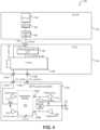
- FIG. 4is a block diagram of a barely Doherty dual amplifier circuit operating with an ET circuit that uses information from a transceiver according to an exemplary aspect of the present disclosure.
- FIG. 5provides a circuit-level diagram of the impedance inverter and transformer circuit of the barely Doherty dual amplifier circuit of FIG. 4 ,
- FIGS. 6 A- 6 Dprovide an illustration of the progression from an ideal impedance inverter to a practical impedance inverter using negatively-coupled inductors.
- FIGS. 7 A- 7 Dprovide an illustration of the progression from an ideal impedance inverter to a practical impedance inverter using positively-coupled inductors.
- FIG. 8provides an alternate power amplifier circuit where both Vcc_carrier and Vcc_peaking are provided in the impedance inverter.
- FIG. 9provides an alternate power amplifier circuit where the impedance inverter is based on the topology derived in FIGS. 6 A- 6 D .
- FIG. 10provides an alternate power amplifier circuit where the impedance inverter includes an additional variable capacitor
- FIG. 11provides an alternate power amplifier circuit using negatively-coupled inductors in the impedance inverter
- FIG. 12provides an alternate power amplifier circuit using positively-coupled inductors in the impedance inverter with parallel variable capacitors.
- FIG. 13provides an alternate power amplifier circuit where Vcc_carrier is provided to the transformer circuit instead of the impedance inverter.
- Embodiments of the disclosurerelate to a barely Doherty dual envelope tracking (BD 2 E) circuit.
- a transmitter chainincludes an envelope tracking (ET) circuit that controls a Doherty dual power amplifier array.
- the ET circuitprovides two control signals (supply voltage signals) that are used to control or modulate a carrier amplifier and a peaking amplifier independently of one another.
- the BD 2 E circuitincludes an improved impedance inverter that isolates the peaking amplifier from the carrier amplifier to allow this independent control. By providing independent control, greater linearity may be provided while preserving the efficiency of the circuit.
- FIG. 1Before addressing the particular impedance inverter of the present disclosure and its use with a Doherty dual amplifier circuit, an overview of a transmitter apparatus is provided with reference to FIG. 1 .
- a Doherty dual amplifier structure provided in FIG. 2 Ais explored in a normal mode of operation in FIGS. 2 B- 2 D and in a barely Doherty dual amplifier, operations are explored in FIGS. 3 A- 3 C .
- a discussion of particular exemplary aspects of the present disclosurebegins below with reference to FIG. 4 .
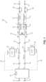
- FIG. 1is a schematic diagram of an exemplary transmitter apparatus 10 (also referred to as a transmitter circuit) configured to amplify a first input signal 12 and a second input signal 14 for concurrent transmission from a first antenna 16 and a second antenna 18 , respectively, as is common in fifth generation-new radio (5G-NR) cellular standards.
- 5G-NRfifth generation-new radio
- exemplary aspectsare described with reference to a 5G-NR compliant transmitter, it should be appreciated that the present disclosure is not so limited and may be used in other transmitters, including, but not limited to, single antenna transmitters, uplink multiple antenna transmitters, multiple input-multiple output (MIMO) type transmitters, and the like.
- MIMOmultiple input-multiple output
- the transmitter apparatus 10includes a transceiver circuit 20 configured to receive the first input signal 12 and the second input signal 14 .
- the transceiver circuit 20is configured to generate a first RF signal 22 , sometimes referred to as signal a or RFina, from the first input signal 12 and a second RF signal 24 , sometimes referred to as signal b or RFinb, from the second input signal 14 .
- signals a and bare orthogonal.
- the transmitter apparatus 10includes two (2) power amplifier circuits 26 and 28 to amplify the first RF signal 22 and the second RF signal 24 , respectively.
- the power amplifier circuits 26 and 28may also be a network of power amplifiers, and each may generically be referred to as a power amplifier network. It should be appreciated that either or both of the power amplifier circuits 26 and 28 may be Doherty dual amplifier circuits.
- the two power amplifier circuits 26 and 28may be controlled by ET integrated circuits (ICs) (ETICs) 30 and 32 , respectively.
- the ETICs 30 and 32are controlled by a Vrampa signal 34 and a Vrampb signal 36 from the transceiver circuit 20 .
- the signals 34 , 36are differential signals.
- signals 22 ′ and 24 ′are provided to respective filters 38 and 40 .
- the filters 38 and 40are coupled to impedance tuners 42 and 44 , respectively.
- the impedance tuners 42 and 44are coupled to the antennas 16 and 18 , respectively, such as through a coaxial or flex line connection (noted at 46 and 48 , respectively).
- the line with no signalmay be terminated to a known voltage level (e.g., to ground). Accordingly, termination structures 50 and 52 are provided to provide such terminations.
- the power amplifier circuit 26 and/or the power amplifier circuit 28may be a Doherty dual amplifier circuit as better illustrated in FIG. 2 A .
- the power amplifier circuit 26may be a single-ended amplifier circuit.
- the power amplifier circuit 26may include a first amplifier, also known as a carrier amplifier 60 , which, since it acts as a modulated current source, provides a current Ima through a load-line 62 to an impedance inverter 64 .
- the carrier amplifier 60may be controlled by an input voltage Vcc_Carrier, which may be from an envelope tracking (ET) circuit or average power tracking (APT) circuit.
- ETenvelope tracking
- APTaverage power tracking
- the power amplifier circuit 26may include a second amplifier, also known as a peaking amplifier 66 , which, since it also acts as a modulated current source, provides a current jlpa through a load-line 68 to a node 70 .
- the node 70is also coupled to the impedance inverter 64 and to an impedance load 72 (which is the output of the power amplifier circuit 26 (e.g., signal 22 ′ appears at the load 72 to be provided to the filter 38 ).
- the peaking amplifier 66may be controlled by an input voltage Vcc_Peaking, which may also be from an ET circuit or APT circuit. Because of its position, the impedance inverter 64 may be said to couple the carrier amplifier 60 to the peaking amplifier 66 .
- the peaking amplifier 66is also activated and operates from the average power to the peak power.
- the average poweris half the peak power and thus may be considered ⁇ 6 decibels (dB) below the peak power.
- dBdecibels
- the line 82represents the output current Im of the carrier amplifier 60
- the line 84represents the output current Ip of the peaking amplifier 66 .
- the line 82linearly increases from zero to the average power 86 (e.g., 1) and continues to the peak power 88 (e.g., 2).
- the line 84remains at zero until the average power 86 is reached, at which point the line 84 has a linear slope to the peak power 88 .
- each of the amplifiers 60 , 66is providing half the peak power.
- a power graph 90is provided in FIG. 2 C for an alternate representation of this operation.
- Line 92is the power provided by the combination of the carrier amplifier 60 and the peaking amplifier 66 . Up until point 94 , corresponding to the average power 86 , all of line 92 is provided by the carrier amplifier 60 . At point 94 , the carrier amplifier 60 still provides additional power as shown by line 96 , but it is only a portion of the total power of line 92 .
- Line 98shows the power provided by the peaking amplifier 66 . Line 98 is zero until the average power 86 is reached at which point the peaking amplifier 66 begins contributing to the total power of line 92 .
- the load seen by the power amplifiers 60 , 66is shown in FIG. 2 D as graph 100 .
- a line 102shows the load seen by the carrier amplifier 60 .
- Line 102is flat (and relatively large) until the average power 86 is reached, and at point 104 begins decreasing.
- Line 106corresponds to the load seen by the peaking amplifier 66 , and line 106 starts at a large impedance point 108 and rapidly diminishes to match the load of the carrier amplifier 60 .
- each amplifier 60 , 66is seeing half the load. It should be appreciated that the higher the load seen by the amplifiers 60 , 66 , the better power transfer.
- One attempt to improve performanceinvolves moving the activation of the peaking amplifier 66 to a point below the average power. For example, the peaking amplifier 66 may be activated at ⁇ 12 dB below the peak power. Such early activation is sometimes referred to as barely Doherty dual (BDD or BD 2 ) amplifiers.
- FIGS. 3 A- 3 CBDD or BD 2 operation is illustrated in FIGS. 3 A- 3 C , with the understanding that a Doherty dual amplifier circuit can operate in either mode depending on how it is controlled (i.e., the same structure illustrated in FIG. 2 A can operate in both normal Doherty dual mode and in barely Doherty dual mode).
- FIG. 3 Acorresponds to FIG. 2 B , and shows a graph 80 ′, where the line 82 again represents the output current Im of the carrier amplifier 60 and the line 84 ′ represents the output current Ip of the peaking amplifier 66 .
- the line 82linearly increases from zero to the average power 86 (e.g., 1) and continues to the peak power 88 (e.g., 2).
- the line 84 ′remains at zero only until point 110 (e.g., ⁇ 12 dB) is reached, at which point line 84 ′ has a linear slope to the peak power 88 .
- point 110e.g., ⁇ 12 dB
- each of the amplifiers 60 , 66is providing half the peak power.
- a power graph 90 ′is provided in FIG. 3 B for an alternate representation of this operation.
- Line 92 ′is the power provided by the combination of the carrier amplifier 60 and the peaking amplifier 66 . Up until point 112 , corresponding to point 110 in FIG. 3 A , all of line 92 ′ is provided by the carrier amplifier 60 . At point 112 , the carrier amplifier 60 still provides additional power as shown by line 114 , but it is only a portion of the total power of line 92 ′.
- Line 116shows the power provided by the peaking amplifier 66 . Line 116 is zero until point 112 is reached at which point the peaking amplifier 66 begins contributing to the total power of line 92 ′.
- the load seen by the power amplifiers 60 , 66is shown in FIG. 3 C as graph 100 ′.
- a line 102 ′shows the load seen by the carrier amplifier 60 .
- Line 102 ′is flat (and relatively large) until the point 110 is reached.
- Line 106 ′corresponds to the load seen by the peaking amplifier 66 , and line 106 ′ starts at a large impedance and rapidly diminishes to match the load of the carrier amplifier 60 .
- each amplifier 60 , 66is seeing half the load.
- the carrier amplifier 60begins seeing a lower load earlier resulting in an earlier loss of efficiency.
- the peaking amplifier 66is seeing a lower load earlier (contrast lines 106 ′ with line 106 and point 108 versus point 108 ′).
- ETrelies on a signal from an envelope detection circuit in a transceiver circuit to detect changes in the original signal that is going to be amplified.
- the signal sent from the envelope detection circuitmay be single ended or differential.
- the ETICthen generates a signal that acts as the supply voltage (Vcc) for the power amplifier circuit 26 , 28 .
- the supply voltage signal from the ETICis provided to both the carrier amplifier and the peaking amplifier. While using an ETIC with a BD 2 circuit provides some supply voltage modulation, it fails to take full advantage of the two-amplifier arrangement and still suffers from some loss of efficiency.
- Exemplary aspects of the present disclosureallow for independent control of the carrier amplifier and the peaking amplifier. This independent control is achieved by using the impedance inverter to isolate the carrier amplifier from the peaking amplifier. With this isolation, the amplifiers may be controlled independently to maintain linearity and reduce efficiency losses that may result from variations in the load perceived by the two amplifiers. Additionally, digital predistortion (DPD) may be used to help the amplifiers remain in isogain (i.e., having a constant gain).
- DPDdigital predistortion
- a transmitter circuit 150may include a transceiver circuit 152 (sometimes referred to as XCVR and corresponding to the transceiver circuit 20 of FIG. 1 ), an ETIC 154 (corresponding to the ETIC 30 ), and a BD 2 E power amplifier circuit 156 (corresponding to the power amplifier circuit 26 ).
- the power amplifier circuit 156provides signal 22 ′ to the transmitter filter 38 (not shown) and other downstream circuitry as shown in FIG. 1 .
- the transceiver circuit 152may include an ET-look up table (ET-LUT) 158 , a delay circuit 160 , and a digital-to-analog converter (DAC) 162 that collectively generate the Vramp signal that is provided to the ETIC 154 .
- the ETIC 154receives the Vramp signal at an input 164 .
- This Vramp signalis split into a Vcc_carrier_tgt (target) signal and a signal that is used to determine a desired gain/slope for a peaking amplifier in the power amplifier circuit 156 using a programmable LUT 166 .
- the programmable LUT 166provides a Vcc_peaking_tgt (target) signal to a tracker circuit 168 .
- the tracker circuit 168also receives Vcc_carrier_tgt. Based on the two target signals, the tracker circuit 168 generates a Vcc_carrier signal and a Vcc_peaking signal, both of which are supplied through respective outputs 170 A, 170 B to the power amplifier circuit 156 .
- the power amplifier circuit 156receives the Vcc_carrier signal and the Vcc_peaking signal at inputs 172 A, 172 B, respectively.
- the power amplifier circuit 156is a differential power amplifier circuit and includes a positive carrier amplifier 174 , a negative or minus carrier amplifier 176 , a positive peaking amplifier 178 , and a negative or minus peaking amplifier 180 .
- the carrier amplifiers 174 , 176are coupled to an impedance inverter 182 as are the peaking amplifiers 178 , 180 .
- Direct current (DC) blocking capacitors 184 A, 184 Bmay be positioned between the peaking amplifiers 178 , 180 and the impedance inverter 182 .
- the Vcc_carrier signalis provided to the impedance inverter 182 and controls the carrier amplifiers 174 , 176 as better described below with reference to FIG. 5 .
- the Vcc_peaking signalis supplied at a node within a transformer circuit 186 to control the peaking amplifiers 178 , 180 as better described below with reference to FIG. 5 .
- the transformer circuit 186produces the amplified signal 22 ′ at an output node 188 .
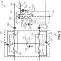
- FIG. 5provides more detail about an exemplary topology for the impedance inverter 182 and the transformer circuit 186 within the power amplifier circuit 156 .
- the impedance inverter 182includes a first inductor pair 200 and a second inductor pair 202 .
- the first inductor pair 200includes a first inductor 204 and a second inductor 206 with a node 208 therebetween.
- the first inductor 204is positively coupled to the second inductor 206 with a value of M equal to the product of L and K.
- the second inductor pair 202includes a third inductor 210 and a fourth inductor 212 with a node 214 therebetween.
- the third inductor 210is positively coupled to the fourth inductor 212 with a value of M equal to the product of L and K.
- the nodes 208 and 214are coupled and Vcc_carrier is provided at a supply voltage input node 215 , where the nodes 208 and 214 are coupled.
- a capacitor 216couples the nodes 208 , 214 to ground at radio frequencies, allowing Vcc_carrier (which is typically below 100 megahertz (MHz)) to operate normally.
- a first variable capacitor 218is positioned in parallel to the first inductor pair 200 .
- a second variable capacitor 220is positioned in parallel to the second inductor pair 202 .
- the transformer circuit 186includes a primary transformer 222 formed of inductors 224 , 226 having a supply voltage input node 228 therebetween.
- the transformer circuit 186further includes a secondary transformer 230 formed of inductors 232 , 234 .
- Vcc_peakingis provided at the supply voltage input node 228 .
- a capacitor 236couples the supply voltage input node 228 to ground at radio frequencies, allowing Vcc_peaking (which is typically below 100 MHz) to operate normally.
- the secondary transformer 230is coupled to an output load to provide the amplified signal 22 ′.
- An additional capacitor 238is provided to couple the output node 188 to ground at baseband frequencies, allowing the amplified signal 22 ′ to operate at radio frequencies.
- FIG. 6 Ashows an ideal impedance inverter 300 based on three element inductors 302 , 304 , and 306 arranged in a T-network.
- the middle shunt inductor 306has a negative inductor of value of ⁇ La while the two other inductors 302 , 304 have a positive inductor value of La.
- Z 1the resulting input impedance on N 1
- Z 2the impedance on N 2
- the impedance inverter 310approximates the ideal impedance inverter 300 as evidenced by an equivalent lumped impedance inverter circuit 316 , having inductors 318 , 320 , and 322 that can be formed from the topology of the impedance inverter 310 .
- the inductor 322has a negative inductance value of ⁇ L*K, which is not the same inductance value of the inductors 318 , 320 (i.e., L*(1+K)), but it is close.
- an impedance inverter 316 ′has the inductors 318 , 320 , and 322 with a variable capacitor (C 0 ) 324 added on the node N 3 to add the remaining extra negative reactance such that the sum of the negative inductor reactance with the added capacitive reactance is equal in amplitude but opposite in sign to the positive reactance of the two inductors L*(1+K).
- C 0variable capacitor
- FIG. 6 Dshows impedance inverter 310 ′ with negatively-coupled inductors 312 , 314 and a variable capacitor 328 that has the desired coefficient Ka at the resonance frequency.
- the impedance inverter 310 ′ compared with just using two non-coupled inductorshas a higher Ka factor for the same inductance due to the increased term (1+K); that is, one can create a larger Ka factor for a given L value by creating the negative coupling. Also, tuning of the Ka factor can be done via adjusting the value of C 0 versus frequency of operation thereby changing the resonance frequency.
- the network 350is based on three inductors 352 , 354 , and 356 , in which the inductor 352 between N 1 and N 2 is a negative inductor of value ⁇ La, while the two other inductors 354 , 356 are La each.
- an impedance network 360is formed as illustrated in FIG. 7 B .
- the impedance network 360approximates the network 350 as evidenced by an equivalent lumped impedance network 366 , having inductors 368 , 370 , and 372 that can be formed from the topology of the impedance network 360 .
- the inductor 372has a negative inductance value of ⁇ L*(1 ⁇ K 2 )/K, which is not the same inductance value the inductors 368 , 370 (i.e., L*(1 ⁇ K)), but it is close.
- an impedance network 366 ′has a variable capacitor (C 0 ) 374 that is put in in parallel with the inductor 372 to insert an additional positive admittance such that the equivalent admittance has the same value as the shunt element admittance but with opposite sign.
- the resulting impedance network 366 ′has a Ka term equal to j*L*(1 ⁇ K)* ⁇ with K ⁇ 0 and thus equal to
- K ⁇ aj * L C ⁇ 0 * ( ( 1 - K ) ( 1 + K ) ) , thus allowing creation of a much larger impedance inverter Ka factor due to the term
- FIG. 7 Dillustrates an impedance network 360 ′ that has the inductors 362 , 364 positively coupled to one another and a variable capacitor 376 in parallel between nodes N 1 and N 2 .
- Kamay be tuned via tuning C 0 relative to the frequency of operation.
- the middle node N 3which is tied to an RF ground, can be used as a supply DC bias.
- topologiesi.e., impedance inverter 310 ′ and impedance network 360 ′
- impedance inverter 182may be used within the impedance inverter 182 to allow the control signals Vcc_carrier and Vcc_peaking to be supplied and control the carrier amplifier and the peaking amplifier to be controlled independently as shown in FIG. 5 .
- a power amplifier circuit 156 ′has an impedance inverter 182 ′ and a transformer circuit 186 ′.
- the transformer circuit 186 ′is essentially identical to the transformer circuit 186 , but there is no input for the Vcc_peaking between the inductors 224 , 226 .
- the impedance inverter 182 ′includes a first inductor 400 and a second inductor 402 .
- the first inductor 400is positively coupled to the second inductor 402 with a value of M equal to the product of L and K. Note that the first inductor 400 is not electrically coupled to the second inductor 402 .
- the impedance inverter 182 ′also includes a third inductor 404 and a fourth inductor 406 .
- the third inductor 404is positively coupled to the fourth inductor 406 with a value of M equal to the product of L and K. Again, the third inductor 404 is not electrically coupled to the fourth inductor 406 .
- the first and third inductors 400 , 404are coupled with a node 408 therebetween.
- the second and fourth inductors 402 , 406are coupled with a node 410 therebetween.
- the node 408receives Vcc_carrier. Because the inductors 400 , 404 are isolated from the inductors 402 , 406 , Vcc_carrier does not reach the inductors 402 , 406 .
- the node 408is also coupled to ground at radio frequencies through a capacitor 412 .
- the node 410receives Vcc_peaking. Again, the isolation between the inductors 400 , 404 and the inductors 402 , 406 means Vcc_peaking does not reach the inductors 400 , 404 .
- the node 410is also coupled to ground at radio frequencies through a capacitor 414 .
- the first variable capacitor 218 and the second variable capacitor 220are provided as previously described.
- FIG. 9illustrates a power amplifier circuit 420 that includes has an impedance inverter 422 and a transformer circuit 424 .
- the transformer circuit 424is essentially identical to the transformer circuit 186 and a further discussion is omitted.
- the impedance inverter 422includes a first inductor 426 and a second inductor 428 with a node 430 therebetween.
- the first inductor 426is negatively coupled to the second inductor 428 .
- the node 430receives Vcc_carrier.
- a capacitor 432couples the node 430 to ground at radio frequencies. Additionally, variable capacitors 434 A, 434 B may be used to isolate the impedance inverter 422 from the transformer circuit 424 at baseband frequencies and allow for some tuning of the resonant frequencies.
- FIG. 10illustrates a similar power amplifier circuit 420 ′ which is essentially identical to the power amplifier circuit 420 , but the impedance inverter 422 ′ includes an additional variable capacitor 436 coupling the two variable capacitors 434 A, 434 B. This additional capacitor allows for extra tuning.
- FIGS. 11 - 13provide alternate structures that provide improved impedance inverters, albeit without the independent control.
- FIG. 11illustrates a power amplifier circuit 450 with an impedance inverter 452 that has negatively-coupled inductors 454 , 456 with node 458 therebetween and negatively-coupled inductors 460 , 462 with node 464 therebetween. Nodes 458 , 464 are coupled by a variable capacitor 466 .
- the power amplifier circuit 450also includes a transformer circuit 468 that is identical to the transformer circuits 424 and 186 .
- FIG. 12illustrates a similar power amplifier circuit 450 ′ with an impedance inverter 452 ′.
- the impedance inverter 452 ′has positively-coupled inductors 454 , 456 with node 458 therebetween and positively-coupled inductors 460 , 462 with node 464 therebetween.
- Nodes 458 , 464are coupled at node 470 , which is coupled to ground by a capacitor 472 , which couples to ground at radio frequencies, but not baseband frequencies.
- variable capacitors 474 A, 474 Bare provided similar to the variable capacitors 218 , 220 of FIG. 5 . Again, this arrangement does not allow for independent control of the carrier amplifiers 174 , 176 and the peaking amplifiers 178 , 180 , but does provide a larger impedance inverter.
- FIG. 13illustrates a power amplifier circuit 450 ′′ that is similar to the power amplifier circuits 450 and 450 ′ in FIGS. 11 and 12 , but moves the input for Vcc_carrier from the transformer circuit to the impedance inverter. Specifically, the node 470 ′ now receives Vcc_carrier.
- the transformer circuit 476has a node 478 that is coupled to ground at radio frequencies through a capacitor 480 .
Landscapes
- Engineering & Computer Science (AREA)
- Power Engineering (AREA)
- Computer Networks & Wireless Communication (AREA)
- Signal Processing (AREA)
- Amplifiers (AREA)
Abstract
Description
with the Ka factor
thus allowing creation of a much larger impedance inverter Ka factor due to the term
which is greater than 1 since K is negative.
Claims (21)
Priority Applications (1)
| Application Number | Priority Date | Filing Date | Title |
|---|---|---|---|
| US17/351,560US12068720B2 (en) | 2021-02-26 | 2021-06-18 | Barely Doherty dual envelope tracking (BD2E) circuit |
Applications Claiming Priority (2)
| Application Number | Priority Date | Filing Date | Title |
|---|---|---|---|
| US202163154030P | 2021-02-26 | 2021-02-26 | |
| US17/351,560US12068720B2 (en) | 2021-02-26 | 2021-06-18 | Barely Doherty dual envelope tracking (BD2E) circuit |
Publications (2)
| Publication Number | Publication Date |
|---|---|
| US20220278651A1 US20220278651A1 (en) | 2022-09-01 |
| US12068720B2true US12068720B2 (en) | 2024-08-20 |
Family
ID=83007245
Family Applications (1)
| Application Number | Title | Priority Date | Filing Date |
|---|---|---|---|
| US17/351,560Active2042-05-28US12068720B2 (en) | 2021-02-26 | 2021-06-18 | Barely Doherty dual envelope tracking (BD2E) circuit |
Country Status (1)
| Country | Link |
|---|---|
| US (1) | US12068720B2 (en) |
Families Citing this family (6)
| Publication number | Priority date | Publication date | Assignee | Title |
|---|---|---|---|---|
| US11909385B2 (en) | 2020-10-19 | 2024-02-20 | Qorvo Us, Inc. | Fast-switching power management circuit and related apparatus |
| US12265442B2 (en) | 2020-12-04 | 2025-04-01 | Qorvo Us, Inc. | Power management integrated circuit |
| EP4268364B1 (en) | 2020-12-22 | 2024-11-27 | Qorvo US, Inc. | Power management apparatus operable with multiple configurations |
| US12267046B2 (en) | 2021-02-15 | 2025-04-01 | Qorvo Us, Inc. | Power amplifier system |
| US12063018B2 (en) | 2021-06-10 | 2024-08-13 | Qorvo Us, Inc. | Envelope tracking integrated circuit operable with multiple types of power amplifiers |
| US20240356192A1 (en)* | 2023-04-18 | 2024-10-24 | Apple Inc. | Transformer based series doherty power amplifier |
Citations (256)
| Publication number | Priority date | Publication date | Assignee | Title |
|---|---|---|---|---|
| JPH03104422A (en) | 1989-09-19 | 1991-05-01 | Nippon Telegr & Teleph Corp <Ntt> | Linear transmission equipment |
| US5510753A (en) | 1993-11-23 | 1996-04-23 | Blade Technologies Inc. | Composite bridge amplifier with output overload and thermal protection |
| US5838732A (en) | 1994-10-31 | 1998-11-17 | Airnet Communications Corp. | Reducing peak-to-average variance of a composite transmitted signal generated by a digital combiner via carrier phase offset |
| US6107862A (en) | 1997-02-28 | 2000-08-22 | Seiko Instruments Inc. | Charge pump circuit |
| US6141377A (en) | 1998-07-30 | 2000-10-31 | Cisco Technology, Inc. | Method and apparatus for voice frequency noise reduction in splitterless ADSL |
| US6141541A (en) | 1997-12-31 | 2000-10-31 | Motorola, Inc. | Method, device, phone and base station for providing envelope-following for variable envelope radio frequency signals |
| US6411531B1 (en) | 2000-11-21 | 2002-06-25 | Linear Technology Corporation | Charge pump DC/DC converters with reduced input noise |
| US20020167827A1 (en) | 2001-01-29 | 2002-11-14 | Hiroyuki Umeda | Power supply apparatus |
| US20030107428A1 (en) | 2001-11-09 | 2003-06-12 | Stmicroelectronics S.R.L. | Low power charge pump circuit |
| US20040266366A1 (en) | 2003-06-24 | 2004-12-30 | Ian Robinson | Multi-mode amplifier system |
| US20050090209A1 (en) | 2003-10-23 | 2005-04-28 | Behzad Arya R. | High linearity, high efficiency power amplifier with DSP assisted linearity optimization |
| US20050227646A1 (en) | 2004-03-18 | 2005-10-13 | Ryo Yamazaki | Detecting and maintaining linearity in a power amplifier system through comparing peak and RMS power levels |
| US20050232385A1 (en) | 2004-03-02 | 2005-10-20 | Matsushita Electric Industrial Co., Ltd. | Two-point frequency modulation apparatus, wireless transmitting apparatus, and wireless receiving apparatus |
| US6985033B1 (en) | 2003-05-15 | 2006-01-10 | Marvell International Ltd. | Circuits and methods for adjusting power amplifier predistortion, and power amplifiers and other devices including the same |
| US20060028271A1 (en) | 2003-02-19 | 2006-02-09 | Nujira Ltd. | High efficiency amplification |
| US20060240786A1 (en) | 2002-10-31 | 2006-10-26 | Xiaowei Liu | Method and system for broadband predistortion linearization |
| US20070036212A1 (en) | 2005-05-06 | 2007-02-15 | Silicon Laboratories Inc. | Digital Controller Based Power Factor Correction Circuit |
| US20070052474A1 (en) | 2005-09-05 | 2007-03-08 | Fujitsu Limited | Amplifier and device having amplifier, and mutual conductance control method |
| US7193467B2 (en) | 2004-03-30 | 2007-03-20 | Rambus Inc. | Differential amplifiers and methods of using same |
| US20070258602A1 (en) | 2006-05-05 | 2007-11-08 | Nokia Corporation | Method and arrangement for optimizing efficiency of a power amplifier |
| US20070290748A1 (en) | 2006-06-04 | 2007-12-20 | Wangmyong Woo | Systems, Methods, and Apparatuses for Linear Envelope Elimination and Restoration Transmitters |
| US20080116960A1 (en) | 2006-11-22 | 2008-05-22 | Oki Electric Industry Co., Ltd. | Charge pump-type dc/dc converter |
| US20080231358A1 (en) | 2007-03-23 | 2008-09-25 | Mitsubishi Electric Corporation | Power amplifier circuit |
| US7471155B1 (en) | 2007-05-25 | 2008-12-30 | Rf Micro Devices, Inc. | Cancelling switching power supply ripple from a radio frequency signal |
| US20090016085A1 (en) | 2007-07-11 | 2009-01-15 | Semtech Corporation | Method and Apparatus for a Charge Pump DC-to-DC Converter Having Parallel Operating Modes |
| US20090045872A1 (en) | 2005-03-07 | 2009-02-19 | Peter Blakeborough Kenington | Integrated transceiver with envelope tracking |
| US20090191826A1 (en) | 2008-01-29 | 2009-07-30 | Matsushita Electric Industrial Co., Ltd. | High-Efficiency Envelope Tracking Systems and Methods for Radio Frequency Power Amplifiers |
| US7570931B2 (en) | 2006-06-02 | 2009-08-04 | Crestcom, Inc. | RF transmitter with variably biased RF power amplifier and method therefor |
| US20100283534A1 (en) | 2009-05-07 | 2010-11-11 | John Pierdomenico | BOOSTING xDSL AMPLIFIER SUPPLY POWER ON-DEMAND |
| US20100308919A1 (en) | 2009-06-03 | 2010-12-09 | Jaroslaw Adamski | Methods and devices for leakage current reduction |
| US20110074373A1 (en) | 2009-09-29 | 2011-03-31 | Richtek Technology Corp. | Control circuit and method for a buck-boost power converter |
| US20110136452A1 (en) | 2008-08-20 | 2011-06-09 | Freescale Semiconductor, Inc. | Wireless communication unit, integrated circuit and method of power control of a power amplifier therefor |
| US20110148705A1 (en) | 2009-12-21 | 2011-06-23 | Peter Kenington | Single envelope tracking system for an active antenna array |
| US20110175681A1 (en) | 2010-01-21 | 2011-07-21 | Panasonic Corporation | Radio frequency power amplifier and wireless communication device including the same |
| US7994862B1 (en) | 2010-02-11 | 2011-08-09 | Sige Semiconductor Inc. | Circuit and method of temperature dependent power amplifier biasing |
| US20110279179A1 (en) | 2010-05-17 | 2011-11-17 | Avago Technologies Wireless Ip (Singapore) | Apparatus and method for controlling power amplifier |
| US20120194274A1 (en) | 2011-02-01 | 2012-08-02 | Paul Fowers | Integrated circuit, wireless communication unit and method for providing a power supply |
| US20120200435A1 (en) | 2011-02-07 | 2012-08-09 | Rf Micro Devices, Inc. | Apparatuses and methods for rate conversion and fractional delay calculation using a coefficient look up table |
| US20120281597A1 (en) | 2011-05-02 | 2012-11-08 | Rf Micro Devices, Inc. | Radio front end and power management architecture for lte-advanced |
| US20120299645A1 (en) | 2010-04-20 | 2012-11-29 | Rf Micro Devices, Inc. | Temperature correcting an envelope power supply signal for rf pa circuitry |
| US20120299647A1 (en) | 2010-04-20 | 2012-11-29 | Rf Micro Devices, Inc. | Pa envelope power supply undershoot compensation |
| US20130021827A1 (en) | 2011-07-22 | 2013-01-24 | Zhong Ye | System and method for envelope tracking power supply |
| US20130072139A1 (en) | 2011-09-21 | 2013-03-21 | Samsung Electronics Co. Ltd. | Apparatus and method for processing reduced bandwidth envelope tracking and digital pre-distortion |
| US20130100991A1 (en) | 2011-10-20 | 2013-04-25 | Samsung Electronics Co. Ltd. | Digital pre-distortion method and apparatus thereof for changing memory degree depending on input level |
| US20130127548A1 (en) | 2011-11-18 | 2013-05-23 | Nujira Ltd | Apparatus and methods for voltage converters |
| US20130130724A1 (en) | 2011-11-21 | 2013-05-23 | Broadcom Corporation | Wireless communication device capable of efficient network search |
| US20130141064A1 (en) | 2011-12-01 | 2013-06-06 | Rf Micro Devices, Inc. | Voltage offset loop for a switching controller |
| US8461928B2 (en) | 2011-01-25 | 2013-06-11 | Provigent Ltd. | Constant-gain power amplifier |
| US20130162233A1 (en) | 2011-12-27 | 2013-06-27 | St-Ericsson Sa | Single feedback loop for parallel architecture buck converter - ldo regulator |
| US8493141B2 (en) | 2010-04-19 | 2013-07-23 | Rf Micro Devices, Inc. | Pseudo-envelope following power management system |
| US20130187711A1 (en) | 2012-01-19 | 2013-07-25 | Motorola Mobility, Inc. | Method and apparatus for resource block based transmitter optimization in wireless communication devices |
| US20130200865A1 (en) | 2010-08-13 | 2013-08-08 | Nujira Limited | Switch mode power supply for envelope tracking |
| US8519788B2 (en) | 2010-04-19 | 2013-08-27 | Rf Micro Devices, Inc. | Boost charge-pump with fractional ratio and offset loop for supply modulation |
| US20130271221A1 (en) | 2010-04-20 | 2013-10-17 | Rf Micro Devices, Inc. | Direct current (dc)-dc converter having a multi-stage output filter |
| US8588713B2 (en) | 2011-01-10 | 2013-11-19 | Rf Micro Devices, Inc. | Power management system for multi-carriers transmitter |
| US20140009226A1 (en) | 2012-07-08 | 2014-01-09 | R2 Semiconductor, Inc. | Decoupling circuits for filtering a voltage supply of multiple power amplifiers |
| US20140028390A1 (en) | 2012-07-25 | 2014-01-30 | Qualcomm Incorporated | Energy source sharing |
| US20140028370A1 (en) | 2012-01-16 | 2014-01-30 | Nujira Limited | Crest Factor Reduction Applied To Shaping Table To Increase Power Amplifier Efficiency Of Envelope Tracking Amplifier |
| US20140055197A1 (en) | 2011-05-05 | 2014-02-27 | Rf Micro Devices, Inc. | Power management architecture for modulated and constant supply operation |
| US20140057684A1 (en) | 2011-05-05 | 2014-02-27 | Rf Micro Devices, Inc. | Power loop control based envelope tracking |
| US20140103995A1 (en) | 2012-10-15 | 2014-04-17 | Andreas Langer | Control Circuit and Method for Controlling an Operation of a Power Amplifier |
| US8718188B2 (en) | 2011-04-25 | 2014-05-06 | Skyworks Solutions, Inc. | Apparatus and methods for envelope tracking |
| US8725218B2 (en) | 2011-03-25 | 2014-05-13 | R2 Semiconductor, Inc. | Multimode operation DC-DC converter |
| US8723492B2 (en) | 2011-03-22 | 2014-05-13 | Integrated Device Technology, Inc. | Autonomous controlled headroom low dropout regulator for single inductor multiple output power supply |
| US20140155002A1 (en) | 2012-12-03 | 2014-06-05 | Broadcom Corporation | Envelope Tracking Signal Bandwidth Control |
| US20140169427A1 (en) | 2012-12-19 | 2014-06-19 | Mediatek Singapore Pte. Ltd. | Method and apparatus for calibrating an envelope tracking system |
| US20140184335A1 (en) | 2012-12-28 | 2014-07-03 | Peregrine Semiconductor Corporation | Amplifiers Operating in Envelope Tracking Mode or Non-Envelope Tracking Mode |
| CN103916093A (en) | 2012-12-28 | 2014-07-09 | 联发科技股份有限公司 | Method for correcting envelope tracking system, communication unit and integrated circuit |
| US20140199949A1 (en) | 2013-01-16 | 2014-07-17 | Motorola Mobility Llc | Method for improving tx gain in envelope tracking systems |
| US20140203869A1 (en) | 2013-01-24 | 2014-07-24 | Rf Micro Devices, Inc. | Communications based adjustments of an offset capacitive voltage |
| US20140210550A1 (en) | 2013-01-28 | 2014-07-31 | Qualcomm Incorporated | Reverse current prevention |
| US20140213196A1 (en) | 2013-01-31 | 2014-07-31 | Andreas Langer | Recalibration of envelope tracking transfer function during active transmission |
| US20140218109A1 (en) | 2013-02-01 | 2014-08-07 | Nujira Limited | 2g support for 2g and 3g/4g envelope tracking modulator |
| US8803603B2 (en) | 2011-06-24 | 2014-08-12 | Nujira Limited | Envelope tracking system for MIMO |
| US20140235185A1 (en) | 2012-03-04 | 2014-08-21 | Quantance, Inc. | Envelope Tracking Power Amplifier System with Delay Calibration |
| US8818305B1 (en) | 2012-11-14 | 2014-08-26 | Motorola Mobility Llc | Supply transitions in an envelope tracked power amplifier |
| US20140266428A1 (en) | 2013-03-14 | 2014-09-18 | Rf Micro Devices, Inc. | Envelope tracking power supply voltage dynamic range reduction |
| US20140266423A1 (en) | 2013-03-15 | 2014-09-18 | Quantance, Inc. | Envelope Tracking System with Internal Power Amplifier Characterization |
| US8854129B2 (en) | 2010-04-15 | 2014-10-07 | Nujira Limited | Timing alignment for modulated supply |
| US20140315504A1 (en) | 2013-04-17 | 2014-10-23 | Fujitsu Limited | Power supply circuit, power supply system, and radio communication apparatus |
| US8879665B2 (en) | 2011-06-08 | 2014-11-04 | Broadcom Corporation | Controlling a power amplifier based on transmitter output emissions |
| US20140361837A1 (en) | 2011-02-01 | 2014-12-11 | Mediatek Singapore Pte. Ltd. | Integrated circuit wireless communication unit and method for providing a power supply |
| US20140361830A1 (en) | 2013-06-06 | 2014-12-11 | Qualcomm Incorporated | Envelope tracker with variable boosted supply voltage |
| US8913690B2 (en) | 2011-05-13 | 2014-12-16 | Sumitomo Electric Industries, Ltd. | Amplifier circuit and wireless communication equipment |
| US8942651B2 (en) | 2010-04-20 | 2015-01-27 | Rf Micro Devices, Inc. | Cascaded converged power amplifier |
| US8947161B2 (en) | 2011-12-01 | 2015-02-03 | Rf Micro Devices, Inc. | Linear amplifier power supply modulation for envelope tracking |
| US20150048883A1 (en) | 2013-08-14 | 2015-02-19 | Quantance, Inc. | Stabilizing a Power Combining Power Supply System |
| US20150071382A1 (en) | 2013-09-12 | 2015-03-12 | Fujitsu Limited | Digital pre-distortion transmitter and method for controlling the same |
| US8989682B2 (en) | 2011-02-07 | 2015-03-24 | Skyworks Solutions, Inc. | Apparatus and methods for envelope tracking calibration |
| US20150098523A1 (en) | 2013-10-04 | 2015-04-09 | Samsung Electronics Co., Ltd. | Apparatus and method for power amplification |
| US9020451B2 (en) | 2012-07-26 | 2015-04-28 | Rf Micro Devices, Inc. | Programmable RF notch filter for envelope tracking |
| US9018921B2 (en) | 2011-08-17 | 2015-04-28 | National Semiconductor Corporation | Battery charger architecture |
| US20150139358A1 (en) | 2013-11-18 | 2015-05-21 | Qualcomm Incorporated | Pre-distortion in a wireless transmitter |
| US9041364B2 (en) | 2011-12-01 | 2015-05-26 | Rf Micro Devices, Inc. | RF power converter |
| US9041365B2 (en) | 2011-12-01 | 2015-05-26 | Rf Micro Devices, Inc. | Multiple mode RF power converter |
| US20150155836A1 (en) | 2013-12-02 | 2015-06-04 | Futurewei Technologies, Inc. | Nonlinear Load Pre-Distortion for Open Loop Envelope Tracking |
| US9055529B2 (en) | 2013-10-04 | 2015-06-09 | Samsung Electronics Co., Ltd. | System and method for adaptive in-network time alignment for envelope tracking power amplifier |
| US9065509B1 (en) | 2014-01-09 | 2015-06-23 | Mediatek Inc. | Methods and apparatus for envelope tracking system |
| US9069365B2 (en) | 2012-02-18 | 2015-06-30 | R2 Semiconductor, Inc. | DC-DC converter enabling rapid output voltage changes |
| US20150188432A1 (en) | 2012-08-10 | 2015-07-02 | Texas Instruments Incorporated | Switched mode assisted linear regulator with seamless transition between power tracking configurations |
| US9098099B2 (en) | 2010-11-11 | 2015-08-04 | Samsung Electronics Co., Ltd. | Device and method for increasing output efficiency of mobile communication terminal |
| US20150236729A1 (en) | 2014-02-16 | 2015-08-20 | Mediatek Inc. | Methods and apparatus for envelope tracking system |
| US20150236654A1 (en) | 2014-02-19 | 2015-08-20 | Futurewei Technologies, Inc. | Envelope Tracking Apparatus and Method |
| US20150236652A1 (en) | 2014-02-19 | 2015-08-20 | Research & Business Foundation Sungkyunkwan University | Multi mode bias modulator operating in envelope tracking mode or average power tracking mode and envelope tracking power amplifier using the same |
| US20150236877A1 (en) | 2014-02-14 | 2015-08-20 | Mediatek Inc. | Methods and apparatus for envelope tracking system |
| EP2909928A1 (en) | 2012-10-19 | 2015-08-26 | Telefonaktiebolaget LM Ericsson (Publ) | Apparatus and method for load modulating an amplifier |
| US20150280652A1 (en) | 2014-03-28 | 2015-10-01 | Intel IP Corporation | Apparatus and a Method for Providing a Supply Control Signal for a Supply Unit |
| US9167514B2 (en) | 2012-12-03 | 2015-10-20 | Broadcom Corporation | Unequal amplifier gain compression via shaping table |
| US9166538B2 (en) | 2011-02-01 | 2015-10-20 | Mediatek Singapore Pte. Ltd. | Integrated circuit wireless communication unit and method for providing a power supply |
| US9166830B2 (en) | 2013-07-18 | 2015-10-20 | Intel Deutschland Gmbh | Systems and methods utilizing adaptive envelope tracking |
| US20150333781A1 (en) | 2014-05-19 | 2015-11-19 | Skyworks Solutions, Inc. | Rf transceiver front end module with improved linearity |
| US9197182B2 (en) | 2010-02-01 | 2015-11-24 | Rf Micro Devices, Inc. | Envelope power supply calibration of a multi-mode radio frequency power amplifier |
| US9225362B2 (en) | 2013-03-14 | 2015-12-29 | Quantance, Inc. | Power supply |
| CN105322894A (en) | 2014-07-29 | 2016-02-10 | 天工方案公司 | Envelope tracking with low frequency loss correction |
| US9263997B2 (en) | 2013-03-14 | 2016-02-16 | Quantance, Inc. | Self setting power supply using negative output impedance |
| US20160050629A1 (en) | 2014-08-13 | 2016-02-18 | Skyworks Solutions, Inc. | Apparatus and methods for wideband envelope tracking systems |
| US9271236B2 (en) | 2013-03-14 | 2016-02-23 | Quantance, Inc. | ET system with adjustment for noise |
| US9270230B2 (en) | 2008-11-18 | 2016-02-23 | Snaptrack, Inc. | Power supply arrangement for multi-stage amplifier |
| US20160065139A1 (en) | 2014-09-02 | 2016-03-03 | Samsung Electronics Co., Ltd. | Method and apparatus for supplying power to a radio frequency power amplifier |
| US20160065137A1 (en) | 2014-08-26 | 2016-03-03 | Rf Micro Devices, Inc. | Reduced bandwidth envelope tracking |
| US9280163B2 (en) | 2011-12-01 | 2016-03-08 | Rf Micro Devices, Inc. | Average power tracking controller |
| US9298198B2 (en) | 2011-12-28 | 2016-03-29 | Rf Micro Devices, Inc. | Noise reduction for envelope tracking |
| US20160099686A1 (en) | 2014-07-23 | 2016-04-07 | Eta Devices, Inc. | Linearity and noise improvement for multilevel power amplifier systems using multi-pulse drain transitions |
| US20160099687A1 (en) | 2014-10-03 | 2016-04-07 | Rf Micro Devices, Inc. | Envelope tracking with reduced dynamic range |
| US20160105151A1 (en) | 2014-10-13 | 2016-04-14 | Intel Corporation | Switchable Dual Core Power Amplifier |
| US20160118941A1 (en) | 2013-05-29 | 2016-04-28 | Nokia Technologies Oy | Amplication of a radio frequency signal |
| US20160126900A1 (en) | 2013-05-22 | 2016-05-05 | Snaptrack, Inc. | Transfer function regulation |
| US9344304B1 (en) | 2014-12-18 | 2016-05-17 | Intel IP Corporation | Communication device with power supply load variation noise reduction for envelope tracking and method therefor |
| US9356512B2 (en) | 2013-07-29 | 2016-05-31 | Broadcom Corporation | Envelope tracking power supply with direct connection to power source |
| US9362868B2 (en) | 2013-12-02 | 2016-06-07 | Futurewei Technologies, Inc. | Reduced power amplifier load impact for open loop envelope tracking |
| US20160164550A1 (en) | 2014-12-09 | 2016-06-09 | Intel Corporation | Envelope tracking path delay fine tuning and calibration |
| US20160164551A1 (en) | 2014-12-05 | 2016-06-09 | Rf Micro Devices, Inc. | Envelope tracking with reduced circuit area and power consumption |
| US20160173031A1 (en) | 2014-12-12 | 2016-06-16 | Intel Corporation | Envelope Tracking in Connection with Simultaneous Transmission in one or more Frequency Bands |
| US20160181995A1 (en) | 2014-12-23 | 2016-06-23 | Nokia Corporation | Reconfigurable bias and supply drivers for radio frequency power amplifiers |
| US9379667B2 (en) | 2011-05-05 | 2016-06-28 | Rf Micro Devices, Inc. | Multiple power supply input parallel amplifier based envelope tracking |
| US20160187627A1 (en) | 2014-12-24 | 2016-06-30 | Canon Kabushiki Kaisha | Zoom lens and image pickup apparatus including the same |
| US20160197627A1 (en) | 2015-01-04 | 2016-07-07 | Huawei Technologies Co., Ltd. | Digital predistortion system and method based on envelope tracking and radio frequency system |
| US20160249300A1 (en) | 2015-02-19 | 2016-08-25 | Mediatek Inc. | Envelope Tracking (ET) Closed-Loop On-the-Fly Calibration |
| US20160294587A1 (en) | 2015-04-02 | 2016-10-06 | Futurewei Technologies, Inc. | Open loop digital pwm envelope tracking system with dynamic boosting |
| CN106208974A (en) | 2016-08-30 | 2016-12-07 | 厦门信同信息技术有限公司 | A kind of design method of digital power amplifier based on adaptive digital envelop following technology |
| US20170005619A1 (en) | 2015-07-01 | 2017-01-05 | Qorvo Us, Inc. | Envelope tracking power converter circuitry |
| US20170005676A1 (en) | 2015-07-03 | 2017-01-05 | Mediatek Singipore Pte, Ltd. | Communication units and methods for power supply control |
| US20170006543A1 (en) | 2015-07-01 | 2017-01-05 | Rf Micro Devices, Inc. | Dual-mode envelope tracking power converter circuitry |
| US20170012675A1 (en) | 2014-02-10 | 2017-01-12 | Clairvoyant Technology Llc | Polar transmitter for rfid reader |
| US9595869B2 (en) | 2015-02-27 | 2017-03-14 | Qualcomm Incorporated | Multi-level switching regulator circuits and methods with finite state machine control |
| US9614477B1 (en) | 2016-01-12 | 2017-04-04 | Avago Technologies General Ip (Singapore) Pte. Ltd. | Envelope tracking supply modulators for multiple power amplifiers |
| US9634666B2 (en) | 2014-12-23 | 2017-04-25 | Intel IP Corporation | Push-pull driver, a transmitter, a receiver, a transceiver, an integrated circuit, a method for generating a signal at an output |
| US20170141736A1 (en) | 2015-11-13 | 2017-05-18 | Analog Devices Global | Broadband envelope tracking |
| EP3174199A2 (en) | 2011-05-05 | 2017-05-31 | Qorvo US, Inc. | Power management architecture for modulated and constant supply operation |
| CN106877824A (en) | 2016-12-29 | 2017-06-20 | 中国电子科技集团公司第五十研究所 | Envelope tracking power supply control system and method based on FPGA signal processing |
| US9705451B2 (en) | 2013-07-04 | 2017-07-11 | Murata Manufacturing Co., Ltd. | Power amplification module |
| US9748845B1 (en) | 2013-11-02 | 2017-08-29 | Sridhar Kotikalapoodi | Method and apparatus for wide bandwidth, efficient power supply |
| US20170302183A1 (en) | 2014-10-06 | 2017-10-19 | Zentrum Mikroelektronik Dresden Ag | Pulsed linear power converter |
| US9806676B2 (en) | 2015-07-28 | 2017-10-31 | Skyworks Solutions, Inc. | Power amplification system with programmable load line |
| US20170317913A1 (en) | 2016-04-28 | 2017-11-02 | Samsung Electronics Co., Ltd. | System and method for frequency-domain weighted least squares |
| US20170338773A1 (en) | 2016-05-17 | 2017-11-23 | Skyworks Solutions, Inc. | Power amplification system with envelope-based bias |
| US20180013465A1 (en) | 2016-07-06 | 2018-01-11 | Qorvo Us, Inc. | Multi-mode radio frequency circuitry |
| US20180048276A1 (en) | 2016-08-12 | 2018-02-15 | Qorvo Us, Inc. | Multi-mode envelope tracking amplifier circuit |
| US20180048265A1 (en) | 2015-02-23 | 2018-02-15 | Nokia Technologies Oy | Method and Apparatus for Supplying Power to an Amplifier |
| US9900204B2 (en) | 2010-04-20 | 2018-02-20 | Qorvo Us, Inc. | Multiple functional equivalence digital communications interface |
| US20180076772A1 (en) | 2016-09-14 | 2018-03-15 | Skyworks Solutions, Inc. | Apparatus and methods for envelope tracking systems with automatic mode selection |
| US9923520B1 (en) | 2016-09-21 | 2018-03-20 | Qualcomm Incorporated | Switching power supply for RF power amplifiers |
| US20180123453A1 (en) | 2016-11-01 | 2018-05-03 | Lion Semiconductor Inc. | Feedback control for efficient high-speed battery charging |
| US20180152144A1 (en) | 2016-11-25 | 2018-05-31 | Samsung Electronics Co., Ltd. | Supply modulator and communication device including the same |
| CN108141184A (en) | 2015-05-29 | 2018-06-08 | Qorvo美国公司 | Linear power amplifier |
| US10003416B1 (en) | 2016-12-16 | 2018-06-19 | Rohde & Schwarz Gmbh & Co. Kg | Method for measuring characteristics of a transmitter unit of a device under test, test system and radio frequency device |
| US20180254530A1 (en) | 2015-09-08 | 2018-09-06 | Volt Technology Limited | Battery with a voltage regulation device |
| US10090808B1 (en) | 2017-03-30 | 2018-10-02 | Intel IP Corporation | Feed-forward envelope tracking |
| US10090809B1 (en) | 2017-08-15 | 2018-10-02 | Qorvo Us, Inc. | Multi-mode mobile power management circuit |
| US20180288697A1 (en) | 2017-03-31 | 2018-10-04 | Intel IP Corporation | Adaptive envelope tracking threshold |
| WO2018182778A1 (en) | 2017-03-30 | 2018-10-04 | Intel Corporation | Distributed feed-forward envelope tracking system |
| US10097145B1 (en) | 2017-12-11 | 2018-10-09 | Qorvo Us, Inc. | Multi-mode power management circuit |
| US10103693B2 (en) | 2015-09-30 | 2018-10-16 | Skyworks Solutions, Inc. | Power amplifier linearization system and method |
| US20180302042A1 (en) | 2015-12-24 | 2018-10-18 | Huawei Technologies Co., Ltd. | Power amplifier control method and apparatus, and power amplifier control system |
| US20180309414A1 (en) | 2017-04-25 | 2018-10-25 | Qorvo Us, Inc. | Envelope tracking amplifier circuit |
| US10116470B2 (en) | 2015-10-28 | 2018-10-30 | Futurewei Technologies, Inc. | Combined low and high frequency continuous-time linear equalizers |
| US10158330B1 (en) | 2017-07-17 | 2018-12-18 | Qorvo Us, Inc. | Multi-mode envelope tracking amplifier circuit |
| US10158329B1 (en) | 2017-07-17 | 2018-12-18 | Qorvo Us, Inc. | Envelope tracking power amplifier circuit |
| US20180367101A1 (en) | 2017-06-19 | 2018-12-20 | Realtek Semiconductor Corporation | Envelope-tracking power supply modulator |
| US20180375483A1 (en) | 2017-06-21 | 2018-12-27 | Skyworks Solutions, Inc. | Wide bandwidth envelope trackers |
| US20180375476A1 (en) | 2017-06-21 | 2018-12-27 | Skyworks Solutions, Inc. | Fast envelope tracking systems for power amplifiers |
| US10170989B2 (en) | 2010-09-03 | 2019-01-01 | Skyworks Solutions, Inc. | Methods for fabricating an integrated circuit with a voltage regulator |
| CN109150212A (en) | 2014-02-24 | 2019-01-04 | 华为技术有限公司 | Load current sensor for envelope-tracking modulator |
| US20190028060A1 (en) | 2017-07-18 | 2019-01-24 | Samsung Electro-Mechanics Co., Ltd. | Envelope tracking current bias circuit with offset removal function and power amplifier |
| US20190068234A1 (en) | 2017-08-31 | 2019-02-28 | Qorvo Us, Inc. | Multi radio access technology power management circuit |
| US20190097277A1 (en) | 2016-04-27 | 2019-03-28 | Autonetworks Technologies, Ltd. | Power source device |
| US20190109566A1 (en) | 2017-10-06 | 2019-04-11 | Qorvo Us, Inc. | Nonlinear bandwidth compression circuitry |
| US10291181B2 (en) | 2016-11-02 | 2019-05-14 | Samsung Electronics Co., Ltd. | Supply modulator and communication device including the same |
| US20190181804A1 (en) | 2017-12-13 | 2019-06-13 | Qorvo Us, Inc. | Wide-bandwidth envelope tracking circuit |
| US10326408B2 (en) | 2017-09-18 | 2019-06-18 | Qorvo Us, Inc. | Envelope tracking power management circuit |
| US20190222178A1 (en) | 2018-01-18 | 2019-07-18 | Qorvo Us, Inc. | Envelope tracking voltage tracker circuit and related power management circuit |
| US20190222175A1 (en) | 2018-01-15 | 2019-07-18 | Qorvo Us, Inc. | Envelope tracking power management circuit |
| US10361744B1 (en) | 2018-03-05 | 2019-07-23 | Qorvo Us, Inc. | Transceiver circuit and related radio frequency circuit |
| US20190229623A1 (en) | 2016-10-06 | 2019-07-25 | Murata Manufacturing Co., Ltd. | Dc-dc converter |
| US20190238095A1 (en) | 2018-02-01 | 2019-08-01 | Qorvo Us, Inc. | Envelope tracking circuit and related power amplifier system |
| US10382071B2 (en) | 2016-01-27 | 2019-08-13 | Qorvo Us, Inc. | Bandwidth optimization for power amplifier power supplies |
| US20190253023A1 (en) | 2018-02-09 | 2019-08-15 | Research & Business Foundation Sungkyunkwan University | Dual-output and dual-mode supply modulator, two-stage power amplifier using the same, and supply modulation method therefor |
| US20190267956A1 (en) | 2018-02-28 | 2019-08-29 | Qorvo Us, Inc. | Power amplifier apparatus supporting reverse intermodulation product cancellation |
| US20190288645A1 (en) | 2018-03-15 | 2019-09-19 | Qorvo Us, Inc. | Multimode voltage tracker circuit |
| US20190319584A1 (en) | 2018-04-17 | 2019-10-17 | Qorvo Us, Inc. | Low modulation bandwidth envelope tracking circuit |
| US20190386565A1 (en) | 2018-03-28 | 2019-12-19 | Qualcomm Incorporated | Methods and apparatuses for voltage regulation using predictively charged precharge rails |
| US20200007090A1 (en) | 2018-06-28 | 2020-01-02 | Qorvo Us, Inc. | Envelope tracking amplifier circuit |
| US20200036337A1 (en) | 2018-07-24 | 2020-01-30 | Qorvo Us, Inc. | Envelope tracking amplifier apparatus |
| US20200106392A1 (en) | 2018-10-02 | 2020-04-02 | Qorvo Us, Inc. | Envelope tracking amplifier circuit |
| US20200127730A1 (en) | 2018-10-19 | 2020-04-23 | Qorvo Us, Inc. | Envelope tracking amplifier apparatus |
| US20200127608A1 (en) | 2018-10-19 | 2020-04-23 | Qorvo Us, Inc. | Multi-amplifier envelope tracking circuit and related apparatus |
| US20200127625A1 (en) | 2018-10-19 | 2020-04-23 | Qorvo Us, Inc. | Distributed envelope tracking amplifier circuit and related apparatus |
| US20200136563A1 (en) | 2018-10-31 | 2020-04-30 | Qorvo Us, Inc. | Envelope tracking system |
| US20200136575A1 (en) | 2018-10-31 | 2020-04-30 | Qorvo Us, Inc. | Multimode envelope tracking circuit and related apparatus |
| US20200136561A1 (en) | 2018-10-31 | 2020-04-30 | Qorvo Us, Inc. | Envelope tracking system |
| US20200144966A1 (en) | 2018-11-05 | 2020-05-07 | Qorvo Us, Inc. | Radio frequency front-end circuit |
| US20200153394A1 (en) | 2018-11-12 | 2020-05-14 | Qorvo Us, Inc. | Radio frequency amplifier circuitry |
| US20200177131A1 (en) | 2018-12-04 | 2020-06-04 | Qorvo Us, Inc. | Group delay optimization circuit and related apparatus |
| US20200204116A1 (en) | 2018-12-19 | 2020-06-25 | Qorvo Us, Inc. | Envelope tracking integrated circuit and related apparatus |
| US20200228063A1 (en) | 2019-01-15 | 2020-07-16 | Qorvo Us, Inc. | Multi-radio access technology envelope tracking amplifier apparatus |
| US20200259456A1 (en) | 2019-02-07 | 2020-08-13 | Qorvo Us, Inc. | Dual-input envelope tracking integrated circuit and related apparatus |
| US20200259685A1 (en) | 2019-02-07 | 2020-08-13 | Qorvo Us, Inc. | Adaptive frequency equalizer for wide modulation bandwidth envelope tracking |
| US20200266766A1 (en) | 2019-02-18 | 2020-08-20 | Qorvo Us, Inc. | Modulated power apparatus |
| US10756675B2 (en) | 2018-11-28 | 2020-08-25 | Qorvo Us, Inc. | Broadband power amplifier circuit |
| US20200313622A1 (en) | 2019-03-29 | 2020-10-01 | Intel Corporation | Voltage regulation systems and methods with adjustable boost and step-down regulation |
| US20200321917A1 (en) | 2018-04-30 | 2020-10-08 | Samsung Electronics Co., Ltd. | Symbol power tracking amplification system and a wireless communication device including the same |
| US20200321848A1 (en) | 2019-04-02 | 2020-10-08 | Qorvo Us, Inc. | Dual-modulation power management circuit |
| WO2020206246A1 (en) | 2019-04-03 | 2020-10-08 | Apple Inc. | DIGITAL ENVELOPE TRACKER FOR mmWAVE SYMBOL POWER TRACKING AND DIGITAL ENVELOPE TRACKER FOR MULTIPLE-TX CHANNELS WITH SHARED-RESOURCE VOLTAGE REGULATOR |
| US20200328720A1 (en) | 2019-04-12 | 2020-10-15 | Qorvo Us, Inc. | Envelope tracking power amplifier apparatus |
| US20200336105A1 (en) | 2019-04-17 | 2020-10-22 | Qorvo Us, Inc. | Multi-bandwidth envelope tracking integrated circuit and related apparatus |
| US20200336111A1 (en) | 2019-04-18 | 2020-10-22 | Qorvo Us, Inc. | Multi-bandwidth envelope tracking integrated circuit |
| US20200350865A1 (en) | 2019-05-02 | 2020-11-05 | Qorvo Us, Inc. | Envelope tracking integrated circuit and related apparatus |
| US20200350878A1 (en) | 2019-03-15 | 2020-11-05 | Skyworks Solutions, Inc. | Envelope tracking systems for power amplifiers |
| US20200382061A1 (en) | 2019-05-30 | 2020-12-03 | Qorvo Us, Inc. | Envelope tracking amplifier apparatus |
| US20200382066A1 (en) | 2019-05-30 | 2020-12-03 | Qorvo Us, Inc. | Envelope tracking integrated circuit |
| US10862431B1 (en) | 2019-05-30 | 2020-12-08 | Qorvo Us, Inc. | Envelope tracking amplification architecture |
| US10879804B2 (en) | 2018-07-23 | 2020-12-29 | Samsung Electronics Co.. Ltd. | Switching regulator for dynamically changing output voltage and power supply circuit including the switching regulator |
| WO2021016350A1 (en) | 2019-07-25 | 2021-01-28 | Qorvo Us, Inc. | Multi-mode power management apparatus |
| US20210036604A1 (en) | 2019-08-02 | 2021-02-04 | Qorvo Us, Inc. | Multi-level charge pump circuit |
| WO2021046453A1 (en) | 2019-09-06 | 2021-03-11 | Eta Wireless, Inc. | Power management control over a transmission line for millimeter wave chip sets for cellular radios |
| US20210099137A1 (en) | 2019-09-27 | 2021-04-01 | Skyworks Solutions, Inc. | Multi-level envelope tracking systems with adjusted voltage steps |
| US20210159590A1 (en) | 2019-11-26 | 2021-05-27 | Samsung Electronics Co., Ltd. | Method and apparatus for supplying voltage to amplifier using multiple linear regulators |
| US20210175896A1 (en) | 2019-12-06 | 2021-06-10 | Cirrus Logic International Semiconductor Ltd. | Using a tracking switched-mode power supply to increase efficiency of a current digital-to-analog converter-based output stage |
| US20210184708A1 (en) | 2019-12-13 | 2021-06-17 | Qorvo Us, Inc. | Multi-mode power management integrated circuit in a small formfactor wireless apparatus |
| US20210194522A1 (en) | 2019-12-20 | 2021-06-24 | Qorvo Us, Inc. | Envelope tracking system |
| US20210194515A1 (en) | 2016-03-07 | 2021-06-24 | Samsung Electronics Co., Ltd. | Electronic device and method for transmitting and receiving signals |
| US20210194517A1 (en) | 2019-12-19 | 2021-06-24 | Qualcomm Incorporated | Envelope tracking system having fast transition time for a radio frequency (rf) amplifier |
| US20210211108A1 (en) | 2020-01-08 | 2021-07-08 | Qorvo Us, Inc. | Envelope tracking power management apparatus incorporating multiple power amplifiers |
| US20210226585A1 (en) | 2020-01-17 | 2021-07-22 | Qorvo Us, Inc. | Envelope tracking integrated circuit supporting multiple types of power amplifiers |
| US20210234513A1 (en) | 2020-01-28 | 2021-07-29 | Qorvo Us, Inc. | Envelope tracking circuitry |
| US20210265953A1 (en) | 2020-02-26 | 2021-08-26 | Qorvo Us, Inc. | Average power tracking power management integrated circuit |
| US20210281228A1 (en) | 2020-03-04 | 2021-09-09 | Qorvo Us, Inc. | Apparatus and method for calibrating an envelope tracking lookup table |
| US11121684B2 (en) | 2017-12-15 | 2021-09-14 | Apple Inc. | Method and apparatus for digital envelope tracking with dynamically changing voltage levels for power amplifier |
| US20210288615A1 (en) | 2020-03-12 | 2021-09-16 | Qorvo Us, Inc. | Fast-switching average power tracking power management integrated circuit |
| US11128261B2 (en) | 2012-12-28 | 2021-09-21 | Psemi Corporation | Constant Vds1 bias control for stacked transistor configuration |
| US20210305944A1 (en) | 2020-03-30 | 2021-09-30 | Qorvo Us, Inc. | Device and device protection system |
| US20210356299A1 (en) | 2019-01-14 | 2021-11-18 | Chun Soo Park | Zero-force equalized vector synthesis absolute encoder method and apparatus |
| US20220021348A1 (en) | 2020-07-15 | 2022-01-20 | Qualcomm Incorporated | High voltage switch with fast turn-off |
| US20220103137A1 (en) | 2020-09-25 | 2022-03-31 | Qorvo Us, Inc. | Envelope tracking power amplifier apparatus |
| US20220123698A1 (en) | 2020-10-20 | 2022-04-21 | Murata Manufacturing Co., Ltd. | Power amplifier circuit |
| WO2022103493A1 (en) | 2020-11-16 | 2022-05-19 | Qorvo Us, Inc. | Progressive envelope tracking with delay compensation |
- 2021
- 2021-06-18USUS17/351,560patent/US12068720B2/enactiveActive
Patent Citations (280)
| Publication number | Priority date | Publication date | Assignee | Title |
|---|---|---|---|---|
| JPH03104422A (en) | 1989-09-19 | 1991-05-01 | Nippon Telegr & Teleph Corp <Ntt> | Linear transmission equipment |
| US5510753A (en) | 1993-11-23 | 1996-04-23 | Blade Technologies Inc. | Composite bridge amplifier with output overload and thermal protection |
| US5838732A (en) | 1994-10-31 | 1998-11-17 | Airnet Communications Corp. | Reducing peak-to-average variance of a composite transmitted signal generated by a digital combiner via carrier phase offset |
| US6107862A (en) | 1997-02-28 | 2000-08-22 | Seiko Instruments Inc. | Charge pump circuit |
| US6141541A (en) | 1997-12-31 | 2000-10-31 | Motorola, Inc. | Method, device, phone and base station for providing envelope-following for variable envelope radio frequency signals |
| US6141377A (en) | 1998-07-30 | 2000-10-31 | Cisco Technology, Inc. | Method and apparatus for voice frequency noise reduction in splitterless ADSL |
| US6411531B1 (en) | 2000-11-21 | 2002-06-25 | Linear Technology Corporation | Charge pump DC/DC converters with reduced input noise |
| US20020167827A1 (en) | 2001-01-29 | 2002-11-14 | Hiroyuki Umeda | Power supply apparatus |
| US20030107428A1 (en) | 2001-11-09 | 2003-06-12 | Stmicroelectronics S.R.L. | Low power charge pump circuit |
| US20060240786A1 (en) | 2002-10-31 | 2006-10-26 | Xiaowei Liu | Method and system for broadband predistortion linearization |
| US20060028271A1 (en) | 2003-02-19 | 2006-02-09 | Nujira Ltd. | High efficiency amplification |
| US6985033B1 (en) | 2003-05-15 | 2006-01-10 | Marvell International Ltd. | Circuits and methods for adjusting power amplifier predistortion, and power amplifiers and other devices including the same |
| US7043213B2 (en) | 2003-06-24 | 2006-05-09 | Northrop Grumman Corporation | Multi-mode amplifier system |
| US20040266366A1 (en) | 2003-06-24 | 2004-12-30 | Ian Robinson | Multi-mode amplifier system |
| US20050090209A1 (en) | 2003-10-23 | 2005-04-28 | Behzad Arya R. | High linearity, high efficiency power amplifier with DSP assisted linearity optimization |
| US20050232385A1 (en) | 2004-03-02 | 2005-10-20 | Matsushita Electric Industrial Co., Ltd. | Two-point frequency modulation apparatus, wireless transmitting apparatus, and wireless receiving apparatus |
| US20050227646A1 (en) | 2004-03-18 | 2005-10-13 | Ryo Yamazaki | Detecting and maintaining linearity in a power amplifier system through comparing peak and RMS power levels |
| US7193467B2 (en) | 2004-03-30 | 2007-03-20 | Rambus Inc. | Differential amplifiers and methods of using same |
| US20090045872A1 (en) | 2005-03-07 | 2009-02-19 | Peter Blakeborough Kenington | Integrated transceiver with envelope tracking |
| US20070036212A1 (en) | 2005-05-06 | 2007-02-15 | Silicon Laboratories Inc. | Digital Controller Based Power Factor Correction Circuit |
| US20070052474A1 (en) | 2005-09-05 | 2007-03-08 | Fujitsu Limited | Amplifier and device having amplifier, and mutual conductance control method |
| US20070258602A1 (en) | 2006-05-05 | 2007-11-08 | Nokia Corporation | Method and arrangement for optimizing efficiency of a power amplifier |
| US7570931B2 (en) | 2006-06-02 | 2009-08-04 | Crestcom, Inc. | RF transmitter with variably biased RF power amplifier and method therefor |
| US20070290748A1 (en) | 2006-06-04 | 2007-12-20 | Wangmyong Woo | Systems, Methods, and Apparatuses for Linear Envelope Elimination and Restoration Transmitters |
| US20080116960A1 (en) | 2006-11-22 | 2008-05-22 | Oki Electric Industry Co., Ltd. | Charge pump-type dc/dc converter |
| US20080231358A1 (en) | 2007-03-23 | 2008-09-25 | Mitsubishi Electric Corporation | Power amplifier circuit |
| US7471155B1 (en) | 2007-05-25 | 2008-12-30 | Rf Micro Devices, Inc. | Cancelling switching power supply ripple from a radio frequency signal |
| US20090016085A1 (en) | 2007-07-11 | 2009-01-15 | Semtech Corporation | Method and Apparatus for a Charge Pump DC-to-DC Converter Having Parallel Operating Modes |
| US20090191826A1 (en) | 2008-01-29 | 2009-07-30 | Matsushita Electric Industrial Co., Ltd. | High-Efficiency Envelope Tracking Systems and Methods for Radio Frequency Power Amplifiers |
| US20110136452A1 (en) | 2008-08-20 | 2011-06-09 | Freescale Semiconductor, Inc. | Wireless communication unit, integrated circuit and method of power control of a power amplifier therefor |
| US9270230B2 (en) | 2008-11-18 | 2016-02-23 | Snaptrack, Inc. | Power supply arrangement for multi-stage amplifier |
| US20100283534A1 (en) | 2009-05-07 | 2010-11-11 | John Pierdomenico | BOOSTING xDSL AMPLIFIER SUPPLY POWER ON-DEMAND |
| US20100308919A1 (en) | 2009-06-03 | 2010-12-09 | Jaroslaw Adamski | Methods and devices for leakage current reduction |
| US20110074373A1 (en) | 2009-09-29 | 2011-03-31 | Richtek Technology Corp. | Control circuit and method for a buck-boost power converter |
| US20110148705A1 (en) | 2009-12-21 | 2011-06-23 | Peter Kenington | Single envelope tracking system for an active antenna array |
| US20110175681A1 (en) | 2010-01-21 | 2011-07-21 | Panasonic Corporation | Radio frequency power amplifier and wireless communication device including the same |
| US9197182B2 (en) | 2010-02-01 | 2015-11-24 | Rf Micro Devices, Inc. | Envelope power supply calibration of a multi-mode radio frequency power amplifier |
| US7994862B1 (en) | 2010-02-11 | 2011-08-09 | Sige Semiconductor Inc. | Circuit and method of temperature dependent power amplifier biasing |
| US8854129B2 (en) | 2010-04-15 | 2014-10-07 | Nujira Limited | Timing alignment for modulated supply |
| US8493141B2 (en) | 2010-04-19 | 2013-07-23 | Rf Micro Devices, Inc. | Pseudo-envelope following power management system |
| US8519788B2 (en) | 2010-04-19 | 2013-08-27 | Rf Micro Devices, Inc. | Boost charge-pump with fractional ratio and offset loop for supply modulation |
| US20130271221A1 (en) | 2010-04-20 | 2013-10-17 | Rf Micro Devices, Inc. | Direct current (dc)-dc converter having a multi-stage output filter |
| US20120299647A1 (en) | 2010-04-20 | 2012-11-29 | Rf Micro Devices, Inc. | Pa envelope power supply undershoot compensation |
| US9900204B2 (en) | 2010-04-20 | 2018-02-20 | Qorvo Us, Inc. | Multiple functional equivalence digital communications interface |
| US20120299645A1 (en) | 2010-04-20 | 2012-11-29 | Rf Micro Devices, Inc. | Temperature correcting an envelope power supply signal for rf pa circuitry |
| US8942651B2 (en) | 2010-04-20 | 2015-01-27 | Rf Micro Devices, Inc. | Cascaded converged power amplifier |
| US20110279179A1 (en) | 2010-05-17 | 2011-11-17 | Avago Technologies Wireless Ip (Singapore) | Apparatus and method for controlling power amplifier |
| US20130200865A1 (en) | 2010-08-13 | 2013-08-08 | Nujira Limited | Switch mode power supply for envelope tracking |
| US10170989B2 (en) | 2010-09-03 | 2019-01-01 | Skyworks Solutions, Inc. | Methods for fabricating an integrated circuit with a voltage regulator |
| US9098099B2 (en) | 2010-11-11 | 2015-08-04 | Samsung Electronics Co., Ltd. | Device and method for increasing output efficiency of mobile communication terminal |
| US8588713B2 (en) | 2011-01-10 | 2013-11-19 | Rf Micro Devices, Inc. | Power management system for multi-carriers transmitter |
| US8461928B2 (en) | 2011-01-25 | 2013-06-11 | Provigent Ltd. | Constant-gain power amplifier |
| US9166538B2 (en) | 2011-02-01 | 2015-10-20 | Mediatek Singapore Pte. Ltd. | Integrated circuit wireless communication unit and method for providing a power supply |
| US20140361837A1 (en) | 2011-02-01 | 2014-12-11 | Mediatek Singapore Pte. Ltd. | Integrated circuit wireless communication unit and method for providing a power supply |
| US20120194274A1 (en) | 2011-02-01 | 2012-08-02 | Paul Fowers | Integrated circuit, wireless communication unit and method for providing a power supply |
| US8989682B2 (en) | 2011-02-07 | 2015-03-24 | Skyworks Solutions, Inc. | Apparatus and methods for envelope tracking calibration |
| US20120200435A1 (en) | 2011-02-07 | 2012-08-09 | Rf Micro Devices, Inc. | Apparatuses and methods for rate conversion and fractional delay calculation using a coefficient look up table |
| US8723492B2 (en) | 2011-03-22 | 2014-05-13 | Integrated Device Technology, Inc. | Autonomous controlled headroom low dropout regulator for single inductor multiple output power supply |
| US8725218B2 (en) | 2011-03-25 | 2014-05-13 | R2 Semiconductor, Inc. | Multimode operation DC-DC converter |
| US8718188B2 (en) | 2011-04-25 | 2014-05-06 | Skyworks Solutions, Inc. | Apparatus and methods for envelope tracking |
| US20120281597A1 (en) | 2011-05-02 | 2012-11-08 | Rf Micro Devices, Inc. | Radio front end and power management architecture for lte-advanced |
| US8774065B2 (en) | 2011-05-02 | 2014-07-08 | Rf Micro Devices, Inc. | Radio front end and power management architecture for LTE-advanced |
| US20140057684A1 (en) | 2011-05-05 | 2014-02-27 | Rf Micro Devices, Inc. | Power loop control based envelope tracking |
| US20140055197A1 (en) | 2011-05-05 | 2014-02-27 | Rf Micro Devices, Inc. | Power management architecture for modulated and constant supply operation |
| US9247496B2 (en) | 2011-05-05 | 2016-01-26 | Rf Micro Devices, Inc. | Power loop control based envelope tracking |
| EP3174199A2 (en) | 2011-05-05 | 2017-05-31 | Qorvo US, Inc. | Power management architecture for modulated and constant supply operation |
| US9379667B2 (en) | 2011-05-05 | 2016-06-28 | Rf Micro Devices, Inc. | Multiple power supply input parallel amplifier based envelope tracking |
| US8913690B2 (en) | 2011-05-13 | 2014-12-16 | Sumitomo Electric Industries, Ltd. | Amplifier circuit and wireless communication equipment |
| US8879665B2 (en) | 2011-06-08 | 2014-11-04 | Broadcom Corporation | Controlling a power amplifier based on transmitter output emissions |
| US8803603B2 (en) | 2011-06-24 | 2014-08-12 | Nujira Limited | Envelope tracking system for MIMO |
| US20130021827A1 (en) | 2011-07-22 | 2013-01-24 | Zhong Ye | System and method for envelope tracking power supply |
| US9018921B2 (en) | 2011-08-17 | 2015-04-28 | National Semiconductor Corporation | Battery charger architecture |
| US20130072139A1 (en) | 2011-09-21 | 2013-03-21 | Samsung Electronics Co. Ltd. | Apparatus and method for processing reduced bandwidth envelope tracking and digital pre-distortion |
| US20130100991A1 (en) | 2011-10-20 | 2013-04-25 | Samsung Electronics Co. Ltd. | Digital pre-distortion method and apparatus thereof for changing memory degree depending on input level |
| US20130127548A1 (en) | 2011-11-18 | 2013-05-23 | Nujira Ltd | Apparatus and methods for voltage converters |
| US20130130724A1 (en) | 2011-11-21 | 2013-05-23 | Broadcom Corporation | Wireless communication device capable of efficient network search |
| US9041364B2 (en) | 2011-12-01 | 2015-05-26 | Rf Micro Devices, Inc. | RF power converter |
| US9041365B2 (en) | 2011-12-01 | 2015-05-26 | Rf Micro Devices, Inc. | Multiple mode RF power converter |
| US8947161B2 (en) | 2011-12-01 | 2015-02-03 | Rf Micro Devices, Inc. | Linear amplifier power supply modulation for envelope tracking |
| US9280163B2 (en) | 2011-12-01 | 2016-03-08 | Rf Micro Devices, Inc. | Average power tracking controller |
| US20150234402A1 (en) | 2011-12-01 | 2015-08-20 | Rf Micro Devices, Inc. | Multiple mode rf power converter |
| US20130141064A1 (en) | 2011-12-01 | 2013-06-06 | Rf Micro Devices, Inc. | Voltage offset loop for a switching controller |
| US9377797B2 (en) | 2011-12-01 | 2016-06-28 | Rf Micro Devices, Inc. | Multiple mode RF power converter |
| US20130162233A1 (en) | 2011-12-27 | 2013-06-27 | St-Ericsson Sa | Single feedback loop for parallel architecture buck converter - ldo regulator |
| US9298198B2 (en) | 2011-12-28 | 2016-03-29 | Rf Micro Devices, Inc. | Noise reduction for envelope tracking |
| US20140028370A1 (en) | 2012-01-16 | 2014-01-30 | Nujira Limited | Crest Factor Reduction Applied To Shaping Table To Increase Power Amplifier Efficiency Of Envelope Tracking Amplifier |
| US20130187711A1 (en) | 2012-01-19 | 2013-07-25 | Motorola Mobility, Inc. | Method and apparatus for resource block based transmitter optimization in wireless communication devices |
| US9069365B2 (en) | 2012-02-18 | 2015-06-30 | R2 Semiconductor, Inc. | DC-DC converter enabling rapid output voltage changes |
| US20140235185A1 (en) | 2012-03-04 | 2014-08-21 | Quantance, Inc. | Envelope Tracking Power Amplifier System with Delay Calibration |
| US20140009226A1 (en) | 2012-07-08 | 2014-01-09 | R2 Semiconductor, Inc. | Decoupling circuits for filtering a voltage supply of multiple power amplifiers |
| US20140028390A1 (en) | 2012-07-25 | 2014-01-30 | Qualcomm Incorporated | Energy source sharing |
| US9020451B2 (en) | 2012-07-26 | 2015-04-28 | Rf Micro Devices, Inc. | Programmable RF notch filter for envelope tracking |
| US20150188432A1 (en) | 2012-08-10 | 2015-07-02 | Texas Instruments Incorporated | Switched mode assisted linear regulator with seamless transition between power tracking configurations |
| US20140103995A1 (en) | 2012-10-15 | 2014-04-17 | Andreas Langer | Control Circuit and Method for Controlling an Operation of a Power Amplifier |
| EP2909928A1 (en) | 2012-10-19 | 2015-08-26 | Telefonaktiebolaget LM Ericsson (Publ) | Apparatus and method for load modulating an amplifier |
| US8818305B1 (en) | 2012-11-14 | 2014-08-26 | Motorola Mobility Llc | Supply transitions in an envelope tracked power amplifier |
| US9167514B2 (en) | 2012-12-03 | 2015-10-20 | Broadcom Corporation | Unequal amplifier gain compression via shaping table |
| US20140155002A1 (en) | 2012-12-03 | 2014-06-05 | Broadcom Corporation | Envelope Tracking Signal Bandwidth Control |
| US20140169427A1 (en) | 2012-12-19 | 2014-06-19 | Mediatek Singapore Pte. Ltd. | Method and apparatus for calibrating an envelope tracking system |
| CN103916093A (en) | 2012-12-28 | 2014-07-09 | 联发科技股份有限公司 | Method for correcting envelope tracking system, communication unit and integrated circuit |
| US20140184335A1 (en) | 2012-12-28 | 2014-07-03 | Peregrine Semiconductor Corporation | Amplifiers Operating in Envelope Tracking Mode or Non-Envelope Tracking Mode |
| US11128261B2 (en) | 2012-12-28 | 2021-09-21 | Psemi Corporation | Constant Vds1 bias control for stacked transistor configuration |
| US20140199949A1 (en) | 2013-01-16 | 2014-07-17 | Motorola Mobility Llc | Method for improving tx gain in envelope tracking systems |
| US20140203869A1 (en) | 2013-01-24 | 2014-07-24 | Rf Micro Devices, Inc. | Communications based adjustments of an offset capacitive voltage |
| US20140210550A1 (en) | 2013-01-28 | 2014-07-31 | Qualcomm Incorporated | Reverse current prevention |
| US20140213196A1 (en) | 2013-01-31 | 2014-07-31 | Andreas Langer | Recalibration of envelope tracking transfer function during active transmission |
| CN107093987A (en) | 2013-01-31 | 2017-08-25 | 英特尔德国有限责任公司 | The recalibration of envelope-tracking transmission function during active transmitting |
| US20160226448A1 (en) | 2013-02-01 | 2016-08-04 | Snaptrack, Inc. | 2g support for 2g and 3g/4g envelope tracking modulator |
| US20140218109A1 (en) | 2013-02-01 | 2014-08-07 | Nujira Limited | 2g support for 2g and 3g/4g envelope tracking modulator |
| US20140266428A1 (en) | 2013-03-14 | 2014-09-18 | Rf Micro Devices, Inc. | Envelope tracking power supply voltage dynamic range reduction |
| US9263997B2 (en) | 2013-03-14 | 2016-02-16 | Quantance, Inc. | Self setting power supply using negative output impedance |
| US9271236B2 (en) | 2013-03-14 | 2016-02-23 | Quantance, Inc. | ET system with adjustment for noise |
| US9225362B2 (en) | 2013-03-14 | 2015-12-29 | Quantance, Inc. | Power supply |
| US20140266423A1 (en) | 2013-03-15 | 2014-09-18 | Quantance, Inc. | Envelope Tracking System with Internal Power Amplifier Characterization |
| US9270239B2 (en) | 2013-03-15 | 2016-02-23 | Quantance, Inc. | Envelope tracking system with internal power amplifier characterization |
| US20140315504A1 (en) | 2013-04-17 | 2014-10-23 | Fujitsu Limited | Power supply circuit, power supply system, and radio communication apparatus |
| US20160126900A1 (en) | 2013-05-22 | 2016-05-05 | Snaptrack, Inc. | Transfer function regulation |
| US20160118941A1 (en) | 2013-05-29 | 2016-04-28 | Nokia Technologies Oy | Amplication of a radio frequency signal |
| US9837962B2 (en) | 2013-06-06 | 2017-12-05 | Qualcomm Incorporated | Envelope tracker with variable boosted supply voltage |
| US20140361830A1 (en) | 2013-06-06 | 2014-12-11 | Qualcomm Incorporated | Envelope tracker with variable boosted supply voltage |
| US9705451B2 (en) | 2013-07-04 | 2017-07-11 | Murata Manufacturing Co., Ltd. | Power amplification module |
| US9166830B2 (en) | 2013-07-18 | 2015-10-20 | Intel Deutschland Gmbh | Systems and methods utilizing adaptive envelope tracking |
| US9356512B2 (en) | 2013-07-29 | 2016-05-31 | Broadcom Corporation | Envelope tracking power supply with direct connection to power source |
| US20150048883A1 (en) | 2013-08-14 | 2015-02-19 | Quantance, Inc. | Stabilizing a Power Combining Power Supply System |
| US20150071382A1 (en) | 2013-09-12 | 2015-03-12 | Fujitsu Limited | Digital pre-distortion transmitter and method for controlling the same |
| US20150098523A1 (en) | 2013-10-04 | 2015-04-09 | Samsung Electronics Co., Ltd. | Apparatus and method for power amplification |
| US9055529B2 (en) | 2013-10-04 | 2015-06-09 | Samsung Electronics Co., Ltd. | System and method for adaptive in-network time alignment for envelope tracking power amplifier |
| US9748845B1 (en) | 2013-11-02 | 2017-08-29 | Sridhar Kotikalapoodi | Method and apparatus for wide bandwidth, efficient power supply |
| US20150139358A1 (en) | 2013-11-18 | 2015-05-21 | Qualcomm Incorporated | Pre-distortion in a wireless transmitter |
| US9362868B2 (en) | 2013-12-02 | 2016-06-07 | Futurewei Technologies, Inc. | Reduced power amplifier load impact for open loop envelope tracking |
| US20150155836A1 (en) | 2013-12-02 | 2015-06-04 | Futurewei Technologies, Inc. | Nonlinear Load Pre-Distortion for Open Loop Envelope Tracking |
| US9065509B1 (en) | 2014-01-09 | 2015-06-23 | Mediatek Inc. | Methods and apparatus for envelope tracking system |
| US9288098B2 (en) | 2014-01-09 | 2016-03-15 | Mediatek, Inc. | Methods and apparatus for envelope tracking system |
| US20170012675A1 (en) | 2014-02-10 | 2017-01-12 | Clairvoyant Technology Llc | Polar transmitter for rfid reader |
| US20150236877A1 (en) | 2014-02-14 | 2015-08-20 | Mediatek Inc. | Methods and apparatus for envelope tracking system |
| US20150236729A1 (en) | 2014-02-16 | 2015-08-20 | Mediatek Inc. | Methods and apparatus for envelope tracking system |
| US9520907B2 (en) | 2014-02-16 | 2016-12-13 | Mediatek Inc. | Methods and apparatus for envelope tracking system |
| US20150236654A1 (en) | 2014-02-19 | 2015-08-20 | Futurewei Technologies, Inc. | Envelope Tracking Apparatus and Method |
| US20150236652A1 (en) | 2014-02-19 | 2015-08-20 | Research & Business Foundation Sungkyunkwan University | Multi mode bias modulator operating in envelope tracking mode or average power tracking mode and envelope tracking power amplifier using the same |
| CN109150212A (en) | 2014-02-24 | 2019-01-04 | 华为技术有限公司 | Load current sensor for envelope-tracking modulator |
| US20150280652A1 (en) | 2014-03-28 | 2015-10-01 | Intel IP Corporation | Apparatus and a Method for Providing a Supply Control Signal for a Supply Unit |
| US20150333781A1 (en) | 2014-05-19 | 2015-11-19 | Skyworks Solutions, Inc. | Rf transceiver front end module with improved linearity |
| US20160099686A1 (en) | 2014-07-23 | 2016-04-07 | Eta Devices, Inc. | Linearity and noise improvement for multilevel power amplifier systems using multi-pulse drain transitions |
| US9831834B2 (en) | 2014-07-29 | 2017-11-28 | Skyworks Solutions, Inc. | Envelope tracking with low frequency loss correction |
| CN105322894A (en) | 2014-07-29 | 2016-02-10 | 天工方案公司 | Envelope tracking with low frequency loss correction |
| US9445371B2 (en) | 2014-08-13 | 2016-09-13 | Skyworks Solutions, Inc. | Apparatus and methods for wideband envelope tracking systems |
| US20160050629A1 (en) | 2014-08-13 | 2016-02-18 | Skyworks Solutions, Inc. | Apparatus and methods for wideband envelope tracking systems |
| US20160065137A1 (en) | 2014-08-26 | 2016-03-03 | Rf Micro Devices, Inc. | Reduced bandwidth envelope tracking |
| US9595981B2 (en) | 2014-08-26 | 2017-03-14 | Qorvo Us, Inc. | Reduced bandwidth envelope tracking |
| US20160065139A1 (en) | 2014-09-02 | 2016-03-03 | Samsung Electronics Co., Ltd. | Method and apparatus for supplying power to a radio frequency power amplifier |
| US20160099687A1 (en) | 2014-10-03 | 2016-04-07 | Rf Micro Devices, Inc. | Envelope tracking with reduced dynamic range |
| US9584071B2 (en) | 2014-10-03 | 2017-02-28 | Qorvo Us, Inc. | Envelope tracking with reduced dynamic range |
| US20170302183A1 (en) | 2014-10-06 | 2017-10-19 | Zentrum Mikroelektronik Dresden Ag | Pulsed linear power converter |
| US20160105151A1 (en) | 2014-10-13 | 2016-04-14 | Intel Corporation | Switchable Dual Core Power Amplifier |
| US20160164551A1 (en) | 2014-12-05 | 2016-06-09 | Rf Micro Devices, Inc. | Envelope tracking with reduced circuit area and power consumption |
| CN105680807A (en) | 2014-12-09 | 2016-06-15 | 英特尔公司 | Envelope tracking path delay fine tuning and calibration |
| US20160164550A1 (en) | 2014-12-09 | 2016-06-09 | Intel Corporation | Envelope tracking path delay fine tuning and calibration |
| US20160173031A1 (en) | 2014-12-12 | 2016-06-16 | Intel Corporation | Envelope Tracking in Connection with Simultaneous Transmission in one or more Frequency Bands |
| US9344304B1 (en) | 2014-12-18 | 2016-05-17 | Intel IP Corporation | Communication device with power supply load variation noise reduction for envelope tracking and method therefor |
| US20160181995A1 (en) | 2014-12-23 | 2016-06-23 | Nokia Corporation | Reconfigurable bias and supply drivers for radio frequency power amplifiers |
| US9634666B2 (en) | 2014-12-23 | 2017-04-25 | Intel IP Corporation | Push-pull driver, a transmitter, a receiver, a transceiver, an integrated circuit, a method for generating a signal at an output |
| US9515622B2 (en) | 2014-12-23 | 2016-12-06 | Nokia Technologies Oy | Reconfigurable bias and supply drivers for radio frequency power amplifiers |
| US20160187627A1 (en) | 2014-12-24 | 2016-06-30 | Canon Kabushiki Kaisha | Zoom lens and image pickup apparatus including the same |
| US20160197627A1 (en) | 2015-01-04 | 2016-07-07 | Huawei Technologies Co., Ltd. | Digital predistortion system and method based on envelope tracking and radio frequency system |
| CN106209270A (en) | 2015-02-19 | 2016-12-07 | 联发科技股份有限公司 | Calibration method and device of closed-loop envelope tracking system |
| US20160249300A1 (en) | 2015-02-19 | 2016-08-25 | Mediatek Inc. | Envelope Tracking (ET) Closed-Loop On-the-Fly Calibration |
| US20180048265A1 (en) | 2015-02-23 | 2018-02-15 | Nokia Technologies Oy | Method and Apparatus for Supplying Power to an Amplifier |
| US9595869B2 (en) | 2015-02-27 | 2017-03-14 | Qualcomm Incorporated | Multi-level switching regulator circuits and methods with finite state machine control |
| US9596110B2 (en) | 2015-04-02 | 2017-03-14 | Futurewei Technologies, Inc. | Open loop digital PWM envelope tracking system with dynamic boosting |
| US20160294587A1 (en) | 2015-04-02 | 2016-10-06 | Futurewei Technologies, Inc. | Open loop digital pwm envelope tracking system with dynamic boosting |
| CN108141184A (en) | 2015-05-29 | 2018-06-08 | Qorvo美国公司 | Linear power amplifier |
| US20170005619A1 (en) | 2015-07-01 | 2017-01-05 | Qorvo Us, Inc. | Envelope tracking power converter circuitry |
| US20170006543A1 (en) | 2015-07-01 | 2017-01-05 | Rf Micro Devices, Inc. | Dual-mode envelope tracking power converter circuitry |
| US20170005676A1 (en) | 2015-07-03 | 2017-01-05 | Mediatek Singipore Pte, Ltd. | Communication units and methods for power supply control |
| US9806676B2 (en) | 2015-07-28 | 2017-10-31 | Skyworks Solutions, Inc. | Power amplification system with programmable load line |
| US20180254530A1 (en) | 2015-09-08 | 2018-09-06 | Volt Technology Limited | Battery with a voltage regulation device |
| US10103693B2 (en) | 2015-09-30 | 2018-10-16 | Skyworks Solutions, Inc. | Power amplifier linearization system and method |
| US10116470B2 (en) | 2015-10-28 | 2018-10-30 | Futurewei Technologies, Inc. | Combined low and high frequency continuous-time linear equalizers |
| US20170141736A1 (en) | 2015-11-13 | 2017-05-18 | Analog Devices Global | Broadband envelope tracking |
| US20180302042A1 (en) | 2015-12-24 | 2018-10-18 | Huawei Technologies Co., Ltd. | Power amplifier control method and apparatus, and power amplifier control system |
| US9614477B1 (en) | 2016-01-12 | 2017-04-04 | Avago Technologies General Ip (Singapore) Pte. Ltd. | Envelope tracking supply modulators for multiple power amplifiers |
| US10382071B2 (en) | 2016-01-27 | 2019-08-13 | Qorvo Us, Inc. | Bandwidth optimization for power amplifier power supplies |
| US20210194515A1 (en) | 2016-03-07 | 2021-06-24 | Samsung Electronics Co., Ltd. | Electronic device and method for transmitting and receiving signals |
| US20190097277A1 (en) | 2016-04-27 | 2019-03-28 | Autonetworks Technologies, Ltd. | Power source device |
| US20170317913A1 (en) | 2016-04-28 | 2017-11-02 | Samsung Electronics Co., Ltd. | System and method for frequency-domain weighted least squares |
| US20170338773A1 (en) | 2016-05-17 | 2017-11-23 | Skyworks Solutions, Inc. | Power amplification system with envelope-based bias |
| US20180013465A1 (en) | 2016-07-06 | 2018-01-11 | Qorvo Us, Inc. | Multi-mode radio frequency circuitry |
| US20180048276A1 (en) | 2016-08-12 | 2018-02-15 | Qorvo Us, Inc. | Multi-mode envelope tracking amplifier circuit |
| CN106208974A (en) | 2016-08-30 | 2016-12-07 | 厦门信同信息技术有限公司 | A kind of design method of digital power amplifier based on adaptive digital envelop following technology |
| US20180076772A1 (en) | 2016-09-14 | 2018-03-15 | Skyworks Solutions, Inc. | Apparatus and methods for envelope tracking systems with automatic mode selection |
| US10110169B2 (en) | 2016-09-14 | 2018-10-23 | Skyworks Solutions, Inc. | Apparatus and methods for envelope tracking systems with automatic mode selection |
| US9923520B1 (en) | 2016-09-21 | 2018-03-20 | Qualcomm Incorporated | Switching power supply for RF power amplifiers |
| US20190229623A1 (en) | 2016-10-06 | 2019-07-25 | Murata Manufacturing Co., Ltd. | Dc-dc converter |
| US20180123453A1 (en) | 2016-11-01 | 2018-05-03 | Lion Semiconductor Inc. | Feedback control for efficient high-speed battery charging |
| US10291181B2 (en) | 2016-11-02 | 2019-05-14 | Samsung Electronics Co., Ltd. | Supply modulator and communication device including the same |
| US20180152144A1 (en) | 2016-11-25 | 2018-05-31 | Samsung Electronics Co., Ltd. | Supply modulator and communication device including the same |
| US10003416B1 (en) | 2016-12-16 | 2018-06-19 | Rohde & Schwarz Gmbh & Co. Kg | Method for measuring characteristics of a transmitter unit of a device under test, test system and radio frequency device |
| CN106877824A (en) | 2016-12-29 | 2017-06-20 | 中国电子科技集团公司第五十研究所 | Envelope tracking power supply control system and method based on FPGA signal processing |
| WO2018182778A1 (en) | 2017-03-30 | 2018-10-04 | Intel Corporation | Distributed feed-forward envelope tracking system |
| US10090808B1 (en) | 2017-03-30 | 2018-10-02 | Intel IP Corporation | Feed-forward envelope tracking |
| US20180288697A1 (en) | 2017-03-31 | 2018-10-04 | Intel IP Corporation | Adaptive envelope tracking threshold |
| US20180309414A1 (en) | 2017-04-25 | 2018-10-25 | Qorvo Us, Inc. | Envelope tracking amplifier circuit |
| US20180367101A1 (en) | 2017-06-19 | 2018-12-20 | Realtek Semiconductor Corporation | Envelope-tracking power supply modulator |
| US20180375483A1 (en) | 2017-06-21 | 2018-12-27 | Skyworks Solutions, Inc. | Wide bandwidth envelope trackers |
| US20180375476A1 (en) | 2017-06-21 | 2018-12-27 | Skyworks Solutions, Inc. | Fast envelope tracking systems for power amplifiers |
| US10158330B1 (en) | 2017-07-17 | 2018-12-18 | Qorvo Us, Inc. | Multi-mode envelope tracking amplifier circuit |
| US20190044480A1 (en) | 2017-07-17 | 2019-02-07 | Qorvo Us, Inc. | Multi-mode envelope tracking amplifier circuit |
| US10158329B1 (en) | 2017-07-17 | 2018-12-18 | Qorvo Us, Inc. | Envelope tracking power amplifier circuit |
| US20190028060A1 (en) | 2017-07-18 | 2019-01-24 | Samsung Electro-Mechanics Co., Ltd. | Envelope tracking current bias circuit with offset removal function and power amplifier |
| US10090809B1 (en) | 2017-08-15 | 2018-10-02 | Qorvo Us, Inc. | Multi-mode mobile power management circuit |
| US20190068234A1 (en) | 2017-08-31 | 2019-02-28 | Qorvo Us, Inc. | Multi radio access technology power management circuit |
| US10326408B2 (en) | 2017-09-18 | 2019-06-18 | Qorvo Us, Inc. | Envelope tracking power management circuit |
| US20190109613A1 (en) | 2017-10-06 | 2019-04-11 | Qorvo Us, Inc. | Envelope tracking system for transmitting a wide modulation bandwidth signal(s) |
| US20190109566A1 (en) | 2017-10-06 | 2019-04-11 | Qorvo Us, Inc. | Nonlinear bandwidth compression circuitry |
| US10097145B1 (en) | 2017-12-11 | 2018-10-09 | Qorvo Us, Inc. | Multi-mode power management circuit |
| US20190181804A1 (en) | 2017-12-13 | 2019-06-13 | Qorvo Us, Inc. | Wide-bandwidth envelope tracking circuit |
| US11121684B2 (en) | 2017-12-15 | 2021-09-14 | Apple Inc. | Method and apparatus for digital envelope tracking with dynamically changing voltage levels for power amplifier |
| US20190222175A1 (en) | 2018-01-15 | 2019-07-18 | Qorvo Us, Inc. | Envelope tracking power management circuit |
| US20190222178A1 (en) | 2018-01-18 | 2019-07-18 | Qorvo Us, Inc. | Envelope tracking voltage tracker circuit and related power management circuit |
| US20190238095A1 (en) | 2018-02-01 | 2019-08-01 | Qorvo Us, Inc. | Envelope tracking circuit and related power amplifier system |
| US20190253023A1 (en) | 2018-02-09 | 2019-08-15 | Research & Business Foundation Sungkyunkwan University | Dual-output and dual-mode supply modulator, two-stage power amplifier using the same, and supply modulation method therefor |
| US20190267956A1 (en) | 2018-02-28 | 2019-08-29 | Qorvo Us, Inc. | Power amplifier apparatus supporting reverse intermodulation product cancellation |
| US10361744B1 (en) | 2018-03-05 | 2019-07-23 | Qorvo Us, Inc. | Transceiver circuit and related radio frequency circuit |
| US10476437B2 (en) | 2018-03-15 | 2019-11-12 | Qorvo Us, Inc. | Multimode voltage tracker circuit |
| US20190288645A1 (en) | 2018-03-15 | 2019-09-19 | Qorvo Us, Inc. | Multimode voltage tracker circuit |
| US20190386565A1 (en) | 2018-03-28 | 2019-12-19 | Qualcomm Incorporated | Methods and apparatuses for voltage regulation using predictively charged precharge rails |
| US20190319584A1 (en) | 2018-04-17 | 2019-10-17 | Qorvo Us, Inc. | Low modulation bandwidth envelope tracking circuit |
| US20200321917A1 (en) | 2018-04-30 | 2020-10-08 | Samsung Electronics Co., Ltd. | Symbol power tracking amplification system and a wireless communication device including the same |
| US20200007090A1 (en) | 2018-06-28 | 2020-01-02 | Qorvo Us, Inc. | Envelope tracking amplifier circuit |
| US10879804B2 (en) | 2018-07-23 | 2020-12-29 | Samsung Electronics Co.. Ltd. | Switching regulator for dynamically changing output voltage and power supply circuit including the switching regulator |
| US20200036337A1 (en) | 2018-07-24 | 2020-01-30 | Qorvo Us, Inc. | Envelope tracking amplifier apparatus |
| US20200106392A1 (en) | 2018-10-02 | 2020-04-02 | Qorvo Us, Inc. | Envelope tracking amplifier circuit |
| US20200127625A1 (en) | 2018-10-19 | 2020-04-23 | Qorvo Us, Inc. | Distributed envelope tracking amplifier circuit and related apparatus |
| US20200127608A1 (en) | 2018-10-19 | 2020-04-23 | Qorvo Us, Inc. | Multi-amplifier envelope tracking circuit and related apparatus |
| US20200127730A1 (en) | 2018-10-19 | 2020-04-23 | Qorvo Us, Inc. | Envelope tracking amplifier apparatus |
| US20200136575A1 (en) | 2018-10-31 | 2020-04-30 | Qorvo Us, Inc. | Multimode envelope tracking circuit and related apparatus |
| US20200136561A1 (en) | 2018-10-31 | 2020-04-30 | Qorvo Us, Inc. | Envelope tracking system |
| US20200136563A1 (en) | 2018-10-31 | 2020-04-30 | Qorvo Us, Inc. | Envelope tracking system |
| US20200144966A1 (en) | 2018-11-05 | 2020-05-07 | Qorvo Us, Inc. | Radio frequency front-end circuit |
| US20200153394A1 (en) | 2018-11-12 | 2020-05-14 | Qorvo Us, Inc. | Radio frequency amplifier circuitry |
| US10756675B2 (en) | 2018-11-28 | 2020-08-25 | Qorvo Us, Inc. | Broadband power amplifier circuit |
| US20200177131A1 (en) | 2018-12-04 | 2020-06-04 | Qorvo Us, Inc. | Group delay optimization circuit and related apparatus |
| US20200204116A1 (en) | 2018-12-19 | 2020-06-25 | Qorvo Us, Inc. | Envelope tracking integrated circuit and related apparatus |
| US20210356299A1 (en) | 2019-01-14 | 2021-11-18 | Chun Soo Park | Zero-force equalized vector synthesis absolute encoder method and apparatus |
| US20200228063A1 (en) | 2019-01-15 | 2020-07-16 | Qorvo Us, Inc. | Multi-radio access technology envelope tracking amplifier apparatus |
| US20200259685A1 (en) | 2019-02-07 | 2020-08-13 | Qorvo Us, Inc. | Adaptive frequency equalizer for wide modulation bandwidth envelope tracking |
| US20200259456A1 (en) | 2019-02-07 | 2020-08-13 | Qorvo Us, Inc. | Dual-input envelope tracking integrated circuit and related apparatus |
| US20200266766A1 (en) | 2019-02-18 | 2020-08-20 | Qorvo Us, Inc. | Modulated power apparatus |
| US20200350878A1 (en) | 2019-03-15 | 2020-11-05 | Skyworks Solutions, Inc. | Envelope tracking systems for power amplifiers |
| US20200313622A1 (en) | 2019-03-29 | 2020-10-01 | Intel Corporation | Voltage regulation systems and methods with adjustable boost and step-down regulation |
| US20200321848A1 (en) | 2019-04-02 | 2020-10-08 | Qorvo Us, Inc. | Dual-modulation power management circuit |
| WO2020206246A1 (en) | 2019-04-03 | 2020-10-08 | Apple Inc. | DIGITAL ENVELOPE TRACKER FOR mmWAVE SYMBOL POWER TRACKING AND DIGITAL ENVELOPE TRACKER FOR MULTIPLE-TX CHANNELS WITH SHARED-RESOURCE VOLTAGE REGULATOR |
| US20200328720A1 (en) | 2019-04-12 | 2020-10-15 | Qorvo Us, Inc. | Envelope tracking power amplifier apparatus |
| US20200336105A1 (en) | 2019-04-17 | 2020-10-22 | Qorvo Us, Inc. | Multi-bandwidth envelope tracking integrated circuit and related apparatus |
| US20200336111A1 (en) | 2019-04-18 | 2020-10-22 | Qorvo Us, Inc. | Multi-bandwidth envelope tracking integrated circuit |
| US20200350865A1 (en) | 2019-05-02 | 2020-11-05 | Qorvo Us, Inc. | Envelope tracking integrated circuit and related apparatus |
| US20200382066A1 (en) | 2019-05-30 | 2020-12-03 | Qorvo Us, Inc. | Envelope tracking integrated circuit |
| US10862431B1 (en) | 2019-05-30 | 2020-12-08 | Qorvo Us, Inc. | Envelope tracking amplification architecture |
| US20200382061A1 (en) | 2019-05-30 | 2020-12-03 | Qorvo Us, Inc. | Envelope tracking amplifier apparatus |
| WO2021016350A1 (en) | 2019-07-25 | 2021-01-28 | Qorvo Us, Inc. | Multi-mode power management apparatus |
| US20210036604A1 (en) | 2019-08-02 | 2021-02-04 | Qorvo Us, Inc. | Multi-level charge pump circuit |
| WO2021046453A1 (en) | 2019-09-06 | 2021-03-11 | Eta Wireless, Inc. | Power management control over a transmission line for millimeter wave chip sets for cellular radios |
| US20210099137A1 (en) | 2019-09-27 | 2021-04-01 | Skyworks Solutions, Inc. | Multi-level envelope tracking systems with adjusted voltage steps |
| US20210159590A1 (en) | 2019-11-26 | 2021-05-27 | Samsung Electronics Co., Ltd. | Method and apparatus for supplying voltage to amplifier using multiple linear regulators |
| US20210175896A1 (en) | 2019-12-06 | 2021-06-10 | Cirrus Logic International Semiconductor Ltd. | Using a tracking switched-mode power supply to increase efficiency of a current digital-to-analog converter-based output stage |
| US11050433B1 (en) | 2019-12-06 | 2021-06-29 | Cirrus Logic, Inc. | Using a tracking switched-mode power supply to increase efficiency of a current digital-to-analog converter-based output stage |
| US20210184708A1 (en) | 2019-12-13 | 2021-06-17 | Qorvo Us, Inc. | Multi-mode power management integrated circuit in a small formfactor wireless apparatus |
| US20210194517A1 (en) | 2019-12-19 | 2021-06-24 | Qualcomm Incorporated | Envelope tracking system having fast transition time for a radio frequency (rf) amplifier |
| US20210194522A1 (en) | 2019-12-20 | 2021-06-24 | Qorvo Us, Inc. | Envelope tracking system |
| US20210211108A1 (en) | 2020-01-08 | 2021-07-08 | Qorvo Us, Inc. | Envelope tracking power management apparatus incorporating multiple power amplifiers |
| US20210226585A1 (en) | 2020-01-17 | 2021-07-22 | Qorvo Us, Inc. | Envelope tracking integrated circuit supporting multiple types of power amplifiers |
| US20210234513A1 (en) | 2020-01-28 | 2021-07-29 | Qorvo Us, Inc. | Envelope tracking circuitry |
| US20210265953A1 (en) | 2020-02-26 | 2021-08-26 | Qorvo Us, Inc. | Average power tracking power management integrated circuit |
| US20210281228A1 (en) | 2020-03-04 | 2021-09-09 | Qorvo Us, Inc. | Apparatus and method for calibrating an envelope tracking lookup table |
| US20210288615A1 (en) | 2020-03-12 | 2021-09-16 | Qorvo Us, Inc. | Fast-switching average power tracking power management integrated circuit |
| US20210305944A1 (en) | 2020-03-30 | 2021-09-30 | Qorvo Us, Inc. | Device and device protection system |
| US20220021348A1 (en) | 2020-07-15 | 2022-01-20 | Qualcomm Incorporated | High voltage switch with fast turn-off |
| US20220103137A1 (en) | 2020-09-25 | 2022-03-31 | Qorvo Us, Inc. | Envelope tracking power amplifier apparatus |
| US20220123698A1 (en) | 2020-10-20 | 2022-04-21 | Murata Manufacturing Co., Ltd. | Power amplifier circuit |
| WO2022103493A1 (en) | 2020-11-16 | 2022-05-19 | Qorvo Us, Inc. | Progressive envelope tracking with delay compensation |
Non-Patent Citations (130)
| Title |
|---|
| Advisory Action for U.S. Appl. No. 15/888,300, dated Jun. 5, 2019, 3 pages. |
| Advisory Action for U.S. Appl. No. 15/986,948, dated Nov. 8, 2019, 3 pages. |
| Advisory Action for U.S. Appl. No. 16/018,426, dated Nov. 19, 2019, 3 pages. |
| Advisory Action for U.S. Appl. No. 16/174,535, dated Sep. 24, 2020, 3 pages. |
| Advisory Action for U.S. Appl. No. 16/807,575, dated Jul. 28, 2022, 3 pages. |
| Advisory Action for U.S. Appl. No. 17/073,764, dated Aug. 23, 2022, 3 pages. |
| Advisory Action for U.S. Appl. No. 17/073,764, dated May 26, 2023, 3 pages. |
| Chen, S. et al., "A 4.5 μW 2.4 GHZ Wake-Up Receiver Based on Complementary Current-Reuse RF Detector," 2015 IEEE International Symposium on Circuits and Systems (ISCAS), May 24-27, 2015, IEEE, pp. 1214-1217. |
| Corrected Notice of Allowability for U.S. Appl. No. 15/888,300, dated Feb. 25, 2020, 7 pages. |
| Corrected Notice of Allowability for U.S. Appl. No. 15/888,300, dated May 13, 2020, 7 pages. |
| Decision to Grant for Chinese Patent Application No. 202010083654.0, dated Sep. 11, 2023, 8 pages. |
| Examination Report for European Patent Application No. 21790723.7, mailed Mar. 7, 2024, 5 pages. |
| Extended European Search Report for European Patent Application No. 22153526.3, dated Jul. 13, 2022, 9 pages. |
| Final Office Action for U.S. Appl. No. 15/888,300, dated Feb. 15, 2019, 15 pages. |
| Final Office Action for U.S. Appl. No. 15/986,948, dated Aug. 27, 2019, 9 pages. |
| Final Office Action for U.S. Appl. No. 16/018,426, dated Sep. 4, 2019, 12 pages. |
| Final Office Action for U.S. Appl. No. 16/122,611, dated Sep. 18, 2020, 17 pages. |
| Final Office Action for U.S. Appl. No. 16/174,535, dated Jul. 1, 2020, 7 pages. |
| Final Office Action for U.S. Appl. No. 16/263,316, dated May 13, 2020, 10 pages. |
| Final Office Action for U.S. Appl. No. 16/284,023, dated Nov. 3, 2020, 7 pages. |
| Final Office Action for U.S. Appl. No. 16/807,575, dated May 4, 2022, 12 pages. |
| Final Office Action for U.S. Appl. No. 17/032,553, dated Jul. 29, 2022, 6 pages. |
| Final Office Action for U.S. Appl. No. 17/073,764, dated Jun. 1, 2022, 22 pages. |
| Final Office Action for U.S. Appl. No. 17/073,764, dated Mar. 3, 2023, 14 pages. |
| Final Office Action for U.S. Appl. No. 17/163,642, dated Nov. 25, 2022, 13 pages. |
| First Office Action for Chinese Patent Application No. 202010083654.0, dated May 12, 2023, 17 pages. |
| Intention to Grant for European Patent Application No. 21806074.7, mailed May 10, 2024, 27 pages. |
| International Preliminary Report on Patentability for International Patent Application No. PCT/US2021/050892, dated Oct. 24, 2022, 20 pages. |
| International Preliminary Report on Patentability for International Patent Application No. PCT/US2021/052151, dated Oct. 13, 2022, 21 pages. |
| International Preliminary Report on Patentability for International Patent Application No. PCT/US2021/052830, dated Feb. 20, 2023, 21 pages. |
| International Preliminary Report on Patentability for International Patent Application No. PCT/US2021/054141, dated Sep. 29, 2022, 20 pages. |
| International Search Report and Written Opinion for International Patent Application No. PCT/US2021/050892, dated Jan. 5, 2022, 20 pages. |
| International Search Report and Written Opinion for International Patent Application No. PCT/US2021/052151, dated Jan. 4, 2022, 16 pages. |
| International Search Report and Written Opinion for International Patent Application No. PCT/US2021/052830, dated Jan. 24, 2022, 13 pages. |
| International Search Report and Written Opinion for International Patent Application No. PCT/US2021/054141 dated Jan. 25, 2022, 15 pages. |
| International Search Report and Written Opinion for International Patent Application No. PCT/US2023/085103, mailed Apr. 26, 2024, 17 pages. |
| Non-Final Office Action for U.S. Appl. No. 14/836,634, dated May 16, 2016, 9 pages. |
| Non-Final Office Action for U.S. Appl. No. 14/868,890, dated Jul. 14, 2016, 13 pages. |
| Non-Final Office Action for U.S. Appl. No. 15/792,909, dated May 18, 2018, 13 pages. |
| Non-Final Office Action for U.S. Appl. No. 15/888,260, dated May 2, 2019, 14 pages. |
| Non-Final Office Action for U.S. Appl. No. 15/888,300, dated Aug. 28, 2018, 11 pages. |
| Non-Final Office Action for U.S. Appl. No. 15/888,300, dated Jun. 27, 2019, 17 pages. |
| Non-Final Office Action for U.S. Appl. No. 15/986,948, dated Mar. 28, 2019, 8 pages. |
| Non-Final Office Action for U.S. Appl. No. 16/018,426, dated Apr. 11, 2019, 11 pages. |
| Non-Final Office Action for U.S. Appl. No. 16/122,611, dated Mar. 11, 2020, 16 pages. |
| Non-Final Office Action for U.S. Appl. No. 16/174,535, dated Feb. 4, 2020, 7 pages. |
| Non-Final Office Action for U.S. Appl. No. 16/246,859, dated Apr. 28, 2020, 9 pages. |
| Non-Final Office Action for U.S. Appl. No. 16/263,316, dated Dec. 23, 2019, 10 pages. |
| Non-Final Office Action for U.S. Appl. No. 16/263,316, dated Jul. 17, 2020, 4 pages. |
| Non-Final Office Action for U.S. Appl. No. 16/263,316, dated Nov. 24, 2020, 4 pages. |
| Non-Final Office Action for U.S. Appl. No. 16/284,023, dated Jun. 24, 2020, 7 pages. |
| Non-Final Office Action for U.S. Appl. No. 16/416,812, dated Oct. 16, 2020, 8 pages. |
| Non-Final Office Action for U.S. Appl. No. 16/435,940, dated Jul. 23, 2020, 6 pages. |
| Non-Final Office Action for U.S. Appl. No. 16/514,051, dated Nov. 13, 2020, 9 pages. |
| Non-Final Office Action for U.S. Appl. No. 16/582,471, dated Mar. 24, 2021, 11 pages. |
| Non-Final Office Action for U.S. Appl. No. 16/597,952, dated May 26, 2021, 7 pages. |
| Non-Final Office Action for U.S. Appl. No. 16/597,952, dated Nov. 10, 2021, 9 pages. |
| Non-Final Office Action for U.S. Appl. No. 16/689,236 dated Mar. 2, 2021, 15 pages. |
| Non-Final Office Action for U.S. Appl. No. 16/774,060, dated Aug. 17, 2020, 6 pages. |
| Non-Final Office Action for U.S. Appl. No. 16/775,554, dated Jun. 14, 2021, 5 pages. |
| Non-Final Office Action for U.S. Appl. No. 16/807,575, dated Jan. 31, 2022, 12 pages. |
| Non-Final Office Action for U.S. Appl. No. 17/032,553, dated Mar. 21, 2022, 4 pages. |
| Non-Final Office Action for U.S. Appl. No. 17/073,764, dated Dec. 24, 2021, 22 pages. |
| Non-Final Office Action for U.S. Appl. No. 17/073,764, dated Sep. 30, 2022, 13 pages. |
| Non-Final Office Action for U.S. Appl. No. 17/126,561, dated Oct. 14, 2021, 6 pages. |
| Non-Final Office Action for U.S. Appl. No. 17/146,765, dated Sep. 7, 2022, 10 pages. |
| Non-Final Office Action for U.S. Appl. No. 17/163,642, dated Aug. 17, 2022, 9 pages. |
| Non-Final Office Action for U.S. Appl. No. 17/331,996, mailed Feb. 1, 2024, 9 pages. |
| Non-Final Office Action for U.S. Appl. No. 17/343,912, mailed Dec. 14, 2023, 6 pages. |
| Non-Final Office Action for U.S. Appl. No. 17/363,568, dated Nov. 9, 2023, 8 pages. |
| Notice of Allowance for U.S. Appl. No. 15/459,449, dated Mar. 28, 2018, 7 pages. |
| Notice of Allowance for U.S. Appl. No. 15/704,131, dated Jul. 17, 2018, 7 pages. |
| Notice of Allowance for U.S. Appl. No. 15/723,460, dated Jul. 24, 2018, 8 pages. |
| Notice of Allowance for U.S. Appl. No. 15/728,202, dated Aug. 2, 2018, 7 pages. |
| Notice of Allowance for U.S. Appl. No. 15/792,909, dated Dec. 19, 2018, 11 pages. |
| Notice of Allowance for U.S. Appl. No. 15/888,300, dated Jan. 14, 2020, 11 pages. |
| Notice of Allowance for U.S. Appl. No. 15/902,244, dated Feb. 8, 2019, 8 pages. |
| Notice of Allowance for U.S. Appl. No. 15/964,762, dated Mar. 18, 2019, 7 pages. |
| Notice of Allowance for U.S. Appl. No. 15/984,566, dated Mar. 18, 2019, 7 pages. |
| Notice of Allowance for U.S. Appl. No. 15/984,566, dated May 21, 2019, 6 pages. |
| Notice of Allowance for U.S. Appl. No. 15/986,948, dated Dec. 13, 2019, 7 pages. |
| Notice of Allowance for U.S. Appl. No. 15/993,705, dated Oct. 31, 2018, 7 pages. |
| Notice of Allowance for U.S. Appl. No. 16/018,426, dated Mar. 31, 2020, 7 pages. |
| Notice of Allowance for U.S. Appl. No. 16/122,611, dated Apr. 1, 2021, 8 pages. |
| Notice of Allowance for U.S. Appl. No. 16/122,611, dated Dec. 1, 2020, 9 pages. |
| Notice of Allowance for U.S. Appl. No. 16/122,611, dated Jan. 13, 2021, 8 pages. |
| Notice of Allowance for U.S. Appl. No. 16/150,556, dated Jul. 29, 2019, 7 pages. |
| Notice of Allowance for U.S. Appl. No. 16/155,127, dated Jun. 1, 2020, 8 pages. |
| Notice of Allowance for U.S. Appl. No. 16/174,535, dated Oct. 29, 2020, 7 pages. |
| Notice of Allowance for U.S. Appl. No. 16/180,887, dated Jan. 13, 2020, 8 pages. |
| Notice of Allowance for U.S. Appl. No. 16/246,859, dated Sep. 18, 2020, 8 pages. |
| Notice of Allowance for U.S. Appl. No. 16/263,316, dated Mar. 30, 2021, 7 pages. |
| Notice of Allowance for U.S. Appl. No. 16/284,023, dated Jan. 19, 2021, 7 pages. |
| Notice of Allowance for U.S. Appl. No. 16/354,234, dated Apr. 24, 2020, 9 pages. |
| Notice of Allowance for U.S. Appl. No. 16/416,812, dated Feb. 16, 2021, 8 pages. |
| Notice of Allowance for U.S. Appl. No. 16/435,940, dated Dec. 21, 2020, 7 pages. |
| Notice of Allowance for U.S. Appl. No. 16/582,471, dated Feb. 1, 2022, 9 pages. |
| Notice of Allowance for U.S. Appl. No. 16/582,471, dated Jun. 22, 2021, 9 pages. |
| Notice of Allowance for U.S. Appl. No. 16/590,790, dated Jan. 27, 2021, 7 pages. |
| Notice of Allowance for U.S. Appl. No. 16/661,061, dated Feb. 10, 2021, 7 pages. |
| Notice of Allowance for U.S. Appl. No. 16/689,236 dated Jun. 9, 2021, 7 pages. |
| Notice of Allowance for U.S. Appl. No. 16/774,060, dated Feb. 3, 2021, 7 pages. |
| Notice of Allowance for U.S. Appl. No. 16/807,575, dated Aug. 19, 2022, 8 pages. |
| Notice of Allowance for U.S. Appl. No. 16/834,049, dated Jun. 24, 2021, 8 pages. |
| Notice of Allowance for U.S. Appl. No. 17/011,313, dated Nov. 4, 2021, 8 pages. |
| Notice of Allowance for U.S. Appl. No. 17/032,553, dated Oct. 11, 2022, 7 pages. |
| Notice of Allowance for U.S. Appl. No. 17/073,764, dated Aug. 23, 2023, 12 pages. |
| Notice of Allowance for U.S. Appl. No. 17/115,982, dated Nov. 12, 2021, 8 pages. |
| Notice of Allowance for U.S. Appl. No. 17/148,064, dated Aug. 18, 2022, 8 pages. |
| Notice of Allowance for U.S. Appl. No. 17/163,642, dated Mar. 1, 2023, 10 pages. |
| Notice of Allowance for U.S. Appl. No. 17/331,996, mailed Jun. 14, 2024, 9 pages. |
| Notice of Allowance for U.S. Appl. No. 17/331,996, mailed Mar. 1, 2024, 8 pages. |
| Notice of Allowance for U.S. Appl. No. 17/343,912, mailed Mar. 4, 2024, 7 pages. |
| Notice of Allowance for U.S. Appl. No. 17/351,560, mailed Apr. 19, 2024, 8 pages. |
| Notice of Allowance for U.S. Appl. No. 17/363,568, mailed Jan. 3, 2024, 7 pages. |
| Notification to Grant for Chinese Patent Application No. 202010083654.0, mailed Nov. 9, 2023, 8 pages. |
| Notification to Grant for Chinese Patent Application No. 202010097807.7, dated Jul. 11, 2023, 14 pages. |
| Pfister, Henry, "Discrete-Time Signal Processing," Lecture Note, pfister.ee.duke.edu/courses/ece485/dtsp.pdf, Mar. 3, 2017, 22 pages. |
| Quayle Action for U.S. Appl. No. 16/354,234, dated Mar. 6, 2020, 8 pages. |
| Quayle Action for U.S. Appl. No. 16/421,905, dated Aug. 25, 2020, 5 pages. |
| Quayle Action for U.S. Appl. No. 16/589,940, dated Dec. 4, 2020, 8 pages. |
| Quayle Action for U.S. Appl. No. 16/855,154, dated Oct. 25, 2021, 6 pages. |
| Supplemental Notice of Allowability for U.S. Appl. No. 15/902,244, dated Mar. 20, 2019, 6 pages. |
| U.S. Appl. No. 16/834,049, filed Mar. 30, 2020. |
| U.S. Appl. No. 17/032,553, filed Sep. 25, 2020. |
| U.S. Appl. No. 17/073,764, filed Oct. 19, 2020. |
| U.S. Appl. No. 17/363,522, filed Jun. 30, 2021. |
| Wan, F. et al., "Negative Group Delay Theory of a Four-Port RC-Network Feedback Operational Amplifier," IEEE Access, vol. 7, Jun. 13, 2019, IEEE, 13 pages. |
| Written Opinion for International Patent Application No. PCT/US2021/052830, dated Nov. 3, 2022, 7 pages. |
| Ying, K. et al., "A Wideband Envelope Detector with Low Ripple and High Detection Speed," 2018 IEEE International Symposium on Circuits and Systems (ISCAS), May 27-30, 2018, IEEE, 5 pages. |
Also Published As
| Publication number | Publication date |
|---|---|
| US20220278651A1 (en) | 2022-09-01 |
Similar Documents
| Publication | Publication Date | Title |
|---|---|---|
| US12068720B2 (en) | Barely Doherty dual envelope tracking (BD2E) circuit | |
| US6359513B1 (en) | CMOS power amplifier with reduced harmonics and improved efficiency | |
| US7629843B2 (en) | Parallel power amplifier and associated methods | |
| US6577199B2 (en) | Harmonic matching network for a saturated amplifier | |
| CN102237853B (en) | Power control of reconfigurable outphasing chireix amplifiers and methods | |
| US20050248401A1 (en) | Composite power amplifier | |
| CN111064438B (en) | Analog predistortion circuit, power amplifier and radio frequency module | |
| JP2019503133A (en) | Power amplifying device, envelope tracking type amplifying device, and method for amplifying a signal | |
| US6522194B1 (en) | Envelope restoration scheme for linear high-efficiency power amplification | |
| EP3529893B1 (en) | Wideband power amplifier and method of designing wideband power amplifier network | |
| US20250192724A1 (en) | Power amplifier system | |
| US11482974B2 (en) | Radio-frequency amplifier | |
| US8653887B2 (en) | Method and arrangement in a mobile communication system | |
| JP2005045440A (en) | Power amplifier and wireless communication apparatus using the same | |
| CN101002379A (en) | Auxiliary transistor gate bias control system and method | |
| EP2754238A1 (en) | Envelope tracking power amplifier with low impedance supply feed | |
| CN102106082A (en) | Commutating amplifier with wide dynamic range | |
| US20240014787A1 (en) | Envelope tracking integrated circuit operable across wide modulation bandwidth | |
| US7463092B2 (en) | Amplifier with variable impedance transformation and method of amplification using the same | |
| US10637415B1 (en) | Linearity improving system and linearity improving method | |
| US11201593B2 (en) | Doherty power amplifier system | |
| US9385663B2 (en) | Envelope tracking push-pull or differential power amplifier | |
| CN104052408A (en) | Integrated circuit | |
| RU2437206C1 (en) | Combined amplifier, radio station and method for increasing efficiency of combined amplifier | |
| EP4307562A1 (en) | Analog amplitude pre-distortion circuit and method |
Legal Events
| Date | Code | Title | Description |
|---|---|---|---|
| AS | Assignment | Owner name:QORVO US, INC., NORTH CAROLINA Free format text:ASSIGNMENT OF ASSIGNORS INTEREST;ASSIGNOR:KHLAT, NADIM;REEL/FRAME:056585/0175 Effective date:20210512 | |
| FEPP | Fee payment procedure | Free format text:ENTITY STATUS SET TO UNDISCOUNTED (ORIGINAL EVENT CODE: BIG.); ENTITY STATUS OF PATENT OWNER: LARGE ENTITY | |
| STPP | Information on status: patent application and granting procedure in general | Free format text:DOCKETED NEW CASE - READY FOR EXAMINATION | |
| STPP | Information on status: patent application and granting procedure in general | Free format text:EX PARTE QUAYLE ACTION MAILED | |
| STPP | Information on status: patent application and granting procedure in general | Free format text:RESPONSE TO EX PARTE QUAYLE ACTION ENTERED AND FORWARDED TO EXAMINER | |
| STPP | Information on status: patent application and granting procedure in general | Free format text:NOTICE OF ALLOWANCE MAILED -- APPLICATION RECEIVED IN OFFICE OF PUBLICATIONS | |
| ZAAA | Notice of allowance and fees due | Free format text:ORIGINAL CODE: NOA | |
| ZAAB | Notice of allowance mailed | Free format text:ORIGINAL CODE: MN/=. | |
| STPP | Information on status: patent application and granting procedure in general | Free format text:AWAITING TC RESP., ISSUE FEE NOT PAID | |
| STPP | Information on status: patent application and granting procedure in general | Free format text:NOTICE OF ALLOWANCE MAILED -- APPLICATION RECEIVED IN OFFICE OF PUBLICATIONS | |
| ZAAA | Notice of allowance and fees due | Free format text:ORIGINAL CODE: NOA | |
| STPP | Information on status: patent application and granting procedure in general | Free format text:DOCKETED NEW CASE - READY FOR EXAMINATION | |
| STPP | Information on status: patent application and granting procedure in general | Free format text:NOTICE OF ALLOWANCE MAILED -- APPLICATION RECEIVED IN OFFICE OF PUBLICATIONS | |
| ZAAA | Notice of allowance and fees due | Free format text:ORIGINAL CODE: NOA | |
| ZAAB | Notice of allowance mailed | Free format text:ORIGINAL CODE: MN/=. | |
| STPP | Information on status: patent application and granting procedure in general | Free format text:PUBLICATIONS -- ISSUE FEE PAYMENT VERIFIED | |
| STPP | Information on status: patent application and granting procedure in general | Free format text:AWAITING TC RESP, ISSUE FEE PAYMENT VERIFIED | |
| STPP | Information on status: patent application and granting procedure in general | Free format text:PUBLICATIONS -- ISSUE FEE PAYMENT VERIFIED | |
| STCF | Information on status: patent grant | Free format text:PATENTED CASE |