US12062623B2 - RF device without silicon handle substrate for enhanced thermal and electrical performance and methods of forming the same - Google Patents
RF device without silicon handle substrate for enhanced thermal and electrical performance and methods of forming the sameDownload PDFInfo
- Publication number
- US12062623B2 US12062623B2US18/306,599US202318306599AUS12062623B2US 12062623 B2US12062623 B2US 12062623B2US 202318306599 AUS202318306599 AUS 202318306599AUS 12062623 B2US12062623 B2US 12062623B2
- Authority
- US
- United States
- Prior art keywords
- layer
- mold
- mold compound
- active layer
- silicon
- Prior art date
- Legal status (The legal status is an assumption and is not a legal conclusion. Google has not performed a legal analysis and makes no representation as to the accuracy of the status listed.)
- Active
Links
- 229910052710siliconInorganic materials0.000titleclaimsabstractdescription97
- XUIMIQQOPSSXEZ-UHFFFAOYSA-NSiliconChemical compound[Si]XUIMIQQOPSSXEZ-UHFFFAOYSA-N0.000titleclaimsabstractdescription96
- 239000010703siliconSubstances0.000titleclaimsabstractdescription96
- 238000000034methodMethods0.000titleclaimsdescription64
- 239000000758substrateSubstances0.000titleclaimsdescription49
- 238000002955isolationMethods0.000claimsabstractdescription59
- 150000001875compoundsChemical class0.000claimsabstractdescription57
- 229910052732germaniumInorganic materials0.000claimsabstractdescription7
- 239000013078crystalSubstances0.000claimsabstractdescription6
- GNPVGFCGXDBREM-UHFFFAOYSA-Ngermanium atomChemical compound[Ge]GNPVGFCGXDBREM-UHFFFAOYSA-N0.000claimsabstractdescription6
- 230000008569processEffects0.000claimsdescription40
- 238000002161passivationMethods0.000claimsdescription22
- 239000002243precursorSubstances0.000claimsdescription18
- VYPSYNLAJGMNEJ-UHFFFAOYSA-NSilicium dioxideChemical compoundO=[Si]=OVYPSYNLAJGMNEJ-UHFFFAOYSA-N0.000claimsdescription15
- 229910000577Silicon-germaniumInorganic materials0.000claimsdescription15
- 239000000463materialSubstances0.000claimsdescription10
- 239000000377silicon dioxideSubstances0.000claimsdescription7
- 235000012239silicon dioxideNutrition0.000claimsdescription7
- 229910052581Si3N4Inorganic materials0.000claimsdescription5
- 238000004140cleaningMethods0.000claimsdescription5
- 239000004065semiconductorSubstances0.000claimsdescription5
- HQVNEWCFYHHQES-UHFFFAOYSA-Nsilicon nitrideChemical compoundN12[Si]34N5[Si]62N3[Si]51N64HQVNEWCFYHHQES-UHFFFAOYSA-N0.000claimsdescription5
- LEVVHYCKPQWKOP-UHFFFAOYSA-N[Si].[Ge]Chemical compound[Si].[Ge]LEVVHYCKPQWKOP-UHFFFAOYSA-N0.000claimsdescription4
- 239000003990capacitorSubstances0.000claimsdescription4
- 230000000295complement effectEffects0.000claimsdescription3
- 230000005669field effectEffects0.000claimsdescription3
- 239000002861polymer materialSubstances0.000claimsdescription2
- 229920001169thermoplasticPolymers0.000claimsdescription2
- 229920001187thermosetting polymerPolymers0.000claimsdescription2
- 239000004416thermosoftening plasticSubstances0.000claimsdescription2
- 235000012431wafersNutrition0.000description57
- ONBQEOIKXPHGMB-VBSBHUPXSA-N1-[2-[(2s,3r,4s,5r)-3,4-dihydroxy-5-(hydroxymethyl)oxolan-2-yl]oxy-4,6-dihydroxyphenyl]-3-(4-hydroxyphenyl)propan-1-oneChemical compoundO[C@@H]1[C@H](O)[C@@H](CO)O[C@H]1OC1=CC(O)=CC(O)=C1C(=O)CCC1=CC=C(O)C=C1ONBQEOIKXPHGMB-VBSBHUPXSA-N0.000description32
- 229940126142compound 16Drugs0.000description32
- LVDRREOUMKACNJ-BKMJKUGQSA-NN-[(2R,3S)-2-(4-chlorophenyl)-1-(1,4-dimethyl-2-oxoquinolin-7-yl)-6-oxopiperidin-3-yl]-2-methylpropane-1-sulfonamideChemical compoundCC(C)CS(=O)(=O)N[C@H]1CCC(=O)N([C@@H]1c1ccc(Cl)cc1)c1ccc2c(C)cc(=O)n(C)c2c1LVDRREOUMKACNJ-BKMJKUGQSA-N0.000description16
- 238000005530etchingMethods0.000description11
- HEMHJVSKTPXQMS-UHFFFAOYSA-MSodium hydroxideChemical compound[OH-].[Na+]HEMHJVSKTPXQMS-UHFFFAOYSA-M0.000description9
- 238000005516engineering processMethods0.000description8
- 238000012858packaging processMethods0.000description7
- 239000011521glassSubstances0.000description5
- RYGMFSIKBFXOCR-UHFFFAOYSA-NCopperChemical compound[Cu]RYGMFSIKBFXOCR-UHFFFAOYSA-N0.000description4
- KWYUFKZDYYNOTN-UHFFFAOYSA-MPotassium hydroxideChemical compound[OH-].[K+]KWYUFKZDYYNOTN-UHFFFAOYSA-M0.000description4
- 230000008901benefitEffects0.000description4
- 229910052802copperInorganic materials0.000description4
- 239000010949copperSubstances0.000description4
- 230000001419dependent effectEffects0.000description4
- 238000005538encapsulationMethods0.000description4
- 239000003365glass fiberSubstances0.000description4
- 238000004519manufacturing processMethods0.000description4
- OIPILFWXSMYKGL-UHFFFAOYSA-NacetylcholineChemical compoundCC(=O)OCC[N+](C)(C)COIPILFWXSMYKGL-UHFFFAOYSA-N0.000description3
- 229960004373acetylcholineDrugs0.000description3
- UMIVXZPTRXBADB-UHFFFAOYSA-NbenzocyclobuteneChemical compoundC1=CC=C2CCC2=C1UMIVXZPTRXBADB-UHFFFAOYSA-N0.000description3
- 230000002939deleterious effectEffects0.000description3
- 238000000465mouldingMethods0.000description3
- 239000004642PolyimideSubstances0.000description2
- 238000000748compression mouldingMethods0.000description2
- 239000003989dielectric materialSubstances0.000description2
- 230000000694effectsEffects0.000description2
- 239000004744fabricSubstances0.000description2
- 238000000227grindingMethods0.000description2
- 239000011810insulating materialSubstances0.000description2
- 229910052751metalInorganic materials0.000description2
- 239000002184metalSubstances0.000description2
- 150000002739metalsChemical class0.000description2
- 238000012986modificationMethods0.000description2
- 230000004048modificationEffects0.000description2
- 238000012536packaging technologyMethods0.000description2
- 229920000647polyepoxidePolymers0.000description2
- 229920001721polyimidePolymers0.000description2
- 238000012545processingMethods0.000description2
- 239000002210silicon-based materialSubstances0.000description2
- 229910000679solderInorganic materials0.000description2
- 239000002904solventSubstances0.000description2
- 239000000126substanceSubstances0.000description2
- WGTYBPLFGIVFAS-UHFFFAOYSA-Mtetramethylammonium hydroxideChemical compound[OH-].C[N+](C)(C)CWGTYBPLFGIVFAS-UHFFFAOYSA-M0.000description2
- 238000001721transfer mouldingMethods0.000description2
- 229910052582BNInorganic materials0.000description1
- PZNSFCLAULLKQX-UHFFFAOYSA-NBoron nitrideChemical compoundN#BPZNSFCLAULLKQX-UHFFFAOYSA-N0.000description1
- OKTJSMMVPCPJKN-UHFFFAOYSA-NCarbonChemical compound[C]OKTJSMMVPCPJKN-UHFFFAOYSA-N0.000description1
- 239000004593EpoxySubstances0.000description1
- 229910000676Si alloyInorganic materials0.000description1
- LNUFLCYMSVYYNW-ZPJMAFJPSA-N[(2r,3r,4s,5r,6r)-2-[(2r,3r,4s,5r,6r)-6-[(2r,3r,4s,5r,6r)-6-[(2r,3r,4s,5r,6r)-6-[[(3s,5s,8r,9s,10s,13r,14s,17r)-10,13-dimethyl-17-[(2r)-6-methylheptan-2-yl]-2,3,4,5,6,7,8,9,11,12,14,15,16,17-tetradecahydro-1h-cyclopenta[a]phenanthren-3-yl]oxy]-4,5-disulfoChemical compoundO([C@@H]1[C@@H](COS(O)(=O)=O)O[C@@H]([C@@H]([C@H]1OS(O)(=O)=O)OS(O)(=O)=O)O[C@@H]1[C@@H](COS(O)(=O)=O)O[C@@H]([C@@H]([C@H]1OS(O)(=O)=O)OS(O)(=O)=O)O[C@@H]1[C@@H](COS(O)(=O)=O)O[C@H]([C@@H]([C@H]1OS(O)(=O)=O)OS(O)(=O)=O)O[C@@H]1C[C@@H]2CC[C@H]3[C@@H]4CC[C@@H]([C@]4(CC[C@@H]3[C@@]2(C)CC1)C)[C@H](C)CCCC(C)C)[C@H]1O[C@H](COS(O)(=O)=O)[C@@H](OS(O)(=O)=O)[C@H](OS(O)(=O)=O)[C@H]1OS(O)(=O)=OLNUFLCYMSVYYNW-ZPJMAFJPSA-N0.000description1
- 239000000654additiveSubstances0.000description1
- 239000000853adhesiveSubstances0.000description1
- 230000001070adhesive effectEffects0.000description1
- 239000002313adhesive filmSubstances0.000description1
- 229910045601alloyInorganic materials0.000description1
- 239000000956alloySubstances0.000description1
- PNEYBMLMFCGWSK-UHFFFAOYSA-Naluminium oxideInorganic materials[O-2].[O-2].[O-2].[Al+3].[Al+3]PNEYBMLMFCGWSK-UHFFFAOYSA-N0.000description1
- 230000004888barrier functionEffects0.000description1
- 230000015572biosynthetic processEffects0.000description1
- 239000002041carbon nanotubeSubstances0.000description1
- 229910021393carbon nanotubeInorganic materials0.000description1
- 239000012876carrier materialSubstances0.000description1
- 230000001413cellular effectEffects0.000description1
- 238000006243chemical reactionMethods0.000description1
- 238000011109contaminationMethods0.000description1
- 230000008878couplingEffects0.000description1
- 238000010168coupling processMethods0.000description1
- 238000005859coupling reactionMethods0.000description1
- 238000013461designMethods0.000description1
- 238000011161developmentMethods0.000description1
- LTYMSROWYAPPGB-UHFFFAOYSA-Ndiphenyl sulfideChemical compoundC=1C=CC=CC=1SC1=CC=CC=C1LTYMSROWYAPPGB-UHFFFAOYSA-N0.000description1
- 238000001312dry etchingMethods0.000description1
- 238000000407epitaxyMethods0.000description1
- 125000003700epoxy groupChemical group0.000description1
- 239000003822epoxy resinSubstances0.000description1
- 230000017525heat dissipationEffects0.000description1
- 230000020169heat generationEffects0.000description1
- 239000012212insulatorSubstances0.000description1
- 238000004806packaging method and processMethods0.000description1
- 229920006389polyphenyl polymerPolymers0.000description1
- 230000005855radiationEffects0.000description1
- 229910052594sapphireInorganic materials0.000description1
- 239000010980sapphireSubstances0.000description1
- 229910052814silicon oxideInorganic materials0.000description1
- 239000012780transparent materialSubstances0.000description1
- 238000005406washingMethods0.000description1
- 238000001039wet etchingMethods0.000description1
- IGELFKKMDLGCJO-UHFFFAOYSA-Nxenon difluorideChemical compoundF[Xe]FIGELFKKMDLGCJO-UHFFFAOYSA-N0.000description1
Images


Classifications
- H—ELECTRICITY
- H01—ELECTRIC ELEMENTS
- H01L—SEMICONDUCTOR DEVICES NOT COVERED BY CLASS H10
- H01L23/00—Details of semiconductor or other solid state devices
- H01L23/58—Structural electrical arrangements for semiconductor devices not otherwise provided for, e.g. in combination with batteries
- H01L23/64—Impedance arrangements
- H01L23/66—High-frequency adaptations
- H—ELECTRICITY
- H01—ELECTRIC ELEMENTS
- H01L—SEMICONDUCTOR DEVICES NOT COVERED BY CLASS H10
- H01L21/00—Processes or apparatus adapted for the manufacture or treatment of semiconductor or solid state devices or of parts thereof
- H01L21/02—Manufacture or treatment of semiconductor devices or of parts thereof
- H01L21/04—Manufacture or treatment of semiconductor devices or of parts thereof the devices having potential barriers, e.g. a PN junction, depletion layer or carrier concentration layer
- H01L21/48—Manufacture or treatment of parts, e.g. containers, prior to assembly of the devices, using processes not provided for in a single one of the groups H01L21/18 - H01L21/326 or H10D48/04 - H10D48/07
- H01L21/4814—Conductive parts
- H01L21/4846—Leads on or in insulating or insulated substrates, e.g. metallisation
- H01L21/4853—Connection or disconnection of other leads to or from a metallisation, e.g. pins, wires, bumps
- H—ELECTRICITY
- H01—ELECTRIC ELEMENTS
- H01L—SEMICONDUCTOR DEVICES NOT COVERED BY CLASS H10
- H01L21/00—Processes or apparatus adapted for the manufacture or treatment of semiconductor or solid state devices or of parts thereof
- H01L21/02—Manufacture or treatment of semiconductor devices or of parts thereof
- H01L21/04—Manufacture or treatment of semiconductor devices or of parts thereof the devices having potential barriers, e.g. a PN junction, depletion layer or carrier concentration layer
- H01L21/48—Manufacture or treatment of parts, e.g. containers, prior to assembly of the devices, using processes not provided for in a single one of the groups H01L21/18 - H01L21/326 or H10D48/04 - H10D48/07
- H01L21/4814—Conductive parts
- H01L21/4846—Leads on or in insulating or insulated substrates, e.g. metallisation
- H01L21/4857—Multilayer substrates
- H—ELECTRICITY
- H01—ELECTRIC ELEMENTS
- H01L—SEMICONDUCTOR DEVICES NOT COVERED BY CLASS H10
- H01L21/00—Processes or apparatus adapted for the manufacture or treatment of semiconductor or solid state devices or of parts thereof
- H01L21/02—Manufacture or treatment of semiconductor devices or of parts thereof
- H01L21/04—Manufacture or treatment of semiconductor devices or of parts thereof the devices having potential barriers, e.g. a PN junction, depletion layer or carrier concentration layer
- H01L21/50—Assembly of semiconductor devices using processes or apparatus not provided for in a single one of the groups H01L21/18 - H01L21/326 or H10D48/04 - H10D48/07 e.g. sealing of a cap to a base of a container
- H01L21/56—Encapsulations, e.g. encapsulation layers, coatings
- H01L21/561—Batch processing
- H—ELECTRICITY
- H01—ELECTRIC ELEMENTS
- H01L—SEMICONDUCTOR DEVICES NOT COVERED BY CLASS H10
- H01L21/00—Processes or apparatus adapted for the manufacture or treatment of semiconductor or solid state devices or of parts thereof
- H01L21/02—Manufacture or treatment of semiconductor devices or of parts thereof
- H01L21/04—Manufacture or treatment of semiconductor devices or of parts thereof the devices having potential barriers, e.g. a PN junction, depletion layer or carrier concentration layer
- H01L21/50—Assembly of semiconductor devices using processes or apparatus not provided for in a single one of the groups H01L21/18 - H01L21/326 or H10D48/04 - H10D48/07 e.g. sealing of a cap to a base of a container
- H01L21/56—Encapsulations, e.g. encapsulation layers, coatings
- H01L21/565—Moulds
- H—ELECTRICITY
- H01—ELECTRIC ELEMENTS
- H01L—SEMICONDUCTOR DEVICES NOT COVERED BY CLASS H10
- H01L21/00—Processes or apparatus adapted for the manufacture or treatment of semiconductor or solid state devices or of parts thereof
- H01L21/02—Manufacture or treatment of semiconductor devices or of parts thereof
- H01L21/04—Manufacture or treatment of semiconductor devices or of parts thereof the devices having potential barriers, e.g. a PN junction, depletion layer or carrier concentration layer
- H01L21/50—Assembly of semiconductor devices using processes or apparatus not provided for in a single one of the groups H01L21/18 - H01L21/326 or H10D48/04 - H10D48/07 e.g. sealing of a cap to a base of a container
- H01L21/56—Encapsulations, e.g. encapsulation layers, coatings
- H01L21/568—Temporary substrate used as encapsulation process aid
- H—ELECTRICITY
- H01—ELECTRIC ELEMENTS
- H01L—SEMICONDUCTOR DEVICES NOT COVERED BY CLASS H10
- H01L21/00—Processes or apparatus adapted for the manufacture or treatment of semiconductor or solid state devices or of parts thereof
- H01L21/67—Apparatus specially adapted for handling semiconductor or electric solid state devices during manufacture or treatment thereof; Apparatus specially adapted for handling wafers during manufacture or treatment of semiconductor or electric solid state devices or components ; Apparatus not specifically provided for elsewhere
- H01L21/683—Apparatus specially adapted for handling semiconductor or electric solid state devices during manufacture or treatment thereof; Apparatus specially adapted for handling wafers during manufacture or treatment of semiconductor or electric solid state devices or components ; Apparatus not specifically provided for elsewhere for supporting or gripping
- H01L21/6835—Apparatus specially adapted for handling semiconductor or electric solid state devices during manufacture or treatment thereof; Apparatus specially adapted for handling wafers during manufacture or treatment of semiconductor or electric solid state devices or components ; Apparatus not specifically provided for elsewhere for supporting or gripping using temporarily an auxiliary support
- H—ELECTRICITY
- H01—ELECTRIC ELEMENTS
- H01L—SEMICONDUCTOR DEVICES NOT COVERED BY CLASS H10
- H01L21/00—Processes or apparatus adapted for the manufacture or treatment of semiconductor or solid state devices or of parts thereof
- H01L21/70—Manufacture or treatment of devices consisting of a plurality of solid state components formed in or on a common substrate or of parts thereof; Manufacture of integrated circuit devices or of parts thereof
- H01L21/77—Manufacture or treatment of devices consisting of a plurality of solid state components or integrated circuits formed in, or on, a common substrate
- H01L21/78—Manufacture or treatment of devices consisting of a plurality of solid state components or integrated circuits formed in, or on, a common substrate with subsequent division of the substrate into plural individual devices
- H—ELECTRICITY
- H01—ELECTRIC ELEMENTS
- H01L—SEMICONDUCTOR DEVICES NOT COVERED BY CLASS H10
- H01L23/00—Details of semiconductor or other solid state devices
- H01L23/28—Encapsulations, e.g. encapsulating layers, coatings, e.g. for protection
- H01L23/31—Encapsulations, e.g. encapsulating layers, coatings, e.g. for protection characterised by the arrangement or shape
- H01L23/3107—Encapsulations, e.g. encapsulating layers, coatings, e.g. for protection characterised by the arrangement or shape the device being completely enclosed
- H01L23/3121—Encapsulations, e.g. encapsulating layers, coatings, e.g. for protection characterised by the arrangement or shape the device being completely enclosed a substrate forming part of the encapsulation
- H01L23/3128—Encapsulations, e.g. encapsulating layers, coatings, e.g. for protection characterised by the arrangement or shape the device being completely enclosed a substrate forming part of the encapsulation the substrate having spherical bumps for external connection
- H—ELECTRICITY
- H01—ELECTRIC ELEMENTS
- H01L—SEMICONDUCTOR DEVICES NOT COVERED BY CLASS H10
- H01L23/00—Details of semiconductor or other solid state devices
- H01L23/28—Encapsulations, e.g. encapsulating layers, coatings, e.g. for protection
- H01L23/31—Encapsulations, e.g. encapsulating layers, coatings, e.g. for protection characterised by the arrangement or shape
- H01L23/3107—Encapsulations, e.g. encapsulating layers, coatings, e.g. for protection characterised by the arrangement or shape the device being completely enclosed
- H01L23/3135—Double encapsulation or coating and encapsulation
- H—ELECTRICITY
- H01—ELECTRIC ELEMENTS
- H01L—SEMICONDUCTOR DEVICES NOT COVERED BY CLASS H10
- H01L23/00—Details of semiconductor or other solid state devices
- H01L23/34—Arrangements for cooling, heating, ventilating or temperature compensation ; Temperature sensing arrangements
- H01L23/36—Selection of materials, or shaping, to facilitate cooling or heating, e.g. heatsinks
- H01L23/367—Cooling facilitated by shape of device
- H01L23/3675—Cooling facilitated by shape of device characterised by the shape of the housing
- H—ELECTRICITY
- H01—ELECTRIC ELEMENTS
- H01L—SEMICONDUCTOR DEVICES NOT COVERED BY CLASS H10
- H01L23/00—Details of semiconductor or other solid state devices
- H01L23/34—Arrangements for cooling, heating, ventilating or temperature compensation ; Temperature sensing arrangements
- H01L23/36—Selection of materials, or shaping, to facilitate cooling or heating, e.g. heatsinks
- H01L23/373—Cooling facilitated by selection of materials for the device or materials for thermal expansion adaptation, e.g. carbon
- H01L23/3737—Organic materials with or without a thermoconductive filler
- H—ELECTRICITY
- H01—ELECTRIC ELEMENTS
- H01L—SEMICONDUCTOR DEVICES NOT COVERED BY CLASS H10
- H01L23/00—Details of semiconductor or other solid state devices
- H01L23/52—Arrangements for conducting electric current within the device in operation from one component to another, i.e. interconnections, e.g. wires, lead frames
- H01L23/538—Arrangements for conducting electric current within the device in operation from one component to another, i.e. interconnections, e.g. wires, lead frames the interconnection structure between a plurality of semiconductor chips being formed on, or in, insulating substrates
- H01L23/5383—Multilayer substrates
- H—ELECTRICITY
- H01—ELECTRIC ELEMENTS
- H01L—SEMICONDUCTOR DEVICES NOT COVERED BY CLASS H10
- H01L23/00—Details of semiconductor or other solid state devices
- H01L23/52—Arrangements for conducting electric current within the device in operation from one component to another, i.e. interconnections, e.g. wires, lead frames
- H01L23/538—Arrangements for conducting electric current within the device in operation from one component to another, i.e. interconnections, e.g. wires, lead frames the interconnection structure between a plurality of semiconductor chips being formed on, or in, insulating substrates
- H01L23/5386—Geometry or layout of the interconnection structure
- H—ELECTRICITY
- H01—ELECTRIC ELEMENTS
- H01L—SEMICONDUCTOR DEVICES NOT COVERED BY CLASS H10
- H01L23/00—Details of semiconductor or other solid state devices
- H01L23/52—Arrangements for conducting electric current within the device in operation from one component to another, i.e. interconnections, e.g. wires, lead frames
- H01L23/538—Arrangements for conducting electric current within the device in operation from one component to another, i.e. interconnections, e.g. wires, lead frames the interconnection structure between a plurality of semiconductor chips being formed on, or in, insulating substrates
- H01L23/5389—Arrangements for conducting electric current within the device in operation from one component to another, i.e. interconnections, e.g. wires, lead frames the interconnection structure between a plurality of semiconductor chips being formed on, or in, insulating substrates the chips being integrally enclosed by the interconnect and support structures
- H—ELECTRICITY
- H01—ELECTRIC ELEMENTS
- H01L—SEMICONDUCTOR DEVICES NOT COVERED BY CLASS H10
- H01L24/00—Arrangements for connecting or disconnecting semiconductor or solid-state bodies; Methods or apparatus related thereto
- H01L24/01—Means for bonding being attached to, or being formed on, the surface to be connected, e.g. chip-to-package, die-attach, "first-level" interconnects; Manufacturing methods related thereto
- H01L24/18—High density interconnect [HDI] connectors; Manufacturing methods related thereto
- H01L24/19—Manufacturing methods of high density interconnect preforms
- H—ELECTRICITY
- H01—ELECTRIC ELEMENTS
- H01L—SEMICONDUCTOR DEVICES NOT COVERED BY CLASS H10
- H01L24/00—Arrangements for connecting or disconnecting semiconductor or solid-state bodies; Methods or apparatus related thereto
- H01L24/01—Means for bonding being attached to, or being formed on, the surface to be connected, e.g. chip-to-package, die-attach, "first-level" interconnects; Manufacturing methods related thereto
- H01L24/18—High density interconnect [HDI] connectors; Manufacturing methods related thereto
- H01L24/20—Structure, shape, material or disposition of high density interconnect preforms
- H—ELECTRICITY
- H01—ELECTRIC ELEMENTS
- H01L—SEMICONDUCTOR DEVICES NOT COVERED BY CLASS H10
- H01L24/00—Arrangements for connecting or disconnecting semiconductor or solid-state bodies; Methods or apparatus related thereto
- H01L24/93—Batch processes
- H01L24/95—Batch processes at chip-level, i.e. with connecting carried out on a plurality of singulated devices, i.e. on diced chips
- H01L24/96—Batch processes at chip-level, i.e. with connecting carried out on a plurality of singulated devices, i.e. on diced chips the devices being encapsulated in a common layer, e.g. neo-wafer or pseudo-wafer, said common layer being separable into individual assemblies after connecting
- H—ELECTRICITY
- H01—ELECTRIC ELEMENTS
- H01L—SEMICONDUCTOR DEVICES NOT COVERED BY CLASS H10
- H01L2221/00—Processes or apparatus adapted for the manufacture or treatment of semiconductor or solid state devices or of parts thereof covered by H01L21/00
- H01L2221/67—Apparatus for handling semiconductor or electric solid state devices during manufacture or treatment thereof; Apparatus for handling wafers during manufacture or treatment of semiconductor or electric solid state devices or components; Apparatus not specifically provided for elsewhere
- H01L2221/683—Apparatus for handling semiconductor or electric solid state devices during manufacture or treatment thereof; Apparatus for handling wafers during manufacture or treatment of semiconductor or electric solid state devices or components; Apparatus not specifically provided for elsewhere for supporting or gripping
- H01L2221/68304—Apparatus for handling semiconductor or electric solid state devices during manufacture or treatment thereof; Apparatus for handling wafers during manufacture or treatment of semiconductor or electric solid state devices or components; Apparatus not specifically provided for elsewhere for supporting or gripping using temporarily an auxiliary support
- H01L2221/68345—Apparatus for handling semiconductor or electric solid state devices during manufacture or treatment thereof; Apparatus for handling wafers during manufacture or treatment of semiconductor or electric solid state devices or components; Apparatus not specifically provided for elsewhere for supporting or gripping using temporarily an auxiliary support used as a support during the manufacture of self supporting substrates
- H—ELECTRICITY
- H01—ELECTRIC ELEMENTS
- H01L—SEMICONDUCTOR DEVICES NOT COVERED BY CLASS H10
- H01L2224/00—Indexing scheme for arrangements for connecting or disconnecting semiconductor or solid-state bodies and methods related thereto as covered by H01L24/00
- H01L2224/01—Means for bonding being attached to, or being formed on, the surface to be connected, e.g. chip-to-package, die-attach, "first-level" interconnects; Manufacturing methods related thereto
- H01L2224/02—Bonding areas; Manufacturing methods related thereto
- H01L2224/04—Structure, shape, material or disposition of the bonding areas prior to the connecting process
- H01L2224/0401—Bonding areas specifically adapted for bump connectors, e.g. under bump metallisation [UBM]
- H—ELECTRICITY
- H01—ELECTRIC ELEMENTS
- H01L—SEMICONDUCTOR DEVICES NOT COVERED BY CLASS H10
- H01L2224/00—Indexing scheme for arrangements for connecting or disconnecting semiconductor or solid-state bodies and methods related thereto as covered by H01L24/00
- H01L2224/01—Means for bonding being attached to, or being formed on, the surface to be connected, e.g. chip-to-package, die-attach, "first-level" interconnects; Manufacturing methods related thereto
- H01L2224/02—Bonding areas; Manufacturing methods related thereto
- H01L2224/04—Structure, shape, material or disposition of the bonding areas prior to the connecting process
- H01L2224/04105—Bonding areas formed on an encapsulation of the semiconductor or solid-state body, e.g. bonding areas on chip-scale packages
- H—ELECTRICITY
- H01—ELECTRIC ELEMENTS
- H01L—SEMICONDUCTOR DEVICES NOT COVERED BY CLASS H10
- H01L2224/00—Indexing scheme for arrangements for connecting or disconnecting semiconductor or solid-state bodies and methods related thereto as covered by H01L24/00
- H01L2224/01—Means for bonding being attached to, or being formed on, the surface to be connected, e.g. chip-to-package, die-attach, "first-level" interconnects; Manufacturing methods related thereto
- H01L2224/02—Bonding areas; Manufacturing methods related thereto
- H01L2224/04—Structure, shape, material or disposition of the bonding areas prior to the connecting process
- H01L2224/05—Structure, shape, material or disposition of the bonding areas prior to the connecting process of an individual bonding area
- H01L2224/05001—Internal layers
- H01L2224/05005—Structure
- H01L2224/05008—Bonding area integrally formed with a redistribution layer on the semiconductor or solid-state body, e.g.
- H—ELECTRICITY
- H01—ELECTRIC ELEMENTS
- H01L—SEMICONDUCTOR DEVICES NOT COVERED BY CLASS H10
- H01L2224/00—Indexing scheme for arrangements for connecting or disconnecting semiconductor or solid-state bodies and methods related thereto as covered by H01L24/00
- H01L2224/01—Means for bonding being attached to, or being formed on, the surface to be connected, e.g. chip-to-package, die-attach, "first-level" interconnects; Manufacturing methods related thereto
- H01L2224/02—Bonding areas; Manufacturing methods related thereto
- H01L2224/04—Structure, shape, material or disposition of the bonding areas prior to the connecting process
- H01L2224/05—Structure, shape, material or disposition of the bonding areas prior to the connecting process of an individual bonding area
- H01L2224/0554—External layer
- H01L2224/05541—Structure
- H01L2224/05548—Bonding area integrally formed with a redistribution layer on the semiconductor or solid-state body
- H—ELECTRICITY
- H01—ELECTRIC ELEMENTS
- H01L—SEMICONDUCTOR DEVICES NOT COVERED BY CLASS H10
- H01L2224/00—Indexing scheme for arrangements for connecting or disconnecting semiconductor or solid-state bodies and methods related thereto as covered by H01L24/00
- H01L2224/01—Means for bonding being attached to, or being formed on, the surface to be connected, e.g. chip-to-package, die-attach, "first-level" interconnects; Manufacturing methods related thereto
- H01L2224/02—Bonding areas; Manufacturing methods related thereto
- H01L2224/04—Structure, shape, material or disposition of the bonding areas prior to the connecting process
- H01L2224/05—Structure, shape, material or disposition of the bonding areas prior to the connecting process of an individual bonding area
- H01L2224/0554—External layer
- H01L2224/0556—Disposition
- H01L2224/05569—Disposition the external layer being disposed on a redistribution layer on the semiconductor or solid-state body
- H—ELECTRICITY
- H01—ELECTRIC ELEMENTS
- H01L—SEMICONDUCTOR DEVICES NOT COVERED BY CLASS H10
- H01L2224/00—Indexing scheme for arrangements for connecting or disconnecting semiconductor or solid-state bodies and methods related thereto as covered by H01L24/00
- H01L2224/01—Means for bonding being attached to, or being formed on, the surface to be connected, e.g. chip-to-package, die-attach, "first-level" interconnects; Manufacturing methods related thereto
- H01L2224/10—Bump connectors; Manufacturing methods related thereto
- H01L2224/12—Structure, shape, material or disposition of the bump connectors prior to the connecting process
- H01L2224/12105—Bump connectors formed on an encapsulation of the semiconductor or solid-state body, e.g. bumps on chip-scale packages
- H—ELECTRICITY
- H01—ELECTRIC ELEMENTS
- H01L—SEMICONDUCTOR DEVICES NOT COVERED BY CLASS H10
- H01L2224/00—Indexing scheme for arrangements for connecting or disconnecting semiconductor or solid-state bodies and methods related thereto as covered by H01L24/00
- H01L2224/01—Means for bonding being attached to, or being formed on, the surface to be connected, e.g. chip-to-package, die-attach, "first-level" interconnects; Manufacturing methods related thereto
- H01L2224/10—Bump connectors; Manufacturing methods related thereto
- H01L2224/12—Structure, shape, material or disposition of the bump connectors prior to the connecting process
- H01L2224/13—Structure, shape, material or disposition of the bump connectors prior to the connecting process of an individual bump connector
- H01L2224/13001—Core members of the bump connector
- H01L2224/13099—Material
- H01L2224/131—Material with a principal constituent of the material being a metal or a metalloid, e.g. boron [B], silicon [Si], germanium [Ge], arsenic [As], antimony [Sb], tellurium [Te] and polonium [Po], and alloys thereof
- H01L2224/13138—Material with a principal constituent of the material being a metal or a metalloid, e.g. boron [B], silicon [Si], germanium [Ge], arsenic [As], antimony [Sb], tellurium [Te] and polonium [Po], and alloys thereof the principal constituent melting at a temperature of greater than or equal to 950°C and less than 1550°C
- H01L2224/13147—Copper [Cu] as principal constituent
- H—ELECTRICITY
- H01—ELECTRIC ELEMENTS
- H01L—SEMICONDUCTOR DEVICES NOT COVERED BY CLASS H10
- H01L2224/00—Indexing scheme for arrangements for connecting or disconnecting semiconductor or solid-state bodies and methods related thereto as covered by H01L24/00
- H01L2224/01—Means for bonding being attached to, or being formed on, the surface to be connected, e.g. chip-to-package, die-attach, "first-level" interconnects; Manufacturing methods related thereto
- H01L2224/18—High density interconnect [HDI] connectors; Manufacturing methods related thereto
- H01L2224/20—Structure, shape, material or disposition of high density interconnect preforms
- H01L2224/21—Structure, shape, material or disposition of high density interconnect preforms of an individual HDI interconnect
- H01L2224/214—Connecting portions
- H—ELECTRICITY
- H01—ELECTRIC ELEMENTS
- H01L—SEMICONDUCTOR DEVICES NOT COVERED BY CLASS H10
- H01L2224/00—Indexing scheme for arrangements for connecting or disconnecting semiconductor or solid-state bodies and methods related thereto as covered by H01L24/00
- H01L2224/93—Batch processes
- H01L2224/94—Batch processes at wafer-level, i.e. with connecting carried out on a wafer comprising a plurality of undiced individual devices
- H—ELECTRICITY
- H01—ELECTRIC ELEMENTS
- H01L—SEMICONDUCTOR DEVICES NOT COVERED BY CLASS H10
- H01L23/00—Details of semiconductor or other solid state devices
- H01L23/48—Arrangements for conducting electric current to or from the solid state body in operation, e.g. leads, terminal arrangements ; Selection of materials therefor
- H01L23/488—Arrangements for conducting electric current to or from the solid state body in operation, e.g. leads, terminal arrangements ; Selection of materials therefor consisting of soldered or bonded constructions
- H01L23/498—Leads, i.e. metallisations or lead-frames on insulating substrates, e.g. chip carriers
- H01L23/49811—Additional leads joined to the metallisation on the insulating substrate, e.g. pins, bumps, wires, flat leads
- H01L23/49816—Spherical bumps on the substrate for external connection, e.g. ball grid arrays [BGA]
- H—ELECTRICITY
- H01—ELECTRIC ELEMENTS
- H01L—SEMICONDUCTOR DEVICES NOT COVERED BY CLASS H10
- H01L2924/00—Indexing scheme for arrangements or methods for connecting or disconnecting semiconductor or solid-state bodies as covered by H01L24/00
- H01L2924/10—Details of semiconductor or other solid state devices to be connected
- H01L2924/11—Device type
- H01L2924/12—Passive devices, e.g. 2 terminal devices
- H01L2924/1203—Rectifying Diode
- H—ELECTRICITY
- H01—ELECTRIC ELEMENTS
- H01L—SEMICONDUCTOR DEVICES NOT COVERED BY CLASS H10
- H01L2924/00—Indexing scheme for arrangements or methods for connecting or disconnecting semiconductor or solid-state bodies as covered by H01L24/00
- H01L2924/10—Details of semiconductor or other solid state devices to be connected
- H01L2924/11—Device type
- H01L2924/12—Passive devices, e.g. 2 terminal devices
- H01L2924/1205—Capacitor
- H—ELECTRICITY
- H01—ELECTRIC ELEMENTS
- H01L—SEMICONDUCTOR DEVICES NOT COVERED BY CLASS H10
- H01L2924/00—Indexing scheme for arrangements or methods for connecting or disconnecting semiconductor or solid-state bodies as covered by H01L24/00
- H01L2924/10—Details of semiconductor or other solid state devices to be connected
- H01L2924/11—Device type
- H01L2924/12—Passive devices, e.g. 2 terminal devices
- H01L2924/1206—Inductor
- H—ELECTRICITY
- H01—ELECTRIC ELEMENTS
- H01L—SEMICONDUCTOR DEVICES NOT COVERED BY CLASS H10
- H01L2924/00—Indexing scheme for arrangements or methods for connecting or disconnecting semiconductor or solid-state bodies as covered by H01L24/00
- H01L2924/10—Details of semiconductor or other solid state devices to be connected
- H01L2924/11—Device type
- H01L2924/12—Passive devices, e.g. 2 terminal devices
- H01L2924/1207—Resistor
- H—ELECTRICITY
- H01—ELECTRIC ELEMENTS
- H01L—SEMICONDUCTOR DEVICES NOT COVERED BY CLASS H10
- H01L2924/00—Indexing scheme for arrangements or methods for connecting or disconnecting semiconductor or solid-state bodies as covered by H01L24/00
- H01L2924/10—Details of semiconductor or other solid state devices to be connected
- H01L2924/11—Device type
- H01L2924/13—Discrete devices, e.g. 3 terminal devices
- H01L2924/1304—Transistor
- H01L2924/1306—Field-effect transistor [FET]
- H01L2924/13091—Metal-Oxide-Semiconductor Field-Effect Transistor [MOSFET]
Definitions
- the present disclosurerelates to a radio frequency (RF) device and a process for making the same, and more particularly to an RF device with enhanced thermal and electrical performance, and a wafer-level packaging process to provide the RF device with enhanced performance.
- RFradio frequency
- RFradio frequency
- the conventional silicon substratesmay have two undesirable properties for the RF devices: harmonic distortion and low resistivity values.
- the harmonic distortionis a critical impediment to achieve high level linearity in the RF devices built over silicon substrates.
- high speed and high performance transistorsare more densely integrated in RF devices. Consequently, the amount of heat generated by the RF devices will increase significantly due to the large number of transistors integrated in the RF devices, the large amount of power passing through the transistors, and/or the high operation speed of the transistors. Accordingly, it is desirable to package the RF devices in a configuration for better heat dissipation.
- Wafer-level fan-out (WLFO) packaging technology and embedded wafer-level ball grid array (EWLB) technologycurrently attract substantial attention in portable RF applications.
- WLFO and EWLB technologiesare designed to provide high density input/output ports (I/O) without increasing the size of a package. This capability allows for densely packaging the RF devices within a single wafer.
- the present disclosurerelates to a radio frequency (RF) device with enhanced thermal and electrical performance, and a process for making the same.
- the disclosed RF deviceincludes a mold device die and a multilayer redistribution structure.
- the mold device dieincludes a first mold compound and a device region with a front-end-of-line (FEOL) portion and a back-end-of-line (BEOL) portion.
- the FEOL portionhas an active layer, a contact layer, and isolation sections.
- the active layer and the isolation sectionsreside over the contact layer, the isolation sections surround the active layer, and the active layer does not extend vertically beyond the isolation sections.
- the BEOLresides underneath the FEOL portion and includes connecting layers.
- the first mold compoundresides over the active layer of the FEOL portion without silicon crystal, which has no germanium content, in between.
- the multilayer redistribution structureis formed underneath the BEOL portion of the mold device die.
- the multilayer redistribution structureincludes a number of bump structures on a bottom surface of the multilayer redistribution structure and redistribution interconnections within the multilayer redistribution structure.
- the bump structuresare electrically coupled to the FEOL portion of the mold device die via the redistribution interconnections and the connecting layers within the BEOL portion.
- a portion of the first mold compoundresides over the isolation sections.
- the isolation sectionsextend vertically beyond a top surface of the active layer to define an opening within the isolation sections and over the active layer.
- the first mold compoundfills the opening.
- the RF devicefurther includes a passivation layer directly over the top surface of the active layer and within the opening.
- the passivation layeris formed of silicon dioxide, silicon nitride, or combination of both, and the first mold compound is in contact with the passivation layer.
- the RF devicefurther includes an interfacial layer directly over the top surface of the active layer and within the opening.
- the interfacial layeris formed of silicon germanium (SiGe), and the first mold compound is in contact with the interfacial layer.
- the first mold compoundis in contact with the top surface of the active layer.
- a top surface of each isolation section and a top surface of the active layerare coplanar, and the first mold compound resides over both the active layer and the isolation sections.
- the first mold compoundhas a thermal conductivity greater than 1 W/m ⁇ K.
- the first mold compoundhas a dielectric constant less than 8.
- the first mold compoundhas a dielectric constant between 3 and 5.
- the FEOL portionis configured to provide at least one of a switch field-effect transistor (FET), a diode, a capacitor, a resistor, and an inductor.
- FETswitch field-effect transistor
- an alternative RF deviceincludes a mold device die and a multilayer redistribution structure.
- the mold device dieincludes a first mold compound and a device region with a FEOL portion and a BEOL portion.
- the FEOL portionhas an active layer, a contact layer, and isolation sections.
- the active layer and the isolation sectionsreside over the contact layer, the isolation sections surround the active layer, and the active layer does not extend vertically beyond the isolation sections.
- the BEOL portionresides underneath the FEOL portion and includes connecting layers.
- the first mold compoundresides over the active layer of the FEOL portion without silicon crystal, which has no germanium content, in between.
- the multilayer redistribution structureis formed underneath the BEOL portion of the mold device die, and includes a number of bump structures on a bottom surface of the multilayer redistribution structure and redistribution interconnections within the multilayer redistribution structure.
- the bump structuresare electrically coupled to the FEOL portion of the mold device die via the redistribution interconnections and the connecting layers within the BEOL portion.
- the alternative RF devicefurther includes a second mold compound residing over the multilayer redistribution structure and encapsulating the mold device die.
- the first mold compoundis formed from a same material as the second mold compound.
- the first mold compound and the second mold compoundare formed from different materials.
- a precursor wafer having a number of device regionsis firstly provided.
- Each device regionincludes a BEOL portion and a FEOL portion over the BEOL portion.
- the FEOL portionhas an active layer, a contact layer, and isolation sections.
- the active layer and the isolation sectionsreside over the contact layer, the isolation sections surround the active layer, and the active layer does not extend vertically beyond the isolation sections.
- an interfacial layer formed of silicon germanium (SiGe)is directly over the active layer of each device region, and a silicon handle substrate is directly over each interfacial layer.
- the silicon handle substrateis removed completely.
- a first mold compoundis then applied to provide a mold device wafer that includes a number of mold device dies.
- the first mold compoundis applied over the active layer of each device region from where the silicon handle substrate is removed.
- Silicon crystalwhich has no germanium content, does not exist between the active layer of each device region and the first mold compound.
- Each mold device dieincludes a corresponding device region and a portion of the first mold compound over the active layer of the corresponding device region.
- the exemplary processfurther includes bonding the precursor wafer to a temporary carrier via a bonding layer before the silicon handle substrate is removed, and debonding the temporary carrier and cleaning the bonding layer from the precursor wafer after the first mold compound is applied.
- the exemplary processfurther includes forming a multilayer redistribution structure underneath the mold device wafer.
- the multilayer redistribution structureincludes a number of bump structures on a bottom surface of the multilayer redistribution structure and redistribution interconnections within the multilayer redistribution structure.
- Each bump structureis electrically coupled to one active layer of a corresponding mold device die via the redistribution interconnections and connecting layers within the BEOL portion of the corresponding mold device die.
- the exemplary processfurther includes singulating the mold device wafer into a number of individual mold device dies, A second mold compound is then applied around and over the individual mold device dies to provide a double mold device wafer.
- the second mold compoundencapsulates a top surface and side surfaces of each individual mold device die, while a bottom surface of each individual mold device die is exposed.
- a bottom surface of the double mold device waferis a combination of the bottom surface of each individual mold device die and a bottom surface of the second mold compound.
- a multilayer redistribution structureis formed underneath the double mold device wafer.
- the multilayer redistribution structureincludes a number of bump structures on a bottom surface of the multilayer redistribution structure and redistribution interconnections within the multilayer redistribution structure.
- Each bump structureis electrically coupled to one active layer of a corresponding individual mold device die via the redistribution interconnections and connecting layers within the BEOL portion of the corresponding individual mold device die.
- the exemplary processfurther includes removing the interfacial layer before applying the first mold compound, such that the active layer of each device region is in contact with the first mold compound after the first mold compound is applied.
- the exemplary processfurther includes removing the interfacial layer and applying a passivation layer directly over the active layer of each device region before applying the first mold compound.
- the passivation layeris formed of silicon dioxide, silicon nitride, or combination of both, and the passivation layer is in contact with the first mold compound after the first mold compound is applied.
- providing the precursor waferstarts with providing a Si—SiGe—Si wafer that includes a common silicon epitaxial layer, a common interfacial layer over the common silicon epitaxial layer, and the silicon handle substrate over the common interfacial layer.
- the interfacial layeris formed of SiGe.
- a complementary metal-oxide-semiconductor (CMOS) processis then performed to provide the precursor wafer.
- CMOScomplementary metal-oxide-semiconductor
- the isolation sectionsextend through the common silicon epitaxial layer and the common interfacial layer, and extend into the silicon handle substrate, such that the common interfacial layer separates into a number of individual interfacial layers, and the common silicon epitaxial layer separates into a number of individual silicon epitaxial layers.
- Each active layer of the device regionis formed from a corresponding individual silicon epitaxial layer, each individual interfacial layer directly resides over a top surface of a corresponding active layer, and the silicon handle substrate resides
- providing the precursor waferstarts with providing a Si—SiGe—Si wafer that includes a common silicon epitaxial layer, a common interfacial layer over the common silicon epitaxial layer, and the silicon handle substrate over the common interfacial layer.
- the common interfacial layeris formed of SiGe and includes a number of interfacial layers that are connected.
- a CMOS processis then performed to provide the precursor wafer.
- the isolation sectionsextend through the common silicon epitaxial layer and extend into the common interfacial layer, such that the common silicon epitaxial layer separates into a number of individual silicon epitaxial layers and the interfacial layers remain connected.
- Each active layer of the device regionis formed from a corresponding individual silicon epitaxial layer, each interfacial layer directly resides over the top surface of a corresponding active layer, and the silicon handle substrate remains directly over the common interfacial layer.
- FIG. 1shows an exemplary radio frequency (RF) device with enhanced thermal and electrical performance according to one embodiment of the present disclosure.
- RFradio frequency
- FIG. 2shows an alternative RF device with enhanced thermal and electrical performance according to one embodiment of the present disclosure.
- FIGS. 3 - 14provide an exemplary wafer-level packaging process that illustrates steps to fabricate the exemplary RF device shown in FIG. 1 .
- FIGS. 15 - 20provide an alternative wafer-level packaging process that illustrates steps to fabricate the alternative RF device shown in FIG. 2 .
- FIGS. 1 - 20may not be drawn to scale.
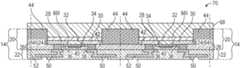
- FIG. 1shows an exemplary RF device 10 formed from a Si—SiGe—Si wafer (processing details are described in following paragraphs) according to one embodiment of the present disclosure.
- the exemplary RF device 10includes a mold device die 12 with a device region 14 and a first mold compound 16 , and a multilayer redistribution structure 18 formed under the mold device die 12 .
- the device region 14includes a front-end-of-line (FEOL) portion 20 and a back-end-of-line (BEOL) portion 22 underneath the FEOL portion 20 .
- the FEOL portion 20is configured to provide a switch field-effect transistor (FET), and includes an active layer 24 and a contact layer 26 .
- the active layer 24has a source 28 , a drain 30 , and a channel 32 between the source 28 and the drain 30 .
- the source 28 , the drain 30 , and the channel 32are formed from a same silicon epitaxial layer.
- the contact layer 26is formed underneath the active layer 24 and includes a gate structure 34 , a source contact 36 , a drain contact 38 , and a gate contact 40 .
- the gate structure 34may be formed of silicon oxide, and extends horizontally underneath the channel 32 (from underneath the source 28 to underneath the drain 30 ).
- the source contact 36is connected to and under the source 28
- the drain contact 38is connected to and under the drain 30
- the gate contact 40is connected to and under the gate structure 34 .
- An insulating material 42may be formed around the source contact 36 , the drain contact 38 , the gate structure 34 , and the gate contact 40 to electrically separate the source 28 , the drain 30 , and the gate structure 34 .
- the FEOL portion 20may have different FET configurations or provide different device components, such as a diode, a capacitor, a resistor, and/or an inductor.
- the FEOL portion 20also includes isolation sections 44 , which reside over the insulating material 42 of the contact layer 26 and surround the active layer 24 .
- the isolation sections 44are configured to electrically separate the RF device 10 , especially the active layer 24 , from other devices formed in a common wafer (not shown).
- the isolation sections 44may extend from a top surface of the contact layer 26 and vertically beyond a top surface of the active layer 24 to define an opening 46 that is within the isolation sections 44 and over the active layer 24 .
- the first mold compound 16fills the opening 46 and may extend over the isolation sections 44 .
- the isolation sections 44may be formed of silicon dioxide, which may resist etching chemistries such as potassium hydroxide (KOH), sodium hydroxide (NaOH), and acetylcholine (ACH).
- the RF device 10may further include a passivation layer 48 , which may be formed of silicon dioxide, silicon nitride, or combination of both, directly over the top surface of the active layer 24 and within the opening 46 .
- a passivation layer 48may be formed of silicon dioxide, silicon nitride, or combination of both, directly over the top surface of the active layer 24 and within the opening 46 .
- the first mold compound 16is directly over the passivation layer 48 .
- the passivation layer 48is configured to terminate surface bonds of the active layer 24 , which may be responsible for unwanted leakage.
- the passivation layermay also serve as a barrier and is configured to protect the active layer 24 from moisture or ionic contamination. If the passivation layer 48 is omitted, the first mold compound 16 may be in contact with the top surface of the active layer 24 .
- the RF device 10may further include an interfacial layer (described in the following paragraphs and not shown herein), which is formed of SiGe, directly over the top surface of the active layer 24 and within the opening 46 .
- the first mold compound 16may be directly over the interfacial layer.
- the interfacial layeris from the Si—SiGe—Si wafer (processing details are described in following paragraphs), which is used to fabricate the RF device 10 . If the interfacial layer is omitted, the first mold compound 18 may be in contact with the top surface of the active layer 24 .
- each isolation section 44 and the top surface of the active layer 24are coplanar (not shown), and the opening 46 is omitted.
- the first mold compound 16resides over both the active layer 24 and the isolation sections 44 of the FEOL portion 20 . Note that the active layer 24 is never vertically beyond the isolation sections 44 , otherwise the isolation sections 44 may not fully separate the active layer 24 from other devices formed from the same wafer.
- the BEOL portion 22is underneath the FEOL portion 20 and includes multiple connecting layers 50 formed within dielectric layers 52 . Some of the connecting layers 50 are encapsulated by the dielectric layers 52 (not shown), while some of the connecting layers 50 have a bottom portion not covered by the dielectric layers 52 . Certain connecting layers 50 are electrically connected to the FEOL portion 20 . For the purpose of this illustration, one of the connecting layers 50 is connected to the source contact 36 , and another connecting layer 50 is connected to the drain contact 38 .
- the multilayer redistribution structure 18which is formed underneath the BEOL portion 22 of the mold device die 12 , includes a number of redistribution interconnections 54 , a dielectric pattern 56 , and a number of bump structures 58 .
- each redistribution interconnection 54is connected to a corresponding connecting layer 50 within the BEOL portion 22 and extends over a bottom surface of the BEOL portion 22 .
- the connections between the redistribution interconnections 54 and the connecting layers 50are solder-free.
- the dielectric pattern 56is formed around and underneath each redistribution interconnection 54 . A bottom portion of each redistribution interconnection 54 is exposed through the dielectric pattern 56 .
- Each bump structure 58is formed at a bottom of the multilayer redistribution structure 18 and electrically coupled to a corresponding redistribution interconnection 54 through the dielectric pattern 56 . Consequently, the redistribution interconnections 54 are configured to connect the bump structures 58 to certain ones of the connecting layer 50 in the BEOL portion 22 , which are electrically connected to the FEOL portion 20 . As such, the bump structures 58 are electrically connected to the FEOL portion 20 via corresponding redistribution interconnections 54 and corresponding connecting layers 50 . In addition, the bump structures 58 are separate from each other and extend underneath the dielectric pattern 56 .
- some of the redistribution interconnections 54may be configured to connect the mold device die 12 to other device components formed from the same wafer (not shown).
- the multilayer redistribution structure 18may be free of glass fiber or glass-free.
- the glass fiberrefers to individual glass strands twisted to become a larger grouping. These glass strands may then be woven into a fabric.
- the redistribution interconnections 54may be formed of copper or other suitable metals.
- the dielectric pattern 56may be formed of benzocyclobutene (BCB), polyimide, or other dielectric materials.
- the bump structures 58may be solder balls or copper pillars.
- the multilayer redistribution structure 18has a thickness between 2 ⁇ m and 300 ⁇ m.
- the heat generated in the device region 14may travel upward to a bottom portion of the first mold compound 16 , which is over the active layer 24 , and then will pass downward through the device region 14 and toward the multilayer redistribution structure 18 , which will dissipate the heat. It is therefore highly desirable to have high thermal conductivities of the first mold compound 16 .
- the first mold compound 16may have a thermal conductivity greater than 1 W/m ⁇ K, or greater than 10 W/m ⁇ K.
- the first mold compound 16may have a low dielectric constant less than 8, or between 3 and 5 to yield low RF coupling.
- the first mold compound 16may be formed of thermoplastics or thermoset polymer materials, such as PPS (poly phenyl sulfide), overmold epoxies doped with boron nitride, alumina, carbon nanotubes, or diamond-like thermal additives, or the like.
- a thickness of the first mold compound 16is based on the required thermal performance of the RF device 10 , the device layout, the distance from the multilayer redistribution structure 18 , as well as the specifics of the package and assembly.
- the first mold compound 16may have a thickness between 200 ⁇ m and 500 ⁇ m.
- FIG. 2shows an alternative RF device 10 A, which further includes a second mold compound 60 compared to the RF device 10 .
- the multilayer redistribution structure 18extends horizontally beyond the mold device die 12
- the second mold compound 60resides over the multilayer redistribution structure 18 to encapsulate the mold device die 12 .
- the redistribution interconnections 54 of the multilayer redistribution structure 18may extend horizontally beyond the mold device die 12
- the bump structures 58 of the multilayer redistribution structure 18may not be confined within a periphery of the mold device die 12 .
- the second mold compound 60may be formed of a same or different material as the first mold compound 16 . Unlike the first mold compound 16 , the second mold compound 60 may not have thermal conductivity or dielectric constant requirements.
- FIGS. 3 - 14provide an exemplary wafer-level packaging process that illustrates steps to fabricate the exemplary RF device 10 shown in FIG. 1 .
- the exemplary stepsare illustrated in a series, the exemplary steps are not necessarily order dependent. Some steps may be done in a different order than that presented. Further, processes within the scope of this disclosure may include fewer or more steps than those illustrated in FIGS. 3 - 14 .
- a Si—SiGe—Si wafer 62is provided as illustrated in FIG. 3 .
- the Si—SiGe—Si wafer 62includes a common silicon epitaxial layer 64 , a common interfacial layer 66 over the common silicon epitaxial layer 64 , and a silicon handle substrate 68 over the common interfacial layer 66 .
- the common interfacial layer 66which is formed of SiGe, separates the common silicon epitaxial layer 64 from the silicon handle substrate 68 .
- the common silicon epitaxial layer 64is formed from a device grade silicon material, which has desired silicon epitaxy characteristics to form electronic devices.
- the common interfacial layer 66is formed from an alloy with any molar ratio of Si and Ge. The higher the Ge concentration, the better the etch selectivity between the silicon handle substrate 68 and the common interfacial layer 66 , but also the more difficult the epitaxial growth of the common silicon epitaxial layer 64 becomes.
- the common interfacial layer 66may have a Ge concentration greater than 15% or greater than 25%. The Ge concentration may be uniform throughout the common interfacial layer 66 .
- the Ge concentrationmay be vertically graded (between 1% and 50%) so as to yield the necessary strain relief for the growth of the common silicon epitaxial layer 64 .
- the silicon handle substrate 68may consist of conventional low cost, low resistivity, and high dielectric constant silicon.
- the common silicon epitaxial layer 64has higher resistivity, lower harmonic generation, and lower dielectric constant than the silicon handle substrate 68 .
- a thickness of the common silicon epitaxial layer 64may be between 700 nm and 2000 nm, a thickness of the common interfacial layer 66 may be between 100 nm and 1000 nm, and a thickness of the silicon handle substrate 68 may be between 200 ⁇ m and 500 ⁇ m.
- CMOScomplementary metal-oxide-semiconductor
- the FEOL portion 20 of each device region 14is configured to provide a switch FET.
- the FEOL portion 20may have different FET configurations or provide different device components, such as a diode, a capacitor, a resistor, and/or an inductor.
- the isolation sections 44 of each device region 14extend through the common silicon epitaxial layer 64 and the common interfacial layer 66 , and extend into the silicon handle substrate 68 .
- the common interfacial layer 66separates into a number of individual interfacial layers 661
- the common silicon epitaxial layer 64separates into a number of individual silicon epitaxial layers 641 , each of which is used to form a corresponding active layer 24 in one device region 14 .
- the isolation sections 44may be formed by shallow trench isolation (STI).
- the top surface of the active layer 24is in contact with a corresponding interfacial layer 661 .
- the silicon handle substrate 68resides over each individual interfacial layer 661 , and portions of the silicon handle substrate 68 may reside over the isolation sections 44 .
- the BEOL portion 22 of the device region 14which includes at least the multiple connecting layers 50 and the dielectric layers 52 , is formed under the contact layer 26 of the FEOL portion 20 . Bottom portions of certain connecting layers 50 are exposed through the dielectric layers 52 at the bottom surface of the BEOL portion 22 .
- the isolation sections 44do not extend into the silicon handle substrate 68 . Instead, the isolation sections 44 only extend through the common silicon epitaxial layer 64 and extend into the common interfacial layer 66 , as illustrated in FIG. 4 B .
- the common interfacial layer 66remains continuous, and the individual interfacial layers 661 are connected with each other.
- the common interfacial layer 66directly resides over the top surface of each active layer 24 , and directly resides over a top surface of each isolation section 44 .
- the silicon handle substrate 68remains over the common interfacial layer 66 .
- the isolation sections 44may extend through the common silicon epitaxial layer 64 but do not extend into the common interfacial layer 66 (not shown).
- each isolation section 44 and the top surface of each active layer 24may be coplanar (not shown).
- the common interfacial layer 66 and the silicon handle substrate 68remain intact.
- the common interfacial layer 66is over each isolation section 44 and each active layer 24
- the silicon handle substrate 68is over the common interfacial layer 66 .
- the precursor wafer 70is then bonded to a temporary carrier 72 , as illustrated in FIG. 5 .
- the precursor wafer 70may be bonded to the temporary carrier 72 via a bonding layer 74 , which provides a planarized surface to the temporary carrier 72 .
- the temporary carrier 72may be a thick silicon wafer from a cost and thermal expansion point of view, but may also be construed of glass, sapphire, or other suitable carrier material.
- the bonding layer 74may be a span-on polymeric adhesive film, such as the Brewer Science WaferBOND line of temporary adhesive materials.
- the silicon handle substrate 68is then selectively removed to provide an etched wafer 76 , wherein the selective removal is stopped on each interfacial layer 661 , as illustrated in FIG. 6 . If the isolation sections 44 extend vertically beyond the interfacial layers 661 , the removal of the silicon handle substrate 68 will provide the opening 46 over each active layer 24 and within the isolation sections 44 .
- Removing the silicon handle substrate 68may be provided by chemical mechanical grinding and an etching process with a wet/dry etchant chemistry, which may be TMAH, KOH, NaOH, ACH, or XeF2, or provided by the etching process itself. As an example, the silicon handle substrate 68 may be ground to a thinner thickness to reduce the following etching time.
- etching processis then performed to completely remove the remaining silicon handle substrate 68 . Since the silicon handle substrate 68 and the interfacial layers 661 have different characteristics, they may have different reactions to a same etching technique (for instance: different etching speeds with a same etchant). Consequently, the etching system is capable of identifying the presence of the interfacial layers 661 , and capable of indicating when to stop the etching process.
- the isolation sections 44are not removed and protect sides of each FEOL portion 20 .
- the bonding layer 74 and the temporary carrier 72protect the bottom surface of each BEOL portion 22 .
- the top surface of each isolation section 44 and the top surface of each interfacial layer 661are exposed after the removing process. If the isolation sections 44 only extend into the common interfacial layer 66 but not through the common interfacial layer 66 (as shown in FIG. 3 B ), or the top surface of each isolation section 44 and the top surface of each active layer 24 are coplanar (not shown), only the top surface of the common interfacial layer 66 is exposed (not shown).
- the interfacial layers 661may be conducting.
- the interfacial layer 661may cause appreciable leakage between the source 28 and the drain 30 of the active layer 24 . Therefore, in some applications, such as FET applications, it is desired to also remove the interfacial layers 661 (or the common interfacial layer 66 ), as illustrated in FIG. 7 .
- the interfacial layers 661may be removed by the same etching process used to remove the silicon handle substrate 68 , or may be removed by another etching process, such as HCl dry etch systems.
- the interfacial layer 661may be completely depleted and may not cause any appreciable leakage between the source 28 and the drain 30 of the FEOL portion 20 . In that case, the interfacial layers 661 may be left intact.
- the passivation layer 48which may be formed of silicon dioxide, silicon nitride, or combination of both, may be formed directly over the active layer 24 of each FEOL portion 20 , as illustrated in FIG. 8 . If there is the opening 46 over each active layer 24 and within the isolation sections 44 , the passivation layer 48 is formed within the opening 46 .
- the passivation layer 48is configured to terminate the surface bonds at the top surface of the active layer 24 , which may be responsible for unwanted leakage.
- the passivation layer 48may be formed by CVD dielectric filming or passivating plasma.
- the mold device wafer 78includes a number of the mold device dies 12 , each of which includes the device region 14 , and a portion of the first mold compound 16 .
- the first mold compound 16fills each opening 46 and is in contact with the passivation layer 48 within the opening 46 .
- portions of the first mold compound 16may extend over the isolation sections 44 . If there is no passivation layer 48 formed in each opening 46 , the first mold compound 16 is in contact with the top surface of each active layer 24 (not shown). If the interfacial layer 661 remains over the top surface of each active layer 24 , the first mold compound 16 is in contact with the interfacial layer 661 (not shown). The first mold compound 16 always resides over each active layer 24 .
- the first mold compound 16may be applied by various procedures, such as compression molding, sheet molding, overmolding, transfer molding, dam fill encapsulation, and screen print encapsulation.
- the first mold compound 16may have a superior thermal conductivity greater than 1 W/m ⁇ K, or greater than 10 W/m ⁇ K, and may have a dielectric constant less than 8, or between 3 and 5.
- the temporary carrier 72provides mechanical strength and rigidity to the etched wafer 76 .
- a curing process(not shown) is followed to harden the first mold compound 16 .
- the curing temperatureis between 100° C. and 320° C. depending on which material is used as the first mold compound 16 .
- the first mold compound 16may be thinned and/or planarized (not shown).
- the temporary carrier 72is then debonded from the mold device wafer 78 , and the bonding layer 74 is cleaned from the mold device wafer 78 , as illustrated in FIG. 10 .
- a number of debonding processes and cleaning processesmay be applied depending on the nature of the temporary carrier 72 and the bonding layer 74 chosen in the earlier steps.
- the temporary carrier 72may be mechanically debonded using a lateral blade process with the stack heated to a proper temperature.
- Other suitable processesinvolve radiation of UV light through the temporary carrier 72 if it is formed of a transparent material, or chemical debonding using a proper solvent.
- the bonding layer 74may be eliminated by wet or dry etching processes, such as proprietary solvents and plasma washing.
- each mold device die 12 in the mold device wafer 78may be electrically verified to be working properly at this point.
- the multilayer redistribution structure 18is formed underneath the mold device wafer 78 according to one embodiment of the present disclosure.
- the redistribution stepsare illustrated in a series, the redistribution steps are not necessarily order dependent. Some steps may be done in a different order than that presented. Further, redistribution steps within the scope of this disclosure may include fewer or more steps than those illustrated in FIGS. 11 - 13 .
- a number of the redistribution interconnections 54are firstly formed underneath each BEOL portion 22 , as illustrated in FIG. 11 .
- Each redistribution interconnection 54is electrically coupled to the exposed bottom portion of the corresponding connecting layer 50 within the BEOL portion 22 , and may extend over the bottom surface of the BEOL portion 22 .
- the connections between the redistribution interconnections 54 and the connecting layers 50are solder-free.
- the dielectric pattern 56is then formed underneath each BEOL portion 22 to partially encapsulate each redistribution interconnection 54 , as illustrated in FIG. 12 . As such, the bottom portion of each redistribution interconnection 54 is exposed through the dielectric pattern 56 .
- redistribution interconnectionselectrically coupled to the redistribution interconnection 54 through the dielectric pattern 56 , and extra dielectric patterns (not shown) formed underneath the dielectric pattern 56 , such that a bottom portion of each extra redistribution interconnection is exposed.
- each bump structure 58is formed at the bottom of the multilayer redistribution structure 18 and electrically coupled to an exposed bottom portion of the corresponding redistribution interconnection 54 through the dielectric pattern 56 . Consequently, the redistribution interconnections 54 are configured to connect the bump structures 58 to certain ones of the connecting layer 50 in the BEOL portion 22 , which are electrically connected to the FEOL portion 20 . As such, the bump structures 58 are electrically connected to the FEOL portion 20 via corresponding redistribution interconnections 54 and corresponding connecting layers 50 . In addition, the bump structures 58 are separate from each other and extend underneath the dielectric pattern 56 .
- the multilayer redistribution structure 18may be free of glass fiber or glass-free.
- the glass fiberrefers to individual glass strands twisted to become a larger grouping. These glass strands may then be woven into a fabric.
- the redistribution interconnections 54may be formed of copper or other suitable metals
- the dielectric pattern 56may be formed of BCB, polyimide, or other dielectric materials
- the bump structures 58may be solder balls or copper pillars.
- the multilayer redistribution structure 18has a thickness between 2 ⁇ m and 300 ⁇ m.
- FIG. 14shows a final step to singulate the WLFO package 80 into individual RF devices 10 . The singulating step may be provided by a probing and dicing process at certain isolation sections 44 .
- FIGS. 15 - 20provide an alternative wafer-level packaging process that illustrates steps to fabricate the alternative RF device 10 A shown in FIG. 2 .
- the exemplary stepsare illustrated in a series, the exemplary steps are not necessarily order dependent. Some steps may be done in a different order than that presented. Further, processes within the scope of this disclosure may include fewer or more steps than those illustrated in FIGS. 15 - 20 .
- a singulating stepis followed to singulate the mold device wafer 78 into individual mold device dies 12 , as illustrated in FIG. 15 .
- Each mold device die 12may have a same height and includes the device region 14 with the FEOL portion 20 and the BEOL portion 22 and the first mold compound 16 .
- the second mold compound 60is applied around and over the mold device dies 12 to provide a double mold device wafer 82 , as illustrated in FIG. 16 .
- the second mold compound 60encapsulates a top surface and side surfaces of each mold device die 12 , while a bottom surface of each mold device die 12 , which is the bottom surface of the BEOL portion 22 , is exposed.
- a bottom surface of the double mold device wafer 82is a combination of the bottom surface of each mold device die 12 and a bottom surface of the second mold compound 60 .
- the bottom portions of certain ones of the connecting layers 50remain exposed at the bottom surface of each mold device die 12 .
- the second mold compound 60may be applied by various procedures, such as sheet molding, overmolding, compression molding, transfer molding, dam fill encapsulation, or screen print encapsulation.
- the second mold compound 60may be formed of the same or different material as the first mold compound 16 . However, unlike the first mold compound 16 , the second mold compound 60 does not have thermal conductivity or electrical resistivity requirements.
- the second mold compound 60may be an organic epoxy resin system or the like.
- a curing process(not shown) is then used to harden the second mold compound 60 .
- the curing temperatureis between 100° C. and 320° C. depending on which material is used as the second mold compound 60 .
- a grinding process(not shown) may be followed to provide a planarized top surface of the second mold compound 60 .
- the multilayer redistribution structure 18is formed according to one embodiment of the present disclosure.
- the redistribution stepsare illustrated in a series, the redistribution steps are not necessarily order dependent. Some steps may be done in a different order than that presented. Further, redistribution steps within the scope of this disclosure may include fewer or more steps than those illustrated in FIGS. 17 - 19 .
- a number of the redistribution interconnections 54are firstly formed underneath the double mold device wafer 82 , as illustrated in FIG. 17 .
- Each redistribution interconnection 54is electrically coupled to the corresponding connecting layer 50 within the BEOL portion 22 , and may extend horizontally beyond the corresponding mold device die 12 and underneath the second mold compound 60 .
- the connections between the redistribution interconnections 54 and the connecting layers 50are solder-free.
- the dielectric pattern 56is then formed underneath the double mold device wafer 82 to partially encapsulate each redistribution interconnection 54 , as illustrated in FIG. 18 . As such, the bottom portion of each redistribution interconnection 54 is exposed through the dielectric pattern 56 .
- redistribution interconnectionselectrically coupled to the redistribution interconnection 54 through the dielectric pattern 56 , and extra dielectric patterns (not shown) formed underneath the dielectric pattern 56 , such that a bottom portion of each extra redistribution interconnection is exposed.
- each bump structure 58is formed at the bottom of the multilayer redistribution structure 18 and electrically coupled to an exposed bottom portion of the corresponding redistribution interconnection 54 through the dielectric pattern 56 . Consequently, the redistribution interconnections 54 are configured to connect the bump structures 58 to certain ones of the connecting layer 50 in the BEOL portion 22 , which are electrically connected to the FEOL portion 20 . As such, the bump structures 58 are electrically connected to the FEOL portion 20 via corresponding redistribution interconnections 54 and corresponding connecting layers 50 .
- the bump structures 58may not be confined within a periphery of a corresponding mold device die 12 .
- the bump structures 58are separate from each other and extend underneath the dielectric pattern 56 .
- FIG. 20shows a final step to singulate the alternative WLFO package 80 A into individual alternative RF devices 10 A.
- the singulating stepmay be provided by a probing and dicing process at portions of the second mold compound 60 , which are horizontally between adjacent mold device dies 12 .
Landscapes
- Engineering & Computer Science (AREA)
- Microelectronics & Electronic Packaging (AREA)
- Computer Hardware Design (AREA)
- Power Engineering (AREA)
- Physics & Mathematics (AREA)
- Condensed Matter Physics & Semiconductors (AREA)
- General Physics & Mathematics (AREA)
- Manufacturing & Machinery (AREA)
- Chemical & Material Sciences (AREA)
- Materials Engineering (AREA)
- Ceramic Engineering (AREA)
- Geometry (AREA)
- Element Separation (AREA)
- Metal-Oxide And Bipolar Metal-Oxide Semiconductor Integrated Circuits (AREA)
- Insulated Gate Type Field-Effect Transistor (AREA)
- Internal Circuitry In Semiconductor Integrated Circuit Devices (AREA)
- Input Circuits Of Receivers And Coupling Of Receivers And Audio Equipment (AREA)
- Semiconductor Integrated Circuits (AREA)
Abstract
Description
Claims (18)
Priority Applications (1)
| Application Number | Priority Date | Filing Date | Title |
|---|---|---|---|
| US18/306,599US12062623B2 (en) | 2019-01-23 | 2023-04-25 | RF device without silicon handle substrate for enhanced thermal and electrical performance and methods of forming the same |
Applications Claiming Priority (3)
| Application Number | Priority Date | Filing Date | Title |
|---|---|---|---|
| US201962795804P | 2019-01-23 | 2019-01-23 | |
| US16/427,019US11923313B2 (en) | 2019-01-23 | 2019-05-30 | RF device without silicon handle substrate for enhanced thermal and electrical performance and methods of forming the same |
| US18/306,599US12062623B2 (en) | 2019-01-23 | 2023-04-25 | RF device without silicon handle substrate for enhanced thermal and electrical performance and methods of forming the same |
Related Parent Applications (1)
| Application Number | Title | Priority Date | Filing Date |
|---|---|---|---|
| US16/427,019DivisionUS11923313B2 (en) | 2019-01-23 | 2019-05-30 | RF device without silicon handle substrate for enhanced thermal and electrical performance and methods of forming the same |
Publications (2)
| Publication Number | Publication Date |
|---|---|
| US20230260921A1 US20230260921A1 (en) | 2023-08-17 |
| US12062623B2true US12062623B2 (en) | 2024-08-13 |
Family
ID=67138021
Family Applications (2)
| Application Number | Title | Priority Date | Filing Date |
|---|---|---|---|
| US16/427,019ActiveUS11923313B2 (en) | 2019-01-23 | 2019-05-30 | RF device without silicon handle substrate for enhanced thermal and electrical performance and methods of forming the same |
| US18/306,599ActiveUS12062623B2 (en) | 2019-01-23 | 2023-04-25 | RF device without silicon handle substrate for enhanced thermal and electrical performance and methods of forming the same |
Family Applications Before (1)
| Application Number | Title | Priority Date | Filing Date |
|---|---|---|---|
| US16/427,019ActiveUS11923313B2 (en) | 2019-01-23 | 2019-05-30 | RF device without silicon handle substrate for enhanced thermal and electrical performance and methods of forming the same |
Country Status (6)
| Country | Link |
|---|---|
| US (2) | US11923313B2 (en) |
| EP (1) | EP3915134A1 (en) |
| KR (2) | KR20250027591A (en) |
| CN (1) | CN113632209A (en) |
| TW (1) | TWI815993B (en) |
| WO (1) | WO2020153983A1 (en) |
Families Citing this family (14)
| Publication number | Priority date | Publication date | Assignee | Title |
|---|---|---|---|---|
| US12062700B2 (en) | 2018-04-04 | 2024-08-13 | Qorvo Us, Inc. | Gallium-nitride-based module with enhanced electrical performance and process for making the same |
| US12046505B2 (en) | 2018-04-20 | 2024-07-23 | Qorvo Us, Inc. | RF devices with enhanced performance and methods of forming the same utilizing localized SOI formation |
| CN118213279A (en) | 2018-07-02 | 2024-06-18 | Qorvo美国公司 | RF semiconductor device and method for manufacturing the same |
| US11646242B2 (en) | 2018-11-29 | 2023-05-09 | Qorvo Us, Inc. | Thermally enhanced semiconductor package with at least one heat extractor and process for making the same |
| KR20250027591A (en) | 2019-01-23 | 2025-02-26 | 코르보 유에스, 인크. | Rf semiconductor device and manufacturing method thereof |
| US12046570B2 (en) | 2019-01-23 | 2024-07-23 | Qorvo Us, Inc. | RF devices with enhanced performance and methods of forming the same |
| US12046483B2 (en) | 2019-01-23 | 2024-07-23 | Qorvo Us, Inc. | RF devices with enhanced performance and methods of forming the same |
| US12057374B2 (en) | 2019-01-23 | 2024-08-06 | Qorvo Us, Inc. | RF devices with enhanced performance and methods of forming the same |
| US12074086B2 (en) | 2019-11-01 | 2024-08-27 | Qorvo Us, Inc. | RF devices with nanotube particles for enhanced performance and methods of forming the same |
| US11646289B2 (en) | 2019-12-02 | 2023-05-09 | Qorvo Us, Inc. | RF devices with enhanced performance and methods of forming the same |
| US11923238B2 (en) | 2019-12-12 | 2024-03-05 | Qorvo Us, Inc. | Method of forming RF devices with enhanced performance including attaching a wafer to a support carrier by a bonding technique without any polymer adhesive |
| US12129168B2 (en) | 2019-12-23 | 2024-10-29 | Qorvo Us, Inc. | Microelectronics package with vertically stacked MEMS device and controller device |
| WO2022125722A1 (en)* | 2020-12-11 | 2022-06-16 | Qorvo Us, Inc. | Microelectronics package with vertically stacked wafer slices and process for making the same |
| WO2022186857A1 (en) | 2021-03-05 | 2022-09-09 | Qorvo Us, Inc. | Selective etching process for si-ge and doped epitaxial silicon |
Citations (379)
| Publication number | Priority date | Publication date | Assignee | Title |
|---|---|---|---|---|
| JPS505733Y1 (en) | 1970-02-23 | 1975-02-18 | ||
| JPS5338954A (en) | 1976-09-21 | 1978-04-10 | Mitsubishi Electric Corp | Strip line circulator |
| US4093562A (en) | 1976-02-20 | 1978-06-06 | Matsushita Electric Industrial Co., Ltd. | Polymeric compositions for manufacture of secondary electron multiplier tubes and method for manufacture thereof |
| US4366202A (en) | 1981-06-19 | 1982-12-28 | Kimberly-Clark Corporation | Ceramic/organic web |
| US5013681A (en) | 1989-09-29 | 1991-05-07 | The United States Of America As Represented By The Secretary Of The Navy | Method of producing a thin silicon-on-insulator layer |
| US5061663A (en) | 1986-09-04 | 1991-10-29 | E. I. Du Pont De Nemours And Company | AlN and AlN-containing composites |
| US5069626A (en) | 1987-07-01 | 1991-12-03 | Western Digital Corporation | Plated plastic castellated interconnect for electrical components |
| US5164687A (en) | 1991-06-17 | 1992-11-17 | Renaissance Electronics Corp. | Compact lumped constant non-reciprocal circuit element |
| US5294295A (en) | 1991-10-31 | 1994-03-15 | Vlsi Technology, Inc. | Method for moisture sealing integrated circuits using silicon nitride spacer protection of oxide passivation edges |
| US5362972A (en) | 1990-04-20 | 1994-11-08 | Hitachi, Ltd. | Semiconductor device using whiskers |
| US5391257A (en) | 1993-12-10 | 1995-02-21 | Rockwell International Corporation | Method of transferring a thin film to an alternate substrate |
| US5459368A (en) | 1993-08-06 | 1995-10-17 | Matsushita Electric Industrial Co., Ltd. | Surface acoustic wave device mounted module |
| US5646432A (en) | 1992-05-14 | 1997-07-08 | Seiko Instruments Inc. | Semiconductor thin film formed on a supporting substrate |
| US5648013A (en) | 1992-12-24 | 1997-07-15 | Canon Kabushiki Kaisha | Plastic additive, plastic composition containing the additive and plastic molding containing the additive |
| US5699027A (en) | 1995-03-28 | 1997-12-16 | Matsushita Electric Industrial Co., Ltd. | Surface acoustic wave devices having a guard layer |
| US5709960A (en) | 1996-06-21 | 1998-01-20 | Motorola, Inc. | Mold compound |
| US5729075A (en) | 1995-06-12 | 1998-03-17 | National Semiconductor Corporation | Tuneable microelectromechanical system resonator |
| US5831369A (en) | 1994-05-02 | 1998-11-03 | Siemens Matsushita Components Gmbh & Co. Kg | Encapsulation for electronic components and method for producing the encapsulation |
| US5920142A (en) | 1996-03-08 | 1999-07-06 | Matsushita Electric Industrial Co., Ltd. | Electronic part and a method of production thereof |
| JPH11220077A (en) | 1997-10-15 | 1999-08-10 | Toshiba Corp | Semiconductor device and method of manufacturing semiconductor device |
| US6072557A (en) | 1998-07-31 | 2000-06-06 | Sharp Kabushiki Kaisha | Color liquid crystal display apparatus and method for producing the same |
| CN1256300A (en) | 1998-10-05 | 2000-06-14 | Ge医疗系统有限公司 | Electric insulating and cooling material for high-voltage power-supply unit |
| US6084284A (en) | 1994-11-18 | 2000-07-04 | Adamic, Jr.; Fred W. | Integrated circuit including inverted dielectric isolation |
| US6137125A (en) | 1995-12-21 | 2000-10-24 | The Whitaker Corporation | Two layer hermetic-like coating for on-wafer encapsulatuon of GaAs MMIC's having flip-chip bonding capabilities |
| US6154366A (en) | 1999-11-23 | 2000-11-28 | Intel Corporation | Structures and processes for fabricating moisture resistant chip-on-flex packages |
| US6154372A (en) | 1993-09-02 | 2000-11-28 | Siemens Aktiengesellschaft | Multichip module for surface mounting on printed circuit boards |
| EP1098386A1 (en) | 1999-03-26 | 2001-05-09 | Hitachi Metals, Ltd. | Concentrated constant irreciprocal device |
| US6235554B1 (en) | 1995-11-27 | 2001-05-22 | Micron Technology, Inc. | Method for fabricating stackable chip scale semiconductor package |
| US6236061B1 (en) | 1999-01-08 | 2001-05-22 | Lakshaman Mahinda Walpita | Semiconductor crystallization on composite polymer substrates |
| US20010004131A1 (en) | 1999-12-17 | 2001-06-21 | Tobita Masayuki | Adhesion method and electronic component |
| US6268654B1 (en) | 1997-04-18 | 2001-07-31 | Ankor Technology, Inc. | Integrated circuit package having adhesive bead supporting planar lid above planar substrate |
| US6271469B1 (en) | 1999-11-12 | 2001-08-07 | Intel Corporation | Direct build-up layer on an encapsulated die package |
| JP2002093957A (en) | 2000-09-11 | 2002-03-29 | Sony Corp | Electronic circuit device and its manufacturing method |
| JP2002100767A (en) | 2000-09-25 | 2002-04-05 | Toshiba Corp | Semiconductor element |
| US6377112B1 (en) | 2000-12-05 | 2002-04-23 | Semiconductor Components Industries Llc | Circuit and method for PMOS device N-well bias control |
| US20020070443A1 (en) | 2000-12-08 | 2002-06-13 | Xiao-Chun Mu | Microelectronic package having an integrated heat sink and build-up layers |
| US20020074641A1 (en) | 2000-12-15 | 2002-06-20 | Steven Towle | Microelectronic package having a bumpless laminated interconnection layer |
| US6423570B1 (en) | 2000-10-18 | 2002-07-23 | Intel Corporation | Method to protect an encapsulated die package during back grinding with a solder metallization layer and devices formed thereby |
| US6426559B1 (en) | 2000-06-29 | 2002-07-30 | National Semiconductor Corporation | Miniature 3D multi-chip module |
| US6441498B1 (en) | 1997-12-02 | 2002-08-27 | Hyundai Electronics Industries Co., Ltd. | Semiconductor substrate and land grid array semiconductor package using same |
| JP2002252376A (en) | 2001-02-23 | 2002-09-06 | Seiwa Electric Mfg Co Ltd | Surface mount type light emitting diode and method of manufacturing the same |
| US20020137263A1 (en) | 2001-03-26 | 2002-09-26 | Steven Towle | Dispensing process for fabrication of microelectronic packages |
| US20020185675A1 (en) | 2001-06-06 | 2002-12-12 | International Business Machines Corporation | SOI device with reduced junction capacitance |
| US6578458B1 (en) | 1996-11-12 | 2003-06-17 | Micron Technology, Inc. | Method for sawing wafers employing multiple indexing techniques for multiple die dimensions |
| US20030207515A1 (en) | 2002-01-09 | 2003-11-06 | Micron Technology, Inc., Boise, Id | Stacked die in die BGA package |
| US20040021152A1 (en) | 2002-08-05 | 2004-02-05 | Chanh Nguyen | Ga/A1GaN Heterostructure Field Effect Transistor with dielectric recessed gate |
| US6703688B1 (en) | 2001-03-02 | 2004-03-09 | Amberwave Systems Corporation | Relaxed silicon germanium platform for high speed CMOS electronics and high speed analog circuits |
| US6713859B1 (en) | 2000-09-13 | 2004-03-30 | Intel Corporation | Direct build-up layer on an encapsulated die package having a moisture barrier structure |
| US20040093901A1 (en) | 2002-11-07 | 2004-05-20 | Hyun-Ki Kim | Method for fabricating optical fiber block using silicon-glass anodic bonding technique |
| US20040166642A1 (en) | 2003-02-20 | 2004-08-26 | Hao-Yu Chen | Semiconductor nano-rod devices |
| US20040164367A1 (en) | 2003-02-21 | 2004-08-26 | Jae-Yeong Park | Duplexer filter having film bulk acoustic resonator and semiconductor package thereof |
| US20040173790A1 (en) | 2003-03-05 | 2004-09-09 | Yee-Chia Yeo | Method of forming strained silicon on insulator substrate |
| JP2004273604A (en) | 2003-03-06 | 2004-09-30 | Fujitsu Ltd | Method of manufacturing semiconductor device and semiconductor electronic component and semiconductor electronic component |
| US20040219765A1 (en) | 2002-12-31 | 2004-11-04 | Rafael Reif | Method of forming a multi-layer semiconductor structure incorporating a processing handle member |
| JP2004327557A (en) | 2003-04-22 | 2004-11-18 | Matsushita Electric Works Ltd | Method of manufacturing electronic part and semiconductor device |
| US20040266159A1 (en) | 2003-06-28 | 2004-12-30 | International Business Machines Corporation | Method for forming interconnects on thin wafers |
| US6841413B2 (en) | 2002-01-07 | 2005-01-11 | Intel Corporation | Thinned die integrated circuit package |
| US20050037595A1 (en) | 2003-08-11 | 2005-02-17 | Sumitomo Electric Industries, Ltd | Method of recovering and reproducing substrates and method of producing semiconductor wafers |
| US6864540B1 (en) | 2004-05-21 | 2005-03-08 | International Business Machines Corp. | High performance FET with elevated source/drain region |
| US6864156B1 (en) | 2003-04-04 | 2005-03-08 | Xilinx, Inc. | Semiconductor wafer with well contacts on back side |
| US20050079686A1 (en) | 2002-02-19 | 2005-04-14 | Infineon Technologies Ag | Method for producing a cover, method for producing a packaged device |
| US6943429B1 (en) | 2001-03-08 | 2005-09-13 | Amkor Technology, Inc. | Wafer having alignment marks extending from a first to a second surface of the wafer |
| US20050212419A1 (en) | 2004-03-23 | 2005-09-29 | Eastman Kodak Company | Encapsulating oled devices |
| CN1696231A (en) | 2004-05-11 | 2005-11-16 | 国际商业机器公司 | Reworkable conductive adhesive composition and method of making same |
| US20050258447A1 (en) | 2004-05-17 | 2005-11-24 | Shinko Electric Industries Co., Ltd. | Electronic parts and method of manufacturing electronic parts packaging structure |
| US20050260842A1 (en) | 2004-05-18 | 2005-11-24 | Erdem Kaltalioglu | Final passivation scheme for integrated circuits |
| JP2006005025A (en) | 2004-06-15 | 2006-01-05 | Sharp Corp | Manufacturing method of semiconductor wafer provided with lid and manufacturing method of semiconductor device |
| US20060009041A1 (en) | 2004-07-06 | 2006-01-12 | Iyer R S | Silicon nitride film with stress control |
| US6992400B2 (en) | 2004-01-30 | 2006-01-31 | Nokia Corporation | Encapsulated electronics device with improved heat dissipation |
| US20060057782A1 (en) | 2004-09-14 | 2006-03-16 | Stmicroelectronics Sa | Thin glass chip for an electronic component and manufacturing method |
| US7042072B1 (en) | 2002-08-02 | 2006-05-09 | Amkor Technology, Inc. | Semiconductor package and method of manufacturing the same which reduces warpage |
| US20060099781A1 (en) | 2002-07-24 | 2006-05-11 | Bernard Beaumont | Method for producing by vapour-phase epitaxy a gallium nitride film with low defect density |
| US20060105496A1 (en) | 2004-11-16 | 2006-05-18 | Chen Howard H | Device and method for fabricating double-sided SOI wafer scale package with through via connections |
| US7049692B2 (en) | 2003-03-11 | 2006-05-23 | Fujitsu Limited | Stacked semiconductor device |
| US20060108585A1 (en) | 2004-11-22 | 2006-05-25 | Au Optronics Corp. | Thin film transistors and fabrication methods thereof |
| US20060110887A1 (en) | 2004-11-22 | 2006-05-25 | Taiwan Semiconductor Manufacturing Company, Ltd. | Microelectronic device and a method for its manufacture |
| US20060124961A1 (en)* | 2003-12-26 | 2006-06-15 | Canon Kabushiki Kaisha | Semiconductor substrate, manufacturing method thereof, and semiconductor device |
| US7064391B1 (en) | 2003-04-04 | 2006-06-20 | Xilinx, Inc. | Bond and back side etchback transistor fabrication process |
| US7109635B1 (en) | 2003-06-11 | 2006-09-19 | Sawtek, Inc. | Wafer level packaging of materials with different coefficients of thermal expansion |
| US20060228074A1 (en) | 2004-11-24 | 2006-10-12 | Michal Lipson | Waveguide structure for guiding light in low-index material |
| US20060261446A1 (en) | 2005-05-19 | 2006-11-23 | Micron Technology, Inc. | Backside method and system for fabricating semiconductor components with conductive interconnects |
| US20070020807A1 (en) | 2004-11-09 | 2007-01-25 | Geefay Frank S | Protective structures and methods of fabricating protective structures over wafers |
| US20070034910A1 (en) | 2005-08-10 | 2007-02-15 | Shie Jin S | Fabrication method of spiral inductor on porous glass substrate |
| US7183172B2 (en) | 2002-05-22 | 2007-02-27 | Samsung Electronics Co., Ltd. | Method of forming silicon-on-insulator (SOI) semiconductor substrate and SOI semiconductor substrate formed thereby |
| US20070045738A1 (en) | 2005-08-26 | 2007-03-01 | Memc Electronic Materials, Inc. | Method for the manufacture of a strained silicon-on-insulator structure |
| US7190064B2 (en) | 2002-02-04 | 2007-03-13 | Casio Computer Co., Ltd. | Semiconductor device and method of manufacturing the same |
| US20070069393A1 (en) | 2003-07-24 | 2007-03-29 | Toshiyuki Asahi | Wiring board embedded with spherical semiconductor element |
| US20070075317A1 (en) | 2005-09-30 | 2007-04-05 | Seiko Epson Corporation | Semiconductor device and semiconductor device manufacturing method |
| US20070121326A1 (en) | 2005-11-29 | 2007-05-31 | Gelcore, Llc | LED lighting assemblies with thermal overmolding |
| US20070122943A1 (en) | 2005-11-30 | 2007-05-31 | Foong Chee S | Method of making semiconductor package having exposed heat spreader |
| US7238560B2 (en) | 2004-07-23 | 2007-07-03 | Cree, Inc. | Methods of fabricating nitride-based transistors with a cap layer and a recessed gate |
| WO2007074651A1 (en) | 2005-12-26 | 2007-07-05 | Sharp Kabushiki Kaisha | Solid state imaging element module fabrication method |
| US20070158746A1 (en) | 2006-01-12 | 2007-07-12 | Tatsuya Ohguro | Semiconductor device having SOI substrate |
| US20070181992A1 (en) | 2006-02-06 | 2007-08-09 | Micron Technology, Inc. | Microelectronic devices and methods for manufacturing microelectronic devices |
| US20070190747A1 (en) | 2006-01-23 | 2007-08-16 | Tessera Technologies Hungary Kft. | Wafer level packaging to lidded chips |
| US20070194342A1 (en) | 2006-01-12 | 2007-08-23 | Kinzer Daniel M | GaN SEMICONDUCTOR DEVICE AND PROCESS EMPLOYING GaN ON THIN SAPHIRE LAYER ON POLYCRYSTALLINE SILICON CARBIDE |
| JP2007227439A (en) | 2006-02-21 | 2007-09-06 | Denso Corp | Method and apparatus of manufacturing semiconductor device |
| US7279750B2 (en) | 2004-03-31 | 2007-10-09 | Casio Computer Co., Ltd. | Semiconductor device incorporating a semiconductor constructing body and an interconnecting layer which is connected to a ground layer via a vertical conducting portion |
| US20070252481A1 (en) | 2005-06-16 | 2007-11-01 | Murata Manufacturing Co., Ltd. | Piezoelectric device and method for producing same |
| US20070276092A1 (en) | 2003-12-25 | 2007-11-29 | Jsr Corporation | Thermoplastic Elastomer Composition, Method for Producing Same and Formed Article |
| US20080020513A1 (en) | 2004-01-27 | 2008-01-24 | Casio Computer Co., Ltd. | Method of fabricating semiconductor device having conducting portion of upper and lower conductive layers on a peripheral surface of the semiconductor device |
| US20080050901A1 (en) | 2006-08-23 | 2008-02-28 | Micron Technology, Inc. | Packaged microelectronic devices and methods for manufacturing packaged microelectronic devices |
| US20080050852A1 (en) | 2006-08-23 | 2008-02-28 | Tae-Hyung Hwang | Manufacturing of flexible display device panel |
| US20080087959A1 (en) | 2003-10-09 | 2008-04-17 | Stmicroelectronics S.A. | Manufacturing method of semiconductor-on-insulator region structures |
| US20080157303A1 (en) | 2006-12-28 | 2008-07-03 | Advanced Chip Engineering Technology Inc. | Structure of super thin chip scale package and method of the same |
| US20080164528A1 (en) | 2007-01-10 | 2008-07-10 | International Business Machines Corporation | Self-aligned metal-semiconductor alloy and metallization for sub-lithographic source and drain contacts |
| US7402901B2 (en) | 2005-03-16 | 2008-07-22 | Sony Corporation | Semiconductor device and method of manufacturing semiconductor device |
| JP2008235490A (en) | 2007-03-19 | 2008-10-02 | Sumitomo Bakelite Co Ltd | Hollow structure and manufacturing method therefor |
| US20080251927A1 (en) | 2007-04-13 | 2008-10-16 | Texas Instruments Incorporated | Electromigration-Resistant Flip-Chip Solder Joints |
| US20080265978A1 (en) | 2007-04-26 | 2008-10-30 | Robert Mark Englekirk | Tuning capacitance to enhance FET stack voltage withstand |
| US20080272497A1 (en) | 2007-05-04 | 2008-11-06 | Micron Technology, Inc. | Methods of forming conductive vias through substrates, and structures and assemblies resulting therefrom |
| US20080277800A1 (en) | 2007-05-08 | 2008-11-13 | Samsung Electronics Co., Ltd. | Semiconductor package and method of forming the same |
| JP2008279567A (en) | 2007-05-11 | 2008-11-20 | Denso Corp | Manufacturing method of semi-conductor apparatus |
| US20080315372A1 (en) | 2007-06-20 | 2008-12-25 | Stats Chippac, Ltd. | Wafer Level Integration Package |
| US20090008714A1 (en) | 2007-07-06 | 2009-01-08 | Hee-Il Chae | Semiconductor devices and methods of forming the same |
| US20090010056A1 (en) | 2002-11-20 | 2009-01-08 | The Regents Of The University Of California | Method and apparatus for capacitorless double-gate storage |
| US20090014856A1 (en) | 2007-07-10 | 2009-01-15 | International Business Machine Corporation | Microbump seal |
| JP2009026880A (en) | 2007-07-18 | 2009-02-05 | Denso Corp | Method of manufacturing semiconductor apparatus |
| US7489032B2 (en) | 2003-12-25 | 2009-02-10 | Casio Computer Co., Ltd. | Semiconductor device including a hard sheet to reduce warping of a base plate and method of fabricating the same |
| US20090090979A1 (en) | 2007-10-04 | 2009-04-09 | International Business Machines Corporation | High performance mosfet |
| US20090179266A1 (en) | 2008-01-11 | 2009-07-16 | International Business Machines Corporation | Device structures for a metal-oxide-semiconductor field effect transistor and methods of fabricating such device structures |
| JP2009530823A (en) | 2006-03-17 | 2009-08-27 | マイクロケム コーポレイション | MEMS device packaging |
| JP2009200274A (en) | 2008-02-22 | 2009-09-03 | Toshiba Corp | Integrated semiconductor apparatus |
| US20090230542A1 (en) | 2008-03-13 | 2009-09-17 | Stats Chippac, Ltd. | Semiconductor Device With Integrated Passive Circuit and Method of Making the Same Using Sacrificial Substrate |
| US20090243097A1 (en) | 2008-03-31 | 2009-10-01 | Casio Computer Co., Ltd. | Semiconductor device having low dielectric constant film and manufacturing method thereof |
| US7596849B1 (en) | 2003-06-11 | 2009-10-06 | Triquint Semiconductor, Inc. | Method of assembling a wafer-level package filter |
| US7619347B1 (en) | 2005-05-24 | 2009-11-17 | Rf Micro Devices, Inc. | Layer acoustic wave device and method of making the same |
| US20090302484A1 (en) | 2008-06-10 | 2009-12-10 | Micron Technology, Inc. | Packaged microelectronic devices and methods for manufacturing packaged microelectronic devices |
| JP2009302526A (en) | 2008-05-16 | 2009-12-24 | Denso Corp | Electronic circuit device and manufacturing method thereof |
| US20100003803A1 (en) | 2006-12-19 | 2010-01-07 | Shin-Etsu Handotai Co., Ltd. | Manufacturing method of strained si substrate |
| US20100012354A1 (en) | 2008-07-14 | 2010-01-21 | Logan Brook Hedin | Thermally conductive polymer based printed circuit board |
| US20100029045A1 (en) | 2008-08-01 | 2010-02-04 | Freescale Semiconductor, Inc. | Packaging an integrated circuit die with backside metallization |
| US20100045145A1 (en) | 2008-08-19 | 2010-02-25 | Nihon Dempa Kogyo Co., Ltd. | Piezoelectric component and manufacturing method thereof |
| US20100081232A1 (en) | 2007-05-10 | 2010-04-01 | International Business Machines Corporation | Layer transfer process and functionally enhanced integrated circuits produced thereby |
| US20100081237A1 (en) | 2008-09-30 | 2010-04-01 | Avago Technologies Fiber Ip (Singapore) Pte. Ltd. | Integrated Circuit Assemblies and Methods for Encapsulating a Semiconductor Device |
| US20100105209A1 (en) | 2008-10-23 | 2010-04-29 | Lam Research Corporation | Silicon etch with passivation using plasma enhanced oxidation |
| US20100109122A1 (en) | 2008-11-05 | 2010-05-06 | Stmicroelectronics Inc. | Method to reduce metal fuse thickness without extra mask |
| US7714535B2 (en) | 2006-07-28 | 2010-05-11 | Semiconductor Energy Laboratory Co., Ltd. | Power storage device |
| US20100120204A1 (en) | 2008-11-11 | 2010-05-13 | Shinko Electric Industries Co., Ltd. | Method of manufacturing semiconductor device |
| US7723838B2 (en) | 2004-01-20 | 2010-05-25 | Shinko Electric Industries Co., Ltd. | Package structure having semiconductor device embedded within wiring board |
| US20100127340A1 (en) | 2008-11-21 | 2010-05-27 | Kabushiki Kaisha Toshiba | Mems package and method of manufacturing the mems package |
| US20100173436A1 (en) | 2009-01-05 | 2010-07-08 | Dalsa Semiconductor Inc. | Method of making biomems devices |
| WO2010080068A1 (en) | 2009-01-12 | 2010-07-15 | Ravi Kanth Kolan | Method for manufacturing a low cost three dimensional stack package and resulting structures using through silicon vias and assemblies |
| CN101785098A (en) | 2007-09-18 | 2010-07-21 | 英特尔公司 | Microelectronic package and method of forming the same |
| US20100200919A1 (en) | 2009-02-06 | 2010-08-12 | Sony Corporation | Semiconductor device |
| US7816231B2 (en) | 2006-08-29 | 2010-10-19 | International Business Machines Corporation | Device structures including backside contacts, and methods for forming same |
| US7843072B1 (en) | 2008-08-12 | 2010-11-30 | Amkor Technology, Inc. | Semiconductor package having through holes |
| CN101901953A (en) | 2009-05-27 | 2010-12-01 | 帕特仑电子有限公司 | Circulator/isolator |
| US20100314637A1 (en) | 2009-06-16 | 2010-12-16 | Kim Sung-Jin | Heat releasing semiconductor package, method for manufacturing the same, and display apparatus including the same |
| US20110003433A1 (en) | 2009-07-01 | 2011-01-06 | Shinko Electric Industries Co., Ltd. | Manufacturing method of semiconductor device |
| US7868419B1 (en) | 2007-10-18 | 2011-01-11 | Rf Micro Devices, Inc. | Linearity improvements of semiconductor substrate based radio frequency devices |
| US20110018126A1 (en) | 2009-07-23 | 2011-01-27 | Raytheon Company | Low noise high thermal conductivity mixed signal package |
| US20110026232A1 (en) | 2009-07-30 | 2011-02-03 | Megica Corporation | System-in packages |
| US20110036400A1 (en) | 2009-08-17 | 2011-02-17 | First Solar, Inc. | Barrier layer |
| US20110062549A1 (en) | 2009-09-11 | 2011-03-17 | Stats Chippac, Ltd. | Semiconductor Device and Method of Forming Integrated Passive Device |
| US7910405B2 (en) | 2004-06-02 | 2011-03-22 | Casio Computer Co., Ltd. | Semiconductor device having adhesion increasing film to prevent peeling |
| US20110068433A1 (en) | 2009-09-24 | 2011-03-24 | Qualcomm Incorporated | Forming radio frequency integrated circuits |
| US20110102002A1 (en) | 2008-04-09 | 2011-05-05 | Riehl Bill L | Electrode and sensor having carbon nanostructures |
| US7955955B2 (en) | 2007-05-10 | 2011-06-07 | International Business Machines Corporation | Using crack arrestor for inhibiting damage from dicing and chip packaging interaction failures in back end of line structures |
| US20110133341A1 (en) | 2009-12-04 | 2011-06-09 | Shinko Electric Industries Co., Ltd. | Semiconductor package and method of manufacturing the same |
| US7960218B2 (en) | 2006-09-08 | 2011-06-14 | Wisconsin Alumni Research Foundation | Method for fabricating high-speed thin-film transistors |
| US20110171792A1 (en) | 2010-01-08 | 2011-07-14 | International Business Machines Corporation | Back-gated fully depleted soi transistor |
| US8004089B2 (en) | 2008-01-31 | 2011-08-23 | Casio Computer Co., Ltd. | Semiconductor device having wiring line and manufacturing method thereof |
| US20110227158A1 (en) | 2009-12-04 | 2011-09-22 | Institute of Microelectronics, Chinese Academy of Sciences | 3d integrated circuit structure, semiconductor device and method of manufacturing same |
| JP2011216780A (en) | 2010-04-01 | 2011-10-27 | Shin Etsu Handotai Co Ltd | Silicon epitaxial wafer, method for producing the same, method for producing bonded soi wafer, and bonded soi wafer |
| US20110272800A1 (en) | 2010-05-10 | 2011-11-10 | Shinko Electric Industries Co,Ltd. | Semiconductor package and method of manufacturing same |
| US20110272824A1 (en) | 2010-05-04 | 2011-11-10 | Stats Chippac, Ltd. | Semiconductor Device and Method of Forming Channels in Back Surface of FO-WLCSP for Heat Dissipation |
| JP2011243596A (en) | 2010-05-14 | 2011-12-01 | Panasonic Corp | Manufacturing method of package component and package component |
| US20110294244A1 (en) | 2010-05-26 | 2011-12-01 | Panasonic Liquid Crystal Display Co., Ltd. | Method for manufacturing display device |
| US20120003813A1 (en) | 2010-06-30 | 2012-01-05 | Ta Ko Chuang | Oxygen plasma conversion process for preparing a surface for bonding |
| US20120045871A1 (en) | 2010-08-17 | 2012-02-23 | Samsung Electronics Co., Ltd | Method of manufacturing semiconductor package |
| US20120068276A1 (en) | 2010-09-21 | 2012-03-22 | Taiwan Semiconductor Manufacturing Company, Ltd. | Microstructure with an enhanced anchor |
| US20120091520A1 (en) | 2010-10-15 | 2012-04-19 | Elpida Memory, Inc. | Semiconductor device, method for forming the same, and data processing system |
| US20120094418A1 (en) | 2010-10-18 | 2012-04-19 | Triquint Semiconductor, Inc. | Wafer Level Package and Manufacturing Method Using Photodefinable Polymer for Enclosing Acoustic Devices |
| US20120098074A1 (en) | 2010-10-21 | 2012-04-26 | Taiwan Semiconductor Manufacturing Company, Ltd. | Mems device with release aperture |
| US20120104495A1 (en) | 2010-10-27 | 2012-05-03 | Institute of Microelectronics, Chinese Academy of Sciences | Semiconductor structure and method for manufacturing the same |
| US20120119346A1 (en) | 2010-11-17 | 2012-05-17 | Yunhyeok Im | Semiconductor package and method of forming the same |
| US20120153393A1 (en) | 2010-12-17 | 2012-06-21 | Institute of Microelectronics, Chinese Academy of Sciences | Transistor, Semiconductor Device Comprising the Transistor and Method for Manufacturing the Same |
| JP2012129419A (en) | 2010-12-16 | 2012-07-05 | Shinko Electric Ind Co Ltd | Semiconductor package and method for manufacturing the same |
| US20120168863A1 (en) | 2010-12-31 | 2012-07-05 | Institute of Microelectronics, Chinese Academy of Sciences | Semiconductor Structure and Method for Manufacturing the Same |
| JP2012156251A (en) | 2011-01-25 | 2012-08-16 | Shinko Electric Ind Co Ltd | Semiconductor package and method for manufacturing the same |
| US20120256260A1 (en) | 2011-04-08 | 2012-10-11 | International Business Machines Corporation | Dual-depth self-aligned isolation structure for a back gate electrode |
| US8299633B2 (en) | 2009-12-21 | 2012-10-30 | Advanced Micro Devices, Inc. | Semiconductor chip device with solder diffusion protection |
| US20120292700A1 (en) | 2011-05-16 | 2012-11-22 | International Business Machines Corporation | Extremely Thin Semiconductor-On-Insulator (ETSOI) FET With A Back Gate and Reduced Parasitic Capacitance And Method of Forming The Same |
| US20120299105A1 (en) | 2011-05-24 | 2012-11-29 | International Business Machines Corporation | ETSOI CMOS with Back Gates |
| US20120313243A1 (en) | 2011-06-13 | 2012-12-13 | Siliconware Precision Industries Co., Ltd. | Chip-scale package |
| US20130001665A1 (en) | 2011-06-23 | 2013-01-03 | Huilong Zhu | Mosfet and method for manufacturing the same |
| US20130015429A1 (en) | 2011-07-12 | 2013-01-17 | The Regents Of The University Of California | All graphene flash memory device |
| US20130037929A1 (en) | 2011-08-09 | 2013-02-14 | Kay S. Essig | Stackable wafer level packages and related methods |
| US20130049205A1 (en) | 2011-08-25 | 2013-02-28 | Intel Mobile Communications GmbH | Semiconductor Device and Method of Manufacturing a Semiconductor Device Including Grinding Steps |
| CN103000537A (en) | 2011-09-15 | 2013-03-27 | 万国半导体股份有限公司 | Wafer-level package structure and production method thereof |
| US20130082399A1 (en) | 2011-10-04 | 2013-04-04 | Won-keun Kim | Semiconductor package and method of manufacturing the same |
| US8420447B2 (en) | 2011-03-23 | 2013-04-16 | Stats Chippac Ltd. | Integrated circuit packaging system with flipchip leadframe and method of manufacture thereof |
| US20130099315A1 (en) | 2011-09-16 | 2013-04-25 | Huilong Zhu | Mosfet and method for manufacturing the same |
| US20130105966A1 (en) | 2011-10-26 | 2013-05-02 | Maxim Integrated Products, Inc. | Three-dimensional chip-to-wafer integration |
| US20130147009A1 (en) | 2011-12-08 | 2013-06-13 | SK Hynix Inc. | Semiconductor device and method for manufacturing the same |
| US20130196483A1 (en) | 2012-01-26 | 2013-08-01 | International Business Machines Corporation | Soi structures including a buried boron nitride dielectric |
| US20130200456A1 (en) | 2011-09-07 | 2013-08-08 | Huilong Zhu | Semiconductor Substrate, Integrated Circuit Having the Semiconductor Substrate, and Methods of Manufacturing the Same |
| JP2013162096A (en) | 2012-02-08 | 2013-08-19 | Fujitsu Semiconductor Ltd | Semiconductor chip manufacturing method and laminate device |
| US20130221493A1 (en) | 2012-02-28 | 2013-08-29 | Samsung Electronics Co., Ltd. | Semiconductor package |
| US20130241040A1 (en) | 2012-03-14 | 2013-09-19 | Kabushiki Kaisha Toshiba | Semiconductor device and method of manufacturing the same |
| US8563403B1 (en) | 2012-06-27 | 2013-10-22 | International Business Machines Corporation | Three dimensional integrated circuit integration using alignment via/dielectric bonding first and through via formation last |
| US20130280826A1 (en) | 2010-02-16 | 2013-10-24 | Deca Technologies Inc. | Adaptive patterning for panelized packaging |
| JP2013222745A (en) | 2012-04-13 | 2013-10-28 | Ibiden Co Ltd | Electronic component and manufacturing method of the same |
| US8568547B2 (en) | 2005-08-02 | 2013-10-29 | Hitachi Cable, Ltd. | Molded product and manufacturing method thereof |
| US20130299871A1 (en) | 2012-05-14 | 2013-11-14 | Anton Mauder | Lateral transistor on polymer |
| JP2013254918A (en) | 2012-06-08 | 2013-12-19 | Shinko Electric Ind Co Ltd | Semiconductor package and method of manufacturing the same |
| US20130334698A1 (en) | 2012-06-18 | 2013-12-19 | Invensas Corporation | Microelectronic assembly tolerant to misplacement of microelectronic elements therein |
| US20140015131A1 (en) | 2012-07-13 | 2014-01-16 | Intel Mobile Communications GmbH | Stacked fan-out semiconductor chip |
| US20140021583A1 (en) | 2012-07-18 | 2014-01-23 | Taiwan Semiconductor Manufacturing Company, Ltd. | Package structures including a capacitor and methods of forming the same |
| US8643148B2 (en) | 2011-11-30 | 2014-02-04 | Taiwan Semiconductor Manufacturing Company, Ltd. | Chip-on-Wafer structures and methods for forming the same |
| US20140035129A1 (en) | 2009-07-15 | 2014-02-06 | Io Semiconductor, Inc. | Thin integrated circuit chip-on-board assembly and method of making |
| US8658475B1 (en) | 2009-07-29 | 2014-02-25 | Rf Micro Devices, Inc. | Stacked body-contacted field effect transistor |
| TW201409612A (en) | 2012-07-09 | 2014-03-01 | Qualcomm Inc | Integrating through substrate vias from wafer backside layers of integrated circuits |
| US8664044B2 (en) | 2011-11-02 | 2014-03-04 | Stmicroelectronics Pte Ltd. | Method of fabricating land grid array semiconductor package |
| CN103730429A (en) | 2013-12-05 | 2014-04-16 | 南通富士通微电子股份有限公司 | Packaging structure |
| JP2014509448A (en) | 2011-01-14 | 2014-04-17 | インターナショナル・ビジネス・マシーンズ・コーポレーション | Reversible adhesive thermal interface material |
| US20140134803A1 (en) | 2012-11-15 | 2014-05-15 | Michael G. Kelly | Method And System For A Semiconductor Device Package With A Die-To-Die First Bond |
| CN103811474A (en) | 2012-11-07 | 2014-05-21 | 索尼公司 | Semiconductor device, method of manufacturing semiconductor device, and antenna switch module |
| CN103872012A (en) | 2012-12-13 | 2014-06-18 | 台湾积体电路制造股份有限公司 | Antenna Apparatus and Method |
| US20140197530A1 (en) | 2013-01-11 | 2014-07-17 | Intel Mobile Communications GmbH | Semiconductor device with chip having low-k-layers |
| US8791532B2 (en) | 2009-11-18 | 2014-07-29 | Sensirion Ag | Sensor mounted in flip-chip technology on a substrate |
| US20140210314A1 (en) | 2007-08-31 | 2014-07-31 | Rf Micro Devices, Inc. | Mems vibrating structure using an orientation dependent single-crystal piezoelectric thin film layer |
| US20140219604A1 (en) | 2013-02-04 | 2014-08-07 | Douglas R. Hackler, Sr. | Flexible 3-D Photonic Device |
| US8802495B2 (en) | 2012-08-03 | 2014-08-12 | Samsung Electronics Co., Ltd. | Semiconductor packages, methods of manufacturing the same, and semiconductor package structures including the same |
| US8803242B2 (en) | 2011-09-19 | 2014-08-12 | Eta Semiconductor Inc. | High mobility enhancement mode FET |
| US20140252567A1 (en) | 2013-03-06 | 2014-09-11 | Rf Micro Devices, Inc. | Patterned silicon-on-plastic (sop) technology and methods of manufacturing the same |
| US20140252566A1 (en) | 2013-03-06 | 2014-09-11 | Rf Micro Devices, Inc. | Silicon-on-dual plastic (sodp) technology and methods of manufacturing the same |
| US20140264818A1 (en) | 2013-03-15 | 2014-09-18 | Randall D. Lowe, JR. | Polymer thermal interface material having enhanced thermal conductivity |
| US20140264813A1 (en) | 2013-03-13 | 2014-09-18 | Taiwan Semiconductor Manufacturing Company, Ltd. | Semiconductor Device Package and Method |
| US20140306324A1 (en) | 2013-03-06 | 2014-10-16 | Rf Micro Devices, Inc. | Semiconductor device with a polymer substrate and methods of manufacturing the same |
| US20140323064A1 (en) | 2013-04-29 | 2014-10-30 | Broadcom Corporation | Mcm integration and power amplifier matching of non-reciprocal devices |
| CN104134607A (en) | 2013-05-03 | 2014-11-05 | 英飞凌科技股份有限公司 | Removable indicator structure in electronic chip of common substrate for process adjustment |
| US20140327150A1 (en) | 2012-08-03 | 2014-11-06 | Deok-Young Jung | Semiconductor packages, methods of manufacturing the same, and semiconductor package structures including the same |
| US20140346573A1 (en) | 2013-05-23 | 2014-11-27 | International Business Machines Corporation | Semiconductor device including embedded crystalline back-gate bias planes, related design structure and method of fabrication |
| US20140356602A1 (en) | 2013-05-30 | 2014-12-04 | Samsung Display Co., Ltd. | Window for display device and display device including the window |
| US8906755B1 (en) | 2013-07-24 | 2014-12-09 | International Business Machines Corporation | Active matrix using hybrid integrated circuit and bipolar transistor |
| TW201448172A (en) | 2013-03-15 | 2014-12-16 | Globalfoundries Sg Pte Ltd | Non-volatile memory device with TSI/TSV application |
| US8921990B2 (en) | 2012-12-18 | 2014-12-30 | Samsung Electronics Co., Ltd. | Semiconductor package |
| US8927968B2 (en) | 2012-12-18 | 2015-01-06 | International Business Machines Corporation | Accurate control of distance between suspended semiconductor nanowires and substrate surface |
| US20150015321A1 (en) | 2005-07-11 | 2015-01-15 | Peregrine Semiconductor Corporation | Circuit and Method for Controlling Charge Injection in Radio Frequency Switches |
| TW201503315A (en) | 2013-07-01 | 2015-01-16 | Powertech Technology Inc | Thermally dissipating flip-chip package |
| US20150021754A1 (en) | 2009-11-25 | 2015-01-22 | Stats Chippac, Ltd. | Semiconductor Device and Method of Forming Thermal Lid for Balancing Warpage and Thermal Management |
| US8963321B2 (en) | 2011-09-12 | 2015-02-24 | Infineon Technologies Ag | Semiconductor device including cladded base plate |
| US20150060956A1 (en) | 2013-09-03 | 2015-03-05 | Windtop Technology Corp. | Integrated mems pressure sensor with mechanical electrical isolation |
| US20150060967A1 (en) | 2013-09-02 | 2015-03-05 | Sony Corporation | Semiconductor device, method of manufacturing the same, and semiconductor unit |
| US8983399B2 (en) | 2009-01-07 | 2015-03-17 | Sony Corporation | Semiconductor device, method of manufacturing the same, in-millimeter-wave dielectric transmission device, method of manufacturing the same, and in-millimeter-wave dielectric transmission system |
| US20150076713A1 (en) | 2013-09-13 | 2015-03-19 | Taiwan Semiconductor Manufacturing Company, Ltd. | Integrated Fan-Out Package Structures with Recesses in Molding Compound |
| US20150097302A1 (en) | 2009-07-03 | 2015-04-09 | Tera Probe, Inc. | Semiconductor construct and manufacturing method thereof as well as semiconductor device and manufacturing method thereof |
| EP2862204A1 (en) | 2012-06-19 | 2015-04-22 | Raytheon Company | Multichip packaging for imaging system |
| US20150108666A1 (en) | 2013-10-18 | 2015-04-23 | Infineon Technologies Ag | Thinning in package using separation structure as stop |
| US20150115416A1 (en) | 2013-10-31 | 2015-04-30 | Rf Micro Devices, Inc. | Silicon-on-plastic semiconductor device and method of making the same |
| US20150130045A1 (en) | 2013-11-08 | 2015-05-14 | Taiwan Semiconductor Manufacturing Company, Ltd | Thermally conductive structure for heat dissipation in semiconductor packages |
| US20150136858A1 (en) | 2011-08-08 | 2015-05-21 | David Finn | Transponder chip module with coupling frame on a common substrate for secure and non-secure smartcards and tags |
| WO2015074439A1 (en) | 2013-11-22 | 2015-05-28 | 京东方科技集团股份有限公司 | Array substrate and preparation method therefor, and display device |
| US20150162307A1 (en) | 2013-12-11 | 2015-06-11 | Taiwan Semiconductor Manufacturing Company, Ltd. | Packages with Thermal Management Features for Reduced Thermal Crosstalk and Methods of Forming Same |
| US20150171006A1 (en) | 2013-12-13 | 2015-06-18 | Taiwan Semiconductor Manufacturing Company, Ltd. | 3DIC Package and Methods of Forming the Same |
| US20150197419A1 (en) | 2014-01-16 | 2015-07-16 | Taiwan Semiconductor Manufacturing Company, Ltd. | Mems devices and methods for forming same |
| US20150235993A1 (en) | 2014-02-14 | 2015-08-20 | Taiwan Semiconductor Manufacturing Company, Ltd. | Thermal Performance Structure for Semiconductor Packages and Method of Forming Same |
| US20150235990A1 (en) | 2014-02-14 | 2015-08-20 | Taiwan Semiconductor Manufacturing Company, Ltd. | Substrate design for semiconductor packages and method of forming same |
| US20150243881A1 (en) | 2013-10-15 | 2015-08-27 | Robert L. Sankman | Magnetic shielded integrated circuit package |
| US20150255368A1 (en) | 2013-03-06 | 2015-09-10 | Rf Micro Devices, Inc. | Silicon-on-plastic semiconductor device with interfacial adhesion layer |
| US20150279789A1 (en) | 2014-03-28 | 2015-10-01 | Ravindranath V. Mahajan | Electromagnetic interference shield for semiconductor chip packages |
| US9165793B1 (en) | 2014-05-02 | 2015-10-20 | Invensas Corporation | Making electrical components in handle wafers of integrated circuit packages |
| US20150311132A1 (en) | 2014-04-28 | 2015-10-29 | Taiwan Semiconductor Manufacturing Company, Ltd. | Scribe line structure and method of forming same |
| US20150364344A1 (en) | 2014-06-13 | 2015-12-17 | Taiwan Semiconductor Manufacturing Company, Ltd. | Integrated Circuit Packages and Methods of Forming Same |
| US20150380394A1 (en) | 2014-06-27 | 2015-12-31 | Hye-Young Jang | Semiconductor packages and methods for fabricating the same |
| US20150380523A1 (en) | 2014-06-30 | 2015-12-31 | International Business Machines Corporation | Thin-film ambipolar logic |
| US20160002510A1 (en) | 2013-03-22 | 2016-01-07 | Henkel IP & Holding GmbH | Diene/dienophile couples and thermosetting resin compositions having reworkability |
| US20160056544A1 (en) | 2013-09-11 | 2016-02-25 | International Business Machines Corporation | Antenna-in-package structures with broadside and end-fire radiations |
| EP2996143A1 (en) | 2014-09-12 | 2016-03-16 | RF Micro Devices, Inc. | Printed circuit module having semiconductor device with a polymer substrate and methods of manufacturing the same |
| US20160079233A1 (en) | 2014-09-15 | 2016-03-17 | Infineon Technologies Austria Ag | Iii-v semiconductor material based ac switch |
| US20160093580A1 (en) | 2011-12-30 | 2016-03-31 | Deca Technologies Inc. | Semiconductor device and method comprising redistribution layers |
| US20160100489A1 (en)* | 2014-10-01 | 2016-04-07 | Rf Micro Devices, Inc. | Method for manufacturing an integrated circuit package |
| US20160126196A1 (en) | 2014-11-03 | 2016-05-05 | Rf Micro Devices, Inc. | Printed circuit module having a semiconductor device with a protective layer in place of a low-resistivity handle layer |
| US20160133591A1 (en) | 2014-11-07 | 2016-05-12 | Amkor Technology, Inc. | Semiconductor device and manufacturing method thereof |
| US20160141263A1 (en) | 2014-11-18 | 2016-05-19 | International Business Machines Corporation | Semiconductor device including built-in crack-arresting film structure |
| US20160141249A1 (en) | 2014-11-13 | 2016-05-19 | Samsung Electronics Co., Ltd. | Semiconductor Devices |
| US9349700B2 (en) | 2013-04-24 | 2016-05-24 | Stats Chippac, Ltd. | Semiconductor device and method of forming stress-reduced conductive joint structures |
| US20160155706A1 (en) | 2014-11-28 | 2016-06-02 | Mitsubishi Electric Corporation | Semiconductor module and power converter |
| DE102014117594A1 (en) | 2014-12-01 | 2016-06-02 | Infineon Technologies Ag | Semiconductor package and method for its production |
| US9368429B2 (en) | 2011-10-25 | 2016-06-14 | Intel Corporation | Interposer for hermetic sealing of sensor chips and for their integration with integrated circuit chips |
| US20160260745A1 (en) | 2015-03-03 | 2016-09-08 | Innolux Corporation | Display panel and display device |
| US20160284570A1 (en) | 2015-03-25 | 2016-09-29 | Rf Micro Devices, Inc. | Encapsulated dies with enhanced thermal performance |
| US9461001B1 (en) | 2015-07-22 | 2016-10-04 | Advanced Semiconductor Engineering, Inc. | Semiconductor device package integrated with coil for wireless charging and electromagnetic interference shielding, and method of manufacturing the same |
| US20160300771A1 (en) | 2006-08-11 | 2016-10-13 | Qualcomm Incorporated | Chip package and method for fabricating the same |
| CN106057747A (en) | 2015-04-09 | 2016-10-26 | 三星电子株式会社 | Semiconductor package including heat spreader and method for manufacturing the same |
| CN106098609A (en) | 2016-06-20 | 2016-11-09 | 西安电子科技大学 | Based on the manufacture method of wafer scale uniaxial strain Si on the decrystallized AlN enterree with scale effect |
| CN106158786A (en) | 2015-04-15 | 2016-11-23 | 力成科技股份有限公司 | Semiconductor package and manufacturing method thereof |
| US20160343604A1 (en) | 2015-05-22 | 2016-11-24 | Rf Micro Devices, Inc. | Substrate structure with embedded layer for post-processing silicon handle elimination |
| US20160343592A1 (en) | 2015-03-25 | 2016-11-24 | Qorvo Us, Inc. | Flip chip module with enhanced properties |
| US20160347609A1 (en) | 2015-05-29 | 2016-12-01 | Taiwan Semiconductor Manufacturing Company, Ltd. | MEMS Packages and Methods of Manufacture Thereof |
| US9520428B2 (en) | 2013-04-26 | 2016-12-13 | Olympus Corporation | Image pickup apparatus |
| US20160362292A1 (en) | 2015-06-15 | 2016-12-15 | Taiwan Semiconductor Manufacturing Company Ltd. | Semiconductor structure and manufacturing method thereof |
| US20170005000A1 (en) | 2015-07-01 | 2017-01-05 | Imec Vzw | Method for bonding and interconnecting integrated circuit devices |
| US20170024503A1 (en) | 2013-05-20 | 2017-01-26 | Synopsys, Inc. | Semi-local ballistic mobility model |
| TW201705382A (en) | 2015-03-17 | 2017-02-01 | 太陽愛迪生半導體有限公司 | Thermally stable charge trapping layer for the fabrication of semiconductor-on-insulator structures |
| US20170033026A1 (en) | 2015-07-30 | 2017-02-02 | Semtech Corporation | Semiconductor Device and Method of Forming Small Z Semiconductor Package |
| US20170053938A1 (en) | 2015-08-21 | 2017-02-23 | Skyworks Solutions, Inc. | Non-uniform spacing in transistor stacks |
| US20170062284A1 (en) | 2015-08-28 | 2017-03-02 | Skyworks Solutions, Inc. | Silicon on porous silicon |
| US20170062366A1 (en) | 2015-08-25 | 2017-03-02 | Ziptronix, Inc. | Conductive barrier direct hybrid bonding |
| US20170077028A1 (en) | 2015-09-11 | 2017-03-16 | Qorvo Us, Inc. | Backside semiconductor die trimming |
| US9653428B1 (en) | 2015-04-14 | 2017-05-16 | Amkor Technology, Inc. | Semiconductor package and fabricating method thereof |
| TW201719827A (en) | 2015-08-18 | 2017-06-01 | 三菱電機股份有限公司 | Semiconductor device |
| TW201724310A (en) | 2015-10-12 | 2017-07-01 | 戴卡科技有限公司 | Multi-die package comprising unit specific alignment and unit specific routing |
| US9698081B2 (en) | 2014-05-09 | 2017-07-04 | Taiwan Semiconductor Manufacturing Company, Ltd. | 3D chip-on-wafer-on-substrate structure with via last process |
| US20170190572A1 (en) | 2015-12-31 | 2017-07-06 | Taiwan Semiconductor Manufacturing Company, Ltd. | Integrated Circuit Package and Method of Forming Same |
| US20170200648A1 (en) | 2014-07-08 | 2017-07-13 | Massachusetts Institute Of Technology | Method of manufacturing a substrate |
| US20170207350A1 (en) | 2016-01-19 | 2017-07-20 | Qorvo Us, Inc. | Microelectronics package with integrated sensors |
| US20170263539A1 (en) | 2013-03-14 | 2017-09-14 | General Electric Company | Power overlay structure and method of making same |
| TW201733056A (en) | 2016-03-01 | 2017-09-16 | 精材科技股份有限公司 | Chip package and method of manufacturing same |
| US9786586B1 (en) | 2016-08-21 | 2017-10-10 | Micron Technology, Inc. | Semiconductor package and fabrication method thereof |
| TW201738943A (en) | 2016-02-03 | 2017-11-01 | 台灣積體電路製造股份有限公司 | Semiconductor structure and manufacturing method thereof |
| US20170323860A1 (en) | 2016-05-09 | 2017-11-09 | Qorvo Us, Inc. | Microelectronics package with inductive element and magnetically enhanced mold compound component |
| US9824974B2 (en) | 2014-12-04 | 2017-11-21 | Invensas Corporation | Integrated circuit assemblies with rigid layers used for protection against mechanical thinning and for other purposes, and methods of fabricating such assemblies |
| US20170334710A1 (en) | 2016-05-20 | 2017-11-23 | Qorvo Us, Inc. | Wafer-level package with enhanced performance |
| US20170358511A1 (en) | 2016-06-10 | 2017-12-14 | Qorvo Us, Inc. | Thermally enhanced semiconductor package with thermal additive and process for making the same |
| CN107481998A (en) | 2017-07-05 | 2017-12-15 | 华为技术有限公司 | Package structure and electronic device |
| US9859254B1 (en) | 2016-06-30 | 2018-01-02 | Taiwan Semiconductor Manufacturing Company Ltd. | Semiconductor structure and a manufacturing method thereof |
| US20180019184A1 (en) | 2016-07-18 | 2018-01-18 | Qorvo Us, Inc. | Thermally enhanced semiconductor package having field effect transistors with back-gate feature |
| US9875971B2 (en) | 2015-03-26 | 2018-01-23 | Globalfoundries Singapore Pte. Ltd. | Magnetic shielding of MRAM package |
| US20180042110A1 (en) | 2016-08-04 | 2018-02-08 | X-Celeprint Limited | Printable 3d electronic structure |
| US20180044177A1 (en) | 2016-08-12 | 2018-02-15 | Qorvo Us, Inc. | Wafer-level package with enhanced performance |
| US20180047653A1 (en) | 2016-08-12 | 2018-02-15 | Qorvo Us, Inc. | Wafer-level package with enhanced performance |
| US20180044169A1 (en) | 2016-08-12 | 2018-02-15 | Qorvo Us, Inc. | Wafer-level package with enhanced performance |
| US20180076174A1 (en) | 2016-09-12 | 2018-03-15 | Qorvo Us, Inc. | Semiconductor package with reduced parasitic coupling effects and process for making the same |
| US9941245B2 (en) | 2007-09-25 | 2018-04-10 | Intel Corporation | Integrated circuit packages including high density bump-less build up layers and a lesser density core or coreless substrate |
| WO2018083961A1 (en) | 2016-11-01 | 2018-05-11 | 信越化学工業株式会社 | Method for transferring device layer to transfer substrate and highly heat conductive substrate |
| US20180138227A1 (en) | 2012-02-29 | 2018-05-17 | Canon Kabushiki Kaisha | Photoelectric conversion device, image pickup system and method of manufacturing photoelectric conversion device |
| US20180138082A1 (en) | 2016-05-20 | 2018-05-17 | Qorvo Us, Inc. | Air-cavity module with enhanced device isolation |
| US20180145678A1 (en) | 2016-11-18 | 2018-05-24 | Qorvo Us, Inc. | Stacked field-effect transistor switch |
| US20180151461A1 (en) | 2016-11-29 | 2018-05-31 | Globalfoundries Inc. | Stiffener for fan-out wafer level packaging and method of manufacturing |
| US20180166358A1 (en) | 2016-12-09 | 2018-06-14 | Qorvo Us, Inc. | Thermally enhanced semiconductor package and process for making the same |
| WO2018125242A1 (en) | 2016-12-30 | 2018-07-05 | Intel Corporation | Microelectronic devices designed with 3d stacked ultra thin package modules for high frequency communications |
| US20180240797A1 (en) | 2015-09-01 | 2018-08-23 | Sony Corporation | Stacked body |
| US20180240759A1 (en) | 2017-02-23 | 2018-08-23 | Qorvo Us, Inc. | Integrated module with electromagnetic shielding |
| TW201834084A (en) | 2016-12-07 | 2018-09-16 | 新加坡商星科金朋有限公司 | Semiconductor device and method of forming an integrated system-in-package module having an embedded inductor or package |
| US20180269188A1 (en) | 2017-03-15 | 2018-09-20 | Taiwan Semiconductor Manufacturing Company, Ltd. | Semiconductor packages and methods of forming same |
| WO2018168391A1 (en) | 2017-03-13 | 2018-09-20 | 三菱電機株式会社 | Microwave device and antenna |
| US20180277632A1 (en) | 2017-03-23 | 2018-09-27 | Qualcomm Incorporated | Porous semiconductor handle substrate |
| TW201835971A (en) | 2017-03-27 | 2018-10-01 | 台灣積體電路製造股份有限公司 | A method for lithography patterning |
| TW201839858A (en) | 2017-04-28 | 2018-11-01 | 台灣積體電路製造股份有限公司 | Semiconductor device and method of fabricating the same |
| TW201839870A (en) | 2017-04-26 | 2018-11-01 | 台灣積體電路製造股份有限公司 | Semiconductor device manufacturing method |
| US20180331041A1 (en) | 2017-05-09 | 2018-11-15 | Taiwan Semiconductor Manufacturing Company Ltd. | Semiconductor package device with integrated antenna and manufacturing method thereof |
| US10134837B1 (en) | 2017-06-30 | 2018-11-20 | Qualcomm Incorporated | Porous silicon post processing |
| US20190013254A1 (en) | 2017-07-06 | 2019-01-10 | Qorvo Us, Inc. | Wafer-level packaging for enhanced performance |
| US20190043812A1 (en) | 2017-07-17 | 2019-02-07 | International Business Machines Corporation | Interchip backside connection |
| US20190074263A1 (en) | 2017-09-05 | 2019-03-07 | Qorvo Us, Inc. | Microelectronics package with self-aligned stacked-die assembly |
| US20190074271A1 (en) | 2017-09-05 | 2019-03-07 | Qorvo Us, Inc. | Microelectronics package with self-aligned stacked-die assembly |
| US20190104653A1 (en) | 2017-09-29 | 2019-04-04 | Qorvo Us, Inc. | Double-sided module with electromagnetic shielding |
| US20190172826A1 (en) | 2015-03-09 | 2019-06-06 | Monolithic 3D Inc. | A 3d semiconductor wafer, devices, and structure |
| US20190189599A1 (en) | 2017-12-19 | 2019-06-20 | Amkor Technology, Inc. | Semiconductor device with integrated heat distribution and manufacturing method thereof |
| US20190229101A1 (en) | 2018-01-19 | 2019-07-25 | Nepes Co., Ltd. | Semiconductor package |
| US20190237421A1 (en) | 2018-01-30 | 2019-08-01 | Renesas Electronics Corporation | Semiconductor device and manufacturing method thereof |
| US20190287953A1 (en) | 2018-03-15 | 2019-09-19 | Samsung Electronics Co., Ltd. | Semiconductor package |
| US20190288006A1 (en) | 2018-03-13 | 2019-09-19 | Psemi Corporation | Backside Charge Control for FET Integrated Circuits |
| US20190304910A1 (en) | 2018-04-03 | 2019-10-03 | General Electric Company | Embedded electronics package with multi-thickness interconnect structure and method of making same |
| US20190304977A1 (en) | 2018-03-28 | 2019-10-03 | Qorvo Us, Inc. | Bulk cmos devices with enhanced performance and methods of forming the same utilizing bulk cmos process |
| US20190312110A1 (en) | 2018-04-04 | 2019-10-10 | Qorvo Us, Inc. | Gallium-nitride-based module with enhanced electrical performance and process for making the same |
| US20190326159A1 (en) | 2018-04-20 | 2019-10-24 | Qorvo Us, Inc. | Rf devices with enhanced performance and methods of forming the same utilizing localized soi formation |
| US20190378819A1 (en) | 2018-06-11 | 2019-12-12 | Qorvo Us, Inc. | Microelectronics package with vertically stacked dies |
| US20200006193A1 (en) | 2018-07-02 | 2020-01-02 | Qorvo Us, Inc. | Rf devices with enhanced performance and methods of forming the same |
| US20200027814A1 (en) | 2017-03-31 | 2020-01-23 | Panasonic Intellectual Property Management Co., Ltd. | Semiconductor device and method for fabricating the same |
| US20200118838A1 (en) | 2018-10-10 | 2020-04-16 | Qorvo Us, Inc. | Wafer-level fan-out package with enhanced performance |
| US20200115220A1 (en) | 2018-10-10 | 2020-04-16 | Qorvo Us, Inc. | Wafer-level fan-out package with enhanced performance |
| US20200176347A1 (en) | 2018-11-29 | 2020-06-04 | Qorvo Us, Inc. | Thermally enhanced package and process for making the same |
| US20200235054A1 (en) | 2019-01-23 | 2020-07-23 | Qorvo Us, Inc. | Rf devices with enhanced performance and methods of forming the same |
| US20200235074A1 (en) | 2019-01-23 | 2020-07-23 | Qorvo Us, Inc. | Rf devices with enhanced performance and methods of forming the same |
| US20200234978A1 (en) | 2019-01-23 | 2020-07-23 | Qorvo Us, Inc. | Rf devices with enhanced performance and methods of forming the same |
| US20200235066A1 (en) | 2019-01-23 | 2020-07-23 | Qorvo Us, Inc. | Rf devices with enhanced performance and methods of forming the same |
| US20200235059A1 (en) | 2019-01-22 | 2020-07-23 | X-Celeprint Limited | Secure integrated-circuit systems |
| US20200235024A1 (en) | 2019-01-23 | 2020-07-23 | Qorvo Us, Inc. | Rf devices with enhanced performance and methods of forming the same |
| US20200235040A1 (en) | 2019-01-23 | 2020-07-23 | Qorvo Us, Inc. | Rf devices with enhanced performance and methods of forming the same |
| US20210134699A1 (en) | 2019-11-01 | 2021-05-06 | Qorvo Us, Inc. | Rf devices with nanotube particles for enhanced performance and methods of forming the same |
| US20210167031A1 (en) | 2019-12-02 | 2021-06-03 | Qorvo Us, Inc. | Rf devices with enhanced performance and methods of forming the same |
| US20210183693A1 (en) | 2019-12-12 | 2021-06-17 | Qorvo Us, Inc. | Rf devices with enhanced performance and methods of forming the same |
| US20210188624A1 (en) | 2019-12-23 | 2021-06-24 | Qorvo Us, Inc. | Microelectronics package with vertically stacked mems device and controller device |
| US20210348078A1 (en) | 2018-07-17 | 2021-11-11 | University Of Yamanashi | Electrically-conductive lubricant |
| US20220285205A1 (en) | 2021-03-05 | 2022-09-08 | Qorvo Us, Inc. | SELECTIVE ETCHING PROCESS FOR SiGe AND DOPED EPITAXIAL SILICON |
- 2019
- 2019-05-30KRKR1020257005206Apatent/KR20250027591A/enactivePending
- 2019-05-30WOPCT/US2019/034699patent/WO2020153983A1/ennot_activeCeased
- 2019-05-30USUS16/427,019patent/US11923313B2/enactiveActive
- 2019-05-30EPEP19734952.5Apatent/EP3915134A1/enactivePending
- 2019-05-30CNCN201980094528.0Apatent/CN113632209A/enactivePending
- 2019-05-30KRKR1020217026777Apatent/KR102771428B1/enactiveActive
- 2019-11-11TWTW108140788Apatent/TWI815993B/enactive
- 2023
- 2023-04-25USUS18/306,599patent/US12062623B2/enactiveActive
Patent Citations (434)
| Publication number | Priority date | Publication date | Assignee | Title |
|---|---|---|---|---|
| JPS505733Y1 (en) | 1970-02-23 | 1975-02-18 | ||
| US4093562A (en) | 1976-02-20 | 1978-06-06 | Matsushita Electric Industrial Co., Ltd. | Polymeric compositions for manufacture of secondary electron multiplier tubes and method for manufacture thereof |
| JPS5338954A (en) | 1976-09-21 | 1978-04-10 | Mitsubishi Electric Corp | Strip line circulator |
| US4366202A (en) | 1981-06-19 | 1982-12-28 | Kimberly-Clark Corporation | Ceramic/organic web |
| US5061663A (en) | 1986-09-04 | 1991-10-29 | E. I. Du Pont De Nemours And Company | AlN and AlN-containing composites |
| US5069626A (en) | 1987-07-01 | 1991-12-03 | Western Digital Corporation | Plated plastic castellated interconnect for electrical components |
| US5013681A (en) | 1989-09-29 | 1991-05-07 | The United States Of America As Represented By The Secretary Of The Navy | Method of producing a thin silicon-on-insulator layer |
| US5362972A (en) | 1990-04-20 | 1994-11-08 | Hitachi, Ltd. | Semiconductor device using whiskers |
| US5164687A (en) | 1991-06-17 | 1992-11-17 | Renaissance Electronics Corp. | Compact lumped constant non-reciprocal circuit element |
| US5294295A (en) | 1991-10-31 | 1994-03-15 | Vlsi Technology, Inc. | Method for moisture sealing integrated circuits using silicon nitride spacer protection of oxide passivation edges |
| US5646432A (en) | 1992-05-14 | 1997-07-08 | Seiko Instruments Inc. | Semiconductor thin film formed on a supporting substrate |
| US5648013A (en) | 1992-12-24 | 1997-07-15 | Canon Kabushiki Kaisha | Plastic additive, plastic composition containing the additive and plastic molding containing the additive |
| US5459368A (en) | 1993-08-06 | 1995-10-17 | Matsushita Electric Industrial Co., Ltd. | Surface acoustic wave device mounted module |
| US6154372A (en) | 1993-09-02 | 2000-11-28 | Siemens Aktiengesellschaft | Multichip module for surface mounting on printed circuit boards |
| US5391257A (en) | 1993-12-10 | 1995-02-21 | Rockwell International Corporation | Method of transferring a thin film to an alternate substrate |
| US5831369A (en) | 1994-05-02 | 1998-11-03 | Siemens Matsushita Components Gmbh & Co. Kg | Encapsulation for electronic components and method for producing the encapsulation |
| US6446316B1 (en) | 1994-05-02 | 2002-09-10 | Siemens Matsushita Components Gmbh & Co. Kg | Method for producing an encapsulation for a SAW component operating with surface acoustic waves |
| US6084284A (en) | 1994-11-18 | 2000-07-04 | Adamic, Jr.; Fred W. | Integrated circuit including inverted dielectric isolation |
| US5699027A (en) | 1995-03-28 | 1997-12-16 | Matsushita Electric Industrial Co., Ltd. | Surface acoustic wave devices having a guard layer |
| US5729075A (en) | 1995-06-12 | 1998-03-17 | National Semiconductor Corporation | Tuneable microelectromechanical system resonator |
| US6235554B1 (en) | 1995-11-27 | 2001-05-22 | Micron Technology, Inc. | Method for fabricating stackable chip scale semiconductor package |
| US6137125A (en) | 1995-12-21 | 2000-10-24 | The Whitaker Corporation | Two layer hermetic-like coating for on-wafer encapsulatuon of GaAs MMIC's having flip-chip bonding capabilities |
| US5920142A (en) | 1996-03-08 | 1999-07-06 | Matsushita Electric Industrial Co., Ltd. | Electronic part and a method of production thereof |
| US5709960A (en) | 1996-06-21 | 1998-01-20 | Motorola, Inc. | Mold compound |
| US6578458B1 (en) | 1996-11-12 | 2003-06-17 | Micron Technology, Inc. | Method for sawing wafers employing multiple indexing techniques for multiple die dimensions |
| US6268654B1 (en) | 1997-04-18 | 2001-07-31 | Ankor Technology, Inc. | Integrated circuit package having adhesive bead supporting planar lid above planar substrate |
| JPH11220077A (en) | 1997-10-15 | 1999-08-10 | Toshiba Corp | Semiconductor device and method of manufacturing semiconductor device |
| US6441498B1 (en) | 1997-12-02 | 2002-08-27 | Hyundai Electronics Industries Co., Ltd. | Semiconductor substrate and land grid array semiconductor package using same |
| US6072557A (en) | 1998-07-31 | 2000-06-06 | Sharp Kabushiki Kaisha | Color liquid crystal display apparatus and method for producing the same |
| CN1256300A (en) | 1998-10-05 | 2000-06-14 | Ge医疗系统有限公司 | Electric insulating and cooling material for high-voltage power-supply unit |
| US6236061B1 (en) | 1999-01-08 | 2001-05-22 | Lakshaman Mahinda Walpita | Semiconductor crystallization on composite polymer substrates |
| EP1098386A1 (en) | 1999-03-26 | 2001-05-09 | Hitachi Metals, Ltd. | Concentrated constant irreciprocal device |
| US6271469B1 (en) | 1999-11-12 | 2001-08-07 | Intel Corporation | Direct build-up layer on an encapsulated die package |
| US6154366A (en) | 1999-11-23 | 2000-11-28 | Intel Corporation | Structures and processes for fabricating moisture resistant chip-on-flex packages |
| US6649012B2 (en) | 1999-12-17 | 2003-11-18 | Polymatech Co., Ltd. | Adhesion method and electronic component |
| US20010004131A1 (en) | 1999-12-17 | 2001-06-21 | Tobita Masayuki | Adhesion method and electronic component |
| US6426559B1 (en) | 2000-06-29 | 2002-07-30 | National Semiconductor Corporation | Miniature 3D multi-chip module |
| JP2002093957A (en) | 2000-09-11 | 2002-03-29 | Sony Corp | Electronic circuit device and its manufacturing method |
| US6713859B1 (en) | 2000-09-13 | 2004-03-30 | Intel Corporation | Direct build-up layer on an encapsulated die package having a moisture barrier structure |
| JP2002100767A (en) | 2000-09-25 | 2002-04-05 | Toshiba Corp | Semiconductor element |
| US20020127780A1 (en) | 2000-10-18 | 2002-09-12 | Qing Ma | Method to protect an encapsulated die package during back grinding with a solder metallization layer and devices formed thereby |
| US20020127769A1 (en) | 2000-10-18 | 2002-09-12 | Qing Ma | Method to protect an encapsulated die package during back grinding with a solder metallization layer and devices formed thereby |
| US6423570B1 (en) | 2000-10-18 | 2002-07-23 | Intel Corporation | Method to protect an encapsulated die package during back grinding with a solder metallization layer and devices formed thereby |
| US6964889B2 (en) | 2000-10-18 | 2005-11-15 | Intel Corporation | Method to protect an encapsulated die package during back grinding with a solder metallization layer and devices formed thereby |
| US6902950B2 (en) | 2000-10-18 | 2005-06-07 | Intel Corporation | Method to protect an encapsulated die package during back grinding with a solder metallization layer and devices formed thereby |
| US6377112B1 (en) | 2000-12-05 | 2002-04-23 | Semiconductor Components Industries Llc | Circuit and method for PMOS device N-well bias control |
| US20020070443A1 (en) | 2000-12-08 | 2002-06-13 | Xiao-Chun Mu | Microelectronic package having an integrated heat sink and build-up layers |
| US20020074641A1 (en) | 2000-12-15 | 2002-06-20 | Steven Towle | Microelectronic package having a bumpless laminated interconnection layer |
| JP2002252376A (en) | 2001-02-23 | 2002-09-06 | Seiwa Electric Mfg Co Ltd | Surface mount type light emitting diode and method of manufacturing the same |
| US20050077511A1 (en) | 2001-03-02 | 2005-04-14 | Amberwave Systems Corporation | Relaxed SiGe platform for high speed CMOS electronics and high speed analog circuits |
| US6703688B1 (en) | 2001-03-02 | 2004-03-09 | Amberwave Systems Corporation | Relaxed silicon germanium platform for high speed CMOS electronics and high speed analog circuits |
| US6943429B1 (en) | 2001-03-08 | 2005-09-13 | Amkor Technology, Inc. | Wafer having alignment marks extending from a first to a second surface of the wafer |
| US20020137263A1 (en) | 2001-03-26 | 2002-09-26 | Steven Towle | Dispensing process for fabrication of microelectronic packages |
| US20020185675A1 (en) | 2001-06-06 | 2002-12-12 | International Business Machines Corporation | SOI device with reduced junction capacitance |
| US6841413B2 (en) | 2002-01-07 | 2005-01-11 | Intel Corporation | Thinned die integrated circuit package |
| US20030207515A1 (en) | 2002-01-09 | 2003-11-06 | Micron Technology, Inc., Boise, Id | Stacked die in die BGA package |
| US7190064B2 (en) | 2002-02-04 | 2007-03-13 | Casio Computer Co., Ltd. | Semiconductor device and method of manufacturing the same |
| US7288435B2 (en) | 2002-02-19 | 2007-10-30 | Infineon Technologies Ag | Method for producing a cover, method for producing a packaged device |
| US20050079686A1 (en) | 2002-02-19 | 2005-04-14 | Infineon Technologies Ag | Method for producing a cover, method for producing a packaged device |
| US7183172B2 (en) | 2002-05-22 | 2007-02-27 | Samsung Electronics Co., Ltd. | Method of forming silicon-on-insulator (SOI) semiconductor substrate and SOI semiconductor substrate formed thereby |
| US20060099781A1 (en) | 2002-07-24 | 2006-05-11 | Bernard Beaumont | Method for producing by vapour-phase epitaxy a gallium nitride film with low defect density |
| US7042072B1 (en) | 2002-08-02 | 2006-05-09 | Amkor Technology, Inc. | Semiconductor package and method of manufacturing the same which reduces warpage |
| US20040021152A1 (en) | 2002-08-05 | 2004-02-05 | Chanh Nguyen | Ga/A1GaN Heterostructure Field Effect Transistor with dielectric recessed gate |
| US20040093901A1 (en) | 2002-11-07 | 2004-05-20 | Hyun-Ki Kim | Method for fabricating optical fiber block using silicon-glass anodic bonding technique |
| US20090010056A1 (en) | 2002-11-20 | 2009-01-08 | The Regents Of The University Of California | Method and apparatus for capacitorless double-gate storage |
| US20040219765A1 (en) | 2002-12-31 | 2004-11-04 | Rafael Reif | Method of forming a multi-layer semiconductor structure incorporating a processing handle member |
| US7307003B2 (en) | 2002-12-31 | 2007-12-11 | Massachusetts Institute Of Technology | Method of forming a multi-layer semiconductor structure incorporating a processing handle member |
| US20040166642A1 (en) | 2003-02-20 | 2004-08-26 | Hao-Yu Chen | Semiconductor nano-rod devices |
| US20040164367A1 (en) | 2003-02-21 | 2004-08-26 | Jae-Yeong Park | Duplexer filter having film bulk acoustic resonator and semiconductor package thereof |
| US20040173790A1 (en) | 2003-03-05 | 2004-09-09 | Yee-Chia Yeo | Method of forming strained silicon on insulator substrate |
| JP2004273604A (en) | 2003-03-06 | 2004-09-30 | Fujitsu Ltd | Method of manufacturing semiconductor device and semiconductor electronic component and semiconductor electronic component |
| US7049692B2 (en) | 2003-03-11 | 2006-05-23 | Fujitsu Limited | Stacked semiconductor device |
| US6864156B1 (en) | 2003-04-04 | 2005-03-08 | Xilinx, Inc. | Semiconductor wafer with well contacts on back side |
| US7064391B1 (en) | 2003-04-04 | 2006-06-20 | Xilinx, Inc. | Bond and back side etchback transistor fabrication process |
| JP2004327557A (en) | 2003-04-22 | 2004-11-18 | Matsushita Electric Works Ltd | Method of manufacturing electronic part and semiconductor device |
| US7635636B2 (en) | 2003-06-11 | 2009-12-22 | Triquint Semiconductor, Inc. | Wafer level packaging of materials with different coefficients of thermal expansion |
| US7109635B1 (en) | 2003-06-11 | 2006-09-19 | Sawtek, Inc. | Wafer level packaging of materials with different coefficients of thermal expansion |
| US7596849B1 (en) | 2003-06-11 | 2009-10-06 | Triquint Semiconductor, Inc. | Method of assembling a wafer-level package filter |
| US20040266159A1 (en) | 2003-06-28 | 2004-12-30 | International Business Machines Corporation | Method for forming interconnects on thin wafers |
| US20070069393A1 (en) | 2003-07-24 | 2007-03-29 | Toshiyuki Asahi | Wiring board embedded with spherical semiconductor element |
| US20050037595A1 (en) | 2003-08-11 | 2005-02-17 | Sumitomo Electric Industries, Ltd | Method of recovering and reproducing substrates and method of producing semiconductor wafers |
| US20080087959A1 (en) | 2003-10-09 | 2008-04-17 | Stmicroelectronics S.A. | Manufacturing method of semiconductor-on-insulator region structures |
| US7489032B2 (en) | 2003-12-25 | 2009-02-10 | Casio Computer Co., Ltd. | Semiconductor device including a hard sheet to reduce warping of a base plate and method of fabricating the same |
| US20070276092A1 (en) | 2003-12-25 | 2007-11-29 | Jsr Corporation | Thermoplastic Elastomer Composition, Method for Producing Same and Formed Article |
| US20060124961A1 (en)* | 2003-12-26 | 2006-06-15 | Canon Kabushiki Kaisha | Semiconductor substrate, manufacturing method thereof, and semiconductor device |
| US7723838B2 (en) | 2004-01-20 | 2010-05-25 | Shinko Electric Industries Co., Ltd. | Package structure having semiconductor device embedded within wiring board |
| US20080020513A1 (en) | 2004-01-27 | 2008-01-24 | Casio Computer Co., Ltd. | Method of fabricating semiconductor device having conducting portion of upper and lower conductive layers on a peripheral surface of the semiconductor device |
| US6992400B2 (en) | 2004-01-30 | 2006-01-31 | Nokia Corporation | Encapsulated electronics device with improved heat dissipation |
| US20050212419A1 (en) | 2004-03-23 | 2005-09-29 | Eastman Kodak Company | Encapsulating oled devices |
| US7279750B2 (en) | 2004-03-31 | 2007-10-09 | Casio Computer Co., Ltd. | Semiconductor device incorporating a semiconductor constructing body and an interconnecting layer which is connected to a ground layer via a vertical conducting portion |
| CN1696231A (en) | 2004-05-11 | 2005-11-16 | 国际商业机器公司 | Reworkable conductive adhesive composition and method of making same |
| US20050258447A1 (en) | 2004-05-17 | 2005-11-24 | Shinko Electric Industries Co., Ltd. | Electronic parts and method of manufacturing electronic parts packaging structure |
| US20050260842A1 (en) | 2004-05-18 | 2005-11-24 | Erdem Kaltalioglu | Final passivation scheme for integrated circuits |
| US6864540B1 (en) | 2004-05-21 | 2005-03-08 | International Business Machines Corp. | High performance FET with elevated source/drain region |
| US7910405B2 (en) | 2004-06-02 | 2011-03-22 | Casio Computer Co., Ltd. | Semiconductor device having adhesion increasing film to prevent peeling |
| JP2006005025A (en) | 2004-06-15 | 2006-01-05 | Sharp Corp | Manufacturing method of semiconductor wafer provided with lid and manufacturing method of semiconductor device |
| US20060009041A1 (en) | 2004-07-06 | 2006-01-12 | Iyer R S | Silicon nitride film with stress control |
| US7238560B2 (en) | 2004-07-23 | 2007-07-03 | Cree, Inc. | Methods of fabricating nitride-based transistors with a cap layer and a recessed gate |
| US20060057782A1 (en) | 2004-09-14 | 2006-03-16 | Stmicroelectronics Sa | Thin glass chip for an electronic component and manufacturing method |
| US20070020807A1 (en) | 2004-11-09 | 2007-01-25 | Geefay Frank S | Protective structures and methods of fabricating protective structures over wafers |
| US20060105496A1 (en) | 2004-11-16 | 2006-05-18 | Chen Howard H | Device and method for fabricating double-sided SOI wafer scale package with through via connections |
| US20060108585A1 (en) | 2004-11-22 | 2006-05-25 | Au Optronics Corp. | Thin film transistors and fabrication methods thereof |
| US20060110887A1 (en) | 2004-11-22 | 2006-05-25 | Taiwan Semiconductor Manufacturing Company, Ltd. | Microelectronic device and a method for its manufacture |
| US20060228074A1 (en) | 2004-11-24 | 2006-10-12 | Michal Lipson | Waveguide structure for guiding light in low-index material |
| US7402901B2 (en) | 2005-03-16 | 2008-07-22 | Sony Corporation | Semiconductor device and method of manufacturing semiconductor device |
| US7393770B2 (en) | 2005-05-19 | 2008-07-01 | Micron Technology, Inc. | Backside method for fabricating semiconductor components with conductive interconnects |
| US20060261446A1 (en) | 2005-05-19 | 2006-11-23 | Micron Technology, Inc. | Backside method and system for fabricating semiconductor components with conductive interconnects |
| US7619347B1 (en) | 2005-05-24 | 2009-11-17 | Rf Micro Devices, Inc. | Layer acoustic wave device and method of making the same |
| US7427824B2 (en) | 2005-06-16 | 2008-09-23 | Murata Manufacturing Co., Ltd. | Piezoelectric device and method for producing same |
| US20070252481A1 (en) | 2005-06-16 | 2007-11-01 | Murata Manufacturing Co., Ltd. | Piezoelectric device and method for producing same |
| US20150015321A1 (en) | 2005-07-11 | 2015-01-15 | Peregrine Semiconductor Corporation | Circuit and Method for Controlling Charge Injection in Radio Frequency Switches |
| US8568547B2 (en) | 2005-08-02 | 2013-10-29 | Hitachi Cable, Ltd. | Molded product and manufacturing method thereof |
| US20070034910A1 (en) | 2005-08-10 | 2007-02-15 | Shie Jin S | Fabrication method of spiral inductor on porous glass substrate |
| US20070045738A1 (en) | 2005-08-26 | 2007-03-01 | Memc Electronic Materials, Inc. | Method for the manufacture of a strained silicon-on-insulator structure |
| US20070075317A1 (en) | 2005-09-30 | 2007-04-05 | Seiko Epson Corporation | Semiconductor device and semiconductor device manufacturing method |
| US20130155681A1 (en) | 2005-11-29 | 2013-06-20 | Ge Lighting Solutions Llc | Led lighting assemblies with thermal overmolding |
| US20070121326A1 (en) | 2005-11-29 | 2007-05-31 | Gelcore, Llc | LED lighting assemblies with thermal overmolding |
| US20070122943A1 (en) | 2005-11-30 | 2007-05-31 | Foong Chee S | Method of making semiconductor package having exposed heat spreader |
| WO2007074651A1 (en) | 2005-12-26 | 2007-07-05 | Sharp Kabushiki Kaisha | Solid state imaging element module fabrication method |
| US20070194342A1 (en) | 2006-01-12 | 2007-08-23 | Kinzer Daniel M | GaN SEMICONDUCTOR DEVICE AND PROCESS EMPLOYING GaN ON THIN SAPHIRE LAYER ON POLYCRYSTALLINE SILICON CARBIDE |
| US20070158746A1 (en) | 2006-01-12 | 2007-07-12 | Tatsuya Ohguro | Semiconductor device having SOI substrate |
| US20070190747A1 (en) | 2006-01-23 | 2007-08-16 | Tessera Technologies Hungary Kft. | Wafer level packaging to lidded chips |
| US20070181992A1 (en) | 2006-02-06 | 2007-08-09 | Micron Technology, Inc. | Microelectronic devices and methods for manufacturing microelectronic devices |
| JP2007227439A (en) | 2006-02-21 | 2007-09-06 | Denso Corp | Method and apparatus of manufacturing semiconductor device |
| JP2009530823A (en) | 2006-03-17 | 2009-08-27 | マイクロケム コーポレイション | MEMS device packaging |
| US7714535B2 (en) | 2006-07-28 | 2010-05-11 | Semiconductor Energy Laboratory Co., Ltd. | Power storage device |
| US20160300771A1 (en) | 2006-08-11 | 2016-10-13 | Qualcomm Incorporated | Chip package and method for fabricating the same |
| US7749882B2 (en) | 2006-08-23 | 2010-07-06 | Micron Technology, Inc. | Packaged microelectronic devices and methods for manufacturing packaged microelectronic devices |
| US20080050852A1 (en) | 2006-08-23 | 2008-02-28 | Tae-Hyung Hwang | Manufacturing of flexible display device panel |
| US20080050901A1 (en) | 2006-08-23 | 2008-02-28 | Micron Technology, Inc. | Packaged microelectronic devices and methods for manufacturing packaged microelectronic devices |
| US7816231B2 (en) | 2006-08-29 | 2010-10-19 | International Business Machines Corporation | Device structures including backside contacts, and methods for forming same |
| US7960218B2 (en) | 2006-09-08 | 2011-06-14 | Wisconsin Alumni Research Foundation | Method for fabricating high-speed thin-film transistors |
| US20100003803A1 (en) | 2006-12-19 | 2010-01-07 | Shin-Etsu Handotai Co., Ltd. | Manufacturing method of strained si substrate |
| US20080157303A1 (en) | 2006-12-28 | 2008-07-03 | Advanced Chip Engineering Technology Inc. | Structure of super thin chip scale package and method of the same |
| US20080164528A1 (en) | 2007-01-10 | 2008-07-10 | International Business Machines Corporation | Self-aligned metal-semiconductor alloy and metallization for sub-lithographic source and drain contacts |
| JP2008235490A (en) | 2007-03-19 | 2008-10-02 | Sumitomo Bakelite Co Ltd | Hollow structure and manufacturing method therefor |
| US20080251927A1 (en) | 2007-04-13 | 2008-10-16 | Texas Instruments Incorporated | Electromigration-Resistant Flip-Chip Solder Joints |
| US20080265978A1 (en) | 2007-04-26 | 2008-10-30 | Robert Mark Englekirk | Tuning capacitance to enhance FET stack voltage withstand |
| US8183151B2 (en) | 2007-05-04 | 2012-05-22 | Micron Technology, Inc. | Methods of forming conductive vias through substrates, and structures and assemblies resulting therefrom |
| US20080272497A1 (en) | 2007-05-04 | 2008-11-06 | Micron Technology, Inc. | Methods of forming conductive vias through substrates, and structures and assemblies resulting therefrom |
| US20080277800A1 (en) | 2007-05-08 | 2008-11-13 | Samsung Electronics Co., Ltd. | Semiconductor package and method of forming the same |
| US7955955B2 (en) | 2007-05-10 | 2011-06-07 | International Business Machines Corporation | Using crack arrestor for inhibiting damage from dicing and chip packaging interaction failures in back end of line structures |
| US20100081232A1 (en) | 2007-05-10 | 2010-04-01 | International Business Machines Corporation | Layer transfer process and functionally enhanced integrated circuits produced thereby |
| US7855101B2 (en) | 2007-05-10 | 2010-12-21 | International Business Machines Corporation | Layer transfer process and functionally enhanced integrated circuits produced thereby |
| JP2008279567A (en) | 2007-05-11 | 2008-11-20 | Denso Corp | Manufacturing method of semi-conductor apparatus |
| US20080315372A1 (en) | 2007-06-20 | 2008-12-25 | Stats Chippac, Ltd. | Wafer Level Integration Package |
| US20090261460A1 (en) | 2007-06-20 | 2009-10-22 | Stats Chippac, Ltd. | Wafer Level Integration Package |
| US20090008714A1 (en) | 2007-07-06 | 2009-01-08 | Hee-Il Chae | Semiconductor devices and methods of forming the same |
| US20090014856A1 (en) | 2007-07-10 | 2009-01-15 | International Business Machine Corporation | Microbump seal |
| JP2009026880A (en) | 2007-07-18 | 2009-02-05 | Denso Corp | Method of manufacturing semiconductor apparatus |
| US20140210314A1 (en) | 2007-08-31 | 2014-07-31 | Rf Micro Devices, Inc. | Mems vibrating structure using an orientation dependent single-crystal piezoelectric thin film layer |
| CN101785098A (en) | 2007-09-18 | 2010-07-21 | 英特尔公司 | Microelectronic package and method of forming the same |
| US9941245B2 (en) | 2007-09-25 | 2018-04-10 | Intel Corporation | Integrated circuit packages including high density bump-less build up layers and a lesser density core or coreless substrate |
| US20090090979A1 (en) | 2007-10-04 | 2009-04-09 | International Business Machines Corporation | High performance mosfet |
| US7868419B1 (en) | 2007-10-18 | 2011-01-11 | Rf Micro Devices, Inc. | Linearity improvements of semiconductor substrate based radio frequency devices |
| US7790543B2 (en) | 2008-01-11 | 2010-09-07 | International Business Machines Corporation | Device structures for a metal-oxide-semiconductor field effect transistor and methods of fabricating such device structures |
| US20090179266A1 (en) | 2008-01-11 | 2009-07-16 | International Business Machines Corporation | Device structures for a metal-oxide-semiconductor field effect transistor and methods of fabricating such device structures |
| US8004089B2 (en) | 2008-01-31 | 2011-08-23 | Casio Computer Co., Ltd. | Semiconductor device having wiring line and manufacturing method thereof |
| JP2009200274A (en) | 2008-02-22 | 2009-09-03 | Toshiba Corp | Integrated semiconductor apparatus |
| US20090230542A1 (en) | 2008-03-13 | 2009-09-17 | Stats Chippac, Ltd. | Semiconductor Device With Integrated Passive Circuit and Method of Making the Same Using Sacrificial Substrate |
| US20090243097A1 (en) | 2008-03-31 | 2009-10-01 | Casio Computer Co., Ltd. | Semiconductor device having low dielectric constant film and manufacturing method thereof |
| US20110102002A1 (en) | 2008-04-09 | 2011-05-05 | Riehl Bill L | Electrode and sensor having carbon nanostructures |
| JP2009302526A (en) | 2008-05-16 | 2009-12-24 | Denso Corp | Electronic circuit device and manufacturing method thereof |
| US20090302484A1 (en) | 2008-06-10 | 2009-12-10 | Micron Technology, Inc. | Packaged microelectronic devices and methods for manufacturing packaged microelectronic devices |
| US20100012354A1 (en) | 2008-07-14 | 2010-01-21 | Logan Brook Hedin | Thermally conductive polymer based printed circuit board |
| US20100029045A1 (en) | 2008-08-01 | 2010-02-04 | Freescale Semiconductor, Inc. | Packaging an integrated circuit die with backside metallization |
| US7843072B1 (en) | 2008-08-12 | 2010-11-30 | Amkor Technology, Inc. | Semiconductor package having through holes |
| US20100045145A1 (en) | 2008-08-19 | 2010-02-25 | Nihon Dempa Kogyo Co., Ltd. | Piezoelectric component and manufacturing method thereof |
| US20100081237A1 (en) | 2008-09-30 | 2010-04-01 | Avago Technologies Fiber Ip (Singapore) Pte. Ltd. | Integrated Circuit Assemblies and Methods for Encapsulating a Semiconductor Device |
| US20100105209A1 (en) | 2008-10-23 | 2010-04-29 | Lam Research Corporation | Silicon etch with passivation using plasma enhanced oxidation |
| US20100109122A1 (en) | 2008-11-05 | 2010-05-06 | Stmicroelectronics Inc. | Method to reduce metal fuse thickness without extra mask |
| US20100120204A1 (en) | 2008-11-11 | 2010-05-13 | Shinko Electric Industries Co., Ltd. | Method of manufacturing semiconductor device |
| US20100127340A1 (en) | 2008-11-21 | 2010-05-27 | Kabushiki Kaisha Toshiba | Mems package and method of manufacturing the mems package |
| US20100173436A1 (en) | 2009-01-05 | 2010-07-08 | Dalsa Semiconductor Inc. | Method of making biomems devices |
| US8983399B2 (en) | 2009-01-07 | 2015-03-17 | Sony Corporation | Semiconductor device, method of manufacturing the same, in-millimeter-wave dielectric transmission device, method of manufacturing the same, and in-millimeter-wave dielectric transmission system |
| WO2010080068A1 (en) | 2009-01-12 | 2010-07-15 | Ravi Kanth Kolan | Method for manufacturing a low cost three dimensional stack package and resulting structures using through silicon vias and assemblies |
| US20100200919A1 (en) | 2009-02-06 | 2010-08-12 | Sony Corporation | Semiconductor device |
| CN101901953A (en) | 2009-05-27 | 2010-12-01 | 帕特仑电子有限公司 | Circulator/isolator |
| US20100314637A1 (en) | 2009-06-16 | 2010-12-16 | Kim Sung-Jin | Heat releasing semiconductor package, method for manufacturing the same, and display apparatus including the same |
| US20110003433A1 (en) | 2009-07-01 | 2011-01-06 | Shinko Electric Industries Co., Ltd. | Manufacturing method of semiconductor device |
| US9406637B2 (en) | 2009-07-03 | 2016-08-02 | Aoi Electronics Co., Ltd. | Semiconductor construct and manufacturing method thereof as well as semiconductor device and manufacturing method thereof |
| US20150097302A1 (en) | 2009-07-03 | 2015-04-09 | Tera Probe, Inc. | Semiconductor construct and manufacturing method thereof as well as semiconductor device and manufacturing method thereof |
| US20140035129A1 (en) | 2009-07-15 | 2014-02-06 | Io Semiconductor, Inc. | Thin integrated circuit chip-on-board assembly and method of making |
| US20110018126A1 (en) | 2009-07-23 | 2011-01-27 | Raytheon Company | Low noise high thermal conductivity mixed signal package |
| US8658475B1 (en) | 2009-07-29 | 2014-02-25 | Rf Micro Devices, Inc. | Stacked body-contacted field effect transistor |
| US20110026232A1 (en) | 2009-07-30 | 2011-02-03 | Megica Corporation | System-in packages |
| US8503186B2 (en) | 2009-07-30 | 2013-08-06 | Megica Corporation | System-in packages |
| US20110036400A1 (en) | 2009-08-17 | 2011-02-17 | First Solar, Inc. | Barrier layer |
| US20110062549A1 (en) | 2009-09-11 | 2011-03-17 | Stats Chippac, Ltd. | Semiconductor Device and Method of Forming Integrated Passive Device |
| US20110068433A1 (en) | 2009-09-24 | 2011-03-24 | Qualcomm Incorporated | Forming radio frequency integrated circuits |
| US8791532B2 (en) | 2009-11-18 | 2014-07-29 | Sensirion Ag | Sensor mounted in flip-chip technology on a substrate |
| US20150021754A1 (en) | 2009-11-25 | 2015-01-22 | Stats Chippac, Ltd. | Semiconductor Device and Method of Forming Thermal Lid for Balancing Warpage and Thermal Management |
| US20110133341A1 (en) | 2009-12-04 | 2011-06-09 | Shinko Electric Industries Co., Ltd. | Semiconductor package and method of manufacturing the same |
| US20110227158A1 (en) | 2009-12-04 | 2011-09-22 | Institute of Microelectronics, Chinese Academy of Sciences | 3d integrated circuit structure, semiconductor device and method of manufacturing same |
| US8299633B2 (en) | 2009-12-21 | 2012-10-30 | Advanced Micro Devices, Inc. | Semiconductor chip device with solder diffusion protection |
| US20110171792A1 (en) | 2010-01-08 | 2011-07-14 | International Business Machines Corporation | Back-gated fully depleted soi transistor |
| US20130280826A1 (en) | 2010-02-16 | 2013-10-24 | Deca Technologies Inc. | Adaptive patterning for panelized packaging |
| JP2011216780A (en) | 2010-04-01 | 2011-10-27 | Shin Etsu Handotai Co Ltd | Silicon epitaxial wafer, method for producing the same, method for producing bonded soi wafer, and bonded soi wafer |
| US20110272824A1 (en) | 2010-05-04 | 2011-11-10 | Stats Chippac, Ltd. | Semiconductor Device and Method of Forming Channels in Back Surface of FO-WLCSP for Heat Dissipation |
| US20110272800A1 (en) | 2010-05-10 | 2011-11-10 | Shinko Electric Industries Co,Ltd. | Semiconductor package and method of manufacturing same |
| JP2011243596A (en) | 2010-05-14 | 2011-12-01 | Panasonic Corp | Manufacturing method of package component and package component |
| US20110294244A1 (en) | 2010-05-26 | 2011-12-01 | Panasonic Liquid Crystal Display Co., Ltd. | Method for manufacturing display device |
| US20120003813A1 (en) | 2010-06-30 | 2012-01-05 | Ta Ko Chuang | Oxygen plasma conversion process for preparing a surface for bonding |
| US20120045871A1 (en) | 2010-08-17 | 2012-02-23 | Samsung Electronics Co., Ltd | Method of manufacturing semiconductor package |
| US20120068276A1 (en) | 2010-09-21 | 2012-03-22 | Taiwan Semiconductor Manufacturing Company, Ltd. | Microstructure with an enhanced anchor |
| US20120091520A1 (en) | 2010-10-15 | 2012-04-19 | Elpida Memory, Inc. | Semiconductor device, method for forming the same, and data processing system |
| US20120094418A1 (en) | 2010-10-18 | 2012-04-19 | Triquint Semiconductor, Inc. | Wafer Level Package and Manufacturing Method Using Photodefinable Polymer for Enclosing Acoustic Devices |
| US20120098074A1 (en) | 2010-10-21 | 2012-04-26 | Taiwan Semiconductor Manufacturing Company, Ltd. | Mems device with release aperture |
| US20120104495A1 (en) | 2010-10-27 | 2012-05-03 | Institute of Microelectronics, Chinese Academy of Sciences | Semiconductor structure and method for manufacturing the same |
| US20120119346A1 (en) | 2010-11-17 | 2012-05-17 | Yunhyeok Im | Semiconductor package and method of forming the same |
| JP2012129419A (en) | 2010-12-16 | 2012-07-05 | Shinko Electric Ind Co Ltd | Semiconductor package and method for manufacturing the same |
| US20120153393A1 (en) | 2010-12-17 | 2012-06-21 | Institute of Microelectronics, Chinese Academy of Sciences | Transistor, Semiconductor Device Comprising the Transistor and Method for Manufacturing the Same |
| US20120168863A1 (en) | 2010-12-31 | 2012-07-05 | Institute of Microelectronics, Chinese Academy of Sciences | Semiconductor Structure and Method for Manufacturing the Same |
| JP2014509448A (en) | 2011-01-14 | 2014-04-17 | インターナショナル・ビジネス・マシーンズ・コーポレーション | Reversible adhesive thermal interface material |
| JP2012156251A (en) | 2011-01-25 | 2012-08-16 | Shinko Electric Ind Co Ltd | Semiconductor package and method for manufacturing the same |
| US8420447B2 (en) | 2011-03-23 | 2013-04-16 | Stats Chippac Ltd. | Integrated circuit packaging system with flipchip leadframe and method of manufacture thereof |
| US20120256260A1 (en) | 2011-04-08 | 2012-10-11 | International Business Machines Corporation | Dual-depth self-aligned isolation structure for a back gate electrode |
| US20120292700A1 (en) | 2011-05-16 | 2012-11-22 | International Business Machines Corporation | Extremely Thin Semiconductor-On-Insulator (ETSOI) FET With A Back Gate and Reduced Parasitic Capacitance And Method of Forming The Same |
| US20120299105A1 (en) | 2011-05-24 | 2012-11-29 | International Business Machines Corporation | ETSOI CMOS with Back Gates |
| US20120313243A1 (en) | 2011-06-13 | 2012-12-13 | Siliconware Precision Industries Co., Ltd. | Chip-scale package |
| US20130001665A1 (en) | 2011-06-23 | 2013-01-03 | Huilong Zhu | Mosfet and method for manufacturing the same |
| US8772853B2 (en) | 2011-07-12 | 2014-07-08 | The Regents Of The University Of California | All graphene flash memory device |
| US20130015429A1 (en) | 2011-07-12 | 2013-01-17 | The Regents Of The University Of California | All graphene flash memory device |
| US20150136858A1 (en) | 2011-08-08 | 2015-05-21 | David Finn | Transponder chip module with coupling frame on a common substrate for secure and non-secure smartcards and tags |
| US20130037929A1 (en) | 2011-08-09 | 2013-02-14 | Kay S. Essig | Stackable wafer level packages and related methods |
| US9064883B2 (en) | 2011-08-25 | 2015-06-23 | Intel Mobile Communications GmbH | Chip with encapsulated sides and exposed surface |
| US20130049205A1 (en) | 2011-08-25 | 2013-02-28 | Intel Mobile Communications GmbH | Semiconductor Device and Method of Manufacturing a Semiconductor Device Including Grinding Steps |
| CN102956468A (en) | 2011-08-25 | 2013-03-06 | 英特尔移动通信有限责任公司 | Semiconductor device and method of manufacturing a semiconductor device including grinding steps |
| US9646856B2 (en) | 2011-08-25 | 2017-05-09 | Intel Deutschland Gmbh | Method of manufacturing a semiconductor device including removing a relief layer from back surface of semiconductor chip |
| US20150262844A1 (en) | 2011-08-25 | 2015-09-17 | Intel Mobile Communications GmbH | Semiconductor device and method of manufacturing a semiconductor device including grinding sets |
| US20130200456A1 (en) | 2011-09-07 | 2013-08-08 | Huilong Zhu | Semiconductor Substrate, Integrated Circuit Having the Semiconductor Substrate, and Methods of Manufacturing the Same |
| US8963321B2 (en) | 2011-09-12 | 2015-02-24 | Infineon Technologies Ag | Semiconductor device including cladded base plate |
| CN103000537A (en) | 2011-09-15 | 2013-03-27 | 万国半导体股份有限公司 | Wafer-level package structure and production method thereof |
| US20130099315A1 (en) | 2011-09-16 | 2013-04-25 | Huilong Zhu | Mosfet and method for manufacturing the same |
| US8803242B2 (en) | 2011-09-19 | 2014-08-12 | Eta Semiconductor Inc. | High mobility enhancement mode FET |
| US20130082399A1 (en) | 2011-10-04 | 2013-04-04 | Won-keun Kim | Semiconductor package and method of manufacturing the same |
| US9368429B2 (en) | 2011-10-25 | 2016-06-14 | Intel Corporation | Interposer for hermetic sealing of sensor chips and for their integration with integrated circuit chips |
| US20130105966A1 (en) | 2011-10-26 | 2013-05-02 | Maxim Integrated Products, Inc. | Three-dimensional chip-to-wafer integration |
| US8664044B2 (en) | 2011-11-02 | 2014-03-04 | Stmicroelectronics Pte Ltd. | Method of fabricating land grid array semiconductor package |
| US8643148B2 (en) | 2011-11-30 | 2014-02-04 | Taiwan Semiconductor Manufacturing Company, Ltd. | Chip-on-Wafer structures and methods for forming the same |
| US20130147009A1 (en) | 2011-12-08 | 2013-06-13 | SK Hynix Inc. | Semiconductor device and method for manufacturing the same |
| US20160093580A1 (en) | 2011-12-30 | 2016-03-31 | Deca Technologies Inc. | Semiconductor device and method comprising redistribution layers |
| US20130196483A1 (en) | 2012-01-26 | 2013-08-01 | International Business Machines Corporation | Soi structures including a buried boron nitride dielectric |
| JP2013162096A (en) | 2012-02-08 | 2013-08-19 | Fujitsu Semiconductor Ltd | Semiconductor chip manufacturing method and laminate device |
| US8816407B2 (en) | 2012-02-28 | 2014-08-26 | Samsung Electronics Co., Ltd. | Semiconductor package |
| US20130221493A1 (en) | 2012-02-28 | 2013-08-29 | Samsung Electronics Co., Ltd. | Semiconductor package |
| US20180138227A1 (en) | 2012-02-29 | 2018-05-17 | Canon Kabushiki Kaisha | Photoelectric conversion device, image pickup system and method of manufacturing photoelectric conversion device |
| US20130241040A1 (en) | 2012-03-14 | 2013-09-19 | Kabushiki Kaisha Toshiba | Semiconductor device and method of manufacturing the same |
| JP2013222745A (en) | 2012-04-13 | 2013-10-28 | Ibiden Co Ltd | Electronic component and manufacturing method of the same |
| US8835978B2 (en) | 2012-05-14 | 2014-09-16 | Infineon Technologies Ag | Lateral transistor on polymer |
| US20130299871A1 (en) | 2012-05-14 | 2013-11-14 | Anton Mauder | Lateral transistor on polymer |
| JP2013254918A (en) | 2012-06-08 | 2013-12-19 | Shinko Electric Ind Co Ltd | Semiconductor package and method of manufacturing the same |
| US20130334698A1 (en) | 2012-06-18 | 2013-12-19 | Invensas Corporation | Microelectronic assembly tolerant to misplacement of microelectronic elements therein |
| EP2862204A1 (en) | 2012-06-19 | 2015-04-22 | Raytheon Company | Multichip packaging for imaging system |
| US8563403B1 (en) | 2012-06-27 | 2013-10-22 | International Business Machines Corporation | Three dimensional integrated circuit integration using alignment via/dielectric bonding first and through via formation last |
| TW201409612A (en) | 2012-07-09 | 2014-03-01 | Qualcomm Inc | Integrating through substrate vias from wafer backside layers of integrated circuits |
| US20140015131A1 (en) | 2012-07-13 | 2014-01-16 | Intel Mobile Communications GmbH | Stacked fan-out semiconductor chip |
| US20140021583A1 (en) | 2012-07-18 | 2014-01-23 | Taiwan Semiconductor Manufacturing Company, Ltd. | Package structures including a capacitor and methods of forming the same |
| US20140327150A1 (en) | 2012-08-03 | 2014-11-06 | Deok-Young Jung | Semiconductor packages, methods of manufacturing the same, and semiconductor package structures including the same |
| US8802495B2 (en) | 2012-08-03 | 2014-08-12 | Samsung Electronics Co., Ltd. | Semiconductor packages, methods of manufacturing the same, and semiconductor package structures including the same |
| CN103811474A (en) | 2012-11-07 | 2014-05-21 | 索尼公司 | Semiconductor device, method of manufacturing semiconductor device, and antenna switch module |
| US20140134803A1 (en) | 2012-11-15 | 2014-05-15 | Michael G. Kelly | Method And System For A Semiconductor Device Package With A Die-To-Die First Bond |
| CN103872012A (en) | 2012-12-13 | 2014-06-18 | 台湾积体电路制造股份有限公司 | Antenna Apparatus and Method |
| US20140168014A1 (en) | 2012-12-13 | 2014-06-19 | Taiwan Semiconductor Manufacturing Company, Ltd. | Antenna Apparatus and Method |
| US8927968B2 (en) | 2012-12-18 | 2015-01-06 | International Business Machines Corporation | Accurate control of distance between suspended semiconductor nanowires and substrate surface |
| US8921990B2 (en) | 2012-12-18 | 2014-12-30 | Samsung Electronics Co., Ltd. | Semiconductor package |
| US20140197530A1 (en) | 2013-01-11 | 2014-07-17 | Intel Mobile Communications GmbH | Semiconductor device with chip having low-k-layers |
| US20140219604A1 (en) | 2013-02-04 | 2014-08-07 | Douglas R. Hackler, Sr. | Flexible 3-D Photonic Device |
| US20140252567A1 (en) | 2013-03-06 | 2014-09-11 | Rf Micro Devices, Inc. | Patterned silicon-on-plastic (sop) technology and methods of manufacturing the same |
| US20140306324A1 (en) | 2013-03-06 | 2014-10-16 | Rf Micro Devices, Inc. | Semiconductor device with a polymer substrate and methods of manufacturing the same |
| US20150255368A1 (en) | 2013-03-06 | 2015-09-10 | Rf Micro Devices, Inc. | Silicon-on-plastic semiconductor device with interfacial adhesion layer |
| US20140252566A1 (en) | 2013-03-06 | 2014-09-11 | Rf Micro Devices, Inc. | Silicon-on-dual plastic (sodp) technology and methods of manufacturing the same |
| US20170271200A1 (en) | 2013-03-06 | 2017-09-21 | Qorvo Us, Inc. | Silicon-on-plastic semiconductor device with interfacial adhesion layer |
| US9812350B2 (en) | 2013-03-06 | 2017-11-07 | Qorvo Us, Inc. | Method of manufacture for a silicon-on-plastic semiconductor device with interfacial adhesion layer |
| US9214337B2 (en) | 2013-03-06 | 2015-12-15 | Rf Micro Devices, Inc. | Patterned silicon-on-plastic (SOP) technology and methods of manufacturing the same |
| US20140264813A1 (en) | 2013-03-13 | 2014-09-18 | Taiwan Semiconductor Manufacturing Company, Ltd. | Semiconductor Device Package and Method |
| US8941248B2 (en) | 2013-03-13 | 2015-01-27 | Taiwan Semiconductor Manufacturing Company, Ltd. | Semiconductor device package and method |
| US20170263539A1 (en) | 2013-03-14 | 2017-09-14 | General Electric Company | Power overlay structure and method of making same |
| TW201448172A (en) | 2013-03-15 | 2014-12-16 | Globalfoundries Sg Pte Ltd | Non-volatile memory device with TSI/TSV application |
| US20140264818A1 (en) | 2013-03-15 | 2014-09-18 | Randall D. Lowe, JR. | Polymer thermal interface material having enhanced thermal conductivity |
| US20160002510A1 (en) | 2013-03-22 | 2016-01-07 | Henkel IP & Holding GmbH | Diene/dienophile couples and thermosetting resin compositions having reworkability |
| US9349700B2 (en) | 2013-04-24 | 2016-05-24 | Stats Chippac, Ltd. | Semiconductor device and method of forming stress-reduced conductive joint structures |
| US9520428B2 (en) | 2013-04-26 | 2016-12-13 | Olympus Corporation | Image pickup apparatus |
| US20140323064A1 (en) | 2013-04-29 | 2014-10-30 | Broadcom Corporation | Mcm integration and power amplifier matching of non-reciprocal devices |
| US20140327003A1 (en) | 2013-05-03 | 2014-11-06 | Infineon Technologies Ag | Removable indicator structure in electronic chips of a common substrate for process adjustment |
| CN104134607A (en) | 2013-05-03 | 2014-11-05 | 英飞凌科技股份有限公司 | Removable indicator structure in electronic chip of common substrate for process adjustment |
| US20170024503A1 (en) | 2013-05-20 | 2017-01-26 | Synopsys, Inc. | Semi-local ballistic mobility model |
| US20140346573A1 (en) | 2013-05-23 | 2014-11-27 | International Business Machines Corporation | Semiconductor device including embedded crystalline back-gate bias planes, related design structure and method of fabrication |
| US20140356602A1 (en) | 2013-05-30 | 2014-12-04 | Samsung Display Co., Ltd. | Window for display device and display device including the window |
| TW201503315A (en) | 2013-07-01 | 2015-01-16 | Powertech Technology Inc | Thermally dissipating flip-chip package |
| US8906755B1 (en) | 2013-07-24 | 2014-12-09 | International Business Machines Corporation | Active matrix using hybrid integrated circuit and bipolar transistor |
| US20150060967A1 (en) | 2013-09-02 | 2015-03-05 | Sony Corporation | Semiconductor device, method of manufacturing the same, and semiconductor unit |
| US20150060956A1 (en) | 2013-09-03 | 2015-03-05 | Windtop Technology Corp. | Integrated mems pressure sensor with mechanical electrical isolation |
| US20160056544A1 (en) | 2013-09-11 | 2016-02-25 | International Business Machines Corporation | Antenna-in-package structures with broadside and end-fire radiations |
| US20150076713A1 (en) | 2013-09-13 | 2015-03-19 | Taiwan Semiconductor Manufacturing Company, Ltd. | Integrated Fan-Out Package Structures with Recesses in Molding Compound |
| US20150243881A1 (en) | 2013-10-15 | 2015-08-27 | Robert L. Sankman | Magnetic shielded integrated circuit package |
| US20150108666A1 (en) | 2013-10-18 | 2015-04-23 | Infineon Technologies Ag | Thinning in package using separation structure as stop |
| US20170032957A1 (en) | 2013-10-31 | 2017-02-02 | Qorvo Us, Inc. | Method of manufacture for a semiconductor device |
| US20150115416A1 (en) | 2013-10-31 | 2015-04-30 | Rf Micro Devices, Inc. | Silicon-on-plastic semiconductor device and method of making the same |
| US20150130045A1 (en) | 2013-11-08 | 2015-05-14 | Taiwan Semiconductor Manufacturing Company, Ltd | Thermally conductive structure for heat dissipation in semiconductor packages |
| WO2015074439A1 (en) | 2013-11-22 | 2015-05-28 | 京东方科技集团股份有限公司 | Array substrate and preparation method therefor, and display device |
| CN103730429A (en) | 2013-12-05 | 2014-04-16 | 南通富士通微电子股份有限公司 | Packaging structure |
| US20150162307A1 (en) | 2013-12-11 | 2015-06-11 | Taiwan Semiconductor Manufacturing Company, Ltd. | Packages with Thermal Management Features for Reduced Thermal Crosstalk and Methods of Forming Same |
| US20150171006A1 (en) | 2013-12-13 | 2015-06-18 | Taiwan Semiconductor Manufacturing Company, Ltd. | 3DIC Package and Methods of Forming the Same |
| US20150197419A1 (en) | 2014-01-16 | 2015-07-16 | Taiwan Semiconductor Manufacturing Company, Ltd. | Mems devices and methods for forming same |
| US20150235993A1 (en) | 2014-02-14 | 2015-08-20 | Taiwan Semiconductor Manufacturing Company, Ltd. | Thermal Performance Structure for Semiconductor Packages and Method of Forming Same |
| US20150235990A1 (en) | 2014-02-14 | 2015-08-20 | Taiwan Semiconductor Manufacturing Company, Ltd. | Substrate design for semiconductor packages and method of forming same |
| US20150279789A1 (en) | 2014-03-28 | 2015-10-01 | Ravindranath V. Mahajan | Electromagnetic interference shield for semiconductor chip packages |
| US20150311132A1 (en) | 2014-04-28 | 2015-10-29 | Taiwan Semiconductor Manufacturing Company, Ltd. | Scribe line structure and method of forming same |
| US9165793B1 (en) | 2014-05-02 | 2015-10-20 | Invensas Corporation | Making electrical components in handle wafers of integrated circuit packages |
| US9698081B2 (en) | 2014-05-09 | 2017-07-04 | Taiwan Semiconductor Manufacturing Company, Ltd. | 3D chip-on-wafer-on-substrate structure with via last process |
| US20150364344A1 (en) | 2014-06-13 | 2015-12-17 | Taiwan Semiconductor Manufacturing Company, Ltd. | Integrated Circuit Packages and Methods of Forming Same |
| US20150380394A1 (en) | 2014-06-27 | 2015-12-31 | Hye-Young Jang | Semiconductor packages and methods for fabricating the same |
| US20150380523A1 (en) | 2014-06-30 | 2015-12-31 | International Business Machines Corporation | Thin-film ambipolar logic |
| US20170200648A1 (en) | 2014-07-08 | 2017-07-13 | Massachusetts Institute Of Technology | Method of manufacturing a substrate |
| US20160079137A1 (en) | 2014-09-12 | 2016-03-17 | Rf Micro Devices, Inc. | Printed circuit module having semiconductor device with a polymer substrate and methods of manufacturing the same |
| US9824951B2 (en) | 2014-09-12 | 2017-11-21 | Qorvo Us, Inc. | Printed circuit module having semiconductor device with a polymer substrate and methods of manufacturing the same |
| EP2996143A1 (en) | 2014-09-12 | 2016-03-16 | RF Micro Devices, Inc. | Printed circuit module having semiconductor device with a polymer substrate and methods of manufacturing the same |
| US20160079233A1 (en) | 2014-09-15 | 2016-03-17 | Infineon Technologies Austria Ag | Iii-v semiconductor material based ac switch |
| US20160100489A1 (en)* | 2014-10-01 | 2016-04-07 | Rf Micro Devices, Inc. | Method for manufacturing an integrated circuit package |
| US9530709B2 (en) | 2014-11-03 | 2016-12-27 | Qorvo Us, Inc. | Methods of manufacturing a printed circuit module having a semiconductor device with a protective layer in place of a low-resistivity handle layer |
| US20170098587A1 (en) | 2014-11-03 | 2017-04-06 | Qorvo Us, Inc. | Methods of manufacturing a printed circuit module having a semiconductor device with a protective layer in place of a low-resistivity handle layer |
| US20160126196A1 (en) | 2014-11-03 | 2016-05-05 | Rf Micro Devices, Inc. | Printed circuit module having a semiconductor device with a protective layer in place of a low-resistivity handle layer |
| US20160126111A1 (en) | 2014-11-03 | 2016-05-05 | Rf Micro Devices, Inc. | Methods of manufacturing a printed circuit module having a semiconductor device with a protective layer in place of a low-resistivity handle layer |
| US20160133591A1 (en) | 2014-11-07 | 2016-05-12 | Amkor Technology, Inc. | Semiconductor device and manufacturing method thereof |
| US20160141249A1 (en) | 2014-11-13 | 2016-05-19 | Samsung Electronics Co., Ltd. | Semiconductor Devices |
| US20160141263A1 (en) | 2014-11-18 | 2016-05-19 | International Business Machines Corporation | Semiconductor device including built-in crack-arresting film structure |
| US20160155706A1 (en) | 2014-11-28 | 2016-06-02 | Mitsubishi Electric Corporation | Semiconductor module and power converter |
| DE102014117594A1 (en) | 2014-12-01 | 2016-06-02 | Infineon Technologies Ag | Semiconductor package and method for its production |
| US9824974B2 (en) | 2014-12-04 | 2017-11-21 | Invensas Corporation | Integrated circuit assemblies with rigid layers used for protection against mechanical thinning and for other purposes, and methods of fabricating such assemblies |
| US20160260745A1 (en) | 2015-03-03 | 2016-09-08 | Innolux Corporation | Display panel and display device |
| US20190172826A1 (en) | 2015-03-09 | 2019-06-06 | Monolithic 3D Inc. | A 3d semiconductor wafer, devices, and structure |
| TW201705382A (en) | 2015-03-17 | 2017-02-01 | 太陽愛迪生半導體有限公司 | Thermally stable charge trapping layer for the fabrication of semiconductor-on-insulator structures |
| US20160284568A1 (en) | 2015-03-25 | 2016-09-29 | Rf Micro Devices, Inc. | Encapsulated dies with enhanced thermal performance |
| US20160284570A1 (en) | 2015-03-25 | 2016-09-29 | Rf Micro Devices, Inc. | Encapsulated dies with enhanced thermal performance |
| US9613831B2 (en) | 2015-03-25 | 2017-04-04 | Qorvo Us, Inc. | Encapsulated dies with enhanced thermal performance |
| US20160343592A1 (en) | 2015-03-25 | 2016-11-24 | Qorvo Us, Inc. | Flip chip module with enhanced properties |
| US9875971B2 (en) | 2015-03-26 | 2018-01-23 | Globalfoundries Singapore Pte. Ltd. | Magnetic shielding of MRAM package |
| CN106057747A (en) | 2015-04-09 | 2016-10-26 | 三星电子株式会社 | Semiconductor package including heat spreader and method for manufacturing the same |
| US9653428B1 (en) | 2015-04-14 | 2017-05-16 | Amkor Technology, Inc. | Semiconductor package and fabricating method thereof |
| CN106158786A (en) | 2015-04-15 | 2016-11-23 | 力成科技股份有限公司 | Semiconductor package and manufacturing method thereof |
| US20160343604A1 (en) | 2015-05-22 | 2016-11-24 | Rf Micro Devices, Inc. | Substrate structure with embedded layer for post-processing silicon handle elimination |
| US20160347609A1 (en) | 2015-05-29 | 2016-12-01 | Taiwan Semiconductor Manufacturing Company, Ltd. | MEMS Packages and Methods of Manufacture Thereof |
| US20160362292A1 (en) | 2015-06-15 | 2016-12-15 | Taiwan Semiconductor Manufacturing Company Ltd. | Semiconductor structure and manufacturing method thereof |
| US20170005000A1 (en) | 2015-07-01 | 2017-01-05 | Imec Vzw | Method for bonding and interconnecting integrated circuit devices |
| US9461001B1 (en) | 2015-07-22 | 2016-10-04 | Advanced Semiconductor Engineering, Inc. | Semiconductor device package integrated with coil for wireless charging and electromagnetic interference shielding, and method of manufacturing the same |
| US20170033026A1 (en) | 2015-07-30 | 2017-02-02 | Semtech Corporation | Semiconductor Device and Method of Forming Small Z Semiconductor Package |
| TW201719827A (en) | 2015-08-18 | 2017-06-01 | 三菱電機股份有限公司 | Semiconductor device |
| US20190172842A1 (en) | 2015-08-21 | 2019-06-06 | Skyworks Solutions, Inc. | Transistor finger spacing and dimension variation in electronic devices |
| US20170053938A1 (en) | 2015-08-21 | 2017-02-23 | Skyworks Solutions, Inc. | Non-uniform spacing in transistor stacks |
| US20170062366A1 (en) | 2015-08-25 | 2017-03-02 | Ziptronix, Inc. | Conductive barrier direct hybrid bonding |
| US20170062284A1 (en) | 2015-08-28 | 2017-03-02 | Skyworks Solutions, Inc. | Silicon on porous silicon |
| US20180240797A1 (en) | 2015-09-01 | 2018-08-23 | Sony Corporation | Stacked body |
| US20170077028A1 (en) | 2015-09-11 | 2017-03-16 | Qorvo Us, Inc. | Backside semiconductor die trimming |
| TW201724310A (en) | 2015-10-12 | 2017-07-01 | 戴卡科技有限公司 | Multi-die package comprising unit specific alignment and unit specific routing |
| US20170190572A1 (en) | 2015-12-31 | 2017-07-06 | Taiwan Semiconductor Manufacturing Company, Ltd. | Integrated Circuit Package and Method of Forming Same |
| US20170207350A1 (en) | 2016-01-19 | 2017-07-20 | Qorvo Us, Inc. | Microelectronics package with integrated sensors |
| TW201738943A (en) | 2016-02-03 | 2017-11-01 | 台灣積體電路製造股份有限公司 | Semiconductor structure and manufacturing method thereof |
| TW201733056A (en) | 2016-03-01 | 2017-09-16 | 精材科技股份有限公司 | Chip package and method of manufacturing same |
| US20170323860A1 (en) | 2016-05-09 | 2017-11-09 | Qorvo Us, Inc. | Microelectronics package with inductive element and magnetically enhanced mold compound component |
| US20170323804A1 (en) | 2016-05-09 | 2017-11-09 | Qorvo Us, Inc. | Microelectronics package with inductive element and magnetically enhanced mold compound component |
| US20180138082A1 (en) | 2016-05-20 | 2018-05-17 | Qorvo Us, Inc. | Air-cavity module with enhanced device isolation |
| US10882740B2 (en) | 2016-05-20 | 2021-01-05 | Qorvo Us, Inc. | Wafer-level package with enhanced performance and manufacturing method thereof |
| US20170334710A1 (en) | 2016-05-20 | 2017-11-23 | Qorvo Us, Inc. | Wafer-level package with enhanced performance |
| US20170358511A1 (en) | 2016-06-10 | 2017-12-14 | Qorvo Us, Inc. | Thermally enhanced semiconductor package with thermal additive and process for making the same |
| CN106098609A (en) | 2016-06-20 | 2016-11-09 | 西安电子科技大学 | Based on the manufacture method of wafer scale uniaxial strain Si on the decrystallized AlN enterree with scale effect |
| US9859254B1 (en) | 2016-06-30 | 2018-01-02 | Taiwan Semiconductor Manufacturing Company Ltd. | Semiconductor structure and a manufacturing method thereof |
| US20180019184A1 (en) | 2016-07-18 | 2018-01-18 | Qorvo Us, Inc. | Thermally enhanced semiconductor package having field effect transistors with back-gate feature |
| US20180019185A1 (en) | 2016-07-18 | 2018-01-18 | Qorvo Us, Inc. | Thermally enhanced semiconductor package having field effect transistors with back-gate feature |
| US20180042110A1 (en) | 2016-08-04 | 2018-02-08 | X-Celeprint Limited | Printable 3d electronic structure |
| US20180044177A1 (en) | 2016-08-12 | 2018-02-15 | Qorvo Us, Inc. | Wafer-level package with enhanced performance |
| US20190057922A1 (en) | 2016-08-12 | 2019-02-21 | Qorvo Us, Inc. | Wafer-level package with enhanced performance |
| US20180044169A1 (en) | 2016-08-12 | 2018-02-15 | Qorvo Us, Inc. | Wafer-level package with enhanced performance |
| US20180047653A1 (en) | 2016-08-12 | 2018-02-15 | Qorvo Us, Inc. | Wafer-level package with enhanced performance |
| US9786586B1 (en) | 2016-08-21 | 2017-10-10 | Micron Technology, Inc. | Semiconductor package and fabrication method thereof |
| US20180261470A1 (en) | 2016-09-12 | 2018-09-13 | Qorvo Us, Inc. | Semiconductor package with reduced parasitic coupling effects and process for making the same |
| US20180076174A1 (en) | 2016-09-12 | 2018-03-15 | Qorvo Us, Inc. | Semiconductor package with reduced parasitic coupling effects and process for making the same |
| TW201826332A (en) | 2016-11-01 | 2018-07-16 | 日商信越化學工業股份有限公司 | Method for transferring device layer to transfer substrate and highly heat conductive substrate |
| US20200058541A1 (en) | 2016-11-01 | 2020-02-20 | Shin-Etsu Chemical Co., Ltd. | Method of transferring device layer to transfer substrate and highly thermal conductive substrate |
| WO2018083961A1 (en) | 2016-11-01 | 2018-05-11 | 信越化学工業株式会社 | Method for transferring device layer to transfer substrate and highly heat conductive substrate |
| US20180145678A1 (en) | 2016-11-18 | 2018-05-24 | Qorvo Us, Inc. | Stacked field-effect transistor switch |
| US20180151461A1 (en) | 2016-11-29 | 2018-05-31 | Globalfoundries Inc. | Stiffener for fan-out wafer level packaging and method of manufacturing |
| TW201834084A (en) | 2016-12-07 | 2018-09-16 | 新加坡商星科金朋有限公司 | Semiconductor device and method of forming an integrated system-in-package module having an embedded inductor or package |
| US20180166358A1 (en) | 2016-12-09 | 2018-06-14 | Qorvo Us, Inc. | Thermally enhanced semiconductor package and process for making the same |
| US20180342439A1 (en) | 2016-12-09 | 2018-11-29 | Qorvo Us, Inc. | Thermally enhanced semiconductor package and process for making the same |
| WO2018125242A1 (en) | 2016-12-30 | 2018-07-05 | Intel Corporation | Microelectronic devices designed with 3d stacked ultra thin package modules for high frequency communications |
| US20180240759A1 (en) | 2017-02-23 | 2018-08-23 | Qorvo Us, Inc. | Integrated module with electromagnetic shielding |
| WO2018168391A1 (en) | 2017-03-13 | 2018-09-20 | 三菱電機株式会社 | Microwave device and antenna |
| US20180269188A1 (en) | 2017-03-15 | 2018-09-20 | Taiwan Semiconductor Manufacturing Company, Ltd. | Semiconductor packages and methods of forming same |
| US10784348B2 (en) | 2017-03-23 | 2020-09-22 | Qualcomm Incorporated | Porous semiconductor handle substrate |
| US20180277632A1 (en) | 2017-03-23 | 2018-09-27 | Qualcomm Incorporated | Porous semiconductor handle substrate |
| TW201835971A (en) | 2017-03-27 | 2018-10-01 | 台灣積體電路製造股份有限公司 | A method for lithography patterning |
| US20200027814A1 (en) | 2017-03-31 | 2020-01-23 | Panasonic Intellectual Property Management Co., Ltd. | Semiconductor device and method for fabricating the same |
| TW201839870A (en) | 2017-04-26 | 2018-11-01 | 台灣積體電路製造股份有限公司 | Semiconductor device manufacturing method |
| TW201839858A (en) | 2017-04-28 | 2018-11-01 | 台灣積體電路製造股份有限公司 | Semiconductor device and method of fabricating the same |
| US20180331041A1 (en) | 2017-05-09 | 2018-11-15 | Taiwan Semiconductor Manufacturing Company Ltd. | Semiconductor package device with integrated antenna and manufacturing method thereof |
| US10134837B1 (en) | 2017-06-30 | 2018-11-20 | Qualcomm Incorporated | Porous silicon post processing |
| CN107481998A (en) | 2017-07-05 | 2017-12-15 | 华为技术有限公司 | Package structure and electronic device |
| US20190013254A1 (en) | 2017-07-06 | 2019-01-10 | Qorvo Us, Inc. | Wafer-level packaging for enhanced performance |
| US20190013255A1 (en) | 2017-07-06 | 2019-01-10 | Qorvo Us, Inc. | Wafer-level packaging for enhanced performance |
| US20190043812A1 (en) | 2017-07-17 | 2019-02-07 | International Business Machines Corporation | Interchip backside connection |
| US20190074271A1 (en) | 2017-09-05 | 2019-03-07 | Qorvo Us, Inc. | Microelectronics package with self-aligned stacked-die assembly |
| US20190074263A1 (en) | 2017-09-05 | 2019-03-07 | Qorvo Us, Inc. | Microelectronics package with self-aligned stacked-die assembly |
| US20190104653A1 (en) | 2017-09-29 | 2019-04-04 | Qorvo Us, Inc. | Double-sided module with electromagnetic shielding |
| US20190189599A1 (en) | 2017-12-19 | 2019-06-20 | Amkor Technology, Inc. | Semiconductor device with integrated heat distribution and manufacturing method thereof |
| US20190229101A1 (en) | 2018-01-19 | 2019-07-25 | Nepes Co., Ltd. | Semiconductor package |
| US20190237421A1 (en) | 2018-01-30 | 2019-08-01 | Renesas Electronics Corporation | Semiconductor device and manufacturing method thereof |
| US20190288006A1 (en) | 2018-03-13 | 2019-09-19 | Psemi Corporation | Backside Charge Control for FET Integrated Circuits |
| US20190287953A1 (en) | 2018-03-15 | 2019-09-19 | Samsung Electronics Co., Ltd. | Semiconductor package |
| US10727212B2 (en) | 2018-03-15 | 2020-07-28 | Samsung Electronics Co., Ltd. | Semiconductor package |
| US20190304977A1 (en) | 2018-03-28 | 2019-10-03 | Qorvo Us, Inc. | Bulk cmos devices with enhanced performance and methods of forming the same utilizing bulk cmos process |
| US20190304910A1 (en) | 2018-04-03 | 2019-10-03 | General Electric Company | Embedded electronics package with multi-thickness interconnect structure and method of making same |
| US20190312110A1 (en) | 2018-04-04 | 2019-10-10 | Qorvo Us, Inc. | Gallium-nitride-based module with enhanced electrical performance and process for making the same |
| US20190326159A1 (en) | 2018-04-20 | 2019-10-24 | Qorvo Us, Inc. | Rf devices with enhanced performance and methods of forming the same utilizing localized soi formation |
| US20190378819A1 (en) | 2018-06-11 | 2019-12-12 | Qorvo Us, Inc. | Microelectronics package with vertically stacked dies |
| US20190378821A1 (en) | 2018-06-11 | 2019-12-12 | Qorvo Us, Inc. | Microelectronics package with vertically stacked dies |
| US20200006193A1 (en) | 2018-07-02 | 2020-01-02 | Qorvo Us, Inc. | Rf devices with enhanced performance and methods of forming the same |
| US20210348078A1 (en) | 2018-07-17 | 2021-11-11 | University Of Yamanashi | Electrically-conductive lubricant |
| US20200118838A1 (en) | 2018-10-10 | 2020-04-16 | Qorvo Us, Inc. | Wafer-level fan-out package with enhanced performance |
| US20200115220A1 (en) | 2018-10-10 | 2020-04-16 | Qorvo Us, Inc. | Wafer-level fan-out package with enhanced performance |
| US20200176347A1 (en) | 2018-11-29 | 2020-06-04 | Qorvo Us, Inc. | Thermally enhanced package and process for making the same |
| US20200235059A1 (en) | 2019-01-22 | 2020-07-23 | X-Celeprint Limited | Secure integrated-circuit systems |
| US20200235024A1 (en) | 2019-01-23 | 2020-07-23 | Qorvo Us, Inc. | Rf devices with enhanced performance and methods of forming the same |
| US20200235040A1 (en) | 2019-01-23 | 2020-07-23 | Qorvo Us, Inc. | Rf devices with enhanced performance and methods of forming the same |
| US20200235054A1 (en) | 2019-01-23 | 2020-07-23 | Qorvo Us, Inc. | Rf devices with enhanced performance and methods of forming the same |
| US20200235066A1 (en) | 2019-01-23 | 2020-07-23 | Qorvo Us, Inc. | Rf devices with enhanced performance and methods of forming the same |
| US20200234978A1 (en) | 2019-01-23 | 2020-07-23 | Qorvo Us, Inc. | Rf devices with enhanced performance and methods of forming the same |
| US20200235074A1 (en) | 2019-01-23 | 2020-07-23 | Qorvo Us, Inc. | Rf devices with enhanced performance and methods of forming the same |
| US20210134699A1 (en) | 2019-11-01 | 2021-05-06 | Qorvo Us, Inc. | Rf devices with nanotube particles for enhanced performance and methods of forming the same |
| US20210167031A1 (en) | 2019-12-02 | 2021-06-03 | Qorvo Us, Inc. | Rf devices with enhanced performance and methods of forming the same |
| US11646289B2 (en) | 2019-12-02 | 2023-05-09 | Qorvo Us, Inc. | RF devices with enhanced performance and methods of forming the same |
| US20210183693A1 (en) | 2019-12-12 | 2021-06-17 | Qorvo Us, Inc. | Rf devices with enhanced performance and methods of forming the same |
| US20210188624A1 (en) | 2019-12-23 | 2021-06-24 | Qorvo Us, Inc. | Microelectronics package with vertically stacked mems device and controller device |
| US20220285205A1 (en) | 2021-03-05 | 2022-09-08 | Qorvo Us, Inc. | SELECTIVE ETCHING PROCESS FOR SiGe AND DOPED EPITAXIAL SILICON |
Non-Patent Citations (392)
| Title |
|---|
| Advisory Action and Applicant-Initiated Interview Summary for U.S. Appl. No. 15/262,457, mailed Feb. 28, 2018, 5 pages. |
| Advisory Action and Examiner-Initiated Interview Summary for U.S. Appl. No. 16/678,551, mailed Sep. 13, 2021, 3 pages. |
| Advisory Action and Examiner-Initiated Interview Summary for U.S. Appl. No. 16/678,573, mailed Sep. 10, 2021, 3 pages. |
| Advisory Action for U.S. Appl. No. 13/852,648, mailed Mar. 7, 2014, 4 pages. |
| Advisory Action for U.S. Appl. No. 14/315,765, mailed Jul. 22, 2015, 3 pages. |
| Advisory Action for U.S. Appl. No. 14/715,830, mailed Oct. 31, 2016, 6 pages. |
| Advisory Action for U.S. Appl. No. 14/885,202, mailed Nov. 29, 2016, 3 pages. |
| Advisory Action for U.S. Appl. No. 15/173,037, mailed Jul. 20, 2017, 3 pages. |
| Advisory Action for U.S. Appl. No. 15/601,858, mailed Jan. 22, 2019, 3 pages. |
| Advisory Action for U.S. Appl. No. 15/873,152, mailed Oct. 11, 2019, 3 pages. |
| Advisory Action for U.S. Appl. No. 15/992,613, mailed Jul. 29, 2019, 3 pages. |
| Advisory Action for U.S. Appl. No. 16/204,214, mailed Apr. 15, 2020, 3 pages. |
| Advisory Action for U.S. Appl. No. 16/390,496, mailed Mar. 1, 2021, 3 pages. |
| Advisory Action for U.S. Appl. No. 16/427,019, mailed Aug. 2, 2021, 3 pages. |
| Advisory Action for U.S. Appl. No. 16/454,809, mailed Oct. 23, 2020, 3 pages. |
| Advisory Action for U.S. Appl. No. 16/678,551, mailed Jul. 28, 2023, 3 pages. |
| Advisory Action for U.S. Appl. No. 16/844,406, mailed Jul. 26, 2022, 3 pages. |
| Advisory Action for U.S. Appl. No. 16/844,406, mailed May 12, 2023, 3 pages. |
| Advisory Action for U.S. Appl. No. 17/102,957, mailed Oct. 27, 2022, 7 pages. |
| Ali, K. Ben et al., "RF SOI CMOS Technology on Commercial Trap-Rich High Resistivity SOI Wafer," 2012 IEEE International SOI Conference (SOI), Oct. 1-4, 2012, Napa, California, IEEE, 2 pages. |
| Anderson, D.R., "Thermal Conductivity of Polymers," Sandia Corporation, Mar. 8, 1966, pp. 677-690. |
| Applicant-Initiated Interview Summary for U.S. Appl. No. 13/852,648, mailed Jan. 27, 2014, 4 pages. |
| Applicant-Initiated Interview Summary for U.S. Appl. No. 16/678,551, mailed Aug. 22, 2023, 7 pages. |
| Applicant-Initiated Interview Summary for U.S. Appl. No. 16/678,573, mailed May 7, 2021, 2 pages. |
| Applicant-Initiated Interview Summary for U.S. Appl. No. 16/844,406, mailed Sep. 13, 2023, 2 pages. |
| Author Unknown, "96% Alumina, thick-film, as fired," MatWeb, Date Unknown, date accessed Apr. 6, 2016, 2 pages, http://www.matweb.com/search/DataSheet.aspx?MatGUID=3996a734395a4870a9739076918c4297&ckck=1. |
| Author Unknown, "CoolPoly D5108 Thermally Conductive Polyphenylene Sulfide (PPS)," Cool Polymers, Inc., Aug. 8, 2007, 2 pages. |
| Author Unknown, "CoolPoly D5506 Thermally Conductive Liquid Crystalline Polymer (LCP)," Cool Polymers, Inc., Dec. 12, 2013, 2 pages. |
| Author Unknown, "CoolPoly D-Series—Thermally Conductive Dielectric Plastics," Cool Polymers, Retrieved Jun. 24, 2013, http://coolpolymers.com/dseries.asp, 1 page. |
| Author Unknown, "CoolPoly E2 Thermally Conductive Liquid Crystalline Polymer (LCP)," Cool Polymers, Inc., Aug. 8, 2007, http://www.coolpolymers.com/Files/DS/Datasheet_e2.pdf, 1 page. |
| Author Unknown, "CoolPoly E3605 Thermally Conductive Polyamide 4,6 (PA 4,6)," Cool Polymers, Inc., Aug. 4, 2007, 1 page, http://www.coolpolymers.com/Files/DS/Datasheet_e3605.pdf. |
| Author Unknown, "CoolPoly E5101 Thermally Conductive Polyphenylene Sulfide (PPS)," Cool Polymers, Inc., Aug. 27, 2007, 1 page, http://www.coolpolymers.com/Files/DS/Datasheet_e5101.pdf. |
| Author Unknown, "CoolPoly E5107 Thermally Conductive Polyphenylene Sulfide (PPS)," Cool Polymers, Inc., Aug. 8, 2007, 1 page, http://coolpolymers.com/Files/DS/Datasheet_e5107.pdf. |
| Author Unknown, "CoolPoly Selection Tool," Cool Polymers, Inc., 2006, 1 page, http://www.coolpolymers.com/select.asp?Application=Substrates+%26+Electcronic_Packaging. |
| Author Unknown, "CoolPoly Thermally Conductive Plastics for Dielectric Heat Plates," Cool Polymers, Inc., 2006, 2 pages, http://www.coolpolymers.com/heatplate.asp. |
| Author Unknown, "CoolPoly Thermally Conductive Plastics for Substrates and Electronic Packaging," Cool Polymers, Inc., 2005, 1 page. |
| Author Unknown, "Electrical Properties of Plastic Materials," Professional Plastics, Oct. 28, 2011, http://www.professionalplastics.com/professionalplastics/ElectricalPropertiesofPlastics.pdf, accessed Dec. 18, 2014, 4 pages. |
| Author Unknown, "Fully Sintered Ferrite Powders," Powder Processing and Technology, LLC, Date Unknown, 1 page. |
| Author Unknown, "Heat Transfer," Cool Polymers, Inc., 2006, http://www.coolpolymers.com/heattrans.html, 2 pages. |
| Author Unknown, "Hysol UF3808," Henkel Corporation, Technical Data Sheet, May 2013, 2 pages. |
| Author Unknown, "PolyOne Therma-Tech™ LC-5000C TC LCP," MatWeb, Date Unknown, date accessed Apr. 6, 2016, 2 pages, http://www.matweb.com/search/datasheettext.aspx?matguid=89754e8bb26148d083c5ebb05a0cbff1. |
| Author Unknown, "Sapphire Substrate," from CRC Handbook of Chemistry and Physics, Date Unknown, 1 page. |
| Author Unknown, "The Technology: AKHAN's Approach and Solution: The Miraj Diamond™ Platform," 2015, accessed Oct. 9, 2016, http://www.akhansemi.com/technology.html#the-miraj-diamond-platform, 5 pages. |
| Author Unknown, "Thermal Properties of Plastic Materials," Professional Plastics, Aug. 21, 2010, http://www.professionalplastics.com/professionalplastics/ThermalPropertiesofPlasticMaterials.pdf, accessed Dec. 18, 2014, 4 pages. |
| Author Unknown, "Thermal Properties of Solids," PowerPoint Presentation, No Date, 28 slides, http://www.phys.huji.ac.il/Phys_Hug/Lectures/77602/PHONONS_2_thermal.pdf. |
| Author Unknown, "Thermal Resistance & Thermal Conductance," C-Therm Technologies Ltd., accessed Sep. 19, 2013, 4 pages, http://www.ctherm.com/products/tci_thermal_conductivity/helpful_links_tools/thermal_resistance_thermal_conductance/. |
| Beck, D., et al., "CMOS on FZ-High Resistivity Substrate for Monolithic Integration of SiGe-RF-Circuitry and Readout Electronics," IEEE Transactions on Electron Devices, vol. 44, No. 7, Jul. 1997, pp. 1091-1101. |
| Bernheim et al., "Chapter 9: Lamination," Tools and Manufacturing Engineers Handbook (book), Apr. 1, 1996, Society of Manufacturing Engineers, p. 9-1. |
| Board Opinion for Chinese Patent Application No. 201780058052.6, mailed Jan. 15, 2024, 28 pages. |
| Board Opinion for Chinese Patent Application No. 201780058052.6, mailed Oct. 8, 2023, 15 pages. |
| Borel, S et al., "Control of Selectivity between SiGe and Si in Isotropic Etching Processes," Japanese Journal of Applied Physics, vol. 43, No. 6B, 2004, pp. 3964-3966. |
| Botula, A., et al., "A Thin-Film SOI 180nm CMOS RF Switch Technology," IEEE Topical Meeting on Silicon Monolithic Integrated Circuits in RF Systems, (SiRF '09), Jan. 2009, pp. 1-4. |
| Carroll, M., et al., "High-Resistivity SOI CMOS Cellular Antenna Switches," Annual IEEE Compound Semiconductor Integrated Circuit Symposium, (CISC 2009), Oct. 2009, pp. 1-4. |
| Colinge, J.P., et al., "A Low-Voltage, Low-Power Microwave SOI MOSFET," Proceedings of 1996 IEEE International SOI Conference, Oct. 1996, pp. 128-129. |
| Corrected Notice of Allowability for U.S. Appl. No. 14/261,029, mailed Nov. 17, 2015, 5 pages. |
| Corrected Notice of Allowability for U.S. Appl. No. 14/851,652, mailed Oct. 20, 2017, 5 pages. |
| Corrected Notice of Allowability for U.S. Appl. No. 15/287,273, mailed Jul. 21, 2017, 5 pages. |
| Corrected Notice of Allowability for U.S. Appl. No. 15/695,579, mailed Apr. 1, 2020, 4 pages. |
| Corrected Notice of Allowability for U.S. Appl. No. 15/695,579, mailed Feb. 5, 2020, 5 pages. |
| Corrected Notice of Allowability for U.S. Appl. No. 15/695,579, mailed May 20, 2020, 4 pages. |
| Corrected Notice of Allowability for U.S. Appl. No. 16/426,527, mailed Aug. 18, 2021, 4 pages. |
| Corrected Notice of Allowability for U.S. Appl. No. 16/678,551, mailed Jan. 27, 2022, 3 pages. |
| Corrected Notice of Allowability for U.S. Appl. No. 16/678,551, mailed Nov. 24, 2021, 3 pages. |
| Corrected Notice of Allowability for U.S. Appl. No. 16/678,573, mailed Nov. 24, 2021, 3 pages. |
| Corrected Notice of Allowability for U.S. Appl. No. 16/678,602, mailed Aug. 26, 2021, 4 pages. |
| Corrected Notice of Allowability for U.S. Appl. No. 17/109,935, mailed Apr. 12, 2023, 4 pages. |
| Corrected Notice of Allowability for U.S. Appl. No. 17/109,935, mailed Jan. 10, 2023, 4 pages. |
| Corrected Notice of Allowability for U.S. Appl. No. 17/109,935, mailed Mar. 1, 2023, 4 pages. |
| Corrected Notice of Allowability for U.S. Appl. No. 17/109,935, mailed Nov. 10, 2022, 4 pages. |
| Corrected Notice of Allowability for U.S. Appl. No. 17/389,977, mailed Nov. 24, 2023, 5 pages. |
| Corrected Notice of Allowability for U.S. Appl. No. 17/389,977, mailed Oct. 25, 2023, 5 pages. |
| Corrected Notice of Allowability for U.S. Appl. No. 17/389,977, mailed Sep. 20, 2023, 5 pages. |
| Corrected Notice of Allowability U.S. Appl. No. 17/109,935, mailed Jul. 1, 2022, 4 pages. |
| Corrected Notice of Allowability U.S. Appl. No. 17/109,935, mailed Jul. 27, 2022, 4 pages. |
| Corrected Notice of Allowability U.S. Appl. No. 17/109,935, mailed Sep. 14, 2022, 4 pages. |
| Corrected Notice of Allowance for U.S. Appl. No. 14/851,652, mailed Jul. 24, 2017, 6 pages. |
| Corrected Notice of Allowance for U.S. Appl. No. 14/851,652, mailed Sep. 6, 2017, 5 pages. |
| Corrected Notice of Allowance for U.S. Appl. No. 15/676,693, mailed Aug. 29, 2018, 5 pages. |
| Costa, J et al., "Integrated MEMS Switch Technology on SOI-CMOS," Proceedings of Hilton Head Workshop: A Solid-State Sensors, Actuators and Microsystems Workshop, Jun. 1-5, 2008, Hilton Head Island, SC, IEEE, pp. 900-903. |
| Costa, J et al., "Silicon RFCMOS SOI Technology with Above-IC MEMS Integration for Front End Wireless Applications," Bipolar/BiCMOS Circuits and Technology Meeting, 2008, BCTM 2008, IEEE, pp. 204-207. |
| Costa, J., "RFCMOS SOI Technology for 4G Reconfigurable RF Solutions," Session WEC1-2, Proceedings of the 2013 IEEE International Microwave Symposium, 4 pages. |
| Decision of Rejection for Chinese Patent Application No. 201780058052.6, mailed Mar. 30, 2023, 16 pages. |
| Decision of Rejection for Japanese Patent Application No. 2015-180657, mailed Mar. 17, 2020, 4 pages. |
| Decision to Grant for Japanese Patent Application No. 2018-526613, mailed Aug. 17, 2020, 5 pages. |
| Decision to Grant for Japanese Patent Application No. 2020119130, mailed Sep. 7, 2021, 4 pages. |
| Decision to Grant for Japanese Patent Application No. 2022032477, mailed Mar. 14, 2023, 5 pages. |
| Dhar, S. et al., "Electron Mobility Model for Strained-Si Devices," IEEE Transactions on Electron Devices, vol. 52, No. 4, Apr. 2005, IEEE, pp. 527-533. |
| Esfeh, Babak Kazemi et al., "RF Non-Linearities from Si-Based Substrates," 2014 International Workshop on Integrated Nonlinear Microwave and Millimetre-wave Circuits (INMMiC), Apr. 2-4, 2014, IEEE, 3 pages. |
| Examination Report for European Patent Application No. 16751791.1, mailed Apr. 30, 2020, 15 pages. |
| Examination Report for Singapore Patent Application No. 11201901193U, mailed May 26, 2020, 6 pages. |
| Extended European Search Report for European Patent Application No. 15184861.1, mailed Jan. 25, 2016, 6 pages. |
| Fillion R. et al., "Development of a Plastic Encapsulated Multichip Technology for High Volume Low Cost Commercial Electronics," Electronic Components and Technology Conference, vol. 1, May 1994, IEEE, 5 pages. |
| Final Office Action and Examiner-Initiated Interview Summary for U.S. Appl. No. 16/678,551, mailed Jun. 28, 2021, 9 pages. |
| Final Office Action and Examiner-Initiated Interview Summary for U.S. Appl. No. 16/678,573, mailed Jun. 28, 2021, 10 pages. |
| Final Office Action for U.S. Appl. No. 13/852,648, mailed Jul. 20, 2016, 14 pages. |
| Final Office Action for U.S. Appl. No. 13/852,648, mailed Nov. 26, 2013, 21 pages. |
| Final Office Action for U.S. Appl. No. 13/852,648, mailed Oct. 22, 2015, 20 pages. |
| Final Office Action for U.S. Appl. No. 14/260,909, mailed Aug. 12, 2015, 18 pages. |
| Final Office Action for U.S. Appl. No. 14/315,765, mailed May 11, 2015, 17 pages. |
| Final Office Action for U.S. Appl. No. 14/715,830, mailed Sep. 6, 2016, 13 pages. |
| Final Office Action for U.S. Appl. No. 14/885,202, mailed Sep. 27, 2016, 7 pages. |
| Final Office Action for U.S. Appl. No. 15/173,037, mailed May 2, 2017, 13 pages. |
| Final Office Action for U.S. Appl. No. 15/262,457, mailed Dec. 19, 2017, 12 pages. |
| Final Office Action for U.S. Appl. No. 15/387,855, mailed May 24, 2018, 9 pages. |
| Final Office Action for U.S. Appl. No. 15/601,858, mailed Nov. 26, 2018, 16 pages. |
| Final Office Action for U.S. Appl. No. 15/616,109, mailed Apr. 19, 2018, 18 pages. |
| Final Office Action for U.S. Appl. No. 15/873,152, mailed Aug. 8, 2019, 13 pages. |
| Final Office Action for U.S. Appl. No. 15/992,613, mailed May 24, 2019, 11 pages. |
| Final Office Action for U.S. Appl. No. 16/204,214, mailed Mar. 6, 2020, 14 pages. |
| Final Office Action for U.S. Appl. No. 16/204,214, mailed Nov. 30, 2020, 15 pages. |
| Final Office Action for U.S. Appl. No. 16/390,496, mailed Dec. 24, 2020, 21 pages. |
| Final Office Action for U.S. Appl. No. 16/426,527, mailed May 25, 2023, 9 pages. |
| Final Office Action for U.S. Appl. No. 16/427,019, mailed May 21, 2021, 16 pages. |
| Final Office Action for U.S. Appl. No. 16/454,809, mailed Aug. 21, 2020, 12 pages. |
| Final Office Action for U.S. Appl. No. 16/678,551, mailed May 26, 2023, 16 pages. |
| Final Office Action for U.S. Appl. No. 16/678,602, mailed Jun. 1, 2021, 9 pages. |
| Final Office Action for U.S. Appl. No. 16/844,406, mailed Jun. 24, 2022, 17 pages. |
| Final Office Action for U.S. Appl. No. 16/844,406, mailed Mar. 6, 2023, 13 pages. |
| Final Office Action for U.S. Appl. No. 16/844,406, mailed Sep. 28, 2023, 7 pages. |
| Final Office Action for U.S. Appl. No. 17/102,957, mailed Aug. 18, 2022, 12 pages. |
| Final Office Action for U.S. Appl. No. 17/102,957, mailed Oct. 26, 2023, 27 pages. |
| Final Office Action for U.S. Appl. No. 17/121,194, mailed Sep. 7, 2023, 24 pages. |
| Final Rejection for Japanese Patent Application No. 2011-229152, drafted Oct. 25, 2013, 2 pages. |
| Finne, R. M. et al., "A Water-Amine-Complexing Agent System for Etching Silicon," Journal of the Electrochemical Society, vol. 114, No. 9, Sep. 1967, pp. 965-970. |
| Fiorenza, et al., "Detailed Simulation Study of a Reverse Embedded-SiGE Strained-Silicon MOSFET," IEEE Transactions on Electron Devices, vol. 55, Issue 2, Feb. 2008, pp. 640-648. |
| Fiorenza, et al., "Systematic study of thick strained silicon NMOSFETs for digital applications," International SiGE Technology and Device Meeting, May 2006, IEEE, 2 pages. |
| First Office Action for Chinese Patent Application No. 201510746323.X, mailed Nov. 2, 2018, 12 pages. |
| First Office Action for Chinese Patent Application No. 201680058198.6, mailed Dec. 29, 2020, 14 pages. |
| First Office Action for Chinese Patent Application No. 201780058052.6, mailed Nov. 2, 2022, 22 pages. |
| First Office Action for Chinese Patent Application No. 201780062516.0, mailed Nov. 2, 2022, 10 pages. |
| First Office Action for Chinese Patent Application No. 201780063121.2, mailed Nov. 23, 2022, 12 pages. |
| First Office Action for Chinese Patent Application No. 201980050433.9, mailed Sep. 4, 2023, 20 pages. |
| First Office Action for Chinese Patent Application No. 201980077328.4, mailed Aug. 28, 2023, 15 pages. |
| First Office Action for Chinese Patent Application No. 201980079375.2, mailed May 5, 2023, 17 pages. |
| First Office Action for Chinese Patent Application No. 201980090320.1, mailed Sep. 5, 2023, 11 pages. |
| Gamble, H. S et al., "Low-Loss CPW Lines on Surface Stabilized High-Resistivity Silicon," IEEE Microwave and Guided Wave Letters, vol. 9, No. 10, Oct. 1999, pp. 395-397. |
| Henawy, Mahmoud Al et al., "New Thermoplastic Polymer Substrate for Microstrip Antennas at 60 GHz," German Microwave Conference, Mar. 15-17, 2010, Berlin, Germany, IEEE, pp. 5-8. |
| Huang, et al., "Carrier Mobility Enhancement in Strained Si-On-Insulator Fabricated by Wafer Bonding," Symposium on VLSI Technology, Digest of Technical Papers, 2001, pp. 57-58. |
| Huang, Xingyi, et al., "A Review of Dielectric Polymer Composites with High Thermal Conductivity," IEEE Electrical Insulation Magazine, vol. 27, No. 4, Jul./Aug. 2011, pp. 8-16. |
| Intention to Grant for European Patent Application No. 17757646.9, mailed Feb. 27, 2020, 55 pages. |
| International Preliminary Report on Patentability for International Patent Application No. PCT/US2019/025591, mailed Oct. 15, 2020, 6 pages. |
| International Preliminary Report on Patentability for International Patent Application No. PCT/US2019/034645, mailed Jan. 14, 2021, 9 pages. |
| International Preliminary Report on Patentability for International Patent Application No. PCT/US2019/034699, mailed Aug. 5, 2021, 9 pages. |
| International Preliminary Report on Patentability for International Patent Application No. PCT/US2019/055317, mailed Apr. 22, 2021, 11 pages. |
| International Preliminary Report on Patentability for International Patent Application No. PCT/US2019/055321, mailed Apr. 22, 2021, 14 pages. |
| International Preliminary Report on Patentability for International Patent Application No. PCT/US2019/063460, mailed Jun. 10, 2021, 9 pages. |
| International Preliminary Report on Patentability for International Patent Application No. PCT/US2020/014662, mailed Aug. 5, 2021, 11 pages. |
| International Preliminary Report on Patentability for International Patent Application No. PCT/US2020/014665, mailed Aug. 5, 2021, 10 pages. |
| International Preliminary Report on Patentability for International Patent Application No. PCT/US2020/014666, mailed Aug. 5, 2021, 11 pages. |
| International Preliminary Report on Patentability for International Patent Application No. PCT/US2020/014667, mailed Aug. 5, 2021, 8 pages. |
| International Preliminary Report on Patentability for International Patent Application No. PCT/US2020/014669, mailed Aug. 5, 2021, 9 pages. |
| International Preliminary Report on Patentability for PCT/US2016/045809, mailed Feb. 22, 2018, 8 pages. |
| International Preliminary Report on Patentability for PCT/US2017/046744, mailed Feb. 21, 2019, 11 pages. |
| International Preliminary Report on Patentability for PCT/US2017/046758, mailed Feb. 21, 2019, 11 pages. |
| International Preliminary Report on Patentability for PCT/US2017/046779, mailed Feb. 21, 2019, 11 pages. |
| International Search Report and Written Opinion for International Patent Application No. PCT/US19/25591, mailed Jun. 21, 2019, 7 pages. |
| International Search Report and Written Opinion for International Patent Application No. PCT/US2019/034645, mailed Sep. 19, 2019, 14 pages. |
| International Search Report and Written Opinion for International Patent Application No. PCT/US2019/034699, mailed Oct. 29, 2019, 13 pages. |
| International Search Report and Written Opinion for International Patent Application No. PCT/US2019/055317, mailed Feb. 6, 2020, 17 pages. |
| International Search Report and Written Opinion for International Patent Application No. PCT/US2019/055321, mailed Jan. 27, 2020, 23 pages. |
| International Search Report and Written Opinion for International Patent Application No. PCT/US2019/063460, mailed Feb. 25, 2020, 14 pages. |
| International Search Report and Written Opinion for International Patent Application No. PCT/US2020/014662, mailed May 7, 2020, 18 pages. |
| International Search Report and Written Opinion for International Patent Application No. PCT/US2020/014665, mailed May 13, 2020, 17 pages. |
| International Search Report and Written Opinion for International Patent Application No. PCT/US2020/014666, mailed Jun. 4, 2020, 18 pages. |
| International Search Report and Written Opinion for International Patent Application No. PCT/US2020/014667, mailed May 18, 2020, 14 pages. |
| International Search Report and Written Opinion for International Patent Application No. PCT/US2020/014669, mailed Jun. 4, 2020, 15 pages. |
| International Search Report and Written Opinion for International Patent Application No. PCT/US2021/062509, mailed Mar. 29, 2022, 20 pages. |
| International Search Report and Written Opinion for International Patent Application No. PCT/US2021/063093, mailed May 4, 2022, 15 pages. |
| International Search Report and Written Opinion for International Patent Application No. PCT/US2021/063094, mailed Aug. 9, 2022, 24 pages. |
| International Search Report and Written Opinion for PCT/US2016/045809, mailed Oct. 7, 2016, 11 pages. |
| International Search Report and Written Opinion for PCT/US2017/046744, mailed Nov. 27, 2017, 17 pages. |
| International Search Report and Written Opinion for PCT/US2017/046758, mailed Nov. 16, 2017, 19 pages. |
| International Search Report and Written Opinion for PCT/US2017/046779, mailed Nov. 29, 2017, 17 pages. |
| Invitation to Pay Additional Fees and Partial International Search for International Patent Application No. PCT/US2021/063094, mailed Apr. 19, 2022, 15 pages. |
| Joshi, V. et al., "MEMS Solutions in RF Applications," 2013 IEEE SOI-3D-Subthreshold Microelectronics Technology Unified Conference (S3S), Oct. 2013, IEEE, 2 pages. |
| Jung, Boo Yang, et al., "Study of FCMBGA with Low CTE Core Substrate," 2009 Electronic Components and Technology Conference, May 2009, pp. 301-304. |
| Kerr, D.C., et al., "Identification of RF Harmonic Distortion on Si Substrates and Its Reduction Using a Trap-Rich Layer," IEEE Topical Meeting on Silicon Monolithic Integrated Circuits in RF Systems, (SiRF 2008), Jan. 2008, pp. 151-154. |
| Lederer, D., et al., "New Substrate Passivation Method Dedicated to HR SOI Wafer Fabrication with Increased Substrate Resistivity," IEEE Electron Device Letters, vol. 26, No. 11, Nov. 2005, pp. 805-807. |
| Lederer, Dimitri et al., "Substrate loss mechanisms for microstrip and CPW transmission lines on lossy silicon wafers," Solid-State Electronics, vol. 47, No. 11, Nov. 2003, pp. 1927-1936. |
| Lee, Kwang Hong et al., "Integration of III-V materials and Si-CMOS through double layer transfer process," Japanese Journal of Applied Physics, vol. 54, Jan. 2015, pp. 030209-1 to 030209-5. |
| Lee, Tzung-Yin, et al., "Modeling of SOI FET for RF Switch Applications," IEEE Radio Frequency Integrated Circuits Symposium, May 23-25, 2010, Anaheim, CA, IEEE, pp. 479-482. |
| Lin, Yueh, Chin, et al., "Enhancement-Mode GaN MIS-HEMTs With LaHfOx Gate Insulator for Power Application," IEEE Electronic Device Letters, vol. 38, Issue 8, 2017, 4 pages. |
| Lu, J.Q., et al., "Evaluation Procedures for Wafer Bonding and Thinning of Interconnect Test Structures for 3D ICs," Proceedings of the IEEE 2003 International Interconnect Technology Conference, Jun. 2-4, 2003, pp. 74-76. |
| Mamunya, YE.P., et al., "Electrical and Thermal Conductivity of Polymers Filled with Metal Powders," European Polymer Journal, vol. 38, 2002, pp. 1887-1897. |
| Mansour, Raafat R., "RF MEMS-CMOS Device Integration," IEEE Microwave Magazine, vol. 14, No. 1, Jan. 2013, pp. 39-56. |
| Mazuré, C et al., "Advanced SOI Substrate Manufacturing," 2004 IEEE International Conference on Integrated Circuit Design and Technology, 2004, IEEE, pp. 105-111. |
| Micak, R et al., "Photo-Assisted Electrochemical Machining of Micromechanical Structures," Proceedings of Micro Electro Mechanical Systems, Feb. 7-10, 1993, Fort Lauderdale, FL, IEEE, pp. 225-229. |
| Morris, Art, "Monolithic Integration of RF-MEMS within CMOS," 2015 International Symposium on VLSI Technology, Systems and Application (VLSI-TSA), Apr. 27-29, 2015, IEEE, 2 pages. |
| Nan, et al., "Effect of Germanium content on mobility enhancement for strained silicon FET," Student Conference on Research and Development, Dec. 2017, IEEE, pp. 154-157. |
| Niklaus, F., et al., "Adhesive Wafer Bonding," Journal of Applied Physics, vol. 99, No. 3, 031101 (2006), 28 pages. |
| Non-Final Office Action for U.S. Appl. No. 12/906,689, mailed May 27, 2011, 13 pages. |
| Non-Final Office Action for U.S. Appl. No. 12/906,689, mailed Nov. 4, 2011, 20 pages. |
| Non-Final Office Action for U.S. Appl. No. 13/852,648, mailed Feb. 19, 2016, 12 pages. |
| Non-Final Office Action for U.S. Appl. No. 13/852,648, mailed Jul. 18, 2013, 20 pages. |
| Non-Final Office Action for U.S. Appl. No. 13/852,648, mailed Jun. 24, 2015, 20 pages. |
| Non-Final Office Action for U.S. Appl. No. 14/260,909, mailed Mar. 20, 2015, 20 pages. |
| Non-Final Office Action for U.S. Appl. No. 14/261,029, mailed Dec. 5, 2014, 15 pages. |
| Non-Final Office Action for U.S. Appl. No. 14/315,765, mailed Jan. 2, 2015, 6 pages. |
| Non-Final Office Action for U.S. Appl. No. 14/529,870, mailed Feb. 12, 2016, 14 pages. |
| Non-Final Office Action for U.S. Appl. No. 14/715,830, mailed Apr. 13, 2016, 16 pages. |
| Non-Final Office Action for U.S. Appl. No. 14/851,652, mailed Oct. 7, 2016, 10 pages. |
| Non-Final Office Action for U.S. Appl. No. 14/885,202, mailed Apr. 14, 2016, 5 pages. |
| Non-Final Office Action for U.S. Appl. No. 15/085,185, mailed Feb. 15, 2017, 10 pages. |
| Non-Final Office Action for U.S. Appl. No. 15/085,185, mailed Jun. 6, 2017, 5 pages. |
| Non-Final Office Action for U.S. Appl. No. 15/173,037, mailed Jan. 10, 2017, 8 pages. |
| Non-Final Office Action for U.S. Appl. No. 15/229,780, mailed Jun. 30, 2017, 12 pages. |
| Non-Final Office Action for U.S. Appl. No. 15/262,457, mailed Apr. 19, 2018, 10 pages. |
| Non-Final Office Action for U.S. Appl. No. 15/262,457, mailed Aug. 7, 2017, 10 pages. |
| Non-Final Office Action for U.S. Appl. No. 15/293,947, mailed Apr. 7, 2017, 12 pages. |
| Non-Final Office Action for U.S. Appl. No. 15/353,346, mailed May 23, 2017, 15 pages. |
| Non-Final Office Action for U.S. Appl. No. 15/387,855, mailed Jan. 16, 2018, 7 pages. |
| Non-Final Office Action for U.S. Appl. No. 15/491,064, mailed Jan. 2, 2018, 9 pages. |
| Non-Final Office Action for U.S. Appl. No. 15/601,858, mailed Apr. 17, 2019, 9 pages. |
| Non-Final Office Action for U.S. Appl. No. 15/601,858, mailed Jun. 26, 2018, 12 pages. |
| Non-Final Office Action for U.S. Appl. No. 15/616,109, mailed Oct. 23, 2017, 16 pages. |
| Non-Final Office Action for U.S. Appl. No. 15/652,826, mailed Nov. 3, 2017, 5 pages. |
| Non-Final Office Action for U.S. Appl. No. 15/652,867, mailed Oct. 10, 2017, 5 pages. |
| Non-Final Office Action for U.S. Appl. No. 15/676,415, mailed Mar. 27, 2018, 14 page. |
| Non-Final Office Action for U.S. Appl. No. 15/676,621, mailed Mar. 26, 2018, 16 pages. |
| Non-Final Office Action for U.S. Appl. No. 15/676,693, mailed May 3, 2018, 14 pages. |
| Non-Final Office Action for U.S. Appl. No. 15/695,579, mailed Jan. 28, 2019, 8 pages. |
| Non-Final Office Action for U.S. Appl. No. 15/795,915, mailed Feb. 23, 2018, 6 pages. |
| Non-Final Office Action for U.S. Appl. No. 15/816,637, mailed Oct. 31, 2019, 10 pages. |
| Non-Final Office Action for U.S. Appl. No. 15/873,152, mailed May 24, 2019, 11 pages. |
| Non-Final Office Action for U.S. Appl. No. 15/945,418, mailed Nov. 1, 2018, 13 pages. |
| Non-Final Office Action for U.S. Appl. No. 15/992,613, mailed Feb. 27, 2019, 15 pages. |
| Non-Final Office Action for U.S. Appl. No. 16/204,214, mailed May 19, 2020, 15 pages. |
| Non-Final Office Action for U.S. Appl. No. 16/204,214, mailed Oct. 9, 2019, 15 pages. |
| Non-Final Office Action for U.S. Appl. No. 16/374,125, mailed Jun. 26, 2020, 12 pages. |
| Non-Final Office Action for U.S. Appl. No. 16/390,496, mailed Jul. 10, 2020, 17 pages. |
| Non-Final Office Action for U.S. Appl. No. 16/426,527, mailed Feb. 16, 2022, 9 pages. |
| Non-Final Office Action for U.S. Appl. No. 16/426,527, mailed Feb. 9, 2023, 9 pages. |
| Non-Final Office Action for U.S. Appl. No. 16/426,527, mailed Nov. 20, 2020, 7 pages. |
| Non-Final Office Action for U.S. Appl. No. 16/427,019, mailed Dec. 2, 2021, 17 pages. |
| Non-Final Office Action for U.S. Appl. No. 16/427,019, mailed Nov. 19, 2020, 19 pages. |
| Non-Final Office Action for U.S. Appl. No. 16/454,687, mailed May 15, 2020, 14 pages. |
| Non-Final Office Action for U.S. Appl. No. 16/454,809, mailed May 15, 2020, 12 pages. |
| Non-Final Office Action for U.S. Appl. No. 16/527,702, mailed Jan. 10, 2020, 10 pages. |
| Non-Final Office Action for U.S. Appl. No. 16/678,551, mailed Apr. 7, 2021, 9 pages. |
| Non-Final Office Action for U.S. Appl. No. 16/678,551, mailed Mar. 28, 2023, 14 pages. |
| Non-Final Office Action for U.S. Appl. No. 16/678,573, mailed Feb. 19, 2021, 11 pages. |
| Non-Final Office Action for U.S. Appl. No. 16/678,586, mailed Aug. 12, 2021, 16 pages. |
| Non-Final Office Action for U.S. Appl. No. 16/678,602, mailed Feb. 19, 2021, 10 pages. |
| Non-Final Office Action for U.S. Appl. No. 16/678,602, mailed Oct. 6, 2023, 18 pages. |
| Non-Final Office Action for U.S. Appl. No. 16/844,406, mailed Jun. 23, 2023, 18 pages. |
| Non-Final Office Action for U.S. Appl. No. 16/844,406, mailed Oct. 6, 2022, 17 pages. |
| Non-Final Office Action for U.S. Appl. No. 17/102,957, mailed Apr. 13, 2023, 24 pages. |
| Non-Final Office Action for U.S. Appl. No. 17/121,194, mailed May 9, 2023, 22 pages. |
| Non-Final Office Action for U.S. Appl. No. 17/389,977, mailed Mar. 28, 2023, 10 pages. |
| Notice of Allowability for U.S. Appl. No. 15/695,579, mailed Jun. 25, 2020, 4 pages. |
| Notice of Allowance and Applicant-Initiated Interview Summary for U.S. Appl. No. 15/262,457, mailed Sep. 28, 2018, 16 pages. |
| Notice of Allowance and Applicant-Initiated Interview Summary for U.S. Appl. No. 16/678,602, mailed Mar. 7, 2024, 14 pages. |
| Notice of Allowance and Examiner-Initiated Interview Summary for U.S. Appl. No. 16/678,551, mailed Oct. 21, 2021, 8 pages. |
| Notice of Allowance and Examiner-Initiated Interview Summary for U.S. Appl. No. 16/678,573, mailed Oct. 21, 2021, 7 pages. |
| Notice of Allowance and Examiner-Initiated Interview Summary for U.S. Appl. No. 16/678,602, mailed Aug. 12, 2021, 11 pages. |
| Notice of Allowance for for U.S. Appl. No. 16/844,406, mailed, Nov. 16, 2023, 11 pages. |
| Notice of Allowance for Taiwanese Patent Application No. 108119536, mailed Apr. 30, 2024, 4 pages. |
| Notice of Allowance for U.S. Appl. No. 13/852,648, mailed Jan. 22, 2015, 8 pages. |
| Notice of Allowance for U.S. Appl. No. 13/852,648, mailed Jun. 16, 2014, 9 pages. |
| Notice of Allowance for U.S. Appl. No. 13/852,648, mailed Sep. 26, 2014, 8 pages. |
| Notice of Allowance for U.S. Appl. No. 14/261,029, mailed Apr. 27, 2015, 10 pages. |
| Notice of Allowance for U.S. Appl. No. 14/529,870, mailed Jul. 15, 2016, 8 pages. |
| Notice of Allowance for U.S. Appl. No. 14/715,830, mailed Feb. 10, 2017, 8 pages. |
| Notice of Allowance for U.S. Appl. No. 14/715,830, mailed Mar. 2, 2017, 8 pages. |
| Notice of Allowance for U.S. Appl. No. 14/851,652, mailed Apr. 11, 2017, 9 pages. |
| Notice of Allowance for U.S. Appl. No. 14/872,910, mailed Nov. 17, 2017, 11 pages. |
| Notice of Allowance for U.S. Appl. No. 14/885,202, mailed Jan. 27, 2017, 7 pages. |
| Notice of Allowance for U.S. Appl. No. 14/885,202, mailed Jul. 24, 2017, 8 pages. |
| Notice of Allowance for U.S. Appl. No. 14/885,243, mailed Aug. 31, 2016, 8 pages. |
| Notice of Allowance for U.S. Appl. No. 14/959,129, mailed Oct. 11, 2016, 8 pages. |
| Notice of Allowance for U.S. Appl. No. 15/173,037, mailed Aug. 9, 2017, 7 pages. |
| Notice of Allowance for U.S. Appl. No. 15/229,780, mailed Oct. 3, 2017, 7 pages. |
| Notice of Allowance for U.S. Appl. No. 15/287,202, mailed Aug. 25, 2017, 11 pages. |
| Notice of Allowance for U.S. Appl. No. 15/287,273, mailed Jun. 30, 2017, 8 pages. |
| Notice of Allowance for U.S. Appl. No. 15/293,947, mailed Aug. 14, 2017, 7 pages. |
| Notice of Allowance for U.S. Appl. No. 15/353,346, mailed Sep. 25, 2017, 9 pages. |
| Notice of Allowance for U.S. Appl. No. 15/387,855, mailed Aug. 10, 2018, 7 pages. |
| Notice of Allowance for U.S. Appl. No. 15/408,560, mailed Sep. 25, 2017, 8 pages. |
| Notice of Allowance for U.S. Appl. No. 15/491,064, mailed Apr. 30, 2018, 9 pages. |
| Notice of Allowance for U.S. Appl. No. 15/498,040, mailed Feb. 20, 2018, 8 pages. |
| Notice of Allowance for U.S. Appl. No. 15/601,858, mailed Aug. 16, 2019, 8 pages. |
| Notice of Allowance for U.S. Appl. No. 15/616,109, mailed Jul. 2, 2018, 7 pages. |
| Notice of Allowance for U.S. Appl. No. 15/648,082, mailed Nov. 29, 2017, 8 pages. |
| Notice of Allowance for U.S. Appl. No. 15/676,621, mailed Jun. 5, 2018, 8 pages. |
| Notice of Allowance for U.S. Appl. No. 15/676,693, mailed Jul. 20, 2018, 8 pages. |
| Notice of Allowance for U.S. Appl. No. 15/695,579, mailed Mar. 20, 2019, 8 pages. |
| Notice of Allowance for U.S. Appl. No. 15/695,629, mailed Jul. 11, 2018, 12 pages. |
| Notice of Allowance for U.S. Appl. No. 15/789,107, mailed May 18, 2018, 8 pages. |
| Notice of Allowance for U.S. Appl. No. 15/795,915, mailed Jun. 15, 2018, 7 pages. |
| Notice of Allowance for U.S. Appl. No. 15/816,637, mailed Apr. 2, 2020, 8 pages. |
| Notice of Allowance for U.S. Appl. No. 15/873,152, mailed Dec. 10, 2019, 9 pages. |
| Notice of Allowance for U.S. Appl. No. 15/873,152, mailed May 11, 2020, 8 pages. |
| Notice of Allowance for U.S. Appl. No. 15/914,538, mailed Aug. 1, 2018, 9 pages. |
| Notice of Allowance for U.S. Appl. No. 15/975,230, mailed Jul. 22, 2019, 7 pages. |
| Notice of Allowance for U.S. Appl. No. 15/992,613, mailed Sep. 23, 2019, 7 pages. |
| Notice of Allowance for U.S. Appl. No. 15/992,639, mailed May 9, 2019, 7 pages. |
| Notice of Allowance for U.S. Appl. No. 16/004,961, mailed Apr. 30, 2020, 8 pages. |
| Notice of Allowance for U.S. Appl. No. 16/004,961, mailed Aug. 28, 2019, 8 pages. |
| Notice of Allowance for U.S. Appl. No. 16/004,961, mailed Jan. 11, 2019, 8 pages. |
| Notice of Allowance for U.S. Appl. No. 16/004,961, mailed May 13, 2019, 8 pages. |
| Notice of Allowance for U.S. Appl. No. 16/038,879, mailed Apr. 15, 2020, 9 pages. |
| Notice of Allowance for U.S. Appl. No. 16/038,879, mailed Jan. 9, 2019, 8 pages. |
| Notice of Allowance for U.S. Appl. No. 16/168,327, mailed Jun. 28, 2019, 7 pages. |
| Notice of Allowance for U.S. Appl. No. 16/204,214, mailed Feb. 17, 2021, 11 pages. |
| Notice of Allowance for U.S. Appl. No. 16/368,210, mailed Jun. 17, 2020, 10 pages. |
| Notice of Allowance for U.S. Appl. No. 16/374,125, mailed Dec. 16, 2020, 9 pages. |
| Notice of Allowance for U.S. Appl. No. 16/390,496, mailed Apr. 5, 2021, 7 pages. |
| Notice of Allowance for U.S. Appl. No. 16/390,496, mailed Aug. 24, 2023, 24 pages. |
| Notice of Allowance for U.S. Appl. No. 16/426,527, mailed Jan. 22, 2024, 10 pages. |
| Notice of Allowance for U.S. Appl. No. 16/426,527, mailed Jun. 22, 2023, 8 pages. |
| Notice of Allowance for U.S. Appl. No. 16/426,527, mailed May 14, 2021, 9 pages. |
| Notice of Allowance for U.S. Appl. No. 16/427,019, mailed Mar. 10, 2023, 10 pages. |
| Notice of Allowance for U.S. Appl. No. 16/454,687, mailed Aug. 14, 2020, 7 pages. |
| Notice of Allowance for U.S. Appl. No. 16/454,809, mailed Nov. 25, 2020, 8 pages. |
| Notice of Allowance for U.S. Appl. No. 16/527,702, mailed Apr. 9, 2020, 8 pages. |
| Notice of Allowance for U.S. Appl. No. 16/527,702, mailed Nov. 13, 2020, 8 pages. |
| Notice of Allowance for U.S. Appl. No. 16/678,551, mailed Dec. 7, 2023, 9 pages. |
| Notice of Allowance for U.S. Appl. No. 16/678,619, mailed Jul. 8, 2021, 10 pages. |
| Notice of Allowance for U.S. Appl. No. 16/703,251, mailed Aug. 27, 2020, 8 pages. |
| Notice of Allowance for U.S. Appl. No. 17/102,957, mailed Jun. 25, 2024, 11 pages. |
| Notice of Allowance for U.S. Appl. No. 17/109,935, mailed Apr. 20, 2022, 15 pages. |
| Notice of Allowance for U.S. Appl. No. 17/109,935, mailed Oct. 28, 2022, 7 pages. |
| Notice of Allowance for U.S. Appl. No. 17/121,194, mailed Oct. 23, 2023, 8 pages. |
| Notice of Allowance for U.S. Appl. No. 17/306,194, mailed Aug. 24, 2023, 10 pages. |
| Notice of Allowance for U.S. Appl. No. 17/389,977, mailed Aug. 16, 2023, 8 pages. |
| Notice of Allowance for U.S. Appl. No. 17/389,977, mailed Jan. 18, 2024, 17 pages. |
| Notice of Allowance for U.S. Appl. No. 17/554,477, mailed Mar. 7, 2023, 8 pages. |
| Notice of Allowance for U.S. Appl. No. 17/573,112, mailed Mar. 8, 2023, 8 pages. |
| Notice of Allowance for U.S. Appl. No. 17/970,078, mailed Aug. 25, 2023, 10 pages. |
| Notice of Allowance for U.S. Appl. No. 18/151,235, mailed May 29, 2024, 22 pages. |
| Notice of Preliminary Rejection for Korean Patent Application No. 10-2018-7006660, mailed Sep. 3, 2022, 6 pages. |
| Notice of Preliminary Rejection for Korean Patent Application No. 1020217026747, mailed May 1, 2024, 5 pages. |
| Notice of Preliminary Rejection for Korean Patent Application No. 1020217026748, mailed May 22, 2024, 15 pages. |
| Notice of Preliminary Rejection for Korean Patent Application No. 1020217026776, mailed May 20, 2024, 4 pages. |
| Notice of Preliminary Rejection for Korean Patent Application No. 1020217026777, mailed Apr. 23, 2024, 15 pages. |
| Notice of Preliminary Rejection for Korean Patent Application No. 1020217026777, mailed Jul. 28, 2023, 12 pages. |
| Notice of Preliminary Rejection for Korean Patent Application No. 1020217026781, mailed May 29, 2024, 13 pages. |
| Notice of Preliminary Rejection for Korean Patent Application No. 1020217026784, mailed May 28, 2024, 13 pages. |
| Notice of Reasons for Refusal for Japanese Patent Application No. 2015-180657, mailed Jul. 9, 2019, 4 pages. |
| Notice of Reasons for Refusal for Japanese Patent Application No. 2019507768, mailed Jul. 26, 2021, 4 pages. |
| Notice of Reasons for Refusal for Japanese Patent Application No. 2020119130, mailed Jun. 29, 2021, 4 pages. |
| Notice of Reasons for Rejection for Japanese Patent Application No. 2019507765, mailed Jun. 28, 2021, 4 pages. |
| Notice of Reasons for Rejection for Japanese Patent Application No. 2022032477, mailed Oct. 3, 2022, 4 pages. |
| Notification of Reasons for Refusal for Japanese Patent Application No. 2018-526613, mailed May 11, 2020, 5 pages. |
| Office Action for Japanese Patent Application No. 2011-229152, drafted May 10, 2013, 7 pages. |
| Office Action for Japanese Patent Application No. 2018-526613, mailed Nov. 5, 2019, 8 pages. |
| Office Action for Taiwanese Patent Application No. 108119536, mailed Jul. 13, 2023, 6 pages. |
| Office Action for Taiwanese Patent Application No. 108119536, mailed Nov. 24, 2023, 22 pages. |
| Office Action for Taiwanese Patent Application No. 108140788, mailed Mar. 25, 2021, 18 pages. |
| Office Action for Taiwanese Patent Application No. 109102892, mailed Apr. 14, 2023, 18 pages. |
| Office Action for Taiwanese Patent Application No. 109102892, mailed Sep. 13, 2023, 18 pages. |
| Office Action for Taiwanese Patent Application No. 109102895, mailed Nov. 30, 2023, 16 pages. |
| Office Action for Taiwanese Patent Application No. 113110397, mailed May 7, 2024, 10 pages. |
| Office Action of the Intellectual Property Office for Taiwanese Patent Application No. 104130224, mailed Jun. 15, 2016, 9 pages. |
| Parthasarathy, S., et al., "RF SOI Switch FET Design and Modeling Tradeoffs for GSM Applications," 2010 23rd International Conference on VLSI Design, (VLSID '10), Jan. 2010, pp. 194-199. |
| Preliminary Examination Report for Taiwanese Patent Application No. 108140788, mailed Dec. 9, 2022, 13 pages. |
| Preliminary Examination Report for Taiwanese Patent Application No. 108143149, mailed Oct. 18, 2023, 30 pages. |
| Preliminary Examination Report for Taiwanese Patent Application No. 109102893, mailed Sep. 7, 2023, 10 pages. |
| Preliminary Examination Report for Taiwanese Patent Application No. 109102895, mailed May 30, 2023, 18 pages. |
| Preliminary Examination Report for Tawainese Patent Application No. 109102896, mailed Jul. 4, 2023, 19 pages. |
| Quayle Action for U.S. Appl. No. 16/678,551, mailed Oct. 4, 2023, 6 pages. |
| Quayle Action for U.S. Appl. No. 16/703,251, mailed Jun. 26, 2020, 5 pages. |
| Raskin, J.P., et al., "Coupling Effects in High-Resistivity SIMOX Substrates for VHF and Microwave Applications," Proceedings of 1995 IEEE International SOI Conference, Oct. 1995, pp. 62-63. |
| Raskin, Jean-Pierre et al., "Substrate Crosstalk Reduction Using SOI Technology," IEEE Transactions on Electron Devices, vol. 44, No. 12, Dec. 1997, pp. 2252-2261. |
| Reasons for Rejection for Japanese Patent Application No. 2019507767, mailed Jun. 25, 2021, 5 pages. |
| Reasons for Rejection for Taiwanese Patent Application No. 109102896, mailed Dec. 13, 2023, 17 pages. |
| Rong, B., et al., "Surface-Passivated High-Resistivity Silicon Substrates for RFICs," IEEE Electron Device Letters, vol. 25, No. 4, Apr. 2004, pp. 176-178. |
| Search Report for Japanese Patent Application No. 2011-229152, created on Feb. 22, 2013, 58 pages. |
| Search Report for Japanese Patent Application No. 2019507768, mailed Jul. 15, 2021, 42 pages. |
| Second Office Action for Chinese Patent Application No. 201680058198.6, mailed Sep. 8, 2021, 8 pages. |
| Second Office Action for Chinese Patent Application No. 201980077328.4, mailed Mar. 29, 2024, 14 pages. |
| Second Office Action for Chinese Patent Application No. 201980079375.2, mailed Nov. 21, 2023, 17 pages. |
| Sherman, Lilli M., "Plastics that Conduct Heat," Plastics Technology Online, Jun. 2001, Retrieved May 17, 2016, http://www.ptonline.com/articles/plastics-that-conduct-heat, Gardner Business Media, Inc., 5 pages. |
| Shukla, Shishir, et al., "GaN-on-Si Switched Mode RF Power Amplifiers for Non-Constant Envelope Signals," IEEE Topical Conference on RF/Microwave Power Amplifiers for Radio and Wireless Applications, 2017, pp. 88-91. |
| Sugii, Nobuyuki, et al., "Performance Enhancement of Strained-Si MOSFETs Fabricated on a Chemical- Mechanical-Polished SiGE Substrate," IEEE Transactions on Electron Devices, vol. 49, Issue 12, Dec. 2002, pp. 2237-2243. |
| Supplemental Notice of Allowability and Applicant-Initiated Interview Summary for U.S. Appl. No. 15/287,273, mailed Oct. 18, 2017, 6 pages. |
| Supplemental Notice of Allowability for U.S. Appl. No. 15/287,273, mailed Feb. 23, 2018, 5 pages. |
| Supplemental Notice of Allowability for U.S. Appl. No. 15/287,273, mailed Jan. 17, 2018, 5 pages. |
| Supplemental Notice of Allowability for U.S. Appl. No. 15/287,273, mailed Nov. 2, 2017, 5 pages. |
| Supplemental Notice of Allowability for U.S. Appl. No. 15/287,273, mailed Sep. 7, 2017, 5 pages. |
| Supplemental Notice of Allowability for U.S. Appl. No. 17/306,194, mailed Apr. 2, 2024, 7 pages. |
| Supplementary Examination Report for Singapore Patent Application No. 11201901194S, mailed Mar. 10, 2021, 3 pages. |
| Tombak, A., et al., "High-Efficiency Cellular Power Amplifiers Based on a Modified LDMOS Process on Bulk Silicon and Silicon-On-Insulator Substrates with Integrated Power Management Circuitry," IEEE Transactions on Microwave Theory and Techniques, vol. 60, No. 6, Jun. 2012, pp. 1862-1869. |
| Tsai, Chun-Lin, et al., "Smart GaN platform; Performance & Challenges," IEEE International Electron Devices Meeting, 2017, 4 pages. |
| Tsai, Szu-Ping., et al., "Performance Enhancement of Flip-Chip Packaged AlGAaN/GaN HEMTs by Strain Engineering Design," IEEE Transcations on Electron Devices, vol. 63, Issue 10, Oct. 2016, pp. 3876-3881. |
| US 10,896,908 B2, 01/2021, Costa et al. (withdrawn) |
| Von Trapp, F., "Hybrid Bonding: From Concept to Commercialization," Apr. 2, 2018, 3D InCities, https://www.3dincites.com/2018/04/hybrid-bonding-from-concept-to-commercialization/, 10 pages. |
| Welser, J. et al., "Electron Mobility Enhancement in Strained-Si N-Type Metal-Oxide-Semiconductor Field-Effect Transistors," IEEE Electron Device Letters, vol. 15, No. 3, Mar. 1994, IEEE, pp. 100-102. |
| Written Decision on Registration for Korean Patent Application No. 10-2018-7006660, mailed Feb. 24, 2023, 8 pages. |
| Yamanaka, A., et al., "Thermal Conductivity of High-Strength Polyetheylene Fiber and Applications for Cryogenic Use," International Scholarly Research Network, ISRN Materials Science, vol. 2011, Article ID 718761, May 25, 2011, 10 pages. |
| Yin, Haizhou, et al., "Fully-depleted Strained-Si on Insulator NMOSFETs without Relaxed SiGe Buffers," International Electron Devices Meeting, Dec. 2003, San Francisco, California, IEEE, 4 pages. |
| Zeng, X et al., "A Combination of Boron Nitride Nanotubes and Cellulose Nanofibers for the Preparation of a Nanocomposite with High Thermal Conductivity," ACS Nano, vol. 11, No. 5, 2017, American Chemical Society, pp. 5167-5178. |
Also Published As
| Publication number | Publication date |
|---|---|
| US20200235054A1 (en) | 2020-07-23 |
| KR102771428B1 (en) | 2025-02-26 |
| KR20210129656A (en) | 2021-10-28 |
| US11923313B2 (en) | 2024-03-05 |
| TWI815993B (en) | 2023-09-21 |
| KR20250027591A (en) | 2025-02-26 |
| US20230260921A1 (en) | 2023-08-17 |
| EP3915134A1 (en) | 2021-12-01 |
| WO2020153983A1 (en) | 2020-07-30 |
| TW202101602A (en) | 2021-01-01 |
| CN113632209A (en) | 2021-11-09 |
Similar Documents
| Publication | Publication Date | Title |
|---|---|---|
| US12062623B2 (en) | RF device without silicon handle substrate for enhanced thermal and electrical performance and methods of forming the same | |
| US12112999B2 (en) | RF devices with enhanced performance and methods of forming the same | |
| US11961813B2 (en) | RF devices with enhanced performance and methods of forming the same | |
| US12046535B2 (en) | RF devices with enhanced performance and methods of forming the same | |
| US12368056B2 (en) | RF devices with enhanced performance and methods of forming the same | |
| US11387157B2 (en) | RF devices with enhanced performance and methods of forming the same | |
| US11646289B2 (en) | RF devices with enhanced performance and methods of forming the same | |
| US20240234241A1 (en) | Rf devices with nanotube particles for enhanced performance and methods of forming the same | |
| US11923238B2 (en) | Method of forming RF devices with enhanced performance including attaching a wafer to a support carrier by a bonding technique without any polymer adhesive |
Legal Events
| Date | Code | Title | Description |
|---|---|---|---|
| AS | Assignment | Owner name:QORVO US, INC., NORTH CAROLINA Free format text:ASSIGNMENT OF ASSIGNORS INTEREST;ASSIGNORS:COSTA, JULIO C.;CARROLL, MICHAEL;SIGNING DATES FROM 20190605 TO 20191030;REEL/FRAME:063433/0771 | |
| FEPP | Fee payment procedure | Free format text:ENTITY STATUS SET TO UNDISCOUNTED (ORIGINAL EVENT CODE: BIG.); ENTITY STATUS OF PATENT OWNER: LARGE ENTITY | |
| STPP | Information on status: patent application and granting procedure in general | Free format text:DOCKETED NEW CASE - READY FOR EXAMINATION | |
| STPP | Information on status: patent application and granting procedure in general | Free format text:NON FINAL ACTION MAILED | |
| STPP | Information on status: patent application and granting procedure in general | Free format text:RESPONSE TO NON-FINAL OFFICE ACTION ENTERED AND FORWARDED TO EXAMINER | |
| STPP | Information on status: patent application and granting procedure in general | Free format text:NOTICE OF ALLOWANCE MAILED -- APPLICATION RECEIVED IN OFFICE OF PUBLICATIONS | |
| ZAAB | Notice of allowance mailed | Free format text:ORIGINAL CODE: MN/=. | |
| STPP | Information on status: patent application and granting procedure in general | Free format text:AWAITING TC RESP., ISSUE FEE NOT PAID | |
| STPP | Information on status: patent application and granting procedure in general | Free format text:NOTICE OF ALLOWANCE MAILED -- APPLICATION RECEIVED IN OFFICE OF PUBLICATIONS | |
| STPP | Information on status: patent application and granting procedure in general | Free format text:PUBLICATIONS -- ISSUE FEE PAYMENT VERIFIED | |
| STPP | Information on status: patent application and granting procedure in general | Free format text:PUBLICATIONS -- ISSUE FEE PAYMENT VERIFIED | |
| STCF | Information on status: patent grant | Free format text:PATENTED CASE | |
| CC | Certificate of correction |