US12062524B2 - Plasma reactor having a variable coupling of low frequency RF power to an annular electrode - Google Patents
Plasma reactor having a variable coupling of low frequency RF power to an annular electrodeDownload PDFInfo
- Publication number
- US12062524B2 US12062524B2US16/025,995US201816025995AUS12062524B2US 12062524 B2US12062524 B2US 12062524B2US 201816025995 AUS201816025995 AUS 201816025995AUS 12062524 B2US12062524 B2US 12062524B2
- Authority
- US
- United States
- Prior art keywords
- electrically conductive
- plasma
- plasma reactor
- frequency
- reaction chamber
- Prior art date
- Legal status (The legal status is an assumption and is not a legal conclusion. Google has not performed a legal analysis and makes no representation as to the accuracy of the status listed.)
- Active, expires
Links
- 230000008878couplingEffects0.000titleclaimsabstractdescription50
- 238000010168coupling processMethods0.000titleclaimsabstractdescription50
- 238000005859coupling reactionMethods0.000titleclaimsabstractdescription50
- 238000006243chemical reactionMethods0.000claimsabstractdescription35
- 239000003989dielectric materialSubstances0.000claimsabstractdescription8
- 239000000758substrateSubstances0.000claimsdescription34
- 238000012545processingMethods0.000claimsdescription26
- 238000009826distributionMethods0.000claimsdescription19
- 230000005684electric fieldEffects0.000claimsdescription11
- 238000000034methodMethods0.000claimsdescription11
- 239000004020conductorSubstances0.000claimsdescription9
- 230000001939inductive effectEffects0.000claimsdescription6
- 229910052751metalInorganic materials0.000claimsdescription6
- 239000002184metalSubstances0.000claimsdescription6
- TWNQGVIAIRXVLR-UHFFFAOYSA-Noxo(oxoalumanyloxy)alumaneChemical compoundO=[Al]O[Al]=OTWNQGVIAIRXVLR-UHFFFAOYSA-N0.000claimsdescription6
- 239000000376reactantSubstances0.000claimsdescription6
- 239000004065semiconductorSubstances0.000claimsdescription6
- VYPSYNLAJGMNEJ-UHFFFAOYSA-NSilicium dioxideChemical compoundO=[Si]=OVYPSYNLAJGMNEJ-UHFFFAOYSA-N0.000claimsdescription4
- 230000032258transportEffects0.000claimsdescription4
- 229910052814silicon oxideInorganic materials0.000claimsdescription3
- RUDFQVOCFDJEEF-UHFFFAOYSA-Nyttrium(III) oxideInorganic materials[O-2].[O-2].[O-2].[Y+3].[Y+3]RUDFQVOCFDJEEF-UHFFFAOYSA-N0.000claimsdescription2
- 239000003990capacitorSubstances0.000claims5
- 239000010410layerSubstances0.000description11
- 238000010586diagramMethods0.000description9
- 238000005530etchingMethods0.000description8
- 239000012530fluidSubstances0.000description6
- 239000000463materialSubstances0.000description6
- 238000009616inductively coupled plasmaMethods0.000description4
- 230000007774longtermEffects0.000description4
- 229910052782aluminiumInorganic materials0.000description3
- XAGFODPZIPBFFR-UHFFFAOYSA-NaluminiumChemical compound[Al]XAGFODPZIPBFFR-UHFFFAOYSA-N0.000description3
- 230000008859changeEffects0.000description3
- 230000000694effectsEffects0.000description3
- 239000002245particleSubstances0.000description3
- HBMJWWWQQXIZIP-UHFFFAOYSA-Nsilicon carbideChemical compound[Si+]#[C-]HBMJWWWQQXIZIP-UHFFFAOYSA-N0.000description3
- 229910010271silicon carbideInorganic materials0.000description3
- 229910000838Al alloyInorganic materials0.000description2
- 238000013459approachMethods0.000description2
- 238000005229chemical vapour depositionMethods0.000description2
- 239000011248coating agentSubstances0.000description2
- 238000000576coating methodMethods0.000description2
- 238000011109contaminationMethods0.000description2
- 230000003247decreasing effectEffects0.000description2
- 230000007547defectEffects0.000description2
- 238000004519manufacturing processMethods0.000description2
- 239000000203mixtureSubstances0.000description2
- 238000001020plasma etchingMethods0.000description2
- 230000008569processEffects0.000description2
- 229910052710siliconInorganic materials0.000description2
- 239000010703siliconSubstances0.000description2
- OKTJSMMVPCPJKN-UHFFFAOYSA-NCarbonChemical compound[C]OKTJSMMVPCPJKN-UHFFFAOYSA-N0.000description1
- XUIMIQQOPSSXEZ-UHFFFAOYSA-NSiliconChemical compound[Si]XUIMIQQOPSSXEZ-UHFFFAOYSA-N0.000description1
- RFEISCHXNDRNLV-UHFFFAOYSA-Naluminum yttriumChemical compound[Al].[Y]RFEISCHXNDRNLV-UHFFFAOYSA-N0.000description1
- 230000008901benefitEffects0.000description1
- 239000011247coating layerSubstances0.000description1
- 238000005260corrosionMethods0.000description1
- 230000007797corrosionEffects0.000description1
- 238000006073displacement reactionMethods0.000description1
- 238000010292electrical insulationMethods0.000description1
- 238000005516engineering processMethods0.000description1
- 229910002804graphiteInorganic materials0.000description1
- 239000010439graphiteSubstances0.000description1
- 230000017525heat dissipationEffects0.000description1
- 230000006872improvementEffects0.000description1
- 150000002500ionsChemical class0.000description1
- 238000012423maintenanceMethods0.000description1
- 230000007246mechanismEffects0.000description1
- 238000012986modificationMethods0.000description1
- 230000004048modificationEffects0.000description1
- 238000009828non-uniform distributionMethods0.000description1
- 230000002093peripheral effectEffects0.000description1
- 239000010453quartzSubstances0.000description1
- 230000005855radiationEffects0.000description1
- 230000000717retained effectEffects0.000description1
- 238000006467substitution reactionMethods0.000description1
Images


Classifications
- H—ELECTRICITY
- H01—ELECTRIC ELEMENTS
- H01J—ELECTRIC DISCHARGE TUBES OR DISCHARGE LAMPS
- H01J37/00—Discharge tubes with provision for introducing objects or material to be exposed to the discharge, e.g. for the purpose of examination or processing thereof
- H01J37/32—Gas-filled discharge tubes
- H01J37/32431—Constructional details of the reactor
- H01J37/32623—Mechanical discharge control means
- H01J37/32642—Focus rings
- H—ELECTRICITY
- H01—ELECTRIC ELEMENTS
- H01J—ELECTRIC DISCHARGE TUBES OR DISCHARGE LAMPS
- H01J37/00—Discharge tubes with provision for introducing objects or material to be exposed to the discharge, e.g. for the purpose of examination or processing thereof
- H01J37/32—Gas-filled discharge tubes
- H01J37/32009—Arrangements for generation of plasma specially adapted for examination or treatment of objects, e.g. plasma sources
- H01J37/32082—Radio frequency generated discharge
- H01J37/32137—Radio frequency generated discharge controlling of the discharge by modulation of energy
- C—CHEMISTRY; METALLURGY
- C23—COATING METALLIC MATERIAL; COATING MATERIAL WITH METALLIC MATERIAL; CHEMICAL SURFACE TREATMENT; DIFFUSION TREATMENT OF METALLIC MATERIAL; COATING BY VACUUM EVAPORATION, BY SPUTTERING, BY ION IMPLANTATION OR BY CHEMICAL VAPOUR DEPOSITION, IN GENERAL; INHIBITING CORROSION OF METALLIC MATERIAL OR INCRUSTATION IN GENERAL
- C23C—COATING METALLIC MATERIAL; COATING MATERIAL WITH METALLIC MATERIAL; SURFACE TREATMENT OF METALLIC MATERIAL BY DIFFUSION INTO THE SURFACE, BY CHEMICAL CONVERSION OR SUBSTITUTION; COATING BY VACUUM EVAPORATION, BY SPUTTERING, BY ION IMPLANTATION OR BY CHEMICAL VAPOUR DEPOSITION, IN GENERAL
- C23C16/00—Chemical coating by decomposition of gaseous compounds, without leaving reaction products of surface material in the coating, i.e. chemical vapour deposition [CVD] processes
- C23C16/44—Chemical coating by decomposition of gaseous compounds, without leaving reaction products of surface material in the coating, i.e. chemical vapour deposition [CVD] processes characterised by the method of coating
- C23C16/50—Chemical coating by decomposition of gaseous compounds, without leaving reaction products of surface material in the coating, i.e. chemical vapour deposition [CVD] processes characterised by the method of coating using electric discharges
- C23C16/505—Chemical coating by decomposition of gaseous compounds, without leaving reaction products of surface material in the coating, i.e. chemical vapour deposition [CVD] processes characterised by the method of coating using electric discharges using radio frequency discharges
- C23C16/509—Chemical coating by decomposition of gaseous compounds, without leaving reaction products of surface material in the coating, i.e. chemical vapour deposition [CVD] processes characterised by the method of coating using electric discharges using radio frequency discharges using internal electrodes
- H—ELECTRICITY
- H01—ELECTRIC ELEMENTS
- H01J—ELECTRIC DISCHARGE TUBES OR DISCHARGE LAMPS
- H01J37/00—Discharge tubes with provision for introducing objects or material to be exposed to the discharge, e.g. for the purpose of examination or processing thereof
- H01J37/32—Gas-filled discharge tubes
- H01J37/32009—Arrangements for generation of plasma specially adapted for examination or treatment of objects, e.g. plasma sources
- H01J37/32082—Radio frequency generated discharge
- H01J37/32137—Radio frequency generated discharge controlling of the discharge by modulation of energy
- H01J37/32155—Frequency modulation
- H—ELECTRICITY
- H01—ELECTRIC ELEMENTS
- H01J—ELECTRIC DISCHARGE TUBES OR DISCHARGE LAMPS
- H01J37/00—Discharge tubes with provision for introducing objects or material to be exposed to the discharge, e.g. for the purpose of examination or processing thereof
- H01J37/32—Gas-filled discharge tubes
- H01J37/32009—Arrangements for generation of plasma specially adapted for examination or treatment of objects, e.g. plasma sources
- H01J37/32082—Radio frequency generated discharge
- H01J37/32174—Circuits specially adapted for controlling the RF discharge
- H01J37/32183—Matching circuits
- H—ELECTRICITY
- H01—ELECTRIC ELEMENTS
- H01J—ELECTRIC DISCHARGE TUBES OR DISCHARGE LAMPS
- H01J37/00—Discharge tubes with provision for introducing objects or material to be exposed to the discharge, e.g. for the purpose of examination or processing thereof
- H01J37/32—Gas-filled discharge tubes
- H01J37/32009—Arrangements for generation of plasma specially adapted for examination or treatment of objects, e.g. plasma sources
- H01J37/32366—Localised processing
- H01J37/32385—Treating the edge of the workpieces
- H—ELECTRICITY
- H01—ELECTRIC ELEMENTS
- H01J—ELECTRIC DISCHARGE TUBES OR DISCHARGE LAMPS
- H01J37/00—Discharge tubes with provision for introducing objects or material to be exposed to the discharge, e.g. for the purpose of examination or processing thereof
- H01J37/32—Gas-filled discharge tubes
- H01J37/32431—Constructional details of the reactor
- H01J37/32458—Vessel
- H01J37/32477—Vessel characterised by the means for protecting vessels or internal parts, e.g. coatings
- H01J37/32495—Means for protecting the vessel against plasma
- H—ELECTRICITY
- H01—ELECTRIC ELEMENTS
- H01J—ELECTRIC DISCHARGE TUBES OR DISCHARGE LAMPS
- H01J37/00—Discharge tubes with provision for introducing objects or material to be exposed to the discharge, e.g. for the purpose of examination or processing thereof
- H01J37/32—Gas-filled discharge tubes
- H01J37/32431—Constructional details of the reactor
- H01J37/32532—Electrodes
- H01J37/32541—Shape
- H—ELECTRICITY
- H01—ELECTRIC ELEMENTS
- H01J—ELECTRIC DISCHARGE TUBES OR DISCHARGE LAMPS
- H01J37/00—Discharge tubes with provision for introducing objects or material to be exposed to the discharge, e.g. for the purpose of examination or processing thereof
- H01J37/32—Gas-filled discharge tubes
- H01J37/32431—Constructional details of the reactor
- H01J37/32532—Electrodes
- H01J37/32577—Electrical connecting means
- H—ELECTRICITY
- H01—ELECTRIC ELEMENTS
- H01J—ELECTRIC DISCHARGE TUBES OR DISCHARGE LAMPS
- H01J37/00—Discharge tubes with provision for introducing objects or material to be exposed to the discharge, e.g. for the purpose of examination or processing thereof
- H01J37/32—Gas-filled discharge tubes
- H01J37/32917—Plasma diagnostics
- H01J37/32935—Monitoring and controlling tubes by information coming from the object and/or discharge
- H01J37/32963—End-point detection
- H—ELECTRICITY
- H01—ELECTRIC ELEMENTS
- H01L—SEMICONDUCTOR DEVICES NOT COVERED BY CLASS H10
- H01L21/00—Processes or apparatus adapted for the manufacture or treatment of semiconductor or solid state devices or of parts thereof
- H01L21/67—Apparatus specially adapted for handling semiconductor or electric solid state devices during manufacture or treatment thereof; Apparatus specially adapted for handling wafers during manufacture or treatment of semiconductor or electric solid state devices or components ; Apparatus not specifically provided for elsewhere
- H01L21/683—Apparatus specially adapted for handling semiconductor or electric solid state devices during manufacture or treatment thereof; Apparatus specially adapted for handling wafers during manufacture or treatment of semiconductor or electric solid state devices or components ; Apparatus not specifically provided for elsewhere for supporting or gripping
- H01L21/6831—Apparatus specially adapted for handling semiconductor or electric solid state devices during manufacture or treatment thereof; Apparatus specially adapted for handling wafers during manufacture or treatment of semiconductor or electric solid state devices or components ; Apparatus not specifically provided for elsewhere for supporting or gripping using electrostatic chucks
- H01L21/6833—Details of electrostatic chucks
- H—ELECTRICITY
- H01—ELECTRIC ELEMENTS
- H01L—SEMICONDUCTOR DEVICES NOT COVERED BY CLASS H10
- H01L21/00—Processes or apparatus adapted for the manufacture or treatment of semiconductor or solid state devices or of parts thereof
- H01L21/67—Apparatus specially adapted for handling semiconductor or electric solid state devices during manufacture or treatment thereof; Apparatus specially adapted for handling wafers during manufacture or treatment of semiconductor or electric solid state devices or components ; Apparatus not specifically provided for elsewhere
- H01L21/683—Apparatus specially adapted for handling semiconductor or electric solid state devices during manufacture or treatment thereof; Apparatus specially adapted for handling wafers during manufacture or treatment of semiconductor or electric solid state devices or components ; Apparatus not specifically provided for elsewhere for supporting or gripping
- H01L21/687—Apparatus specially adapted for handling semiconductor or electric solid state devices during manufacture or treatment thereof; Apparatus specially adapted for handling wafers during manufacture or treatment of semiconductor or electric solid state devices or components ; Apparatus not specifically provided for elsewhere for supporting or gripping using mechanical means, e.g. chucks, clamps or pinches
- H01L21/68714—Apparatus specially adapted for handling semiconductor or electric solid state devices during manufacture or treatment thereof; Apparatus specially adapted for handling wafers during manufacture or treatment of semiconductor or electric solid state devices or components ; Apparatus not specifically provided for elsewhere for supporting or gripping using mechanical means, e.g. chucks, clamps or pinches the wafers being placed on a susceptor, stage or support
- H01L21/68721—Apparatus specially adapted for handling semiconductor or electric solid state devices during manufacture or treatment thereof; Apparatus specially adapted for handling wafers during manufacture or treatment of semiconductor or electric solid state devices or components ; Apparatus not specifically provided for elsewhere for supporting or gripping using mechanical means, e.g. chucks, clamps or pinches the wafers being placed on a susceptor, stage or support characterised by edge clamping, e.g. clamping ring
- B—PERFORMING OPERATIONS; TRANSPORTING
- B05—SPRAYING OR ATOMISING IN GENERAL; APPLYING FLUENT MATERIALS TO SURFACES, IN GENERAL
- B05C—APPARATUS FOR APPLYING FLUENT MATERIALS TO SURFACES, IN GENERAL
- B05C13/00—Means for manipulating or holding work, e.g. for separate articles
- B05C13/02—Means for manipulating or holding work, e.g. for separate articles for particular articles
- H—ELECTRICITY
- H01—ELECTRIC ELEMENTS
- H01J—ELECTRIC DISCHARGE TUBES OR DISCHARGE LAMPS
- H01J2237/00—Discharge tubes exposing object to beam, e.g. for analysis treatment, etching, imaging
- H01J2237/20—Positioning, supporting, modifying or maintaining the physical state of objects being observed or treated
- H01J2237/2007—Holding mechanisms
- H—ELECTRICITY
- H01—ELECTRIC ELEMENTS
- H01J—ELECTRIC DISCHARGE TUBES OR DISCHARGE LAMPS
- H01J2237/00—Discharge tubes exposing object to beam, e.g. for analysis treatment, etching, imaging
- H01J2237/32—Processing objects by plasma generation
- H01J2237/33—Processing objects by plasma generation characterised by the type of processing
- H01J2237/334—Etching
- H01J2237/3341—Reactive etching
- H—ELECTRICITY
- H01—ELECTRIC ELEMENTS
- H01J—ELECTRIC DISCHARGE TUBES OR DISCHARGE LAMPS
- H01J37/00—Discharge tubes with provision for introducing objects or material to be exposed to the discharge, e.g. for the purpose of examination or processing thereof
- H01J37/32—Gas-filled discharge tubes
- H01J37/32009—Arrangements for generation of plasma specially adapted for examination or treatment of objects, e.g. plasma sources
- H01J37/32082—Radio frequency generated discharge
- H01J37/32091—Radio frequency generated discharge the radio frequency energy being capacitively coupled to the plasma
- H—ELECTRICITY
- H01—ELECTRIC ELEMENTS
- H01J—ELECTRIC DISCHARGE TUBES OR DISCHARGE LAMPS
- H01J37/00—Discharge tubes with provision for introducing objects or material to be exposed to the discharge, e.g. for the purpose of examination or processing thereof
- H01J37/32—Gas-filled discharge tubes
- H01J37/32009—Arrangements for generation of plasma specially adapted for examination or treatment of objects, e.g. plasma sources
- H01J37/32082—Radio frequency generated discharge
- H01J37/32137—Radio frequency generated discharge controlling of the discharge by modulation of energy
- H01J37/32155—Frequency modulation
- H01J37/32165—Plural frequencies
- H—ELECTRICITY
- H01—ELECTRIC ELEMENTS
- H01J—ELECTRIC DISCHARGE TUBES OR DISCHARGE LAMPS
- H01J37/00—Discharge tubes with provision for introducing objects or material to be exposed to the discharge, e.g. for the purpose of examination or processing thereof
- H01J37/32—Gas-filled discharge tubes
- H01J37/32009—Arrangements for generation of plasma specially adapted for examination or treatment of objects, e.g. plasma sources
- H01J37/32082—Radio frequency generated discharge
- H01J37/32174—Circuits specially adapted for controlling the RF discharge
- H—ELECTRICITY
- H01—ELECTRIC ELEMENTS
- H01J—ELECTRIC DISCHARGE TUBES OR DISCHARGE LAMPS
- H01J37/00—Discharge tubes with provision for introducing objects or material to be exposed to the discharge, e.g. for the purpose of examination or processing thereof
- H01J37/32—Gas-filled discharge tubes
- H01J37/32431—Constructional details of the reactor
- H01J37/32715—Workpiece holder
Definitions
- Embodiments of the present disclosurerelate to the field of semiconductor processing technologies, and more particularly relate to a plasma reactor having a function of tuning low frequency RF power distribution.
- FIG. 1 aillustrates a typical processor for plasma etching, wherein the processor comprises a reaction chamber 10 a top portion of which includes a dielectric window, an inductive coil 7 being provided above the dielectric window, the inductive coil 7 being connected to a high frequency (13 MHz and above) radio-frequency (RF) source 6 via an RF matching device 8 ; the processor further comprises at least one reactant gas source 11 ( 110 in FIGS.
- the processorcomprises a reaction chamber 10 a top portion of which includes a dielectric window, an inductive coil 7 being provided above the dielectric window, the inductive coil 7 being connected to a high frequency (13 MHz and above) radio-frequency (RF) source 6 via an RF matching device 8 ; the processor further comprises at least one reactant gas source 11 ( 110 in FIGS.
- RFradio-frequency
- a base 20is provided at a lower portion of the inside space of the reaction chamber 10 , the base being connected to a bias RF source 4 via a bias RF power matching device 50 , wherein the frequency outputted by the bias RF source is generally below 2 MHz.
- a bottom portion of the reaction chamber 10further includes a gas exhaust device to exhaust gas so as to maintain a low pressure inside the reaction chamber, and a valve 3 tuning an internal pressure by tuning an openness degree of the valve.
- the base 20is usually made by surface anodized aluminum alloy, or by coating a layer of corrosion-resistance dielectric material on the surface of the aluminum alloy, so as to avoid corrosion by an etching gas in the reaction chamber, which would otherwise cause a series of problems such as particle contamination.
- An electrostatic chuck 21is provided at an upper surface of the base, for fixing the substrate 22 to the upper surface of the electrostatic chuck.
- a raised stepis further provided at a lower sidewall of the base, and a coupling ring 25 is provided on the step, wherein distribution of RF energy coupled to a substrate edge area is changed based on the material and shape of the coupling ring 25 as selected.
- a focus ring 23is provided above the coupling ring 25 , wherein an inner wall of the focus ring 23 surrounds and closely approaches the substrate 22 ; and an upper surface of the focus ring 23 is exposed to the plasma above.
- a bias RF poweris used for controlling the thickness of a sheath formed on the upper surface of the substrate and the focus ring, wherein the thicknesses of the sheath determines energy and direction of the ions in the plasma incident to the substrate.
- the etching speed and etching direction in the substrate edge areawould be caused inconsistent with those in the substrate central area, which deteriorates the uniformity of substrate processing and lowers the yield of final chips.
- the focus ring 23is retained in a plasma filled with an etching gas for a long term, the surface material of the focus ring 23 will be surely corroded after being subjected to plasma processing for a certain duration, and the height of the upper surface of the focus ring will also decrease accordingly; the decreased height will seriously affect the distribution and modality of the sheath in the substrate edge area; to compensate the plasma processing result drift occurring during long-term working, a corresponding compensation mechanism or method needs to be devised.
- an annular cavityis provided inside the coupling ring 25 or the focus ring, and dielectric fluid is introduced in the cavity, so as to tune a bias RF power distributed above the focus ring by tuning the amount or composition of the dielectric fluid, thereby compensating the processing result drift caused by height change of the focus ring.
- this methodrequires providing a dielectric fluid supply pipeline inside the reaction chamber and further providing a hermetic cavity inside the components such as couple ring or focus ring; besides, it's difficult to measure the height of dielectric fluid level when employing this method; therefore, in industry practice, this method will result in a higher complexity in structures of components and a higher cost; moreover, it is very difficult to perform precise and fine tuning to electric field distribution.
- a mechanical driving deviceis provided in the reaction chamber to drive the coupling ring 25 or the focus ring 23 to move finely up or down so as to change the electric field distribution in the substrate edge area.
- this methodwill cause particle contamination to movable parts; besides, it is also hard to precisely locate the coupling ring 25 and focus ring 23 in movement, where a location displacement even under 1 mm will result in nonuniform processing distribution processing result.
- the two tuning methods abovealso have a most serious common defect: they have little effect on the low frequency RF power coupled to the focus ring 23 , and to effectively improve power distribution, a large-amplitude tuning is necessary. As shown in FIG.
- the input low frequency RF power P 0passes through an equivalent capacitance C 11 between a base 20 and a substrate 22 to couple power P 1 ′ to the substrate, and meanwhile passes through an equivalent capacitance C 12 derived from the capacitances of the base 20 through the coupling ring 25 to the focus ring 23 , where the value of the C 12 is very small and not easily tunable, such that P 2 ′ would be far smaller than P 1 ′ and a ratio between the powers cannot be tuned easily.
- a highly electrically conductive materialsuch as aluminum and silicon carbide may be selected to manufacture the coupling ring 25 .
- a compensating approach through material selectioncan only compensate for a certain period, which cannot dynamically compensate the processing result drift caused by consuming of the focus ring.
- a new tuning apparatusis desired in the industry, so as to finely and precisely tune low frequency RF power distribution in substrate center and edge areas, thereby improving the uniformity of substrate processing technique.
- the tuning apparatusis required to have a simple structure and a low cost and be applicable to various plasma processing equipment.
- Embodiments of the present disclosureprovide a plasma reactor, which may simply and effectively tune an RF power in a substrate edge area and compensate substrate edge titling caused by consuming of a focus ring during long-term use.
- Embodiments of the present disclosuredisclose a plasma reactor having a function of tuning low frequency RF power distribution, comprising:
- a reaction chamberin which an electrically conductive base is provided, the electrically conductive base being connected to a low frequency RF source 40 via a first matching device 50 , an electrostatic chuck being provided on the electrically conductive base, an upper surface of the electrostatic chuck being configured for fixing a substrate prior to processing, an outer sidewall of the electrically conductive base being provided with at least one layer of plasma-resistance dielectric layer, a coupling ring made of a dielectric material being arranged to surround an outer perimeter of the base, a focus ring being disposed above the coupling ring, the focus ring being arranged to surround the electrostatic chuck and to be exposed to a plasma during a plasma processing procedure; the plasma reactor further comprising an annular electrode disposed above the coupling ring but below the focus ring; a wire, a first end of which is electrically connected to the base, and a second end of which is connected to the annular electrode, a variable capacitance being serially connected to the wire.
- a frequency of RF signals outputted by the low frequency RF sourceis lower than 13 MHz, and preferably, the frequency of the RF signals outputted by the low frequency RF source is lower than 2 MHz.
- the reactorfurther comprises a gas inlet device and a high frequency RF source, wherein the high frequency RF source outputs a high frequency RF power to the reaction chamber, such that a reactant gas introduced in the reaction chamber generates a plasma, and wherein a frequency of RF signals outputted by the high frequency RF source is higher than 13 MHz.
- the present disclosuremay be applied to a CCP (Capacitively-Coupled Plasma) reaction chamber, wherein an upper electrode is provided on top of the CCP reaction chamber, via which upper electrode the reactant gas is fed into the reaction chamber, the high frequency RF source being connected to the base or the upper electrode.
- CCPCapacitively-Coupled Plasma
- ICPInductively-Coupled Plasma
- variable capacitance in the present disclosureis disposed below the base, and preferably, a hermetic baffle plate is provided at bottom of the reaction chamber, wherein the variable capacitance is disposed in an atmospheric environment below the hermetic baffle plate.
- the chamber wall of the reaction chamberis formed by a grounded metal, the grounded metal forming an electric field shielding space in which the variable capacitance is positioned,
- the plasma-resistance dielectric layer of the outer sidewall of the electrically conductive baseis made of aluminum oxide or aluminum yttrium
- the coupling ringis made of silicon oxide or aluminum oxide.
- the electrically conductive connection part of the plasma reactor in the embodiments of the present disclosuremay also comprise a plurality of branch wires each being uniformly distributed below the focus ring, one ends of the plurality of branch wires being connected to the annular electrode, and the other ends thereof being connected to a common variable capacitance.
- the plurality of branch wiresare uniformly distributed below the focus ring, first ends of the plurality of branch wires being connected to the annular electrode, and the other ends thereof being connected to the base, wherein each branch wire is serially connected with its own variable capacitance.
- the annular electrodecomprises a plurality of arc-shaped electrically conductive sheets, a gap or an insulating part being provided between every two arc-shaped electrically conductive sheets, such that every electrically conductive sheet is electrically insulated from another one, and the first ends of the plurality of branch wires being respectively connected to the plurality of arc-shaped electrically conductive sheets.
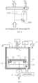
- FIG. 1 ais a schematic diagram of a plasma processor in the prior art
- FIG. 1 bis a schematic diagram of distribution of medium and low frequency RF powers in a plasma processor in the prior art
- FIG. 2 ais a schematic diagram of a plasma processor in the present disclosure
- FIG. 2 bis a schematic diagram of distributions of medium and low frequency RF powers in a plasma processor of the present disclosure
- FIG. 3is a schematic diagram of another embodiment of a plasma processor in the present disclosure.
- FIG. 4is a schematic diagram of a third embodiment of a plasma processor in the present disclosure.
- FIG. 5is a schematic diagram of a fourth embodiment of a plasma processor in the present disclosure.
- FIG. 2a preferred embodiment of the present disclosure will be further illustrated with reference to FIG. 2 .
- the inventorsfind that when a high frequency RF power is inputted in a base 120 , the RF power can be easily coupled to the focus ring, because for a high frequency signal, the thin (tens of microns) dielectric corrosion-resistance layer at a surface of the base 120 and the coupling ring 125 have a very small impedance.
- the coupling ringis always made of a dielectric material such as aluminum oxide or silicon oxide, it is impossible to tunably distribute the low frequency RF power to the focus ring 123 at the substrate edge without hardware improvement; although the coupling ring may also be made of a highly electrically conductive material, such a coupling ring can only achieve a relatively good etching effect in a short term, and as the time elapses, it still cannot compensate the processing result drift caused by consuming of the focus ring.
- the focus ring 123is usually made of a dielectric material such as quartz and aluminum oxide or a semiconductor material such as silicon carbide and silicon so as to avoid the substrate from being contaminated by the particles produced during the plasma processing process while providing sufficient electrical conductivity.
- the present disclosureprovides a novel plasma processing chamber shown in FIG. 2 a , whose basic structure is identical to the prior art shown in FIG. 1 a , except that an electrically conductive connection part is applied for transmitting the low frequency RF power, wherein the electrically conductive connection part is typically a wire, the wire being directly guided till above the coupling ring but below the focus ring and meanwhile a variable capacitance 124 being serially connected on the wire.
- the electrically conductive connection partis typically a wire, the wire being directly guided till above the coupling ring but below the focus ring and meanwhile a variable capacitance 124 being serially connected on the wire.
- annular electrode 127is disposed above the coupling ring 125 and the focus ring is disposed on the annular electrode; a first end of the wire is directly electrically connected to the annular electrode 127 , the other end thereof is directly electrically connected to the base 120 , and a variable capacitance 124 is serially connected on the wire, such that the low frequency RF power transported to the focus ring is tuned by tuning a capacitance value of the variable capacitance 124 .
- the annular electrode 127may be made of any electrically conductive material, e.g., aluminum, graphite, etc., as long as the material may provide a good electrical conductivity.
- variable capacitance of the present disclosuremay be disposed in a vacuum space below the electrically conductive base 120 ; most preferably, the variable capacitance 124 is disposed in an atmospheric environment below the hermetic baffle plate in the reaction chamber, only required to allow the two ends of the wire to pass through the hermetic baffle plate; disposing the variable capacitance in the atmospheric environment facilitates heat dissipation and maintenance.
- a reaction chamber wall 100is formed by a grounded metal, the grounded metal forming an electric field shielding space, such that as long as the variable capacitance 124 is disposed within the electric field shielding space of the reaction chamber, even it is in the atmospheric environment below the hermetic baffle plate, radiation of a low frequency electric field from the variable capacitance 124 to the external environment may still be avoided.
- the variable capacitance in the present disclosurenot only has a small size and a low cost, but also has a simple mechanical structure.
- FIG. 2 bshows an equivalent circuit diagram and an RF power distribution diagram of the present disclosure.
- the equivalent capacitance C 21 coupled to the substrate centeris still large, such that the main power can be coupled to the substrate, but the equivalent capacitance C 22 derived from the capacitances of the base 120 through a sidewall corrosion-resistance dielectric layer and the coupling ring 125 to the focus ring 123 is still very small, which cannot transport a relatively large RF power.
- variable capacitance 124does not transport the RF power in a traditional coupling manner; instead, it directly conducts the RF power in the base 120 to a lower surface of the target focus ring 123 in a direct electrical connection manner, thereby bypassing the impedance that seriously affects low frequency RF power coupling, wherein the variable capacitance 124 may adaptively select a value range and a tuning range according to needs; therefore, by simply tuning the capacitance value, the variable capacitance 124 of the present disclosure may effectively tune the low frequency RF power transported to the focus ring 123 .
- variable capacitanceWhen the reaction chamber is in an initial state, the variable capacitance is at an initial value; after a long-time plasma processing, when it is detected that the processing result in the substrate edge area is different from the center, the controller may real-time automatically change the capacitance value of the variable capacitance based on a set parameter, such that more low frequency RF power is transported to the focus ring at the substrate edge, further raising the sheath at the focus ring, making the sheath in substrate edge area and above the focus ring have the same height, thereby improving etching uniformity.
- a typical defect of the processing resultis the edge tilting of the etching hole in the substrate edge area.
- the etching hole in the substrate edge areawill have an inward tilting angle.
- the substrate processing resultis continuously detected until the uniformity of processing result deviates again from a preset threshold, and then the capacitance value of the variable capacitance is re-tuned based on the detected data.
- the present disclosuremay prevent frequent replacement of the focus ring in a long term and maintain a stable plasma processing result only by changing parameters of the variable capacitance without a need of providing a fluid pipeline or mechanical driving means in the vacuum environment.
- the present disclosuremay also be applied to a capacitively-coupled plasma (CCP) processor, where what is provided on top of the reaction chamber of the capacitively-coupled plasma processor is not a dielectric window, but an electrically conductive upper electrode in a flat showerhead shape, via which upper electrode the reactant gas is fed to a reaction area below.
- the high frequency RF power(13 MHz above, e.g. 27 MHz, 60 MHz) may be transported to the base 120 serving as a lower electrode; at this point, the upper electrode is grounded; alternatively, the high frequency RF power may also be transported to the upper electrode.
- the dielectric parameters of the coupling ring and the focus ringwill simultaneously affect distributions of high frequency and low frequency RF powers; however, with the electrical conduction path provided in the present disclosure, the high frequency RF power is mainly transported to the focus ring 123 by way of coupling, while part of the low frequency power is coupled to the focus ring 123 via the coupling ring 125 , and the other part thereof, which is tunable, is transported to the focus ring 123 by way of direct conduction; therefore, the present disclosure further has a function of separately tuning the high frequency and low frequency RF powers, so as to more accurately tune the plasma density distribution (high frequency power dominated) and sheath distribution (low frequency power dominated) from the center to the edge of the upper surface of the substrate.
- the present disclosureadditionally provides a low frequency RF energy supply circuit whose structure is simple and whose power is tunable.
- the equivalent capacitance C 22 of the lower electrode coupled to the focus ring via the coupling ring and the variable capacitance 124 additionally provided by the present disclosurejointly determine the low frequency RF power distributed to the focus ring, wherein the coupling ring may be preferably made of a dielectric material; in this way, the C 22 is relatively small, but added with the additional variable capacitance 124 , the capacitance tuning range may be much broader. If the coupling ring 125 is made of a highly electrically conductive material, the present disclosure may be still effective, except that the tuning range for the equivalent capacitance of C 22 plus 124 is slightly different.
- the dielectric layerhas a very large impedance to the low frequency RF signal, such that even a very thin plasma resistance coating (formed by A1203 or Y203) will appreciably affect the power for coupling the low frequency RF power to the focus ring at the substrate edge.
- a very thin plasma resistance coatingformed by A1203 or Y203
- the impedances to corresponding RF frequenciesare also different.
- RF power in specific frequency bandcannot be effectively transported to the focus ring.
- the specific frequency bandwill be moved to a higher frequency band.
- the low frequency RF signal in the present disclosureis usually lower than 2 MHz, and the effect is most appreciable particularly when lower than 1 MHz, e.g. 400 KHz.
- an RF signal higher than 2 MHz, e.g. 13 MHzmay also adopt connection wires of the present disclosure, causing the low frequency RF power to be transported to the focus ring in an effective and tunable manner.
- the present disclosurefurther provides another embodiment, the basic structure of which is identical to the first embodiment shown in FIG. 2 , except that besides being directly connected to the lower electrode 120 via a wire 137 (see FIG. 4 ), the variable capacitance 124 may also be connected to an intermedia conductive part 129 which is made of an electrically conductive material and disposed above the upper surface of a step 79 (see FIG. 4 ).
- the low frequency RF power of the lower electrodeis inputted to the intermedia conductive part 129 by coupling the dielectric layer crossing the upper surface of the step, and then is transported to the annular electrode 127 via the wire and the variable capacitance 124 , wherein the electrical conductive part, which may be annular or may include a plurality of separate conductors, surrounds the lower electrode sidewall.
- the electric field inputted to the lower electrodeis mainly upward coupled to a top portion of the reaction chamber.
- the equivalent capacitance C 12 laterally coupled to the focus ring 123 from the lower electrodeis very small; however, in the present disclosure, the intermedia conductive part 129 is a conductor extending in a horizontal direction, such that a large number of upward electric field lines from the step of the lower electrode may pass through the dielectric corrosion-resistance layer at the top surface of the step to reach the electrically conductive part; therefore, the equivalent capacitance is far larger than C 12 in the prior art.
- the low frequency electric fieldmay be guided to the annular electrode 127 above the coupling ring 125 , so as to tune the low frequency RF energy in the substrate edge area.
- a lower end of the wire 137may be directly electrically connected to the electrically conductive base 120 or coupled to the intermediate conductive part 129 of the electrically conductive base.
- the annular electrodemay also be embedded in the focus ring 123 , or as shown in the embodiment of FIG. 5 , an annular electrode 127 ′ is embedded in an upper half portion of the coupling ring 125 made of a dielectric material, such that although the equivalent capacitance coupled to the focus ring 123 from the lower electrode 120 is smaller than a value of the variable capacitance 124 shown in FIG.
- the object of the present disclosuremay also be achieved.
- the focus ring 123 ′when a focus ring 123 ′ is made of a conductor or semiconductor material (silicon, silicon carbide, aluminum, etc.), the focus ring 123 ′ per se may serve as the annular electrode of the present disclosure, such that at this point, the upper end of the wire may be directly connected to the focus ring 123 ′.
- the electrically conductive connection partmay also comprise a plurality of branch wires, and preferably, the plurality of branch wires are uniformly and symmetrically distributed in an outer peripheral of the base, such that each branch wire and its adjacent branch wires are spaced with a same distance but connected to different areas of the annular electrode.
- branch wiresare uniformly and symmetrically distributed in an outer peripheral of the base, such that each branch wire and its adjacent branch wires are spaced with a same distance but connected to different areas of the annular electrode.
- each branch wireis both connected to the electrically conductive base and the annular electrode, three independently tunable variable capacitance are serially connected to the three branch wires, and by tuning the three variable capacitance, the low frequency power may be uniformly distributed on the annular electrode from the three branch wires.
- the annular electrodemay be partitioned into three segments of arc-shaped electrically conductive plates which jointly form the annular electrode, wherein a gap or an insulating part is present between every two arc-shaped electrically conductive plates to thereby implement mutual electrical insulation; and by tuning the three variable capacitance, sheath thicknesses of different areas on the focus ring may be tuned area by area, thereby solving the problem of nonuniform sheath at some azimuths in the substrate edge annular area.
- variable capacitance in the present disclosureis only a best mode, and any other variable impedance devices that may tune the impedance of the low frequency power, including a hybrid circuit comprising a variable inductor and a capacitance arrangement, or a circuit formed by combination of other elements, may perform the function of impedance tuning.
- a hybrid circuitcomprising a variable inductor and a capacitance arrangement, or a circuit formed by combination of other elements, may perform the function of impedance tuning.
- Such alternativesare common knowledge in the industry and thus will not be listed one by one.
Landscapes
- Engineering & Computer Science (AREA)
- Chemical & Material Sciences (AREA)
- Physics & Mathematics (AREA)
- Plasma & Fusion (AREA)
- Analytical Chemistry (AREA)
- Computer Hardware Design (AREA)
- General Physics & Mathematics (AREA)
- Manufacturing & Machinery (AREA)
- Condensed Matter Physics & Semiconductors (AREA)
- Microelectronics & Electronic Packaging (AREA)
- Power Engineering (AREA)
- Chemical Kinetics & Catalysis (AREA)
- General Chemical & Material Sciences (AREA)
- Materials Engineering (AREA)
- Mechanical Engineering (AREA)
- Metallurgy (AREA)
- Organic Chemistry (AREA)
- Drying Of Semiconductors (AREA)
- Plasma Technology (AREA)
Abstract
Description
Claims (10)
Applications Claiming Priority (2)
| Application Number | Priority Date | Filing Date | Title |
|---|---|---|---|
| CN201710533117.X | 2017-07-03 | ||
| CN201710533117.XACN109216144B (en) | 2017-07-03 | 2017-07-03 | Plasma reactor with low-frequency radio frequency power distribution adjusting function |
Publications (2)
| Publication Number | Publication Date |
|---|---|
| US20190006155A1 US20190006155A1 (en) | 2019-01-03 |
| US12062524B2true US12062524B2 (en) | 2024-08-13 |
Family
ID=64739140
Family Applications (1)
| Application Number | Title | Priority Date | Filing Date |
|---|---|---|---|
| US16/025,995Active2038-10-10US12062524B2 (en) | 2017-07-03 | 2018-07-02 | Plasma reactor having a variable coupling of low frequency RF power to an annular electrode |
Country Status (4)
| Country | Link |
|---|---|
| US (1) | US12062524B2 (en) |
| KR (1) | KR102045484B1 (en) |
| CN (1) | CN109216144B (en) |
| TW (1) | TWI791027B (en) |
Cited By (1)
| Publication number | Priority date | Publication date | Assignee | Title |
|---|---|---|---|---|
| US20240038512A1 (en)* | 2022-07-27 | 2024-02-01 | Hochschule Für Angewandte Wissenschaft Und Kunst Hildesheim/Holzminden/Göttingen | Measurement Apparatus for Alternating Currents and Voltages of Physical Plasmas, Particularly of Cold Plasmas at Atmospheric Pressure, and Plasma Generator Comprising Such a Measurement Apparatus |
Families Citing this family (21)
| Publication number | Priority date | Publication date | Assignee | Title |
|---|---|---|---|---|
| JP6518024B1 (en)* | 2017-10-30 | 2019-05-22 | 日本碍子株式会社 | Electrostatic chuck and manufacturing method thereof |
| CN110323117B (en)* | 2018-03-28 | 2024-06-21 | 三星电子株式会社 | Plasma treatment equipment |
| KR102595900B1 (en)* | 2018-11-13 | 2023-10-30 | 삼성전자주식회사 | Plasma processing apparatus |
| US11393663B2 (en)* | 2019-02-25 | 2022-07-19 | Tokyo Electron Limited | Methods and systems for focus ring thickness determinations and feedback control |
| CN112530776B (en)* | 2019-09-18 | 2024-02-09 | 中微半导体设备(上海)股份有限公司 | Plasma processing device |
| US12266511B2 (en)* | 2019-11-26 | 2025-04-01 | Tokyo Electron Limited | Substrate support and substrate processing apparatus |
| JP7563843B2 (en)* | 2019-11-26 | 2024-10-08 | 東京エレクトロン株式会社 | Mounting table and substrate processing apparatus |
| TWI714366B (en)* | 2019-11-26 | 2020-12-21 | 聚昌科技股份有限公司 | Etching machine structure with the vertical position dynamically adjustable of the coil |
| CN112885690B (en)* | 2019-11-29 | 2023-10-20 | 中微半导体设备(上海)股份有限公司 | Plasma processing device |
| CN112992635B (en)* | 2019-12-13 | 2023-10-24 | 中微半导体设备(上海)股份有限公司 | Wafer fixing device, forming method thereof and plasma processing equipment |
| CN113013009B (en)* | 2019-12-20 | 2024-10-11 | 中微半导体设备(上海)股份有限公司 | Plasma processing device with radio frequency power distribution adjusting function and adjusting method |
| US11887820B2 (en)* | 2020-01-10 | 2024-01-30 | COMET Technologies USA, Inc. | Sector shunts for plasma-based wafer processing systems |
| CN113496862B (en)* | 2020-04-02 | 2024-09-06 | 中微半导体设备(上海)股份有限公司 | Plasma reactor and radio frequency power distribution adjusting method thereof |
| US20210391146A1 (en)* | 2020-06-11 | 2021-12-16 | Applied Materials, Inc. | Rf frequency control and ground path return in semiconductor process chambers |
| GB202012560D0 (en)* | 2020-08-12 | 2020-09-23 | Spts Technologies Ltd | Apparatus and method |
| CN114678270B (en)* | 2020-12-24 | 2025-08-08 | 中微半导体设备(上海)股份有限公司 | Inductively coupled plasma processing device and etching method thereof |
| CN115565840A (en)* | 2021-07-02 | 2023-01-03 | 中微半导体设备(上海)股份有限公司 | A plasma processing device and processing method |
| WO2023018596A1 (en)* | 2021-08-12 | 2023-02-16 | Lam Research Corporation | Process module chamber providing symmetric rf return path |
| KR20230068011A (en) | 2021-11-10 | 2023-05-17 | 삼성전자주식회사 | Substrate processing apparatus and method of manufacturing semiconductor device using the same |
| CN115332065A (en)* | 2022-07-15 | 2022-11-11 | 江苏鲁汶仪器有限公司 | Wafer uniformity optimization method for ICP (inductively coupled plasma) chamber |
| CN118016497A (en)* | 2022-11-09 | 2024-05-10 | 北京北方华创微电子装备有限公司 | Wafer carrying device and semiconductor process equipment |
Citations (42)
| Publication number | Priority date | Publication date | Assignee | Title |
|---|---|---|---|---|
| US6095084A (en)* | 1996-02-02 | 2000-08-01 | Applied Materials, Inc. | High density plasma process chamber |
| US6232236B1 (en)* | 1999-08-03 | 2001-05-15 | Applied Materials, Inc. | Apparatus and method for controlling plasma uniformity in a semiconductor wafer processing system |
| TW506234B (en) | 2000-09-18 | 2002-10-11 | Tokyo Electron Ltd | Tunable focus ring for plasma processing |
| US6478924B1 (en)* | 2000-03-07 | 2002-11-12 | Applied Materials, Inc. | Plasma chamber support having dual electrodes |
| US20030056901A1 (en)* | 2001-06-29 | 2003-03-27 | Alps Electric Co., Ltd. | Plasma processing apparatus and plasma processing system with reduced feeding loss, and method for stabilizing the apparatus and system |
| US20040050327A1 (en)* | 2001-01-22 | 2004-03-18 | Tokyo Electron Limited | Vertically translatable chuck assembly and method for a plasma reactor system |
| US20040163593A1 (en)* | 2002-12-26 | 2004-08-26 | Canon Kabushiki Kaisha | Plasma-processing apparatus |
| US20050079737A1 (en)* | 2003-10-10 | 2005-04-14 | Kellerman Peter L. | Mems based contact conductivity electrostatic chuck |
| US20060221540A1 (en)* | 2005-03-31 | 2006-10-05 | Shinji Himori | Capacitive coupling plasma processing apparatus |
| US7132618B2 (en)* | 2000-03-17 | 2006-11-07 | Applied Materials, Inc. | MERIE plasma reactor with overhead RF electrode tuned to the plasma with arcing suppression |
| US7193168B1 (en) | 2005-11-10 | 2007-03-20 | International Business Machines Corporation | Pneumatic switch for non-invasive testing and debug |
| US20070091006A1 (en) | 2005-10-21 | 2007-04-26 | Sanmina-Sci, A Delaware Corporation | Self-tuning radio frequency identification antenna system |
| US20070113981A1 (en)* | 2003-11-19 | 2007-05-24 | Tokyo Electron Limited | Etch system with integrated inductive coupling |
| US20080182416A1 (en)* | 2007-01-30 | 2008-07-31 | Collins Kenneth S | Plasma process uniformity across a wafer by apportioning power among plural vhf sources |
| US20080236749A1 (en) | 2007-03-28 | 2008-10-02 | Tokyo Electron Limited | Plasma processing apparatus |
| TW200908063A (en) | 2007-06-28 | 2009-02-16 | Lam Res Corp | Methods and apparatus for substrate processing |
| US20100006225A1 (en) | 2008-07-11 | 2010-01-14 | Hitachi High-Technologies Corporation | Plasma processing apparatus |
| TW201003771A (en) | 2008-03-25 | 2010-01-16 | Tokyo Electron Ltd | Plasma processing apparatus |
| US20100012274A1 (en) | 2008-07-18 | 2010-01-21 | Tokyo Electron Limited | Focus ring, substrate mounting table and plasma processing apparatus having same |
| US20100025369A1 (en) | 2008-07-30 | 2010-02-04 | Hitachi High-Technologies Corporation | Plasma processing apparatus and plasma processing method |
| US20100203736A1 (en) | 2009-02-12 | 2010-08-12 | Hitachi High-Technologies Corporation | Plasma Processing Method |
| US20100243162A1 (en) | 2009-03-31 | 2010-09-30 | Tokyo Electron Limited | Plasma processing apparatus |
| US20100326957A1 (en)* | 2009-06-24 | 2010-12-30 | Kenji Maeda | Plasma processing apparatus and plasma processing method |
| US20110126405A1 (en)* | 2009-09-29 | 2011-06-02 | Jonghoon Baek | Off-Center Ground Return for RF-Powered Showerhead |
| US8124539B2 (en)* | 2003-04-24 | 2012-02-28 | Tokyo Electron Limited | Plasma processing apparatus, focus ring, and susceptor |
| US8222157B2 (en)* | 2006-07-18 | 2012-07-17 | Lam Research Corporation | Hybrid RF capacitively and inductively coupled plasma source using multifrequency RF powers and methods of use thereof |
| US20120216955A1 (en)* | 2011-02-25 | 2012-08-30 | Toshiba Materials Co., Ltd. | Plasma processing apparatus |
| US20120252141A1 (en)* | 2011-03-28 | 2012-10-04 | Tokyo Electron Limited | Adaptive Recipe Selector |
| CN103227091A (en) | 2013-04-19 | 2013-07-31 | 中微半导体设备(上海)有限公司 | Plasma processing device |
| TW201334633A (en) | 2011-11-22 | 2013-08-16 | Lam Res Corp | Systems and methods for controlling a plasma edge region |
| US8617351B2 (en)* | 2002-07-09 | 2013-12-31 | Applied Materials, Inc. | Plasma reactor with minimal D.C. coils for cusp, solenoid and mirror fields for plasma uniformity and device damage reduction |
| US20140054268A1 (en) | 2012-02-23 | 2014-02-27 | Lam Research Corporation | Electronic Knob for Tuning Radial Etch Non-Uniformity at VHF Frequencies |
| CN103715049A (en) | 2012-09-29 | 2014-04-09 | 中微半导体设备(上海)有限公司 | Plasma processing apparatus and method for adjusting process rate of marginal area of substrate |
| CN103811247A (en) | 2014-02-17 | 2014-05-21 | 清华大学 | Focusing ring for plasma etching and plasma etching device with same |
| CN203800029U (en) | 2014-03-28 | 2014-08-27 | 中芯国际集成电路制造(北京)有限公司 | Etching reaction chamber |
| US8904957B2 (en)* | 2001-07-10 | 2014-12-09 | Tokyo Electron Limited | Plasma processor and plasma processing method |
| CN104241070A (en) | 2013-06-24 | 2014-12-24 | 中微半导体设备(上海)有限公司 | Gas injection device used for inductively couple plasma chamber |
| US20150170925A1 (en)* | 2013-12-17 | 2015-06-18 | Tokyo Electron Limited | System and method for controlling plasma density |
| US20160307743A1 (en)* | 2015-04-17 | 2016-10-20 | Lam Research Corporation | Chamber with vertical support stem for symmetric conductance and rf delivery |
| US20160351404A1 (en)* | 2015-05-28 | 2016-12-01 | Hitachi High-Technologies Corporation | Plasma processing apparatus and plasma processing method |
| US20170018411A1 (en) | 2015-07-13 | 2017-01-19 | Lam Research Corporation | Extreme edge sheath and wafer profile tuning through edge-localized ion trajectory control and plasma operation |
| US20190206703A1 (en)* | 2017-12-29 | 2019-07-04 | Advanced Micro-Fabrication Equipment Inc, China | Plasma reactor having a function of tuning low frequency rf power distribution |
- 2017
- 2017-07-03CNCN201710533117.XApatent/CN109216144B/enactiveActive
- 2018
- 2018-06-29TWTW107122653Apatent/TWI791027B/enactive
- 2018-07-02USUS16/025,995patent/US12062524B2/enactiveActive
- 2018-07-02KRKR1020180076328Apatent/KR102045484B1/enactiveActive
Patent Citations (57)
| Publication number | Priority date | Publication date | Assignee | Title |
|---|---|---|---|---|
| US6095084A (en)* | 1996-02-02 | 2000-08-01 | Applied Materials, Inc. | High density plasma process chamber |
| US6232236B1 (en)* | 1999-08-03 | 2001-05-15 | Applied Materials, Inc. | Apparatus and method for controlling plasma uniformity in a semiconductor wafer processing system |
| US6478924B1 (en)* | 2000-03-07 | 2002-11-12 | Applied Materials, Inc. | Plasma chamber support having dual electrodes |
| US7132618B2 (en)* | 2000-03-17 | 2006-11-07 | Applied Materials, Inc. | MERIE plasma reactor with overhead RF electrode tuned to the plasma with arcing suppression |
| TW506234B (en) | 2000-09-18 | 2002-10-11 | Tokyo Electron Ltd | Tunable focus ring for plasma processing |
| US20030201069A1 (en) | 2000-09-18 | 2003-10-30 | Johnson Wayne L. | Tunable focus ring for plasma processing |
| US20040050327A1 (en)* | 2001-01-22 | 2004-03-18 | Tokyo Electron Limited | Vertically translatable chuck assembly and method for a plasma reactor system |
| US20030056901A1 (en)* | 2001-06-29 | 2003-03-27 | Alps Electric Co., Ltd. | Plasma processing apparatus and plasma processing system with reduced feeding loss, and method for stabilizing the apparatus and system |
| US20150083333A1 (en)* | 2001-07-10 | 2015-03-26 | Tokyo Electron Limited | Plasma processor and plasma processing method |
| US8904957B2 (en)* | 2001-07-10 | 2014-12-09 | Tokyo Electron Limited | Plasma processor and plasma processing method |
| US9437402B2 (en)* | 2001-07-10 | 2016-09-06 | Tokyo Electron Limited | Plasma processor and plasma processing method |
| US9728381B2 (en)* | 2001-07-10 | 2017-08-08 | Tokyo Electron Limited | Plasma processor and plasma processing method |
| US8617351B2 (en)* | 2002-07-09 | 2013-12-31 | Applied Materials, Inc. | Plasma reactor with minimal D.C. coils for cusp, solenoid and mirror fields for plasma uniformity and device damage reduction |
| US20040163593A1 (en)* | 2002-12-26 | 2004-08-26 | Canon Kabushiki Kaisha | Plasma-processing apparatus |
| US8124539B2 (en)* | 2003-04-24 | 2012-02-28 | Tokyo Electron Limited | Plasma processing apparatus, focus ring, and susceptor |
| US20050079737A1 (en)* | 2003-10-10 | 2005-04-14 | Kellerman Peter L. | Mems based contact conductivity electrostatic chuck |
| US20070113981A1 (en)* | 2003-11-19 | 2007-05-24 | Tokyo Electron Limited | Etch system with integrated inductive coupling |
| US20060221540A1 (en)* | 2005-03-31 | 2006-10-05 | Shinji Himori | Capacitive coupling plasma processing apparatus |
| US8070911B2 (en)* | 2005-03-31 | 2011-12-06 | Tokyo Electron Limited | Capacitive coupling plasma processing apparatus |
| US20070091006A1 (en) | 2005-10-21 | 2007-04-26 | Sanmina-Sci, A Delaware Corporation | Self-tuning radio frequency identification antenna system |
| US7193168B1 (en) | 2005-11-10 | 2007-03-20 | International Business Machines Corporation | Pneumatic switch for non-invasive testing and debug |
| US8222157B2 (en)* | 2006-07-18 | 2012-07-17 | Lam Research Corporation | Hybrid RF capacitively and inductively coupled plasma source using multifrequency RF powers and methods of use thereof |
| US20080182416A1 (en)* | 2007-01-30 | 2008-07-31 | Collins Kenneth S | Plasma process uniformity across a wafer by apportioning power among plural vhf sources |
| US20080236749A1 (en) | 2007-03-28 | 2008-10-02 | Tokyo Electron Limited | Plasma processing apparatus |
| CN101720501A (en) | 2007-06-28 | 2010-06-02 | 朗姆研究公司 | Methods and apparatus for substrate processing |
| TW200908063A (en) | 2007-06-28 | 2009-02-16 | Lam Res Corp | Methods and apparatus for substrate processing |
| US7758764B2 (en) | 2007-06-28 | 2010-07-20 | Lam Research Corporation | Methods and apparatus for substrate processing |
| TW201003771A (en) | 2008-03-25 | 2010-01-16 | Tokyo Electron Ltd | Plasma processing apparatus |
| US8293068B2 (en) | 2008-03-25 | 2012-10-23 | Tokyo Electron Limited | Plasma processing apparatus |
| US20100006225A1 (en) | 2008-07-11 | 2010-01-14 | Hitachi High-Technologies Corporation | Plasma processing apparatus |
| JP2010021404A (en) | 2008-07-11 | 2010-01-28 | Hitachi High-Technologies Corp | Plasma processing apparatus |
| US20100012274A1 (en) | 2008-07-18 | 2010-01-21 | Tokyo Electron Limited | Focus ring, substrate mounting table and plasma processing apparatus having same |
| US20100025369A1 (en) | 2008-07-30 | 2010-02-04 | Hitachi High-Technologies Corporation | Plasma processing apparatus and plasma processing method |
| KR20100092348A (en) | 2009-02-12 | 2010-08-20 | 가부시키가이샤 히다치 하이테크놀로지즈 | Plasma processing method |
| US20100203736A1 (en) | 2009-02-12 | 2010-08-12 | Hitachi High-Technologies Corporation | Plasma Processing Method |
| US20100243162A1 (en) | 2009-03-31 | 2010-09-30 | Tokyo Electron Limited | Plasma processing apparatus |
| TW201127222A (en) | 2009-03-31 | 2011-08-01 | Tokyo Electron Ltd | Plasma processing apparatus |
| US20100326957A1 (en)* | 2009-06-24 | 2010-12-30 | Kenji Maeda | Plasma processing apparatus and plasma processing method |
| US20110126405A1 (en)* | 2009-09-29 | 2011-06-02 | Jonghoon Baek | Off-Center Ground Return for RF-Powered Showerhead |
| US20120216955A1 (en)* | 2011-02-25 | 2012-08-30 | Toshiba Materials Co., Ltd. | Plasma processing apparatus |
| US20120252141A1 (en)* | 2011-03-28 | 2012-10-04 | Tokyo Electron Limited | Adaptive Recipe Selector |
| US9396908B2 (en) | 2011-11-22 | 2016-07-19 | Lam Research Corporation | Systems and methods for controlling a plasma edge region |
| TW201334633A (en) | 2011-11-22 | 2013-08-16 | Lam Res Corp | Systems and methods for controlling a plasma edge region |
| US20140054268A1 (en) | 2012-02-23 | 2014-02-27 | Lam Research Corporation | Electronic Knob for Tuning Radial Etch Non-Uniformity at VHF Frequencies |
| CN103715049A (en) | 2012-09-29 | 2014-04-09 | 中微半导体设备(上海)有限公司 | Plasma processing apparatus and method for adjusting process rate of marginal area of substrate |
| CN103227091A (en) | 2013-04-19 | 2013-07-31 | 中微半导体设备(上海)有限公司 | Plasma processing device |
| CN104241070A (en) | 2013-06-24 | 2014-12-24 | 中微半导体设备(上海)有限公司 | Gas injection device used for inductively couple plasma chamber |
| US20150170925A1 (en)* | 2013-12-17 | 2015-06-18 | Tokyo Electron Limited | System and method for controlling plasma density |
| KR20160101021A (en) | 2013-12-17 | 2016-08-24 | 도쿄엘렉트론가부시키가이샤 | System and method for controlling plasma density |
| CN106415779A (en) | 2013-12-17 | 2017-02-15 | 东京毅力科创株式会社 | System and method for controlling plasma density |
| US10002744B2 (en)* | 2013-12-17 | 2018-06-19 | Tokyo Electron Limited | System and method for controlling plasma density |
| CN103811247A (en) | 2014-02-17 | 2014-05-21 | 清华大学 | Focusing ring for plasma etching and plasma etching device with same |
| CN203800029U (en) | 2014-03-28 | 2014-08-27 | 中芯国际集成电路制造(北京)有限公司 | Etching reaction chamber |
| US20160307743A1 (en)* | 2015-04-17 | 2016-10-20 | Lam Research Corporation | Chamber with vertical support stem for symmetric conductance and rf delivery |
| US20160351404A1 (en)* | 2015-05-28 | 2016-12-01 | Hitachi High-Technologies Corporation | Plasma processing apparatus and plasma processing method |
| US20170018411A1 (en) | 2015-07-13 | 2017-01-19 | Lam Research Corporation | Extreme edge sheath and wafer profile tuning through edge-localized ion trajectory control and plasma operation |
| US20190206703A1 (en)* | 2017-12-29 | 2019-07-04 | Advanced Micro-Fabrication Equipment Inc, China | Plasma reactor having a function of tuning low frequency rf power distribution |
Cited By (2)
| Publication number | Priority date | Publication date | Assignee | Title |
|---|---|---|---|---|
| US20240038512A1 (en)* | 2022-07-27 | 2024-02-01 | Hochschule Für Angewandte Wissenschaft Und Kunst Hildesheim/Holzminden/Göttingen | Measurement Apparatus for Alternating Currents and Voltages of Physical Plasmas, Particularly of Cold Plasmas at Atmospheric Pressure, and Plasma Generator Comprising Such a Measurement Apparatus |
| US12340994B2 (en)* | 2022-07-27 | 2025-06-24 | Hochschule Für Angewandte Wissenschaft Und Kunst Hildesheim/Holzminden/Göttingen | Measurement apparatus for alternating currents and voltages of physical plasmas, particularly of cold plasmas at atmospheric pressure, and plasma generator comprising such a measurement apparatus |
Also Published As
| Publication number | Publication date |
|---|---|
| US20190006155A1 (en) | 2019-01-03 |
| TWI791027B (en) | 2023-02-01 |
| TW201907760A (en) | 2019-02-16 |
| KR20190004231A (en) | 2019-01-11 |
| CN109216144B (en) | 2021-08-06 |
| CN109216144A (en) | 2019-01-15 |
| KR102045484B1 (en) | 2019-11-15 |
Similar Documents
| Publication | Publication Date | Title |
|---|---|---|
| US12062524B2 (en) | Plasma reactor having a variable coupling of low frequency RF power to an annular electrode | |
| US11830747B2 (en) | Plasma reactor having a function of tuning low frequency RF power distribution | |
| US10615004B2 (en) | Distributed electrode array for plasma processing | |
| US7837828B2 (en) | Substrate supporting structure for semiconductor processing, and plasma processing device | |
| US7199327B2 (en) | Method and system for arc suppression in a plasma processing system | |
| JP4904202B2 (en) | Plasma reactor | |
| US11387134B2 (en) | Process kit for a substrate support | |
| US10012248B2 (en) | Annular baffle | |
| US20040159287A1 (en) | Plasma reactor with overhead RF source power electrode having a resonance that is virtually pressure independent | |
| CN108257840B (en) | Plasma processing device | |
| WO2020022141A1 (en) | Plasma processing device | |
| US12293902B2 (en) | Process kit for a substrate support | |
| US8425719B2 (en) | Plasma generating apparatus | |
| KR20180122964A (en) | Active far edge plasma tunability | |
| KR20070112662A (en) | Inductively coupled plasma reactor | |
| CN211350572U (en) | Plasma reactor | |
| CN113496862B (en) | Plasma reactor and radio frequency power distribution adjusting method thereof | |
| WO2024015187A1 (en) | Process kit for a substrate support | |
| CN113013009A (en) | Plasma processing device with radio frequency power distribution adjusting function and adjusting method |
Legal Events
| Date | Code | Title | Description |
|---|---|---|---|
| FEPP | Fee payment procedure | Free format text:ENTITY STATUS SET TO UNDISCOUNTED (ORIGINAL EVENT CODE: BIG.); ENTITY STATUS OF PATENT OWNER: LARGE ENTITY | |
| FEPP | Fee payment procedure | Free format text:ENTITY STATUS SET TO SMALL (ORIGINAL EVENT CODE: SMAL); ENTITY STATUS OF PATENT OWNER: LARGE ENTITY | |
| STPP | Information on status: patent application and granting procedure in general | Free format text:APPLICATION DISPATCHED FROM PREEXAM, NOT YET DOCKETED | |
| AS | Assignment | Owner name:ADVANCED MICRO-FABRICATION EQUIPMENT INC, SHANGHAI, CHINA Free format text:ASSIGNMENT OF ASSIGNORS INTEREST;ASSIGNORS:ZHAO, KUI;LIU, SHENJIAN;NI, TUQIANG;REEL/FRAME:048294/0743 Effective date:20180815 Owner name:ADVANCED MICRO-FABRICATION EQUIPMENT INC, SHANGHAI Free format text:ASSIGNMENT OF ASSIGNORS INTEREST;ASSIGNORS:ZHAO, KUI;LIU, SHENJIAN;NI, TUQIANG;REEL/FRAME:048294/0743 Effective date:20180815 | |
| STPP | Information on status: patent application and granting procedure in general | Free format text:DOCKETED NEW CASE - READY FOR EXAMINATION | |
| AS | Assignment | Owner name:ADVANCED MICRO-FABRICATION EQUIPMENT INC. CHINA, C Free format text:CHANGE OF NAME;ASSIGNOR:ADVANCED MICRO-FABRICATION EQUIPMENT INC, SHANGHAI;REEL/FRAME:049352/0507 Effective date:20181221 Owner name:ADVANCED MICRO-FABRICATION EQUIPMENT INC. CHINA, CHINA Free format text:CHANGE OF NAME;ASSIGNOR:ADVANCED MICRO-FABRICATION EQUIPMENT INC, SHANGHAI;REEL/FRAME:049352/0507 Effective date:20181221 | |
| STPP | Information on status: patent application and granting procedure in general | Free format text:NON FINAL ACTION MAILED | |
| STPP | Information on status: patent application and granting procedure in general | Free format text:FINAL REJECTION MAILED | |
| STPP | Information on status: patent application and granting procedure in general | Free format text:RESPONSE AFTER FINAL ACTION FORWARDED TO EXAMINER | |
| STPP | Information on status: patent application and granting procedure in general | Free format text:ADVISORY ACTION MAILED | |
| STPP | Information on status: patent application and granting procedure in general | Free format text:DOCKETED NEW CASE - READY FOR EXAMINATION | |
| STPP | Information on status: patent application and granting procedure in general | Free format text:NON FINAL ACTION MAILED | |
| STPP | Information on status: patent application and granting procedure in general | Free format text:RESPONSE TO NON-FINAL OFFICE ACTION ENTERED AND FORWARDED TO EXAMINER | |
| STPP | Information on status: patent application and granting procedure in general | Free format text:FINAL REJECTION MAILED | |
| STPP | Information on status: patent application and granting procedure in general | Free format text:DOCKETED NEW CASE - READY FOR EXAMINATION | |
| STPP | Information on status: patent application and granting procedure in general | Free format text:NON FINAL ACTION MAILED | |
| STPP | Information on status: patent application and granting procedure in general | Free format text:FINAL REJECTION MAILED | |
| FEPP | Fee payment procedure | Free format text:ENTITY STATUS SET TO UNDISCOUNTED (ORIGINAL EVENT CODE: BIG.); ENTITY STATUS OF PATENT OWNER: LARGE ENTITY | |
| STPP | Information on status: patent application and granting procedure in general | Free format text:DOCKETED NEW CASE - READY FOR EXAMINATION | |
| STPP | Information on status: patent application and granting procedure in general | Free format text:NOTICE OF ALLOWANCE MAILED -- APPLICATION RECEIVED IN OFFICE OF PUBLICATIONS | |
| STPP | Information on status: patent application and granting procedure in general | Free format text:PUBLICATIONS -- ISSUE FEE PAYMENT RECEIVED | |
| STPP | Information on status: patent application and granting procedure in general | Free format text:PUBLICATIONS -- ISSUE FEE PAYMENT VERIFIED | |
| STCF | Information on status: patent grant | Free format text:PATENTED CASE |