US12052021B2 - Phase-locked loop slip detector - Google Patents
Phase-locked loop slip detectorDownload PDFInfo
- Publication number
- US12052021B2 US12052021B2US17/931,165US202217931165AUS12052021B2US 12052021 B2US12052021 B2US 12052021B2US 202217931165 AUS202217931165 AUS 202217931165AUS 12052021 B2US12052021 B2US 12052021B2
- Authority
- US
- United States
- Prior art keywords
- output
- lock
- circuit
- flip
- pfd
- Prior art date
- Legal status (The legal status is an assumption and is not a legal conclusion. Google has not performed a legal analysis and makes no representation as to the accuracy of the status listed.)
- Active
Links
Images


Classifications
- H—ELECTRICITY
- H03—ELECTRONIC CIRCUITRY
- H03L—AUTOMATIC CONTROL, STARTING, SYNCHRONISATION OR STABILISATION OF GENERATORS OF ELECTRONIC OSCILLATIONS OR PULSES
- H03L7/00—Automatic control of frequency or phase; Synchronisation
- H03L7/06—Automatic control of frequency or phase; Synchronisation using a reference signal applied to a frequency- or phase-locked loop
- H03L7/08—Details of the phase-locked loop
- H03L7/085—Details of the phase-locked loop concerning mainly the frequency- or phase-detection arrangement including the filtering or amplification of its output signal
- H03L7/089—Details of the phase-locked loop concerning mainly the frequency- or phase-detection arrangement including the filtering or amplification of its output signal the phase or frequency detector generating up-down pulses
- H03L7/0891—Details of the phase-locked loop concerning mainly the frequency- or phase-detection arrangement including the filtering or amplification of its output signal the phase or frequency detector generating up-down pulses the up-down pulses controlling source and sink current generators, e.g. a charge pump
- H—ELECTRICITY
- H03—ELECTRONIC CIRCUITRY
- H03L—AUTOMATIC CONTROL, STARTING, SYNCHRONISATION OR STABILISATION OF GENERATORS OF ELECTRONIC OSCILLATIONS OR PULSES
- H03L7/00—Automatic control of frequency or phase; Synchronisation
- H03L7/06—Automatic control of frequency or phase; Synchronisation using a reference signal applied to a frequency- or phase-locked loop
- H03L7/08—Details of the phase-locked loop
- H03L7/085—Details of the phase-locked loop concerning mainly the frequency- or phase-detection arrangement including the filtering or amplification of its output signal
- H03L7/087—Details of the phase-locked loop concerning mainly the frequency- or phase-detection arrangement including the filtering or amplification of its output signal using at least two phase detectors or a frequency and phase detector in the loop
- H—ELECTRICITY
- H03—ELECTRONIC CIRCUITRY
- H03L—AUTOMATIC CONTROL, STARTING, SYNCHRONISATION OR STABILISATION OF GENERATORS OF ELECTRONIC OSCILLATIONS OR PULSES
- H03L7/00—Automatic control of frequency or phase; Synchronisation
- H03L7/06—Automatic control of frequency or phase; Synchronisation using a reference signal applied to a frequency- or phase-locked loop
- H03L7/08—Details of the phase-locked loop
- H03L7/085—Details of the phase-locked loop concerning mainly the frequency- or phase-detection arrangement including the filtering or amplification of its output signal
- H03L7/095—Details of the phase-locked loop concerning mainly the frequency- or phase-detection arrangement including the filtering or amplification of its output signal using a lock detector
Definitions
- a phase-locked loopis a circuit that generates an output signal whose phase is related to the phase of its input signal.
- a PLLtypically receives a reference clock as input signal and generates an output dock as its output signal. The PLL strives to maintain a prescribed phase relationship between the output dock and the input reference clock. Deviations in the phase of the output and reference docks can cause undesirable behaviors of any downstream electronics that rely on the output clock from the PLL.
- a phase-locked loopincludes a phase-frequency detector (PFD) having a first PFD input, a second PFD input, and a PFD output.
- the PFDis configured to generate a first signal on the PFD output.
- the first signalcomprises pulses having pulse widths indicative of a phase difference between signals on the first and second PFD inputs.
- a low pass filterLPF
- a flip-flophas a clock input and a flip-flop output. The clock input is coupled to the LPF output.
- a lock-slip control circuitis coupled to the flip-flop output and to the first PFD input. The lock-slip control circuit is configured to determine phase-lock and phase-slip based at least in part on a signal on the flip-flop output.
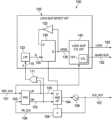
- FIG. 1illustrates an example of a phase-locked loop (PLL) with slip detection.
- PLLphase-locked loop
- FIG. 2includes a timing diagram illustrating the operation of the PLL of FIG. 1 .
- FIG. 3shows an example circuit implementation for a configurable low-pass filter of the PLL of FIG. 1 .
- FIG. 4includes a state diagram of the operation of a lock-slip control circuit for the PLL of FIG. 1 .
- the phase of an output clock from a PLLis controlled to maintain a prescribed phase relationship with respect to its input reference clock.
- the output clockmay desirably be phase-locked to the reference clock.
- An undesirably large phase differencemay occur, however, due to, for example, noise that infects the PLL.
- the reference clockmay be susceptible to noise. Further, noise may infect the PLL through the PLL's power supply.
- any downstream circuitry that relies on the PLL's output clock being phase-locked to the input reference clockmay be detrimentally impacted by the use of an output clock from the PLL that has “slipped.”
- the output clock from the PLLis characterized as being in a “lock” state or a “slip” state.
- the lock statemeans that the phase difference between the output and reference clocks is less than a prescribed threshold.
- the slip statemeans that the phase difference is larger than the prescribed threshold and the PLL is also referred to in this state as having “lost lock.”
- the disclosed examplesare directed to a slip detect circuit for a PLL.
- the slip detect circuitdetermines whether the PLL has achieved lock or whether the PLL has slipped.
- a LOCK signal generated by the slip detect circuitindicates whether the PLL is in lock (e.g., LOCK asserted high) or whether the PLL has slipped (e.g., LOCK asserted low).
- FIG. 1shows an example of a PLL 100 including a phase-frequency detector (PFD) 102 , a loop filter and charge pump 104 , a voltage-controlled oscillator (VCO) 106 , a frequency divider 108 , and a lock-slip detect circuit 120 .
- the lock-slip detect circuit 120includes a low pass filter (LPF) 122 , a data (D) flip-flop 130 , an inverter 132 , and a lock-slip control circuit 140 .
- a reference clock (REF_CLK) 101is provided to an input of the PFD 102 .
- the frequency of an output clock (CLK_OUT) 107is divided down by a frequency divider 108 to generate a feedback clock (FB_CLK) 109 , which is also provided to another input of the PFD 102 .
- FB_CLKfeedback clock
- the PFD 102is coupled to the loop filter and charge pump 104 and generates output signals UP 105 and DN 103 to the loop filter and charge pump 104 .
- UP 105is asserted high by the PFD 102 when FB_CLK 109 lags REF_CLK 101
- DN 103is asserted high by the PFD 102 when FB_CLK 109 leads REF_CLK 101 .
- An asserted high UP 105causes the loop filter and charge pump 104 to produce a voltage to the VCO 106 so as to increase its output frequency to thereby reduce the phase difference between FB_CLK 109 and REF_CLK 101 .
- An asserted high DN 103causes the loop filter and charge pump 104 to produce a voltage to the VCO 106 so as to decrease its output frequency.
- the frequency divider 108is included in the example in which the CLK_OUT from the VCO 106 has a frequency that is greater than REF_CLK 101 .
- CLK_OUT 107has the same frequency as REF_CLK 101
- a frequency divideris not used and the CLK_OUT is provided directly to the input of the PFD 102 .
- the output signal from the loop filter and charge pump 104is provided to the VCO 106 and causes the VCO to increase or decrease the frequency of CLK OUT 107 .
- the feedback loop of the PLL 100continually monitors the phase and frequency difference between FB_CLK 109 and REF_CLK 101 and responds to any difference by adjusting the operation of the VCO 106 to maintain phase lock.
- the lock-slip detect circuit 120determines whether the PLL is in lock or has slipped and generates a LOCK signal 150 accordingly.
- LOCKis asserted high to indicate a lock condition and asserted low to indicate a slip condition.
- LOCKindicates whether the PLL is in lock, and a separate signal is generated by the lock-skip control circuit 140 to indicate slip.
- the QUASI SLIP signal 152will be explained below.
- the PLL 100 of the example of FIG. 1also includes an OR gate 111 (or other type of logic gate(s)).
- OR gate 111has inputs that are coupled to the PFD's outputs on which UP 105 and DN 103 are generated.
- OR gate 111logically OR's UP 105 and DN 103 together to produce an output signal shown as A 115 .
- a 115is indicative of the existence of a phase difference between the REF_CLK 101 and the FB_CLK 109 (without regard to differentiating between a phase lead or a phase lag).
- OR gate 111may be separate from PFD 102 , or included as part of the PFD 102 .
- the A signal 115 generated by the PFD 102is provided to the LPF 122 .
- An example of A 115is shown in the timing diagram of FIG. 2 and further explained below.
- the LPF 122low pass filters A 115 to generate B 125 .
- An example of B 125is shown in the timing diagram of FIG. 2 and further explained below.
- the output of the LPF 122is coupled to a clock input of the D flip-flop 130 . As such, B 125 is used to clock the D flip-flop 130 .
- the Q output of the D flip-flop 130is coupled to an input of inverter 132 , and the output of the inverter 132 is coupled to the D input of the D flip-flop 130 .
- B 125e.g., a rising edge of B
- the Q output of the D flip-flop 130changes logic state.
- the signal produced by the Q output of the D flip-flop 130is labeled UPDN 135 in FIG. 1 .
- UPDN 135is provided to an input of the lock-slip control circuit 140 .
- the lock-slip control circuit 140comprises a hardware state machine comprising logic gates, counters (e.g., one or more counters 141 ), flip-flops, etc. and generates LOCK 150 and QUASI SLIP 152 as will be explained above.
- FIG. 2shows an example timing diagram illustrating the operation of PLL 100 .
- the signals illustrated in FIG. 2include REF_CLK 101 , FB_CLK 109 , A 115 , B 125 , and UPDN 135 . Varying amounts of phase difference between REF_CLK 101 and FB_CLK 109 are shown in FIG. 2 . Because A 115 is the logical OR of UP and DN, when REF_CLK 101 leads FB_CLK 109 , A 115 is asserted high upon the occurrence of a rising edge of REF_CLK 101 and deasserted upon the occurrence of a corresponding rising edge of FB_CLK 109 .
- FIG. 2shows an example timing diagram illustrating the operation of PLL 100 .
- the signals illustrated in FIG. 2include REF_CLK 101 , FB_CLK 109 , A 115 , B 125 , and UPDN 135 . Varying amounts of phase difference between REF_CLK 101 and
- the widths of the pulses on A 115are a function of the phase delay between REF_CLK 101 and FB_CLK 109 .
- the width of pulse 202is smaller than the width of pulse 204 because rising edges 220 and 221 of REF_CLK 101 and FB_CLK 109 , respectively, are closer together than rising edges 222 and 223 .
- the widths of pulses 206 and 208are relatively large because of the relatively large phase difference between rising edges 224 and 226 of REF_CLK 101 and corresponding edges 225 and 227 of FB_CLK 109 .
- LPF 122generates B 125 based on A 115 (B 125 is a low-pass filtered version of A 115 ).
- the frequency response of LPF 122is configured to eliminate A's relatively narrow pulses 202 and 214 from being present in B 125 .
- the relatively short duration negative pulse 207also is filtered out of A 115 and thus not present in B 125 .
- the narrow duration pulses 202 and 214represent corresponding clock cycles of REF_CLK 101 and FB_CLK 109 that are less than a threshold amount of phase difference and thus considered to be “in phase” (lock).
- the pulses 240 , 242 , 244 , and 246 that are present in B 125correspond to clock cycles of FB_CLK 109 that have a large enough phase difference in relation to REF_CLK 101 so as to be considered “out of phase.”
- FIG. 3shows an example implementation of the LPF 122 .
- the frequency response of the LPF 122(e.g., its corner frequency) is configurable.
- the LPF 122includes a buffer 301 , capacitors C 0 , C 1 , and C 2 , and switches S 1 and S 2 (e.g., transistor switches).
- the input of buffer 301is coupled to the PFD 102 to receive A 115 .
- the output of the bufferis coupled to capacitor C 0 and to switches S 1 and S 2 .
- Switch S 1connects to capacitor C 1 and switch S 2 connects to capacitor C 2 .
- Capacitor C 0is “always on” and capacitors C 1 and C 2 can be selectively enabled and disabled by controlling their respective switches S 1 and S 2 .
- the LPF 122implements an “RC” filter in which the on-resistance of buffer 301 provides the resistance for the filter and the effective capacitance enabled by control of switches S 1 and S 2 provides the capacitance for the filter.
- C 0is always on and represents the minimum amount of capacitance for the filter.
- the filter capacitancecan be increased by closing either or both of switches S 1 and S 2 . Additional switch and capacitor pairs can be included in other examples. In one example, the capacitance of C 1 equals that of C 0 , and the capacitance of C 2 is twice that of C 0 .
- the capacitor array of C 0 -C 2may comprise a binary-weighted capacitor array.
- the switchesmay be controlled by a digital value stored in a configuration register on the same semiconductor die as PLL 100 .
- the capacitance of C 0may be such that the LPF 122 is configured to filter out pulses on A that have a width equal to or smaller than 500 picoseconds (ps).
- the pulse width that is filtered out by LPF 122may be increased through closure of one or more of the switches S 1 , S 2 .
- FIG. 2also shows UPDN 135 produced by the D flip-flop 130 .
- the D flip-flop 130 in this examplechanges the state of its Q output (UPDN 135 ) upon a rising edge of its clock input (B 125 )
- the D flip-flop 130changes the logic state of UPDN 135 upon each occurrence of a rising edge of B 125 .
- rising edges 251 , 252 , 253 , and 254 of B 125cause UPDN 135 to change state as shown at 261 , 262 , 263 , and 264 .
- the counters 141 within the example lock-slip control circuit 140count edges (both rising and falling) of UPDN 135 to determine the occurrence of X UPDN edges in Y cycles of REF_CLK 101 .
- the values of X and Yare configured into the lock-slip control circuit 140 so that a slip is detected upon the occurrence of X or more edges of UPDN 135 in Y cycles of REF_CLK 101 .
- LOCK 150is asserted to a state (e.g., low) indicative of the slip state for PLL 100 .
- the REF_CLK 101also is provided to the lock-slip control circuit 140 .
- the minimum width of a pulse on UPDN 135is the time duration of at least one cycle of REF_CLK 101 .
- REF_CLK 101can be used by a counter 141 to count edges of UPDN 135 , and a separate (higher frequency) clock is not needed for this purpose.
- the logic implemented by the lock-slip control circuit 140 to detect a lock condition and to detect a slip conditionis described below.
- FIG. 4illustrates a sample of a state diagram 300 governing the operation of the lock-slip control circuit 140 .
- the states shown in the sample state diagram 300include IDLE 310 , SILENT COUNT 320 , LOCK COUNT 330 , LOCK WAIT 340 , and SLIP COUNT 350 .
- the lock-slip control circuit 140starts in the IDLE state 310 , and then transitions to the SILENT COUNT state 320 .
- the lock-slip control circuit 140counts pulses of the REF_CLK 101 corresponding to a BLANKING COUNT period of time.
- a 115At power-on, it is possible for A 115 not to toggle between high and low due to a large initial phase difference between REF_CLK 101 and FB_CLK 109 , and if no pulses on A 115 are present, then the lock-slip control circuit 140 might determine that the PLL 100 is in lock when it has not yet locked CLK_OUT 107 to REF_CLK 101 . During the BLANKING COUNT period of time, the lock-slip control circuit 140 does not count edges of UPDN 135 and thus does not determine if a slip condition has occurred, nor whether a lock condition has occurred.
- the IDLE state 310is re-entered, and the lock-slip control circuit 140 remains in this state as long as no UPDN edges are detected.
- the statetransitions from the IDLE state 310 to the LOCK COUNT state 330 .
- the lock-slip control circuit 140While in the LOCK COUNT state 330 , the lock-slip control circuit 140 counts for a REF COUNT period of time. In one example, the lock-slip control circuit 140 counts pulses of REF_CLK corresponding to the REF COUNT period of time.
- REF COUNTrepresents a period of time during which the absence of any UPDN edges indicates that the PLL 100 has achieved lock. While in the LOCK COUNT state 330 , LOCK 150 is deasserted (to indicate that phase lock has not been yet been achieved). Upon detection of an UPDN edge, the counter which counts REF COUNT is reset.
- the lock-slip control circuit 140transitions to the LOCK WAIT state 340 . While in the LOCK WAIT state, LOCK 150 is asserted to indicate that PLL 100 has achieved lock. As long as no UPDN edges are detected, the lock-slip control circuit 140 remains in the LOCK WAIT state 340 . Upon detection of an UPDN edge, the lock-slip control circuit 140 transitions to the SLIP COUNT state 350 .
- the lock-slip control circuit 140While in the SLIP COUNT state 350 , the lock-slip control circuit 140 counts cycles of REF_CLK 101 for a period of time Y. Over the course of Y time, if fewer than X UPDN edges are detected, then an insufficient number of UPDN edges are detected to affirmatively determine that the PLL 100 has slipped, and the lock-slip control circuit 140 transitions its state back to the LOCK WAIT state 340 . LOCK 150 continues to be asserted to indicate that the PLL 100 remains in phase lock.
- the lock-slip control circuit 140affirmatively determines that the PLL has slipped and the lock-slip control circuit 140 transitions its state to the IDLE state 310 in which LOCK 150 is deasserted indicating loss of lock (i.e., the PLL has slipped).
- the values of X and Ymay be designed into the lock-slip control circuit 140 or may be user-configurable. In one example, X is 16 and Y is 32, meaning that slip is determined if the lock-slip control circuit 140 detects 16 or more UPDN edges in 32 cycles of REF CLK 101 .
- FIG. 1illustrates that the lock-slip control circuit 140 also generates QUASI SLIP 152 .
- the quasi slip feature of the PLL 100may be enabled or disabled by a user (e.g., programming a control register within the PLL 100 ). If enabled, the lock-slip control circuit 140 asserts QUASI SLIP 152 responsive to the lock-slip control circuit 140 being in the SLIP COUNT state 350 . That is, while LOCK 150 is asserted, if even one edge of UPDN 135 is detected, then QUASI SLIP 152 is asserted, even though the lock-slip control circuit 140 has not yet affirmatively determined that the PLL has slipped.
- An asserted QUASI SLIP 152indicates that the PLL is still determined to be in phase lock, but that at least one cycle of FB_CLK 109 is out of phase with respect to REF_CLK 101 by more than a threshold value that would cause LOCK to be deasserted if X or more UPDN edges out of Y REF_CLK cycles were detected (e.g., the maximum width of the A 115 pulses that is filtered out by LPF 122 from being present in B 125 ).
- Any circuitry that uses CLK_OUT 107 from the PLL 100 and that is particularly sensitive to any cycles of CLK_OUT that are substantially out of phase with respect to REF_CLK 101can respond to the assertion of QUASI SLIP 152 in a suitable, application-specific manner.
- the lock-slip control circuit 140can also detect slip based on the occurrence of n*X UPDN edges out of m*Y REF_CLK cycles, where m may be greater than n.
- the values of m and mmay be configurable (e.g., in an externally-accessible configuration register) to tune the sensitivity as per application requirements.
- nis 3 and m is 4.
- the lock-slip control circuit 140determines slip to have occurred if 3X UPDN edges occurs in 4Y REF_CLK cycles.
- Xis 16 and Y is 32, and thus slip is detected if 48 UPDN edges are detected in 128 REF_CLK cycles.
- the lock-slip control circuit 140determines slip to have occurred if either or both of the following conditions are true: (a) X or more UPDN edges occur out of Y REF_CLK cycles, or (b) n*X (or more) UPDN edges occur out of m*Y REF_CLK cycles.
- Coupleis used throughout the specification. The term may cover connections, communications, or signal paths that enable a functional relationship consistent with the description of the present disclosure. For example, if device A generates a signal to control device B to perform an action, in a first example device A is coupled to device B, or in a second example device A is coupled to device B through intervening component C if intervening component C does not substantially alter the functional relationship between device A and device B such that device B is controlled by device A via the control signal generated by device A.
Landscapes
- Stabilization Of Oscillater, Synchronisation, Frequency Synthesizers (AREA)
Abstract
Description
Claims (20)
Priority Applications (1)
| Application Number | Priority Date | Filing Date | Title |
|---|---|---|---|
| US17/931,165US12052021B2 (en) | 2019-06-24 | 2022-09-12 | Phase-locked loop slip detector |
Applications Claiming Priority (4)
| Application Number | Priority Date | Filing Date | Title |
|---|---|---|---|
| US201962865787P | 2019-06-24 | 2019-06-24 | |
| US16/703,232US11133807B2 (en) | 2019-06-24 | 2019-12-04 | Phase-locked loop slip detector |
| US17/458,001US11444626B2 (en) | 2019-06-24 | 2021-08-26 | Phase-locked loop slip detector |
| US17/931,165US12052021B2 (en) | 2019-06-24 | 2022-09-12 | Phase-locked loop slip detector |
Related Parent Applications (1)
| Application Number | Title | Priority Date | Filing Date |
|---|---|---|---|
| US17/458,001ContinuationUS11444626B2 (en) | 2019-06-24 | 2021-08-26 | Phase-locked loop slip detector |
Publications (2)
| Publication Number | Publication Date |
|---|---|
| US20230006681A1 US20230006681A1 (en) | 2023-01-05 |
| US12052021B2true US12052021B2 (en) | 2024-07-30 |
Family
ID=74038672
Family Applications (3)
| Application Number | Title | Priority Date | Filing Date |
|---|---|---|---|
| US16/703,232ActiveUS11133807B2 (en) | 2019-06-24 | 2019-12-04 | Phase-locked loop slip detector |
| US17/458,001ActiveUS11444626B2 (en) | 2019-06-24 | 2021-08-26 | Phase-locked loop slip detector |
| US17/931,165ActiveUS12052021B2 (en) | 2019-06-24 | 2022-09-12 | Phase-locked loop slip detector |
Family Applications Before (2)
| Application Number | Title | Priority Date | Filing Date |
|---|---|---|---|
| US16/703,232ActiveUS11133807B2 (en) | 2019-06-24 | 2019-12-04 | Phase-locked loop slip detector |
| US17/458,001ActiveUS11444626B2 (en) | 2019-06-24 | 2021-08-26 | Phase-locked loop slip detector |
Country Status (1)
| Country | Link |
|---|---|
| US (3) | US11133807B2 (en) |
Families Citing this family (2)
| Publication number | Priority date | Publication date | Assignee | Title |
|---|---|---|---|---|
| US11133807B2 (en)* | 2019-06-24 | 2021-09-28 | Texas Instruments Incorporated | Phase-locked loop slip detector |
| KR20250026046A (en)* | 2023-08-16 | 2025-02-25 | 에스케이하이닉스 주식회사 | Electronic device and electronic system for performing a phase control operation |
Citations (32)
| Publication number | Priority date | Publication date | Assignee | Title |
|---|---|---|---|---|
| US4516250A (en) | 1983-08-26 | 1985-05-07 | At&T Information Systems | Frequency and phase comparator with slip detection capability |
| US4902920A (en) | 1988-09-26 | 1990-02-20 | General Signal Corporation | Extended range phase detector |
| US5790613A (en) | 1995-07-07 | 1998-08-04 | Pioneer Electronic Corporation | Cycle slip detector and phase locked loop circuit and digital signal reproducing apparatus using the same |
| US6265902B1 (en) | 1999-11-02 | 2001-07-24 | Ericsson Inc. | Slip-detecting phase detector and method for improving phase-lock loop lock time |
| US6392457B1 (en) | 2000-10-02 | 2002-05-21 | Agere Systems Guardian Corp. | Self-aligned clock recovery circuit using a proportional phase detector with an integral frequency detector |
| US20020175769A1 (en)* | 2001-05-24 | 2002-11-28 | Wong Keng L. | Variable lock window for a phase locked loop |
| US20050073343A1 (en)* | 2003-10-07 | 2005-04-07 | Samsung Electronics Co., Ltd. | Phase-locked loop circuit having phase lock detection function and method for detecting phase lock thereof |
| US7173462B1 (en) | 2005-10-27 | 2007-02-06 | Mediatek Inc. | Second order delay-locked loop for data recovery |
| US7183861B2 (en)* | 2004-07-27 | 2007-02-27 | Samsung Electronics, Co., Ltd. | Circuits and methods for detecting phase lock |
| US20070205833A1 (en) | 2006-02-28 | 2007-09-06 | Mar Wing J | Adaptive cycle-slipped detector for unlock detection in phase-locked loop applications |
| US7742551B2 (en)* | 2006-07-31 | 2010-06-22 | Mosaid Technologies Incorporated | Pulse counter with clock edge recovery |
| US7876148B2 (en) | 2007-12-28 | 2011-01-25 | Hynix Semiconductor Inc. | Low pass filter and lock detector circuit |
| US7940088B1 (en)* | 2009-03-31 | 2011-05-10 | Pmc-Sierra, Inc. | High speed phase frequency detector |
| US8004337B2 (en)* | 2007-01-30 | 2011-08-23 | Dolpan Audio, Llc | Digital delay circuit |
| US8258831B1 (en)* | 2009-11-09 | 2012-09-04 | Marvell Israel (M.I.S.L) Ltd. | Method and apparatus for clock generator lock detector |
| US8368446B2 (en) | 2011-04-21 | 2013-02-05 | Hynix Semiconductor Inc. | Delay locked loop |
| US8368439B2 (en)* | 2010-03-18 | 2013-02-05 | Samsung Electronics Co., Ltd. | Phase locked loop circuit, method of detecting lock, and system having the circuit |
| US20140312943A1 (en)* | 2013-04-22 | 2014-10-23 | Asahi Kasei Microdevices Corporation | Phase-locked loop device with managed transition to random noise operation mode |
| US20160079984A1 (en)* | 2014-09-15 | 2016-03-17 | Stmicroelectronics (Crolles 2) Sas | Device for generating a clock signal by frequency multiplication |
| US20160112055A1 (en)* | 2014-10-20 | 2016-04-21 | Texas Instruments Incorporated | Phase frequency detector (pfd) circuit with improved lock time |
| US20160308541A1 (en)* | 2015-04-17 | 2016-10-20 | Taiwan Semiconductor Manufacturing Company Ltd. | Circuit for digitizing phase differences, pll circuit and method for the same |
| US9577650B2 (en)* | 2013-02-22 | 2017-02-21 | Microchip Technology Incorporated | Phase lock loop lock indicator |
| US20190013815A1 (en) | 2017-07-07 | 2019-01-10 | Nxp B.V. | Phase locked loop |
| US10236896B1 (en) | 2018-03-12 | 2019-03-19 | Motorola Solutions, Inc. | Reducing transient response in a phase-locked loop circuit |
| US20190219674A1 (en)* | 2018-01-12 | 2019-07-18 | Analog Devices Global Unlimited Company | Receiver with tunable filter for light range finding system |
| US20190280700A1 (en) | 2018-03-09 | 2019-09-12 | Texas Instruments Incorporated | Cycle slip detection and correction in phase-locked loop |
| US10659062B2 (en)* | 2016-12-15 | 2020-05-19 | Mitsubishi Electric Corporation | PLL circuit |
| US20200403622A1 (en)* | 2019-06-24 | 2020-12-24 | Texas Instruments Incorporated | Phase-locked loop slip detector |
| US20210013888A1 (en)* | 2019-07-11 | 2021-01-14 | Samsung Electronics Co., Ltd. | Phase locked circuit, method of operating the same, and transceiver |
| US10928886B2 (en) | 2019-02-25 | 2021-02-23 | Intel Corporation | Frequency overshoot and voltage droop mitigation apparatus and method |
| US10979058B2 (en)* | 2016-05-11 | 2021-04-13 | Sony Corporation | Detection device and detection method |
| US11271572B2 (en)* | 2020-04-29 | 2022-03-08 | Analog Devices International Unlimited Company | Self-tuning phase-locked loop (PLL) circuit |
- 2019
- 2019-12-04USUS16/703,232patent/US11133807B2/enactiveActive
- 2021
- 2021-08-26USUS17/458,001patent/US11444626B2/enactiveActive
- 2022
- 2022-09-12USUS17/931,165patent/US12052021B2/enactiveActive
Patent Citations (33)
| Publication number | Priority date | Publication date | Assignee | Title |
|---|---|---|---|---|
| US4516250A (en) | 1983-08-26 | 1985-05-07 | At&T Information Systems | Frequency and phase comparator with slip detection capability |
| US4902920A (en) | 1988-09-26 | 1990-02-20 | General Signal Corporation | Extended range phase detector |
| US5790613A (en) | 1995-07-07 | 1998-08-04 | Pioneer Electronic Corporation | Cycle slip detector and phase locked loop circuit and digital signal reproducing apparatus using the same |
| US6265902B1 (en) | 1999-11-02 | 2001-07-24 | Ericsson Inc. | Slip-detecting phase detector and method for improving phase-lock loop lock time |
| US6392457B1 (en) | 2000-10-02 | 2002-05-21 | Agere Systems Guardian Corp. | Self-aligned clock recovery circuit using a proportional phase detector with an integral frequency detector |
| US20020175769A1 (en)* | 2001-05-24 | 2002-11-28 | Wong Keng L. | Variable lock window for a phase locked loop |
| US20050073343A1 (en)* | 2003-10-07 | 2005-04-07 | Samsung Electronics Co., Ltd. | Phase-locked loop circuit having phase lock detection function and method for detecting phase lock thereof |
| US7183861B2 (en)* | 2004-07-27 | 2007-02-27 | Samsung Electronics, Co., Ltd. | Circuits and methods for detecting phase lock |
| US7173462B1 (en) | 2005-10-27 | 2007-02-06 | Mediatek Inc. | Second order delay-locked loop for data recovery |
| US20070205833A1 (en) | 2006-02-28 | 2007-09-06 | Mar Wing J | Adaptive cycle-slipped detector for unlock detection in phase-locked loop applications |
| US7742551B2 (en)* | 2006-07-31 | 2010-06-22 | Mosaid Technologies Incorporated | Pulse counter with clock edge recovery |
| US8004337B2 (en)* | 2007-01-30 | 2011-08-23 | Dolpan Audio, Llc | Digital delay circuit |
| US7876148B2 (en) | 2007-12-28 | 2011-01-25 | Hynix Semiconductor Inc. | Low pass filter and lock detector circuit |
| US7940088B1 (en)* | 2009-03-31 | 2011-05-10 | Pmc-Sierra, Inc. | High speed phase frequency detector |
| US8258831B1 (en)* | 2009-11-09 | 2012-09-04 | Marvell Israel (M.I.S.L) Ltd. | Method and apparatus for clock generator lock detector |
| US8368439B2 (en)* | 2010-03-18 | 2013-02-05 | Samsung Electronics Co., Ltd. | Phase locked loop circuit, method of detecting lock, and system having the circuit |
| US8368446B2 (en) | 2011-04-21 | 2013-02-05 | Hynix Semiconductor Inc. | Delay locked loop |
| US9577650B2 (en)* | 2013-02-22 | 2017-02-21 | Microchip Technology Incorporated | Phase lock loop lock indicator |
| US20140312943A1 (en)* | 2013-04-22 | 2014-10-23 | Asahi Kasei Microdevices Corporation | Phase-locked loop device with managed transition to random noise operation mode |
| US20160079984A1 (en)* | 2014-09-15 | 2016-03-17 | Stmicroelectronics (Crolles 2) Sas | Device for generating a clock signal by frequency multiplication |
| US20160112055A1 (en)* | 2014-10-20 | 2016-04-21 | Texas Instruments Incorporated | Phase frequency detector (pfd) circuit with improved lock time |
| US20160308541A1 (en)* | 2015-04-17 | 2016-10-20 | Taiwan Semiconductor Manufacturing Company Ltd. | Circuit for digitizing phase differences, pll circuit and method for the same |
| US10979058B2 (en)* | 2016-05-11 | 2021-04-13 | Sony Corporation | Detection device and detection method |
| US10659062B2 (en)* | 2016-12-15 | 2020-05-19 | Mitsubishi Electric Corporation | PLL circuit |
| US20190013815A1 (en) | 2017-07-07 | 2019-01-10 | Nxp B.V. | Phase locked loop |
| US20190219674A1 (en)* | 2018-01-12 | 2019-07-18 | Analog Devices Global Unlimited Company | Receiver with tunable filter for light range finding system |
| US20190280700A1 (en) | 2018-03-09 | 2019-09-12 | Texas Instruments Incorporated | Cycle slip detection and correction in phase-locked loop |
| US10868550B2 (en)* | 2018-03-09 | 2020-12-15 | Texas Instruments Incorporated | Cycle slip detection and correction in phase-locked loop |
| US10236896B1 (en) | 2018-03-12 | 2019-03-19 | Motorola Solutions, Inc. | Reducing transient response in a phase-locked loop circuit |
| US10928886B2 (en) | 2019-02-25 | 2021-02-23 | Intel Corporation | Frequency overshoot and voltage droop mitigation apparatus and method |
| US20200403622A1 (en)* | 2019-06-24 | 2020-12-24 | Texas Instruments Incorporated | Phase-locked loop slip detector |
| US20210013888A1 (en)* | 2019-07-11 | 2021-01-14 | Samsung Electronics Co., Ltd. | Phase locked circuit, method of operating the same, and transceiver |
| US11271572B2 (en)* | 2020-04-29 | 2022-03-08 | Analog Devices International Unlimited Company | Self-tuning phase-locked loop (PLL) circuit |
Also Published As
| Publication number | Publication date |
|---|---|
| US20200403622A1 (en) | 2020-12-24 |
| US20210384913A1 (en) | 2021-12-09 |
| US11133807B2 (en) | 2021-09-28 |
| US20230006681A1 (en) | 2023-01-05 |
| US11444626B2 (en) | 2022-09-13 |
Similar Documents
| Publication | Publication Date | Title |
|---|---|---|
| US7940088B1 (en) | High speed phase frequency detector | |
| US8076979B2 (en) | Lock detection circuit for phase locked loop | |
| US9503105B2 (en) | Phase frequency detector (PFD) circuit with improved lock time | |
| US8049533B1 (en) | Receiver and method for dynamically adjusting sensitivity of receiver | |
| US12052021B2 (en) | Phase-locked loop slip detector | |
| US6879195B2 (en) | PLL lock detection circuit using edge detection | |
| EP2633620B1 (en) | Pll dual edge lock detector | |
| US5631591A (en) | Method and apparatus for synchronizing timing signals of two integrated circuit chips | |
| CN111464180B (en) | Phase-locked loop circuit with locking detection function | |
| US7663417B2 (en) | Phase-locked loop circuit | |
| US6927635B2 (en) | Lock detectors having a narrow sensitivity range | |
| US7567642B2 (en) | Phase detector with extended linear operating range | |
| US9374038B2 (en) | Phase frequency detector circuit | |
| US6614317B2 (en) | Variable lock window for a phase locked loop | |
| US7183861B2 (en) | Circuits and methods for detecting phase lock | |
| US7598816B2 (en) | Phase lock loop circuit with delaying phase frequency comparson output signals | |
| US20020094054A1 (en) | Phase-locked loop lock detector circuit and method of lock detection | |
| KR20200109481A (en) | Apparatus for Detecting Phase Frequency with Delay Less | |
| KR20080077515A (en) | Phase locking detection method and phase locked loop circuit for performing the same | |
| US20120110365A1 (en) | Method for locking frequency of usb device and usb frequency locking device | |
| US20020039397A1 (en) | Phase comparator circuit | |
| JP3079943B2 (en) | PLL circuit | |
| JP2016063445A (en) | Pll circuit and semiconductor integrated circuit | |
| WO2024059587A1 (en) | Single and dual edge triggered phase error detection | |
| CN116865747A (en) | Frequency locking control method, frequency locking circuit and chip of phase-locked loop |
Legal Events
| Date | Code | Title | Description |
|---|---|---|---|
| FEPP | Fee payment procedure | Free format text:ENTITY STATUS SET TO UNDISCOUNTED (ORIGINAL EVENT CODE: BIG.); ENTITY STATUS OF PATENT OWNER: LARGE ENTITY | |
| STPP | Information on status: patent application and granting procedure in general | Free format text:DOCKETED NEW CASE - READY FOR EXAMINATION | |
| STPP | Information on status: patent application and granting procedure in general | Free format text:NON FINAL ACTION MAILED | |
| STPP | Information on status: patent application and granting procedure in general | Free format text:RESPONSE TO NON-FINAL OFFICE ACTION ENTERED AND FORWARDED TO EXAMINER | |
| STPP | Information on status: patent application and granting procedure in general | Free format text:FINAL REJECTION MAILED | |
| STPP | Information on status: patent application and granting procedure in general | Free format text:RESPONSE AFTER FINAL ACTION FORWARDED TO EXAMINER | |
| STPP | Information on status: patent application and granting procedure in general | Free format text:ADVISORY ACTION MAILED | |
| STPP | Information on status: patent application and granting procedure in general | Free format text:DOCKETED NEW CASE - READY FOR EXAMINATION | |
| STPP | Information on status: patent application and granting procedure in general | Free format text:NON FINAL ACTION MAILED | |
| STPP | Information on status: patent application and granting procedure in general | Free format text:RESPONSE TO NON-FINAL OFFICE ACTION ENTERED AND FORWARDED TO EXAMINER | |
| STPP | Information on status: patent application and granting procedure in general | Free format text:NOTICE OF ALLOWANCE MAILED -- APPLICATION RECEIVED IN OFFICE OF PUBLICATIONS | |
| ZAAA | Notice of allowance and fees due | Free format text:ORIGINAL CODE: NOA | |
| ZAAB | Notice of allowance mailed | Free format text:ORIGINAL CODE: MN/=. | |
| STPP | Information on status: patent application and granting procedure in general | Free format text:PUBLICATIONS -- ISSUE FEE PAYMENT VERIFIED | |
| STCF | Information on status: patent grant | Free format text:PATENTED CASE |