US12034015B2 - Programmable pixel array - Google Patents
Programmable pixel arrayDownload PDFInfo
- Publication number
- US12034015B2 US12034015B2US16/421,441US201916421441AUS12034015B2US 12034015 B2US12034015 B2US 12034015B2US 201916421441 AUS201916421441 AUS 201916421441AUS 12034015 B2US12034015 B2US 12034015B2
- Authority
- US
- United States
- Prior art keywords
- pixel
- pixel cell
- array
- data
- programming
- Prior art date
- Legal status (The legal status is an assumption and is not a legal conclusion. Google has not performed a legal analysis and makes no representation as to the accuracy of the status listed.)
- Active, expires
Links
- 238000005259measurementMethods0.000claimsabstractdescription64
- 230000002093peripheral effectEffects0.000claimsabstractdescription48
- 238000000034methodMethods0.000claimsabstractdescription22
- 238000013139quantizationMethods0.000claimsdescription40
- 239000004065semiconductorSubstances0.000claimsdescription15
- 239000000758substrateSubstances0.000claimsdescription15
- 238000000605extractionMethods0.000claimsdescription12
- 238000005286illuminationMethods0.000claimsdescription8
- 238000012805post-processingMethods0.000claimsdescription8
- 238000012545processingMethods0.000description22
- 210000005252bulbus oculiAnatomy0.000description19
- 230000000875corresponding effectEffects0.000description15
- 238000012546transferMethods0.000description13
- 238000003384imaging methodMethods0.000description10
- 238000007906compressionMethods0.000description9
- 230000006835compressionEffects0.000description9
- 230000005540biological transmissionEffects0.000description7
- 230000003287optical effectEffects0.000description7
- 230000008569processEffects0.000description7
- 230000002829reductive effectEffects0.000description7
- 238000004590computer programMethods0.000description6
- 230000008878couplingEffects0.000description6
- 238000010168coupling processMethods0.000description6
- 238000005859coupling reactionMethods0.000description6
- 230000004927fusionEffects0.000description6
- 239000011159matrix materialSubstances0.000description6
- 230000036961partial effectEffects0.000description6
- 230000009471actionEffects0.000description5
- 238000010586diagramMethods0.000description5
- 230000000694effectsEffects0.000description5
- 230000002452interceptive effectEffects0.000description5
- 230000002123temporal effectEffects0.000description5
- 230000008859changeEffects0.000description4
- 238000001514detection methodMethods0.000description4
- 238000005070samplingMethods0.000description4
- 238000013144data compressionMethods0.000description3
- 210000001508eyeAnatomy0.000description3
- 239000011521glassSubstances0.000description3
- 239000007788liquidSubstances0.000description3
- 238000013507mappingMethods0.000description3
- 102100040862Dual specificity protein kinase CLK1Human genes0.000description2
- 101000749294Homo sapiens Dual specificity protein kinase CLK1Proteins0.000description2
- 230000000712assemblyEffects0.000description2
- 238000000429assemblyMethods0.000description2
- 230000003190augmentative effectEffects0.000description2
- 230000008901benefitEffects0.000description2
- 230000001427coherent effectEffects0.000description2
- 239000003086colorantSubstances0.000description2
- 238000010276constructionMethods0.000description2
- 230000001276controlling effectEffects0.000description2
- 230000002596correlated effectEffects0.000description2
- 239000000463materialSubstances0.000description2
- 239000004033plasticSubstances0.000description2
- 210000001747pupilAnatomy0.000description2
- 230000004044responseEffects0.000description2
- 238000012935AveragingMethods0.000description1
- WREGKURFCTUGRC-POYBYMJQSA-NZalcitabineChemical compoundO=C1N=C(N)C=CN1[C@@H]1O[C@H](CO)CC1WREGKURFCTUGRC-POYBYMJQSA-N0.000description1
- 230000001133accelerationEffects0.000description1
- 230000004913activationEffects0.000description1
- 238000003491arrayMethods0.000description1
- 238000013528artificial neural networkMethods0.000description1
- 230000009286beneficial effectEffects0.000description1
- 230000003750conditioning effectEffects0.000description1
- 230000004907fluxEffects0.000description1
- 230000006870functionEffects0.000description1
- 230000000670limiting effectEffects0.000description1
- 238000005457optimizationMethods0.000description1
- 229920000642polymerPolymers0.000description1
- 230000002040relaxant effectEffects0.000description1
- 230000004434saccadic eye movementEffects0.000description1
- 238000000926separation methodMethods0.000description1
- 230000011664signalingEffects0.000description1
- 229910052710siliconInorganic materials0.000description1
- 239000010703siliconSubstances0.000description1
- 238000001228spectrumMethods0.000description1
- 230000003068static effectEffects0.000description1
- 239000000126substanceSubstances0.000description1
- 230000001360synchronised effectEffects0.000description1
- 239000013598vectorSubstances0.000description1
- 229960000523zalcitabineDrugs0.000description1
Images


Classifications
- H01L27/14605—
- H—ELECTRICITY
- H04—ELECTRIC COMMUNICATION TECHNIQUE
- H04N—PICTORIAL COMMUNICATION, e.g. TELEVISION
- H04N25/00—Circuitry of solid-state image sensors [SSIS]; Control thereof
- H04N25/70—SSIS architectures; Circuits associated therewith
- H04N25/76—Addressed sensors, e.g. MOS or CMOS sensors
- H04N25/77—Pixel circuitry, e.g. memories, A/D converters, pixel amplifiers, shared circuits or shared components
- H04N25/772—Pixel circuitry, e.g. memories, A/D converters, pixel amplifiers, shared circuits or shared components comprising A/D, V/T, V/F, I/T or I/F converters
- H—ELECTRICITY
- H04—ELECTRIC COMMUNICATION TECHNIQUE
- H04N—PICTORIAL COMMUNICATION, e.g. TELEVISION
- H04N23/00—Cameras or camera modules comprising electronic image sensors; Control thereof
- H04N23/60—Control of cameras or camera modules
- H04N23/61—Control of cameras or camera modules based on recognised objects
- H—ELECTRICITY
- H04—ELECTRIC COMMUNICATION TECHNIQUE
- H04N—PICTORIAL COMMUNICATION, e.g. TELEVISION
- H04N23/00—Cameras or camera modules comprising electronic image sensors; Control thereof
- H04N23/60—Control of cameras or camera modules
- H04N23/665—Control of cameras or camera modules involving internal camera communication with the image sensor, e.g. synchronising or multiplexing SSIS control signals
- H—ELECTRICITY
- H04—ELECTRIC COMMUNICATION TECHNIQUE
- H04N—PICTORIAL COMMUNICATION, e.g. TELEVISION
- H04N23/00—Cameras or camera modules comprising electronic image sensors; Control thereof
- H04N23/80—Camera processing pipelines; Components thereof
- H—ELECTRICITY
- H04—ELECTRIC COMMUNICATION TECHNIQUE
- H04N—PICTORIAL COMMUNICATION, e.g. TELEVISION
- H04N25/00—Circuitry of solid-state image sensors [SSIS]; Control thereof
- H04N25/40—Extracting pixel data from image sensors by controlling scanning circuits, e.g. by modifying the number of pixels sampled or to be sampled
- H04N25/44—Extracting pixel data from image sensors by controlling scanning circuits, e.g. by modifying the number of pixels sampled or to be sampled by partially reading an SSIS array
- H—ELECTRICITY
- H04—ELECTRIC COMMUNICATION TECHNIQUE
- H04N—PICTORIAL COMMUNICATION, e.g. TELEVISION
- H04N25/00—Circuitry of solid-state image sensors [SSIS]; Control thereof
- H04N25/40—Extracting pixel data from image sensors by controlling scanning circuits, e.g. by modifying the number of pixels sampled or to be sampled
- H04N25/46—Extracting pixel data from image sensors by controlling scanning circuits, e.g. by modifying the number of pixels sampled or to be sampled by combining or binning pixels
- H—ELECTRICITY
- H04—ELECTRIC COMMUNICATION TECHNIQUE
- H04N—PICTORIAL COMMUNICATION, e.g. TELEVISION
- H04N25/00—Circuitry of solid-state image sensors [SSIS]; Control thereof
- H04N25/50—Control of the SSIS exposure
- H04N25/53—Control of the integration time
- H04N25/533—Control of the integration time by using differing integration times for different sensor regions
- H04N25/535—Control of the integration time by using differing integration times for different sensor regions by dynamic region selection
- H—ELECTRICITY
- H04—ELECTRIC COMMUNICATION TECHNIQUE
- H04N—PICTORIAL COMMUNICATION, e.g. TELEVISION
- H04N25/00—Circuitry of solid-state image sensors [SSIS]; Control thereof
- H04N25/70—SSIS architectures; Circuits associated therewith
- H04N25/76—Addressed sensors, e.g. MOS or CMOS sensors
- H04N25/77—Pixel circuitry, e.g. memories, A/D converters, pixel amplifiers, shared circuits or shared components
- H—ELECTRICITY
- H04—ELECTRIC COMMUNICATION TECHNIQUE
- H04N—PICTORIAL COMMUNICATION, e.g. TELEVISION
- H04N25/00—Circuitry of solid-state image sensors [SSIS]; Control thereof
- H04N25/70—SSIS architectures; Circuits associated therewith
- H04N25/79—Arrangements of circuitry being divided between different or multiple substrates, chips or circuit boards, e.g. stacked image sensors
- H04N5/23229—
- H04N5/341—
- H—ELECTRICITY
- H10—SEMICONDUCTOR DEVICES; ELECTRIC SOLID-STATE DEVICES NOT OTHERWISE PROVIDED FOR
- H10F—INORGANIC SEMICONDUCTOR DEVICES SENSITIVE TO INFRARED RADIATION, LIGHT, ELECTROMAGNETIC RADIATION OF SHORTER WAVELENGTH OR CORPUSCULAR RADIATION
- H10F39/00—Integrated devices, or assemblies of multiple devices, comprising at least one element covered by group H10F30/00, e.g. radiation detectors comprising photodiode arrays
- H10F39/80—Constructional details of image sensors
- H10F39/802—Geometry or disposition of elements in pixels, e.g. address-lines or gate electrodes
- H10F39/8023—Disposition of the elements in pixels, e.g. smaller elements in the centre of the imager compared to larger elements at the periphery
Definitions
- the disclosurerelates generally to image sensors, and more specifically to image sensors comprising a programmable pixel array.
- a typical image sensorincludes an array of pixel cells.
- Each pixel cellmay include a photodiode to sense light by converting photons into charge (e.g., electrons or holes).
- the charge converted at each pixel cellcan be quantized to become a digital pixel value, and an image can be generated from an array of digital pixel values.
- Many applicationsmay require the image sensor to provide high-resolution images and/or at high frame rates.
- the present disclosurerelates to image sensors. More specifically, and without limitation, this disclosure relates to an image sensor having a programmable pixel cell array.
- the pixel array programming mapcomprises an array of programming data.
- the first addressis generated based on a location of the first programming data within the array of programming data.
- the peripheral circuitis configured to output a stream of digital outputs including the first digital output to the image processor.
- the image processoris configured to: synchronize timing of reception of the stream of digital outputs based on the pixel array programming map; and identify the first digital output from the stream of digital outputs based on the synchronization.
- the each pixel cellis configured to generate an analog signal representing a result of the light measurement operation, the digital output being generated based on quantizing the analog signal at a programmable quantization resolution.
- the peripheral circuitis configured to: transmit, based on the first address, a first signal to the first pixel cell to set a first quantization resolution; and transmit, based on the second address, a second signal to the second pixel cell to set a second quantization resolution different from the first quantization resolution.
- the array of pixel cellsis formed on a first semiconductor substrate. At least one of the peripheral circuit and the post processor circuit is formed on a second semiconductor substrate. The first semiconductor substrate and the second semiconductor substrate forms a stack.
- FIG. 4illustrates a cross section of an embodiment of the waveguide display.
- a typical image sensorincludes an array of pixel cells. Each pixel cell includes a photodiode to sense incident light by converting photons into charge (e.g., electrons or holes). The charge generated by photodiodes of the array of pixel cells can then be quantized by an analog-to-digital converter (ADC) into digital values.
- ADCanalog-to-digital converter
- the ADCcan quantize the charge by, for example, using a comparator to compare a voltage representing the charge with one or more quantization levels, and a digital value can be generated based on the comparison result.
- the digital valuescan then be stored in a memory to generate the image.
- the image data from an image sensorcan support various wearable applications, such as fusion of 2D and 3D sensing, object recognition and tracking, location tracking, etc. These applications can extract feature information from a subset of pixels of the image to perform computations. For example, to perform 3D sensing, an application can identify pixels of reflected structured light (e.g., dots), compare a pattern extracted from the pixels with the transmitted structured light, and perform depth computation based on the comparison. The application can also identify 2D pixel data from the same pixel cells that provide the extracted pattern of structured light to perform fusion of 2D and 3D sensing. To perform object recognition and tracking, an application can also identify pixels of image features of the object, extract the image features from the pixels, and perform the recognition and tracking based on the extraction results. These applications are typically executed on a host processor, which can be electrically connected with the image sensor and receive the pixel data via interconnects. The host processor, the image sensor, and the interconnects can be part of a wearable device.
- a host processorwhich can be electrically
- All these applicationscan benefit from high-resolution images and/or high frame rates.
- Higher-resolution imagesallow the application to extract more detailed features/patterns (e.g., more refined patterns of reflected structured light, more detailed image features, etc.), whereas providing images generated at a higher frame rate enables an application to track the location of an object, the location of the wearable device, etc., at a higher sampling rate, both of which can improve the performances of the applications.
- the subset of the pixel cellscan be selected based on, for example, the subset of the pixel cells being more likely to provide relevant information to the application than the rest of the pixel cells. For example, for an object tracking application, the subset of the pixel cells can be determined as being more likely to include pixel data of an object being tracked. As another example, for a 3D sensing application, the subset of the pixel cells can be determined as being more likely to include pixel data of reflected structured light.
- the pixel array programming mapcan be used to configure the other aspects of the light measurement operations at the pixel cells.
- the exposure time at each pixel cellcan be individually configured by the pixel array programming map to support a calibration operation.
- a subset of pixel cellscan be configured to have zero exposure time to generate digital pixel data representing dark pixels.
- the pixel data generated by other pixel cells having non-zero exposure datacan be adjusted based on the dark pixel data to account for the effects of temperature and/or other physical conditions that can affect the pixel data.
- the disclosed techniquesmay include or be implemented in conjunction with an artificial reality system.
- Artificial realityis a form of reality that has been adjusted in some manner before presentation to a user, which may include, e.g., a virtual reality (VR), an augmented reality (AR), a mixed reality (MR), a hybrid reality, or some combination and/or derivatives thereof.
- Artificial reality contentmay include completely generated content or generated content combined with captured (e.g., real-world) content.
- the artificial reality contentmay include video, audio, haptic feedback, or some combination thereof, any of which may be presented in a single channel or in multiple channels (such as stereo video that produces a three-dimensional effect to the viewer).
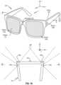
- FIG. 1 Ais a diagram of an embodiment of a near-eye display 100 .
- Near-eye display 100presents media to a user. Examples of media presented by near-eye display 100 include one or more images, video, and/or audio.
- audiois presented via an external device (e.g., speakers and/or headphones) that receives audio information from the near-eye display 100 , a console, or both, and presents audio data based on the audio information.
- Near-eye display 100is generally configured to operate as a virtual reality (VR) display.
- near-eye display 100is modified to operate as an augmented reality (AR) display and/or a mixed reality (MR) display.
- ARaugmented reality
- MRmixed reality
- Near-eye display 100includes a frame 105 and a display 110 .
- Frame 105is coupled to one or more optical elements.
- Display 110is configured for the user to see content presented by near-eye display 100 .
- display 110comprises a waveguide display assembly for directing light from one or more images to an eye of the user.
- Near-eye display 100further includes image sensors 120 a , 120 b , 120 c , and 120 d .
- image sensors 120 a , 120 b , 120 c , and 120 dmay include a pixel array configured to generate image data representing different fields of views along different directions.
- sensors 120 a and 120 bmay be configured to provide image data representing two fields of view towards a direction A along the Z axis
- sensor 120 cmay be configured to provide image data representing a field of view towards a direction B along the X axis
- sensor 120 dmay be configured to provide image data representing a field of view towards a direction C along the X axis.
- sensors 120 a - 120 dcan be configured as input devices to control or influence the display content of the near-eye display 100 , to provide an interactive VR/AR/MR experience to a user who wears near-eye display 100 .
- sensors 120 a - 120 dcan generate physical image data of a physical environment in which the user is located.
- the physical image datacan be provided to a location tracking system to track a location and/or a path of movement of the user in the physical environment.
- a systemcan then update the image data provided to display 110 based on, for example, the location and orientation of the user, to provide the interactive experience.
- near-eye display 100may further include one or more active illuminators 130 to project light into the physical environment.
- the light projectedcan be associated with different frequency spectrums (e.g., visible light, infra-red light, ultra-violet light, etc.), and can serve various purposes.
- illuminator 130may project light in a dark environment (or in an environment with low intensity of infra-red light, ultra-violet light, etc.) to assist sensors 120 a - 120 d in capturing images of different objects within the dark environment to, for example, enable location tracking of the user.
- Illuminator 130may project certain markers onto the objects within the environment, to assist the location tracking system in identifying the objects for map construction/updating.
- the emitted lightmay be associated with a certain pattern, and can be reflected by the left eyeball of the user.
- Sensor 150 amay include a pixel array to receive the reflected light and generate an image of the reflected pattern.
- illuminators 140 d , 140 e , and 140 fmay emit NIR lights carrying the pattern. The NIR lights can be reflected by the right eyeball of the user, and may be received by sensor 150 b .
- Sensor 150 bmay also include a pixel array to generate an image of the reflected pattern. Based on the images of the reflected pattern from sensors 150 a and 150 b , the system can determine a gaze point of the user, and update the image data provided to display 100 based on the determined gaze point to provide an interactive experience to the user.
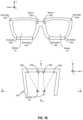
- Directing element 360redirects the received input image light 355 to decoupling element 365 such that the received input image light 355 is decoupled out of output waveguide 320 via decoupling element 365 .
- Directing element 360is part of, or affixed to, first side 370 - 1 of output waveguide 320 .
- Decoupling element 365is part of, or affixed to, second side 370 - 2 of output waveguide 320 , such that directing element 360 is opposed to the decoupling element 365 .
- Source assembly 310generates image light 355 in accordance with instructions from the controller 330 .
- Source assembly 310includes a source 410 and an optics system 415 .
- Source 410is a light source that generates coherent or partially coherent light.
- Source 410may be, e.g., a laser diode, a vertical cavity surface emitting laser, and/or a light emitting diode.
- Optics system 415includes one or more optical components that condition the light from source 410 .
- Conditioning light from source 410may include, e.g., expanding, collimating, and/or adjusting orientation in accordance with instructions from controller 330 .
- the one or more optical componentsmay include one or more lenses, liquid lenses, mirrors, apertures, and/or gratings.
- optics system 415includes a liquid lens with a plurality of electrodes that allows scanning of a beam of light with a threshold value of scanning angle to shift the beam of light to a region outside the liquid lens.
- Image light 355Light emitted from the optics system 415 (and also source assembly 310 ) is referred to as image light 355 .
- the application store 545stores one or more applications for execution by the control circuitries 510 .
- An applicationis a group of instructions, that, when executed by a processor, generates content for presentation to the user. Examples of applications include: gaming applications, conferencing applications, video playback applications, or other suitable applications.
- Tracking module 550tracks movements of near-eye display 100 using slow calibration information from the imaging device 535 . Tracking module 550 also determines positions of a reference point of near-eye display 100 using position information from the fast calibration information.
- Engine 555executes applications within system 500 and receives position information, acceleration information, velocity information, and/or predicted future positions of near-eye display 100 from tracking module 550 .
- information received by engine 555may be used for producing a signal (e.g., display instructions) to waveguide display assembly 210 that determines a type of content presented to the user.
- engine 555may determine the content to be presented to the user based on a location of the user (e.g., provided by tracking module 550 ), or a gaze point of the user (e.g., based on image data provided by imaging device 535 ), a distance between an object and user (e.g., based on image data provided by imaging device 535 ).
- FIG. 6 A , FIG. 6 B , FIG. 6 C , FIG. 6 D , and FIG. 6 Eillustrate examples of an image sensor 600 and its operations.
- image sensor 600can include an array of pixel cells, including pixel cell 601 , and can generate digital intensity data corresponding to pixels of an image.
- Pixel cell 601may be part of pixel cells 402 of FIG. 4 .
- pixel cell 601may include a photodiode 602 , an electronic shutter gate 603 , a transfer gate 604 , a reset gate 605 , a charge storage device 606 , and a quantizer 607 .
- image sensor 600can transmit only the pixel data from group of pixel cells 620 and 630 to the host processor to reduce the volume of pixel data being transmitted. Such arrangements can allow transmission of higher resolution images at a higher frame rate.
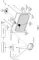
- an illuminator 640can project a pattern 642 of structured light onto an object 650 .
- the structured lightcan be reflected on a surface of an object 650 , and a pattern 652 of reflected light can be captured by image sensor 600 to generate an image.
- Host processorcan match pattern 652 with pattern 642 and determine the depth of object 650 with respect to image sensor 600 based on the image locations of pattern 652 in the image.
- only groups of pixel cells 660 , 662 , 664 , and 666contain relevant information (e.g., pixel data of pattern 652 ).
- the programming data of each entry of pixel array programming map 720can be transmitted sequentially following a pre-determined scanning pattern, such as traversing a row from left to right (e.g., A 00 , A 01 , . . . A 0i ), followed by the next row from left to right (e.g., A 10 , A 11 , . . . A 1i ), to form a stream of serial data.
- the programming data for each entrycan be extracted and identified from the stream of serial data based on the scanning pattern and the order by which the entries are received.
- pixel array programming map 720can be sent only when certain programming data need to be updated between frames, and only the programming data that need to be updated are included in pixel array programming map 720 .
- a pixel cellcan be configured to perform light measurement operation in the visible light wavelength range (e.g., with programming data set to 1), in the infra light wavelength range (e.g., with programming data set to ⁇ 1), or no measurement (e.g., with programming data set to 0).
- the non-binary programming data of pixel array programming map 720 bcan also take on other values to set, for example, the duration of the exposure period, a quantization resolution/bit depth etc.
- application 708may maintain a model of an environment in which an object being tracked is located based on prior images, and predict the pixel cells that are likely to provide the pixel data of the object in a current image based on an environment model.
- image sensor 704or other processing circuit that is part of the same chip as image sensor 704 , may also compute fixed primitives (e.g. temporal or spatial contrast) and estimate where relevant information is occurring based on those primitives, and generate pixel array programming map 720 a based on the estimation.
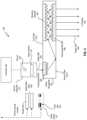
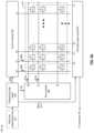
- FIG. 8 A and FIG. 8 Billustrate example components of peripheral circuit 716 and pixel cell array 718 .
- peripheral circuit 716can include a programming map parser 802 , a column controller 804 , a row controller 806 , and a pixel data output module 807 .
- Programming map parser 802can parse pixel array programming map 720 , which can be in a serial data stream, to identify the programming data for each pixel cell. The identification of the programming data can be based on, for example, a pre-determined scanning pattern by which the two-dimensional pixel array programming map is converted into the serial format, as well as the order by which the programming data is received by programming map parser 802 from the serial data stream.
- Programming map parser 802can create a mapping among the row addresses of the pixel cells, the column addresses of the pixel cells, and one or more configuration signals based on the programming data targeted at the pixel cells. Based on the mapping, programming map parser 802 can transmit control signals 808 including the column addresses and the configuration signals to column controller 804 , as well as control signals 810 including the row addresses mapped to the column addresses and the configuration signals to row controller 806 . In some examples, the configuration signals can also be split between control signals 808 and control signals 810 , or sent as part of control signals 810 to row controller 806 .
- Column controller 804 and row controller 806are configured to forward the configuration signals received from programming map parser 802 to the configuration memory of each pixel cell of pixel cell array 718 .
- column controller 804drives a plurality of sets of column buses C 0 , C 1 , . . . Ci.
- Each set of column busesincludes one or more buses and can be used to transmit control signals 722 of FIG. 7 A , which can include a column selection signal and/or other configuration signals, to a column of pixel cells.
- column bus(es) C 0can transmit a column selection signal 808 a to select a column of pixel cells p 00 , p 01 , . . .
- row bus(es) R 0can transmit a row selection signal 810 a to select a row of pixel cells p 00 , p 10 , p 10
- row bus(es) R 1can transmit a row selection signal 810 b to select a row of pixel cell p 01 , p 11 , p 1i , etc.
- Any pixel cell within pixel cell array 718can be selected based on a combination of the row selection signal and the column signal to receive the configuration signals.
- the row selection signals, column selection signals, and the configuration signalsare synchronized based on control signals 808 and 810 from programming map parser 802 , as described above.
- Pixel data output module 807can receive the pixel data from the buses, convert the pixel data into one or more serial data streams (e.g., using a shift register), and transmit the data streams to host device 702 under a pre-determined protocol such as MIPI.
- pixel data output module 807can also receive control signals 808 and 810 from programming map parser 802 to determine, for example, which pixel cell does not output pixel data, the bit width of pixel data output by each pixel cell, etc., and then adjust the generation of serial data streams accordingly.
- each set of column buses (e.g., C 0 , C 1 , etc.) and row buses (e.g., R 0 , R 1 , etc.)can include multiple bits.
- each set of column buses and row busescan carry N+1 bits. It is understood that in some examples each set of column buses and row buses can also carry a single data bit.
- Each pixel cellis also electrically connected with transistors T, such as T 00 , T 10 , T 10 , T 11 , etc., to control the transmission of configuration signals to the pixel cell.
- configuration memory 830 of each pixel cellcan be implemented as a dynamic random access memory (DRAM), but in some examples, additional row/column buses can be included in pixel cell array 718 to enable configuration memory 830 of each pixel cell to be implemented as static random access memory (SRAM).
- DRAMdynamic random access memory
- SRAMstatic random access memory
- each pixel cellalso includes transistors O, such as O 00 , O 10 , O 10 , O 11 , etc., to control the sharing of the output bus D among a column of pixel cells.
- the transistors O of each rowcan be controlled by a read signal (e.g., read_R 0 , read_R 1 , etc.) to enable a row-by-row read out of the pixel data, such that one row of pixel cells output pixel data through output buses D 0 , D 1 , . . . Di, followed by the next row of pixel cells.
- a read signale.g., read_R 0 , read_R 1 , etc.
- the row and column selection signal for that pixel cellcan be de-asserted to prevent transistor T of the pixel cell from transmitting a logical one to configuration memory 830 of that pixel cell.
- the column and/or row busescan also carry the configuration data (e.g., a digital value to set the exposure period, a clock signal to set the quantization/bit depth), etc.
- the configuration memory of multiple pixel cellscan be written simultaneously, as described above.
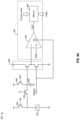
- FIG. 9 Aillustrates an example of pixel cell 902 of which the generation of pixel data can be enabled/disabled.
- a pixel cell 902can include a photodiode 602 , electronic shutter gate 603 , transfer gate 604 , charge storage device 606 , and quantizer 607 including a comparator 904 and a memory 906 .
- Pixel cell 902further includes reset gate 605 which can be controlled to reset charge storage device 606 before the exposure period starts.
- Memory 906can receive counter values from a free running counter which can be internal or external to pixel cell 902 .
- Pixel cell 902further includes a voltage buffer 908 to buffer the analog voltage at charge storage device 606 .
- voltage buffer 908 and comparator 904can be turned on/off by an ON/OFF signal, which can be stored in the configuration memory based on the row selection and column selection signals on the row bus and column bus, as described in FIG. 8 B .
- the row and column selection signalscan be generated based on pixel array programming maps 720 a of FIG. 7 C .
- the ON/OFF signalcan then be read out from the configuration memory.
- comparator 904 and voltage buffer 908are disabled, no latch signal is generated.
- Memory 906does not store a counter value, and the outputting of pixel data can be disabled. In some examples (not shown in FIG. 9 A ), memory 906 can also be power gated by the ON/OFF signal.
- pixel data output module 807can also be configured based on control signals from programming map parser 802 to skip the read out of the pixel data output of that pixel cell.
- substantial power savingcan be achieved at the pixel cell by disabling the voltage buffer and the comparator, which typically uses the most power among the components of the pixel cell.
- the volume of pixel data transmitted to the host devicecan also be reduced, which can further reduce the power consumption at the interconnect and at the host device.
- FIG. 9 Billustrates an example of pixel cell 912 which can be configured to operate in a dark mode.
- pixel cell 912includes a dark gate 914 .
- Either dark gate 914 or reset gate 605 (or both)can reset charge storage device 606 .
- dark gate 914can receive a control signal (labelled “DARK”) from the configuration memory, which receives the control signal from transistor T of the pixel cell based on the row selection and column selection signals on the row bus and column bus, as described in FIG. 8 B .
- the row and column selection signalscan be generated based on pixel array programming maps 720 a of FIG. 7 C .
- pixel cell 912can generate a pixel output representing a dark pixel (e.g., a pixel that does not receive incident light).
- the pixel outputcan be used to perform calibration (e.g., to account for the effect of temperature).
- other pixel cellscan operate in normal mode (e.g., with the DARK signal turned off), and their pixel output can be offset or scaled based on the dark pixel value to remove the effect of temperature on the pixel output, such that the adjusted pixel output can provide a more accurate representation of the intensity of incident light.
- the exposure period of pixel cell 922can be set at zero to generate dark pixel data for calibration as described in FIG. 9 B .
- programmable exposure periodcan also be implemented based on, for example, selectively turning on groups of pixel cells at the start of their exposure periods and turning off groups of pixels cell at end of their exposure periods.
- FIG. 9 Dillustrates an example of pixel cell 932 which can be configured to measure light of different wavelengths, or to generate no pixel data output.
- pixel cell 932includes a first photodiode 934 , a first photodiode enable gate 936 , a second photodiode 938 , and a second photodiode enable gate 940 .
- First photodiode 934can be configured to measure light in the infra-red wavelength range
- second photodiode 938can be configured to measure light in the visible wavelength range.
- each photodiodecan be coupled with an electronic shutter gate and a transfer gate.
- Pixel cell 932can be configured to operate one of three modes.
- the IR_en signalcan be asserted, which allows first photodiode enable gate 936 to transfer charge from first photodiode 934 to charge storage device 606 for measurement.
- the VIS_en signalcan be asserted, which allows second photodiode enable gate 940 to transfer charge from second photodiode 938 to charge storage device 606 for measurement.
- comparator 904 and voltage buffer 908are enabled to perform quantization of the charge.
- comparator 904 and voltage buffer 908are disabled, and pixel cell 932 does not output pixel data.
- the IR_en signal, VIS_en signal, and the On/Off signalcan be provided to the configuration memory of each pixel cell via the column buses C and/or the row buses R and based on pixel array programming maps 720 b of FIG. 7 C .
- an image sensor comprising pixel cell 932can be configured to generate 2D image frames (based on sensing of visible light) and 3D image frames (based on sensing of infra-red light) at different times to provide fusion of 2D-3D sensing.
- the CLK 0 and CLK 1 clock signals, as well as the RES_SEL signalcan be supplied to the pixel cells via the column buses C and/or row buses R and based on pixel array programming maps 720 b of FIG. 7 C .
- pixel data output module 807can also be configured to skip the read out of certain bits (e.g., most significant bits) of the pixel data output from pixel cells having a lower quantization resolution and lower bit width based on control signals from programming map parser 802 .
- the programming of the quantization resolution/bit depthcan be performed to maximize the efficiency of sensing and transmission of pixel data.
- voltage multiplexor 956can be controlled by the SUM signal to forward buffered analog voltage 960 a to comparator 904 a for quantization to output pixel data, whereas comparator 904 a of quantizer 607 a of pixel cell 952 b can also be enabled to quantize buffered analog voltage 960 b to output pixel data.
- the aforementioned pixel binning schemecan be activated by setting the programming data corresponding to master pixel cells to 1 in pixel array programming map 720 a .
- Post processor 1100may include a pixel compression module 1104 , a dot extraction module 1106 , etc., to perform data compression operations.
- pixel compression module 1104may perform, for example, a compressive sensing operation based on summing the pixel data outputs of pixel cells of selected groups, and transmitting the summed pixel data outputs to host device 702 to represent the outputs of the selected groups.
- pixel compression module 1104can perform a temporal compression operation, in which pixel compression module 1104 can process frames of pixel data from pixel cell array 718 at a first frame rate, compress the pixel data, and output compressed pixel data to host device 702 at a second frame rate lower than the first frame rate.
- Post processor 1100can also perform other different types of post-processing, such as HDR multiple exposure capture, optical flow, etc.
- HDRwould combine multiple frames with different exposure times. Such operation allows discarding data where pixels saturate, or the signal is buried below the noise floor. Such operation also allows averaging photon flux across multiple measurements.
- Host device 702can synchronize the illumination of object 1202 with the light measurement operations at pixel cell array 718 by, for example, enabling a subset of pixel cells of pixel cell array 718 , such as subset 1206 , at a time to detect light reflected by object 1202 .
- the subsetsare determined based on the illumination sequence such that at any given time during the illumination sequence, the selected subset of pixel cells is the most likely to receive light reflected by object 1202 .
- host device 702can generate pixel array programming map 720 based on the sequence of illumination by illuminator 1200 as reflected by the sequence of activation of the light emitters of illuminator 1200 , the sequence of movement of the mirror of illuminator 1200 , etc.
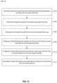
- FIG. 13is a flowchart of an example method 1300 for generating image data.
- Method 1300can be performed by, for example, an image processing system such as image processing system 700 .
- the image processing systemmay include an array of pixel cells, such as pixel cell array 718 , where each pixel cell of the array of pixel cells configured to perform a light measurement operation and to generate a digital output of the light measurement operation.
- Each pixel cellis also associated with a configuration memory (e.g., configuration memory 830 ) that is individually addressable.
- the image process systemfurther includes a peripheral circuit (e.g. peripheral circuit 716 ) that can configure the light measurement operations at the array of pixel cells, and an image processor (e.g., host processor 706 ) configured to generate an image frame based on the digital outputs of at least some of the array of pixel cells.
- a peripheral circuite.g. peripheral circuit 716
- an image processore.g., host processor 706
- Method 1300starts with step 1302 , in which peripheral circuit 716 receives a pixel array programming map including programming data targeted at each pixel cell of an array of pixel cells.
- the pixel array programming mapmay include, for example, pixel array programming map 720 .
- the programming data of each entry of pixel array programming map 720can be transmitted sequentially following a pre-determined scanning pattern, such as traversing a row from left to right, followed by the next row from left to right, to form a stream of serial data.
- peripheral circuit 716can configure a first light measurement operation at the first pixel cell based on the first programming data.
- the configurationcan be based on transmitting one or more row signals and one or more column signals along respectively the row buses and column buses to select the configuration memory of the first pixel cell to receive the first programming data.
- the configurationcan include, for example, enabling/disabling generation of pixel data at the first pixel cell, configuring the first pixel to operate in a dark mode (to generate dark pixel data) or in a normal mode, setting a wavelength range of measurement, the duration of exposure period, a quantization resolution, pixel binning operation, compressive sensing, etc.
- the image processorcan generate an image frame based on pixel data output by at least one of the first pixel cell or the second pixel cell.
- the pixel cellscan output pixel data to pixel data output module, which can stream the pixel data to the image sensor.
- the image sensorcan operate an application to generate an image frame based on the pixel data.
- Embodiments of the disclosuremay also relate to an apparatus for performing the operations described.
- the apparatusmay be specially constructed for the required purposes, and/or it may comprise a general-purpose computing device selectively activated or reconfigured by a computer program stored in the computer.
- a computer programmay be stored in a non-transitory, tangible computer readable storage medium, or any type of media suitable for storing electronic instructions, which may be coupled to a computer system bus.
- any computing systems referred to in the specificationmay include a single processor or may be architectures employing multiple processor designs for increased computing capability.
Landscapes
- Engineering & Computer Science (AREA)
- Multimedia (AREA)
- Signal Processing (AREA)
- Length Measuring Devices By Optical Means (AREA)
- Transforming Light Signals Into Electric Signals (AREA)
- Display Devices Of Pinball Game Machines (AREA)
Abstract
Description
R=det(M)−k(trace(M))2 (Equation 2)
Claims (20)
Priority Applications (7)
| Application Number | Priority Date | Filing Date | Title |
|---|---|---|---|
| US16/421,441US12034015B2 (en) | 2018-05-25 | 2019-05-23 | Programmable pixel array |
| KR1020207037369AKR20210013206A (en) | 2018-05-25 | 2019-05-24 | Programmable pixel array |
| JP2020561752AJP2021525019A (en) | 2018-05-25 | 2019-05-24 | Programmable pixel array |
| PCT/US2019/034007WO2019227050A1 (en) | 2018-05-25 | 2019-05-24 | Programmable pixel array |
| EP19731047.7AEP3804297A1 (en) | 2018-05-25 | 2019-05-24 | Programmable pixel array |
| CN201980048866.0ACN112470459A (en) | 2018-05-25 | 2019-05-24 | Programmable pixel array |
| TW108118209ATWI810304B (en) | 2018-05-25 | 2019-05-27 | Apparatus and method for generating image frame |
Applications Claiming Priority (2)
| Application Number | Priority Date | Filing Date | Title |
|---|---|---|---|
| US201862676849P | 2018-05-25 | 2018-05-25 | |
| US16/421,441US12034015B2 (en) | 2018-05-25 | 2019-05-23 | Programmable pixel array |
Publications (2)
| Publication Number | Publication Date |
|---|---|
| US20190363118A1 US20190363118A1 (en) | 2019-11-28 |
| US12034015B2true US12034015B2 (en) | 2024-07-09 |
Family
ID=68614052
Family Applications (1)
| Application Number | Title | Priority Date | Filing Date |
|---|---|---|---|
| US16/421,441Active2039-12-17US12034015B2 (en) | 2018-05-25 | 2019-05-23 | Programmable pixel array |
Country Status (7)
| Country | Link |
|---|---|
| US (1) | US12034015B2 (en) |
| EP (1) | EP3804297A1 (en) |
| JP (1) | JP2021525019A (en) |
| KR (1) | KR20210013206A (en) |
| CN (1) | CN112470459A (en) |
| TW (1) | TWI810304B (en) |
| WO (1) | WO2019227050A1 (en) |
Cited By (1)
| Publication number | Priority date | Publication date | Assignee | Title |
|---|---|---|---|---|
| US20240085707A1 (en)* | 2020-05-22 | 2024-03-14 | Magic Leap, Inc. | Augmented and virtual reality display systems with correlated in-coupling and out-coupling optical regions for efficient light utilization |
Families Citing this family (40)
| Publication number | Priority date | Publication date | Assignee | Title |
|---|---|---|---|---|
| US10686996B2 (en) | 2017-06-26 | 2020-06-16 | Facebook Technologies, Llc | Digital pixel with extended dynamic range |
| US10598546B2 (en) | 2017-08-17 | 2020-03-24 | Facebook Technologies, Llc | Detecting high intensity light in photo sensor |
| US12034015B2 (en) | 2018-05-25 | 2024-07-09 | Meta Platforms Technologies, Llc | Programmable pixel array |
| US11906353B2 (en) | 2018-06-11 | 2024-02-20 | Meta Platforms Technologies, Llc | Digital pixel with extended dynamic range |
| US11463636B2 (en) | 2018-06-27 | 2022-10-04 | Facebook Technologies, Llc | Pixel sensor having multiple photodiodes |
| US10897586B2 (en) | 2018-06-28 | 2021-01-19 | Facebook Technologies, Llc | Global shutter image sensor |
| US10931884B2 (en) | 2018-08-20 | 2021-02-23 | Facebook Technologies, Llc | Pixel sensor having adaptive exposure time |
| US11956413B2 (en) | 2018-08-27 | 2024-04-09 | Meta Platforms Technologies, Llc | Pixel sensor having multiple photodiodes and shared comparator |
| US11595602B2 (en) | 2018-11-05 | 2023-02-28 | Meta Platforms Technologies, Llc | Image sensor post processing |
| US11888002B2 (en) | 2018-12-17 | 2024-01-30 | Meta Platforms Technologies, Llc | Dynamically programmable image sensor |
| US11962928B2 (en) | 2018-12-17 | 2024-04-16 | Meta Platforms Technologies, Llc | Programmable pixel array |
| US11218660B1 (en) | 2019-03-26 | 2022-01-04 | Facebook Technologies, Llc | Pixel sensor having shared readout structure |
| US11943561B2 (en) | 2019-06-13 | 2024-03-26 | Meta Platforms Technologies, Llc | Non-linear quantization at pixel sensor |
| US12108141B2 (en) | 2019-08-05 | 2024-10-01 | Meta Platforms Technologies, Llc | Dynamically programmable image sensor |
| JP7460345B2 (en)* | 2019-09-30 | 2024-04-02 | ブリルニクス シンガポール プライベート リミテッド | Solid-state imaging device, driving method for solid-state imaging device, and electronic device |
| US11936998B1 (en) | 2019-10-17 | 2024-03-19 | Meta Platforms Technologies, Llc | Digital pixel sensor having extended dynamic range |
| US11935291B2 (en) | 2019-10-30 | 2024-03-19 | Meta Platforms Technologies, Llc | Distributed sensor system |
| US11948089B2 (en) | 2019-11-07 | 2024-04-02 | Meta Platforms Technologies, Llc | Sparse image sensing and processing |
| US11468146B2 (en)* | 2019-12-06 | 2022-10-11 | Globalfoundries U.S. Inc. | Array of integrated pixel and memory cells for deep in-sensor, in-memory computing |
| US12141888B1 (en) | 2019-12-18 | 2024-11-12 | Meta Platforms Technologies, Llc | Dynamic and hierarchical image sensing and processing |
| WO2021164887A1 (en)* | 2020-02-21 | 2021-08-26 | Toyota Motor Europe | 6d pose and shape estimation method |
| US11195580B2 (en)* | 2020-02-26 | 2021-12-07 | Globalfoundries U.S. Inc. | Integrated pixel and two-terminal non-volatile memory cell and an array of cells for deep in-sensor, in-memory computing |
| US11394902B2 (en)* | 2020-03-23 | 2022-07-19 | Qualcomm Incorporated | Sparse infrared pixel design for image sensors |
| US11503221B2 (en)* | 2020-04-01 | 2022-11-15 | Samsung Electronics Co., Ltd. | System and method for motion warping using multi-exposure frames |
| US11902685B1 (en) | 2020-04-28 | 2024-02-13 | Meta Platforms Technologies, Llc | Pixel sensor having hierarchical memory |
| EP3913754A1 (en)* | 2020-05-19 | 2021-11-24 | Prophesee | Light source for structured light, structured light projection apparatus and system |
| US11825228B2 (en) | 2020-05-20 | 2023-11-21 | Meta Platforms Technologies, Llc | Programmable pixel array having multiple power domains |
| US11206368B2 (en)* | 2020-05-22 | 2021-12-21 | Omnivision Technologies, Inc. | Data readout power saving techniques for shift register structure |
| US11910114B2 (en) | 2020-07-17 | 2024-02-20 | Meta Platforms Technologies, Llc | Multi-mode image sensor |
| US12075175B1 (en) | 2020-09-08 | 2024-08-27 | Meta Platforms Technologies, Llc | Programmable smart sensor with adaptive readout |
| US11956560B2 (en) | 2020-10-09 | 2024-04-09 | Meta Platforms Technologies, Llc | Digital pixel sensor having reduced quantization operation |
| US11935575B1 (en) | 2020-12-23 | 2024-03-19 | Meta Platforms Technologies, Llc | Heterogeneous memory system |
| US12022218B2 (en) | 2020-12-29 | 2024-06-25 | Meta Platforms Technologies, Llc | Digital image sensor using a single-input comparator based quantizer |
| DE102021100124A1 (en)* | 2021-01-07 | 2022-07-07 | Schölly Fiberoptic GmbH | Method for transmitting a raw image data stream from an image sensor |
| CN118435031A (en)* | 2021-12-24 | 2024-08-02 | 三星电子株式会社 | Sensor assembly including dimming member and electronic device including the same |
| US12244936B2 (en) | 2022-01-26 | 2025-03-04 | Meta Platforms Technologies, Llc | On-sensor image processor utilizing contextual data |
| CN119111076A (en)* | 2022-05-10 | 2024-12-10 | 索尼半导体解决方案公司 | Image sensor, information processing method, and program |
| US12299770B2 (en)* | 2022-05-11 | 2025-05-13 | SoftEye, Inc. | Methods and apparatus for scalable processing |
| US12124623B1 (en) | 2022-06-30 | 2024-10-22 | Meta Platforms Technologies, Llc | Techniques for gaze-contingent sensing and processing |
| US12368960B2 (en)* | 2022-08-05 | 2025-07-22 | Corephotonics Ltd. | Systems and methods for zoom digital camera with automatic adjustable zoom field of view |
Citations (238)
| Publication number | Priority date | Publication date | Assignee | Title |
|---|---|---|---|---|
| US4121896A (en) | 1976-03-24 | 1978-10-24 | Shepherd Thomas H | Apparatus for the production of contact lenses |
| EP0775591A2 (en) | 1995-11-22 | 1997-05-28 | Fujicopian Co., Ltd. | Thermal melt-transfer recording material |
| US6384905B1 (en) | 2000-07-07 | 2002-05-07 | The United States Of America As Represented By The Secretary Of The Navy | Optic flow sensor with fused elementary motion detector outputs |
| US20020113886A1 (en) | 2001-02-20 | 2002-08-22 | Jaroslav Hynecek | High Dynamic Range Active Pixel CMOS Image Sensor and data processing system incorporating adaptive pixel reset |
| US20030005231A1 (en) | 2001-06-29 | 2003-01-02 | Ooi Eng Hun | Hardware emulation of parallel ATA drives with serial ATA interface |
| US20030020100A1 (en) | 1999-10-26 | 2003-01-30 | Guidash Robert M. | CMOS image sensor with extended dynamic range |
| JP2003319262A (en) | 2002-04-18 | 2003-11-07 | Idaku Ishii | Image pickup camera apparatus and image data reading method for imager |
| US6853579B1 (en) | 2003-09-09 | 2005-02-08 | Taiwan Semiconductor Manufacturing Co., Ltd. | Non-refresh four-transistor memory cell |
| US20050058773A1 (en) | 2003-08-06 | 2005-03-17 | Seiko Epson Corporation | Method of manufacturing micro lens, micro lens, optical device, optical transmitting device, laser printer head, and laser printer |
| US20050057389A1 (en) | 2003-09-15 | 2005-03-17 | Krymski Alex I. | Ramp generation with capacitors |
| US20050073874A1 (en) | 2003-10-03 | 2005-04-07 | International Business Machines Corporation | Method to improve cache capacity of SOI and bulk |
| JP2005129139A (en) | 2003-10-23 | 2005-05-19 | Fuji Photo Film Co Ltd | Magnetic recording medium |
| US20050237380A1 (en) | 2004-04-23 | 2005-10-27 | Toshiaki Kakii | Coding method for notion-image data, decoding method, terminal equipment executing these, and two-way interactive system |
| EP1603170A1 (en) | 2003-03-10 | 2005-12-07 | Toyoda Gosei Co., Ltd. | Solid element device and method for manufacture thereof |
| WO2006022077A1 (en) | 2004-08-23 | 2006-03-02 | Sony Corporation | Image pickup device, image pickup result processing method and integrated circuit |
| JP2006113139A (en) | 2004-10-12 | 2006-04-27 | Alps Electric Co Ltd | Reflector, liquid crystal display device and indenter for manufacturing reflector |
| US20060224792A1 (en) | 2005-03-31 | 2006-10-05 | Ooi Eng H | Method and apparatus for concurrent and independent data transfer on host controllers |
| JP2006348085A (en) | 2005-06-13 | 2006-12-28 | Nissan Motor Co Ltd | Cushion actuator using ionic liquid and vehicle component comprising the same |
| EP1746820A1 (en) | 2004-04-12 | 2007-01-24 | Sugawa, Shigetoshi | Solid-state imaging device, optical sensor, and solid-state imaging device operation method |
| US20070076109A1 (en) | 2005-10-04 | 2007-04-05 | Alexander Krymski | High speed CMOS image sensor circuits with block memory readout |
| US20070222881A1 (en) | 2003-04-14 | 2007-09-27 | Micron Technology, Inc. | Cmos image sensor with active reset and 4-transistor pixels |
| US20080007731A1 (en) | 2004-05-23 | 2008-01-10 | Botchway Stanley W | Imaging Device |
| US20080055736A1 (en) | 2006-08-30 | 2008-03-06 | Sony Corporation | Optical element and production device for producing same |
| US7359275B1 (en) | 2005-09-08 | 2008-04-15 | Integrated Device Technology, Inc. | Reduced size dual-port SRAM cell |
| US7362355B1 (en) | 2003-08-04 | 2008-04-22 | Pixim, Inc. | Digital CMOS image sensor incorporating a programmable multi-functional lookup table |
| US20080226170A1 (en) | 2007-03-15 | 2008-09-18 | Canon Kabushiki Kaisha | Image sensing apparatus, method, program and storage medium |
| JP2008270500A (en) | 2007-04-19 | 2008-11-06 | Sharp Corp | Solid-state imaging device, manufacturing method thereof, and electronic information device |
| US20090033588A1 (en) | 2007-08-02 | 2009-02-05 | Canon Kabushiki Kaisha | System, head-mounted display, and control method thereof |
| EP2037505A1 (en) | 2003-01-10 | 2009-03-18 | Paul Scherrer Institut | Photon counting imaging device |
| US20090245637A1 (en) | 2008-03-25 | 2009-10-01 | Barman Roderick A | Efficient selection and application of regions of interest in digital imaging |
| US20100197821A1 (en) | 2009-02-03 | 2010-08-05 | Samsung Electronics Co., Ltd. | Adhesive composition and adhesive film made therefrom |
| US20100197876A1 (en) | 2009-02-03 | 2010-08-05 | Samsung Electronics Co., Ltd. | Photocurable compound |
| US20100194956A1 (en) | 2009-02-05 | 2010-08-05 | The Hong Kong University Of Science And Technology | Apparatus and method for improving dynamic range and linearity of CMOS image sensor |
| EP2228846A1 (en) | 2009-03-03 | 2010-09-15 | Fujifilm Corporation | Barrier laminate, gas barrier film, and device using the same |
| US20100245600A1 (en) | 2009-03-30 | 2010-09-30 | Chang Soon-Keun | Digital photographing device, method of controlling the digital photographing device, and computer-readable storage medium |
| US20100276572A1 (en) | 2005-06-02 | 2010-11-04 | Sony Corporation | Semiconductor image sensor module and method of manufacturing the same |
| US20110055461A1 (en) | 2009-08-26 | 2011-03-03 | Steiner Avi | Systems and methods for pre-equalization and code design for a flash memory |
| US20110075470A1 (en) | 2009-09-30 | 2011-03-31 | Taiwan Semiconductor Manufacturing Co., Ltd. | Embedded sram structure and chip |
| US7920409B1 (en) | 2007-06-05 | 2011-04-05 | Arizona Board Of Regents For And On Behalf Of Arizona State University | SRAM cell with intrinsically high stability and low leakage |
| US7956914B2 (en) | 2007-08-07 | 2011-06-07 | Micron Technology, Inc. | Imager methods, apparatuses, and systems providing a skip mode with a wide dynamic range operation |
| EP2330173A2 (en) | 2008-07-04 | 2011-06-08 | LG Chem, Ltd. | A radial type liquid crystal compound, and an optical film and liquid crystal display (lcd) device containing compound |
| US7969759B1 (en) | 2008-12-19 | 2011-06-28 | Suvolta, Inc. | Method and apparatus for improving SRAM write operations |
| US20110155892A1 (en) | 2009-12-24 | 2011-06-30 | Imagerlabs, Inc. | Adjustable cmos sensor array |
| EP2357679A2 (en) | 2008-11-14 | 2011-08-17 | Samsung LED Co., Ltd. | Vertical/horizontal light-emitting diode for semiconductor |
| KR20110100974A (en) | 2010-03-05 | 2011-09-15 | 동우 화인켐 주식회사 | Colored photosensitive resin composition, color filter and liquid crystal display device including the same |
| US20110254986A1 (en) | 2009-09-11 | 2011-10-20 | Panasonic Corporation | Analog-digital converter, image sensor system and camera device |
| US20110267362A1 (en) | 2003-04-24 | 2011-11-03 | Micron Technology, Inc. | Gamma variation using illumination intensity |
| US20120002460A1 (en) | 2010-06-30 | 2012-01-05 | Stmicroelectronics S.R.L. | Dynamically configurable sram cell for low voltage operation |
| US20120002459A1 (en) | 2010-06-30 | 2012-01-05 | Stmicroelectronics S.R.L. | 5t sram memory for low voltage applications |
| US20120044399A1 (en) | 2010-08-23 | 2012-02-23 | Sony Corporation | Imaging apparatus, method of controlling imaging apparatus, and program |
| US8134623B2 (en) | 2008-03-21 | 2012-03-13 | Stmicroelectronics (Research & Development) Ltd. | Analog-to-digital conversion in image sensors using a differential comparison |
| US20120086082A1 (en) | 2010-10-07 | 2012-04-12 | Pierre Malinge | Dual port static random access memory cell layout |
| US20120105668A1 (en) | 2010-10-27 | 2012-05-03 | Qualcomm Incorporated | Region of interest extraction |
| US20120105475A1 (en) | 2010-11-02 | 2012-05-03 | Google Inc. | Range of Focus in an Augmented Reality Application |
| US20120113119A1 (en) | 2010-11-05 | 2012-05-10 | Nova Research, Inc. | Super resolution infrared imaging system |
| US20120133807A1 (en) | 2010-11-30 | 2012-05-31 | Industrial Technology Research Institute | Image capture device |
| US20120161088A1 (en) | 2010-12-24 | 2012-06-28 | Cheil Industries Inc. | Photosensitive Resin Composition and Color Filter Using the Same |
| US20120198312A1 (en) | 2011-02-02 | 2012-08-02 | Seagate Technology Llc | Methods and devices to increase memory device data reliability |
| US20120200499A1 (en) | 2010-02-28 | 2012-08-09 | Osterhout Group, Inc. | Ar glasses with event, sensor, and user action based control of applications resident on external devices with feedback |
| US20120212465A1 (en) | 2011-02-17 | 2012-08-23 | White Christopher J | Electroluminescent display device with optically communicating chiplets |
| CN102665049A (en) | 2012-03-29 | 2012-09-12 | 中国科学院半导体研究所 | Programmable visual chip-based visual image processing system |
| US20120240007A1 (en) | 2010-10-20 | 2012-09-20 | Stec, Inc. | Ldpc decoding for solid state storage devices |
| US20120262616A1 (en) | 2011-04-14 | 2012-10-18 | Lg Innotek Co., Ltd. | Pixel, pixel array, image sensor including the same and method for operating the image sensor |
| JP2013043383A (en) | 2011-08-24 | 2013-03-04 | Fujifilm Corp | Barrier laminate, gas barrier film, and device using barrier laminate or gas barrier film |
| US20130056809A1 (en) | 2011-09-07 | 2013-03-07 | Duli Mao | Image Sensor with Reduced Noiseby Blocking Nitridation Over Selected Areas |
| US20130057742A1 (en) | 2011-09-05 | 2013-03-07 | Canon Kabushiki Kaisha | Solid-state imaging apparatus and method of driving the same |
| US20130069787A1 (en) | 2011-09-21 | 2013-03-21 | Google Inc. | Locking Mechanism Based on Unnatural Movement of Head-Mounted Display |
| US20130068929A1 (en) | 2011-09-21 | 2013-03-21 | Johannes Solhusvik | Stacked-chip imaging systems |
| US8441535B2 (en) | 2008-03-05 | 2013-05-14 | Omnivision Technologies, Inc. | System and method for independent image sensor parameter control in regions of interest |
| US20130120642A1 (en) | 2011-11-11 | 2013-05-16 | Samsung Electronics Co., Ltd. | Digital photographing apparatus and method of controlling the same |
| US20130141619A1 (en) | 2011-12-02 | 2013-06-06 | Samsung Electronics Co., Ltd. | Image sensors and image processing devices including the same |
| CN103207716A (en) | 2012-01-17 | 2013-07-17 | 爱特梅尔公司 | Sensor stack with opposing electrodes |
| US20130185609A1 (en) | 2012-01-17 | 2013-07-18 | Samsung Electronics Co., Ltd. | Nonvolatile memory system |
| US20130187027A1 (en) | 2012-01-20 | 2013-07-25 | Omnivision Technologies, Inc. | Image sensor with integrated ambient light detection |
| US20130198577A1 (en) | 2012-01-30 | 2013-08-01 | Samsung Electronics Co., Ltd. | Memory, memory system, and error checking and correcting method for memory |
| US20130207219A1 (en) | 2005-09-29 | 2013-08-15 | Samsung Electronics Co., Ltd | Pixel having two semiconductor layers, image sensor including the pixel, and image processing system including the image sensor |
| US20130215290A1 (en) | 2012-02-21 | 2013-08-22 | Johannes Solhusvik | Detecting transient signals using stacked-chip imaging systems |
| US20130293753A1 (en) | 2012-05-02 | 2013-11-07 | Aptina Imaging Corporation | Image data compression using stacked-chip image sensors |
| US20130299674A1 (en) | 2012-05-14 | 2013-11-14 | Boyd Fowler | Digital Pixel Sensor with Reduced Noise |
| US20130300009A1 (en) | 2012-05-10 | 2013-11-14 | Vage Oganesian | Method Of Making Stamped Multi-Layer Polymer Lens |
| US20130314591A1 (en) | 2010-11-24 | 2013-11-28 | Nokia Corporation | Optically Refracting Surfaces |
| US20130326116A1 (en) | 2012-06-01 | 2013-12-05 | Seagate Technology Llc | Allocating memory usage based on quality metrics |
| US20140042299A1 (en) | 2012-04-27 | 2014-02-13 | Taiwan Semiconductor Manufacturing Company, Ltd. | CMOS Image Sensor Chips with Stacked Scheme and Methods for Forming the Same |
| US20140055635A1 (en) | 2012-08-21 | 2014-02-27 | Samsung Electronics Co., Ltd. | Image sensor and electronic device including the same |
| US20140063250A1 (en) | 2012-09-06 | 2014-03-06 | Hyun Jin Park | Apparatus and method of processing image of vehicle and system for processing image of vehicle using the same |
| WO2014055391A2 (en) | 2012-10-05 | 2014-04-10 | Rambus Inc. | Conditional-reset, multi-bit read-out image sensor |
| US20140170345A1 (en) | 2011-09-26 | 2014-06-19 | Fujifilm Corporation | Barrier laminate and novel polymer compound |
| US20140247382A1 (en) | 2011-10-06 | 2014-09-04 | Isis Innovation Limited | Random Access Addressing on Active Pixel Image Sensor |
| EP2804074A2 (en) | 2013-04-29 | 2014-11-19 | Tobii Technology AB | Power Efficient Image Sensing Apparatus, Method of Operating the Same and Eye/Gaze Tracking System |
| CN104204904A (en) | 2012-01-24 | 2014-12-10 | 亚利桑那大学评议会 | Compact eye-tracking head-mounted display |
| US20140368687A1 (en) | 2013-06-14 | 2014-12-18 | Fujitsu Limited | Terminal device and line of sight detection method |
| US20150050480A1 (en) | 2012-03-29 | 2015-02-19 | Fujifilm Corporation | Gas barrier film |
| US20150050479A1 (en) | 2012-03-29 | 2015-02-19 | Fujifilm Corporation | Gas barrier film |
| US20150085134A1 (en) | 2013-09-20 | 2015-03-26 | Vlad Novotny | Infrared Imager Readout Electronics |
| US20150158259A1 (en) | 2012-02-07 | 2015-06-11 | Hoya Lens Manufacturing Philippines Inc. | Polarized plastic lens for spectacles and method for manufacturing polarized plastic lens for spectacles |
| US20150189209A1 (en) | 2013-12-26 | 2015-07-02 | Han Yang | Correlated double sampling circuit, analog to digital converter and image sensor including the same |
| US20150201142A1 (en) | 2013-09-10 | 2015-07-16 | Rambus Inc. | Image sensor with threshold-based output encoding |
| US9094629B2 (en) | 2011-08-05 | 2015-07-28 | Canon Kabushiki Kaisha | Image pickup apparatus |
| US20150222827A1 (en) | 2014-01-31 | 2015-08-06 | Canon Kabushiki Kaisha | Image pickup apparatus and photographing apparatus including the same |
| US20150229859A1 (en) | 2014-02-07 | 2015-08-13 | Rambus Inc. | Feedthrough-compensated image sensor |
| US20150279884A1 (en) | 2014-03-28 | 2015-10-01 | Semiconductor Energy Laboratory Co., Ltd. | Imaging device |
| US20150309316A1 (en) | 2011-04-06 | 2015-10-29 | Microsoft Technology Licensing, Llc | Ar glasses with predictive control of external device based on event input |
| US20150309311A1 (en) | 2014-04-24 | 2015-10-29 | Lg Electronics Inc. | Head mounted display and method for controlling the same |
| US20150312502A1 (en) | 2014-03-25 | 2015-10-29 | Imec Vzw | Imaging sensor |
| US20150358571A1 (en) | 2013-01-25 | 2015-12-10 | Innovaciones Microelectrónicas S.L.(Anafocus) | Advanced region of interest function for image sensors |
| US20150381911A1 (en) | 2014-06-27 | 2015-12-31 | Omnivision Technologies, Inc. | System and method for digital correlated double sampling in an image sensor |
| US20160011422A1 (en) | 2014-03-10 | 2016-01-14 | Ion Virtual Technology Corporation | Method and system for reducing motion blur when experiencing virtual or augmented reality environments |
| US20160018645A1 (en) | 2014-01-24 | 2016-01-21 | Osterhout Group, Inc. | See-through computer display systems |
| US20160021302A1 (en) | 2014-07-18 | 2016-01-21 | Samsung Electronics Co., Ltd. | Cognitive sensor and method of operating of the same |
| US20160028974A1 (en) | 2014-07-25 | 2016-01-28 | Rambus Inc. | Low-noise, high dynamic-range image sensor |
| US20160032074A1 (en) | 2013-03-13 | 2016-02-04 | President And Fellows Of Harvard College | Solidifiable composition for preparaton of liquid-infused slippery surfaces and methods of applying |
| US20160048964A1 (en) | 2014-08-13 | 2016-02-18 | Empire Technology Development Llc | Scene analysis for improved eye tracking |
| US9282264B2 (en) | 2012-09-07 | 2016-03-08 | Samsung Electronics Co., Ltd. | Analog-to-digital conversion circuit, and image sensor including the same |
| US20160078614A1 (en) | 2014-09-16 | 2016-03-17 | Samsung Electronics Co., Ltd. | Computer aided diagnosis apparatus and method based on size model of region of interest |
| US20160088253A1 (en) | 2013-06-05 | 2016-03-24 | Kabushiki Kaisha Toshiba | Image sensor device, image processing device and method for manufacturing image sensor device |
| WO2016042734A1 (en) | 2014-09-19 | 2016-03-24 | パナソニックIpマネジメント株式会社 | Solid-state imaging device |
| US20160100115A1 (en) | 2013-06-27 | 2016-04-07 | Olympus Corporation | Analog/digital converter and solid-state imaging device |
| US20160105656A1 (en) | 2014-10-13 | 2016-04-14 | Quanta Computer Inc. | White balance method in multi-exposure imaging system |
| US20160117829A1 (en) | 2014-10-23 | 2016-04-28 | Samsung Electronics Co., Ltd. | Electronic device and method for processing image |
| US9363454B2 (en) | 2012-03-19 | 2016-06-07 | Sony Corporation | Solid-state imaging unit and electronic apparatus with a signal charge accumulated in a photoelectric conversion section is divided to be read in predetermined times of intermediate transfer operations and a complete transfer operation |
| US20160165160A1 (en) | 2014-12-05 | 2016-06-09 | Qualcomm Incorporated | Pixel readout architecture for full well capacity extension |
| WO2016088840A1 (en) | 2014-12-03 | 2016-06-09 | 株式会社ニコン | Image pickup device, electronic apparatus, and program |
| WO2016095057A1 (en) | 2014-12-19 | 2016-06-23 | Sulon Technologies Inc. | Peripheral tracking for an augmented reality head mounted device |
| US20160210785A1 (en) | 2013-10-03 | 2016-07-21 | Sulon Technologies Inc. | Augmented reality system and method for positioning and mapping |
| US20160256039A1 (en) | 2013-11-20 | 2016-09-08 | Olympus Corporation | Image-capturing element |
| US20160295148A1 (en) | 2015-03-30 | 2016-10-06 | Hamilton Sundstrand Corporation | Imaging circuit including frame asynchronous pulse detection |
| US20160344965A1 (en) | 2012-04-18 | 2016-11-24 | Brightway Vision Ltd. | Controllable gated sensor |
| US20160360127A1 (en) | 2015-06-05 | 2016-12-08 | Caeleste Cvba | Global shutter high dynamic range sensor |
| CN106255978A (en) | 2014-04-29 | 2016-12-21 | 微软技术许可有限责任公司 | Facial expression is followed the tracks of |
| WO2017003477A1 (en) | 2015-07-01 | 2017-01-05 | Tyrrell Brian M | Method and apparatus for on-chip per-pixel pseudo-random time coded exposure |
| WO2017013806A1 (en) | 2015-07-23 | 2017-01-26 | オリンパス株式会社 | Solid-state imaging device |
| US20170039906A1 (en) | 2015-08-03 | 2017-02-09 | Oculus Vr, Llc | Enhanced Visual Perception Through Distance-Based Ocular Projection |
| US20170041571A1 (en) | 2015-07-01 | 2017-02-09 | Brian M. Tyrrell | Method and apparatus for on-chip per-pixel pseudo-random time coded exposure |
| JP2017060155A (en) | 2015-09-16 | 2017-03-23 | キヤノン株式会社 | Imaging device and imaging apparatus |
| WO2017047010A1 (en) | 2015-09-16 | 2017-03-23 | Canon Kabushiki Kaisha | Image sensor and image capturing apparatus |
| US20170117310A1 (en) | 2014-03-31 | 2017-04-27 | Sony Corporation | Solid-state image sensor, electronic apparatus, and imaging method |
| US9646681B1 (en) | 2016-04-25 | 2017-05-09 | Qualcomm Incorporated | Memory cell with improved write margin |
| US20170154909A1 (en) | 2015-11-30 | 2017-06-01 | Semiconductor Energy Laboratory Co., Ltd. | Signal processing circuit and semiconductor device including the signal processing circuit |
| US20170161579A1 (en) | 2014-09-30 | 2017-06-08 | Qualcomm Incorporated | Single-processor computer vision hardware control and application execution |
| DE102015122055A1 (en) | 2015-12-17 | 2017-06-22 | Carl Zeiss Ag | Optical system and method for transmitting a source image |
| US20170228345A1 (en) | 2016-02-08 | 2017-08-10 | Spero Devices, Inc. | Analog Co-Processor |
| US20170248789A1 (en) | 2016-02-29 | 2017-08-31 | Seiko Epson Corporation | Light flux diameter expanding element and image display device |
| US20170272768A1 (en) | 2016-03-17 | 2017-09-21 | Facebook, Inc. | System and method for data compressing optical sensor data prior to transferring to a host system |
| US20170270664A1 (en) | 2016-03-21 | 2017-09-21 | The Board Of Trustees Of The Leland Stanford Junior University | Methods for characterizing features of interest in digital images and systems for practicing same |
| US20170280031A1 (en) | 2016-03-25 | 2017-09-28 | Raymond Kirk Price | Illumination Module |
| US20170293799A1 (en) | 2016-04-07 | 2017-10-12 | Tobii Ab | Image sensor for vision based human computer interaction |
| US20170307887A1 (en) | 2016-04-25 | 2017-10-26 | Petri Antero Stenberg | Diffractive optical elements with analog modulations and switching |
| US20170339327A1 (en) | 2016-05-17 | 2017-11-23 | Altasens, Inc. | Image sensor combining high dynamic range techniques |
| US20170338262A1 (en) | 2014-11-12 | 2017-11-23 | Sony Corporation | Solid-state imaging device and electronic apparatus |
| US20180027174A1 (en) | 2016-07-19 | 2018-01-25 | Qualcomm Incorporated | Signaling camera configuration changes using metadata defined for a camera command set |
| US9912885B2 (en) | 2014-01-31 | 2018-03-06 | Canon Kabushiki Kaisha | Image pickup apparatus having partial readout function or skip readout function and photographing apparatus including the same |
| US9955091B1 (en) | 2016-12-20 | 2018-04-24 | Omnivision Technologies, Inc. | High dynamic range image sensor read out architecture using in-frame multi-bit exposure control |
| US20180115725A1 (en) | 2016-10-21 | 2018-04-26 | The Johns Hopkins University | Flexible pixel-wise exposure control and readout |
| US20180136471A1 (en) | 2016-11-16 | 2018-05-17 | Magic Leap, Inc. | Multi-resolution display assembly for head-mounted display systems |
| US20180143701A1 (en) | 2016-11-21 | 2018-05-24 | Samsung Electronics Co., Ltd. | Event-based sensor comprising power control circuit |
| US20180176545A1 (en) | 2016-11-25 | 2018-06-21 | Nokia Technologies Oy | Virtual reality display |
| US10007350B1 (en) | 2014-06-26 | 2018-06-26 | Leap Motion, Inc. | Integrated gestural interaction and multi-user collaboration in immersive virtual reality environments |
| US20180204867A1 (en) | 2017-01-13 | 2018-07-19 | Samsung Electronics Co., Ltd. | Cmos image sensor (cis) including mram (magnetic random access memory) |
| US20180211582A1 (en) | 2015-06-10 | 2018-07-26 | Apple Inc. | Display panel redundancy schemes |
| US20180224658A1 (en) | 2011-11-09 | 2018-08-09 | Google Llc | Measurement Method and System |
| US20180239108A1 (en) | 2015-09-16 | 2018-08-23 | Canon Kabushiki Kaisha | Image sensor and image capturing apparatus |
| US20180241953A1 (en) | 2017-02-17 | 2018-08-23 | Semiconductor Components Industries, Llc | Methods and apparatus for pixel binning and readout |
| US20180252857A1 (en) | 2017-03-03 | 2018-09-06 | Microsoft Technology Licensing, Llc | Metasurface optical coupling elements for a display waveguide |
| US20180270436A1 (en) | 2016-04-07 | 2018-09-20 | Tobii Ab | Image sensor for vision based on human computer interaction |
| US20180276841A1 (en) | 2017-03-23 | 2018-09-27 | Intel Corporation | Method and system of determining object positions for image processing using wireless network angle of transmission |
| US10090342B1 (en) | 2017-08-01 | 2018-10-02 | Semiconductor Components Industries, Llc | Stacked image sensor capacitors and related methods |
| US20180284594A1 (en) | 2017-03-31 | 2018-10-04 | Beijing Neusoft Medical Equipment Co., Ltd. | Imaging method and imaging system |
| US20180288344A1 (en) | 2017-03-28 | 2018-10-04 | Qualcomm Incorporated | Systems and methods for dynamic voltage scaling of an image signal processor |
| US10154221B2 (en) | 2016-08-24 | 2018-12-11 | Canon Kabushiki Kaisha | Imaging device, imaging system, mobile apparatus, and drive method of imaging device |
| WO2018231962A1 (en) | 2017-06-13 | 2018-12-20 | Drinksavvy, Inc. | Colorimetric sensors and methods of manufacturing the same |
| US20190019023A1 (en) | 2016-12-01 | 2019-01-17 | Varjo Technologies Oy | Gaze-tracking system and method |
| WO2019018084A1 (en) | 2017-07-19 | 2019-01-24 | Qualcomm Incorporated | Cmos image sensor on-die motion detection using inter-pixel mesh relationship |
| US20190027454A1 (en) | 2016-09-19 | 2019-01-24 | Taiwan Semiconductor Manufacturing Co., Ltd. | Chip package structure with bump |
| US20190035154A1 (en) | 2017-07-25 | 2019-01-31 | Oculus Vr, Llc | Sensor system based on stacked sensor layers |
| US20190046044A1 (en) | 2015-06-14 | 2019-02-14 | Facense Ltd. | Respiration-based estimation of an aerobic activity parameter |
| US20190098232A1 (en) | 2017-09-26 | 2019-03-28 | Brillnics Inc. | Solid-state imaging device, method for driving solid-state imaging device, and electronic apparatus |
| US20190110039A1 (en) | 2017-10-09 | 2019-04-11 | Facebook Technologies, Llc | Head-mounted display tracking system |
| US20190123088A1 (en) | 2017-10-24 | 2019-04-25 | Samsung Electronics Co., Ltd. | Stacked cmos image sensor |
| US20190149751A1 (en) | 2017-11-15 | 2019-05-16 | Nvidia Corporation | Sparse scanout for image sensors |
| US20190172227A1 (en) | 2016-09-15 | 2019-06-06 | Sony Corporation | Information processing apparatus and method and program |
| WO2019111528A1 (en) | 2017-12-06 | 2019-06-13 | ソニーセミコンダクタソリューションズ株式会社 | Solid-state imaging device, control method for solid–state imaging device and computer program |
| US20190191116A1 (en) | 2017-12-20 | 2019-06-20 | Semiconductor Components Industries, Llc | Image sensors with low-voltage transistors |
| US20190199946A1 (en) | 2017-12-26 | 2019-06-27 | Waymo Llc | Adjustable Vertical Field of View |
| US20190204527A1 (en) | 2017-12-28 | 2019-07-04 | Nidec Sankyo Corporation | Lens unit and manufacturing method of metal mold |
| US10345447B1 (en) | 2018-06-27 | 2019-07-09 | Luminar Technologies, Inc. | Dynamic vision sensor to direct lidar scanning |
| WO2019145578A1 (en) | 2018-06-11 | 2019-08-01 | Fotonation Limited | Neural network image processing apparatus |
| US20190246036A1 (en) | 2018-02-02 | 2019-08-08 | Futurewei Technologies, Inc. | Gesture- and gaze-based visual data acquisition system |
| US20190253650A1 (en) | 2018-02-13 | 2019-08-15 | SK Hynix Inc. | Comparison device and cmos image sensor including the same |
| WO2019178060A1 (en) | 2018-03-12 | 2019-09-19 | Magic Leap, Inc. | Tilting array based display |
| US20190307313A1 (en) | 2014-05-09 | 2019-10-10 | Jack Wade | Systems and methods for medical imaging |
| US20190331914A1 (en) | 2011-07-20 | 2019-10-31 | Google Llc | Experience Sharing with Region-Of-Interest Selection |
| US20190363118A1 (en) | 2018-05-25 | 2019-11-28 | Facebook Technologies, Llc | Programmable pixel array |
| US20190361250A1 (en) | 2017-12-18 | 2019-11-28 | Facebook Technologies, Llc | Eye tracking for pupil steering in head-mounted displays using eye tracking sensors |
| WO2019244142A2 (en) | 2018-06-22 | 2019-12-26 | Facebook Technologies, Llc | Switchable reflective devices and methods and systems for fabrication thereof |
| US20200035661A1 (en) | 2015-11-10 | 2020-01-30 | Taiwan Semiconductor Manufacturing Company, Ltd. | Multi-Stack Package-on-Package Structures |
| US20200053299A1 (en) | 2018-08-10 | 2020-02-13 | International Business Machines Corporation | Image sensor with analog sample and hold circuit control for analog neural networks |
| US20200098096A1 (en) | 2018-09-24 | 2020-03-26 | Movidius Ltd. | Methods and apparatus to generate masked images based on selective privacy and/or location tracking |
| US10607413B1 (en) | 2015-09-08 | 2020-03-31 | Ultrahaptics IP Two Limited | Systems and methods of rerendering image hands to create a realistic grab experience in virtual reality/augmented reality environments |
| WO2020077283A1 (en) | 2018-10-12 | 2020-04-16 | Supermem, Inc. | Error correcting memory systems |
| US20200195828A1 (en)* | 2018-12-17 | 2020-06-18 | Facebook Technologies, Llc | Programmable pixel array |
| US20200193206A1 (en) | 2018-12-18 | 2020-06-18 | Slyce Acquisition Inc. | Scene and user-input context aided visual search |
| US20200195875A1 (en) | 2018-12-17 | 2020-06-18 | Facebook Technologies, Llc | Dynamically programmable image sensor |
| US20200228740A1 (en) | 2019-01-11 | 2020-07-16 | Brillnics, Inc. | Solid-state imaging device, method for driving solid-state imaging device, and electronic apparatus |
| US20200273784A1 (en) | 2017-12-30 | 2020-08-27 | Intel Corporation | Ultra-thin, hyper-density semiconductor packages |
| US10867655B1 (en) | 2019-07-08 | 2020-12-15 | Micron Technology, Inc. | Methods and apparatus for dynamically adjusting performance of partitioned memory |
| US10897586B2 (en)* | 2018-06-28 | 2021-01-19 | Facebook Technologies, Llc | Global shutter image sensor |
| US20210026796A1 (en) | 2019-07-23 | 2021-01-28 | Qualcomm Incorporated | I3c point to point |
| US20210044742A1 (en)* | 2019-08-05 | 2021-02-11 | Facebook Technologies, Llc | Dynamically programmable image sensor |
| US10939062B2 (en) | 2017-03-09 | 2021-03-02 | Sony Semiconductor Solutions Corporation | Solid-state imaging apparatus and electronic equipment |
| US20210075982A1 (en) | 2017-12-21 | 2021-03-11 | Robert Bosch Gmbh | Intensity-Normalized Image Sensor |
| US20210084249A1 (en) | 2017-12-27 | 2021-03-18 | Sony Semiconductor Solutions Corporation | Imaging element |
| US10970619B1 (en) | 2020-08-21 | 2021-04-06 | Moffett Technologies Co., Limited | Method and system for hierarchical weight-sparse convolution processing |
| US20210110187A1 (en) | 2020-10-01 | 2021-04-15 | Intel Corporation | Spatially sparse neural network accelerator for multi-dimension visual analytics |
| US10984235B2 (en) | 2016-12-16 | 2021-04-20 | Qualcomm Incorporated | Low power data generation for iris-related detection and authentication |
| US20210118847A1 (en) | 2019-10-17 | 2021-04-22 | Taiwan Semiconductor Manufacturing Co., Ltd. | Memory module, semiconductor package including the same, and manufacturing method thereof |
| US20210142086A1 (en) | 2019-11-07 | 2021-05-13 | Facebook Technologies, Llc | Sparse image sensing and processing |
| US20210144326A1 (en) | 2018-04-04 | 2021-05-13 | Sony Semiconductor Solutions Corporation | Solid-state imaging device |
| US20210152758A1 (en) | 2018-04-27 | 2021-05-20 | Sony Semiconductor Solutions Corporation | Imaging device and driving method of imaging device |
| EP3833005A1 (en) | 2018-07-31 | 2021-06-09 | Sony Semiconductor Solutions Corporation | Imaging device and vehicle control system |
| US20210185264A1 (en) | 2019-12-13 | 2021-06-17 | Sony Semiconductor Solutions Corporation | Dynamic region of interest and frame rate for event based sensor and imaging camera |
| US20210185199A1 (en) | 2019-12-13 | 2021-06-17 | Perkinelmer Health Sciences, Inc. | Random Access Sensor |
| US11057581B2 (en)* | 2018-01-24 | 2021-07-06 | Facebook Technologies, Llc | Digital pixel array with multi-stage readouts |
| US20210227159A1 (en) | 2020-01-17 | 2021-07-22 | Canon Kabushiki Kaisha | Image pickup apparatus, control method, and computer program storage medium |
| US20210264679A1 (en) | 2017-07-25 | 2021-08-26 | Facebook Technologies, Llc | Smart sensor |
| US20210281794A1 (en) | 2018-02-15 | 2021-09-09 | Sony Semiconductor Solutions Corporation | Imaging apparatus |
| US20210283871A1 (en) | 2016-09-06 | 2021-09-16 | The Australian National University | Method for fabricating lenses |
| US20210289156A1 (en) | 2020-03-13 | 2021-09-16 | Sony Semiconductor Solutions Corporation | Solid-state image capturing element and image capturing device |
| US11126497B2 (en) | 2018-06-07 | 2021-09-21 | Samsung Electronics Co., Ltd. | Method of equalizing bit error rates of memory device |
| US20210306586A1 (en) | 2018-08-31 | 2021-09-30 | Sony Corporation | Imaging apparatus, imaging system, imaging method, and imaging program |
| US20210337148A1 (en) | 2020-04-27 | 2021-10-28 | Shenzhen GOODIX Technology Co., Ltd. | Ping pong readout structure in image sensor with dual pixel supply |
| US20210368124A1 (en)* | 2020-05-20 | 2021-11-25 | Facebook Technologies, Llc | Programmable pixel array having multiple power domains |
| US20210377496A1 (en) | 2020-06-01 | 2021-12-02 | Samsung Electronics Co., Ltd. | Image sensor, a mobile device including the same and a method of controlling sensing sensitivity of an image sensor |
| US20210409625A1 (en)* | 2018-11-29 | 2021-12-30 | Sony Semiconductor Solutions Corporation | Solid-state image sensor and imaging device |
| US20220021833A1 (en)* | 2020-07-17 | 2022-01-20 | Facebook Technologies, Llc | Multi-mode image sensor |
| US20220076726A1 (en) | 2020-09-04 | 2022-03-10 | Micron Technology, Inc. | Methods and apparatus for probabilistic refresh in volatile memory devices |
| US11568609B1 (en) | 2017-07-25 | 2023-01-31 | Meta Platforms Technologies, Llc | Image sensor having on-chip compute circuit |
| US11630724B2 (en) | 2018-11-13 | 2023-04-18 | Samsung Electronics Co., Ltd. | Memory controller including ECC circuit, memory system having the same, and method of operating memory system and memory controller |
| US20230239582A1 (en)* | 2022-01-26 | 2023-07-27 | Meta Platforms Technologies, Llc | On-sensor image processor utilizing contextual data |
Family Cites Families (1)
| Publication number | Priority date | Publication date | Assignee | Title |
|---|---|---|---|---|
| US20100226495A1 (en)* | 2007-10-29 | 2010-09-09 | Michael Kelly | Digital readout method and apparatus |
- 2019
- 2019-05-23USUS16/421,441patent/US12034015B2/enactiveActive
- 2019-05-24CNCN201980048866.0Apatent/CN112470459A/enactivePending
- 2019-05-24EPEP19731047.7Apatent/EP3804297A1/enactivePending
- 2019-05-24JPJP2020561752Apatent/JP2021525019A/ennot_activeCeased
- 2019-05-24WOPCT/US2019/034007patent/WO2019227050A1/ennot_activeCeased
- 2019-05-24KRKR1020207037369Apatent/KR20210013206A/ennot_activeWithdrawn
- 2019-05-27TWTW108118209Apatent/TWI810304B/ennot_activeIP Right Cessation
Patent Citations (272)
| Publication number | Priority date | Publication date | Assignee | Title |
|---|---|---|---|---|
| US4121896A (en) | 1976-03-24 | 1978-10-24 | Shepherd Thomas H | Apparatus for the production of contact lenses |
| EP0775591A2 (en) | 1995-11-22 | 1997-05-28 | Fujicopian Co., Ltd. | Thermal melt-transfer recording material |
| US20030020100A1 (en) | 1999-10-26 | 2003-01-30 | Guidash Robert M. | CMOS image sensor with extended dynamic range |
| US6384905B1 (en) | 2000-07-07 | 2002-05-07 | The United States Of America As Represented By The Secretary Of The Navy | Optic flow sensor with fused elementary motion detector outputs |
| US20020113886A1 (en) | 2001-02-20 | 2002-08-22 | Jaroslav Hynecek | High Dynamic Range Active Pixel CMOS Image Sensor and data processing system incorporating adaptive pixel reset |
| US20030005231A1 (en) | 2001-06-29 | 2003-01-02 | Ooi Eng Hun | Hardware emulation of parallel ATA drives with serial ATA interface |
| JP2003319262A (en) | 2002-04-18 | 2003-11-07 | Idaku Ishii | Image pickup camera apparatus and image data reading method for imager |
| EP2037505A1 (en) | 2003-01-10 | 2009-03-18 | Paul Scherrer Institut | Photon counting imaging device |
| EP1603170A1 (en) | 2003-03-10 | 2005-12-07 | Toyoda Gosei Co., Ltd. | Solid element device and method for manufacture thereof |
| US20070222881A1 (en) | 2003-04-14 | 2007-09-27 | Micron Technology, Inc. | Cmos image sensor with active reset and 4-transistor pixels |
| US20110267362A1 (en) | 2003-04-24 | 2011-11-03 | Micron Technology, Inc. | Gamma variation using illumination intensity |
| US7362355B1 (en) | 2003-08-04 | 2008-04-22 | Pixim, Inc. | Digital CMOS image sensor incorporating a programmable multi-functional lookup table |
| US20050058773A1 (en) | 2003-08-06 | 2005-03-17 | Seiko Epson Corporation | Method of manufacturing micro lens, micro lens, optical device, optical transmitting device, laser printer head, and laser printer |
| US6853579B1 (en) | 2003-09-09 | 2005-02-08 | Taiwan Semiconductor Manufacturing Co., Ltd. | Non-refresh four-transistor memory cell |
| US20050057389A1 (en) | 2003-09-15 | 2005-03-17 | Krymski Alex I. | Ramp generation with capacitors |
| US20050073874A1 (en) | 2003-10-03 | 2005-04-07 | International Business Machines Corporation | Method to improve cache capacity of SOI and bulk |
| JP2005129139A (en) | 2003-10-23 | 2005-05-19 | Fuji Photo Film Co Ltd | Magnetic recording medium |
| EP1746820A1 (en) | 2004-04-12 | 2007-01-24 | Sugawa, Shigetoshi | Solid-state imaging device, optical sensor, and solid-state imaging device operation method |
| US20050237380A1 (en) | 2004-04-23 | 2005-10-27 | Toshiaki Kakii | Coding method for notion-image data, decoding method, terminal equipment executing these, and two-way interactive system |
| US20080007731A1 (en) | 2004-05-23 | 2008-01-10 | Botchway Stanley W | Imaging Device |
| WO2006022077A1 (en) | 2004-08-23 | 2006-03-02 | Sony Corporation | Image pickup device, image pickup result processing method and integrated circuit |
| EP1788802A1 (en) | 2004-08-23 | 2007-05-23 | Sony Corporation | Image pickup device, image pickup result processing method and integrated circuit |
| JP2006113139A (en) | 2004-10-12 | 2006-04-27 | Alps Electric Co Ltd | Reflector, liquid crystal display device and indenter for manufacturing reflector |
| US20060224792A1 (en) | 2005-03-31 | 2006-10-05 | Ooi Eng H | Method and apparatus for concurrent and independent data transfer on host controllers |
| US20100276572A1 (en) | 2005-06-02 | 2010-11-04 | Sony Corporation | Semiconductor image sensor module and method of manufacturing the same |
| JP2006348085A (en) | 2005-06-13 | 2006-12-28 | Nissan Motor Co Ltd | Cushion actuator using ionic liquid and vehicle component comprising the same |
| US7359275B1 (en) | 2005-09-08 | 2008-04-15 | Integrated Device Technology, Inc. | Reduced size dual-port SRAM cell |
| US20130207219A1 (en) | 2005-09-29 | 2013-08-15 | Samsung Electronics Co., Ltd | Pixel having two semiconductor layers, image sensor including the pixel, and image processing system including the image sensor |
| US20070076109A1 (en) | 2005-10-04 | 2007-04-05 | Alexander Krymski | High speed CMOS image sensor circuits with block memory readout |
| US7659925B2 (en) | 2005-10-04 | 2010-02-09 | Alexander Krymski | High speed CMOS image sensor circuits with memory readout |
| US20080055736A1 (en) | 2006-08-30 | 2008-03-06 | Sony Corporation | Optical element and production device for producing same |
| US20080226170A1 (en) | 2007-03-15 | 2008-09-18 | Canon Kabushiki Kaisha | Image sensing apparatus, method, program and storage medium |
| JP2008270500A (en) | 2007-04-19 | 2008-11-06 | Sharp Corp | Solid-state imaging device, manufacturing method thereof, and electronic information device |
| US7920409B1 (en) | 2007-06-05 | 2011-04-05 | Arizona Board Of Regents For And On Behalf Of Arizona State University | SRAM cell with intrinsically high stability and low leakage |
| US20090033588A1 (en) | 2007-08-02 | 2009-02-05 | Canon Kabushiki Kaisha | System, head-mounted display, and control method thereof |
| US7956914B2 (en) | 2007-08-07 | 2011-06-07 | Micron Technology, Inc. | Imager methods, apparatuses, and systems providing a skip mode with a wide dynamic range operation |
| US8441535B2 (en) | 2008-03-05 | 2013-05-14 | Omnivision Technologies, Inc. | System and method for independent image sensor parameter control in regions of interest |
| US8134623B2 (en) | 2008-03-21 | 2012-03-13 | Stmicroelectronics (Research & Development) Ltd. | Analog-to-digital conversion in image sensors using a differential comparison |
| US20090245637A1 (en) | 2008-03-25 | 2009-10-01 | Barman Roderick A | Efficient selection and application of regions of interest in digital imaging |
| EP2330173A2 (en) | 2008-07-04 | 2011-06-08 | LG Chem, Ltd. | A radial type liquid crystal compound, and an optical film and liquid crystal display (lcd) device containing compound |
| EP2357679A2 (en) | 2008-11-14 | 2011-08-17 | Samsung LED Co., Ltd. | Vertical/horizontal light-emitting diode for semiconductor |
| US7969759B1 (en) | 2008-12-19 | 2011-06-28 | Suvolta, Inc. | Method and apparatus for improving SRAM write operations |
| US20100197821A1 (en) | 2009-02-03 | 2010-08-05 | Samsung Electronics Co., Ltd. | Adhesive composition and adhesive film made therefrom |
| US20100197876A1 (en) | 2009-02-03 | 2010-08-05 | Samsung Electronics Co., Ltd. | Photocurable compound |
| US20100194956A1 (en) | 2009-02-05 | 2010-08-05 | The Hong Kong University Of Science And Technology | Apparatus and method for improving dynamic range and linearity of CMOS image sensor |
| EP2228846A1 (en) | 2009-03-03 | 2010-09-15 | Fujifilm Corporation | Barrier laminate, gas barrier film, and device using the same |
| US20100245600A1 (en) | 2009-03-30 | 2010-09-30 | Chang Soon-Keun | Digital photographing device, method of controlling the digital photographing device, and computer-readable storage medium |
| US20110055461A1 (en) | 2009-08-26 | 2011-03-03 | Steiner Avi | Systems and methods for pre-equalization and code design for a flash memory |
| US20110254986A1 (en) | 2009-09-11 | 2011-10-20 | Panasonic Corporation | Analog-digital converter, image sensor system and camera device |
| US20110075470A1 (en) | 2009-09-30 | 2011-03-31 | Taiwan Semiconductor Manufacturing Co., Ltd. | Embedded sram structure and chip |
| US20110155892A1 (en) | 2009-12-24 | 2011-06-30 | Imagerlabs, Inc. | Adjustable cmos sensor array |
| US20120200499A1 (en) | 2010-02-28 | 2012-08-09 | Osterhout Group, Inc. | Ar glasses with event, sensor, and user action based control of applications resident on external devices with feedback |
| KR20110100974A (en) | 2010-03-05 | 2011-09-15 | 동우 화인켐 주식회사 | Colored photosensitive resin composition, color filter and liquid crystal display device including the same |
| US20120002459A1 (en) | 2010-06-30 | 2012-01-05 | Stmicroelectronics S.R.L. | 5t sram memory for low voltage applications |
| US20120002460A1 (en) | 2010-06-30 | 2012-01-05 | Stmicroelectronics S.R.L. | Dynamically configurable sram cell for low voltage operation |
| US20120044399A1 (en) | 2010-08-23 | 2012-02-23 | Sony Corporation | Imaging apparatus, method of controlling imaging apparatus, and program |
| US8675110B2 (en) | 2010-08-23 | 2014-03-18 | Sony Corporation | Imaging apparatus, method of controlling imaging apparatus, and program for continuous image capturing |
| US20120086082A1 (en) | 2010-10-07 | 2012-04-12 | Pierre Malinge | Dual port static random access memory cell layout |
| US20120240007A1 (en) | 2010-10-20 | 2012-09-20 | Stec, Inc. | Ldpc decoding for solid state storage devices |
| US20120105668A1 (en) | 2010-10-27 | 2012-05-03 | Qualcomm Incorporated | Region of interest extraction |
| US20120105475A1 (en) | 2010-11-02 | 2012-05-03 | Google Inc. | Range of Focus in an Augmented Reality Application |
| US20120113119A1 (en) | 2010-11-05 | 2012-05-10 | Nova Research, Inc. | Super resolution infrared imaging system |
| US20130314591A1 (en) | 2010-11-24 | 2013-11-28 | Nokia Corporation | Optically Refracting Surfaces |
| US20120133807A1 (en) | 2010-11-30 | 2012-05-31 | Industrial Technology Research Institute | Image capture device |
| US20120161088A1 (en) | 2010-12-24 | 2012-06-28 | Cheil Industries Inc. | Photosensitive Resin Composition and Color Filter Using the Same |
| US20120198312A1 (en) | 2011-02-02 | 2012-08-02 | Seagate Technology Llc | Methods and devices to increase memory device data reliability |
| US20120212465A1 (en) | 2011-02-17 | 2012-08-23 | White Christopher J | Electroluminescent display device with optically communicating chiplets |
| US20150309316A1 (en) | 2011-04-06 | 2015-10-29 | Microsoft Technology Licensing, Llc | Ar glasses with predictive control of external device based on event input |
| US20120262616A1 (en) | 2011-04-14 | 2012-10-18 | Lg Innotek Co., Ltd. | Pixel, pixel array, image sensor including the same and method for operating the image sensor |
| US20190331914A1 (en) | 2011-07-20 | 2019-10-31 | Google Llc | Experience Sharing with Region-Of-Interest Selection |
| US9094629B2 (en) | 2011-08-05 | 2015-07-28 | Canon Kabushiki Kaisha | Image pickup apparatus |
| JP2013043383A (en) | 2011-08-24 | 2013-03-04 | Fujifilm Corp | Barrier laminate, gas barrier film, and device using barrier laminate or gas barrier film |
| US20130057742A1 (en) | 2011-09-05 | 2013-03-07 | Canon Kabushiki Kaisha | Solid-state imaging apparatus and method of driving the same |
| US20130056809A1 (en) | 2011-09-07 | 2013-03-07 | Duli Mao | Image Sensor with Reduced Noiseby Blocking Nitridation Over Selected Areas |
| CN106791504A (en) | 2011-09-21 | 2017-05-31 | 普廷数码影像控股公司 | Stacked chips imaging system |
| US20130068929A1 (en) | 2011-09-21 | 2013-03-21 | Johannes Solhusvik | Stacked-chip imaging systems |
| JP2014531820A (en) | 2011-09-21 | 2014-11-27 | アプティナ イメージング コーポレイションAptina Imaging Corporation | Stacked chip imaging system |
| US20130069787A1 (en) | 2011-09-21 | 2013-03-21 | Google Inc. | Locking Mechanism Based on Unnatural Movement of Head-Mounted Display |
| CN103907133A (en) | 2011-09-21 | 2014-07-02 | 普廷数码影像控股公司 | Stacked Chip Imaging System |
| US20140170345A1 (en) | 2011-09-26 | 2014-06-19 | Fujifilm Corporation | Barrier laminate and novel polymer compound |
| US20140247382A1 (en) | 2011-10-06 | 2014-09-04 | Isis Innovation Limited | Random Access Addressing on Active Pixel Image Sensor |
| US20180224658A1 (en) | 2011-11-09 | 2018-08-09 | Google Llc | Measurement Method and System |
| US20130120642A1 (en) | 2011-11-11 | 2013-05-16 | Samsung Electronics Co., Ltd. | Digital photographing apparatus and method of controlling the same |
| US20130141619A1 (en) | 2011-12-02 | 2013-06-06 | Samsung Electronics Co., Ltd. | Image sensors and image processing devices including the same |
| US20130185609A1 (en) | 2012-01-17 | 2013-07-18 | Samsung Electronics Co., Ltd. | Nonvolatile memory system |
| CN103207716A (en) | 2012-01-17 | 2013-07-17 | 爱特梅尔公司 | Sensor stack with opposing electrodes |
| US20130187027A1 (en) | 2012-01-20 | 2013-07-25 | Omnivision Technologies, Inc. | Image sensor with integrated ambient light detection |
| CN104204904A (en) | 2012-01-24 | 2014-12-10 | 亚利桑那大学评议会 | Compact eye-tracking head-mounted display |
| US20130198577A1 (en) | 2012-01-30 | 2013-08-01 | Samsung Electronics Co., Ltd. | Memory, memory system, and error checking and correcting method for memory |
| US20150158259A1 (en) | 2012-02-07 | 2015-06-11 | Hoya Lens Manufacturing Philippines Inc. | Polarized plastic lens for spectacles and method for manufacturing polarized plastic lens for spectacles |
| US20130215290A1 (en) | 2012-02-21 | 2013-08-22 | Johannes Solhusvik | Detecting transient signals using stacked-chip imaging systems |
| US9363454B2 (en) | 2012-03-19 | 2016-06-07 | Sony Corporation | Solid-state imaging unit and electronic apparatus with a signal charge accumulated in a photoelectric conversion section is divided to be read in predetermined times of intermediate transfer operations and a complete transfer operation |
| US20150050480A1 (en) | 2012-03-29 | 2015-02-19 | Fujifilm Corporation | Gas barrier film |
| US20150050479A1 (en) | 2012-03-29 | 2015-02-19 | Fujifilm Corporation | Gas barrier film |
| CN102665049A (en) | 2012-03-29 | 2012-09-12 | 中国科学院半导体研究所 | Programmable visual chip-based visual image processing system |
| US20160344965A1 (en) | 2012-04-18 | 2016-11-24 | Brightway Vision Ltd. | Controllable gated sensor |
| US9723233B2 (en) | 2012-04-18 | 2017-08-01 | Brightway Vision Ltd. | Controllable gated sensor |
| US20140042299A1 (en) | 2012-04-27 | 2014-02-13 | Taiwan Semiconductor Manufacturing Company, Ltd. | CMOS Image Sensor Chips with Stacked Scheme and Methods for Forming the Same |
| US20130293753A1 (en) | 2012-05-02 | 2013-11-07 | Aptina Imaging Corporation | Image data compression using stacked-chip image sensors |
| US20130300009A1 (en) | 2012-05-10 | 2013-11-14 | Vage Oganesian | Method Of Making Stamped Multi-Layer Polymer Lens |
| US8779346B2 (en) | 2012-05-14 | 2014-07-15 | BAE Systems Imaging Solutions Inc. | Digital pixel sensor with reduced noise |
| US20130299674A1 (en) | 2012-05-14 | 2013-11-14 | Boyd Fowler | Digital Pixel Sensor with Reduced Noise |
| US20130326116A1 (en) | 2012-06-01 | 2013-12-05 | Seagate Technology Llc | Allocating memory usage based on quality metrics |
| US9210330B2 (en) | 2012-08-21 | 2015-12-08 | Samsung Electronics Co., Ltd. | Image sensor and electronic device including the same |
| US20140055635A1 (en) | 2012-08-21 | 2014-02-27 | Samsung Electronics Co., Ltd. | Image sensor and electronic device including the same |
| US20140063250A1 (en) | 2012-09-06 | 2014-03-06 | Hyun Jin Park | Apparatus and method of processing image of vehicle and system for processing image of vehicle using the same |
| US9282264B2 (en) | 2012-09-07 | 2016-03-08 | Samsung Electronics Co., Ltd. | Analog-to-digital conversion circuit, and image sensor including the same |
| WO2014055391A2 (en) | 2012-10-05 | 2014-04-10 | Rambus Inc. | Conditional-reset, multi-bit read-out image sensor |
| US20150358571A1 (en) | 2013-01-25 | 2015-12-10 | Innovaciones Microelectrónicas S.L.(Anafocus) | Advanced region of interest function for image sensors |
| US20160032074A1 (en) | 2013-03-13 | 2016-02-04 | President And Fellows Of Harvard College | Solidifiable composition for preparaton of liquid-infused slippery surfaces and methods of applying |
| EP2804074A2 (en) | 2013-04-29 | 2014-11-19 | Tobii Technology AB | Power Efficient Image Sensing Apparatus, Method of Operating the Same and Eye/Gaze Tracking System |
| US20160088253A1 (en) | 2013-06-05 | 2016-03-24 | Kabushiki Kaisha Toshiba | Image sensor device, image processing device and method for manufacturing image sensor device |
| US20140368687A1 (en) | 2013-06-14 | 2014-12-18 | Fujitsu Limited | Terminal device and line of sight detection method |
| US20160100115A1 (en) | 2013-06-27 | 2016-04-07 | Olympus Corporation | Analog/digital converter and solid-state imaging device |
| US20150201142A1 (en) | 2013-09-10 | 2015-07-16 | Rambus Inc. | Image sensor with threshold-based output encoding |
| US20170310910A1 (en)* | 2013-09-10 | 2017-10-26 | Rambus Inc. | Oversampled image sensor with conditional pixel readout |
| US20150085134A1 (en) | 2013-09-20 | 2015-03-26 | Vlad Novotny | Infrared Imager Readout Electronics |
| US20160210785A1 (en) | 2013-10-03 | 2016-07-21 | Sulon Technologies Inc. | Augmented reality system and method for positioning and mapping |
| US20160256039A1 (en) | 2013-11-20 | 2016-09-08 | Olympus Corporation | Image-capturing element |
| US20150189209A1 (en) | 2013-12-26 | 2015-07-02 | Han Yang | Correlated double sampling circuit, analog to digital converter and image sensor including the same |
| US20160018645A1 (en) | 2014-01-24 | 2016-01-21 | Osterhout Group, Inc. | See-through computer display systems |
| US9912885B2 (en) | 2014-01-31 | 2018-03-06 | Canon Kabushiki Kaisha | Image pickup apparatus having partial readout function or skip readout function and photographing apparatus including the same |
| US9826175B2 (en) | 2014-01-31 | 2017-11-21 | Canon Kabushiki Kaisha | Image pickup apparatus and photographing apparatus including the same |
| US20150222827A1 (en) | 2014-01-31 | 2015-08-06 | Canon Kabushiki Kaisha | Image pickup apparatus and photographing apparatus including the same |
| US20150229859A1 (en) | 2014-02-07 | 2015-08-13 | Rambus Inc. | Feedthrough-compensated image sensor |
| US20160011422A1 (en) | 2014-03-10 | 2016-01-14 | Ion Virtual Technology Corporation | Method and system for reducing motion blur when experiencing virtual or augmented reality environments |
| US20150312502A1 (en) | 2014-03-25 | 2015-10-29 | Imec Vzw | Imaging sensor |
| US20150279884A1 (en) | 2014-03-28 | 2015-10-01 | Semiconductor Energy Laboratory Co., Ltd. | Imaging device |
| US20170117310A1 (en) | 2014-03-31 | 2017-04-27 | Sony Corporation | Solid-state image sensor, electronic apparatus, and imaging method |
| US20150309311A1 (en) | 2014-04-24 | 2015-10-29 | Lg Electronics Inc. | Head mounted display and method for controlling the same |
| CN106255978A (en) | 2014-04-29 | 2016-12-21 | 微软技术许可有限责任公司 | Facial expression is followed the tracks of |
| US20190307313A1 (en) | 2014-05-09 | 2019-10-10 | Jack Wade | Systems and methods for medical imaging |
| US10007350B1 (en) | 2014-06-26 | 2018-06-26 | Leap Motion, Inc. | Integrated gestural interaction and multi-user collaboration in immersive virtual reality environments |
| US20150381911A1 (en) | 2014-06-27 | 2015-12-31 | Omnivision Technologies, Inc. | System and method for digital correlated double sampling in an image sensor |
| US9832370B2 (en) | 2014-07-18 | 2017-11-28 | Samsung Electronics Co., Ltd. | Cognitive sensor and method of operating of the same |
| US20160021302A1 (en) | 2014-07-18 | 2016-01-21 | Samsung Electronics Co., Ltd. | Cognitive sensor and method of operating of the same |
| US20160028974A1 (en) | 2014-07-25 | 2016-01-28 | Rambus Inc. | Low-noise, high dynamic-range image sensor |
| US20160048964A1 (en) | 2014-08-13 | 2016-02-18 | Empire Technology Development Llc | Scene analysis for improved eye tracking |
| US20160078614A1 (en) | 2014-09-16 | 2016-03-17 | Samsung Electronics Co., Ltd. | Computer aided diagnosis apparatus and method based on size model of region of interest |
| WO2016042734A1 (en) | 2014-09-19 | 2016-03-24 | パナソニックIpマネジメント株式会社 | Solid-state imaging device |
| US20170161579A1 (en) | 2014-09-30 | 2017-06-08 | Qualcomm Incorporated | Single-processor computer vision hardware control and application execution |
| US10515284B2 (en) | 2014-09-30 | 2019-12-24 | Qualcomm Incorporated | Single-processor computer vision hardware control and application execution |
| US20160105656A1 (en) | 2014-10-13 | 2016-04-14 | Quanta Computer Inc. | White balance method in multi-exposure imaging system |
| US20160117829A1 (en) | 2014-10-23 | 2016-04-28 | Samsung Electronics Co., Ltd. | Electronic device and method for processing image |
| US20170338262A1 (en) | 2014-11-12 | 2017-11-23 | Sony Corporation | Solid-state imaging device and electronic apparatus |
| WO2016088840A1 (en) | 2014-12-03 | 2016-06-09 | 株式会社ニコン | Image pickup device, electronic apparatus, and program |
| CN107005641A (en) | 2014-12-03 | 2017-08-01 | 株式会社尼康 | Camera, electronic device and program |
| EP3229457A1 (en) | 2014-12-03 | 2017-10-11 | Nikon Corporation | Image pickup device, electronic apparatus, and program |
| US20160165160A1 (en) | 2014-12-05 | 2016-06-09 | Qualcomm Incorporated | Pixel readout architecture for full well capacity extension |
| US9560296B2 (en) | 2014-12-05 | 2017-01-31 | Qualcomm Incorporated | Pixel readout architecture for full well capacity extension |
| WO2016095057A1 (en) | 2014-12-19 | 2016-06-23 | Sulon Technologies Inc. | Peripheral tracking for an augmented reality head mounted device |
| US20160295148A1 (en) | 2015-03-30 | 2016-10-06 | Hamilton Sundstrand Corporation | Imaging circuit including frame asynchronous pulse detection |
| US20160360127A1 (en) | 2015-06-05 | 2016-12-08 | Caeleste Cvba | Global shutter high dynamic range sensor |
| US20180211582A1 (en) | 2015-06-10 | 2018-07-26 | Apple Inc. | Display panel redundancy schemes |
| US20190046044A1 (en) | 2015-06-14 | 2019-02-14 | Facense Ltd. | Respiration-based estimation of an aerobic activity parameter |
| WO2017003477A1 (en) | 2015-07-01 | 2017-01-05 | Tyrrell Brian M | Method and apparatus for on-chip per-pixel pseudo-random time coded exposure |
| US9743024B2 (en) | 2015-07-01 | 2017-08-22 | Massachusetts Institute Of Technology | Method and apparatus for on-chip per-pixel pseudo-random time coded exposure |
| US20170041571A1 (en) | 2015-07-01 | 2017-02-09 | Brian M. Tyrrell | Method and apparatus for on-chip per-pixel pseudo-random time coded exposure |
| US10321081B2 (en) | 2015-07-23 | 2019-06-11 | Olympus Corporation | Solid-state imaging device |
| US20180167575A1 (en) | 2015-07-23 | 2018-06-14 | Olympus Corporation | Solid-state imaging device |
| WO2017013806A1 (en) | 2015-07-23 | 2017-01-26 | オリンパス株式会社 | Solid-state imaging device |
| US10274730B2 (en) | 2015-08-03 | 2019-04-30 | Facebook Technologies, Llc | Display with an embedded eye tracker |
| US20170039906A1 (en) | 2015-08-03 | 2017-02-09 | Oculus Vr, Llc | Enhanced Visual Perception Through Distance-Based Ocular Projection |
| US10607413B1 (en) | 2015-09-08 | 2020-03-31 | Ultrahaptics IP Two Limited | Systems and methods of rerendering image hands to create a realistic grab experience in virtual reality/augmented reality environments |
| WO2017047010A1 (en) | 2015-09-16 | 2017-03-23 | Canon Kabushiki Kaisha | Image sensor and image capturing apparatus |
| JP2017060155A (en) | 2015-09-16 | 2017-03-23 | キヤノン株式会社 | Imaging device and imaging apparatus |
| US20180239108A1 (en) | 2015-09-16 | 2018-08-23 | Canon Kabushiki Kaisha | Image sensor and image capturing apparatus |
| US20200035661A1 (en) | 2015-11-10 | 2020-01-30 | Taiwan Semiconductor Manufacturing Company, Ltd. | Multi-Stack Package-on-Package Structures |
| US10096631B2 (en) | 2015-11-30 | 2018-10-09 | Semiconductor Energy Laboratory Co., Ltd. | Signal processing circuit and semiconductor device including the signal processing circuit |
| US20170154909A1 (en) | 2015-11-30 | 2017-06-01 | Semiconductor Energy Laboratory Co., Ltd. | Signal processing circuit and semiconductor device including the signal processing circuit |
| DE102015122055A1 (en) | 2015-12-17 | 2017-06-22 | Carl Zeiss Ag | Optical system and method for transmitting a source image |
| US20170228345A1 (en) | 2016-02-08 | 2017-08-10 | Spero Devices, Inc. | Analog Co-Processor |
| US20170248789A1 (en) | 2016-02-29 | 2017-08-31 | Seiko Epson Corporation | Light flux diameter expanding element and image display device |
| US10715824B2 (en) | 2016-03-17 | 2020-07-14 | Facebook Technologies, Llc | System and method for data compressing optical sensor data prior to transferring to a host system |
| US20170272768A1 (en) | 2016-03-17 | 2017-09-21 | Facebook, Inc. | System and method for data compressing optical sensor data prior to transferring to a host system |
| US20170270664A1 (en) | 2016-03-21 | 2017-09-21 | The Board Of Trustees Of The Leland Stanford Junior University | Methods for characterizing features of interest in digital images and systems for practicing same |
| US20170280031A1 (en) | 2016-03-25 | 2017-09-28 | Raymond Kirk Price | Illumination Module |
| US20180270436A1 (en) | 2016-04-07 | 2018-09-20 | Tobii Ab | Image sensor for vision based on human computer interaction |
| US20170293799A1 (en) | 2016-04-07 | 2017-10-12 | Tobii Ab | Image sensor for vision based human computer interaction |
| US10594974B2 (en) | 2016-04-07 | 2020-03-17 | Tobii Ab | Image sensor for vision based on human computer interaction |
| US9646681B1 (en) | 2016-04-25 | 2017-05-09 | Qualcomm Incorporated | Memory cell with improved write margin |
| US20170307887A1 (en) | 2016-04-25 | 2017-10-26 | Petri Antero Stenberg | Diffractive optical elements with analog modulations and switching |
| US20170339327A1 (en) | 2016-05-17 | 2017-11-23 | Altasens, Inc. | Image sensor combining high dynamic range techniques |
| US20180027174A1 (en) | 2016-07-19 | 2018-01-25 | Qualcomm Incorporated | Signaling camera configuration changes using metadata defined for a camera command set |
| US10154221B2 (en) | 2016-08-24 | 2018-12-11 | Canon Kabushiki Kaisha | Imaging device, imaging system, mobile apparatus, and drive method of imaging device |
| US20210283871A1 (en) | 2016-09-06 | 2021-09-16 | The Australian National University | Method for fabricating lenses |
| US20190172227A1 (en) | 2016-09-15 | 2019-06-06 | Sony Corporation | Information processing apparatus and method and program |
| US20190027454A1 (en) | 2016-09-19 | 2019-01-24 | Taiwan Semiconductor Manufacturing Co., Ltd. | Chip package structure with bump |
| US10484628B2 (en)* | 2016-10-21 | 2019-11-19 | The Johns Hopkins University | Flexible pixel-wise exposure control and readout |
| US20180115725A1 (en) | 2016-10-21 | 2018-04-26 | The Johns Hopkins University | Flexible pixel-wise exposure control and readout |
| US20180136471A1 (en) | 2016-11-16 | 2018-05-17 | Magic Leap, Inc. | Multi-resolution display assembly for head-mounted display systems |
| US20180143701A1 (en) | 2016-11-21 | 2018-05-24 | Samsung Electronics Co., Ltd. | Event-based sensor comprising power control circuit |
| US20180176545A1 (en) | 2016-11-25 | 2018-06-21 | Nokia Technologies Oy | Virtual reality display |
| US20190019023A1 (en) | 2016-12-01 | 2019-01-17 | Varjo Technologies Oy | Gaze-tracking system and method |
| US10984235B2 (en) | 2016-12-16 | 2021-04-20 | Qualcomm Incorporated | Low power data generation for iris-related detection and authentication |
| US9955091B1 (en) | 2016-12-20 | 2018-04-24 | Omnivision Technologies, Inc. | High dynamic range image sensor read out architecture using in-frame multi-bit exposure control |
| US10157951B2 (en) | 2017-01-13 | 2018-12-18 | Samsung Electronics Co., Ltd. | CMOS image sensor (CIS) including MRAM (magnetic random access memory) |
| US20180204867A1 (en) | 2017-01-13 | 2018-07-19 | Samsung Electronics Co., Ltd. | Cmos image sensor (cis) including mram (magnetic random access memory) |
| US20180241953A1 (en) | 2017-02-17 | 2018-08-23 | Semiconductor Components Industries, Llc | Methods and apparatus for pixel binning and readout |
| US20180252857A1 (en) | 2017-03-03 | 2018-09-06 | Microsoft Technology Licensing, Llc | Metasurface optical coupling elements for a display waveguide |
| US10939062B2 (en) | 2017-03-09 | 2021-03-02 | Sony Semiconductor Solutions Corporation | Solid-state imaging apparatus and electronic equipment |
| US20180276841A1 (en) | 2017-03-23 | 2018-09-27 | Intel Corporation | Method and system of determining object positions for image processing using wireless network angle of transmission |
| US20180288344A1 (en) | 2017-03-28 | 2018-10-04 | Qualcomm Incorporated | Systems and methods for dynamic voltage scaling of an image signal processor |
| US20180284594A1 (en) | 2017-03-31 | 2018-10-04 | Beijing Neusoft Medical Equipment Co., Ltd. | Imaging method and imaging system |
| WO2018231962A1 (en) | 2017-06-13 | 2018-12-20 | Drinksavvy, Inc. | Colorimetric sensors and methods of manufacturing the same |
| WO2019018084A1 (en) | 2017-07-19 | 2019-01-24 | Qualcomm Incorporated | Cmos image sensor on-die motion detection using inter-pixel mesh relationship |
| CN109298528A (en) | 2017-07-25 | 2019-02-01 | 脸谱科技有限责任公司 | sensor assembly and head-mounted display |
| US20210264679A1 (en) | 2017-07-25 | 2021-08-26 | Facebook Technologies, Llc | Smart sensor |
| US11568609B1 (en) | 2017-07-25 | 2023-01-31 | Meta Platforms Technologies, Llc | Image sensor having on-chip compute circuit |
| US20190035154A1 (en) | 2017-07-25 | 2019-01-31 | Oculus Vr, Llc | Sensor system based on stacked sensor layers |
| US10726627B2 (en) | 2017-07-25 | 2020-07-28 | Facebook Technologies, Llc | Sensor system based on stacked sensor layers |
| US10090342B1 (en) | 2017-08-01 | 2018-10-02 | Semiconductor Components Industries, Llc | Stacked image sensor capacitors and related methods |
| US20190098232A1 (en) | 2017-09-26 | 2019-03-28 | Brillnics Inc. | Solid-state imaging device, method for driving solid-state imaging device, and electronic apparatus |
| US20190110039A1 (en) | 2017-10-09 | 2019-04-11 | Facebook Technologies, Llc | Head-mounted display tracking system |
| US20190123088A1 (en) | 2017-10-24 | 2019-04-25 | Samsung Electronics Co., Ltd. | Stacked cmos image sensor |
| US20190149751A1 (en) | 2017-11-15 | 2019-05-16 | Nvidia Corporation | Sparse scanout for image sensors |
| US20200280689A1 (en) | 2017-12-06 | 2020-09-03 | Sony Semiconductor Solutions Corporation | Solid imaging apparatus, control method of solid imaging apparatus, and computer program |
| WO2019111528A1 (en) | 2017-12-06 | 2019-06-13 | ソニーセミコンダクタソリューションズ株式会社 | Solid-state imaging device, control method for solid–state imaging device and computer program |
| US20190361250A1 (en) | 2017-12-18 | 2019-11-28 | Facebook Technologies, Llc | Eye tracking for pupil steering in head-mounted displays using eye tracking sensors |
| US20190191116A1 (en) | 2017-12-20 | 2019-06-20 | Semiconductor Components Industries, Llc | Image sensors with low-voltage transistors |
| US20210075982A1 (en) | 2017-12-21 | 2021-03-11 | Robert Bosch Gmbh | Intensity-Normalized Image Sensor |
| US10999539B2 (en) | 2017-12-26 | 2021-05-04 | Waymo Llc | Adjustable vertical field of view |
| US20190199946A1 (en) | 2017-12-26 | 2019-06-27 | Waymo Llc | Adjustable Vertical Field of View |
| US20210084249A1 (en) | 2017-12-27 | 2021-03-18 | Sony Semiconductor Solutions Corporation | Imaging element |
| US20190204527A1 (en) | 2017-12-28 | 2019-07-04 | Nidec Sankyo Corporation | Lens unit and manufacturing method of metal mold |
| US20200273784A1 (en) | 2017-12-30 | 2020-08-27 | Intel Corporation | Ultra-thin, hyper-density semiconductor packages |
| US11057581B2 (en)* | 2018-01-24 | 2021-07-06 | Facebook Technologies, Llc | Digital pixel array with multi-stage readouts |
| US20190246036A1 (en) | 2018-02-02 | 2019-08-08 | Futurewei Technologies, Inc. | Gesture- and gaze-based visual data acquisition system |
| US20190253650A1 (en) | 2018-02-13 | 2019-08-15 | SK Hynix Inc. | Comparison device and cmos image sensor including the same |
| US20210281794A1 (en) | 2018-02-15 | 2021-09-09 | Sony Semiconductor Solutions Corporation | Imaging apparatus |
| WO2019178060A1 (en) | 2018-03-12 | 2019-09-19 | Magic Leap, Inc. | Tilting array based display |
| US20210144326A1 (en) | 2018-04-04 | 2021-05-13 | Sony Semiconductor Solutions Corporation | Solid-state imaging device |
| US20210152758A1 (en) | 2018-04-27 | 2021-05-20 | Sony Semiconductor Solutions Corporation | Imaging device and driving method of imaging device |
| US20190363118A1 (en) | 2018-05-25 | 2019-11-28 | Facebook Technologies, Llc | Programmable pixel array |
| US11126497B2 (en) | 2018-06-07 | 2021-09-21 | Samsung Electronics Co., Ltd. | Method of equalizing bit error rates of memory device |
| WO2019145578A1 (en) | 2018-06-11 | 2019-08-01 | Fotonation Limited | Neural network image processing apparatus |
| WO2019244142A2 (en) | 2018-06-22 | 2019-12-26 | Facebook Technologies, Llc | Switchable reflective devices and methods and systems for fabrication thereof |
| US10345447B1 (en) | 2018-06-27 | 2019-07-09 | Luminar Technologies, Inc. | Dynamic vision sensor to direct lidar scanning |
| US10897586B2 (en)* | 2018-06-28 | 2021-01-19 | Facebook Technologies, Llc | Global shutter image sensor |
| EP3833005A1 (en) | 2018-07-31 | 2021-06-09 | Sony Semiconductor Solutions Corporation | Imaging device and vehicle control system |
| US20200053299A1 (en) | 2018-08-10 | 2020-02-13 | International Business Machines Corporation | Image sensor with analog sample and hold circuit control for analog neural networks |
| US20210306586A1 (en) | 2018-08-31 | 2021-09-30 | Sony Corporation | Imaging apparatus, imaging system, imaging method, and imaging program |
| US20200098096A1 (en) | 2018-09-24 | 2020-03-26 | Movidius Ltd. | Methods and apparatus to generate masked images based on selective privacy and/or location tracking |
| US10915995B2 (en) | 2018-09-24 | 2021-02-09 | Movidius Ltd. | Methods and apparatus to generate masked images based on selective privacy and/or location tracking |
| US11204835B2 (en) | 2018-10-12 | 2021-12-21 | Supermem, Inc. | Error correcting memory systems |
| WO2020077283A1 (en) | 2018-10-12 | 2020-04-16 | Supermem, Inc. | Error correcting memory systems |
| US11630724B2 (en) | 2018-11-13 | 2023-04-18 | Samsung Electronics Co., Ltd. | Memory controller including ECC circuit, memory system having the same, and method of operating memory system and memory controller |
| US20210409625A1 (en)* | 2018-11-29 | 2021-12-30 | Sony Semiconductor Solutions Corporation | Solid-state image sensor and imaging device |
| US20200195828A1 (en)* | 2018-12-17 | 2020-06-18 | Facebook Technologies, Llc | Programmable pixel array |
| US11888002B2 (en)* | 2018-12-17 | 2024-01-30 | Meta Platforms Technologies, Llc | Dynamically programmable image sensor |
| US20200195875A1 (en) | 2018-12-17 | 2020-06-18 | Facebook Technologies, Llc | Dynamically programmable image sensor |
| US20200193206A1 (en) | 2018-12-18 | 2020-06-18 | Slyce Acquisition Inc. | Scene and user-input context aided visual search |
| US20200228740A1 (en) | 2019-01-11 | 2020-07-16 | Brillnics, Inc. | Solid-state imaging device, method for driving solid-state imaging device, and electronic apparatus |
| US10867655B1 (en) | 2019-07-08 | 2020-12-15 | Micron Technology, Inc. | Methods and apparatus for dynamically adjusting performance of partitioned memory |
| US20210026796A1 (en) | 2019-07-23 | 2021-01-28 | Qualcomm Incorporated | I3c point to point |
| US20210044742A1 (en)* | 2019-08-05 | 2021-02-11 | Facebook Technologies, Llc | Dynamically programmable image sensor |
| US20210118847A1 (en) | 2019-10-17 | 2021-04-22 | Taiwan Semiconductor Manufacturing Co., Ltd. | Memory module, semiconductor package including the same, and manufacturing method thereof |
| US20210142086A1 (en) | 2019-11-07 | 2021-05-13 | Facebook Technologies, Llc | Sparse image sensing and processing |
| US20210185264A1 (en) | 2019-12-13 | 2021-06-17 | Sony Semiconductor Solutions Corporation | Dynamic region of interest and frame rate for event based sensor and imaging camera |
| US20210185199A1 (en) | 2019-12-13 | 2021-06-17 | Perkinelmer Health Sciences, Inc. | Random Access Sensor |
| US20210227159A1 (en) | 2020-01-17 | 2021-07-22 | Canon Kabushiki Kaisha | Image pickup apparatus, control method, and computer program storage medium |
| US20210289156A1 (en) | 2020-03-13 | 2021-09-16 | Sony Semiconductor Solutions Corporation | Solid-state image capturing element and image capturing device |
| US20210337148A1 (en) | 2020-04-27 | 2021-10-28 | Shenzhen GOODIX Technology Co., Ltd. | Ping pong readout structure in image sensor with dual pixel supply |
| US11825228B2 (en)* | 2020-05-20 | 2023-11-21 | Meta Platforms Technologies, Llc | Programmable pixel array having multiple power domains |
| US20210368124A1 (en)* | 2020-05-20 | 2021-11-25 | Facebook Technologies, Llc | Programmable pixel array having multiple power domains |
| US20210377496A1 (en) | 2020-06-01 | 2021-12-02 | Samsung Electronics Co., Ltd. | Image sensor, a mobile device including the same and a method of controlling sensing sensitivity of an image sensor |
| US20220021833A1 (en)* | 2020-07-17 | 2022-01-20 | Facebook Technologies, Llc | Multi-mode image sensor |
| US11910114B2 (en)* | 2020-07-17 | 2024-02-20 | Meta Platforms Technologies, Llc | Multi-mode image sensor |
| US10970619B1 (en) | 2020-08-21 | 2021-04-06 | Moffett Technologies Co., Limited | Method and system for hierarchical weight-sparse convolution processing |
| US20220076726A1 (en) | 2020-09-04 | 2022-03-10 | Micron Technology, Inc. | Methods and apparatus for probabilistic refresh in volatile memory devices |
| US20210110187A1 (en) | 2020-10-01 | 2021-04-15 | Intel Corporation | Spatially sparse neural network accelerator for multi-dimension visual analytics |
| US20230239582A1 (en)* | 2022-01-26 | 2023-07-27 | Meta Platforms Technologies, Llc | On-sensor image processor utilizing contextual data |
Non-Patent Citations (130)
| Title |
|---|
| Advisory Action dated Oct. 1, 2021 for U.S. Appl. No. 17/083,920, filed Oct. 29, 2020, 4 pages. |
| Amir M.F., et al., "3-D Stacked Image Sensor With Deep Neural Network Computation," IEEE Sensors Journal, IEEE Service Center, New York, NY, US, May 15, 2018, vol. 18 (10), pp. 4187-4199, XP011681876. |
| Amir M.F., et al., "NeuroSensor: A 3D Image Sensor with Integrated Neural Accelerator," IEEE SOI-3D-Subthreshold Microelectronics Technology Unified Conference (S3S), Oct. 2016, pp. 1-2. |
| Cho K., et al., "A Low Power Dual CDS for a col. Parallel CMOS Image Sensor," Journal of Semiconductor Technology and Science, Dec. 30, 2012, vol. 12 (4), pp. 388-396. |
| Chuxi L., et al., "A Memristor-Based Processing-in-Memory Architechture for Deep Convolutional Neural Networks Approximate Computation," Journal of Computer Research and Development, Jun. 30, 2017, vol. 54 (6), pp. 1367-1380. |
| Corrected Notice of Allowability dated Apr. 9, 2021 for U.S. Appl. No. 16/255,528, filed Jan. 23, 2019, 5 Pages. |
| Corrected Notice of Allowance mailed Apr. 18, 2023 for U.S. Appl. No. 17/127,670, filed Mar. 5, 2021,2 pages. |
| Corrected Notice of Allowance mailed Oct. 13, 2023 for U.S. Appl. No. 17/324,803, filed May 19, 2021, 2 pages. |
| Devlin N.R., et al., "Patterning Decomposable Polynorbornene with Electron Beam Lithography to Create Nanochannels," Journal of Vacuum Science and Technology, vol. 27, No. 6,Dec. 1, 2009, pp. 2508-2511. |
| Dong J., et al., "Self-Assembly of Highly Stable Zirconium(IV) Coordination Cages with Aggregation Induced Emission Molecular Rotors for Live-Cell Imaging," Angewandte Chemie International Edition, vol. 59, No. 25, Jun. 15, 2020,10 pages. |
| Extended European Search Report for European Application No. 18179846.3, dated Dec. 7, 2018, 10 Pages. |
| Extended European Search Report for European Application No. 18179851.3, dated Dec. 7, 2018, 8 Pages. |
| Extended European Search Report for European Application No. 19743908.6, dated Sep. 30, 2020, 9 Pages. |
| Final Office Action dated Jan. 27, 2021 for U.S. Appl. No. 16/255,528, filed Jan. 23, 2019, 31 Pages. |
| Final Office Action dated Oct. 18, 2021 for U.S. Appl. No. 16/716,050, filed Dec. 16, 2019, 18 Pages. |
| Final Office Action mailed Apr. 12, 2023 for U.S. Appl. No. 16/983,863, filed Aug. 3, 2020, 21 pages. |
| Final Office Action mailed Oct. 6, 2022 for U.S. Appl. No. 17/127,670, filed Dec. 18, 2020, 20 pages. |
| Final Office Action mailed Sep. 25, 2023 for U.S. Appl. No. 17/469,258, filed Sep. 8, 2021, 17 pages. |
| International Application No. PCT/US2019/034007, International Search Report and Written Opinion dated Oct. 28, 2019, 19 pages. |
| International Preliminary Report on Patentability for International Application No. PCT/US2020/044807, dated Feb. 17, 2022, 10 pages. |
| International Preliminary Report on Patentability for International Application No. PCT/US2020/058439, mailed Jun. 23, 2022, 11 pages. |
| International Preliminary Report on Patentability for International Application No. PCT/US2020/059560, mailed Jun. 16, 2022, 8 pages. |
| International Preliminary Report on Patentability for International Application No. PCT/US2020/061218, mailed Jun. 9, 2022, 9 pages. |
| International Preliminary Report on Patentability for International Application No. PCT/US2020/062991, mailed Jul. 7, 2022, 8 pages. |
| International Preliminary Report on Patentability for International Application No. PCT/US2020/066992, mailed Jul. 7, 2022, 27 pages. |
| International Preliminary Report on Patentability for International Application No. PCT/US2021/014970, mailed Sep. 9, 2022, 7 pages. |
| International Preliminary Report on Patentability for International Application No. PCT/US2021/016158, mailed Aug. 18, 2022, 7 pages. |
| International Search Report and Written Opinion for International Application No. PCT/US2018/039350, dated Nov. 15, 2018, 11 Pages. |
| International Search Report and Written Opinion for International Application No. PCT/US2018/039352, dated Oct. 26, 2018, 8 Pages. |
| International Search Report and Written Opinion for International Application No. PCT/US2018/039431, dated Nov. 7, 2018, 12 Pages. |
| International Search Report and Written Opinion for International Application No. PCT/US2020/056758, mailed Feb. 17, 2021, 11 Pages. |
| International Search Report and Written Opinion for International Application No. PCT/US2020/058097, dated Feb. 12, 2021, 09 Pages. |
| International Search Report and Written Opinion for International Application No. PCT/US2020/058439, mailed Apr. 6, 2021, 16 Pages. |
| International Search Report and Written Opinion for International Application No. PCT/US2020/059560, mailed Feb. 9, 2021, 9 Pages. |
| International Search Report and Written Opinion for International Application No. PCT/US2020/061218, mailed Feb. 16, 2021, 11 pages. |
| International Search Report and Written Opinion for International Application No. PCT/US2020/062991, mailed Feb. 24, 2021, 9 Pages. |
| International Search Report and Written Opinion for International Application No. PCT/US2020/066992, mailed May 17, 2021, 31 Pages. |
| International Search Report and Written Opinion for International Application No. PCT/US2021/014970, mailed Apr. 26, 2021,8 Pages. |
| International Search Report and Written Opinion for International Application No. PCT/US2021/031201, dated Aug. 2, 2021, 13 Pages. |
| International Search Report and Written Opinion for International Application No. PCT/US2021/033321, dated Sep. 6, 2021, 11 pages. |
| International Search Report and Written Opinion for International Application No. PCT/US2022/034259, mailed Oct. 21, 2022, 10 pages. |
| International Search Report and Written Opinion for International Application No. PCT/US2023/011630, mailed Apr. 6, 2023, 10 pages. |
| Invitation to Pay Additional Fees and Where Applicable, Protest Fee for International Application No. PCT/US2021/041775, Oct. 8, 2021, 12 pages. |
| Khaled S.R., "A Review of Piezoelectric Polymers as Functional Materials for Electromechanical Transducers," Smart Materials and Structures, IOP Publishing LTD, Bristol, GB, Jan. 20, 2014 [retrieved on Jan. 20, 2014], vol. 23 (3), Article 33001,29 pages, XP020258249, ISSN: 0964-1726, DOI: 10.1088/0964-1726/23/3/033001. |
| Levola T., "Diffractive Optics for Virtual Reality Displays," Journal of the Society for Information Display—SID, May 2006, vol. 14 (5), pp. 467-475, XP008093627. |
| Millet L., et al., "A 5500-Frames/s 85-GOPS/W 3-D Stacked BSI Vision Chip Based on Parallel in-Focal-Plane Acquisition and Processing," IEEE Journal of Solid-State Circuits, USA, Apr. 1, 2019, vol. 54 (4), pp. 1096-1105, XP011716786. |
| Non-Final Office Action dated Jul. 10, 2020 for U.S. Appl. No. 16/255,528, filed Jan. 23, 2019, 27 Pages. |
| Non-Final Office Action dated Jul. 25, 2019 for U.S. Appl. No. 15/909,162, filed Mar. 1, 2018, 20 Pages. |
| Non-Final Office Action dated Nov. 23, 2018 for U.S. Appl. No. 15/847,517, filed Dec. 19, 2017, 21 Pages. |
| Non-Final Office Action dated Oct. 21, 2021 for U.S. Appl. No. 17/083,920, filed Oct. 29, 2020, 19 Pages. |
| Non-Final Office Action dated Sep. 2, 2021 for U.S. Appl. No. 16/910,844, filed Jun. 24, 2020, 7 Pages. |
| Non-Final Office Action mailed Dec. 8, 2023 for U.S. Appl. No. 17/645,904, filed Dec. 23, 2021, 19 pages. |
| Non-Final Office Action mailed Feb. 2, 2023 for U.S. Appl. No. 17/469,258, filed Sep. 8, 2021, 17 pages. |
| Non-Final Office Action mailed Jul. 22, 2021 for U.S. Appl. No. 16/834,605, filed Mar. 30, 2020, 12 pages. |
| Non-Final Office Action mailed Jun. 30, 2023 for U.S. Appl. No. 17/556,436, filed Dec. 20, 2021,25 pages. |
| Non-Final Office Action mailed Mar. 6, 2023 for U.S. Appl. No. 17/992,648, filed Nov. 22, 2022, 24 pages. |
| Non-Final Office Action mailed Nov. 14, 2023 for U.S. Appl. No. 16/983,863, filed Aug. 3, 2020, 10 pages. |
| Non-Final Office Action mailed Nov. 2, 2022 for U.S. Appl. No. 16/983,863, filed Aug. 3, 2020, 20 pages. |
| Notice of Allowance dated Apr. 1, 2021 for U.S. Appl. No. 16/255,528, filed Jan. 23, 2019, 7 Pages. |
| Notice of Allowance dated Aug. 25, 2021 for U.S. Appl. No. 16/715,792, filed Dec. 16, 2019, 9 Pages. |
| Notice of Allowance dated Dec. 22, 2021 for U.S. Appl. No. 16/910,844, filed Jun. 24, 2020, 7 pages. |
| Notice of Allowance dated Feb. 14, 2022 for U.S. Appl. No. 16/715,792, filed Dec. 16, 2019, 9 pages. |
| Notice of Allowance dated Feb. 22, 2022 for U.S. Appl. No. 17/083,920, filed Oct. 29, 2020, 10 pages. |
| Notice of Allowance dated Mar. 18, 2020 for U.S. Appl. No. 15/909,162, filed Mar. 1, 2018, 9 Pages. |
| Notice of Allowance dated Nov. 24, 2021 for U.S. Appl. No. 16/910,844, filed Jun. 24, 2020, 8 pages. |
| Notice of Allowance mailed Apr. 19, 2023 for U.S. Appl. No. 16/715,792, filed Dec. 16, 2019, 9 pages. |
| Notice of Allowance mailed Aug. 16, 2023 for U.S. Appl. No. 16/715,792, filed Dec. 16, 2019, 9 pages. |
| Notice of Allowance mailed Aug. 22, 2023 for U.S. Appl. No. 17/992,648, filed Nov. 22, 2022, 10 pages. |
| Notice of Allowance mailed Aug. 24, 2022 for U.S. Appl. No. 17/091,331, filed Nov. 6, 2020, 9 pages. |
| Notice of Allowance mailed Aug. 30, 2023 for U.S. Appl. No. 17/324,803, filed May 19, 2021, 5 pages. |
| Notice of Allowance mailed Dec. 12, 2023 for U.S. Appl. No. 17/992,648, filed Nov. 22, 2022, 10 pages. |
| Notice of Allowance mailed Feb. 7, 2023 for U.S. Appl. No. 17/083,920, filed Oct. 29, 2020, 10 pages. |
| Notice of Allowance mailed Feb. 8, 2023 for U.S. Appl. No. 17/324,803, filed May 19, 2021, 8 pages. |
| Notice of Allowance mailed Jan. 26, 2023 for U.S. Appl. No. 16/716,050, filed Dec. 16, 2019, 14 pages. |
| Notice of Allowance mailed Jul. 18, 2023 for U.S. Appl. No. 17/091,331, filed Nov. 6, 2020, 7 pages. |
| Notice of Allowance mailed Jun. 17, 2022 for U.S. Appl. No. 16/715,792, filed Dec. 16, 2019, 2 pages. |
| Notice of Allowance mailed Jun. 2, 2022 for U.S. Appl. No. 16/716,050, filed Dec. 16, 2019, 13 pages. |
| Notice of Allowance mailed Jun. 3, 2022 for U.S. Appl. No. 17/324,803, filed May 19, 2021, 6 pages. |
| Notice of Allowance mailed Jun. 7, 2023 for U.S. Appl. No. 16/716,050, filed Dec. 16, 2019, 18 pages. |
| Notice of Allowance mailed Mar. 22, 2022 for U.S. Appl. No. 16/834,605, filed Mar. 30, 2020, 8 pages. |
| Notice of Allowance mailed Mar. 27, 2023 for U.S. Appl. No. 17/127,670, filed Dec. 18, 2020,9 pages. |
| Notice of Allowance mailed Mar. 28, 2023 for U.S. Appl. No. 17/091,331, filed Nov. 6, 2020, 5 pages. |
| Notice of Allowance mailed May 22, 2023 for U.S. Appl. No. 17/324,803, filed May 19, 2021, 5 pages. |
| Notice of Allowance mailed May 23, 2022 for U.S. Appl. No. 17/324,803, filed May 19, 2021, 9 pages. |
| Notice of Allowance mailed May 24, 2022 for U.S. Appl. No. 16/715,792, filed Dec. 16, 2019, 9 pages. |
| Notice of Allowance mailed May 31, 2022 for U.S. Appl. No. 16/706,859, filed Dec. 9, 2019, 13 pages. |
| Notice of Allowance mailed Nov. 1, 2023 for U.S. Appl. No. 17/091,331, filed Nov. 6, 2020, 7 pages. |
| Notice of Allowance mailed Nov. 15, 2023 for U.S. Appl. No. 17/083,920, filed Oct. 29, 2020, 12 pages. |
| Notice of Allowance mailed Nov. 16, 2023 for U.S. Appl. No. 17/556,436, filed Dec. 20, 2021, 8 pages. |
| Notice of Allowance mailed Sep. 12, 2023 for U.S. Appl. No. 17/324,803, filed May 19, 2021,2 pages. |
| Notice of Allowance mailed Sep. 15, 2023 for U.S. Appl. No. 16/716,050, filed Dec. 16, 2019, 18 pages. |
| Notice of Allowance mailed Sep. 19, 2022 for U.S. Appl. No. 16/716,050, filed Dec. 16, 2019, 13 pages. |
| Notice of Allowance mailed Sep. 2, 2022 for U.S. Appl. No. 16/715,792, filed Dec. 16, 2019, 9 pages. |
| Notice of Allowance mailed Sep. 28, 2022 for U.S. Appl. No. 16/716,050, filed Dec. 16, 2019, 6 pages. |
| Notice of Allowance mailed Sep. 8, 2022 for U.S. Appl. No. 17/324,803, filed May 19, 2021, 8 pages. |
| Notice of Allowance mailed Sep. 9, 2022 for U.S. Appl. No. 17/083,920, filed Oct. 29, 2020, 10 pages. |
| Notice of Allowance mailed Sep. 9, 2022 for U.S. Appl. No. 17/091,331, filed Nov. 6, 2020, 2 pages. |
| Office Action dated Jul. 3, 2020 for Chinese Application No. 201810821296, filed Jul. 24, 2018, 17 Pages. |
| Office Action dated Jun. 28, 2020 for Chinese Application No. 201810821296, filed Jul. 24, 2018, 2 Pages. |
| Office Action dated Mar. 9, 2021 for Chinese Application No. 201810821296, filed Jul. 24, 2018, 10 Pages. |
| Office Action mailed Apr. 5, 2022 for European Patent Application No. 19731047.7, filed May 24, 2019, 7 pages. |
| Office Action mailed Aug. 11, 2022 for European Patent Application No. 19731047.7, filed May 24, 2019, 10 pages. |
| Office Action mailed Aug. 17, 2022 for Chinese Application No. 201980083991.5, filed Jun. 17, 2021, 24 pages. |
| Office Action mailed Dec. 12, 2023 for Japanese Patent Application No. 2021-526520, filed on Dec. 17, 2019, 5 pages. |
| Office Action mailed Dec. 26, 2023 for Japanese Patent Application No. 2021-531109, filed on May 31, 2021, 2 pages. |
| Office Action mailed Dec. 7, 2023 for Chinese Application No. 201980092371.8, filed Dec. 17, 2019, 7 pages. |
| Office Action mailed Dec. 7, 2023 for Chinese Application No. 202080047086.7, filed Aug. 4, 2020, 7 pages. |
| Office Action mailed Feb. 11, 2023 for Chinese Application No. 201980048866.0, filed May 24, 2019, 20 Pages. |
| Office Action mailed Feb. 13, 2023 for Taiwan Application No. 108146255, filed Dec. 17, 2019, 30 pages. |
| Office Action mailed Jul. 29, 2022 for Taiwan Application No. 108118209, filed May 27, 2019, 15 pages. |
| Office Action mailed Mar. 14, 2023 for Taiwan Application No. 108146257, filed Dec. 17, 2019, 25 pages. |
| Office Action mailed Mar. 23, 2023 for Chinese Application No. 201980083991.5, filed Jun. 17, 2021,21 pages. |
| Office Action mailed Sep. 20, 2023 for Taiwan Application No. 109139740, filed Nov. 13, 2020, 17 pages. |
| Office Action mailed Sep. 5, 2023 for Japanese Patent Application No. 2020-561752, filed on Nov. 2, 2020, 5 pages. |
| Partial European Search Report for European Application No. 18179838.0, dated Dec. 5, 2018, 13 Pages. |
| PCT/US2019/066805, "International Search Report and Written Opinion", dated Mar. 6, 2020, 13 pages. |
| PCT/US2019/066831, "International Search Report and Written Opinion", dated Feb. 27, 2020, 15 pages. |
| PCT/US2020/044807, "International Search Report and Written Opinion", dated Sep. 30, 2020, 12 pages. |
| PCT/US2020/059636, "International Search Report and Written Opinion", dated Feb. 11, 2021, 18 pages. |
| PCT/US2021/033321, "International Search Report and Written Opinion", dated Sep. 6, 2021, 11 pages. |
| Restriction Requirement dated Feb. 2, 2021 for U.S. Appl. No. 16/716,050, filed Dec. 16, 2019, 7 Pages. |
| Sebastian A., et al., "Memory Devices and Applications for in-memory Computing," Nature Nanotechnology, Nature Publication Group, Inc, London, Mar. 30, 2020, vol. 15 (7), pp. 529-544, XP037194929. |
| Shi C., et al., "A 1000fps Vision Chip Based on a Dynamically Reconfigurable Hybrid Architecture Comprising a PE Array and Self-Organizing Map Neural Network," International Solid-State Circuits Conference, Session 7, Image Sensors, Feb. 10, 2014, pp. 128-130, XP055826878. |
| U.S. Appl. No. 16/715,792, "Non-Final Office Action", dated Jan. 1, 2021, 15 pages. |
| U.S. Appl. No. 16/715,792, "Notice of Allowance", dated Apr. 16, 2021, 10 pages. |
| U.S. Appl. No. 16/715,792, "Notice of Allowance", dated Aug. 25, 2021, 9 pages. |
| U.S. Appl. No. 16/716,050, "Non-Final Office Action", dated May 14, 2021, 16 pages. |
| U.S. Appl. No. 17/083,920, "Advisory Action", dated Oct. 1, 2021, 4 pages. |
| U.S. Appl. No. 17/083,920, "Final Office Action", dated Jul. 28, 2021, 19 pages. |
| U.S. Appl. No. 17/083,920, "Non-Final Office Action", dated Apr. 21, 2021,17 pages. |
Cited By (2)
| Publication number | Priority date | Publication date | Assignee | Title |
|---|---|---|---|---|
| US20240085707A1 (en)* | 2020-05-22 | 2024-03-14 | Magic Leap, Inc. | Augmented and virtual reality display systems with correlated in-coupling and out-coupling optical regions for efficient light utilization |
| US12282170B2 (en)* | 2020-05-22 | 2025-04-22 | Magic Leap, Inc. | Augmented and virtual reality display systems with correlated in-coupling and out-coupling optical regions for efficient light utilization |
Also Published As
| Publication number | Publication date |
|---|---|
| EP3804297A1 (en) | 2021-04-14 |
| TWI810304B (en) | 2023-08-01 |
| WO2019227050A1 (en) | 2019-11-28 |
| US20190363118A1 (en) | 2019-11-28 |
| KR20210013206A (en) | 2021-02-03 |
| TW202005356A (en) | 2020-01-16 |
| CN112470459A (en) | 2021-03-09 |
| JP2021525019A (en) | 2021-09-16 |
Similar Documents
| Publication | Publication Date | Title |
|---|---|---|
| US12034015B2 (en) | Programmable pixel array | |
| US11962928B2 (en) | Programmable pixel array | |
| US11948089B2 (en) | Sparse image sensing and processing | |
| US11825228B2 (en) | Programmable pixel array having multiple power domains | |
| US12108141B2 (en) | Dynamically programmable image sensor | |
| US11888002B2 (en) | Dynamically programmable image sensor | |
| US11974044B2 (en) | Pixel sensor having adaptive exposure time | |
| US11960638B2 (en) | Distributed sensor system | |
| US11910114B2 (en) | Multi-mode image sensor | |
| US12244936B2 (en) | On-sensor image processor utilizing contextual data | |
| US11601607B2 (en) | Infrared and non-infrared channel blender for depth mapping using structured light | |
| US12170854B2 (en) | Noise-reduction circuit for an image sensor |
Legal Events
| Date | Code | Title | Description |
|---|---|---|---|
| FEPP | Fee payment procedure | Free format text:ENTITY STATUS SET TO UNDISCOUNTED (ORIGINAL EVENT CODE: BIG.); ENTITY STATUS OF PATENT OWNER: LARGE ENTITY | |
| STPP | Information on status: patent application and granting procedure in general | Free format text:DOCKETED NEW CASE - READY FOR EXAMINATION | |
| AS | Assignment | Owner name:FACEBOOK TECHNOLOGIES, LLC, CALIFORNIA Free format text:ASSIGNMENT OF ASSIGNORS INTEREST;ASSIGNORS:BERKOVICH, ANDREW SAMUEL;LIU, XINQIAO;NEWCOMBE, RICHARD ANDREW;AND OTHERS;SIGNING DATES FROM 20190530 TO 20190818;REEL/FRAME:050087/0030 | |
| STPP | Information on status: patent application and granting procedure in general | Free format text:NON FINAL ACTION MAILED | |
| STPP | Information on status: patent application and granting procedure in general | Free format text:RESPONSE TO NON-FINAL OFFICE ACTION ENTERED AND FORWARDED TO EXAMINER | |
| STPP | Information on status: patent application and granting procedure in general | Free format text:FINAL REJECTION MAILED | |
| STPP | Information on status: patent application and granting procedure in general | Free format text:NOTICE OF ALLOWANCE MAILED -- APPLICATION RECEIVED IN OFFICE OF PUBLICATIONS | |
| ZAAA | Notice of allowance and fees due | Free format text:ORIGINAL CODE: NOA | |
| ZAAB | Notice of allowance mailed | Free format text:ORIGINAL CODE: MN/=. | |
| AS | Assignment | Owner name:META PLATFORMS TECHNOLOGIES, LLC, CALIFORNIA Free format text:CHANGE OF NAME;ASSIGNOR:FACEBOOK TECHNOLOGIES, LLC;REEL/FRAME:060990/0518 Effective date:20220318 | |
| STPP | Information on status: patent application and granting procedure in general | Free format text:NOTICE OF ALLOWANCE MAILED -- APPLICATION RECEIVED IN OFFICE OF PUBLICATIONS | |
| ZAAA | Notice of allowance and fees due | Free format text:ORIGINAL CODE: NOA | |
| ZAAB | Notice of allowance mailed | Free format text:ORIGINAL CODE: MN/=. | |
| STPP | Information on status: patent application and granting procedure in general | Free format text:DOCKETED NEW CASE - READY FOR EXAMINATION | |
| STPP | Information on status: patent application and granting procedure in general | Free format text:NOTICE OF ALLOWANCE MAILED -- APPLICATION RECEIVED IN OFFICE OF PUBLICATIONS | |
| ZAAA | Notice of allowance and fees due | Free format text:ORIGINAL CODE: NOA | |
| ZAAB | Notice of allowance mailed | Free format text:ORIGINAL CODE: MN/=. | |
| STPP | Information on status: patent application and granting procedure in general | Free format text:DOCKETED NEW CASE - READY FOR EXAMINATION | |
| STPP | Information on status: patent application and granting procedure in general | Free format text:NOTICE OF ALLOWANCE MAILED -- APPLICATION RECEIVED IN OFFICE OF PUBLICATIONS | |
| ZAAA | Notice of allowance and fees due | Free format text:ORIGINAL CODE: NOA | |
| ZAAB | Notice of allowance mailed | Free format text:ORIGINAL CODE: MN/=. | |
| STPP | Information on status: patent application and granting procedure in general | Free format text:PUBLICATIONS -- ISSUE FEE PAYMENT VERIFIED | |
| STCF | Information on status: patent grant | Free format text:PATENTED CASE |