US12029546B2 - Implantable sensor enclosure with thin sidewalls - Google Patents
Implantable sensor enclosure with thin sidewallsDownload PDFInfo
- Publication number
- US12029546B2 US12029546B2US18/094,537US202318094537AUS12029546B2US 12029546 B2US12029546 B2US 12029546B2US 202318094537 AUS202318094537 AUS 202318094537AUS 12029546 B2US12029546 B2US 12029546B2
- Authority
- US
- United States
- Prior art keywords
- implant
- housing
- walls
- coil
- end walls
- Prior art date
- Legal status (The legal status is an assumption and is not a legal conclusion. Google has not performed a legal analysis and makes no representation as to the accuracy of the status listed.)
- Active
Links
Images


Classifications
- A—HUMAN NECESSITIES
- A61—MEDICAL OR VETERINARY SCIENCE; HYGIENE
- A61B—DIAGNOSIS; SURGERY; IDENTIFICATION
- A61B5/00—Measuring for diagnostic purposes; Identification of persons
- A61B5/0002—Remote monitoring of patients using telemetry, e.g. transmission of vital signals via a communication network
- A61B5/0031—Implanted circuitry
- A—HUMAN NECESSITIES
- A61—MEDICAL OR VETERINARY SCIENCE; HYGIENE
- A61B—DIAGNOSIS; SURGERY; IDENTIFICATION
- A61B5/00—Measuring for diagnostic purposes; Identification of persons
- A61B5/07—Endoradiosondes
- A61B5/076—Permanent implantation
- A—HUMAN NECESSITIES
- A61—MEDICAL OR VETERINARY SCIENCE; HYGIENE
- A61B—DIAGNOSIS; SURGERY; IDENTIFICATION
- A61B5/00—Measuring for diagnostic purposes; Identification of persons
- A61B5/02—Detecting, measuring or recording for evaluating the cardiovascular system, e.g. pulse, heart rate, blood pressure or blood flow
- A61B5/021—Measuring pressure in heart or blood vessels
- A61B5/0215—Measuring pressure in heart or blood vessels by means inserted into the body
- A—HUMAN NECESSITIES
- A61—MEDICAL OR VETERINARY SCIENCE; HYGIENE
- A61B—DIAGNOSIS; SURGERY; IDENTIFICATION
- A61B5/00—Measuring for diagnostic purposes; Identification of persons
- A61B5/68—Arrangements of detecting, measuring or recording means, e.g. sensors, in relation to patient
- A61B5/6846—Arrangements of detecting, measuring or recording means, e.g. sensors, in relation to patient specially adapted to be brought in contact with an internal body part, i.e. invasive
- A61B5/6847—Arrangements of detecting, measuring or recording means, e.g. sensors, in relation to patient specially adapted to be brought in contact with an internal body part, i.e. invasive mounted on an invasive device
- A61B5/686—Permanently implanted devices, e.g. pacemakers, other stimulators, biochips
- A—HUMAN NECESSITIES
- A61—MEDICAL OR VETERINARY SCIENCE; HYGIENE
- A61B—DIAGNOSIS; SURGERY; IDENTIFICATION
- A61B5/00—Measuring for diagnostic purposes; Identification of persons
- A61B5/68—Arrangements of detecting, measuring or recording means, e.g. sensors, in relation to patient
- A61B5/6846—Arrangements of detecting, measuring or recording means, e.g. sensors, in relation to patient specially adapted to be brought in contact with an internal body part, i.e. invasive
- A61B5/6847—Arrangements of detecting, measuring or recording means, e.g. sensors, in relation to patient specially adapted to be brought in contact with an internal body part, i.e. invasive mounted on an invasive device
- A61B5/6861—Capsules, e.g. for swallowing or implanting
- A—HUMAN NECESSITIES
- A61—MEDICAL OR VETERINARY SCIENCE; HYGIENE
- A61B—DIAGNOSIS; SURGERY; IDENTIFICATION
- A61B2562/00—Details of sensors; Constructional details of sensor housings or probes; Accessories for sensors
- A61B2562/16—Details of sensor housings or probes; Details of structural supports for sensors
Definitions
- Ceramic machiningcan produce walls of approximately 0.5-0.7 mm thickness. For implants whose length, width, and height dimensions are typically ones of millimeters, this can represent a significant reduction in available internal volume for components such as antennas.
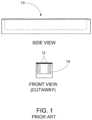
- FIG. 1An example of a prior art hermetic implant package 10 is shown in FIG. 1 .
- the implant package 10includes thick sidewalls 12 that limit the space available for the internal components, in this case implant antenna 14 .
- implant antenna 14For example, an implant package of width 4 mm that has sidewalls 0.5 mm thick only has a maximum of 3 mm of width available for an implant antenna.
- FIG. 1shows an antenna 14 that is placed into the implant package from an opening at the top of the package.
- a top layer 16is connected or bonded to the implant package and sealed as shown in FIG. 2 A .
- FIG. 4 Cillustrates the completed implant, for an alternative embodiment of the present invention, with etched cavities and a split housing;
- the implant packagemay utilize thin membrane materials such as glass, quartz, sapphire, fused silica, alumina, titanium, diamond, or other materials known in the art, to increase the space available inside an implant package of a fixed outer size.
- thin membrane materialssuch as glass, quartz, sapphire, fused silica, alumina, titanium, diamond, or other materials known in the art.
- the thin membraneis bonded to the top of the implant package, as in FIGS. 1 and 2
- the thin membrane or membranesmay be bonded to the side of the implant package, such that they are in a plane substantially parallel with the axis of the coil, as in FIG. 3 .
- the length of the implant housingmay have values of 5, 10, 15, 20, 25, or 30 mm long.
- the cross sectionsmay have width ⁇ height values of 5 ⁇ 3 mm, 4.5 ⁇ 2.25 mm, 3.25 ⁇ 2.25 mm, 2.5 ⁇ 1.75 mm, or 2 ⁇ 1 mm.
- an antenna coil 14is placed into the housing 300 via the open walls on the long side.
- Microelectronics 301which may include one or more pressure sensors, may also be placed inside housing 300 , inside the region encircled by coil 14 , or outside of this region.
- FIG. 3 Cdepicts the final step, in which thin walls 302 are bonded to housing 300 , such as hermetically bonded. It will be appreciated that the thin walls 302 may be sealed or bonded in any appropriate manner. It will also be appreciated that the concepts herein may apply to non-hermetic housing applications, such as acute implants. In these cases, non-hermetic materials and bonding methods known in the art may be used. As illustrated and described in the examples herein, the thin walls 302 may be substantially thinner, or include a portion that is substantially thinner, than the remaining walls of the housing. Non-limiting examples of wall thicknesses of the housing walls and thin walls 302 are provided below.
- the implant packagecan achieve the maximum possible coil loop area within the width constraint imposed on the short dimension.
- the coil axis 303refers to the central axis of a generally spirally wound coil 14 , as shown in FIG. 3 .
- the spirally wound coil 14may be any appropriate shape, such as circular, rectangular, or any other shape.
- the final implant produced by the process of FIG. 3meets the complex requirements of medical implants: (i) small cross-sectional area, (ii) non-metal housing, (iii) hermetic sealing, (iv) biocompatibility, and (v) maximum internal volume for a given external volume.
- internal electronics 301may include one or more pressure sensors known in the art, and thin walls 302 may be flexible membranes which communicate pressure to internal electronics 301 by means of an incompressible fluid or gel that fills the cavity formed by housing 300 and thin walls 302 .
- the thin walls 302may be flexible membranes which are part of a sensing electronic circuit, thus transducing pressure directly into an electronic signal of a sensing circuit.
- the walls of the housing other than the thin walls 302may be greater than 0.3 mm.
- each sidewallmay have a thickness of less than 0.15 mm.
- each sidewallmay have a thickness less than about 0.050 mm.
- by using membranes as the thin sidewalls 302 of the implant package 20each sidewall may have a thickness of about 0.025 mm.
- each sidewallmay have a thickness less than about 0.025 mm, such as about 0.020 mm, about 0.015 mm, about 0.010 mm, about 0.005 mm, about 0.001 mm and any sized thickness in between.
- the thin walls 302may have one half or less of the thickness of the non-thin walls of the housing 20 .
- thin walls 302may be made of one or more thin film materials such as glass, quartz, fused silica, titanium, silicon, sapphire, diamond, or others. It may be thinned by polishing, etching, or other methods well known in the art. Thin walls 302 may be bonded to housing 300 by several means known in the art, including laser welding, glass frit bonding, or compression bonding by brazing, soldering, or eutectic bonding, following deposition of a metal braze ring on the two surfaces.
- the architecture of FIG. 3 Cprovides a further advantage over the prior art.
- the metal ringis parallel to the antenna windings, as in prior art FIG. 1 , it may absorb and dissipate significant amounts of energy going to and coming from the antenna 14 , due to shielding and eddy current formation.
- the diaphragm bonding ringsare arranged perpendicular to the antenna windings as in FIG. 3 C , the shielding and eddy current effects are practically eliminated.
- the thin-walled housing or implant package 20provides a significant improvement in the efficient use of space inside an implant package over prior art.
- the maximum available width for the antennawas approximately 3 mm.
- the available width for the antennais approximately 3.95 mm.
- Such an increase in antenna width for a given implant outer sizemay dramatically increase the wireless link distance of an implantable wireless sensor.
- This difference in antenna width of the thin-walled implant package 20can translate into a catheter delivery system that is about 3 Fr sizes smaller for the present invention than for prior art systems.
- the inventionis thus particularly useful in wireless implants that have one axis longer than the others, which is generally the case for implants that are intended for placement in blood vessels, or intended for delivery through a catheter device. If the ratio of length to width of such an implant is x, then increasing the coil's width dimension by n microns creates more coil area than the same increase in the length dimension, by a factor of x. In such wireless implants, one can generally maximize coil area by placing the thinnest sidewalls parallel to the coil axis, and perpendicular to the shorter dimension, as in FIG. 3 C .
- the implant architecturecan be used to maximize the size of any internal component, substance, or combination thereof.
- thesemay include, but are not limited to, drugs, steroids, batteries, stimulus electrodes, pacing circuitry, flow sensors, chemical sensors, or other electronics.
- the coil 14can be generally circular, ovular, rectangular, or can take the form of any polygon that encloses an area.
- a rectangular housingis shown in the exemplary embodiment figures, the concept of disposing the thin walls on the outer periphery of coil 14 , parallel to coil axis 303 , can be generalized to any polygonal shape.
- the disclosed invention depicted in FIG. 3may have a further benefit for pressure sensing implants.
- Many commonly available chip-scale pressure sensorsare well suited for use in wireless implants.
- such pressure sensorsgenerally have small, thin, pressure sensing diaphragms, on the order of 2 mm diameter or less and thickness of 500 nm or less. If such a diaphragm is exposed to living tissue or blood, one or more layers of cells will usually grow on it after a period of several days or weeks. Cell layers such as this are known to stiffen the sensor's diaphragm, decreasing the device's sensitivity.
- FIG. 1shows a further benefit for pressure sensing implants.
- the thin sidewalls 302may serve as flexible pressure diaphragms, which communicate pressure to chip-scale pressure sensors on internal electronics 301 through a pressure-communicating medium. Because they are larger in area and generally stiffer than the diaphragms of chip scale sensors, the thin sidewalls 302 will not be stiffened significantly by several layers of cell growth, compared to the smaller diaphragms of the chip-scale sensors. Thus the present invention allows pressure sensor implant designers to select from a number of available off-the-shelf or custom chip-scale pressure sensors, without having to worry about diaphragm stiffening due to cell growth.
- the thin-walled implant package 20may be used with RF medical implants
- the designs set forth hereinare useful for any micro device or component where a non-metal hermetic enclosure is required and where it is desirable to minimize sidewall thickness. Examples include, but are not limited to, sensors, actuators, or transponders located in harsh chemical environments, in liquid immersion, in high temperature zones (such as engines), or in environments where sterility is critical. Other examples include applications where the internal electronics must be hermetically housed, but cannot tolerate shielding or eddy current losses imposed by metal housings or braze rings.
- the designs and methods described hereinovercome the many challenges associated with wireless sensors that use radiofrequency.
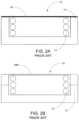
- the housingis formed in two pieces 401 and 402 , each with a cavity formed by one of the micromachining processes known in the art. The location of the cavity is shown as a dotted line in the side view, and can be seen in the cutaway.
- the coil 14 , electronics 301 , and other internalsare inserted into one of the housing pieces 401 .
- housing pieces 401 and 402are bonded together hermetically by one of the methods previously disclosed. Note that in FIGS. 4 A- 4 C , housing pieces 401 and 402 are shown as symmetrical, but asymmetrical pieces may also be employed.
- the internal volume of the housingmay not need to be filled with an incompressible fluid, as thin sidewalls 502 do not need to communicate pressure. Additionally, it will be appreciated that the steps of bonding electronics 501 , bonding each of thin sidewalls 502 , or inserting coil 14 , may be done in a different order.
- the electronics 501may be a single, solid state device, such as a capacitive sensor, or it may be multiple devices attached to a hermetic substrate such as LTCC.
- FIG. 6illustrates an embodiment similar to that of FIG. 5 .
- the electronics 601are placed on the exterior of housing 600 , but this time on one of the short ends.
- FIG. 6depicts hermetic electrical feedthroughs connecting electronics 601 to coil 14 , but a ‘free wire’ connection method such as the one depicted in FIGS. 5 A and 5 B may also be employed.
- the thin sidewalls 302are not communicating pressure and so incompressible liquid fill may not be required.
- the invention disclosed hereinis particularly advantageous when the wireless implant is required to be long and narrow, as is typically the case with cardiovascular implants. With such geometries, any coil width gained in the short dimension has a dramatic impact on coil area and hence link distance.
- the embodiments disclosed hereinmay benefit from having the final sidewalls attached in a vacuum environment, to prevent internal pressures inside the housing from varying with temperature.
- the internal volumemay be filled with an inert gas to limit corrosion of the internals.
- implant housing embodiments disclosed hereincan be made using all thick walls, and then post-processing the housing to thin portions of the walls that are parallel to the coil's axis.
- State of the art post-processing technologiessuch as grinding, polishing, etching, or laser ablation are some possible means for accomplishing this.
- the external housingmay be surface treated with a biocompatible material to limit clot formation, control cell growth, or improve lubricity.
- a biocompatible materialmay include heparin, silicone, parylene, cell tissue monolayers, or other coatings well known to those of ordinary skill in the art.
Landscapes
- Health & Medical Sciences (AREA)
- Life Sciences & Earth Sciences (AREA)
- Engineering & Computer Science (AREA)
- Heart & Thoracic Surgery (AREA)
- Public Health (AREA)
- Veterinary Medicine (AREA)
- Biophysics (AREA)
- Pathology (AREA)
- Physics & Mathematics (AREA)
- Biomedical Technology (AREA)
- General Health & Medical Sciences (AREA)
- Medical Informatics (AREA)
- Molecular Biology (AREA)
- Surgery (AREA)
- Animal Behavior & Ethology (AREA)
- Cardiology (AREA)
- Vascular Medicine (AREA)
- Physiology (AREA)
- Computer Networks & Wireless Communication (AREA)
- Measuring And Recording Apparatus For Diagnosis (AREA)
Abstract
Description
Claims (19)
Priority Applications (2)
| Application Number | Priority Date | Filing Date | Title |
|---|---|---|---|
| US18/094,537US12029546B2 (en) | 2011-06-30 | 2023-01-09 | Implantable sensor enclosure with thin sidewalls |
| US18/765,785US20240358275A1 (en) | 2011-06-30 | 2024-07-08 | Implantable sensor enclosure with thin sidewalls |
Applications Claiming Priority (6)
| Application Number | Priority Date | Filing Date | Title |
|---|---|---|---|
| US201161502982P | 2011-06-30 | 2011-06-30 | |
| PCT/US2012/044998WO2013003754A1 (en) | 2011-06-30 | 2012-06-29 | Implantable sensor enclosure with thin sidewalls |
| US201414129725A | 2014-02-21 | 2014-02-21 | |
| US15/837,075US10433764B2 (en) | 2011-06-30 | 2017-12-11 | Implantable sensor enclosure with thin sidewalls |
| US16/594,155US11547320B2 (en) | 2011-06-30 | 2019-10-07 | Implantable sensor enclosure with thin sidewalls |
| US18/094,537US12029546B2 (en) | 2011-06-30 | 2023-01-09 | Implantable sensor enclosure with thin sidewalls |
Related Parent Applications (1)
| Application Number | Title | Priority Date | Filing Date |
|---|---|---|---|
| US16/594,155ContinuationUS11547320B2 (en) | 2011-06-30 | 2019-10-07 | Implantable sensor enclosure with thin sidewalls |
Related Child Applications (1)
| Application Number | Title | Priority Date | Filing Date |
|---|---|---|---|
| US18/765,785ContinuationUS20240358275A1 (en) | 2011-06-30 | 2024-07-08 | Implantable sensor enclosure with thin sidewalls |
Publications (2)
| Publication Number | Publication Date |
|---|---|
| US20230371842A1 US20230371842A1 (en) | 2023-11-23 |
| US12029546B2true US12029546B2 (en) | 2024-07-09 |
Family
ID=88792542
Family Applications (2)
| Application Number | Title | Priority Date | Filing Date |
|---|---|---|---|
| US18/094,537ActiveUS12029546B2 (en) | 2011-06-30 | 2023-01-09 | Implantable sensor enclosure with thin sidewalls |
| US18/765,785PendingUS20240358275A1 (en) | 2011-06-30 | 2024-07-08 | Implantable sensor enclosure with thin sidewalls |
Family Applications After (1)
| Application Number | Title | Priority Date | Filing Date |
|---|---|---|---|
| US18/765,785PendingUS20240358275A1 (en) | 2011-06-30 | 2024-07-08 | Implantable sensor enclosure with thin sidewalls |
Country Status (1)
| Country | Link |
|---|---|
| US (2) | US12029546B2 (en) |
Citations (48)
| Publication number | Priority date | Publication date | Assignee | Title |
|---|---|---|---|---|
| US4026276A (en) | 1976-04-05 | 1977-05-31 | The Johns Hopkins University | Intracranial pressure monitor |
| US5454270A (en) | 1994-06-06 | 1995-10-03 | Motorola, Inc. | Hermetically sealed pressure sensor and method thereof |
| US5510276A (en) | 1992-12-28 | 1996-04-23 | Commissariat A L'energie Atomique | Process for producing a pressure transducer using silicon-on-insulator technology |
| US5840148A (en) | 1995-06-30 | 1998-11-24 | Bio Medic Data Systems, Inc. | Method of assembly of implantable transponder |
| JP2000005136A (en) | 1998-06-26 | 2000-01-11 | Nippon Telegr & Teleph Corp <Ntt> | Temperature measuring device and implant |
| US20010018598A1 (en) | 1998-11-06 | 2001-08-30 | Gregory M. Cruise | Compositions, systems, and methods for creating in situ, chemically cross-linked, mechanical barriers |
| US20020045921A1 (en)* | 2000-10-16 | 2002-04-18 | Remon Medical Technologies Ltd. | Implantable pressure sensors and methods for making and using them |
| JP2002515278A (en) | 1998-05-18 | 2002-05-28 | コミツサリア タ レネルジー アトミーク | Measuring one or more physical parameters using a medical probe |
| JP2003144417A (en) | 2001-08-29 | 2003-05-20 | Rare Metal:Kk | In-vivo information detecting system, and tag device and relay device used for the same |
| US6939299B1 (en) | 1999-12-13 | 2005-09-06 | Kurt Petersen | Implantable continuous intraocular pressure sensor |
| JP2005284511A (en) | 2004-03-29 | 2005-10-13 | Matsushita Electric Ind Co Ltd | INSERTION TYPE WIRELESS COMMUNICATION MEDIUM DEVICE AND ELECTRONIC DEVICE |
| CN1701464A (en) | 2003-05-15 | 2005-11-23 | 西铁城时计株式会社 | Electronic device having metal package unit having built-in antenna unit |
| US20060109188A1 (en) | 2003-05-15 | 2006-05-25 | Ienobu Ikeda | Electronic device having metal package unit having built-in antenna unit |
| US20060177956A1 (en) | 2005-02-10 | 2006-08-10 | Cardiomems, Inc. | Method of manufacturing a hermetic chamber with electrical feedthroughs |
| JP2006522635A (en) | 2003-04-14 | 2006-10-05 | レモン メディカル テクノロジーズ リミテッド | Acoustic telemetry device for in-body communication |
| US20060241354A1 (en) | 2005-04-12 | 2006-10-26 | Allen Mark G | Electromagnetically coupled hermetic chamber |
| JP2006309582A (en) | 2005-04-28 | 2006-11-09 | Hitachi Ltd | Wireless IC tag and method of manufacturing wireless IC tag |
| US20060287602A1 (en) | 2005-06-21 | 2006-12-21 | Cardiomems, Inc. | Implantable wireless sensor for in vivo pressure measurement |
| US7174212B1 (en) | 2003-12-10 | 2007-02-06 | Pacesetter, Inc. | Implantable medical device having a casing providing high-speed telemetry |
| JP2007512859A (en) | 2003-11-03 | 2007-05-24 | マイクロチップス・インコーポレーテッド | Medical device for sensing glucose |
| JP2007516746A (en) | 2003-12-11 | 2007-06-28 | プロテウス バイオメディカル インコーポレイテッド | Implantable pressure sensor |
| US20070163355A1 (en) | 2006-01-13 | 2007-07-19 | Kavlico Corporation | Preformed sensor housing and methods to produce thin metal diaphragms |
| US20070208390A1 (en) | 2006-03-01 | 2007-09-06 | Von Arx Jeffrey A | Implantable wireless sound sensor |
| JP2007256287A (en) | 2006-03-21 | 2007-10-04 | Radi Medical Systems Ab | Pressure sensor |
| US20070267708A1 (en) | 2006-05-22 | 2007-11-22 | Cardiomems, Inc. | Methods and apparatus having an integrated circuit attached to fused silica |
| JP2008022935A (en) | 2006-07-19 | 2008-02-07 | Matsushita Electric Ind Co Ltd | In vivo device |
| CN101128957A (en) | 2006-03-13 | 2008-02-20 | 株式会社村田制作所 | portable electronic device |
| US7401521B2 (en) | 2003-06-13 | 2008-07-22 | Telecom Italia S.P.A. | Pressure sensor with integrated structure |
| CN101278439A (en) | 2005-11-22 | 2008-10-01 | 株式会社村田制作所 | Coil antenna and portable electronic apparatus |
| US20080269829A1 (en) | 2007-04-26 | 2008-10-30 | Medtronic, Inc. | Metal injection molded titanium alloy housing for implantable medical devices |
| US20080269573A1 (en) | 2007-04-30 | 2008-10-30 | Integrated Sensing Systems, Inc. | Procedure and system for monitoring a physiological parameter within an internal organ of a living body |
| US7574792B2 (en) | 2003-09-16 | 2009-08-18 | Cardiomems, Inc. | Method of manufacturing an implantable wireless sensor |
| US20090221885A1 (en) | 2008-02-25 | 2009-09-03 | Cardiac Pacemakers, Inc. | Optical Window Assembly for Implantable Medical Device |
| WO2009146089A2 (en) | 2008-04-01 | 2009-12-03 | Cardiomems, Inc. | System and apparatus for in-vivo assessment of relative position of an implant |
| US7686762B1 (en)* | 2002-10-03 | 2010-03-30 | Integrated Sensing Systems, Inc. | Wireless device and system for monitoring physiologic parameters |
| US7763487B2 (en) | 2005-05-06 | 2010-07-27 | Stmicroelectronics S.R.L. | Integrated differential pressure sensor and manufacturing process thereof |
| JP2010538254A (en) | 2007-08-27 | 2010-12-09 | コーニンクレッカ フィリップス エレクトロニクス エヌ ヴィ | Pressure sensor, sensor probe with pressure sensor, medical device with sensor probe, and method of manufacturing sensor probe |
| US20110004076A1 (en) | 2008-02-01 | 2011-01-06 | Smith & Nephew, Inc. | System and method for communicating with an implant |
| US20110063088A1 (en) | 2009-09-16 | 2011-03-17 | Greatbatch Ltd. | Rfid detection and identification system for implantable medical devices |
| US20110106120A1 (en) | 2008-01-18 | 2011-05-05 | Med Institute, Inc. | Intravascular device attachment system having tubular expandable body |
| WO2012015955A1 (en) | 2010-07-27 | 2012-02-02 | Endotronix, Inc. | Pressure sensor, centering anchor, delivery system and method |
| US8132465B1 (en) | 2007-08-01 | 2012-03-13 | Silicon Microstructures, Inc. | Sensor element placement for package stress compensation |
| US8154389B2 (en) | 2007-03-15 | 2012-04-10 | Endotronix, Inc. | Wireless sensor reader |
| WO2013003754A1 (en) | 2011-06-30 | 2013-01-03 | Endotronix, Inc. | Implantable sensor enclosure with thin sidewalls |
| US8493187B2 (en) | 2007-03-15 | 2013-07-23 | Endotronix, Inc. | Wireless sensor reader |
| US20140028467A1 (en) | 2007-03-15 | 2014-01-30 | Endotronix, Inc. | Wireless sensor reader |
| US20140306807A1 (en) | 2007-03-15 | 2014-10-16 | Endotronix, Inc. | Wireless sensor reader |
| US20160029956A1 (en) | 2011-06-30 | 2016-02-04 | Endotronix, Inc. | Pressure sensing implant |
- 2023
- 2023-01-09USUS18/094,537patent/US12029546B2/enactiveActive
- 2024
- 2024-07-08USUS18/765,785patent/US20240358275A1/enactivePending
Patent Citations (53)
| Publication number | Priority date | Publication date | Assignee | Title |
|---|---|---|---|---|
| US4026276A (en) | 1976-04-05 | 1977-05-31 | The Johns Hopkins University | Intracranial pressure monitor |
| US5510276A (en) | 1992-12-28 | 1996-04-23 | Commissariat A L'energie Atomique | Process for producing a pressure transducer using silicon-on-insulator technology |
| US5454270A (en) | 1994-06-06 | 1995-10-03 | Motorola, Inc. | Hermetically sealed pressure sensor and method thereof |
| US5840148A (en) | 1995-06-30 | 1998-11-24 | Bio Medic Data Systems, Inc. | Method of assembly of implantable transponder |
| JP2002515278A (en) | 1998-05-18 | 2002-05-28 | コミツサリア タ レネルジー アトミーク | Measuring one or more physical parameters using a medical probe |
| JP2000005136A (en) | 1998-06-26 | 2000-01-11 | Nippon Telegr & Teleph Corp <Ntt> | Temperature measuring device and implant |
| US20010018598A1 (en) | 1998-11-06 | 2001-08-30 | Gregory M. Cruise | Compositions, systems, and methods for creating in situ, chemically cross-linked, mechanical barriers |
| US6939299B1 (en) | 1999-12-13 | 2005-09-06 | Kurt Petersen | Implantable continuous intraocular pressure sensor |
| US20020045921A1 (en)* | 2000-10-16 | 2002-04-18 | Remon Medical Technologies Ltd. | Implantable pressure sensors and methods for making and using them |
| JP2003144417A (en) | 2001-08-29 | 2003-05-20 | Rare Metal:Kk | In-vivo information detecting system, and tag device and relay device used for the same |
| US20110046452A1 (en) | 2002-10-03 | 2011-02-24 | Integrated Sensing Systems, Inc. | Wireless device and system for monitoring physiologic parameters |
| US7686762B1 (en)* | 2002-10-03 | 2010-03-30 | Integrated Sensing Systems, Inc. | Wireless device and system for monitoring physiologic parameters |
| JP2006522635A (en) | 2003-04-14 | 2006-10-05 | レモン メディカル テクノロジーズ リミテッド | Acoustic telemetry device for in-body communication |
| US7198603B2 (en) | 2003-04-14 | 2007-04-03 | Remon Medical Technologies, Inc. | Apparatus and methods using acoustic telemetry for intrabody communications |
| US20060109188A1 (en) | 2003-05-15 | 2006-05-25 | Ienobu Ikeda | Electronic device having metal package unit having built-in antenna unit |
| CN1701464A (en) | 2003-05-15 | 2005-11-23 | 西铁城时计株式会社 | Electronic device having metal package unit having built-in antenna unit |
| US7401521B2 (en) | 2003-06-13 | 2008-07-22 | Telecom Italia S.P.A. | Pressure sensor with integrated structure |
| US7574792B2 (en) | 2003-09-16 | 2009-08-18 | Cardiomems, Inc. | Method of manufacturing an implantable wireless sensor |
| JP2007512859A (en) | 2003-11-03 | 2007-05-24 | マイクロチップス・インコーポレーテッド | Medical device for sensing glucose |
| US7174212B1 (en) | 2003-12-10 | 2007-02-06 | Pacesetter, Inc. | Implantable medical device having a casing providing high-speed telemetry |
| JP2007516746A (en) | 2003-12-11 | 2007-06-28 | プロテウス バイオメディカル インコーポレイテッド | Implantable pressure sensor |
| JP2005284511A (en) | 2004-03-29 | 2005-10-13 | Matsushita Electric Ind Co Ltd | INSERTION TYPE WIRELESS COMMUNICATION MEDIUM DEVICE AND ELECTRONIC DEVICE |
| US20060177956A1 (en) | 2005-02-10 | 2006-08-10 | Cardiomems, Inc. | Method of manufacturing a hermetic chamber with electrical feedthroughs |
| US20060241354A1 (en) | 2005-04-12 | 2006-10-26 | Allen Mark G | Electromagnetically coupled hermetic chamber |
| JP2006309582A (en) | 2005-04-28 | 2006-11-09 | Hitachi Ltd | Wireless IC tag and method of manufacturing wireless IC tag |
| US7763487B2 (en) | 2005-05-06 | 2010-07-27 | Stmicroelectronics S.R.L. | Integrated differential pressure sensor and manufacturing process thereof |
| US20060287602A1 (en) | 2005-06-21 | 2006-12-21 | Cardiomems, Inc. | Implantable wireless sensor for in vivo pressure measurement |
| CN101278439A (en) | 2005-11-22 | 2008-10-01 | 株式会社村田制作所 | Coil antenna and portable electronic apparatus |
| US20070163355A1 (en) | 2006-01-13 | 2007-07-19 | Kavlico Corporation | Preformed sensor housing and methods to produce thin metal diaphragms |
| US20070208390A1 (en) | 2006-03-01 | 2007-09-06 | Von Arx Jeffrey A | Implantable wireless sound sensor |
| CN101128957A (en) | 2006-03-13 | 2008-02-20 | 株式会社村田制作所 | portable electronic device |
| JP2007256287A (en) | 2006-03-21 | 2007-10-04 | Radi Medical Systems Ab | Pressure sensor |
| US20070267708A1 (en) | 2006-05-22 | 2007-11-22 | Cardiomems, Inc. | Methods and apparatus having an integrated circuit attached to fused silica |
| JP2008022935A (en) | 2006-07-19 | 2008-02-07 | Matsushita Electric Ind Co Ltd | In vivo device |
| US8154389B2 (en) | 2007-03-15 | 2012-04-10 | Endotronix, Inc. | Wireless sensor reader |
| US9305456B2 (en) | 2007-03-15 | 2016-04-05 | Endotronix, Inc. | Wireless sensor reader |
| US20140306807A1 (en) | 2007-03-15 | 2014-10-16 | Endotronix, Inc. | Wireless sensor reader |
| US20140028467A1 (en) | 2007-03-15 | 2014-01-30 | Endotronix, Inc. | Wireless sensor reader |
| US8493187B2 (en) | 2007-03-15 | 2013-07-23 | Endotronix, Inc. | Wireless sensor reader |
| US20080269829A1 (en) | 2007-04-26 | 2008-10-30 | Medtronic, Inc. | Metal injection molded titanium alloy housing for implantable medical devices |
| US20080269573A1 (en) | 2007-04-30 | 2008-10-30 | Integrated Sensing Systems, Inc. | Procedure and system for monitoring a physiological parameter within an internal organ of a living body |
| US8132465B1 (en) | 2007-08-01 | 2012-03-13 | Silicon Microstructures, Inc. | Sensor element placement for package stress compensation |
| JP2010538254A (en) | 2007-08-27 | 2010-12-09 | コーニンクレッカ フィリップス エレクトロニクス エヌ ヴィ | Pressure sensor, sensor probe with pressure sensor, medical device with sensor probe, and method of manufacturing sensor probe |
| US20110106120A1 (en) | 2008-01-18 | 2011-05-05 | Med Institute, Inc. | Intravascular device attachment system having tubular expandable body |
| US20110004076A1 (en) | 2008-02-01 | 2011-01-06 | Smith & Nephew, Inc. | System and method for communicating with an implant |
| US20090221885A1 (en) | 2008-02-25 | 2009-09-03 | Cardiac Pacemakers, Inc. | Optical Window Assembly for Implantable Medical Device |
| WO2009146089A2 (en) | 2008-04-01 | 2009-12-03 | Cardiomems, Inc. | System and apparatus for in-vivo assessment of relative position of an implant |
| US20110063088A1 (en) | 2009-09-16 | 2011-03-17 | Greatbatch Ltd. | Rfid detection and identification system for implantable medical devices |
| WO2012015955A1 (en) | 2010-07-27 | 2012-02-02 | Endotronix, Inc. | Pressure sensor, centering anchor, delivery system and method |
| WO2013003754A1 (en) | 2011-06-30 | 2013-01-03 | Endotronix, Inc. | Implantable sensor enclosure with thin sidewalls |
| CA2840645A1 (en) | 2011-06-30 | 2013-01-03 | Endotronix, Inc. | Implantable sensor enclosure with thin sidewalls |
| US20140155710A1 (en) | 2011-06-30 | 2014-06-05 | Endotronix, Inc. | Implantable sensor enclosure with thin sidewalls |
| US20160029956A1 (en) | 2011-06-30 | 2016-02-04 | Endotronix, Inc. | Pressure sensing implant |
Non-Patent Citations (6)
| Title |
|---|
| Extended European Search Report for Application 14806873.7 PCT/US2014030661, dated May 20, 2016, 7 pp., European Patent Office, Germany. |
| Extended European Search Report, Application No. 12804636.4-1660 / 2725969, Endotronix, Inc., dated Jan. 20, 2015. |
| IL Notification No. 25, Notification of Defects in Patent Application No. 230193 in Israel, report issue date Jan. 26, 2017, State of Israel Ministry of Justice, The Patent Office. |
| Japanese Office Action dated Mar. 22, 2018, dated Mar. 27, 2018, 6 pages. |
| Patent Cooperation Treaty (PCT), International Search Report and Written Opinion for Application PCT/US/14/30661, dated Sep. 17, 2015, 8 pp., Interational Searching Authority, US. |
| Patent Cooperation Treaty (PCT), International Search Report and Written Opinion for Application PCT/US12/44998, dated Sep. 25, 2012, 9 pgs., International Searching Authority, US. |
Also Published As
| Publication number | Publication date |
|---|---|
| US20240358275A1 (en) | 2024-10-31 |
| US20230371842A1 (en) | 2023-11-23 |
Similar Documents
| Publication | Publication Date | Title |
|---|---|---|
| US11547320B2 (en) | Implantable sensor enclosure with thin sidewalls | |
| US11707230B2 (en) | Pressure sensing implant | |
| AU2019201803B2 (en) | Pressure sensing implant | |
| US20160324443A1 (en) | Pressure sensing implant | |
| AU2022271366B2 (en) | Pressure sensing implant | |
| US12029546B2 (en) | Implantable sensor enclosure with thin sidewalls | |
| US20230380764A1 (en) | Pressure sensing implant |
Legal Events
| Date | Code | Title | Description |
|---|---|---|---|
| FEPP | Fee payment procedure | Free format text:ENTITY STATUS SET TO UNDISCOUNTED (ORIGINAL EVENT CODE: BIG.); ENTITY STATUS OF PATENT OWNER: SMALL ENTITY | |
| FEPP | Fee payment procedure | Free format text:ENTITY STATUS SET TO SMALL (ORIGINAL EVENT CODE: SMAL); ENTITY STATUS OF PATENT OWNER: SMALL ENTITY | |
| AS | Assignment | Owner name:ENDOTRONIX, INC., ILLINOIS Free format text:ASSIGNMENT OF ASSIGNORS INTEREST;ASSIGNORS:ROWLAND, HARRY;NAGY, MICHAEL;REEL/FRAME:064825/0207 Effective date:20171211 | |
| STPP | Information on status: patent application and granting procedure in general | Free format text:NON FINAL ACTION MAILED | |
| STPP | Information on status: patent application and granting procedure in general | Free format text:RESPONSE TO NON-FINAL OFFICE ACTION ENTERED AND FORWARDED TO EXAMINER | |
| STPP | Information on status: patent application and granting procedure in general | Free format text:NOTICE OF ALLOWANCE MAILED -- APPLICATION RECEIVED IN OFFICE OF PUBLICATIONS | |
| STPP | Information on status: patent application and granting procedure in general | Free format text:DOCKETED NEW CASE - READY FOR EXAMINATION | |
| STPP | Information on status: patent application and granting procedure in general | Free format text:NOTICE OF ALLOWANCE MAILED -- APPLICATION RECEIVED IN OFFICE OF PUBLICATIONS | |
| STPP | Information on status: patent application and granting procedure in general | Free format text:PUBLICATIONS -- ISSUE FEE PAYMENT RECEIVED | |
| STPP | Information on status: patent application and granting procedure in general | Free format text:PUBLICATIONS -- ISSUE FEE PAYMENT VERIFIED | |
| STCF | Information on status: patent grant | Free format text:PATENTED CASE | |
| FEPP | Fee payment procedure | Free format text:ENTITY STATUS SET TO UNDISCOUNTED (ORIGINAL EVENT CODE: BIG.); ENTITY STATUS OF PATENT OWNER: LARGE ENTITY |