US12015391B2 - XBAR devices with excess piezoelectric material removed - Google Patents
XBAR devices with excess piezoelectric material removedDownload PDFInfo
- Publication number
- US12015391B2 US12015391B2US17/894,001US202217894001AUS12015391B2US 12015391 B2US12015391 B2US 12015391B2US 202217894001 AUS202217894001 AUS 202217894001AUS 12015391 B2US12015391 B2US 12015391B2
- Authority
- US
- United States
- Prior art keywords
- cavity
- substrate
- piezoelectric layer
- idt
- piezoelectric
- Prior art date
- Legal status (The legal status is an assumption and is not a legal conclusion. Google has not performed a legal analysis and makes no representation as to the accuracy of the status listed.)
- Active
Links
- 239000000463materialSubstances0.000titleabstractdescription90
- 239000000758substrateSubstances0.000claimsabstractdescription104
- 239000004020conductorSubstances0.000claimsdescription86
- VYPSYNLAJGMNEJ-UHFFFAOYSA-NSilicium dioxideChemical groupO=[Si]=OVYPSYNLAJGMNEJ-UHFFFAOYSA-N0.000claimsdescription20
- 229910052751metalInorganic materials0.000claimsdescription13
- 239000002184metalSubstances0.000claimsdescription12
- 239000000377silicon dioxideSubstances0.000claimsdescription11
- 229910052681coesiteInorganic materials0.000claimsdescription8
- 229910052906cristobaliteInorganic materials0.000claimsdescription8
- 229910052682stishoviteInorganic materials0.000claimsdescription8
- 229910052905tridymiteInorganic materials0.000claimsdescription8
- 235000012239silicon dioxideNutrition0.000claimsdescription7
- GQYHUHYESMUTHG-UHFFFAOYSA-Nlithium niobateChemical compound[Li+].[O-][Nb](=O)=OGQYHUHYESMUTHG-UHFFFAOYSA-N0.000claimsdescription5
- WSMQKESQZFQMFW-UHFFFAOYSA-N5-methyl-pyrazole-3-carboxylic acidChemical compoundCC1=CC(C(O)=O)=NN1WSMQKESQZFQMFW-UHFFFAOYSA-N0.000claimsdescription4
- 239000010410layerSubstances0.000description120
- 238000000034methodMethods0.000description39
- 230000008569processEffects0.000description26
- 238000004891communicationMethods0.000description14
- 238000005530etchingMethods0.000description14
- XUIMIQQOPSSXEZ-UHFFFAOYSA-NSiliconChemical compound[Si]XUIMIQQOPSSXEZ-UHFFFAOYSA-N0.000description11
- 229910052710siliconInorganic materials0.000description11
- 239000010703siliconSubstances0.000description11
- 238000000151depositionMethods0.000description9
- 230000005684electric fieldEffects0.000description9
- 239000010408filmSubstances0.000description8
- 238000003780insertionMethods0.000description7
- 230000037431insertionEffects0.000description7
- 238000002161passivationMethods0.000description7
- 238000010897surface acoustic wave methodMethods0.000description6
- 230000008878couplingEffects0.000description5
- 238000010168coupling processMethods0.000description5
- 238000005859coupling reactionMethods0.000description5
- 239000003989dielectric materialSubstances0.000description5
- 238000012545processingMethods0.000description5
- 239000013078crystalSubstances0.000description4
- PCHJSUWPFVWCPO-UHFFFAOYSA-NgoldChemical compound[Au]PCHJSUWPFVWCPO-UHFFFAOYSA-N0.000description4
- 229910052737goldInorganic materials0.000description4
- 239000010931goldSubstances0.000description4
- 150000002500ionsChemical class0.000description4
- 230000013011matingEffects0.000description4
- 229910052581Si3N4Inorganic materials0.000description3
- 229910052782aluminiumInorganic materials0.000description3
- XAGFODPZIPBFFR-UHFFFAOYSA-NaluminiumChemical compound[Al]XAGFODPZIPBFFR-UHFFFAOYSA-N0.000description3
- 230000008901benefitEffects0.000description3
- 230000008021depositionEffects0.000description3
- 238000013461designMethods0.000description3
- 238000005516engineering processMethods0.000description3
- 230000033001locomotionEffects0.000description3
- 238000004519manufacturing processMethods0.000description3
- 238000000059patterningMethods0.000description3
- 229920002120photoresistant polymerPolymers0.000description3
- 229910000679solderInorganic materials0.000description3
- 229910000838Al alloyInorganic materials0.000description2
- VYZAMTAEIAYCRO-UHFFFAOYSA-NChromiumChemical compound[Cr]VYZAMTAEIAYCRO-UHFFFAOYSA-N0.000description2
- RYGMFSIKBFXOCR-UHFFFAOYSA-NCopperChemical compound[Cu]RYGMFSIKBFXOCR-UHFFFAOYSA-N0.000description2
- 229910000881Cu alloyInorganic materials0.000description2
- ZOKXTWBITQBERF-UHFFFAOYSA-NMolybdenumChemical compound[Mo]ZOKXTWBITQBERF-UHFFFAOYSA-N0.000description2
- RTAQQCXQSZGOHL-UHFFFAOYSA-NTitaniumChemical compound[Ti]RTAQQCXQSZGOHL-UHFFFAOYSA-N0.000description2
- 230000009471actionEffects0.000description2
- PNEYBMLMFCGWSK-UHFFFAOYSA-Naluminium oxideInorganic materials[O-2].[O-2].[O-2].[Al+3].[Al+3]PNEYBMLMFCGWSK-UHFFFAOYSA-N0.000description2
- 229910052790berylliumInorganic materials0.000description2
- ATBAMAFKBVZNFJ-UHFFFAOYSA-Nberyllium atomChemical compound[Be]ATBAMAFKBVZNFJ-UHFFFAOYSA-N0.000description2
- 229910052802copperInorganic materials0.000description2
- 239000010949copperSubstances0.000description2
- 229910052593corundumInorganic materials0.000description2
- 238000000708deep reactive-ion etchingMethods0.000description2
- 230000001419dependent effectEffects0.000description2
- 238000010586diagramMethods0.000description2
- 230000000694effectsEffects0.000description2
- 238000005538encapsulationMethods0.000description2
- 238000007667floatingMethods0.000description2
- 238000005468ion implantationMethods0.000description2
- 230000001788irregularEffects0.000description2
- 229910052750molybdenumInorganic materials0.000description2
- 239000011733molybdenumSubstances0.000description2
- 238000004806packaging method and processMethods0.000description2
- 238000000206photolithographyMethods0.000description2
- 239000004065semiconductorSubstances0.000description2
- 238000000926separation methodMethods0.000description2
- 238000004088simulationMethods0.000description2
- 239000000126substanceSubstances0.000description2
- 238000012360testing methodMethods0.000description2
- 239000010409thin filmSubstances0.000description2
- 229910052719titaniumInorganic materials0.000description2
- 239000010936titaniumSubstances0.000description2
- WFKWXMTUELFFGS-UHFFFAOYSA-NtungstenChemical compound[W]WFKWXMTUELFFGS-UHFFFAOYSA-N0.000description2
- 229910052721tungstenInorganic materials0.000description2
- 239000010937tungstenSubstances0.000description2
- 229910001845yogo sapphireInorganic materials0.000description2
- 229910002601GaNInorganic materials0.000description1
- GYHNNYVSQQEPJS-UHFFFAOYSA-NGalliumChemical compound[Ga]GYHNNYVSQQEPJS-UHFFFAOYSA-N0.000description1
- JMASRVWKEDWRBT-UHFFFAOYSA-NGallium nitrideChemical compound[Ga]#NJMASRVWKEDWRBT-UHFFFAOYSA-N0.000description1
- BPQQTUXANYXVAA-UHFFFAOYSA-NOrthosilicateChemical compound[O-][Si]([O-])([O-])[O-]BPQQTUXANYXVAA-UHFFFAOYSA-N0.000description1
- 229910005171Si3O4Inorganic materials0.000description1
- 239000012790adhesive layerSubstances0.000description1
- 238000000137annealingMethods0.000description1
- 230000002457bidirectional effectEffects0.000description1
- 230000005540biological transmissionEffects0.000description1
- 230000015572biosynthetic processEffects0.000description1
- 230000001413cellular effectEffects0.000description1
- 238000005229chemical vapour depositionMethods0.000description1
- 229910052804chromiumInorganic materials0.000description1
- 239000011651chromiumSubstances0.000description1
- -1chromium or titaniumChemical class0.000description1
- 238000004140cleaningMethods0.000description1
- 238000000576coating methodMethods0.000description1
- PMHQVHHXPFUNSP-UHFFFAOYSA-Mcopper(1+);methylsulfanylmethane;bromideChemical compoundBr[Cu].CSCPMHQVHHXPFUNSP-UHFFFAOYSA-M0.000description1
- 230000007797corrosionEffects0.000description1
- 238000005260corrosionMethods0.000description1
- 229910021419crystalline siliconInorganic materials0.000description1
- 230000001627detrimental effectEffects0.000description1
- 238000001312dry etchingMethods0.000description1
- 238000001704evaporationMethods0.000description1
- 230000008020evaporationEffects0.000description1
- 229910052733galliumInorganic materials0.000description1
- 238000000227grindingMethods0.000description1
- 238000007689inspectionMethods0.000description1
- 238000002955isolationMethods0.000description1
- 229910052746lanthanumInorganic materials0.000description1
- FZLIPJUXYLNCLC-UHFFFAOYSA-Nlanthanum atomChemical compound[La]FZLIPJUXYLNCLC-UHFFFAOYSA-N0.000description1
- 238000001459lithographyMethods0.000description1
- 239000012528membraneSubstances0.000description1
- 239000007769metal materialSubstances0.000description1
- 150000002739metalsChemical class0.000description1
- 238000012544monitoring processMethods0.000description1
- 150000004767nitridesChemical class0.000description1
- 229910021420polycrystalline siliconInorganic materials0.000description1
- 238000002360preparation methodMethods0.000description1
- 239000010453quartzSubstances0.000description1
- 229910052594sapphireInorganic materials0.000description1
- 239000010980sapphireSubstances0.000description1
- 238000007789sealingMethods0.000description1
- 230000035939shockEffects0.000description1
- HQVNEWCFYHHQES-UHFFFAOYSA-Nsilicon nitrideChemical compoundN12[Si]34N5[Si]62N3[Si]51N64HQVNEWCFYHHQES-UHFFFAOYSA-N0.000description1
- 239000007787solidSubstances0.000description1
- 238000004544sputter depositionMethods0.000description1
- 230000002123temporal effectEffects0.000description1
- 238000012800visualizationMethods0.000description1
- XLYOFNOQVPJJNP-UHFFFAOYSA-NwaterSubstancesOXLYOFNOQVPJJNP-UHFFFAOYSA-N0.000description1
- 238000001039wet etchingMethods0.000description1
Images


Classifications
- H—ELECTRICITY
- H03—ELECTRONIC CIRCUITRY
- H03H—IMPEDANCE NETWORKS, e.g. RESONANT CIRCUITS; RESONATORS
- H03H3/00—Apparatus or processes specially adapted for the manufacture of impedance networks, resonating circuits, resonators
- H03H3/007—Apparatus or processes specially adapted for the manufacture of impedance networks, resonating circuits, resonators for the manufacture of electromechanical resonators or networks
- H03H3/02—Apparatus or processes specially adapted for the manufacture of impedance networks, resonating circuits, resonators for the manufacture of electromechanical resonators or networks for the manufacture of piezoelectric or electrostrictive resonators or networks
- H—ELECTRICITY
- H03—ELECTRONIC CIRCUITRY
- H03H—IMPEDANCE NETWORKS, e.g. RESONANT CIRCUITS; RESONATORS
- H03H9/00—Networks comprising electromechanical or electro-acoustic elements; Electromechanical resonators
- H03H9/02—Details
- H03H9/02007—Details of bulk acoustic wave devices
- H03H9/02015—Characteristics of piezoelectric layers, e.g. cutting angles
- H—ELECTRICITY
- H03—ELECTRONIC CIRCUITRY
- H03H—IMPEDANCE NETWORKS, e.g. RESONANT CIRCUITS; RESONATORS
- H03H9/00—Networks comprising electromechanical or electro-acoustic elements; Electromechanical resonators
- H03H9/02—Details
- H03H9/02007—Details of bulk acoustic wave devices
- H03H9/02157—Dimensional parameters, e.g. ratio between two dimension parameters, length, width or thickness
- H—ELECTRICITY
- H03—ELECTRONIC CIRCUITRY
- H03H—IMPEDANCE NETWORKS, e.g. RESONANT CIRCUITS; RESONATORS
- H03H9/00—Networks comprising electromechanical or electro-acoustic elements; Electromechanical resonators
- H03H9/02—Details
- H03H9/02228—Guided bulk acoustic wave devices or Lamb wave devices having interdigital transducers situated in parallel planes on either side of a piezoelectric layer
- H—ELECTRICITY
- H03—ELECTRONIC CIRCUITRY
- H03H—IMPEDANCE NETWORKS, e.g. RESONANT CIRCUITS; RESONATORS
- H03H9/00—Networks comprising electromechanical or electro-acoustic elements; Electromechanical resonators
- H03H9/15—Constructional features of resonators consisting of piezoelectric or electrostrictive material
- H03H9/17—Constructional features of resonators consisting of piezoelectric or electrostrictive material having a single resonator
- H03H9/171—Constructional features of resonators consisting of piezoelectric or electrostrictive material having a single resonator implemented with thin-film techniques, i.e. of the film bulk acoustic resonator [FBAR] type
- H03H9/172—Means for mounting on a substrate, i.e. means constituting the material interface confining the waves to a volume
- H03H9/174—Membranes
- H—ELECTRICITY
- H03—ELECTRONIC CIRCUITRY
- H03H—IMPEDANCE NETWORKS, e.g. RESONANT CIRCUITS; RESONATORS
- H03H9/00—Networks comprising electromechanical or electro-acoustic elements; Electromechanical resonators
- H03H9/15—Constructional features of resonators consisting of piezoelectric or electrostrictive material
- H03H9/205—Constructional features of resonators consisting of piezoelectric or electrostrictive material having multiple resonators
- H—ELECTRICITY
- H03—ELECTRONIC CIRCUITRY
- H03H—IMPEDANCE NETWORKS, e.g. RESONANT CIRCUITS; RESONATORS
- H03H9/00—Networks comprising electromechanical or electro-acoustic elements; Electromechanical resonators
- H03H9/46—Filters
- H03H9/54—Filters comprising resonators of piezoelectric or electrostrictive material
- H03H9/56—Monolithic crystal filters
- H03H9/566—Electric coupling means therefor
- H03H9/568—Electric coupling means therefor consisting of a ladder configuration
- H—ELECTRICITY
- H03—ELECTRONIC CIRCUITRY
- H03H—IMPEDANCE NETWORKS, e.g. RESONANT CIRCUITS; RESONATORS
- H03H9/00—Networks comprising electromechanical or electro-acoustic elements; Electromechanical resonators
- H03H9/46—Filters
- H03H9/54—Filters comprising resonators of piezoelectric or electrostrictive material
- H03H9/58—Multiple crystal filters
- H03H9/582—Multiple crystal filters implemented with thin-film techniques
- H03H9/586—Means for mounting to a substrate, i.e. means constituting the material interface confining the waves to a volume
- H03H9/588—Membranes
- H—ELECTRICITY
- H03—ELECTRONIC CIRCUITRY
- H03H—IMPEDANCE NETWORKS, e.g. RESONANT CIRCUITS; RESONATORS
- H03H9/00—Networks comprising electromechanical or electro-acoustic elements; Electromechanical resonators
- H03H9/46—Filters
- H03H9/54—Filters comprising resonators of piezoelectric or electrostrictive material
- H03H9/58—Multiple crystal filters
- H03H9/60—Electric coupling means therefor
- H03H9/605—Electric coupling means therefor consisting of a ladder configuration
- H—ELECTRICITY
- H03—ELECTRONIC CIRCUITRY
- H03H—IMPEDANCE NETWORKS, e.g. RESONANT CIRCUITS; RESONATORS
- H03H3/00—Apparatus or processes specially adapted for the manufacture of impedance networks, resonating circuits, resonators
- H03H3/007—Apparatus or processes specially adapted for the manufacture of impedance networks, resonating circuits, resonators for the manufacture of electromechanical resonators or networks
- H03H3/02—Apparatus or processes specially adapted for the manufacture of impedance networks, resonating circuits, resonators for the manufacture of electromechanical resonators or networks for the manufacture of piezoelectric or electrostrictive resonators or networks
- H03H2003/023—Apparatus or processes specially adapted for the manufacture of impedance networks, resonating circuits, resonators for the manufacture of electromechanical resonators or networks for the manufacture of piezoelectric or electrostrictive resonators or networks the resonators or networks being of the membrane type
Definitions
- This disclosurerelates to radio frequency filters using acoustic wave resonators, and specifically to filters for use in communications equipment.
- a radio frequency (RF) filteris a two-port device configured to pass some frequencies and to stop other frequencies, where “pass” means transmit with relatively low signal loss and “stop” means block or substantially attenuate.
- the range of frequencies passed by a filteris referred to as the “pass-band” of the filter.
- the range of frequencies stopped by such a filteris referred to as the “stop-band” of the filter.
- a typical RF filterhas at least one pass-band and at least one stop-band. Specific requirements on a passband or stop-band depend on the specific application.
- a “pass-band”may be defined as a frequency range where the insertion loss of a filter is better than a defined value such as 1 dB, 2 dB, or 3 dB.
- a “stop-band”may be defined as a frequency range where the rejection of a filter is greater than a defined value such as 20 dB, 30 dB, 40 dB, or greater depending on application.
- RF filtersare used in communications systems where information is transmitted over wireless links.
- RF filtersmay be found in the RF front-ends of cellular base stations, mobile telephone and computing devices, satellite transceivers and ground stations, IoT (Internet of Things) devices, laptop computers and tablets, fixed point radio links, and other communications systems.
- IoTInternet of Things
- RF filtersare also used in radar and electronic and information warfare systems.
- RF filterstypically require many design trade-offs to achieve, for each specific application, the best compromise between performance parameters such as insertion loss, rejection, isolation, power handling, linearity, size and cost. Specific design and manufacturing methods and enhancements can benefit simultaneously one or several of these requirements.
- Performance enhancements to the RF filters in a wireless systemcan have broad impact to system performance. Improvements in RF filters can be leveraged to provide system performance improvements such as larger cell size, longer battery life, higher data rates, greater network capacity, lower cost, enhanced security, higher reliability, etc. These improvements can be realized at many levels of the wireless system both separately and in combination, for example at the RF module, RF transceiver, mobile or fixed sub-system, or network levels.
- High performance RF filters for present communication systemscommonly incorporate acoustic wave resonators including surface acoustic wave (SAW) resonators, bulk acoustic wave (BAW) resonators, film bulk acoustic wave resonators (FBAR), and other types of acoustic resonators.
- SAWsurface acoustic wave
- BAWbulk acoustic wave
- FBARfilm bulk acoustic wave resonators
- these existing technologiesare not well-suited for use at the higher frequencies and bandwidths proposed for future communications networks.
- Radio access technology for mobile telephone networkshas been standardized by the 3GPP (3 rd Generation Partnership Project).
- Radio access technology for 5 th generation mobile networksis defined in the 5G NR (new radio) standard.
- the 5G NR standarddefines several new communications bands. Two of these new communications bands are n77, which uses the frequency range from 3300 MHz to 4200 MHz, and n79, which uses the frequency range from 4400 MHz to 5000 MHz.
- Both band n77 and band n79use time-division duplexing (TDD), such that a communications device operating in band n77 and/or band n79 use the same frequencies for both uplink and downlink transmissions.
- TDDtime-division duplexing
- Bandpass filters for bands n77 and n79must be capable of handling the transmit power of the communications device.
- WiFi bands at 5 GHz and 6 GHzalso require high frequency and wide bandwidth.
- the 5G NR standardalso defines millimeter wave communication bands with frequencies between 24.25 GHz and 40 GHz.
- the Transversely-Excited Film Bulk Acoustic Resonatoris an acoustic resonator structure for use in microwave filters.
- the XBARis described in U.S. Pat. No. 10,491,291, titled TRANSVERSELY EXCITED FILM BULK ACOUSTIC RESONATOR.
- An XBAR resonatorcomprises an interdigital transducer (IDT) formed on a thin floating layer, or diaphragm, of a single-crystal piezoelectric material.
- the IDTincludes a first set of parallel fingers, extending from a first busbar and a second set of parallel fingers extending from a second busbar. The first and second sets of parallel fingers are interleaved.
- XBAR resonatorsprovide very high electromechanical coupling and high frequency capability.
- XBAR resonatorsmay be used in a variety of RF filters including band-reject filters, band-pass filters, duplexers, and multiplexers.
- XBARsare well suited for use in filters for communications bands with frequencies above 3 GHz.
- FIG. 1includes a schematic plan view and two schematic cross-sectional views of a transversely-excited film bulk acoustic resonator (XBAR).
- XBARtransversely-excited film bulk acoustic resonator
- FIG. 2is an expanded schematic cross-sectional view of a portion of the XBAR of FIG. 1 .
- FIG. 3 Ais an alternative schematic cross-sectional view of an XBAR.
- FIG. 3 Bis a graphical illustration of the primary acoustic mode of interest in an XBAR.
- FIG. 4 Ais a cross-sectional view of a simulation of the acoustic modes excited between conductors in an XBAR device.
- FIG. 4 Bis a graph of the conductance of the structure shown in FIG. 4 A
- FIG. 5 Ais a schematic circuit diagram and layout for a high frequency band-pass filter using XBARs.
- FIG. 5 Bis a schematic plan view of a filter incorporating five XBAR devices.
- FIG. 5 Cis a schematic cross-sectional view at the plane B-B defined in Detail A of FIG. 5 B .
- FIGS. 5 D, 5 E, 5 F, and 5 Gare schematic cross-sectional views at the plane C-C defined in FIG. 5 B .
- FIG. 6is a flow chart showing a process for making an XBAR having excess piezoelectric material removed.
- FIG. 7is a schematic cross-sectional view of an XBAR resonator at the plane B-B defined in Detail A of FIG. 5 B prior to removing excess piezoelectric material.
- elements appearing in figuresare assigned three-digit or four-digit reference designators, where the two least significant digits are specific to the element and the one or two most significant digit is the figure number where the element is first introduced.
- An element that is not described in conjunction with a figuremay be presumed to have the same characteristics and function as a previously-described element having the same reference designator or the same two least significant digits.
- the Shear-Mode Film Bulk Acoustic Resonatoris a new resonator structure for use in microwave filters.
- the XBARis described in U.S. Pat. No. 10,491,291, titled TRANSVERSELY EXCITED FILM BULK ACOUSTIC RESONATOR, which is incorporated herein by reference in its entirety.
- An XBAR resonatorcomprises an interdigital transducer (IDT) formed on a thin floating layer, membrane or diaphragm, of a piezoelectric material.
- IDTinterdigital transducer
- a microwave signal applied to the IDTexcites a shear primary acoustic wave in the piezoelectric diaphragm, such that the acoustic energy flows substantially normal to the surfaces of the layer, which is orthogonal or transverse to the direction of the electric field generated by the IDT.
- XBAR resonatorsprovide very high electromechanical coupling and high frequency capability.
- the followingdescribes improved XBAR resonators, filters and fabrication techniques for XBAR resonators with excess piezoelectric material removed.
- the excess piezoelectric material between conductors (other than the resonator IDTs) of an RF filteris removed to avoid exciting acoustic modes that then couple to the substrate and increase insertion loss.
- the excess piezoelectric materialmay be removed from between pairs of conductors outside of the XBAR resonators of an RF filter, such as from between a signal conductor and a ground conductor, or from between two signal conductors.
- FIG. 1shows a simplified schematic top view and orthogonal cross-sectional views of a transversely-excited film bulk acoustic resonator (XBAR) 100 .
- XBAR resonatorssuch as the resonator 100 may be used in a variety of RF filters including band-reject filters, band-pass filters, duplexers, and multiplexers.
- XBARsare particularly suited for use in filters for communications bands with frequencies above 3 GHz.
- the XBAR 100is made up of a thin film conductor pattern formed on a surface of a piezoelectric plate 110 having parallel front and back surfaces 112 , 114 , respectively.
- the piezoelectric plateis a thin single-crystal layer of a piezoelectric material such as lithium niobate, lithium tantalate, lanthanum gallium silicate, gallium nitride, or aluminum nitride.
- the piezoelectric plateis cut such that the orientation of the X, Y, and Z crystalline axes with respect to the front and back surfaces is known and consistent.
- the piezoelectric platesmay be Z-cut, which is to say the Z axis is normal to the surfaces.
- XBARsmay be fabricated on piezoelectric plates with other crystallographic orientations.
- the back surface 114 of the piezoelectric plate 110is attached to a substrate 120 that provides mechanical support to the piezoelectric plate 110 .
- the substrate 120may be, for example, silicon, sapphire, quartz, or some other material.
- the substratemay have layers of silicon thermal oxide (TOX) and crystalline silicon.
- the back surface 114 of the piezoelectric plate 110may be bonded to the substrate 120 using a wafer bonding process, or grown on the substrate 120 , or attached to the substrate in some other manner.
- the piezoelectric platemay be attached directly to the substrate or may be attached to the substrate via one or more intermediate material layers.
- the diaphragm 115is contiguous with the rest of the piezoelectric plate 110 around all of a perimeter 145 of the cavity 140 . In this context, “contiguous” means “continuously connected without any intervening item”.
- the conductor pattern of the XBAR 100includes an interdigital transducer (IDT) 130 .
- the IDT 130includes a first plurality of parallel fingers, such as finger 136 , extending from a first busbar 132 and a second plurality of fingers extending from a second busbar 134 .
- the first and second pluralities of parallel fingersare interleaved.
- the interleaved fingers 136overlap for a distance AP, commonly referred to as the “aperture” of the IDT.
- the center-to-center distance L between the outermost fingers of the IDT 130is the “length” of the IDT.
- the first and second busbars 132 , 134serve as the terminals of the XBAR 100 .
- a radio frequency or microwave signal applied between the two busbars 132 , 134 of the IDT 130excites a primary acoustic mode within the piezoelectric plate 110 .
- the excited primary acoustic modeis a bulk shear mode where acoustic energy propagates along a direction substantially orthogonal to the surface of the piezoelectric plate 110 , which is also normal, or transverse, to the direction of the electric field created by the IDT fingers.
- the XBARis considered a transversely-excited film bulk wave resonator.
- a cavity 140is formed in the substrate 120 such that a portion 115 of the piezoelectric plate 110 containing the IDT 130 is suspended over the cavity 140 without contacting the substrate 120 or the bottom of the cavity.
- “Cavity”has its conventional meaning of “an empty space within a solid body.”
- the cavitymay contain a gas, air, or a vacuum.
- there is also a second substrate, package or other materialhaving a cavity (not shown) above the plate 110 , which may be a mirror image of substrate 120 and cavity 140 .
- the cavity above plate 110may have an empty space depth greater than that of cavity 140 .
- the fingersextend over (and part of the busbars may optionally extend over) the cavity (or between the cavities).
- the cavity 140may be a hole completely through the substrate 120 (as shown in Section A-A and Section B-B of FIG. 1 ) or a recess in the substrate 120 (as shown subsequently in FIG. 3 A ).
- the cavity 140may be formed, for example, by selective etching of the substrate 120 before or after the piezoelectric plate 110 and the substrate 120 are attached.
- the cavity 140has a rectangular shape with an extent greater than the aperture AP and length L of the IDT 130 .
- a cavity of an XBARmay have a different shape, such as a regular or irregular polygon.
- the cavity of an XBARmay more or fewer than four sides, which may be straight or curved.
- the portion 115 of the piezoelectric plate suspended over the cavity 140will be referred to herein as the “diaphragm” (for lack of a better term) due to its physical resemblance to the diaphragm of a microphone.
- the diaphragmmay be continuously and seamlessly connected to the rest of the piezoelectric plate 110 around all, or nearly all, of perimeter of the cavity 140 .
- “contiguous”means “continuously connected without any intervening item”.
- the geometric pitch and width of the IDT fingersis greatly exaggerated with respect to the length (dimension L) and aperture (dimension AP) of the XBAR.
- a typical XBARhas more than ten parallel fingers in the IDT 110 .
- An XBARmay have hundreds, possibly thousands, of parallel fingers in the IDT 110 .
- the thickness of the fingers in the cross-sectional viewsis greatly exaggerated.
- FIG. 2shows a detailed schematic cross-sectional view of the XBAR 100 of FIG. 1 .
- the cross-sectional viewmay be a portion of the XBAR 100 that includes fingers of the IDT.
- the piezoelectric plate 110is a single-crystal layer of piezoelectrical material having a thickness ts.
- the tsmay be, for example, 100 nm to 1500 nm.
- the thickness tsmay be, for example, 200 nm to 1000 nm.
- a front-side dielectric layer 214may optionally be formed on the front side of the piezoelectric plate 110 .
- the “front side” of the XBARis, by definition, the surface facing away from the substrate.
- the front-side dielectric layer 214has a thickness tfd.
- the front-side dielectric layer 214is formed between the IDT fingers 238 .
- the front side dielectric layer 214may also be deposited over the IDT fingers 238 .
- a back-side dielectric layer 216may optionally be formed on the back side of the piezoelectric plate 110 .
- the back-side dielectric layer 216has a thickness tbd.
- the front-side and back-side dielectric layers 214 , 216may be a non-piezoelectric dielectric material, such as silicon dioxide or silicon nitride.
- the tfd and tbdmay be, for example, 0 to 500 nm. tfd and tbd are typically less than the thickness ts of the piezoelectric plate.
- the tfd and tbdare not necessarily equal, and the front-side and back-side dielectric layers 214 , 216 are not necessarily the same material. Either or both of the front-side and back-side dielectric layers 214 , 216 may be formed of multiple layers of two or more materials.
- the front side dielectric layer 214may be formed over the IDTs of some (e.g., selected ones) of the XBAR devices in a filter.
- the front side dielectric 214may be formed between and cover the IDT finger of some XBAR devices but not be formed on other XBAR devices.
- a front side frequency-setting dielectric layermay be formed over the IDTs of shunt resonators to lower the resonance frequencies of the shunt resonators with respect to the resonance frequencies of series resonators, which have thinner or no front side dielectric.
- Some filtersmay include two or more different thicknesses of front side dielectric over various resonators. The resonance frequency of the resonators can be set thus “tuning” the resonator, at least in part, by selecting a thicknesses of the front side dielectric.
- a passivation layermay be formed over the entire surface of the XBAR device 100 except for contact pads where electric connections are made to circuitry external to the XBAR device.
- the passivation layeris a thin dielectric layer intended to seal and protect the surfaces of the XBAR device while the XBAR device is incorporated into a package.
- the front side dielectric layer and/or the passivation layermay be, SiO 2 , Si 3 N 4 , Al 2 O 3 , some other dielectric material, or a combination of these materials.
- the thickness of the passivation layermay be selected to protect the piezoelectric plate and the metal conductors from water and chemical corrosion, particularly for power durability purposes. It may range from 10 to 100 nm.
- the passivation materialmay consist of multiple oxide and/or nitride coatings such as SiO 2 and Si 3 N 4 material.
- the IDT fingers 238may be one or more layers of aluminum or a substantially aluminum alloy, copper or a substantially copper alloy, beryllium, tungsten, molybdenum, gold, or some other conductive material. Thin (relative to the total thickness of the conductors) layers of other metals, such as chromium or titanium, may be formed under and/or over the fingers to improve adhesion between the fingers and the piezoelectric plate 110 and/or to passivate or encapsulate the fingers.
- the busbars ( 132 , 134 in FIG. 1 ) of the IDTmay be made of the same or different materials as the fingers.
- Dimension pis the center-to-center spacing or “pitch” of the IDT fingers, which may be referred to as the pitch of the IDT and/or the pitch of the XBAR.
- Dimension wis the width or “mark” of the IDT fingers.
- the IDT of an XBARdiffers substantially from the IDTs used in surface acoustic wave (SAW) resonators.
- SAWsurface acoustic wave
- the pitch of the IDTis one-half of the acoustic wavelength at the resonance frequency.
- the mark-to-pitch ratio of a SAW resonator IDTis typically close to 0.5 (i.e. the mark or finger width is about one-fourth of the acoustic wavelength at resonance).
- the pitch p of the IDTis typically 2 to 20 times the width w of the fingers.
- the pitch p of the IDTis typically 2 to 20 times the thickness is of the piezoelectric slab 212 .
- the width of the IDT fingers in an XBARis not constrained to one-fourth of the acoustic wavelength at resonance.
- the width of XBAR IDT fingersmay be 500 nm or greater, such that the IDT can be fabricated using optical lithography.
- the thickness tm of the IDT fingersmay be from 100 nm to about equal to the width w.
- the thickness of the busbars ( 132 , 134 in FIG. 1 ) of the IDTmay be the same as, or greater than, the thickness tm of the IDT fingers.
- FIG. 3 Ais an alternative cross-sectional view of XBAR device 300 along the section plane A-A defined in FIG. 1 .
- a piezoelectric plate 310is attached to a substrate 320 .
- a portion of the piezoelectric plate 310forms a diaphragm 315 spanning a cavity 340 in the substrate.
- the cavity 340does not fully penetrate the substrate 320 , and is formed in the substrate under the portion of the piezoelectric plate 310 containing the IDT of an XBAR.
- Fingers, such as finger 336of an IDT are disposed on the diaphragm 315 .
- Plate 310 , diaphragm 315 and fingers 336may be plate 110 , diaphragm 115 and fingers 136 .
- the cavity 340may be formed, for example, by etching the substrate 320 before attaching the piezoelectric plate 310 .
- the cavity 340may be formed by etching the substrate 320 with a selective etchant that reaches the substrate through one or more openings 342 provided in the piezoelectric plate 310 .
- the diaphragm 315may be contiguous with the rest of the piezoelectric plate 310 around a large portion of a perimeter 345 of the cavity 340 .
- the diaphragm 315may be contiguous with the rest of the piezoelectric plate 310 around at least 50% of the perimeter of the cavity 340 .
- One or more intermediate material layers 322may be attached between plate 310 and substrate 320 .
- An intermediary layermay be a bonding layer, an etch stop layer, a sealing layer, an adhesive layer or layer of other material that is attached or bonded to plate 310 and substrate 320 .
- the piezoelectric plate 310is attached directly to the substrate 320 and an intermediary layer does not exist.
- the lateral extent of the cavityis a continuous closed band area of substrate 320 that surrounds and defines the size of the cavity 340 in the direction normal to the plane of the drawing.
- the lateral (i.e. left-right as shown in the figure) extent of the cavity 340is defined by the lateral edges substrate 320 .
- the cavity 340has a side cross-section rectangular, or nearly rectangular, cross section.
- the XBAR 300 shown in FIG. 3 Awill be referred to herein as a “front-side etch” configuration since the cavity 340 is etched from the front side of the substrate 320 (before or after attaching the piezoelectric plate 310 ).
- the XBAR 100 of FIG. 1will be referred to herein as a “back-side etch” configuration since the cavity 140 is etched from the back side of the substrate 120 after attaching the piezoelectric plate 110 .
- the XBAR 300shows one or more openings 342 in the piezoelectric plate 310 at the left and right sides of the cavity 340 . However, in some cases openings 342 in the piezoelectric plate 310 are only at the left or right side of the cavity 340 .
- FIG. 3 Bis a graphical illustration of the primary acoustic mode of interest in an XBAR.
- FIG. 3 Bshows a small portion of an XBAR 350 including a piezoelectric plate 310 and three interleaved IDT fingers 336 .
- XBAR 350may be part of any XBAR herein.
- An RF voltageis applied to the interleaved fingers 336 . This voltage creates a time-varying electric field between the fingers.
- the direction of the electric fieldis primarily lateral, or parallel to the surface of the piezoelectric plate 310 , as indicated by the arrows labeled “electric field”. Due to the high dielectric constant of the piezoelectric plate, the electric field is highly concentrated in the plate relative to the air.
- shear deformationis defined as deformation in which parallel planes in a material remain parallel and maintain a constant distance while translating relative to each other.
- a “shear acoustic mode”is defined as an acoustic vibration mode in a medium that results in shear deformation of the medium.
- the shear deformations in the XBAR 350are represented by the curves 360 , with the adjacent small arrows providing a schematic indication of the direction and magnitude of atomic motion.
- An acoustic resonator based on shear acoustic wave resonancescan achieve better performance than current state-of-the art film-bulk-acoustic-resonators (FBAR) and solidly-mounted-resonator bulk-acoustic-wave (SMR BAW) devices where the electric field is applied in the thickness direction.
- the piezoelectric coupling for shear wave XBAR resonancescan be high (>20%) compared to other acoustic resonators. High piezoelectric coupling enables the design and implementation of microwave and millimeter-wave filters with appreciable bandwidth.
- FIG. 4 Ais a cross-sectional view of a simulation of the acoustic modes 460 excited by two conductors 424 and 426 in an XBAR device 400 .
- the deviceincludes a 400 nm thick layer of lithium niobate piezoelectric material 410 bonded to a silicon substrate 420 that is 250 ⁇ m thick.
- a 2 micron thick silicon dioxide bonding layer 422is disposed between the piezoelectric layer 410 and the substrate 420 .
- the bonding layermay be Al2O3 or SiO2. Bonding layer 422 may be bonded to layer 410 and substrate 420 , thus bonding them together.
- Two conductors 424 and 426are formed on the top surface of piezoelectric layer 410 .
- the conductorsrepresent, for example, a signal electrode and a ground electrode on the surface of an XBAR filter.
- the conductorsmay be a certain distance past the perimeter of any cavity of a resonator of the device, such as a certain distance noted for FIG. 5 B .
- the electrodesare aluminum, 500 nm thick, and separated by 80 microns.
- the piezoelectric layer 410 and bonding layer 422extend across the 80 micron separation without being bonded to or covered by the conductors.
- a radio frequency electric field between the conductors 424 and 426(as would occur if 424 and 426 are a signal conductor and a ground conductor in a filter) excites a shear acoustic mode in the piezoelectric layer 410 between the conductors.
- the acoustic modetravels through the bonding layer and the substrate. If the back surface of the substrate is polished, the acoustic mode reflects such that the surface of the piezoelectric plate and the back surface of the substrate form a resonant cavity. If the back surface of the substrate is textured (for example by grinding) the acoustic mode is dispersed after reflection.
- FIG. 4 Bis a graph 470 of the Conductance (in Siemens per meter of conductor length) of the structure shown in FIG. 4 A as a function of frequency (GHz).
- the curve 471is a plot of the conductance when the back surface of the silicon substrate 420 is polished. In this case, the top surface of the piezoelectric layer and the back surface of the substrate form a cavity that results in resonance peaks 472 separated by about 10 MHz. These resonance peaks may result in undesired effects such as ripple within the passband of the filter having device 400 .
- the curve 475is a plot of the conductance when the back surface of the silicon substrate is suitably textured (e.g. fine ground). In this case, the resonance peaks do not form. The residual conductance contributes to the insertion loss of the filter. This increase in insertion loss can be detrimental to filter performance.
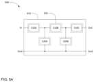
- FIG. 5 Ais a schematic circuit diagram and layout for a high frequency band-pass filter 500 using XBARs.
- the filter 500has a conventional ladder filter architecture including three series resonators 510 A, 510 B, 510 C and two shunt resonators 520 A, 520 B.
- the three series resonators 510 A, 510 B, and 510 Care connected in series between a first port and a second port.
- the first and second portsare labeled “In” and “Out”, respectively.
- the filter 500is bidirectional and either port and serve as the input or output of the filter.
- the two shunt resonators 520 A, 520 Bare connected from nodes between the series resonators to ground. All the shunt resonators and series resonators are XBARs on a single die.
- the three series resonators 510 A, B, C and the two shunt resonators 520 A, B of the filter 500are formed on a single plate 410 of piezoelectric material bonded to a silicon substrate (not visible).
- Each resonatorincludes a respective IDT (not shown), with at least the fingers of the IDT disposed over a cavity in the substrate.
- the term “respective”means “relating things each to each”, which is to say with a one-to-one correspondence.
- the cavitiesare illustrated schematically as the dashed rectangles (such as the rectangle 535 ).
- each IDTis disposed over a respective cavity.
- the IDTs of two or more resonatorsmay be disposed over a single cavity.
- the portions or areas of the piezoelectric material of plate 410 that extend a certain distance past the perimeter 545 of the cavities of filter 500 (or cavity perimeter 135 of FIG. 1 )may be removed.
- This removingmay include removing the piezoelectric material: a) that extends in the length direction past the perimeter of the cavity by between 2 and 25 percent more the length of the cavity; and b) that extends in the width direction past the perimeter of the cavity by between 2 and 25 percent more the width of the cavity.
- This removingmay include removing the excess piezoelectric material between conductors (other than the resonator IDTs) of an RF filter to avoid exciting acoustic modes that then couple to the substrate and increase insertion loss.
- This removingmay include removing the excess piezoelectric material from between pairs of conductors outside of the XBAR resonators of an RF filter, such as from between a signal conductor and a ground conductor, or from between two signal conductors.
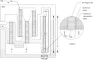
- FIG. 5 Bis a schematic plan view of a filter 550 incorporating five XBAR devices labeled “X1” to “X5”.
- the filter 550is exemplary and does not represent any particular application.
- the filter 550includes five XBAR devices X1-X5.
- Filter 550may be filter 500 of FIG. 5 A , where device X1 is series resonator 510 A, device X2 is shunt resonator 520 A, device X3 is series resonator 510 B, device X4 is shunt resonator 520 B, and device X5 is series resonator 510 C.
- the filter 550may be formed on a single die.
- a “die”may be a semiconductor chip or integrated circuit (IC) chip that is diced from other chips such as of a wafer. It may be a monolithic integrated circuit (also referred to as an IC, a chip, or a microchip) that has a set of electronic circuits on one small flat piece (or “chip”) of semiconductor material that is normally silicon.
- ICintegrated circuit
- FIG. 5 Bshows a ground (GND) conductor of the filter 550 which may be connected to or part of busbars on one side of the XBARs X2 and X4 as shown.
- the GND conductoris connected to a ground signal of the filter 550 .
- FIG. 5 Bshows an input (IN) signal conductor of the filter 550 which may be connected to or part of busbars on one side of the XBAR X1 as shown.
- the IN conductoris connected to an input signal for the filter 550 .
- FIG. 5 Bshows an output (OUT) signal conductor of the filter 550 which may be connected to or part of busbars on one side of the XBAR X5 as shown.
- the OUT conductoris connected to an output signal for the filter 550 .
- FIG. 5 B and detail Ashow the dashed lines outline of the cavity perimeters, such as perimeter 585 behind the IDT fingers. Perimeter 585 may represent a cavity perimeter such as perimeter 135 or 535 . FIG. 5 B and detail A also show the dot-dash lines perimeter of the piezoelectric material perimeters, such as perimeter 590 .
- Perimeter 590may represent a perimeter of the piezoelectric material that: a) extends in the piezoelectric material length direction LP past the perimeter of the cavity length LC by more than 5, 10 or 20 percent of the length of the cavity LC; and b) that extends in the piezoelectric material width direction WP past the perimeter of the perimeter of the cavity width WC by more than 5, 10 or 20 percent of a width of the cavity WC. This may be true for any one or more (up to all) of the five XBAR devices X1-X5.
- the piezoelectric materialmay be removed from the entire surface of the filter 550 except within the rectangles defined by the dot-dash lines, such as perimeter 590 and the similar perimeters of XBAR devices X1-X4.
- the outlines of the cavities and the piezoelectric layerare shown as rectangles for ease of presentation but may have other shapes.
- the perimeters of the cavities and piezoelectric layersmay be irregular polygons or generally rectangular with non-straight (e.g. curved, serrated, or wavy) sides.
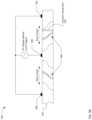
- FIG. 5 Cis a schematic cross-sectional 595 view at the plane B-B defined in Detail A of FIG. 5 B .
- FIG. 5 Cshows filter device X5 comprising substrate 520 having cavity 540 .
- the substratehas additional cavities where devices X1-X4 are formed and may be a single die.
- Bonding layer 522is formed on the substrate but is not over the cavity 540 .
- Piezoelectric plate 510is bonded to the bonding layer 522 and spans the cavity 540 . In some cases, layer 522 does not exist and the plate is directly attached to the substrate.
- An interdigital transducer (IDT) formed on a front surface of the piezoelectric plate 510has interleaved fingers 536 over the cavity 540 .
- the conductorsare shown as metal, they may be another proper conductive material.
- the substrateis shown as silicon, it may be another proper substrate material.
- the bonding layeris shown as silicon dioxide, it may be another proper bonding material.
- the Piezoelectric plate 510includes the diaphragm having piezoelectric material spanning the cavity and excess portions that extend a certain length past the perimeter of the cavity.
- the excess portionsmay extend a certain length and width distance (LP and WP) past the length and width perimeter of the cavity (LC and WC).
- the excess portionsmay be a perimeter of the piezoelectric material that extends in the length and width direction past the perimeter of the cavity by: a) more than 5, 10 or 20 percent; or b) between 2 and 25 percent.
- Fingers 536may span or be over cavity 540 . In some cases, part of the busbars of the IDT is also over the cavity. In other cases, all of the busbars are over the substrate 520 but not over the cavity. At least portions of the busbars are over the substrate (e.g., not over the cavity) to better conduct heat generated in the IDT to the substrate.
- the thicknesses of the piezoelectric layer 510 , bonding layer 522 , fingers 536 , and metal conductors 524 and 526are greatly exaggerated for ease of depiction.
- the left side of FIG. 5 Cillustrates the case where the piezoelectric layer 510 , but not the SiO 2 bonding layer 522 , is removed outside of the area of the resonator cavity 540 , such as removed from extending beyond width WP.
- the right side of FIG. 5 Cillustrates the case where both the piezoelectric layer 510 and the bonding layer 522 are removed outside of the area of the resonator cavity 540 , such as removed from extending beyond width WP.
- This rightside configurationprovides an improved thermal connection between the metal conductor 524 and the Si substrate 520 , but requires the metal conductor cover a larger height step 598 than on the left side.
- FIGS. 5 D, 5 E, 5 F, and 5 Gare schematic cross-sectional views at the plane C-C defined in FIG. 5 B . These views show a cross-section though a conductor 524 / 526 remote from a resonator, such as noted for FIGS. 4 A- 5 C .
- FIG. 5 D and FIG. 5 Eare consistent with the right and left sides of FIG. 5 C , respectively.
- FIG. 5 Fis an alternative configuration in which the excess piezoelectric material 510 is removed after the conductor patterns 524 and 526 are formed. In this case, the piezoelectric layer 510 and the SiO 2 bonding layer 522 remain beneath the conductor.
- FIG. 5 Gextends the configuration of 5 F by removing a portion of the Si substrate 520 between conductors 524 and 526 to reduce stray capacitance.
- FIGS. 5 B, 5 C, 5 D, and 5 Eillustrate a conceptually easy solution to the problems of FIGS. 4 A-B , which is to etch away the undesired portions of the piezoelectric plate 510 immediately after bonding the plate 510 to the substrate 520 or bonding layer 522 (e.g., at 625 A in FIG. 6 ).
- FIGS. 5 F and 5 Gillustrate an alternative process sequence where the undesired portions of the piezoelectric plate 510 are etched (e.g., at 625 B in FIG. 6 ) after the conductors 524 and 526 are formed.
- the benefit of the alternative processis that the conductors do not have to go over steps where the piezoelectric plate has been removed, such as shown at step 598 of FIG.
- the conductor thicknessis typically 500 nm and the piezoelectric plate thickness is typically 400 nm which may cause a conductor bonding problem at or near the step, such as gaps between the conductor and bonding layer or substrate. These step may also cause other fabrication problems.
- piezoelectric material between conductorssuch as in the 80 ⁇ m gap between conductors 424 and 426 as noted for FIGS. 4 A-B .
- Piezoelectric material under the conductorssuch as under conductors 424 and 426 as noted for FIGS. 4 A-B , or for FIGS. 5 D-G does not excite acoustic modes.
- FIG. 6is a simplified flow chart showing a process 600 for making an XBAR having excess piezoelectric material removed or a filter incorporating XBARs having excess piezoelectric material removed. This is the same as the process defined in pending application Ser. No. 16/438,121, which is incorporated herein by reference, with the added step of removing the excess piezoelectric material at 625 A before the conductor patterns are formed or at 625 B after the conductor patterns are formed.
- the process 600starts at 605 with a substrate and a plate of piezoelectric material and ends at 695 with a completed XBAR or filter having excess piezoelectric material removed, such as shown for FIGS. 5 A- 5 G .
- the piezoelectric platemay be mounted on a sacrificial substrate or may be a portion of wafer of piezoelectric material.
- the flow chart of FIG. 6includes only major process steps. Various conventional process steps (e.g. surface preparation, chemical mechanical processing (CMP), cleaning, inspection, deposition, photolithography, baking, annealing, monitoring, testing, etc.) may be performed before, between, after, and during the steps shown in FIG. 6 .
- CMPchemical mechanical processing
- the flow chart of FIG. 6captures three variations of the process 600 for making an XBAR which differ in when and how cavities are formed in the substrate.
- the cavitiesmay be formed at steps 610 A, 610 B, or 610 C. Only one of these steps is performed in each of the three variations of the process 600 .
- the flow chart of FIG. 6also captures two variations of the process 600 for making an XBAR which differ in when and how excess piezoelectric material is removed.
- the excess piezoelectric materialmay be removed at step 625 A or 625 B. Only one of these steps is performed in each of these two variations of the process 600 . In another variation, some of the excess piezoelectric material may be removed at step 625 A and more if it removed at step 625 B.
- the piezoelectric platemay be, for example, Z-cut, rotated Z-cut, or rotated Y-cut lithium niobate or lithium tantalate or a material noted for plate 110 .
- the piezoelectric platemay be some other material and/or some other cut.
- the substratemay be silicon.
- the substratemay be some other material that allows formation of deep cavities by etching or other processing.
- the silicon substratemay have layers of silicon TOX and polycrystalline silicon.
- one or more cavitiesare formed in the substrate at 610 A, before the piezoelectric plate is bonded to the substrate at 620 .
- a separate cavitymay be formed for each resonator in a filter device.
- the one or more cavitiesmay be formed using conventional photolithographic and etching techniques. These techniques may be isotropic or anisotropic; and may use deep reactive ion etching (DRIE).
- DRIEdeep reactive ion etching
- the cavities formed at 610 Awill not penetrate through the substrate, and the resulting resonator devices will have a cross-section as shown in FIG. 3 A .
- the piezoelectric plateis bonded to the substrate.
- the piezoelectric plate and the substratemay be bonded by a wafer bonding process.
- the mating surfaces of the substrate and the piezoelectric plateare highly polished.
- One or more layers of intermediate materials, such as an oxide or metal,may be formed or deposited on the mating surface of one or both of the piezoelectric plate and the substrate.
- One or both mating surfacesmay be activated using, for example, a plasma process. The mating surfaces may then be pressed together with considerable force to establish molecular bonds between the piezoelectric plate and the substrate or intermediate material layers.
- bonding layer 522may be used to bond the plate to the substrate.
- the piezoelectric plateis initially mounted on a sacrificial substrate. After the piezoelectric plate and the substrate are bonded, the sacrificial substrate, and any intervening layers, are removed to expose the surface of the piezoelectric plate (the surface that previously faced the sacrificial substrate).
- the sacrificial substratemay be removed, for example, by material-dependent wet or dry etching or some other process.
- a second variation of 620starts with a single-crystal piezoelectric wafer. Ions are implanted to a controlled depth beneath a surface of the piezoelectric wafer (not shown in FIG. 6 ). The portion of the wafer from the surface to the depth of the ion implantation is (or will become) the thin piezoelectric plate and the balance of the wafer is effectively the sacrificial substrate. After the implanted surface of the piezoelectric wafer and device substrate are bonded, the piezoelectric wafer may be split at the plane of the implanted ions (for example, using thermal shock), leaving a thin plate of piezoelectric material exposed and bonded to the substrate.
- the thickness of the thin plate piezoelectric materialis determined by the energy (and thus depth) of the implanted ions.
- the process of ion implantation and subsequent separation of a thin plateis commonly referred to as “ion slicing”.
- the exposed surface of the thin piezoelectric platemay be polished or planarized after the piezoelectric wafer is split.
- the portions of the piezoelectric material that extend a certain distance past the perimeter of the cavity of the XBAR resonatorare removed after the piezoelectric plate is bonded to the substrate at 620 and before the conductor pattern is formed at 630 .
- Thismay be removing piezoelectric material extending beyond LP and WP of the resonator.
- the portionsmay be removed by patterning and etching to remove the piezoelectric material that extends a certain distance past the perimeter of the cavity.
- Removing the portions of piezoelectric materialmay include removing bonding layer 522 that is below the excess portions of the piezoelectric layer that are removed. In other cases, it does not and those portions of layer 522 remain.
- bonding layer 522can be used as an etch stop for removing the excess portions piezoelectric material.
- Removing the portions of piezoelectric materialmay include removing the piezoelectric material: a) that extends in the length direction past the perimeter of the cavity by more than between 2 and 25 percent the length of the cavity; and b) that extends in the width direction past the perimeter of the cavity by more than between 2 and 25 percent the width of the cavity.
- This removingmay include removing the excess piezoelectric material between conductors (other than the resonator IDTs) of an RF filter to avoid exciting acoustic modes that then couple to the substrate and increase insertion loss.
- This removingmay include removing the excess piezoelectric material from between pairs of conductors outside of the XBAR resonators of an RF filter, such as from between a signal conductor and a ground conductor, or from between two signal conductors.
- Removing the portions of piezoelectric materialmay only be removing piezoelectric material between conductors, such as in the 80 ⁇ m gap between conductors 424 and 426 as noted for FIGS. 4 A-B .
- Piezoelectric material under the conductorssuch as under conductors 424 and 426 as noted for FIGS. 4 A-B , or for FIGS. 5 D-G is not removed.
- FIG. 7is a schematic cross-sectional view at the plane B-B defined in FIG. 5 B of an XBAR resonator 700 prior to removing excess piezoelectric material.
- This viewillustrates the case where the piezoelectric layer 710 has excess portions P 1 and P 2 to be removed from outside of the area of the resonator cavity 540 , such as removed from extending beyond width WP and length LP (not shown).
- the excess portions P 1 and P 2 of layer 710can be removed with or without removing the bonding layer 522 from those portions.
- the portions P 1 and P 2may be removed by patterning and etching layer 710 .
- Removing portions P 1 and P 2may include removing bonding layer 522 below portions P 1 and P 2 , such as noted at 625 A and 625 B; and/or may include removing the conductor pattern above portions P 1 and P 2 , such as noted at step 625 B.
- resonator 700may be further processed to become an XBAR having excess piezoelectric material removed as noted herein, such as for FIGS. 5 C- 5 G .
- Conductor patterns and dielectric layers defining one or more XBAR devicesare formed on the surface of the piezoelectric plate at 630 .
- a filter devicewill have two or more conductor layers that are sequentially deposited and patterned.
- the conductor layersmay include bonding pads, gold or solder bumps, or other means for making connection between the device and external circuitry.
- the conductor layersmay be, for example, aluminum, an aluminum alloy, copper, a copper alloy, molybdenum, tungsten, beryllium, gold, or some other conductive metal.
- one or more layers of other materialsmay be disposed below (i.e. between the conductor layer and the piezoelectric plate) and/or on top of the conductor layer.
- a thin film of titanium, chrome, or other metalmay be used to improve the adhesion between the conductor layers and the piezoelectric plate.
- the conductor layersmay include bonding pads, gold or solder bumps, or other means for making connection between the device and external circuitry.
- Conductor patternsmay be formed at 630 by depositing the conductor layers over the surface of the piezoelectric plate and removing excess metal by etching through patterned photoresist. Alternatively, the conductor patterns may be formed at 630 using a lift-off process. Photoresist may be deposited over the piezoelectric plate and patterned to define the conductor pattern. The conductor layer may be deposited in sequence over the surface of the piezoelectric plate. The photoresist may then be removed, which removes the excess material, leaving the conductor pattern. In some cases, forming at 630 occurs prior to bonding at 620 , such as where the IDTs are formed prior to bonding the plate to the substrate.
- the portions of the piezoelectric material that extend a certain distance past the perimeter of the cavity of the XBAR resonatorare removed after the conductor pattern is formed at 630 and before front side dielectric is optionally formed at 640 . This may be removing piezoelectric material as noted at step 625 A and/or FIG. 7 . The portions may be removed by patterning and etching to remove the piezoelectric material that extends a certain distance past the perimeter of the cavity.
- Removing this piezoelectric materialmay include removing conductor pattern that is above the excess portions of the piezoelectric layer that are removed. Removing the portions of piezoelectric material may include removing bonding layer 522 that is below the excess portions of the piezoelectric layer that are removed. In other cases, it does not and those portions of layer 522 remain.
- bonding layer 522can be used as an etch stop for removing the excess portions piezoelectric material.
- Removing the portions of piezoelectric materialmay include removing piezoelectric material beside the IDTs or where the IDTs are not formed. It may include removing piezoelectric material beside or where the conductor material and conductors are not formed.
- a front-side dielectric layer or layersmay be formed by depositing one or more layers of dielectric material on the front side of the piezoelectric plate, over one or more desired conductor patterns of IDT or XBAR devices.
- the one or more dielectric layersmay be deposited using a conventional deposition technique such as sputtering, evaporation, or chemical vapor deposition.
- the one or more dielectric layersmay be deposited over the entire surface of the piezoelectric plate, including on top of the conductor pattern.
- one or more lithography processes(using photomasks) may be used to limit the deposition of the dielectric layers to selected areas of the piezoelectric plate, such as only between the interleaved fingers of the IDTs.
- depositing at 640includes depositing a first thickness of at least one dielectric layer over the front-side surface of selected IDTs, but no dielectric or a second thickness less than the first thickness of at least one dielectric over the other IDTs.
- depositing at 640includes depositing a first thickness of at least one dielectric layer over the front-side surface of selected IDTs, but no dielectric or a second thickness less than the first thickness of at least one dielectric over the other IDTs.
- An alternativeis where these dielectric layers are only between the interleaved fingers of the IDTs.
- the one or more dielectric layersmay include, for example, a dielectric layer selectively formed over the IDTs of shunt resonators to shift the resonance frequency of the shunt resonators relative to the resonance frequency of series resonators as described in U.S. Pat. No. 10,491,192.
- the one or more dielectric layersmay include an encapsulation/passivation layer deposited over all or a substantial portion of the device.
- the different thickness of these dielectric layerscauses the selected XBARs to be tuned to different frequencies as compared to the other XBARs.
- the resonance frequencies of the XBARs in a filtermay be tuned using different front-side dielectric layer thickness on some XBARs.
- the presence of the dielectric layers of various thicknesseshas little or no effect on the piezoelectric coupling.
- one or more cavitiesare formed in the back side of the substrate at 610 B after all the conductor patterns and dielectric layers are formed at 630 .
- a separate cavitymay be formed for each resonator in a filter device.
- the one or more cavitiesmay be formed using an anisotropic or orientation-dependent dry or wet etch to open holes through the back-side of the substrate to the piezoelectric plate. In this case, the resulting resonator devices will have a cross-section as shown in FIG. 1 .
- one or more cavities in the form of recesses in the substrate top layer 322may be formed at 610 C by etching a sacrificial layer formed in the front side of the substrate using an etchant introduced through openings in the piezoelectric plate.
- a separate cavitymay be formed for each resonator in a filter device.
- the one or more cavitiesmay be formed using an isotropic or orientation-independent dry etch that passes through holes in the piezoelectric plate and etches the sacrificial layer formed in recesses in the front-side of the substrate.
- the one or more cavities formed at 610 Cwill not penetrate completely through the substrate top layer 322 , and the resulting resonator devices will have a cross-section as shown in FIG. 3 A .
- the filter or XBAR deviceis completed at 660 .
- Actions that may occur at 660include depositing an encapsulation/passivation layer such as SiO 2 or Si 3 O 4 over all or a portion of the device; forming bonding pads or solder bumps or other means for making connection between the device and external circuitry; excising individual devices from a wafer containing multiple devices; other packaging steps; and testing.
- Another action that may occur at 660is to tune the resonant frequencies of the resonators within a filter device by adding or removing metal or dielectric material from the front side of the device.
- FIGS. 1 - 3 B and 5 B- 5 Cmay show examples of the fingers of selected IDTs after completion at 660 .
- Forming the cavities at 610 Amay require the fewest total process steps but has the disadvantage that the XBAR diaphragms will be unsupported during all of the subsequent process steps. This may lead to damage to, or unacceptable distortion of, the diaphragms during subsequent processing.
- Forming the cavities using a back-side etch at 610 Brequires additional handling inherent in two-sided wafer processing. Forming the cavities from the back side also greatly complicates packaging the XBAR devices since both the front side and the back side of the device must be sealed by the package.
- Forming the cavities by etching from the front side at 610 Cdoes not require two-sided wafer processing and has the advantage that the XBAR diaphragms are supported during all of the preceding process steps.
- an etching process capable of forming the cavities through openings in the piezoelectric platewill necessarily be isotropic.
- such an etching process using a sacrificial materialallows for a controlled etching of the cavity, both laterally (i.e. parallel to the surface of the substrate) as well as normal to the surface of the substrate.
- “plurality”means two or more. As used herein, a “set” of items may include one or more of such items.
- the terms “comprising”, “including”, “carrying”, “having”, “containing”, “involving”, and the likeare to be understood to be open-ended, i.e., to mean including but not limited to. Only the transitional phrases “consisting of” and “consisting essentially of”, respectively, are closed or semi-closed transitional phrases with respect to claims.
Landscapes
- Physics & Mathematics (AREA)
- Acoustics & Sound (AREA)
- Chemical & Material Sciences (AREA)
- Crystallography & Structural Chemistry (AREA)
- Engineering & Computer Science (AREA)
- Manufacturing & Machinery (AREA)
- Piezo-Electric Or Mechanical Vibrators, Or Delay Or Filter Circuits (AREA)
Abstract
Description
Claims (14)
Priority Applications (1)
| Application Number | Priority Date | Filing Date | Title |
|---|---|---|---|
| US17/894,001US12015391B2 (en) | 2020-11-13 | 2022-08-23 | XBAR devices with excess piezoelectric material removed |
Applications Claiming Priority (3)
| Application Number | Priority Date | Filing Date | Title |
|---|---|---|---|
| US202063113301P | 2020-11-13 | 2020-11-13 | |
| US17/123,029US11496113B2 (en) | 2020-11-13 | 2020-12-15 | XBAR devices with excess piezoelectric material removed |
| US17/894,001US12015391B2 (en) | 2020-11-13 | 2022-08-23 | XBAR devices with excess piezoelectric material removed |
Related Parent Applications (1)
| Application Number | Title | Priority Date | Filing Date |
|---|---|---|---|
| US17/123,029ContinuationUS11496113B2 (en) | 2020-11-13 | 2020-12-15 | XBAR devices with excess piezoelectric material removed |
Publications (2)
| Publication Number | Publication Date |
|---|---|
| US20220407495A1 US20220407495A1 (en) | 2022-12-22 |
| US12015391B2true US12015391B2 (en) | 2024-06-18 |
Family
ID=81587997
Family Applications (2)
| Application Number | Title | Priority Date | Filing Date |
|---|---|---|---|
| US17/123,029Active2041-06-17US11496113B2 (en) | 2020-11-13 | 2020-12-15 | XBAR devices with excess piezoelectric material removed |
| US17/894,001ActiveUS12015391B2 (en) | 2020-11-13 | 2022-08-23 | XBAR devices with excess piezoelectric material removed |
Family Applications Before (1)
| Application Number | Title | Priority Date | Filing Date |
|---|---|---|---|
| US17/123,029Active2041-06-17US11496113B2 (en) | 2020-11-13 | 2020-12-15 | XBAR devices with excess piezoelectric material removed |
Country Status (1)
| Country | Link |
|---|---|
| US (2) | US11496113B2 (en) |
Families Citing this family (4)
| Publication number | Priority date | Publication date | Assignee | Title |
|---|---|---|---|---|
| KR20230003544A (en)* | 2020-05-18 | 2023-01-06 | 어쿠스티스, 인크. | Bulk Acoustic Wave Resonator Filters Containing High Impedance Shunt Branches and Methods of Forming The Same |
| US11496113B2 (en)* | 2020-11-13 | 2022-11-08 | Resonant Inc. | XBAR devices with excess piezoelectric material removed |
| US12028039B2 (en)* | 2020-11-13 | 2024-07-02 | Murata Manufacturing Co., Ltd. | Forming XBAR devices with excess piezoelectric material removed |
| US12362725B2 (en) | 2020-11-13 | 2025-07-15 | Murata Manufacturing Co., Ltd. | Transversely-excited film bulk acoustic filters with excess piezoelectric material removed |
Citations (196)
| Publication number | Priority date | Publication date | Assignee | Title |
|---|---|---|---|---|
| US5204575A (en) | 1990-10-15 | 1993-04-20 | Kokusai Electric Co., Ltd. | Surface acoustic wave resonator |
| US5274345A (en) | 1992-05-13 | 1993-12-28 | Andersen Laboratories | Dual function reflector structures for interdigital saw transducer |
| US5446330A (en) | 1993-03-15 | 1995-08-29 | Matsushita Electric Industrial Co., Ltd. | Surface acoustic wave device having a lamination structure |
| US5552655A (en) | 1994-05-04 | 1996-09-03 | Trw Inc. | Low frequency mechanical resonator |
| US5726610A (en) | 1995-06-19 | 1998-03-10 | Motorola Inc. | Saw filter device for radio tranceiver utilizing different coupling coefficient ratios |
| US5729186A (en) | 1995-04-12 | 1998-03-17 | Matsushita Electric Industrial Co., Ltd. | Resonator ladder surface acoustic wave filter suppressing spurious signals |
| US5853601A (en) | 1997-04-03 | 1998-12-29 | Northrop Grumman Corporation | Top-via etch technique for forming dielectric membranes |
| US6172582B1 (en) | 1996-02-20 | 2001-01-09 | Cts Corporation | Saw resonator and ladder filter with specified number of reflector electrode fingers |
| US6271617B1 (en) | 1997-08-28 | 2001-08-07 | Murata Manufacturing Co., Ltd. | Surface acoustic wave device with a tungsten-aluminum layered interdigital transducer |
| US6377140B1 (en) | 1999-07-09 | 2002-04-23 | Oki Electric Industry Co., Ltd. | Saw resonator filter with bridged-T configuration |
| US20020079986A1 (en) | 2000-12-21 | 2002-06-27 | Ruby Richard C. | Bulk acoustic resonator perimeter reflection system |
| US20020130736A1 (en) | 2001-03-19 | 2002-09-19 | Murata Manufacturing Co., Ltd | Edge-reflection surface acoustic wave filter |
| US20020153970A1 (en) | 2001-04-09 | 2002-10-24 | Kenichi Noto | Surface acoustic wave filter, surface acoustic wave device and communication device |
| US20020158714A1 (en) | 2001-04-27 | 2002-10-31 | Nokia Corporation | Method and system for wafer-level tuning of bulk acoustic wave resonators and filters by reducing thickness non-uniformity |
| US20020189062A1 (en) | 2001-06-15 | 2002-12-19 | Asia Pacific Microsystems, Inc. | Manufacturing method for a high quality film bulk acoustic wave device |
| US6516503B1 (en) | 1999-05-26 | 2003-02-11 | Murata Manufacturing Co., Ltd. | Method of making surface acoustic wave device |
| US20030042998A1 (en) | 2001-08-24 | 2003-03-06 | Edmonson Peter J. | Leaky surface acoustic wave resonators |
| US6540827B1 (en) | 1998-02-17 | 2003-04-01 | Trustees Of Columbia University In The City Of New York | Slicing of single-crystal films using ion implantation |
| US20030080831A1 (en) | 2001-10-25 | 2003-05-01 | Naumenko Natalya F. | Surface acoustic wave devices using optimized cuts of lithium niobate (LiNbO3) |
| US6570470B2 (en) | 2000-06-30 | 2003-05-27 | Kyocera Corporation | Surface acoustic wave ladder filter utilizing parallel resonators with different resonant frequencies |
| US20030199105A1 (en) | 2002-04-22 | 2003-10-23 | Kub Francis J. | Method for making piezoelectric resonator and surface acoustic wave device using hydrogen implant layer splitting |
| US20040041496A1 (en) | 2002-09-04 | 2004-03-04 | Fujitsu Media Devices Limited | Surface acoustic wave device, filter device and method of producing the surface acoustic wave device |
| US6707229B1 (en) | 1999-06-03 | 2004-03-16 | Tele Filter Zweigniederlassung Der Dover Germany Gmbh | Surface acoustic wave filter |
| US20040100164A1 (en) | 2002-11-26 | 2004-05-27 | Murata Manufacturing Co., Ltd. | Manufacturing method of electronic device |
| US20040130410A1 (en) | 2001-05-11 | 2004-07-08 | Kosuke Nishimura | Filter using film bulk acoustic resonator and transmission/reception switch |
| US20040140866A1 (en) | 2003-01-16 | 2004-07-22 | Murata Manufacturing Co., Ltd. | Ladder filter, branching filter, and communication apparatus |
| US20040233020A1 (en) | 2002-03-06 | 2004-11-25 | Hiroyuki Nakamura | Surface acoustic wave filter, balanced type circuit, and communication apparatus |
| US6833774B2 (en) | 2002-06-25 | 2004-12-21 | Sawtek, Inc. | Surface acoustic wave filter |
| US20040261250A1 (en) | 2000-09-06 | 2004-12-30 | Murata Manufacturing Co., Ltd. | Method for adjusting a frequency characteristic of an edge reflection type surface acoustic wave device and method for producing an- edge reflection type surface acoustic wave device |
| US20050077982A1 (en) | 2003-08-29 | 2005-04-14 | Tsukasa Funasaka | Surface acoustic wave element and electronic equipment provided with the element |
| US20050185026A1 (en) | 2004-01-26 | 2005-08-25 | Motohisa Noguchi | Piezoelectric element, piezoelectric actuator, ink jet recording head, ink jet printer, surface acoustic wave element, frequency filter, oscillator, electronic circuit, thin film piezoelectric resonator, and electronic apparatus |
| US20050218488A1 (en) | 2004-03-31 | 2005-10-06 | Mie Matsuo | Electronic component having micro-electrical mechanical system |
| US20050264136A1 (en) | 2004-05-31 | 2005-12-01 | Jun Tsutsumi | Surface acoustic wave device |
| US7009468B2 (en) | 2001-04-27 | 2006-03-07 | Murata Manufacturing Co., Ltd. | Surface acoustic wave device and electronic device using the same |
| US20060152107A1 (en) | 2005-01-07 | 2006-07-13 | Seiko Epson Corporation | Lamb-wave high-frequency resonator |
| US20060179642A1 (en) | 2005-02-03 | 2006-08-17 | Kabushiki Kaisha Toshiba | Method for manufacturing a film bulk acoustic resonator |
| US7105980B2 (en) | 2002-07-03 | 2006-09-12 | Sawtek, Inc. | Saw filter device and method employing normal temperature bonding for producing desirable filter production and performance characteristics |
| US20070030096A1 (en) | 2005-08-08 | 2007-02-08 | Fujitsu Media Devices Limited | Duplexer and ladder type filter |
| US20070182510A1 (en) | 2006-02-06 | 2007-08-09 | Samsung Electronics Co., Ltd. | Multi-band filter module and method of fabricating the same |
| US20070188047A1 (en) | 2006-02-16 | 2007-08-16 | Seiko Epson Corporation | Lamb wave type frequency device and method thereof |
| US20070194863A1 (en) | 2006-02-17 | 2007-08-23 | Kabushiki Kaisha Toshiba | Film bulk acoustic resonator and method of manufacturing same |
| US20070267942A1 (en) | 2006-05-19 | 2007-11-22 | Hisanori Matsumoto | Piezoelectric film resonator, radio-frequency filter using them, and radio-frequency module using them |
| US7345400B2 (en) | 2003-01-27 | 2008-03-18 | Murata Manufacturing Co., Ltd. | Surface acoustic wave device |
| US20080246559A1 (en) | 2007-01-19 | 2008-10-09 | Farrokh Ayazi | Lithographically-defined multi-standard multi-frequency high-Q tunable micromechanical resonators |
| US7463118B2 (en) | 2006-06-09 | 2008-12-09 | Texas Instruments Incorporated | Piezoelectric resonator with an efficient all-dielectric Bragg reflector |
| US7535152B2 (en) | 2005-10-19 | 2009-05-19 | Murata Manufacturing Co., Ltd. | Lamb wave device |
| US20100019866A1 (en) | 2008-07-23 | 2010-01-28 | Fujitsu Limited | Acoustic wave device, method of manufacturing acoustic wave device and transmission apparatus |
| US7684109B2 (en) | 2007-02-28 | 2010-03-23 | Maxim Integrated Products, Inc. | Bragg mirror optimized for shear waves |
| US20100117483A1 (en) | 2007-07-30 | 2010-05-13 | Murata Manufacturing Co., Ltd. | Elastic wave device and method of producing the same |
| US20100123367A1 (en) | 2008-11-19 | 2010-05-20 | Ngk Insulators, Ltd. | Lamb wave device |
| US7868519B2 (en) | 2007-09-06 | 2011-01-11 | Murata Manufacturing Co., Ltd. | Piezoelectric resonator including an acoustic reflector portion |
| US20110018389A1 (en) | 2008-01-30 | 2011-01-27 | Kyocera Corporation | Acoustic Wave Device and Method for Production of Same |
| US20110018654A1 (en) | 2009-07-27 | 2011-01-27 | Avago Technologies Wireless Ip (Singapore) Pte. Ltd. | Resonator filter with multiple cross-couplings |
| US7941103B2 (en) | 2005-11-15 | 2011-05-10 | Taiyo Yuden Co., Ltd. | Duplexer |
| US20110109196A1 (en) | 2008-07-11 | 2011-05-12 | Goto Rei | Plate wave element and electronic equipment using same |
| US20110254406A1 (en) | 2009-01-07 | 2011-10-20 | Murata Manufacturing Co., Ltd. | Boundary acoustic wave device |
| US20110278993A1 (en) | 2010-05-17 | 2011-11-17 | Murata Manufacturing Co., Ltd. | Method for manufacturing composite piezoelectric substrate and piezoelectric device |
| US20120073390A1 (en) | 2010-09-29 | 2012-03-29 | The George Washington University | Synchronous One-Pole Surface Acoustic Wave Resonator |
| US20120198672A1 (en) | 2011-02-04 | 2012-08-09 | Taiyo Yuden Co., Ltd. | Method for manufacturing acoustic wave device |
| US8278802B1 (en) | 2008-04-24 | 2012-10-02 | Rf Micro Devices, Inc. | Planarized sacrificial layer for MEMS fabrication |
| US8294330B1 (en) | 2009-03-31 | 2012-10-23 | Triquint Semiconductor, Inc. | High coupling, low loss saw filter and associated method |
| US20120286900A1 (en) | 2010-01-28 | 2012-11-15 | Murata Manufacturing Co., Ltd. | Tunable filter |
| US20120326809A1 (en) | 2010-03-12 | 2012-12-27 | Murata Manufacturing Co., Ltd. | Elastic wave resonator and ladder filter |
| US8344815B2 (en) | 2008-10-24 | 2013-01-01 | Seiko Epson Corporation | Surface acoustic wave resonator, surface acoustic wave oscillator, and surface acoustic wave module unit |
| US20130127551A1 (en) | 2010-08-05 | 2013-05-23 | Adaptalog Limited | Crystal reference oscillator for navigation applications |
| US20130234805A1 (en) | 2012-03-07 | 2013-09-12 | Taiyo Yuden Co., Ltd. | Resonator, frequency filter, duplexer, electronic device, and method of manufacturing resonator |
| US20130271238A1 (en) | 2012-04-13 | 2013-10-17 | Taiyo Yuden Co., Ltd. | Filter device, manufacturing method for filter device, and duplexer |
| US20130278609A1 (en) | 2012-04-19 | 2013-10-24 | Qualcomm Mems Technologies, Inc. | Isotropically-etched cavities for evanescent-mode electromagnetic-wave cavity resonators |
| US20130321100A1 (en) | 2012-06-05 | 2013-12-05 | Avago Technologies Wireless Ip (Singapore) Pte. Ltd. | Laterally-coupled acoustic resonators |
| US20140009032A1 (en) | 2012-07-04 | 2014-01-09 | Taiyo Yuden Co., Ltd. | Lamb wave device and manufacturing method thereof |
| US20140130319A1 (en) | 2010-09-28 | 2014-05-15 | Murata Manufacturing Co., Ltd. | Method for manufacturing piezoelectric device |
| US20140145556A1 (en) | 2011-08-08 | 2014-05-29 | Murata Manufacturing Co., Ltd. | Elastic wave device |
| US20140151151A1 (en) | 2010-10-15 | 2014-06-05 | Commissariat A L'energie Atomique Et Aux Energies Alternatives | Heterogenous acoustic structure formed from a homogeneous material |
| US20140152145A1 (en) | 2010-11-30 | 2014-06-05 | Murata Manufacturing Co., Ltd. | Elastic wave device and manufacturing method for same |
| US20140173862A1 (en) | 2007-12-25 | 2014-06-26 | Murata Manufacturing Co., Ltd. | Method for manufacturing composite piezoelectric substrate |
| US20140225684A1 (en) | 2011-10-24 | 2014-08-14 | Murata Manufacturing Co., Ltd. | Surface acoustic wave device |
| US8816567B2 (en) | 2011-07-19 | 2014-08-26 | Qualcomm Mems Technologies, Inc. | Piezoelectric laterally vibrating resonator structure geometries for spurious frequency suppression |
| US8829766B2 (en) | 2008-08-01 | 2014-09-09 | Epcos Ag | Piezoelectric resonator operating in thickness shear mode |
| US8932686B2 (en) | 2008-10-31 | 2015-01-13 | Murata Manufacturing Co., Ltd. | Method for producing piezoelectric composite substrate |
| US20150014795A1 (en) | 2013-07-10 | 2015-01-15 | Avago Technologies General Ip (Singapore) Pte. Ltd. | Surface passivation of substrate by mechanically damaging surface layer |
| US20150042417A1 (en) | 2013-08-06 | 2015-02-12 | Murata Manufacturing Co., Ltd. | High-frequency module |
| US20150165479A1 (en) | 2013-12-12 | 2015-06-18 | Qualcomm Incorporated | Piezoelectric ultrasonic transducer and process |
| US9130145B2 (en) | 2012-03-29 | 2015-09-08 | Vectron International Gmbh | Surface acoustic wave component |
| US9148121B2 (en) | 2012-08-17 | 2015-09-29 | Taiyo Yuden Co., Ltd. | Acoustic wave filter, duplexer, and module |
| US20150319537A1 (en) | 2012-12-12 | 2015-11-05 | Epcos Ag | Electroacoustic Components and Methods Thereof |
| US20150333730A1 (en) | 2010-04-23 | 2015-11-19 | Teknologian Tutkimuskeskus Vtt Oy | Wide-band acoustically coupled thin-film BAW filter |
| US20150365067A1 (en) | 2013-03-21 | 2015-12-17 | Ngk Insulators, Ltd. | Composite Substrates for Acoustic Wave Elements, and Acoustic Wave Elements |
| US9219466B2 (en) | 2011-11-11 | 2015-12-22 | Teknologian Tutkimuskeskus Vtt Oy | Laterally coupled bulk acoustic wave filter with improved passband characteristics |
| US20160028367A1 (en) | 2014-07-25 | 2016-01-28 | Akoustis, Inc. | Single crystal acoustic resonator and bulk acoustic wave filter |
| WO2016017104A1 (en) | 2014-07-31 | 2016-02-04 | Skyworks Panasonic Filter Solutions Japan Co., Ltd. | Acoustic wave filters and duplexers using same |
| US9276557B1 (en) | 2013-07-01 | 2016-03-01 | Sandia Corporation | Programmable electroacoustic filter apparatus and method for its manufacture |
| US20160087187A1 (en) | 2014-05-29 | 2016-03-24 | Avago Technologies General Ip (Singapore) Pte. Ltd. | Capacitive coupled resonator and filter device with comb electrodes and support pillars separating piezoelectric layer |
| US9369105B1 (en) | 2007-08-31 | 2016-06-14 | Rf Micro Devices, Inc. | Method for manufacturing a vibrating MEMS circuit |
| US20160182009A1 (en) | 2014-12-17 | 2016-06-23 | Rf Micro Devices, Inc. | Plate wave devices with wave confinement structures and fabrication methods |
| US9425765B2 (en) | 2013-04-22 | 2016-08-23 | Northeastern University | Nano- and micro-electromechanical resonators |
| US9525398B1 (en) | 2014-05-27 | 2016-12-20 | Sandia Corporation | Single crystal micromechanical resonator and fabrication methods thereof |
| US20170063332A1 (en) | 2015-08-25 | 2017-03-02 | Avago Technologies General Ip (Singapore) Pte. Ltd. | Surface acoustic wave (saw) resonator having trap-rich region |
| US9640750B2 (en) | 2011-03-25 | 2017-05-02 | Skyworks Filter Solutions Japan Co., Ltd. | Acoustic wave device with suppressed higher order transverse modes |
| US20170155373A1 (en) | 2015-11-30 | 2017-06-01 | Avago Technologies General Ip (Singapore) Pte. Ltd. | Surface acoustic wave (saw) resonator structure with dielectric material below electrode fingers |
| US20170179928A1 (en) | 2015-11-13 | 2017-06-22 | Resonant Inc. | Acoustic wave filter with enhanced rejection |
| US20170179225A1 (en) | 2011-05-25 | 2017-06-22 | Semiconductor Components Industries, Llc | Semiconductor device having a super junction structure and method of manufacturing the same |
| US20170214387A1 (en) | 2016-01-26 | 2017-07-27 | Avago Technologies General Ip (Singapore) Pte. Ltd. | Bulk acoustic wave resonator with piezoelectric layer comprising lithium niobate or lithium tantalate |
| US20170214381A1 (en) | 2016-01-22 | 2017-07-27 | Rf Micro Devices, Inc. | Guided wave devices with selectively thinned piezoelectric layers |
| US20170222622A1 (en) | 2016-01-28 | 2017-08-03 | Triquint Semiconductor, Inc. | Surface acoustic wave device having a piezoelectric layer on a quartz substrate and methods of manufacturing thereof |
| US20170222617A1 (en) | 2014-10-16 | 2017-08-03 | Murata Manufacturing Co., Ltd. | High-frequency module |
| US9762202B2 (en) | 2008-12-17 | 2017-09-12 | Analog Devices, Inc. | Method of manufacturing a mechanical resonating structure |
| US9780759B2 (en) | 2010-12-24 | 2017-10-03 | Murata Manufacturing Co., Ltd. | Elastic wave device and method for manufacturing the same |
| US9837984B2 (en) | 2014-12-24 | 2017-12-05 | Qorvo Us, Inc. | RF ladder filter with simplified acoustic RF resonator parallel capacitance compensation |
| US20170370791A1 (en) | 2016-06-28 | 2017-12-28 | Taiyo Yuden Co., Ltd. | Method of fabricating acoustic wave device and acoustic wave device |
| WO2018003273A1 (en) | 2016-06-28 | 2018-01-04 | 株式会社村田製作所 | Multiplexer, high-frequency front end circuit, and communication device |
| US20180005950A1 (en) | 2016-06-29 | 2018-01-04 | Murata Manufacturing Co., Ltd. | Electronic component device, method of mounting electronic component device on circuit board, and mounting structure of electronic component device on circuit board |
| US20180026603A1 (en) | 2015-05-22 | 2018-01-25 | Murata Manufacturing Co., Ltd. | Electronic component |
| US20180033952A1 (en) | 2016-07-28 | 2018-02-01 | Taiyo Yuden Co., Ltd. | Electronic device and method of fabricating the same |
| US20180041191A1 (en) | 2016-08-08 | 2018-02-08 | Samsung Electro-Mechanics Co., Ltd. | Saw filter device and method of manufacturing the same |
| US20180062615A1 (en) | 2015-05-08 | 2018-03-01 | Murata Manufacturing Co., Ltd. | High frequency module |
| US20180062617A1 (en) | 2016-08-25 | 2018-03-01 | Qualcomm Incorporated | Single-chip multi-frequency film bulk acoustic-wave resonators |
| US20180123016A1 (en) | 2012-06-15 | 2018-05-03 | Carnegie Mellon University | Microelectronic structures with suspended lithium-based thin films |
| US20180191322A1 (en) | 2017-01-03 | 2018-07-05 | Win Semiconductors Corp. | Method for fabricating bulk acoustic wave resonator with mass adjustment structure |
| US20180262179A1 (en) | 2017-01-24 | 2018-09-13 | Skyworks Solutions, Inc. | Acoustic wave device with acoustically separated multi-channel feedback |
| US10079414B2 (en) | 2015-03-17 | 2018-09-18 | The United States Of America, As Represented By The Secretary Of The Navy | Switched multiplexer with flat group delay and channelized limiting |
| US20180278227A1 (en) | 2017-03-24 | 2018-09-27 | Dror Hurwitz | Method for fabricating rf resonators and filters |
| US20180309426A1 (en) | 2015-10-20 | 2018-10-25 | Soitec | Surface acoustic wave device and associated production method |
| US10187039B2 (en) | 2016-06-07 | 2019-01-22 | Skyworks Filter Solutions Japan Co., Ltd. | Filter devices having reduced spurious emissions from lamb waves |
| US10200013B2 (en) | 2016-02-18 | 2019-02-05 | X-Celeprint Limited | Micro-transfer-printed acoustic wave filter device |
| US20190044498A1 (en) | 2016-04-25 | 2019-02-07 | Murata Manufacturing Co., Ltd. | Elastic wave device and method for manufacturing the same |
| US20190068164A1 (en) | 2016-03-11 | 2019-02-28 | Akoustis, Inc. | 5G BAND n79 ACOUSTIC WAVE RESONATOR RF FILTER CIRCUIT |
| US20190131953A1 (en) | 2017-10-31 | 2019-05-02 | The Board Of Trustees Of The University Of Illinois | Interdigital transducers on a piezoelectric thin-film for signal compression |
| US10284176B1 (en) | 2015-06-03 | 2019-05-07 | Qorvo Us, Inc. | Temperature compensated surface acoustic wave device and methods of manufacturing the same |
| US20190181832A1 (en) | 2017-12-07 | 2019-06-13 | Infineon Technologies Ag | System and method for a radio frequency filter |
| US20190190487A1 (en) | 2016-08-30 | 2019-06-20 | Murata Manufacturing Co., Ltd. | Elastic wave device and method for manufacturing the same |
| US20190245509A1 (en) | 2018-02-05 | 2019-08-08 | Zhuhai Crystal Resonance Technologies Co., Ltd. | Method for fabricating single crystal piezoelectric rf resonators and filters with improved cavity definition |
| US20190253038A1 (en) | 2016-03-11 | 2019-08-15 | Akoustis, Inc. | 5G n79 WI-FI ACOUSTIC TRIPLEXER CIRCUIT |
| US20190273480A1 (en) | 2018-03-02 | 2019-09-05 | Skyworks Solutions, Inc. | Lamb wave loop circuit for acoustic wave filter |
| US10476469B2 (en) | 2016-02-17 | 2019-11-12 | Board of Trustees of the Univsity of Illinois | Spurious-mode-free, laterally-vibrating microelectromechanical system resonators |
| US20190348966A1 (en) | 2018-05-10 | 2019-11-14 | Globalfoundries Singapore Pte. Ltd. | Acoustic wave filter formed on a v-groove topography and method for producing the same |
| US10491192B1 (en) | 2018-06-15 | 2019-11-26 | Resonant Inc. | Transversely-excited film bulk acoustic resonator |
| US20190379351A1 (en) | 2017-03-13 | 2019-12-12 | Murata Manufacturing Co., Ltd. | Notch filter |
| US20190386636A1 (en) | 2018-06-15 | 2019-12-19 | Resonant Inc. | Transversely-excited film bulk acoustic resonator |
| US20200007110A1 (en) | 2017-03-15 | 2020-01-02 | Murata Manufacturing Co., Ltd. | Acoustic wave element, acoustic wave filter device, and multiplexer |
| US20200021272A1 (en) | 2018-07-10 | 2020-01-16 | Texas Instruments Incorporated | Laterally Vibrating Bulk Acoustic Wave Resonator |
| US20200028481A1 (en) | 2018-07-18 | 2020-01-23 | Skyworks Solutions, Inc. | Hybrid acoustic lc filter with harmonic suppression |
| US20200036357A1 (en) | 2017-04-26 | 2020-01-30 | Murata Manufacturing Co., Ltd. | Acoustic wave device |
| US20200083861A1 (en) | 2018-09-12 | 2020-03-12 | Skyworks Global Pte. Ltd. | Recess frame structure for a bulk acoustic wave resonator |
| US10601392B2 (en) | 2018-06-15 | 2020-03-24 | Resonant Inc. | Solidly-mounted transversely-excited film bulk acoustic resonator |
| US10637438B2 (en) | 2018-06-15 | 2020-04-28 | Resonant Inc. | Transversely-excited film bulk acoustic resonators for high power applications |
| US20200177160A1 (en) | 2018-11-30 | 2020-06-04 | Resonant Inc. | Bandpass filter with improved upper band edge sharpness |
| US20200235719A1 (en) | 2018-06-15 | 2020-07-23 | Resonant Inc. | Xbar resonators with non-rectangular diaphragms |
| US20200259480A1 (en) | 2019-02-08 | 2020-08-13 | Vtt Technical Research Centre Of Finland Ltd | Low loss acoustic device |
| US20200274520A1 (en) | 2019-02-27 | 2020-08-27 | Skyworks Global Pte. Ltd. | Bulk acoustic wave resonator structure |
| US10790802B2 (en) | 2018-06-15 | 2020-09-29 | Resonant Inc. | Transversely excited film bulk acoustic resonator using rotated Y-X cut lithium niobate |
| US20200313645A1 (en) | 2019-03-25 | 2020-10-01 | Skyworks Solutions, Inc. | Acoustic wave filters with isolation |
| US10797675B2 (en) | 2018-06-15 | 2020-10-06 | Resonant Inc. | Transversely excited film bulk acoustic resonator using rotated z-cut lithium niobate |
| US10812048B2 (en) | 2016-09-02 | 2020-10-20 | Murata Manufacturing Co., Ltd. | Acoustic wave filter device, radio-frequency front-end circuit, and communication apparatus |
| US10819309B1 (en) | 2019-04-05 | 2020-10-27 | Resonant Inc. | Transversely-excited film bulk acoustic resonator package and method |
| US10826462B2 (en) | 2018-06-15 | 2020-11-03 | Resonant Inc. | Transversely-excited film bulk acoustic resonators with molybdenum conductors |
| US20200350891A1 (en) | 2018-06-15 | 2020-11-05 | Resonant Inc. | Transversely-excited film bulk acoustic resonator with etch-stop layer |
| US10868513B2 (en) | 2018-06-15 | 2020-12-15 | Resonant Inc. | Transversely-excited film bulk acoustic filters with symmetric layout |
| US10868510B2 (en) | 2018-06-15 | 2020-12-15 | Resonant Inc. | Transversely-excited film bulk acoustic resonator with half-lambda dielectric layer |
| US20210013859A1 (en) | 2018-06-15 | 2021-01-14 | Resonant Inc. | Transversely-excited film bulk acoustic resonator with etched conductor patterns |
| US10911021B2 (en) | 2019-06-27 | 2021-02-02 | Resonant Inc. | Transversely-excited film bulk acoustic resonator with lateral etch stop |
| US10917072B2 (en) | 2019-06-24 | 2021-02-09 | Resonant Inc. | Split ladder acoustic wave filters |
| US10985728B2 (en) | 2018-06-15 | 2021-04-20 | Resonant Inc. | Transversely-excited film bulk acoustic resonator and filter with a uniform-thickness dielectric overlayer |
| US20210119595A1 (en) | 2019-06-27 | 2021-04-22 | Resonant Inc. | Xbar frontside etch process using polysilicon sacrificial layer |
| US10992282B1 (en) | 2020-06-18 | 2021-04-27 | Resonant Inc. | Transversely-excited film bulk acoustic resonators with electrodes having a second layer of variable width |
| US10992284B2 (en) | 2018-06-15 | 2021-04-27 | Resonant Inc. | Filter using transversely-excited film bulk acoustic resonators with multiple frequency setting layers |
| US10992283B2 (en) | 2018-06-15 | 2021-04-27 | Resonant Inc. | High power transversely-excited film bulk acoustic resonators on rotated Z-cut lithium niobate |
| US10998877B2 (en) | 2018-06-15 | 2021-05-04 | Resonant Inc. | Film bulk acoustic resonator fabrication method with frequency trimming based on electric measurements prior to cavity etch |
| US11003971B2 (en) | 2017-11-07 | 2021-05-11 | Resonant Inc. | Ultra-wide-band saw sensor with hyperbolically frequency-modulated etched reflector |
| US20210152154A1 (en) | 2019-11-19 | 2021-05-20 | Skyworks Solutions, Inc. | Surface acoustic wave device |
| US20210265978A1 (en) | 2018-06-15 | 2021-08-26 | Resonant Inc. | Filters using transversly-excited film bulk acoustic resonators with frequency-setting dielectric layers |
| US11146238B2 (en) | 2018-06-15 | 2021-10-12 | Resonant Inc. | Film bulk acoustic resonator fabrication method |
| US11143561B2 (en) | 2018-12-05 | 2021-10-12 | Resonant Inc. | Passive microphone/pressure sensor using a piezoelectric diaphragm |
| US11146232B2 (en) | 2018-06-15 | 2021-10-12 | Resonant Inc. | Transversely-excited film bulk acoustic resonator with reduced spurious modes |
| US20210328574A1 (en) | 2020-04-20 | 2021-10-21 | Resonant Inc. | Small transversely-excited film bulk acoustic resonators with enhanced q-factor |
| US11171629B2 (en) | 2018-06-15 | 2021-11-09 | Resonant Inc. | Transversely-excited film bulk acoustic resonator using pre-formed cavities |
| US20210351762A1 (en) | 2020-05-06 | 2021-11-11 | Resonant Inc. | Transversely-excited film bulk acoustic resonators with interdigital transducer configured to reduce diaphragm stress |
| US11201601B2 (en) | 2018-06-15 | 2021-12-14 | Resonant Inc. | Transversely-excited film bulk acoustic resonator with multiple diaphragm thicknesses and fabrication method |
| US11206009B2 (en) | 2019-08-28 | 2021-12-21 | Resonant Inc. | Transversely-excited film bulk acoustic resonator with interdigital transducer with varied mark and pitch |
| US20210399750A1 (en) | 2020-06-23 | 2021-12-23 | Qorvo Us, Inc. | Multiplexing circuits with baw resonators as network elements for higher performance |
| US11228296B2 (en) | 2018-06-15 | 2022-01-18 | Resonant Inc. | Transversely-excited film bulk acoustic resonator with a cavity having a curved perimeter |
| US11239822B2 (en) | 2018-06-15 | 2022-02-01 | Resonant Inc. | Transversely-excited film bulk acoustic resonator using YX-cut lithium niobate for high power applications |
| US11239816B1 (en) | 2021-01-15 | 2022-02-01 | Resonant Inc. | Decoupled transversely-excited film bulk acoustic resonators |
| US11264969B1 (en) | 2020-08-06 | 2022-03-01 | Resonant Inc. | Transversely-excited film bulk acoustic resonator comprising small cells |
| US11264966B2 (en) | 2018-06-15 | 2022-03-01 | Resonant Inc. | Solidly-mounted transversely-excited film bulk acoustic resonator with diamond layers in Bragg reflector stack |
| US11271540B1 (en) | 2020-08-19 | 2022-03-08 | Resonant Inc. | Transversely-excited film bulk acoustic resonator with tether-supported diaphragm |
| US11283424B2 (en) | 2020-05-04 | 2022-03-22 | Resonant Inc. | Transversely-excited film bulk acoustic resonator with etched conductor patterns |
| US11309865B1 (en) | 2020-10-05 | 2022-04-19 | Resonant Inc. | Acoustic matrix diplexers and radios using acoustic matrix diplexers |
| US11323095B2 (en) | 2018-06-15 | 2022-05-03 | Resonant Inc. | Rotation in XY plane to suppress spurious modes in XBAR devices |
| US11323091B2 (en) | 2018-06-15 | 2022-05-03 | Resonant Inc. | Transversely-excited film bulk acoustic resonator with diaphragm support pedestals |
| US11323089B2 (en) | 2018-06-15 | 2022-05-03 | Resonant Inc. | Filter using piezoelectric film bonded to high resistivity silicon substrate with trap-rich layer |
| US11323096B2 (en) | 2018-06-15 | 2022-05-03 | Resonant Inc. | Transversely-excited film bulk acoustic resonator with periodic etched holes |
| US11349450B2 (en) | 2018-06-15 | 2022-05-31 | Resonant Inc. | Symmetric transversely-excited film bulk acoustic resonators with reduced spurious modes |
| US11349452B2 (en) | 2018-06-15 | 2022-05-31 | Resonant Inc. | Transversely-excited film bulk acoustic filters with symmetric layout |
| US11356077B2 (en) | 2020-07-18 | 2022-06-07 | Resonant Inc. | Acoustic resonators and filters with reduced temperature coefficient of frequency |
| US11374549B2 (en) | 2018-06-15 | 2022-06-28 | Resonant Inc. | Filter using transversely-excited film bulk acoustic resonators with divided frequency-setting dielectric layers |
| US11496113B2 (en)* | 2020-11-13 | 2022-11-08 | Resonant Inc. | XBAR devices with excess piezoelectric material removed |
- 2020
- 2020-12-15USUS17/123,029patent/US11496113B2/enactiveActive
- 2022
- 2022-08-23USUS17/894,001patent/US12015391B2/enactiveActive
Patent Citations (225)
| Publication number | Priority date | Publication date | Assignee | Title |
|---|---|---|---|---|
| US5204575A (en) | 1990-10-15 | 1993-04-20 | Kokusai Electric Co., Ltd. | Surface acoustic wave resonator |
| US5274345A (en) | 1992-05-13 | 1993-12-28 | Andersen Laboratories | Dual function reflector structures for interdigital saw transducer |
| US5446330A (en) | 1993-03-15 | 1995-08-29 | Matsushita Electric Industrial Co., Ltd. | Surface acoustic wave device having a lamination structure |
| US5552655A (en) | 1994-05-04 | 1996-09-03 | Trw Inc. | Low frequency mechanical resonator |
| US5729186A (en) | 1995-04-12 | 1998-03-17 | Matsushita Electric Industrial Co., Ltd. | Resonator ladder surface acoustic wave filter suppressing spurious signals |
| US5726610A (en) | 1995-06-19 | 1998-03-10 | Motorola Inc. | Saw filter device for radio tranceiver utilizing different coupling coefficient ratios |
| US6172582B1 (en) | 1996-02-20 | 2001-01-09 | Cts Corporation | Saw resonator and ladder filter with specified number of reflector electrode fingers |
| US5853601A (en) | 1997-04-03 | 1998-12-29 | Northrop Grumman Corporation | Top-via etch technique for forming dielectric membranes |
| US6271617B1 (en) | 1997-08-28 | 2001-08-07 | Murata Manufacturing Co., Ltd. | Surface acoustic wave device with a tungsten-aluminum layered interdigital transducer |
| US6540827B1 (en) | 1998-02-17 | 2003-04-01 | Trustees Of Columbia University In The City Of New York | Slicing of single-crystal films using ion implantation |
| US6710514B2 (en) | 1999-05-26 | 2004-03-23 | Murata Manufacturing Co., Ltd. | Surface acoustic wave device |
| US6516503B1 (en) | 1999-05-26 | 2003-02-11 | Murata Manufacturing Co., Ltd. | Method of making surface acoustic wave device |
| US6707229B1 (en) | 1999-06-03 | 2004-03-16 | Tele Filter Zweigniederlassung Der Dover Germany Gmbh | Surface acoustic wave filter |
| US6377140B1 (en) | 1999-07-09 | 2002-04-23 | Oki Electric Industry Co., Ltd. | Saw resonator filter with bridged-T configuration |
| US6570470B2 (en) | 2000-06-30 | 2003-05-27 | Kyocera Corporation | Surface acoustic wave ladder filter utilizing parallel resonators with different resonant frequencies |
| US20040261250A1 (en) | 2000-09-06 | 2004-12-30 | Murata Manufacturing Co., Ltd. | Method for adjusting a frequency characteristic of an edge reflection type surface acoustic wave device and method for producing an- edge reflection type surface acoustic wave device |
| US20020079986A1 (en) | 2000-12-21 | 2002-06-27 | Ruby Richard C. | Bulk acoustic resonator perimeter reflection system |
| US20020130736A1 (en) | 2001-03-19 | 2002-09-19 | Murata Manufacturing Co., Ltd | Edge-reflection surface acoustic wave filter |
| US20020153970A1 (en) | 2001-04-09 | 2002-10-24 | Kenichi Noto | Surface acoustic wave filter, surface acoustic wave device and communication device |
| US7009468B2 (en) | 2001-04-27 | 2006-03-07 | Murata Manufacturing Co., Ltd. | Surface acoustic wave device and electronic device using the same |
| US20020158714A1 (en) | 2001-04-27 | 2002-10-31 | Nokia Corporation | Method and system for wafer-level tuning of bulk acoustic wave resonators and filters by reducing thickness non-uniformity |
| US20040130410A1 (en) | 2001-05-11 | 2004-07-08 | Kosuke Nishimura | Filter using film bulk acoustic resonator and transmission/reception switch |
| US20020189062A1 (en) | 2001-06-15 | 2002-12-19 | Asia Pacific Microsystems, Inc. | Manufacturing method for a high quality film bulk acoustic wave device |
| US20030042998A1 (en) | 2001-08-24 | 2003-03-06 | Edmonson Peter J. | Leaky surface acoustic wave resonators |
| US20030080831A1 (en) | 2001-10-25 | 2003-05-01 | Naumenko Natalya F. | Surface acoustic wave devices using optimized cuts of lithium niobate (LiNbO3) |
| US20040233020A1 (en) | 2002-03-06 | 2004-11-25 | Hiroyuki Nakamura | Surface acoustic wave filter, balanced type circuit, and communication apparatus |
| US20030199105A1 (en) | 2002-04-22 | 2003-10-23 | Kub Francis J. | Method for making piezoelectric resonator and surface acoustic wave device using hydrogen implant layer splitting |
| US6833774B2 (en) | 2002-06-25 | 2004-12-21 | Sawtek, Inc. | Surface acoustic wave filter |
| US7105980B2 (en) | 2002-07-03 | 2006-09-12 | Sawtek, Inc. | Saw filter device and method employing normal temperature bonding for producing desirable filter production and performance characteristics |
| US20040041496A1 (en) | 2002-09-04 | 2004-03-04 | Fujitsu Media Devices Limited | Surface acoustic wave device, filter device and method of producing the surface acoustic wave device |
| US20040100164A1 (en) | 2002-11-26 | 2004-05-27 | Murata Manufacturing Co., Ltd. | Manufacturing method of electronic device |
| US20040140866A1 (en) | 2003-01-16 | 2004-07-22 | Murata Manufacturing Co., Ltd. | Ladder filter, branching filter, and communication apparatus |
| US7345400B2 (en) | 2003-01-27 | 2008-03-18 | Murata Manufacturing Co., Ltd. | Surface acoustic wave device |
| US20050077982A1 (en) | 2003-08-29 | 2005-04-14 | Tsukasa Funasaka | Surface acoustic wave element and electronic equipment provided with the element |
| US20050185026A1 (en) | 2004-01-26 | 2005-08-25 | Motohisa Noguchi | Piezoelectric element, piezoelectric actuator, ink jet recording head, ink jet printer, surface acoustic wave element, frequency filter, oscillator, electronic circuit, thin film piezoelectric resonator, and electronic apparatus |
| US20050218488A1 (en) | 2004-03-31 | 2005-10-06 | Mie Matsuo | Electronic component having micro-electrical mechanical system |
| US20050264136A1 (en) | 2004-05-31 | 2005-12-01 | Jun Tsutsumi | Surface acoustic wave device |
| US20060152107A1 (en) | 2005-01-07 | 2006-07-13 | Seiko Epson Corporation | Lamb-wave high-frequency resonator |
| US20060179642A1 (en) | 2005-02-03 | 2006-08-17 | Kabushiki Kaisha Toshiba | Method for manufacturing a film bulk acoustic resonator |
| US20070030096A1 (en) | 2005-08-08 | 2007-02-08 | Fujitsu Media Devices Limited | Duplexer and ladder type filter |
| US7535152B2 (en) | 2005-10-19 | 2009-05-19 | Murata Manufacturing Co., Ltd. | Lamb wave device |
| US7941103B2 (en) | 2005-11-15 | 2011-05-10 | Taiyo Yuden Co., Ltd. | Duplexer |
| US20070182510A1 (en) | 2006-02-06 | 2007-08-09 | Samsung Electronics Co., Ltd. | Multi-band filter module and method of fabricating the same |
| US7728483B2 (en) | 2006-02-16 | 2010-06-01 | Seiko Epson Corporation | Lamb wave type frequency device and method thereof |
| US20070188047A1 (en) | 2006-02-16 | 2007-08-16 | Seiko Epson Corporation | Lamb wave type frequency device and method thereof |
| US20100064492A1 (en) | 2006-02-16 | 2010-03-18 | Seiko Epson Corporation | Lamb wave type frequency device and method thereof |
| US20070194863A1 (en) | 2006-02-17 | 2007-08-23 | Kabushiki Kaisha Toshiba | Film bulk acoustic resonator and method of manufacturing same |
| US20070267942A1 (en) | 2006-05-19 | 2007-11-22 | Hisanori Matsumoto | Piezoelectric film resonator, radio-frequency filter using them, and radio-frequency module using them |
| US7463118B2 (en) | 2006-06-09 | 2008-12-09 | Texas Instruments Incorporated | Piezoelectric resonator with an efficient all-dielectric Bragg reflector |
| US20080246559A1 (en) | 2007-01-19 | 2008-10-09 | Farrokh Ayazi | Lithographically-defined multi-standard multi-frequency high-Q tunable micromechanical resonators |
| US7684109B2 (en) | 2007-02-28 | 2010-03-23 | Maxim Integrated Products, Inc. | Bragg mirror optimized for shear waves |
| US20100117483A1 (en) | 2007-07-30 | 2010-05-13 | Murata Manufacturing Co., Ltd. | Elastic wave device and method of producing the same |
| US9369105B1 (en) | 2007-08-31 | 2016-06-14 | Rf Micro Devices, Inc. | Method for manufacturing a vibrating MEMS circuit |
| US7868519B2 (en) | 2007-09-06 | 2011-01-11 | Murata Manufacturing Co., Ltd. | Piezoelectric resonator including an acoustic reflector portion |
| US20140173862A1 (en) | 2007-12-25 | 2014-06-26 | Murata Manufacturing Co., Ltd. | Method for manufacturing composite piezoelectric substrate |
| US20110018389A1 (en) | 2008-01-30 | 2011-01-27 | Kyocera Corporation | Acoustic Wave Device and Method for Production of Same |
| US8278802B1 (en) | 2008-04-24 | 2012-10-02 | Rf Micro Devices, Inc. | Planarized sacrificial layer for MEMS fabrication |
| US20110109196A1 (en) | 2008-07-11 | 2011-05-12 | Goto Rei | Plate wave element and electronic equipment using same |
| US20100019866A1 (en) | 2008-07-23 | 2010-01-28 | Fujitsu Limited | Acoustic wave device, method of manufacturing acoustic wave device and transmission apparatus |
| US8829766B2 (en) | 2008-08-01 | 2014-09-09 | Epcos Ag | Piezoelectric resonator operating in thickness shear mode |
| US8344815B2 (en) | 2008-10-24 | 2013-01-01 | Seiko Epson Corporation | Surface acoustic wave resonator, surface acoustic wave oscillator, and surface acoustic wave module unit |
| US8932686B2 (en) | 2008-10-31 | 2015-01-13 | Murata Manufacturing Co., Ltd. | Method for producing piezoelectric composite substrate |
| US7965015B2 (en) | 2008-11-19 | 2011-06-21 | Ngk Insulators, Ltd. | Lamb wave device |
| US20100123367A1 (en) | 2008-11-19 | 2010-05-20 | Ngk Insulators, Ltd. | Lamb wave device |
| US9762202B2 (en) | 2008-12-17 | 2017-09-12 | Analog Devices, Inc. | Method of manufacturing a mechanical resonating structure |
| US20110254406A1 (en) | 2009-01-07 | 2011-10-20 | Murata Manufacturing Co., Ltd. | Boundary acoustic wave device |
| US8294330B1 (en) | 2009-03-31 | 2012-10-23 | Triquint Semiconductor, Inc. | High coupling, low loss saw filter and associated method |
| US20110018654A1 (en) | 2009-07-27 | 2011-01-27 | Avago Technologies Wireless Ip (Singapore) Pte. Ltd. | Resonator filter with multiple cross-couplings |
| US20120286900A1 (en) | 2010-01-28 | 2012-11-15 | Murata Manufacturing Co., Ltd. | Tunable filter |
| US20120326809A1 (en) | 2010-03-12 | 2012-12-27 | Murata Manufacturing Co., Ltd. | Elastic wave resonator and ladder filter |
| US20150333730A1 (en) | 2010-04-23 | 2015-11-19 | Teknologian Tutkimuskeskus Vtt Oy | Wide-band acoustically coupled thin-film BAW filter |
| US20110278993A1 (en) | 2010-05-17 | 2011-11-17 | Murata Manufacturing Co., Ltd. | Method for manufacturing composite piezoelectric substrate and piezoelectric device |
| US20130127551A1 (en) | 2010-08-05 | 2013-05-23 | Adaptalog Limited | Crystal reference oscillator for navigation applications |
| US20140130319A1 (en) | 2010-09-28 | 2014-05-15 | Murata Manufacturing Co., Ltd. | Method for manufacturing piezoelectric device |
| US20120073390A1 (en) | 2010-09-29 | 2012-03-29 | The George Washington University | Synchronous One-Pole Surface Acoustic Wave Resonator |
| US20140151151A1 (en) | 2010-10-15 | 2014-06-05 | Commissariat A L'energie Atomique Et Aux Energies Alternatives | Heterogenous acoustic structure formed from a homogeneous material |
| US9748923B2 (en) | 2010-11-30 | 2017-08-29 | Murata Manufacturing Co., Ltd. | Elastic wave device and manufacturing method for same |
| US20140152145A1 (en) | 2010-11-30 | 2014-06-05 | Murata Manufacturing Co., Ltd. | Elastic wave device and manufacturing method for same |
| US9780759B2 (en) | 2010-12-24 | 2017-10-03 | Murata Manufacturing Co., Ltd. | Elastic wave device and method for manufacturing the same |
| US20120198672A1 (en) | 2011-02-04 | 2012-08-09 | Taiyo Yuden Co., Ltd. | Method for manufacturing acoustic wave device |
| US9640750B2 (en) | 2011-03-25 | 2017-05-02 | Skyworks Filter Solutions Japan Co., Ltd. | Acoustic wave device with suppressed higher order transverse modes |
| US20170179225A1 (en) | 2011-05-25 | 2017-06-22 | Semiconductor Components Industries, Llc | Semiconductor device having a super junction structure and method of manufacturing the same |
| US8816567B2 (en) | 2011-07-19 | 2014-08-26 | Qualcomm Mems Technologies, Inc. | Piezoelectric laterally vibrating resonator structure geometries for spurious frequency suppression |
| US20140145556A1 (en) | 2011-08-08 | 2014-05-29 | Murata Manufacturing Co., Ltd. | Elastic wave device |
| US20140225684A1 (en) | 2011-10-24 | 2014-08-14 | Murata Manufacturing Co., Ltd. | Surface acoustic wave device |
| US9219466B2 (en) | 2011-11-11 | 2015-12-22 | Teknologian Tutkimuskeskus Vtt Oy | Laterally coupled bulk acoustic wave filter with improved passband characteristics |
| US20130234805A1 (en) | 2012-03-07 | 2013-09-12 | Taiyo Yuden Co., Ltd. | Resonator, frequency filter, duplexer, electronic device, and method of manufacturing resonator |
| US9112134B2 (en) | 2012-03-07 | 2015-08-18 | Taiyo Yuden Co., Ltd. | Resonator, frequency filter, duplexer, electronic device, and method of manufacturing resonator |
| US9130145B2 (en) | 2012-03-29 | 2015-09-08 | Vectron International Gmbh | Surface acoustic wave component |
| US20130271238A1 (en) | 2012-04-13 | 2013-10-17 | Taiyo Yuden Co., Ltd. | Filter device, manufacturing method for filter device, and duplexer |
| US20130278609A1 (en) | 2012-04-19 | 2013-10-24 | Qualcomm Mems Technologies, Inc. | Isotropically-etched cavities for evanescent-mode electromagnetic-wave cavity resonators |
| US9093979B2 (en) | 2012-06-05 | 2015-07-28 | Avago Technologies General Ip (Singapore) Pte. Ltd. | Laterally-coupled acoustic resonators |
| US20130321100A1 (en) | 2012-06-05 | 2013-12-05 | Avago Technologies Wireless Ip (Singapore) Pte. Ltd. | Laterally-coupled acoustic resonators |
| US20180123016A1 (en) | 2012-06-15 | 2018-05-03 | Carnegie Mellon University | Microelectronic structures with suspended lithium-based thin films |
| US20140009032A1 (en) | 2012-07-04 | 2014-01-09 | Taiyo Yuden Co., Ltd. | Lamb wave device and manufacturing method thereof |
| US9148121B2 (en) | 2012-08-17 | 2015-09-29 | Taiyo Yuden Co., Ltd. | Acoustic wave filter, duplexer, and module |
| US20150319537A1 (en) | 2012-12-12 | 2015-11-05 | Epcos Ag | Electroacoustic Components and Methods Thereof |
| US20150365067A1 (en) | 2013-03-21 | 2015-12-17 | Ngk Insulators, Ltd. | Composite Substrates for Acoustic Wave Elements, and Acoustic Wave Elements |
| US9425765B2 (en) | 2013-04-22 | 2016-08-23 | Northeastern University | Nano- and micro-electromechanical resonators |
| US9276557B1 (en) | 2013-07-01 | 2016-03-01 | Sandia Corporation | Programmable electroacoustic filter apparatus and method for its manufacture |
| US20150014795A1 (en) | 2013-07-10 | 2015-01-15 | Avago Technologies General Ip (Singapore) Pte. Ltd. | Surface passivation of substrate by mechanically damaging surface layer |
| US20150042417A1 (en) | 2013-08-06 | 2015-02-12 | Murata Manufacturing Co., Ltd. | High-frequency module |
| US20150165479A1 (en) | 2013-12-12 | 2015-06-18 | Qualcomm Incorporated | Piezoelectric ultrasonic transducer and process |
| US9525398B1 (en) | 2014-05-27 | 2016-12-20 | Sandia Corporation | Single crystal micromechanical resonator and fabrication methods thereof |
| US20160087187A1 (en) | 2014-05-29 | 2016-03-24 | Avago Technologies General Ip (Singapore) Pte. Ltd. | Capacitive coupled resonator and filter device with comb electrodes and support pillars separating piezoelectric layer |
| US20160028367A1 (en) | 2014-07-25 | 2016-01-28 | Akoustis, Inc. | Single crystal acoustic resonator and bulk acoustic wave filter |
| WO2016017104A1 (en) | 2014-07-31 | 2016-02-04 | Skyworks Panasonic Filter Solutions Japan Co., Ltd. | Acoustic wave filters and duplexers using same |
| US20170222617A1 (en) | 2014-10-16 | 2017-08-03 | Murata Manufacturing Co., Ltd. | High-frequency module |
| US20160182009A1 (en) | 2014-12-17 | 2016-06-23 | Rf Micro Devices, Inc. | Plate wave devices with wave confinement structures and fabrication methods |
| US9837984B2 (en) | 2014-12-24 | 2017-12-05 | Qorvo Us, Inc. | RF ladder filter with simplified acoustic RF resonator parallel capacitance compensation |
| US10079414B2 (en) | 2015-03-17 | 2018-09-18 | The United States Of America, As Represented By The Secretary Of The Navy | Switched multiplexer with flat group delay and channelized limiting |
| US20180062615A1 (en) | 2015-05-08 | 2018-03-01 | Murata Manufacturing Co., Ltd. | High frequency module |
| US20180026603A1 (en) | 2015-05-22 | 2018-01-25 | Murata Manufacturing Co., Ltd. | Electronic component |
| US10284176B1 (en) | 2015-06-03 | 2019-05-07 | Qorvo Us, Inc. | Temperature compensated surface acoustic wave device and methods of manufacturing the same |
| US20170063332A1 (en) | 2015-08-25 | 2017-03-02 | Avago Technologies General Ip (Singapore) Pte. Ltd. | Surface acoustic wave (saw) resonator having trap-rich region |
| US20180309426A1 (en) | 2015-10-20 | 2018-10-25 | Soitec | Surface acoustic wave device and associated production method |
| US20170179928A1 (en) | 2015-11-13 | 2017-06-22 | Resonant Inc. | Acoustic wave filter with enhanced rejection |
| US20170155373A1 (en) | 2015-11-30 | 2017-06-01 | Avago Technologies General Ip (Singapore) Pte. Ltd. | Surface acoustic wave (saw) resonator structure with dielectric material below electrode fingers |
| US20170214381A1 (en) | 2016-01-22 | 2017-07-27 | Rf Micro Devices, Inc. | Guided wave devices with selectively thinned piezoelectric layers |
| US10211806B2 (en) | 2016-01-22 | 2019-02-19 | Qorvo Us, Inc. | Guided wave devices with embedded electrodes and non-embedded electrodes |
| US20170214387A1 (en) | 2016-01-26 | 2017-07-27 | Avago Technologies General Ip (Singapore) Pte. Ltd. | Bulk acoustic wave resonator with piezoelectric layer comprising lithium niobate or lithium tantalate |
| US20170222622A1 (en) | 2016-01-28 | 2017-08-03 | Triquint Semiconductor, Inc. | Surface acoustic wave device having a piezoelectric layer on a quartz substrate and methods of manufacturing thereof |
| US10476469B2 (en) | 2016-02-17 | 2019-11-12 | Board of Trustees of the Univsity of Illinois | Spurious-mode-free, laterally-vibrating microelectromechanical system resonators |
| US10200013B2 (en) | 2016-02-18 | 2019-02-05 | X-Celeprint Limited | Micro-transfer-printed acoustic wave filter device |
| US20190253038A1 (en) | 2016-03-11 | 2019-08-15 | Akoustis, Inc. | 5G n79 WI-FI ACOUSTIC TRIPLEXER CIRCUIT |
| US20190068164A1 (en) | 2016-03-11 | 2019-02-28 | Akoustis, Inc. | 5G BAND n79 ACOUSTIC WAVE RESONATOR RF FILTER CIRCUIT |
| US20190044498A1 (en) | 2016-04-25 | 2019-02-07 | Murata Manufacturing Co., Ltd. | Elastic wave device and method for manufacturing the same |
| US10187039B2 (en) | 2016-06-07 | 2019-01-22 | Skyworks Filter Solutions Japan Co., Ltd. | Filter devices having reduced spurious emissions from lamb waves |
| US10644674B2 (en) | 2016-06-28 | 2020-05-05 | Murata Manufacturing Co., Ltd. | Multiplexer, radio-frequency front-end circuit, and communication device |
| US20190123721A1 (en) | 2016-06-28 | 2019-04-25 | Murata Manufacturing Co., Ltd. | Multiplexer, radio-frequency front-end circuit, and communication device |
| WO2018003273A1 (en) | 2016-06-28 | 2018-01-04 | 株式会社村田製作所 | Multiplexer, high-frequency front end circuit, and communication device |
| US20170370791A1 (en) | 2016-06-28 | 2017-12-28 | Taiyo Yuden Co., Ltd. | Method of fabricating acoustic wave device and acoustic wave device |
| US20180005950A1 (en) | 2016-06-29 | 2018-01-04 | Murata Manufacturing Co., Ltd. | Electronic component device, method of mounting electronic component device on circuit board, and mounting structure of electronic component device on circuit board |
| US20180033952A1 (en) | 2016-07-28 | 2018-02-01 | Taiyo Yuden Co., Ltd. | Electronic device and method of fabricating the same |
| US20180041191A1 (en) | 2016-08-08 | 2018-02-08 | Samsung Electro-Mechanics Co., Ltd. | Saw filter device and method of manufacturing the same |
| US20180062617A1 (en) | 2016-08-25 | 2018-03-01 | Qualcomm Incorporated | Single-chip multi-frequency film bulk acoustic-wave resonators |
| US20190190487A1 (en) | 2016-08-30 | 2019-06-20 | Murata Manufacturing Co., Ltd. | Elastic wave device and method for manufacturing the same |
| US10812048B2 (en) | 2016-09-02 | 2020-10-20 | Murata Manufacturing Co., Ltd. | Acoustic wave filter device, radio-frequency front-end circuit, and communication apparatus |
| US20180191322A1 (en) | 2017-01-03 | 2018-07-05 | Win Semiconductors Corp. | Method for fabricating bulk acoustic wave resonator with mass adjustment structure |
| US20180262179A1 (en) | 2017-01-24 | 2018-09-13 | Skyworks Solutions, Inc. | Acoustic wave device with acoustically separated multi-channel feedback |
| US20190379351A1 (en) | 2017-03-13 | 2019-12-12 | Murata Manufacturing Co., Ltd. | Notch filter |
| US20200007110A1 (en) | 2017-03-15 | 2020-01-02 | Murata Manufacturing Co., Ltd. | Acoustic wave element, acoustic wave filter device, and multiplexer |
| US20180278227A1 (en) | 2017-03-24 | 2018-09-27 | Dror Hurwitz | Method for fabricating rf resonators and filters |
| US20200036357A1 (en) | 2017-04-26 | 2020-01-30 | Murata Manufacturing Co., Ltd. | Acoustic wave device |
| US20190131953A1 (en) | 2017-10-31 | 2019-05-02 | The Board Of Trustees Of The University Of Illinois | Interdigital transducers on a piezoelectric thin-film for signal compression |
| US11003971B2 (en) | 2017-11-07 | 2021-05-11 | Resonant Inc. | Ultra-wide-band saw sensor with hyperbolically frequency-modulated etched reflector |
| US20190181832A1 (en) | 2017-12-07 | 2019-06-13 | Infineon Technologies Ag | System and method for a radio frequency filter |
| US20190245509A1 (en) | 2018-02-05 | 2019-08-08 | Zhuhai Crystal Resonance Technologies Co., Ltd. | Method for fabricating single crystal piezoelectric rf resonators and filters with improved cavity definition |
| US20190273480A1 (en) | 2018-03-02 | 2019-09-05 | Skyworks Solutions, Inc. | Lamb wave loop circuit for acoustic wave filter |
| US20190348966A1 (en) | 2018-05-10 | 2019-11-14 | Globalfoundries Singapore Pte. Ltd. | Acoustic wave filter formed on a v-groove topography and method for producing the same |
| US11114998B2 (en) | 2018-06-15 | 2021-09-07 | Resonant Inc. | Transversely-excited film bulk acoustic resonators for high power applications |
| US20210265978A1 (en) | 2018-06-15 | 2021-08-26 | Resonant Inc. | Filters using transversly-excited film bulk acoustic resonators with frequency-setting dielectric layers |
| US11374549B2 (en) | 2018-06-15 | 2022-06-28 | Resonant Inc. | Filter using transversely-excited film bulk acoustic resonators with divided frequency-setting dielectric layers |
| US10601392B2 (en) | 2018-06-15 | 2020-03-24 | Resonant Inc. | Solidly-mounted transversely-excited film bulk acoustic resonator |
| US10637438B2 (en) | 2018-06-15 | 2020-04-28 | Resonant Inc. | Transversely-excited film bulk acoustic resonators for high power applications |
| US11349452B2 (en) | 2018-06-15 | 2022-05-31 | Resonant Inc. | Transversely-excited film bulk acoustic filters with symmetric layout |
| US11349450B2 (en) | 2018-06-15 | 2022-05-31 | Resonant Inc. | Symmetric transversely-excited film bulk acoustic resonators with reduced spurious modes |
| US20200235719A1 (en) | 2018-06-15 | 2020-07-23 | Resonant Inc. | Xbar resonators with non-rectangular diaphragms |
| US11323096B2 (en) | 2018-06-15 | 2022-05-03 | Resonant Inc. | Transversely-excited film bulk acoustic resonator with periodic etched holes |
| US10756697B2 (en) | 2018-06-15 | 2020-08-25 | Resonant Inc. | Transversely-excited film bulk acoustic resonator |
| US11323089B2 (en) | 2018-06-15 | 2022-05-03 | Resonant Inc. | Filter using piezoelectric film bonded to high resistivity silicon substrate with trap-rich layer |
| US10790802B2 (en) | 2018-06-15 | 2020-09-29 | Resonant Inc. | Transversely excited film bulk acoustic resonator using rotated Y-X cut lithium niobate |
| US11323090B2 (en) | 2018-06-15 | 2022-05-03 | Resonant Inc. | Transversely-excited film bulk acoustic resonator using Y-X-cut lithium niobate for high power applications |
| US10797675B2 (en) | 2018-06-15 | 2020-10-06 | Resonant Inc. | Transversely excited film bulk acoustic resonator using rotated z-cut lithium niobate |
| US20190386635A1 (en) | 2018-06-15 | 2019-12-19 | Resonant Inc. | Transversely-excited film bulk acoustic resonator |
| US11323091B2 (en) | 2018-06-15 | 2022-05-03 | Resonant Inc. | Transversely-excited film bulk acoustic resonator with diaphragm support pedestals |
| US10826462B2 (en) | 2018-06-15 | 2020-11-03 | Resonant Inc. | Transversely-excited film bulk acoustic resonators with molybdenum conductors |
| US20200350891A1 (en) | 2018-06-15 | 2020-11-05 | Resonant Inc. | Transversely-excited film bulk acoustic resonator with etch-stop layer |
| US10868512B2 (en) | 2018-06-15 | 2020-12-15 | Resonant Inc. | High power transversely-excited film bulk acoustic resonators on Z-cut lithium niobate |
| US10868513B2 (en) | 2018-06-15 | 2020-12-15 | Resonant Inc. | Transversely-excited film bulk acoustic filters with symmetric layout |
| US10868510B2 (en) | 2018-06-15 | 2020-12-15 | Resonant Inc. | Transversely-excited film bulk acoustic resonator with half-lambda dielectric layer |
| US20210013859A1 (en) | 2018-06-15 | 2021-01-14 | Resonant Inc. | Transversely-excited film bulk acoustic resonator with etched conductor patterns |
| US10911023B2 (en) | 2018-06-15 | 2021-02-02 | Resonant Inc. | Transversely-excited film bulk acoustic resonator with etch-stop layer |
| US11323095B2 (en) | 2018-06-15 | 2022-05-03 | Resonant Inc. | Rotation in XY plane to suppress spurious modes in XBAR devices |
| US10911017B2 (en) | 2018-06-15 | 2021-02-02 | Resonant Inc. | Solidly mounted transversely excited film bulk acoustic resonator using rotated Z-cut lithium niobate |
| US10917070B2 (en) | 2018-06-15 | 2021-02-09 | Resonant Inc. | Bandpass filter with frequency separation between shunt and series resonators set by dielectric layer thickness |
| US11264966B2 (en) | 2018-06-15 | 2022-03-01 | Resonant Inc. | Solidly-mounted transversely-excited film bulk acoustic resonator with diamond layers in Bragg reflector stack |
| US10985726B2 (en) | 2018-06-15 | 2021-04-20 | Resonant Inc. | Transversely excited film bulk acoustic resonator with recessed interdigital transducer fingers |
| US10985728B2 (en) | 2018-06-15 | 2021-04-20 | Resonant Inc. | Transversely-excited film bulk acoustic resonator and filter with a uniform-thickness dielectric overlayer |
| US10985730B2 (en) | 2018-06-15 | 2021-04-20 | Resonant Inc. | Filter devices having high power transversely-excited film bulk acoustic resonators |
| US11239822B2 (en) | 2018-06-15 | 2022-02-01 | Resonant Inc. | Transversely-excited film bulk acoustic resonator using YX-cut lithium niobate for high power applications |
| US11228296B2 (en) | 2018-06-15 | 2022-01-18 | Resonant Inc. | Transversely-excited film bulk acoustic resonator with a cavity having a curved perimeter |
| US10992284B2 (en) | 2018-06-15 | 2021-04-27 | Resonant Inc. | Filter using transversely-excited film bulk acoustic resonators with multiple frequency setting layers |
| US10992283B2 (en) | 2018-06-15 | 2021-04-27 | Resonant Inc. | High power transversely-excited film bulk acoustic resonators on rotated Z-cut lithium niobate |
| US10998882B2 (en) | 2018-06-15 | 2021-05-04 | Resonant Inc. | XBAR resonators with non-rectangular diaphragms |
| US10998877B2 (en) | 2018-06-15 | 2021-05-04 | Resonant Inc. | Film bulk acoustic resonator fabrication method with frequency trimming based on electric measurements prior to cavity etch |
| US20190386636A1 (en) | 2018-06-15 | 2019-12-19 | Resonant Inc. | Transversely-excited film bulk acoustic resonator |
| US11201601B2 (en) | 2018-06-15 | 2021-12-14 | Resonant Inc. | Transversely-excited film bulk acoustic resonator with multiple diaphragm thicknesses and fabrication method |
| US11171629B2 (en) | 2018-06-15 | 2021-11-09 | Resonant Inc. | Transversely-excited film bulk acoustic resonator using pre-formed cavities |
| US10491192B1 (en) | 2018-06-15 | 2019-11-26 | Resonant Inc. | Transversely-excited film bulk acoustic resonator |
| US11114996B2 (en) | 2018-06-15 | 2021-09-07 | Resonant Inc. | Transversely-excited film bulk acoustic resonators with molybdenum conductors |
| US11139794B2 (en) | 2018-06-15 | 2021-10-05 | Resonant Inc. | Transversely-excited film bulk acoustic resonator |
| US11146238B2 (en) | 2018-06-15 | 2021-10-12 | Resonant Inc. | Film bulk acoustic resonator fabrication method |
| US11165407B2 (en) | 2018-06-15 | 2021-11-02 | Resonant Inc. | Solidly-mounted transversely-excited film bulk acoustic resonator |
| US11146231B2 (en) | 2018-06-15 | 2021-10-12 | Resonant Inc. | Solidly-mounted transversely-excited film bulk acoustic resonator with recessed interdigital transducer fingers |
| US11146232B2 (en) | 2018-06-15 | 2021-10-12 | Resonant Inc. | Transversely-excited film bulk acoustic resonator with reduced spurious modes |
| US11146244B2 (en) | 2018-06-15 | 2021-10-12 | Resonant Inc. | Solidly-mounted transversely excited film bulk acoustic resonator using rotated Y-X cut lithium niobate |
| US20200021272A1 (en) | 2018-07-10 | 2020-01-16 | Texas Instruments Incorporated | Laterally Vibrating Bulk Acoustic Wave Resonator |
| US20200028481A1 (en) | 2018-07-18 | 2020-01-23 | Skyworks Solutions, Inc. | Hybrid acoustic lc filter with harmonic suppression |
| US20200083861A1 (en) | 2018-09-12 | 2020-03-12 | Skyworks Global Pte. Ltd. | Recess frame structure for a bulk acoustic wave resonator |
| US20200177160A1 (en) | 2018-11-30 | 2020-06-04 | Resonant Inc. | Bandpass filter with improved upper band edge sharpness |
| US11143561B2 (en) | 2018-12-05 | 2021-10-12 | Resonant Inc. | Passive microphone/pressure sensor using a piezoelectric diaphragm |
| US20200259480A1 (en) | 2019-02-08 | 2020-08-13 | Vtt Technical Research Centre Of Finland Ltd | Low loss acoustic device |
| US20200274520A1 (en) | 2019-02-27 | 2020-08-27 | Skyworks Global Pte. Ltd. | Bulk acoustic wave resonator structure |
| US20200313645A1 (en) | 2019-03-25 | 2020-10-01 | Skyworks Solutions, Inc. | Acoustic wave filters with isolation |
| US10819309B1 (en) | 2019-04-05 | 2020-10-27 | Resonant Inc. | Transversely-excited film bulk acoustic resonator package and method |
| US10917072B2 (en) | 2019-06-24 | 2021-02-09 | Resonant Inc. | Split ladder acoustic wave filters |
| US11381221B2 (en) | 2019-06-24 | 2022-07-05 | Resonant Inc. | Transversely-excited bulk acoustic resonator split ladder filter |
| US20210119595A1 (en) | 2019-06-27 | 2021-04-22 | Resonant Inc. | Xbar frontside etch process using polysilicon sacrificial layer |
| US10911021B2 (en) | 2019-06-27 | 2021-02-02 | Resonant Inc. | Transversely-excited film bulk acoustic resonator with lateral etch stop |
| US11206009B2 (en) | 2019-08-28 | 2021-12-21 | Resonant Inc. | Transversely-excited film bulk acoustic resonator with interdigital transducer with varied mark and pitch |
| US20210152154A1 (en) | 2019-11-19 | 2021-05-20 | Skyworks Solutions, Inc. | Surface acoustic wave device |
| US11368139B2 (en) | 2020-04-20 | 2022-06-21 | Resonant Inc. | Small transversely-excited film bulk acoustic resonators with enhanced Q-factor |
| US20210328574A1 (en) | 2020-04-20 | 2021-10-21 | Resonant Inc. | Small transversely-excited film bulk acoustic resonators with enhanced q-factor |
| US11283424B2 (en) | 2020-05-04 | 2022-03-22 | Resonant Inc. | Transversely-excited film bulk acoustic resonator with etched conductor patterns |
| US20210351762A1 (en) | 2020-05-06 | 2021-11-11 | Resonant Inc. | Transversely-excited film bulk acoustic resonators with interdigital transducer configured to reduce diaphragm stress |
| US10992282B1 (en) | 2020-06-18 | 2021-04-27 | Resonant Inc. | Transversely-excited film bulk acoustic resonators with electrodes having a second layer of variable width |
| US20210399750A1 (en) | 2020-06-23 | 2021-12-23 | Qorvo Us, Inc. | Multiplexing circuits with baw resonators as network elements for higher performance |
| US11356077B2 (en) | 2020-07-18 | 2022-06-07 | Resonant Inc. | Acoustic resonators and filters with reduced temperature coefficient of frequency |
| US11264969B1 (en) | 2020-08-06 | 2022-03-01 | Resonant Inc. | Transversely-excited film bulk acoustic resonator comprising small cells |
| US11271539B1 (en) | 2020-08-19 | 2022-03-08 | Resonant Inc. | Transversely-excited film bulk acoustic resonator with tether-supported diaphragm |
| US11271540B1 (en) | 2020-08-19 | 2022-03-08 | Resonant Inc. | Transversely-excited film bulk acoustic resonator with tether-supported diaphragm |
| US11309865B1 (en) | 2020-10-05 | 2022-04-19 | Resonant Inc. | Acoustic matrix diplexers and radios using acoustic matrix diplexers |
| US11496113B2 (en)* | 2020-11-13 | 2022-11-08 | Resonant Inc. | XBAR devices with excess piezoelectric material removed |
| US11239816B1 (en) | 2021-01-15 | 2022-02-01 | Resonant Inc. | Decoupled transversely-excited film bulk acoustic resonators |
Non-Patent Citations (39)
| Title |
|---|
| A. C. Guyette, "Theory and Design of Intrinsically Switched Multiplexers With Optimum Phase Linearity," in IEEE Transactions on Microwave Theory and Techniques, vol. 61, No. 9, pp. 3254-3264, Sep. 2013, doi: 10.1109/TMTT.2013.2274963. Sep. 2013. |
| Acoustic Properties of Solids ONDA Corporation 592 Weddell Drive, Sunnyvale, CA 94089, Apr. 11, 2003, pp. 5 (Year 2003). 2003. |
| Bahreyni, B. Fabrication and Design of Resonant Microdevices Andrew William, Inc. 2018, NY (Year 2008). 2008. |
| Bai et al. "The Simulation of Resonant Mode and Effective Electromechanical Coupling Coefficient of Lithium Niobate Crystal with Different Orientations", J. Phys.: Conf. Ser. 1637 012064, 2020 (Year: 2020). |
| Buchanan "Ceramic Materials for Electronics" 3rd Edition, first published in 2004 by Marcel Dekker, Inc. pp. 496 (Year 2004). Jan. 00, 2004. |
| Ekeom, D. & Dubus, Bertrand & Volatier, A . . . (2006). Solidly mounted resonator (SMR) FEM-BEM simulation. 1474-1477. 10.1109/ULTSYM.2006.371. |
| G. Manohar, "Investigation of Various Surface Acoustic Wave Design Configurations for Improved Sensitivity." Doctoral dissertation, University of South Florida, USA, Jan. 2012, 7 pages. |
| Gnewuch, et al. "Broadband monolithic acousto-optic tunable filter", Mar. 1, 2000 / vol. 25, No. 5 / Optics Letters (Year: 2000). |
| Kadota et al. "5.4 Ghz Lamb Wave Resonator on LiNbO3 Thin Crystal Plate and Its Application," published in Japanese Journal of Applied Physics 50 (2011) 07HD11. (Year: 2011) 2011. |
| Kadota et al., "Ultra-Wideband Ladder Filter Using SH0 Plate Wave in Thin LiNbO3 Plate and Its Application to Tunable Filter", IEEE Transactions on Ultrasonics, Ferroelectrics, and Frequency Control, vol. 62, No. 5, May 2015, pp. 939-946 (Year: 2015). |
| Lin et al., "A novel weighted method for layered SAW filters using slanted finger interdigital transducers", J. Phys. D: Appl. Phys. 39 (2006) pp. 466-470 (Year: 2006). |
| M. Kadota et al.; "Ultrawide Band Ladder Filter using SH0 plate Wave in Thin LiNb03 Plate and its Application"; 2014 IEEE International Ultrasonics Symposium Proceedings, 2014, pp. 2031-2034. (Year: 2014). |
| M. Kadota, S. Tanaka, "Wideband acoustic wave resonators composed of hetero acoustic layer structure," Japanese Journal of Applied Physics, vol. 57, No. 7S1. Published Jun. 5, 2018. 5 pages. |
| M.-H. Li et al.; "Temperature Stability Analysis of Thin-Film Lithium Niobate SH0 Plate Wave Resonators"; Journal of Microelectromechanical Systems, vol. 28, No. 5, Oct. 2019, pp. 799-809. (Year: 2019). |
| Material Properties of Tibtech Innovations, © 2018 Tibtech Innovations (Year 2018). 2018. |
| Merriam Webster, dictionary meaning of the word "diaphragm", since 1828, Merriam Webster (Year: 1828) 1828. |
| Mizutaui, K. and Toda, K., "Analysis of lamb wave propagation characteristics in rotated Ycut Xpropagation LiNbO3 plates." Electron. Comm. Jpn. Pt. I, 69, No. 4 (1986): 47-55. doi:10.1002/ecja.4410690406. |
| Moussa et al. Review on Triggered Liposomal Drug Delivery with a Focus on Ultrasound 2015, Bentham Science Publishers, pp. 16 (Year 2005) 2005. |
| Namdeo et al. "Simulation on Effects of Electrical Loading due to Interdigital Transducers in Surface Acoustic Wave Resonator", published in Procedia Engineering 64 ( 2013) of Science Direct pp. 322-330 (Year: 2013) 2013. |
| Naumenko et al., "Optimal orientations of Lithium Niobate for resonator SAW filters", 2003 IEEE Ultrasonics Symposium—pp. 2110-2113. (Year: 2003). |
| R. Olsson III, K. Hattar et al. "A high electromechanical coupling coefficient SH0 Lamb wave lithiumniobate micromechanical resonator and a method for fabrication" Sensors and Actuators A: Physical, vol. 209, Mar. 1, 2014, pp. 183-190. |
| Reinhardt, "Acoustic filters based on thin single crystal LiNbQ,3 films: status and prospects", 2014 IEEE International Ultrasonics Symposium Proceedings, pp. 773-781 (Year: 2014). |
| Rodriguez-Madrid et al., "Super-High-Frequency SAW Resonators on AIN/Diamond", IEEE Electron Device Letters, vol. 33, No. 4, Apr. 2012, pp. 495-497. Year: 2012) 2012. |
| Safari et al. "Piezoelectric for Transducer Applications" published by Elsevier Science Ltd., pp. 4 (Year: 2000). 2020. |
| Santosh, G., Surface acoustic wave devices on silicon using patterned and thin film ZnO, Ph.D. thesis, Feb. 2016, Indian Institute of technology Guwahati, Assam, India Feb. 2016. |
| Sinha et al., "Slanted finger Inter-digital Transducers for the design of improved performance small shape factor mid-bandwidth SAW filters", IEEE MTT-S International Microwave and RF Conference, 2013. (Year: 2013). |
| Sorokin et al.Study of Microwave Acoustic Attenuation in a Multi-frequency Bulk Acoustic Resonator Based on a Synthetic Diamond Single CrystalPublished in Acoustical Physics, vol. 61, No. 6, 2015 pp. 675 (Year 2015) Jan. 00, 2015. |
| T. Takai, H. Iwamoto, et al., "I.H.P.Saw Technology and its Application to Microacoustic Components (Invited)." 2017 IEEE International Ultrasonics Symposium, Sep. 6-9, 2017. pp. 1-8. |
| USPTO/ISA, International Search Report and Written Opinion for PCT Application No. PCT/US2019/036433 dated Aug. 29, 2019. |
| USPTO/ISA, International Search Report and Written Opinion for PCT Application No. PCT/US2019/058632 dated Jan. 17, 2020. |
| USPTO/ISA, International Search Report and Written Opinion for PCT Application No. PCT/US2020/45654 dated Oct. 29, 2020. |
| USPTO/ISA, International Search Report and Written Opinion for PCT Application No. PCT/US2021/024824 dated Jul. 27, 2021, 9 total pages. |
| USPTO/ISA, International Search Report and Written Opinion for PCT Application No. PCT/US2021/048505 dated Dec. 1, 2021, 11 total pages. |
| Wu et al., "Frequency band-gap measurement of two-dimensional air/silicon phononic crystals using layered slanted finger interdigital transducers", J. Appl. Phys. 97, 094916, 2005 (Year: 2005). |
| Y. Yang, A. Gao et al. "5 GHZ Lithium Niobate MEMS Resonators With High FOM of 153", 2017 IEEE 30th International Conference in Micro Electro Mechanical Systems (MEMS). Jan. 22-26, 2017. pp. 942-945. |
| Y. Yang, R. Lu et al. "Towards Ka Band Acoustics: Lithium Niobat Asymmetrical Mode Piezoelectric MEMS Resonators", Department of Electrical and Computer Engineering University of Illinois at Urbana-Champaign, May 2018. pp. 1-2. |
| Yanson Yang, Ruochen Lu, Songbin Gong, High Q Antisymmetric Mode Lithium Niobate MEMS Resonators With Spurious Mitigation, Journal of Microelectromechanical Systems, vol. 29, No. 2, Apr. 2020. Apr. 2, 2020. |
| Yu-Po Wong, Luyan Qiu, Naoto Matsuoka, Ken-ya Hashimoto, Broadband Piston Mode Operation for First-order Antisymmetric Mode Resonators, 2020 IEEE International Ultrasonics Symposium, Sep. 2020. Sep. 2020. |
| Zou, Jie "High-Performance Aluminum Nitride Lamb Wave Resonators for RF Front-End Technology" University of California, Berkeley, Summer 2015, pp. 63 (Year 2015) Jan. 00, 2015. |
Also Published As
| Publication number | Publication date |
|---|---|
| US20220407495A1 (en) | 2022-12-22 |
| US11496113B2 (en) | 2022-11-08 |
| US20220158621A1 (en) | 2022-05-19 |
Similar Documents
| Publication | Publication Date | Title |
|---|---|---|
| US11881835B2 (en) | Transversely-excited film bulk acoustic resonator with low thermal impedance | |
| US12015391B2 (en) | XBAR devices with excess piezoelectric material removed | |
| US11916532B2 (en) | Transversely-excited film bulk acoustic resonators with piezoelectric diaphragm supported by piezoelectric substrate | |
| US20230137468A1 (en) | Dielectric coated transversely-excited film bulk acoustic resonator (xbar) for coupling optimization | |
| US12424999B2 (en) | Transversely-excited film bulk acoustic resonators with gap dielectric stripes in busbar-electrode gaps | |
| US20240213955A1 (en) | Resonators with different membrane thicknesses on the same die | |
| US20240137005A1 (en) | Sandwiched xbar for third harmonic operation | |
| US20230208393A1 (en) | Transversely-excited film bulk acoustic resonators with gap dielectric stripes in busbar-electrode gaps | |
| US20230111410A1 (en) | Transversely-excited film bulk acoustic resonators with curved shaped ends of fingers or opposing busbars | |
| US12341492B2 (en) | Transversely-excited film bulk acoustic resonators with busbar side edges that form angles with a perimeter of the cavity | |
| US20230022403A1 (en) | Transversely-excited film bulk acoustic resonators with narrow gaps between busbars and ends of interdigital transducer fingers | |
| US20230096387A1 (en) | Transversely-excited film bulk acoustic resonators wafer-level packaging using a dielectric cover | |
| US20230049436A1 (en) | Electrode geometry to minimize stress in transversely-excited film bulk acoustic resonators | |
| US12003226B2 (en) | Transversely-excited film bulk acoustic resonator with low thermal impedance | |
| US12028039B2 (en) | Forming XBAR devices with excess piezoelectric material removed | |
| US12362725B2 (en) | Transversely-excited film bulk acoustic filters with excess piezoelectric material removed | |
| US12021496B2 (en) | Resonators with different membrane thicknesses on the same die | |
| JP7732500B2 (en) | FILTER DEVICE AND METHOD FOR MANUFACTURING FILTER DEVICE | |
| US12166472B2 (en) | Transversely-excited film bulk acoustic resonators with multiple piezoelectric membrane thicknesses on the same chip | |
| US20220231657A1 (en) | Transversely-excited film bulk acoustic resonators with improved coupling and reduced energy leakage | |
| CN120200582A (en) | Formation of an XBAR device with excess piezoelectric material removed | |
| WO2023129921A1 (en) | Transatirsely-excited film bulk acoustic resonators with gap dielectric stripes in busbar-electrode gaps |
Legal Events
| Date | Code | Title | Description |
|---|---|---|---|
| FEPP | Fee payment procedure | Free format text:ENTITY STATUS SET TO UNDISCOUNTED (ORIGINAL EVENT CODE: BIG.); ENTITY STATUS OF PATENT OWNER: LARGE ENTITY | |
| AS | Assignment | Owner name:RESONANT INC., TEXAS Free format text:ASSIGNMENT OF ASSIGNORS INTEREST;ASSIGNOR:YANTCHEV, VENTSISLAV;REEL/FRAME:060882/0514 Effective date:20201214 | |
| STPP | Information on status: patent application and granting procedure in general | Free format text:DOCKETED NEW CASE - READY FOR EXAMINATION | |
| AS | Assignment | Owner name:MURATA MANUFACTURING CO., LTD, JAPAN Free format text:ASSIGNMENT OF ASSIGNORS INTEREST;ASSIGNOR:RESONANT INC.;REEL/FRAME:061966/0748 Effective date:20221117 | |
| STPP | Information on status: patent application and granting procedure in general | Free format text:NON FINAL ACTION MAILED | |
| STPP | Information on status: patent application and granting procedure in general | Free format text:RESPONSE TO NON-FINAL OFFICE ACTION ENTERED AND FORWARDED TO EXAMINER | |
| STPP | Information on status: patent application and granting procedure in general | Free format text:FINAL REJECTION MAILED | |
| STPP | Information on status: patent application and granting procedure in general | Free format text:RESPONSE AFTER FINAL ACTION FORWARDED TO EXAMINER | |
| STPP | Information on status: patent application and granting procedure in general | Free format text:NOTICE OF ALLOWANCE MAILED -- APPLICATION RECEIVED IN OFFICE OF PUBLICATIONS | |
| STPP | Information on status: patent application and granting procedure in general | Free format text:PUBLICATIONS -- ISSUE FEE PAYMENT VERIFIED | |
| STCF | Information on status: patent grant | Free format text:PATENTED CASE |