US12014958B2 - Microfeature workpieces and methods for forming interconnects in microfeature workpieces - Google Patents
Microfeature workpieces and methods for forming interconnects in microfeature workpiecesDownload PDFInfo
- Publication number
- US12014958B2 US12014958B2US18/047,049US202218047049AUS12014958B2US 12014958 B2US12014958 B2US 12014958B2US 202218047049 AUS202218047049 AUS 202218047049AUS 12014958 B2US12014958 B2US 12014958B2
- Authority
- US
- United States
- Prior art keywords
- interconnect
- substrate
- workpiece
- conductive
- integrated circuit
- Prior art date
- Legal status (The legal status is an assumption and is not a legal conclusion. Google has not performed a legal analysis and makes no representation as to the accuracy of the status listed.)
- Expired - Lifetime
Links
Images


Classifications
- H—ELECTRICITY
- H01—ELECTRIC ELEMENTS
- H01L—SEMICONDUCTOR DEVICES NOT COVERED BY CLASS H10
- H01L21/00—Processes or apparatus adapted for the manufacture or treatment of semiconductor or solid state devices or of parts thereof
- H01L21/70—Manufacture or treatment of devices consisting of a plurality of solid state components formed in or on a common substrate or of parts thereof; Manufacture of integrated circuit devices or of parts thereof
- H01L21/71—Manufacture of specific parts of devices defined in group H01L21/70
- H01L21/768—Applying interconnections to be used for carrying current between separate components within a device comprising conductors and dielectrics
- H01L21/76898—Applying interconnections to be used for carrying current between separate components within a device comprising conductors and dielectrics formed through a semiconductor substrate
- H—ELECTRICITY
- H01—ELECTRIC ELEMENTS
- H01L—SEMICONDUCTOR DEVICES NOT COVERED BY CLASS H10
- H01L23/00—Details of semiconductor or other solid state devices
- H01L23/48—Arrangements for conducting electric current to or from the solid state body in operation, e.g. leads, terminal arrangements ; Selection of materials therefor
- H01L23/481—Internal lead connections, e.g. via connections, feedthrough structures
- H—ELECTRICITY
- H01—ELECTRIC ELEMENTS
- H01L—SEMICONDUCTOR DEVICES NOT COVERED BY CLASS H10
- H01L2224/00—Indexing scheme for arrangements for connecting or disconnecting semiconductor or solid-state bodies and methods related thereto as covered by H01L24/00
- H01L2224/01—Means for bonding being attached to, or being formed on, the surface to be connected, e.g. chip-to-package, die-attach, "first-level" interconnects; Manufacturing methods related thereto
- H01L2224/10—Bump connectors; Manufacturing methods related thereto
- H01L2224/12—Structure, shape, material or disposition of the bump connectors prior to the connecting process
- H01L2224/13—Structure, shape, material or disposition of the bump connectors prior to the connecting process of an individual bump connector
- H01L2224/13001—Core members of the bump connector
- H01L2224/1302—Disposition
- H01L2224/13025—Disposition the bump connector being disposed on a via connection of the semiconductor or solid-state body
- H—ELECTRICITY
- H01—ELECTRIC ELEMENTS
- H01L—SEMICONDUCTOR DEVICES NOT COVERED BY CLASS H10
- H01L23/00—Details of semiconductor or other solid state devices
- H01L23/48—Arrangements for conducting electric current to or from the solid state body in operation, e.g. leads, terminal arrangements ; Selection of materials therefor
- H01L23/488—Arrangements for conducting electric current to or from the solid state body in operation, e.g. leads, terminal arrangements ; Selection of materials therefor consisting of soldered or bonded constructions
- H01L23/498—Leads, i.e. metallisations or lead-frames on insulating substrates, e.g. chip carriers
- H01L23/49827—Via connections through the substrates, e.g. pins going through the substrate, coaxial cables
- H—ELECTRICITY
- H01—ELECTRIC ELEMENTS
- H01L—SEMICONDUCTOR DEVICES NOT COVERED BY CLASS H10
- H01L23/00—Details of semiconductor or other solid state devices
- H01L23/52—Arrangements for conducting electric current within the device in operation from one component to another, i.e. interconnections, e.g. wires, lead frames
- H01L23/538—Arrangements for conducting electric current within the device in operation from one component to another, i.e. interconnections, e.g. wires, lead frames the interconnection structure between a plurality of semiconductor chips being formed on, or in, insulating substrates
- H01L23/5384—Conductive vias through the substrate with or without pins, e.g. buried coaxial conductors
Definitions
- the present inventionrelates to methods for forming interconnects in microfeature workpieces and microfeature workpieces formed using such methods.
- Microelectronic devices, micromechanical devices, and other devices with microfeaturesare typically formed by constructing several layers of components on a workpiece.
- a plurality of diesare fabricated on a single workpiece, and each die generally includes an integrated circuit and a plurality of bond-pads coupled to the integrated circuit.
- the diesare separated from each other and packaged to form individual microelectronic devices that can be attached to modules or installed in other products.
- interconnectsthat electrically couple conductive components located in different layers.
- Such interconnectselectrically couple bond-pads or other conductive elements proximate to one side of the dies to conductive elements proximate to the other side of the dies.
- Through-wafer interconnectsare constructed by forming deep vias on the front side and/or backside of the workpiece and in alignment with corresponding bond-pads at the front side of the workpiece.
- the viasare often blind vias in that they are closed at one end.
- the blind viasare then filled with a conductive fill material.
- solder balls or other external electrical contactsare subsequently attached to the through-wafer interconnects at the backside and/or the front side of the workpiece.
- the solder balls or external contactscan be attached either before or after singulating the dies from the workpiece.
- Conventional processes for forming external contacts on through-wafer interconnectsinclude (a) depositing a dielectric layer on the backside of the workpiece, (b) forming a photoresist on the dielectric layer, (c) patterning and developing the photoresist, (d) etching the dielectric layer to form holes aligned with corresponding interconnects, (e) removing the photoresist from the workpiece, and (f) forming conductive external contacts in the holes in the dielectric layer.
- One concern with forming external contacts on the backside of a workpieceis that conventional processes are relatively expensive because patterning the photoresist requires a mask. Masks are expensive and time-consuming to construct because they require very expensive photolithography equipment to achieve the tolerances required in semiconductor devices. Accordingly, there is a need to reduce the cost of forming external contacts on workpieces with through-wafer interconnects.
- FIGS. 1 A- 1 Iillustrate stages of a method for forming interconnects in a microfeature workpiece in accordance with one embodiment of the invention.
- FIG. 1 Ais a schematic side cross-sectional view of a portion of the workpiece at an intermediate stage after partially forming a plurality of interconnects.
- FIG. 1 Bis a schematic side cross-sectional view of the area 1 B shown in FIG. 1 A with the workpiece flipped over.
- FIG. 1 Cis a schematic side cross-sectional view of the portion of the workpiece after thinning the substrate from the second side.
- FIG. 1 Dis a schematic side cross-sectional view of the portion of the workpiece after selectively removing additional material from the second side of the substrate so that the interconnect projects from the substrate.
- FIG. 1 Eis a schematic side cross-sectional view of the area 1 E shown in FIG. 1 D after forming a recess in the second end portion of the interconnect.
- FIG. 1 Fis a schematic side cross-sectional view of the portion of the workpiece after forming a dielectric structure across the second side of the substrate and the second end portion of the interconnect.
- FIG. 1 Gis a schematic side cross-sectional view of the portion of the workpiece after removing sections of the interconnect and the dielectric structure.
- FIG. 1 His a schematic side cross-sectional view of the portion of the workpiece after removing the section of the first dielectric layer from the recess in the interconnect.
- FIG. 1 Iis a schematic side cross-sectional view of the portion of the workpiece after forming a conductive member at the second end portion of the interconnect.
- FIGS. 2 A- 2 Cillustrate stages in a method for forming interconnects in a microfeature workpiece in accordance with another embodiment of the invention.
- FIG. 2 Ais a schematic side cross-sectional view of a portion of the workpiece at an intermediate stage after partially forming an interconnect.
- FIG. 2 Bis a schematic side cross-sectional view of the portion of the workpiece after removing sections of the interconnect and the dielectric structure.
- FIG. 2 Cis a schematic side cross-sectional view of the portion of the workpiece after forming the conductive member on the exposed surface of the interconnect.
- FIGS. 3 A- 3 Cillustrate stages in a method for forming interconnects in a microfeature workpiece in accordance with another embodiment of the invention.
- FIG. 3 Ais a schematic side cross-sectional view of a portion of the workpiece at an intermediate stage after partially forming an interconnect.
- FIG. 3 Bis a schematic side cross-sectional view of the portion of the workpiece after removing sections of the interconnect and the dielectric structure.
- FIG. 3 Cis a schematic side cross-sectional view of the workpiece after forming a conductive member on the exposed surface of the interconnect.
- One aspect of the inventionis directed to methods of forming an interconnect in a microfeature workpiece having a terminal and a substrate with a first side carrying the terminal and a second side opposite the first side.
- An embodiment of one such methodincludes (a) constructing an electrically conductive interconnect extending from the terminal to at least an intermediate depth in the substrate, and (b) removing material from the second side of the substrate so that a portion of the interconnect projects from the substrate. The material can be removed from the second side of the substrate by thinning the substrate so that a surface of the interconnect is exposed and selectively etching the substrate so that the portion of the interconnect projects from the substrate.
- a methodin another embodiment, includes providing a microfeature workpiece having (a) a substrate with a first side and a second side opposite the first side, (b) a terminal carried by the first side of the substrate, and (c) an electrically conductive interconnect extending from the terminal through the substrate and projecting from the second side of the substrate.
- the methodfurther includes applying a dielectric layer to the second side of the substrate and the portion of the interconnect projecting from the second side of the substrate, and removing a section of the dielectric layer to expose a surface of the interconnect with the interconnect intersecting a plane defined by the remaining section of the dielectric layer.
- a methodin another embodiment, includes forming an electrically conductive interconnect having a first portion at the terminal and a second portion at an intermediate depth in the substrate.
- the electrically conductive interconnectis electrically connected to the terminal.
- the methodfurther includes thinning the substrate from the second side to at least the second portion of the interconnect, applying a dielectric layer to the second side of the substrate and the second portion of the interconnect, and exposing a surface of the second portion of the interconnect without photolithography.
- a microfeature workpieceincludes a substrate and a microelectronic die formed in and/or on the substrate.
- the substratehas a first side and a second side opposite the first side.
- the dieincludes a terminal at the first side of the substrate and an integrated circuit operably coupled to the terminal.
- the workpiecefurther includes an electrically conductive interconnect extending from the terminal through the substrate such that a portion of the interconnect projects from the second side of the substrate. The interconnect is electrically coupled to the terminal.
- a microfeature workpiecein another embodiment, includes a substrate and a microelectronic die formed in and/or on the substrate.
- the substratehas a first side and a second side opposite the first side.
- the dieincludes a terminal at the first side of the substrate and an integrated circuit operably coupled to the terminal.
- the workpiecefurther includes (a) a hole extending through the terminal and the substrate, (b) a dielectric layer on the second side of the substrate defining a plane, and (c) an electrically conductive interconnect.
- the interconnectincludes a conductive fill material in the hole and a conductive layer in the hole between the conductive fill material and the substrate. Both the conductive fill material and the conductive layer are electrically coupled to the terminal and extend from the terminal through the substrate. Moreover, both the conductive fill material and the conductive layer project from the substrate such that the conductive fill material and the conductive layer intersect the plane.
- microfeature workpieceis used throughout to include substrates upon which and/or in which microelectronic devices, micromechanical devices, data storage elements, optics, and other features are fabricated.
- microfeature workpiecescan be semiconductor wafers, glass substrates, dielectric substrates, or many other types of substrates.
- Many features on such microfeature workpieceshave critical dimensions less than or equal to 1 ⁇ m, and in many applications the critical dimensions of the smaller features are less than 0.25 ⁇ m or even less than 0.1 ⁇ m. Where the context permits, singular or plural terms may also include the plural or singular term, respectively.
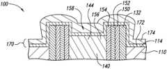
- FIGS. 1 A- 1 Iillustrate stages of a method for forming interconnects in a microfeature workpiece 100 in accordance with one embodiment of the invention.
- FIG. 1 Ais a schematic side cross-sectional view of a portion of the workpiece 100 at an intermediate stage after partially forming a plurality of interconnects 140 .
- the workpiece 100can include a substrate 110 and a plurality of microelectronic dies 120 formed in and/or on the substrate 110 .
- the substrate 110has a first side 112 and a second side 114 opposite the first side 112 .
- the substrate 110is generally a semiconductor wafer, and the dies 120 are arranged in a die pattern on the wafer.
- the individual dies 120include integrated circuitry 122 (shown schematically) and a plurality of terminals 124 (e.g., bond-pads) electrically coupled to the integrated circuitry 122 .
- the terminals 124 shown in FIG. 1 Aare external features at the first side 112 of the substrate 110 . In other embodiments, however, the terminals 124 can be internal features that are embedded at an intermediate depth within the substrate 110 .
- the dies 120can have different features to perform different functions.
- the individual diesmay further include an image sensor (e.g., CMOS image sensor or CCD image sensor) for capturing pictures or other images in the visible spectrum, or detecting radiation in other spectrums (e.g., IR or UV ranges).
- an image sensore.g., CMOS image sensor or CCD image sensor
- the first dielectric layer 130was applied to the first side 112 of the substrate 110 , and the interconnects 140 were partially formed in the workpiece 100 .
- the first dielectric layer 130can be a polyimide material or other suitable nonconductive materials.
- the first dielectric layer 130can be parylene, a low temperature chemical vapor deposition (low temperature CVD) material such as silicon nitride (Si 3 N 4 ), silicon oxide (SiO 2 ), and/or other suitable materials.
- low temperature CVDlow temperature chemical vapor deposition
- the conductive interconnects 140extend from the first dielectric layer 130 to an intermediate depth in the substrate 110 . As described in greater detail below with regard to FIG.
- the conductive interconnects 140can include several layers of conductive material that are electrically coupled to corresponding terminals 124 . Suitable methods for forming the portion of the interconnects 140 illustrated in FIG. 1 A are disclosed in U.S. patent application Ser. Nos. 10/713,878; 10/867,352; 10/879,398; 11/027,443; 11/056,211; 11/169,546; 11/217,877; and 11/218,243, which are incorporated herein by reference.
- the workpiece 100can optionally be attached to a support member 190 with an adhesive 192 to provide rigidity to the workpiece 100 during subsequent processing steps.
- FIG. 1 Bis a schematic side cross-sectional view of the area 1 B shown in FIG. 1 A with the workpiece 100 flipped over.
- the workpiece 100includes an interconnect hole 180 extending from the terminal 114 to an intermediate depth in the substrate 110 , a second dielectric layer 132 in the interconnect hole 180 , and a vent hole 182 extending from the interconnect hole 180 to the second side 114 of the substrate 110 .
- the second dielectric layer 132electrically insulates components in the substrate 110 from the interconnect 140 .
- the second dielectric layer 132can be an ALD (atomic layer deposition) aluminum oxide material applied using a suitable deposition process or another suitable low temperature CVD oxide.
- the second dielectric layer 132can include a silane-based and/or an aluminum-based oxide material.
- the second dielectric layer 132can include other suitable dielectric materials.
- the illustrated interconnect 140is formed in the interconnect hole 180 and has a first end portion 142 at the first dielectric layer 130 and a second end portion 144 at an intermediate depth in the substrate 110 .
- the illustrated interconnect 140includes a diffusion barrier layer 150 deposited over the second dielectric layer 132 in the hole 180 , a seed layer 152 formed over the barrier layer 150 in the hole 180 , a conductive layer 154 deposited over the seed layer 152 in the hole 180 , and a conductive fill material 152 formed over the conductive layer 154 in the hole 180 .
- the diffusion barrier layer 150can be a layer of tantalum that is deposited onto the workpiece 100 using physical vapor deposition (PVD) and has a thickness of approximately 150 Angstroms.
- the barrier layer 150may be deposited onto the workpiece 100 using other vapor deposition processes, such as CVD, and/or may have a different thickness. In either case, the barrier layer 150 is not limited to tantalum, but rather may be composed of tungsten or other suitable materials that help contain the conductive fill material 156 in the interconnect hole 180 .
- the seed layer 152can be deposited using vapor deposition techniques, such as PVD, CVD, atomic layer deposition, and/or plating.
- the seed layer 152can be composed of Cu or other suitable materials.
- the thickness of the seed layer 152may be about 2000 Angstroms, but could be more or less depending on the depth and aspect ratio of the hole 180 .
- the conductive layer 154can be Cu that is deposited onto the seed layer 152 in an electroless plating operation, electroplating operation, or another suitable method.
- the thickness of the conductive layer 154can be about 1 micron, however, in other embodiments the conductive layer 154 can have a different thickness and/or include other suitable materials.
- the workpiece 100may include a second conductive layer (not shown) that is deposited over the conductive layer 154 in the hole 180 .
- the second conductive layercan be Ni or other suitable materials that function as a wetting agent for facilitating deposition of subsequent materials into the hole 180 .
- the conductive fill material 156can include Cu, Ni, Co, Ag, Au, SnAgCu solder, AuSn solder, a solder having a different composition, or other suitable materials or alloys of materials having the desired conductivity.
- the conductive fill material 156may be deposited into the hole 180 using plating processes, solder wave processes, screen printing processes, reflow processes, vapor deposition processes, or other suitable techniques.
- the interconnectsmay have a different structure.
- the interconnectsmay have additional layers in lieu of or in addition to the layers described above.
- FIG. 1 Cis a schematic side cross-sectional view of the portion of the workpiece 100 after thinning the substrate 110 from the second side 114 .
- the substrate 110can be thinned by grinding, dry etching, chemical etching, chemical polishing, chemical-mechanical polishing, or other suitable processes.
- the thinning processmay also remove a section of the second end portion 114 of the interconnect 140 .
- the initial thickness of the substrate 110is approximately 750 microns and the interconnect 140 extends to an intermediate depth of approximately 150 microns in the substrate 110
- the post-thinning thickness T of the substrate 110is approximately 140 microns. These thicknesses can be different in other embodiments.
- the illustrated interconnect 140includes an exposed surface 146 at the second end portion 144 .
- FIG. 1 Dis a schematic side cross-sectional view of the portion of the workpiece 100 after selectively removing additional material from the second side 114 of the substrate 110 so that the interconnect 140 projects from the substrate 110 .
- the additional materialcan be removed via a plasma etch with SF 6 or another suitable etchant that is selective to silicon. Alternatively, the additional material can be removed with other processes.
- the second end portion 144 of the interconnect 140projects a first distance D 1 from the second side of the substrate 110 .
- the first distance D 1is between approximately 5 and 10 microns, although the first distance D 1 can be less than 5 microns or more than 10 microns in other embodiments.
- the first distance D 1is selected based on the subsequent processing and application requirements.
- FIG. 1 Eis a schematic side cross-sectional view of the area 1 E shown in FIG. 1 D after forming a recess 158 in the second end portion 144 of the interconnect 140 .
- the recess 158is formed by removing a portion of the conductive fill material 156 from the interconnect 140 .
- the conductive fill material 156can be removed by a wet etch process with an etchant that is selective to the conductive fill material 156 and, consequently, removes the conductive fill material 156 at a faster rate than the seed and/or conductive layers 152 and/or 154 .
- the illustrated recess 158extends from the surface 146 of the interconnect 140 to a surface 157 of the conductive fill material 156 , and has a depth D 2 less than the first distance D 1 .
- the depth D 2 of the recess 158is selected based on the subsequent processing and application requirements. In other embodiments, such as the embodiments described below with reference to FIGS. 2 A- 3 C , the interconnects may not include a recess in the second end portion 144 .
- FIG. 1 Fis a schematic side cross-sectional view of the portion of the workpiece 100 after forming a dielectric structure 170 across the second side 114 of the substrate 110 and the second end portion 144 of the interconnect 140 .
- the illustrated dielectric structure 170includes a first dielectric layer 172 and a second dielectric layer 174 deposited on the first dielectric layer 172 .
- the first dielectric layer 172can be parylene HT and have a thickness of approximately 0.5 micron. In other embodiments, other dielectric materials can be used and/or have different thicknesses.
- the second dielectric layer 174can be an oxide such as silicon oxide (SiO 2 ) and/or other suitable materials that are deposited by chemical vapor deposition and/or other suitable processes. In additional embodiments, the dielectric structure 170 can include a different number of layers.
- FIG. 1 Gis a schematic side cross-sectional view of the portion of the workpiece 100 after removing sections of the interconnect 140 and the dielectric structure 170 .
- the sections of the interconnect 140 and the dielectric structure 170can be removed by grinding, dry etching, chemical etching, chemical polishing, chemical-mechanical polishing, or other suitable processes.
- the workpiece 100is polished to remove portions of the second dielectric layer 132 , the barrier layer 150 , the seed layer 152 , the conductive layer 154 , the first dielectric layer 172 , and the second dielectric layer 174 .
- the volume of material removedis selected so that (a) the recess 158 in the interconnect 140 has a desired depth D 3 , and (b) the interconnect 140 projects a desired distance D 4 from an exterior surface 175 of the dielectric structure 170 .
- the interconnectmay not project from the exterior surface 175 of the dielectric structure 170 . In either case, the interconnect 140 intersects a plane defined by the dielectric structure 170 .
- FIG. 1 His a schematic side cross-sectional view of the portion of the workpiece 100 after removing the section of the first dielectric layer 172 from the recess 158 in the interconnect 140 .
- the section of the first dielectric layer 172can be removed from the recess 158 by a plasma etching process (e.g., O 2 plasma) or another suitable method that selectively removes the first dielectric layer 172 without significantly effecting the dielectric structure 170 formed on the substrate 110 .
- a plasma etching processe.g., O 2 plasma
- FIG. 1 Iis a schematic side cross-sectional view of the portion of the workpiece 100 after forming a conductive member 160 on the second end portion 144 of the interconnect 140 .
- the illustrated conductive member 160is a cap disposed in the recess 158 and extending over the barrier layer 150 , the seed layer 152 , and the conductive layer 154 .
- the capprojects a desired distance D 5 from the substrate 110 and forms an external contact for connection to an external device.
- the conductive member 160can be electrolessly plated onto the second end portion 144 of the interconnect 140 or formed using other suitable processes.
- the conductive member 160can include Ni or other suitable conductive materials.
- the interconnect 140may not include the conductive member 160 .
- the second end portion 144 of the interconnects 140can be attached directly to an external device, or a conductive coupler (e.g., a solder ball) can be attached directly to the second end portion 144 .
- a conductive couplere.g.,
- the interconnect 140projects from the substrate 110 .
- the section of the dielectric structure 170 covering the interconnect 140can be removed by a simple polishing process without exposing the backside of the substrate 110 .
- the resulting exposed surface 146 on the interconnect 140may form an external contact to which an external device can be attached.
- the conductive member 160can be disposed on the exposed surface 146 and form the external contact.
- an advantage of this featureis that the illustrated method does not require expensive and time-consuming photolithography processes to form external contacts on the backside of the workpiece 100 .
- the interconnect 140can be sized to project a desired distance from the external surface 175 of the dielectric structure 170 .
- the distancecan be selected based on the application requirements for the die 110 . For example, in applications in which the die 110 is stacked on another die, the distance may be selected to provide a desired gap between the two dies.
- FIGS. 2 A- 2 Cillustrate stages in a method for forming interconnects in a microfeature workpiece 200 in accordance with another embodiment of the invention.
- FIG. 2 Ais a schematic side cross-sectional view of a portion of the workpiece 200 at an intermediate stage after partially forming an interconnect 240 .
- the illustrated workpiece 200is generally similar to the workpiece 100 described above with reference to FIGS. 1 A- 1 F .
- the illustrated workpiece 200includes a substrate 110 , an interconnect 240 extending through and projecting from the substrate 110 , and a dielectric structure 270 formed over the substrate 110 and the interconnect 240 .
- the illustrated interconnect 240does not include a recess at the second end portion 244 .
- FIG. 2 Bis a schematic side cross-sectional view of the portion of the workpiece 200 after removing sections of the interconnect 240 and the dielectric structure 270 .
- the sections of the interconnect 240 and the dielectric structure 170can be removed by grinding, dry etching, chemical etching, chemical polishing, chemical-mechanical polishing, or other suitable processes.
- the volume of the material removedis selected so that the interconnect 240 projects a desired distance D 6 from an exterior surface 275 of the dielectric structure 270 .
- the illustrated interconnect 240includes a generally planar exposed surface 246 extending across the barrier layer 150 , the seed layer 152 , the conductive layer 154 , and the conductive fill material 156 .
- FIG. 2 Cis a schematic side cross-sectional view of the portion of the workpiece 200 after forming a conductive member 260 on the generally planar exposed surface 246 of the interconnect 240 .
- the conductive member 260forms part of the electrically conductive interconnect 240 and, accordingly, is electrically coupled to the terminal 114 ( FIG. 1 B ).
- FIGS. 3 A- 3 Cillustrate stages in a method for forming interconnects in a microfeature workpiece 300 in accordance with another embodiment of the invention.
- FIG. 3 Ais a schematic side cross-sectional view of a portion of the workpiece 300 at an intermediate stage after partially forming an interconnect 340 .
- the illustrated workpiece 300is generally similar to the workpiece 200 described above with reference to FIG. 2 A .
- the illustrated workpiece 300includes a substrate 110 , an interconnect 340 extending through and projecting from the substrate 110 , and a dielectric structure 370 formed over the substrate 110 and the interconnect 340 .
- FIG. 3 Bis a schematic side cross-sectional view of the portion of the workpiece 300 after removing sections of the interconnect 340 and the dielectric structure 370 .
- the sections of the interconnect 340 and the dielectric structure 370are removed to form a generally planar surface across the workpiece 300 such that an exposed surface 346 of the interconnect 340 is generally coplanar with an exterior surface 375 of the dielectric structure 370 .
- FIG. 3 Cis a schematic side cross-sectional view of the workpiece 300 after forming a conductive member 360 on the exposed surface 346 of the interconnect 340 .
- the conductive member 360forms part of the electrically conductive interconnect 340 and, accordingly, is electrically coupled to the terminal 114 ( FIG. 1 B ).
Landscapes
- Engineering & Computer Science (AREA)
- Physics & Mathematics (AREA)
- Condensed Matter Physics & Semiconductors (AREA)
- General Physics & Mathematics (AREA)
- Computer Hardware Design (AREA)
- Microelectronics & Electronic Packaging (AREA)
- Power Engineering (AREA)
- Manufacturing & Machinery (AREA)
- Internal Circuitry In Semiconductor Integrated Circuit Devices (AREA)
Abstract
Description
This application is a continuation of U.S. application Ser. No. 16/991,965 filed Aug. 12, 2020, which is a continuation of U.S. application Ser. No. 15/662,204 filed Jul. 27, 2017, which is a divisional of U.S. application Ser. No. 12/965,301 filed Dec. 10, 2010, which is a divisional of U.S. application Ser. No. 11/217,169 filed Sep. 1, 2005, now U.S. Pat. No. 7,863,187, each of which is incorporated herein by reference in its entirety.
The present invention relates to methods for forming interconnects in microfeature workpieces and microfeature workpieces formed using such methods.
Microelectronic devices, micromechanical devices, and other devices with microfeatures are typically formed by constructing several layers of components on a workpiece. In the case of microelectronic devices, a plurality of dies are fabricated on a single workpiece, and each die generally includes an integrated circuit and a plurality of bond-pads coupled to the integrated circuit. The dies are separated from each other and packaged to form individual microelectronic devices that can be attached to modules or installed in other products.
One aspect of fabricating and packaging such dies is forming interconnects that electrically couple conductive components located in different layers. In some applications, it may be desirable to form interconnects that extend completely through the dies or through a significant portion of the dies. Such interconnects electrically couple bond-pads or other conductive elements proximate to one side of the dies to conductive elements proximate to the other side of the dies. Through-wafer interconnects, for example, are constructed by forming deep vias on the front side and/or backside of the workpiece and in alignment with corresponding bond-pads at the front side of the workpiece. The vias are often blind vias in that they are closed at one end. The blind vias are then filled with a conductive fill material. After further processing, the workpiece is thinned to reduce the thickness of the final dies. Solder balls or other external electrical contacts are subsequently attached to the through-wafer interconnects at the backside and/or the front side of the workpiece. The solder balls or external contacts can be attached either before or after singulating the dies from the workpiece.
Conventional processes for forming external contacts on through-wafer interconnects include (a) depositing a dielectric layer on the backside of the workpiece, (b) forming a photoresist on the dielectric layer, (c) patterning and developing the photoresist, (d) etching the dielectric layer to form holes aligned with corresponding interconnects, (e) removing the photoresist from the workpiece, and (f) forming conductive external contacts in the holes in the dielectric layer. One concern with forming external contacts on the backside of a workpiece is that conventional processes are relatively expensive because patterning the photoresist requires a mask. Masks are expensive and time-consuming to construct because they require very expensive photolithography equipment to achieve the tolerances required in semiconductor devices. Accordingly, there is a need to reduce the cost of forming external contacts on workpieces with through-wafer interconnects.
The following disclosure describes several embodiments of methods for forming interconnects in microfeature workpieces, and microfeature workpieces having such interconnects. One aspect of the invention is directed to methods of forming an interconnect in a microfeature workpiece having a terminal and a substrate with a first side carrying the terminal and a second side opposite the first side. An embodiment of one such method includes (a) constructing an electrically conductive interconnect extending from the terminal to at least an intermediate depth in the substrate, and (b) removing material from the second side of the substrate so that a portion of the interconnect projects from the substrate. The material can be removed from the second side of the substrate by thinning the substrate so that a surface of the interconnect is exposed and selectively etching the substrate so that the portion of the interconnect projects from the substrate.
In another embodiment, a method includes providing a microfeature workpiece having (a) a substrate with a first side and a second side opposite the first side, (b) a terminal carried by the first side of the substrate, and (c) an electrically conductive interconnect extending from the terminal through the substrate and projecting from the second side of the substrate. The method further includes applying a dielectric layer to the second side of the substrate and the portion of the interconnect projecting from the second side of the substrate, and removing a section of the dielectric layer to expose a surface of the interconnect with the interconnect intersecting a plane defined by the remaining section of the dielectric layer.
In another embodiment, a method includes forming an electrically conductive interconnect having a first portion at the terminal and a second portion at an intermediate depth in the substrate. The electrically conductive interconnect is electrically connected to the terminal. The method further includes thinning the substrate from the second side to at least the second portion of the interconnect, applying a dielectric layer to the second side of the substrate and the second portion of the interconnect, and exposing a surface of the second portion of the interconnect without photolithography.
Another aspect of the invention is directed to microfeature workpieces. In one embodiment, a microfeature workpiece includes a substrate and a microelectronic die formed in and/or on the substrate. The substrate has a first side and a second side opposite the first side. The die includes a terminal at the first side of the substrate and an integrated circuit operably coupled to the terminal. The workpiece further includes an electrically conductive interconnect extending from the terminal through the substrate such that a portion of the interconnect projects from the second side of the substrate. The interconnect is electrically coupled to the terminal.
In another embodiment, a microfeature workpiece includes a substrate and a microelectronic die formed in and/or on the substrate. The substrate has a first side and a second side opposite the first side. The die includes a terminal at the first side of the substrate and an integrated circuit operably coupled to the terminal. The workpiece further includes (a) a hole extending through the terminal and the substrate, (b) a dielectric layer on the second side of the substrate defining a plane, and (c) an electrically conductive interconnect. The interconnect includes a conductive fill material in the hole and a conductive layer in the hole between the conductive fill material and the substrate. Both the conductive fill material and the conductive layer are electrically coupled to the terminal and extend from the terminal through the substrate. Moreover, both the conductive fill material and the conductive layer project from the substrate such that the conductive fill material and the conductive layer intersect the plane.
Specific details of several embodiments of the invention are described below with reference to interconnects extending from a terminal proximate to the front side of a workpiece, but the methods and interconnects described below can be used for other types of interconnects within microelectronic workpieces. Several details describing well-known structures or processes often associated with fabricating microelectronic devices are not set forth in the following description for purposes of clarity. Also, several other embodiments of the invention can have different configurations, components, or procedures than those described in this section. A person of ordinary skill in the art, therefore, will accordingly understand that the invention may have other embodiments with additional elements, or the invention may have other embodiments without several of the elements shown and described below with reference toFIGS.1A-3C .
The term “microfeature workpiece” is used throughout to include substrates upon which and/or in which microelectronic devices, micromechanical devices, data storage elements, optics, and other features are fabricated. For example, microfeature workpieces can be semiconductor wafers, glass substrates, dielectric substrates, or many other types of substrates. Many features on such microfeature workpieces have critical dimensions less than or equal to 1 μm, and in many applications the critical dimensions of the smaller features are less than 0.25 μm or even less than 0.1 μm. Where the context permits, singular or plural terms may also include the plural or singular term, respectively. Moreover, unless the word “or” is expressly limited to mean only a single item exclusive from other items in reference to a list of at least two items, then the use of “or” in such a list is to be interpreted as including (a) any single item in the list, (b) all of the items in the list, or (c) any combination of the items in the list. Additionally, the term “comprising” is used throughout to mean including at least the recited feature(s) such that any greater number of the same features and/or types of other features and components are not precluded.
In previous processing steps, a firstdielectric layer 130 was applied to thefirst side 112 of thesubstrate 110, and theinterconnects 140 were partially formed in theworkpiece 100. Thefirst dielectric layer 130 can be a polyimide material or other suitable nonconductive materials. For example, thefirst dielectric layer 130 can be parylene, a low temperature chemical vapor deposition (low temperature CVD) material such as silicon nitride (Si3N4), silicon oxide (SiO2), and/or other suitable materials. The foregoing list of dielectric materials is not exhaustive. Theconductive interconnects 140 extend from thefirst dielectric layer 130 to an intermediate depth in thesubstrate 110. As described in greater detail below with regard toFIG.1B , theconductive interconnects 140 can include several layers of conductive material that are electrically coupled tocorresponding terminals 124. Suitable methods for forming the portion of theinterconnects 140 illustrated inFIG.1A are disclosed in U.S. patent application Ser. Nos. 10/713,878; 10/867,352; 10/879,398; 11/027,443; 11/056,211; 11/169,546; 11/217,877; and 11/218,243, which are incorporated herein by reference. After partially forming theinterconnects 140, theworkpiece 100 can optionally be attached to asupport member 190 with an adhesive192 to provide rigidity to theworkpiece 100 during subsequent processing steps.
The illustratedinterconnect 140 is formed in theinterconnect hole 180 and has afirst end portion 142 at thefirst dielectric layer 130 and asecond end portion 144 at an intermediate depth in thesubstrate 110. The illustratedinterconnect 140 includes adiffusion barrier layer 150 deposited over thesecond dielectric layer 132 in thehole 180, aseed layer 152 formed over thebarrier layer 150 in thehole 180, aconductive layer 154 deposited over theseed layer 152 in thehole 180, and aconductive fill material 152 formed over theconductive layer 154 in thehole 180. Thediffusion barrier layer 150 can be a layer of tantalum that is deposited onto theworkpiece 100 using physical vapor deposition (PVD) and has a thickness of approximately 150 Angstroms. In other embodiments, thebarrier layer 150 may be deposited onto theworkpiece 100 using other vapor deposition processes, such as CVD, and/or may have a different thickness. In either case, thebarrier layer 150 is not limited to tantalum, but rather may be composed of tungsten or other suitable materials that help contain theconductive fill material 156 in theinterconnect hole 180.
Theseed layer 152 can be deposited using vapor deposition techniques, such as PVD, CVD, atomic layer deposition, and/or plating. Theseed layer 152 can be composed of Cu or other suitable materials. The thickness of theseed layer 152 may be about 2000 Angstroms, but could be more or less depending on the depth and aspect ratio of thehole 180. Theconductive layer 154 can be Cu that is deposited onto theseed layer 152 in an electroless plating operation, electroplating operation, or another suitable method. The thickness of theconductive layer 154 can be about 1 micron, however, in other embodiments theconductive layer 154 can have a different thickness and/or include other suitable materials. In additional embodiments, theworkpiece 100 may include a second conductive layer (not shown) that is deposited over theconductive layer 154 in thehole 180. The second conductive layer can be Ni or other suitable materials that function as a wetting agent for facilitating deposition of subsequent materials into thehole 180.
Theconductive fill material 156 can include Cu, Ni, Co, Ag, Au, SnAgCu solder, AuSn solder, a solder having a different composition, or other suitable materials or alloys of materials having the desired conductivity. Theconductive fill material 156 may be deposited into thehole 180 using plating processes, solder wave processes, screen printing processes, reflow processes, vapor deposition processes, or other suitable techniques. In other embodiments, the interconnects may have a different structure. For example, the interconnects may have additional layers in lieu of or in addition to the layers described above.
One feature of the method illustrated inFIGS.1A-1I is that theinterconnect 140 projects from thesubstrate 110. As a result, the section of thedielectric structure 170 covering theinterconnect 140 can be removed by a simple polishing process without exposing the backside of thesubstrate 110. The resulting exposedsurface 146 on theinterconnect 140 may form an external contact to which an external device can be attached. Alternatively, theconductive member 160 can be disposed on the exposedsurface 146 and form the external contact. In either case, an advantage of this feature is that the illustrated method does not require expensive and time-consuming photolithography processes to form external contacts on the backside of theworkpiece 100.
Another advantage of the method illustrated inFIGS.1A-1I is that theinterconnect 140 can be sized to project a desired distance from theexternal surface 175 of thedielectric structure 170. The distance can be selected based on the application requirements for thedie 110. For example, in applications in which thedie 110 is stacked on another die, the distance may be selected to provide a desired gap between the two dies.
From the foregoing, it will be appreciated that specific embodiments of the invention have been described herein for purposes of illustration, but that various modifications may be made without deviating from the spirit and scope of the invention. For example, many of the elements of one embodiment can be combined with other embodiments in addition to or in lieu of the elements of the other embodiments. Accordingly, the invention is not limited except as by the appended claims.
Claims (7)
1. An integrated circuit structure, comprising:
an integrated circuit substrate having a conductive pad on a first face thereof and a through hole that extends through the integrated circuit substrate and the pad; and
an electrically conductive interconnect in the through hole and through and onto the pad, the electrically conductive interconnect filling the through hole adjacent the first face, and including a recess therein adjacent a second face of the integrated circuit substrate, the recess defining inner walls of the conductive electrode, wherein the recess has a depth less than or equal to a thickness of an insulating layer over the second face of the integrated circuit substrate.
2. The integrated circuit structure ofclaim 1 , further comprising:
a conductive bump that extends into the recess and directly contacts the inner walls of the conductive electrode.
3. The integrated circuit structure ofclaim 2 , wherein the conductive bump comprises nickel (Ni).
4. The integrated circuit structure ofclaim 2 , wherein the conductive bump completely fills the recess.
5. The integrated circuit structure ofclaim 1 , further comprising a seed layer between the electrically conductive interconnect and the substrate in the through hole.
6. The integrated circuit structure ofclaim 5 , wherein the seed layer comprises copper (Cu).
7. The integrated circuit structure ofclaim 1 , wherein the electrically conductive interconnect comprises copper (Cu), nickel (Ni), cobalt (Co), silver (Ag), gold (Au), tin (Sn), or a combination thereof.
Priority Applications (2)
| Application Number | Priority Date | Filing Date | Title |
|---|---|---|---|
| US18/047,049US12014958B2 (en) | 2005-09-01 | 2022-10-17 | Microfeature workpieces and methods for forming interconnects in microfeature workpieces |
| US18/744,493US20240339360A1 (en) | 2005-09-01 | 2024-06-14 | Microfeature workpieces and methods for forming interconnects in microfeature workpieces |
Applications Claiming Priority (5)
| Application Number | Priority Date | Filing Date | Title |
|---|---|---|---|
| US11/217,169US7863187B2 (en) | 2005-09-01 | 2005-09-01 | Microfeature workpieces and methods for forming interconnects in microfeature workpieces |
| US12/965,301US20110079900A1 (en) | 2005-09-01 | 2010-12-10 | Microfeature workpieces and methods for forming interconnects in microfeature workpieces |
| US15/662,204US20170323828A1 (en) | 2005-09-01 | 2017-07-27 | Microfeature workpieces and methods for forming interconnects in microfeature workpieces |
| US16/991,965US11476160B2 (en) | 2005-09-01 | 2020-08-12 | Microfeature workpieces and methods for forming interconnects in microfeature workpieces |
| US18/047,049US12014958B2 (en) | 2005-09-01 | 2022-10-17 | Microfeature workpieces and methods for forming interconnects in microfeature workpieces |
Related Parent Applications (1)
| Application Number | Title | Priority Date | Filing Date |
|---|---|---|---|
| US16/991,965ContinuationUS11476160B2 (en) | 2005-09-01 | 2020-08-12 | Microfeature workpieces and methods for forming interconnects in microfeature workpieces |
Related Child Applications (1)
| Application Number | Title | Priority Date | Filing Date |
|---|---|---|---|
| US18/744,493ContinuationUS20240339360A1 (en) | 2005-09-01 | 2024-06-14 | Microfeature workpieces and methods for forming interconnects in microfeature workpieces |
Publications (2)
| Publication Number | Publication Date |
|---|---|
| US20230106554A1 US20230106554A1 (en) | 2023-04-06 |
| US12014958B2true US12014958B2 (en) | 2024-06-18 |
Family
ID=37804834
Family Applications (6)
| Application Number | Title | Priority Date | Filing Date |
|---|---|---|---|
| US11/217,169Active2027-05-25US7863187B2 (en) | 2005-09-01 | 2005-09-01 | Microfeature workpieces and methods for forming interconnects in microfeature workpieces |
| US12/965,301AbandonedUS20110079900A1 (en) | 2005-09-01 | 2010-12-10 | Microfeature workpieces and methods for forming interconnects in microfeature workpieces |
| US15/662,204AbandonedUS20170323828A1 (en) | 2005-09-01 | 2017-07-27 | Microfeature workpieces and methods for forming interconnects in microfeature workpieces |
| US16/991,965Active2026-02-08US11476160B2 (en) | 2005-09-01 | 2020-08-12 | Microfeature workpieces and methods for forming interconnects in microfeature workpieces |
| US18/047,049Expired - LifetimeUS12014958B2 (en) | 2005-09-01 | 2022-10-17 | Microfeature workpieces and methods for forming interconnects in microfeature workpieces |
| US18/744,493PendingUS20240339360A1 (en) | 2005-09-01 | 2024-06-14 | Microfeature workpieces and methods for forming interconnects in microfeature workpieces |
Family Applications Before (4)
| Application Number | Title | Priority Date | Filing Date |
|---|---|---|---|
| US11/217,169Active2027-05-25US7863187B2 (en) | 2005-09-01 | 2005-09-01 | Microfeature workpieces and methods for forming interconnects in microfeature workpieces |
| US12/965,301AbandonedUS20110079900A1 (en) | 2005-09-01 | 2010-12-10 | Microfeature workpieces and methods for forming interconnects in microfeature workpieces |
| US15/662,204AbandonedUS20170323828A1 (en) | 2005-09-01 | 2017-07-27 | Microfeature workpieces and methods for forming interconnects in microfeature workpieces |
| US16/991,965Active2026-02-08US11476160B2 (en) | 2005-09-01 | 2020-08-12 | Microfeature workpieces and methods for forming interconnects in microfeature workpieces |
Family Applications After (1)
| Application Number | Title | Priority Date | Filing Date |
|---|---|---|---|
| US18/744,493PendingUS20240339360A1 (en) | 2005-09-01 | 2024-06-14 | Microfeature workpieces and methods for forming interconnects in microfeature workpieces |
Country Status (2)
| Country | Link |
|---|---|
| US (6) | US7863187B2 (en) |
| WO (1) | WO2007027969A2 (en) |
Families Citing this family (39)
| Publication number | Priority date | Publication date | Assignee | Title |
|---|---|---|---|---|
| US8084866B2 (en) | 2003-12-10 | 2011-12-27 | Micron Technology, Inc. | Microelectronic devices and methods for filling vias in microelectronic devices |
| US7091124B2 (en)* | 2003-11-13 | 2006-08-15 | Micron Technology, Inc. | Methods for forming vias in microelectronic devices, and methods for packaging microelectronic devices |
| US20050247894A1 (en) | 2004-05-05 | 2005-11-10 | Watkins Charles M | Systems and methods for forming apertures in microfeature workpieces |
| US7232754B2 (en)* | 2004-06-29 | 2007-06-19 | Micron Technology, Inc. | Microelectronic devices and methods for forming interconnects in microelectronic devices |
| US7189954B2 (en)* | 2004-07-19 | 2007-03-13 | Micron Technology, Inc. | Microelectronic imagers with optical devices and methods of manufacturing such microelectronic imagers |
| US7425499B2 (en) | 2004-08-24 | 2008-09-16 | Micron Technology, Inc. | Methods for forming interconnects in vias and microelectronic workpieces including such interconnects |
| SG120200A1 (en) | 2004-08-27 | 2006-03-28 | Micron Technology Inc | Slanted vias for electrical circuits on circuit boards and other substrates |
| US7300857B2 (en) | 2004-09-02 | 2007-11-27 | Micron Technology, Inc. | Through-wafer interconnects for photoimager and memory wafers |
| US7271482B2 (en)* | 2004-12-30 | 2007-09-18 | Micron Technology, Inc. | Methods for forming interconnects in microelectronic workpieces and microelectronic workpieces formed using such methods |
| KR100661169B1 (en)* | 2005-06-03 | 2006-12-26 | 삼성전자주식회사 | Packaging chip and its packaging method |
| US7795134B2 (en) | 2005-06-28 | 2010-09-14 | Micron Technology, Inc. | Conductive interconnect structures and formation methods using supercritical fluids |
| US7863187B2 (en) | 2005-09-01 | 2011-01-04 | Micron Technology, Inc. | Microfeature workpieces and methods for forming interconnects in microfeature workpieces |
| US7262134B2 (en) | 2005-09-01 | 2007-08-28 | Micron Technology, Inc. | Microfeature workpieces and methods for forming interconnects in microfeature workpieces |
| US7622377B2 (en) | 2005-09-01 | 2009-11-24 | Micron Technology, Inc. | Microfeature workpiece substrates having through-substrate vias, and associated methods of formation |
| KR100694424B1 (en)* | 2006-02-17 | 2007-03-12 | 주식회사 하이닉스반도체 | Multi chip package device and method for manufacturing the same |
| US7749899B2 (en) | 2006-06-01 | 2010-07-06 | Micron Technology, Inc. | Microelectronic workpieces and methods and systems for forming interconnects in microelectronic workpieces |
| US7629249B2 (en)* | 2006-08-28 | 2009-12-08 | Micron Technology, Inc. | Microfeature workpieces having conductive interconnect structures formed by chemically reactive processes, and associated systems and methods |
| US7902643B2 (en) | 2006-08-31 | 2011-03-08 | Micron Technology, Inc. | Microfeature workpieces having interconnects and conductive backplanes, and associated systems and methods |
| DE102007039754A1 (en)* | 2007-06-22 | 2008-12-24 | Fraunhofer-Gesellschaft zur Förderung der angewandten Forschung e.V. | Process for the production of substrates |
| SG149710A1 (en) | 2007-07-12 | 2009-02-27 | Micron Technology Inc | Interconnects for packaged semiconductor devices and methods for manufacturing such devices |
| SG150410A1 (en) | 2007-08-31 | 2009-03-30 | Micron Technology Inc | Partitioned through-layer via and associated systems and methods |
| US7884015B2 (en) | 2007-12-06 | 2011-02-08 | Micron Technology, Inc. | Methods for forming interconnects in microelectronic workpieces and microelectronic workpieces formed using such methods |
| US8084854B2 (en) | 2007-12-28 | 2011-12-27 | Micron Technology, Inc. | Pass-through 3D interconnect for microelectronic dies and associated systems and methods |
| US8253230B2 (en) | 2008-05-15 | 2012-08-28 | Micron Technology, Inc. | Disabling electrical connections using pass-through 3D interconnects and associated systems and methods |
| KR20100020718A (en)* | 2008-08-13 | 2010-02-23 | 삼성전자주식회사 | Semiconductor chip, stack structure, and methods of fabricating the semiconductor chip and the stack structure |
| US8513119B2 (en) | 2008-12-10 | 2013-08-20 | Taiwan Semiconductor Manufacturing Company, Ltd. | Method of forming bump structure having tapered sidewalls for stacked dies |
| US20100171197A1 (en)* | 2009-01-05 | 2010-07-08 | Hung-Pin Chang | Isolation Structure for Stacked Dies |
| US7998860B2 (en)* | 2009-03-12 | 2011-08-16 | Micron Technology, Inc. | Method for fabricating semiconductor components using maskless back side alignment to conductive vias |
| US9406561B2 (en)* | 2009-04-20 | 2016-08-02 | International Business Machines Corporation | Three dimensional integrated circuit integration using dielectric bonding first and through via formation last |
| US8791549B2 (en) | 2009-09-22 | 2014-07-29 | Taiwan Semiconductor Manufacturing Company, Ltd. | Wafer backside interconnect structure connected to TSVs |
| US8466059B2 (en) | 2010-03-30 | 2013-06-18 | Taiwan Semiconductor Manufacturing Company, Ltd. | Multi-layer interconnect structure for stacked dies |
| US8900994B2 (en) | 2011-06-09 | 2014-12-02 | Taiwan Semiconductor Manufacturing Company, Ltd. | Method for producing a protective structure |
| US8816505B2 (en) | 2011-07-29 | 2014-08-26 | Tessera, Inc. | Low stress vias |
| US8563403B1 (en) | 2012-06-27 | 2013-10-22 | International Business Machines Corporation | Three dimensional integrated circuit integration using alignment via/dielectric bonding first and through via formation last |
| FR3009128A1 (en) | 2013-07-25 | 2015-01-30 | Commissariat Energie Atomique | METHOD FOR PRODUCING A CONDUCTIVE PLATE ON A CONDUCTIVE ELEMENT |
| US9484325B2 (en)* | 2013-10-09 | 2016-11-01 | Invensas Corporation | Interconnections for a substrate associated with a backside reveal |
| US9443758B2 (en)* | 2013-12-11 | 2016-09-13 | Taiwan Semiconductor Manufacturing Co., Ltd. | Connecting techniques for stacked CMOS devices |
| US9653381B2 (en) | 2014-06-17 | 2017-05-16 | Micron Technology, Inc. | Semiconductor structures and die assemblies including conductive vias and thermally conductive elements and methods of forming such structures |
| CN104409364B (en)* | 2014-11-19 | 2017-12-01 | 清华大学 | Pinboard and preparation method thereof, encapsulating structure and the bonding method for pinboard |
Citations (514)
| Publication number | Priority date | Publication date | Assignee | Title |
|---|---|---|---|---|
| US2821959A (en) | 1956-03-29 | 1958-02-04 | Bell Telephone Labor Inc | Mass soldering of electrical assemblies |
| US3006318A (en) | 1958-03-26 | 1961-10-31 | Western Electric Co | Apparatus for applying solder coatings to surfaces |
| US3345134A (en) | 1962-04-21 | 1967-10-03 | Knapsack Ag | Process and apparatus for the manufacture of titanium nitride |
| US3865298A (en) | 1973-08-14 | 1975-02-11 | Atomic Energy Commission | Solder leveling |
| US3902036A (en) | 1974-05-02 | 1975-08-26 | Western Electric Co | Control system using multiplexed laser beams |
| US4040168A (en) | 1975-11-24 | 1977-08-09 | Rca Corporation | Fabrication method for a dual gate field-effect transistor |
| US4368106A (en) | 1980-10-27 | 1983-01-11 | General Electric Company | Implantation of electrical feed-through conductors |
| EP0127946A1 (en) | 1983-05-10 | 1984-12-12 | BRITISH TELECOMMUNICATIONS public limited company | Method of producing a via in a semiconductor device |
| US4534100A (en) | 1982-06-28 | 1985-08-13 | The United States Of America As Represented By The Secretary Of The Air Force | Electrical method of making conductive paths in silicon |
| US4581301A (en) | 1984-04-10 | 1986-04-08 | Michaelson Henry W | Additive adhesive based process for the manufacture of printed circuit boards |
| US4608480A (en) | 1983-06-15 | 1986-08-26 | S.N.E.C.M.A. | Process and apparatus for laser drilling |
| US4614427A (en) | 1983-05-20 | 1986-09-30 | Hitachi, Ltd. | Automatic contaminants detection apparatus |
| US4627971A (en) | 1985-04-22 | 1986-12-09 | Alza Corporation | Osmotic device with self-sealing passageway |
| US4660063A (en) | 1985-03-18 | 1987-04-21 | General Electric Company | Immersion type ISFET |
| JPS6352432A (en) | 1986-08-22 | 1988-03-05 | Hitachi Vlsi Eng Corp | semiconductor equipment |
| US4756765A (en) | 1982-01-26 | 1988-07-12 | Avco Research Laboratory, Inc. | Laser removal of poor thermally-conductive materials |
| US4768291A (en) | 1987-03-12 | 1988-09-06 | Monarch Technologies Corporation | Apparatus for dry processing a semiconductor wafer |
| US4818728A (en) | 1986-12-03 | 1989-04-04 | Sharp Kabushiki Kaisha | Method of making a hybrid semiconductor device |
| JPH01252308A (en) | 1988-03-31 | 1989-10-09 | Toppan Printing Co Ltd | Hole formation method for multilayer circuit wiring board |
| US4907127A (en) | 1988-03-21 | 1990-03-06 | Lee John K C | Printed circuit board construction and method for producing printed circuit end products |
| JPH02235589A (en) | 1989-03-09 | 1990-09-18 | Fuji Electric Co Ltd | Laser beam machining method |
| US4959705A (en) | 1988-10-17 | 1990-09-25 | Ford Microelectronics, Inc. | Three metal personalization of application specific monolithic microwave integrated circuit |
| US4964212A (en) | 1988-09-29 | 1990-10-23 | Commissariat A L'energie Atomique | Process for producing electrical connections through a substrate |
| US4984597A (en) | 1984-05-21 | 1991-01-15 | Cfm Technologies Research Associates | Apparatus for rinsing and drying surfaces |
| US5006922A (en) | 1990-02-14 | 1991-04-09 | Motorola, Inc. | Packaged semiconductor device having a low cost ceramic PGA package |
| US5024966A (en) | 1988-12-21 | 1991-06-18 | At&T Bell Laboratories | Method of forming a silicon-based semiconductor optical device mount |
| US5027184A (en) | 1981-03-02 | 1991-06-25 | Rockwell International Corporation | NPN type lateral transistor with minimal substrate operation interference |
| US5026964A (en) | 1986-02-28 | 1991-06-25 | General Electric Company | Optical breakthrough sensor for laser drill |
| US5037782A (en) | 1989-03-29 | 1991-08-06 | Mitsubishi Denki Kabushiki Kaisha | Method of making a semiconductor device including via holes |
| US5098864A (en) | 1989-11-29 | 1992-03-24 | Olin Corporation | Process for manufacturing a metal pin grid array package |
| US5102829A (en) | 1991-07-22 | 1992-04-07 | At&T Bell Laboratories | Plastic pin grid array package |
| US5123902A (en) | 1988-09-13 | 1992-06-23 | Carl-Zeiss-Stiftung | Method and apparatus for performing surgery on tissue wherein a laser beam is applied to the tissue |
| US5144412A (en) | 1987-02-19 | 1992-09-01 | Olin Corporation | Process for manufacturing plastic pin grid arrays and the product produced thereby |
| US5145099A (en) | 1990-07-13 | 1992-09-08 | Micron Technology, Inc. | Method for combining die attach and lead bond in the assembly of a semiconductor package |
| US5158911A (en) | 1990-08-03 | 1992-10-27 | Thomson Composants Microondes | Method for interconnection between an integrated circuit and a support circuit, and integrated circuit adapted to this method |
| US5200366A (en) | 1990-04-27 | 1993-04-06 | Hitachi, Ltd. | Semiconductor device, its fabrication method and molding apparatus used therefor |
| JPH05104316A (en) | 1991-10-15 | 1993-04-27 | Nec Corp | Counter boring device |
| US5219344A (en) | 1988-06-09 | 1993-06-15 | Visx, Incorporated | Methods and apparatus for laser sculpture of the cornea |
| US5233448A (en) | 1992-05-04 | 1993-08-03 | Industrial Technology Research Institute | Method of manufacturing a liquid crystal display panel including photoconductive electrostatic protection |
| US5237148A (en) | 1990-10-04 | 1993-08-17 | Brother Kogyo Kabushiki | Device for manufacturing a nozzle and its manufacturing method |
| US5289631A (en) | 1992-03-04 | 1994-03-01 | Mcnc | Method for testing, burn-in, and/or programming of integrated circuit chips |
| US5291062A (en) | 1993-03-01 | 1994-03-01 | Motorola, Inc. | Area array semiconductor device having a lid with functional contacts |
| US5292686A (en) | 1991-08-21 | 1994-03-08 | Triquint Semiconductor, Inc. | Method of forming substrate vias in a GaAs wafer |
| US5294568A (en) | 1990-10-12 | 1994-03-15 | Genus, Inc. | Method of selective etching native oxide |
| US5304743A (en) | 1992-05-12 | 1994-04-19 | Lsi Logic Corporation | Multilayer IC semiconductor package |
| US5378312A (en) | 1993-12-07 | 1995-01-03 | International Business Machines Corporation | Process for fabricating a semiconductor structure having sidewalls |
| US5378313A (en) | 1993-12-22 | 1995-01-03 | Pace; Benedict G. | Hybrid circuits and a method of manufacture |
| US5380681A (en) | 1994-03-21 | 1995-01-10 | United Microelectronics Corporation | Three-dimensional multichip package and methods of fabricating |
| US5402435A (en) | 1993-03-05 | 1995-03-28 | Matsushita Electric Industrial Co., Ltd. | Optical device |
| US5406630A (en) | 1992-05-04 | 1995-04-11 | Motorola, Inc. | Tamperproof arrangement for an integrated circuit device |
| US5424573A (en) | 1992-03-04 | 1995-06-13 | Hitachi, Ltd. | Semiconductor package having optical interconnection access |
| TW250597B (en) | 1993-06-04 | 1995-07-01 | Framatome & Cie | |
| US5438212A (en) | 1993-02-25 | 1995-08-01 | Mitsubishi Denki Kabushiki Kaisha | Semiconductor device with heat dissipation structure |
| US5447871A (en) | 1993-03-05 | 1995-09-05 | Goldstein; Edward F. | Electrically conductive interconnection through a body of semiconductor material |
| US5464960A (en) | 1993-01-12 | 1995-11-07 | Iatrotech, Inc. | Laser calibration device |
| US5481483A (en) | 1992-11-23 | 1996-01-02 | Ford Motor Company | Non-contact method of obtaining dimensional information about an object for comparing similar objects |
| US5485039A (en) | 1991-12-27 | 1996-01-16 | Hitachi, Ltd. | Semiconductor substrate having wiring conductors at a first main surface electrically connected to plural pins at a second main surface |
| US5496755A (en) | 1989-11-29 | 1996-03-05 | Texas Instruments Incorporated | Integrated circuit and method |
| US5515167A (en) | 1994-09-13 | 1996-05-07 | Hughes Aircraft Company | Transparent optical chuck incorporating optical monitoring |
| US5518956A (en) | 1993-09-02 | 1996-05-21 | General Electric Company | Method of isolating vertical shorts in an electronic array using laser ablation |
| US5550403A (en) | 1994-06-02 | 1996-08-27 | Lsi Logic Corporation | Improved laminate package for an integrated circuit and integrated circuit having such a package |
| US5585675A (en) | 1994-05-11 | 1996-12-17 | Harris Corporation | Semiconductor die packaging tub having angularly offset pad-to-pad via structure configured to allow three-dimensional stacking and electrical interconnections among multiple identical tubs |
| US5585308A (en) | 1993-12-23 | 1996-12-17 | Sgs-Thomson Microelectronics, Inc. | Method for improved pre-metal planarization |
| US5614743A (en) | 1994-07-26 | 1997-03-25 | Kabushiki Kaisha Toshiba | Microwave integrated circuit (MIC) having a reactance element formed on a groove |
| US5618752A (en) | 1995-06-05 | 1997-04-08 | Harris Corporation | Method of fabrication of surface mountable integrated circuits |
| US5624437A (en) | 1995-03-28 | 1997-04-29 | Freeman; Jerre M. | High resolution, high speed, programmable laser beam modulating apparatus for microsurgery |
| US5627106A (en) | 1994-05-06 | 1997-05-06 | United Microelectronics Corporation | Trench method for three dimensional chip connecting during IC fabrication |
| US5646067A (en) | 1995-06-05 | 1997-07-08 | Harris Corporation | Method of bonding wafers having vias including conductive material |
| US5654221A (en) | 1994-10-17 | 1997-08-05 | International Business Machines Corporation | Method for forming semiconductor chip and electronic module with integrated surface interconnects/components |
| US5673846A (en) | 1995-08-24 | 1997-10-07 | International Business Machines Corporation | Solder anchor decal and method |
| US5684642A (en) | 1994-02-22 | 1997-11-04 | Mitsubishi Denki Kabushiki Kaisha | Optical transmission system and light radiating method |
| US5690841A (en) | 1993-12-10 | 1997-11-25 | Pharmacia Biotech Ab | Method of producing cavity structures |
| US5718791A (en) | 1995-06-05 | 1998-02-17 | R + S Stanztechnik Gmbh | Method of laminating a trim panel and folding a cover sheet edge around the panel rim |
| US5723904A (en) | 1993-03-10 | 1998-03-03 | Sumitomo Electric Industries, Ltd. | Packaged semiconductor device suitable to be mounted and connected to microstrip line structure board |
| US5726493A (en) | 1994-06-13 | 1998-03-10 | Fujitsu Limited | Semiconductor device and semiconductor device unit having ball-grid-array type package structure |
| US5734555A (en) | 1994-03-30 | 1998-03-31 | Intel Corporation | Shared socket multi-chip module and/or piggyback pin grid array package |
| US5771158A (en) | 1995-09-21 | 1998-06-23 | Mitsubishi Denki Kabushiki Kaisha | Printed circuit board, printed circuit board used for flat panel display drive circuit, and flat panel display device |
| US5773359A (en) | 1995-12-26 | 1998-06-30 | Motorola, Inc. | Interconnect system and method of fabrication |
| US5776824A (en) | 1995-12-22 | 1998-07-07 | Micron Technology, Inc. | Method for producing laminated film/metal structures for known good die ("KG") applications |
| US5807439A (en) | 1997-09-29 | 1998-09-15 | Siemens Aktiengesellschaft | Apparatus and method for improved washing and drying of semiconductor wafers |
| US5811799A (en) | 1997-07-31 | 1998-09-22 | Wu; Liang-Chung | Image sensor package having a wall with a sealed cover |
| US5821532A (en) | 1997-06-16 | 1998-10-13 | Eastman Kodak Company | Imager package substrate |
| US5825080A (en) | 1995-12-18 | 1998-10-20 | Atr Optical And Radio Communications Research Laboratories | Semiconductor device provided with surface grounding conductor for covering surfaces of electrically insulating films |
| US5826628A (en) | 1996-01-24 | 1998-10-27 | Micron Technology, Inc. | Form tooling and method of forming semiconductor package leads |
| US5847454A (en) | 1993-02-04 | 1998-12-08 | Cornell Research Foundcatton, Inc. | Electrically isolated released microstructures |
| US5851845A (en) | 1995-12-18 | 1998-12-22 | Micron Technology, Inc. | Process for packaging a semiconductor die using dicing and testing |
| US5857963A (en) | 1996-07-17 | 1999-01-12 | Welch Allyn, Inc. | Tab imager assembly for use in an endoscope |
| US5861654A (en) | 1995-11-28 | 1999-01-19 | Eastman Kodak Company | Image sensor assembly |
| US5870289A (en) | 1994-12-15 | 1999-02-09 | Hitachi, Ltd. | Chip connection structure having diret through-hole connections through adhesive film and wiring substrate |
| US5870823A (en) | 1996-11-27 | 1999-02-16 | International Business Machines Corporation | Method of forming a multilayer electronic packaging substrate with integral cooling channels |
| US5893828A (en) | 1996-05-02 | 1999-04-13 | Uram; Martin | Contact laser surgical endoscope and associated myringotomy procedure |
| US5904499A (en) | 1994-12-22 | 1999-05-18 | Pace; Benedict G | Package for power semiconductor chips |
| US5969422A (en) | 1997-05-15 | 1999-10-19 | Advanced Micro Devices, Inc. | Plated copper interconnect structure |
| US5998292A (en) | 1997-11-12 | 1999-12-07 | International Business Machines Corporation | Method for making three dimensional circuit integration |
| US5998240A (en) | 1996-07-22 | 1999-12-07 | Northrop Grumman Corporation | Method of extracting heat from a semiconductor body and forming microchannels therein |
| US6004867A (en) | 1996-12-16 | 1999-12-21 | Samsung Electronics Co., Ltd. | Chip-size packages assembled using mass production techniques at the wafer-level |
| US6007719A (en) | 1995-02-17 | 1999-12-28 | Seuk Won Yoo | Process for high concentrated waste water treatment using membrane separation |
| US6008914A (en) | 1994-04-28 | 1999-12-28 | Mitsubishi Denki Kabushiki Kaisha | Laser transfer machining apparatus |
| US6008070A (en) | 1998-05-21 | 1999-12-28 | Micron Technology, Inc. | Wafer level fabrication and assembly of chip scale packages |
| US6080291A (en) | 1998-07-10 | 2000-06-27 | Semitool, Inc. | Apparatus for electrochemically processing a workpiece including an electrical contact assembly having a seal member |
| US6087719A (en) | 1997-04-25 | 2000-07-11 | Kabushiki Kaisha Toshiba | Chip for multi-chip semiconductor device and method of manufacturing the same |
| US6097087A (en) | 1997-10-31 | 2000-08-01 | Micron Technology, Inc. | Semiconductor package including flex circuit, interconnects and dense array external contacts |
| US6103547A (en) | 1997-01-17 | 2000-08-15 | Micron Technology, Inc. | High speed IC package configuration |
| US6107679A (en) | 1997-12-22 | 2000-08-22 | Oki Electric Industry Co., Ltd. | Semiconductor device |
| US6107180A (en) | 1998-01-30 | 2000-08-22 | Motorola, Inc. | Method for forming interconnect bumps on a semiconductor die |
| US6107186A (en) | 1999-01-27 | 2000-08-22 | Advanced Micro Devices, Inc. | High planarity high-density in-laid metallization patterns by damascene-CMP processing |
| US6110825A (en) | 1997-11-26 | 2000-08-29 | Stmicroelectronics, S.R.L. | Process for forming front-back through contacts in micro-integrated electronic devices |
| US6114240A (en) | 1997-12-18 | 2000-09-05 | Micron Technology, Inc. | Method for fabricating semiconductor components using focused laser beam |
| US6119335A (en) | 1997-12-02 | 2000-09-19 | Samsung Electro-Mechanics Co., Ltd. | Method for manufacturing multi-layer printed circuit board |
| US6124634A (en) | 1996-03-07 | 2000-09-26 | Micron Technology, Inc. | Micromachined chip scale package |
| US6130141A (en) | 1998-10-14 | 2000-10-10 | Lucent Technologies Inc. | Flip chip metallization |
| US6137163A (en) | 1997-09-12 | 2000-10-24 | Hyundai Electronics Industries Co., Ltd. | Semiconductor substrate and stackable semiconductor package and fabrication method thereof |
| US6137182A (en) | 1996-07-23 | 2000-10-24 | Advanced Micro Devices, Inc. | Method of reducing via and contact dimensions beyond photolithography equipment limits |
| US6140604A (en) | 1998-06-18 | 2000-10-31 | General Electric Company | Laser drilling breakthrough detector |
| US6143588A (en) | 1997-09-09 | 2000-11-07 | Amkor Technology, Inc. | Method of making an integrated circuit package employing a transparent encapsulant |
| US6148509A (en) | 1997-04-07 | 2000-11-21 | Micron Technology, Inc. | Method for supporting an integrated circuit die |
| US6159764A (en) | 1997-07-02 | 2000-12-12 | Micron Technology, Inc. | Varied-thickness heat sink for integrated circuit (IC) packages and method of fabricating IC packages |
| US6180518B1 (en) | 1999-10-29 | 2001-01-30 | Lucent Technologies Inc. | Method for forming vias in a low dielectric constant material |
| US6184060B1 (en) | 1996-10-29 | 2001-02-06 | Trusi Technologies Llc | Integrated circuits and methods for their fabrication |
| US6184465B1 (en) | 1998-11-12 | 2001-02-06 | Micron Technology, Inc. | Semiconductor package |
| US6187615B1 (en) | 1998-08-28 | 2001-02-13 | Samsung Electronics Co., Ltd. | Chip scale packages and methods for manufacturing the chip scale packages at wafer level |
| US6191487B1 (en) | 1998-04-23 | 2001-02-20 | Minco Technology Labs, Inc. | Semiconductor and flip chip packages and method having a back-side connection |
| KR20010018694A (en) | 1999-08-21 | 2001-03-15 | 윤종용 | Manufacturing method for three demensional stack chip package |
| US6203539B1 (en) | 1993-05-07 | 2001-03-20 | Visx, Incorporated | Method and system for laser treatment of refractive errors using offset imaging |
| JP2001077496A (en) | 1999-09-06 | 2001-03-23 | Ngk Insulators Ltd | Substrate for printed circuit and its manufacture |
| JP2001082931A (en) | 1999-09-09 | 2001-03-30 | Toshiba Corp | Hole depth measuring method and hole depth measuring device |
| US6222136B1 (en) | 1997-11-12 | 2001-04-24 | International Business Machines Corporation | Printed circuit board with continuous connective bumps |
| US6222270B1 (en) | 1997-06-24 | 2001-04-24 | Samsung Electronics Co., Ltd. | Integrated circuit bonding pads including closed vias and closed conductive patterns |
| US6221769B1 (en) | 1999-03-05 | 2001-04-24 | International Business Machines Corporation | Method for integrated circuit power and electrical connections via through-wafer interconnects |
| US6229202B1 (en) | 2000-01-10 | 2001-05-08 | Micron Technology, Inc. | Semiconductor package having downset leadframe for reducing package bow |
| US6228687B1 (en) | 1999-06-28 | 2001-05-08 | Micron Technology, Inc. | Wafer-level package and methods of fabricating |
| US6235552B1 (en) | 1999-07-09 | 2001-05-22 | Samsung Electronics Co., Ltd. | Chip scale package and method for manufacturing the same using a redistribution substrate |
| US6246108B1 (en) | 1997-09-15 | 2001-06-12 | Micron Technology, Inc. | Integrated circuit package including lead frame with electrically isolated alignment feature |
| US6252300B1 (en) | 1999-01-14 | 2001-06-26 | United Microelectronics Corp. | Direct contact through hole type wafer structure |
| US6268114B1 (en) | 1998-09-18 | 2001-07-31 | Taiwan Semiconductor Manufacturing Company, Ltd | Method for forming fine-pitched solder bumps |
| US6271580B1 (en) | 1996-12-30 | 2001-08-07 | Micron Technology, Inc. | Leads under chip in conventional IC package |
| US6277757B1 (en) | 1999-06-01 | 2001-08-21 | Winbond Electronics Corp. | Methods to modify wet by dry etched via profile |
| US20010020739A1 (en) | 2000-03-09 | 2001-09-13 | Nec Corporation | Flip chip type semiconductor device and method for manufacturing the same |
| US6291894B1 (en) | 1998-08-31 | 2001-09-18 | Micron Technology, Inc. | Method and apparatus for a semiconductor package for vertical surface mounting |
| US6294837B1 (en) | 1997-12-18 | 2001-09-25 | Micron Technology, Inc. | Semiconductor interconnect having laser machined contacts |
| US6297155B1 (en) | 1999-05-03 | 2001-10-02 | Motorola Inc. | Method for forming a copper layer over a semiconductor wafer |
| JP2001298147A (en) | 2000-04-18 | 2001-10-26 | Kawasaki Steel Corp | Semiconductor device and manufacturing method thereof |
| EP1154474A1 (en) | 1999-08-23 | 2001-11-14 | Rohm Co., Ltd. | Semiconductor device and method of manufacture thereof |
| US6324253B1 (en) | 1998-08-26 | 2001-11-27 | Yuyama Mfg. Co., Ltd. | Tablet inspection apparatus |
| US6326689B1 (en) | 1999-07-26 | 2001-12-04 | Stmicroelectronics, Inc. | Backside contact for touchchip |
| US6329632B1 (en) | 1998-07-30 | 2001-12-11 | Societe Nationale d'Etude et de Construction de Moteurs d'Aviation “SNECMA” | Method and device for machining holes or shapes of varying profile using an excimer laser |
| US20020005583A1 (en) | 2000-06-07 | 2002-01-17 | Mitsubishi Denki Kabushiki Kaisha | Semiconductor device and fabrication process therefor |
| US6341009B1 (en) | 2000-02-24 | 2002-01-22 | Quantronix Corporation | Laser delivery system and method for photolithographic mask repair |
| JP2002018585A (en) | 1999-12-23 | 2002-01-22 | Matsushita Electric Ind Co Ltd | Method and apparatus for drilling holes with a sub-wavelength pitch using a laser |
| US6344976B1 (en) | 1997-04-07 | 2002-02-05 | Micron Technology, Inc. | Interdigitated leads-over-chip lead frame device and method for supporting an integrated circuit die |
| US20020020898A1 (en) | 2000-08-16 | 2002-02-21 | Vu Quat T. | Microelectronic substrates with integrated devices |
| US20020027293A1 (en) | 2001-06-28 | 2002-03-07 | Fujitsu Limited | Three dimensional semiconductor integrated circuit device and method for making the same |
| US6359254B1 (en) | 1999-09-30 | 2002-03-19 | United Technologies Corporation | Method for producing shaped hole in a structure |
| US6359328B1 (en) | 1998-12-31 | 2002-03-19 | Intel Corporation | Methods for making interconnects and diffusion barriers in integrated circuits |
| KR20020022122A (en) | 2000-07-27 | 2002-03-25 | 크리스띠앙 쥘랭 | Process for fabricating a multilevel circuitry comprising tracks and microvias |
| US6372548B2 (en) | 1998-06-04 | 2002-04-16 | Matsushita Electric Industrial Co., Ltd. | Method for fabricating a semiconductor package with a semiconductor device attached to a multilayered substrate |
| US6388208B1 (en) | 1999-06-11 | 2002-05-14 | Teradyne, Inc. | Multi-connection via with electrically isolated segments |
| US20020057468A1 (en) | 2000-11-14 | 2002-05-16 | Masao Segawa | Image pickup apparatus, method thereof, and electric apparatus |
| US6391770B2 (en) | 1997-04-24 | 2002-05-21 | Mitsubishi Denki Kabushiki Kaisha | Method of manufacturing semiconductor device |
| US20020059722A1 (en) | 1995-07-27 | 2002-05-23 | Nec Corporation | Method of mounting a semiconductor device to a substrate and a mounted structure |
| US6406636B1 (en) | 1999-06-02 | 2002-06-18 | Megasense, Inc. | Methods for wafer to wafer bonding using microstructures |
| US20020094607A1 (en) | 2001-01-16 | 2002-07-18 | Uta Gebauer | Electronic component with stacked semiconductor chips and method of producing the component |
| US20020096729A1 (en) | 2001-01-24 | 2002-07-25 | Tu Hsiu Wen | Stacked package structure of image sensor |
| KR20020061812A (en) | 2001-01-18 | 2002-07-25 | 삼성전자 주식회사 | Ball grid array type multi chip package and stack package |
| US6433304B2 (en) | 1999-12-22 | 2002-08-13 | Honda Giken Kogyo Kabushiki Kaisha | Perforating machining method with laser beam |
| US6432821B1 (en) | 2000-12-18 | 2002-08-13 | Intel Corporation | Method of copper electroplating |
| US6433303B1 (en) | 2000-03-31 | 2002-08-13 | Matsushita Electric Industrial Co., Ltd. | Method and apparatus using laser pulses to make an array of microcavity holes |
| US6437441B1 (en) | 1997-07-10 | 2002-08-20 | Kawasaki Microelectronics, Inc. | Wiring structure of a semiconductor integrated circuit and a method of forming the wiring structure |
| US6437284B1 (en) | 1999-06-25 | 2002-08-20 | Mitsubishi Denki Kabushiki Kaisha | Optical system and apparatus for laser heat treatment and method for producing semiconductor devices by using the same |
| US20020115290A1 (en) | 2001-02-22 | 2002-08-22 | Halahan Patrick B. | Semiconductor structures having multiple conductive layers in an opening, and methods for fabricating same |
| US6441487B2 (en) | 1997-10-20 | 2002-08-27 | Flip Chip Technologies, L.L.C. | Chip scale package using large ductile solder balls |
| US6444576B1 (en) | 2000-06-16 | 2002-09-03 | Chartered Semiconductor Manufacturing, Ltd. | Three dimensional IC package module |
| US6448106B1 (en) | 1999-11-09 | 2002-09-10 | Fujitsu Limited | Modules with pins and methods for making modules with pins |
| US6452270B1 (en) | 2000-10-13 | 2002-09-17 | Advanced Semiconductor Engineering, Inc. | Semiconductor device having bump electrode |
| US20020130390A1 (en) | 2001-03-13 | 2002-09-19 | Ming-Dou Ker | ESD protection circuit with very low input capacitance for high-frequency I/O ports |
| US6455425B1 (en) | 2000-01-18 | 2002-09-24 | Advanced Micro Devices, Inc. | Selective deposition process for passivating top interface of damascene-type Cu interconnect lines |
| US6457515B1 (en) | 1999-08-06 | 2002-10-01 | The Ohio State University | Two-layered micro channel heat sink, devices and systems incorporating same |
| US6459150B1 (en) | 2000-08-17 | 2002-10-01 | Industrial Technology Research Institute | Electronic substrate having an aperture position through a substrate, conductive pads, and an insulating layer |
| US6459039B1 (en) | 2000-06-19 | 2002-10-01 | International Business Machines Corporation | Method and apparatus to manufacture an electronic package with direct wiring pattern |
| US6468889B1 (en) | 2000-08-08 | 2002-10-22 | Advanced Micro Devices, Inc. | Backside contact for integrated circuit and method of forming same |
| US6486549B1 (en) | 2001-11-10 | 2002-11-26 | Bridge Semiconductor Corporation | Semiconductor module with encapsulant base |
| US6486083B1 (en) | 2000-02-15 | 2002-11-26 | Kokusai Electric Co., Ltd. | Semiconductor device manufacturing method and semiconductor manufacturing apparatus |
| US20020190371A1 (en) | 2001-06-14 | 2002-12-19 | Shinko Electric Industries Co., Ltd. | Semiconductor device and method of production of same |
| US20030014895A1 (en) | 1999-10-08 | 2003-01-23 | Lizotte Todd E. | Control system for ablating high-density array of vias or indentation in surface of object |
| US6521530B2 (en) | 1998-11-13 | 2003-02-18 | Fujitsu Limited | Composite interposer and method for producing a composite interposer |
| US6521516B2 (en) | 2001-06-29 | 2003-02-18 | Intel Corporation | Process for local on-chip cooling of semiconductor devices using buried microchannels |
| US20030042564A1 (en) | 2000-12-04 | 2003-03-06 | Fujitsu Limited | Semiconductor device having an interconnecting post formed on an interposer within a sealing resin |
| US6534863B2 (en) | 2001-02-09 | 2003-03-18 | International Business Machines Corporation | Common ball-limiting metallurgy for I/O sites |
| US6534192B1 (en) | 1999-09-24 | 2003-03-18 | Lucent Technologies Inc. | Multi-purpose finish for printed wiring boards and method of manufacture of such boards |
| US6545563B1 (en) | 1990-07-16 | 2003-04-08 | Raytheon Company | Digitally controlled monolithic microwave integrated circuits |
| US6555782B2 (en) | 1997-12-12 | 2003-04-29 | Matsushita Electric Industrial Co., Ltd. | Laser machining method, laser machining apparatus, and its control method |
| US6560047B2 (en) | 2001-08-29 | 2003-05-06 | Samsung Electro-Mechanics Co., Ltd. | Image module |
| US6569777B1 (en) | 2002-10-02 | 2003-05-27 | Taiwan Semiconductor Manufacturing Co., Ltd | Plasma etching method to form dual damascene with improved via profile |
| US6569711B1 (en) | 1998-04-28 | 2003-05-27 | International Business Machines Corporation | Methods and apparatus for balancing differences in thermal expansion in electronic packaging |
| DE10205026C1 (en) | 2002-02-07 | 2003-05-28 | Bosch Gmbh Robert | Semiconductor substrate used for vertical integration of integrated circuits comprises a first conductor strip on its front side, and a region formed by insulating trenches and electrically insulated from the substrate |
| US6572606B2 (en) | 2000-01-12 | 2003-06-03 | Lasersight Technologies, Inc. | Laser fluence compensation of a curved surface |
| US6576531B2 (en) | 2001-08-24 | 2003-06-10 | Micron Technology, Inc. | Method for cutting semiconductor wafers |
| US6580174B2 (en) | 2001-09-28 | 2003-06-17 | Intel Corporation | Vented vias for via in pad technology yield improvements |
| US6582987B2 (en) | 2000-12-30 | 2003-06-24 | Electronics And Telecommunications Research Institute | Method of fabricating microchannel array structure embedded in silicon substrate |
| US6582992B2 (en) | 2001-11-16 | 2003-06-24 | Micron Technology, Inc. | Stackable semiconductor package and wafer level fabrication method |
| US20030119308A1 (en) | 2001-12-20 | 2003-06-26 | Geefay Frank S. | Sloped via contacts |
| US6593644B2 (en) | 2001-04-19 | 2003-07-15 | International Business Machines Corporation | System of a package fabricated on a semiconductor or dielectric wafer with wiring on one face, vias extending through the wafer, and external connections on the opposing face |
| US6599436B1 (en) | 2001-12-06 | 2003-07-29 | Sandia Corporation | Formation of interconnections to microfluidic devices |
| US20030148597A1 (en) | 2002-01-09 | 2003-08-07 | Tan Hock Chuan | Stacked die in die BGA package |
| US6606251B1 (en) | 2002-02-07 | 2003-08-12 | Cooligy Inc. | Power conditioning module |
| US6614033B2 (en) | 1998-04-17 | 2003-09-02 | Kabushiki Kaisha Toshiba | Ion implantation apparatus, ion generating apparatus and semiconductor manufacturing method with ion implantation processes |
| US6621045B1 (en) | 2002-07-25 | 2003-09-16 | Matsushita Electric Industrial Co., Ltd. | Workpiece stabilization with gas flow |
| US6620031B2 (en) | 2001-04-04 | 2003-09-16 | Lam Research Corporation | Method for optimizing the planarizing length of a polishing pad |
| US6620731B1 (en) | 1997-12-18 | 2003-09-16 | Micron Technology, Inc. | Method for fabricating semiconductor components and interconnects with contacts on opposing sides |
| US20030173678A1 (en) | 2002-03-18 | 2003-09-18 | Fujitsu Limited | Semiconductor device and method for fabricating the same |
| US6638410B2 (en) | 1998-03-20 | 2003-10-28 | Semitool, Inc. | Apparatus and method for electrolytically depositing copper on a semiconductor workpiece |
| US20030216023A1 (en) | 1997-03-26 | 2003-11-20 | Wark James M. | Projected contact structures for engaging bumped semiconductor devices and methods of making the same |
| US6653236B2 (en) | 2002-03-29 | 2003-11-25 | Micron Technology, Inc. | Methods of forming metal-containing films over surfaces of semiconductor substrates; and semiconductor constructions |
| US6660622B2 (en) | 2000-11-01 | 2003-12-09 | Applied Materials, Inc. | Process for removing an underlying layer and depositing a barrier layer in one reactor |
| US6658818B2 (en) | 2001-02-03 | 2003-12-09 | Hassia Verpackungsmaschinen Gmbh | Process and machine for dividing a multi-layered web utilized in aseptic packaging into a plurality of individual webs of equal width |
| US6660630B1 (en) | 2002-10-10 | 2003-12-09 | Taiwan Semiconductor Manufacturing Co. Ltd. | Method for forming a tapered dual damascene via portion with improved performance |
| US6664485B2 (en) | 1998-03-25 | 2003-12-16 | International Business Machines Corporation | Full additive process with filled plated through holes |
| US6664129B2 (en) | 1996-10-29 | 2003-12-16 | Tri-Si Technologies, Inc. | Integrated circuits and methods for their fabrication |
| US6667551B2 (en) | 2000-01-21 | 2003-12-23 | Seiko Epson Corporation | Semiconductor device and manufacturing thereof, including a through-hole with a wider intermediate cavity |
| US20040004280A1 (en) | 2002-07-04 | 2004-01-08 | Manabu Shibata | Semiconductor device and system having semiconductor device mounted thereon |
| US6680459B2 (en) | 2001-06-22 | 2004-01-20 | Nippei Toyama Corporation | Laser beam machining apparatus and laser beam machining method |
| US20040018712A1 (en) | 2002-07-29 | 2004-01-29 | Plas Hubert Vander | Method of forming a through-substrate interconnect |
| US20040023447A1 (en) | 2002-08-02 | 2004-02-05 | Semiconductor Energy Laboratory Co., Ltd. | Organic thin film transistor and method of manufacturing the same, and semiconductor device having the organic thin film transistor |
| US6699787B2 (en) | 2001-06-14 | 2004-03-02 | Shinko Electric Industries Co., Ltd. | Semiconductor device and method of production of same |
| US20040043607A1 (en) | 2002-08-29 | 2004-03-04 | Farnworth Warren M. | Methods for creating electrophoretically insulated vias in semiconductive substrates and resulting structures |
| US20040041261A1 (en) | 2002-08-29 | 2004-03-04 | Kinsman Larry D. | Flip-chip image sensor packages and methods of fabrication |
| US6703689B2 (en) | 2000-07-11 | 2004-03-09 | Seiko Epson Corporation | Miniature optical element for wireless bonding in an electronic instrument |
| US20040046251A1 (en) | 2002-08-20 | 2004-03-11 | Seung-Whan Lee | Semiconductor contact structure and method of forming the same |
| US6708405B2 (en) | 2000-08-28 | 2004-03-23 | Infineon Technologies Ag | Method for producing an electrically conducting connection |
| US6720661B2 (en) | 2000-06-02 | 2004-04-13 | Seiko Epson Corporation | Semiconductor device, method of fabricating the same, stack-type semiconductor device, circuit board and electronic instrument |
| US20040073607A1 (en) | 2002-09-25 | 2004-04-15 | Su Chi Chung | Multimedia messaging system and method |
| EP1415950A2 (en) | 2002-10-17 | 2004-05-06 | Institute of Microelectronics | Wafer-level package for micro-electro-mechanical systems |
| US20040087441A1 (en) | 2002-10-29 | 2004-05-06 | Christina Bock | Platinum based nano-size catalysts |
| US6734084B1 (en) | 2003-02-04 | 2004-05-11 | Mitsubishi Denki Kabushiki Kaisha | Method of manufacturing a semiconductor device with recesses using anodic oxide |
| US20040094389A1 (en) | 2002-11-19 | 2004-05-20 | Boyce Keith W. | Conveyor having carriers with movable jaws |
| US6746971B1 (en) | 2002-12-05 | 2004-06-08 | Advanced Micro Devices, Inc. | Method of forming copper sulfide for memory cell |
| US6750144B2 (en) | 2002-02-15 | 2004-06-15 | Faraday Technology Marketing Group, Llc | Method for electrochemical metallization and planarization of semiconductor substrates having features of different sizes |
| US6756564B2 (en) | 2001-12-31 | 2004-06-29 | Andrx Pharmaceuticals Llc | System and method for removing particulate created from a drilled or cut surface |
| US20040137701A1 (en) | 2002-10-11 | 2004-07-15 | Sanyo Electric Co., Ltd. | Semiconductor device and manufacturing method thereof |
| US20040137661A1 (en) | 2003-01-15 | 2004-07-15 | Shinko Electric Industries Co., Ltd. | Semiconductor device manufacturing method |
| US20040141536A1 (en) | 2001-12-31 | 2004-07-22 | Honeywell International Inc. | Optoelectronic devices and methods of production |
| US6770958B2 (en) | 2002-05-17 | 2004-08-03 | Taiwan Semiconductor Manufacturing Company | Under bump metallization structure |
| US6774486B2 (en) | 2001-10-10 | 2004-08-10 | Micron Technology, Inc. | Circuit boards containing vias and methods for producing same |
| US6777244B2 (en) | 2000-12-06 | 2004-08-17 | Hrl Laboratories, Llc | Compact sensor using microcavity structures |
| US20040159958A1 (en) | 2003-02-14 | 2004-08-19 | Renesas Technology Corp. | Semiconductor device and method of manufacturing the same |
| US20040159668A1 (en) | 2003-01-23 | 2004-08-19 | Vasilios Vasiadis | Device for handling and orienting pills or tablets in a precise manner |
| US6780749B2 (en) | 2000-07-26 | 2004-08-24 | Texas Instruments Incorporated | Method of manufacturing a semiconductor chip comprising multiple bonding pads in staggard rows on edges |
| US6790775B2 (en) | 2002-10-31 | 2004-09-14 | Hewlett-Packard Development Company, L.P. | Method of forming a through-substrate interconnect |
| US20040178491A1 (en) | 1997-12-18 | 2004-09-16 | Salman Akram | Method for fabricating semiconductor components by forming conductive members using solder |
| US20040180539A1 (en) | 2002-12-20 | 2004-09-16 | Fujikura Ltd | Method of forming a penetration electrode and substrate having a penetration electrode |
| US20040192033A1 (en) | 2003-01-15 | 2004-09-30 | Kazumi Hara | Semiconductor device, method of manufacturing the same, circuit board, and electronic instrument |
| US20040188260A1 (en) | 2003-03-31 | 2004-09-30 | Matthias Bonkabeta | Method of plating a semiconductor structure |
| US20040198033A1 (en) | 2002-08-20 | 2004-10-07 | Lee Teck Kheng | Double bumping of flexible substrate for first and second level interconnects |
| US6809421B1 (en) | 1996-12-02 | 2004-10-26 | Kabushiki Kaisha Toshiba | Multichip semiconductor device, chip therefor and method of formation thereof |
| US6809025B2 (en) | 1997-02-18 | 2004-10-26 | Micron Technology, Inc. | Method of making a void-free aluminum film |
| US20040219342A1 (en) | 2003-01-07 | 2004-11-04 | Boggs David W. | Electronic substrate with direct inner layer component interconnection |
| US20040219763A1 (en) | 2002-02-20 | 2004-11-04 | Kim Sarah E. | Process of vertically stacking multiple wafers supporting different active integrated circuit (IC) devices |
| US20040222082A1 (en) | 2003-05-05 | 2004-11-11 | Applied Materials, Inc. | Oblique ion milling of via metallization |
| US6818464B2 (en) | 2001-10-17 | 2004-11-16 | Hymite A/S | Double-sided etching technique for providing a semiconductor structure with through-holes, and a feed-through metalization process for sealing the through-holes |
| US6825127B2 (en) | 2001-07-24 | 2004-11-30 | Zarlink Semiconductor Inc. | Micro-fluidic devices |
| US6825557B2 (en) | 2002-12-17 | 2004-11-30 | Intel Corporation | Localized backside chip cooling with integrated smart valves |
| US6828175B2 (en) | 2002-08-29 | 2004-12-07 | Micron Technology, Inc. | Semiconductor component with backside contacts and method of fabrication |
| US6828223B2 (en) | 2001-12-14 | 2004-12-07 | Taiwan Semiconductor Manufacturing Co. | Localized slots for stress relieve in copper |
| US20040245623A1 (en) | 2003-03-28 | 2004-12-09 | Kazumi Hara | Semiconductor device, circuit substrate and electronic instrument |
| US20040245649A1 (en) | 2003-04-16 | 2004-12-09 | Seiko Epson Corporation | Optical device, optical module, semiconductor apparatus and its manufacturing method, and electronic apparatus |
| US20040255258A1 (en) | 2003-06-13 | 2004-12-16 | Sun Microsystems, Inc. | Method, apparatus, and computer program product for generation of a via array within a fill area of a design layout |
| WO2004109770A2 (en) | 2003-06-05 | 2004-12-16 | Oticon A/S | Through wafer via process and amplifier with through wafer via |
| US20040262753A1 (en) | 2003-06-27 | 2004-12-30 | Denso Corporation | Flip chip packaging structure and related packaging method |
| US20040265562A1 (en) | 2003-01-30 | 2004-12-30 | Uzoh Cyprian E | Method of electroplating copper layers with flat topography |
| US6838377B2 (en) | 2001-03-05 | 2005-01-04 | Murata Manufacturing Co., Ltd. | High frequency circuit chip and method of producing the same |
| US6841849B2 (en) | 2002-03-19 | 2005-01-11 | Seiko Epson Corporation | Semiconductor device and method of manufacturing the same, circuit board and electronic instrument |
| US6847109B2 (en) | 2002-09-25 | 2005-01-25 | Samsung Electronics Co., Ltd. | Area array semiconductor package and 3-dimensional stack thereof |
| US20050026443A1 (en) | 2003-08-01 | 2005-02-03 | Goo Ju-Seon | Method for forming a silicon oxide layer using spin-on glass |
| US6856023B2 (en) | 2002-01-22 | 2005-02-15 | Canon Kabushiki Kaisha | Semiconductor device and method of manufacturing semiconductor device |
| US20050037608A1 (en) | 2003-08-13 | 2005-02-17 | Ibm | Deep filled vias |
| US6858891B2 (en) | 2002-03-06 | 2005-02-22 | Micron Technology, Inc. | Nanotube semiconductor devices and methods for making the same |
| US20050046002A1 (en) | 2003-08-26 | 2005-03-03 | Kang-Wook Lee | Chip stack package and manufacturing method thereof |
| US6864457B1 (en) | 2002-02-25 | 2005-03-08 | The Board Of Regents Of The University Of Nebraska | Laser machining of materials |
| US6864172B2 (en) | 2002-06-18 | 2005-03-08 | Sanyo Electric Co., Ltd. | Manufacturing method of semiconductor device |
| WO2005022965A2 (en) | 2003-08-29 | 2005-03-10 | Thermalworks, Inc. | Expansion constrained die stack |
| US6867073B1 (en) | 2003-10-21 | 2005-03-15 | Ziptronix, Inc. | Single mask via method and device |
| US6867390B2 (en) | 2001-04-30 | 2005-03-15 | Lsp Technologies, Inc | Automated positioning of mobile laser peening head |
| US20050064707A1 (en) | 2003-09-23 | 2005-03-24 | Nishant Sinha | Process and integration scheme for fabricating conductive components, through-vias and semiconductor components including conductive through-wafer vias |
| US6873054B2 (en) | 2002-04-24 | 2005-03-29 | Seiko Epson Corporation | Semiconductor device and a method of manufacturing the same, a circuit board and an electronic apparatus |
| US20050067620A1 (en) | 2003-09-30 | 2005-03-31 | International Business Machines Corporation | Three dimensional CMOS integrated circuits having device layers built on different crystal oriented wafers |
| US20050069782A1 (en) | 2003-09-26 | 2005-03-31 | Flip Chip Technologies, L.L.C. | Forming partial-depth features in polymer film |
| JP2005093980A (en) | 2003-09-16 | 2005-04-07 | Irvine Sensors Corp | Stackable layer, mini stack, and laminated electronic module |
| WO2005036940A1 (en) | 2003-10-09 | 2005-04-21 | Qualcomm Incorporated | Telescoping blind via in three-layer core |
| US20050101054A1 (en) | 2002-04-05 | 2005-05-12 | Stmicroelectronics S.R.L. | Process for manufacturing a through insulated interconnection in a body of semiconductor material |
| US20050101116A1 (en) | 2003-11-10 | 2005-05-12 | Shih-Hsien Tseng | Integrated circuit device and the manufacturing method thereof |
| US20050106834A1 (en) | 2003-11-03 | 2005-05-19 | Andry Paul S. | Method and apparatus for filling vias |
| US20050104228A1 (en) | 2003-11-13 | 2005-05-19 | Rigg Sidney B. | Microelectronic devices, methods for forming vias in microelectronic devices, and methods for packaging microelectronic devices |
| US20050110889A1 (en) | 2003-11-26 | 2005-05-26 | Tuttle Mark E. | Packaged microelectronic imagers and methods of packaging microelectronic imagers |
| US20050110095A1 (en) | 2003-11-20 | 2005-05-26 | Taiwan Semiconductor Manufacturing Co. | Novel stacked string for power protection and power connection |
| US20050127478A1 (en) | 2003-12-10 | 2005-06-16 | Hiatt William M. | Microelectronic devices and methods for filling vias in microelectronic devices |
| US20050136646A1 (en) | 2003-12-18 | 2005-06-23 | Endicott Interconnect Technologies, Inc. | Method of providing printed circuit board with conductive holes and board resulting therefrom |
| US6910268B2 (en) | 2001-03-27 | 2005-06-28 | Formfactor, Inc. | Method for fabricating an IC interconnect system including an in-street integrated circuit wafer via |
| US20050139390A1 (en) | 2003-12-24 | 2005-06-30 | Han Kim | Printed circuit board and package having oblique vias |
| US6913952B2 (en) | 2003-07-03 | 2005-07-05 | Micron Technology, Inc. | Methods of forming circuit traces and contact pads for interposers utilized in semiconductor packages |
| US6916725B2 (en) | 2003-01-24 | 2005-07-12 | Seiko Epson Corporation | Method for manufacturing semiconductor device, and method for manufacturing semiconductor module |
| US20050151228A1 (en) | 2003-12-04 | 2005-07-14 | Kazumasa Tanida | Semiconductor chip and manufacturing method for the same, and semiconductor device |
| US20050150683A1 (en) | 2004-01-12 | 2005-07-14 | Farnworth Warren M. | Methods of fabricating substrates and substrate precursor structures resulting therefrom |
| US20050164500A1 (en) | 2002-08-13 | 2005-07-28 | Lindgren Joseph T. | Selective passivation of exposed silicon |
| US20050179120A1 (en) | 2003-12-16 | 2005-08-18 | Koji Yamaguchi | Process for producing semiconductor device, semiconductor device, circuit board and electronic equipment |
| US20050184219A1 (en) | 2004-02-23 | 2005-08-25 | Kirby Kyle K. | Packaged microelectronic imagers and methods of packaging microelectronic imagers |
| US6936536B2 (en) | 2002-10-09 | 2005-08-30 | Micron Technology, Inc. | Methods of forming conductive through-wafer vias |
| US20050189637A1 (en) | 2004-02-17 | 2005-09-01 | Sanyo Electric Co., Ltd. | Semiconductor device and manufacturing method thereof |
| US20050191861A1 (en) | 2003-03-21 | 2005-09-01 | Steven Verhaverbeke | Using supercritical fluids and/or dense fluids in semiconductor applications |
| US6939343B2 (en) | 2003-02-28 | 2005-09-06 | Nidex Co., Ltd. | Ophthalmic laser surgical apparatus |
| US20050194169A1 (en) | 2004-03-05 | 2005-09-08 | Tonomura Samuel D. | Periodic interleaved star with vias electromagnetic bandgap structure for microstrip and flip chip on board applications |
| US6943056B2 (en) | 2002-04-16 | 2005-09-13 | Renesas Technology Corp. | Semiconductor device manufacturing method and electronic equipment using same |
| US6946325B2 (en) | 2003-03-14 | 2005-09-20 | Micron Technology, Inc. | Methods for packaging microelectronic devices |
| US20050208766A1 (en) | 2004-03-19 | 2005-09-22 | Kirby Kyle K | Etch solution for selectively removing silicon and methods of selectively removing silicon |
| US6951627B2 (en) | 2002-04-26 | 2005-10-04 | Matsushita Electric Industrial Co., Ltd. | Method of drilling holes with precision laser micromachining |
| US20050218497A1 (en) | 2004-03-30 | 2005-10-06 | Nec Electronics Corporation | Through electrode, spacer provided with the through electrode, and method of manufacturing the same |
| US6953748B2 (en) | 2003-07-31 | 2005-10-11 | Seiko Epson Corporation | Method of manufacturing semiconductor device |
| US20050227382A1 (en) | 2004-04-02 | 2005-10-13 | Hui Angela T | In-situ surface treatment for memory cell formation |
| US20050230805A1 (en) | 2004-04-16 | 2005-10-20 | Ikuya Miyazawa | Semiconductor device, method for producing the same, circuit board, and electronic apparatus |
| US20050236708A1 (en) | 2004-04-27 | 2005-10-27 | Farnworth Warren M | Microelectronic imaging devices and methods of packaging microelectronic imaging devices |
| JP2005310817A (en) | 2004-04-16 | 2005-11-04 | Seiko Epson Corp | Semiconductor device manufacturing method, circuit board, and electronic apparatus |
| US6962867B2 (en) | 2002-07-31 | 2005-11-08 | Microntechnology, Inc. | Methods of fabrication of semiconductor dice having back side redistribution layer accessed using through-silicon vias and assemblies thereof |
| US20050247894A1 (en) | 2004-05-05 | 2005-11-10 | Watkins Charles M | Systems and methods for forming apertures in microfeature workpieces |
| US20050254133A1 (en) | 2004-05-13 | 2005-11-17 | Salman Akram | Integrated optics units and methods of manufacturing integrated optics units for use with microelectronic imagers |
| US20050253213A1 (en) | 2004-05-13 | 2005-11-17 | Tongbi Jiang | Covers for microelectronic imagers and methods for wafer-level packaging of microelectronics imagers |
| US20050258530A1 (en) | 2004-04-13 | 2005-11-24 | Al Vindasius | Micropede stacked die component assembly |
| US6970775B2 (en) | 2003-03-21 | 2005-11-29 | Robert Bosch Gmbh | Method of tank leak diagnosis |
| US20050272221A1 (en) | 2004-06-08 | 2005-12-08 | Yen Yu L | Method of reducing alignment measurement errors between device layers |
| US20050275051A1 (en) | 2004-06-14 | 2005-12-15 | Farnworth Warren M | Prefabricated housings for microelectronic imagers and methods for packaging microelectronic imagers |
| US20050277293A1 (en) | 2004-06-15 | 2005-12-15 | Kim Soon-Bum | Fabrication method of wafer level chip scale packages |
| US20050275750A1 (en) | 2004-06-09 | 2005-12-15 | Salman Akram | Wafer-level packaged microelectronic imagers and processes for wafer-level packaging |
| US20050275048A1 (en) | 2004-06-14 | 2005-12-15 | Farnworth Warren M | Microelectronic imagers and methods of packaging microelectronic imagers |
| US20050275049A1 (en) | 2004-06-10 | 2005-12-15 | Kirby Kyle K | Packaged microelectronic imagers and methods of packging microelectronic imagers |
| US20050282374A1 (en) | 2004-06-22 | 2005-12-22 | Samsung Electronics Co., Ltd. | Method of forming a thin wafer stack for a wafer level package |
| US20050285154A1 (en) | 2004-06-29 | 2005-12-29 | Salman Akram | Packaged microelectronic imagers and methods of packaging microelectronic imagers |
| US6982487B2 (en) | 2003-03-25 | 2006-01-03 | Samsung Electronics Co., Ltd. | Wafer level package and multi-package stack |
| US6982141B2 (en) | 2002-08-01 | 2006-01-03 | Matsushita Electric Industrial Co., Ltd. | Semiconductor device and manufacturing method thereof |
| US20060003566A1 (en) | 2004-06-30 | 2006-01-05 | Ismail Emesh | Methods and apparatuses for semiconductor fabrication utilizing through-wafer interconnects |
| US20060011809A1 (en) | 2004-07-19 | 2006-01-19 | Farnworth Warren M | Microelectronic imagers with optical devices and methods of manufacturing such microelectronic imagers |
| US20060014313A1 (en) | 2004-07-16 | 2006-01-19 | Hall Frank L | Microelectronic imaging units and methods of manufacturing microelectronic imaging units |
| US20060023107A1 (en) | 2004-08-02 | 2006-02-02 | Bolken Todd O | Microelectronic imagers with optics supports having threadless interfaces and methods for manufacturing such microelectronic imagers |
| US20060024856A1 (en) | 2004-07-28 | 2006-02-02 | Derderian James M | Microelectronic imaging units and methods of manufacturing microelectronic imaging units |
| US20060035415A1 (en) | 2004-08-16 | 2006-02-16 | Wood Alan G | Frame structure and semiconductor attach process for use therewith for fabrication of image sensor packages and the like, and resulting packages |
| US20060035402A1 (en) | 2004-08-10 | 2006-02-16 | Street Bret K | Microelectronic imaging units and methods of manufacturing microelectronic imaging units |
| US20060040421A1 (en) | 2004-08-19 | 2006-02-23 | Farnworth Warren M | Spacers for packaged microelectronic imagers and methods of making and using spacers for wafer-level packaging of imagers |
| US20060038272A1 (en) | 2004-08-17 | 2006-02-23 | Texas Instruments Incorporated | Stacked wafer scale package |
| US20060038183A1 (en) | 2004-08-19 | 2006-02-23 | Oliver Steven D | Microelectronic imagers with curved image sensors and methods for manufacturing microelectronic imagers |
| US20060040428A1 (en) | 2004-08-19 | 2006-02-23 | Johnson Mark S | Conductive structures for microfeature devices and methods for fabricating microfeature devices |
| US20060046471A1 (en) | 2004-08-27 | 2006-03-02 | Kirby Kyle K | Methods for forming vias of varying lateral dimensions and semiconductor components and assemblies including same |
| US20060044433A1 (en) | 2004-08-31 | 2006-03-02 | Micron Technology, Inc. | Microelectronic imagers having front side contacts and methods of packaging such microelectronic imagers |
| US20060043569A1 (en) | 2004-08-27 | 2006-03-02 | Benson Peter A | Low temperature methods of forming back side redistribution layers in association with through wafer interconnects, semiconductor devices including same, and assemblies |
| US20060043509A1 (en) | 2004-08-24 | 2006-03-02 | Watkins Charles M | Packaged microelectronic imaging devices and methods of packaging microelectronic imaging devices |
| US20060042952A1 (en) | 2004-08-24 | 2006-03-02 | Oliver Steven D | Methods for forming interconnects in vias and microelectronic workpieces including such interconnects |
| US20060046468A1 (en) | 2004-08-31 | 2006-03-02 | Salman Akram | Through-substrate interconnect fabrication methods and resulting structures and assemblies |
| US20060043599A1 (en) | 2004-09-02 | 2006-03-02 | Salman Akram | Through-wafer interconnects for photoimager and memory wafers |
| US20060046537A1 (en) | 2004-08-27 | 2006-03-02 | Chong Chin H | Slanted vias for electrical circuits on circuit boards and other substrates |
| US20060046438A1 (en) | 2004-08-31 | 2006-03-02 | Kirby Kyle K | Wafer reinforcement structure and methods of fabrication |
| US20060043262A1 (en) | 2004-08-30 | 2006-03-02 | Micron Technology, Inc. | Microelectronic imagers with integrated optical devices and methods for manufacturing such microelectronic imagers |
| US20060046332A1 (en) | 2004-08-26 | 2006-03-02 | Derderian James M | Microelectronic Imaging units and methods of manufacturing microelectronic imaging units |
| US20060043512A1 (en) | 2004-08-24 | 2006-03-02 | Oliver Steven D | Microelectronic imagers with optical devices having integral reference features and methods for manufacturing such microelectronic imagers |
| US20060057836A1 (en) | 2004-09-10 | 2006-03-16 | Agency For Science, Technology And Research | Method of stacking thin substrates by transfer bonding |
| US20060057776A1 (en) | 2004-09-10 | 2006-03-16 | Advanced Semiconductor Engineering Inc. | Wafer stacking package method |
| US7022609B2 (en) | 2002-08-30 | 2006-04-04 | Fujikura Ltd. | Manufacturing method of a semiconductor substrate provided with a through hole electrode |
| US7023090B2 (en) | 2003-01-29 | 2006-04-04 | Taiwan Semiconductor Manufacturing Company, Ltd. | Bonding pad and via structure design |
| US20060071347A1 (en) | 2004-10-04 | 2006-04-06 | Sharp Kabushiki Kaisha | Semiconductor device and fabrication method thereof |
| US7029937B2 (en) | 2002-03-19 | 2006-04-18 | Seiko Epson Corporation | Semiconductor device and method of manufacturing the same, circuit board, and electronic instrument |
| US20060084258A1 (en) | 2002-11-29 | 2006-04-20 | Renesas Technology Corp | Semiconductor device and method of manufacturing the same |
| US7033927B2 (en) | 2004-06-22 | 2006-04-25 | International Business Machines Corporation | Apparatus and method for thermal isolation, circuit cooling and electromagnetic shielding of a wafer |
| US7034401B2 (en) | 2003-12-17 | 2006-04-25 | Tru-Si Technologies, Inc. | Packaging substrates for integrated circuits and soldering methods |
| US7039401B2 (en) | 2000-11-24 | 2006-05-02 | Telecom Italia | Physical private mobile telecommunications network |
| US7037836B2 (en) | 2002-12-16 | 2006-05-02 | Dongbuanam Semiconductor Inc. | Method of manufacturing a semiconductor device without oxidized copper layer |
| US7041598B2 (en) | 2003-06-25 | 2006-05-09 | Hewlett-Packard Development Company, L.P. | Directional ion etching process for patterning self-aligned via contacts |
| US7045015B2 (en) | 1998-09-30 | 2006-05-16 | Optomec Design Company | Apparatuses and method for maskless mesoscale material deposition |
| WO2006053036A2 (en) | 2004-11-10 | 2006-05-18 | Unitive International Limited | Non-circular via holes for bumping pads and related structures |
| US7049170B2 (en) | 2003-12-17 | 2006-05-23 | Tru-Si Technologies, Inc. | Integrated circuits and packaging substrates with cavities, and attachment methods including insertion of protruding contact pads into cavities |
| US7071031B2 (en) | 2002-11-14 | 2006-07-04 | International Business Machines Corporation | Three-dimensional integrated CMOS-MEMS device and process for making the same |
| US20060148250A1 (en) | 2004-12-30 | 2006-07-06 | Micron Technology, Inc. | Methods for forming interconnects in microelectronic workpieces and microelectronic workpieces formed using such methods |
| US7074703B2 (en) | 2003-06-19 | 2006-07-11 | Seiko Epson Corporation | Semiconductor device and method of manufacturing the same, circuit board, and electronic instrument |
| US20060154153A1 (en) | 2005-01-10 | 2006-07-13 | Taiwan Semiconductor Manufacturing Co., Ltd. | Anti-ESD photomask blank |
| US20060151880A1 (en) | 2005-01-10 | 2006-07-13 | Micron Technology, Inc. | Interconnect structures with bond-pads and methods of forming bump sites on bond-pads |
| US20060160367A1 (en) | 2005-01-19 | 2006-07-20 | Micron Technology, Inc. And Idaho Research Foundation | Methods of treating semiconductor substrates |
| US7084073B2 (en) | 2002-11-12 | 2006-08-01 | Samsung Electronics Co., Ltd. | Method of forming a via hole through a glass wafer |
| US20060177999A1 (en) | 2005-02-10 | 2006-08-10 | Micron Technology, Inc. | Microelectronic workpieces and methods for forming interconnects in microelectronic workpieces |
| US20060177959A1 (en) | 2005-02-10 | 2006-08-10 | Micron Technology, Inc. | Microfeature workpieces having microlenses and methods of forming microlenses on microfeature workpieces |
| US7092284B2 (en) | 2004-08-20 | 2006-08-15 | Infineon Technologies Ag | MRAM with magnetic via for storage of information and field sensor |
| US20060180941A1 (en) | 2004-08-31 | 2006-08-17 | Kirby Kyle K | Substrate, semiconductor die, multichip module, and system including a via structure comprising a plurality of conductive elements |
| US20060186492A1 (en) | 2005-02-18 | 2006-08-24 | Micron Technology, Inc. | Microelectronic imagers with shaped image sensors and methods for manufacturing microelectronic imagers |
| US20060195729A1 (en) | 2001-12-05 | 2006-08-31 | Arbor Company Llp | Reconfigurable processor module comprising hybrid stacked integrated circuit die elements |
| US20060199363A1 (en) | 2004-06-29 | 2006-09-07 | Micron Technology, Inc. | Microelectronic devices and methods for forming interconnects in microelectronic devices |
| US20060204651A1 (en) | 2005-03-09 | 2006-09-14 | Micron Technology, Inc. | Formation of insulator oxide films with acid or base catalyzed hydrolysis of alkoxides in supercritical carbon dioxide |
| US7111149B2 (en) | 2003-07-07 | 2006-09-19 | Intel Corporation | Method and apparatus for generating a device ID for stacked devices |
| US20060208360A1 (en) | 2005-03-17 | 2006-09-21 | Taiwan Semiconductor Manufacturing Co., Ltd. | Top via pattern for bond pad structure |
| US20060223301A1 (en) | 2004-12-17 | 2006-10-05 | Serge Vanhaelemeersch | Formation of deep via airgaps for three dimensional wafer to wafer interconnect |
| US7129112B2 (en) | 2003-03-25 | 2006-10-31 | Seiko Epson Corporation | Manufacturing method for semiconductor device, semiconductor device, and electronic apparatus |
| US20060252262A1 (en) | 2005-05-03 | 2006-11-09 | Rockwell Scientific Licensing, Llc | Semiconductor structures having via structures between planar frontside and backside surfaces and methods of fabricating the same |
| US20060252254A1 (en) | 2005-05-06 | 2006-11-09 | Basol Bulent M | Filling deep and wide openings with defect-free conductor |
| US20060249849A1 (en) | 2004-06-18 | 2006-11-09 | Uri Cohen | Methods and structures for interconnect passivation |
| US20060255443A1 (en) | 2005-05-10 | 2006-11-16 | Samsung Electronics Co., Ltd. | Multi stack packaging chip and method of manufacturing the same |
| US7138710B2 (en) | 2003-06-19 | 2006-11-21 | Seiko Epson Corporation | Semiconductor device and method of manufacturing the same, circuit board, and electronic instrument |
| WO2006124597A2 (en) | 2005-05-12 | 2006-11-23 | Foster Ron B | Infinitely stackable interconnect device and method |
| US20060270108A1 (en) | 2003-03-31 | 2006-11-30 | Farnworth Warren M | Method for fabricating semiconductor components with thinned substrate, circuit side contacts, conductive vias and backside contacts |
| US20060278989A1 (en) | 2005-06-14 | 2006-12-14 | John Trezza | Triaxial through-chip connection |
| US20060278994A1 (en) | 2005-06-14 | 2006-12-14 | John Trezza | Inverse chip connector |
| US20060278995A1 (en) | 2005-06-14 | 2006-12-14 | John Trezza | Chip spanning connection |
| US20060278979A1 (en) | 2005-06-09 | 2006-12-14 | Intel Corporation | Die stacking recessed pad wafer design |
| US20060281224A1 (en) | 2004-01-06 | 2006-12-14 | International Business Machines Corporation | Compliant passivated edge seal for low-k interconnect structures |
| US7151009B2 (en) | 2004-06-18 | 2006-12-19 | Samsung Electronics Co., Ltd. | Method for manufacturing wafer level chip stack package |
| US20060289967A1 (en) | 2005-06-22 | 2006-12-28 | John Heck | Through-wafer vias and surface metallization for coupling thereto |
| US20060289968A1 (en) | 2005-06-28 | 2006-12-28 | Micron Technology, Inc. | Conductive interconnect structures and formation methods using supercritical fluids |
| US20060292877A1 (en) | 2005-06-28 | 2006-12-28 | Lake Rickie C | Semiconductor substrates including vias of nonuniform cross section, methods of forming and associated structures |
| US20060290001A1 (en) | 2005-06-28 | 2006-12-28 | Micron Technology, Inc. | Interconnect vias and associated methods of formation |
| US20070004079A1 (en) | 2005-06-30 | 2007-01-04 | Geefay Frank S | Method for making contact through via contact to an offset contactor inside a cap for the wafer level packaging of FBAR chips |
| US7164565B2 (en) | 2002-11-29 | 2007-01-16 | Sigmatel, Inc. | ESD protection circuit |
| US20070012655A1 (en) | 2005-07-15 | 2007-01-18 | Samsung Electronics Co., Ltd. | Micro-package, multi-stack micro-package, and manufacturing method therefor |
| US7166247B2 (en) | 2002-06-24 | 2007-01-23 | Micron Technology, Inc. | Foamed mechanical planarization pads made with supercritical fluid |
| US20070020805A1 (en) | 2002-02-20 | 2007-01-25 | Kim Sarah E | Etch stop layer for silicon (Si) via etch in three-dimensional (3-D) wafer-to-wafer vertical stack |
| US20070020935A1 (en) | 2005-07-19 | 2007-01-25 | Taylor Theodore M | Process for enhancing solubility and reaction rates in supercritical fluids |
| US7170183B1 (en) | 2005-05-13 | 2007-01-30 | Amkor Technology, Inc. | Wafer level stacked package |
| US20070023121A1 (en) | 2005-07-29 | 2007-02-01 | Freescale Semiconductor, Inc. | Fabrication of three dimensional integrated circuit employing multiple die panels |
| US20070032061A1 (en) | 2005-08-05 | 2007-02-08 | Farnworth Warren M | Methods of forming through-wafer interconnects and structures resulting therefrom |
| US20070035033A1 (en) | 2005-05-26 | 2007-02-15 | Volkan Ozguz | Stackable tier structure comprising high density feedthrough |
| US20070037379A1 (en) | 2005-08-11 | 2007-02-15 | Ziptronix | 3D IC method and device |
| US20070042598A1 (en) | 2003-03-04 | 2007-02-22 | Hyun-Mog Park | Dielectric with sidewall passivating layer |
| US7183176B2 (en) | 2004-08-25 | 2007-02-27 | Agency For Science, Technology And Research | Method of forming through-wafer interconnects for vertical wafer level packaging |
| US7183653B2 (en) | 2003-12-17 | 2007-02-27 | Intel Corporation | Via including multiple electrical paths |
| US20070045812A1 (en) | 2005-08-31 | 2007-03-01 | Micron Technology, Inc. | Microfeature assemblies including interconnect structures and methods for forming such interconnect structures |
| US20070045806A1 (en) | 2004-02-05 | 2007-03-01 | United Microelectronics Corp. | Structure of an ultra-thin wafer level stack package |
| US20070045120A1 (en) | 2005-09-01 | 2007-03-01 | Micron Technology, Inc. | Methods and apparatus for filling features in microfeature workpieces |
| US20070049019A1 (en) | 2005-09-01 | 2007-03-01 | Wai Chien M | Method of selectively depositing materials on a substrate using a supercritical fluid |
| US20070045826A1 (en) | 2005-09-01 | 2007-03-01 | Micron Technology, Inc. | Microfeature workpiece substrates having through-substrate vias, and associated methods of formation |
| US20070048994A1 (en) | 2005-09-01 | 2007-03-01 | Tuttle Mark E | Methods for forming through-wafer interconnects and structures resulting therefrom |
| US20070045779A1 (en) | 2005-09-01 | 2007-03-01 | Hiatt W M | Methods for forming through-wafer interconnects, intermediate structures so formed, and devices and systems having at least one solder dam structure |
| US20070049016A1 (en) | 2005-09-01 | 2007-03-01 | Micron Technology, Inc. | Microfeature workpieces and methods for forming interconnects in microfeature workpieces |
| US20070048896A1 (en) | 2005-08-30 | 2007-03-01 | International Business Machines Corporation | Conductive through via structure and process for electronic device carriers |
| US20070045834A1 (en) | 2005-08-31 | 2007-03-01 | Micron Technology, Inc. | Interconnecting substrates for microelectronic dies, methods for forming vias in such substrates, and methods for packaging microelectronic devices |
| US20070045632A1 (en) | 2005-09-01 | 2007-03-01 | Micron Technology, Inc. | Microelectronic imaging units and methods of manufacturing microelectronic imaging units at the wafer level |
| US20070045515A1 (en) | 2005-09-01 | 2007-03-01 | Micron Technology, Inc. | Microelectronic imaging devices and associated methods for attaching transmissive elements |
| US20070045388A1 (en) | 2005-08-31 | 2007-03-01 | Micron Technology, Inc. | Microfeature workpieces having alloyed conductive structures, and associated methods |
| US7186650B1 (en) | 2004-08-02 | 2007-03-06 | Advanced Micro Devices, Inc. | Control of bottom dimension of tapered contact via variation(s) of etch process |
| WO2007025812A1 (en) | 2005-08-31 | 2007-03-08 | Forschungsverbund Berlin E.V. | Method for producing through-contacts in semi-conductor wafers |
| US7190061B2 (en) | 2003-01-03 | 2007-03-13 | Samsung Electronics Co., Ltd. | stack package made of chip scale packages |
| US20070057028A1 (en) | 2005-08-30 | 2007-03-15 | Micron Technology, Inc. | Systems and methods for depositing conductive material into openings in microfeature workpieces |
| US7193308B2 (en) | 2003-09-26 | 2007-03-20 | Seiko Epson Corporation | Intermediate chip module, semiconductor device, circuit board, and electronic device |
| US7199050B2 (en) | 2004-08-24 | 2007-04-03 | Micron Technology, Inc. | Pass through via technology for use during the manufacture of a semiconductor device |
| US20070077753A1 (en) | 2004-09-09 | 2007-04-05 | Iwatake Michael M | Fabrication of via contacts having dual silicide layers |
| US20070082427A1 (en) | 2005-10-12 | 2007-04-12 | Mitsubishi Electric Corporation | Method for manufacturing a compound semiconductor device having an improved via hole |
| WO2007043718A1 (en) | 2005-10-11 | 2007-04-19 | Tae-Seok Park | Wafer level package using silicon via contacts for cmos image sensor and method of fabricating the same |
| US20070099395A1 (en) | 2005-11-03 | 2007-05-03 | Uppili Sridhar | Wafer level packaging process |
| US20070096263A1 (en) | 2005-11-03 | 2007-05-03 | International Business Machines Corporation | Accessible chip stack and process of manufacturing thereof |
| US7214615B2 (en)* | 2003-03-17 | 2007-05-08 | Seiko Epson Corporation | Method of manufacturing semiconductor device, semiconductor device, circuit substrate and electronic apparatus |
| US7217596B2 (en) | 2002-05-08 | 2007-05-15 | Micron Technology, Inc. | Stacked die module and techniques for forming a stacked die module |
| US7217888B2 (en) | 2002-11-26 | 2007-05-15 | Shinko Electric Industries Co., Ltd. | Electronic parts packaging structure and method of manufacturing the same |
| US7223634B2 (en) | 2003-07-31 | 2007-05-29 | Seiko Epson Corporation | Semiconductor device, method for manufacturing the same, circuit board, and electronic apparatus |
| US20070122940A1 (en) | 2005-11-30 | 2007-05-31 | Viswanadam Gautham | Method for packaging a semiconductor device |
| US20070145563A1 (en) | 2005-12-28 | 2007-06-28 | Punzalan Nelson V | Stacked packages with interconnecting pins |
| US20070152342A1 (en) | 2005-12-30 | 2007-07-05 | Taiwan Semiconductor Manufacturing Co., Ltd. | Via structure and process for forming the same |
| US20070155997A1 (en) | 2002-12-30 | 2007-07-05 | Bo Li | Organic compositions |
| US20070161235A1 (en) | 2005-06-14 | 2007-07-12 | John Trezza | Back-to-front via process |
| US20070166997A1 (en) | 2006-01-18 | 2007-07-19 | Andreas Knorr | Semiconductor devices and methods of manufacture thereof |
| US20070170574A1 (en) | 2006-01-25 | 2007-07-26 | Teledyne Licensing, Llc | Buried via technology for three dimensional integrated circuits |
| US7256073B2 (en) | 2003-04-24 | 2007-08-14 | Sanyo Electric Co., Ltd. | Semiconductor device and manufacturing method thereof |
| US20070190803A1 (en) | 2004-05-21 | 2007-08-16 | Agere Systems Inc. | Device and method to eliminate shorting induced by via to metal misalignment |
| US7262134B2 (en) | 2005-09-01 | 2007-08-28 | Micron Technology, Inc. | Microfeature workpieces and methods for forming interconnects in microfeature workpieces |
| US7262495B2 (en) | 2004-10-07 | 2007-08-28 | Hewlett-Packard Development Company, L.P. | 3D interconnect with protruding contacts |
| US20070202617A1 (en) | 2005-04-08 | 2007-08-30 | Hembree David R | Method for fabricating stacked semiconductor components with through wire interconnects |
| US20070222050A1 (en) | 2006-03-17 | 2007-09-27 | Seung Hyun Lee | Stack package utilizing through vias and re-distribution lines |
| US20070228926A1 (en) | 2006-03-29 | 2007-10-04 | Teo Kiat C | Carbon nanotube via interconnect |
| US7279776B2 (en) | 2004-05-25 | 2007-10-09 | Canon Kabushiki Kaisha | Method of manufacturing semiconductor device and semiconductor device |
| US7291911B2 (en) | 2004-02-03 | 2007-11-06 | Nec Electronics Corporation | Semiconductor device and manufacturing method thereof |
| US20070267138A1 (en) | 2003-03-28 | 2007-11-22 | White George E | Methods for Fabricating Three-Dimensional All Organic Interconnect Structures |
| US20070281473A1 (en) | 2006-06-01 | 2007-12-06 | Micron Technology, Inc. | Microelectronic workpieces and methods and systems for forming interconnects in microelectronic workpieces |
| US20070293040A1 (en) | 2006-03-29 | 2007-12-20 | Asm Nutool, Inc. | Filling deep features with conductors in semiconductor manufacturing |
| US7317256B2 (en) | 2005-06-01 | 2008-01-08 | Intel Corporation | Electronic packaging including die with through silicon via |
| US20080006850A1 (en) | 2006-07-10 | 2008-01-10 | Innovative Micro Technology | System and method for forming through wafer vias using reverse pulse plating |
| US20080050904A1 (en) | 2006-08-28 | 2008-02-28 | Micron Technology, Inc. | Methods for attaching microfeature dies to external devices |
| US20080050911A1 (en) | 2006-08-28 | 2008-02-28 | Micron Technology, Inc. | Microfeature workpieces having conductive interconnect structures formed by chemically reactive processes, and associated systems and methods |
| US20080057620A1 (en) | 2006-08-30 | 2008-03-06 | Micron Technology, Inc. | Redistribution layers for microfeature workpieces, and associated systems and methods |
| US20080054444A1 (en) | 2006-08-31 | 2008-03-06 | Micron Technology, Inc. | Microfeature workpieces having interconnects and conductive backplanes, and associated systems and methods |
| US20080079120A1 (en) | 2006-10-03 | 2008-04-03 | Innovative Micro Technology | Interconnect structure using through wafer vias and method of fabrication |
| US20080079121A1 (en) | 2006-09-30 | 2008-04-03 | Kwon Whan Han | Through-silicon via and method for forming the same |
| US20080081398A1 (en) | 2006-10-02 | 2008-04-03 | Fionix Inc. | Cap Wafer for Wafer Bonded Packaging and Method for Manufacturing the Same |
| US20080081386A1 (en) | 2006-09-29 | 2008-04-03 | Raravikar Nachiket R | Through-die metal vias with a dispersed phase of graphitic structures of carbon for reduced thermal expansion and increased electrical conductance |
| US7408265B2 (en) | 2002-08-15 | 2008-08-05 | Micron Technology, Inc. | Use of a dual-tone resist to form photomasks including alignment mark protection, intermediate semiconductor device structures and bulk semiconductor device substrates |
| US7432582B2 (en) | 2002-07-29 | 2008-10-07 | Hewlett-Packard Development Company, L.P. | Method of forming a through-substrate interconnect |
| US20080265933A1 (en) | 2005-09-07 | 2008-10-30 | Nec Corporation | Semiconductor Device Testing Apparatus and Power Supply Unit |
| US7446404B2 (en) | 2006-01-25 | 2008-11-04 | Advanced Semiconductor Engineering, Inc. | Three-dimensional package and method of making the same |
| US7449098B1 (en) | 1999-10-05 | 2008-11-11 | Novellus Systems, Inc. | Method for planar electroplating |
| US20080299762A1 (en) | 2007-05-29 | 2008-12-04 | Freescale Semiconductor, Inc. | Method for forming interconnects for 3-D applications |
| US20080299759A1 (en) | 2007-05-29 | 2008-12-04 | Freescale Semiconductor, Inc. | Method to form a via |
| US20080318361A1 (en) | 2007-06-20 | 2008-12-25 | Kwon Whan Han | Method for manufacturing semiconductor package |
| US20090007934A1 (en) | 2007-07-06 | 2009-01-08 | Micron Technology, Inc. | Systems and methods for exposing semiconductor workpieces to vapors for through-hole cleaning and/or other processes |
| US20090014859A1 (en) | 2007-07-12 | 2009-01-15 | Micron Technology, Inc. | Interconnects for packaged semiconductor devices and methods for manufacturing such devices |
| US7491582B2 (en) | 2004-08-31 | 2009-02-17 | Seiko Epson Corporation | Method for manufacturing semiconductor device and semiconductor device |
| US20090057912A1 (en) | 2007-08-31 | 2009-03-05 | Micron Technology, Inc. | Partitioned through-layer via and associated systems and methods |
| US20090091962A1 (en) | 2007-10-04 | 2009-04-09 | Samsung Electronics Co., Ltd. | Multi-chip memory device with stacked memory chips, method of stacking memory chips, and method of controlling operation of multi-chip package memory |
| US20090127668A1 (en) | 2007-11-21 | 2009-05-21 | Samsung Electronics Co., Ltd. | Stacked semiconductor device and method of forming serial path thereof |
| US20090146312A1 (en) | 2007-12-06 | 2009-06-11 | Micron Technology, Inc. | Methods for forming interconnects in microelectronic workpieces and microelectronic workpieces formed using such methods |
| US20090166846A1 (en) | 2007-12-28 | 2009-07-02 | Micron Technology, Inc. | Pass-through 3d interconnect for microelectronic dies and associated systems and methods |
| US20090180257A1 (en) | 2008-01-15 | 2009-07-16 | Samsung Electronics Co., Ltd. | Stacked semiconductor apparatus, system and method of fabrication |
| US20090224405A1 (en) | 2008-03-07 | 2009-09-10 | Taiwan Semiconductor Manufacturing Co., Ltd. | Through via process |
| US7589009B1 (en) | 2006-10-02 | 2009-09-15 | Newport Fab, Llc | Method for fabricating a top conductive layer in a semiconductor die and related structure |
| US20090283898A1 (en) | 2008-05-15 | 2009-11-19 | Janzen Jeffery W | Disabling electrical connections using pass-through 3d interconnects and associated systems and methods |
| US20090315154A1 (en) | 2008-06-19 | 2009-12-24 | Micron Technology, Inc. | Semiconductor with through-substrate interconnect |
| US20090321947A1 (en) | 2008-06-27 | 2009-12-31 | Micron Technology, Inc. | Surface depressions for die-to-die interconnects and associated systems and methods |
| US20100038778A1 (en)* | 2008-08-13 | 2010-02-18 | Samsung Electronics Co., Ltd. | Integrated circuit structures and fabricating methods that use voids in through holes as joining interfaces |
| US20100038800A1 (en) | 2008-08-18 | 2010-02-18 | Samsung Electronics Co., Ltd. | Through-silicon via structures including conductive protective layers and methods of forming the same |
| US20100090317A1 (en) | 2008-10-15 | 2010-04-15 | Bernd Zimmermann | Interconnect Structures and Methods |
| US7777323B2 (en) | 2006-05-22 | 2010-08-17 | Samsung Electronics Co., Ltd. | Semiconductor structure and method for forming the same |
| US7833895B2 (en) | 2008-05-12 | 2010-11-16 | Texas Instruments Incorporated | TSVS having chemically exposed TSV tips for integrated circuit devices |
| US20110042819A1 (en) | 2009-08-20 | 2011-02-24 | Ying-Nan Wen | Chip package and method for forming the same |
| US20110056740A1 (en) | 2009-09-09 | 2011-03-10 | Dai Nippon Printing Co., Ltd. | Through-hole electrode substrate and manufacturing method thereof |
| US20110156268A1 (en) | 2009-12-29 | 2011-06-30 | Bin-Hong Cheng | Semiconductor Process, Semiconductor Element and Package Having Semiconductor Element |
| US20110291268A1 (en) | 2010-06-01 | 2011-12-01 | David Wei Wang | Semiconductor wafer structure and multi-chip stack structure |
| US20130147036A1 (en) | 2011-12-13 | 2013-06-13 | Stats Chippac, Ltd. | Semiconductor Device and Method of Forming UBM Structure on Back Surface of TSV Semiconductor Wafer |
| US20140048937A1 (en) | 2012-08-16 | 2014-02-20 | SK Hynix Inc. | Semiconductor device and method for manufacturing the same |
Family Cites Families (11)
| Publication number | Priority date | Publication date | Assignee | Title |
|---|---|---|---|---|
| DE102007034306B3 (en)* | 2007-07-24 | 2009-04-02 | Austriamicrosystems Ag | Semiconductor substrate with via and method for producing a semiconductor substrate with via |
| KR101002680B1 (en)* | 2008-10-21 | 2010-12-21 | 삼성전기주식회사 | Semiconductor package and manufacturing method thereof |
| US8501587B2 (en)* | 2009-01-13 | 2013-08-06 | Taiwan Semiconductor Manufacturing Company, Ltd. | Stacked integrated chips and methods of fabrication thereof |
| TWI406380B (en)* | 2009-09-23 | 2013-08-21 | Advanced Semiconductor Eng | Semiconductor element having a via and method for making the same and package having a semiconductor element with a via |
| KR101604607B1 (en)* | 2009-10-26 | 2016-03-18 | 삼성전자주식회사 | Semiconductor device and method of manufacturing the semiconductor device |
| US8399987B2 (en)* | 2009-12-04 | 2013-03-19 | Samsung Electronics Co., Ltd. | Microelectronic devices including conductive vias, conductive caps and variable thickness insulating layers |
| US8227839B2 (en)* | 2010-03-17 | 2012-07-24 | Texas Instruments Incorporated | Integrated circuit having TSVS including hillock suppression |
| US8691691B2 (en)* | 2011-07-29 | 2014-04-08 | International Business Machines Corporation | TSV pillar as an interconnecting structure |
| US8710670B2 (en)* | 2011-12-14 | 2014-04-29 | Stats Chippac Ltd. | Integrated circuit packaging system with coupling features and method of manufacture thereof |
| US8963336B2 (en)* | 2012-08-03 | 2015-02-24 | Samsung Electronics Co., Ltd. | Semiconductor packages, methods of manufacturing the same, and semiconductor package structures including the same |
| US9076655B2 (en)* | 2013-01-16 | 2015-07-07 | Stats Chippac, Ltd. | Semiconductor device and method of forming through-silicon-via with sacrificial layer |
- 2005
- 2005-09-01USUS11/217,169patent/US7863187B2/enactiveActive
- 2006
- 2006-09-01WOPCT/US2006/034146patent/WO2007027969A2/ennot_activeApplication Discontinuation
- 2010
- 2010-12-10USUS12/965,301patent/US20110079900A1/ennot_activeAbandoned
- 2017
- 2017-07-27USUS15/662,204patent/US20170323828A1/ennot_activeAbandoned
- 2020
- 2020-08-12USUS16/991,965patent/US11476160B2/enactiveActive
- 2022
- 2022-10-17USUS18/047,049patent/US12014958B2/ennot_activeExpired - Lifetime
- 2024
- 2024-06-14USUS18/744,493patent/US20240339360A1/enactivePending
Patent Citations (569)
| Publication number | Priority date | Publication date | Assignee | Title |
|---|---|---|---|---|
| US2821959A (en) | 1956-03-29 | 1958-02-04 | Bell Telephone Labor Inc | Mass soldering of electrical assemblies |
| US3006318A (en) | 1958-03-26 | 1961-10-31 | Western Electric Co | Apparatus for applying solder coatings to surfaces |
| US3345134A (en) | 1962-04-21 | 1967-10-03 | Knapsack Ag | Process and apparatus for the manufacture of titanium nitride |
| US3865298A (en) | 1973-08-14 | 1975-02-11 | Atomic Energy Commission | Solder leveling |
| US3902036A (en) | 1974-05-02 | 1975-08-26 | Western Electric Co | Control system using multiplexed laser beams |
| US4040168A (en) | 1975-11-24 | 1977-08-09 | Rca Corporation | Fabrication method for a dual gate field-effect transistor |
| US4368106A (en) | 1980-10-27 | 1983-01-11 | General Electric Company | Implantation of electrical feed-through conductors |
| US5027184A (en) | 1981-03-02 | 1991-06-25 | Rockwell International Corporation | NPN type lateral transistor with minimal substrate operation interference |
| US4756765A (en) | 1982-01-26 | 1988-07-12 | Avco Research Laboratory, Inc. | Laser removal of poor thermally-conductive materials |
| US4534100A (en) | 1982-06-28 | 1985-08-13 | The United States Of America As Represented By The Secretary Of The Air Force | Electrical method of making conductive paths in silicon |
| EP0127946A1 (en) | 1983-05-10 | 1984-12-12 | BRITISH TELECOMMUNICATIONS public limited company | Method of producing a via in a semiconductor device |
| US4614427A (en) | 1983-05-20 | 1986-09-30 | Hitachi, Ltd. | Automatic contaminants detection apparatus |
| US4608480A (en) | 1983-06-15 | 1986-08-26 | S.N.E.C.M.A. | Process and apparatus for laser drilling |
| US4581301A (en) | 1984-04-10 | 1986-04-08 | Michaelson Henry W | Additive adhesive based process for the manufacture of printed circuit boards |
| US4984597B1 (en) | 1984-05-21 | 1999-10-26 | Cfmt Inc | Apparatus for rinsing and drying surfaces |
| US4984597A (en) | 1984-05-21 | 1991-01-15 | Cfm Technologies Research Associates | Apparatus for rinsing and drying surfaces |
| US4660063A (en) | 1985-03-18 | 1987-04-21 | General Electric Company | Immersion type ISFET |
| US4627971A (en) | 1985-04-22 | 1986-12-09 | Alza Corporation | Osmotic device with self-sealing passageway |
| US5026964A (en) | 1986-02-28 | 1991-06-25 | General Electric Company | Optical breakthrough sensor for laser drill |
| JPS6352432A (en) | 1986-08-22 | 1988-03-05 | Hitachi Vlsi Eng Corp | semiconductor equipment |
| US4818728A (en) | 1986-12-03 | 1989-04-04 | Sharp Kabushiki Kaisha | Method of making a hybrid semiconductor device |
| US5144412A (en) | 1987-02-19 | 1992-09-01 | Olin Corporation | Process for manufacturing plastic pin grid arrays and the product produced thereby |
| US4768291A (en) | 1987-03-12 | 1988-09-06 | Monarch Technologies Corporation | Apparatus for dry processing a semiconductor wafer |
| US4907127A (en) | 1988-03-21 | 1990-03-06 | Lee John K C | Printed circuit board construction and method for producing printed circuit end products |
| JPH01252308A (en) | 1988-03-31 | 1989-10-09 | Toppan Printing Co Ltd | Hole formation method for multilayer circuit wiring board |
| US5219344A (en) | 1988-06-09 | 1993-06-15 | Visx, Incorporated | Methods and apparatus for laser sculpture of the cornea |
| US5123902A (en) | 1988-09-13 | 1992-06-23 | Carl-Zeiss-Stiftung | Method and apparatus for performing surgery on tissue wherein a laser beam is applied to the tissue |
| US4964212A (en) | 1988-09-29 | 1990-10-23 | Commissariat A L'energie Atomique | Process for producing electrical connections through a substrate |
| US4959705A (en) | 1988-10-17 | 1990-09-25 | Ford Microelectronics, Inc. | Three metal personalization of application specific monolithic microwave integrated circuit |
| US5024966A (en) | 1988-12-21 | 1991-06-18 | At&T Bell Laboratories | Method of forming a silicon-based semiconductor optical device mount |
| JPH02235589A (en) | 1989-03-09 | 1990-09-18 | Fuji Electric Co Ltd | Laser beam machining method |
| US5037782A (en) | 1989-03-29 | 1991-08-06 | Mitsubishi Denki Kabushiki Kaisha | Method of making a semiconductor device including via holes |
| US5098864A (en) | 1989-11-29 | 1992-03-24 | Olin Corporation | Process for manufacturing a metal pin grid array package |
| US5496755A (en) | 1989-11-29 | 1996-03-05 | Texas Instruments Incorporated | Integrated circuit and method |
| US5006922A (en) | 1990-02-14 | 1991-04-09 | Motorola, Inc. | Packaged semiconductor device having a low cost ceramic PGA package |
| US5200366A (en) | 1990-04-27 | 1993-04-06 | Hitachi, Ltd. | Semiconductor device, its fabrication method and molding apparatus used therefor |
| US5145099A (en) | 1990-07-13 | 1992-09-08 | Micron Technology, Inc. | Method for combining die attach and lead bond in the assembly of a semiconductor package |
| US6545563B1 (en) | 1990-07-16 | 2003-04-08 | Raytheon Company | Digitally controlled monolithic microwave integrated circuits |
| US5158911A (en) | 1990-08-03 | 1992-10-27 | Thomson Composants Microondes | Method for interconnection between an integrated circuit and a support circuit, and integrated circuit adapted to this method |
| US5237148A (en) | 1990-10-04 | 1993-08-17 | Brother Kogyo Kabushiki | Device for manufacturing a nozzle and its manufacturing method |
| US5294568A (en) | 1990-10-12 | 1994-03-15 | Genus, Inc. | Method of selective etching native oxide |
| US5102829A (en) | 1991-07-22 | 1992-04-07 | At&T Bell Laboratories | Plastic pin grid array package |
| US5292686A (en) | 1991-08-21 | 1994-03-08 | Triquint Semiconductor, Inc. | Method of forming substrate vias in a GaAs wafer |
| JPH05104316A (en) | 1991-10-15 | 1993-04-27 | Nec Corp | Counter boring device |
| US5485039A (en) | 1991-12-27 | 1996-01-16 | Hitachi, Ltd. | Semiconductor substrate having wiring conductors at a first main surface electrically connected to plural pins at a second main surface |
| US5289631A (en) | 1992-03-04 | 1994-03-01 | Mcnc | Method for testing, burn-in, and/or programming of integrated circuit chips |
| US5424573A (en) | 1992-03-04 | 1995-06-13 | Hitachi, Ltd. | Semiconductor package having optical interconnection access |
| US5233448A (en) | 1992-05-04 | 1993-08-03 | Industrial Technology Research Institute | Method of manufacturing a liquid crystal display panel including photoconductive electrostatic protection |
| US5406630A (en) | 1992-05-04 | 1995-04-11 | Motorola, Inc. | Tamperproof arrangement for an integrated circuit device |
| US5304743A (en) | 1992-05-12 | 1994-04-19 | Lsi Logic Corporation | Multilayer IC semiconductor package |
| US5481483A (en) | 1992-11-23 | 1996-01-02 | Ford Motor Company | Non-contact method of obtaining dimensional information about an object for comparing similar objects |
| US5464960A (en) | 1993-01-12 | 1995-11-07 | Iatrotech, Inc. | Laser calibration device |
| US5847454A (en) | 1993-02-04 | 1998-12-08 | Cornell Research Foundcatton, Inc. | Electrically isolated released microstructures |
| US5438212A (en) | 1993-02-25 | 1995-08-01 | Mitsubishi Denki Kabushiki Kaisha | Semiconductor device with heat dissipation structure |
| US5291062A (en) | 1993-03-01 | 1994-03-01 | Motorola, Inc. | Area array semiconductor device having a lid with functional contacts |
| US5447871A (en) | 1993-03-05 | 1995-09-05 | Goldstein; Edward F. | Electrically conductive interconnection through a body of semiconductor material |
| US5402435A (en) | 1993-03-05 | 1995-03-28 | Matsushita Electric Industrial Co., Ltd. | Optical device |
| US5723904A (en) | 1993-03-10 | 1998-03-03 | Sumitomo Electric Industries, Ltd. | Packaged semiconductor device suitable to be mounted and connected to microstrip line structure board |
| US6203539B1 (en) | 1993-05-07 | 2001-03-20 | Visx, Incorporated | Method and system for laser treatment of refractive errors using offset imaging |
| TW250597B (en) | 1993-06-04 | 1995-07-01 | Framatome & Cie | |
| US5518956A (en) | 1993-09-02 | 1996-05-21 | General Electric Company | Method of isolating vertical shorts in an electronic array using laser ablation |
| US5378312A (en) | 1993-12-07 | 1995-01-03 | International Business Machines Corporation | Process for fabricating a semiconductor structure having sidewalls |
| US5690841A (en) | 1993-12-10 | 1997-11-25 | Pharmacia Biotech Ab | Method of producing cavity structures |
| US5378313A (en) | 1993-12-22 | 1995-01-03 | Pace; Benedict G. | Hybrid circuits and a method of manufacture |
| US5585308A (en) | 1993-12-23 | 1996-12-17 | Sgs-Thomson Microelectronics, Inc. | Method for improved pre-metal planarization |
| US5684642A (en) | 1994-02-22 | 1997-11-04 | Mitsubishi Denki Kabushiki Kaisha | Optical transmission system and light radiating method |
| US5380681A (en) | 1994-03-21 | 1995-01-10 | United Microelectronics Corporation | Three-dimensional multichip package and methods of fabricating |
| US5734555A (en) | 1994-03-30 | 1998-03-31 | Intel Corporation | Shared socket multi-chip module and/or piggyback pin grid array package |
| US6008914A (en) | 1994-04-28 | 1999-12-28 | Mitsubishi Denki Kabushiki Kaisha | Laser transfer machining apparatus |
| US5627106A (en) | 1994-05-06 | 1997-05-06 | United Microelectronics Corporation | Trench method for three dimensional chip connecting during IC fabrication |
| US5585675A (en) | 1994-05-11 | 1996-12-17 | Harris Corporation | Semiconductor die packaging tub having angularly offset pad-to-pad via structure configured to allow three-dimensional stacking and electrical interconnections among multiple identical tubs |
| US5550403A (en) | 1994-06-02 | 1996-08-27 | Lsi Logic Corporation | Improved laminate package for an integrated circuit and integrated circuit having such a package |
| US5726493A (en) | 1994-06-13 | 1998-03-10 | Fujitsu Limited | Semiconductor device and semiconductor device unit having ball-grid-array type package structure |
| US5614743A (en) | 1994-07-26 | 1997-03-25 | Kabushiki Kaisha Toshiba | Microwave integrated circuit (MIC) having a reactance element formed on a groove |
| US5515167A (en) | 1994-09-13 | 1996-05-07 | Hughes Aircraft Company | Transparent optical chuck incorporating optical monitoring |
| US5654221A (en) | 1994-10-17 | 1997-08-05 | International Business Machines Corporation | Method for forming semiconductor chip and electronic module with integrated surface interconnects/components |
| US5870289A (en) | 1994-12-15 | 1999-02-09 | Hitachi, Ltd. | Chip connection structure having diret through-hole connections through adhesive film and wiring substrate |
| US5904499A (en) | 1994-12-22 | 1999-05-18 | Pace; Benedict G | Package for power semiconductor chips |
| US6007719A (en) | 1995-02-17 | 1999-12-28 | Seuk Won Yoo | Process for high concentrated waste water treatment using membrane separation |
| US5624437A (en) | 1995-03-28 | 1997-04-29 | Freeman; Jerre M. | High resolution, high speed, programmable laser beam modulating apparatus for microsurgery |
| US5646067A (en) | 1995-06-05 | 1997-07-08 | Harris Corporation | Method of bonding wafers having vias including conductive material |
| US5718791A (en) | 1995-06-05 | 1998-02-17 | R + S Stanztechnik Gmbh | Method of laminating a trim panel and folding a cover sheet edge around the panel rim |
| US5618752A (en) | 1995-06-05 | 1997-04-08 | Harris Corporation | Method of fabrication of surface mountable integrated circuits |
| US20020059722A1 (en) | 1995-07-27 | 2002-05-23 | Nec Corporation | Method of mounting a semiconductor device to a substrate and a mounted structure |
| US5673846A (en) | 1995-08-24 | 1997-10-07 | International Business Machines Corporation | Solder anchor decal and method |
| US5771158A (en) | 1995-09-21 | 1998-06-23 | Mitsubishi Denki Kabushiki Kaisha | Printed circuit board, printed circuit board used for flat panel display drive circuit, and flat panel display device |
| US5861654A (en) | 1995-11-28 | 1999-01-19 | Eastman Kodak Company | Image sensor assembly |
| US5851845A (en) | 1995-12-18 | 1998-12-22 | Micron Technology, Inc. | Process for packaging a semiconductor die using dicing and testing |
| US5825080A (en) | 1995-12-18 | 1998-10-20 | Atr Optical And Radio Communications Research Laboratories | Semiconductor device provided with surface grounding conductor for covering surfaces of electrically insulating films |
| US5776824A (en) | 1995-12-22 | 1998-07-07 | Micron Technology, Inc. | Method for producing laminated film/metal structures for known good die ("KG") applications |
| US5773359A (en) | 1995-12-26 | 1998-06-30 | Motorola, Inc. | Interconnect system and method of fabrication |
| US5826628A (en) | 1996-01-24 | 1998-10-27 | Micron Technology, Inc. | Form tooling and method of forming semiconductor package leads |
| US6124634A (en) | 1996-03-07 | 2000-09-26 | Micron Technology, Inc. | Micromachined chip scale package |
| US5893828A (en) | 1996-05-02 | 1999-04-13 | Uram; Martin | Contact laser surgical endoscope and associated myringotomy procedure |
| US5857963A (en) | 1996-07-17 | 1999-01-12 | Welch Allyn, Inc. | Tab imager assembly for use in an endoscope |
| US5998240A (en) | 1996-07-22 | 1999-12-07 | Northrop Grumman Corporation | Method of extracting heat from a semiconductor body and forming microchannels therein |
| US6137182A (en) | 1996-07-23 | 2000-10-24 | Advanced Micro Devices, Inc. | Method of reducing via and contact dimensions beyond photolithography equipment limits |
| US6664129B2 (en) | 1996-10-29 | 2003-12-16 | Tri-Si Technologies, Inc. | Integrated circuits and methods for their fabrication |
| US6184060B1 (en) | 1996-10-29 | 2001-02-06 | Trusi Technologies Llc | Integrated circuits and methods for their fabrication |
| US6882030B2 (en) | 1996-10-29 | 2005-04-19 | Tru-Si Technologies, Inc. | Integrated circuit structures with a conductor formed in a through hole in a semiconductor substrate and protruding from a surface of the substrate |
| US5870823A (en) | 1996-11-27 | 1999-02-16 | International Business Machines Corporation | Method of forming a multilayer electronic packaging substrate with integral cooling channels |
| US6809421B1 (en) | 1996-12-02 | 2004-10-26 | Kabushiki Kaisha Toshiba | Multichip semiconductor device, chip therefor and method of formation thereof |
| US6004867A (en) | 1996-12-16 | 1999-12-21 | Samsung Electronics Co., Ltd. | Chip-size packages assembled using mass production techniques at the wafer-level |
| US6271580B1 (en) | 1996-12-30 | 2001-08-07 | Micron Technology, Inc. | Leads under chip in conventional IC package |
| US6133622A (en) | 1997-01-17 | 2000-10-17 | Micron Technology, Inc. | High speed IC package configuration |
| US6103547A (en) | 1997-01-17 | 2000-08-15 | Micron Technology, Inc. | High speed IC package configuration |
| US6809025B2 (en) | 1997-02-18 | 2004-10-26 | Micron Technology, Inc. | Method of making a void-free aluminum film |
| US20030216023A1 (en) | 1997-03-26 | 2003-11-20 | Wark James M. | Projected contact structures for engaging bumped semiconductor devices and methods of making the same |
| US6148509A (en) | 1997-04-07 | 2000-11-21 | Micron Technology, Inc. | Method for supporting an integrated circuit die |
| US6344976B1 (en) | 1997-04-07 | 2002-02-05 | Micron Technology, Inc. | Interdigitated leads-over-chip lead frame device and method for supporting an integrated circuit die |
| US6391770B2 (en) | 1997-04-24 | 2002-05-21 | Mitsubishi Denki Kabushiki Kaisha | Method of manufacturing semiconductor device |
| US6087719A (en) | 1997-04-25 | 2000-07-11 | Kabushiki Kaisha Toshiba | Chip for multi-chip semiconductor device and method of manufacturing the same |
| US5969422A (en) | 1997-05-15 | 1999-10-19 | Advanced Micro Devices, Inc. | Plated copper interconnect structure |
| US5821532A (en) | 1997-06-16 | 1998-10-13 | Eastman Kodak Company | Imager package substrate |
| US6222270B1 (en) | 1997-06-24 | 2001-04-24 | Samsung Electronics Co., Ltd. | Integrated circuit bonding pads including closed vias and closed conductive patterns |
| US6159764A (en) | 1997-07-02 | 2000-12-12 | Micron Technology, Inc. | Varied-thickness heat sink for integrated circuit (IC) packages and method of fabricating IC packages |
| US6437441B1 (en) | 1997-07-10 | 2002-08-20 | Kawasaki Microelectronics, Inc. | Wiring structure of a semiconductor integrated circuit and a method of forming the wiring structure |
| US5811799A (en) | 1997-07-31 | 1998-09-22 | Wu; Liang-Chung | Image sensor package having a wall with a sealed cover |
| US6143588A (en) | 1997-09-09 | 2000-11-07 | Amkor Technology, Inc. | Method of making an integrated circuit package employing a transparent encapsulant |
| US6137163A (en) | 1997-09-12 | 2000-10-24 | Hyundai Electronics Industries Co., Ltd. | Semiconductor substrate and stackable semiconductor package and fabrication method thereof |
| US6246108B1 (en) | 1997-09-15 | 2001-06-12 | Micron Technology, Inc. | Integrated circuit package including lead frame with electrically isolated alignment feature |
| US5807439A (en) | 1997-09-29 | 1998-09-15 | Siemens Aktiengesellschaft | Apparatus and method for improved washing and drying of semiconductor wafers |
| US6441487B2 (en) | 1997-10-20 | 2002-08-27 | Flip Chip Technologies, L.L.C. | Chip scale package using large ductile solder balls |
| US6097087A (en) | 1997-10-31 | 2000-08-01 | Micron Technology, Inc. | Semiconductor package including flex circuit, interconnects and dense array external contacts |
| US5998292A (en) | 1997-11-12 | 1999-12-07 | International Business Machines Corporation | Method for making three dimensional circuit integration |
| US6222136B1 (en) | 1997-11-12 | 2001-04-24 | International Business Machines Corporation | Printed circuit board with continuous connective bumps |
| US6110825A (en) | 1997-11-26 | 2000-08-29 | Stmicroelectronics, S.R.L. | Process for forming front-back through contacts in micro-integrated electronic devices |
| US6119335A (en) | 1997-12-02 | 2000-09-19 | Samsung Electro-Mechanics Co., Ltd. | Method for manufacturing multi-layer printed circuit board |
| US6555782B2 (en) | 1997-12-12 | 2003-04-29 | Matsushita Electric Industrial Co., Ltd. | Laser machining method, laser machining apparatus, and its control method |
| US20040178491A1 (en) | 1997-12-18 | 2004-09-16 | Salman Akram | Method for fabricating semiconductor components by forming conductive members using solder |
| US6114240A (en) | 1997-12-18 | 2000-09-05 | Micron Technology, Inc. | Method for fabricating semiconductor components using focused laser beam |
| US6620731B1 (en) | 1997-12-18 | 2003-09-16 | Micron Technology, Inc. | Method for fabricating semiconductor components and interconnects with contacts on opposing sides |
| US6294837B1 (en) | 1997-12-18 | 2001-09-25 | Micron Technology, Inc. | Semiconductor interconnect having laser machined contacts |
| US6903443B2 (en) | 1997-12-18 | 2005-06-07 | Micron Technology, Inc. | Semiconductor component and interconnect having conductive members and contacts on opposing sides |
| US6107679A (en) | 1997-12-22 | 2000-08-22 | Oki Electric Industry Co., Ltd. | Semiconductor device |
| US6107180A (en) | 1998-01-30 | 2000-08-22 | Motorola, Inc. | Method for forming interconnect bumps on a semiconductor die |
| US6638410B2 (en) | 1998-03-20 | 2003-10-28 | Semitool, Inc. | Apparatus and method for electrolytically depositing copper on a semiconductor workpiece |
| US6664485B2 (en) | 1998-03-25 | 2003-12-16 | International Business Machines Corporation | Full additive process with filled plated through holes |
| US6614033B2 (en) | 1998-04-17 | 2003-09-02 | Kabushiki Kaisha Toshiba | Ion implantation apparatus, ion generating apparatus and semiconductor manufacturing method with ion implantation processes |
| US6191487B1 (en) | 1998-04-23 | 2001-02-20 | Minco Technology Labs, Inc. | Semiconductor and flip chip packages and method having a back-side connection |
| US6569711B1 (en) | 1998-04-28 | 2003-05-27 | International Business Machines Corporation | Methods and apparatus for balancing differences in thermal expansion in electronic packaging |
| US6326697B1 (en) | 1998-05-21 | 2001-12-04 | Micron Technology, Inc. | Hermetically sealed chip scale packages formed by wafer level fabrication and assembly |
| US6008070A (en) | 1998-05-21 | 1999-12-28 | Micron Technology, Inc. | Wafer level fabrication and assembly of chip scale packages |
| US6372548B2 (en) | 1998-06-04 | 2002-04-16 | Matsushita Electric Industrial Co., Ltd. | Method for fabricating a semiconductor package with a semiconductor device attached to a multilayered substrate |
| US6140604A (en) | 1998-06-18 | 2000-10-31 | General Electric Company | Laser drilling breakthrough detector |
| US6080291A (en) | 1998-07-10 | 2000-06-27 | Semitool, Inc. | Apparatus for electrochemically processing a workpiece including an electrical contact assembly having a seal member |
| US6329632B1 (en) | 1998-07-30 | 2001-12-11 | Societe Nationale d'Etude et de Construction de Moteurs d'Aviation “SNECMA” | Method and device for machining holes or shapes of varying profile using an excimer laser |
| US6324253B1 (en) | 1998-08-26 | 2001-11-27 | Yuyama Mfg. Co., Ltd. | Tablet inspection apparatus |
| US6187615B1 (en) | 1998-08-28 | 2001-02-13 | Samsung Electronics Co., Ltd. | Chip scale packages and methods for manufacturing the chip scale packages at wafer level |
| US6291894B1 (en) | 1998-08-31 | 2001-09-18 | Micron Technology, Inc. | Method and apparatus for a semiconductor package for vertical surface mounting |
| US6268114B1 (en) | 1998-09-18 | 2001-07-31 | Taiwan Semiconductor Manufacturing Company, Ltd | Method for forming fine-pitched solder bumps |
| US7045015B2 (en) | 1998-09-30 | 2006-05-16 | Optomec Design Company | Apparatuses and method for maskless mesoscale material deposition |
| US6130141A (en) | 1998-10-14 | 2000-10-10 | Lucent Technologies Inc. | Flip chip metallization |
| US6184465B1 (en) | 1998-11-12 | 2001-02-06 | Micron Technology, Inc. | Semiconductor package |
| US6521530B2 (en) | 1998-11-13 | 2003-02-18 | Fujitsu Limited | Composite interposer and method for producing a composite interposer |
| US6359328B1 (en) | 1998-12-31 | 2002-03-19 | Intel Corporation | Methods for making interconnects and diffusion barriers in integrated circuits |
| US6252300B1 (en) | 1999-01-14 | 2001-06-26 | United Microelectronics Corp. | Direct contact through hole type wafer structure |
| US6107186A (en) | 1999-01-27 | 2000-08-22 | Advanced Micro Devices, Inc. | High planarity high-density in-laid metallization patterns by damascene-CMP processing |
| US6221769B1 (en) | 1999-03-05 | 2001-04-24 | International Business Machines Corporation | Method for integrated circuit power and electrical connections via through-wafer interconnects |
| US6297155B1 (en) | 1999-05-03 | 2001-10-02 | Motorola Inc. | Method for forming a copper layer over a semiconductor wafer |
| US6277757B1 (en) | 1999-06-01 | 2001-08-21 | Winbond Electronics Corp. | Methods to modify wet by dry etched via profile |
| US6406636B1 (en) | 1999-06-02 | 2002-06-18 | Megasense, Inc. | Methods for wafer to wafer bonding using microstructures |
| US6388208B1 (en) | 1999-06-11 | 2002-05-14 | Teradyne, Inc. | Multi-connection via with electrically isolated segments |
| US6437284B1 (en) | 1999-06-25 | 2002-08-20 | Mitsubishi Denki Kabushiki Kaisha | Optical system and apparatus for laser heat treatment and method for producing semiconductor devices by using the same |
| US6228687B1 (en) | 1999-06-28 | 2001-05-08 | Micron Technology, Inc. | Wafer-level package and methods of fabricating |
| US6235552B1 (en) | 1999-07-09 | 2001-05-22 | Samsung Electronics Co., Ltd. | Chip scale package and method for manufacturing the same using a redistribution substrate |
| US6326689B1 (en) | 1999-07-26 | 2001-12-04 | Stmicroelectronics, Inc. | Backside contact for touchchip |
| US6457515B1 (en) | 1999-08-06 | 2002-10-01 | The Ohio State University | Two-layered micro channel heat sink, devices and systems incorporating same |
| KR20010018694A (en) | 1999-08-21 | 2001-03-15 | 윤종용 | Manufacturing method for three demensional stack chip package |
| EP1154474A1 (en) | 1999-08-23 | 2001-11-14 | Rohm Co., Ltd. | Semiconductor device and method of manufacture thereof |
| JP2001077496A (en) | 1999-09-06 | 2001-03-23 | Ngk Insulators Ltd | Substrate for printed circuit and its manufacture |
| JP2001082931A (en) | 1999-09-09 | 2001-03-30 | Toshiba Corp | Hole depth measuring method and hole depth measuring device |
| US6534192B1 (en) | 1999-09-24 | 2003-03-18 | Lucent Technologies Inc. | Multi-purpose finish for printed wiring boards and method of manufacture of such boards |
| US6359254B1 (en) | 1999-09-30 | 2002-03-19 | United Technologies Corporation | Method for producing shaped hole in a structure |
| US7449098B1 (en) | 1999-10-05 | 2008-11-11 | Novellus Systems, Inc. | Method for planar electroplating |
| US20030014895A1 (en) | 1999-10-08 | 2003-01-23 | Lizotte Todd E. | Control system for ablating high-density array of vias or indentation in surface of object |
| US6180518B1 (en) | 1999-10-29 | 2001-01-30 | Lucent Technologies Inc. | Method for forming vias in a low dielectric constant material |
| US6448106B1 (en) | 1999-11-09 | 2002-09-10 | Fujitsu Limited | Modules with pins and methods for making modules with pins |
| US6433304B2 (en) | 1999-12-22 | 2002-08-13 | Honda Giken Kogyo Kabushiki Kaisha | Perforating machining method with laser beam |
| JP2002018585A (en) | 1999-12-23 | 2002-01-22 | Matsushita Electric Ind Co Ltd | Method and apparatus for drilling holes with a sub-wavelength pitch using a laser |
| US20020060208A1 (en) | 1999-12-23 | 2002-05-23 | Xinbing Liu | Apparatus for drilling holes with sub-wavelength pitch with laser |
| US6229202B1 (en) | 2000-01-10 | 2001-05-08 | Micron Technology, Inc. | Semiconductor package having downset leadframe for reducing package bow |
| US6572606B2 (en) | 2000-01-12 | 2003-06-03 | Lasersight Technologies, Inc. | Laser fluence compensation of a curved surface |
| US6455425B1 (en) | 2000-01-18 | 2002-09-24 | Advanced Micro Devices, Inc. | Selective deposition process for passivating top interface of damascene-type Cu interconnect lines |
| US6667551B2 (en) | 2000-01-21 | 2003-12-23 | Seiko Epson Corporation | Semiconductor device and manufacturing thereof, including a through-hole with a wider intermediate cavity |
| US6852621B2 (en) | 2000-01-21 | 2005-02-08 | Seiko Epson Corporation | Semiconductor device and manufacturing method therefor, circuit board, and electronic equipment |
| US6486083B1 (en) | 2000-02-15 | 2002-11-26 | Kokusai Electric Co., Ltd. | Semiconductor device manufacturing method and semiconductor manufacturing apparatus |
| US6341009B1 (en) | 2000-02-24 | 2002-01-22 | Quantronix Corporation | Laser delivery system and method for photolithographic mask repair |
| US20010020739A1 (en) | 2000-03-09 | 2001-09-13 | Nec Corporation | Flip chip type semiconductor device and method for manufacturing the same |
| US6433303B1 (en) | 2000-03-31 | 2002-08-13 | Matsushita Electric Industrial Co., Ltd. | Method and apparatus using laser pulses to make an array of microcavity holes |
| JP2001298147A (en) | 2000-04-18 | 2001-10-26 | Kawasaki Steel Corp | Semiconductor device and manufacturing method thereof |
| US6720661B2 (en) | 2000-06-02 | 2004-04-13 | Seiko Epson Corporation | Semiconductor device, method of fabricating the same, stack-type semiconductor device, circuit board and electronic instrument |
| US20020005583A1 (en) | 2000-06-07 | 2002-01-17 | Mitsubishi Denki Kabushiki Kaisha | Semiconductor device and fabrication process therefor |
| US6444576B1 (en) | 2000-06-16 | 2002-09-03 | Chartered Semiconductor Manufacturing, Ltd. | Three dimensional IC package module |
| US6459039B1 (en) | 2000-06-19 | 2002-10-01 | International Business Machines Corporation | Method and apparatus to manufacture an electronic package with direct wiring pattern |
| US6703689B2 (en) | 2000-07-11 | 2004-03-09 | Seiko Epson Corporation | Miniature optical element for wireless bonding in an electronic instrument |
| US6780749B2 (en) | 2000-07-26 | 2004-08-24 | Texas Instruments Incorporated | Method of manufacturing a semiconductor chip comprising multiple bonding pads in staggard rows on edges |
| KR20020022122A (en) | 2000-07-27 | 2002-03-25 | 크리스띠앙 쥘랭 | Process for fabricating a multilevel circuitry comprising tracks and microvias |
| US6468889B1 (en) | 2000-08-08 | 2002-10-22 | Advanced Micro Devices, Inc. | Backside contact for integrated circuit and method of forming same |
| US20020020898A1 (en) | 2000-08-16 | 2002-02-21 | Vu Quat T. | Microelectronic substrates with integrated devices |
| US6459150B1 (en) | 2000-08-17 | 2002-10-01 | Industrial Technology Research Institute | Electronic substrate having an aperture position through a substrate, conductive pads, and an insulating layer |
| US6708405B2 (en) | 2000-08-28 | 2004-03-23 | Infineon Technologies Ag | Method for producing an electrically conducting connection |
| US6452270B1 (en) | 2000-10-13 | 2002-09-17 | Advanced Semiconductor Engineering, Inc. | Semiconductor device having bump electrode |
| US6660622B2 (en) | 2000-11-01 | 2003-12-09 | Applied Materials, Inc. | Process for removing an underlying layer and depositing a barrier layer in one reactor |
| US20020057468A1 (en) | 2000-11-14 | 2002-05-16 | Masao Segawa | Image pickup apparatus, method thereof, and electric apparatus |
| US7039401B2 (en) | 2000-11-24 | 2006-05-02 | Telecom Italia | Physical private mobile telecommunications network |
| US20030042564A1 (en) | 2000-12-04 | 2003-03-06 | Fujitsu Limited | Semiconductor device having an interconnecting post formed on an interposer within a sealing resin |
| US6777244B2 (en) | 2000-12-06 | 2004-08-17 | Hrl Laboratories, Llc | Compact sensor using microcavity structures |
| US6432821B1 (en) | 2000-12-18 | 2002-08-13 | Intel Corporation | Method of copper electroplating |
| US6582987B2 (en) | 2000-12-30 | 2003-06-24 | Electronics And Telecommunications Research Institute | Method of fabricating microchannel array structure embedded in silicon substrate |
| US20020094607A1 (en) | 2001-01-16 | 2002-07-18 | Uta Gebauer | Electronic component with stacked semiconductor chips and method of producing the component |
| KR20020061812A (en) | 2001-01-18 | 2002-07-25 | 삼성전자 주식회사 | Ball grid array type multi chip package and stack package |
| US20020096729A1 (en) | 2001-01-24 | 2002-07-25 | Tu Hsiu Wen | Stacked package structure of image sensor |
| US6658818B2 (en) | 2001-02-03 | 2003-12-09 | Hassia Verpackungsmaschinen Gmbh | Process and machine for dividing a multi-layered web utilized in aseptic packaging into a plurality of individual webs of equal width |
| US6534863B2 (en) | 2001-02-09 | 2003-03-18 | International Business Machines Corporation | Common ball-limiting metallurgy for I/O sites |
| US6498381B2 (en) | 2001-02-22 | 2002-12-24 | Tru-Si Technologies, Inc. | Semiconductor structures having multiple conductive layers in an opening, and methods for fabricating same |
| US20020115290A1 (en) | 2001-02-22 | 2002-08-22 | Halahan Patrick B. | Semiconductor structures having multiple conductive layers in an opening, and methods for fabricating same |
| US6838377B2 (en) | 2001-03-05 | 2005-01-04 | Murata Manufacturing Co., Ltd. | High frequency circuit chip and method of producing the same |
| US20020130390A1 (en) | 2001-03-13 | 2002-09-19 | Ming-Dou Ker | ESD protection circuit with very low input capacitance for high-frequency I/O ports |
| US6910268B2 (en) | 2001-03-27 | 2005-06-28 | Formfactor, Inc. | Method for fabricating an IC interconnect system including an in-street integrated circuit wafer via |
| US6620031B2 (en) | 2001-04-04 | 2003-09-16 | Lam Research Corporation | Method for optimizing the planarizing length of a polishing pad |
| US6593644B2 (en) | 2001-04-19 | 2003-07-15 | International Business Machines Corporation | System of a package fabricated on a semiconductor or dielectric wafer with wiring on one face, vias extending through the wafer, and external connections on the opposing face |
| US6867390B2 (en) | 2001-04-30 | 2005-03-15 | Lsp Technologies, Inc | Automated positioning of mobile laser peening head |
| US20020190371A1 (en) | 2001-06-14 | 2002-12-19 | Shinko Electric Industries Co., Ltd. | Semiconductor device and method of production of same |
| US6703310B2 (en) | 2001-06-14 | 2004-03-09 | Shinko Electric Industries Co., Ltd. | Semiconductor device and method of production of same |
| US6699787B2 (en) | 2001-06-14 | 2004-03-02 | Shinko Electric Industries Co., Ltd. | Semiconductor device and method of production of same |
| US6680459B2 (en) | 2001-06-22 | 2004-01-20 | Nippei Toyama Corporation | Laser beam machining apparatus and laser beam machining method |
| US20020027293A1 (en) | 2001-06-28 | 2002-03-07 | Fujitsu Limited | Three dimensional semiconductor integrated circuit device and method for making the same |
| US6521516B2 (en) | 2001-06-29 | 2003-02-18 | Intel Corporation | Process for local on-chip cooling of semiconductor devices using buried microchannels |
| US6825127B2 (en) | 2001-07-24 | 2004-11-30 | Zarlink Semiconductor Inc. | Micro-fluidic devices |
| US6576531B2 (en) | 2001-08-24 | 2003-06-10 | Micron Technology, Inc. | Method for cutting semiconductor wafers |
| US6560047B2 (en) | 2001-08-29 | 2003-05-06 | Samsung Electro-Mechanics Co., Ltd. | Image module |
| US6580174B2 (en) | 2001-09-28 | 2003-06-17 | Intel Corporation | Vented vias for via in pad technology yield improvements |
| US6797616B2 (en) | 2001-10-10 | 2004-09-28 | Micron Technology, Inc. | Circuit boards containing vias and methods for producing same |
| US6774486B2 (en) | 2001-10-10 | 2004-08-10 | Micron Technology, Inc. | Circuit boards containing vias and methods for producing same |
| US6818464B2 (en) | 2001-10-17 | 2004-11-16 | Hymite A/S | Double-sided etching technique for providing a semiconductor structure with through-holes, and a feed-through metalization process for sealing the through-holes |
| US6486549B1 (en) | 2001-11-10 | 2002-11-26 | Bridge Semiconductor Corporation | Semiconductor module with encapsulant base |
| US6582992B2 (en) | 2001-11-16 | 2003-06-24 | Micron Technology, Inc. | Stackable semiconductor package and wafer level fabrication method |
| US20060195729A1 (en) | 2001-12-05 | 2006-08-31 | Arbor Company Llp | Reconfigurable processor module comprising hybrid stacked integrated circuit die elements |
| US6599436B1 (en) | 2001-12-06 | 2003-07-29 | Sandia Corporation | Formation of interconnections to microfluidic devices |
| US6828223B2 (en) | 2001-12-14 | 2004-12-07 | Taiwan Semiconductor Manufacturing Co. | Localized slots for stress relieve in copper |
| US20040198040A1 (en) | 2001-12-20 | 2004-10-07 | Geefay Frank S. | Sloped via contacts |
| US6903012B2 (en) | 2001-12-20 | 2005-06-07 | Agilent Technologies, Inc. | Sloped via contacts |
| US20030119308A1 (en) | 2001-12-20 | 2003-06-26 | Geefay Frank S. | Sloped via contacts |
| US6756564B2 (en) | 2001-12-31 | 2004-06-29 | Andrx Pharmaceuticals Llc | System and method for removing particulate created from a drilled or cut surface |
| US20040141536A1 (en) | 2001-12-31 | 2004-07-22 | Honeywell International Inc. | Optoelectronic devices and methods of production |
| US20030148597A1 (en) | 2002-01-09 | 2003-08-07 | Tan Hock Chuan | Stacked die in die BGA package |
| US6856023B2 (en) | 2002-01-22 | 2005-02-15 | Canon Kabushiki Kaisha | Semiconductor device and method of manufacturing semiconductor device |
| DE10205026C1 (en) | 2002-02-07 | 2003-05-28 | Bosch Gmbh Robert | Semiconductor substrate used for vertical integration of integrated circuits comprises a first conductor strip on its front side, and a region formed by insulating trenches and electrically insulated from the substrate |
| US6606251B1 (en) | 2002-02-07 | 2003-08-12 | Cooligy Inc. | Power conditioning module |
| US6750144B2 (en) | 2002-02-15 | 2004-06-15 | Faraday Technology Marketing Group, Llc | Method for electrochemical metallization and planarization of semiconductor substrates having features of different sizes |
| US20070111386A1 (en) | 2002-02-20 | 2007-05-17 | Kim Sarah E | Process of vertically stacking multiple wafers supporting different active integrated circuit (IC) devices |
| US20040219763A1 (en) | 2002-02-20 | 2004-11-04 | Kim Sarah E. | Process of vertically stacking multiple wafers supporting different active integrated circuit (IC) devices |
| US20070020805A1 (en) | 2002-02-20 | 2007-01-25 | Kim Sarah E | Etch stop layer for silicon (Si) via etch in three-dimensional (3-D) wafer-to-wafer vertical stack |
| US6864457B1 (en) | 2002-02-25 | 2005-03-08 | The Board Of Regents Of The University Of Nebraska | Laser machining of materials |
| US6858891B2 (en) | 2002-03-06 | 2005-02-22 | Micron Technology, Inc. | Nanotube semiconductor devices and methods for making the same |
| US20030173678A1 (en) | 2002-03-18 | 2003-09-18 | Fujitsu Limited | Semiconductor device and method for fabricating the same |
| US6841849B2 (en) | 2002-03-19 | 2005-01-11 | Seiko Epson Corporation | Semiconductor device and method of manufacturing the same, circuit board and electronic instrument |
| US7029937B2 (en) | 2002-03-19 | 2006-04-18 | Seiko Epson Corporation | Semiconductor device and method of manufacturing the same, circuit board, and electronic instrument |
| US6653236B2 (en) | 2002-03-29 | 2003-11-25 | Micron Technology, Inc. | Methods of forming metal-containing films over surfaces of semiconductor substrates; and semiconductor constructions |
| US20050101054A1 (en) | 2002-04-05 | 2005-05-12 | Stmicroelectronics S.R.L. | Process for manufacturing a through insulated interconnection in a body of semiconductor material |
| US6943056B2 (en) | 2002-04-16 | 2005-09-13 | Renesas Technology Corp. | Semiconductor device manufacturing method and electronic equipment using same |
| US6873054B2 (en) | 2002-04-24 | 2005-03-29 | Seiko Epson Corporation | Semiconductor device and a method of manufacturing the same, a circuit board and an electronic apparatus |
| US6951627B2 (en) | 2002-04-26 | 2005-10-04 | Matsushita Electric Industrial Co., Ltd. | Method of drilling holes with precision laser micromachining |
| US7217596B2 (en) | 2002-05-08 | 2007-05-15 | Micron Technology, Inc. | Stacked die module and techniques for forming a stacked die module |
| US6770958B2 (en) | 2002-05-17 | 2004-08-03 | Taiwan Semiconductor Manufacturing Company | Under bump metallization structure |
| US6864172B2 (en) | 2002-06-18 | 2005-03-08 | Sanyo Electric Co., Ltd. | Manufacturing method of semiconductor device |
| US7166247B2 (en) | 2002-06-24 | 2007-01-23 | Micron Technology, Inc. | Foamed mechanical planarization pads made with supercritical fluid |
| US20040004280A1 (en) | 2002-07-04 | 2004-01-08 | Manabu Shibata | Semiconductor device and system having semiconductor device mounted thereon |
| US6621045B1 (en) | 2002-07-25 | 2003-09-16 | Matsushita Electric Industrial Co., Ltd. | Workpiece stabilization with gas flow |
| US20040018712A1 (en) | 2002-07-29 | 2004-01-29 | Plas Hubert Vander | Method of forming a through-substrate interconnect |
| US7432582B2 (en) | 2002-07-29 | 2008-10-07 | Hewlett-Packard Development Company, L.P. | Method of forming a through-substrate interconnect |
| US6962867B2 (en) | 2002-07-31 | 2005-11-08 | Microntechnology, Inc. | Methods of fabrication of semiconductor dice having back side redistribution layer accessed using through-silicon vias and assemblies thereof |
| US6982141B2 (en) | 2002-08-01 | 2006-01-03 | Matsushita Electric Industrial Co., Ltd. | Semiconductor device and manufacturing method thereof |
| US20040023447A1 (en) | 2002-08-02 | 2004-02-05 | Semiconductor Energy Laboratory Co., Ltd. | Organic thin film transistor and method of manufacturing the same, and semiconductor device having the organic thin film transistor |
| US20050164500A1 (en) | 2002-08-13 | 2005-07-28 | Lindgren Joseph T. | Selective passivation of exposed silicon |
| US7408265B2 (en) | 2002-08-15 | 2008-08-05 | Micron Technology, Inc. | Use of a dual-tone resist to form photomasks including alignment mark protection, intermediate semiconductor device structures and bulk semiconductor device substrates |
| US20040198033A1 (en) | 2002-08-20 | 2004-10-07 | Lee Teck Kheng | Double bumping of flexible substrate for first and second level interconnects |
| US20040046251A1 (en) | 2002-08-20 | 2004-03-11 | Seung-Whan Lee | Semiconductor contact structure and method of forming the same |
| US6885107B2 (en) | 2002-08-29 | 2005-04-26 | Micron Technology, Inc. | Flip-chip image sensor packages and methods of fabrication |
| US6903442B2 (en) | 2002-08-29 | 2005-06-07 | Micron Technology, Inc. | Semiconductor component having backside pin contacts |
| US20040041261A1 (en) | 2002-08-29 | 2004-03-04 | Kinsman Larry D. | Flip-chip image sensor packages and methods of fabrication |
| US20040043607A1 (en) | 2002-08-29 | 2004-03-04 | Farnworth Warren M. | Methods for creating electrophoretically insulated vias in semiconductive substrates and resulting structures |
| US6828175B2 (en) | 2002-08-29 | 2004-12-07 | Micron Technology, Inc. | Semiconductor component with backside contacts and method of fabrication |
| US7022609B2 (en) | 2002-08-30 | 2006-04-04 | Fujikura Ltd. | Manufacturing method of a semiconductor substrate provided with a through hole electrode |
| US20040073607A1 (en) | 2002-09-25 | 2004-04-15 | Su Chi Chung | Multimedia messaging system and method |
| US6847109B2 (en) | 2002-09-25 | 2005-01-25 | Samsung Electronics Co., Ltd. | Area array semiconductor package and 3-dimensional stack thereof |
| US6569777B1 (en) | 2002-10-02 | 2003-05-27 | Taiwan Semiconductor Manufacturing Co., Ltd | Plasma etching method to form dual damascene with improved via profile |
| US7265052B2 (en) | 2002-10-09 | 2007-09-04 | Micron Technology, Inc. | Methods of forming conductive through-wafer vias |
| US6936536B2 (en) | 2002-10-09 | 2005-08-30 | Micron Technology, Inc. | Methods of forming conductive through-wafer vias |
| US20070158853A1 (en) | 2002-10-09 | 2007-07-12 | Micron Technology, Inc. | Device with novel conductive via structure |
| US6660630B1 (en) | 2002-10-10 | 2003-12-09 | Taiwan Semiconductor Manufacturing Co. Ltd. | Method for forming a tapered dual damascene via portion with improved performance |
| US20040137701A1 (en) | 2002-10-11 | 2004-07-15 | Sanyo Electric Co., Ltd. | Semiconductor device and manufacturing method thereof |
| EP1415950A2 (en) | 2002-10-17 | 2004-05-06 | Institute of Microelectronics | Wafer-level package for micro-electro-mechanical systems |
| US20040087441A1 (en) | 2002-10-29 | 2004-05-06 | Christina Bock | Platinum based nano-size catalysts |
| US6790775B2 (en) | 2002-10-31 | 2004-09-14 | Hewlett-Packard Development Company, L.P. | Method of forming a through-substrate interconnect |
| US7084073B2 (en) | 2002-11-12 | 2006-08-01 | Samsung Electronics Co., Ltd. | Method of forming a via hole through a glass wafer |
| US7071031B2 (en) | 2002-11-14 | 2006-07-04 | International Business Machines Corporation | Three-dimensional integrated CMOS-MEMS device and process for making the same |
| US20040094389A1 (en) | 2002-11-19 | 2004-05-20 | Boyce Keith W. | Conveyor having carriers with movable jaws |
| US7217888B2 (en) | 2002-11-26 | 2007-05-15 | Shinko Electric Industries Co., Ltd. | Electronic parts packaging structure and method of manufacturing the same |
| US20060084258A1 (en) | 2002-11-29 | 2006-04-20 | Renesas Technology Corp | Semiconductor device and method of manufacturing the same |
| US7164565B2 (en) | 2002-11-29 | 2007-01-16 | Sigmatel, Inc. | ESD protection circuit |
| US6746971B1 (en) | 2002-12-05 | 2004-06-08 | Advanced Micro Devices, Inc. | Method of forming copper sulfide for memory cell |
| US7037836B2 (en) | 2002-12-16 | 2006-05-02 | Dongbuanam Semiconductor Inc. | Method of manufacturing a semiconductor device without oxidized copper layer |
| US6825557B2 (en) | 2002-12-17 | 2004-11-30 | Intel Corporation | Localized backside chip cooling with integrated smart valves |
| US7094677B2 (en) | 2002-12-20 | 2006-08-22 | Fujikura Ltd. | Method of forming a penetration electrode and substrate having a penetration electrode |
| US20040180539A1 (en) | 2002-12-20 | 2004-09-16 | Fujikura Ltd | Method of forming a penetration electrode and substrate having a penetration electrode |
| US20070155997A1 (en) | 2002-12-30 | 2007-07-05 | Bo Li | Organic compositions |
| US7190061B2 (en) | 2003-01-03 | 2007-03-13 | Samsung Electronics Co., Ltd. | stack package made of chip scale packages |
| US20040219342A1 (en) | 2003-01-07 | 2004-11-04 | Boggs David W. | Electronic substrate with direct inner layer component interconnection |
| US20040137661A1 (en) | 2003-01-15 | 2004-07-15 | Shinko Electric Industries Co., Ltd. | Semiconductor device manufacturing method |
| US20040192033A1 (en) | 2003-01-15 | 2004-09-30 | Kazumi Hara | Semiconductor device, method of manufacturing the same, circuit board, and electronic instrument |
| US20040159668A1 (en) | 2003-01-23 | 2004-08-19 | Vasilios Vasiadis | Device for handling and orienting pills or tablets in a precise manner |
| US6916725B2 (en) | 2003-01-24 | 2005-07-12 | Seiko Epson Corporation | Method for manufacturing semiconductor device, and method for manufacturing semiconductor module |
| US7023090B2 (en) | 2003-01-29 | 2006-04-04 | Taiwan Semiconductor Manufacturing Company, Ltd. | Bonding pad and via structure design |
| US20040265562A1 (en) | 2003-01-30 | 2004-12-30 | Uzoh Cyprian E | Method of electroplating copper layers with flat topography |
| US6734084B1 (en) | 2003-02-04 | 2004-05-11 | Mitsubishi Denki Kabushiki Kaisha | Method of manufacturing a semiconductor device with recesses using anodic oxide |
| US20040159958A1 (en) | 2003-02-14 | 2004-08-19 | Renesas Technology Corp. | Semiconductor device and method of manufacturing the same |
| US6939343B2 (en) | 2003-02-28 | 2005-09-06 | Nidex Co., Ltd. | Ophthalmic laser surgical apparatus |
| US20070042598A1 (en) | 2003-03-04 | 2007-02-22 | Hyun-Mog Park | Dielectric with sidewall passivating layer |
| US6946325B2 (en) | 2003-03-14 | 2005-09-20 | Micron Technology, Inc. | Methods for packaging microelectronic devices |
| US7214615B2 (en)* | 2003-03-17 | 2007-05-08 | Seiko Epson Corporation | Method of manufacturing semiconductor device, semiconductor device, circuit substrate and electronic apparatus |
| US20050191861A1 (en) | 2003-03-21 | 2005-09-01 | Steven Verhaverbeke | Using supercritical fluids and/or dense fluids in semiconductor applications |
| US6970775B2 (en) | 2003-03-21 | 2005-11-29 | Robert Bosch Gmbh | Method of tank leak diagnosis |
| US6982487B2 (en) | 2003-03-25 | 2006-01-03 | Samsung Electronics Co., Ltd. | Wafer level package and multi-package stack |
| US7498661B2 (en) | 2003-03-25 | 2009-03-03 | Seiko Epson Corporation | Manufacturing method for semiconductor device, semiconductor device, and electronic apparatus |
| US7129112B2 (en) | 2003-03-25 | 2006-10-31 | Seiko Epson Corporation | Manufacturing method for semiconductor device, semiconductor device, and electronic apparatus |
| US20040245623A1 (en) | 2003-03-28 | 2004-12-09 | Kazumi Hara | Semiconductor device, circuit substrate and electronic instrument |
| US20070267138A1 (en) | 2003-03-28 | 2007-11-22 | White George E | Methods for Fabricating Three-Dimensional All Organic Interconnect Structures |
| US20060270108A1 (en) | 2003-03-31 | 2006-11-30 | Farnworth Warren M | Method for fabricating semiconductor components with thinned substrate, circuit side contacts, conductive vias and backside contacts |
| US20040188260A1 (en) | 2003-03-31 | 2004-09-30 | Matthias Bonkabeta | Method of plating a semiconductor structure |
| US20040245649A1 (en) | 2003-04-16 | 2004-12-09 | Seiko Epson Corporation | Optical device, optical module, semiconductor apparatus and its manufacturing method, and electronic apparatus |
| US7256073B2 (en) | 2003-04-24 | 2007-08-14 | Sanyo Electric Co., Ltd. | Semiconductor device and manufacturing method thereof |
| US20040222082A1 (en) | 2003-05-05 | 2004-11-11 | Applied Materials, Inc. | Oblique ion milling of via metallization |
| WO2004109770A2 (en) | 2003-06-05 | 2004-12-16 | Oticon A/S | Through wafer via process and amplifier with through wafer via |
| US20040255258A1 (en) | 2003-06-13 | 2004-12-16 | Sun Microsystems, Inc. | Method, apparatus, and computer program product for generation of a via array within a fill area of a design layout |
| US7074703B2 (en) | 2003-06-19 | 2006-07-11 | Seiko Epson Corporation | Semiconductor device and method of manufacturing the same, circuit board, and electronic instrument |
| US7138710B2 (en) | 2003-06-19 | 2006-11-21 | Seiko Epson Corporation | Semiconductor device and method of manufacturing the same, circuit board, and electronic instrument |
| US7041598B2 (en) | 2003-06-25 | 2006-05-09 | Hewlett-Packard Development Company, L.P. | Directional ion etching process for patterning self-aligned via contacts |
| US20040262753A1 (en) | 2003-06-27 | 2004-12-30 | Denso Corporation | Flip chip packaging structure and related packaging method |
| US6913952B2 (en) | 2003-07-03 | 2005-07-05 | Micron Technology, Inc. | Methods of forming circuit traces and contact pads for interposers utilized in semiconductor packages |
| US7111149B2 (en) | 2003-07-07 | 2006-09-19 | Intel Corporation | Method and apparatus for generating a device ID for stacked devices |
| US7223634B2 (en) | 2003-07-31 | 2007-05-29 | Seiko Epson Corporation | Semiconductor device, method for manufacturing the same, circuit board, and electronic apparatus |
| US6953748B2 (en) | 2003-07-31 | 2005-10-11 | Seiko Epson Corporation | Method of manufacturing semiconductor device |
| US20050026443A1 (en) | 2003-08-01 | 2005-02-03 | Goo Ju-Seon | Method for forming a silicon oxide layer using spin-on glass |
| US20050037608A1 (en) | 2003-08-13 | 2005-02-17 | Ibm | Deep filled vias |
| US20050046002A1 (en) | 2003-08-26 | 2005-03-03 | Kang-Wook Lee | Chip stack package and manufacturing method thereof |
| WO2005022965A2 (en) | 2003-08-29 | 2005-03-10 | Thermalworks, Inc. | Expansion constrained die stack |
| JP2005093980A (en) | 2003-09-16 | 2005-04-07 | Irvine Sensors Corp | Stackable layer, mini stack, and laminated electronic module |
| US20050064707A1 (en) | 2003-09-23 | 2005-03-24 | Nishant Sinha | Process and integration scheme for fabricating conductive components, through-vias and semiconductor components including conductive through-wafer vias |
| US20070166991A1 (en) | 2003-09-23 | 2007-07-19 | Nishant Sinha | Methods for forming conductive vias in semiconductor device components |
| US20050069782A1 (en) | 2003-09-26 | 2005-03-31 | Flip Chip Technologies, L.L.C. | Forming partial-depth features in polymer film |
| US7193308B2 (en) | 2003-09-26 | 2007-03-20 | Seiko Epson Corporation | Intermediate chip module, semiconductor device, circuit board, and electronic device |
| US20050067620A1 (en) | 2003-09-30 | 2005-03-31 | International Business Machines Corporation | Three dimensional CMOS integrated circuits having device layers built on different crystal oriented wafers |
| WO2005036940A1 (en) | 2003-10-09 | 2005-04-21 | Qualcomm Incorporated | Telescoping blind via in three-layer core |
| US6867073B1 (en) | 2003-10-21 | 2005-03-15 | Ziptronix, Inc. | Single mask via method and device |
| US20050106834A1 (en) | 2003-11-03 | 2005-05-19 | Andry Paul S. | Method and apparatus for filling vias |
| US20050101116A1 (en) | 2003-11-10 | 2005-05-12 | Shih-Hsien Tseng | Integrated circuit device and the manufacturing method thereof |
| US7091124B2 (en) | 2003-11-13 | 2006-08-15 | Micron Technology, Inc. | Methods for forming vias in microelectronic devices, and methods for packaging microelectronic devices |
| US20060264041A1 (en) | 2003-11-13 | 2006-11-23 | Micron Technology, Inc. | Microelectronic devices, methods for forming vias in microelectronic devices, and methods for packaging microelectronic devices |
| US20060216862A1 (en) | 2003-11-13 | 2006-09-28 | Micron Technology, Inc. | Microelectronic devices, methods for forming vias in microelectronic devices, and methods for packaging microelectronic devices |
| US20050104228A1 (en) | 2003-11-13 | 2005-05-19 | Rigg Sidney B. | Microelectronic devices, methods for forming vias in microelectronic devices, and methods for packaging microelectronic devices |
| US20050110095A1 (en) | 2003-11-20 | 2005-05-26 | Taiwan Semiconductor Manufacturing Co. | Novel stacked string for power protection and power connection |
| US20050231626A1 (en) | 2003-11-26 | 2005-10-20 | Micron Technology, Inc. | Packaged microelectronic imagers and methods of packaging microelectronic imagers |
| US20050110889A1 (en) | 2003-11-26 | 2005-05-26 | Tuttle Mark E. | Packaged microelectronic imagers and methods of packaging microelectronic imagers |
| US7282444B2 (en) | 2003-12-04 | 2007-10-16 | Rohm Co., Ltd. | Semiconductor chip and manufacturing method for the same, and semiconductor device |
| US20050151228A1 (en) | 2003-12-04 | 2005-07-14 | Kazumasa Tanida | Semiconductor chip and manufacturing method for the same, and semiconductor device |
| US20050127478A1 (en) | 2003-12-10 | 2005-06-16 | Hiatt William M. | Microelectronic devices and methods for filling vias in microelectronic devices |
| US20050179120A1 (en) | 2003-12-16 | 2005-08-18 | Koji Yamaguchi | Process for producing semiconductor device, semiconductor device, circuit board and electronic equipment |
| US7183653B2 (en) | 2003-12-17 | 2007-02-27 | Intel Corporation | Via including multiple electrical paths |
| US7034401B2 (en) | 2003-12-17 | 2006-04-25 | Tru-Si Technologies, Inc. | Packaging substrates for integrated circuits and soldering methods |
| US7049170B2 (en) | 2003-12-17 | 2006-05-23 | Tru-Si Technologies, Inc. | Integrated circuits and packaging substrates with cavities, and attachment methods including insertion of protruding contact pads into cavities |
| US20050136646A1 (en) | 2003-12-18 | 2005-06-23 | Endicott Interconnect Technologies, Inc. | Method of providing printed circuit board with conductive holes and board resulting therefrom |
| US20050139390A1 (en) | 2003-12-24 | 2005-06-30 | Han Kim | Printed circuit board and package having oblique vias |
| US20060281224A1 (en) | 2004-01-06 | 2006-12-14 | International Business Machines Corporation | Compliant passivated edge seal for low-k interconnect structures |
| US20050150683A1 (en) | 2004-01-12 | 2005-07-14 | Farnworth Warren M. | Methods of fabricating substrates and substrate precursor structures resulting therefrom |
| US7291911B2 (en) | 2004-02-03 | 2007-11-06 | Nec Electronics Corporation | Semiconductor device and manufacturing method thereof |
| US20070045806A1 (en) | 2004-02-05 | 2007-03-01 | United Microelectronics Corp. | Structure of an ultra-thin wafer level stack package |
| US20050189637A1 (en) | 2004-02-17 | 2005-09-01 | Sanyo Electric Co., Ltd. | Semiconductor device and manufacturing method thereof |
| US20050184219A1 (en) | 2004-02-23 | 2005-08-25 | Kirby Kyle K. | Packaged microelectronic imagers and methods of packaging microelectronic imagers |
| US20050194169A1 (en) | 2004-03-05 | 2005-09-08 | Tonomura Samuel D. | Periodic interleaved star with vias electromagnetic bandgap structure for microstrip and flip chip on board applications |
| US20050208766A1 (en) | 2004-03-19 | 2005-09-22 | Kirby Kyle K | Etch solution for selectively removing silicon and methods of selectively removing silicon |
| US20050218497A1 (en) | 2004-03-30 | 2005-10-06 | Nec Electronics Corporation | Through electrode, spacer provided with the through electrode, and method of manufacturing the same |
| US20050227382A1 (en) | 2004-04-02 | 2005-10-13 | Hui Angela T | In-situ surface treatment for memory cell formation |
| US20050258530A1 (en) | 2004-04-13 | 2005-11-24 | Al Vindasius | Micropede stacked die component assembly |
| JP2005310817A (en) | 2004-04-16 | 2005-11-04 | Seiko Epson Corp | Semiconductor device manufacturing method, circuit board, and electronic apparatus |
| US20050230805A1 (en) | 2004-04-16 | 2005-10-20 | Ikuya Miyazawa | Semiconductor device, method for producing the same, circuit board, and electronic apparatus |
| US20050236708A1 (en) | 2004-04-27 | 2005-10-27 | Farnworth Warren M | Microelectronic imaging devices and methods of packaging microelectronic imaging devices |
| US20060191882A1 (en) | 2004-05-05 | 2006-08-31 | Micron Technology, Inc. | Systems and methods for forming apertures in microfeature workpieces |
| US20060186097A1 (en) | 2004-05-05 | 2006-08-24 | Micron Technology, Inc. | Systems and methods for forming apertures in microfeature workpieces |
| US20050247894A1 (en) | 2004-05-05 | 2005-11-10 | Watkins Charles M | Systems and methods for forming apertures in microfeature workpieces |
| US20050253213A1 (en) | 2004-05-13 | 2005-11-17 | Tongbi Jiang | Covers for microelectronic imagers and methods for wafer-level packaging of microelectronics imagers |
| US20050254133A1 (en) | 2004-05-13 | 2005-11-17 | Salman Akram | Integrated optics units and methods of manufacturing integrated optics units for use with microelectronic imagers |
| US20070190803A1 (en) | 2004-05-21 | 2007-08-16 | Agere Systems Inc. | Device and method to eliminate shorting induced by via to metal misalignment |
| US7279776B2 (en) | 2004-05-25 | 2007-10-09 | Canon Kabushiki Kaisha | Method of manufacturing semiconductor device and semiconductor device |
| US20050272221A1 (en) | 2004-06-08 | 2005-12-08 | Yen Yu L | Method of reducing alignment measurement errors between device layers |
| US20050275750A1 (en) | 2004-06-09 | 2005-12-15 | Salman Akram | Wafer-level packaged microelectronic imagers and processes for wafer-level packaging |
| US20050275049A1 (en) | 2004-06-10 | 2005-12-15 | Kirby Kyle K | Packaged microelectronic imagers and methods of packging microelectronic imagers |
| US20050275051A1 (en) | 2004-06-14 | 2005-12-15 | Farnworth Warren M | Prefabricated housings for microelectronic imagers and methods for packaging microelectronic imagers |
| US20050275048A1 (en) | 2004-06-14 | 2005-12-15 | Farnworth Warren M | Microelectronic imagers and methods of packaging microelectronic imagers |
| US20050277293A1 (en) | 2004-06-15 | 2005-12-15 | Kim Soon-Bum | Fabrication method of wafer level chip scale packages |
| US7151009B2 (en) | 2004-06-18 | 2006-12-19 | Samsung Electronics Co., Ltd. | Method for manufacturing wafer level chip stack package |
| US20060249849A1 (en) | 2004-06-18 | 2006-11-09 | Uri Cohen | Methods and structures for interconnect passivation |
| US7033927B2 (en) | 2004-06-22 | 2006-04-25 | International Business Machines Corporation | Apparatus and method for thermal isolation, circuit cooling and electromagnetic shielding of a wafer |
| US20050282374A1 (en) | 2004-06-22 | 2005-12-22 | Samsung Electronics Co., Ltd. | Method of forming a thin wafer stack for a wafer level package |
| US20050285154A1 (en) | 2004-06-29 | 2005-12-29 | Salman Akram | Packaged microelectronic imagers and methods of packaging microelectronic imagers |
| US7232754B2 (en) | 2004-06-29 | 2007-06-19 | Micron Technology, Inc. | Microelectronic devices and methods for forming interconnects in microelectronic devices |
| US20060199363A1 (en) | 2004-06-29 | 2006-09-07 | Micron Technology, Inc. | Microelectronic devices and methods for forming interconnects in microelectronic devices |
| US7858429B2 (en) | 2004-06-29 | 2010-12-28 | Round Rock Research, Llc | Packaged microelectronic imagers and methods of packaging microelectronic imagers |
| US20060003566A1 (en) | 2004-06-30 | 2006-01-05 | Ismail Emesh | Methods and apparatuses for semiconductor fabrication utilizing through-wafer interconnects |
| US20060014313A1 (en) | 2004-07-16 | 2006-01-19 | Hall Frank L | Microelectronic imaging units and methods of manufacturing microelectronic imaging units |
| US20060011809A1 (en) | 2004-07-19 | 2006-01-19 | Farnworth Warren M | Microelectronic imagers with optical devices and methods of manufacturing such microelectronic imagers |
| US20060024856A1 (en) | 2004-07-28 | 2006-02-02 | Derderian James M | Microelectronic imaging units and methods of manufacturing microelectronic imaging units |
| US20060023107A1 (en) | 2004-08-02 | 2006-02-02 | Bolken Todd O | Microelectronic imagers with optics supports having threadless interfaces and methods for manufacturing such microelectronic imagers |
| US7186650B1 (en) | 2004-08-02 | 2007-03-06 | Advanced Micro Devices, Inc. | Control of bottom dimension of tapered contact via variation(s) of etch process |
| US20060035402A1 (en) | 2004-08-10 | 2006-02-16 | Street Bret K | Microelectronic imaging units and methods of manufacturing microelectronic imaging units |
| US20060035415A1 (en) | 2004-08-16 | 2006-02-16 | Wood Alan G | Frame structure and semiconductor attach process for use therewith for fabrication of image sensor packages and the like, and resulting packages |
| US20060038272A1 (en) | 2004-08-17 | 2006-02-23 | Texas Instruments Incorporated | Stacked wafer scale package |
| US20060038183A1 (en) | 2004-08-19 | 2006-02-23 | Oliver Steven D | Microelectronic imagers with curved image sensors and methods for manufacturing microelectronic imagers |
| US20060040421A1 (en) | 2004-08-19 | 2006-02-23 | Farnworth Warren M | Spacers for packaged microelectronic imagers and methods of making and using spacers for wafer-level packaging of imagers |
| US20060040428A1 (en) | 2004-08-19 | 2006-02-23 | Johnson Mark S | Conductive structures for microfeature devices and methods for fabricating microfeature devices |
| US7092284B2 (en) | 2004-08-20 | 2006-08-15 | Infineon Technologies Ag | MRAM with magnetic via for storage of information and field sensor |
| US7199050B2 (en) | 2004-08-24 | 2007-04-03 | Micron Technology, Inc. | Pass through via technology for use during the manufacture of a semiconductor device |
| US20060043512A1 (en) | 2004-08-24 | 2006-03-02 | Oliver Steven D | Microelectronic imagers with optical devices having integral reference features and methods for manufacturing such microelectronic imagers |
| US20070178694A1 (en) | 2004-08-24 | 2007-08-02 | Hiatt William M | Pass through via technology for use during the manufacture of a semiconductor device |
| US20060043509A1 (en) | 2004-08-24 | 2006-03-02 | Watkins Charles M | Packaged microelectronic imaging devices and methods of packaging microelectronic imaging devices |
| US20060042952A1 (en) | 2004-08-24 | 2006-03-02 | Oliver Steven D | Methods for forming interconnects in vias and microelectronic workpieces including such interconnects |
| US7183176B2 (en) | 2004-08-25 | 2007-02-27 | Agency For Science, Technology And Research | Method of forming through-wafer interconnects for vertical wafer level packaging |
| US20060046332A1 (en) | 2004-08-26 | 2006-03-02 | Derderian James M | Microelectronic Imaging units and methods of manufacturing microelectronic imaging units |
| US7083425B2 (en) | 2004-08-27 | 2006-08-01 | Micron Technology, Inc. | Slanted vias for electrical circuits on circuit boards and other substrates |
| US20060046471A1 (en) | 2004-08-27 | 2006-03-02 | Kirby Kyle K | Methods for forming vias of varying lateral dimensions and semiconductor components and assemblies including same |
| US20060043569A1 (en) | 2004-08-27 | 2006-03-02 | Benson Peter A | Low temperature methods of forming back side redistribution layers in association with through wafer interconnects, semiconductor devices including same, and assemblies |
| US20060240687A1 (en) | 2004-08-27 | 2006-10-26 | Micron Technology, Inc. | Slanted vias for electrical circuits on circuit boards and other substrates |
| US20060046537A1 (en) | 2004-08-27 | 2006-03-02 | Chong Chin H | Slanted vias for electrical circuits on circuit boards and other substrates |
| US20060043262A1 (en) | 2004-08-30 | 2006-03-02 | Micron Technology, Inc. | Microelectronic imagers with integrated optical devices and methods for manufacturing such microelectronic imagers |
| US20060044433A1 (en) | 2004-08-31 | 2006-03-02 | Micron Technology, Inc. | Microelectronic imagers having front side contacts and methods of packaging such microelectronic imagers |
| US20060046468A1 (en) | 2004-08-31 | 2006-03-02 | Salman Akram | Through-substrate interconnect fabrication methods and resulting structures and assemblies |
| US7109068B2 (en) | 2004-08-31 | 2006-09-19 | Micron Technology, Inc. | Through-substrate interconnect fabrication methods |
| US20060180941A1 (en) | 2004-08-31 | 2006-08-17 | Kirby Kyle K | Substrate, semiconductor die, multichip module, and system including a via structure comprising a plurality of conductive elements |
| US20060046438A1 (en) | 2004-08-31 | 2006-03-02 | Kirby Kyle K | Wafer reinforcement structure and methods of fabrication |
| US7491582B2 (en) | 2004-08-31 | 2009-02-17 | Seiko Epson Corporation | Method for manufacturing semiconductor device and semiconductor device |
| US7300857B2 (en) | 2004-09-02 | 2007-11-27 | Micron Technology, Inc. | Through-wafer interconnects for photoimager and memory wafers |
| US20060043599A1 (en) | 2004-09-02 | 2006-03-02 | Salman Akram | Through-wafer interconnects for photoimager and memory wafers |
| US20070077753A1 (en) | 2004-09-09 | 2007-04-05 | Iwatake Michael M | Fabrication of via contacts having dual silicide layers |
| US20060057776A1 (en) | 2004-09-10 | 2006-03-16 | Advanced Semiconductor Engineering Inc. | Wafer stacking package method |
| US20060057836A1 (en) | 2004-09-10 | 2006-03-16 | Agency For Science, Technology And Research | Method of stacking thin substrates by transfer bonding |
| US20060071347A1 (en) | 2004-10-04 | 2006-04-06 | Sharp Kabushiki Kaisha | Semiconductor device and fabrication method thereof |
| US7262495B2 (en) | 2004-10-07 | 2007-08-28 | Hewlett-Packard Development Company, L.P. | 3D interconnect with protruding contacts |
| WO2006053036A2 (en) | 2004-11-10 | 2006-05-18 | Unitive International Limited | Non-circular via holes for bumping pads and related structures |
| US20060223301A1 (en) | 2004-12-17 | 2006-10-05 | Serge Vanhaelemeersch | Formation of deep via airgaps for three dimensional wafer to wafer interconnect |
| US20060148250A1 (en) | 2004-12-30 | 2006-07-06 | Micron Technology, Inc. | Methods for forming interconnects in microelectronic workpieces and microelectronic workpieces formed using such methods |
| US7271482B2 (en) | 2004-12-30 | 2007-09-18 | Micron Technology, Inc. | Methods for forming interconnects in microelectronic workpieces and microelectronic workpieces formed using such methods |
| US20060154153A1 (en) | 2005-01-10 | 2006-07-13 | Taiwan Semiconductor Manufacturing Co., Ltd. | Anti-ESD photomask blank |
| US20060151880A1 (en) | 2005-01-10 | 2006-07-13 | Micron Technology, Inc. | Interconnect structures with bond-pads and methods of forming bump sites on bond-pads |
| US20060160367A1 (en) | 2005-01-19 | 2006-07-20 | Micron Technology, Inc. And Idaho Research Foundation | Methods of treating semiconductor substrates |
| US20060177959A1 (en) | 2005-02-10 | 2006-08-10 | Micron Technology, Inc. | Microfeature workpieces having microlenses and methods of forming microlenses on microfeature workpieces |
| US20060177999A1 (en) | 2005-02-10 | 2006-08-10 | Micron Technology, Inc. | Microelectronic workpieces and methods for forming interconnects in microelectronic workpieces |
| US20060186492A1 (en) | 2005-02-18 | 2006-08-24 | Micron Technology, Inc. | Microelectronic imagers with shaped image sensors and methods for manufacturing microelectronic imagers |
| US20060204651A1 (en) | 2005-03-09 | 2006-09-14 | Micron Technology, Inc. | Formation of insulator oxide films with acid or base catalyzed hydrolysis of alkoxides in supercritical carbon dioxide |
| US20060208360A1 (en) | 2005-03-17 | 2006-09-21 | Taiwan Semiconductor Manufacturing Co., Ltd. | Top via pattern for bond pad structure |
| US20070202617A1 (en) | 2005-04-08 | 2007-08-30 | Hembree David R | Method for fabricating stacked semiconductor components with through wire interconnects |
| US20070222054A1 (en) | 2005-04-08 | 2007-09-27 | Hembree David R | Semiconductor components with through wire interconnects |
| US20060252262A1 (en) | 2005-05-03 | 2006-11-09 | Rockwell Scientific Licensing, Llc | Semiconductor structures having via structures between planar frontside and backside surfaces and methods of fabricating the same |
| US20060252254A1 (en) | 2005-05-06 | 2006-11-09 | Basol Bulent M | Filling deep and wide openings with defect-free conductor |
| US20060255443A1 (en) | 2005-05-10 | 2006-11-16 | Samsung Electronics Co., Ltd. | Multi stack packaging chip and method of manufacturing the same |
| WO2006124597A2 (en) | 2005-05-12 | 2006-11-23 | Foster Ron B | Infinitely stackable interconnect device and method |
| US7170183B1 (en) | 2005-05-13 | 2007-01-30 | Amkor Technology, Inc. | Wafer level stacked package |
| US20070035033A1 (en) | 2005-05-26 | 2007-02-15 | Volkan Ozguz | Stackable tier structure comprising high density feedthrough |
| US7317256B2 (en) | 2005-06-01 | 2008-01-08 | Intel Corporation | Electronic packaging including die with through silicon via |
| US20060278979A1 (en) | 2005-06-09 | 2006-12-14 | Intel Corporation | Die stacking recessed pad wafer design |
| US20070138562A1 (en) | 2005-06-14 | 2007-06-21 | Cubic Wafer, Inc. | Coaxial through chip connection |
| US20070228576A1 (en) | 2005-06-14 | 2007-10-04 | John Trezza | Isolating chip-to-chip contact |
| US20070197013A1 (en) | 2005-06-14 | 2007-08-23 | Cubic Wafer, Inc. | Processed Wafer Via |
| US20070182020A1 (en) | 2005-06-14 | 2007-08-09 | John Trezza | Chip connector |
| US20070167004A1 (en) | 2005-06-14 | 2007-07-19 | John Trezza | Triaxial through-chip connection |
| US20060278988A1 (en) | 2005-06-14 | 2006-12-14 | John Trezza | Profiled contact |
| US20060281243A1 (en) | 2005-06-14 | 2006-12-14 | John Trezza | Through chip connection |
| US20060278980A1 (en) | 2005-06-14 | 2006-12-14 | John Trezza | Patterned contact |
| US20060278994A1 (en) | 2005-06-14 | 2006-12-14 | John Trezza | Inverse chip connector |
| US20060278989A1 (en) | 2005-06-14 | 2006-12-14 | John Trezza | Triaxial through-chip connection |
| US20070161235A1 (en) | 2005-06-14 | 2007-07-12 | John Trezza | Back-to-front via process |
| US20060278995A1 (en) | 2005-06-14 | 2006-12-14 | John Trezza | Chip spanning connection |
| US20070158839A1 (en) | 2005-06-14 | 2007-07-12 | John Trezza | Thermally balanced via |
| US20060289967A1 (en) | 2005-06-22 | 2006-12-28 | John Heck | Through-wafer vias and surface metallization for coupling thereto |
| US20060289968A1 (en) | 2005-06-28 | 2006-12-28 | Micron Technology, Inc. | Conductive interconnect structures and formation methods using supercritical fluids |
| US20060292877A1 (en) | 2005-06-28 | 2006-12-28 | Lake Rickie C | Semiconductor substrates including vias of nonuniform cross section, methods of forming and associated structures |
| US20060290001A1 (en) | 2005-06-28 | 2006-12-28 | Micron Technology, Inc. | Interconnect vias and associated methods of formation |
| US20070004079A1 (en) | 2005-06-30 | 2007-01-04 | Geefay Frank S | Method for making contact through via contact to an offset contactor inside a cap for the wafer level packaging of FBAR chips |
| US20070012655A1 (en) | 2005-07-15 | 2007-01-18 | Samsung Electronics Co., Ltd. | Micro-package, multi-stack micro-package, and manufacturing method therefor |
| US20070020935A1 (en) | 2005-07-19 | 2007-01-25 | Taylor Theodore M | Process for enhancing solubility and reaction rates in supercritical fluids |
| US20070023121A1 (en) | 2005-07-29 | 2007-02-01 | Freescale Semiconductor, Inc. | Fabrication of three dimensional integrated circuit employing multiple die panels |
| US20070032061A1 (en) | 2005-08-05 | 2007-02-08 | Farnworth Warren M | Methods of forming through-wafer interconnects and structures resulting therefrom |
| US20070037379A1 (en) | 2005-08-11 | 2007-02-15 | Ziptronix | 3D IC method and device |
| US20070057028A1 (en) | 2005-08-30 | 2007-03-15 | Micron Technology, Inc. | Systems and methods for depositing conductive material into openings in microfeature workpieces |
| US20070048896A1 (en) | 2005-08-30 | 2007-03-01 | International Business Machines Corporation | Conductive through via structure and process for electronic device carriers |
| WO2007025812A1 (en) | 2005-08-31 | 2007-03-08 | Forschungsverbund Berlin E.V. | Method for producing through-contacts in semi-conductor wafers |
| US20070045834A1 (en) | 2005-08-31 | 2007-03-01 | Micron Technology, Inc. | Interconnecting substrates for microelectronic dies, methods for forming vias in such substrates, and methods for packaging microelectronic devices |
| US20070045812A1 (en) | 2005-08-31 | 2007-03-01 | Micron Technology, Inc. | Microfeature assemblies including interconnect structures and methods for forming such interconnect structures |
| US20070045388A1 (en) | 2005-08-31 | 2007-03-01 | Micron Technology, Inc. | Microfeature workpieces having alloyed conductive structures, and associated methods |
| US20070262424A1 (en) | 2005-09-01 | 2007-11-15 | Micron Technology, Inc. | Methods for forming through-wafer interconnects and devices and systems having at least one dam structure |
| US20070049019A1 (en) | 2005-09-01 | 2007-03-01 | Wai Chien M | Method of selectively depositing materials on a substrate using a supercritical fluid |
| US7262134B2 (en) | 2005-09-01 | 2007-08-28 | Micron Technology, Inc. | Microfeature workpieces and methods for forming interconnects in microfeature workpieces |
| US20070049016A1 (en) | 2005-09-01 | 2007-03-01 | Micron Technology, Inc. | Microfeature workpieces and methods for forming interconnects in microfeature workpieces |
| US20070045515A1 (en) | 2005-09-01 | 2007-03-01 | Micron Technology, Inc. | Microelectronic imaging devices and associated methods for attaching transmissive elements |
| US20070045779A1 (en) | 2005-09-01 | 2007-03-01 | Hiatt W M | Methods for forming through-wafer interconnects, intermediate structures so formed, and devices and systems having at least one solder dam structure |
| US11476160B2 (en)* | 2005-09-01 | 2022-10-18 | Micron Technology, Inc. | Microfeature workpieces and methods for forming interconnects in microfeature workpieces |
| US20210005514A1 (en) | 2005-09-01 | 2021-01-07 | Micron Technology, Inc. | Microfeature workpieces and methods for forming interconnects in microfeature workpieces |
| US20070048994A1 (en) | 2005-09-01 | 2007-03-01 | Tuttle Mark E | Methods for forming through-wafer interconnects and structures resulting therefrom |
| US20070045826A1 (en) | 2005-09-01 | 2007-03-01 | Micron Technology, Inc. | Microfeature workpiece substrates having through-substrate vias, and associated methods of formation |
| US20110079900A1 (en) | 2005-09-01 | 2011-04-07 | Micron Technology, Inc. | Microfeature workpieces and methods for forming interconnects in microfeature workpieces |
| US20070045632A1 (en) | 2005-09-01 | 2007-03-01 | Micron Technology, Inc. | Microelectronic imaging units and methods of manufacturing microelectronic imaging units at the wafer level |
| US20070045120A1 (en) | 2005-09-01 | 2007-03-01 | Micron Technology, Inc. | Methods and apparatus for filling features in microfeature workpieces |
| US20080265933A1 (en) | 2005-09-07 | 2008-10-30 | Nec Corporation | Semiconductor Device Testing Apparatus and Power Supply Unit |
| WO2007043718A1 (en) | 2005-10-11 | 2007-04-19 | Tae-Seok Park | Wafer level package using silicon via contacts for cmos image sensor and method of fabricating the same |
| US20070082427A1 (en) | 2005-10-12 | 2007-04-12 | Mitsubishi Electric Corporation | Method for manufacturing a compound semiconductor device having an improved via hole |
| US20070096263A1 (en) | 2005-11-03 | 2007-05-03 | International Business Machines Corporation | Accessible chip stack and process of manufacturing thereof |
| US20070099395A1 (en) | 2005-11-03 | 2007-05-03 | Uppili Sridhar | Wafer level packaging process |
| US20070122940A1 (en) | 2005-11-30 | 2007-05-31 | Viswanadam Gautham | Method for packaging a semiconductor device |
| US20070145563A1 (en) | 2005-12-28 | 2007-06-28 | Punzalan Nelson V | Stacked packages with interconnecting pins |
| US7378726B2 (en) | 2005-12-28 | 2008-05-27 | Intel Corporation | Stacked packages with interconnecting pins |
| US20070152342A1 (en) | 2005-12-30 | 2007-07-05 | Taiwan Semiconductor Manufacturing Co., Ltd. | Via structure and process for forming the same |
| US20070166997A1 (en) | 2006-01-18 | 2007-07-19 | Andreas Knorr | Semiconductor devices and methods of manufacture thereof |
| US7446404B2 (en) | 2006-01-25 | 2008-11-04 | Advanced Semiconductor Engineering, Inc. | Three-dimensional package and method of making the same |
| US20070170574A1 (en) | 2006-01-25 | 2007-07-26 | Teledyne Licensing, Llc | Buried via technology for three dimensional integrated circuits |
| US20070222050A1 (en) | 2006-03-17 | 2007-09-27 | Seung Hyun Lee | Stack package utilizing through vias and re-distribution lines |
| US20070293040A1 (en) | 2006-03-29 | 2007-12-20 | Asm Nutool, Inc. | Filling deep features with conductors in semiconductor manufacturing |
| US20070228926A1 (en) | 2006-03-29 | 2007-10-04 | Teo Kiat C | Carbon nanotube via interconnect |
| US7777323B2 (en) | 2006-05-22 | 2010-08-17 | Samsung Electronics Co., Ltd. | Semiconductor structure and method for forming the same |
| US20070281473A1 (en) | 2006-06-01 | 2007-12-06 | Micron Technology, Inc. | Microelectronic workpieces and methods and systems for forming interconnects in microelectronic workpieces |
| US20080006850A1 (en) | 2006-07-10 | 2008-01-10 | Innovative Micro Technology | System and method for forming through wafer vias using reverse pulse plating |
| US20080050904A1 (en) | 2006-08-28 | 2008-02-28 | Micron Technology, Inc. | Methods for attaching microfeature dies to external devices |
| US20080050911A1 (en) | 2006-08-28 | 2008-02-28 | Micron Technology, Inc. | Microfeature workpieces having conductive interconnect structures formed by chemically reactive processes, and associated systems and methods |
| US20080057620A1 (en) | 2006-08-30 | 2008-03-06 | Micron Technology, Inc. | Redistribution layers for microfeature workpieces, and associated systems and methods |
| US20080054444A1 (en) | 2006-08-31 | 2008-03-06 | Micron Technology, Inc. | Microfeature workpieces having interconnects and conductive backplanes, and associated systems and methods |
| US20080081386A1 (en) | 2006-09-29 | 2008-04-03 | Raravikar Nachiket R | Through-die metal vias with a dispersed phase of graphitic structures of carbon for reduced thermal expansion and increased electrical conductance |
| US20080079121A1 (en) | 2006-09-30 | 2008-04-03 | Kwon Whan Han | Through-silicon via and method for forming the same |
| US7589009B1 (en) | 2006-10-02 | 2009-09-15 | Newport Fab, Llc | Method for fabricating a top conductive layer in a semiconductor die and related structure |
| US20080081398A1 (en) | 2006-10-02 | 2008-04-03 | Fionix Inc. | Cap Wafer for Wafer Bonded Packaging and Method for Manufacturing the Same |
| US20080079120A1 (en) | 2006-10-03 | 2008-04-03 | Innovative Micro Technology | Interconnect structure using through wafer vias and method of fabrication |
| US20080299762A1 (en) | 2007-05-29 | 2008-12-04 | Freescale Semiconductor, Inc. | Method for forming interconnects for 3-D applications |
| US20080299759A1 (en) | 2007-05-29 | 2008-12-04 | Freescale Semiconductor, Inc. | Method to form a via |
| US20080318361A1 (en) | 2007-06-20 | 2008-12-25 | Kwon Whan Han | Method for manufacturing semiconductor package |
| US20090007934A1 (en) | 2007-07-06 | 2009-01-08 | Micron Technology, Inc. | Systems and methods for exposing semiconductor workpieces to vapors for through-hole cleaning and/or other processes |
| US20120270405A1 (en) | 2007-07-06 | 2012-10-25 | Micron Technology, Inc. | Systems and methods for exposing semiconductor workpieces to vapors for through-hole cleaning and/or other processes |
| US20090014859A1 (en) | 2007-07-12 | 2009-01-15 | Micron Technology, Inc. | Interconnects for packaged semiconductor devices and methods for manufacturing such devices |
| US20100330749A1 (en) | 2007-07-12 | 2010-12-30 | Micron Technology, Inc. | Interconnects for packaged semiconductor devices and methods for manufacturing such devices |
| US20110019372A1 (en) | 2007-08-31 | 2011-01-27 | Micron Technology, Inc. | Partitioned through-layer via and associated systems and methods |
| US20090057912A1 (en) | 2007-08-31 | 2009-03-05 | Micron Technology, Inc. | Partitioned through-layer via and associated systems and methods |
| US20090091962A1 (en) | 2007-10-04 | 2009-04-09 | Samsung Electronics Co., Ltd. | Multi-chip memory device with stacked memory chips, method of stacking memory chips, and method of controlling operation of multi-chip package memory |
| US20090127668A1 (en) | 2007-11-21 | 2009-05-21 | Samsung Electronics Co., Ltd. | Stacked semiconductor device and method of forming serial path thereof |
| US20110133302A1 (en) | 2007-12-06 | 2011-06-09 | Micron Technology, Inc. | Methods for forming interconnects in microelectronic workpieces and microelectronic workpieces formed using such methods |
| US20090146312A1 (en) | 2007-12-06 | 2009-06-11 | Micron Technology, Inc. | Methods for forming interconnects in microelectronic workpieces and microelectronic workpieces formed using such methods |
| US20120094443A1 (en) | 2007-12-28 | 2012-04-19 | Micron Technology, Inc. | Pass-through 3d interconnect for microelectronic dies and associated systems and methods |
| US20090166846A1 (en) | 2007-12-28 | 2009-07-02 | Micron Technology, Inc. | Pass-through 3d interconnect for microelectronic dies and associated systems and methods |
| US20090180257A1 (en) | 2008-01-15 | 2009-07-16 | Samsung Electronics Co., Ltd. | Stacked semiconductor apparatus, system and method of fabrication |
| US20090224405A1 (en) | 2008-03-07 | 2009-09-10 | Taiwan Semiconductor Manufacturing Co., Ltd. | Through via process |
| US7833895B2 (en) | 2008-05-12 | 2010-11-16 | Texas Instruments Incorporated | TSVS having chemically exposed TSV tips for integrated circuit devices |
| US20090283898A1 (en) | 2008-05-15 | 2009-11-19 | Janzen Jeffery W | Disabling electrical connections using pass-through 3d interconnects and associated systems and methods |
| US20090315154A1 (en) | 2008-06-19 | 2009-12-24 | Micron Technology, Inc. | Semiconductor with through-substrate interconnect |
| US20090321947A1 (en) | 2008-06-27 | 2009-12-31 | Micron Technology, Inc. | Surface depressions for die-to-die interconnects and associated systems and methods |
| US20100038778A1 (en)* | 2008-08-13 | 2010-02-18 | Samsung Electronics Co., Ltd. | Integrated circuit structures and fabricating methods that use voids in through holes as joining interfaces |
| US20100038800A1 (en) | 2008-08-18 | 2010-02-18 | Samsung Electronics Co., Ltd. | Through-silicon via structures including conductive protective layers and methods of forming the same |
| US20100090317A1 (en) | 2008-10-15 | 2010-04-15 | Bernd Zimmermann | Interconnect Structures and Methods |
| US20110042819A1 (en) | 2009-08-20 | 2011-02-24 | Ying-Nan Wen | Chip package and method for forming the same |
| US20110056740A1 (en) | 2009-09-09 | 2011-03-10 | Dai Nippon Printing Co., Ltd. | Through-hole electrode substrate and manufacturing method thereof |
| US20110156268A1 (en) | 2009-12-29 | 2011-06-30 | Bin-Hong Cheng | Semiconductor Process, Semiconductor Element and Package Having Semiconductor Element |
| US20110291268A1 (en) | 2010-06-01 | 2011-12-01 | David Wei Wang | Semiconductor wafer structure and multi-chip stack structure |
| US20130147036A1 (en) | 2011-12-13 | 2013-06-13 | Stats Chippac, Ltd. | Semiconductor Device and Method of Forming UBM Structure on Back Surface of TSV Semiconductor Wafer |
| US20140048937A1 (en) | 2012-08-16 | 2014-02-20 | SK Hynix Inc. | Semiconductor device and method for manufacturing the same |
Non-Patent Citations (40)
Also Published As
| Publication number | Publication date |
|---|---|
| US20110079900A1 (en) | 2011-04-07 |
| US20170323828A1 (en) | 2017-11-09 |
| US11476160B2 (en) | 2022-10-18 |
| WO2007027969A2 (en) | 2007-03-08 |
| US20230106554A1 (en) | 2023-04-06 |
| US7863187B2 (en) | 2011-01-04 |
| US20240339360A1 (en) | 2024-10-10 |
| US20210005514A1 (en) | 2021-01-07 |
| US20070049016A1 (en) | 2007-03-01 |
Similar Documents
| Publication | Publication Date | Title |
|---|---|---|
| US12014958B2 (en) | Microfeature workpieces and methods for forming interconnects in microfeature workpieces | |
| US8476769B2 (en) | Through-silicon vias and methods for forming the same | |
| US8247907B2 (en) | Methods for forming interconnects in microelectronic workpieces and microelectronic workpieces formed using such methods | |
| US8390125B2 (en) | Through-silicon via formed with a post passivation interconnect structure | |
| KR101171526B1 (en) | Carrier Wafer Modification Improves TSV Rear Interconnect Formation | |
| US8405191B2 (en) | Semiconductor device structures | |
| US8461045B2 (en) | Bond pad connection to redistribution lines having tapered profiles | |
| US7902643B2 (en) | Microfeature workpieces having interconnects and conductive backplanes, and associated systems and methods | |
| US10910345B2 (en) | Semiconductor device with stacked die device | |
| US10600689B2 (en) | Vias and conductive routing layers in semiconductor substrates | |
| TWI418000B (en) | Semiconductor structures and methods of forming the same | |
| US12176311B2 (en) | Micro bump, method for forming micro bump, chip interconnection structure and chip interconnection method |
Legal Events
| Date | Code | Title | Description |
|---|---|---|---|
| FEPP | Fee payment procedure | Free format text:ENTITY STATUS SET TO UNDISCOUNTED (ORIGINAL EVENT CODE: BIG.); ENTITY STATUS OF PATENT OWNER: LARGE ENTITY | |
| STPP | Information on status: patent application and granting procedure in general | Free format text:NON FINAL ACTION MAILED | |
| AS | Assignment | Owner name:MICRON TECHNOLOGY, INC., IDAHO Free format text:ASSIGNMENT OF ASSIGNORS INTEREST;ASSIGNORS:HIATT, WILLIAM M.;DANDO, ROSS S.;REEL/FRAME:064426/0250 Effective date:20050830 | |
| STPP | Information on status: patent application and granting procedure in general | Free format text:RESPONSE TO NON-FINAL OFFICE ACTION ENTERED AND FORWARDED TO EXAMINER | |
| STPP | Information on status: patent application and granting procedure in general | Free format text:FINAL REJECTION MAILED | |
| STPP | Information on status: patent application and granting procedure in general | Free format text:NOTICE OF ALLOWANCE MAILED -- APPLICATION RECEIVED IN OFFICE OF PUBLICATIONS | |
| STPP | Information on status: patent application and granting procedure in general | Free format text:PUBLICATIONS -- ISSUE FEE PAYMENT VERIFIED | |
| STCF | Information on status: patent grant | Free format text:PATENTED CASE |