US12009804B2 - Transversely-excited film bulk acoustic resonator with interdigital transducer with varied mark and pitch - Google Patents
Transversely-excited film bulk acoustic resonator with interdigital transducer with varied mark and pitchDownload PDFInfo
- Publication number
- US12009804B2 US12009804B2US17/460,737US202117460737AUS12009804B2US 12009804 B2US12009804 B2US 12009804B2US 202117460737 AUS202117460737 AUS 202117460737AUS 12009804 B2US12009804 B2US 12009804B2
- Authority
- US
- United States
- Prior art keywords
- pitch
- mark
- idt
- acoustic resonator
- fingers
- Prior art date
- Legal status (The legal status is an assumption and is not a legal conclusion. Google has not performed a legal analysis and makes no representation as to the accuracy of the status listed.)
- Active, expires
Links
- 230000005284excitationEffects0.000claimsabstract6
- 239000000758substrateSubstances0.000claimsdescription23
- 230000007704transitionEffects0.000claims2
- 239000000463materialSubstances0.000description21
- 238000004891communicationMethods0.000description10
- 239000010408filmSubstances0.000description9
- VYPSYNLAJGMNEJ-UHFFFAOYSA-Nsilicon dioxideInorganic materialsO=[Si]=OVYPSYNLAJGMNEJ-UHFFFAOYSA-N0.000description8
- 239000004020conductorSubstances0.000description7
- 238000000034methodMethods0.000description6
- 238000010897surface acoustic wave methodMethods0.000description6
- 235000012239silicon dioxideNutrition0.000description5
- 229910052782aluminiumInorganic materials0.000description4
- XAGFODPZIPBFFR-UHFFFAOYSA-NaluminiumChemical compound[Al]XAGFODPZIPBFFR-UHFFFAOYSA-N0.000description4
- 239000013078crystalSubstances0.000description4
- GQYHUHYESMUTHG-UHFFFAOYSA-Nlithium niobateChemical compound[Li+].[O-][Nb](=O)=OGQYHUHYESMUTHG-UHFFFAOYSA-N0.000description4
- 239000007787solidSubstances0.000description4
- 238000012800visualizationMethods0.000description4
- 229910052581Si3N4Inorganic materials0.000description3
- XUIMIQQOPSSXEZ-UHFFFAOYSA-NSiliconChemical compound[Si]XUIMIQQOPSSXEZ-UHFFFAOYSA-N0.000description3
- PMHQVHHXPFUNSP-UHFFFAOYSA-Mcopper(1+);methylsulfanylmethane;bromideChemical compoundBr[Cu].CSCPMHQVHHXPFUNSP-UHFFFAOYSA-M0.000description3
- 230000000694effectsEffects0.000description3
- 229910052710siliconInorganic materials0.000description3
- 239000010703siliconSubstances0.000description3
- 239000000377silicon dioxideSubstances0.000description3
- HQVNEWCFYHHQES-UHFFFAOYSA-Nsilicon nitrideChemical compoundN12[Si]34N5[Si]62N3[Si]51N64HQVNEWCFYHHQES-UHFFFAOYSA-N0.000description3
- WSMQKESQZFQMFW-UHFFFAOYSA-N5-methyl-pyrazole-3-carboxylic acidChemical compoundCC1=CC(C(O)=O)=NN1WSMQKESQZFQMFW-UHFFFAOYSA-N0.000description2
- 229910002601GaNInorganic materials0.000description2
- GYHNNYVSQQEPJS-UHFFFAOYSA-NGalliumChemical compound[Ga]GYHNNYVSQQEPJS-UHFFFAOYSA-N0.000description2
- JMASRVWKEDWRBT-UHFFFAOYSA-NGallium nitrideChemical compound[Ga]#NJMASRVWKEDWRBT-UHFFFAOYSA-N0.000description2
- ZOKXTWBITQBERF-UHFFFAOYSA-NMolybdenumChemical compound[Mo]ZOKXTWBITQBERF-UHFFFAOYSA-N0.000description2
- BPQQTUXANYXVAA-UHFFFAOYSA-NOrthosilicateChemical compound[O-][Si]([O-])([O-])[O-]BPQQTUXANYXVAA-UHFFFAOYSA-N0.000description2
- 238000013461designMethods0.000description2
- 239000003989dielectric materialSubstances0.000description2
- 229910052733galliumInorganic materials0.000description2
- PCHJSUWPFVWCPO-UHFFFAOYSA-NgoldChemical compound[Au]PCHJSUWPFVWCPO-UHFFFAOYSA-N0.000description2
- 229910052737goldInorganic materials0.000description2
- 239000010931goldSubstances0.000description2
- 238000003780insertionMethods0.000description2
- 230000037431insertionEffects0.000description2
- 229910052746lanthanumInorganic materials0.000description2
- FZLIPJUXYLNCLC-UHFFFAOYSA-Nlanthanum atomChemical compound[La]FZLIPJUXYLNCLC-UHFFFAOYSA-N0.000description2
- 229910052751metalInorganic materials0.000description2
- 239000002184metalSubstances0.000description2
- 150000002739metalsChemical class0.000description2
- 229910052750molybdenumInorganic materials0.000description2
- 239000011733molybdenumSubstances0.000description2
- BASFCYQUMIYNBI-UHFFFAOYSA-NplatinumChemical compound[Pt]BASFCYQUMIYNBI-UHFFFAOYSA-N0.000description2
- 239000010453quartzSubstances0.000description2
- 229910052594sapphireInorganic materials0.000description2
- 239000010980sapphireSubstances0.000description2
- 238000004088simulationMethods0.000description2
- 239000010409thin filmSubstances0.000description2
- 229910000838Al alloyInorganic materials0.000description1
- VYZAMTAEIAYCRO-UHFFFAOYSA-NChromiumChemical compound[Cr]VYZAMTAEIAYCRO-UHFFFAOYSA-N0.000description1
- RYGMFSIKBFXOCR-UHFFFAOYSA-NCopperChemical compound[Cu]RYGMFSIKBFXOCR-UHFFFAOYSA-N0.000description1
- 229910000881Cu alloyInorganic materials0.000description1
- 229920000265PolyparaphenylenePolymers0.000description1
- RTAQQCXQSZGOHL-UHFFFAOYSA-NTitaniumChemical compound[Ti]RTAQQCXQSZGOHL-UHFFFAOYSA-N0.000description1
- 229910052790berylliumInorganic materials0.000description1
- ATBAMAFKBVZNFJ-UHFFFAOYSA-Nberyllium atomChemical compound[Be]ATBAMAFKBVZNFJ-UHFFFAOYSA-N0.000description1
- 230000001413cellular effectEffects0.000description1
- 229910052804chromiumInorganic materials0.000description1
- 239000011651chromiumSubstances0.000description1
- -1chromium or titaniumChemical class0.000description1
- 229910052802copperInorganic materials0.000description1
- 239000010949copperSubstances0.000description1
- 238000003870depth resolved spectroscopyMethods0.000description1
- 208000009743drug hypersensitivity syndromeDiseases0.000description1
- 230000005684electric fieldEffects0.000description1
- 238000005516engineering processMethods0.000description1
- 238000005530etchingMethods0.000description1
- 230000001788irregularEffects0.000description1
- 238000002955isolationMethods0.000description1
- 230000007774longtermEffects0.000description1
- 238000004519manufacturing processMethods0.000description1
- 238000000206photolithographyMethods0.000description1
- 229920003023plasticPolymers0.000description1
- 239000004033plasticSubstances0.000description1
- 229910052697platinumInorganic materials0.000description1
- HBMJWWWQQXIZIP-UHFFFAOYSA-Nsilicon carbideChemical compound[Si+]#[C-]HBMJWWWQQXIZIP-UHFFFAOYSA-N0.000description1
- 229910010271silicon carbideInorganic materials0.000description1
- 230000002123temporal effectEffects0.000description1
- 229910052719titaniumInorganic materials0.000description1
- 239000010936titaniumSubstances0.000description1
- WFKWXMTUELFFGS-UHFFFAOYSA-NtungstenChemical compound[W]WFKWXMTUELFFGS-UHFFFAOYSA-N0.000description1
- 229910052721tungstenInorganic materials0.000description1
- 239000010937tungstenSubstances0.000description1
Images


Classifications
- H—ELECTRICITY
- H03—ELECTRONIC CIRCUITRY
- H03H—IMPEDANCE NETWORKS, e.g. RESONANT CIRCUITS; RESONATORS
- H03H9/00—Networks comprising electromechanical or electro-acoustic elements; Electromechanical resonators
- H03H9/15—Constructional features of resonators consisting of piezoelectric or electrostrictive material
- H03H9/17—Constructional features of resonators consisting of piezoelectric or electrostrictive material having a single resonator
- H03H9/171—Constructional features of resonators consisting of piezoelectric or electrostrictive material having a single resonator implemented with thin-film techniques, i.e. of the film bulk acoustic resonator [FBAR] type
- H03H9/172—Means for mounting on a substrate, i.e. means constituting the material interface confining the waves to a volume
- H03H9/174—Membranes
- H—ELECTRICITY
- H03—ELECTRONIC CIRCUITRY
- H03H—IMPEDANCE NETWORKS, e.g. RESONANT CIRCUITS; RESONATORS
- H03H9/00—Networks comprising electromechanical or electro-acoustic elements; Electromechanical resonators
- H03H9/25—Constructional features of resonators using surface acoustic waves
- H—ELECTRICITY
- H03—ELECTRONIC CIRCUITRY
- H03H—IMPEDANCE NETWORKS, e.g. RESONANT CIRCUITS; RESONATORS
- H03H9/00—Networks comprising electromechanical or electro-acoustic elements; Electromechanical resonators
- H03H9/02—Details
- H03H9/02228—Guided bulk acoustic wave devices or Lamb wave devices having interdigital transducers situated in parallel planes on either side of a piezoelectric layer
- H—ELECTRICITY
- H03—ELECTRONIC CIRCUITRY
- H03H—IMPEDANCE NETWORKS, e.g. RESONANT CIRCUITS; RESONATORS
- H03H9/00—Networks comprising electromechanical or electro-acoustic elements; Electromechanical resonators
- H03H9/02—Details
- H03H9/02535—Details of surface acoustic wave devices
- H03H9/02543—Characteristics of substrate, e.g. cutting angles
- H03H9/02559—Characteristics of substrate, e.g. cutting angles of lithium niobate or lithium-tantalate substrates
- H—ELECTRICITY
- H03—ELECTRONIC CIRCUITRY
- H03H—IMPEDANCE NETWORKS, e.g. RESONANT CIRCUITS; RESONATORS
- H03H9/00—Networks comprising electromechanical or electro-acoustic elements; Electromechanical resonators
- H03H9/02—Details
- H03H9/125—Driving means, e.g. electrodes, coils
- H03H9/13—Driving means, e.g. electrodes, coils for networks consisting of piezoelectric or electrostrictive materials
- H03H9/132—Driving means, e.g. electrodes, coils for networks consisting of piezoelectric or electrostrictive materials characterized by a particular shape
- H—ELECTRICITY
- H03—ELECTRONIC CIRCUITRY
- H03H—IMPEDANCE NETWORKS, e.g. RESONANT CIRCUITS; RESONATORS
- H03H9/00—Networks comprising electromechanical or electro-acoustic elements; Electromechanical resonators
- H03H9/02—Details
- H03H9/125—Driving means, e.g. electrodes, coils
- H03H9/145—Driving means, e.g. electrodes, coils for networks using surface acoustic waves
- H03H9/14544—Transducers of particular shape or position
- H03H9/14576—Transducers whereby only the last fingers have different characteristics with respect to the other fingers, e.g. different shape, thickness or material, split finger
- H03H9/14582—Transducers whereby only the last fingers have different characteristics with respect to the other fingers, e.g. different shape, thickness or material, split finger the last fingers having a different pitch
- H—ELECTRICITY
- H03—ELECTRONIC CIRCUITRY
- H03H—IMPEDANCE NETWORKS, e.g. RESONANT CIRCUITS; RESONATORS
- H03H9/00—Networks comprising electromechanical or electro-acoustic elements; Electromechanical resonators
- H03H9/46—Filters
- H03H9/54—Filters comprising resonators of piezoelectric or electrostrictive material
- H03H9/56—Monolithic crystal filters
- H—ELECTRICITY
- H03—ELECTRONIC CIRCUITRY
- H03H—IMPEDANCE NETWORKS, e.g. RESONANT CIRCUITS; RESONATORS
- H03H9/00—Networks comprising electromechanical or electro-acoustic elements; Electromechanical resonators
- H03H9/46—Filters
- H03H9/64—Filters using surface acoustic waves
- H03H9/6406—Filters characterised by a particular frequency characteristic
Definitions
- This disclosurerelates to radio frequency filters using acoustic wave resonators, and specifically to filters for use in communications equipment.
- a radio frequency (RF) filteris a two-port device configured to pass some frequencies and to stop other frequencies, where “pass” means transmit with relatively low signal loss and “stop” means block or substantially attenuate.
- the range of frequencies passed by a filteris referred to as the “pass-band” of the filter.
- the range of frequencies stopped by such a filteris referred to as the “stop-band” of the filter.
- a typical RF filterhas at least one pass-band and at least one stop-band. Specific requirements on a pass-band or stop-band depend on the specific application.
- a “pass-band”may be defined as a frequency range where the insertion loss of a filter is better than a defined value such as 1 dB, 2 dB, or 3 dB.
- a “stop-band”may be defined as a frequency range where the rejection of a filter is greater than a defined value such as 20 dB, 30 dB, 40 dB, or greater depending on application.
- RF filtersare used in communications systems where information is transmitted over wireless links.
- RF filtersmay be found in the RF front-ends of cellular base stations, mobile telephone and computing devices, satellite transceivers and ground stations, IoT (Internet of Things) devices, laptop computers and tablets, fixed point radio links, and other communications systems.
- IoTInternet of Things
- RF filtersare also used in radar and electronic and information warfare systems.
- RF filterstypically require many design trade-offs to achieve, for each specific application, the best compromise between performance parameters such as insertion loss, rejection, isolation, power handling, linearity, size and cost. Specific design and manufacturing methods and enhancements can benefit simultaneously one or several of these requirements.
- Performance enhancements to the RF filters in a wireless systemcan have broad impact to system performance. Improvements in RF filters can be leveraged to provide system performance improvements such as larger cell size, longer battery life, higher data rates, greater network capacity, lower cost, enhanced security, higher reliability, etc. These improvements can be realized at many levels of the wireless system both separately and in combination, for example at the RF module, RF transceiver, mobile or fixed sub-system, or network levels.
- LTETMLong Term Evolution
- 5 GHz5 GHz
- 5 GHz5 GHz
- Future proposals for wireless communicationsinclude millimeter wave communication bands with frequencies up to 28 GHz.
- High performance RF filters for present communication systemscommonly incorporate acoustic wave resonators including surface acoustic wave (SAW) resonators, bulk acoustic wave BAW) resonators, film bulk acoustic wave resonators (FBAR), and other types of acoustic resonators.
- SAWsurface acoustic wave
- BAWbulk acoustic wave BAW
- FBARfilm bulk acoustic wave resonators
- these existing technologiesare not well-suited for use at the higher frequencies proposed for future communications networks.
- FIG. 1includes a schematic plan view and two schematic cross-sectional views of a transversely-excited film bulk acoustic resonator (XBAR).
- XBARtransversely-excited film bulk acoustic resonator
- FIG. 2is an expanded schematic cross-sectional view of a portion of the XBAR of FIG. 1 .
- FIG. 3includes a schematic plan view and a schematic cross-sectional view of a solidly-mounted transversely-excited film bulk acoustic resonator (SM XBAR).
- SM XBARtransversely-excited film bulk acoustic resonator
- FIG. 4is an expanded schematic cross-sectional view of a portion of the SM XBAR of FIG. 3 .
- FIG. 5is an expanded schematic plan view of a unit cell for an interdigital transducer (IDT) with pitch and mark varied along the length of the IDT.
- IDTinterdigital transducer
- FIG. 6is a schematic plan view of an IDT made up of eight of the unit cells of FIG. 5 .
- FIG. 7is an expanded schematic plan view of another unit cell for an interdigital transducer (IDT) with pitch and mark varied along the length of the IDT.
- IDTinterdigital transducer
- FIG. 8is an expanded schematic plan view of another unit cell for an interdigital transducer (IDT) with pitch and mark varied along the length of the IDT.
- IDTinterdigital transducer
- FIG. 9is an expanded schematic plan view of a unit cell for an IDT with pitch and mark varied across the aperture of the IDT.
- FIG. 10is an expanded schematic plan view of another unit cell for an IDT with pitch and mark varied continuously across the aperture of the IDT.
- FIG. 11is a schematic plan view of an IDT made up of eight of the unit cells of FIG. 8 .
- FIG. 12is a chart comparing the admittances of a simulated XBAR with varied pitch and mark and a simulated XBAR with constant pitch and mark.
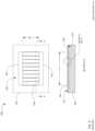
- FIG. 1shows a simplified schematic top view and orthogonal cross-sectional views of a transversely-excited film bulk acoustic resonator (XBAR) 100 as described in U.S. Pat. No. 10,491,192.
- XBAR resonatorssuch as the resonator 100 may be used in a variety of RF filters including band-reject filters, band-pass filters, duplexers, and multiplexers.
- XBARsare particularly suited for use in filters for communications bands with frequencies above 3 GHz.
- the XBAR 100is made up of a thin film conductor pattern formed on a surface of a piezoelectric plate 110 having parallel front and back surfaces 112 , 114 , respectively.
- the piezoelectric plateis a thin single-crystal layer of a piezoelectric material such as lithium niobate, lithium tantalate, lanthanum gallium silicate, gallium nitride, or aluminum nitride.
- the piezoelectric plateis cut such that the orientation of the X, Y, and Z crystalline axes with respect to the front and back surfaces is known and consistent.
- the piezoelectric platesare Z-cut, which is to say the Z axis is normal to the front and back surfaces 112 , 114 .
- XBARsmay be fabricated on piezoelectric plates with other crystallographic orientations.
- the back surface 114 of the piezoelectric plate 110is attached to a surface of the substrate 120 except for a portion of the piezoelectric plate 110 that forms a diaphragm 115 spanning a cavity 140 formed in the substrate.
- the portion of the piezoelectric plate that spans the cavityis referred to herein as the “diaphragm” 115 due to its physical resemblance to the diaphragm of a microphone.
- the diaphragm 115is contiguous with the rest of the piezoelectric plate 110 around all of a perimeter 145 of the cavity 140 .
- “contiguous”means “continuously connected without any intervening item”.
- the substrate 120provides mechanical support to the piezoelectric plate 110 .
- the substrate 120may be, for example, silicon, sapphire, quartz, or some other material or combination of materials.
- the back surface 114 of the piezoelectric plate 110may be bonded to the substrate 120 using a wafer bonding process.
- the piezoelectric plate 110may be grown on the substrate 120 or attached to the substrate in some other manner.
- the piezoelectric plate 110may be attached directly to the substrate or may be attached to the substrate 120 via one or more intermediate material layers.
- the cavity 140has its conventional meaning of “an empty space within a solid body.”
- the cavity 140may be a hole completely through the substrate 120 (as shown in Section A-A and Section B-B) or a recess in the substrate 120 (as shown subsequently in FIG. 3 A and FIG. 3 B ).
- the cavity 140may be formed, for example, by selective etching of the substrate 120 before or after the piezoelectric plate 110 and the substrate 120 are attached.
- the conductor pattern of the XBAR 100includes an interdigital transducer (IDT) 130 .
- the IDT 130includes a first plurality of fingers, such as finger 136 , extending from a first busbar 132 and a second plurality of fingers extending from a second busbar 134 .
- the first and second pluralities of fingersare interleaved.
- the interleaved fingersoverlap for a distance AP, commonly referred to as the “aperture” of the IDT.
- the center-to-center distance L between the outermost fingers of the IDT 130is the “length” of the IDT.
- the fingersare typically, but not necessarily, parallel to each other.
- the first and second busbars 132 , 134serve as the terminals of the XBAR 100 .
- the piezoelectric plate 110 and the IDT 130are configured such that a radio frequency or microwave signal applied between the two busbars 132 , 134 of the IDT 130 excites a primary acoustic mode within the piezoelectric plate 110 .
- the primary acoustic modeis a bulk shear mode where the primary direction of atomic motion within the piezoelectric plate 110 is parallel to the surfaces of the plate and perpendicular to the fingers of the IDT 130 .
- Acoustic energypropagates along a direction substantially orthogonal to the surface of the piezoelectric plate 110 , which is also normal, or transverse, to the direction of the electric field created by the IDT fingers.
- the XBARis considered a transversely-excited film bulk wave resonator.
- the IDT 130is positioned on the piezoelectric plate 110 such that at least the fingers of the IDT 130 are disposed on the diaphragm 115 of the piezoelectric plate that spans, or is suspended over, the cavity 140 .
- the cavity 140has a rectangular shape with an extent greater than the aperture AP and length L of the IDT 130 .
- a cavity of an XBARmay have a different shape, such as a regular or irregular polygon.
- the cavity of an XBARmay more or fewer than four sides, which may be straight or curved.
- the geometric pitch and width of the IDT fingersis greatly exaggerated with respect to the length (dimension L) and aperture (dimension AP) of the XBAR.
- a typical XBARhas more than ten parallel fingers in the IDT 110 .
- An XBARmay have hundreds, possibly thousands, of parallel fingers in the IDT 110 .
- the thickness of the fingers in the cross-sectional viewsis greatly exaggerated.
- FIG. 2shows a detailed schematic cross-sectional view of the XBAR 100 .
- the piezoelectric plate 110is a single-crystal layer of piezoelectrical material having a thickness ts.
- tsmay be, for example, 100 nm to 1500 nm.
- the thickness tsmay be, for example, 200 nm to 1000 nm.
- a front-side dielectric layer 214may optionally be formed on the front side of the piezoelectric plate 110 .
- the “front side” of the XBARis, by definition, the surface facing away from the substrate.
- the front-side dielectric layer 214has a thickness tfd.
- the front-side dielectric layer 214is formed between the IDT fingers 238 .
- the front side dielectric layer 214may also be deposited over the IDT fingers 238 .
- a back-side dielectric layer 216may optionally be formed on the back side of the piezoelectric plate 110 .
- the back-side dielectric layer 216has a thickness tbd.
- the front-side and back-side dielectric layers 214 , 216may be a non-piezoelectric dielectric material, such as silicon dioxide or silicon nitride.
- tfd and tbdmay be, for example, 0 to 500 nm.
- tfd and tbdare typically less than the thickness ts of the piezoelectric plate.
- tfd and tbdare not necessarily equal, and the front-side and back-side dielectric layers 214 , 216 are not necessarily the same material.
- Either or both of the front-side and back-side dielectric layers 214 , 216may be formed of multiple layers of two or more materials.
- the IDT fingers 238may be aluminum, a substantially aluminum alloys, copper, a substantially copper alloys, molybdenum, beryllium, gold, or some other conductive material. Thin (relative to the total thickness of the conductors) layers of other metals, such as chromium or titanium, may be formed under and/or over the fingers to improve adhesion between the fingers and the piezoelectric plate 110 and/or to passivate or encapsulate the fingers.
- the busbars ( 132 , 134 in FIG. 1 ) of the IDTmay be made of the same or different materials as the fingers.
- Dimension pis the “pitch” of the IDT fingers, which may be referred to as the pitch of the IDT and/or the pitch of the XBAR. For an IDT with constant pitch, the pitch is equal to the center-to-center spacing of the fingers.
- Dimension wis the width or “mark” of the IDT fingers.
- the IDT of an XBARdiffers substantially from the IDTs used in surface acoustic wave (SAW) resonators. In a SAW resonator, the pitch of the IDT is one-half of the acoustic wavelength at the resonance frequency. Additionally, the mark-to-pitch ratio of a SAW resonator IDT is typically close to 0.5 (i.e.
- the mark or finger widthis about one-fourth of the acoustic wavelength at resonance).
- the pitch p of the IDTis typically 2 to 20 times the width w of the fingers.
- the pitch p of the IDTis typically 2 to 20 times the thickness ts of the piezoelectric slab 212 .
- the width of the IDT fingers in an XBARis not constrained to one-fourth of the acoustic wavelength at resonance.
- the width of XBAR IDT fingersmay be 500 nm or greater, such that the IDT can be fabricated using optical lithography.
- the thickness tm of the IDT fingersmay be from 100 nm to about 2.5 times the thickness ts of the piezoelectric slab 212 .
- the thickness of the busbars ( 132 , 134 in FIG. 1 ) of the IDTmay be the same as, or greater than, the thickness tm of the IDT fingers.
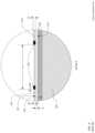
- FIG. 3shows a simplified schematic top view and an orthogonal cross-sectional view of a solidly-mounted transversely-excited film bulk acoustic resonator (SM XBAR) 300 as described in patent application Ser. No. 16/438,141.
- SM XBAR resonatorssuch as the resonator 300 , may be used in a variety of RF filters including band-reject filters, band-pass filters, duplexers, and multiplexers.
- the SM XBAR 300is made up of a thin film conductor pattern formed on a front surface 312 of a piezoelectric plate 310 having parallel front and back surfaces 312 , 314 , respectively.
- the piezoelectric plateis a thin single-crystal layer of a piezoelectric material such as lithium niobate, lithium tantalate, lanthanum gallium silicate, gallium nitride, or aluminum nitride.
- the piezoelectric plateis cut such that the orientation of the X, Y, and Z crystalline axes with respect to the front and back surfaces is known and consistent.
- the piezoelectric platesare Z-cut, which is to say the Z axis is normal to the surfaces of the plate.
- SM XBARsmay be fabricated on piezoelectric plates with other crystallographic orientations.
- the back surface 314 of the piezoelectric plate 310is attached to, and mechanically supported by, a substrate 320 .
- the substrate 320may be, for example, silicon, sapphire, quartz, or some other material.
- the piezoelectric plate 310may be attached to the substrate 320 via a plurality of intermediate material layers.
- the conductor pattern of the SM XBAR 300includes an IDT 330 similar to the IDT 130 previously described.
- the IDT 330includes a first plurality of fingers, such as finger 336 , extending from a first busbar 332 and a second plurality of fingers extending from a second busbar 334 .
- the first and second pluralities of parallel fingersare interleaved.
- the interleaved fingersoverlap for a distance AP, commonly referred to as the “aperture” of the IDT.
- the center-to-center distance L between the outermost fingers of the IDT 330is the “length” of the IDT.
- the first and second busbars 332 , 334serve as the terminals of the SM XBAR 300 .
- a radio frequency or microwave signal applied between the two busbars 332 , 334 of the IDT 330excites a primary acoustic wave within the piezoelectric plate 310 .
- the excited primary acoustic waveis a bulk shear wave that propagates in the direction normal to the surface of the piezoelectric plate 310 .
- the geometric pitch and width of the IDT fingersare greatly exaggerated with respect to the length (dimension L) and aperture (dimension AP) of the SM XBAR.
- a typical SM XBARhas more than ten parallel fingers in the IDT 310 .
- An SM XBARmay have hundreds, possibly thousands, of parallel fingers in the IDT 310 .
- the thickness of the fingers in the cross-sectional viewsis greatly exaggerated.
- FIG. 4shows a detailed schematic cross-sectional view of detail D of the SM XBAR 300 of FIG. 3 .
- the piezoelectric plate 310is a single-crystal layer of piezoelectric material having a thickness ts. ts may be, for example, 100 nm to 1500 nm.
- the IDT fingers 336may be one or more layers of conductive materials as previously described. Dimension p is the center-to-center spacing or “pitch” of the IDT fingers. Dimension w is the width or “mark” of the IDT fingers.
- a front-side dielectric layer 414may optionally be formed on the front surface 312 of the piezoelectric plate 310 .
- the front-side dielectric layer 414has a thickness tfd.
- the front-side dielectric layer 414may be formed between the IDT fingers 336 .
- the front side dielectric layer 414may also be deposited over the IDT fingers 336 .
- the front-side dielectric layer 414may be a non-piezoelectric dielectric material, such as silicon dioxide or silicon nitride.
- tfdmay be, for example, 0 to 500 nm.
- An acoustic Bragg reflector 440is sandwiched between a surface 322 of the substrate 320 and the back surface 314 of the piezoelectric plate 310 .
- the term “sandwiched”means the acoustic Bragg reflector 440 is both disposed between and physically connected to a surface 322 of the substrate 320 and the back surface 314 of the piezoelectric plate 310 .
- thin layers of additional materialsmay be disposed between the acoustic Bragg reflector 440 and the surface 322 of the substrate 320 and/or between the Bragg reflector 440 and the back surface 314 of the piezoelectric plate 310 .
- Such additional material layersmay be present, for example, to facilitate bonding the piezoelectric plate 310 , the acoustic Bragg reflector 440 , and the substrate 320 .
- the acoustic Bragg reflector 440includes multiple layers that alternate between materials having high acoustic impedance and materials have low acoustic impedance. “High” and “low” are relative terms. For each layer, the standard for comparison is the adjacent layers. Each “high” acoustic impedance layer has an acoustic impedance higher than that of both the adjacent low acoustic impedance layers. Each “low” acoustic impedance layer has an acoustic impedance lower than that of both the adjacent high acoustic impedance layers. Each of the layers has a thickness equal to, or about, one-fourth of the acoustic wavelength at or near a resonance frequency of the SM XBAR 300 .
- Materials having comparatively low acoustic impedanceinclude silicon dioxide, silicon oxycarbide, aluminum, and certain plastics such as cross-linked polyphenylene polymers.
- Materials having comparatively high acoustic impedanceinclude silicon nitride, aluminum nitride, silicon carbide, and metals such as molybdenum, tungsten, gold, and platinum. All of the high acoustic impedance layers of the acoustic Bragg reflector 440 are not necessarily the same material, and all of the low acoustic impedance layers are not necessarily the same material. In the example of FIG. 4 , the acoustic Bragg reflector 440 has a total of six layers. An acoustic Bragg reflector may have more than, or less than, six layers.
- the resonance and anti-resonance frequencies of the primary acoustic mode of an XBAR or an SM-XBARare determined by multiple factors including the type, crystallographic orientation, and thickness of the piezoelectric slab and the pitch and mark of the IDT fingers.
- different combinations of mark and pitch on the same piezoelectric diaphragmcan excite the same primary acoustic mode.
- two acoustic modesare considered to be the same if the two acoustic modes have the same direction of acoustic energy flow and the same resonance and/or anti-resonance frequencies.
- a radio frequency or microwave signal applied across the IDT of an XBAR or an SM-XBARmay also excite undesired spurious acoustics modes.
- the frequency and strength of such spurious acoustic modesalso depend on multiple factors including the pitch and mark of the IDT fingers. However, two or more mark/pitch combinations that excite the same primary acoustic mode do not necessarily excite the same spurious modes.
- the pitch and mark within an IDTis changed between two or more mark/pitch combinations that produce the same primary acoustic mode but different spurious modes, the different spurious modes will not add constructively over the area of the IDT.
- FIG. 5is an expanded schematic plan view of a unit cell 500 for an IDT where the pitch and mark vary along the length of the IDT.
- the scale of the plan viewhas been stretched or expanded horizontally for ease of presentation of the various dimensions.
- P 1is a first pitch value
- P 2is a second pitch value
- M 1is a first mark value
- M 2is a second mark value.
- the differences between P 1 and P 2 and between M 1 and M 2are exaggerated for ease of visualization.
- An IDT having a pitch P 1 and a mark M 1would excite a primary acoustic mode with particular resonance and antiresonance frequencies.
- An IDT having a pitch P 2 and a mark M 2would excite the same primary acoustic mode, which is to say a primary acoustic mode with the same resonance and/or antiresonance frequencies.
- the unit cell 500includes a first set of IDT fingers 512 , 514 , 516 extending from an upper busbar 510 , and a second set of IDT fingers 522 , 524 extending from a lower busbar 520 .
- directional termssuch as upper, lower, left, right, vertical, horizontal, etc. refer to direction or position within the drawing being discussed and do not imply any physical position or orientation.
- the unit cell 500is intended to be cascaded in the horizontal direction (as will be described in conjunction with FIG. 6 ) to form an IDT.
- the unit cell 500only includes portions of the end fingers 512 and 516 . Other portions of those fingers exist within adjacent unit cells (not shown in FIG. 5 ).
- the unit cell 500is divided into a first pitch/mark zone 530 and a second pitch/mark zone 540 .
- the pitch between adjacent fingersis P 1 and the mark of the fingers is M 1 .
- the pitch between adjacent fingersis P 2 and the mark of the fingers is M 2 .
- the mark/pitch combination of the IDTchanges between M 1 /P 1 and M 2 /P 2 every two fingers.
- each finger 512 , 514 , 516 of first set of IDT fingers extending from the upper busbar 510has a uniform width of (M 1 +M 2 )/2, including portions of fingers 512 and 516 within adjacent unit cells.
- the pitchis not measured to the respective centers of the first set of IDT fingers, but to a dashed line that divides each finger in a ratio of M 1 /M 2 .
- finger 514is divided such that the portion of the finger extending left into the 1 st pitch/mark zone 530 has a width of M 1 /2, and the portion of this finger extending right into the 2 nd pitch/mark zone 540 has a width of M 2 /2.
- the second set of IDT fingers 522 , 524 extending from the lower busbar 520has a center-to-center distance between adjacent fingers equal to P 1 +P 2 .
- the mark of the second set of IDT fingers 522 , 524alternates between M 1 (e.g. finger 522 ) and M 2 (e.g. finger 524 ).
- the net effectis that the unit cell 500 has two periods of pitch P 1 and mark M 1 followed by two periods of pitch P 2 and mark M 2 .
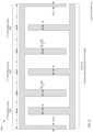
- FIG. 6is a schematic plan view of an IDT 600 composed of eight copies 500 A to 500 H of the unit cell 500 juxtaposed along the length of the IDT 600 resulting in a total of 33 fingers.
- the IDT 600is shown reasonably to scale (approximately 1600:1), with the exception that the differences between P 1 and P 2 and between M 1 and M 2 are still exaggerated for ease of visualization.
- the IDT 600has eight first pitch/mark zones 630 A to 630 H in which the pitch and mark are P 1 and M 1 , respectively.
- the eight first pitch/mark zones 630 A to 630 Hare interleaved with eight second pitch/mark zones 640 A to 640 H, in which the pitch and mark are P 2 and M 2 , respectively.
- a pattern of two periods of pitch P 1 and mark M 1 alternating with two periods of pitch P 2 and mark M 2is continued along the length of the IDT.
- Using eight copies of the unit cell 500is exemplary and an IDT may use more or fewer than 8 unit cells and have more or fewer than 33 fingers.
- the unit cell 500is exemplary.
- a unit cell for varying the pitch and mark along the length of an IDTmay, for example, may have three or more consecutive periods of each mark/pitch combination as shown in FIG. 7 .
- FIG. 7shows a unit cell 700 including a first pitch/mark zone 730 in which the pitch and mark are P 1 and M 1 , respectively, and a second pitch/mark zone 740 in which the pitch and mark are P 2 and M 2 , respectively.
- Each pitch/mark zone 730 , 740includes three periods of the respective pitch/mark combination.
- a unit cell for varying the pitch and mark along the length of an IDTmay cycle between three or more mark/pitch zones as shown in FIG. 8 .
- FIG. 8shows a unit cell 800 including a first pitch/mark zone 830 in which the pitch and mark are P 1 and M 1 , respectively, a second pitch/mark zone 840 in which the pitch and mark are P 2 and M 2 , respectively, and a third pitch/mark zone 850 in which the pitch and mark are P 3 and M 3 , respectively.
- the pitch and mark of the three pitch/mark zonesare unique, which is to say P 1 ⁇ P 2 ⁇ P 3 ⁇ P 1 and M 1 ⁇ M 2 ⁇ M 3 ⁇ M 1 .
- Each pitch/mark zone 830 , 840 , 850includes two periods of the respective pitch/mark combination.
- each pitch/mark zonewill have a unique pitch and unique mark that are not equal to the pitch and mark, respectively, of any other pitch/mark zone.
- FIG. 9is an expanded schematic plan view of a unit cell 900 for an IDT where pitch and mark vary across the aperture of the IDT.
- the scale of the plan viewhas been stretched or expanded horizontally for ease of presentation of the various dimensions.
- P 1is a first pitch value
- P 2is a second pitch value
- M 1is a first mark value
- M 2is a second mark value.
- the differences between P 1 and P 2 and between M 1 and M 2are exaggerated for ease of visualization.
- An IDT having a pitch P 1 and a mark M 1would excite a primary acoustic mode with particular resonance and antiresonance frequencies.
- An IDT having a pitch P 2 and a mark M 2would excite the same primary acoustic mode, which is to say a primary acoustic mode with the same resonance and/or antiresonance frequencies.
- the unit cell 900includes a first set of IDT fingers 912 , 914 , 916 extending from an upper busbar 910 , and a second set of IDT fingers 922 , 924 extending from a lower busbar 920 .
- the unit cell 900is intended to be cascaded in the horizontal direction to form an IDT.
- the unit cell 900only includes portions of the end fingers 912 and 916 . Other portions of those fingers exist within adjacent unit cells (not shown in FIG. 9 ).
- dot-dash rectangles 930identify first pitch/mark zones of the IDT where the local pitch is P 1 and the local mark is M 1 .
- dashed rectangles 940identify second pitch/mark zones of the IDT where the local pitch is P 2 and the local mark is M 2 .
- the mark/pitch combination of the IDTsteps between M 1 /P 1 and M 2 /P 2 across the aperture AP for every pair of fingers.
- the pitch between fingers 912 and 922is P 2 and the mark is M 2 over the upper half of the aperture proximate the upper busbar 910 .
- the pitch between fingers 912 and 922is P 1 and the mark is M 1 over the lower half of the aperture AP proximate the lower busbar 920 .
- the upper half of the aperture between fingers 912 and 922is a 2 nd pitch/mark zone 940 (as indicated by the dashed rectangle).
- the lower half of the aperture between fingers 912 and 922is a 1st pitch/mark zone 930 (as indicated by the dot-dash rectangle).
- the change between a first pitch/mark zone and a second pitch/mark zoneis reversed between fingers 922 and 914 .
- the unit cell 900may be cascaded to provide an IDT with any desired length with a corresponding number of fingers.
- the unit cell 900is exemplary.
- a unit cell for varying the pitch and mark across the aperture of an IDTmay, for example, switch between three or more mark/pitch combinations and may switch between pitch/mark combinations in two or more steps across the aperture.
- FIG. 10is an expanded schematic plan view of another unit cell 1000 for an IDT with pitch and mark continuously varied across the aperture of the IDT.
- the scale of the plan viewhas been stretched or expanded horizontally for ease of presentation of the various dimensions.
- P 1is a first pitch value
- P 2is a second pitch value
- M 1is a first mark value
- M 2is a second mark value.
- the differences between P 1 and P 2 and between M 1 and M 2are exaggerated for ease of visualization.
- An IDT having a pitch P 1 and a mark M 1would excite a primary acoustic mode with particular resonance and antiresonance frequencies.
- An IDT having a pitch P 2 and a mark M 2would excite the same primary acoustic mode, which is to say a primary acoustic mode with the same resonance and/or antiresonance frequencies.
- the unit cell 1000includes a first set of IDT fingers 1012 , 1014 , 1016 extending from an upper busbar 1010 , and a second set of IDT fingers 1022 , 1024 extending from a lower busbar 1020 .
- the unit cell 1000is intended to be cascaded in the horizontal direction (as was described in conjunction with FIG. 6 ) to form an IDT.
- the unit cell 1000only includes portions of the end fingers 1012 and 1016 . Other portions of those fingers exist within adjacent unit cells (not shown in FIG. 10 ).
- the mark/pitch combination of the IDTvaries continuously between M 1 /P 1 and M 2 /P 2 across the aperture of the IDT for every pair of fingers.
- the pitch between fingers 1022 and 1014is P 1 at the upper edge of the aperture AP proximate the upper busbar 1010 and P 2 at the lower edge of the aperture AP proximate the lower busbar 1020 .
- At least portions of fingers 1022 and 1024 within the aperture APare tilted, which is to say not perpendicular to the lower bus bar 1020 .
- the portion of finger 1022 within the aperture APtilts from perpendicular to the lower busbar 1020 by an angle equal to the arctangent of (P 2 -P 1 )/AP.
- the portion of finger 1024 within the aperture APtilts from perpendicular to the lower busbar 1020 by the same angular magnitude in the opposite direction of the tilt of finger 1022 .
- the spacing between adjacent fingers in the same set of fingersis P 2 +P 1 .
- the markmust also vary across the aperture.
- the first set of IDT fingers 1012 , 1014 , 1016 extending from the upper busbar 1010are tapered and the second set of IDT fingers 1022 , 1024 extending from the lower busbar 1020 are tilted.
- the width of fingers 1012 and 1016is M 1 at the upper edge of the aperture AP proximate the upper busbar 1010 and M 2 at the lower edge of the aperture AP proximate the lower busbar 1020 .
- the width of finger 1014is M 2 at the upper edge of the aperture AP proximate the upper busbar 1010 and M 1 at the lower edge of the aperture AP proximate the lower busbar 1020 .
- the tilted fingers 1022 and 1024have a fixed width, parallel to the busbars 1010 , 1020 equal to (M 1 +M 2 )/2. Simulation results show that an RF signal applied to the unit cell 100 excites essentially the same shear primary acoustic mode over the entire unit cell 1000 .
- FIG. 11is a schematic plan view of an IDT 1100 composed of eight copies 1000 A TO 1000 H of the unit cell 1000 juxtaposed along the length of an IDT with a total of 33 fingers.
- the IDT 1100is shown reasonably to scale. For every pair of adjacent fingers, the effective mark and pitch vary between M 1 /P 1 and M 2 /P 2 across the aperture of the IDT.
- the IDT 1100is exemplary.
- An IDT with varied pitch and mark across the aperturemay, for example, have more or fewer that 8 unit cells and more or fewer than 33 fingers.
- An IDTmay use two or more two or more different unit cells in rotation.
- FIG. 12is a chart illustrating the effect that varying IDT pitch and mark can have on XBAR performance.
- the solid curve 1210is a plot of the magnitude of the admittance as a function of frequency for a representative conventional XBAR device with fixed IDT pitch and mark.
- the dashed curve 1210exhibits a primary acoustic mode with a resonance at about 4.72 GHz and an antiresonance at about 5.31 GHz.
- the curve 1220also exhibits spurious acoustic modes (which are circled in FIG. 12 ) at about 4.15 GHz, 4.75 GHz, 4.95 GHz, and 5.85 GHz to 5.9 GHz.
- the dashed curve 1220is a plot of the magnitude of the admittance as a function of frequency for a comparable XBAR device with the IDT pitch and mark varied across the aperture as shown in FIG. 10 and FIG. 11 .
- the curve 1220exhibits a primary acoustic mode that is essentially the same as the primary acoustic mode of the conventional XBAR device (solid curve 1210 ).
- the various spurious acoustic modesare substantially suppressed by varying the IDT pitch and mark.
- the curves 1210 and 1220 in FIG. 12are result of simulation of XBAR devices using a finite element method.
- the representative XBAR device(solid curve 1210 ) had a lithium niobate diaphragm 400 nm thick and aluminum electrodes 100 nm thick.
- the pitch and mark of the IDTwere 3.875 m and 850 nm, respectively.
- the XBAR device with varying mark and pitch(dashed curve 1220 ) also has a lithium niobate diaphragm 400 nm thick and aluminum electrodes 100 nm thick.
- the XBAR devices simulated to generate the curves 1210 and 1220are exemplary. XBAR devices may be designed with different dimensions for operation at the same or other frequencies.
- “plurality”means two or more. As used herein, a “set” of items may include one or more of such items.
- the terms “comprising”, “including”, “carrying”, “having”, “containing”, “involving”, and the likeare to be understood to be open-ended, i.e., to mean including but not limited to. Only the transitional phrases “consisting of” and “consisting essentially of”, respectively, are closed or semi-closed transitional phrases with respect to claims.
Landscapes
- Physics & Mathematics (AREA)
- Acoustics & Sound (AREA)
- Chemical & Material Sciences (AREA)
- Engineering & Computer Science (AREA)
- Materials Engineering (AREA)
- Crystallography & Structural Chemistry (AREA)
- Piezo-Electric Or Mechanical Vibrators, Or Delay Or Filter Circuits (AREA)
- Surface Acoustic Wave Elements And Circuit Networks Thereof (AREA)
Abstract
Description
Claims (19)
Priority Applications (12)
| Application Number | Priority Date | Filing Date | Title |
|---|---|---|---|
| US17/460,737US12009804B2 (en) | 2019-08-28 | 2021-08-30 | Transversely-excited film bulk acoustic resonator with interdigital transducer with varied mark and pitch |
| US17/560,889US12237826B2 (en) | 2018-06-15 | 2021-12-23 | Transversely-excited film bulk acoustic resonator with optimized electrode thickness, mark, and pitch |
| US17/561,714US11929731B2 (en) | 2018-02-18 | 2021-12-24 | Transversely-excited film bulk acoustic resonator with optimized electrode mark, and pitch |
| US17/563,360US11824520B2 (en) | 2018-06-15 | 2021-12-28 | Transversely-excited film bulk acoustic resonator with optimized electrode thickness, mark, and pitch |
| US17/563,384US12021502B2 (en) | 2018-06-15 | 2021-12-28 | Transversely-excited film bulk acoustic resonator with multi-mark electrodes and optimized electrode thickness |
| US17/565,720US20220131525A1 (en) | 2018-06-15 | 2021-12-30 | Transversely-excited film bulk acoustic resonator with optimized piezoelectric plate thickness |
| US17/565,762US12021503B2 (en) | 2018-06-15 | 2021-12-30 | Transversely-excited film bulk acoustic resonator with optimized piezoelectric plate thickness and having multiple pitches and marks |
| US17/565,695US20220123723A1 (en) | 2018-06-15 | 2021-12-30 | Transversely-excited film bulk acoustic resonator with optimized piezoelectric plate thickness and electrode mark and pitch |
| US17/584,396US12021504B2 (en) | 2018-06-15 | 2022-01-26 | Transversely-excited film bulk acoustic resonator with a front-side dielectric layer and optimized pitch and mark |
| US17/696,105US11942922B2 (en) | 2018-06-15 | 2022-03-16 | Transversely-excited film bulk acoustic resonator with optimized electrode thickness, mark, and pitch |
| US18/478,406US12095446B2 (en) | 2018-06-15 | 2023-09-29 | Transversely-excited film bulk acoustic resonator with optimized electrode thickness, mark, and pitch |
| US19/030,388US20250247073A1 (en) | 2018-06-15 | 2025-01-17 | Transversely-excited film bulk acoustic resonator with optimized piezoelectric plate thickness |
Applications Claiming Priority (3)
| Application Number | Priority Date | Filing Date | Title |
|---|---|---|---|
| US201962892871P | 2019-08-28 | 2019-08-28 | |
| US16/805,471US11206009B2 (en) | 2019-08-28 | 2020-02-28 | Transversely-excited film bulk acoustic resonator with interdigital transducer with varied mark and pitch |
| US17/460,737US12009804B2 (en) | 2019-08-28 | 2021-08-30 | Transversely-excited film bulk acoustic resonator with interdigital transducer with varied mark and pitch |
Related Parent Applications (2)
| Application Number | Title | Priority Date | Filing Date |
|---|---|---|---|
| US16/805,471ContinuationUS11206009B2 (en) | 2018-02-18 | 2020-02-28 | Transversely-excited film bulk acoustic resonator with interdigital transducer with varied mark and pitch |
| US17/388,745Continuation-In-PartUS12088281B2 (en) | 2018-02-18 | 2021-07-29 | Transversely-excited film bulk acoustic resonator with multi-mark interdigital transducer |
Related Child Applications (2)
| Application Number | Title | Priority Date | Filing Date |
|---|---|---|---|
| US17/229,767Continuation-In-PartUS12040779B2 (en) | 2018-02-18 | 2021-04-13 | Small transversely-excited film bulk acoustic resonators with enhanced Q-factor |
| US17/560,889Continuation-In-PartUS12237826B2 (en) | 2018-02-18 | 2021-12-23 | Transversely-excited film bulk acoustic resonator with optimized electrode thickness, mark, and pitch |
Publications (2)
| Publication Number | Publication Date |
|---|---|
| US20210391847A1 US20210391847A1 (en) | 2021-12-16 |
| US12009804B2true US12009804B2 (en) | 2024-06-11 |
Family
ID=74679197
Family Applications (3)
| Application Number | Title | Priority Date | Filing Date |
|---|---|---|---|
| US16/805,471Active2040-03-13US11206009B2 (en) | 2018-02-18 | 2020-02-28 | Transversely-excited film bulk acoustic resonator with interdigital transducer with varied mark and pitch |
| US17/128,593Active2041-08-16US11949403B2 (en) | 2019-08-28 | 2020-12-21 | Transversely-excited film bulk acoustic resonator with interdigital transducer with varied mark and pitch |
| US17/460,737Active2041-02-10US12009804B2 (en) | 2018-02-18 | 2021-08-30 | Transversely-excited film bulk acoustic resonator with interdigital transducer with varied mark and pitch |
Family Applications Before (2)
| Application Number | Title | Priority Date | Filing Date |
|---|---|---|---|
| US16/805,471Active2040-03-13US11206009B2 (en) | 2018-02-18 | 2020-02-28 | Transversely-excited film bulk acoustic resonator with interdigital transducer with varied mark and pitch |
| US17/128,593Active2041-08-16US11949403B2 (en) | 2019-08-28 | 2020-12-21 | Transversely-excited film bulk acoustic resonator with interdigital transducer with varied mark and pitch |
Country Status (1)
| Country | Link |
|---|---|
| US (3) | US11206009B2 (en) |
Families Citing this family (14)
| Publication number | Priority date | Publication date | Assignee | Title |
|---|---|---|---|---|
| US11206009B2 (en)* | 2019-08-28 | 2021-12-21 | Resonant Inc. | Transversely-excited film bulk acoustic resonator with interdigital transducer with varied mark and pitch |
| US20210273629A1 (en)* | 2020-02-28 | 2021-09-02 | Resonant Inc. | Transversely-excited film bulk acoustic resonator with multi-pitch interdigital transducer |
| US12341490B2 (en) | 2020-04-20 | 2025-06-24 | Murata Manufacturing Co., Ltd. | Low loss transversely-excited film bulk acoustic resonators and filters |
| US11476834B2 (en) | 2020-10-05 | 2022-10-18 | Resonant Inc. | Transversely-excited film bulk acoustic resonator matrix filters with switches in parallel with sub-filter shunt capacitors |
| US11658639B2 (en) | 2020-10-05 | 2023-05-23 | Murata Manufacturing Co., Ltd. | Transversely-excited film bulk acoustic resonator matrix filters with noncontiguous passband |
| US11728784B2 (en) | 2020-10-05 | 2023-08-15 | Murata Manufacturing Co., Ltd. | Transversely-excited film bulk acoustic resonator matrix filters with split die sub-filters |
| US11496113B2 (en) | 2020-11-13 | 2022-11-08 | Resonant Inc. | XBAR devices with excess piezoelectric material removed |
| US12348216B2 (en) | 2021-03-24 | 2025-07-01 | Murata Manufacturing Co., Ltd. | Acoustic filters with shared acoustic tracks and cascaded series resonators |
| CN117321912A (en)* | 2021-03-30 | 2023-12-29 | 株式会社村田制作所 | Filters for 6GHz WI-FI using transversely excited thin film bulk acoustic resonators |
| US12057823B2 (en) | 2021-05-07 | 2024-08-06 | Murata Manufacturing Co., Ltd. | Transversely-excited film bulk acoustic resonator with concentric interdigitated transducer fingers |
| WO2023048256A1 (en)* | 2021-09-27 | 2023-03-30 | 株式会社村田製作所 | Elastic wave device |
| US12407326B2 (en) | 2021-11-04 | 2025-09-02 | Murata Manufacturing Co., Ltd. | Stacked die transversely-excited film bulk acoustic resonator (XBAR) filters |
| WO2023190369A1 (en)* | 2022-03-29 | 2023-10-05 | 株式会社村田製作所 | Elastic wave device |
| CN119174105A (en)* | 2022-05-13 | 2024-12-20 | 株式会社村田制作所 | Elastic wave device and filter device |
Citations (215)
| Publication number | Priority date | Publication date | Assignee | Title |
|---|---|---|---|---|
| US5446330A (en) | 1993-03-15 | 1995-08-29 | Matsushita Electric Industrial Co., Ltd. | Surface acoustic wave device having a lamination structure |
| US5552655A (en) | 1994-05-04 | 1996-09-03 | Trw Inc. | Low frequency mechanical resonator |
| US5631515A (en) | 1994-03-17 | 1997-05-20 | Fujitsu Limited | Surface acoustic wave device |
| US5726610A (en) | 1995-06-19 | 1998-03-10 | Motorola Inc. | Saw filter device for radio tranceiver utilizing different coupling coefficient ratios |
| JPH10209804A (en) | 1997-01-27 | 1998-08-07 | Oki Electric Ind Co Ltd | Surface acoustic wave resonator and surface acoustic wave filter |
| US5853601A (en) | 1997-04-03 | 1998-12-29 | Northrop Grumman Corporation | Top-via etch technique for forming dielectric membranes |
| JP2001244785A (en) | 2000-02-29 | 2001-09-07 | Kyocera Corp | Surface acoustic wave device |
| US6377140B1 (en) | 1999-07-09 | 2002-04-23 | Oki Electric Industry Co., Ltd. | Saw resonator filter with bridged-T configuration |
| US20020079986A1 (en) | 2000-12-21 | 2002-06-27 | Ruby Richard C. | Bulk acoustic resonator perimeter reflection system |
| JP2002300003A (en) | 2001-03-29 | 2002-10-11 | Kyocera Corp | Elastic wave filter |
| US20020158714A1 (en) | 2001-04-27 | 2002-10-31 | Nokia Corporation | Method and system for wafer-level tuning of bulk acoustic wave resonators and filters by reducing thickness non-uniformity |
| US20020189062A1 (en) | 2001-06-15 | 2002-12-19 | Asia Pacific Microsystems, Inc. | Manufacturing method for a high quality film bulk acoustic wave device |
| US6516503B1 (en) | 1999-05-26 | 2003-02-11 | Murata Manufacturing Co., Ltd. | Method of making surface acoustic wave device |
| JP2003078389A (en) | 2001-08-31 | 2003-03-14 | Matsushita Electric Ind Co Ltd | Surface acoustic wave device and method of manufacturing the same |
| US6540827B1 (en) | 1998-02-17 | 2003-04-01 | Trustees Of Columbia University In The City Of New York | Slicing of single-crystal films using ion implantation |
| US20030080831A1 (en) | 2001-10-25 | 2003-05-01 | Naumenko Natalya F. | Surface acoustic wave devices using optimized cuts of lithium niobate (LiNbO3) |
| US6570470B2 (en) | 2000-06-30 | 2003-05-27 | Kyocera Corporation | Surface acoustic wave ladder filter utilizing parallel resonators with different resonant frequencies |
| US20030199105A1 (en) | 2002-04-22 | 2003-10-23 | Kub Francis J. | Method for making piezoelectric resonator and surface acoustic wave device using hydrogen implant layer splitting |
| US20040041496A1 (en) | 2002-09-04 | 2004-03-04 | Fujitsu Media Devices Limited | Surface acoustic wave device, filter device and method of producing the surface acoustic wave device |
| US6707229B1 (en)* | 1999-06-03 | 2004-03-16 | Tele Filter Zweigniederlassung Der Dover Germany Gmbh | Surface acoustic wave filter |
| JP2004129222A (en) | 2002-07-31 | 2004-04-22 | Murata Mfg Co Ltd | Piezoelectric component and method of manufacturing the same |
| US20040100164A1 (en) | 2002-11-26 | 2004-05-27 | Murata Manufacturing Co., Ltd. | Manufacturing method of electronic device |
| JP2004523179A (en) | 2001-03-13 | 2004-07-29 | エプコス アクチエンゲゼルシャフト | Transducer structure operated by sound waves |
| US20040207485A1 (en) | 2003-03-31 | 2004-10-21 | Osamu Kawachi | Surface acoustic wave device and method of fabricating the same |
| US6833774B2 (en) | 2002-06-25 | 2004-12-21 | Sawtek, Inc. | Surface acoustic wave filter |
| US20040261250A1 (en) | 2000-09-06 | 2004-12-30 | Murata Manufacturing Co., Ltd. | Method for adjusting a frequency characteristic of an edge reflection type surface acoustic wave device and method for producing an- edge reflection type surface acoustic wave device |
| US20050099091A1 (en) | 2003-11-12 | 2005-05-12 | Fujitsu Media Devices Limited | Elastic boundary wave device and method of manufacturing the same |
| US20050185026A1 (en) | 2004-01-26 | 2005-08-25 | Motohisa Noguchi | Piezoelectric element, piezoelectric actuator, ink jet recording head, ink jet printer, surface acoustic wave element, frequency filter, oscillator, electronic circuit, thin film piezoelectric resonator, and electronic apparatus |
| US20050218488A1 (en) | 2004-03-31 | 2005-10-06 | Mie Matsuo | Electronic component having micro-electrical mechanical system |
| US20050264136A1 (en) | 2004-05-31 | 2005-12-01 | Jun Tsutsumi | Surface acoustic wave device |
| US20060131731A1 (en) | 2004-11-22 | 2006-06-22 | Takao Sato | Midair semiconductor device and manufacturing method of the same |
| US20060152107A1 (en) | 2005-01-07 | 2006-07-13 | Seiko Epson Corporation | Lamb-wave high-frequency resonator |
| US20060179642A1 (en) | 2005-02-03 | 2006-08-17 | Kabushiki Kaisha Toshiba | Method for manufacturing a film bulk acoustic resonator |
| US20070090898A1 (en) | 2003-12-16 | 2007-04-26 | Murata Manufacturing Co., Ltd. | Boundary acoustic wave device |
| US20070115079A1 (en) | 2004-07-20 | 2007-05-24 | Murata Manufacturing Co., Ltd. | Piezoelectric filter |
| US20070182510A1 (en) | 2006-02-06 | 2007-08-09 | Samsung Electronics Co., Ltd. | Multi-band filter module and method of fabricating the same |
| US20070188047A1 (en) | 2006-02-16 | 2007-08-16 | Seiko Epson Corporation | Lamb wave type frequency device and method thereof |
| US20070194863A1 (en) | 2006-02-17 | 2007-08-23 | Kabushiki Kaisha Toshiba | Film bulk acoustic resonator and method of manufacturing same |
| US20070267942A1 (en) | 2006-05-19 | 2007-11-22 | Hisanori Matsumoto | Piezoelectric film resonator, radio-frequency filter using them, and radio-frequency module using them |
| JP2007329584A (en) | 2006-06-06 | 2007-12-20 | Fujitsu Media Device Kk | Boundary acoustic wave element, resonator and filter |
| US20070296304A1 (en) | 2006-06-22 | 2007-12-27 | Seiko Epson Corporation | Acoustic wave device and method of manufacturing acoustic wave device |
| US20080018414A1 (en) | 2006-07-24 | 2008-01-24 | Fujitsu Media Devices Limited | Elastic wave device and manufacturing method of the same |
| US7345400B2 (en) | 2003-01-27 | 2008-03-18 | Murata Manufacturing Co., Ltd. | Surface acoustic wave device |
| US20080246559A1 (en) | 2007-01-19 | 2008-10-09 | Farrokh Ayazi | Lithographically-defined multi-standard multi-frequency high-Q tunable micromechanical resonators |
| US20080297280A1 (en) | 2007-05-31 | 2008-12-04 | Robert Thalhammer | Integrated Coupled Resonator Filter and Bulk Acoustic Wave Devices |
| US7463118B2 (en) | 2006-06-09 | 2008-12-09 | Texas Instruments Incorporated | Piezoelectric resonator with an efficient all-dielectric Bragg reflector |
| US7535152B2 (en) | 2005-10-19 | 2009-05-19 | Murata Manufacturing Co., Ltd. | Lamb wave device |
| US20090315640A1 (en) | 2008-06-24 | 2009-12-24 | Murata Manufacturing Co., Ltd. | Duplexer |
| JP2010062816A (en) | 2008-09-03 | 2010-03-18 | Murata Mfg Co Ltd | Acoustic wave filter |
| US7684109B2 (en) | 2007-02-28 | 2010-03-23 | Maxim Integrated Products, Inc. | Bragg mirror optimized for shear waves |
| WO2010047114A1 (en) | 2008-10-24 | 2010-04-29 | エプソントヨコム株式会社 | Surface acoustic wave resonator, surface acoustic wave oscillator, and surface acoustic wave modular device |
| JP2010103803A (en) | 2008-10-24 | 2010-05-06 | Epson Toyocom Corp | Surface acoustic wave resonator, surface acoustic wave oscillator, and surface acoustic wave module device |
| US20100123367A1 (en) | 2008-11-19 | 2010-05-20 | Ngk Insulators, Ltd. | Lamb wave device |
| US20100212127A1 (en) | 2009-02-24 | 2010-08-26 | Habbo Heinze | Process for Adapting Resonance Frequency of a BAW Resonator |
| JP2010233210A (en) | 2009-03-03 | 2010-10-14 | Nippon Dempa Kogyo Co Ltd | Elastic wave device and electronic component |
| US20100301703A1 (en) | 2009-03-31 | 2010-12-02 | Sand9, Inc. | Integration of piezoelectric materials with substrates |
| US7868519B2 (en) | 2007-09-06 | 2011-01-11 | Murata Manufacturing Co., Ltd. | Piezoelectric resonator including an acoustic reflector portion |
| US20110018654A1 (en) | 2009-07-27 | 2011-01-27 | Avago Technologies Wireless Ip (Singapore) Pte. Ltd. | Resonator filter with multiple cross-couplings |
| US20110018389A1 (en) | 2008-01-30 | 2011-01-27 | Kyocera Corporation | Acoustic Wave Device and Method for Production of Same |
| US20110102107A1 (en) | 2008-02-05 | 2011-05-05 | Nihon Dempa Kogyo Co., Ltd. | Filter, portable terminal and electronic component |
| US7941103B2 (en) | 2005-11-15 | 2011-05-10 | Taiyo Yuden Co., Ltd. | Duplexer |
| US7939987B1 (en) | 2008-10-23 | 2011-05-10 | Triquint Semiconductor, Inc. | Acoustic wave device employing reflective elements for confining elastic energy |
| US20110109196A1 (en) | 2008-07-11 | 2011-05-12 | Goto Rei | Plate wave element and electronic equipment using same |
| US20110199160A1 (en)* | 2008-10-24 | 2011-08-18 | Epson Toyocom Corporation | Surface acoustic wave resonator, surface acoustic wave oscillator, and surface acoustic wave module unit |
| US20110278993A1 (en) | 2010-05-17 | 2011-11-17 | Murata Manufacturing Co., Ltd. | Method for manufacturing composite piezoelectric substrate and piezoelectric device |
| US8278802B1 (en) | 2008-04-24 | 2012-10-02 | Rf Micro Devices, Inc. | Planarized sacrificial layer for MEMS fabrication |
| US8294330B1 (en) | 2009-03-31 | 2012-10-23 | Triquint Semiconductor, Inc. | High coupling, low loss saw filter and associated method |
| US20120286900A1 (en) | 2010-01-28 | 2012-11-15 | Murata Manufacturing Co., Ltd. | Tunable filter |
| WO2013021948A1 (en) | 2011-08-08 | 2013-02-14 | 株式会社村田製作所 | Elastic wave device |
| US20130057360A1 (en) | 2010-04-23 | 2013-03-07 | Teknologian Tutkimuskeskus Vtt | Wide-band acoustically coupled thin-film baw filter |
| US20130207747A1 (en) | 2010-12-28 | 2013-08-15 | Kyocera Corporation | Acoustic wave element and acoustic wave device using same |
| US20130234805A1 (en) | 2012-03-07 | 2013-09-12 | Taiyo Yuden Co., Ltd. | Resonator, frequency filter, duplexer, electronic device, and method of manufacturing resonator |
| US20130271238A1 (en) | 2012-04-13 | 2013-10-17 | Taiyo Yuden Co., Ltd. | Filter device, manufacturing method for filter device, and duplexer |
| US20130278609A1 (en) | 2012-04-19 | 2013-10-24 | Qualcomm Mems Technologies, Inc. | Isotropically-etched cavities for evanescent-mode electromagnetic-wave cavity resonators |
| US20130321100A1 (en) | 2012-06-05 | 2013-12-05 | Avago Technologies Wireless Ip (Singapore) Pte. Ltd. | Laterally-coupled acoustic resonators |
| US20140009032A1 (en) | 2012-07-04 | 2014-01-09 | Taiyo Yuden Co., Ltd. | Lamb wave device and manufacturing method thereof |
| US20140009247A1 (en) | 2012-07-03 | 2014-01-09 | Taiyo Yuden Co., Ltd. | Duplexer |
| US20140113571A1 (en) | 2012-10-18 | 2014-04-24 | Panasonic Corporation | Electronic device including filter |
| US20140130319A1 (en) | 2010-09-28 | 2014-05-15 | Murata Manufacturing Co., Ltd. | Method for manufacturing piezoelectric device |
| US20140151151A1 (en) | 2010-10-15 | 2014-06-05 | Commissariat A L'energie Atomique Et Aux Energies Alternatives | Heterogenous acoustic structure formed from a homogeneous material |
| US20140152145A1 (en) | 2010-11-30 | 2014-06-05 | Murata Manufacturing Co., Ltd. | Elastic wave device and manufacturing method for same |
| US20140173862A1 (en) | 2007-12-25 | 2014-06-26 | Murata Manufacturing Co., Ltd. | Method for manufacturing composite piezoelectric substrate |
| US20140225684A1 (en) | 2011-10-24 | 2014-08-14 | Murata Manufacturing Co., Ltd. | Surface acoustic wave device |
| US8816567B2 (en) | 2011-07-19 | 2014-08-26 | Qualcomm Mems Technologies, Inc. | Piezoelectric laterally vibrating resonator structure geometries for spurious frequency suppression |
| US8829766B2 (en) | 2008-08-01 | 2014-09-09 | Epcos Ag | Piezoelectric resonator operating in thickness shear mode |
| US20140312994A1 (en) | 2011-11-11 | 2014-10-23 | Teknologian tutkimuskeskut VTT | Laterally coupled bulk acoustic wave filter with improved passband characteristics |
| US8932686B2 (en) | 2008-10-31 | 2015-01-13 | Murata Manufacturing Co., Ltd. | Method for producing piezoelectric composite substrate |
| US20150014795A1 (en) | 2013-07-10 | 2015-01-15 | Avago Technologies General Ip (Singapore) Pte. Ltd. | Surface passivation of substrate by mechanically damaging surface layer |
| US20150042417A1 (en) | 2013-08-06 | 2015-02-12 | Murata Manufacturing Co., Ltd. | High-frequency module |
| JP2015054986A (en) | 2013-09-11 | 2015-03-23 | 太陽誘電株式会社 | Aluminum nitride film forming method, acoustic wave device manufacturing method, and aluminum nitride film manufacturing apparatus |
| US20150165479A1 (en) | 2013-12-12 | 2015-06-18 | Qualcomm Incorporated | Piezoelectric ultrasonic transducer and process |
| WO2015098694A1 (en) | 2013-12-26 | 2015-07-02 | 株式会社村田製作所 | Elastic wave device, and production method therefor |
| US20150244149A1 (en) | 2012-05-30 | 2015-08-27 | Euphoenix B.V. | Tunable Semiconductor Device And Method For Making Tunable Semiconductor Device |
| US9130145B2 (en) | 2012-03-29 | 2015-09-08 | Vectron International Gmbh | Surface acoustic wave component |
| US20150319537A1 (en) | 2012-12-12 | 2015-11-05 | Epcos Ag | Electroacoustic Components and Methods Thereof |
| JP2016001923A (en) | 2013-02-27 | 2016-01-07 | 京セラ株式会社 | Elastic wave device, duplexer and communication module |
| US9240768B2 (en) | 2011-11-22 | 2016-01-19 | Taiyo Yuden Co., Ltd. | Duplexer with transmission and reception filters each including resonators formed on different chips |
| US20160028367A1 (en) | 2014-07-25 | 2016-01-28 | Akoustis, Inc. | Single crystal acoustic resonator and bulk acoustic wave filter |
| US20160036415A1 (en) | 2014-07-31 | 2016-02-04 | Skyworks Panasonic Filter Solutions Japan Co., Ltd. | Elastic wave filters and duplexers using same |
| WO2016017104A1 (en) | 2014-07-31 | 2016-02-04 | Skyworks Panasonic Filter Solutions Japan Co., Ltd. | Acoustic wave filters and duplexers using same |
| US9276557B1 (en) | 2013-07-01 | 2016-03-01 | Sandia Corporation | Programmable electroacoustic filter apparatus and method for its manufacture |
| US20160079958A1 (en) | 2014-05-30 | 2016-03-17 | Avago Technologies General Ip (Singapore) Pte. Ltd. | Acoustic resonator comprising vertically extended acoustic cavity |
| WO2016052129A1 (en) | 2014-09-30 | 2016-04-07 | 株式会社村田製作所 | Acoustic wave device and method for manufacturing same |
| US20160149554A1 (en) | 2013-09-06 | 2016-05-26 | Murata Manufacturing Co., Ltd. | Elastic wave resonator, elastic wave filter device, and duplexer |
| US9369105B1 (en) | 2007-08-31 | 2016-06-14 | Rf Micro Devices, Inc. | Method for manufacturing a vibrating MEMS circuit |
| US20160182009A1 (en) | 2014-12-17 | 2016-06-23 | Rf Micro Devices, Inc. | Plate wave devices with wave confinement structures and fabrication methods |
| US9425765B2 (en) | 2013-04-22 | 2016-08-23 | Northeastern University | Nano- and micro-electromechanical resonators |
| WO2016147687A1 (en) | 2015-03-13 | 2016-09-22 | 株式会社村田製作所 | Elastic wave device and production method for same |
| US20160301382A1 (en) | 2013-12-25 | 2016-10-13 | Murata Manufacturing Co., Ltd. | Electronic component module |
| US9525398B1 (en) | 2014-05-27 | 2016-12-20 | Sandia Corporation | Single crystal micromechanical resonator and fabrication methods thereof |
| US20170063332A1 (en) | 2015-08-25 | 2017-03-02 | Avago Technologies General Ip (Singapore) Pte. Ltd. | Surface acoustic wave (saw) resonator having trap-rich region |
| US20170104470A1 (en) | 2015-10-09 | 2017-04-13 | Avago Technologies General Ip (Singapore) Pte. Ltd. | Interdigitated transducers and reflectors for surface acoustic wave devices with non-uniformly spaced elements |
| US9640750B2 (en) | 2011-03-25 | 2017-05-02 | Skyworks Filter Solutions Japan Co., Ltd. | Acoustic wave device with suppressed higher order transverse modes |
| CN106788318A (en) | 2016-11-22 | 2017-05-31 | 山东科技大学 | A kind of method for manufacturing FBAR on a flexible substrate |
| US20170179225A1 (en) | 2011-05-25 | 2017-06-22 | Semiconductor Components Industries, Llc | Semiconductor device having a super junction structure and method of manufacturing the same |
| US20170179928A1 (en) | 2015-11-13 | 2017-06-22 | Resonant Inc. | Acoustic wave filter with enhanced rejection |
| US20170201232A1 (en) | 2016-01-07 | 2017-07-13 | Taiyo Yuden Co., Ltd. | Acoustic wave device and method of fabricating the same |
| US20170214381A1 (en) | 2016-01-22 | 2017-07-27 | Rf Micro Devices, Inc. | Guided wave devices with selectively thinned piezoelectric layers |
| US20170214387A1 (en) | 2016-01-26 | 2017-07-27 | Avago Technologies General Ip (Singapore) Pte. Ltd. | Bulk acoustic wave resonator with piezoelectric layer comprising lithium niobate or lithium tantalate |
| US20170214389A1 (en) | 2016-01-27 | 2017-07-27 | Taiyo Yuden Co., Ltd. | Resonant circuit, filter circuit, and acoustic wave resonator |
| US20170222617A1 (en) | 2014-10-16 | 2017-08-03 | Murata Manufacturing Co., Ltd. | High-frequency module |
| US20170222622A1 (en) | 2016-01-28 | 2017-08-03 | Triquint Semiconductor, Inc. | Surface acoustic wave device having a piezoelectric layer on a quartz substrate and methods of manufacturing thereof |
| US9762202B2 (en) | 2008-12-17 | 2017-09-12 | Analog Devices, Inc. | Method of manufacturing a mechanical resonating structure |
| US20170264266A1 (en) | 2014-12-25 | 2017-09-14 | Murata Manufacturing Co., Ltd. | Acoustic wave device and manufacturing method for same |
| US9780759B2 (en) | 2010-12-24 | 2017-10-03 | Murata Manufacturing Co., Ltd. | Elastic wave device and method for manufacturing the same |
| US20170290160A1 (en) | 2016-04-01 | 2017-10-05 | Skyworks Filter Solutions Japan Co., Ltd. | Electronic package including cavity defined by resin and method of forming same |
| WO2017188342A1 (en) | 2016-04-27 | 2017-11-02 | 京セラ株式会社 | Elastic wave element and communication device |
| US9837984B2 (en) | 2014-12-24 | 2017-12-05 | Qorvo Us, Inc. | RF ladder filter with simplified acoustic RF resonator parallel capacitance compensation |
| JP2017220910A (en) | 2016-06-10 | 2017-12-14 | 太陽誘電株式会社 | Elastic wave device |
| US20170370791A1 (en) | 2016-06-28 | 2017-12-28 | Taiyo Yuden Co., Ltd. | Method of fabricating acoustic wave device and acoustic wave device |
| WO2018003273A1 (en) | 2016-06-28 | 2018-01-04 | 株式会社村田製作所 | Multiplexer, high-frequency front end circuit, and communication device |
| WO2018003268A1 (en) | 2016-06-28 | 2018-01-04 | 株式会社村田製作所 | Elastic wave filter device, multiplexer, high-frequency front end circuit, and communication device |
| US20180005950A1 (en) | 2016-06-29 | 2018-01-04 | Murata Manufacturing Co., Ltd. | Electronic component device, method of mounting electronic component device on circuit board, and mounting structure of electronic component device on circuit board |
| US20180013405A1 (en) | 2015-04-30 | 2018-01-11 | Murata Manufacturing Co., Ltd. | Ladder filter and duplexer |
| US20180013400A1 (en) | 2016-07-05 | 2018-01-11 | Taiyo Yuden Co., Ltd. | Acoustic wave device |
| US20180026603A1 (en) | 2015-05-22 | 2018-01-25 | Murata Manufacturing Co., Ltd. | Electronic component |
| US20180033952A1 (en) | 2016-07-28 | 2018-02-01 | Taiyo Yuden Co., Ltd. | Electronic device and method of fabricating the same |
| US20180041191A1 (en) | 2016-08-08 | 2018-02-08 | Samsung Electro-Mechanics Co., Ltd. | Saw filter device and method of manufacturing the same |
| US20180062615A1 (en) | 2015-05-08 | 2018-03-01 | Murata Manufacturing Co., Ltd. | High frequency module |
| US20180062617A1 (en) | 2016-08-25 | 2018-03-01 | Qualcomm Incorporated | Single-chip multi-frequency film bulk acoustic-wave resonators |
| US20180123016A1 (en)* | 2012-06-15 | 2018-05-03 | Carnegie Mellon University | Microelectronic structures with suspended lithium-based thin films |
| US20180152169A1 (en) | 2016-11-30 | 2018-05-31 | Skyworks Solutions, Inc. | Saw filters with stepped-profile piezoelectric substrate |
| US20180191322A1 (en) | 2017-01-03 | 2018-07-05 | Win Semiconductors Corp. | Method for fabricating bulk acoustic wave resonator with mass adjustment structure |
| US20180212589A1 (en) | 2010-10-14 | 2018-07-26 | Teknologian Tutkimuskeskus Vtt Oy | Wide-band acoustically coupled thin-film baw filter |
| WO2018163860A1 (en) | 2017-03-06 | 2018-09-13 | 株式会社村田製作所 | Elastic wave device, high-frequency front end circuit, communication device and method for manufacturing elastic wave device |
| US10079414B2 (en) | 2015-03-17 | 2018-09-18 | The United States Of America, As Represented By The Secretary Of The Navy | Switched multiplexer with flat group delay and channelized limiting |
| US20180278227A1 (en) | 2017-03-24 | 2018-09-27 | Dror Hurwitz | Method for fabricating rf resonators and filters |
| US20180309426A1 (en) | 2015-10-20 | 2018-10-25 | Soitec | Surface acoustic wave device and associated production method |
| JP2018166259A (en) | 2017-03-28 | 2018-10-25 | 京セラ株式会社 | Elastic wave element |
| US20180316333A1 (en) | 2017-05-01 | 2018-11-01 | Taiyo Yuden Co., Ltd. | Acoustic wave resonator, filter, and multiplexer |
| US20180358948A1 (en) | 2016-02-17 | 2018-12-13 | The Board Of Trustees Of The University Of Illinois | Spurious-mode-free, laterally-vibrating microelectro-mechanical system resonators |
| JP2018207144A (en) | 2017-05-30 | 2018-12-27 | 太陽誘電株式会社 | Elastic wave device |
| US20190007022A1 (en) | 2017-03-31 | 2019-01-03 | Ngk Insulators, Ltd. | Bonded bodies and acoustic wave devices |
| US10187039B2 (en) | 2016-06-07 | 2019-01-22 | Skyworks Filter Solutions Japan Co., Ltd. | Filter devices having reduced spurious emissions from lamb waves |
| US10200013B2 (en) | 2016-02-18 | 2019-02-05 | X-Celeprint Limited | Micro-transfer-printed acoustic wave filter device |
| US20190068155A1 (en) | 2016-06-07 | 2019-02-28 | Murata Manufacturing Co., Ltd. | Elastic wave device and method for producing the same |
| US20190068164A1 (en) | 2016-03-11 | 2019-02-28 | Akoustis, Inc. | 5G BAND n79 ACOUSTIC WAVE RESONATOR RF FILTER CIRCUIT |
| US20190131953A1 (en) | 2017-10-31 | 2019-05-02 | The Board Of Trustees Of The University Of Illinois | Interdigital transducers on a piezoelectric thin-film for signal compression |
| US10284176B1 (en) | 2015-06-03 | 2019-05-07 | Qorvo Us, Inc. | Temperature compensated surface acoustic wave device and methods of manufacturing the same |
| US20190148621A1 (en) | 2016-03-11 | 2019-05-16 | Akoustis, Inc. | Method of manufacture for single crystal acoustic resonator devices using micro-vias |
| US20190181833A1 (en) | 2016-08-26 | 2019-06-13 | Murata Manufacturing Co., Ltd. | Acoustic wave filter device, multiplexer, radio frequency front-end circuit, and communication device |
| US20190181825A1 (en) | 2017-12-07 | 2019-06-13 | Infineon Technologies Ag | System and method for a radio frequency filter |
| WO2019117133A1 (en) | 2017-12-12 | 2019-06-20 | 株式会社村田製作所 | Multiplexer, high frequency front end circuit, and communication device |
| US20190207583A1 (en) | 2017-12-28 | 2019-07-04 | Taiyo Yuden Co., Ltd. | Acoustic wave device, filter, and multiplexer |
| WO2019138810A1 (en) | 2018-01-12 | 2019-07-18 | 株式会社村田製作所 | Elastic wave device, multiplexer, high-frequency front end circuit, and communication device |
| US20190245518A1 (en) | 2016-10-28 | 2019-08-08 | Kyocera Corporation | Acoustic wave filter, acoustic wave device, multiplexer, and communication apparatus |
| US10389391B2 (en) | 2016-01-29 | 2019-08-20 | Kyocera Corporation | Acoustic wave resonator, acoustic wave filter, multiplexer, and communication apparatus |
| US20190273480A1 (en) | 2018-03-02 | 2019-09-05 | Skyworks Solutions, Inc. | Lamb wave loop circuit for acoustic wave filter |
| JP2019186655A (en) | 2018-04-04 | 2019-10-24 | 太陽誘電株式会社 | Elastic wave device, multiplexer, and composite substrate |
| CN110417373A (en) | 2019-07-25 | 2019-11-05 | 华南理工大学 | A frequency-tunable transverse field-excited film bulk acoustic resonator and its preparation method |
| US20190348966A1 (en) | 2018-05-10 | 2019-11-14 | Globalfoundries Singapore Pte. Ltd. | Acoustic wave filter formed on a v-groove topography and method for producing the same |
| US10491192B1 (en) | 2018-06-15 | 2019-11-26 | Resonant Inc. | Transversely-excited film bulk acoustic resonator |
| US20190386636A1 (en) | 2018-06-15 | 2019-12-19 | Resonant Inc. | Transversely-excited film bulk acoustic resonator |
| US20200007110A1 (en) | 2017-03-15 | 2020-01-02 | Murata Manufacturing Co., Ltd. | Acoustic wave element, acoustic wave filter device, and multiplexer |
| US20200021272A1 (en) | 2018-07-10 | 2020-01-16 | Texas Instruments Incorporated | Laterally Vibrating Bulk Acoustic Wave Resonator |
| US20200036357A1 (en) | 2017-04-26 | 2020-01-30 | Murata Manufacturing Co., Ltd. | Acoustic wave device |
| US10601392B2 (en) | 2018-06-15 | 2020-03-24 | Resonant Inc. | Solidly-mounted transversely-excited film bulk acoustic resonator |
| CN210431367U (en) | 2019-07-25 | 2020-04-28 | 华南理工大学 | A Frequency Tunable Transverse Field Excited Thin Film Bulk Acoustic Resonator |
| US10637438B2 (en) | 2018-06-15 | 2020-04-28 | Resonant Inc. | Transversely-excited film bulk acoustic resonators for high power applications |
| WO2020092414A2 (en) | 2018-10-31 | 2020-05-07 | Resonant Inc. | Solidly-mounted transversely-excited film bulk acoustic resonator |
| WO2020100744A1 (en) | 2018-11-16 | 2020-05-22 | 株式会社村田製作所 | Elastic wave device |
| US20200235719A1 (en) | 2018-06-15 | 2020-07-23 | Resonant Inc. | Xbar resonators with non-rectangular diaphragms |
| JP2020113939A (en) | 2019-01-16 | 2020-07-27 | 株式会社村田製作所 | Elastic wave device |
| US20200244247A1 (en) | 2019-01-30 | 2020-07-30 | Murata Manufacturing Co., Ltd. | Acoustic wave filter |
| US20200274520A1 (en) | 2019-02-27 | 2020-08-27 | Skyworks Global Pte. Ltd. | Bulk acoustic wave resonator structure |
| US20200295729A1 (en) | 2019-03-14 | 2020-09-17 | Resonant Inc. | Transversely-excited film bulk acoustic resonator with partial bragg reflectors |
| US20200304091A1 (en) | 2018-06-15 | 2020-09-24 | Resonant Inc. | Solidly-mounted transversely-excited film bulk acoustic resonator with diamond layers in bragg reflector stack |
| US10790802B2 (en) | 2018-06-15 | 2020-09-29 | Resonant Inc. | Transversely excited film bulk acoustic resonator using rotated Y-X cut lithium niobate |
| US10797675B2 (en) | 2018-06-15 | 2020-10-06 | Resonant Inc. | Transversely excited film bulk acoustic resonator using rotated z-cut lithium niobate |
| US20200321939A1 (en) | 2019-04-05 | 2020-10-08 | Resonant Inc. | Transversely-excited film bulk acoustic resonator package and method |
| US10826462B2 (en) | 2018-06-15 | 2020-11-03 | Resonant Inc. | Transversely-excited film bulk acoustic resonators with molybdenum conductors |
| US20200350891A1 (en) | 2018-06-15 | 2020-11-05 | Resonant Inc. | Transversely-excited film bulk acoustic resonator with etch-stop layer |
| US20200373907A1 (en) | 2018-06-15 | 2020-11-26 | Resonant Inc. | Transversely-excited film bulk acoustic resonator with multi-pitch interdigital transducer |
| US10868513B2 (en) | 2018-06-15 | 2020-12-15 | Resonant Inc. | Transversely-excited film bulk acoustic filters with symmetric layout |
| US10868510B2 (en) | 2018-06-15 | 2020-12-15 | Resonant Inc. | Transversely-excited film bulk acoustic resonator with half-lambda dielectric layer |
| US20210013859A1 (en) | 2018-06-15 | 2021-01-14 | Resonant Inc. | Transversely-excited film bulk acoustic resonator with etched conductor patterns |
| US10911021B2 (en) | 2019-06-27 | 2021-02-02 | Resonant Inc. | Transversely-excited film bulk acoustic resonator with lateral etch stop |
| US10917072B2 (en) | 2019-06-24 | 2021-02-09 | Resonant Inc. | Split ladder acoustic wave filters |
| US10985728B2 (en) | 2018-06-15 | 2021-04-20 | Resonant Inc. | Transversely-excited film bulk acoustic resonator and filter with a uniform-thickness dielectric overlayer |
| US10992283B2 (en) | 2018-06-15 | 2021-04-27 | Resonant Inc. | High power transversely-excited film bulk acoustic resonators on rotated Z-cut lithium niobate |
| US10992282B1 (en) | 2020-06-18 | 2021-04-27 | Resonant Inc. | Transversely-excited film bulk acoustic resonators with electrodes having a second layer of variable width |
| US10992284B2 (en) | 2018-06-15 | 2021-04-27 | Resonant Inc. | Filter using transversely-excited film bulk acoustic resonators with multiple frequency setting layers |
| US10998877B2 (en) | 2018-06-15 | 2021-05-04 | Resonant Inc. | Film bulk acoustic resonator fabrication method with frequency trimming based on electric measurements prior to cavity etch |
| US11003971B2 (en) | 2017-11-07 | 2021-05-11 | Resonant Inc. | Ultra-wide-band saw sensor with hyperbolically frequency-modulated etched reflector |
| US20210152150A1 (en)* | 2019-08-28 | 2021-05-20 | Resonant Inc. | Transversely-excited film bulk acoustic resonator with interdigital transducer with varied mark and pitch |
| US20210273631A1 (en) | 2020-02-28 | 2021-09-02 | Resonant Inc. | Split-ladder band n77 filter using transversely-excited film bulk acoustic resonators |
| US20210313951A1 (en) | 2018-06-15 | 2021-10-07 | Resonant Inc. | Transversely-excited film bulk acoustic resonator with reduced spurious modes |
| US20210328575A1 (en) | 2018-06-15 | 2021-10-21 | Resonant Inc. | Film bulk acoustic resonator fabrication method |
| CN113765495A (en) | 2020-05-19 | 2021-12-07 | 谐振公司 | Transverse-excited film bulk acoustic resonator using YX-cut lithium niobate for high power applications |
| US11201601B2 (en) | 2018-06-15 | 2021-12-14 | Resonant Inc. | Transversely-excited film bulk acoustic resonator with multiple diaphragm thicknesses and fabrication method |
| US20220103160A1 (en) | 2020-02-28 | 2022-03-31 | Resonant Inc. | Filter using transversely-excited film bulk acoustic resonators with inductively coupled sub-resonators |
| US20220116015A1 (en) | 2018-06-15 | 2022-04-14 | Resonant Inc. | Transversely-excited film bulk acoustic resonator with optimized electrode thickness, mark, and pitch |
| US20220123720A1 (en) | 2018-02-18 | 2022-04-21 | Resonant Inc. | Transversely-excited film bulk acoustic resonator with optimized electrode mark, and pitch |
| US20220149808A1 (en) | 2020-11-11 | 2022-05-12 | Resonant Inc. | Transversely-excited film bulk acoustic resonator with low thermal impedance |
| US11418167B2 (en) | 2020-02-28 | 2022-08-16 | Resonant, Inc. | Transversely-excited film bulk acoustic resonator with multi-pitch interdigital transducer |
Family Cites Families (1)
| Publication number | Priority date | Publication date | Assignee | Title |
|---|---|---|---|---|
| US10819319B1 (en) | 2018-11-20 | 2020-10-27 | Impinj, Inc. | Level shifter circuit with self-gated transition amplifier |
- 2020
- 2020-02-28USUS16/805,471patent/US11206009B2/enactiveActive
- 2020-12-21USUS17/128,593patent/US11949403B2/enactiveActive
- 2021
- 2021-08-30USUS17/460,737patent/US12009804B2/enactiveActive
Patent Citations (257)
| Publication number | Priority date | Publication date | Assignee | Title |
|---|---|---|---|---|
| US5446330A (en) | 1993-03-15 | 1995-08-29 | Matsushita Electric Industrial Co., Ltd. | Surface acoustic wave device having a lamination structure |
| US5631515A (en) | 1994-03-17 | 1997-05-20 | Fujitsu Limited | Surface acoustic wave device |
| US5552655A (en) | 1994-05-04 | 1996-09-03 | Trw Inc. | Low frequency mechanical resonator |
| US5726610A (en) | 1995-06-19 | 1998-03-10 | Motorola Inc. | Saw filter device for radio tranceiver utilizing different coupling coefficient ratios |
| JPH10209804A (en) | 1997-01-27 | 1998-08-07 | Oki Electric Ind Co Ltd | Surface acoustic wave resonator and surface acoustic wave filter |
| US5853601A (en) | 1997-04-03 | 1998-12-29 | Northrop Grumman Corporation | Top-via etch technique for forming dielectric membranes |
| US6540827B1 (en) | 1998-02-17 | 2003-04-01 | Trustees Of Columbia University In The City Of New York | Slicing of single-crystal films using ion implantation |
| US6516503B1 (en) | 1999-05-26 | 2003-02-11 | Murata Manufacturing Co., Ltd. | Method of making surface acoustic wave device |
| US6710514B2 (en) | 1999-05-26 | 2004-03-23 | Murata Manufacturing Co., Ltd. | Surface acoustic wave device |
| US6707229B1 (en)* | 1999-06-03 | 2004-03-16 | Tele Filter Zweigniederlassung Der Dover Germany Gmbh | Surface acoustic wave filter |
| US6377140B1 (en) | 1999-07-09 | 2002-04-23 | Oki Electric Industry Co., Ltd. | Saw resonator filter with bridged-T configuration |
| JP2001244785A (en) | 2000-02-29 | 2001-09-07 | Kyocera Corp | Surface acoustic wave device |
| US6570470B2 (en) | 2000-06-30 | 2003-05-27 | Kyocera Corporation | Surface acoustic wave ladder filter utilizing parallel resonators with different resonant frequencies |
| US20040261250A1 (en) | 2000-09-06 | 2004-12-30 | Murata Manufacturing Co., Ltd. | Method for adjusting a frequency characteristic of an edge reflection type surface acoustic wave device and method for producing an- edge reflection type surface acoustic wave device |
| US20020079986A1 (en) | 2000-12-21 | 2002-06-27 | Ruby Richard C. | Bulk acoustic resonator perimeter reflection system |
| US7042132B2 (en) | 2001-03-13 | 2006-05-09 | Epcos Ag | Transducer structure that operates with acoustic waves |
| JP2004523179A (en) | 2001-03-13 | 2004-07-29 | エプコス アクチエンゲゼルシャフト | Transducer structure operated by sound waves |
| JP2002300003A (en) | 2001-03-29 | 2002-10-11 | Kyocera Corp | Elastic wave filter |
| US20020158714A1 (en) | 2001-04-27 | 2002-10-31 | Nokia Corporation | Method and system for wafer-level tuning of bulk acoustic wave resonators and filters by reducing thickness non-uniformity |
| US20020189062A1 (en) | 2001-06-15 | 2002-12-19 | Asia Pacific Microsystems, Inc. | Manufacturing method for a high quality film bulk acoustic wave device |
| JP2003078389A (en) | 2001-08-31 | 2003-03-14 | Matsushita Electric Ind Co Ltd | Surface acoustic wave device and method of manufacturing the same |
| US20030080831A1 (en) | 2001-10-25 | 2003-05-01 | Naumenko Natalya F. | Surface acoustic wave devices using optimized cuts of lithium niobate (LiNbO3) |
| US20030199105A1 (en) | 2002-04-22 | 2003-10-23 | Kub Francis J. | Method for making piezoelectric resonator and surface acoustic wave device using hydrogen implant layer splitting |
| US6833774B2 (en) | 2002-06-25 | 2004-12-21 | Sawtek, Inc. | Surface acoustic wave filter |
| JP2004129222A (en) | 2002-07-31 | 2004-04-22 | Murata Mfg Co Ltd | Piezoelectric component and method of manufacturing the same |
| US20040207033A1 (en) | 2002-07-31 | 2004-10-21 | Yoshihiro Koshido | Piezoelectric component and production method therefor |
| JP2004096677A (en) | 2002-09-04 | 2004-03-25 | Fujitsu Media Device Kk | Surface acoustic wave device, filter device and method of manufacturing the same |
| US20040041496A1 (en) | 2002-09-04 | 2004-03-04 | Fujitsu Media Devices Limited | Surface acoustic wave device, filter device and method of producing the surface acoustic wave device |
| US20040100164A1 (en) | 2002-11-26 | 2004-05-27 | Murata Manufacturing Co., Ltd. | Manufacturing method of electronic device |
| US7345400B2 (en) | 2003-01-27 | 2008-03-18 | Murata Manufacturing Co., Ltd. | Surface acoustic wave device |
| US20040207485A1 (en) | 2003-03-31 | 2004-10-21 | Osamu Kawachi | Surface acoustic wave device and method of fabricating the same |
| JP2004304622A (en) | 2003-03-31 | 2004-10-28 | Fujitsu Media Device Kk | Surface acoustic wave device and method of manufacturing the same |
| US20050099091A1 (en) | 2003-11-12 | 2005-05-12 | Fujitsu Media Devices Limited | Elastic boundary wave device and method of manufacturing the same |
| US20070090898A1 (en) | 2003-12-16 | 2007-04-26 | Murata Manufacturing Co., Ltd. | Boundary acoustic wave device |
| US20050185026A1 (en) | 2004-01-26 | 2005-08-25 | Motohisa Noguchi | Piezoelectric element, piezoelectric actuator, ink jet recording head, ink jet printer, surface acoustic wave element, frequency filter, oscillator, electronic circuit, thin film piezoelectric resonator, and electronic apparatus |
| US20050218488A1 (en) | 2004-03-31 | 2005-10-06 | Mie Matsuo | Electronic component having micro-electrical mechanical system |
| US20050264136A1 (en) | 2004-05-31 | 2005-12-01 | Jun Tsutsumi | Surface acoustic wave device |
| US20070115079A1 (en) | 2004-07-20 | 2007-05-24 | Murata Manufacturing Co., Ltd. | Piezoelectric filter |
| JP2006173557A (en) | 2004-11-22 | 2006-06-29 | Toshiba Corp | Hollow semiconductor device and manufacturing method thereof |
| US20060131731A1 (en) | 2004-11-22 | 2006-06-22 | Takao Sato | Midair semiconductor device and manufacturing method of the same |
| US20060152107A1 (en) | 2005-01-07 | 2006-07-13 | Seiko Epson Corporation | Lamb-wave high-frequency resonator |
| US20060179642A1 (en) | 2005-02-03 | 2006-08-17 | Kabushiki Kaisha Toshiba | Method for manufacturing a film bulk acoustic resonator |
| US7535152B2 (en) | 2005-10-19 | 2009-05-19 | Murata Manufacturing Co., Ltd. | Lamb wave device |
| US7941103B2 (en) | 2005-11-15 | 2011-05-10 | Taiyo Yuden Co., Ltd. | Duplexer |
| US20070182510A1 (en) | 2006-02-06 | 2007-08-09 | Samsung Electronics Co., Ltd. | Multi-band filter module and method of fabricating the same |
| US20070188047A1 (en) | 2006-02-16 | 2007-08-16 | Seiko Epson Corporation | Lamb wave type frequency device and method thereof |
| JP2007251910A (en) | 2006-02-16 | 2007-09-27 | Seiko Epson Corp | Lamb wave type high frequency device, manufacturing method of lamb wave type high frequency device |
| US7728483B2 (en) | 2006-02-16 | 2010-06-01 | Seiko Epson Corporation | Lamb wave type frequency device and method thereof |
| US20100064492A1 (en) | 2006-02-16 | 2010-03-18 | Seiko Epson Corporation | Lamb wave type frequency device and method thereof |
| US20070194863A1 (en) | 2006-02-17 | 2007-08-23 | Kabushiki Kaisha Toshiba | Film bulk acoustic resonator and method of manufacturing same |
| US20070267942A1 (en) | 2006-05-19 | 2007-11-22 | Hisanori Matsumoto | Piezoelectric film resonator, radio-frequency filter using them, and radio-frequency module using them |
| JP2007329584A (en) | 2006-06-06 | 2007-12-20 | Fujitsu Media Device Kk | Boundary acoustic wave element, resonator and filter |
| US7463118B2 (en) | 2006-06-09 | 2008-12-09 | Texas Instruments Incorporated | Piezoelectric resonator with an efficient all-dielectric Bragg reflector |
| US20070296304A1 (en) | 2006-06-22 | 2007-12-27 | Seiko Epson Corporation | Acoustic wave device and method of manufacturing acoustic wave device |
| US20080018414A1 (en) | 2006-07-24 | 2008-01-24 | Fujitsu Media Devices Limited | Elastic wave device and manufacturing method of the same |
| US20080246559A1 (en) | 2007-01-19 | 2008-10-09 | Farrokh Ayazi | Lithographically-defined multi-standard multi-frequency high-Q tunable micromechanical resonators |
| US7684109B2 (en) | 2007-02-28 | 2010-03-23 | Maxim Integrated Products, Inc. | Bragg mirror optimized for shear waves |
| US20080297280A1 (en) | 2007-05-31 | 2008-12-04 | Robert Thalhammer | Integrated Coupled Resonator Filter and Bulk Acoustic Wave Devices |
| US9369105B1 (en) | 2007-08-31 | 2016-06-14 | Rf Micro Devices, Inc. | Method for manufacturing a vibrating MEMS circuit |
| US7868519B2 (en) | 2007-09-06 | 2011-01-11 | Murata Manufacturing Co., Ltd. | Piezoelectric resonator including an acoustic reflector portion |
| US20140173862A1 (en) | 2007-12-25 | 2014-06-26 | Murata Manufacturing Co., Ltd. | Method for manufacturing composite piezoelectric substrate |
| US20110018389A1 (en) | 2008-01-30 | 2011-01-27 | Kyocera Corporation | Acoustic Wave Device and Method for Production of Same |
| US20110102107A1 (en) | 2008-02-05 | 2011-05-05 | Nihon Dempa Kogyo Co., Ltd. | Filter, portable terminal and electronic component |
| US8278802B1 (en) | 2008-04-24 | 2012-10-02 | Rf Micro Devices, Inc. | Planarized sacrificial layer for MEMS fabrication |
| US20090315640A1 (en) | 2008-06-24 | 2009-12-24 | Murata Manufacturing Co., Ltd. | Duplexer |
| US20110109196A1 (en) | 2008-07-11 | 2011-05-12 | Goto Rei | Plate wave element and electronic equipment using same |
| US8829766B2 (en) | 2008-08-01 | 2014-09-09 | Epcos Ag | Piezoelectric resonator operating in thickness shear mode |
| JP2010062816A (en) | 2008-09-03 | 2010-03-18 | Murata Mfg Co Ltd | Acoustic wave filter |
| US7939987B1 (en) | 2008-10-23 | 2011-05-10 | Triquint Semiconductor, Inc. | Acoustic wave device employing reflective elements for confining elastic energy |
| JP2010103803A (en) | 2008-10-24 | 2010-05-06 | Epson Toyocom Corp | Surface acoustic wave resonator, surface acoustic wave oscillator, and surface acoustic wave module device |
| WO2010047114A1 (en) | 2008-10-24 | 2010-04-29 | エプソントヨコム株式会社 | Surface acoustic wave resonator, surface acoustic wave oscillator, and surface acoustic wave modular device |
| US20110199160A1 (en)* | 2008-10-24 | 2011-08-18 | Epson Toyocom Corporation | Surface acoustic wave resonator, surface acoustic wave oscillator, and surface acoustic wave module unit |
| US8344815B2 (en) | 2008-10-24 | 2013-01-01 | Seiko Epson Corporation | Surface acoustic wave resonator, surface acoustic wave oscillator, and surface acoustic wave module unit |
| US8932686B2 (en) | 2008-10-31 | 2015-01-13 | Murata Manufacturing Co., Ltd. | Method for producing piezoelectric composite substrate |
| JP2010154505A (en) | 2008-11-19 | 2010-07-08 | Ngk Insulators Ltd | Lamb wave device |
| US7965015B2 (en) | 2008-11-19 | 2011-06-21 | Ngk Insulators, Ltd. | Lamb wave device |
| US20100123367A1 (en) | 2008-11-19 | 2010-05-20 | Ngk Insulators, Ltd. | Lamb wave device |
| US9762202B2 (en) | 2008-12-17 | 2017-09-12 | Analog Devices, Inc. | Method of manufacturing a mechanical resonating structure |
| US20100212127A1 (en) | 2009-02-24 | 2010-08-26 | Habbo Heinze | Process for Adapting Resonance Frequency of a BAW Resonator |
| JP2010233210A (en) | 2009-03-03 | 2010-10-14 | Nippon Dempa Kogyo Co Ltd | Elastic wave device and electronic component |
| US8294330B1 (en) | 2009-03-31 | 2012-10-23 | Triquint Semiconductor, Inc. | High coupling, low loss saw filter and associated method |
| US20100301703A1 (en) | 2009-03-31 | 2010-12-02 | Sand9, Inc. | Integration of piezoelectric materials with substrates |
| US20110018654A1 (en) | 2009-07-27 | 2011-01-27 | Avago Technologies Wireless Ip (Singapore) Pte. Ltd. | Resonator filter with multiple cross-couplings |
| US20120286900A1 (en) | 2010-01-28 | 2012-11-15 | Murata Manufacturing Co., Ltd. | Tunable filter |
| US20130057360A1 (en) | 2010-04-23 | 2013-03-07 | Teknologian Tutkimuskeskus Vtt | Wide-band acoustically coupled thin-film baw filter |
| JP2013528996A (en) | 2010-04-23 | 2013-07-11 | テクノロジアン テュトキムスケスクス ヴェーテーテー | Broadband acoustic coupling thin film BAW filter |
| US20150333730A1 (en) | 2010-04-23 | 2015-11-19 | Teknologian Tutkimuskeskus Vtt Oy | Wide-band acoustically coupled thin-film BAW filter |
| US20110278993A1 (en) | 2010-05-17 | 2011-11-17 | Murata Manufacturing Co., Ltd. | Method for manufacturing composite piezoelectric substrate and piezoelectric device |
| US20140130319A1 (en) | 2010-09-28 | 2014-05-15 | Murata Manufacturing Co., Ltd. | Method for manufacturing piezoelectric device |
| US20180212589A1 (en) | 2010-10-14 | 2018-07-26 | Teknologian Tutkimuskeskus Vtt Oy | Wide-band acoustically coupled thin-film baw filter |
| US20140151151A1 (en) | 2010-10-15 | 2014-06-05 | Commissariat A L'energie Atomique Et Aux Energies Alternatives | Heterogenous acoustic structure formed from a homogeneous material |
| US9748923B2 (en) | 2010-11-30 | 2017-08-29 | Murata Manufacturing Co., Ltd. | Elastic wave device and manufacturing method for same |
| US20140152145A1 (en) | 2010-11-30 | 2014-06-05 | Murata Manufacturing Co., Ltd. | Elastic wave device and manufacturing method for same |
| US9780759B2 (en) | 2010-12-24 | 2017-10-03 | Murata Manufacturing Co., Ltd. | Elastic wave device and method for manufacturing the same |
| US20130207747A1 (en) | 2010-12-28 | 2013-08-15 | Kyocera Corporation | Acoustic wave element and acoustic wave device using same |
| US9640750B2 (en) | 2011-03-25 | 2017-05-02 | Skyworks Filter Solutions Japan Co., Ltd. | Acoustic wave device with suppressed higher order transverse modes |
| US20170179225A1 (en) | 2011-05-25 | 2017-06-22 | Semiconductor Components Industries, Llc | Semiconductor device having a super junction structure and method of manufacturing the same |
| US8816567B2 (en) | 2011-07-19 | 2014-08-26 | Qualcomm Mems Technologies, Inc. | Piezoelectric laterally vibrating resonator structure geometries for spurious frequency suppression |
| US20140145556A1 (en) | 2011-08-08 | 2014-05-29 | Murata Manufacturing Co., Ltd. | Elastic wave device |
| US9564873B2 (en) | 2011-08-08 | 2017-02-07 | Murata Manufacturing Co., Ltd. | Elastic wave device |
| WO2013021948A1 (en) | 2011-08-08 | 2013-02-14 | 株式会社村田製作所 | Elastic wave device |
| US20140225684A1 (en) | 2011-10-24 | 2014-08-14 | Murata Manufacturing Co., Ltd. | Surface acoustic wave device |
| US20140312994A1 (en) | 2011-11-11 | 2014-10-23 | Teknologian tutkimuskeskut VTT | Laterally coupled bulk acoustic wave filter with improved passband characteristics |
| US9219466B2 (en) | 2011-11-11 | 2015-12-22 | Teknologian Tutkimuskeskus Vtt Oy | Laterally coupled bulk acoustic wave filter with improved passband characteristics |
| US9240768B2 (en) | 2011-11-22 | 2016-01-19 | Taiyo Yuden Co., Ltd. | Duplexer with transmission and reception filters each including resonators formed on different chips |
| JP2013214954A (en) | 2012-03-07 | 2013-10-17 | Taiyo Yuden Co Ltd | Resonator, frequency filter, duplexer, electronic device, and method for manufacturing resonator |
| US20130234805A1 (en) | 2012-03-07 | 2013-09-12 | Taiyo Yuden Co., Ltd. | Resonator, frequency filter, duplexer, electronic device, and method of manufacturing resonator |
| US9112134B2 (en) | 2012-03-07 | 2015-08-18 | Taiyo Yuden Co., Ltd. | Resonator, frequency filter, duplexer, electronic device, and method of manufacturing resonator |
| US9130145B2 (en) | 2012-03-29 | 2015-09-08 | Vectron International Gmbh | Surface acoustic wave component |
| US20130271238A1 (en) | 2012-04-13 | 2013-10-17 | Taiyo Yuden Co., Ltd. | Filter device, manufacturing method for filter device, and duplexer |
| US20130278609A1 (en) | 2012-04-19 | 2013-10-24 | Qualcomm Mems Technologies, Inc. | Isotropically-etched cavities for evanescent-mode electromagnetic-wave cavity resonators |
| US20150244149A1 (en) | 2012-05-30 | 2015-08-27 | Euphoenix B.V. | Tunable Semiconductor Device And Method For Making Tunable Semiconductor Device |
| US9093979B2 (en) | 2012-06-05 | 2015-07-28 | Avago Technologies General Ip (Singapore) Pte. Ltd. | Laterally-coupled acoustic resonators |
| US20130321100A1 (en) | 2012-06-05 | 2013-12-05 | Avago Technologies Wireless Ip (Singapore) Pte. Ltd. | Laterally-coupled acoustic resonators |
| US20180123016A1 (en)* | 2012-06-15 | 2018-05-03 | Carnegie Mellon University | Microelectronic structures with suspended lithium-based thin films |
| US20140009247A1 (en) | 2012-07-03 | 2014-01-09 | Taiyo Yuden Co., Ltd. | Duplexer |
| US20140009032A1 (en) | 2012-07-04 | 2014-01-09 | Taiyo Yuden Co., Ltd. | Lamb wave device and manufacturing method thereof |
| US20140113571A1 (en) | 2012-10-18 | 2014-04-24 | Panasonic Corporation | Electronic device including filter |
| US20150319537A1 (en) | 2012-12-12 | 2015-11-05 | Epcos Ag | Electroacoustic Components and Methods Thereof |
| US20160049920A1 (en) | 2013-02-27 | 2016-02-18 | Kyocera Corporation | Acoustic wave element, duplexer, and communication module |
| JP2016001923A (en) | 2013-02-27 | 2016-01-07 | 京セラ株式会社 | Elastic wave device, duplexer and communication module |
| US9425765B2 (en) | 2013-04-22 | 2016-08-23 | Northeastern University | Nano- and micro-electromechanical resonators |
| US9276557B1 (en) | 2013-07-01 | 2016-03-01 | Sandia Corporation | Programmable electroacoustic filter apparatus and method for its manufacture |
| US20150014795A1 (en) | 2013-07-10 | 2015-01-15 | Avago Technologies General Ip (Singapore) Pte. Ltd. | Surface passivation of substrate by mechanically damaging surface layer |
| US20150042417A1 (en) | 2013-08-06 | 2015-02-12 | Murata Manufacturing Co., Ltd. | High-frequency module |
| US20160149554A1 (en) | 2013-09-06 | 2016-05-26 | Murata Manufacturing Co., Ltd. | Elastic wave resonator, elastic wave filter device, and duplexer |
| JP2015054986A (en) | 2013-09-11 | 2015-03-23 | 太陽誘電株式会社 | Aluminum nitride film forming method, acoustic wave device manufacturing method, and aluminum nitride film manufacturing apparatus |
| US20150165479A1 (en) | 2013-12-12 | 2015-06-18 | Qualcomm Incorporated | Piezoelectric ultrasonic transducer and process |
| US20160301382A1 (en) | 2013-12-25 | 2016-10-13 | Murata Manufacturing Co., Ltd. | Electronic component module |
| WO2015098694A1 (en) | 2013-12-26 | 2015-07-02 | 株式会社村田製作所 | Elastic wave device, and production method therefor |
| US9525398B1 (en) | 2014-05-27 | 2016-12-20 | Sandia Corporation | Single crystal micromechanical resonator and fabrication methods thereof |
| US20160079958A1 (en) | 2014-05-30 | 2016-03-17 | Avago Technologies General Ip (Singapore) Pte. Ltd. | Acoustic resonator comprising vertically extended acoustic cavity |
| US20160028367A1 (en) | 2014-07-25 | 2016-01-28 | Akoustis, Inc. | Single crystal acoustic resonator and bulk acoustic wave filter |
| JP2017526254A (en) | 2014-07-31 | 2017-09-07 | スカイワークスフィルターソリューションズジャパン株式会社 | Elastic wave filter and duplexer using the same |
| WO2016017104A1 (en) | 2014-07-31 | 2016-02-04 | Skyworks Panasonic Filter Solutions Japan Co., Ltd. | Acoustic wave filters and duplexers using same |
| US20160036415A1 (en) | 2014-07-31 | 2016-02-04 | Skyworks Panasonic Filter Solutions Japan Co., Ltd. | Elastic wave filters and duplexers using same |
| WO2016052129A1 (en) | 2014-09-30 | 2016-04-07 | 株式会社村田製作所 | Acoustic wave device and method for manufacturing same |
| US20170187352A1 (en) | 2014-09-30 | 2017-06-29 | Murata Manufacturing Co., Ltd. | Elastic wave device and manufacturing method therefor |
| US20170222617A1 (en) | 2014-10-16 | 2017-08-03 | Murata Manufacturing Co., Ltd. | High-frequency module |
| US20160182009A1 (en) | 2014-12-17 | 2016-06-23 | Rf Micro Devices, Inc. | Plate wave devices with wave confinement structures and fabrication methods |
| US9837984B2 (en) | 2014-12-24 | 2017-12-05 | Qorvo Us, Inc. | RF ladder filter with simplified acoustic RF resonator parallel capacitance compensation |
| US20170264266A1 (en) | 2014-12-25 | 2017-09-14 | Murata Manufacturing Co., Ltd. | Acoustic wave device and manufacturing method for same |
| WO2016147687A1 (en) | 2015-03-13 | 2016-09-22 | 株式会社村田製作所 | Elastic wave device and production method for same |
| US10079414B2 (en) | 2015-03-17 | 2018-09-18 | The United States Of America, As Represented By The Secretary Of The Navy | Switched multiplexer with flat group delay and channelized limiting |
| US20180013405A1 (en) | 2015-04-30 | 2018-01-11 | Murata Manufacturing Co., Ltd. | Ladder filter and duplexer |
| US20180062615A1 (en) | 2015-05-08 | 2018-03-01 | Murata Manufacturing Co., Ltd. | High frequency module |
| US20180026603A1 (en) | 2015-05-22 | 2018-01-25 | Murata Manufacturing Co., Ltd. | Electronic component |
| US10284176B1 (en) | 2015-06-03 | 2019-05-07 | Qorvo Us, Inc. | Temperature compensated surface acoustic wave device and methods of manufacturing the same |
| US20170063332A1 (en) | 2015-08-25 | 2017-03-02 | Avago Technologies General Ip (Singapore) Pte. Ltd. | Surface acoustic wave (saw) resonator having trap-rich region |
| US20170104470A1 (en) | 2015-10-09 | 2017-04-13 | Avago Technologies General Ip (Singapore) Pte. Ltd. | Interdigitated transducers and reflectors for surface acoustic wave devices with non-uniformly spaced elements |
| US20180309426A1 (en) | 2015-10-20 | 2018-10-25 | Soitec | Surface acoustic wave device and associated production method |
| US20170179928A1 (en) | 2015-11-13 | 2017-06-22 | Resonant Inc. | Acoustic wave filter with enhanced rejection |
| US20170201232A1 (en) | 2016-01-07 | 2017-07-13 | Taiyo Yuden Co., Ltd. | Acoustic wave device and method of fabricating the same |
| US20170214381A1 (en) | 2016-01-22 | 2017-07-27 | Rf Micro Devices, Inc. | Guided wave devices with selectively thinned piezoelectric layers |
| US10211806B2 (en) | 2016-01-22 | 2019-02-19 | Qorvo Us, Inc. | Guided wave devices with embedded electrodes and non-embedded electrodes |
| US20170214387A1 (en) | 2016-01-26 | 2017-07-27 | Avago Technologies General Ip (Singapore) Pte. Ltd. | Bulk acoustic wave resonator with piezoelectric layer comprising lithium niobate or lithium tantalate |
| US20170214389A1 (en) | 2016-01-27 | 2017-07-27 | Taiyo Yuden Co., Ltd. | Resonant circuit, filter circuit, and acoustic wave resonator |
| US20170222622A1 (en) | 2016-01-28 | 2017-08-03 | Triquint Semiconductor, Inc. | Surface acoustic wave device having a piezoelectric layer on a quartz substrate and methods of manufacturing thereof |
| US10389391B2 (en) | 2016-01-29 | 2019-08-20 | Kyocera Corporation | Acoustic wave resonator, acoustic wave filter, multiplexer, and communication apparatus |
| US20180358948A1 (en) | 2016-02-17 | 2018-12-13 | The Board Of Trustees Of The University Of Illinois | Spurious-mode-free, laterally-vibrating microelectro-mechanical system resonators |
| US10200013B2 (en) | 2016-02-18 | 2019-02-05 | X-Celeprint Limited | Micro-transfer-printed acoustic wave filter device |
| US20190068164A1 (en) | 2016-03-11 | 2019-02-28 | Akoustis, Inc. | 5G BAND n79 ACOUSTIC WAVE RESONATOR RF FILTER CIRCUIT |
| US20190148621A1 (en) | 2016-03-11 | 2019-05-16 | Akoustis, Inc. | Method of manufacture for single crystal acoustic resonator devices using micro-vias |
| US20170290160A1 (en) | 2016-04-01 | 2017-10-05 | Skyworks Filter Solutions Japan Co., Ltd. | Electronic package including cavity defined by resin and method of forming same |
| WO2017188342A1 (en) | 2016-04-27 | 2017-11-02 | 京セラ株式会社 | Elastic wave element and communication device |
| US10187039B2 (en) | 2016-06-07 | 2019-01-22 | Skyworks Filter Solutions Japan Co., Ltd. | Filter devices having reduced spurious emissions from lamb waves |
| US20190068155A1 (en) | 2016-06-07 | 2019-02-28 | Murata Manufacturing Co., Ltd. | Elastic wave device and method for producing the same |
| JP2017220910A (en) | 2016-06-10 | 2017-12-14 | 太陽誘電株式会社 | Elastic wave device |
| US20170359050A1 (en) | 2016-06-10 | 2017-12-14 | Taiyo Yuden Co., Ltd. | Acoustic wave device |
| WO2018003273A1 (en) | 2016-06-28 | 2018-01-04 | 株式会社村田製作所 | Multiplexer, high-frequency front end circuit, and communication device |
| US20170370791A1 (en) | 2016-06-28 | 2017-12-28 | Taiyo Yuden Co., Ltd. | Method of fabricating acoustic wave device and acoustic wave device |
| US20190123721A1 (en) | 2016-06-28 | 2019-04-25 | Murata Manufacturing Co., Ltd. | Multiplexer, radio-frequency front-end circuit, and communication device |
| WO2018003268A1 (en) | 2016-06-28 | 2018-01-04 | 株式会社村田製作所 | Elastic wave filter device, multiplexer, high-frequency front end circuit, and communication device |
| US10644674B2 (en) | 2016-06-28 | 2020-05-05 | Murata Manufacturing Co., Ltd. | Multiplexer, radio-frequency front-end circuit, and communication device |
| US20180005950A1 (en) | 2016-06-29 | 2018-01-04 | Murata Manufacturing Co., Ltd. | Electronic component device, method of mounting electronic component device on circuit board, and mounting structure of electronic component device on circuit board |
| US20180013400A1 (en) | 2016-07-05 | 2018-01-11 | Taiyo Yuden Co., Ltd. | Acoustic wave device |
| US20180033952A1 (en) | 2016-07-28 | 2018-02-01 | Taiyo Yuden Co., Ltd. | Electronic device and method of fabricating the same |
| US20180041191A1 (en) | 2016-08-08 | 2018-02-08 | Samsung Electro-Mechanics Co., Ltd. | Saw filter device and method of manufacturing the same |
| US20180062617A1 (en) | 2016-08-25 | 2018-03-01 | Qualcomm Incorporated | Single-chip multi-frequency film bulk acoustic-wave resonators |
| US20190181833A1 (en) | 2016-08-26 | 2019-06-13 | Murata Manufacturing Co., Ltd. | Acoustic wave filter device, multiplexer, radio frequency front-end circuit, and communication device |
| US20190245518A1 (en) | 2016-10-28 | 2019-08-08 | Kyocera Corporation | Acoustic wave filter, acoustic wave device, multiplexer, and communication apparatus |
| CN106788318A (en) | 2016-11-22 | 2017-05-31 | 山东科技大学 | A kind of method for manufacturing FBAR on a flexible substrate |
| JP2018093487A (en) | 2016-11-30 | 2018-06-14 | スカイワークス ソリューションズ, インコーポレイテッドSkyworks Solutions, Inc. | Saw filter that comprises piezoelectric substrate having stepwise cross section |
| US20180152169A1 (en) | 2016-11-30 | 2018-05-31 | Skyworks Solutions, Inc. | Saw filters with stepped-profile piezoelectric substrate |
| US20180191322A1 (en) | 2017-01-03 | 2018-07-05 | Win Semiconductors Corp. | Method for fabricating bulk acoustic wave resonator with mass adjustment structure |
| WO2018163860A1 (en) | 2017-03-06 | 2018-09-13 | 株式会社村田製作所 | Elastic wave device, high-frequency front end circuit, communication device and method for manufacturing elastic wave device |
| US20200007110A1 (en) | 2017-03-15 | 2020-01-02 | Murata Manufacturing Co., Ltd. | Acoustic wave element, acoustic wave filter device, and multiplexer |
| US20180278227A1 (en) | 2017-03-24 | 2018-09-27 | Dror Hurwitz | Method for fabricating rf resonators and filters |
| JP2018166259A (en) | 2017-03-28 | 2018-10-25 | 京セラ株式会社 | Elastic wave element |
| US20190007022A1 (en) | 2017-03-31 | 2019-01-03 | Ngk Insulators, Ltd. | Bonded bodies and acoustic wave devices |
| US20200036357A1 (en) | 2017-04-26 | 2020-01-30 | Murata Manufacturing Co., Ltd. | Acoustic wave device |
| US20180316333A1 (en) | 2017-05-01 | 2018-11-01 | Taiyo Yuden Co., Ltd. | Acoustic wave resonator, filter, and multiplexer |
| JP2018207144A (en) | 2017-05-30 | 2018-12-27 | 太陽誘電株式会社 | Elastic wave device |
| US20190131953A1 (en) | 2017-10-31 | 2019-05-02 | The Board Of Trustees Of The University Of Illinois | Interdigital transducers on a piezoelectric thin-film for signal compression |
| US11003971B2 (en) | 2017-11-07 | 2021-05-11 | Resonant Inc. | Ultra-wide-band saw sensor with hyperbolically frequency-modulated etched reflector |
| US20190181825A1 (en) | 2017-12-07 | 2019-06-13 | Infineon Technologies Ag | System and method for a radio frequency filter |
| WO2019117133A1 (en) | 2017-12-12 | 2019-06-20 | 株式会社村田製作所 | Multiplexer, high frequency front end circuit, and communication device |
| US20190207583A1 (en) | 2017-12-28 | 2019-07-04 | Taiyo Yuden Co., Ltd. | Acoustic wave device, filter, and multiplexer |
| US20200328728A1 (en) | 2018-01-12 | 2020-10-15 | Murata Manufacturing Co., Ltd. | Acoustic wave device, multiplexer, radio-frequency front-end circuit, and communication device |
| WO2019138810A1 (en) | 2018-01-12 | 2019-07-18 | 株式会社村田製作所 | Elastic wave device, multiplexer, high-frequency front end circuit, and communication device |
| US20220123720A1 (en) | 2018-02-18 | 2022-04-21 | Resonant Inc. | Transversely-excited film bulk acoustic resonator with optimized electrode mark, and pitch |
| US20190273480A1 (en) | 2018-03-02 | 2019-09-05 | Skyworks Solutions, Inc. | Lamb wave loop circuit for acoustic wave filter |
| JP2019186655A (en) | 2018-04-04 | 2019-10-24 | 太陽誘電株式会社 | Elastic wave device, multiplexer, and composite substrate |
| US20190348966A1 (en) | 2018-05-10 | 2019-11-14 | Globalfoundries Singapore Pte. Ltd. | Acoustic wave filter formed on a v-groove topography and method for producing the same |
| US10797675B2 (en) | 2018-06-15 | 2020-10-06 | Resonant Inc. | Transversely excited film bulk acoustic resonator using rotated z-cut lithium niobate |
| US10985728B2 (en) | 2018-06-15 | 2021-04-20 | Resonant Inc. | Transversely-excited film bulk acoustic resonator and filter with a uniform-thickness dielectric overlayer |
| US10637438B2 (en) | 2018-06-15 | 2020-04-28 | Resonant Inc. | Transversely-excited film bulk acoustic resonators for high power applications |
| US10601392B2 (en) | 2018-06-15 | 2020-03-24 | Resonant Inc. | Solidly-mounted transversely-excited film bulk acoustic resonator |
| US20210313951A1 (en) | 2018-06-15 | 2021-10-07 | Resonant Inc. | Transversely-excited film bulk acoustic resonator with reduced spurious modes |
| US20210328575A1 (en) | 2018-06-15 | 2021-10-21 | Resonant Inc. | Film bulk acoustic resonator fabrication method |
| US20200235719A1 (en) | 2018-06-15 | 2020-07-23 | Resonant Inc. | Xbar resonators with non-rectangular diaphragms |
| US11201601B2 (en) | 2018-06-15 | 2021-12-14 | Resonant Inc. | Transversely-excited film bulk acoustic resonator with multiple diaphragm thicknesses and fabrication method |
| US10491192B1 (en) | 2018-06-15 | 2019-11-26 | Resonant Inc. | Transversely-excited film bulk acoustic resonator |
| US10756697B2 (en) | 2018-06-15 | 2020-08-25 | Resonant Inc. | Transversely-excited film bulk acoustic resonator |
| US10998877B2 (en) | 2018-06-15 | 2021-05-04 | Resonant Inc. | Film bulk acoustic resonator fabrication method with frequency trimming based on electric measurements prior to cavity etch |
| US10998882B2 (en) | 2018-06-15 | 2021-05-04 | Resonant Inc. | XBAR resonators with non-rectangular diaphragms |
| US20200304091A1 (en) | 2018-06-15 | 2020-09-24 | Resonant Inc. | Solidly-mounted transversely-excited film bulk acoustic resonator with diamond layers in bragg reflector stack |
| US10790802B2 (en) | 2018-06-15 | 2020-09-29 | Resonant Inc. | Transversely excited film bulk acoustic resonator using rotated Y-X cut lithium niobate |
| US10992284B2 (en) | 2018-06-15 | 2021-04-27 | Resonant Inc. | Filter using transversely-excited film bulk acoustic resonators with multiple frequency setting layers |
| US20220116015A1 (en) | 2018-06-15 | 2022-04-14 | Resonant Inc. | Transversely-excited film bulk acoustic resonator with optimized electrode thickness, mark, and pitch |
| US20190386636A1 (en) | 2018-06-15 | 2019-12-19 | Resonant Inc. | Transversely-excited film bulk acoustic resonator |
| US10992283B2 (en) | 2018-06-15 | 2021-04-27 | Resonant Inc. | High power transversely-excited film bulk acoustic resonators on rotated Z-cut lithium niobate |
| US10826462B2 (en) | 2018-06-15 | 2020-11-03 | Resonant Inc. | Transversely-excited film bulk acoustic resonators with molybdenum conductors |
| US20200350891A1 (en) | 2018-06-15 | 2020-11-05 | Resonant Inc. | Transversely-excited film bulk acoustic resonator with etch-stop layer |
| US20200373907A1 (en) | 2018-06-15 | 2020-11-26 | Resonant Inc. | Transversely-excited film bulk acoustic resonator with multi-pitch interdigital transducer |
| US10868513B2 (en) | 2018-06-15 | 2020-12-15 | Resonant Inc. | Transversely-excited film bulk acoustic filters with symmetric layout |
| US10868512B2 (en) | 2018-06-15 | 2020-12-15 | Resonant Inc. | High power transversely-excited film bulk acoustic resonators on Z-cut lithium niobate |
| US10868510B2 (en) | 2018-06-15 | 2020-12-15 | Resonant Inc. | Transversely-excited film bulk acoustic resonator with half-lambda dielectric layer |
| US20210013859A1 (en) | 2018-06-15 | 2021-01-14 | Resonant Inc. | Transversely-excited film bulk acoustic resonator with etched conductor patterns |
| US10911017B2 (en) | 2018-06-15 | 2021-02-02 | Resonant Inc. | Solidly mounted transversely excited film bulk acoustic resonator using rotated Z-cut lithium niobate |
| US20220149814A1 (en) | 2018-06-15 | 2022-05-12 | Resonant Inc. | Transversely-excited film bulk acoustic resonator with a front-side dielectric layer and optimized pitch and mark |
| US10911023B2 (en) | 2018-06-15 | 2021-02-02 | Resonant Inc. | Transversely-excited film bulk acoustic resonator with etch-stop layer |
| US20220123723A1 (en) | 2018-06-15 | 2022-04-21 | Resonant Inc. | Transversely-excited film bulk acoustic resonator with optimized piezoelectric plate thickness and electrode mark and pitch |
| US10917070B2 (en) | 2018-06-15 | 2021-02-09 | Resonant Inc. | Bandpass filter with frequency separation between shunt and series resonators set by dielectric layer thickness |
| US10985730B2 (en) | 2018-06-15 | 2021-04-20 | Resonant Inc. | Filter devices having high power transversely-excited film bulk acoustic resonators |
| US11146232B2 (en) | 2018-06-15 | 2021-10-12 | Resonant Inc. | Transversely-excited film bulk acoustic resonator with reduced spurious modes |
| US10985726B2 (en) | 2018-06-15 | 2021-04-20 | Resonant Inc. | Transversely excited film bulk acoustic resonator with recessed interdigital transducer fingers |
| US20200021272A1 (en) | 2018-07-10 | 2020-01-16 | Texas Instruments Incorporated | Laterally Vibrating Bulk Acoustic Wave Resonator |
| WO2020092414A2 (en) | 2018-10-31 | 2020-05-07 | Resonant Inc. | Solidly-mounted transversely-excited film bulk acoustic resonator |
| WO2020100744A1 (en) | 2018-11-16 | 2020-05-22 | 株式会社村田製作所 | Elastic wave device |
| JP2020113939A (en) | 2019-01-16 | 2020-07-27 | 株式会社村田製作所 | Elastic wave device |
| US20200244247A1 (en) | 2019-01-30 | 2020-07-30 | Murata Manufacturing Co., Ltd. | Acoustic wave filter |
| US20200274520A1 (en) | 2019-02-27 | 2020-08-27 | Skyworks Global Pte. Ltd. | Bulk acoustic wave resonator structure |
| US20200295729A1 (en) | 2019-03-14 | 2020-09-17 | Resonant Inc. | Transversely-excited film bulk acoustic resonator with partial bragg reflectors |
| US10819309B1 (en) | 2019-04-05 | 2020-10-27 | Resonant Inc. | Transversely-excited film bulk acoustic resonator package and method |
| US20200321939A1 (en) | 2019-04-05 | 2020-10-08 | Resonant Inc. | Transversely-excited film bulk acoustic resonator package and method |
| US10917072B2 (en) | 2019-06-24 | 2021-02-09 | Resonant Inc. | Split ladder acoustic wave filters |
| US10911021B2 (en) | 2019-06-27 | 2021-02-02 | Resonant Inc. | Transversely-excited film bulk acoustic resonator with lateral etch stop |
| CN110417373A (en) | 2019-07-25 | 2019-11-05 | 华南理工大学 | A frequency-tunable transverse field-excited film bulk acoustic resonator and its preparation method |
| CN210431367U (en) | 2019-07-25 | 2020-04-28 | 华南理工大学 | A Frequency Tunable Transverse Field Excited Thin Film Bulk Acoustic Resonator |
| US20210152150A1 (en)* | 2019-08-28 | 2021-05-20 | Resonant Inc. | Transversely-excited film bulk acoustic resonator with interdigital transducer with varied mark and pitch |
| US20210273631A1 (en) | 2020-02-28 | 2021-09-02 | Resonant Inc. | Split-ladder band n77 filter using transversely-excited film bulk acoustic resonators |
| US20220103160A1 (en) | 2020-02-28 | 2022-03-31 | Resonant Inc. | Filter using transversely-excited film bulk acoustic resonators with inductively coupled sub-resonators |
| US11418167B2 (en) | 2020-02-28 | 2022-08-16 | Resonant, Inc. | Transversely-excited film bulk acoustic resonator with multi-pitch interdigital transducer |
| CN113765495A (en) | 2020-05-19 | 2021-12-07 | 谐振公司 | Transverse-excited film bulk acoustic resonator using YX-cut lithium niobate for high power applications |
| US10992282B1 (en) | 2020-06-18 | 2021-04-27 | Resonant Inc. | Transversely-excited film bulk acoustic resonators with electrodes having a second layer of variable width |
| US20220149808A1 (en) | 2020-11-11 | 2022-05-12 | Resonant Inc. | Transversely-excited film bulk acoustic resonator with low thermal impedance |
Non-Patent Citations (40)
| Title |
|---|
| A. C. Guyette, "Theory and Design of Intrinsically Switched Multiplexers With Optimum Phase Linearity," in IEEE Transactions on Microwave Theory and Techniques, vol. 61, No. 9, pp. 3254-3264, Sep. 2013, doi: 10.1109/TMTT.2013.2274963. Sep. 2013. |
| Abass et al. "Effects of inhomogeneous grain size distribution in polycrystalline silicon solar cells", Energy Procedia 10(2011) pp. 55-60 © 2011 Published by Elsevier Ltd. |
| Acoustic Properties of Solids ONDA Corporation 592 Weddell Drive, Sunnyvale, CA 94089, Apr. 11, 2003, pp. 5 (Year 2003). 2003. |
| Bahreyni, B. Fabrication and Design of Resonant Microdevices Andrew William, Inc. 2018, NY (Year 2008). 2008. |
| Buchanan "Ceramic Materials for Electronics" 3rd Edition, first published in 2004 by Marcel Dekker, Inc. pp. 496 (Year 2004). Jan. 00, 2004. |
| Chen et al., "Development and Application of SAW Filter," Micromachines, Apr. 20, 2022, vol. 13, No. 656, pp. 1-15. |
| Ekeom, D. & Dubus, Bertrand & Volatier, A . . . (2006). Solidly mounted resonator (SMR) FEM-BEM simulation. 1474-1477. 10.1109/ULTSYM.2006.371. |
| G. Manohar, "Investigation of Various Surface Acoustic Wave Design Configurations for Improved Sensitivity." Doctoral dissertation, University of South Florida, USA, Jan. 2012, 7 pages. |
| Gnewuch, et al. "Broadband monolithic acousto-optic tunable filter", Mar. 1, 2000 / vol. 25, No. 5 / Optics Letters. |
| Gorisse et al., "Lateral Field Excitation of membrane-based Aluminum Nitride resonators", 2011 Joint Conference of the IEEE International Frequency Control and the European Frequency and Time Forum (FCS) Proceedings. |
| Herrmann et al., "Properties of shear-horizontal surface acoustic waves in different layered quartz-SiO2 structures," Ultrasonics, 1999, vol. 37, pp. 335-341. |
| Kadota et al. "5.4 Ghz Lamb Wave Resonator on LiNbO3 Thin Crystal Plate and Its Application," published in Japanese Journal of Applied Physics 50 (2011) 07HD11. (Year: 2011) 2011. |
| Kadota et al., "Ultra-Wideband Ladder Filter Using SH0 Plate Wave in Thin LiNbO3 Plate and Its Application to Tunable Filter", IEEE Transactions on Ultrasonics, Ferroelectrics, and Frequency Control, vol. 62, No. 5, May 2015, pp. 939-946. |
| Lam et al., "A Review of Lame and Lamb Mode Crystal Resonators for Timing Applications and Prospects of Lame and Lamb Mode Piezo MEMS Resonators for Filtering Applications," 2018 International Symposium on Acoustic Wave Devices for Future Mobile Communication Systems, Mar. 6-7, 2018, 12 pages. |
| M. Kadota, S. Tanaka, "Wideband acoustic wave resonators composed of hetero acoustic layer structure," Japanese Journal of Applied Physics, vol. 57, No. 7S1. Published Jun. 5, 2018. 5 pages. |
| Material Properties of Tibtech Innovations, © 2018 Tibtech Innovations (Year 2018). 2018. |
| Merriam Webster, dictionary meaning of the word "diaphragm", since 1828, Merriam Webster (Year: 1828) 1828. |
| Mizutaui, K. and Toda, K., "Analysis of lamb wave propagation characteristics in rotated Ycut Xpropagation LiNbO3 plates." Electron. Comm. Jpn. Pt. I, 69, No. 4 (1986): 47-55. doi:10.1002/ecja.4410690406. |
| Moussa et al. Review on Triggered Liposomal Drug Delivery with a Focus on Ultrasound 2015, Bentham Science Publishers, pp. 16 (Year 2005) 2005. |
| Namdeo et al. "Simulation on Effects of Electrical Loading due to Interdigital Transducers in Surface Acoustic Wave Resonator", published in Procedia Engineering 64 ( 2013) of Science Direct pp. 322-330 (Year: 2013) 2013. |
| Naumenko et al., "Optimal orientations of Lithium Niobate for resonator SAW filters", 2003 IEEE Ultrasonics Symposium—pp. 2110-2113. (Year: 2003). |
| Pang et al., "Self-Aligned Lateral Field Excitation Film Acoustic Resonator with Very Large Electromechanical Coupling", 2004 IEEE International Ultrasonics, Ferroelectrics and Frequency Control Joint 50th Anniversary Conference, pp. 558-561. |
| R. Olsson III, K. Hattar et al. "A high electromechanical coupling coefficient SH0 Lamb wave lithiumniobate micromechanical resonator and a method for fabrication" Sensors and Actuators A: Physical, vol. 209, Mar. 1, 2014, pp. 183-190. |
| Reinhardt, "Acoustic filters based on thin single crystal LiNb••3 films: status and prospects", 2014 IEEE International Ultrasonics Symposium Proceedings, pp. 773-781. |
| Rodriguez-Madrid et al., "Super-High-Frequency SAW Resonators on AIN/Diamond", IEEE Electron Device Letters, vol. 33, No. 4, Apr. 2012, pp. 495-497. Year: 2012) 2012. |
| Safari et al. "Piezoelectric for Transducer Applications" published by Elsevier Science Ltd., pp. 4 (Year: 2000). 2020. |
| Santosh, G. , Surface acoustic wave devices on silicon using patterned and thin film ZnO, Ph.D. thesis, Feb. 2016, Indian Institute of technology Guwahati, Assam, India Feb. 2016. |
| Sorokin et al. Study of Microwave Acoustic Attenuation in a Multi-frequency Bulk Acoustic Resonator Based on a Synthetic Diamond Single Crystal Published in Acoustical Physics, vol. 61, No. 6, 2015 pp. 675 (Year 2015) Jan. 00, 2015. |
| T. Takai, H. Iwamoto, et al., "I.H.P.Saw Technology and its Application to Microacoustic Components (Invited)." 2017 IEEE International Ultrasonics Symposium, Sep. 6-9, 2017. pp. 1-8. |
| USPTO/ISA, International Search Report and Written Opinion for PCT Application No. PCT/US2019/036433 dated Aug. 29, 2019. |
| USPTO/ISA, International Search Report and Written Opinion for PCT Application No. PCT/US2019/058632 dated Jan. 17, 2020. |
| USPTO/ISA, International Search Report and Written Opinion for PCT Application No. PCT/US2020/45654 dated Oct. 29, 2020. |
| USPTO/ISA, International Search Report and Written Opinion for PCT Application No. PCT/US2021/024824 dated Jul. 27, 2021, 9 total pages. |
| Xue et al., "High Q Lateral-Field-Excited Bulk Resonator Based on Single-Crystal LiTaO3 for 5G Wireless Communication", Journal of Electron devices society, Mar. 2021, Introduction. |
| Y. Yang, A. Gao et al. "5 GHZ Lithium Niobate MEMS Resonators With High FOM of 153", 2017 IEEE 30th International Conference in Micro Electro Mechanical Systems (MEMS). Jan. 22-26, 2017. pp. 942-945. |
| Y. Yang, R. Lu et al. "Towards Ka Band Acoustics: Lithium Niobat Asymmetrical Mode Piezoelectric MEMS Resonators", Department of Electrical and Computer Engineering University of Illinois at Urbana-Champaign, May 2018. pp. 1-2. |
| Yandrapalli et al., "Toward Band n78 Shear Bulk Acoustic Resonators Using Crystalline Y-Cut Lithium Niobate Films with Spurious Suppression", Journal of Microelectromechanical Systems, vol. 32, No. 4, Aug. 2023, pp. 327-334. |
| Yanson Yang, Ruochen Lu, Songbin Gong, High Q Antisymmetric Mode Lithium Niobate MEMS Resonators With Spurious Mitigation, Journal of Microelectromechanical Systems, vol. 29, No. 2, Apr. 2020. Apr. 2, 2020. |
| Yu-Po Wong, Luyan Qiu, Naoto Matsuoka, Ken-ya Hashimoto, Broadband Piston Mode Operation for First-order Antisymmetric Mode Resonators, 2020 IEEE International Ultrasonics Symposium, Sep. 2020. Sep. 2020. |
| Zou, Jie "High-Performance Aluminum Nitride Lamb Wave Resonators for RF Front-End Technology" University of California, Berkeley, Summer 2015, pp. 63 (Year 2015) Jan. 00, 2015. |
Also Published As
| Publication number | Publication date |
|---|---|
| US11949403B2 (en) | 2024-04-02 |
| US20210067138A1 (en) | 2021-03-04 |
| US20210391847A1 (en) | 2021-12-16 |
| US11206009B2 (en) | 2021-12-21 |
| US20210152150A1 (en) | 2021-05-20 |
Similar Documents
| Publication | Publication Date | Title |
|---|---|---|
| US12009804B2 (en) | Transversely-excited film bulk acoustic resonator with interdigital transducer with varied mark and pitch | |
| US12088272B2 (en) | Solidly-mounted transversely-excited film bulk acoustic resonator | |
| US12301204B2 (en) | Solidly-mounted transversely-excited film bulk acoustic resonator | |
| US10911017B2 (en) | Solidly mounted transversely excited film bulk acoustic resonator using rotated Z-cut lithium niobate | |
| US11901873B2 (en) | Transversely-excited film bulk acoustic resonator with partial BRAGG reflectors | |
| US20200373907A1 (en) | Transversely-excited film bulk acoustic resonator with multi-pitch interdigital transducer | |
| US11632096B2 (en) | Transversely-excited film bulk acoustic resonator comprising small cells | |
| US11736090B2 (en) | Film bulk acoustic resonators in thin LN-LT layers | |
| JP2024129000A (en) | Acoustic resonator and filter device | |
| US12289094B2 (en) | Transversely-excited film bulk acoustic resonator with symmetric diaphragm | |
| US12095441B2 (en) | Transversely excited film bulk acoustic resonator with recessed interdigital transducer fingers | |
| US20230327644A1 (en) | Ladder filter with transversely-excited film bulk acoustic resonators having different pitches |
Legal Events
| Date | Code | Title | Description |
|---|---|---|---|
| FEPP | Fee payment procedure | Free format text:ENTITY STATUS SET TO UNDISCOUNTED (ORIGINAL EVENT CODE: BIG.); ENTITY STATUS OF PATENT OWNER: LARGE ENTITY | |
| AS | Assignment | Owner name:RESONANT INC., TEXAS Free format text:ASSIGNMENT OF ASSIGNORS INTEREST;ASSIGNOR:YANTCHEV, VENTSISLAV;REEL/FRAME:057344/0866 Effective date:20200220 | |
| STPP | Information on status: patent application and granting procedure in general | Free format text:DOCKETED NEW CASE - READY FOR EXAMINATION | |
| AS | Assignment | Owner name:MURATA MANUFACTURING CO., LTD, JAPAN Free format text:ASSIGNMENT OF ASSIGNORS INTEREST;ASSIGNOR:RESONANT INC.;REEL/FRAME:061966/0748 Effective date:20221117 | |
| STPP | Information on status: patent application and granting procedure in general | Free format text:NON FINAL ACTION MAILED | |
| STPP | Information on status: patent application and granting procedure in general | Free format text:RESPONSE TO NON-FINAL OFFICE ACTION ENTERED AND FORWARDED TO EXAMINER | |
| STPP | Information on status: patent application and granting procedure in general | Free format text:AWAITING TC RESP., ISSUE FEE NOT PAID | |
| STPP | Information on status: patent application and granting procedure in general | Free format text:NOTICE OF ALLOWANCE MAILED -- APPLICATION RECEIVED IN OFFICE OF PUBLICATIONS | |
| STPP | Information on status: patent application and granting procedure in general | Free format text:PUBLICATIONS -- ISSUE FEE PAYMENT VERIFIED | |
| STCF | Information on status: patent grant | Free format text:PATENTED CASE |