US12002679B2 - High step coverage tungsten deposition - Google Patents
High step coverage tungsten depositionDownload PDFInfo
- Publication number
- US12002679B2 US12002679B2US17/601,918US202017601918AUS12002679B2US 12002679 B2US12002679 B2US 12002679B2US 202017601918 AUS202017601918 AUS 202017601918AUS 12002679 B2US12002679 B2US 12002679B2
- Authority
- US
- United States
- Prior art keywords
- chamber
- tungsten
- feature
- reducing agent
- boron
- Prior art date
- Legal status (The legal status is an assumption and is not a legal conclusion. Google has not performed a legal analysis and makes no representation as to the accuracy of the status listed.)
- Active, expires
Links
Images


Classifications
- C—CHEMISTRY; METALLURGY
- C23—COATING METALLIC MATERIAL; COATING MATERIAL WITH METALLIC MATERIAL; CHEMICAL SURFACE TREATMENT; DIFFUSION TREATMENT OF METALLIC MATERIAL; COATING BY VACUUM EVAPORATION, BY SPUTTERING, BY ION IMPLANTATION OR BY CHEMICAL VAPOUR DEPOSITION, IN GENERAL; INHIBITING CORROSION OF METALLIC MATERIAL OR INCRUSTATION IN GENERAL
- C23C—COATING METALLIC MATERIAL; COATING MATERIAL WITH METALLIC MATERIAL; SURFACE TREATMENT OF METALLIC MATERIAL BY DIFFUSION INTO THE SURFACE, BY CHEMICAL CONVERSION OR SUBSTITUTION; COATING BY VACUUM EVAPORATION, BY SPUTTERING, BY ION IMPLANTATION OR BY CHEMICAL VAPOUR DEPOSITION, IN GENERAL
- C23C16/00—Chemical coating by decomposition of gaseous compounds, without leaving reaction products of surface material in the coating, i.e. chemical vapour deposition [CVD] processes
- C23C16/44—Chemical coating by decomposition of gaseous compounds, without leaving reaction products of surface material in the coating, i.e. chemical vapour deposition [CVD] processes characterised by the method of coating
- C23C16/455—Chemical coating by decomposition of gaseous compounds, without leaving reaction products of surface material in the coating, i.e. chemical vapour deposition [CVD] processes characterised by the method of coating characterised by the method used for introducing gases into reaction chamber or for modifying gas flows in reaction chamber
- C23C16/45523—Pulsed gas flow or change of composition over time
- C23C16/45525—Atomic layer deposition [ALD]
- C23C16/45527—Atomic layer deposition [ALD] characterized by the ALD cycle, e.g. different flows or temperatures during half-reactions, unusual pulsing sequence, use of precursor mixtures or auxiliary reactants or activations
- C—CHEMISTRY; METALLURGY
- C23—COATING METALLIC MATERIAL; COATING MATERIAL WITH METALLIC MATERIAL; CHEMICAL SURFACE TREATMENT; DIFFUSION TREATMENT OF METALLIC MATERIAL; COATING BY VACUUM EVAPORATION, BY SPUTTERING, BY ION IMPLANTATION OR BY CHEMICAL VAPOUR DEPOSITION, IN GENERAL; INHIBITING CORROSION OF METALLIC MATERIAL OR INCRUSTATION IN GENERAL
- C23C—COATING METALLIC MATERIAL; COATING MATERIAL WITH METALLIC MATERIAL; SURFACE TREATMENT OF METALLIC MATERIAL BY DIFFUSION INTO THE SURFACE, BY CHEMICAL CONVERSION OR SUBSTITUTION; COATING BY VACUUM EVAPORATION, BY SPUTTERING, BY ION IMPLANTATION OR BY CHEMICAL VAPOUR DEPOSITION, IN GENERAL
- C23C16/00—Chemical coating by decomposition of gaseous compounds, without leaving reaction products of surface material in the coating, i.e. chemical vapour deposition [CVD] processes
- C23C16/04—Coating on selected surface areas, e.g. using masks
- C23C16/045—Coating cavities or hollow spaces, e.g. interior of tubes; Infiltration of porous substrates
- H—ELECTRICITY
- H01—ELECTRIC ELEMENTS
- H01L—SEMICONDUCTOR DEVICES NOT COVERED BY CLASS H10
- H01L21/00—Processes or apparatus adapted for the manufacture or treatment of semiconductor or solid state devices or of parts thereof
- H01L21/02—Manufacture or treatment of semiconductor devices or of parts thereof
- H01L21/04—Manufacture or treatment of semiconductor devices or of parts thereof the devices having potential barriers, e.g. a PN junction, depletion layer or carrier concentration layer
- H01L21/18—Manufacture or treatment of semiconductor devices or of parts thereof the devices having potential barriers, e.g. a PN junction, depletion layer or carrier concentration layer the devices having semiconductor bodies comprising elements of Group IV of the Periodic Table or AIIIBV compounds with or without impurities, e.g. doping materials
- H01L21/28—Manufacture of electrodes on semiconductor bodies using processes or apparatus not provided for in groups H01L21/20 - H01L21/268
- H01L21/283—Deposition of conductive or insulating materials for electrodes conducting electric current
- H01L21/285—Deposition of conductive or insulating materials for electrodes conducting electric current from a gas or vapour, e.g. condensation
- H01L21/28506—Deposition of conductive or insulating materials for electrodes conducting electric current from a gas or vapour, e.g. condensation of conductive layers
- H01L21/28512—Deposition of conductive or insulating materials for electrodes conducting electric current from a gas or vapour, e.g. condensation of conductive layers on semiconductor bodies comprising elements of Group IV of the Periodic Table
- H01L21/28568—Deposition of conductive or insulating materials for electrodes conducting electric current from a gas or vapour, e.g. condensation of conductive layers on semiconductor bodies comprising elements of Group IV of the Periodic Table the conductive layers comprising transition metals
- C—CHEMISTRY; METALLURGY
- C23—COATING METALLIC MATERIAL; COATING MATERIAL WITH METALLIC MATERIAL; CHEMICAL SURFACE TREATMENT; DIFFUSION TREATMENT OF METALLIC MATERIAL; COATING BY VACUUM EVAPORATION, BY SPUTTERING, BY ION IMPLANTATION OR BY CHEMICAL VAPOUR DEPOSITION, IN GENERAL; INHIBITING CORROSION OF METALLIC MATERIAL OR INCRUSTATION IN GENERAL
- C23C—COATING METALLIC MATERIAL; COATING MATERIAL WITH METALLIC MATERIAL; SURFACE TREATMENT OF METALLIC MATERIAL BY DIFFUSION INTO THE SURFACE, BY CHEMICAL CONVERSION OR SUBSTITUTION; COATING BY VACUUM EVAPORATION, BY SPUTTERING, BY ION IMPLANTATION OR BY CHEMICAL VAPOUR DEPOSITION, IN GENERAL
- C23C16/00—Chemical coating by decomposition of gaseous compounds, without leaving reaction products of surface material in the coating, i.e. chemical vapour deposition [CVD] processes
- C23C16/06—Chemical coating by decomposition of gaseous compounds, without leaving reaction products of surface material in the coating, i.e. chemical vapour deposition [CVD] processes characterised by the deposition of metallic material
- C23C16/08—Chemical coating by decomposition of gaseous compounds, without leaving reaction products of surface material in the coating, i.e. chemical vapour deposition [CVD] processes characterised by the deposition of metallic material from metal halides
- C23C16/14—Deposition of only one other metal element
- H—ELECTRICITY
- H01—ELECTRIC ELEMENTS
- H01L—SEMICONDUCTOR DEVICES NOT COVERED BY CLASS H10
- H01L21/00—Processes or apparatus adapted for the manufacture or treatment of semiconductor or solid state devices or of parts thereof
- H01L21/02—Manufacture or treatment of semiconductor devices or of parts thereof
- H01L21/04—Manufacture or treatment of semiconductor devices or of parts thereof the devices having potential barriers, e.g. a PN junction, depletion layer or carrier concentration layer
- H01L21/18—Manufacture or treatment of semiconductor devices or of parts thereof the devices having potential barriers, e.g. a PN junction, depletion layer or carrier concentration layer the devices having semiconductor bodies comprising elements of Group IV of the Periodic Table or AIIIBV compounds with or without impurities, e.g. doping materials
- H01L21/28—Manufacture of electrodes on semiconductor bodies using processes or apparatus not provided for in groups H01L21/20 - H01L21/268
- H01L21/283—Deposition of conductive or insulating materials for electrodes conducting electric current
- H01L21/285—Deposition of conductive or insulating materials for electrodes conducting electric current from a gas or vapour, e.g. condensation
- H01L21/28506—Deposition of conductive or insulating materials for electrodes conducting electric current from a gas or vapour, e.g. condensation of conductive layers
- H01L21/28512—Deposition of conductive or insulating materials for electrodes conducting electric current from a gas or vapour, e.g. condensation of conductive layers on semiconductor bodies comprising elements of Group IV of the Periodic Table
- H01L21/28556—Deposition of conductive or insulating materials for electrodes conducting electric current from a gas or vapour, e.g. condensation of conductive layers on semiconductor bodies comprising elements of Group IV of the Periodic Table by chemical means, e.g. CVD, LPCVD, PECVD, laser CVD
- H01L21/28562—Selective deposition
- H—ELECTRICITY
- H01—ELECTRIC ELEMENTS
- H01L—SEMICONDUCTOR DEVICES NOT COVERED BY CLASS H10
- H01L21/00—Processes or apparatus adapted for the manufacture or treatment of semiconductor or solid state devices or of parts thereof
- H01L21/70—Manufacture or treatment of devices consisting of a plurality of solid state components formed in or on a common substrate or of parts thereof; Manufacture of integrated circuit devices or of parts thereof
- H01L21/71—Manufacture of specific parts of devices defined in group H01L21/70
- H01L21/768—Applying interconnections to be used for carrying current between separate components within a device comprising conductors and dielectrics
- H01L21/76838—Applying interconnections to be used for carrying current between separate components within a device comprising conductors and dielectrics characterised by the formation and the after-treatment of the conductors
- H01L21/76841—Barrier, adhesion or liner layers
- H01L21/76871—Layers specifically deposited to enhance or enable the nucleation of further layers, i.e. seed layers
- H01L21/76876—Layers specifically deposited to enhance or enable the nucleation of further layers, i.e. seed layers for deposition from the gas phase, e.g. CVD
- H—ELECTRICITY
- H01—ELECTRIC ELEMENTS
- H01L—SEMICONDUCTOR DEVICES NOT COVERED BY CLASS H10
- H01L21/00—Processes or apparatus adapted for the manufacture or treatment of semiconductor or solid state devices or of parts thereof
- H01L21/70—Manufacture or treatment of devices consisting of a plurality of solid state components formed in or on a common substrate or of parts thereof; Manufacture of integrated circuit devices or of parts thereof
- H01L21/71—Manufacture of specific parts of devices defined in group H01L21/70
- H01L21/768—Applying interconnections to be used for carrying current between separate components within a device comprising conductors and dielectrics
- H01L21/76838—Applying interconnections to be used for carrying current between separate components within a device comprising conductors and dielectrics characterised by the formation and the after-treatment of the conductors
- H01L21/76877—Filling of holes, grooves or trenches, e.g. vias, with conductive material
- H01L21/76879—Filling of holes, grooves or trenches, e.g. vias, with conductive material by selective deposition of conductive material in the vias, e.g. selective C.V.D. on semiconductor material, plating
Definitions
- Tungsten (W) film deposition using chemical vapor deposition (CVD) techniquesis an integral part of semiconductor fabrication processes.
- tungsten filmsmay be used as low resistivity electrical connections in the form of horizontal interconnects, vias between adjacent metal layers, and contacts between a first metal layer and the devices on a silicon substrate.
- Tungsten filmsmay also be used in various memory applications, including in formation of buried wordline (bWL) architectures for dynamic random access memory (DRAM), word lines for 3D NAND, and logic applications.
- bWLburied wordline
- DRAMdynamic random access memory
- 3D NAND3D NAND
- One aspect of the disclosurerelates to a method including providing a substrate including a feature having an opening in a top surface, a sidewall and a bottom in a chamber; and depositing a tungsten nucleation layer in the feature by performing multiple cycles of: flowing a boron-containing reducing agent pulse in the chamber, wherein the boron-containing reducing agent is adsorbed to the feature sidewall and feature bottom, purging the chamber, flowing a tungsten-containing precursor pulse in the chamber to react with the adsorbed boron-containing reducing agent, and purging the chamber, wherein hydrogen (H 2 ) is flowed during the boron-containing reducing agent pulse and no H 2 is flowed during the tungsten-containing precursor pulse and wherein H 2 suppresses thermal decomposition of the boron-containing reducing agent.
- H 2hydrogen
- the tungsten nucleation layeris at least 10 Angstroms thick and step coverage throughout the feature is at least 90%, step coverage being the ratio of the thickness of the tungsten nucleation layer at any point in the feature to the thickness of the tungsten nucleation layer at the top surface.
- depositing the nucleation layerfurther includes at least one cycle of flowing a silane pulse in the chamber; purging the chamber; flowing a tungsten-containing precursor pulse in the chamber; and purging the chamber, wherein no hydrogen is flowed during the tungsten-containing precursor pulse.
- no hydrogenis flowed during the silane pulse. In some embodiments, hydrogen is flowed during the silane pulse. In some embodiments, the tungsten nucleation layer is between 10 Angstroms and 50 Angstroms thick. In some embodiments. the substrate temperature is below 350° C. In some embodiments, the substrate temperature is between about 250° C. and 300° C. In some embodiments, hydrogen reacts with decomposition byproducts of the boron-containing reducing agent.
- the boron-containing reducing agent pulse in the chamberis flowed into the chamber with an inert carrier gas.
- the volumetric flow ratio of the H 2 to the boron-containing reducing agentis between 20:1 and 400:1.
- the boron-containing reducing agentis diborane.
- Another aspect of the disclosurerelates to a method including providing a substrate including a feature having an opening in a top surface, a sidewall and a bottom in a chamber; depositing a tungsten nucleation layer in the feature by performing multiple cycles of: flowing a boron-containing reducing agent pulse in the chamber; purging the chamber; flowing a tungsten-containing precursor pulse in the chamber; and purging the chamber, wherein hydrogen is flowed during the boron-containing reducing agent pulse and no hydrogen is flowed during the tungsten-containing precursor pulse.
- the tungsten nucleation layeris at least 10 Angstroms thick and step coverage throughout the feature is at least 90%, step coverage being the ratio of the thickness of the tungsten nucleation layer at any point in the feature to the thickness of the tungsten nucleation layer at the top surface.
- depositing the nucleation layerfurther includes at least one cycle of flowing a silane pulse in the chamber; purging the chamber; flowing a tungsten-containing precursor pulse in the chamber; and purging the chamber, wherein no hydrogen is flowed during the tungsten-containing precursor pulse.
- no hydrogenis flowed during the silane pulse. In some embodiments, hydrogen is flowed during the silane pulse. In some embodiments, the tungsten nucleation layer is between 10 Angstroms and 50 Angstroms thick. In some embodiments. the substrate temperature is below 350° C. In some embodiments, the substrate temperature is between about 250° C. and 300° C. In some embodiments, hydrogen reacts with decomposition byproducts of the boron-containing reducing agent.
- the boron-containing reducing agent pulse in the chamberis flowed into the chamber with an inert carrier gas.
- the volumetric flow ratio of the H2 to the boron-containing reducing agentis between 20:1 and 400:1.
- the boron-containing reducing agentis diborane.
- Another aspect of the disclosurerelates to an apparatus including: (a) a process chamber including at least one station having a pedestal configured to hold a substrate; (b) at least one outlet for coupling to a vacuum; (c) one or more process gas inlets coupled to one or more process gas sources; and (d) a controller for controlling operations in the apparatus, including machine-readable instructions for: flowing a boron-containing reducing agent pulse in the chamber, purging the chamber, flowing a tungsten-containing precursor pulse in the chamber, and purging the chamber, wherein hydrogen is flowed during the boron-containing reducing agent pulse and no hydrogen is flowed during the tungsten-containing precursor pulse.
- the controllerincludes instructions for maintaining a pedestal temperature less than 350° C. In some embodiments, the controller includes instructions for maintaining a pedestal temperature between 175° C. to 300° C. In some embodiments, the controller includes instructions for flowing a silane pulse in the chamber; purging the chamber; flowing a tungsten-containing precursor pulse in the chamber; and purging the chamber, wherein no hydrogen is flowed during the tungsten-containing precursor pulse.
- FIGS. 1 A- 1 Hshow examples of a features that may be filled with tungsten in accordance with embodiments disclosed herein.
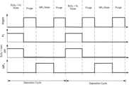
- FIG. 2 A and FIG. 2 Bshows examples of timing sequence diagrams showing example cycles of a method for depositing a tungsten nucleation layer using diborane.
- FIG. 3illustrates a schematic representation of an example of a feature provided in a partially manufactured semiconductor substrate with a tungsten nucleation layer formed with the feature.
- FIG. 4is a schematic of an example of a process system suitable for conducting deposition processes in accordance with embodiments.
- FIG. 5is a schematic of an example of a deposition station depicted suitable for conducting deposition processes in accordance with embodiments.
- FIG. 6is a schematic of an example of a manifold system that may be used in accordance with various embodiments.
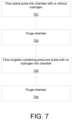
- FIG. 7shows a deposition cycle including flowing silane pulse in the chamber ( 701 ); purging the chamber ( 702 ); flowing a tungsten-containing precursor pulse in the chamber ( 703 ); and purging the chamber ( 704 ).
- Described hereinare methods of filling features with tungsten and related systems and apparatus. Examples of application include logic and memory contact fill, DRAM buried wordline fill, vertically integrated memory gate/wordline fill, and 3-D integration with through-silicon vias (TSVs).
- TSVsthrough-silicon vias
- the methods described hereincan be used to fill vertical features, such as in tungsten vias, and horizontal features, such as vertical NAND (VNAND) wordlines, and The methods may be used for conformal and bottom-up or inside-out fill.
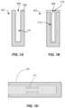
- the featurescan be characterized by one or more of narrow and/or re-entrant openings, constrictions within the feature, and high aspect ratios. Examples of features that can be filled are depicted in FIGS. 1 A- 1 C .
- FIG. 1 Ashows an example of a cross-sectional depiction of a vertical feature 101 to be filled with tungsten.
- the featurecan include a feature hole 105 in a substrate 103 .
- the substratemay be a silicon wafer, e.g., 200-mm wafer, 300-mm wafer, 450-mm wafer, including wafers having one or more layers of material such as dielectric, conducting, or semi-conducting material deposited thereon.
- the feature hole 105may have an aspect ratio of at least about 2:1, at least about 4:1, at least about 6:1 or higher.
- the feature hole 105may also have a dimension near the opening, e.g., an opening diameter or line width, of between about 10 nm to 500 nm, for example between about 25 nm to 300 nm.
- the feature hole 105can be referred to as an unfilled feature or simply a feature.
- the feature, and any featuremay be characterized in part by an axis 118 that extends through the length of the feature, with vertically-oriented features having vertical axes and horizontally-oriented features having horizontal axes.
- FIG. 1 Bshows an example of a feature 101 that has a re-entrant profile.
- a re-entrant profileis a profile that narrows from a bottom, closed end, or interior of the feature to the feature opening. According to various embodiments, the profile may narrow gradually and/or include an overhang at the feature opening.
- FIG. 1 Bshows an example of the latter, with an under-layer 113 lining the sidewall or interior surfaces of the feature hole 105 .
- the under-layer 113can be for example, a diffusion barrier layer, an adhesion layer, a nucleation layer, a combination of thereof, or any other applicable material.
- the under-layer 113forms an overhang 115 such that the under-layer 113 is thicker near the opening of the feature 101 than inside the feature 101 .
- FIG. 1 Cshows examples of views of various filled features having constrictions.
- Each of the examples (a), (b) and (c) in FIG. 1 Cincludes a constriction 109 at a midpoint within the feature.
- the constriction 109can be, for example, between about 15 nm-20 nm wide.
- Constrictionscan cause pinch off during deposition of tungsten in the feature using conventional techniques, with deposited tungsten blocking further deposition past the constriction before that portion of the feature is filled, resulting in voids in the feature.
- Example (b)further includes a liner/barrier overhang 115 at the feature opening. Such an overhang could also be a potential pinch-off point.
- Example (c)includes a constriction 112 further away from the field region than the overhang 115 in example (b). As described further below, methods described herein allow void-free fill as depicted in FIG. 1 C .
- FIG. 1 Dshows an example of a word line 150 in a VNAND structure 148 that includes a constriction 151 .
- the constrictionscan be due to the presence of pillars in a VNAND or other structure.
- FIG. 1 Eshows a plan view of pillars 125 in a VNAND structure, with FIG. 1 F showing a simplified schematic of a cross-sectional depiction of the pillars 125 .
- Arrows in FIG. 1 Erepresent deposition material; as pillars 125 are disposed between an area 127 and a gas inlet or other deposition source, adjacent pillars can result in constrictions that present challenges in void free fill of an area 127 .
- FIG. 1 Gprovides another example of a view horizontal feature, for example, of a VNAND or other structure including pillar constrictions 151 .
- the example in FIG. 1 Gis open-ended, with material to be deposited able to enter laterally from two sides as indicated by the arrows. (It should be noted that example in FIG. 1 G can be seen as a 2-D rendering 3-D features of the structure, with the FIG.
- 3-D structurescan be characterized with the area to be filled extending along three dimensions (e.g., in the X, Y and Z-directions in the example of FIG. 1 F ), and can present more challenges for fill than filling holes or trenches that extend along one or two dimensions. For example, controlling fill of a 3-D structure can be challenging as deposition gasses may enter a feature from multiple dimensions. The methods may also be used to fill interconnects to tungsten wordlines as shown in FIG.
- interconnect features 170may be filled with tungsten to connect to the tungsten wordlines 172 .
- Examples of feature fill for horizontally-oriented and vertically-oriented featuresare described below. It should be noted that in most cases, the examples applicable to both horizontally-oriented or vertically-oriented features.
- Distribution of a material within a featuremay be characterized by its step coverage.
- “step coverage”is defined as a ratio of two thicknesses, e.g., the thickness of the material inside the feature divided by the thickness of the material near the opening.
- the term “inside the feature”represents a middle portion of the feature located about the middle point of the feature along the feature's axis, e.g., an area between about 25% and 75% of the distance or, in certain embodiments, between about 40% and 60% of the distance along the feature's depth measured from the feature's opening, or an end portion of the feature located between about 75% and 95% of the distance along the feature's axis as measured from the opening.
- near the opening of the featureor “near the feature's opening” represents a top portion of the feature located within 25% or, more specifically, within 10% of the opening's edge or other element representative of the opening's edge. Step coverage of over 100% can be achieved, for example, by filling a feature wider in the middle or near the bottom of the feature than at the feature opening or where a thicker film is deposited within the feature than on or near the opening.
- a nucleation layeris typically a thin conformal layer that facilitates subsequent deposition of bulk tungsten-containing material thereon.
- a nucleation layermay be deposited prior to any fill of the feature and/or at subsequent points during fill of the feature with tungsten or a tungsten-containing material.
- the nucleation layeris deposited sequentially injecting pulses of a reducing agent, optional purge gases, and tungsten-containing precursor from the reaction chamber. The process is repeated in a cyclical fashion until the desired thickness is achieved.
- Nucleation layer thicknesscan depend on the nucleation layer deposition method as well as the desired quality of bulk deposition. In general, nucleation layer thickness is sufficient to support high quality, uniform bulk deposition. Examples may range from 5 ⁇ -100 ⁇ , or 12 ⁇ -50 ⁇ .
- ALD techniquesdiffer from chemical vapor deposition (CVD) techniques in which reactants are introduced together.
- the nucleation layeris deposited using a pulsed nucleation layer (PNL) technique.
- PNLpulsed nucleation layer
- pulses of a reducing agent, optional purge gases, and tungsten-containing precursorare sequentially injected into and purged from the reaction chamber. The process is repeated in a cyclical fashion until the desired thickness is achieved.
- PNLbroadly embodies any cyclical process of sequentially adding reactants for reaction on a semiconductor substrate, including ALD techniques.
- tungsten nucleation layerDescribed herein are methods of depositing a tungsten nucleation layer that achieve very good step coverage.
- the methodsinvolve a sequence of alternating pulses of a tungsten-containing precursor and a boron-containing reducing agent, while co-flowing hydrogen (H 2 ) with the boron-containing reducing agent.
- the H 2 flowis stopped prior to the tungsten-containing precursor flow.
- a parasitic CVD componentis reduced, resulting in a more self-limiting process. This in turn improves step coverage and conformality of the nucleation layer.
- ALD tungsten processesmay use two half-reactions enabled by the sequential delivery of two or more co-reactants.
- One co-reactantacts to functionalize the surface and permit the adsorption of tungsten-containing species to the substrate.
- Subsequent cyclesresult in the deposition of a conformal thin film.
- Flowing hydrogen in the background or as a carrier gas during the tungsten-containing precursor doseresults in a higher deposition rate, thicker nucleation layer, and reduced conformality. This is due to part of the tungsten-containing precursor being consumed by a parasitic CVD reaction with the hydrogen.
- co-flowing H 2 with B 2 H 6improves conformality.
- B 2 H 6can decompose during the ALD cycle (e.g., B 2 H 6 ⁇ 2 ⁇ 3B 3 +3H 2 ) which in turn results in parasitic reactions that contribute to the CVD reaction.
- the parasitic CVD contributiondegrades the step coverage of the process.
- B 2 H 6 and H 2By co-flowing B 2 H 6 and H 2 , the decomposition of B 2 H 6 is suppressed. While some B 2 H 6 may decompose, the presence of H 2 can significantly reduce the amount. Further, the H 2 may react with B 2 H 6 decomposition products or other reaction byproducts to form diborane (e.g., 2B 3 +9H 2 ⁇ 3B 2 H 6 ).
- the parasitic CVD contribution to the depositionis thus reduced or minimized. This shifts the thin film deposition process closer to a pure ALD process and improves the step coverage and conformality.
- Substrate temperaturesmay be below about 350° C., for example between about 175° C. and 300° C., or between about 250° C. and 300° C. Lower temperatures result in less decomposition and more control over the deposition. Even at these relatively low temperatures, diborane is susceptible to decomposition.
- chamber pressureare between 10 torr and 60 torr, or 10 torr and 40 torr. In some embodiments, it is above 10 torr. It may also be below 10 torr to reduce fluorine incorporation, for example.
- Example growth ratesmay be 2 ⁇ -20 ⁇ per cycle, or 4 ⁇ -12 ⁇ per cycle, with the growth rates lower as more hydrogen is used to suppress the parasitic CVD reaction and increase step coverage.
- the hydrogen:diborane volumetric flow ratiomay be tuned to provide the desired effect for a particular structure. Too high, and the physisorption or chemisorption of the diborane may be unnecessarily slow. Too low, and the diborane may decompose, causing the parasitic CVD effect described above. Examples of ranges of H 2 :B 2 H 6 are 20:1-400:1.
- the diborane(or other reducing agent) is delivered with an inert gas.
- B 2 H 6may be mixed with nitrogen (N 2 ) in a 20:1 N 2 :B 2 H 6 ratio.
- the H 2 to diborane/inert gas mixturemay be 1:1-20:1 to obtain 20:1-400:1 H 2 :B 2 H 6 in that example.
- Nitrogenis an example of gas that may be mixed with diborane or other reducing agent; any inert gas that is chemically compatible with the reducing agent and does not react with it may be used, with helium (He) another example.
- FIG. 2 A and FIG. 2 Bexample shows examples of timing sequence diagrams showing example cycles of a method for depositing a tungsten nucleation layer using diborane. As shown, hydrogen is flowed only during the diborane pulse.
- the tungsten nucleation layersmay be deposited using a silicon-based precursor (e.g., silane, SiH4) in addition to diborane.
- a silicon-based precursore.g., silane, SiH4
- silane pulsesare added as part of the sequence: e.g., B/W/B/W/S/W, where B represents a diborane pulse, W a tungsten-containing precursor pulses, and S a silicon-containing precursors pulse; intervening purges are not explicitly shown.
- silane or other silicon-containing precursormay be pulsed without hydrogen.
- the tungsten-containing precursormay be a tungsten halide that can be reduced by a boron-containing reducing agent including tungsten fluorides (e.g., WF6) and tungsten chlorides (e.g., WCl5 and WCl6).
- a boron-containing reducing agentincluding tungsten fluorides (e.g., WF6) and tungsten chlorides (e.g., WCl5 and WCl6).
- WF6tungsten fluorides
- tungsten chloridese.g., WCl5 and WCl6
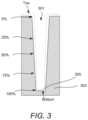
- FIG. 3illustrates a schematic representation of a feature 301 provided in a partially manufactured semiconductor substrate 303 with a tungsten nucleation layer 305 formed with the feature 301 .
- the figurealso specifies different points of measurements of the layer thickness, including at the top of the feature, the bottom of the feature, and at various sidewall depths, as measured as % of feature depth.
- Step coverageis measured as the ratio of the thickness at a bottom or sidewall position to the top position, unless otherwise indicated.
- pulsing hydrogen with a co-reactantmay be performed to improve conformality during ALD deposition of other materials and other co-reactants, when the co-reactants are susceptible to decomposition and are hydrides.
- examples of other metals that may be depositedinclude molybdenum (Mo) and ruthenium (Ru).
- ALD of tungsten nucleation layerswas performed in features using Processes A and B on structures of the same dimensions:
- Step coveragewas measured at the top sidewall, middle sidewall and bottom sidewall with respect to the film deposited on the top horizontal surface.
- the top sidewallrefers to a point about 5% of feature depth, middle about 50%, and bottom about 95% of feature depth.
- Process ATop sidewall 91.7% 98.8% Middle sidewall 70.8% 100% Bottom sidewall 58.3% 91.8%
- the featuremay be filled with a bulk tungsten layer.
- tungsten bulk depositioncan occur by a CVD process in which a reducing agent and a tungsten-containing precursor are flowed into a deposition chamber to deposit a bulk fill layer in the feature.
- tungsten bulk depositioncan occur by an ALD process in which a reducing agent and a tungsten-containing precursor are sequentially introduced into a deposition chamber to deposit a bulk fill layer in the feature. If CVD is used, this operation can involve flowing the reactants continuously until the desired amount is deposited. In certain implementations, the CVD operation may take place in multiple stages, with multiple periods of continuous and simultaneous flow of reactants separated by periods of one or more reactant flows diverted. Still further, inhibition of tungsten growth and/or etching may be performed during feature fill.
- tungsten containing gasesincluding, but not limited to, WF6, WCl6, and W(CO)6 can be used as the tungsten-containing precursor.
- the tungsten-containing precursoris a halogen-containing compound, such as WF6.
- the reducing agentis hydrogen gas, though other reducing agents may be used including silane (SiH 4 ), disilane (Si 2 H 6 ) hydrazine (N 2 H 4 ), diborane (B 2 H 6 ) and germane (GeH 4 ).
- hydrogen gasis used as the reducing agent in the CVD process.
- a tungsten precursor that can decompose to form a bulk tungsten layercan be used. Bulk deposition may also occur using other types of processes including ALD processes.
- Depositionmay proceed according to various implementations until a certain feature profile is achieved and/or a certain amount of tungsten is deposited.
- the deposition time and other relevant parametersmay be determined by modeling and/or trial and error. For example, for an initial deposition for an inside out fill process in which tungsten can be conformally deposited in a feature until pinch-off, it may be straightforward to determine based on the feature dimensions the tungsten thickness and corresponding deposition time that will achieve pinch-off.
- a process chambermay be equipped with various sensors to perform in-situ metrology measurements for end-point detection of a deposition operation. Examples of in-situ metrology include optical microscopy and X-Ray Fluorescence (XRF) for determining thickness of deposited films.
- XRFX-Ray Fluorescence
- the tungsten films described hereinmay include some amount of other compounds, dopants and/or impurities such as nitrogen, carbon, oxygen, boron, phosphorous, sulfur, silicon, germanium and the like, depending on the particular precursors and processes used.
- the tungsten content in the filmmay range from 20% to 100% (atomic) tungsten.
- the filmsare tungsten-rich, having at least 50% (atomic) tungsten, or even at least about 60%, 75%, 90%, or 99% (atomic) tungsten.
- the filmsmay be a mixture of metallic or elemental tungsten (W) and other tungsten-containing compounds such as tungsten carbide (WC), tungsten nitride (WN), etc.
- CVD and ALD deposition of these materialscan include using any appropriate precursors.
- CVD and ALD deposition of tungsten nitridecan include using halogen-containing and halogen-free tungsten-containing and nitrogen-containing compounds.
- Example deposition apparatusesinclude various systems, e.g., ALTUS® and ALTUS® Max, available from Lam Research Corp., of Fremont, California, or any of a variety of other commercially available processing systems.
- atomic layer depositionmay be performed at a first station that is one of two, five, or even more deposition stations positioned within a single deposition chamber.
- a diborane (B 2 H 6 )/hydrogen (H2) co-flow and tungsten hexafluoride (WF6)may be introduced in alternating pulses to the surface of the semiconductor substrate, at the first station, using an individual gas supply system that creates a localized atmosphere at the substrate surface.
- Another stationmay be used for tungsten bulk layer deposition. Two or more stations may be used to deposit tungsten in parallel processing. Alternatively a wafer may be indexed to have operations performed over two or more stations sequentially.
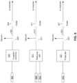
- FIG. 4is a schematic of a process system suitable for conducting deposition processes in accordance with embodiments.
- the system 400includes a transfer module 403 .
- the transfer module 403provides a clean, pressurized environment to minimize risk of contamination of substrates being processed as they are moved between various reactor modules.
- Mounted on the transfer module 403is a multi-station reactor 409 capable of performing ALD and CVD according to various embodiments.
- Multi-station reactor 409may include multiple stations 411 , 413 , 415 , and 417 that may sequentially perform operations in accordance with disclosed embodiments.
- multi-station reactor 409may be configured such that station 411 performs a tungsten nucleation layer deposition using a chlorine-containing tungsten precursor or a fluorine-containing precursor, and station 413 performs an ALD tungsten deposition operation according to various embodiments.
- station 415may also form an ALD tungsten deposition operation, and station 417 may perform a CVD operation.
- Stationsmay include a heated pedestal or substrate support, one or more gas inlets or showerhead or dispersion plate.
- An example of a deposition station 500is depicted in FIG. 5 , including substrate support 502 and showerhead 503 .
- a heatermay be provided in pedestal portion 501 .
- the transfer module 403also mounted on the transfer module 403 may be one or more single or multi-station modules 407 capable of performing plasma or chemical (non-plasma) pre-cleans, other deposition operations, or etch operations.
- the modulemay also be used for various treatments to, for example, prepare a substrate for a deposition process.
- the system 400also includes one or more wafer source modules 401 , where wafers are stored before and after processing.
- An atmospheric robot (not shown) in the atmospheric transfer chamber 419may first remove wafers from the source modules 401 to loadlocks 421 .
- a wafer transfer device(generally a robot arm unit) in the transfer module 403 moves the wafers from loadlocks 421 to and among the modules mounted on the transfer module 403 .
- a system controller 429is employed to control process conditions during deposition.
- the controller 429will typically include one or more memory devices and one or more processors.
- a processormay include a CPU or computer, analog and/or digital input/output connections, stepper motor controller boards, etc.
- the controller 429may control all of the activities of the deposition apparatus.
- the system controller 429executes system control software, including sets of instructions for controlling the timing, mixture of gases, chamber pressure, chamber temperature, wafer temperature, radio frequency (RF) power levels, wafer chuck or pedestal position, and other parameters of a particular process.
- RFradio frequency
- Other computer programs stored on memory devices associated with the controller 429may be employed in some embodiments.
- the user interfacemay include a display screen, graphical software displays of the apparatus and/or process conditions, and user input devices such as pointing devices, keyboards, touch screens, microphones, etc.
- System control logicmay be configured in any suitable way.
- the logiccan be designed or configured in hardware and/or software.
- the instructions for controlling the drive circuitrymay be hard coded or provided as software.
- the instructionsmay be provided by “programming.” Such programming is understood to include logic of any form, including hard coded logic in digital signal processors, application-specific integrated circuits, and other devices which have specific algorithms implemented as hardware. Programming is also understood to include software or firmware instructions that may be executed on a general purpose processor.
- System control softwaremay be coded in any suitable computer readable programming language.
- the computer program code for controlling the germanium-containing reducing agent pulses, hydrogen flow, and tungsten-containing precursor pulses, and other processes in a process sequencecan be written in any conventional computer readable programming language: for example, assembly language, C, C++, Pascal, Fortran, or others. Compiled object code or script is executed by the processor to perform the tasks identified in the program. Also as indicated, the program code may be hard coded.
- the controller parametersrelate to process conditions, such as, for example, process gas composition and flow rates, temperature, pressure, cooling gas pressure, substrate temperature, and chamber wall temperature. These parameters are provided to the user in the form of a recipe, and may be entered utilizing the user interface.
- Signals for monitoring the processmay be provided by analog and/or digital input connections of the system controller 429 .
- the signals for controlling the processare output on the analog and digital output connections of the deposition apparatus 400 .
- the system softwaremay be designed or configured in many different ways. For example, various chamber component subroutines or control objects may be written to control operation of the chamber components necessary to carry out the deposition processes in accordance with the disclosed embodiments. Examples of programs or sections of programs for this purpose include substrate positioning code, process gas control code, pressure control code, and heater control code.
- a controller 429is part of a system, which may be part of the above-described examples.
- Such systemscan include semiconductor processing equipment, including a processing tool or tools, chamber or chambers, a platform or platforms for processing, and/or specific processing components (a wafer pedestal, a gas flow system, etc.).
- These systemsmay be integrated with electronics for controlling their operation before, during, and after processing of a semiconductor wafer or substrate.
- the electronicsmay be referred to as the “controller,” which may control various components or subparts of the system or systems.
- the controller 429may be programmed to control any of the processes disclosed herein, including the delivery of processing gases, temperature settings (e.g., heating and/or cooling), pressure settings, vacuum settings, power settings, radio frequency (RF) generator settings in some systems, RF matching circuit settings, frequency settings, flow rate settings, fluid delivery settings, positional and operation settings, wafer transfers into and out of a tool and other transfer tools and/or load locks connected to or interfaced with a specific system.
- temperature settingse.g., heating and/or cooling
- pressure settingse.g., vacuum settings
- power settingse.g., radio frequency (RF) generator settings in some systems
- RF matching circuit settingse.g., frequency settings, flow rate settings, fluid delivery settings, positional and operation settings
- the controllermay be defined as electronics having various integrated circuits, logic, memory, and/or software that receive instructions, issue instructions, control operation, enable cleaning operations, enable endpoint measurements, and the like.
- the integrated circuitsmay include chips in the form of firmware that store program instructions, digital signal processors (DSPs), chips defined as application specific integrated circuits (ASICs), and/or one or more microprocessors, or microcontrollers that execute program instructions (e.g., software).
- Program instructionsmay be instructions communicated to the controller in the form of various individual settings (or program files), defining operational parameters for carrying out a particular process on or for a semiconductor wafer or to a system.
- the operational parametersmay, in some embodiments, be part of a recipe defined by process engineers to accomplish one or more processing steps during the fabrication of one or more layers, materials, metals, oxides, silicon, silicon dioxide, surfaces, circuits, and/or dies of a wafer.
- the controller 429may be a part of or coupled to a computer that is integrated with, coupled to the system, otherwise networked to the system, or a combination thereof.
- the controller 429may be in the “cloud” or all or a part of a fab host computer system, which can allow for remote access of the wafer processing.
- the computermay enable remote access to the system to monitor current progress of fabrication operations, examine a history of past fabrication operations, examine trends or performance metrics from a plurality of fabrication operations, to change parameters of current processing, to set processing steps to follow a current processing, or to start a new process.
- a remote computere.g.
- a servercan provide process recipes to a system over a network, which may include a local network or the Internet.
- the remote computermay include a user interface that enables entry or programming of parameters and/or settings, which are then communicated to the system from the remote computer.
- the controllerreceives instructions in the form of data, which specify parameters for each of the processing steps to be performed during one or more operations. It should be understood that the parameters may be specific to the type of process to be performed and the type of tool that the controller is configured to interface with or control.
- the controllermay be distributed, such as by including one or more discrete controllers that are networked together and working towards a common purpose, such as the processes and controls described herein.
- An example of a distributed controller for such purposeswould be one or more integrated circuits on a chamber in communication with one or more integrated circuits located remotely (such as at the platform level or as part of a remote computer) that combine to control a process on the chamber.
- example systemsmay include a plasma etch chamber or module, a deposition chamber or module, a spin-rinse chamber or module, a metal plating chamber or module, a clean chamber or module, a bevel edge etch chamber or module, a physical vapor deposition (PVD) chamber or module, a CVD chamber or module, an ALD chamber or module, an atomic layer etch (ALE) chamber or module, an ion implantation chamber or module, a track chamber or module, and any other semiconductor processing systems that may be associated or used in the fabrication and/or manufacturing of semiconductor wafers.
- PVDphysical vapor deposition
- CVDchemical vapor deposition
- ALDatomic layer etch
- ALEatomic layer etch
- the controllermight communicate with one or more of other tool circuits or modules, other tool components, cluster tools, other tool interfaces, adjacent tools, neighboring tools, tools located throughout a factory, a main computer, another controller, or tools used in material transport that bring containers of wafers to and from tool locations and/or load ports in a semiconductor manufacturing factory.
- the controller 429may include various programs.
- a substrate positioning programmay include program code for controlling chamber components that are used to load the substrate onto a pedestal or chuck and to control the spacing between the substrate and other parts of the chamber such as a gas inlet and/or target.
- a process gas control programmay include code for controlling gas composition, flow rates, pulse times, and optionally for flowing gas into the chamber prior to deposition in order to stabilize the pressure in the chamber.
- a pressure control programmay include code for controlling the pressure in the chamber by regulating, e.g., a throttle valve in the exhaust system of the chamber.
- a heater control programmay include code for controlling the current to a heating unit that is used to heat the substrate. Alternatively, the heater control program may control delivery of a heat transfer gas such as helium to the wafer chuck.
- the apparatusmay include a gas manifold system, which provides line charges to the various gas distribution lines as shown schematically in FIG. 6 .
- Manifold 604has inputs from a source 601 of a tungsten-containing precursor gas, which may include an accumulator (not shown), which can also be referred to as a charge volume.
- Manifold 611has an input from a source 609 of hydrogen (H2) and a source 610 of diborane-containing mixture or other reducing gas (not shown). Both of these sources may include an accumulator (not shown).
- Manifold 621has an input from a source 619 of purge gas, which also may include an accumulator.
- the manifolds 604 , 611 and 6521provide tungsten-containing precursor gas, co-reactant gas, and purge gas to the deposition chamber through valved distribution lines, 605 , 613 and 625 respectively.
- the various valvesmay be opened or closed to provide a line charge, i.e., to pressurize the distribution lines.
- valve 606is closed to vacuum and valve 608 is closed.
- valve 608is opened and the co-flow gas is delivered to the chamber.
- valve 608is closed.
- the chambercan then be purged to a vacuum by opening of valve 606 to vacuum.
- Similar processescan be used to deliver the reducing gas.
- distribution line 613is charged by closing valve 615 and closing valve 617 to vacuum. Opening of valve 615 allows for delivery of the reducing gas to the chamber.
- distribution line 625is charged by closing valve 627 and closing valve 623 to vacuum. Opening of valve 627 allows for delivery of the argon or other inert purge gas to the chamber.
- the diborane or other reducing gascan be mixed with hydrogen at any point in the process and is not limited to the arrangement of FIG. 6 .
- a hydrogen/diborane mixture as storedmay be used.
- itmay be obtained from separate sources but mixed during the process at some point before delivery to the chamber or may be delivered separately to the chamber with mixing occurring in the chamber.
- FIG. 6also shows vacuum pumps in which valves 606 , 617 and 623 , respectively, can be opened to purge the system.
- the supply of gas through the various distribution linesis controlled by a controller, such as a mass flow controller which is controlled by a microprocessor, a digital signal processor or the like, that is programmed with the flow rates, duration of the flow, and the sequencing of the processes.
- valve and MFC commandsare delivered to embedded digital input-output controllers (IOC) in discrete packets of information containing instructions for all time-critical commands for all or a part of a deposition sequence.
- IOCembedded digital input-output controllers
- the ALTUS systems of Lam Researchprovide at least one IOC sequence.
- the IOCscan be physically located at various points in the apparatus; e.g., within the process module or on a stand-alone power rack standing some distance away from the process module. There may be multiple IOCs in each module (e.g., 3 per module).
- all commands for controlling valves and setting flow for MFCsmay be included in a single IOC sequence. This assures that the timing of all the devices is tightly controlled from an absolute standpoint and also relative to each other.
- a second sequencemight be running concurrently to deposit a bulk metal at other deposition stations in the same module.
- the relative timing of the devices controlling the delivery of reagents to stations 3 - 4is important within that group of devices, but the relative timing of the ALD process at stations 1 - 2 can be offset from the relative timing of stations 3 - 4 .
- An IOCtranslates the information in a packetized sequence and delivers digital or analog command signals directly to MFC or pneumatic solenoid banks controlling the valves.
- a pulse of tungsten-containing precursor gasmay be generated as follows. Initially, the system diverts WF6 to a vacuum pump for a period of time while the MFC or other flow-controlling device stabilizes. This may be done for a period of between about 0.5 to 5 seconds in one example. Next, the system pressurizes the tungsten gas delivery manifold by closing both the valve 606 to vacuum and the valve 608 to the deposition chamber. This may be done for a period of between about 0.1 and 5 seconds, for example, to create an initial burst of reagent when the valve to the deposition chamber is opened. This is accomplished by opening valve 508 for between about 0.1 and 10 seconds in one example.
- the tungsten-containing gasis purged from the deposition chamber using a suitable purge gas.
- the systemmay pressurize the purge gas delivery manifold by closing valve 623 and valve 627 .
- Valves to an accumulator(not shown) are also closed to permit the accumulator to pressurize. This may be done for a period of between about 0.1 and 5 seconds, for example, to rapidly flush reagent from the deposition chamber when the valve to the deposition chamber is opened.
- valve 527is opened to the deposition chamber, an accumulator outlet valve is opened simultaneously or shortly thereafter to increase the mass flow of purge gas into the deposition chamber.
- Multiple accumulatorsmay be used sequentially flow pressurized the same reactant or purge gas into the chamber during a single pulse operation. This can increases the overall mass flow rate.
- Lithographic patterning of a filmtypically includes some or all of the following steps, each step provided with a number of possible tools: (1) application of photoresist on a workpiece, i.e., substrate, using a spin-on or spray-on tool; (2) curing of photoresist using a hot plate or furnace or UV curing tool; (3) exposing the photoresist to visible or UV or x-ray light with a tool such as a wafer stepper; (4) developing the resist so as to selectively remove resist and thereby pattern it using a tool such as a wet bench; (5) transferring the resist pattern into an underlying film or workpiece by using a dry or plasma-assisted etching tool; and (6) removing the resist using a tool such as an RF or microwave plasma resist stripper
Landscapes
- Chemical & Material Sciences (AREA)
- Engineering & Computer Science (AREA)
- Manufacturing & Machinery (AREA)
- General Physics & Mathematics (AREA)
- Physics & Mathematics (AREA)
- Computer Hardware Design (AREA)
- Microelectronics & Electronic Packaging (AREA)
- Power Engineering (AREA)
- Condensed Matter Physics & Semiconductors (AREA)
- Chemical Kinetics & Catalysis (AREA)
- General Chemical & Material Sciences (AREA)
- Materials Engineering (AREA)
- Mechanical Engineering (AREA)
- Metallurgy (AREA)
- Organic Chemistry (AREA)
- Crystallography & Structural Chemistry (AREA)
- Chemical Vapour Deposition (AREA)
- Electrodes Of Semiconductors (AREA)
- Internal Circuitry In Semiconductor Integrated Circuit Devices (AREA)
Abstract
Description
- Process A: multiple cycles of (B2H6-Ar purge-WF6-Ar purge) with H2 flow constant
- Process B: multiple cycles of (B2H6-Ar purge-WF6-Ar purge) with H2 flow constant only during B2H6pulses.
| Process A | Process B | |||
| Top sidewall | 91.7% | 98.8% | ||
| Middle sidewall | 70.8% | 100% | ||
| Bottom sidewall | 58.3% | 91.8% | ||
- Process C: multiple cycles of (B2H6-Ar purge-WF6-Ar purge) with no H2at all:
| Process C | |||
| Top sidewall | 83% | ||
| Middle sidewall | 74% | ||
| Bottom sidewall | 66% | ||
Claims (15)
Priority Applications (1)
| Application Number | Priority Date | Filing Date | Title |
|---|---|---|---|
| US17/601,918US12002679B2 (en) | 2019-04-11 | 2020-04-07 | High step coverage tungsten deposition |
Applications Claiming Priority (3)
| Application Number | Priority Date | Filing Date | Title |
|---|---|---|---|
| US201962832291P | 2019-04-11 | 2019-04-11 | |
| US17/601,918US12002679B2 (en) | 2019-04-11 | 2020-04-07 | High step coverage tungsten deposition |
| PCT/US2020/027107WO2020210260A1 (en) | 2019-04-11 | 2020-04-07 | High step coverage tungsten deposition |
Publications (2)
| Publication Number | Publication Date |
|---|---|
| US20220181158A1 US20220181158A1 (en) | 2022-06-09 |
| US12002679B2true US12002679B2 (en) | 2024-06-04 |
Family
ID=72751976
Family Applications (1)
| Application Number | Title | Priority Date | Filing Date |
|---|---|---|---|
| US17/601,918Active2040-06-10US12002679B2 (en) | 2019-04-11 | 2020-04-07 | High step coverage tungsten deposition |
Country Status (7)
| Country | Link |
|---|---|
| US (1) | US12002679B2 (en) |
| JP (1) | JP2022522226A (en) |
| KR (1) | KR20210141762A (en) |
| CN (1) | CN113710830A (en) |
| SG (1) | SG11202111277UA (en) |
| TW (1) | TW202104638A (en) |
| WO (1) | WO2020210260A1 (en) |
Cited By (1)
| Publication number | Priority date | Publication date | Assignee | Title |
|---|---|---|---|---|
| US12237221B2 (en) | 2019-05-22 | 2025-02-25 | Lam Research Corporation | Nucleation-free tungsten deposition |
Families Citing this family (6)
| Publication number | Priority date | Publication date | Assignee | Title |
|---|---|---|---|---|
| KR102806630B1 (en) | 2018-05-03 | 2025-05-12 | 램 리써치 코포레이션 | Method for depositing tungsten and other metals on 3D NAND structures |
| US11972952B2 (en) | 2018-12-14 | 2024-04-30 | Lam Research Corporation | Atomic layer deposition on 3D NAND structures |
| KR20220047333A (en) | 2019-08-12 | 2022-04-15 | 램 리써치 코포레이션 | Tungsten Deposition |
| JP7295749B2 (en)* | 2019-09-13 | 2023-06-21 | キオクシア株式会社 | Semiconductor device manufacturing method |
| US20230317458A1 (en)* | 2022-04-05 | 2023-10-05 | Applied Materials, Inc. | Gap fill enhancement with thermal etch |
| CN120153124A (en)* | 2022-11-02 | 2025-06-13 | 朗姆研究公司 | Dual nitrogen gas flow capability for low fluorine tungsten deposition |
Citations (314)
| Publication number | Priority date | Publication date | Assignee | Title |
|---|---|---|---|---|
| JPS5629648A (en) | 1979-08-16 | 1981-03-25 | Toshiba Tungaloy Co Ltd | High hardness sintered body |
| US4746375A (en) | 1987-05-08 | 1988-05-24 | General Electric Company | Activation of refractory metal surfaces for electroless plating |
| JPS63274772A (en) | 1987-05-07 | 1988-11-11 | Res Dev Corp Of Japan | Production method of titanium boride |
| US4804560A (en) | 1986-03-17 | 1989-02-14 | Fujitsu Limited | Method of selectively depositing tungsten upon a semiconductor substrate |
| US4874719A (en) | 1986-05-06 | 1989-10-17 | Kabushiki Kaisha Toshiba | Method for manufacturing an electrical connection between conductor levels |
| JPH0266399A (en) | 1988-08-30 | 1990-03-06 | Semiconductor Energy Lab Co Ltd | Gas charging vessel and manufacture thereof |
| JPH02187031A (en) | 1989-01-14 | 1990-07-23 | Sharp Corp | Semiconductor device |
| US4962063A (en) | 1988-11-10 | 1990-10-09 | Applied Materials, Inc. | Multistep planarized chemical vapor deposition process with the use of low melting inorganic material for flowing while depositing |
| US5028565A (en) | 1989-08-25 | 1991-07-02 | Applied Materials, Inc. | Process for CVD deposition of tungsten layer on semiconductor wafer |
| EP0437110A2 (en) | 1990-01-08 | 1991-07-17 | Lsi Logic Corporation | Tungsten deposition process for low contact resistivity to silicon |
| JPH04142061A (en) | 1990-10-02 | 1992-05-15 | Sony Corp | Formation of tungsten plug |
| JPH04216630A (en) | 1990-12-17 | 1992-08-06 | Oki Electric Ind Co Ltd | Wiring formation of semiconductor element |
| US5227329A (en) | 1990-08-31 | 1993-07-13 | Hitachi, Ltd. | Method of manufacturing semiconductor device |
| JPH05226280A (en) | 1992-02-14 | 1993-09-03 | Matsushita Electric Ind Co Ltd | Manufacture of semiconductor device |
| US5250467A (en) | 1991-03-29 | 1993-10-05 | Applied Materials, Inc. | Method for forming low resistance and low defect density tungsten contacts to silicon semiconductor wafer |
| US5250329A (en) | 1989-04-06 | 1993-10-05 | Microelectronics And Computer Technology Corporation | Method of depositing conductive lines on a dielectric |
| US5308655A (en) | 1991-08-16 | 1994-05-03 | Materials Research Corporation | Processing for forming low resistivity titanium nitride films |
| US5326723A (en) | 1992-09-09 | 1994-07-05 | Intel Corporation | Method for improving stability of tungsten chemical vapor deposition |
| US5370739A (en) | 1992-06-15 | 1994-12-06 | Materials Research Corporation | Rotating susceptor semiconductor wafer processing cluster tool module useful for tungsten CVD |
| JPH07147321A (en) | 1993-11-26 | 1995-06-06 | Nec Corp | Manufacture of semiconductor device |
| JPH07226393A (en) | 1994-02-15 | 1995-08-22 | Sony Corp | Method and apparatus for dry-etching |
| JPH08115984A (en) | 1994-10-17 | 1996-05-07 | Hitachi Ltd | Semiconductor device and manufacturing method thereof |
| US5567583A (en) | 1991-12-16 | 1996-10-22 | Biotronics Corporation | Methods for reducing non-specific priming in DNA detection |
| JPH08325735A (en) | 1995-05-31 | 1996-12-10 | Nippon Telegr & Teleph Corp <Ntt> | Method for forming tungsten film |
| JPH0922896A (en) | 1995-07-07 | 1997-01-21 | Toshiba Corp | Selective metal film formation method |
| JPH0927596A (en) | 1995-07-11 | 1997-01-28 | Sanyo Electric Co Ltd | Manufacture of semiconductor device |
| US5633200A (en) | 1996-05-24 | 1997-05-27 | Micron Technology, Inc. | Process for manufacturing a large grain tungsten nitride film and process for manufacturing a lightly nitrided titanium salicide diffusion barrier with a large grain tungsten nitride cover layer |
| TW310461B (en) | 1995-11-10 | 1997-07-11 | Matsushita Electric Industrial Co Ltd | |
| US5661080A (en) | 1992-12-10 | 1997-08-26 | Hyundai Electronics Industries Co., Ltd. | Method for fabricating tungsten plug |
| US5726096A (en) | 1993-12-17 | 1998-03-10 | Hyundai Electronics Industries Co., Ltd. | Method for forming a tungsten silicide layer in a semiconductor device |
| JPH10144688A (en) | 1996-11-02 | 1998-05-29 | Hyundai Electron Ind Co Ltd | Method of forming contact plugs of semiconductor device having contact holes different in size |
| JPH10163132A (en) | 1996-11-28 | 1998-06-19 | Hyundai Electron Ind Co Ltd | Metal wiring of semiconductor device and its formation |
| US5795824A (en) | 1997-08-28 | 1998-08-18 | Novellus Systems, Inc. | Method for nucleation of CVD tungsten films |
| US5804249A (en) | 1997-02-07 | 1998-09-08 | Lsi Logic Corporation | Multistep tungsten CVD process with amorphization step |
| US5817576A (en) | 1994-09-27 | 1998-10-06 | Applied Materials, Inc. | Utilization of SiH4 soak and purge in deposition processes |
| US5833817A (en) | 1996-04-22 | 1998-11-10 | Taiwan Semiconductor Manufacturing Company, Ltd. | Method for improving conformity and contact bottom coverage of sputtered titanium nitride barrier layers |
| WO1998051838A1 (en) | 1997-05-16 | 1998-11-19 | Applied Materials, Inc. | Low resistivity w using b2h¿6? |
| KR100196018B1 (en) | 1994-12-06 | 1999-06-15 | 포만 제프리 엘 | Method for electrically connect of separated devices |
| US5913145A (en) | 1997-08-28 | 1999-06-15 | Texas Instruments Incorporated | Method for fabricating thermally stable contacts with a diffusion barrier formed at high temperatures |
| US5916634A (en) | 1996-10-01 | 1999-06-29 | Sandia Corporation | Chemical vapor deposition of W-Si-N and W-B-N |
| US5926720A (en) | 1997-09-08 | 1999-07-20 | Lsi Logic Corporation | Consistent alignment mark profiles on semiconductor wafers using PVD shadowing |
| US5956609A (en) | 1997-08-11 | 1999-09-21 | Taiwan Semiconductor Manufacturing Company, Ltd. | Method for reducing stress and improving step-coverage of tungsten interconnects and plugs |
| US5963833A (en) | 1996-07-03 | 1999-10-05 | Micron Technology, Inc. | Method for cleaning semiconductor wafers and |
| JP2966406B2 (en) | 1998-01-26 | 1999-10-25 | エルジー セミコン カンパニー リミテッド | Semiconductor element wiring forming method |
| JPH11330006A (en) | 1998-04-30 | 1999-11-30 | Internatl Business Mach Corp <Ibm> | Ultrathin single phase barrier layer for conductor and its manufacturing method |
| US5994749A (en) | 1997-01-20 | 1999-11-30 | Nec Corporation | Semiconductor device having a gate electrode film containing nitrogen |
| US6001729A (en) | 1995-01-10 | 1999-12-14 | Kawasaki Steel Corporation | Method of forming wiring structure for semiconductor device |
| US6017818A (en) | 1996-01-22 | 2000-01-25 | Texas Instruments Incorporated | Process for fabricating conformal Ti-Si-N and Ti-B-N based barrier films with low defect density |
| US6034419A (en) | 1989-04-07 | 2000-03-07 | Inmos Limited | Semiconductor device with a tungsten contact |
| US6037263A (en) | 1998-11-05 | 2000-03-14 | Vanguard International Semiconductor Corporation | Plasma enhanced CVD deposition of tungsten and tungsten compounds |
| US6066366A (en) | 1998-07-22 | 2000-05-23 | Applied Materials, Inc. | Method for depositing uniform tungsten layers by CVD |
| JP2000208516A (en) | 1999-01-11 | 2000-07-28 | Nec Corp | Semiconductor device having multilayer wiring structure and manufacture thereof |
| US6099904A (en) | 1997-12-02 | 2000-08-08 | Applied Materials, Inc. | Low resistivity W using B2 H6 nucleation step |
| US6107200A (en) | 1998-03-12 | 2000-08-22 | Fujitsu Limited | Semiconductor device manufacturing method |
| JP2000235962A (en) | 1999-02-17 | 2000-08-29 | Ulvac Japan Ltd | Manufacture of barrier film |
| US6143082A (en) | 1998-10-08 | 2000-11-07 | Novellus Systems, Inc. | Isolation of incompatible processes in a multi-station processing chamber |
| US6174812B1 (en) | 1999-06-08 | 2001-01-16 | United Microelectronics Corp. | Copper damascene technology for ultra large scale integration circuits |
| WO2001027347A1 (en) | 1999-10-15 | 2001-04-19 | Asm Microchemistry Oy | Method of depositing transition metal nitride thin films |
| WO2001029893A1 (en) | 1999-10-15 | 2001-04-26 | Asm America, Inc. | Method for depositing nanolaminate thin films on sensitive surfaces |
| TW434708B (en) | 1998-12-22 | 2001-05-16 | Hyundai Electronics Ind | Method for forming gate electrodes of semiconductor device |
| US6245654B1 (en) | 1999-03-31 | 2001-06-12 | Taiwan Semiconductor Manufacturing Company, Ltd | Method for preventing tungsten contact/via plug loss after a backside pressure fault |
| US20010007797A1 (en) | 2000-01-06 | 2001-07-12 | Seong-Dai Jang | Method of forming a tungsten plug in a semiconductor device |
| US20010008808A1 (en) | 1995-10-25 | 2001-07-19 | Fernando Gonzalez | A Method Of Fabricating A DRAM Transistor With A Dual Gate Oxide Technique |
| US6265312B1 (en) | 1999-08-02 | 2001-07-24 | Stmicroelectronics, Inc. | Method for depositing an integrated circuit tungsten film stack that includes a post-nucleation pump down step |
| US20010014533A1 (en) | 1999-01-08 | 2001-08-16 | Shih-Wei Sun | Method of fabricating salicide |
| US6277744B1 (en) | 2000-01-21 | 2001-08-21 | Advanced Micro Devices, Inc. | Two-level silane nucleation for blanket tungsten deposition |
| US20010015494A1 (en) | 1997-06-13 | 2001-08-23 | Kie Y. Ahn | Integrated circuit wiring with low rc time delay |
| TW452607B (en) | 1999-03-26 | 2001-09-01 | Nat Science Council | Production of a refractory metal by chemical vapor deposition of a bilayer-stacked tungsten metal |
| US6284316B1 (en) | 1998-02-25 | 2001-09-04 | Micron Technology, Inc. | Chemical vapor deposition of titanium |
| US6287965B1 (en) | 1997-07-28 | 2001-09-11 | Samsung Electronics Co, Ltd. | Method of forming metal layer using atomic layer deposition and semiconductor device having the metal layer as barrier metal layer or upper or lower electrode of capacitor |
| US6294468B1 (en) | 1999-05-24 | 2001-09-25 | Agere Systems Guardian Corp. | Method of chemical vapor depositing tungsten films |
| US6297152B1 (en) | 1996-12-12 | 2001-10-02 | Applied Materials, Inc. | CVD process for DCS-based tungsten silicide |
| US6306211B1 (en) | 1999-03-23 | 2001-10-23 | Matsushita Electric Industrial Co., Ltd. | Method for growing semiconductor film and method for fabricating semiconductor device |
| KR20010093766A (en) | 2000-03-29 | 2001-10-29 | 조셉 제이. 스위니 | Reduced fluorine containation for tungsten cvd |
| US6309964B1 (en) | 1999-07-08 | 2001-10-30 | Taiwan Semiconductor Manufacturing Company | Method for forming a copper damascene structure over tungsten plugs with improved adhesion, oxidation resistance, and diffusion barrier properties using nitridation of the tungsten plug |
| US6309966B1 (en) | 1999-09-03 | 2001-10-30 | Motorola, Inc. | Apparatus and method of a low pressure, two-step nucleation tungsten deposition |
| US6310300B1 (en) | 1996-11-08 | 2001-10-30 | International Business Machines Corporation | Fluorine-free barrier layer between conductor and insulator for degradation prevention |
| EP1156132A2 (en) | 2000-05-19 | 2001-11-21 | Murata Manufacturing Co., Ltd. | Method of forming electrode film |
| US20010044041A1 (en) | 2000-05-18 | 2001-11-22 | Badding Michael E. | High performance solid electrolyte fuel cells |
| JP2002016066A (en) | 2000-06-27 | 2002-01-18 | Mitsubishi Electric Corp | Semiconductor device and method of manufacturing the same |
| EP1179838A2 (en) | 2000-07-31 | 2002-02-13 | Applied Materials, Inc. | Deposition of tungsten films from W(CO)6 |
| US6355558B1 (en) | 1999-06-10 | 2002-03-12 | Texas Instruments Incorporated | Metallization structure, and associated method, to improve crystallographic texture and cavity fill for CVD aluminum/PVD aluminum alloy films |
| US20020037630A1 (en) | 2000-06-08 | 2002-03-28 | Micron Technology, Inc. | Methods for forming and integrated circuit structures containing ruthenium and tungsten containing layers |
| US20020048938A1 (en) | 1998-12-18 | 2002-04-25 | Hotaka Ishizuka | Tungsten film forming method |
| WO2002041379A1 (en) | 2000-11-17 | 2002-05-23 | Tokyo Electron Limited | Method of forming metal wiring and semiconductor manufacturing apparatus for forming metal wiring |
| US6404054B1 (en) | 1998-10-28 | 2002-06-11 | Samsung Electronics Co., Ltd. | Tungsten layer formation method for semiconductor device and semiconductor device using the same |
| KR20020049730A (en) | 2000-12-20 | 2002-06-26 | 윤종용 | Method for forming an interconnection of semiconductor device having a smooth surface |
| US20020090796A1 (en) | 1999-09-13 | 2002-07-11 | Applied Materials, Inc. | Silicon layer to improve plug filling by CVD |
| US20020117399A1 (en) | 2001-02-23 | 2002-08-29 | Applied Materials, Inc. | Atomically thin highly resistive barrier layer in a copper via |
| US20020155722A1 (en) | 1999-08-24 | 2002-10-24 | Alessandra Satta | Method for bottomless deposition of barrier layers in integrated circuit metallization schemes |
| US20020168840A1 (en) | 2001-05-11 | 2002-11-14 | Applied Materials, Inc. | Deposition of tungsten silicide films |
| US20020177316A1 (en) | 2000-11-16 | 2002-11-28 | Miller Anne E. | Slurry and method for chemical mechanical polishing of copper |
| US6491978B1 (en) | 2000-07-10 | 2002-12-10 | Applied Materials, Inc. | Deposition of CVD layers for copper metallization using novel metal organic chemical vapor deposition (MOCVD) precursors |
| US20020192953A1 (en) | 2001-06-19 | 2002-12-19 | Yu-Piao Wang | Method for forming a plug metal layer |
| US20020190379A1 (en) | 2001-03-28 | 2002-12-19 | Applied Materials, Inc. | W-CVD with fluorine-free tungsten nucleation |
| WO2002101114A1 (en) | 2001-06-12 | 2002-12-19 | Applied Materials, Inc. | Mocvd method for tungsten deposition |
| US20030013300A1 (en) | 2001-07-16 | 2003-01-16 | Applied Materials, Inc. | Method and apparatus for depositing tungsten after surface treatment to improve film characteristics |
| US20030059980A1 (en) | 2001-09-25 | 2003-03-27 | Ling Chen | Copper interconnect barrier layer structure and formation method |
| WO2003029515A2 (en) | 2001-07-16 | 2003-04-10 | Applied Materials, Inc. | Formation of composite tungsten films |
| US6551929B1 (en) | 2000-06-28 | 2003-04-22 | Applied Materials, Inc. | Bifurcated deposition process for depositing refractory metal layers employing atomic layer deposition and chemical vapor deposition techniques |
| US20030082296A1 (en) | 2001-09-14 | 2003-05-01 | Kai Elers | Metal nitride deposition by ALD with reduction pulse |
| US20030082902A1 (en) | 2001-10-31 | 2003-05-01 | Shoichi Fukui | Semiconductor-device fabrication method |
| US20030091870A1 (en) | 2001-11-15 | 2003-05-15 | Siddhartha Bhowmik | Method of forming a liner for tungsten plugs |
| US6566250B1 (en) | 2002-03-18 | 2003-05-20 | Taiwant Semiconductor Manufacturing Co., Ltd | Method for forming a self aligned capping layer |
| US6566262B1 (en) | 2001-11-01 | 2003-05-20 | Lsi Logic Corporation | Method for creating self-aligned alloy capping layers for copper interconnect structures |
| US20030104126A1 (en) | 2001-10-10 | 2003-06-05 | Hongbin Fang | Method for depositing refractory metal layers employing sequential deposition techniques |
| KR20030050652A (en) | 2001-12-19 | 2003-06-25 | 주식회사 하이닉스반도체 | Method for forming tungsten layer |
| US20030123216A1 (en) | 2001-12-27 | 2003-07-03 | Yoon Hyungsuk A. | Deposition of tungsten for the formation of conformal tungsten silicide |
| JP2003193233A (en) | 2001-08-14 | 2003-07-09 | Tokyo Electron Ltd | Method for depositing tungsten film |
| US20030127043A1 (en) | 2001-07-13 | 2003-07-10 | Applied Materials, Inc. | Pulsed nucleation deposition of tungsten layers |
| US20030129828A1 (en) | 1999-10-02 | 2003-07-10 | Uri Cohen | Methods for making multiple seed layers for metallic interconnects |
| US6593233B1 (en) | 1995-03-03 | 2003-07-15 | Nec Electronics Corporation | Semiconductor device and method for manufacturing the same |
| US6635965B1 (en) | 2001-05-22 | 2003-10-21 | Novellus Systems, Inc. | Method for producing ultra-thin tungsten layers with improved step coverage |
| CN1455447A (en) | 2003-05-15 | 2003-11-12 | 上海集成电路研发中心有限公司 | Process flow of improved tungsten plug structure |
| US20030209193A1 (en) | 2000-07-07 | 2003-11-13 | Van Wijck Margreet Albertine Anne-Marie | Atomic layer CVD |
| US20030224217A1 (en) | 2002-05-31 | 2003-12-04 | Applied Materials, Inc. | Metal nitride formation |
| US20040044127A1 (en) | 2002-08-22 | 2004-03-04 | Konica Corporation | Organic-inorganic hybrid film, its manufacturing method, optical film, and polarizing film |
| US6706625B1 (en) | 2002-12-06 | 2004-03-16 | Chartered Semiconductor Manufacturing Ltd. | Copper recess formation using chemical process for fabricating barrier cap for lines and vias |
| US6720261B1 (en) | 1999-06-02 | 2004-04-13 | Agere Systems Inc. | Method and system for eliminating extrusions in semiconductor vias |
| US6740585B2 (en) | 2001-07-25 | 2004-05-25 | Applied Materials, Inc. | Barrier formation using novel sputter deposition method with PVD, CVD, or ALD |
| US20040142557A1 (en) | 2003-01-21 | 2004-07-22 | Novellus Systems, Inc. | Deposition of tungsten nitride |
| US20040151845A1 (en) | 2003-02-04 | 2004-08-05 | Tue Nguyen | Nanolayer deposition process |
| US6777331B2 (en) | 2000-03-07 | 2004-08-17 | Simplus Systems Corporation | Multilayered copper structure for improving adhesion property |
| JP2004235456A (en) | 2003-01-30 | 2004-08-19 | Seiko Epson Corp | Film forming apparatus, film forming method, and semiconductor device manufacturing method |
| US6790773B1 (en) | 2002-08-28 | 2004-09-14 | Novellus Systems, Inc. | Process for forming barrier/seed structures for integrated circuits |
| US6794287B2 (en) | 2000-01-18 | 2004-09-21 | Asm International Nv | Process for growing metal or metal carbide thin films utilizing boron-containing reducing agents |
| JP2004273764A (en) | 2003-03-07 | 2004-09-30 | Tokyo Electron Ltd | Method for forming tungsten film |
| KR20040085153A (en) | 2002-01-17 | 2004-10-07 | 썬듀 테크놀로지스 엘엘씨 | Ald apparatus and method |
| US20040202786A1 (en) | 2001-05-22 | 2004-10-14 | Novellus Systems, Inc. | Method of forming low-resistivity tungsten interconnects |
| US20040206267A1 (en) | 2002-12-23 | 2004-10-21 | Sankar Sambasivan | Aluminum phosphate coatings |
| US20050009325A1 (en) | 2003-06-18 | 2005-01-13 | Hua Chung | Atomic layer deposition of barrier materials |
| US6844258B1 (en) | 2003-05-09 | 2005-01-18 | Novellus Systems, Inc. | Selective refractory metal and nitride capping |
| JP2005029821A (en) | 2003-07-09 | 2005-02-03 | Tokyo Electron Ltd | Film-forming method |
| US20050031786A1 (en) | 2001-05-22 | 2005-02-10 | Novellus Systems, Inc. | Method for reducing tungsten film roughness and improving step coverage |
| US6861356B2 (en) | 1997-11-05 | 2005-03-01 | Tokyo Electron Limited | Method of forming a barrier film and method of forming wiring structure and electrodes of semiconductor device having a barrier film |
| US20050059236A1 (en) | 2003-09-11 | 2005-03-17 | Akio Nishida | Semiconductor device and a method of manufacturing the same |
| WO2005034223A1 (en) | 2003-09-30 | 2005-04-14 | Tokyo Electron Limited | Method of depositing metal layers from metal-carbonyl precursors |
| US6903016B2 (en) | 1999-10-02 | 2005-06-07 | Uri Cohen | Combined conformal/non-conformal seed layers for metallic interconnects |
| KR20050054122A (en) | 2003-12-04 | 2005-06-10 | 성명모 | Method of fabricating thin film using uv-enhanced atomic layer deposition |
| US6905543B1 (en) | 2002-06-19 | 2005-06-14 | Novellus Systems, Inc | Methods of forming tungsten nucleation layer |
| US6908848B2 (en) | 2000-12-20 | 2005-06-21 | Samsung Electronics, Co., Ltd. | Method for forming an electrical interconnection providing improved surface morphology of tungsten |
| US20050136594A1 (en) | 2003-12-23 | 2005-06-23 | Hynix Semiconductor Inc. | Method for forming bit-line of semiconductor device |
| KR20050068555A (en) | 2003-12-30 | 2005-07-05 | 주식회사 아이피에스 | A method of plating a thin film |
| KR20050087428A (en) | 2004-02-26 | 2005-08-31 | 노벨러스 시스템즈, 인코포레이티드 | Deposition of tungsten nitride |
| US20050191803A1 (en) | 1997-11-05 | 2005-09-01 | Tokyo Electron Limited | Method of forming a metal film for electrode |
| US6962873B1 (en) | 2002-12-10 | 2005-11-08 | Novellus Systems, Inc. | Nitridation of electrolessly deposited cobalt |
| US20060003581A1 (en) | 2004-06-30 | 2006-01-05 | Johnston Steven W | Atomic layer deposited tantalum containing adhesion layer |
| US20060009034A1 (en) | 2000-06-28 | 2006-01-12 | Lai Ken K | Methods for depositing tungsten layers employing atomic layer deposition techniques |
| US20060145190A1 (en) | 2004-12-31 | 2006-07-06 | Salzman David B | Surface passivation for III-V compound semiconductors |
| KR20060087844A (en) | 2005-01-31 | 2006-08-03 | 삼성전자주식회사 | Semiconductor device and manufacturing method thereof |
| US20060211244A1 (en) | 2005-03-18 | 2006-09-21 | International Business Machines Corporation | Clustered surface preparation for silicide and metal contacts |
| US20060265100A1 (en) | 2001-02-13 | 2006-11-23 | Micron Technology, Inc. | Sequential pulse deposition |
| US20060284317A1 (en) | 2005-06-17 | 2006-12-21 | Fujitsu Limited | Semiconductor device and a fabrication process thereof |
| US20070009658A1 (en) | 2001-07-13 | 2007-01-11 | Yoo Jong H | Pulse nucleation enhanced nucleation technique for improved step coverage and better gap fill for WCVD process |
| JP2007009298A (en) | 2005-07-01 | 2007-01-18 | Tokyo Electron Ltd | Tungsten film forming method, film forming apparatus, storage medium, and semiconductor device |
| JP2007027627A (en) | 2005-07-21 | 2007-02-01 | Sharp Corp | Vapor deposition method |
| JP2007507892A (en) | 2003-09-30 | 2007-03-29 | 東京エレクトロン株式会社 | A method of forming a metal layer using an intermittent precursor gas flow process. |
| KR100705936B1 (en) | 2006-06-30 | 2007-04-13 | 주식회사 하이닉스반도체 | Bit line formation method of semiconductor device |
| US20070087560A1 (en) | 2005-10-14 | 2007-04-19 | Samsung Electronics Co., Ltd. | Method of manufacturing semiconductor device |
| US20070099420A1 (en) | 2005-11-02 | 2007-05-03 | Dominguez Juan E | Direct tailoring of the composition and density of ALD films |
| US7220671B2 (en) | 2005-03-31 | 2007-05-22 | Intel Corporation | Organometallic precursors for the chemical phase deposition of metal films in interconnect applications |
| US20070199922A1 (en) | 2006-02-27 | 2007-08-30 | Applied Materials, Inc. | Etch methods to form anisotropic features for high aspect ratio applications |
| JP2007251164A (en) | 2006-03-15 | 2007-09-27 | Internatl Business Mach Corp <Ibm> | Interconnect structure, semiconductor structure and method of forming interconnect structure (formation of oxidation-resistant seed layer for interconnect usage) |
| JP2007250907A (en) | 2006-03-16 | 2007-09-27 | Renesas Technology Corp | Semiconductor device and manufacturing method therefor |
| WO2007121249A2 (en) | 2006-04-11 | 2007-10-25 | Applied Materials, Inc. | Process for forming cobalt-containing materials |
| US20070264105A1 (en) | 2006-05-12 | 2007-11-15 | Axcelis Technologies Inc. | Combination load lock for handling workpieces |
| WO2007146537A2 (en) | 2006-06-09 | 2007-12-21 | Micron Technology, Inc. | Method of forming a layer of material using an atomic layer deposition process |
| KR20080001460A (en) | 2006-06-29 | 2008-01-03 | 주식회사 하이닉스반도체 | Tungsten film formation method of semiconductor device and tungsten wiring layer formation method using same |
| US20080017891A1 (en) | 2006-06-30 | 2008-01-24 | Suman Datta | Pinning layer for low resistivity n-type source drain ohmic contacts |
| US20080045010A1 (en) | 2003-08-26 | 2008-02-21 | Novellus Systems, Inc. | Reducing silicon attack and improving resistivity of tungsten nitride film |
| US7338900B2 (en) | 2002-12-27 | 2008-03-04 | Ulvac Inc. | Method for forming tungsten nitride film |
| JP2008060603A (en) | 2001-08-24 | 2008-03-13 | Tokyo Electron Ltd | Method of forming film |
| CN101154576A (en) | 2006-09-29 | 2008-04-02 | 海力士半导体有限公司 | Method of forming tungsten polymetallic gates with low resistance |
| US20080081453A1 (en) | 2006-09-29 | 2008-04-03 | Hynix Semiconductor Inc. | Method of forming metal wire of semiconductor device |
| US20080081127A1 (en) | 2006-09-28 | 2008-04-03 | Thompson David M | Organometallic compounds, processes for the preparation thereof and methods of use thereof |
| US20080081470A1 (en) | 2006-09-29 | 2008-04-03 | Tokyo Electron Limited | Method for forming strained silicon nitride films and a device containing such films |
| KR20080036679A (en) | 2006-10-24 | 2008-04-29 | 삼성전자주식회사 | Method for forming nonvolatile memory device |
| US20080124926A1 (en) | 2001-05-22 | 2008-05-29 | Novellus Systems, Inc. | Methods for growing low-resistivity tungsten film |
| KR20080060012A (en) | 2006-12-26 | 2008-07-01 | 동부일렉트로닉스 주식회사 | Metal wiring formation method of semiconductor device |
| KR20080061978A (en) | 2006-12-28 | 2008-07-03 | 주식회사 하이닉스반도체 | Wiring Formation Method of Semiconductor Device |
| US7416979B2 (en) | 2001-07-25 | 2008-08-26 | Applied Materials, Inc. | Deposition methods for barrier and tungsten materials |
| US7419904B2 (en) | 2004-04-12 | 2008-09-02 | Ulvac Inc. | Method for forming barrier film and method for forming electrode film |
| US7429402B2 (en) | 2004-12-10 | 2008-09-30 | Applied Materials, Inc. | Ruthenium as an underlayer for tungsten film deposition |
| US20080248649A1 (en) | 2007-04-05 | 2008-10-09 | Adetutu Olubunmi O | First inter-layer dielectric stack for non-volatile memory |
| US20080254619A1 (en) | 2007-04-14 | 2008-10-16 | Tsang-Jung Lin | Method of fabricating a semiconductor device |
| US20080254623A1 (en) | 2001-05-22 | 2008-10-16 | Novellus Systems, Inc. | Methods for growing low-resistivity tungsten for high aspect ratio and small features |
| US20080268642A1 (en) | 2007-04-20 | 2008-10-30 | Kazutaka Yanagita | Deposition of transition metal carbide containing films |
| CN101308794A (en) | 2007-05-15 | 2008-11-19 | 应用材料股份有限公司 | Atomic Layer Deposition of Tungsten Materials |
| US20080283844A1 (en) | 2007-05-16 | 2008-11-20 | Oki Electric Industry Co., Ltd. | Method for manufacturing a field effect transistor having a field plate |
| US7465665B2 (en) | 2000-06-28 | 2008-12-16 | Applied Materials, Inc. | Method for depositing tungsten-containing layers by vapor deposition techniques |
| US20080317972A1 (en) | 2007-06-21 | 2008-12-25 | Asm International N.V. | Method for depositing thin films by mixed pulsed cvd and ald |
| US7485340B2 (en) | 1999-10-15 | 2009-02-03 | Asm International N.V. | Production of elemental films using a boron-containing reducing agent |
| US20090050937A1 (en) | 2003-12-26 | 2009-02-26 | Panasonic Corporation | Semiconductor device and method for manufacturing semiconductor device |
| US20090053893A1 (en) | 2005-01-19 | 2009-02-26 | Amit Khandelwal | Atomic layer deposition of tungsten materials |
| US7501344B2 (en) | 2000-06-27 | 2009-03-10 | Applied Materials, Inc. | Formation of boride barrier layers using chemisorption techniques |
| US20090137117A1 (en) | 2007-11-15 | 2009-05-28 | Samsung Electronics Co., Ltd. | Method Forming Contact Plug for Semiconductor Device Using H2 Remote Plasma Treatment |
| CN101447427A (en) | 2007-11-30 | 2009-06-03 | 海力士半导体有限公司 | Method for forming tungsten film and method for forming wiring of semiconductor device using the same |
| US20090142509A1 (en) | 2007-12-03 | 2009-06-04 | Kabushiki Kaisha Kobe Seiko Sho (Kobe Steel, Ltd) | Hard coating excellent in sliding property and method for forming same |
| US20090149022A1 (en) | 2007-12-05 | 2009-06-11 | Novellus Systems, Inc. | Method for improving uniformity and adhesion of low resistivity tungsten film |
| KR20090068187A (en) | 2007-12-21 | 2009-06-25 | 노벨러스 시스템즈, 인코포레이티드 | Method for forming all-tungsten junctions and lines |
| US20090160030A1 (en) | 2005-09-01 | 2009-06-25 | Micron Technology, Inc. | Methods for forming through wafer interconnects and structures resulting therefrom |
| KR20090074560A (en) | 2008-01-02 | 2009-07-07 | 주식회사 하이닉스반도체 | Tungsten Film Formation Method of Semiconductor Device |
| CN101540294A (en) | 2008-03-21 | 2009-09-23 | 海力士半导体有限公司 | Method for fabricating semiconductor device with interface barrier |
| KR20090103815A (en) | 2008-03-28 | 2009-10-01 | 도쿄엘렉트론가부시키가이샤 | Electrostatic chuck and manufacturing method thereof |
| JP2009253008A (en) | 2008-04-07 | 2009-10-29 | Panasonic Corp | Manufacturing method of piezoelectric device |
| CN101572291A (en) | 2009-06-12 | 2009-11-04 | 中国科学院上海微系统与信息技术研究所 | Storage unit structure for realizing multilevel storage and manufacture method thereof |
| US20090315154A1 (en) | 2008-06-19 | 2009-12-24 | Micron Technology, Inc. | Semiconductor with through-substrate interconnect |
| US20090321943A1 (en) | 2008-06-30 | 2009-12-31 | Mark Meldrim | Seed layer for reduced resistance tungsten film |
| US20100007797A1 (en) | 2008-07-08 | 2010-01-14 | Zeitera, Llc | Digital Video Fingerprinting Based on Resultant Weighted Gradient Orientation Computation |
| US7655567B1 (en) | 2007-07-24 | 2010-02-02 | Novellus Systems, Inc. | Methods for improving uniformity and resistivity of thin tungsten films |
| US20100055904A1 (en) | 2008-08-29 | 2010-03-04 | Novellus Systems Inc. | Method for reducing tungsten roughness and improving reflectivity |
| US7675119B2 (en) | 2006-12-25 | 2010-03-09 | Elpida Memory, Inc. | Semiconductor device and manufacturing method thereof |
| US20100062149A1 (en) | 2008-09-08 | 2010-03-11 | Applied Materials, Inc. | Method for tuning a deposition rate during an atomic layer deposition process |
| KR20100029952A (en) | 2008-09-09 | 2010-03-18 | 주식회사 하이닉스반도체 | Phase change random access memory device with the metallic capping layer and manufacturing of the same |
| US20100072623A1 (en) | 2008-09-19 | 2010-03-25 | Advanced Micro Devices, Inc. | Semiconductor device with improved contact plugs, and related fabrication methods |
| US20100120245A1 (en) | 2008-11-07 | 2010-05-13 | Agus Sofian Tjandra | Plasma and thermal anneal treatment to improve oxidation resistance of metal-containing films |
| US20100130002A1 (en) | 2008-11-25 | 2010-05-27 | Dao Thuy B | Multilayered through via |
| US20100130003A1 (en) | 2008-11-25 | 2010-05-27 | Chuan-Yi Lin | Method of Forming Through-Silicon Vias |
| US7732327B2 (en) | 2000-06-28 | 2010-06-08 | Applied Materials, Inc. | Vapor deposition of tungsten materials |
| US20100144140A1 (en) | 2008-12-10 | 2010-06-10 | Novellus Systems, Inc. | Methods for depositing tungsten films having low resistivity for gapfill applications |
| US20100155846A1 (en) | 2008-12-19 | 2010-06-24 | Niloy Mukherjee | Metal-insulator-semiconductor tunneling contacts |
| US20100159694A1 (en) | 2008-06-12 | 2010-06-24 | Novellus Systems Inc. | Method for depositing thin tungsten film with low resistivity and robust micro-adhesion characteristics |
| US7745329B2 (en) | 2002-02-26 | 2010-06-29 | Applied Materials, Inc. | Tungsten nitride atomic layer deposition processes |
| US20100167527A1 (en) | 2008-12-31 | 2010-07-01 | Applied Materials, Inc. | Method of depositing tungsten film with reduced resistivity and improved surface morphology |
| CN101770978A (en) | 2008-12-31 | 2010-07-07 | Y·舒尔 | High aspect ratio plug fill process |
| US20100171220A1 (en) | 2006-05-08 | 2010-07-08 | Taiwan Semiconductor Manufacturing Company, Ltd. | Reducing Resistivity in Interconnect Structures of Integrated Circuits |
| CN101789369A (en) | 2010-01-28 | 2010-07-28 | 上海宏力半导体制造有限公司 | Etching method of polymetallic tungsten gate |
| US20100244141A1 (en) | 2009-03-31 | 2010-09-30 | Sven Beyer | Threshold adjustment of transistors including high-k metal gate electrode structures comprising an intermediate etch stop layer |
| US20100244260A1 (en) | 2008-10-09 | 2010-09-30 | Panasonic Corporation | Semiconductor device and method for fabricating the same |
| US20100267230A1 (en) | 2009-04-16 | 2010-10-21 | Anand Chandrashekar | Method for forming tungsten contacts and interconnects with small critical dimensions |
| US20100330800A1 (en) | 2009-06-26 | 2010-12-30 | Seagate Technology Llc | Methods of forming layers of alpha-tantalum |
| CN101952945A (en) | 2007-11-29 | 2011-01-19 | 朗姆研究公司 | Pulsed bias plasma process to control microloading |
| US20110020546A1 (en) | 2009-05-15 | 2011-01-27 | Asm International N.V. | Low Temperature ALD of Noble Metals |
| CN101970352A (en) | 2007-12-21 | 2011-02-09 | 朗姆研究公司 | Activation solution for electroless plating on dielectric layers |
| JP2011035366A (en) | 2009-08-04 | 2011-02-17 | Novellus Systems Inc | Method of depositing tungsten on feature with high aspect ratio |
| US20110059608A1 (en) | 2009-09-09 | 2011-03-10 | Novellus Systems, Inc. | Method for improving adhesion of low resistivity tungsten/tungsten nitride layers |
| US20110156154A1 (en) | 2009-12-30 | 2011-06-30 | Jan Hoentschel | High-k metal gate electrode structures formed at different process stages of a semiconductor device |
| US7977243B2 (en) | 2001-11-14 | 2011-07-12 | Canon Anelva Corporation | Barrier metal film production apparatus, barrier metal film production method, metal film production method, and metal film production apparatus |
| US20110221044A1 (en) | 2010-03-12 | 2011-09-15 | Michal Danek | Tungsten barrier and seed for copper filled tsv |
| KR20110105645A (en) | 2010-03-19 | 2011-09-27 | 노벨러스 시스템즈, 인코포레이티드 | Deposition of Tungsten Thin Films with Low Resistance and Strong Micro-adhesive Properties |
| US20110236594A1 (en) | 2010-03-25 | 2011-09-29 | Jason Haverkamp | In-Situ Deposition of Film Stacks |
| JP2011192680A (en) | 2010-03-11 | 2011-09-29 | Novellus Systems Inc | Method of forming tungsten thin film with low resistivity and robust micro-adhesion characteristic |
| WO2011119293A2 (en) | 2010-03-24 | 2011-09-29 | Applied Materials, Inc. | Formation of liner and barrier for tungsten as gate electrode and as contact plug to reduce resistance and enhance device performance |
| US8062977B1 (en) | 2008-01-31 | 2011-11-22 | Novellus Systems, Inc. | Ternary tungsten-containing resistive thin films |
| US8087966B2 (en) | 2004-04-21 | 2012-01-03 | Koninklijke Philips Electronics N.V. | Method for the thermal treatment of tungsten electrodes free from thorium oxide for high-pressure discharge lamps |
| US20120009785A1 (en) | 2010-07-09 | 2012-01-12 | Anand Chandrashekar | Depositing Tungsten Into High Aspect Ratio Features |
| KR20120005992A (en) | 2010-07-09 | 2012-01-17 | 노벨러스 시스템즈, 인코포레이티드 | Depositing Tungsten Inside High Aspect Ratio Features |
| US8129270B1 (en) | 2008-12-10 | 2012-03-06 | Novellus Systems, Inc. | Method for depositing tungsten film having low resistivity, low roughness and high reflectivity |
| US20120077342A1 (en) | 2010-09-27 | 2012-03-29 | Juwen Gao | Systems and methods for selective tungsten deposition in vias |
| US20120199887A1 (en) | 2011-02-03 | 2012-08-09 | Lana Chan | Methods of controlling tungsten film properties |
| US8258057B2 (en) | 2006-03-30 | 2012-09-04 | Intel Corporation | Copper-filled trench contact for transistor performance improvement |
| US20120225192A1 (en) | 2011-03-01 | 2012-09-06 | Applied Materials, Inc. | Apparatus And Process For Atomic Layer Deposition |
| US20120231626A1 (en) | 2011-03-10 | 2012-09-13 | Applied Materials, Inc. | Formation of liner and barrier for tungsten as gate electrode and as contact plug to reduce resistance and enhance device performance |
| US20120294874A1 (en) | 2009-11-19 | 2012-11-22 | Paul Anthony Macary | Method for Producing T Cell Receptor-Like Monoclonal Antibodies and Uses Thereof |
| CN102867953A (en) | 2012-07-24 | 2013-01-09 | 龙能科技(苏州)有限公司 | Method for producing lithium ion battery cathode material by using hydroxide or hydroxyl oxide |
| US20130043554A1 (en) | 2011-08-18 | 2013-02-21 | Wafertech, Llc | Method and structure for vertical integration of semiconductor devices |
| US20130062677A1 (en) | 2011-09-09 | 2013-03-14 | International Business Machines Corporation | Self-aligned bottom plate for metal high-k dielectric metal insulator metal (mim) embedded dynamic random access memory |
| JP2013080891A (en) | 2011-09-22 | 2013-05-02 | Toshiba Corp | Semiconductor device and manufacturing method of the same |
| US20130109172A1 (en) | 2011-10-28 | 2013-05-02 | Joshua Collins | High temperature tungsten metallization process |
| CN103132046A (en) | 2011-11-25 | 2013-06-05 | 东京毅力科创株式会社 | Method for forming tungsten film |
| US20130168864A1 (en) | 2001-05-22 | 2013-07-04 | Sang-Hyeob Lee | Method for producing ultra-thin tungsten layers with improved step coverage |
| WO2013148880A1 (en) | 2012-03-27 | 2013-10-03 | Novellus Systems, Inc. | Tungsten feature fill |
| US20140011358A1 (en) | 2012-06-29 | 2014-01-09 | Novellus Systems, Inc. | Methods of forming tensile tungsten films and compressive tungsten films |
| US20140030889A1 (en) | 2012-07-27 | 2014-01-30 | Feng Chen | Methods of improving tungsten contact resistance in small critical dimension features |
| US20140027664A1 (en) | 2012-07-26 | 2014-01-30 | Lam Research Corporation | Ternary tungsten boride nitride films and methods for forming same |
| TW201409697A (en) | 2012-08-31 | 2014-03-01 | Sk Hynix Inc | Semiconductor device having tungsten gate electrode and method of fabricating the same |
| US20140061931A1 (en) | 2012-08-31 | 2014-03-06 | SK Hynix Inc. | Semiconductor device including fluorine-free tungsten barrier layer and method for fabricating the same |
| US20140073135A1 (en) | 2012-09-09 | 2014-03-13 | Yan Guan | Method for depositing tungsten film with low roughness and low resistivity |
| WO2014058536A1 (en) | 2012-10-11 | 2014-04-17 | Applied Materials, Inc. | Tungsten growth modulation by controlling surface composition |
| US20140154883A1 (en) | 2009-04-16 | 2014-06-05 | Lam Research Corporation | Tungsten nucleation process to enable low resistivity tungsten feature fill |
| US20140209026A1 (en) | 2012-02-14 | 2014-07-31 | Novellus Systems, Inc. | Plasma activated deposition of a conformal film on a substrate surface |
| US20140308812A1 (en) | 2013-04-12 | 2014-10-16 | Reza Arghavani | Cvd based metal/semiconductor ohmic contact for high volume manufacturing applications |
| US20140319614A1 (en) | 2013-04-25 | 2014-10-30 | GlobalFoundries, Inc. | Finfet channel stress using tungsten contacts in raised epitaxial source and drain |
| US20150037972A1 (en) | 2013-07-30 | 2015-02-05 | Lam Research Corporation | Methods and apparatuses for atomic layer cleaning of contacts and vias |
| US8993055B2 (en) | 2005-10-27 | 2015-03-31 | Asm International N.V. | Enhanced thin film deposition |
| JP2015067869A (en) | 2013-09-30 | 2015-04-13 | 株式会社日立国際電気 | Method of manufacturing semiconductor device, and substrate processing apparatus and program |
| TW201519317A (en) | 2013-07-25 | 2015-05-16 | Lam Res Corp | Void free tungsten fill in different sized features |
| US9064684B1 (en) | 2009-09-24 | 2015-06-23 | Novellus Systems, Inc. | Flowable oxide deposition using rapid delivery of process gases |
| US20150179461A1 (en) | 2013-12-19 | 2015-06-25 | Lam Research Corporation | Method for depositing extremely low resistivity tungsten |
| CN104752339A (en) | 2013-12-27 | 2015-07-01 | 朗姆研究公司 | Tungsten Nucleation Process for Low Resistivity Tungsten Feature Fill |
| US20150240359A1 (en) | 2014-02-25 | 2015-08-27 | Asm Ip Holding B.V. | Gas Supply Manifold And Method Of Supplying Gases To Chamber Using Same |
| US20150325475A1 (en) | 2014-05-09 | 2015-11-12 | Lam Research Corporation | Methods of preparing tungsten and tungsten nitride thin films using tungsten chloride precursor |
| KR20160039139A (en) | 2014-09-30 | 2016-04-08 | 램 리써치 코포레이션 | Feature fill with nucleation inhibition |
| US20160233220A1 (en) | 2015-02-11 | 2016-08-11 | Lam Research Corporation | Tungsten for wordline applications |
| US20160293467A1 (en) | 2013-10-18 | 2016-10-06 | Brooks Automation, Inc. | Processing apparatus |
| US20160336222A1 (en) | 2015-05-13 | 2016-11-17 | Applied Materials, Inc. | Tungsten Films by Organometallic or Silane Pre-Treatment of Substrate |
| US20160351402A1 (en) | 2015-05-28 | 2016-12-01 | Tokyo Electron Limited | Method of reducing stress in metal film and metal film forming method |
| US20160351401A1 (en) | 2015-05-27 | 2016-12-01 | Lam Research Corporation | Deposition of low fluorine tungsten by sequential cvd process |
| US20160351444A1 (en) | 2015-05-27 | 2016-12-01 | Lam Research Corporation | Tungsten films having low fluorine content |
| US20170040214A1 (en) | 2015-08-07 | 2017-02-09 | Lam Research Corporation | Atomic layer etching of tungsten for enhanced tungsten deposition fill |
| US20170069527A1 (en) | 2011-12-09 | 2017-03-09 | Asm International N.V. | Selective formation of metallic films on metallic surfaces |
| US20170117155A1 (en) | 2015-05-27 | 2017-04-27 | Lam Research Corporation | Method of forming low resistivity fluorine free tungsten film without nucleation |
| TW201715067A (en) | 2015-05-27 | 2017-05-01 | 蘭姆研究公司 | Deposition of low fluorine tungsten by sequential CVD process |
| WO2017123967A1 (en) | 2016-01-16 | 2017-07-20 | Applied Materials, Inc. | Pecvd tungsten containing hardmask films and methods of making |
| US20170306490A1 (en) | 2016-04-25 | 2017-10-26 | Applied Materials, Inc. | Enhanced Spatial ALD Of Metals Through Controlled Precursor Mixing |
| US20170306479A1 (en) | 2016-04-21 | 2017-10-26 | Asm Ip Holding B.V. | Deposition of metal borides and silicides |
| US20170365513A1 (en) | 2012-03-27 | 2017-12-21 | Lam Research Corporation | Tungsten feature fill with nucleation inhibition |
| US20180053660A1 (en) | 2016-08-16 | 2018-02-22 | Lam Research Corporation | Method for preventing line bending during metal fill process |
| US20180076042A1 (en) | 2016-09-13 | 2018-03-15 | Applied Materials, Inc. | Borane mediated dehydrogenation process from silane and alkylsilane species for spacer and hardmask application |
| US20180247832A1 (en) | 2016-02-04 | 2018-08-30 | Lam Research Corporation | Control of directionality in atomic layer etching |
| KR20180101745A (en) | 2017-03-06 | 2018-09-14 | 한국전력공사 | Floating tower body raising equipment and method thereof |
| WO2019036292A1 (en) | 2017-08-14 | 2019-02-21 | Lam Research Corporation | Metal fill process for three-dimensional vertical nand wordline |
| WO2019055317A1 (en) | 2017-09-13 | 2019-03-21 | Lam Research Corporation | Dielectric gapfill of high aspect ratio features utilizing a sacrificial etch cap layer |
| CN111357083A (en) | 2017-11-20 | 2020-06-30 | 朗姆研究公司 | self-limiting growth |
| WO2020185618A1 (en) | 2019-03-11 | 2020-09-17 | Lam Research Corporation | Precursors for deposition of molybdenum-containing films |
| US20210238736A1 (en) | 2018-05-03 | 2021-08-05 | Lam Research Corporation | Method of depositing tungsten and other metals in 3d nand structures |
| WO2021178399A1 (en) | 2020-03-06 | 2021-09-10 | Lam Research Corporation | Atomic layer etching of molybdenum |
| US20210335617A1 (en) | 2018-12-14 | 2021-10-28 | Lam Research Corporation | Atomic layer deposition on 3d nand structures |
| US20210348271A1 (en) | 2020-05-07 | 2021-11-11 | Asm Ip Holding B.V. | Apparatus and methods for performing an in-situ etch of reaction chambers with fluorine-based radicals |
| US20220037163A1 (en) | 2020-07-31 | 2022-02-03 | Taiwan Semiconductor Manufacturing Co., Ltd. | Plasma-assisted etching of metal oxides |
| US20220254685A1 (en) | 2019-05-22 | 2022-08-11 | Lam Research Corporation | Nucleation-free tungsten deposition |
| US20220364232A1 (en) | 2019-08-12 | 2022-11-17 | Lam Research Corporation | Tungsten deposition |
| US20230130557A1 (en) | 2020-03-04 | 2023-04-27 | Lam Research Corporation | Reactant gas pulse delivery |
| US20230290639A1 (en) | 2020-07-29 | 2023-09-14 | Lam Research Corporation | Low resistance gate oxide metallization liner |
- 2020
- 2020-04-07WOPCT/US2020/027107patent/WO2020210260A1/ennot_activeCeased
- 2020-04-07SGSG11202111277UApatent/SG11202111277UA/enunknown
- 2020-04-07CNCN202080027971.9Apatent/CN113710830A/enactivePending
- 2020-04-07USUS17/601,918patent/US12002679B2/enactiveActive
- 2020-04-07KRKR1020217036832Apatent/KR20210141762A/enactivePending
- 2020-04-07JPJP2021559713Apatent/JP2022522226A/enactivePending
- 2020-04-09TWTW109111977Apatent/TW202104638A/enunknown
Patent Citations (475)
| Publication number | Priority date | Publication date | Assignee | Title |
|---|---|---|---|---|
| JPS5629648A (en) | 1979-08-16 | 1981-03-25 | Toshiba Tungaloy Co Ltd | High hardness sintered body |
| US4804560A (en) | 1986-03-17 | 1989-02-14 | Fujitsu Limited | Method of selectively depositing tungsten upon a semiconductor substrate |
| US4874719A (en) | 1986-05-06 | 1989-10-17 | Kabushiki Kaisha Toshiba | Method for manufacturing an electrical connection between conductor levels |
| JPS63274772A (en) | 1987-05-07 | 1988-11-11 | Res Dev Corp Of Japan | Production method of titanium boride |
| US4746375A (en) | 1987-05-08 | 1988-05-24 | General Electric Company | Activation of refractory metal surfaces for electroless plating |
| JPH0266399A (en) | 1988-08-30 | 1990-03-06 | Semiconductor Energy Lab Co Ltd | Gas charging vessel and manufacture thereof |
| US4962063A (en) | 1988-11-10 | 1990-10-09 | Applied Materials, Inc. | Multistep planarized chemical vapor deposition process with the use of low melting inorganic material for flowing while depositing |
| JPH02187031A (en) | 1989-01-14 | 1990-07-23 | Sharp Corp | Semiconductor device |
| US5250329A (en) | 1989-04-06 | 1993-10-05 | Microelectronics And Computer Technology Corporation | Method of depositing conductive lines on a dielectric |
| US6034419A (en) | 1989-04-07 | 2000-03-07 | Inmos Limited | Semiconductor device with a tungsten contact |
| US5028565A (en) | 1989-08-25 | 1991-07-02 | Applied Materials, Inc. | Process for CVD deposition of tungsten layer on semiconductor wafer |
| EP0437110A2 (en) | 1990-01-08 | 1991-07-17 | Lsi Logic Corporation | Tungsten deposition process for low contact resistivity to silicon |
| US5391394A (en) | 1990-01-08 | 1995-02-21 | Lsi Logic Corporation | Tungsten deposition process for low contact resistivity to silicon |
| US5227329A (en) | 1990-08-31 | 1993-07-13 | Hitachi, Ltd. | Method of manufacturing semiconductor device |
| JPH04142061A (en) | 1990-10-02 | 1992-05-15 | Sony Corp | Formation of tungsten plug |
| JPH04216630A (en) | 1990-12-17 | 1992-08-06 | Oki Electric Ind Co Ltd | Wiring formation of semiconductor element |
| US5250467A (en) | 1991-03-29 | 1993-10-05 | Applied Materials, Inc. | Method for forming low resistance and low defect density tungsten contacts to silicon semiconductor wafer |
| US5308655A (en) | 1991-08-16 | 1994-05-03 | Materials Research Corporation | Processing for forming low resistivity titanium nitride films |
| US5567583A (en) | 1991-12-16 | 1996-10-22 | Biotronics Corporation | Methods for reducing non-specific priming in DNA detection |
| JPH05226280A (en) | 1992-02-14 | 1993-09-03 | Matsushita Electric Ind Co Ltd | Manufacture of semiconductor device |
| US5370739A (en) | 1992-06-15 | 1994-12-06 | Materials Research Corporation | Rotating susceptor semiconductor wafer processing cluster tool module useful for tungsten CVD |
| US5326723A (en) | 1992-09-09 | 1994-07-05 | Intel Corporation | Method for improving stability of tungsten chemical vapor deposition |
| US5661080A (en) | 1992-12-10 | 1997-08-26 | Hyundai Electronics Industries Co., Ltd. | Method for fabricating tungsten plug |
| JPH07147321A (en) | 1993-11-26 | 1995-06-06 | Nec Corp | Manufacture of semiconductor device |
| US5726096A (en) | 1993-12-17 | 1998-03-10 | Hyundai Electronics Industries Co., Ltd. | Method for forming a tungsten silicide layer in a semiconductor device |
| JPH07226393A (en) | 1994-02-15 | 1995-08-22 | Sony Corp | Method and apparatus for dry-etching |
| US5817576A (en) | 1994-09-27 | 1998-10-06 | Applied Materials, Inc. | Utilization of SiH4 soak and purge in deposition processes |
| JPH08115984A (en) | 1994-10-17 | 1996-05-07 | Hitachi Ltd | Semiconductor device and manufacturing method thereof |
| KR100196018B1 (en) | 1994-12-06 | 1999-06-15 | 포만 제프리 엘 | Method for electrically connect of separated devices |
| US6001729A (en) | 1995-01-10 | 1999-12-14 | Kawasaki Steel Corporation | Method of forming wiring structure for semiconductor device |
| US6593233B1 (en) | 1995-03-03 | 2003-07-15 | Nec Electronics Corporation | Semiconductor device and method for manufacturing the same |
| JPH08325735A (en) | 1995-05-31 | 1996-12-10 | Nippon Telegr & Teleph Corp <Ntt> | Method for forming tungsten film |
| JPH0922896A (en) | 1995-07-07 | 1997-01-21 | Toshiba Corp | Selective metal film formation method |
| JPH0927596A (en) | 1995-07-11 | 1997-01-28 | Sanyo Electric Co Ltd | Manufacture of semiconductor device |
| US20010008808A1 (en) | 1995-10-25 | 2001-07-19 | Fernando Gonzalez | A Method Of Fabricating A DRAM Transistor With A Dual Gate Oxide Technique |
| US6260266B1 (en) | 1995-11-10 | 2001-07-17 | Matsushita Electric Industrial Co., Ltd. | Method of forming wire interconnection wire |
| TW310461B (en) | 1995-11-10 | 1997-07-11 | Matsushita Electric Industrial Co Ltd | |
| US6017818A (en) | 1996-01-22 | 2000-01-25 | Texas Instruments Incorporated | Process for fabricating conformal Ti-Si-N and Ti-B-N based barrier films with low defect density |
| US5833817A (en) | 1996-04-22 | 1998-11-10 | Taiwan Semiconductor Manufacturing Company, Ltd. | Method for improving conformity and contact bottom coverage of sputtered titanium nitride barrier layers |
| US5633200A (en) | 1996-05-24 | 1997-05-27 | Micron Technology, Inc. | Process for manufacturing a large grain tungsten nitride film and process for manufacturing a lightly nitrided titanium salicide diffusion barrier with a large grain tungsten nitride cover layer |
| US5963833A (en) | 1996-07-03 | 1999-10-05 | Micron Technology, Inc. | Method for cleaning semiconductor wafers and |
| US5916634A (en) | 1996-10-01 | 1999-06-29 | Sandia Corporation | Chemical vapor deposition of W-Si-N and W-B-N |
| JPH10144688A (en) | 1996-11-02 | 1998-05-29 | Hyundai Electron Ind Co Ltd | Method of forming contact plugs of semiconductor device having contact holes different in size |
| US6310300B1 (en) | 1996-11-08 | 2001-10-30 | International Business Machines Corporation | Fluorine-free barrier layer between conductor and insulator for degradation prevention |
| JPH10163132A (en) | 1996-11-28 | 1998-06-19 | Hyundai Electron Ind Co Ltd | Metal wiring of semiconductor device and its formation |
| US6297152B1 (en) | 1996-12-12 | 2001-10-02 | Applied Materials, Inc. | CVD process for DCS-based tungsten silicide |
| US5994749A (en) | 1997-01-20 | 1999-11-30 | Nec Corporation | Semiconductor device having a gate electrode film containing nitrogen |
| US5804249A (en) | 1997-02-07 | 1998-09-08 | Lsi Logic Corporation | Multistep tungsten CVD process with amorphization step |
| JP2001525889A (en) | 1997-05-16 | 2001-12-11 | アプライド マテリアルズ インコーポレイテッド | Low resistivity tungsten using B lower 2 H lower 6 |
| WO1998051838A1 (en) | 1997-05-16 | 1998-11-19 | Applied Materials, Inc. | Low resistivity w using b2h¿6? |
| US20010015494A1 (en) | 1997-06-13 | 2001-08-23 | Kie Y. Ahn | Integrated circuit wiring with low rc time delay |
| US6287965B1 (en) | 1997-07-28 | 2001-09-11 | Samsung Electronics Co, Ltd. | Method of forming metal layer using atomic layer deposition and semiconductor device having the metal layer as barrier metal layer or upper or lower electrode of capacitor |
| US5956609A (en) | 1997-08-11 | 1999-09-21 | Taiwan Semiconductor Manufacturing Company, Ltd. | Method for reducing stress and improving step-coverage of tungsten interconnects and plugs |
| US5913145A (en) | 1997-08-28 | 1999-06-15 | Texas Instruments Incorporated | Method for fabricating thermally stable contacts with a diffusion barrier formed at high temperatures |
| US5795824A (en) | 1997-08-28 | 1998-08-18 | Novellus Systems, Inc. | Method for nucleation of CVD tungsten films |
| US5926720A (en) | 1997-09-08 | 1999-07-20 | Lsi Logic Corporation | Consistent alignment mark profiles on semiconductor wafers using PVD shadowing |
| US20050191803A1 (en) | 1997-11-05 | 2005-09-01 | Tokyo Electron Limited | Method of forming a metal film for electrode |
| US6861356B2 (en) | 1997-11-05 | 2005-03-01 | Tokyo Electron Limited | Method of forming a barrier film and method of forming wiring structure and electrodes of semiconductor device having a barrier film |
| US6099904A (en) | 1997-12-02 | 2000-08-08 | Applied Materials, Inc. | Low resistivity W using B2 H6 nucleation step |
| US6206967B1 (en) | 1997-12-02 | 2001-03-27 | Applied Materials, Inc. | Low resistivity W using B2H6 nucleation step |
| JP2966406B2 (en) | 1998-01-26 | 1999-10-25 | エルジー セミコン カンパニー リミテッド | Semiconductor element wiring forming method |
| KR100272523B1 (en) | 1998-01-26 | 2000-12-01 | 김영환 | Method for forming metallization of semiconductor device |
| US6284316B1 (en) | 1998-02-25 | 2001-09-04 | Micron Technology, Inc. | Chemical vapor deposition of titanium |
| US6107200A (en) | 1998-03-12 | 2000-08-22 | Fujitsu Limited | Semiconductor device manufacturing method |
| JPH11330006A (en) | 1998-04-30 | 1999-11-30 | Internatl Business Mach Corp <Ibm> | Ultrathin single phase barrier layer for conductor and its manufacturing method |
| US6066366A (en) | 1998-07-22 | 2000-05-23 | Applied Materials, Inc. | Method for depositing uniform tungsten layers by CVD |
| US6143082A (en) | 1998-10-08 | 2000-11-07 | Novellus Systems, Inc. | Isolation of incompatible processes in a multi-station processing chamber |
| US6404054B1 (en) | 1998-10-28 | 2002-06-11 | Samsung Electronics Co., Ltd. | Tungsten layer formation method for semiconductor device and semiconductor device using the same |
| US6037263A (en) | 1998-11-05 | 2000-03-14 | Vanguard International Semiconductor Corporation | Plasma enhanced CVD deposition of tungsten and tungsten compounds |
| US20020048938A1 (en) | 1998-12-18 | 2002-04-25 | Hotaka Ishizuka | Tungsten film forming method |
| US6465347B2 (en) | 1998-12-18 | 2002-10-15 | Tokyo Electron Limited | Tungsten film forming method |
| TW434708B (en) | 1998-12-22 | 2001-05-16 | Hyundai Electronics Ind | Method for forming gate electrodes of semiconductor device |
| US6340629B1 (en) | 1998-12-22 | 2002-01-22 | Hyundai Electronics Industries Co., Ltd. | Method for forming gate electrodes of semiconductor device using a separated WN layer |
| US20010014533A1 (en) | 1999-01-08 | 2001-08-16 | Shih-Wei Sun | Method of fabricating salicide |
| JP2000208516A (en) | 1999-01-11 | 2000-07-28 | Nec Corp | Semiconductor device having multilayer wiring structure and manufacture thereof |
| JP2000235962A (en) | 1999-02-17 | 2000-08-29 | Ulvac Japan Ltd | Manufacture of barrier film |
| US6306211B1 (en) | 1999-03-23 | 2001-10-23 | Matsushita Electric Industrial Co., Ltd. | Method for growing semiconductor film and method for fabricating semiconductor device |
| TW452607B (en) | 1999-03-26 | 2001-09-01 | Nat Science Council | Production of a refractory metal by chemical vapor deposition of a bilayer-stacked tungsten metal |
| US6245654B1 (en) | 1999-03-31 | 2001-06-12 | Taiwan Semiconductor Manufacturing Company, Ltd | Method for preventing tungsten contact/via plug loss after a backside pressure fault |
| US6294468B1 (en) | 1999-05-24 | 2001-09-25 | Agere Systems Guardian Corp. | Method of chemical vapor depositing tungsten films |
| US6720261B1 (en) | 1999-06-02 | 2004-04-13 | Agere Systems Inc. | Method and system for eliminating extrusions in semiconductor vias |
| US6174812B1 (en) | 1999-06-08 | 2001-01-16 | United Microelectronics Corp. | Copper damascene technology for ultra large scale integration circuits |
| US6355558B1 (en) | 1999-06-10 | 2002-03-12 | Texas Instruments Incorporated | Metallization structure, and associated method, to improve crystallographic texture and cavity fill for CVD aluminum/PVD aluminum alloy films |
| US6309964B1 (en) | 1999-07-08 | 2001-10-30 | Taiwan Semiconductor Manufacturing Company | Method for forming a copper damascene structure over tungsten plugs with improved adhesion, oxidation resistance, and diffusion barrier properties using nitridation of the tungsten plug |
| US6265312B1 (en) | 1999-08-02 | 2001-07-24 | Stmicroelectronics, Inc. | Method for depositing an integrated circuit tungsten film stack that includes a post-nucleation pump down step |
| US20020155722A1 (en) | 1999-08-24 | 2002-10-24 | Alessandra Satta | Method for bottomless deposition of barrier layers in integrated circuit metallization schemes |
| US6309966B1 (en) | 1999-09-03 | 2001-10-30 | Motorola, Inc. | Apparatus and method of a low pressure, two-step nucleation tungsten deposition |
| US20020090796A1 (en) | 1999-09-13 | 2002-07-11 | Applied Materials, Inc. | Silicon layer to improve plug filling by CVD |
| US6903016B2 (en) | 1999-10-02 | 2005-06-07 | Uri Cohen | Combined conformal/non-conformal seed layers for metallic interconnects |
| US20030129828A1 (en) | 1999-10-02 | 2003-07-10 | Uri Cohen | Methods for making multiple seed layers for metallic interconnects |
| WO2001027347A1 (en) | 1999-10-15 | 2001-04-19 | Asm Microchemistry Oy | Method of depositing transition metal nitride thin films |
| KR20020040877A (en) | 1999-10-15 | 2002-05-30 | 추후제출 | Method of depositing transition metal nitride thin films |
| US7485340B2 (en) | 1999-10-15 | 2009-02-03 | Asm International N.V. | Production of elemental films using a boron-containing reducing agent |
| WO2001029893A1 (en) | 1999-10-15 | 2001-04-26 | Asm America, Inc. | Method for depositing nanolaminate thin films on sensitive surfaces |
| US6902763B1 (en) | 1999-10-15 | 2005-06-07 | Asm International N.V. | Method for depositing nanolaminate thin films on sensitive surfaces |
| US20010007797A1 (en) | 2000-01-06 | 2001-07-12 | Seong-Dai Jang | Method of forming a tungsten plug in a semiconductor device |
| US6794287B2 (en) | 2000-01-18 | 2004-09-21 | Asm International Nv | Process for growing metal or metal carbide thin films utilizing boron-containing reducing agents |
| US6277744B1 (en) | 2000-01-21 | 2001-08-21 | Advanced Micro Devices, Inc. | Two-level silane nucleation for blanket tungsten deposition |
| US6777331B2 (en) | 2000-03-07 | 2004-08-17 | Simplus Systems Corporation | Multilayered copper structure for improving adhesion property |
| KR20010093766A (en) | 2000-03-29 | 2001-10-29 | 조셉 제이. 스위니 | Reduced fluorine containation for tungsten cvd |
| US6429126B1 (en) | 2000-03-29 | 2002-08-06 | Applied Materials, Inc. | Reduced fluorine contamination for tungsten CVD |
| US20010044041A1 (en) | 2000-05-18 | 2001-11-22 | Badding Michael E. | High performance solid electrolyte fuel cells |
| US6581258B2 (en) | 2000-05-19 | 2003-06-24 | Murata Manufacturing Co., Ltd. | Method of forming electrode film |
| EP1156132A2 (en) | 2000-05-19 | 2001-11-21 | Murata Manufacturing Co., Ltd. | Method of forming electrode film |
| US20020037630A1 (en) | 2000-06-08 | 2002-03-28 | Micron Technology, Inc. | Methods for forming and integrated circuit structures containing ruthenium and tungsten containing layers |
| JP2002016066A (en) | 2000-06-27 | 2002-01-18 | Mitsubishi Electric Corp | Semiconductor device and method of manufacturing the same |
| US7501344B2 (en) | 2000-06-27 | 2009-03-10 | Applied Materials, Inc. | Formation of boride barrier layers using chemisorption techniques |
| US7501343B2 (en) | 2000-06-27 | 2009-03-10 | Applied Materials, Inc. | Formation of boride barrier layers using chemisorption techniques |
| US7465665B2 (en) | 2000-06-28 | 2008-12-16 | Applied Materials, Inc. | Method for depositing tungsten-containing layers by vapor deposition techniques |
| US7745333B2 (en) | 2000-06-28 | 2010-06-29 | Applied Materials, Inc. | Methods for depositing tungsten layers employing atomic layer deposition techniques |
| US20060009034A1 (en) | 2000-06-28 | 2006-01-12 | Lai Ken K | Methods for depositing tungsten layers employing atomic layer deposition techniques |
| US7674715B2 (en) | 2000-06-28 | 2010-03-09 | Applied Materials, Inc. | Method for forming tungsten materials during vapor deposition processes |
| US7405158B2 (en) | 2000-06-28 | 2008-07-29 | Applied Materials, Inc. | Methods for depositing tungsten layers employing atomic layer deposition techniques |
| US7709385B2 (en) | 2000-06-28 | 2010-05-04 | Applied Materials, Inc. | Method for depositing tungsten-containing layers by vapor deposition techniques |
| US20090156004A1 (en) | 2000-06-28 | 2009-06-18 | Moris Kori | Method for forming tungsten materials during vapor deposition processes |
| US7732327B2 (en) | 2000-06-28 | 2010-06-08 | Applied Materials, Inc. | Vapor deposition of tungsten materials |
| US20080280438A1 (en) | 2000-06-28 | 2008-11-13 | Ken Kaung Lai | Methods for depositing tungsten layers employing atomic layer deposition techniques |
| US6551929B1 (en) | 2000-06-28 | 2003-04-22 | Applied Materials, Inc. | Bifurcated deposition process for depositing refractory metal layers employing atomic layer deposition and chemical vapor deposition techniques |
| US7465666B2 (en) | 2000-06-28 | 2008-12-16 | Applied Materials, Inc. | Method for forming tungsten materials during vapor deposition processes |
| US7235486B2 (en) | 2000-06-28 | 2007-06-26 | Applied Materials, Inc. | Method for forming tungsten materials during vapor deposition processes |
| US20050059241A1 (en) | 2000-06-28 | 2005-03-17 | Moris Kori | Method and system for controlling the presence of fluorine in refractory metal layers |
| US20030209193A1 (en) | 2000-07-07 | 2003-11-13 | Van Wijck Margreet Albertine Anne-Marie | Atomic layer CVD |
| US6491978B1 (en) | 2000-07-10 | 2002-12-10 | Applied Materials, Inc. | Deposition of CVD layers for copper metallization using novel metal organic chemical vapor deposition (MOCVD) precursors |
| JP2002124488A (en) | 2000-07-31 | 2002-04-26 | Applied Materials Inc | Method for depositing tungsten film from W (CO) 6 |
| EP1179838A2 (en) | 2000-07-31 | 2002-02-13 | Applied Materials, Inc. | Deposition of tungsten films from W(CO)6 |
| US20020177316A1 (en) | 2000-11-16 | 2002-11-28 | Miller Anne E. | Slurry and method for chemical mechanical polishing of copper |
| WO2002041379A1 (en) | 2000-11-17 | 2002-05-23 | Tokyo Electron Limited | Method of forming metal wiring and semiconductor manufacturing apparatus for forming metal wiring |
| JP2008283220A (en) | 2000-11-17 | 2008-11-20 | Tokyo Electron Ltd | Forming method of tungsten film |
| US6908848B2 (en) | 2000-12-20 | 2005-06-21 | Samsung Electronics, Co., Ltd. | Method for forming an electrical interconnection providing improved surface morphology of tungsten |
| KR20020049730A (en) | 2000-12-20 | 2002-06-26 | 윤종용 | Method for forming an interconnection of semiconductor device having a smooth surface |
| US20060265100A1 (en) | 2001-02-13 | 2006-11-23 | Micron Technology, Inc. | Sequential pulse deposition |
| US20020117399A1 (en) | 2001-02-23 | 2002-08-29 | Applied Materials, Inc. | Atomically thin highly resistive barrier layer in a copper via |
| US20020190379A1 (en) | 2001-03-28 | 2002-12-19 | Applied Materials, Inc. | W-CVD with fluorine-free tungsten nucleation |
| JP2004536960A (en) | 2001-03-28 | 2004-12-09 | アプライド マテリアルズ インコーポレイテッド | W-CVD by fluorine-free tungsten nucleation |
| US20020168840A1 (en) | 2001-05-11 | 2002-11-14 | Applied Materials, Inc. | Deposition of tungsten silicide films |
| US7141494B2 (en) | 2001-05-22 | 2006-11-28 | Novellus Systems, Inc. | Method for reducing tungsten film roughness and improving step coverage |
| US7955972B2 (en) | 2001-05-22 | 2011-06-07 | Novellus Systems, Inc. | Methods for growing low-resistivity tungsten for high aspect ratio and small features |
| US20100035427A1 (en) | 2001-05-22 | 2010-02-11 | Novellus Systems, Inc. | Methods for growing low-resistivity tungsten film |
| US20080254623A1 (en) | 2001-05-22 | 2008-10-16 | Novellus Systems, Inc. | Methods for growing low-resistivity tungsten for high aspect ratio and small features |
| US8409985B2 (en) | 2001-05-22 | 2013-04-02 | Novellus Systems, Inc. | Methods for growing low-resistivity tungsten for high aspect ratio and small features |
| US20130168864A1 (en) | 2001-05-22 | 2013-07-04 | Sang-Hyeob Lee | Method for producing ultra-thin tungsten layers with improved step coverage |
| US6635965B1 (en) | 2001-05-22 | 2003-10-21 | Novellus Systems, Inc. | Method for producing ultra-thin tungsten layers with improved step coverage |
| US7262125B2 (en) | 2001-05-22 | 2007-08-28 | Novellus Systems, Inc. | Method of forming low-resistivity tungsten interconnects |
| US20080124926A1 (en) | 2001-05-22 | 2008-05-29 | Novellus Systems, Inc. | Methods for growing low-resistivity tungsten film |
| US20110223763A1 (en) | 2001-05-22 | 2011-09-15 | Lana Hiului Chan | Methods for growing low-resistivity tungsten for high aspect ratio and small features |
| US20040202786A1 (en) | 2001-05-22 | 2004-10-14 | Novellus Systems, Inc. | Method of forming low-resistivity tungsten interconnects |
| US9076843B2 (en) | 2001-05-22 | 2015-07-07 | Novellus Systems, Inc. | Method for producing ultra-thin tungsten layers with improved step coverage |
| US9583385B2 (en) | 2001-05-22 | 2017-02-28 | Novellus Systems, Inc. | Method for producing ultra-thin tungsten layers with improved step coverage |
| US8048805B2 (en) | 2001-05-22 | 2011-11-01 | Novellus Systems, Inc. | Methods for growing low-resistivity tungsten film |
| US20050031786A1 (en) | 2001-05-22 | 2005-02-10 | Novellus Systems, Inc. | Method for reducing tungsten film roughness and improving step coverage |
| US7589017B2 (en) | 2001-05-22 | 2009-09-15 | Novellus Systems, Inc. | Methods for growing low-resistivity tungsten film |
| US20150279732A1 (en) | 2001-05-22 | 2015-10-01 | Novellus Systems, Inc. | Method for producing ultra-thin tungsten layers with improved step coverage |
| WO2002101114A1 (en) | 2001-06-12 | 2002-12-19 | Applied Materials, Inc. | Mocvd method for tungsten deposition |
| US20020192953A1 (en) | 2001-06-19 | 2002-12-19 | Yu-Piao Wang | Method for forming a plug metal layer |
| US20030190802A1 (en) | 2001-06-19 | 2003-10-09 | United Microelectronics Corp. | Method for forming a plug metal layer |
| US20030127043A1 (en) | 2001-07-13 | 2003-07-10 | Applied Materials, Inc. | Pulsed nucleation deposition of tungsten layers |
| US7211144B2 (en) | 2001-07-13 | 2007-05-01 | Applied Materials, Inc. | Pulsed nucleation deposition of tungsten layers |
| US20080317954A1 (en) | 2001-07-13 | 2008-12-25 | Xinliang Lu | Pulsed deposition process for tungsten nucleation |
| US20070009658A1 (en) | 2001-07-13 | 2007-01-11 | Yoo Jong H | Pulse nucleation enhanced nucleation technique for improved step coverage and better gap fill for WCVD process |
| US7695563B2 (en) | 2001-07-13 | 2010-04-13 | Applied Materials, Inc. | Pulsed deposition process for tungsten nucleation |
| US20030013300A1 (en) | 2001-07-16 | 2003-01-16 | Applied Materials, Inc. | Method and apparatus for depositing tungsten after surface treatment to improve film characteristics |
| US7749815B2 (en) | 2001-07-16 | 2010-07-06 | Applied Materials, Inc. | Methods for depositing tungsten after surface treatment |
| WO2003029515A2 (en) | 2001-07-16 | 2003-04-10 | Applied Materials, Inc. | Formation of composite tungsten films |
| US20040014315A1 (en) | 2001-07-16 | 2004-01-22 | Applied Materials, Inc. | Formation of composite tungsten films |
| JP2005518088A (en) | 2001-07-16 | 2005-06-16 | アプライド マテリアルズ インコーポレイテッド | Formation of tungsten composite film |
| TW567544B (en) | 2001-07-16 | 2003-12-21 | Applied Materials Inc | Method and apparatus for depositing tungsten after surface treatment to improve film characteristics |
| US7605083B2 (en) | 2001-07-16 | 2009-10-20 | Applied Materials, Inc. | Formation of composite tungsten films |
| US6939804B2 (en) | 2001-07-16 | 2005-09-06 | Applied Materials, Inc. | Formation of composite tungsten films |
| US6936538B2 (en) | 2001-07-16 | 2005-08-30 | Applied Materials, Inc. | Method and apparatus for depositing tungsten after surface treatment to improve film characteristics |
| US7611990B2 (en) | 2001-07-25 | 2009-11-03 | Applied Materials, Inc. | Deposition methods for barrier and tungsten materials |
| US6740585B2 (en) | 2001-07-25 | 2004-05-25 | Applied Materials, Inc. | Barrier formation using novel sputter deposition method with PVD, CVD, or ALD |
| US7416979B2 (en) | 2001-07-25 | 2008-08-26 | Applied Materials, Inc. | Deposition methods for barrier and tungsten materials |
| JP2003193233A (en) | 2001-08-14 | 2003-07-09 | Tokyo Electron Ltd | Method for depositing tungsten film |
| JP2008060603A (en) | 2001-08-24 | 2008-03-13 | Tokyo Electron Ltd | Method of forming film |
| US20030082296A1 (en) | 2001-09-14 | 2003-05-01 | Kai Elers | Metal nitride deposition by ALD with reduction pulse |
| US6607976B2 (en) | 2001-09-25 | 2003-08-19 | Applied Materials, Inc. | Copper interconnect barrier layer structure and formation method |
| US20030059980A1 (en) | 2001-09-25 | 2003-03-27 | Ling Chen | Copper interconnect barrier layer structure and formation method |
| US6797340B2 (en) | 2001-10-10 | 2004-09-28 | Applied Materials, Inc. | Method for depositing refractory metal layers employing sequential deposition techniques |
| JP2008303466A (en) | 2001-10-10 | 2008-12-18 | Applied Materials Inc | Method for depositing a refractory metal layer using a series of deposition techniques |
| US20030104126A1 (en) | 2001-10-10 | 2003-06-05 | Hongbin Fang | Method for depositing refractory metal layers employing sequential deposition techniques |
| TW589684B (en) | 2001-10-10 | 2004-06-01 | Applied Materials Inc | Method for depositing refractory metal layers employing sequential deposition techniques |
| US20060040052A1 (en)* | 2001-10-10 | 2006-02-23 | Hongbin Fang | Methods for depositing tungsten layers employing atomic layer deposition techniques |
| US20040247788A1 (en) | 2001-10-10 | 2004-12-09 | Hongbin Fang | Method for depositing refractory metal layers employing sequential deposition techniques |
| US20030082902A1 (en) | 2001-10-31 | 2003-05-01 | Shoichi Fukui | Semiconductor-device fabrication method |
| US6566262B1 (en) | 2001-11-01 | 2003-05-20 | Lsi Logic Corporation | Method for creating self-aligned alloy capping layers for copper interconnect structures |
| US7977243B2 (en) | 2001-11-14 | 2011-07-12 | Canon Anelva Corporation | Barrier metal film production apparatus, barrier metal film production method, metal film production method, and metal film production apparatus |
| US20030091870A1 (en) | 2001-11-15 | 2003-05-15 | Siddhartha Bhowmik | Method of forming a liner for tungsten plugs |
| KR20030050652A (en) | 2001-12-19 | 2003-06-25 | 주식회사 하이닉스반도체 | Method for forming tungsten layer |
| US20030123216A1 (en) | 2001-12-27 | 2003-07-03 | Yoon Hyungsuk A. | Deposition of tungsten for the formation of conformal tungsten silicide |
| KR20040085153A (en) | 2002-01-17 | 2004-10-07 | 썬듀 테크놀로지스 엘엘씨 | Ald apparatus and method |
| US7745329B2 (en) | 2002-02-26 | 2010-06-29 | Applied Materials, Inc. | Tungsten nitride atomic layer deposition processes |
| US6566250B1 (en) | 2002-03-18 | 2003-05-20 | Taiwant Semiconductor Manufacturing Co., Ltd | Method for forming a self aligned capping layer |
| US20030224217A1 (en) | 2002-05-31 | 2003-12-04 | Applied Materials, Inc. | Metal nitride formation |
| US6905543B1 (en) | 2002-06-19 | 2005-06-14 | Novellus Systems, Inc | Methods of forming tungsten nucleation layer |
| US20040044127A1 (en) | 2002-08-22 | 2004-03-04 | Konica Corporation | Organic-inorganic hybrid film, its manufacturing method, optical film, and polarizing film |
| US6790773B1 (en) | 2002-08-28 | 2004-09-14 | Novellus Systems, Inc. | Process for forming barrier/seed structures for integrated circuits |
| US6706625B1 (en) | 2002-12-06 | 2004-03-16 | Chartered Semiconductor Manufacturing Ltd. | Copper recess formation using chemical process for fabricating barrier cap for lines and vias |
| US6962873B1 (en) | 2002-12-10 | 2005-11-08 | Novellus Systems, Inc. | Nitridation of electrolessly deposited cobalt |
| US20040206267A1 (en) | 2002-12-23 | 2004-10-21 | Sankar Sambasivan | Aluminum phosphate coatings |
| US7338900B2 (en) | 2002-12-27 | 2008-03-04 | Ulvac Inc. | Method for forming tungsten nitride film |
| US7005372B2 (en) | 2003-01-21 | 2006-02-28 | Novellus Systems, Inc. | Deposition of tungsten nitride |
| US20040142557A1 (en) | 2003-01-21 | 2004-07-22 | Novellus Systems, Inc. | Deposition of tungsten nitride |
| US20060094238A1 (en) | 2003-01-21 | 2006-05-04 | Novellus Systems, Inc. | Deposition of tungsten nitride |
| US7691749B2 (en) | 2003-01-21 | 2010-04-06 | Novellus Systems, Inc. | Deposition of tungsten nitride |
| JP2004235456A (en) | 2003-01-30 | 2004-08-19 | Seiko Epson Corp | Film forming apparatus, film forming method, and semiconductor device manufacturing method |
| US20040151845A1 (en) | 2003-02-04 | 2004-08-05 | Tue Nguyen | Nanolayer deposition process |
| JP2004273764A (en) | 2003-03-07 | 2004-09-30 | Tokyo Electron Ltd | Method for forming tungsten film |
| TW200421465A (en) | 2003-03-07 | 2004-10-16 | Tokyo Electron Ltd | Method of forming tungsten film |
| US7157798B1 (en) | 2003-05-09 | 2007-01-02 | Novellus Systems, Inc. | Selective refractory metal and nitride capping |
| US6844258B1 (en) | 2003-05-09 | 2005-01-18 | Novellus Systems, Inc. | Selective refractory metal and nitride capping |
| CN1455447A (en) | 2003-05-15 | 2003-11-12 | 上海集成电路研发中心有限公司 | Process flow of improved tungsten plug structure |
| US7595263B2 (en) | 2003-06-18 | 2009-09-29 | Applied Materials, Inc. | Atomic layer deposition of barrier materials |
| US20050009325A1 (en) | 2003-06-18 | 2005-01-13 | Hua Chung | Atomic layer deposition of barrier materials |
| US20070190780A1 (en) | 2003-06-18 | 2007-08-16 | Applied Materials, Inc. | Atomic layer deposition of barrier materials |
| JP2005029821A (en) | 2003-07-09 | 2005-02-03 | Tokyo Electron Ltd | Film-forming method |
| KR20050022261A (en) | 2003-08-26 | 2005-03-07 | 노벨러스 시스템즈, 인코포레이티드 | Method for reducing tungsten film roughness and improving step coverage |
| WO2005027211A1 (en) | 2003-08-26 | 2005-03-24 | Novellus Systems, Inc. | Method for reducing tungsten film roughness and improving step coverage |
| US7754604B2 (en) | 2003-08-26 | 2010-07-13 | Novellus Systems, Inc. | Reducing silicon attack and improving resistivity of tungsten nitride film |
| US20080045010A1 (en) | 2003-08-26 | 2008-02-21 | Novellus Systems, Inc. | Reducing silicon attack and improving resistivity of tungsten nitride film |
| US20050059236A1 (en) | 2003-09-11 | 2005-03-17 | Akio Nishida | Semiconductor device and a method of manufacturing the same |
| JP2007507892A (en) | 2003-09-30 | 2007-03-29 | 東京エレクトロン株式会社 | A method of forming a metal layer using an intermittent precursor gas flow process. |
| WO2005034223A1 (en) | 2003-09-30 | 2005-04-14 | Tokyo Electron Limited | Method of depositing metal layers from metal-carbonyl precursors |
| JP2007520052A (en) | 2003-09-30 | 2007-07-19 | 東京エレクトロン株式会社 | A method of depositing a metal layer from a metal-carbonyl precursor. |
| KR20050054122A (en) | 2003-12-04 | 2005-06-10 | 성명모 | Method of fabricating thin film using uv-enhanced atomic layer deposition |
| US20050136594A1 (en) | 2003-12-23 | 2005-06-23 | Hynix Semiconductor Inc. | Method for forming bit-line of semiconductor device |
| US20090050937A1 (en) | 2003-12-26 | 2009-02-26 | Panasonic Corporation | Semiconductor device and method for manufacturing semiconductor device |
| KR20050068555A (en) | 2003-12-30 | 2005-07-05 | 주식회사 아이피에스 | A method of plating a thin film |
| KR20050087428A (en) | 2004-02-26 | 2005-08-31 | 노벨러스 시스템즈, 인코포레이티드 | Deposition of tungsten nitride |
| US7419904B2 (en) | 2004-04-12 | 2008-09-02 | Ulvac Inc. | Method for forming barrier film and method for forming electrode film |
| US8087966B2 (en) | 2004-04-21 | 2012-01-03 | Koninklijke Philips Electronics N.V. | Method for the thermal treatment of tungsten electrodes free from thorium oxide for high-pressure discharge lamps |
| US20060003581A1 (en) | 2004-06-30 | 2006-01-05 | Johnston Steven W | Atomic layer deposited tantalum containing adhesion layer |
| US7429402B2 (en) | 2004-12-10 | 2008-09-30 | Applied Materials, Inc. | Ruthenium as an underlayer for tungsten film deposition |
| US20060145190A1 (en) | 2004-12-31 | 2006-07-06 | Salzman David B | Surface passivation for III-V compound semiconductors |
| US7964505B2 (en) | 2005-01-19 | 2011-06-21 | Applied Materials, Inc. | Atomic layer deposition of tungsten materials |
| TW200626748A (en) | 2005-01-19 | 2006-08-01 | Applied Materials Inc | Methods for depositing tungsten layers employing atomic layer deposition techniques |
| US20090053893A1 (en) | 2005-01-19 | 2009-02-26 | Amit Khandelwal | Atomic layer deposition of tungsten materials |
| US20120244699A1 (en) | 2005-01-19 | 2012-09-27 | Applied Materials, Inc. | Atomic layer deposition of tungsten materials |
| KR20060087844A (en) | 2005-01-31 | 2006-08-03 | 삼성전자주식회사 | Semiconductor device and manufacturing method thereof |
| US20060211244A1 (en) | 2005-03-18 | 2006-09-21 | International Business Machines Corporation | Clustered surface preparation for silicide and metal contacts |
| US7220671B2 (en) | 2005-03-31 | 2007-05-22 | Intel Corporation | Organometallic precursors for the chemical phase deposition of metal films in interconnect applications |
| US20060284317A1 (en) | 2005-06-17 | 2006-12-21 | Fujitsu Limited | Semiconductor device and a fabrication process thereof |
| JP2007027680A (en) | 2005-06-17 | 2007-02-01 | Fujitsu Ltd | Semiconductor device manufacturing method and semiconductor device |
| KR20080015129A (en) | 2005-07-01 | 2008-02-18 | 동경 엘렉트론 주식회사 | Tungsten film forming method, film forming apparatus, storage medium and semiconductor device |
| TW200710968A (en) | 2005-07-01 | 2007-03-16 | Tokyo Electron Ltd | Method for depositing tungsten film, film deposition system, storage medium, and semiconductor device |
| JP2007009298A (en) | 2005-07-01 | 2007-01-18 | Tokyo Electron Ltd | Tungsten film forming method, film forming apparatus, storage medium, and semiconductor device |
| CN101213320A (en) | 2005-07-01 | 2008-07-02 | 东京毅力科创株式会社 | Method for forming tungsten film, film forming apparatus, storage medium, and semiconductor device |
| US20090045517A1 (en) | 2005-07-01 | 2009-02-19 | Tokyo Electron Limited | Method for forming tungsten film, film-forming apparatus, storage medium and semiconductor device |
| JP2007027627A (en) | 2005-07-21 | 2007-02-01 | Sharp Corp | Vapor deposition method |
| US20090160030A1 (en) | 2005-09-01 | 2009-06-25 | Micron Technology, Inc. | Methods for forming through wafer interconnects and structures resulting therefrom |
| US20070087560A1 (en) | 2005-10-14 | 2007-04-19 | Samsung Electronics Co., Ltd. | Method of manufacturing semiconductor device |
| US8993055B2 (en) | 2005-10-27 | 2015-03-31 | Asm International N.V. | Enhanced thin film deposition |
| US20070099420A1 (en) | 2005-11-02 | 2007-05-03 | Dominguez Juan E | Direct tailoring of the composition and density of ALD films |
| US20070199922A1 (en) | 2006-02-27 | 2007-08-30 | Applied Materials, Inc. | Etch methods to form anisotropic features for high aspect ratio applications |
| JP2007251164A (en) | 2006-03-15 | 2007-09-27 | Internatl Business Mach Corp <Ibm> | Interconnect structure, semiconductor structure and method of forming interconnect structure (formation of oxidation-resistant seed layer for interconnect usage) |
| JP2007250907A (en) | 2006-03-16 | 2007-09-27 | Renesas Technology Corp | Semiconductor device and manufacturing method therefor |
| US8258057B2 (en) | 2006-03-30 | 2012-09-04 | Intel Corporation | Copper-filled trench contact for transistor performance improvement |
| WO2007121249A2 (en) | 2006-04-11 | 2007-10-25 | Applied Materials, Inc. | Process for forming cobalt-containing materials |
| JP2009533877A (en) | 2006-04-11 | 2009-09-17 | アプライド マテリアルズ インコーポレイテッド | Process for forming cobalt-containing materials |
| KR20080110897A (en) | 2006-04-11 | 2008-12-19 | 어플라이드 머티어리얼스, 인코포레이티드 | Process for Forming Cobalt-Containing Materials |
| US20100171220A1 (en) | 2006-05-08 | 2010-07-08 | Taiwan Semiconductor Manufacturing Company, Ltd. | Reducing Resistivity in Interconnect Structures of Integrated Circuits |
| US20070264105A1 (en) | 2006-05-12 | 2007-11-15 | Axcelis Technologies Inc. | Combination load lock for handling workpieces |
| WO2007146537A2 (en) | 2006-06-09 | 2007-12-21 | Micron Technology, Inc. | Method of forming a layer of material using an atomic layer deposition process |
| JP2009540123A (en) | 2006-06-09 | 2009-11-19 | マイクロン テクノロジー, インク. | Method of forming a material layer using atomic layer deposition |
| KR20080001460A (en) | 2006-06-29 | 2008-01-03 | 주식회사 하이닉스반도체 | Tungsten film formation method of semiconductor device and tungsten wiring layer formation method using same |
| US7563718B2 (en) | 2006-06-29 | 2009-07-21 | Hynix Semiconductor Inc. | Method for forming tungsten layer of semiconductor device and method for forming tungsten wiring layer using the same |
| US20080017891A1 (en) | 2006-06-30 | 2008-01-24 | Suman Datta | Pinning layer for low resistivity n-type source drain ohmic contacts |
| JP2008016803A (en) | 2006-06-30 | 2008-01-24 | Hynix Semiconductor Inc | Method of forming bit line of semiconductor element |
| US7355254B2 (en) | 2006-06-30 | 2008-04-08 | Intel Corporation | Pinning layer for low resistivity N-type source drain ohmic contacts |
| KR100705936B1 (en) | 2006-06-30 | 2007-04-13 | 주식회사 하이닉스반도체 | Bit line formation method of semiconductor device |
| US20080081127A1 (en) | 2006-09-28 | 2008-04-03 | Thompson David M | Organometallic compounds, processes for the preparation thereof and methods of use thereof |
| KR20090095546A (en) | 2006-09-28 | 2009-09-09 | 프랙스에어 테크놀로지, 인코포레이티드 | Organometallic precursor compounds |
| US20080081452A1 (en) | 2006-09-29 | 2008-04-03 | Soo Hyun Kim | Method of forming tungsten polymetal gate having low resistance |
| US20080081470A1 (en) | 2006-09-29 | 2008-04-03 | Tokyo Electron Limited | Method for forming strained silicon nitride films and a device containing such films |
| JP2008091844A (en) | 2006-09-29 | 2008-04-17 | Hynix Semiconductor Inc | Metal wiring forming method for semiconductor element |
| US20080081453A1 (en) | 2006-09-29 | 2008-04-03 | Hynix Semiconductor Inc. | Method of forming metal wire of semiconductor device |
| CN101154576A (en) | 2006-09-29 | 2008-04-02 | 海力士半导体有限公司 | Method of forming tungsten polymetallic gates with low resistance |
| KR20080036679A (en) | 2006-10-24 | 2008-04-29 | 삼성전자주식회사 | Method for forming nonvolatile memory device |
| US7675119B2 (en) | 2006-12-25 | 2010-03-09 | Elpida Memory, Inc. | Semiconductor device and manufacturing method thereof |
| KR20080060012A (en) | 2006-12-26 | 2008-07-01 | 동부일렉트로닉스 주식회사 | Metal wiring formation method of semiconductor device |
| KR20080061978A (en) | 2006-12-28 | 2008-07-03 | 주식회사 하이닉스반도체 | Wiring Formation Method of Semiconductor Device |
| KR20100014714A (en) | 2007-04-05 | 2010-02-10 | 프리스케일 세미컨덕터, 인크. | A first inter-layer dielectric stack for non-volatile memory |
| US20080248649A1 (en) | 2007-04-05 | 2008-10-09 | Adetutu Olubunmi O | First inter-layer dielectric stack for non-volatile memory |
| US20080254619A1 (en) | 2007-04-14 | 2008-10-16 | Tsang-Jung Lin | Method of fabricating a semiconductor device |
| US20080268642A1 (en) | 2007-04-20 | 2008-10-30 | Kazutaka Yanagita | Deposition of transition metal carbide containing films |
| CN101308794A (en) | 2007-05-15 | 2008-11-19 | 应用材料股份有限公司 | Atomic Layer Deposition of Tungsten Materials |
| JP2009024252A (en) | 2007-05-15 | 2009-02-05 | Applied Materials Inc | Atomic layer deposition of tungsten materials |
| KR20080101745A (en) | 2007-05-15 | 2008-11-21 | 어플라이드 머티어리얼스, 인코포레이티드 | Atomic Layer Deposition of Tungsten Materials |
| US20080283844A1 (en) | 2007-05-16 | 2008-11-20 | Oki Electric Industry Co., Ltd. | Method for manufacturing a field effect transistor having a field plate |
| US20080317972A1 (en) | 2007-06-21 | 2008-12-25 | Asm International N.V. | Method for depositing thin films by mixed pulsed cvd and ald |
| US8101521B1 (en) | 2007-07-24 | 2012-01-24 | Novellus Systems, Inc. | Methods for improving uniformity and resistivity of thin tungsten films |
| US7655567B1 (en) | 2007-07-24 | 2010-02-02 | Novellus Systems, Inc. | Methods for improving uniformity and resistivity of thin tungsten films |
| US20090137117A1 (en) | 2007-11-15 | 2009-05-28 | Samsung Electronics Co., Ltd. | Method Forming Contact Plug for Semiconductor Device Using H2 Remote Plasma Treatment |
| US20110281438A1 (en) | 2007-11-29 | 2011-11-17 | Lam Research Corporation | Pulsed bias plasma process to control microloading |
| CN101952945A (en) | 2007-11-29 | 2011-01-19 | 朗姆研究公司 | Pulsed bias plasma process to control microloading |
| CN101447427A (en) | 2007-11-30 | 2009-06-03 | 海力士半导体有限公司 | Method for forming tungsten film and method for forming wiring of semiconductor device using the same |
| US20090142509A1 (en) | 2007-12-03 | 2009-06-04 | Kabushiki Kaisha Kobe Seiko Sho (Kobe Steel, Ltd) | Hard coating excellent in sliding property and method for forming same |
| US20100273327A1 (en) | 2007-12-05 | 2010-10-28 | Novellus Systems, Inc. | Method for improving uniformity and adhesion of low resistivity tungsten film |
| US20090149022A1 (en) | 2007-12-05 | 2009-06-11 | Novellus Systems, Inc. | Method for improving uniformity and adhesion of low resistivity tungsten film |
| US8329576B2 (en) | 2007-12-05 | 2012-12-11 | Novellus Systems, Inc. | Method for improving uniformity and adhesion of low resistivity tungsten film |
| US7772114B2 (en) | 2007-12-05 | 2010-08-10 | Novellus Systems, Inc. | Method for improving uniformity and adhesion of low resistivity tungsten film |
| JP2009144242A (en) | 2007-12-05 | 2009-07-02 | Novellus Systems Inc | Method for improving uniformity and adhesiveness of low-resistivity tungsten film |
| KR20090068187A (en) | 2007-12-21 | 2009-06-25 | 노벨러스 시스템즈, 인코포레이티드 | Method for forming all-tungsten junctions and lines |
| US20120040530A1 (en) | 2007-12-21 | 2012-02-16 | Raashina Humayun | Methods for forming all tungsten contacts and lines |
| US8367546B2 (en) | 2007-12-21 | 2013-02-05 | Novellus Systems, Inc. | Methods for forming all tungsten contacts and lines |
| CN101970352A (en) | 2007-12-21 | 2011-02-09 | 朗姆研究公司 | Activation solution for electroless plating on dielectric layers |
| US20090163025A1 (en) | 2007-12-21 | 2009-06-25 | Novellus Systems, Inc. | Methods for forming all tungsten contacts and lines |
| US8053365B2 (en) | 2007-12-21 | 2011-11-08 | Novellus Systems, Inc. | Methods for forming all tungsten contacts and lines |
| KR20090074560A (en) | 2008-01-02 | 2009-07-07 | 주식회사 하이닉스반도체 | Tungsten Film Formation Method of Semiconductor Device |
| US8062977B1 (en) | 2008-01-31 | 2011-11-22 | Novellus Systems, Inc. | Ternary tungsten-containing resistive thin films |
| CN101540294A (en) | 2008-03-21 | 2009-09-23 | 海力士半导体有限公司 | Method for fabricating semiconductor device with interface barrier |
| KR20090103815A (en) | 2008-03-28 | 2009-10-01 | 도쿄엘렉트론가부시키가이샤 | Electrostatic chuck and manufacturing method thereof |
| JP2009253008A (en) | 2008-04-07 | 2009-10-29 | Panasonic Corp | Manufacturing method of piezoelectric device |
| US20120015518A1 (en) | 2008-06-12 | 2012-01-19 | Anand Chandrashekar | Method for depositing thin tungsten film with low resistivity and robust micro-adhesion characteristics |
| US8058170B2 (en) | 2008-06-12 | 2011-11-15 | Novellus Systems, Inc. | Method for depositing thin tungsten film with low resistivity and robust micro-adhesion characteristics |
| US8409987B2 (en) | 2008-06-12 | 2013-04-02 | Novellus Systems, Inc. | Method for depositing thin tungsten film with low resistivity and robust micro-adhesion characteristics |
| US20100159694A1 (en) | 2008-06-12 | 2010-06-24 | Novellus Systems Inc. | Method for depositing thin tungsten film with low resistivity and robust micro-adhesion characteristics |
| US20090315154A1 (en) | 2008-06-19 | 2009-12-24 | Micron Technology, Inc. | Semiconductor with through-substrate interconnect |
| US20090321943A1 (en) | 2008-06-30 | 2009-12-31 | Mark Meldrim | Seed layer for reduced resistance tungsten film |
| US20100007797A1 (en) | 2008-07-08 | 2010-01-14 | Zeitera, Llc | Digital Video Fingerprinting Based on Resultant Weighted Gradient Orientation Computation |
| US8551885B2 (en) | 2008-08-29 | 2013-10-08 | Novellus Systems, Inc. | Method for reducing tungsten roughness and improving reflectivity |
| KR20110056494A (en) | 2008-08-29 | 2011-05-30 | 노벨러스 시스템즈, 인코포레이티드 | How to reduce tungsten roughness and improve reflectance |
| CN102084462A (en) | 2008-08-29 | 2011-06-01 | 诺发系统有限公司 | Method for reducing tungsten roughness and improving reflectivity |
| US20100055904A1 (en) | 2008-08-29 | 2010-03-04 | Novellus Systems Inc. | Method for reducing tungsten roughness and improving reflectivity |
| WO2010025357A2 (en) | 2008-08-29 | 2010-03-04 | Novellus Systems, Inc. | Method for reducing tungsten roughness and improving reflectivity |
| KR20130119519A (en) | 2008-08-29 | 2013-10-31 | 노벨러스 시스템즈, 인코포레이티드 | Method for reducing tungsten roughness and improving reflectivity |
| US20100062149A1 (en) | 2008-09-08 | 2010-03-11 | Applied Materials, Inc. | Method for tuning a deposition rate during an atomic layer deposition process |
| KR20100029952A (en) | 2008-09-09 | 2010-03-18 | 주식회사 하이닉스반도체 | Phase change random access memory device with the metallic capping layer and manufacturing of the same |
| US20100072623A1 (en) | 2008-09-19 | 2010-03-25 | Advanced Micro Devices, Inc. | Semiconductor device with improved contact plugs, and related fabrication methods |
| US20100244260A1 (en) | 2008-10-09 | 2010-09-30 | Panasonic Corporation | Semiconductor device and method for fabricating the same |
| US20100120245A1 (en) | 2008-11-07 | 2010-05-13 | Agus Sofian Tjandra | Plasma and thermal anneal treatment to improve oxidation resistance of metal-containing films |
| US20100130003A1 (en) | 2008-11-25 | 2010-05-27 | Chuan-Yi Lin | Method of Forming Through-Silicon Vias |
| US20100130002A1 (en) | 2008-11-25 | 2010-05-27 | Dao Thuy B | Multilayered through via |
| US20100144140A1 (en) | 2008-12-10 | 2010-06-10 | Novellus Systems, Inc. | Methods for depositing tungsten films having low resistivity for gapfill applications |
| US20120164832A1 (en) | 2008-12-10 | 2012-06-28 | Anand Chandrashekar | Method for depositing tungsten film having low resistivity, low roughness and high reflectivity |
| US8129270B1 (en) | 2008-12-10 | 2012-03-06 | Novellus Systems, Inc. | Method for depositing tungsten film having low resistivity, low roughness and high reflectivity |
| KR20110084166A (en) | 2008-12-19 | 2011-07-21 | 인텔 코포레이션 | Metal-Insulator-Semiconductor Tunnel Contact |
| US20100155846A1 (en) | 2008-12-19 | 2010-06-24 | Niloy Mukherjee | Metal-insulator-semiconductor tunneling contacts |
| US8110877B2 (en) | 2008-12-19 | 2012-02-07 | Intel Corporation | Metal-insulator-semiconductor tunneling contacts having an insulative layer disposed between source/drain contacts and source/drain regions |
| KR20110108382A (en) | 2008-12-31 | 2011-10-05 | 어플라이드 머티어리얼스, 인코포레이티드 | Method of depositing tungsten film with reduced resistivity and improved surface morphology |
| CN101770978A (en) | 2008-12-31 | 2010-07-07 | Y·舒尔 | High aspect ratio plug fill process |
| US8071478B2 (en) | 2008-12-31 | 2011-12-06 | Applied Materials, Inc. | Method of depositing tungsten film with reduced resistivity and improved surface morphology |
| US20100167527A1 (en) | 2008-12-31 | 2010-07-01 | Applied Materials, Inc. | Method of depositing tungsten film with reduced resistivity and improved surface morphology |
| US20100244141A1 (en) | 2009-03-31 | 2010-09-30 | Sven Beyer | Threshold adjustment of transistors including high-k metal gate electrode structures comprising an intermediate etch stop layer |
| US8623733B2 (en) | 2009-04-16 | 2014-01-07 | Novellus Systems, Inc. | Methods for depositing ultra thin low resistivity tungsten film for small critical dimension contacts and interconnects |
| US9236297B2 (en) | 2009-04-16 | 2016-01-12 | Novellus Systems, Inc. | Low tempature tungsten film deposition for small critical dimension contacts and interconnects |
| US20140154883A1 (en) | 2009-04-16 | 2014-06-05 | Lam Research Corporation | Tungsten nucleation process to enable low resistivity tungsten feature fill |
| US20160118345A1 (en) | 2009-04-16 | 2016-04-28 | Novellus Systems, Inc. | Low tempature tungsten film deposition for small critical dimension contacts and interconnects |
| US9673146B2 (en) | 2009-04-16 | 2017-06-06 | Novellus Systems, Inc. | Low temperature tungsten film deposition for small critical dimension contacts and interconnects |
| KR101495372B1 (en) | 2009-04-16 | 2015-02-24 | 노벨러스 시스템즈, 인코포레이티드 | Methods for depositing ultra thin low resistivity tungsten film for small critical dimension contacts and interconnects |
| JP2010251760A (en) | 2009-04-16 | 2010-11-04 | Novellus Systems Inc | Method for depositing ultra-thin, low-resistance tungsten films for small critical dimension contact devices and interconnectors |
| US20100267230A1 (en) | 2009-04-16 | 2010-10-21 | Anand Chandrashekar | Method for forming tungsten contacts and interconnects with small critical dimensions |
| US9159571B2 (en) | 2009-04-16 | 2015-10-13 | Lam Research Corporation | Tungsten deposition process using germanium-containing reducing agent |
| US20140162451A1 (en) | 2009-04-16 | 2014-06-12 | Novellus Systems, Inc. | Methods for depositing ultra thin low resistivity tungsten film for small critical dimension contacts and interconnects |
| US20100267235A1 (en) | 2009-04-16 | 2010-10-21 | Feng Chen | Methods for depositing ultra thin low resistivity tungsten film for small critical dimension contacts and interconnects |
| KR20100114856A (en) | 2009-04-16 | 2010-10-26 | 노벨러스 시스템즈, 인코포레이티드 | Methods for depositing ultra thin low resistivity tungsten film for small critical dimension contacts and interconnects |
| US20110020546A1 (en) | 2009-05-15 | 2011-01-27 | Asm International N.V. | Low Temperature ALD of Noble Metals |
| CN101572291A (en) | 2009-06-12 | 2009-11-04 | 中国科学院上海微系统与信息技术研究所 | Storage unit structure for realizing multilevel storage and manufacture method thereof |
| US20100330800A1 (en) | 2009-06-26 | 2010-12-30 | Seagate Technology Llc | Methods of forming layers of alpha-tantalum |
| US10103058B2 (en) | 2009-08-04 | 2018-10-16 | Novellus Systems, Inc. | Tungsten feature fill |
| US20190019725A1 (en) | 2009-08-04 | 2019-01-17 | Novellus Systems, Inc. | Tungsten feature fill |
| US8119527B1 (en) | 2009-08-04 | 2012-02-21 | Novellus Systems, Inc. | Depositing tungsten into high aspect ratio features |
| JP2011035366A (en) | 2009-08-04 | 2011-02-17 | Novellus Systems Inc | Method of depositing tungsten on feature with high aspect ratio |
| US20130302980A1 (en) | 2009-08-04 | 2013-11-14 | Anand Chandrashekar | Tungsten feature fill |
| US9653353B2 (en) | 2009-08-04 | 2017-05-16 | Novellus Systems, Inc. | Tungsten feature fill |
| KR20110027607A (en) | 2009-09-09 | 2011-03-16 | 노벨러스 시스템즈, 인코포레이티드 | How to improve adhesion of low resistivity tungsten / tungsten nitride layers |
| US8207062B2 (en) | 2009-09-09 | 2012-06-26 | Novellus Systems, Inc. | Method for improving adhesion of low resistivity tungsten/tungsten nitride layers |
| US20110059608A1 (en) | 2009-09-09 | 2011-03-10 | Novellus Systems, Inc. | Method for improving adhesion of low resistivity tungsten/tungsten nitride layers |
| US9064684B1 (en) | 2009-09-24 | 2015-06-23 | Novellus Systems, Inc. | Flowable oxide deposition using rapid delivery of process gases |
| US20120294874A1 (en) | 2009-11-19 | 2012-11-22 | Paul Anthony Macary | Method for Producing T Cell Receptor-Like Monoclonal Antibodies and Uses Thereof |
| US20110156154A1 (en) | 2009-12-30 | 2011-06-30 | Jan Hoentschel | High-k metal gate electrode structures formed at different process stages of a semiconductor device |
| CN101789369A (en) | 2010-01-28 | 2010-07-28 | 上海宏力半导体制造有限公司 | Etching method of polymetallic tungsten gate |
| JP2011192680A (en) | 2010-03-11 | 2011-09-29 | Novellus Systems Inc | Method of forming tungsten thin film with low resistivity and robust micro-adhesion characteristic |
| US20110221044A1 (en) | 2010-03-12 | 2011-09-15 | Michal Danek | Tungsten barrier and seed for copper filled tsv |
| US8709948B2 (en) | 2010-03-12 | 2014-04-29 | Novellus Systems, Inc. | Tungsten barrier and seed for copper filled TSV |
| KR20110105645A (en) | 2010-03-19 | 2011-09-27 | 노벨러스 시스템즈, 인코포레이티드 | Deposition of Tungsten Thin Films with Low Resistance and Strong Micro-adhesive Properties |
| US20110233778A1 (en) | 2010-03-24 | 2011-09-29 | Applied Materials, Inc. | Formation of liner and barrier for tungsten as gate electrode and as contact plug to reduce resistance and enhance device performance |
| WO2011119293A2 (en) | 2010-03-24 | 2011-09-29 | Applied Materials, Inc. | Formation of liner and barrier for tungsten as gate electrode and as contact plug to reduce resistance and enhance device performance |
| US20110236594A1 (en) | 2010-03-25 | 2011-09-29 | Jason Haverkamp | In-Situ Deposition of Film Stacks |
| US20120009785A1 (en) | 2010-07-09 | 2012-01-12 | Anand Chandrashekar | Depositing Tungsten Into High Aspect Ratio Features |
| KR20120005992A (en) | 2010-07-09 | 2012-01-17 | 노벨러스 시스템즈, 인코포레이티드 | Depositing Tungsten Inside High Aspect Ratio Features |
| CN103125013A (en) | 2010-09-27 | 2013-05-29 | 诺发系统公司 | Systems and methods for selective tungsten deposition in vias |
| US20120077342A1 (en) | 2010-09-27 | 2012-03-29 | Juwen Gao | Systems and methods for selective tungsten deposition in vias |
| US20120199887A1 (en) | 2011-02-03 | 2012-08-09 | Lana Chan | Methods of controlling tungsten film properties |
| US20120225192A1 (en) | 2011-03-01 | 2012-09-06 | Applied Materials, Inc. | Apparatus And Process For Atomic Layer Deposition |
| US20120231626A1 (en) | 2011-03-10 | 2012-09-13 | Applied Materials, Inc. | Formation of liner and barrier for tungsten as gate electrode and as contact plug to reduce resistance and enhance device performance |
| US20130285195A1 (en) | 2011-08-18 | 2013-10-31 | Wafertech, Llc | Vertically integrated semiconductor devices |
| US20130043554A1 (en) | 2011-08-18 | 2013-02-21 | Wafertech, Llc | Method and structure for vertical integration of semiconductor devices |
| US20130062677A1 (en) | 2011-09-09 | 2013-03-14 | International Business Machines Corporation | Self-aligned bottom plate for metal high-k dielectric metal insulator metal (mim) embedded dynamic random access memory |
| JP2013080891A (en) | 2011-09-22 | 2013-05-02 | Toshiba Corp | Semiconductor device and manufacturing method of the same |
| US20130109172A1 (en) | 2011-10-28 | 2013-05-02 | Joshua Collins | High temperature tungsten metallization process |
| CN103132046A (en) | 2011-11-25 | 2013-06-05 | 东京毅力科创株式会社 | Method for forming tungsten film |
| US20170069527A1 (en) | 2011-12-09 | 2017-03-09 | Asm International N.V. | Selective formation of metallic films on metallic surfaces |
| US20140209026A1 (en) | 2012-02-14 | 2014-07-31 | Novellus Systems, Inc. | Plasma activated deposition of a conformal film on a substrate surface |
| US20160190008A1 (en) | 2012-03-27 | 2016-06-30 | Novellus Systems, Inc. | Tungsten feature fill |
| US20170365513A1 (en) | 2012-03-27 | 2017-12-21 | Lam Research Corporation | Tungsten feature fill with nucleation inhibition |
| US9240347B2 (en) | 2012-03-27 | 2016-01-19 | Novellus Systems, Inc. | Tungsten feature fill |
| CN110004429A (en) | 2012-03-27 | 2019-07-12 | 诺发系统公司 | The filling of tungsten feature |
| TW201405781A (en) | 2012-03-27 | 2014-02-01 | Novellus Systems Inc | Tungsten feature fill |
| US20150056803A1 (en) | 2012-03-27 | 2015-02-26 | Novellus Systems, Inc. | Tungsten feature fill |
| CN110004429B (en) | 2012-03-27 | 2021-08-31 | 诺发系统公司 | Tungsten feature fill |
| WO2013148880A1 (en) | 2012-03-27 | 2013-10-03 | Novellus Systems, Inc. | Tungsten feature fill |
| US20140011358A1 (en) | 2012-06-29 | 2014-01-09 | Novellus Systems, Inc. | Methods of forming tensile tungsten films and compressive tungsten films |
| US9034760B2 (en) | 2012-06-29 | 2015-05-19 | Novellus Systems, Inc. | Methods of forming tensile tungsten films and compressive tungsten films |
| CN102867953A (en) | 2012-07-24 | 2013-01-09 | 龙能科技(苏州)有限公司 | Method for producing lithium ion battery cathode material by using hydroxide or hydroxyl oxide |
| US20140027664A1 (en) | 2012-07-26 | 2014-01-30 | Lam Research Corporation | Ternary tungsten boride nitride films and methods for forming same |
| US9969622B2 (en) | 2012-07-26 | 2018-05-15 | Lam Research Corporation | Ternary tungsten boride nitride films and methods for forming same |
| CN103579184A (en) | 2012-07-26 | 2014-02-12 | 朗姆研究公司 | Ternary tungsten boride nitride films and methods for forming same |
| US20140030889A1 (en) | 2012-07-27 | 2014-01-30 | Feng Chen | Methods of improving tungsten contact resistance in small critical dimension features |
| US8975184B2 (en) | 2012-07-27 | 2015-03-10 | Novellus Systems, Inc. | Methods of improving tungsten contact resistance in small critical dimension features |
| TW201409697A (en) | 2012-08-31 | 2014-03-01 | Sk Hynix Inc | Semiconductor device having tungsten gate electrode and method of fabricating the same |
| KR20140028992A (en) | 2012-08-31 | 2014-03-10 | 에스케이하이닉스 주식회사 | Semiconductor device with tungsten gate electrode and method for fabricating the same |
| US20140061784A1 (en) | 2012-08-31 | 2014-03-06 | SK Hynix Inc. | Semiconductor device having tungsten gate electrode and method for fabricating the same |
| JP2014049747A (en) | 2012-08-31 | 2014-03-17 | Sk Hynix Inc | Semiconductor device including tungsten gate electrode and method for manufacturing the same |
| US20140061931A1 (en) | 2012-08-31 | 2014-03-06 | SK Hynix Inc. | Semiconductor device including fluorine-free tungsten barrier layer and method for fabricating the same |
| US20140073135A1 (en) | 2012-09-09 | 2014-03-13 | Yan Guan | Method for depositing tungsten film with low roughness and low resistivity |
| US8853080B2 (en) | 2012-09-09 | 2014-10-07 | Novellus Systems, Inc. | Method for depositing tungsten film with low roughness and low resistivity |
| WO2014058536A1 (en) | 2012-10-11 | 2014-04-17 | Applied Materials, Inc. | Tungsten growth modulation by controlling surface composition |
| US20140308812A1 (en) | 2013-04-12 | 2014-10-16 | Reza Arghavani | Cvd based metal/semiconductor ohmic contact for high volume manufacturing applications |
| US9153486B2 (en) | 2013-04-12 | 2015-10-06 | Lam Research Corporation | CVD based metal/semiconductor OHMIC contact for high volume manufacturing applications |
| KR102255768B1 (en) | 2013-04-12 | 2021-05-25 | 램 리써치 코포레이션 | Cvd based metal/semiconductor ohmic contact for high volume manufacturing applications |
| US20140319614A1 (en) | 2013-04-25 | 2014-10-30 | GlobalFoundries, Inc. | Finfet channel stress using tungsten contacts in raised epitaxial source and drain |
| TW201519317A (en) | 2013-07-25 | 2015-05-16 | Lam Res Corp | Void free tungsten fill in different sized features |
| US20150037972A1 (en) | 2013-07-30 | 2015-02-05 | Lam Research Corporation | Methods and apparatuses for atomic layer cleaning of contacts and vias |
| JP2015067869A (en) | 2013-09-30 | 2015-04-13 | 株式会社日立国際電気 | Method of manufacturing semiconductor device, and substrate processing apparatus and program |
| US20160293467A1 (en) | 2013-10-18 | 2016-10-06 | Brooks Automation, Inc. | Processing apparatus |
| US9589808B2 (en) | 2013-12-19 | 2017-03-07 | Lam Research Corporation | Method for depositing extremely low resistivity tungsten |
| US20150179461A1 (en) | 2013-12-19 | 2015-06-25 | Lam Research Corporation | Method for depositing extremely low resistivity tungsten |
| US20170133231A1 (en) | 2013-12-19 | 2017-05-11 | Lam Research Corporation | Method for depositing extremely low resistivity tungsten |
| CN104752339B (en) | 2013-12-27 | 2019-06-18 | 朗姆研究公司 | Tungsten Nucleation Process for Low Resistivity Tungsten Feature Fill |
| CN104752339A (en) | 2013-12-27 | 2015-07-01 | 朗姆研究公司 | Tungsten Nucleation Process for Low Resistivity Tungsten Feature Fill |
| US20150240359A1 (en) | 2014-02-25 | 2015-08-27 | Asm Ip Holding B.V. | Gas Supply Manifold And Method Of Supplying Gases To Chamber Using Same |
| JP2015221940A (en) | 2014-05-09 | 2015-12-10 | ラム リサーチ コーポレーションLam Research Corporation | Method for preparing tungsten and tungsten nitride thin film by using tungsten chloride precursor |
| CN105097446A (en) | 2014-05-09 | 2015-11-25 | 朗姆研究公司 | Methods of preparing tungsten and tungsten nitride thin films using tungsten chloride precursor |
| KR20150128615A (en) | 2014-05-09 | 2015-11-18 | 램 리써치 코포레이션 | Methods of preparing tungsten and tungsten nitride thin films using tungsten chloride precursor |
| US20150325475A1 (en) | 2014-05-09 | 2015-11-12 | Lam Research Corporation | Methods of preparing tungsten and tungsten nitride thin films using tungsten chloride precursor |
| KR20160039139A (en) | 2014-09-30 | 2016-04-08 | 램 리써치 코포레이션 | Feature fill with nucleation inhibition |
| US20160233220A1 (en) | 2015-02-11 | 2016-08-11 | Lam Research Corporation | Tungsten for wordline applications |
| US20160336222A1 (en) | 2015-05-13 | 2016-11-17 | Applied Materials, Inc. | Tungsten Films by Organometallic or Silane Pre-Treatment of Substrate |
| US9754824B2 (en) | 2015-05-27 | 2017-09-05 | Lam Research Corporation | Tungsten films having low fluorine content |
| US20170117155A1 (en) | 2015-05-27 | 2017-04-27 | Lam Research Corporation | Method of forming low resistivity fluorine free tungsten film without nucleation |
| US10546751B2 (en) | 2015-05-27 | 2020-01-28 | Lam Research Corporation | Forming low resistivity fluorine free tungsten film without nucleation |
| US20160351444A1 (en) | 2015-05-27 | 2016-12-01 | Lam Research Corporation | Tungsten films having low fluorine content |
| US20160351401A1 (en) | 2015-05-27 | 2016-12-01 | Lam Research Corporation | Deposition of low fluorine tungsten by sequential cvd process |
| KR20160140458A (en) | 2015-05-27 | 2016-12-07 | 램 리써치 코포레이션 | Tungsten films having low fluorine content |
| TW201715067A (en) | 2015-05-27 | 2017-05-01 | 蘭姆研究公司 | Deposition of low fluorine tungsten by sequential CVD process |
| JP2017014615A (en) | 2015-05-27 | 2017-01-19 | ラム リサーチ コーポレーションLam Research Corporation | Tungsten film having little fluorine content |
| US9613818B2 (en) | 2015-05-27 | 2017-04-04 | Lam Research Corporation | Deposition of low fluorine tungsten by sequential CVD process |
| US20180240675A1 (en) | 2015-05-27 | 2018-08-23 | Lam Research Corporation | Forming low resistivity fluorine free tungsten film without nucleation |
| US9978605B2 (en) | 2015-05-27 | 2018-05-22 | Lam Research Corporation | Method of forming low resistivity fluorine free tungsten film without nucleation |
| US20160351402A1 (en) | 2015-05-28 | 2016-12-01 | Tokyo Electron Limited | Method of reducing stress in metal film and metal film forming method |
| US20170040214A1 (en) | 2015-08-07 | 2017-02-09 | Lam Research Corporation | Atomic layer etching of tungsten for enhanced tungsten deposition fill |
| JP2017053024A (en) | 2015-08-07 | 2017-03-16 | ラム リサーチ コーポレーションLam Research Corporation | Tungsten atomic layer etching for enhancement of tungsten deposition charging |
| WO2017123967A1 (en) | 2016-01-16 | 2017-07-20 | Applied Materials, Inc. | Pecvd tungsten containing hardmask films and methods of making |
| US20180247832A1 (en) | 2016-02-04 | 2018-08-30 | Lam Research Corporation | Control of directionality in atomic layer etching |
| US20170306479A1 (en) | 2016-04-21 | 2017-10-26 | Asm Ip Holding B.V. | Deposition of metal borides and silicides |
| US20170306490A1 (en) | 2016-04-25 | 2017-10-26 | Applied Materials, Inc. | Enhanced Spatial ALD Of Metals Through Controlled Precursor Mixing |
| CN107768304A (en) | 2016-08-16 | 2018-03-06 | 朗姆研究公司 | Method for preventing wire bending during metal filling process |
| US20180053660A1 (en) | 2016-08-16 | 2018-02-22 | Lam Research Corporation | Method for preventing line bending during metal fill process |
| US20180076042A1 (en) | 2016-09-13 | 2018-03-15 | Applied Materials, Inc. | Borane mediated dehydrogenation process from silane and alkylsilane species for spacer and hardmask application |
| KR20180101745A (en) | 2017-03-06 | 2018-09-14 | 한국전력공사 | Floating tower body raising equipment and method thereof |
| US11348795B2 (en) | 2017-08-14 | 2022-05-31 | Lam Research Corporation | Metal fill process for three-dimensional vertical NAND wordline |
| WO2019036292A1 (en) | 2017-08-14 | 2019-02-21 | Lam Research Corporation | Metal fill process for three-dimensional vertical nand wordline |
| WO2019055317A1 (en) | 2017-09-13 | 2019-03-21 | Lam Research Corporation | Dielectric gapfill of high aspect ratio features utilizing a sacrificial etch cap layer |
| CN111357083A (en) | 2017-11-20 | 2020-06-30 | 朗姆研究公司 | self-limiting growth |
| US20210238736A1 (en) | 2018-05-03 | 2021-08-05 | Lam Research Corporation | Method of depositing tungsten and other metals in 3d nand structures |
| US11549175B2 (en) | 2018-05-03 | 2023-01-10 | Lam Research Corporation | Method of depositing tungsten and other metals in 3D NAND structures |
| US20210335617A1 (en) | 2018-12-14 | 2021-10-28 | Lam Research Corporation | Atomic layer deposition on 3d nand structures |
| WO2020185618A1 (en) | 2019-03-11 | 2020-09-17 | Lam Research Corporation | Precursors for deposition of molybdenum-containing films |
| US20220254685A1 (en) | 2019-05-22 | 2022-08-11 | Lam Research Corporation | Nucleation-free tungsten deposition |
| US20220364232A1 (en) | 2019-08-12 | 2022-11-17 | Lam Research Corporation | Tungsten deposition |
| US20230130557A1 (en) | 2020-03-04 | 2023-04-27 | Lam Research Corporation | Reactant gas pulse delivery |
| WO2021178399A1 (en) | 2020-03-06 | 2021-09-10 | Lam Research Corporation | Atomic layer etching of molybdenum |
| US20210348271A1 (en) | 2020-05-07 | 2021-11-11 | Asm Ip Holding B.V. | Apparatus and methods for performing an in-situ etch of reaction chambers with fluorine-based radicals |
| US20230290639A1 (en) | 2020-07-29 | 2023-09-14 | Lam Research Corporation | Low resistance gate oxide metallization liner |
| US20220037163A1 (en) | 2020-07-31 | 2022-02-03 | Taiwan Semiconductor Manufacturing Co., Ltd. | Plasma-assisted etching of metal oxides |
Non-Patent Citations (339)
| Title |
|---|
| Aldjapan.com "Principle-ALD Japan, Inc." [webpage] pp. 1-10. [retrieved from URL: https://aldjapan.com/%E5%8E%9F%E7%90%86/]. |
| Anonymous, "Lam Research enables next-generation memory with industry's first ALD process for low-fluorine tungsten fill" Semiconductor Digest News and Industry Trends for Solid State Technology, Aug. 2016, 2 Pages. |
| Becker, Jill (Apr. 7, 2003) "Diffusion barrier properties of tungsten nitride films grown by atomic layer deposition from bis(tert-butylimido)bis(dimethylamido)tungsten and ammonia," Applied Physics Letters, 82(14):2239-2241, [Retrieved online Dec. 13, 2013 at http://dx.doi.org/10.1063/1.1565699]. |
| Bell et al. (Jan. 1996) "Batch Reactor Kinetic Studies of Tungsten LPCVD from Silane and Tungsten Hexafluoride", J. Electrochem. Soc., 143(1):296-302. |
| Chinese Fifth Office Action dated Aug. 24, 2018 issued in Application No. CN 201380022693.8. |
| Chinese Fifth Office Action dated May 5, 2015 issued in Application No. CN 200980133560.1. |
| Chinese First Office Action dated Jun. 2, 2017 issued in Application No. CN 201410856793.7. |
| Chinese First Office Action dated Mar. 18, 2016 issued in Application No. CN 201380022693.8. |
| Chinese First Office Action dated Oct. 27, 2020 issued in Application No. CN 201811491805.5. |
| Chinese First Office Action dated Sep. 18, 2012 issued in Application No. CN 200980133560.1. |
| Chinese First Office Action dated Sep. 6, 2015 issued in Application No. CN 201310320848.8. |
| Chinese Fourth Office Action dated Jan. 5, 2015 issued in Application No. CN 200980133560.1. |
| Chinese Fourth Office Action dated Mar. 15, 2018 issued in Application No. CN 201380022693.8. |
| Chinese Second Office Action dated Aug. 7, 2013 issued in Application No. CN 200980133560.1. |
| Chinese Second Office Action dated Feb. 5, 2018 issued in Application No. CN 201410856793.7. |
| Chinese Second Office Action dated Jan. 23, 2017 issued in Application No. CN 201380022693.8. |
| Chinese Second Office Action dated May 16, 2016 issued in Application No. CN 201310320848.8. |
| Chinese Third Office Action dated Apr. 22, 2014 issued in Application No. CN 200980133560.1. |
| Chinese Third Office Action dated Oct. 8, 2018 issued in Application No. CN 201410856793.7. |
| Chinese Third Office Action dated Sep. 25, 2017 issued in Application No. CN 201380022693.8. |
| CN Office Action dated Feb. 14, 2023 in Application No. CN202080037670.4 with English translation. |
| CN Office Action dated Feb. 18, 2024 in CN Application No. 201880059689.1, with English Translation. |
| CN Office Action dated Jan. 26, 2024 in CN Application No. 202080027971.9, with English Translation. |
| CN Office Action dated Jan. 9, 2024 in CN Application No. 201910418672.7 with English Translation. |
| CN office action dated Jul. 26, 2023, in application No. CN202080037670.4 with English Translation. |
| CN Office Action dated Jun. 27, 2023, in Application No. CN201910418672.7 with English translation. |
| CN Office Action dated Mar. 10, 2023, in Application No. CN201880059689.1 with English translation. |
| CN Office Action dated Mar. 30, 2023, in Application No. CN202080027971.9 with English translation. |
| CN Office Action dated Nov. 17, 2023 in CN Application No. 202080057266.3, with English Translation. |
| CN Office Action dated Oct. 11, 2022, in Application No. CN201910418672.7 with English translation. |
| CN Office Action dated Oct. 11, 2023, in application No. CN202110914064.2 with English translation. |
| CN Office Action dated Oct. 7, 2023, in Application No. CN201880059689.1 with English translation. |
| Collins et al. (Jan. 21, 2003) "Pulsed Deposition of Ultra Thin Tungsten for Plugfill of High Aspect Ratio Contacts," Presentation made at Semicon Korea, 9 pages. |
| Coventor Brochure "3D NAND: Challenges Beyond 96-Layer Memory Arrays", Oct. 12, 2018, pp. 1-4. |
| Diawara, Y. et al. (1993) "Rapid thermal annealing for reducing stress in tungsten x-ray mask absorber," http://dx.doi.org/10.1116/1.586673, Journal of Vacuum Science & Technology B 11:296-300 (per table of contents of journal). |
| Dominique, S. et al., "An alternative to Tungsten in 3D-NAND technology", IEEE International Interconnect Technology Conference (IITC), 2021, pp. 1-3. |
| Elam et al. (2001) "Nucleation and Growth During Tungsten Atomic Layer Deposition on SiO2 Surfaces," Thin Solid Films, 13pp. |
| Fair, James A. (1983) Presentation by Inventor "Chemical Vapor Deposition of Refractory Metal Silicides," Genus Incorporated, 27 pp. |
| George et al. (1996) "Surface Chemistry for atomic Layer Growth", J. Phys. Chem, 100(31):13121-13131. |
| Gonohe, Narishi (2002) "Tungsten Nitride Deposition by Thermal Chemical Vapor Deposition as Barrier Metal for Cu Interconnection," [ http://www.jim.co.jp/journal/e/pdf3/43/07/1585.pdf.], Materials Transactions, 43(7):1585-1592. |
| Habuka, Hitoshi (2010) "Advance of Atomic Layer Deposition in Semiconductor Materials Manufacturing Process: Cleaning Technology for Thin Film Formation Reactor" Department of Chemical and Energy Engineering, Yokohama National University, 79, 5 Tokiwadai Hodogaya-ku Kanagawa 240, 8501, Japan. |
| Hoover, Cynthia (Jul. 2007) "Enabling Materials for Contact Metallization," Praxair Electronic Materials R&D, pp. 1-16. |
| International Preliminary Report on Patentability and written opinion dated Sep. 15, 2022, in PCT Application No. PCT/US2021/020748. |
| International Preliminary Report on Patentability dated Dec. 2, 2021, issued in PCT/US2020/033461. |
| International Preliminary Report on Patentability dated Feb. 24, 2022 in PCT Application No. PCT/US2020/070394. |
| International Preliminary Report on Patentability dated Feb. 9, 2023 in PCT Application No. PCT/US2020/070325. |
| International Preliminary Report on Patentability dated Jun. 24, 2021 issued in Application No. PCT/US2019/066301. |
| International Preliminary Report on Patentability dated Nov. 12, 2020 in Application No. PCT/US2019/030712. |
| International Preliminary Report on Patentability dated Oct. 21, 2021, in application No. PCT/US2020/027107. |
| International Search Report and Written Opinion dated Apr. 13, 2020 issued in Application No. PCT/US2019/066301. |
| International Search Report and Written Opinion dated Apr. 27, 2021 in PCT Application No. PCT/US2020/070325. |
| International Search Report and Written Opinion dated Aug. 16, 2023, in Application No. PCT/US2023/017635. |
| International Search Report and Written Opinion dated Aug. 19, 2019 in Application No. PCT/US2019/030712. |
| International Search Report and Written Opinion dated Jul. 24, 2020 issued in Application No. PCT/US2020/027107. |
| International Search Report and Written Opinion dated Jun. 18, 2021, in PCT Application No. PCT/US2021/020748. |
| International Search Report and Written Opinion dated Nov. 27, 2020, in PCT Application No. PCT/US2020/070394. |
| International Search Report and Written Opinion dated Sep. 4, 2020 in PCT Application No. PCT/US2020/033461. |
| Jamie, W. et al., "In Situ Atomic Layer Deposition and Electron Tunneling Characterization of Monolayer Al2O3 on Fe for Magnetic Tunnel Junctions", AIP Advances, 2018, vol. 8, No. 125218, pp. 1-9. |
| Japanese First Office Action dated Jun. 24, 2020 issued in Application No. JP 2016-105216. |
| Japanese First Office Action dated Jun. 3, 2020 issued in Application No. JP 2016-104837. |
| Japanese Notification of Reasons for Rejection dated Dec. 20, 2016 issued in Application No. JP 2015-503547. |
| Japanese Office Action dated Dec. 3, 2013 issued in Application No. JP 2011-525228. |
| Japanese Office Action dated Feb. 14, 2023 issued in Application No. JP2020-508312 with English translation. |
| Japanese Office Action dated Jul. 29, 2014 issued in Application No. JP 2010-093544. |
| Japanese Office Action dated Jun. 17, 2014 issued in Application No. JP 2010-055163. |
| Japanese Office Action dated Mar. 4, 2014 issued in Application No. JP 2010-093522. |
| Japanese Office Action dated May 7, 2013, issued in Application No. JP 2008-310322. |
| Japanese Office Action dated Sep. 3, 2013, issued in Application No. JP 2008-325333. |
| Japanese Second Office Action dated Apr. 5, 2021 issued in Application No. JP 2016-104837. |
| Japanese Second Office Action dated Mar. 3, 2021 issued in Application No. JP 2016-105216. |
| Johnson, R.W., Hultqvist, A., Bent, S.F., "A brief review of atomic layer deposition: from fundamentals to applications", Materials today, (Jun. 1, 2014), 17(5):236-46. |
| JP Office Action dated Jan. 30, 2024 in JP Application No. JP2021-533642, with English Translation. |
| JP Office Action dated Jul. 19, 2022, in Application No. JP2020-508312 with English translation. |
| JP Office Action dated Jun. 6, 2023 in Application No. JP2020561743 With English translation. |
| JP Office Action dated Mar. 19, 2024 in JP Application No. 2020-561743, with English Translation. |
| JP Office Action dated May 31, 2022, in Application No. JP2016-104837 with English translation. |
| JP Office Action dated Nov. 24, 2021, in Application No. JP20160104837 with English translation. |
| JP Office Action dated Sep. 5, 2023, in Application No. JP2020-508312 with English translation. |
| Kim, K. et al., "Simulation of Residual Stress and Its Impact on a Poly-Silicon Channel for Three-Dimensional, Stacked, Vertical-NAND Flash Memories", Journal of the Korean Physical Society, 2017, vol. 70 (12), pp. 1041-1048. |
| Kim, S. et al., "Effects of B2H6 Pretreatment on ALD of W Film Using a Sequential Supply of WF6 and SiH4", Electrochemical and Solid-State Letters, The Electrochemical Society, 2005, vol. 8, No. 10, pp. C155-C159. |
| Klaus et al. (2000) "Atomic layer deposition of tungsten using sequential surface chemistry with a sacrificial stripping reaction," Thin Solid Films 360:145-153. |
| Klaus et al. (2000) "Atomically Controlled Growth of Tungsten and Tungsten Nitride Using Sequential Surface Reactions," Applied Surface Science, pp. 162-163, 479-491. |
| Korean Decision for Grant dated Apr. 7, 2020 issued in Application No. KR 10-2020-7000199. |
| Korean Decision for Grant dated Nov. 5, 2021 issued in Application No. KR 10-2014-0192527. |
| Korean Final Rejection dated Jun. 30, 2021 issued in Application No. KR 10-2014-0192527. |
| Korean Final Rejection Office Action dated Apr. 27, 2021 issued in Application No. KR 10-2016-0064157. |
| Korean First Notification of Provisional Rejection, dated Dec. 8, 2010, issued in Application No. KR 2004-0036346. |
| Korean First Office Action dated Apr. 18, 2019 issued in Application No. KR 10-2014-7030125. |
| Korean First Office Action dated Aug. 2, 2021, issued in Application No. KR 10-2014-0184759. |
| Korean First Office Action dated Aug. 30, 2019 issued in Application No. KR 10-2013-0075854. |
| Korean First Office Action dated Aug. 6, 2020 issued in Application No. KR 10-2014-0044410. |
| Korean First Office Action dated Dec. 21, 2020 issued in Application No. KR 10-2014-0192527. |
| Korean First Office Action dated Jan. 1, 2019 issued in Application No. KR 10-2013-0089130. |
| Korean First Office Action dated Jul. 10, 2015 issued in Application No. KR 10-2014-0090283. |
| Korean First Office Action dated Jul. 12, 2021 issued in Application No. KR 10-2021-0063953. |
| Korean First Office Action dated Nov. 25, 2020 issued in Application No. KR 10-2020-0124056. |
| Korean First Office Action dated Oct. 1, 2020 issued in Application No. KR 10-2016-0064157. |
| Korean First Office Action dated Oct. 21, 2019 issued in Application No. KR 10-2013-0108151 with English translation. |
| Korean First Office Action dated Sep. 24, 2019 issued in Application No. KR 10-2013-0089834. |
| Korean Notification of Provisional Rejection dated Jul. 17, 2012, issued in Application No. KR 2010-0087997. |
| Korean Office Action dated Jul. 19, 2013 issued in Application No. KR 2011-7004322. |
| Korean Office Action dated Jul. 28, 2021 issued in Application No. KR 10-2016-0064157. |
| Korean Office Action dated Jun. 17, 2014 issued in Application No. KR 10-2013-7027117. |
| Korean Office Action dated Jun. 21, 2021 issued in Application No. KR 10-2020-0124056. |
| Korean Office Action dated Jun. 28, 2020 issued in Application No. KR 10-2020-0141428. |
| Korean Office Action dated Mar. 21, 2013 issued in Application No. KR 10-2010-0024905. |
| Korean Office Action dated Mar. 4, 2013 in Application No. KR 2010-0035449. |
| Korean Office Action dated Nov. 30, 2020 issued in Application No. KR 10-2020-0141428. |
| Korean Office Action dated Nov. 4, 2013 issued in Application No. KR 10-2013-7027117. |
| Korean Office Action dated Sep. 6, 2012 issued in Application No. KR 2011-7004322. |
| Korean Office Action, dated Jun. 13, 2011, issued in Application No. KR 2011-0032098. |
| Korean Office Action, dated Mar. 28, 2013, issued in Application No. KR 10-2007-0012027. |
| Korean Office Action, dated Nov. 24, 2010, issued in Application No. KR 10-2004-0013210. |
| Korean Second Office Action dated Apr. 7, 2020 issued in Application No. KR 10-2013-0075854. |
| Korean Second Office Action dated Jan. 25, 2014 in Application No. KR 10-2010-0035453. |
| Korean Second Office Action dated Mar. 11, 2020 issued in Application No. KR 10-2013-0108151. |
| Korean Third Office Action dated Jun. 25, 2020 issued in Application No. KR 10-2013-0108151. |
| Korean Third Office Action dated Jun. 29, 2020 issued in Application No. KR 10-2013-0075854. |
| KR Final Office Action dated Oct. 31, 2023 in KR Application No. KR10-2016-0064757, with English Translation. |
| KR Final Rejection dated Oct. 5, 2021, in application No. KR1020200141428 with English translation. |
| KR Office Action dated Apr. 19, 2022, in application No. KR20140184759 with English Translation. |
| KR Office Action dated Aug. 22, 2023, in Application No. KR 10-2022-0088685 with English translation. |
| KR Office Action dated Dec. 1, 2022, in Application No. KR10-2022-0088685 with English translation. |
| KR Office Action dated Dec. 14, 2021, in application No. 20210063953 with English translation. |
| KR Office Action dated Dec. 6, 2022, in Application No. KR10-2022-0106634 with English translation. |
| KR Office Action dated Feb. 11, 2023 in Application No. KR10-2016-0064757 with English translation. |
| KR Office Action dated Feb. 16, 2022, in Application No. KR1020160064157 with English translation. |
| KR Office Action dated Jan. 11, 2022, in KR Application No. 10-2022-0000825 with English translation. |
| KR Office Action dated Jul. 31, 2023, in Application No. KR10-2020-7007526 with English translation. |
| KR Office Action dated Jun. 23, 2022, in Application No. KR10-2022-0015236 with English translation. |
| KR Office Action dated Mar. 11, 2024 in KR Application No. 10-2020-7007526 with English translation. |
| KR Office action dated May 25, 2022, in Application No. KR20210063953 with English Translation. |
| Lai, Ken et al. (Jul. 17, 2000) "Tungsten chemical vapor deposition using tungsten hexacarbonyl: microstructure of as-deposited and annealed films," [http://dx.doi.org/10.1016/S0040-6090(00)00943-3], Thin Solid Films, 370:114-121. |
| Lai, Ken K. and Lamb, H. Henry (1995) "Precursors for Organometallic Chemical Vapor Deposition of Tungsten Carbide Films," Chemistry Material, 7(12):2284-2292. |
| Lee et al. (Jan. 21, 2003) "Pulsed Deposition of Ultra Thin Tungsten and its Application for Plugfill of High Aspect Ratio Contacts," Abstract, 1 page. |
| Lee, B. et al., "ALD Tungsten Solves Capacity Challenges in 3D NAND Device Manufacturing", Lam Brochure, Jan. 2019, pp. 1-4. |
| Li et al. (2002) "Deposition of WNxCy—Thin Films by ALCVDTM Method for Diffusion Barriers in Metallization," IITC Conference Report, 3 pp. |
| Li, Z. et al., "Atomic Layer Deposition of Ultrathin Copper Metal Films from a Liquid Copper(I) Amidinate Precursor", Journal of The Electrochemical Society, 2006, vol. 153, No. 11, pp. C787-C794. |
| Lim, B. et al., "Atomic Layer Deposition of Transition Metals", Nature Materials, 2003, vol. 2, pp. 749-754. |
| Manik. P, et al. (2012) "Fermi-level unpinning and low resistivity in contacts to n-type Ge with a thin ZnO interfacial layer," App. Phys. Lett. 101:182105-5. |
| Mingxia L., et al., "Template-induced W Formation and Size Effect of Residual Stress and Resistivity in W Films," Wanfang Data Knowledge Service Platform, 2007, pp. 328-334. |
| Notice of Allowance dated Dec. 3, 2012, issued in U.S. Appl. No. 13/095,734. |
| PCT International Preliminary Report on Patentability and Written Opinion, dated Mar. 10, 2011, issued in PCT/US2009/055349. |
| PCT International Preliminary Report on Patentability and Written Opinion, dated Oct. 9, 2014, issued in PCT/US2013/034167. |
| PCT International Search Report and Written Opinion, dated Apr. 12, 2010, issued in PCT/US2009/055349. |
| PCT International Search Report and Written Opinion, dated Jul. 26, 2013, issued in PCT/US2013/034167. |
| PCT Search Report and Written Opinion, dated Jan. 19, 2005, issued in PCT/US2004/006940. |
| Saito et al. (2001) "A Novel Copper Interconnection Technology Using Self Aligned Metal Capping Method," IEEE, 3pp. |
| SG Office Action dated Jul. 24, 2023, in application No. SG11202111277U. |
| SG Written Opinion dated Sep. 1, 2023 in Application No. SG11202201293W. |
| Shioya, Yoshimi et al. (Dec. 1, 1985) "Analysis of stress in chemical vapor deposition tungsten silicide film," [Retrieved online Dec. 18, 2013 at http://dx.doi.org/10.1063/1.335552], Journal of Applied Physics, 58(11):4194-4199. |
| Taiwan Examination Report dated Dec. 26, 2016 issued in Application No. TW 102123248. |
| Taiwan Examination Report dated Mar. 16, 2017 issued in Application No. TW 102132433. |
| Taiwan Examination Report dated Oct. 26, 2016 issued in Application No. TW 102126696. |
| Taiwan Examination Report dated Oct. 26, 2016 issued in Application No. TW 102126976. |
| Taiwan Examination Report, dated Jun. 22, 2017, issued in Application No. TW 103113287. |
| Taiwan First Office Action [Reissued] dated Jun. 20, 2018, issued in Application No. TW 103144260. |
| Taiwan First Office Action dated Jun. 27, 2018 issued in Application No. TW 103145125. |
| Taiwan Office Action (Rejection Decision) dated Oct. 28, 2015 issued in Application No. TW 099130354. |
| Taiwan Office Action and Search Report dated Feb. 12, 2015 issued in Application No. TW 099130354. |
| Taiwan Office Action dated Aug. 4, 2015 issued in Application No. TW 099111859. |
| Taiwan Office Action dated Dec. 27, 2014 issued in Application No. TW 099111860. |
| Taiwan Office Action dated Jan. 10, 2017 issued in Application No. TW 105105984. |
| Taiwan Office Action dated Jun. 8, 2015 issued in Application No. TW 099107504. |
| Taiwan Office Action dated Oct. 25, 2016 issued in Application No. TW 102110947. |
| Taiwan Search Report dated Nov. 30, 2016 issued in Application No. TW 099130354. |
| Taiwanese First Office Action dated Nov. 13, 2019 issued in Application No. TW 105116371. |
| Taiwanese First Office Action dated Nov. 25, 2019 issued in Application No. TW 105116363. |
| Taiwanese Second Office Action dated Aug. 19, 2020 issued in Application No. TW 105116371. |
| Taiwanese Third Office Action dated Mar. 16, 2021 issued in Application No. TW 105116371. |
| TW Office Action dated Feb. 21, 2022, in Application No. TW107128141 with English translation. |
| TW Office Action dated May 23, 2023 in Application No. TW111140395 with English Translation. |
| U.S. Appl. No. 13/758,928, Inventors Humayun et al.,filed on Feb. 4, 2013. |
| U.S. Appl. No. 17/907,959, inventors Birru et al., filed on Aug. 29, 2022. |
| U.S. Appl. No. 18/003,137, inventors Schloss et al., filed on Dec. 22, 2022. |
| U.S. Appl. No. 18/612,005, inventors Deng R, et al., filed on Mar. 21, 2024. |
| U.S. Corrected Notice of Allowance dated May 5, 2022 in U.S. Appl. No. 16/638,430. |
| U.S. Final Office Action dated Dec. 20, 2023 in U.S. Appl. No. 17/633,562. |
| U.S. Final Office Action dated Mar. 21, 2019, issued in U.S. Appl. No. 15/415,800. |
| U.S. Final Office Action dated Sep. 25, 2023, in U.S. Appl. No. 17/312,594. |
| U.S. Final Office Action, dated Apr. 14, 2017, issued in U.S. Appl. No. 14/965,806. |
| U.S. Final Office Action, dated Apr. 28, 2009, issued in U.S. Appl. No. 11/782,570. |
| U.S. Final Office Action, dated Apr. 30, 2012, issued in U.S. Appl. No. 12/755,248. |
| U.S. Final Office Action, dated Dec. 28, 2005, issued in U.S. Appl. No. 10/815,560. |
| U.S. Final Office Action, dated Dec. 30, 2010, issued in U.S. Appl. No. 11/963,698. |
| U.S. Final Office Action, dated Dec. 9, 2009, issued in U.S. Appl. No. 11/963,698. |
| U.S. Final Office Action, dated Feb. 14, 2014, issued in U.S. Appl. No. 13/560,688. |
| U.S. Final Office Action, dated Feb. 25, 2009, issued in U.S. Appl. No. 11/349,035. |
| U.S. Final Office Action, dated Feb. 26, 2009, issued in U.S. Appl. No. 11/265,531. |
| U.S. Final Office Action, dated Feb. 7, 2011, issued in U.S. Appl. No. 12/202,126. |
| U.S. Final Office Action, dated Jan. 13, 2010, issued in U.S. Appl. No. 12/030,645. |
| U.S. Final Office Action, dated Jan. 14, 2016, issued in U.S. Appl. No. 13/949,092. |
| U.S. Final Office Action, dated Jan. 20, 2017, issued in U.S. Appl. No. 14/723,275. |
| U.S. Final Office Action, dated Jan. 26, 2010 from U.S. Appl. No. 11/951,236. |
| U.S. Final Office Action, dated Jul. 14, 2005, issued in U.S. Appl. No. 10/649,351. |
| U.S. Final Office Action, dated Jul. 17, 2015, issued in U.S. Appl. No. 14/502,817. |
| U.S. Final Office Action, dated Jul. 2, 2014, issued in U.S. Appl. No. 13/020,748. |
| U.S. Final Office Action, dated Jul. 23, 2010, issued in U.S. Appl. No. 12/030,645. |
| U.S. Final Office Action, dated Jul. 25, 2016, issued in U.S. Appl. No. 14/738,685. |
| U.S. Final Office Action, dated Jun. 15, 2011, issued in U.S. Appl. No. 12/636,616. |
| U.S. Final Office Action, dated Jun. 2, 2015, issued in U.S. Appl. No. 14/097,160. |
| U.S. Final Office Action, dated May 17, 2006, issued in U.S. Appl. No. 10/984,126. |
| U.S. Final Office Action, dated May 18, 2017, issued in U.S. Appl. No. 13/949,092. |
| U.S. Final Office Action, dated May 31, 2016, issued in U.S. Appl. No. 14/135,375. |
| U.S. Final Office Action, dated May 7, 2010, issued in U.S. Appl. No. 12/202,126. |
| U.S. Final Office Action, dated Nov. 16, 2012, issued in U.S. Appl. No. 13/020,748. |
| U.S. Final Office Action, dated Nov. 17, 2011, issued in U.S. Appl. No. 12/829,119. |
| U.S. Final Office Action, dated Nov. 20, 2009, issued in U.S. Appl. No. 11/349,035. |
| U.S. Final Office Action, dated Nov. 26, 2013, issued in U.S. Appl. No. 13/633,798. |
| U.S. Final Office Action, dated Nov. 5, 2014, issued in U.S. Appl. No. 13/633,502. |
| U.S. Final Office Action, dated Oct. 16, 2014, issued in U.S. Appl. No. 13/862,048. |
| U.S. Final Office Action, dated Oct. 19, 2010, issued in U.S. Appl. No. 12/407,541. |
| U.S. Final Office Action, dated Sep. 12, 2012, issued in U.S. Appl. No. 12/755,259. |
| U.S. Final Office Action, dated Sep. 29, 2015, issued in U.S. Appl. No. 14/135,375. |
| U.S. Non Final Office Action dated Mar. 16, 2023 in U.S. Appl. No. 17/312,594. |
| U.S. Non-Final Office Action dated Dec. 15, 2021 in U.S. Appl. No. 17/250,014. |
| U.S. Non-Final Office Action dated Jul. 7, 2023, in U.S. Appl. No. 17/633,562. |
| U.S. Non-Final Office Action dated Sep. 21, 2021, in U.S. Appl. No. 16/638,430. |
| U.S. Notice of Allowance (Supplemental Notice of Allowability), dated Apr. 16, 2015, issued in U.S. Appl. No. 13/633,502. |
| U.S. Notice of Allowance and Fee Due, dated Jan. 24, 2011, issued in U.S. Appl. No. 12/030,645. |
| U.S. Notice of Allowance dated Apr. 19, 2024 in U.S. Appl. No. 17/633,562. |
| U.S. Notice of Allowance dated Dec. 19, 2023 in U.S. Appl. No. 17/312,594. |
| U.S. Notice of Allowance dated Dec. 24, 2013, issued in U.S. Appl. No. 12/723,532. |
| U.S. Notice of Allowance dated Jan. 2, 2024 in U.S. Appl. No. 17/312,594. |
| U.S. Notice of Allowance dated Jan. 25, 2022, in U.S. Appl. No. 16/638,430. |
| U.S. Notice of Allowance dated Jun. 7, 2022 in U.S. Appl. No. 17/250,014. |
| U.S. Notice of Allowance dated Mar. 27, 2024 in U.S. Appl. No. 17/312,594. |
| U.S. Notice of Allowance dated Nov. 29, 2012, issued in U.S. Appl. No. 13/244,016. |
| U.S. Notice of Allowance dated Sep. 16, 2022 in U.S. Appl. No. 17/250,014. |
| U.S. Notice of Allowance dated Sep. 4, 2013 issued in U.S. Appl. No. 12/755,259. |
| U.S. Notice of Allowance, dated Apr. 28, 2015, issued in U.S. Appl. No. 13/862,048. |
| U.S. Notice of Allowance, dated Apr. 6, 2010, issued in U.S. Appl. No. 11/951,236. |
| U.S. Notice of Allowance, dated Aug. 25, 2006, issued in U.S. Appl. No. 10/984,126. |
| U.S. Notice of Allowance, dated Aug. 3, 2016, issued in U.S. Appl. No. 13/851,885. |
| U.S. Notice of Allowance, dated Aug. 7, 2012, issued in U.S. Appl. No. 12/829,119. |
| U.S. Notice of Allowance, dated Dec. 14, 2016, issued in U.S. Appl. No. 13/851,885. |
| U.S. Notice of Allowance, dated Jan. 12, 2018, issued in U.S. Appl. No. 13/949,092. |
| U.S. Notice of Allowance, dated Jan. 19, 2005, issued in U.S. Appl. No. 10/435,010. |
| U.S. Notice of Allowance, dated Jan. 19, 2018, issued in U.S. Appl. No. 15/398,462. |
| U.S. Notice of Allowance, dated Jan. 20, 2017, issued in U.S. Appl. No. 14/989,444. |
| U.S. Notice of Allowance, dated Jan. 22, 2015, issued in U.S. Appl. No. 13/928,216. |
| U.S. Notice of Allowance, dated Jul. 10, 2013, issued in U.S. Appl. No. 12/755,259. |
| U.S. Notice of Allowance, dated Jul. 21, 2006, issued in U.S. Appl. No. 10/649,351. |
| U.S. Notice of Allowance, dated Jul. 25, 2011, issued in U.S. Appl. No. 12/363,330. |
| U.S. Notice of Allowance, dated Jun. 17, 2015, issued in U.S. Appl. No. 13/862,048. |
| U.S. Notice of Allowance, dated Jun. 2, 2015, issued in U.S. Appl. No. 14/173,733. |
| U.S. Notice of Allowance, dated Jun. 30, 2011, issued in U.S. Appl. No. 12/538,770. |
| U.S. Notice of Allowance, dated Jun. 7, 2013, issued in U.S. Appl. No. 12/202,126. |
| U.S. Notice of Allowance, dated Mar. 12, 2003, issued in U.S. Appl. No. 09/975,074. |
| U.S. Notice of Allowance, dated Mar. 2, 2010, issued in U.S. Appl. No. 11/349,035. |
| U.S. Notice of Allowance, dated Mar. 2, 2012, issued in U.S. Appl. No. 12/556,490. |
| U.S. Notice of Allowance, dated Mar. 2, 2015, issued in U.S. Appl. No. 13/633,502. |
| U.S. Notice of Allowance, dated Mar. 24, 2017, issued in U.S. Appl. No. 13/851,885. |
| U.S. Notice of Allowance, dated May 23, 2014, issued in U.S. Appl. No. 13/633,798. |
| U.S. Notice of Allowance, dated May 4, 2009, issued in U.S. Appl. No. 11/265,531. |
| U.S. Notice of Allowance, dated May 4, 2017, issued in U.S. Appl. No. 14/723,275. |
| U.S. Notice of Allowance, dated Nov. 17, 2009, issued in U.S. Appl. No. 11/305,368. |
| U.S. Notice of Allowance, dated Nov. 18, 2016, issued in U.S. Appl. No. 14/723,270. |
| U.S. Notice of Allowance, dated Nov. 4, 2014, issued in U.S. Appl. No. 13/560,688. |
| U.S. Notice of Allowance, dated Oct. 13, 2016, issued in U.S. Appl. No. 14/738,685. |
| U.S. Notice of Allowance, dated Oct. 25, 2016, issued in U.S. Appl. No. 14/135,375. |
| U.S. Notice of Allowance, dated Oct. 4, 2012, issued in U.S. Appl. No. 13/276,170. |
| U.S. Notice of Allowance, dated Oct. 7, 2004, issued in U.S. Appl. No. 10/435,010. |
| U.S. Notice of Allowance, dated Sep. 14, 2005, issued in U.S. Appl. No. 10/690,492. |
| U.S. Notice of Allowance, dated Sep. 17, 2009, issued in U.S. Appl. No. 11/782,570. |
| U.S. Notice of Allowance, dated Sep. 19, 2011, issued in U.S. Appl. No. 12/407,541. |
| U.S. Notice of Allowance, dated Sep. 2, 2011, issued in U.S. Appl. No. 11/963,698. |
| U.S. Notice of Allowance, dated Sep. 25, 2015, issued in U.S. Appl. No. 14/502,817. |
| U.S. Notice of Allowance, dated Sep. 30, 2011, issued in U.S. Appl. No. 12/636,616. |
| U.S. Notice of Allowance, dated Sep. 6, 2019, issued in U.S. Appl. No. 15/958,662. |
| U.S. Notice of Allowance, dated Sep. 9, 2015, issued in U.S. Appl. No. 14/097,160. |
| U.S. Notice of Allowance,, dated Apr. 24, 2007, issued in U.S. Appl. No. 10/815,560. |
| U.S. Office Action dated Dec. 18, 2012, issued in U.S. Appl. No. 12/723,532. |
| U.S. Office Action dated Jul. 18, 2013, issued in U.S. Appl. No. 12/723,532. |
| U.S. Office Action dated Oct. 21, 2009, issued in U.S. Appl. No. 12/202,126. |
| U.S. Office Action Restriction/Election dated Sep. 9, 2021 issued in U.S. Appl. No. 17/250,014. |
| U.S. Office Action, dated Apr. 16, 2012, issued in U.S. Appl. No. 13/276,170. |
| U.S. Office Action, dated Apr. 17, 2006, issued in U.S. Appl. No. 10/815,560. |
| U.S. Office Action, dated Apr. 19, 2012, issued in U.S. Appl. No. 12/829,119. |
| U.S. Office Action, dated Apr. 3, 2009, issued in U.S. Appl. No. 11/305,368. |
| U.S. Office Action, dated Apr. 4, 2019, issued in U.S. Appl. No. 15/958,662. |
| U.S. Office Action, dated Apr. 7, 2014, issued in U.S. Appl. No. 13/633,502. |
| U.S. Office Action, dated Aug. 21, 2008, issued in U.S. Appl. No. 11/265,531. |
| U.S. Office Action, dated Aug. 5, 2009, issued in U.S. Appl. No. 11/951,236. |
| U.S. Office Action, dated Aug. 6, 2012, issued in U.S. Appl. No. 13/095,734. |
| U.S. Office Action, dated Dec. 11, 2014, issued in U.S. Appl. No. 14/173,733. |
| U.S. Office Action, dated Dec. 18, 2014, issued in U.S. Appl. No. 14/097,160. |
| U.S. Office Action, dated Dec. 18, 2014, issued in U.S. Appl. No. 14/502,817. |
| U.S. Office Action, dated Dec. 23, 2014, issued in U.S. Appl. No. 13/851,885. |
| U.S. Office Action, dated Dec. 30, 2005, issued in U.S. Appl. No. 10/649,351. |
| U.S. Office Action, dated Feb. 1, 2016, issued in U.S. Appl. No. 14/723,275. |
| U.S. Office Action, dated Feb. 15, 2013, issued in U.S. Appl. No. 12/755,248. |
| U.S. Office Action, dated Feb. 16, 2012, issued in U.S. Appl. No. 12/755,259. |
| U.S. Office Action, dated Feb. 24, 2014, issued in U.S. Appl. No. 13/020,748. |
| U.S. Office Action, dated Feb. 8, 2005, issued in U.S. Appl. No. 10/649,351. |
| U.S. Office Action, dated Jan. 12, 2016, issued in U.S. Appl. No. 14/738,685. |
| U.S. Office Action, dated Jan. 21, 2016, issued in U.S. Appl. No. 14/135,375. |
| U.S. Office Action, dated Jan. 25, 2011, issued in U.S. Appl. No. 12/636,616. |
| U.S. Office Action, dated Jan. 7, 2013, issued in U.S. Appl. No. 12/202,126. |
| U.S. Office Action, dated Jul. 12, 2005, issued in U.S. Appl. No. 10/815,560. |
| U.S. Office Action, dated Jul. 12, 2016, issued in U.S. Appl. No. 14/723,270. |
| U.S. Office Action, dated Jul. 17, 2002, issued in U.S. Appl. No. 09/975,074. |
| U.S. Office Action, dated Jul. 20, 2017, issued in U.S. Appl. No. 15/398,462. |
| U.S. Office Action, dated Jul. 26, 2010 issued in U.S. Appl. No. 12/202,126. |
| U.S. Office Action, dated Jul. 28, 2016, issued in U.S. Appl. No. 14/723,275. |
| U.S. Office Action, dated Jul. 7, 2016, issued in U.S. Appl. No. 14/989,444. |
| U.S. Office Action, dated Jun. 11, 2009, issued in U.S. Appl. No. 11/963,698. |
| U.S. Office Action, dated Jun. 11, 2010, issued in U.S. Appl. No. 11/963,698. |
| U.S. Office Action, dated Jun. 14, 2011, issued in U.S. Appl. No. 12/556,490. |
| U.S. Office Action, dated Jun. 14, 2013, issued in U.S. Appl. No. 13/633,798. |
| U.S. Office Action, dated Jun. 20, 2013, issued in U.S. Appl. No. 13/560,688. |
| U.S. Office Action, dated Jun. 22, 2004, issued in U.S. Appl. No. 10/435,010. |
| U.S. Office Action, dated Jun. 24, 2009, issued in U.S. Appl. No. 12/030,645. |
| U.S. Office Action, dated Jun. 27, 2008, issued in U.S. Appl. No. 11/305,368. |
| U.S. Office Action, dated Jun. 30, 2011, issued in U.S. Appl. No. 12/829,119. |
| U.S. Office Action, dated Jun. 4, 2009, issued in U.S. Appl. No. 11/349,035. |
| U.S. Office Action, dated Mar. 23, 2005, issued in U.S. Appl. No. 10/690,492. |
| U.S. Office Action, dated Mar. 6, 2012, issued in U.S. Appl. No. 13/244,016. |
| U.S. Office Action, dated May 10, 2012, issued in U.S. Appl. No. 13/020,748. |
| U.S. Office Action, dated May 13, 2011, issued in U.S. Appl. No. 12/755,248. |
| U.S. Office Action, dated May 2, 2011, issued in U.S. Appl. No. 12/407,541. |
| U.S. Office Action, dated May 29, 2015, issued in U.S. Appl. No. 13/949,092. |
| U.S. Office Action, dated May 3, 2010, issued in U.S. Appl. No. 12/407,541. |
| U.S. Office Action, dated May 30, 2014, issued in U.S. Appl. No. 13/862,048. |
| U.S. Office Action, dated May 6, 2015, issued in U.S. Appl. No. 14/135,375. |
| U.S. Office Action, dated Nov. 23, 2005, issued in U.S. Appl. No. 10/984,126. |
| U.S. Office Action, dated Nov. 23, 2010, issued in U.S. Appl. No. 12/538,770. |
| U.S. Office Action, dated Oct. 16, 2008, issued in U.S. Appl. No. 11/349,035. |
| U.S. Office Action, dated Oct. 24, 2018, issued in U.S. Appl. No. 15/415,800. |
| U.S. Office Action, dated Oct. 28, 2011, issued in U.S. Appl. No. 12/755,248. |
| U.S. Office Action, dated Sep. 11, 2017, issued in U.S. Appl. No. 14/965,806. |
| U.S. Office Action, dated Sep. 18, 2014, issued in U.S. Appl. No. 13/928,216. |
| U.S. Office Action, dated Sep. 19, 2016, issued in U.S. Appl. No. 13/949,092. |
| U.S. Office Action, dated Sep. 2, 2016, issued in U.S. Appl. No. 14/965,806. |
| U.S. Office Action, dated Sep. 28, 2006, issued in U.S. Appl. No. 10/815,560. |
| U.S. Office Action, dated Sep. 29, 2008, issued in U.S. Appl. No. 11/782,570. |
| U.S. Restriction requirement dated Apr. 20, 2023 in U.S. Appl. No. 17/633,562. |
| U.S. Supplemental Notice of Allowance dated Dec. 14, 2022 in U.S. Appl. No. 17/250,014. |
| Wikipedia "Atomic layer deposition" [webpage] Mar. 25, 2020, pp. 1-9. retrieved from, URL: https://ja.wikipedia.org/w/index.php?title=Atomic Layer Deposition & oldid = 76757564. |
Cited By (1)
| Publication number | Priority date | Publication date | Assignee | Title |
|---|---|---|---|---|
| US12237221B2 (en) | 2019-05-22 | 2025-02-25 | Lam Research Corporation | Nucleation-free tungsten deposition |
Also Published As
| Publication number | Publication date |
|---|---|
| WO2020210260A1 (en) | 2020-10-15 |
| US20220181158A1 (en) | 2022-06-09 |
| CN113710830A (en) | 2021-11-26 |
| SG11202111277UA (en) | 2021-11-29 |
| JP2022522226A (en) | 2022-04-14 |
| KR20210141762A (en) | 2021-11-23 |
| TW202104638A (en) | 2021-02-01 |
Similar Documents
| Publication | Publication Date | Title |
|---|---|---|
| US20230290680A1 (en) | Self-limiting growth | |
| US12327762B2 (en) | Molybdenum fill | |
| US12002679B2 (en) | High step coverage tungsten deposition | |
| US9754824B2 (en) | Tungsten films having low fluorine content | |
| US10546751B2 (en) | Forming low resistivity fluorine free tungsten film without nucleation | |
| US20210140043A1 (en) | Deposition of pure metal films | |
| US11972952B2 (en) | Atomic layer deposition on 3D NAND structures | |
| US9613818B2 (en) | Deposition of low fluorine tungsten by sequential CVD process | |
| US12077858B2 (en) | Tungsten deposition | |
| US10199267B2 (en) | Tungsten nitride barrier layer deposition | |
| US20240249949A1 (en) | Tungsten wordline fill in high aspect ratio 3d nand architecture | |
| US12060639B2 (en) | Rapid flush purging during atomic layer deposition | |
| US20250038050A1 (en) | Feature fill with nucleation inhibition | |
| US20240376598A1 (en) | Process gas ramp during semiconductor processing | |
| US20240158913A1 (en) | Reducing line bending during metal fill process | |
| WO2023114737A1 (en) | Tungsten wordline fill in high aspect ratio 3d nand architecture | |
| WO2024196766A1 (en) | Sequence for tungsten nitride deposition |
Legal Events
| Date | Code | Title | Description |
|---|---|---|---|
| FEPP | Fee payment procedure | Free format text:ENTITY STATUS SET TO UNDISCOUNTED (ORIGINAL EVENT CODE: BIG.); ENTITY STATUS OF PATENT OWNER: LARGE ENTITY | |
| AS | Assignment | Owner name:LAM RESEARCH CORPORATION, CALIFORNIA Free format text:ASSIGNMENT OF ASSIGNORS INTEREST;ASSIGNORS:BOWES, MICHAEL;YANG, TSUNG-HAN;CHANDRASHEKAR, ANAND;AND OTHERS;SIGNING DATES FROM 20110328 TO 20200412;REEL/FRAME:058661/0737 | |
| STPP | Information on status: patent application and granting procedure in general | Free format text:DOCKETED NEW CASE - READY FOR EXAMINATION | |
| STPP | Information on status: patent application and granting procedure in general | Free format text:NON FINAL ACTION MAILED | |
| STPP | Information on status: patent application and granting procedure in general | Free format text:RESPONSE TO NON-FINAL OFFICE ACTION ENTERED AND FORWARDED TO EXAMINER | |
| STPP | Information on status: patent application and granting procedure in general | Free format text:NOTICE OF ALLOWANCE MAILED -- APPLICATION RECEIVED IN OFFICE OF PUBLICATIONS | |
| STPP | Information on status: patent application and granting procedure in general | Free format text:AWAITING TC RESP., ISSUE FEE NOT PAID | |
| STPP | Information on status: patent application and granting procedure in general | Free format text:NOTICE OF ALLOWANCE MAILED -- APPLICATION RECEIVED IN OFFICE OF PUBLICATIONS | |
| STPP | Information on status: patent application and granting procedure in general | Free format text:AWAITING TC RESP, ISSUE FEE PAYMENT VERIFIED | |
| STPP | Information on status: patent application and granting procedure in general | Free format text:PUBLICATIONS -- ISSUE FEE PAYMENT VERIFIED | |
| STCF | Information on status: patent grant | Free format text:PATENTED CASE |