US12002611B2 - High power low frequency coils - Google Patents
High power low frequency coilsDownload PDFInfo
- Publication number
- US12002611B2 US12002611B2US17/006,693US202017006693AUS12002611B2US 12002611 B2US12002611 B2US 12002611B2US 202017006693 AUS202017006693 AUS 202017006693AUS 12002611 B2US12002611 B2US 12002611B2
- Authority
- US
- United States
- Prior art keywords
- winding
- layer
- coil
- coil form
- winding layer
- Prior art date
- Legal status (The legal status is an assumption and is not a legal conclusion. Google has not performed a legal analysis and makes no representation as to the accuracy of the status listed.)
- Active, expires
Links
Images


Classifications
- H—ELECTRICITY
- H01—ELECTRIC ELEMENTS
- H01F—MAGNETS; INDUCTANCES; TRANSFORMERS; SELECTION OF MATERIALS FOR THEIR MAGNETIC PROPERTIES
- H01F5/00—Coils
- H—ELECTRICITY
- H01—ELECTRIC ELEMENTS
- H01F—MAGNETS; INDUCTANCES; TRANSFORMERS; SELECTION OF MATERIALS FOR THEIR MAGNETIC PROPERTIES
- H01F27/00—Details of transformers or inductances, in general
- H01F27/006—Details of transformers or inductances, in general with special arrangement or spacing of turns of the winding(s), e.g. to produce desired self-resonance
- H—ELECTRICITY
- H01—ELECTRIC ELEMENTS
- H01F—MAGNETS; INDUCTANCES; TRANSFORMERS; SELECTION OF MATERIALS FOR THEIR MAGNETIC PROPERTIES
- H01F27/00—Details of transformers or inductances, in general
- H01F27/28—Coils; Windings; Conductive connections
- H01F27/2823—Wires
- H01F27/2828—Construction of conductive connections, of leads
- H—ELECTRICITY
- H01—ELECTRIC ELEMENTS
- H01F—MAGNETS; INDUCTANCES; TRANSFORMERS; SELECTION OF MATERIALS FOR THEIR MAGNETIC PROPERTIES
- H01F27/00—Details of transformers or inductances, in general
- H01F27/28—Coils; Windings; Conductive connections
- H01F27/32—Insulating of coils, windings, or parts thereof
- H01F27/324—Insulation between coil and core, between different winding sections, around the coil; Other insulation structures
- H01F27/325—Coil bobbins
- H—ELECTRICITY
- H01—ELECTRIC ELEMENTS
- H01F—MAGNETS; INDUCTANCES; TRANSFORMERS; SELECTION OF MATERIALS FOR THEIR MAGNETIC PROPERTIES
- H01F37/00—Fixed inductances not covered by group H01F17/00
- H01F37/005—Fixed inductances not covered by group H01F17/00 without magnetic core
- H—ELECTRICITY
- H01—ELECTRIC ELEMENTS
- H01F—MAGNETS; INDUCTANCES; TRANSFORMERS; SELECTION OF MATERIALS FOR THEIR MAGNETIC PROPERTIES
- H01F41/00—Apparatus or processes specially adapted for manufacturing or assembling magnets, inductances or transformers; Apparatus or processes specially adapted for manufacturing materials characterised by their magnetic properties
- H01F41/02—Apparatus or processes specially adapted for manufacturing or assembling magnets, inductances or transformers; Apparatus or processes specially adapted for manufacturing materials characterised by their magnetic properties for manufacturing cores, coils, or magnets
- H01F41/04—Apparatus or processes specially adapted for manufacturing or assembling magnets, inductances or transformers; Apparatus or processes specially adapted for manufacturing materials characterised by their magnetic properties for manufacturing cores, coils, or magnets for manufacturing coils
- H01F41/06—Coil winding
- H01F41/064—Winding non-flat conductive wires, e.g. rods, cables or cords
- H—ELECTRICITY
- H01—ELECTRIC ELEMENTS
- H01J—ELECTRIC DISCHARGE TUBES OR DISCHARGE LAMPS
- H01J37/00—Discharge tubes with provision for introducing objects or material to be exposed to the discharge, e.g. for the purpose of examination or processing thereof
- H01J37/32—Gas-filled discharge tubes
- H01J37/32009—Arrangements for generation of plasma specially adapted for examination or treatment of objects, e.g. plasma sources
- H01J37/32082—Radio frequency generated discharge
- H01J37/321—Radio frequency generated discharge the radio frequency energy being inductively coupled to the plasma
- H01J37/3211—Antennas, e.g. particular shapes of coils
- H—ELECTRICITY
- H01—ELECTRIC ELEMENTS
- H01J—ELECTRIC DISCHARGE TUBES OR DISCHARGE LAMPS
- H01J37/00—Discharge tubes with provision for introducing objects or material to be exposed to the discharge, e.g. for the purpose of examination or processing thereof
- H01J37/32—Gas-filled discharge tubes
- H01J37/32009—Arrangements for generation of plasma specially adapted for examination or treatment of objects, e.g. plasma sources
- H01J37/32082—Radio frequency generated discharge
- H01J37/32174—Circuits specially adapted for controlling the RF discharge
- H01J37/32183—Matching circuits
- H—ELECTRICITY
- H05—ELECTRIC TECHNIQUES NOT OTHERWISE PROVIDED FOR
- H05H—PLASMA TECHNIQUE; PRODUCTION OF ACCELERATED ELECTRICALLY-CHARGED PARTICLES OR OF NEUTRONS; PRODUCTION OR ACCELERATION OF NEUTRAL MOLECULAR OR ATOMIC BEAMS
- H05H1/00—Generating plasma; Handling plasma
- H05H1/24—Generating plasma
Definitions
- Radio frequency (RF) Plasma-enhanced processingis extensively used in semiconductor manufacturing to etch different types of films, deposit thin films at low to intermediate processing temperatures and perform surface treatment and cleaning. Characteristic of such processes is the employment of a plasma, i.e., a partially ionized gas, that is used to generate neutral species and ions from precursors inside a reaction chamber, provide energy for ion bombardment, and/or perform other actions.
- a plasmai.e., a partially ionized gas
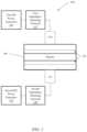
- FIG. 1is a schematic representation of a RF plasma processing system according to embodiments of the present disclosure.
- FIG. 2is a side view of a coil according to embodiments of the present disclosure.
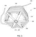
- FIG. 3is a side elevation view of the coil of FIG. 2 according to embodiments of the present disclosure.
- FIG. 4is an end view of the coil of FIG. 2 according to embodiments of the present disclosure.
- FIG. 5is a side perspective view of the coil of FIG. 2 according to embodiments of the present disclosure.
- FIG. 6is a side view of the coil of FIG. 2 according to embodiments of the present disclosure.
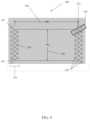
- FIG. 7is a side view of a coil in a coil block according to embodiments of the present disclosure.
- FIG. 8is an elevated perspective schematic representation of a coil in FIG. 7 in a coil block according to embodiments of the present disclosure.
- FIG. 9is a schematic cross-sectional representation of a coil according to embodiments of the present disclosure.
- FIG. 10is a schematic representation of a trifilar inductor according to embodiments of the present disclosure.
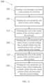
- FIG. 11is a flowchart of a method of forming a coil for a plasma processing device according to embodiments of the present disclosure
- the article “a”is intended to have its ordinary meaning in the patent arts, namely “one or more.”
- the term “about” when applied to a valuegenerally means within the tolerance range of the equipment used to produce the value, or in some examples, means plus or minus 10%, or plus or minus 5%, or plus or minus 1%, unless otherwise expressly specified.
- the term “substantially” as used hereinmeans a majority, or almost all, or all, or an amount with a range of about 51% to about 100%, for example.
- examples hereinare intended to be illustrative only and are presented for discussion purposes and not by way of limitation.
- Typical cylindrical single layer coilsmay have a number of issues and limitations in use. For example, typical cylindrical single layer coils may have a reduced Q factor when the length is greater than the diameter. Additionally, such coils have experienced poor cooling due to trapped air adjacent to the cylinder coil form when wound on a dielectric cylinder. Coils may also have a relatively long magnetic field return path that may result in high coupling coefficient to aluminum shield housing walls that produce eddy losses that result in lower Q values. Typical coils may also have lower inductance per unit length of wire that may result in lower Q values. Such coils may also have less predictable manufacturing tolerances.
- Embodiments of the present disclosuremay decrease losses in voltage and current at high power, which results in better Q values due to better stored to dissipated energy ratios.
- Embodiments of the present disclosuremay also advantageously maximize inductance per unit length of wire used, thereby resulting in better Q values. Such embodiments may further reduce distributed voltage across windings thereby reducing voltage stress potentials internally.
- Embodimentsmay further reduce magnetic field coupling to aluminum shield housing by optimizing magnetic field return paths, thereby reducing coupled eddy losses to the shield.
- Embodimentsmay also increase airflow around the inductor wire to improve cooling.
- Other advantagesmay include a mechanical form that provides predictable wire dimensional spacing in X, Y, and Z directions resulting in tighter manufacturing tolerance spread. Not all embodiments will exhibit all these characteristics and, to the extent that they exhibit more than one, they may not do so to the same extent.
- Embodiments of the present disclosuremay provide relatively high-power low frequency coils, such as for example, coils having a frequency of about 400 k.
- coils disclosed hereinmay have frequencies lower than 400 k and/or higher than 400 k depending on the application.
- the disclosed geometrycompacts the magnetic fields so as to reduce coupling interactions with the shield walls surrounding a coil.
- the registered start of each winding from the same sidereduces the voltage stress from layer to layer allowing higher voltage operation than a continuous filament sequentially wound coil of multiple layers traversing from side to side.
- the geometric positioning of wires for equal spacingmay also result in close tolerance repeatability approaching +/ ⁇ 1 percent.
- RF plasma processing system 100includes a first RF generator 105 and a second RF generator 110 , a first impedance matching network 115 , a second impedance matching network 120 , a sheath 125 , a plasma powering device, such as showerhead 130 or equivalent powered element such as an electrode, and a pedestal 135 .
- plasma power devicesmay refer to any device that introduces power to generate plasma and may include, for example, showerhead 130 and/or other types of electrodes, as well as antenna and the like.
- RF plasma processing system 100may include one or more first and second RF generators 105 , 110 that deliver power to a reaction chamber 140 through one or more impedance matching networks 115 , 120 .
- RF powerflows from the first RF generator 105 through the impedance matching network 115 to showerhead 130 into plasma in reaction chamber 140 , to an electrode (not shown) other than showerhead 130 , or to an inductive antenna (not shown) that electromagnetically provides power to the plasma, where after the power flows from the plasma to ground and/or to pedestal 135 and/or to second impedance matching network 120 .
- first impedance matching network 115compensates for variations in a load impedance inside reaction chamber 140 so the combined impedance of showerhead 130 and first impedance matching network 115 equal the output of first RF generator 105 , e.g., 50 ohms, by adjusting the reactive components (not separately shown), e.g., variable capacitors, within first impedance matching network 115 .
- Impedance matching networks 115 , 120are designed to adjust their internal reactive elements such that the load impedance matches the source impedance. Embodiments of the present disclosure may be used in impedance matching networks 115 , 120 , filters (not shown), resonators (not shown), and the like.
- a coil 200includes a coil form 205 , which is shown having six coil form extensions 210 . While six coil form extensions 210 are shown, in other embodiments, coil form 205 may be three, four, five, seven, or more coil form extensions 210 . Coil form extensions 210 may project radially outward from a coil form center 215 . Coil form center 215 may be used to attach coil 200 to a block (not shown), that will be illustrated below.
- One or more spacers 220 / 222may be disposed on a radially outward edge of one or more coil form extensions 210 .
- two spacers 220 / 222are illustrated with one inward spacer 220 disposed radially inward and a second outward spacer 222 disposed radially outward.
- Spacers 220 / 222may be formed from the same material as coil form 205 , or in other embodiments may be formed from other materials.
- a wire 225may be concentrically wrapped around coil form 205 and coil form extensions 210 , starting at the center, i.e., at the radially outward edge of coil form 205 .
- Inward spacer 220may then be disposed on top of coil form 205 , and wire 225 may be wrapped through inward spacer 220 .
- Outward spacer 222may then be disposed on top of inward spacer 200 , and wire 225 may be wrapper through outward spacer 222 .
- more than one wire 225may be used.
- a first wiremay be wrapped around coil form 205 .
- a second wiremay be wrapped around inward spacer 220 and a third wire may be wrapped around outward spacer 222 .
- the three wiresmay then be connected using one or more electrical connectors, such as an electric bus.
- coil 200includes a cylindrical winding that includes multiple layers, which in this embodiments includes three layers of windings.
- the windingstarts at the innermost diameter, and the winding continues for seven turns, which will be illustrated in greater detail below.
- wire 225returns through the center of coil form 205 back to the starting position and then overlays the first winding to start a second winding., where the first winding started.
- the second windingcontinues to its end, which in this embodiment includes eight turns.
- the second windingonce reaching the end, returns through the center of coil form 205 .
- Wire 225may then continue for a third winding, which in this embodiment includes nine turns.
- the wiremay exit coil 200 , to be electrically connected to other components through, for example, a lug (not shown) or other types of electrical connectors.
- the number of layers that are usedis decreased.
- the voltage stressmay be divided by a factor of three. If each winding included the same length of turns, wire 225 would end up with the same amount of voltage across it. Additionally, such geometry compacts the magnetic fields such as to reduce coupling interactions with shield walls (not shown) that surround coil 200 in operation.
- coil 200may also include a start of each winding that starts from the same side of coil 200 , coil form 205 , and coil form extensions 210 .
- start of each windingmay be reduced from layer to layer allowing higher voltage operation than a continuous filament sequentially would coil, where multiple layers traverse from side to side.
- geometric positioning of the wiresprovide for equal spacing, which results in close tolerance repeatability in a range of around one percent.
- coil 200includes coil form 205 , which is shown having six coil form extensions 210 . As illustrated, coil form extensions 210 project radially outward from coil form center 215 .
- One or more spacers 220 / 222may be disposed on a radially outward edge of one or more coil form extensions 210 . In this embodiment, two spacers 220 / 222 are illustrated with one inward spacer 220 disposed radially inward and a second outward spacer 222 disposed radially outward.
- Wire 225may be concentrically wrapped around coil form 205 and coil form extensions 210 , starting at the center, i.e., at the radially outward edge of coil form 205 .
- Inward spacer 220may then be disposed on top of coil form 205 , and wire 225 may be wrapped through inward spacer 220 .
- Outward spacer 222may then be disposed on top of inward spacer 200 , and wire 225 may be wrapper through outward spacer 222 .
- Both ends of wire 225may include electrical connectors 230 , such as lugs.
- electrical connectors 230may include other types of connectors, such as, for example, male-female connectors, screw connectors, bolt connectors, and/or any other types of electrical connectors 230 used or suitable in the art.
- electrical connectors 230may be insulated or partially insulated, depending on operational requirements.
- coil 200includes coil form 205 , which is shown having six coil form extensions 210 . As illustrated, coil form extensions 210 project radially outward from coil form center 215 . One or more spacers 220 / 222 may be disposed on a radially outward edge of one or more coil form extensions 210 . In this embodiment, two spacers 220 / 222 are illustrated with one inward spacer 220 disposed radially inward and a second outward spacer 222 disposed radially outward.
- Wire 225may be concentrically wrapped around coil form 205 and coil form extensions 210 , starting at the center, i.e., at the radially outward edge of coil form 205 .
- Inward spacer 220may then be disposed on top of coil form 205 , and wire 225 may be wrapped through inward spacer 220 .
- Outward spacer 222may then be disposed on top of inward spacer 200 , and wire 225 may be wrapper through outward spacer 222 .
- the third windingi.e., the outermost radial winding includes nine windings.
- the middle, or second windingincludes eight windings, while the innermost radial winding includes seven windings.
- a triangular winding formresults, which may provide one or more of the advantages discussed above. The triangular winding form will be illustrated and discussed in greater detail below.
- FIG. 5a side perspective view of coil 200 according to embodiments of the present disclosure is shown.
- coil 200includes coil form 205 , which is shown having six coil form extensions 210 .
- coil form extensions 210project radially outward from coil form center 215 .
- One or more spacers 220 / 222may be disposed on a radially outward edge of one or more coil form extensions 210 .
- two spacers 220 / 222are illustrated with one inward spacer 220 disposed radially inward and a second outward spacer 222 disposed radially outward.
- Wire 225may be concentrically wrapped around coil form 205 and coil form extensions 210 , starting at the center, i.e., at the radially outward edge of coil form 205 .
- Inward spacer 220may then be disposed on top of coil form 205 , and wire 225 may be wrapped through inward spacer 220 .
- Outward spacer 222may then be disposed on top of inward spacer 200 , and wire 225 may be wrapper through outward spacer 222 .
- coil 200includes coil form 205 , which is shown having six coil form extensions 210 . As illustrated, coil form extensions 210 project radially outward from coil form center 215 .
- One or more spacers 220 / 222may be disposed on a radially outward edge of one or more coil form extensions 210 .
- two spacers 220 / 222are illustrated with one inward spacer 220 disposed radially inward and a second outward spacer 222 disposed radially outward.
- Wire 225may be concentrically wrapped around coil form 205 and coil form extensions 210 , starting at the center, i.e., at the radially outward edge of coil form 205 .
- Inward spacer 220may then be disposed on top of coil form 205 , and wire 225 may be wrapped through inward spacer 220 .
- Outward spacer 222may then be disposed on top of inward spacer 200 , and wire 225 may be wrapper through outward spacer 222 .
- the outermost winding 235returns to the center of the winding 240 before exiting coil 200 to be connected to another device.
- the middle winding 245also returns to the center of the winding 240 before being wound into the third winding 240 .
- the innermost winding 250also returns to the center of the winding 240 being would into the middle winding 245 .
- coil 200includes coil form 205 , which is shown having six coil form extensions 210 . As illustrated, coil form extensions 210 project radially outward from coil form the coil center.
- One or more spacers 220 / 222may be disposed on a radially outward edge of one or more coil form extensions 210 .
- two spacers 220 / 222are illustrated with one inward spacer 220 disposed radially inward and a second outward spacer 222 disposed radially outward.
- coil 200is shown disposed within a coil block 255 .
- Coil 200may be connected to coil block 255 through various types of mechanical attachments 260 such as, for example, bolts.
- Coil block 255may be formed from various materials, including those of which coil 200 is formed.
- Coil block 255may be used to hold coil 200 in place during operation and may be connected to housing (not shown) or other components using one or more attachment points 265 .
- Coil block 255 and wire 225 windingswill be explained in greater detail with respect to FIG. 8 .
- coil 200includes coil form 205 , which is shown having six coil form extensions 210 . As illustrated, coil form extensions 210 project radially outward from coil form center 215 .
- One or more spacers 220 / 222may be disposed on a radially outward edge of one or more coil form extensions 210 . In this embodiment, two spacers 220 / 222 are illustrated with one inward spacer 220 disposed radially inward and a second outward spacer 222 disposed radially outward.
- Wire 225may be concentrically wrapped around coil form 205 and coil form extensions 210 , starting at the center, i.e., at the radially outward edge of coil form 205 .
- Inward spacer 220may then be disposed on top of coil form 205 , and wire 225 may be wrapped through inward spacer 220 .
- Outward spacer 222may then be disposed on top of inward spacer 200 , and wire 225 may be wrapper through outward spacer 222 .
- Wire 225may pass through a respective set of grooves 223 that are formed in coil form 205 , inward spacer 220 , and outward spacer 222 .
- Coil 200also is illustrated having two electrical connectors 230 / 232 .
- First electrical connector 230starts the inner most, first, winding, while second electrical connector terminates as the outermost, third, winding.
- both electrical connectors 230 / 232are shown as lugs, but other electrical connectors, such as those described above may also be used.
- coil 200is shown disposed within a coil block 255 .
- Coil 200may be connected to coil block 255 through various types of mechanical attachments 260 such as, for example, bolts.
- Coil block 255may be formed from various materials, including those of which coil 200 is formed.
- Foil block 255may be used to hold coil 200 in place during operation and may be connected to housing (not shown) or other components using one or more attachment points 265 .
- FIG. 9a schematic cross-sectional representation of coil 200 according to embodiments of the present disclosure is shown.
- coil 200is shown having three windings of wire 225 .
- Each winding would in relation to each adjacent wireis spaced both axially and radially at a fixed distance, so that a cross-section of completed concentric layers of winding forms a unilateral triangle is disposition of all conductor centers.
- the unilateral triangle geometryis illustrated at reference character 270 .
- the progression of winding turn count of one turn per layermay thereby optimize field return path.
- the winding turn count of one turn per layeris illustrated at reference character 275 .
- Embodiments of the present disclosuremay thus provide a plurality of concentric cylinder or polygonal cross-section windings of wire such that the spacing between any adjacent turn is equal and on the order of 0.25 to 1 radius of the wire used.
- Such embodimentsmay include concentric cylinders of wire that are connected so that the start of a first winding continues to a finish-turn and then axially returns to the same starting end of the first winding to start a new larger diameter cylindrical winding layer concentric to the first winding, thereby encompassing the first winding.
- the start of the second windingcontinues to a finish-turn and then returns axially to the same starting end as the first and second winding to start a new cylinder of winding concentric to the second and first winding.
- the concentric coilsmay thereby have common registered starts and finishes of each winding.
- the collective cross-section of windingsincludes a diameter 280 and a length, which collectively forms a diameter to length 285 ratio, which is the mean diameter, of between 2:1 and 3:1, and in certain embodiments between 2.4:1 and 2.5:1, and in still other embodiments about 2.46:1.
- Wire turnsmay be parallel and perpendicular to the coil axis for 5 ⁇ 6 th of a turn and step from one guide groove to the next for 1 ⁇ 6 th of a turn. Such a mechanical technique may thereby simplify construction of the coil during manufacturing.
- the one turn increase per layermay thereby provide advantages of improved magnetic field coupling and wire separation may be maintained when a wire ascends radially from a lower later to a next layer.
- FIG. 10a schematic representation of a trifilar inductor according to embodiments of the present disclosure is shown.
- a first electrical connector 230which in this embodiment is a first lug, is connected to an electrical source (not shown).
- Wire 225is then wound into three concentric windings.
- First winding 250includes seven turns and forms the innermost portion of the coil.
- Second winding 245includes eight turns and forms the middle portion of the coil.
- Third winding 235includes nine turns and forms the outermost portion of the coil.
- Wire 225then exits coil and truncates at second end connector 232 .
- FIG. 11a flowchart of a method of forming a coil for a plasma processing device according to embodiments of the present disclosure is shown.
- the methodincludes feeding (block 300 ) a wire through a coil form a central portion of a coil form.
- the central portion of the coil formmay include one or more apertures that allow the wire to pass through the coil form.
- the methodmay further include winding (block 305 ) the wire around the coil form to form a first winding.
- the wiremay initially pass through the aperture in the coil form and then pass around a radially outward portion of the coil form.
- the wiremay pass through grooves that are preformed in the coil form, or may be pressed against the coil form, depending on operational requirements.
- the methodmay further include returning (block 310 ) the wire to the central portion of the coil form center of the coil form.
- the wiremay thereby return to the central portion at a location on the same side as where the first winding started.
- the final location of the first winding, while on the same side of the coil form,may be located longitudinally at a different location with respect to the aperture the wire initially passed through.
- the methodmay further include winding (block 315 ) the wire around the coil form to form a second winding that is radially further from the central portion of the coil form center than the first winding. As such, the second winding is outside the first winding.
- the second windingmay start by passing through a second aperture the is on the same side of the coil form as the first aperture but may be in a different longitudinal location.
- the methodmay further include returning (block 320 ) the wire to the central portion of the coil form center of the coil form.
- the wiremay thereby return to the center portion at a location on the same side as where the first winding started and ended.
- the final location of the second winding, while on the same side of the coil form,may be located longitudinally at a different location with respect to the aperture the wire initially passed through to start the second winding.
- the methodmay further include winding (block 325 ) the wire around the coil form to form a third winding that is radially further from the central portion of the coil form central than the second winding.
- the wiremay thereby return to the center portion at a location on the same side as where the first and second windings started and ended.
- the final location of the third winding, while on the same side of the coil form,may be located longitudinally at a different location with respect to the aperture the wire initially passed through to start the first and/or second windings.
- the first windingis disposed on at least a portion of the coil form
- the second windingis disposed on at least a portion of a first spacer
- the first spacerdisposed on a radially distal portion of the coil form
- the third windingis disposed on at least a portion of second spacer, the second spacer disposed on the first spacer.
- the first spacermay be added to the coil after the first winding occurs.
- the second spacermay be added to the coil after the second winding occurs. Because the spacers are added in sequence, the assembly of the coil may be easier, due to access to the radially outmost edge of the coil during any given winding.
- the first windingmay include seven turns
- the second windingmay include eight turns
- the third windingmay include nine turns.
- the number of turns for any given windingmay vary based on the number of coil form extensions, and the desired results of a particular operation.
- a coilmay include three progressive windings of four, five, and six winding. Those of ordinary skill in the part will appreciate that variations on the number of turns for easy winding may vary based on desired results.
- advantages of the present disclosuremay provide reduced losses in voltage and current at high power.
- the reduced loss in voltage and current at high powermay thereby result in an increased quality factor relative to typical cylindrical single layer coils.
- advantages of the present disclosuremay provide increased quality factor due to stored to dissipated energy ratios.
- advantages of the present disclosuremay provide an optimized/maximized inductance per unit length of wire used.
- advantages of the present disclosuremay provide reduced distributed voltage across windings reducing internal voltage stress potentials.
- advantages of the present disclosuremay provide reduced magnetic field coupling to aluminum shield housing by optimizing the magnetic field return path, thereby reducing coupled eddy losses to the shield.
- advantages of the present disclosuremay provide increased airflow around the inductor wire for improved cooling.
- advantages of the present disclosuremay provide a mechanical form that provides predictable wire dimensional spacing along the X axis, Y axis, and Z axis, thereby resulting in tighter manufacturing tolerance spread.
Landscapes
- Engineering & Computer Science (AREA)
- Power Engineering (AREA)
- Physics & Mathematics (AREA)
- Plasma & Fusion (AREA)
- Chemical & Material Sciences (AREA)
- Analytical Chemistry (AREA)
- Manufacturing & Machinery (AREA)
- Spectroscopy & Molecular Physics (AREA)
- Coils Of Transformers For General Uses (AREA)
- Plasma Technology (AREA)
- Manufacturing Cores, Coils, And Magnets (AREA)
Abstract
Description
Claims (20)
Priority Applications (4)
| Application Number | Priority Date | Filing Date | Title |
|---|---|---|---|
| KR1020227001279AKR20220053547A (en) | 2019-08-28 | 2020-08-28 | high power low frequency coils |
| PCT/US2020/048630WO2021041984A1 (en) | 2019-08-28 | 2020-08-28 | High power low frequency coils |
| JP2022513551AJP2022546488A (en) | 2019-08-28 | 2020-08-28 | High power low frequency coil |
| US17/006,693US12002611B2 (en) | 2019-08-28 | 2020-08-28 | High power low frequency coils |
Applications Claiming Priority (2)
| Application Number | Priority Date | Filing Date | Title |
|---|---|---|---|
| US201962893066P | 2019-08-28 | 2019-08-28 | |
| US17/006,693US12002611B2 (en) | 2019-08-28 | 2020-08-28 | High power low frequency coils |
Publications (2)
| Publication Number | Publication Date |
|---|---|
| US20210065956A1 US20210065956A1 (en) | 2021-03-04 |
| US12002611B2true US12002611B2 (en) | 2024-06-04 |
Family
ID=74681314
Family Applications (1)
| Application Number | Title | Priority Date | Filing Date |
|---|---|---|---|
| US17/006,693Active2042-06-30US12002611B2 (en) | 2019-08-28 | 2020-08-28 | High power low frequency coils |
Country Status (6)
| Country | Link |
|---|---|
| US (1) | US12002611B2 (en) |
| EP (1) | EP4022656A4 (en) |
| JP (1) | JP2022546488A (en) |
| KR (1) | KR20220053547A (en) |
| CN (1) | CN114144853B (en) |
| WO (1) | WO2021041984A1 (en) |
Cited By (1)
| Publication number | Priority date | Publication date | Assignee | Title |
|---|---|---|---|---|
| US20240371604A1 (en)* | 2021-08-12 | 2024-11-07 | Lam Research Corporation | Process module chamber providing symmetric rf return path |
Citations (184)
| Publication number | Priority date | Publication date | Assignee | Title |
|---|---|---|---|---|
| US1017348A (en)* | 1911-05-19 | 1912-02-13 | Thomas E Murray | Reactance-coil. |
| GB238560A (en) | 1924-08-14 | 1926-07-01 | Dimmitt Ross Lovejoy | Improvements in inductance coils |
| DE538664C (en) | 1930-01-26 | 1931-11-16 | Siemens Schuckertwerke Akt Ges | Choke coil with superimposed layers of adjacent turns |
| GB563452A (en) | 1942-05-05 | 1944-08-15 | British Thomson Houston Co Ltd | Improvements in and relating to electric apparatus and windings therefor |
| US4188177A (en) | 1977-02-07 | 1980-02-12 | Texas Instruments Incorporated | System for fabrication of semiconductor bodies |
| EP0065147A1 (en) | 1981-05-15 | 1982-11-24 | Westinghouse Electric Corporation | Method of forming electric coils |
| US4422078A (en) | 1980-11-24 | 1983-12-20 | Cremeen Melvin L | Full wave communication antenna |
| US4477792A (en)* | 1982-01-29 | 1984-10-16 | Westinghouse Electric Corp. | Modular power system reactor |
| US4679007A (en) | 1985-05-20 | 1987-07-07 | Advanced Energy, Inc. | Matching circuit for delivering radio frequency electromagnetic energy to a variable impedance load |
| US5052997A (en) | 1987-04-10 | 1991-10-01 | The United States Of America As Represented By The Secretary Of The Department Of Health And Human Services | Diathermy coil |
| JPH04239211A (en) | 1991-01-11 | 1992-08-27 | Shindengen Electric Mfg Co Ltd | Matching control circuit for rf generator |
| US5175472A (en) | 1991-12-30 | 1992-12-29 | Comdel, Inc. | Power monitor of RF plasma |
| US5195045A (en) | 1991-02-27 | 1993-03-16 | Astec America, Inc. | Automatic impedance matching apparatus and method |
| JPH05284046A (en) | 1991-01-29 | 1993-10-29 | Shindengen Electric Mfg Co Ltd | Impedance matching control circuit for rf generator |
| US5394061A (en) | 1993-01-14 | 1995-02-28 | Adtec Co., Ltd. | High frequency plasma power source and impedance matching device for supplying power to a semiconductor processing apparatus |
| US5474648A (en) | 1994-07-29 | 1995-12-12 | Lsi Logic Corporation | Uniform and repeatable plasma processing |
| US5576629A (en) | 1994-10-24 | 1996-11-19 | Fourth State Technology, Inc. | Plasma monitoring and control method and system |
| US5609737A (en) | 1993-08-24 | 1997-03-11 | Frontec Incorporated | Film manufacturing method using single reaction chamber for chemical-vapor deposition and sputtering |
| US5629653A (en) | 1995-07-07 | 1997-05-13 | Applied Materials, Inc. | RF match detector circuit with dual directional coupler |
| US5737175A (en) | 1996-06-19 | 1998-04-07 | Lam Research Corporation | Bias-tracking D.C. power circuit for an electrostatic chuck |
| US5792261A (en) | 1993-12-17 | 1998-08-11 | Tokyo Electron Limited | Plasma process apparatus |
| US5810963A (en) | 1995-09-28 | 1998-09-22 | Kabushiki Kaisha Toshiba | Plasma processing apparatus and method |
| US5842154A (en) | 1997-09-15 | 1998-11-24 | Eni Technologies, Inc. | Fuzzy logic tuning of RF matching network |
| US5849136A (en) | 1991-10-11 | 1998-12-15 | Applied Materials, Inc. | High frequency semiconductor wafer processing apparatus and method |
| US5866869A (en) | 1997-02-24 | 1999-02-02 | Illinois Tool Works Inc. | Plasma pilot arc control |
| US5889252A (en) | 1996-12-19 | 1999-03-30 | Lam Research Corporation | Method of and apparatus for independently controlling electric parameters of an impedance matching network |
| US5910886A (en) | 1997-11-07 | 1999-06-08 | Sierra Applied Sciences, Inc. | Phase-shift power supply |
| US5914974A (en) | 1997-02-21 | 1999-06-22 | Cymer, Inc. | Method and apparatus for eliminating reflected energy due to stage mismatch in nonlinear magnetic compression modules |
| US6016131A (en) | 1995-08-16 | 2000-01-18 | Applied Materials, Inc. | Inductively coupled plasma reactor with an inductive coil antenna having independent loops |
| US6157179A (en) | 1997-06-13 | 2000-12-05 | U.S. Philips Corporation | Switched-mode power supply for charging a capacitance during a first period, forming a resonant circuit with an inductance, and discharging the capacitance into a load during a second period disjunct from the first period |
| US6164241A (en) | 1998-06-30 | 2000-12-26 | Lam Research Corporation | Multiple coil antenna for inductively-coupled plasma generation systems |
| US6252354B1 (en) | 1996-11-04 | 2001-06-26 | Applied Materials, Inc. | RF tuning method for an RF plasma reactor using frequency servoing and power, voltage, current or DI/DT control |
| US6313584B1 (en) | 1998-09-17 | 2001-11-06 | Tokyo Electron Limited | Electrical impedance matching system and method |
| US6313587B1 (en) | 1998-01-13 | 2001-11-06 | Fusion Lighting, Inc. | High frequency inductive lamp and power oscillator |
| US6326597B1 (en) | 1999-04-15 | 2001-12-04 | Applied Materials, Inc. | Temperature control system for process chamber |
| US6407648B1 (en) | 1999-11-15 | 2002-06-18 | Werlatone, Inc. | Four-way non-directional power combiner |
| US6507155B1 (en) | 2000-04-06 | 2003-01-14 | Applied Materials Inc. | Inductively coupled plasma source with controllable power deposition |
| CN1404184A (en) | 2001-08-31 | 2003-03-19 | 耀登科技股份有限公司 | The Method of Processing Antenna by Instant Welding |
| US20030150710A1 (en) | 2001-10-09 | 2003-08-14 | Evans John D. | Plasma production device and method and RF driver circuit |
| US20030230984A1 (en) | 2002-05-31 | 2003-12-18 | Toshiaki Kitamura | Plasma generating method, plasma apparatus, phase difference detecting method, impedance detecting method, measuring device, and coaxial type impedance matching device |
| US6677828B1 (en) | 2000-08-17 | 2004-01-13 | Eni Technology, Inc. | Method of hot switching a plasma tuner |
| US20040026235A1 (en) | 2002-05-17 | 2004-02-12 | Applied Films Corporation | System and apparatus for control of sputter deposition process |
| US6703080B2 (en) | 2002-05-20 | 2004-03-09 | Eni Technology, Inc. | Method and apparatus for VHF plasma processing with load mismatch reliability and stability |
| CN1509493A (en) | 2001-03-30 | 2004-06-30 | 拉姆研究有限公司 | Laminated RF Excitation Coils for Inductive Plasma Processors |
| US6806437B2 (en) | 2002-09-04 | 2004-10-19 | Samsung Electronics Co., Ltd. | Inductively coupled plasma generating apparatus incorporating double-layered coil antenna |
| CN1582485A (en) | 2001-09-14 | 2005-02-16 | 拉姆研究有限公司 | Plasma processor coil |
| US20050045475A1 (en) | 2003-08-28 | 2005-03-03 | Kiyomi Watanabe | Sputtering apparatus |
| US6876155B2 (en) | 2002-12-31 | 2005-04-05 | Lam Research Corporation | Plasma processor apparatus and method, and antenna |
| US6894245B2 (en) | 2000-03-17 | 2005-05-17 | Applied Materials, Inc. | Merie plasma reactor with overhead RF electrode tuned to the plasma with arcing suppression |
| US20050270805A1 (en) | 2004-05-31 | 2005-12-08 | Sony Corporation | Switching power supply circuit |
| US20060005928A1 (en) | 2002-03-08 | 2006-01-12 | Lam Research Corporation | Apparatus and methods for improving the stability of RF power delivery to a plasma load |
| US7030335B2 (en) | 2000-03-17 | 2006-04-18 | Applied Materials, Inc. | Plasma reactor with overhead RF electrode tuned to the plasma with arcing suppression |
| US7042311B1 (en) | 2003-10-10 | 2006-05-09 | Novellus Systems, Inc. | RF delivery configuration in a plasma processing system |
| US7079597B1 (en) | 1999-10-05 | 2006-07-18 | Kabushiki Kaisha Kenwood | Method and circuit for acquisition |
| US20060169582A1 (en) | 2005-02-03 | 2006-08-03 | Applied Materials, Inc. | Physical vapor deposition plasma reactor with RF source power applied to the target and having a magnetron |
| US7102292B2 (en) | 2001-12-10 | 2006-09-05 | Tokyo Electron Limited | Method and device for removing harmonics in semiconductor plasma processing systems |
| US7192505B2 (en) | 2002-07-12 | 2007-03-20 | Advanced Plasma, Inc. | Wafer probe for measuring plasma and surface characteristics in plasma processing environments |
| US7196283B2 (en) | 2000-03-17 | 2007-03-27 | Applied Materials, Inc. | Plasma reactor overhead source power electrode with low arcing tendency, cylindrical gas outlets and shaped surface |
| US7215697B2 (en) | 1999-08-27 | 2007-05-08 | Hill Alan E | Matched impedance controlled avalanche driver |
| US7220937B2 (en) | 2000-03-17 | 2007-05-22 | Applied Materials, Inc. | Plasma reactor with overhead RF source power electrode with low loss, low arcing tendency and low contamination |
| US20070121267A1 (en) | 2003-11-27 | 2007-05-31 | Hiroyuki Kotani | High-frequency power supply system |
| US7251121B2 (en) | 2005-03-05 | 2007-07-31 | Innovation Engineering Llc | Electronically variable capacitor array |
| US7259623B2 (en) | 2004-05-28 | 2007-08-21 | Ixys Corporation | RF generator with reduced size and weight |
| CN200962339Y (en) | 2006-09-19 | 2007-10-17 | 金亚东 | Aluminum core coil line |
| US7298128B2 (en) | 2005-01-11 | 2007-11-20 | Innovation Engineering Llc | Method of detecting RF powder delivered to a load and complex impedance of the load |
| US20080061793A1 (en) | 2004-09-04 | 2008-03-13 | Applied Materials, Inc. | Detection and Suppression of Electrical Arcing |
| US20080061901A1 (en) | 2006-09-13 | 2008-03-13 | Jack Arthur Gilmore | Apparatus and Method for Switching Between Matching Impedances |
| US7467612B2 (en) | 2005-04-19 | 2008-12-23 | Knite, Inc. | Method and apparatus for operating traveling spark igniter at high pressure |
| US20080317974A1 (en) | 2005-08-26 | 2008-12-25 | Fujifilm Manufacturing Europe B.V. | Method and Arrangement for Generating and Controlling a Discharge Plasma |
| US20090026964A1 (en) | 2007-07-23 | 2009-01-29 | Huettinger Elektronik Gmbh + Co. Kg | High Frequency Power Supply |
| CN101454851A (en) | 2006-05-30 | 2009-06-10 | Abb技术有限公司 | Disc-wound transformer with foil conductor and method of manufacturing the same |
| US20100012029A1 (en) | 2008-07-15 | 2010-01-21 | Applied Materials, Inc. | Apparatus for controlling radial distribution of plasma ion density and ion energy at a workpiece surface by multi-frequency rf impedance tuning |
| US20100098882A1 (en) | 2008-10-21 | 2010-04-22 | Applied Materials, Inc. | Plasma source for chamber cleaning and process |
| US20100096261A1 (en) | 2008-10-17 | 2010-04-22 | Applied Materials, Inc. | Physical vapor deposition reactor with circularly symmetric rf feed and dc feed to the sputter target |
| US7795877B2 (en) | 2006-11-02 | 2010-09-14 | Current Technologies, Llc | Power line communication and power distribution parameter measurement system and method |
| US20100314048A1 (en) | 2009-06-12 | 2010-12-16 | Maolin Long | Adjusting current ratios in inductively coupled plasma processing systems |
| US20110121735A1 (en) | 2000-02-22 | 2011-05-26 | Kreos Capital Iii (Uk) Limited | Tissue resurfacing |
| US20110140607A1 (en) | 2008-05-30 | 2011-06-16 | Colorado State University Research Foundation | System, method and apparatus for generating plasma |
| US20110148303A1 (en) | 2009-12-22 | 2011-06-23 | Van Zyl Gideon | Efficient active source impedance modification of a power amplifier |
| CN102203888A (en) | 2008-06-30 | 2011-09-28 | 线圈创新控股有限公司 | Choke coil for an electrical power supply system with reduced sound emission |
| US20120097524A1 (en) | 2010-10-20 | 2012-04-26 | COMET Technologies USA, Inc. | Rf impedance matching network with secondary frequency and sub-harmonic variant |
| WO2012054305A2 (en) | 2010-10-20 | 2012-04-26 | Comet Technologies Usa, Inc | Rf impedance matching network with secondary dc input |
| WO2012054306A2 (en) | 2010-10-20 | 2012-04-26 | Comet Technologies Usa, Inc | Pulse mode capability for operation of an rf/vhf impedance matching network with 4 quadrant, vrms/irms responding detector circuitry |
| US8169162B2 (en) | 2008-03-26 | 2012-05-01 | Kyosan Electric Mfg. Co., Ltd. | Abnormal discharge suppressing device for vacuum apparatus |
| US8169262B2 (en) | 2008-12-29 | 2012-05-01 | Princeton Technology Corporation | Method for reducing offset voltage of operational amplifier and the circuit using the same |
| US20120145322A1 (en) | 2010-12-13 | 2012-06-14 | Hitachi High-Technologies Corporation | Plasma processing apparatus |
| US8203372B2 (en) | 2008-04-22 | 2012-06-19 | Cisco Technology, Inc. | Synchronous rectifier post regulator |
| US8222822B2 (en) | 2009-10-27 | 2012-07-17 | Tyco Healthcare Group Lp | Inductively-coupled plasma device |
| CN102611210A (en) | 2012-03-27 | 2012-07-25 | 东南大学 | Design method of disc resonator in wireless power transmission system |
| US20120262064A1 (en) | 2005-10-31 | 2012-10-18 | Mks Instruments, Inc. | Radio Frequency Power Delivery System |
| US20130140984A1 (en) | 2010-07-15 | 2013-06-06 | Tohoku University | Plasma processing apparatus and plasma processing method |
| US8471746B2 (en) | 2011-07-08 | 2013-06-25 | Tektronix, Inc. | Digital-to-analog conversion with combined pulse modulators |
| US20130180964A1 (en) | 2008-12-05 | 2013-07-18 | Advanced Energy Industries, Inc. | Over-voltage protection during arc recovery for plasma-chamber power supplies |
| US20130214683A1 (en) | 2012-02-22 | 2013-08-22 | Lam Research Corporation | Impedance-Based Adjustment of Power and Frequency |
| US20130278140A1 (en) | 2012-04-19 | 2013-10-24 | Luxim Corporation | Electrodeless plasma lamp utilizing acoustic modulation |
| US20130345847A1 (en) | 2009-11-19 | 2013-12-26 | John C. Valcore, JR. | Arrangement for plasma processing system control based on rf voltage |
| US8742669B2 (en) | 2009-02-02 | 2014-06-03 | Advanced Energy Industries, Inc. | Passive power distribution for multiple electrode inductive plasma source |
| US8803424B2 (en) | 2010-10-20 | 2014-08-12 | COMET Technologies USA, Inc. | RF/VHF impedance matching, 4 quadrant, dual directional coupler with V RMS/IRMS responding detector circuitry |
| US20140225504A1 (en) | 2013-02-12 | 2014-08-14 | Tokyo Electron Limited | Plasma processing apparatus, plasma processing method and high frequency generator |
| US20140239813A1 (en) | 2013-02-27 | 2014-08-28 | Advanced Energy Industries, Inc. | Reliable plasma ignition and reignition |
| US20140265911A1 (en) | 2013-03-14 | 2014-09-18 | Hisahiro Kamata | High-voltage inverter, dielectric-barrier discharge evice and cation apparatus |
| US8896391B2 (en) | 2000-07-20 | 2014-11-25 | Blackberry Limited | Tunable microwave devices with auto-adjusting matching circuit |
| US20140367043A1 (en) | 2013-06-17 | 2014-12-18 | Applied Materials, Inc. | Method for fast and repeatable plasma ignition and tuning in plasma chambers |
| US20150115797A1 (en) | 2012-06-18 | 2015-04-30 | Kyosan Electric Mfg. Co., Ltd. | High-frequency power supply device and ignition voltage selection method |
| US9042121B2 (en) | 2008-12-29 | 2015-05-26 | Advanced Energy Industries, Inc. | Power converter with preemptive protection |
| US9065426B2 (en) | 2011-11-03 | 2015-06-23 | Advanced Energy Industries, Inc. | High frequency solid state switching for impedance matching |
| US9105447B2 (en) | 2012-08-28 | 2015-08-11 | Advanced Energy Industries, Inc. | Wide dynamic range ion energy bias control; fast ion energy switching; ion energy control and a pulsed bias supply; and a virtual front panel |
| US9124248B2 (en) | 2011-01-20 | 2015-09-01 | Advanced Energy Industries, Inc. | Impedance-matching network using BJT switches in variable-reactance circuits |
| US9142388B2 (en) | 2011-01-25 | 2015-09-22 | Advanced Energy Industries, Inc. | Capacitively coupled remote plasma source |
| US9148086B2 (en) | 2013-10-22 | 2015-09-29 | Advanced Energy Industries, Inc. | Photovoltaic DC sub-array control system and method |
| US9166481B1 (en) | 2013-03-14 | 2015-10-20 | Vlt, Inc. | Digital control of resonant power converters |
| US9171700B2 (en) | 2012-06-15 | 2015-10-27 | COMET Technologies USA, Inc. | Plasma pulse tracking system and method |
| US20150313000A1 (en) | 2012-10-09 | 2015-10-29 | Novellus Systems, Inc. | Hybrid impedance matching for inductively coupled plasma system |
| US9196459B2 (en) | 2014-01-10 | 2015-11-24 | Reno Technologies, Inc. | RF impedance matching network |
| US9208992B2 (en) | 2010-04-26 | 2015-12-08 | Advanced Energy Industries, Inc. | Method for controlling ion energy distribution |
| US9225299B2 (en) | 2011-04-18 | 2015-12-29 | Advanced Energy Industries, Inc. | Variable-class amplifier, system, and method |
| US9224579B2 (en) | 2012-11-01 | 2015-12-29 | Advanced Energy Industries, Inc. | Adjustable non-dissipative voltage boosting snubber network for achieving large boost voltages |
| US20160002020A1 (en) | 2013-03-04 | 2016-01-07 | Kabushiki Kaisha Cosmo Life | Water dispenser |
| JP5863117B2 (en) | 2009-12-30 | 2016-02-16 | フィリップ・モーリス・プロダクツ・ソシエテ・アノニム | Method and apparatus for producing pouch-like tobacco products |
| US9287098B2 (en) | 2012-11-01 | 2016-03-15 | Advanced Energy Industries, Inc. | Charge removal from electrodes in unipolar sputtering system |
| US9294100B2 (en) | 2012-12-04 | 2016-03-22 | Advanced Energy Industries, Inc. | Frequency tuning system and method for finding a global optimum |
| WO2016048449A1 (en) | 2014-09-25 | 2016-03-31 | Applied Materials, Inc. | Detecting plasma arcs by monitoring rf reflected power in a plasma processing chamber |
| US9306533B1 (en) | 2015-02-20 | 2016-04-05 | Reno Technologies, Inc. | RF impedance matching network |
| US9313870B2 (en) | 2012-08-31 | 2016-04-12 | Advanced Energy Industries, Inc. | Arc management with voltage reversal and improved recovery |
| US9345122B2 (en) | 2014-05-02 | 2016-05-17 | Reno Technologies, Inc. | Method for controlling an RF generator |
| CN105704550A (en) | 2016-02-02 | 2016-06-22 | 四川长虹电器股份有限公司 | Method for realizing rapid wireless network connection upon power-on of intelligent television |
| WO2016097730A1 (en) | 2014-12-16 | 2016-06-23 | John Wood | A power coupler |
| US9385021B2 (en) | 2012-02-23 | 2016-07-05 | Lam Research Corporation | Electronic knob for tuning radial etch non-uniformity at VHF frequencies |
| US20160308560A1 (en) | 2013-05-09 | 2016-10-20 | Lam Research Corporation | Systems and methods for reducing power reflected towards a higher frequency rf generator during a period of a lower rf generator and for using a relationship to reduce reflected power |
| US9478397B2 (en) | 2011-01-04 | 2016-10-25 | Advanced Energy Industries, Inc. | System level power delivery to a plasma processing load |
| US9483066B2 (en) | 2012-11-01 | 2016-11-01 | Advanced Energy Industries, Inc. | Adjustable non-dissipative voltage boosting snubber network |
| US9490353B2 (en) | 2012-08-28 | 2016-11-08 | Advanced Energy Industries, Inc. | Three terminal PIN diode |
| US9496122B1 (en) | 2014-01-10 | 2016-11-15 | Reno Technologies, Inc. | Electronically variable capacitor and RF matching network incorporating same |
| US9525412B2 (en) | 2015-02-18 | 2016-12-20 | Reno Technologies, Inc. | Switching circuit |
| US9544987B2 (en) | 2014-06-30 | 2017-01-10 | Advanced Energy Industries, Inc. | Frequency tuning for pulsed radio frequency plasma processing |
| US9577516B1 (en) | 2016-02-18 | 2017-02-21 | Advanced Energy Industries, Inc. | Apparatus for controlled overshoot in a RF generator |
| US9578731B2 (en) | 2014-10-16 | 2017-02-21 | Advanced Energy Industries, Inc. | Systems and methods for obtaining information about a plasma load |
| US9589767B2 (en) | 2013-07-19 | 2017-03-07 | Advanced Energy Industries, Inc. | Systems, methods, and apparatus for minimizing cross coupled wafer surface potentials |
| US9591739B2 (en) | 2014-05-02 | 2017-03-07 | Reno Technologies, Inc. | Multi-stage heterodyne control circuit |
| US20170133886A1 (en) | 2008-09-27 | 2017-05-11 | Witricity Corporation | Wireless powered television |
| US9697911B2 (en) | 2013-09-19 | 2017-07-04 | Renesas Electronics Corporation | Semiconductor storage device and test method thereof using a common bit line |
| US9711335B2 (en) | 2013-07-17 | 2017-07-18 | Advanced Energy Industries, Inc. | System and method for balancing consumption of targets in pulsed dual magnetron sputtering (DMS) processes |
| US9729122B2 (en) | 2015-02-18 | 2017-08-08 | Reno Technologies, Inc. | Switching circuit |
| US9728378B2 (en) | 2014-05-02 | 2017-08-08 | Reno Technologies, Inc. | Method for controlling an RF generator |
| CN206415543U (en) | 2016-12-19 | 2017-08-18 | 中铁隆昌铁路器材有限公司 | A kind of metalwork load coil coiling device |
| US9741544B2 (en) | 2014-03-24 | 2017-08-22 | Advanced Energy Industries, Inc. | System and method for control of high efficiency generator source impedance |
| US9745660B2 (en) | 2014-05-02 | 2017-08-29 | Reno Technologies, Inc. | Method for controlling a plasma chamber |
| US9748076B1 (en) | 2016-04-20 | 2017-08-29 | Advanced Energy Industries, Inc. | Apparatus for frequency tuning in a RF generator |
| US9755641B1 (en) | 2014-01-10 | 2017-09-05 | Reno Technologies, Inc. | High speed high voltage switching circuit |
| US9807863B1 (en) | 2016-06-09 | 2017-10-31 | Advanced Energy Industries, Inc. | Switching amplifier |
| CN107304753A (en) | 2016-04-22 | 2017-10-31 | 彩虹量子有限公司 | Rotary actuator made using shape memory alloy |
| US9812305B2 (en) | 2015-04-27 | 2017-11-07 | Advanced Energy Industries, Inc. | Rate enhanced pulsed DC sputtering system |
| US20170338081A1 (en) | 2016-05-18 | 2017-11-23 | Tokyo Electron Limited | Plasma processing apparatus |
| US20170345620A1 (en) | 2016-05-24 | 2017-11-30 | Mks Instruments, Inc. | Solid-state impedance matching systems including a hybrid tuning network with a switchable coarse tuning network and a varactor fine tuning network |
| US9844127B2 (en) | 2014-01-10 | 2017-12-12 | Reno Technologies, Inc. | High voltage switching circuit |
| US9865432B1 (en) | 2014-01-10 | 2018-01-09 | Reno Technologies, Inc. | RF impedance matching network |
| CN107796974A (en) | 2016-08-31 | 2018-03-13 | 施耐德电器工业公司 | Coil type sensor including its measurement apparatus, breaker and its winding method |
| US9952297B2 (en) | 2014-05-08 | 2018-04-24 | Auburn University | Parallel plate transmission line for broadband nuclear magnetic resonance imaging |
| CN108109826A (en) | 2017-12-12 | 2018-06-01 | 辽宁华冶集团发展有限公司 | A kind of mining general epoxy cast dry transformer trapezoidal coil structure |
| US10008317B2 (en) | 2015-12-08 | 2018-06-26 | Smart Wires Inc. | Voltage or impedance-injection method using transformers with multiple secondary windings for dynamic power flow control |
| US10020752B1 (en) | 2017-09-26 | 2018-07-10 | Vlt, Inc. | Adaptive control of resonant power converters |
| US10026592B2 (en) | 2016-07-01 | 2018-07-17 | Lam Research Corporation | Systems and methods for tailoring ion energy distribution function by odd harmonic mixing |
| US20180261431A1 (en) | 2017-03-13 | 2018-09-13 | Applied Materials, Inc. | Dual radio-frequency tuner for process control of a plasma process |
| EP3376513A1 (en) | 2017-03-13 | 2018-09-19 | ABB Schweiz AG | An arrangement of lcl filter structure |
| US10139285B2 (en) | 2014-12-23 | 2018-11-27 | Advanced Energy Industries, Inc. | Fully-differential amplification for pyrometry |
| US10141788B2 (en) | 2015-10-22 | 2018-11-27 | Witricity Corporation | Dynamic tuning in wireless energy transfer systems |
| EP3416174A1 (en) | 2017-06-14 | 2018-12-19 | LAM Research Corporation | Articulated direct-mount inductor and associated systems and methods |
| US10217618B2 (en) | 2011-05-10 | 2019-02-26 | Advanced Energy Industries, Inc. | Current threshold response mode for arc management |
| US10224184B2 (en) | 2014-03-24 | 2019-03-05 | Aes Global Holdings, Pte. Ltd | System and method for control of high efficiency generator source impedance |
| US10224186B2 (en) | 2015-03-13 | 2019-03-05 | Aes Global Holdings, Pte. Ltd | Plasma source device and methods |
| CN208622519U (en) | 2018-06-07 | 2019-03-19 | 南京电气高压互感器有限公司 | A kind of shunt capacitor differential pressure type discharge coil |
| US10263577B2 (en) | 2016-12-09 | 2019-04-16 | Advanced Energy Industries, Inc. | Gate drive circuit and method of operating the same |
| CN109643605A (en) | 2016-11-08 | 2019-04-16 | 皇家飞利浦有限公司 | Inductor for high frequency and high power applications |
| US10269540B1 (en) | 2018-01-25 | 2019-04-23 | Advanced Energy Industries, Inc. | Impedance matching system and method of operating the same |
| WO2019096564A1 (en) | 2017-11-17 | 2019-05-23 | Evatec Ag | Rf power delivery to vacuum plasma processing |
| US20190172683A1 (en) | 2015-02-18 | 2019-06-06 | Reno Technologies, Inc. | Switching circuit |
| US20190199241A1 (en) | 2016-07-15 | 2019-06-27 | Mitsubishi Electric Corporation | Resonant inverter |
| US10340879B2 (en) | 2015-02-18 | 2019-07-02 | Reno Technologies, Inc. | Switching circuit |
| US10373811B2 (en) | 2015-07-24 | 2019-08-06 | Aes Global Holdings, Pte. Ltd | Systems and methods for single magnetron sputtering |
| US10374070B2 (en) | 2013-02-07 | 2019-08-06 | John Wood | Bidirectional bipolar-mode JFET driver circuitry |
| US10411769B2 (en) | 2010-12-10 | 2019-09-10 | Sun Patent Trust | Signal generation method and signal generation device |
| US10410836B2 (en) | 2017-02-22 | 2019-09-10 | Lam Research Corporation | Systems and methods for tuning to reduce reflected power in multiple states |
| US10447174B1 (en) | 2018-11-14 | 2019-10-15 | Advanced Energy Industries, Inc. | Additive synthesis of interleaved switch mode power stages for minimal delay in set point tracking |
| US10475622B2 (en) | 2017-09-26 | 2019-11-12 | Advanced Energy Industries, Inc. | System and method for plasma ignition |
Family Cites Families (12)
| Publication number | Priority date | Publication date | Assignee | Title |
|---|---|---|---|---|
| US3246270A (en)* | 1962-09-10 | 1966-04-12 | Westinghouse Electric Corp | Graded insulation for interleaved windings |
| JPS5926188B2 (en)* | 1977-04-20 | 1984-06-25 | 電気音響株式会社 | flyback transformer |
| US4216455A (en)* | 1978-04-06 | 1980-08-05 | Litton Systems, Inc. | Inductive device with precision wound coil |
| JPS5863117A (en)* | 1981-10-13 | 1983-04-14 | Toshiba Corp | Dry current limiting reactor |
| JP4925600B2 (en)* | 2005-04-13 | 2012-04-25 | 株式会社ライフ技術研究所 | Plasma generator and film forming method using the same |
| KR20080031153A (en)* | 2005-08-04 | 2008-04-08 | 더 리전트 오브 더 유니버시티 오브 캘리포니아 | Interleaved Three-Dimensional On-Chip Differential Inductors and Transformers |
| EP2250652A1 (en)* | 2008-02-18 | 2010-11-17 | Advanced Magnet Lab, Inc. | Helical coil design and process for direct fabrication from a conductive layer |
| EP2487697A1 (en)* | 2011-02-08 | 2012-08-15 | ABB Technology AG | Dry-type transformer and method of manufacturing a dry-type transformer |
| US9759789B2 (en)* | 2011-12-02 | 2017-09-12 | Koninklijke Philips N.V. | Coil arrangement for MPI |
| CN104134532B (en)* | 2013-05-03 | 2017-09-08 | 胜美达电机(香港)有限公司 | A kind of coil of inside diameter-variable and the electronic module being made using it |
| JP6369536B2 (en)* | 2014-03-28 | 2018-08-08 | 株式会社村田製作所 | Coil module |
| CN105070455B (en)* | 2015-07-20 | 2017-03-22 | 中国船舶重工集团公司第七一〇研究所 | Non-moment solenoidal magnetic field coil with radial openings |
- 2020
- 2020-08-28EPEP20859074.5Apatent/EP4022656A4/enactivePending
- 2020-08-28USUS17/006,693patent/US12002611B2/enactiveActive
- 2020-08-28CNCN202080052752.6Apatent/CN114144853B/enactiveActive
- 2020-08-28KRKR1020227001279Apatent/KR20220053547A/enactivePending
- 2020-08-28JPJP2022513551Apatent/JP2022546488A/enactivePending
- 2020-08-28WOPCT/US2020/048630patent/WO2021041984A1/ennot_activeCeased
Patent Citations (224)
| Publication number | Priority date | Publication date | Assignee | Title |
|---|---|---|---|---|
| US1017348A (en)* | 1911-05-19 | 1912-02-13 | Thomas E Murray | Reactance-coil. |
| GB238560A (en) | 1924-08-14 | 1926-07-01 | Dimmitt Ross Lovejoy | Improvements in inductance coils |
| DE538664C (en) | 1930-01-26 | 1931-11-16 | Siemens Schuckertwerke Akt Ges | Choke coil with superimposed layers of adjacent turns |
| GB563452A (en) | 1942-05-05 | 1944-08-15 | British Thomson Houston Co Ltd | Improvements in and relating to electric apparatus and windings therefor |
| US4188177A (en) | 1977-02-07 | 1980-02-12 | Texas Instruments Incorporated | System for fabrication of semiconductor bodies |
| US4422078A (en) | 1980-11-24 | 1983-12-20 | Cremeen Melvin L | Full wave communication antenna |
| EP0065147A1 (en) | 1981-05-15 | 1982-11-24 | Westinghouse Electric Corporation | Method of forming electric coils |
| US4477792A (en)* | 1982-01-29 | 1984-10-16 | Westinghouse Electric Corp. | Modular power system reactor |
| US4679007A (en) | 1985-05-20 | 1987-07-07 | Advanced Energy, Inc. | Matching circuit for delivering radio frequency electromagnetic energy to a variable impedance load |
| US5052997A (en) | 1987-04-10 | 1991-10-01 | The United States Of America As Represented By The Secretary Of The Department Of Health And Human Services | Diathermy coil |
| JPH04239211A (en) | 1991-01-11 | 1992-08-27 | Shindengen Electric Mfg Co Ltd | Matching control circuit for rf generator |
| JPH05284046A (en) | 1991-01-29 | 1993-10-29 | Shindengen Electric Mfg Co Ltd | Impedance matching control circuit for rf generator |
| US5195045A (en) | 1991-02-27 | 1993-03-16 | Astec America, Inc. | Automatic impedance matching apparatus and method |
| US5849136A (en) | 1991-10-11 | 1998-12-15 | Applied Materials, Inc. | High frequency semiconductor wafer processing apparatus and method |
| US5175472A (en) | 1991-12-30 | 1992-12-29 | Comdel, Inc. | Power monitor of RF plasma |
| US5394061A (en) | 1993-01-14 | 1995-02-28 | Adtec Co., Ltd. | High frequency plasma power source and impedance matching device for supplying power to a semiconductor processing apparatus |
| US5609737A (en) | 1993-08-24 | 1997-03-11 | Frontec Incorporated | Film manufacturing method using single reaction chamber for chemical-vapor deposition and sputtering |
| US5792261A (en) | 1993-12-17 | 1998-08-11 | Tokyo Electron Limited | Plasma process apparatus |
| US5474648A (en) | 1994-07-29 | 1995-12-12 | Lsi Logic Corporation | Uniform and repeatable plasma processing |
| US5576629A (en) | 1994-10-24 | 1996-11-19 | Fourth State Technology, Inc. | Plasma monitoring and control method and system |
| US5629653A (en) | 1995-07-07 | 1997-05-13 | Applied Materials, Inc. | RF match detector circuit with dual directional coupler |
| US6016131A (en) | 1995-08-16 | 2000-01-18 | Applied Materials, Inc. | Inductively coupled plasma reactor with an inductive coil antenna having independent loops |
| US5810963A (en) | 1995-09-28 | 1998-09-22 | Kabushiki Kaisha Toshiba | Plasma processing apparatus and method |
| US5737175A (en) | 1996-06-19 | 1998-04-07 | Lam Research Corporation | Bias-tracking D.C. power circuit for an electrostatic chuck |
| US6252354B1 (en) | 1996-11-04 | 2001-06-26 | Applied Materials, Inc. | RF tuning method for an RF plasma reactor using frequency servoing and power, voltage, current or DI/DT control |
| US5889252A (en) | 1996-12-19 | 1999-03-30 | Lam Research Corporation | Method of and apparatus for independently controlling electric parameters of an impedance matching network |
| US5914974A (en) | 1997-02-21 | 1999-06-22 | Cymer, Inc. | Method and apparatus for eliminating reflected energy due to stage mismatch in nonlinear magnetic compression modules |
| US5866869A (en) | 1997-02-24 | 1999-02-02 | Illinois Tool Works Inc. | Plasma pilot arc control |
| US6157179A (en) | 1997-06-13 | 2000-12-05 | U.S. Philips Corporation | Switched-mode power supply for charging a capacitance during a first period, forming a resonant circuit with an inductance, and discharging the capacitance into a load during a second period disjunct from the first period |
| US5842154A (en) | 1997-09-15 | 1998-11-24 | Eni Technologies, Inc. | Fuzzy logic tuning of RF matching network |
| US5910886A (en) | 1997-11-07 | 1999-06-08 | Sierra Applied Sciences, Inc. | Phase-shift power supply |
| US6313587B1 (en) | 1998-01-13 | 2001-11-06 | Fusion Lighting, Inc. | High frequency inductive lamp and power oscillator |
| US6949887B2 (en) | 1998-01-13 | 2005-09-27 | Intel Corporation | High frequency inductive lamp and power oscillator |
| US6164241A (en) | 1998-06-30 | 2000-12-26 | Lam Research Corporation | Multiple coil antenna for inductively-coupled plasma generation systems |
| US6463875B1 (en) | 1998-06-30 | 2002-10-15 | Lam Research Corporation | Multiple coil antenna for inductively-coupled plasma generation systems |
| US6313584B1 (en) | 1998-09-17 | 2001-11-06 | Tokyo Electron Limited | Electrical impedance matching system and method |
| US6326597B1 (en) | 1999-04-15 | 2001-12-04 | Applied Materials, Inc. | Temperature control system for process chamber |
| US7215697B2 (en) | 1999-08-27 | 2007-05-08 | Hill Alan E | Matched impedance controlled avalanche driver |
| US7079597B1 (en) | 1999-10-05 | 2006-07-18 | Kabushiki Kaisha Kenwood | Method and circuit for acquisition |
| US6407648B1 (en) | 1999-11-15 | 2002-06-18 | Werlatone, Inc. | Four-way non-directional power combiner |
| US20110121735A1 (en) | 2000-02-22 | 2011-05-26 | Kreos Capital Iii (Uk) Limited | Tissue resurfacing |
| US7030335B2 (en) | 2000-03-17 | 2006-04-18 | Applied Materials, Inc. | Plasma reactor with overhead RF electrode tuned to the plasma with arcing suppression |
| US7196283B2 (en) | 2000-03-17 | 2007-03-27 | Applied Materials, Inc. | Plasma reactor overhead source power electrode with low arcing tendency, cylindrical gas outlets and shaped surface |
| US7220937B2 (en) | 2000-03-17 | 2007-05-22 | Applied Materials, Inc. | Plasma reactor with overhead RF source power electrode with low loss, low arcing tendency and low contamination |
| US6894245B2 (en) | 2000-03-17 | 2005-05-17 | Applied Materials, Inc. | Merie plasma reactor with overhead RF electrode tuned to the plasma with arcing suppression |
| US6507155B1 (en) | 2000-04-06 | 2003-01-14 | Applied Materials Inc. | Inductively coupled plasma source with controllable power deposition |
| US8896391B2 (en) | 2000-07-20 | 2014-11-25 | Blackberry Limited | Tunable microwave devices with auto-adjusting matching circuit |
| US6677828B1 (en) | 2000-08-17 | 2004-01-13 | Eni Technology, Inc. | Method of hot switching a plasma tuner |
| CN1509493A (en) | 2001-03-30 | 2004-06-30 | 拉姆研究有限公司 | Laminated RF Excitation Coils for Inductive Plasma Processors |
| CN1404184A (en) | 2001-08-31 | 2003-03-19 | 耀登科技股份有限公司 | The Method of Processing Antenna by Instant Welding |
| CN1582485A (en) | 2001-09-14 | 2005-02-16 | 拉姆研究有限公司 | Plasma processor coil |
| US20030150710A1 (en) | 2001-10-09 | 2003-08-14 | Evans John D. | Plasma production device and method and RF driver circuit |
| US7102292B2 (en) | 2001-12-10 | 2006-09-05 | Tokyo Electron Limited | Method and device for removing harmonics in semiconductor plasma processing systems |
| US20060005928A1 (en) | 2002-03-08 | 2006-01-12 | Lam Research Corporation | Apparatus and methods for improving the stability of RF power delivery to a plasma load |
| US20040026235A1 (en) | 2002-05-17 | 2004-02-12 | Applied Films Corporation | System and apparatus for control of sputter deposition process |
| US6703080B2 (en) | 2002-05-20 | 2004-03-09 | Eni Technology, Inc. | Method and apparatus for VHF plasma processing with load mismatch reliability and stability |
| US20030230984A1 (en) | 2002-05-31 | 2003-12-18 | Toshiaki Kitamura | Plasma generating method, plasma apparatus, phase difference detecting method, impedance detecting method, measuring device, and coaxial type impedance matching device |
| US7192505B2 (en) | 2002-07-12 | 2007-03-20 | Advanced Plasma, Inc. | Wafer probe for measuring plasma and surface characteristics in plasma processing environments |
| US6806437B2 (en) | 2002-09-04 | 2004-10-19 | Samsung Electronics Co., Ltd. | Inductively coupled plasma generating apparatus incorporating double-layered coil antenna |
| US6876155B2 (en) | 2002-12-31 | 2005-04-05 | Lam Research Corporation | Plasma processor apparatus and method, and antenna |
| US20050045475A1 (en) | 2003-08-28 | 2005-03-03 | Kiyomi Watanabe | Sputtering apparatus |
| US7042311B1 (en) | 2003-10-10 | 2006-05-09 | Novellus Systems, Inc. | RF delivery configuration in a plasma processing system |
| US7796368B2 (en) | 2003-11-27 | 2010-09-14 | Daihen Corporation | High-frequency power supply system |
| US20070121267A1 (en) | 2003-11-27 | 2007-05-31 | Hiroyuki Kotani | High-frequency power supply system |
| US7259623B2 (en) | 2004-05-28 | 2007-08-21 | Ixys Corporation | RF generator with reduced size and weight |
| US20050270805A1 (en) | 2004-05-31 | 2005-12-08 | Sony Corporation | Switching power supply circuit |
| US20080061793A1 (en) | 2004-09-04 | 2008-03-13 | Applied Materials, Inc. | Detection and Suppression of Electrical Arcing |
| US7514936B2 (en) | 2004-09-04 | 2009-04-07 | Applied Materials, Inc. | Detection and suppression of electrical arcing |
| US7298128B2 (en) | 2005-01-11 | 2007-11-20 | Innovation Engineering Llc | Method of detecting RF powder delivered to a load and complex impedance of the load |
| US20060169584A1 (en) | 2005-02-03 | 2006-08-03 | Applied Materials Inc. | Physical vapor deposition plasma reactor with RF source power applied to the target |
| US20060169582A1 (en) | 2005-02-03 | 2006-08-03 | Applied Materials, Inc. | Physical vapor deposition plasma reactor with RF source power applied to the target and having a magnetron |
| US7251121B2 (en) | 2005-03-05 | 2007-07-31 | Innovation Engineering Llc | Electronically variable capacitor array |
| US7467612B2 (en) | 2005-04-19 | 2008-12-23 | Knite, Inc. | Method and apparatus for operating traveling spark igniter at high pressure |
| US20080317974A1 (en) | 2005-08-26 | 2008-12-25 | Fujifilm Manufacturing Europe B.V. | Method and Arrangement for Generating and Controlling a Discharge Plasma |
| US20120262064A1 (en) | 2005-10-31 | 2012-10-18 | Mks Instruments, Inc. | Radio Frequency Power Delivery System |
| CN101454851A (en) | 2006-05-30 | 2009-06-10 | Abb技术有限公司 | Disc-wound transformer with foil conductor and method of manufacturing the same |
| US20080061901A1 (en) | 2006-09-13 | 2008-03-13 | Jack Arthur Gilmore | Apparatus and Method for Switching Between Matching Impedances |
| CN200962339Y (en) | 2006-09-19 | 2007-10-17 | 金亚东 | Aluminum core coil line |
| US7795877B2 (en) | 2006-11-02 | 2010-09-14 | Current Technologies, Llc | Power line communication and power distribution parameter measurement system and method |
| US20090026964A1 (en) | 2007-07-23 | 2009-01-29 | Huettinger Elektronik Gmbh + Co. Kg | High Frequency Power Supply |
| US8466622B2 (en) | 2007-07-23 | 2013-06-18 | Huettinger Elektronik Gmbh + Co. Kg | High frequency power supply |
| US8421377B2 (en) | 2007-07-23 | 2013-04-16 | Huettinger Elektronik Gmbh + Co. Kg | Protecting high-frequency amplifers |
| US8169162B2 (en) | 2008-03-26 | 2012-05-01 | Kyosan Electric Mfg. Co., Ltd. | Abnormal discharge suppressing device for vacuum apparatus |
| US8203372B2 (en) | 2008-04-22 | 2012-06-19 | Cisco Technology, Inc. | Synchronous rectifier post regulator |
| US20110140607A1 (en) | 2008-05-30 | 2011-06-16 | Colorado State University Research Foundation | System, method and apparatus for generating plasma |
| CN102203888A (en) | 2008-06-30 | 2011-09-28 | 线圈创新控股有限公司 | Choke coil for an electrical power supply system with reduced sound emission |
| US20100012029A1 (en) | 2008-07-15 | 2010-01-21 | Applied Materials, Inc. | Apparatus for controlling radial distribution of plasma ion density and ion energy at a workpiece surface by multi-frequency rf impedance tuning |
| US20170133886A1 (en) | 2008-09-27 | 2017-05-11 | Witricity Corporation | Wireless powered television |
| US20100096261A1 (en) | 2008-10-17 | 2010-04-22 | Applied Materials, Inc. | Physical vapor deposition reactor with circularly symmetric rf feed and dc feed to the sputter target |
| US20100098882A1 (en) | 2008-10-21 | 2010-04-22 | Applied Materials, Inc. | Plasma source for chamber cleaning and process |
| US8884180B2 (en) | 2008-12-05 | 2014-11-11 | Advanced Energy Industries, Inc. | Over-voltage protection during arc recovery for plasma-chamber power supplies |
| US20130180964A1 (en) | 2008-12-05 | 2013-07-18 | Advanced Energy Industries, Inc. | Over-voltage protection during arc recovery for plasma-chamber power supplies |
| US8169262B2 (en) | 2008-12-29 | 2012-05-01 | Princeton Technology Corporation | Method for reducing offset voltage of operational amplifier and the circuit using the same |
| US9042121B2 (en) | 2008-12-29 | 2015-05-26 | Advanced Energy Industries, Inc. | Power converter with preemptive protection |
| US8742669B2 (en) | 2009-02-02 | 2014-06-03 | Advanced Energy Industries, Inc. | Passive power distribution for multiple electrode inductive plasma source |
| US20100314048A1 (en) | 2009-06-12 | 2010-12-16 | Maolin Long | Adjusting current ratios in inductively coupled plasma processing systems |
| US8222822B2 (en) | 2009-10-27 | 2012-07-17 | Tyco Healthcare Group Lp | Inductively-coupled plasma device |
| US20130345847A1 (en) | 2009-11-19 | 2013-12-26 | John C. Valcore, JR. | Arrangement for plasma processing system control based on rf voltage |
| US20110148303A1 (en) | 2009-12-22 | 2011-06-23 | Van Zyl Gideon | Efficient active source impedance modification of a power amplifier |
| JP5863117B2 (en) | 2009-12-30 | 2016-02-16 | フィリップ・モーリス・プロダクツ・ソシエテ・アノニム | Method and apparatus for producing pouch-like tobacco products |
| US9208992B2 (en) | 2010-04-26 | 2015-12-08 | Advanced Energy Industries, Inc. | Method for controlling ion energy distribution |
| US20130140984A1 (en) | 2010-07-15 | 2013-06-06 | Tohoku University | Plasma processing apparatus and plasma processing method |
| US8803424B2 (en) | 2010-10-20 | 2014-08-12 | COMET Technologies USA, Inc. | RF/VHF impedance matching, 4 quadrant, dual directional coupler with V RMS/IRMS responding detector circuitry |
| WO2012054305A2 (en) | 2010-10-20 | 2012-04-26 | Comet Technologies Usa, Inc | Rf impedance matching network with secondary dc input |
| US9111725B2 (en) | 2010-10-20 | 2015-08-18 | COMET Technologies USA, Inc. | RF/VHF impedance matching, 4 quadrant, dual directional coupler with VRMS/IRMS responding detector circuitry |
| US8491759B2 (en) | 2010-10-20 | 2013-07-23 | COMET Technologies USA, Inc. | RF impedance matching network with secondary frequency and sub-harmonic variant |
| WO2012054306A2 (en) | 2010-10-20 | 2012-04-26 | Comet Technologies Usa, Inc | Pulse mode capability for operation of an rf/vhf impedance matching network with 4 quadrant, vrms/irms responding detector circuitry |
| US8779662B2 (en) | 2010-10-20 | 2014-07-15 | Comet Technologies Usa, Inc | Pulse mode capability for operation of an RF/VHF impedance matching network with 4 quadrant, VRMS/IRMS responding detector circuitry |
| US8928229B2 (en) | 2010-10-20 | 2015-01-06 | COMET Technologies, USA, Inc. | Pulse mode capability for operation of an RF/VHF impedance matching network with a 4 quadrant, VRMS/IRMS responding detector circuitry |
| US20120097524A1 (en) | 2010-10-20 | 2012-04-26 | COMET Technologies USA, Inc. | Rf impedance matching network with secondary frequency and sub-harmonic variant |
| WO2012054307A2 (en) | 2010-10-20 | 2012-04-26 | Comet Technologies Usa, Inc | Rf impedance matching network with secondary frequency and sub-harmonic variant |
| US20120097104A1 (en) | 2010-10-20 | 2012-04-26 | COMET Technologies USA, Inc. | Rf impedance matching network with secondary dc input |
| US20150002020A1 (en) | 2010-10-20 | 2015-01-01 | COMET Technologies USA, Inc. | Rf/vhf impedance matching, 4 quadrant, dual directional coupler with vrms/irms responding detector circuitry |
| US9337804B2 (en) | 2010-11-04 | 2016-05-10 | Advanced Energy Industries, Inc. | Impedance matching network with high frequency switching |
| US10411769B2 (en) | 2010-12-10 | 2019-09-10 | Sun Patent Trust | Signal generation method and signal generation device |
| US20120145322A1 (en) | 2010-12-13 | 2012-06-14 | Hitachi High-Technologies Corporation | Plasma processing apparatus |
| US9478397B2 (en) | 2011-01-04 | 2016-10-25 | Advanced Energy Industries, Inc. | System level power delivery to a plasma processing load |
| US9124248B2 (en) | 2011-01-20 | 2015-09-01 | Advanced Energy Industries, Inc. | Impedance-matching network using BJT switches in variable-reactance circuits |
| US9660613B2 (en) | 2011-01-20 | 2017-05-23 | Advanced Energy Industries, Inc. | Impedance-matching network using BJT switches in variable-reactance circuits |
| US9524854B2 (en) | 2011-01-25 | 2016-12-20 | Advanced Energy Industries, Inc. | Electrostatic remote plasma source system and method |
| US9142388B2 (en) | 2011-01-25 | 2015-09-22 | Advanced Energy Industries, Inc. | Capacitively coupled remote plasma source |
| US9225299B2 (en) | 2011-04-18 | 2015-12-29 | Advanced Energy Industries, Inc. | Variable-class amplifier, system, and method |
| US10217618B2 (en) | 2011-05-10 | 2019-02-26 | Advanced Energy Industries, Inc. | Current threshold response mode for arc management |
| US8471746B2 (en) | 2011-07-08 | 2013-06-25 | Tektronix, Inc. | Digital-to-analog conversion with combined pulse modulators |
| US9065426B2 (en) | 2011-11-03 | 2015-06-23 | Advanced Energy Industries, Inc. | High frequency solid state switching for impedance matching |
| US20130214683A1 (en) | 2012-02-22 | 2013-08-22 | Lam Research Corporation | Impedance-Based Adjustment of Power and Frequency |
| US9385021B2 (en) | 2012-02-23 | 2016-07-05 | Lam Research Corporation | Electronic knob for tuning radial etch non-uniformity at VHF frequencies |
| CN102611210A (en) | 2012-03-27 | 2012-07-25 | 东南大学 | Design method of disc resonator in wireless power transmission system |
| US20130278140A1 (en) | 2012-04-19 | 2013-10-24 | Luxim Corporation | Electrodeless plasma lamp utilizing acoustic modulation |
| US9171700B2 (en) | 2012-06-15 | 2015-10-27 | COMET Technologies USA, Inc. | Plasma pulse tracking system and method |
| US20150115797A1 (en) | 2012-06-18 | 2015-04-30 | Kyosan Electric Mfg. Co., Ltd. | High-frequency power supply device and ignition voltage selection method |
| US9490353B2 (en) | 2012-08-28 | 2016-11-08 | Advanced Energy Industries, Inc. | Three terminal PIN diode |
| US9105447B2 (en) | 2012-08-28 | 2015-08-11 | Advanced Energy Industries, Inc. | Wide dynamic range ion energy bias control; fast ion energy switching; ion energy control and a pulsed bias supply; and a virtual front panel |
| US9673028B2 (en) | 2012-08-31 | 2017-06-06 | Advanced Energy Industries, Inc. | Arc management with voltage reversal and improved recovery |
| US9313870B2 (en) | 2012-08-31 | 2016-04-12 | Advanced Energy Industries, Inc. | Arc management with voltage reversal and improved recovery |
| US20150313000A1 (en) | 2012-10-09 | 2015-10-29 | Novellus Systems, Inc. | Hybrid impedance matching for inductively coupled plasma system |
| US9620340B2 (en) | 2012-11-01 | 2017-04-11 | Advanced Energy Industries, Inc. | Charge removal from electrodes in unipolar sputtering system |
| US9483066B2 (en) | 2012-11-01 | 2016-11-01 | Advanced Energy Industries, Inc. | Adjustable non-dissipative voltage boosting snubber network |
| US9287098B2 (en) | 2012-11-01 | 2016-03-15 | Advanced Energy Industries, Inc. | Charge removal from electrodes in unipolar sputtering system |
| US9558917B2 (en) | 2012-11-01 | 2017-01-31 | Advanced Energy Industries, Inc. | Adjustable non-dissipative voltage boosting snubber network for achieving large boost voltages |
| US9651957B1 (en) | 2012-11-01 | 2017-05-16 | Advanced Energy Industries, Inc. | Adjustable non-dissipative voltage boosting snubber network |
| US9520269B2 (en) | 2012-11-01 | 2016-12-13 | Advanced Energy Industries, Inc. | Adjustable non-dissipative voltage boosting snubber network for achieving large boost voltages |
| US9224579B2 (en) | 2012-11-01 | 2015-12-29 | Advanced Energy Industries, Inc. | Adjustable non-dissipative voltage boosting snubber network for achieving large boost voltages |
| US9294100B2 (en) | 2012-12-04 | 2016-03-22 | Advanced Energy Industries, Inc. | Frequency tuning system and method for finding a global optimum |
| US9773644B2 (en) | 2012-12-04 | 2017-09-26 | Advanced Energy Industries, Inc. | Power generator with frequency tuning for use with plasma loads |
| US10374070B2 (en) | 2013-02-07 | 2019-08-06 | John Wood | Bidirectional bipolar-mode JFET driver circuitry |
| US20140225504A1 (en) | 2013-02-12 | 2014-08-14 | Tokyo Electron Limited | Plasma processing apparatus, plasma processing method and high frequency generator |
| US9418822B2 (en) | 2013-02-12 | 2016-08-16 | Tokyo Electron Limited | Plasma processing apparatus, plasma processing method and high frequency generator |
| US20140239813A1 (en) | 2013-02-27 | 2014-08-28 | Advanced Energy Industries, Inc. | Reliable plasma ignition and reignition |
| US9536713B2 (en) | 2013-02-27 | 2017-01-03 | Advanced Energy Industries, Inc. | Reliable plasma ignition and reignition |
| US20160002020A1 (en) | 2013-03-04 | 2016-01-07 | Kabushiki Kaisha Cosmo Life | Water dispenser |
| US20140265911A1 (en) | 2013-03-14 | 2014-09-18 | Hisahiro Kamata | High-voltage inverter, dielectric-barrier discharge evice and cation apparatus |
| US9166481B1 (en) | 2013-03-14 | 2015-10-20 | Vlt, Inc. | Digital control of resonant power converters |
| US10469108B2 (en) | 2013-05-09 | 2019-11-05 | Lam Research Corporation | Systems and methods for using computer-generated models to reduce reflected power towards a high frequency RF generator during a cycle of operations of a low frequency RF generator |
| US20160308560A1 (en) | 2013-05-09 | 2016-10-20 | Lam Research Corporation | Systems and methods for reducing power reflected towards a higher frequency rf generator during a period of a lower rf generator and for using a relationship to reduce reflected power |
| US20140367043A1 (en) | 2013-06-17 | 2014-12-18 | Applied Materials, Inc. | Method for fast and repeatable plasma ignition and tuning in plasma chambers |
| US10332730B2 (en) | 2013-07-17 | 2019-06-25 | Aes Global Holdings, Pte. Ltd | Method for balancing consumption of targets in pulsed dual magnetron sputtering (DMS) processes |
| US9711335B2 (en) | 2013-07-17 | 2017-07-18 | Advanced Energy Industries, Inc. | System and method for balancing consumption of targets in pulsed dual magnetron sputtering (DMS) processes |
| US9589767B2 (en) | 2013-07-19 | 2017-03-07 | Advanced Energy Industries, Inc. | Systems, methods, and apparatus for minimizing cross coupled wafer surface potentials |
| US9697911B2 (en) | 2013-09-19 | 2017-07-04 | Renesas Electronics Corporation | Semiconductor storage device and test method thereof using a common bit line |
| US9148086B2 (en) | 2013-10-22 | 2015-09-29 | Advanced Energy Industries, Inc. | Photovoltaic DC sub-array control system and method |
| US9865432B1 (en) | 2014-01-10 | 2018-01-09 | Reno Technologies, Inc. | RF impedance matching network |
| US9844127B2 (en) | 2014-01-10 | 2017-12-12 | Reno Technologies, Inc. | High voltage switching circuit |
| US10026594B2 (en) | 2014-01-10 | 2018-07-17 | Reno Technologies, Inc. | RF impedance matching network |
| US9755641B1 (en) | 2014-01-10 | 2017-09-05 | Reno Technologies, Inc. | High speed high voltage switching circuit |
| US9496122B1 (en) | 2014-01-10 | 2016-11-15 | Reno Technologies, Inc. | Electronically variable capacitor and RF matching network incorporating same |
| US9196459B2 (en) | 2014-01-10 | 2015-11-24 | Reno Technologies, Inc. | RF impedance matching network |
| US9741544B2 (en) | 2014-03-24 | 2017-08-22 | Advanced Energy Industries, Inc. | System and method for control of high efficiency generator source impedance |
| US10224184B2 (en) | 2014-03-24 | 2019-03-05 | Aes Global Holdings, Pte. Ltd | System and method for control of high efficiency generator source impedance |
| US9543122B2 (en) | 2014-05-02 | 2017-01-10 | Reno Technologies, Inc. | Method for controlling an RF generator |
| US9728378B2 (en) | 2014-05-02 | 2017-08-08 | Reno Technologies, Inc. | Method for controlling an RF generator |
| US9591739B2 (en) | 2014-05-02 | 2017-03-07 | Reno Technologies, Inc. | Multi-stage heterodyne control circuit |
| US9745660B2 (en) | 2014-05-02 | 2017-08-29 | Reno Technologies, Inc. | Method for controlling a plasma chamber |
| US9345122B2 (en) | 2014-05-02 | 2016-05-17 | Reno Technologies, Inc. | Method for controlling an RF generator |
| US9952297B2 (en) | 2014-05-08 | 2018-04-24 | Auburn University | Parallel plate transmission line for broadband nuclear magnetic resonance imaging |
| US9711331B2 (en) | 2014-06-30 | 2017-07-18 | Advanced Energy Industries, Inc. | Frequency tuning for pulsed radio frequency plasma processing |
| US9544987B2 (en) | 2014-06-30 | 2017-01-10 | Advanced Energy Industries, Inc. | Frequency tuning for pulsed radio frequency plasma processing |
| US9852890B2 (en) | 2014-06-30 | 2017-12-26 | Advanced Energy Industries, Inc. | Frequency tuning for pulsed radio frequency plasma processing |
| WO2016048449A1 (en) | 2014-09-25 | 2016-03-31 | Applied Materials, Inc. | Detecting plasma arcs by monitoring rf reflected power in a plasma processing chamber |
| US9854659B2 (en) | 2014-10-16 | 2017-12-26 | Advanced Energy Industries, Inc. | Noise based frequency tuning and identification of plasma characteristics |
| US10194518B2 (en) | 2014-10-16 | 2019-01-29 | Advanced Energy Industries, Inc. | Noise based frequency tuning and identification of plasma characteristics |
| US9578731B2 (en) | 2014-10-16 | 2017-02-21 | Advanced Energy Industries, Inc. | Systems and methods for obtaining information about a plasma load |
| WO2016097730A1 (en) | 2014-12-16 | 2016-06-23 | John Wood | A power coupler |
| US20180034446A1 (en) | 2014-12-16 | 2018-02-01 | John Wood | A power coupler |
| US10139285B2 (en) | 2014-12-23 | 2018-11-27 | Advanced Energy Industries, Inc. | Fully-differential amplification for pyrometry |
| US9525412B2 (en) | 2015-02-18 | 2016-12-20 | Reno Technologies, Inc. | Switching circuit |
| US20190172683A1 (en) | 2015-02-18 | 2019-06-06 | Reno Technologies, Inc. | Switching circuit |
| US9729122B2 (en) | 2015-02-18 | 2017-08-08 | Reno Technologies, Inc. | Switching circuit |
| US10340879B2 (en) | 2015-02-18 | 2019-07-02 | Reno Technologies, Inc. | Switching circuit |
| US20160248396A1 (en) | 2015-02-20 | 2016-08-25 | Reno Technologies, Inc. | Rf impedance matching network |
| US9306533B1 (en) | 2015-02-20 | 2016-04-05 | Reno Technologies, Inc. | RF impedance matching network |
| US9584090B2 (en) | 2015-02-20 | 2017-02-28 | Reno Technologies, Inc. | RF impedance matching network |
| US10224186B2 (en) | 2015-03-13 | 2019-03-05 | Aes Global Holdings, Pte. Ltd | Plasma source device and methods |
| US9812305B2 (en) | 2015-04-27 | 2017-11-07 | Advanced Energy Industries, Inc. | Rate enhanced pulsed DC sputtering system |
| US10373811B2 (en) | 2015-07-24 | 2019-08-06 | Aes Global Holdings, Pte. Ltd | Systems and methods for single magnetron sputtering |
| US10141788B2 (en) | 2015-10-22 | 2018-11-27 | Witricity Corporation | Dynamic tuning in wireless energy transfer systems |
| US10008317B2 (en) | 2015-12-08 | 2018-06-26 | Smart Wires Inc. | Voltage or impedance-injection method using transformers with multiple secondary windings for dynamic power flow control |
| CN105704550A (en) | 2016-02-02 | 2016-06-22 | 四川长虹电器股份有限公司 | Method for realizing rapid wireless network connection upon power-on of intelligent television |
| US10074518B2 (en) | 2016-02-18 | 2018-09-11 | Advanced Energy Industries, Inc. | Apparatus for controlled overshoot in a RF generator |
| US9577516B1 (en) | 2016-02-18 | 2017-02-21 | Advanced Energy Industries, Inc. | Apparatus for controlled overshoot in a RF generator |
| US10026595B2 (en) | 2016-04-20 | 2018-07-17 | Advanced Energy Industries, Inc. | Apparatus for frequency tuning in a RF generator |
| US9748076B1 (en) | 2016-04-20 | 2017-08-29 | Advanced Energy Industries, Inc. | Apparatus for frequency tuning in a RF generator |
| CN107304753A (en) | 2016-04-22 | 2017-10-31 | 彩虹量子有限公司 | Rotary actuator made using shape memory alloy |
| US20170338081A1 (en) | 2016-05-18 | 2017-11-23 | Tokyo Electron Limited | Plasma processing apparatus |
| US20170345620A1 (en) | 2016-05-24 | 2017-11-30 | Mks Instruments, Inc. | Solid-state impedance matching systems including a hybrid tuning network with a switchable coarse tuning network and a varactor fine tuning network |
| US10314156B2 (en) | 2016-06-09 | 2019-06-04 | Advanced Energy Industries, Inc. | Switching amplifier |
| US9807863B1 (en) | 2016-06-09 | 2017-10-31 | Advanced Energy Industries, Inc. | Switching amplifier |
| US10026592B2 (en) | 2016-07-01 | 2018-07-17 | Lam Research Corporation | Systems and methods for tailoring ion energy distribution function by odd harmonic mixing |
| US20190199241A1 (en) | 2016-07-15 | 2019-06-27 | Mitsubishi Electric Corporation | Resonant inverter |
| CN107796974A (en) | 2016-08-31 | 2018-03-13 | 施耐德电器工业公司 | Coil type sensor including its measurement apparatus, breaker and its winding method |
| CN109643605A (en) | 2016-11-08 | 2019-04-16 | 皇家飞利浦有限公司 | Inductor for high frequency and high power applications |
| US10263577B2 (en) | 2016-12-09 | 2019-04-16 | Advanced Energy Industries, Inc. | Gate drive circuit and method of operating the same |
| CN206415543U (en) | 2016-12-19 | 2017-08-18 | 中铁隆昌铁路器材有限公司 | A kind of metalwork load coil coiling device |
| US10410836B2 (en) | 2017-02-22 | 2019-09-10 | Lam Research Corporation | Systems and methods for tuning to reduce reflected power in multiple states |
| US20180261431A1 (en) | 2017-03-13 | 2018-09-13 | Applied Materials, Inc. | Dual radio-frequency tuner for process control of a plasma process |
| EP3376513A1 (en) | 2017-03-13 | 2018-09-19 | ABB Schweiz AG | An arrangement of lcl filter structure |
| EP3416174A1 (en) | 2017-06-14 | 2018-12-19 | LAM Research Corporation | Articulated direct-mount inductor and associated systems and methods |
| US10020752B1 (en) | 2017-09-26 | 2018-07-10 | Vlt, Inc. | Adaptive control of resonant power converters |
| US10475622B2 (en) | 2017-09-26 | 2019-11-12 | Advanced Energy Industries, Inc. | System and method for plasma ignition |
| WO2019096564A1 (en) | 2017-11-17 | 2019-05-23 | Evatec Ag | Rf power delivery to vacuum plasma processing |
| CN108109826A (en) | 2017-12-12 | 2018-06-01 | 辽宁华冶集团发展有限公司 | A kind of mining general epoxy cast dry transformer trapezoidal coil structure |
| US10269540B1 (en) | 2018-01-25 | 2019-04-23 | Advanced Energy Industries, Inc. | Impedance matching system and method of operating the same |
| CN208622519U (en) | 2018-06-07 | 2019-03-19 | 南京电气高压互感器有限公司 | A kind of shunt capacitor differential pressure type discharge coil |
| US10447174B1 (en) | 2018-11-14 | 2019-10-15 | Advanced Energy Industries, Inc. | Additive synthesis of interleaved switch mode power stages for minimal delay in set point tracking |
Non-Patent Citations (12)
| Title |
|---|
| 1st Office Action Chinese Application 202080052752.6, dated Dec. 22, 2023. |
| Banna, et al., "Inductively Coupled Pulsed Plasmas in the Presence of Synchronous Pulsed Substrate Bias for Robust, Reliable, and Fine Conductor Etching", IEEE Transactions on Plasma Science, vol. 37, No. 9, Sep. 2009, pp. 1730-1746. |
| Bender, et al., "Characterization of a RF=dc-magnetron discharge for the sputter deposition of transparent and highly conductive ITO films", Appl. Phys. A 69, (1999), pp. 397-409. |
| Economou, Demetre J., "Fundamentals and application of ion-ion plasmas", Applied Surface Science 253 (2007), pp. 6672-6680. |
| Godyak et al., "Plasma parameter evolution in a periodically pulsed ICP", XXVIIth, Eindhoven, the Netherlands, Jul. 18-22, 2005, 4 pages. |
| Kushner, Mark J., "Pulsed Plasmas as a Method to Improve Uniformity During Materials Processing", Journal of Applied Physics, Jul. 1, 2004, vol. 96, No. 1, pp. 82-93. |
| LTM Technologies, M. Haass "Synchronous Plasma Pulsing for Etch Applications", Apr. 3, 2010 16 pages. |
| PCT/US2018/062951—International Search Report and Written Opinion of International Searching Authority, dated Aug. 28, 2019, 10 pages. |
| PCT/US2020/038892—International Search Report and Written Opinion of the International Searching Authority, dated Oct. 6, 2020, 3 pages. |
| PCT/US2020/038899—International Search Report and Written Opinion of the International Searching Authority, dated Sep. 26, 2019, 5 pages. |
| PCT/US2020/048630 EESR dated Sep. 1, 2023, 10 pages. |
| Stowell, et al., "RF-superimposed DC and pulsed DC sputtering for deposition of transparent conductive oxides", Thin Solid Films 515 (2007), pp. 7654-7657. |
Cited By (1)
| Publication number | Priority date | Publication date | Assignee | Title |
|---|---|---|---|---|
| US20240371604A1 (en)* | 2021-08-12 | 2024-11-07 | Lam Research Corporation | Process module chamber providing symmetric rf return path |
Also Published As
| Publication number | Publication date |
|---|---|
| CN114144853B (en) | 2024-12-27 |
| JP2022546488A (en) | 2022-11-04 |
| WO2021041984A1 (en) | 2021-03-04 |
| US20210065956A1 (en) | 2021-03-04 |
| EP4022656A4 (en) | 2023-10-04 |
| EP4022656A1 (en) | 2022-07-06 |
| CN114144853A (en) | 2022-03-04 |
| KR20220053547A (en) | 2022-04-29 |
Similar Documents
| Publication | Publication Date | Title |
|---|---|---|
| JP7029340B2 (en) | Filter device and plasma processing device | |
| TWI818925B (en) | Radiofrequency (rf) filter for multi-frequency rf bias | |
| US20060038730A1 (en) | Litzendraht loop antenna and associated methods | |
| KR20160012118A (en) | Plasma treatment device and filter unit | |
| US10796839B2 (en) | Radio frequency transformer winding coil structure | |
| WO2012044977A2 (en) | Compact rf antenna for an inductively coupled plasma ion source | |
| US12340933B2 (en) | Inductor, device equipped with inductor and method for manufacturing inductor | |
| JP7422077B2 (en) | High power radio frequency helical coil filter | |
| JP2013501369A (en) | Current compensation choke and method of manufacturing current compensation choke | |
| US12002611B2 (en) | High power low frequency coils | |
| WO2020112918A1 (en) | Fluid cooled magnetic element | |
| US4084144A (en) | High voltage winding comprising several component coils for voltage transformers | |
| KR100225220B1 (en) | High Frequency Equipment (MICO WAVE DEVICE) | |
| CN113474869B (en) | Transformer for applying AC voltage to electrode | |
| US20240038497A1 (en) | Compound helical inductor coil | |
| JPWO2019133302A5 (en) | ||
| JPH02106900A (en) | Inductance variable quadruple-poleparticle accelerator and high-frequency resonator used therefor | |
| WO2023145546A1 (en) | Plasma treatment device | |
| JP2004057100A (en) | High frequency thawing equipment | |
| JPH0922857A (en) | Electronic parts |
Legal Events
| Date | Code | Title | Description |
|---|---|---|---|
| FEPP | Fee payment procedure | Free format text:ENTITY STATUS SET TO UNDISCOUNTED (ORIGINAL EVENT CODE: BIG.); ENTITY STATUS OF PATENT OWNER: LARGE ENTITY | |
| STPP | Information on status: patent application and granting procedure in general | Free format text:DOCKETED NEW CASE - READY FOR EXAMINATION | |
| AS | Assignment | Owner name:COMET TECHNOLOGIES USA, INC., CALIFORNIA Free format text:ASSIGNMENT OF ASSIGNORS INTEREST;ASSIGNORS:ROUGH, KIRKWOOD;CUTTINO, AARON;SIGNING DATES FROM 20200918 TO 20200920;REEL/FRAME:056700/0241 | |
| STPP | Information on status: patent application and granting procedure in general | Free format text:RESPONSE TO NON-FINAL OFFICE ACTION ENTERED AND FORWARDED TO EXAMINER | |
| STPP | Information on status: patent application and granting procedure in general | Free format text:NON FINAL ACTION MAILED | |
| STPP | Information on status: patent application and granting procedure in general | Free format text:RESPONSE TO NON-FINAL OFFICE ACTION ENTERED AND FORWARDED TO EXAMINER | |
| STPP | Information on status: patent application and granting procedure in general | Free format text:NOTICE OF ALLOWANCE MAILED -- APPLICATION RECEIVED IN OFFICE OF PUBLICATIONS | |
| ZAAB | Notice of allowance mailed | Free format text:ORIGINAL CODE: MN/=. | |
| STPP | Information on status: patent application and granting procedure in general | Free format text:PUBLICATIONS -- ISSUE FEE PAYMENT VERIFIED | |
| STCF | Information on status: patent grant | Free format text:PATENTED CASE |