US11994921B2 - Display apparatus - Google Patents
Display apparatusDownload PDFInfo
- Publication number
- US11994921B2 US11994921B2US17/542,604US202117542604AUS11994921B2US 11994921 B2US11994921 B2US 11994921B2US 202117542604 AUS202117542604 AUS 202117542604AUS 11994921 B2US11994921 B2US 11994921B2
- Authority
- US
- United States
- Prior art keywords
- beading
- display panel
- display apparatus
- absorbing material
- bonded
- Prior art date
- Legal status (The legal status is an assumption and is not a legal conclusion. Google has not performed a legal analysis and makes no representation as to the accuracy of the status listed.)
- Active, expires
Links
Images


Classifications
- H—ELECTRICITY
- H05—ELECTRIC TECHNIQUES NOT OTHERWISE PROVIDED FOR
- H05K—PRINTED CIRCUITS; CASINGS OR CONSTRUCTIONAL DETAILS OF ELECTRIC APPARATUS; MANUFACTURE OF ASSEMBLAGES OF ELECTRICAL COMPONENTS
- H05K7/00—Constructional details common to different types of electric apparatus
- H05K7/20—Modifications to facilitate cooling, ventilating, or heating
- H05K7/20954—Modifications to facilitate cooling, ventilating, or heating for display panels
- H05K7/20963—Heat transfer by conduction from internal heat source to heat radiating structure
- H—ELECTRICITY
- H10—SEMICONDUCTOR DEVICES; ELECTRIC SOLID-STATE DEVICES NOT OTHERWISE PROVIDED FOR
- H10K—ORGANIC ELECTRIC SOLID-STATE DEVICES
- H10K59/00—Integrated devices, or assemblies of multiple devices, comprising at least one organic light-emitting element covered by group H10K50/00
- H10K59/80—Constructional details
- H10K59/8794—Arrangements for heating and cooling
- G—PHYSICS
- G06—COMPUTING OR CALCULATING; COUNTING
- G06F—ELECTRIC DIGITAL DATA PROCESSING
- G06F1/00—Details not covered by groups G06F3/00 - G06F13/00 and G06F21/00
- G06F1/16—Constructional details or arrangements
- G06F1/20—Cooling means
- G06F1/203—Cooling means for portable computers, e.g. for laptops
Definitions
- the present disclosurerelates to a display apparatus having a thin thickness while ensuring heat dissipation and rigidity characteristics.
- a display apparatusis a device that displays a screen, and includes a monitor, a television, and the like.
- the display apparatusincludes various types of display apparatuses, such as a display apparatus using a cathode ray tube, a display apparatus using a light emitting diode, a display apparatus using an organic light emitting diode, a liquid crystal display apparatus and an electronic paper display apparatus.
- display apparatusessuch as a display apparatus using a cathode ray tube, a display apparatus using a light emitting diode, a display apparatus using an organic light emitting diode, a liquid crystal display apparatus and an electronic paper display apparatus.
- the display apparatus using the organic light emitting diodehas superior luminance characteristics and viewing angle characteristics, and it is possible to implement the display apparatus using the organic light emitting diode in an ultra-thin shape because of not requiring a backlight unit.
- a thickness of a support panelis inevitably increased to satisfy both heat dissipation and rigidity standards.
- the display apparatus using the organic light emitting diodeis implemented as an ultra-thin, when thickness of the support panel is increased, it is difficult to secure an internal space to which various mechanical engineering techniques are applied.
- One aspect of the present disclosureprovides a display apparatus including a display panel, a support panel arranged at a rear of the display panel, and a control module arranged at a rear of the support panel to control the display panel.
- the support panelincludes a first body arranged at the rear of the display panel, a second body bonded to the first body at a rear of the first body to form an accommodation space with the first body, and a heat absorbing material accommodated in the accommodation space to receive heat from the display panel that is absorbed by the first body, to thereby reduce an increase in a temperature of the display panel.
- Each of the first body and the second bodymay include a plurality of beading formed to protrude along a direction facing each other.
- the plurality of beadingmay include a plurality of first beading formed to protrude from the first body toward the second body, and a plurality of second beading formed to protrude from the second body toward the first body.
- Each of the plurality of first beadingmay include a first protruding portion formed to protrude toward the second body, and a first concave portion formed on an opposite surface of the first protruding portion.
- Each of the plurality of second beadingmay include a second protruding portion formed to protrude toward the first body, and a second concave portion formed on an opposite surface of the second protruding portion.
- the first protruding portionmay be among a plurality of first protruding portions and the second protruding portion may be among a plurality of second protruding portions.
- the support panelmay include a three-layer structure, and a double junction structure where the plurality of first protruding portions are bonded to the second body and the plurality of second protruding portions are bonded to the first body.
- a contact area between the first body and the heat absorbing materialmay be increased by the plurality of first beading, and a contact area between the second body and the heat absorbing material may be increased by the plurality of second beading.
- Heat generated by the display panelmay be absorbed by the first body and the heat absorbed by the first body may be efficiently transferred to the heat absorbing material through a contact surface that is increased between the first body and the heat absorbing material.
- Heat transferred to the heat absorbing materialmay be efficiently transferred to the second body through a contact surface that is increased between the second body and the heat absorbing material, and then discharged to an outside.
- the plurality of first beading and the plurality of second beadingmay be formed to have a high density, respectively, at a position corresponding to a center and an upper end of the display panel in which a temperature of the display panel is relatively high.
- the plurality of first protruding portions and the plurality of second protruding portionsmay be bonded to the second body and the first body, respectively, by an adhesive.
- the plurality of first protruding portions and the plurality of second protruding portionsmay be bonded to the second body and the first body, respectively, by mechanical bonding by press-fitting or brazing.
- a holemay be formed in the second body corresponding to a bonding surface between the plurality of first protruding portions and the second body, and a hole is formed in the first body corresponding to a bonding surface between the plurality of second protruding portions and the first body.
- the first bodymay include a plurality of protrusions formed to protrude along a direction facing the second body and bonded to the second body
- the second bodymay include a plurality of beading formed to protrude along a direction facing the first body and bonded to the first body
- the heat absorbing materialmay be filled in the plurality of protrusions, and each of the plurality of beading may include a protruding portion formed to protrude toward the first body and a concave portion formed on an opposite surface of the protruding portion.
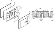
- FIG. 1is a schematic exploded perspective view of a display apparatus according to one embodiment of the present disclosure.
- FIG. 2is a schematic cross-sectional view of the display apparatus according to one embodiment of the present disclosure.
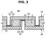
- FIG. 3is a schematic cross-sectional view of a support panel according to one embodiment of the present disclosure.
- FIG. 4is a view schematically illustrating a state in which a plurality of beading is formed on the support panel according to one embodiment of the present disclosure.
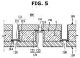
- FIG. 5is a cross-sectional view schematically illustrating a state in which a hole is formed on a first body and a second body of a support panel according to another embodiment of the present disclosure.
- FIG. 6is a cross-sectional view schematically illustrating a state in which a plurality of protrusions is formed on a first body of a support panel according to another embodiment of the present disclosure.
- FIG. 7is a cross-sectional view schematically illustrating a state in which a hole is formed on the first body and the second body of FIG. 6 .
- FIG. 8is a cross-sectional view schematically illustrating a state in which a plurality of protrusions is formed on a first body of a support panel, and a state in which a heat absorbing material is filled in the plurality of protrusions according to another embodiment of the present disclosure.
- FIG. 9is a cross-sectional view schematically illustrating a state in which a hole is formed on the first body and the second body of FIG. 8 .
- FIG. 10is a cross-sectional view schematically illustrating a state in which a plurality of beading is formed on only a first body of a support panel according to another embodiment of the present disclosure.
- FIG. 11is a cross-sectional view schematically illustrating a state in which a plurality of beading is formed on only a second body of a support panel according to another embodiment of the present disclosure.
- first, second, third, etc.may be used herein to describe various elements, but elements are not limited by these terms. These terms are only used to distinguish one element from another element. For example, without departing from the scope of the disclosure, a first element may be termed as a second element, and a second element may be termed as a first element.
- the term of “and/or”includes a plurality of combinations of relevant items or any one item among a plurality of relevant items.
- front surfaceIn the following detailed description, the terms of “front surface”, “rear surface”, “front side”, “rear side”, “upper portion”, “lower portion”, “front end”, “lower end”, “left side”, “right side”, and the like may be defined by the drawings, but the shape and the location of the component is not limited by the term.
- the present disclosureis directed to providing a display apparatus capable of satisfying both heat dissipation and rigidity standards while reducing a thickness of a support panel.
- a display apparatusmay satisfy both heat dissipation and rigidity standards while reducing a thickness of a support panel.
- FIG. 1is a schematic exploded perspective view of a display apparatus according to one embodiment of the present disclosure
- FIG. 2is a schematic cross-sectional view of the display apparatus according to one embodiment of the present disclosure.
- a display apparatusmay include a display panel 10 on which a screen is displayed, a front cover 20 arranged in front of the display panel 10 , a support panel 100 arranged at a rear of the display panel 10 , and a control module 30 arranged at a rear of the support panel 100 .
- a definition of the front cover 20 and the support panel 100is based on when the display apparatus stands upright to allow the display panel 10 to face forward.
- the front cover 20may serve as a top cover and the support panel 100 may serve as a bottom chassis.
- the display panel 10may be a panel configured to emit light by itself without a backlight unit, such as an organic light emitting diode (OLED).
- OLEDorganic light emitting diode
- the front cover 20may be arranged in front of the display panel 10 to form a front edge appearance of the display apparatus.
- the support panel 100may be arranged at the rear of the display panel 10 to form a rear exterior of the display apparatus.
- the support panel 100may include a first body 110 arranged at the rear of the display panel 10 , a second body 120 bonded to the first body 110 at the rear of the first body 110 , and a heat absorbing material 130 filled in a space between the first body 110 and the second body 120 (refer to FIG. 3 ).
- the support panel 100may form the rear exterior of the display apparatus by itself.
- a separate rear case 140may be arranged at the rear of the support panel 100 to form a rear exterior of the display apparatus.
- the control module 30may be arranged at the rear of the support panel 100 to control the display panel 10 .
- the control module 30may be arranged between the support panel 100 and the rear case 140 .
- FIG. 3is a schematic cross-sectional view of a support panel according to one embodiment of the present disclosure.
- the support panel 100may include the first body 110 arranged at the rear of the display panel 10 , the second body 120 bonded to the first body 110 at the rear of the first body 110 to form an accommodation space S with the first body 110 , and the heat absorbing material 130 filled in accommodation space S (refer to FIG. 1 ).
- the first body 110may be a metal having a high thermal conductivity and high rigidity, such as steel or aluminum.
- the first body 110may be arranged at the rear of the display panel 10 to absorb heat generated from the display panel 10 . Heat generated by the display panel 10 may be dissipated through the support panel 100 . Heat generated from the display panel 10 may be dissipated through the support panel 100 to prevent an increase in a temperature of the display panel 10 (refer to FIG. 1 ).
- the second body 120may be a metal having a high thermal conductivity and high rigidity, such as steel or aluminum.
- the second body 120may be bonded to the first body 110 at the rear of the first body 110 to form the accommodation space S with the first body 110 .
- the heat absorbed by the first body 110may be transferred to the second body 120 through the heat absorbing material 130 .
- the heat transferred to the second body 120may be radiated to the outside. Accordingly, the heat generated from the display panel 10 may be dissipated to the outside through the support panel 100 to prevent the increase in the temperature of the display panel 10 (refer to FIG. 1 ).
- the heat absorbing material 130may be filled in the accommodation space S formed between the first body 110 and the second body 120 .
- the heat absorbing material 130may be a material having high specific heat and high latent heat. Because the heat absorbing material 130 has high specific heat and high latent heat, the heat absorbing material 130 may efficiently receive heat absorbed by the first body 110 . Accordingly, the heat generated in the display panel 10 and absorbed by the first body 110 may be rapidly transferred to the heat absorbing material 130 to prevent the increase in the temperature of the display panel 10 (refer to FIG. 1 ).
- the support panel 100may form a three-layer structure including the first body 110 , the heat absorbing material 130 , and the second body 120 . Because the support panel 100 has the three-layer structure, it is possible to efficiently prevent deformation of the support panel 100 caused by thermal expansion.
- the first body 110 and the second body 120may include a plurality of beading 111 and 121 each protruding in a direction facing each other.
- the plurality of beading 111 and 121may include a plurality of first beading 111 protruding from the first body 110 toward the second body 120 and a plurality of second beading 121 protruding from the second body 120 toward the first body 110 .
- Each of the plurality of first beading 111may include a first protruding portion 113 protruding toward the second body 120 and a first concave portion 115 formed on an opposite surface of the first protruding portion 113 .
- the first protruding portion 113 protruding toward the second body 120may be bonded to the second body 120 .
- a first bonding surface 114may be formed at a portion in which the first protruding portion 113 is bonded to the second body 120 .
- the first concave portion 115may be provided in a shape in which a groove is recessed on the opposite surface of the first protruding portion 113 .
- the first concave portion 115may be an empty space that is not filled with anything.
- Each of the plurality of second beading 121may include a second protruding portion 123 protruding toward the first body 110 and a second concave portion 125 formed on an opposite surface of the second protruding portion 123 .
- the second protruding portion 123 protruding toward the first body 110may be bonded to the first body 110 .
- a second bonding surface 124may be formed at a portion in which the second protruding portion 123 is bonded to the first body 110 .
- the second concave portion 125may be provided in a shape in which a groove is recessed on the opposite surface of the second protruding portion 123 .
- the second concave portion 125may be an empty space that is not filled with anything.
- the support panel 100may include a double junction structure in which the first protruding portion 113 formed on the first body 110 is bonded to the second body 120 , and the second protruding portion 123 formed on the second body 120 is bonded to the first body 110 . Because the support panel 100 includes the double junction structure, it is possible to efficiently prevent deformation of the support panel 100 caused by thermal expansion.
- a contact area between the heat absorbing material 130 , which is filled in the accommodation space S, and the first body 110may be increased by the plurality of first beading 111 formed on the first body 110 .
- the contact area between the first body 110 and the heat absorbing material 130is increased, the heat absorbed by the first body 110 may be more efficiently transferred to the heat absorbing material 130 .
- the heat generated by the display panel 10may be more efficiently dissipated (refer to FIG. 1 ).
- a contact area between the heat absorbing material 130 , which is filled in the accommodation space S, and the second body 120may be increased by the plurality of second beading 121 formed on the second body 120 .
- the contact area between the second body 120 and the heat absorbing material 130is increased, the heat that is absorbed by the first body 110 and transferred to the heat absorbing material 130 may be more efficiently transferred to the second body 120 .
- the heat generated by the display panel 10may be more efficiently dissipated (refer to FIG. 1 ).
- the first body 110 and the second body 120By forming the first body 110 and the second body 120 with members having different thermal conductivities, it is possible to control a direction, in which the heat generated by the display panel 10 is transferred.
- the first body 110 that absorbs heat generated by the display panel 10may be formed of a metal having a high thermal conductivity.
- the second body 120 that radiates the heat absorbed by the first body 110 to the outsidemay be formed of a metal having a low thermal conductivity.
- the transfer of the heat absorbed by the first body 110may be reduced in a thickness direction, which is a vertical direction in the drawing.
- the heat absorbing material 130may be selected as a material having a high or low thermal conductivity according to the direction in which the heat generated by the display panel 10 is transferred (refer to FIG. 1 ).
- the plurality of first protruding portions 113 and the second body 120 , and the plurality of second protruding portions 123 and the first body 110may be bonded to each other by an adhesive.
- the plurality of first protruding portions 113 and the second body 120 , and the plurality of second protruding portions 123 and the first body 110may be bonded by mechanical bonding by press-fitting or brazing, respectively.
- FIG. 4is a view schematically illustrating a state in which a plurality of beading is formed on the support panel according to one embodiment of the present disclosure.
- the support panel 100on which the plurality of beading 111 and 121 illustrated in FIG. 4 is formed, may be one of the first body 110 and the second body 120 .
- the plurality of beading 111 and 121may be formed in a circular shape or a straight shape having a length.
- the heat generated from the display panel 10may have a relatively higher temperature at the center and upper end of the display panel 10 than at the edge of the display panel 10 .
- the plurality of beading 111 and 121may be formed to have a high density in the support panel 100 at positions corresponding to the center and upper ends of the display panel 10 where heat of a relatively high temperature is generated.
- the plurality of beading 111 and 121is formed in the circular shape and another portion of the plurality of beading 111 and 121 is formed in the straight shape having a length, but is not limited thereto.
- all of the plurality of beading 111 and 121may be formed in the circular shape or all of the plurality of beading 111 and 121 may be formed in the straight shape.
- the plurality of beading 111 and 121may be formed at a high density around the edge where heat of a high temperature is generated.
- FIG. 5is a cross-sectional view schematically illustrating a state in which a hole is formed on a first body and a second body of a support panel according to another embodiment of the present disclosure.
- a hole 126may be formed in a second body 120 corresponding to a first bonding surface 114 in which a plurality of first protruding portions 111 is bonded to the second body 120 .
- a hole 116may be formed in a first body 110 corresponding to a second bonding surface 124 in which a plurality of second protruding portions 121 is bonded to the first body 110 .
- FIG. 6is a cross-sectional view schematically illustrating a state in which a plurality of protrusions is formed on a first body of a support panel according to another embodiment of the present disclosure
- FIG. 7is a cross-sectional view schematically illustrating a state in which a hole is formed on the first body and the second body of FIG. 6 .
- a first body 110may include a plurality of protrusions 117 protruding in a direction facing a second body 120 and bonded to the second body 120 .
- the second body 120may include a plurality of beading 127 protruding in a direction facing the first body 110 and bonded to the first body 110 .
- the plurality of protrusions 117is the same as the first beading 111 of the first body 110 illustrated in FIG. 3 except that there is no concave portion on the opposite surface, and thus a detailed description thereof will be omitted.
- FIG. 7Because a configuration of a bonding surface and a hole illustrated in FIG. 7 is the same as the configuration of the bonding surface and the hole illustrated in FIG. 3 , the configuration of FIG. 7 has the same reference numbers as those of FIG. 3 .
- a hole 126may be formed in a second body 120 corresponding to a first bonding surface 114 in which a plurality of protrusions 117 is bonded to the second body 120 .
- a hole 116may be formed in a first body 110 corresponding to a second bonding surface 124 in which a plurality of protruding portions 128 is bonded to the first body 110 .
- FIG. 8is a cross-sectional view schematically illustrating a state in which a plurality of protrusions is formed on a first body of a support panel, and a state in which a heat absorbing material is filled in the plurality of protrusions according to another embodiment of the present disclosure
- FIG. 9is a cross-sectional view schematically illustrating a state in which a hole is formed on the first body and the second body of FIG. 8 .
- a first body 110may include a plurality of protrusions 117 protruding in a direction facing a second body 120 and bonded to a second body 120 .
- the second body 120may include a plurality of beading 127 protruding in a direction facing the first body 110 and bonded to the first body 110 .
- the plurality of protrusions 117is the same as the protrusions 117 of the first body 110 illustrated in FIG. 6 except that the heat absorbing material 130 is filled therein, a detailed description thereof will be omitted.
- FIG. 9Because a configuration of a bonding surface and a hole illustrated in FIG. 9 is the same as the configuration of the bonding surface and the hole illustrated in FIG. 3 , the configuration of FIG. 9 has the same reference numbers as those of FIG. 3 .
- a hole 126may be formed in a second body 120 corresponding to a first bonding surface 114 in which a plurality of protrusions 117 is bonded to the second body 120 .
- a hole 116may be formed in a first body 110 corresponding to a second bonding surface 124 in which a plurality of protruding portions 128 is bonded to the first body 110 .
- FIG. 10is a cross-sectional view schematically illustrating a state in which a plurality of beading is formed on only a first body of a support panel according to another embodiment of the present disclosure
- FIG. 11is a cross-sectional view schematically illustrating a state in which a plurality of beading is formed on only a second body of a support panel according to another embodiment of the present disclosure.
- a first body 110may include a plurality of first beading 111 protruding in a direction toward a second body 120 and bonded to the second body 120 . Because a configuration of the first body 110 is the same as that of the first body 110 illustrated in FIG. 3 , a detailed description thereof will be omitted.
- a configuration of a plurality of second beading 121may be omitted in the second body 120 .
- a second body 120may include a plurality of second beading 121 protruding in a direction toward a first body 110 and bonded to the first body 110 . Because a configuration of the second body 120 is the same as that of the second body 120 illustrated in FIG. 3 , a detailed description thereof will be omitted.
- a configuration of a plurality of first beading 111may be omitted in the first body 110 .
Landscapes
- Engineering & Computer Science (AREA)
- Physics & Mathematics (AREA)
- Theoretical Computer Science (AREA)
- Thermal Sciences (AREA)
- Microelectronics & Electronic Packaging (AREA)
- Computer Hardware Design (AREA)
- Human Computer Interaction (AREA)
- General Engineering & Computer Science (AREA)
- General Physics & Mathematics (AREA)
- Devices For Indicating Variable Information By Combining Individual Elements (AREA)
- Optics & Photonics (AREA)
Abstract
Description
Claims (11)
Applications Claiming Priority (3)
| Application Number | Priority Date | Filing Date | Title |
|---|---|---|---|
| KR1020190065812AKR102730876B1 (en) | 2019-06-04 | 2019-06-04 | Display apparatus |
| KR10-2019-0065812 | 2019-06-04 | ||
| PCT/KR2019/015115WO2020246666A1 (en) | 2019-06-04 | 2019-11-08 | Display device |
Related Parent Applications (1)
| Application Number | Title | Priority Date | Filing Date |
|---|---|---|---|
| PCT/KR2019/015115ContinuationWO2020246666A1 (en) | 2019-06-04 | 2019-11-08 | Display device |
Publications (2)
| Publication Number | Publication Date |
|---|---|
| US20220093891A1 US20220093891A1 (en) | 2022-03-24 |
| US11994921B2true US11994921B2 (en) | 2024-05-28 |
Family
ID=73652346
Family Applications (1)
| Application Number | Title | Priority Date | Filing Date |
|---|---|---|---|
| US17/542,604Active2040-05-18US11994921B2 (en) | 2019-06-04 | 2021-12-06 | Display apparatus |
Country Status (3)
| Country | Link |
|---|---|
| US (1) | US11994921B2 (en) |
| KR (1) | KR102730876B1 (en) |
| WO (1) | WO2020246666A1 (en) |
Families Citing this family (1)
| Publication number | Priority date | Publication date | Assignee | Title |
|---|---|---|---|---|
| EP4346342A4 (en) | 2021-11-30 | 2024-12-25 | Samsung Electronics Co., Ltd. | Display apparatus |
Citations (49)
| Publication number | Priority date | Publication date | Assignee | Title |
|---|---|---|---|---|
| US5268816A (en)* | 1982-09-28 | 1993-12-07 | Lexmark International, Inc. | Movable display screen for a computer |
| US5450221A (en)* | 1993-09-08 | 1995-09-12 | Delco Electronics Corporation | Compact liquid crystal display for instrument panel having a wrap around flexible printed circuit board and translucent web |
| US5666261A (en)* | 1995-09-25 | 1997-09-09 | At&T Global Information Solutions Company | Honeycomb celled-sheet layer composite panel for monitoring an LCD to a laptop computer |
| US5811923A (en)* | 1996-12-23 | 1998-09-22 | Optical Coating Laboratory, Inc. | Plasma display panel with infrared absorbing coating |
| US5831374A (en)* | 1996-01-12 | 1998-11-03 | Matsushita Electric Industrial Co., Ltd. | Plasma display panel, method of fabricating the same, and display apparatus using the plasma display panel |
| US5952782A (en)* | 1995-08-25 | 1999-09-14 | Fujitsu Limited | Surface discharge plasma display including light shielding film between adjacent electrode pairs |
| US6346334B1 (en)* | 1999-02-02 | 2002-02-12 | Tokai Rubber Industries, Ltd. | Plasma display panel assembly |
| US20030017320A1 (en)* | 2001-07-13 | 2003-01-23 | Mochida Corporation | Radiating sheet and PDP panel |
| US20030025428A1 (en)* | 2001-08-03 | 2003-02-06 | Ki-Jung Kim | Plasma display device having efficient heat conductivity |
| US20030230381A1 (en)* | 2002-04-26 | 2003-12-18 | Hiroshi Watanabe | Manufacturing method and dismantling method for plasma display device |
| KR100446084B1 (en) | 2002-01-16 | 2004-08-30 | 삼성전자주식회사 | Image display apparatus |
| US6849992B2 (en)* | 2001-12-03 | 2005-02-01 | Samsung Sdi Co., Ltd. | Plasma display device having efficient heat conductivity |
| US20050047067A1 (en)* | 2003-09-01 | 2005-03-03 | Won-Kyu Bang | Display apparatus having improved heat dissipation capabilities |
| US20050057915A1 (en)* | 2003-02-12 | 2005-03-17 | Hon Hai Precision Industry Co., Ltd. | Patterned light guide plate and display device having same |
| US20050073253A1 (en)* | 2003-10-07 | 2005-04-07 | Au Optronics Corp. | Plasma display device capable of increasing attachment of heat-dissipating plate to plasma display panel |
| US20050077835A1 (en)* | 2003-10-08 | 2005-04-14 | Ki-Jung Kim | Thermal conductive medium for display device, method of fabricating the same, and plasma display panel assembly using the same |
| US6882108B2 (en)* | 2002-03-27 | 2005-04-19 | Samsung Sdi Co., Ltd. | Plasma display device with reduced noise exiting through heat radiation ventilation openings |
| US20050212429A1 (en)* | 2003-04-22 | 2005-09-29 | Matsushita Electric Industrial Co. Ltd | Plasma display panel and method for producing same |
| US20050243106A1 (en)* | 2004-04-29 | 2005-11-03 | Sung-Won Bae | Plasma display apparatus |
| US20050258749A1 (en)* | 2004-05-19 | 2005-11-24 | Joong-Ha Ahn | Plasma display device |
| JP2005337612A (en) | 2004-05-27 | 2005-12-08 | Sony Corp | Cooler and display device |
| US20060028790A1 (en)* | 2004-08-06 | 2006-02-09 | Lg Electronics Inc. | Display device |
| KR100647591B1 (en) | 2003-11-22 | 2006-11-17 | 삼성에스디아이 주식회사 | Plasma display device |
| US7161296B2 (en)* | 2003-04-28 | 2007-01-09 | Samsung Sdi Co., Ltd. | Plasma display device that efficiently and effectively draws heat out from a functioning plasma display panel |
| US7176605B2 (en)* | 2003-06-23 | 2007-02-13 | Samsung Sdi Co., Ltd. | Plasma display device having anisotropic thermal conduction medium |
| US7235922B2 (en)* | 2002-07-06 | 2007-06-26 | Lg Electronics Inc. | Plasma display panel with porous pad |
| US20070153458A1 (en)* | 2005-12-19 | 2007-07-05 | Mitsuo Okimoto | Flat-panel display apparatus |
| US7323808B2 (en)* | 2003-09-25 | 2008-01-29 | Samsung Sdi Co., Ltd. | Plasma display panel assembly including heat absorption layer |
| US7554798B2 (en)* | 2005-07-22 | 2009-06-30 | Hitachi, Ltd. | Flat display panel module and flat display apparatus |
| US7649737B2 (en)* | 2006-03-17 | 2010-01-19 | Hitachi, Ltd. | Flat panel display |
| US7679285B2 (en)* | 2004-10-25 | 2010-03-16 | Samsung Sdi Co., Ltd. | Plasma display device |
| US7679931B2 (en)* | 2005-06-28 | 2010-03-16 | Samsung Sdi Co., Ltd. | Plasma display apparatus having improved structure and heat dissipation |
| US20110134064A1 (en)* | 2001-11-02 | 2011-06-09 | Neonode, Inc. | On a substrate formed or resting display arrangement |
| US8107259B2 (en)* | 2007-05-23 | 2012-01-31 | Kyocera Corporation | Portable electronic device |
| US8125771B2 (en)* | 2006-04-11 | 2012-02-28 | Sony Corporation | Electronic apparatus |
| US20120229726A1 (en)* | 2011-03-10 | 2012-09-13 | Samsung Electronics Co., Ltd. | Liquid crystal display apparatus |
| US20120231566A1 (en)* | 2011-03-12 | 2012-09-13 | Oh Jae-Young | Method of fabricating lightweight and thin liquid crystal display device |
| US20130147079A1 (en)* | 2008-01-11 | 2013-06-13 | Lenovo (Singapore) Pte. Ltd. | Casing structures for electronic devices |
| US20130328462A1 (en)* | 2010-02-02 | 2013-12-12 | Apple Inc. | Offset Control for Assemblying an Electronic Device Housing |
| US20140008041A1 (en) | 2012-07-04 | 2014-01-09 | Samsung Electronics Co., Ltd. | Display apparatus |
| US8922983B1 (en)* | 2012-03-27 | 2014-12-30 | Amazon Technologies, Inc. | Internal metal support structure for mobile device |
| US9459660B2 (en)* | 2013-01-10 | 2016-10-04 | Seiko Epson Corporation | Display device and electronic apparatus |
| US20170090109A1 (en) | 2014-04-16 | 2017-03-30 | Sakai Display Products Corporation | Display Apparatus |
| US9709295B2 (en)* | 2013-03-15 | 2017-07-18 | Honeywell International, Inc. | Electronic device and methods |
| US9769964B2 (en)* | 2013-01-18 | 2017-09-19 | Lg Electronics Inc. | Heat discharging sheet and display device including the same |
| US10114422B2 (en)* | 2016-09-09 | 2018-10-30 | Samsung Display Co., Ltd. | Cover panel and display device including the same |
| US20190165300A1 (en) | 2017-11-30 | 2019-05-30 | Lg Display Co., Ltd. | Display Apparatus |
| US20210307213A1 (en)* | 2018-08-07 | 2021-09-30 | Samsung Electronics Co., Ltd. | Display apparatus |
| US11775020B2 (en)* | 2020-04-27 | 2023-10-03 | Samsung Display Co., Ltd. | Display device and method of manufacturing the same |
- 2019
- 2019-06-04KRKR1020190065812Apatent/KR102730876B1/enactiveActive
- 2019-11-08WOPCT/KR2019/015115patent/WO2020246666A1/ennot_activeCeased
- 2021
- 2021-12-06USUS17/542,604patent/US11994921B2/enactiveActive
Patent Citations (56)
| Publication number | Priority date | Publication date | Assignee | Title |
|---|---|---|---|---|
| US5268816A (en)* | 1982-09-28 | 1993-12-07 | Lexmark International, Inc. | Movable display screen for a computer |
| US5450221A (en)* | 1993-09-08 | 1995-09-12 | Delco Electronics Corporation | Compact liquid crystal display for instrument panel having a wrap around flexible printed circuit board and translucent web |
| US5952782A (en)* | 1995-08-25 | 1999-09-14 | Fujitsu Limited | Surface discharge plasma display including light shielding film between adjacent electrode pairs |
| US5666261A (en)* | 1995-09-25 | 1997-09-09 | At&T Global Information Solutions Company | Honeycomb celled-sheet layer composite panel for monitoring an LCD to a laptop computer |
| US5831374A (en)* | 1996-01-12 | 1998-11-03 | Matsushita Electric Industrial Co., Ltd. | Plasma display panel, method of fabricating the same, and display apparatus using the plasma display panel |
| US5811923A (en)* | 1996-12-23 | 1998-09-22 | Optical Coating Laboratory, Inc. | Plasma display panel with infrared absorbing coating |
| US6346334B1 (en)* | 1999-02-02 | 2002-02-12 | Tokai Rubber Industries, Ltd. | Plasma display panel assembly |
| US20030017320A1 (en)* | 2001-07-13 | 2003-01-23 | Mochida Corporation | Radiating sheet and PDP panel |
| US6700315B2 (en)* | 2001-08-03 | 2004-03-02 | Samsung Sdi Co., Ltd. | Plasma display device having efficient heat conductivity |
| US20030025428A1 (en)* | 2001-08-03 | 2003-02-06 | Ki-Jung Kim | Plasma display device having efficient heat conductivity |
| US20110134064A1 (en)* | 2001-11-02 | 2011-06-09 | Neonode, Inc. | On a substrate formed or resting display arrangement |
| US6849992B2 (en)* | 2001-12-03 | 2005-02-01 | Samsung Sdi Co., Ltd. | Plasma display device having efficient heat conductivity |
| KR100446084B1 (en) | 2002-01-16 | 2004-08-30 | 삼성전자주식회사 | Image display apparatus |
| US6882108B2 (en)* | 2002-03-27 | 2005-04-19 | Samsung Sdi Co., Ltd. | Plasma display device with reduced noise exiting through heat radiation ventilation openings |
| US20030230381A1 (en)* | 2002-04-26 | 2003-12-18 | Hiroshi Watanabe | Manufacturing method and dismantling method for plasma display device |
| US7235922B2 (en)* | 2002-07-06 | 2007-06-26 | Lg Electronics Inc. | Plasma display panel with porous pad |
| US20050057915A1 (en)* | 2003-02-12 | 2005-03-17 | Hon Hai Precision Industry Co., Ltd. | Patterned light guide plate and display device having same |
| US20050212429A1 (en)* | 2003-04-22 | 2005-09-29 | Matsushita Electric Industrial Co. Ltd | Plasma display panel and method for producing same |
| US7161296B2 (en)* | 2003-04-28 | 2007-01-09 | Samsung Sdi Co., Ltd. | Plasma display device that efficiently and effectively draws heat out from a functioning plasma display panel |
| US7176605B2 (en)* | 2003-06-23 | 2007-02-13 | Samsung Sdi Co., Ltd. | Plasma display device having anisotropic thermal conduction medium |
| US20050047067A1 (en)* | 2003-09-01 | 2005-03-03 | Won-Kyu Bang | Display apparatus having improved heat dissipation capabilities |
| US7323808B2 (en)* | 2003-09-25 | 2008-01-29 | Samsung Sdi Co., Ltd. | Plasma display panel assembly including heat absorption layer |
| US20050073253A1 (en)* | 2003-10-07 | 2005-04-07 | Au Optronics Corp. | Plasma display device capable of increasing attachment of heat-dissipating plate to plasma display panel |
| US20050077835A1 (en)* | 2003-10-08 | 2005-04-14 | Ki-Jung Kim | Thermal conductive medium for display device, method of fabricating the same, and plasma display panel assembly using the same |
| KR100647591B1 (en) | 2003-11-22 | 2006-11-17 | 삼성에스디아이 주식회사 | Plasma display device |
| US20050243106A1 (en)* | 2004-04-29 | 2005-11-03 | Sung-Won Bae | Plasma display apparatus |
| US20050258749A1 (en)* | 2004-05-19 | 2005-11-24 | Joong-Ha Ahn | Plasma display device |
| US7224121B2 (en)* | 2004-05-19 | 2007-05-29 | Samsung Sdi Co., Ltd. | Plasma display device |
| JP2005337612A (en) | 2004-05-27 | 2005-12-08 | Sony Corp | Cooler and display device |
| US20060028790A1 (en)* | 2004-08-06 | 2006-02-09 | Lg Electronics Inc. | Display device |
| US7679285B2 (en)* | 2004-10-25 | 2010-03-16 | Samsung Sdi Co., Ltd. | Plasma display device |
| US7679931B2 (en)* | 2005-06-28 | 2010-03-16 | Samsung Sdi Co., Ltd. | Plasma display apparatus having improved structure and heat dissipation |
| US7554798B2 (en)* | 2005-07-22 | 2009-06-30 | Hitachi, Ltd. | Flat display panel module and flat display apparatus |
| US8093811B2 (en)* | 2005-07-22 | 2012-01-10 | Hitachi, Ltd. | Flat display panel module and flat display apparatus |
| US20070153458A1 (en)* | 2005-12-19 | 2007-07-05 | Mitsuo Okimoto | Flat-panel display apparatus |
| US7876553B2 (en)* | 2005-12-19 | 2011-01-25 | Hitachi, Ltd. | Flat-panel display apparatus |
| US7649737B2 (en)* | 2006-03-17 | 2010-01-19 | Hitachi, Ltd. | Flat panel display |
| US8125771B2 (en)* | 2006-04-11 | 2012-02-28 | Sony Corporation | Electronic apparatus |
| US8107259B2 (en)* | 2007-05-23 | 2012-01-31 | Kyocera Corporation | Portable electronic device |
| US20130147079A1 (en)* | 2008-01-11 | 2013-06-13 | Lenovo (Singapore) Pte. Ltd. | Casing structures for electronic devices |
| US20130328462A1 (en)* | 2010-02-02 | 2013-12-12 | Apple Inc. | Offset Control for Assemblying an Electronic Device Housing |
| US20120229726A1 (en)* | 2011-03-10 | 2012-09-13 | Samsung Electronics Co., Ltd. | Liquid crystal display apparatus |
| US20120231566A1 (en)* | 2011-03-12 | 2012-09-13 | Oh Jae-Young | Method of fabricating lightweight and thin liquid crystal display device |
| US8922983B1 (en)* | 2012-03-27 | 2014-12-30 | Amazon Technologies, Inc. | Internal metal support structure for mobile device |
| US20140008041A1 (en) | 2012-07-04 | 2014-01-09 | Samsung Electronics Co., Ltd. | Display apparatus |
| US9459660B2 (en)* | 2013-01-10 | 2016-10-04 | Seiko Epson Corporation | Display device and electronic apparatus |
| US9769964B2 (en)* | 2013-01-18 | 2017-09-19 | Lg Electronics Inc. | Heat discharging sheet and display device including the same |
| US10234161B2 (en)* | 2013-03-15 | 2019-03-19 | Ademco Inc. | Thermostat with display and printed circuit board |
| US9709295B2 (en)* | 2013-03-15 | 2017-07-18 | Honeywell International, Inc. | Electronic device and methods |
| US9784467B2 (en)* | 2013-03-15 | 2017-10-10 | Honeywell International Inc. | Thermostat with display and printed circuit board |
| US10480805B2 (en)* | 2013-03-15 | 2019-11-19 | Ademco Inc. | Thermostat assembly |
| US20170090109A1 (en) | 2014-04-16 | 2017-03-30 | Sakai Display Products Corporation | Display Apparatus |
| US10114422B2 (en)* | 2016-09-09 | 2018-10-30 | Samsung Display Co., Ltd. | Cover panel and display device including the same |
| US20190165300A1 (en) | 2017-11-30 | 2019-05-30 | Lg Display Co., Ltd. | Display Apparatus |
| US20210307213A1 (en)* | 2018-08-07 | 2021-09-30 | Samsung Electronics Co., Ltd. | Display apparatus |
| US11775020B2 (en)* | 2020-04-27 | 2023-10-03 | Samsung Display Co., Ltd. | Display device and method of manufacturing the same |
Non-Patent Citations (2)
| Title |
|---|
| International Search for International Patent Application No. PCT/KR2019/015115 dated Mar. 9, 2020. |
| Office Action dated Feb. 26, 2024, in Korean Application No. 10-2019-0065812. |
Also Published As
| Publication number | Publication date |
|---|---|
| KR20200139379A (en) | 2020-12-14 |
| KR102730876B1 (en) | 2024-11-18 |
| WO2020246666A1 (en) | 2020-12-10 |
| US20220093891A1 (en) | 2022-03-24 |
Similar Documents
| Publication | Publication Date | Title |
|---|---|---|
| US9826654B2 (en) | Display | |
| JP4442304B2 (en) | Light emitting unit heat dissipation device and backlight device | |
| EP2610939B1 (en) | Display device | |
| US8934227B2 (en) | Display device | |
| US20140008041A1 (en) | Display apparatus | |
| KR101888910B1 (en) | Display apparatus | |
| JPWO2020017210A1 (en) | Image display device | |
| US20120162567A1 (en) | Electronic device | |
| JP2006059607A (en) | Heat radiation device and display device | |
| US7898798B2 (en) | Heat dissipating structure for electronic component and display device | |
| US9709252B2 (en) | Backlight unit and display device including truss structure | |
| US11994921B2 (en) | Display apparatus | |
| JP2019105840A (en) | Back cover and display device having the same | |
| KR20130088534A (en) | Display device | |
| JP2009224207A (en) | Heat radiation structure and display device | |
| JP2006058486A (en) | Heatsink and display device | |
| JP4862251B2 (en) | Heat dissipation device and display device | |
| JP6174799B2 (en) | Display device and television receiver | |
| JP2010015098A (en) | Video display device | |
| JP2019198017A (en) | Display device and television receiver | |
| KR102371200B1 (en) | Display Device | |
| KR20120058206A (en) | Organic light emitting diode display | |
| KR100615285B1 (en) | Plasma display device | |
| US20250204211A1 (en) | Display device | |
| JP2009230992A (en) | Heat sink for thin type display |
Legal Events
| Date | Code | Title | Description |
|---|---|---|---|
| FEPP | Fee payment procedure | Free format text:ENTITY STATUS SET TO UNDISCOUNTED (ORIGINAL EVENT CODE: BIG.); ENTITY STATUS OF PATENT OWNER: LARGE ENTITY | |
| STPP | Information on status: patent application and granting procedure in general | Free format text:DOCKETED NEW CASE - READY FOR EXAMINATION | |
| STPP | Information on status: patent application and granting procedure in general | Free format text:NON FINAL ACTION MAILED | |
| STPP | Information on status: patent application and granting procedure in general | Free format text:RESPONSE TO NON-FINAL OFFICE ACTION ENTERED AND FORWARDED TO EXAMINER | |
| STPP | Information on status: patent application and granting procedure in general | Free format text:NOTICE OF ALLOWANCE MAILED -- APPLICATION RECEIVED IN OFFICE OF PUBLICATIONS | |
| ZAAB | Notice of allowance mailed | Free format text:ORIGINAL CODE: MN/=. | |
| AS | Assignment | Owner name:SAMSUNG ELECTRONICS CO., LTD., KOREA, REPUBLIC OF Free format text:ASSIGNMENT OF ASSIGNORS INTEREST;ASSIGNORS:KIM, SUNG KI;JUNG, HYUN JUN;REEL/FRAME:066884/0180 Effective date:20240322 | |
| STPP | Information on status: patent application and granting procedure in general | Free format text:AWAITING TC RESP., ISSUE FEE NOT PAID | |
| STPP | Information on status: patent application and granting procedure in general | Free format text:NOTICE OF ALLOWANCE MAILED -- APPLICATION RECEIVED IN OFFICE OF PUBLICATIONS | |
| STPP | Information on status: patent application and granting procedure in general | Free format text:PUBLICATIONS -- ISSUE FEE PAYMENT VERIFIED | |
| STCF | Information on status: patent grant | Free format text:PATENTED CASE |