US11981501B2 - Loading cassette for substrate including glass and substrate loading method to which same is applied - Google Patents
Loading cassette for substrate including glass and substrate loading method to which same is appliedDownload PDFInfo
- Publication number
- US11981501B2 US11981501B2US17/433,342US202017433342AUS11981501B2US 11981501 B2US11981501 B2US 11981501B2US 202017433342 AUS202017433342 AUS 202017433342AUS 11981501 B2US11981501 B2US 11981501B2
- Authority
- US
- United States
- Prior art keywords
- target substrate
- loading
- substrate
- supporting member
- condition
- Prior art date
- Legal status (The legal status is an assumption and is not a legal conclusion. Google has not performed a legal analysis and makes no representation as to the accuracy of the status listed.)
- Active, expires
Links
- 239000000758substrateSubstances0.000titleclaimsabstractdescription349
- 238000011068loading methodMethods0.000titleclaimsabstractdescription166
- 239000011521glassSubstances0.000titleclaimsdescription77
- 238000000034methodMethods0.000claimsdescription19
- 238000004806packaging method and processMethods0.000claimsdescription18
- 239000004065semiconductorSubstances0.000claimsdescription9
- 238000009826distributionMethods0.000description15
- 125000006850spacer groupChemical group0.000description6
- 229910052782aluminiumInorganic materials0.000description5
- XAGFODPZIPBFFR-UHFFFAOYSA-NaluminiumChemical compound[Al]XAGFODPZIPBFFR-UHFFFAOYSA-N0.000description5
- 238000004519manufacturing processMethods0.000description5
- 239000000463materialSubstances0.000description5
- 229920006260polyaryletherketonePolymers0.000description4
- 230000008569processEffects0.000description4
- 238000012360testing methodMethods0.000description4
- 229910052751metalInorganic materials0.000description3
- 239000002184metalSubstances0.000description3
- 229920001774PerfluoroetherPolymers0.000description2
- 235000017276SalviaNutrition0.000description2
- 241001072909SalviaSpecies0.000description2
- 230000000052comparative effectEffects0.000description2
- 150000001875compoundsChemical class0.000description2
- 238000013461designMethods0.000description2
- 230000000694effectsEffects0.000description2
- 238000011156evaluationMethods0.000description2
- 239000000203mixtureSubstances0.000description2
- 238000007747platingMethods0.000description2
- 229920001343polytetrafluoroethylenePolymers0.000description2
- 229940058401polytetrafluoroethyleneDrugs0.000description2
- 239000004810polytetrafluoroethyleneSubstances0.000description2
- 238000003860storageMethods0.000description2
- 238000012546transferMethods0.000description2
- VGGSQFUCUMXWEO-UHFFFAOYSA-NEtheneChemical compoundC=CVGGSQFUCUMXWEO-UHFFFAOYSA-N0.000description1
- 239000005977EthyleneSubstances0.000description1
- 238000010521absorption reactionMethods0.000description1
- 239000002253acidSubstances0.000description1
- 230000004075alterationEffects0.000description1
- 238000005452bendingMethods0.000description1
- 230000008901benefitEffects0.000description1
- 230000015572biosynthetic processEffects0.000description1
- 230000000903blocking effectEffects0.000description1
- 230000015556catabolic processEffects0.000description1
- 238000005520cutting processMethods0.000description1
- 238000006731degradation reactionMethods0.000description1
- 230000000881depressing effectEffects0.000description1
- 239000006185dispersionSubstances0.000description1
- 239000012530fluidSubstances0.000description1
- 238000003780insertionMethods0.000description1
- 230000037431insertionEffects0.000description1
- 238000013508migrationMethods0.000description1
- 230000005012migrationEffects0.000description1
- 238000012986modificationMethods0.000description1
- 230000004048modificationEffects0.000description1
- 230000000149penetrating effectEffects0.000description1
- 229920000515polycarbonatePolymers0.000description1
- 239000004417polycarbonateSubstances0.000description1
- 238000012545processingMethods0.000description1
- 238000007665saggingMethods0.000description1
- 239000000523sampleSubstances0.000description1
- 230000008685targetingEffects0.000description1
Images


Classifications
- H—ELECTRICITY
- H01—ELECTRIC ELEMENTS
- H01L—SEMICONDUCTOR DEVICES NOT COVERED BY CLASS H10
- H01L21/00—Processes or apparatus adapted for the manufacture or treatment of semiconductor or solid state devices or of parts thereof
- H01L21/67—Apparatus specially adapted for handling semiconductor or electric solid state devices during manufacture or treatment thereof; Apparatus specially adapted for handling wafers during manufacture or treatment of semiconductor or electric solid state devices or components ; Apparatus not specifically provided for elsewhere
- H01L21/673—Apparatus specially adapted for handling semiconductor or electric solid state devices during manufacture or treatment thereof; Apparatus specially adapted for handling wafers during manufacture or treatment of semiconductor or electric solid state devices or components ; Apparatus not specifically provided for elsewhere using specially adapted carriers or holders; Fixing the workpieces on such carriers or holders
- H01L21/6734—Apparatus specially adapted for handling semiconductor or electric solid state devices during manufacture or treatment thereof; Apparatus specially adapted for handling wafers during manufacture or treatment of semiconductor or electric solid state devices or components ; Apparatus not specifically provided for elsewhere using specially adapted carriers or holders; Fixing the workpieces on such carriers or holders specially adapted for supporting large square shaped substrates
- B—PERFORMING OPERATIONS; TRANSPORTING
- B65—CONVEYING; PACKING; STORING; HANDLING THIN OR FILAMENTARY MATERIAL
- B65D—CONTAINERS FOR STORAGE OR TRANSPORT OF ARTICLES OR MATERIALS, e.g. BAGS, BARRELS, BOTTLES, BOXES, CANS, CARTONS, CRATES, DRUMS, JARS, TANKS, HOPPERS, FORWARDING CONTAINERS; ACCESSORIES, CLOSURES, OR FITTINGS THEREFOR; PACKAGING ELEMENTS; PACKAGES
- B65D85/00—Containers, packaging elements or packages, specially adapted for particular articles or materials
- B65D85/30—Containers, packaging elements or packages, specially adapted for particular articles or materials for articles particularly sensitive to damage by shock or pressure
- B65D85/48—Containers, packaging elements or packages, specially adapted for particular articles or materials for articles particularly sensitive to damage by shock or pressure for glass sheets
- H—ELECTRICITY
- H01—ELECTRIC ELEMENTS
- H01L—SEMICONDUCTOR DEVICES NOT COVERED BY CLASS H10
- H01L21/00—Processes or apparatus adapted for the manufacture or treatment of semiconductor or solid state devices or of parts thereof
- H01L21/67—Apparatus specially adapted for handling semiconductor or electric solid state devices during manufacture or treatment thereof; Apparatus specially adapted for handling wafers during manufacture or treatment of semiconductor or electric solid state devices or components ; Apparatus not specifically provided for elsewhere
- H01L21/673—Apparatus specially adapted for handling semiconductor or electric solid state devices during manufacture or treatment thereof; Apparatus specially adapted for handling wafers during manufacture or treatment of semiconductor or electric solid state devices or components ; Apparatus not specifically provided for elsewhere using specially adapted carriers or holders; Fixing the workpieces on such carriers or holders
- H01L21/67303—Vertical boat type carrier whereby the substrates are horizontally supported, e.g. comprising rod-shaped elements
- H01L21/67309—Vertical boat type carrier whereby the substrates are horizontally supported, e.g. comprising rod-shaped elements characterized by the substrate support
- H—ELECTRICITY
- H01—ELECTRIC ELEMENTS
- H01L—SEMICONDUCTOR DEVICES NOT COVERED BY CLASS H10
- H01L21/00—Processes or apparatus adapted for the manufacture or treatment of semiconductor or solid state devices or of parts thereof
- H01L21/67—Apparatus specially adapted for handling semiconductor or electric solid state devices during manufacture or treatment thereof; Apparatus specially adapted for handling wafers during manufacture or treatment of semiconductor or electric solid state devices or components ; Apparatus not specifically provided for elsewhere
- H01L21/673—Apparatus specially adapted for handling semiconductor or electric solid state devices during manufacture or treatment thereof; Apparatus specially adapted for handling wafers during manufacture or treatment of semiconductor or electric solid state devices or components ; Apparatus not specifically provided for elsewhere using specially adapted carriers or holders; Fixing the workpieces on such carriers or holders
- H01L21/6732—Vertical carrier comprising wall type elements whereby the substrates are horizontally supported, e.g. comprising sidewalls
- H—ELECTRICITY
- H01—ELECTRIC ELEMENTS
- H01L—SEMICONDUCTOR DEVICES NOT COVERED BY CLASS H10
- H01L21/00—Processes or apparatus adapted for the manufacture or treatment of semiconductor or solid state devices or of parts thereof
- H01L21/67—Apparatus specially adapted for handling semiconductor or electric solid state devices during manufacture or treatment thereof; Apparatus specially adapted for handling wafers during manufacture or treatment of semiconductor or electric solid state devices or components ; Apparatus not specifically provided for elsewhere
- H01L21/677—Apparatus specially adapted for handling semiconductor or electric solid state devices during manufacture or treatment thereof; Apparatus specially adapted for handling wafers during manufacture or treatment of semiconductor or electric solid state devices or components ; Apparatus not specifically provided for elsewhere for conveying, e.g. between different workstations
- H01L21/67763—Apparatus specially adapted for handling semiconductor or electric solid state devices during manufacture or treatment thereof; Apparatus specially adapted for handling wafers during manufacture or treatment of semiconductor or electric solid state devices or components ; Apparatus not specifically provided for elsewhere for conveying, e.g. between different workstations the wafers being stored in a carrier, involving loading and unloading
- H01L21/67766—Mechanical parts of transfer devices
- H—ELECTRICITY
- H01—ELECTRIC ELEMENTS
- H01L—SEMICONDUCTOR DEVICES NOT COVERED BY CLASS H10
- H01L21/00—Processes or apparatus adapted for the manufacture or treatment of semiconductor or solid state devices or of parts thereof
- H01L21/67—Apparatus specially adapted for handling semiconductor or electric solid state devices during manufacture or treatment thereof; Apparatus specially adapted for handling wafers during manufacture or treatment of semiconductor or electric solid state devices or components ; Apparatus not specifically provided for elsewhere
- H01L21/677—Apparatus specially adapted for handling semiconductor or electric solid state devices during manufacture or treatment thereof; Apparatus specially adapted for handling wafers during manufacture or treatment of semiconductor or electric solid state devices or components ; Apparatus not specifically provided for elsewhere for conveying, e.g. between different workstations
- H01L21/67763—Apparatus specially adapted for handling semiconductor or electric solid state devices during manufacture or treatment thereof; Apparatus specially adapted for handling wafers during manufacture or treatment of semiconductor or electric solid state devices or components ; Apparatus not specifically provided for elsewhere for conveying, e.g. between different workstations the wafers being stored in a carrier, involving loading and unloading
- H01L21/67778—Apparatus specially adapted for handling semiconductor or electric solid state devices during manufacture or treatment thereof; Apparatus specially adapted for handling wafers during manufacture or treatment of semiconductor or electric solid state devices or components ; Apparatus not specifically provided for elsewhere for conveying, e.g. between different workstations the wafers being stored in a carrier, involving loading and unloading involving loading and unloading of wafers
- H—ELECTRICITY
- H05—ELECTRIC TECHNIQUES NOT OTHERWISE PROVIDED FOR
- H05K—PRINTED CIRCUITS; CASINGS OR CONSTRUCTIONAL DETAILS OF ELECTRIC APPARATUS; MANUFACTURE OF ASSEMBLAGES OF ELECTRICAL COMPONENTS
- H05K13/00—Apparatus or processes specially adapted for manufacturing or adjusting assemblages of electric components
- H05K13/0061—Tools for holding the circuit boards during processing; handling transport of printed circuit boards
- H05K13/0069—Holders for printed circuit boards
Definitions
- An embodimentrelates to a loading cassette of a substrate including glass and a method of loading a substrate applied with the same.
- a cassetteis applied to transfer and store many substrates easily, accurately, and harmoniously.
- a cassetteallows many substrates to be loaded in up and down with space from each other in the inside of a frame whose one side surface is opened. And a method of withdrawing these loaded substrates for proceeding of work of the substrates and after that inserting the substrates processed by the work into a cassette again is carried out.
- a glass substrate for semiconductor packagingis utilized for a high-end packaging substrate, and forms multiple vias in a thin glass substrate for utilizing as a packaging substrate.
- a glass substrate with a comparatively thin thicknessmay be fragile to vibration or impact due to its properties, and in a case of a glass substrate with a large area, a sag may occur in a high possibility inside a cassette due to own weight and this may accelerate damage of the glass substrate.
- the background art described aboveis a technical information which has been kept by inventors for deriving example embodiments, or found in a process of deriving example embodiments, and is not necessarily a known art opened to general public before the present application.
- Objectives of an embodimentis to provide a loading cassette minimizing impact transmitted to a substrate including glass and particularly being suitable for loading and moving of a glass substrate with a large area, and a method of loading a substrate applied with the same.
- a loading cassetteaccording to one embodiment includes
- an edge supporting unitfor connecting the upper plate and the lower plate and supporting left and right edges of the target substrate
- a rear supporting unitfor connecting the upper plate and the lower plate and supporting a rear edge of the target substrate
- the rear supporting unitincludes
- a rear framebeing connecting the upper plate and the lower plate in a rear surface
- a middle supporting memberbeing protruding to the front direction from the rear frame
- the target substrateis a substrate including a glass substrate which includes or does not include a through hole
- the middle supporting membercontrols a maximum sag of the target substrate based on the edge supporting unit (as 0 mm) within 3 mm.
- D1when a thickness (mm) of the target substrate is expressed as GT, D1 is a distance (mm) between one side of the edge supporting member and the middle supporting unit and the D1 may satisfy below Condition (1) or Condition (2); When 0.1 ⁇ GT ⁇ 0.5,150 ⁇ D 1 ⁇ 275 Condition (1): When 0.5 ⁇ GT ⁇ 1.5,220 ⁇ D 1 ⁇ 330. Condition (2):
- the middle supporting membermay include a middle supporting bar, wherein the middle bearing member is disposed at one part of the middle supporting member and the rear frame is near to other part of the middle supporting member, the middle bearing member may be disposed to have gradient to be higher than the other part.
- the edge supporting unitmay include
- a side framebeing connecting the upper plate and the lower plate in both left and right sides respectively
- an edge supporting memberforming a side slot disposed in the rear frame to support the left and right edges of the target substrate and not allowing the target substrate to contact the side frame
- the side slotmay be formed in plurality along an up-and-down direction of the side frame with having intervals.
- the middle supporting membermay include
- a middle supporting barbeing protruding to the front from the connecting block, wherein the left-and-right width of the middle supporting bar is narrower as being distant from the connecting block,
- middle bearing membermay be disposed in the middle supporting bar in a number of one, two, or more.
- a length of the middle supporting barmay be 1 ⁇ 3 to 2 ⁇ 3 of the back-and-forth length of the loading space.
- the rear supporting unitmay include
- a rear framebeing connecting the upper plate and the lower plate at the rear surface and having rear inserting slots formed in a left-and-right direction
- a middle supporting memberbeing protruding to the front direction from the rear frame and being combined with the rear inserting slots and having a first area portion and a second area portion
- a middle bearing memberbeing protruding from the upper surface of the middle supporting member and directly connecting the target substrate to control sag of the target substrate
- first area portionmay be connected to the rear frame and the area of the second area portion may be narrower than the area of the first area portion.
- a method of loading a target substrateincludes
- the target substrateincludes a glass substrate with or without a through hole
- Condition (1)when the thickness (mm) of the target substrate is expressed as GT, D1 which is a distance (mm) between one side of the edge supporting member and the middle supporting member may satisfy below Condition (1) or Condition (2); When 0.1 ⁇ GT ⁇ 0.5,150 ⁇ D 1 ⁇ 275 Condition (1): When 0.5 ⁇ GT ⁇ 1.5,220 ⁇ D 1 ⁇ 330. Condition (2):
- a method of loading a target substrateincludes
- a carry-in stepfor allowing the entire target substrate to enter and be disposed inside a loading space, in which the target substrate is polygonal having L as the length (mm) and W as the width (mm) is carried in the loading space of a cassette, by applying a loading carrier having two or more hands with maintaining variation (D) indicated by below Formula (1) within ⁇ 15 to +10 mm;
- a support stepfor controlling a maximum sag of the target substrate to be within 3 mm based on the edge supporting unit (as 0 mm) by supporting the target substrate with a middle supporting member in at least one point or more of the middle;
- the target substrateis a glass substrate having many through holes or a substrate for semiconductor packaging in which an electrical conductive pattern and an insulating layer are laminated to the glass substrate, and
- Dh (mm)which is an interval between the edge supporting units neighboring to each other in up and down may satisfy below Formula (2);
- a cassettewhich can load a target substrate without occurring a sag of a target substrate and a problem of damage in a substrate due to the sag can be provided, as minimizing damage which can occur during loading, moving, and carrying out of glass even though the target substrate including a glass substrate of a large area with or without a through hole.
- a target substrate placed in a loading spacecan stably keep a loaded state through being supported by an edge supporting unit and a rear supporting unit, and can be protected from impact which can occur during loading, impact added from the external, and the like.
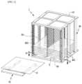
- FIG. 1is a perspective view for showing a loading cassette according to an embodiment of the present application
- FIG. 2is a schematic view for showing a state of a glass substrate loaded in a loading cassette of FIG. 1 ;
- FIG. 3is a cross sectional view cut along a III-III line from FIG. 2 ;
- FIG. 4is an enlarged view of A portion of FIG. 3 ;
- FIG. 5is an enlarged view of a center supporting unit of FIG. 3 ;
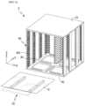
- FIG. 6is a perspective view for showing a loading cassette according to one embodiment of the present application.
- FIG. 7is a schematic view for showing a glass substrate loaded in a loading cassette of FIG. 6 ;
- FIG. 8is a cross sectional view cut along a VI-VI line from FIG. 7 ;
- FIG. 9is an enlarged view of A portion of FIG. 8 ;
- FIG. 10is an enlarged view of a center supporting unit of FIG. 8 ;
- FIG. 11is a side view for showing a center supporting unit of FIG. 10 ;
- FIG. 12is a schematic view for showing a state of a center supporting unit of FIG. 11 supporting a glass substrate.
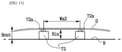
- FIG. 13is a conceptual view for illustrating a fork test conducted in the present application.
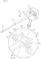
- FIGS. 14 A and 14 Bare conceptual views for illustrating a loading carrier and a target substrate of the present application, and a sag observed at a-a′, respectively;
- FIG. 15is a conceptual view for illustrating a process for a target substrate placed on a loading carrier to be inserted into a loading space
- X-basedmay mean that a compound includes a compound corresponding to X or a derivative of X.
- B being disposed on Ameans that B is disposed in direct contact with A or disposed over A with another layer interposed therebetween and thus should not be interpreted as being limited to B being disposed in direct contact with A.
- B being connected to Ameans that B is connected to A directly or through another element therebetween, and thus should not be interpreted as being limited to B being directly connected to A, unless otherwise noted.
- sagis evaluated for a position of a sagged portion from the reference position by mm unit, and expressed in a positive number.
- a loading cassette according to one embodimentwill be described with reference to FIGS. 1 to 5 .
- FIG. 1is a perspective view for showing a loading cassette according to an embodiment of the present application
- FIG. 2is a schematic view for showing a state of a glass substrate loaded in a loading cassette of FIG. 1
- FIG. 3is a cross sectional view cut along a III-III line from FIG. 2
- FIG. 4is an enlarged view of A portion of FIG. 3
- FIG. 5is an enlarged view of a center supporting unit of FIG. 3 .
- a loading cassette 1supports a loaded target substrate G and the like, and comprises an upper plate 10 , a lower plate 20 , an edge supporting unit 40 , and a rear supporting unit 50 .
- the loading cassette 1may further comprise a front stopper 60 .
- the upper plate 10 and the lower plate 20have a predetermined area and are apart from each other in an up-and-down direction.
- the lower plate 20may be formed by many frames connected in breadth and length directions.
- the upper plate 10 and the lower plate 20have an interval maintained by an edge supporting unit 40 and a rear supporting unit 50 . And, among them, a loading space 30 where a target substrate G is loaded is formed.
- a loading capacity of the loading space 30may be changed depending on the sizes of the upper plate 10 and the lower plate 20 ; and the up-and-down direction lengths of the edge supporting unit 40 and the rear supporting unit 50 .
- the loading capacity, in particularly the sizes of the upper plate 10 and the lower plate 20may be changed depending on the standard of the target substrate G.
- the target substrate Gmay be a substrate with a large area, and may be a glass substrate whose thickness is 1 mm or less, or a substrate in which an insulating layer and/or an electrical conductive layer are formed on the glass substrate (or glass substrate having through vias).
- the target substrate Gmay substantially have a quadrangle plate form whose one side is 400 mm or more, but its shape is not limited to a quadrangle plate form.
- a target substrate Gmay have a first surface and a second surface facing each other.
- a target substrate Gmay have a plurality a core via penetrating through the first surface and the second surface.
- the core viamay include a first opening part in contact with the first surface; a second opening part in contact with the second surface; and a minimum inner diameter part having the smallest inner diameter in the entire core via from the first opening part to the second opening part.
- An average diameter of the minimum inner diameter partmay be 50 ⁇ m to 95 ⁇ m.
- Equation 1The minimum inner diameter and satisfies the condition of Equation 1 below. 0.83 ⁇ D 90 ⁇ D 50 ⁇ 1.25 ⁇ D 10 [Equation 1]
- D 50is a value corresponding to 50% in the diameter distribution of the minimum inner diameter
- D 90is a value corresponding to 90% in the diameter distribution of the minimum inner diameter
- D 10is a value corresponding to 10% in the diameter distribution of the minimum inner diameter.
- An average diameter of the minimum inner diametermay be 55 ⁇ m to 85 ⁇ m, or 60 ⁇ m to 70 ⁇ m.
- the minimum inner partmay satisfy the condition of Equation 1-1 below. 0.83 ⁇ D 90 ⁇ D 50 ⁇ 1.25 ⁇ D 10 [Equation 1-1]
- D 50is a value corresponding to 50% in the diameter distribution of the minimum inner part
- D 90is a value corresponding to 90% in the diameter distribution of the minimum inner part
- D 10is a value corresponding to 10% in the diameter distribution of the minimum inner part.
- a target opening partwhich is a larger one between the first surface opening part diameter and the second surface opening part diameter, may have an average diameter of 70 ⁇ m to 120 ⁇ m.
- a target opening part which is a larger one between the first surface opening part diameter and the second surface opening part diametermay satisfy the condition of Equation 2 below. 0.9 ⁇ D 90 ⁇ D 50 ⁇ 1.1 ⁇ D 10 [Equation 2]
- D 50is a value corresponding to 50% in the diameter distribution of a target opening part
- D 90is a value corresponding to 90% in the diameter distribution of a target opening part
- D 10is a value corresponding to 10% in the diameter distribution of a target opening part.
- a target opening partwhich is a larger one between the first surface opening part diameter and the second surface opening part diameter, may have an average diameter of 80 ⁇ m to 105 ⁇ m.
- a target opening part which is a larger one between the first surface opening part diameter and the second surface opening part diametermay satisfy the condition of Equation 2-1 below. 0.92 ⁇ D 90 ⁇ D 50 ⁇ 1.08 ⁇ D 10 [Equation 2-1]
- D 50is a value corresponding to 50% in the diameter distribution of a target opening part
- D 90is a value corresponding to 90% in the diameter distribution of a target opening part
- D 10is a value corresponding to 10% in the diameter distribution of a target opening part.
- an average diameter of a target opening partwhich is a larger one between the first surface opening part diameter—which is a diameter at an opening part in contact with the first surface—and the second surface opening part diameter—which is a diameter at an opening part in contact with the second surface—may have a larger value than D 50 , which is a value corresponding to 50% in the diameter distribution of a target opening part.
- the diameter distribution described aboveis evaluated based on a diameter which is observed and measured by microscope in the cross-section, after dividing prepared samples into 9 compartments (3 ⁇ 3), and processing of cutting the samples of 5 areas (top left, bottom left, center, top right, bottom right).
- a loading cassette 1may load stably a target substrate which has a core via with the above-described diameter distribution and diameter.
- the point at which the minimum inner diameter part is locatedwhen the entire length of the core via is 100%, may be a point of 40% to 60% from the first opening part, and may be a point of 45% to 55%.
- the minimum inner diameter partis at the position described above, based on the entire length of core via, the design of electrically conductive layer of packaging substrate and the process of forming electrically conductive layer may be easier.
- a loading cassette according to an embodimentcan load this fragile target substrate stably.
- the core viamay be disposed in the number of 100 to 3000, or 100 to 2500, or 225 to 1024 based on a unit area (1 cm ⁇ 1 cm) of the target substrate.
- the core viamay be disposed at the target substrate in a pitch of 1.2 mm or less, may be disposed in a pitch of 0.12 to 1.2 mm, may be disposed in a pitch of 0.3 to 0.9 mm.
- a loading cassette according to an embodimentcan load this fragile target substrate stably.
- the target substrate Gmay be a stress-controlled glass substrate.
- the target substrate Gmay have a stress difference value (P) according to the below Formula (1) of 1.5 MPa or less; between a stress measured at a plain line which is a line linking places where the core via is not formed, and a stress measured at a via line which is a line linking places where the core via is formed.
- Pa stress difference value (P) according to the below Formula (1) of 1.5 MPa or less; between a stress measured at a plain line which is a line linking places where the core via is not formed, and a stress measured at a via line which is a line linking places where the core via is formed.
- PVp ⁇ Np Formula (1)
- the Pis a stress difference value measured at the same glass substrate
- the Vpis a difference between the maximum value and the minimum value of stress measured at a via line
- the Npis a difference between the maximum value and the minimum value of stress measured at a plain line.
- the P valuemay be 1.35 MPa or less, 1.2 MPa or less, or 1.1 MPa or less. Also, the P value may be 0.01 MPa or more, or 0.1 MPa or more.
- a glass substrate in which core vias having a stress difference value (P) in these ranges are formedis applied as a substrate for semiconductor packaging, it is possible to manufacture a packaging substrate having more stable mechanical properties, and a loading cassette according to an embodiment can load this fragile target substrate stably.
- the Vp valuemay be 2.5 MPa or less, or 2.3 MPa or less, and the Vp value may be 2.0 MPa or less, or 1.8 MPa or less. Also, the Vp value may be 0.2 MPa or more, or 0.4 MPa or more.
- Vpa difference between the maximum value and the minimum value of stress measured at a via line
- a glass substrate where core vias are formedis applied as a substrate for semiconductor packaging
- a loading cassette according to an embodimentcan load this fragile target substrate stably.
- the Np valuemay be 1.0 MPa or less, 0.9 MPa or less, or 0.8 MPa or less. Also, the Np value may be 0.1 MPa or more, or 0.2 MPa or more.
- a difference (Np) between the maximum value and the minimum value of stress measured at a plain lineis in these ranges, and a glass substrate where core vias are formed is applied as a substrate for semiconductor packaging, it is possible to manufacture a packaging substrate having more stable mechanical properties. And a loading cassette according to an embodiment can load this fragile target substrate stably.
- the glass substratemay satisfy a condition that a stress difference ratio (K) according to below Formula (2) is 6 or less.
- KLp/La Formula (2):
- the Kis stress difference ratio measured at the same plane of the same glass substrate
- the Lpis a difference of the maximum value and the minimum value of stress measured at a target line
- the Lais an average value of stress measured at the target line, wherein the target line is selected one from a plain line which is a line linking places where a core via is not formed and a via line which is a line linking places where a core via is formed.
- the K valuemay be 5 or less, 4.5 or less, or 4 or less.
- a target substrate where core vias are formedis applied as a substrate for semiconductor packaging, it is possible to manufacture a packaging substrate having more stable mechanical properties.
- a loading cassette according to an embodimentcan load this fragile target substrate stably.
- the stress difference ratio (K) which is measured at the plain linemay have a value of 2 or less.
- the stress difference ratio (Kn) of a plain linemay be 1.8 or less, more than 0.3, or more than 0.5.
- the stress difference ratio (K) which is measured at the via linemay have a value of 6 or less, or 5 or less.
- the stress difference ratio (Kv) of a via linemay be 4.5 or less, or 3 or less.
- the stress difference ratio of a via linemay be 0.5 or more, 1.0 or more, or 1.5 or more.
- the stressis analyzed by applying a birefringence 2D evaluation device.
- the birefringence 2D dispersion evaluation devicemay be WPA-200 device of NPM (NIPPON PULSE KOREA CO., LTD).
- measured valuessuch as a birefringence value are inputted by the device, and stress at a measuring route is presented by pressure unit (ex. MPa) through a predetermined calculation process.
- stresscan be measured by inputting a stress-optical coefficient and a thickness of a measuring target, and 2.4 is applied as the stress-optical coefficient in the present disclosure.
- the edge supporting units 40are arranged in a back-and-forth direction (Y) at both left and right sides of the upper plate 10 and the lower plate 20 , and connect the upper plate 10 and the lower plate 20 . And the edge supporting units 40 support the edges of both left and right sides of the target substrate G.
- the edge supporting unit 40may comprise a buffer covering layer placed in at least a part of its surface.
- the rear supporting unit 50connects the upper plate 10 and the lower plate 20 by being disposed at the rear of the upper plate 10 and the lower plate 20 .
- the rear supporting unit 50is disposed with having a certain distance with the center of the rear or the edge supporting unit 40 , and thereby controls the target substrate G loaded in the loading space 30 not to be sagged by its own weight.
- the rear supporting unit 50supports at least a part of the target substrate G and thereby prevents the target substrate G overall from sagging.
- the front stopper 60blocks the target substrate G loaded in the loading space 30 not to fall off to the external of the loading space 30 at the front of the loading space 30 .
- the front stopper 60may comprise a buffer covering layer placed in at least a part of its surface.
- the target substrate G of the loading space 30can maintain a stable loaded state by the edge supporting unit 40 and the rear supporting unit 50 . And the target substrate G of the loading space can be protected stably from impact which may occur during loading, impact added from external, and the like. Accordingly, damage of the target substrate G which may occur during loading and moving of the target substrate could be minimized.
- the edge supporting unit 40comprises a side frame 41 , and an edge supporting member 42 .
- the side frame 41has a predetermined length, its upper side is combined with a side surface of the upper plate 10 and its lower side is combined with a side surface of the lower plate 20 .
- the side frame 41is combined with a fastening means (not shown) like a bolt.
- the side frame 41may be formed with aluminum coated or not coated by a protecting layer or the like.
- a material of the side frame 41is not limited to aluminum.
- the edge supporting member 42is connected to the side frame 41 .
- the edge supporting members 42are arranged along an up-and-down direction (Z) of the side frame 41 with intervals. Accordingly, a side slot 421 is formed between the edge supporting members 42 neighboring to each other. A target substrate G inserted to the side slot 421 is placed in an upper surface of the edge supporting member 42 . On the other hand, neighboring edge supporting members 42 are connected from each other and their sides are not allowed to contact the side frame 41 when the target substrate G is loaded. And the edge supporting member 42 may comprise a buffer covering layer in at least a part of the surface thereof.
- the rear supporting unit 50may comprise a rear frame 51 , a middle supporting member 52 , a middle bearing member 53 and a rear stopper 54 .
- the rear frame 51has a predetermined length, its upper side is combined with the rear surface of the upper plate 10 and its lower side is combined with the rear surface of the lower plate 20 .
- the rear frame 51is also combined through a fastening means and may be formed with aluminum coated or not coated by a protecting layer or the like.
- the rear frame 51may comprise a rear main bar 511 in which holding slots where the connecting blocks are placed are formed along an up-and-down length direction, and a stopper combining bar 512 which is extended from both sides of the rear main bar to both left and right sides and combined with the rear stopper.
- the rear main bar 511may comprise a holding slot 511 a connected to a loading space 30 .
- the holding slot 511 amay be formed along an up-and-down length direction (Z) of the rear main bar 511 , and the area of the holding slot 511 a may become wider in a direction from the inner surface to the opened front.
- the stopper combining bar 512is extended in a left-and-right direction (X) from both sides of the rear main bar 511 and has a preset area.
- the stopper combining bar 512has a plane.
- the stopper combining bar 512is composed in one body with the rear main bar 511 and made with aluminum or the like which is coated or not coated.
- the middle supporting member 52may comprise a connecting block 521 and a middle supporting bar 522 .
- the connecting block 521is placed in a holding slot 511 a and fixed with a fastening means (not shown).
- the connecting block 521may be not dislocated from the holding slot 511 a . That is, the connecting block 512 may be placed inside the connecting block 521 .
- the middle supporting bar 522has a preset length, is connected to the rear main bar 511 by the connecting block 521 , and protrudes from the connecting block 521 to the front.
- the length of the middle supporting bar 522is equal to or shorter than the length of the loading space 30 in a back-and-forth direction Y, and in detail may be formed to be shorter.
- the length of the middle supporting barmay be 1 ⁇ 3 to 2 ⁇ 3, or 2 ⁇ 5 to 4 ⁇ 5 of the length from the front to the rear.
- the middle supporting bar 522supports a target substrate G from at least one or more points, and the supporting point is exemplified as a middle bearing member 53 described in below, but may support the target substrate by oneself.
- the position of the middle supporting bar 522may become gradually high as being far from a connecting block 522 , and thereby the height at one point where a middle supporting bar 522 and a target substrate G meet may be higher compared to a side slot 421 placed in a position neighboring to each other.
- a middle supporting baritself may sag slightly as some of the own weight of a target substrate is added to a middle supporting bar 522 at one point where the middle supporting bar 522 meets the target substrate. Additionally, when the middle supporting bar 522 itself is equipped to have a higher height than a side slot 421 placed in a position corresponding to this without such a gradient applied, it may increase a possibility of occurring damage or stain of a target substrate because a contact with a middle supporting bar 522 is caused even in a portion where sag is comparatively small in a target substrate.
- the variation of the height thereofcan be controlled within 3 mm compared to when the middle supporting bar 522 does not support a target substrate G.
- the thickness of the middle supporting bar 522can be modified, and the angle can be modified.
- the middle supporting bar 522may have a shape in which the area in one side which meets the target substrate is narrower and the area becomes wider as being close to a connecting block 521 .
- the middle supporting bar 522itself or the upper surface thereof may be gradient in a certain angle.
- the upper surface of the middle supporting member 52may have an angle at a point which a line from one end combined with the connecting block 521 to the other end contacting with the target substrate and a line parallel to the upper plate or the lower plate meet, and the angle may be 0.1 to 5 degree, or 0.1 to 3 degree.
- a sag of a middle supporting bar 522can be controlled and a sag of a target substrate G can be more efficiently controlled.
- the middle supporting members 52may be made with aluminum or the like which is coated or not coated, and are being arranged in an up-and-down direction (Z) in a loading space 30 .
- the arranging interval of middle supporting members 52may be substantially the same with the arranging interval of edge supporting members 42 .
- the middle bearing member 53is arranged in an upper surface of a middle supporting bar 522 to protrude to an upper portion and in contact with the center portion of a target substrate G.
- the middle bearing members 53may be arranged in 1, 2, or more with having intervals along a length direction (Y) of a middle supporting bar 522 .
- the middle bearing member 53may comprise a buffer covering layer placed on at least a part of the surface thereof.
- the middle supporting member 53may support some of a target substrate of a loading space 30 on a middle supporting member 52 along a length direction (Y) thereof, and the target substrate G may control sag of the target substrate which may occur in a loading space 30 .
- D1which is a distance (mm) between one side of the edge supporting member and the middle supporting member can satisfy a below Condition (1) or Condition (2).
- D1which is a distance (mm) between one side of the edge supporting member and the middle supporting member can satisfy a below Condition (1-1) or Condition (2-1).
- 0.2 ⁇ GT ⁇ 0.5,200 ⁇ D 1 ⁇ 275 Condition (1-1)When 0.5 ⁇ GT ⁇ 1.2,230 ⁇ D 1 ⁇ 300 Condition (2-1):
- the middle supporting member 52can control the maximum sag of the target substrate based on the edge supporting unit (0 mm) within 3 mm.
- a sag which occurs when the middle supporting member 52 supports the target substratecan be controlled within 3 mm based on when the middle supporting member 52 does not support the target substrate (0 mm).
- the target substrate Gmay be a glass substrate or a glass substrate in which a through hole is formed, and a thickness of it may be 0.25 to 0.45 mm D1 as a distance between one end within the edge supporting member 42 and the middle supporting member 52 may be applied to be 200 to 275 mm.
- a sag of a target substratemay be controlled within 2 mm, and the target substrate may be stored and moved more stably.
- the target substratemay be a glass substrate with through holes which has a metal plating layer and/or an insulting layer formed on at least one surface, and the total average thickness may of the target substrate be 0.3 to 1.2 mm, or 0.5 to 0.9 mm D1 as a distance between one end within the edge supporting member and the middle supporting member may be applied to be 230 to 300 mm.
- sag of the target substratemay be controlled within 1 mm, and the target substrate may be stored and moved more stably.
- the target substrate Gmay be a glass substrate having a cavity structure or a glass substrate having a cavity structure and through holes, and the thickness of a thick portion not having a cavity structure may be 0.4 to 1 mm, or 0.5 to 0.9 mm.
- D1 as a distance between one end of the edge supporting member and the middle supporting membermay be applied to be 200 to 275 mm. In such a case, a sag of a target substrate may be controlled within 2 mm, and the target substrate may be stored and moved more stably.
- the target substrate Gmay be a glass substrate having the cavity structure in which a metal plating layer and/or an insulting layer is formed on at least one surface, and the total average thickness of the target substrate may be 0.5 to 1.3 mm, or 0.7 to 1.2 mm D1 as a distance between one end within the edge supporting member 42 and the middle supporting member 52 may be applied to be 230 to 300 mm.
- a sag of a target substratemay be controlled within 1 mm, and the target substrate may be stored and moved more stably.
- a rear stopper 54is disposed in a loading space 30 and connected to a stopper combining bar 512 .
- the rear stoppers 54are arranged along to an up-and-down length direction (Z) of a stopper combining bar 512 . Between neighboring rear stoppers 54 , a rear slot 541 where a target substrate G is inserted is prepared, and the neighboring rear stoppers 54 are connected from each other. Here, an edge of a rear portion of a target substrate G may be disposed on an upper surface of a rear stopper 54 . In addition, the neighboring rear stoppers 54 are connected from each other. Accordingly, the rear part of a target substrate G disposed in a rear slot 541 is not in contact with a stopper combining bar 512 .
- the rear stopper 54may comprise a buffer covering layer in at least a part of the surface thereof.
- a front stopper 60may comprise a bar member 61 , a spacer 62 , a rod member 63 , and a stopper member 64 .
- the spacer 62is protruding to the front by being connected to an edge supporting unit 40 placed in the front.
- the spacers 62may be arranged along an up-and-down direction (Z) of the edge supporting unit 40 .
- the bar member 61has a predetermined length and is being connected to the spacer 62 .
- the bar member 61faces to the edge supporting unit 40 with having an interval by a spacer 62 .
- the rod member 63is being extended to the front from the bar member 61 to the edge supporting unit supporting a target substrate G.
- the stopper member 64faces the front (a thickness surface) of a target substrate G placed in the edge supporting member 42 with protruding to an up-and-down direction (Z) from an end portion of the rod member 63 .
- the front of the target substrate G placed in the edge supporting member 42is caught by the stopper member 64 and not to be fallen off to the front.
- the front stopper 60may be arranged along an up-and-down direction of the edge supporting unit 40 .
- the front stopper 60may comprise a buffer covering layer placed in at least a part of the surface thereof.
- the buffer covering layermay be overall placed in portions contacting with a target substrate G loaded in a loading space 30 , so that damage of the target substrate G, which can occur in loading or carrying our procedure, can be minimized. Also, when cassette is migrated with taking the target substrate G placed in a loading space 30 , a movement or damage of the target substrate G could not occur substantially. Accordingly, a loadability of the target substrate G can be increased and a reliability of the loading cassette can be increased.
- the buffer covering layermay comprise PTFE (Poly Tetra Fluoro Ethylene), FEP (Flourinated Ethylene Prophylene), PFA (Per Fluoro Alkoxy), or PEEK (polyaryletherketone), and specifically may comprise PEEK (polyaryletherketone).
- PTFEPoly Tetra Fluoro Ethylene
- FEPFlourinated Ethylene Prophylene
- PFAPer Fluoro Alkoxy
- PEEKpolyaryletherketone
- PEEKpolyaryletherketone
- the loading cassette 1may further comprise a loading carrier 70 for loading a target substrate G in a loading space 30 , or pulling the loaded target substrate G out.
- the loading cassette 1may be one cassette alone, or may be a cassette unit (not shown) formed by stacking the loading cassette 1 in a side direction and/or up-and-down direction.
- a fixing means(not shown) for fixing the loading cassettes neighboring to each other may be further applied, and the fixing means can be applied without limit if it does not disturb insertion and storage of the target substrate.
- the loading carrier 70is being connected to a robot arm (not shown) or the like, and can fix a target substrate G by an absorption method.
- the loading carrier 70allows the target substrate G to be inserted in a side slot 421 and places it on an edge bearing member 43 . On the contrary to this, a target substrate G placed on the edge bearing member 43 is lifted for the loaded target substrate G to be carried out from the loading space 30 .
- the loading carrier 70makes a target substrate G be placed on a depressurizing pad and after that the target substrate G be absorbed, fixed, and moved. For being detached subsequently, a method of releasing a pressure of the depressurizing pad can allow the target substrate G to be separated. In this time, when the depressing pad and the target substrate is not separated properly, compressed air may be added to the depressurizing pad to separate the depressurizing pad and the target substrate more easily.
- FIG. 6is a perspective view for showing a loading cassette according to one embodiment of the present application
- FIG. 7is a schematic view for showing a target substrate loaded in a loading cassette of FIG. 6
- FIG. 8is a cross sectional view cut along a VIII-VIII line from FIG. 7
- FIG. 9is an enlarged view of A portion of FIG. 8
- FIG. 10is an enlarged view of a rear supporting unit of FIG. 8
- FIG. 11is an side view for showing a rear supporting unit of FIG. 10
- FIG. 12is a schematic view for showing a state of a rear supporting unit of FIG. 11 supporting a target substrate.
- a loading cassette 2according to another example embodiment comprises an upper plate 10 , a lower plate 20 , an edge supporting unit 40 and a rear supporting unit 50 .
- the upper plate 10 and the lower plate 20is same as an upper plate and a lower plate of a loading cassette 1 described above according to FIGS. 1 to 7 , and thus the further description is omitted.
- An edge supporting unit 40comprises a side frame 41 , an edge supporting member 42 , and an edge bearing member 43 .
- a rear supporting unit 50comprises a rear frame 51 , a middle supporting member 52 , and a middle bearing member 53 .
- the side frame 41connects the upper plate 10 and the lower plate 20 . And a surface of the side frame 41 connected to a loading space 30 , side inserting slots 411 are formed in a back-and-forth direction (Y). The side inserting slots 411 are formed in plurality with having intervals along an up-and-down length direction (Z) of a side frame 41 .
- the edge supporting member 42is combined to the side inserting slots 411 and protruding to a loading space 30 .
- An upper surface and a side surface of the edge supporting member 42faces to a target substrate G.
- the edge bearing member 43protrudes from the upper surface of the edge supporting member 42 to an upper portion.
- the edge bearing members 43are arranged along a length direction (Y) of the edge supporting member 42 .
- the edge bearing member 43may comprise a buffer covering layer placed in at least a part of the surface thereof.
- the edge supporting member 42may also comprise a buffer covering layer placed in at least a part of the surface thereof.
- Such an edge supporting unit 40has a composition and an acting effect corresponding to the edge supporting unit according to embodiments of FIGS. 1 to 7 and thus the further description is omitted.
- a rear supporting unit 50may comprise a rear frame 51 , a middle supporting member 52 , and a middle bearing member 53 .
- the rear frame 51connects an upper plate 10 and a lower plate 20 .
- rear inserting slots 513may be formed in a left-and-right direction (X).
- Xleft-and-right direction
- a side inserting slot 411 and a rear inserting slot 513may be formed in the same position based on the lower plate 20 .
- the middle supporting member 52is combined with the rear inserting slot 513 and protrudes in a front direction from the rear frame 51 .
- the middle supporting member 52may face to a sagged portion of a target substrate G, and for example, may face to the center portion.
- the middle supporting member 52may have a first area portion 523 and a second area portion 524 whose area is narrower than the first area portion 523 .
- the length of the second area portion 524may be longer than the length of the first area portion 523 .
- the total length of the middle supporting member 52may be one-half or more of the front-and-rear length of a target space 30 .
- the gradient of the middle supporting member 52may be gradient in a lower direction from the second area portion 524 to the first area portion 523 . That is, the middle supporting member 52 may have a gradually gradient shape to a lower direction from the front to the rear. In this case, even though a sag of a target substrate occurs, a portion directly contacting with the middle supporting member 52 can be reduced, and the possibility of occurring damage of the target substrate can be reduced.
- the upper surface of the middle supporting member 52may have gradient in a certain angle.
- the upper surface of the middle supporting member 52may have an angle at a point where a line one end combined with the rear inserting slot 513 and the other end contacting with the target substrate and a line parallel to the upper plate or the lower plate meet, and the angle may be 0.1 to 10 degree, 0.1 to 5 degree, or 0.1 to 3 degree.
- the middle bearing member 53is protruding from an upper surface of the middle supporting member 52 .
- the middle bearing members 53are being arranged with having intervals along a length direction (Y) of the middle supporting member 52 .
- the middle bearing member 53may contact a target substrate G and thereby directly support the center portion of the target substrate G.
- the middle bearing member 53can support the center portion of a target substrate G through the middle supporting member 52 and thereby prevent the center portion of a target substrate G from sag by the own weight.
- FIGS. 1 to 5Various characteristics found in embodiments illustrated in FIGS. 1 to 5 also can be applied to the present embodiment.
- the loading cassettes ( 1 or 2 )may further comprise a protecting housing (not shown) for surrounding the edge supporting unit.
- the protecting housingmay have a shape of surrounding at least one between the upper plate and the lower plate, and the edge supporting unit.
- the protecting housingmay be an overall rectangular shape in which one surface is opened and may be covered on the loading cassette.
- the protecting housingmay further comprise a housing opening and shutting part (not shown) which allows a glass substrate to enter and can be opened and shut in a part or the whole within a surface surrounding the edge supporting unit.
- the protecting housingmay serve as preventing function from foreign material to be mixed when the loading cassette moves in a state of loading glass substrates and blocking the possibility of being damaged by flow of the fluid in a glass substrate.
- the protecting housingmay serve as a preventing role being damaged of the inside of another loading cassette or the loaded glass substrate even though some glass substrate of any one loading cassette is damaged when many loading cassettes have been loaded to be moved or stacked.
- a material of the protecting housinga material which is excellent in impact resistance, heat resistance, acid resistance, and so on and endures the weight of a glass substrate and a cassette, specifically a polycarbonate material which is clear or non-clear may be applied, and this case is advantageous in having a sufficient strength and excellent dimensional stability.
- a method of loading a target substratecomprises a carry-in step; a support step; and a completion step.
- a method of loading a target substrateis performed through the above described a loading cassette ( 1 or 2 ) and a loading carrier 70 below.
- the carry-in stepis a step that a target substrate G is moved by applying a loading carrier 70 having two or more hands 72 .
- the target substrate Gmay be a glass substrate having many through holes or a substrate for semiconductor packaging in which an electrically conductive pattern and an insulating layer are laminated to the glass substrate.
- the target substrate Ggenerally has a thin thickness (in general, 1500 ⁇ m or less) and thereby can be easily bended or curved. Also, because a glass substrate in which a through hole (core via) is formed in the predetermined size and position is applied as a target substrate, stress is concentrated in some section, imbalanced stress may occur in the glass substrate overall, and this may induce degradation of mechanical strength of the substrate. Accordingly, it is required to transfer and store a target substrate stably with minimizing sag or bending of the target substrate. And this is more important when applying a substrate with a larger area.
- the target substrate Gmay be a polygonal glass substrate having L as the length (mm) and W as the width (mm).
- the L and Wmay be respectively 400 mm or more, and the target substrate may, for example, comprise a glass substrate in a quadrangle shape.
- a target substrate Gis moved with controlling to occur variation predetermined or less.
- the variationis calculated by below Equation (1) (refer to FIG. 1 ).
- Variation ( D )Inside Height of Target Substrate ( H in,mm) ⁇ Outside Height of Target Substrate ( H out,mm) Equation (1):
- the inside height and the outside height of the target substrateis applied by measuring height at the same reference line (B).
- the variation (D)may be within ⁇ 15 to +10 mm, ⁇ 10 to 7 mm, or ⁇ 10 to 4 mm A variation in this range may be adjusted by changing the number of hands to be applied, and the position and the interval of the hand fork.
- the hands 72respectively have one or more hand forks 72 a and may have Wa2 (mm) as the shortest interval between hand forks 72 a placed in the hands 72 which respectively satisfies below Condition (1) or Condition (2).
- GTrefers to the thickness (mm) of the target substrate.
- the Wa2 (mm)may respectively satisfy below Condition (1-1) or Condition (2-1).
- Condition (1-1)When 0.1 ⁇ GT ⁇ 0.5,( W/ 2.5) ⁇ Wa 2 ⁇ ( W/ 1.9)
- Condition (1-1)When 0.5 ⁇ GT ⁇ 1.5,( W/ 2.2) ⁇ Wa 2 ⁇ ( W/ 1.8).
- Wa1 valuewhich is an interval between hand forks 72 a placed on the same hand 72 may satisfy below Condition (3) or Condition (4).
- Condition (3)When 0.1 ⁇ GT ⁇ 0.5,( L/ 3.4) ⁇ Wa 1 ⁇ ( L/ 1.8)
- Condition (3)When 0.5 ⁇ GT ⁇ 1.5,( W/ 2.3) ⁇ Wa 1 ⁇ ( W/ 1.6).
- the Wa1 valuemay satisfy below Condition (3-1) or Condition (4-1).
- Condition (3-1)When 0.1 ⁇ GT ⁇ 0.5,( L/ 2.5) ⁇ Wa 1 ⁇ ( L/ 1.9) Condition (3-1): When 0.5 ⁇ GT ⁇ 1.5,( L/ 2.2) ⁇ Wa 1 ⁇ ( L/ 1.8) Condition (4-1):
- the target substrate Gis carried in a loading space 30 of a loading cassette ( 1 or 2 ) with maintaining the variation (D) within a range described above, and the left and right edges of the target substrate is placed on the edge supporting unit 40 of the loading cassettes, thereby allowing the entire target substrate to enter and be placed inside the loading space 30 .
- This entrancemay be controlled by a loading carrier and hands moving along a predetermined moving route.
- the result of a fork test performed with a glass substrate in which has through viaswill be disclosed.
- the glass substratehad a size of 508 ⁇ 508 (length ⁇ width, mm) and a thickness of 0.3 to 0.7 mm was formed.
- a variationinside height-outside height
- a variationis 4.7 mm
- a variationis ⁇ 0.6 mm
- a variationis ⁇ 1 mm
- a fork intervalis 320 mm
- a variationis ⁇ 11 mm
- a fork intervalis 420 mm
- a variationis ⁇ 27.5 mm.
- the result of a test based on a glass substrate in which a through via is not formedwas; when a fork interval is 220 mm, a variation (inside height-outside height) is 4.9 mm; when a fork interval is 270 mm, a variation is ⁇ 0.4 mm; when a fork interval is 320 mm, a variation is ⁇ 5.1 mm; and when a fork interval is 420 mm, a variation is ⁇ 17.1 mm.
- the support stepis a step of controlling a maximum sag of a target substrate G within 3 mm by supporting the target substrate in at least one point or more of the middle thereof by a middle supporting member 52 .
- a sagis determined by an interval from an edge supporting unit 40 (basement, 0 mm)
- the maximum sagmay be negative, but it is expressed by converting to be positive.
- a maximum sag of the target substratemay be controlled by adjusting D1.
- the D1is a distance between one side of the edge supporting member 42 and a middle supporting member 52
- D1when a thickness of a target substrate is GT, D1 can satisfy below condition (5) or (6).
- condition (5)When 0.1 ⁇ GT ⁇ 0.5,150 ⁇ D 1 ⁇ 275 Condition (5): When 0.5 ⁇ GT ⁇ 1.5,220 ⁇ D 1 ⁇ 330 Condition (6):
- D1can satisfy below conditions (5-1) to (6-1).
- 5-1)0.2 ⁇ GT ⁇ 0.5,200 ⁇ D 1 ⁇ 275 Condition
- 6-1)0.5 ⁇ GT ⁇ 1.2,230 ⁇ D 1 ⁇ 300 Condition
- the middle supporting member 52may comprise a middle supporting bar 522 .
- the middle supporting bar 522has one portion which a middle bearing member 53 may be placed at and the other portion which is placed close to the rear frame 51 .
- the middle supporting bar 522have a gradient, which the one portion is placed to be higher than the other portion.
- the height of the middle bearing membermay be changed within 3 mm based on a height compared to not supporting the target substrate (0 mm) It may bring it to conduct a stabler supporting role.
- the completion stepis for releasing the fixation of the loading carrier 70 with the target substrate G and carrying out the loading carrier to external of the loading cassette ( 1 or 2 .)
- a hand 72 of the loading carrierhas a hand fork 72 a placed in a portion directly contacting with the target substrate, and the hand fork may have a pressure adjusting mean (not shown) selectively.
- the hand forkmay be adjusted to inhale or exhale air by being connected to a pressure controlling device (not shown) separately prepared through the hand.
- the target substratecan be fixed on a hand by depressurizing with letting the hand fork contact with the target substrate and inhale air.
- a force of fixing the target substrateis removed from the hand fork by relieving depressurizing state and the hand fork is allowed to exhale air temporarily to separate the hand fork and the target substrate easily.
- the loading cassette ( 1 or 2 )comprise multiple edge supporting units 40 .
- a distance between the edge supporting units neighboring up and down to each otheris Dh (unit: mm) Dh may satisfy below Equation (2). 25+( GT ⁇ 0.8)*8 ⁇ Dh Equation (2):
- the Dhmay be 40 mm or less, or 35 mm or less for efficiency of loading.
- a method of loading a target substratecomprises, an entering step for carrying in a target substrate comprising a glass substrate with or without a through hole to a loading space of a loading cassette;
- a supporting stepfor moving the entire target substrate to be placed inside the loading space and have left and right edges of the target substrate being placed on the edge supporting unit of the loading cassette by fixing the target substrate to a loading carrier, wherein at least one point or more of the middle of the target substrate supports at least a part of own weight of the target substrate though being placed on the middle supporting member; and a completing step for releasing the fixation of the loading carrier and the target substrate.
- the maximum sag of the target substrate based on the edge supporting unit (0 mm)is controlled within 3 mm.
- the method of loading the target substrateloads the target substrate by comprising an entering step for carrying in a target substrate fixed on a depressurizing pad (not shown) to a loading space to be placed in an edge supporting unit 40 ; and a supporting step for releasing pressure of the depressurizing pad and letting the left and right edges of the target substrate to be placed in the edge supporting unit 40 , wherein at least one point or more of the middle of the target substrate is supported by the middle supporting member supporting member 52 .
- the target substrateis the same as above description in that it is a substrate comprising a glass substrate with or without a through hole.
- the middle supporting member 52can control the maximum sag of a target substrate based on the edge supporting unit (0 mm) within 3 mm.
- the target substrate Gmay be supported by at least one surface contacting the gradient middle supporting member 52 from at least one point.
- sag occurring when the middle supporting member 52 supports the target substratecan be controlled within 3 mm based on when the middle supporting member 52 does not support the target substrate (0 mm).
- the middle supporting membermay comprise a middle supporting bar.
- the middle supporting barhas one portion which a middle bearing member may be placed at and the other portion which is placed close to the rear frame.
- the middle supporting bar 522has a gradient, which the one portion is placed to be higher than the other portion.
- the height of the middle bearing membermay be changed within 3 mm based on a height compared to not supporting the target substrate (0 mm.)
- a glass substrate GAs a target substrate, a glass substrate G was prepared, whose length and breadth were 500 mm respectively, thickness was about 0.4 mm, and the glass substrate was formed through vias as diameter of 100 ⁇ m and their pits of 1 mm.
- the prepared glass substratewas carried into the loading space through a loading carrier, and stayed for 24 hours.
- both left and right edges of the glass substratewere supported by edge supporting members, not applying middle supporting members, and a sag at the center of the glass substrate as a target substrate was occurred 30 mm or more.
- the prepared glass substratewas carried into the loading space through a loading carrier 70 , and stayed for 24 hours.
Landscapes
- Engineering & Computer Science (AREA)
- Manufacturing & Machinery (AREA)
- Microelectronics & Electronic Packaging (AREA)
- Physics & Mathematics (AREA)
- Condensed Matter Physics & Semiconductors (AREA)
- General Physics & Mathematics (AREA)
- Computer Hardware Design (AREA)
- Power Engineering (AREA)
- Mechanical Engineering (AREA)
- Robotics (AREA)
- Container, Conveyance, Adherence, Positioning, Of Wafer (AREA)
Abstract
Description
When 0.1<GT≤0.5,150≤D1≤275 Condition (1):
When 0.5<GT≤1.5,220≤D1≤330. Condition (2):
When 0.1<GT≤0.5,150≤D1≤275 Condition (1):
When 0.5<GT≤1.5,220≤D1≤330. Condition (2):
Variation (D)=Inside Height of Target Substrate (Hin,mm)−Outside Height of Target Substrate (Hout,mm) Equation (1):
When 0.1<GT≤0.5,(W/3.4)≤Wa2≤(W/1.8) Condition (1):
When 0.5<GT≤1.5,(W/2.3)≤Wa2≤(W/1.6). Condition (2):
0.83×D90≤D50≤1.25×D10 [Equation 1]
In the
0.83×D90≤D50≤1.25×D10 [Equation 1-1]
0.9×D90≤D50≤1.1×D10 [Equation 2]
0.92×D90≤D50≤1.08×D10 [Equation 2-1]
P=Vp−Np Formula (1)
K=Lp/La Formula (2):
When 0.1<GT≤0.5,150≤D1≤275 Condition (1):
When 0.5<GT≤1.5,220≤D1≤330 Condition (2):
When 0.2<GT≤0.5,200≤D1≤275 Condition (1-1):
When 0.5<GT≤1.2,230≤D1≤300 Condition (2-1):
Variation (D)=Inside Height of Target Substrate (Hin,mm)−Outside Height of Target Substrate (Hout,mm) Equation (1):
When 0.1<GT≤0.5,(W/3.4)≤Wa2≤(W/1.8) Condition (1):
When 0.5<GT≤1.5,(W/2.3)≤Wa2≤(W/1.6) Condition (2):
When 0.1<GT≤0.5,(W/2.5)≤Wa2≤(W/1.9) Condition (1-1):
When 0.5<GT≤1.5,(W/2.2)≤Wa2≤(W/1.8). Condition (2-1):
When 0.1<GT≤0.5,(L/3.4)≤Wa1≤(L/1.8) Condition (3):
When 0.5<GT≤1.5,(W/2.3)≤Wa1≤(W/1.6). Condition (4):
When 0.1<GT≤0.5,(L/2.5)≤Wa1≤(L/1.9) Condition (3-1):
When 0.5<GT≤1.5,(L/2.2)≤Wa1≤(L/1.8) Condition (4-1):
When 0.1<GT≤0.5,150≤D1≤275 Condition (5):
When 0.5<GT≤1.5,220≤D1≤330 Condition (6):
When 0.2<GT≤0.5,200≤D1≤275 Condition (5-1):
When 0.5<GT≤1.2,230≤D1≤300 Condition (6-1):
25+(GT−0.8)*8≤Dh Equation (2):
The Dh may be 40 mm or less, or 35 mm or less for efficiency of loading.
When 0.1<GT≤0.5,150≤D1≤275 Condition (1):
When 0.5<GT≤1.5,220≤D1≤330 Condition (2):
- an upper plate;
- a lower plate facing to the upper plate with an interval;
- a loading space between the upper plate and the lower plate and a target substrate being disposed in,
- an edge supporting unit for connecting the upper plate and the lower plate and supporting left and right edges of the target substrate, and
- a rear supporting unit for connecting the upper plate and the lower plate and supporting a rear edge of the target substrate,
- was prepared.
- an
upper plate 10; - a
lower plate 20 facing to the upper plate with an interval; - a
loading space 30 between the upper plate and the lower plate and a target substrate being disposed in, - an
edge supporting unit 40 for connecting the upper plate and the lower plate and supporting left and right edges of the target substrate, and - a
rear supporting unit 50 for connecting the upper plate and the lower plate and supporting a rear edge of the target substrate, - wherein the
rear supporting unit 50 comprises arear frame 51 being connecting theupper plate 10 and thelower plate 20 in a rear surface and amiddle supporting member 52 being protruding to the front direction from the rear frame, was prepared.
- an
| 1, 2: loading cassette | 10: upper plate | ||
| 20: lower plate | 30: loading space | ||
| 40: edge supporting unit | 41: side frame | ||
| 411: side inserting slot | 42: edge supporting member | ||
| 421: side slot | 43: edge bearing member | ||
| 50: rear supporting unit | 51: rear frame | ||
| 511: rear main bar | 511a: holding slot | ||
| 512: stopper combining bar | 513: rear inserting slot | ||
| 52: middle supporting member | 521: connecting block | ||
| 522: middle supporting bar | 523: first area portion | ||
| 524: second area portion | 53: middle bearing member | ||
| 54: rear stopper | 541: rear slot | ||
| 60: front stopper | 61: bar member | ||
| 62: spacer | 63: rod member | ||
| 64: stopper member | 70: loading carrier | ||
Claims (10)
When 0.1<GT≤0.5,150≤D1≤275 Condition (1):
When 0.5<GT≤1.5,220≤D1≤330. Condition (2):
When 0.1<GT≤0.5,150≤D1≤275 Condition (1):
When 0.5<GT≤1.5,220≤D1≤330. Condition (2):
Variation (D)=Inside Height of Target Substrate (Hin,mm)−Outside Height of Target Substrate (Hout,mm) Equation (1):
When 0.1<GT≤0.5,(W/3.4)≤Wa2≤(W/1.8) Condition (1):
When 0.5<GT≤1.5,(W/2.3)≤Wa2≤(W/1.6). Condition (2):
25+(GT−0.8)*8≤Dh. Equation (2):
Priority Applications (1)
| Application Number | Priority Date | Filing Date | Title |
|---|---|---|---|
| US17/433,342US11981501B2 (en) | 2019-03-12 | 2020-03-12 | Loading cassette for substrate including glass and substrate loading method to which same is applied |
Applications Claiming Priority (7)
| Application Number | Priority Date | Filing Date | Title |
|---|---|---|---|
| US201962816995P | 2019-03-12 | 2019-03-12 | |
| US201962816984P | 2019-03-12 | 2019-03-12 | |
| US201962826105P | 2019-03-29 | 2019-03-29 | |
| US201962826144P | 2019-03-29 | 2019-03-29 | |
| US201962826122P | 2019-03-29 | 2019-03-29 | |
| US17/433,342US11981501B2 (en) | 2019-03-12 | 2020-03-12 | Loading cassette for substrate including glass and substrate loading method to which same is applied |
| PCT/KR2020/003480WO2020185020A1 (en) | 2019-03-12 | 2020-03-12 | Loading cassette for substrate including glass and substrate loading method to which same is applied |
Publications (2)
| Publication Number | Publication Date |
|---|---|
| US20220048699A1 US20220048699A1 (en) | 2022-02-17 |
| US11981501B2true US11981501B2 (en) | 2024-05-14 |
Family
ID=72426431
Family Applications (1)
| Application Number | Title | Priority Date | Filing Date |
|---|---|---|---|
| US17/433,342Active2041-05-29US11981501B2 (en) | 2019-03-12 | 2020-03-12 | Loading cassette for substrate including glass and substrate loading method to which same is applied |
Country Status (4)
| Country | Link |
|---|---|
| US (1) | US11981501B2 (en) |
| KR (1) | KR102537005B1 (en) |
| CN (1) | CN113424304B (en) |
| WO (1) | WO2020185020A1 (en) |
Families Citing this family (2)
| Publication number | Priority date | Publication date | Assignee | Title |
|---|---|---|---|---|
| JP6915037B2 (en)* | 2017-02-27 | 2021-08-04 | ミライアル株式会社 | Board storage container |
| KR20220121297A (en)* | 2021-02-24 | 2022-09-01 | 삼성디스플레이 주식회사 | Glass plate loading device and glass plate strengthening method using the same |
Citations (170)
| Publication number | Priority date | Publication date | Assignee | Title |
|---|---|---|---|---|
| US4835598A (en) | 1985-06-13 | 1989-05-30 | Matsushita Electric Works, Ltd. | Wiring board |
| US5304743A (en) | 1992-05-12 | 1994-04-19 | Lsi Logic Corporation | Multilayer IC semiconductor package |
| KR970050005A (en) | 1995-12-13 | 1997-07-29 | 김광호 | Liquid Crystal Display Glass Loading Cassettes and Jigs |
| EP0526456B1 (en) | 1990-04-27 | 1997-08-27 | International Business Machines Corporation | A multi-layer package incorporating a recessed cavity for a semiconductor chip |
| KR0184043B1 (en) | 1995-08-01 | 1999-05-01 | 구자홍 | Multi-Interface System for VAudio |
| JP2000142876A (en) | 1999-01-01 | 2000-05-23 | Sharp Corp | Substrate storage cassette |
| JP2001007531A (en) | 1999-06-18 | 2001-01-12 | Ngk Spark Plug Co Ltd | Manufacture of wiring board |
| JP3173250B2 (en) | 1993-10-25 | 2001-06-04 | ソニー株式会社 | Method for manufacturing resin-encapsulated semiconductor device |
| CN1317163A (en) | 1998-09-10 | 2001-10-10 | 通道系统集团公司 | Non-circular micro-via |
| KR20010107033A (en) | 2000-05-24 | 2001-12-07 | 구본준, 론 위라하디락사 | Cassette for Loading Glass |
| KR20020008574A (en) | 2000-07-24 | 2002-01-31 | 김영민 | Multi-fork type end effector and the method to carry the glass substrate |
| KR200266536Y1 (en) | 2001-07-12 | 2002-02-28 | (주)상아프론테크 | Side frame for lcd glass cassette |
| US20020093120A1 (en) | 2000-12-28 | 2002-07-18 | Stmicroelectronics S.R.I. | Manufacturing method of an electronic device package |
| US20020180015A1 (en) | 2001-05-31 | 2002-12-05 | Yoshihide Yamaguchi | Semiconductor module |
| US20030179341A1 (en)* | 2002-03-25 | 2003-09-25 | Choo Hun Jun | Cassette for liquid crystal panel inspection and method of inspecting liquid crystal panel |
| WO2004053983A1 (en) | 2002-12-05 | 2004-06-24 | Intel Corporation | Metal core substrate packaging |
| KR100447323B1 (en) | 2002-03-22 | 2004-09-07 | 주식회사 하이닉스반도체 | Method of physical vapor deposition in a semiconductor device |
| JP2004311919A (en) | 2003-02-21 | 2004-11-04 | Shinko Electric Ind Co Ltd | Through-hole filling method |
| CN1614464A (en) | 2003-11-08 | 2005-05-11 | 纳伊系统株式会社 | Receiving box for glass substrate of liquid crystal panel |
| JP2005235497A (en) | 2004-02-18 | 2005-09-02 | Seiko Epson Corp | Organic electroluminescence device and electronic device |
| KR100538733B1 (en) | 2003-01-02 | 2005-12-26 | 이 아이 듀폰 디 네모아 앤드 캄파니 | Process for the constrained sintering of asymmetrically configured dielectric layers |
| WO2006050205A2 (en) | 2004-11-01 | 2006-05-11 | H.C. Starck Inc. | Refractory metal substrate with improved thermal conductivity |
| US20060179341A1 (en) | 2005-02-04 | 2006-08-10 | York International Corporation | Method of clearing an HVAC control fault code memory |
| US20060182556A1 (en)* | 2005-01-10 | 2006-08-17 | Au Optronics Corporation | Substrate transportation device (wire) |
| US20060202322A1 (en) | 2003-09-24 | 2006-09-14 | Ibiden Co., Ltd. | Interposer, and multilayer printed wiring board |
| US20060226094A1 (en)* | 2005-04-08 | 2006-10-12 | Jae-Nam Cho | Glass cassette for loading glass substrates of display panels |
| KR100687557B1 (en) | 2005-12-07 | 2007-02-27 | 삼성전기주식회사 | Substrate with improved warping and substrate formation method |
| JP2007080720A (en) | 2005-09-15 | 2007-03-29 | Asahi Kasei Corp | Conductive metal paste |
| KR100720090B1 (en) | 2000-08-29 | 2007-05-18 | 삼성전자주식회사 | Glass Stacking Cassette for Liquid Crystal Display |
| JP2007227967A (en) | 2007-04-27 | 2007-09-06 | Hitachi Ltd | Semiconductor module and manufacturing method thereof |
| CN101039549A (en) | 2006-03-17 | 2007-09-19 | 日本特殊陶业株式会社 | Manufacturing method of wiring substrate and mask used for printing |
| JP2007281251A (en) | 2006-04-07 | 2007-10-25 | E I Du Pont De Nemours & Co | Support bar and substrate cassette |
| JP2007281252A (en) | 2006-04-07 | 2007-10-25 | E I Du Pont De Nemours & Co | Substrate cassette |
| JP3998984B2 (en) | 2002-01-18 | 2007-10-31 | 富士通株式会社 | Circuit board and manufacturing method thereof |
| JP2007291396A (en) | 1999-08-25 | 2007-11-08 | Hitachi Chem Co Ltd | Wiring-connecting material and process for producing circuit board with the same |
| JP4012375B2 (en) | 2001-05-31 | 2007-11-21 | 株式会社ルネサステクノロジ | Wiring board and manufacturing method thereof |
| KR100794961B1 (en) | 2006-07-04 | 2008-01-16 | 주식회사제4기한국 | PSA method for manufacturing printed circuit boards |
| US20080017407A1 (en) | 2006-07-24 | 2008-01-24 | Ibiden Co., Ltd. | Interposer and electronic device using the same |
| KR20080047127A (en) | 2006-11-24 | 2008-05-28 | 엘지디스플레이 주식회사 | Substrate storage cassette and substrate transport apparatus including the same |
| CN101189921A (en) | 2005-06-01 | 2008-05-28 | 松下电器产业株式会社 | Circuit board, manufacturing method thereof, and electronic component using the same |
| WO2008105496A1 (en) | 2007-03-01 | 2008-09-04 | Nec Corporation | Interposer with capacitor mounted thereon and method for manufacturing the interposer |
| US20080217761A1 (en) | 2007-03-08 | 2008-09-11 | Advanced Chip Engineering Technology Inc. | Structure of semiconductor device package and method of the same |
| KR100859206B1 (en) | 2007-03-15 | 2008-09-18 | 주식회사제4기한국 | Manufacturing method of LHH using plasma |
| EP1988758A1 (en) | 2006-02-22 | 2008-11-05 | Ibiden Co., Ltd. | Printed wiring board and process for producing the same |
| WO2009005492A1 (en) | 2007-06-29 | 2009-01-08 | United States Postal Service | Systems and methods for validating an address |
| JP2009295862A (en) | 2008-06-06 | 2009-12-17 | Mitsubishi Electric Corp | High-frequency resin package |
| JP2010080679A (en) | 2008-09-26 | 2010-04-08 | Kyocera Corp | Method of manufacturing semiconductor device |
| KR20100044450A (en) | 2008-10-22 | 2010-04-30 | 주식회사 디이엔티 | Positioning device of cassette for exposure equipment |
| KR20100097383A (en) | 2009-02-26 | 2010-09-03 | 삼성전기주식회사 | Package substrate and method for manufacturing the same |
| CN102097330A (en) | 2009-12-11 | 2011-06-15 | 日月光半导体(上海)股份有限公司 | Conduction structure of encapsulation substrate and manufacturing method thereof |
| CN102106198A (en) | 2008-07-23 | 2011-06-22 | 日本电气株式会社 | Semiconductor device and method for manufacturing same |
| CN102122691A (en) | 2011-01-18 | 2011-07-13 | 王楚雯 | LED (light-emitting diode) epitaxial wafer, LED structure and formation method of LED structure |
| KR20110112974A (en) | 2010-04-08 | 2011-10-14 | 삼성전기주식회사 | Package substrate and its manufacturing method |
| JP2011228495A (en) | 2010-04-20 | 2011-11-10 | Asahi Glass Co Ltd | Method of manufacturing glass substrate for forming semiconductor device penetration electrode and glass substrate for forming semiconductor device penetration electrode |
| CN102246299A (en) | 2008-10-15 | 2011-11-16 | Aac微技术有限公司 | Method for making via interconnection |
| KR20120023120A (en) | 2009-06-22 | 2012-03-12 | 미쓰비시덴키 가부시키가이샤 | Semiconductor package and semiconductor package mounting structure |
| US20120106117A1 (en) | 2010-11-02 | 2012-05-03 | Georgia Tech Research Corporation | Ultra-thin interposer assemblies with through vias |
| KR20120051992A (en) | 2010-11-15 | 2012-05-23 | 삼성전기주식회사 | Radiant heat substrate and method for manufacturing the radiant heat substrate, and package structure with the radiant heat substrate |
| US20120153463A1 (en) | 2010-12-16 | 2012-06-21 | Ngk Spark Plug Co., Ltd. | Multilayer wiring substrate and method of manufacturing the same |
| KR101160120B1 (en) | 2011-04-01 | 2012-06-26 | 한밭대학교 산학협력단 | Method for wiring metallization of glass substrate and glass substrate manufactured thereof |
| US20120186866A1 (en) | 2011-01-20 | 2012-07-26 | Ibiden Co., Ltd. | Wiring board and method for manufacturing the same |
| CN102844857A (en) | 2010-04-20 | 2012-12-26 | 旭硝子株式会社 | Glass substrate for semiconductor device via |
| US20130050227A1 (en) | 2011-08-30 | 2013-02-28 | Qualcomm Mems Technologies, Inc. | Glass as a substrate material and a final package for mems and ic devices |
| KR20130027159A (en) | 2011-09-07 | 2013-03-15 | 효창산업 주식회사 | Support bar of cassette for lcd glass and the assembling jig |
| US20130069251A1 (en) | 2011-09-15 | 2013-03-21 | Shinko Electric Industries Co., Ltd. | Wiring substrate, method of manufacturing the same, and semiconductor device |
| KR20130038825A (en) | 2010-03-03 | 2013-04-18 | 조지아 테크 리서치 코포레이션 | Through-package-via(tpv) structures on inorganic interposer and methods for fabricating same |
| CN103188866A (en) | 2011-12-29 | 2013-07-03 | 揖斐电株式会社 | Printed wiring board and method for manufacturing printed wiring board |
| CN103208480A (en) | 2012-05-29 | 2013-07-17 | 珠海越亚封装基板技术股份有限公司 | Multilayer electronic structure with through-holes having different sizes |
| JP2013537723A (en) | 2010-08-26 | 2013-10-03 | コーニング インコーポレイテッド | Glass interposer panel and method of manufacturing the same |
| US20130293482A1 (en) | 2012-05-04 | 2013-11-07 | Qualcomm Mems Technologies, Inc. | Transparent through-glass via |
| JP2014045026A (en) | 2012-08-24 | 2014-03-13 | Sony Corp | Wiring board and wiring board manufacturing method |
| US20140085847A1 (en) | 2012-09-27 | 2014-03-27 | Shinko Electric Industries Co., Ltd. | Wiring substrate |
| KR20140044746A (en) | 2012-10-05 | 2014-04-15 | 신꼬오덴기 고교 가부시키가이샤 | Wiring substrate and method for manufacturing wiring substrate |
| US20140116763A1 (en) | 2012-10-25 | 2014-05-01 | Ibiden Co., Ltd. | Wiring board with built-in electronic component and method for manufacturing the same |
| US20140116767A1 (en) | 2012-10-25 | 2014-05-01 | Ibiden Co., Ltd. | Wiring board with built-in electronic component and method for manufacturing the same |
| JP2014127701A (en) | 2012-12-27 | 2014-07-07 | Ibiden Co Ltd | Wiring board and method of manufacturing the same |
| US8774580B2 (en) | 2009-12-02 | 2014-07-08 | Alcatel Lucent | Turning mirror for photonic integrated circuits |
| JP2014139963A (en) | 2013-01-21 | 2014-07-31 | Ngk Spark Plug Co Ltd | Glass substrate manufacturing method |
| US20140326686A1 (en)* | 2013-05-06 | 2014-11-06 | Shenzhen China Star Optoelectronics Technology Co., Ltd. | Substrate cartridge |
| KR101466582B1 (en) | 2009-12-17 | 2014-11-28 | 인텔 코포레이션 | Substrate for integrated circuit devices including multi-layer glass core and methods of making the same |
| KR101468680B1 (en) | 2013-05-09 | 2014-12-04 | (주)옵토레인 | Method for manufacturing through via of interposer and semiconductor package comprising interposer |
| JP2014236029A (en) | 2013-05-31 | 2014-12-15 | イビデン株式会社 | Printed wiring board and method of manufacturing printed wiring board |
| KR101486366B1 (en) | 2011-12-16 | 2015-01-26 | 에이블프린트 테크놀로지 코포레이션 리미티드 | Method for securing carrier by gas pressurization to inhibit warpage of the carrier |
| JP2015018675A (en) | 2013-07-10 | 2015-01-29 | 富士フイルム株式会社 | Method for manufacturing conductive film and conductive film |
| US20150027757A1 (en) | 2013-07-29 | 2015-01-29 | Samsung Electro-Mechanics Co., Ltd. | Pcb having glass core |
| JP2015070189A (en) | 2013-09-30 | 2015-04-13 | 凸版印刷株式会社 | Interposer and manufacturing method therefor, and semiconductor device including interposer and manufacturing method therefor |
| JP2015080800A (en) | 2013-10-23 | 2015-04-27 | 旭硝子株式会社 | Method for forming a through hole in a glass substrate using laser light |
| JP2015095590A (en) | 2013-11-13 | 2015-05-18 | 大日本印刷株式会社 | Penetration electrode substrate manufacturing method, penetration electrode substrate, and semiconductor device |
| JP2015103586A (en) | 2013-11-21 | 2015-06-04 | 大日本印刷株式会社 | Through electrode substrate and semiconductor device using through electrode substrate |
| KR101531097B1 (en) | 2013-08-22 | 2015-06-23 | 삼성전기주식회사 | Interposer substrate and method of manufacturing the same |
| US20150235989A1 (en) | 2014-02-14 | 2015-08-20 | Taiwan Semiconductor Manufacturing Company, Ltd. | Substrate design for semiconductor packages and method of forming same |
| US20150235936A1 (en) | 2014-02-14 | 2015-08-20 | Taiwan Semiconductor Manufacturing Company, Ltd. | Substrate design for semiconductor packages and method of forming same |
| US20150235915A1 (en) | 2014-02-14 | 2015-08-20 | Taiwan Semiconductor Manufacturing Company, Ltd. | Substrate Design for Semiconductor Packages and Method of Forming Same |
| US20150245486A1 (en) | 2014-02-21 | 2015-08-27 | Lg Innotek Co., Ltd. | Printed circuit board and method of fabricating the same |
| KR20150145697A (en) | 2014-06-19 | 2015-12-30 | 가부시키가이샤 제이디바이스 | Semiconductor package and method of manufacturing the same |
| WO2015198912A1 (en) | 2014-06-26 | 2015-12-30 | ソニー株式会社 | Semiconductor device and method for manufacturing semiconductor device |
| JP2016018831A (en) | 2014-07-07 | 2016-02-01 | イビデン株式会社 | Printed wiring board |
| US9263370B2 (en) | 2013-09-27 | 2016-02-16 | Qualcomm Mems Technologies, Inc. | Semiconductor device with via bar |
| JP2016034030A (en) | 2015-09-29 | 2016-03-10 | 大日本印刷株式会社 | Penetration electrode substrate and method of manufacturing the penetration electrode substrate |
| WO2016052221A1 (en) | 2014-09-30 | 2016-04-07 | 株式会社村田製作所 | Semiconductor package and mounting structure thereof |
| US20160111380A1 (en) | 2014-10-21 | 2016-04-21 | Georgia Tech Research Corporation | New structure of microelectronic packages with edge protection by coating |
| KR20160048868A (en) | 2013-08-29 | 2016-05-04 | 코닝 인코포레이티드 | Methods for forming vias in glass substrates |
| JP2016111221A (en) | 2014-12-08 | 2016-06-20 | 日本特殊陶業株式会社 | Method of manufacturing wiring board and wiring board |
| JP2016136615A (en) | 2015-01-23 | 2016-07-28 | サムソン エレクトロ−メカニックス カンパニーリミテッド. | Printed circuit board with embedded electronic component and manufacturing method of the same |
| KR20160094502A (en) | 2015-01-30 | 2016-08-10 | 주식회사 심텍 | Chip embedded type printed circuit board and method of manufacturing the same and stack package using the same |
| US9420708B2 (en) | 2011-03-29 | 2016-08-16 | Ibiden Co., Ltd. | Method for manufacturing multilayer printed wiring board |
| US20160286660A1 (en) | 2015-03-25 | 2016-09-29 | International Business Machines Corporation | Glass interposer with thermal vias |
| KR20160114710A (en) | 2014-01-31 | 2016-10-05 | 코닝 인코포레이티드 | Methods and apparatus for providing an interposer for interconnecting semiconductor chips |
| CN106029286A (en) | 2013-12-17 | 2016-10-12 | 康宁股份有限公司 | Method for rapid laser drilling in glass and products made therefrom |
| US20160300740A1 (en)* | 2015-04-07 | 2016-10-13 | Boe Technology Group Co., Ltd. | Cassette and Substrate Transfer Device |
| KR20160124323A (en) | 2015-04-16 | 2016-10-27 | 삼성전기주식회사 | Semiconductor device package and manufacturing method thereof |
| US20160351545A1 (en) | 2015-06-01 | 2016-12-01 | Samsung Electro-Mechanics Co., Ltd. | Printed circuit board, method, and semiconductor package |
| JP2016213466A (en) | 2015-05-11 | 2016-12-15 | サムソン エレクトロ−メカニックス カンパニーリミテッド. | Fan-out semiconductor package and manufacturing method thereof |
| JP2016213253A (en) | 2015-04-30 | 2016-12-15 | 大日本印刷株式会社 | Through electrode substrate and interposer using through electrode substrate and semiconductor device |
| JP2017005174A (en) | 2015-06-12 | 2017-01-05 | 凸版印刷株式会社 | Wiring circuit board, semiconductor device, method for manufacturing wiring circuit board, and method for manufacturing semiconductor device |
| US20170040265A1 (en) | 2015-05-11 | 2017-02-09 | Samsung Electro-Mechanics Co., Ltd. | Fan-out semiconductor package and method of manufacturing the same |
| CN106449574A (en) | 2016-12-05 | 2017-02-22 | 中国科学院微电子研究所 | Coaxial differential pair silicon through hole structure |
| JP2017041645A (en) | 2014-08-29 | 2017-02-23 | 三井金属鉱業株式会社 | Conductor connection structure, method of producing the same, conductive composition, and electronic component module |
| US20170064835A1 (en) | 2015-08-31 | 2017-03-02 | Ibiden Co., Ltd. | Printed wiring board and method for manufacturing printed wiring board |
| JP6110437B2 (en) | 2015-05-01 | 2017-04-05 | ▲き▼邦科技股▲分▼有限公司 | Semiconductor packaging method |
| WO2017057645A1 (en) | 2015-10-02 | 2017-04-06 | 三井金属鉱業株式会社 | Bonding junction structure |
| US20170144844A1 (en)* | 2015-06-20 | 2017-05-25 | Boe Technology Croup Co., Ltd. | System For Loading And Unloading Cassette and Method For Loading And Unloading Cassette |
| JP2017112209A (en) | 2015-12-16 | 2017-06-22 | 新光電気工業株式会社 | Wiring board, semiconductor device and wiring board manufacturing method |
| US20170186710A1 (en) | 2014-05-27 | 2017-06-29 | University Of Florida Research Foundation, Inc. | Glass interposer integrated high quality electronic components and systems |
| JP2017121648A (en) | 2016-01-07 | 2017-07-13 | 日立化成株式会社 | Assembly manufacturing method, pressure junction container and pressure junction apparatus |
| KR20170084562A (en) | 2016-01-12 | 2017-07-20 | 삼성전기주식회사 | Package substrate |
| KR101760846B1 (en) | 2010-07-30 | 2017-07-24 | 어플라이드 머티어리얼스, 인코포레이티드 | Methods for depositing metal in high aspect ratio features |
| US20170223825A1 (en) | 2016-02-02 | 2017-08-03 | Georgia Tech Research Corporation | Mixed-Signal Substrate with Integrated Through-Substrate Vias |
| CN107112297A (en) | 2014-11-14 | 2017-08-29 | 凸版印刷株式会社 | Wired circuit board, semiconductor device, the manufacture method of wired circuit board, the manufacture method of semiconductor device |
| WO2017188281A1 (en) | 2016-04-28 | 2017-11-02 | 旭硝子株式会社 | Glass laminate and manufacturing method therefor |
| KR20170126394A (en) | 2016-05-09 | 2017-11-17 | 에이블고 테크놀로지 씨오.,엘티디. | Method for suppressing material warpage by means of pressure difference |
| JP2017216398A (en) | 2016-06-01 | 2017-12-07 | 凸版印刷株式会社 | Glass circuit board |
| US20170363850A1 (en)* | 2014-05-29 | 2017-12-21 | Rarecyte, Inc. | Automated substrate loading |
| US20170363580A1 (en) | 2015-02-19 | 2017-12-21 | Saudi Arabian Oil Company | Slug flow monitoring and gas measurement |
| KR101825276B1 (en) | 2013-03-15 | 2018-02-02 | 쇼오트 글라스 테크놀로지스 (쑤저우) 코퍼레이션 리미티드. | Chemically toughened flexible ultrathin glass |
| JP6273873B2 (en) | 2014-02-04 | 2018-02-07 | 大日本印刷株式会社 | Manufacturing method of glass interposer substrate |
| CN107758041A (en) | 2016-08-18 | 2018-03-06 | 象牙弗隆泰克株式会社 | Box and its including the support bar for supporting substrate carrying case insert structure body |
| US20180068868A1 (en) | 2016-09-08 | 2018-03-08 | Corning Incorporated | Articles having holes with morphology attributes and methods for fabricating the same |
| CN107848878A (en) | 2015-07-24 | 2018-03-27 | 旭硝子株式会社 | Glass substrate, laminated substrate, manufacturing method of laminated substrate, laminate, package, and manufacturing method of glass substrate |
| KR20180040498A (en) | 2016-10-12 | 2018-04-20 | 쇼오트 글라스 테크놀로지스 (쑤저우) 코퍼레이션 리미티드. | An electronic device structure and an ultra-thin glass sheet used therein |
| US20180139844A1 (en) | 2016-11-16 | 2018-05-17 | Siliconware Precision Industries Co., Ltd. | Electronic device, method for fabricating an electronic device, and substrate structure |
| WO2018101468A1 (en) | 2016-12-02 | 2018-06-07 | 凸版印刷株式会社 | Electronic component and method for manufacturing electronic component |
| KR20180067568A (en) | 2015-10-09 | 2018-06-20 | 코닝 인코포레이티드 | Glass-based substrates with vias and processes for forming them |
| JP2018107256A (en) | 2016-12-26 | 2018-07-05 | 凸版印刷株式会社 | Glass wiring board, semiconductor package substrate, semiconductor device, and method for manufacturing semiconductor device |
| JP2018107423A (en) | 2016-12-27 | 2018-07-05 | 大日本印刷株式会社 | Perforated substrate, mounting substrate including perforated substrate, and manufacturing method of perforated substrate |
| JP2018116951A (en) | 2017-01-16 | 2018-07-26 | 富士通株式会社 | Circuit board, circuit board manufacturing method, and electronic apparatus |
| JP2018120902A (en) | 2017-01-24 | 2018-08-02 | ゼネラル・エレクトリック・カンパニイ | Power electronics package and method of manufacturing the same |
| KR20180088599A (en) | 2017-01-27 | 2018-08-06 | 쇼오트 아게 | Structured plate-like glass element and process for the production thereof |
| US20180240778A1 (en) | 2017-02-22 | 2018-08-23 | Intel Corporation | Embedded multi-die interconnect bridge with improved power delivery |
| KR101903485B1 (en) | 2018-03-27 | 2018-10-02 | (주)상아프론테크 | Cassette for loading substrate |
| JP2018160697A (en) | 2018-07-06 | 2018-10-11 | 大日本印刷株式会社 | Through electrode substrate |
| JP2018163901A (en) | 2017-03-24 | 2018-10-18 | イビデン株式会社 | Print circuit board |
| JP2018163986A (en) | 2017-03-24 | 2018-10-18 | 大日本印刷株式会社 | Through electrode substrate and manufacturing method thereof |
| KR20180116733A (en) | 2017-04-14 | 2018-10-25 | 한국전자통신연구원 | Semiconductor package |
| JP2018174190A (en) | 2017-03-31 | 2018-11-08 | 大日本印刷株式会社 | Through electrode substrate and manufacturing method thereof |
| JP2018174189A (en) | 2017-03-31 | 2018-11-08 | 大日本印刷株式会社 | Through electrode substrate and manufacturing method thereof |
| CN108878343A (en) | 2018-06-29 | 2018-11-23 | 信利半导体有限公司 | A kind of manufacturing method of flexible display apparatus |
| US20180342451A1 (en) | 2017-05-25 | 2018-11-29 | Corning Incorporated | Silica-containing substrates with vias having an axially variable sidewall taper and methods for forming the same |
| US20180342450A1 (en) | 2017-05-25 | 2018-11-29 | Corning Incorporated | Articles having vias with geometry attributes and methods for fabricating the same |
| JP2018199605A (en) | 2017-05-29 | 2018-12-20 | Agc株式会社 | Glass substrate manufacturing method and glass substrate |
| KR20190002622A (en) | 2016-04-29 | 2019-01-08 | 쇼오트 글라스 테크놀로지스 (쑤저우) 코퍼레이션 리미티드. | High Strength Ultra-thin Glass and Manufacturing Method Thereof |
| KR20190003050A (en) | 2017-06-30 | 2019-01-09 | 한국과학기술원 | Method for Processing Metallization in Through Type Through Glass Via |
| KR20190008103A (en) | 2017-07-14 | 2019-01-23 | 가부시기가이샤 디스코 | Method for manufacturing a glass interposer |
| JP2019016672A (en) | 2017-07-05 | 2019-01-31 | 大日本印刷株式会社 | Mounting board and manufacturing method of mounting board |
| KR101944718B1 (en) | 2018-07-05 | 2019-02-01 | (주)상아프론테크 | Insert structure and cassette for loading substrate with the same |
| CN109411432A (en) | 2017-08-18 | 2019-03-01 | 财团法人工业技术研究院 | Semiconductor packaging redistribution layer structure |
| KR20190026676A (en) | 2016-05-24 | 2019-03-13 | 이매진 코퍼레이션 | High-precision shadow mask deposition system and method therefor |
| TW201929100A (en) | 2017-12-19 | 2019-07-16 | 南韓商三星電子股份有限公司 | Semiconductor package |
| US10483210B2 (en) | 2014-11-05 | 2019-11-19 | Corning Incorporated | Glass articles with non-planar features and alkali-free glass elements |
| US20230062692A1 (en)* | 2021-08-26 | 2023-03-02 | Samsung Display Co., Ltd. | Cassette for accommodating glass, method for loading glass into cassette, and method for manufacturing cover window |
- 2020
- 2020-03-12KRKR1020217015657Apatent/KR102537005B1/enactiveActive
- 2020-03-12WOPCT/KR2020/003480patent/WO2020185020A1/ennot_activeCeased
- 2020-03-12USUS17/433,342patent/US11981501B2/enactiveActive
- 2020-03-12CNCN202080013515.9Apatent/CN113424304B/enactiveActive
Patent Citations (198)
| Publication number | Priority date | Publication date | Assignee | Title |
|---|---|---|---|---|
| US4835598A (en) | 1985-06-13 | 1989-05-30 | Matsushita Electric Works, Ltd. | Wiring board |
| EP0526456B1 (en) | 1990-04-27 | 1997-08-27 | International Business Machines Corporation | A multi-layer package incorporating a recessed cavity for a semiconductor chip |
| US5304743A (en) | 1992-05-12 | 1994-04-19 | Lsi Logic Corporation | Multilayer IC semiconductor package |
| US5414222A (en) | 1992-05-12 | 1995-05-09 | Lsi Logic Corporation | Multilayer IC semiconductor package |
| JP3173250B2 (en) | 1993-10-25 | 2001-06-04 | ソニー株式会社 | Method for manufacturing resin-encapsulated semiconductor device |
| KR0184043B1 (en) | 1995-08-01 | 1999-05-01 | 구자홍 | Multi-Interface System for VAudio |
| KR970050005A (en) | 1995-12-13 | 1997-07-29 | 김광호 | Liquid Crystal Display Glass Loading Cassettes and Jigs |
| CN1317163A (en) | 1998-09-10 | 2001-10-10 | 通道系统集团公司 | Non-circular micro-via |
| JP2000142876A (en) | 1999-01-01 | 2000-05-23 | Sharp Corp | Substrate storage cassette |
| JP2001007531A (en) | 1999-06-18 | 2001-01-12 | Ngk Spark Plug Co Ltd | Manufacture of wiring board |
| JP2007291396A (en) | 1999-08-25 | 2007-11-08 | Hitachi Chem Co Ltd | Wiring-connecting material and process for producing circuit board with the same |
| KR20010107033A (en) | 2000-05-24 | 2001-12-07 | 구본준, 론 위라하디락사 | Cassette for Loading Glass |
| KR20020008574A (en) | 2000-07-24 | 2002-01-31 | 김영민 | Multi-fork type end effector and the method to carry the glass substrate |
| KR100720090B1 (en) | 2000-08-29 | 2007-05-18 | 삼성전자주식회사 | Glass Stacking Cassette for Liquid Crystal Display |
| US20020093120A1 (en) | 2000-12-28 | 2002-07-18 | Stmicroelectronics S.R.I. | Manufacturing method of an electronic device package |
| US20020180015A1 (en) | 2001-05-31 | 2002-12-05 | Yoshihide Yamaguchi | Semiconductor module |
| US6610934B2 (en) | 2001-05-31 | 2003-08-26 | Hitachi, Ltd. | Semiconductor module and method of making the device |
| JP4012375B2 (en) | 2001-05-31 | 2007-11-21 | 株式会社ルネサステクノロジ | Wiring board and manufacturing method thereof |
| KR200266536Y1 (en) | 2001-07-12 | 2002-02-28 | (주)상아프론테크 | Side frame for lcd glass cassette |
| JP3998984B2 (en) | 2002-01-18 | 2007-10-31 | 富士通株式会社 | Circuit board and manufacturing method thereof |
| KR100870685B1 (en) | 2002-01-18 | 2008-11-26 | 후지쯔 가부시끼가이샤 | Circuit boards and manufacturing method thereof |
| KR100447323B1 (en) | 2002-03-22 | 2004-09-07 | 주식회사 하이닉스반도체 | Method of physical vapor deposition in a semiconductor device |
| US20030179341A1 (en)* | 2002-03-25 | 2003-09-25 | Choo Hun Jun | Cassette for liquid crystal panel inspection and method of inspecting liquid crystal panel |
| WO2004053983A1 (en) | 2002-12-05 | 2004-06-24 | Intel Corporation | Metal core substrate packaging |
| KR100538733B1 (en) | 2003-01-02 | 2005-12-26 | 이 아이 듀폰 디 네모아 앤드 캄파니 | Process for the constrained sintering of asymmetrically configured dielectric layers |
| JP2004311919A (en) | 2003-02-21 | 2004-11-04 | Shinko Electric Ind Co Ltd | Through-hole filling method |
| US20060202322A1 (en) | 2003-09-24 | 2006-09-14 | Ibiden Co., Ltd. | Interposer, and multilayer printed wiring board |
| KR20060111449A (en) | 2003-09-24 | 2006-10-27 | 이비덴 가부시키가이샤 | Interposer, Multilayer Printed Circuit Board |
| CN1614464A (en) | 2003-11-08 | 2005-05-11 | 纳伊系统株式会社 | Receiving box for glass substrate of liquid crystal panel |
| JP2005235497A (en) | 2004-02-18 | 2005-09-02 | Seiko Epson Corp | Organic electroluminescence device and electronic device |
| KR20070085553A (en) | 2004-11-01 | 2007-08-27 | 에이치. 씨. 스타아크 아이앤씨 | Refractory Metal Substrate with Improved Thermal Conductivity |
| WO2006050205A2 (en) | 2004-11-01 | 2006-05-11 | H.C. Starck Inc. | Refractory metal substrate with improved thermal conductivity |
| US20060182556A1 (en)* | 2005-01-10 | 2006-08-17 | Au Optronics Corporation | Substrate transportation device (wire) |
| US20060179341A1 (en) | 2005-02-04 | 2006-08-10 | York International Corporation | Method of clearing an HVAC control fault code memory |
| US20060226094A1 (en)* | 2005-04-08 | 2006-10-12 | Jae-Nam Cho | Glass cassette for loading glass substrates of display panels |
| CN101189921A (en) | 2005-06-01 | 2008-05-28 | 松下电器产业株式会社 | Circuit board, manufacturing method thereof, and electronic component using the same |
| US20090117336A1 (en) | 2005-06-01 | 2009-05-07 | Matsushita Electric Industrial Co., Ltd | Circuit board, method for manufacturing such circuit board, and electronic component using such circuit board |
| JP2007080720A (en) | 2005-09-15 | 2007-03-29 | Asahi Kasei Corp | Conductive metal paste |
| KR100687557B1 (en) | 2005-12-07 | 2007-02-27 | 삼성전기주식회사 | Substrate with improved warping and substrate formation method |
| EP1988758A1 (en) | 2006-02-22 | 2008-11-05 | Ibiden Co., Ltd. | Printed wiring board and process for producing the same |
| CN101039549A (en) | 2006-03-17 | 2007-09-19 | 日本特殊陶业株式会社 | Manufacturing method of wiring substrate and mask used for printing |
| US20100224524A1 (en)* | 2006-04-07 | 2010-09-09 | Ichiro Yuasa | Substrate cassette |
| JP2007281252A (en) | 2006-04-07 | 2007-10-25 | E I Du Pont De Nemours & Co | Substrate cassette |
| CN101415626A (en) | 2006-04-07 | 2009-04-22 | 纳幕尔杜邦公司 | Support bar and substrate cassette |
| JP2007281251A (en) | 2006-04-07 | 2007-10-25 | E I Du Pont De Nemours & Co | Support bar and substrate cassette |
| KR100794961B1 (en) | 2006-07-04 | 2008-01-16 | 주식회사제4기한국 | PSA method for manufacturing printed circuit boards |
| CN101371355A (en) | 2006-07-24 | 2009-02-18 | 揖斐电株式会社 | Relay substrate and electronic device using the same |
| US20080017407A1 (en) | 2006-07-24 | 2008-01-24 | Ibiden Co., Ltd. | Interposer and electronic device using the same |
| WO2008013054A1 (en) | 2006-07-24 | 2008-01-31 | Ibiden Co., Ltd. | Interposer and electronic device using the same |
| KR20080047127A (en) | 2006-11-24 | 2008-05-28 | 엘지디스플레이 주식회사 | Substrate storage cassette and substrate transport apparatus including the same |
| WO2008105496A1 (en) | 2007-03-01 | 2008-09-04 | Nec Corporation | Interposer with capacitor mounted thereon and method for manufacturing the interposer |
| US20080217761A1 (en) | 2007-03-08 | 2008-09-11 | Advanced Chip Engineering Technology Inc. | Structure of semiconductor device package and method of the same |
| KR100859206B1 (en) | 2007-03-15 | 2008-09-18 | 주식회사제4기한국 | Manufacturing method of LHH using plasma |
| JP2007227967A (en) | 2007-04-27 | 2007-09-06 | Hitachi Ltd | Semiconductor module and manufacturing method thereof |
| WO2009005492A1 (en) | 2007-06-29 | 2009-01-08 | United States Postal Service | Systems and methods for validating an address |
| JP2009295862A (en) | 2008-06-06 | 2009-12-17 | Mitsubishi Electric Corp | High-frequency resin package |
| CN102106198A (en) | 2008-07-23 | 2011-06-22 | 日本电气株式会社 | Semiconductor device and method for manufacturing same |
| JP2010080679A (en) | 2008-09-26 | 2010-04-08 | Kyocera Corp | Method of manufacturing semiconductor device |
| CN102246299A (en) | 2008-10-15 | 2011-11-16 | Aac微技术有限公司 | Method for making via interconnection |
| KR20100044450A (en) | 2008-10-22 | 2010-04-30 | 주식회사 디이엔티 | Positioning device of cassette for exposure equipment |
| KR20100097383A (en) | 2009-02-26 | 2010-09-03 | 삼성전기주식회사 | Package substrate and method for manufacturing the same |
| KR20120023120A (en) | 2009-06-22 | 2012-03-12 | 미쓰비시덴키 가부시키가이샤 | Semiconductor package and semiconductor package mounting structure |
| US8774580B2 (en) | 2009-12-02 | 2014-07-08 | Alcatel Lucent | Turning mirror for photonic integrated circuits |
| CN102097330A (en) | 2009-12-11 | 2011-06-15 | 日月光半导体(上海)股份有限公司 | Conduction structure of encapsulation substrate and manufacturing method thereof |
| KR101466582B1 (en) | 2009-12-17 | 2014-11-28 | 인텔 코포레이션 | Substrate for integrated circuit devices including multi-layer glass core and methods of making the same |
| KR101825149B1 (en) | 2010-03-03 | 2018-02-02 | 조지아 테크 리서치 코포레이션 | Through-package-via(tpv) structures on inorganic interposer and methods for fabricating same |
| KR20130038825A (en) | 2010-03-03 | 2013-04-18 | 조지아 테크 리서치 코포레이션 | Through-package-via(tpv) structures on inorganic interposer and methods for fabricating same |
| KR20110112974A (en) | 2010-04-08 | 2011-10-14 | 삼성전기주식회사 | Package substrate and its manufacturing method |
| CN102844857A (en) | 2010-04-20 | 2012-12-26 | 旭硝子株式会社 | Glass substrate for semiconductor device via |
| JP2011228495A (en) | 2010-04-20 | 2011-11-10 | Asahi Glass Co Ltd | Method of manufacturing glass substrate for forming semiconductor device penetration electrode and glass substrate for forming semiconductor device penetration electrode |
| KR101760846B1 (en) | 2010-07-30 | 2017-07-24 | 어플라이드 머티어리얼스, 인코포레이티드 | Methods for depositing metal in high aspect ratio features |
| US20140034374A1 (en) | 2010-08-26 | 2014-02-06 | Corning Incorporated | Glass interposer panels and methods for making the same |
| JP2013537723A (en) | 2010-08-26 | 2013-10-03 | コーニング インコーポレイテッド | Glass interposer panel and method of manufacturing the same |
| WO2012061304A1 (en) | 2010-11-02 | 2012-05-10 | Georgia Tech Research Corporation | Ultra-thin interposer assemblies with through vias |
| US20120106117A1 (en) | 2010-11-02 | 2012-05-03 | Georgia Tech Research Corporation | Ultra-thin interposer assemblies with through vias |
| US9167694B2 (en) | 2010-11-02 | 2015-10-20 | Georgia Tech Research Corporation | Ultra-thin interposer assemblies with through vias |
| KR20120051992A (en) | 2010-11-15 | 2012-05-23 | 삼성전기주식회사 | Radiant heat substrate and method for manufacturing the radiant heat substrate, and package structure with the radiant heat substrate |
| US20120153463A1 (en) | 2010-12-16 | 2012-06-21 | Ngk Spark Plug Co., Ltd. | Multilayer wiring substrate and method of manufacturing the same |
| CN102122691A (en) | 2011-01-18 | 2011-07-13 | 王楚雯 | LED (light-emitting diode) epitaxial wafer, LED structure and formation method of LED structure |
| JP2013038374A (en) | 2011-01-20 | 2013-02-21 | Ibiden Co Ltd | Wiring board and manufacturing method of the same |
| US20120186866A1 (en) | 2011-01-20 | 2012-07-26 | Ibiden Co., Ltd. | Wiring board and method for manufacturing the same |
| US9420708B2 (en) | 2011-03-29 | 2016-08-16 | Ibiden Co., Ltd. | Method for manufacturing multilayer printed wiring board |
| KR101160120B1 (en) | 2011-04-01 | 2012-06-26 | 한밭대학교 산학협력단 | Method for wiring metallization of glass substrate and glass substrate manufactured thereof |
| US20130050227A1 (en) | 2011-08-30 | 2013-02-28 | Qualcomm Mems Technologies, Inc. | Glass as a substrate material and a final package for mems and ic devices |
| KR20130027159A (en) | 2011-09-07 | 2013-03-15 | 효창산업 주식회사 | Support bar of cassette for lcd glass and the assembling jig |
| US20130069251A1 (en) | 2011-09-15 | 2013-03-21 | Shinko Electric Industries Co., Ltd. | Wiring substrate, method of manufacturing the same, and semiconductor device |
| KR101486366B1 (en) | 2011-12-16 | 2015-01-26 | 에이블프린트 테크놀로지 코포레이션 리미티드 | Method for securing carrier by gas pressurization to inhibit warpage of the carrier |
| CN103188866A (en) | 2011-12-29 | 2013-07-03 | 揖斐电株式会社 | Printed wiring board and method for manufacturing printed wiring board |
| US20130293482A1 (en) | 2012-05-04 | 2013-11-07 | Qualcomm Mems Technologies, Inc. | Transparent through-glass via |
| CN103208480A (en) | 2012-05-29 | 2013-07-17 | 珠海越亚封装基板技术股份有限公司 | Multilayer electronic structure with through-holes having different sizes |
| JP2014045026A (en) | 2012-08-24 | 2014-03-13 | Sony Corp | Wiring board and wiring board manufacturing method |
| JP2014072205A (en) | 2012-09-27 | 2014-04-21 | Shinko Electric Ind Co Ltd | Wiring board |
| US20140085847A1 (en) | 2012-09-27 | 2014-03-27 | Shinko Electric Industries Co., Ltd. | Wiring substrate |
| KR20140044746A (en) | 2012-10-05 | 2014-04-15 | 신꼬오덴기 고교 가부시키가이샤 | Wiring substrate and method for manufacturing wiring substrate |
| US20140116763A1 (en) | 2012-10-25 | 2014-05-01 | Ibiden Co., Ltd. | Wiring board with built-in electronic component and method for manufacturing the same |
| US20140116767A1 (en) | 2012-10-25 | 2014-05-01 | Ibiden Co., Ltd. | Wiring board with built-in electronic component and method for manufacturing the same |
| JP2014127701A (en) | 2012-12-27 | 2014-07-07 | Ibiden Co Ltd | Wiring board and method of manufacturing the same |
| JP2014139963A (en) | 2013-01-21 | 2014-07-31 | Ngk Spark Plug Co Ltd | Glass substrate manufacturing method |
| KR101825276B1 (en) | 2013-03-15 | 2018-02-02 | 쇼오트 글라스 테크놀로지스 (쑤저우) 코퍼레이션 리미티드. | Chemically toughened flexible ultrathin glass |
| US20140326686A1 (en)* | 2013-05-06 | 2014-11-06 | Shenzhen China Star Optoelectronics Technology Co., Ltd. | Substrate cartridge |
| KR101468680B1 (en) | 2013-05-09 | 2014-12-04 | (주)옵토레인 | Method for manufacturing through via of interposer and semiconductor package comprising interposer |
| JP2014236029A (en) | 2013-05-31 | 2014-12-15 | イビデン株式会社 | Printed wiring board and method of manufacturing printed wiring board |
| JP2015018675A (en) | 2013-07-10 | 2015-01-29 | 富士フイルム株式会社 | Method for manufacturing conductive film and conductive film |
| US20150027757A1 (en) | 2013-07-29 | 2015-01-29 | Samsung Electro-Mechanics Co., Ltd. | Pcb having glass core |
| KR20150014167A (en) | 2013-07-29 | 2015-02-06 | 삼성전기주식회사 | Pcb having glass core |
| KR101531097B1 (en) | 2013-08-22 | 2015-06-23 | 삼성전기주식회사 | Interposer substrate and method of manufacturing the same |
| KR20160048868A (en) | 2013-08-29 | 2016-05-04 | 코닝 인코포레이티드 | Methods for forming vias in glass substrates |
| US9263370B2 (en) | 2013-09-27 | 2016-02-16 | Qualcomm Mems Technologies, Inc. | Semiconductor device with via bar |
| JP2015070189A (en) | 2013-09-30 | 2015-04-13 | 凸版印刷株式会社 | Interposer and manufacturing method therefor, and semiconductor device including interposer and manufacturing method therefor |
| JP2015080800A (en) | 2013-10-23 | 2015-04-27 | 旭硝子株式会社 | Method for forming a through hole in a glass substrate using laser light |
| JP2015095590A (en) | 2013-11-13 | 2015-05-18 | 大日本印刷株式会社 | Penetration electrode substrate manufacturing method, penetration electrode substrate, and semiconductor device |
| JP2015103586A (en) | 2013-11-21 | 2015-06-04 | 大日本印刷株式会社 | Through electrode substrate and semiconductor device using through electrode substrate |
| EP3083125B1 (en) | 2013-12-17 | 2021-04-14 | Corning Incorporated | Method for rapid laser drilling of holes in glass |
| CN106029286A (en) | 2013-12-17 | 2016-10-12 | 康宁股份有限公司 | Method for rapid laser drilling in glass and products made therefrom |
| JP2017510531A (en) | 2013-12-17 | 2017-04-13 | コーニング インコーポレイテッド | High speed laser drilling method for glass and glass products |
| KR20160114710A (en) | 2014-01-31 | 2016-10-05 | 코닝 인코포레이티드 | Methods and apparatus for providing an interposer for interconnecting semiconductor chips |
| JP6273873B2 (en) | 2014-02-04 | 2018-02-07 | 大日本印刷株式会社 | Manufacturing method of glass interposer substrate |
| US9768090B2 (en) | 2014-02-14 | 2017-09-19 | Taiwan Semiconductor Manufacturing Company, Ltd. | Substrate design for semiconductor packages and method of forming same |
| US20150235936A1 (en) | 2014-02-14 | 2015-08-20 | Taiwan Semiconductor Manufacturing Company, Ltd. | Substrate design for semiconductor packages and method of forming same |
| US20150235915A1 (en) | 2014-02-14 | 2015-08-20 | Taiwan Semiconductor Manufacturing Company, Ltd. | Substrate Design for Semiconductor Packages and Method of Forming Same |
| US20150235989A1 (en) | 2014-02-14 | 2015-08-20 | Taiwan Semiconductor Manufacturing Company, Ltd. | Substrate design for semiconductor packages and method of forming same |
| US20150245486A1 (en) | 2014-02-21 | 2015-08-27 | Lg Innotek Co., Ltd. | Printed circuit board and method of fabricating the same |
| US20170186710A1 (en) | 2014-05-27 | 2017-06-29 | University Of Florida Research Foundation, Inc. | Glass interposer integrated high quality electronic components and systems |
| US20170363850A1 (en)* | 2014-05-29 | 2017-12-21 | Rarecyte, Inc. | Automated substrate loading |
| KR20150145697A (en) | 2014-06-19 | 2015-12-30 | 가부시키가이샤 제이디바이스 | Semiconductor package and method of manufacturing the same |
| US20170154860A1 (en) | 2014-06-26 | 2017-06-01 | Sony Corporation | Semiconductor device and method of manufacturing semiconductor device |
| WO2015198912A1 (en) | 2014-06-26 | 2015-12-30 | ソニー株式会社 | Semiconductor device and method for manufacturing semiconductor device |
| JP2016018831A (en) | 2014-07-07 | 2016-02-01 | イビデン株式会社 | Printed wiring board |
| JP2017041645A (en) | 2014-08-29 | 2017-02-23 | 三井金属鉱業株式会社 | Conductor connection structure, method of producing the same, conductive composition, and electronic component module |
| WO2016052221A1 (en) | 2014-09-30 | 2016-04-07 | 株式会社村田製作所 | Semiconductor package and mounting structure thereof |
| US20160111380A1 (en) | 2014-10-21 | 2016-04-21 | Georgia Tech Research Corporation | New structure of microelectronic packages with edge protection by coating |
| US10483210B2 (en) | 2014-11-05 | 2019-11-19 | Corning Incorporated | Glass articles with non-planar features and alkali-free glass elements |
| CN107112297A (en) | 2014-11-14 | 2017-08-29 | 凸版印刷株式会社 | Wired circuit board, semiconductor device, the manufacture method of wired circuit board, the manufacture method of semiconductor device |
| JP2016111221A (en) | 2014-12-08 | 2016-06-20 | 日本特殊陶業株式会社 | Method of manufacturing wiring board and wiring board |
| JP2016136615A (en) | 2015-01-23 | 2016-07-28 | サムソン エレクトロ−メカニックス カンパニーリミテッド. | Printed circuit board with embedded electronic component and manufacturing method of the same |
| KR20160094502A (en) | 2015-01-30 | 2016-08-10 | 주식회사 심텍 | Chip embedded type printed circuit board and method of manufacturing the same and stack package using the same |
| US20170363580A1 (en) | 2015-02-19 | 2017-12-21 | Saudi Arabian Oil Company | Slug flow monitoring and gas measurement |
| US20160286660A1 (en) | 2015-03-25 | 2016-09-29 | International Business Machines Corporation | Glass interposer with thermal vias |
| US20160300740A1 (en)* | 2015-04-07 | 2016-10-13 | Boe Technology Group Co., Ltd. | Cassette and Substrate Transfer Device |
| KR20160124323A (en) | 2015-04-16 | 2016-10-27 | 삼성전기주식회사 | Semiconductor device package and manufacturing method thereof |
| JP2016213253A (en) | 2015-04-30 | 2016-12-15 | 大日本印刷株式会社 | Through electrode substrate and interposer using through electrode substrate and semiconductor device |
| JP6110437B2 (en) | 2015-05-01 | 2017-04-05 | ▲き▼邦科技股▲分▼有限公司 | Semiconductor packaging method |
| US20170040265A1 (en) | 2015-05-11 | 2017-02-09 | Samsung Electro-Mechanics Co., Ltd. | Fan-out semiconductor package and method of manufacturing the same |
| US20180226351A1 (en) | 2015-05-11 | 2018-08-09 | Samsung Electro-Mechanics Co., Ltd. | Fan-out semiconductor package and method of manufacturing the same |
| JP2016213466A (en) | 2015-05-11 | 2016-12-15 | サムソン エレクトロ−メカニックス カンパニーリミテッド. | Fan-out semiconductor package and manufacturing method thereof |
| US20160351545A1 (en) | 2015-06-01 | 2016-12-01 | Samsung Electro-Mechanics Co., Ltd. | Printed circuit board, method, and semiconductor package |
| KR20160141516A (en) | 2015-06-01 | 2016-12-09 | 삼성전기주식회사 | Printed circuit board, method for manufacturing the same and semiconductor package having the thereof |
| JP2016225620A (en) | 2015-06-01 | 2016-12-28 | サムソン エレクトロ−メカニックス カンパニーリミテッド. | Printed circuit board, printed circuit board manufacturing method, and semiconductor package including the same |
| CN107683524A (en) | 2015-06-12 | 2018-02-09 | 凸版印刷株式会社 | Wired circuit board, semiconductor device, method of manufacturing printed circuit board, and method of manufacturing semiconductor device |
| JP2017005174A (en) | 2015-06-12 | 2017-01-05 | 凸版印刷株式会社 | Wiring circuit board, semiconductor device, method for manufacturing wiring circuit board, and method for manufacturing semiconductor device |
| US20170144844A1 (en)* | 2015-06-20 | 2017-05-25 | Boe Technology Croup Co., Ltd. | System For Loading And Unloading Cassette and Method For Loading And Unloading Cassette |
| CN107848878A (en) | 2015-07-24 | 2018-03-27 | 旭硝子株式会社 | Glass substrate, laminated substrate, manufacturing method of laminated substrate, laminate, package, and manufacturing method of glass substrate |
| JP2017050315A (en) | 2015-08-31 | 2017-03-09 | イビデン株式会社 | Printed wiring board and method of manufacturing the same |
| US20170064835A1 (en) | 2015-08-31 | 2017-03-02 | Ibiden Co., Ltd. | Printed wiring board and method for manufacturing printed wiring board |
| JP2016034030A (en) | 2015-09-29 | 2016-03-10 | 大日本印刷株式会社 | Penetration electrode substrate and method of manufacturing the penetration electrode substrate |
| WO2017057645A1 (en) | 2015-10-02 | 2017-04-06 | 三井金属鉱業株式会社 | Bonding junction structure |
| KR20180067568A (en) | 2015-10-09 | 2018-06-20 | 코닝 인코포레이티드 | Glass-based substrates with vias and processes for forming them |
| JP2017112209A (en) | 2015-12-16 | 2017-06-22 | 新光電気工業株式会社 | Wiring board, semiconductor device and wiring board manufacturing method |
| US20170179013A1 (en) | 2015-12-16 | 2017-06-22 | Shinko Electric Industries Co., Ltd. | Wiring board, and semiconductor device |
| JP2017121648A (en) | 2016-01-07 | 2017-07-13 | 日立化成株式会社 | Assembly manufacturing method, pressure junction container and pressure junction apparatus |
| KR20170084562A (en) | 2016-01-12 | 2017-07-20 | 삼성전기주식회사 | Package substrate |
| US20170223825A1 (en) | 2016-02-02 | 2017-08-03 | Georgia Tech Research Corporation | Mixed-Signal Substrate with Integrated Through-Substrate Vias |
| WO2017188281A1 (en) | 2016-04-28 | 2017-11-02 | 旭硝子株式会社 | Glass laminate and manufacturing method therefor |
| KR20190002622A (en) | 2016-04-29 | 2019-01-08 | 쇼오트 글라스 테크놀로지스 (쑤저우) 코퍼레이션 리미티드. | High Strength Ultra-thin Glass and Manufacturing Method Thereof |
| KR20170126394A (en) | 2016-05-09 | 2017-11-17 | 에이블고 테크놀로지 씨오.,엘티디. | Method for suppressing material warpage by means of pressure difference |
| KR20190026676A (en) | 2016-05-24 | 2019-03-13 | 이매진 코퍼레이션 | High-precision shadow mask deposition system and method therefor |
| JP2017216398A (en) | 2016-06-01 | 2017-12-07 | 凸版印刷株式会社 | Glass circuit board |
| CN107758041A (en) | 2016-08-18 | 2018-03-06 | 象牙弗隆泰克株式会社 | Box and its including the support bar for supporting substrate carrying case insert structure body |
| US20180068868A1 (en) | 2016-09-08 | 2018-03-08 | Corning Incorporated | Articles having holes with morphology attributes and methods for fabricating the same |
| KR20180040498A (en) | 2016-10-12 | 2018-04-20 | 쇼오트 글라스 테크놀로지스 (쑤저우) 코퍼레이션 리미티드. | An electronic device structure and an ultra-thin glass sheet used therein |
| US20180139844A1 (en) | 2016-11-16 | 2018-05-17 | Siliconware Precision Industries Co., Ltd. | Electronic device, method for fabricating an electronic device, and substrate structure |
| WO2018101468A1 (en) | 2016-12-02 | 2018-06-07 | 凸版印刷株式会社 | Electronic component and method for manufacturing electronic component |
| US20190269013A1 (en) | 2016-12-02 | 2019-08-29 | Toppan Printing Co., Ltd. | Electronic component and method of producing electronic component |
| CN106449574A (en) | 2016-12-05 | 2017-02-22 | 中国科学院微电子研究所 | Coaxial differential pair silicon through hole structure |
| JP2018107256A (en) | 2016-12-26 | 2018-07-05 | 凸版印刷株式会社 | Glass wiring board, semiconductor package substrate, semiconductor device, and method for manufacturing semiconductor device |
| JP2018107423A (en) | 2016-12-27 | 2018-07-05 | 大日本印刷株式会社 | Perforated substrate, mounting substrate including perforated substrate, and manufacturing method of perforated substrate |
| JP2018116951A (en) | 2017-01-16 | 2018-07-26 | 富士通株式会社 | Circuit board, circuit board manufacturing method, and electronic apparatus |
| JP2018120902A (en) | 2017-01-24 | 2018-08-02 | ゼネラル・エレクトリック・カンパニイ | Power electronics package and method of manufacturing the same |
| KR20180088599A (en) | 2017-01-27 | 2018-08-06 | 쇼오트 아게 | Structured plate-like glass element and process for the production thereof |
| US20180240778A1 (en) | 2017-02-22 | 2018-08-23 | Intel Corporation | Embedded multi-die interconnect bridge with improved power delivery |
| JP2018163901A (en) | 2017-03-24 | 2018-10-18 | イビデン株式会社 | Print circuit board |
| JP2018163986A (en) | 2017-03-24 | 2018-10-18 | 大日本印刷株式会社 | Through electrode substrate and manufacturing method thereof |
| JP2018174190A (en) | 2017-03-31 | 2018-11-08 | 大日本印刷株式会社 | Through electrode substrate and manufacturing method thereof |
| JP2018174189A (en) | 2017-03-31 | 2018-11-08 | 大日本印刷株式会社 | Through electrode substrate and manufacturing method thereof |
| KR20180116733A (en) | 2017-04-14 | 2018-10-25 | 한국전자통신연구원 | Semiconductor package |
| US20180342451A1 (en) | 2017-05-25 | 2018-11-29 | Corning Incorporated | Silica-containing substrates with vias having an axially variable sidewall taper and methods for forming the same |
| US20180342450A1 (en) | 2017-05-25 | 2018-11-29 | Corning Incorporated | Articles having vias with geometry attributes and methods for fabricating the same |
| JP2018199605A (en) | 2017-05-29 | 2018-12-20 | Agc株式会社 | Glass substrate manufacturing method and glass substrate |
| KR20190003050A (en) | 2017-06-30 | 2019-01-09 | 한국과학기술원 | Method for Processing Metallization in Through Type Through Glass Via |
| JP2019016672A (en) | 2017-07-05 | 2019-01-31 | 大日本印刷株式会社 | Mounting board and manufacturing method of mounting board |
| KR20190008103A (en) | 2017-07-14 | 2019-01-23 | 가부시기가이샤 디스코 | Method for manufacturing a glass interposer |
| CN109411432A (en) | 2017-08-18 | 2019-03-01 | 财团法人工业技术研究院 | Semiconductor packaging redistribution layer structure |
| TW201929100A (en) | 2017-12-19 | 2019-07-16 | 南韓商三星電子股份有限公司 | Semiconductor package |
| KR101903485B1 (en) | 2018-03-27 | 2018-10-02 | (주)상아프론테크 | Cassette for loading substrate |
| CN108878343A (en) | 2018-06-29 | 2018-11-23 | 信利半导体有限公司 | A kind of manufacturing method of flexible display apparatus |
| KR101944718B1 (en) | 2018-07-05 | 2019-02-01 | (주)상아프론테크 | Insert structure and cassette for loading substrate with the same |
| JP2018160697A (en) | 2018-07-06 | 2018-10-11 | 大日本印刷株式会社 | Through electrode substrate |
| US20230062692A1 (en)* | 2021-08-26 | 2023-03-02 | Samsung Display Co., Ltd. | Cassette for accommodating glass, method for loading glass into cassette, and method for manufacturing cover window |
Non-Patent Citations (4)
| Title |
|---|
| International Search Report dated Jul. 1, 2020 in counterpart International Patent Application No. PCT/KR2020/003480 (2 pages in English and 2 pages in Korean). |
| U.S. Appl. No. 17/433,338, filed Aug. 24, 2021, Kim et al., Absolics Inc. |
| U.S. Appl. No. 17/433,349, filed Aug. 24, 2021, Kim et al., Absolics Inc. |
| U.S. Appl. No. 17/434,906, filed Aug. 30, 2021, Kim et al., Absolics Inc. |
Also Published As
| Publication number | Publication date |
|---|---|
| CN113424304B (en) | 2024-04-12 |
| KR102537005B1 (en) | 2023-05-26 |
| WO2020185020A1 (en) | 2020-09-17 |
| CN113424304A (en) | 2021-09-21 |
| KR20210068578A (en) | 2021-06-09 |
| US20220048699A1 (en) | 2022-02-17 |
Similar Documents
| Publication | Publication Date | Title |
|---|---|---|
| US11981501B2 (en) | Loading cassette for substrate including glass and substrate loading method to which same is applied | |
| US20210035841A1 (en) | Vertical batch furnace assembly | |
| US7547175B2 (en) | Transfer device for substrate and storing device and hand therein, and substrate handled by the device | |
| US20090167294A1 (en) | Test handler, method for loading and manufacturing packaged chips, and method for transferring test trays | |
| KR102033242B1 (en) | Interposer assembly and method | |
| TW200303579A (en) | Semiconductor wafer cleaning systems and methods | |
| KR20010082688A (en) | Semiconductor manufacturing apparatus | |
| KR101216268B1 (en) | Cassette for loading thin plate glass at heat treat apparatus for tempering a thin glass | |
| US8505468B2 (en) | Substrate accommodating tray | |
| KR101532952B1 (en) | Method for unloading semiconductor device in testhandler | |
| KR101000598B1 (en) | Rack apparatus for glass loading cassette used for thin glass tempered heat treatment device | |
| KR100716418B1 (en) | Magazine for Semiconductor Package Manufacturing | |
| KR101422628B1 (en) | Glass Pallet Pallet and Glass Pan | |
| KR102586968B1 (en) | Boat apparatus | |
| KR200386422Y1 (en) | A cassette with wire ropes that loads LCD glass | |
| JP2007119216A (en) | Suction device for cell of solar cell | |
| TWI878497B (en) | Substrate tray transfer system for substrate process equipment | |
| CN111453156B (en) | Metal mask packaging box | |
| JP4196881B2 (en) | PCB cassette | |
| US11993537B2 (en) | Substrate loading cassette and method of processing substrate using the same | |
| JP5118560B2 (en) | Wafer storage carrier | |
| KR102638654B1 (en) | Device for transferring substrates capable of layer movement | |
| KR102747279B1 (en) | Substrate supporting member, substrate conveying apparatus, and manufacturing method of substrate supporting member | |
| KR101681192B1 (en) | Transfer robot | |
| JP2023172751A (en) | loading device |
Legal Events
| Date | Code | Title | Description |
|---|---|---|---|
| AS | Assignment | Owner name:SKC CO., LTD., KOREA, REPUBLIC OF Free format text:ASSIGNMENT OF ASSIGNORS INTEREST;ASSIGNORS:KIM, SUNGJIN;RHO, YOUNGHO;KIM, JINCHEOL;AND OTHERS;SIGNING DATES FROM 20210813 TO 20210818;REEL/FRAME:057278/0376 | |
| FEPP | Fee payment procedure | Free format text:ENTITY STATUS SET TO UNDISCOUNTED (ORIGINAL EVENT CODE: BIG.); ENTITY STATUS OF PATENT OWNER: LARGE ENTITY | |
| STPP | Information on status: patent application and granting procedure in general | Free format text:DOCKETED NEW CASE - READY FOR EXAMINATION | |
| AS | Assignment | Owner name:ABSOLICS INC., GEORGIA Free format text:ASSIGNMENT OF ASSIGNORS INTEREST;ASSIGNOR:SKC CO., LTD.;REEL/FRAME:058354/0977 Effective date:20211202 | |
| FEPP | Fee payment procedure | Free format text:ENTITY STATUS SET TO SMALL (ORIGINAL EVENT CODE: SMAL); ENTITY STATUS OF PATENT OWNER: LARGE ENTITY | |
| STPP | Information on status: patent application and granting procedure in general | Free format text:NOTICE OF ALLOWANCE MAILED -- APPLICATION RECEIVED IN OFFICE OF PUBLICATIONS | |
| ZAAB | Notice of allowance mailed | Free format text:ORIGINAL CODE: MN/=. | |
| STPP | Information on status: patent application and granting procedure in general | Free format text:NOTICE OF ALLOWANCE MAILED -- APPLICATION RECEIVED IN OFFICE OF PUBLICATIONS | |
| FEPP | Fee payment procedure | Free format text:ENTITY STATUS SET TO UNDISCOUNTED (ORIGINAL EVENT CODE: BIG.); ENTITY STATUS OF PATENT OWNER: LARGE ENTITY | |
| STPP | Information on status: patent application and granting procedure in general | Free format text:PUBLICATIONS -- ISSUE FEE PAYMENT VERIFIED | |
| STCF | Information on status: patent grant | Free format text:PATENTED CASE |