US11980046B2 - Method for forming an isolation structure having multiple thicknesses to mitigate damage to a display device - Google Patents
Method for forming an isolation structure having multiple thicknesses to mitigate damage to a display deviceDownload PDFInfo
- Publication number
- US11980046B2 US11980046B2US16/884,375US202016884375AUS11980046B2US 11980046 B2US11980046 B2US 11980046B2US 202016884375 AUS202016884375 AUS 202016884375AUS 11980046 B2US11980046 B2US 11980046B2
- Authority
- US
- United States
- Prior art keywords
- isolation
- reflector
- isolation layer
- reflector electrode
- electrode
- Prior art date
- Legal status (The legal status is an assumption and is not a legal conclusion. Google has not performed a legal analysis and makes no representation as to the accuracy of the status listed.)
- Active
Links
Images


Classifications
- H—ELECTRICITY
- H10—SEMICONDUCTOR DEVICES; ELECTRIC SOLID-STATE DEVICES NOT OTHERWISE PROVIDED FOR
- H10K—ORGANIC ELECTRIC SOLID-STATE DEVICES
- H10K59/00—Integrated devices, or assemblies of multiple devices, comprising at least one organic light-emitting element covered by group H10K50/00
- H10K59/10—OLED displays
- H10K59/12—Active-matrix OLED [AMOLED] displays
- H10K59/1201—Manufacture or treatment
- H—ELECTRICITY
- H10—SEMICONDUCTOR DEVICES; ELECTRIC SOLID-STATE DEVICES NOT OTHERWISE PROVIDED FOR
- H10K—ORGANIC ELECTRIC SOLID-STATE DEVICES
- H10K50/00—Organic light-emitting devices
- H10K50/80—Constructional details
- H10K50/805—Electrodes
- H10K50/81—Anodes
- H10K50/818—Reflective anodes, e.g. ITO combined with thick metallic layers
- H—ELECTRICITY
- H10—SEMICONDUCTOR DEVICES; ELECTRIC SOLID-STATE DEVICES NOT OTHERWISE PROVIDED FOR
- H10K—ORGANIC ELECTRIC SOLID-STATE DEVICES
- H10K50/00—Organic light-emitting devices
- H10K50/80—Constructional details
- H10K50/805—Electrodes
- H10K50/82—Cathodes
- H10K50/828—Transparent cathodes, e.g. comprising thin metal layers
- H—ELECTRICITY
- H10—SEMICONDUCTOR DEVICES; ELECTRIC SOLID-STATE DEVICES NOT OTHERWISE PROVIDED FOR
- H10K—ORGANIC ELECTRIC SOLID-STATE DEVICES
- H10K59/00—Integrated devices, or assemblies of multiple devices, comprising at least one organic light-emitting element covered by group H10K50/00
- H10K59/10—OLED displays
- H10K59/12—Active-matrix OLED [AMOLED] displays
- H10K59/122—Pixel-defining structures or layers, e.g. banks
- H—ELECTRICITY
- H10—SEMICONDUCTOR DEVICES; ELECTRIC SOLID-STATE DEVICES NOT OTHERWISE PROVIDED FOR
- H10K—ORGANIC ELECTRIC SOLID-STATE DEVICES
- H10K59/00—Integrated devices, or assemblies of multiple devices, comprising at least one organic light-emitting element covered by group H10K50/00
- H10K59/10—OLED displays
- H10K59/12—Active-matrix OLED [AMOLED] displays
- H10K59/124—Insulating layers formed between TFT elements and OLED elements
- H—ELECTRICITY
- H10—SEMICONDUCTOR DEVICES; ELECTRIC SOLID-STATE DEVICES NOT OTHERWISE PROVIDED FOR
- H10K—ORGANIC ELECTRIC SOLID-STATE DEVICES
- H10K59/00—Integrated devices, or assemblies of multiple devices, comprising at least one organic light-emitting element covered by group H10K50/00
- H10K59/80—Constructional details
- H10K59/805—Electrodes
- H10K59/8051—Anodes
- H10K59/80518—Reflective anodes, e.g. ITO combined with thick metallic layers
- H—ELECTRICITY
- H10—SEMICONDUCTOR DEVICES; ELECTRIC SOLID-STATE DEVICES NOT OTHERWISE PROVIDED FOR
- H10K—ORGANIC ELECTRIC SOLID-STATE DEVICES
- H10K59/00—Integrated devices, or assemblies of multiple devices, comprising at least one organic light-emitting element covered by group H10K50/00
- H10K59/80—Constructional details
- H10K59/805—Electrodes
- H10K59/8052—Cathodes
- H10K59/80524—Transparent cathodes, e.g. comprising thin metal layers
- H—ELECTRICITY
- H10—SEMICONDUCTOR DEVICES; ELECTRIC SOLID-STATE DEVICES NOT OTHERWISE PROVIDED FOR
- H10K—ORGANIC ELECTRIC SOLID-STATE DEVICES
- H10K2102/00—Constructional details relating to the organic devices covered by this subclass
- H10K2102/301—Details of OLEDs
- H10K2102/351—Thickness
- H—ELECTRICITY
- H10—SEMICONDUCTOR DEVICES; ELECTRIC SOLID-STATE DEVICES NOT OTHERWISE PROVIDED FOR
- H10K—ORGANIC ELECTRIC SOLID-STATE DEVICES
- H10K59/00—Integrated devices, or assemblies of multiple devices, comprising at least one organic light-emitting element covered by group H10K50/00
- H10K59/10—OLED displays
- H10K59/12—Active-matrix OLED [AMOLED] displays
- H—ELECTRICITY
- H10—SEMICONDUCTOR DEVICES; ELECTRIC SOLID-STATE DEVICES NOT OTHERWISE PROVIDED FOR
- H10K—ORGANIC ELECTRIC SOLID-STATE DEVICES
- H10K59/00—Integrated devices, or assemblies of multiple devices, comprising at least one organic light-emitting element covered by group H10K50/00
- H10K59/80—Constructional details
- H10K59/875—Arrangements for extracting light from the devices
- H10K59/876—Arrangements for extracting light from the devices comprising a resonant cavity structure, e.g. Bragg reflector pair
Definitions
- the image display devicemay comprise an array of pixel regions. Each pixel region may have an optical emitter structure and may be coupled to a semiconductor device.
- the semiconductor devicemay selectively apply an electrical signal (e.g., a voltage) to the optical emitter structure.
- the optical emitter structuremay emit an optical signal (e.g., light).
- the optical emitter structuremay, for example, be an organic light emitting diode (OLED) or some other suitable light emitting device.
- FIG. 1illustrates a cross-sectional view of some embodiments of a display device having an isolation structure arranged over a reflector electrode structure, where the isolation structure comprises a first portion and further comprises a second portion that is spaced apart from and has a different thickness than the first portion.
- FIG. 2illustrates a cross-sectional view of some additional embodiments of a display device as in FIG. 1 , as well as an example light path through a portion of the isolation structure.
- FIGS. 3 and 4illustrates cross-sectional views of some additional embodiments of a display device as in FIG. 1 , wherein the display device comprises an isolation structure having layers of different materials.
- FIGS. 5 - 18 , 19 A- 19 C, 20 , and 21illustrate cross-sectional views of some embodiments of a method of forming a display device having an isolation structure arranged over a reflector electrode structure, wherein the isolation structure comprises first and second portions spaced apart from one another to mitigate damage to the reflector electrode structure.
- FIG. 22illustrates a flow diagram of some embodiments of a method corresponding to FIGS. 5 - 18 , 19 A- 19 C, 20 , and 21 .
- first and second featuresare formed in direct contact
- additional featuresmay be formed between the first and second features, such that the first and second features may not be in direct contact
- present disclosuremay repeat reference numerals and/or letters in the various examples. This repetition is for the purpose of simplicity and clarity and does not in itself dictate a relationship between the various embodiments and/or configurations discussed.
- spatially relative termssuch as “beneath,” “below,” “lower,” “above,” “upper” and the like, may be used herein for ease of description to describe one element or feature's relationship to another element(s) or feature(s) as illustrated in the figures.
- the spatially relative termsare intended to encompass different orientations of the device in use or operation in addition to the orientation depicted in the figures.
- the apparatusmay be otherwise oriented (rotated 90 degrees or at other orientations) and the spatially relative descriptors used herein may likewise be interpreted accordingly.
- a display deviceincludes an array of pixel regions, wherein each pixel region comprises a portion of an isolation structure arranged between a reflector electrode and a transparent electrode.
- a via structuremay extend through the isolation structure to electrically couple the reflector electrode to the transparent electrode.
- An optical emitter structuremay be arranged over the transparent electrode.
- the isolation structuremay comprise silicon dioxide and the portion of the isolation structure may have a thickness that corresponds to a certain color.
- an electrical signale.g., voltage
- the electrical signalmay cause light to be produced at the interface between the optical emitter structure and the transparent electrode (e.g., due to electron-hole recombination).
- the lightmay reflect off a top surface of the isolation structure and/or may travel through the isolation structure, reflect off of the reflector electrode, and travel back towards the top surface of the isolation structure. Due to constructive interference of a given wavelength of light at the top surface of the isolation structure, and/or destructive interface of other wavelengths of light at the top surface of the isolation, colored light according to the thickness of the portion of the isolation structure may be emitted from a top surface of the optical emitter structure.
- a first isolation layermay, for example, be formed over a first reflector electrode and a second reflector electrode.
- the first isolation layermay then be patterned to remove the first isolation layer from the second reflector electrode.
- a second isolation layermay then be formed over the first isolation layer and the second reflector electrode.
- the patterning of the first isolation layermay damage (e.g., pits, crystal defects, increased surface roughness, etc.) a top surface of the second reflector electrode, and thus, impact the interface between the second isolation layer and the second reflector electrode.
- an etching processmay be used to remove the first isolation layer that covers the second reflector electrode.
- the etching processmay use a dry etchant and damage the top surface of the second reflector electrode by increasing the surface roughness. Because the second reflector electrode receives and reflects light at the top surface of the second reflector, when the top surface is damaged, the reflected light may scatter, which may cause the emitted light to be a different color and/or reduce the intensity of the emitted light, for example. Thus, the aforementioned patterning process may result in an unreliable display device.
- a first reflector electrode and a second reflector electrodeare formed over an interconnect structure.
- a first isolation layeris deposited over the first and second reflector electrodes.
- a first masking layeris formed over the first reflector electrode such that the first masking layer directly overlies the first reflector electrode and does not directly overlie the second reflector electrode.
- a second isolation layeris deposited over the first isolation layer and over the first masking layer.
- a second masking layeris then formed over the second reflector electrode such that the second masking layer directly overlies the second reflector electrode and does not directly overlie the first reflector electrode or the first masking layer.
- a first removal processis performed to remove portions of the first and second isolation layers that do not directly underlie the first or second masking layers.
- the first and second masking layersare hard masks, and thus, during the first removal process, the first and second masking layers protect the underlying first isolation layer, second isolation layer, first reflector electrode, and second reflector electrode from damage caused by the first removal process.
- the first removal processutilizes plasma dry etching, and the first and second masking layers block ions from passing through to underlying first and second isolation layers and underlying first and second reflector electrodes.
- a second removal processis performed to remove the first and second masking layers.
- the second removal processmay be performed by a wet etch to selectively remove the first and second masking layers, while the first and second reflector electrodes are protected by the first and second isolation layers.
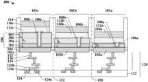
- FIG. 1illustrates a cross-sectional view 100 of some embodiments of a display device comprising an isolation structure having first, second, and third portions separated from one another.
- the display device of the cross-sectional view 100includes a first pixel region 101 a, a second pixel region 101 b, and a third pixel region 101 c.
- Each of the first, second, and third pixel regions 101 a, 101 b, 101 care configured to emit a different color of light (e.g., red, green, blue) when subjected to an electrical signal (e.g., voltage), and the color of light depends on the thickness and material of an isolation structure 106 .
- the first pixel region 101 amay comprise a first portion 106 a of the isolation structure 106 that has a first thickness t1; the second pixel region 101 b may comprise a second portion 106 b of the isolation structure 106 that has a second thickness t 2 ; and the third pixel region 101 c may comprise a third portion 106 c of the isolation structure 106 that has a third thickness t 3 .
- the first, second, and third thicknesses t 1 , t 2 , t 3are each different from one another.
- the first thickness t 1may be less than the second and third thicknesses t 2 , t 3
- the second thickness t 2may be less than the third thickness t 3 .
- the first portion 106 a, the second portion 106 b, and the third portion 106 c of the isolation structure 106may each comprise one or more oxides, such as, for example, silicon dioxide, aluminum oxide, or the like.
- the first portion 106 a, the second portion 106 b, and the third portion 106 c of the isolation structure 106may comprise a nitride (e.g., silicon nitride), or some other material that has optical properties, such that colored light is visible from the surface of the material and the colored light is dependent on the thickness of each portion ( 106 a, 106 b, 106 c ) of the isolation structure 106 .
- the first thickness t 1may correspond to red light
- the second thickness t 2may correspond to blue light
- the third thickness t 3may correspond to green light.
- the first portion 106 a of the isolation structure 106may be arranged between a first reflector electrode 102 a and a first transparent electrode 112 a.
- the second portion 106 b of the isolation structure 106may be arranged between a second reflector electrode 102 b and a second transparent electrode 112 b.
- the third portion 106 c of the isolation structure 106may be arranged between a third reflector electrode 102 c and a third transparent electrode 112 c.
- a first optical emitter structure 110 a, a second optical emitter structure 110 b, and a third optical emitter structure 110 cmay be arranged over the first transparent electrode 112 a, the second transparent electrode 112 b, and the third transparent electrode 112 c, respectively.
- a first via structure 108 a, a second via structure 108 b, and a third via structure 108extend through the first portion 106 a of the isolation structure 106 , the second portion 106 b of the isolation structure 106 , and the third portion 106 c of the isolation structure 106 , respectively.
- the via structures ( 108 a, 108 b, 108 c )extend from a top surface to a bottom surface of the portions ( 106 a, 106 b, 106 c ) of the isolation structure 106 .
- the first via structure 108 amay electrically couple the first reflector electrode 102 a to the first transparent electrode 112 a; the second via structure 108 b may electrically couple the second reflector electrode 102 b to the second transparent electrode 112 b; and the third via structure 108 c may electrically couple the third reflector electrode 102 c to the third transparent electrode 112 c.
- the first, second, and third reflector electrodes 102 a, 102 b, 102 cmay be coupled to control circuitry 120 .
- the first, second, and third reflector electrodes 102 a, 102 b, 102 care disposed over an interconnect structure 130 comprising a network of interconnect wires 134 and interconnect vias 136 embedded in an interconnect dielectric structure 132 .
- the interconnect structure 130is arranged over a substrate 122 and coupled to semiconductor devices 124 .
- the semiconductor devices 124may be, for example, metal oxide semiconductor field-effect transistors (MOSFETs) comprising source/drain regions 124 a within the substrate 122 and a gate electrode 124 b over the substrate 122 .
- the gate electrode 124 bmay be separated from the substrate 122 by a gate dielectric layer 124 c.
- the control circuitry 120is configured to selectively supply an electrical signal (e.g., voltage) to each of the first, second, and third pixel regions 101 a, 101 b, 101 c to emit colored light as indicated by digital data.
- an electrical signale.g., voltage
- the electrical signale.g., voltage
- the electrical signalmay cause the first optical emitter structure 110 a to produce light, and that light may reflect off of top surfaces of the first portion 106 a of the isolation structure 106 and/or travel through the first portion 106 a of the isolation structure 106 , reflect off of the first reflector electrode 102 a and exit through the top surfaces of the first portion 106 a of the isolation structure 106 . Due to constructive and/or destructive interference, colored light dependent on the first thickness t 1 and material of the first portion 106 a of the isolation structure 106 is visible.
- first barrier structures 104 and/or second barrier structures 114separate the first, second, and third pixel regions 101 a - 101 c. In some embodiments, each of the first, second, and third portions 106 a, 106 b, 106 c of the isolation structure 106 are completely separated from one another by the second barrier structures 114 .
- a first line 150may be arranged between the first and second portions 106 a, 106 b of the isolation structure 106 without intersecting the first or second portions 106 a, 106 b of the isolation structure 106 .
- the first line 150may continuously extend in a first direction that is normal to an upper surface of the first reflector electrode 102 a, and also may be arranged between the first reflector electrode 102 a and the second reflector electrode 102 b, between the first transparent electrode 112 a and the second transparent electrode 112 b, and between the first optical emitter structure 110 a and the second optical emitter structure 110 b.
- the first line 150may intersect the first and second barrier structures 104 , 114 .
- the second barrier structures 114directly overlie the first barrier structures 104 .
- a second line 152 that is parallel to the first line 150 and continuously extends in the first directionmay be arranged between the second portion 106 b of the isolation structure 106 and the third portion 106 b of the isolation structure 106 without intersecting the second or third portions 106 b, 106 c of the isolation structure 106 .
- each of the first, second, and third portions 106 a, 106 b, 106 c of the isolation structure 106may be completely separated from one another as a result of protecting the first, second, and third reflector electrodes 102 a, 102 b, 102 c during manufacturing of the isolation structure 106 ; in some embodiments, the separation amongst the first, second, and third portions 106 a, 106 b, 106 c of the isolation structure 106 also mitigates optical interference between each of the first, second, and third pixel regions 101 a, 101 b, 101 c to provide a reliable display device.
- FIG. 2illustrates a cross-sectional view 200 of some embodiments of a display device comprising an isolation structure having first, second, and third portions separated from one another and an example light path during operation of the display device.
- the display device in the cross-sectional view 200includes a first reflector electrode 102 a having a first width w 1 , a second reflector electrode 102 b having a second width w 2 , and a third reflector electrode 102 c having a third width w 3 .
- the first width w 1 , the second width w 2 , and the third width w 3may be substantially equal to one another, as in FIG. 1 , for example, whereas in other embodiments, as in FIG. 2 , the first, second, and third widths w 1 , w 2 , w 3 may be different from one another.
- the third width w 3may be smaller than the second width w 2
- the second width w 2may be smaller than the first width w 1
- the smallest widthcorresponds to the pixel region (e.g., 101 a ) that has the portion (e.g., 106 a ) of the isolation structure 106 with the smallest thickness (e.g., t 1 ).
- the largest widthcorresponds to the pixel region (e.g., 101 a ) that has the portion (e.g., 106 c ) of the isolation structure (e.g., 106 ) with the largest thickness (e.g., t 3 ).
- the widths (e.g., w 1 , w 2 , w 3 ) of the reflector electrodes (e.g., 102 a, 102 b, 102 c ) in each pixel region (e.g., 101 a, 101 b, 101 c )do not have a correlation with the thicknesses (e.g., t 1 , t 2 , t 3 ) of the portions (e.g., 106 a, 106 b, 106 c ) of the isolation structure (e.g., 106 ).
- the cross-sectional view 200also illustrates an exemplary first light path 202 in the first pixel region 101 a and an exemplary second light path 204 in the second pixel region 101 b.
- lightis generated by the first optical emitter structure 110 a and the second optical emitter structure 110 b due to an electrical signal (e.g., voltage) applied to the first reflector electrode 102 a and the second electrode 102 b, respectively, by the control circuitry 120 .
- an electrical signale.g., voltage
- the first pixel region 101 a and the second pixel region 101 bare “ON” (e.g., light is generated at the first and second optical emitter structures 110 a, 110 b ), whereas the third pixel region 101 c is “OFF” (e.g., light is not generated by the third optical emitter structure 110 c ).
- the exemplary first light path 202shows how in some embodiments, the generated light at the first optical emitter structure 110 a may reflect off of a top surface of the first portion 106 a of the isolation structure 106 and/or travel through the first portion 106 a of the isolation structure 106 , reflect off of the first reflector electrode 102 a, and travel back up towards the top surface of the first portion 106 a of the isolation structure 106 . Due to constructive interference of a first wavelength and/or destructive interference of remaining wavelengths, colored light having the first wavelength that is emitted/visible from a top surface of the first optical emitter structure 110 a in the first pixel region 101 a.
- the first wavelengthis associated with the first thickness t 1 and material(s) of the first portion 106 a of the isolation structure 106 and, in some embodiments, is the only wavelength or the predominant wavelength emitted/visible from the top surface of the first optical emitter structure 110 a.
- the exemplary second light path 204shows how in some embodiments, the generated light at the second optical emitter structure 110 b may reflect off of a top surface of the second portion 106 b of the isolation structure 106 and/or travel through the second portion 106 b of the isolation structure 106 , reflect off of the second reflector electrode 102 b, and travel back up towards the top surface of the second portion 106 b of the isolation structure 106 . Due to constructive of a second wavelength and/or destructive interference of remaining wavelengths, colored light having the second wavelength is emitted/visible from a top surface of the second optical emitter structure 110 b in the second pixel region 101 b.
- the second wavelengthis associated with the second thickness t 2 and material(s) of the second portion 106 b of the isolation structure 106 and, in some embodiments, is the only wavelength or the predominant wavelength emitted/visible from the top surface of the second optical emitter structure 110 b.
- the second thickness t 2 of the second portion 106 b of the isolation structure 106is different than the first thickness t 1 of the first portion 106 a of the isolation structure 106 , the second wavelength will be different from the first wavelength, and thus, the second pixel region 101 b emits a different colored light than the first pixel region 101 a.
- the control circuitry 120may use digital data to selectively turn “ON” one or more of the pixel regions (e.g., 101 a, 101 b, 101 c ) to produce an optical image.
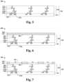
- FIG. 3illustrates a cross-sectional view 300 of some embodiments of a display device comprising an isolation structure having first, second, and third portions, wherein the second and third portions comprise multiple layers.
- the display device in the cross-sectional view 300includes: 1) a first portion 106 a of an isolation structure 106 comprising a first isolation layer 302 ; 2) a second portion 106 b of the isolation structure 106 comprising a second isolation layer 304 arranged over the first isolation layer 302 ; and 3) a third portion 106 c of the isolation structure 106 comprising the second isolation layer 304 arranged over the first isolation layer 302 and arranged below a third isolation layer 306 .
- the first, second, and third portions 106 a , 106 b , 106 c of the isolation structure 106are still separated from one another by the second barrier structures 114 .
- the first, second, and third isolation layers 302 , 304 , 306comprise different materials.
- the first isolation layer 302may comprise aluminum oxide; the second isolation layer 304 may comprise silicon dioxide; and the third layer may comprise some other material that has optical properties, such as silicon nitride.
- each of the first isolation layer 302 , the second isolation layer 304 , and the third isolation layer 306may comprise a same material, such as, for example, silicon dioxide.
- the isolation layersmay not be distinguishable from one another, and the first, second, and third portions 106 a , 106 b , 106 c of the isolation structure 106 may look like the first, second, and third portions 106 a , 106 b , 106 c of the isolation structure 106 illustrated in the cross-sectional view 100 of FIG. 1 .
- the first thickness t 1 of the first portion 106 a of the isolation structure 106may equal a thickness of the first isolation layer 302 .
- the first portion 106 a of the isolation structure 106contacts the first reflector electrode 102 a at a first interface 308 and contacts the first transparent electrode 112 a at a second interface 310 .
- the first thickness t 1 of the first portion 106 a of the isolation structure 106may be measured from the first interface 308 to the second interface 310 in a first direction normal to a top surface of the first reflector electrode 102 a.
- the second thickness t 2 of the second portion 106 b of the isolation structure 106may equal a sum of the thickness of the first isolation layer 302 and a thickness of the second isolation layer 304 .
- the second portion 106 b of the isolation structure 106contacts the second reflector electrode 102 b at a third interface 312 and contacts the second transparent electrode 112 b at a fourth interface 314 .
- the second thickness t 2 of the second portion 106 b of the isolation structure 106may be measured from the third interface 312 to the fourth interface 314 in the first direction.
- the third thickness t 3 of the third portion 106 c of the isolation structure 106may equal a sum of the thickness of the first isolation layer 302 , the thickness of the second isolation layer 304 , and a thickness of a third isolation layer 306 .
- the third portion 106 c of the isolation structure 106contacts the third reflector electrode 102 c at a fifth interface 316 and contacts the third transparent electrode 112 c at a sixth interface 318 .
- the third thickness t 3 of the third portion 106 c of the isolation structure 106may be measured from the fifth interface 316 to the sixth interface 318 in the first direction.
- the cross-sectional view 300 of FIG. 3further illustrates that in some embodiments, the first, second, and third via structures 108 a , 108 b , 108 c may respectively extend completely through the first, second, and third portions 106 a , 106 b , 106 c of the isolation structure 106 .
- the via structure ( 108 a , 108 b , 108 c )comprises a material that completely fill the space between outer sidewalls of each via structures ( 108 a , 108 b , 108 c ). In other embodiments (e.g., FIG.
- the transparent electrode ( 112 a , 112 b , 112 c )fills some of the space between the outer sidewalls of the via structure ( 108 a , 108 b , 108 c ).
- the electrical connection between the transparent electrode ( 112 , 112 b , 112 c ) and the reflector electrode ( 102 a , 102 b , 102 c )may be more efficient because the via structure ( 108 a , 108 b , 108 c ) is thinner between the reflector electrode ( 102 a , 102 b , 102 c ) and the transparent electrode ( 112 a , 112 b , 112 c ).
- FIG. 4illustrates a cross-sectional view 400 of an isolation structure having first, second, and third portions, wherein the third portion of the isolation structure comprises second and third layers comprising a same material.
- the cross-sectional view 400 of FIG. 4illustrates some embodiments of a display device wherein the portions ( 106 a, 106 b, 106 c ) of the isolation structure ( 106 ) may be wider than their respective overlying transparent electrodes ( 112 a, 112 b, 112 c ) and/or optical emitter structures ( 110 a, 110 b, 110 c ).
- the display device in the cross-sectional view 400includes the first, second, and third portions 106 a, 106 b, 106 c of the isolation structure 106 .
- the third portion 106 c of the isolation structure 106may comprise the first isolation layer 302 , the second isolation layer 304 , and the third isolation layer 304 .
- the first isolation layer 302may comprise a first material
- the second and third isolation layers 304 , 306may comprise a second material that is different than the first material.
- the first materialmay comprise aluminum oxide
- the second materialmay comprise silicon dioxide.
- the first isolation layer 302may be thinner than each of second and third isolation layers 304 , 306 .
- the first isolation layer 302may comprise aluminum oxide, for example, because during deposition, it may be easier to control the thickness of aluminum oxide than silicon dioxide, for example. Because the second and third isolation layers 304 , 306 may comprise the same second material, a seventh interface 402 between the second and third isolation layers 304 , 306 may not be distinguishable, as illustrated by a dotted line.
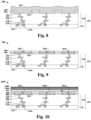
- FIGS. 5 - 18 , 19 A- 19 C, 20 , and 21illustrate cross-sectional views 500 - 1800 , 1900 A- 1900 C, 2000 , and 2100 of some embodiments of a method of forming an isolation structure over a reflector electrode structure to prevent damage to the reflector electrode structure and to produce a reliable display device.
- FIGS. 5 - 18 , 19 A- 19 C, 20 , and 21are described in relation to a method, it will be appreciated that the structures disclosed in FIGS. 5 - 18 , 19 A- 19 C, 20 , and 21 are not limited to such a method, but instead may stand alone as structures independent of the method.
- control circuitry 120may be formed over a substrate 122 .
- the control circuitry 120may comprise an interconnect structure 130 arranged over a substrate 122 .
- the interconnect structure 130may comprise interconnect wires 134 and interconnect vias 136 embedded in an interconnect dielectric structure 132 .
- the interconnect wires and vias 134 , 136may comprise copper, tungsten, or the like.
- the interconnect structure 130may be coupled to semiconductor devices 124 integrated on the substrate 122 .
- the semiconductor devices 124may be or comprise metal oxide semiconductor field-effect transistors (MOSFETs), wherein the MOSFETs comprise source/drain regions 124 a in the substrate 122 .
- the semiconductor devices 124may further comprise a gate electrode 124 b arranged over a gate dielectric layer 124 c on the substrate 122 .
- a first dielectric layer 602 , a first barrier layer 603 , and a second dielectric layer 604may be formed over the interconnect structure 130 .
- the first dielectric layer 602 , the first barrier layer 603 , and the second dielectric layer 604may comprise a same material.
- at least the first barrier layer 603may comprise a different material than the first and/or second dielectric layers 602 , 604 .
- the first barrier layer 603may comprise a dielectric material that may also act as an etch stop layer to protect the interconnect structure 130 .
- the first barrier layer 603may comprise a nitride (e.g., silicon nitride), a carbide (e.g., silicon carbide), or the like.
- the first and second dielectric layers 604may comprise a dielectric material such as, for example, nitride (e.g., silicon nitride, silicon oxynitride), a carbide (e.g., silicon carbide), an oxide (e.g., silicon oxide), borosilicate glass (BSG), undoped silicate glass (USG), phosphoric silicate glass (PSG), borophosphosilicate glass (BPSG), a low-k oxide (e.g., a carbon doped oxide, SiCOH), or the like.
- the first and/or second dielectric layers 604may comprise a same material as the interconnect dielectric structure 132 .
- the first dielectric layer 602 , the first barrier layer 603 , and/or the second dielectric layer 604may each be formed using a deposition process (e.g., physical vapor deposition (PVD), chemical vapor deposition (CVD), PE-CVD, atomic layer deposition (ALD), sputtering, etc.).
- PVDphysical vapor deposition
- CVDchemical vapor deposition
- PE-CVDPE-CVD
- atomic layer depositionALD
- sputteringetc.
- each cavity 702may expose a top one of the interconnect vias 136 .
- the cavities 702may be formed using photolithography and removal (e.g., etching) processes.
- each cavity 702may have equal widths, wherein a first width w 1 is equal to a second width w 2 and a third width w 3 . In other embodiments, at least one of the first, second, or third widths w 1 , w 2 , w 3 is different.
- a conductive material 802may be deposited over the interconnect structure 130 , such that the conductive material 802 fills in the cavities ( 702 of FIG. 7 ).
- the conductive material 802comprises a metal that is both electrically conductive and optically reflective.
- the conductive material 802may comprise aluminum or aluminum copper.
- the conductive material 802may be deposited over the interconnect dielectric structure 132 using a deposition process (e.g., physical vapor deposition (PVD), chemical vapor deposition (CVD), PE-CVD, atomic layer deposition (ALD), sputtering, etc.).
- the conductive material 802overfills the cavities ( 702 of FIG. 7 ), such that the conductive material 802 has top surfaces above the second dielectric layer 604 .
- a planarization process(e.g., chemical mechanical planarization (CMP)) is performed to remove portions of the conductive material ( 802 of FIG. 8 ) that are above the second dielectric layer 604 , thereby forming a first reflector electrode 102 a, a second reflector electrode 102 b, and a third reflector electrode 102 c.
- the first reflector electrode 102 amay have the first width w 1
- the second reflector electrode 102 bmay have the second width w 2
- the third reflector electrode 102 cmay have the third width w 3 .
- the first, second, and third reflector electrodes 102 a, 102 b, 102 cmay have upper surfaces that are substantially co-planar with one another. Further, the first, second, and third reflector electrodes 102 a, 102 b, 102 c may have upper surfaces that are substantially co-planar with the second dielectric layer 604 . In other embodiments, the planarization process may remove the second dielectric layer 604 , for example, and thus, the first, second, and third reflector electrodes 102 a, 102 b, 102 c may have upper surfaces that are substantially co-planar with the first barrier structures 104 .
- the first, second, and third reflector electrodes 102 a, 102 b, 102 cmay each be coupled to a different one of the semiconductor devices 124 , in some embodiments. Further, each of the first, second, and third reflector electrodes 102 a, 102 b, 102 c may be laterally spaced apart from one another and electrically isolated by one another by the first barrier structures 104 .
- the first reflector electrode 102 amay have a first average surface roughness
- the second reflector electrode 102 bmay have a second average surface roughness
- the third reflector electrode 102 cmay have a third average surface roughness.
- the first, second, and third average surface roughnessmay be substantially equal to one another, as each reflector electrode ( 102 a, 102 b, 102 c ) comprises a same material and is formed simultaneously using a same process method (e.g., deposition of the conductive material 802 of FIG. 8 followed by a planarization process).
- a roughness measurement toole.g., a profilometer, atomic force microscopy (AFM), etc. calculates a mean line along a surface and measures the deviation between the height of a peak or valley on the surface from the mean line. After measuring many deviations at many peaks and valleys throughout the surface, the average surface roughness is calculated by taking the mean of the many deviations, where the deviations are absolute values. In other embodiments, the surface roughness is quantified by measuring a total thickness variation (TTV). The TTV of a layer is the difference between the smallest thickness and the largest thickness of the layer. The TTV is measured throughout the length of a layer.
- TTVtotal thickness variation
- a first isolation layer 302may be formed over the first, second, and third reflector electrodes 102 a, 102 b, 102 c.
- the first isolation layer 302may comprise a material that has optical properties such that such that colored light is visible from the surface of the material, and wherein the colored light is dependent on the thickness of the first isolation layer 302 .
- the first isolation layer 302may comprise, for example, an oxide, such as aluminum oxide or silicon dioxide.
- the first isolation layer 302may have a first thickness t 1 , and in some embodiments, the first thickness t 1 may be in a range of between, for example, approximately 200 angstroms and approximately 600 angstroms.
- the first thickness t 1may be in a range of between, for example approximately 49 angstroms and approximately 51 angstroms.
- the first isolation layer 302may comprise aluminum oxide that is deposited by atomic layer deposition (ALD), which allows for precise control of the first thickness t 1 .
- ALDatomic layer deposition
- the first isolation layer 302may be formed using a different deposition process than ALD, such as physical vapor deposition (PVD), chemical vapor deposition (CVD), PE-CVD, sputtering.
- PVDphysical vapor deposition
- CVDchemical vapor deposition
- PE-CVDPE-CVD
- a first conformal masking layer 1004may be deposited over the first isolation layer 302 .
- the first conformal masking layer 1004may comprise, for example, titanium, titanium nitride, tantalum, tantalum nitride, silicon nitride, or the like.
- the first conformal masking layer 1004may be deposited using a deposition process (e.g., physical vapor deposition (PVD), chemical vapor deposition (CVD), PE-CVD, atomic layer deposition (ALD), sputtering, etc.).
- PVDphysical vapor deposition
- CVDchemical vapor deposition
- PE-CVDatomic layer deposition
- sputteringetc.
- a first conformal oxide layer 1006may be formed over the first conformal masking layer 1004 .
- the first conformal oxide layer 1006may be used to more precisely pattern the first conformal masking layer 1004 , as illustrated in FIGS. 11 and 12 .
- the first conformal oxide layer 1006may be omitted.
- the first conformal oxide layer 1006may comprise an oxide material such as, for example, silicon dioxide, silicon oxynitride, aluminum oxide, or the like.
- the first conformal oxide layer 1006may, in some embodiments, be formed by using a deposition process (e.g., physical vapor deposition (PVD), chemical vapor deposition (CVD), PE-CVD, atomic layer deposition (ALD), sputtering, etc.).
- a deposition processe.g., physical vapor deposition (PVD), chemical vapor deposition (CVD), PE-CVD, atomic layer deposition (ALD), sputtering, etc.
- the first conformal oxide layer( 1006 of FIG. 10 ) may be selectively patterned to form a first oxide layer 1106 over the first conformal masking layer 1004 .
- the first oxide layer 1106is formed to directly overlie the first reflector electrode 102 a, and without directly overlying the second or third reflector electrodes 102 b, 102 c. Further, in some embodiments, the first oxide layer 1106 completely overlies the first reflector electrode 102 a, and thus, the first oxide layer 1106 may have a width that is about equal to or greater than the first width w 1 of the first reflector electrode 102 a.
- the first oxide layer 1106may be formed by, for example, a photolithography/etching process or some other suitable process.
- a dry etching processmay be used to form the first oxide layer 1106 , and the first conformal masking layer 1004 may block the passage of ions during the dry etching process, thereby protecting the underlying first isolation layer 302 and first, second, and third reflector electrodes 102 a, 102 b, 102 c from damage due to dry etching.
- portions of the first conformal masking layer ( 1004 ) that are uncovered by the first oxide layer 1106may be removed to form a first masking layer 1204 .
- the first oxide layer 1106acts as a mask to form the first masking layer 1204 .
- a wet etching processis used to remove portions of the first conformal masking layer ( 1004 ).
- the wet etching processmay use a wet etchant comprising, for example, hydrogen peroxide.
- the wet etchant used in the wet etching processdoes not remove or affect the first isolation layer 302 , the second reflector electrode 102 b, and the third reflector electrode 102 c.
- the first isolation layer 302 , the second reflector electrode 102 b, and the third reflector electrode 102 cmay remain substantially unchanged during the formation of the first oxide layer 1106 and of the first masking layer 1204 . If dry etching were used, ions from the dry etching may pass through the first isolation layer 302 and impinge on the second reflector electrode 102 b and the third reflector electrode 102 c.
- the first masking layer 1204may have curved outer sidewalls 1204 s as a result of the lateral effect of the wet etching process.
- a second isolation layer 304may be formed over the first isolation layer 302 and the first masking layer 1204 .
- the second isolation layer 304may comprise a same or different material than the first isolation layer 302 .
- the second isolation layer 304may comprise, for example, an oxide, such as aluminum oxide or silicon dioxide.
- the second isolation layer 304may have a fourth thickness t 4 , and in some embodiments, the fourth thickness t 4 may be in a range of between, for example, approximately 200 angstroms and approximately 800 angstroms. In some other embodiments, the fourth thickness t 4 may be in a range of between, for example, approximately 800 angstroms and approximately 1000 angstroms. In some embodiments, the fourth thickness t 4 is less than, greater than, or about equal to the first thickness t 1 of the first isolation layer 302 . For example, in the cross-sectional view 1300 , the fourth thickness t 4 is greater than the first thickness t 1 .
- the second isolation layer 304may be formed using a deposition process (e.g., physical vapor deposition (PVD), chemical vapor deposition (CVD), PE-CVD, atomic layer deposition (ALD), sputtering, etc.).
- the second isolation layer 304may directly contact the first isolation layer 302 .
- an interface between the first and second isolation layers 302 , 304may not be distinguishable.
- a second conformal masking layer 1402may be formed over the second isolation layer 304 .
- the second conformal masking layer 1402may comprise the same material and may be deposited using the same deposition process as the first conformal masking layer ( 1004 of FIG. 10 ).
- a second conformal oxide layer 1404may be deposited over the second conformal masking layer 1402 .
- the second conformal oxide layer 1404may comprise the same material and may be deposited using the same deposition process as the first conformal oxide layer ( 1006 of FIG. 10 ).
- the second conformal oxide layer ( 1404 of FIG. 14 ) and the second conformal masking layer ( 1402 of FIG. 14 )may be patterned such that a second masking layer 1502 and a second oxide layer 1504 directly overlie the second reflector electrode 102 b without directly overlying the first or third reflector electrodes 102 a, 102 c.
- the patterning of the second oxide layer 1504 and the second masking layer 1502may be conducted using the same or similar steps are presented in FIGS. 11 and 12 regarding the formation of the first oxide layer 1106 arranged over the first masking layer 1204 .
- the second oxide layer 1504 and the second masking layer 1502completely overlie the second reflector electrode 102 b, and thus, the second oxide layer 1504 and the second masking layer 1502 may each have a width that is about equal to or greater than the second width w 2 of the second reflector electrode 102 b.
- the second isolation layer 304remains substantially unchanged during the formation of the second masking layer 1502 because the second masking layer 1502 prevents the passage of ions and is patterned using a wet etching process, in some embodiments.
- a third isolation layer 306may be formed over the second isolation layer 304 and the second masking layer 1502 .
- the third isolation layer 306may comprise a same or different material than the first isolation layer 302 and/or the second isolation layer 304 .
- the third isolation layer 306may comprise, for example, an oxide, such as aluminum oxide or silicon dioxide.
- the third isolation layer 306may have a fifth thickness t 5 , and in some embodiments, the fifth thickness t 5 may be in a range of between, for example, approximately 200 angstroms and approximately 1100 angstroms. In some other embodiments, the fifth thickness t 5 may be in a range of between, for example, approximately 1100 angstroms and approximately 1300 angstroms. In some embodiments, the fifth thickness t 5 is less than, greater than, or about equal to the fourth thickness t 4 of the second isolation layer 304 . For example, in the cross-sectional view 1600 , the fifth thickness t 5 is about equal to the fourth thickness t 4 .
- the third isolation layer 306may be formed using a deposition process (e.g., physical vapor deposition (PVD), chemical vapor deposition (CVD), PE-CVD, atomic layer deposition (ALD), sputtering, etc.).
- the third isolation layer 306may directly contact the second isolation layer 304 .
- an interface between the second and third isolation layers 304 , 306may not be distinguishable.
- a third conformal masking layer 1702may be formed over the third isolation layer 306 .
- the third conformal masking layer 1702may comprise the same material and may be deposited using the same deposition process as the first conformal masking layer ( 1004 of FIG. 10 ).
- a third conformal oxide layer 1704may be deposited over the third conformal masking layer 1702 .
- the third conformal oxide layer 1704may comprise the same material and may be deposited using the same deposition process as the first conformal oxide layer ( 1006 of FIG. 10 ).
- the third conformal oxide layer ( 1704 of FIG. 17 ) and the third conformal masking layer ( 1702 of FIG. 17 )may be patterned such that a third masking layer 1802 and a third oxide layer 1804 directly overlie the third reflector electrode 102 c without directly overlying the second or third reflector electrodes 102 b, 102 c.
- the patterning of the third oxide layer 1804 and the third masking layer 1802may be conducted using the same or similar steps are presented in FIGS. 11 and 12 regarding the formation of the first oxide layer 1106 arranged over the first masking layer 1204 .
- the third oxide layer 1804 and the third masking layer 1802completely overlie the third reflector electrode 102 c, and thus, the third oxide layer 1804 and the third masking layer 1802 may each have a width that is about equal to or greater than the third width w 3 of the third reflector electrode 102 c. Further, similar to the first isolation layer 302 during the formation of the first masking layer 1204 , the third isolation layer 306 remains substantially unchanged during the formation of the third masking layer 1802 because the third masking layer 1802 prevents the passage of ions and is patterned using a wet etching process, in some embodiments.
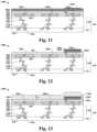
- a first removal process 1902is performed to remove portions of the first, second, and third isolation layers 302 , 304 , 306 uncovered by the first, second, and third masking layers 1204 , 1502 , 1802 .
- the cross-sectional views 1900 A, 1900 B, and 1900 C of FIGS. 19 A, 19 B, and 19 Cillustrate the first removal process 1902 respectively at a first time, a second time, and a third time, where the second time is after the first time and the third time is after the second time.
- the third isolation layer 306 that is uncovered by the third masking layer 1802is removed.
- the first removal process 1902uses a vertical etch.
- the first removal process 1902is an etching process that utilizes a dry etchant.
- the dry etchantdoes not remove the first, second, or third masking layers 1204 , 1502 , 1802 .
- the first oxide layer 1106 , the second oxide layer 1504 , and the third oxide layer 1804comprise a same material as the first, second, and/or third isolation layers 302 , 304 , 306 .
- the first removal process 1902may partially remove the first, second, and third oxide layers 1106 , 1504 , 1804 such that after the first removal process 1902 , the first, second, and third oxide layers 1106 , 1504 , 1804 may have a higher average surface roughness than before the first removal process 1902 .
- the first removal process 1902may completely remove the first oxide layer 1106 , the second oxide layer 1504 , and the third oxide layer 1804 . Nevertheless, the first, second, and third masking layers 1204 , 1502 , 1802 cover and protect the underlying first, second, and/or third isolation layers 302 , 304 , 306 from ions during the dry etch.
- the first removal process 1902begins to remove portions of the second isolation layer 304 uncovered by the second and third masking layers 1502 , 1802 .
- the same dry etchantis used during the first removal process 1902 .
- different dry etchantsmay be used to effectively remove each of the first, second, and third isolation layers 302 , 304 , 306 that are uncovered or that do not directly underlie the first, second, or third masking layers 1204 , 1502 , 1802 .
- a carbon fluoride based dry etchantmay be used, whereas in some other embodiments, for a nitride-based first, second, and/or third isolation layer 302 , 304 , 306 , a carbon hydrogen fluoride based dry etchant may be used. It will be appreciated that other dry etchants are also within the scope of the disclosure.
- the first removal process 1902finishes and removes portions of the first, second, and third isolation layers 302 , 304 , 306 that do not directly underlie the first, second, or third masking layers 1204 , 1502 , 1802 .
- the first removal process 1902may stop at the second dielectric layer 604 or at the first barrier structures 104 .
- first, second, and third masking layers 1204 , 1502 , 1802completely overlie the first, second, and third reflector electrodes 102 a, 102 b, 102 c, respectively, the first, second, and third reflector electrodes 102 a, 102 b, 102 c do not get damaged by the first removal process 1902 and therefore maintain the first, second, and third average surface roughnesses, respectively.
- patterning of the first, second, and third isolation layers 302 , 304 , 306does not damage the first, second, and third reflector electrodes 102 a, 102 b, 102 c and optical properties of the first, second, and third reflector electrodes 102 a, 102 b, 102 c are maintained.
- a second removal processmay be performed to remove the first, second, and third masking layers ( 1204 , 1502 , 1802 of FIG. 19 C ). Further, in some embodiments, the second removal process also remove the first oxide layer ( 1106 of FIG. 19 C ), the second oxide layer ( 1504 of FIG. 19 C ), and the third oxide layer ( 1804 of FIG. 19 C ).
- the second removal processmay comprise, for example, a dry etching process to remove the first oxide layer ( 1106 of FIG. 19 C ), the second oxide layer ( 1504 of FIG. 19 C ), and the third oxide layer ( 1804 of FIG.
- the second removal processmay only comprise a wet etching process to remove the first, second, and third masking layers ( 1204 , 1502 , 1802 of FIG. 19 C ).
- wet etchingis used in place of dry etching to prevent damage to the first, second, and third isolation layers 302 - 306 and the first, second, and third reflector electrodes 102 a - 102 c. If dry etchants were employed, ions from the dry etching may pass through the first, second, and third isolation layers 302 - 306 to upper surfaces respectively of the first, second, and third reflector electrodes 102 a - 102 c. This would damage the crystalline structure of the first, second, and third isolation layers 302 - 306 and would increase upper surface roughness of the first, second, and third reflector electrodes 102 a - 102 c. The crystalline damage and/or increased surface damage would, in turn, increase light scattering and degrade reliability of the display device.
- the first, second, and third isolation layers 302 , 304 , 306form an isolation structure 106 coupled to the control circuitry 120 .
- a first portion 106 a of the isolation structure 106comprises the first isolation layer 302 .
- the first portion 106 a of the isolation structure 106has the first thickness t 1 .
- a second portion 106 b of the isolation 106 structurecomprises portions respectively of the first isolation layer 302 and the second isolation layer 304 that directly overlie the second reflector electrode 102 b.
- the first isolation layer 302 of the second portion 106 b of the isolation structuredirectly contacts the second reflector electrode 102 b.
- the second portion 106 b of the isolation structure 106has a second thickness t 2 that in some embodiments, is in a range of between, for example, approximately 300 angstroms and approximately 1300 angstroms.
- the second thickness t 2is greater than the first thickness t 1 , such that an upper surface of the first portion 106 a of the isolation structure 106 is below an upper surface of the second portion 106 b of the isolation structure 106 .
- the second thickness t 2is equal a sum of the first thickness t 1 and the fourth thickness t 4 .
- a third portion 106 c of the isolation structure 106directly overlies the third reflector electrode 102 c and comprises portions respectively of the first isolation layer 302 , the second isolation layer 304 , and the third isolation layer 306 .
- the first isolation layer 302 of the third portion 106 c of the isolation structuredirectly contacts the third reflector electrode 102 c.
- the third portion 106 c of the isolation structure 106has a third thickness t 3 that, in some embodiments, is in a range of between, for example, approximately 400 angstroms and approximately 1500 angstroms.
- the third thickness t 3is equal to a sum of the first thickness t 1 , the second thickness t 2 , and the third thickness t 3 .
- the third thickness t 3may be greater than the second thickness t 2 , such that the upper surface of the second portion 106 b of the isolation structure 106 is below an upper surface of the third portion 106 c of the isolation structure 106 .
- the first, second, and third portions 106 a, 106 b, 106 c of the isolation structure 106are completely laterally spaced apart from one another, allowing for optical isolation.
- first, second, and third via structures 108 a, 108 b, 108 care formed over and extending through the first, second, and third portions 106 a, 106 b, 106 c of the interconnect structure, respectively, to contact the first, second, and third reflector electrodes 102 a, 102 b, 102 c, respectively.
- the via structures ( 108 a, 108 b, 108 c )may comprise tantalum, titanium, or some other conductive material.
- first, second, and third transparent electrodes 112 a, 112 b, 112 cmay be formed over the first, second, and third portions 106 a, 106 b, 106 c of the isolation structure 106 , respectively.
- the first transparent electrode 112 amay directly contact the first portion 106 a of the isolation structure 106 .
- the second transparent electrode 112 bmay directly contact the second portion 106 b of the isolation structure 106 .
- the third transparent electrode 112 cmay directly contact the third portion 106 c of the isolation structure 106 .
- the transparent electrodes ( 112 a, 112 b, 112 c )comprise an electrically conductive material that is also optically transparent, such as, for example, indium tin oxide (ITO), fluorine tin oxide (FTO), or the like.
- each of the transparent electrodes ( 112 a, 112 b, 112 c )may have a thickness that is, for example, in a range of between approximately 500 angstroms and approximately 3000 angstroms.
- a first optical emitter structure 110 a, a second optical emitter structure 110 b, and a third optical emitter structure 110 cmay be respectively formed over the first transparent electrode 112 a, the second transparent electrode 112 b, and the third transparent electrode 112 c.
- the optical emitter structures ( 110 a, 110 b, 110 c )may be or comprise an organic light emitting diode (OLED) or some other suitable light generating device.
- each of the optical emitter structures ( 110 a, 110 b, 110 c )may have a thickness in the range of between, for example, approximately 500 angstroms and approximately 3000 angstroms.
- second barrier structures 114are formed to separate the transparent electrodes ( 112 a, 112 b, 112 c ) and the optical emitter structures ( 110 a, 110 b, 110 c ) to define a first pixel region 101 a, a second pixel region 101 b, and a third pixel region 101 c. Further, the second barrier structures 114 may completely separate the first, second, and third portions 106 a, 106 b, 106 c of the isolation structure 106 . It will be appreciated that the display device may comprise an array of pixel regions, and may comprise more than the first, second, and third pixel regions 101 a, 101 b, 101 c.
- the second barrier structures 114may directly overlie the first barrier structures 104 , and the second barrier structures 114 may comprise a dielectric material to electrically and optically isolate the pixel regions ( 101 a, 101 b, 101 c ) from one another.
- the second barrier structures 114may comprise a nitride (e.g., silicon nitride, silicon oxynitride), an oxide (e.g., silicon oxide), or the like.
- the second barrier structures 114may comprise a multi-layer film stack of silicon nitride and silicon oxide.
- the second barrier structures 114may comprise a same material as the isolation structure 106 , the first barrier structures 104 , and/or the interconnect dielectric structure 132 . In other embodiments, the second barrier structures 114 may comprise a different material as the isolation structure 106 , the first barrier structures 104 , and/or the interconnect dielectric structure 132 .
- the via structures ( 108 a, 108 b, 108 c ), the transparent electrodes ( 112 a, 112 b, 112 c ), the optical emitter structures ( 110 a, 110 b, 110 c ), and the second barrier structures 114may each be formed through various steps comprising deposition processes (e.g., physical vapor deposition (PVD), chemical vapor deposition (CVD), PE-CVD, atomic layer deposition (ALD), sputtering, etc.), removal processes (e.g., wet etching, dry etching, chemical mechanical planarization (CMP), etc.), and/or patterning processes (e.g., photolithography/etching).
- PVDphysical vapor deposition
- CVDchemical vapor deposition
- PE-CVDatomic layer deposition
- sputteringetc.
- removal processese.g., wet etching, dry etching, chemical mechanical planarization (CMP), etc.
- patterning processese
- the display devicecomprises control circuitry 120 to selectively operate the first, second, and third pixel regions 101 a, 101 b, 101 c. Because the first, second, and third reflector electrodes 102 a, 102 b, 102 c are protected from the first removal process ( 1902 of FIGS.
- each of the pixel regions ( 101 a, 101 b, 101 c )may be selectively operated by the control circuitry 120 to reliably emit colored light depending on the thicknesses (t 1 , t 2 , t 3 ) and/or materials of each portion ( 106 a, 106 b, 106 c ) of the isolation structure ( 106 ).
- FIG. 22illustrates a flow diagram of some embodiments of a method 2200 corresponding to FIGS. 5 - 18 , 19 A- 19 C, 20 , and 21 .
- method 2200is illustrated and described below as a series of acts or events, it will be appreciated that the illustrated ordering of such acts or events are not to be interpreted in a limiting sense. For example, some acts may occur in different orders and/or concurrently with other acts or events apart from those illustrated and/or described herein. In addition, not all illustrated acts may be required to implement one or more aspects or embodiments of the description herein. Further, one or more of the acts depicted herein may be carried out in one or more separate acts and/or phases.
- FIGS. 7 - 9illustrate cross-sectional views 700 - 900 of some embodiments corresponding to act 2202 .
- FIG. 10illustrates cross-sectional view 1000 of some embodiments corresponding to act 2204 .
- a first masking layeris formed over the first reflector electrode such that the first masking layer directly overlies the first reflector electrode but not the second reflector electrode.
- FIGS. 10 - 12illustrate cross-sectional views 1000 - 1200 of some embodiments corresponding to act 2206 .
- FIG. 13illustrates cross-sectional view 1300 of some embodiments corresponding to act 2208 .
- FIGS. 14 and 15illustrate cross-sectional views 1400 and 1500 , respectively, of some embodiments corresponding to act 1910 .
- FIGS. 19 A, 19 B, and 19 Cillustrate cross-sectional views 1900 A, 1900 B, and 1900 C, respectively, of some embodiments corresponding to act 2212 .
- FIG. 20illustrates cross-sectional view 2000 of some embodiments corresponding to act 2214 .
- the present disclosurerelates to a method of forming an isolation structure that prevents damage to upper surfaces of an underlying reflector electrode structure to improve reliability of a display device.
- the present disclosurerelates to a display device comprising: a first reflector electrode; a second reflector electrode that is separated from the first reflector electrode; an isolation structure overlying the first and second reflector electrodes, the isolation structure comprising: a first portion that overlies the first reflector electrode and has a first thickness, and a second portion that overlies the second reflector electrode, has a second thickness greater than the first thickness, and is separated from the first portion of the isolation structure; and a first optical emitter structure and a second optical emitter structure respectively overlying the first and second portions of the isolation structure.
- the present disclosurerelates to a display device comprising: a first reflector electrode and a second reflector electrode over an interconnect structure; a first isolation layer comprising a pair of segments that are spaced from each other and that respectively overlie the first and second reflector electrodes; a second isolation layer overlying the first isolation layer and the second reflector electrode, but not the first reflector electrode; a first optical emitter structure overlying the first isolation layer and the first reflector electrode and a second optical emitter structure overlying the second isolation layer and the second reflector electrode; and a first conductive structure and a second conductive structure respectively extending from the first reflector electrode to the first optical emitter structure and from the second reflector electrode to the second optical emitter structure, wherein the first conductive structure extends through the first isolation layer, and wherein the second conductive structure extends through the first and second isolation layers.
- the present disclosurerelates to a method of forming a display device, comprising: forming a first reflector electrode and a second reflector electrode over an interconnect structure, wherein the first reflector electrode is laterally separated from the second reflector electrode; depositing a first isolation layer over the first and second reflector electrodes; forming a first masking layer directly overlying the first reflector electrode; depositing a second isolation layer over the first isolation layer and over the first masking layer; forming a second masking layer over the second isolation layer and directly overlying the second reflector electrode; performing a first removal process to remove portions of the first and second isolation layers that do not directly underlie the first or second masking layers; and performing a second removal process to remove the first and second masking layers.
Landscapes
- Engineering & Computer Science (AREA)
- Microelectronics & Electronic Packaging (AREA)
- Manufacturing & Machinery (AREA)
- Physics & Mathematics (AREA)
- Optics & Photonics (AREA)
- Devices For Indicating Variable Information By Combining Individual Elements (AREA)
Abstract
Description
Claims (17)
Priority Applications (4)
| Application Number | Priority Date | Filing Date | Title |
|---|---|---|---|
| US16/884,375US11980046B2 (en) | 2020-05-27 | 2020-05-27 | Method for forming an isolation structure having multiple thicknesses to mitigate damage to a display device |
| TW109138650ATWI758934B (en) | 2020-05-27 | 2020-11-05 | Display device and method of forming the same |
| CN202011237628.5ACN113206127B (en) | 2020-05-27 | 2020-11-09 | Display device and method of forming the same |
| US17/872,585US20220359846A1 (en) | 2020-05-27 | 2022-07-25 | Method for forming an isolation structure having multiple thicknesses to mitigate damage to a display device |
Applications Claiming Priority (1)
| Application Number | Priority Date | Filing Date | Title |
|---|---|---|---|
| US16/884,375US11980046B2 (en) | 2020-05-27 | 2020-05-27 | Method for forming an isolation structure having multiple thicknesses to mitigate damage to a display device |
Related Child Applications (1)
| Application Number | Title | Priority Date | Filing Date |
|---|---|---|---|
| US17/872,585DivisionUS20220359846A1 (en) | 2020-05-27 | 2022-07-25 | Method for forming an isolation structure having multiple thicknesses to mitigate damage to a display device |
Publications (2)
| Publication Number | Publication Date |
|---|---|
| US20210376282A1 US20210376282A1 (en) | 2021-12-02 |
| US11980046B2true US11980046B2 (en) | 2024-05-07 |
Family
ID=77025076
Family Applications (2)
| Application Number | Title | Priority Date | Filing Date |
|---|---|---|---|
| US16/884,375ActiveUS11980046B2 (en) | 2020-05-27 | 2020-05-27 | Method for forming an isolation structure having multiple thicknesses to mitigate damage to a display device |
| US17/872,585PendingUS20220359846A1 (en) | 2020-05-27 | 2022-07-25 | Method for forming an isolation structure having multiple thicknesses to mitigate damage to a display device |
Family Applications After (1)
| Application Number | Title | Priority Date | Filing Date |
|---|---|---|---|
| US17/872,585PendingUS20220359846A1 (en) | 2020-05-27 | 2022-07-25 | Method for forming an isolation structure having multiple thicknesses to mitigate damage to a display device |
Country Status (3)
| Country | Link |
|---|---|
| US (2) | US11980046B2 (en) |
| CN (1) | CN113206127B (en) |
| TW (1) | TWI758934B (en) |
Families Citing this family (2)
| Publication number | Priority date | Publication date | Assignee | Title |
|---|---|---|---|---|
| US11980046B2 (en)* | 2020-05-27 | 2024-05-07 | Taiwan Semiconductor Manufacturing Company, Ltd. | Method for forming an isolation structure having multiple thicknesses to mitigate damage to a display device |
| CN115349178B (en)* | 2021-03-12 | 2025-09-05 | 应用材料意大利有限公司 | Method and apparatus for printing on substrates for producing solar cells |
Citations (193)
| Publication number | Priority date | Publication date | Assignee | Title |
|---|---|---|---|---|
| US4538143A (en) | 1981-06-24 | 1985-08-27 | Clarion Co., Ltd. | Light-emitting diode displayer |
| US5213984A (en)* | 1990-10-18 | 1993-05-25 | Fuji Xerox Co., Ltd. | Method of manufacturing an image sensor |
| US6392340B2 (en)* | 1998-02-27 | 2002-05-21 | Sanyo Electric Co., Ltd. | Color display apparatus having electroluminescence elements |
| US6414738B1 (en)* | 1997-03-31 | 2002-07-02 | Seiko Epson Corporation | Display |
| US20020093284A1 (en)* | 2001-01-15 | 2002-07-18 | Masaya Adachi | Light-emitting devices and light-emitting displays |
| US20030146695A1 (en)* | 2001-12-18 | 2003-08-07 | Seiko Epson Corporation | Display apparatus and electric device |
| US20030230972A1 (en)* | 2002-06-12 | 2003-12-18 | Eastman Kodak Company | Oled display having color filters for improving contrast |
| US20040058527A1 (en)* | 2002-09-20 | 2004-03-25 | Semiconductor Energy Laboratory Co., Ltd. | Manufacturing method of semiconductor device |
| US6737800B1 (en)* | 2003-02-18 | 2004-05-18 | Eastman Kodak Company | White-emitting organic electroluminescent device with color filters and reflective layer for causing colored light constructive interference |
| US20040217697A1 (en)* | 2003-05-01 | 2004-11-04 | Kwan-Hee Lee | High efficiency organic electroluminescent display and method for fabricating the same |
| US20050008770A1 (en)* | 2003-06-02 | 2005-01-13 | Tomomi Kawase | Method of manufacturing color filter substrate, method of manufacturing electroluminescent substrate, electro-optical device and method of manufacturing the same, and electronic apparatus and method of manufacturing the same |
| US20050017630A1 (en)* | 2003-07-26 | 2005-01-27 | Seoung-Yoon Ryu | Flat panel display with high efficiency and method of fabricating the same |
| US20050067953A1 (en)* | 2003-09-12 | 2005-03-31 | Semiconductor Energy Laboratory Co., Ltd. | Light emitting device and method for manufacturing the same |
| US20050142976A1 (en)* | 2003-12-26 | 2005-06-30 | Koji Suzuki | Method for manufacturing display device |
| US20050161830A1 (en)* | 2004-01-26 | 2005-07-28 | Seiko Epson Corporation | Electro-optical device, method of manufacturing the same, and electronic apparatus |
| US20050213002A1 (en)* | 2004-03-24 | 2005-09-29 | Toppoly Optoelectronics Corp. | Transflective liquid crystal display and method of fabricating the same |
| US20050225232A1 (en)* | 2004-04-07 | 2005-10-13 | Eastman Kodak Company | Color OLED with added color gamut pixels |
| US20050253171A1 (en)* | 2004-05-17 | 2005-11-17 | Tae-Wook Kang | Organic light emitting display and method of fabricating the same |
| US20050269947A1 (en)* | 2004-06-02 | 2005-12-08 | Seiko Epson Corporation. | Organic EL device and electronic apparatus |
| US20060108917A1 (en)* | 2004-10-08 | 2006-05-25 | Chi Mei Optoelectronics Corp. | Organic electroluminescent device and fabricating method thereof |
| US20060145159A1 (en)* | 2003-03-26 | 2006-07-06 | Seiichi Yokoyama | Light-emitting device, method of manufacturing the same, and display unit |
| US20060244369A1 (en)* | 2005-03-31 | 2006-11-02 | Kitazume Eiichi | Organic electroluminescent device and the manufacturing method |
| US20070102737A1 (en) | 2003-09-19 | 2007-05-10 | Mitsuhiro Kashiwabara | Display unit, method of manufacturing same, organic light emitting unit, and method of manufacturing same |
| US20070132368A1 (en)* | 2005-12-08 | 2007-06-14 | Seiko Epson Corporation | Method for manufacturing organic light-emitting device, organic light-emitting device, and electronic apparatus |
| US20070164275A1 (en)* | 2006-01-16 | 2007-07-19 | Seiko Epson Corporation | Light-emitting device, method for manufacturing light-emitting device, and electronic apparatus |
| US20070205420A1 (en)* | 2004-03-24 | 2007-09-06 | Koninklijke Philips Electronics, N.V. | Electroluminescent display devices |
| US20080169757A1 (en)* | 2007-01-16 | 2008-07-17 | Tpo Displays Corp. | Top-emitting organic electroluminescent display |
| US20080284326A1 (en)* | 2007-05-15 | 2008-11-20 | Jong-Hyun Choi | Organic light emitting diode display device and method of fabricating the same |
| KR20090003590A (en)* | 2007-07-03 | 2009-01-12 | 엘지디스플레이 주식회사 | Organic light emitting display device and manufacturing method |
| US20090051283A1 (en)* | 2007-08-21 | 2009-02-26 | Cok Ronald S | Led device having improved contrast |
| US20090160322A1 (en)* | 2007-05-28 | 2009-06-25 | Panasonic Corporation | Organic el device and display |
| US20090170230A1 (en)* | 2007-12-28 | 2009-07-02 | Casio Computer Co., Ltd. | Manufacturing method of display apparatus and manufacturing apparatus |
| US20090184636A1 (en)* | 2008-01-23 | 2009-07-23 | Cok Ronald S | Led device having improved power distribution |
| US20090200544A1 (en)* | 2008-02-12 | 2009-08-13 | Samsung Electronics Co., Ltd. | Organic light emitting device and method of manufacturing the same |
| US20090251051A1 (en)* | 2008-04-04 | 2009-10-08 | Young-In Hwang | Organic light emitting diode display and method for manufacturing the same |
| US20090256477A1 (en)* | 2008-04-14 | 2009-10-15 | Samsung Electronics Co., Ltd. | Organic light emitting device and manufacturing method thereof |
| US20090278450A1 (en)* | 2008-05-08 | 2009-11-12 | Seiko Epson Corporation | Organic el device, electronic apparatus, and method for manufacturing organic el device |
| US20090283786A1 (en)* | 2008-05-14 | 2009-11-19 | Seiko Epson Corporation | Light emitting device and electronic apparatus |
| US20090295282A1 (en)* | 2008-05-28 | 2009-12-03 | Ji-Hwan Yoon | Organic light emitting display device |
| US20100026178A1 (en)* | 2008-08-04 | 2010-02-04 | Samsung Electronics Co., Ltd. | Organic light emitting display and fabricating method thereof |
| US20100052524A1 (en)* | 2008-08-29 | 2010-03-04 | Fujifilm Corporation | Color display device and method for manufacturing the same |
| US20100053044A1 (en)* | 2008-09-01 | 2010-03-04 | Lee Hae-Yeon | Organic light emitting diode display and method for manufacturing the same |
| US7719182B2 (en)* | 2005-09-22 | 2010-05-18 | Global Oled Technology Llc | OLED device having improved light output |
| US7741770B2 (en)* | 2007-10-05 | 2010-06-22 | Global Oled Technology Llc | LED device having improved light output |
| US20100200875A1 (en)* | 2009-02-06 | 2010-08-12 | Seiko Epson Corporation | Organic electroluminescent device and electronic apparatus |
| US7855508B2 (en)* | 2007-09-17 | 2010-12-21 | Global Oled Technology Llc | LED device having improved light output |
| US7868543B2 (en)* | 2003-11-07 | 2011-01-11 | Seiko Epson Corporation | Light-emitting device having openings in electrode |
| US7888858B2 (en)* | 2007-08-21 | 2011-02-15 | Global Oled Technology Llc | Light emitting diode device incorporating a white light emitting layer in combination with a plurality of optical microcavities |
| US7923920B2 (en)* | 2006-10-24 | 2011-04-12 | Canon Kabushiki Kaisha | Organic light-emitting elements of LED with light reflection layers in each spaced on opposite sides of transparent conductive layer |
| US20110095675A1 (en)* | 2009-10-23 | 2011-04-28 | Seiko Epson Corporation | Light emitting device and electronic device |
| US20110114957A1 (en)* | 2009-11-13 | 2011-05-19 | Eun-Hyun Kim | Thin film transistor and organic light emitting display apparatus |
| US20110127500A1 (en)* | 2009-11-30 | 2011-06-02 | Samsung Mobile Display Co., Ltd. | Oled display apparatus and method of manufacturing the same |
| US20110241000A1 (en)* | 2010-03-30 | 2011-10-06 | Jong-Hyun Choi | Organic light-emitting display apparatus and method of manufacturing the same |
| US20110316007A1 (en)* | 2010-06-29 | 2011-12-29 | Sony Corporation | Display device |
| US20110317429A1 (en) | 2009-03-03 | 2011-12-29 | Satoshi Aiba | Method for producing light-emitting display device, light-emitting display device and light-emitting display |
| US20120001185A1 (en)* | 2010-06-30 | 2012-01-05 | Lee Dae-Woo | Organic Light Emitting Diode Display and Manufacturing Method Thereof |
| US20120012834A1 (en)* | 2009-05-28 | 2012-01-19 | Sharp Kabushiki Kaisha | Organic electroluminescence display device, method for producing same, color filter substrate and method for producing same |
| US20120091482A1 (en)* | 2009-07-02 | 2012-04-19 | Sharp Kabushiki Kaisha | Organic el element, method for manufacturing the same, and organic el display device |
| US20120098414A1 (en)* | 2009-06-23 | 2012-04-26 | Fuji Electric Co., Ltd. | Flat panel display, intermediate manufactured product and method of manufacturing same |
| US20120098412A1 (en)* | 2010-10-22 | 2012-04-26 | Dong-Woo Shin | Display devices and methods of manufacturing display devices |
| US20120112172A1 (en)* | 2010-11-04 | 2012-05-10 | Sony Corporation | Display device, method of manufacturing display device, and electronic apparatus |
| US8253127B2 (en)* | 2007-02-05 | 2012-08-28 | Lg Chem, Ltd. | Organic light-emitting device having improved light-emitting efficiency and method for fabricating the same |
| US20120228603A1 (en)* | 2009-11-17 | 2012-09-13 | Sharp Kabushiki Kaisha | Organic el display |
| US20120248465A1 (en)* | 2011-03-31 | 2012-10-04 | Jin-Baek Choi | Organic light emitting diode display and manufacturing method thereof |
| US20120286305A1 (en)* | 2011-05-11 | 2012-11-15 | Semiconductor Energy Laboratory Co., Ltd. | Light-Emitting Element, Light-Emitting Module, Light-Emitting Panel, and Light-Emitting Device |
| US20130119388A1 (en)* | 2011-11-10 | 2013-05-16 | Samsung Mobile Display Co., Ltd. | Organic light-emitting display device and method of manufacturing the same |
| US20140028181A1 (en)* | 2012-07-27 | 2014-01-30 | Samsung Display Co., Ltd. | Organic light-emitting display device |
| US20140070671A1 (en)* | 2012-09-11 | 2014-03-13 | Samsung Electronics Co., Ltd. | Resonance apparatus for processing electrical loss using conductive material and method for manufacturing the same |
| US20140084310A1 (en)* | 2012-09-25 | 2014-03-27 | Kabushiki Kaisha Toshiba | Display device and method for manufacturing same |
| US20140110735A1 (en)* | 2012-10-23 | 2014-04-24 | Japan Display Inc. | Electroluminescence display device |
| US20140131679A1 (en) | 2012-11-09 | 2014-05-15 | Samsung Corning Precision Materials Co., Ltd. | Organic light emitting devices |
| US20140183460A1 (en)* | 2012-12-31 | 2014-07-03 | Lg Display Co., Ltd. | Organic light emitting diode display device and method of manufacturing the same |
| US20140191202A1 (en)* | 2013-01-04 | 2014-07-10 | Lg Display Co., Ltd. | Oled micro-cavity structure and method of making |
| US8816579B2 (en) | 2011-08-12 | 2014-08-26 | Samsung Display Co., Ltd. | Organic light-emitting device and method of manufacturing the same |
| US20140284575A1 (en)* | 2013-03-21 | 2014-09-25 | Nozomu Sugisawa | Display device and electronic device |
| US20140284576A1 (en)* | 2013-03-21 | 2014-09-25 | Nozomu Sugisawa | Display device, manufacturing method thereof, and electronic device |
| US8847215B2 (en)* | 2012-08-24 | 2014-09-30 | Lg Display Co., Ltd. | Organic light-emitting diode and method of fabricating the same |
| US8895967B2 (en)* | 2011-10-27 | 2014-11-25 | Lg Display Co., Ltd. | Organic electroluminescent display device |
| US8933471B2 (en) | 2010-01-08 | 2015-01-13 | Panasonic Corporation | Organic EL panel, display device using same, and method for producing organic EL panel |
| US20150144908A1 (en)* | 2013-11-26 | 2015-05-28 | Lg Display Co., Ltd. | Organic light emitting display panel and organic light emitting display device including the same |
| US20150187852A1 (en)* | 2012-08-01 | 2015-07-02 | Semiconductor Energy Laboratory Co., Ltd. | Display Device |
| US20150263304A1 (en)* | 2012-10-31 | 2015-09-17 | Lg Display Co., Ltd. | Organic light emitting display device |
| US20150280170A1 (en)* | 2014-03-27 | 2015-10-01 | Universal Display Corporation | Hermetically sealed isolated oled pixels |
| US20150318339A1 (en)* | 2014-05-02 | 2015-11-05 | Semiconductor Energy Laboratory Co., Ltd. | Light-emitting device and input/output device |
| US20150333110A1 (en)* | 2013-08-30 | 2015-11-19 | Lg Display Co., Ltd. | Organic electroluminescent device and method for fabricating the same |
| US20160126294A1 (en)* | 2013-06-05 | 2016-05-05 | Seiko Epson Corporation | Electro-optical apparatus, manufacturing method for electro-optical apparatus, and electronic device |
| US20160133878A1 (en)* | 2014-11-07 | 2016-05-12 | Semiconductor Energy Laboratory Co., Ltd. | Light-Emitting Element, Light-Emitting Device, Display Device, Electronic Device, and Lighting Device |
| US20160190523A1 (en)* | 2014-12-31 | 2016-06-30 | Samsung Display Co., Ltd. | Method of manufacturing organic light-emitting diode display |
| US20160315131A1 (en)* | 2015-04-24 | 2016-10-27 | Boe Technology Group Co., Ltd. | Array substrate, fabrication method thereof and display device |
| US20160365390A1 (en)* | 2015-06-10 | 2016-12-15 | Japan Display Inc. | Display device |
| US20160372528A1 (en)* | 2013-12-06 | 2016-12-22 | Sharp Kabushiki Kaisha | Light-emitting substrate, photovoltaic cell, display device, lighting device, electronic device, organic light-emitting diode, and method of manufacturing light-emitting substrate |
| US20170077448A1 (en)* | 2015-09-14 | 2017-03-16 | Japan Display Inc. | Display device |
| US20170092707A1 (en)* | 2015-09-29 | 2017-03-30 | Boe Technology Group Co., Ltd. | Bottom-emitting oled display panel |
| US20170098793A1 (en)* | 2014-06-03 | 2017-04-06 | Sharp Kabushiki Kaisha | Organic el element and method for manufacturing same |
| US9653520B2 (en)* | 2011-11-15 | 2017-05-16 | Lg Display Co., Ltd. | Organic light emitting display panel and method of manufacturing the same |
| US20170141172A1 (en)* | 2015-11-12 | 2017-05-18 | Samsung Display Co., Ltd., | Organic light-emitting display and manufacturing method thereof |
| US20170194385A1 (en)* | 2015-12-30 | 2017-07-06 | Lg Display Co., Ltd. | Organic light-emitting diode display device |
| US20170207249A1 (en)* | 2016-01-18 | 2017-07-20 | Lg Electronics Inc. | Display device using semiconductor light emitting device |
| US20170235173A1 (en)* | 2014-09-10 | 2017-08-17 | Sharp Kabushiki Kaisha | Semiconductor device, liquid crystal display device, and semiconductor device manufacturing method |
| US20170243928A1 (en)* | 2016-02-24 | 2017-08-24 | Boe Technology Group Co., Ltd. | Organic light-emitting diode (oled) array substrate, display device and manufacturing method thereof |
| US20170250233A1 (en)* | 2016-02-26 | 2017-08-31 | Japan Display Inc. | Display device |
| US20170279084A1 (en)* | 2016-03-22 | 2017-09-28 | Japan Display Inc. | Display device |
| US20170331062A1 (en)* | 2015-11-12 | 2017-11-16 | Panasonic Intellectual Property Management Co., Ltd. | Optical sensor |
| US20170352842A1 (en) | 2016-06-06 | 2017-12-07 | Seiko Epson Corporation | Organic el device, method for manufacturing organic el device, and electronic instrument |
| US20180062116A1 (en)* | 2016-08-31 | 2018-03-01 | Lg Display Co., Ltd. | Display device having a micro-cavity structure and method for forming the same |
| US20180061905A1 (en)* | 2016-08-31 | 2018-03-01 | Lg Display Co., Ltd. | Organic light-emitting display device and method of manufacturing the same |
| US20180138259A1 (en)* | 2016-11-15 | 2018-05-17 | Samsung Display Co., Ltd. | Display device |
| US20180190944A1 (en)* | 2016-12-30 | 2018-07-05 | Lg Display Co., Ltd. | Organic light-emitting display device |
| US20180190740A1 (en)* | 2016-12-30 | 2018-07-05 | Lg Display Co., Ltd. | Organic light emitting display device |
| US10032831B2 (en)* | 2014-12-18 | 2018-07-24 | Japan Display Inc. | Organic EL display device |
| US20180233694A1 (en)* | 2017-02-16 | 2018-08-16 | Joled Inc. | Organic el display panel and method of manufacturing organic el display panel |
| US20180254303A1 (en)* | 2017-03-01 | 2018-09-06 | Joled Inc. | Organic electroluminescent element, organic electroluminescent panel, and luminescent unit |
| US20180301519A1 (en)* | 2017-04-13 | 2018-10-18 | Japan Display Inc. | Display device |
| US20190006617A1 (en)* | 2017-07-03 | 2019-01-03 | Joled Inc. | Display device and method of manufacturing display device |
| US20190058022A1 (en)* | 2017-08-16 | 2019-02-21 | Lg Display Co., Ltd. | Organic Light Emitting Display Device, Head Mounted Display Including the Same and Method of Fabricating the Same |
| US20190131352A1 (en)* | 2017-11-02 | 2019-05-02 | Lg Display Co., Ltd. | Organic light-emitting display |
| US20190165317A1 (en)* | 2017-11-27 | 2019-05-30 | Boe Technology Group Co., Ltd. | Display unit, method for manufacturing the same and array substrate |
| US20190165085A1 (en)* | 2017-11-30 | 2019-05-30 | Lg Display Co., Ltd. | Electroluminescent display device |
| US20190163531A1 (en) | 2016-08-11 | 2019-05-30 | Huawei Technologies Co., Ltd. | Resource processing method, apparatus, and terminal |
| US20190172874A1 (en)* | 2017-12-05 | 2019-06-06 | Lg Display Co., Ltd. | Electroluminescent display device |
| US20190172898A1 (en)* | 2017-12-05 | 2019-06-06 | Lg Display Co., Ltd. | Light-emitting display device and method of manufacturing the same |
| US20190181200A1 (en)* | 2017-12-07 | 2019-06-13 | Lg Display Co., Ltd. | Electroluminescence display device |
| US20190181199A1 (en)* | 2017-12-07 | 2019-06-13 | Lg Display Co., Ltd. | Organic light-emitting display |
| US20190189713A1 (en)* | 2017-12-15 | 2019-06-20 | Joled Inc. | Organic el display panel, organic el display device, and organic el display panel manufacturing method |
| US20190189701A1 (en)* | 2017-12-18 | 2019-06-20 | Lg Display Co., Ltd. | Electroluminescent display device |
| US20190198816A1 (en)* | 2017-12-27 | 2019-06-27 | Lg Display Co., Ltd. | High-aperture-ratio microdisplay with microcavity structure |
| US20190206953A1 (en)* | 2017-07-21 | 2019-07-04 | Boe Technology Group Co., Ltd. | Display apparatus, electroluminescent display panel and method of acquiring and displaying image by display apparatus |
| US20190206949A1 (en)* | 2017-12-28 | 2019-07-04 | Lg Display Co., Ltd. | Electroluminescent display device |
| US20190207163A1 (en)* | 2017-12-29 | 2019-07-04 | Lg Display Co., Ltd. | Electroluminescence display device |
| US20190229163A1 (en)* | 2018-01-24 | 2019-07-25 | Joled Inc. | Display unit and light emission unit |
| GB2570580A (en) | 2017-12-27 | 2019-07-31 | Lg Display Co Ltd | High-aperture-ratio microdisplay with microcavity structure |
| US20190256655A1 (en)* | 2016-11-10 | 2019-08-22 | Toray Industries, Inc. | Di-amine compound, and heat-resistant resin and resin composition using the same |
| US10403695B2 (en)* | 2016-10-31 | 2019-09-03 | Lg Display Co., Ltd. | Organic light-emitting display device and method of manufacturing the same |
| US20190326359A1 (en)* | 2017-05-10 | 2019-10-24 | Boe Technology Group Co., Ltd. | Oled touch display panel, method for manufacturing the same and touch display device |
| US20190363290A1 (en)* | 2017-03-30 | 2019-11-28 | Sharp Kabushiki Kaisha | Display device and production method of said display device |
| US20200013839A1 (en)* | 2018-07-09 | 2020-01-09 | Joled Inc. | Organic el display panel and method of manufacturing the same, organic el display device and electronic apparatus |
| US20200028107A1 (en)* | 2016-11-11 | 2020-01-23 | Nec Lighting, Ltd. | Organic el device |
| US20200035758A1 (en)* | 2018-07-27 | 2020-01-30 | Lg Display Co., Ltd. | Electroluminescent display device |
| US20200119106A1 (en)* | 2018-10-12 | 2020-04-16 | Lg Display Co., Ltd. | Organic light emitting display device |
| US20200127056A1 (en)* | 2018-08-20 | 2020-04-23 | Wuhan China Star Optpelectronics Technology Co., Ltd. | Organic light emitting display panel and method for manufacturing the same |
| US20200136078A1 (en)* | 2018-10-26 | 2020-04-30 | Joled Inc. | Organic el element, method of manufacturing organic el element, organic el panel, organic el display device and electronic apparatus |
| US20200152711A1 (en)* | 2018-11-13 | 2020-05-14 | BOE Technology Group Co.,Ltd. | Display Substrate And Method Of Manufacturing The Same, And Display Panel |
| US20200185471A1 (en)* | 2018-12-11 | 2020-06-11 | Lg Display Co., Ltd. | Organic Light Emitting Display Device and Method of Fabricating Thereof |
| US20200185650A1 (en)* | 2018-12-07 | 2020-06-11 | Lg Display Co., Ltd. | Electroluminescent display device |
| US20200194713A1 (en)* | 2018-12-17 | 2020-06-18 | Lg Display Co., Ltd. | Display panel |
| US20200194522A1 (en)* | 2018-12-14 | 2020-06-18 | Lg Display Co., Ltd. | Electroluminescent display device and method of manufacturing the same |
| US20200194518A1 (en)* | 2018-12-18 | 2020-06-18 | Lg Display Co., Ltd. | Organic Light Emitting Display Device |
| US20200203448A1 (en)* | 2018-12-24 | 2020-06-25 | Lg Display Co., Ltd. | Organic light emitting display device |
| US20200212121A1 (en)* | 2018-12-28 | 2020-07-02 | Lg Display Co., Ltd. | Display device |
| US10797113B2 (en)* | 2016-01-25 | 2020-10-06 | Semiconductor Energy Laboratory Co., Ltd. | Light-emitting device with layered electrode structures |
| US20200358019A1 (en) | 2019-05-09 | 2020-11-12 | Au Optronics Corporation | Display apparatus and manufacturing method thereof |
| US20200381652A1 (en)* | 2018-08-01 | 2020-12-03 | Boe Technology Group Co., Ltd. | Electrode, method of manufacturing the same, light-emitting device and display device |
| US20210028243A1 (en)* | 2018-05-07 | 2021-01-28 | Boe Technology Group Co., Ltd. | Display panel, method for fabricating the same and display device |
| US20210043705A1 (en)* | 2019-08-07 | 2021-02-11 | Lg Display Co., Ltd. | Display Device and Method for Manufacturing the Same |
| US20210050387A1 (en)* | 2019-08-12 | 2021-02-18 | Samsung Electronics Co., Ltd. | Organic light emitting device and method of manufacturing the same |
| US10930708B2 (en)* | 2018-11-02 | 2021-02-23 | Boe Technology Group Co., Ltd. | OLED display substrate and method for manufacturing the same, display device |
| US20210057670A1 (en)* | 2019-08-23 | 2021-02-25 | Apple Inc. | Organic Light-Emitting Diode Display with Patterned Anodes and Optical Cavities |
| US20210066416A1 (en)* | 2019-08-30 | 2021-03-04 | Boe Technology Group Co., Ltd. | Display Substrate and Preparation Method Thereof, and Display Device |
| US10943817B2 (en)* | 2017-11-30 | 2021-03-09 | Intel Corporation | Etch-stop layer topography for advanced integrated circuit structure fabrication |
| US20210074953A1 (en)* | 2019-09-11 | 2021-03-11 | Samsung Electronics Co., Ltd. | Light emitting device and method of manufacturing the same |
| US20210091334A1 (en)* | 2019-09-23 | 2021-03-25 | Lg Display Co., Ltd. | Display Device and Method for Manufacturing the Same |
| US20210091152A1 (en)* | 2019-09-23 | 2021-03-25 | Boe Technology Group Co., Ltd. | Display Substrate and Preparation Method Thereof, and Display Apparatus |
| US20210098748A1 (en)* | 2019-09-27 | 2021-04-01 | Boe Technology Group Co., Ltd. | Display substrate and method for manufacturing the same |
| US20210111366A1 (en)* | 2019-10-15 | 2021-04-15 | Taiwan Semiconductor Manufacturing Co., Ltd. | Formation of a two-layer via structure to mitigate damage to a display device |
| US20210111235A1 (en)* | 2018-05-11 | 2021-04-15 | Sony Semiconductor Solutions Corporation | Display device, method for manufacturing display device, and electronic apparatus |
| US20210111312A1 (en)* | 2019-10-15 | 2021-04-15 | Taiwan Semiconductor Manufacturing Co., Ltd. | Display device reflector having improved reflectivity |
| US20210116810A1 (en)* | 2018-08-01 | 2021-04-22 | Toray Industries, Inc. | Resin composition, resin sheet, cured film, method for producing cured film, semiconductor device, and display device |
| US20210134895A1 (en)* | 2019-11-06 | 2021-05-06 | Boe Technology Group Co., Ltd. | Light Emitting Device and Method for Manufacturing The Same, and Display Device |
| US20210159457A1 (en)* | 2019-11-27 | 2021-05-27 | Applied Materials, Inc. | Stretchable Polymer and Dielectric Layers for Electronic Displays |
| US20210167319A1 (en)* | 2018-11-06 | 2021-06-03 | Boe Technology Group Co., Ltd. | Anode, light emitting device, display substrate and method of manufacturing the same, and display device |
| US20210202886A1 (en)* | 2019-12-31 | 2021-07-01 | Lg Display Co., Ltd. | Organic light emitting display apparatus |
| US20210217819A1 (en)* | 2018-02-06 | 2021-07-15 | Innolux Corporation | Display device |
| US20210233969A1 (en)* | 2014-09-11 | 2021-07-29 | Boe Technology Group Co., Ltd. | Display panel and display device |
| US20210265417A1 (en)* | 2020-02-24 | 2021-08-26 | Taiwan Semiconductor Manufacturing Co., Ltd. | Hard mask layer below via structure in display device |
| US20210280822A1 (en)* | 2018-03-30 | 2021-09-09 | Boe Technology Group Co., Ltd. | Organic light emitting diode display panel and display apparatus, fabricating method thereof |
| US20210335901A1 (en)* | 2018-12-06 | 2021-10-28 | Hefei Xinsheng Optoelectronics Technology Co., Ltd. | Display substrate, display panel, display apparatus, and method of fabricating a display substrate thereof |
| US20210335942A1 (en)* | 2018-02-09 | 2021-10-28 | Boe Technology Group Co., Ltd. | Organic light emitting diode display panel, organic light emitting diode counter substrate, and fabricating method thereof |
| US20210367003A1 (en)* | 2017-10-27 | 2021-11-25 | Boe Technology Group Co., Ltd. | Display substrate, display apparatus, and method of fabricating display substrate |
| US20210366994A1 (en)* | 2018-04-13 | 2021-11-25 | Boe Technology Group Co., Ltd. | Oled device, method of manufacturing the same, and display panel |
| US20210367005A1 (en)* | 2018-07-18 | 2021-11-25 | Hefei Xinsheng Optoelectronics Technology Co., Ltd. | Transparent display panel and display device |
| US20210375999A1 (en)* | 2018-01-11 | 2021-12-02 | Boe Technology Group Co., Ltd. | Display panel and display device |
| US20210376282A1 (en)* | 2020-05-27 | 2021-12-02 | Taiwan Semiconductor Manufacturing Co., Ltd. | Method for forming an isolation structure having multiple thicknesses to mitigate damage to a display device |
| US20210384265A1 (en)* | 2018-09-07 | 2021-12-09 | Boe Technology Group Co., Ltd. | Array substrate, method of fabricating array substrate, and display panel |
| US20220036773A1 (en)* | 2020-07-31 | 2022-02-03 | Innolux Corporation | Flexible electronic device |
| US20220037432A1 (en)* | 2019-06-14 | 2022-02-03 | Chengdu Boe Optoelectronics Technology Co., Ltd. | Pixel defining layer, organic light-emitting diode display panel, and manufacturing method thereof |
| US20220077250A1 (en)* | 2020-09-04 | 2022-03-10 | Shenzhen China Star Optoelectronics Semiconductor Display Technology Co., Ltd. | Display panel and manufacturing method of same |
| US20220140047A1 (en)* | 2020-03-27 | 2022-05-05 | Boe Technology Group Co., Ltd. | Display panel and display device |
| US20220140018A1 (en)* | 2020-03-18 | 2022-05-05 | Boe Technology Group Co., Ltd. | Array substrate, fabricating method therefor and display panel |
| US20220320208A1 (en)* | 2018-12-13 | 2022-10-06 | Lg Display Co., Ltd | Electroluminescent display device with bank between same color sub-pixels |
| US20220328790A1 (en)* | 2019-06-21 | 2022-10-13 | Samsung Display Co., Ltd. | Display device |
| US20220367575A1 (en)* | 2021-05-13 | 2022-11-17 | Semiconductor Energy Laboratory Co., Ltd. | Display apparatus, display module, electronic device, and method for manufacturing display apparatus |
| US20220376013A1 (en)* | 2019-08-23 | 2022-11-24 | Boe Technology Group Co., Ltd. | Display panel and manufacturing method thereof, and display apparatus |
| US11910639B2 (en) | 2020-10-15 | 2024-02-20 | Samsung Display Co., Ltd. | Display device and method of manufacturing the same |
Family Cites Families (33)
| Publication number | Priority date | Publication date | Assignee | Title |
|---|---|---|---|---|
| EP1305824A4 (en)* | 2000-06-06 | 2007-07-25 | Univ Fraser Simon | METHOD FOR PRODUCING ELECTRONIC MATERIALS |
| WO2004077519A2 (en)* | 2003-02-27 | 2004-09-10 | Mukundan Narasimhan | Dielectric barrier layer films |
| FR2853134B1 (en)* | 2003-03-25 | 2005-07-01 | St Microelectronics Sa | PROCESS FOR MANUFACTURING A METALLIC GRID TRANSISTOR, AND CORRESPONDING TRANSISTOR |
| JP2006024811A (en)* | 2004-07-09 | 2006-01-26 | Sony Corp | Method for manufacturing semiconductor device |
| JP2006253015A (en)* | 2005-03-11 | 2006-09-21 | Idemitsu Kosan Co Ltd | Organic electroluminescence color light emitting device |
| KR101499234B1 (en)* | 2008-06-27 | 2015-03-05 | 삼성디스플레이 주식회사 | Organic light emitting device, method of manufacturing the same and shadow mask therefor |
| KR101582941B1 (en)* | 2008-12-24 | 2016-01-08 | 삼성디스플레이 주식회사 | Organic light emitting device and manufacturing method thereof |
| AU2010324764A1 (en)* | 2009-11-24 | 2012-06-14 | University Of Florida Research Foundation, Inc. | Method and apparatus for sensing infrared radiation |
| DE102010042982A1 (en)* | 2010-10-27 | 2012-05-03 | Osram Opto Semiconductors Gmbh | Electronic component and method for manufacturing an electronic component |
| WO2012070085A1 (en)* | 2010-11-24 | 2012-05-31 | パナソニック株式会社 | Organic el panel, display device using same, and method for producing organic el panel |
| JP2013077383A (en)* | 2011-09-29 | 2013-04-25 | Canon Inc | Display device |
| TWI508279B (en)* | 2012-01-19 | 2015-11-11 | Joled Inc | Display and manufacturing method thereof, unit, transfer method, organic electroluminescence unit and manufacturing method thereof, and electronic device |
| JP2014026902A (en)* | 2012-07-30 | 2014-02-06 | Sony Corp | Display device, method for manufacturing display device, and electronic apparatus |
| KR101954973B1 (en)* | 2012-09-19 | 2019-03-08 | 삼성디스플레이 주식회사 | Organic light emitting display |
| US20140203245A1 (en)* | 2013-01-24 | 2014-07-24 | Apple Inc. | Active Matrix Organic Light Emitting Diode Display Having Variable Optical Path Length for Microcavity |
| KR101998627B1 (en)* | 2013-01-25 | 2019-07-11 | 삼성디스플레이 주식회사 | Organic electroluminescent device and manufacturing method thereof |
| US8975187B2 (en)* | 2013-03-15 | 2015-03-10 | Taiwan Semiconductor Manufacturing Company, Ltd. | Stress-controlled formation of tin hard mask |
| JP6207263B2 (en)* | 2013-07-03 | 2017-10-04 | 株式会社ジャパンディスプレイ | Organic EL display device and manufacturing method thereof |
| JP6601047B2 (en)* | 2015-08-07 | 2019-11-06 | ソニー株式会社 | LIGHT EMITTING ELEMENT, MANUFACTURING METHOD THEREOF, AND DISPLAY DEVICE |
| KR102717868B1 (en)* | 2016-09-13 | 2024-10-15 | 삼성디스플레이 주식회사 | Display device |
| JP6947375B2 (en)* | 2016-09-28 | 2021-10-13 | 株式会社Joled | Organic EL display panel and manufacturing method of organic EL display panel |
| CN106784401A (en)* | 2016-12-21 | 2017-05-31 | 武汉华星光电技术有限公司 | Organic luminescent device and preparation method thereof |
| TWI791481B (en)* | 2017-01-30 | 2023-02-11 | 德商麥克專利有限公司 | Method for forming an organic electroluminescence (el) element |
| WO2018181049A1 (en)* | 2017-03-30 | 2018-10-04 | 株式会社クオルテック | Method for manufacturing el display panel, manufacturing device for el display panel, el display panel, and el display device |
| CN109390372B (en)* | 2017-08-08 | 2021-11-16 | 合肥视涯技术有限公司 | Pixel structure, forming method thereof and display screen |
| CN114566533A (en)* | 2018-05-09 | 2022-05-31 | 京东方科技集团股份有限公司 | Display panel, manufacturing method thereof and display device |
| CN109004006B (en)* | 2018-07-27 | 2021-10-22 | 京东方科技集团股份有限公司 | Organic light-emitting display substrate, manufacturing method thereof, and display device |
| CN109148725B (en)* | 2018-08-30 | 2021-02-26 | 京东方科技集团股份有限公司 | Light-emitting device, pixel unit, preparation method of pixel unit, and display device |
| CN109638037B (en)* | 2018-11-15 | 2021-04-02 | 武汉华星光电半导体显示技术有限公司 | Full-color display module and manufacturing method thereof |
| WO2021018303A2 (en)* | 2019-07-31 | 2021-02-04 | 京东方科技集团股份有限公司 | Display substrate and display device |
| KR102812018B1 (en)* | 2019-08-26 | 2025-05-23 | 엘지디스플레이 주식회사 | Display Panel and Head Mounted Display Device Having the Same Therein |
| CN210467891U (en)* | 2019-11-29 | 2020-05-05 | 京东方科技集团股份有限公司 | Array substrate and display device |
| KR102753560B1 (en)* | 2019-12-31 | 2025-01-10 | 엘지디스플레이 주식회사 | Display Panel and Head Mounted Display Device Having the Same Therein |
- 2020
- 2020-05-27USUS16/884,375patent/US11980046B2/enactiveActive
- 2020-11-05TWTW109138650Apatent/TWI758934B/enactive
- 2020-11-09CNCN202011237628.5Apatent/CN113206127B/enactiveActive
- 2022
- 2022-07-25USUS17/872,585patent/US20220359846A1/enactivePending
Patent Citations (223)
| Publication number | Priority date | Publication date | Assignee | Title |
|---|---|---|---|---|
| US4538143A (en) | 1981-06-24 | 1985-08-27 | Clarion Co., Ltd. | Light-emitting diode displayer |
| US5213984A (en)* | 1990-10-18 | 1993-05-25 | Fuji Xerox Co., Ltd. | Method of manufacturing an image sensor |
| US6414738B1 (en)* | 1997-03-31 | 2002-07-02 | Seiko Epson Corporation | Display |
| US6392340B2 (en)* | 1998-02-27 | 2002-05-21 | Sanyo Electric Co., Ltd. | Color display apparatus having electroluminescence elements |
| US20020093284A1 (en)* | 2001-01-15 | 2002-07-18 | Masaya Adachi | Light-emitting devices and light-emitting displays |
| US20030146695A1 (en)* | 2001-12-18 | 2003-08-07 | Seiko Epson Corporation | Display apparatus and electric device |
| US20030230972A1 (en)* | 2002-06-12 | 2003-12-18 | Eastman Kodak Company | Oled display having color filters for improving contrast |
| US6911772B2 (en)* | 2002-06-12 | 2005-06-28 | Eastman Kodak Company | Oled display having color filters for improving contrast |
| US20040058527A1 (en)* | 2002-09-20 | 2004-03-25 | Semiconductor Energy Laboratory Co., Ltd. | Manufacturing method of semiconductor device |
| US6737800B1 (en)* | 2003-02-18 | 2004-05-18 | Eastman Kodak Company | White-emitting organic electroluminescent device with color filters and reflective layer for causing colored light constructive interference |
| US20060145159A1 (en)* | 2003-03-26 | 2006-07-06 | Seiichi Yokoyama | Light-emitting device, method of manufacturing the same, and display unit |
| US20040217697A1 (en)* | 2003-05-01 | 2004-11-04 | Kwan-Hee Lee | High efficiency organic electroluminescent display and method for fabricating the same |
| US20060250074A1 (en)* | 2003-05-01 | 2006-11-09 | Kwan-Hee Lee | High efficiency organic electroluminescent display and method for fabricating the same |
| US20050008770A1 (en)* | 2003-06-02 | 2005-01-13 | Tomomi Kawase | Method of manufacturing color filter substrate, method of manufacturing electroluminescent substrate, electro-optical device and method of manufacturing the same, and electronic apparatus and method of manufacturing the same |
| US20050017630A1 (en)* | 2003-07-26 | 2005-01-27 | Seoung-Yoon Ryu | Flat panel display with high efficiency and method of fabricating the same |
| US20050067953A1 (en)* | 2003-09-12 | 2005-03-31 | Semiconductor Energy Laboratory Co., Ltd. | Light emitting device and method for manufacturing the same |
| US20070102737A1 (en) | 2003-09-19 | 2007-05-10 | Mitsuhiro Kashiwabara | Display unit, method of manufacturing same, organic light emitting unit, and method of manufacturing same |
| US20110241038A1 (en) | 2003-09-19 | 2011-10-06 | Sony Corporation | Display unit, method of manufacturing same, organic light emitting unit, and method of manufacturing same |
| US7868543B2 (en)* | 2003-11-07 | 2011-01-11 | Seiko Epson Corporation | Light-emitting device having openings in electrode |
| US20050142976A1 (en)* | 2003-12-26 | 2005-06-30 | Koji Suzuki | Method for manufacturing display device |
| US20050161830A1 (en)* | 2004-01-26 | 2005-07-28 | Seiko Epson Corporation | Electro-optical device, method of manufacturing the same, and electronic apparatus |
| US20070205420A1 (en)* | 2004-03-24 | 2007-09-06 | Koninklijke Philips Electronics, N.V. | Electroluminescent display devices |
| US20050213002A1 (en)* | 2004-03-24 | 2005-09-29 | Toppoly Optoelectronics Corp. | Transflective liquid crystal display and method of fabricating the same |
| US20050225232A1 (en)* | 2004-04-07 | 2005-10-13 | Eastman Kodak Company | Color OLED with added color gamut pixels |
| US20050253171A1 (en)* | 2004-05-17 | 2005-11-17 | Tae-Wook Kang | Organic light emitting display and method of fabricating the same |
| US20050269947A1 (en)* | 2004-06-02 | 2005-12-08 | Seiko Epson Corporation. | Organic EL device and electronic apparatus |
| US20060108917A1 (en)* | 2004-10-08 | 2006-05-25 | Chi Mei Optoelectronics Corp. | Organic electroluminescent device and fabricating method thereof |
| US20060244369A1 (en)* | 2005-03-31 | 2006-11-02 | Kitazume Eiichi | Organic electroluminescent device and the manufacturing method |
| US7719182B2 (en)* | 2005-09-22 | 2010-05-18 | Global Oled Technology Llc | OLED device having improved light output |
| US20070132368A1 (en)* | 2005-12-08 | 2007-06-14 | Seiko Epson Corporation | Method for manufacturing organic light-emitting device, organic light-emitting device, and electronic apparatus |
| US20070164275A1 (en)* | 2006-01-16 | 2007-07-19 | Seiko Epson Corporation | Light-emitting device, method for manufacturing light-emitting device, and electronic apparatus |
| US20090159906A1 (en)* | 2006-01-16 | 2009-06-25 | Seiko Epson Corporation | Light-emitting device, method for manufacturing light-emitting device, and electronic apparatus |
| US7923920B2 (en)* | 2006-10-24 | 2011-04-12 | Canon Kabushiki Kaisha | Organic light-emitting elements of LED with light reflection layers in each spaced on opposite sides of transparent conductive layer |
| US20080169757A1 (en)* | 2007-01-16 | 2008-07-17 | Tpo Displays Corp. | Top-emitting organic electroluminescent display |
| US7812519B2 (en)* | 2007-01-16 | 2010-10-12 | Tpo Displays Corp. | Top-emitting organic electroluminescent display |
| US8253127B2 (en)* | 2007-02-05 | 2012-08-28 | Lg Chem, Ltd. | Organic light-emitting device having improved light-emitting efficiency and method for fabricating the same |
| US20080284326A1 (en)* | 2007-05-15 | 2008-11-20 | Jong-Hyun Choi | Organic light emitting diode display device and method of fabricating the same |
| US20090160322A1 (en)* | 2007-05-28 | 2009-06-25 | Panasonic Corporation | Organic el device and display |
| KR20090003590A (en)* | 2007-07-03 | 2009-01-12 | 엘지디스플레이 주식회사 | Organic light emitting display device and manufacturing method |
| US7859188B2 (en)* | 2007-08-21 | 2010-12-28 | Global Oled Technology Llc | LED device having improved contrast |
| US7888858B2 (en)* | 2007-08-21 | 2011-02-15 | Global Oled Technology Llc | Light emitting diode device incorporating a white light emitting layer in combination with a plurality of optical microcavities |
| US20090051283A1 (en)* | 2007-08-21 | 2009-02-26 | Cok Ronald S | Led device having improved contrast |
| US7855508B2 (en)* | 2007-09-17 | 2010-12-21 | Global Oled Technology Llc | LED device having improved light output |
| US8207668B2 (en)* | 2007-09-17 | 2012-06-26 | Global Oled Technology Llc | LED device having improved light output |
| US7741770B2 (en)* | 2007-10-05 | 2010-06-22 | Global Oled Technology Llc | LED device having improved light output |
| US20090170230A1 (en)* | 2007-12-28 | 2009-07-02 | Casio Computer Co., Ltd. | Manufacturing method of display apparatus and manufacturing apparatus |
| US20090184636A1 (en)* | 2008-01-23 | 2009-07-23 | Cok Ronald S | Led device having improved power distribution |
| US20090200544A1 (en)* | 2008-02-12 | 2009-08-13 | Samsung Electronics Co., Ltd. | Organic light emitting device and method of manufacturing the same |
| US20090251051A1 (en)* | 2008-04-04 | 2009-10-08 | Young-In Hwang | Organic light emitting diode display and method for manufacturing the same |
| US20090256477A1 (en)* | 2008-04-14 | 2009-10-15 | Samsung Electronics Co., Ltd. | Organic light emitting device and manufacturing method thereof |
| US20090278450A1 (en)* | 2008-05-08 | 2009-11-12 | Seiko Epson Corporation | Organic el device, electronic apparatus, and method for manufacturing organic el device |
| US20090283786A1 (en)* | 2008-05-14 | 2009-11-19 | Seiko Epson Corporation | Light emitting device and electronic apparatus |
| US20090295282A1 (en)* | 2008-05-28 | 2009-12-03 | Ji-Hwan Yoon | Organic light emitting display device |
| US20100026178A1 (en)* | 2008-08-04 | 2010-02-04 | Samsung Electronics Co., Ltd. | Organic light emitting display and fabricating method thereof |
| US20100052524A1 (en)* | 2008-08-29 | 2010-03-04 | Fujifilm Corporation | Color display device and method for manufacturing the same |
| US8237360B2 (en)* | 2008-08-29 | 2012-08-07 | Fujifilm Corporation | Color display device having white sub-pixels and embedded light reflective layers |
| US20120299002A1 (en)* | 2008-08-29 | 2012-11-29 | Fujifilm Corporation | Color display device having white sub-pixels and embedded light reflective layers |
| US20100053044A1 (en)* | 2008-09-01 | 2010-03-04 | Lee Hae-Yeon | Organic light emitting diode display and method for manufacturing the same |
| US20100200875A1 (en)* | 2009-02-06 | 2010-08-12 | Seiko Epson Corporation | Organic electroluminescent device and electronic apparatus |
| US10135032B2 (en)* | 2009-03-03 | 2018-11-20 | Udc Ireland Limited | Method for producing light-emitting display device, light-emitting display device and light-emitting display |
| US20110317429A1 (en) | 2009-03-03 | 2011-12-29 | Satoshi Aiba | Method for producing light-emitting display device, light-emitting display device and light-emitting display |
| US20120012834A1 (en)* | 2009-05-28 | 2012-01-19 | Sharp Kabushiki Kaisha | Organic electroluminescence display device, method for producing same, color filter substrate and method for producing same |
| US20120098414A1 (en)* | 2009-06-23 | 2012-04-26 | Fuji Electric Co., Ltd. | Flat panel display, intermediate manufactured product and method of manufacturing same |
| US20120091482A1 (en)* | 2009-07-02 | 2012-04-19 | Sharp Kabushiki Kaisha | Organic el element, method for manufacturing the same, and organic el display device |
| US20110095675A1 (en)* | 2009-10-23 | 2011-04-28 | Seiko Epson Corporation | Light emitting device and electronic device |
| US20110114957A1 (en)* | 2009-11-13 | 2011-05-19 | Eun-Hyun Kim | Thin film transistor and organic light emitting display apparatus |
| US20120228603A1 (en)* | 2009-11-17 | 2012-09-13 | Sharp Kabushiki Kaisha | Organic el display |
| US9059424B2 (en)* | 2009-11-30 | 2015-06-16 | Samsung Display Co., Ltd. | OLED display apparatus and method of manufacturing the same |
| US20110127500A1 (en)* | 2009-11-30 | 2011-06-02 | Samsung Mobile Display Co., Ltd. | Oled display apparatus and method of manufacturing the same |
| US8933471B2 (en) | 2010-01-08 | 2015-01-13 | Panasonic Corporation | Organic EL panel, display device using same, and method for producing organic EL panel |
| US20110241000A1 (en)* | 2010-03-30 | 2011-10-06 | Jong-Hyun Choi | Organic light-emitting display apparatus and method of manufacturing the same |
| US20110316007A1 (en)* | 2010-06-29 | 2011-12-29 | Sony Corporation | Display device |
| US20120001185A1 (en)* | 2010-06-30 | 2012-01-05 | Lee Dae-Woo | Organic Light Emitting Diode Display and Manufacturing Method Thereof |
| US9660219B2 (en)* | 2010-10-22 | 2017-05-23 | Samsung Display Co., Ltd. | Methods of manufacturing display devices |
| US20150270510A1 (en)* | 2010-10-22 | 2015-09-24 | Samsung Display Co., Ltd. | Methods of manufacturing display devices |
| US20120098412A1 (en)* | 2010-10-22 | 2012-04-26 | Dong-Woo Shin | Display devices and methods of manufacturing display devices |
| US20120112172A1 (en)* | 2010-11-04 | 2012-05-10 | Sony Corporation | Display device, method of manufacturing display device, and electronic apparatus |
| US20120248465A1 (en)* | 2011-03-31 | 2012-10-04 | Jin-Baek Choi | Organic light emitting diode display and manufacturing method thereof |
| US20120286305A1 (en)* | 2011-05-11 | 2012-11-15 | Semiconductor Energy Laboratory Co., Ltd. | Light-Emitting Element, Light-Emitting Module, Light-Emitting Panel, and Light-Emitting Device |
| US8816579B2 (en) | 2011-08-12 | 2014-08-26 | Samsung Display Co., Ltd. | Organic light-emitting device and method of manufacturing the same |
| US8895967B2 (en)* | 2011-10-27 | 2014-11-25 | Lg Display Co., Ltd. | Organic electroluminescent display device |
| US20130119388A1 (en)* | 2011-11-10 | 2013-05-16 | Samsung Mobile Display Co., Ltd. | Organic light-emitting display device and method of manufacturing the same |
| US9653520B2 (en)* | 2011-11-15 | 2017-05-16 | Lg Display Co., Ltd. | Organic light emitting display panel and method of manufacturing the same |
| US20140028181A1 (en)* | 2012-07-27 | 2014-01-30 | Samsung Display Co., Ltd. | Organic light-emitting display device |
| US20150187852A1 (en)* | 2012-08-01 | 2015-07-02 | Semiconductor Energy Laboratory Co., Ltd. | Display Device |
| US8847215B2 (en)* | 2012-08-24 | 2014-09-30 | Lg Display Co., Ltd. | Organic light-emitting diode and method of fabricating the same |
| US20140070671A1 (en)* | 2012-09-11 | 2014-03-13 | Samsung Electronics Co., Ltd. | Resonance apparatus for processing electrical loss using conductive material and method for manufacturing the same |
| US20140084310A1 (en)* | 2012-09-25 | 2014-03-27 | Kabushiki Kaisha Toshiba | Display device and method for manufacturing same |
| US9048369B2 (en)* | 2012-10-23 | 2015-06-02 | Japan Display Inc. | Electroluminescence display device |
| US20140110735A1 (en)* | 2012-10-23 | 2014-04-24 | Japan Display Inc. | Electroluminescence display device |
| US20150263304A1 (en)* | 2012-10-31 | 2015-09-17 | Lg Display Co., Ltd. | Organic light emitting display device |
| US20140131679A1 (en) | 2012-11-09 | 2014-05-15 | Samsung Corning Precision Materials Co., Ltd. | Organic light emitting devices |
| US20140183460A1 (en)* | 2012-12-31 | 2014-07-03 | Lg Display Co., Ltd. | Organic light emitting diode display device and method of manufacturing the same |
| US20140191202A1 (en)* | 2013-01-04 | 2014-07-10 | Lg Display Co., Ltd. | Oled micro-cavity structure and method of making |
| US9343515B2 (en)* | 2013-03-21 | 2016-05-17 | Semiconductor Energy Laboratory Co., Ltd. | Display device, manufacturing method thereof, and electronic device |
| US20140284576A1 (en)* | 2013-03-21 | 2014-09-25 | Nozomu Sugisawa | Display device, manufacturing method thereof, and electronic device |
| US20140284575A1 (en)* | 2013-03-21 | 2014-09-25 | Nozomu Sugisawa | Display device and electronic device |
| US20180240854A1 (en)* | 2013-06-05 | 2018-08-23 | Seiko Epson Corporation | Electro-optical apparatus, manufacturing method for electro-optical apparatus, and electronic device |
| US20160126294A1 (en)* | 2013-06-05 | 2016-05-05 | Seiko Epson Corporation | Electro-optical apparatus, manufacturing method for electro-optical apparatus, and electronic device |
| US20150333110A1 (en)* | 2013-08-30 | 2015-11-19 | Lg Display Co., Ltd. | Organic electroluminescent device and method for fabricating the same |
| US20150144908A1 (en)* | 2013-11-26 | 2015-05-28 | Lg Display Co., Ltd. | Organic light emitting display panel and organic light emitting display device including the same |
| US20160372528A1 (en)* | 2013-12-06 | 2016-12-22 | Sharp Kabushiki Kaisha | Light-emitting substrate, photovoltaic cell, display device, lighting device, electronic device, organic light-emitting diode, and method of manufacturing light-emitting substrate |
| US20150280170A1 (en)* | 2014-03-27 | 2015-10-01 | Universal Display Corporation | Hermetically sealed isolated oled pixels |
| US20210119175A1 (en)* | 2014-03-27 | 2021-04-22 | Universal Display Corporation | Hermetically sealed isolated oled pixels |
| US20150318339A1 (en)* | 2014-05-02 | 2015-11-05 | Semiconductor Energy Laboratory Co., Ltd. | Light-emitting device and input/output device |
| US20170098793A1 (en)* | 2014-06-03 | 2017-04-06 | Sharp Kabushiki Kaisha | Organic el element and method for manufacturing same |
| US20170235173A1 (en)* | 2014-09-10 | 2017-08-17 | Sharp Kabushiki Kaisha | Semiconductor device, liquid crystal display device, and semiconductor device manufacturing method |
| US20210233969A1 (en)* | 2014-09-11 | 2021-07-29 | Boe Technology Group Co., Ltd. | Display panel and display device |
| US20160133878A1 (en)* | 2014-11-07 | 2016-05-12 | Semiconductor Energy Laboratory Co., Ltd. | Light-Emitting Element, Light-Emitting Device, Display Device, Electronic Device, and Lighting Device |
| US10032831B2 (en)* | 2014-12-18 | 2018-07-24 | Japan Display Inc. | Organic EL display device |
| US20160190523A1 (en)* | 2014-12-31 | 2016-06-30 | Samsung Display Co., Ltd. | Method of manufacturing organic light-emitting diode display |
| US20160315131A1 (en)* | 2015-04-24 | 2016-10-27 | Boe Technology Group Co., Ltd. | Array substrate, fabrication method thereof and display device |
| US20160365390A1 (en)* | 2015-06-10 | 2016-12-15 | Japan Display Inc. | Display device |
| US20170077448A1 (en)* | 2015-09-14 | 2017-03-16 | Japan Display Inc. | Display device |
| US20170092707A1 (en)* | 2015-09-29 | 2017-03-30 | Boe Technology Group Co., Ltd. | Bottom-emitting oled display panel |
| US20170141172A1 (en)* | 2015-11-12 | 2017-05-18 | Samsung Display Co., Ltd., | Organic light-emitting display and manufacturing method thereof |
| US20170331062A1 (en)* | 2015-11-12 | 2017-11-16 | Panasonic Intellectual Property Management Co., Ltd. | Optical sensor |
| US20170194385A1 (en)* | 2015-12-30 | 2017-07-06 | Lg Display Co., Ltd. | Organic light-emitting diode display device |
| US20170207249A1 (en)* | 2016-01-18 | 2017-07-20 | Lg Electronics Inc. | Display device using semiconductor light emitting device |
| US10797113B2 (en)* | 2016-01-25 | 2020-10-06 | Semiconductor Energy Laboratory Co., Ltd. | Light-emitting device with layered electrode structures |
| US9954035B2 (en)* | 2016-02-24 | 2018-04-24 | Boe Technology Group Co., Ltd. | Organic light emitting diode with a plurality composite electrode having different thicknesses |
| US20170243928A1 (en)* | 2016-02-24 | 2017-08-24 | Boe Technology Group Co., Ltd. | Organic light-emitting diode (oled) array substrate, display device and manufacturing method thereof |
| US20170250233A1 (en)* | 2016-02-26 | 2017-08-31 | Japan Display Inc. | Display device |
| US20170279084A1 (en)* | 2016-03-22 | 2017-09-28 | Japan Display Inc. | Display device |
| US20170352842A1 (en) | 2016-06-06 | 2017-12-07 | Seiko Epson Corporation | Organic el device, method for manufacturing organic el device, and electronic instrument |
| US20190163531A1 (en) | 2016-08-11 | 2019-05-30 | Huawei Technologies Co., Ltd. | Resource processing method, apparatus, and terminal |
| US20180062116A1 (en)* | 2016-08-31 | 2018-03-01 | Lg Display Co., Ltd. | Display device having a micro-cavity structure and method for forming the same |
| US20180061905A1 (en)* | 2016-08-31 | 2018-03-01 | Lg Display Co., Ltd. | Organic light-emitting display device and method of manufacturing the same |
| US10403695B2 (en)* | 2016-10-31 | 2019-09-03 | Lg Display Co., Ltd. | Organic light-emitting display device and method of manufacturing the same |
| US20190256655A1 (en)* | 2016-11-10 | 2019-08-22 | Toray Industries, Inc. | Di-amine compound, and heat-resistant resin and resin composition using the same |
| US20200028107A1 (en)* | 2016-11-11 | 2020-01-23 | Nec Lighting, Ltd. | Organic el device |
| US20180138259A1 (en)* | 2016-11-15 | 2018-05-17 | Samsung Display Co., Ltd. | Display device |
| US20180190740A1 (en)* | 2016-12-30 | 2018-07-05 | Lg Display Co., Ltd. | Organic light emitting display device |
| US20180190944A1 (en)* | 2016-12-30 | 2018-07-05 | Lg Display Co., Ltd. | Organic light-emitting display device |
| US20180233694A1 (en)* | 2017-02-16 | 2018-08-16 | Joled Inc. | Organic el display panel and method of manufacturing organic el display panel |
| US20180254303A1 (en)* | 2017-03-01 | 2018-09-06 | Joled Inc. | Organic electroluminescent element, organic electroluminescent panel, and luminescent unit |
| US20190363290A1 (en)* | 2017-03-30 | 2019-11-28 | Sharp Kabushiki Kaisha | Display device and production method of said display device |
| US20180301519A1 (en)* | 2017-04-13 | 2018-10-18 | Japan Display Inc. | Display device |
| US20190326359A1 (en)* | 2017-05-10 | 2019-10-24 | Boe Technology Group Co., Ltd. | Oled touch display panel, method for manufacturing the same and touch display device |
| US20190006617A1 (en)* | 2017-07-03 | 2019-01-03 | Joled Inc. | Display device and method of manufacturing display device |
| US20190206953A1 (en)* | 2017-07-21 | 2019-07-04 | Boe Technology Group Co., Ltd. | Display apparatus, electroluminescent display panel and method of acquiring and displaying image by display apparatus |
| US20190058022A1 (en)* | 2017-08-16 | 2019-02-21 | Lg Display Co., Ltd. | Organic Light Emitting Display Device, Head Mounted Display Including the Same and Method of Fabricating the Same |
| US20210367003A1 (en)* | 2017-10-27 | 2021-11-25 | Boe Technology Group Co., Ltd. | Display substrate, display apparatus, and method of fabricating display substrate |
| US20190131352A1 (en)* | 2017-11-02 | 2019-05-02 | Lg Display Co., Ltd. | Organic light-emitting display |
| US10431774B2 (en)* | 2017-11-27 | 2019-10-01 | Boe Technology Group Co., Ltd. | Display unit, method for manufacturing the same and array substrate |
| US20190165317A1 (en)* | 2017-11-27 | 2019-05-30 | Boe Technology Group Co., Ltd. | Display unit, method for manufacturing the same and array substrate |
| US10943817B2 (en)* | 2017-11-30 | 2021-03-09 | Intel Corporation | Etch-stop layer topography for advanced integrated circuit structure fabrication |
| US20190165085A1 (en)* | 2017-11-30 | 2019-05-30 | Lg Display Co., Ltd. | Electroluminescent display device |
| US20190172874A1 (en)* | 2017-12-05 | 2019-06-06 | Lg Display Co., Ltd. | Electroluminescent display device |
| US20190172898A1 (en)* | 2017-12-05 | 2019-06-06 | Lg Display Co., Ltd. | Light-emitting display device and method of manufacturing the same |
| US20190181200A1 (en)* | 2017-12-07 | 2019-06-13 | Lg Display Co., Ltd. | Electroluminescence display device |
| US20190181199A1 (en)* | 2017-12-07 | 2019-06-13 | Lg Display Co., Ltd. | Organic light-emitting display |
| US20190189713A1 (en)* | 2017-12-15 | 2019-06-20 | Joled Inc. | Organic el display panel, organic el display device, and organic el display panel manufacturing method |
| US10916589B2 (en)* | 2017-12-18 | 2021-02-09 | Lg Display Co., Ltd. | Electroluminescent display device |
| US20190189701A1 (en)* | 2017-12-18 | 2019-06-20 | Lg Display Co., Ltd. | Electroluminescent display device |
| US20190198816A1 (en)* | 2017-12-27 | 2019-06-27 | Lg Display Co., Ltd. | High-aperture-ratio microdisplay with microcavity structure |
| GB2570580A (en) | 2017-12-27 | 2019-07-31 | Lg Display Co Ltd | High-aperture-ratio microdisplay with microcavity structure |
| US20190206949A1 (en)* | 2017-12-28 | 2019-07-04 | Lg Display Co., Ltd. | Electroluminescent display device |
| US20190207163A1 (en)* | 2017-12-29 | 2019-07-04 | Lg Display Co., Ltd. | Electroluminescence display device |
| US20210375999A1 (en)* | 2018-01-11 | 2021-12-02 | Boe Technology Group Co., Ltd. | Display panel and display device |
| US20190229163A1 (en)* | 2018-01-24 | 2019-07-25 | Joled Inc. | Display unit and light emission unit |
| US20210217819A1 (en)* | 2018-02-06 | 2021-07-15 | Innolux Corporation | Display device |
| US20210335942A1 (en)* | 2018-02-09 | 2021-10-28 | Boe Technology Group Co., Ltd. | Organic light emitting diode display panel, organic light emitting diode counter substrate, and fabricating method thereof |
| US20210280822A1 (en)* | 2018-03-30 | 2021-09-09 | Boe Technology Group Co., Ltd. | Organic light emitting diode display panel and display apparatus, fabricating method thereof |
| US20210366994A1 (en)* | 2018-04-13 | 2021-11-25 | Boe Technology Group Co., Ltd. | Oled device, method of manufacturing the same, and display panel |
| US11404490B2 (en)* | 2018-04-13 | 2022-08-02 | Boe Technology Group Co., Ltd. | OLED device, method of manufacturing the same, and display panel |
| US20210028243A1 (en)* | 2018-05-07 | 2021-01-28 | Boe Technology Group Co., Ltd. | Display panel, method for fabricating the same and display device |
| US20210111235A1 (en)* | 2018-05-11 | 2021-04-15 | Sony Semiconductor Solutions Corporation | Display device, method for manufacturing display device, and electronic apparatus |
| US20200013839A1 (en)* | 2018-07-09 | 2020-01-09 | Joled Inc. | Organic el display panel and method of manufacturing the same, organic el display device and electronic apparatus |
| US20210367005A1 (en)* | 2018-07-18 | 2021-11-25 | Hefei Xinsheng Optoelectronics Technology Co., Ltd. | Transparent display panel and display device |
| US11404488B2 (en)* | 2018-07-18 | 2022-08-02 | Hefei Xinsheng Optoelectronics Technology Co., Ltd. | Transparent display panel and display device |
| US20200035758A1 (en)* | 2018-07-27 | 2020-01-30 | Lg Display Co., Ltd. | Electroluminescent display device |
| US20200381652A1 (en)* | 2018-08-01 | 2020-12-03 | Boe Technology Group Co., Ltd. | Electrode, method of manufacturing the same, light-emitting device and display device |
| US20210116810A1 (en)* | 2018-08-01 | 2021-04-22 | Toray Industries, Inc. | Resin composition, resin sheet, cured film, method for producing cured film, semiconductor device, and display device |
| US20200127056A1 (en)* | 2018-08-20 | 2020-04-23 | Wuhan China Star Optpelectronics Technology Co., Ltd. | Organic light emitting display panel and method for manufacturing the same |
| US20210384265A1 (en)* | 2018-09-07 | 2021-12-09 | Boe Technology Group Co., Ltd. | Array substrate, method of fabricating array substrate, and display panel |
| US20200119106A1 (en)* | 2018-10-12 | 2020-04-16 | Lg Display Co., Ltd. | Organic light emitting display device |
| US20200136078A1 (en)* | 2018-10-26 | 2020-04-30 | Joled Inc. | Organic el element, method of manufacturing organic el element, organic el panel, organic el display device and electronic apparatus |
| US10930708B2 (en)* | 2018-11-02 | 2021-02-23 | Boe Technology Group Co., Ltd. | OLED display substrate and method for manufacturing the same, display device |
| US20210167319A1 (en)* | 2018-11-06 | 2021-06-03 | Boe Technology Group Co., Ltd. | Anode, light emitting device, display substrate and method of manufacturing the same, and display device |
| US20200152711A1 (en)* | 2018-11-13 | 2020-05-14 | BOE Technology Group Co.,Ltd. | Display Substrate And Method Of Manufacturing The Same, And Display Panel |
| US20210335901A1 (en)* | 2018-12-06 | 2021-10-28 | Hefei Xinsheng Optoelectronics Technology Co., Ltd. | Display substrate, display panel, display apparatus, and method of fabricating a display substrate thereof |
| US20200185650A1 (en)* | 2018-12-07 | 2020-06-11 | Lg Display Co., Ltd. | Electroluminescent display device |
| US20200185471A1 (en)* | 2018-12-11 | 2020-06-11 | Lg Display Co., Ltd. | Organic Light Emitting Display Device and Method of Fabricating Thereof |
| US20220320208A1 (en)* | 2018-12-13 | 2022-10-06 | Lg Display Co., Ltd | Electroluminescent display device with bank between same color sub-pixels |
| US20200194522A1 (en)* | 2018-12-14 | 2020-06-18 | Lg Display Co., Ltd. | Electroluminescent display device and method of manufacturing the same |
| US20200194713A1 (en)* | 2018-12-17 | 2020-06-18 | Lg Display Co., Ltd. | Display panel |
| US11189815B2 (en)* | 2018-12-17 | 2021-11-30 | Lg Display Co., Ltd. | Display panel |
| US20200194518A1 (en)* | 2018-12-18 | 2020-06-18 | Lg Display Co., Ltd. | Organic Light Emitting Display Device |
| US20200203448A1 (en)* | 2018-12-24 | 2020-06-25 | Lg Display Co., Ltd. | Organic light emitting display device |
| US20200212121A1 (en)* | 2018-12-28 | 2020-07-02 | Lg Display Co., Ltd. | Display device |
| US20200358019A1 (en) | 2019-05-09 | 2020-11-12 | Au Optronics Corporation | Display apparatus and manufacturing method thereof |
| US20220037432A1 (en)* | 2019-06-14 | 2022-02-03 | Chengdu Boe Optoelectronics Technology Co., Ltd. | Pixel defining layer, organic light-emitting diode display panel, and manufacturing method thereof |
| US20220328790A1 (en)* | 2019-06-21 | 2022-10-13 | Samsung Display Co., Ltd. | Display device |
| US20210043705A1 (en)* | 2019-08-07 | 2021-02-11 | Lg Display Co., Ltd. | Display Device and Method for Manufacturing the Same |
| US11362145B2 (en)* | 2019-08-12 | 2022-06-14 | Samsung Electronics Co., Ltd. | Organic light emitting device and method of manufacturing the same |
| US20210050387A1 (en)* | 2019-08-12 | 2021-02-18 | Samsung Electronics Co., Ltd. | Organic light emitting device and method of manufacturing the same |
| US20210057670A1 (en)* | 2019-08-23 | 2021-02-25 | Apple Inc. | Organic Light-Emitting Diode Display with Patterned Anodes and Optical Cavities |
| US20220376013A1 (en)* | 2019-08-23 | 2022-11-24 | Boe Technology Group Co., Ltd. | Display panel and manufacturing method thereof, and display apparatus |
| US20210066416A1 (en)* | 2019-08-30 | 2021-03-04 | Boe Technology Group Co., Ltd. | Display Substrate and Preparation Method Thereof, and Display Device |
| US20210074953A1 (en)* | 2019-09-11 | 2021-03-11 | Samsung Electronics Co., Ltd. | Light emitting device and method of manufacturing the same |
| US20210091334A1 (en)* | 2019-09-23 | 2021-03-25 | Lg Display Co., Ltd. | Display Device and Method for Manufacturing the Same |
| US20210091152A1 (en)* | 2019-09-23 | 2021-03-25 | Boe Technology Group Co., Ltd. | Display Substrate and Preparation Method Thereof, and Display Apparatus |
| US20210098748A1 (en)* | 2019-09-27 | 2021-04-01 | Boe Technology Group Co., Ltd. | Display substrate and method for manufacturing the same |
| US11005063B2 (en)* | 2019-09-27 | 2021-05-11 | Boe Technology Group Co., Ltd. | Display substrate having microcavities |
| US11024774B2 (en)* | 2019-10-15 | 2021-06-01 | Taiwan Semiconductor Manufacturing Co., Ltd. | Display device reflector having improved reflectivity |
| US20210111366A1 (en)* | 2019-10-15 | 2021-04-15 | Taiwan Semiconductor Manufacturing Co., Ltd. | Formation of a two-layer via structure to mitigate damage to a display device |
| US20210111312A1 (en)* | 2019-10-15 | 2021-04-15 | Taiwan Semiconductor Manufacturing Co., Ltd. | Display device reflector having improved reflectivity |
| US20210328174A1 (en)* | 2019-10-15 | 2021-10-21 | Taiwan Semiconductor Manufacturing Company, Ltd. | Formation of a two-layer via structure to mitigate damage to a display device |
| US11069873B2 (en)* | 2019-10-15 | 2021-07-20 | Taiwan Semiconductor Manufacturing Company, Ltd. | Formation of a two-layer via structure to mitigate damage to a display device |
| US20210134895A1 (en)* | 2019-11-06 | 2021-05-06 | Boe Technology Group Co., Ltd. | Light Emitting Device and Method for Manufacturing The Same, and Display Device |
| US20210159457A1 (en)* | 2019-11-27 | 2021-05-27 | Applied Materials, Inc. | Stretchable Polymer and Dielectric Layers for Electronic Displays |
| US20210202886A1 (en)* | 2019-12-31 | 2021-07-01 | Lg Display Co., Ltd. | Organic light emitting display apparatus |
| US20220359609A1 (en)* | 2020-02-24 | 2022-11-10 | Taiwan Semiconductor Manufacturing Company, Ltd. | Hard mask layer below via structure in display device |
| US20210265417A1 (en)* | 2020-02-24 | 2021-08-26 | Taiwan Semiconductor Manufacturing Co., Ltd. | Hard mask layer below via structure in display device |
| US20220140018A1 (en)* | 2020-03-18 | 2022-05-05 | Boe Technology Group Co., Ltd. | Array substrate, fabricating method therefor and display panel |
| US20220140047A1 (en)* | 2020-03-27 | 2022-05-05 | Boe Technology Group Co., Ltd. | Display panel and display device |
| US20220359846A1 (en)* | 2020-05-27 | 2022-11-10 | Taiwan Semiconductor Manufacturing Company, Ltd. | Method for forming an isolation structure having multiple thicknesses to mitigate damage to a display device |
| US20210376282A1 (en)* | 2020-05-27 | 2021-12-02 | Taiwan Semiconductor Manufacturing Co., Ltd. | Method for forming an isolation structure having multiple thicknesses to mitigate damage to a display device |
| US20220036773A1 (en)* | 2020-07-31 | 2022-02-03 | Innolux Corporation | Flexible electronic device |
| US20220077250A1 (en)* | 2020-09-04 | 2022-03-10 | Shenzhen China Star Optoelectronics Semiconductor Display Technology Co., Ltd. | Display panel and manufacturing method of same |
| US11910639B2 (en) | 2020-10-15 | 2024-02-20 | Samsung Display Co., Ltd. | Display device and method of manufacturing the same |
| US20220367575A1 (en)* | 2021-05-13 | 2022-11-17 | Semiconductor Energy Laboratory Co., Ltd. | Display apparatus, display module, electronic device, and method for manufacturing display apparatus |
Non-Patent Citations (15)
| Title |
|---|
| Addison Engineering, Inc. "Silicon Nitride—LPCVD Grown." The date of publication is unknown. Retrieved online on Aug. 8, 2019 from https://www.addisonengineering.com/. |
| Bohlen, Brandon Scott. "PECVD grown DBR for microcavity OLED sensor." Retrospective Theses and Dissertations. 14847, published in 2007. |
| Kmide et al. "Light Scattering." Graphene, 2014, published in 2014. |
| Microwaves101.com "Photolithography 101." Published Dec. 2011. |
| Mirshafieyan et al. "Silicon colors: spectral selective perfect light absorption in single layer silicon films on aluminum surface and its thermal tunability." Optics Express 22(25):31545-31554, published on Dec. 12, 2014. |
| Non-Final Office Action dated Mar. 25, 2024, for U.S. Appl. No. 17/872,585. |
| Phuong Le Minh. "Silicon Light Emitting Devices for Integrated Applications." University of Twente, published in 2003. |
| Physics and Radio-Electronics. "Light Emitting Diode (LED)." The date of publication is unknown. Retrieved online on Aug. 2, 2019 from https://www.physics-and-radio-electronics.com/electronic-devices-and-circuits/semiconductor-diodes/lightemittingdiodeledconstructionworking.html. |
| Southwest Center for Microsystems Education (SCME) University of New Mexico. "The Rainbow Wafer Activity." Published in 2010. |
| Waechtler et al. "Optical Properties of Sputtered Tantalum Nitride Films Determined by Spectroscopic Ellipsometry." Oral contributed presentation; 4th Workshop Ellipsometry, Feb. 20-22, 2006, Berlin, Germany, published Mar. 16, 2006. |
| Wikipedia.org "Pixel." Published on Jul. 27, 2019. |
| Wikipedia.org "Sputter Cleaning." Published on Nov. 6, 2017. |
| Wikipedia.org "Sputtering." Published on May 4, 2019. |
| Wikipedia.org "Transparent Conducting Film." Published on Jul. 13, 2019. |
| Wikipedia.org. "OLED." Published on Jul. 23, 2019. |
Also Published As
| Publication number | Publication date |
|---|---|
| CN113206127B (en) | 2025-08-19 |
| US20210376282A1 (en) | 2021-12-02 |
| US20220359846A1 (en) | 2022-11-10 |
| CN113206127A (en) | 2021-08-03 |
| TW202145556A (en) | 2021-12-01 |
| TWI758934B (en) | 2022-03-21 |
Similar Documents
| Publication | Publication Date | Title |
|---|---|---|
| US11616209B2 (en) | Formation of a two-layer via structure to mitigate damage to a display device | |
| US20220359846A1 (en) | Method for forming an isolation structure having multiple thicknesses to mitigate damage to a display device | |
| KR20200076635A (en) | Process for manufacturing a pixel of an oled micro-display | |
| TWI692889B (en) | Resistive random access memory structure and manufacturing method thereof | |
| KR102866120B1 (en) | Display Device | |
| CN112670428B (en) | Display device and method of forming the same | |
| US20220359609A1 (en) | Hard mask layer below via structure in display device | |
| KR100606532B1 (en) | Manufacturing Method of Semiconductor Device | |
| US7855434B2 (en) | Semiconductor device capable of decreasing variations in size of metal resistance element | |
| KR100445032B1 (en) | Organic electro luminescence display device and method of manufacturing the same | |
| US8741676B2 (en) | Method of manufacturing OLED-on-silicon | |
| CN113299687B (en) | Display device and method of forming the same | |
| KR20220143250A (en) | Organic light emitting diode display device and manufacturing method thereof | |
| US20200152918A1 (en) | Light emitting device and manufacturing method thereof | |
| US20020079558A1 (en) | Multi-layer film stack for extinction of substrate reflections during patterning | |
| TW201631749A (en) | Thin film transistor substrate and display panel thereof | |
| US20230209937A1 (en) | Organic light emitting display device and manufacturing method thereof | |
| KR100759258B1 (en) | Manufacturing method of semiconductor device | |
| US20200152722A1 (en) | Light emitting device and manufacturing method thereof |
Legal Events
| Date | Code | Title | Description |
|---|---|---|---|
| FEPP | Fee payment procedure | Free format text:ENTITY STATUS SET TO UNDISCOUNTED (ORIGINAL EVENT CODE: BIG.); ENTITY STATUS OF PATENT OWNER: LARGE ENTITY | |
| AS | Assignment | Owner name:TAIWAN SEMICONDUCTOR MANUFACTURING CO., LTD., TAIWAN Free format text:ASSIGNMENT OF ASSIGNORS INTEREST;ASSIGNORS:CHANG, YUNG-CHANG;LIU, MING CHYI;REEL/FRAME:053172/0199 Effective date:20200625 | |
| STPP | Information on status: patent application and granting procedure in general | Free format text:RESPONSE TO NON-FINAL OFFICE ACTION ENTERED AND FORWARDED TO EXAMINER | |
| STPP | Information on status: patent application and granting procedure in general | Free format text:NON FINAL ACTION MAILED | |
| STPP | Information on status: patent application and granting procedure in general | Free format text:RESPONSE TO NON-FINAL OFFICE ACTION ENTERED AND FORWARDED TO EXAMINER | |
| STPP | Information on status: patent application and granting procedure in general | Free format text:FINAL REJECTION MAILED | |
| STPP | Information on status: patent application and granting procedure in general | Free format text:DOCKETED NEW CASE - READY FOR EXAMINATION | |
| STPP | Information on status: patent application and granting procedure in general | Free format text:NON FINAL ACTION MAILED | |
| STPP | Information on status: patent application and granting procedure in general | Free format text:ADVISORY ACTION MAILED | |
| STPP | Information on status: patent application and granting procedure in general | Free format text:DOCKETED NEW CASE - READY FOR EXAMINATION | |
| STPP | Information on status: patent application and granting procedure in general | Free format text:NON FINAL ACTION MAILED | |
| STPP | Information on status: patent application and granting procedure in general | Free format text:RESPONSE TO NON-FINAL OFFICE ACTION ENTERED AND FORWARDED TO EXAMINER | |
| STPP | Information on status: patent application and granting procedure in general | Free format text:NOTICE OF ALLOWANCE MAILED -- APPLICATION RECEIVED IN OFFICE OF PUBLICATIONS | |
| STPP | Information on status: patent application and granting procedure in general | Free format text:NOTICE OF ALLOWANCE MAILED -- APPLICATION RECEIVED IN OFFICE OF PUBLICATIONS | |
| STPP | Information on status: patent application and granting procedure in general | Free format text:NOTICE OF ALLOWANCE MAILED -- APPLICATION RECEIVED IN OFFICE OF PUBLICATIONS | |
| STPP | Information on status: patent application and granting procedure in general | Free format text:PUBLICATIONS -- ISSUE FEE PAYMENT RECEIVED | |
| STCF | Information on status: patent grant | Free format text:PATENTED CASE | |
| STPP | Information on status: patent application and granting procedure in general | Free format text:AWAITING TC RESP., ISSUE FEE NOT PAID | |
| STPP | Information on status: patent application and granting procedure in general | Free format text:PUBLICATIONS -- ISSUE FEE PAYMENT VERIFIED | |
| STCF | Information on status: patent grant | Free format text:PATENTED CASE |