US11973342B2 - ESD protection for integrated circuit devices - Google Patents
ESD protection for integrated circuit devicesDownload PDFInfo
- Publication number
- US11973342B2 US11973342B2US18/125,465US202318125465AUS11973342B2US 11973342 B2US11973342 B2US 11973342B2US 202318125465 AUS202318125465 AUS 202318125465AUS 11973342 B2US11973342 B2US 11973342B2
- Authority
- US
- United States
- Prior art keywords
- integrated circuit
- circuit
- terminal
- circuit device
- power supply
- Prior art date
- Legal status (The legal status is an assumption and is not a legal conclusion. Google has not performed a legal analysis and makes no representation as to the accuracy of the status listed.)
- Active, expires
Links
Images


Classifications
- H—ELECTRICITY
- H02—GENERATION; CONVERSION OR DISTRIBUTION OF ELECTRIC POWER
- H02H—EMERGENCY PROTECTIVE CIRCUIT ARRANGEMENTS
- H02H9/00—Emergency protective circuit arrangements for limiting excess current or voltage without disconnection
- H02H9/04—Emergency protective circuit arrangements for limiting excess current or voltage without disconnection responsive to excess voltage
- H02H9/045—Emergency protective circuit arrangements for limiting excess current or voltage without disconnection responsive to excess voltage adapted to a particular application and not provided for elsewhere
- H02H9/046—Emergency protective circuit arrangements for limiting excess current or voltage without disconnection responsive to excess voltage adapted to a particular application and not provided for elsewhere responsive to excess voltage appearing at terminals of integrated circuits
- H01L27/0255—
- H01L27/0262—
- H01L27/0266—
- H01L27/0288—
- H01L27/0292—
- H01L27/0296—
- H—ELECTRICITY
- H10—SEMICONDUCTOR DEVICES; ELECTRIC SOLID-STATE DEVICES NOT OTHERWISE PROVIDED FOR
- H10D—INORGANIC ELECTRIC SEMICONDUCTOR DEVICES
- H10D89/00—Aspects of integrated devices not covered by groups H10D84/00 - H10D88/00
- H10D89/60—Integrated devices comprising arrangements for electrical or thermal protection, e.g. protection circuits against electrostatic discharge [ESD]
- H10D89/601—Integrated devices comprising arrangements for electrical or thermal protection, e.g. protection circuits against electrostatic discharge [ESD] for devices having insulated gate electrodes, e.g. for IGFETs or IGBTs
- H10D89/611—Integrated devices comprising arrangements for electrical or thermal protection, e.g. protection circuits against electrostatic discharge [ESD] for devices having insulated gate electrodes, e.g. for IGFETs or IGBTs using diodes as protective elements
- H—ELECTRICITY
- H10—SEMICONDUCTOR DEVICES; ELECTRIC SOLID-STATE DEVICES NOT OTHERWISE PROVIDED FOR
- H10D—INORGANIC ELECTRIC SEMICONDUCTOR DEVICES
- H10D89/00—Aspects of integrated devices not covered by groups H10D84/00 - H10D88/00
- H10D89/60—Integrated devices comprising arrangements for electrical or thermal protection, e.g. protection circuits against electrostatic discharge [ESD]
- H10D89/601—Integrated devices comprising arrangements for electrical or thermal protection, e.g. protection circuits against electrostatic discharge [ESD] for devices having insulated gate electrodes, e.g. for IGFETs or IGBTs
- H10D89/711—Integrated devices comprising arrangements for electrical or thermal protection, e.g. protection circuits against electrostatic discharge [ESD] for devices having insulated gate electrodes, e.g. for IGFETs or IGBTs using bipolar transistors as protective elements
- H10D89/713—Integrated devices comprising arrangements for electrical or thermal protection, e.g. protection circuits against electrostatic discharge [ESD] for devices having insulated gate electrodes, e.g. for IGFETs or IGBTs using bipolar transistors as protective elements including a PNP transistor and a NPN transistor, wherein each of said transistors has its base region coupled to the collector region of the other transistor, e.g. silicon controlled rectifier [SCR] devices
- H—ELECTRICITY
- H10—SEMICONDUCTOR DEVICES; ELECTRIC SOLID-STATE DEVICES NOT OTHERWISE PROVIDED FOR
- H10D—INORGANIC ELECTRIC SEMICONDUCTOR DEVICES
- H10D89/00—Aspects of integrated devices not covered by groups H10D84/00 - H10D88/00
- H10D89/60—Integrated devices comprising arrangements for electrical or thermal protection, e.g. protection circuits against electrostatic discharge [ESD]
- H10D89/601—Integrated devices comprising arrangements for electrical or thermal protection, e.g. protection circuits against electrostatic discharge [ESD] for devices having insulated gate electrodes, e.g. for IGFETs or IGBTs
- H10D89/811—Integrated devices comprising arrangements for electrical or thermal protection, e.g. protection circuits against electrostatic discharge [ESD] for devices having insulated gate electrodes, e.g. for IGFETs or IGBTs using FETs as protective elements
- H—ELECTRICITY
- H10—SEMICONDUCTOR DEVICES; ELECTRIC SOLID-STATE DEVICES NOT OTHERWISE PROVIDED FOR
- H10D—INORGANIC ELECTRIC SEMICONDUCTOR DEVICES
- H10D89/00—Aspects of integrated devices not covered by groups H10D84/00 - H10D88/00
- H10D89/60—Integrated devices comprising arrangements for electrical or thermal protection, e.g. protection circuits against electrostatic discharge [ESD]
- H10D89/601—Integrated devices comprising arrangements for electrical or thermal protection, e.g. protection circuits against electrostatic discharge [ESD] for devices having insulated gate electrodes, e.g. for IGFETs or IGBTs
- H10D89/911—Integrated devices comprising arrangements for electrical or thermal protection, e.g. protection circuits against electrostatic discharge [ESD] for devices having insulated gate electrodes, e.g. for IGFETs or IGBTs using passive elements as protective elements
- H—ELECTRICITY
- H10—SEMICONDUCTOR DEVICES; ELECTRIC SOLID-STATE DEVICES NOT OTHERWISE PROVIDED FOR
- H10D—INORGANIC ELECTRIC SEMICONDUCTOR DEVICES
- H10D89/00—Aspects of integrated devices not covered by groups H10D84/00 - H10D88/00
- H10D89/60—Integrated devices comprising arrangements for electrical or thermal protection, e.g. protection circuits against electrostatic discharge [ESD]
- H10D89/601—Integrated devices comprising arrangements for electrical or thermal protection, e.g. protection circuits against electrostatic discharge [ESD] for devices having insulated gate electrodes, e.g. for IGFETs or IGBTs
- H10D89/921—Integrated devices comprising arrangements for electrical or thermal protection, e.g. protection circuits against electrostatic discharge [ESD] for devices having insulated gate electrodes, e.g. for IGFETs or IGBTs characterised by the configuration of the interconnections connecting the protective arrangements, e.g. ESD buses
- H—ELECTRICITY
- H10—SEMICONDUCTOR DEVICES; ELECTRIC SOLID-STATE DEVICES NOT OTHERWISE PROVIDED FOR
- H10D—INORGANIC ELECTRIC SEMICONDUCTOR DEVICES
- H10D89/00—Aspects of integrated devices not covered by groups H10D84/00 - H10D88/00
- H10D89/60—Integrated devices comprising arrangements for electrical or thermal protection, e.g. protection circuits against electrostatic discharge [ESD]
- H10D89/601—Integrated devices comprising arrangements for electrical or thermal protection, e.g. protection circuits against electrostatic discharge [ESD] for devices having insulated gate electrodes, e.g. for IGFETs or IGBTs
- H10D89/931—Integrated devices comprising arrangements for electrical or thermal protection, e.g. protection circuits against electrostatic discharge [ESD] for devices having insulated gate electrodes, e.g. for IGFETs or IGBTs characterised by the dispositions of the protective arrangements
Definitions
- the present inventionrelates generally to an integrated circuit (IC) device, and more particularly to improving electrostatic discharge (ESD) protection for an IC device.
- ICintegrated circuit
- ESDelectrostatic discharge
- ESDelectrostatic discharge
- FIG. 1is a circuit schematic diagram of an integrated circuit device including a circuit having an ESD protection circuit structure according to an embodiment.
- FIG. 2is a circuit schematic diagram of an integrated circuit device including a circuit having an ESD protection circuit structure according to an embodiment.
- FIGS. 3 A and 3 Bare circuit schematic diagrams of complementary IGFETs having a plurality of horizontally disposed channels that can be vertically aligned above a substrate with each channel being surrounded by a gate structure according to an embodiment.
- FIG. 4is a top plan view of an integrated circuit device including n-type and p-type IGFETS according to an embodiment.
- FIG. 5is a cross sectional view of integrated circuit device according to an embodiment.
- FIG. 6is a cross sectional view of integrated circuit device according to an embodiment.
- FIG. 7is a schematic diagram of an integrated circuit device according to an embodiment.
- FIG. 8is a schematic diagram of an integrated circuit device according to an embodiment.
- FIG. 9is a circuit schematic diagram of an ESD protection circuit structure according to an embodiment.
- FIG. 10is a circuit schematic diagram of an ESD protection circuit structure according to an embodiment.
- FIG. 11is a circuit schematic diagram of an ESD protection circuit structure according to an embodiment.
- FIG. 12is a current-voltage diagram of an ESD protection circuit structure according to an embodiment.
- FIG. 13is a circuit schematic diagram of an integrated circuit device according to an embodiment.
- FIG. 14is a circuit schematic diagram of an integrated circuit device according to an embodiment.
- FIG. 15is a circuit schematic diagram of an integrated circuit device according to an embodiment.
- FIG. 16is a circuit schematic diagram of an integrated circuit device according to an embodiment.
- FIG. 17is a schematic diagram of an integrated circuit device according to an embodiment.
- FIG. 18is a schematic diagram of an integrated circuit device according to an embodiment.
- FIG. 19is a cross-sectional schematic diagram of a planar IGFET that can be formed in a region according to an embodiment.
- FIGS. 20 A and 20 Bare cross-sectional schematic diagrams of a FinFET that can be formed in a region according to an embodiment.
- FIG. 21is a schematic diagram of an integrated circuit device having an ESD protection circuit structure having a plurality of horizontally current carrying regions that can be vertically aligned above a substrate according to an embodiment.
- FIG. 22is a diagram of an integrated circuit device according to an embodiment.
- FIG. 23is a circuit schematic diagram of an internal circuit and an ESD protection circuit structure according to an embodiment.
- FIG. 24is a circuit schematic diagram of an integrated circuit device including a circuit having an ESD protection circuit structure according to an embodiment.
- an input circuit, output circuit, and or input and output circuit including a transistor having a plurality of vertically stacked channels with improved gate controlcan be electrically connected to an external terminal and have an ESD (electrostatic discharge) circuit having at least portion of the ESD protection circuit structure formed in a layer/region below the input/output circuit.
- ESDelectrostatic discharge
- an integrated circuit device including a circuit having an ESD protection circuit structureis set forth in a schematic diagram and given the general reference character 100 .
- the circuit formed on integrated circuit device 100can include pads ( 110 , 120 , and 130 ), internal circuit 140 , interface circuit 150 , and ESD protection circuit structures ( 160 and 170 ).
- Integrated circuit device 100may be a semiconductor device.
- Pad 110may receive an externally provided supply potential (for example VDD).
- Pad 120may receive an externally provided power supply potential (for example, VSS i.e. ground potential).
- Pad 110may be electrically connected to provide an externally provided supply potential (for example VDD) to internal circuit 140 , interface circuit 150 , and ESD protection circuit structures ( 160 and 170 ).
- Pad 120may be electrically connected to provide an externally provided power supply potential (for example VSS) to internal circuit 140 , interface circuit 150 , and ESD structures ( 160 and 170 ).
- Pad 130may provide and/or receive an external signal (for example, a data or control signal) to or from interface circuit 150 through ESD protection circuit structure 170 .
- Interface circuitmay receive or generate an internal signal at terminal 152 .
- Interface circuit 150may be a buffer circuit that buffers the external and internal signals generated or received.
- Internal circuit 140may receive at least one signal at an input terminal 142 and may provide at least one signal at an output terminal 144 .
- internal circuit 140may be an internal voltage regulating circuit that provides an internal power supply potential.
- the input terminal 142 and the output terminal 144 of internal circuit 140are not electrically connected to any pad that can receive or provide a signal external to the integrated circuit device 100 .
- internal circuit 140may include insulated gate field effect transistors (IGFETs) having a plurality of horizontally disposed channels that can be vertically aligned above a substrate with each channel being surrounded by a gate structure.
- Interface circuit 150may include insulated gate field effect transistors (IGFETs) having a plurality of horizontally disposed channels that can be vertically aligned above a substrate with each channel being surrounded by a gate structure. Both internal circuit 140 and interface circuit 150 may include p-type and n-type IGFETs.
- ESD protection circuit structures ( 160 and 170 )may include electrical components (such as diodes) formed with a plurality of horizontally disposed cathodes and anodes that can be vertically aligned above a substrate.
- ESD protection circuit structures ( 160 and 170 )may include electrical components (such as diodes, transistors, silicon controlled rectifiers (SCRs) and/or resistors) formed in the substrate.
- interface circuit 150may include electrical components (such as IGFETs) formed in the substrate.
- ESD protection circuit structures160 and 170
- a process having larger critical dimensionsi.e. an older process and less expensive
- the semiconductor substratemay then be sent to a state of the art fabrication facility to form the circuit including insulated gate field effect transistors (IGFETs) having a plurality of horizontally disposed channels that can be vertically aligned above a substrate with each channel being surrounded by a gate structure as will be discussed further in the specification.
- IGFETsinsulated gate field effect transistors
- Integrated circuit device 200may include a first circuit section 202 and a second circuit section 204 .
- First circuit section 202may include circuits that only have external connections to a power supply potential and/or a ground (VSS) potential.
- Second circuit section 204may include circuits that have external connections to a power supply potential, a ground potential, and/or a pad coupled to provide or receive an external signal, such as a data signal, control signal or a clock signal, as just a few examples.
- First circuit section 202may include an internal circuit 212 and an ESD protection circuit structure 214 .
- Internal circuit 212 and ESD structure 214may each be electrically connected to pad ( 210 and 216 ).
- Internal circuit 212may receive an input signal at an input terminal 218 and may provide an output signal at an output terminal 220 .
- Pad 210may receive an external power supply potential, such as VDD and pad 216 may receive an external reference potential such as VSS.
- internal circuit 212may be an internal power supply generator and may receive an external power supply potential at pad 210 and may provide an internal power supply potential to be used by internal circuits.
- the input terminal 218 and the output terminal 220 of internal circuit 212are not electrically connected to any pad that can receive or provide a signal external to the integrated circuit device 200 .
- Second circuit section 204may include pads ( 250 , 264 , and 266 ), an ESD protection circuit structure 252 , an interface circuit 254 , and ESD protection circuit structure 256 .
- Interface circuit 254may provide or receive an internal signal at terminal 262 and may provide and/or receive an external signal at pad 266 through ESD protection circuit structure 256 .
- Interface circuit 254may be electrically connected to pads ( 250 and 264 ).
- Pads ( 250 and 264 )may respectively receive an external power supply potential (such as VDD) and a reference potential (such as VSS).
- ESD structure 252may be electrically connected between pads ( 250 and 264 ).
- ESD structure 256may be electrically connected to pads ( 250 , 264 , and 266 ).
- internal circuit 212may include insulated gate field effect transistors (IGFETs) having a plurality of horizontally disposed channels that can be vertically aligned above a substrate with each channel being surrounded by a gate structure.
- Interface circuit 254may include insulated gate field effect transistors (IGFETs) having a plurality of horizontally disposed channels that can be vertically aligned above a substrate with each channel being surrounded by a gate structure. Both internal circuit 212 and interface circuit 254 may include p-type and n-type IGFETs.
- ESD protection circuit structuresmay include electrical components (such as diodes, transistors, and/or resistors) formed with a plurality of horizontally disposed cathodes and anodes that can be vertically aligned above a substrate.
- ESD protection circuit structuresmay include electrical components (such as diodes, transistors, SCRs and/or resistors) formed in the substrate.
- interface circuit 254may include electrical components (such as IGFETs) formed in the substrate.
- ESD protection circuit structures( 214 , 252 , and 256 ) are formed in a semiconductor substrate of integrated circuit device 200 , a process having larger critical dimensions (i.e. an older and cheaper process) may be used.
- the semiconductor substratemay then be sent to a state of the art fabrication facility to form the circuit including insulated gate field effect transistors (IGFETs) having a plurality of horizontally disposed channels that can be vertically aligned above a substrate with each channel being surrounded by a gate structure as will be discussed further in the instant specification.
- IGFETsinsulated gate field effect transistors
- Power supply potentials externally provided to pads ( 210 and 250 )may be different power supply potentials, such as a first potential (VDD1) for internal circuit 212 and a second potential (VDD2) for interface circuit 254 .
- VDD1first potential
- VDD2second potential
- the IGFETshaving a plurality of horizontally disposed channels that can be vertically aligned above a substrate with each channel being surrounded by a gate structure will now be discussed.
- FIGS. 3 A and 3 Bcircuit schematic diagrams of complementary IGFETs having a plurality of horizontally disposed channels that can be vertically aligned above a substrate with each channel being surrounded by a gate structure according to an embodiment are set forth.
- FIG. 3 Ais a N-channel (N-type) IGFET 300 A and
- FIG. 3 Bis a P-channel (P-type) IGFET 300 B.
- N-channel IGFET 300 Aincludes a control gate terminal 310 A, a first source/drain terminal 320 A, and a second source/drain terminal 330 A.
- Control gate terminal 310 Amay be electrically connected to control gate 312 A.
- Control gate 312 Amay be drawn as a plurality of control gates on each side of a plurality of channel region 314 A. In reality, control gate 312 A may surround a plurality of horizontally disposed channel regions 314 A that can be vertically aligned above a substrate.
- P-channel IGFET 300 Bincludes a control gate terminal 310 B, a first source/drain terminal 320 B, and a second source/drain terminal 330 B.
- Control gate terminal 310 Bmay be electrically connected to control gate 312 B.
- Control gate 312 Bmay be drawn as a plurality of control gates on each side of a plurality of channel region 314 B. In reality, control gate 312 B may surround a plurality of horizontally disposed channel regions 314 B that can be vertically aligned above a substrate.
- FIG. 4a top plan view of an integrated circuit device including n-type and p-type IGFETS according to an embodiment is set forth and given the general reference character 400 .
- Integrated circuit device 400may include an N-type IGFET 410 A and a P-type IGFET 410 B.
- N-type IGFET 410 A and P-type IGFET 410 Bmay each include a control gate that may surround a plurality of horizontally disposed channel regions that can be vertically aligned above a substrate.
- N-type IGFET 410 Amay include drain/source contacts 418 A, a gate contact 416 A, a gate structure 414 A, and vertically aligned and horizontally disposed channel region structures 412 A.
- P-type IGFET 410 Bmay include drain/source contacts 418 B, a gate contact 416 B, a gate structure 414 B, and vertically aligned and horizontally disposed channel region structures 412 B.
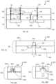
- FIG. 5a cross sectional view of integrated circuit device 400 is set forth.
- the cross-sectional viewis along the line II-II of FIG. 4 .
- Integrated circuit device 400may include a substrate 402 , an insulator layer 422 a N-type IGFET 410 A, and a P-type IGFET 410 B.
- N-type IGFET 410 Amay include a gate contact 416 A, a gate structure 414 A, and vertically aligned and horizontally disposed channel regions 412 A, and gate insulating layer 420 A.
- Gate insulating layer 420 Amay surround each vertically aligned and horizontally disposed channel regions 412 A.
- P-type IGFET 410 Bmay include a gate contact 416 B, a gate structure 414 B, and vertically aligned and horizontally disposed channel regions 412 B, and gate insulating layer 420 B.
- Gate insulating layer 420 Bmay surround each vertically aligned and horizontally disposed channel regions 412 B.
- IGFETS including vertically aligned and horizontally disposed channel region structuresmay be used in internal circuits 140 of FIG. 1 or internal circuits 212 of FIG. 2 and/or interface circuit 150 of FIG. 1 and/or interface circuit 254 of FIG. 2 , for example and ESD protection circuit structures ( 140 , 160 , 170 , 214 , 252 , and/or 256 ) may include diodes, transistors, SCRs and/or resistors formed in substrate 402 .
- FIG. 6a cross sectional view of integrated device 400 is set forth.
- the cross-sectional viewis along the line I-I of FIG. 4 .
- there are two lines I-I as the N-type IGFET 410 A and P-type IGFET 410 Bmay have similar structures except the materials and/or doping of materials may differ and elements are designated with the suffix “A/B” to illustrate such.
- Semiconductor device 400may include a substrate 402 , an insulator layer 422 and N-type and P-type IGFETs ( 410 A/B).
- IGFET 410 A/Bmay include a gate contact 416 A/B, a gate structure 414 A/B, vertically aligned and horizontally disposed channel regions 412 A/B, gate insulating layer 420 A/B, and drain/source contacts 418 A/B.
- Gate structure 416 A/B and gate insulating layer 420 A/Bmay surround each vertically aligned and horizontally disposed channel regions 412 A/B.
- IGFETsmay be formed by forming a layered crystal of two materials over dielectric region 422 .
- layers of silicon and silicon germaniummay be formed.
- An etch and deposit stepmay then be used to form the source/drain regions ( 418 A and 418 B).
- the silicon layermay form the channel regions ( 412 A and 412 B).
- the silicon germanium layersmay be etched by using a chemical that can selectively etch silicon germanium with the source/drain regions ( 418 A and 418 B) used as support structures.
- the gate dielectric layers( 420 A and 420 B) may be formed using atomic layer deposition, for example of hafnium-dioxide.
- gate structure( 416 A and 416 B) may be formed using atomic layer deposition of a metal layer, for example, tungsten.
- the n-type IGFETs 410 Amay have source/drain regions 418 A doped with n-type carriers, such as phosphorous and/or arsenic, for example.
- the p-type IGFETs 410 Bmay have source/drain regions 418 B doped with p-type carriers, such as boron, for example.
- IGFETS including vertically aligned and horizontally disposed channel region structuresmay be used in internal circuits 140 of FIG. 1 or internal circuits 212 of FIG. 2 and/or interface circuits 150 of FIG. 1 and/or interface circuit 254 of FIG. 2 , for example and ESD structures ( 140 , 160 , 170 , 214 , 252 , and/or 256 ) may include diodes, transistors, and/or resistors formed in substrate 402 .
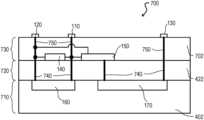
- FIG. 7a schematic diagram of an integrated circuit device according to an embodiment is set forth and given the general reference character 700 .
- Integrated circuit device 700may include similar constituents as integrated circuit device 100 including IGFETs of integrated circuit device 400 , such constituents may be given the same reference character.
- Integrated device 700can include ESD protection circuit structures 160 and 170 formed in a substrate 402 , an internal circuit 140 , and an interface circuit 150 .
- Integrated circuit device 700may include different regions.
- a region 710may include ESD structures ( 160 and 170 ) formed in a semiconductor substrate 402 .
- Another region 720may include an insulator region 422 which may contain wirings 740 .
- Wirings 740may provide an interconnect between ESD structures ( 160 and 170 ) and interface circuit 150 , internal circuit 140 , and/or pads ( 110 , 120 , and 130 ).
- Wirings 740may be in the form of vertical vias that are formed through insulator layer 422 and/or region 720 .
- Another region 730may include internal circuit 140 and interface circuit 150 , as well as wirings 750 , and pads ( 110 , 120 , and 130 ).
- Pad 110may receive an externally provided supply potential (for example VDD).
- Pad 120may receive an externally provided power supply potential (for example VSS), and pad 130 may provide and/or receive an external signal (for example, a data or control signal).
- ESD protection circuit structures ( 160 and 170 ) in region 710may be formed using planar IGFETs, n-type and/or p-type diffusion regions, and silicon control rectifiers (SCR), for example.
- Region 720may include passive elements, such as polysilicon and/or metal resistors, incorporated in ESD protection circuit structures ( 160 and 170 ).
- Internal circuit 140 and interface circuit 150 in region 730may include p-type and n-type IGFETs having a plurality of horizontally disposed channels that can be vertically aligned above substrate 402 .
- Region 730may generally have circuitry comprising p-type and n-type IGFETs having a plurality of horizontally disposed channels that can be vertically aligned above substrate 402 .
- Region 710may include planar IGFETs fabricated using older technologies with more relaxed critical dimensions. In this way, reliable ESD protection circuit structures can be made more cheaply. Another advantage is that the region 730 exclusively has the normal operating circuits (i.e. exclusive of ESD protection circuit structures which only operate when there is an ESD event).
- integrated circuit device 700is a microprocessor
- the central processing unit (CPU), bus, and memorywould all be located in region 730 and manufactured with a cutting-edge state of the art process having smaller critical dimensions.
- ESD structure ( 160 and 170 )below the functional circuits, chip size can be reduced.
- FIG. 8a schematic diagram of an integrated circuit device according to an embodiment is set forth and given the general reference character 800 .
- Integrated circuit device 800may include similar constituents as semiconductor device 200 including IGFETs of integrated circuit device 400 , such constituents may be given the same reference character.
- Integrated circuit device 800can include ESD protection circuit structures ( 214 , 252 , and 256 ) formed in a substrate 402 , an internal circuit 212 , and an interface circuit 254 .
- Integrated circuit device 800may include different regions.
- a region 810may include ESD protection circuit structures ( 214 , 252 , and 256 ) formed in a semiconductor substrate 402 .
- Another region 820may include an insulator region 422 which may contain wirings 840 .
- Wirings 840may provide an interconnect between ESD protection circuit structures ( 214 , 252 , and 256 ) and interface circuit 254 , internal circuit 212 , and/or pads ( 210 , 216 , 250 , 264 , and 266 ).
- Wirings 840may be in the form of vertical vias that are formed through insulator layer 422 and/or region 820 .
- Another region 830may include internal circuit 212 and interface circuit 254 , as well as wirings 850 , and pads ( 210 , 216 , 250 , 264 , and 266 ).
- Internal circuit 212 and ESD protection circuit structure 214may each be electrically connected to pad ( 210 and 216 ).
- Internal circuit 212may receive an input signal at an input terminal 218 and may provide an output signal at an output terminal 220 .
- Pad 210may receive an external power supply potential, such as VDD and pad 216 may receive an external reference potential such as VSS.
- internal circuit 212may be an internal power supply generator and may receive an external power supply potential at pad 216 and may provide an internal power supply potential to be used by internal circuits.
- Pad 250may receive an externally provided supply potential (for example VDD).
- Pad 264may receive an externally provided power supply potential (for example VSS), and pad 266 may provide and/or receive an external signal (for example, a data or control signal).
- ESD protection circuit structures ( 214 , 252 , and 256 ) in region 810may be formed using planar IGFETs, n-type and/or p-type diffusion regions, and silicon control rectifiers (SCR), for example.
- Region 820may include passive elements, such as polysilicon and/or metal resistors, incorporated in ESD structures ( 214 , 252 , and 256 ).
- Internal circuit 212 and interface circuit 254 in region 830may include p-type and n-type IGFETs having a plurality of horizontally disposed channels that can be vertically aligned above substrate 402 .
- Region 830may generally have circuitry comprising p-type and n-type IGFETs having a plurality of horizontally disposed channels that can be vertically aligned above substrate 402 .
- Region 810may include planar IGFETs or FinFETs fabricated using older technologies with more relaxed critical dimensions. In this way, reliable ESD protection circuit structures can be made more cheaply. Another advantage is that the region 830 exclusively has the normal operating circuits (i.e. exclusive of ESD structures which only operate when there is an ESD event).
- semiconductor device 800is a microprocessor
- the central processing unit (CPU), bus, and memorywould all be located in region 830 and manufactured with a cutting edge state of the art process having smaller critical dimensions.
- ESD protection circuit structures214 , 252 , and 256 ) below the functional circuits, chip size can be reduced.
- FIGS. 9 to 11illustrate various ESD protection circuit structures that may be formed in regions ( 710 and 810 ) of FIGS. 7 and 8 .
- ESD structure 900may be a silicon controlled rectifier (SCR).
- ESD structure 900may include bipolar transistors (Q 1 and Q 2 ) and resistors (R 910 and R 920 ).
- Bipolar transistor Q 1may have an emitter terminal connected to a terminal 910 , a base terminal commonly connected to a first terminal of resistor R 920 and a collector terminal of bipolar transistor Q 2 , and a collector terminal commonly connected to a base terminal of bipolar transistor Q 2 and a first terminal of resistor R 910 .
- Bipolar transistor Q 2may have an emitter terminal connected to a terminal 920 .
- Resistor R 910may have a second terminal connected to terminal 920 .
- Resistor R 920may have a second terminal connected to terminal 910 .
- ESD structure 900may be used as ESD protection circuit structures ( 160 , 170 , 214 , 252 , and/or 256 ).
- terminal 910When used as ESD protection circuit structure ( 140 , 214 , or 252 ) terminal 910 may be electrically connected to pads ( 110 , 210 , or 250 ) respectively, and terminal 920 may be electrically connected to pads ( 120 , 216 , or 264 ) respectively.
- ESD protection circuit structure 900is used as ESD protection circuit structure ( 170 or 256 ), terminal 910 may be connected to pads ( 130 or 266 ) respectively and terminal 920 may be electrically connected to pads ( 120 or 264 ) respectively.
- FIG. 10a circuit schematic diagram of an ESD protection circuit structure according to an embodiment is set forth and given the general reference character 1000 .
- ESD protection circuit structure 1000can include diodes (D 1002 and D 1004 ).
- Diode D 1002may have a cathode terminal connected to terminal 1020 and an anode terminal connected to terminal 1010 .
- Diode D 1004may have a cathode terminal connected to terminal 1010 and an anode terminal connected to terminal 1030 .
- ESD protection circuit structure 1000may be used as ESD protection circuit structures ( 170 and 256 ).
- terminal 1020When used as ESD protection circuit structures ( 170 or 256 ), terminal 1020 may be electrically connected to pads ( 110 or 250 ), respectively, terminal 1010 may be electrically connected to pads ( 130 or 266 ), respectively, and terminal 1030 may be electrically connected to pads ( 120 or 264 ), respectively.
- FIG. 11a circuit schematic diagram of an ESD protection circuit structure according to an embodiment is set forth and given the general reference character 1100 .
- ESD structure 1100can include IGFETs (P 1102 and N 1102 ).
- IGFET P 1102may have a source terminal and gate terminal commonly electrically connected to terminal 1120 and drain terminal electrically connected to terminal 1110 .
- IGFET N 1102may have a source terminal and gate terminal commonly electrically connected to terminal 1130 and drain terminal electrically connected to terminal 1110 .
- IGFET P 1102may be a p-type IGFET and IGFET N 1102 may be a n-type IGFET.
- ESD structure 1100may be used as ESD protection circuit structures ( 170 and 256 ).
- terminal 1120When used as ESD protection circuit structures ( 170 or 256 ), terminal 1120 may be electrically connected to pads ( 110 or 250 ), respectively, terminal 1110 may be electrically connected to pads ( 130 or 266 ), respectively, and terminal 1130 may be electrically connected to pads ( 120 or 264 ), respectively.
- FIG. 12a current-voltage diagram of an ESD protection circuit structure is set forth.
- FIG. 12is a current-voltage diagram of a typical ESD protection circuit structure.
- FIG. 12may be a current-voltage (I-V) diagram of SCR 900 of FIG. 9 .
- the current voltage diagram of FIG. 12shows the SCR 900 in a forward blocking region 1202 in which there is minimal leakage current, which occurs when there is no ESD event.
- the SCR 900snaps back through snap back region 1206 toward a minimum holding voltage Vholding at point 1208 .
- the holding region 1210the SCR functions as a near ideal switch, the slope in holding region 1210 represents the on resistance of the SCR 1200 . This slope is proportional to the size of the SCR 1200 , thus a larger SCR 1200 dissipates more current at a lower holding voltage in the holding region.
- the trigger voltage Vtriggeris important to place at a voltage that will be low enough that the IGFETs formed with vertically aligned and horizontally disposed channel regions in regions ( 730 and 830 ) will not breakdown during an ESD event.
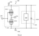
- FIG. 13a circuit schematic diagram of an integrated circuit device according to an embodiment is set forth and given the general reference character 1300 .
- Integrated circuit device 1300can include an ESD protection circuit structure 1310 and an input buffer circuit 1320 .
- ESD protection circuit structure 1310can be electrically connected to receive an input signal at a pad 1304 .
- the input signalmay pass through the ESD protection circuit structure 1310 to terminal 1314 .
- Input buffer circuit 1320may receive the input signal from terminal 1314 and may provide an output signal at terminal 1308 (terminal 1308 may be an output terminal). Input buffer circuit 1320 may receive an enable signal EN at terminal 1322 and a reference potential Vref at terminal 1324 .
- ESD circuit structure 1310can include an ESD protection circuit structure 1312 and a resistor R 1300 .
- ESD protection circuit structure 1312may be electrically connected to pads ( 1302 , 1304 , and 1306 ).
- Pad 1302may receive an externally provided power supply potential, such as VDD.
- Pad 1306receive an externally provided power supply potential, such as VSS.
- Pad 1304may receive an input signal, such as an address, data, and/or control signal, as just a few examples.
- ESD protection circuit structure 1312may be electrically connected to a first terminal of resistor R 1300 .
- Resistor R 1300may be electrically connected to terminal 1314 .
- ESD structure 1312may be an ESD protection circuit structure ( 900 , 1000 , or 1100 ), as just a few examples.
- pad 1304may be electrically connected to terminal ( 910 , 1010 , or 1110 ), respectively.
- Input buffer circuit 1320may include IGFETs (P 1322 , P 1324 , N 1322 , N 1324 , and N 1326 ).
- IGFET P 1322may have a source terminal electrically connected to pad 1302 and commonly coupled to a source terminal of IGFET P 1324 .
- IGFET P 1322may have a gate terminal and a drain terminal commonly connected to a gate terminal of IGFET P 1324 and a drain terminal of IGFET N 1322 .
- IGFET P 1324may have a drain terminal connected to terminal 1308 .
- IGFET N 1322may have a gate terminal coupled to receive a signal at terminal 1314 through ESD circuit structure 1310 .
- IGFET N 1322may have a source terminal commonly connected to a source terminal of IGFET N 1324 and a drain terminal of IGFET N 1326 .
- IGFET N 1324may have a drain terminal connected to terminal 1308 and a gate terminal connected to receive a reference potential Vref at terminal 1324 .
- IGFET N 1326may have a gate terminal connected to receive an enable signal EN at terminal 1322 and a source terminal connected to pad 1306 .
- Input buffer circuit 1320may operate as a differential input buffer that is enabled when enable signal EN is at a logic high level and disabled when enable signal EN is at a logic low level.
- IGFETsmay each include a control gate that may surround a plurality of horizontally disposed channel regions that can be vertically aligned above a substrate as set forth in FIGS. 3 A, 3 B, 4 , 5 , and 6 and may be formed in region ( 702 or 802 ) as set forth in FIGS. 7 and 8 , respectively.
- ESD structure 1312may be formed in regions 402 in FIGS. 7 and 8 , for example.
- Resistor R 1300may be formed in region ( 402 and/or 422 ) in FIGS. 7 and 8 , for example.
- Resistor R 1300may even be formed in region ( 702 or 802 ) as set forth in FIGS. 7 and 8 , respectively. Resistor R 1300 may be formed, for example, as a diffusion layer in region 402 , a metal layer in region 422 , and/or a metal layer in region ( 702 or 802 ) as set forth in FIGS. 7 and 8 , respectively.
- Reference potential Vrefmay provide a threshold voltage for determining the logic level of an input signal received at pad 1304 . For example, if the potential of the input signal received at pad 1304 is greater than reference potential Vref, input buffer circuit 1320 may provide a logic high output at output terminal 1308 . However, if the potential of the input signal received at pad 1304 is less than reference potential Vref, input buffer circuit 1320 may provide a logic low output at output terminal 1308 .
- FIG. 14a circuit schematic diagram of an integrated circuit device according to an embodiment is set forth and given the general reference character 1400 .
- Integrated circuit device 1400can include an ESD protection circuit structure 1410 and an output buffer circuit 1420 .
- ESD circuit structure 1410can be electrically connected to a pad 1404 where an output signal may be provided externally to the integrated circuit device 1400 .
- the output signalmay pass from output buffer 1420 through the ESD circuit structure 1410 to pad 1404 .
- Output buffer circuit 1420may receive an input signal from terminal 1408 and may provide an output signal at terminal 1414
- ESD circuit structure 1420can include an ESD structure 1412 and a resistor R 1400 .
- ESD structure 1412may be electrically connected to pads ( 1402 , 1404 , and 1406 ).
- Pad 1402may receive an externally provided power supply potential, such as VDD.
- Pad 1406receive an externally provided power supply potential, such as VSS.
- Pad 1404may receive a signal to be provided externally from integrated circuit device 1400 .
- ESD protection circuit structure 1412may be electrically connected to a first terminal of resistor R 1400 .
- a second terminal of resistor R 1400may be electrically connected to terminal 1414 .
- ESD protection circuit structure 1412may be an ESD protection circuit structure ( 900 , 1000 , or 1100 ), as just a few examples.
- pad 1404may be electrically connected to terminal ( 910 , 1010 , or 1110 ), respectively.
- Output buffer circuit 1420may include IGFETs (P 1422 and N 1422 ). IGFET P 1422 may have a source terminal electrically connected to pad 1402 . IGFET P 1422 may have a gate terminal and input terminal 1408 and a gate of IGFET N 1422 . IGFET P 1422 may have a drain commonly connected to a drain of IGFET N 1422 and a second terminal of resistor R 1400 at node 1414 . IGFET N 1422 may have a source terminal electrically connected to pad 1406 . Output buffer circuit 1420 may operate as an inverter logic circuit that provides current drive to a signal, such as a data signal or the like that is to be driven to components external to integrated circuit device 1400 .
- a signalsuch as a data signal or the like
- IGFETsmay each include a control gate that may surround a plurality of horizontally disposed channel regions that can be vertically aligned above a substrate as set forth in FIGS. 3 A, 3 B, 4 , 5 , and 6 and may be formed in region ( 702 or 802 ) as set forth in FIGS. 7 and 8 , respectively.
- ESD protection circuit structure 1412may be formed in regions 402 in FIGS. 7 and 8 , for example.
- Resistor R 1400may be formed in region ( 402 and/or 422 ) in FIGS. 7 and 8 , for example. Resistor R 1400 may even be formed in region ( 702 or 802 ) as set forth in FIGS. 7 and 8 , respectively.
- Resistor R 1300may be formed, for example, as a diffusion layer in region 402 , a metal layer in region 422 , and/or a metal layer in region ( 702 or 802 ) as set forth in FIGS. 7 and 8 , respectively.
- Integrated circuit device 1500may include like constituents as integrated circuit device 1400 and such constituents may be designated by the same reference character and for brevity will not be discussed.
- Integrated circuit device 1500may differ from integrated circuit device 1400 of FIG. 14 , in that an output buffer 1520 may have IGFETs (P 1522 and N 1522 ) that are formed in substrate 402 and may be planar IGFETs of FinFETs, while other circuits, such as an internal circuit ( 140 or 212 ) of FIGS.
- IGFETsmay be formed from IGFETs that include a control gate that may surround a plurality of horizontally disposed channel regions that can be vertically aligned above a substrate as set forth in FIGS. 3 A, 3 B, 4 , 5 , and 6 and may be formed in region ( 702 or 802 ) as set forth in FIGS. 7 and 8 , respectively.
- Integrated circuit device 1300 and integrated circuit devices ( 1400 and 1500 )may be incorporated into integrated circuit devices ( 100 and 200 ).
- Integrated circuit device 1300may have a separate pad electrically connected to the input terminal 1304 than a pad electrically connected to the output terminal 1404 of integrated circuit devices ( 1400 and 1500 ).
- Input buffer circuit 1320 and ESD structure 1310 of integrated circuit device 1300may be used as interface circuit 150 and ESD circuit structure 170 of integrated circuit device 100 of FIG. 1 .
- Input buffer circuit 1320 and ESD structure 1310 of integrated circuit device 1300may be used as interface circuit 254 and ESD circuit structure 256 of integrated circuit device 200 of FIG. 2 .
- Output buffer circuit 1420 and ESD structure 1410 of integrated circuit device 1400may be used as interface circuit 150 and ESD circuit structure 170 of integrated circuit device 100 of FIG. 1 .
- Output buffer circuit 1420 and ESD structure 1410 of integrated circuit device 1400may be used as interface circuit 254 and ESD circuit structure 256 of integrated circuit device 200 of FIG. 2 .
- Output buffer circuit 1520 and ESD structure 1510 of integrated circuit device 1500may be used as interface circuit 150 and ESD circuit structure 170 of integrated circuit device 100 of FIG. 1 .
- Output buffer circuit 1520 and ESD structure 1510 of integrated circuit device 1500may be used as interface circuit 254 and ESD circuit structure 256 of integrated circuit device 200 of FIG. 2 .
- FIG. 16a schematic diagram of an integrated circuit device according to an embodiment is set forth and given the general reference character 1600 .
- Integrated circuit device 1600may be like integrated circuit device 700 of FIG. 7 , except integrated circuit device 1600 may include a resistor 1610 formed in region 730 along with the circuitry comprising p-type and n-type IGFETs having a plurality of horizontally disposed channels that can be vertically aligned above semiconductor substrate 402 .
- Resistor 1610may have one terminal electrically connected to pad 130 as well as ESD protection circuit structure 170 and another terminal electrically connected to interface circuit 150 . Resistor 1610 may correspond to resistors R 1400 in integrated circuit devices ( 1400 and 1500 ) as set forth in FIGS. 14 and 15 . Resistor 1610 may comprise a metal, such as copper, tungsten, aluminum, and/or titanium or even polysilicon, as just a few examples.
- FIG. 17a schematic diagram of an integrated circuit device according to an embodiment is set forth and given the general reference character 1700 .
- Integrated circuit device 1700may be like integrated circuit device 700 of FIG. 7 , except integrated circuit device 1700 may include a resistor 1710 formed in region 720 along with wirings 740 .
- Resistor 1710may have one terminal electrically connected to pad 130 as well as ESD protection circuit structure 170 and another terminal electrically connected to interface circuit 150 . Resistor 1710 may correspond to resistors R 1400 in integrated circuit devices ( 1400 and 1500 ) as set forth in FIGS. 14 and 15 . Resistor 1710 may comprise a metal, such as copper, tungsten, aluminum, and/or titanium or even polysilicon, as just a few examples.
- FIG. 18a schematic diagram of an integrated circuit device according to an embodiment is set forth and given the general reference character 1800 .
- Integrated circuit device 1800may be like integrated circuit device 700 of FIG. 7 , except integrated circuit device 1800 may include a resistor 1810 formed in region 710 along with ESD structures ( 160 and 170 ) and planar IGFETs fabricated using older technologies with more relaxed critical dimensions.
- Resistor 1810may have one terminal electrically connected to pad 130 as well as ESD protection circuit structure 170 and another terminal electrically connected to interface circuit 150 . Resistor 1810 may correspond to resistors R 1400 in integrated circuit devices ( 1400 and 1500 ) as set forth in FIGS. 14 and 15 . Resistor 1810 may comprise a metal, such as copper, tungsten, aluminum, and/or titanium, or polysilicon or a diffusion layer, as just a few examples.
- Resistors (R 1300 , R 1400 , 1610 , 1710 , and/or 1810 )need sufficient resistance to provide a voltage drop between the pad 1404 and the interface circuit 150 .
- Resistors (R 1300 and R 1400 )may be about 1 k ⁇ to 10 k ⁇ .
- the process minimum feature size of region 730may be the control gate length of p-type and n-type IGFETs having a plurality of horizontally disposed channels that can be vertically aligned above semiconductor substrate 402 .
- Gate lengthis illustrated with reference to FIG. 6 , in which “L” is the gate length of IGFET 410 A/B. In the embodiments, the minimum gate length may be about 5 nm or less.
- the process minimum feature size of region 402may be substantially greater.
- a gate length of planar IGFETs formed in region 402may be 10 nm or greater.
- An example of a planar IGFETis illustrated in FIG. 19 .
- FIGS. 19a cross-sectional schematic diagram of a planar IGFET that can be formed in region 402 is set forth and given the general reference character 1900 .
- a planar IGFET formed in region 402can include a semiconductor substrate 1902 in which source/drain regions 1918 may be formed, a gate insulating layer 1920 , a control gate 1914 and an insulating layer 1930 .
- Region 402can include p-type IGFETs and n-type IGFETs.
- an n-type IGFETmay be formed by implanting n-type impurities into source/drain regions 1918 of a p-type semiconductor substrate 1902 .
- a p-type IGFETmay be formed by providing a n-type well in semiconductor substrate 1902 and implanting p-type impurities into source/drain regions 1918 .
- Planar IGFETmay have a gate length L 1 of about 10 nm or greater. In this way, cost may be reduced as compared to the fabrication to IGFETs having a plurality of horizontally disposed channels that can be vertically aligned above a substrate with each channel being surrounded by a gate structure as in region 702 .
- the IGFET formed in region 402can be used as IGFETs (P 1522 and N 1522 ) that are formed in substrate 402 as illustrated in FIG. 15 , while other circuits, such as an internal circuit ( 140 or 212 ) of FIGS. 1 and 2 , respectively, may be formed from IGFETs that include a control gate that may surround a plurality of horizontally disposed channel regions that can be vertically aligned above a substrate as set forth in FIGS. 3 A, 3 B, 4 , 5 , and 6 and may be formed in region ( 702 or 802 ) as set forth in FIGS. 7 and 8 , respectively.
- FIGS. 20 A and 20 Ba cross-sectional schematic diagrams of a Fin field effect transistor (FinFET) type IGFET (i.e. FinFET) that can be formed in region 402 is set forth and given the general reference character 2000 .
- FinFETFin field effect transistor
- FIG. 20 Amay be a cross-sectional schematic diagram of a FinFET along the width of a channel region 2016 and FIG. 20 B may be a cross-sectional schematic diagram of a FinFET along the length of a channel region 2016 and between source/drain regions 2018 .
- a FinFET formed in region 402can include a semiconductor substrate 2002 in which source/drain regions 2018 may be formed, a gate insulating layer 2020 , a control gate 2014 and an insulating layer 2030 .
- Region 402can include p-type FinFETs and n-type FinFETs.
- an n-type FinFETmay be formed by implanting n-type impurities into source/drain regions 2018 of a p-type semiconductor substrate 2002 .
- a p-type FinFETmay be formed by providing a n-type well in semiconductor substrate 2002 and implanting p-type impurities into source/drain regions 2018 .
- FinFETmay have a gate length L 2 of about 7 nm or greater. In this way, cost may be reduced as compared to the fabrication to IGFETs having a plurality of horizontally disposed channels that can be vertically aligned above a substrate with each channel being surrounded by a gate structure as in region 702 .
- the FinFET formed in region 402can be used as IGFETs (P 1522 and N 1522 ) that are formed in substrate 402 as illustrated in FIG. 15 , while other circuits, such as an internal circuit ( 140 or 212 ) of FIGS. 1 and 2 , respectively, may be formed from IGFETs that include a control gate that may surround a plurality of horizontally disposed channel regions that can be vertically aligned above a substrate as set forth in FIGS. 3 A, 3 B, 4 , 5 , and 6 and may be formed in region ( 702 or 802 ) as set forth in FIGS. 7 and 8 , respectively.
- FIG. 21a schematic diagram of an integrated circuit device having an ESD protection circuit structure having a plurality of horizontally current carrying regions that can be vertically aligned above a substrate is set forth and given the general reference character 2100 .
- Integrated circuit deviceincludes regions ( 710 , 720 , and 730 ). As noted earlier, region 710 may be formed with a technology node that is older and cheaper than region 730 . Region 710 may include planar IGFETs and ESD structures. However, integrated circuit device 2100 may differ in that an ESD structure may be formed in region 730 and may include diodes (D 2102 and D 2104 ). Diodes (D 2102 and D 2104 ) may include a plurality of horizontally disposed current carrying regions that can be vertically aligned above a substrate region 402 . The current carrying regions may include a first impurity doped region 2112 and a second impurity doped region 2114 .
- Each diodemay include a cathode terminal 2116 and an anode terminal 2118 .
- the anode terminal 2118 of diode D 2102may be electrically connected to the cathode terminal 2116 of diode D 2104 and may be electrically connected to a pad 2110 which may be electrically connected to provide or receive an external signal.
- the cathode terminal 2116 of diode D 2102may be electrically connected to a pad 2120 .
- Pad 2120may receive an externally provided power supply potential, such as VDD.
- the anode terminal 2118 of diode D 2104may be electrically connected to a pad 2130 .
- Pad 2130may receive an externally provided power supply potential, such as VSS.
- the ESD protection circuit structure of FIG. 21 including diodes (D 2102 and D 2104 )may correspond to ESD protection circuit structure 1000 of FIG. 10 and may be used accordingly.
- Pad 2130may correspond to terminal 1030
- pad 2110may correspond to terminal 1010
- pad 2120may correspond to terminal 1020 .
- diode D 2102may correspond to diode D 1002
- diode D 2104may correspond to diode D 1004 .
- Diodesmay be formed by forming a layered crystal of two materials over dielectric region 422 .
- layers of silicon and silicon germaniummay be formed.
- the silicon layermay form the first and second impurity doped regions ( 2112 and 2114 ), i.e. the current carrying regions.
- the silicon germanium layersmay be etched by using a chemical that can selectively etch silicon germanium with the cathode and anode terminals ( 2116 and 2118 ) used as support structures.
- a dielectric layer 2122may be formed using atomic layer deposition of a dielectric, for example, silicon dioxide.
- the first impurity doped region 2112may be doped with n-type carriers, such as phosphorous and/or arsenic, for example.
- the second impurity doped region 2114may be doped with p-type carriers, such as boron, for example.
- the dopingmay be done by implantation with a mask layer over regions other than the desired regions to receive the impurities. In this way each of the plurality of horizontally disposed current carrying regions may form a p-n junction diode in parallel with each other.
- Diodesmay be formed in conjunction with insulated gate field effect transistors (IGFETs) having a plurality of horizontally disposed channels that can be vertically aligned above a substrate with each channel being surrounded by a gate structure as discussed above.
- IGFETsinsulated gate field effect transistors
- FIG. 22a diagram of an integrated circuit device according to an embodiment is set forth and given the general reference character 2100 .
- Integrated circuit device 2200may differ from integrated circuit devices of previous embodiments in that a region 2210 may be disposed between regions ( 720 and 730 ), otherwise integrated circuit device 2200 may be substantially the same as previous embodiments.
- Region 2210may be a crystalline semiconductor layer.
- region 2210may be silicon material.
- Region 2210may be silicon, silicon carbide, epitaxial silicon, as just a few examples.
- Region 2210may improve the manufacturability of layers used to form the horizontally disposed and vertically aligned channel regions.
- Integrated circuit device 2200may include insulated gate field effect transistors (IGFETs) having a plurality of horizontally disposed channels that can be vertically aligned above a substrate with each channel being surrounded by a gate structure formed in region 730 as discussed above, as well as ESD protection circuit structures formed in regions ( 710 , 720 , and 730 ) as discussed in previous embodiments.
- IGFETsinsulated gate field effect transistors
- FIG. 23a circuit schematic diagram of an internal circuit and an ESD protection circuit structure according to an embodiment is set forth and given the general reference character 2300 .
- Circuit 2300can include an internal circuit 2310 and an ESD protection circuit structure 2320 .
- Internal circuit 2300may receive a power supply potential from a pad 2302 .
- the power supply potential from pad 2302may be an externally applied power supply potential such as VDD.
- Internal circuit 2300may receive a power supply potential from a pad 2306 .
- the power supply potential from pad 2306may be an externally supplied power supply potential such as VSS.
- Internal circuitmay receive an input signal from an input terminal 2308 and provide an output signal at a terminal 2314 .
- Internal circuit 2310may include a p-type IGFET P 2312 and an n-type IGFET N 2312 . Both p-type IGFET P 2312 and n-type IGFET N 2312 may each include a plurality of horizontally disposed channels that can be vertically aligned above a substrate with each channel being surrounded by a gate structure.
- P-type IGFET P 2312may have a source terminal electrically connected to pad 2302 .
- N-type IGFET N 2312may have a source terminal electrically connected to pad 2306 .
- P-type IGFET P 2312 and N-type IGFET N 2312may have gate terminals commonly connected to receive the input signal from input terminal 2308 and drain terminals commonly connected to provide the output signal at output terminal 2314 .
- ESD protection circuit structure 2320may be used as ESD protection circuit structure 160 or any/each or ESD circuit structures ( 214 and 252 ) of FIGS. 1 and 2 , respectively.
- Internal circuit 2310may not be electrically connected to receive or provide a signal external to the integrated circuit device.
- ESD protection circuit structure 2320may include two ESD protection circuits, a diode D 2324 and an ESD protection circuit 2322 , each electrically connected between pads ( 2302 and 2306 ). In this way, ESD protection circuit structure 2320 may provide protection for an ESD event at either pad ( 2302 or 2306 ), that receive externally provided power supply potentials.
- ESD protection circuit 2322may be a SCR such as SCR 900 illustrated in FIG. 9 .
- ESD protection circuit 2322can be provided in regions ( 710 or 810 ),
- Diode D 2324can have a cathode terminal electrically connected to pad 2302 and an anode terminal electrically connected to pad 2306 .
- Diode D 2324can be formed in regions ( 710 or 810 ) as a p-n junction or in region ( 730 or 830 ).
- diode D 2324may include a plurality of horizontally current carrying regions that can be vertically aligned above a substrate as illustrated with respect to diodes (D 2104 and D 2102 ) in FIG. 21 .
- Integrated circuit device 2400may have similar circuit constituents as integrated circuit device 200 of FIG. 2 and such constituents may have the same reference character.
- Integrated circuit device 2400may include a first circuit section 202 , a second circuit section 2410 , and a third circuit section 2440 .
- First circuit section 202may include circuits that only have external connections to a power supply potential and/or a ground (VSS) potential.
- Second circuit section 2410may include circuits that have external connections to a power supply potential, a ground potential, and/or a pad coupled to receive an external signal, such as a data signal, control signal or a clock signal, as just a few examples.
- Third circuit section 2440may include circuits that have external connections to a power supply potential, a ground potential, and/or a pad coupled to provide an external signal, such as a data signal, control signal or a clock signal, as just a few examples.
- First circuit section 202may include an internal circuit 212 and an ESD protection circuit structure 214 .
- Internal circuit 212 and ESD structure 214may each be electrically connected to pad ( 210 and 216 ).
- Internal circuit 212may receive an input signal at an input terminal 218 and may provide an output signal at an output terminal 220 .
- Pad 210may receive an external power supply potential, such as VDD and pad 216 may receive an external reference potential such as VSS.
- internal circuit 212may be an internal power supply generator and may receive an external power supply potential at pad 210 and may provide an internal power supply potential to be used by internal circuits.
- the input terminal 218 and the output terminal 220 of internal circuit 212are not electrically connected to any pad that can receive or provide a signal external to the integrated circuit device 200 .
- Second circuit section 2410may include pads ( 2412 , 2414 , and 2416 ), an ESD protection circuit structure 2422 , an input buffer circuit 2420 , and ESD protection circuit structure 2418 .
- Input buffer circuit 2420may receive an external signal at pad 2416 through ESD protection circuit structure 2418 and may provide an internal signal at terminal 2424 .
- Input buffer circuit 2420may be electrically connected to pads ( 2412 and 2414 ).
- Pads ( 2412 and 2414 )may respectively receive an external power supply potential (such as VDD) and a reference potential (such as VSS).
- ESD structure 2422may be electrically connected between pads ( 2412 and 2414 ).
- ESD structure 2418may be electrically connected to pads ( 2412 , 2414 , and 2416 ).
- Third circuit section 2440may include pads ( 2442 , 2444 , and 2446 ), an ESD protection circuit structure 2448 , an output buffer circuit 2450 , and ESD protection circuit structure 2452 .
- Output buffer circuit 2450may receive an internal signal at terminal 2454 and may provide an external signal at pad 2446 through ESD protection circuit structure 2452 .
- Output buffer circuit 2450may be electrically connected to pads ( 2442 and 2444 ).
- Pads ( 2442 and 2444 )may respectively receive an external power supply potential (such as VDD) and a reference potential (such as VSS).
- ESD structure 2448may be electrically connected between pads ( 2442 and 2444 ).
- ESD structure 2452may be electrically connected to pads ( 2442 , 2444 , and 2446 ).
- internal circuit 212may include insulated gate field effect transistors (IGFETs) having a plurality of horizontally disposed channels that can be vertically aligned above a substrate with each channel being surrounded by a gate structure.
- IGFETsinsulated gate field effect transistors
- Input buffer circuit 2420may include insulated gate field effect transistors (IGFETs) having a plurality of horizontally disposed channels that can be vertically aligned above a substrate with each channel being surrounded by a gate structure.
- Output buffer circuit 2452may include insulated gate field effect transistors (IGFETs) having a plurality of horizontally disposed channels that can be vertically aligned above a substrate with each channel being surrounded by a gate structure.
- ESD protection circuit structuresmay include electrical components (such as diodes, transistors, and/or resistors) formed with a plurality of horizontally disposed cathodes and anodes that can be vertically aligned above a substrate.
- ESD protection circuit structuresmay include electrical components (such as diodes, transistors, SCRs and/or resistors) formed in the substrate.
- input buffer circuit 2420 and/or output buffer circuit 2452may include electrical components (such as IGFETs) formed in the substrate.
- ESD protection circuit structures( 214 , 2418 , 2422 , 2448 , and 2452 ) are formed in a semiconductor substrate of integrated circuit device 2400 .
- a process having larger critical dimensionsi.e. an older and cheaper process
- the semiconductor substratemay then be sent to a state of the art fabrication facility to form the circuit including insulated gate field effect transistors (IGFETs) having a plurality of horizontally disposed channels that can be vertically aligned above a substrate with each channel being surrounded by a gate structure as will be discussed further in the instant specification.
- IGFETsinsulated gate field effect transistors
- Integrated circuit device 1300 and integrated circuit devicesmay be incorporated into integrated circuit device 2400 .
- Input buffer circuit 1320 and ESD structure 1310 of integrated circuit device 1300may be used as input circuit 2420 and ESD circuit structure 2418 of integrated circuit device 2400 of FIG. 24 .
- Output buffer circuit 1420 and ESD structure 1410 of integrated circuit device 1400may be used as output buffer circuit 2450 and ESD circuit structure 2452 of integrated circuit device 2400 of FIG. 24 .
- Output buffer circuit 1520 and ESD structure 1510 of integrated circuit device 1500may be used as output buffer circuit 2450 and ESD circuit structure 2452 of integrated circuit device 2400 of FIG. 24 .
- Power supply potentials externally provided to pads ( 210 , 2412 , and 2442 )may be different power supply potentials, such as a first potential (VDD1) for internal circuit 212 , a second potential (VDD2) for input buffer circuit 2420 , and/or a third potential (VDD3) for output buffer circuit 2450 .
- VDD1first potential
- VDD2second potential
- VDD3third potential
- Input buffer 1300 of FIG. 13 and output buffers ( 1400 and 1500 ) of FIGS. 14 and 15may be incorporated into integrated circuit devices 2400 .
- Integrated circuit devicesmay be contiguous structures, such that, regions may be deposited or bonded in a semiconductor fabrication facility and preferably all formed on a contiguous wafer in a multiple of units and then separated before packaged or set in a multi-chip package.
- regions710 , 720 , and 730
- regionsmay be contiguous regions with virtually no separation other than a region border formed by a change of materials.
- region 710may be formed on a first semiconductor wafer and regions ( 720 and 730 ) may be formed on a second semiconductor wafer, then the first and second wafer may be bonded using a wafer to wafer bonding technique followed by dicing and packaging to form the integrated circuit device.
- region 710may be formed on a first semiconductor wafer and regions ( 720 and 730 ) may be formed on a second semiconductor wafer, then the either the first or second wafer may be diced and a die pick and place may be used to place dies on the first or second intact wafer, followed by dicing and packaging to form the integrated circuit device.
- padmay be any circuit connection that is electrically connected to provide or receive a signal or a potential externally to the integrated circuit device.
- a connectioncan be a conduit for an ESD event.
- Electrically connectedcan be a connection through a wiring other passive component such as a resistor.
- a voltagemay be expressed as a potential.
- a signalcan be a data or control signal that can transition between logic levels, as just a few examples.
- a signalis not a power supply potential used to provide power to circuitry.
Landscapes
- Engineering & Computer Science (AREA)
- Microelectronics & Electronic Packaging (AREA)
- Semiconductor Integrated Circuits (AREA)
- Metal-Oxide And Bipolar Metal-Oxide Semiconductor Integrated Circuits (AREA)
Abstract
Description
Claims (20)
Priority Applications (2)
| Application Number | Priority Date | Filing Date | Title |
|---|---|---|---|
| US18/125,465US11973342B2 (en) | 2020-03-18 | 2023-03-23 | ESD protection for integrated circuit devices |
| US18/243,269US12119641B2 (en) | 2020-03-18 | 2023-09-07 | ESD protection for integrated circuit devices |
Applications Claiming Priority (4)
| Application Number | Priority Date | Filing Date | Title |
|---|---|---|---|
| US202062991157P | 2020-03-18 | 2020-03-18 | |
| US17/030,679US11368016B2 (en) | 2020-03-18 | 2020-09-24 | ESD protection for integrated circuit devices |
| US17/726,089US11641105B2 (en) | 2020-03-18 | 2022-04-21 | ESD protection for integrated circuit devices |
| US18/125,465US11973342B2 (en) | 2020-03-18 | 2023-03-23 | ESD protection for integrated circuit devices |
Related Parent Applications (1)
| Application Number | Title | Priority Date | Filing Date |
|---|---|---|---|
| US17/726,089ContinuationUS11641105B2 (en) | 2020-03-18 | 2022-04-21 | ESD protection for integrated circuit devices |
Related Child Applications (1)
| Application Number | Title | Priority Date | Filing Date |
|---|---|---|---|
| US18/243,269ContinuationUS12119641B2 (en) | 2020-03-18 | 2023-09-07 | ESD protection for integrated circuit devices |
Publications (2)
| Publication Number | Publication Date |
|---|---|
| US20230238798A1 US20230238798A1 (en) | 2023-07-27 |
| US11973342B2true US11973342B2 (en) | 2024-04-30 |
Family
ID=77748547
Family Applications (7)
| Application Number | Title | Priority Date | Filing Date |
|---|---|---|---|
| US17/030,662AbandonedUS20210296306A1 (en) | 2020-03-18 | 2020-09-24 | Esd protection for integrated circuit devices |
| US17/030,694Active2041-12-18US11664656B2 (en) | 2020-03-18 | 2020-09-24 | ESD protection for integrated circuit devices |
| US17/030,679ActiveUS11368016B2 (en) | 2020-03-18 | 2020-09-24 | ESD protection for integrated circuit devices |
| US17/726,089ActiveUS11641105B2 (en) | 2020-03-18 | 2022-04-21 | ESD protection for integrated circuit devices |
| US18/125,465Active2040-12-23US11973342B2 (en) | 2020-03-18 | 2023-03-23 | ESD protection for integrated circuit devices |
| US18/135,364Active2041-01-05US12401192B2 (en) | 2020-03-18 | 2023-04-17 | ESD protection for integrated circuit devices |
| US18/243,269ActiveUS12119641B2 (en) | 2020-03-18 | 2023-09-07 | ESD protection for integrated circuit devices |
Family Applications Before (4)
| Application Number | Title | Priority Date | Filing Date |
|---|---|---|---|
| US17/030,662AbandonedUS20210296306A1 (en) | 2020-03-18 | 2020-09-24 | Esd protection for integrated circuit devices |
| US17/030,694Active2041-12-18US11664656B2 (en) | 2020-03-18 | 2020-09-24 | ESD protection for integrated circuit devices |
| US17/030,679ActiveUS11368016B2 (en) | 2020-03-18 | 2020-09-24 | ESD protection for integrated circuit devices |
| US17/726,089ActiveUS11641105B2 (en) | 2020-03-18 | 2022-04-21 | ESD protection for integrated circuit devices |
Family Applications After (2)
| Application Number | Title | Priority Date | Filing Date |
|---|---|---|---|
| US18/135,364Active2041-01-05US12401192B2 (en) | 2020-03-18 | 2023-04-17 | ESD protection for integrated circuit devices |
| US18/243,269ActiveUS12119641B2 (en) | 2020-03-18 | 2023-09-07 | ESD protection for integrated circuit devices |
Country Status (1)
| Country | Link |
|---|---|
| US (7) | US20210296306A1 (en) |
Families Citing this family (5)
| Publication number | Priority date | Publication date | Assignee | Title |
|---|---|---|---|---|
| CN107910858B (en)* | 2017-12-07 | 2020-09-18 | 长鑫存储技术有限公司 | Low-voltage electrostatic protection circuit, chip circuit and electrostatic protection method thereof |
| US20210296306A1 (en) | 2020-03-18 | 2021-09-23 | Mavagail Technology, LLC | Esd protection for integrated circuit devices |
| US11855076B2 (en)* | 2021-01-15 | 2023-12-26 | Taiwan Semiconductor Manufacturing Co., Ltd. | Electrostatic discharge (ESD) array with back end of line (BEOL) connection in a carrier wafer |
| US11862625B2 (en)* | 2021-07-01 | 2024-01-02 | Nxp Usa, Inc. | Area-efficient ESD protection inside standard cells |
| US11972793B2 (en) | 2021-09-15 | 2024-04-30 | Mavagail Technology, LLC | Integrated circuit device including an SRAM portion having end power select circuits |
Citations (57)
| Publication number | Priority date | Publication date | Assignee | Title |
|---|---|---|---|---|
| US5610425A (en)* | 1995-02-06 | 1997-03-11 | Motorola, Inc. | Input/output electrostatic discharge protection circuit for an integrated circuit |
| US5910873A (en)* | 1997-02-19 | 1999-06-08 | National Semiconductor Corporation | Field oxide transistor based feedback circuit for electrical overstress protection |
| US6388850B1 (en)* | 1999-01-04 | 2002-05-14 | Taiwan Semiconductor Manufacturing Co., Ltd. | Gate-coupled ESD protection circuit without transient leakage |
| US20020109153A1 (en)* | 2001-02-15 | 2002-08-15 | Ming-Dou Ker | Silicon-on-insulator diodes and ESD protection circuits |
| US6535368B2 (en) | 1999-06-03 | 2003-03-18 | Texas Instruments Incorporated | Shared 5 volt tolerant ESD protection circuit for low voltage CMOS process |
| US20030107856A1 (en)* | 2001-12-11 | 2003-06-12 | Chien-Chang Huang | ESD protection circuit |
| US20040256675A1 (en) | 2003-06-17 | 2004-12-23 | Infineon Technologies North America Corp. | Electro-static discharge protection circuit and method for making the same |
| US20050173765A1 (en)* | 2004-02-06 | 2005-08-11 | Magnachip Semiconductor, Ltd. | Device for electrostatic discharge protection and circuit thereof |
| US20050247979A1 (en) | 2004-04-30 | 2005-11-10 | Greg Fung | ESD protection structure with SiGe BJT devices |
| US20090067104A1 (en)* | 2007-09-10 | 2009-03-12 | Stockinger Michael A | Electrostatic discharge circuit and method therefor |
| US20090278251A1 (en) | 2008-05-12 | 2009-11-12 | Taiwan Semiconductor Manufacturing Co., Ltd. | Pad Structure for 3D Integrated Circuit |
| US20090289304A1 (en) | 2006-04-07 | 2009-11-26 | Koninklijke Philips Electronics Nv | Co-integration of multi-gate fet with other fet devices in cmos technology |
| US20100103570A1 (en)* | 2008-10-27 | 2010-04-29 | Ming-Hsiang Song | Circuit and Method for Power Clamp Triggered Dual SCR ESD Protection |
| US20100157494A1 (en)* | 2008-12-24 | 2010-06-24 | Kim Sang-Kyung | Electrostatic discharge protection circuit |
| US20100328826A1 (en)* | 2009-06-24 | 2010-12-30 | Salman Akram A | Field Effect Resistor for ESD Protection |
| US20120162836A1 (en) | 2010-12-22 | 2012-06-28 | Hitachi, Ltd. | Semiconductor device |
| RU2467431C1 (en)* | 2011-04-12 | 2012-11-20 | Открытое акционерное общество "АНГСТРЕМ" | Device for protecting leads of complementary mos (metal-oxide-semiconductor) integrated circuits on sos (silicon-on-sapphire) and soi (silicon-on-insulator) structures from static electric discharges |
| US20130120885A1 (en)* | 2011-11-15 | 2013-05-16 | Mansour Keramat | LOW NOISE ESD PROTECTION FOR SOCs WITH ANALOG OR RADIO FREQUENCY DEVICES |
| US20130278301A1 (en)* | 2012-04-23 | 2013-10-24 | Active-Semi, Inc. | Power Management Integrated Circuit for Driving Inductive Loads |
| US20130294170A1 (en) | 2012-05-04 | 2013-11-07 | Elpida Memory, Inc. | Switch and semiconductor device including the switch |
| US20140268444A1 (en)* | 2013-03-15 | 2014-09-18 | Nantero Inc. | Electrostatic discharge protection circuits using carbon nanotube field effect transistor (cntfet) devices and methods of making same |
| US9219005B2 (en) | 2011-06-28 | 2015-12-22 | Monolithic 3D Inc. | Semiconductor system and device |
| US9373612B1 (en)* | 2013-05-31 | 2016-06-21 | Altera Corporation | Electrostatic discharge protection circuits and methods |
| US9385527B2 (en)* | 2013-06-05 | 2016-07-05 | Globalfoundries Inc. | Enhanced charge device model clamp |
| CN106024793A (en) | 2015-03-26 | 2016-10-12 | 三重富士通半导体股份有限公司 | Semiconductor device |
| US20160372920A1 (en) | 2015-06-18 | 2016-12-22 | Navitas Semiconductor, Inc. | Integrated esd protection circuits in gan |
| US20170200785A1 (en)* | 2016-01-11 | 2017-07-13 | Semiconductor Components Industries, Llc | Semiconductor device having self-isolating bulk substrate and method therefor |
| US9711500B1 (en) | 2016-02-16 | 2017-07-18 | Darryl G. Walker | Package including a plurality of stacked semiconductor devices having area efficient ESD protection |
| US9871034B1 (en) | 2012-12-29 | 2018-01-16 | Monolithic 3D Inc. | Semiconductor device and structure |
| US20180082992A1 (en)* | 2016-09-22 | 2018-03-22 | Freescale Semiconductor, Inc. | Integrated circuit with protection from transient electrical stress events and method therefor |
| US20180138289A1 (en) | 2015-06-27 | 2018-05-17 | Intel Corporation | Ge nano wire transistor with gaas as the sacrificial layer |
| US20180212023A1 (en) | 2015-09-24 | 2018-07-26 | Intel Corporation | Hybrid trigate and nanowire cmos device architecture |
| US20180219007A1 (en) | 2017-02-01 | 2018-08-02 | Indian Institute Of Science | Low trigger and holding voltage silicon controlled rectifier (scr) for non-planar technologies |
| US20180247929A1 (en) | 2017-02-25 | 2018-08-30 | Indian Institute Of Science | Semiconductor devices and methods to enhance electrostatic discharge (esd) robustness, latch-up, and hot carrier immunity |
| WO2018190881A1 (en) | 2017-04-15 | 2018-10-18 | Intel IP Corporation | Multi-drain esd-robust transistor arrangements |
| US20190074297A1 (en) | 2016-05-06 | 2019-03-07 | Socionext Inc. | Semiconductor integrated circuit device |
| US10290626B1 (en) | 2018-01-12 | 2019-05-14 | Globalfoundries Inc. | High voltage electrostatic discharge (ESD) bipolar integrated in a vertical field-effect transistor (VFET) technology and method for producing the same |
| US20190165186A1 (en) | 2016-08-01 | 2019-05-30 | Socionext Inc. | Semiconductor chip |
| US10354995B2 (en) | 2009-10-12 | 2019-07-16 | Monolithic 3D Inc. | Semiconductor memory device and structure |
| US20200168715A1 (en) | 2018-11-28 | 2020-05-28 | Taiwan Semiconductor Manufacturing Company, Ltd. | Gate-All-Around (GAA) Method and Devices |
| US20200295127A1 (en) | 2019-03-13 | 2020-09-17 | Intel Corporation | Stacked transistors with different crystal orientations in different device strata |
| US20200312960A1 (en) | 2019-03-29 | 2020-10-01 | Intel Corporation | Gate-all-around integrated circuit structures having embedded gesnb source or drain structures |
| US20200343387A1 (en) | 2019-04-24 | 2020-10-29 | Taiwan Semiconductor Manufacturing Co., Ltd. | Semiconductor Structure Having Both Gate-All-Around Devices and Planar Devices |
| US20200403007A1 (en) | 2019-06-20 | 2020-12-24 | Intel Corporation | Substrate-less finfet diode architectures with backside metal contact and subfin regions |
| US20210118882A1 (en)* | 2019-10-18 | 2021-04-22 | Taiwan Semiconductor Manufacturing Co., Ltd. | Structure and method of integrated circuit having decouple capacitance |
| US20210225839A1 (en) | 2020-01-16 | 2021-07-22 | Taiwan Semiconductor Manufacturing Co., Ltd. | Semiconductor Devices Having Gate Dielectric Layers of Varying Thicknesses and Methods of Forming the Same |
| US20210242220A1 (en)* | 2015-05-26 | 2021-08-05 | Semiconductor Energy Laboratory Co., Ltd. | Semiconductor device |
| US20210296306A1 (en) | 2020-03-18 | 2021-09-23 | Mavagail Technology, LLC | Esd protection for integrated circuit devices |
| US20210305436A1 (en) | 2020-03-25 | 2021-09-30 | Intel Corporation | Gate-all-around integrated circuit structures including varactors |
| US11145657B1 (en) | 2014-01-28 | 2021-10-12 | Monolithic 3D Inc. | 3D semiconductor device and structure |
| US20210366846A1 (en) | 2020-05-21 | 2021-11-25 | Taiwan Semiconductor Manufacturing Company Ltd. | Electrostatic discharge circuit and method of forming the same |
| US20210384188A1 (en) | 2020-06-09 | 2021-12-09 | Samsung Electronics Co., Ltd. | Electrostatic discharge device and electrostatic discharge protection circuit including the same |
| US20210391320A1 (en) | 2020-06-15 | 2021-12-16 | Taiwan Semiconductor Manufacturing Co., Ltd. | Forming ESD Devices Using Multi-Gate Compatible Processes |
| US20210408285A1 (en) | 2020-06-26 | 2021-12-30 | Intel Corporation | Gate-all-around integrated circuit structures having germanium-doped nanoribbon channel structures |
| US20220044104A1 (en) | 2019-12-16 | 2022-02-10 | Tencent Technology (Shenzhen) Company Limited | Method and apparatus for forward computation of neural network, and computer-readable storage medium |
| US20220328411A1 (en) | 2013-03-12 | 2022-10-13 | Monolithic 3D Inc. | 3d semiconductor device and structure |
| US11594618B2 (en) | 2016-11-29 | 2023-02-28 | Taiwan Semiconductor Manufacturing Company, Ltd. | FinFET devices and methods of forming |
Family Cites Families (85)
| Publication number | Priority date | Publication date | Assignee | Title |
|---|---|---|---|---|
| JP2770784B2 (en)* | 1995-05-31 | 1998-07-02 | 日本電気株式会社 | Silicon-on-insulator semiconductor device |
| CN1998120A (en)* | 2004-06-08 | 2007-07-11 | 沙诺夫公司 | Method and apparatus for providing current controlled electrostatic discharge protection |
| KR100555567B1 (en) | 2004-07-30 | 2006-03-03 | 삼성전자주식회사 | Method of manufacturing multi-crosslink channel transistor |
| US7242564B2 (en)* | 2004-10-20 | 2007-07-10 | Toppoly Optoelectronics Corporation | ESD protection circuit for charge pump and electronic device and system using the same |
| FR2884648B1 (en) | 2005-04-13 | 2007-09-07 | Commissariat Energie Atomique | STRUCTURE AND METHOD FOR PRODUCING A MICROELECTRONIC DEVICE HAVING ONE OR MORE QUANTUM THREADS FOR FORMING A CHANNEL OR MORE CHANNELS OF TRANSISTORS |
| DE102005039365B4 (en) | 2005-08-19 | 2022-02-10 | Infineon Technologies Ag | Gate-controlled fin resistive element operating as a pinch - resistor for use as an ESD protection element in an electrical circuit and a device for protecting against electrostatic discharges in an electrical circuit |
| FR2895835B1 (en) | 2005-12-30 | 2008-05-09 | Commissariat Energie Atomique | ACHIEVING A MULTI-BRANCH CHANNEL STRUCTURE OF A TRANSISTOR GRID AND MEANS FOR ISOLATING THIS GRID FROM THE SOURCE AND DRAIN REGIONS |
| US7687859B2 (en) | 2007-09-07 | 2010-03-30 | Infineon Technologies Ag | Electronic circuit and method of manufacturing an electronic circuit |
| FR2923646A1 (en) | 2007-11-09 | 2009-05-15 | Commissariat Energie Atomique | MEMORY CELL SRAM WITH TRANSISTORS WITH VERTICAL MULTI-CHANNEL STRUCTURE |
| JP2010041013A (en)* | 2008-08-08 | 2010-02-18 | Oki Semiconductor Co Ltd | Protection circuit |
| US10366970B2 (en) | 2009-10-12 | 2019-07-30 | Monolithic 3D Inc. | 3D semiconductor device and structure |
| US9438031B2 (en) | 2012-02-29 | 2016-09-06 | Freescale Semiconductor, Inc. | Electrostatic discharge protection circuit arrangement, electronic circuit and ESD protection method |
| US10515935B2 (en) | 2012-12-22 | 2019-12-24 | Monolithic 3D Inc. | 3D semiconductor device and structure |
| US9385058B1 (en) | 2012-12-29 | 2016-07-05 | Monolithic 3D Inc. | Semiconductor device and structure |
| US9431529B2 (en) | 2014-09-08 | 2016-08-30 | Samsung Electronics Co., Ltd. | Confined semi-metal field effect transistor |
| WO2016099580A2 (en) | 2014-12-23 | 2016-06-23 | Lupino James John | Three dimensional integrated circuits employing thin film transistors |
| CN107408533B (en) | 2015-06-19 | 2022-02-08 | 瑞萨电子株式会社 | Semiconductor device |
| US9614068B2 (en) | 2015-09-02 | 2017-04-04 | Samsung Electronics Co., Ltd. | Semiconductor device and method of fabricating the same |
| US10790281B2 (en) | 2015-12-03 | 2020-09-29 | Intel Corporation | Stacked channel structures for MOSFETs |
| US10672868B2 (en) | 2015-12-24 | 2020-06-02 | Intel Corporation | Methods of forming self aligned spacers for nanowire device structures |
| US9755017B1 (en) | 2016-03-01 | 2017-09-05 | International Business Machines Corporation | Co-integration of silicon and silicon-germanium channels for nanosheet devices |
| US10304936B2 (en) | 2016-05-04 | 2019-05-28 | International Business Machines Corporation | Protection of high-K dielectric during reliability anneal on nanosheet structures |
| US10411006B2 (en)* | 2016-05-09 | 2019-09-10 | Infineon Technologies Ag | Poly silicon based interface protection |
| US10332986B2 (en) | 2016-08-22 | 2019-06-25 | International Business Machines Corporation | Formation of inner spacer on nanosheet MOSFET |
| US9653464B1 (en) | 2016-09-14 | 2017-05-16 | International Business Machines Corporation | Asymmetric band gap junctions in narrow band gap MOSFET |
| US10032793B2 (en) | 2016-09-16 | 2018-07-24 | International Business Machines Corporation | Asymmetric junction engineering for narrow band gap MOSFET |
| KR102698026B1 (en) | 2016-09-28 | 2024-08-21 | 삼성전자주식회사 | Method for forming dielectric layer and Method for fabricating semiconductor device |
| US9842835B1 (en) | 2016-10-10 | 2017-12-12 | International Business Machines Corporation | High density nanosheet diodes |
| US10600638B2 (en) | 2016-10-24 | 2020-03-24 | International Business Machines Corporation | Nanosheet transistors with sharp junctions |
| US10410931B2 (en) | 2017-01-09 | 2019-09-10 | Samsung Electronics Co., Ltd. | Fabricating method of nanosheet transistor spacer including inner spacer |
| US9935014B1 (en) | 2017-01-12 | 2018-04-03 | International Business Machines Corporation | Nanosheet transistors having different gate dielectric thicknesses on the same chip |
| US10049882B1 (en) | 2017-01-25 | 2018-08-14 | Samsung Electronics Co., Ltd. | Method for fabricating semiconductor device including forming a dielectric layer on a structure having a height difference using ALD |
| US10050107B1 (en) | 2017-02-13 | 2018-08-14 | International Business Machines Corporation | Nanosheet transistors on bulk material |
| US9847390B1 (en) | 2017-02-16 | 2017-12-19 | Globalfoundries Inc. | Self-aligned wrap-around contacts for nanosheet devices |
| US10319813B2 (en) | 2017-03-27 | 2019-06-11 | International Business Machines Corporation | Nanosheet CMOS transistors |
| US10297664B2 (en) | 2017-04-13 | 2019-05-21 | Globalfoundries Inc. | Nanosheet transistor with uniform effective gate length |
| US10103065B1 (en) | 2017-04-25 | 2018-10-16 | International Business Machines Corporation | Gate metal patterning for tight pitch applications |
| US10410933B2 (en) | 2017-05-23 | 2019-09-10 | Globalfoundries Inc. | Replacement metal gate patterning for nanosheet devices |
| US10074575B1 (en) | 2017-06-21 | 2018-09-11 | International Business Machines Corporation | Integrating and isolating nFET and pFET nanosheet transistors on a substrate |
| US10109533B1 (en) | 2017-06-29 | 2018-10-23 | Globalfoundries Inc. | Nanosheet devices with CMOS epitaxy and method of forming |
| US9947804B1 (en) | 2017-07-24 | 2018-04-17 | Globalfoundries Inc. | Methods of forming nanosheet transistor with dielectric isolation of source-drain regions and related structure |
| US10546942B2 (en) | 2017-07-25 | 2020-01-28 | International Business Machines Corporation | Nanosheet transistor with optimized junction and cladding defectivity control |
| US10290549B2 (en) | 2017-09-05 | 2019-05-14 | Globalfoundries Inc. | Integrated circuit structure, gate all-around integrated circuit structure and methods of forming same |
| US10553495B2 (en) | 2017-10-19 | 2020-02-04 | International Business Machines Corporation | Nanosheet transistors with different gate dielectrics and workfunction metals |
| US10243061B1 (en) | 2017-11-15 | 2019-03-26 | International Business Machines Corporation | Nanosheet transistor |
| US10229971B1 (en) | 2017-11-16 | 2019-03-12 | International Business Machines Corporation | Integration of thick and thin nanosheet transistors on a single chip |
| US10714391B2 (en) | 2017-12-04 | 2020-07-14 | Tokyo Electron Limited | Method for controlling transistor delay of nanowire or nanosheet transistor devices |
| US10418493B2 (en) | 2017-12-19 | 2019-09-17 | International Business Machines Corporation | Tight pitch stack nanowire isolation |
| US10439049B2 (en) | 2017-12-19 | 2019-10-08 | International Business Machines Corporation | Nanosheet device with close source drain proximity |
| US10539528B2 (en) | 2017-12-19 | 2020-01-21 | International Business Machines Corporation | Stacked nanofluidics structure |
| US10381068B2 (en) | 2017-12-20 | 2019-08-13 | International Business Machines Corporation | Ultra dense and stable 4T SRAM cell design having NFETs and PFETs |
| US10374089B2 (en) | 2017-12-22 | 2019-08-06 | International Business Machines Corporation | Tensile strain in NFET channel |
| US10622208B2 (en) | 2017-12-22 | 2020-04-14 | International Business Machines Corporation | Lateral semiconductor nanotube with hexagonal shape |
| US10600889B2 (en) | 2017-12-22 | 2020-03-24 | International Business Machines Corporation | Nanosheet transistors with thin inner spacers and tight pitch gate |
| US10418449B2 (en) | 2018-01-10 | 2019-09-17 | Globalfoundries Inc. | Circuits based on complementary field-effect transistors |
| US10535733B2 (en) | 2018-01-11 | 2020-01-14 | International Business Machines Corporation | Method of forming a nanosheet transistor |
| KR102620595B1 (en)* | 2018-01-22 | 2024-01-03 | 삼성전자주식회사 | Semiconductor device including insulating layers and method of manufacturing the same |
| US10424651B2 (en) | 2018-01-26 | 2019-09-24 | International Business Machines Corporation | Forming nanosheet transistor using sacrificial spacer and inner spacers |
| US10756613B2 (en) | 2018-02-01 | 2020-08-25 | Marvell Asia Pte, Ltd. | Controlling current flow between nodes with adjustable back-gate voltage |
| US10734525B2 (en) | 2018-03-14 | 2020-08-04 | Globalfoundries Inc. | Gate-all-around transistor with spacer support and methods of forming same |
| US10263100B1 (en) | 2018-03-19 | 2019-04-16 | International Business Machines Corporation | Buffer regions for blocking unwanted diffusion in nanosheet transistors |
| US10446664B1 (en) | 2018-03-20 | 2019-10-15 | International Business Machines Corporation | Inner spacer formation and contact resistance reduction in nanosheet transistors |
| US10566438B2 (en) | 2018-04-02 | 2020-02-18 | International Business Machines Corporation | Nanosheet transistor with dual inner airgap spacers |
| US10566445B2 (en) | 2018-04-03 | 2020-02-18 | International Business Machines Corporation | Gate spacer and inner spacer formation for nanosheet transistors having relatively small space between gates |
| US10243054B1 (en) | 2018-04-03 | 2019-03-26 | International Business Machines Corporation | Integrating standard-gate and extended-gate nanosheet transistors on the same substrate |
| US10381273B1 (en) | 2018-04-11 | 2019-08-13 | International Business Machines Corporation | Vertically stacked multi-channel transistor structure |
| US10424639B1 (en) | 2018-04-19 | 2019-09-24 | International Business Machines Corporation | Nanosheet transistor with high-mobility channel |
| US10431651B1 (en) | 2018-04-30 | 2019-10-01 | International Business Machines Corporation | Nanosheet transistor with robust source/drain isolation from substrate |
| US10388646B1 (en) | 2018-06-04 | 2019-08-20 | Sandisk Technologies Llc | Electrostatic discharge protection devices including a field-induced switching element |
| US10332809B1 (en) | 2018-06-21 | 2019-06-25 | International Business Machines Corporation | Method and structure to introduce strain in stack nanosheet field effect transistor |
| US10490559B1 (en) | 2018-06-27 | 2019-11-26 | International Business Machines Corporation | Gate formation scheme for nanosheet transistors having different work function metals and different nanosheet width dimensions |
| US10283516B1 (en) | 2018-06-27 | 2019-05-07 | International Business Machines Corporation | Stacked nanosheet field effect transistor floating-gate EEPROM cell and array |
| US10615256B2 (en) | 2018-06-27 | 2020-04-07 | International Business Machines Corporation | Nanosheet transistor gate structure having reduced parasitic capacitance |
| US10692866B2 (en) | 2018-07-16 | 2020-06-23 | International Business Machines Corporation | Co-integrated channel and gate formation scheme for nanosheet transistors having separately tuned threshold voltages |
| US10679906B2 (en) | 2018-07-17 | 2020-06-09 | International Business Machines Corporation | Method of forming nanosheet transistor structures with reduced parasitic capacitance and improved junction sharpness |
| US10410927B1 (en) | 2018-07-23 | 2019-09-10 | International Business Machines Corporation | Method and structure for forming transistors with high aspect ratio gate without patterning collapse |
| US10643899B2 (en) | 2018-07-27 | 2020-05-05 | International Business Machines Corporation | Gate stack optimization for wide and narrow nanosheet transistor devices |
| US10734523B2 (en) | 2018-08-13 | 2020-08-04 | International Business Machines Corporation | Nanosheet substrate to source/drain isolation |
| US10615257B2 (en) | 2018-09-07 | 2020-04-07 | International Business Machines Corporation | Patterning method for nanosheet transistors |
| US10756175B2 (en) | 2018-09-18 | 2020-08-25 | International Business Machines Corporation | Inner spacer formation and contact resistance reduction in nanosheet transistors |
| US10680107B2 (en) | 2018-09-24 | 2020-06-09 | International Business Machines Corporation | Nanosheet transistor with stable structure |
| US20200194577A1 (en) | 2018-12-13 | 2020-06-18 | Intel Corporation | Gan based hemt device relaxed buffer structure on silicon |
| EP3675167B1 (en) | 2018-12-28 | 2021-06-09 | IMEC vzw | A semiconductor device and a method for forming a semiconductor device |
| US10734286B1 (en) | 2019-02-07 | 2020-08-04 | International Business Machines Corporation | Multiple dielectrics for gate-all-around transistors |
| US10665669B1 (en) | 2019-02-26 | 2020-05-26 | Globalfoundries Inc. | Insulative structure with diffusion break integral with isolation layer and methods to form same |
- 2020
- 2020-09-24USUS17/030,662patent/US20210296306A1/ennot_activeAbandoned
- 2020-09-24USUS17/030,694patent/US11664656B2/enactiveActive
- 2020-09-24USUS17/030,679patent/US11368016B2/enactiveActive
- 2022
- 2022-04-21USUS17/726,089patent/US11641105B2/enactiveActive
- 2023
- 2023-03-23USUS18/125,465patent/US11973342B2/enactiveActive
- 2023-04-17USUS18/135,364patent/US12401192B2/enactiveActive
- 2023-09-07USUS18/243,269patent/US12119641B2/enactiveActive
Patent Citations (60)
| Publication number | Priority date | Publication date | Assignee | Title |
|---|---|---|---|---|
| US5610425A (en)* | 1995-02-06 | 1997-03-11 | Motorola, Inc. | Input/output electrostatic discharge protection circuit for an integrated circuit |
| US5910873A (en)* | 1997-02-19 | 1999-06-08 | National Semiconductor Corporation | Field oxide transistor based feedback circuit for electrical overstress protection |
| US6388850B1 (en)* | 1999-01-04 | 2002-05-14 | Taiwan Semiconductor Manufacturing Co., Ltd. | Gate-coupled ESD protection circuit without transient leakage |
| US6535368B2 (en) | 1999-06-03 | 2003-03-18 | Texas Instruments Incorporated | Shared 5 volt tolerant ESD protection circuit for low voltage CMOS process |
| US20020109153A1 (en)* | 2001-02-15 | 2002-08-15 | Ming-Dou Ker | Silicon-on-insulator diodes and ESD protection circuits |
| US20030107856A1 (en)* | 2001-12-11 | 2003-06-12 | Chien-Chang Huang | ESD protection circuit |
| US20040256675A1 (en) | 2003-06-17 | 2004-12-23 | Infineon Technologies North America Corp. | Electro-static discharge protection circuit and method for making the same |
| US20050173765A1 (en)* | 2004-02-06 | 2005-08-11 | Magnachip Semiconductor, Ltd. | Device for electrostatic discharge protection and circuit thereof |
| US20050247979A1 (en) | 2004-04-30 | 2005-11-10 | Greg Fung | ESD protection structure with SiGe BJT devices |
| US20090289304A1 (en) | 2006-04-07 | 2009-11-26 | Koninklijke Philips Electronics Nv | Co-integration of multi-gate fet with other fet devices in cmos technology |
| US20090067104A1 (en)* | 2007-09-10 | 2009-03-12 | Stockinger Michael A | Electrostatic discharge circuit and method therefor |
| US20090278251A1 (en) | 2008-05-12 | 2009-11-12 | Taiwan Semiconductor Manufacturing Co., Ltd. | Pad Structure for 3D Integrated Circuit |
| US20100103570A1 (en)* | 2008-10-27 | 2010-04-29 | Ming-Hsiang Song | Circuit and Method for Power Clamp Triggered Dual SCR ESD Protection |
| US20100157494A1 (en)* | 2008-12-24 | 2010-06-24 | Kim Sang-Kyung | Electrostatic discharge protection circuit |
| US20100328826A1 (en)* | 2009-06-24 | 2010-12-30 | Salman Akram A | Field Effect Resistor for ESD Protection |
| US10354995B2 (en) | 2009-10-12 | 2019-07-16 | Monolithic 3D Inc. | Semiconductor memory device and structure |
| US20120162836A1 (en) | 2010-12-22 | 2012-06-28 | Hitachi, Ltd. | Semiconductor device |
| RU2467431C1 (en)* | 2011-04-12 | 2012-11-20 | Открытое акционерное общество "АНГСТРЕМ" | Device for protecting leads of complementary mos (metal-oxide-semiconductor) integrated circuits on sos (silicon-on-sapphire) and soi (silicon-on-insulator) structures from static electric discharges |
| US9219005B2 (en) | 2011-06-28 | 2015-12-22 | Monolithic 3D Inc. | Semiconductor system and device |
| US20130120885A1 (en)* | 2011-11-15 | 2013-05-16 | Mansour Keramat | LOW NOISE ESD PROTECTION FOR SOCs WITH ANALOG OR RADIO FREQUENCY DEVICES |
| US20130278301A1 (en)* | 2012-04-23 | 2013-10-24 | Active-Semi, Inc. | Power Management Integrated Circuit for Driving Inductive Loads |
| US20130294170A1 (en) | 2012-05-04 | 2013-11-07 | Elpida Memory, Inc. | Switch and semiconductor device including the switch |
| US9871034B1 (en) | 2012-12-29 | 2018-01-16 | Monolithic 3D Inc. | Semiconductor device and structure |
| US20220328411A1 (en) | 2013-03-12 | 2022-10-13 | Monolithic 3D Inc. | 3d semiconductor device and structure |
| US20140268444A1 (en)* | 2013-03-15 | 2014-09-18 | Nantero Inc. | Electrostatic discharge protection circuits using carbon nanotube field effect transistor (cntfet) devices and methods of making same |
| US9373612B1 (en)* | 2013-05-31 | 2016-06-21 | Altera Corporation | Electrostatic discharge protection circuits and methods |
| US9385527B2 (en)* | 2013-06-05 | 2016-07-05 | Globalfoundries Inc. | Enhanced charge device model clamp |
| US11145657B1 (en) | 2014-01-28 | 2021-10-12 | Monolithic 3D Inc. | 3D semiconductor device and structure |
| CN106024793A (en) | 2015-03-26 | 2016-10-12 | 三重富士通半导体股份有限公司 | Semiconductor device |
| CN106024793B (en) | 2015-03-26 | 2019-02-22 | 三重富士通半导体股份有限公司 | Semiconductor device |
| US20210242220A1 (en)* | 2015-05-26 | 2021-08-05 | Semiconductor Energy Laboratory Co., Ltd. | Semiconductor device |
| US20160372920A1 (en) | 2015-06-18 | 2016-12-22 | Navitas Semiconductor, Inc. | Integrated esd protection circuits in gan |
| US20180138289A1 (en) | 2015-06-27 | 2018-05-17 | Intel Corporation | Ge nano wire transistor with gaas as the sacrificial layer |
| US20180212023A1 (en) | 2015-09-24 | 2018-07-26 | Intel Corporation | Hybrid trigate and nanowire cmos device architecture |
| US20170200785A1 (en)* | 2016-01-11 | 2017-07-13 | Semiconductor Components Industries, Llc | Semiconductor device having self-isolating bulk substrate and method therefor |
| US9711500B1 (en) | 2016-02-16 | 2017-07-18 | Darryl G. Walker | Package including a plurality of stacked semiconductor devices having area efficient ESD protection |
| US20190074297A1 (en) | 2016-05-06 | 2019-03-07 | Socionext Inc. | Semiconductor integrated circuit device |
| US20190165186A1 (en) | 2016-08-01 | 2019-05-30 | Socionext Inc. | Semiconductor chip |
| US20180082992A1 (en)* | 2016-09-22 | 2018-03-22 | Freescale Semiconductor, Inc. | Integrated circuit with protection from transient electrical stress events and method therefor |
| US11594618B2 (en) | 2016-11-29 | 2023-02-28 | Taiwan Semiconductor Manufacturing Company, Ltd. | FinFET devices and methods of forming |
| US20180219007A1 (en) | 2017-02-01 | 2018-08-02 | Indian Institute Of Science | Low trigger and holding voltage silicon controlled rectifier (scr) for non-planar technologies |
| US20180247929A1 (en) | 2017-02-25 | 2018-08-30 | Indian Institute Of Science | Semiconductor devices and methods to enhance electrostatic discharge (esd) robustness, latch-up, and hot carrier immunity |
| WO2018190881A1 (en) | 2017-04-15 | 2018-10-18 | Intel IP Corporation | Multi-drain esd-robust transistor arrangements |
| US10290626B1 (en) | 2018-01-12 | 2019-05-14 | Globalfoundries Inc. | High voltage electrostatic discharge (ESD) bipolar integrated in a vertical field-effect transistor (VFET) technology and method for producing the same |
| US20200168715A1 (en) | 2018-11-28 | 2020-05-28 | Taiwan Semiconductor Manufacturing Company, Ltd. | Gate-All-Around (GAA) Method and Devices |
| US20200295127A1 (en) | 2019-03-13 | 2020-09-17 | Intel Corporation | Stacked transistors with different crystal orientations in different device strata |
| US20200312960A1 (en) | 2019-03-29 | 2020-10-01 | Intel Corporation | Gate-all-around integrated circuit structures having embedded gesnb source or drain structures |
| US20200343387A1 (en) | 2019-04-24 | 2020-10-29 | Taiwan Semiconductor Manufacturing Co., Ltd. | Semiconductor Structure Having Both Gate-All-Around Devices and Planar Devices |
| US20200403007A1 (en) | 2019-06-20 | 2020-12-24 | Intel Corporation | Substrate-less finfet diode architectures with backside metal contact and subfin regions |
| US20210118882A1 (en)* | 2019-10-18 | 2021-04-22 | Taiwan Semiconductor Manufacturing Co., Ltd. | Structure and method of integrated circuit having decouple capacitance |
| US20220044104A1 (en) | 2019-12-16 | 2022-02-10 | Tencent Technology (Shenzhen) Company Limited | Method and apparatus for forward computation of neural network, and computer-readable storage medium |
| US20210225839A1 (en) | 2020-01-16 | 2021-07-22 | Taiwan Semiconductor Manufacturing Co., Ltd. | Semiconductor Devices Having Gate Dielectric Layers of Varying Thicknesses and Methods of Forming the Same |
| US11368016B2 (en) | 2020-03-18 | 2022-06-21 | Mavagail Technology, LLC | ESD protection for integrated circuit devices |
| US20220247172A1 (en) | 2020-03-18 | 2022-08-04 | Mavagail Technology, LLC | Esd protection for integrated circuit devices |
| US20210296306A1 (en) | 2020-03-18 | 2021-09-23 | Mavagail Technology, LLC | Esd protection for integrated circuit devices |
| US20210305436A1 (en) | 2020-03-25 | 2021-09-30 | Intel Corporation | Gate-all-around integrated circuit structures including varactors |
| US20210366846A1 (en) | 2020-05-21 | 2021-11-25 | Taiwan Semiconductor Manufacturing Company Ltd. | Electrostatic discharge circuit and method of forming the same |
| US20210384188A1 (en) | 2020-06-09 | 2021-12-09 | Samsung Electronics Co., Ltd. | Electrostatic discharge device and electrostatic discharge protection circuit including the same |
| US20210391320A1 (en) | 2020-06-15 | 2021-12-16 | Taiwan Semiconductor Manufacturing Co., Ltd. | Forming ESD Devices Using Multi-Gate Compatible Processes |
| US20210408285A1 (en) | 2020-06-26 | 2021-12-30 | Intel Corporation | Gate-all-around integrated circuit structures having germanium-doped nanoribbon channel structures |
Non-Patent Citations (6)
| Title |
|---|
| Office Action, dated Mar. 3, 2023, for U.S. Appl. No. 17/030,662, with filing date of Sep. 24, 2023. |
| U.S. Appl. No. 17/030,662 Advisory Action, dated Aug. 24, 2023. |
| U.S. Appl. No. 17/030,662 Final Office Action, dated Jun. 23, 2023. |
| U.S. Appl. No. 17/030,679, filed Sep. 24, 2020, to which the present application claims priority. |
| U.S. Appl. No. 17/726,089, filed Apr. 21, 2022, to which the present application claims priority. |
| U.S. Appl. No. 62/991,157, filed Mar. 18, 2020, to which the present application claims priority. |
Also Published As
| Publication number | Publication date |
|---|---|
| US12401192B2 (en) | 2025-08-26 |
| US20210296306A1 (en) | 2021-09-23 |
| US20230238798A1 (en) | 2023-07-27 |
| US20230253784A1 (en) | 2023-08-10 |
| US20230420934A1 (en) | 2023-12-28 |
| US12119641B2 (en) | 2024-10-15 |
| US20210296889A1 (en) | 2021-09-23 |
| US11641105B2 (en) | 2023-05-02 |
| US11368016B2 (en) | 2022-06-21 |
| US20220247172A1 (en) | 2022-08-04 |
| US20210296307A1 (en) | 2021-09-23 |
| US11664656B2 (en) | 2023-05-30 |
Similar Documents
| Publication | Publication Date | Title |
|---|---|---|
| US11973342B2 (en) | ESD protection for integrated circuit devices | |
| TWI609489B (en) | Vertical semiconductor component with thin substrate | |
| US10079230B2 (en) | Double-sided vertical semiconductor device with thinned substrate | |
| US7253064B2 (en) | Cascode I/O driver with improved ESD operation | |
| US8815654B2 (en) | Vertical current controlled silicon on insulator (SOI) device such as a silicon controlled rectifier and method of forming vertical SOI current controlled devices | |
| US20070008668A1 (en) | Charge modulation network for multiple power domains for silicon-on-insulator technology | |
| US10373944B2 (en) | ESD protection circuit with integral deep trench trigger diodes | |
| KR20080106951A (en) | ESD Protection Circuit and Method Having Separate Diode Devices | |
| US6774417B1 (en) | Electrostatic discharge protection device for integrated circuits | |
| JPH10256393A (en) | Semiconductor device | |
| WO1987002511A1 (en) | Protection of igfet integrated circuits from electrostatic discharge | |
| US20240321781A1 (en) | Electrostatic discharge (esd) array with circuit controlled switches | |
| US6137143A (en) | Diode and transistor design for high speed I/O | |
| US20230170297A1 (en) | Semiconductor component including back side input/output signal routing | |
| US8004067B2 (en) | Semiconductor apparatus | |
| US8941959B2 (en) | ESD protection apparatus | |
| KR100591125B1 (en) | Gate Ground EnMOS Transistor for Protection from Electrostatic Discharge | |
| TWI881759B (en) | Input/output driver | |
| JP2002100739A (en) | Semiconductor device |
Legal Events
| Date | Code | Title | Description |
|---|---|---|---|
| AS | Assignment | Owner name:MAVAGAIL TECHNOLOGY, LLC, CALIFORNIA Free format text:ASSIGNMENT OF ASSIGNORS INTEREST;ASSIGNOR:WALKER, DARRYL G;REEL/FRAME:063155/0864 Effective date:20200318 | |
| FEPP | Fee payment procedure | Free format text:ENTITY STATUS SET TO UNDISCOUNTED (ORIGINAL EVENT CODE: BIG.); ENTITY STATUS OF PATENT OWNER: SMALL ENTITY | |
| FEPP | Fee payment procedure | Free format text:ENTITY STATUS SET TO SMALL (ORIGINAL EVENT CODE: SMAL); ENTITY STATUS OF PATENT OWNER: SMALL ENTITY | |
| STPP | Information on status: patent application and granting procedure in general | Free format text:NON FINAL ACTION MAILED | |
| STPP | Information on status: patent application and granting procedure in general | Free format text:RESPONSE TO NON-FINAL OFFICE ACTION ENTERED AND FORWARDED TO EXAMINER | |
| STPP | Information on status: patent application and granting procedure in general | Free format text:NOTICE OF ALLOWANCE MAILED -- APPLICATION RECEIVED IN OFFICE OF PUBLICATIONS | |
| STPP | Information on status: patent application and granting procedure in general | Free format text:AWAITING TC RESP., ISSUE FEE NOT PAID | |
| STPP | Information on status: patent application and granting procedure in general | Free format text:NOTICE OF ALLOWANCE MAILED -- APPLICATION RECEIVED IN OFFICE OF PUBLICATIONS | |
| STPP | Information on status: patent application and granting procedure in general | Free format text:PUBLICATIONS -- ISSUE FEE PAYMENT VERIFIED | |
| STPP | Information on status: patent application and granting procedure in general | Free format text:PUBLICATIONS -- ISSUE FEE PAYMENT VERIFIED Free format text:AWAITING TC RESP, ISSUE FEE PAYMENT VERIFIED | |
| STCF | Information on status: patent grant | Free format text:PATENTED CASE | |
| AS | Assignment | Owner name:SAMSUNG ELECTRONICS CO., LTD., KOREA, REPUBLIC OF Free format text:ASSIGNMENT OF ASSIGNORS INTEREST;ASSIGNOR:MAVAGAIL TECHNOLOGY, LLC;REEL/FRAME:068740/0461 Effective date:20240916 |