US11973261B2 - Antenna structure and wireless communication device using same - Google Patents
Antenna structure and wireless communication device using sameDownload PDFInfo
- Publication number
- US11973261B2 US11973261B2US17/150,214US202117150214AUS11973261B2US 11973261 B2US11973261 B2US 11973261B2US 202117150214 AUS202117150214 AUS 202117150214AUS 11973261 B2US11973261 B2US 11973261B2
- Authority
- US
- United States
- Prior art keywords
- metallic
- gap
- radiation
- side frame
- slot
- Prior art date
- Legal status (The legal status is an assumption and is not a legal conclusion. Google has not performed a legal analysis and makes no representation as to the accuracy of the status listed.)
- Active, expires
Links
Images


Classifications
- H—ELECTRICITY
- H01—ELECTRIC ELEMENTS
- H01Q—ANTENNAS, i.e. RADIO AERIALS
- H01Q1/00—Details of, or arrangements associated with, antennas
- H01Q1/12—Supports; Mounting means
- H01Q1/22—Supports; Mounting means by structural association with other equipment or articles
- H01Q1/24—Supports; Mounting means by structural association with other equipment or articles with receiving set
- H01Q1/241—Supports; Mounting means by structural association with other equipment or articles with receiving set used in mobile communications, e.g. GSM
- H01Q1/242—Supports; Mounting means by structural association with other equipment or articles with receiving set used in mobile communications, e.g. GSM specially adapted for hand-held use
- H01Q1/243—Supports; Mounting means by structural association with other equipment or articles with receiving set used in mobile communications, e.g. GSM specially adapted for hand-held use with built-in antennas
- H—ELECTRICITY
- H01—ELECTRIC ELEMENTS
- H01Q—ANTENNAS, i.e. RADIO AERIALS
- H01Q1/00—Details of, or arrangements associated with, antennas
- H01Q1/36—Structural form of radiating elements, e.g. cone, spiral, umbrella; Particular materials used therewith
- H—ELECTRICITY
- H01—ELECTRIC ELEMENTS
- H01Q—ANTENNAS, i.e. RADIO AERIALS
- H01Q1/00—Details of, or arrangements associated with, antennas
- H01Q1/44—Details of, or arrangements associated with, antennas using equipment having another main function to serve additionally as an antenna, e.g. means for giving an antenna an aesthetic aspect
- H—ELECTRICITY
- H01—ELECTRIC ELEMENTS
- H01Q—ANTENNAS, i.e. RADIO AERIALS
- H01Q1/00—Details of, or arrangements associated with, antennas
- H01Q1/48—Earthing means; Earth screens; Counterpoises
- H—ELECTRICITY
- H01—ELECTRIC ELEMENTS
- H01Q—ANTENNAS, i.e. RADIO AERIALS
- H01Q1/00—Details of, or arrangements associated with, antennas
- H01Q1/50—Structural association of antennas with earthing switches, lead-in devices or lightning protectors
- H—ELECTRICITY
- H01—ELECTRIC ELEMENTS
- H01Q—ANTENNAS, i.e. RADIO AERIALS
- H01Q1/00—Details of, or arrangements associated with, antennas
- H01Q1/52—Means for reducing coupling between antennas; Means for reducing coupling between an antenna and another structure
- H—ELECTRICITY
- H01—ELECTRIC ELEMENTS
- H01Q—ANTENNAS, i.e. RADIO AERIALS
- H01Q13/00—Waveguide horns or mouths; Slot antennas; Leaky-waveguide antennas; Equivalent structures causing radiation along the transmission path of a guided wave
- H01Q13/10—Resonant slot antennas
- H—ELECTRICITY
- H01—ELECTRIC ELEMENTS
- H01Q—ANTENNAS, i.e. RADIO AERIALS
- H01Q5/00—Arrangements for simultaneous operation of antennas on two or more different wavebands, e.g. dual-band or multi-band arrangements
- H01Q5/20—Arrangements for simultaneous operation of antennas on two or more different wavebands, e.g. dual-band or multi-band arrangements characterised by the operating wavebands
- H01Q5/28—Arrangements for establishing polarisation or beam width over two or more different wavebands
- H—ELECTRICITY
- H01—ELECTRIC ELEMENTS
- H01Q—ANTENNAS, i.e. RADIO AERIALS
- H01Q5/00—Arrangements for simultaneous operation of antennas on two or more different wavebands, e.g. dual-band or multi-band arrangements
- H01Q5/30—Arrangements for providing operation on different wavebands
- H01Q5/307—Individual or coupled radiating elements, each element being fed in an unspecified way
- H01Q5/314—Individual or coupled radiating elements, each element being fed in an unspecified way using frequency dependent circuits or components, e.g. trap circuits or capacitors
- H01Q5/328—Individual or coupled radiating elements, each element being fed in an unspecified way using frequency dependent circuits or components, e.g. trap circuits or capacitors between a radiating element and ground
- H—ELECTRICITY
- H01—ELECTRIC ELEMENTS
- H01Q—ANTENNAS, i.e. RADIO AERIALS
- H01Q5/00—Arrangements for simultaneous operation of antennas on two or more different wavebands, e.g. dual-band or multi-band arrangements
- H01Q5/30—Arrangements for providing operation on different wavebands
- H01Q5/307—Individual or coupled radiating elements, each element being fed in an unspecified way
- H01Q5/314—Individual or coupled radiating elements, each element being fed in an unspecified way using frequency dependent circuits or components, e.g. trap circuits or capacitors
- H01Q5/335—Individual or coupled radiating elements, each element being fed in an unspecified way using frequency dependent circuits or components, e.g. trap circuits or capacitors at the feed, e.g. for impedance matching
- H—ELECTRICITY
- H01—ELECTRIC ELEMENTS
- H01Q—ANTENNAS, i.e. RADIO AERIALS
- H01Q5/00—Arrangements for simultaneous operation of antennas on two or more different wavebands, e.g. dual-band or multi-band arrangements
- H01Q5/50—Feeding or matching arrangements for broad-band or multi-band operation
- H—ELECTRICITY
- H01—ELECTRIC ELEMENTS
- H01Q—ANTENNAS, i.e. RADIO AERIALS
- H01Q9/00—Electrically-short antennas having dimensions not more than twice the operating wavelength and consisting of conductive active radiating elements
- H01Q9/04—Resonant antennas
- H01Q9/30—Resonant antennas with feed to end of elongated active element, e.g. unipole
- H01Q9/42—Resonant antennas with feed to end of elongated active element, e.g. unipole with folded element, the folded parts being spaced apart a small fraction of the operating wavelength
- H—ELECTRICITY
- H04—ELECTRIC COMMUNICATION TECHNIQUE
- H04B—TRANSMISSION
- H04B1/00—Details of transmission systems, not covered by a single one of groups H04B3/00 - H04B13/00; Details of transmission systems not characterised by the medium used for transmission
- H04B1/005—Details of transmission systems, not covered by a single one of groups H04B3/00 - H04B13/00; Details of transmission systems not characterised by the medium used for transmission adapting radio receivers, transmitters andtransceivers for operation on two or more bands, i.e. frequency ranges
- H04B1/0053—Details of transmission systems, not covered by a single one of groups H04B3/00 - H04B13/00; Details of transmission systems not characterised by the medium used for transmission adapting radio receivers, transmitters andtransceivers for operation on two or more bands, i.e. frequency ranges with common antenna for more than one band
- H04B1/006—Details of transmission systems, not covered by a single one of groups H04B3/00 - H04B13/00; Details of transmission systems not characterised by the medium used for transmission adapting radio receivers, transmitters andtransceivers for operation on two or more bands, i.e. frequency ranges with common antenna for more than one band using switches for selecting the desired band
Definitions
- the subject matter hereingenerally relates to wireless communications, to an antenna structure, and to a wireless communication device using the antenna structure.
- Antennasare for receiving and transmitting wireless signals at different frequencies.
- the antenna structureis complicated and occupies a large space in a wireless communication device, which makes miniaturization of the wireless communication device problematic.
- FIG. 1is a schematic diagram of an embodiment of a wireless communication device including an antenna structure.
- FIG. 2is an assembled, isometric view of the wireless communication device of FIG. 1 .
- FIG. 3is a circuit diagram of the antenna structure of FIG. 1 .
- FIG. 4is a current path distribution graph of the antenna structure of FIG. 3 .
- FIG. 5is a circuit diagrams of a switch circuit of the antenna structure of FIG. 3 .
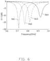
- FIG. 6is a scattering parameter graph when the antenna structure of FIG. 4 works in a Long Term Evolution Advanced (LTE-A) low frequency mode.
- LTE-ALong Term Evolution Advanced
- FIG. 7is a radiation efficiency graph when the antenna structure of FIG. 4 works in LTE-A low frequency mode.
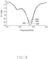
- FIG. 8is a scattering parameter graph when the antenna structure of FIG. 4 works in LTE-A middle and high frequency modes.
- FIG. 9is a radiation efficiency graph when the antenna structure of FIG. 4 works in LTE-A middle and high frequency modes.
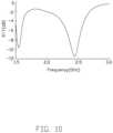
- FIG. 10is a scattering parameter graph when the antenna structure of FIG. 4 works in a Global Positioning System (GPS) mode and a WIFI 2.4 GHz mode.
- GPSGlobal Positioning System
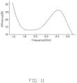
- FIG. 11is a radiation efficiency graph when the antenna structure of FIG. 4 works in GPS mode and WIFI 2.4 GHz mode.
- FIG. 12is a scattering parameter graph when the antenna structure of FIG. 4 works in a WIFI 5 GHz mode.
- FIG. 13is a radiation efficiency graph when the antenna structure of FIG. 4 works in WIFI 5 GHz mode.
- Coupledis defined as connected, whether directly or indirectly through intervening components, and is not necessarily limited to physical connections.
- the connectioncan be such that the objects are permanently connected or releasably connected.
- substantiallyis defined to be essentially conforming to the particular dimension, shape, or other feature that the term modifies, such that the component need not be exact.
- substantially cylindricalmeans that the object resembles a cylinder, but can have one or more deviations from a true cylinder.
- comprisingwhen utilized, means “including, but not necessarily limited to”; it specifically indicates open-ended inclusion or membership in the so-described combination, group, series, and the like.
- the present disclosureis described in relation to an antenna structure and a wireless communication device using same.
- FIG. 1 and FIG. 2illustrate an embodiment of a wireless communication device 200 using an antenna structure 100 .
- the wireless communication device 200can be, for example, a mobile phone or a personal digital assistant.
- the antenna structure 100can transmit and receive radio waves, to exchange wireless signals.
- FIG. 1is a schematic diagram of the antenna structure 100 applied to the wireless communication device 200 .
- FIG. 2is a diagram of the assembled wireless communication device 200 .
- the antenna structure 100includes a metallic housing 11 , a first feed portion 12 , a second feed portion 13 , a third feed portion 14 , a first ground portion 15 , a second ground portion 17 , and a switch circuit 18 .
- the metallic housing 11at least includes a metallic side frame 111 , a metallic back board 112 , and a metallic middle frame 113 .
- the metallic side frame 111is substantially a ring structure.
- the metallic side frame 111is made of metal or other conductive materials.
- the metallic back board 112is positioned at a periphery of the metallic side frame 111 .
- an opening(not shown) is defined on a side of the metallic side frame 111 away the metallic back board 112 , for receiving a display unit 201 of the wireless communication device 200 .
- the display unit 201has a display plane, and the display plane is exposed through the opening.
- the metallic middle frame 113is substantially a rectangular sheet.
- the metallic middle frame 113is made of metal or other conductive materials.
- the metallic middle frame 113is a metal sheet located between the display unit 201 and the metallic back board 112 .
- the metallic middle frame 113is used to support the display unit 201 , provide electromagnetic shielding, and improve mechanical strength of the wireless communication device 200 .
- the metallic side frame 111 , the metallic back board 112 , and the metallic middle frame 113form an integral metal structure.
- the display unit 201has a high screen-to-body ratio. That is, an area of the display plane of the display unit 201 is greater than 70% of a frontal area of the wireless communication device 200 , and even a full front screen (approximately 100%) can be achieved.
- the full screenrefers to a slot other than the necessary slot defined in the antenna structure 100 , so the left, the right, and the lower sides of the display unit 201 can be connected to the metallic side frame 111 seamlessly.
- the metallic side frame 111at least includes an end portion 115 , a first side portion 116 , and a second side portion 117 .
- the end portion 115is a top end of the wireless communication device 200 . That is, the antenna structure 100 constitutes an upper antenna of the wireless communication device 200 .
- the first side portion 116 and the second side portion 117are positioned opposite to each other.
- the first side portion 116 and the second side portion 117are each disposed at one end of the end portion 115 , and are preferably disposed vertically.
- the metallic housing 11defines a slot 118 and at least one gap.
- the slot 118is defined on the metallic side frame 111 .
- the slot 118is substantially U-shaped, and is defined at the end portion 115 extending towards the first side portion 116 and the second side portion 117 .
- the slot 118is defined on a location of the metallic side frame 111 close to the metallic back board 112 , and extends toward the display unit 201 .
- a width of the slot 118is approximately half of a width of the metallic side frame 111 . That is, the slot 118 is defined on a side of the metallic side frame 111 close to the metallic back board 112 and extends away from the metallic back board 112 to the middle of the metallic side frame 111 .
- the metallic housing 11defines three gaps, namely a first gap 120 , a second gap 121 , and a third gap 122 .
- the first gap 120 , the second gap 121 , and the third gap 122are defined on the metallic side frame 111 .
- the first gap 120is defined at the end portion 115 and positioned near the first side portion 116 .
- the second gap 121is spaced from the first gap 120 .
- the second gap 121is defined at the first side portion 116 and positioned near the end portion 115 . That is, the first gap 120 and the second gap 121 are defined (according to FIG. 2 ) at top left corner of the metallic housing 11 .
- the third gap 122is spaced from the first gap 120 .
- the third gap 122is defined at the second side portion 117 and positioned near the end portion 115 . As FIG. 2 shows, the third gap 122 is defined at top right corner of the metallic housing 11 .
- the first gap 120 and the third gap 122all penetrate and interrupt the metallic side frame 111 , and communicate with the slot 118 .
- the second gap 121is defined at the metallic side frame 111 and extends along a direction toward the metallic back board 112 (or the slot 118 ). That is, the second gap 121 is a virtual gap, which is not in communication with the slot 118 .
- the slot 118 and the at least one gapcooperatively divide the metallic housing 11 into at least two radiation portions.
- the slot 118 , the first gap 120 , the second gap 121 , and the third gap 122divide the metallic housing 11 into two radiation portions, namely a first radiation portion F 1 and a second radiation portion F 2 .
- the metallic side frame 111 between the first gap 120 and an end of the slot 118 at the first side portion 16forms the first radiation portion F 1 .
- the metallic side frame 111 between the first gap 120 and the third gap 122forms the second radiation portion F 2 .
- the second gap 121further divides the first radiation portion F 1 into two portions, namely a first radiation section F 11 and a second radiation section F 12 .
- the metallic side frame 111 between the first gap 120 and the second gap 121forms the first radiation section F 11 .
- the metallic side frame 111 between the second gap 121 and an end of the first side portion 16 corresponding to the slot 118forms the second radiation section F 12 .
- the second gap 121is a virtual gap, the first radiation section F 11 and the second radiation section F 12 are not insulated from each other. That is, the first radiation section F 1 l is still connected to the second radiation section F 12 .
- a notch 123is defined on the side of the metallic middle frame 113 near the end portion 115 .
- the notch 123is substantially U-shaped. That is, the notch 123 is defined in the portion of the metallic middle frame 113 corresponding to the end portion 115 , and extends along the metallic middle frame 113 and is parallel to the first side portion 116 and the second side portion 117 . Then, the notch 123 is substantially parallel to the slot 118 and communicates with the slot 118 , the first gap 120 , and the third gap 122 .
- one side of the first radiation portion F 1 near an end of the slot 118 located at the first side portion 116is connected to the metallic middle frame 113 and the metallic back board 113 , namely, it is grounded.
- the second radiation portion F 2is spaced apart from and insulated from the metallic middle frame 113 . That is, the slot 118 and the notch 123 separate the radiator of the metallic side frame (that is, the second radiation portion F 2 ,) and the metallic back board 112 .
- the first gap 120 , the second gap 121 , and the third gap 122have the same width.
- the width of each of the first gap 120 , the second gap 121 , and the third gap 122is 1-2 mm.
- the slot 118 , the first gap 120 , and the second gap 121 , the third gap 122 , and the notch 123are all filled with an insulating material (such as plastic, rubber, glass, wood, ceramic, etc., not being limited to these).
- the wireless communication device 200further includes a circuit board 21 and at least one electronic component.
- the circuit board 21is received in a space formed by the metallic side frame 111 , the metallic middle frame 113 , and the metallic back board 112 .
- One end of the circuit board 21is spaced apart from the metallic side frame 111 , thus a headroom 210 is formed between the circuit board 21 and the metallic side frame 111 .
- the circuit board 21includes a first feed point 211 , a second feed point 212 , a third feed point 213 , a first ground point 214 , and a second ground point 215 .
- the first feed point 211 , the second feed point 212 , the third feed point 213 , the first ground point 214 , and the second ground point 215are spaced apart from each other.
- the first feed point 211 , the second feed point 212 , the third feed point 213feed current and signals to the antenna structure 100 .
- the first ground point 214 and the second ground point 215ground the antenna structure 100 .
- the wireless communication device 200includes at least four electronic components, namely first to fourth electronic components 22 - 25 .
- the first to fourth electronic components 22 - 25are located at a same side of the circuit board 21 near the end portion 115 .
- the first electronic component 22is a front lens module.
- the first electronic component 22is positioned on an edge of the circuit board 21 adjacent to the second radiation portion F 2 .
- the first electronic component 22is positioned so as to be insulated by the slot 118 from the second radiation portion F 2 .
- the second electronic component 23is a proximity sensor.
- the second electronic component 23is positioned on the circuit board 21 and is spaced apart from the first electronic component 22 .
- the third electronic component 24is a receiver.
- the third electronic component 24is positioned on the circuit board 21 and is positioned at one side of the first electronic component 22 near the first gap 120 .
- the second electronic component 23 and the third electronic component 24are also spaced and insulated by the slot 118 from the second radiation portion F 2 .
- the fourth electronic component 25is an audio output interface.
- the fourth electronic component 25is positioned on the circuit board 21 .
- the fourth electronic component 25is positioned on a side of the third electronic component 24 away from the first electronic component 22 .
- the fourth electronic component 25is positioned to correspond to the first gap 120 .
- the metallic side frame 111further defines an earphone hole (not shown).
- the earphone holeis defined on the end portion 115 .
- the earphone holeis positioned to correspond to the fourth electronic component 25 . In this way, an external device, such as an earphone, can be inserted through the earphone hole to establish an electrical connection with the fourth electronic component 25 .
- the first feed portion 12is positioned in the metallic housing 11 .
- One end of the first feed portion 12may be electrically connected to the first radiation section F 11 by means of an elastic sheet, a microstrip line, a strip line, or a coaxial cable.
- the other end of the first feed portion 12is electrically connected to the first feed point 211 through a matching circuit 124 , to feed current and signals to the first radiation section F 11 of the first radiation portion F 1 .
- the second feed portion 13is positioned in the metallic housing 11 .
- One end of the second feed portion 13may be electrically connected to the second radiation section F 12 by means of an elastic sheet, a microstrip line, a strip line, or a coaxial cable.
- the other end of the second feed portion 13is electrically connected to the second feed point 212 through a matching circuit 131 , to feed current and signals to the second radiation section F 12 of the first radiation portion F 1 .
- the third feed portion 14is positioned in the metallic housing 11 .
- One end of the third feed portion 14is electrically connected to one end of the second radiation portion F 2 near the third gap 122 by means of an elastic sheet, a microstrip line, a strip line, or a coaxial cable.
- the other end of the third feed portion 14is electrically connected to the third feed point 213 through a matching circuit 141 , to feed current and signals to the second radiation portion F 2 .
- the first feed portion 12 , the second feed portion 13 , and the third feed portion 14may be made of iron, copper foil, or a conductor in a laser direct structuring (LDS) process.
- LDSlaser direct structuring
- the first ground portion 15is positioned in the metallic housing 11 between the third electronic element 24 and the fourth electronic element 25 .
- One end of the first ground portion 15may be electrically connected to the second radiation portion F 2 .
- the other end of the first ground portion 15is electrically connected to the first ground point 214 through a matching circuit 151 , to ground the first radiation portion F 1 .
- the matching circuits 124 , 131 , 141 , and 151may be L-shaped matching circuits, T-shaped matching circuits, ⁇ -shaped matching circuits, or other arrangement of capacitors and inductors to adjust the impedance matching of corresponding radiation portion or radiation section. For example, the impedance matching of the first radiation section F 11 , the second radiation section F 12 , and the second radiation section F 2 is adjusted.
- the second ground portion 17is positioned in the metallic housing 11 between the third feed portion 14 and the second side portion 117 .
- One end of the second ground portion 17may be electrically connected to one end of the second radiation portion F 2 near the third gap 122 .
- the other end of the second ground portion 17is electrically connected to the second ground point 215 through the switch circuit 18 , to ground the second radiation portion F 2 .
- FIG. 4illustrates a diagram of current paths of the antenna structure 100 .
- the first feed portion 12supplies a current
- the currentflows through the first radiation section F 11 of the first radiation portion F 1 , toward the first gap 120 (path P 1 ), to excite a first working mode and generate a radiation signal in a first radiation frequency band.
- the currentwill flow through the second radiation section F 12 of the first radiation portion F 1 and the first radiation section F 11 , toward the first gap 120 (path P 2 ), to excite a second working mode and generate a radiation signal in a second radiation frequency band.
- the third feed portion 14supplies a current
- the currentwill flow through the second radiation portion F 2 , toward the first gap 120 , and is grounded through the first ground portion 15 and the matching circuit 151 (path P 3 ), to excite a third working mode and generate a radiation signal in a third radiation frequency band.
- the currentalso flows through the first ground portion 15 through the first ground point 214 , flows through the second radiation portion F 2 toward the third gap 122 (path P 4 ), to excite a fourth working mode and generate a radiation signal in a fourth radiation frequency band.
- the first working modeincludes a global positioning system (GPS) mode and a WIFI 2.4 GHz mode.
- the second working modeis a WIFI 5 GHz mode.
- the third working modeincludes a Long Term Evolution Advanced (LTE-A) middle frequency mode and an LTE-A high frequency mode.
- the fourth working modeis an LTE-A low frequency mode.
- the frequencies of the first radiation frequency bandinclude 1575 MHz and 2400-2484 MHz.
- the frequencies of the second radiation frequency bandare 5150-5850 MHz.
- the frequencies of the third radiation frequency bandinclude 1710-2170 MHz and 2300-2690 MHz.
- the frequencies of the fourth radiation frequency bandare 700-960 MHz.
- the switch circuit 18includes a switching unit 181 and a plurality of switching elements 183 .
- the switching unit 181may be a single pole single throw switch, a single pole double throw switch, a single pole three throw switch, a single pole four throw switch, a single pole six throw switch, a single pole eight throw switch, or the like.
- the switching unit 181is electrically connected to the second radiation portion F 2 .
- the switching elements 183can be inductors, capacitors, or a combination of them.
- the switching elements 183are connected in parallel to each other.
- One end of each switching element 183is electrically connected to the switching unit 181 .
- the other end of each switching element 183is electrically connected to the second ground point 215 , namely, grounded.
- the switching unit 181can switch the second radiation portion F 2 to connect with different switching elements 183 , for adjusting the fourth radiation frequency band, that is, the frequencies of the low frequency band.
- FIG. 6is a graph of scattering parameters (S parameters) when the antenna structure 100 works in the LTE-A low frequency mode.
- a curve S 61is an S 11 value when the antenna structure 100 works in the frequency band of LTE-A Band17 (704-746 MHz).
- a curve S 62is an S 11 value when the antenna structure 100 works in the frequency band of LTE-A Band13 (746-787 MHz).
- a curve S 63is an S 11 value when the antenna structure 100 works in the frequency band of LTE-A Band5 (869-894 MHz).
- a curve S 64is an S 11 value when the antenna structure 100 works in the frequency band of LTE-A Band8 (880-960 MHz).
- FIG. 7is a graph of the radiation efficiency when the antenna structure 100 works in the LTE-A low frequency mode.
- a curve S 71is a radiation efficiency when the antenna structure 100 works in the frequency band of LTE-A Band17 (704-746 MHz).
- a curve S 72is a radiation efficiency when the antenna structure 100 works in the frequency band of LTE-A Band13 (746-787 MHz).
- a curve S 73is a radiation efficiency value when the antenna structure 100 works in the frequency band of LTE-A Band5 (869-894 MHz).
- a curve S 74is a radiation efficiency when the antenna structure 100 works in the frequency band of LTE-A Band8 (880-960 MHz).
- FIG. 8is a graph of scattering parameters (S parameters) when the antenna structure 100 works in the LTE-A middle and high frequency modes.
- a curve S 81is an S 11 value when the low frequency of the antenna structure 100 is LTE-A Band17 (704-746 MHz), and the antenna structure 100 works in the LTE-A middle and high frequency bands.
- a curve S 82is an S 11 value when the low frequency of the antenna structure 100 is LTE-A Band13 (746-787 MHz), and the antenna structure 100 works in the LTE-A middle and high frequency bands.
- a curve S 83is an S 11 value when the low frequency of the antenna structure 100 is LTE-A Band5 (869-894 MHz), and the antenna structure 100 works in the LTE-A middle and high frequency bands.
- a curve S 64is an S 11 value when the low frequency of the antenna structure 100 is LTE-A Band8 (880-960 MHz), and the antenna structure 100 works in the LTE-A middle and high frequency bands.
- FIG. 9is a graph of the radiation efficiency when the antenna structure 100 works in the LTE-A middle and high frequency modes.
- a curve S 91is a radiation efficiency value when the low frequency of the antenna structure 100 is LTE-A Band17 (704-746 MHz), and the antenna structure 100 works in the LTE-A middle and high frequency bands.
- a curve S 92is a radiation efficiency value when the low frequency of the antenna structure 100 is LTE-A Band13 (746-787 MHz), and the antenna structure 100 works in the LTE-A middle and high frequency bands.
- a curve S 93is a radiation efficiency value when the low frequency of the antenna structure 100 is LTE-A Band5 (869-894 MHz), and the antenna structure 100 works in the LTE-A middle and high frequency bands.
- a curve S 94is a radiation efficiency value when the low frequency of the antenna structure 100 is LTE-A Band8 (880-960 MHz), and the antenna structure 100 works in the LTE-A middle and high frequency bands.
- FIG. 10is a graph of scattering parameters (S parameters) when the antenna structure 100 works in the GPS mode and the WIFI 2.4 GHz mode.
- FIG. 11is a graph of the radiation efficiency when the antenna structure 100 works in the GPS mode and the WIFI 2.4 GHz mode.
- FIG. 12is a graph of scattering parameters (S parameters) when the antenna structure 100 works in the WIFI 5 GHz mode.
- FIG. 13is a graph of total radiation efficiency when the antenna structure 100 works in the WIFI 5 GHz mode.
- FIG. 6 to FIG. 113show that the antenna structure 100 is provided with the switch circuit 18 , to switch between various low frequency modes of the antenna structure 100 .
- Thisimproves the low frequency bandwidth and gives better antenna effectiveness.
- the antenna structure 100works in the frequency bands of LTE-A Band17 (704-746 MHz), LTE-A Band13 (746-787 MHz), LTE-A Band5 (869-894 MHz), and LTE-A Band8 (880-960 MHz
- the LTE-A middle and high frequency bandsare all about 1710-2690 MHz, and the antenna structure 100 can also cover frequency bands of GPS, WIFI 2.4 GHz, and WIFI 5 GHz. That is, when the switch circuit 18 is switched across, the switch circuit 18 is only used to change the low frequency mode of the antenna structure 100 without affecting the middle and high frequency modes. This feature is good for a carrier aggregation application (CA) of LTE-A.
- CAcarrier aggregation application
- the antenna structure 100can generate various working modes through the switching of the switch circuit 18 , such as low frequency mode, middle frequency mode, high frequency mode, GPS mode, WIFI 2.4 GHz mode, and WIFI 5 GHz mode, so that communication bands commonly used in the world are covered.
- the antenna structure 100can cover GSM850/900/WCDMA Band5/Band8/Band13/Band17 at low frequencies, GSM 1800/1900/WCDMA 2100 (1710-2170 MHz) at middle frequencies, LTE-A Band1, Band40, Band41 (2300-2690 MHz) at high frequencies, and frequency bands of GPS, WIFI 2.4 GHz, and WIFI 5 GHz.
- the frequency bands of the antenna structure 100can be applied to the operation of GSM Qual-band, UMTS Band I/II/V/VIII frequency bands, and LTE 850/900/1800/1900/2100/2300/2500 frequency bands, as commonly used worldwide.
- the antenna structure 100sets at least one gap (such as the first gap 120 , the second gap 121 , and the third gap 122 ) on the metallic side frame 111 to create at least two radiation portions from the metallic side frame 111 .
- the antenna structure 100further includes the switch circuit 18 . Therefore, it can cover multiple frequency bands, such as, low frequency, middle frequency, high frequency, and frequency bands of GPS, WIFI 2.4 GHz, and WIFI 5 GHz through different switching methods, and renders radiation capabilities of the antenna structure 100 more effective in broadband ranges compared to a general metal backing.
- the antenna structure 100increases the low frequency bandwidth and provides better antenna efficiency, covering the requirements of global frequency band applications and supporting CA.
- the antenna structure 100has a full front screen, and the antenna structure 100 still has good performance in the less-than-optimal environment of the metallic back board 112 , the metallic side frame 111 , and a large area of grounded metal around it.
Landscapes
- Engineering & Computer Science (AREA)
- Computer Networks & Wireless Communication (AREA)
- Signal Processing (AREA)
- Support Of Aerials (AREA)
Abstract
Description
Claims (14)
Applications Claiming Priority (2)
| Application Number | Priority Date | Filing Date | Title |
|---|---|---|---|
| CN202010051202.4ACN113140892B (en) | 2020-01-17 | 2020-01-17 | Antenna structure and wireless communication device with same |
| CN202010051202.4 | 2020-01-17 |
Publications (2)
| Publication Number | Publication Date |
|---|---|
| US20210226319A1 US20210226319A1 (en) | 2021-07-22 |
| US11973261B2true US11973261B2 (en) | 2024-04-30 |
Family
ID=76808220
Family Applications (1)
| Application Number | Title | Priority Date | Filing Date |
|---|---|---|---|
| US17/150,214Active2042-05-16US11973261B2 (en) | 2020-01-17 | 2021-01-15 | Antenna structure and wireless communication device using same |
Country Status (2)
| Country | Link |
|---|---|
| US (1) | US11973261B2 (en) |
| CN (1) | CN113140892B (en) |
Cited By (1)
| Publication number | Priority date | Publication date | Assignee | Title |
|---|---|---|---|---|
| US12418100B2 (en)* | 2021-05-26 | 2025-09-16 | Guangdong Oppo Mobile Telecommunications Corp., Ltd. | Antenna assembly and electronic device |
Families Citing this family (3)
| Publication number | Priority date | Publication date | Assignee | Title |
|---|---|---|---|---|
| AU2018423290B2 (en)* | 2018-05-15 | 2021-12-16 | Huawei Technologies Co., Ltd. | Antenna system and terminal device |
| CN113078444B (en)* | 2020-01-06 | 2024-06-11 | 深圳富泰宏精密工业有限公司 | Antenna structure and wireless communication device with same |
| CN119948699A (en) | 2022-09-26 | 2025-05-06 | 三星电子株式会社 | Electronic device comprising an antenna |
Citations (35)
| Publication number | Priority date | Publication date | Assignee | Title |
|---|---|---|---|---|
| US20140218244A1 (en)* | 2013-02-01 | 2014-08-07 | Chiun Mai Communication Systems, Inc. | Antenna assembly and wireless communication device employing same |
| US20160056531A1 (en)* | 2014-08-21 | 2016-02-25 | Samsung Electronics Co., Ltd. | Antenna apparatus and electronic device having the same |
| US20160149290A1 (en)* | 2014-11-21 | 2016-05-26 | Samsung Electronics Co., Ltd. | Antenna and electronic device including the same |
| CN205543232U (en) | 2016-01-27 | 2016-08-31 | 杭州禾声科技有限公司 | Multiple band antenna based on metal frame |
| US20170033441A1 (en)* | 2015-07-28 | 2017-02-02 | Samsung Electronics Co., Ltd. | Antenna device and electronic device including same |
| US20170048363A1 (en)* | 2015-08-13 | 2017-02-16 | Samsung Electronics Co., Ltd. | Antenna and electronic device including the same |
| US20170047639A1 (en)* | 2015-08-10 | 2017-02-16 | Samsung Electronics Co., Ltd. | Antenna device and electronic device including the same |
| US20170170562A1 (en)* | 2015-12-15 | 2017-06-15 | Samsung Electronics Co., Ltd. | Electronic device including antenna |
| US20170237150A1 (en)* | 2016-02-17 | 2017-08-17 | Samsung Electronics Co., Ltd. | Electronic device including antenna |
| US20170244149A1 (en)* | 2016-02-18 | 2017-08-24 | Samsung Electronics Co., Ltd. | Electronic device including antenna unit |
| US20170244818A1 (en)* | 2016-02-20 | 2017-08-24 | Samsung Electronics Co., Ltd. | Antenna and electronic device including the same |
| US20170244163A1 (en)* | 2016-02-19 | 2017-08-24 | Samsung Electronics Co., Ltd. | Antenna structure and electronic device including the same |
| US20170302771A1 (en)* | 2016-04-19 | 2017-10-19 | Samsung Electronics Co., Ltd. | Electronic device including antenna |
| US20180026370A1 (en)* | 2016-07-19 | 2018-01-25 | Chiun Mai Communication Systems, Inc. | Antenna structure and wireless communication device using same |
| US20180026360A1 (en)* | 2016-07-19 | 2018-01-25 | Chiun Mai Communication Systems, Inc. | Antenna structure and wireless communication device using same |
| US20180026353A1 (en)* | 2016-07-21 | 2018-01-25 | Chiun Mai Communication Systems, Inc. | Antenna structure and wireless communication device using same |
| US20180026344A1 (en)* | 2016-07-19 | 2018-01-25 | Chiun Mai Communication Systems, Inc. | Antenna structure and wireless communication device using same |
| US20180026334A1 (en)* | 2016-07-21 | 2018-01-25 | Chiun Mai Communication Systems, Inc. | Antenna structure and wireless communication device using same |
| US20180026343A1 (en)* | 2016-07-19 | 2018-01-25 | Chiun Mai Communication Systems, Inc. | Antenna structure and wireless communication device using same |
| US20180026336A1 (en)* | 2016-07-21 | 2018-01-25 | Chiun Mai Communication Systems, Inc. | Antenna structure and wireless communication device using same |
| US20180062244A1 (en)* | 2016-07-21 | 2018-03-01 | Chiun Mai Communication Systems, Inc. | Antenna structure and wireless communication device using same |
| US20180248250A1 (en)* | 2017-02-24 | 2018-08-30 | Chiun Mai Communication Systems, Inc. | Antenna structure and wireless communication device using same |
| US20180248264A1 (en)* | 2017-02-24 | 2018-08-30 | Chiun Mai Communication Systems, Inc. | Antenna structure and wireless communication device using same |
| WO2018232678A1 (en)* | 2017-06-19 | 2018-12-27 | 上海传英信息技术有限公司 | Antenna system of mobile terminal and mobile terminal having the same |
| US20190044218A1 (en)* | 2017-08-05 | 2019-02-07 | Chiun Mai Communication Systems, Inc. | Antenna structure and wireless communication device using same |
| US20190131694A1 (en)* | 2017-10-30 | 2019-05-02 | Chiun Mai Communication Systems, Inc. | Antenna assembly and wireless communication device employing same |
| US20190181554A1 (en)* | 2017-12-12 | 2019-06-13 | Chiun Mai Communication Systems, Inc. | Antenna structure |
| US20190372223A1 (en)* | 2018-06-01 | 2019-12-05 | Chiun Mai Communication Systems, Inc. | Antenna structure |
| CN110661084A (en) | 2018-06-28 | 2020-01-07 | 深圳富泰宏精密工业有限公司 | Antenna structure and wireless communication device with same |
| US20200373669A1 (en)* | 2017-11-10 | 2020-11-26 | Huawei Technologies Co., Ltd. | Mobile Terminal and Antenna of Mobile Terminal |
| US20210151886A1 (en)* | 2018-05-15 | 2021-05-20 | Huawei Technologies Co., Ltd. | Antenna System and Terminal Device |
| US20210210837A1 (en)* | 2020-01-06 | 2021-07-08 | Chiun Mai Communication Systems, Inc. | Antenna structure and wireless communication device using same |
| US20220037764A1 (en)* | 2020-07-30 | 2022-02-03 | Chiun Mai Communication Systems, Inc. | Antenna structure and electronic device using same |
| US11342653B2 (en)* | 2020-01-06 | 2022-05-24 | Chiun Mai Communication Systems, Inc. | Antenna structure and wireless communication device using same |
| US11349199B2 (en)* | 2020-01-06 | 2022-05-31 | Chiun Mai Communication Systems, Inc. | Antenna structure and wireless communication device using same |
Family Cites Families (7)
| Publication number | Priority date | Publication date | Assignee | Title |
|---|---|---|---|---|
| TWI656691B (en)* | 2016-07-21 | 2019-04-11 | 群邁通訊股份有限公司 | Antenna structure and wireless communication device having the same |
| TWI650904B (en)* | 2016-07-21 | 2019-02-11 | 群邁通訊股份有限公司 | Antenna structure and wireless communication device with same |
| CN108232412B (en)* | 2016-12-09 | 2020-04-03 | 深圳富泰宏精密工业有限公司 | Antenna structure and wireless communication device with same |
| TWI648907B (en)* | 2017-09-04 | 2019-01-21 | 廣達電腦股份有限公司 | Mobile device |
| CN108258382B (en)* | 2017-12-29 | 2020-09-18 | 瑞声科技(新加坡)有限公司 | Antenna system |
| CN110011077A (en)* | 2018-01-05 | 2019-07-12 | 深圳富泰宏精密工业有限公司 | Antenna structure and wireless communication device with the antenna structure |
| JP2020010314A (en)* | 2018-06-27 | 2020-01-16 | 京セラ株式会社 | Antenna substrate and communication module |
- 2020
- 2020-01-17CNCN202010051202.4Apatent/CN113140892B/enactiveActive
- 2021
- 2021-01-15USUS17/150,214patent/US11973261B2/enactiveActive
Patent Citations (37)
| Publication number | Priority date | Publication date | Assignee | Title |
|---|---|---|---|---|
| US20140218244A1 (en)* | 2013-02-01 | 2014-08-07 | Chiun Mai Communication Systems, Inc. | Antenna assembly and wireless communication device employing same |
| US20160056531A1 (en)* | 2014-08-21 | 2016-02-25 | Samsung Electronics Co., Ltd. | Antenna apparatus and electronic device having the same |
| US20160149290A1 (en)* | 2014-11-21 | 2016-05-26 | Samsung Electronics Co., Ltd. | Antenna and electronic device including the same |
| US20170033441A1 (en)* | 2015-07-28 | 2017-02-02 | Samsung Electronics Co., Ltd. | Antenna device and electronic device including same |
| US20170047639A1 (en)* | 2015-08-10 | 2017-02-16 | Samsung Electronics Co., Ltd. | Antenna device and electronic device including the same |
| US20170048363A1 (en)* | 2015-08-13 | 2017-02-16 | Samsung Electronics Co., Ltd. | Antenna and electronic device including the same |
| US20170170562A1 (en)* | 2015-12-15 | 2017-06-15 | Samsung Electronics Co., Ltd. | Electronic device including antenna |
| CN205543232U (en) | 2016-01-27 | 2016-08-31 | 杭州禾声科技有限公司 | Multiple band antenna based on metal frame |
| US20170237150A1 (en)* | 2016-02-17 | 2017-08-17 | Samsung Electronics Co., Ltd. | Electronic device including antenna |
| US20170244149A1 (en)* | 2016-02-18 | 2017-08-24 | Samsung Electronics Co., Ltd. | Electronic device including antenna unit |
| US20170244163A1 (en)* | 2016-02-19 | 2017-08-24 | Samsung Electronics Co., Ltd. | Antenna structure and electronic device including the same |
| US20170244818A1 (en)* | 2016-02-20 | 2017-08-24 | Samsung Electronics Co., Ltd. | Antenna and electronic device including the same |
| US20170302771A1 (en)* | 2016-04-19 | 2017-10-19 | Samsung Electronics Co., Ltd. | Electronic device including antenna |
| US20180026343A1 (en)* | 2016-07-19 | 2018-01-25 | Chiun Mai Communication Systems, Inc. | Antenna structure and wireless communication device using same |
| US20180026360A1 (en)* | 2016-07-19 | 2018-01-25 | Chiun Mai Communication Systems, Inc. | Antenna structure and wireless communication device using same |
| US20180026344A1 (en)* | 2016-07-19 | 2018-01-25 | Chiun Mai Communication Systems, Inc. | Antenna structure and wireless communication device using same |
| US20180026370A1 (en)* | 2016-07-19 | 2018-01-25 | Chiun Mai Communication Systems, Inc. | Antenna structure and wireless communication device using same |
| US20180026353A1 (en)* | 2016-07-21 | 2018-01-25 | Chiun Mai Communication Systems, Inc. | Antenna structure and wireless communication device using same |
| US20180026334A1 (en)* | 2016-07-21 | 2018-01-25 | Chiun Mai Communication Systems, Inc. | Antenna structure and wireless communication device using same |
| US20180026336A1 (en)* | 2016-07-21 | 2018-01-25 | Chiun Mai Communication Systems, Inc. | Antenna structure and wireless communication device using same |
| US20180062244A1 (en)* | 2016-07-21 | 2018-03-01 | Chiun Mai Communication Systems, Inc. | Antenna structure and wireless communication device using same |
| US20180248250A1 (en)* | 2017-02-24 | 2018-08-30 | Chiun Mai Communication Systems, Inc. | Antenna structure and wireless communication device using same |
| US20180248264A1 (en)* | 2017-02-24 | 2018-08-30 | Chiun Mai Communication Systems, Inc. | Antenna structure and wireless communication device using same |
| WO2018232678A1 (en)* | 2017-06-19 | 2018-12-27 | 上海传英信息技术有限公司 | Antenna system of mobile terminal and mobile terminal having the same |
| US20190044218A1 (en)* | 2017-08-05 | 2019-02-07 | Chiun Mai Communication Systems, Inc. | Antenna structure and wireless communication device using same |
| US20190131694A1 (en)* | 2017-10-30 | 2019-05-02 | Chiun Mai Communication Systems, Inc. | Antenna assembly and wireless communication device employing same |
| US20200373669A1 (en)* | 2017-11-10 | 2020-11-26 | Huawei Technologies Co., Ltd. | Mobile Terminal and Antenna of Mobile Terminal |
| US20190181554A1 (en)* | 2017-12-12 | 2019-06-13 | Chiun Mai Communication Systems, Inc. | Antenna structure |
| US20190181555A1 (en) | 2017-12-12 | 2019-06-13 | Chiun Mai Communication Systems, Inc. | Antenna structure |
| CN109921176A (en) | 2017-12-12 | 2019-06-21 | 深圳富泰宏精密工业有限公司 | Antenna structure and wireless communication device with the antenna structure |
| US20210151886A1 (en)* | 2018-05-15 | 2021-05-20 | Huawei Technologies Co., Ltd. | Antenna System and Terminal Device |
| US20190372223A1 (en)* | 2018-06-01 | 2019-12-05 | Chiun Mai Communication Systems, Inc. | Antenna structure |
| CN110661084A (en) | 2018-06-28 | 2020-01-07 | 深圳富泰宏精密工业有限公司 | Antenna structure and wireless communication device with same |
| US20210210837A1 (en)* | 2020-01-06 | 2021-07-08 | Chiun Mai Communication Systems, Inc. | Antenna structure and wireless communication device using same |
| US11342653B2 (en)* | 2020-01-06 | 2022-05-24 | Chiun Mai Communication Systems, Inc. | Antenna structure and wireless communication device using same |
| US11349199B2 (en)* | 2020-01-06 | 2022-05-31 | Chiun Mai Communication Systems, Inc. | Antenna structure and wireless communication device using same |
| US20220037764A1 (en)* | 2020-07-30 | 2022-02-03 | Chiun Mai Communication Systems, Inc. | Antenna structure and electronic device using same |
Cited By (1)
| Publication number | Priority date | Publication date | Assignee | Title |
|---|---|---|---|---|
| US12418100B2 (en)* | 2021-05-26 | 2025-09-16 | Guangdong Oppo Mobile Telecommunications Corp., Ltd. | Antenna assembly and electronic device |
Also Published As
| Publication number | Publication date |
|---|---|
| CN113140892B (en) | 2024-04-26 |
| US20210226319A1 (en) | 2021-07-22 |
| CN113140892A (en) | 2021-07-20 |
Similar Documents
| Publication | Publication Date | Title |
|---|---|---|
| US10892552B2 (en) | Antenna structure | |
| US11973261B2 (en) | Antenna structure and wireless communication device using same | |
| US11355853B2 (en) | Antenna structure and wireless communication device using the same | |
| US11699841B2 (en) | Antenna structure and electronic device using same | |
| US10290925B2 (en) | Antenna structure and wireless communication device using same | |
| US11349199B2 (en) | Antenna structure and wireless communication device using same | |
| US11923599B2 (en) | Antenna structure and wireless communication device using same | |
| US20210320392A1 (en) | Antenna structure and electronic device using same | |
| US11431085B2 (en) | Antenna structure and wireless communication device using same | |
| US20180248264A1 (en) | Antenna structure and wireless communication device using same | |
| US10256525B2 (en) | Antenna structure and wireless communication device using same | |
| US12230896B2 (en) | Antenna structure and electronic device using the same | |
| US11342669B2 (en) | Antenna structure and wireless communication device using same | |
| US11637361B2 (en) | Antenna structure and wireless communication device | |
| US12068527B2 (en) | Antenna structure and wireless communication device using same | |
| US11342653B2 (en) | Antenna structure and wireless communication device using same | |
| TWI724754B (en) | Antenna structure and wireless communication device with same | |
| US11631943B2 (en) | Antenna structure and wireless communication device using same | |
| US11404770B2 (en) | Antenna structure and wireless communication device | |
| TWI724738B (en) | Antenna structure and wireless communication device with same | |
| TWI727597B (en) | Antenna structure and wireless communication device with same | |
| TWI724737B (en) | Antenna structure and wireless communication device with same | |
| US20230094721A1 (en) | Antenna structure and wireless communication device using same | |
| CN120224603A (en) | Electronic devices |
Legal Events
| Date | Code | Title | Description |
|---|---|---|---|
| AS | Assignment | Owner name:CHIUN MAI COMMUNICATION SYSTEMS, INC., TAIWAN Free format text:ASSIGNMENT OF ASSIGNORS INTEREST;ASSIGNORS:SUNG, KUN-LIN;CHEN, YUNG-CHIN;LEE, YI-CHIEH;REEL/FRAME:054933/0578 Effective date:20201225 | |
| FEPP | Fee payment procedure | Free format text:ENTITY STATUS SET TO UNDISCOUNTED (ORIGINAL EVENT CODE: BIG.); ENTITY STATUS OF PATENT OWNER: LARGE ENTITY | |
| STPP | Information on status: patent application and granting procedure in general | Free format text:APPLICATION DISPATCHED FROM PREEXAM, NOT YET DOCKETED | |
| STPP | Information on status: patent application and granting procedure in general | Free format text:DOCKETED NEW CASE - READY FOR EXAMINATION | |
| STPP | Information on status: patent application and granting procedure in general | Free format text:NON FINAL ACTION MAILED | |
| STPP | Information on status: patent application and granting procedure in general | Free format text:RESPONSE TO NON-FINAL OFFICE ACTION ENTERED AND FORWARDED TO EXAMINER | |
| STPP | Information on status: patent application and granting procedure in general | Free format text:FINAL REJECTION MAILED | |
| STPP | Information on status: patent application and granting procedure in general | Free format text:DOCKETED NEW CASE - READY FOR EXAMINATION | |
| STPP | Information on status: patent application and granting procedure in general | Free format text:NOTICE OF ALLOWANCE MAILED -- APPLICATION RECEIVED IN OFFICE OF PUBLICATIONS | |
| ZAAB | Notice of allowance mailed | Free format text:ORIGINAL CODE: MN/=. | |
| STPP | Information on status: patent application and granting procedure in general | Free format text:AWAITING TC RESP, ISSUE FEE PAYMENT VERIFIED | |
| STPP | Information on status: patent application and granting procedure in general | Free format text:PUBLICATIONS -- ISSUE FEE PAYMENT VERIFIED | |
| STCF | Information on status: patent grant | Free format text:PATENTED CASE |