US11962057B2 - Glass based empty substrate integrated waveguide devices - Google Patents
Glass based empty substrate integrated waveguide devicesDownload PDFInfo
- Publication number
- US11962057B2 US11962057B2US17/598,009US202017598009AUS11962057B2US 11962057 B2US11962057 B2US 11962057B2US 202017598009 AUS202017598009 AUS 202017598009AUS 11962057 B2US11962057 B2US 11962057B2
- Authority
- US
- United States
- Prior art keywords
- esiw
- copper
- pattern
- photoresist
- wafer
- Prior art date
- Legal status (The legal status is an assumption and is not a legal conclusion. Google has not performed a legal analysis and makes no representation as to the accuracy of the status listed.)
- Active, expires
Links
Images


Classifications
- H—ELECTRICITY
- H01—ELECTRIC ELEMENTS
- H01P—WAVEGUIDES; RESONATORS, LINES, OR OTHER DEVICES OF THE WAVEGUIDE TYPE
- H01P3/00—Waveguides; Transmission lines of the waveguide type
- H01P3/12—Hollow waveguides
- H—ELECTRICITY
- H01—ELECTRIC ELEMENTS
- H01P—WAVEGUIDES; RESONATORS, LINES, OR OTHER DEVICES OF THE WAVEGUIDE TYPE
- H01P3/00—Waveguides; Transmission lines of the waveguide type
- H01P3/12—Hollow waveguides
- H01P3/121—Hollow waveguides integrated in a substrate
- C—CHEMISTRY; METALLURGY
- C03—GLASS; MINERAL OR SLAG WOOL
- C03C—CHEMICAL COMPOSITION OF GLASSES, GLAZES OR VITREOUS ENAMELS; SURFACE TREATMENT OF GLASS; SURFACE TREATMENT OF FIBRES OR FILAMENTS MADE FROM GLASS, MINERALS OR SLAGS; JOINING GLASS TO GLASS OR OTHER MATERIALS
- C03C10/00—Devitrified glass ceramics, i.e. glass ceramics having a crystalline phase dispersed in a glassy phase and constituting at least 50% by weight of the total composition
- C—CHEMISTRY; METALLURGY
- C03—GLASS; MINERAL OR SLAG WOOL
- C03C—CHEMICAL COMPOSITION OF GLASSES, GLAZES OR VITREOUS ENAMELS; SURFACE TREATMENT OF GLASS; SURFACE TREATMENT OF FIBRES OR FILAMENTS MADE FROM GLASS, MINERALS OR SLAGS; JOINING GLASS TO GLASS OR OTHER MATERIALS
- C03C14/00—Glass compositions containing a non-glass component, e.g. compositions containing fibres, filaments, whiskers, platelets, or the like, dispersed in a glass matrix
- C03C14/006—Glass compositions containing a non-glass component, e.g. compositions containing fibres, filaments, whiskers, platelets, or the like, dispersed in a glass matrix the non-glass component being in the form of microcrystallites, e.g. of optically or electrically active material
- C—CHEMISTRY; METALLURGY
- C03—GLASS; MINERAL OR SLAG WOOL
- C03C—CHEMICAL COMPOSITION OF GLASSES, GLAZES OR VITREOUS ENAMELS; SURFACE TREATMENT OF GLASS; SURFACE TREATMENT OF FIBRES OR FILAMENTS MADE FROM GLASS, MINERALS OR SLAGS; JOINING GLASS TO GLASS OR OTHER MATERIALS
- C03C15/00—Surface treatment of glass, not in the form of fibres or filaments, by etching
- C—CHEMISTRY; METALLURGY
- C03—GLASS; MINERAL OR SLAG WOOL
- C03C—CHEMICAL COMPOSITION OF GLASSES, GLAZES OR VITREOUS ENAMELS; SURFACE TREATMENT OF GLASS; SURFACE TREATMENT OF FIBRES OR FILAMENTS MADE FROM GLASS, MINERALS OR SLAGS; JOINING GLASS TO GLASS OR OTHER MATERIALS
- C03C17/00—Surface treatment of glass, not in the form of fibres or filaments, by coating
- C03C17/34—Surface treatment of glass, not in the form of fibres or filaments, by coating with at least two coatings having different compositions
- C03C17/36—Surface treatment of glass, not in the form of fibres or filaments, by coating with at least two coatings having different compositions at least one coating being a metal
- C03C17/40—Surface treatment of glass, not in the form of fibres or filaments, by coating with at least two coatings having different compositions at least one coating being a metal all coatings being metal coatings
- C—CHEMISTRY; METALLURGY
- C03—GLASS; MINERAL OR SLAG WOOL
- C03C—CHEMICAL COMPOSITION OF GLASSES, GLAZES OR VITREOUS ENAMELS; SURFACE TREATMENT OF GLASS; SURFACE TREATMENT OF FIBRES OR FILAMENTS MADE FROM GLASS, MINERALS OR SLAGS; JOINING GLASS TO GLASS OR OTHER MATERIALS
- C03C3/00—Glass compositions
- C03C3/04—Glass compositions containing silica
- C03C3/076—Glass compositions containing silica with 40% to 90% silica, by weight
- C03C3/095—Glass compositions containing silica with 40% to 90% silica, by weight containing rare earths
- C—CHEMISTRY; METALLURGY
- C03—GLASS; MINERAL OR SLAG WOOL
- C03C—CHEMICAL COMPOSITION OF GLASSES, GLAZES OR VITREOUS ENAMELS; SURFACE TREATMENT OF GLASS; SURFACE TREATMENT OF FIBRES OR FILAMENTS MADE FROM GLASS, MINERALS OR SLAGS; JOINING GLASS TO GLASS OR OTHER MATERIALS
- C03C4/00—Compositions for glass with special properties
- C03C4/04—Compositions for glass with special properties for photosensitive glass
- H—ELECTRICITY
- H01—ELECTRIC ELEMENTS
- H01L—SEMICONDUCTOR DEVICES NOT COVERED BY CLASS H10
- H01L23/00—Details of semiconductor or other solid state devices
- H01L23/58—Structural electrical arrangements for semiconductor devices not otherwise provided for, e.g. in combination with batteries
- H01L23/64—Impedance arrangements
- H01L23/66—High-frequency adaptations
- H—ELECTRICITY
- H01—ELECTRIC ELEMENTS
- H01P—WAVEGUIDES; RESONATORS, LINES, OR OTHER DEVICES OF THE WAVEGUIDE TYPE
- H01P11/00—Apparatus or processes specially adapted for manufacturing waveguides or resonators, lines, or other devices of the waveguide type
- H01P11/001—Manufacturing waveguides or transmission lines of the waveguide type
- H01P11/002—Manufacturing hollow waveguides
- C—CHEMISTRY; METALLURGY
- C03—GLASS; MINERAL OR SLAG WOOL
- C03C—CHEMICAL COMPOSITION OF GLASSES, GLAZES OR VITREOUS ENAMELS; SURFACE TREATMENT OF GLASS; SURFACE TREATMENT OF FIBRES OR FILAMENTS MADE FROM GLASS, MINERALS OR SLAGS; JOINING GLASS TO GLASS OR OTHER MATERIALS
- C03C2214/00—Nature of the non-vitreous component
- C03C2214/04—Particles; Flakes
- C03C2214/05—Particles; Flakes surface treated, e.g. coated
- C—CHEMISTRY; METALLURGY
- C03—GLASS; MINERAL OR SLAG WOOL
- C03C—CHEMICAL COMPOSITION OF GLASSES, GLAZES OR VITREOUS ENAMELS; SURFACE TREATMENT OF GLASS; SURFACE TREATMENT OF FIBRES OR FILAMENTS MADE FROM GLASS, MINERALS OR SLAGS; JOINING GLASS TO GLASS OR OTHER MATERIALS
- C03C2214/00—Nature of the non-vitreous component
- C03C2214/08—Metals
- C—CHEMISTRY; METALLURGY
- C03—GLASS; MINERAL OR SLAG WOOL
- C03C—CHEMICAL COMPOSITION OF GLASSES, GLAZES OR VITREOUS ENAMELS; SURFACE TREATMENT OF GLASS; SURFACE TREATMENT OF FIBRES OR FILAMENTS MADE FROM GLASS, MINERALS OR SLAGS; JOINING GLASS TO GLASS OR OTHER MATERIALS
- C03C2218/00—Methods for coating glass
- C03C2218/10—Deposition methods
- C03C2218/11—Deposition methods from solutions or suspensions
- C03C2218/115—Deposition methods from solutions or suspensions electro-enhanced deposition
- C—CHEMISTRY; METALLURGY
- C03—GLASS; MINERAL OR SLAG WOOL
- C03C—CHEMICAL COMPOSITION OF GLASSES, GLAZES OR VITREOUS ENAMELS; SURFACE TREATMENT OF GLASS; SURFACE TREATMENT OF FIBRES OR FILAMENTS MADE FROM GLASS, MINERALS OR SLAGS; JOINING GLASS TO GLASS OR OTHER MATERIALS
- C03C2218/00—Methods for coating glass
- C03C2218/10—Deposition methods
- C03C2218/15—Deposition methods from the vapour phase
- C03C2218/154—Deposition methods from the vapour phase by sputtering
- C—CHEMISTRY; METALLURGY
- C03—GLASS; MINERAL OR SLAG WOOL
- C03C—CHEMICAL COMPOSITION OF GLASSES, GLAZES OR VITREOUS ENAMELS; SURFACE TREATMENT OF GLASS; SURFACE TREATMENT OF FIBRES OR FILAMENTS MADE FROM GLASS, MINERALS OR SLAGS; JOINING GLASS TO GLASS OR OTHER MATERIALS
- C03C2218/00—Methods for coating glass
- C03C2218/30—Aspects of methods for coating glass not covered above
- C03C2218/32—After-treatment
- C03C2218/328—Partly or completely removing a coating
- C03C2218/33—Partly or completely removing a coating by etching
- C—CHEMISTRY; METALLURGY
- C03—GLASS; MINERAL OR SLAG WOOL
- C03C—CHEMICAL COMPOSITION OF GLASSES, GLAZES OR VITREOUS ENAMELS; SURFACE TREATMENT OF GLASS; SURFACE TREATMENT OF FIBRES OR FILAMENTS MADE FROM GLASS, MINERALS OR SLAGS; JOINING GLASS TO GLASS OR OTHER MATERIALS
- C03C2218/00—Methods for coating glass
- C03C2218/30—Aspects of methods for coating glass not covered above
- C03C2218/34—Masking
- H—ELECTRICITY
- H01—ELECTRIC ELEMENTS
- H01L—SEMICONDUCTOR DEVICES NOT COVERED BY CLASS H10
- H01L2223/00—Details relating to semiconductor or other solid state devices covered by the group H01L23/00
- H01L2223/58—Structural electrical arrangements for semiconductor devices not otherwise provided for
- H01L2223/64—Impedance arrangements
- H01L2223/66—High-frequency adaptations
- H01L2223/6605—High-frequency electrical connections
- H01L2223/6627—Waveguides, e.g. microstrip line, strip line, coplanar line
- H—ELECTRICITY
- H01—ELECTRIC ELEMENTS
- H01L—SEMICONDUCTOR DEVICES NOT COVERED BY CLASS H10
- H01L23/00—Details of semiconductor or other solid state devices
- H01L23/12—Mountings, e.g. non-detachable insulating substrates
- H01L23/14—Mountings, e.g. non-detachable insulating substrates characterised by the material or its electrical properties
- H01L23/15—Ceramic or glass substrates
- H—ELECTRICITY
- H01—ELECTRIC ELEMENTS
- H01P—WAVEGUIDES; RESONATORS, LINES, OR OTHER DEVICES OF THE WAVEGUIDE TYPE
- H01P5/00—Coupling devices of the waveguide type
- H01P5/08—Coupling devices of the waveguide type for linking dissimilar lines or devices
- H01P5/10—Coupling devices of the waveguide type for linking dissimilar lines or devices for coupling balanced lines or devices with unbalanced lines or devices
- H01P5/107—Hollow-waveguide/strip-line transitions
Definitions
- the present inventionrelates in general to the field of glass based empty substrate integrated waveguide devices. More particularly, the present invention relates to the reduction of parasitic capacitance from fringe capacitance in an RF capacitive resonate filter on the same substrate or in a package.
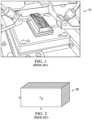
- FIG. 1shows an image of a traditional waveguide device 10 of the prior art.
- empty substrate integrate waveguide (ESIW) devicessuch as those developed by Belenguer, et al. A. Belenguer, H. Esteban, and V. E. Boria, “Novel empty substrate integrated waveguide for high-performance microwave integrated circuits,” IEEE Trans. Microw. Theory Techn., vol. 62, no. 4, pp. 832-839, 2014, and B. A. Belenguer, J. L. Cano, H. Esteban, E. Artal, and V. E. Boria, “Empty substrate integrated waveguide technology for E plane high-frequency and high-performance circuits,” Radio Sci., vol. 52, no. 1, pp. 49-69, 2017.
- EIWempty substrate integrate waveguide
- FIG. 2shows the dimension definition of rectangular substrate integrated 20 of the prior art.
- ESIW devicesinclude: (1) less metal it used that carries the signal, which is far greater than it would be in microstrip or stripline device; (2) they can be manufactured at a low cost and easy to manufacture using a standard printed circuit board (PCB) substrate; (3) lower transmission losses and higher Q resonators and filters than other planar transmission lines; (4) lower cut-off frequency than traditional waveguide; and (5) higher peak power handling capability.
- PCBprinted circuit board
- ESIWcan be thought of as a dielectric filled waveguide (DFW) where the dielectric constant is 1 and the loss tangent is zero.
- the dimension “b”is not important, as it does not affect the cut off frequency of the waveguide.
- cut off frequency of arbitrary modeis found by the following formula:
- f cc 2 ⁇ ⁇ ⁇ ( m ⁇ ⁇ a ) 2 + ( n ⁇ ⁇ b ) 2 ,
- cis the speed of light
- m, nare mode numbers
- a, bare the vertical and horizontal dimensions of the waveguide.
- a dielectricless SIW (DSIW) or Empty SIWwas first presented in 2016.
- a thick substratewas milled, metallized, and then covered with a top metallic cover stuck with a prepreg layer (preimpregnated composite fibers, where a thermoset polymer matrix material, such as epoxy, is present), so that it is almost dielectric-free.
- a prepreg layerpreimpregnated composite fibers, where a thermoset polymer matrix material, such as epoxy, is present
- the earliest ESIWwas proposed by Belenguer in which they removed part of the dielectric body in the substrate to reduce the power dissipated in the dielectric.
- the emptied substratehad to be closed with top and bottom conducting layers. These layers could be simple, low-cost FR4 substrates, and the authors proposed to affix the layers to the central substrate using a prepreg PCB.
- the via holes forming the walls of the waveguidecould be of any of the plated-through, buried, or blind types.
- the vias and lateral wallswould be metallized using a standard procedure of PCB. As a result, the lateral walls of the waveguide are formed.
- the waveguideis closed by attaching two metallic covers to the main PCB substrate.
- One of the coversacts as the upper waveguide wall while the other becomes the lower face of the waveguide 30 (see Prior Art FIG. 3 ).
- the electrical connection among these different layersmust be of very high quality, otherwise, the device will not function adequately.
- This high-quality interlayer connectionis achieved by means of soldering.
- a tin soldering pastewas used to solder the different layers. This soldering paste is distributed on the top and bottom of the main layer. The structure is assembled, and, finally, the solder paste is dried in a reflow oven.
- the present inventionincludes a method of making an empty substrate integrated waveguide (ESIW) device including antenna and RF signal launch elements comprising, consisting essentially of, or consisting of, the steps of: forming an ESIW pattern, an ESIW supports RF signal launch, a perimeter ground patterns and one or more edges of a waveguide on a wafer comprising lithium ions; annealing the exposed pattern in the presence of silver ions at a temperature that enables silver ions to coalesce into silver nanoparticles, and increasing the temperature to between 520° C.-620° C.
- ESIWempty substrate integrated waveguide
- the ESIWhas a Q greater than 40. In another aspect, the ESIW has a lower cut-off frequency than a printed circuit board waveguide device at the same frequency. In another aspect, the ESIW has a higher peak power handling capability than a printed circuit board waveguide device at the same frequency. In another aspect, the first, the second, or both first and second titanium layers have a thickness of 300 ⁇ .
- the present inventionincludes a method of creating a empty substrate integrated waveguide system including at least one or more of a phase matching, time delay, crossover or filter elements, connected to an antenna and RF signal launch element, comprising, consisting essentially of, or consisting of: exposing to an ESIW pattern, an ESIW support, RF signal launch, perimeter ground patterns, and the edges of a waveguide; annealing the exposed pattern temperature enabling the coalesces silver ions into silver nanoparticles; annealing the exposed pattern temperature range heated between 520° C.-620° C.
- the ESIWhas a Q greater than 20, 30, 35, 36, 37, 38, 39, or 40. In another aspect, the ESIW has a Lower cut-off frequency than a printed circuit board waveguide device at the same frequency. In another aspect, the ESIW has higher peak power handling capability than an ESIW. In another aspect, the first, the second, or both first and second titanium layers have a thickness of 300 ⁇ .
- the present inventionincludes a high Q empty substrate integrated waveguide devices and/or system with low loss, mechanically and thermally stabilized in a photodefinable glass ceramic substrate.
- the ESIWhas a Q greater than 20, 30, 35, 36, 37, 38, 39, or 40.
- the ESIWhas a lower cut-off frequency than a printed circuit board waveguide device at the same frequency.
- the ESIWhas a higher peak power handling capability than a printed circuit ESIW.
- FIG. 1shows a traditional Empty Waveguide Device using traditional of the prior art.
- FIG. 2shows the dimension definition of rectangular Substrate Integrated of the prior art.
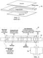
- FIG. 3shows a basic empty surface integrated waveguide structure in a PCB published by Belenguer of the prior art.
- FIG. 4shows a microstrip line to empty substrate integrate waveguide (ESIW) connection made in a printed circuit board.
- EIWintegrated waveguide
- FIG. 5 Ashows top view
- FIG. 5 Ban oblique view, of a RF filter that can be a part of the ESIW system of the present invention.
- FIG. 6 Ashows a top view
- FIG. 6 Bshows an oblique view, of a cavity RF filter that can be a part of the ESIW system of the present invention.
- FIG. 7 Ashows a top view
- FIG. 7 Ban oblique view, of a RF filter coupler that can be a part of the ESIW system of the present invention.
- the present inventionrelates in general to the field of glass based empty substrate integrated waveguide devices. More particularly, the present invention relates to the reduction of parasitic capacitance from fringe capacitance in an RF capacitive resonate filter on the same substrate or in a package. In certain aspects, the present invention is a fringe capacitance reduction of a coupled transmission line resonate filters.
- Photosensitive glass structureshave been suggested for a number of micromachining and microfabrication processes such as integrated electronic elements in conjunction with other elements systems or subsystems.
- Semiconductor microfabrication using thin film additive processes on semiconductor, insulating or conductive substratesis expensive with low yield and a high variability in performance.
- An example of additive micro-transmissioncan be seen in articles Semiconductor Microfabrication Processes by Tian et al., which rely on expensive capital equipment; photolithography and reactive ion etching or ion beam milling tools that generally cost in excess of one million dollars each and require an ultra-clean, high-production silicon fabrication facility costing millions to billions more.
- This inventionprovides a cost effective glass ceramic electronic individual device or as an array of passive devices for a uniform response for RF frequencies with low loss, without the need for reactive ion etching or ion beam milling.
- the present inventionincludes a novel method for fabricating a low loss RF empty substrate integrate waveguide (ESIW) structure in APEX Glass structure for use in forming a number of structures with mechanical stabilization and electrical isolation in a photodefinable glass-ceramic.
- the present inventionincludes ESIW structure to create in multiple planes of a photodefinable glass-ceramic substrate, such process employing the (a) exposure to excitation energy such that the exposure occurs at various angles by either altering the orientation of the substrate or of the energy source, (b) a bake step and (c) an etch step.
- the photosensitive glass substratecan a glass substrate comprising a composition of: 60-76 weight % silica; at least 3 weight % K 2 O with 6 weight %-16 weight % of a combination of K 2 O and Na 2 O; 0.003-1 weight % of at least one oxide selected from the group consisting of Ag 2 O and Au 2 O; 0.003-2 weight % Cu 2 O; 0.75 weight %-7 weight % B 2 O 3 , and 6-7 weight % Al 2 O 3 ; with the combination of B 2 O 3 ; and Al 2 O 3 not exceeding 13 weight %; 8-15 weight % Li 2 O; and 0.001-0.1 weight % CeO 2 .
- the photosensitive glass substrateis a glass substrate comprising a composition of: 35-76 weight % silica, 3-16 weight % K 2 O, 0.003-1 weight % Ag 2 O, 8-15 weight % Li 2 O, and 0.001-0.1 weight % CeO 2 .
- the photosensitive glass substrateis at least one of: a photo-definable glass substrate comprises at least 0.1 weight % Sb 2 O 3 or As 2 O 3 , a photo-definable glass substrate comprises 0.003-1 weight % Au 2 O; a photo-definable glass substrate comprises 1-18 weight % of an oxide selected from the group consisting of CaO, ZnO, PbO, MgO, SrO and BaO.
- the present inventionincludes a high Q empty substrate integrated waveguide device and/or system with low loss, and that is mechanically and thermally stabilized in a photodefinable glass ceramic substrate.
- the ESIWhas a Q greater than 20, 30, 35, 36, 37, 38, 39, or 40.
- the ESIWhas a lower cut-off frequency than a printed circuit board waveguide device at the same frequency.
- the ESIWhas a higher peak power handling capability than a printed circuit ESIW.
- the present inventionhas created the capability to create such fabricating a low loss RF ESIW structure including mechanical support elements in both the vertical as well as horizontal plane for photodefinable glass-ceramic substrate.
- Step 1Lap and polish a photodefinable glass ceramic substrate or wafer.
- the photodefinable glass-ceramic substrateis then exposed to the ESIW pattern, ESIW supports and perimeter ground patterns.
- the ESIW patternis the basic pattern of the waveguide defining areas of no glass.
- the ESIW support elementscan be a cylindrical pattern can have a diameter ranging from 5 ⁇ m to 150 ⁇ m in with but preferably 35 ⁇ m in diameter.
- the perimeter ground patternis the pattern that defines the edges of the waveguide. Patterns are exposed using approximately 20 J/cm 2 of 310 nm light for 2 to 20 min exposure.
- Step 3Anneal at temperature range heated between of 420° C.-520° C. for between 10 minutes to 2 hours, for the coalescing of silver ions into silver nanoparticles and temperature range heated between 520° C.-620° C. for between 10 minutes and 2 hours allowing the lithium oxide to form around the silver nanoparticles.
- Step 4Coat the topside of the wafer with photoresist; expose and develop a pattern to protect the waveguide pattern while leaving the ground pattern exposed.
- Step 5Spin on blanket photoresist on to the backside of the wafer, place the cooled wafer into an HF bath to etch the exposed ground ceramic portions.
- Step 6Using a standard photoresist stripper, remove the photoresist leaving ground pattern openings and ceramic waveguide areas in the wafer.
- Step 7Place the wafer into a copper electroplating bath and plate the open ground pattern with copper until all ground openings are filled.
- Step 8Coat the backside of the wafer with photoresist; expose and develop a rectangular element with small etch release features, this will become the back side of the ESIW.
- Step 9Using a metallization tool such as a sputtering system deposit 200 ⁇ to 2,000 ⁇ of titanium metal, e.g., 300 ⁇ : followed by a 1 ⁇ m deposition of copper onto the backside of the wafer.
- a metallization toolsuch as a sputtering system deposit 200 ⁇ to 2,000 ⁇ of titanium metal, e.g., 300 ⁇ : followed by a 1 ⁇ m deposition of copper onto the backside of the wafer.
- Step 10Using a standard photoresist stripper remove the photoresist leaving rectangular copper element for the bottom of the ESIW structure that is electrically connected to the ground pattern copper.
- Step 11Coat the backside of the wafer with photoresist; expose and develop a rectangular element that is oversized of the ceramic ESIW pattern with etch release features.
- Step 12Place the wafer into a copper electroplating bath and plate the exposed copper areas with between 5-50 um of copper in order to improve the rigidity of the ESIW structure.
- Step 13Using a metallization tool such as a sputtering system deposit 200 ⁇ to 2,000 ⁇ of titanium metal, e.g., 300 ⁇ : followed by a 0.5 um to 1 ⁇ m deposition of copper onto the topside of the wafer.
- a metallization toolsuch as a sputtering system deposit 200 ⁇ to 2,000 ⁇ of titanium metal, e.g., 300 ⁇ : followed by a 0.5 um to 1 ⁇ m deposition of copper onto the topside of the wafer.
- Step 14Coat the top side of the wafer with photoresist; expose and develop the top side ESIW pattern as well as patterns for RF signal launch elements, Phase matching elements, time delay elements, filter elements and antenna elements.
- Step 15Using a standard photoresist stripper, copper etchant and titanium etchant remove the photoresist and etch any exposed deposition metal, leaving the electroplated copper ESIW patterns.
- Step 16The wafer is then placed into a 0.5% to 50% HF in an ultrasonic bath.
- the photodefinable glass-ceramic substrateis then exposed to the ESIW pattern that includes ESIW supports and perimeter ground patterns.
- the ESIW patternis the basic rectangular pattern of the waveguide defining areas.
- the volume of the rectangular patterncan range between 0% to 100% dielectric. Generally, the volume of the rectangular pattern will have no dielectric material.
- the ESIW support elementscan be a cylindrical pattern, hexagonal or other pattern with a diameter ranging from 5 ⁇ m to 200 ⁇ m but preferably 35 ⁇ m in diameter.
- the perimeter of the rectangulardefines the edges of the waveguide and may be electrically connected to ground.
- the patternsare exposed using approximately 20 J/cm 2 of 310 nm light for 2 to 20 min exposure.
- After exposing the photodefinable glass substrateis annealed at temperature range heated between of 420° C.-520° C. for between 10 minutes to 2 hours. This annealing process coalesces the silver ions into silver nanoparticles.
- the photodefinable glass substrateis the annealed at a temperature range heated between 520° C.-620° C.
- the top side of the photodefinable glass substrateis then coated with photoresist; where a pattern is exposed and developed to protect the waveguide pattern while leaving the ground pattern exposed.
- the backside photodefinable glass substrateis coated with a blanket photoresist and then into an HF bath to etch the exposed ground ceramic portions are etched.
- the HF etchant bathcan have a concentration between 2% and 20% but often 10% at room temperature. See FIG. 4 shows an empty substrate integrated waveguide 40 of the present invention. Using a standard photoresist stripper remove the photoresist leaving ground pattern openings and ceramic waveguide areas in the wafer.
- the copper platingcan range from 5 ⁇ m to 50 ⁇ m bit preferably 20 ⁇ m thick.
- the backside of the photodefinable glass substrateis coated with photoresist.
- a rectangular elementis the exposed and developed including small etch release features. This will become the backside of the ESIW.
- These etch release featurescan be rectangular, round or square openings between 10-200 um in size, evenly spaced between 0.05 and 1 mm apart covering the entire ESIW ceramic pattern.
- a metallization toolsuch as a sputtering system or other metallization tool to deposit 200 ⁇ to 2,000 ⁇ of titanium metal, e.g., 300 ⁇ : followed by a between 0.5 ⁇ m to 15 ⁇ m, e.g., 1 ⁇ m of copper onto the backside of the photodefinable glass substrate.
- a standard photoresist stripperremove the photoresist leaving rectangular copper element for the bottom of the ESIW structure that is electrically connected to the ground pattern copper.
- coat the backside of the photodefinable glass substrate with photoresistexpose and develop a rectangular element that is oversized by 5-35% but preferably 15% of the ceramic ESIW pattern with etch release features.
- the photodefinable glass substrateis placed into a copper electroplating bath and plate the exposed copper areas with between 5-100 ⁇ m of copper in order to improve the rigidity of the ESIW structure.
- a metallization toolsuch as a sputtering system deposit 200 ⁇ to 2,000 ⁇ of titanium metal preferably 300 ⁇ : followed by a 0.5 ⁇ m to 5 ⁇ m, e.g., 1 ⁇ m deposition of copper onto the topside of the photodefinable glass substrate.
- the photodefinable glass substrateis then coat the topside with photoresist is exposed and developed with the topside ESIW pattern.
- This patternincludes patterns for RF signal launch elements, Phase matching elements, time delay elements, filter elements and antenna elements.
- the photodefinable glass substrateis then placed into a copper electroplating bath and plate the exposed copper areas with between 5-100 ⁇ m of copper.
- the photoresist on the photodefinable glass substrateremoved using standard photoresist stripper, copper etchant and titanium etchant remove the photoresist and etch any exposed deposition metal, leaving the electroplated copper ESIW patterns.
- the photodefinable glass substrateis then placed into a 0.5% to 50% HF solution preferably 10%.
- the etching processcan be accelerated by use of an ultrasonic bath.
- the ultrasonic bathcan be operated in the pulse, sweep and fix mode at frequencies from 28 Khz to 200 Khz to release the ESIW structure and remove all of the defined ceramic structures.
- the photodefinable glass substrateis then placed into a deionized water (DI) rinse bath to stop the etching process substrate.
- DIdeionized water
- the photodefinable glass substraterinsed and dried wafer.
- the photodefinable glass substrateis then translated to a wafer dicing system to release the ESIW device/system.
- the ESIW deviceis a simple antenna combined with an RF signal launch elements.
- a ESIW systemincludes phase matching elements, time delay elements, filter elements in addition to antenna and RF signal launch elements.
- FIG. 4shows an empty substrate integrated waveguide 40 of the present invention, in which a substrate 42 , in this case the photodefinable glass substrate, has been formed into the device.
- a substrate 42in this case the photodefinable glass substrate
- the edge ground via(s) 48(EGVs), which are anchor point vias on each side of the removed glass, contact the upper metallization 50 and the lower metallization 52 .
- ESVsedge ground vias
- the processcan be designed to allow for additional circuits or features.
- perforated areas 54in addition to unsupported metal areas 56 , which are not in electrical contact with the edge ground vias 48 .
- a close-up view 58is shown for the through-vias, that also show the option for cutting-in or undercutting the lower metallization area 52 .
- FIG. 5 Ashows top view, and FIG. 5 B an oblique view, of a RF filter that can be a part of the ESIW system of the present invention.
- FIG. 6 Ashows a top view
- FIG. 6 Bshows an oblique view, of a cavity RF filter that can be a part of the ESIW system of the present invention.
- FIG. 7 Ashows a top view
- FIG. 7 Ban oblique view, of a RF filter coupler that can be a part of the ESIW system of the present invention.
- Each of the top and oblique views of 5 A to 7 Bcan be used to form the device shown in FIG. 4 .
- compositions of the inventioncan be used to achieve methods of the invention.
- the words “comprising”(and any form of comprising, such as “comprise” and “comprises”), “having” (and any form of having, such as “have” and “has”), “including” (and any form of including, such as “includes” and “include”) or “containing” (and any form of containing, such as “contains” and “contain”) are inclusive or open-ended and do not exclude additional, unrecited elements or method steps.
- “comprising”may be replaced with “consisting essentially of” or “consisting of”.
- the phrase “consisting essentially of”requires the specified integer(s) or steps as well as those that do not materially affect the character or function of the claimed invention.
- the term “consisting”is used to indicate the presence of the recited integer (e.g., a feature, an element, a characteristic, a property, a method/process step or a limitation) or group of integers (e.g., feature(s), element(s), characteristic(s), property(ies), method/process steps or limitation(s)) only.
- A, B, C, or combinations thereofrefers to all permutations and combinations of the listed items preceding the term.
- “A, B, C, or combinations thereof”is intended to include at least one of: A, B, C, AB, AC, BC, or ABC, and if order is important in a particular context, also BA, CA, CB, CBA, BCA, ACB, BAC, or CAB.
- expressly includedare combinations that contain repeats of one or more item or term, such as BB, AAA, AB, BBC, AAABCCCC, CBBAAA, CABABB, and so forth.
- BBBB
- AAAAAA
- ABBBC
- AAABCCCCCCCBBAAA
- CABABBCABABB
- words of approximationsuch as, without limitation, “about”, “substantial” or “substantially” refers to a condition that when so modified is understood to not necessarily be absolute or perfect but would be considered close enough to those of ordinary skill in the art to warrant designating the condition as being present.
- the extent to which the description may varywill depend on how great a change can be instituted and still have one of ordinary skill in the art recognize the modified feature as still having the required characteristics and capabilities of the unmodified feature.
- a numerical value herein that is modified by a word of approximationsuch as “about” may vary from the stated value by at least ⁇ 1, 2, 3, 4, 5, 6, 7, 10, 12 or 15%.
- compositions and/or methods disclosed and claimed hereincan be made and executed without undue experimentation in light of the present disclosure. While the compositions and methods of this invention have been described in terms of preferred embodiments, it will be apparent to those of skill in the art that variations may be applied to the compositions and/or methods and in the steps or in the sequence of steps of the method described herein without departing from the concept, spirit and scope of the invention. All such similar substitutes and modifications apparent to those skilled in the art are deemed to be within the spirit, scope and concept of the invention as defined by the appended claims.
- each dependent claimcan depend both from the independent claim and from each of the prior dependent claims for each and every claim so long as the prior claim provides a proper antecedent basis for a claim term or element.
- a general purpose processore.g., microprocessor, conventional processor, controller, microcontroller, state machine or combination of computing devices
- DSPdigital signal processor
- ASICapplication specific integrated circuit
- FPGAfield programmable gate array
- steps of a method or process described hereinmay be embodied directly in hardware, in a software module executed by a processor, or in a combination of the two.
- a software modulemay reside in RAM memory, flash memory, ROM memory, EPROM memory, EEPROM memory, registers, hard disk, a removable disk, a CD-ROM, or any other form of storage medium known in the art.
Landscapes
- Chemical & Material Sciences (AREA)
- Engineering & Computer Science (AREA)
- Organic Chemistry (AREA)
- Materials Engineering (AREA)
- Geochemistry & Mineralogy (AREA)
- General Chemical & Material Sciences (AREA)
- Chemical Kinetics & Catalysis (AREA)
- Life Sciences & Earth Sciences (AREA)
- Ceramic Engineering (AREA)
- Condensed Matter Physics & Semiconductors (AREA)
- Crystallography & Structural Chemistry (AREA)
- Dispersion Chemistry (AREA)
- Microelectronics & Electronic Packaging (AREA)
- Computer Hardware Design (AREA)
- General Physics & Mathematics (AREA)
- Physics & Mathematics (AREA)
- Power Engineering (AREA)
- Manufacturing & Machinery (AREA)
- Optical Integrated Circuits (AREA)
- Waveguides (AREA)
- Electroplating Methods And Accessories (AREA)
- Manufacturing Of Printed Wiring (AREA)
- Control Of Motors That Do Not Use Commutators (AREA)
Abstract
Description
Claims (10)
Priority Applications (1)
| Application Number | Priority Date | Filing Date | Title |
|---|---|---|---|
| US17/598,009US11962057B2 (en) | 2019-04-05 | 2020-04-03 | Glass based empty substrate integrated waveguide devices |
Applications Claiming Priority (3)
| Application Number | Priority Date | Filing Date | Title |
|---|---|---|---|
| US201962829882P | 2019-04-05 | 2019-04-05 | |
| US17/598,009US11962057B2 (en) | 2019-04-05 | 2020-04-03 | Glass based empty substrate integrated waveguide devices |
| PCT/US2020/026673WO2020206323A1 (en) | 2019-04-05 | 2020-04-03 | Glass based empty substrate integrated waveguide devices |
Publications (2)
| Publication Number | Publication Date |
|---|---|
| US20220173488A1 US20220173488A1 (en) | 2022-06-02 |
| US11962057B2true US11962057B2 (en) | 2024-04-16 |
Family
ID=72667425
Family Applications (1)
| Application Number | Title | Priority Date | Filing Date |
|---|---|---|---|
| US17/598,009Active2041-03-24US11962057B2 (en) | 2019-04-05 | 2020-04-03 | Glass based empty substrate integrated waveguide devices |
Country Status (7)
| Country | Link |
|---|---|
| US (1) | US11962057B2 (en) |
| EP (1) | EP3935687B1 (en) |
| JP (2) | JP7140435B2 (en) |
| KR (1) | KR20210147040A (en) |
| AU (1) | AU2020253553A1 (en) |
| CA (2) | CA3172853A1 (en) |
| WO (1) | WO2020206323A1 (en) |
Families Citing this family (5)
| Publication number | Priority date | Publication date | Assignee | Title |
|---|---|---|---|---|
| WO2020014661A1 (en) | 2018-07-13 | 2020-01-16 | Knowles Cazenovia, Inc. | Millimeter wave filter array |
| KR20220164800A (en) | 2020-04-17 | 2022-12-13 | 3디 글래스 솔루션즈 인코포레이티드 | broadband inductor |
| KR102453374B1 (en)* | 2020-10-19 | 2022-10-12 | 한국전자기술연구원 | Semiconductor package using photosensitive glass and manufacturing method thereof |
| KR102829741B1 (en)* | 2021-01-19 | 2025-07-04 | 주식회사 아모텍 | Method for manufacturing ceramic waveguide filter and ceramic waveguide filter |
| WO2024158994A1 (en)* | 2023-01-25 | 2024-08-02 | 3D Glass Solutions, Inc. | Vertical quasi-coaxial filters |
Citations (290)
| Publication number | Priority date | Publication date | Assignee | Title |
|---|---|---|---|---|
| GB619779A (en) | 1946-01-18 | 1949-03-15 | Gen Aniline & Film Corp | Improvements in iron powder and cores produced therefrom |
| US2515937A (en) | 1943-12-08 | 1950-07-18 | Corning Glass Works | Photosensitive gold glass and method of making it |
| US2515941A (en) | 1946-09-09 | 1950-07-18 | Corning Glass Works | Photosensitive opal glass |
| US2515940A (en) | 1946-09-09 | 1950-07-18 | Corning Glass Works | Photosensitive opal glass |
| US2515943A (en) | 1949-01-07 | 1950-07-18 | Corning Glass Works | Photosensitive glass article and composition and method for making it |
| US2628160A (en) | 1951-08-30 | 1953-02-10 | Corning Glass Works | Sculpturing glass |
| US2684911A (en) | 1951-08-30 | 1954-07-27 | Corning Glass Works | Photosensitively opacifiable glass |
| US2971853A (en) | 1953-03-05 | 1961-02-14 | Corning Glass Works | Ceramic body and method of making it |
| US3281264A (en) | 1963-01-31 | 1966-10-25 | Coast Metals Inc | Method of gold-plating aluminum |
| US3292115A (en) | 1964-09-11 | 1966-12-13 | Hazeltine Research Inc | Easily fabricated waveguide structures |
| US3904991A (en) | 1973-02-12 | 1975-09-09 | Tokyo Shibaura Electric Co | Stripline directional coupler having bent coupling arms |
| GB1407151A (en) | 1973-02-13 | 1975-09-24 | Okikiolu G O | System assemblies of energized components having tapering form for developing progressively increasing electromagnetic energy fields |
| US3985531A (en) | 1975-03-19 | 1976-10-12 | Corning Glass Works | Spontaneously-formed fluormica glass-ceramics |
| US3993401A (en) | 1975-02-10 | 1976-11-23 | Minnesota Mining And Manufacturing Company | Retroreflective material including geometric fresnel zone plates |
| US4029605A (en) | 1975-12-08 | 1977-06-14 | Hercules Incorporated | Metallizing compositions |
| US4131516A (en) | 1977-07-21 | 1978-12-26 | International Business Machines Corporation | Method of making metal filled via holes in ceramic circuit boards |
| JPS56155587A (en) | 1980-05-02 | 1981-12-01 | Fujitsu Ltd | Printed circuit board |
| US4413061A (en) | 1978-02-06 | 1983-11-01 | International Business Machines Corporation | Glass-ceramic structures and sintered multilayer substrates thereof with circuit patterns of gold, silver or copper |
| US4444616A (en) | 1981-06-02 | 1984-04-24 | Hoya Corporation | Method for exposure of chemically machinable light-sensitive glass |
| US4514053A (en) | 1983-08-04 | 1985-04-30 | Corning Glass Works | Integral photosensitive optical device and method |
| US4537612A (en) | 1982-04-01 | 1985-08-27 | Corning Glass Works | Colored photochromic glasses and method |
| JPS61149905A (en) | 1984-12-25 | 1986-07-08 | Fujitsu Ltd | Optical multiplexer and demultiplexer |
| US4611882A (en) | 1982-09-08 | 1986-09-16 | Alps Electric Co., Ltd. | High-frequency circuit device with an annular capacitor on the back of an insulated substrate |
| JPS61231529A (en) | 1985-04-08 | 1986-10-15 | Agency Of Ind Science & Technol | Optical control type optical switch device |
| US4647950A (en) | 1984-05-07 | 1987-03-03 | Kabushiki Kaisha Toshiba | Recording apparatus |
| JPS62202840A (en) | 1986-03-03 | 1987-09-07 | Toshiba Corp | Working of photosensitive glass |
| US4692015A (en) | 1986-03-14 | 1987-09-08 | Xerox Corporation | Short focal lens array with multi-magnification properties |
| JPS63128699A (en) | 1986-11-19 | 1988-06-01 | 株式会社日立製作所 | Light-sensitive glass-ceramic multilayer interconnection board |
| US4788165A (en) | 1987-10-07 | 1988-11-29 | Corning Glass Works | Copper-exuding, boroaluminosilicate glasses |
| EP0311274A2 (en) | 1987-10-07 | 1989-04-12 | Corning Glass Works | Thermal writing on glass or glass-ceramic substrates and copper-exuding glasses |
| US4942076A (en) | 1988-11-03 | 1990-07-17 | Micro Substrates, Inc. | Ceramic substrate with metal filled via holes for hybrid microcircuits and method of making the same |
| JPH0393683A (en) | 1989-09-01 | 1991-04-18 | Fujitsu Ltd | Copper paste and metallization method using the same |
| US5078771A (en) | 1989-02-07 | 1992-01-07 | Canyon Materials, Inc. | Method of making high energy beam sensitive glasses |
| US5147740A (en) | 1990-08-09 | 1992-09-15 | Rockwell International Corporation | Structure and process for fabricating conductive patterns having sub-half micron dimensions |
| EP0507719A1 (en) | 1991-04-04 | 1992-10-07 | International Business Machines Corporation | Improved glass-ceramic to copper adhesion |
| US5212120A (en) | 1991-06-10 | 1993-05-18 | Corning Incorporated | Photosensitive glass |
| JPH05139787A (en) | 1991-11-19 | 1993-06-08 | Seikosha Co Ltd | Working method for photosensitive glass |
| US5312674A (en) | 1992-07-31 | 1994-05-17 | Hughes Aircraft Company | Low-temperature-cofired-ceramic (LTCC) tape structures including cofired ferromagnetic elements, drop-in components and multi-layer transformer |
| US5352996A (en) | 1992-01-30 | 1994-10-04 | Leader Electronics Corp. | Interdigital bandpass filter |
| US5371466A (en) | 1992-07-29 | 1994-12-06 | The Regents Of The University Of California | MRI RF ground breaker assembly |
| US5374291A (en) | 1991-12-10 | 1994-12-20 | Director-General Of Agency Of Industrial Science And Technology | Method of processing photosensitive glass |
| US5395498A (en) | 1991-11-06 | 1995-03-07 | Gombinsky; Moshe | Method for separating biological macromolecules and means therfor |
| US5409741A (en) | 1991-04-12 | 1995-04-25 | Laude; Lucien D. | Method for metallizing surfaces by means of metal powders |
| JPH0826767A (en) | 1994-07-13 | 1996-01-30 | Nippon Glass Kk | Soda lime-silica photosensitive glass and its production |
| JPH08179155A (en) | 1994-12-26 | 1996-07-12 | Ricoh Co Ltd | Method for coupling lens and optical fiber and method for producing lens substrate |
| JPH107435A (en) | 1996-06-26 | 1998-01-13 | Ngk Spark Plug Co Ltd | Glass ceramic wiring substrate and its production |
| US5733370A (en) | 1996-01-16 | 1998-03-31 | Seagate Technology, Inc. | Method of manufacturing a bicrystal cluster magnetic recording medium |
| US5779521A (en) | 1995-03-03 | 1998-07-14 | Sony Corporation | Method and apparatus for chemical/mechanical polishing |
| JPH10199728A (en) | 1997-01-07 | 1998-07-31 | Murata Mfg Co Ltd | Thin-film coil component and method of manufacturing the same |
| US5850623A (en) | 1997-03-14 | 1998-12-15 | Eastman Chemical Company | Method for standardizing raman spectrometers to obtain stable and transferable calibrations |
| US5902715A (en) | 1992-11-09 | 1999-05-11 | Fujitsu Limited | Method of forming a mirror in a waveguide |
| US5919607A (en) | 1995-10-26 | 1999-07-06 | Brown University Research Foundation | Photo-encoded selective etching for glass based microtechnology applications |
| EP0685857B1 (en) | 1994-06-03 | 1999-09-08 | Mitel Semiconductor Limited | Inductor chip device |
| EP0949648A1 (en) | 1996-09-26 | 1999-10-13 | Asahi Glass Company Ltd. | Plasma display protective plate and its manufacturing method |
| US5998224A (en) | 1997-05-16 | 1999-12-07 | Abbott Laboratories | Magnetically assisted binding assays utilizing a magnetically responsive reagent |
| JPH11344648A (en) | 1998-05-07 | 1999-12-14 | Trw Inc | Fiber/waveguide-mirror-lens alignment device |
| US6046641A (en) | 1998-07-22 | 2000-04-04 | Eni Technologies, Inc. | Parallel HV MOSFET high power stable amplifier |
| US6066448A (en) | 1995-03-10 | 2000-05-23 | Meso Sclae Technologies, Llc. | Multi-array, multi-specific electrochemiluminescence testing |
| US6094336A (en) | 1997-04-25 | 2000-07-25 | U.S. Philips Corporation | Enveloped multilayer capacitor |
| JP2000228615A (en) | 1999-02-05 | 2000-08-15 | Tokin Corp | Lc bandpass filter |
| US6136210A (en) | 1998-11-02 | 2000-10-24 | Xerox Corporation | Photoetching of acoustic lenses for acoustic ink printing |
| US6171886B1 (en) | 1998-06-30 | 2001-01-09 | Eastman Kodak Company | Method of making integrated hybrid silicon-based micro-actuator devices |
| JP2001033664A (en) | 1999-07-21 | 2001-02-09 | Hitachi Cable Ltd | Optical fiber block |
| US6258497B1 (en) | 1992-07-29 | 2001-07-10 | International Business Machines Corporation | Precise endpoint detection for etching processes |
| US6287965B1 (en) | 1997-07-28 | 2001-09-11 | Samsung Electronics Co, Ltd. | Method of forming metal layer using atomic layer deposition and semiconductor device having the metal layer as barrier metal layer or upper or lower electrode of capacitor |
| US6329702B1 (en) | 2000-07-06 | 2001-12-11 | Tyco Electronics Corporation | High frequency carrier |
| US20010051584A1 (en) | 2000-04-26 | 2001-12-13 | Matsushita Electric Industrial Co., Ltd. | Dielectric ceramic composition and method for producing the same, and device for communication apparatus using the same |
| US20020015546A1 (en) | 2000-07-31 | 2002-02-07 | Bhagavatula Venkata A. | Bulk internal bragg gratings and optical devices |
| US6373369B2 (en) | 1999-07-26 | 2002-04-16 | Taiwan Semiconductor Manufacturing Company | High efficiency thin film inductor |
| US6383566B1 (en) | 1999-06-30 | 2002-05-07 | Saint-Gobain Vitrage | Process for depositing a tungsten-based and/or molybdenum-based layer on a rigid substrate, and substrate thus coated |
| US20020086246A1 (en) | 2000-12-30 | 2002-07-04 | Lg Electronics Inc. | Method of fabricating barrier ribs in plasma display panel |
| US6417754B1 (en) | 1997-12-08 | 2002-07-09 | The Regents Of The University Of California | Three-dimensional coil inductor |
| US20020100608A1 (en) | 1999-05-27 | 2002-08-01 | Hoya Corporation | Multilayer printed wiring board and a process of producing same |
| US6485690B1 (en) | 1999-05-27 | 2002-11-26 | Orchid Biosciences, Inc. | Multiple fluid sample processor and system |
| US6495411B1 (en) | 2000-07-13 | 2002-12-17 | Promos Technology Inc. | Technique to improve deep trench capacitance by increasing surface thereof |
| US6511793B1 (en) | 1999-03-24 | 2003-01-28 | Lg Electronics Inc. | Method of manufacturing microstructure using photosensitive glass substrate |
| US6514375B2 (en) | 1997-12-15 | 2003-02-04 | Ricoh Company, Ltd. | Dry etching endpoint detection system |
| US20030025227A1 (en) | 2001-08-02 | 2003-02-06 | Zograph, Llc | Reproduction of relief patterns |
| US6562523B1 (en) | 1996-10-31 | 2003-05-13 | Canyon Materials, Inc. | Direct write all-glass photomask blanks |
| US20030107459A1 (en) | 2001-10-30 | 2003-06-12 | Kazuaki Takahashi | Radio frequency module and method for manufacturing the same |
| US20030124716A1 (en) | 2000-10-10 | 2003-07-03 | Biotrove, Inc., A Delaware Corporation | Apparatus for assay, synthesis and storage, and methods of manufacture, use, and manipulation thereof |
| US20030135201A1 (en) | 2001-09-28 | 2003-07-17 | Gonnelli Robert R. | Microneedle with membrane |
| US20030143802A1 (en) | 2002-01-28 | 2003-07-31 | Nanya Technology Corporation | Method of forming a bottle-shaped trench in a semiconductor substrate |
| US20030156819A1 (en) | 2002-02-15 | 2003-08-21 | Mark Pruss | Optical waveguide |
| US20030174944A1 (en) | 2002-03-14 | 2003-09-18 | Corning Incorporated | Fiber array and methods for fabricating the fiber array |
| US20030228682A1 (en) | 2002-04-30 | 2003-12-11 | University Of Maryland, Baltimore | Fluorescence sensing |
| US20030231830A1 (en) | 2002-05-14 | 2003-12-18 | Naoko Hikichi | Optical module |
| KR20040001906A (en) | 2002-06-29 | 2004-01-07 | 주식회사 하이닉스반도체 | Method for fabricating capacitor |
| US6678453B2 (en) | 1999-11-04 | 2004-01-13 | Corning Incorporated | High aspect ratio patterning of glass film |
| US20040008391A1 (en) | 1999-09-16 | 2004-01-15 | Bowley Christopher C. | Holographically-formed polymer dispersed liquid crystals with multiple gratings |
| US6686824B1 (en) | 1998-05-29 | 2004-02-03 | Nissha Printing Co., Ltd. | Toroidal printed coil |
| US20040020690A1 (en) | 1998-03-20 | 2004-02-05 | Parker John Leroy | Via connector and method of making same |
| US20040058504A1 (en) | 2002-09-20 | 2004-03-25 | Kellar Scot A. | Ultra-high capacitance device based on nanostructures |
| US20040104449A1 (en) | 2001-03-29 | 2004-06-03 | Jun-Bo Yoon | Three- dimensional metal devices highly suspended above semiconductor substrate, their circuit model, and method for manufacturing the same |
| US6771860B2 (en) | 2001-06-29 | 2004-08-03 | Xanoptix, Inc. | Module mounted aligning optical connector |
| US20040155748A1 (en) | 2003-02-02 | 2004-08-12 | Dietrich Steingroever | Transformer for producing high electrical currents |
| US6783920B2 (en) | 2003-01-15 | 2004-08-31 | The Aerospace Corporation | Photosensitive glass variable laser exposure patterning method |
| US20040171076A1 (en) | 2001-12-20 | 2004-09-02 | Dejneka Matthew J. | Detectable micro to nano sized structures, methods of manufacture and use |
| US20040184705A1 (en) | 2003-01-08 | 2004-09-23 | Mikihiro Shimada | Optical waveguide component and method of manufacturing the same |
| US20040198582A1 (en) | 2003-04-01 | 2004-10-07 | Borrelli Nicholas F. | Optical elements and methods of making optical elements |
| US20040227596A1 (en) | 2003-02-11 | 2004-11-18 | Nguyen John A. | Ultra broadband inductor assembly |
| US6824974B2 (en) | 2001-06-11 | 2004-11-30 | Genorx, Inc. | Electronic detection of biological molecules using thin layers |
| US6830221B1 (en) | 2003-12-19 | 2004-12-14 | The Aerospace Corporation | Integrated glass ceramic spacecraft |
| EP1487019A1 (en) | 2003-06-12 | 2004-12-15 | Koninklijke Philips Electronics N.V. | Electronic device and method of manufacturing thereof |
| KR20050000923A (en) | 2003-06-25 | 2005-01-06 | 삼성전기주식회사 | An ic chip internal type power amplifier module |
| CN1562831A (en) | 2004-04-16 | 2005-01-12 | 武汉理工大学 | Method for preparing microcrystalline glass/glass carrier material having nano holes in high density |
| US6843902B1 (en) | 2001-07-20 | 2005-01-18 | The Regents Of The University Of California | Methods for fabricating metal nanowires |
| US6875544B1 (en) | 2002-10-03 | 2005-04-05 | Sandia Corporation | Method for the fabrication of three-dimensional microstructures by deep X-ray lithography |
| US20050089901A1 (en) | 2000-09-22 | 2005-04-28 | Porter Marc D. | Raman-active reagents and the use thereof |
| US20050105860A1 (en) | 2003-02-24 | 2005-05-19 | Ngk Spark Plug Co., Ltd. | Optical device mounted substrate assembly |
| US20050111162A1 (en) | 2003-10-31 | 2005-05-26 | Tetsuya Osaka | Thin film capacitor, high-density packaging substrate incorporating thin film capacitor, and method for manufacturing thin-film capacitor |
| US20050118779A1 (en) | 2003-11-28 | 2005-06-02 | Myung-Kyu Ahn | Method for fabricating semiconductor device |
| US20050150683A1 (en) | 2004-01-12 | 2005-07-14 | Farnworth Warren M. | Methods of fabricating substrates and substrate precursor structures resulting therefrom |
| US20050170670A1 (en) | 2003-11-17 | 2005-08-04 | King William P. | Patterning of sacrificial materials |
| JP2005215644A (en) | 2004-02-02 | 2005-08-11 | Sharp Corp | Optical module and manufacturing method thereof |
| US6932933B2 (en) | 2001-03-30 | 2005-08-23 | The Aerospace Corporation | Ultraviolet method of embedding structures in photocerams |
| US20050212432A1 (en) | 2005-06-27 | 2005-09-29 | Osram Sylvania Inc. | Incandescent lamp that emits infrared light and a method of making the lamp |
| JP2005302987A (en) | 2004-04-12 | 2005-10-27 | Dainippon Printing Co Ltd | Passive element built-in wiring board and manufacturing method thereof |
| US20050277550A1 (en) | 2004-06-09 | 2005-12-15 | Ferro Corporation | Lead-free and cadmium-free conductive copper thick film pastes |
| US6977722B2 (en) | 2001-06-29 | 2005-12-20 | Meso Scale Technologies, Llc. | Assay plates, reader systems and methods for luminescence test measurements |
| DE102004059252A1 (en) | 2004-06-09 | 2006-01-19 | Schott Ag | Optically active structure application method for Fresnel lens manufacture, involves photographic structuring photosensitive resist layer, coating substrate with optically active layer and lifting-off resist layer |
| JP2006032982A (en) | 2005-09-02 | 2006-02-02 | Semiconductor Energy Lab Co Ltd | Heating processing method of thin film |
| US7033821B2 (en) | 2000-11-08 | 2006-04-25 | Surface Logix, Inc. | Device for monitoring cell motility in real-time |
| US20060092079A1 (en) | 2004-10-01 | 2006-05-04 | De Rochemont L P | Ceramic antenna module and methods of manufacture thereof |
| US20060118965A1 (en) | 2004-12-02 | 2006-06-08 | Nec Electronics Corporation | Semiconductor device, semiconductor module employing thereof and method for manufacturing semiconductor device |
| US7064045B2 (en) | 2004-08-30 | 2006-06-20 | Miradia Inc. | Laser based method and device for forming spacer structures for packaging optical reflection devices |
| JP2006179564A (en) | 2004-12-21 | 2006-07-06 | Nec Corp | Semiconductor connection substrate, method of manufacturing the same semiconductor apparatus, semiconductor device, and semiconductor substrate |
| US20060147344A1 (en) | 2004-09-30 | 2006-07-06 | The University Of Cincinnati | Fully packed capillary electrophoretic separation microchips with self-assembled silica colloidal particles in microchannels and their preparation methods |
| US20060159916A1 (en) | 2003-05-05 | 2006-07-20 | Nanosys, Inc. | Nanofiber surfaces for use in enhanced surface area applications |
| US20060158300A1 (en) | 2005-01-20 | 2006-07-20 | Avx Corporation | High Q planar inductors and IPD applications |
| EP1683571A1 (en) | 2005-01-20 | 2006-07-26 | Samsung Electronics Co., Ltd. | Patterning method, substrate for biomolecule immobilization using the patterning method, and biochip employing the substrate |
| US20060171033A1 (en) | 2004-12-31 | 2006-08-03 | Schott Ag | Method for producing an optical component, optical component produced according to the method and devices comprising such components |
| US20060177855A1 (en) | 2005-01-21 | 2006-08-10 | Utermohlen Joseph G | Nanoparticles for manipulation of biopolymers and methods of thereof |
| KR20060092643A (en) | 2005-02-18 | 2006-08-23 | 주식회사 하이닉스반도체 | Semiconductor memory device and manufacturing method thereof |
| US20060193214A1 (en) | 2005-02-28 | 2006-08-31 | Takeshi Shimano | Optical head, optical information storage apparatus, and their fabrication method |
| US7132054B1 (en) | 2004-09-08 | 2006-11-07 | Sandia Corporation | Method to fabricate hollow microneedle arrays |
| JP2006324489A (en) | 2005-05-19 | 2006-11-30 | Matsushita Electric Ind Co Ltd | Chip coil and manufacturing method thereof |
| US20060283948A1 (en) | 2005-06-20 | 2006-12-21 | Denso Corporation | Antenna coil, resonant antenna having antenna coil, and card type wireless device having resonant antenna |
| US7179638B2 (en) | 1999-07-30 | 2007-02-20 | Large Scale Biology Corporation | Microarrays and their manufacture by slicing |
| US20070121263A1 (en) | 2005-11-29 | 2007-05-31 | Jeng-Shu Liu | Timing controller chip |
| US20070120263A1 (en) | 2005-08-19 | 2007-05-31 | Zvonimir Gabric | Conductor track arrangement and associated production method |
| US20070155021A1 (en) | 2005-12-29 | 2007-07-05 | Intel Corporation | Modification of metal nanoparticles for improved analyte detection by surface enhanced Raman spectroscopy (SERS) |
| US20070158787A1 (en) | 2003-11-13 | 2007-07-12 | Rajen Chanchani | Heterogeneously integrated microsystem-on-a-chip |
| WO2007088058A2 (en) | 2006-02-02 | 2007-08-09 | Xsil Technology Limited | Support for wafer singulation |
| US7277151B2 (en) | 2001-10-15 | 2007-10-02 | Samsung Sdi Co., Ltd. | Flat panel display with photosensitive glass spacer |
| US20070248126A1 (en) | 2002-06-10 | 2007-10-25 | New Wave Research | Scribing sapphire substrates with a solid state uv laser |
| US20070267708A1 (en) | 2006-05-22 | 2007-11-22 | Cardiomems, Inc. | Methods and apparatus having an integrated circuit attached to fused silica |
| US20070272829A1 (en) | 2006-05-29 | 2007-11-29 | Atsuo Nakagawa | Solid-state imaging device and method for fabricating the same |
| US20070279837A1 (en) | 2004-03-18 | 2007-12-06 | Nanosys, Inc. | Nanofiber Surface Based Capacitors |
| US7306689B2 (en) | 1998-10-27 | 2007-12-11 | Sony Corporation | Optical waveguide and method for producing same |
| US20070296520A1 (en) | 2005-04-18 | 2007-12-27 | Murata Manufacturing Co., Ltd. | High-frequency module |
| US7326538B2 (en) | 2002-01-04 | 2008-02-05 | Becton Dickinson And Company | Binding proteins as biosensors |
| US20080042785A1 (en) | 2006-08-16 | 2008-02-21 | Fujitsu Limited | Inductor circuit board, method of forming inductor, and bias-T circuit |
| US20080079565A1 (en) | 2006-09-28 | 2008-04-03 | Semiconductor Energy Laboratory Co., Ltd. | Wireless sensor device |
| US20080136572A1 (en) | 2006-12-06 | 2008-06-12 | Farrokh Ayazi | Micro-electromechanical switched tunable inductor |
| US20080174976A1 (en) | 2001-07-12 | 2008-07-24 | Hitachi, Ltd. | Electronic Circuit Component |
| US20080182079A1 (en) | 2006-06-28 | 2008-07-31 | Northwestern University | Etching and hole arrays |
| US7407768B2 (en) | 2002-09-11 | 2008-08-05 | Synamem Corporation | Membrane-based assays |
| US7410763B2 (en) | 2005-09-01 | 2008-08-12 | Intel Corporation | Multiplex data collection and analysis in bioanalyte detection |
| US20080226228A1 (en) | 2007-03-15 | 2008-09-18 | Hitachi Cable, Ltd. | Optical system connection structure, optical component, and optical communication module |
| US20080223603A1 (en) | 2007-03-12 | 2008-09-18 | Samsung Electro-Mechanics Co., Ltd. | Capacitor embedded printed circuit board |
| US20080231402A1 (en) | 2007-03-22 | 2008-09-25 | Industrial Technology Research Institute | Inductor devices |
| WO2008119080A1 (en) | 2007-03-28 | 2008-10-02 | Life Bioscience Inc. | Compositions and methods to fabricate a photoactive substrate suitable for shaped glass structures |
| JP2008252797A (en) | 2007-03-30 | 2008-10-16 | Tdk Corp | Dielectric resonator, dielectric filter, and characteristic adjustment method thereof |
| US7439128B2 (en) | 2003-04-07 | 2008-10-21 | International Business Machines Corporation | Method of creating deep trench capacitor using a P+ metal electrode |
| US20080291442A1 (en) | 2005-06-13 | 2008-11-27 | Solaris Nanosciences, Inc. | Chemical and biological sensing using metallic particles in amplifying and absorbing media |
| US20080305268A1 (en) | 2007-06-05 | 2008-12-11 | Air Products And Chemicals, Inc. | Low Temperature Thermal Conductive Inks |
| WO2008154931A1 (en) | 2007-06-18 | 2008-12-24 | Danmarks Tekniske Universitet (Technical University Of Denmark) | Adsorbent beads suitable for use in separation of biological molecules |
| US20080316678A1 (en) | 2006-07-14 | 2008-12-25 | Ehrenberg Scott G | Nanoparticle ultracapacitor |
| US7470518B2 (en) | 2002-02-12 | 2008-12-30 | Cellectricon Ab | Systems and method for rapidly changing the solution environment around sensors |
| US20090029185A1 (en) | 2007-07-27 | 2009-01-29 | Cheng-Chang Lee | Magnetic device and manufacturing method thereof |
| US7497554B2 (en) | 2004-07-22 | 2009-03-03 | Konica Minolta Holdings, Inc. | Ink jet print head |
| WO2009029733A2 (en) | 2007-08-28 | 2009-03-05 | Life Biosciences, Inc. | Method of providing a pattern of biological-binding areas for biological testing |
| WO2009062011A1 (en) | 2007-11-07 | 2009-05-14 | Masachusetts Institute Of Technology | Method of forming a locally periodic 3d structure with larger-scale variation in periodic properties and applications thereof |
| US20090130736A1 (en) | 2003-02-06 | 2009-05-21 | Becton, Dickinson And Company | Pretreatment method for extraction of nucleic acid from biological samples and kits therefor |
| US20090170032A1 (en) | 2007-12-28 | 2009-07-02 | Fujitsu Media Devices Limited | Method of manufacturing electronic device |
| US20090182720A1 (en) | 2008-01-15 | 2009-07-16 | Cain Michael W | Maintained Symbol Table Only Index |
| US20090200540A1 (en) | 2008-02-07 | 2009-08-13 | Bjoerk Mikael T | Metal-Oxide-Semiconductor Device Including a Multiple-Layer Energy Filter |
| US20090243783A1 (en) | 2006-08-28 | 2009-10-01 | Avago Technologies Ecbu (Singapore) Pte. Ltd. | Minimizing Electromagnetic Interference in Coil Transducers |
| WO2009126649A2 (en) | 2008-04-07 | 2009-10-15 | Life Bioscience, Inc. | Method of providing particles having biological-binding areas for biological applications |
| US20090290281A1 (en) | 2007-02-14 | 2009-11-26 | Murata Manufacturing Co., Ltd. | Multilayer ceramic capacitor and method for manufacturing the same |
| US20100009838A1 (en) | 2007-03-26 | 2010-01-14 | Murata Manufacturing Co., Ltd. | Photosensitive dielectric paste and electronic part made with the same |
| US20100022416A1 (en) | 2008-07-25 | 2010-01-28 | Life Bioscience, Inc. | Assay plates, methods and systems having one or more etched features |
| KR100941691B1 (en) | 2009-04-10 | 2010-02-12 | (주)제이스 | Photosensitve glass wafer and method for manufacturing potosensitve glass wafer and semiconductor probe chip |
| US20100044089A1 (en) | 2007-03-01 | 2010-02-25 | Akinobu Shibuya | Interposer integrated with capacitors and method for manufacturing the same |
| US20100059265A1 (en) | 2008-09-11 | 2010-03-11 | Myung-Soo Kim | Contact of semiconductor device and manufacturing method thereof |
| US20100237462A1 (en) | 2009-03-18 | 2010-09-23 | Benjamin Beker | Package Level Tuning Techniques for Propagation Channels of High-Speed Signals |
| US20110003422A1 (en) | 2009-07-02 | 2011-01-06 | Advanced Microfab, LLC | Method of forming monolithic cmos-mems hybrid integrated, packaged structures |
| US20110045284A1 (en) | 2008-03-12 | 2011-02-24 | Dai Nippon Printing Co., Ltd. | Decorative sheet for three-dimensional work |
| US20110065662A1 (en) | 2009-07-24 | 2011-03-17 | Amazentis Sa | Compounds, Compositions, and Methods for Protecting Brain Health in Neurodegenerative Disorders |
| US7915076B2 (en) | 2005-10-11 | 2011-03-29 | Sony Corporation | Hybrid module and method of manufacturing the same |
| US20110084371A1 (en) | 2009-10-14 | 2011-04-14 | Stmicroelectronics, Inc. | Modular low stress package technology |
| US20110086606A1 (en) | 2009-10-14 | 2011-04-14 | Integrated System Solution Corp. | Adaptive receivers |
| US20110108525A1 (en) | 2009-11-11 | 2011-05-12 | Industrial Technology Research Institute | Method and system for manufacturing microstructure in photosensitive glass substrate |
| US20110115051A1 (en) | 2009-11-19 | 2011-05-19 | Shin-Hye Kim | Semiconductor devices including 3-d structures with support pad structures and related methods and systems |
| US20110114496A1 (en) | 2008-07-15 | 2011-05-19 | Dopp Robert B | Electrochemical Devices, Systems, and Methods |
| US7948342B2 (en) | 2008-07-24 | 2011-05-24 | Cutt-A-Watt Enterprises, Llc | Electromotive rectification system |
| US20110170273A1 (en) | 2010-01-13 | 2011-07-14 | The Aerospace Corporation | Photostructured Magnetic Devices and Methods for Making Same |
| US20110195360A1 (en) | 2010-02-10 | 2011-08-11 | Life Bioscience, Inc. | Methods to fabricate a photoactive substrate suitable for microfabrication |
| US20110217657A1 (en) | 2010-02-10 | 2011-09-08 | Life Bioscience, Inc. | Methods to fabricate a photoactive substrate suitable for microfabrication |
| WO2011109648A1 (en) | 2010-03-03 | 2011-09-09 | Georgia Tech Research Corporation | Through-package-via (tpv) structures on inorganic interposer and methods for fabricating same |
| JP2011192836A (en) | 2010-03-15 | 2011-09-29 | Fujitsu Ltd | Semiconductor device and manufacturing method therefor |
| US20110284725A1 (en) | 2008-03-04 | 2011-11-24 | The Regents Of The Univeristy Of California | Microlens arrays for enhanced light concentration |
| US20110304999A1 (en) | 2010-06-10 | 2011-12-15 | Taiwan Semiconductor Manufacturing Company, Ltd. | Interposer-on-Glass Package Structures |
| US20120080612A1 (en) | 2009-04-03 | 2012-04-05 | Research Triangle Institute | Cantilever-based mems optical scanning apparatus, system and method |
| JP2012079960A (en) | 2010-10-04 | 2012-04-19 | Denso Corp | Capacitor structure and method for manufacturing the same |
| WO2012078213A1 (en) | 2010-12-09 | 2012-06-14 | Tessera Inc | High density three-dimensional integrated capacitors |
| US20120161330A1 (en) | 2010-12-22 | 2012-06-28 | Intel Corporation | Device packaging with substrates having embedded lines and metal defined pads |
| KR101167691B1 (en) | 2011-08-09 | 2012-07-20 | 주식회사 비티엔아이티솔루션스 | Multilayer capacitor having photosensitive glass, fabrication method thereof, and the use the same |
| US20130001770A1 (en) | 2011-06-29 | 2013-01-03 | Yong Liu | Wafer level embedded and stacked die power system-in-package packages |
| US20130015467A1 (en) | 2011-07-14 | 2013-01-17 | Infineon Technologies Ag | System and Method for Wafer Level Packaging |
| US20130015578A1 (en) | 2011-07-13 | 2013-01-17 | Oracle International Corporation | Interconnection and assembly of three-dimensional chip packages |
| JP2013062473A (en) | 2011-09-15 | 2013-04-04 | Toppan Printing Co Ltd | Wiring board and manufacturing method therefor |
| US20130105941A1 (en) | 2011-10-26 | 2013-05-02 | International Business Machines Corporation | Semiconductor device including in wafer inductors, related method and design structure |
| US20130119401A1 (en) | 2010-06-18 | 2013-05-16 | Soraa, Inc. | Large area nitride crystal and method for making it |
| US20130183805A1 (en) | 2010-09-14 | 2013-07-18 | International Business Machines Corporation | High capacitance trench capacitor |
| US20130209026A1 (en) | 2012-02-10 | 2013-08-15 | International Business Machines Corporation | Through-substrate optical coupling to photonics chips |
| US20130233202A1 (en) | 2010-12-03 | 2013-09-12 | Ei Du Pont De Nemours And Company | Inks and processes for preparing copper indium gallium sulfide/selenide coatings and films |
| US20130278568A1 (en) | 2012-04-24 | 2013-10-24 | Qualcomm Mems Technologies, Inc. | Metal-insulator-metal capacitors on glass substrates |
| JP2013217989A (en) | 2012-04-04 | 2013-10-24 | Hitachi Chemical Co Ltd | Optical fiber connector |
| US20130308906A1 (en) | 2012-05-21 | 2013-11-21 | LaXense, Inc. | System and method for dense coupling between optical devices and an optical fiber array |
| US20130337604A1 (en) | 2012-06-19 | 2013-12-19 | E I Du Pont De Nemours And Company | Method of manufacturing thick-film electrode |
| US20140002906A1 (en) | 2011-03-17 | 2014-01-02 | Enplas Corporation | Lens array |
| US20140035892A1 (en) | 2012-08-03 | 2014-02-06 | Qualcomm Mems Technologies, Inc. | Incorporation of passives and fine pitch through via for package on package |
| US20140035540A1 (en) | 2012-02-08 | 2014-02-06 | Dais Analytic Corporation | Energy storage device and methods |
| US20140035935A1 (en) | 2012-08-03 | 2014-02-06 | Qualcomm Mems Technologies, Inc. | Passives via bar |
| US20140070380A1 (en) | 2012-09-11 | 2014-03-13 | Chia-Pin Chiu | Bridge interconnect with air gap in package assembly |
| WO2014043267A1 (en) | 2012-09-12 | 2014-03-20 | Life Bioscience, Inc. | Methods of fabricating photoactive substrates suitable for electromagnetic transmission and filtering applications |
| US20140104288A1 (en) | 2012-10-16 | 2014-04-17 | Qualcomm Mems Technologies, Inc. | Through substrate via inductors |
| WO2014062226A1 (en) | 2012-10-19 | 2014-04-24 | Rutgers, The State University Of New Jersey | In situ exfoliation method to fabricate a graphene-reinforced polymer matrix composite |
| US20140144681A1 (en) | 2012-11-27 | 2014-05-29 | Qualcomm Mems Technologies, Inc. | Adhesive metal nitride on glass and related methods |
| US20140145326A1 (en) | 2012-11-29 | 2014-05-29 | United Microelectronics Corp. | Substrate with integrated passive devices and method of manufacturing the same |
| US20140169746A1 (en) | 2012-12-14 | 2014-06-19 | Hon Hai Precision Industry Co., Ltd. | Optical connector with sloped surface |
| US20140203891A1 (en) | 2012-01-16 | 2014-07-24 | Murata Manufacturing Co., Ltd. | Rf signal blocking device |
| US20140247269A1 (en) | 2013-03-04 | 2014-09-04 | Qualcomm Mems Technologies, Inc. | High density, low loss 3-d through-glass inductor with magnetic core |
| US20140272688A1 (en) | 2013-03-15 | 2014-09-18 | Photronics, Inc. | Grayscale lithography of photo definable glass |
| WO2014193525A1 (en) | 2013-05-31 | 2014-12-04 | Qualcomm Incorporated | High pass filters and low pass filters using through glass via technology and method for manufacturing the same |
| US20140367695A1 (en) | 2013-06-18 | 2014-12-18 | Stephen P. Barlow | Trench high electron mobility transistor device |
| JP2014241365A (en) | 2013-06-12 | 2014-12-25 | 株式会社デンソー | Penetration type capacitor |
| JP2015028651A (en) | 2006-12-22 | 2015-02-12 | シスコ テクノロジー,インコーポレイテッド | Dual-lensed unitary optical receiver assembly |
| US20150048901A1 (en) | 2013-08-19 | 2015-02-19 | Harris Corporation | Microelectromechanical systems comprising differential inductors and methods for making the same |
| US20150071593A1 (en) | 2012-03-28 | 2015-03-12 | Enplas Corporation | Optical receptacle and optical module comprising same |
| KR101519760B1 (en) | 2013-12-27 | 2015-05-12 | 전자부품연구원 | Method of forming metal line and metal line substrate fabricated thereby |
| WO2015108648A1 (en) | 2014-01-14 | 2015-07-23 | Qualcomm Incorporated | A stacked conductive interconnect inductor |
| US20150210074A1 (en) | 2012-08-16 | 2015-07-30 | Chien-Hua Chen | Diagonal openings in photodefinable glass |
| US20150228712A1 (en) | 2014-02-10 | 2015-08-13 | Qualcomm Incorporated | High quality factor capacitors and methods for fabricating high quality factor capacitors |
| US20150263429A1 (en) | 2011-08-31 | 2015-09-17 | Mehrnoosh Vahidpour | Micromachined millimeter-wave frequency scanning array |
| CN105047558A (en) | 2011-03-14 | 2015-11-11 | 等离子瑟姆有限公司 | Method for plasma dicing a substrate |
| US20160048079A1 (en) | 2014-08-12 | 2016-02-18 | Su-Young Lee | Method, photolithography method, and method of manufacturing a semiconductor device using a pellicle film |
| US20160152505A1 (en) | 2013-08-07 | 2016-06-02 | Hoya Corporation | Photosensitive Glass Molding and Method of Manufacturing the Same |
| US20160181211A1 (en) | 2013-09-27 | 2016-06-23 | Intel Corporation | Die package with superposer substrate for passive components |
| US20160185653A1 (en) | 2013-09-04 | 2016-06-30 | Hoya Corporation | Silicate ceramics, plate-like substrate, and method of producing plate-like substrate |
| US9385083B1 (en) | 2015-05-22 | 2016-07-05 | Hrl Laboratories, Llc | Wafer-level die to package and die to die interconnects suspended over integrated heat sinks |
| US20160254579A1 (en) | 2013-10-07 | 2016-09-01 | Koninklijke Philips N.V. | Precision batch production method for manufacturing ferrite rods |
| CN105938928A (en) | 2015-03-04 | 2016-09-14 | 天工方案公司 | Devices and methods related to multiple-pole ceramic resonator filters |
| US20160265974A1 (en) | 2015-03-09 | 2016-09-15 | Corning Incorporated | Glass waveguide spectrophotometer |
| US20160268665A1 (en) | 2003-03-04 | 2016-09-15 | Nuvotronics, Inc | Coaxial Waveguide Microstructures Having an Active Device and Methods of Formation Thereof |
| US9449753B2 (en) | 2013-08-30 | 2016-09-20 | Qualcomm Incorporated | Varying thickness inductor |
| US20160320568A1 (en) | 2013-12-19 | 2016-11-03 | 3M Innovative Properties Company | Multimode optical connector |
| US20160380614A1 (en) | 2015-06-26 | 2016-12-29 | Rf Micro Devices, Inc. | Saw resonator with resonant cavities |
| US20170003421A1 (en) | 2014-01-24 | 2017-01-05 | 3D Glass Solutions, Inc | Methods of Fabricating Photoactive Substrates for Micro-lenses and Arrays |
| US20170077892A1 (en) | 2015-09-15 | 2017-03-16 | Karl L. Thorup | High isolation power combiner/splitter and coupler |
| US20170094794A1 (en) | 2015-09-30 | 2017-03-30 | 3D Glass Solutions, Inc | Photo-definable glass with integrated electronics and ground plane |
| US9635757B1 (en) | 2016-08-11 | 2017-04-25 | Unimicron Technology Corp. | Circuit board and manufacturing method thereof |
| US20170213762A1 (en) | 2016-01-21 | 2017-07-27 | Applied Materials, Inc. | Process and chemistry of plating of through silicon vias |
| US9755305B2 (en) | 2012-08-16 | 2017-09-05 | Ethertronics, Inc. | Active antenna adapted for impedance matching and band switching using a shared component |
| US9819991B1 (en) | 2016-02-29 | 2017-11-14 | Amazon Technologies, Inc. | Adaptive impedance matching interface |
| US9843083B2 (en)* | 2012-10-09 | 2017-12-12 | Mesaplexx Pty Ltd | Multi-mode filter having a dielectric resonator mounted on a carrier and surrounded by a trench |
| US20170370870A1 (en) | 2016-06-27 | 2017-12-28 | Robert Bosch Llc | Electrode arrangement with improved electron transfer rates for redox of molecules |
| US20180310399A1 (en) | 2015-12-21 | 2018-10-25 | Intel Corporation | Microelectronic devices with embedded substrate cavities for device to device communications |
| US20180315811A1 (en) | 2017-04-26 | 2018-11-01 | Samsung Electronics Co., Ltd. | Capacitor, semiconductor device and methods of manufacturing the capacitor and the semiconductor device |
| US20180323485A1 (en) | 2017-05-02 | 2018-11-08 | Bae Systems Information And Electronic Systems Integration Inc. | Miniature ltcc coupled stripline resonator filters for digital receivers |
| JP2018200912A (en) | 2017-05-25 | 2018-12-20 | 凸版印刷株式会社 | Built-in capacitor glass circuit board and manufacturing method thereof |
| US10201901B2 (en) | 2015-01-29 | 2019-02-12 | Canon Kabushiki Kaisha | Robot apparatus, method for controlling robot, program, and recording medium |
| US20190280079A1 (en) | 2016-11-24 | 2019-09-12 | Murata Integrated Passive Solutions | Integrated electronic component suitable for broadband biasing |
| US20200060513A1 (en) | 2017-05-02 | 2020-02-27 | Olympus Corporation | Waveguide, image transmission apparatus including waveguide, endoscope including waveguide, and endoscope system |
| US20200066443A1 (en) | 2018-08-21 | 2020-02-27 | Shenzhen Weitongbo Technology Co., Ltd. | Capacitor and method for fabricating the same |
| US20200119255A1 (en) | 2016-07-01 | 2020-04-16 | Intel Corporation | Techniques for monolithic co-integration of thin-film bulk acoustic resonator devices and iii-n semiconductor transistor devices |
| US20200168536A1 (en) | 2018-11-28 | 2020-05-28 | Intel Corporation | Asymmetric cored integrated circuit package supports |
| CN210668058U (en) | 2019-12-09 | 2020-06-02 | 梅州市成就电子科技有限公司 | A Broadband Conical Inductor |
| US20200211985A1 (en) | 2018-12-29 | 2020-07-02 | Intel Corporation | Integrated magnetic inductors for embedded-multi-die interconnect bridge substrates |
| US20200227470A1 (en) | 2019-01-16 | 2020-07-16 | Intel Corporation | Filter-centric iii-n films enabling rf filter integration with iii-n transistors |
| US20200235020A1 (en) | 2017-07-24 | 2020-07-23 | Corning Incorporated | Precision Structured Glass Articles, integrated circuit packages, optical devices, microfluidic devices, and Methods for Making the Same |
| US20200252074A1 (en) | 2018-12-21 | 2020-08-06 | Analog Devices International Unlimited Company | Data acquisition system-in-package |
| US20200275558A1 (en) | 2017-12-11 | 2020-08-27 | Toppan Printing Co.,Ltd. | Glass wiring board, method for manufacturing the same, and semiconductor device |
| US20210013303A1 (en) | 2019-07-08 | 2021-01-14 | Yangtze Memory Technologies Co., Ltd. | Structure and method for forming capacitors for a three-dimensional nand |
| US20210271275A1 (en) | 2020-02-28 | 2021-09-02 | Qualcomm Incorporated | Voltage regulation integrated circuit (ic) with circuit components in an integrated three-dimensional (3d) inductor core and related methods of fabrication |
| JP2021145131A (en) | 2018-04-10 | 2021-09-24 | スリーディー グラス ソリューションズ, インク3D Glass Solutions, Inc | RF integrated power adjustment capacitor |
| US11527807B2 (en)* | 2018-03-07 | 2022-12-13 | At&S Austria Technologie & Systemtechnik Aktiengesellschaft | Electronic device having first and second component carrier parts with cut-outs therein and adhesively joined to form a cavity that supports an electronic component therein |
| US11524807B2 (en) | 2011-08-25 | 2022-12-13 | Crown Packaging Technology, Inc. | Food processing in metal cans |
Family Cites Families (2)
| Publication number | Priority date | Publication date | Assignee | Title |
|---|---|---|---|---|
| EP3140838B1 (en) | 2014-05-05 | 2021-08-25 | 3D Glass Solutions, Inc. | Inductive device in a photo-definable glass structure |
| US11139582B2 (en) | 2018-09-17 | 2021-10-05 | 3D Glass Solutions, Inc. | High efficiency compact slotted antenna with a ground plane |
- 2020
- 2020-04-03JPJP2021557964Apatent/JP7140435B2/enactiveActive
- 2020-04-03AUAU2020253553Apatent/AU2020253553A1/ennot_activeAbandoned
- 2020-04-03EPEP20783596.8Apatent/EP3935687B1/enactiveActive
- 2020-04-03CACA3172853Apatent/CA3172853A1/enactivePending
- 2020-04-03KRKR1020217036023Apatent/KR20210147040A/ennot_activeCeased
- 2020-04-03WOPCT/US2020/026673patent/WO2020206323A1/ennot_activeCeased
- 2020-04-03CACA3135975Apatent/CA3135975C/enactiveActive
- 2020-04-03USUS17/598,009patent/US11962057B2/enactiveActive
- 2022
- 2022-09-01JPJP2022139159Apatent/JP2022174154A/enactivePending
Patent Citations (309)
| Publication number | Priority date | Publication date | Assignee | Title |
|---|---|---|---|---|
| US2515937A (en) | 1943-12-08 | 1950-07-18 | Corning Glass Works | Photosensitive gold glass and method of making it |
| GB619779A (en) | 1946-01-18 | 1949-03-15 | Gen Aniline & Film Corp | Improvements in iron powder and cores produced therefrom |
| US2515941A (en) | 1946-09-09 | 1950-07-18 | Corning Glass Works | Photosensitive opal glass |
| US2515940A (en) | 1946-09-09 | 1950-07-18 | Corning Glass Works | Photosensitive opal glass |
| US2515943A (en) | 1949-01-07 | 1950-07-18 | Corning Glass Works | Photosensitive glass article and composition and method for making it |
| US2628160A (en) | 1951-08-30 | 1953-02-10 | Corning Glass Works | Sculpturing glass |
| US2684911A (en) | 1951-08-30 | 1954-07-27 | Corning Glass Works | Photosensitively opacifiable glass |
| US2971853A (en) | 1953-03-05 | 1961-02-14 | Corning Glass Works | Ceramic body and method of making it |
| US3281264A (en) | 1963-01-31 | 1966-10-25 | Coast Metals Inc | Method of gold-plating aluminum |
| US3292115A (en) | 1964-09-11 | 1966-12-13 | Hazeltine Research Inc | Easily fabricated waveguide structures |
| US3904991A (en) | 1973-02-12 | 1975-09-09 | Tokyo Shibaura Electric Co | Stripline directional coupler having bent coupling arms |
| GB1407151A (en) | 1973-02-13 | 1975-09-24 | Okikiolu G O | System assemblies of energized components having tapering form for developing progressively increasing electromagnetic energy fields |
| US3993401A (en) | 1975-02-10 | 1976-11-23 | Minnesota Mining And Manufacturing Company | Retroreflective material including geometric fresnel zone plates |
| US3985531A (en) | 1975-03-19 | 1976-10-12 | Corning Glass Works | Spontaneously-formed fluormica glass-ceramics |
| US4029605A (en) | 1975-12-08 | 1977-06-14 | Hercules Incorporated | Metallizing compositions |
| US4131516A (en) | 1977-07-21 | 1978-12-26 | International Business Machines Corporation | Method of making metal filled via holes in ceramic circuit boards |
| US4413061A (en) | 1978-02-06 | 1983-11-01 | International Business Machines Corporation | Glass-ceramic structures and sintered multilayer substrates thereof with circuit patterns of gold, silver or copper |
| JPS56155587A (en) | 1980-05-02 | 1981-12-01 | Fujitsu Ltd | Printed circuit board |
| US4444616A (en) | 1981-06-02 | 1984-04-24 | Hoya Corporation | Method for exposure of chemically machinable light-sensitive glass |
| US4537612A (en) | 1982-04-01 | 1985-08-27 | Corning Glass Works | Colored photochromic glasses and method |
| US4611882A (en) | 1982-09-08 | 1986-09-16 | Alps Electric Co., Ltd. | High-frequency circuit device with an annular capacitor on the back of an insulated substrate |
| US4514053A (en) | 1983-08-04 | 1985-04-30 | Corning Glass Works | Integral photosensitive optical device and method |
| US4647950A (en) | 1984-05-07 | 1987-03-03 | Kabushiki Kaisha Toshiba | Recording apparatus |
| JPS61149905A (en) | 1984-12-25 | 1986-07-08 | Fujitsu Ltd | Optical multiplexer and demultiplexer |
| JPS61231529A (en) | 1985-04-08 | 1986-10-15 | Agency Of Ind Science & Technol | Optical control type optical switch device |
| JPS62202840A (en) | 1986-03-03 | 1987-09-07 | Toshiba Corp | Working of photosensitive glass |
| US4692015A (en) | 1986-03-14 | 1987-09-08 | Xerox Corporation | Short focal lens array with multi-magnification properties |
| JPS63128699A (en) | 1986-11-19 | 1988-06-01 | 株式会社日立製作所 | Light-sensitive glass-ceramic multilayer interconnection board |
| US4788165A (en) | 1987-10-07 | 1988-11-29 | Corning Glass Works | Copper-exuding, boroaluminosilicate glasses |
| EP0311274A2 (en) | 1987-10-07 | 1989-04-12 | Corning Glass Works | Thermal writing on glass or glass-ceramic substrates and copper-exuding glasses |
| US4942076A (en) | 1988-11-03 | 1990-07-17 | Micro Substrates, Inc. | Ceramic substrate with metal filled via holes for hybrid microcircuits and method of making the same |
| US5078771A (en) | 1989-02-07 | 1992-01-07 | Canyon Materials, Inc. | Method of making high energy beam sensitive glasses |
| JPH0393683A (en) | 1989-09-01 | 1991-04-18 | Fujitsu Ltd | Copper paste and metallization method using the same |
| US5147740A (en) | 1990-08-09 | 1992-09-15 | Rockwell International Corporation | Structure and process for fabricating conductive patterns having sub-half micron dimensions |
| EP0507719A1 (en) | 1991-04-04 | 1992-10-07 | International Business Machines Corporation | Improved glass-ceramic to copper adhesion |
| US5215610A (en) | 1991-04-04 | 1993-06-01 | International Business Machines Corporation | Method for fabricating superconductor packages |
| US5409741A (en) | 1991-04-12 | 1995-04-25 | Laude; Lucien D. | Method for metallizing surfaces by means of metal powders |
| US5212120A (en) | 1991-06-10 | 1993-05-18 | Corning Incorporated | Photosensitive glass |
| US5395498A (en) | 1991-11-06 | 1995-03-07 | Gombinsky; Moshe | Method for separating biological macromolecules and means therfor |
| JPH05139787A (en) | 1991-11-19 | 1993-06-08 | Seikosha Co Ltd | Working method for photosensitive glass |
| US5374291A (en) | 1991-12-10 | 1994-12-20 | Director-General Of Agency Of Industrial Science And Technology | Method of processing photosensitive glass |
| US5352996A (en) | 1992-01-30 | 1994-10-04 | Leader Electronics Corp. | Interdigital bandpass filter |
| US5371466A (en) | 1992-07-29 | 1994-12-06 | The Regents Of The University Of California | MRI RF ground breaker assembly |
| US6258497B1 (en) | 1992-07-29 | 2001-07-10 | International Business Machines Corporation | Precise endpoint detection for etching processes |
| US5312674A (en) | 1992-07-31 | 1994-05-17 | Hughes Aircraft Company | Low-temperature-cofired-ceramic (LTCC) tape structures including cofired ferromagnetic elements, drop-in components and multi-layer transformer |
| US5902715A (en) | 1992-11-09 | 1999-05-11 | Fujitsu Limited | Method of forming a mirror in a waveguide |
| EP0685857B1 (en) | 1994-06-03 | 1999-09-08 | Mitel Semiconductor Limited | Inductor chip device |
| JPH0826767A (en) | 1994-07-13 | 1996-01-30 | Nippon Glass Kk | Soda lime-silica photosensitive glass and its production |
| JPH08179155A (en) | 1994-12-26 | 1996-07-12 | Ricoh Co Ltd | Method for coupling lens and optical fiber and method for producing lens substrate |
| US5779521A (en) | 1995-03-03 | 1998-07-14 | Sony Corporation | Method and apparatus for chemical/mechanical polishing |
| US6066448A (en) | 1995-03-10 | 2000-05-23 | Meso Sclae Technologies, Llc. | Multi-array, multi-specific electrochemiluminescence testing |
| US5919607A (en) | 1995-10-26 | 1999-07-06 | Brown University Research Foundation | Photo-encoded selective etching for glass based microtechnology applications |
| US5733370A (en) | 1996-01-16 | 1998-03-31 | Seagate Technology, Inc. | Method of manufacturing a bicrystal cluster magnetic recording medium |
| JPH107435A (en) | 1996-06-26 | 1998-01-13 | Ngk Spark Plug Co Ltd | Glass ceramic wiring substrate and its production |
| EP0949648A1 (en) | 1996-09-26 | 1999-10-13 | Asahi Glass Company Ltd. | Plasma display protective plate and its manufacturing method |
| US6562523B1 (en) | 1996-10-31 | 2003-05-13 | Canyon Materials, Inc. | Direct write all-glass photomask blanks |
| JPH10199728A (en) | 1997-01-07 | 1998-07-31 | Murata Mfg Co Ltd | Thin-film coil component and method of manufacturing the same |
| US5850623A (en) | 1997-03-14 | 1998-12-15 | Eastman Chemical Company | Method for standardizing raman spectrometers to obtain stable and transferable calibrations |
| US6094336A (en) | 1997-04-25 | 2000-07-25 | U.S. Philips Corporation | Enveloped multilayer capacitor |
| US5998224A (en) | 1997-05-16 | 1999-12-07 | Abbott Laboratories | Magnetically assisted binding assays utilizing a magnetically responsive reagent |
| US6287965B1 (en) | 1997-07-28 | 2001-09-11 | Samsung Electronics Co, Ltd. | Method of forming metal layer using atomic layer deposition and semiconductor device having the metal layer as barrier metal layer or upper or lower electrode of capacitor |
| US6417754B1 (en) | 1997-12-08 | 2002-07-09 | The Regents Of The University Of California | Three-dimensional coil inductor |
| US6514375B2 (en) | 1997-12-15 | 2003-02-04 | Ricoh Company, Ltd. | Dry etching endpoint detection system |
| US20040020690A1 (en) | 1998-03-20 | 2004-02-05 | Parker John Leroy | Via connector and method of making same |
| JPH11344648A (en) | 1998-05-07 | 1999-12-14 | Trw Inc | Fiber/waveguide-mirror-lens alignment device |
| US6686824B1 (en) | 1998-05-29 | 2004-02-03 | Nissha Printing Co., Ltd. | Toroidal printed coil |
| US6171886B1 (en) | 1998-06-30 | 2001-01-09 | Eastman Kodak Company | Method of making integrated hybrid silicon-based micro-actuator devices |
| US6046641A (en) | 1998-07-22 | 2000-04-04 | Eni Technologies, Inc. | Parallel HV MOSFET high power stable amplifier |
| US7306689B2 (en) | 1998-10-27 | 2007-12-11 | Sony Corporation | Optical waveguide and method for producing same |
| US6136210A (en) | 1998-11-02 | 2000-10-24 | Xerox Corporation | Photoetching of acoustic lenses for acoustic ink printing |
| JP2000228615A (en) | 1999-02-05 | 2000-08-15 | Tokin Corp | Lc bandpass filter |
| US6511793B1 (en) | 1999-03-24 | 2003-01-28 | Lg Electronics Inc. | Method of manufacturing microstructure using photosensitive glass substrate |
| US20020100608A1 (en) | 1999-05-27 | 2002-08-01 | Hoya Corporation | Multilayer printed wiring board and a process of producing same |
| US6485690B1 (en) | 1999-05-27 | 2002-11-26 | Orchid Biosciences, Inc. | Multiple fluid sample processor and system |
| US6383566B1 (en) | 1999-06-30 | 2002-05-07 | Saint-Gobain Vitrage | Process for depositing a tungsten-based and/or molybdenum-based layer on a rigid substrate, and substrate thus coated |
| JP2001033664A (en) | 1999-07-21 | 2001-02-09 | Hitachi Cable Ltd | Optical fiber block |
| US6373369B2 (en) | 1999-07-26 | 2002-04-16 | Taiwan Semiconductor Manufacturing Company | High efficiency thin film inductor |
| US7179638B2 (en) | 1999-07-30 | 2007-02-20 | Large Scale Biology Corporation | Microarrays and their manufacture by slicing |
| US20040008391A1 (en) | 1999-09-16 | 2004-01-15 | Bowley Christopher C. | Holographically-formed polymer dispersed liquid crystals with multiple gratings |
| US6678453B2 (en) | 1999-11-04 | 2004-01-13 | Corning Incorporated | High aspect ratio patterning of glass film |
| US20010051584A1 (en) | 2000-04-26 | 2001-12-13 | Matsushita Electric Industrial Co., Ltd. | Dielectric ceramic composition and method for producing the same, and device for communication apparatus using the same |
| US6329702B1 (en) | 2000-07-06 | 2001-12-11 | Tyco Electronics Corporation | High frequency carrier |
| US6495411B1 (en) | 2000-07-13 | 2002-12-17 | Promos Technology Inc. | Technique to improve deep trench capacitance by increasing surface thereof |
| US20020015546A1 (en) | 2000-07-31 | 2002-02-07 | Bhagavatula Venkata A. | Bulk internal bragg gratings and optical devices |
| US20050089901A1 (en) | 2000-09-22 | 2005-04-28 | Porter Marc D. | Raman-active reagents and the use thereof |
| US20030124716A1 (en) | 2000-10-10 | 2003-07-03 | Biotrove, Inc., A Delaware Corporation | Apparatus for assay, synthesis and storage, and methods of manufacture, use, and manipulation thereof |
| US7033821B2 (en) | 2000-11-08 | 2006-04-25 | Surface Logix, Inc. | Device for monitoring cell motility in real-time |
| US20020086246A1 (en) | 2000-12-30 | 2002-07-04 | Lg Electronics Inc. | Method of fabricating barrier ribs in plasma display panel |
| US20040104449A1 (en) | 2001-03-29 | 2004-06-03 | Jun-Bo Yoon | Three- dimensional metal devices highly suspended above semiconductor substrate, their circuit model, and method for manufacturing the same |
| US6932933B2 (en) | 2001-03-30 | 2005-08-23 | The Aerospace Corporation | Ultraviolet method of embedding structures in photocerams |
| US6824974B2 (en) | 2001-06-11 | 2004-11-30 | Genorx, Inc. | Electronic detection of biological molecules using thin layers |
| US6977722B2 (en) | 2001-06-29 | 2005-12-20 | Meso Scale Technologies, Llc. | Assay plates, reader systems and methods for luminescence test measurements |
| US6771860B2 (en) | 2001-06-29 | 2004-08-03 | Xanoptix, Inc. | Module mounted aligning optical connector |
| US20080174976A1 (en) | 2001-07-12 | 2008-07-24 | Hitachi, Ltd. | Electronic Circuit Component |
| US6843902B1 (en) | 2001-07-20 | 2005-01-18 | The Regents Of The University Of California | Methods for fabricating metal nanowires |
| US20030025227A1 (en) | 2001-08-02 | 2003-02-06 | Zograph, Llc | Reproduction of relief patterns |
| US20030135201A1 (en) | 2001-09-28 | 2003-07-17 | Gonnelli Robert R. | Microneedle with membrane |
| US7277151B2 (en) | 2001-10-15 | 2007-10-02 | Samsung Sdi Co., Ltd. | Flat panel display with photosensitive glass spacer |
| US20030107459A1 (en) | 2001-10-30 | 2003-06-12 | Kazuaki Takahashi | Radio frequency module and method for manufacturing the same |
| US20040171076A1 (en) | 2001-12-20 | 2004-09-02 | Dejneka Matthew J. | Detectable micro to nano sized structures, methods of manufacture and use |
| US7326538B2 (en) | 2002-01-04 | 2008-02-05 | Becton Dickinson And Company | Binding proteins as biosensors |
| US20030143802A1 (en) | 2002-01-28 | 2003-07-31 | Nanya Technology Corporation | Method of forming a bottle-shaped trench in a semiconductor substrate |
| US7470518B2 (en) | 2002-02-12 | 2008-12-30 | Cellectricon Ab | Systems and method for rapidly changing the solution environment around sensors |
| US20030156819A1 (en) | 2002-02-15 | 2003-08-21 | Mark Pruss | Optical waveguide |
| US20030174944A1 (en) | 2002-03-14 | 2003-09-18 | Corning Incorporated | Fiber array and methods for fabricating the fiber array |
| US20030228682A1 (en) | 2002-04-30 | 2003-12-11 | University Of Maryland, Baltimore | Fluorescence sensing |
| US20030231830A1 (en) | 2002-05-14 | 2003-12-18 | Naoko Hikichi | Optical module |
| US20070248126A1 (en) | 2002-06-10 | 2007-10-25 | New Wave Research | Scribing sapphire substrates with a solid state uv laser |
| KR20040001906A (en) | 2002-06-29 | 2004-01-07 | 주식회사 하이닉스반도체 | Method for fabricating capacitor |
| US7407768B2 (en) | 2002-09-11 | 2008-08-05 | Synamem Corporation | Membrane-based assays |
| US20040058504A1 (en) | 2002-09-20 | 2004-03-25 | Kellar Scot A. | Ultra-high capacitance device based on nanostructures |
| US6875544B1 (en) | 2002-10-03 | 2005-04-05 | Sandia Corporation | Method for the fabrication of three-dimensional microstructures by deep X-ray lithography |
| US20040184705A1 (en) | 2003-01-08 | 2004-09-23 | Mikihiro Shimada | Optical waveguide component and method of manufacturing the same |
| US6783920B2 (en) | 2003-01-15 | 2004-08-31 | The Aerospace Corporation | Photosensitive glass variable laser exposure patterning method |
| US20040155748A1 (en) | 2003-02-02 | 2004-08-12 | Dietrich Steingroever | Transformer for producing high electrical currents |
| US20090130736A1 (en) | 2003-02-06 | 2009-05-21 | Becton, Dickinson And Company | Pretreatment method for extraction of nucleic acid from biological samples and kits therefor |
| US20040227596A1 (en) | 2003-02-11 | 2004-11-18 | Nguyen John A. | Ultra broadband inductor assembly |
| US20050105860A1 (en) | 2003-02-24 | 2005-05-19 | Ngk Spark Plug Co., Ltd. | Optical device mounted substrate assembly |
| US20160268665A1 (en) | 2003-03-04 | 2016-09-15 | Nuvotronics, Inc | Coaxial Waveguide Microstructures Having an Active Device and Methods of Formation Thereof |
| US20040198582A1 (en) | 2003-04-01 | 2004-10-07 | Borrelli Nicholas F. | Optical elements and methods of making optical elements |
| US7439128B2 (en) | 2003-04-07 | 2008-10-21 | International Business Machines Corporation | Method of creating deep trench capacitor using a P+ metal electrode |
| US20060159916A1 (en) | 2003-05-05 | 2006-07-20 | Nanosys, Inc. | Nanofiber surfaces for use in enhanced surface area applications |
| EP1487019A1 (en) | 2003-06-12 | 2004-12-15 | Koninklijke Philips Electronics N.V. | Electronic device and method of manufacturing thereof |
| KR20050000923A (en) | 2003-06-25 | 2005-01-06 | 삼성전기주식회사 | An ic chip internal type power amplifier module |
| US20050111162A1 (en) | 2003-10-31 | 2005-05-26 | Tetsuya Osaka | Thin film capacitor, high-density packaging substrate incorporating thin film capacitor, and method for manufacturing thin-film capacitor |
| US20070158787A1 (en) | 2003-11-13 | 2007-07-12 | Rajen Chanchani | Heterogeneously integrated microsystem-on-a-chip |
| US20050170670A1 (en) | 2003-11-17 | 2005-08-04 | King William P. | Patterning of sacrificial materials |
| US20050118779A1 (en) | 2003-11-28 | 2005-06-02 | Myung-Kyu Ahn | Method for fabricating semiconductor device |
| US6830221B1 (en) | 2003-12-19 | 2004-12-14 | The Aerospace Corporation | Integrated glass ceramic spacecraft |
| US20050150683A1 (en) | 2004-01-12 | 2005-07-14 | Farnworth Warren M. | Methods of fabricating substrates and substrate precursor structures resulting therefrom |
| US7603772B2 (en) | 2004-01-12 | 2009-10-20 | Micron Technology, Inc. | Methods of fabricating substrates including one or more conductive vias |
| JP2005215644A (en) | 2004-02-02 | 2005-08-11 | Sharp Corp | Optical module and manufacturing method thereof |
| US20070279837A1 (en) | 2004-03-18 | 2007-12-06 | Nanosys, Inc. | Nanofiber Surface Based Capacitors |
| JP2005302987A (en) | 2004-04-12 | 2005-10-27 | Dainippon Printing Co Ltd | Passive element built-in wiring board and manufacturing method thereof |
| CN1562831A (en) | 2004-04-16 | 2005-01-12 | 武汉理工大学 | Method for preparing microcrystalline glass/glass carrier material having nano holes in high density |
| US20050277550A1 (en) | 2004-06-09 | 2005-12-15 | Ferro Corporation | Lead-free and cadmium-free conductive copper thick film pastes |
| DE102004059252A1 (en) | 2004-06-09 | 2006-01-19 | Schott Ag | Optically active structure application method for Fresnel lens manufacture, involves photographic structuring photosensitive resist layer, coating substrate with optically active layer and lifting-off resist layer |
| US7497554B2 (en) | 2004-07-22 | 2009-03-03 | Konica Minolta Holdings, Inc. | Ink jet print head |
| US7064045B2 (en) | 2004-08-30 | 2006-06-20 | Miradia Inc. | Laser based method and device for forming spacer structures for packaging optical reflection devices |
| US20070023386A1 (en) | 2004-09-08 | 2007-02-01 | Kravitz Stanley H | Hollow microneedle array |
| US7132054B1 (en) | 2004-09-08 | 2006-11-07 | Sandia Corporation | Method to fabricate hollow microneedle arrays |
| US20060147344A1 (en) | 2004-09-30 | 2006-07-06 | The University Of Cincinnati | Fully packed capillary electrophoretic separation microchips with self-assembled silica colloidal particles in microchannels and their preparation methods |
| US20060092079A1 (en) | 2004-10-01 | 2006-05-04 | De Rochemont L P | Ceramic antenna module and methods of manufacture thereof |
| US20060118965A1 (en) | 2004-12-02 | 2006-06-08 | Nec Electronics Corporation | Semiconductor device, semiconductor module employing thereof and method for manufacturing semiconductor device |
| US20090075478A1 (en) | 2004-12-02 | 2009-03-19 | Nec Electronics Corporation | Semiconductor device,having a through electrode, semiconductor module employing thereof and method for manufacturing semiconductor device having a through electrode |
| JP2006179564A (en) | 2004-12-21 | 2006-07-06 | Nec Corp | Semiconductor connection substrate, method of manufacturing the same semiconductor apparatus, semiconductor device, and semiconductor substrate |
| US8062753B2 (en) | 2004-12-31 | 2011-11-22 | Schott Ag | Method for producing an optical component, optical component produced according to the method and devices comprising such components |
| US20060171033A1 (en) | 2004-12-31 | 2006-08-03 | Schott Ag | Method for producing an optical component, optical component produced according to the method and devices comprising such components |
| EP1683571A1 (en) | 2005-01-20 | 2006-07-26 | Samsung Electronics Co., Ltd. | Patterning method, substrate for biomolecule immobilization using the patterning method, and biochip employing the substrate |
| US20060188907A1 (en) | 2005-01-20 | 2006-08-24 | In-Ho Lee | Patterning method, substrate for biomolecule immobilization using the patterning method, and biochip employing the substrate |
| US20060158300A1 (en) | 2005-01-20 | 2006-07-20 | Avx Corporation | High Q planar inductors and IPD applications |
| US20060177855A1 (en) | 2005-01-21 | 2006-08-10 | Utermohlen Joseph G | Nanoparticles for manipulation of biopolymers and methods of thereof |
| KR20060092643A (en) | 2005-02-18 | 2006-08-23 | 주식회사 하이닉스반도체 | Semiconductor memory device and manufacturing method thereof |
| US20060193214A1 (en) | 2005-02-28 | 2006-08-31 | Takeshi Shimano | Optical head, optical information storage apparatus, and their fabrication method |
| US20070296520A1 (en) | 2005-04-18 | 2007-12-27 | Murata Manufacturing Co., Ltd. | High-frequency module |
| JP2006324489A (en) | 2005-05-19 | 2006-11-30 | Matsushita Electric Ind Co Ltd | Chip coil and manufacturing method thereof |
| US20080291442A1 (en) | 2005-06-13 | 2008-11-27 | Solaris Nanosciences, Inc. | Chemical and biological sensing using metallic particles in amplifying and absorbing media |
| US20060283948A1 (en) | 2005-06-20 | 2006-12-21 | Denso Corporation | Antenna coil, resonant antenna having antenna coil, and card type wireless device having resonant antenna |
| US20050212432A1 (en) | 2005-06-27 | 2005-09-29 | Osram Sylvania Inc. | Incandescent lamp that emits infrared light and a method of making the lamp |
| US20070120263A1 (en) | 2005-08-19 | 2007-05-31 | Zvonimir Gabric | Conductor track arrangement and associated production method |
| US7410763B2 (en) | 2005-09-01 | 2008-08-12 | Intel Corporation | Multiplex data collection and analysis in bioanalyte detection |
| JP2006032982A (en) | 2005-09-02 | 2006-02-02 | Semiconductor Energy Lab Co Ltd | Heating processing method of thin film |
| US7915076B2 (en) | 2005-10-11 | 2011-03-29 | Sony Corporation | Hybrid module and method of manufacturing the same |
| US20070121263A1 (en) | 2005-11-29 | 2007-05-31 | Jeng-Shu Liu | Timing controller chip |
| US20070155021A1 (en) | 2005-12-29 | 2007-07-05 | Intel Corporation | Modification of metal nanoparticles for improved analyte detection by surface enhanced Raman spectroscopy (SERS) |
| WO2007088058A2 (en) | 2006-02-02 | 2007-08-09 | Xsil Technology Limited | Support for wafer singulation |
| US20070267708A1 (en) | 2006-05-22 | 2007-11-22 | Cardiomems, Inc. | Methods and apparatus having an integrated circuit attached to fused silica |
| US20070272829A1 (en) | 2006-05-29 | 2007-11-29 | Atsuo Nakagawa | Solid-state imaging device and method for fabricating the same |
| US20080182079A1 (en) | 2006-06-28 | 2008-07-31 | Northwestern University | Etching and hole arrays |
| US20080316678A1 (en) | 2006-07-14 | 2008-12-25 | Ehrenberg Scott G | Nanoparticle ultracapacitor |
| US20080042785A1 (en) | 2006-08-16 | 2008-02-21 | Fujitsu Limited | Inductor circuit board, method of forming inductor, and bias-T circuit |
| US20090243783A1 (en) | 2006-08-28 | 2009-10-01 | Avago Technologies Ecbu (Singapore) Pte. Ltd. | Minimizing Electromagnetic Interference in Coil Transducers |
| US20080079565A1 (en) | 2006-09-28 | 2008-04-03 | Semiconductor Energy Laboratory Co., Ltd. | Wireless sensor device |
| US20080136572A1 (en) | 2006-12-06 | 2008-06-12 | Farrokh Ayazi | Micro-electromechanical switched tunable inductor |
| JP2015028651A (en) | 2006-12-22 | 2015-02-12 | シスコ テクノロジー,インコーポレイテッド | Dual-lensed unitary optical receiver assembly |
| US20090290281A1 (en) | 2007-02-14 | 2009-11-26 | Murata Manufacturing Co., Ltd. | Multilayer ceramic capacitor and method for manufacturing the same |
| US20100044089A1 (en) | 2007-03-01 | 2010-02-25 | Akinobu Shibuya | Interposer integrated with capacitors and method for manufacturing the same |
| US20080223603A1 (en) | 2007-03-12 | 2008-09-18 | Samsung Electro-Mechanics Co., Ltd. | Capacitor embedded printed circuit board |
| US20080226228A1 (en) | 2007-03-15 | 2008-09-18 | Hitachi Cable, Ltd. | Optical system connection structure, optical component, and optical communication module |
| US20080231402A1 (en) | 2007-03-22 | 2008-09-25 | Industrial Technology Research Institute | Inductor devices |
| US20100009838A1 (en) | 2007-03-26 | 2010-01-14 | Murata Manufacturing Co., Ltd. | Photosensitive dielectric paste and electronic part made with the same |
| WO2008119080A1 (en) | 2007-03-28 | 2008-10-02 | Life Bioscience Inc. | Compositions and methods to fabricate a photoactive substrate suitable for shaped glass structures |
| US8096147B2 (en) | 2007-03-28 | 2012-01-17 | Life Bioscience, Inc. | Methods to fabricate a photoactive substrate suitable for shaped glass structures |
| US20080245109A1 (en) | 2007-03-28 | 2008-10-09 | Life Bioscience, Inc. | Methods to fabricate a photoactive substrate suitable for shaped glass structures |
| US8361333B2 (en) | 2007-03-28 | 2013-01-29 | Life Bioscience, Inc. | Compositions and methods to fabricate a photoactive substrate suitable for shaped glass structures |
| US20130142998A1 (en) | 2007-03-28 | 2013-06-06 | Life Bioscience, Inc. | Compositions and methods to fabricate a photoactive substrate suitable for shaped glass structures |
| JP2008252797A (en) | 2007-03-30 | 2008-10-16 | Tdk Corp | Dielectric resonator, dielectric filter, and characteristic adjustment method thereof |
| US20080305268A1 (en) | 2007-06-05 | 2008-12-11 | Air Products And Chemicals, Inc. | Low Temperature Thermal Conductive Inks |
| WO2008154931A1 (en) | 2007-06-18 | 2008-12-24 | Danmarks Tekniske Universitet (Technical University Of Denmark) | Adsorbent beads suitable for use in separation of biological molecules |
| US20090029185A1 (en) | 2007-07-27 | 2009-01-29 | Cheng-Chang Lee | Magnetic device and manufacturing method thereof |
| WO2009029733A2 (en) | 2007-08-28 | 2009-03-05 | Life Biosciences, Inc. | Method of providing a pattern of biological-binding areas for biological testing |
| US8492315B2 (en) | 2007-08-28 | 2013-07-23 | Life Bioscience, Inc. | Method of providing a pattern of biological-binding areas for biological testing |
| WO2009062011A1 (en) | 2007-11-07 | 2009-05-14 | Masachusetts Institute Of Technology | Method of forming a locally periodic 3d structure with larger-scale variation in periodic properties and applications thereof |
| US20090170032A1 (en) | 2007-12-28 | 2009-07-02 | Fujitsu Media Devices Limited | Method of manufacturing electronic device |
| US20090182720A1 (en) | 2008-01-15 | 2009-07-16 | Cain Michael W | Maintained Symbol Table Only Index |
| US20090200540A1 (en) | 2008-02-07 | 2009-08-13 | Bjoerk Mikael T | Metal-Oxide-Semiconductor Device Including a Multiple-Layer Energy Filter |
| US20110284725A1 (en) | 2008-03-04 | 2011-11-24 | The Regents Of The Univeristy Of California | Microlens arrays for enhanced light concentration |
| US20110045284A1 (en) | 2008-03-12 | 2011-02-24 | Dai Nippon Printing Co., Ltd. | Decorative sheet for three-dimensional work |
| US8076162B2 (en) | 2008-04-07 | 2011-12-13 | Life Bioscience, Inc. | Method of providing particles having biological-binding areas for biological applications |
| WO2009126649A2 (en) | 2008-04-07 | 2009-10-15 | Life Bioscience, Inc. | Method of providing particles having biological-binding areas for biological applications |
| US20110114496A1 (en) | 2008-07-15 | 2011-05-19 | Dopp Robert B | Electrochemical Devices, Systems, and Methods |
| US7948342B2 (en) | 2008-07-24 | 2011-05-24 | Cutt-A-Watt Enterprises, Llc | Electromotive rectification system |
| US20100022416A1 (en) | 2008-07-25 | 2010-01-28 | Life Bioscience, Inc. | Assay plates, methods and systems having one or more etched features |
| WO2010011939A2 (en) | 2008-07-25 | 2010-01-28 | Life Bioscience, Inc. | Assay plates, methods and systems having one or more etched features |
| US20100059265A1 (en) | 2008-09-11 | 2010-03-11 | Myung-Soo Kim | Contact of semiconductor device and manufacturing method thereof |
| US20100237462A1 (en) | 2009-03-18 | 2010-09-23 | Benjamin Beker | Package Level Tuning Techniques for Propagation Channels of High-Speed Signals |
| US20120080612A1 (en) | 2009-04-03 | 2012-04-05 | Research Triangle Institute | Cantilever-based mems optical scanning apparatus, system and method |
| KR100941691B1 (en) | 2009-04-10 | 2010-02-12 | (주)제이스 | Photosensitve glass wafer and method for manufacturing potosensitve glass wafer and semiconductor probe chip |
| US20110003422A1 (en) | 2009-07-02 | 2011-01-06 | Advanced Microfab, LLC | Method of forming monolithic cmos-mems hybrid integrated, packaged structures |
| US20110065662A1 (en) | 2009-07-24 | 2011-03-17 | Amazentis Sa | Compounds, Compositions, and Methods for Protecting Brain Health in Neurodegenerative Disorders |
| US20110084371A1 (en) | 2009-10-14 | 2011-04-14 | Stmicroelectronics, Inc. | Modular low stress package technology |
| US20110086606A1 (en) | 2009-10-14 | 2011-04-14 | Integrated System Solution Corp. | Adaptive receivers |
| US20110108525A1 (en) | 2009-11-11 | 2011-05-12 | Industrial Technology Research Institute | Method and system for manufacturing microstructure in photosensitive glass substrate |
| US20110115051A1 (en) | 2009-11-19 | 2011-05-19 | Shin-Hye Kim | Semiconductor devices including 3-d structures with support pad structures and related methods and systems |
| US20110170273A1 (en) | 2010-01-13 | 2011-07-14 | The Aerospace Corporation | Photostructured Magnetic Devices and Methods for Making Same |
| WO2011100445A1 (en) | 2010-02-10 | 2011-08-18 | Life Bioscience, Inc. | Methods to fabricate a photoactive substrate suitable for microfabrication |
| US8709702B2 (en)* | 2010-02-10 | 2014-04-29 | 3D Glass Solutions | Methods to fabricate a photoactive substrate suitable for microfabrication |
| US20110195360A1 (en) | 2010-02-10 | 2011-08-11 | Life Bioscience, Inc. | Methods to fabricate a photoactive substrate suitable for microfabrication |
| US20110217657A1 (en) | 2010-02-10 | 2011-09-08 | Life Bioscience, Inc. | Methods to fabricate a photoactive substrate suitable for microfabrication |
| WO2011109648A1 (en) | 2010-03-03 | 2011-09-09 | Georgia Tech Research Corporation | Through-package-via (tpv) structures on inorganic interposer and methods for fabricating same |
| JP2011192836A (en) | 2010-03-15 | 2011-09-29 | Fujitsu Ltd | Semiconductor device and manufacturing method therefor |
| US20110304999A1 (en) | 2010-06-10 | 2011-12-15 | Taiwan Semiconductor Manufacturing Company, Ltd. | Interposer-on-Glass Package Structures |
| US20130119401A1 (en) | 2010-06-18 | 2013-05-16 | Soraa, Inc. | Large area nitride crystal and method for making it |
| US20130183805A1 (en) | 2010-09-14 | 2013-07-18 | International Business Machines Corporation | High capacitance trench capacitor |
| JP2012079960A (en) | 2010-10-04 | 2012-04-19 | Denso Corp | Capacitor structure and method for manufacturing the same |
| US20130233202A1 (en) | 2010-12-03 | 2013-09-12 | Ei Du Pont De Nemours And Company | Inks and processes for preparing copper indium gallium sulfide/selenide coatings and films |
| WO2012078213A1 (en) | 2010-12-09 | 2012-06-14 | Tessera Inc | High density three-dimensional integrated capacitors |
| US20120161330A1 (en) | 2010-12-22 | 2012-06-28 | Intel Corporation | Device packaging with substrates having embedded lines and metal defined pads |
| CN105047558A (en) | 2011-03-14 | 2015-11-11 | 等离子瑟姆有限公司 | Method for plasma dicing a substrate |
| US20140002906A1 (en) | 2011-03-17 | 2014-01-02 | Enplas Corporation | Lens array |
| US20130001770A1 (en) | 2011-06-29 | 2013-01-03 | Yong Liu | Wafer level embedded and stacked die power system-in-package packages |
| US20130015578A1 (en) | 2011-07-13 | 2013-01-17 | Oracle International Corporation | Interconnection and assembly of three-dimensional chip packages |
| US20130015467A1 (en) | 2011-07-14 | 2013-01-17 | Infineon Technologies Ag | System and Method for Wafer Level Packaging |
| KR101167691B1 (en) | 2011-08-09 | 2012-07-20 | 주식회사 비티엔아이티솔루션스 | Multilayer capacitor having photosensitive glass, fabrication method thereof, and the use the same |
| US11524807B2 (en) | 2011-08-25 | 2022-12-13 | Crown Packaging Technology, Inc. | Food processing in metal cans |
| US20150263429A1 (en) | 2011-08-31 | 2015-09-17 | Mehrnoosh Vahidpour | Micromachined millimeter-wave frequency scanning array |
| JP2013062473A (en) | 2011-09-15 | 2013-04-04 | Toppan Printing Co Ltd | Wiring board and manufacturing method therefor |
| US20130105941A1 (en) | 2011-10-26 | 2013-05-02 | International Business Machines Corporation | Semiconductor device including in wafer inductors, related method and design structure |
| US20140203891A1 (en) | 2012-01-16 | 2014-07-24 | Murata Manufacturing Co., Ltd. | Rf signal blocking device |
| US20140035540A1 (en) | 2012-02-08 | 2014-02-06 | Dais Analytic Corporation | Energy storage device and methods |
| US20130209026A1 (en) | 2012-02-10 | 2013-08-15 | International Business Machines Corporation | Through-substrate optical coupling to photonics chips |
| US20150071593A1 (en) | 2012-03-28 | 2015-03-12 | Enplas Corporation | Optical receptacle and optical module comprising same |
| JP2013217989A (en) | 2012-04-04 | 2013-10-24 | Hitachi Chemical Co Ltd | Optical fiber connector |
| US20130278568A1 (en) | 2012-04-24 | 2013-10-24 | Qualcomm Mems Technologies, Inc. | Metal-insulator-metal capacitors on glass substrates |
| US20130308906A1 (en) | 2012-05-21 | 2013-11-21 | LaXense, Inc. | System and method for dense coupling between optical devices and an optical fiber array |
| US20130337604A1 (en) | 2012-06-19 | 2013-12-19 | E I Du Pont De Nemours And Company | Method of manufacturing thick-film electrode |
| US20140035892A1 (en) | 2012-08-03 | 2014-02-06 | Qualcomm Mems Technologies, Inc. | Incorporation of passives and fine pitch through via for package on package |
| US20140035935A1 (en) | 2012-08-03 | 2014-02-06 | Qualcomm Mems Technologies, Inc. | Passives via bar |
| US9755305B2 (en) | 2012-08-16 | 2017-09-05 | Ethertronics, Inc. | Active antenna adapted for impedance matching and band switching using a shared component |
| US20150210074A1 (en) | 2012-08-16 | 2015-07-30 | Chien-Hua Chen | Diagonal openings in photodefinable glass |
| US20140070380A1 (en) | 2012-09-11 | 2014-03-13 | Chia-Pin Chiu | Bridge interconnect with air gap in package assembly |
| WO2014043267A1 (en) | 2012-09-12 | 2014-03-20 | Life Bioscience, Inc. | Methods of fabricating photoactive substrates suitable for electromagnetic transmission and filtering applications |
| US20150277047A1 (en) | 2012-09-12 | 2015-10-01 | Life Bioscience, Inc. | Methods of fabricating photoactive substrates suitable for electromagnetic transmission and filtering applications |
| US9843083B2 (en)* | 2012-10-09 | 2017-12-12 | Mesaplexx Pty Ltd | Multi-mode filter having a dielectric resonator mounted on a carrier and surrounded by a trench |
| WO2014062311A2 (en) | 2012-10-16 | 2014-04-24 | Qualcomm Mems Technologies, Inc. | Through substrate via inductors |
| US20140104284A1 (en) | 2012-10-16 | 2014-04-17 | Qualcomm Mems Technologies, Inc. | Through substrate via inductors |
| US20140104288A1 (en) | 2012-10-16 | 2014-04-17 | Qualcomm Mems Technologies, Inc. | Through substrate via inductors |
| WO2014062226A1 (en) | 2012-10-19 | 2014-04-24 | Rutgers, The State University Of New Jersey | In situ exfoliation method to fabricate a graphene-reinforced polymer matrix composite |
| US20140144681A1 (en) | 2012-11-27 | 2014-05-29 | Qualcomm Mems Technologies, Inc. | Adhesive metal nitride on glass and related methods |
| US20140145326A1 (en) | 2012-11-29 | 2014-05-29 | United Microelectronics Corp. | Substrate with integrated passive devices and method of manufacturing the same |
| US20140169746A1 (en) | 2012-12-14 | 2014-06-19 | Hon Hai Precision Industry Co., Ltd. | Optical connector with sloped surface |
| US20140247269A1 (en) | 2013-03-04 | 2014-09-04 | Qualcomm Mems Technologies, Inc. | High density, low loss 3-d through-glass inductor with magnetic core |
| US20140272688A1 (en) | 2013-03-15 | 2014-09-18 | Photronics, Inc. | Grayscale lithography of photo definable glass |
| WO2014193525A1 (en) | 2013-05-31 | 2014-12-04 | Qualcomm Incorporated | High pass filters and low pass filters using through glass via technology and method for manufacturing the same |
| JP2014241365A (en) | 2013-06-12 | 2014-12-25 | 株式会社デンソー | Penetration type capacitor |
| US20140367695A1 (en) | 2013-06-18 | 2014-12-18 | Stephen P. Barlow | Trench high electron mobility transistor device |
| US20160152505A1 (en) | 2013-08-07 | 2016-06-02 | Hoya Corporation | Photosensitive Glass Molding and Method of Manufacturing the Same |
| US20150048901A1 (en) | 2013-08-19 | 2015-02-19 | Harris Corporation | Microelectromechanical systems comprising differential inductors and methods for making the same |
| US9449753B2 (en) | 2013-08-30 | 2016-09-20 | Qualcomm Incorporated | Varying thickness inductor |
| US20160185653A1 (en) | 2013-09-04 | 2016-06-30 | Hoya Corporation | Silicate ceramics, plate-like substrate, and method of producing plate-like substrate |
| US20160181211A1 (en) | 2013-09-27 | 2016-06-23 | Intel Corporation | Die package with superposer substrate for passive components |
| US20160254579A1 (en) | 2013-10-07 | 2016-09-01 | Koninklijke Philips N.V. | Precision batch production method for manufacturing ferrite rods |
| US20160320568A1 (en) | 2013-12-19 | 2016-11-03 | 3M Innovative Properties Company | Multimode optical connector |
| KR101519760B1 (en) | 2013-12-27 | 2015-05-12 | 전자부품연구원 | Method of forming metal line and metal line substrate fabricated thereby |
| WO2015108648A1 (en) | 2014-01-14 | 2015-07-23 | Qualcomm Incorporated | A stacked conductive interconnect inductor |
| US20170003421A1 (en) | 2014-01-24 | 2017-01-05 | 3D Glass Solutions, Inc | Methods of Fabricating Photoactive Substrates for Micro-lenses and Arrays |
| US20150228712A1 (en) | 2014-02-10 | 2015-08-13 | Qualcomm Incorporated | High quality factor capacitors and methods for fabricating high quality factor capacitors |
| US20160048079A1 (en) | 2014-08-12 | 2016-02-18 | Su-Young Lee | Method, photolithography method, and method of manufacturing a semiconductor device using a pellicle film |
| US10201901B2 (en) | 2015-01-29 | 2019-02-12 | Canon Kabushiki Kaisha | Robot apparatus, method for controlling robot, program, and recording medium |
| CN105938928A (en) | 2015-03-04 | 2016-09-14 | 天工方案公司 | Devices and methods related to multiple-pole ceramic resonator filters |
| US20160265974A1 (en) | 2015-03-09 | 2016-09-15 | Corning Incorporated | Glass waveguide spectrophotometer |
| US9385083B1 (en) | 2015-05-22 | 2016-07-05 | Hrl Laboratories, Llc | Wafer-level die to package and die to die interconnects suspended over integrated heat sinks |
| US20160380614A1 (en) | 2015-06-26 | 2016-12-29 | Rf Micro Devices, Inc. | Saw resonator with resonant cavities |
| US20170077892A1 (en) | 2015-09-15 | 2017-03-16 | Karl L. Thorup | High isolation power combiner/splitter and coupler |
| US10070533B2 (en) | 2015-09-30 | 2018-09-04 | 3D Glass Solutions, Inc. | Photo-definable glass with integrated electronics and ground plane |
| US20170094794A1 (en) | 2015-09-30 | 2017-03-30 | 3D Glass Solutions, Inc | Photo-definable glass with integrated electronics and ground plane |
| US20180310399A1 (en) | 2015-12-21 | 2018-10-25 | Intel Corporation | Microelectronic devices with embedded substrate cavities for device to device communications |
| US20170213762A1 (en) | 2016-01-21 | 2017-07-27 | Applied Materials, Inc. | Process and chemistry of plating of through silicon vias |
| US9819991B1 (en) | 2016-02-29 | 2017-11-14 | Amazon Technologies, Inc. | Adaptive impedance matching interface |
| US20170370870A1 (en) | 2016-06-27 | 2017-12-28 | Robert Bosch Llc | Electrode arrangement with improved electron transfer rates for redox of molecules |
| US20200119255A1 (en) | 2016-07-01 | 2020-04-16 | Intel Corporation | Techniques for monolithic co-integration of thin-film bulk acoustic resonator devices and iii-n semiconductor transistor devices |
| US9635757B1 (en) | 2016-08-11 | 2017-04-25 | Unimicron Technology Corp. | Circuit board and manufacturing method thereof |
| US20190280079A1 (en) | 2016-11-24 | 2019-09-12 | Murata Integrated Passive Solutions | Integrated electronic component suitable for broadband biasing |
| US20180315811A1 (en) | 2017-04-26 | 2018-11-01 | Samsung Electronics Co., Ltd. | Capacitor, semiconductor device and methods of manufacturing the capacitor and the semiconductor device |
| US20200060513A1 (en) | 2017-05-02 | 2020-02-27 | Olympus Corporation | Waveguide, image transmission apparatus including waveguide, endoscope including waveguide, and endoscope system |
| US20180323485A1 (en) | 2017-05-02 | 2018-11-08 | Bae Systems Information And Electronic Systems Integration Inc. | Miniature ltcc coupled stripline resonator filters for digital receivers |
| JP2018200912A (en) | 2017-05-25 | 2018-12-20 | 凸版印刷株式会社 | Built-in capacitor glass circuit board and manufacturing method thereof |
| US20200235020A1 (en) | 2017-07-24 | 2020-07-23 | Corning Incorporated | Precision Structured Glass Articles, integrated circuit packages, optical devices, microfluidic devices, and Methods for Making the Same |
| US20200275558A1 (en) | 2017-12-11 | 2020-08-27 | Toppan Printing Co.,Ltd. | Glass wiring board, method for manufacturing the same, and semiconductor device |
| US11527807B2 (en)* | 2018-03-07 | 2022-12-13 | At&S Austria Technologie & Systemtechnik Aktiengesellschaft | Electronic device having first and second component carrier parts with cut-outs therein and adhesively joined to form a cavity that supports an electronic component therein |
| JP2021145131A (en) | 2018-04-10 | 2021-09-24 | スリーディー グラス ソリューションズ, インク3D Glass Solutions, Inc | RF integrated power adjustment capacitor |
| US20200066443A1 (en) | 2018-08-21 | 2020-02-27 | Shenzhen Weitongbo Technology Co., Ltd. | Capacitor and method for fabricating the same |
| US20200168536A1 (en) | 2018-11-28 | 2020-05-28 | Intel Corporation | Asymmetric cored integrated circuit package supports |
| US20200252074A1 (en) | 2018-12-21 | 2020-08-06 | Analog Devices International Unlimited Company | Data acquisition system-in-package |
| US20200211985A1 (en) | 2018-12-29 | 2020-07-02 | Intel Corporation | Integrated magnetic inductors for embedded-multi-die interconnect bridge substrates |
| US20200227470A1 (en) | 2019-01-16 | 2020-07-16 | Intel Corporation | Filter-centric iii-n films enabling rf filter integration with iii-n transistors |
| US20210013303A1 (en) | 2019-07-08 | 2021-01-14 | Yangtze Memory Technologies Co., Ltd. | Structure and method for forming capacitors for a three-dimensional nand |
| CN210668058U (en) | 2019-12-09 | 2020-06-02 | 梅州市成就电子科技有限公司 | A Broadband Conical Inductor |
| US20210271275A1 (en) | 2020-02-28 | 2021-09-02 | Qualcomm Incorporated | Voltage regulation integrated circuit (ic) with circuit components in an integrated three-dimensional (3d) inductor core and related methods of fabrication |
Non-Patent Citations (91)
| Title |
|---|
| Aslan, et al, "Metal-Enhanced Fluorescence: an emerging tool in biotechnology" Current opinion in Biotechnology (2005), 16:55-62. |
| Azad, I., et al., "Design and Performance Analysis of 2.45 GHz Microwave Bandpass Filter with Reduced Harmonics," International Journal of Engineering Research and Development (2013), 5(11):57-67. |
| Bakir, Muhannad S., et al., "Revolutionary Nanosilicon Ancillary Technologies for Ultimate-Performance Gigascale Systems," IEEE 2007 Custom Integrated Circuits Conference (CICC), 2007, pp. 421-428. |
| Beke, S., et al., "Fabrication of Transparent and Conductive Microdevices," Journal of Laser Micro/Nanoengineering (2012), 7(1):28-32. |
| Brusberg, et al. "Thin Glass Based Packaging Technologies for Optoelectronic Modules" Electronic Components and Technology Conference, May 26-29, 2009, pp. 207-212, DOI:10.1109/ECTC.2009.5074018, pp. 208-211; Figures 3, 8. |
| Cheng, et al. "Three-dimensional Femtosecond Laser Integration in Glasses" The Review of Laser Engineering, vol. 36, 2008, pp. 1206-1209, Section 2, Subsection 3.1. |
| Chou, et al., "Design and Demonstration of Micro-mirrors and Lenses for Low Loss and Low Cost Single-Mode Fiber Coupling in 3D Glass Photonic Interposers," 2016 IEEE 66th Electronic Components and Technology Conference, May 31-Jun. 3, 7 pp. |
| Chowdhury, et al, "Metal-Enhanced Chemiluminescence", J Fluorescence (2006), 16:295-299. |
| Crawford, Gregory P., "Flexible Flat Panel Display Technology," John Wiley and Sons, NY, (2005), 9 pages. |
| Dang, et al. "Integrated thermal-fluidic I/O interconnects for an on-chip microchannel heat sink," IEEE Electron Device Letters, vol. 27, No. 2, pp. 117-119, 2006. |
| Dietrich, T.R., et al., "Fabrication Technologies for Microsystems Utilizing Photoetchable Glass," Microelectronic Engineering 30, (1996), pp. 407-504. |
| European Search Report and Supplemental European Search Report for EP 18828907 dated Mar. 25, 2020, 11 pp. |
| European Search Report and Supplemental European Search Report for EP 18889385.3 dated Dec. 2, 2020, 8 pp. |
| European Search Report and Supplemental European Search Report for EP 18898912.3 dated Feb. 2, 2021, 10 pp. |
| European Search Report and Supplemental European Search Report for EP 19784673.6 dated Feb. 2, 2021, 8 pp. |
| European Search Report and Supplemental European Search Report for EP 19811031.4 dated Feb. 26, 2021, 7 pp. |
| European Search Report and Supplemental European Search Report for EP 19861556.9 dated Jan. 18, 2022, 9 pp. |
| European Search Report and Supplemental European Search Report for EP 19905255.6 dated Aug. 4, 2022, 8 pp. |
| European Search Report and Supplemental European Search Report for EP 19905255.6 dated Jul. 26, 2022, 8 pp. |
| European Search Report and Supplemental European Search Report for EP 20783596.8 dated Oct. 26, 2022, 13 pp. |
| European Search Report and Supplemental European Search Report for EP 20877664.1 dated Oct. 28, 2022, 10 pp. |
| European Search Report and Supplemental European Search Report for EP 21787618.4 dated Jul. 28, 2023, 10 pp. |
| Extended European Search Report 15741032.5 dated Aug. 4, 2017, 11 pp. |
| Extended European Search Report 15789595.4 dated Mar. 31, 2017, 7 pp. |
| Extended European Search Report 17744848.7 dated Oct. 30, 2019, 9 pp. |
| Extended European Search Report 17757365.6 dated Oct. 14, 2019, 14 pp. |
| Extended European Search Report for EP 19906040.1 dated Feb. 4, 2022, 16 pp. |
| Extended European Search Report for EP 20792242.8 dated May 3, 2022, 10 pp. |
| Flemming, J.H., et al., "Cost Effective 3D Glass Microfabrication for Advanced RF Packages," Microwave Journal, Apr. 14, 2014, 12 pp. |
| Foster, T., "High-Q RF Devices in APEX Glass," Jun. 21, 2018, https://nanopdf.com/download/high-q-rf-devices-in-apex-glass_pdf, retrieved on Oct. 3, 2022, 8 pp. |
| Geddes, et al, "Metal-Enhanced Fluorescence" J Fluorescence, (2002), 12:121-129. |
| Gomez-Morilla, et al. "Micropatterning of Foturan photosensitive glass following exposure to MeV proton beams" Journal of Micromechanics and Microengineering, vol. 15, 2005, pp. 706-709, DOI:10.1088/0960-1317/15/4/006. |
| Green, S., "Heterogeneous Integration of DARPA: Pathfinding and Progress in Assembly Approaches," viewed on and retrieved from the Internet on Feb. 26, 2021, <URL:https://web.archive.org/web/20181008153224/https://www.ectc.net/files/68/Demmin%20Darpa.pdf>, published Oct. 8, 2018 per the Wayback Machine. |
| Grine et al., High-Q Substrate Integrated Waveguide Resonator Filter With Dielectric Loading, Jul. 24, 2017, IEEE vol. 5 2017, pp. 12526-12532 (Year: 2017).* |
| Grine, F. et al., "High-Q Substrate Integrated Waveguide Resonator Filter With Dielectric Loading," IEEE Access vol. 5, Jul. 12, 2017, pp. 12526-12532. |
| Hyeon, I-J, et al., "Millimeter-Wave Substrate Integrated Waveguide Using Micromachined Tungsten-Coated Through Glass Silicon Via Structures," Micromachines, vol. 9, 172 Apr. 9, 2018, 9 pp. |
| Intel Corporation, "Intel® 82566 Layout Checklist (version 1.0)", 2006. |
| International Search Report and Written Opinion for PCT/US2008/058783 dated Jul. 1, 2008, 15 pp. |
| International Search Report and Written Opinion for PCT/US2008/074699 dated Feb. 26, 2009, 11 pp. |
| International Search Report and Written Opinion for PCT/US2009/039807 dated Nov. 24, 2009, 13 pp. |
| International Search Report and Written Opinion for PCT/US2009/051711 dated Mar. 5, 2010, 15 pp. |
| International Search Report and Written Opinion for PCT/US2011/024369 dated Mar. 25, 2011, 13 pp. |
| International Search Report and Written Opinion for PCT/US2013/059305 dated Jan. 10, 2014, 6 pp. |
| International Search Report and Written Opinion for PCT/US2015/012758 dated Apr. 8, 2015, 11 pp. |
| International Search Report and Written Opinion for PCT/US2015/029222 dated Jul. 22, 2015, 9 pp. |
| International Search Report and Written Opinion for PCT/US2017/019483 dated May 19, 2017, 11 pp. |
| International Search Report and Written Opinion for PCT/US2017/026662 dated Jun. 5, 2017, 11 pp. |
| International Search Report and Written Opinion for PCT/US2018/029559 dated Aug. 3, 2018, 9 pp. |
| International Search Report and Written Opinion for PCT/US2018/039841 dated Sep. 20, 2018 by Australian Patent Office, 12 pp. |
| International Search Report and Written Opinion for PCT/US2018/065520 dated Mar. 20, 2019 by Australian Patent Office, 11 pp. |
| International Search Report and Written Opinion for PCT/US2018/068184 dated Mar. 19, 2019 by Australian Patent Office, 11 pp. |
| International Search Report and Written Opinion for PCT/US2019/024496 dated Jun. 20, 2019 by Australian Patent Office, 9 pp. |
| International Search Report and Written Opinion for PCT/US2019/068586 dated Mar. 12, 2020 by USPTO, 10 pp. |
| International Search Report and Written Opinion for PCT/US2019/068590 dated Mar. 5, 2020 by USPTO, 9 pp. |
| International Search Report and Written Opinion for PCT/US2019/068593 dated Mar. 16, 2020 by USPTO, 8 pp. |
| International Search Report and Written Opinion for PCT/US2019/34245 dated Aug. 9, 2019 by Australian Patent Office, 10 pp. |
| International Search Report and Written Opinion for PCT/US2019/50644 dated Dec. 4, 2019 by USPTO, 9 pp. |
| International Search Report and Written Opinion for PCT/US2020/026673 dated Jun. 22, 2020, by the USPTO, 13 pp. |
| International Search Report and Written Opinion for PCT/US2020/28474 dated Jul. 17, 2020 by the USPTO, 7 pp. |
| International Search Report and Written Opinion for PCT/US2020/54394 dated Jan. 7, 2021 by the USPTO, 15 pp. |
| International Search Report and Written Opinion for PCT/US2021/21371 dated May 20, 2021 by the USPTO, 10 pp. |
| International Search Report and Written Opinion for PCT/US2021/27499 dated Jun. 16, 2021 by the USPTO, 7 pp. |
| International Search Report and Written Opinion for PCT/US2022/29442 dated Oct. 6, 2022 by the USPTO, 20 pp. |
| International Search Report and Written Opinion for PCT/US2022/31993 dated Sep. 9, 2022 by the USPTO, 9 pp. |
| International Search Report and Written Opinion for PCT/US2022/42516 dated Feb. 3, 2023 by the USPTO, 22 pp. |
| International Search Report and Written Opinion for PCT/US2023/010118 dated Apr. 5, 2023 by the USPTO, 12 pp. |
| International Search Report and Written Opinion for PCT/US2023/064364 dated Sep. 27, 2023, by USPTO 11 ps. |
| International Search Report and Written Opinion for PCT/US2023/17311 dated Aug. 14, 2023 by the USPTO, 16 pp. |
| International Technology Roadmap for Semiconductors, 2007 Edition, "Assembly and Packaging," 9 pages. |
| Kamagaing, et al., "Investigation of a photodefinable glass substrate for millimeter-wave radios on package," Proceeds of the 2014 IEEE 64th Electronic Components and Technology Conference, May 27, 2014, pp. 1610-1615. |
| Kim, Dongsu, et al., "A Compact and Low-profile GaN Power Amplifier Using Interposer-based MMCI Technology," 2014 IEEE 16th Electronics Packaging Technology Conference, pp. 672-675. |
| Lakowicz, et al; "Advances in Surface-Enhanced Fluorescence", J Fluorescence, (2004), 14:425-441. |
| Lewis, Sr., "Hawley's Condensed Chemical Dictionary." 13th ed, 1997, John Wiley and Sons. p. 231. |
| Lin, C.H., et al., "Fabrication of Microlens Arrays in Photosensitive Glass by Femtosecond Laser Direct Writing," Appl Phys A (2009) 97:751-757. |
| Livingston, F.E., et al., "Effect of Laser Parameters on the Exposure and Selective Etch Rate in Photostructurable Glass," SPIE vol. 4637 (2002); pp. 404-412. |
| Lyon, L.A., et al., "Raman Spectroscopy," Anal Chem (1998), 70:341R-361R. |
| Mohamedelhassan, A., "Fabrication of Ridge Waveguides in Lithium Niobate," Independent thesis Advanced level, KTH, School of Engineering Sciences, Physics, 2012, 68 pp. |
| Muharram, B., Thesis from University of Calgary Graduate Studies, "Substrate-Integrated Waveguide Based Antenna in Remote Respiratory Sensing," 2012, 97 pp. |
| Optics 101, "What is a Halogen Lamp?", Apr. 25, 2014, p. 1-2. |
| Papapolymerou, I., et al., "Micromachined patch antennas," IEEE Transactions on Antennas and Propagation, vol. 46, No. 2, 1998, pp. 275-283. |
| Perro, A., et al., "Design and synthesis of Janus micro- and nanoparticles," J Mater Chem (2005), 15:3745-3760. |
| Quantum Leap, "Liquid Crystal Polymer (LCP) LDMOS Packages," Quantum Leap Datasheet, (2004), mlconnelly.com/QLPKG.Final_LDMOS_DataSheet.pdf, 2 pages. |
| Scrantom, Charles Q., "LTCC Technology—Where We Are and Where We're Going—IV," Jun. 2000, 12 pages. |
| Supplementary European Search Repor for EP 21768296.2 dated May 5, 2023, 10 pp. |
| TechNote #104, Bangs Laboratories, www.bangslabs.com/technotes/104.pdf, "Silica Microspheres". |
| TechNote #201, Bangs Laboratories, www.bangslabs.com/technotes/201.pdf, "Working with Microspheres". |
| TechNote #205, Bangs Laboratories, www.bangslabs.com/technotes/205.pdf, "Covalent Coupling". |
| Topper, et al., "Development of a high density glass interposer based on wafer level packaging technologies," 2014 IEEE 64th Electronic Components and Technology Conference, May 27, 2014, pp. 1498-1503. |
| Wang, et al. "Optical waveguide fabrication and integration with a micro-mirror inside photosensitive glass by femtosecond laser direct writing" Applied Physics A, vol. 88, 2007, pp. 699-704, DOI:10.1007/S00339-007-4030-9. |
| Zhang, H., et al., "Biofunctionalized Nanoarrays of Inorganic Structures Prepared by Dip-Pen Nanolithography," Nanotechnology (2003), 14:1113-1117. |
| Zhang, H., et al., Synthesis of Hierarchically Porous Silica and Metal Oxide Beads Using Emulsion-Templated Polymer Scaffolds, Chem Mater (2004), 16:4245-4256. |
Also Published As
| Publication number | Publication date |
|---|---|
| JP2022174154A (en) | 2022-11-22 |
| KR20210147040A (en) | 2021-12-06 |
| CA3135975C (en) | 2022-11-22 |
| CA3135975A1 (en) | 2020-10-08 |
| EP3935687A4 (en) | 2022-12-07 |
| EP3935687B1 (en) | 2023-12-13 |
| US20220173488A1 (en) | 2022-06-02 |
| EP3935687A1 (en) | 2022-01-12 |
| JP2022524646A (en) | 2022-05-09 |
| CA3172853A1 (en) | 2020-10-08 |
| WO2020206323A1 (en) | 2020-10-08 |
| AU2020253553A1 (en) | 2021-10-28 |
| JP7140435B2 (en) | 2022-09-21 |
Similar Documents
| Publication | Publication Date | Title |
|---|---|---|
| US11962057B2 (en) | Glass based empty substrate integrated waveguide devices | |
| KR102518025B1 (en) | High efficiency compact slotted antenna with a ground plane | |
| US10903545B2 (en) | Method of making a mechanically stabilized radio frequency transmission line device | |
| US11894594B2 (en) | Coupled transmission line resonate RF filter | |
| US11677373B2 (en) | Impedence matching conductive structure for high efficiency RF circuits | |
| WO2024158994A1 (en) | Vertical quasi-coaxial filters | |
| US20240014794A1 (en) | Impedence Matching Conductive Structure for High Efficiency RF Circuits |
Legal Events
| Date | Code | Title | Description |
|---|---|---|---|
| FEPP | Fee payment procedure | Free format text:ENTITY STATUS SET TO UNDISCOUNTED (ORIGINAL EVENT CODE: BIG.); ENTITY STATUS OF PATENT OWNER: SMALL ENTITY | |
| AS | Assignment | Owner name:3D GLASS SOLUTIONS, INC., NEW MEXICO Free format text:ASSIGNMENT OF ASSIGNORS INTEREST;ASSIGNORS:FLEMMING, JEB H.;COOK, ROGER;MCWETHY, KYLE;SIGNING DATES FROM 20190411 TO 20190412;REEL/FRAME:057729/0818 | |
| FEPP | Fee payment procedure | Free format text:ENTITY STATUS SET TO SMALL (ORIGINAL EVENT CODE: SMAL); ENTITY STATUS OF PATENT OWNER: SMALL ENTITY | |
| STPP | Information on status: patent application and granting procedure in general | Free format text:DOCKETED NEW CASE - READY FOR EXAMINATION | |
| STPP | Information on status: patent application and granting procedure in general | Free format text:NON FINAL ACTION MAILED | |
| STPP | Information on status: patent application and granting procedure in general | Free format text:RESPONSE TO NON-FINAL OFFICE ACTION ENTERED AND FORWARDED TO EXAMINER | |
| STPP | Information on status: patent application and granting procedure in general | Free format text:NOTICE OF ALLOWANCE MAILED -- APPLICATION RECEIVED IN OFFICE OF PUBLICATIONS | |
| STPP | Information on status: patent application and granting procedure in general | Free format text:PUBLICATIONS -- ISSUE FEE PAYMENT VERIFIED | |
| STCF | Information on status: patent grant | Free format text:PATENTED CASE |