US11961756B2 - Vented susceptor - Google Patents
Vented susceptorDownload PDFInfo
- Publication number
- US11961756B2 US11961756B2US16/744,063US202016744063AUS11961756B2US 11961756 B2US11961756 B2US 11961756B2US 202016744063 AUS202016744063 AUS 202016744063AUS 11961756 B2US11961756 B2US 11961756B2
- Authority
- US
- United States
- Prior art keywords
- susceptor
- channel region
- channels
- face
- region
- Prior art date
- Legal status (The legal status is an assumption and is not a legal conclusion. Google has not performed a legal analysis and makes no representation as to the accuracy of the status listed.)
- Active, expires
Links
Images


Classifications
- H—ELECTRICITY
- H01—ELECTRIC ELEMENTS
- H01L—SEMICONDUCTOR DEVICES NOT COVERED BY CLASS H10
- H01L21/00—Processes or apparatus adapted for the manufacture or treatment of semiconductor or solid state devices or of parts thereof
- H01L21/67—Apparatus specially adapted for handling semiconductor or electric solid state devices during manufacture or treatment thereof; Apparatus specially adapted for handling wafers during manufacture or treatment of semiconductor or electric solid state devices or components ; Apparatus not specifically provided for elsewhere
- H01L21/67005—Apparatus not specifically provided for elsewhere
- H01L21/67011—Apparatus for manufacture or treatment
- H01L21/67098—Apparatus for thermal treatment
- H01L21/67109—Apparatus for thermal treatment mainly by convection
- H—ELECTRICITY
- H01—ELECTRIC ELEMENTS
- H01L—SEMICONDUCTOR DEVICES NOT COVERED BY CLASS H10
- H01L21/00—Processes or apparatus adapted for the manufacture or treatment of semiconductor or solid state devices or of parts thereof
- H01L21/67—Apparatus specially adapted for handling semiconductor or electric solid state devices during manufacture or treatment thereof; Apparatus specially adapted for handling wafers during manufacture or treatment of semiconductor or electric solid state devices or components ; Apparatus not specifically provided for elsewhere
- H01L21/683—Apparatus specially adapted for handling semiconductor or electric solid state devices during manufacture or treatment thereof; Apparatus specially adapted for handling wafers during manufacture or treatment of semiconductor or electric solid state devices or components ; Apparatus not specifically provided for elsewhere for supporting or gripping
- H01L21/687—Apparatus specially adapted for handling semiconductor or electric solid state devices during manufacture or treatment thereof; Apparatus specially adapted for handling wafers during manufacture or treatment of semiconductor or electric solid state devices or components ; Apparatus not specifically provided for elsewhere for supporting or gripping using mechanical means, e.g. chucks, clamps or pinches
- H01L21/68714—Apparatus specially adapted for handling semiconductor or electric solid state devices during manufacture or treatment thereof; Apparatus specially adapted for handling wafers during manufacture or treatment of semiconductor or electric solid state devices or components ; Apparatus not specifically provided for elsewhere for supporting or gripping using mechanical means, e.g. chucks, clamps or pinches the wafers being placed on a susceptor, stage or support
- H01L21/68735—Apparatus specially adapted for handling semiconductor or electric solid state devices during manufacture or treatment thereof; Apparatus specially adapted for handling wafers during manufacture or treatment of semiconductor or electric solid state devices or components ; Apparatus not specifically provided for elsewhere for supporting or gripping using mechanical means, e.g. chucks, clamps or pinches the wafers being placed on a susceptor, stage or support characterised by edge profile or support profile
- C—CHEMISTRY; METALLURGY
- C23—COATING METALLIC MATERIAL; COATING MATERIAL WITH METALLIC MATERIAL; CHEMICAL SURFACE TREATMENT; DIFFUSION TREATMENT OF METALLIC MATERIAL; COATING BY VACUUM EVAPORATION, BY SPUTTERING, BY ION IMPLANTATION OR BY CHEMICAL VAPOUR DEPOSITION, IN GENERAL; INHIBITING CORROSION OF METALLIC MATERIAL OR INCRUSTATION IN GENERAL
- C23C—COATING METALLIC MATERIAL; COATING MATERIAL WITH METALLIC MATERIAL; SURFACE TREATMENT OF METALLIC MATERIAL BY DIFFUSION INTO THE SURFACE, BY CHEMICAL CONVERSION OR SUBSTITUTION; COATING BY VACUUM EVAPORATION, BY SPUTTERING, BY ION IMPLANTATION OR BY CHEMICAL VAPOUR DEPOSITION, IN GENERAL
- C23C16/00—Chemical coating by decomposition of gaseous compounds, without leaving reaction products of surface material in the coating, i.e. chemical vapour deposition [CVD] processes
- C23C16/44—Chemical coating by decomposition of gaseous compounds, without leaving reaction products of surface material in the coating, i.e. chemical vapour deposition [CVD] processes characterised by the method of coating
- C23C16/458—Chemical coating by decomposition of gaseous compounds, without leaving reaction products of surface material in the coating, i.e. chemical vapour deposition [CVD] processes characterised by the method of coating characterised by the method used for supporting substrates in the reaction chamber
- C23C16/4582—Rigid and flat substrates, e.g. plates or discs
- C23C16/4583—Rigid and flat substrates, e.g. plates or discs the substrate being supported substantially horizontally
- H—ELECTRICITY
- H01—ELECTRIC ELEMENTS
- H01J—ELECTRIC DISCHARGE TUBES OR DISCHARGE LAMPS
- H01J37/00—Discharge tubes with provision for introducing objects or material to be exposed to the discharge, e.g. for the purpose of examination or processing thereof
- H01J37/32—Gas-filled discharge tubes
- H01J37/32431—Constructional details of the reactor
- H01J37/3244—Gas supply means
- H01J37/32449—Gas control, e.g. control of the gas flow
- H—ELECTRICITY
- H01—ELECTRIC ELEMENTS
- H01J—ELECTRIC DISCHARGE TUBES OR DISCHARGE LAMPS
- H01J37/00—Discharge tubes with provision for introducing objects or material to be exposed to the discharge, e.g. for the purpose of examination or processing thereof
- H01J37/32—Gas-filled discharge tubes
- H01J37/32431—Constructional details of the reactor
- H01J37/32715—Workpiece holder
- H01J37/32724—Temperature
- H—ELECTRICITY
- H01—ELECTRIC ELEMENTS
- H01L—SEMICONDUCTOR DEVICES NOT COVERED BY CLASS H10
- H01L21/00—Processes or apparatus adapted for the manufacture or treatment of semiconductor or solid state devices or of parts thereof
- H01L21/67—Apparatus specially adapted for handling semiconductor or electric solid state devices during manufacture or treatment thereof; Apparatus specially adapted for handling wafers during manufacture or treatment of semiconductor or electric solid state devices or components ; Apparatus not specifically provided for elsewhere
- H01L21/683—Apparatus specially adapted for handling semiconductor or electric solid state devices during manufacture or treatment thereof; Apparatus specially adapted for handling wafers during manufacture or treatment of semiconductor or electric solid state devices or components ; Apparatus not specifically provided for elsewhere for supporting or gripping
- H01L21/687—Apparatus specially adapted for handling semiconductor or electric solid state devices during manufacture or treatment thereof; Apparatus specially adapted for handling wafers during manufacture or treatment of semiconductor or electric solid state devices or components ; Apparatus not specifically provided for elsewhere for supporting or gripping using mechanical means, e.g. chucks, clamps or pinches
- H01L21/68714—Apparatus specially adapted for handling semiconductor or electric solid state devices during manufacture or treatment thereof; Apparatus specially adapted for handling wafers during manufacture or treatment of semiconductor or electric solid state devices or components ; Apparatus not specifically provided for elsewhere for supporting or gripping using mechanical means, e.g. chucks, clamps or pinches the wafers being placed on a susceptor, stage or support
- H01L21/6875—Apparatus specially adapted for handling semiconductor or electric solid state devices during manufacture or treatment thereof; Apparatus specially adapted for handling wafers during manufacture or treatment of semiconductor or electric solid state devices or components ; Apparatus not specifically provided for elsewhere for supporting or gripping using mechanical means, e.g. chucks, clamps or pinches the wafers being placed on a susceptor, stage or support characterised by a plurality of individual support members, e.g. support posts or protrusions
- H—ELECTRICITY
- H01—ELECTRIC ELEMENTS
- H01L—SEMICONDUCTOR DEVICES NOT COVERED BY CLASS H10
- H01L21/00—Processes or apparatus adapted for the manufacture or treatment of semiconductor or solid state devices or of parts thereof
- H01L21/67—Apparatus specially adapted for handling semiconductor or electric solid state devices during manufacture or treatment thereof; Apparatus specially adapted for handling wafers during manufacture or treatment of semiconductor or electric solid state devices or components ; Apparatus not specifically provided for elsewhere
- H01L21/683—Apparatus specially adapted for handling semiconductor or electric solid state devices during manufacture or treatment thereof; Apparatus specially adapted for handling wafers during manufacture or treatment of semiconductor or electric solid state devices or components ; Apparatus not specifically provided for elsewhere for supporting or gripping
- H01L21/687—Apparatus specially adapted for handling semiconductor or electric solid state devices during manufacture or treatment thereof; Apparatus specially adapted for handling wafers during manufacture or treatment of semiconductor or electric solid state devices or components ; Apparatus not specifically provided for elsewhere for supporting or gripping using mechanical means, e.g. chucks, clamps or pinches
- H01L21/68714—Apparatus specially adapted for handling semiconductor or electric solid state devices during manufacture or treatment thereof; Apparatus specially adapted for handling wafers during manufacture or treatment of semiconductor or electric solid state devices or components ; Apparatus not specifically provided for elsewhere for supporting or gripping using mechanical means, e.g. chucks, clamps or pinches the wafers being placed on a susceptor, stage or support
- H01L21/68785—Apparatus specially adapted for handling semiconductor or electric solid state devices during manufacture or treatment thereof; Apparatus specially adapted for handling wafers during manufacture or treatment of semiconductor or electric solid state devices or components ; Apparatus not specifically provided for elsewhere for supporting or gripping using mechanical means, e.g. chucks, clamps or pinches the wafers being placed on a susceptor, stage or support characterised by the mechanical construction of the susceptor, stage or support
- H—ELECTRICITY
- H01—ELECTRIC ELEMENTS
- H01L—SEMICONDUCTOR DEVICES NOT COVERED BY CLASS H10
- H01L21/00—Processes or apparatus adapted for the manufacture or treatment of semiconductor or solid state devices or of parts thereof
- H01L21/67—Apparatus specially adapted for handling semiconductor or electric solid state devices during manufacture or treatment thereof; Apparatus specially adapted for handling wafers during manufacture or treatment of semiconductor or electric solid state devices or components ; Apparatus not specifically provided for elsewhere
- H01L21/683—Apparatus specially adapted for handling semiconductor or electric solid state devices during manufacture or treatment thereof; Apparatus specially adapted for handling wafers during manufacture or treatment of semiconductor or electric solid state devices or components ; Apparatus not specifically provided for elsewhere for supporting or gripping
- H01L21/687—Apparatus specially adapted for handling semiconductor or electric solid state devices during manufacture or treatment thereof; Apparatus specially adapted for handling wafers during manufacture or treatment of semiconductor or electric solid state devices or components ; Apparatus not specifically provided for elsewhere for supporting or gripping using mechanical means, e.g. chucks, clamps or pinches
- H01L21/68714—Apparatus specially adapted for handling semiconductor or electric solid state devices during manufacture or treatment thereof; Apparatus specially adapted for handling wafers during manufacture or treatment of semiconductor or electric solid state devices or components ; Apparatus not specifically provided for elsewhere for supporting or gripping using mechanical means, e.g. chucks, clamps or pinches the wafers being placed on a susceptor, stage or support
- H01L21/68742—Apparatus specially adapted for handling semiconductor or electric solid state devices during manufacture or treatment thereof; Apparatus specially adapted for handling wafers during manufacture or treatment of semiconductor or electric solid state devices or components ; Apparatus not specifically provided for elsewhere for supporting or gripping using mechanical means, e.g. chucks, clamps or pinches the wafers being placed on a susceptor, stage or support characterised by a lifting arrangement, e.g. lift pins
Definitions
- This disclosurerelates generally to semiconductor processing, and more particularly to susceptors for supporting semiconductor substrates in process chambers.
- Semiconductor fabrication processesare typically conducted with the substrates supported within a reaction chamber on a susceptor under controlled process conditions.
- semiconductor substratese.g., wafers
- a number of quality control issues related to the physical interaction between the substrate and the susceptorcan arise during processing.
- a susceptorin some embodiments, can include a face that is configured to support a substrate thereon; an outer edge forming an outer perimeter around the face; a back surface opposite the face.
- the facecan include: a channel region positioned between an the outer edge and a center of the face; and a plurality of channels disposed within the channel region and extending radially relative to the center of the face.
- the susceptorcan include one or more apertures extending between the face and the back surface, the one or more apertures configured to allow for pins to extend therethrough and lift a substrate from the face of the susceptor, the one or more apertures disposed within the channel region.
- the facefurther comprises a radially extending substantially flat and smooth rim region between the outer edge and an outer radial boundary of the channel region.
- a cross section of at least one of the plurality of channelscan include first and second sidewalls, each of the first and second sidewalls being substantially flat. The first and second sidewalls can be disposed at an acute angle relative to each other.
- each of the plurality of channelsis substantially straight in a radial direction, and wherein an angular separation between first and second channels of the plurality of channels is greater than an angular separation between the second and a third channel of the plurality of channels, wherein the first channel is radially consecutive with the second channel and the second channel is radially consecutive with the third channel.
- the angular separation between the first and second channelsis at least about 50% greater than the angular separation between the second and third channels.
- the one or more aperturesis disposed between the first and second channels.
- the one or more aperturescomprises at least three apertures, and wherein an angular separation between each radially consecutive aperture of the at least three apertures is substantially equal.
- the channel regioncomprises an outer channel region and an inner channel region, wherein the outer channel region has an elevated portion relative to the inner channel region, the outer channel region configured to support the substrate.
- the number of channels within the channel region of the faceis between 15 and 30.
- a susceptorincludes an outer susceptor configured to support a substrate, the outer susceptor comprising: a generally round edge; an aperture; and a first channel region positioned between the edge of the outer susceptor and the aperture to form a generally annular ring, the first channel region comprising a first plurality of radially extending channels; and an inner susceptor configured to be supported by the outer susceptor in an assembled state, the inner susceptor comprising: a generally round edge; and a second channel region positioned between a center and the edge of the inner susceptor, the second channel region comprising a second plurality of radially extending channels.
- a cross section of at least one of the first plurality of channelscomprises curvilinear sidewalls.
- each of the first and second plurality of channelsis substantially straight in a radial direction, and wherein, in the assembled state, the each of the first plurality of channels is substantially collinear with corresponding channels of the second plurality of channels.
- the angular separation between radially consecutive channels of the first and second channelsis between about 3° and 35°.
- the outer susceptorfurther comprises a support region positioned between the first channel region and the aperture, wherein the support region comprises an outer support region and an inner support region, wherein the outer support region has an elevated portion relative to the inner support region, wherein the outer support region is configured to support the inner susceptor.
- the first channel regioncomprises an outer channel region and an inner channel region, wherein the outer channel region has an elevated portion relative to the inner channel region, the outer channel region configured to support the substrate.
- the support regioncomprises a third plurality of channels fluidly connected to the first plurality of channels.
- the one or more support elementscomprises at least three radial protrusions extending into the aperture.
- the inner susceptorcomprises one or more recesses, each recess configured to engage with a corresponding radial protrusion in the assembled state and prevent movement of the inner susceptor relative to the outer susceptor.
- at least one of the first or second pluralities of channelscomprises between 20 and 30 channels. In some embodiments, at least one of the first or second pluralities of channels comprises between 30 and 60 channels.
- a susceptorincludes: a face configured to support a substrate thereon; an outer edge forming an outer perimeter around the face; a back surface opposite the face, wherein the face comprises: a channel region positioned between an the outer edge and a center of the face; and a plurality of channels disposed within the channel region and extending radially relative to the center of the face; and a radially extending substantially flat and smooth rim region between the outer edge and an outer radial boundary of the channel region.
- FIG. 1shows an example susceptor that may be used to support a substrate (e.g., wafer).
- FIG. 2shows a back surface of the example susceptor of FIG. 1 .
- FIG. 3shows a cross-sectional side view of the example susceptor shown in FIGS. 1 - 2 .
- FIG. 4shows a cross sectional view of an example channel.
- FIG. 5shows a detail view of a cross section of a portion of a susceptor.
- FIG. 6shows an example inner susceptor that may be used with a corresponding outer susceptor to support a substrate.
- FIG. 7shows a back view of the example inner susceptor of FIG. 6 .
- FIG. 8shows another example inner susceptor with 24 channels.
- FIG. 9shows a back view of the example inner susceptor of FIG. 8 .
- FIG. 10shows a cross-sectional side view of a portion of any example inner susceptor shown in FIGS. 6 - 9 .
- FIG. 11shows an example outer susceptor that may be used to support a substrate.
- FIG. 12shows a back view of the example outer susceptor of FIG. 11 .
- FIG. 13shows another example outer susceptor with 24 channels.
- FIG. 14shows a back view of the example outer susceptor of FIG. 8 .
- FIG. 15shows a cross-sectional side view of the example outer susceptor shown in any of FIGS. 11 - 14 .
- FIG. 16shows a cross sectional view of an example channel.
- FIG. 17shows a susceptor in an assembled state with the inner susceptor and the outer 202 together.
- FIG. 18shows another example embodiment of a susceptor in an assembled state.
- FIG. 19shows a cross sectional side view of a portion of a susceptor.
- FIG. 20shows the cross sectional side view of FIG. 19 with an indication of fluid flow within the susceptor in the assembled state.
- Susceptorsare commonly formed by machining graphite into a desired shape and applying a silicon carbide (SiC) coating. Susceptors can be formed in different shapes, but many are circular.
- quality control issuescan arise during processing, relating to the physical interaction between the substrate and the susceptor. These issues can include, for example, substrate sliding, sticking, and curling, and backside deposition. Such quality control issues can decrease the overall quality of the substrates and semiconductor devices, resulting in reduced yield and increased costs.
- Backside depositionoccurs when process gases flow into the space between the substrate and the susceptor and deposit on a back surface of the substrate. Because the flow of the process gases is not controlled between the substrate and the susceptor, random deposition can occur on the backside of the substrate. This random deposition can create thickness inconsistencies on the backside, which can affect local site flatness on the front side, and ultimately cause device uniformity issues.
- a reactant gasis passed over the heated wafer, causing the chemical vapor deposition (CVD) of a thin layer of reactant material on the wafer.
- CVDchemical vapor deposition
- Other exemplary processesinclude sputter deposition, photolithography, dry etching, plasma processing, and high temperature annealing. Many of these processes require high temperatures and can be performed in the same or similar reaction chambers.
- Wafersmay be processed at various temperatures to promote high quality deposition. Temperature control is especially helpful at temperatures below the mass transport regime, such as about 500° C. to 900° C. for silicon CVD using silane. In this kinetic regime, if the temperature is not uniform across the surface of the wafer, the deposited film thickness will be uneven. However, lower temperatures may sometimes be used in certain scenarios.
- Wafersmay be made of silicon, most commonly with a diameter of about 150 mm (about 6 inches) or of about 200 mm (about 8 inches) and with a thickness of about 0.725 mm. Recently, larger silicon wafers with a diameter of about 300 mm (about 12 inches) and a thickness of about 0.775 mm have been utilized because they exploit the benefits of single-wafer processing even more efficiently. Even larger wafers are expected in the future.
- a typical single-wafer susceptorincludes a pocket or recess within which the wafer rests during processing. In many cases, the recess is shaped to receive the wafer very closely.
- a substratemay be moved within the reaction chamber by an effector or other robotic substrate handling device, such as a Bernoulli wand.
- an effector or other robotic substrate handling devicesuch as a Bernoulli wand.
- a Bernoulli wandis described in U.S. Pat. No. 5,997,588, the entire disclosure of which is hereby incorporated by reference herein for all purposes.
- Substrate “slide” or “skate”occurs during substrate unload when a cushion of gas in the susceptor on the upper surface of the susceptor, for example, in the susceptor's recess or pocket is unable to escape fast enough to allow the substrate to quickly and precisely transfer onto the susceptor from the effector.
- the substratefloats momentarily above the susceptor as the gas slowly escapes, and it tends to drift off-center. Thus, the substrate may not rest in the center of the pocket as normally intended, and uneven heating of the substrate can result.
- Such drifting of the substrate to the edge of a susceptorcan result in poor thickness uniformity, poor resistivity uniformity, and crystallographic slip, depending on the nature of the layer being deposited.
- a plurality of protrusionsmay lift the substrate from the susceptor, to facilitate transfer to or from the susceptor by an effector.
- “stick”can occur when the substrate clings to the underlying support because gas is slow to flow into the small space between the substrate and the surface of the substrate support pocket. This creates a vacuum effect between the substrate and the substrate support as the substrate is lifted. Stick can contribute to particle contamination due to scratching against the substrate support and, in extreme cases, can cause lifting of the substrate holder on the order of 1 to 2 mm.
- Substrate “curl”is warping of the substrate caused by radial and axial temperature gradients in the substrate. Severe curl can cause a portion of the substrate to contact the bottom side of a Bernoulli wand, for example, when a cold substrate is initially dropped onto a hot substrate support. Curl can similarly affect interaction with other robotic substrate handling devices. In the case of a Bernoulli wand, the top side of the substrate can scratch the Bernoulli wand, causing particulate contamination on the substrate. This significantly reduces yield.
- a susceptorcan include flow channels or perforated designs to reduce slide, stick, curl, backside deposition, and other substrate processing quality issues.
- an upper surface of a susceptorcan include channels that allow generally horizontal flow along the upper surface to reduce these issues.
- susceptors that include radially channeled grid designscan still cause backside damage on the substrate.
- a perforated susceptorcan include additional vent channels that allow flow through an upper surface of the susceptor (e.g., vertically) to prevent such damage. Nonetheless, in some susceptors, backside deposition may still occur on perforated substrates that include such vents.
- vent holesmay have disadvantageous locations or be incompatible with grids or other channeled structures that allow gases to access the backside of the susceptor.
- Embodiments of horizontal channels that provide improved venting, and/or with reduced substrate stickmay be a solution to these problems, as described in more detail below. Some embodiments may also provide aesthetically pleasing benefits.
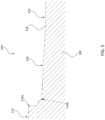
- FIG. 1shows an example susceptor 100 that may be used to support a substrate (e.g., wafer).
- the susceptor 100can include an outer edge 108 forming an outer perimeter around a face 104 .
- the face 104can include a rim region 112 , a channel region having an inner channel region 124 and an outer channel region 128 , and an inner region 132 .
- the face 104may further include one or more channels 120 .
- the susceptor 100may comprise one or more materials, such as elemental or molecular materials. Such materials can include non-oxide ceramics, such as silicon carbide (SiC or CSi), graphite, or any other ceramic. Other materials may be used, such as metal.
- the susceptor 100may include a silicon carbide coating, such as silicon-carbide-coated graphite.
- the face 104may be substantially flat, although it may include other profiled portions as described below. Additionally or alternatively, the susceptor 100 may have a relatively low profile (i.e., general cross-sectional thickness) to reduce weight of the susceptor 100 and/or to allow for more precise handling of the substrate.
- the face 104may be configured to hold or support the substrate (not shown).
- the edge 108may be substantially round, to form an approximately circular susceptor.
- the rim region 112can be positioned radially outwardly from the channel region, and may provide additional structural integrity and/or easier access to portions of the susceptor 100 as needed.
- the rim region 112may be bounded between the edge 108 and an outer radial boundary 116 of the outer channel region 128 . Any “boundary” described herein may be a subtle difference in rise angle, material, curvature/concavity, smoothness, and/or other difference between adjacent regions.
- the rim region 112may be substantially flat and/or smooth.
- the rim region 112may be substantially free of channels, protrusions, holes, and/or other irregularities in the surface of the rim region 112 .
- the rim region 112can have a radial width (defined as the radial distance between the edge 108 and the outer radial boundary 116 ) of between about 15 mm and 35 mm, and in some embodiments, about 25 mm.
- the channel regioncan be positioned between the outer radial boundary 116 and an inner radial boundary 136 that forms an outer perimeter around inner region 132 .
- One or both of the outer radial boundary 116 and/or the inner radial boundary 136may be round, such as substantially a circle or other rounded shape (e.g., oval).
- the inner region 132may be substantially flat and/or smooth.
- the inner region 132may be substantially free of channels, protrusions, and/or other irregularities.
- the inner region 132can shaped and/or sized to provide additional structural integrity to the susceptor 100 .
- an inclusion of irregularities within the inner region 132may reduce the strength of the inner region 132 .
- the inner region 132is recessed relative to the surrounding channel region.
- the inner radial boundary 136may be substantially formed by the difference in elevation between the inner region 132 and the inner channel region 124 .
- the channel regionmay be disposed adjacent and/or radially inward of the rim region 112 .
- the channel regionmay be disposed between the rim region 112 and the inner region 132 .
- one or more channels 120may be formed within the face 104 , but for convenience, reference will be made to a plurality of channels 120 throughout.
- the channels 120may extend radially outwardly from a center of the face 104 towards (and in some embodiments, to and through) the edge 108 .
- the channels 120can extend from the inner radial boundary 136 to the outer radial boundary 116 .
- the channels 120may extend substantially radially from the center of the face 104 , and in some embodiments, from the inner radial boundary 136 .
- consecutive channels 120may form an angular separation 140 , as shown.
- the angular separation 140can form an acute angle.
- the angular separation 140may be between about 5° and 35° and in some embodiments is about 15° between at least two consecutive channels 120 .
- Consecutive channels 120may be referred to as successive or adjacent channels 120 herein.
- a plurality of regularly spaced consecutive channels 120may have a substantially the same angular separation 140 between each set of consecutive channels 120 .
- the face 104may include multiple sets of such pluralities of consecutive channels 120 .
- the regularity of angular separation 140may be interrupted, for example, by one or more irregularities in the channel region.
- one or more apertures 144may be included in the channel region.
- the apertures 144may be configured to allow raisers (e.g., pins, prongs, rods, etc.) therethrough.
- the raisersmay be used by a susceptor support apparatus (e.g., a spider) (not shown) to raise a wafer up from the susceptor 100 without raising the susceptor 100 itself.
- a susceptor support apparatuse.g., a spider
- an angular separation 140 between consecutive channels 120 where irregularities may be foundcan be greater, such as double the angular separation 140 described above.
- Such increased angular separationcan provide additional structural integrity to those portions of the susceptor which include apertures 144 , and/or can provide additional space to avoid interference with the raisers and susceptor support apparatus.
- the channel regioncan include the inner channel region 124 and the outer channel region 128 .
- the outer channel region 128can form the outer boundary of the substrate “pocket.”
- the inner channel region 124may transition to the outer channel region 128 at a channel region boundary 126 .
- the outer channel region 128may be configured to support the substrate.
- the outer channel region 128may have a sloped and/or concave surface, which forms an elevated portion, relative to the inner channel region 124 , to limit the amount of the substrate (e.g., an edge or rim) that is touching the susceptor 100 .
- the majority of surface area of the channel regionmay be dedicated to the inner channel region 124 .
- the inner channel region 124may be substantially flat and/or smooth.
- the inner channel region 124is substantially parallel to one or more of the inner region 132 , the rim region 112 , and/or a back surface 106 (shown in FIG. 2 below).
- One or more portions of the channel region disposed between consecutive channels 120may increase in area moving from the inner radial boundary 136 to the outer radial boundary 116 .
- One or more of the channels 120may be substantially straight.
- the number of channels 120 within the channel regioncan be between about 5 and 50, or between about 18 and 30, but other variants are also possible. In some embodiments, the number of channels is 24.
- FIG. 2shows a back surface 106 of the example susceptor 100 of FIG. 1 .
- the back surface 106may be substantially flat and/or smooth.
- one or more apertures 144may be included as noted above.
- the apertures 144may extend between the face 104 and the back surface 106 so as to allow raisers (described above) therethrough.
- the apertures 144may be disposed at least partially within corresponding protrusions 152 extending from surface 106 .
- the protrusions 152may provide additional structural strength to the susceptor 100 where the raisers will pass through the susceptor 100 .
- a centering cavity 148may be included in the back surface 106 to help center the susceptor 100 on a susceptor support apparatus.
- the centering cavity 148may be configured to receive a pin therein to align and/or prevent the susceptor 100 and/or the substrate from translating relative to the support apparatus. This can promote accuracy of the substrate placement and/or the precision of the deposition on the substrate.
- the centering cavity 148may be surrounded by a structural protrusion for added structural strength. Additional stabilizing elements 156 (e.g., recesses (such as slotted recesses), protrusions, etc.) may be included to align and/or prevent movement (e.g., rotation) of the susceptor 100 during substrate handling or processing.
- FIG. 3shows a cross-sectional side view of the example susceptor 100 shown in FIGS. 1 - 2 .
- the cross sectionpasses through a center of the susceptor 100 .
- the centering cavity 148is disposed at a center of the back surface 106 .
- the centering cavity 148may be opposite the inner region 132 of the face 104 .
- the apertures 144may be disposed within the channel region (e.g., the inner channel region 124 ).
- the back surface 106may be substantially parallel to the face 104 .
- FIG. 4shows a cross sectional view of an example channel 120 .
- the channel 120can include substantially flat sidewalls.
- the sidewallsmay form an angle 160 such as an acute angle.
- the angle 160may be between 30° and 120° and may be approximately 80°.
- the width 164 of the channel 120may be between about 0.1 mm and 2.5 mm and in some embodiments is about 0.6 mm.
- the depth 166 of the channel 120may be between about 0.05 mm and 1.5 mm and in some embodiments is about 0.25 mm.
- the vertex between the sidewallscan be curved.
- FIG. 5shows a detail view of a cross section of a portion of a susceptor, showing a side elevational profile of an example face 104 .
- the outer channel region 128may be tapered, such that it is disposed at a slight incline relative to the inner channel region 124 .
- a rise angle of the outer channel region 128 relative to the inner channel region 124which transitions at the channel region boundary 126 , may be between about 0.5° and 5° and in some embodiments is about 3°.
- the rise anglecan be an absolute value (for example, when the inner channel region 124 is substantially flat).
- the outer channel region 128can be concave.
- a tapered or concave region 128can provide a higher elevation, relative to the inner channel region 124 , to reduce wafer contact with the susceptor.
- the outer radial boundary 116may include a first outer radial boundary 116 a and a second outer radial boundary 116 b in some embodiments.
- the portion between the first outer radial boundary 116 a and the second outer radial boundary 116 bmay include different profiles which can affect gas distribution, for example, in cross-flow reactor environments.
- the profile of this areacan be a non-smooth profile, as shown.
- the profile shape of the susceptor between the first outer radial boundary 116 a and the second outer radial boundary 116 bmay be selected to help improve the shadowing effect.
- the profile shapecan allow reactant to reach closer to the edge of the wafer, resulting in increased yield, for example, with wafers of a certain diameter (e.g., about 300 mm).
- the susceptor 100may be surface-treated to improve performance.
- one or more regions of the face 104may be polished to reduce the likelihood of deformities (e.g., caused by substrate sticking) to affect the substrate.
- the outer channel region 128may be polished to reduce sticking of the edge of the substrate thereto.
- Portions of the susceptor 100may be coated to improve performance.
- the face 104may be coated with silicon carbide.
- the susceptor 100can have a variety of dimensions.
- the susceptor 100can have a thickness of between about 1 mm and 15 mm and in some embodiments is about 3.8 mm.
- a diameter of the edge 108 and/or the outer radial boundary 116may be between about 100 mm and 500 mm and in some embodiments is about 300 mm.
- Each aperture 144can have a diameter of between about 0.5 mm and 6 mm and in some embodiments is about 1.6 mm.
- a susceptormay include an inner susceptor and an outer susceptor which in some embodiments, are configured to allow relative movement therebetween.
- Such susceptorsmay operate, for example, at a higher temperature (e.g., up to about 1200° C.) than the susceptors described in FIGS. 1 - 5 .
- the inner susceptor and outer susceptorcan include many similar features that function similarly as similar features described with respect to other susceptors described herein which may not have an inner and outer susceptor.
- FIG. 6shows an example inner susceptor 201 that may be used with a corresponding outer susceptor 202 (described below) to support a substrate.
- the inner susceptor 201can include an edge 208 and a face 204 .
- the face 204can include a channel region 214 and an inner region 232 .
- the face 204may further include one or more channels 220 .
- the face 204may be substantially flat, although it may include other profiled portions as described below. Additionally or alternatively, the inner susceptor 201 may have a relatively low profile (i.e., general cross-sectional thickness) to reduce weight of the inner susceptor 201 and/or to allow for more precise handling of the substrate and/or inner susceptor 201 .
- the face 204 of the inner susceptor 201may be configured to hold or support the substrate (not shown), for example, during substrate transfer processes. During other times, an outer susceptor 202 (described below) may be configured to support the substrate.
- the edge 208may be substantially round, to form an approximately circular susceptor. Aside from any channels 220 , the face 204 may be substantially flat and/or smooth.
- channel region 214can be positioned between the edge 208 and an inner radial boundary 236 that forms an outer perimeter around the inner region 232 .
- the inner radial boundary 236may be round, such as substantially a circle or other rounded shape (e.g., oval).
- the inner region 232may be substantially flat and/or smooth.
- the inner region 232may be substantially free of channels, protrusions, and/or other irregularities.
- the inner region 232can shaped and/or sized to provide additional structural integrity to a central portion of the inner susceptor 201 .
- an inclusion of irregularities within the inner region 232may otherwise reduce the strength of the structure of the inner susceptor 201 at or near the inner region 232 .
- the inner region 232is recessed relative to the surrounding channel region 214 .
- the inner radial boundary 236may be substantially formed by the difference in elevation between the inner region 223 and the inner channel region 224 .
- one or more channels 220may be formed within the face 204 , but for convenience, reference will be made to a plurality of channels 220 throughout.
- the channels 220may extend radially outwardly from a center of the face 204 towards (and in some embodiments, to and through) the edge 208 .
- the channels 220can extend from the inner radial boundary 236 to the edge 208 .
- the channels 220may extend substantially radially from the center of the face 104 , and in some embodiments, from the inner radial boundary 236 .
- consecutive channels 220may form an angular separation 240 , as shown.
- the angular separation 240can form an acute angle.
- the angular separation 240may be between about 3° and 30° and in some embodiments is about 7.5° between at least two consecutive channels 120 .
- Consecutive channels 220may be referred to as successive or adjacent channels 220 herein.
- a plurality of regularly spaced consecutive channels 220may have a substantially the same angular separation 240 between each set of consecutive channels 220 .
- the face 204may include multiple sets of such pluralities of consecutive channels 220 .
- the regularity of angular separation 240may be interrupted, for example, by one or more irregularities in the channel region 214 .
- one or more apertures 144may be included in the channel region.
- an angular separation 240 between consecutive channels 220 where irregularities may be foundcan be greater, such as double the angular separation 240 described above.
- Such increased angular separationcan provide additional structural integrity and/or can provide additional space to avoid interference with the raisers and susceptor support apparatus.
- the number of channels 220 within the channel region 214can be between about 5 and 60, but other variants are also possible. In some embodiments, the number of channels is about 48 (as shown) or about 24 (see FIG. 8 below).
- FIG. 7is a back view showing a back surface 206 of the example inner susceptor 201 of FIG. 6 .
- the back surface 206may be substantially flat and/or smooth.
- the inner susceptor 201can include a tapered portion 274 .
- the tapered portion 274may be disposed primarily near the edge 208 of the inner susceptor 201 .
- one or more stabilizing elements 256may be included.
- the stabilizing elements 256e.g., recesses, protrusions, etc.
- the one or more stabilizing elements 256may be used to allow a spider or other support mechanism to raise the inner susceptor 201 relative to the outer susceptor 202 .
- a centering cavity 248may be included in the back surface 206 to help center the inner susceptor 201 on a susceptor support apparatus.
- the centering cavity 148may be configured to receive a pin therein to prevent the inner susceptor 201 and/or the substrate from translating relative to the support apparatus. This can promote accuracy of the substrate placement and/or the precision of the deposition on the substrate.
- the centering cavity 248may be surrounded by a structural protrusion for added structural strength.
- the inner susceptor 201may further include one or more recesses 268 .
- the recesses 268may be configured to mate with corresponding elements in the outer susceptor 202 (described in more detail below).
- the recesses 268may be radially spaced from one another at approximately even intervals. This can promote greater stability of the inner susceptor 201 during movement of the inner susceptor 201 and/or the outer susceptor 202 .
- the recesses 268may be substantially rectangular as shown, but other shapes are possible.
- FIGS. 8 - 9show another example inner susceptor 201 having 24 channels instead of 48.
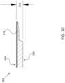
- FIG. 10shows a cross-sectional side view of a portion of any example inner susceptor 201 shown in FIGS. 6 - 9 .
- the tapered portion 274can be disposed along an outer radial portion of the rest of the inner susceptor 201 .
- the inner susceptor 201can have a thickness 272 of between about 2 mm and 25 mm and in some embodiments is about 5.6 mm.
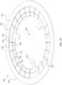
- FIG. 11shows an example outer susceptor 202 that may be used to support a substrate (e.g., wafer).
- the outer susceptor 202can include an edge 210 , a rim region 212 , a channel region having an inner channel region 224 and an outer channel region 228 , and an aperture 246 .
- the channel regionmay include one or more channels 220 .
- the rim region 212may be substantially flat. Additionally or alternatively, the outer susceptor 202 may have a relatively low profile to reduce weight of the outer susceptor 202 and/or to allow for more precise handling of the substrate.
- the outer channel region 228may be configured to hold or support the substrate (not shown).
- the edge 210may be substantially rounded. For example, the edge 210 may form substantially a circle or other round shape.
- the rim region 212can be positioned radially outwardly from the channel region, and may provide additional structural integrity and/or easier access to portions of the outer susceptor 202 as needed.
- the rim region 212may be bounded between the edge 210 and an outer radial boundary 216 of the outer channel region 228 . Any “boundary” described herein may be a subtle difference in rise angle, material, curvature/concavity, smoothness, and/or other difference between adjacent regions.
- the rim region 212may be substantially flat and/or smooth.
- the rim region 212may be substantially free of channels, protrusions, holes, and/or other irregularities in the surface of the rim region 212 .
- the outer susceptor 202can include a channel region disposed between the outer radial boundary 216 and a region boundary 280 , and/or a support region disposed between the rim region 212 (e.g., the region boundary 280 ) and the aperture 246 .
- the support regionmay be disposed adjacent and/or radially inward of the channel region.
- One or more of the outer radial boundary 216 , the region boundary 280 , and/or the aperture 246may be round, such as substantially a circle or other rounded shape (e.g., oval).
- the aperture 246may be configured to allow access to the inner susceptor 201 by a susceptor support apparatus (not shown), for example during transfer of the substrate.
- one or more channels 220may be formed, but for convenience, reference will be made to a plurality of channels 220 throughout.
- the channels 220may extend from the outer radial boundary 216 to the region boundary 280 and/or to the aperture 246 .
- the channels 220may extend substantially radially outwardly from the aperture 246 for example, to the region boundary 280 , to the outer boundary 216 , or to the edge 210 .
- the channels 220may extend substantially radially outwardly from the region boundary 280 , for example, to the 246 for example, to the outer boundary 216 , or to the edge 210 .
- consecutive channels 220may form an angular separation that corresponds to an angular separation 240 of corresponding consecutive channels 220 of the inner susceptor 201 .
- the angular separation of consecutive channels 220 of the outer susceptor 202may be between about 5° and 35° and in some embodiments is about 15° between at least two consecutive channels 220 .
- a plurality of consecutive channels 220may have a substantially the same angular separation 140 between each set of consecutive channels 220 .
- the outer susceptor 202may include multiple sets of such pluralities of consecutive channels 220 .
- a regularity of angular separation 140may be interrupted, for example, by one or more irregularities in the channel region.
- one or more support elements 278may be included in the support region, to provide engagement and support between the inner susceptor 201 and the outer susceptor 202 .
- the support elements 278may be configured in different ways.
- the support elements 278can comprise radial protrusions that extend into aperture 246 .
- the support elementscan be configured to engage with (e.g., be received within) corresponding features in the inner susceptor 201 , such as recesses 268 . Accordingly, an angular separation 240 between consecutive channels 220 where irregularities may be found can be greater, such as double the angular separation 240 described above.
- the channel regioncan include the inner channel region 224 and the outer channel region 228 .
- the outer channel region 228can form the outer boundary of the substrate “pocket.”
- a channel region boundary 226may be positioned between the inner channel region 224 and the outer channel region 228 .
- the outer channel region 228may be configured to support the substrate.
- the outer channel region 228may have a sloped and/or concave surface, relative to inner channel region 224 , transitioning at the channel region boundary 226 , to reduce substrate contact with the outer susceptor 202 , similar to the inner channel region 124 and outer channel region 128 and boundary 126 described with reference to FIG. 5 and other embodiments herein.
- the majority of surface area of the channel regionmay be dedicated to the inner channel region 224 .
- the inner channel region 224may be substantially flat and/or smooth. In some embodiments, the inner channel region 224 is substantially parallel to one or more of the rim region 212 , the support element(s) 278 , and/or a back surface of the outer susceptor 202 . One or more portions of the channel region disposed between consecutive channels 220 may increase in area moving from the region boundary 280 to the outer radial boundary 216 . One or more of the channels 220 may be substantially straight.
- the number of channels 220 within the channel regioncan be between about 5 and 50, but other variants are also possible. In some embodiments, the number of channels is about 48, and in some embodiments (see, e.g., FIGS. 13 - 14 ) the number of channels is about 24.
- the support regioncan include the inner support region 282 and the outer support region 284 .
- the outer support region 228can form an outer boundary to a “pocket” formed by the inner susceptor 201 ( FIG. 8 ), when the inner susceptor 201 is positioned with the outer susceptor 202 .
- the inner support region 282may be separated from the outer support region 284 by a support region boundary 252 .
- the outer support region 284may be configured to support the inner susceptor 201 ( FIG. 8 ).
- the outer support region 284may have a sloped and/or concave surface so that only a rim or edge of the inner susceptor 201 is touching the outer susceptor 202 .
- the majority of surface area of the support regionmay be dedicated to the inner support region 282 .
- the inner support region 282may be substantially flat and/or smooth. In some embodiments, the inner support region 282 is substantially parallel to one or more of the rim region 212 , the support element(s) 278 , and/or a back surface of the outer susceptor 202 .
- One or more portions of the support region disposed between consecutive channels 220may increase in area moving from the aperture 246 to the outer radial boundary 216 .
- One or more of the channels 220may be substantially straight.
- the number of channels 220 within the support regioncan be between about 5 and 50, but other variants are also possible.
- the number of channelsis about 48, and in some embodiments (see, e.g., FIGS. 13 - 14 ) the number of channels is about 24.
- the number of channels in the support regionmay be the same as the number in the channel region.
- one or more channels in the support regionmay link and/or be continuous with corresponding channels in the channel region.
- FIG. 12shows a back surface of the example outer susceptor 202 of FIG. 11 .
- the back surface 106may be substantially flat and/or smooth.
- one or more support elements 278may be included as noted above.
- the support elements 278may include corresponding recesses 286 therein.
- the recesses 286may be configured to receive corresponding protrusions from a susceptor support apparatus (not shown) to align, and prevent rotation and/or translation of the outer susceptor 202 relative to the apparatus, the inner susceptor 201 , and/or the outer susceptor 202 .
- Additional stabilizing elementse.g., recesses, protrusions, etc.
- FIGS. 13 - 14show another example outer susceptor 202 having 24 channels instead of 48.
- FIG. 15shows a cross-sectional side view of the example outer susceptor 202 shown in any of FIGS. 11 - 14 .
- the various regions and boundaries of the outer susceptor 202are shown.
- the rim region 212 and the back surface of the outer susceptor 202may be substantially parallel to each other.
- FIG. 16shows a cross sectional view of an example channel 220 .
- the channel 220can include curvilinear sidewalls.
- the sidewallsmay form substantially a semi-circle along the cross section.
- the radius 288 of curvaturemay be between about 0.1 mm and 2.5 mm and is about 0.6 mm in some embodiments. Curved sidewalls as shown may be helpful in preventing the accumulation of gas therein during deposition.
- the width 264 of the channel 220may be between about 0.1 mm and 5 mm and in some embodiments is about 1.2 mm.
- the depth 266 of the channel 220may be between about 0.05 mm and 1.5 mm and in some embodiments is about 0.6 mm.
- FIG. 17shows a susceptor 200 in an assembled state with the inner susceptor 201 and the outer susceptor 202 together.
- the outer susceptor 202may support the inner susceptor 201 as described above.
- one or more channels 220 of the inner susceptor 201may connect and/or correspond to respective channels 220 of the outer susceptor 202 , for example, so that the channels in the inner and outer susceptor are collinear or substantially radially aligned with respect to each other.
- the connected channels 220may be referred to as single channels.
- FIG. 18shows another example embodiment with fewer channels.
- the edge 208 of the inner susceptor 201may substantially align with the region boundary 280 (not shown) such that the supported region is substantially covered in the assembled state.
- One or more elements of the susceptor 200may comprise one or more materials, such as elemental or molecular materials. Such materials can include non-oxide ceramics, such as silicon carbide (SiC or CSi), graphite, or any other ceramic. Other materials may be used, such as metal.
- one or more elements of the susceptor 200may include a silicon carbide coating, such as silicon-carbide-coated graphite.
- FIG. 19shows a cross sectional side view of an example susceptor 200 such as that shown in FIGS. 17 - 18 .
- the inner susceptor 201may be supported by the inner support region 282 and/or the outer support region 284 . In some embodiments, however, the inner susceptor 201 may not contact the outer susceptor 202 other than at the interface between the support elements 278 and corresponding recesses 268 and among other support/stabilizing elements (e.g., FIGS. 7 - 9 and 11 - 14 ).
- the face 204 of the inner susceptor 201may be substantially coplanar with the inner channel region 224 in the assembled state, as shown.
- the substratemay be substantially supported by the outer channel region 228 .
- the rim region 212may be substantially parallel to the back surface 206 of the inner susceptor 201 in the assembled state.
- the inner susceptor 201 and/or the outer susceptor 202may be treated to improve performance.
- one or more regions of the susceptors 201 , 202may be polished to reduce the likelihood of deformities (e.g., from sticking) to affect the substrate.
- the outer channel region 228may be polished to reduce sticking of the edge of the substrate thereto.
- Portions of the inner susceptor 201 and/or outer susceptor 202may be coated to improve performance, for example, with silicon carbide.
- the inner susceptor 201can have a variety of dimensions.
- the inner susceptor 201 and/or the outer susceptor 202can each have a maximum thickness of between about 1 mm and 15 mm and in some embodiments is about 5.6 mm.
- the combined maximum thickness of the susceptor 200 in the assembled statecan be between about 1 mm and 15 mm and in some embodiments is about 5.6 mm.
- the tapered portion 274can have a maximum thickness of between about 1 mm and 15 mm and in some embodiments is about 2.3 mm.
- a diameter of the inner susceptor 201may be between about 100 mm and 500 mm and in some embodiments is about 255 mm.
- a diameter of the outer susceptor 202may be between about 150 mm and 600 mm and in some embodiments is about 350 mm.
- An inner diameter of the aperture 246(e.g., as measured from the innermost portion of each support element 278 ) may be between about 35 mm and 400 mm and in some embodiments is about 160 mm.
- FIG. 20shows the cross sectional side view of FIG. 19 with an indication of fluid (e.g., gas) flow within the susceptor 200 in the assembled state.
- fluide.g., gas
- the fluidpasses along the face 204 of the inner susceptor 201 radially outward and passes between the inner susceptor 201 and the outer susceptor 202 .
- the fluidpasses underneath the susceptor 200 . Allowing trapped air to go below the susceptor 200 while preventing it from escaping radially can reduce leakage of the reactant and thus prevent depositing on the backside of the substrate.
- vents underneath the susceptor 200can be configured to prevent or reduce leakage from reaching the bottom of the susceptor 200 .
- present aspects and implementationsmay be described in terms of functional block components and various processing steps. Such functional blocks may be realized by any number of hardware or software components configured to perform the specified functions and achieve the various results. For example, the present aspects may employ various sensors, detectors, flow control devices, heaters, and the like, which may carry out a variety of functions. In addition, the present aspects and implementations may be practiced in conjunction with any number of processing methods, and the apparatus and systems described may employ any number of processing methods, and the apparatus and systems described are merely examples of applications of the invention.
Landscapes
- Engineering & Computer Science (AREA)
- Physics & Mathematics (AREA)
- Condensed Matter Physics & Semiconductors (AREA)
- General Physics & Mathematics (AREA)
- Manufacturing & Machinery (AREA)
- Computer Hardware Design (AREA)
- Microelectronics & Electronic Packaging (AREA)
- Power Engineering (AREA)
- Chemical & Material Sciences (AREA)
- Plasma & Fusion (AREA)
- Analytical Chemistry (AREA)
- General Chemical & Material Sciences (AREA)
- Chemical Kinetics & Catalysis (AREA)
- Materials Engineering (AREA)
- Mechanical Engineering (AREA)
- Metallurgy (AREA)
- Organic Chemistry (AREA)
- Container, Conveyance, Adherence, Positioning, Of Wafer (AREA)
- Chemical Vapour Deposition (AREA)
Abstract
Description
Claims (14)
Priority Applications (2)
| Application Number | Priority Date | Filing Date | Title |
|---|---|---|---|
| US16/744,063US11961756B2 (en) | 2019-01-17 | 2020-01-15 | Vented susceptor |
| US18/627,178US20240249970A1 (en) | 2019-01-17 | 2024-04-04 | Vented susceptor |
Applications Claiming Priority (2)
| Application Number | Priority Date | Filing Date | Title |
|---|---|---|---|
| US201962793852P | 2019-01-17 | 2019-01-17 | |
| US16/744,063US11961756B2 (en) | 2019-01-17 | 2020-01-15 | Vented susceptor |
Related Child Applications (1)
| Application Number | Title | Priority Date | Filing Date |
|---|---|---|---|
| US18/627,178DivisionUS20240249970A1 (en) | 2019-01-17 | 2024-04-04 | Vented susceptor |
Publications (2)
| Publication Number | Publication Date |
|---|---|
| US20200234996A1 US20200234996A1 (en) | 2020-07-23 |
| US11961756B2true US11961756B2 (en) | 2024-04-16 |
Family
ID=71610126
Family Applications (2)
| Application Number | Title | Priority Date | Filing Date |
|---|---|---|---|
| US16/744,063Active2040-06-30US11961756B2 (en) | 2019-01-17 | 2020-01-15 | Vented susceptor |
| US18/627,178PendingUS20240249970A1 (en) | 2019-01-17 | 2024-04-04 | Vented susceptor |
Family Applications After (1)
| Application Number | Title | Priority Date | Filing Date |
|---|---|---|---|
| US18/627,178PendingUS20240249970A1 (en) | 2019-01-17 | 2024-04-04 | Vented susceptor |
Country Status (4)
| Country | Link |
|---|---|
| US (2) | US11961756B2 (en) |
| KR (2) | KR102797465B1 (en) |
| CN (1) | CN111446185A (en) |
| TW (1) | TWI839443B (en) |
Cited By (2)
| Publication number | Priority date | Publication date | Assignee | Title |
|---|---|---|---|---|
| US20240249970A1 (en)* | 2019-01-17 | 2024-07-25 | Asm Ip Holding B.V. | Vented susceptor |
| USD1052547S1 (en)* | 2022-10-20 | 2024-11-26 | Nuflare Technology, Inc. | Semiconductor wafer and susceptor heating |
Families Citing this family (13)
| Publication number | Priority date | Publication date | Assignee | Title |
|---|---|---|---|---|
| WO2018158348A1 (en)* | 2017-02-28 | 2018-09-07 | Sgl Carbon Se | Substrate-carrier structure |
| US11309177B2 (en) | 2018-11-06 | 2022-04-19 | Stmicroelectronics S.R.L. | Apparatus and method for manufacturing a wafer |
| USD920936S1 (en) | 2019-01-17 | 2021-06-01 | Asm Ip Holding B.V. | Higher temperature vented susceptor |
| US11404302B2 (en) | 2019-05-22 | 2022-08-02 | Asm Ip Holding B.V. | Substrate susceptor using edge purging |
| IT201900015416A1 (en) | 2019-09-03 | 2021-03-03 | St Microelectronics Srl | APPARATUS FOR GROWING A SLICE OF SEMICONDUCTOR MATERIAL, IN PARTICULAR SILICON CARBIDE, AND ASSOCIATED MANUFACTURING PROCESS |
| US11764101B2 (en)* | 2019-10-24 | 2023-09-19 | ASM IP Holding, B.V. | Susceptor for semiconductor substrate processing |
| KR20250033324A (en)* | 2020-02-11 | 2025-03-07 | 램 리써치 코포레이션 | Carrier ring designs for controlling deposition on wafer bevel/edge |
| TWM630893U (en)* | 2020-09-03 | 2022-08-21 | 美商威科精密儀器公司 | Substrate reactor for epitaxial deposition and substrate carrier for chemical vapor deposition reactor |
| US20220076988A1 (en)* | 2020-09-10 | 2022-03-10 | Applied Materials, Inc. | Back side design for flat silicon carbide susceptor |
| USD1031676S1 (en) | 2020-12-04 | 2024-06-18 | Asm Ip Holding B.V. | Combined susceptor, support, and lift system |
| US20240014065A1 (en)* | 2022-07-08 | 2024-01-11 | Applied Materials, Inc. | Flat susceptor with grid pattern and venting grooves on surface thereof |
| JP1746404S (en)* | 2023-01-11 | 2023-06-15 | Susceptor cover base | |
| US20240347372A1 (en)* | 2023-04-12 | 2024-10-17 | Applied Materials, Inc. | Susceptor |
Citations (155)
| Publication number | Priority date | Publication date | Assignee | Title |
|---|---|---|---|---|
| US3407783A (en) | 1964-08-31 | 1968-10-29 | Emil R. Capita | Vapor deposition apparatus |
| US3549847A (en) | 1967-04-18 | 1970-12-22 | Gen Electric | Graphite susceptor |
| US3641974A (en) | 1969-08-29 | 1972-02-15 | Hitachi Ltd | Apparatus for forming films |
| US3796182A (en) | 1971-12-16 | 1974-03-12 | Applied Materials Tech | Susceptor structure for chemical vapor deposition reactor |
| US4499354A (en) | 1982-10-06 | 1985-02-12 | General Instrument Corp. | Susceptor for radiant absorption heater system |
| US4522149A (en) | 1983-11-21 | 1985-06-11 | General Instrument Corp. | Reactor and susceptor for chemical vapor deposition process |
| US4560420A (en) | 1984-06-13 | 1985-12-24 | At&T Technologies, Inc. | Method for reducing temperature variations across a semiconductor wafer during heating |
| GB2181458A (en) | 1985-10-07 | 1987-04-23 | Epsilon Ltd Partnership | Apparatus and method for an axially symmetric chemical vapor deposition reactor |
| US4710428A (en) | 1984-09-13 | 1987-12-01 | Toshiba Ceramics Co., Ltd. | Sintered silicon carbide porous body impregnated with metallic silicon |
| US4821674A (en) | 1987-03-31 | 1989-04-18 | Deboer Wiebe B | Rotatable substrate supporting mechanism with temperature sensing device for use in chemical vapor deposition equipment |
| EP0339279A2 (en) | 1988-03-31 | 1989-11-02 | Air Products And Chemicals, Inc. | Method for making a wafer holder for use in rapid thermal processing equipment |
| US4958061A (en) | 1988-06-27 | 1990-09-18 | Tokyo Electron Limited | Method and apparatus for heat-treating a substrate |
| US4986215A (en) | 1988-09-01 | 1991-01-22 | Kyushu Electronic Metal Co., Ltd. | Susceptor for vapor-phase growth system |
| US4990374A (en) | 1989-11-28 | 1991-02-05 | Cvd Incorporated | Selective area chemical vapor deposition |
| US5033407A (en) | 1989-02-14 | 1991-07-23 | Anelva Corporation | Low pressure vapor phase growth apparatus |
| US5044943A (en) | 1990-08-16 | 1991-09-03 | Applied Materials, Inc. | Spoked susceptor support for enhanced thermal uniformity of susceptor in semiconductor wafer processing apparatus |
| EP0445596A2 (en) | 1990-03-09 | 1991-09-11 | Applied Materials, Inc. | Double-dome reactor for semiconductor processing |
| EP0448346A1 (en) | 1990-03-19 | 1991-09-25 | Kabushiki Kaisha Toshiba | Vapor-phase deposition apparatus and vapor-phase deposition method |
| US5071670A (en) | 1990-06-11 | 1991-12-10 | Kelly Michael A | Method for chemical vapor deposition under a single reactor vessel divided into separate reaction chambers each with its own depositing and exhausting means |
| US5074017A (en) | 1989-01-13 | 1991-12-24 | Toshiba Ceramics Co., Ltd. | Susceptor |
| US5098198A (en) | 1990-04-19 | 1992-03-24 | Applied Materials, Inc. | Wafer heating and monitor module and method of operation |
| US5119541A (en) | 1987-01-28 | 1992-06-09 | Tadahiro Ohmi | Wafer succeptor apparatus |
| US5119540A (en) | 1990-07-24 | 1992-06-09 | Cree Research, Inc. | Apparatus for eliminating residual nitrogen contamination in epitaxial layers of silicon carbide and resulting product |
| US5121531A (en) | 1990-07-06 | 1992-06-16 | Applied Materials, Inc. | Refractory susceptors for epitaxial deposition apparatus |
| US5156820A (en) | 1989-05-15 | 1992-10-20 | Rapro Technology, Inc. | Reaction chamber with controlled radiant energy heating and distributed reactant flow |
| US5188501A (en) | 1990-04-27 | 1993-02-23 | Shin-Etsu Handotai Co., Ltd. | Wafer transfer system |
| US5199483A (en) | 1991-05-15 | 1993-04-06 | Applied Materials, Inc. | Method and apparatus for cooling wafers |
| US5200157A (en) | 1986-02-17 | 1993-04-06 | Toshiba Ceramics Co., Ltd. | Susceptor for vapor-growth deposition |
| US5242501A (en) | 1982-09-10 | 1993-09-07 | Lam Research Corporation | Susceptor in chemical vapor deposition reactors |
| US5292554A (en) | 1992-11-12 | 1994-03-08 | Applied Materials, Inc. | Deposition apparatus using a perforated pumping plate |
| US5298465A (en) | 1990-08-16 | 1994-03-29 | Applied Materials, Inc. | Plasma etching system |
| US5304248A (en) | 1990-12-05 | 1994-04-19 | Applied Materials, Inc. | Passive shield for CVD wafer processing which provides frontside edge exclusion and prevents backside depositions |
| US5306699A (en) | 1988-08-31 | 1994-04-26 | Superconductor Technologies, Inc. | Reactor vessel for manufacture of superconducting films |
| US5308645A (en) | 1992-08-07 | 1994-05-03 | Delco Electronics Corporation | Method and apparatus for through hole substrate printing |
| US5332442A (en) | 1991-11-15 | 1994-07-26 | Tokyo Electron Kabushiki Kaisha | Surface processing apparatus |
| US5343938A (en) | 1992-12-24 | 1994-09-06 | Vlsi Technology, Inc. | Method and apparatus for thermally insulating a wafer support |
| US5354715A (en) | 1986-12-19 | 1994-10-11 | Applied Materials, Inc. | Thermal chemical vapor deposition of silicon dioxide and in-situ multi-step planarized process |
| US5356486A (en) | 1991-03-04 | 1994-10-18 | Applied Materials, Inc. | Combined wafer support and temperature monitoring device |
| US5370739A (en) | 1992-06-15 | 1994-12-06 | Materials Research Corporation | Rotating susceptor semiconductor wafer processing cluster tool module useful for tungsten CVD |
| EP0634785A1 (en) | 1993-07-13 | 1995-01-18 | Applied Materials, Inc. | Improved susceptor design |
| US5383971A (en) | 1990-10-12 | 1995-01-24 | Genus, Inc. | Differential pressure CVD chuck |
| US5393349A (en) | 1991-08-16 | 1995-02-28 | Tokyo Electron Sagami Kabushiki Kaisha | Semiconductor wafer processing apparatus |
| JPH0758039A (en) | 1993-08-20 | 1995-03-03 | Toshiba Ceramics Co Ltd | Susceptor |
| US5403401A (en) | 1993-03-04 | 1995-04-04 | Xycarb B.V. | Substrate carrier |
| US5421893A (en) | 1993-02-26 | 1995-06-06 | Applied Materials, Inc. | Susceptor drive and wafer displacement mechanism |
| US5427620A (en) | 1987-03-31 | 1995-06-27 | Advanced Semiconductor Materials America, Inc. | Rotatable substrate supporting mechanism with temperature sensing device for use in chemical vapor deposition equipment |
| US5444217A (en) | 1993-01-21 | 1995-08-22 | Moore Epitaxial Inc. | Rapid thermal processing apparatus for processing semiconductor wafers |
| EP0669640A1 (en) | 1994-02-25 | 1995-08-30 | Applied Materials, Inc. | Susceptor for deposition apparatus |
| US5455069A (en) | 1992-06-01 | 1995-10-03 | Motorola, Inc. | Method of improving layer uniformity in a CVD reactor |
| US5456757A (en) | 1993-05-27 | 1995-10-10 | Applied Materials, Inc. | Susceptor for vapor deposition |
| US5461214A (en) | 1992-06-15 | 1995-10-24 | Thermtec, Inc. | High performance horizontal diffusion furnace system |
| US5467220A (en) | 1994-02-18 | 1995-11-14 | Applied Materials, Inc. | Method and apparatus for improving semiconductor wafer surface temperature uniformity |
| US5492566A (en) | 1993-02-08 | 1996-02-20 | Sumnitsch; Franz | Support for disk-shaped articles using the Bernoulli principle |
| US5514439A (en) | 1994-10-14 | 1996-05-07 | Sibley; Thomas | Wafer support fixtures for rapid thermal processing |
| US5516367A (en) | 1993-04-05 | 1996-05-14 | Applied Materials, Inc. | Chemical vapor deposition chamber with a purge guide |
| US5549756A (en) | 1994-02-02 | 1996-08-27 | Applied Materials, Inc. | Optical pyrometer for a thin film deposition system |
| US5551985A (en) | 1995-08-18 | 1996-09-03 | Torrex Equipment Corporation | Method and apparatus for cold wall chemical vapor deposition |
| US5558717A (en) | 1994-11-30 | 1996-09-24 | Applied Materials | CVD Processing chamber |
| WO1996030713A1 (en) | 1995-03-30 | 1996-10-03 | Helpman Intellectual Properties B.V. | Heat exchanger |
| US5583736A (en)* | 1994-11-17 | 1996-12-10 | The United States Of America As Represented By The Department Of Energy | Micromachined silicon electrostatic chuck |
| US5584936A (en) | 1995-12-14 | 1996-12-17 | Cvd, Incorporated | Susceptor for semiconductor wafer processing |
| US5588827A (en) | 1993-12-17 | 1996-12-31 | Brooks Automation Inc. | Passive gas substrate thermal conditioning apparatus and method |
| WO1997008743A1 (en) | 1995-08-22 | 1997-03-06 | Advanced Semiconductor Materials America, Inc. | Low mass susceptor |
| EP0766289A2 (en) | 1995-09-29 | 1997-04-02 | Applied Materials, Inc. | Susceptor for deposition apparatus |
| US5620525A (en) | 1990-07-16 | 1997-04-15 | Novellus Systems, Inc. | Apparatus for supporting a substrate and introducing gas flow doximate to an edge of the substrate |
| US5645646A (en) | 1994-02-25 | 1997-07-08 | Applied Materials, Inc. | Susceptor for deposition apparatus |
| US5656093A (en) | 1996-03-08 | 1997-08-12 | Applied Materials, Inc. | Wafer spacing mask for a substrate support chuck and method of fabricating same |
| US5690742A (en) | 1994-09-06 | 1997-11-25 | Komatsu Electronic Metals Co., Ltd. | Susceptor for an epitaxial growth apparatus |
| US5700725A (en) | 1995-06-26 | 1997-12-23 | Lucent Technologies Inc. | Apparatus and method for making integrated circuits |
| US5738165A (en) | 1993-05-07 | 1998-04-14 | Nikon Corporation | Substrate holding apparatus |
| EP0840358A2 (en) | 1996-11-05 | 1998-05-06 | Applied Materials, Inc. | Sloped substrate support |
| US5761023A (en) | 1996-04-25 | 1998-06-02 | Applied Materials, Inc. | Substrate support with pressure zones having reduced contact area and temperature feedback |
| US5800622A (en) | 1995-07-21 | 1998-09-01 | Mitsubishi Denki Kabushiki Kaisha | Vapor-phase growth apparatus and compound semiconductor device fabricated thereby |
| US5803977A (en) | 1992-09-30 | 1998-09-08 | Applied Materials, Inc. | Apparatus for full wafer deposition |
| US5834737A (en) | 1995-05-12 | 1998-11-10 | Tokyo Electron Limited | Heat treating apparatus |
| USD404370S (en) | 1997-08-20 | 1999-01-19 | Tokyo Electron Limited | Cap for use in a semiconductor wafer heat processing apparatus |
| US5895530A (en) | 1996-02-26 | 1999-04-20 | Applied Materials, Inc. | Method and apparatus for directing fluid through a semiconductor processing chamber |
| US5938850A (en) | 1995-08-04 | 1999-08-17 | Tokyo Electron Limited | Single wafer heat treatment apparatus |
| KR19990069084A (en) | 1998-02-04 | 1999-09-06 | 윤종용 | Susceptor for semiconductor device manufacturing |
| KR19990069091A (en) | 1998-02-04 | 1999-09-06 | 윤종용 | Susceptor for semiconductor device manufacturing |
| US5960159A (en) | 1997-10-14 | 1999-09-28 | Kokusai Electric Co., Ltd. | Heat treatment of semiconductor wafers where upper heater directly heats upper wafer in its entirety and lower heater directly heats lower wafer in its entirety |
| US6001183A (en) | 1996-06-10 | 1999-12-14 | Emcore Corporation | Wafer carriers for epitaxial growth processes |
| US6020212A (en) | 1995-06-09 | 2000-02-01 | Cis Bio International | Phycobiliprotein-linker peptide complex fluorescent tracer and methods of using the same |
| US6068441A (en) | 1997-11-21 | 2000-05-30 | Asm America, Inc. | Substrate transfer system for semiconductor processing equipment |
| US6077357A (en) | 1997-05-29 | 2000-06-20 | Applied Materials, Inc. | Orientless wafer processing on an electrostatic chuck |
| US6090212A (en) | 1997-08-15 | 2000-07-18 | Micro C Technologies, Inc. | Substrate platform for a semiconductor substrate during rapid high temperature processing and method of supporting a substrate |
| US6093252A (en) | 1995-08-03 | 2000-07-25 | Asm America, Inc. | Process chamber with inner support |
| JP2000269310A (en) | 1999-03-15 | 2000-09-29 | Toshiba Corp | Semiconductor wafer support device |
| US6293749B1 (en) | 1997-11-21 | 2001-09-25 | Asm America, Inc. | Substrate transfer system for semiconductor processing equipment |
| US6325858B1 (en) | 1997-11-03 | 2001-12-04 | Asm America, Inc. | Long life high temperature process chamber |
| US6331023B1 (en) | 2000-01-14 | 2001-12-18 | Asm America, Inc. | Gridded substrate transport spatula |
| US6343183B1 (en) | 1995-09-01 | 2002-01-29 | Asm America, Inc. | Wafer support system |
| US20020011211A1 (en) | 2000-04-06 | 2002-01-31 | Halpin Michael W. | Barrier coating for vitreous materials |
| US20020043337A1 (en)* | 1997-11-03 | 2002-04-18 | Goodman Matthew G. | Low mass wafer support system |
| US6394797B1 (en) | 1997-04-02 | 2002-05-28 | Hitachi, Ltd. | Substrate temperature control system and method for controlling temperature of substrate |
| US6402850B1 (en) | 1993-01-13 | 2002-06-11 | Applied Materials, Inc. | Depositing polysilicon films having improved uniformity and apparatus therefor |
| JP2002184843A (en) | 2000-12-13 | 2002-06-28 | Sharp Corp | Semiconductor substrate holding device |
| JP2002526915A (en) | 1998-09-30 | 2002-08-20 | アプライド マテリアルズ インコーポレイテッド | Cathode assembly with built-in electrostatic chuck for holding wafers in semiconductor wafer processing equipment |
| US6464790B1 (en) | 1997-07-11 | 2002-10-15 | Applied Materials, Inc. | Substrate support member |
| US20020189940A1 (en) | 2001-06-14 | 2002-12-19 | Applied Materials, Inc. | Substrate support with multilevel heat transfer mechanism |
| US20030000472A1 (en) | 2001-06-26 | 2003-01-02 | Yu-Dong Lim | Vacuum plate having a symmetrical air-load block |
| US20030049580A1 (en) | 2000-12-22 | 2003-03-13 | Goodman Matthew G. | Susceptor pocket profile to improve process performance |
| JP2003124167A (en) | 2001-10-10 | 2003-04-25 | Sumitomo Heavy Ind Ltd | Wafer support member and double-ended grinding device using the same |
| US6709267B1 (en) | 2002-12-27 | 2004-03-23 | Asm America, Inc. | Substrate holder with deep annular groove to prevent edge heat loss |
| US20040060512A1 (en) | 2002-09-30 | 2004-04-01 | Waldhauer Ann P. | High temperature anneal with improved substrate support |
| USD496008S1 (en) | 2002-12-12 | 2004-09-14 | Tokyo Electron Limited | Exhaust ring for manufacturing semiconductors |
| US20040229002A1 (en) | 2003-05-15 | 2004-11-18 | 3D Systems, Inc. | Stereolithographic seal and support structure for semiconductor wafer |
| US20050092439A1 (en) | 2003-10-29 | 2005-05-05 | Keeton Tony J. | Low/high temperature substrate holder to reduce edge rolloff and backside damage |
| US20050284372A1 (en) | 2004-06-28 | 2005-12-29 | Applied Materials, Inc. | Chamber component having grooved surface with depressions |
| US20060057826A1 (en) | 2002-12-09 | 2006-03-16 | Koninklijke Philips Electronics N.V. | System and method for suppression of wafer temperature drift in cold-wall cvd systems |
| US7033445B2 (en) | 2001-12-27 | 2006-04-25 | Asm America, Inc. | Gridded susceptor |
| USD525127S1 (en) | 2004-03-01 | 2006-07-18 | Kraft Foods Holdings, Inc. | Susceptor ring |
| JP2006228802A (en) | 2005-02-15 | 2006-08-31 | Dainippon Screen Mfg Co Ltd | Wafer end surface protective device |
| KR20070098025A (en) | 2006-03-30 | 2007-10-05 | 삼성전자주식회사 | Semiconductor device manufacturing equipment |
| USD600223S1 (en) | 2008-08-07 | 2009-09-15 | Ravinder Aggarwal | Susceptor ring |
| US7601224B2 (en) | 2002-03-08 | 2009-10-13 | Asm America, Inc. | Method of supporting a substrate in a gas cushion susceptor system |
| US7602224B2 (en) | 2007-05-16 | 2009-10-13 | Hynix Semiconductor, Inc. | Semiconductor device having delay locked loop and method for driving the same |
| US20090280248A1 (en) | 2008-05-06 | 2009-11-12 | Asm America, Inc. | Porous substrate holder with thinned portions |
| US7648579B2 (en) | 2004-02-13 | 2010-01-19 | Asm America, Inc. | Substrate support system for reduced autodoping and backside deposition |
| US20100031884A1 (en) | 2008-08-07 | 2010-02-11 | Asm America, Inc. | Susceptor ring |
| US20100107974A1 (en) | 2008-11-06 | 2010-05-06 | Asm America, Inc. | Substrate holder with varying density |
| US7722441B2 (en) | 2005-10-07 | 2010-05-25 | Rohm And Haas Electronic Materials Llc | Semiconductor processing |
| US7740703B2 (en) | 2003-03-18 | 2010-06-22 | Hitachi Cable, Ltd. | Semiconductor film formation device |
| CN102308362A (en) | 2009-02-09 | 2012-01-04 | Asm美国公司 | Method and apparatus for minimizing contamination in semiconductor processing chamber |
| US8366830B2 (en) | 2003-03-04 | 2013-02-05 | Cree, Inc. | Susceptor apparatus for inverted type MOCVD reactor |
| US20130109192A1 (en) | 2011-10-28 | 2013-05-02 | Asm America, Inc. | Susceptor with ring to limit backside deposition |
| CN103733327A (en) | 2011-08-08 | 2014-04-16 | 应用材料公司 | Substrate support with heater |
| US8801857B2 (en) | 2008-10-31 | 2014-08-12 | Asm America, Inc. | Self-centering susceptor ring assembly |
| US8826769B2 (en)* | 2011-02-04 | 2014-09-09 | Yamada Manufacturing Co., Ltd. | Steering device |
| USD743357S1 (en) | 2013-03-01 | 2015-11-17 | Asm Ip Holding B.V. | Susceptor |
| US20160002778A1 (en) | 2014-07-03 | 2016-01-07 | Applied Materials, Inc. | Substrate support with more uniform edge purge |
| US20160068996A1 (en)* | 2014-09-05 | 2016-03-10 | Applied Materials, Inc. | Susceptor and pre-heat ring for thermal processing of substrates |
| JP1547357S (en) | 2015-07-27 | 2016-04-11 | ||
| US20160133504A1 (en)* | 2014-11-12 | 2016-05-12 | Applied Materials, Inc. | Susceptor design to reduce edge thermal peak |
| US9558985B2 (en) | 2012-03-28 | 2017-01-31 | Acm Research (Shanghai) Inc. | Vacuum chuck |
| USD784276S1 (en) | 2013-08-06 | 2017-04-18 | Applied Materials, Inc. | Susceptor assembly |
| US9633889B2 (en) | 2013-03-06 | 2017-04-25 | Applied Materials, Inc. | Substrate support with integrated vacuum and edge purge conduits |
| US20170175265A1 (en)* | 2015-12-18 | 2017-06-22 | Applied Materials, Inc. | Flat susceptor with grooves for minimizing temperature profile across a substrate |
| TW201724397A (en) | 2015-09-11 | 2017-07-01 | 應用材料股份有限公司 | One-piece process kit shield for reducing the impact of an electric field near the substrate |
| TWD184695S (en) | 2016-04-08 | 2017-08-01 | 應用材料股份有限公司 | Patterned heater pedestal |
| JP1570747S (en) | 2016-04-27 | 2018-02-19 | ||
| JP1570748S (en) | 2016-04-27 | 2018-02-19 | ||
| US20180094350A1 (en) | 2016-09-30 | 2018-04-05 | Asm Ip Holding B.V. | Reactant vaporizer and related systems and methods |
| TWD191199S (en) | 2017-03-31 | 2018-06-21 | 荏原製作所股份有限公司 | Part of the vacuum injection pad |
| US10068791B2 (en) | 2013-03-08 | 2018-09-04 | Semiconductor Components Industries, Llc | Wafer susceptor for forming a semiconductor device and method therefor |
| USD830981S1 (en) | 2017-04-07 | 2018-10-16 | Asm Ip Holding B.V. | Susceptor for semiconductor substrate processing apparatus |
| US10376916B2 (en) | 2012-03-30 | 2019-08-13 | Applied Materials, Inc | Substrate processing system having susceptorless substrate support with enhanced substrate heating control |
| USD864134S1 (en) | 2018-10-24 | 2019-10-22 | Asm Ip Holding B.V. | Susceptor |
| US20190355612A1 (en) | 2017-02-02 | 2019-11-21 | Sumco Corporation | Lift pin, and epitaxial growth apparatus and method of producing silicon epitaxial wafer using the lift pin |
| US20200234996A1 (en) | 2019-01-17 | 2020-07-23 | Asm Ip Holding Bv | Vented susceptor |
| US20200373187A1 (en) | 2019-05-22 | 2020-11-26 | Asm Ip Holding B.V. | Substrate susceptor using edge purging |
| USD914620S1 (en)* | 2019-01-17 | 2021-03-30 | Asm Ip Holding B.V. | Vented susceptor |
| US20210125853A1 (en)* | 2019-10-24 | 2021-04-29 | Asm Ip Holding B.V. | Susceptor for semiconductor substrate processing |
| US11018047B2 (en) | 2018-01-25 | 2021-05-25 | Asm Ip Holding B.V. | Hybrid lift pin |
| USD920936S1 (en)* | 2019-01-17 | 2021-06-01 | Asm Ip Holding B.V. | Higher temperature vented susceptor |
Family Cites Families (4)
| Publication number | Priority date | Publication date | Assignee | Title |
|---|---|---|---|---|
| US8491752B2 (en)* | 2006-12-15 | 2013-07-23 | Tokyo Electron Limited | Substrate mounting table and method for manufacturing same, substrate processing apparatus, and fluid supply mechanism |
| US9666467B2 (en)* | 2014-11-21 | 2017-05-30 | Varian Semiconductor Equipment Associates, Inc. | Detachable high-temperature electrostatic chuck assembly |
| TWI723997B (en)* | 2015-06-19 | 2021-04-11 | 美商應用材料股份有限公司 | Injector for batch processing and methods of use |
| TWI827502B (en)* | 2017-06-19 | 2023-12-21 | 美商應用材料股份有限公司 | Electrostatic chuck for high temperature processing chamber and forming method thereof |
- 2020
- 2020-01-15USUS16/744,063patent/US11961756B2/enactiveActive
- 2020-01-15CNCN202010040324.3Apatent/CN111446185A/enactivePending
- 2020-01-15TWTW109101352Apatent/TWI839443B/enactive
- 2020-01-16KRKR1020200005938Apatent/KR102797465B1/enactiveActive
- 2024
- 2024-04-04USUS18/627,178patent/US20240249970A1/enactivePending
- 2024-07-17KRKR1020240094276Apatent/KR102797501B1/enactiveActive
Patent Citations (172)
| Publication number | Priority date | Publication date | Assignee | Title |
|---|---|---|---|---|
| US3407783A (en) | 1964-08-31 | 1968-10-29 | Emil R. Capita | Vapor deposition apparatus |
| US3549847A (en) | 1967-04-18 | 1970-12-22 | Gen Electric | Graphite susceptor |
| US3641974A (en) | 1969-08-29 | 1972-02-15 | Hitachi Ltd | Apparatus for forming films |
| US3796182A (en) | 1971-12-16 | 1974-03-12 | Applied Materials Tech | Susceptor structure for chemical vapor deposition reactor |
| US5242501A (en) | 1982-09-10 | 1993-09-07 | Lam Research Corporation | Susceptor in chemical vapor deposition reactors |
| US4499354A (en) | 1982-10-06 | 1985-02-12 | General Instrument Corp. | Susceptor for radiant absorption heater system |
| US4522149A (en) | 1983-11-21 | 1985-06-11 | General Instrument Corp. | Reactor and susceptor for chemical vapor deposition process |
| US4560420A (en) | 1984-06-13 | 1985-12-24 | At&T Technologies, Inc. | Method for reducing temperature variations across a semiconductor wafer during heating |
| US4710428A (en) | 1984-09-13 | 1987-12-01 | Toshiba Ceramics Co., Ltd. | Sintered silicon carbide porous body impregnated with metallic silicon |
| GB2181458A (en) | 1985-10-07 | 1987-04-23 | Epsilon Ltd Partnership | Apparatus and method for an axially symmetric chemical vapor deposition reactor |
| US5200157A (en) | 1986-02-17 | 1993-04-06 | Toshiba Ceramics Co., Ltd. | Susceptor for vapor-growth deposition |
| US5354715A (en) | 1986-12-19 | 1994-10-11 | Applied Materials, Inc. | Thermal chemical vapor deposition of silicon dioxide and in-situ multi-step planarized process |
| US6167834B1 (en) | 1986-12-19 | 2001-01-02 | Applied Materials, Inc. | Thermal CVD/PECVD reactor and use for thermal chemical vapor deposition of silicon dioxide and in-situ multi-step planarized process |
| US5119541A (en) | 1987-01-28 | 1992-06-09 | Tadahiro Ohmi | Wafer succeptor apparatus |
| US4821674A (en) | 1987-03-31 | 1989-04-18 | Deboer Wiebe B | Rotatable substrate supporting mechanism with temperature sensing device for use in chemical vapor deposition equipment |
| US5427620A (en) | 1987-03-31 | 1995-06-27 | Advanced Semiconductor Materials America, Inc. | Rotatable substrate supporting mechanism with temperature sensing device for use in chemical vapor deposition equipment |
| EP0339279A2 (en) | 1988-03-31 | 1989-11-02 | Air Products And Chemicals, Inc. | Method for making a wafer holder for use in rapid thermal processing equipment |
| US4978567A (en) | 1988-03-31 | 1990-12-18 | Materials Technology Corporation, Subsidiary Of The Carbon/Graphite Group, Inc. | Wafer holding fixture for chemical reaction processes in rapid thermal processing equipment and method for making same |
| US4958061A (en) | 1988-06-27 | 1990-09-18 | Tokyo Electron Limited | Method and apparatus for heat-treating a substrate |
| US5306699A (en) | 1988-08-31 | 1994-04-26 | Superconductor Technologies, Inc. | Reactor vessel for manufacture of superconducting films |
| US4986215A (en) | 1988-09-01 | 1991-01-22 | Kyushu Electronic Metal Co., Ltd. | Susceptor for vapor-phase growth system |
| US5074017A (en) | 1989-01-13 | 1991-12-24 | Toshiba Ceramics Co., Ltd. | Susceptor |
| US5033407A (en) | 1989-02-14 | 1991-07-23 | Anelva Corporation | Low pressure vapor phase growth apparatus |
| US5156820A (en) | 1989-05-15 | 1992-10-20 | Rapro Technology, Inc. | Reaction chamber with controlled radiant energy heating and distributed reactant flow |
| US4990374A (en) | 1989-11-28 | 1991-02-05 | Cvd Incorporated | Selective area chemical vapor deposition |
| US5108792A (en) | 1990-03-09 | 1992-04-28 | Applied Materials, Inc. | Double-dome reactor for semiconductor processing |
| EP0445596A2 (en) | 1990-03-09 | 1991-09-11 | Applied Materials, Inc. | Double-dome reactor for semiconductor processing |
| EP0448346A1 (en) | 1990-03-19 | 1991-09-25 | Kabushiki Kaisha Toshiba | Vapor-phase deposition apparatus and vapor-phase deposition method |
| US5527393A (en) | 1990-03-19 | 1996-06-18 | Kabushiki Kaisha Toshiba | Vapor-phase deposition apparatus and vapor-phase deposition method |
| US5098198A (en) | 1990-04-19 | 1992-03-24 | Applied Materials, Inc. | Wafer heating and monitor module and method of operation |
| US5188501A (en) | 1990-04-27 | 1993-02-23 | Shin-Etsu Handotai Co., Ltd. | Wafer transfer system |
| US5071670A (en) | 1990-06-11 | 1991-12-10 | Kelly Michael A | Method for chemical vapor deposition under a single reactor vessel divided into separate reaction chambers each with its own depositing and exhausting means |
| US5121531A (en) | 1990-07-06 | 1992-06-16 | Applied Materials, Inc. | Refractory susceptors for epitaxial deposition apparatus |
| US5620525A (en) | 1990-07-16 | 1997-04-15 | Novellus Systems, Inc. | Apparatus for supporting a substrate and introducing gas flow doximate to an edge of the substrate |
| US5119540A (en) | 1990-07-24 | 1992-06-09 | Cree Research, Inc. | Apparatus for eliminating residual nitrogen contamination in epitaxial layers of silicon carbide and resulting product |
| US5298465A (en) | 1990-08-16 | 1994-03-29 | Applied Materials, Inc. | Plasma etching system |
| US5044943A (en) | 1990-08-16 | 1991-09-03 | Applied Materials, Inc. | Spoked susceptor support for enhanced thermal uniformity of susceptor in semiconductor wafer processing apparatus |
| US5383971A (en) | 1990-10-12 | 1995-01-24 | Genus, Inc. | Differential pressure CVD chuck |
| US5304248A (en) | 1990-12-05 | 1994-04-19 | Applied Materials, Inc. | Passive shield for CVD wafer processing which provides frontside edge exclusion and prevents backside depositions |
| US5356486A (en) | 1991-03-04 | 1994-10-18 | Applied Materials, Inc. | Combined wafer support and temperature monitoring device |
| US5199483A (en) | 1991-05-15 | 1993-04-06 | Applied Materials, Inc. | Method and apparatus for cooling wafers |
| US5393349A (en) | 1991-08-16 | 1995-02-28 | Tokyo Electron Sagami Kabushiki Kaisha | Semiconductor wafer processing apparatus |
| US5332442A (en) | 1991-11-15 | 1994-07-26 | Tokyo Electron Kabushiki Kaisha | Surface processing apparatus |
| US5455069A (en) | 1992-06-01 | 1995-10-03 | Motorola, Inc. | Method of improving layer uniformity in a CVD reactor |
| US5461214A (en) | 1992-06-15 | 1995-10-24 | Thermtec, Inc. | High performance horizontal diffusion furnace system |
| US5370739A (en) | 1992-06-15 | 1994-12-06 | Materials Research Corporation | Rotating susceptor semiconductor wafer processing cluster tool module useful for tungsten CVD |
| US5308645A (en) | 1992-08-07 | 1994-05-03 | Delco Electronics Corporation | Method and apparatus for through hole substrate printing |
| US5803977A (en) | 1992-09-30 | 1998-09-08 | Applied Materials, Inc. | Apparatus for full wafer deposition |
| US5292554A (en) | 1992-11-12 | 1994-03-08 | Applied Materials, Inc. | Deposition apparatus using a perforated pumping plate |
| US5343938A (en) | 1992-12-24 | 1994-09-06 | Vlsi Technology, Inc. | Method and apparatus for thermally insulating a wafer support |
| US6402850B1 (en) | 1993-01-13 | 2002-06-11 | Applied Materials, Inc. | Depositing polysilicon films having improved uniformity and apparatus therefor |
| US5683518A (en) | 1993-01-21 | 1997-11-04 | Moore Epitaxial, Inc. | Rapid thermal processing apparatus for processing semiconductor wafers |
| US5444217A (en) | 1993-01-21 | 1995-08-22 | Moore Epitaxial Inc. | Rapid thermal processing apparatus for processing semiconductor wafers |
| US5492566A (en) | 1993-02-08 | 1996-02-20 | Sumnitsch; Franz | Support for disk-shaped articles using the Bernoulli principle |
| US5421893A (en) | 1993-02-26 | 1995-06-06 | Applied Materials, Inc. | Susceptor drive and wafer displacement mechanism |
| US5403401A (en) | 1993-03-04 | 1995-04-04 | Xycarb B.V. | Substrate carrier |
| US5516367A (en) | 1993-04-05 | 1996-05-14 | Applied Materials, Inc. | Chemical vapor deposition chamber with a purge guide |
| US5738165A (en) | 1993-05-07 | 1998-04-14 | Nikon Corporation | Substrate holding apparatus |
| US5456757A (en) | 1993-05-27 | 1995-10-10 | Applied Materials, Inc. | Susceptor for vapor deposition |
| EP0634785A1 (en) | 1993-07-13 | 1995-01-18 | Applied Materials, Inc. | Improved susceptor design |
| JPH0758039A (en) | 1993-08-20 | 1995-03-03 | Toshiba Ceramics Co Ltd | Susceptor |
| US5588827A (en) | 1993-12-17 | 1996-12-31 | Brooks Automation Inc. | Passive gas substrate thermal conditioning apparatus and method |
| US5549756A (en) | 1994-02-02 | 1996-08-27 | Applied Materials, Inc. | Optical pyrometer for a thin film deposition system |
| US5467220A (en) | 1994-02-18 | 1995-11-14 | Applied Materials, Inc. | Method and apparatus for improving semiconductor wafer surface temperature uniformity |
| EP0669640A1 (en) | 1994-02-25 | 1995-08-30 | Applied Materials, Inc. | Susceptor for deposition apparatus |
| US5645646A (en) | 1994-02-25 | 1997-07-08 | Applied Materials, Inc. | Susceptor for deposition apparatus |
| US5690742A (en) | 1994-09-06 | 1997-11-25 | Komatsu Electronic Metals Co., Ltd. | Susceptor for an epitaxial growth apparatus |
| US5514439A (en) | 1994-10-14 | 1996-05-07 | Sibley; Thomas | Wafer support fixtures for rapid thermal processing |
| US5583736A (en)* | 1994-11-17 | 1996-12-10 | The United States Of America As Represented By The Department Of Energy | Micromachined silicon electrostatic chuck |
| US5558717A (en) | 1994-11-30 | 1996-09-24 | Applied Materials | CVD Processing chamber |
| WO1996030713A1 (en) | 1995-03-30 | 1996-10-03 | Helpman Intellectual Properties B.V. | Heat exchanger |
| US5834737A (en) | 1995-05-12 | 1998-11-10 | Tokyo Electron Limited | Heat treating apparatus |
| US6020212A (en) | 1995-06-09 | 2000-02-01 | Cis Bio International | Phycobiliprotein-linker peptide complex fluorescent tracer and methods of using the same |
| US5700725A (en) | 1995-06-26 | 1997-12-23 | Lucent Technologies Inc. | Apparatus and method for making integrated circuits |
| US5800622A (en) | 1995-07-21 | 1998-09-01 | Mitsubishi Denki Kabushiki Kaisha | Vapor-phase growth apparatus and compound semiconductor device fabricated thereby |
| US6608287B2 (en) | 1995-08-03 | 2003-08-19 | Asm America, Inc. | Process chamber with rectangular temperature compensation ring |
| US6093252A (en) | 1995-08-03 | 2000-07-25 | Asm America, Inc. | Process chamber with inner support |
| US5938850A (en) | 1995-08-04 | 1999-08-17 | Tokyo Electron Limited | Single wafer heat treatment apparatus |
| US5551985A (en) | 1995-08-18 | 1996-09-03 | Torrex Equipment Corporation | Method and apparatus for cold wall chemical vapor deposition |
| US6086680A (en) | 1995-08-22 | 2000-07-11 | Asm America, Inc. | Low-mass susceptor |
| WO1997008743A1 (en) | 1995-08-22 | 1997-03-06 | Advanced Semiconductor Materials America, Inc. | Low mass susceptor |
| US6343183B1 (en) | 1995-09-01 | 2002-01-29 | Asm America, Inc. | Wafer support system |
| EP0766289A2 (en) | 1995-09-29 | 1997-04-02 | Applied Materials, Inc. | Susceptor for deposition apparatus |
| US5584936A (en) | 1995-12-14 | 1996-12-17 | Cvd, Incorporated | Susceptor for semiconductor wafer processing |
| US5895530A (en) | 1996-02-26 | 1999-04-20 | Applied Materials, Inc. | Method and apparatus for directing fluid through a semiconductor processing chamber |
| US5656093A (en) | 1996-03-08 | 1997-08-12 | Applied Materials, Inc. | Wafer spacing mask for a substrate support chuck and method of fabricating same |
| US5761023A (en) | 1996-04-25 | 1998-06-02 | Applied Materials, Inc. | Substrate support with pressure zones having reduced contact area and temperature feedback |
| US6001183A (en) | 1996-06-10 | 1999-12-14 | Emcore Corporation | Wafer carriers for epitaxial growth processes |
| EP0840358A2 (en) | 1996-11-05 | 1998-05-06 | Applied Materials, Inc. | Sloped substrate support |
| US6394797B1 (en) | 1997-04-02 | 2002-05-28 | Hitachi, Ltd. | Substrate temperature control system and method for controlling temperature of substrate |
| US6077357A (en) | 1997-05-29 | 2000-06-20 | Applied Materials, Inc. | Orientless wafer processing on an electrostatic chuck |
| US6464790B1 (en) | 1997-07-11 | 2002-10-15 | Applied Materials, Inc. | Substrate support member |
| US6090212A (en) | 1997-08-15 | 2000-07-18 | Micro C Technologies, Inc. | Substrate platform for a semiconductor substrate during rapid high temperature processing and method of supporting a substrate |
| USD404370S (en) | 1997-08-20 | 1999-01-19 | Tokyo Electron Limited | Cap for use in a semiconductor wafer heat processing apparatus |
| US5960159A (en) | 1997-10-14 | 1999-09-28 | Kokusai Electric Co., Ltd. | Heat treatment of semiconductor wafers where upper heater directly heats upper wafer in its entirety and lower heater directly heats lower wafer in its entirety |
| US6325858B1 (en) | 1997-11-03 | 2001-12-04 | Asm America, Inc. | Long life high temperature process chamber |
| US6893507B2 (en) | 1997-11-03 | 2005-05-17 | Asm America, Inc. | Self-centering wafer support system |
| US20020043337A1 (en)* | 1997-11-03 | 2002-04-18 | Goodman Matthew G. | Low mass wafer support system |
| US6293749B1 (en) | 1997-11-21 | 2001-09-25 | Asm America, Inc. | Substrate transfer system for semiconductor processing equipment |
| US6068441A (en) | 1997-11-21 | 2000-05-30 | Asm America, Inc. | Substrate transfer system for semiconductor processing equipment |
| KR19990069084A (en) | 1998-02-04 | 1999-09-06 | 윤종용 | Susceptor for semiconductor device manufacturing |
| KR19990069091A (en) | 1998-02-04 | 1999-09-06 | 윤종용 | Susceptor for semiconductor device manufacturing |
| KR100460338B1 (en) | 1998-02-04 | 2005-01-17 | 삼성전자주식회사 | Susceptor for fabricating semiconductor device to prevent wafer from being dropped during fabricating process and avoid generation of particles |
| JP2002526915A (en) | 1998-09-30 | 2002-08-20 | アプライド マテリアルズ インコーポレイテッド | Cathode assembly with built-in electrostatic chuck for holding wafers in semiconductor wafer processing equipment |
| JP2000269310A (en) | 1999-03-15 | 2000-09-29 | Toshiba Corp | Semiconductor wafer support device |
| US6331023B1 (en) | 2000-01-14 | 2001-12-18 | Asm America, Inc. | Gridded substrate transport spatula |
| US20020011211A1 (en) | 2000-04-06 | 2002-01-31 | Halpin Michael W. | Barrier coating for vitreous materials |
| JP2002184843A (en) | 2000-12-13 | 2002-06-28 | Sharp Corp | Semiconductor substrate holding device |
| US6634882B2 (en) | 2000-12-22 | 2003-10-21 | Asm America, Inc. | Susceptor pocket profile to improve process performance |
| US20030049580A1 (en) | 2000-12-22 | 2003-03-13 | Goodman Matthew G. | Susceptor pocket profile to improve process performance |
| US20020189940A1 (en) | 2001-06-14 | 2002-12-19 | Applied Materials, Inc. | Substrate support with multilevel heat transfer mechanism |
| US20030000472A1 (en) | 2001-06-26 | 2003-01-02 | Yu-Dong Lim | Vacuum plate having a symmetrical air-load block |
| JP2003124167A (en) | 2001-10-10 | 2003-04-25 | Sumitomo Heavy Ind Ltd | Wafer support member and double-ended grinding device using the same |
| US7033445B2 (en) | 2001-12-27 | 2006-04-25 | Asm America, Inc. | Gridded susceptor |
| US7601224B2 (en) | 2002-03-08 | 2009-10-13 | Asm America, Inc. | Method of supporting a substrate in a gas cushion susceptor system |
| US20040060512A1 (en) | 2002-09-30 | 2004-04-01 | Waldhauer Ann P. | High temperature anneal with improved substrate support |
| US20060057826A1 (en) | 2002-12-09 | 2006-03-16 | Koninklijke Philips Electronics N.V. | System and method for suppression of wafer temperature drift in cold-wall cvd systems |
| USD496008S1 (en) | 2002-12-12 | 2004-09-14 | Tokyo Electron Limited | Exhaust ring for manufacturing semiconductors |
| US6709267B1 (en) | 2002-12-27 | 2004-03-23 | Asm America, Inc. | Substrate holder with deep annular groove to prevent edge heat loss |
| US8366830B2 (en) | 2003-03-04 | 2013-02-05 | Cree, Inc. | Susceptor apparatus for inverted type MOCVD reactor |
| US7740703B2 (en) | 2003-03-18 | 2010-06-22 | Hitachi Cable, Ltd. | Semiconductor film formation device |
| JP2007502022A (en) | 2003-05-15 | 2007-02-01 | スリーディー システムズ インコーポレーテッド | Stereolithography seal and support structure for semiconductor wafers |
| US20040229002A1 (en) | 2003-05-15 | 2004-11-18 | 3D Systems, Inc. | Stereolithographic seal and support structure for semiconductor wafer |
| US20050092439A1 (en) | 2003-10-29 | 2005-05-05 | Keeton Tony J. | Low/high temperature substrate holder to reduce edge rolloff and backside damage |
| US8088225B2 (en) | 2004-02-13 | 2012-01-03 | Asm America, Inc. | Substrate support system for reduced autodoping and backside deposition |
| US7648579B2 (en) | 2004-02-13 | 2010-01-19 | Asm America, Inc. | Substrate support system for reduced autodoping and backside deposition |
| USD525127S1 (en) | 2004-03-01 | 2006-07-18 | Kraft Foods Holdings, Inc. | Susceptor ring |
| US20050284372A1 (en) | 2004-06-28 | 2005-12-29 | Applied Materials, Inc. | Chamber component having grooved surface with depressions |
| JP2006228802A (en) | 2005-02-15 | 2006-08-31 | Dainippon Screen Mfg Co Ltd | Wafer end surface protective device |
| US7722441B2 (en) | 2005-10-07 | 2010-05-25 | Rohm And Haas Electronic Materials Llc | Semiconductor processing |
| KR20070098025A (en) | 2006-03-30 | 2007-10-05 | 삼성전자주식회사 | Semiconductor device manufacturing equipment |
| US7602224B2 (en) | 2007-05-16 | 2009-10-13 | Hynix Semiconductor, Inc. | Semiconductor device having delay locked loop and method for driving the same |
| US20090280248A1 (en) | 2008-05-06 | 2009-11-12 | Asm America, Inc. | Porous substrate holder with thinned portions |
| US20100031884A1 (en) | 2008-08-07 | 2010-02-11 | Asm America, Inc. | Susceptor ring |
| WO2010016964A2 (en) | 2008-08-07 | 2010-02-11 | Asm America, Inc. | Susceptor ring |
| USD600223S1 (en) | 2008-08-07 | 2009-09-15 | Ravinder Aggarwal | Susceptor ring |
| US8394229B2 (en) | 2008-08-07 | 2013-03-12 | Asm America, Inc. | Susceptor ring |
| US8801857B2 (en) | 2008-10-31 | 2014-08-12 | Asm America, Inc. | Self-centering susceptor ring assembly |
| US20100107974A1 (en) | 2008-11-06 | 2010-05-06 | Asm America, Inc. | Substrate holder with varying density |
| CN102308362A (en) | 2009-02-09 | 2012-01-04 | Asm美国公司 | Method and apparatus for minimizing contamination in semiconductor processing chamber |
| US8287648B2 (en) | 2009-02-09 | 2012-10-16 | Asm America, Inc. | Method and apparatus for minimizing contamination in semiconductor processing chamber |
| US8826769B2 (en)* | 2011-02-04 | 2014-09-09 | Yamada Manufacturing Co., Ltd. | Steering device |
| CN103733327A (en) | 2011-08-08 | 2014-04-16 | 应用材料公司 | Substrate support with heater |
| US10242890B2 (en) | 2011-08-08 | 2019-03-26 | Applied Materials, Inc. | Substrate support with heater |
| US20130109192A1 (en) | 2011-10-28 | 2013-05-02 | Asm America, Inc. | Susceptor with ring to limit backside deposition |
| US9558985B2 (en) | 2012-03-28 | 2017-01-31 | Acm Research (Shanghai) Inc. | Vacuum chuck |
| US10376916B2 (en) | 2012-03-30 | 2019-08-13 | Applied Materials, Inc | Substrate processing system having susceptorless substrate support with enhanced substrate heating control |
| USD743357S1 (en) | 2013-03-01 | 2015-11-17 | Asm Ip Holding B.V. | Susceptor |
| US9633889B2 (en) | 2013-03-06 | 2017-04-25 | Applied Materials, Inc. | Substrate support with integrated vacuum and edge purge conduits |
| US10068791B2 (en) | 2013-03-08 | 2018-09-04 | Semiconductor Components Industries, Llc | Wafer susceptor for forming a semiconductor device and method therefor |
| USD784276S1 (en) | 2013-08-06 | 2017-04-18 | Applied Materials, Inc. | Susceptor assembly |
| CN106463365A (en) | 2014-07-03 | 2017-02-22 | 应用材料公司 | Substrate support with more uniform edge purge |
| US20160002778A1 (en) | 2014-07-03 | 2016-01-07 | Applied Materials, Inc. | Substrate support with more uniform edge purge |
| US20160068996A1 (en)* | 2014-09-05 | 2016-03-10 | Applied Materials, Inc. | Susceptor and pre-heat ring for thermal processing of substrates |
| US20160133504A1 (en)* | 2014-11-12 | 2016-05-12 | Applied Materials, Inc. | Susceptor design to reduce edge thermal peak |
| JP1547357S (en) | 2015-07-27 | 2016-04-11 | ||
| TW201724397A (en) | 2015-09-11 | 2017-07-01 | 應用材料股份有限公司 | One-piece process kit shield for reducing the impact of an electric field near the substrate |
| US20170175265A1 (en)* | 2015-12-18 | 2017-06-22 | Applied Materials, Inc. | Flat susceptor with grooves for minimizing temperature profile across a substrate |
| TWD184695S (en) | 2016-04-08 | 2017-08-01 | 應用材料股份有限公司 | Patterned heater pedestal |
| JP1570748S (en) | 2016-04-27 | 2018-02-19 | ||
| JP1570747S (en) | 2016-04-27 | 2018-02-19 | ||
| US20180094350A1 (en) | 2016-09-30 | 2018-04-05 | Asm Ip Holding B.V. | Reactant vaporizer and related systems and methods |
| US20190355612A1 (en) | 2017-02-02 | 2019-11-21 | Sumco Corporation | Lift pin, and epitaxial growth apparatus and method of producing silicon epitaxial wafer using the lift pin |
| TWD191199S (en) | 2017-03-31 | 2018-06-21 | 荏原製作所股份有限公司 | Part of the vacuum injection pad |
| USD830981S1 (en) | 2017-04-07 | 2018-10-16 | Asm Ip Holding B.V. | Susceptor for semiconductor substrate processing apparatus |
| US11018047B2 (en) | 2018-01-25 | 2021-05-25 | Asm Ip Holding B.V. | Hybrid lift pin |
| USD864134S1 (en) | 2018-10-24 | 2019-10-22 | Asm Ip Holding B.V. | Susceptor |
| US20200234996A1 (en) | 2019-01-17 | 2020-07-23 | Asm Ip Holding Bv | Vented susceptor |
| USD914620S1 (en)* | 2019-01-17 | 2021-03-30 | Asm Ip Holding B.V. | Vented susceptor |
| USD920936S1 (en)* | 2019-01-17 | 2021-06-01 | Asm Ip Holding B.V. | Higher temperature vented susceptor |
| US20200373187A1 (en) | 2019-05-22 | 2020-11-26 | Asm Ip Holding B.V. | Substrate susceptor using edge purging |
| US20210125853A1 (en)* | 2019-10-24 | 2021-04-29 | Asm Ip Holding B.V. | Susceptor for semiconductor substrate processing |
Non-Patent Citations (1)
| Title |
|---|
| "Shaping the Future in Semiconductor Processing." Advertisement for Morton International, Inc., Ceramic Solutions. vol. 73, No. 7, Jul. 1994: advertisements (circa 1993). |
Cited By (2)
| Publication number | Priority date | Publication date | Assignee | Title |
|---|---|---|---|---|
| US20240249970A1 (en)* | 2019-01-17 | 2024-07-25 | Asm Ip Holding B.V. | Vented susceptor |
| USD1052547S1 (en)* | 2022-10-20 | 2024-11-26 | Nuflare Technology, Inc. | Semiconductor wafer and susceptor heating |
Also Published As
| Publication number | Publication date |
|---|---|
| CN111446185A (en) | 2020-07-24 |
| KR20240116435A (en) | 2024-07-29 |
| US20240249970A1 (en) | 2024-07-25 |
| US20200234996A1 (en) | 2020-07-23 |
| KR20200090119A (en) | 2020-07-28 |
| KR102797501B1 (en) | 2025-04-18 |
| KR102797465B1 (en) | 2025-04-21 |
| TW202032712A (en) | 2020-09-01 |
| TWI839443B (en) | 2024-04-21 |
Similar Documents
| Publication | Publication Date | Title |
|---|---|---|
| US11961756B2 (en) | Vented susceptor | |
| KR100893909B1 (en) | A method of manufacturing a substrate holder | |
| US6776849B2 (en) | Wafer holder with peripheral lift ring | |
| US7601224B2 (en) | Method of supporting a substrate in a gas cushion susceptor system | |
| US10269614B2 (en) | Susceptor design to reduce edge thermal peak | |
| US7070660B2 (en) | Wafer holder with stiffening rib | |
| CN106463450B (en) | Substrate thermal control in an EPI chamber | |
| US6709267B1 (en) | Substrate holder with deep annular groove to prevent edge heat loss | |
| KR102071681B1 (en) | Self-centering susceptor ring assembly | |
| US20050092439A1 (en) | Low/high temperature substrate holder to reduce edge rolloff and backside damage | |
| US20090280248A1 (en) | Porous substrate holder with thinned portions | |
| US20100107974A1 (en) | Substrate holder with varying density | |
| US20030140850A1 (en) | Gridded susceptor | |
| US10519547B2 (en) | Susceptor design to eliminate deposition valleys in the wafer | |
| KR20170051499A (en) | Upper dome for epi chamber | |
| KR20230138547A (en) | Flat pocket susceptor design for improved heat transfer | |
| US12417940B2 (en) | Vented susceptor | |
| TW202534849A (en) | Susceptor and reaction chamber |
Legal Events
| Date | Code | Title | Description |
|---|---|---|---|
| FEPP | Fee payment procedure | Free format text:ENTITY STATUS SET TO UNDISCOUNTED (ORIGINAL EVENT CODE: BIG.); ENTITY STATUS OF PATENT OWNER: LARGE ENTITY | |
| AS | Assignment | Owner name:ASM IP HOLDING B.V., NETHERLANDS Free format text:ASSIGNMENT OF ASSIGNORS INTEREST;ASSIGNORS:ROKKAM, UDAY KIRAN;KIM, SAM;RATHI, SAKET;AND OTHERS;SIGNING DATES FROM 20191030 TO 20191216;REEL/FRAME:052471/0247 | |
| STPP | Information on status: patent application and granting procedure in general | Free format text:DOCKETED NEW CASE - READY FOR EXAMINATION | |
| STPP | Information on status: patent application and granting procedure in general | Free format text:NON FINAL ACTION MAILED | |
| STPP | Information on status: patent application and granting procedure in general | Free format text:RESPONSE TO NON-FINAL OFFICE ACTION ENTERED AND FORWARDED TO EXAMINER | |
| STPP | Information on status: patent application and granting procedure in general | Free format text:FINAL REJECTION MAILED | |
| STPP | Information on status: patent application and granting procedure in general | Free format text:DOCKETED NEW CASE - READY FOR EXAMINATION | |
| STPP | Information on status: patent application and granting procedure in general | Free format text:NON FINAL ACTION MAILED | |
| STCV | Information on status: appeal procedure | Free format text:APPEAL BRIEF (OR SUPPLEMENTAL BRIEF) ENTERED AND FORWARDED TO EXAMINER | |
| STPP | Information on status: patent application and granting procedure in general | Free format text:NON FINAL ACTION MAILED | |
| STPP | Information on status: patent application and granting procedure in general | Free format text:RESPONSE TO NON-FINAL OFFICE ACTION ENTERED AND FORWARDED TO EXAMINER | |
| STPP | Information on status: patent application and granting procedure in general | Free format text:NOTICE OF ALLOWANCE MAILED -- APPLICATION RECEIVED IN OFFICE OF PUBLICATIONS | |
| STPP | Information on status: patent application and granting procedure in general | Free format text:PUBLICATIONS -- ISSUE FEE PAYMENT VERIFIED | |
| STCF | Information on status: patent grant | Free format text:PATENTED CASE |