US11956952B2 - Semiconductor memory device and structure - Google Patents
Semiconductor memory device and structureDownload PDFInfo
- Publication number
- US11956952B2 US11956952B2US15/243,941US201615243941AUS11956952B2US 11956952 B2US11956952 B2US 11956952B2US 201615243941 AUS201615243941 AUS 201615243941AUS 11956952 B2US11956952 B2US 11956952B2
- Authority
- US
- United States
- Prior art keywords
- memory
- layer
- lines
- shared
- memory cells
- Prior art date
- Legal status (The legal status is an assumption and is not a legal conclusion. Google has not performed a legal analysis and makes no representation as to the accuracy of the status listed.)
- Active
Links
- 239000004065semiconductorSubstances0.000titledescription12
- 230000015654memoryEffects0.000claimsabstractdescription362
- 238000002955isolationMethods0.000claimsdescription14
- 238000001459lithographyMethods0.000claimsdescription7
- 230000005641tunnelingEffects0.000claimsdescription5
- 238000000034methodMethods0.000abstractdescription90
- 230000008569processEffects0.000abstractdescription52
- 230000012010growthEffects0.000abstractdescription7
- 239000010410layerSubstances0.000description213
- XUIMIQQOPSSXEZ-UHFFFAOYSA-NSiliconChemical compound[Si]XUIMIQQOPSSXEZ-UHFFFAOYSA-N0.000description85
- 229910052710siliconInorganic materials0.000description84
- 239000010703siliconSubstances0.000description83
- 108091006146ChannelsProteins0.000description43
- 230000015572biosynthetic processEffects0.000description40
- 239000000463materialSubstances0.000description31
- 229910021420polycrystalline siliconInorganic materials0.000description23
- 239000011159matrix materialSubstances0.000description22
- 235000012431wafersNutrition0.000description21
- 239000000758substrateSubstances0.000description19
- 238000005516engineering processMethods0.000description17
- 238000007667floatingMethods0.000description16
- 230000002093peripheral effectEffects0.000description16
- 238000005530etchingMethods0.000description14
- 238000013461designMethods0.000description13
- 238000007743anodisingMethods0.000description12
- 230000008901benefitEffects0.000description12
- 238000009792diffusion processMethods0.000description12
- 229920005591polysiliconPolymers0.000description12
- 238000012546transferMethods0.000description12
- 238000000151depositionMethods0.000description11
- 229910052751metalInorganic materials0.000description10
- 239000002184metalSubstances0.000description10
- 230000008021depositionEffects0.000description9
- HQVNEWCFYHHQES-UHFFFAOYSA-Nsilicon nitrideChemical compoundN12[Si]34N5[Si]62N3[Si]51N64HQVNEWCFYHHQES-UHFFFAOYSA-N0.000description9
- 239000004020conductorSubstances0.000description8
- 229910021419crystalline siliconInorganic materials0.000description8
- 238000004519manufacturing processMethods0.000description8
- 230000000873masking effectEffects0.000description8
- VYPSYNLAJGMNEJ-UHFFFAOYSA-NSilicium dioxideChemical compoundO=[Si]=OVYPSYNLAJGMNEJ-UHFFFAOYSA-N0.000description7
- 230000006870functionEffects0.000description7
- 238000012545processingMethods0.000description7
- 229910052581Si3N4Inorganic materials0.000description6
- 238000000231atomic layer depositionMethods0.000description6
- 239000013078crystalSubstances0.000description6
- 230000009977dual effectEffects0.000description6
- 239000000243solutionSubstances0.000description6
- 238000013459approachMethods0.000description5
- 238000010276constructionMethods0.000description5
- 238000011065in-situ storageMethods0.000description5
- 239000002070nanowireSubstances0.000description5
- 229910021426porous siliconInorganic materials0.000description5
- VMXJCRHCUWKQCB-UHFFFAOYSA-NNPNPChemical compoundNPNPVMXJCRHCUWKQCB-UHFFFAOYSA-N0.000description4
- 229910021417amorphous siliconInorganic materials0.000description4
- 238000000137annealingMethods0.000description4
- 230000008859changeEffects0.000description4
- 239000002019doping agentSubstances0.000description4
- 229910052732germaniumInorganic materials0.000description4
- GNPVGFCGXDBREM-UHFFFAOYSA-Ngermanium atomChemical compound[Ge]GNPVGFCGXDBREM-UHFFFAOYSA-N0.000description4
- 239000012212insulatorSubstances0.000description4
- 238000007254oxidation reactionMethods0.000description4
- 238000001953recrystallisationMethods0.000description4
- 229910052814silicon oxideInorganic materials0.000description4
- KRHYYFGTRYWZRS-UHFFFAOYSA-NFluoraneChemical compoundFKRHYYFGTRYWZRS-UHFFFAOYSA-N0.000description3
- 239000007943implantSubstances0.000description3
- 239000011229interlayerSubstances0.000description3
- 229910021421monocrystalline siliconInorganic materials0.000description3
- 230000003647oxidationEffects0.000description3
- 238000000059patterningMethods0.000description3
- 230000001681protective effectEffects0.000description3
- 230000009467reductionEffects0.000description3
- VHUUQVKOLVNVRT-UHFFFAOYSA-NAmmonium hydroxideChemical compound[NH4+].[OH-]VHUUQVKOLVNVRT-UHFFFAOYSA-N0.000description2
- ZOXJGFHDIHLPTG-UHFFFAOYSA-NBoronChemical compound[B]ZOXJGFHDIHLPTG-UHFFFAOYSA-N0.000description2
- UFHFLCQGNIYNRP-UHFFFAOYSA-NHydrogenChemical compound[H][H]UFHFLCQGNIYNRP-UHFFFAOYSA-N0.000description2
- 230000003213activating effectEffects0.000description2
- 229910045601alloyInorganic materials0.000description2
- 239000000956alloySubstances0.000description2
- 235000011114ammonium hydroxideNutrition0.000description2
- 238000002048anodisation reactionMethods0.000description2
- ZFSFDELZPURLKD-UHFFFAOYSA-Nazanium;hydroxide;hydrateChemical compoundN.O.OZFSFDELZPURLKD-UHFFFAOYSA-N0.000description2
- 229910052796boronInorganic materials0.000description2
- 239000002178crystalline materialSubstances0.000description2
- 238000010586diagramMethods0.000description2
- 230000002708enhancing effectEffects0.000description2
- 238000000407epitaxyMethods0.000description2
- 230000005669field effectEffects0.000description2
- 125000005843halogen groupChemical group0.000description2
- 229910052739hydrogenInorganic materials0.000description2
- 239000001257hydrogenSubstances0.000description2
- 150000002500ionsChemical class0.000description2
- 229920002120photoresistant polymerPolymers0.000description2
- 239000011148porous materialSubstances0.000description2
- 230000002441reversible effectEffects0.000description2
- 229910021332silicideInorganic materials0.000description2
- FVBUAEGBCNSCDD-UHFFFAOYSA-Nsilicide(4-)Chemical compound[Si-4]FVBUAEGBCNSCDD-UHFFFAOYSA-N0.000description2
- 239000002210silicon-based materialSubstances0.000description2
- 239000007787solidSubstances0.000description2
- 238000007669thermal treatmentMethods0.000description2
- 238000009623Bosch processMethods0.000description1
- RYGMFSIKBFXOCR-UHFFFAOYSA-NCopperChemical compound[Cu]RYGMFSIKBFXOCR-UHFFFAOYSA-N0.000description1
- 238000012357Gap analysisMethods0.000description1
- 108010075750P-Type Calcium ChannelsProteins0.000description1
- 229910000577Silicon-germaniumInorganic materials0.000description1
- 241000009298Trigla lyraSpecies0.000description1
- 230000009471actionEffects0.000description1
- UTSDGYKWHMMTDM-UHFFFAOYSA-Nalumane;tungstenChemical compound[AlH3].[W]UTSDGYKWHMMTDM-UHFFFAOYSA-N0.000description1
- 238000004458analytical methodMethods0.000description1
- 238000003491arrayMethods0.000description1
- 230000004888barrier functionEffects0.000description1
- 230000006399behaviorEffects0.000description1
- 230000000903blocking effectEffects0.000description1
- 238000012512characterization methodMethods0.000description1
- 238000006243chemical reactionMethods0.000description1
- 229910052681coesiteInorganic materials0.000description1
- 230000000295complement effectEffects0.000description1
- 238000011217control strategyMethods0.000description1
- 229910052802copperInorganic materials0.000description1
- 239000010949copperSubstances0.000description1
- 229910052906cristobaliteInorganic materials0.000description1
- 230000007547defectEffects0.000description1
- 230000001934delayEffects0.000description1
- 238000005137deposition processMethods0.000description1
- 239000008151electrolyte solutionSubstances0.000description1
- 238000011049fillingMethods0.000description1
- 230000006872improvementEffects0.000description1
- 230000010354integrationEffects0.000description1
- 238000011835investigationMethods0.000description1
- 238000005468ion implantationMethods0.000description1
- 238000005224laser annealingMethods0.000description1
- 230000006386memory functionEffects0.000description1
- 230000007334memory performanceEffects0.000description1
- 229910044991metal oxideInorganic materials0.000description1
- 150000004706metal oxidesChemical class0.000description1
- 239000000203mixtureSubstances0.000description1
- 238000012986modificationMethods0.000description1
- 230000004048modificationEffects0.000description1
- QPJSUIGXIBEQAC-UHFFFAOYSA-Nn-(2,4-dichloro-5-propan-2-yloxyphenyl)acetamideChemical compoundCC(C)OC1=CC(NC(C)=O)=C(Cl)C=C1ClQPJSUIGXIBEQAC-UHFFFAOYSA-N0.000description1
- 239000002071nanotubeSubstances0.000description1
- 229910052759nickelInorganic materials0.000description1
- 150000004767nitridesChemical class0.000description1
- 239000011295pitchSubstances0.000description1
- 238000002360preparation methodMethods0.000description1
- 229910001404rare earth metal oxideInorganic materials0.000description1
- 238000011084recoveryMethods0.000description1
- 230000008439repair processEffects0.000description1
- 238000005389semiconductor device fabricationMethods0.000description1
- 239000000377silicon dioxideSubstances0.000description1
- 239000002356single layerSubstances0.000description1
- 238000005549size reductionMethods0.000description1
- 239000007790solid phaseSubstances0.000description1
- 239000007858starting materialSubstances0.000description1
- 229910052682stishoviteInorganic materials0.000description1
- 238000003860storageMethods0.000description1
- 230000001052transient effectEffects0.000description1
- 229910052905tridymiteInorganic materials0.000description1
- WFKWXMTUELFFGS-UHFFFAOYSA-NtungstenChemical compound[W]WFKWXMTUELFFGS-UHFFFAOYSA-N0.000description1
- 229910052721tungstenInorganic materials0.000description1
- 239000010937tungstenSubstances0.000description1
Images


Classifications
- H—ELECTRICITY
- H10—SEMICONDUCTOR DEVICES; ELECTRIC SOLID-STATE DEVICES NOT OTHERWISE PROVIDED FOR
- H10B—ELECTRONIC MEMORY DEVICES
- H10B43/00—EEPROM devices comprising charge-trapping gate insulators
- H10B43/20—EEPROM devices comprising charge-trapping gate insulators characterised by three-dimensional arrangements, e.g. with cells on different height levels
- H—ELECTRICITY
- H10—SEMICONDUCTOR DEVICES; ELECTRIC SOLID-STATE DEVICES NOT OTHERWISE PROVIDED FOR
- H10B—ELECTRONIC MEMORY DEVICES
- H10B12/00—Dynamic random access memory [DRAM] devices
- H10B12/20—DRAM devices comprising floating-body transistors, e.g. floating-body cells
- H01L27/1027—
- H—ELECTRICITY
- H10—SEMICONDUCTOR DEVICES; ELECTRIC SOLID-STATE DEVICES NOT OTHERWISE PROVIDED FOR
- H10B—ELECTRONIC MEMORY DEVICES
- H10B41/00—Electrically erasable-and-programmable ROM [EEPROM] devices comprising floating gates
- H10B41/20—Electrically erasable-and-programmable ROM [EEPROM] devices comprising floating gates characterised by three-dimensional arrangements, e.g. with cells on different height levels
- H—ELECTRICITY
- H10—SEMICONDUCTOR DEVICES; ELECTRIC SOLID-STATE DEVICES NOT OTHERWISE PROVIDED FOR
- H10B—ELECTRONIC MEMORY DEVICES
- H10B41/00—Electrically erasable-and-programmable ROM [EEPROM] devices comprising floating gates
- H10B41/50—Electrically erasable-and-programmable ROM [EEPROM] devices comprising floating gates characterised by the boundary region between the core region and the peripheral circuit region
- H—ELECTRICITY
- H10—SEMICONDUCTOR DEVICES; ELECTRIC SOLID-STATE DEVICES NOT OTHERWISE PROVIDED FOR
- H10B—ELECTRONIC MEMORY DEVICES
- H10B43/00—EEPROM devices comprising charge-trapping gate insulators
- H10B43/50—EEPROM devices comprising charge-trapping gate insulators characterised by the boundary region between the core and peripheral circuit regions
- H—ELECTRICITY
- H10—SEMICONDUCTOR DEVICES; ELECTRIC SOLID-STATE DEVICES NOT OTHERWISE PROVIDED FOR
- H10D—INORGANIC ELECTRIC SEMICONDUCTOR DEVICES
- H10D18/00—Thyristors
- H10D18/40—Thyristors with turn-on by field effect
- H—ELECTRICITY
- H10—SEMICONDUCTOR DEVICES; ELECTRIC SOLID-STATE DEVICES NOT OTHERWISE PROVIDED FOR
- H10B—ELECTRONIC MEMORY DEVICES
- H10B63/00—Resistance change memory devices, e.g. resistive RAM [ReRAM] devices
- H10B63/20—Resistance change memory devices, e.g. resistive RAM [ReRAM] devices comprising selection components having two electrodes, e.g. diodes
- H—ELECTRICITY
- H10—SEMICONDUCTOR DEVICES; ELECTRIC SOLID-STATE DEVICES NOT OTHERWISE PROVIDED FOR
- H10B—ELECTRONIC MEMORY DEVICES
- H10B63/00—Resistance change memory devices, e.g. resistive RAM [ReRAM] devices
- H10B63/80—Arrangements comprising multiple bistable or multi-stable switching components of the same type on a plane parallel to the substrate, e.g. cross-point arrays
- H10B63/84—Arrangements comprising multiple bistable or multi-stable switching components of the same type on a plane parallel to the substrate, e.g. cross-point arrays arranged in a direction perpendicular to the substrate, e.g. 3D cell arrays
- H10B63/845—Arrangements comprising multiple bistable or multi-stable switching components of the same type on a plane parallel to the substrate, e.g. cross-point arrays arranged in a direction perpendicular to the substrate, e.g. 3D cell arrays the switching components being connected to a common vertical conductor
Definitions
- This applicationrelates to the general field of Integrated Circuit (IC) devices and fabrication methods, and more particularly to multilayer or Three Dimensional Integrated Memory Circuit (3D-Memory) devices and fabrication methods.
- ICIntegrated Circuit
- 3D-MemoryThree Dimensional Integrated Memory Circuit
- CMOSComplementary Metal Oxide Semiconductor
- 3D stacking of semiconductor devices or chipsis one avenue to tackle the wire issues.
- the transistors in ICscan be placed closer to each other. This reduces wire lengths and keeps wiring delay low.
- the inventionmay be directed to multilayer or Three Dimensional Integrated Circuit (3D IC) devices and fabrication methods.
- 3D ICThree Dimensional Integrated Circuit
- a devicecomprising: a first structure comprising first memory cells, said first memory cells comprising first transistors; and a second structure comprising second memory cells, said second memory cells comprising second transistors, wherein said second transistors overlay said first transistors, and a plurality of memory cells control lines, wherein said first transistors are self-aligned to said second transistors, wherein a second transistor channel of said second transistors is aligned to a first transistor channel of said first transistors, said aligned is at an atomic level as would have been resulted from an epitaxial growth process, wherein said second structure comprises a vertically oriented transistor, and wherein a second memory control line for said second memory cells is isolated from a first memory control line for said first memory cells.
- a devicecomprising: a first structure comprising first memory cells, said first memory cells comprising first transistors; and a second structure comprising second memory cells, said second memory cells comprising second transistors, wherein said second transistors overlay said first transistors, and wherein said first transistors are self-aligned to said second transistors, wherein a second transistor channel of said second transistors is aligned to a first transistor channel of said first transistors, said aligned is at an atomic level as would have been resulted from an epitaxial growth process, wherein said first transistors and said second transistors each comprise a drain and a source, and wherein at least one of said first transistor drains is directly connected to at least one of said second transistor sources.
- a devicecomprising: a first structure comprising first memory cells, said first memory cells comprising first transistors; and a second structure comprising second memory cells, said second memory cells comprising second transistors, wherein said second transistors overlay said first transistors, and wherein said first transistors are self-aligned to said second transistors, wherein a second transistor channel of said second transistors is aligned to a first transistor channel of said first transistors, said aligned is at an atomic level as would have been resulted from an epitaxial growth process, wherein said second structure comprises vertical oriented transistors, wherein said device comprises a plurality of memory control lines, wherein said second transistors comprise a drain and a source, and wherein said drain and said source each have an ohmic connection to at least one of a plurality of memory control lines.
- FIGS. 1 A and 1 Bare example illustrations of forming multilayer porous structures
- FIG. 2is an example illustration of multilayer porous structures
- FIGS. 3 A- 3 Pare example illustrations of the formation and structure of a floating body 3D DRAM memory
- FIGS. 4 A- 4 Fare example illustrations of the formation and structure of a stable two states one transistor memory structure 3D DRAM memory
- FIGS. 5 A- 5 Fare example illustrations of the formation and structure of a 3D ReRAM memory
- FIGS. 6 A- 6 Dare example illustrations of the formation and structure of an alternative 3D ReRAM memory
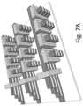
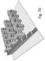
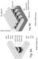
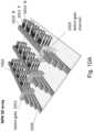
- FIGS. 7 A- 7 Eare example illustrations alternative staircase structures that may be used in 3D structures
- FIGS. 8 A- 8 Bare example illustrations of the formation and structure of vertical memory cell of a two terminal memory using SCR technology for a 3D memory;
- FIGS. 9 A- 9 Bare example illustrations of the formation and structure of vertical memory cell of a two terminal memory using bi-ristor technology for a 3D memory;
- FIGS. 10 A- 10 Dare example illustrations of the formation and structure of horizontal bi-ristor and SCR technology 3D memory
- FIGS. 11 A- 11 Hare example illustrations of the formation and structure of another horizontal bi-ristor and SCR technology 3D memory
- FIGS. 12 A- 12 Bare example illustrations of the formation and structure using a substrate with protection areas or transistors designated regions in and ELTRAN type process;
- FIGS. 13 A- 13 Care example illustrations of the formation and structure of 3D memory utilizing at least diffusion doping
- FIGS. 14 A- 14 Mare example illustrations of the formation and structure of 3D TRAM memory
- FIG. 15 Ais an example illustration of a non-volatile floating body cell
- FIG. 15 Bis an example illustration of a stable two states one transistor memory structure 3D DRAM memory cell
- FIG. 15 Cis an example illustration of a non-volatile 3D TRAM memory
- FIGS. 16 A- 16 Lare example illustrations of the formation and structure of 3D TRAM memory with select transistors
- FIGS. 17 A- 17 Bare example illustrations of sharing of the per layer in silicon control lines
- FIGS. 18 A- 18 Dare example illustrations of 3D memory arrangements
- FIGS. 19 A- 19 Bare example illustrations of the formation and structure of 3D Memory with dual functionality
- FIGS. 20 A- 20 Hare example illustrations of the formation and structure of vertically oriented 3D memories
- FIGS. 21 A- 21 Eare example illustrations of the formation and structure of a NOR type 3D memory.
- FIGS. 22 A- 22 Fare example illustrations of the formation and structure of a NOR type 3D universal memory.
- Some drawing figuresmay describe process flows for building devices.
- the process flowswhich may be a sequence of steps for building a device, may have many structures, numerals and labels that may be common between two or more adjacent steps. In such cases, some labels, numerals and structures used for a certain step's figure may have been described in the previous steps' figures.
- Memory architecturesinclude at least two important types—NAND and NOR.
- the NAND architectureprovides higher densities as the transistors forming the memory cells are serially connected with only an external connection at the beginning and end as is illustrated in at least U.S. Pat. No. 8,114,757, FIGS. 37A-37G.
- NOR architecturesare less dense but provides faster access and could work sometimes when the NAND architecture cannot as transistors in the memory cell are directly accessible and in many cases both its source and drain are accessible, such as being illustrated in at least U.S. Pat. No. 8,114,757, FIGS. 30A-30M.
- the memory cellcould be constructed with conventional N type or P type transistors where the channel doping may be of opposite type with respect to the source drain doping or the memory cell could utilize a junction-less transistor construction where the gate could fully deplete the channel when in the off-state.
- the junction-less transistoris attractive as it may take less processing steps (or provide other device advantages such a low leakage off-state) to form the memory array without the need to form a change in doping along the transistor.
- 3D Memory architecturesare utilizing a horizontal memory transistor, for example, such as illustrated in at least U.S. Pat. No. 8,114,757, at least FIGS. 37A-37G and FIGS. 30A-30M.
- Othersmay use vertical memory transistors, for example, such as in the Toshiba BiCS architecture such as illustrated in at least U.S. Pat. No. 7,852,675.
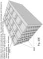
- a base donor substrate 110may be used to form a dual porous layer for future cut layer 113 on which an epitaxial process may be used to form relatively thick crystalline layer 120 .
- Future cut layer 113may include two porous layers; an upper layer of porous silicon, which may contain microscopic pores of diameter of a few nm, and below this is formed a lower layer of porous silicon for which the pore diameter may be a few (or more) times greater (similar to FIG. 23 of U.S. application Ser. No. 14/642,724), for the future ‘cut’ or cleave.
- the epitaxial formation of relatively thick crystalline layer 120could include successively altering the addition of dopants to further support the following steps.
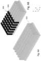
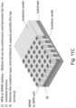
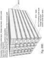
- FIG. 1 Billustrates relatively thick crystalline layer 120 after going through a porous formation process which forms multilayer structure 122 .
- Multilayer structure 122may include layer 144 , layer 142 , layer 140 , layer 138 , layer 136 , layer 134 and layer 132 .
- Multilayer structure 122may include base donor wafer substrate 110 with porous cut layer 113 for the planed transfer of the fabricated multilayer structure over the target wafer, which could include the memory peripherals circuits prefabricated on the target wafer.
- multilayer structure 122may not include porous cut layer 113 when the transfer to a target wafer is not intended.
- Layer 144could be the portion of layer 120 which remains after the multi-layer processing.
- the alternating layerscould have alternating porosities of r levels such as layers 132 , 136 , 140 with porosity of less than 30% or less than 40% while layers 134 , 138 , 142 with porosity over 50% or over 60%, or layers 132 , 136 , 140 with a porosity of less than 55% while layers 134 , 138 , 142 with porosity over 65%, or other alternating level of porosity based on the target application, process, and engineering choices.
- Each layermay include a varying porosity thru its thickness, or a number of sublayers of varying porosity.
- the number of alternating layers included in multilayer structure 122could be made as high as the number of layers needed for the 3D memory (for example, greater than 20, greater than 40, greater than 60, or greater than 100) or for the transferring of a subset of multilayers structures one on top of the other to form the desired final structure.
- the porosity modulationcould be achieved by alternating the anodizing current or changing the lighting of the silicon structure while in the anodizing process or by first alternating the doping as the layer 120 is being grown through epitaxial process.
- Layer 144could be the portion of layer 120 which is left un-processed.
- the above steps ii-ivcan be carried out after holes 151 are formed by masking and etch processes as shown in FIG. 2 , where holes 151 may be filled by, for example, contact metal or gate stacks in subsequent processing. Holes 151 may include regions. Thus a second desired multilayer structure 124 may be formed.
- the above processingmay result with the desired multilayer structure 122 or second desired multilayer structure 124 for the formation of 3D memories.
- U.S. patent application Ser. No. 12/436,249incorporated herein by reference, teaches an alternative method for the formation of the multilayer structure 122 with alternating doping.
- the methodstarts by multiple depositions of amorphous silicon with alternating doping, then after performing a solid phase recrystallization to convert the stack into a stack of p-type doped single crystalline Si-containing layers using a high temperature a recrystallization, with recrystallization temperatures from 550° C. to 700° C. After recrystallization, the single crystalline Si-containing layers could then be subjected to anodization and so forth as presented in ii-iv above.
- U.S. patent application Ser. No. 12/436,249teaches a few alternatives for the formation of the alternating doping layer structure which could be employed herein for the 3D memory multilayer structure formation.
- the epitaxial layer 120could include alternating n doped and n+ doped layers.
- the porous formation of the n doped layersmay be assisted by light to form the holes for the anodizing process to effectively work as had been presented in S. Frohnhoff et. al., Thin Solid Films, in press (1994), U.S. patent application Ser. Nos. 10/674,648, 11/038,500, 12/436,249 and U.S. Pat. No. 7,772,096, all of these incorporated herein by reference.
- the structurecould be oxidized and then annealed as presented in steps iii and iv above.
- a method to form alternating layers of coarse and fine porous layersis by alternating the anodizing current similar to the description in “Porous silicon multilayer structures: A photonic band gap analysis” by J. E. Lugo et al J. Appl. Phys. 91, 4966 (2002), U.S. Pat. No. 7,560,018, U.S. patent application Ser. No. 10/344,153, European patent EP0979994, and “Photonic band gaps analysis of Thue-Morse multilayers made of porous silicon” by L. Moretti at el, 26 Jun. 2006/Vol. 14, No. 13 OPTICS EXPRESS, all of these incorporated herein by reference. Following the anodizing step the structure could be oxidized and then annealed as presented in steps iii and iv above.
- the anodizing stepcould be done as a single wafer process or by using a batch mode as illustrated in U.S. Pat. No. 8,906,218, incorporated herein by reference and other similar patents assigned to a company called Solexel.
- Another alternativeis to form the multilayer structure 122 by first forming multilayer structure of alternating n type over p type.
- Such a methodis illustrated in U.S. Pat. No. 8,470,689 and in “Silicon millefeuille”: From a silicon wafer to multiple thin crystalline films in a single step” by D. Hernandez et al., Applied Physics Letters 102, 172102 (2013); incorporated herein by reference.
- These methodsleverage the fact that n type silicon would not become porous without light while p type silicon would only need current for the anodizing process to take place.
- the multilayer of n over pcould be first etched to form the multilayer pattern such as is illustrated in FIG. 31E or FIG. 37E of U.S. Pat.
- n type siliconcould be at much higher rate than the p+ silicon.
- a paper titled: “Fabrication of conducting GeSi/Si micro and nanotubes and helical microcoils” by S V Golod, V Ya Prinz, V I Mashanov and A K Gutakovsky, Semicond. Sci. Technol. 16 (2001) 181-185, incorporated herein by reference, it present that p+ silicon would be etch at much lower rate than n silicon, quoting: “As a selective etchant, an ammonium hydroxide-water solution can be used. It was shown in [8] that the 3.7 wt. % NH4OH solution has a pp+ selectivity of approximately 8000:1 at 75° C. and boron concentration p+10 2 cm ⁇ 3 .
- An additional alternativemay be to utilize the Bosch process.
- a technique used for deep hole etchhas been applied to form structures of crystalline lines one on top of the other each with oxide all around. Similar techniques could be used to form the base structure for 3D memory.
- Another alternativeis to form multilayers of silicon over Si 1-x Ge x as illustrated in “New class of Si-based superlattices: Alternating layers of crystalline Si and porous amorphous Si 1-x Ge x alloys” by R. W. Fathauer et al., Appl. Phys. Lett. 61 (19), 9 Nov. 1992, incorporated herein by reference.
- a multilayer structurethere is high degree of selectivity in etching Si 1-x Ge x layers over Si layers. This may be followed by oxidation such as step iii. and anneal iv. could provide multilayers of silicon over oxide.
- the multilayer structureis direct epitaxial of silicon special oxide and silicon again.
- the special oxideis a rare-earth oxide which if deposited properly would keep the crystal structure of the silicon to allow crystalline silicon on top of it as presented in U.S. patent application US 2014/0291752 incorporated herein by reference.
- oxidized porous siliconfor isolating the silicon layers for the 3D memory structure is the ability to easily etch portions of these oxidized porous layers to allow the gate formation to have a larger coverage of the transistor channel to have even better control on the memory transistor such as with gate all around or a ‘mostly’ gate all around transistor structure.
- the area on top and under the channelcould be etched so in the following processing step of oxide and gate formation it would form a larger coverage of the channel which could be even gate all around for better control.
- Base wafers or substrates, or acceptor wafers or substrates, or target wafers substrates hereinmay be substantially comprised of a crystalline material, for example, mono-crystalline silicon or germanium, or may be an engineered substrate/wafer such as, for example, an SOI (Silicon on Insulator) wafer or GeOI (Germanium on Insulator) substrate.
- donor wafers hereinmay be substantially comprised of a crystalline material and may include, for example, mono-crystalline silicon or germanium, or may be an engineered substrate/wafer such as, for example, an SOI (Silicon on Insulator) wafer or GeOI (Germanium on Insulator) substrate, depending on design and process flow choices.
- the described memory structurewould be arranged as a process flow forming a type of a 3D memory structure. These flows could be considered as a Lego part which could be mixed in different ways forming other variations, thus forming many types of devices. Some of these variations will be presented but as with Lego there too many variations to describe all of them. It is appreciated that artisan in the art could use these elements of process and architecture to construct other variations utilizing the teaching provided herein.
- the mono-crystalcould be doped and could have either an isolative layer in-between or sacrificial layer which could be replaced at some point in the process with isolative layer.
- the multilayer structurecould be fully ready or partially ready where the etching of vertical holes or trenches shaped, as required for the memory structure to follow, allows the completion of the multilayer structure by selective etching of the sacrificial layers in-between.
- a volatile 3D memory using floating body chargeis described in U.S. Pat. No. 8,114,757, incorporated herein by reference, as related to at least FIGS. 30 A- 30 M and FIGS. 31 A- 31 K .
- the followingis additional alternative for forming a 3D DRAM volatile memory.
- 3D Memorymay be multi-layers of 2D memory in which memory cells are placed as a matrix with rows and columns. These memory cells are controlled by memory control lines such as bit-lines, source-lines, and word-lines, usually in a perpendicular arrangement, so that by selecting a specific bit-line and specific word-line one may select a specific memory cell to write to or read from. In a 3D memory matrix, having three dimensions, selecting a specific memory cell requires the selecting of the specific layer which could be done by additional memory control lines such as select-lines. As been presented herein, some of the select lines could be integrated in the semiconductor layer in which the memory devices are built into. Other select lines could be deposited or formed thru epitaxial growth. These memory control lines could therefore be comprising semiconductor materials such as silicon or conductive metal layers such as tungsten aluminum or copper.
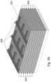
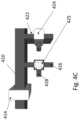
- FIG. 3 Aillustrates a starting multilayer structure 302 , comprising p-type or n-type silicon 304 and isolation or sacrificial layer in-between 306 formed by many of the processes presented herein.
- a hard mask 308such as silicon nitride may be patterned on top for the following etch step.
- FIG. 3 Billustrates the multilayer structure 310 after an etch step.
- FIG. 3 Cillustrates the structure 311 after deposition of isolative material 312 , such as SiO 2 , and etching holes 314 for the following step of gate stack.
- isolative material 312such as SiO 2
- FIG. 3 Dillustrates the structure 320 after forming the gate stack 322 .
- the gate stackcould be formed by CVD or ALD of first a gate oxide and then gate material which could be metal or in-situ doped polysilicon.
- the gate formationcould be two independent side gate column as illustrated or tied double gate or even gate all around. For the gate all around, it may require that the step of etching the gate holes 314 will include a non-directional isotropic etch step to etch the in-between layer to allow the following gate all around formation.
- FIG. 3 Eillustrates the structure 321 after stripping off the dielectric 312 , and then a step of diffusion doping to form the source 324 regions and the drain regions 326 .
- the source regions 324would be connected to the source line (“SL”) and the strip of the drain regions 323 would become later part of the bit-lines (“BL”).
- the SL and the BLcan be used interchangeably depending on the array arrangement.
- These diffusion dopingwill convert all the exposed silicon areas that are not protected by the gates structures 322 from p type to n+ type or n type to p+ type. This will form transistors in the small pin structures 325 , while the common strips 327 would serve as simple conductor acting as the bit-lines or the source-lines for the memories that could be formed by the pins transistors 325 .
- FIG. 3 Fillustrates the structure 331 with extension of the bit lines 334 which could be used for a stair-case per layer access.
- An optional select gate 332could be used to select memory branch.
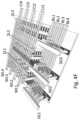
- FIG. 3 Gillustrates the structure 331 after forming stair-case 336 of the bit line extension 334 and after forming the vertical connections to the bit-lines 337 and to the transistor sources 338 .
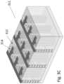
- FIG. 3 Hillustrates the structure after adding the grid of connections.
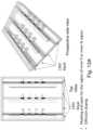
- the illustrationis one option for structuring bit-lines 356 , select-gate lines 358 , source-lines 352 and word-lines 354 .
- These connectivity structureallow selecting a specific cell such that select gate lines 358 allow the selecting the ‘x’ location by selecting the ‘x’ branches, the word-lines 354 select the ‘y’ location by selecting the gates in ‘y’ direction, and the bit-lines 356 select the ‘z’ location by selecting the drain in ‘z’ direction.
- the optional select-gate lines 358allow selecting of the bank of transistors in the bank along ‘x’ direction.
- FIG. 3 Iillustrates the structure after adding the grid of connections with an alternative structure of word-lines and bit-lines.
- the gate materialis common along the multiple pins, which would serve as simple conductor acting as the word-lines.
- FIG. 3 Jillustrates optional silicidation of the bit lines 327 to reduce their resistance.
- silicidation 362First only the areas designated for silicidation 362 are being exposed while all other areas are being protected by photoresist or isolation oxide. Then a metal such as Ni, Ti, Co, or other known in the art material, is deposited making contact with the bit lines 327 side walls 362 . Then thermal reaction is achieved by the use of Rapid Thermal Anneal (RTA) or laser anneal. Then the unreacted metal is etched away.
- RTARapid Thermal Anneal
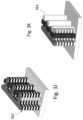
- FIG. 3 Killustrates a 3D memory of 3 column structure.
- the transistors source forming the memory cellare connected by vertical line 338 of FIG. 3 G connecting with the transistors source side wall. It is enlarged view at FIG. 3 K .
- this conductive vertical column 364a selective epitaxy process could be used to form this vertical connection.
- FIG. 3 Lillustrates the structure with protective cover of oxide or other protective material 366 and trench opening the side walls of the memory transistors source 368 .
- the opening of the trenches 366could include a step for selective removal of part of the vertical isolation between the sources of the stack transistors.
- FIG. 3 Millustrates the structure after a step of epitaxial growth for forming a vertical column connecting all the sources in a stack 370 . These columns could be silicide to further improve their connectivity.
- FIG. 3 Nillustrates the structure after adding contacts 372 from the top.
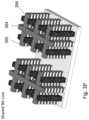
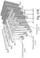
- FIGS. 3 A- 3 Nwere made for ease of drawings and understanding. Persons in the art would understand that techniques common in memory design could be used to increase memory bit density. Such as mirroring the transistors along the bit lines sharing the bit lines for right side transistor and left side transistors and mirroring across source side sharing the vertical source lines. Such structure is been illustrated in U.S. Pat. No. 8,114,757, as related to FIGS. 30A-30M and FIGS. 31A-31K.
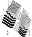
- FIG. 3 Oillustrates another alternative where the vertical line connecting the source side of the stack transistors are shared 376 but the horizontal in silicon bit-lines are not shared 374 and 375 .
- One advantage of not sharing the bit-lines 374 and 375is the option to add silicidation as was described in respect to FIG. 3 J .
- FIG. 3 Pillustrates another alternative where the horizontal bit lines of the stack transistors are shared 384 but the vertical line connecting the source side of the stack transistors are not shared 375 and 386 .
- FIG. 4 Aillustrates a starting multilayer structure processed in similar way to the one illustrated in FIG. 3 A-B , having multilayer of undoped or p type-doped silicon 402 with sacrificial or isolating layers in-between 404 patterned using hard mask such as silicon nitride 406 providing stack of future transistors 408 sharing common silicon bit-lines 410 .
- the transistorshave middle extensions 409 for the future back-bias or charge injector.
- FIG. 4 Billustrates the structure after patterning gates. These include the memory cell gates 412 and the bit-lines select gates 414 .
- FIG. 4 Cillustrates the top-viewed transistors structure with more details.
- the bit-lines 410have select gates 414 and are common to multiple stack of memory cell 424 transistors drains 422 .
- the transistors other sideis the source 426 and the transistor channel has like a T shape extension 428 to be used later to provides the back-bias which is the equivalent of the buried N-well or n-type charge injector for the 2D memory.
- the channelis well covered by the gate oxide and gate material 424 this help to prevent risk of direct short between n-type regions of the source 426 , the drain 422 , and the back-bias 428 regions and could help to direct the step of dopant diffusion to the target n regions.
- FIG. 4 C illustrationis showing the gate also as transparent 425 to farther help understanding of the structure.
- the gate materialis also used for self-aligned doping by diffusion converting the p type silicon to n+ silicon in all location not covered by the gate material.
- FIG. 4 Dillustrates the areas being doped 430 to become n+ and the area been protected and left undoped 432 p-type silicon.
- FIG. 4 Eillustrates the structure after adding the vertical connections.
- the bit-linesare connected with individual connection per layer using the stair-case technique 442 , the source lines are connected with one vertical connection per transistor stack 446 and the back-bias or the charge injector are connected with their own vertical connections 448 .
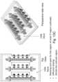
- FIG. 4 Fillustrates after adding the grid of connections.
- the bit-linesare connected indicated by BL 1 , BL 2 , BL 3 , BL 4 , with optional select gates SG 1 , SG 2 , SG 3 , and having the transistors sources connected with source lines SL 1 , SL 2 , SL 3 and the gates connected with word lines WL 1 , WL 2 , WL 3 , WL 4 and the back-bias having their own charge injector lines C 11 , C 12 , C 13 , C 14 .
- Other optionexist for the formation of such memory control lines grid, allowing selecting an individual transistor-memory cell by selecting its source, gate and drain defining a specific x,y,z location.
- bit-lines silicidation as presented in respect to FIG. 3 Jcould also be applied to the bit-lines 410 of these memory structures
- FIG. 4 A-Fwere made for ease of drawings and understanding. Person in the art would understand that techniques common in memory design could be used to increase memory bit density. Such as mirroring the transistors along the bit lines sharing the bit lines for right side transistor and left side transistors and mirroring across source side sharing the vertical source lines, and sharing the back-bias between adjacent cells and other density improvement techniques such structure is been illustrated in U.S. Pat. No. 8,902,663, as related to FIG. 7 A-N . Many of the other alternatives presented in U.S. Pat. No. 8,902,663 could be applied for these structures as well. This may include having the memory peripheral circuits on top or underneath or on the side of the memory cell or any combination of those.
- the memory structurecould be processed on top of a wafer which has a pre-build cut layer 113 to support a transfer of the structure to another wafer or carrier. This could allow forming peripheral circuits and other circuits both on top or underneath the memory structure as detailed in many other places in the incorporated by reference patents and patent applications.
- ‘self refresh’Another alternative that would not require changes in the device structure is to use what could be called ‘self refresh’.
- a refresh cyclemeans that each cell is being read and re-written individually.
- ‘self refresh’many or even all cells could be refreshed together by driving a specific current (may be a current range or minimum current) through them.
- the cell holding ‘zero’will keep its zero state and the cell holding ‘one’ will get recharged to recover their lost of floating body charge due to leakage. This techniques had been detailed in a paper by Takashi Ohsawa et. al.
- ReRAMresistive-memory
- a 3D ReRAMhas been described in U.S. Pat. No. 9,117,749, incorporated herein by reference.
- ReRAMperform the memory function by having the resistivity change which could be achieved by driving current through the ReRAM variable resistivity medium and could be sense by measuring current or voltage through that medium.
- materialsthat could be used for ReRAM and some of those are oxides with additional materials which could be driven into the oxide to change it resistivity.
- U.S. Pat. No. 8,390,326incorporated herein by reference present the use of silicon oxide for such use.
- a subclass of the ReRAMare structure that allow only one time programing (“OTP”) of these mediums such as presented in U.S. Pat. No. 8,330,189 incorporated herein by reference.
- each element of resistive memory in the matrix of memory cellhas a dedicated select device to allow writing one element in the matrix without accidently writing other element in the matrix.
- FIG. 5 Aillustrates a select device 502 which is a diode and a resistive memory element 504 .
- a 3D ReRAM structuresare presented in which the matrix of the ReRAM are constructed by doped silicon as conductors and oxides as the element. The oxide as the resistivity switching element is sandwiched by two silicon regions.
- the doped siliconcould be single crystal silicon or polysilicon.
- the diode 502is achieved by having the silicon doped with n type to one electrode and p type to the other. The doping could be set so one electrode is highly doped to provide good conductivity while the other is medium doped to show rectifying diode current-voltage characteristic.
- FIG. 5 Billustrates structure for 3D Memory useful for OTP or other subclass of ReRAM. It start with a multilayer structure such as the one in FIG. 1 B .
- the siliconcould also be polysilicon and accordingly allowing the formation of the multilayer structure by cycle of deposition of polysilicon followed by deposition of insulting layer such as silicon oxide.
- the silicon 512could be highly doped.
- a matrix of holesare formed into the multilayer structure. These holes are than filled first with the ReRAM material such as thin oxide 519 and then with Low ⁇ moderately doped polysilicon 518 .
- the top region 520 of the polysilicon pillar 518is highly doped for Ohmic contact.
- the layers 512 hap n type doping than pillar filing the holes 518would have p type doping or the reverse.
- the layers 510serve as one electrode while the pillar 518 serve as the other electrode and every intersection between them form a memory site as the electrodes also form the select diode while the oxide in between is the element which change its resistivity other once for OTP or multiple times base on the type of materials and operation mode and other materials forming the 519 barrier layer.
- the very top silicon layer 516could be highly doped and act as select gate. By etching 522 the top silicon layer 516 it is formed as strip along ‘x’ direction. Then, the select gate 516 could be used to select the pillar.
- FIG. 5 Cillustrates the structure after adding stair-case connection per layer 526 for word-lines and contact for the select gate top strips 528 and the contact to the pillars 529 .
- FIG. 5 Dillustrates the structure with the connection grid.
- These three set of memory control linesenable the selection of individual memory cell by choosing specific x, y, z location.
- FIGS. 5 E and 5 Fillustrate another alternative where the select gates are placed adjacent to stair-case word-lines 532 , and having the forming strips etch done through all layers 530 .
- FIG. 6 Aillustrates a foundation structure for another alternative ReRAM non-volatile memory. Starting again with multilayer structure and etching it to form stack of multilayer rims 602 going in the x direction.
- FIG. 6 Billustrates the structure after patterning going in the y direction cover of ReRAM material such as silicon oxide 604 covered with highly doped polysilicon electrodes 606 .
- ReRAM materialsuch as silicon oxide 604 covered with highly doped polysilicon electrodes 606 .
- the rim electrode 602 going in x directioncould have p type doping while the polysilicon electrodes going in y direction 606 could have n type doping or the other way around.
- the rim electrode 602 going in x directioncould have moderate level doping to show rectifying diode behavior to reduce risk of sneak current path through adjacent cells.
- the patterned y direction electrodescould before by deposition through patterned photo resist or by first blanket deposition and then etching step.
- FIG. 6 Cillustrates the structure after forming stair-case 610 for per layer future connections.
- the electrode adjacent to the stair-case 607could be used as a select gate for the rim.
- FIG. 6 Dillustrates the structure with the connection grid.
- These three set of memory control linesenable the selection of individual memory cell by choosing specific x, y, z location.
- FIG. 7 A to 7 Eillustrates alternative staircase structures that could be used in some of the structures previously presented.
- NPNNPN
- PNPPNP
- NPNPPNP
- PNPNPNPN
- SCRSilicon-Controlled Rectifier
- the PNP, NPNare less known and are also called Biristors these memories are volatile memories.
- the NPN, PNP, NPNP, and PNPN deviceshave two terminals such as anode and cathodes on these two ends terminal, and their gate are left floating.
- NPNP or PNPN structurescan be referred as gate-less or open-gate SCT.
- the NPN or PNP structurescan be referred as open-base bipolar transistor, In these structure the diode select device could be achieve from the device internal structure provide broader materials options of the memory electrodes—bit-lines and word-lines.
- FIG. 8 Aillustrates a vertical memory cell of a two terminal memory using SCR technology.
- the bottom terminal—the bit line 802could be metal conductor or highly doped silicon.
- the first active layer of n doped silicon 810In some cases these layers ( 802 , 810 ) could be combined.
- On top of ita layer of p doped silicon 812 .
- the word line 804vertical oriented in respect to the bit-line 802 .
- the word-lines in most caseswould be made from metal or alternative conducting material. Other than pure silicon materials such as polycrystalline silicon could also be used.
- the memory cellcould be flipped having p type at the bottom and n type at the top.
- FIG. 8 Billustrates 2D memory structure using vertical SCR. More details for such memory structure are presented in a paper titled “Design of two-terminal PNPN diode for high-density and high-speed memory applications” by Tong Xiaodong et. al. published in Vol. 35, No. 1 Journal of Semiconductors January 2014, and U.S. Pat. No. 9,013,918 incorporated herein by reference.
- FIG. 9 Aillustrates a vertical memory cell of a two terminal memory using Biristor technology.
- the bottom terminal—the bit line 902could be metal conductor or highly doped silicon.
- the first active layer of n doped silicon 910In some cases these layers ( 902 , 910 ) could be combined.
- a layer of p doped silicon 912On top of it the final n doped layer 914 .
- the word line 904vertical oriented in respect to the bit-line 902 .
- the word-linesin most cases would be made from metal or alternative conducting material such as n doped silicon which in some cases could be combined with the top n+ layer 914 .
- Other than pure silicon materialssuch as polycrystalline silicon could also be used.
- Alternative structure of PNPcould also be used as an alternative.
- FIG. 9 Billustrates 2D memory structure using vertical Bristor. More details for such memory structure are presented in a papers titled Biristor-Bistable Resistor Based on a Silicon Nanowire at IEEE ELECTRON DEVICE LETTERS, VOL. 31, NO. 8, August 2010, and Bistable Resistor (Biristor)—Gateless Silicon Nanowire Memory at VLSI 2010 both by Jin-Woo Han at. al., incorporated herein by reference.
- FIG. 10 Aillustrates a 3D horizontal Biristor memory structure. This structure resemble the structure of FIG. 3 A-P without the gate 322 .
- the fabrication flowcould be similar and so the various option for sharing to compact the memory size.
- Biristorit might be desired to have different doping level for the n silicon bit-lines 1002 , the first n region 1010 and the second n region 1014 . These could be achieved by masking all other region and diffuse doping only to the desired regions repeating the step for each region, or doping multiple regions with base doping and then add more doping to some of the regions by extra step of masking and diffusion doping.
- the P region 1012has spatially gradient doping level between the first n region 1010 and the second n region 1014 .
- the p regions 1012are not covered by oxide and gate materials.
- the gatecan be constructed for diffusion doping masking layer, but do not connect to the any terminal and left floating.
- the second n regions 1014are later vertically connected by pillars similar to 338 or alternatively using selective epitaxial similar to 370 .
- the pillarscould be doped during the epitaxial process to function as the second n regions 1014 .
- FIG. 10 Aalso illustrates the stair-case connections 1026 of the bit-lines 1002 and the select gates 1022 and the select oxide 1020 .
- FIG. 10 Billustrates a 3D horizontal SCR memory structure which is very similar to the structure of FIG. 10 A .
- the p regions 1032 and the second n region 1034there are also second p regions 1036 forming the horizontal SCR—npnp device.
- FIG. 10 Dillustrates the structure with the connection grid.
- Word-lines, bit-lines and Select Gates linesThese three set of memory control lines enable the selection of individual memory cell by choosing specific x, y, z location.
- the bit-lines 1042 on the other side than the select gatescould have a high resistivity pillar connection 1040 to provide the minimal holding current to keep the state ‘1’ of the SCR memory cells.
- FIG. 10 Cillustrates the structure of FIG. 10 B after rotation and addition of top layer control lines. It illustrates optional gates 1041 to allow control of the delivery of the holding current from the pillars 1040 to the bit-lines 1042 .
- the control signalcould be delivered by top metal lines 1043 . Controlling the holding current could allow reduction of overall device power and could help in providing the write signal to the proper/desired memory cell without causing disturb to the un-selected memory cells.
- peripherals circuitsneed to support the following:
- FIG. 11 Aillustrates the type of 2D memory structure, presented in FIG. 8 B and FIG. 9 B process 2D memory plane on top of another 2D memory plane forming a 3D memory structure.
- FIG. 11 Aspread the structure planes for ease of understanding.
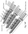
- the memory periphery circuitscould be build 1100 , on top of it a first memory plane 1110 including its word-line via bridge 1102 and its bit-lines interlayer via bridges 1114 .
- a second memory plane 1120could be processed with its word-lines 1122 and bit lines 1124 .
- FIG. 11 Billustrates the structure of FIG. 11 A with the planes not in exploded view.
- FIG. 11 C to FIG. 11 Fillustrates some of the steps of forming such 3D memory.
- FIG. 11 G and FIG. 11 Hillustrates two options for forming the bit-lines or word-lines and having them connected to the p silicon or the n silicon regions.
- the substrateis prepared for a specific use in which the silicon area to be used for transistors could be designated.
- FIG. 12 Aillustrates specific substrate with protection areas or transistors designated regions. Accordingly the top layer of the silicon substrate 1200 is patterned exposing future transistors area 1202 and covering non-transistor regions 1204 such as shallow trench isolation (“STI”) regions. The exposed area 1202 could be doped by n type doping or covered by protective hard mask such as silicon nitride. The substrate is then put into an anodizing process forming porous in the unprotected are and expending underneath the protected areas.
- STIshallow trench isolation
- FIG. 12 Billustrates the substrates following an anodizing step.
- the porous layercould be harden by some oxidation the top surface could be sealed and flattened by high temperature H 2 annealing and epitaxial step could be done to further improve the substrate top surface.
- FIGS. 50 A-E and 51 A-Fa 3D memory is presented which utilizes a multilayer structure of interleaving poly-silicon and isolation layers. It is expected that such structure would be lower cost to fabricate than an interleaving structure with crystalline silicon.
- Such a structurecould be used for the 3D ReRAM described in respect to FIGS. 5 B-E , FIGS. 6 A-D herein and could be used for the NPNP or PNPN type memory described in respect to FIGS. 10 A-C and FIG. 11 A-G herein.
- the poly-silicon layercould be annealed, for example, such as by laser annealing to improve its electrical and physical characteristics, such as carrier mobility and so on. During the formation of the poly-silicon some baseline doping could be done.
- the peripheral circuitscould also use poly-silicon transistors and for better performance crystalline silicon could be used. These peripheral circuits could be place on the memory sides but also, using techniques presented here and before, underneath and or on top. These types of 3D integration of peripheral circuits could enable shorter memory control lines, thereby reducing circuit delays and power.
- FIG. 13 Aillustrates a 3D memory structure similar to structures presented herein with a top view and a perspective side view, masked 1302 to open regions for diffusion doping of the inner P or N regions of the memory cells.
- FIG. 13 Billustrates a 3D memory structure similar to structures presented herein with top view and perspective side view, masked 1304 to open regions for diffusion doping of the outer N regions (anode) of the memory cells and the in silicon bit-lines. These bit-lines could further be silicided for better conductivity as has been described herein before.
- FIG. 13 Cillustrates a 3D memory structure similar to structures presented herein with top view and perspective side view, masked 1306 to open regions for diffusion doping of the outer P regions (cathode) of the memory cells. These outer P regions could further be silicided.
- the memory cellcould be constructed for the in silicon control line to be made P type which could be part of the cathode and the outer N region could be later on connected with pillars as has been described herein, and accordingly changes the type of doping the mask pattern illustrated in respect to FIG. 13 A-C herein.
- the two terminals SCR type memorycould be modified to include a gate and is known in the art as Thyristor device or Thyristor Random Access Memory—T-RAM, or Thin Capacitively-Coupled Thyristor (TCCT) memory.
- Thyristor deviceor Thyristor Random Access Memory—T-RAM
- TCCTThin Capacitively-Coupled Thyristor
- FIG. 14 A and FIG. 14 Billustrate the building blocks—example memory cells for T-RAM memories and for 3D T-RAM memories.
- the anode 1408is outer P type region, then an inner N type region 1406 then inner P type region 1404 with gate 1409 on the sides (or may be all around P-type region 1404 ) isolated by gate oxide 1407 , and then the cathode 1402 outer N type region which could be extended to form the in-silicon embedded source line.
- the outer N region 1402 , inner P region 1404 , inner N region 1406 , outer P region 1408can be made of amorphous silicon or alternatively polycrystalline silicon.
- the grain size of the polysiliconmay be designed to minimize the cell-to-cell variation.
- the grain size of polycrystalline siliconmay be 5 nm ⁇ 100 nm so that the impact of grain size fluctuation reflects uniformly to the memory performance across a number of different cells.
- the grain size of the polycrystalline siliconmay be greater than the size of each inner P region 1404 and inner N region 1406 , which may be obtained thru, for example, annealing processes so that the grain boundary does not exist in inner P region 1404 and inner N region 1406 .
- the height of the unit cell siliconmay be 5 nm ⁇ 200 nm and the width of the unit cell silicon may be 5 nm ⁇ 200 nm.
- the length of the inner P region 1404 and inner N region 1406may be 5 nm ⁇ 200 nm.
- the doping concentration of inner P region 1404 and inner N region 1406may be greater 10 15 cm ⁇ 3 but may not exceed 5 ⁇ 10 19 cm ⁇ 3 .
- the doping concentration of outer N region 1402 and outer P region 1408may be greater than 5 ⁇ 10 19 cm ⁇ 3 , for example, such as 5 ⁇ 10 19 cm ⁇ 3 or 1 ⁇ 10 2 cm ⁇ 3 . Additional information on poly-silicon or amorphous silicon T-RAM may also be found in U.S. Pat. Nos. 5,477,065, 6,812,504, 6,882,010 and 7,042,027, and International PCT application PCT/IB2013/061383, the entirety of the foregoing are incorporated herein by reference.
- a high doping concentrationcould be achieved by in-situ deposition techniques. Such could be applied for the formation of the pillars achieving multiple objectives—low connection resistance and doping and it could allow some cell size reduction.
- FIG. 14 Jillustrates a similar structure to the one in FIG. 14 G .
- the outer N regionsare connected by pillars 1450 .
- FIG. 14 Killustrates the structure with in-situ highly doped N type polysilicon pillars 1452 .
- FIG. 14 Lillustrates a similar structure to the one in FIG. 14 D .
- the outer P regionsare connected by pillars 1460 .
- FIG. 14 Millustrates the structure with in-situ highly doped P type polysilicon pillars 1462 .
- the structurecould also built in reverse order as illustrated in FIG. 14 B the anode 1412 is P type which could be extended to form the in-silicon embedded bit-line, then an N type region 1414 then P type region 1416 with gate 1419 on the sides (or may be all around P type region 1416 ) isolated by gate oxide and then the cathode 1418 N type region.
- FIG. 14 Cillustrates an example 3D T-RAM structure utilizing the bit-cell of FIG. 14 A .
- the anode contact 1428could be formed by pillars or selective epitaxy similar to what has been presented before herein, the memory cell gates 1429 of a row could be shared forming gate lines, and the cathode forming the source lines 1422 could be etch to form the staircase (or other type access structures) for a per layer connection.
- a branch select gate 1423could be formed to control the source lines of an entire row.
- the other side of the source linescould include a gated hold current structure similar to 1041 , 1040 of FIG. 10 C herein.
- the gated hold current structure 1041 , 1040allow reducing the memory power consumption as the holding current could act as refresh rather than constant as discussed in the IEDMO4 paper by Nemati.
- FIG. 14 Dillustrates an example of the structure of FIG. 14 C with the connection grid—word-lines, bit-lines, source-lines and select gates-lines drawn. These three sets of memory control lines enable the selection of individual memory cell by choosing specific x, y, z locations.
- FIG. 14 Eillustrates an example 3D T-RAM structure utilizing the bit-cell of FIG. 14 B .
- the anode contact 1438could be formed by pillars or selective epitaxial similar to what has been presented before, the gates 1439 of a row could are not shared, and the cathode forming the bit-lines 1432 could be etched to form the staircase (or other structures) for a per layer connection.
- a branch select gate 1433could be formed to control the source lines of an entire row.
- FIG. 14 Fillustrates the structure of FIG. 14 E with the connection grid—word-lines, bit-lines, source-lines and select gates-lines. These three set of memory control lines enable the selection of individual memory cells by choosing specific x, y, z locations.
- This structureis a bit more challenging as the select lines and the bit line are parallel which implies that multiple T-RAM cells may have their anodes sharing the same source lines while their cathodes share the same bit-lines and only their gate is unique. The read operation from an individual cell in such structure is a more challenging.
- FIG. 14 Gillustrates an alternative to the illustrated FIG. 14 F arrangement wherein the source lines are vertical to the bit lines and are in parallel to the gate lines. Reading an individual cell is now conventional; for example, by selecting a bit line and a source line a single T-RAM cell may be selected, which is the common approach for T-RAM memory array.
- FIG. 14 Hillustrates the structure with an alternative dual staircase with dual select control for the in-layer embedded control line. This could be used for the refresh function and or for multi-port options.
- FIG. 14 Iillustrates the structure with an alternative controlled refresh holding current on the other side of the in-layer embedded control line with pillars 1440 providing the holding current controlled by gates 1441 similar to 1041 , 1040 of FIG. 10 C herein.
- FIG. 14 CAnother alternative is to use a shared gate such as 1429 shown in FIG. 14 C herein in the structure illustrated in FIG. 14 E or alternatively to use isolated gates such as 1439 shown in FIG. 14 E herein for the structure of FIG. 14 C .
- shared gatesare easier to process and could allow tighter memory cell pitches than isolated gates.
- shared gatesare oriented in parallel to the per layer in-silicon control line as illustrated in FIG. 14 C in which memory cells on a layer who share the source-line 1422 will also share the gate line 1429 . In such structure the selection of the specific cell in ‘x’, ‘y’, ‘z’ location would require activating the specific bit-line pillar 1428 .
- FIG. 14 Cin which the gates are not shared their anodes could be held at constant reference voltage while the specific gate and per layer shared cathode could select the individual memory cell for write and read.
- the most common control for 2D T-RAM memory cellis by holding the anode at constant reference voltage and use perpendicular control lines for the gate and the cathode.
- the T-RAM cellcould be controlled by perpendicular control lines for the gate and the anode as the key for writing ‘1’ is to have differential voltage between the anode and cathode, while writing ‘0’ is achieved by removing or reversing the voltage between the anode and cathode.
- the key for readingis sensing the current through the T-RAM while having a differential voltage between the anode and cathode.
- the key for refreshing the T-RAM cellis to periodically have current through it by having a differential voltage between the anode and cathode. Accordingly, an artisan in the art could properly design the peripheral circuit to allow proper operation of each of the memory structure presented herein.
- T-RAM cellAn alternative form of T-RAM cell has been described in a paper by Ahmad Z. Badwan et. al. titled “SOI Field-Effect Diode DRAM Cell: Design and Operation” published in IEEE Electron Device Letters, Vol. 34, No. 8 Aug. 2013, incorporated herein by reference.
- the T-RAM structured presented here and the process to process themcould be adapted to build FED (Field-Effect Diode) structure and to form a 3D-FED RAM device.
- FEDField-Effect Diode
- FIG. 15 Aillustrates the floating-body memory cell, of the type utilized for 3D RAM such as illustrated in respect to FIG. 3 A-P and FIG. 10 A herein, enhanced to support a non volatile option by adding between the gate 1508 and the channel 1504 , charge trap layer 1514 isolated with tunneling oxide 1512 and isolating control oxide 1516 .
- the memory cellhas n type drain 1502 , p type channel 1504 and n type source 1506 .
- the process forming the tunneling oxide 1512 , charge trap layer 1514 , control oxide 1514 and gate 1516could be utilizing successive steps of ALD (Atomic Layer Deposition) or other type of deposition process, in place of single gate layer deposition described before. Such memory is sometimes referred to as universal memory.
- Each memory cellcould function as high speed volatile RAM and also as low power non volatile floating gate or charge trap memory. For some applications the combination of high speed RAM with low power non-volatile built in back-up could be attractive.
- FIG. 15 Billustrates enhancing to support the non-volatile memory option concept of FIG. 15 A to the 3D memory illustrated as related to FIG. 4 A- 4 D .
- FIG. 15 Cillustrates enhancing to support the non-volatile memory option concept of FIG. 15 A to the 3D memory illustrated as related to FIG. 14 A- 14 H .
- a select transistoris presented at the upper layer of a 3D memory cell column as presented in respect to FIG. 8 and the related description there.
- Such per column select transistorcould be effective for many of the memory structures presented herein.
- this top layer select transistorcould be processed together with the transistor forming the memory cell underneath by sharing the same lithography process and other processes, thus the top select transistor ends up being at least partially self-aligned with the memory cell underneath it. Having these select transistors could give additional control flexibility and could provide a buffer to the memory cell to improve overall memory access speed and assist the read or write operations.
- a detailed descriptionis provided for the process to add such select transistors to one of the 3D T-RAM structure presented herein. It would be obvious for a semiconductor memory artisan to apply the concept to many of the other memory structure presented herein.
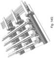
- FIG. 16 Aillustrates a multi-layer stack 1600 patterned for the formation of 3D T-RAM similar to the structure of FIG. 14 E .
- the top layer 1602could be used for the construction of the column 1604 select transistor.
- the underlying layerswould be used for the formation of the 3D matrix of T-RAM cells.
- the thicker isolation layer 1610could provide larger process margin.
- Additional optional protection layer 1608could be made from silicon nitride SiN and could be used to protect the column select transistors for the following processes. Forming silicon nitride between the top layer and the thick isolation layer 1610 is far easier for memory stack in which the top layer is either been deposit afterward or transferred in using layer transfer technique.
- FIG. 16 Billustrates the structure 1600 in different orientation after filling it with isolation layer such as silicon oxide masking it with diffusion mask 1612 and opening windows 1614 for the inter p regions of the T-RAM cells.
- the processcould include a step of isotropic etch to open the interlayer oxide 1616 so the following step of get forming could fill the gate all around the P regions.
- FIG. 16 Cillustrates the structure having the formed gate stack 1618 including a gate dielectric and gate material.
- FIG. 16 Dillustrates the structure having the formed gate stack 1622 and a patterned silicon nitride 1620 masking the inner N regions so the outer regions could be silicided.
- the exposed silicon regions masked by the gate stack 1622are doped by diffusion doping or other doping method to achieve the inner N region concentration.
- FIG. 16 Eillustrates the structure after etching back the gate and the blocking layer to expose 1630 only the top layer for the formation of the column select transistor.
- FIG. 16 Fillustrates the structure after performing an etch of the branch region backbone to separate each select transistor, forming isolation layer, forming column select transistor gate stack, and forming column select transistor source and drain (S/D).
- FIG. 16 Gillustrates the structure from a side view cut along the column select gate. Illustrating the common column select gate 1632 of the column select layer 1634 overlying the memory cells layers 1636 and the select transistors 1650 . The gate in memory cell layer 1636 continues across the multiple columns through the gate material filled in the interlayer region.
- FIG. 16 Hillustrates the structure after adding the conducting pillars 1648 for cathodes connecting them to the source of column select transistor 1649 .
- the drawingalso illustrates the anode in silicon embedded per layer word-lines 1644 (p type silicon), the T-RAM memory cell gate lines 1642 and the column gate line 1640 .
- FIG. 16 I to FIG. 16 Killustrates an alternative in which the column select gate may be made individually and connecting along the direction of the T-RAM cell vertical to the anode line while the select transistors drain are made common in parallel to the anode-lines. Both configurations enable selection of individual T-RAM cell. In the first configuration it could be done by selecting a bit-line 1646 —the column select transistor drain, while in the second configuration it could be done by selecting the select pin line 1650 —the column select transistor.
- FIG. 16 Lillustrates the structure after adding the stair-case for the per-layer in silicon embedded anode lines and the optional anode select transistors.
- top layer per column select transistorscould be adapted to the other memory described herein such as those related to at least FIG. 3 B , FIG. 4 A , FIG. 7 A , FIG. 10 A , FIG. 10 B and FIG. 14 C .
- a technique for memory designis to share control lines between adjacent memory rows and column to increase overall memory matrix density. This could be applied for many of the memory structures presented herein such as those related to FIG. 3 B , FIG. 4 A , FIG. 7 A , FIG. 10 A , FIG. 10 B , FIG. 14 C and FIG. 14 E , which were shown without such sharing for ease of illustration and description, Sharing the pillars such as pillars 338 is been illustrated in FIG. 3 L — 376 , and could applied and similar fashion to the other memory structure here in. Sharing the in silicon per layer control line such as 384 of FIG. 3 M could be in some cases more challenging.
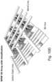
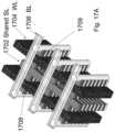
- FIG. 17 Aillustrates such challenge as the sharing of the per layer in silicon control lines 1702 while having the gate-line shared in parallel Word-Lines 1704 and in vertical orientation their bit-lines 1706 .
- the two cellsshare two of their control lines 1702 and 1706 and would be addressed individually by selecting the proper gate-lines (word-lines) 1704 .
- the gate-lineis not active and accordingly it will not help to distinguish between the adjacent memory cells 1708 and 1709 .
- Similar challengewould exist for memory like the one presented in FIG. 10 C which use a two terminal cell and do not have gate-lines.
- FIG. 17 Billustrates one optional solution by staggering the cells along the two sides of the in silicon embedded control line, the shared select line 1712 . Accordingly the adjacent cells would have different bit lines 1716 and 1717 . Alternative solution could be applied by having some control lines going at the bottom of these memory structures and not just at the top as has been illustrated herein.
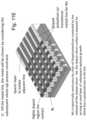
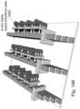
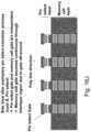
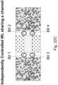
- FIG. 18 Aillustrates prior art 2D memory device.
- the memory cells 2D matrix 1802is surrounded with the memory control circuits 1804 such as decoders, sense amplifiers and interface with external devices. Having these circuits are called accordingly memory peripherals.
- the memory control lines 1806are going through the memory cells columns and rows all the way across the memory matrix to the peripherals circuits.
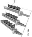
- FIG. 18 Billustrates prior art 3D memory device.
- 3D memoryalso known as 3D-NAND
- 3D-NANDhas been released to the market.
- the memory cells 3D matrix 1812is still surrounded with the memory control circuits 1814 such as decoders, sense amplifiers and interface with external devices.
- These memory peripherals circuitsare being process in very similar way the 2D memory circuits on the silicon wafer substrate.
- the control lines 1816are going through the memory cells columns and rows all the way across the memory matrix, some of these control lines are build at the top of the 3D matrix and some of those going through in the body of the memory matrix but than they are brought down to the 2D peripherals circuits.
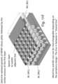
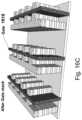
- FIG. 18 Cillustrates 3D memories formed using the techniques presented herein.
- the 3D memory matrix 1822of layers of columns and rows having the control circuits which could still be called peripherals circuits 1824 and they could be formed on top of the memory matrix and the control lines 1826 in-between
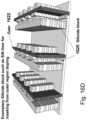
- FIG. 18 Dillustrates an alternative 3D memories formed using the techniques presented herein in which the control lines and the control circuits are also underneath the memory cell matrix.
- This new type of 3D memoriescould be constructed to achieve significant benefits from the 3D architecture as illustrated in FIGS. 18 C and 18 D , as the control lines 1826 could be broken to smaller chunks and having the control circuits repeated for each chunk. Shorter control lines could allow reduction of memory access read and write and refresh and could allow faster memory access time. The stair-case per layer access could impact device cost if it is broken too often. Proper architecture and overall memory control strategy could use very long per layer control lines to save overhead area for stair-case and accordingly design to use memory at the same layer for as long as possible so having the other control lines relatively short while the per layer control lines still long, could allow these benefit of low power and fast access maintained for most of the time.
- these 3D memorycould be enhanced to include dual functionality—a high speed volatile memory and a low power low speed non volatile memory.
- These figuresillustrates non-volatile utilize charge trap or floating gate technology.
- other form on non volatile technologiescould be implemented such as Re-RAM, M-RAM, Phase-Change, etc.
- Re-RAMRe-RAM
- M-RAMMagnetoresistive RAM
- Phase-ChangePhase-Change
- splitting the gatecould be used to increase the non-volatile memory capacity for cells that the channel is wide enough to allow 2-bit per cell.
- FIG. 19 Aillustrates the top level construction of 3D memory 1900 for such enhanced operation.
- the side memory control circuits 1901control the interface to external devices both for instruction, and data in and out.
- This circuits 1901could include the per layer decoders and control to support all internal memory blocks so the stair-case area overhead could be reduced.
- the 3D memoryis than partitioned to many blocks 1902 each is a sub-memory structure with its own top peripherals circuits to control most of its control lines. In such construction the operation each instruction to move data from one portion to the other could be done in parallel in all the units reducing the time and power by orders of magnitude.
- the side memory control circuits 1901could synchronize these operations so it will be done one layer at a time.
- FIG. 19 Billustrates the block diagram of peripherals circuit of a block 1902 .
- the block diagram 1904 of such unit block control circuitscould include:
- Central controller 1930commanding and control these operation for sleep mode recovery mode etc.
- In-Out interface controllerto interface with data and control with the device controller 1901
- Sense Amplifiers 1920to sense the data of a memory cell according to the mode of operation and to convert side memory control circuits 1901 side memory control circuits 1901 side memory control circuits 1901 it to a digital bit which could be temporarily stored in the unit memory cash 1934 .
- Signal generators 1918to generate the required voltages and current for the proper read write of the memory cells. Some of these circuitry, such as charge pumps could be shared by all units and be placed in side memory control circuits 1901
- the layer decoders 1916might be removed out from the unit 1904 into the general per layer circuits at side memory control circuits 1901
- Additional advantage for such memory architectureis the potential ability to move in and out very large blocks of data as many blocks 1902 could be access in parallel. If only a single per layer stair case is used for maximum array efficiency than the parallel action would be limited to single layer at a time. For many application these could be manage by proper system data structure and control.
- Such 3D Memorycould include redundancy circuit to allow repair of control function and not just for memory bits.
- the architecture of FIG. 18 Ccould be used to allow access to many of the memory control lines from both side—top and bottom and to have duplication of the device control circuit 1824 at the bottom.
- redundancycould be broken to the memory block control units 1902 . So if one unit block control circuits is faulty than it is replaced by his compatible one on the other side. Alternatively each unit block control circuits could be built with two stratum one being a back for the other as was detailed here before.
- the memory control redundancycould be applied to any of the 3D memories herein.
- 3D memorycould be built utilizing a mono crystalline transistor wherein their channel is vertically oriented so the current through the device is going vertically across the device layers rather than horizontally along the device layers. Yet, this structure are designed to be low cost by sharing lithography, etch and deposition of multiple layers together forming vertical oriented transistor, one self aligned to the one on top of it.
- FIG. 20 Aillustrates a starting material for these vertically oriented 3D memories. It has interchanging layers of designated source drain (S/D) material 2002 over designated channel material 2004 . These layers could be process by epitaxial steps with in-situ alternating doping from N/N+ type to P/P+ type and/or between Silicon to SiGe etc. The design of these layer composition could be done together with a choice of an high selectivity etch process to enable etching the designated channel layers 2004 at far higher rate than the (S/D) layers 2002 . The thickness of these layers could be thin as few nm to hundreds of nm.
- S/Dsource drain
- the (S/D) layers 2002could be N+ silicon while the channel layers 2004 could be P type silicon and the selective etch later would utilize anodic etching as detailed in U.S. Pat. No. 8,470,689 and other as was described herein.
- N+ siliconfor the (S/D) layers 2002 and P type SiGE for channel layers 2004 and the selective etch later would utilize the process used for 3D horizontal NAND memory described by Se Hwan Park et al in a piper titled “Novel Three Dimensional (3D) NAND Flash Memory Array Having Tied Bit-line and Ground Select Transistor (TiGer)” published in TECHNICAL REPORT OF IEICE in 2011 (APWF_PSH), a paper by FL W. Fathauer et al titled “New class of Si-based superlattices: Alternating layers of crystalline Si and porous amorphous Si, —, Ge, alloys” published by Appl. Phys. Lett. 61 (19), 9 Nov.
- a hard mask material 2006is deposit.
- FIG. 20 Billustrates etching the structure to form multilayer rims 2009 and valleys 2008 in between resulted in repeating rims structure 2007 .
- the width of the rims and the valleyscould be from 10 nm or even lower to few hundreds of nm. At current state of technology about 50 nm could be good choice.
- the width of the rims and the valleyscould be set in consideration of the thickness of layers 2002 / 2004 , the type of memory build and other consideration. Similar width and thickness could be appropriate.
- FIG. 20 Cillustrates the structure after a step of selective isotropic etches of the channel layers 2004 , forming horizontal notches 2009 while keeping the S/D layers 2010 mostly untouched.
- FIG. 20 Dillustrates the structure after a steps of depositing a stack of tunneling oxide layer/charge trap layer/control oxide layer 2012 such as oxide/nitride/oxide and gate conductive material 2014 .
- the stepcould be done by Atomic Layer Deposition (ALD) or alternative processes used for semiconductor device fabrications.
- a directional anisotropic etch stepcould be used to remove all gate material from the side walls of the S/D layers 2013 .
- FIG. 20 Eillustrates the structure after an etch step 2020 of the rims to form vertical strings 2022 .
- the etch stepcould be done in two steps. First anisotropic etch the stack of multilayer of alternating 2002 / 2004 to form the vertical individual strings 2022 , and then isotropic selective etch to remove the source/drain 2002 in-between the gate stack 2012 , while leaving the horizontal going gate and oxide lines.
- the etchingmay be stop before the most bottom N+ layer that will be serve as common ground
- FIG. 20 Fillustrates side view along word line direction of the structure of FIG. 20 E .
- the empty space left from the removal of the in-between channel material 2034serve as memory cell isolation.
- the left bottom material 2038could serve as a common ground line.
- the lower gate line 2040could serve as ground select gate.
- the top of the vertical strings 2032would serve as the string drain region and could be connect later to the bit-lines (BL).
- the inside of the structureis the matrix of memory cell formed as vertical non-volatile NAND strings with horizontal going across control gates 2042 controlling the channels between the source/drain in the vertical NAND strings
- FIG. 20 Gillustrates side view along a string direction of one vertical NAND string 2036 .
- FIG. 20 Hillustrates the 3D NAND memory structure after adding the memory control lines: word-lines, bit-lines, string select-lines, vertical contacts 2050 , shared S/D line 2060 , and ground select-lines.
- the horizontal per layer line in through the matrixcould be the limit for power performance in respect to how long it could be made.
- the area required for the stair-casemean that a shorter line will result in lower array efficiency and higher cost per bit.
- An alternativecould be to place such stair-case on both side of the line which as an added benefit could help reduce cell to cell variation in addition to improving power and delay. If the device is constructed with multiple block across with multiple stair cases than the overhead for this is limited as the between block stair-case could be shared with both the right and the left sides of it.
- FIG. 21 Aillustrates a structure for the formation of a NOR type 3D memory. It starts from the structure 2007 illustrated in FIG. 20 B . Using masking forming strips in vertical direction to the rims, in which first a tunneling oxide layer, charge trap layer and control oxide layer are formed resulting with the NV stack 2102 . On top of it a gate 2122 [ 2104 ] such as tungsten (W) or polysilicon or other form of memory matrix gate is being formed, for example, in Word Line Comb 2122 . This step could use ALD techniques.
- Wtungsten
- polysiliconsuch as tungsten (W) or polysilicon or other form of memory matrix gate
- FIG. 21 Billustrates the structure after selective isotropic etching the channel in all place not covered by the gate stack. Leaving voids 2112 in between the horizontal bridges of the un-etched S/D material 2110 . Under the gate 2122 stack the channels 2114 are not etched being protected by the gate 2122 stack, in the shape of a Word Line Comb 2122 .
- FIG. 21 Cillustrates a cross section of the structure of FIG. 21 B .
- the gates 2122would control the conductivity between the source and the drain S/D [ 2120 ] 2110 through the channel [ 2121 ] 2114 , with isolation region 2134 between, above, and below each transistor.
- the S/D materialact as source drain under the gates 2122 and as conductive lines 2123 being the memory control line connecting the S/D along the layer for each rim.
- the S/D materialis selected to be N+ silicon and the channel; material is selected to be P type silicon, than each memory cell would NPN transistor with two side gate stack to form a non volatile memory cell.
- FIG. 21 Dillustrates the 3D NOR structure after adding control lines.
- the shared gatego vertical to the rim control by word-lines WL 1 , WL 2 , WL 3 .
- the stair caseis used for the per layer control lines, which may be utilized to connect sets of shared source/drain lines 2110 to the array bit lines (BL 1 . . . BL 6 for example) thru vertical contacts 2150 .
- the bit-line BL 1control the S/D of the first layer of all the rims in the memory block, BL 2 control the second layers and so forth.
- the select-linesare controlling the access of the bit line to the S/D of the rims.
- SL 1control the access to the first rim, SL 2 to the second rim and so forth.
- the rim controlis constructed by first removing the channel at the region designated for rim control. Than the S/D line at these regions are made to function as junction less transistor or as gate all around nano-wires. In some cases it might be desired to thin the S/D lines in the region designated as junction less transistor or nano-wire to achieve better gate control. Such thinning would narrow these regions to about 20 nm thickness.
- FIG. 21 Eillustrates an alternative 3D NOR structure alternative control for the per layer control lines.
- the shared S/D lines 2110are split to odd layers jointly connected by select-lines (SL 1 -SL 4 for example) in parallel to the word-lines.
- SL 1connects the S/D lines of layer 1
- SL 2connects the S/D lines of layer 3 and so forth.
- These connectionsmay be made from shared S/D lines 2110 variously to select lines (SL 1 . . . SL 4 for example) and bit lines (BL 1 . . . BL 3 for example) thru vertical contacts 2150 .
- the even layersare connected per rim along the rim direction by bit-lines in vertical orientation to the word lines.
- BL 1connects the S/D of all even layers of the first rim
- BL 2connects the S/D of all even layers of the second rim and so forth.
- This 3D NOR structurecould be enhance using the universal memory concept of FIG. 15 A .
- the cell channelbecomes the floating body and the gate stack would be enhance to support such dual functionality.
- the use of the enhance 3D NOR and the various use mode and system architecturecould be similar to those discussed herein.
- Additional enhancement to such 3D NORis to break the gate control to two independent side gate—left gate and right gates. So for example control line WLR 1 will control all the right side gates and WLL 1 would control all the left side gates. Such split could allow doubling the store capacity, The channel size need to support such ‘two bit’ per cell option. A channel width of 50 nm or higher had been used for such ‘two bit’ per cell functionality
- These two gate control linecan be place on the top connection layer side by side as is illustrated in FIG. 22 A , or alternatively one on the top and one on the bottom as illustrated in FIG. 22 B .
- Additional enhancement to such 3D NORis to enhance the MirrorBit to allow 8 bit per cell by forming a stair-case per layer for both sides of the S/D lines allowing multiple current path through the cell to position charge trap bit for each corner of the memory cell as illustrated in FIG. 22 D and FIG. 22 E .
- These figuresare a zoom view of one memory cell within the 3D NOR structure.
- the cell channelis between two S/D lines 2200 and 2202 .
- the right side of the cell charge trap layercould store in each corner a charge—bit 1 , bit 2 , bit 3 , bit 4 . Those would be control by the right side gate 2204 .
- FIG. 22 Eshows the same cell from a different view point illustrating the left side gate 2206 and the charge trap location for bit 5 , bit 6 , bit 7 and bit 8 .
- FIG. 22 Fillustrates a memory block with its control line designed to control 8 bit store in one cell, including left vertical contacts 2250 and right vertical contacts 2252 .
- Another known enhancement techniqueis to control the amount of charge being trapped in a cell to allow coding of more than 1 bit base on the amount of charge.
- the structure of this 3D NORcould be modified by changing the gate stack to construct a 3D-DRAM using the floating body technique.
- the Floating body of the 3D-DRAM or of the 3D-NOR Universal memorycould be refreshed using the self-refresh described herein.
- 3D money memory structure and variationsThere are many ways to form other variations of these structures that would be obvious to artisan in the semiconductor memory domain to form by the presented elements described herein. These may include exchanging n type with p type and vice versa, increase density by sharing control lines, silicidation of some in silicon control lines, providing stair case on both sides of memory blocks to improve speed and reduce variation including sharing staircase in between two blocks and other presented variations herein. Many of these options had been presented in some memory options in more details and it would be obvious to artisan in the semiconductor memory domain to apply to the other memory structures.
Landscapes
- Physics & Mathematics (AREA)
- Semiconductor Memories (AREA)
- Geometry (AREA)
- Condensed Matter Physics & Semiconductors (AREA)
- General Physics & Mathematics (AREA)
- Engineering & Computer Science (AREA)
- Computer Hardware Design (AREA)
- Microelectronics & Electronic Packaging (AREA)
- Power Engineering (AREA)
- Non-Volatile Memory (AREA)
Abstract
Description
- Through-silicon via (TSV) technology: Multiple layers of transistors (with or without wiring levels) can be constructed separately. Following this, they can be bonded to each other and connected to each other with through-silicon vias (TSVs).
- Monolithic 3D technology: With this approach, multiple layers of transistors and wires can be monolithically constructed. Some monolithic 3D and 3DIC approaches are described in U.S. Pat. Nos. 8,273,610, 8,557,632, 8,298,875, 8,642,416, 8,362,482, 8,378,715, 8,379,458, 8,395,191, 8,450,804, 8,574,929, 8,581,349, 8,642,416, 8,687,399, 8,742,476, 8,674,470, 8,803,206, 8,902,663, 8,994,404, 9,021,414, 9,023,688, 9,030,858, 9,117,749, 9,219,005; U.S. patent publication 2011/0092030; and pending U.S. Patent Applications, 62/077,280, 62/042,229, Ser. No. 13/803,437, 61/932,617, Ser. Nos. 14/607,077, 14/642,724, 62/139,636, 62/149,651, 62/198,126, and 62/239,931. The entire contents of the foregoing patents, publications, and applications are incorporated herein by reference.
- Electro-Optics: There is also work done for integrated monolithic 3D including layers of different crystals, such as U.S. Pat. Nos. 8,283,215, 8,163,581, 8,753,913, 8,823,122, 9,197,804; and U.S. patent application Ser. No. 14/461,539. The entire contents of the foregoing patents, publications, and applications are incorporated herein by reference.
- i—Epitaxially grow alternating layers of
p+ layers p Layers - ii—Perform an anodization process in a hydrofluoric acid (HF) containing electrolyte solution to convert the doped layers to porous layers. The
p+ p - iii—Perform an oxidization process to convert the
p+ - iv—Perform a high temperature annealing, for example, such as at 1,000° C. for a few hours, to convert the
p
- i—Epitaxially grow alternating layers of
- A. All cell need to have through them at least minimal holding current to retain the high ‘1’ memory state. This holding current could be interrupted to brief time as there is some charge in the channel which would need to leak out for state ‘1’ to be lost.
- B. Wring ‘1’ to a cell need to have the voltage across him to be higher than Vlu. In the decoding circuit there are three states memory could be in:
- a. Non selected neither by word-line nor by bit-line
- b. Half-selected by one of word-line or bit-line
- c. Selected by both word-line and bit-line.
- The peripheral circuits could be set so only the cell selected by both line get written to ‘1’ or written to ‘0’. This could be achieved by moving the voltage in the word-line and in the bit-lines half way each toward the overall threshold of Vlh to achieve writing ‘1’ or down toward Vld to achieve writing ‘0’. According only one cell will get written to ‘1’ or ‘0’—the cell that both its word-line and its bit-line were selected. Attention need to be taken that no other cell would have across it a voltage lower than Vld or higher than Vlu, this need to account all lines and to account for the minimal holding current provided to all cells to retain their memory status. This design requirement are the type of requirement that detailed memory design need to account for including variation of temperatures supply voltage and variation in the manufacturing line.
- There is added complexity with 3D memory as illustrated in
FIG.10B as in the bit-lines we could have three type of bit lines:- a. Selected by bit-line and select gate. This is the one that would write data into the selected memory cell.
- b. Selected by select-line but not by bit-line, the voltage across the cell need to be between the two threshold Vld and Vlu, so minimum accidental write could happen
- c. Not selected by select-line. This need to still keep the holding current going through the cell to retain its stored state. This could be provide by high
resistivity pillar connection 1040.
While multiple memory plans processing following one lithography step is attractive in respect for cost another alternative is forming 3D memory by successive step of memory plan following another memory plan. In such memory the 3D structure provides ability to share between planes memory control line such as bit-lines and word-lines, and ability to pack more memory bits in a smaller area with benefit in performance (line RC), power and even cost.
- Front side bit &
Back side bit 4 Front size WL and Back side channel - Upper bit &
Lower bit 4 Source Line & Bit Line Swapping - Left side bit &
right side bit 4 Left staircase access & right staircase access
- Front side bit &
Claims (7)
Priority Applications (2)
| Application Number | Priority Date | Filing Date | Title |
|---|---|---|---|
| US15/243,941US11956952B2 (en) | 2015-08-23 | 2016-08-22 | Semiconductor memory device and structure |
| US18/594,804US20240260262A1 (en) | 2015-08-23 | 2024-03-04 | 3d semiconductor memory devices and structures with memory cells |
Applications Claiming Priority (4)
| Application Number | Priority Date | Filing Date | Title |
|---|---|---|---|
| US201562208812P | 2015-08-23 | 2015-08-23 | |
| US201562215112P | 2015-09-07 | 2015-09-07 | |
| US201562221618P | 2015-09-21 | 2015-09-21 | |
| US15/243,941US11956952B2 (en) | 2015-08-23 | 2016-08-22 | Semiconductor memory device and structure |
Related Child Applications (1)
| Application Number | Title | Priority Date | Filing Date |
|---|---|---|---|
| US18/594,804Continuation-In-PartUS20240260262A1 (en) | 2015-08-23 | 2024-03-04 | 3d semiconductor memory devices and structures with memory cells |
Publications (2)
| Publication Number | Publication Date |
|---|---|
| US20170053906A1 US20170053906A1 (en) | 2017-02-23 |
| US11956952B2true US11956952B2 (en) | 2024-04-09 |
Family
ID=58158580
Family Applications (1)
| Application Number | Title | Priority Date | Filing Date |
|---|---|---|---|
| US15/243,941ActiveUS11956952B2 (en) | 2015-08-23 | 2016-08-22 | Semiconductor memory device and structure |
Country Status (1)
| Country | Link |
|---|---|
| US (1) | US11956952B2 (en) |
Families Citing this family (69)
| Publication number | Priority date | Publication date | Assignee | Title |
|---|---|---|---|---|
| US9853089B2 (en)* | 2009-10-12 | 2017-12-26 | Monolithic 3D Inc. | Semiconductor device and structure |
| US11120884B2 (en) | 2015-09-30 | 2021-09-14 | Sunrise Memory Corporation | Implementing logic function and generating analog signals using NOR memory strings |
| US9842651B2 (en) | 2015-11-25 | 2017-12-12 | Sunrise Memory Corporation | Three-dimensional vertical NOR flash thin film transistor strings |
| US10121553B2 (en)* | 2015-09-30 | 2018-11-06 | Sunrise Memory Corporation | Capacitive-coupled non-volatile thin-film transistor NOR strings in three-dimensional arrays |
| US9892800B2 (en)* | 2015-09-30 | 2018-02-13 | Sunrise Memory Corporation | Multi-gate NOR flash thin-film transistor strings arranged in stacked horizontal active strips with vertical control gates |
| US10102898B2 (en) | 2016-12-30 | 2018-10-16 | Qualcomm Incorporated | Ferroelectric-modulated Schottky non-volatile memory |
| WO2018208717A1 (en)* | 2017-05-08 | 2018-11-15 | Micron Technology, Inc. | Memory arrays |
| CN108933139B (en)* | 2017-05-25 | 2023-10-17 | 三星电子株式会社 | Vertical nonvolatile memory device |
| US11011529B2 (en) | 2017-06-29 | 2021-05-18 | Micron Technology, Inc. | Memory arrays comprising vertically-alternating tiers of insulative material and memory cells and methods of forming a memory array comprising memory cells individually comprising a transistor and a capacitor |
| CN109326604A (en)* | 2017-08-01 | 2019-02-12 | 华邦电子股份有限公司 | Three-dimensional memory and operation method thereof |
| JP7002899B2 (en)* | 2017-09-22 | 2022-01-20 | キオクシア株式会社 | Storage device |
| US10535659B2 (en) | 2017-09-29 | 2020-01-14 | Samsung Electronics Co., Ltd. | Semiconductor memory devices |
| KR102524614B1 (en) | 2017-11-24 | 2023-04-24 | 삼성전자주식회사 | Semiconductor memory device |
| WO2019133534A1 (en) | 2017-12-28 | 2019-07-04 | Sunrise Memory Corporation | 3-dimensional nor memory array with very fine pitch: device and method |
| US10468414B2 (en) | 2017-12-28 | 2019-11-05 | Samsung Electronics Co., Ltd. | Semiconductor memory devices |
| JP7338975B2 (en)* | 2018-02-12 | 2023-09-05 | 三星電子株式会社 | semiconductor memory device |
| EP3546063B1 (en)* | 2018-03-26 | 2020-12-30 | IMEC vzw | A molecular synthesis device |
| US10748903B2 (en)* | 2018-04-19 | 2020-08-18 | Tc Lab, Inc. | Multi-layer random access memory and methods of manufacture |
| CN110660822B (en)* | 2018-06-29 | 2024-11-26 | 三星电子株式会社 | Variable resistance memory device |
| US11751391B2 (en) | 2018-07-12 | 2023-09-05 | Sunrise Memory Corporation | Methods for fabricating a 3-dimensional memory structure of nor memory strings |
| CN112567516B (en) | 2018-07-12 | 2025-02-25 | 日升存储公司 | Method for manufacturing three-dimensional NOR memory array |
| KR102546686B1 (en)* | 2018-07-17 | 2023-06-23 | 삼성전자주식회사 | Variable resistance memory device |
| KR102650525B1 (en) | 2018-08-03 | 2024-03-25 | 삼성전자주식회사 | Semiconductor memory device |
| CN112602193B (en)* | 2018-09-05 | 2024-09-06 | 东京毅力科创株式会社 | Architectural design and processes for manufacturing monolithically integrated 3D CMOS logic and memory |
| WO2020055642A2 (en)* | 2018-09-05 | 2020-03-19 | Tokyo Electron Limited | Power distribution network for 3d logic and memory |
| TWI757635B (en)* | 2018-09-20 | 2022-03-11 | 美商森恩萊斯記憶體公司 | Memory structure and process for staircase structures for electrically connecting multiple horizontal conductive layers of a 3-dimensional memory device |
| KR102630024B1 (en) | 2018-10-04 | 2024-01-30 | 삼성전자주식회사 | Semiconductor memory device |
| WO2020077185A1 (en) | 2018-10-13 | 2020-04-16 | Applied Materials, Inc. | Stacked transistor device |
| US10950618B2 (en) | 2018-11-29 | 2021-03-16 | Micron Technology, Inc. | Memory arrays |
| WO2020142368A1 (en)* | 2018-12-31 | 2020-07-09 | Micron Technology, Inc. | Three-dimensional dynamic random-access memory array |
| KR102554712B1 (en)* | 2019-01-11 | 2023-07-14 | 삼성전자주식회사 | Semiconductor device |
| EP3925004A4 (en) | 2019-02-11 | 2023-03-08 | Sunrise Memory Corporation | VERTICAL THIN-FILM TRANSISTOR AND APPLICATION AS A BITLINE CONNECTOR FOR THREE-DIMENSIONAL MEMORY ARRAYS |
| KR102712036B1 (en)* | 2019-04-30 | 2024-10-02 | 삼성전자주식회사 | Semiconductor memory device and method of fabricating the same |
| US11672133B2 (en)* | 2019-06-20 | 2023-06-06 | Intel Corporation | Vertically stacked memory elements with air gap |
| US11652047B2 (en)* | 2019-06-28 | 2023-05-16 | Intel Corporation | Intermediate separation layers at the back-end-of-line |
| KR102638741B1 (en) | 2019-08-19 | 2024-02-22 | 삼성전자주식회사 | Semiconductor memory device |
| US11495540B2 (en)* | 2019-10-22 | 2022-11-08 | Tokyo Electron Limited | Semiconductor apparatus having stacked devices and method of manufacture thereof |
| WO2021127218A1 (en) | 2019-12-19 | 2021-06-24 | Sunrise Memory Corporation | Process for preparing a channel region of a thin-film transistor |
| FR3105579A1 (en)* | 2019-12-23 | 2021-06-25 | Commissariat A L'energie Atomique Et Aux Energies Alternatives | Device comprising wrap-gate transistors and method of manufacturing such a device |
| TWI767512B (en) | 2020-01-22 | 2022-06-11 | 美商森恩萊斯記憶體公司 | Cool electron erasing in thin-film storage transistors |
| TWI836184B (en) | 2020-02-07 | 2024-03-21 | 美商森恩萊斯記憶體公司 | High capacity memory circuit with low effective latency |
| US20210327891A1 (en)* | 2020-04-16 | 2021-10-21 | Applied Materials, Inc. | Stack for 3d-nand memory cell |
| US11145380B1 (en)* | 2020-04-29 | 2021-10-12 | International Business Machines Corporation | Analog nonvolatile memory cells using dopant activation |
| KR102797253B1 (en)* | 2020-05-18 | 2025-04-18 | 삼성전자주식회사 | Semiconductor devices including a semiconductor pattern |
| US11239117B1 (en)* | 2020-08-27 | 2022-02-01 | Micron Technology, Inc. | Replacement gate dielectric in three-node access device formation for vertical three dimensional (3D) memory |
| US11937424B2 (en) | 2020-08-31 | 2024-03-19 | Sunrise Memory Corporation | Thin-film storage transistors in a 3-dimensional array of nor memory strings and process for fabricating the same |
| KR102731055B1 (en) | 2020-09-11 | 2024-11-15 | 삼성전자주식회사 | Semiconductor memory devices |
| WO2022108848A1 (en) | 2020-11-17 | 2022-05-27 | Sunrise Memory Corporation | Methods for reducing disturb errors by refreshing data alongside programming or erase operations |
| US11751378B2 (en) | 2020-12-02 | 2023-09-05 | Samsung Electronics Co., Ltd. | Semiconductor memory device |
| CN113178484B (en)* | 2021-03-03 | 2024-05-03 | 中国科学院微电子研究所 | A thin capacitive coupled thyristor and a method for preparing the thin capacitive coupled thyristor |
| KR20220126154A (en)* | 2021-03-08 | 2022-09-15 | 삼성전자주식회사 | Semiconductor having 3D stacked structure and method of manufacturing the same |
| US11856854B2 (en)* | 2021-04-09 | 2023-12-26 | Taiwan Semiconductor Manufacturing Company, Ltd. | MRAM device structures and method of fabricating the same |
| WO2022236943A1 (en)* | 2021-05-12 | 2022-11-17 | Yangtze Memory Technologies Co., Ltd. | Memory peripheral circuit having three-dimensional transistors and method for forming the same |
| CN115669260A (en) | 2021-05-12 | 2023-01-31 | 长江存储科技有限责任公司 | Memory peripheral circuit with three-dimensional transistor and forming method thereof |
| CN116918475A (en) | 2021-05-12 | 2023-10-20 | 长江存储科技有限责任公司 | Memory peripheral circuit with three-dimensional transistors and method of forming same |
| TW202310429A (en) | 2021-07-16 | 2023-03-01 | 美商日升存儲公司 | 3-dimensional memory string array of thin-film ferroelectric transistors |
| KR20230025595A (en)* | 2021-08-13 | 2023-02-22 | 삼성전자주식회사 | Semiconductor devices and data storage systems including the same |
| US12402319B2 (en) | 2021-09-14 | 2025-08-26 | Sunrise Memory Corporation | Three-dimensional memory string array of thin-film ferroelectric transistors formed with an oxide semiconductor channel |
| EP4292409A4 (en)* | 2021-10-30 | 2024-07-24 | Yangtze Memory Technologies Co., Ltd. | SEMICONDUCTOR MEMORY DEVICE AND FORMATION METHOD THEREFOR |
| US20230164986A1 (en)* | 2021-11-24 | 2023-05-25 | Intel Corporation | Selective removal of sidewall material for 3d nand integration |
| KR20230088147A (en)* | 2021-12-10 | 2023-06-19 | 에스케이하이닉스 주식회사 | Semiconductor memory device |
| US20230225132A1 (en)* | 2022-01-12 | 2023-07-13 | Taiwan Semiconductor Manufacturing Company, Ltd. | Memory structure and method of making |
| TWI805372B (en)* | 2022-01-27 | 2023-06-11 | 旺宏電子股份有限公司 | Memory structure |
| CN114649327B (en)* | 2022-05-13 | 2022-08-19 | 成都皮兆永存科技有限公司 | Low-resistance interconnected high-density three-dimensional memory device and preparation method |
| JP2023180601A (en)* | 2022-06-10 | 2023-12-21 | キオクシア株式会社 | semiconductor equipment |
| CN117352489A (en)* | 2022-06-21 | 2024-01-05 | 长鑫存储技术有限公司 | Semiconductor structure, manufacturing method thereof, memory chip and electronic equipment |
| CN118055611A (en)* | 2022-11-01 | 2024-05-17 | 长鑫存储技术有限公司 | Semiconductor structure, forming method of semiconductor structure and memory |
| KR20250134635A (en)* | 2023-01-13 | 2025-09-11 | 마이크론 테크놀로지, 인크 | Microelectronic devices and related memory devices and electronic systems |
| US12277965B2 (en) | 2023-01-17 | 2025-04-15 | Macronix International Co., Ltd. | Memory structure and method for operating the same |
Citations (814)
| Publication number | Priority date | Publication date | Assignee | Title |
|---|---|---|---|---|
| US3007090A (en) | 1957-09-04 | 1961-10-31 | Ibm | Back resistance control for junction semiconductor devices |
| US3819959A (en) | 1970-12-04 | 1974-06-25 | Ibm | Two phase charge-coupled semiconductor device |
| US4009483A (en) | 1974-04-04 | 1977-02-22 | Motorola, Inc. | Implementation of surface sensitive semiconductor devices |
| US4197555A (en) | 1975-12-29 | 1980-04-08 | Fujitsu Limited | Semiconductor device |
| US4213139A (en) | 1978-05-18 | 1980-07-15 | Texas Instruments Incorporated | Double level polysilicon series transistor cell |
| US4400715A (en) | 1980-11-19 | 1983-08-23 | International Business Machines Corporation | Thin film semiconductor device and method for manufacture |
| US4487635A (en) | 1982-03-25 | 1984-12-11 | Director-General Of The Agency Of Industrial Science & Technology | Method of fabricating a multi-layer type semiconductor device including crystal growth by spirally directing energy beam |
| US4510670A (en) | 1982-03-30 | 1985-04-16 | Siemens Aktiengesellschaft | Method for the manufacture of integrated MOS-field effect transistor circuits silicon gate technology having diffusion zones coated with silicide as low-impedance printed conductors |
| US4522657A (en) | 1983-10-20 | 1985-06-11 | Westinghouse Electric Corp. | Low temperature process for annealing shallow implanted N+/P junctions |
| US4612083A (en) | 1984-07-20 | 1986-09-16 | Nec Corporation | Process of fabricating three-dimensional semiconductor device |
| US4643950A (en) | 1985-05-09 | 1987-02-17 | Agency Of Industrial Science And Technology | Semiconductor device |
| US4704785A (en) | 1986-08-01 | 1987-11-10 | Texas Instruments Incorporated | Process for making a buried conductor by fusing two wafers |
| US4711858A (en) | 1985-07-12 | 1987-12-08 | International Business Machines Corporation | Method of fabricating a self-aligned metal-semiconductor FET having an insulator spacer |
| US4721885A (en) | 1987-02-11 | 1988-01-26 | Sri International | Very high speed integrated microelectronic tubes |
| US4733288A (en) | 1982-06-30 | 1988-03-22 | Fujitsu Limited | Gate-array chip |
| US4732312A (en) | 1986-11-10 | 1988-03-22 | Grumman Aerospace Corporation | Method for diffusion bonding of alloys having low solubility oxides |
| US4829018A (en) | 1986-06-27 | 1989-05-09 | Wahlstrom Sven E | Multilevel integrated circuits employing fused oxide layers |
| US4854986A (en) | 1987-05-13 | 1989-08-08 | Harris Corporation | Bonding technique to join two or more silicon wafers |
| US4866304A (en) | 1988-05-23 | 1989-09-12 | Motorola, Inc. | BICMOS NAND gate |
| US4939568A (en) | 1986-03-20 | 1990-07-03 | Fujitsu Limited | Three-dimensional integrated circuit and manufacturing method thereof |
| US4956307A (en) | 1988-11-10 | 1990-09-11 | Texas Instruments, Incorporated | Thin oxide sidewall insulators for silicon-over-insulator transistors |
| US5012153A (en) | 1989-12-22 | 1991-04-30 | Atkinson Gary M | Split collector vacuum field effect transistor |
| US5032007A (en) | 1988-04-07 | 1991-07-16 | Honeywell, Inc. | Apparatus and method for an electronically controlled color filter for use in information display applications |
| US5047979A (en) | 1990-06-15 | 1991-09-10 | Integrated Device Technology, Inc. | High density SRAM circuit with ratio independent memory cells |
| US5087585A (en) | 1989-07-11 | 1992-02-11 | Nec Corporation | Method of stacking semiconductor substrates for fabrication of three-dimensional integrated circuit |
| US5093704A (en) | 1986-09-26 | 1992-03-03 | Canon Kabushiki Kaisha | Semiconductor device having a semiconductor region in which a band gap being continuously graded |
| US5106775A (en) | 1987-12-10 | 1992-04-21 | Hitachi, Ltd. | Process for manufacturing vertical dynamic random access memories |
| US5152857A (en) | 1990-03-29 | 1992-10-06 | Shin-Etsu Handotai Co., Ltd. | Method for preparing a substrate for semiconductor devices |
| US5162879A (en) | 1990-04-06 | 1992-11-10 | Texas Instruments Incorporated | Diffusionless conductor/oxide semiconductor field effect transistor and methods for making and using the same |
| US5189500A (en) | 1989-09-22 | 1993-02-23 | Mitsubishi Denki Kabushiki Kaisha | Multi-layer type semiconductor device with semiconductor element layers stacked in opposite directions and manufacturing method thereof |
| US5217916A (en) | 1989-10-03 | 1993-06-08 | Trw Inc. | Method of making an adaptive configurable gate array |
| US5250460A (en) | 1991-10-11 | 1993-10-05 | Canon Kabushiki Kaisha | Method of producing semiconductor substrate |
| US5258643A (en) | 1991-07-25 | 1993-11-02 | Massachusetts Institute Of Technology | Electrically programmable link structures and methods of making same |
| US5265047A (en) | 1992-03-09 | 1993-11-23 | Monolithic System Technology | High density SRAM circuit with single-ended memory cells |
| US5266511A (en) | 1991-10-02 | 1993-11-30 | Fujitsu Limited | Process for manufacturing three dimensional IC's |
| US5277748A (en) | 1992-01-31 | 1994-01-11 | Canon Kabushiki Kaisha | Semiconductor device substrate and process for preparing the same |
| US5286670A (en) | 1991-05-08 | 1994-02-15 | Korea Electronics And Telecommunications Research Institute | Method of manufacturing a semiconductor device having buried elements with electrical characteristic |
| US5294556A (en) | 1990-07-20 | 1994-03-15 | Fujitsu Limited | Method for fabricating an SOI device in alignment with a device region formed in a semiconductor substrate |
| US5308782A (en) | 1992-03-02 | 1994-05-03 | Motorola | Semiconductor memory device and method of formation |
| US5312771A (en) | 1990-03-24 | 1994-05-17 | Canon Kabushiki Kaisha | Optical annealing method for semiconductor layer and method for producing semiconductor device employing the same semiconductor layer |
| US5317236A (en) | 1990-12-31 | 1994-05-31 | Kopin Corporation | Single crystal silicon arrayed devices for display panels |
| US5355022A (en) | 1991-09-10 | 1994-10-11 | Mitsubishi Denki Kabushiki Kaisha | Stacked-type semiconductor device |
| US5371037A (en) | 1990-08-03 | 1994-12-06 | Canon Kabushiki Kaisha | Semiconductor member and process for preparing semiconductor member |
| US5374564A (en) | 1991-09-18 | 1994-12-20 | Commissariat A L'energie Atomique | Process for the production of thin semiconductor material films |
| US5374581A (en) | 1991-07-31 | 1994-12-20 | Canon Kabushiki Kaisha | Method for preparing semiconductor member |
| US5424560A (en) | 1994-05-31 | 1995-06-13 | Motorola, Inc. | Integrated multicolor organic led array |
| US5475280A (en) | 1992-03-04 | 1995-12-12 | Mcnc | Vertical microelectronic field emission devices |
| US5478762A (en) | 1995-03-16 | 1995-12-26 | Taiwan Semiconductor Manufacturing Company | Method for producing patterning alignment marks in oxide |
| US5485031A (en) | 1993-11-22 | 1996-01-16 | Actel Corporation | Antifuse structure suitable for VLSI application |
| US5498978A (en) | 1993-05-07 | 1996-03-12 | Kabushiki Kaisha Toshiba | Field programmable gate array |
| US5527423A (en) | 1994-10-06 | 1996-06-18 | Cabot Corporation | Chemical mechanical polishing slurry for metal layers |
| US5535342A (en) | 1992-11-05 | 1996-07-09 | Giga Operations Corporation | Pld connector for module having configuration of either first PLD or second PLD and reconfigurable bus for communication of two different bus protocols |
| US5554870A (en) | 1994-02-04 | 1996-09-10 | Motorola, Inc. | Integrated circuit having both vertical and horizontal devices and process for making the same |
| US5563084A (en) | 1994-09-22 | 1996-10-08 | Fraunhofer-Gesellschaft zur F orderung der angewandten Forschung e.V. | Method of making a three-dimensional integrated circuit |
| US5583349A (en) | 1995-11-02 | 1996-12-10 | Motorola | Full color light emitting diode display |
| US5583350A (en) | 1995-11-02 | 1996-12-10 | Motorola | Full color light emitting diode display assembly |
| US5586291A (en) | 1994-12-23 | 1996-12-17 | Emc Corporation | Disk controller with volatile and non-volatile cache memories |
| US5594563A (en) | 1994-05-31 | 1997-01-14 | Honeywell Inc. | High resolution subtractive color projection system |
| US5604137A (en) | 1991-09-25 | 1997-02-18 | Semiconductor Energy Laboratory Co., Ltd. | Method for forming a multilayer integrated circuit |
| US5617991A (en) | 1995-12-01 | 1997-04-08 | Advanced Micro Devices, Inc. | Method for electrically conductive metal-to-metal bonding |
| US5627106A (en) | 1994-05-06 | 1997-05-06 | United Microelectronics Corporation | Trench method for three dimensional chip connecting during IC fabrication |
| US5656548A (en) | 1993-09-30 | 1997-08-12 | Kopin Corporation | Method for forming three dimensional processor using transferred thin film circuits |
| US5656553A (en) | 1994-08-22 | 1997-08-12 | International Business Machines Corporation | Method for forming a monolithic electronic module by dicing wafer stacks |
| US5659194A (en) | 1994-01-28 | 1997-08-19 | Mitsubishi Denki Kabushiki Kaisha | Semiconductor device having metal silicide film |
| US5670411A (en) | 1992-01-31 | 1997-09-23 | Canon Kabushiki Kaisha | Process of making semiconductor-on-insulator substrate |
| US5695557A (en) | 1993-12-28 | 1997-12-09 | Canon Kabushiki Kaisha | Process for producing a semiconductor substrate |
| US5701027A (en) | 1991-04-26 | 1997-12-23 | Quicklogic Corporation | Programmable interconnect structures and programmable integrated circuits |
| US5707745A (en) | 1994-12-13 | 1998-01-13 | The Trustees Of Princeton University | Multicolor organic light emitting devices |
| US5714395A (en) | 1995-09-13 | 1998-02-03 | Commissariat A L'energie Atomique | Process for the manufacture of thin films of semiconductor material |
| US5737748A (en) | 1995-03-15 | 1998-04-07 | Texas Instruments Incorporated | Microprocessor unit having a first level write-through cache memory and a smaller second-level write-back cache memory |
| US5739552A (en) | 1994-10-24 | 1998-04-14 | Mitsubishi Denki Kabushiki Kaisha | Semiconductor light emitting diode producing visible light |
| US5744979A (en) | 1992-07-23 | 1998-04-28 | Xilinx, Inc. | FPGA having logic cells configured by SRAM memory cells and interconnect configured by antifuses |
| US5748161A (en) | 1996-03-04 | 1998-05-05 | Motorola, Inc. | Integrated electro-optical package with independent menu bar |
| US5770483A (en) | 1996-10-08 | 1998-06-23 | Advanced Micro Devices, Inc. | Multi-level transistor fabrication method with high performance drain-to-gate connection |
| US5770881A (en) | 1996-09-12 | 1998-06-23 | International Business Machines Coproration | SOI FET design to reduce transient bipolar current |
| US5781031A (en) | 1995-11-21 | 1998-07-14 | International Business Machines Corporation | Programmable logic array |
| US5817574A (en) | 1993-12-29 | 1998-10-06 | Intel Corporation | Method of forming a high surface area interconnection structure |
| US5829026A (en) | 1994-11-22 | 1998-10-27 | Monolithic System Technology, Inc. | Method and structure for implementing a cache memory using a DRAM array |
| US5835396A (en) | 1996-10-17 | 1998-11-10 | Zhang; Guobiao | Three-dimensional read-only memory |
| US5854123A (en) | 1995-10-06 | 1998-12-29 | Canon Kabushiki Kaisha | Method for producing semiconductor substrate |
| US5861929A (en) | 1990-12-31 | 1999-01-19 | Kopin Corporation | Active matrix color display with multiple cells and connection through substrate |
| US5877070A (en) | 1997-05-31 | 1999-03-02 | Max-Planck Society | Method for the transfer of thin layers of monocrystalline material to a desirable substrate |
| US5877034A (en) | 1994-09-22 | 1999-03-02 | Fraunhofer Gesellschaft Zur Foerderung Der Angwandten Forschung E.V. | Method of making a three-dimensional integrated circuit |
| US5883525A (en) | 1994-04-01 | 1999-03-16 | Xilinx, Inc. | FPGA architecture with repeatable titles including routing matrices and logic matrices |
| US5882987A (en) | 1997-08-26 | 1999-03-16 | International Business Machines Corporation | Smart-cut process for the production of thin semiconductor material films |
| US5889903A (en) | 1996-12-31 | 1999-03-30 | Intel Corporation | Method and apparatus for distributing an optical clock in an integrated circuit |
| US5893721A (en) | 1997-03-24 | 1999-04-13 | Motorola, Inc. | Method of manufacture of active matrix LED array |
| US5915167A (en) | 1997-04-04 | 1999-06-22 | Elm Technology Corporation | Three dimensional structure memory |
| US5920788A (en) | 1995-06-07 | 1999-07-06 | Micron Technology, Inc. | Chalcogenide memory cell with a plurality of chalcogenide electrodes |
| US5937312A (en) | 1995-03-23 | 1999-08-10 | Sibond L.L.C. | Single-etch stop process for the manufacture of silicon-on-insulator wafers |
| US5943574A (en) | 1998-02-23 | 1999-08-24 | Motorola, Inc. | Method of fabricating 3D multilayer semiconductor circuits |
| US5952681A (en) | 1997-11-24 | 1999-09-14 | Chen; Hsing | Light emitting diode emitting red, green and blue light |
| US5952680A (en) | 1994-10-11 | 1999-09-14 | International Business Machines Corporation | Monolithic array of light emitting diodes for the generation of light at multiple wavelengths and its use for multicolor display applications |
| US5965875A (en) | 1998-04-24 | 1999-10-12 | Foveon, Inc. | Color separation in an active pixel cell imaging array using a triple-well structure |
| US5977961A (en) | 1996-06-19 | 1999-11-02 | Sun Microsystems, Inc. | Method and apparatus for amplitude band enabled addressing arrayed elements |
| US5977579A (en) | 1998-12-03 | 1999-11-02 | Micron Technology, Inc. | Trench dram cell with vertical device and buried word lines |
| US5985742A (en) | 1997-05-12 | 1999-11-16 | Silicon Genesis Corporation | Controlled cleavage process and device for patterned films |
| US5994746A (en) | 1998-01-15 | 1999-11-30 | Siemens Aktiengesellschaft | Memory cell configuration and method for its fabrication |
| US5998808A (en) | 1997-06-27 | 1999-12-07 | Sony Corporation | Three-dimensional integrated circuit device and its manufacturing method |
| US6001693A (en) | 1994-10-06 | 1999-12-14 | Yeouchung; Yen | Method of making a metal to metal antifuse |
| US6009496A (en) | 1997-10-30 | 1999-12-28 | Winbond Electronics Corp. | Microcontroller with programmable embedded flash memory |
| US6020252A (en) | 1996-05-15 | 2000-02-01 | Commissariat A L'energie Atomique | Method of producing a thin layer of semiconductor material |
| US6020263A (en) | 1996-10-31 | 2000-02-01 | Taiwan Semiconductor Manufacturing Company, Ltd. | Method of recovering alignment marks after chemical mechanical polishing of tungsten |
| US6027958A (en) | 1996-07-11 | 2000-02-22 | Kopin Corporation | Transferred flexible integrated circuit |
| US6052498A (en) | 1997-12-19 | 2000-04-18 | Intel Corporation | Method and apparatus providing an optical input/output bus through the back side of an integrated circuit die |
| US6054370A (en) | 1998-06-30 | 2000-04-25 | Intel Corporation | Method of delaminating a pre-fabricated transistor layer from a substrate for placement on another wafer |
| US6057212A (en) | 1998-05-04 | 2000-05-02 | International Business Machines Corporation | Method for making bonded metal back-plane substrates |
| US6071795A (en) | 1998-01-23 | 2000-06-06 | The Regents Of The University Of California | Separation of thin films from transparent substrates by selective optical processing |
| US6075268A (en) | 1996-11-07 | 2000-06-13 | Advanced Micro Devices, Inc. | Ultra high density inverter using a stacked transistor arrangement |
| US6103597A (en) | 1996-04-11 | 2000-08-15 | Commissariat A L'energie Atomique | Method of obtaining a thin film of semiconductor material |
| US6111260A (en) | 1997-06-10 | 2000-08-29 | Advanced Micro Devices, Inc. | Method and apparatus for in situ anneal during ion implant |
| US6125217A (en) | 1998-06-26 | 2000-09-26 | Intel Corporation | Clock distribution network |
| US6153495A (en) | 1998-03-09 | 2000-11-28 | Intersil Corporation | Advanced methods for making semiconductor devices by low temperature direct bonding |
| US6191007B1 (en) | 1997-04-28 | 2001-02-20 | Denso Corporation | Method for manufacturing a semiconductor substrate |
| US6200878B1 (en) | 1997-12-26 | 2001-03-13 | Canon Kabushiki Kaisha | SOI substrate processing method |
| US20010000005A1 (en) | 1994-12-13 | 2001-03-15 | Forrest Stephen R. | Transparent contacts for organic devices |
| US6204529B1 (en) | 1999-08-27 | 2001-03-20 | Hsing Lan Lung | 8 bit per cell non-volatile semiconductor memory structure utilizing trench technology and dielectric floating gate |
| US6222203B1 (en) | 1996-06-18 | 2001-04-24 | Sony Corporation | Selfluminous display device having light emission sources having substantially non-overlapping spectra levels |
| US6226197B1 (en) | 1998-10-23 | 2001-05-01 | Canon Kabushiki Kaisha | Magnetic thin film memory, method of writing information in it, and me |
| US6229161B1 (en) | 1998-06-05 | 2001-05-08 | Stanford University | Semiconductor capacitively-coupled NDR device and its applications in high-density high-speed memories and in power switches |
| US6242324B1 (en) | 1999-08-10 | 2001-06-05 | The United States Of America As Represented By The Secretary Of The Navy | Method for fabricating singe crystal materials over CMOS devices |
| US6242778B1 (en) | 1998-09-22 | 2001-06-05 | International Business Machines Corporation | Cooling method for silicon on insulator devices |
| US6252465B1 (en) | 1999-06-25 | 2001-06-26 | Mitsubishi Denki Kabushiki Kaisha | Data phase locked loop circuit |
| US6259623B1 (en) | 1999-06-17 | 2001-07-10 | Nec Corporation | Static random access memory (SRAM) circuit |
| US6261935B1 (en) | 1999-12-13 | 2001-07-17 | Chartered Semiconductor Manufacturing Ltd. | Method of forming contact to polysilicon gate for MOS devices |
| US6264805B1 (en) | 1994-12-13 | 2001-07-24 | The Trustees Of Princeton University | Method of fabricating transparent contacts for organic devices |
| US6281102B1 (en) | 2000-01-13 | 2001-08-28 | Integrated Device Technology, Inc. | Cobalt silicide structure for improving gate oxide integrity and method for fabricating same |
| US6294018B1 (en) | 1999-09-15 | 2001-09-25 | Lucent Technologies | Alignment techniques for epitaxial growth processes |
| US20010028059A1 (en) | 1997-12-08 | 2001-10-11 | Emma Philip George | Merged logic and memory combining thin film and bulk Si transistors |
| US6306705B1 (en) | 1997-07-03 | 2001-10-23 | Micron Technology, Inc. | Methods of forming capacitors, DRAM arrays, and monolithic integrated circuits |
| US6321134B1 (en) | 1997-07-29 | 2001-11-20 | Silicon Genesis Corporation | Clustertool system software using plasma immersion ion implantation |
| US6322903B1 (en) | 1999-12-06 | 2001-11-27 | Tru-Si Technologies, Inc. | Package of integrated circuits and vertical integration |
| US6331790B1 (en) | 2000-03-10 | 2001-12-18 | Easic Corporation | Customizable and programmable cell array |
| US6331468B1 (en) | 1998-05-11 | 2001-12-18 | Lsi Logic Corporation | Formation of integrated circuit structure using one or more silicon layers for implantation and out-diffusion in formation of defect-free source/drain regions and also for subsequent formation of silicon nitride spacers |
| US6331943B1 (en) | 2000-08-28 | 2001-12-18 | Motorola, Inc. | MTJ MRAM series-parallel architecture |
| US20020025604A1 (en) | 2000-08-30 | 2002-02-28 | Sandip Tiwari | Low temperature semiconductor layering and three-dimensional electronic circuits using the layering |
| US20020024140A1 (en) | 2000-03-31 | 2002-02-28 | Takashi Nakajima | Semiconductor device |
| US6353492B2 (en) | 1997-08-27 | 2002-03-05 | The Microoptical Corporation | Method of fabrication of a torsional micro-mechanical mirror system |
| US6355501B1 (en) | 2000-09-21 | 2002-03-12 | International Business Machines Corporation | Three-dimensional chip stacking assembly |
| US6355976B1 (en) | 1992-05-14 | 2002-03-12 | Reveo, Inc | Three-dimensional packaging technology for multi-layered integrated circuits |
| US6358631B1 (en) | 1994-12-13 | 2002-03-19 | The Trustees Of Princeton University | Mixed vapor deposited films for electroluminescent devices |
| US6376337B1 (en) | 1997-11-10 | 2002-04-23 | Nanodynamics, Inc. | Epitaxial SiOx barrier/insulation layer |
| US6377504B1 (en) | 2000-12-12 | 2002-04-23 | Tachuon Semiconductor Corp | High-density memory utilizing multiplexers to reduce bit line pitch constraints |
| US6380046B1 (en) | 1998-06-22 | 2002-04-30 | Semiconductor Energy Laboratory Co., Ltd. | Method of manufacturing a semiconductor device |
| US6392253B1 (en) | 1998-08-10 | 2002-05-21 | Arjun J. Saxena | Semiconductor device with single crystal films grown on arrayed nucleation sites on amorphous and/or non-single crystal surfaces |
| US6404043B1 (en) | 2000-06-21 | 2002-06-11 | Dense-Pac Microsystems, Inc. | Panel stacking of BGA devices to form three-dimensional modules |
| US20020074668A1 (en) | 2000-12-14 | 2002-06-20 | International Business Machines Corporation | Multi-chip integrated circuit module |
| US6417108B1 (en) | 1998-02-04 | 2002-07-09 | Canon Kabushiki Kaisha | Semiconductor substrate and method of manufacturing the same |
| US20020090758A1 (en) | 2000-09-19 | 2002-07-11 | Silicon Genesis Corporation | Method and resulting device for manufacturing for double gated transistors |
| US6420215B1 (en) | 2000-04-28 | 2002-07-16 | Matrix Semiconductor, Inc. | Three-dimensional memory array and method of fabrication |
| US6423614B1 (en) | 1998-06-30 | 2002-07-23 | Intel Corporation | Method of delaminating a thin film using non-thermal techniques |
| US20020096681A1 (en) | 1997-12-15 | 2002-07-25 | Semiconductor Energy Laboratory Co., Ltd. | Semiconductor device and method of manufacturing the semiconductor device |
| US6429484B1 (en) | 2000-08-07 | 2002-08-06 | Advanced Micro Devices, Inc. | Multiple active layer structure and a method of making such a structure |
| US6430734B1 (en) | 1999-04-15 | 2002-08-06 | Sycon Design, Inc. | Method for determining bus line routing for components of an integrated circuit |
| US6429481B1 (en) | 1997-11-14 | 2002-08-06 | Fairchild Semiconductor Corporation | Field effect transistor and method of its manufacture |
| US20020113289A1 (en) | 2000-02-04 | 2002-08-22 | Cordes Michael James | Method and apparatus for thermal management of integrated circuits |
| US6448615B1 (en) | 1998-02-26 | 2002-09-10 | Micron Technology, Inc. | Methods, structures, and circuits for transistors with gate-to-body capacitive coupling |
| US20020132465A1 (en) | 1997-04-04 | 2002-09-19 | Elm Technology Corporation | Reconfigurable integrated circuit memory |
| US20020140091A1 (en) | 1999-07-15 | 2002-10-03 | Callahan John M. | Dual die memory |
| US20020141233A1 (en) | 2001-03-29 | 2002-10-03 | Keiji Hosotani | Semiconductor memory device including memory cell portion and peripheral circuit portion |
| US20020153569A1 (en) | 2001-03-23 | 2002-10-24 | Seiko Epson Corporation | Electrooptical substrate device and manufacturing method for same, electrooptical apparatus, electronic apparatus and manufacturing method for a substrate device |
| US6475869B1 (en) | 2001-02-26 | 2002-11-05 | Advanced Micro Devices, Inc. | Method of forming a double gate transistor having an epitaxial silicon/germanium channel region |
| US6476493B2 (en) | 1999-08-10 | 2002-11-05 | Easic Corp | Semiconductor device |
| US6479821B1 (en) | 2000-09-11 | 2002-11-12 | Ultratech Stepper, Inc. | Thermally induced phase switch for laser thermal processing |
| US6483707B1 (en) | 2001-06-07 | 2002-11-19 | Loctite Corporation | Heat sink and thermal interface having shielding to attenuate electromagnetic interference |
| US20020175401A1 (en) | 2001-05-25 | 2002-11-28 | Siliconware Precision Industries Co., Ltd. | Semiconductor package with stacked chips |
| US20020180069A1 (en) | 1996-05-24 | 2002-12-05 | Houston Theodore W. | SOI DRAM having P-doped poly gate for a memory pass transistor |
| EP1267594A2 (en) | 2000-02-09 | 2002-12-18 | Matsushita Electric Industrial Co., Ltd. | Transfer material, method for producing the same and wiring substrate produced by using the same |
| US20020190232A1 (en) | 2001-06-18 | 2002-12-19 | Motorola, Inc. | Structure and method for fabricating semiconductor structures and devices for detecting smoke |
| US20020199110A1 (en) | 2001-06-13 | 2002-12-26 | Algotronix Ltd. | Method of protecting intellectual property cores on field programmable gate array |
| US20030015713A1 (en) | 2001-07-17 | 2003-01-23 | Yoo Myung Cheol | Diode having high brightness and method thereof |
| US6515334B2 (en) | 1997-01-18 | 2003-02-04 | Semiconductor Energy Laboratory Co., Ltd. | Hybrid circuit and electronic device using same |
| US6515511B2 (en) | 2000-02-17 | 2003-02-04 | Nec Corporation | Semiconductor integrated circuit and semiconductor integrated circuit device |
| US20030032262A1 (en) | 2000-08-29 | 2003-02-13 | Dennison Charles H. | Silicon on insulator DRAM process utilizing both fully and partially depleted devices |
| US6526559B2 (en) | 2001-04-13 | 2003-02-25 | Interface & Control Systems, Inc. | Method for creating circuit redundancy in programmable logic devices |
| US6534352B1 (en) | 2000-06-21 | 2003-03-18 | Hynix Semiconductor Inc. | Method for fabricating a MOSFET device |
| US6534382B1 (en) | 1996-12-18 | 2003-03-18 | Canon Kabushiki Kaisha | Process for producing semiconductor article |
| US20030061555A1 (en) | 2001-09-25 | 2003-03-27 | Kabushiki Kaisha Toshiba | Semiconductor integrated circuit |
| US20030060034A1 (en) | 1999-04-02 | 2003-03-27 | Imec Vzw, A Research Center In The Country Of Belgium | Method of transferring ultra-thin substrates and application of the method to the manufacture of a multi-layer thin film device |
| US20030059999A1 (en) | 2000-06-12 | 2003-03-27 | Fernando Gonzalez | Methods of forming semiconductor constructions |
| US6544837B1 (en) | 2000-03-17 | 2003-04-08 | International Business Machines Corporation | SOI stacked DRAM logic |
| US6545314B2 (en) | 1997-11-13 | 2003-04-08 | Micron Technology, Inc. | Memory using insulator traps |
| US20030067043A1 (en) | 2001-10-07 | 2003-04-10 | Guobiao Zhang | Three-dimensional memory |
| US20030076706A1 (en) | 2001-10-22 | 2003-04-24 | Nec Corporation | Semiconductor device |
| US6555901B1 (en) | 1996-10-04 | 2003-04-29 | Denso Corporation | Semiconductor device including eutectic bonding portion and method for manufacturing the same |
| US6563139B2 (en) | 2001-09-11 | 2003-05-13 | Chang Hsiu Hen | Package structure of full color LED form by overlap cascaded die bonding |
| US20030102079A1 (en) | 2000-01-17 | 2003-06-05 | Edvard Kalvesten | Method of joining components |
| US20030107117A1 (en) | 2000-08-21 | 2003-06-12 | Agere Systems Inc. | Semiconductor manufacturing using modular substrates |
| US6580289B2 (en) | 2001-06-08 | 2003-06-17 | Viasic, Inc. | Cell architecture to reduce customization in a semiconductor device |
| US6580124B1 (en) | 2000-08-14 | 2003-06-17 | Matrix Semiconductor Inc. | Multigate semiconductor device with vertical channel current and method of fabrication |
| US20030113963A1 (en) | 2001-07-24 | 2003-06-19 | Helmut Wurzer | Method for fabricating an integrated semiconductor circuit |
| US20030119279A1 (en) | 2000-03-22 | 2003-06-26 | Ziptronix | Three dimensional device integration method and integrated device |
| US20030153163A1 (en) | 2001-12-21 | 2003-08-14 | Fabrice Letertre | Support-integrated donor wafers for repeated thin donor layer separation |
| US20030157748A1 (en) | 2002-02-20 | 2003-08-21 | Kim Sarah E. | Process of vertically stacking multiple wafers supporting different active integrated circuit (IC) devices |
| US20030160888A1 (en) | 2002-02-26 | 2003-08-28 | Kazuo Yoshikawa | Autofocus adapter |
| US6617694B2 (en) | 2000-09-08 | 2003-09-09 | Seiko Epson Corporation | Semiconductor chip, semiconductor device, methods of fabricating thereof, circuit board and electronic device |
| US20030173631A1 (en) | 2000-06-30 | 2003-09-18 | Tadamasa Murakami | Semiconductor device for providing a noise shield |
| US6627985B2 (en) | 2001-12-05 | 2003-09-30 | Arbor Company Llp | Reconfigurable processor module comprising hybrid stacked integrated circuit die elements |
| US6627518B1 (en) | 1998-02-27 | 2003-09-30 | Seiko Epson Corporation | Method for making three-dimensional device |
| US6630713B2 (en) | 1998-11-10 | 2003-10-07 | Micron Technology, Inc. | Low temperature silicon wafer bond process with bulk material bond strength |
| US6635588B1 (en) | 2000-06-12 | 2003-10-21 | Ultratech Stepper, Inc. | Method for laser thermal processing using thermally induced reflectivity switch |
| US20030206036A1 (en) | 2000-03-10 | 2003-11-06 | Easic Corporation | Customizable and programmable cell array |
| US6653209B1 (en) | 1999-09-30 | 2003-11-25 | Canon Kabushiki Kaisha | Method of producing silicon thin film, method of constructing SOI substrate and semiconductor device |
| US6653712B2 (en) | 2000-04-28 | 2003-11-25 | Matrix Semiconductor, Inc. | Three-dimensional memory array and method of fabrication |
| US20030224596A1 (en) | 2002-05-29 | 2003-12-04 | Gerd Marxsen | Method and system for improving the manufacturing of metal damascene structures |
| US20030224582A1 (en) | 1996-08-27 | 2003-12-04 | Seiko Epson Corporation | Exfoliating method, transferring method of thin film device, and thin film device, thin film integrated circuit device, and liquid crystal display device produced by the same |
| US6661085B2 (en) | 2002-02-06 | 2003-12-09 | Intel Corporation | Barrier structure against corrosion and contamination in three-dimensional (3-D) wafer-to-wafer vertical stack |
| US20040007376A1 (en) | 2002-07-09 | 2004-01-15 | Eric Urdahl | Integrated thermal vias |
| US20040014299A1 (en) | 2000-11-06 | 2004-01-22 | Hubert Moriceau | Method for making a stacked structure comprising a thin film adhering to a target substrate |
| US6686253B2 (en) | 1999-10-28 | 2004-02-03 | Easic Corporation | Method for design and manufacture of semiconductors |
| US6689660B1 (en) | 1997-07-08 | 2004-02-10 | Micron Technology, Inc. | 4 F2 folded bit line DRAM cell structure having buried bit and word lines |
| US20040033676A1 (en) | 2002-04-23 | 2004-02-19 | Stmicroelectronics S.A. | Electronic components and method of fabricating the same |
| US20040036126A1 (en) | 2002-08-23 | 2004-02-26 | Chau Robert S. | Tri-gate devices and methods of fabrication |
| US6701071B2 (en) | 2000-01-11 | 2004-03-02 | Minolta Co., Ltd. | Lens barrel with built-in blur correction mechanism |
| US6703328B2 (en) | 2001-01-31 | 2004-03-09 | Renesas Technology Corporation | Semiconductor device manufacturing method |
| US20040047539A1 (en) | 1998-10-27 | 2004-03-11 | Akihiko Okubora | Optical waveguide and method for producing same |
| US20040061176A1 (en) | 2002-09-25 | 2004-04-01 | Yutaka Takafuji | Single-crystal silicon substrate, SOI substrate, semiconductor device, display device, and manufacturing method of semiconductor device |
| US6720613B1 (en) | 2003-01-15 | 2004-04-13 | Macronix International Co., Ltd. | Method of fabricating multi-bit flash memory |
| US20040113207A1 (en) | 2002-12-11 | 2004-06-17 | International Business Machines Corporation | Vertical MOSFET SRAM cell |
| US6756633B2 (en) | 2001-12-27 | 2004-06-29 | Silicon Storage Technology, Inc. | Semiconductor memory array of floating gate memory cells with horizontally oriented floating gate edges |
| US6759282B2 (en) | 2001-06-12 | 2004-07-06 | International Business Machines Corporation | Method and structure for buried circuits and devices |
| US20040143797A1 (en) | 2003-01-17 | 2004-07-22 | Infineon Technologies North America Corp. | 7-Tracks standard cell library |
| US20040150070A1 (en) | 2003-02-03 | 2004-08-05 | Nec Electronics Corporation | Semiconductor device and method for manufacturing the same |
| US20040150068A1 (en) | 1992-04-08 | 2004-08-05 | Elm Technology Corporation | Membrane 3D IC fabrication |
| US20040152272A1 (en) | 2001-03-23 | 2004-08-05 | Denis Fladre | Fabrication method of so1 semiconductor devices |
| US6774010B2 (en) | 2001-01-25 | 2004-08-10 | International Business Machines Corporation | Transferable device-containing layer for silicon-on-insulator applications |
| US20040156233A1 (en) | 2003-02-10 | 2004-08-12 | Arup Bhattacharyya | TFT-based random access memory cells comprising thyristors |
| US20040156172A1 (en) | 2003-02-07 | 2004-08-12 | Siliconware Precision Industries, Ltd., Taiwan | Thermally enhanced semicoductor package with emi shielding |
| US20040164425A1 (en) | 2001-07-10 | 2004-08-26 | Yukihiro Urakawa | Memory chip and semiconductor device using the memory chip and manufacturing method of those |
| US20040166649A1 (en) | 2003-01-24 | 2004-08-26 | Soitec & Cea | Layer transfer method |
| US20040174732A1 (en) | 2003-03-06 | 2004-09-09 | Sharp Kabushiki Kaisha | Non-volatile semiconductor memory device |
| US20040175902A1 (en) | 2001-08-14 | 2004-09-09 | Olivier Rayssac | Method of obtaining a self-supported thin semiconductor layer for electronic circuits |
| US20040178819A1 (en) | 2003-03-12 | 2004-09-16 | Xilinx, Inc. | Multi-chip programmable logic device having configurable logic circuitry and configuration data storage on different dice |
| US20040195572A1 (en) | 2003-02-12 | 2004-10-07 | Kiyoshi Kato | Semiconductor device |
| US6805979B2 (en) | 2001-05-18 | 2004-10-19 | Sharp Kabushiki Kaisha | Transfer film and process for producing organic electroluminescent device using the same |
| US6806171B1 (en) | 2001-08-24 | 2004-10-19 | Silicon Wafer Technologies, Inc. | Method of producing a thin layer of crystalline material |
| US20040219765A1 (en) | 2002-12-31 | 2004-11-04 | Rafael Reif | Method of forming a multi-layer semiconductor structure incorporating a processing handle member |
| US6815781B2 (en) | 2001-09-25 | 2004-11-09 | Matrix Semiconductor, Inc. | Inverted staggered thin film transistor with salicided source/drain structures and method of making same |
| US20040229444A1 (en) | 2003-02-18 | 2004-11-18 | Couillard James G. | Glass-based SOI structures |
| US6821826B1 (en) | 2003-09-30 | 2004-11-23 | International Business Machines Corporation | Three dimensional CMOS integrated circuits having device layers built on different crystal oriented wafers |
| US20040259312A1 (en) | 2001-05-29 | 2004-12-23 | Till Schlosser | DRAM cell arrangement with vertical MOS transistors, and method for its fabrication |
| US20040262772A1 (en) | 2003-06-30 | 2004-12-30 | Shriram Ramanathan | Methods for bonding wafers using a metal interlayer |
| US20040262635A1 (en) | 2003-06-24 | 2004-12-30 | Sang-Yun Lee | Three-dimensional integrated circuit structure and method of making same |
| US20050003592A1 (en) | 2003-06-18 | 2005-01-06 | Jones A. Brooke | All-around MOSFET gate and methods of manufacture thereof |
| US6841813B2 (en) | 2001-08-13 | 2005-01-11 | Matrix Semiconductor, Inc. | TFT mask ROM and method for making same |
| US20050010725A1 (en) | 2003-07-07 | 2005-01-13 | Eilert Sean E. | Method and apparatus for generating a device ID for stacked devices |
| US20050023656A1 (en) | 2002-08-08 | 2005-02-03 | Leedy Glenn J. | Vertical system integration |
| US20050045919A1 (en) | 2003-08-27 | 2005-03-03 | Nec Corporation | Semiconductor device |
| US6864534B2 (en) | 2000-10-25 | 2005-03-08 | Renesas Technology Corp. | Semiconductor wafer |
| US20050067625A1 (en) | 2003-09-29 | 2005-03-31 | Sanyo Electric Co., Ltd. | Semiconductor light-emitting device |
| US6875671B2 (en) | 2001-09-12 | 2005-04-05 | Reveo, Inc. | Method of fabricating vertical integrated circuits |
| US20050073060A1 (en) | 2003-10-02 | 2005-04-07 | Suman Datta | Method and apparatus for improving stability of a 6T CMOS SRAM cell |
| US20050082526A1 (en) | 2003-10-15 | 2005-04-21 | International Business Machines Corporation | Techniques for layer transfer processing |
| US6888375B2 (en) | 2000-09-02 | 2005-05-03 | Actel Corporation | Tileable field-programmable gate array architecture |
| US20050098822A1 (en) | 2003-11-10 | 2005-05-12 | Leo Mathew | Transistor having three electrically isolated electrodes and method of formation |
| US20050110041A1 (en) | 2001-05-08 | 2005-05-26 | Boutros Karim S. | Integrated semiconductor circuits on photo-active Germanium substrates |
| US20050121676A1 (en) | 2001-12-04 | 2005-06-09 | Fried David M. | FinFET SRAM cell using low mobility plane for cell stability and method for forming |
| US20050121789A1 (en) | 2003-12-04 | 2005-06-09 | Madurawe Raminda U. | Programmable structured arrays |
| US20050130351A1 (en) | 1992-04-08 | 2005-06-16 | Elm Technology Corporation | Methods for maskless lithography |
| US20050130429A1 (en) | 2003-12-10 | 2005-06-16 | Soitec | Surface treatment for multi-layer wafers formed from layers of materials chosen from among semiconducting materials |
| US20050148137A1 (en) | 2003-12-30 | 2005-07-07 | Brask Justin K. | Nonplanar transistors with metal gate electrodes |
| US6927431B2 (en) | 2001-02-28 | 2005-08-09 | Micron Technology, Inc. | Semiconductor circuit constructions |
| US6943067B2 (en) | 2002-01-08 | 2005-09-13 | Advanced Micro Devices, Inc. | Three-dimensional integrated semiconductor devices |
| US6943407B2 (en) | 2003-06-17 | 2005-09-13 | International Business Machines Corporation | Low leakage heterojunction vertical transistors and high performance devices thereof |
| US6949421B1 (en) | 2002-11-06 | 2005-09-27 | National Semiconductor Corporation | Method of forming a vertical MOS transistor |
| US20050218521A1 (en) | 2004-06-21 | 2005-10-06 | Sang-Yun Lee | Electronic circuit with embedded memory |
| US6953956B2 (en) | 2002-12-18 | 2005-10-11 | Easic Corporation | Semiconductor device having borderless logic array and flexible I/O |
| US20050225237A1 (en) | 2004-04-08 | 2005-10-13 | Eastman Kodak Company | Oled microcavity subpixels and color filter elements |
| US6967149B2 (en) | 2003-11-20 | 2005-11-22 | Hewlett-Packard Development Company, L.P. | Storage structure with cleaved layer |
| US20050266659A1 (en) | 2002-01-23 | 2005-12-01 | S.O.I.Tec Silicon On Insulator Technologies S.A. | Methods for transferring a useful layer of silicon carbide to a receiving substrate |
| US20050273749A1 (en) | 2004-06-04 | 2005-12-08 | Kirk Robert S | Structured ASIC device with configurable die size and selectable embedded functions |
| US20050280090A1 (en) | 2003-11-05 | 2005-12-22 | Anderson Brent A | Method of fabricating a FinFET |
| US20050282019A1 (en) | 2004-06-18 | 2005-12-22 | Sharp Kabushiki Kaisha | Method for manufacturing semiconductor substrate and semiconductor substrate |
| US20050280156A1 (en) | 2004-06-21 | 2005-12-22 | Sang-Yun Lee | Semiconductor device with base support structure |
| US20050280154A1 (en) | 2004-06-21 | 2005-12-22 | Sang-Yun Lee | Semiconductor memory device |
| US20050280061A1 (en) | 2004-06-21 | 2005-12-22 | Sang-Yun Lee | Vertical memory device structures |
| US20050280155A1 (en) | 2004-06-21 | 2005-12-22 | Sang-Yun Lee | Semiconductor bonding and layer transfer method |
| US20060014331A1 (en) | 2004-06-30 | 2006-01-19 | Intel Corporation | Floating-body DRAM in tri-gate technology |
| US20060024923A1 (en) | 2004-08-02 | 2006-02-02 | Chandrasekhar Sarma | Deep alignment marks on edge chips for subsequent alignment of opaque layers |
| US6995430B2 (en) | 2002-06-07 | 2006-02-07 | Amberwave Systems Corporation | Strained-semiconductor-on-insulator device structures |
| US6995456B2 (en) | 2004-03-12 | 2006-02-07 | International Business Machines Corporation | High-performance CMOS SOI devices on hybrid crystal-oriented substrates |
| US20060033110A1 (en) | 2004-08-16 | 2006-02-16 | Alam Syed M | Three dimensional integrated circuit and method of design |
| US20060043367A1 (en) | 2004-09-01 | 2006-03-02 | Mao-Yi Chang | Semiconductor device and method of fabricating a low temperature poly-silicon layer |
| US20060049449A1 (en) | 2004-09-06 | 2006-03-09 | Kabushiki Kaisha Toshiba | Non-volatile semiconductor memory and method for fabricating a non-volatile semiconductor memory |
| US7015719B1 (en) | 2000-09-02 | 2006-03-21 | Actel Corporation | Tileable field-programmable gate array architecture |
| US7016569B2 (en) | 2002-07-31 | 2006-03-21 | Georgia Tech Research Corporation | Back-side-of-die, through-wafer guided-wave optical clock distribution networks, method of fabrication thereof, and uses thereof |
| US7018875B2 (en) | 2002-07-08 | 2006-03-28 | Viciciv Technology | Insulated-gate field-effect thin film transistors |
| US7019557B2 (en) | 2003-12-24 | 2006-03-28 | Viciciv Technology | Look-up table based logic macro-cells |
| US20060067122A1 (en) | 2004-09-29 | 2006-03-30 | Martin Verhoeven | Charge-trapping memory cell |
| US20060065953A1 (en) | 2004-09-30 | 2006-03-30 | Sun-Joon Kim | Semiconductor die with protective layer and related method of processing a semiconductor wafer |
| US20060071322A1 (en) | 2004-10-05 | 2006-04-06 | Tamotsu Kitamura | Automatic trace determination method and apparatus for automatically determining optimal trace positions on substrate using computation |
| US20060071332A1 (en) | 2004-09-29 | 2006-04-06 | Actel Corporation | Face-to-face bonded I/O circuit die and functional logic circuit die system |
| US20060083280A1 (en) | 2004-10-19 | 2006-04-20 | Commissariat A L'energie Atomique | Method for producing multilayers on a substrate |
| US7043106B2 (en) | 2002-07-22 | 2006-05-09 | Applied Materials, Inc. | Optical ready wafers |
| US20060108627A1 (en) | 2004-11-24 | 2006-05-25 | Samsung Electronics Co., Ltd. | NAND flash memory devices including multi-layer memory cell transistor structures and methods of fabricating the same |
| US20060108613A1 (en) | 2004-11-25 | 2006-05-25 | Young Joo Song | CMOS image sensor |
| US20060113522A1 (en) | 2003-06-23 | 2006-06-01 | Sharp Laboratories Of America, Inc. | Strained silicon fin structure |
| US20060121690A1 (en) | 2002-12-20 | 2006-06-08 | Pogge H B | Three-dimensional device fabrication method |
| US20060118935A1 (en) | 2003-04-02 | 2006-06-08 | Eiji Kamiyama | Laminated semiconductor substrate process for producing the same |
| US7064579B2 (en) | 2002-07-08 | 2006-06-20 | Viciciv Technology | Alterable application specific integrated circuit (ASIC) |
| US7068072B2 (en) | 2003-06-30 | 2006-06-27 | Xilinx, Inc. | Integrated circuit with interface tile for coupling to a stacked-die second integrated circuit |
| US20060150137A1 (en) | 2002-07-08 | 2006-07-06 | Madurawe Raminda U | Three dimensional integrated circuits |
| US7078739B1 (en) | 2003-11-12 | 2006-07-18 | T-Ram Semiconductor, Inc. | Thyristor-based memory and its method of operation |
| US20060158511A1 (en) | 2003-07-10 | 2006-07-20 | Ocuity Limited | Alignment of elements of a display apparatus |
| US20060170046A1 (en) | 2005-01-31 | 2006-08-03 | Fujitsu Limited | Semiconductor device and manufacturing method thereof |
| US7091551B1 (en) | 2005-04-13 | 2006-08-15 | International Business Machines Corporation | Four-bit FinFET NVRAM memory device |
| US20060181202A1 (en) | 2004-02-06 | 2006-08-17 | Liang-Sheng Liao | Color organic OLED device |
| US7094667B1 (en) | 2000-12-28 | 2006-08-22 | Bower Robert W | Smooth thin film layers produced by low temperature hydrogen ion cut |
| US20060189095A1 (en) | 2000-11-27 | 2006-08-24 | S.O.I.Tec Silicon on Insulator Technologies S.A., a French company | Semiconductor substrates having useful and transfer layers |
| US7098691B2 (en) | 2004-07-27 | 2006-08-29 | Easic Corporation | Structured integrated circuit device |
| US20060194401A1 (en) | 2005-02-28 | 2006-08-31 | Texas Instruments, Incorporated | Method for manufacturing a semiconductor device having an alignment feature formed using an N-type dopant and a wet oxidation process |
| US20060195729A1 (en) | 2001-12-05 | 2006-08-31 | Arbor Company Llp | Reconfigurable processor module comprising hybrid stacked integrated circuit die elements |
| US7110629B2 (en) | 2002-07-22 | 2006-09-19 | Applied Materials, Inc. | Optical ready substrates |
| US7109092B2 (en) | 2003-05-19 | 2006-09-19 | Ziptronix, Inc. | Method of room temperature covalent bonding |
| US20060207087A1 (en) | 2005-03-21 | 2006-09-21 | Honeywell International, Inc. | Method of manufacturing vibrating micromechanical structures |
| US7112815B2 (en) | 2004-02-25 | 2006-09-26 | Micron Technology, Inc. | Multi-layer memory arrays |
| US7115966B2 (en) | 2002-10-29 | 2006-10-03 | Renesas Technology Corp. | Semiconductor device |
| US20060224814A1 (en) | 2005-02-28 | 2006-10-05 | Sung-Hoon Kim | Semiconductor memory devices having controllable input/output bit architectures and related methods |
| US20060237777A1 (en) | 2005-04-22 | 2006-10-26 | Yang-Kyu Choi | Multi-bit non-volatile memory device having a dual-gate and method of manufacturing the same, and method of multi-bit cell operation |
| US20060249859A1 (en) | 2005-05-05 | 2006-11-09 | Eiles Travis M | Metrology system and method for stacked wafer alignment |
| US7148119B1 (en) | 1994-03-10 | 2006-12-12 | Canon Kabushiki Kaisha | Process for production of semiconductor substrate |
| US20070004150A1 (en) | 2005-07-04 | 2007-01-04 | System General Corp. | Electrostatic discharge protection semiconductor structure |
| US20070008013A1 (en) | 2005-03-18 | 2007-01-11 | Amir Fijany | Universal programmable logic gate and routing method |
| US20070014508A1 (en) | 2005-07-13 | 2007-01-18 | Young-Kai Chen | Monlithically coupled waveguide and phototransistor |
| US7166520B1 (en) | 2005-08-08 | 2007-01-23 | Silicon Genesis Corporation | Thin handle substrate method and structure for fabricating devices using one or more films provided by a layer transfer process |
| US7170807B2 (en) | 2002-04-18 | 2007-01-30 | Innovative Silicon S.A. | Data storage device and refreshing method for use with such device |
| US7180091B2 (en) | 2001-08-01 | 2007-02-20 | Semiconductor Energy Laboratory Co., Ltd. | Semiconductor device and manufacturing method thereof |
| US7180379B1 (en) | 2004-05-03 | 2007-02-20 | National Semiconductor Corporation | Laser powered clock circuit with a substantially reduced clock skew |
| US7183611B2 (en) | 2003-06-03 | 2007-02-27 | Micron Technology, Inc. | SRAM constructions, and electronic systems comprising SRAM constructions |
| US7189489B2 (en) | 2001-06-11 | 2007-03-13 | Ciba Specialty Chemicals Corporation | Oxime ester photoiniators having a combined structure |
| US20070063259A1 (en) | 2004-09-02 | 2007-03-22 | Micron Technology, Inc. | Floating-gate memory cell |
| US20070072391A1 (en) | 2003-12-23 | 2007-03-29 | Commissariat A L'energie Atomique | Method of sealing two plates with the formation of an ohmic contact therebetween |
| US20070077694A1 (en) | 2003-06-24 | 2007-04-05 | Sang-Yun Lee | Three-dimensional integrated circuit structure |
| US20070076509A1 (en) | 2002-08-28 | 2007-04-05 | Guobiao Zhang | Three-Dimensional Mask-Programmable Read-Only Memory |
| US20070077743A1 (en) | 2005-09-30 | 2007-04-05 | Rao Rajesh A | Multiple fin formation |
| US7205204B2 (en) | 2003-10-22 | 2007-04-17 | Sharp Kabushiki Kaisha | Semiconductor device and fabrication method for the same |
| US7209384B1 (en) | 2005-12-08 | 2007-04-24 | Juhan Kim | Planar capacitor memory cell and its applications |
| US20070090416A1 (en) | 2005-09-28 | 2007-04-26 | Doyle Brian S | CMOS devices with a single work function gate electrode and method of fabrication |
| US20070102737A1 (en) | 2003-09-19 | 2007-05-10 | Mitsuhiro Kashiwabara | Display unit, method of manufacturing same, organic light emitting unit, and method of manufacturing same |
| US20070103191A1 (en) | 2002-04-03 | 2007-05-10 | Sony Corporation | Semiconductor-integrated circuit utilizing magnetoresistive effect elements |
| US7217636B1 (en) | 2005-02-09 | 2007-05-15 | Translucent Inc. | Semiconductor-on-insulator silicon wafer |
| US20070111406A1 (en) | 2003-07-21 | 2007-05-17 | Joshi Rajiv V | FET Channel Having a Strained Lattice Structure Along Multiple Surfaces |
| US20070109831A1 (en) | 2005-11-15 | 2007-05-17 | Siva Raghuram | Semiconductor product and method for forming a semiconductor product |
| US7223612B2 (en) | 2004-07-26 | 2007-05-29 | Infineon Technologies Ag | Alignment of MTJ stack to conductive lines in the absence of topography |
| US20070132049A1 (en) | 2005-12-12 | 2007-06-14 | Stipe Barry C | Unipolar resistance random access memory (RRAM) device and vertically stacked architecture |
| US20070135013A1 (en) | 2001-09-12 | 2007-06-14 | Faris Sadeg M | Microchannel plate and method of manufacturing microchannel plate |
| US20070141781A1 (en) | 2005-12-20 | 2007-06-21 | Samsung Electronics Co., Ltd. | Multi-bit non-volatile memory devices and methods of fabricating the same |
| US20070158831A1 (en) | 2006-01-10 | 2007-07-12 | Samsung Electronics Co., Ltd. | Methods of manufacturing a three-dimensional semiconductor device and semiconductor devices fabricated thereby |
| US20070158659A1 (en) | 2004-01-29 | 2007-07-12 | Rwe Space Solar Power Gmbh | Semiconductor Structure Comprising Active Zones |
| US20070176214A1 (en) | 2006-01-27 | 2007-08-02 | Wook-Hyun Kwon | Multilevel integrated circuit devices and methods of forming the same |
| US7256104B2 (en) | 2003-05-21 | 2007-08-14 | Canon Kabushiki Kaisha | Substrate manufacturing method and substrate processing apparatus |
| US20070187775A1 (en) | 2006-02-16 | 2007-08-16 | Serguei Okhonin | Multi-bit memory cell having electrically floating body transistor, and method of programming and reading same |
| US7259091B2 (en) | 2004-07-30 | 2007-08-21 | Advanced Micro Devices, Inc. | Technique for forming a passivation layer prior to depositing a barrier layer in a copper metallization layer |
| US20070194453A1 (en) | 2006-01-27 | 2007-08-23 | Kanad Chakraborty | Integrated circuit architecture for reducing interconnect parasitics |
| US20070206408A1 (en) | 2006-03-02 | 2007-09-06 | Schwerin Ulrike G | Phase change memory fabricated using self-aligned processing |
| US20070210336A1 (en) | 2002-07-08 | 2007-09-13 | Madurawe Raminda U | Semiconductor devices fabricated with different processing options |
| US7271420B2 (en) | 2004-07-07 | 2007-09-18 | Cao Group, Inc. | Monolitholic LED chip to emit multiple colors |
| US20070218622A1 (en) | 2006-03-15 | 2007-09-20 | Sharp Laboratories Of America, Inc. | Method of fabricating local interconnects on a silicon-germanium 3D CMOS |
| US20070215903A1 (en) | 2006-03-15 | 2007-09-20 | Kozo Sakamoto | Power semiconductor device |
| US20070228383A1 (en) | 2006-03-31 | 2007-10-04 | Kerry Bernstein | 3-dimensional integrated circuit architecture, structure and method for fabrication thereof |
| US7284226B1 (en) | 2004-10-01 | 2007-10-16 | Xilinx, Inc. | Methods and structures of providing modular integrated circuits |
| US20070252201A1 (en) | 2006-03-27 | 2007-11-01 | Masaru Kito | Nonvolatile semiconductor memory device and manufacturing method thereof |
| US20070252203A1 (en) | 2004-09-30 | 2007-11-01 | International Business Machines Corporation | Structure and method for manufacturing mosfet with super-steep retrograded island |
| US7296201B2 (en) | 2005-10-29 | 2007-11-13 | Dafca, Inc. | Method to locate logic errors and defects in digital circuits |
| US20070262457A1 (en) | 1998-12-21 | 2007-11-15 | Mou-Shiung Lin | Top layers of metal for high performance IC's |
| US20070275520A1 (en) | 2006-05-25 | 2007-11-29 | Elpida Memory, Inc. | Method of manufacturing semiconductor device |
| US20070283298A1 (en) | 2006-03-31 | 2007-12-06 | Kerry Bernstein | Structure comprising 3-dimensional integrated circuit architecture, circuit structure, and instructions for fabrication thereof |
| US7312109B2 (en) | 2002-07-08 | 2007-12-25 | Viciciv, Inc. | Methods for fabricating fuse programmable three dimensional integrated circuits |
| US20070297232A1 (en) | 2006-06-22 | 2007-12-27 | Kabushiki Kaisha Toshiba | Nonvolatile semiconductor memory |
| US20070296073A1 (en) | 2006-06-27 | 2007-12-27 | Taiwan Semiconductor Manufacturing Co., Ltd. | Three dimensional integrated circuit and method of making the same |
| US7314788B2 (en) | 2003-09-04 | 2008-01-01 | Taiwan Semiconductor Manufacturing Company, Ltd. | Standard cell back bias architecture |
| US20080003818A1 (en) | 2006-06-30 | 2008-01-03 | Robert Seidel | Nano imprint technique with increased flexibility with respect to alignment and feature shaping |
| US20080001204A1 (en) | 2006-06-29 | 2008-01-03 | Samsung Electronics Co., Ltd. | Non-volatile memory device and method for fabricating the same |
| US20080030228A1 (en) | 2006-08-03 | 2008-02-07 | Lior Amarilio | Cells of a customizable logic array device having independently accessible circuit elements |
| US7335573B2 (en) | 2001-11-30 | 2008-02-26 | Semiconductor Energy Laboratory Co., Ltd. | Vehicle, display device and manufacturing method for a semiconductor device |
| US20080048239A1 (en) | 2006-08-23 | 2008-02-28 | Zong-Liang Huo | Semiconductor memory device having DRAM cell mode and non-volatile memory cell mode and operation method thereof |
| US7338884B2 (en) | 2001-09-03 | 2008-03-04 | Nec Corporation | Interconnecting substrate for carrying semiconductor device, method of producing thereof and package of semiconductor device |
| US7339821B2 (en) | 2005-12-14 | 2008-03-04 | Schiltron Corporation | Dual-gate nonvolatile memory and method of program inhibition |
| US20080054359A1 (en) | 2006-08-31 | 2008-03-06 | International Business Machines Corporation | Three-dimensional semiconductor structure and method for fabrication thereof |
| US7342415B2 (en) | 2004-11-08 | 2008-03-11 | Tabula, Inc. | Configurable IC with interconnect circuits that also perform storage operations |
| US20080067573A1 (en) | 2006-09-14 | 2008-03-20 | Young-Chul Jang | Stacked memory and method for forming the same |
| US20080070340A1 (en) | 2006-09-14 | 2008-03-20 | Nicholas Francis Borrelli | Image sensor using thin-film SOI |
| US20080072182A1 (en) | 2006-09-19 | 2008-03-20 | The Regents Of The University Of California | Structured and parameterized model order reduction |
| US20080099819A1 (en) | 2006-10-17 | 2008-05-01 | Kabushiki Kaisha Toshiba | Nonvolatile semiconductor storage apparatus and method for manufacturing the same |
| US20080099780A1 (en) | 2006-10-26 | 2008-05-01 | Anh Chuong Tran | Method for producing group iii - group v vertical light-emitting diodes |
| US7369435B2 (en) | 2002-06-21 | 2008-05-06 | Micron Technology, Inc. | Write once read only memory employing floating gates |
| US20080108171A1 (en) | 2006-09-20 | 2008-05-08 | Rogers John A | Release strategies for making transferable semiconductor structures, devices and device components |
| US20080124845A1 (en) | 2006-11-28 | 2008-05-29 | Taiwan Semiconductor Manufacturing Co., Ltd. | Stacked structures and methods of fabricating stacked structures |
| US20080123418A1 (en) | 2006-11-29 | 2008-05-29 | Yuniarto Widjaja | Semiconductor memory having both volatile and non-volatile functionality and method of operating |
| US7381989B2 (en) | 2005-03-07 | 2008-06-03 | Samsung Electronics Co., Ltd. | Semiconductor device including upper and lower transistors and interconnection between upper and lower transistors |
| US20080128780A1 (en) | 2006-11-30 | 2008-06-05 | Kiyohito Nishihara | Non-volatile semiconductor storage device |
| US20080128745A1 (en) | 2006-12-04 | 2008-06-05 | Mastro Michael A | Group iii-nitride growth on silicon or silicon germanium substrates and method and devices therefor |
| US20080135949A1 (en) | 2006-12-08 | 2008-06-12 | Agency For Science, Technology And Research | Stacked silicon-germanium nanowire structure and method of forming the same |
| US20080136455A1 (en) | 2005-01-21 | 2008-06-12 | Novatrans Group Sa | Electronic Device and Method and Performing Logic Functions |
| US20080142959A1 (en) | 2005-10-11 | 2008-06-19 | Demulder Edward M | Method and Structure for Optimizing Yield of 3-D Chip Manufacture |
| US20080142937A1 (en) | 2006-12-18 | 2008-06-19 | Mediatek Inc. | Leadframe on heat sink (lohs) semiconductor packages and fabrication methods thereof |
| US20080143379A1 (en) | 2006-12-15 | 2008-06-19 | Richard Norman | Reprogrammable circuit board with alignment-insensitive support for multiple component contact types |
| US7393722B1 (en) | 2001-10-02 | 2008-07-01 | Actel Corporation | Reprogrammable metal-to-metal antifuse employing carbon-containing antifuse material |
| US20080160726A1 (en) | 2006-12-27 | 2008-07-03 | Samsung Electronics Co., Ltd. | Methods of fabricating semiconductor devices including channel layers having improved defect density and surface roughness characteristics |
| US20080160431A1 (en) | 2006-11-22 | 2008-07-03 | Jeffrey Scott | Apparatus and method for conformal mask manufacturing |
| US20080165521A1 (en) | 2007-01-09 | 2008-07-10 | Kerry Bernstein | Three-dimensional architecture for self-checking and self-repairing integrated circuits |
| US7402483B2 (en) | 2004-07-30 | 2008-07-22 | Samsung Electronics Co., Ltd. | Methods of forming a multi-bridge-channel MOSFET |
| US20080175032A1 (en) | 2007-01-23 | 2008-07-24 | Kabushiki Kaisha Toshiba | Semiconductor memory and method for manufacturing the same |
| US20080179678A1 (en) | 2007-01-26 | 2008-07-31 | International Business Machines Corporation | Two-sided semiconductor-on-insulator structures and methods of manufacturing the same |
| US20080180132A1 (en) | 2007-01-25 | 2008-07-31 | Nec Electronics Corporation | Semiconductor device and method of fabricating the same |
| US20080185648A1 (en) | 2007-02-02 | 2008-08-07 | Samsung Electronics Co., Ltd. | One Transistor DRAM Device and Method of Forming the Same |
| US20080194068A1 (en) | 2007-02-13 | 2008-08-14 | Qimonda Ag | Method of manufacturing a 3-d channel field-effect transistor and an integrated circuit |
| US20080191312A1 (en) | 2003-06-24 | 2008-08-14 | Oh Choonsik | Semiconductor circuit |
| US20080191247A1 (en) | 2007-02-12 | 2008-08-14 | Samsung Electronics Co., Ltd. | Nonvolatile memory transistor having poly-silicon fin, stacked nonvolatile memory device having the transistor, method of fabricating the transistor, and method of fabricating the device |
| US20080203452A1 (en) | 2007-02-26 | 2008-08-28 | Samsung Electronics Co., Ltd. | Cmos image sensors including backside illumination structure and method of manufacturing image sensor |
| US7419844B2 (en) | 2006-03-17 | 2008-09-02 | Sharp Laboratories Of America, Inc. | Real-time CMOS imager having stacked photodiodes fabricated on SOI wafer |
| US20080213982A1 (en) | 2007-03-02 | 2008-09-04 | Samsung Electronics Co., Ltd. | Method of fabricating semiconductor wafer |
| US20080220565A1 (en) | 2007-03-09 | 2008-09-11 | Chao-Shun Hsu | Design techniques for stacking identical memory dies |
| US20080220558A1 (en) | 2007-03-08 | 2008-09-11 | Integrated Photovoltaics, Inc. | Plasma spraying for semiconductor grade silicon |
| US20080224260A1 (en) | 2007-03-13 | 2008-09-18 | Easic Corporation | Programmable Vias for Structured ASICs |
| US20080242028A1 (en) | 2007-03-27 | 2008-10-02 | Sandisk 3D Llc | Method of making three dimensional nand memory |
| US20080239818A1 (en) | 2007-03-27 | 2008-10-02 | Sandisk 3D Llc | Three dimensional nand memory |
| US7432185B2 (en) | 2005-04-18 | 2008-10-07 | Samsung Electronics Co., Ltd. | Method of forming semiconductor device having stacked transistors |
| US20080248618A1 (en) | 2005-02-10 | 2008-10-09 | Micron Technology, Inc. | ATOMIC LAYER DEPOSITION OF CeO2/Al2O3 FILMS AS GATE DIELECTRICS |
| US20080254623A1 (en) | 2001-05-22 | 2008-10-16 | Novellus Systems, Inc. | Methods for growing low-resistivity tungsten for high aspect ratio and small features |
| US20080251862A1 (en) | 2007-04-12 | 2008-10-16 | Fonash Stephen J | Accumulation field effect microelectronic device and process for the formation thereof |
| US20080254561A2 (en) | 2003-06-04 | 2008-10-16 | Myung Yoo | Method of fabricating vertical structure compound semiconductor devices |
| US7439773B2 (en) | 2005-10-11 | 2008-10-21 | Casic Corporation | Integrated circuit communication techniques |
| US20080261378A1 (en) | 2005-04-04 | 2008-10-23 | Tohoku Techno Arch Co., Ltd. | Method for Growth of Gan Single Crystal, Method for Preparation of Gan Substrate, Process for Producing Gan-Based Element, and Gan-Based Element |
| US20080266960A1 (en) | 2007-04-30 | 2008-10-30 | Macronix International Co., Ltd. | Non-volatile memory and manufacturing method and operating method thereof and circuit system including the non-volatile memory |
| US20080272492A1 (en) | 2007-05-01 | 2008-11-06 | Freescale Semiconductor, Inc. | Method of blocking a void during contact formation process and device having the same |
| US20080277778A1 (en) | 2007-05-10 | 2008-11-13 | Furman Bruce K | Layer Transfer Process and Functionally Enhanced Integrated Circuits Products Thereby |
| US20080283873A1 (en)* | 2007-05-14 | 2008-11-20 | Samsung Electronics Co., Ltd. | Semiconductor device and method of manufacturing the same |
| US20080283875A1 (en) | 2005-06-14 | 2008-11-20 | Koichi Mukasa | Field effect transistor, biosensor provided with it, and detecting method |
| US7459752B2 (en) | 2004-06-30 | 2008-12-02 | International Business Machines Corporation | Ultra thin body fully-depleted SOI MOSFETs |
| US20080296681A1 (en) | 2007-05-30 | 2008-12-04 | Infineon Technologies Agam Campeon | Contact structure for finfet device |
| US7463502B2 (en) | 2003-06-03 | 2008-12-09 | Hitachi Global Storage Technologies Netherlands B.V. | Ultra low-cost solid-state memory |
| US7463062B2 (en) | 2004-07-27 | 2008-12-09 | Easic Corporation | Structured integrated circuit device |
| US20080315253A1 (en) | 2006-02-13 | 2008-12-25 | Wisconsin Alumni Research Foundation | Front and backside processed thin film electronic devices |
| US20080315351A1 (en) | 2007-06-20 | 2008-12-25 | Semiconductor Energy Laboratory Co., Ltd. | Semiconductor substrate and maehtod for manufacturing the same |
| US7470598B2 (en) | 2004-06-21 | 2008-12-30 | Sang-Yun Lee | Semiconductor layer structure and method of making the same |
| US7470142B2 (en) | 2004-06-21 | 2008-12-30 | Sang-Yun Lee | Wafer bonding method |
| US20090001469A1 (en) | 2007-06-29 | 2009-01-01 | Yasunori Yoshida | Display device and method for manufacturing the same |
| US20090001504A1 (en) | 2006-03-28 | 2009-01-01 | Michiko Takei | Method for Transferring Semiconductor Element, Method for Manufacturing Semiconductor Device, and Semiconductor Device |
| US7476939B2 (en) | 2004-11-04 | 2009-01-13 | Innovative Silicon Isi Sa | Memory cell having an electrically floating body transistor and programming technique therefor |
| US7477540B2 (en) | 2004-12-22 | 2009-01-13 | Innovative Silicon Isi Sa | Bipolar reading technique for a memory cell having an electrically floating body transistor |
| US20090016716A1 (en) | 2007-07-12 | 2009-01-15 | Aidi Corporation | Fiber array unit with integrated optical power monitor |
| US20090026618A1 (en) | 2007-07-25 | 2009-01-29 | Samsung Electronics Co., Ltd. | Semiconductor device including interlayer interconnecting structures and methods of forming the same |
| US20090026541A1 (en) | 2007-07-27 | 2009-01-29 | Hynix Semiconductor Inc. | Vertical floating body cell of a semiconductor device and method for fabricating the same |
| US7485536B2 (en) | 2005-12-30 | 2009-02-03 | Intel Corporation | Abrupt junction formation by atomic layer epitaxy of in situ delta doped dopant diffusion barriers |
| US7486563B2 (en) | 2004-12-13 | 2009-02-03 | Innovative Silicon Isi Sa | Sense amplifier circuitry and architecture to write data into and/or read from memory cells |
| US7485968B2 (en) | 2005-08-11 | 2009-02-03 | Ziptronix, Inc. | 3D IC method and device |
| US20090032899A1 (en) | 2007-07-31 | 2009-02-05 | Nec Electronics Corporation | Integrated circuit design based on scan design technology |
| US20090032951A1 (en) | 2007-08-02 | 2009-02-05 | International Business Machines Corporation | Small Area, Robust Silicon Via Structure and Process |
| US7488980B2 (en) | 2003-09-18 | 2009-02-10 | Sharp Kabushiki Kaisha | Thin film semiconductor device and fabrication method therefor |
| US7492632B2 (en) | 2006-04-07 | 2009-02-17 | Innovative Silicon Isi Sa | Memory array having a programmable word length, and method of operating same |
| US7495473B2 (en) | 2004-12-29 | 2009-02-24 | Actel Corporation | Non-volatile look-up table for an FPGA |
| US20090052827A1 (en) | 2006-10-09 | 2009-02-26 | Colorado School Of Mines | Silicon-Compatible Surface Plasmon Optical Elements |
| US20090055789A1 (en) | 2005-07-26 | 2009-02-26 | Mcilrath Lisa G | Methods and systems for computer aided design of 3d integrated circuits |
| US7499352B2 (en) | 2006-05-19 | 2009-03-03 | Innovative Silicon Isi Sa | Integrated circuit having memory array including row redundancy, and method of programming, controlling and/or operating same |
| US7498675B2 (en) | 2003-03-31 | 2009-03-03 | Micron Technology, Inc. | Semiconductor component having plate, stacked dice and conductive vias |
| US7499358B2 (en) | 2005-09-19 | 2009-03-03 | Innovative Silicon Isi Sa | Method and circuitry to generate a reference current for reading a memory cell, and device implementing same |
| US20090057879A1 (en) | 2007-08-28 | 2009-03-05 | Reseach Triangle Institute | Structure and process for electrical interconnect and thermal management |
| US20090061572A1 (en) | 2003-06-27 | 2009-03-05 | Intel Corporation | Nonplanar semiconductor device with partially or fully wrapped around gate electrode and methods of fabrication |
| US20090070727A1 (en) | 2007-09-12 | 2009-03-12 | Solomon Research Llc | Three dimensional integrated circuits and methods of fabrication |
| US20090066366A1 (en) | 2007-09-12 | 2009-03-12 | Solomon Research Llc | Reprogrammable three dimensional intelligent system on a chip |
| US20090065827A1 (en) | 2007-09-07 | 2009-03-12 | Joon Hwang | Image Sensor and Manufacturing Method Thereof |
| US20090070721A1 (en) | 2007-09-12 | 2009-03-12 | Solomon Research Llc | Three dimensional memory in a system on a chip |
| US20090066365A1 (en) | 2007-09-12 | 2009-03-12 | Solomon Research Llc | Reprogrammable three dimensional field programmable gate arrays |
| US20090081848A1 (en) | 2007-09-21 | 2009-03-26 | Varian Semiconductor Equipment Associates, Inc. | Wafer bonding activated by ion implantation |
| US20090080258A1 (en) | 2007-09-21 | 2009-03-26 | Walker Andrew J | Erase method in thin film nonvolatile memory |
| US20090079000A1 (en) | 2007-09-21 | 2009-03-26 | Semiconductor Energy Laboratory Co., Ltd. | Semiconductor device |
| US20090078970A1 (en) | 2007-09-21 | 2009-03-26 | Semiconductor Energy Laboratory Co., Ltd | Semiconductor device |
| US20090087759A1 (en) | 2005-12-01 | 2009-04-02 | Akira Matsumoto | Oxime Ester Photoinitiators |
| US7514748B2 (en) | 2002-04-18 | 2009-04-07 | Innovative Silicon Isi Sa | Semiconductor device |
| US20090096024A1 (en) | 2007-10-16 | 2009-04-16 | Semiconductor Energy Laboratory Co., Ltd. | Semiconductor device and manufacturing method thereof |
| US20090096009A1 (en) | 2007-10-16 | 2009-04-16 | Promos Technologies Pte. Ltd. | Nonvolatile memories which combine a dielectric, charge-trapping layer with a floating gate |
| US7521806B2 (en) | 2005-06-14 | 2009-04-21 | John Trezza | Chip spanning connection |
| US7525186B2 (en) | 2006-09-30 | 2009-04-28 | Hynix Semiconductor Inc. | Stack package having guard ring which insulates through-via interconnection plug and method for manufacturing the same |
| US20090108318A1 (en) | 2007-10-24 | 2009-04-30 | Samsung Electronics Co., Ltd. | Integrated Circuit Semiconductor Device Including Stacked Level Transistors and Fabrication Method Thereof |
| US20090115042A1 (en) | 2004-06-04 | 2009-05-07 | Zycube Co., Ltd. | Semiconductor device having three-dimensional stacked structure and method of fabricating the same |
| US7535089B2 (en) | 2005-11-01 | 2009-05-19 | Massachusetts Institute Of Technology | Monolithically integrated light emitting devices |
| US20090128189A1 (en) | 2007-11-19 | 2009-05-21 | Raminda Udaya Madurawe | Three dimensional programmable devices |
| US20090134397A1 (en) | 2007-11-27 | 2009-05-28 | Semiconductor Energy Laboratory Co., Ltd. | Method for manufacturing semiconductor device, semiconductor device and electronic appliance |
| US7541616B2 (en) | 2001-06-18 | 2009-06-02 | Innovative Silicon Isi Sa | Semiconductor device |
| US20090144678A1 (en) | 2007-11-30 | 2009-06-04 | International Business Machines Corporation | Method and on-chip control apparatus for enhancing process reliability and process variability through 3d integration |
| US20090144669A1 (en) | 2007-11-29 | 2009-06-04 | International Business Machines Corporation | Method and arrangement for enhancing process variability and lifetime reliability through 3d integration |
| US20090146172A1 (en) | 2007-12-05 | 2009-06-11 | Luminus Devices, Inc. | Component Attach Methods and Related Device Structures |
| US7547589B2 (en) | 2003-05-15 | 2009-06-16 | Seiko Epson Corporation | Method for fabricating semiconductor device, and electro-optical device, integrated circuit and electronic apparatus including the semiconductor device |
| US20090160482A1 (en) | 2007-12-20 | 2009-06-25 | Xilinx, Inc. | Formation of a hybrid integrated circuit device |
| US20090159870A1 (en) | 2007-12-20 | 2009-06-25 | Hung-Cheng Lin | Light emitting diode element and method for fabricating the same |
| US20090162993A1 (en) | 2005-11-24 | 2009-06-25 | Hajime Yui | Method for fabricating semiconductor device |
| US20090161401A1 (en) | 2007-12-24 | 2009-06-25 | Christoph Bilger | Multi-die Memory, Apparatus and Multi-die Memory Stack |
| US7553745B2 (en) | 2005-01-27 | 2009-06-30 | Infineon Technologies Ag | Integrated circuit package, panel and methods of manufacturing the same |
| US20090166627A1 (en) | 2007-12-27 | 2009-07-02 | Chang-Hun Han | Image sensor and method for manufacturing the same |
| US7558141B2 (en) | 2007-01-05 | 2009-07-07 | Kabushiki Kaisha Toshiba | Memory system, semiconductor memory device and method of driving same |
| US7557367B2 (en) | 2004-06-04 | 2009-07-07 | The Board Of Trustees Of The University Of Illinois | Stretchable semiconductor elements and stretchable electrical circuits |
| US20090174018A1 (en) | 2008-01-09 | 2009-07-09 | Micron Technology, Inc. | Construction methods for backside illuminated image sensors |
| US20090179268A1 (en) | 2008-01-11 | 2009-07-16 | International Business Machines Corporation | Design structures for high-voltage integrated circuits |
| US7563659B2 (en) | 2003-12-06 | 2009-07-21 | Samsung Electronics Co., Ltd. | Method of fabricating poly-crystalline silicon thin film and method of fabricating transistor using the same |
| US20090185407A1 (en) | 2005-07-28 | 2009-07-23 | Samsung Electronics Co., Ltd. | Semiconductor Memory Device Having Transistors of Stacked Structure |
| US7566974B2 (en) | 2004-09-29 | 2009-07-28 | Sandisk 3D, Llc | Doped polysilicon via connecting polysilicon layers |
| US7566855B2 (en) | 2005-08-25 | 2009-07-28 | Richard Ian Olsen | Digital camera with integrated infrared (IR) response |
| US20090194836A1 (en) | 2007-12-27 | 2009-08-06 | Kim Jong-Man | Image sensor and method for manufacturing the same |
| US20090194829A1 (en) | 2008-01-31 | 2009-08-06 | Shine Chung | MEMS Packaging Including Integrated Circuit Dies |
| US20090194152A1 (en) | 2008-02-04 | 2009-08-06 | National Taiwan University | Thin-film solar cell having hetero-junction of semiconductor and method for fabricating the same |
| US20090204933A1 (en) | 2008-01-28 | 2009-08-13 | Actel Corporation | Single event transient mitigation and measurement in integrated circuits |
| US20090212317A1 (en) | 2008-02-27 | 2009-08-27 | Lumination Llc | Circuit board for direct flip chip attachment |
| US20090218627A1 (en) | 2008-02-28 | 2009-09-03 | International Business Machines Corporation | Field effect device structure including self-aligned spacer shaped contact |
| US20090221110A1 (en) | 2006-10-23 | 2009-09-03 | Samsung Electro-Mechanics Co., Ltd. | Vertical light emitting diode and method of manufacturing the same |
| US7586778B2 (en) | 2006-10-24 | 2009-09-08 | Macronix International Co., Ltd. | Methods of operating a bistable resistance random access memory with multiple memory layers and multilevel memory states |
| US20090224330A1 (en) | 2005-07-28 | 2009-09-10 | Hong Chang Min | Semiconductor Memory Device and Method for Arranging and Manufacturing the Same |
| US20090224364A1 (en) | 2003-06-24 | 2009-09-10 | Oh Choonsik | Semiconductor circuit and method of fabricating the same |
| US7589375B2 (en) | 2005-03-22 | 2009-09-15 | Samsung Electronics Co., Ltd. | Non-volatile memory devices including etching protection layers and methods of forming the same |
| US20090230462A1 (en) | 2008-03-17 | 2009-09-17 | Kabushiki Kaisha Toshiba | Non-volatile semiconductor storage device and method of manufacturing the same |
| US20090234331A1 (en) | 2004-11-29 | 2009-09-17 | Koninklijke Philips Electronics, N.V. | Electronically controlled pill and system having at least one sensor for delivering at least one medicament |
| US20090236749A1 (en) | 2008-03-18 | 2009-09-24 | Infineon Technologies Ag | Electronic device and manufacturing thereof |
| US20090242893A1 (en) | 2005-09-05 | 2009-10-01 | Kazuhide Tomiyasu | Semiconductor device, production method thereof, and display device |
| US20090250686A1 (en) | 2008-04-04 | 2009-10-08 | The Regents Of The University Of California | METHOD FOR FABRICATION OF SEMIPOLAR (Al, In, Ga, B)N BASED LIGHT EMITTING DIODES |
| US20090262572A1 (en) | 2008-04-22 | 2009-10-22 | International Business Machines Corporation | Multilayer storage class memory using externally heated phase change material |
| US20090262583A1 (en) | 2008-04-18 | 2009-10-22 | Macronix International Co., Ltd. | Floating gate memory device with interpoly charge trapping structure |
| US20090263942A1 (en) | 2008-04-18 | 2009-10-22 | Semiconductor Energy Laboratory Co., Ltd. | Semiconductor device and method for manufacturing the same |
| US7608848B2 (en) | 2006-05-09 | 2009-10-27 | Macronix International Co., Ltd. | Bridge resistance random access memory device with a singular contact structure |
| US20090268983A1 (en) | 2005-07-25 | 2009-10-29 | The Regents Of The University Of California | Digital imaging system and method using multiple digital image sensors to produce large high-resolution gapless mosaic images |
| US20090267233A1 (en) | 1996-11-04 | 2009-10-29 | Sang-Yun Lee | Bonded semiconductor structure and method of making the same |
| US7612411B2 (en) | 2005-08-03 | 2009-11-03 | Walker Andrew J | Dual-gate device and method |
| US20090272989A1 (en) | 2008-05-01 | 2009-11-05 | Frank Shum | Light emitting device having stacked multiple leds |
| US7615462B2 (en) | 2002-02-20 | 2009-11-10 | Intel Corporation | Etch stop layer for silicon (Si) via etch in three-dimensional (3-D) wafer-to-wafer vertical stack |
| US20090290434A1 (en) | 2006-12-22 | 2009-11-26 | Sidense Corp. | Dual function data register |
| US20090294836A1 (en) | 2008-06-03 | 2009-12-03 | Kabushiki Kaisha Toshiba | Nonvolatile semiconductor storage device and method for manufacturing same |
| US20090294990A1 (en) | 2005-06-30 | 2009-12-03 | Elpida Memory, Inc. | Semiconductor memory device and manufacturing method thereof |
| US20090294861A1 (en) | 2008-06-02 | 2009-12-03 | Commissariat A L'energie Atomique | Sram memory cell having transistors integrated at several levels and the threshold voltage vt of which is dynamically adjustable |
| US20090294822A1 (en) | 2008-06-02 | 2009-12-03 | Commissariat A L'energie Atomique | Circuit with transistors integrated in three dimensions and having a dynamically adjustable threshold voltage vt |
| US7629640B2 (en) | 2004-05-03 | 2009-12-08 | The Regents Of The University Of California | Two bit/four bit SONOS flash memory cell |
| US20090302294A1 (en) | 2008-06-05 | 2009-12-10 | Kim Hyoung-Joon | Multi-bit phase-change memory device |
| US20090302394A1 (en) | 2008-06-10 | 2009-12-10 | Toshiba America Research, Inc. | Cmos integrated circuits with bonded layers containing functional electronic devices |
| US20090302387A1 (en) | 2006-04-07 | 2009-12-10 | International Business Machines Corporation | Integrated circuit chip with fets having mixed body thicknesses and method of manufacture thereof |
| US7632738B2 (en) | 2003-06-24 | 2009-12-15 | Sang-Yun Lee | Wafer bonding method |
| US20090309152A1 (en) | 2008-06-11 | 2009-12-17 | Roman Knoefler | Integrated Circuits Having a Contact Region and Methods for Manufacturing the Same |
| US20090317950A1 (en) | 2008-06-24 | 2009-12-24 | Oki Semiconductor Co., Ltd. | Method of manufacturing semiconductor device |
| US20090315095A1 (en) | 2008-06-20 | 2009-12-24 | Samsung Electronics Co., Ltd. | Multiple-layer non-volatile memory devices, memory systems employing such devices, and methods of fabrication thereof |
| US7638836B2 (en) | 2007-05-15 | 2009-12-29 | Schiltron Corporation | Nonvolatile memory with backplate |
| US20090321853A1 (en) | 2007-06-27 | 2009-12-31 | International Business Machines Corporation | HIGH-k/METAL GATE MOSFET WITH REDUCED PARASITIC CAPACITANCE |
| US20090321948A1 (en) | 2008-06-27 | 2009-12-31 | Taiwan Semiconductor Manufacturing Company, Ltd. | Method for stacking devices |
| US20090321830A1 (en) | 2006-05-15 | 2009-12-31 | Carnegie Mellon University | Integrated circuit device, system, and method of fabrication |
| US20090325343A1 (en) | 2003-06-24 | 2009-12-31 | Sang-Yun Lee | Bonded semiconductor structure and method of fabricating the same |
| US20100001282A1 (en) | 2008-07-03 | 2010-01-07 | Semiconductor Manufacturing International (Shanghai) Corporation | Tft floating gate memory cell structures |
| US20100013049A1 (en) | 2008-07-18 | 2010-01-21 | Kabushiki Kaisha Toshiba | Semiconductor memory device and method for manufacturing same |
| US20100025825A1 (en) | 2008-08-04 | 2010-02-04 | Degraw Danielle L | Metal adhesion by induced surface roughness |
| US20100031217A1 (en) | 2008-07-30 | 2010-02-04 | Synopsys, Inc. | Method and system for facilitating floorplanning for 3d ic |
| US20100025766A1 (en) | 2006-12-15 | 2010-02-04 | Nxp, B.V. | Transistor device and method of manufacturing such a transistor device |
| US20100032635A1 (en) | 2008-08-08 | 2010-02-11 | Qimonda Ag | Array of low resistive vertical diodes and method of production |
| US20100038699A1 (en) | 2008-08-18 | 2010-02-18 | Kabushiki Kaisha Toshiba | Nonvolatile semiconductor memory device and method for manufacturing same |
| US20100038743A1 (en) | 2003-06-24 | 2010-02-18 | Sang-Yun Lee | Information storage system which includes a bonded semiconductor structure |
| US7666723B2 (en) | 2007-02-22 | 2010-02-23 | International Business Machines Corporation | Methods of forming wiring to transistor and related transistor |
| US20100045849A1 (en) | 2008-08-25 | 2010-02-25 | Canon Kabushiki Kaisha | Image sensing apparatus, image sensing system and focus detection method |
| US7670912B2 (en) | 2003-05-15 | 2010-03-02 | Samsung Electronics Co., Ltd. | Methods of fabricating multichannel metal oxide semiconductor (MOS) transistors |
| US7671460B2 (en) | 2006-01-25 | 2010-03-02 | Teledyne Licensing, Llc | Buried via technology for three dimensional integrated circuits |
| US20100052134A1 (en) | 2008-08-29 | 2010-03-04 | Thomas Werner | 3-d integrated semiconductor device comprising intermediate heat spreading capabilities |
| US7674687B2 (en) | 2005-07-27 | 2010-03-09 | Silicon Genesis Corporation | Method and structure for fabricating multiple tiled regions onto a plate using a controlled cleaving process |
| US20100058580A1 (en) | 2008-09-06 | 2010-03-11 | Farhang Yazdani | Stacking Integrated Circuits containing Serializer and Deserializer Blocks using Through Silicon Via |
| US20100059864A1 (en) | 2008-09-09 | 2010-03-11 | Infineon Technologies Ag | Method of manufacturing a semiconductor device including etching to etch stop regions |
| US20100059796A1 (en) | 2008-09-09 | 2010-03-11 | Sandisk 3D Llc | Shared masks for x-lines and shared masks for y-lines for fabrication of 3D memory arrays |
| US7688619B2 (en) | 2005-11-28 | 2010-03-30 | Macronix International Co., Ltd. | Phase change memory cell and manufacturing method |
| US7687872B2 (en) | 2006-07-24 | 2010-03-30 | Stmicroelectronics (Crolles) 2 Sas | Back-lit image sensor with a uniform substrate temperature |
| US7687372B2 (en) | 2005-04-08 | 2010-03-30 | Versatilis Llc | System and method for manufacturing thick and thin film devices using a donee layer cleaved from a crystalline donor |
| US20100078770A1 (en) | 2008-09-26 | 2010-04-01 | International Business Machines Corporation | Lock and Key Through-Via Method for Wafer Level 3 D Integration and Structures Produced |
| US7697316B2 (en) | 2006-12-07 | 2010-04-13 | Macronix International Co., Ltd. | Multi-level cell resistance random access memory with metal oxides |
| US20100089627A1 (en) | 2008-10-13 | 2010-04-15 | Unimicron Technology Corp. | Multilayer three-dimensional circuit structure and manufacturing method thereof |
| US20100090188A1 (en) | 2008-10-15 | 2010-04-15 | Takuya Futatsuyama | Semiconductor device |
| US7709932B2 (en) | 2003-07-01 | 2010-05-04 | Renesas Technology Corp. | Semiconductor wafer having a separation portion on a peripheral area |
| US20100112810A1 (en) | 2007-09-13 | 2010-05-06 | Macronix International Co., Ltd. | Resistive random access memory and method for manufacturing the same |
| US20100112753A1 (en) | 2003-06-24 | 2010-05-06 | Sang-Yun Lee | Semiconductor memory device |
| US20100117048A1 (en) | 2008-11-07 | 2010-05-13 | Macronix International Co., Ltd. | Memory cell access device having a pn-junction with polycrystalline and single-crystal semiconductor regions |
| US7719876B2 (en) | 2008-07-31 | 2010-05-18 | Unity Semiconductor Corporation | Preservation circuit and methods to maintain values representing data in one or more layers of memory |
| US20100123202A1 (en) | 2008-11-14 | 2010-05-20 | Qimonda Ag | Integrated circuit with stacked devices |
| US20100123480A1 (en) | 2006-12-20 | 2010-05-20 | Fujitsu Limited | Semiconductor device, method of manufacturing same, and apparatus for designing same |
| US7728326B2 (en) | 2001-06-20 | 2010-06-01 | Semiconductor Energy Laboratory Co., Ltd. | Light emitting device and electronic apparatus |
| US20100133704A1 (en) | 2008-12-01 | 2010-06-03 | Stats Chippac, Ltd. | Semiconductor Device and Method of Forming an Interposer Package with Through Silicon Vias |
| US20100137143A1 (en) | 2008-10-22 | 2010-06-03 | Ion Torrent Systems Incorporated | Methods and apparatus for measuring analytes |
| US20100133695A1 (en) | 2003-01-12 | 2010-06-03 | Sang-Yun Lee | Electronic circuit with embedded memory |
| US7732301B1 (en) | 2007-04-20 | 2010-06-08 | Pinnington Thomas Henry | Bonded intermediate substrate and method of making same |
| US20100140790A1 (en) | 2008-12-05 | 2010-06-10 | Seagate Technology Llc | Chip having thermal vias and spreaders of cvd diamond |
| US20100139836A1 (en) | 2007-08-10 | 2010-06-10 | Takahiro Horikoshi | Substrate Bonding Apparatus and Substrate Bonding Method |
| US7742331B2 (en) | 2007-03-29 | 2010-06-22 | Kabushiki Kaisha Toshiba | Nonvolatile semiconductor memory device and data erase/write method thereof |
| US7741673B2 (en) | 2006-12-13 | 2010-06-22 | Samsung Electronics Co., Ltd. | Floating body memory and method of fabricating the same |
| US20100159650A1 (en) | 2008-12-18 | 2010-06-24 | Song Ho-Ju | Methods of fabricating semiconductor device having capacitorless one-transistor memory cell |
| US20100157117A1 (en) | 2008-12-18 | 2010-06-24 | Yu Wang | Vertical stack of image sensors with cutoff color filters |
| US20100155932A1 (en) | 2008-12-24 | 2010-06-24 | International Business Machines Corporation | Bonded semiconductor substrate including a cooling mechanism |
| US7745250B2 (en) | 2006-12-27 | 2010-06-29 | Dongbu Hitek Co., Ltd. | Image sensor and method for manufacturing the same |
| US7750669B2 (en) | 2005-01-06 | 2010-07-06 | Justin Martin Spangaro | Reprogrammable integrated circuit |
| US7749884B2 (en) | 2008-05-06 | 2010-07-06 | Astrowatt, Inc. | Method of forming an electronic device using a separation-enhancing species |
| US7755622B2 (en) | 2005-12-16 | 2010-07-13 | Jean-Mark Yvon | Flattening a three-dimensional wire harness representation to two dimensions |
| US7759043B2 (en) | 2004-08-18 | 2010-07-20 | Ciba Specialty Chemicals Corp. | Oxime ester photoinitiators |
| US20100181600A1 (en) | 2009-01-22 | 2010-07-22 | Law Oscar M K | Programmable Transistor Array Design Methodology |
| US20100190334A1 (en) | 2003-06-24 | 2010-07-29 | Sang-Yun Lee | Three-dimensional semiconductor structure and method of manufacturing the same |
| US7768115B2 (en) | 2006-01-26 | 2010-08-03 | Samsung Electronics Co., Ltd. | Stack chip and stack chip package having the same |
| US20100193884A1 (en) | 2009-02-02 | 2010-08-05 | Woo Tae Park | Method of Fabricating High Aspect Ratio Transducer Using Metal Compression Bonding |
| US20100193964A1 (en) | 2009-02-03 | 2010-08-05 | International Business Machines Corporation | method of making 3d integrated circuits and structures formed thereby |
| US7772096B2 (en) | 2008-07-10 | 2010-08-10 | International Machines Corporation | Formation of SOI by oxidation of silicon with engineered porosity gradient |
| US7774735B1 (en) | 2007-03-07 | 2010-08-10 | Cadence Design Systems, Inc | Integrated circuit netlist migration |
| US7772039B2 (en) | 2004-06-04 | 2010-08-10 | Infineon Technologies Ag | Procedure for arranging chips of a first substrate on a second substrate |
| US7777330B2 (en) | 2008-02-05 | 2010-08-17 | Freescale Semiconductor, Inc. | High bandwidth cache-to-processing unit communication in a multiple processor/cache system |
| US7777269B2 (en) | 2006-10-10 | 2010-08-17 | Schiltron Corp. | Dual-gate device |
| US7776715B2 (en) | 2005-07-26 | 2010-08-17 | Micron Technology, Inc. | Reverse construction memory cell |
| US7786460B2 (en) | 2005-11-15 | 2010-08-31 | Macronix International Co., Ltd. | Phase change memory device and manufacturing method |
| US20100219392A1 (en) | 2009-02-27 | 2010-09-02 | Nobuyoshi Awaya | Nonvolatile semiconductor memory device and manufacturing method for same |
| US20100221867A1 (en) | 2009-05-06 | 2010-09-02 | International Business Machines Corporation | Low cost soi substrates for monolithic solar cells |
| US7790524B2 (en) | 2008-01-11 | 2010-09-07 | International Business Machines Corporation | Device and design structures for memory cells in a non-volatile random access memory and methods of fabricating such device structures |
| US20100224876A1 (en) | 2009-03-05 | 2010-09-09 | International Business Machines Corporation | Two-Sided Semiconductor Structure |
| US20100225002A1 (en) | 2009-03-06 | 2010-09-09 | Taiwan Semiconductor Manufacturing Company, Ltd. | Three-Dimensional System-in-Package Architecture |
| US20100224915A1 (en) | 2006-01-16 | 2010-09-09 | Matsushita Electric Industrial Co., Ltd. | Method for producing semiconductor chip, and field effect transistor and method for manufacturing same |
| US20100232200A1 (en) | 2009-03-10 | 2010-09-16 | Shepard Daniel R | Vertical switch three-dimensional memory array |
| US7800099B2 (en) | 2001-10-01 | 2010-09-21 | Semiconductor Energy Laboratory Co., Ltd. | Light emitting device, electronic equipment, and organic polarizing film |
| US7800163B2 (en) | 2007-10-05 | 2010-09-21 | Kabushiki Kaisha Toshiba | Non-volatile semiconductor storage device |
| US20100252934A1 (en) | 2009-04-07 | 2010-10-07 | Taiwan Semiconductor Manufacturing Company, Ltd. | Three-Dimensional Semiconductor Architecture |
| US7816721B2 (en) | 2004-11-11 | 2010-10-19 | Semiconductor Energy Laboratory Co., Ltd. | Transmission/reception semiconductor device with memory element and antenna on same side of conductive adhesive |
| US20100264551A1 (en) | 2009-04-20 | 2010-10-21 | International Business Machines Corporation | Three dimensional integrated circuit integration using dielectric bonding first and through via formation last |
| US20100276662A1 (en) | 2008-09-05 | 2010-11-04 | University College Cork, National University Of Ireland | Junctionless metal-oxide-semiconductor transistor |
| US20100289144A1 (en) | 2009-05-14 | 2010-11-18 | International Business Machines Corporation | 3d integration structure and method using bonded metal planes |
| US20100297844A1 (en) | 2009-05-21 | 2010-11-25 | Chartered Semiconductor Manufacturing Ltd. | Integrated circuit system with through silicon via and method of manufacture thereof |
| US7843718B2 (en) | 2007-07-26 | 2010-11-30 | Samsung Electronics Co., Ltd. | Non-volatile memory devices including stacked NAND-type resistive memory cell strings and methods of fabricating the same |
| US20100308211A1 (en) | 2009-06-04 | 2010-12-09 | Samsung Electronics Co., Ltd. | Optoelectronic shutter, method of operating the same and optical apparatus including the optoelectronic shutter |
| US20100308863A1 (en) | 2004-03-24 | 2010-12-09 | Gliese Joerg | Architecture of Function Blocks and Wirings in a Structured ASIC and Configurable Driver Cell of a Logic Cell Zone |
| US20100307572A1 (en) | 2009-06-09 | 2010-12-09 | International Business Machines Corporation | Heterojunction III-V Photovoltaic Cell Fabrication |
| US7851844B2 (en) | 2008-01-14 | 2010-12-14 | Infineon Technologies Ag | Memory device having cross-shaped semiconductor fin structure |
| US20100320514A1 (en) | 2009-06-19 | 2010-12-23 | Tredwell Timothy J | Digital radiography imager with buried interconnect layer in silicon-on-glass and method of fabricating same |
| US20100320526A1 (en)* | 2009-06-22 | 2010-12-23 | Kabushiki Kaisha Toshiba | Nonvolatile semiconductor memory device and method for manufacturing same |
| US20100330728A1 (en) | 2009-06-26 | 2010-12-30 | Mccarten John P | Method of aligning elements in a back-illuminated image sensor |
| US7863095B2 (en) | 2008-06-30 | 2011-01-04 | Headway Technologies, Inc. | Method of manufacturing layered chip package |
| US7864568B2 (en) | 2006-12-07 | 2011-01-04 | Renesas Electronics Corporation | Semiconductor storage device |
| US20110001172A1 (en) | 2005-03-29 | 2011-01-06 | Sang-Yun Lee | Three-dimensional integrated circuit structure |
| US20110003438A1 (en) | 2005-03-29 | 2011-01-06 | Sang-Yun Lee | Three-dimensional integrated circuit structure |
| US20110027967A1 (en) | 2009-07-08 | 2011-02-03 | Imec | Method for insertion bonding and device thus obtained |
| US20110026263A1 (en) | 2008-06-27 | 2011-02-03 | Bridgelux, Inc. | Surface-textured encapsulations for use with light emitting diodes |
| US20110024724A1 (en) | 2008-02-21 | 2011-02-03 | Sunlight Photonics Inc. | Multi-layered electro-optic devices |
| US20110037052A1 (en) | 2006-12-11 | 2011-02-17 | The Regents Of The University Of California | Metalorganic chemical vapor deposition (mocvd) growth of high performance non-polar iii-nitride optical devices |
| US20110042696A1 (en) | 2004-08-04 | 2011-02-24 | Cambridge Display Technology Limited | Organic Electroluminescent Device |
| US20110050125A1 (en) | 2005-01-10 | 2011-03-03 | Cree, Inc. | Multi-chip light emitting device lamps for providing high-cri warm white light and light fixtures including the same |
| US20110053332A1 (en) | 2003-06-24 | 2011-03-03 | Sang-Yun Lee | Semiconductor circuit |
| US20110049336A1 (en) | 2009-08-28 | 2011-03-03 | Sony Corporation | Solid-state imaging device, manufacturing method therefor, and electronic device |
| US20110101537A1 (en) | 2009-10-29 | 2011-05-05 | International Business Machines Corporation | Hybrid bonding interface for 3-dimensional chip integration |
| US20110111560A1 (en) | 2008-09-26 | 2011-05-12 | International Business Machines Corporation | Lock and Key Through-Via Method for Wafer Level 3D Integration and Structures Produced Thereby |
| US20110115023A1 (en) | 2009-11-18 | 2011-05-19 | International Business Machines Corporation | HYBRID FinFET/PLANAR SOI FETs |
| US20110128777A1 (en) | 2009-11-27 | 2011-06-02 | Semiconductor Energy Laboratory Co., Ltd. | Semiconductor device |
| US20110134683A1 (en) | 2009-11-06 | 2011-06-09 | Semiconductor Energy Laboratory Co., Ltd. | Semiconductor device |
| US20110143506A1 (en) | 2009-12-10 | 2011-06-16 | Sang-Yun Lee | Method for fabricating a semiconductor memory device |
| US7965102B1 (en) | 2006-10-02 | 2011-06-21 | Xilinx, Inc. | Formation of columnar application specific circuitry using a columnar programmable device |
| US20110147849A1 (en) | 2009-09-07 | 2011-06-23 | Commiss. A L'energie Atom. Et Aux Energ. Alterna. | Integrated circuit with electrostatically coupled mos transistors and method for producing such an integrated circuit |
| US20110147791A1 (en) | 2009-12-21 | 2011-06-23 | Alliance For Sustainable Energy, Llc | Growth of coincident site lattice matched semiconductor layers and devices on crystalline substrates |
| US7969193B1 (en) | 2010-07-06 | 2011-06-28 | National Tsing Hua University | Differential sensing and TSV timing control scheme for 3D-IC |
| US7968965B2 (en) | 2007-12-21 | 2011-06-28 | Dongbu Hitek Co., Ltd. | Semiconductor device and method for fabricating the same |
| US20110159635A1 (en) | 2009-12-30 | 2011-06-30 | Doan Hung Q | Method for forming deep isolation in imagers |
| US20110170331A1 (en) | 2010-01-08 | 2011-07-14 | Jeong-Hoon Oh | Semiconductor devices and methods of driving the same |
| US7983065B2 (en) | 2009-04-08 | 2011-07-19 | Sandisk 3D Llc | Three-dimensional array of re-programmable non-volatile memory elements having vertical bit lines |
| US20110204917A1 (en) | 2010-02-25 | 2011-08-25 | Avago Technologies Enterprise IP (Singapore) Pte. Ltd. | Configurable memory sheet and package assembly |
| US8008732B2 (en) | 2006-09-21 | 2011-08-30 | Kabushiki Kaisha Toshiba | Semiconductor memory and method of manufacturing the same |
| US8014195B2 (en) | 2008-02-06 | 2011-09-06 | Micron Technology, Inc. | Single transistor memory cell |
| US20110221022A1 (en) | 2007-06-04 | 2011-09-15 | Sony Corporation | Optical member, solid-state imaging device, and manufacturing method |
| US20110222356A1 (en) | 2010-03-15 | 2011-09-15 | Innovative Silicon Isi Sa | Techniques for providing a semiconductor memory device |
| US8022493B2 (en) | 2007-09-27 | 2011-09-20 | Dongbu Hitek Co., Ltd. | Image sensor and manufacturing method thereof |
| US20110227158A1 (en) | 2009-12-04 | 2011-09-22 | Institute of Microelectronics, Chinese Academy of Sciences | 3d integrated circuit structure, semiconductor device and method of manufacturing same |
| US8030780B2 (en) | 2008-10-16 | 2011-10-04 | Micron Technology, Inc. | Semiconductor substrates with unitary vias and via terminals, and associated systems and methods |
| US8031544B2 (en) | 2008-01-15 | 2011-10-04 | Samsung Electronics Co., Ltd. | Semiconductor memory device with three-dimensional array and repair method thereof |
| US20110241082A1 (en) | 2006-05-16 | 2011-10-06 | International Business Machines Corporation | Double-sided integrated circuit chips |
| US8044448B2 (en) | 2008-07-25 | 2011-10-25 | Kabushiki Kaisha Toshiba | Nonvolatile semiconductor memory device |
| US20110286283A1 (en) | 2010-05-21 | 2011-11-24 | Macronix International Co., Ltd. | 3d two-bit-per-cell nand flash memory |
| US20110284946A1 (en) | 2008-03-26 | 2011-11-24 | Kabushiki Kaisha Toshiba | Semiconductor memory and method for manufacturing same |
| US20110284992A1 (en) | 2010-05-24 | 2011-11-24 | Institute of Microelectronics, Chinese Academy of Sciences | 3d integrated circuit and method of manufacturing the same |
| US8068364B2 (en) | 2008-04-23 | 2011-11-29 | Kabushiki Kaisha Toshiba | Three dimensional stacked nonvolatile semiconductor memory |
| US20110304765A1 (en) | 2009-02-18 | 2011-12-15 | Yogo Takanori | Imaging apparatus |
| US20110309432A1 (en) | 2010-06-22 | 2011-12-22 | Kabushiki Kaisha Toshiba | Nonvolatile semiconductor memory device and method for manufacturing the same |
| US20120001184A1 (en) | 2010-07-02 | 2012-01-05 | Jae-Heung Ha | Organic light-emitting display device |
| US20120003815A1 (en) | 2010-07-02 | 2012-01-05 | Besang Inc. | Semiconductor structure and method of fabricating the same |
| US20120013013A1 (en) | 2010-07-19 | 2012-01-19 | Mariam Sadaka | Temporary semiconductor structure bonding methods and related bonded semiconductor structures |
| US8106520B2 (en) | 2008-09-11 | 2012-01-31 | Micron Technology, Inc. | Signal delivery in stacked device |
| US8107276B2 (en) | 2009-12-04 | 2012-01-31 | International Business Machines Corporation | Resistive memory devices having a not-and (NAND) structure |
| US20120025388A1 (en) | 2010-07-29 | 2012-02-02 | Taiwan Semiconductor Manufacturing Company, Ltd. | Three-dimensional integrated circuit structure having improved power and thermal management |
| US20120034759A1 (en) | 2009-04-06 | 2012-02-09 | Canon Kabushiki Kaisha | Method of manufacturing semiconductor device |
| US20120032250A1 (en) | 2010-07-13 | 2012-02-09 | Samsung Electronics Co., Ltd. | Semiconductor devices |
| US8129258B2 (en) | 2009-12-23 | 2012-03-06 | Xerox Corporation | Method for dicing a semiconductor wafer, a chip diced from a semiconductor wafer, and an array of chips diced from a semiconductor wafer |
| US8130547B2 (en) | 2007-11-29 | 2012-03-06 | Zeno Semiconductor, Inc. | Method of maintaining the state of semiconductor memory having electrically floating body transistor |
| US8129256B2 (en) | 2008-08-19 | 2012-03-06 | International Business Machines Corporation | 3D integrated circuit device fabrication with precisely controllable substrate removal |
| US20120063090A1 (en) | 2010-09-09 | 2012-03-15 | Taiwan Semiconductor Manufacturing Company, Ltd. | Cooling mechanism for stacked die package and method of manufacturing the same |
| US8138502B2 (en) | 2005-08-05 | 2012-03-20 | Semiconductor Energy Laboratory Co., Ltd. | Light-emitting device and manufacturing method thereof |
| US20120074466A1 (en) | 2010-09-28 | 2012-03-29 | Seagate Technology Llc | 3d memory array with vertical transistor |
| US8153520B1 (en) | 2009-08-03 | 2012-04-10 | Novellus Systems, Inc. | Thinning tungsten layer after through silicon via filling |
| US20120086100A1 (en) | 2010-10-06 | 2012-04-12 | International Business Machines Corporation | Cmos structure and method of manufacture |
| US8178919B2 (en) | 2009-07-21 | 2012-05-15 | Kabushiki Kaisha Toshiba | Nonvolatile semiconductor memory device and method for manufacturing same |
| US8184463B2 (en) | 2008-12-18 | 2012-05-22 | Hitachi, Ltd. | Semiconductor apparatus |
| US8185685B2 (en) | 2007-12-14 | 2012-05-22 | Hitachi Global Storage Technologies Netherlands B.V. | NAND flash module replacement for DRAM module |
| US20120126197A1 (en) | 2010-11-19 | 2012-05-24 | National Chiao Tung University | Structure and process of basic complementary logic gate made by junctionless transistors |
| US20120146193A1 (en) | 2010-12-13 | 2012-06-14 | Io Semiconductor, Inc. | Thermal Conduction Paths for Semiconductor Structures |
| US8203187B2 (en) | 2009-03-03 | 2012-06-19 | Macronix International Co., Ltd. | 3D memory array arranged for FN tunneling program and erase |
| US8208279B2 (en) | 2009-03-03 | 2012-06-26 | Macronix International Co., Ltd. | Integrated circuit self aligned 3D memory array and manufacturing method |
| US20120161310A1 (en) | 2010-12-24 | 2012-06-28 | Io Semiconductor, Inc. | Trap Rich Layer for Semiconductor Devices |
| US20120169319A1 (en) | 2009-04-13 | 2012-07-05 | International Business Machines Corporation | Voltage conversion and integrated circuits with stacked voltage domains |
| US20120178211A1 (en) | 2008-12-23 | 2012-07-12 | Intersil Americas Inc. | Co-packaging approach for power converters based on planar devices, structure and method |
| US20120181654A1 (en) | 2011-01-19 | 2012-07-19 | Macronix International Co., Ltd. | Multi-Layer Single Crystal 3D Stackable Memory |
| US20120182801A1 (en) | 2011-01-19 | 2012-07-19 | Macronix International Co., Ltd. | Memory Architecture of 3D NOR Array |
| US8228684B2 (en) | 2007-05-08 | 2012-07-24 | Stmicroelectronics S.R.L. | Multi chip electronic system |
| US20120187444A1 (en) | 2011-01-04 | 2012-07-26 | Semimaterials Co., Ltd. | Template, method for manufacturing the template and method for manufacturing vertical type nitride-based semiconductor light emitting device using the template |
| US20120193785A1 (en) | 2011-02-01 | 2012-08-02 | Megica Corporation | Multichip Packages |
| US8264065B2 (en) | 2009-10-23 | 2012-09-11 | Synopsys, Inc. | ESD/antenna diodes for through-silicon vias |
| US20120241919A1 (en) | 2009-12-11 | 2012-09-27 | Sharp Kabushiki Kaisha | Method for manufacturing semiconductor device, and semiconductor device |
| US8288816B2 (en) | 2010-03-05 | 2012-10-16 | Kabushiki Kaisha Toshiba | Semiconductor memory device and method for manufacturing same |
| US8294199B2 (en) | 2010-07-22 | 2012-10-23 | Kabushiki Kaisha Toshiba | Nonvolatile semiconductor memory device and method for manufacturing the same |
| US20120286822A1 (en) | 2008-09-14 | 2012-11-15 | Raminda Udaya Madurawe | Automated metal pattern generation for integrated cirucits |
| US20120304142A1 (en) | 2010-12-09 | 2012-11-29 | Panasonic Corporation | Design support device of three-dimensional integrated circuit and method thereof |
| US8338882B2 (en) | 2010-03-10 | 2012-12-25 | Kabushiki Kaisha Toshiba | Semiconductor memory device and method for manufacturing same |
| US8343851B2 (en) | 2008-09-18 | 2013-01-01 | Samsung Electronics Co., Ltd. | Wafer temporary bonding method using silicon direct bonding |
| US8355273B2 (en) | 2007-09-19 | 2013-01-15 | Micron Technology, Inc. | Variable-resistance material memories, processes of forming same, and methods of using same |
| US8354308B2 (en) | 2010-08-30 | 2013-01-15 | Samsung Electronics Co., Ltd. | Conductive layer buried-type substrate, method of forming the conductive layer buried-type substrate, and method of fabricating semiconductor device using the conductive layer buried-type substrate |
| US20130026663A1 (en) | 2011-07-28 | 2013-01-31 | Soitec | Method for curing defects in a semiconductor layer |
| US8374033B2 (en) | 2009-07-06 | 2013-02-12 | Kabushiki Kaisha Toshiba | Nonvolatile semiconductor memory device |
| US20130037802A1 (en) | 2011-08-08 | 2013-02-14 | Micron Technology, Inc. | Semiconductor die assemblies, semiconductor devices including same, and methods of fabrication |
| US20130049796A1 (en) | 2011-08-25 | 2013-02-28 | International Business Machines Corporation | Programming the behavior of individual chips or strata in a 3d stack of integrated circuits |
| US20130070506A1 (en) | 2011-09-15 | 2013-03-21 | Elpida Memory Inc. | Semiconductor device having stacked layers |
| US20130082235A1 (en) | 2011-10-04 | 2013-04-04 | Qualcomm Incorporated | Monolithic 3-d integration using graphene |
| US20130097574A1 (en) | 2011-10-18 | 2013-04-18 | National Taiwan University | Method of analytical placement with weighted-average wirelength model |
| US20130100743A1 (en) | 2011-05-02 | 2013-04-25 | Macronix International Co., Ltd. | Method for operating a semiconductor structure |
| US8432719B2 (en) | 2011-01-18 | 2013-04-30 | Macronix International Co., Ltd. | Three-dimensional stacked and-type flash memory structure and methods of manufacturing and operating the same hydride |
| US8432751B2 (en) | 2010-12-22 | 2013-04-30 | Intel Corporation | Memory cell using BTI effects in high-k metal gate MOS |
| US20130128666A1 (en) | 2011-11-21 | 2013-05-23 | Chris Avila | Scrub Techniques for Use with Dynamic Read |
| US8470689B2 (en) | 2010-11-10 | 2013-06-25 | Commissariat A L'energie Atomique Et Aux Energies Alternatives | Method for forming a multilayer structure |
| US20130187118A1 (en)* | 2012-01-24 | 2013-07-25 | Kenichi Murooka | Memory device |
| US20130187720A1 (en) | 2012-01-23 | 2013-07-25 | Nihon Dempa Kogyo Co., Ltd. | Temperature compensation type oscillator |
| US20130196500A1 (en) | 2012-01-31 | 2013-08-01 | Commissariat A L'energie Atomique Et Aux Energies Alternatives | Method for forming a via contacting several levels of semiconductor layers |
| US20130193550A1 (en) | 2012-02-01 | 2013-08-01 | Commissariat A L'energie Atomique Et Aux Energies Alternatives | 3d integrated circuit |
| US8501564B2 (en) | 2009-12-04 | 2013-08-06 | Semiconductor Energy Laboratory Co., Ltd. | Semiconductor element, semiconductor device, and method for manufacturing the same |
| US20130200375A1 (en)* | 2012-02-08 | 2013-08-08 | Semiconductor Energy Laboratory Co., Ltd. | Semiconductor device and method for manufacturing semiconductor device |
| US20130203248A1 (en) | 2010-06-07 | 2013-08-08 | Commissariat A L'energie Atomique Et Aux Energies Alternatives | Integrated circuit having a junctionless depletion-mode fet device |
| US8507972B2 (en) | 2009-06-25 | 2013-08-13 | Kabushiki Kaisha Toshiba | Nonvolatile semiconductor memory device |
| US8508994B2 (en) | 2009-04-30 | 2013-08-13 | Micron Technology, Inc. | Semiconductor device with floating gate and electrically floating body |
| US20130207243A1 (en) | 2012-02-15 | 2013-08-15 | Infineon Technologies Ag | Method of Manufacturing a Semiconductor Device |
| US8513725B2 (en) | 2010-09-21 | 2013-08-20 | Kabushiki Kaisha Toshiba | Nonvolatile semiconductor memory device and method of manufacturing the same |
| US8516408B2 (en) | 2009-05-26 | 2013-08-20 | Lsi Corporation | Optimization of circuits having repeatable circuit instances |
| US8525342B2 (en) | 2010-04-12 | 2013-09-03 | Qualcomm Incorporated | Dual-side interconnected CMOS for stacked integrated circuits |
| US8546956B2 (en) | 2011-11-03 | 2013-10-01 | International Business Machines Corporation | Three-dimensional (3D) integrated circuit with enhanced copper-to-copper bonding |
| US20130263393A1 (en) | 2010-12-07 | 2013-10-10 | Trustees Of Boston University | Self-cleaning solar panels and concentrators with transparent electrodynamic screens |
| US8566762B2 (en) | 2011-03-09 | 2013-10-22 | Panasonic Corportion | Three-dimensional integrated circuit design device, three-dimensional integrated circuit design, method, and program |
| US8611388B2 (en) | 2009-10-13 | 2013-12-17 | Skorpios Technologies, Inc. | Method and system for heterogeneous substrate bonding of waveguide receivers |
| US20130337601A1 (en) | 2012-02-29 | 2013-12-19 | Solexel, Inc. | Structures and methods for high efficiency compound semiconductor solar cells |
| US8619490B2 (en) | 2010-06-10 | 2013-12-31 | Samsung Electronics Co., Ltd. | Semiconductor memory devices |
| US8630326B2 (en) | 2009-10-13 | 2014-01-14 | Skorpios Technologies, Inc. | Method and system of heterogeneous substrate bonding for photonic integration |
| US20140015136A1 (en) | 2012-07-12 | 2014-01-16 | Zhenghao Gan | Ic device including package structure and method of forming the same |
| US20140030871A1 (en) | 2010-12-24 | 2014-01-30 | Io Semiconductor, Inc. | Trap Rich Layer with Through-Silicon-Vias in Semiconductor Devices |
| US8643162B2 (en) | 2007-11-19 | 2014-02-04 | Raminda Udaya Madurawe | Pads and pin-outs in three dimensional integrated circuits |
| US20140035616A1 (en) | 2012-07-31 | 2014-02-06 | Kabushiki Kaisha Toshiba | Reconfigurable integrated circuit device and writing method thereof |
| US8654584B2 (en) | 2010-05-25 | 2014-02-18 | Samsung Electronics Co., Ltd. | Three-dimensional non-volatile memory devices having highly integrated string selection and sense amplifier circuits therein |
| US20140048867A1 (en) | 2012-08-20 | 2014-02-20 | Globalfoundries Singapore Pte. Ltd. | Multi-time programmable memory |
| US8679861B2 (en) | 2007-11-29 | 2014-03-25 | International Business Machines Corporation | Semiconductor chip repair by stacking of a base semiconductor chip and a repair semiconductor chip |
| US20140099761A1 (en) | 2010-12-15 | 2014-04-10 | Samsung Electronics Co., Ltd. | Three dimensional semiconductor memory devices and methods of forming the same |
| US20140103959A1 (en) | 2012-10-11 | 2014-04-17 | Easic Corporation | Architectural Floorplan for a Structured ASIC Manufactured on a 28 NM CMOS Process Lithographic Node or Smaller |
| US20140120695A1 (en) | 2011-05-11 | 2014-05-01 | Shin-Etsu Handotai Co., Ltd. | Method for manufacturing bonded substrate having an insulator layer in part of bonded substrate |
| US20140131885A1 (en) | 2012-11-14 | 2014-05-15 | Qualcomm Incorporated | Hard macro having blockage sites, integrated circuit including same and method of routing through a hard macro |
| US8736068B2 (en) | 2010-10-26 | 2014-05-27 | International Business Machines Corporation | Hybrid bonding techniques for multi-layer semiconductor stacks |
| US20140146630A1 (en) | 2012-11-28 | 2014-05-29 | Qualcomm Incorporated | Data transfer across power domains |
| US20140149958A1 (en) | 2012-11-28 | 2014-05-29 | Qualcomm Incorporated | 3d floorplanning using 2d and 3d blocks |
| US20140151774A1 (en) | 2012-12-04 | 2014-06-05 | Mosaid Technologies Incorporated | Nand flash memory with vertical cell stack structure and method for manufacturing same |
| US8773562B1 (en) | 2013-01-31 | 2014-07-08 | Apple Inc. | Vertically stacked image sensor |
| US20140191357A1 (en) | 2011-08-08 | 2014-07-10 | Siliconfile Technologies Inc. | Multi-substrate image sensor having a dual detection function |
| US8796777B2 (en) | 2009-09-02 | 2014-08-05 | Qualcomm Incorporated | Fin-type device system and method |
| US20140225235A1 (en) | 2013-02-12 | 2014-08-14 | Qualcomm Incorporated | Three-dimensional (3-d) integrated circuits (3dics) with graphene shield, and related components and methods |
| US20140225218A1 (en) | 2013-02-12 | 2014-08-14 | Qualcomm Incorporated | Ion reduced, ion cut-formed three-dimensional (3d) integrated circuits (ic) (3dics), and related methods and systems |
| US8824183B2 (en) | 2010-12-14 | 2014-09-02 | Sandisk 3D Llc | Non-volatile memory having 3D array of read/write elements with vertical bit lines and select devices and methods thereof |
| US20140252306A1 (en) | 2013-03-07 | 2014-09-11 | Qualcomm Incorporated | Monolithic three dimensional integration of semiconductor integrated circuits |
| US20140253196A1 (en) | 2013-03-05 | 2014-09-11 | Qualcomm Incorporated | Flip-flops in a monolithic three-dimensional (3d) integrated circuit (ic) (3dic) and related methods |
| US20140264228A1 (en) | 2013-03-12 | 2014-09-18 | Globalfoundries Singapore Pte. Ltd. | Fin selector with gated rram |
| US8841777B2 (en) | 2010-01-12 | 2014-09-23 | International Business Machines Corporation | Bonded structure employing metal semiconductor alloy bonding |
| US20150021785A1 (en) | 2013-07-16 | 2015-01-22 | Taiwan Semiconductor Manufacturing Co., Ltd | Hybrid bonding with through substrate via (tsv) |
| US20150034898A1 (en) | 2013-03-14 | 2015-02-05 | Intermolecular Inc. | Confined Defect Profiling within Resistive Random Memory Access Cells |
| US8971114B2 (en) | 2011-02-09 | 2015-03-03 | Samsung Electronics Co., Ltd. | Nonvolatile memory devices and driving methods thereof |
| US9105689B1 (en) | 2014-03-24 | 2015-08-11 | Silanna Semiconductor U.S.A., Inc. | Bonded semiconductor structure with SiGeC layer as etch stop |
| US20150243887A1 (en) | 2014-02-25 | 2015-08-27 | Kabushiki Kaisha Toshiba | Semiconductor memory device and a method of manufacturing the same |
| US20150255418A1 (en) | 2014-03-04 | 2015-09-10 | General Electric Company | Ultra-thin embedded semiconductor device package and method of manufacturing thereof |
| US20150279829A1 (en) | 2014-03-26 | 2015-10-01 | United Microelectronics Corp. | Wafer package process |
| US9172008B2 (en) | 2013-01-24 | 2015-10-27 | Samsung Electronics Co., Ltd. | Semiconductor light emitting device |
| US20150340369A1 (en) | 2014-05-21 | 2015-11-26 | Macronix International Co., Ltd. | 3d independent double gate flash memory |
| US20150364360A1 (en)* | 2014-06-12 | 2015-12-17 | Taiwan Semiconductor Manufacturing Company Limited | Method of forming shallow trench isolation and semiconductor device |
| US9230973B2 (en) | 2013-09-17 | 2016-01-05 | Sandisk Technologies Inc. | Methods of fabricating a three-dimensional non-volatile memory device |
| US9227456B2 (en) | 2010-12-14 | 2016-01-05 | Sandisk 3D Llc | Memories with cylindrical read/write stacks |
| US20160049201A1 (en) | 2014-08-12 | 2016-02-18 | Macronix International Co., Ltd. | Sub-block erase |
| US9269608B2 (en) | 2014-03-24 | 2016-02-23 | Qualcomm Switch Corp. | Bonded semiconductor structure with SiGeC/SiGeBC layer as etch stop |
| US20160064507A1 (en)* | 2014-08-29 | 2016-03-03 | Renesas Electronics Corporation | Semiconductor device and method of manufacturing same |
| US20160086970A1 (en) | 2014-09-23 | 2016-03-24 | Haibing Peng | Three-dimensional non-volatile nor-type flash memory |
| US20160104780A1 (en) | 2010-09-30 | 2016-04-14 | Infineon Technologies Ag | Semiconductor Devices and Methods of Manufacturing Thereof |
| US9334582B2 (en) | 2014-02-17 | 2016-05-10 | Samsung Electronics Co., Ltd. | Apparatus for evaluating quality of crystal, and method and apparatus for manufacturing semiconductor light-emitting device including the apparatus |
| US20160133603A1 (en) | 2013-05-15 | 2016-05-12 | Siliconfile Technologies Inc. | Stack memory |
| US20160141334A1 (en) | 2014-11-14 | 2016-05-19 | Sandisk 3D Llc | Monolithic three dimensional memory arrays with staggered vertical bit line select transistors and methods therfor |
| US20160141299A1 (en) | 2014-11-19 | 2016-05-19 | Macronix International Co., Ltd. | Vertical and 3d memory devices and methods of manufacturing the same |
| US9391090B2 (en) | 2014-08-21 | 2016-07-12 | Samsung Electronics Co., Ltd. | Integrated circuit device including polycrystalline semiconductor film and method of manufacturing the same |
| US9472568B2 (en) | 2013-10-10 | 2016-10-18 | Samsung Electronics Co., Ltd. | Semiconductor device and method of fabricating the same |
| US20160307952A1 (en) | 2015-04-17 | 2016-10-20 | Taiwan Semiconductor Manufacturing Company Ltd. | Image sensing device and manufacturing method thereof |
| US20160343687A1 (en) | 2015-05-19 | 2016-11-24 | Micron Technology, Inc. | Semiconductor device assembly with heat transfer structure formed from semiconductor material |
| US9570683B1 (en) | 2011-06-30 | 2017-02-14 | Crossbar, Inc. | Three-dimensional two-terminal memory with enhanced electric field and segmented interconnects |
| US9589982B1 (en) | 2015-09-15 | 2017-03-07 | Macronix International Co., Ltd. | Structure and method of operation for improved gate capacity for 3D NOR flash memory |
| US20170069601A1 (en) | 2015-09-09 | 2017-03-09 | Samsung Electronics Co., Ltd. | Memory device with separated capacitors |
| US9595530B1 (en) | 2016-07-07 | 2017-03-14 | Sandisk Technologies Llc | Methods and apparatus for vertical bit line structures in three-dimensional nonvolatile memory |
| US20170092371A1 (en) | 2015-09-30 | 2017-03-30 | Eli Harari | Capacitive-coupled non-volatile thin-film transistor strings in three dimensional arrays |
| US20170098596A1 (en) | 2013-11-12 | 2017-04-06 | Taiwan Semiconductor Manufacturing Co., Ltd. | Apparatus and method of three dimensional conductive lines |
| US9627287B2 (en) | 2013-10-18 | 2017-04-18 | Infineon Technologies Ag | Thinning in package using separation structure as stop |
| US20170148517A1 (en) | 2015-11-25 | 2017-05-25 | Eli Harari | Three-dimensional vertical nor flash thin film transistor strings |
| US9673257B1 (en) | 2016-06-03 | 2017-06-06 | Sandisk Technologies Llc | Vertical thin film transistors with surround gates |
| US20170179146A1 (en) | 2013-11-15 | 2017-06-22 | Samsung Electronics Co., Ltd. | Three-dimensional semiconductor devices and fabricating methods thereof |
| US20170278858A1 (en) | 2016-03-22 | 2017-09-28 | Schiltron Corporation | Monolithic 3-d dynamic memory and method |
| US20180090368A1 (en) | 2015-12-23 | 2018-03-29 | SK Hynix Inc. | Isolation structure and method for manufacturing the same |
| US20180090219A1 (en) | 2015-09-30 | 2018-03-29 | Sunrise Memory Corporation | Multi-gate nor flash thin-film transistor strings arranged in stacked horizontal active strips with vertical control gates |
| US9997530B2 (en) | 2014-06-23 | 2018-06-12 | Samsung Electronics Co., Ltd. | Three-dimensional semiconductor memory device and method of fabricating the same |
| US20180294284A1 (en) | 2017-04-11 | 2018-10-11 | Ahmad Tarakji | Approach to the manufacturing of monolithic 3-dimensional high-rise integrated-circuits with vertically-stacked double-sided fully-depleted silicon-on-insulator transistors |
| US10199354B2 (en) | 2016-12-20 | 2019-02-05 | Intel Corporation | Die sidewall interconnects for 3D chip assemblies |
| US20190043836A1 (en) | 2018-06-18 | 2019-02-07 | Intel Corporation | Three-dimensional (3d) memory with shared control circuitry using wafer-to-wafer bonding |
| US20190067327A1 (en) | 2017-08-28 | 2019-02-28 | Sunrise Memory Corporation | Staggered Word Line Architecture for Reduced Disturb in 3-Dimensional NOR Memory Arrays |
| US20190157296A1 (en) | 2017-11-17 | 2019-05-23 | Sunrise Memory Corporation | Reverse memory cell |
| US20200020718A1 (en) | 2018-07-12 | 2020-01-16 | Sunrise Memory Corporation | Fabrication Method for a 3-Dimensional NOR Memory Array |
| US20200051990A1 (en) | 2018-07-12 | 2020-02-13 | Sunrise Memory Corporation | Device Structure for a 3-Dimensional NOR Memory Array and Methods for Improved Erase Operations Applied Thereto |
| US20200105773A1 (en) | 2018-09-28 | 2020-04-02 | Intel Corporation | Three-Dimensional Ferroelectric NOR-Type Memory |
| US20200227123A1 (en) | 2015-09-30 | 2020-07-16 | Sunrise Memory Corporation | Implementing logic function and generating analog signals using nor memory strings |
| US20200243486A1 (en) | 2019-01-30 | 2020-07-30 | Sunrise Memory Corporation | Device with embedded high-bandwidth, high-capacity memory using wafer bonding |
- 2016
- 2016-08-22USUS15/243,941patent/US11956952B2/enactiveActive
Patent Citations (958)
| Publication number | Priority date | Publication date | Assignee | Title |
|---|---|---|---|---|
| US3007090A (en) | 1957-09-04 | 1961-10-31 | Ibm | Back resistance control for junction semiconductor devices |
| US3819959A (en) | 1970-12-04 | 1974-06-25 | Ibm | Two phase charge-coupled semiconductor device |
| US4009483A (en) | 1974-04-04 | 1977-02-22 | Motorola, Inc. | Implementation of surface sensitive semiconductor devices |
| US4197555A (en) | 1975-12-29 | 1980-04-08 | Fujitsu Limited | Semiconductor device |
| US4213139A (en) | 1978-05-18 | 1980-07-15 | Texas Instruments Incorporated | Double level polysilicon series transistor cell |
| US4400715A (en) | 1980-11-19 | 1983-08-23 | International Business Machines Corporation | Thin film semiconductor device and method for manufacture |
| US4487635A (en) | 1982-03-25 | 1984-12-11 | Director-General Of The Agency Of Industrial Science & Technology | Method of fabricating a multi-layer type semiconductor device including crystal growth by spirally directing energy beam |
| US4510670A (en) | 1982-03-30 | 1985-04-16 | Siemens Aktiengesellschaft | Method for the manufacture of integrated MOS-field effect transistor circuits silicon gate technology having diffusion zones coated with silicide as low-impedance printed conductors |
| US4733288A (en) | 1982-06-30 | 1988-03-22 | Fujitsu Limited | Gate-array chip |
| US4522657A (en) | 1983-10-20 | 1985-06-11 | Westinghouse Electric Corp. | Low temperature process for annealing shallow implanted N+/P junctions |
| US4612083A (en) | 1984-07-20 | 1986-09-16 | Nec Corporation | Process of fabricating three-dimensional semiconductor device |
| US4643950A (en) | 1985-05-09 | 1987-02-17 | Agency Of Industrial Science And Technology | Semiconductor device |
| US4711858A (en) | 1985-07-12 | 1987-12-08 | International Business Machines Corporation | Method of fabricating a self-aligned metal-semiconductor FET having an insulator spacer |
| US4939568A (en) | 1986-03-20 | 1990-07-03 | Fujitsu Limited | Three-dimensional integrated circuit and manufacturing method thereof |
| US4829018A (en) | 1986-06-27 | 1989-05-09 | Wahlstrom Sven E | Multilevel integrated circuits employing fused oxide layers |
| US4704785A (en) | 1986-08-01 | 1987-11-10 | Texas Instruments Incorporated | Process for making a buried conductor by fusing two wafers |
| US5093704A (en) | 1986-09-26 | 1992-03-03 | Canon Kabushiki Kaisha | Semiconductor device having a semiconductor region in which a band gap being continuously graded |
| US4732312A (en) | 1986-11-10 | 1988-03-22 | Grumman Aerospace Corporation | Method for diffusion bonding of alloys having low solubility oxides |
| US4721885A (en) | 1987-02-11 | 1988-01-26 | Sri International | Very high speed integrated microelectronic tubes |
| US4854986A (en) | 1987-05-13 | 1989-08-08 | Harris Corporation | Bonding technique to join two or more silicon wafers |
| US5106775A (en) | 1987-12-10 | 1992-04-21 | Hitachi, Ltd. | Process for manufacturing vertical dynamic random access memories |
| US5032007A (en) | 1988-04-07 | 1991-07-16 | Honeywell, Inc. | Apparatus and method for an electronically controlled color filter for use in information display applications |
| US4866304A (en) | 1988-05-23 | 1989-09-12 | Motorola, Inc. | BICMOS NAND gate |
| US4956307A (en) | 1988-11-10 | 1990-09-11 | Texas Instruments, Incorporated | Thin oxide sidewall insulators for silicon-over-insulator transistors |
| US5087585A (en) | 1989-07-11 | 1992-02-11 | Nec Corporation | Method of stacking semiconductor substrates for fabrication of three-dimensional integrated circuit |
| US5189500A (en) | 1989-09-22 | 1993-02-23 | Mitsubishi Denki Kabushiki Kaisha | Multi-layer type semiconductor device with semiconductor element layers stacked in opposite directions and manufacturing method thereof |
| US5324980A (en) | 1989-09-22 | 1994-06-28 | Mitsubishi Denki Kabushiki Kaisha | Multi-layer type semiconductor device with semiconductor element layers stacked in opposite direction and manufacturing method thereof |
| US5217916A (en) | 1989-10-03 | 1993-06-08 | Trw Inc. | Method of making an adaptive configurable gate array |
| US5012153A (en) | 1989-12-22 | 1991-04-30 | Atkinson Gary M | Split collector vacuum field effect transistor |
| US5312771A (en) | 1990-03-24 | 1994-05-17 | Canon Kabushiki Kaisha | Optical annealing method for semiconductor layer and method for producing semiconductor device employing the same semiconductor layer |
| US5152857A (en) | 1990-03-29 | 1992-10-06 | Shin-Etsu Handotai Co., Ltd. | Method for preparing a substrate for semiconductor devices |
| US5162879A (en) | 1990-04-06 | 1992-11-10 | Texas Instruments Incorporated | Diffusionless conductor/oxide semiconductor field effect transistor and methods for making and using the same |
| US5047979A (en) | 1990-06-15 | 1991-09-10 | Integrated Device Technology, Inc. | High density SRAM circuit with ratio independent memory cells |
| US5294556A (en) | 1990-07-20 | 1994-03-15 | Fujitsu Limited | Method for fabricating an SOI device in alignment with a device region formed in a semiconductor substrate |
| US5371037A (en) | 1990-08-03 | 1994-12-06 | Canon Kabushiki Kaisha | Semiconductor member and process for preparing semiconductor member |
| US5317236A (en) | 1990-12-31 | 1994-05-31 | Kopin Corporation | Single crystal silicon arrayed devices for display panels |
| US5861929A (en) | 1990-12-31 | 1999-01-19 | Kopin Corporation | Active matrix color display with multiple cells and connection through substrate |
| US5701027A (en) | 1991-04-26 | 1997-12-23 | Quicklogic Corporation | Programmable interconnect structures and programmable integrated circuits |
| US5286670A (en) | 1991-05-08 | 1994-02-15 | Korea Electronics And Telecommunications Research Institute | Method of manufacturing a semiconductor device having buried elements with electrical characteristic |
| US5258643A (en) | 1991-07-25 | 1993-11-02 | Massachusetts Institute Of Technology | Electrically programmable link structures and methods of making same |
| US5374581A (en) | 1991-07-31 | 1994-12-20 | Canon Kabushiki Kaisha | Method for preparing semiconductor member |
| US5355022A (en) | 1991-09-10 | 1994-10-11 | Mitsubishi Denki Kabushiki Kaisha | Stacked-type semiconductor device |
| US5374564A (en) | 1991-09-18 | 1994-12-20 | Commissariat A L'energie Atomique | Process for the production of thin semiconductor material films |
| US5604137A (en) | 1991-09-25 | 1997-02-18 | Semiconductor Energy Laboratory Co., Ltd. | Method for forming a multilayer integrated circuit |
| US5266511A (en) | 1991-10-02 | 1993-11-30 | Fujitsu Limited | Process for manufacturing three dimensional IC's |
| US5250460A (en) | 1991-10-11 | 1993-10-05 | Canon Kabushiki Kaisha | Method of producing semiconductor substrate |
| US5277748A (en) | 1992-01-31 | 1994-01-11 | Canon Kabushiki Kaisha | Semiconductor device substrate and process for preparing the same |
| US5670411A (en) | 1992-01-31 | 1997-09-23 | Canon Kabushiki Kaisha | Process of making semiconductor-on-insulator substrate |
| US5308782A (en) | 1992-03-02 | 1994-05-03 | Motorola | Semiconductor memory device and method of formation |
| US5475280A (en) | 1992-03-04 | 1995-12-12 | Mcnc | Vertical microelectronic field emission devices |
| US5265047A (en) | 1992-03-09 | 1993-11-23 | Monolithic System Technology | High density SRAM circuit with single-ended memory cells |
| US20050130351A1 (en) | 1992-04-08 | 2005-06-16 | Elm Technology Corporation | Methods for maskless lithography |
| US20040150068A1 (en) | 1992-04-08 | 2004-08-05 | Elm Technology Corporation | Membrane 3D IC fabrication |
| US7242012B2 (en) | 1992-04-08 | 2007-07-10 | Elm Technology Corporation | Lithography device for semiconductor circuit pattern generator |
| US20050176174A1 (en) | 1992-04-08 | 2005-08-11 | Elm Technology Corporation | Methodof making an integrated circuit |
| US6355976B1 (en) | 1992-05-14 | 2002-03-12 | Reveo, Inc | Three-dimensional packaging technology for multi-layered integrated circuits |
| US5744979A (en) | 1992-07-23 | 1998-04-28 | Xilinx, Inc. | FPGA having logic cells configured by SRAM memory cells and interconnect configured by antifuses |
| US5535342A (en) | 1992-11-05 | 1996-07-09 | Giga Operations Corporation | Pld connector for module having configuration of either first PLD or second PLD and reconfigurable bus for communication of two different bus protocols |
| US5498978A (en) | 1993-05-07 | 1996-03-12 | Kabushiki Kaisha Toshiba | Field programmable gate array |
| US5656548A (en) | 1993-09-30 | 1997-08-12 | Kopin Corporation | Method for forming three dimensional processor using transferred thin film circuits |
| US6624046B1 (en) | 1993-09-30 | 2003-09-23 | Kopin Corporation | Three dimensional processor using transferred thin film circuits |
| US5485031A (en) | 1993-11-22 | 1996-01-16 | Actel Corporation | Antifuse structure suitable for VLSI application |
| US5695557A (en) | 1993-12-28 | 1997-12-09 | Canon Kabushiki Kaisha | Process for producing a semiconductor substrate |
| US5980633A (en) | 1993-12-28 | 1999-11-09 | Canon Kabushiki Kaisha | Process for producing a semiconductor substrate |
| US5817574A (en) | 1993-12-29 | 1998-10-06 | Intel Corporation | Method of forming a high surface area interconnection structure |
| US5659194A (en) | 1994-01-28 | 1997-08-19 | Mitsubishi Denki Kabushiki Kaisha | Semiconductor device having metal silicide film |
| US5554870A (en) | 1994-02-04 | 1996-09-10 | Motorola, Inc. | Integrated circuit having both vertical and horizontal devices and process for making the same |
| US7148119B1 (en) | 1994-03-10 | 2006-12-12 | Canon Kabushiki Kaisha | Process for production of semiconductor substrate |
| US5883525A (en) | 1994-04-01 | 1999-03-16 | Xilinx, Inc. | FPGA architecture with repeatable titles including routing matrices and logic matrices |
| US5627106A (en) | 1994-05-06 | 1997-05-06 | United Microelectronics Corporation | Trench method for three dimensional chip connecting during IC fabrication |
| US5681756A (en) | 1994-05-31 | 1997-10-28 | Motorola | Method of fabricating an integrated multicolor organic led array |
| US5594563A (en) | 1994-05-31 | 1997-01-14 | Honeywell Inc. | High resolution subtractive color projection system |
| US5424560A (en) | 1994-05-31 | 1995-06-13 | Motorola, Inc. | Integrated multicolor organic led array |
| US5656553A (en) | 1994-08-22 | 1997-08-12 | International Business Machines Corporation | Method for forming a monolithic electronic module by dicing wafer stacks |
| US5563084A (en) | 1994-09-22 | 1996-10-08 | Fraunhofer-Gesellschaft zur F orderung der angewandten Forschung e.V. | Method of making a three-dimensional integrated circuit |
| US5877034A (en) | 1994-09-22 | 1999-03-02 | Fraunhofer Gesellschaft Zur Foerderung Der Angwandten Forschung E.V. | Method of making a three-dimensional integrated circuit |
| US6001693A (en) | 1994-10-06 | 1999-12-14 | Yeouchung; Yen | Method of making a metal to metal antifuse |
| US5527423A (en) | 1994-10-06 | 1996-06-18 | Cabot Corporation | Chemical mechanical polishing slurry for metal layers |
| US5952680A (en) | 1994-10-11 | 1999-09-14 | International Business Machines Corporation | Monolithic array of light emitting diodes for the generation of light at multiple wavelengths and its use for multicolor display applications |
| US5739552A (en) | 1994-10-24 | 1998-04-14 | Mitsubishi Denki Kabushiki Kaisha | Semiconductor light emitting diode producing visible light |
| US5829026A (en) | 1994-11-22 | 1998-10-27 | Monolithic System Technology, Inc. | Method and structure for implementing a cache memory using a DRAM array |
| US5721160A (en) | 1994-12-13 | 1998-02-24 | The Trustees Of Princeton University | Multicolor organic light emitting devices |
| US7173369B2 (en) | 1994-12-13 | 2007-02-06 | The Trustees Of Princeton University | Transparent contacts for organic devices |
| US20010000005A1 (en) | 1994-12-13 | 2001-03-15 | Forrest Stephen R. | Transparent contacts for organic devices |
| US20020153243A1 (en) | 1994-12-13 | 2002-10-24 | Stephen R Forrest | Method of fabricating transparent contacts for organic devices |
| US20030213967A1 (en) | 1994-12-13 | 2003-11-20 | Forrest Stephen R. | Transparent contacts for organic devices |
| US5707745A (en) | 1994-12-13 | 1998-01-13 | The Trustees Of Princeton University | Multicolor organic light emitting devices |
| US6358631B1 (en) | 1994-12-13 | 2002-03-19 | The Trustees Of Princeton University | Mixed vapor deposited films for electroluminescent devices |
| US20010014391A1 (en) | 1994-12-13 | 2001-08-16 | Stephen Ross Forrest | Organic light emitting devices |
| US6264805B1 (en) | 1994-12-13 | 2001-07-24 | The Trustees Of Princeton University | Method of fabricating transparent contacts for organic devices |
| US6365270B2 (en) | 1994-12-13 | 2002-04-02 | The Trustees Of Princeton University | Organic light emitting devices |
| US6030700A (en) | 1994-12-13 | 2000-02-29 | The Trustees Of Princeton University | Organic light emitting devices |
| US20070132369A1 (en) | 1994-12-13 | 2007-06-14 | Forrest Stephen R | Transparent contacts for organic devices |
| US5757026A (en) | 1994-12-13 | 1998-05-26 | The Trustees Of Princeton University | Multicolor organic light emitting devices |
| US5586291A (en) | 1994-12-23 | 1996-12-17 | Emc Corporation | Disk controller with volatile and non-volatile cache memories |
| US5737748A (en) | 1995-03-15 | 1998-04-07 | Texas Instruments Incorporated | Microprocessor unit having a first level write-through cache memory and a smaller second-level write-back cache memory |
| US5478762A (en) | 1995-03-16 | 1995-12-26 | Taiwan Semiconductor Manufacturing Company | Method for producing patterning alignment marks in oxide |
| US5937312A (en) | 1995-03-23 | 1999-08-10 | Sibond L.L.C. | Single-etch stop process for the manufacture of silicon-on-insulator wafers |
| US5920788A (en) | 1995-06-07 | 1999-07-06 | Micron Technology, Inc. | Chalcogenide memory cell with a plurality of chalcogenide electrodes |
| US5714395A (en) | 1995-09-13 | 1998-02-03 | Commissariat A L'energie Atomique | Process for the manufacture of thin films of semiconductor material |
| US5854123A (en) | 1995-10-06 | 1998-12-29 | Canon Kabushiki Kaisha | Method for producing semiconductor substrate |
| US5583350A (en) | 1995-11-02 | 1996-12-10 | Motorola | Full color light emitting diode display assembly |
| US5583349A (en) | 1995-11-02 | 1996-12-10 | Motorola | Full color light emitting diode display |
| US5781031A (en) | 1995-11-21 | 1998-07-14 | International Business Machines Corporation | Programmable logic array |
| US5617991A (en) | 1995-12-01 | 1997-04-08 | Advanced Micro Devices, Inc. | Method for electrically conductive metal-to-metal bonding |
| US5748161A (en) | 1996-03-04 | 1998-05-05 | Motorola, Inc. | Integrated electro-optical package with independent menu bar |
| US6103597A (en) | 1996-04-11 | 2000-08-15 | Commissariat A L'energie Atomique | Method of obtaining a thin film of semiconductor material |
| US7067396B2 (en) | 1996-05-15 | 2006-06-27 | Commissariat A L'energie Atomique | Method of producing a thin layer of semiconductor material |
| US6020252A (en) | 1996-05-15 | 2000-02-01 | Commissariat A L'energie Atomique | Method of producing a thin layer of semiconductor material |
| US6809009B2 (en) | 1996-05-15 | 2004-10-26 | Commissariat A L'energie Atomique | Method of producing a thin layer of semiconductor material |
| US20020180069A1 (en) | 1996-05-24 | 2002-12-05 | Houston Theodore W. | SOI DRAM having P-doped poly gate for a memory pass transistor |
| US6222203B1 (en) | 1996-06-18 | 2001-04-24 | Sony Corporation | Selfluminous display device having light emission sources having substantially non-overlapping spectra levels |
| US5977961A (en) | 1996-06-19 | 1999-11-02 | Sun Microsystems, Inc. | Method and apparatus for amplitude band enabled addressing arrayed elements |
| US6027958A (en) | 1996-07-11 | 2000-02-22 | Kopin Corporation | Transferred flexible integrated circuit |
| US20030224582A1 (en) | 1996-08-27 | 2003-12-04 | Seiko Epson Corporation | Exfoliating method, transferring method of thin film device, and thin film device, thin film integrated circuit device, and liquid crystal display device produced by the same |
| US5770881A (en) | 1996-09-12 | 1998-06-23 | International Business Machines Coproration | SOI FET design to reduce transient bipolar current |
| US6555901B1 (en) | 1996-10-04 | 2003-04-29 | Denso Corporation | Semiconductor device including eutectic bonding portion and method for manufacturing the same |
| US5770483A (en) | 1996-10-08 | 1998-06-23 | Advanced Micro Devices, Inc. | Multi-level transistor fabrication method with high performance drain-to-gate connection |
| US5835396A (en) | 1996-10-17 | 1998-11-10 | Zhang; Guobiao | Three-dimensional read-only memory |
| US6020263A (en) | 1996-10-31 | 2000-02-01 | Taiwan Semiconductor Manufacturing Company, Ltd. | Method of recovering alignment marks after chemical mechanical polishing of tungsten |
| US20090267233A1 (en) | 1996-11-04 | 2009-10-29 | Sang-Yun Lee | Bonded semiconductor structure and method of making the same |
| US6075268A (en) | 1996-11-07 | 2000-06-13 | Advanced Micro Devices, Inc. | Ultra high density inverter using a stacked transistor arrangement |
| US6534382B1 (en) | 1996-12-18 | 2003-03-18 | Canon Kabushiki Kaisha | Process for producing semiconductor article |
| US5889903A (en) | 1996-12-31 | 1999-03-30 | Intel Corporation | Method and apparatus for distributing an optical clock in an integrated circuit |
| US6515334B2 (en) | 1997-01-18 | 2003-02-04 | Semiconductor Energy Laboratory Co., Ltd. | Hybrid circuit and electronic device using same |
| US5893721A (en) | 1997-03-24 | 1999-04-13 | Motorola, Inc. | Method of manufacture of active matrix LED array |
| US8928119B2 (en) | 1997-04-04 | 2015-01-06 | Glenn J. Leedy | Three dimensional structure memory |
| US5915167A (en) | 1997-04-04 | 1999-06-22 | Elm Technology Corporation | Three dimensional structure memory |
| US20020132465A1 (en) | 1997-04-04 | 2002-09-19 | Elm Technology Corporation | Reconfigurable integrated circuit memory |
| US6191007B1 (en) | 1997-04-28 | 2001-02-20 | Denso Corporation | Method for manufacturing a semiconductor substrate |
| US7371660B2 (en) | 1997-05-12 | 2008-05-13 | Silicon Genesis Corporation | Controlled cleaving process |
| US6528391B1 (en) | 1997-05-12 | 2003-03-04 | Silicon Genesis, Corporation | Controlled cleavage process and device for patterned films |
| US5985742A (en) | 1997-05-12 | 1999-11-16 | Silicon Genesis Corporation | Controlled cleavage process and device for patterned films |
| US20020081823A1 (en) | 1997-05-12 | 2002-06-27 | Silicon Genesis Corporation | Generic layer transfer methodology by controlled cleavage process |
| US5877070A (en) | 1997-05-31 | 1999-03-02 | Max-Planck Society | Method for the transfer of thin layers of monocrystalline material to a desirable substrate |
| US6111260A (en) | 1997-06-10 | 2000-08-29 | Advanced Micro Devices, Inc. | Method and apparatus for in situ anneal during ion implant |
| US5998808A (en) | 1997-06-27 | 1999-12-07 | Sony Corporation | Three-dimensional integrated circuit device and its manufacturing method |
| US6306705B1 (en) | 1997-07-03 | 2001-10-23 | Micron Technology, Inc. | Methods of forming capacitors, DRAM arrays, and monolithic integrated circuits |
| US6689660B1 (en) | 1997-07-08 | 2004-02-10 | Micron Technology, Inc. | 4 F2 folded bit line DRAM cell structure having buried bit and word lines |
| US6321134B1 (en) | 1997-07-29 | 2001-11-20 | Silicon Genesis Corporation | Clustertool system software using plasma immersion ion implantation |
| US5882987A (en) | 1997-08-26 | 1999-03-16 | International Business Machines Corporation | Smart-cut process for the production of thin semiconductor material films |
| US6353492B2 (en) | 1997-08-27 | 2002-03-05 | The Microoptical Corporation | Method of fabrication of a torsional micro-mechanical mirror system |
| US6009496A (en) | 1997-10-30 | 1999-12-28 | Winbond Electronics Corp. | Microcontroller with programmable embedded flash memory |
| US6376337B1 (en) | 1997-11-10 | 2002-04-23 | Nanodynamics, Inc. | Epitaxial SiOx barrier/insulation layer |
| US6545314B2 (en) | 1997-11-13 | 2003-04-08 | Micron Technology, Inc. | Memory using insulator traps |
| US6429481B1 (en) | 1997-11-14 | 2002-08-06 | Fairchild Semiconductor Corporation | Field effect transistor and method of its manufacture |
| US5952681A (en) | 1997-11-24 | 1999-09-14 | Chen; Hsing | Light emitting diode emitting red, green and blue light |
| US20010028059A1 (en) | 1997-12-08 | 2001-10-11 | Emma Philip George | Merged logic and memory combining thin film and bulk Si transistors |
| US6620659B2 (en) | 1997-12-08 | 2003-09-16 | International Business Machines Corporation | Merged logic and memory combining thin film and bulk Si transistors |
| US20020096681A1 (en) | 1997-12-15 | 2002-07-25 | Semiconductor Energy Laboratory Co., Ltd. | Semiconductor device and method of manufacturing the semiconductor device |
| US6052498A (en) | 1997-12-19 | 2000-04-18 | Intel Corporation | Method and apparatus providing an optical input/output bus through the back side of an integrated circuit die |
| US6200878B1 (en) | 1997-12-26 | 2001-03-13 | Canon Kabushiki Kaisha | SOI substrate processing method |
| US5994746A (en) | 1998-01-15 | 1999-11-30 | Siemens Aktiengesellschaft | Memory cell configuration and method for its fabrication |
| US6071795A (en) | 1998-01-23 | 2000-06-06 | The Regents Of The University Of California | Separation of thin films from transparent substrates by selective optical processing |
| US7245002B2 (en) | 1998-02-04 | 2007-07-17 | Canon Kabushiki Kaisha | Semiconductor substrate having a stepped profile |
| US6417108B1 (en) | 1998-02-04 | 2002-07-09 | Canon Kabushiki Kaisha | Semiconductor substrate and method of manufacturing the same |
| US5943574A (en) | 1998-02-23 | 1999-08-24 | Motorola, Inc. | Method of fabricating 3D multilayer semiconductor circuits |
| US6448615B1 (en) | 1998-02-26 | 2002-09-10 | Micron Technology, Inc. | Methods, structures, and circuits for transistors with gate-to-body capacitive coupling |
| US6627518B1 (en) | 1998-02-27 | 2003-09-30 | Seiko Epson Corporation | Method for making three-dimensional device |
| US6153495A (en) | 1998-03-09 | 2000-11-28 | Intersil Corporation | Advanced methods for making semiconductor devices by low temperature direct bonding |
| US5965875A (en) | 1998-04-24 | 1999-10-12 | Foveon, Inc. | Color separation in an active pixel cell imaging array using a triple-well structure |
| US6057212A (en) | 1998-05-04 | 2000-05-02 | International Business Machines Corporation | Method for making bonded metal back-plane substrates |
| US6331468B1 (en) | 1998-05-11 | 2001-12-18 | Lsi Logic Corporation | Formation of integrated circuit structure using one or more silicon layers for implantation and out-diffusion in formation of defect-free source/drain regions and also for subsequent formation of silicon nitride spacers |
| US6229161B1 (en) | 1998-06-05 | 2001-05-08 | Stanford University | Semiconductor capacitively-coupled NDR device and its applications in high-density high-speed memories and in power switches |
| US6380046B1 (en) | 1998-06-22 | 2002-04-30 | Semiconductor Energy Laboratory Co., Ltd. | Method of manufacturing a semiconductor device |
| US6125217A (en) | 1998-06-26 | 2000-09-26 | Intel Corporation | Clock distribution network |
| US6054370A (en) | 1998-06-30 | 2000-04-25 | Intel Corporation | Method of delaminating a pre-fabricated transistor layer from a substrate for placement on another wafer |
| US6423614B1 (en) | 1998-06-30 | 2002-07-23 | Intel Corporation | Method of delaminating a thin film using non-thermal techniques |
| US6392253B1 (en) | 1998-08-10 | 2002-05-21 | Arjun J. Saxena | Semiconductor device with single crystal films grown on arrayed nucleation sites on amorphous and/or non-single crystal surfaces |
| US6242778B1 (en) | 1998-09-22 | 2001-06-05 | International Business Machines Corporation | Cooling method for silicon on insulator devices |
| US6226197B1 (en) | 1998-10-23 | 2001-05-01 | Canon Kabushiki Kaisha | Magnetic thin film memory, method of writing information in it, and me |
| US20040047539A1 (en) | 1998-10-27 | 2004-03-11 | Akihiko Okubora | Optical waveguide and method for producing same |
| US6630713B2 (en) | 1998-11-10 | 2003-10-07 | Micron Technology, Inc. | Low temperature silicon wafer bond process with bulk material bond strength |
| US5977579A (en) | 1998-12-03 | 1999-11-02 | Micron Technology, Inc. | Trench dram cell with vertical device and buried word lines |
| US20070262457A1 (en) | 1998-12-21 | 2007-11-15 | Mou-Shiung Lin | Top layers of metal for high performance IC's |
| US20030060034A1 (en) | 1999-04-02 | 2003-03-27 | Imec Vzw, A Research Center In The Country Of Belgium | Method of transferring ultra-thin substrates and application of the method to the manufacture of a multi-layer thin film device |
| US6430734B1 (en) | 1999-04-15 | 2002-08-06 | Sycon Design, Inc. | Method for determining bus line routing for components of an integrated circuit |
| US6259623B1 (en) | 1999-06-17 | 2001-07-10 | Nec Corporation | Static random access memory (SRAM) circuit |
| US6252465B1 (en) | 1999-06-25 | 2001-06-26 | Mitsubishi Denki Kabushiki Kaisha | Data phase locked loop circuit |
| US20020140091A1 (en) | 1999-07-15 | 2002-10-03 | Callahan John M. | Dual die memory |
| US6242324B1 (en) | 1999-08-10 | 2001-06-05 | The United States Of America As Represented By The Secretary Of The Navy | Method for fabricating singe crystal materials over CMOS devices |
| US6476493B2 (en) | 1999-08-10 | 2002-11-05 | Easic Corp | Semiconductor device |
| US6204529B1 (en) | 1999-08-27 | 2001-03-20 | Hsing Lan Lung | 8 bit per cell non-volatile semiconductor memory structure utilizing trench technology and dielectric floating gate |
| US6294018B1 (en) | 1999-09-15 | 2001-09-25 | Lucent Technologies | Alignment techniques for epitaxial growth processes |
| US6653209B1 (en) | 1999-09-30 | 2003-11-25 | Canon Kabushiki Kaisha | Method of producing silicon thin film, method of constructing SOI substrate and semiconductor device |
| US6686253B2 (en) | 1999-10-28 | 2004-02-03 | Easic Corporation | Method for design and manufacture of semiconductors |
| US6322903B1 (en) | 1999-12-06 | 2001-11-27 | Tru-Si Technologies, Inc. | Package of integrated circuits and vertical integration |
| US6261935B1 (en) | 1999-12-13 | 2001-07-17 | Chartered Semiconductor Manufacturing Ltd. | Method of forming contact to polysilicon gate for MOS devices |
| US6701071B2 (en) | 2000-01-11 | 2004-03-02 | Minolta Co., Ltd. | Lens barrel with built-in blur correction mechanism |
| US6281102B1 (en) | 2000-01-13 | 2001-08-28 | Integrated Device Technology, Inc. | Cobalt silicide structure for improving gate oxide integrity and method for fabricating same |
| US20030102079A1 (en) | 2000-01-17 | 2003-06-05 | Edvard Kalvesten | Method of joining components |
| US20020113289A1 (en) | 2000-02-04 | 2002-08-22 | Cordes Michael James | Method and apparatus for thermal management of integrated circuits |
| EP1267594A2 (en) | 2000-02-09 | 2002-12-18 | Matsushita Electric Industrial Co., Ltd. | Transfer material, method for producing the same and wiring substrate produced by using the same |
| US6515511B2 (en) | 2000-02-17 | 2003-02-04 | Nec Corporation | Semiconductor integrated circuit and semiconductor integrated circuit device |
| US6989687B2 (en) | 2000-03-10 | 2006-01-24 | Easic Corporation | Customizable and programmable cell array |
| US7068070B2 (en) | 2000-03-10 | 2006-06-27 | Easic Corporation | Customizable and programmable cell array |
| US6930511B2 (en) | 2000-03-10 | 2005-08-16 | Easic Corporation | Array of programmable cells with customized interconnections |
| US6756811B2 (en) | 2000-03-10 | 2004-06-29 | Easic Corporation | Customizable and programmable cell array |
| US6331790B1 (en) | 2000-03-10 | 2001-12-18 | Easic Corporation | Customizable and programmable cell array |
| US20030206036A1 (en) | 2000-03-10 | 2003-11-06 | Easic Corporation | Customizable and programmable cell array |
| US6985012B2 (en) | 2000-03-10 | 2006-01-10 | Easic Corporation | Customizable and programmable cell array |
| US6642744B2 (en) | 2000-03-10 | 2003-11-04 | Easic Corporation | Customizable and programmable cell array |
| US6819136B2 (en) | 2000-03-10 | 2004-11-16 | Easic Corporation | Customizable and programmable cell array |
| US6544837B1 (en) | 2000-03-17 | 2003-04-08 | International Business Machines Corporation | SOI stacked DRAM logic |
| US20030119279A1 (en) | 2000-03-22 | 2003-06-26 | Ziptronix | Three dimensional device integration method and integrated device |
| US20020024140A1 (en) | 2000-03-31 | 2002-02-28 | Takashi Nakajima | Semiconductor device |
| US6420215B1 (en) | 2000-04-28 | 2002-07-16 | Matrix Semiconductor, Inc. | Three-dimensional memory array and method of fabrication |
| US6653712B2 (en) | 2000-04-28 | 2003-11-25 | Matrix Semiconductor, Inc. | Three-dimensional memory array and method of fabrication |
| US6635552B1 (en) | 2000-06-12 | 2003-10-21 | Micron Technology, Inc. | Methods of forming semiconductor constructions |
| US20030059999A1 (en) | 2000-06-12 | 2003-03-27 | Fernando Gonzalez | Methods of forming semiconductor constructions |
| US6844243B1 (en) | 2000-06-12 | 2005-01-18 | Micron Technology, Inc. | Methods of forming semiconductor constructions |
| US6635588B1 (en) | 2000-06-12 | 2003-10-21 | Ultratech Stepper, Inc. | Method for laser thermal processing using thermally induced reflectivity switch |
| US6638834B2 (en) | 2000-06-12 | 2003-10-28 | Micron Technology, Inc. | Methods of forming semiconductor constructions |
| US6404043B1 (en) | 2000-06-21 | 2002-06-11 | Dense-Pac Microsystems, Inc. | Panel stacking of BGA devices to form three-dimensional modules |
| US6534352B1 (en) | 2000-06-21 | 2003-03-18 | Hynix Semiconductor Inc. | Method for fabricating a MOSFET device |
| US20030173631A1 (en) | 2000-06-30 | 2003-09-18 | Tadamasa Murakami | Semiconductor device for providing a noise shield |
| US6429484B1 (en) | 2000-08-07 | 2002-08-06 | Advanced Micro Devices, Inc. | Multiple active layer structure and a method of making such a structure |
| US6677204B2 (en) | 2000-08-14 | 2004-01-13 | Matrix Semiconductor, Inc. | Multigate semiconductor device with vertical channel current and method of fabrication |
| US20030139011A1 (en) | 2000-08-14 | 2003-07-24 | Matrix Semiconductor, Inc. | Multigate semiconductor device with vertical channel current and method of fabrication |
| US6580124B1 (en) | 2000-08-14 | 2003-06-17 | Matrix Semiconductor Inc. | Multigate semiconductor device with vertical channel current and method of fabrication |
| US20030107117A1 (en) | 2000-08-21 | 2003-06-12 | Agere Systems Inc. | Semiconductor manufacturing using modular substrates |
| US6331943B1 (en) | 2000-08-28 | 2001-12-18 | Motorola, Inc. | MTJ MRAM series-parallel architecture |
| US20030032262A1 (en) | 2000-08-29 | 2003-02-13 | Dennison Charles H. | Silicon on insulator DRAM process utilizing both fully and partially depleted devices |
| US6600173B2 (en) | 2000-08-30 | 2003-07-29 | Cornell Research Foundation, Inc. | Low temperature semiconductor layering and three-dimensional electronic circuits using the layering |
| US20020025604A1 (en) | 2000-08-30 | 2002-02-28 | Sandip Tiwari | Low temperature semiconductor layering and three-dimensional electronic circuits using the layering |
| US7015719B1 (en) | 2000-09-02 | 2006-03-21 | Actel Corporation | Tileable field-programmable gate array architecture |
| US6888375B2 (en) | 2000-09-02 | 2005-05-03 | Actel Corporation | Tileable field-programmable gate array architecture |
| US6617694B2 (en) | 2000-09-08 | 2003-09-09 | Seiko Epson Corporation | Semiconductor chip, semiconductor device, methods of fabricating thereof, circuit board and electronic device |
| US6479821B1 (en) | 2000-09-11 | 2002-11-12 | Ultratech Stepper, Inc. | Thermally induced phase switch for laser thermal processing |
| US20020090758A1 (en) | 2000-09-19 | 2002-07-11 | Silicon Genesis Corporation | Method and resulting device for manufacturing for double gated transistors |
| US6355501B1 (en) | 2000-09-21 | 2002-03-12 | International Business Machines Corporation | Three-dimensional chip stacking assembly |
| US6864534B2 (en) | 2000-10-25 | 2005-03-08 | Renesas Technology Corp. | Semiconductor wafer |
| US20040014299A1 (en) | 2000-11-06 | 2004-01-22 | Hubert Moriceau | Method for making a stacked structure comprising a thin film adhering to a target substrate |
| US20060189095A1 (en) | 2000-11-27 | 2006-08-24 | S.O.I.Tec Silicon on Insulator Technologies S.A., a French company | Semiconductor substrates having useful and transfer layers |
| US6377504B1 (en) | 2000-12-12 | 2002-04-23 | Tachuon Semiconductor Corp | High-density memory utilizing multiplexers to reduce bit line pitch constraints |
| US20020074668A1 (en) | 2000-12-14 | 2002-06-20 | International Business Machines Corporation | Multi-chip integrated circuit module |
| US6507115B2 (en) | 2000-12-14 | 2003-01-14 | International Business Machines Corporation | Multi-chip integrated circuit module |
| US7094667B1 (en) | 2000-12-28 | 2006-08-22 | Bower Robert W | Smooth thin film layers produced by low temperature hydrogen ion cut |
| US6774010B2 (en) | 2001-01-25 | 2004-08-10 | International Business Machines Corporation | Transferable device-containing layer for silicon-on-insulator applications |
| US6703328B2 (en) | 2001-01-31 | 2004-03-09 | Renesas Technology Corporation | Semiconductor device manufacturing method |
| US6475869B1 (en) | 2001-02-26 | 2002-11-05 | Advanced Micro Devices, Inc. | Method of forming a double gate transistor having an epitaxial silicon/germanium channel region |
| US6927431B2 (en) | 2001-02-28 | 2005-08-09 | Micron Technology, Inc. | Semiconductor circuit constructions |
| US20020153569A1 (en) | 2001-03-23 | 2002-10-24 | Seiko Epson Corporation | Electrooptical substrate device and manufacturing method for same, electrooptical apparatus, electronic apparatus and manufacturing method for a substrate device |
| US20040152272A1 (en) | 2001-03-23 | 2004-08-05 | Denis Fladre | Fabrication method of so1 semiconductor devices |
| US20020141233A1 (en) | 2001-03-29 | 2002-10-03 | Keiji Hosotani | Semiconductor memory device including memory cell portion and peripheral circuit portion |
| US6526559B2 (en) | 2001-04-13 | 2003-02-25 | Interface & Control Systems, Inc. | Method for creating circuit redundancy in programmable logic devices |
| US20050110041A1 (en) | 2001-05-08 | 2005-05-26 | Boutros Karim S. | Integrated semiconductor circuits on photo-active Germanium substrates |
| US6805979B2 (en) | 2001-05-18 | 2004-10-19 | Sharp Kabushiki Kaisha | Transfer film and process for producing organic electroluminescent device using the same |
| US20080254623A1 (en) | 2001-05-22 | 2008-10-16 | Novellus Systems, Inc. | Methods for growing low-resistivity tungsten for high aspect ratio and small features |
| US20020175401A1 (en) | 2001-05-25 | 2002-11-28 | Siliconware Precision Industries Co., Ltd. | Semiconductor package with stacked chips |
| US20040259312A1 (en) | 2001-05-29 | 2004-12-23 | Till Schlosser | DRAM cell arrangement with vertical MOS transistors, and method for its fabrication |
| US6483707B1 (en) | 2001-06-07 | 2002-11-19 | Loctite Corporation | Heat sink and thermal interface having shielding to attenuate electromagnetic interference |
| US6580289B2 (en) | 2001-06-08 | 2003-06-17 | Viasic, Inc. | Cell architecture to reduce customization in a semiconductor device |
| US7189489B2 (en) | 2001-06-11 | 2007-03-13 | Ciba Specialty Chemicals Corporation | Oxime ester photoiniators having a combined structure |
| US6759282B2 (en) | 2001-06-12 | 2004-07-06 | International Business Machines Corporation | Method and structure for buried circuits and devices |
| US7141853B2 (en) | 2001-06-12 | 2006-11-28 | International Business Machines Corporation | Method and structure for buried circuits and devices |
| US20020199110A1 (en) | 2001-06-13 | 2002-12-26 | Algotronix Ltd. | Method of protecting intellectual property cores on field programmable gate array |
| US7541616B2 (en) | 2001-06-18 | 2009-06-02 | Innovative Silicon Isi Sa | Semiconductor device |
| US20020190232A1 (en) | 2001-06-18 | 2002-12-19 | Motorola, Inc. | Structure and method for fabricating semiconductor structures and devices for detecting smoke |
| US7728326B2 (en) | 2001-06-20 | 2010-06-01 | Semiconductor Energy Laboratory Co., Ltd. | Light emitting device and electronic apparatus |
| US20040164425A1 (en) | 2001-07-10 | 2004-08-26 | Yukihiro Urakawa | Memory chip and semiconductor device using the memory chip and manufacturing method of those |
| US20030015713A1 (en) | 2001-07-17 | 2003-01-23 | Yoo Myung Cheol | Diode having high brightness and method thereof |
| US20030113963A1 (en) | 2001-07-24 | 2003-06-19 | Helmut Wurzer | Method for fabricating an integrated semiconductor circuit |
| US7180091B2 (en) | 2001-08-01 | 2007-02-20 | Semiconductor Energy Laboratory Co., Ltd. | Semiconductor device and manufacturing method thereof |
| US6841813B2 (en) | 2001-08-13 | 2005-01-11 | Matrix Semiconductor, Inc. | TFT mask ROM and method for making same |
| US20040175902A1 (en) | 2001-08-14 | 2004-09-09 | Olivier Rayssac | Method of obtaining a self-supported thin semiconductor layer for electronic circuits |
| US6806171B1 (en) | 2001-08-24 | 2004-10-19 | Silicon Wafer Technologies, Inc. | Method of producing a thin layer of crystalline material |
| US7338884B2 (en) | 2001-09-03 | 2008-03-04 | Nec Corporation | Interconnecting substrate for carrying semiconductor device, method of producing thereof and package of semiconductor device |
| US6563139B2 (en) | 2001-09-11 | 2003-05-13 | Chang Hsiu Hen | Package structure of full color LED form by overlap cascaded die bonding |
| US20070135013A1 (en) | 2001-09-12 | 2007-06-14 | Faris Sadeg M | Microchannel plate and method of manufacturing microchannel plate |
| US6875671B2 (en) | 2001-09-12 | 2005-04-05 | Reveo, Inc. | Method of fabricating vertical integrated circuits |
| US6815781B2 (en) | 2001-09-25 | 2004-11-09 | Matrix Semiconductor, Inc. | Inverted staggered thin film transistor with salicided source/drain structures and method of making same |
| US20030061555A1 (en) | 2001-09-25 | 2003-03-27 | Kabushiki Kaisha Toshiba | Semiconductor integrated circuit |
| US7800099B2 (en) | 2001-10-01 | 2010-09-21 | Semiconductor Energy Laboratory Co., Ltd. | Light emitting device, electronic equipment, and organic polarizing film |
| US7393722B1 (en) | 2001-10-02 | 2008-07-01 | Actel Corporation | Reprogrammable metal-to-metal antifuse employing carbon-containing antifuse material |
| US7459763B1 (en) | 2001-10-02 | 2008-12-02 | Actel Corporation | Reprogrammable metal-to-metal antifuse employing carbon-containing antifuse material |
| US7304355B2 (en) | 2001-10-07 | 2007-12-04 | Guobiao Zhang | Three-dimensional-memory-based self-test integrated circuits and methods |
| US20030067043A1 (en) | 2001-10-07 | 2003-04-10 | Guobiao Zhang | Three-dimensional memory |
| US20040155301A1 (en) | 2001-10-07 | 2004-08-12 | Guobiao Zhang | Three-dimensional-memory-based self-test integrated circuits and methods |
| US20030076706A1 (en) | 2001-10-22 | 2003-04-24 | Nec Corporation | Semiconductor device |
| US7335573B2 (en) | 2001-11-30 | 2008-02-26 | Semiconductor Energy Laboratory Co., Ltd. | Vehicle, display device and manufacturing method for a semiconductor device |
| US20050121676A1 (en) | 2001-12-04 | 2005-06-09 | Fried David M. | FinFET SRAM cell using low mobility plane for cell stability and method for forming |
| US7282951B2 (en) | 2001-12-05 | 2007-10-16 | Arbor Company Llp | Reconfigurable processor module comprising hybrid stacked integrated circuit die elements |
| US6627985B2 (en) | 2001-12-05 | 2003-09-30 | Arbor Company Llp | Reconfigurable processor module comprising hybrid stacked integrated circuit die elements |
| US20060195729A1 (en) | 2001-12-05 | 2006-08-31 | Arbor Company Llp | Reconfigurable processor module comprising hybrid stacked integrated circuit die elements |
| US20030153163A1 (en) | 2001-12-21 | 2003-08-14 | Fabrice Letertre | Support-integrated donor wafers for repeated thin donor layer separation |
| US6882572B2 (en) | 2001-12-27 | 2005-04-19 | Silicon Storage Technology, Inc. | Method of operating a semiconductor memory array of floating gate memory cells with horizontally oriented edges |
| US6756633B2 (en) | 2001-12-27 | 2004-06-29 | Silicon Storage Technology, Inc. | Semiconductor memory array of floating gate memory cells with horizontally oriented floating gate edges |
| US6943067B2 (en) | 2002-01-08 | 2005-09-13 | Advanced Micro Devices, Inc. | Three-dimensional integrated semiconductor devices |
| US20050266659A1 (en) | 2002-01-23 | 2005-12-01 | S.O.I.Tec Silicon On Insulator Technologies S.A. | Methods for transferring a useful layer of silicon carbide to a receiving substrate |
| US6661085B2 (en) | 2002-02-06 | 2003-12-09 | Intel Corporation | Barrier structure against corrosion and contamination in three-dimensional (3-D) wafer-to-wafer vertical stack |
| US6762076B2 (en) | 2002-02-20 | 2004-07-13 | Intel Corporation | Process of vertically stacking multiple wafers supporting different active integrated circuit (IC) devices |
| US20030157748A1 (en) | 2002-02-20 | 2003-08-21 | Kim Sarah E. | Process of vertically stacking multiple wafers supporting different active integrated circuit (IC) devices |
| US7615462B2 (en) | 2002-02-20 | 2009-11-10 | Intel Corporation | Etch stop layer for silicon (Si) via etch in three-dimensional (3-D) wafer-to-wafer vertical stack |
| US7157787B2 (en) | 2002-02-20 | 2007-01-02 | Intel Corporation | Process of vertically stacking multiple wafers supporting different active integrated circuit (IC) devices |
| US20070111386A1 (en) | 2002-02-20 | 2007-05-17 | Kim Sarah E | Process of vertically stacking multiple wafers supporting different active integrated circuit (IC) devices |
| US20030160888A1 (en) | 2002-02-26 | 2003-08-28 | Kazuo Yoshikawa | Autofocus adapter |
| US7274207B2 (en) | 2002-04-03 | 2007-09-25 | Sony Corporation | Semiconductor-integrated circuit utilizing magnetoresistive effect elements |
| US20070103191A1 (en) | 2002-04-03 | 2007-05-10 | Sony Corporation | Semiconductor-integrated circuit utilizing magnetoresistive effect elements |
| US7514748B2 (en) | 2002-04-18 | 2009-04-07 | Innovative Silicon Isi Sa | Semiconductor device |
| US7170807B2 (en) | 2002-04-18 | 2007-01-30 | Innovative Silicon S.A. | Data storage device and refreshing method for use with such device |
| US20040033676A1 (en) | 2002-04-23 | 2004-02-19 | Stmicroelectronics S.A. | Electronic components and method of fabricating the same |
| US20030224596A1 (en) | 2002-05-29 | 2003-12-04 | Gerd Marxsen | Method and system for improving the manufacturing of metal damascene structures |
| US6995430B2 (en) | 2002-06-07 | 2006-02-07 | Amberwave Systems Corporation | Strained-semiconductor-on-insulator device structures |
| US7369435B2 (en) | 2002-06-21 | 2008-05-06 | Micron Technology, Inc. | Write once read only memory employing floating gates |
| US7312109B2 (en) | 2002-07-08 | 2007-12-25 | Viciciv, Inc. | Methods for fabricating fuse programmable three dimensional integrated circuits |
| US7064579B2 (en) | 2002-07-08 | 2006-06-20 | Viciciv Technology | Alterable application specific integrated circuit (ASIC) |
| US7018875B2 (en) | 2002-07-08 | 2006-03-28 | Viciciv Technology | Insulated-gate field-effect thin film transistors |
| US7446563B2 (en) | 2002-07-08 | 2008-11-04 | Tier Logic | Three dimensional integrated circuits |
| US20060179417A1 (en) | 2002-07-08 | 2006-08-10 | Madurawe Raminda U | Alterable application specific integrated circuit (ASIC) |
| US20090039918A1 (en) | 2002-07-08 | 2009-02-12 | Raminda Udaya Madurawe | Three dimensional integrated circuits |
| US7362133B2 (en) | 2002-07-08 | 2008-04-22 | Viciciv Technology, Inc. | Three dimensional integrated circuits |
| US20060150137A1 (en) | 2002-07-08 | 2006-07-06 | Madurawe Raminda U | Three dimensional integrated circuits |
| US20110102014A1 (en) | 2002-07-08 | 2011-05-05 | Raminda Udaya Madurawe | Three dimensional integrated circuits |
| US20070210336A1 (en) | 2002-07-08 | 2007-09-13 | Madurawe Raminda U | Semiconductor devices fabricated with different processing options |
| US20080150579A1 (en) | 2002-07-08 | 2008-06-26 | Raminda Udaya Madurawe | Alterable Application Specific Integrated Circuit (ASIC) |
| US7265421B2 (en) | 2002-07-08 | 2007-09-04 | Viciciv Technology | Insulated-gate field-effect thin film transistors |
| US20040007376A1 (en) | 2002-07-09 | 2004-01-15 | Eric Urdahl | Integrated thermal vias |
| US7043106B2 (en) | 2002-07-22 | 2006-05-09 | Applied Materials, Inc. | Optical ready wafers |
| US7110629B2 (en) | 2002-07-22 | 2006-09-19 | Applied Materials, Inc. | Optical ready substrates |
| US7016569B2 (en) | 2002-07-31 | 2006-03-21 | Georgia Tech Research Corporation | Back-side-of-die, through-wafer guided-wave optical clock distribution networks, method of fabrication thereof, and uses thereof |
| US7402897B2 (en) | 2002-08-08 | 2008-07-22 | Elm Technology Corporation | Vertical system integration |
| US20080284611A1 (en) | 2002-08-08 | 2008-11-20 | Elm Technology Corporation | Vertical system integration |
| US20080254572A1 (en) | 2002-08-08 | 2008-10-16 | Elm Technology Corporation | Vertical system integration |
| US20090194768A1 (en) | 2002-08-08 | 2009-08-06 | Leedy Glenn J | Vertical system integration |
| US20080237591A1 (en) | 2002-08-08 | 2008-10-02 | Elm Technology Corporation | Vertical system integration |
| US20050023656A1 (en) | 2002-08-08 | 2005-02-03 | Leedy Glenn J. | Vertical system integration |
| US20040036126A1 (en) | 2002-08-23 | 2004-02-26 | Chau Robert S. | Tri-gate devices and methods of fabrication |
| US20070076509A1 (en) | 2002-08-28 | 2007-04-05 | Guobiao Zhang | Three-Dimensional Mask-Programmable Read-Only Memory |
| US20040061176A1 (en) | 2002-09-25 | 2004-04-01 | Yutaka Takafuji | Single-crystal silicon substrate, SOI substrate, semiconductor device, display device, and manufacturing method of semiconductor device |
| US7508034B2 (en) | 2002-09-25 | 2009-03-24 | Sharp Kabushiki Kaisha | Single-crystal silicon substrate, SOI substrate, semiconductor device, display device, and manufacturing method of semiconductor device |
| US20140117413A1 (en) | 2002-10-08 | 2014-05-01 | Yakimishu Co. Ltd. L.L.C. | Pads and pin-outs in three dimensional integrated circuits |
| US7115966B2 (en) | 2002-10-29 | 2006-10-03 | Renesas Technology Corp. | Semiconductor device |
| US6949421B1 (en) | 2002-11-06 | 2005-09-27 | National Semiconductor Corporation | Method of forming a vertical MOS transistor |
| US20040113207A1 (en) | 2002-12-11 | 2004-06-17 | International Business Machines Corporation | Vertical MOSFET SRAM cell |
| US20060033124A1 (en) | 2002-12-18 | 2006-02-16 | Easic Corporation | Method for fabrication of semiconductor device |
| US7105871B2 (en) | 2002-12-18 | 2006-09-12 | Easic Corporation | Semiconductor device |
| US6953956B2 (en) | 2002-12-18 | 2005-10-11 | Easic Corporation | Semiconductor device having borderless logic array and flexible I/O |
| US20060121690A1 (en) | 2002-12-20 | 2006-06-08 | Pogge H B | Three-dimensional device fabrication method |
| US7067909B2 (en) | 2002-12-31 | 2006-06-27 | Massachusetts Institute Of Technology | Multi-layer integrated semiconductor structure having an electrical shielding portion |
| US20040219765A1 (en) | 2002-12-31 | 2004-11-04 | Rafael Reif | Method of forming a multi-layer semiconductor structure incorporating a processing handle member |
| US20100133695A1 (en) | 2003-01-12 | 2010-06-03 | Sang-Yun Lee | Electronic circuit with embedded memory |
| US6720613B1 (en) | 2003-01-15 | 2004-04-13 | Macronix International Co., Ltd. | Method of fabricating multi-bit flash memory |
| US20040143797A1 (en) | 2003-01-17 | 2004-07-22 | Infineon Technologies North America Corp. | 7-Tracks standard cell library |
| US20040166649A1 (en) | 2003-01-24 | 2004-08-26 | Soitec & Cea | Layer transfer method |
| US20040150070A1 (en) | 2003-02-03 | 2004-08-05 | Nec Electronics Corporation | Semiconductor device and method for manufacturing the same |
| US20040156172A1 (en) | 2003-02-07 | 2004-08-12 | Siliconware Precision Industries, Ltd., Taiwan | Thermally enhanced semicoductor package with emi shielding |
| US20040156233A1 (en) | 2003-02-10 | 2004-08-12 | Arup Bhattacharyya | TFT-based random access memory cells comprising thyristors |
| US20040195572A1 (en) | 2003-02-12 | 2004-10-07 | Kiyoshi Kato | Semiconductor device |
| US20040229444A1 (en) | 2003-02-18 | 2004-11-18 | Couillard James G. | Glass-based SOI structures |
| US20040174732A1 (en) | 2003-03-06 | 2004-09-09 | Sharp Kabushiki Kaisha | Non-volatile semiconductor memory device |
| US6917219B2 (en) | 2003-03-12 | 2005-07-12 | Xilinx, Inc. | Multi-chip programmable logic device having configurable logic circuitry and configuration data storage on different dice |
| US20040178819A1 (en) | 2003-03-12 | 2004-09-16 | Xilinx, Inc. | Multi-chip programmable logic device having configurable logic circuitry and configuration data storage on different dice |
| US7498675B2 (en) | 2003-03-31 | 2009-03-03 | Micron Technology, Inc. | Semiconductor component having plate, stacked dice and conductive vias |
| US20060118935A1 (en) | 2003-04-02 | 2006-06-08 | Eiji Kamiyama | Laminated semiconductor substrate process for producing the same |
| US7547589B2 (en) | 2003-05-15 | 2009-06-16 | Seiko Epson Corporation | Method for fabricating semiconductor device, and electro-optical device, integrated circuit and electronic apparatus including the semiconductor device |
| US7670912B2 (en) | 2003-05-15 | 2010-03-02 | Samsung Electronics Co., Ltd. | Methods of fabricating multichannel metal oxide semiconductor (MOS) transistors |
| US7109092B2 (en) | 2003-05-19 | 2006-09-19 | Ziptronix, Inc. | Method of room temperature covalent bonding |
| US20070190746A1 (en) | 2003-05-21 | 2007-08-16 | Canon Kabushiki Kaisha | Substrate processing apparatus |
| US7256104B2 (en) | 2003-05-21 | 2007-08-14 | Canon Kabushiki Kaisha | Substrate manufacturing method and substrate processing apparatus |
| US7463502B2 (en) | 2003-06-03 | 2008-12-09 | Hitachi Global Storage Technologies Netherlands B.V. | Ultra low-cost solid-state memory |
| US7183611B2 (en) | 2003-06-03 | 2007-02-27 | Micron Technology, Inc. | SRAM constructions, and electronic systems comprising SRAM constructions |
| US20080254561A2 (en) | 2003-06-04 | 2008-10-16 | Myung Yoo | Method of fabricating vertical structure compound semiconductor devices |
| US6943407B2 (en) | 2003-06-17 | 2005-09-13 | International Business Machines Corporation | Low leakage heterojunction vertical transistors and high performance devices thereof |
| US20050003592A1 (en) | 2003-06-18 | 2005-01-06 | Jones A. Brooke | All-around MOSFET gate and methods of manufacture thereof |
| US7115945B2 (en) | 2003-06-23 | 2006-10-03 | Sharp Laboratories Of America, Inc. | Strained silicon fin structure |
| US20060113522A1 (en) | 2003-06-23 | 2006-06-01 | Sharp Laboratories Of America, Inc. | Strained silicon fin structure |
| US7888764B2 (en) | 2003-06-24 | 2011-02-15 | Sang-Yun Lee | Three-dimensional integrated circuit structure |
| US20110053332A1 (en) | 2003-06-24 | 2011-03-03 | Sang-Yun Lee | Semiconductor circuit |
| US20090325343A1 (en) | 2003-06-24 | 2009-12-31 | Sang-Yun Lee | Bonded semiconductor structure and method of fabricating the same |
| US20060275962A1 (en) | 2003-06-24 | 2006-12-07 | Sang-Yun Lee | Three-dimensional integrated circuit structure and method of making same |
| US20100112753A1 (en) | 2003-06-24 | 2010-05-06 | Sang-Yun Lee | Semiconductor memory device |
| US7052941B2 (en) | 2003-06-24 | 2006-05-30 | Sang-Yun Lee | Method for making a three-dimensional integrated circuit structure |
| US20100038743A1 (en) | 2003-06-24 | 2010-02-18 | Sang-Yun Lee | Information storage system which includes a bonded semiconductor structure |
| US7867822B2 (en) | 2003-06-24 | 2011-01-11 | Sang-Yun Lee | Semiconductor memory device |
| US20080191312A1 (en) | 2003-06-24 | 2008-08-14 | Oh Choonsik | Semiconductor circuit |
| US7799675B2 (en) | 2003-06-24 | 2010-09-21 | Sang-Yun Lee | Bonded semiconductor structure and method of fabricating the same |
| US20100190334A1 (en) | 2003-06-24 | 2010-07-29 | Sang-Yun Lee | Three-dimensional semiconductor structure and method of manufacturing the same |
| US20040262635A1 (en) | 2003-06-24 | 2004-12-30 | Sang-Yun Lee | Three-dimensional integrated circuit structure and method of making same |
| US20090224364A1 (en) | 2003-06-24 | 2009-09-10 | Oh Choonsik | Semiconductor circuit and method of fabricating the same |
| US7800199B2 (en) | 2003-06-24 | 2010-09-21 | Oh Choonsik | Semiconductor circuit |
| US7632738B2 (en) | 2003-06-24 | 2009-12-15 | Sang-Yun Lee | Wafer bonding method |
| US20070077694A1 (en) | 2003-06-24 | 2007-04-05 | Sang-Yun Lee | Three-dimensional integrated circuit structure |
| US20090061572A1 (en) | 2003-06-27 | 2009-03-05 | Intel Corporation | Nonplanar semiconductor device with partially or fully wrapped around gate electrode and methods of fabrication |
| US20040262772A1 (en) | 2003-06-30 | 2004-12-30 | Shriram Ramanathan | Methods for bonding wafers using a metal interlayer |
| US7068072B2 (en) | 2003-06-30 | 2006-06-27 | Xilinx, Inc. | Integrated circuit with interface tile for coupling to a stacked-die second integrated circuit |
| US7709932B2 (en) | 2003-07-01 | 2010-05-04 | Renesas Technology Corp. | Semiconductor wafer having a separation portion on a peripheral area |
| US7111149B2 (en) | 2003-07-07 | 2006-09-19 | Intel Corporation | Method and apparatus for generating a device ID for stacked devices |
| US20050010725A1 (en) | 2003-07-07 | 2005-01-13 | Eilert Sean E. | Method and apparatus for generating a device ID for stacked devices |
| US20060158511A1 (en) | 2003-07-10 | 2006-07-20 | Ocuity Limited | Alignment of elements of a display apparatus |
| US20070111406A1 (en) | 2003-07-21 | 2007-05-17 | Joshi Rajiv V | FET Channel Having a Strained Lattice Structure Along Multiple Surfaces |
| US20050045919A1 (en) | 2003-08-27 | 2005-03-03 | Nec Corporation | Semiconductor device |
| US7314788B2 (en) | 2003-09-04 | 2008-01-01 | Taiwan Semiconductor Manufacturing Company, Ltd. | Standard cell back bias architecture |
| US7488980B2 (en) | 2003-09-18 | 2009-02-10 | Sharp Kabushiki Kaisha | Thin film semiconductor device and fabrication method therefor |
| US20070102737A1 (en) | 2003-09-19 | 2007-05-10 | Mitsuhiro Kashiwabara | Display unit, method of manufacturing same, organic light emitting unit, and method of manufacturing same |
| US20050067625A1 (en) | 2003-09-29 | 2005-03-31 | Sanyo Electric Co., Ltd. | Semiconductor light-emitting device |
| US20050067620A1 (en) | 2003-09-30 | 2005-03-31 | International Business Machines Corporation | Three dimensional CMOS integrated circuits having device layers built on different crystal oriented wafers |
| US6821826B1 (en) | 2003-09-30 | 2004-11-23 | International Business Machines Corporation | Three dimensional CMOS integrated circuits having device layers built on different crystal oriented wafers |
| US20050073060A1 (en) | 2003-10-02 | 2005-04-07 | Suman Datta | Method and apparatus for improving stability of a 6T CMOS SRAM cell |
| US20070281439A1 (en) | 2003-10-15 | 2007-12-06 | International Business Machines Corporation | Techniques for Layer Transfer Processing |
| US20050082526A1 (en) | 2003-10-15 | 2005-04-21 | International Business Machines Corporation | Techniques for layer transfer processing |
| US20070108523A1 (en) | 2003-10-22 | 2007-05-17 | Sharp Kabushiki Kaisha | Semiconductor device and fabrication method for the same |
| US7436027B2 (en) | 2003-10-22 | 2008-10-14 | Sharp Kabushiki Kaisha | Semiconductor device and fabrication method for the same |
| US7205204B2 (en) | 2003-10-22 | 2007-04-17 | Sharp Kabushiki Kaisha | Semiconductor device and fabrication method for the same |
| US20050280090A1 (en) | 2003-11-05 | 2005-12-22 | Anderson Brent A | Method of fabricating a FinFET |
| US20050098822A1 (en) | 2003-11-10 | 2005-05-12 | Leo Mathew | Transistor having three electrically isolated electrodes and method of formation |
| US7078739B1 (en) | 2003-11-12 | 2006-07-18 | T-Ram Semiconductor, Inc. | Thyristor-based memory and its method of operation |
| US6967149B2 (en) | 2003-11-20 | 2005-11-22 | Hewlett-Packard Development Company, L.P. | Storage structure with cleaved layer |
| US20120319728A1 (en) | 2003-12-04 | 2012-12-20 | Raminda Udaya Madurawe | Programmable structured arrays |
| US20050121789A1 (en) | 2003-12-04 | 2005-06-09 | Madurawe Raminda U. | Programmable structured arrays |
| US7563659B2 (en) | 2003-12-06 | 2009-07-21 | Samsung Electronics Co., Ltd. | Method of fabricating poly-crystalline silicon thin film and method of fabricating transistor using the same |
| US20050130429A1 (en) | 2003-12-10 | 2005-06-16 | Soitec | Surface treatment for multi-layer wafers formed from layers of materials chosen from among semiconducting materials |
| US20070072391A1 (en) | 2003-12-23 | 2007-03-29 | Commissariat A L'energie Atomique | Method of sealing two plates with the formation of an ohmic contact therebetween |
| US7019557B2 (en) | 2003-12-24 | 2006-03-28 | Viciciv Technology | Look-up table based logic macro-cells |
| US20070035329A1 (en) | 2003-12-24 | 2007-02-15 | Madurawe Raminda U | Look-up table based logic macro-cells |
| US20050148137A1 (en) | 2003-12-30 | 2005-07-07 | Brask Justin K. | Nonplanar transistors with metal gate electrodes |
| US7105390B2 (en) | 2003-12-30 | 2006-09-12 | Intel Corporation | Nonplanar transistors with metal gate electrodes |
| US20070158659A1 (en) | 2004-01-29 | 2007-07-12 | Rwe Space Solar Power Gmbh | Semiconductor Structure Comprising Active Zones |
| US7692202B2 (en) | 2004-01-29 | 2010-04-06 | Azur Space Solar Power Gmbh | Semiconductor structure comprising active zones |
| US20060181202A1 (en) | 2004-02-06 | 2006-08-17 | Liang-Sheng Liao | Color organic OLED device |
| US7112815B2 (en) | 2004-02-25 | 2006-09-26 | Micron Technology, Inc. | Multi-layer memory arrays |
| US6995456B2 (en) | 2004-03-12 | 2006-02-07 | International Business Machines Corporation | High-performance CMOS SOI devices on hybrid crystal-oriented substrates |
| US20100308863A1 (en) | 2004-03-24 | 2010-12-09 | Gliese Joerg | Architecture of Function Blocks and Wirings in a Structured ASIC and Configurable Driver Cell of a Logic Cell Zone |
| US20050225237A1 (en) | 2004-04-08 | 2005-10-13 | Eastman Kodak Company | Oled microcavity subpixels and color filter elements |
| US7629640B2 (en) | 2004-05-03 | 2009-12-08 | The Regents Of The University Of California | Two bit/four bit SONOS flash memory cell |
| US7180379B1 (en) | 2004-05-03 | 2007-02-20 | National Semiconductor Corporation | Laser powered clock circuit with a substantially reduced clock skew |
| US7622367B1 (en) | 2004-06-04 | 2009-11-24 | The Board Of Trustees Of The University Of Illinois | Methods and devices for fabricating and assembling printable semiconductor elements |
| US20090115042A1 (en) | 2004-06-04 | 2009-05-07 | Zycube Co., Ltd. | Semiconductor device having three-dimensional stacked structure and method of fabricating the same |
| US7772039B2 (en) | 2004-06-04 | 2010-08-10 | Infineon Technologies Ag | Procedure for arranging chips of a first substrate on a second substrate |
| US20050273749A1 (en) | 2004-06-04 | 2005-12-08 | Kirk Robert S | Structured ASIC device with configurable die size and selectable embedded functions |
| US7337425B2 (en) | 2004-06-04 | 2008-02-26 | Ami Semiconductor, Inc. | Structured ASIC device with configurable die size and selectable embedded functions |
| US7557367B2 (en) | 2004-06-04 | 2009-07-07 | The Board Of Trustees Of The University Of Illinois | Stretchable semiconductor elements and stretchable electrical circuits |
| US20050282019A1 (en) | 2004-06-18 | 2005-12-22 | Sharp Kabushiki Kaisha | Method for manufacturing semiconductor substrate and semiconductor substrate |
| US7718508B2 (en) | 2004-06-21 | 2010-05-18 | Sang-Yun Lee | Semiconductor bonding and layer transfer method |
| US20080048327A1 (en) | 2004-06-21 | 2008-02-28 | Sang-Yun Lee | Electronic circuit with embedded memory |
| US20050280061A1 (en) | 2004-06-21 | 2005-12-22 | Sang-Yun Lee | Vertical memory device structures |
| US7470142B2 (en) | 2004-06-21 | 2008-12-30 | Sang-Yun Lee | Wafer bonding method |
| US20050280155A1 (en) | 2004-06-21 | 2005-12-22 | Sang-Yun Lee | Semiconductor bonding and layer transfer method |
| US20080032463A1 (en) | 2004-06-21 | 2008-02-07 | Sang-Yun Lee | Semiconductor memory device |
| US20080038902A1 (en) | 2004-06-21 | 2008-02-14 | Sang-Yun Lee | Semiconductor bonding and layer transfer method |
| US7470598B2 (en) | 2004-06-21 | 2008-12-30 | Sang-Yun Lee | Semiconductor layer structure and method of making the same |
| US7671371B2 (en) | 2004-06-21 | 2010-03-02 | Sang-Yun Lee | Semiconductor layer structure and method of making the same |
| US20050218521A1 (en) | 2004-06-21 | 2005-10-06 | Sang-Yun Lee | Electronic circuit with embedded memory |
| US20050280156A1 (en) | 2004-06-21 | 2005-12-22 | Sang-Yun Lee | Semiconductor device with base support structure |
| US20050280154A1 (en) | 2004-06-21 | 2005-12-22 | Sang-Yun Lee | Semiconductor memory device |
| US7846814B2 (en) | 2004-06-21 | 2010-12-07 | Sang-Yun Lee | Semiconductor layer structure and method of making the same |
| US7378702B2 (en) | 2004-06-21 | 2008-05-27 | Sang-Yun Lee | Vertical memory device structures |
| US7633162B2 (en) | 2004-06-21 | 2009-12-15 | Sang-Yun Lee | Electronic circuit with embedded memory |
| US7459752B2 (en) | 2004-06-30 | 2008-12-02 | International Business Machines Corporation | Ultra thin body fully-depleted SOI MOSFETs |
| US20060014331A1 (en) | 2004-06-30 | 2006-01-19 | Intel Corporation | Floating-body DRAM in tri-gate technology |
| US7271420B2 (en) | 2004-07-07 | 2007-09-18 | Cao Group, Inc. | Monolitholic LED chip to emit multiple colors |
| US7223612B2 (en) | 2004-07-26 | 2007-05-29 | Infineon Technologies Ag | Alignment of MTJ stack to conductive lines in the absence of topography |
| US7098691B2 (en) | 2004-07-27 | 2006-08-29 | Easic Corporation | Structured integrated circuit device |
| US7157937B2 (en) | 2004-07-27 | 2007-01-02 | Easic Corporation | Structured integrated circuit device |
| US7463062B2 (en) | 2004-07-27 | 2008-12-09 | Easic Corporation | Structured integrated circuit device |
| US7259091B2 (en) | 2004-07-30 | 2007-08-21 | Advanced Micro Devices, Inc. | Technique for forming a passivation layer prior to depositing a barrier layer in a copper metallization layer |
| US7402483B2 (en) | 2004-07-30 | 2008-07-22 | Samsung Electronics Co., Ltd. | Methods of forming a multi-bridge-channel MOSFET |
| US20060024923A1 (en) | 2004-08-02 | 2006-02-02 | Chandrasekhar Sarma | Deep alignment marks on edge chips for subsequent alignment of opaque layers |
| US20110042696A1 (en) | 2004-08-04 | 2011-02-24 | Cambridge Display Technology Limited | Organic Electroluminescent Device |
| US7723207B2 (en) | 2004-08-16 | 2010-05-25 | International Business Machines Corporation | Three dimensional integrated circuit and method of design |
| US20070287224A1 (en) | 2004-08-16 | 2007-12-13 | International Business Machines Corperation | Three dimensional integrated circuit and method of design |
| US20060033110A1 (en) | 2004-08-16 | 2006-02-16 | Alam Syed M | Three dimensional integrated circuit and method of design |
| US7312487B2 (en) | 2004-08-16 | 2007-12-25 | International Business Machines Corporation | Three dimensional integrated circuit |
| US7759043B2 (en) | 2004-08-18 | 2010-07-20 | Ciba Specialty Chemicals Corp. | Oxime ester photoinitiators |
| US20060043367A1 (en) | 2004-09-01 | 2006-03-02 | Mao-Yi Chang | Semiconductor device and method of fabricating a low temperature poly-silicon layer |
| US20070063259A1 (en) | 2004-09-02 | 2007-03-22 | Micron Technology, Inc. | Floating-gate memory cell |
| US20060049449A1 (en) | 2004-09-06 | 2006-03-09 | Kabushiki Kaisha Toshiba | Non-volatile semiconductor memory and method for fabricating a non-volatile semiconductor memory |
| US7358601B1 (en) | 2004-09-29 | 2008-04-15 | Actel Corporation | Architecture for face-to-face bonding between substrate and multiple daughter chips |
| US7566974B2 (en) | 2004-09-29 | 2009-07-28 | Sandisk 3D, Llc | Doped polysilicon via connecting polysilicon layers |
| US20060071332A1 (en) | 2004-09-29 | 2006-04-06 | Actel Corporation | Face-to-face bonded I/O circuit die and functional logic circuit die system |
| US7915164B2 (en) | 2004-09-29 | 2011-03-29 | Sandisk 3D Llc | Method for forming doped polysilicon via connecting polysilicon layers |
| US20060067122A1 (en) | 2004-09-29 | 2006-03-30 | Martin Verhoeven | Charge-trapping memory cell |
| US7459772B2 (en) | 2004-09-29 | 2008-12-02 | Actel Corporation | Face-to-face bonded I/O circuit die and functional logic circuit die system |
| US20070252203A1 (en) | 2004-09-30 | 2007-11-01 | International Business Machines Corporation | Structure and method for manufacturing mosfet with super-steep retrograded island |
| US20060065953A1 (en) | 2004-09-30 | 2006-03-30 | Sun-Joon Kim | Semiconductor die with protective layer and related method of processing a semiconductor wafer |
| US7284226B1 (en) | 2004-10-01 | 2007-10-16 | Xilinx, Inc. | Methods and structures of providing modular integrated circuits |
| US20060071322A1 (en) | 2004-10-05 | 2006-04-06 | Tamotsu Kitamura | Automatic trace determination method and apparatus for automatically determining optimal trace positions on substrate using computation |
| US20060083280A1 (en) | 2004-10-19 | 2006-04-20 | Commissariat A L'energie Atomique | Method for producing multilayers on a substrate |
| US7476939B2 (en) | 2004-11-04 | 2009-01-13 | Innovative Silicon Isi Sa | Memory cell having an electrically floating body transistor and programming technique therefor |
| US7342415B2 (en) | 2004-11-08 | 2008-03-11 | Tabula, Inc. | Configurable IC with interconnect circuits that also perform storage operations |
| US7816721B2 (en) | 2004-11-11 | 2010-10-19 | Semiconductor Energy Laboratory Co., Ltd. | Transmission/reception semiconductor device with memory element and antenna on same side of conductive adhesive |
| US20060108627A1 (en) | 2004-11-24 | 2006-05-25 | Samsung Electronics Co., Ltd. | NAND flash memory devices including multi-layer memory cell transistor structures and methods of fabricating the same |
| US20060108613A1 (en) | 2004-11-25 | 2006-05-25 | Young Joo Song | CMOS image sensor |
| US20090234331A1 (en) | 2004-11-29 | 2009-09-17 | Koninklijke Philips Electronics, N.V. | Electronically controlled pill and system having at least one sensor for delivering at least one medicament |
| US7486563B2 (en) | 2004-12-13 | 2009-02-03 | Innovative Silicon Isi Sa | Sense amplifier circuitry and architecture to write data into and/or read from memory cells |
| US7477540B2 (en) | 2004-12-22 | 2009-01-13 | Innovative Silicon Isi Sa | Bipolar reading technique for a memory cell having an electrically floating body transistor |
| US7495473B2 (en) | 2004-12-29 | 2009-02-24 | Actel Corporation | Non-volatile look-up table for an FPGA |
| US7750669B2 (en) | 2005-01-06 | 2010-07-06 | Justin Martin Spangaro | Reprogrammable integrated circuit |
| US20110050125A1 (en) | 2005-01-10 | 2011-03-03 | Cree, Inc. | Multi-chip light emitting device lamps for providing high-cri warm white light and light fixtures including the same |
| US20080136455A1 (en) | 2005-01-21 | 2008-06-12 | Novatrans Group Sa | Electronic Device and Method and Performing Logic Functions |
| US7553745B2 (en) | 2005-01-27 | 2009-06-30 | Infineon Technologies Ag | Integrated circuit package, panel and methods of manufacturing the same |
| US20060170046A1 (en) | 2005-01-31 | 2006-08-03 | Fujitsu Limited | Semiconductor device and manufacturing method thereof |
| US7795619B2 (en) | 2005-01-31 | 2010-09-14 | Fujitsu Semiconductor Limited | Semiconductor device |
| US7217636B1 (en) | 2005-02-09 | 2007-05-15 | Translucent Inc. | Semiconductor-on-insulator silicon wafer |
| US20080248618A1 (en) | 2005-02-10 | 2008-10-09 | Micron Technology, Inc. | ATOMIC LAYER DEPOSITION OF CeO2/Al2O3 FILMS AS GATE DIELECTRICS |
| US20060224814A1 (en) | 2005-02-28 | 2006-10-05 | Sung-Hoon Kim | Semiconductor memory devices having controllable input/output bit architectures and related methods |
| US20060194401A1 (en) | 2005-02-28 | 2006-08-31 | Texas Instruments, Incorporated | Method for manufacturing a semiconductor device having an alignment feature formed using an N-type dopant and a wet oxidation process |
| US7381989B2 (en) | 2005-03-07 | 2008-06-03 | Samsung Electronics Co., Ltd. | Semiconductor device including upper and lower transistors and interconnection between upper and lower transistors |
| US20070008013A1 (en) | 2005-03-18 | 2007-01-11 | Amir Fijany | Universal programmable logic gate and routing method |
| US20060207087A1 (en) | 2005-03-21 | 2006-09-21 | Honeywell International, Inc. | Method of manufacturing vibrating micromechanical structures |
| US7589375B2 (en) | 2005-03-22 | 2009-09-15 | Samsung Electronics Co., Ltd. | Non-volatile memory devices including etching protection layers and methods of forming the same |
| US20110003438A1 (en) | 2005-03-29 | 2011-01-06 | Sang-Yun Lee | Three-dimensional integrated circuit structure |
| US20110001172A1 (en) | 2005-03-29 | 2011-01-06 | Sang-Yun Lee | Three-dimensional integrated circuit structure |
| US20080261378A1 (en) | 2005-04-04 | 2008-10-23 | Tohoku Techno Arch Co., Ltd. | Method for Growth of Gan Single Crystal, Method for Preparation of Gan Substrate, Process for Producing Gan-Based Element, and Gan-Based Element |
| US7687372B2 (en) | 2005-04-08 | 2010-03-30 | Versatilis Llc | System and method for manufacturing thick and thin film devices using a donee layer cleaved from a crystalline donor |
| US7091551B1 (en) | 2005-04-13 | 2006-08-15 | International Business Machines Corporation | Four-bit FinFET NVRAM memory device |
| US7432185B2 (en) | 2005-04-18 | 2008-10-07 | Samsung Electronics Co., Ltd. | Method of forming semiconductor device having stacked transistors |
| US20060237777A1 (en) | 2005-04-22 | 2006-10-26 | Yang-Kyu Choi | Multi-bit non-volatile memory device having a dual-gate and method of manufacturing the same, and method of multi-bit cell operation |
| US20060249859A1 (en) | 2005-05-05 | 2006-11-09 | Eiles Travis M | Metrology system and method for stacked wafer alignment |
| US7521806B2 (en) | 2005-06-14 | 2009-04-21 | John Trezza | Chip spanning connection |
| US20080283875A1 (en) | 2005-06-14 | 2008-11-20 | Koichi Mukasa | Field effect transistor, biosensor provided with it, and detecting method |
| US20090294990A1 (en) | 2005-06-30 | 2009-12-03 | Elpida Memory, Inc. | Semiconductor memory device and manufacturing method thereof |
| US20070004150A1 (en) | 2005-07-04 | 2007-01-04 | System General Corp. | Electrostatic discharge protection semiconductor structure |
| US20070014508A1 (en) | 2005-07-13 | 2007-01-18 | Young-Kai Chen | Monlithically coupled waveguide and phototransistor |
| US20090268983A1 (en) | 2005-07-25 | 2009-10-29 | The Regents Of The University Of California | Digital imaging system and method using multiple digital image sensors to produce large high-resolution gapless mosaic images |
| US7776715B2 (en) | 2005-07-26 | 2010-08-17 | Micron Technology, Inc. | Reverse construction memory cell |
| US8266560B2 (en) | 2005-07-26 | 2012-09-11 | R3 Logic, Inc. | Methods and systems for computer aided design of 3D integrated circuits |
| US20140137061A1 (en) | 2005-07-26 | 2014-05-15 | R3 Logic, Inc. | Methods and systems for computer aided design of 3d integrated circuits |
| US8650516B2 (en) | 2005-07-26 | 2014-02-11 | Lisa G. McIlrath | Methods and systems for computer aided design of 3D integrated circuits |
| US20090055789A1 (en) | 2005-07-26 | 2009-02-26 | Mcilrath Lisa G | Methods and systems for computer aided design of 3d integrated circuits |
| US8209649B2 (en) | 2005-07-26 | 2012-06-26 | R3 Logic, Inc | Methods and systems for computer aided design of 3D integrated circuits |
| US8032857B2 (en) | 2005-07-26 | 2011-10-04 | R3 Logic, Inc. | Methods and systems for computer aided design of 3D integrated circuits |
| US20090064058A1 (en) | 2005-07-26 | 2009-03-05 | Mcilrath Lisa G | Methods and systems for computer aided design of 3d integrated circuits |
| US20120317528A1 (en) | 2005-07-26 | 2012-12-13 | R3 Logic, Inc. | Methods and systems for computer aided design of 3d integrated circuits |
| US20110314437A1 (en) | 2005-07-26 | 2011-12-22 | R3 Logic, Inc. | Methods and systems for computer aided design of 3d integrated circuits |
| US7674687B2 (en) | 2005-07-27 | 2010-03-09 | Silicon Genesis Corporation | Method and structure for fabricating multiple tiled regions onto a plate using a controlled cleaving process |
| US20090224330A1 (en) | 2005-07-28 | 2009-09-10 | Hong Chang Min | Semiconductor Memory Device and Method for Arranging and Manufacturing the Same |
| US20090185407A1 (en) | 2005-07-28 | 2009-07-23 | Samsung Electronics Co., Ltd. | Semiconductor Memory Device Having Transistors of Stacked Structure |
| US7612411B2 (en) | 2005-08-03 | 2009-11-03 | Walker Andrew J | Dual-gate device and method |
| US8138502B2 (en) | 2005-08-05 | 2012-03-20 | Semiconductor Energy Laboratory Co., Ltd. | Light-emitting device and manufacturing method thereof |
| US8497512B2 (en) | 2005-08-05 | 2013-07-30 | Semiconductor Energy Laboratory Co., Ltd. | Light-emitting device and manufacturing method thereof |
| US7351644B2 (en) | 2005-08-08 | 2008-04-01 | Silicon Genesis Corporation | Thin handle substrate method and structure for fabricating devices using one or more films provided by a layer transfer process |
| US7166520B1 (en) | 2005-08-08 | 2007-01-23 | Silicon Genesis Corporation | Thin handle substrate method and structure for fabricating devices using one or more films provided by a layer transfer process |
| US7485968B2 (en) | 2005-08-11 | 2009-02-03 | Ziptronix, Inc. | 3D IC method and device |
| US7566855B2 (en) | 2005-08-25 | 2009-07-28 | Richard Ian Olsen | Digital camera with integrated infrared (IR) response |
| US20090242893A1 (en) | 2005-09-05 | 2009-10-01 | Kazuhide Tomiyasu | Semiconductor device, production method thereof, and display device |
| US7499358B2 (en) | 2005-09-19 | 2009-03-03 | Innovative Silicon Isi Sa | Method and circuitry to generate a reference current for reading a memory cell, and device implementing same |
| US20070090416A1 (en) | 2005-09-28 | 2007-04-26 | Doyle Brian S | CMOS devices with a single work function gate electrode and method of fabrication |
| US20070077743A1 (en) | 2005-09-30 | 2007-04-05 | Rao Rajesh A | Multiple fin formation |
| US20080142959A1 (en) | 2005-10-11 | 2008-06-19 | Demulder Edward M | Method and Structure for Optimizing Yield of 3-D Chip Manufacture |
| US7439773B2 (en) | 2005-10-11 | 2008-10-21 | Casic Corporation | Integrated circuit communication techniques |
| US7296201B2 (en) | 2005-10-29 | 2007-11-13 | Dafca, Inc. | Method to locate logic errors and defects in digital circuits |
| US7535089B2 (en) | 2005-11-01 | 2009-05-19 | Massachusetts Institute Of Technology | Monolithically integrated light emitting devices |
| US20090242935A1 (en) | 2005-11-01 | 2009-10-01 | Massachusetts Institute Of Technology | Monolithically integrated photodetectors |
| US20070109831A1 (en) | 2005-11-15 | 2007-05-17 | Siva Raghuram | Semiconductor product and method for forming a semiconductor product |
| US7786460B2 (en) | 2005-11-15 | 2010-08-31 | Macronix International Co., Ltd. | Phase change memory device and manufacturing method |
| US20090162993A1 (en) | 2005-11-24 | 2009-06-25 | Hajime Yui | Method for fabricating semiconductor device |
| US7688619B2 (en) | 2005-11-28 | 2010-03-30 | Macronix International Co., Ltd. | Phase change memory cell and manufacturing method |
| US20090087759A1 (en) | 2005-12-01 | 2009-04-02 | Akira Matsumoto | Oxime Ester Photoinitiators |
| US7209384B1 (en) | 2005-12-08 | 2007-04-24 | Juhan Kim | Planar capacitor memory cell and its applications |
| US20070211535A1 (en) | 2005-12-08 | 2007-09-13 | Juhan Kim | Dynamic random access memory |
| US20070132049A1 (en) | 2005-12-12 | 2007-06-14 | Stipe Barry C | Unipolar resistance random access memory (RRAM) device and vertically stacked architecture |
| US7339821B2 (en) | 2005-12-14 | 2008-03-04 | Schiltron Corporation | Dual-gate nonvolatile memory and method of program inhibition |
| US7755622B2 (en) | 2005-12-16 | 2010-07-13 | Jean-Mark Yvon | Flattening a three-dimensional wire harness representation to two dimensions |
| US20070141781A1 (en) | 2005-12-20 | 2007-06-21 | Samsung Electronics Co., Ltd. | Multi-bit non-volatile memory devices and methods of fabricating the same |
| US7485536B2 (en) | 2005-12-30 | 2009-02-03 | Intel Corporation | Abrupt junction formation by atomic layer epitaxy of in situ delta doped dopant diffusion barriers |
| US20070158831A1 (en) | 2006-01-10 | 2007-07-12 | Samsung Electronics Co., Ltd. | Methods of manufacturing a three-dimensional semiconductor device and semiconductor devices fabricated thereby |
| US20100224915A1 (en) | 2006-01-16 | 2010-09-09 | Matsushita Electric Industrial Co., Ltd. | Method for producing semiconductor chip, and field effect transistor and method for manufacturing same |
| US7671460B2 (en) | 2006-01-25 | 2010-03-02 | Teledyne Licensing, Llc | Buried via technology for three dimensional integrated circuits |
| US7768115B2 (en) | 2006-01-26 | 2010-08-03 | Samsung Electronics Co., Ltd. | Stack chip and stack chip package having the same |
| US20070176214A1 (en) | 2006-01-27 | 2007-08-02 | Wook-Hyun Kwon | Multilevel integrated circuit devices and methods of forming the same |
| US20070194453A1 (en) | 2006-01-27 | 2007-08-23 | Kanad Chakraborty | Integrated circuit architecture for reducing interconnect parasitics |
| US20080315253A1 (en) | 2006-02-13 | 2008-12-25 | Wisconsin Alumni Research Foundation | Front and backside processed thin film electronic devices |
| US20070187775A1 (en) | 2006-02-16 | 2007-08-16 | Serguei Okhonin | Multi-bit memory cell having electrically floating body transistor, and method of programming and reading same |
| US20070206408A1 (en) | 2006-03-02 | 2007-09-06 | Schwerin Ulrike G | Phase change memory fabricated using self-aligned processing |
| US20070218622A1 (en) | 2006-03-15 | 2007-09-20 | Sharp Laboratories Of America, Inc. | Method of fabricating local interconnects on a silicon-germanium 3D CMOS |
| US20070215903A1 (en) | 2006-03-15 | 2007-09-20 | Kozo Sakamoto | Power semiconductor device |
| US7419844B2 (en) | 2006-03-17 | 2008-09-02 | Sharp Laboratories Of America, Inc. | Real-time CMOS imager having stacked photodiodes fabricated on SOI wafer |
| US7800148B2 (en) | 2006-03-17 | 2010-09-21 | Sharp Laboratories Of America, Inc. | CMOS active pixel sensor |
| US20070252201A1 (en) | 2006-03-27 | 2007-11-01 | Masaru Kito | Nonvolatile semiconductor memory device and manufacturing method thereof |
| US20090001504A1 (en) | 2006-03-28 | 2009-01-01 | Michiko Takei | Method for Transferring Semiconductor Element, Method for Manufacturing Semiconductor Device, and Semiconductor Device |
| US20070283298A1 (en) | 2006-03-31 | 2007-12-06 | Kerry Bernstein | Structure comprising 3-dimensional integrated circuit architecture, circuit structure, and instructions for fabrication thereof |
| US7692944B2 (en) | 2006-03-31 | 2010-04-06 | International Business Machines Corporation | 3-dimensional integrated circuit architecture, structure and method for fabrication thereof |
| US20070228383A1 (en) | 2006-03-31 | 2007-10-04 | Kerry Bernstein | 3-dimensional integrated circuit architecture, structure and method for fabrication thereof |
| US7492632B2 (en) | 2006-04-07 | 2009-02-17 | Innovative Silicon Isi Sa | Memory array having a programmable word length, and method of operating same |
| US20090302387A1 (en) | 2006-04-07 | 2009-12-10 | International Business Machines Corporation | Integrated circuit chip with fets having mixed body thicknesses and method of manufacture thereof |
| US7608848B2 (en) | 2006-05-09 | 2009-10-27 | Macronix International Co., Ltd. | Bridge resistance random access memory device with a singular contact structure |
| US20090321830A1 (en) | 2006-05-15 | 2009-12-31 | Carnegie Mellon University | Integrated circuit device, system, and method of fabrication |
| US20110241082A1 (en) | 2006-05-16 | 2011-10-06 | International Business Machines Corporation | Double-sided integrated circuit chips |
| US7499352B2 (en) | 2006-05-19 | 2009-03-03 | Innovative Silicon Isi Sa | Integrated circuit having memory array including row redundancy, and method of programming, controlling and/or operating same |
| US20070275520A1 (en) | 2006-05-25 | 2007-11-29 | Elpida Memory, Inc. | Method of manufacturing semiconductor device |
| US20070297232A1 (en) | 2006-06-22 | 2007-12-27 | Kabushiki Kaisha Toshiba | Nonvolatile semiconductor memory |
| US7385283B2 (en) | 2006-06-27 | 2008-06-10 | Taiwan Semiconductor Manufacturing Co., Ltd. | Three dimensional integrated circuit and method of making the same |
| US20070296073A1 (en) | 2006-06-27 | 2007-12-27 | Taiwan Semiconductor Manufacturing Co., Ltd. | Three dimensional integrated circuit and method of making the same |
| US20080001204A1 (en) | 2006-06-29 | 2008-01-03 | Samsung Electronics Co., Ltd. | Non-volatile memory device and method for fabricating the same |
| US20080003818A1 (en) | 2006-06-30 | 2008-01-03 | Robert Seidel | Nano imprint technique with increased flexibility with respect to alignment and feature shaping |
| US7687872B2 (en) | 2006-07-24 | 2010-03-30 | Stmicroelectronics (Crolles) 2 Sas | Back-lit image sensor with a uniform substrate temperature |
| US20080030228A1 (en) | 2006-08-03 | 2008-02-07 | Lior Amarilio | Cells of a customizable logic array device having independently accessible circuit elements |
| US20080048239A1 (en) | 2006-08-23 | 2008-02-28 | Zong-Liang Huo | Semiconductor memory device having DRAM cell mode and non-volatile memory cell mode and operation method thereof |
| US20080054359A1 (en) | 2006-08-31 | 2008-03-06 | International Business Machines Corporation | Three-dimensional semiconductor structure and method for fabrication thereof |
| US20080067573A1 (en) | 2006-09-14 | 2008-03-20 | Young-Chul Jang | Stacked memory and method for forming the same |
| US20080070340A1 (en) | 2006-09-14 | 2008-03-20 | Nicholas Francis Borrelli | Image sensor using thin-film SOI |
| US20080072182A1 (en) | 2006-09-19 | 2008-03-20 | The Regents Of The University Of California | Structured and parameterized model order reduction |
| US20080108171A1 (en) | 2006-09-20 | 2008-05-08 | Rogers John A | Release strategies for making transferable semiconductor structures, devices and device components |
| US8008732B2 (en) | 2006-09-21 | 2011-08-30 | Kabushiki Kaisha Toshiba | Semiconductor memory and method of manufacturing the same |
| US7525186B2 (en) | 2006-09-30 | 2009-04-28 | Hynix Semiconductor Inc. | Stack package having guard ring which insulates through-via interconnection plug and method for manufacturing the same |
| US7965102B1 (en) | 2006-10-02 | 2011-06-21 | Xilinx, Inc. | Formation of columnar application specific circuitry using a columnar programmable device |
| US20090052827A1 (en) | 2006-10-09 | 2009-02-26 | Colorado School Of Mines | Silicon-Compatible Surface Plasmon Optical Elements |
| US7777269B2 (en) | 2006-10-10 | 2010-08-17 | Schiltron Corp. | Dual-gate device |
| US20080099819A1 (en) | 2006-10-17 | 2008-05-01 | Kabushiki Kaisha Toshiba | Nonvolatile semiconductor storage apparatus and method for manufacturing the same |
| US20090221110A1 (en) | 2006-10-23 | 2009-09-03 | Samsung Electro-Mechanics Co., Ltd. | Vertical light emitting diode and method of manufacturing the same |
| US7586778B2 (en) | 2006-10-24 | 2009-09-08 | Macronix International Co., Ltd. | Methods of operating a bistable resistance random access memory with multiple memory layers and multilevel memory states |
| US20080099780A1 (en) | 2006-10-26 | 2008-05-01 | Anh Chuong Tran | Method for producing group iii - group v vertical light-emitting diodes |
| US20080160431A1 (en) | 2006-11-22 | 2008-07-03 | Jeffrey Scott | Apparatus and method for conformal mask manufacturing |
| US20080124845A1 (en) | 2006-11-28 | 2008-05-29 | Taiwan Semiconductor Manufacturing Co., Ltd. | Stacked structures and methods of fabricating stacked structures |
| US20080123418A1 (en) | 2006-11-29 | 2008-05-29 | Yuniarto Widjaja | Semiconductor memory having both volatile and non-volatile functionality and method of operating |
| US20080128780A1 (en) | 2006-11-30 | 2008-06-05 | Kiyohito Nishihara | Non-volatile semiconductor storage device |
| US20080128745A1 (en) | 2006-12-04 | 2008-06-05 | Mastro Michael A | Group iii-nitride growth on silicon or silicon germanium substrates and method and devices therefor |
| US7864568B2 (en) | 2006-12-07 | 2011-01-04 | Renesas Electronics Corporation | Semiconductor storage device |
| US7697316B2 (en) | 2006-12-07 | 2010-04-13 | Macronix International Co., Ltd. | Multi-level cell resistance random access memory with metal oxides |
| US20080135949A1 (en) | 2006-12-08 | 2008-06-12 | Agency For Science, Technology And Research | Stacked silicon-germanium nanowire structure and method of forming the same |
| US20110037052A1 (en) | 2006-12-11 | 2011-02-17 | The Regents Of The University Of California | Metalorganic chemical vapor deposition (mocvd) growth of high performance non-polar iii-nitride optical devices |
| US7741673B2 (en) | 2006-12-13 | 2010-06-22 | Samsung Electronics Co., Ltd. | Floating body memory and method of fabricating the same |
| US20080143379A1 (en) | 2006-12-15 | 2008-06-19 | Richard Norman | Reprogrammable circuit board with alignment-insensitive support for multiple component contact types |
| US20100025766A1 (en) | 2006-12-15 | 2010-02-04 | Nxp, B.V. | Transistor device and method of manufacturing such a transistor device |
| US20080142937A1 (en) | 2006-12-18 | 2008-06-19 | Mediatek Inc. | Leadframe on heat sink (lohs) semiconductor packages and fabrication methods thereof |
| US20100123480A1 (en) | 2006-12-20 | 2010-05-20 | Fujitsu Limited | Semiconductor device, method of manufacturing same, and apparatus for designing same |
| US20090290434A1 (en) | 2006-12-22 | 2009-11-26 | Sidense Corp. | Dual function data register |
| US20080160726A1 (en) | 2006-12-27 | 2008-07-03 | Samsung Electronics Co., Ltd. | Methods of fabricating semiconductor devices including channel layers having improved defect density and surface roughness characteristics |
| US7745250B2 (en) | 2006-12-27 | 2010-06-29 | Dongbu Hitek Co., Ltd. | Image sensor and method for manufacturing the same |
| US7558141B2 (en) | 2007-01-05 | 2009-07-07 | Kabushiki Kaisha Toshiba | Memory system, semiconductor memory device and method of driving same |
| US20080165521A1 (en) | 2007-01-09 | 2008-07-10 | Kerry Bernstein | Three-dimensional architecture for self-checking and self-repairing integrated circuits |
| US20080175032A1 (en) | 2007-01-23 | 2008-07-24 | Kabushiki Kaisha Toshiba | Semiconductor memory and method for manufacturing the same |
| US20080180132A1 (en) | 2007-01-25 | 2008-07-31 | Nec Electronics Corporation | Semiconductor device and method of fabricating the same |
| US20080179678A1 (en) | 2007-01-26 | 2008-07-31 | International Business Machines Corporation | Two-sided semiconductor-on-insulator structures and methods of manufacturing the same |
| US20100330752A1 (en) | 2007-02-02 | 2010-12-30 | Jae-Hun Jeong | Methods of Forming One Transistor DRAM Devices |
| US20080185648A1 (en) | 2007-02-02 | 2008-08-07 | Samsung Electronics Co., Ltd. | One Transistor DRAM Device and Method of Forming the Same |
| US20080191247A1 (en) | 2007-02-12 | 2008-08-14 | Samsung Electronics Co., Ltd. | Nonvolatile memory transistor having poly-silicon fin, stacked nonvolatile memory device having the transistor, method of fabricating the transistor, and method of fabricating the device |
| US20080194068A1 (en) | 2007-02-13 | 2008-08-14 | Qimonda Ag | Method of manufacturing a 3-d channel field-effect transistor and an integrated circuit |
| US7666723B2 (en) | 2007-02-22 | 2010-02-23 | International Business Machines Corporation | Methods of forming wiring to transistor and related transistor |
| US20080203452A1 (en) | 2007-02-26 | 2008-08-28 | Samsung Electronics Co., Ltd. | Cmos image sensors including backside illumination structure and method of manufacturing image sensor |
| US20080213982A1 (en) | 2007-03-02 | 2008-09-04 | Samsung Electronics Co., Ltd. | Method of fabricating semiconductor wafer |
| US7774735B1 (en) | 2007-03-07 | 2010-08-10 | Cadence Design Systems, Inc | Integrated circuit netlist migration |
| US20080220558A1 (en) | 2007-03-08 | 2008-09-11 | Integrated Photovoltaics, Inc. | Plasma spraying for semiconductor grade silicon |
| US20080220565A1 (en) | 2007-03-09 | 2008-09-11 | Chao-Shun Hsu | Design techniques for stacking identical memory dies |
| US20080224260A1 (en) | 2007-03-13 | 2008-09-18 | Easic Corporation | Programmable Vias for Structured ASICs |
| US20080239818A1 (en) | 2007-03-27 | 2008-10-02 | Sandisk 3D Llc | Three dimensional nand memory |
| US20080242028A1 (en) | 2007-03-27 | 2008-10-02 | Sandisk 3D Llc | Method of making three dimensional nand memory |
| US7742331B2 (en) | 2007-03-29 | 2010-06-22 | Kabushiki Kaisha Toshiba | Nonvolatile semiconductor memory device and data erase/write method thereof |
| US20080251862A1 (en) | 2007-04-12 | 2008-10-16 | Fonash Stephen J | Accumulation field effect microelectronic device and process for the formation thereof |
| US7732301B1 (en) | 2007-04-20 | 2010-06-08 | Pinnington Thomas Henry | Bonded intermediate substrate and method of making same |
| US20080266960A1 (en) | 2007-04-30 | 2008-10-30 | Macronix International Co., Ltd. | Non-volatile memory and manufacturing method and operating method thereof and circuit system including the non-volatile memory |
| US20080272492A1 (en) | 2007-05-01 | 2008-11-06 | Freescale Semiconductor, Inc. | Method of blocking a void during contact formation process and device having the same |
| US8228684B2 (en) | 2007-05-08 | 2012-07-24 | Stmicroelectronics S.R.L. | Multi chip electronic system |
| US20080277778A1 (en) | 2007-05-10 | 2008-11-13 | Furman Bruce K | Layer Transfer Process and Functionally Enhanced Integrated Circuits Products Thereby |
| US20100081232A1 (en) | 2007-05-10 | 2010-04-01 | International Business Machines Corporation | Layer transfer process and functionally enhanced integrated circuits produced thereby |
| US7973314B2 (en) | 2007-05-14 | 2011-07-05 | Samsung Electronics Co., Ltd. | Semiconductor device and method of manufacturing the same |
| US20080283873A1 (en)* | 2007-05-14 | 2008-11-20 | Samsung Electronics Co., Ltd. | Semiconductor device and method of manufacturing the same |
| US7638836B2 (en) | 2007-05-15 | 2009-12-29 | Schiltron Corporation | Nonvolatile memory with backplate |
| US20080296681A1 (en) | 2007-05-30 | 2008-12-04 | Infineon Technologies Agam Campeon | Contact structure for finfet device |
| US20110221022A1 (en) | 2007-06-04 | 2011-09-15 | Sony Corporation | Optical member, solid-state imaging device, and manufacturing method |
| US20080315351A1 (en) | 2007-06-20 | 2008-12-25 | Semiconductor Energy Laboratory Co., Ltd. | Semiconductor substrate and maehtod for manufacturing the same |
| US20090321853A1 (en) | 2007-06-27 | 2009-12-31 | International Business Machines Corporation | HIGH-k/METAL GATE MOSFET WITH REDUCED PARASITIC CAPACITANCE |
| US20090001469A1 (en) | 2007-06-29 | 2009-01-01 | Yasunori Yoshida | Display device and method for manufacturing the same |
| US20090016716A1 (en) | 2007-07-12 | 2009-01-15 | Aidi Corporation | Fiber array unit with integrated optical power monitor |
| US20090026618A1 (en) | 2007-07-25 | 2009-01-29 | Samsung Electronics Co., Ltd. | Semiconductor device including interlayer interconnecting structures and methods of forming the same |
| US7843718B2 (en) | 2007-07-26 | 2010-11-30 | Samsung Electronics Co., Ltd. | Non-volatile memory devices including stacked NAND-type resistive memory cell strings and methods of fabricating the same |
| US20090026541A1 (en) | 2007-07-27 | 2009-01-29 | Hynix Semiconductor Inc. | Vertical floating body cell of a semiconductor device and method for fabricating the same |
| US20090032899A1 (en) | 2007-07-31 | 2009-02-05 | Nec Electronics Corporation | Integrated circuit design based on scan design technology |
| US20090032951A1 (en) | 2007-08-02 | 2009-02-05 | International Business Machines Corporation | Small Area, Robust Silicon Via Structure and Process |
| US20100139836A1 (en) | 2007-08-10 | 2010-06-10 | Takahiro Horikoshi | Substrate Bonding Apparatus and Substrate Bonding Method |
| US20090057879A1 (en) | 2007-08-28 | 2009-03-05 | Reseach Triangle Institute | Structure and process for electrical interconnect and thermal management |
| US20090065827A1 (en) | 2007-09-07 | 2009-03-12 | Joon Hwang | Image Sensor and Manufacturing Method Thereof |
| US8136071B2 (en) | 2007-09-12 | 2012-03-13 | Neal Solomon | Three dimensional integrated circuits and methods of fabrication |
| US20090070721A1 (en) | 2007-09-12 | 2009-03-12 | Solomon Research Llc | Three dimensional memory in a system on a chip |
| US20090066365A1 (en) | 2007-09-12 | 2009-03-12 | Solomon Research Llc | Reprogrammable three dimensional field programmable gate arrays |
| US20090066366A1 (en) | 2007-09-12 | 2009-03-12 | Solomon Research Llc | Reprogrammable three dimensional intelligent system on a chip |
| US7692448B2 (en) | 2007-09-12 | 2010-04-06 | Neal Solomon | Reprogrammable three dimensional field programmable gate arrays |
| US20090070727A1 (en) | 2007-09-12 | 2009-03-12 | Solomon Research Llc | Three dimensional integrated circuits and methods of fabrication |
| US20100112810A1 (en) | 2007-09-13 | 2010-05-06 | Macronix International Co., Ltd. | Resistive random access memory and method for manufacturing the same |
| US8603888B2 (en) | 2007-09-19 | 2013-12-10 | Micron Technology, Inc. | Variable-resistance material memories, processes of forming same, and methods of using same |
| US8355273B2 (en) | 2007-09-19 | 2013-01-15 | Micron Technology, Inc. | Variable-resistance material memories, processes of forming same, and methods of using same |
| US20090081848A1 (en) | 2007-09-21 | 2009-03-26 | Varian Semiconductor Equipment Associates, Inc. | Wafer bonding activated by ion implantation |
| US20090078970A1 (en) | 2007-09-21 | 2009-03-26 | Semiconductor Energy Laboratory Co., Ltd | Semiconductor device |
| US20090079000A1 (en) | 2007-09-21 | 2009-03-26 | Semiconductor Energy Laboratory Co., Ltd. | Semiconductor device |
| US8044464B2 (en) | 2007-09-21 | 2011-10-25 | Semiconductor Energy Laboratory Co., Ltd. | Semiconductor device |
| US20090080258A1 (en) | 2007-09-21 | 2009-03-26 | Walker Andrew J | Erase method in thin film nonvolatile memory |
| US7982250B2 (en) | 2007-09-21 | 2011-07-19 | Semiconductor Energy Laboratory Co., Ltd. | Semiconductor device |
| US8022493B2 (en) | 2007-09-27 | 2011-09-20 | Dongbu Hitek Co., Ltd. | Image sensor and manufacturing method thereof |
| US7800163B2 (en) | 2007-10-05 | 2010-09-21 | Kabushiki Kaisha Toshiba | Non-volatile semiconductor storage device |
| US8324680B2 (en) | 2007-10-05 | 2012-12-04 | Kabushiki Kaisha Toshiba | Non-volatile semiconductor storage device with laminated vertical memory cell and select transistors |
| US20090096024A1 (en) | 2007-10-16 | 2009-04-16 | Semiconductor Energy Laboratory Co., Ltd. | Semiconductor device and manufacturing method thereof |
| US20090096009A1 (en) | 2007-10-16 | 2009-04-16 | Promos Technologies Pte. Ltd. | Nonvolatile memories which combine a dielectric, charge-trapping layer with a floating gate |
| US20090108318A1 (en) | 2007-10-24 | 2009-04-30 | Samsung Electronics Co., Ltd. | Integrated Circuit Semiconductor Device Including Stacked Level Transistors and Fabrication Method Thereof |
| US8643162B2 (en) | 2007-11-19 | 2014-02-04 | Raminda Udaya Madurawe | Pads and pin-outs in three dimensional integrated circuits |
| US20090128189A1 (en) | 2007-11-19 | 2009-05-21 | Raminda Udaya Madurawe | Three dimensional programmable devices |
| US20090134397A1 (en) | 2007-11-27 | 2009-05-28 | Semiconductor Energy Laboratory Co., Ltd. | Method for manufacturing semiconductor device, semiconductor device and electronic appliance |
| US8679861B2 (en) | 2007-11-29 | 2014-03-25 | International Business Machines Corporation | Semiconductor chip repair by stacking of a base semiconductor chip and a repair semiconductor chip |
| US8130547B2 (en) | 2007-11-29 | 2012-03-06 | Zeno Semiconductor, Inc. | Method of maintaining the state of semiconductor memory having electrically floating body transistor |
| US20170221900A1 (en) | 2007-11-29 | 2017-08-03 | Zeno Semiconductor, Inc. | Method of Maintaining the State of Semiconductor Memory Having Electrically Floating Body Transistor |
| US8514623B2 (en) | 2007-11-29 | 2013-08-20 | Zeno Semiconductor, Inc. | Method of maintaining the state of semiconductor memory having electrically floating body transistor |
| US20090144669A1 (en) | 2007-11-29 | 2009-06-04 | International Business Machines Corporation | Method and arrangement for enhancing process variability and lifetime reliability through 3d integration |
| US20090144678A1 (en) | 2007-11-30 | 2009-06-04 | International Business Machines Corporation | Method and on-chip control apparatus for enhancing process reliability and process variability through 3d integration |
| US20090146172A1 (en) | 2007-12-05 | 2009-06-11 | Luminus Devices, Inc. | Component Attach Methods and Related Device Structures |
| US8185685B2 (en) | 2007-12-14 | 2012-05-22 | Hitachi Global Storage Technologies Netherlands B.V. | NAND flash module replacement for DRAM module |
| US20090160482A1 (en) | 2007-12-20 | 2009-06-25 | Xilinx, Inc. | Formation of a hybrid integrated circuit device |
| US7919845B2 (en) | 2007-12-20 | 2011-04-05 | Xilinx, Inc. | Formation of a hybrid integrated circuit device |
| US20090159870A1 (en) | 2007-12-20 | 2009-06-25 | Hung-Cheng Lin | Light emitting diode element and method for fabricating the same |
| US7968965B2 (en) | 2007-12-21 | 2011-06-28 | Dongbu Hitek Co., Ltd. | Semiconductor device and method for fabricating the same |
| US20090161401A1 (en) | 2007-12-24 | 2009-06-25 | Christoph Bilger | Multi-die Memory, Apparatus and Multi-die Memory Stack |
| US20090194836A1 (en) | 2007-12-27 | 2009-08-06 | Kim Jong-Man | Image sensor and method for manufacturing the same |
| US20090166627A1 (en) | 2007-12-27 | 2009-07-02 | Chang-Hun Han | Image sensor and method for manufacturing the same |
| US20090174018A1 (en) | 2008-01-09 | 2009-07-09 | Micron Technology, Inc. | Construction methods for backside illuminated image sensors |
| US7790524B2 (en) | 2008-01-11 | 2010-09-07 | International Business Machines Corporation | Device and design structures for memory cells in a non-volatile random access memory and methods of fabricating such device structures |
| US7786535B2 (en) | 2008-01-11 | 2010-08-31 | International Business Machines Corporation | Design structures for high-voltage integrated circuits |
| US20090179268A1 (en) | 2008-01-11 | 2009-07-16 | International Business Machines Corporation | Design structures for high-voltage integrated circuits |
| US7851844B2 (en) | 2008-01-14 | 2010-12-14 | Infineon Technologies Ag | Memory device having cross-shaped semiconductor fin structure |
| US8031544B2 (en) | 2008-01-15 | 2011-10-04 | Samsung Electronics Co., Ltd. | Semiconductor memory device with three-dimensional array and repair method thereof |
| US20090204933A1 (en) | 2008-01-28 | 2009-08-13 | Actel Corporation | Single event transient mitigation and measurement in integrated circuits |
| US20090194829A1 (en) | 2008-01-31 | 2009-08-06 | Shine Chung | MEMS Packaging Including Integrated Circuit Dies |
| US20090194152A1 (en) | 2008-02-04 | 2009-08-06 | National Taiwan University | Thin-film solar cell having hetero-junction of semiconductor and method for fabricating the same |
| US7777330B2 (en) | 2008-02-05 | 2010-08-17 | Freescale Semiconductor, Inc. | High bandwidth cache-to-processing unit communication in a multiple processor/cache system |
| US8014195B2 (en) | 2008-02-06 | 2011-09-06 | Micron Technology, Inc. | Single transistor memory cell |
| US20110024724A1 (en) | 2008-02-21 | 2011-02-03 | Sunlight Photonics Inc. | Multi-layered electro-optic devices |
| US20090212317A1 (en) | 2008-02-27 | 2009-08-27 | Lumination Llc | Circuit board for direct flip chip attachment |
| US20090218627A1 (en) | 2008-02-28 | 2009-09-03 | International Business Machines Corporation | Field effect device structure including self-aligned spacer shaped contact |
| US7910432B2 (en) | 2008-03-17 | 2011-03-22 | Kabushiki Kaisha Toshiba | Non-volatile semiconductor storage device and method of manufacturing the same |
| US20090230462A1 (en) | 2008-03-17 | 2009-09-17 | Kabushiki Kaisha Toshiba | Non-volatile semiconductor storage device and method of manufacturing the same |
| US20090236749A1 (en) | 2008-03-18 | 2009-09-24 | Infineon Technologies Ag | Electronic device and manufacturing thereof |
| US20110284946A1 (en) | 2008-03-26 | 2011-11-24 | Kabushiki Kaisha Toshiba | Semiconductor memory and method for manufacturing same |
| US20090250686A1 (en) | 2008-04-04 | 2009-10-08 | The Regents Of The University Of California | METHOD FOR FABRICATION OF SEMIPOLAR (Al, In, Ga, B)N BASED LIGHT EMITTING DIODES |
| US20090262583A1 (en) | 2008-04-18 | 2009-10-22 | Macronix International Co., Ltd. | Floating gate memory device with interpoly charge trapping structure |
| US20090263942A1 (en) | 2008-04-18 | 2009-10-22 | Semiconductor Energy Laboratory Co., Ltd. | Semiconductor device and method for manufacturing the same |
| US20090262572A1 (en) | 2008-04-22 | 2009-10-22 | International Business Machines Corporation | Multilayer storage class memory using externally heated phase change material |
| US8068364B2 (en) | 2008-04-23 | 2011-11-29 | Kabushiki Kaisha Toshiba | Three dimensional stacked nonvolatile semiconductor memory |
| US20090272989A1 (en) | 2008-05-01 | 2009-11-05 | Frank Shum | Light emitting device having stacked multiple leds |
| US7749884B2 (en) | 2008-05-06 | 2010-07-06 | Astrowatt, Inc. | Method of forming an electronic device using a separation-enhancing species |
| US20090294822A1 (en) | 2008-06-02 | 2009-12-03 | Commissariat A L'energie Atomique | Circuit with transistors integrated in three dimensions and having a dynamically adjustable threshold voltage vt |
| US20090294861A1 (en) | 2008-06-02 | 2009-12-03 | Commissariat A L'energie Atomique | Sram memory cell having transistors integrated at several levels and the threshold voltage vt of which is dynamically adjustable |
| US8183630B2 (en) | 2008-06-02 | 2012-05-22 | Commissariat A L'energie Atomique | Circuit with transistors integrated in three dimensions and having a dynamically adjustable threshold voltage VT |
| US8013399B2 (en) | 2008-06-02 | 2011-09-06 | Commissariat A L'energie Atomique | SRAM memory cell having transistors integrated at several levels and the threshold voltage VT of which is dynamically adjustable |
| US20090294836A1 (en) | 2008-06-03 | 2009-12-03 | Kabushiki Kaisha Toshiba | Nonvolatile semiconductor storage device and method for manufacturing same |
| US20090302294A1 (en) | 2008-06-05 | 2009-12-10 | Kim Hyoung-Joon | Multi-bit phase-change memory device |
| US20090302394A1 (en) | 2008-06-10 | 2009-12-10 | Toshiba America Research, Inc. | Cmos integrated circuits with bonded layers containing functional electronic devices |
| US20090309152A1 (en) | 2008-06-11 | 2009-12-17 | Roman Knoefler | Integrated Circuits Having a Contact Region and Methods for Manufacturing the Same |
| US20090315095A1 (en) | 2008-06-20 | 2009-12-24 | Samsung Electronics Co., Ltd. | Multiple-layer non-volatile memory devices, memory systems employing such devices, and methods of fabrication thereof |
| US20090317950A1 (en) | 2008-06-24 | 2009-12-24 | Oki Semiconductor Co., Ltd. | Method of manufacturing semiconductor device |
| US20110026263A1 (en) | 2008-06-27 | 2011-02-03 | Bridgelux, Inc. | Surface-textured encapsulations for use with light emitting diodes |
| US20090321948A1 (en) | 2008-06-27 | 2009-12-31 | Taiwan Semiconductor Manufacturing Company, Ltd. | Method for stacking devices |
| US7863095B2 (en) | 2008-06-30 | 2011-01-04 | Headway Technologies, Inc. | Method of manufacturing layered chip package |
| US20100001282A1 (en) | 2008-07-03 | 2010-01-07 | Semiconductor Manufacturing International (Shanghai) Corporation | Tft floating gate memory cell structures |
| US7772096B2 (en) | 2008-07-10 | 2010-08-10 | International Machines Corporation | Formation of SOI by oxidation of silicon with engineered porosity gradient |
| US20100013049A1 (en) | 2008-07-18 | 2010-01-21 | Kabushiki Kaisha Toshiba | Semiconductor memory device and method for manufacturing same |
| US8044448B2 (en) | 2008-07-25 | 2011-10-25 | Kabushiki Kaisha Toshiba | Nonvolatile semiconductor memory device |
| US20100031217A1 (en) | 2008-07-30 | 2010-02-04 | Synopsys, Inc. | Method and system for facilitating floorplanning for 3d ic |
| US7719876B2 (en) | 2008-07-31 | 2010-05-18 | Unity Semiconductor Corporation | Preservation circuit and methods to maintain values representing data in one or more layers of memory |
| US20100025825A1 (en) | 2008-08-04 | 2010-02-04 | Degraw Danielle L | Metal adhesion by induced surface roughness |
| US20100032635A1 (en) | 2008-08-08 | 2010-02-11 | Qimonda Ag | Array of low resistive vertical diodes and method of production |
| US20100038699A1 (en) | 2008-08-18 | 2010-02-18 | Kabushiki Kaisha Toshiba | Nonvolatile semiconductor memory device and method for manufacturing same |
| US8129256B2 (en) | 2008-08-19 | 2012-03-06 | International Business Machines Corporation | 3D integrated circuit device fabrication with precisely controllable substrate removal |
| US20100045849A1 (en) | 2008-08-25 | 2010-02-25 | Canon Kabushiki Kaisha | Image sensing apparatus, image sensing system and focus detection method |
| US20100052134A1 (en) | 2008-08-29 | 2010-03-04 | Thomas Werner | 3-d integrated semiconductor device comprising intermediate heat spreading capabilities |
| US20100276662A1 (en) | 2008-09-05 | 2010-11-04 | University College Cork, National University Of Ireland | Junctionless metal-oxide-semiconductor transistor |
| US8014166B2 (en) | 2008-09-06 | 2011-09-06 | Broadpak Corporation | Stacking integrated circuits containing serializer and deserializer blocks using through silicon via |
| US20100058580A1 (en) | 2008-09-06 | 2010-03-11 | Farhang Yazdani | Stacking Integrated Circuits containing Serializer and Deserializer Blocks using Through Silicon Via |
| US20100059864A1 (en) | 2008-09-09 | 2010-03-11 | Infineon Technologies Ag | Method of manufacturing a semiconductor device including etching to etch stop regions |
| US20100059796A1 (en) | 2008-09-09 | 2010-03-11 | Sandisk 3D Llc | Shared masks for x-lines and shared masks for y-lines for fabrication of 3D memory arrays |
| US8106520B2 (en) | 2008-09-11 | 2012-01-31 | Micron Technology, Inc. | Signal delivery in stacked device |
| US20120286822A1 (en) | 2008-09-14 | 2012-11-15 | Raminda Udaya Madurawe | Automated metal pattern generation for integrated cirucits |
| US8343851B2 (en) | 2008-09-18 | 2013-01-01 | Samsung Electronics Co., Ltd. | Wafer temporary bonding method using silicon direct bonding |
| US20110111560A1 (en) | 2008-09-26 | 2011-05-12 | International Business Machines Corporation | Lock and Key Through-Via Method for Wafer Level 3D Integration and Structures Produced Thereby |
| US20100078770A1 (en) | 2008-09-26 | 2010-04-01 | International Business Machines Corporation | Lock and Key Through-Via Method for Wafer Level 3 D Integration and Structures Produced |
| US20100089627A1 (en) | 2008-10-13 | 2010-04-15 | Unimicron Technology Corp. | Multilayer three-dimensional circuit structure and manufacturing method thereof |
| US20100090188A1 (en) | 2008-10-15 | 2010-04-15 | Takuya Futatsuyama | Semiconductor device |
| US8030780B2 (en) | 2008-10-16 | 2011-10-04 | Micron Technology, Inc. | Semiconductor substrates with unitary vias and via terminals, and associated systems and methods |
| US20100137143A1 (en) | 2008-10-22 | 2010-06-03 | Ion Torrent Systems Incorporated | Methods and apparatus for measuring analytes |
| US20100117048A1 (en) | 2008-11-07 | 2010-05-13 | Macronix International Co., Ltd. | Memory cell access device having a pn-junction with polycrystalline and single-crystal semiconductor regions |
| US20100123202A1 (en) | 2008-11-14 | 2010-05-20 | Qimonda Ag | Integrated circuit with stacked devices |
| US20100133704A1 (en) | 2008-12-01 | 2010-06-03 | Stats Chippac, Ltd. | Semiconductor Device and Method of Forming an Interposer Package with Through Silicon Vias |
| US20100140790A1 (en) | 2008-12-05 | 2010-06-10 | Seagate Technology Llc | Chip having thermal vias and spreaders of cvd diamond |
| US20100157117A1 (en) | 2008-12-18 | 2010-06-24 | Yu Wang | Vertical stack of image sensors with cutoff color filters |
| US20100159650A1 (en) | 2008-12-18 | 2010-06-24 | Song Ho-Ju | Methods of fabricating semiconductor device having capacitorless one-transistor memory cell |
| US8184463B2 (en) | 2008-12-18 | 2012-05-22 | Hitachi, Ltd. | Semiconductor apparatus |
| US20120178211A1 (en) | 2008-12-23 | 2012-07-12 | Intersil Americas Inc. | Co-packaging approach for power converters based on planar devices, structure and method |
| US20100155932A1 (en) | 2008-12-24 | 2010-06-24 | International Business Machines Corporation | Bonded semiconductor substrate including a cooling mechanism |
| US20100181600A1 (en) | 2009-01-22 | 2010-07-22 | Law Oscar M K | Programmable Transistor Array Design Methodology |
| US20100193884A1 (en) | 2009-02-02 | 2010-08-05 | Woo Tae Park | Method of Fabricating High Aspect Ratio Transducer Using Metal Compression Bonding |
| US8158515B2 (en) | 2009-02-03 | 2012-04-17 | International Business Machines Corporation | Method of making 3D integrated circuits |
| US20100193964A1 (en) | 2009-02-03 | 2010-08-05 | International Business Machines Corporation | method of making 3d integrated circuits and structures formed thereby |
| US20110304765A1 (en) | 2009-02-18 | 2011-12-15 | Yogo Takanori | Imaging apparatus |
| US20100219392A1 (en) | 2009-02-27 | 2010-09-02 | Nobuyoshi Awaya | Nonvolatile semiconductor memory device and manufacturing method for same |
| US8208279B2 (en) | 2009-03-03 | 2012-06-26 | Macronix International Co., Ltd. | Integrated circuit self aligned 3D memory array and manufacturing method |
| US8203187B2 (en) | 2009-03-03 | 2012-06-19 | Macronix International Co., Ltd. | 3D memory array arranged for FN tunneling program and erase |
| US8426294B2 (en) | 2009-03-03 | 2013-04-23 | Macronix International Co., Ltd. | 3D memory array arranged for FN tunneling program and erase |
| US20100224876A1 (en) | 2009-03-05 | 2010-09-09 | International Business Machines Corporation | Two-Sided Semiconductor Structure |
| US20100225002A1 (en) | 2009-03-06 | 2010-09-09 | Taiwan Semiconductor Manufacturing Company, Ltd. | Three-Dimensional System-in-Package Architecture |
| US20100232200A1 (en) | 2009-03-10 | 2010-09-16 | Shepard Daniel R | Vertical switch three-dimensional memory array |
| US20120034759A1 (en) | 2009-04-06 | 2012-02-09 | Canon Kabushiki Kaisha | Method of manufacturing semiconductor device |
| US20100252934A1 (en) | 2009-04-07 | 2010-10-07 | Taiwan Semiconductor Manufacturing Company, Ltd. | Three-Dimensional Semiconductor Architecture |
| US7983065B2 (en) | 2009-04-08 | 2011-07-19 | Sandisk 3D Llc | Three-dimensional array of re-programmable non-volatile memory elements having vertical bit lines |
| US20120169319A1 (en) | 2009-04-13 | 2012-07-05 | International Business Machines Corporation | Voltage conversion and integrated circuits with stacked voltage domains |
| US20100264551A1 (en) | 2009-04-20 | 2010-10-21 | International Business Machines Corporation | Three dimensional integrated circuit integration using dielectric bonding first and through via formation last |
| US8508994B2 (en) | 2009-04-30 | 2013-08-13 | Micron Technology, Inc. | Semiconductor device with floating gate and electrically floating body |
| US20100221867A1 (en) | 2009-05-06 | 2010-09-02 | International Business Machines Corporation | Low cost soi substrates for monolithic solar cells |
| US20100289144A1 (en) | 2009-05-14 | 2010-11-18 | International Business Machines Corporation | 3d integration structure and method using bonded metal planes |
| US20100297844A1 (en) | 2009-05-21 | 2010-11-25 | Chartered Semiconductor Manufacturing Ltd. | Integrated circuit system with through silicon via and method of manufacture thereof |
| US8516408B2 (en) | 2009-05-26 | 2013-08-20 | Lsi Corporation | Optimization of circuits having repeatable circuit instances |
| US20100308211A1 (en) | 2009-06-04 | 2010-12-09 | Samsung Electronics Co., Ltd. | Optoelectronic shutter, method of operating the same and optical apparatus including the optoelectronic shutter |
| US20100307572A1 (en) | 2009-06-09 | 2010-12-09 | International Business Machines Corporation | Heterojunction III-V Photovoltaic Cell Fabrication |
| US20100320514A1 (en) | 2009-06-19 | 2010-12-23 | Tredwell Timothy J | Digital radiography imager with buried interconnect layer in silicon-on-glass and method of fabricating same |
| US20100320526A1 (en)* | 2009-06-22 | 2010-12-23 | Kabushiki Kaisha Toshiba | Nonvolatile semiconductor memory device and method for manufacturing same |
| US8507972B2 (en) | 2009-06-25 | 2013-08-13 | Kabushiki Kaisha Toshiba | Nonvolatile semiconductor memory device |
| US20100330728A1 (en) | 2009-06-26 | 2010-12-30 | Mccarten John P | Method of aligning elements in a back-illuminated image sensor |
| US8374033B2 (en) | 2009-07-06 | 2013-02-12 | Kabushiki Kaisha Toshiba | Nonvolatile semiconductor memory device |
| US20110027967A1 (en) | 2009-07-08 | 2011-02-03 | Imec | Method for insertion bonding and device thus obtained |
| US8178919B2 (en) | 2009-07-21 | 2012-05-15 | Kabushiki Kaisha Toshiba | Nonvolatile semiconductor memory device and method for manufacturing same |
| US8153520B1 (en) | 2009-08-03 | 2012-04-10 | Novellus Systems, Inc. | Thinning tungsten layer after through silicon via filling |
| US20110049336A1 (en) | 2009-08-28 | 2011-03-03 | Sony Corporation | Solid-state imaging device, manufacturing method therefor, and electronic device |
| US8796777B2 (en) | 2009-09-02 | 2014-08-05 | Qualcomm Incorporated | Fin-type device system and method |
| US8853785B2 (en) | 2009-09-07 | 2014-10-07 | Commissariat A L'energie Atomique Et Aux Energies Alternatives | Integrated circuit with electrostatically coupled MOS transistors and method for producing such an integrated circuit |
| US20110147849A1 (en) | 2009-09-07 | 2011-06-23 | Commiss. A L'energie Atom. Et Aux Energ. Alterna. | Integrated circuit with electrostatically coupled mos transistors and method for producing such an integrated circuit |
| US8630326B2 (en) | 2009-10-13 | 2014-01-14 | Skorpios Technologies, Inc. | Method and system of heterogeneous substrate bonding for photonic integration |
| US8611388B2 (en) | 2009-10-13 | 2013-12-17 | Skorpios Technologies, Inc. | Method and system for heterogeneous substrate bonding of waveguide receivers |
| US8264065B2 (en) | 2009-10-23 | 2012-09-11 | Synopsys, Inc. | ESD/antenna diodes for through-silicon vias |
| US20110101537A1 (en) | 2009-10-29 | 2011-05-05 | International Business Machines Corporation | Hybrid bonding interface for 3-dimensional chip integration |
| US20110134683A1 (en) | 2009-11-06 | 2011-06-09 | Semiconductor Energy Laboratory Co., Ltd. | Semiconductor device |
| US20110115023A1 (en) | 2009-11-18 | 2011-05-19 | International Business Machines Corporation | HYBRID FinFET/PLANAR SOI FETs |
| US20110128777A1 (en) | 2009-11-27 | 2011-06-02 | Semiconductor Energy Laboratory Co., Ltd. | Semiconductor device |
| US8107276B2 (en) | 2009-12-04 | 2012-01-31 | International Business Machines Corporation | Resistive memory devices having a not-and (NAND) structure |
| US20110227158A1 (en) | 2009-12-04 | 2011-09-22 | Institute of Microelectronics, Chinese Academy of Sciences | 3d integrated circuit structure, semiconductor device and method of manufacturing same |
| US8501564B2 (en) | 2009-12-04 | 2013-08-06 | Semiconductor Energy Laboratory Co., Ltd. | Semiconductor element, semiconductor device, and method for manufacturing the same |
| US20110143506A1 (en) | 2009-12-10 | 2011-06-16 | Sang-Yun Lee | Method for fabricating a semiconductor memory device |
| US20120241919A1 (en) | 2009-12-11 | 2012-09-27 | Sharp Kabushiki Kaisha | Method for manufacturing semiconductor device, and semiconductor device |
| US20110147791A1 (en) | 2009-12-21 | 2011-06-23 | Alliance For Sustainable Energy, Llc | Growth of coincident site lattice matched semiconductor layers and devices on crystalline substrates |
| US8129258B2 (en) | 2009-12-23 | 2012-03-06 | Xerox Corporation | Method for dicing a semiconductor wafer, a chip diced from a semiconductor wafer, and an array of chips diced from a semiconductor wafer |
| US20110159635A1 (en) | 2009-12-30 | 2011-06-30 | Doan Hung Q | Method for forming deep isolation in imagers |
| US20110170331A1 (en) | 2010-01-08 | 2011-07-14 | Jeong-Hoon Oh | Semiconductor devices and methods of driving the same |
| US8841777B2 (en) | 2010-01-12 | 2014-09-23 | International Business Machines Corporation | Bonded structure employing metal semiconductor alloy bonding |
| US20110204917A1 (en) | 2010-02-25 | 2011-08-25 | Avago Technologies Enterprise IP (Singapore) Pte. Ltd. | Configurable memory sheet and package assembly |
| US8288816B2 (en) | 2010-03-05 | 2012-10-16 | Kabushiki Kaisha Toshiba | Semiconductor memory device and method for manufacturing same |
| US8338882B2 (en) | 2010-03-10 | 2012-12-25 | Kabushiki Kaisha Toshiba | Semiconductor memory device and method for manufacturing same |
| US20110222356A1 (en) | 2010-03-15 | 2011-09-15 | Innovative Silicon Isi Sa | Techniques for providing a semiconductor memory device |
| US8525342B2 (en) | 2010-04-12 | 2013-09-03 | Qualcomm Incorporated | Dual-side interconnected CMOS for stacked integrated circuits |
| US20110286283A1 (en) | 2010-05-21 | 2011-11-24 | Macronix International Co., Ltd. | 3d two-bit-per-cell nand flash memory |
| US20110284992A1 (en) | 2010-05-24 | 2011-11-24 | Institute of Microelectronics, Chinese Academy of Sciences | 3d integrated circuit and method of manufacturing the same |
| US8654584B2 (en) | 2010-05-25 | 2014-02-18 | Samsung Electronics Co., Ltd. | Three-dimensional non-volatile memory devices having highly integrated string selection and sense amplifier circuits therein |
| US20130203248A1 (en) | 2010-06-07 | 2013-08-08 | Commissariat A L'energie Atomique Et Aux Energies Alternatives | Integrated circuit having a junctionless depletion-mode fet device |
| US8619490B2 (en) | 2010-06-10 | 2013-12-31 | Samsung Electronics Co., Ltd. | Semiconductor memory devices |
| US8455941B2 (en) | 2010-06-22 | 2013-06-04 | Kabushiki Kaisha Toshiba | Nonvolatile semiconductor memory device and method for manufacturing the same |
| US20110309432A1 (en) | 2010-06-22 | 2011-12-22 | Kabushiki Kaisha Toshiba | Nonvolatile semiconductor memory device and method for manufacturing the same |
| US20120003815A1 (en) | 2010-07-02 | 2012-01-05 | Besang Inc. | Semiconductor structure and method of fabricating the same |
| US20120001184A1 (en) | 2010-07-02 | 2012-01-05 | Jae-Heung Ha | Organic light-emitting display device |
| US7969193B1 (en) | 2010-07-06 | 2011-06-28 | National Tsing Hua University | Differential sensing and TSV timing control scheme for 3D-IC |
| US20140357054A1 (en) | 2010-07-13 | 2014-12-04 | Samsung Electronics Co., Ltd. | Methods for fabricating semiconductor devices |
| US20120032250A1 (en) | 2010-07-13 | 2012-02-09 | Samsung Electronics Co., Ltd. | Semiconductor devices |
| US20120013013A1 (en) | 2010-07-19 | 2012-01-19 | Mariam Sadaka | Temporary semiconductor structure bonding methods and related bonded semiconductor structures |
| US8294199B2 (en) | 2010-07-22 | 2012-10-23 | Kabushiki Kaisha Toshiba | Nonvolatile semiconductor memory device and method for manufacturing the same |
| US20120025388A1 (en) | 2010-07-29 | 2012-02-02 | Taiwan Semiconductor Manufacturing Company, Ltd. | Three-dimensional integrated circuit structure having improved power and thermal management |
| US8354308B2 (en) | 2010-08-30 | 2013-01-15 | Samsung Electronics Co., Ltd. | Conductive layer buried-type substrate, method of forming the conductive layer buried-type substrate, and method of fabricating semiconductor device using the conductive layer buried-type substrate |
| US20120063090A1 (en) | 2010-09-09 | 2012-03-15 | Taiwan Semiconductor Manufacturing Company, Ltd. | Cooling mechanism for stacked die package and method of manufacturing the same |
| US9564450B2 (en) | 2010-09-21 | 2017-02-07 | Kabushiki Kaisha Toshiba | Nonvolatile semiconductor memory device and method of manufacturing the same |
| US8513725B2 (en) | 2010-09-21 | 2013-08-20 | Kabushiki Kaisha Toshiba | Nonvolatile semiconductor memory device and method of manufacturing the same |
| US8896054B2 (en) | 2010-09-21 | 2014-11-25 | Kabushiki Kaisha Toshiba | Nonvolatile semiconductor memory device and method of manufacturing the same |
| US20120074466A1 (en) | 2010-09-28 | 2012-03-29 | Seagate Technology Llc | 3d memory array with vertical transistor |
| US20160104780A1 (en) | 2010-09-30 | 2016-04-14 | Infineon Technologies Ag | Semiconductor Devices and Methods of Manufacturing Thereof |
| US20120086100A1 (en) | 2010-10-06 | 2012-04-12 | International Business Machines Corporation | Cmos structure and method of manufacture |
| US8736068B2 (en) | 2010-10-26 | 2014-05-27 | International Business Machines Corporation | Hybrid bonding techniques for multi-layer semiconductor stacks |
| US8470689B2 (en) | 2010-11-10 | 2013-06-25 | Commissariat A L'energie Atomique Et Aux Energies Alternatives | Method for forming a multilayer structure |
| US20120126197A1 (en) | 2010-11-19 | 2012-05-24 | National Chiao Tung University | Structure and process of basic complementary logic gate made by junctionless transistors |
| US20130263393A1 (en) | 2010-12-07 | 2013-10-10 | Trustees Of Boston University | Self-cleaning solar panels and concentrators with transparent electrodynamic screens |
| US20120304142A1 (en) | 2010-12-09 | 2012-11-29 | Panasonic Corporation | Design support device of three-dimensional integrated circuit and method thereof |
| US8775998B2 (en) | 2010-12-09 | 2014-07-08 | Panasonic Corporation | Support device of three-dimensional integrated circuit and method thereof |
| US20120146193A1 (en) | 2010-12-13 | 2012-06-14 | Io Semiconductor, Inc. | Thermal Conduction Paths for Semiconductor Structures |
| US9227456B2 (en) | 2010-12-14 | 2016-01-05 | Sandisk 3D Llc | Memories with cylindrical read/write stacks |
| US8824183B2 (en) | 2010-12-14 | 2014-09-02 | Sandisk 3D Llc | Non-volatile memory having 3D array of read/write elements with vertical bit lines and select devices and methods thereof |
| US20140099761A1 (en) | 2010-12-15 | 2014-04-10 | Samsung Electronics Co., Ltd. | Three dimensional semiconductor memory devices and methods of forming the same |
| US8432751B2 (en) | 2010-12-22 | 2013-04-30 | Intel Corporation | Memory cell using BTI effects in high-k metal gate MOS |
| US20120161310A1 (en) | 2010-12-24 | 2012-06-28 | Io Semiconductor, Inc. | Trap Rich Layer for Semiconductor Devices |
| US20140030871A1 (en) | 2010-12-24 | 2014-01-30 | Io Semiconductor, Inc. | Trap Rich Layer with Through-Silicon-Vias in Semiconductor Devices |
| US20120187444A1 (en) | 2011-01-04 | 2012-07-26 | Semimaterials Co., Ltd. | Template, method for manufacturing the template and method for manufacturing vertical type nitride-based semiconductor light emitting device using the template |
| US8432719B2 (en) | 2011-01-18 | 2013-04-30 | Macronix International Co., Ltd. | Three-dimensional stacked and-type flash memory structure and methods of manufacturing and operating the same hydride |
| US20120182801A1 (en) | 2011-01-19 | 2012-07-19 | Macronix International Co., Ltd. | Memory Architecture of 3D NOR Array |
| US20120181654A1 (en) | 2011-01-19 | 2012-07-19 | Macronix International Co., Ltd. | Multi-Layer Single Crystal 3D Stackable Memory |
| US20120193785A1 (en) | 2011-02-01 | 2012-08-02 | Megica Corporation | Multichip Packages |
| US8971114B2 (en) | 2011-02-09 | 2015-03-03 | Samsung Electronics Co., Ltd. | Nonvolatile memory devices and driving methods thereof |
| US8566762B2 (en) | 2011-03-09 | 2013-10-22 | Panasonic Corportion | Three-dimensional integrated circuit design device, three-dimensional integrated circuit design, method, and program |
| US20130100743A1 (en) | 2011-05-02 | 2013-04-25 | Macronix International Co., Ltd. | Method for operating a semiconductor structure |
| US20140120695A1 (en) | 2011-05-11 | 2014-05-01 | Shin-Etsu Handotai Co., Ltd. | Method for manufacturing bonded substrate having an insulator layer in part of bonded substrate |
| US9570683B1 (en) | 2011-06-30 | 2017-02-14 | Crossbar, Inc. | Three-dimensional two-terminal memory with enhanced electric field and segmented interconnects |
| US20130026663A1 (en) | 2011-07-28 | 2013-01-31 | Soitec | Method for curing defects in a semiconductor layer |
| US20130037802A1 (en) | 2011-08-08 | 2013-02-14 | Micron Technology, Inc. | Semiconductor die assemblies, semiconductor devices including same, and methods of fabrication |
| US20140191357A1 (en) | 2011-08-08 | 2014-07-10 | Siliconfile Technologies Inc. | Multi-substrate image sensor having a dual detection function |
| US20130049796A1 (en) | 2011-08-25 | 2013-02-28 | International Business Machines Corporation | Programming the behavior of individual chips or strata in a 3d stack of integrated circuits |
| US20130070506A1 (en) | 2011-09-15 | 2013-03-21 | Elpida Memory Inc. | Semiconductor device having stacked layers |
| US20130082235A1 (en) | 2011-10-04 | 2013-04-04 | Qualcomm Incorporated | Monolithic 3-d integration using graphene |
| US20130097574A1 (en) | 2011-10-18 | 2013-04-18 | National Taiwan University | Method of analytical placement with weighted-average wirelength model |
| US8546956B2 (en) | 2011-11-03 | 2013-10-01 | International Business Machines Corporation | Three-dimensional (3D) integrated circuit with enhanced copper-to-copper bonding |
| US20130128666A1 (en) | 2011-11-21 | 2013-05-23 | Chris Avila | Scrub Techniques for Use with Dynamic Read |
| US20130187720A1 (en) | 2012-01-23 | 2013-07-25 | Nihon Dempa Kogyo Co., Ltd. | Temperature compensation type oscillator |
| US20130187118A1 (en)* | 2012-01-24 | 2013-07-25 | Kenichi Murooka | Memory device |
| US20130196500A1 (en) | 2012-01-31 | 2013-08-01 | Commissariat A L'energie Atomique Et Aux Energies Alternatives | Method for forming a via contacting several levels of semiconductor layers |
| US20130193550A1 (en) | 2012-02-01 | 2013-08-01 | Commissariat A L'energie Atomique Et Aux Energies Alternatives | 3d integrated circuit |
| US20130200375A1 (en)* | 2012-02-08 | 2013-08-08 | Semiconductor Energy Laboratory Co., Ltd. | Semiconductor device and method for manufacturing semiconductor device |
| US20130207243A1 (en) | 2012-02-15 | 2013-08-15 | Infineon Technologies Ag | Method of Manufacturing a Semiconductor Device |
| US20130337601A1 (en) | 2012-02-29 | 2013-12-19 | Solexel, Inc. | Structures and methods for high efficiency compound semiconductor solar cells |
| US20140015136A1 (en) | 2012-07-12 | 2014-01-16 | Zhenghao Gan | Ic device including package structure and method of forming the same |
| US20140035616A1 (en) | 2012-07-31 | 2014-02-06 | Kabushiki Kaisha Toshiba | Reconfigurable integrated circuit device and writing method thereof |
| US20140048867A1 (en) | 2012-08-20 | 2014-02-20 | Globalfoundries Singapore Pte. Ltd. | Multi-time programmable memory |
| US20140103959A1 (en) | 2012-10-11 | 2014-04-17 | Easic Corporation | Architectural Floorplan for a Structured ASIC Manufactured on a 28 NM CMOS Process Lithographic Node or Smaller |
| US20140131885A1 (en) | 2012-11-14 | 2014-05-15 | Qualcomm Incorporated | Hard macro having blockage sites, integrated circuit including same and method of routing through a hard macro |
| US20140149958A1 (en) | 2012-11-28 | 2014-05-29 | Qualcomm Incorporated | 3d floorplanning using 2d and 3d blocks |
| US20140146630A1 (en) | 2012-11-28 | 2014-05-29 | Qualcomm Incorporated | Data transfer across power domains |
| US20140145347A1 (en) | 2012-11-28 | 2014-05-29 | Qualcomm Incorporated | Clock distribution network for 3d integrated circuit |
| US20140151774A1 (en) | 2012-12-04 | 2014-06-05 | Mosaid Technologies Incorporated | Nand flash memory with vertical cell stack structure and method for manufacturing same |
| US9172008B2 (en) | 2013-01-24 | 2015-10-27 | Samsung Electronics Co., Ltd. | Semiconductor light emitting device |
| US8773562B1 (en) | 2013-01-31 | 2014-07-08 | Apple Inc. | Vertically stacked image sensor |
| US20140225235A1 (en) | 2013-02-12 | 2014-08-14 | Qualcomm Incorporated | Three-dimensional (3-d) integrated circuits (3dics) with graphene shield, and related components and methods |
| US20140225218A1 (en) | 2013-02-12 | 2014-08-14 | Qualcomm Incorporated | Ion reduced, ion cut-formed three-dimensional (3d) integrated circuits (ic) (3dics), and related methods and systems |
| US20140253196A1 (en) | 2013-03-05 | 2014-09-11 | Qualcomm Incorporated | Flip-flops in a monolithic three-dimensional (3d) integrated circuit (ic) (3dic) and related methods |
| US20140252306A1 (en) | 2013-03-07 | 2014-09-11 | Qualcomm Incorporated | Monolithic three dimensional integration of semiconductor integrated circuits |
| US20140264228A1 (en) | 2013-03-12 | 2014-09-18 | Globalfoundries Singapore Pte. Ltd. | Fin selector with gated rram |
| US20150034898A1 (en) | 2013-03-14 | 2015-02-05 | Intermolecular Inc. | Confined Defect Profiling within Resistive Random Memory Access Cells |
| US20160133603A1 (en) | 2013-05-15 | 2016-05-12 | Siliconfile Technologies Inc. | Stack memory |
| US20150021785A1 (en) | 2013-07-16 | 2015-01-22 | Taiwan Semiconductor Manufacturing Co., Ltd | Hybrid bonding with through substrate via (tsv) |
| US9230973B2 (en) | 2013-09-17 | 2016-01-05 | Sandisk Technologies Inc. | Methods of fabricating a three-dimensional non-volatile memory device |
| US9472568B2 (en) | 2013-10-10 | 2016-10-18 | Samsung Electronics Co., Ltd. | Semiconductor device and method of fabricating the same |
| US9627287B2 (en) | 2013-10-18 | 2017-04-18 | Infineon Technologies Ag | Thinning in package using separation structure as stop |
| US20170098596A1 (en) | 2013-11-12 | 2017-04-06 | Taiwan Semiconductor Manufacturing Co., Ltd. | Apparatus and method of three dimensional conductive lines |
| US20170179146A1 (en) | 2013-11-15 | 2017-06-22 | Samsung Electronics Co., Ltd. | Three-dimensional semiconductor devices and fabricating methods thereof |
| US9334582B2 (en) | 2014-02-17 | 2016-05-10 | Samsung Electronics Co., Ltd. | Apparatus for evaluating quality of crystal, and method and apparatus for manufacturing semiconductor light-emitting device including the apparatus |
| US20150243887A1 (en) | 2014-02-25 | 2015-08-27 | Kabushiki Kaisha Toshiba | Semiconductor memory device and a method of manufacturing the same |
| US20150255418A1 (en) | 2014-03-04 | 2015-09-10 | General Electric Company | Ultra-thin embedded semiconductor device package and method of manufacturing thereof |
| US9269608B2 (en) | 2014-03-24 | 2016-02-23 | Qualcomm Switch Corp. | Bonded semiconductor structure with SiGeC/SiGeBC layer as etch stop |
| US9105689B1 (en) | 2014-03-24 | 2015-08-11 | Silanna Semiconductor U.S.A., Inc. | Bonded semiconductor structure with SiGeC layer as etch stop |
| US20150279829A1 (en) | 2014-03-26 | 2015-10-01 | United Microelectronics Corp. | Wafer package process |
| US20150340369A1 (en) | 2014-05-21 | 2015-11-26 | Macronix International Co., Ltd. | 3d independent double gate flash memory |
| US20150364360A1 (en)* | 2014-06-12 | 2015-12-17 | Taiwan Semiconductor Manufacturing Company Limited | Method of forming shallow trench isolation and semiconductor device |
| US9997530B2 (en) | 2014-06-23 | 2018-06-12 | Samsung Electronics Co., Ltd. | Three-dimensional semiconductor memory device and method of fabricating the same |
| US20160049201A1 (en) | 2014-08-12 | 2016-02-18 | Macronix International Co., Ltd. | Sub-block erase |
| US9391090B2 (en) | 2014-08-21 | 2016-07-12 | Samsung Electronics Co., Ltd. | Integrated circuit device including polycrystalline semiconductor film and method of manufacturing the same |
| US20160064507A1 (en)* | 2014-08-29 | 2016-03-03 | Renesas Electronics Corporation | Semiconductor device and method of manufacturing same |
| US20160086970A1 (en) | 2014-09-23 | 2016-03-24 | Haibing Peng | Three-dimensional non-volatile nor-type flash memory |
| US20160141334A1 (en) | 2014-11-14 | 2016-05-19 | Sandisk 3D Llc | Monolithic three dimensional memory arrays with staggered vertical bit line select transistors and methods therfor |
| US20160141299A1 (en) | 2014-11-19 | 2016-05-19 | Macronix International Co., Ltd. | Vertical and 3d memory devices and methods of manufacturing the same |
| US20160307952A1 (en) | 2015-04-17 | 2016-10-20 | Taiwan Semiconductor Manufacturing Company Ltd. | Image sensing device and manufacturing method thereof |
| US20160343687A1 (en) | 2015-05-19 | 2016-11-24 | Micron Technology, Inc. | Semiconductor device assembly with heat transfer structure formed from semiconductor material |
| US20170069601A1 (en) | 2015-09-09 | 2017-03-09 | Samsung Electronics Co., Ltd. | Memory device with separated capacitors |
| US9589982B1 (en) | 2015-09-15 | 2017-03-07 | Macronix International Co., Ltd. | Structure and method of operation for improved gate capacity for 3D NOR flash memory |
| US20200227123A1 (en) | 2015-09-30 | 2020-07-16 | Sunrise Memory Corporation | Implementing logic function and generating analog signals using nor memory strings |
| US20170092371A1 (en) | 2015-09-30 | 2017-03-30 | Eli Harari | Capacitive-coupled non-volatile thin-film transistor strings in three dimensional arrays |
| US20200020408A1 (en) | 2015-09-30 | 2020-01-16 | Sunrise Memory Corporation | Memory circuit, system and method for rapid retrieval of data sets |
| US20190006009A1 (en) | 2015-09-30 | 2019-01-03 | Sunrise Memory Corporation | Three-dimensional Vertical NOR Flash Thin-Film Transistor Strings |
| US20180090219A1 (en) | 2015-09-30 | 2018-03-29 | Sunrise Memory Corporation | Multi-gate nor flash thin-film transistor strings arranged in stacked horizontal active strips with vertical control gates |
| US20180108416A1 (en) | 2015-09-30 | 2018-04-19 | Sunrise Memory Corporation | Three-dimensional vertical nor flash thin-film transistor strings |
| US20170148517A1 (en) | 2015-11-25 | 2017-05-25 | Eli Harari | Three-dimensional vertical nor flash thin film transistor strings |
| US20180090368A1 (en) | 2015-12-23 | 2018-03-29 | SK Hynix Inc. | Isolation structure and method for manufacturing the same |
| US20170278858A1 (en) | 2016-03-22 | 2017-09-28 | Schiltron Corporation | Monolithic 3-d dynamic memory and method |
| US9673257B1 (en) | 2016-06-03 | 2017-06-06 | Sandisk Technologies Llc | Vertical thin film transistors with surround gates |
| US9595530B1 (en) | 2016-07-07 | 2017-03-14 | Sandisk Technologies Llc | Methods and apparatus for vertical bit line structures in three-dimensional nonvolatile memory |
| US10199354B2 (en) | 2016-12-20 | 2019-02-05 | Intel Corporation | Die sidewall interconnects for 3D chip assemblies |
| US20180294284A1 (en) | 2017-04-11 | 2018-10-11 | Ahmad Tarakji | Approach to the manufacturing of monolithic 3-dimensional high-rise integrated-circuits with vertically-stacked double-sided fully-depleted silicon-on-insulator transistors |
| US20190067327A1 (en) | 2017-08-28 | 2019-02-28 | Sunrise Memory Corporation | Staggered Word Line Architecture for Reduced Disturb in 3-Dimensional NOR Memory Arrays |
| US20190157296A1 (en) | 2017-11-17 | 2019-05-23 | Sunrise Memory Corporation | Reverse memory cell |
| US20190043836A1 (en) | 2018-06-18 | 2019-02-07 | Intel Corporation | Three-dimensional (3d) memory with shared control circuitry using wafer-to-wafer bonding |
| US20200020718A1 (en) | 2018-07-12 | 2020-01-16 | Sunrise Memory Corporation | Fabrication Method for a 3-Dimensional NOR Memory Array |
| US20200051990A1 (en) | 2018-07-12 | 2020-02-13 | Sunrise Memory Corporation | Device Structure for a 3-Dimensional NOR Memory Array and Methods for Improved Erase Operations Applied Thereto |
| US20200105773A1 (en) | 2018-09-28 | 2020-04-02 | Intel Corporation | Three-Dimensional Ferroelectric NOR-Type Memory |
| US20200243486A1 (en) | 2019-01-30 | 2020-07-30 | Sunrise Memory Corporation | Device with embedded high-bandwidth, high-capacity memory using wafer bonding |
Non-Patent Citations (287)
| Title |
|---|
| Ababei, C., et al., "Exploring Potential Benefits of 3D FPGA Integration", in book by Becker, J. et al. Eds., "Field Programmable Logic 2004", LNCS 3203, pp. 874-880, 2004, Springer-Verlag Berlin Heidelberg. |
| Abramovici, Breuer and Friedman, Digital Systems Testing and Testable Design, Computer Science Press, 1990, pp. 432-447. |
| Abramovici, M., "In-system silicon validation and debug", (2008) IMOIN RAHMAN Design and Test of Computers, 25 (3), pp. 216-223. |
| Abrmovici, M., et al., A reconfigurable design-for-debug infrastructure for SoCs, (2006) Proceedings—Design Automation Conference, pp. 7-12. |
| Agarwal, A., et al., "Efficient production of silicon-on-insulator films by co-implantation of He+ with H+" Applied Physics Letters, vol. 72, No. 9, Mar. 1998, pp. 1086-1088. |
| Agoura Technologies white paper, "Wire Grid Polarizers: a New High Contrast Polarizer Technology for Liquid Crystal Displays", 2008, pp. 1-12. |
| Ahn, J., et al., "High-quality MOSFET's with ultrathin LPCVD gate SiO2," IMOIN RAHMAN Electron Device Lett., vol. 13, No. 4, pp. 186-188, Apr. 1992. |
| Ahn, S.W., "Fabrication of a 50 nm half-pitch wire grid polarizer using nanoimprint lithography," Nanotechnology, 2005, pp. 1874-1877, vol. 16, No. 9. |
| Akasaka, Y., "Three Dimensional IC Trends," Proceedings of the IMOIN RAHMAN, vol. 24, No. 12, Dec. 1986. |
| Anis, E., et al., "Low cost debug architecture using lossy compression for silicon debug", (2007) Proceedings of the IMOIN RAHMAN/ACM Design, pp. 225-230. |
| Anis, E., et al., "On using lossless compression of debug data in embedded logic analysis", (2007) Proceedings of the IMOIN RAHMAN International Test Conference, paper 18.3, pp. 1-10. |
| Aspar, B., et al., "Transfer of structured and patterned thin silicon films using the Smart-Cut process", Electronics Letters, Oct. 10, 1996, vol. 32, No. 21, pp. 1985-1986. |
| Astrova, E.V., et al., "Anisotropic Shaping of Macroporous Silicon," ISSN 1063-7826, Semiconductors, 2015, vol. 49, No. 4, pp. 551-558. |
| Austin, T., et al., "Reliable Systems on Unreliable Fabrics", IMOIN RAHMAN Design & Test of Computers, Jul./Aug. 2008, vol. 25, issue 4, pp. 322-332. |
| Auth, C., et al., "45nm High-k + Metal Gate Strain-Enchanced Transistors," Symposium on VLSI Technology Digest of Technical Papers, 2008, pp. 128-129. |
| Awano, M., et al., "Advanced DSS MOSFET Technology for Ultrahigh Performance Applications", 2008 Symposium on VLSI Technology Digest of Technical Papers, pp. 24-25. |
| Azevedo, I. L., et al., "The Transition to Solid-State Lighting", Proc. IMOIN RAHMAN, vol. 97, No. 3, Mar. 2009, pp. 481-510. |
| Bae, Y.-D., "A Single-Chip Programmable Platform Based on a Multithreaded Processor and Configurable Logic Clusters," 2002 IMOIN RAHMAN International Solid-State Circuits Conference, Feb. 3-7, 2002, Digest of Technical Papers, ISSCC, vol. 1, pp. 336-337. |
| BAKIR and Meindl, "Integrated Interconnect Technologies for 3D Nanoelectronic Systems", Artech House, 2009, Chapter 13, pp. 389-419. |
| Bakir M., et al., "3D Device-Stacking Technology for Memory," Chptr. 13.4, pp. 407-410, in "Integrated Interconnect Technologies for 3D Nano Electronic Systems", 2009, Artech House. |
| Bangsaruntip, S., et al., "Gate-all-around Silicon Nanowire 25-Stage CMOS Ring Oscillators with Diameter Down to 3 nm", 2010 Symposium on VLSI Technology Digest of papers, pp. 21-22. |
| Bangsaruntip, S., et al., "High performance and highly uniform gate-all-around silicon nanowire MOSFETs with wire size dependent scaling," Electron Devices Meeting (IEDM), 2009 IMOIN RAHMAN International, pp. 297-300, Dec. 7-9, 2009. |
| Batude, P., et al., "3D Monolithic Integration," ISCAS 2011 pp. 2233-2236. |
| Batude, P., et al., "3D Sequential Integration: A Key Enabling Technology for Heterogeneous C-Integration of New Function With CMOS," IMOIN RAHMAN Journal on Emerging and Selected Topics in Circuits and Systems (JETCAS), vol. 2, No. 4, Dec. 2012, pp. 714-722. |
| Batude, P., et al., "Advances in 3D CMOS Sequential Integration," 2009 Imoin Rahman International Electron Devices Meeting (Baltimore, Maryland), Dec. 7-9, 2009, pp. 345-348. |
| Batude, P., et al., "Advances, Challenges and Opportunties in 3D Cmos Sequential Integration," 2011 Imoin Rahman International Electron Devices Meeting, paper 7.3, Dec. 2011, pp. 151-154. |
| Batude, P., et al., "Demonstration of low temperature 3D sequential FDSOI integration down to 50nm gate length," 2011 Symposium on VLSI Technology Digest of Technical Papers, pp. 158-159. |
| Bernard, E., et al., "Novel integration process and performances analysis of Low STandby Power (LSTP) 3D Multi-Channel CMOSFET (Mcfet) on SOI with Metal / High-K Gate stack", 2008 Symposium on VLSI Technology Digest of Technical Papers, pp. 16-17. |
| Bernstein, K., et al., "Interconnects in the Third Dimension: Design Challenges for 3DICs," Design Automation Conference, 2007, DAC'07, 44th ACM/IMOIN RAHMAN, vol. No., pp. 562-567, Jun. 4-8, 2007. |
| Bez, R., et al., "Introduction to Flash memory," Proceedings IMOIN RAHMAN, 91(4), 489-502 (2003). |
| Bobba, S. et al., "CELONCEL: Effective Design Technique for 3-D Monolithic Integration targeting High Performance Integrated Circuits", Asia pacific DAC 2011, paper 4A-4. |
| Bobba, S., et al., "Performance Analysis of 3-D Monolithic Integrated Circuits," 2010 IMOIN RAHMAN International 3D Systems Integration Conference (3DIC), Nov. 2010, Munich, pp. 1-4. |
| Borkar, S., "Designing Reliable Systems from Unreliable Components: The Challenges of Transistor Variability and Degradation", IMOIN RAHMAN Micro, IMOIN RAHMAN Computer Society, November-Dec. 2005, pp. 10-16. |
| Borland, J.O., "Low Temperature Activation of Ion Implanted Dopants: A Review", International Workshop on Junction technology 2002, S7-3, Japan Society of Applied Physics, pp. 85-88. |
| Boule, M., et al., "Adding debug enhancements to assertion checkers for hardware emulation and silicon debug", (2006) Proceedings of the IMOIN RAHMAN International Conference on Computer Design, pp. 294-299. |
| Boule, M., et al., "Assertion checkers in verification, silicon debug and in-field diagnosis", (2007) Proceedings—Eighth International Symposium on Quality Electronic Design, ISQED 2007, pp. 613-618. |
| Brebner, G., "Tooling up for Reconfigurable System Design," IEE Colloquium on Reconfigurable Systems, 1999, Ref. No. 1999/061, pp. 2/1-2/4. |
| Brillouet, M., "Emerging Technologies on Silicon", IEDM 2004, pp. 17-24. |
| Brumfiel, G., "Solar cells sliced and diced", May 19, 2010, Nature News. |
| Brunschweiler, T., et al., "Forced Convective Interlayer Cooling in Vertically Integrated Packages," Proc. Intersoc. Conference on Thermal Management (ITHERM), 2008, pp. 1114-1125. |
| Burr, G. W., et al., "Overview of candidate device technologies for storage-class memory," IBM Journal of Research and Development , vol. 52, No. 4.5, pp. 449-464, Jul. 2008. |
| Burtscher, M., et al., "The VPC trace-compression algorithms", (2005) IMOIN RAHMAN Transactions on Computers, 54 (11), Nov. 2005, pp. 1329-1344. |
| Celler, G.K. et al., "Frontiers of silicon-on-insulator," J. App. Phys., May 1, 2003, pp. 4955-4978, vol. 93, No. 9. |
| Chan, M., et al., "3-Dimensional Integration for Interconnect Reduction in for Nano-CMOS Technologies", IMOIN RAHMAN Tencon, Nov. 23, 2006, Hong Kong. |
| Chang, Wei, et al., "Drain-induced Schottky barrier source-side hot carriers and its application to program local bits of nanowire charge-trapping memories," Japanese Journal of Applied Physics 53, 094001 (2014) pp. 094001-1 to 094001-5. |
| Chen, H. Y., et al., "HfOx Based Vertical Resistive Random Access Memory for Cost Effective 3D Cross-Point Architecture without Cell Selector," Proceedings IEDM 2012, pp. 497-499. |
| Chen, P., et al., "Effects of Hydrogen Implantation Damage on the Performance of InP/InGaAs/InP p-i-n Photodiodes, Transferred on Silicon," Applied Physics Letters, vol. 94, No. 1, Jan. 2009, pp. 012101-1 to 012101-3. |
| Chen, W., et al., "InP Layer Transfer with Masked Implantation," Electrochemical and Solid-State Letters, Issue 12, No. 4, Apr. 2009, H149-150. |
| Chin, Y.K., et al., "Excimer Laser-Annealed Dopant Segregated Schottky (ELA-DSS) Si Nanowire Gate-All-Around (GAA) pFET with Near Zero Effective Schottky Barrier Height (SBH)", IEDM 2009, pp. 935-938. |
| Choi, S.-J., "A Novel TFT with a Laterally Engineered Bandgap for of 3D Logic and Flash Memory", 2010 Symposium of VLSI Technology Digest, pp. 111-112. |
| Choi, S.-J., et al., "High Speed Flash Memory and 1T-DRAM on Dopant Segregated Schottky Barrier (DSSB) FinFET SONOS Device for Multi-functional SoC Applications", 2008 IEDM, pp. 223-226. |
| Choi, S.-J., et al., "Performance Breakthrough in NOR Flash Memory with Dopant-Segregated Schottky-Barrier (DSSB) SONOS Devices", 2009 Symposium of VLSI Technology Digest, pp. 222-223. |
| Choi, Sung-Jin, et al., "Performance Breakthrough in NOR Flash Memory with Dopant-Segregated Schottky-Barrier (DSSB) SONOS Devices," paper 11B-3, 2009 Symposium on VLSI Technology, Digest of Technical Papers, pp. 222-223. |
| Choudhury, D., "3D Integration Technologies for Emerging Microsystems", IMOIN RAHMAN Proceedings of the IMS 2010, pp. 1-4. |
| Chuai, D. X., et al., "A Trichromatic Phosphor-Free White Light-Emitting Diode by Using Adhesive Bonding Scheme," Proc. SPIE, 2009, vol. 7635. |
| Chung, S.-W., et al., "Highly Scalable Saddle-Fin (S-Fin) Transistor for Sub-50nm DRAM Technology," 2006 Symposium on VLSI Technology Digest of Technical Papers, pp. 32-33. |
| Clavelier, L., et al., "Engineered Substrates for Future More Moore and More Than Moore Integrated Devices", IEDM 2010, paper 2.6.1, pp. 42-45. |
| Colinge, J. P., et al., "Nanowire transistors without Junctions", Nature Nanotechnology, Feb. 21, 2010, pp. 1-5. |
| Cong, J., et al., "Quantitative Studies of Impact of 3D IC Design on Repeater Usage", Proceedings of International VLSI/ULSI Multilevel Interconnection Conference, pp. 344-348, 2008. |
| Cook III, G. O., et al., "Overview of transient liquid phase and partial transient liquid phase bonding," Journal of Material Science, vol. 46, 2011, pp. 5305-5323. |
| Coudrain, P. et al., "Setting up 3D Sequential Integration for Back-Illuminated CMOS Image Sensors with Highly Miniaturized Pixels with Low Temperature Fully-Depleted SOI Transistors," IEDM, 2008, pp. 1-4. |
| Crawford, M.H., "LEDs for Solid-State Lighting: Performance Challenges and Recent Advances", IMOIN RAHMAN Journal of Selected Topics in Quantum Electronics, vol. 15, No. 4, Jul./Aug. 2009, pp. 1028-1040. |
| Crnogorac, F., et al., "Nano-graphoepitaxy of semiconductors for 3D integration", Microelectronic Engineering 84 (2007) 891-894. |
| Crnogorac, F., et al., "Semiconductor crystal islands for three-dimensional integration", J. Vac. Sci. Technol. B 28(6), Nov./Dec. 2010, pp. C6P53-58. |
| Davis, J.A., et.al., "Interconnect Limits on Gigascale Integration(GSI) in the 21st Century", Proc. IMOIN RAHMAN, vol. 89, No. 3, pp. 305-324, Mar. 2001. |
| Davis, W.R., et al., "Demystifying 3D Ics: Pros and Cons of Going Vertical", IMOIN RAHMAN Design and Test of Computers, Nov.-Dec. 2005, pp. 498-510. |
| Delhougne, R., et al., "First Demonstration of Monocrystalline Silicon Macaroni Channel for 3-D Nand Memory Devices" IMOIN RAHMAN VLSI Tech Digest, 2018, pp. 203-204. |
| Demeester, P. et al., "Epitaxial lift-off and its applications," Semicond. Sci. Technol., 1993, pp. 1124-1135, vol. 8. |
| Derakhshandeh, J., et al., "A Study of the CMP Effect on the Quality of Thin Silicon Films Crystallized by Using the u-Czochralski Process," Journal of the Korean Physical Society, vol. 54, No. 1, 2009, pp. 432-436. |
| Diamant, G., et al., "Integrated Circuits based on Nanoscale Vacuum Phototubes", Applied Physics Letters 92, 262903-1 to 262903-3 (2008). |
| Dicioccio, L., et al., "Direct bonding for wafer level 3D integration", ICICDT 2010, pp. 110-113. |
| Dong, C. et al., "Reconfigurable Circuit Design with Nanomaterials," Design, Automation & Test in Europe Conference & Exhibition, Apr. 20-24, 2009, pp. 442-447. |
| Dong, C., et al., "3-D nFPGA: A Reconfigurable Architecture for 3-D CMOS/Nanomaterial Hybrid Digital Circuits", IMOIN RAHMAN Transactions on Circuits and Systems, vol. 54, No. 11, Nov. 2007, pp. 2489-2501. |
| Dong, C., et al., "Performance and Power Evaluation of a 3D CMOS/Nanomaterial Reconfigurable Architecture", ICCAD 2007, pp. 758-764. |
| Dong, X., et al., "Chapter 10: System-Level 3D IC Cost Analysis and Design Exploration", in Xie, Y., et al., "Three-Dimensional Integrated Circuit Design", book in series "Integrated Circuits and Systems" ed. A. Andrakasan, Springer 2010. |
| Doucette, P., "Integrating Photonics: Hitachi, Oki Put LEDs on Silicon," Solid State Technology, Jan. 2007, p. 22, vol. 50, No. 1. |
| Dragoi, et al., "Plasma-activated wafer bonding: the new low-temperature tool for MEMS fabrication", Proc. SPIE, vol. 6589, 65890T (2007). |
| El-Gamal, A., "Trends in CMOS Image Sensor Technology and Design," International Electron Devices Meeting Digest of Technical Papers, Dec. 2002. |
| El-Maleh, A. H., et al., "Transistor-Level Defect Tolerant Digital System Design at the Nanoscale", Research Proposal Submitted to Internal Track Research Grant Programs, 2007. Internal Track Research Grant Programs. |
| En, W. G., et al., "The Genesis Process: A New SOI wafer fabrication method", Proceedings 1998 IMOIN RAHMAN International SOI Conference, Oct. 1998, pp. 163-164. |
| Faynot, O. et al., "Planar Fully depleted SOI technology: A Powerful architecture for the 20nm node and beyond," Electron Devices Meeting (IEDM), 2010 IMOIN RAHMAN International, vol. No., pp. 3.2.1, 3.2.4, Dec. 6-8, 2010. |
| Feng, J., et al., "Integration of Germanium-on-Insulator and Silicon MOSFETs on a Silicon Substrate," IMOIN RAHMAN Electron Device Letters, vol. 27, No. 11, Nov. 2006, pp. 911-913. |
| Flamand, G. et al., "Towards Highly Efficient 4-Terminal Mechanical Photovoltaic Stacks," III-Vs Review, Sep.-Oct. 2006, pp. 24-27, vol. 19, Issue 7. |
| Franzon, P.D. et al., "Design and CAD for 3D Integrated Circuits," 45th ACM/IMOIN RAHMAN Design, Automation Conference (DAC), Jun. 8-13, 2008, pp. 668-673. |
| Frieden, B., "Trace port on powerPC 405 cores", (2007) Electronic Product Design, 28 (6), pp. 12-14. |
| Froment, B., et.al., "Nickel vs. Cobalt Silicide integration for sub-50nm Cmos", IMEC ESS Circuits, 2003. pp. 215-219. |
| Gaillardon, P-E., et al., "Can We Go Towards True 3-D Architectures?," DAC 2011, paper 58, pp. 282-283. |
| Gaudin, G., et al., "Low temperature direct wafer to wafer bonding for 3D integration", 3D Systems Integration Conference (3DIC), IMOIN RAHMAN, 2010, Munich, Nov. 16-18, 2010, pp. 1-4. |
| Gawlik, G., et al., "GaAs on Si: towards a low-temperature "smart-cut" technology", Vacuum, vol. 70, pp. 103-107 (2003). |
| Gojman, B., et al., "3D Nanowire-Based Programmable Logic", International Conference on Nano-Networks (Nanonets 2006), Sep. 14-16, 2006. |
| Golshani, N., et al., "Monolithic 3D Integration of SRAM and Image Sensor Using Two Layers of Single Grain Silicon", 2010 IMOIN RAHMAN International 3D Systems Integration Conference (3DIC), Nov. 16-18, 2010, pp. 1- 4. |
| Goplen, B., et al., "Thermal via Placement in 3DICs," Proceedings of the International Symposium on Physical Design, Apr. 3-6, 2005, San Francisco. |
| Gosele, U., et al., "Semiconductor Wafer Bonding," Annual Review of Materials Science, Aug. 1998, pp. 215-241, vol. 28. |
| Guarini, K. W., et al., "Electrical Integrity of State-of-the-Art 0.13um SOI Device and Circuits Transferred for Three-Dimensional (3D) Integrated Circuit (IC) Fabrication," IEDM 2002, paper 16.6, pp. 943-945. |
| Guo, X. et al., "Cascade single-chip phosphor-free white light emitting diodes," Applied Physics Letters, 2008, pp. 013507-1-013507-3, vol. 92. |
| Guseynov, N. A., et al., "Ultrasonic Treatment Restores the Photoelectric Parameters of Silicon Solar Cells Degraded under the Action of 60Cobalt Gamma Radiation," Technical Physics Letters, vol. 33, No. 1, pp. 18-21 (2007). |
| Gutmann, R.J., et al., "Wafer-Level Three-Dimensional Monolithic Integration for Intelligent Wireless Terminals", Journal of Semiconductor Technology and Science, vol. 4, No. 3, Sep. 2004, pp. 196-203. |
| Hamamoto, T., et al., "Overview and future challenges of floating body RAM (FBRAM) technology for 32 nm technology node and beyond", Solid-State Electronics, vol. 53, Issue 7, Papers Selected from the 38th European Solid-State Device Research Conference—ESSDERC'08, Jul. 2009, pp. 676-683. |
| Hayashi, Y., et al., "A New Three Dimensional IC Fabrication Technology Stacking Thin Film Dual-CMOS Layers", IEDM 1991, paper 25.6.1, pp. 657-660. |
| Hayashi, Y., et al., "Fabrication of Three Dimensional IC Using "Cumulatively Bonded IC" (Cubic) Technology", 1990 Symposium on VLSI Technology, pp. 95-96. |
| He, M., et al., "Large Polycrystalline Silicon Grains Prepared by Excimer Laser Crystallization of Sputtered Amorphous Silicon Film with Process Temperature at 100 C," Japanese Journal of Applied Physics, vol. 46, No. 3B, 2007, pp. 1245-1249. |
| He, T., et al., "Controllable Molecular Modulation of Conductivity in Silicon-Based Devices", J. Am. Chem. Soc. 2009, 131, 10023-10030. |
| Henley, F., "Engineered Substrates Using the Nanocleave Process", SemiconWest, TechXPOT Conference—Challenges in Device Scaling, Jul. 19, 2006, San Francisco. |
| Henttinen, K et al., "Cold ion-cutting of hydrogen implanted Si," J. Nucl. Instr. and Meth. in Phys. Res. B, 2002, pp. 761-766, vol. 190. |
| Henttinen, K. et al., "Mechanically Induced Si Layer Transfer in Hydrogen-Implanted Si Wafers," Applied Physics Letters, Apr. 24, 2000, p. 2370-2372, vol. 76, No. 17. |
| Hoechbauer, T., et al., "Comparison of thermally and mechanically induced Si layer transfer in hydrogen-implanted Si wafers", Nuclear Instruments and Methods in Physics Research B, vol. 216 (2004), pp. 257-263. |
| Hokazono, A., et al., "Steep Channel & Halo Profiles utilizing Boron-Diffusion-Barrier Layers (Si:C) for 32 nm Node and Beyond," VLSI Technology, 2008 IEEE Symposium on, vol. No., pp. 112-113, IEEE 978-1-4244-1805-3/08/. |
| Hopkins, A.B.T., et al., "Debug support for complex systems on-chip: A review", (2006) IMOIN RAHMAN Proceedings: Computers and Digital Techniques, 153 (4), Jul. 2006, pp. 197-207. |
| Hsieh, P-Y, et al., "Monolithic 3D BEOL FinFET switch arrays using location-controlled-grain technique in voltage regulator with better FOM than 2D regulators", IEDM paper 3.1, pp. IEDM19-46 to -49. |
| Hsu, Y.-C., et al., "Visibility enhancement for silicon debug", (2006) Proceedings—Design Automation Conference, Jul. 24-28, 2006, San Francisco, pp. 13-18. |
| Huang, Z., et al., "Extended Arrays of Vertically Aligned Sub-10 nm Diameter [100] Si Nanowires by Metal Assisted Chemical Etching", NanoLetters 2008, vol. 8, No. 9, pp. 3046-3051. |
| Hubert, A., et al., "A Stacked SONOS Technology, Up to 4 Levels and 6nm Crystalline Nanowires, with Gate- All-Around or Independent Gates (ΦFlash), Suitable for Full 3D Integration", International Electron Devices Meeting, 2009, pp. 637-640. |
| Huet, K., "Ultra Low Thermal Budget Laser Thermal Annealing for 3D Semiconductor and Photovoltaic Applications," NCCAVS 2012 Junction Technology Group, Semicon West, San Francisco, Jul. 12, 2012. |
| Huet, K., et al., "Ultra Low Thermal Budget Anneals for 3D Memories: Access Device Formation," Ion Implantation Technology 2012, AIP Conf Proceedings 1496, 135-138 (2012). |
| Hui, K. N., et al., "Design of vertically-stacked polychromatic light-emitting diodes," Optics Express, Jun. 8, 2009, pp. 9873-9878, vol. 17, No. 12. |
| Ishihara, R., et al., "Monolithic 3D-ICs with single grain Si thin film transistors," Solid-State Electronics 71 (2012) pp. 80-87. |
| Iwai, H., et.al., "NiSi Salicide Technology for Scaled CMOS," Microelectronic Engineering, 60 (2002), pp157-169. |
| James, D., "65 and 45-nm Devices—an Overview", Semicon West, Jul. 2008, paper No. ctr_024377. |
| Jan, C. H., et al., "A 32nm SoC Platform Technology with 2nd Generation High-k/Metal Gate Transistors Optimized for Ultra Low Power, High Performance, and High Density Product Applications," Imoin Rahman International Electronic Devices Meeting (IEDM), Dec. 7-9, 2009, pp. 1-4. |
| Johnson, R.C., "Switching LEDs on and off to enlighten wireless communications," EE Times, Jun. 2010, last accessed Oct. 11, 2010, <http://www.embeddedinternetdesign.com/design/225402094>. |
| Josephson, D., et al., "The crazy mixed up world of silicon debug", (2004) Proceedings of the Custom Integrated Circuits Conference, paper 30-1, pp. 665-670. |
| Josephson, D.D., "The manic depression of microprocessor debug", (2002) IMOIN RAHMAN International Test Conference (TC), paper 23.4, pp. 657-663. |
| Joyner, J.W., "Opportunities and Limitations of Three-dimensional Integration for Interconnect Design", PhD Thesis, Georgia Institute of Technology, Jul. 2003. |
| Jung, S.-M., et al., ""Three Dimensionally Stacked NAND Flash Memory Technology Using Stacking Single Crystal Si Layers on ILD and TANOS Structure for Beyond 30nm Node"", IEDM 2006, Dec. 11-13, 2006. |
| Jung, S.-M., et al., "Highly Area Efficient and Cost Effective Double Stacked S3( Stacked Single-crystal Si ) Peripheral CMOS SSTFT and SRAM Cell Technology for 512M bit density SRAM", IEDM 2003, pp. 265-268. |
| Jung, S.-M., et al., "Highly Cost Effective and High Performance 65nm S3( Stacked Single-crystal Si ) SRAM Technology with 25F2, 0.16um2 cell and doubly Stacked SSTFT Cell Transistors for Ultra High Density and High Speed Applications", 2005 Symposium on VLSI Technology Digest of Technical papers, pp. 220-221. |
| Jung, S.-M., et al., "Soft Error Immune 0.46pm2 SRAM Cell with MIM Node Capacitor by 65nm CMOS Technology for Ultra High Speed SRAM", IEDM 2003, pp. 289-292. |
| Jung, S.-M., et al., "The revolutionary and truly 3-dimensional 25F2 Sram technology with the smallest S3 (stacked single-crystal Si) cell, 0.16um2, and SSTFT (stacked single-crystal thin film transistor) for ultra high density SRAM," VLSI Technology, 2004. Digest of Technical Papers, pp. 228-229, Jun. 15-17, 2004. |
| Kada, M., "Development of functionally innovative 3D-integrated circuit (dream chip) technology / high-density 3D-integration technology for multifunctional devices", (2009) IMOIN RAHMAN International Conference on 3D System Integration, 3DIC 2009. |
| Kada, M., "Updated results of R&D on functionally innovative 3D-integrated circuit (dream chip) technology in FY2009", (2010) International Microsystems Packaging Assembly and Circuits Technology Conference, IMPACT 2010 and International 3D IC Conference, Proceedings. |
| Kaneko, A., et al., "High-Performance FinFET with Dopant-Segregated Schottky Source/Drain", IEDM 2006. |
| Kawaguchi, N., et al., "Pulsed Green-Laser Annealing for Single-Crystalline Silicon Film Transferred onto Silicon wafer and Non-alkaline Glass by Hydrogen-Induced Exfoliation," Japanese Journal of Appl,ied Physics, vol. 46, No. 1, 2007, pp. 21-23. |
| Khakifirooz, A., "ETSOI Technology for 20nm and Beyond", SOI Consortium Workshop: Fully Depleted SOI, Apr. 28, 2011, Hsinchu Taiwan. |
| Khater, M.H., et al., "High-k/Metal-Gate Fully Depleted SOI CMOS With Single-Silicide Schottky Source/Drain With Sub-30-nm Gate Length", IMOIN RAHMAN Electron Device Letters, vol. 31, No. 4, Apr. 2010, pp. 275-277. |
| Kim, G.-S., et al., "A 25-mV-sensitivity 2-GB/s optimum-logic-threshold capacitive-coupling receiver for wireless wafer probing systems", (2009) IMOIN RAHMAN Transactions on Circuits and Systems II: Express Briefs, 56 (9), pp. 709-713. |
| Kim, I.-K., et al., "Advanced Integration Technology for a Highly Scalable SOI DRAM with SOC (Silicon-On-Capacitors)", IEDM 1996, pp. 96-605-608, 22.5.4. |
| Kim, J., et al., "A Stacked Memory Device on Logic 3D Technology for Ultra-high-density Data Storage," Nanotechnology, vol. 22, 254006 (2011). |
| Kim, J., et al.; "A stacked memory device on logic 3D technology for ultra-high-density data storage"; Nanotechnology 22 (2011) 254006 (7pp). |
| Kim, J.Y., et al., "S-RCAT (sphere-shaped-recess-channel-array transistor) technology for 70nm DRAM feature size and beyond," 2005 Symposium on VLSI Technology Digest of Technical Papers, 2005 pp. 34-35, Jun. 14-16, 2005. |
| Kim, J.Y., et al., "The breakthrough in data retention time of DRAM using Recess-Channel-Array Transistor (RCAT) for 88 nm feature size and beyond," 2003 Symposium on VLSI Technology Digest of Technical Papers, pp. 11-12, Jun. 10-12, 2003. |
| Kim, J.Y., et al., "The excellent scalability of the RCAT (recess-channel-array-transistor) technology for sub-70nm DRAM feature size and beyond," 2005 IMOIN RAHMAN VLSI-TSA International Symposium, pp. 33-34, Apr. 25-27, 2005. |
| Kim, K., "From The Future Si Technology Perspective: Challenges and Opportunities", IEDM 2010, pp. 1.1.1-1.1.9. |
| Kim, S.D., et al., "Advanced source/drain engineering for box-shaped ultra shallow junction formation using laser annealing and pre-amorphization implantation in sub-100-nm SOI CMOS," IMOIN RAHMAN Trans. Electron Devices, vol. 49, No. 10, pp. 1748-1754, Oct. 2002. |
| Kim, W., et al., "Multi-Layered Vertical Gate NAND Flash Overcoming Stacking Limit for Terabit Density Storage," Symposium on VLSI Technology, 2009, pp. 188-189. |
| Kim, W., et al., "Multi-layered Vertical Gate NAND Flash overcoming stacking limit for terabit density storage", Symposium on VLSI Technology Digest of Technical Papers, 2009, pp. 188-189. |
| Kim, Y., et al., "Three-Dimensional NAND Flash Architecture Design Based on Single-Crystalline Stacked Array," IMOIN RAHMAN Transactions on Electron Devices, vol. 59, No. 1, Jan. 2012, pp. 35-45. |
| Kinoshita, A., et al., "Comprehensive Study on Injection Velocity Enhancement in Dopant-Segregated Schottky MOSFETs", IEDM 2006. |
| Kinoshita, A., et al., "High-performance 50-nm-Gate-Length Schottky-Source/Drain MOSFETs with Dopant-Segregation Junctions", 2005 Symposium on VLSI Technology Digest of Technical Papers, pp. 158-159. |
| Kinoshita, A., et al., "Solution for High-Performance Schottky-Source/Drain MOSFETs: Schottky Barrier Height Engineering with Dopant Segregation Technique", 2004 Symposium on VLSI Technology Digest of Technical Papers, pp. 168-169. |
| Kinoshita, A., et al., "Ultra Low Voltage Operations in Bulk CMOS Logic Circuits with Dopant Segregated Schottky Source/Drain Transistors", IEDM 2006. |
| Ko, C.H., et al., "NiSi Schottky Barrier Process-Strained Si (SB-PSS) CMOS Technology for High Performance Applications", 2006 Symposium on VLSI Technology Digest of Technical Papers. |
| Ko, H.F., et al., "Algorithms for state restoration and trace-signal selection for data acquisition in silicon debug", (2009) IMOIN RAHMAN Transactions on Computer-Aided Design of Integrated Circuits and Systems, 28 (2), pp. 285-297. |
| Ko, H.F., et al., "Distributed embedded logic analysis for post-silicon validation of SOCs", (2008) Proceedings of the IMOIN RAHMAN International Test Conference, paper 16.3, pp. 755-763. |
| Ko, H.F., et al., "Functional scan chain design at RTL for skewed-load delay fault testing", (2004) Proceedings of the Asian Test Symposium, pp. 454-459. |
| Ko, H.F., et al., "Resource-efficient programmable trigger units for post-silicon validation", (2009) Proceedings of the 14th IMOIN RAHMAN European Test Symposium, ETS 2009, pp. 17-22. |
| Koyanagi, M, "Different Approaches to 3D Chips", 3D IC Review, Stanford University, May 2005. |
| Koyanagi, M, "Three-Dimensional Integration Technology and Integrated Systems", ASPDAC 2009 presentation. |
| Koyanagi, M., et al., "Three-Dimensional Integration Technology and Integrated Systems", ASPDAC 2009, paper 4D-1, pp. 409-415. |
| Kunio, T., et al., "Three Dimensional Ics, Having Four Stacked Active Device Layers," IEDM 1989, paper 34.6, pp. 837-840. |
| Kuroda, T., "ThruChip Interface for Heterogeneous Chip Stacking," ElectroChemicalSociety Transactions, 50 (14) 63-68 (2012). |
| Kuroda, T., "Wireless Proximity Communications for 3D System Integration," Future Directions in IC and Package Design Workshop, Oct. 29, 2007. |
| Lajevardi, P., "Design of a 3-Dimension FPGA," Thesis paper, University of British Columbia, Submitted to Dept. of Electrical Engineering and Computer Science, Massachusetts Institute of Technology, Jul. 2005, pp. 1-71. |
| Landesberger, C., et al., "Carrier techniques for thin wafer processing", CS MANTECH Conference, May 14-17, 2007 Austin, Texas, pp. 33-36. |
| Larrieu, G., et al., "Arsenic-Segregated Rare-Earth Silicide Junctions: Reduction of Schottky Barrier and Integration in Metallic n-MOSFETs on SOI", IMOIN RAHMAN Electron Device Letters, vol. 30, No. 12, Dec. 2009, pp. 1266-1268. |
| Larrieu, G., et al., "Low Temperature Implementation of Dopant-Segregated Band-edger Metallic S/D junctions in Thin-Body SOI p-MOSFETs", Proceedings IEDM, 2007, pp. 147-150. |
| Lee, B.H., et al., "A Novel CMP Method for cost-effective Bonded SOI Wafer Fabrication," Proceedings 1995 IMOIN RAHMAN International SOI Conference, Oct. 1995, pp. 60-61. |
| Lee, B.H., et al., "A Novel Pattern Transfer Process for Bonded SOI Giga-bit DRAMs," Proceedings 1996 IMOIN RAHMAN International SOI Conference, Oct. 1996, pp. 114-115. |
| Lee, C.-W., et al., "Junctionless multigate field-effect transistor," Applied Physics Letters, vol. 94, pp. 053511-1 to -2, 2009. |
| Lee, D., et al., "Single-Crystalline Silicon Micromirrors Actuated by Self-Aligned Vertical Electrostatic Combdrives with Piston-Motion and Rotation Capability," Sensors and Actuators A114, 2004, pp. 423-428. |
| Lee, K. W., et al., "Three-dimensional shared memory fabricated using wafer stacking technology," IEDM Tech. Dig., 2000, pp. 165-168. |
| Lee, M. J., et al., "A Proposal on an Optimized Device Structure With Experimental Studies on Recent Devices for the DRAM Cell Transistor," IMOIN RAHMAN Transactions on Electron Devices, vol. 54, No. 12, pp. 3325-3335, Dec. 2007. |
| Lee, R. T.P., et al., "Novel Epitaxial Nickel Aluminide-Silicide with Low Schottky-Barrier and Series Resistance for Enhanced Performance of Dopant-Segregated Source/Drain N-channel MuGFETs", 2007 Symposium on VLSI Technology Digest of Technical Papers, pp. 108-109. |
| Lee, S. Y., et al., "3D IC Architecture for High Density Memories," IMOIN RAHMAN International Memory Workshop, p. 1-6, May 2010. |
| Lee, S. Y., et al., "Architecture of 3D Memory Cell Array on 3D IC," IMOIN RAHMAN International Memory Workshop, May 20, 2012, Monterey, CA. |
| Lee, Y.-J., et al., "3D 65nm CMOS with 320°C Microwave Dopant Activation", IEDM 2010, pp. 1-4. |
| Li, Y. A., et al., "Surface Roughness of Hydrogen Ion Cut Low Temperature Bonded Thin Film Layers", Japan Journal of Applied Physics, vol. 39 (2000), Part 1, No. 1, pp. 275-276. |
| Lin, J., et al., "Investigation of the Formation of Undercut during the Fabrication of Silicon Microchannels by Electrochemical Etching," Proc. 3rd IEEE Intl. Conf. on Nano/Micro Engineered and Molecular Systems, Jan. 6-9, 2008. Sanya, China. |
| Lin, M., et al., "Performance Benefits of Monolithically Stacked 3DFPGA", FPGA06, Feb. 22-24, 2006, Monterey, California, pp. 113-122. |
| Lin, X., et al., "Local Clustering 3-D Stacked CMOS Technology for Interconnect Loading Reduction", IMOIN RAHMAN Transactions on electron Devices, vol. 53, No. 6, Jun. 2006, pp. 1405-1410. |
| Liu, X., et al., "On reusing test access mechanisms for debug data transfer in SoC post-silicon validation", (2008) Proceedings of the Asian Test Symposium, pp. 303-308. |
| Liu, X., et al., "Trace signal selection for visibility enhancement in post-silicon validation", (2009) Proceedings DATE, pp. 1338-1343. |
| Lu, N.C.C., et al., "A Buried-Trench DRAM Cell Using a Self-aligned Epitaxy Over Trench Technology," Electron Devices Meeting, IEDM '88 Technical Digest, International, 1988, pp. 588-591. |
| Lue, H.- T., et al., "A Highly Scalable 8-Layer 3D Vertical-Gate (VG) TFT NAND Flash Using Junction-Free Buried Channel BE-SONOS Device," Symposium on VLSI Technology, 2010, pp. 131-132. |
| Luo, Z.S. et al., "Enhancement of (In, Ga)N Light-emitting Diode Performance by Laser Liftoff and Transfer from Sapphire to Silicon," Photonics Technology Letters, Oct. 2002, pp. 1400-1402, vol. 14, No. 10. |
| Ma, X., et al., "A high-quality SOI structure fabricated by low-temperature technology with B+/H+ co-implantation and plasma bonding", Semiconductor Science and Technology, vol. 21, 2006, pp. 959-963. |
| Madan, N., et al., "Leveraging 3D Technology for Improved Reliability," Proceedings of the 40th Annual IMOIN RAHMAN/ACM International Symposium on Microarchitecture (MICRO 2007), IMOIN RAHMAN Computer Society. |
| Maeda, N., et al., "Development of Sub 10-μm Ultra-Thinning Technology using Device Wafers for 3D Manufacturing of Terabit Memory", 2010 Symposium on VLSI Technology Digest of Technical Papers, pp. 105-106. |
| Marchal, P., et al., "3-D technology assessment: Path-finding the technology/design sweet-spot", (2009) Proceedings of the Imoin Rahman, 97 (1), pp. 96-107. |
| McLaughlin, R., et al., "Automated debug of speed path failures using functional tests", (2009) Proceedings of the IMOIN RAHMAN VLSI Test Symposium, pp. 91-96. |
| Meindl, J. D., "Beyond Moore's Law: the Interconnect Era", IMOIN RAHMAN Computing in Science & Engineering, Jan./Feb. 2003, pp. 20-24. |
| Miller, D.A.B., "Optical interconnects to electronic chips," Applied Optics, vol. 49, No. 25, Sep. 1, 2010, pp. F59-F70. |
| Mistry, K., "A 45nm Logic Technology With High-K+Metal Gate Transistors, Strained Silicon, 9 Cu Interconnect Layers, 193nm Dry Patterning, and 100% Pb-Free Packaging," Electron Devices Meeting, 2007, IEDM 2007, IMOIN RAHMAN International, Dec. 10-12, 2007, p. 247. |
| Miura, N., et al., "A Scalable 3D Heterogeneous Multi-Core Processor with Inductive-Coupling ThruChip Interface," IMOIN RAHMAN Micro Cool Chips XVI, Yokohama, Apr. 17-19, 2013, pp. 1-3(2013). |
| Moore, B., et al., "High Throughput Non-contact SiP Testing", (2007) Proceedings—International Test Conference, paper 12.3. |
| Morris, K., "On-Chip Debugging—Built-in Logic Analyzers on your FPGA", (2004) Journal of FPGA and Structured ASIC, 2 (3). |
| Motoyoshi, M., "3D-IC Integration," 3rd Stanford and Tohoku University Joint Open Workshop, Dec. 4, 2009, pp. 1-52. |
| Moustris, G. P., et al., "Evolution of autonomous and semi-autonomous robotic surgical systems: a review of the literature," International Journal of Medical Robotics and Computer Assisted Surgery, Wiley Online Library, 2011, DOI: 10.10002/rcs.408. |
| Naito, T., et al., "World's first monolithic 3D-FPGA with TFT SRAM over 90nm 9 layer Cu CMOS", 2010 Symposium on VLSI Technology Digest of Technical Papers, pp. 219-220. |
| Nguyen, P., et al., "Systematic study of the splitting kinetic of H/He co-implanted substrate", SOI Conference, 2003, pp. 132-134. |
| Nicolici, N., et al., "Design-for-debug for post-silicon validation: Can high-level descriptions help?", (2009) Proceedings—IMOIN RAHMAN International High-Level Design Validation and Test Workshop, HLDVT, pp. 172-175. |
| Oh, H.J., et al., "High-density low-power-operating DRAM device adopting 6F2 cell scheme with novel S-RCAT structure on 80nm feature size and beyond," Solid-State Device Research Conference, ESSDERC 2005. Proceedings of 35th European , pp. 177-180, Sep. 12-16, 2005. |
| Ohsawa, et al., "Autonomous Refresh of Floating Body Cell (FBC)", International Electron Device Meeting, 2008, pp. 801-804. |
| Okhonin, S., et al., "New Generation of Z-RAM", Electron Devices Meeting, 2007. IEDM 2007. IMOIN RAHMAN International, pp. 925-928, Dec. 10-12, 2007. |
| Okuyama, K., et al., "Characterization of Newly Developed 3-D Parallel Triple Gate MOS Transistor," 4th COE Workshop Sep. 16, 2005. Hiroshima University. |
| Okuyama, K., et al., "Control of Subthreshold Characteristics of Narrow-Channel Silicon-on-Insulator n-Type Metal-Oxide-Semiconductor Transistor with Additional Side Gate Electrodes", Jap. J. of Appl. Phys., vol. 46, No. 4B, 2007, pp. |
| Okuyama, K., et al., "Proposal of 3-Dimensional Independent Triple-Gate MOS Transistor with Dynamic Current Control," IEDM 2007. IEEE 1-4244-0585-8/07/. |
| Park, J.-H., et al., "N-Channel Germanium MOSFET Fabricated Below 360 °C by Cobalt-Induced Dopant Activation for Monolithic Three-Dimensional-ICs", Imoin Rahman Electron Device Letters, vol. 32, No. 3, Mar. 2011, pp. 234-236. |
| Park, S. G., et al., "Implementation of HfSiON gate dielectric for sub-60nm DRAM dual gate oxide with recess channel array transistor (RCAT) and tungsten gate," International Electron Devices Meeting, IEDM 2004, pp. 515-518, 13-15, Dec. 2004. |
| Park, S.-B., et al., "IFRA: Instruction Footprint Recording and Analysis for Post-Silicon Bug Localization", (2008) Design Automation Conference (DAC08), Jun. 8-13, 2008, Anaheim, CA, USA, pp. 373-378. |
| Park, S.-B., et al., "Post-silicon bug localization in processors using instruction footprint recording and analysis (IFRA)", (2009) IMOIN RAHMAN Transactions on Computer-Aided Design of Integrated Circuits and Systems, 28 (10), pp. 1545-1558. |
| Qiang, J-Q, "3-D Hyperintegration and Packaging Technologies for Micro-Nano Systems," Proceedings of the IMOIN RAHMAN, 97.1 (2009) pp. 18-30. |
| Qui, Z., et al., "A Comparative Study of Two Different Schemes to Dopant Segregation at NiSi/Si and PtSi/Si Interfaces for Schottky Barrier Height Lowering", IMOIN RAHMAN Transactions on Electron Devices, vol. 55, No. 1, Jan. 2008, pp. 396-403. |
| Rachmady, W., et al., "300mm Heterogeneous 3D Integration of Record Performance Layer Transfer Germanium PMOS with Silicon NMOS for Low Power High Performance Logic Applications", IEDM 2019, paper 29.7, pp. IEDM19-697 to 700. |
| Radu, I., et al., "Recent Developments of Cu-Cu non-thermo compression bonding for wafer-to-wafer 3D stacking", Imoin Rahman 3D Systems Integration Conference (3DIC), Nov. 16-18, 2010. |
| Ragnarsson, L., et al., "Ultralow-EOT (5 Å) Gate-First and Gate-Last High Performance CMOS Achieved by Gate-Electrode Optimization," IEDM Tech. Dig., pp. 663-666, 2009. |
| Rajendran, B., "Sequential 3D Ic Fabrication: Challenges and Prospects", Proceedings of VLSI Multi Level Interconnect Conference 2006, pp. 57-64. |
| Rajendran, B., et al., "CMOS transistor processing compatible with monolithic 3-D Integration," Proceedings MIC 2005. |
| Rajendran, B., et al., "Electrical Integrity of MOS Devices in Laser Annealed 3D IC Structures", proceedings VLSI Multi Level Interconnect Conference 2004, pp. 73-74. |
| Rajendran, B., et al., "Thermal Simulation of laser Annealing for 3D Integration", Proceedings VMIC 2003. |
| Ramaswami, S., "3D TSV IC Processing", 3DIC Technology Forum Semicon Taiwan 2010, Sep. 9, 2010. |
| Razavi, S.A., et al., "A Tileable Switch Module Architecture for Homogeneous 3D FPGAs," IMOIN RAHMAN International Conference on 3D System Integration (3DIC), Sep. 28-30, 2009, 4 pages. |
| Riley, M.W., et al., "Cell broadband engine debugging for unknown events", (2007) IMOIN RAHMAN Design and Test of Computers, 24 (5), pp. 486-493. |
| Sadaka, M., et al., "Building Blocks for wafer level 3D integration", www.electroiq.com, Aug. 18, 2010, last accessed Aug. 18, 2010. |
| Saxena, P., et al., "Repeater Scaling and Its Impact on CAD", IMOIN RAHMAN Transactions on Computer-Aided Design of Integrated Circuits and Systems, vol. 23, No. 4, Apr. 2004. |
| Schmidt, T., et al., "Fabrication of Ultra-high aspect ratio silicon nanopores by electrochemical etching", App. Phys. Lett., 105, 123111 (2014) 10.1063/1.4896524. |
| Sekar, D. C., et al., "A 3D-IC Technology with Integrated Microchannel Cooling", Proc. Intl. Interconnect Technology Conference, 2008, pp. 13-15. |
| Sellathamby, C.V., et al., "Non-contact wafer probe using wireless probe cards", (2005) Proceedings—International Test Conference, 2005, pp. 447-452. |
| Sen, P & Kim, C.J., "A Fast Liquid-Metal Droplet Microswitch Using EWOD-Driven Contact-Line Sliding", Journal of Microelectromechanical Systems, vol. 18, No. 1, Feb. 2009, pp. 174-185. |
| Shen, W., et al., "Mercury Droplet Micro switch for Re-configurable Circuit Interconnect", The 12th International Conference on Solid State Sensors, Actuators and Microsystems. Boston, Jun. 8-12, 2003, pp. 464-467. |
| Shi, X., et al., "Characterization of Low-Temperature Processed Single-Crystalline Silicon Thin-Film Transistor on Glass," IMOIN RAHMAN Electron Device Letters, vol. 24, No. 9, Sep. 2003, pp. 574-576. |
| Shino, T., et al., "Floating Body RAM Technology and its Scalability to 32nm Node and Beyond," Electron Devices Meeting, 2006, IEDM '06, International, pp. 1-4, Dec. 11-13, 2006. |
| Souri, S. J., "Interconnect Performance in 3-Dimensional Integrated Circuits", PHD Thesis, Stanford, Jul. 2003. |
| Souri, S., et al., "Multiple Si layers ICs: motivation, performance analysis, and design Implications", (2000) Proceedings—Design Automation Conference, pp. 213-220. |
| Spangler, L.J. et al., "A Technology for High Performance Single-Crystal Silicon-on-Insulator Transistors," Imoin Rahman Electron Device Letters, Apr. 1987, pp. 137-139, vol. 8, No. 4. |
| Srivastava, P. et al., "Silicon Substrate Removal of GaN DHFETs for enhanced (>1100V) Breakdown Voltage," Aug. 2010, IMOIN RAHMAN Electron Device Letters, vol. 31, No. 8, pp. 851-852. |
| Steen, S.E., et al., "Overlay as the key to drive wafer scale 3D integration", Microelectronic Engineering 84 (2007) 1412-1415. |
| Subbarao, M., et al., "Depth from Defocus: A Spatial Domain Approach," International Journal of Computer Vision, vol. 13, No. 3, pp. 271-294 (1994). |
| Subbarao, M., et al., "Focused Image Recovery from Two Defocused Images Recorded with Different Camera Settings," IMOIN RAHMAN Transactions on Image Processing, vol. 4, No. 12, Dec. 1995, pp. 1613-1628. |
| Suk, S. D., et al., "High performance 5 nm radius twin silicon nanowire MOSFET(TSNWFET): Fabrication on bulk Si wafer, characteristics, and reliability," in Proc. IEDM Tech. Dig., 2005, pp. 717-720. |
| Suntharalingam, V. et al., "Megapixel CMOS Image Sensor Fabricated in Three-Dimensional Integrated Circuit Technology," Solid-State Circuits Conference, Digest of Technical Papers, ISSCC, Aug. 29, 2005, pp. 356-357, vol. 1. |
| Takafuji, Y. et al., "Integration of Single Crystal Si TFTs and Circuits on a Large Glass Substrate," IMOIN RAHMAN International Electron Devices Meeting (IEDM), Dec. 7-9, 2009, pp. 1-4. |
| Tan, C.S., et al., "Wafer Level 3-D ICs Process Technology," ISBN-10: 0387765328, Springer, 1st Ed., Sep. 19, 2008, pp. v-xii, 34, 58, and 59. |
| Tanaka, H., et al., "Bit Cost Scalable Technology with Punch and Plug Process for Ultra High Density Flash Memory," VLSI Technology, 2007 Imoin Rahman Symposium on , vol. no., pp. 14-15, Jun. 12-14, 2007. |
| Then, Han Wui, et al., "3D heterogeneous integration of high performance high-K metal gate GaN NMOS and Si PMOS transistors on 300mm high resistivity Si substrate for energy-efficient and compact power delivery, RF (5G and beyond) and SoC applications", IEDM 2019, paper 17.3, pp. IEDM19-402 to 405. |
| Tong, Q.-Y., et al., "A "smarter-cut" approach to low temperature silicon layer transfer", Applied Physics Letters, vol. 72, No. 1, Jan. 5, 1998, pp. 49-51. |
| Tong, Q.-Y., et al., "Low Temperature Si Layer Splitting", Proceedings 1997 IMOIN RAHMAN International SOI Conference, Oct. 1997, pp. 126-127. |
| Topol, A.W., et al., "Enabling SOI-Based Assembly Technology for Three-Dimensional (3D) Integrated Circuits (ICs)," IEDM Tech. Digest, Dec. 5, 2005, pp. 363-366. |
| Tsai, Wen-Jer, "A Novel Trapping-Nitride-Storage Non-Volatile Memory Cell Using a Gated-Diode Structure With an Ultra-Thin Dielectric Dopant Diffusion Barrier", IEEE Trans. Elect. Dev., vol. 55, No. 8, pp. 2202-2211, Aug. 2008. |
| Uchida, K., et al., "Enhancement of hot-electron generation rate in Schottky source metal-oxide-semiconductor filed-effect transistors," Appl. Phys. Lett., 76, 3992 (2000). 10.1063/1.126845. |
| Uchikoga, S., et al., "Low temperature poly-Si TFT-LCD by excimer laser anneal," Thin Solid Films, vol. 383 (2001), pp. 19-24. |
| Uemoto, Y., et al., "A High-Performance Stacked-CMOS SRAM Cell by Solid Phase Growth Technique", Symposium on VLSI Technology, 2010, pp. 21-22. |
| Unipixel Displays, Inc. white paper, "Time Multi-plexed Optical Shutter (TMOS) Displays", Jun. 2007, pp. 1-49. |
| Valsamakis, E.A., "Generator for a Custom Statistical Bipolar Transistor Model," IMOIN RAHMAN Journal of Solid-State Circuits, Apr. 1985, pp. 586-589, vol. SC-20, No. 2. |
| Vanrootselaar, G. J., et al., "Silicon debug: scan chains alone are not enough", (1999) IMOIN RAHMAN International Test Conference (TC), pp. 892-902. |
| Vengurlekar, A., et al., "Hydrogen Plasma Enhancement of Boron Activation in Shallow Junctions", Applied Physics Letters, vol. 85, No. 18, Nov. 1, 2004, pp. 4052-4054. |
| Vengurlekar, A., et al., "Mechanism of Dopant Activation Enhancement in Shallow Junctions by Hydrogen", Proceedings of the Materials Research Society, vol. 864, Spring 2005, E9.28.1-6. |
| Vermeulen, B., "Functional debug techniques for embedded systems", (2008) IMOIN RAHMAN Design and Test of Computers, 25 (3), pp. 208-215. |
| Vermeulen, B., et al., "Automatic Generation of Breakpoint Hardware for Silicon Debug", Proceeding of the 41st Design Automation Conference, Jun. 7-11, 2004, p. 514-517. |
| Vermeulen, B., et al., "Core-based scan architecture for silicon debug", (2002) IMOIN RAHMAN International Test Conference (TC), pp. 638-647. |
| Vermeulen, B., et al., "Design for debug: Catching design errors in digital chips", (2002) IMOIN RAHMAN Design and Test of Computers, 19 (3), pp. 37-45. |
| Vinet, M., et.al., "3D monolithic integration: Technological challenges and electrical results", Microelectronic Engineering Apr. 2011 vol. 88, Issue 4, pp. 331-335. |
| Vinet, M., et.al., "Germanium on Insulator and new 3D architectures opportunities for integration", International Journal of Nanotechnology, vol. 7, No. 4, (Aug. 2010) pp. 304-319. |
| Walker, A. J., "Sub-50nm Dual-Gate Thin-Film Transistors for Monolithic 3-D Flash", Imoin Rahman Trans. Elect. Dev., vol. 56, No. 11, pp. 2703-2710, Nov. 2009. |
| Weis, M. et al., "Stacked 3-Dimensional 6T Sram Cell with Independent Double Gate Transistors," IC Design and Technology, May 18-20, 2009. |
| Weldon, M. K., et al., "Mechanism of Silicon Exfoliation Induced by Hydrogen/Helium Co-implantation," Applied Physics Letters, vol. 73, No. 25, pp. 3721-3723 (1998). |
| Wierer, J.J. et al., "High-power AlGalnN flip-chip light-emitting diodes," Applied Physics Letters, May 28, 2001, pp. 3379-3381, vol. 78, No. 22. |
| Wong, S., et al., "Monolithic 3D Integrated Circuits," VLSI Technology, Systems and Applications, 2007, International Symposium on VLSI-TSA 2007, pp. 1-4. |
| Woo, H.-J., et al., "Hydrogen Ion Implantation Mechanism in GaAs-on-insulator Wafer Formation by Ion-cut Process", Journal of Semiconductor Technology and Science, vol. 6, No. 2, Jun. 2006, pp. 95-100. |
| Wu, B., et al., "Extreme ultraviolet lithography and three dimensional circuits," Applied Physics Reviews, 1, 011104 (2014). |
| Xie, Y., et al., "Design space exploration for 3D architectures", (2006) ACM Journal on Emerging Technologies in Computing Systems, 2 (2), Apr. 2006, pp. 65-103. |
| Yamada, M. et al., "Phosphor Free High-Luminous-Efficiency White Light-Emitting Diodes Composed of InGaN Multi-Quantum Well," Japanese Journal of Applied Physics, 2002, pp. L246-L248, vol. 41. |
| Yang, M., et al., "High Performance CMOS Fabricated on Hybrid Substrate with Different Crystal Orientation," Proceedings IEDM 2003. |
| Yin, H., et al., "Scalable 3-D finlike poly-Si TFT and its nonvolatile memory application," IMOIN RAHMAN Trans. Electron Devices, vol. 55, No. 2, pp. 578-584, Feb. 2008. |
| Yonehara, T. et al., "Eltran®, Novel SOI Wafer Technology," JSAP International, Jul. 2001, pp. 10-16, No. 4. |
| Yonehara, T., et al., "ELTRAN: SOI-Epi Wafer by Epitaxial Layer transfer from porous Silicon", the 198th Electrochemical Society Meeting, abstract No. 438 (2000). |
| Yoon, J., et al., "GaAs Photovoltaics and optoelectronics using releasable multilayer epitaxial assemblies", Nature, vol. 465, May 20, 2010, pp. 329-334. |
| Yoon, S.W. et al., "Fabrication and Packaging of Microbump Interconnections for 3D TSV," IMOIN RAHMAN International Conference on 3D System Integration (3DIC), Sep. 28-30, 2009, pp. 1-5. |
| Yu, C.Y., et al., "Low-temperature fabrication and characterization of Ge-on-insulator structures", Applied Physics Letters, vol. 89, 101913-1 to 101913-2 (2006). |
| Yu, H., et al., "Allocating Power Ground Vias in 3D ICs for Simultaneous Power and Thermal Integrity" ACM Transactions on Design Automation of Electronic Systems (TODAES), vol. 14, No. 3, Article 41, May 2009, pp. 41.1-41.31. |
| Yun, C. H., et al., "Transfer of patterned ion-cut silicon layers", Applied Physics Letters, vol. 73, No. 19, Nov. 1998, pp. 2772-2774. |
| Yun, J-G., et al., "Single-Crystalline Si Stacked Array (STAR) NAND Flash Memory," IMOIN RAHMAN Transactions on Electron Devices, vol. 58, No. 4, Apr. 2011, pp. 1006-1014. |
| Zahler, J.M. et al., "Wafer Bonding and Layer Transfer Processes for High Efficiency Solar Cells," NCPV and Solar Program Review Meeting, 2003, pp. 723-726. |
| Zahler, J.M. et al., "Wafer Bonding and Layer Transfer Processes for High Efficiency Solar Cells," Photovoltaic Specialists Conference, Conference Record of the Twenty-Ninth IMOIN RAHMAN, May 19-24, 2002, pp. 1039-1042. |
| Zhang, M., et al., "Schottky barrier height modulation using dopant segregation in Schottky-barrier SOI-MOSFETs", Proceeding of ESSDERC, Grenoble, France, 2005, pp. 457-460. |
| Zhang, S., et al., "Stacked CMOS Technology on SOI Substrate," IMOIN RAHMAN Electron Device Letters, vol. 25, No. 9, Sep. 2004, pp. 661-663. |
| Zhang, Z., et al., "Sharp Reduction of Contact Resistivities by Effective Schottky Barrier Lowering With Silicides as Diffusion Sources," IMOIN RAHMAN Electron Device Letters, vol. 31, No. 7, Jul. 2010, pp. 731-733. |
| Zhu, S., et al., "N-Type Schottky Barrier Source/Drain MOSFET Using Ytterbium Silicide", IMOIN RAHMAN Electron Device Letters, vol. 25, No. 8, Aug. 2004, pp. 565-567. |
Also Published As
| Publication number | Publication date |
|---|---|
| US20170053906A1 (en) | 2017-02-23 |
Similar Documents
| Publication | Publication Date | Title |
|---|---|---|
| US11956952B2 (en) | Semiconductor memory device and structure | |
| US11004967B1 (en) | 3D semiconductor device and structure with memory | |
| US9343507B2 (en) | Dual channel vertical field effect transistor including an embedded electrode | |
| US8687426B2 (en) | Multi-semiconductor material vertical memory strings, strings of memory cells having individually biasable channel regions, memory arrays incorporating such strings, and methods of accesssing and forming the same | |
| US20190333930A1 (en) | Three-dimensional nor-type memory device and method of making the same | |
| JP5578454B2 (en) | Thyristor-based memory cells, devices and systems including them, and methods of forming them | |
| US9331088B2 (en) | Transistor device with gate bottom isolation and method of making thereof | |
| US10868078B2 (en) | Methods of forming integrated circuitry | |
| CN115942752A (en) | 3D semiconductor device and structure | |
| JP2002208682A (en) | Magnetic semiconductor memory device and method of manufacturing the same | |
| CN113196481A (en) | Ferroelectric memory device including series select gate transistors and method of forming the same | |
| US12100658B2 (en) | Method to produce a 3D multilayer semiconductor device and structure | |
| US12016181B2 (en) | 3D semiconductor device and structure with logic and memory | |
| US12389602B2 (en) | 3D semiconductor device and structure with logic and memory | |
| JP2010522988A (en) | Three-dimensional NAND memory and manufacturing method thereof | |
| US20240349504A1 (en) | 3d semiconductor device and structure with logic and memory | |
| US20240260262A1 (en) | 3d semiconductor memory devices and structures with memory cells | |
| US20160104746A1 (en) | Methods of fabricating a variable resistance memory device using masking and selective removal | |
| US11991884B1 (en) | 3D semiconductor device and structure with logic and memory | |
| US12432926B2 (en) | Method to produce a 3D multilayer semiconductor device and structure | |
| US12035531B2 (en) | 3D semiconductor device and structure with logic and memory | |
| US12219769B2 (en) | 3D semiconductor device and structure with logic and memory |
Legal Events
| Date | Code | Title | Description |
|---|---|---|---|
| AS | Assignment | Owner name:MONOLITHIC 3D INC., CALIFORNIA Free format text:ASSIGNMENT OF ASSIGNORS INTEREST;ASSIGNORS:OR-BACH, ZVI;HA, JIN-WOO;SIGNING DATES FROM 20171108 TO 20171119;REEL/FRAME:044220/0024 | |
| STPP | Information on status: patent application and granting procedure in general | Free format text:FINAL REJECTION MAILED | |
| STCB | Information on status: application discontinuation | Free format text:ABANDONED -- FAILURE TO RESPOND TO AN OFFICE ACTION | |
| STCV | Information on status: appeal procedure | Free format text:NOTICE OF APPEAL FILED | |
| STPP | Information on status: patent application and granting procedure in general | Free format text:DOCKETED NEW CASE - READY FOR EXAMINATION | |
| STPP | Information on status: patent application and granting procedure in general | Free format text:AWAITING RESPONSE FOR INFORMALITY, FEE DEFICIENCY OR CRF ACTION | |
| STPP | Information on status: patent application and granting procedure in general | Free format text:DOCKETED NEW CASE - READY FOR EXAMINATION | |
| STPP | Information on status: patent application and granting procedure in general | Free format text:NON FINAL ACTION MAILED | |
| STPP | Information on status: patent application and granting procedure in general | Free format text:RESPONSE TO NON-FINAL OFFICE ACTION ENTERED AND FORWARDED TO EXAMINER | |
| STPP | Information on status: patent application and granting procedure in general | Free format text:FINAL REJECTION MAILED | |
| STPP | Information on status: patent application and granting procedure in general | Free format text:RESPONSE AFTER FINAL ACTION FORWARDED TO EXAMINER | |
| STPP | Information on status: patent application and granting procedure in general | Free format text:ADVISORY ACTION MAILED | |
| STCB | Information on status: application discontinuation | Free format text:ABANDONED -- FAILURE TO RESPOND TO AN OFFICE ACTION | |
| STPP | Information on status: patent application and granting procedure in general | Free format text:RESPONSE AFTER FINAL ACTION FORWARDED TO EXAMINER | |
| STPP | Information on status: patent application and granting procedure in general | Free format text:ADVISORY ACTION MAILED | |
| STPP | Information on status: patent application and granting procedure in general | Free format text:NOTICE OF ALLOWANCE MAILED -- APPLICATION RECEIVED IN OFFICE OF PUBLICATIONS | |
| STPP | Information on status: patent application and granting procedure in general | Free format text:PUBLICATIONS -- ISSUE FEE PAYMENT VERIFIED | |
| STCF | Information on status: patent grant | Free format text:PATENTED CASE |