US11948810B2 - Apparatus for processing substrates or wafers - Google Patents
Apparatus for processing substrates or wafersDownload PDFInfo
- Publication number
- US11948810B2 US11948810B2US15/906,689US201815906689AUS11948810B2US 11948810 B2US11948810 B2US 11948810B2US 201815906689 AUS201815906689 AUS 201815906689AUS 11948810 B2US11948810 B2US 11948810B2
- Authority
- US
- United States
- Prior art keywords
- vent
- vacuum
- ports
- chamber
- transfer chamber
- Prior art date
- Legal status (The legal status is an assumption and is not a legal conclusion. Google has not performed a legal analysis and makes no representation as to the accuracy of the status listed.)
- Active
Links
- 238000012545processingMethods0.000titledescription111
- 235000012431wafersNutrition0.000titledescription20
- 239000000758substrateSubstances0.000titledescription18
- 238000012546transferMethods0.000claimsabstractdescription186
- 238000000034methodMethods0.000claimsabstractdescription83
- 230000008569processEffects0.000claimsabstractdescription79
- 238000003860storageMethods0.000claimsdescription5
- 238000005259measurementMethods0.000description51
- 238000010926purgeMethods0.000description17
- 239000006227byproductSubstances0.000description10
- 239000004065semiconductorSubstances0.000description10
- 238000005086pumpingMethods0.000description7
- 238000004519manufacturing processMethods0.000description6
- 230000007246mechanismEffects0.000description6
- 230000008901benefitEffects0.000description4
- 239000002245particleSubstances0.000description4
- 238000000231atomic layer depositionMethods0.000description3
- 238000005229chemical vapour depositionMethods0.000description3
- 238000000151depositionMethods0.000description3
- 230000008021depositionEffects0.000description3
- 239000011521glassSubstances0.000description3
- 238000005240physical vapour depositionMethods0.000description3
- 238000000137annealingMethods0.000description2
- 238000004380ashingMethods0.000description2
- 230000015572biosynthetic processEffects0.000description2
- 238000001312dry etchingMethods0.000description2
- 238000005530etchingMethods0.000description2
- 239000012530fluidSubstances0.000description2
- 239000000463materialSubstances0.000description2
- 230000003647oxidationEffects0.000description2
- 238000007254oxidation reactionMethods0.000description2
- 229920002120photoresistant polymerPolymers0.000description2
- 238000004544sputter depositionMethods0.000description2
- 108010083687Ion PumpsProteins0.000description1
- 230000004075alterationEffects0.000description1
- 238000010276constructionMethods0.000description1
- 238000005137deposition processMethods0.000description1
- 230000005484gravityEffects0.000description1
- 239000004973liquid crystal related substanceSubstances0.000description1
- 238000012423maintenanceMethods0.000description1
- 230000014759maintenance of locationEffects0.000description1
- 238000001020plasma etchingMethods0.000description1
- 238000001179sorption measurementMethods0.000description1
- 239000000126substanceSubstances0.000description1
- 238000006467substitution reactionMethods0.000description1
Images


Classifications
- H—ELECTRICITY
- H01—ELECTRIC ELEMENTS
- H01L—SEMICONDUCTOR DEVICES NOT COVERED BY CLASS H10
- H01L21/00—Processes or apparatus adapted for the manufacture or treatment of semiconductor or solid state devices or of parts thereof
- H01L21/67—Apparatus specially adapted for handling semiconductor or electric solid state devices during manufacture or treatment thereof; Apparatus specially adapted for handling wafers during manufacture or treatment of semiconductor or electric solid state devices or components ; Apparatus not specifically provided for elsewhere
- H01L21/67005—Apparatus not specifically provided for elsewhere
- H01L21/67011—Apparatus for manufacture or treatment
- H01L21/67017—Apparatus for fluid treatment
- H—ELECTRICITY
- H01—ELECTRIC ELEMENTS
- H01L—SEMICONDUCTOR DEVICES NOT COVERED BY CLASS H10
- H01L21/00—Processes or apparatus adapted for the manufacture or treatment of semiconductor or solid state devices or of parts thereof
- H01L21/67—Apparatus specially adapted for handling semiconductor or electric solid state devices during manufacture or treatment thereof; Apparatus specially adapted for handling wafers during manufacture or treatment of semiconductor or electric solid state devices or components ; Apparatus not specifically provided for elsewhere
- H01L21/67005—Apparatus not specifically provided for elsewhere
- H01L21/67011—Apparatus for manufacture or treatment
- H01L21/67155—Apparatus for manufacturing or treating in a plurality of work-stations
- H01L21/67161—Apparatus for manufacturing or treating in a plurality of work-stations characterized by the layout of the process chambers
- H01L21/67167—Apparatus for manufacturing or treating in a plurality of work-stations characterized by the layout of the process chambers surrounding a central transfer chamber
- H—ELECTRICITY
- H01—ELECTRIC ELEMENTS
- H01L—SEMICONDUCTOR DEVICES NOT COVERED BY CLASS H10
- H01L21/00—Processes or apparatus adapted for the manufacture or treatment of semiconductor or solid state devices or of parts thereof
- H01L21/67—Apparatus specially adapted for handling semiconductor or electric solid state devices during manufacture or treatment thereof; Apparatus specially adapted for handling wafers during manufacture or treatment of semiconductor or electric solid state devices or components ; Apparatus not specifically provided for elsewhere
- H01L21/67005—Apparatus not specifically provided for elsewhere
- H01L21/67011—Apparatus for manufacture or treatment
- H01L21/67155—Apparatus for manufacturing or treating in a plurality of work-stations
- H01L21/6719—Apparatus for manufacturing or treating in a plurality of work-stations characterized by the construction of the processing chambers, e.g. modular processing chambers
- H—ELECTRICITY
- H01—ELECTRIC ELEMENTS
- H01L—SEMICONDUCTOR DEVICES NOT COVERED BY CLASS H10
- H01L21/00—Processes or apparatus adapted for the manufacture or treatment of semiconductor or solid state devices or of parts thereof
- H01L21/67—Apparatus specially adapted for handling semiconductor or electric solid state devices during manufacture or treatment thereof; Apparatus specially adapted for handling wafers during manufacture or treatment of semiconductor or electric solid state devices or components ; Apparatus not specifically provided for elsewhere
- H01L21/67005—Apparatus not specifically provided for elsewhere
- H01L21/67011—Apparatus for manufacture or treatment
- H01L21/67155—Apparatus for manufacturing or treating in a plurality of work-stations
- H01L21/67196—Apparatus for manufacturing or treating in a plurality of work-stations characterized by the construction of the transfer chamber
- H—ELECTRICITY
- H01—ELECTRIC ELEMENTS
- H01L—SEMICONDUCTOR DEVICES NOT COVERED BY CLASS H10
- H01L21/00—Processes or apparatus adapted for the manufacture or treatment of semiconductor or solid state devices or of parts thereof
- H01L21/67—Apparatus specially adapted for handling semiconductor or electric solid state devices during manufacture or treatment thereof; Apparatus specially adapted for handling wafers during manufacture or treatment of semiconductor or electric solid state devices or components ; Apparatus not specifically provided for elsewhere
- H01L21/67005—Apparatus not specifically provided for elsewhere
- H01L21/67011—Apparatus for manufacture or treatment
- H01L21/67126—Apparatus for sealing, encapsulating, glassing, decapsulating or the like
- H—ELECTRICITY
- H01—ELECTRIC ELEMENTS
- H01L—SEMICONDUCTOR DEVICES NOT COVERED BY CLASS H10
- H01L21/00—Processes or apparatus adapted for the manufacture or treatment of semiconductor or solid state devices or of parts thereof
- H01L21/67—Apparatus specially adapted for handling semiconductor or electric solid state devices during manufacture or treatment thereof; Apparatus specially adapted for handling wafers during manufacture or treatment of semiconductor or electric solid state devices or components ; Apparatus not specifically provided for elsewhere
- H01L21/67005—Apparatus not specifically provided for elsewhere
- H01L21/67011—Apparatus for manufacture or treatment
- H01L21/67155—Apparatus for manufacturing or treating in a plurality of work-stations
- H01L21/67201—Apparatus for manufacturing or treating in a plurality of work-stations characterized by the construction of the load-lock chamber
Definitions
- the present disclosurerelates to a vacuum apparatus, more particularly, to a vacuum apparatus for processing wafers or substrates.
- a semiconductor manufacturing process or a flat panel display devicerequires various vacuum processing such as a film deposition process and an etching process.
- vacuum processingundesired byproducts are generated and become particles which reduce yield of semiconductor devices or flat panel devices.
- controlling particles caused from the byproductsis one of the issues to be solved in the semiconductor device manufacturing operations and/or the flat panel display manufacturing operations.
- FIG. 1is a schematic view of a vacuum processing apparatus according to an embodiment of the present disclosure.
- FIG. 2is a schematic view of a vacuum processing apparatus according to an embodiment of the present disclosure.
- FIG. 3is a schematic view of a vent/vacuum port arrangement according to an embodiment of the present disclosure.
- FIG. 4is a schematic view of gas flows according to an embodiment of the present disclosure.
- FIG. 5is a schematic view of gas flows according to an embodiment of the present disclosure.
- FIG. 6is a schematic view of gas flows according to an embodiment of the present disclosure.
- FIG. 7is a schematic view of a vent/vacuum port arrangement according to another embodiment of the present disclosure.
- FIG. 8is a schematic view of a vent/vacuum port arrangement according to another embodiment of the present disclosure.
- FIG. 9is a schematic view of a vent/vacuum port arrangement according to another embodiment of the present disclosure.
- FIG. 10is a schematic view of a vent/vacuum port arrangement according to another embodiment of the present disclosure.
- FIG. 11is a schematic view of a vent/vacuum port arrangement according to another embodiment of the present disclosure.
- FIG. 12is a schematic view of a vacuum processing apparatus according to an embodiment of the present disclosure.
- FIG. 13is a schematic view of a vacuum processing apparatus according to an embodiment of the present disclosure.
- FIG. 14is a schematic view of a vacuum processing apparatus according to an embodiment of the present disclosure.
- FIG. 15is a schematic view of a vacuum processing apparatus according to an embodiment of the present disclosure.
- FIG. 16is a schematic view of a vacuum processing apparatus according to an embodiment of the present disclosure.
- FIG. 17is a schematic view of a vent/vacuum port arrangement according to another embodiment of the present disclosure.
- FIG. 18is a schematic view of a vent/vacuum port arrangement according to another embodiment of the present disclosure.
- FIG. 19is a schematic view of a vent/vacuum port arrangement according to another embodiment of the present disclosure.
- FIG. 20is a schematic view of a vent/vacuum port arrangement according to another embodiment of the present disclosure.
- first and second featuresare formed in direct contact
- additional featuresmay be formed interposing the first and second features, such that the first and second features may not be in direct contact.
- Various featuresmay be arbitrarily drawn in different scales for simplicity and clarity. In the accompanying drawings, some layers/features may be omitted for simplification.
- spatially relative termssuch as “beneath,” “below,” “lower,” “above,” “upper” and the like, may be used herein for ease of description to describe one element or feature's relationship to another element(s) or feature(s) as illustrated in the figures.
- the spatially relative termsare intended to encompass different orientations of the device in use or operation in addition to the orientation depicted in the figures.
- the devicemay be otherwise oriented (rotated 90 degrees or at other orientations) and the spatially relative descriptors used herein may likewise be interpreted accordingly.
- the term “made of”may mean either “comprising” or “consisting of.” Further, in the following fabrication process, there may be one or more additional operations in/between the described operations, and the order of operations may be changed.
- a phrase “one of A, B and C”means “A, B and/or C” (A, B, C, A and B, A and C, B and C, or A, B and C), and does not mean one element from A, one element from B and one element from C, unless otherwise described.
- a vacuum processing apparatus used in semiconductor device manufacturing operations and/or flat panel display manufacturing operationsinclude, for example, a plasma processing chamber, such as a plasma dry etching chamber or a photo resist ashing chamber; a film deposition chamber, such as a chemical vapor deposition (CVD) process chamber, an epitaxial growth chamber, a sputtering chamber, an atomic layer deposition (ALD) chamber or a physical vapor deposition (PVD) chamber; a thermal operation chamber, such as an annealing chamber or a oxidation chamber.
- CVDchemical vapor deposition
- ALDatomic layer deposition
- PVDphysical vapor deposition
- thermal operation chambersuch as an annealing chamber or a oxidation chamber.
- a vacuum processing apparatusincludes a non-processing chamber, such as a chamber for measuring physical, chemical and/or electrical property of the pre-processed and/or post-processed wafer or substrate.
- the vacuum processing apparatusincludes one or more load lock chambers and one or more transfer chambers that connect the one or more load lock chambers and the processing chambers.
- a vacuum processing chambergenerally includes one or more vacuum ports which are connected to a pumping system including one or more vacuum pumps.
- the vacuum apparatusalso includes one or more vent ports to introduce a gas or air when opening the vacuum apparatus or when increasing an inside pressure.
- air or gas flowsare generated inside the vacuum processing chamber. Such air or gas flows may blow up the films or the byproduct deposited on inner walls of the vacuum processing chamber and/or may locally pile up the films or the byproducts inside the vacuum processing chamber.
- FIGS. 1 and 2show a schematic view of a vacuum processing apparatus according to an embodiment of the present disclosure.
- FIGS. 1 and 2show only elements necessary to explain the features of the present embodiments, and it should be understood that one or more additional features not expressly shown in FIGS. 1 and 2 are included in the vacuum processing apparatus.
- the vacuum processing apparatus 10 as shown in FIG. 1includes a transfer chamber 20 to which vacuum processing or measurement chambers 31 , 32 , 33 and 34 are connected via a gate valve 25 , respectively.
- the vacuum processing or measurement chambers 31 , 32 , 33 and 34are one or more of a plasma processing chamber, such as a plasma dry etching chamber or a photo resist ashing chamber; a film deposition chamber, such as a CVD process chamber, an epitaxial growth chamber, a sputtering chamber, an ALD chamber or a PVD chamber; a thermal operation chamber, such as an annealing chamber or an oxidation chamber, or any other vacuum chambers.
- a plasma processing chambersuch as a plasma dry etching chamber or a photo resist ashing chamber
- a film deposition chambersuch as a CVD process chamber, an epitaxial growth chamber, a sputtering chamber, an ALD chamber or a PVD chamber
- a thermal operation chambersuch as an annealing chamber or an oxid
- all the vacuum processing or measurement chambers 31 , 32 , 33 and 34are the same type of chambers (e.g., the same type of processing chambers), and in other embodiments, at least one of the vacuum processing or measurement chambers 31 , 32 , 33 and 34 is a different type of vacuum chamber.
- the processing or processes in the present disclosuremay include measurement operations.
- the vacuum processing or measurement chambermay be simply referred to as a vacuum processing chamber.
- one or more load lock chambers 50are also connected to the transfer chamber 20 via a gate valve 25 , respectively.
- a substrate handling and transferring mechanism 40e.g., a wafer handler
- a semiconductor wafer WF or a glass substrate for a flat panel displayis transferred from one chamber to another chamber by the substrate handling and transferring mechanism 40 .
- four vacuum processing or measurement chambers 31 , 32 , 33 and 34 and two load lock chambers 50are connected to the transfer chamber 20 , but the numbers of chambers are not limited to.
- two or more transfer chambers connected via gate valves, respectively,are used in the vacuum processing apparatus 10 .
- FIG. 2is a schematic view of a vacuum processing apparatus illustrating a vacuum system and a vent system according to an embodiment of the present disclosure.
- vent ports 100 and one or more vacuum ports 120are disposed in the transfer chamber 20 .
- the vent ports 100are used to introduce a vent gas, such as N 2 or air, into the transfer chamber, and the vacuum ports 120 are used to evacuate the transfer chamber.
- the gasis not limited to a vent gas and may be a process gas.
- the transfer chamber 20includes five vent ports 101 , 102 , 103 , 104 and 105 , and three vacuum ports 121 , 122 and 123 in some embodiments.
- Each of the vent ports 101 , 102 , 103 , 104 and 105is fluid communicably connected to a vent gas supply source 60 via gas channels on which one or more valves 111 , 112 , 113 , 114 and 115 are disposed, respectively in some embodiments.
- the vent gas supply source 60is a gas bomb or a gas tank storing pressurized vent gas such as N 2 or air, or a facility gas supply system.
- Each of the vacuum ports 111 , 112 and 113is fluid communicably connected to a pumping system 70 via gas channels on which one or more valves 131 , 132 and 133 are disposed, respectively, in some embodiments.
- the pumping system 70includes one or more dry pumps, such as a turbo molecular pump (TMP), a sorption pump, a sputter ion pump, a mechanical booster pump or a cryo pump.
- TMPturbo molecular pump
- the valves 111 - 115 and 131 - 132are respectively one of an open-close valve and a flow-amount controllable valve.
- one or more process gas ports 190are provided inside the vacuum processing or measurement chambers 31 , 32 , 33 and 34 .
- one or more vacuum portsare provided inside each of the vacuum processing or measurement chambers 31 , 32 , 33 and 34 , which are connected to the pumping system 70 , respectively.
- the pumping systemis provided for the vacuum processing or measurement chambers separately from those for the transfer chamber 20 .
- the vent port connected to the vent gas supply 60is not provided inside the vacuum processing or measurement chambers, and in other embodiments, one or more vent ports are provided inside the vacuum processing or measurement chambers.
- the controller 80is a computer system including one or more processors and the storage 90 stores control program, in some embodiments.
- the controller 80controls operations of, for example, the substrate handling and transferring mechanism 40 , the load lock chambers 50 , gate valves 25 , the valves 111 - 115 for the vent ports 101 - 105 , valves 131 - 133 for the vacuum ports 121 - 123 , a pumping system 70 and each process or measurement chambers 31 - 34 .
- the controller 80controls the valves the valves 111 - 115 for the vent ports 101 - 105 and/or valves 131 - 133 for the vacuum ports 121 - 123 individually.
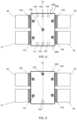
- FIG. 3is a schematic view of a vent/vacuum port arrangement inside the transfer chamber 20 shown in FIGS. 1 and 2 according to an embodiment of the present disclosure.
- the center line CLpasses through the geometric center G of the transfer chamber 20 when viewed from the above.
- the geometric center Gcan be the crossing point of the diagonal lines of the shape of a bottom base plate of the transfer chamber 20 in some embodiments in some embodiments. If the diagonal lines do not cross at the one point and form a polygon, the geometric center G is the center of gravity of the polygon in some embodiments. If the shape of a bottom base plate of the transfer chamber 20 is a triangle, the geometric center G is the center of the triangle.
- the center line CLalso passes one of the side walls 22 constituting the transfer chamber 20 . More specifically, the center line CL is perpendicular to the one of the side walls 22 .
- the vent port 105 and the vacuum ports 121 - 123are line-symmetrically arranged with respect to the center line CL inside the transfer chamber 20 .
- the vent ports 101 - 104are line-symmetrically arranged with respect to the center line CL inside the transfer chamber 20 .
- all of the vacuum ports 121 - 123 and vent ports 101 - 105are line-symmetrically arranged inside the transfer chamber 20 with respect to the center line CL.
- vent port 101is located in front of the gate valve of the process chamber 31
- the vent port 102is located in front of the gate valve of the process chamber 32
- the vent port 103is located in front of the gate valve of the process chamber 33
- the vent port 104is located in front of the gate valve of the process chamber 34 , respectively.
- the process chambers 31 - 34are also line-symmetrically arranged with respect to the center line CL, and thus the vent ports 101 - 104 are line-symmetrically arranged inside the transfer chamber 20 with respect to the center line CL.
- a distance between the gate valve of each of the process chambers 31 - 34 and the corresponding vent portis in a range from about 0.5 mm to about 5 cm in plan view in some embodiments.
- one or more common vent ports 105are provided inside the transfer chamber 20 , in some embodiments. At least one common vent port is provided on the center line CL of the transfer chamber 20 in some embodiments. When two or more common vent ports are provided, the common vent ports are line-symmetrically arranged with respect to the center line CL.
- At least one vacuum portis provided in the transfer chamber 20 .
- At least one vacuum port(e.g., 122 ) is provided on the center line CL of the transfer chamber 20 in some embodiments.
- the vacuum portsare line-symmetrically arranged with respect to the center line CL.
- at least one of the vacuum portsis provided in the transfer chamber 20 in front of the load lock chamber 50 , in some embodiments.
- the vacuum port(s)is located closer to the load lock chamber than the vent ports in some embodiments.
- the common vent portis located closer to the load lock chamber than the vacuum ports and the vacuum ports are arranged in front of opposite one 24 of the side walls.
- the vacuum portsare provided inside the transfer chamber 20 such that the vacuum ports are arranged on a line L parallel to one of side walls (e.g., 22 ) of the transfer chamber 20 as shown in FIG. 3 .
- FIG. 4is a schematic view of gas flows inside the transfer chamber 20 of the vacuum processing apparatus 10 shown in FIGS. 1 - 3 according to an embodiment of the present disclosure.
- the vacuum processing apparatus 10operates in various operation modes or conditions. For example, in an idle condition, no semiconductor wafer or substrate is loaded inside the vacuum processing apparatus 10 . In a processing condition/mode, one or more wafers or substrates are transferred from the load lock chamber 50 to one or more of the process or measurement chambers 31 - 34 by the substrate handling and transferring mechanism 40 inside the transfer chamber, and the wafers or the substrates are processed at the processing or measurement chambers.
- a processing condition/modeone or more wafers or substrates are transferred from the load lock chamber 50 to one or more of the process or measurement chambers 31 - 34 by the substrate handling and transferring mechanism 40 inside the transfer chamber, and the wafers or the substrates are processed at the processing or measurement chambers.
- the valve 112 for the common vent port 105 and the valves 131 - 133 for the vacuum ports 121 - 123are opened by the operation of the controller 80 .
- the common vent port 105 and the vacuum ports 121 - 123are line-symmetrically arranged with respect to the center line CL, gas flows GF from the common vent port 105 to the vacuum ports are line-symmetric with respect to the center line CL of the transfer chamber 20 , as shown in FIG. 4 .
- films or byproductsare generated in the processing chambers 31 - 34 and when the gate valve 25 is opened to transfer the wafer or substrate from/to the processing chamber, the films or the byproducts move from the processing chamber to the transfer chamber.
- the gas flowsare not symmetric, which may be caused by, for example, opening the valve for the vent port 101 and the valve for the vacuum port 122 , a dead space is generated at the corner of the transfer chamber near the vent ports 105 and 103 .
- the films or byproductsare not purged by the purge gas flow and tend to locally deposited in the dead space.
- Such locally deposited film or byproductsmay be blown or stirred up by movement of the wafer handling and transferring mechanism or by other air movement inside the transfer chamber, and may fall on the wafer or substrate.
- vent ports 102 and 103are opened together with or instead of the common vent port 105 during the purge operation. In such a case, the gas flows are also symmetric with respect to the center line CL. In other embodiments, all the vent ports 101 - 105 are opened.
- the line-symmetric arrangement of the vent ports and/or the vacuum portsdoes not necessarily require mathematical accuracy.
- the positions of the vent ports and/or the vacuum portcan deviate from the exact line-symmetric positions as long as the substantially symmetric gas flows can be obtained.
- the deviation of the position from the exact positionscan be 0 to about 2 cm in some embodiments.
- FIGS. 5 and 6are schematic views of gas flows when the gate valve is opened to transfer the semiconductor wafer or the substrate from/to the processing chamber according to an embodiment of the present disclosure.
- the pressure inside the processing chamberis lower than the pressure inside the transfer chamber, in some embodiments.
- no vent port for supplying a vent gase.g., N 2
- a vent gasis supplied from one of the vent ports in the transfer chamber to the vacuum processing or measurement chamber.
- the valve for the vent portis opened and then the gate valve is opened. The timing of opening the gate valve and opening valve for a vent port is not particularly limited.
- FIGS. 5 and 6to purge a specific processing chamber, only the valve for the corresponding vent port located in front of (and closest to) the specific processing chamber is opened as shown in FIGS. 5 and 6 .
- the valve 111when the gate valve 25 for the processing chamber 31 is opened, the valve 111 (see, FIG. 2 ) is opened to introduce the vent gas from the vent port 101 into the processing chamber 31 to minimize the gas flows GF 1 , while other vent valves are closed.
- the valves for the vacuum ports 121 - 123 inside the transfer chamberare also closed in some embodiments.
- FIG. 6when the gate valve 25 for the processing chamber 33 is opened, the valve 113 (see, FIG. 2 ) is opened to introduce the vent gas from the vent port 103 into the processing chamber 33 to minimize the gas flows GF 2 , while other vent valves are closed.
- gas flow travel distances for the processing chambers 31 - 14are different from each other (e.g., at least different between the processing chamber 31 and processing chamber 32 .
- Different lengths of gas flow travel pathsmay cause various problems in the purge operation. For example, a purge operation for the processing chamber 31 may be insufficient compared with a purge operation for the processing chamber 32 when only the common vent port 105 is used, or the longer gas flow traveling path may cause more particles thrown up by the gas flows.
- the gas flow traveling pathsare generally long and due to the wafer handling and transferring mechanism located at the center of the transfer chamber, the gas flows may be disturbed causing non-uniform gas flows.
- FIGS. 7 - 16are schematic views of a vent/vacuum port arrangement and/or the configuration of transfer chambers according to various embodiments of the present disclosure.
- One or more features of two or more following embodimentscan be combined with one or more following embodiments. Configurations, element, features, materials and/or dimensions the same as or similar to those for FIGS. 1 - 6 may be employed in the following embodiments, and the detailed explanations may be omitted. Further, one or more features of the forgoing embodiments can be combined with one or more following embodiments.
- FIG. 7is a schematic view of a vent/vacuum port arrangement according to another embodiment of the present disclosure.
- six ( 6 ) vacuum processing or measurement chambers 31 - 34 and 36 - 37are connected via gate valves, respectively, to a transfer chamber 20 A having a rectangular shape.
- the additional vacuum processing or measurement chambers 36 and 37are the same type as the vacuum processing or measurement chambers 31 - 34 in some embodiments, and different types in other embodiments.
- additional vent ports 106 and 107are provided in front of the vacuum processing or measurement chambers 36 and 37 , respectively.
- the vent ports 101 - 107are line-symmetrically arranged inside the transfer chamber 20 A with respect to the center line CL.
- FIG. 8is a schematic view of a vent/vacuum port arrangement according to another embodiment of the present disclosure.
- the transfer chamber 20 Bincludes two pairs of three vacuum ports and five vent ports as shown in FIG. 8 .
- the vacuum ports 121 - 123are provided at positions close to the side wall 22 B and the vacuum ports 124 - 126 are provided at positions closer to the opposing side wall 24 B.
- the vacuum ports in each setare arranged on a line parallel to the respective side walls (e.g., 22 B or 24 B) of the transfer chamber 20 B.
- the vent ports 101 - 104are provided to the corresponding vacuum processing or measurement chambers 31 - 34 , respectively, similar to FIGS. 1 - 6 .
- the common vent port 105is provided at or near the geometric center of the transfer chamber 20 B.
- the vent ports 101 - 105are line-symmetrically arranged inside the transfer chamber 20 B with respect to the center line CL, and the vacuum ports 121 - 126 are also line-symmetrically arranged inside the transfer chamber 20 B with respect to the center line CL.
- FIG. 9is a schematic view of a vent/vacuum port arrangement according to another embodiment of the present disclosure.
- FIG. 9similar to FIGS. 1 - 6 , four vacuum processing or measurement chambers 31 - 34 are provided to the transfer chamber 20 C.
- the transfer chamber 20 Cincludes only one vacuum port 122 .
- the configuration of the vent ports 101 - 105are the same as the configuration of vent ports shown in FIGS. 1 - 6 .
- the vacuum port 121 and the vent ports 101 - 105are line-symmetrically arranged inside the transfer chamber 20 C with respect to the center line CL.
- FIG. 10is a schematic view of a vent/vacuum port arrangement according to another embodiment of the present disclosure.
- the transfer chamber 20 Dincludes four vent ports for respective vacuum processing or measurement chambers 31 - 34 and two common vent ports 108 and 109 are provided as shown in FIG. 10 .
- the vent ports 108 - 109are line-symmetrically arranged inside the transfer chamber 20 D with respect to the center line CL, and the vent ports 101 - 105 and 108 - 109 are also line-symmetrically arranged inside the transfer chamber 20 D with respect to the center line CL.
- the vacuum ports 121 - 123are line-symmetrically arranged inside the transfer chamber 20 D with respect to the center line CL. In FIG. 10 , the center line CL does not pass through any of the vent ports.
- FIG. 11is a schematic view of a vent/vacuum port arrangement according to another embodiment of the present disclosure.
- FIG. 11similar to FIGS. 1 - 6 , four vacuum processing or measurement chambers 31 - 34 are provided to the transfer chamber 20 E.
- a set of two or more vent portsare provided respectively for the corresponding vacuum processing or measurement chambers 31 - 34 , respectively.
- a set of vent ports 101 Dis provided in front of the vacuum processing or measurement chamber 31
- a set of vent ports 102 Dis provided in front of the vacuum processing or measurement chamber 32
- a set of vent ports 103 Dis provided in front of the vacuum processing or measurement chamber 33
- a set of vent ports 104 Dis provided in front of the vacuum processing or measurement chamber 34 , respectively.
- the size of a semiconductor waferis large (e.g., 12 inches) or a large glass substrate for a flat display panel is used, the size, in particular the width, of the vacuum processing or measurement chambers also becomes large.
- Providing a set of vent portsis advantageous for such large vacuum processing or measurement chamber.
- the vent ports of the set of vent portsare line-symmetrically arranged with respect to the center line CCL of the corresponding vacuum processing or measurement chamber 31 .
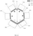
- FIG. 12is a schematic view of a vent/vacuum port arrangement according to another embodiment of the present disclosure.
- the shape of the transfer chamber 1020is hexagonal having six side walls.
- One or more load lock chambers 1050are provided to one of the six side walls via a gate valve 1025 , and five vacuum processing or measurement chambers 1031 , 1032 , 1033 , 1034 and 1035 are connected to the transfer chamber 1020 via gate valves 1025 , respectively.
- three vacuum ports 1120are provided in fro of the load lock chamber 1050
- vent ports 1100are provided respectively to the corresponding vacuum processing or measurement chambers 1031 - 1035 . As shown in FIG.
- the vent ports 1110 and the vacuum ports 1120are line-symmetrically arranged with respect to the center line CL of the transfer chamber 1020 .
- no common vent portis provided in the transfer chamber 1020 .
- one or more common vent portsare provided line-symmetrically with respect to the center line CL.
- vent port 1100 located in front of the vacuum processing or measurement chamber 1033functions as a common vent port similar to the common vent port 105 shown in FIG. 4 , in some embodiments.
- vent ports in front of the vacuum processing or measurement chambers 1032 and 1034function as common vent ports similar to the common vent port 105 shown in FIG. 4 .
- FIG. 13is a schematic view of a vent/vacuum port arrangement according to another embodiment of the present disclosure.
- the shape of the transfer chamber 2020is hexagonal having six side walls.
- Two load lock chambers 2051 , 2052are provided to two of the six side walls via gate valves 2025 , and four vacuum processing or measurement chambers 2031 , 2032 , 2033 and 2034 are connected to the transfer chamber 2020 via gate valves 2025 , respectively.
- a common vent port 2105is provided.
- the common vent port 2015is not provided in other embodiments, and in such a case, the vent ports provided in front of the vacuum processing or measurement chambers 2032 and 2033 functions as a common vent port shown in FIG. 4 .
- the vent ports 2100are provided respectively to the corresponding vacuum processing or measurement chambers 2031 - 2034 . Further, the vacuum ports 2120 are provided respectively to the corresponding load lock chambers 2050 . Further, in some embodiments, a common vacuum port 2122 is provided between the load lock chambers 2050 .
- vent ports 2100 and 2105 and the vacuum ports 2120 and 2122are line-symmetrically arranged with respect to the center line CL of the transfer chamber 2020 .
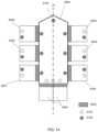
- FIG. 14is a schematic view of a vent/vacuum port arrangement according to another embodiment of the present disclosure.
- the shape of the transfer chamber 3020is elongated pentagonal having five side walls.
- six (6) vacuum processing or measurement chambers 3031 - 3036are connected via gate valves 3025 , respectively, to a transfer chamber 3020 .
- Two load lock chambers 3050are provided to one of the side walls of the transfer chamber 3020 .
- the vent ports 3100are provided respectively in front of the corresponding vacuum processing or measurement chambers 3031 - 3036 , and a common vent port 3105 is also provided.
- Three vacuum ports 3120are provided in front of the load lock chambers 3050 .
- the vent ports 3100 and 3105 and the vacuum ports 3120are line-symmetrically arranged inside the transfer chamber 3020 with respect to the center line CL.
- FIG. 15is a schematic view of a vent/vacuum port arrangement according to another embodiment of the present disclosure.
- the shape of the transfer chamber 4020is a rectangular or a square.
- Six vacuum processing or measurement chambers 4031 , 4032 , 4033 , 4034 , 4035 and 4036are provided. Two of the vacuum processing or measurement chambers are respectively connected to each of three side walls of the transfer chamber 4020 , and two load lock chambers 4050 are connected to the remaining side wall of the transfer chamber 4020 .
- the vent ports 4100are provided respectively in front of the corresponding vacuum processing or measurement chambers 4031 - 4036 , and a common vent port 4105 is also provided. In some embodiments, the common port 4105 is not provided.
- Three vacuum ports 4120are provided in front of the load lock chambers 4050 .
- the vent ports 4100 and 4105 and the vacuum ports 4120are line-symmetrically arranged inside the transfer chamber 4020 with respect to the center line CL.
- FIG. 16is a schematic view of a vent/vacuum port arrangement according to another embodiment of the present disclosure.
- the shape of the transfer chamber 5020is pentagonal having five side walls.
- four vacuum processing or measurement chambers 5031 - 5034are connected via gate valves 5025 , respectively, to a transfer chamber 5020 .
- One or more load lock chambers 5050are provided to one of the side walls of the transfer chamber 5020 .
- the vent ports 5100are provided respectively in front of the corresponding vacuum processing or measurement chambers 5031 - 5034 , and a common vent port 5105 is also provided. In other embodiments, no common vent port is provided.
- Three vacuum ports 5120are provided in front of the load lock chamber 5050 .
- the vent ports 5100 and 5105 and the vacuum ports 5120are line-symmetrically arranged inside the transfer chamber 3020 with respect to the center line CL.
- FIGS. 17 - 20are schematic views of a gas supply/vacuum port arrangement inside a vacuum processing or measurement chamber according to an embodiment of the present disclosure.
- a symmetric port arrangementinside a transfer chamber are explained.
- a symmetric port arrangementis not limited to the transfer chamber, but can be applied to any other vacuum chamber having one or more gas supply ports and one or more vacuum ports.
- One or more features of two or more following embodimentscan be combined with one or more following embodiments. Configurations, element, features, materials and/or dimensions the same as or similar to those for FIGS. 1 - 16 may be employed in the following embodiments, and the detailed explanations may be omitted. Further, one or more features of the forgoing embodiments can be combined with one or more following embodiments.
- FIG. 17is a schematic view of a gas supply/vacuum port arrangement according to an embodiment of the present disclosure.
- a vacuum chamber 11 Aincludes a chamber body 6020 A and a gate valve 6025 A.
- the chamber body 6020 Aincludes at least one gas supply port and at least one vacuum port.
- one gas supply port 6100 A and one vacuum port 6120 Aare provided on the center line CL of the chamber body 6020 A.
- gas flows from the gas supply port 6100 A to the vacuum port 6120 Aare symmetric with respect to the center line CL, thereby minimizing generation of a dead space.
- the gas supply port 6100 Ais located close to the gate valve 6025 A and the vacuum port 6120 A are located to the opposite side of the chamber body 6020 A, and in other embodiments, the vacuum port 6120 A are located close to the gate valve 6025 A and the gas supply port 6100 A is located to the opposite side of the chamber body 6020 A.
- FIG. 18is a schematic view of a gas supply/vacuum port arrangement according to another embodiment of the present disclosure.
- a vacuum chamber 11 Bincludes a chamber body 6020 B and a gate valve 6025 B.
- the chamber body 6020 Bincludes at least one gas supply port and at least one vacuum port.
- one gas supply port 6100 B and two vacuum ports 6120 Bare provided line-symmetrically with respect to the center line CL of the chamber body 6020 B.
- gas flows from the gas supply port 6100 B to the vacuum ports 6120 Bare symmetric with respect to the center line CL, thereby minimizing generation of a dead space.
- the gas supply port 6100 Bis located close to the gate valve 6025 B and the vacuum ports 6120 B are located to the opposite side of the chamber body 6020 B, and in other embodiments, the vacuum ports 6120 B are located close to the gate valve 6025 B and the gas supply port 6100 B is located to the opposite side of the chamber body 6020 B.
- FIG. 19is a schematic view of a gas supply/vacuum port arrangement according to another embodiment of the present disclosure.
- a vacuum chamber 11 Cincludes a chamber body 6020 C and a gate valve 6025 C.
- the chamber body 6020 Cincludes at least one gas supply port and at least one vacuum port.
- two gas supply ports 6100 C and two vacuum ports 6120 Care provided line-symmetrically with respect to the center line CL of the chamber body 6020 C.
- gas flows from the gas supply ports 6100 C to the vacuum ports 6120 Care symmetric with respect to the center line CL, thereby minimizing generation of a dead space.
- the gas supply ports 6100 Care located close to the gate valve 6025 C and the vacuum ports 6120 C are located to the opposite side of the chamber body 6020 C, and in other embodiments, the vacuum ports 6120 C are located close to the gate valve 6025 C and the gas supply ports 6100 C are located to the opposite side of the chamber body 6020 C.
- FIG. 20is a schematic view of a gas supply/vacuum port arrangement according to another embodiment of the present disclosure.
- a vacuum chamber 11 Dincludes a chamber body 6020 D and a gate valve 6025 D.
- the chamber body 6020 Dincludes at least one gas supply port and at least one vacuum port.
- two gas supply ports 6100 D and one vacuum port 6120 Dare provided line-symmetrically with respect to the center line CL of the chamber body 6020 D.
- gas flows from the gas supply ports 6100 D to the vacuum port 6120 Dare symmetric with respect to the center line CL, thereby minimizing generation of a dead space.
- the gas supply ports 6100 Dare located at the middle of the chamber body 6020 D and the vacuum port 6120 D are located to the end side of the chamber body 6020 D opposite to the gate valve 6025 D. In other embodiments, two vacuum ports 6120 D are located at the middle of the chamber body 6020 D and one gas supply port 6100 D is located to the end side of the chamber body 6020 D.
- a vacuum apparatusincludes process chambers, and a transfer chamber coupled to the process chambers.
- the transfer chamberincludes one or more vacuum ports, through which a gas inside the transfer chamber is exhausted, and vent ports, from which a vent gas is supplied.
- the one or more vacuum ports and the vent portsare arranged such that air flows from at least one of the vent ports to the one or more vacuum ports are line-symmetric with respect to a center line of the transfer chamber.
- the vent portsare line-symmetrically arranged with respect to the center line of the transfer chamber.
- at least one vent portis provided in the transfer chamber in front of each of the process chambers.
- At least one common vent portis provided on the center line of the transfer chamber.
- two or more vacuum portsare provided in the transfer chamber.
- the two or more vacuum portsare line-symmetrically arranged with respect to the center line of the transfer chamber.
- at least one of the two or more vacuum portsis provided on the center line of the transfer chamber.
- the vacuum apparatusfurther includes a load lock chamber connected to the transfer chamber.
- At least one of the one or more vacuum portsis provided in the transfer chamber in front of the load lock chamber, and is located closer to the load lock chamber than the vent ports.
- a gate valveis provided between the transfer chamber and each of the process chambers.
- a vacuum apparatusincludes process chambers, a transfer chamber coupled to the process chambers, gate valves provided between the transfer chamber and the process chambers, respectively, a pump system, a gas supply, one or more vacuum ports disposed inside the transfer chamber and connected to the pump system via one or more vacuum valves, respectively, vent ports disposed inside the transfer chamber and connected to the gas supply via vent valves, respectively, and a controller for controlling at least the one or more vacuum valves and the vent valves.
- the vent portsare line-symmetrically arranged with respect to a center line of the transfer chamber.
- the center lineis a line passing through a geometric center of the transfer chamber and is perpendicular to one side wall or one corner of the transfer chamber in plan view.
- the controllerwhen all the gate valves are closed, the controller opens at least one vacuum valve and at least one vent valve such that air flows from at least one vent port to at least one vacuum port are line-symmetric with respect to a center line of the transfer chamber.
- at least one vent portis provided in the transfer chamber in front of each of the process chambers.
- the controllerwhen one of the gate valves corresponding to one of the process chambers is opened, the controller opens one of the vent valves corresponding to one of the vent ports in front of corresponding one of the process chambers.
- the controllerwhen the one of the vent valve opened, the controller does not open remaining vent valves.
- at least one common vent portis provided on the center line of the transfer chamber.
- the controllerwhen all the gate valves are closed, the controller opens at least one vent valve for the at least one common vent port and opens the one or more vacuum valves.
- a vacuum apparatus for processing a semiconductor waferincludes process chambers including at least one selected from the group consisting of a plasma etching chamber and a film deposition chamber, a transfer chamber coupled to the process chambers, and a wafer handler disposed inside the transfer chamber.
- the transfer chamberincludes one or more vacuum ports, through which a gas inside the transfer chamber is exhausted, and vent ports, from which a vent gas is supplied.
- the vent portsare line-symmetrically arranged with respect to a center line of the transfer chamber.
- the center lineis a line passing through a geometric center of the transfer chamber and is perpendicular to one side wall or one corner of the transfer chamber in plan view.
- the vacuum apparatusfurther includes a load lock chamber.
- the one or more vacuum portsare provided in the transfer chamber in front of the load lock chamber, and are located closer to the load lock chamber than the vent ports.
- two or more vacuum portsare provided inside the transfer chamber, and are arranged on a line parallel to one of side walls of the transfer chamber.
- a methodis for operating a vacuum apparatus.
- the vacuum apparatusincludes process chambers, a transfer chamber coupled to the process chambers, gate valves provided between the transfer chamber and the process chambers, respectively, a pump system, a gas supply, one or more vacuum ports disposed inside the transfer chamber and connected to the pump system via one or more vacuum valves, respectively, and vent ports disposed inside the transfer chamber and connected to the gas supply via vent valves, respectively.
- At least one vent portis provided in front of each of the process chambers.
- a methodis for operating a vacuum apparatus.
- the vacuum apparatusincludes process chambers, a transfer chamber coupled to the process chambers, gate valves provided between the transfer chamber and the process chambers, respectively, a pump system, a gas supply, one or more vacuum ports disposed inside the transfer chamber and connected to the pump system via one or more vacuum valves, respectively, and vent ports disposed inside the transfer chamber and connected to the gas supply via vent valves, respectively.
- the methodwhen all the gate valves are closed, at least one vacuum valve and at least one vent valve are opened such that air flows from at least one vent port to at least one vacuum port are line-symmetric with respect to a center line of the transfer chamber.
- only one vent valveis opened while remaining vent valves are closed such that the air flows from only one vent port to at least one vacuum port are line-symmetric with respect to the center line of the transfer chamber.
- two or more vacuum ports and two or more vacuum valvesare provided, and two or more vacuum ports are opened such that air flows from at least one vent port to the two or more vacuum ports are line-symmetric with respect to the center line of the transfer chamber.
Landscapes
- Engineering & Computer Science (AREA)
- Physics & Mathematics (AREA)
- Condensed Matter Physics & Semiconductors (AREA)
- General Physics & Mathematics (AREA)
- Manufacturing & Machinery (AREA)
- Computer Hardware Design (AREA)
- Microelectronics & Electronic Packaging (AREA)
- Power Engineering (AREA)
- Container, Conveyance, Adherence, Positioning, Of Wafer (AREA)
Abstract
Description
Claims (20)
Priority Applications (8)
| Application Number | Priority Date | Filing Date | Title |
|---|---|---|---|
| US15/906,689US11948810B2 (en) | 2017-11-15 | 2018-02-27 | Apparatus for processing substrates or wafers |
| DE102018107547.2ADE102018107547A1 (en) | 2017-11-15 | 2018-03-29 | DEVICE FOR TREATING SUBSTRATES OR WAFERES |
| KR1020180068904AKR20190055704A (en) | 2017-11-15 | 2018-06-15 | Apparatus for processing substrates or wafers |
| CN202211214777.9ACN115483137A (en) | 2017-11-15 | 2018-08-24 | Vacuum device and method for operating the same |
| CN201810974509.4ACN109786282A (en) | 2017-11-15 | 2018-08-24 | Handle the device of substrate or wafer |
| TW107129825ATWI734023B (en) | 2017-11-15 | 2018-08-27 | Vacuum apparatus and method for operating the same |
| KR1020200182025AKR102491903B1 (en) | 2017-11-15 | 2020-12-23 | Apparatus for processing substrates or wafers |
| US18/584,828US20240249957A1 (en) | 2017-11-15 | 2024-02-22 | Apparatus for processing substrates or wafers |
Applications Claiming Priority (2)
| Application Number | Priority Date | Filing Date | Title |
|---|---|---|---|
| US201762586580P | 2017-11-15 | 2017-11-15 | |
| US15/906,689US11948810B2 (en) | 2017-11-15 | 2018-02-27 | Apparatus for processing substrates or wafers |
Related Child Applications (1)
| Application Number | Title | Priority Date | Filing Date |
|---|---|---|---|
| US18/584,828DivisionUS20240249957A1 (en) | 2017-11-15 | 2024-02-22 | Apparatus for processing substrates or wafers |
Publications (2)
| Publication Number | Publication Date |
|---|---|
| US20190148177A1 US20190148177A1 (en) | 2019-05-16 |
| US11948810B2true US11948810B2 (en) | 2024-04-02 |
Family
ID=66432377
Family Applications (1)
| Application Number | Title | Priority Date | Filing Date |
|---|---|---|---|
| US15/906,689ActiveUS11948810B2 (en) | 2017-11-15 | 2018-02-27 | Apparatus for processing substrates or wafers |
Country Status (4)
| Country | Link |
|---|---|
| US (1) | US11948810B2 (en) |
| KR (1) | KR20190055704A (en) |
| CN (1) | CN109786282A (en) |
| TW (1) | TWI734023B (en) |
Cited By (1)
| Publication number | Priority date | Publication date | Assignee | Title |
|---|---|---|---|---|
| US20240249957A1 (en)* | 2017-11-15 | 2024-07-25 | Taiwan Semiconductor Manufacturing Company, Ltd. | Apparatus for processing substrates or wafers |
Families Citing this family (257)
| Publication number | Priority date | Publication date | Assignee | Title |
|---|---|---|---|---|
| US20130023129A1 (en) | 2011-07-20 | 2013-01-24 | Asm America, Inc. | Pressure transmitter for a semiconductor processing environment |
| US10714315B2 (en) | 2012-10-12 | 2020-07-14 | Asm Ip Holdings B.V. | Semiconductor reaction chamber showerhead |
| US20160376700A1 (en) | 2013-02-01 | 2016-12-29 | Asm Ip Holding B.V. | System for treatment of deposition reactor |
| US10941490B2 (en) | 2014-10-07 | 2021-03-09 | Asm Ip Holding B.V. | Multiple temperature range susceptor, assembly, reactor and system including the susceptor, and methods of using the same |
| US10276355B2 (en) | 2015-03-12 | 2019-04-30 | Asm Ip Holding B.V. | Multi-zone reactor, system including the reactor, and method of using the same |
| US10458018B2 (en) | 2015-06-26 | 2019-10-29 | Asm Ip Holding B.V. | Structures including metal carbide material, devices including the structures, and methods of forming same |
| US10211308B2 (en) | 2015-10-21 | 2019-02-19 | Asm Ip Holding B.V. | NbMC layers |
| US11139308B2 (en) | 2015-12-29 | 2021-10-05 | Asm Ip Holding B.V. | Atomic layer deposition of III-V compounds to form V-NAND devices |
| US10529554B2 (en) | 2016-02-19 | 2020-01-07 | Asm Ip Holding B.V. | Method for forming silicon nitride film selectively on sidewalls or flat surfaces of trenches |
| US10343920B2 (en) | 2016-03-18 | 2019-07-09 | Asm Ip Holding B.V. | Aligned carbon nanotubes |
| US11453943B2 (en) | 2016-05-25 | 2022-09-27 | Asm Ip Holding B.V. | Method for forming carbon-containing silicon/metal oxide or nitride film by ALD using silicon precursor and hydrocarbon precursor |
| US9859151B1 (en) | 2016-07-08 | 2018-01-02 | Asm Ip Holding B.V. | Selective film deposition method to form air gaps |
| US10612137B2 (en) | 2016-07-08 | 2020-04-07 | Asm Ip Holdings B.V. | Organic reactants for atomic layer deposition |
| US9887082B1 (en) | 2016-07-28 | 2018-02-06 | Asm Ip Holding B.V. | Method and apparatus for filling a gap |
| US9812320B1 (en) | 2016-07-28 | 2017-11-07 | Asm Ip Holding B.V. | Method and apparatus for filling a gap |
| US11532757B2 (en) | 2016-10-27 | 2022-12-20 | Asm Ip Holding B.V. | Deposition of charge trapping layers |
| US10714350B2 (en) | 2016-11-01 | 2020-07-14 | ASM IP Holdings, B.V. | Methods for forming a transition metal niobium nitride film on a substrate by atomic layer deposition and related semiconductor device structures |
| KR102546317B1 (en) | 2016-11-15 | 2023-06-21 | 에이에스엠 아이피 홀딩 비.브이. | Gas supply unit and substrate processing apparatus including the same |
| KR102762543B1 (en) | 2016-12-14 | 2025-02-05 | 에이에스엠 아이피 홀딩 비.브이. | Substrate processing apparatus |
| US11447861B2 (en) | 2016-12-15 | 2022-09-20 | Asm Ip Holding B.V. | Sequential infiltration synthesis apparatus and a method of forming a patterned structure |
| US11581186B2 (en) | 2016-12-15 | 2023-02-14 | Asm Ip Holding B.V. | Sequential infiltration synthesis apparatus |
| US10269558B2 (en) | 2016-12-22 | 2019-04-23 | Asm Ip Holding B.V. | Method of forming a structure on a substrate |
| US11390950B2 (en) | 2017-01-10 | 2022-07-19 | Asm Ip Holding B.V. | Reactor system and method to reduce residue buildup during a film deposition process |
| US10468261B2 (en) | 2017-02-15 | 2019-11-05 | Asm Ip Holding B.V. | Methods for forming a metallic film on a substrate by cyclical deposition and related semiconductor device structures |
| US10770286B2 (en) | 2017-05-08 | 2020-09-08 | Asm Ip Holdings B.V. | Methods for selectively forming a silicon nitride film on a substrate and related semiconductor device structures |
| US12040200B2 (en) | 2017-06-20 | 2024-07-16 | Asm Ip Holding B.V. | Semiconductor processing apparatus and methods for calibrating a semiconductor processing apparatus |
| US11306395B2 (en) | 2017-06-28 | 2022-04-19 | Asm Ip Holding B.V. | Methods for depositing a transition metal nitride film on a substrate by atomic layer deposition and related deposition apparatus |
| KR20190009245A (en) | 2017-07-18 | 2019-01-28 | 에이에스엠 아이피 홀딩 비.브이. | Methods for forming a semiconductor device structure and related semiconductor device structures |
| US11374112B2 (en) | 2017-07-19 | 2022-06-28 | Asm Ip Holding B.V. | Method for depositing a group IV semiconductor and related semiconductor device structures |
| US10590535B2 (en) | 2017-07-26 | 2020-03-17 | Asm Ip Holdings B.V. | Chemical treatment, deposition and/or infiltration apparatus and method for using the same |
| TWI815813B (en) | 2017-08-04 | 2023-09-21 | 荷蘭商Asm智慧財產控股公司 | Showerhead assembly for distributing a gas within a reaction chamber |
| US10770336B2 (en) | 2017-08-08 | 2020-09-08 | Asm Ip Holding B.V. | Substrate lift mechanism and reactor including same |
| US10692741B2 (en) | 2017-08-08 | 2020-06-23 | Asm Ip Holdings B.V. | Radiation shield |
| US11769682B2 (en) | 2017-08-09 | 2023-09-26 | Asm Ip Holding B.V. | Storage apparatus for storing cassettes for substrates and processing apparatus equipped therewith |
| US11830730B2 (en) | 2017-08-29 | 2023-11-28 | Asm Ip Holding B.V. | Layer forming method and apparatus |
| US11295980B2 (en) | 2017-08-30 | 2022-04-05 | Asm Ip Holding B.V. | Methods for depositing a molybdenum metal film over a dielectric surface of a substrate by a cyclical deposition process and related semiconductor device structures |
| US10658205B2 (en) | 2017-09-28 | 2020-05-19 | Asm Ip Holdings B.V. | Chemical dispensing apparatus and methods for dispensing a chemical to a reaction chamber |
| US10403504B2 (en) | 2017-10-05 | 2019-09-03 | Asm Ip Holding B.V. | Method for selectively depositing a metallic film on a substrate |
| US10923344B2 (en) | 2017-10-30 | 2021-02-16 | Asm Ip Holding B.V. | Methods for forming a semiconductor structure and related semiconductor structures |
| CN111344522B (en) | 2017-11-27 | 2022-04-12 | 阿斯莫Ip控股公司 | Including clean mini-environment device |
| WO2019103613A1 (en) | 2017-11-27 | 2019-05-31 | Asm Ip Holding B.V. | A storage device for storing wafer cassettes for use with a batch furnace |
| US10872771B2 (en) | 2018-01-16 | 2020-12-22 | Asm Ip Holding B. V. | Method for depositing a material film on a substrate within a reaction chamber by a cyclical deposition process and related device structures |
| KR102695659B1 (en) | 2018-01-19 | 2024-08-14 | 에이에스엠 아이피 홀딩 비.브이. | Method for depositing a gap filling layer by plasma assisted deposition |
| TWI799494B (en) | 2018-01-19 | 2023-04-21 | 荷蘭商Asm 智慧財產控股公司 | Deposition method |
| US11081345B2 (en) | 2018-02-06 | 2021-08-03 | Asm Ip Holding B.V. | Method of post-deposition treatment for silicon oxide film |
| US10896820B2 (en) | 2018-02-14 | 2021-01-19 | Asm Ip Holding B.V. | Method for depositing a ruthenium-containing film on a substrate by a cyclical deposition process |
| WO2019158960A1 (en) | 2018-02-14 | 2019-08-22 | Asm Ip Holding B.V. | A method for depositing a ruthenium-containing film on a substrate by a cyclical deposition process |
| US10731249B2 (en) | 2018-02-15 | 2020-08-04 | Asm Ip Holding B.V. | Method of forming a transition metal containing film on a substrate by a cyclical deposition process, a method for supplying a transition metal halide compound to a reaction chamber, and related vapor deposition apparatus |
| KR102636427B1 (en) | 2018-02-20 | 2024-02-13 | 에이에스엠 아이피 홀딩 비.브이. | Substrate processing method and apparatus |
| US10975470B2 (en) | 2018-02-23 | 2021-04-13 | Asm Ip Holding B.V. | Apparatus for detecting or monitoring for a chemical precursor in a high temperature environment |
| US11473195B2 (en) | 2018-03-01 | 2022-10-18 | Asm Ip Holding B.V. | Semiconductor processing apparatus and a method for processing a substrate |
| US11629406B2 (en) | 2018-03-09 | 2023-04-18 | Asm Ip Holding B.V. | Semiconductor processing apparatus comprising one or more pyrometers for measuring a temperature of a substrate during transfer of the substrate |
| KR102646467B1 (en) | 2018-03-27 | 2024-03-11 | 에이에스엠 아이피 홀딩 비.브이. | Method of forming an electrode on a substrate and a semiconductor device structure including an electrode |
| US11230766B2 (en) | 2018-03-29 | 2022-01-25 | Asm Ip Holding B.V. | Substrate processing apparatus and method |
| KR102600229B1 (en) | 2018-04-09 | 2023-11-10 | 에이에스엠 아이피 홀딩 비.브이. | Substrate supporting device, substrate processing apparatus including the same and substrate processing method |
| TWI811348B (en) | 2018-05-08 | 2023-08-11 | 荷蘭商Asm 智慧財產控股公司 | Methods for depositing an oxide film on a substrate by a cyclical deposition process and related device structures |
| US12025484B2 (en) | 2018-05-08 | 2024-07-02 | Asm Ip Holding B.V. | Thin film forming method |
| US12272527B2 (en) | 2018-05-09 | 2025-04-08 | Asm Ip Holding B.V. | Apparatus for use with hydrogen radicals and method of using same |
| KR102596988B1 (en) | 2018-05-28 | 2023-10-31 | 에이에스엠 아이피 홀딩 비.브이. | Method of processing a substrate and a device manufactured by the same |
| US11718913B2 (en) | 2018-06-04 | 2023-08-08 | Asm Ip Holding B.V. | Gas distribution system and reactor system including same |
| TWI840362B (en)* | 2018-06-04 | 2024-05-01 | 荷蘭商Asm Ip私人控股有限公司 | Wafer handling chamber with moisture reduction |
| US11286562B2 (en) | 2018-06-08 | 2022-03-29 | Asm Ip Holding B.V. | Gas-phase chemical reactor and method of using same |
| KR102568797B1 (en) | 2018-06-21 | 2023-08-21 | 에이에스엠 아이피 홀딩 비.브이. | Substrate processing system |
| US10797133B2 (en) | 2018-06-21 | 2020-10-06 | Asm Ip Holding B.V. | Method for depositing a phosphorus doped silicon arsenide film and related semiconductor device structures |
| KR102854019B1 (en) | 2018-06-27 | 2025-09-02 | 에이에스엠 아이피 홀딩 비.브이. | Periodic deposition method for forming a metal-containing material and films and structures comprising the metal-containing material |
| TWI873894B (en) | 2018-06-27 | 2025-02-21 | 荷蘭商Asm Ip私人控股有限公司 | Cyclic deposition methods for forming metal-containing material and films and structures including the metal-containing material |
| US10612136B2 (en) | 2018-06-29 | 2020-04-07 | ASM IP Holding, B.V. | Temperature-controlled flange and reactor system including same |
| US10388513B1 (en) | 2018-07-03 | 2019-08-20 | Asm Ip Holding B.V. | Method for depositing silicon-free carbon-containing film as gap-fill layer by pulse plasma-assisted deposition |
| US10755922B2 (en) | 2018-07-03 | 2020-08-25 | Asm Ip Holding B.V. | Method for depositing silicon-free carbon-containing film as gap-fill layer by pulse plasma-assisted deposition |
| US11031264B2 (en)* | 2018-08-15 | 2021-06-08 | Taiwan Semoconductor Manufacturing Co., Ltd. | Semiconductor device manufacturing system |
| US11430674B2 (en) | 2018-08-22 | 2022-08-30 | Asm Ip Holding B.V. | Sensor array, apparatus for dispensing a vapor phase reactant to a reaction chamber and related methods |
| US11239420B2 (en)* | 2018-08-24 | 2022-02-01 | Lam Research Corporation | Conformal damage-free encapsulation of chalcogenide materials |
| KR102707956B1 (en) | 2018-09-11 | 2024-09-19 | 에이에스엠 아이피 홀딩 비.브이. | Method for deposition of a thin film |
| US11024523B2 (en) | 2018-09-11 | 2021-06-01 | Asm Ip Holding B.V. | Substrate processing apparatus and method |
| CN110970344B (en) | 2018-10-01 | 2024-10-25 | Asmip控股有限公司 | Substrate holding apparatus, system comprising the same and method of using the same |
| US11232963B2 (en) | 2018-10-03 | 2022-01-25 | Asm Ip Holding B.V. | Substrate processing apparatus and method |
| KR102592699B1 (en) | 2018-10-08 | 2023-10-23 | 에이에스엠 아이피 홀딩 비.브이. | Substrate support unit and apparatuses for depositing thin film and processing the substrate including the same |
| KR102605121B1 (en) | 2018-10-19 | 2023-11-23 | 에이에스엠 아이피 홀딩 비.브이. | Substrate processing apparatus and substrate processing method |
| KR102546322B1 (en) | 2018-10-19 | 2023-06-21 | 에이에스엠 아이피 홀딩 비.브이. | Substrate processing apparatus and substrate processing method |
| US12378665B2 (en) | 2018-10-26 | 2025-08-05 | Asm Ip Holding B.V. | High temperature coatings for a preclean and etch apparatus and related methods |
| US11087997B2 (en) | 2018-10-31 | 2021-08-10 | Asm Ip Holding B.V. | Substrate processing apparatus for processing substrates |
| KR102748291B1 (en) | 2018-11-02 | 2024-12-31 | 에이에스엠 아이피 홀딩 비.브이. | Substrate support unit and substrate processing apparatus including the same |
| US11572620B2 (en) | 2018-11-06 | 2023-02-07 | Asm Ip Holding B.V. | Methods for selectively depositing an amorphous silicon film on a substrate |
| US10818758B2 (en) | 2018-11-16 | 2020-10-27 | Asm Ip Holding B.V. | Methods for forming a metal silicate film on a substrate in a reaction chamber and related semiconductor device structures |
| US12040199B2 (en) | 2018-11-28 | 2024-07-16 | Asm Ip Holding B.V. | Substrate processing apparatus for processing substrates |
| US11217444B2 (en) | 2018-11-30 | 2022-01-04 | Asm Ip Holding B.V. | Method for forming an ultraviolet radiation responsive metal oxide-containing film |
| KR102636428B1 (en) | 2018-12-04 | 2024-02-13 | 에이에스엠 아이피 홀딩 비.브이. | A method for cleaning a substrate processing apparatus |
| US11158513B2 (en) | 2018-12-13 | 2021-10-26 | Asm Ip Holding B.V. | Methods for forming a rhenium-containing film on a substrate by a cyclical deposition process and related semiconductor device structures |
| TWI874340B (en) | 2018-12-14 | 2025-03-01 | 荷蘭商Asm Ip私人控股有限公司 | Method of forming device structure, structure formed by the method and system for performing the method |
| TWI866480B (en) | 2019-01-17 | 2024-12-11 | 荷蘭商Asm Ip 私人控股有限公司 | Methods of forming a transition metal containing film on a substrate by a cyclical deposition process |
| KR102727227B1 (en) | 2019-01-22 | 2024-11-07 | 에이에스엠 아이피 홀딩 비.브이. | Semiconductor processing device |
| TWI873122B (en) | 2019-02-20 | 2025-02-21 | 荷蘭商Asm Ip私人控股有限公司 | Method of filling a recess formed within a surface of a substrate, semiconductor structure formed according to the method, and semiconductor processing apparatus |
| TWI838458B (en) | 2019-02-20 | 2024-04-11 | 荷蘭商Asm Ip私人控股有限公司 | Apparatus and methods for plug fill deposition in 3-d nand applications |
| TWI845607B (en) | 2019-02-20 | 2024-06-21 | 荷蘭商Asm Ip私人控股有限公司 | Cyclical deposition method and apparatus for filling a recess formed within a substrate surface |
| KR102626263B1 (en) | 2019-02-20 | 2024-01-16 | 에이에스엠 아이피 홀딩 비.브이. | Cyclical deposition method including treatment step and apparatus for same |
| TWI842826B (en) | 2019-02-22 | 2024-05-21 | 荷蘭商Asm Ip私人控股有限公司 | Substrate processing apparatus and method for processing substrate |
| US11742198B2 (en) | 2019-03-08 | 2023-08-29 | Asm Ip Holding B.V. | Structure including SiOCN layer and method of forming same |
| KR102858005B1 (en) | 2019-03-08 | 2025-09-09 | 에이에스엠 아이피 홀딩 비.브이. | Method for Selective Deposition of Silicon Nitride Layer and Structure Including Selectively-Deposited Silicon Nitride Layer |
| JP2020167398A (en) | 2019-03-28 | 2020-10-08 | エーエスエム・アイピー・ホールディング・ベー・フェー | Door openers and substrate processing equipment provided with door openers |
| KR102809999B1 (en) | 2019-04-01 | 2025-05-19 | 에이에스엠 아이피 홀딩 비.브이. | Method of manufacturing semiconductor device |
| KR20200123380A (en) | 2019-04-19 | 2020-10-29 | 에이에스엠 아이피 홀딩 비.브이. | Layer forming method and apparatus |
| KR20200125453A (en) | 2019-04-24 | 2020-11-04 | 에이에스엠 아이피 홀딩 비.브이. | Gas-phase reactor system and method of using same |
| US11289326B2 (en) | 2019-05-07 | 2022-03-29 | Asm Ip Holding B.V. | Method for reforming amorphous carbon polymer film |
| KR20200130121A (en) | 2019-05-07 | 2020-11-18 | 에이에스엠 아이피 홀딩 비.브이. | Chemical source vessel with dip tube |
| KR20200130652A (en) | 2019-05-10 | 2020-11-19 | 에이에스엠 아이피 홀딩 비.브이. | Method of depositing material onto a surface and structure formed according to the method |
| JP7612342B2 (en) | 2019-05-16 | 2025-01-14 | エーエスエム・アイピー・ホールディング・ベー・フェー | Wafer boat handling apparatus, vertical batch furnace and method |
| JP7598201B2 (en) | 2019-05-16 | 2024-12-11 | エーエスエム・アイピー・ホールディング・ベー・フェー | Wafer boat handling apparatus, vertical batch furnace and method |
| USD947913S1 (en) | 2019-05-17 | 2022-04-05 | Asm Ip Holding B.V. | Susceptor shaft |
| USD975665S1 (en) | 2019-05-17 | 2023-01-17 | Asm Ip Holding B.V. | Susceptor shaft |
| KR20200141002A (en) | 2019-06-06 | 2020-12-17 | 에이에스엠 아이피 홀딩 비.브이. | Method of using a gas-phase reactor system including analyzing exhausted gas |
| KR20200141931A (en) | 2019-06-10 | 2020-12-21 | 에이에스엠 아이피 홀딩 비.브이. | Method for cleaning quartz epitaxial chambers |
| KR20200143254A (en) | 2019-06-11 | 2020-12-23 | 에이에스엠 아이피 홀딩 비.브이. | Method of forming an electronic structure using an reforming gas, system for performing the method, and structure formed using the method |
| USD944946S1 (en) | 2019-06-14 | 2022-03-01 | Asm Ip Holding B.V. | Shower plate |
| KR20210005515A (en) | 2019-07-03 | 2021-01-14 | 에이에스엠 아이피 홀딩 비.브이. | Temperature control assembly for substrate processing apparatus and method of using same |
| JP7499079B2 (en) | 2019-07-09 | 2024-06-13 | エーエスエム・アイピー・ホールディング・ベー・フェー | Plasma device using coaxial waveguide and substrate processing method |
| CN112216646A (en) | 2019-07-10 | 2021-01-12 | Asm Ip私人控股有限公司 | Substrate supporting assembly and substrate processing device comprising same |
| KR20210010307A (en) | 2019-07-16 | 2021-01-27 | 에이에스엠 아이피 홀딩 비.브이. | Substrate processing apparatus |
| KR102860110B1 (en) | 2019-07-17 | 2025-09-16 | 에이에스엠 아이피 홀딩 비.브이. | Methods of forming silicon germanium structures |
| KR20210010816A (en) | 2019-07-17 | 2021-01-28 | 에이에스엠 아이피 홀딩 비.브이. | Radical assist ignition plasma system and method |
| US11643724B2 (en) | 2019-07-18 | 2023-05-09 | Asm Ip Holding B.V. | Method of forming structures using a neutral beam |
| KR20210010817A (en) | 2019-07-19 | 2021-01-28 | 에이에스엠 아이피 홀딩 비.브이. | Method of Forming Topology-Controlled Amorphous Carbon Polymer Film |
| TWI839544B (en) | 2019-07-19 | 2024-04-21 | 荷蘭商Asm Ip私人控股有限公司 | Method of forming topology-controlled amorphous carbon polymer film |
| TWI851767B (en) | 2019-07-29 | 2024-08-11 | 荷蘭商Asm Ip私人控股有限公司 | Methods for selective deposition utilizing n-type dopants and/or alternative dopants to achieve high dopant incorporation |
| CN112309899A (en) | 2019-07-30 | 2021-02-02 | Asm Ip私人控股有限公司 | Substrate processing apparatus |
| CN112309900A (en) | 2019-07-30 | 2021-02-02 | Asm Ip私人控股有限公司 | Substrate processing apparatus |
| US12169361B2 (en) | 2019-07-30 | 2024-12-17 | Asm Ip Holding B.V. | Substrate processing apparatus and method |
| US11587814B2 (en) | 2019-07-31 | 2023-02-21 | Asm Ip Holding B.V. | Vertical batch furnace assembly |
| US11587815B2 (en) | 2019-07-31 | 2023-02-21 | Asm Ip Holding B.V. | Vertical batch furnace assembly |
| US11227782B2 (en) | 2019-07-31 | 2022-01-18 | Asm Ip Holding B.V. | Vertical batch furnace assembly |
| CN112323048B (en) | 2019-08-05 | 2024-02-09 | Asm Ip私人控股有限公司 | Liquid level sensor for chemical source container |
| CN112342526A (en) | 2019-08-09 | 2021-02-09 | Asm Ip私人控股有限公司 | Heater assembly including cooling device and method of using same |
| USD965044S1 (en) | 2019-08-19 | 2022-09-27 | Asm Ip Holding B.V. | Susceptor shaft |
| USD965524S1 (en) | 2019-08-19 | 2022-10-04 | Asm Ip Holding B.V. | Susceptor support |
| JP2021031769A (en) | 2019-08-21 | 2021-03-01 | エーエスエム アイピー ホールディング ビー.ブイ. | Production apparatus of mixed gas of film deposition raw material and film deposition apparatus |
| USD979506S1 (en) | 2019-08-22 | 2023-02-28 | Asm Ip Holding B.V. | Insulator |
| KR20210024423A (en) | 2019-08-22 | 2021-03-05 | 에이에스엠 아이피 홀딩 비.브이. | Method for forming a structure with a hole |
| USD940837S1 (en) | 2019-08-22 | 2022-01-11 | Asm Ip Holding B.V. | Electrode |
| USD949319S1 (en) | 2019-08-22 | 2022-04-19 | Asm Ip Holding B.V. | Exhaust duct |
| KR20210024420A (en) | 2019-08-23 | 2021-03-05 | 에이에스엠 아이피 홀딩 비.브이. | Method for depositing silicon oxide film having improved quality by peald using bis(diethylamino)silane |
| US11286558B2 (en) | 2019-08-23 | 2022-03-29 | Asm Ip Holding B.V. | Methods for depositing a molybdenum nitride film on a surface of a substrate by a cyclical deposition process and related semiconductor device structures including a molybdenum nitride film |
| KR102806450B1 (en) | 2019-09-04 | 2025-05-12 | 에이에스엠 아이피 홀딩 비.브이. | Methods for selective deposition using a sacrificial capping layer |
| KR102733104B1 (en) | 2019-09-05 | 2024-11-22 | 에이에스엠 아이피 홀딩 비.브이. | Substrate processing apparatus |
| WO2021044622A1 (en)* | 2019-09-06 | 2021-03-11 | キヤノンアネルバ株式会社 | Load lock device |
| US11562901B2 (en) | 2019-09-25 | 2023-01-24 | Asm Ip Holding B.V. | Substrate processing method |
| CN112593212B (en) | 2019-10-02 | 2023-12-22 | Asm Ip私人控股有限公司 | Method for forming topologically selective silicon oxide film by cyclic plasma enhanced deposition process |
| TWI846953B (en) | 2019-10-08 | 2024-07-01 | 荷蘭商Asm Ip私人控股有限公司 | Substrate processing device |
| TW202128273A (en) | 2019-10-08 | 2021-08-01 | 荷蘭商Asm Ip私人控股有限公司 | Gas injection system, reactor system, and method of depositing material on surface of substratewithin reaction chamber |
| KR20210042810A (en) | 2019-10-08 | 2021-04-20 | 에이에스엠 아이피 홀딩 비.브이. | Reactor system including a gas distribution assembly for use with activated species and method of using same |
| TWI846966B (en) | 2019-10-10 | 2024-07-01 | 荷蘭商Asm Ip私人控股有限公司 | Method of forming a photoresist underlayer and structure including same |
| US12009241B2 (en) | 2019-10-14 | 2024-06-11 | Asm Ip Holding B.V. | Vertical batch furnace assembly with detector to detect cassette |
| TWI834919B (en) | 2019-10-16 | 2024-03-11 | 荷蘭商Asm Ip私人控股有限公司 | Method of topology-selective film formation of silicon oxide |
| US11637014B2 (en) | 2019-10-17 | 2023-04-25 | Asm Ip Holding B.V. | Methods for selective deposition of doped semiconductor material |
| KR102845724B1 (en) | 2019-10-21 | 2025-08-13 | 에이에스엠 아이피 홀딩 비.브이. | Apparatus and methods for selectively etching films |
| KR20210050453A (en) | 2019-10-25 | 2021-05-07 | 에이에스엠 아이피 홀딩 비.브이. | Methods for filling a gap feature on a substrate surface and related semiconductor structures |
| US11646205B2 (en) | 2019-10-29 | 2023-05-09 | Asm Ip Holding B.V. | Methods of selectively forming n-type doped material on a surface, systems for selectively forming n-type doped material, and structures formed using same |
| KR20210054983A (en) | 2019-11-05 | 2021-05-14 | 에이에스엠 아이피 홀딩 비.브이. | Structures with doped semiconductor layers and methods and systems for forming same |
| US11501968B2 (en) | 2019-11-15 | 2022-11-15 | Asm Ip Holding B.V. | Method for providing a semiconductor device with silicon filled gaps |
| KR102861314B1 (en) | 2019-11-20 | 2025-09-17 | 에이에스엠 아이피 홀딩 비.브이. | Method of depositing carbon-containing material on a surface of a substrate, structure formed using the method, and system for forming the structure |
| CN112951697B (en) | 2019-11-26 | 2025-07-29 | Asmip私人控股有限公司 | Substrate processing apparatus |
| US11450529B2 (en) | 2019-11-26 | 2022-09-20 | Asm Ip Holding B.V. | Methods for selectively forming a target film on a substrate comprising a first dielectric surface and a second metallic surface |
| CN112885692B (en) | 2019-11-29 | 2025-08-15 | Asmip私人控股有限公司 | Substrate processing apparatus |
| CN120432376A (en) | 2019-11-29 | 2025-08-05 | Asm Ip私人控股有限公司 | Substrate processing apparatus |
| JP7527928B2 (en) | 2019-12-02 | 2024-08-05 | エーエスエム・アイピー・ホールディング・ベー・フェー | Substrate processing apparatus and substrate processing method |
| KR20210070898A (en) | 2019-12-04 | 2021-06-15 | 에이에스엠 아이피 홀딩 비.브이. | Substrate processing apparatus |
| KR20210078405A (en) | 2019-12-17 | 2021-06-28 | 에이에스엠 아이피 홀딩 비.브이. | Method of forming vanadium nitride layer and structure including the vanadium nitride layer |
| KR20210080214A (en) | 2019-12-19 | 2021-06-30 | 에이에스엠 아이피 홀딩 비.브이. | Methods for filling a gap feature on a substrate and related semiconductor structures |
| JP7636892B2 (en) | 2020-01-06 | 2025-02-27 | エーエスエム・アイピー・ホールディング・ベー・フェー | Channeled Lift Pins |
| JP7730637B2 (en) | 2020-01-06 | 2025-08-28 | エーエスエム・アイピー・ホールディング・ベー・フェー | Gas delivery assembly, components thereof, and reactor system including same |
| US11993847B2 (en) | 2020-01-08 | 2024-05-28 | Asm Ip Holding B.V. | Injector |
| KR20210093163A (en) | 2020-01-16 | 2021-07-27 | 에이에스엠 아이피 홀딩 비.브이. | Method of forming high aspect ratio features |
| KR102675856B1 (en) | 2020-01-20 | 2024-06-17 | 에이에스엠 아이피 홀딩 비.브이. | Method of forming thin film and method of modifying surface of thin film |
| TWI889744B (en) | 2020-01-29 | 2025-07-11 | 荷蘭商Asm Ip私人控股有限公司 | Contaminant trap system, and baffle plate stack |
| TW202513845A (en) | 2020-02-03 | 2025-04-01 | 荷蘭商Asm Ip私人控股有限公司 | Semiconductor structures and methods for forming the same |
| KR20210100010A (en) | 2020-02-04 | 2021-08-13 | 에이에스엠 아이피 홀딩 비.브이. | Method and apparatus for transmittance measurements of large articles |
| US11776846B2 (en) | 2020-02-07 | 2023-10-03 | Asm Ip Holding B.V. | Methods for depositing gap filling fluids and related systems and devices |
| KR20210103956A (en) | 2020-02-13 | 2021-08-24 | 에이에스엠 아이피 홀딩 비.브이. | Substrate processing apparatus including light receiving device and calibration method of light receiving device |
| TW202146691A (en) | 2020-02-13 | 2021-12-16 | 荷蘭商Asm Ip私人控股有限公司 | Gas distribution assembly, shower plate assembly, and method of adjusting conductance of gas to reaction chamber |
| TWI855223B (en) | 2020-02-17 | 2024-09-11 | 荷蘭商Asm Ip私人控股有限公司 | Method for growing phosphorous-doped silicon layer |
| CN113410160A (en) | 2020-02-28 | 2021-09-17 | Asm Ip私人控股有限公司 | System specially used for cleaning parts |
| KR20210113043A (en) | 2020-03-04 | 2021-09-15 | 에이에스엠 아이피 홀딩 비.브이. | Alignment fixture for a reactor system |
| KR20210116240A (en) | 2020-03-11 | 2021-09-27 | 에이에스엠 아이피 홀딩 비.브이. | Substrate handling device with adjustable joints |
| US11876356B2 (en) | 2020-03-11 | 2024-01-16 | Asm Ip Holding B.V. | Lockout tagout assembly and system and method of using same |
| KR102775390B1 (en) | 2020-03-12 | 2025-02-28 | 에이에스엠 아이피 홀딩 비.브이. | Method for Fabricating Layer Structure Having Target Topological Profile |
| US12173404B2 (en) | 2020-03-17 | 2024-12-24 | Asm Ip Holding B.V. | Method of depositing epitaxial material, structure formed using the method, and system for performing the method |
| KR102755229B1 (en) | 2020-04-02 | 2025-01-14 | 에이에스엠 아이피 홀딩 비.브이. | Thin film forming method |
| TWI887376B (en) | 2020-04-03 | 2025-06-21 | 荷蘭商Asm Ip私人控股有限公司 | Method for manufacturing semiconductor device |
| TWI888525B (en) | 2020-04-08 | 2025-07-01 | 荷蘭商Asm Ip私人控股有限公司 | Apparatus and methods for selectively etching silcon oxide films |
| KR20210127620A (en) | 2020-04-13 | 2021-10-22 | 에이에스엠 아이피 홀딩 비.브이. | method of forming a nitrogen-containing carbon film and system for performing the method |
| KR20210128343A (en) | 2020-04-15 | 2021-10-26 | 에이에스엠 아이피 홀딩 비.브이. | Method of forming chromium nitride layer and structure including the chromium nitride layer |
| US11821078B2 (en) | 2020-04-15 | 2023-11-21 | Asm Ip Holding B.V. | Method for forming precoat film and method for forming silicon-containing film |
| US11996289B2 (en) | 2020-04-16 | 2024-05-28 | Asm Ip Holding B.V. | Methods of forming structures including silicon germanium and silicon layers, devices formed using the methods, and systems for performing the methods |
| KR20210130646A (en) | 2020-04-21 | 2021-11-01 | 에이에스엠 아이피 홀딩 비.브이. | Method for processing a substrate |
| KR20210132600A (en) | 2020-04-24 | 2021-11-04 | 에이에스엠 아이피 홀딩 비.브이. | Methods and systems for depositing a layer comprising vanadium, nitrogen, and a further element |
| CN113555279A (en) | 2020-04-24 | 2021-10-26 | Asm Ip私人控股有限公司 | Methods of forming vanadium nitride-containing layers and structures comprising the same |
| KR20210132612A (en) | 2020-04-24 | 2021-11-04 | 에이에스엠 아이피 홀딩 비.브이. | Methods and apparatus for stabilizing vanadium compounds |
| KR102866804B1 (en) | 2020-04-24 | 2025-09-30 | 에이에스엠 아이피 홀딩 비.브이. | Vertical batch furnace assembly comprising a cooling gas supply |
| TW202208671A (en) | 2020-04-24 | 2022-03-01 | 荷蘭商Asm Ip私人控股有限公司 | Methods of forming structures including vanadium boride and vanadium phosphide layers |
| KR102783898B1 (en) | 2020-04-29 | 2025-03-18 | 에이에스엠 아이피 홀딩 비.브이. | Solid source precursor vessel |
| KR20210134869A (en) | 2020-05-01 | 2021-11-11 | 에이에스엠 아이피 홀딩 비.브이. | Fast FOUP swapping with a FOUP handler |
| JP7726664B2 (en) | 2020-05-04 | 2025-08-20 | エーエスエム・アイピー・ホールディング・ベー・フェー | Substrate processing system for processing a substrate |
| KR20210137395A (en) | 2020-05-07 | 2021-11-17 | 에이에스엠 아이피 홀딩 비.브이. | Apparatus and methods for performing an in-situ etch of reaction chambers with fluorine-based radicals |
| KR102788543B1 (en) | 2020-05-13 | 2025-03-27 | 에이에스엠 아이피 홀딩 비.브이. | Laser alignment fixture for a reactor system |
| TW202146699A (en) | 2020-05-15 | 2021-12-16 | 荷蘭商Asm Ip私人控股有限公司 | Method of forming a silicon germanium layer, semiconductor structure, semiconductor device, method of forming a deposition layer, and deposition system |
| KR20210143653A (en) | 2020-05-19 | 2021-11-29 | 에이에스엠 아이피 홀딩 비.브이. | Substrate processing apparatus |
| KR20210145079A (en) | 2020-05-21 | 2021-12-01 | 에이에스엠 아이피 홀딩 비.브이. | Flange and apparatus for processing substrates |
| KR102795476B1 (en) | 2020-05-21 | 2025-04-11 | 에이에스엠 아이피 홀딩 비.브이. | Structures including multiple carbon layers and methods of forming and using same |
| TWI873343B (en) | 2020-05-22 | 2025-02-21 | 荷蘭商Asm Ip私人控股有限公司 | Reaction system for forming thin film on substrate |
| KR20210146802A (en) | 2020-05-26 | 2021-12-06 | 에이에스엠 아이피 홀딩 비.브이. | Method for depositing boron and gallium containing silicon germanium layers |
| TWI876048B (en) | 2020-05-29 | 2025-03-11 | 荷蘭商Asm Ip私人控股有限公司 | Substrate processing device |
| TW202212620A (en) | 2020-06-02 | 2022-04-01 | 荷蘭商Asm Ip私人控股有限公司 | Apparatus for processing substrate, method of forming film, and method of controlling apparatus for processing substrate |
| TW202208659A (en) | 2020-06-16 | 2022-03-01 | 荷蘭商Asm Ip私人控股有限公司 | Method for depositing boron containing silicon germanium layers |
| TW202218133A (en) | 2020-06-24 | 2022-05-01 | 荷蘭商Asm Ip私人控股有限公司 | Method for forming a layer provided with silicon |
| TWI873359B (en) | 2020-06-30 | 2025-02-21 | 荷蘭商Asm Ip私人控股有限公司 | Substrate processing method |
| US12431354B2 (en) | 2020-07-01 | 2025-09-30 | Asm Ip Holding B.V. | Silicon nitride and silicon oxide deposition methods using fluorine inhibitor |
| TW202202649A (en) | 2020-07-08 | 2022-01-16 | 荷蘭商Asm Ip私人控股有限公司 | Substrate processing method |
| KR20220010438A (en) | 2020-07-17 | 2022-01-25 | 에이에스엠 아이피 홀딩 비.브이. | Structures and methods for use in photolithography |
| KR20220011092A (en) | 2020-07-20 | 2022-01-27 | 에이에스엠 아이피 홀딩 비.브이. | Method and system for forming structures including transition metal layers |
| TWI878570B (en) | 2020-07-20 | 2025-04-01 | 荷蘭商Asm Ip私人控股有限公司 | Method and system for depositing molybdenum layers |
| US12322591B2 (en) | 2020-07-27 | 2025-06-03 | Asm Ip Holding B.V. | Thin film deposition process |
| KR20220021863A (en) | 2020-08-14 | 2022-02-22 | 에이에스엠 아이피 홀딩 비.브이. | Method for processing a substrate |
| US12040177B2 (en) | 2020-08-18 | 2024-07-16 | Asm Ip Holding B.V. | Methods for forming a laminate film by cyclical plasma-enhanced deposition processes |
| TW202228863A (en) | 2020-08-25 | 2022-08-01 | 荷蘭商Asm Ip私人控股有限公司 | Method for cleaning a substrate, method for selectively depositing, and reaction system |
| US11725280B2 (en) | 2020-08-26 | 2023-08-15 | Asm Ip Holding B.V. | Method for forming metal silicon oxide and metal silicon oxynitride layers |
| TW202229601A (en) | 2020-08-27 | 2022-08-01 | 荷蘭商Asm Ip私人控股有限公司 | Method of forming patterned structures, method of manipulating mechanical property, device structure, and substrate processing system |
| TW202217045A (en) | 2020-09-10 | 2022-05-01 | 荷蘭商Asm Ip私人控股有限公司 | Methods for depositing gap filing fluids and related systems and devices |
| USD990534S1 (en) | 2020-09-11 | 2023-06-27 | Asm Ip Holding B.V. | Weighted lift pin |
| KR20220036866A (en) | 2020-09-16 | 2022-03-23 | 에이에스엠 아이피 홀딩 비.브이. | Silicon oxide deposition method |
| JP2022050314A (en)* | 2020-09-17 | 2022-03-30 | 東京エレクトロン株式会社 | Substrate processing apparatus, control method of purge gas and cleaning method of vacuum transfer chamber |
| USD1012873S1 (en) | 2020-09-24 | 2024-01-30 | Asm Ip Holding B.V. | Electrode for semiconductor processing apparatus |
| TWI889903B (en) | 2020-09-25 | 2025-07-11 | 荷蘭商Asm Ip私人控股有限公司 | Semiconductor processing method |
| US12009224B2 (en) | 2020-09-29 | 2024-06-11 | Asm Ip Holding B.V. | Apparatus and method for etching metal nitrides |
| KR20220045900A (en) | 2020-10-06 | 2022-04-13 | 에이에스엠 아이피 홀딩 비.브이. | Deposition method and an apparatus for depositing a silicon-containing material |
| CN114293174A (en) | 2020-10-07 | 2022-04-08 | Asm Ip私人控股有限公司 | Gas supply unit and substrate processing apparatus including the same |
| TW202229613A (en) | 2020-10-14 | 2022-08-01 | 荷蘭商Asm Ip私人控股有限公司 | Method of depositing material on stepped structure |
| TW202232565A (en) | 2020-10-15 | 2022-08-16 | 荷蘭商Asm Ip私人控股有限公司 | Method of manufacturing semiconductor device, and substrate treatment apparatus using ether-cat |
| TW202217037A (en) | 2020-10-22 | 2022-05-01 | 荷蘭商Asm Ip私人控股有限公司 | Method of depositing vanadium metal, structure, device and a deposition assembly |
| TW202223136A (en) | 2020-10-28 | 2022-06-16 | 荷蘭商Asm Ip私人控股有限公司 | Method for forming layer on substrate, and semiconductor processing system |
| US20220139740A1 (en)* | 2020-11-02 | 2022-05-05 | Applied Materials, Inc. | Chamber interface for linked processing tools |
| TW202229620A (en) | 2020-11-12 | 2022-08-01 | 特文特大學 | Deposition system, method for controlling reaction condition, method for depositing |
| TW202229795A (en) | 2020-11-23 | 2022-08-01 | 荷蘭商Asm Ip私人控股有限公司 | A substrate processing apparatus with an injector |
| TW202235649A (en) | 2020-11-24 | 2022-09-16 | 荷蘭商Asm Ip私人控股有限公司 | Methods for filling a gap and related systems and devices |
| TW202235675A (en) | 2020-11-30 | 2022-09-16 | 荷蘭商Asm Ip私人控股有限公司 | Injector, and substrate processing apparatus |
| US12255053B2 (en) | 2020-12-10 | 2025-03-18 | Asm Ip Holding B.V. | Methods and systems for depositing a layer |
| TW202233884A (en) | 2020-12-14 | 2022-09-01 | 荷蘭商Asm Ip私人控股有限公司 | Method of forming structures for threshold voltage control |
| US11946137B2 (en) | 2020-12-16 | 2024-04-02 | Asm Ip Holding B.V. | Runout and wobble measurement fixtures |
| TW202232639A (en) | 2020-12-18 | 2022-08-16 | 荷蘭商Asm Ip私人控股有限公司 | Wafer processing apparatus with a rotatable table |
| TW202226899A (en) | 2020-12-22 | 2022-07-01 | 荷蘭商Asm Ip私人控股有限公司 | Plasma treatment device having matching box |
| TW202242184A (en) | 2020-12-22 | 2022-11-01 | 荷蘭商Asm Ip私人控股有限公司 | Precursor capsule, precursor vessel, vapor deposition assembly, and method of loading solid precursor into precursor vessel |
| TW202231903A (en) | 2020-12-22 | 2022-08-16 | 荷蘭商Asm Ip私人控股有限公司 | Transition metal deposition method, transition metal layer, and deposition assembly for depositing transition metal on substrate |
| JP7154325B2 (en)* | 2021-01-20 | 2022-10-17 | 株式会社Kokusai Electric | SUBSTRATE PROCESSING APPARATUS, SEMICONDUCTOR DEVICE MANUFACTURING METHOD AND PROGRAM |
| USD980814S1 (en) | 2021-05-11 | 2023-03-14 | Asm Ip Holding B.V. | Gas distributor for substrate processing apparatus |
| USD1023959S1 (en) | 2021-05-11 | 2024-04-23 | Asm Ip Holding B.V. | Electrode for substrate processing apparatus |
| USD980813S1 (en) | 2021-05-11 | 2023-03-14 | Asm Ip Holding B.V. | Gas flow control plate for substrate processing apparatus |
| USD981973S1 (en) | 2021-05-11 | 2023-03-28 | Asm Ip Holding B.V. | Reactor wall for substrate processing apparatus |
| USD990441S1 (en) | 2021-09-07 | 2023-06-27 | Asm Ip Holding B.V. | Gas flow control plate |
| USD1060598S1 (en) | 2021-12-03 | 2025-02-04 | Asm Ip Holding B.V. | Split showerhead cover |
| US12288701B2 (en)* | 2022-02-28 | 2025-04-29 | Syskey Technology Co., Ltd. | Multi-chamber semiconductor manufacturing system |
Citations (17)
| Publication number | Priority date | Publication date | Assignee | Title |
|---|---|---|---|---|
| KR920015476A (en) | 1991-01-10 | 1992-08-26 | 오가 노리오 | Multi Chamber Processing Equipment |
| KR20040013965A (en) | 2002-08-09 | 2004-02-14 | 삼성전자주식회사 | Process chamber of multi-chamber type |
| TW200530105A (en) | 2003-10-20 | 2005-09-16 | Applied Materials Inc | Load lock chamber for large area substrate processing system |
| US20070119393A1 (en)* | 2005-11-28 | 2007-05-31 | Ashizawa Kengo | Vacuum processing system |
| TWI294155B (en) | 2002-06-21 | 2008-03-01 | Applied Materials Inc | Transfer chamber for vacuum processing system |
| US20090301392A1 (en)* | 2008-06-06 | 2009-12-10 | Hitachi High-Technologies Corporation | Vacuum processing apparatus |
| US20100236478A1 (en)* | 2007-09-03 | 2010-09-23 | Tokyo Electron Limited | Vacuum processing system |
| US20140262036A1 (en) | 2013-03-15 | 2014-09-18 | Applied Materials, Inc. | Process load lock apparatus, lift assemblies, electronic device processing systems, and methods of processing substrates in load lock locations |
| US20140273489A1 (en) | 2013-03-15 | 2014-09-18 | Applied Materials, Inc. | Processing systems and methods for halide scavenging |
| KR20140129279A (en) | 2012-08-10 | 2014-11-06 | 캐논 아네르바 가부시키가이샤 | Tunnel magneto-resistance element manufacturing apparatus |
| US20150090341A1 (en)* | 2013-09-30 | 2015-04-02 | Applied Materials, Inc. | Transfer chamber gas purge apparatus, electronic device processing systems, and purge methods |
| JP2016004834A (en)* | 2014-06-13 | 2016-01-12 | 東京エレクトロン株式会社 | Vacuum processing device |
| KR20160038949A (en) | 2014-09-30 | 2016-04-08 | 주식회사 원익아이피에스 | Appraratus for processing substrate |
| US20160133491A1 (en) | 2014-11-11 | 2016-05-12 | Applied Materials, Inc. | Multi-cassette carrying case |
| US20160169766A1 (en)* | 2014-12-11 | 2016-06-16 | Tokyo Electron Limited | Leakage determining method, substrate processing apparatus and storage medium |
| US20170356085A1 (en)* | 2016-06-08 | 2017-12-14 | Applied Materials, Inc. | High flow gas diffuser assemblies, systems, and methods |
| US20190096702A1 (en)* | 2017-09-27 | 2019-03-28 | Tokyo Electron Limited | Substrate processing apparatus, substrate processing method, and computer storage medium |
- 2018
- 2018-02-27USUS15/906,689patent/US11948810B2/enactiveActive
- 2018-06-15KRKR1020180068904Apatent/KR20190055704A/ennot_activeCeased
- 2018-08-24CNCN201810974509.4Apatent/CN109786282A/enactivePending
- 2018-08-27TWTW107129825Apatent/TWI734023B/enactive
Patent Citations (21)
| Publication number | Priority date | Publication date | Assignee | Title |
|---|---|---|---|---|
| KR920015476A (en) | 1991-01-10 | 1992-08-26 | 오가 노리오 | Multi Chamber Processing Equipment |
| US5286296A (en) | 1991-01-10 | 1994-02-15 | Sony Corporation | Multi-chamber wafer process equipment having plural, physically communicating transfer means |
| TWI294155B (en) | 2002-06-21 | 2008-03-01 | Applied Materials Inc | Transfer chamber for vacuum processing system |
| KR20040013965A (en) | 2002-08-09 | 2004-02-14 | 삼성전자주식회사 | Process chamber of multi-chamber type |
| TW200530105A (en) | 2003-10-20 | 2005-09-16 | Applied Materials Inc | Load lock chamber for large area substrate processing system |
| US20070119393A1 (en)* | 2005-11-28 | 2007-05-31 | Ashizawa Kengo | Vacuum processing system |
| US20100236478A1 (en)* | 2007-09-03 | 2010-09-23 | Tokyo Electron Limited | Vacuum processing system |
| US20090301392A1 (en)* | 2008-06-06 | 2009-12-10 | Hitachi High-Technologies Corporation | Vacuum processing apparatus |
| KR20140129279A (en) | 2012-08-10 | 2014-11-06 | 캐논 아네르바 가부시키가이샤 | Tunnel magneto-resistance element manufacturing apparatus |
| US20140353149A1 (en) | 2012-08-10 | 2014-12-04 | Canon Anelva Corporation | Tunnel magneto-resistance element manufacturing apparatus |
| US20140273489A1 (en) | 2013-03-15 | 2014-09-18 | Applied Materials, Inc. | Processing systems and methods for halide scavenging |
| US20140262036A1 (en) | 2013-03-15 | 2014-09-18 | Applied Materials, Inc. | Process load lock apparatus, lift assemblies, electronic device processing systems, and methods of processing substrates in load lock locations |
| US20150090341A1 (en)* | 2013-09-30 | 2015-04-02 | Applied Materials, Inc. | Transfer chamber gas purge apparatus, electronic device processing systems, and purge methods |
| KR20160067212A (en) | 2013-09-30 | 2016-06-13 | 어플라이드 머티어리얼스, 인코포레이티드 | Transfer chamber gas purge apparatus, electronic device processing systems, and purge methods |
| JP2016004834A (en)* | 2014-06-13 | 2016-01-12 | 東京エレクトロン株式会社 | Vacuum processing device |
| KR20160038949A (en) | 2014-09-30 | 2016-04-08 | 주식회사 원익아이피에스 | Appraratus for processing substrate |
| US20160133491A1 (en) | 2014-11-11 | 2016-05-12 | Applied Materials, Inc. | Multi-cassette carrying case |
| US20160169766A1 (en)* | 2014-12-11 | 2016-06-16 | Tokyo Electron Limited | Leakage determining method, substrate processing apparatus and storage medium |
| US20170356085A1 (en)* | 2016-06-08 | 2017-12-14 | Applied Materials, Inc. | High flow gas diffuser assemblies, systems, and methods |
| US20190096702A1 (en)* | 2017-09-27 | 2019-03-28 | Tokyo Electron Limited | Substrate processing apparatus, substrate processing method, and computer storage medium |
| JP2019062091A (en)* | 2017-09-27 | 2019-04-18 | 東京エレクトロン株式会社 | Substrate processing apparatus, substrate processing method and computer storage medium |
Cited By (1)
| Publication number | Priority date | Publication date | Assignee | Title |
|---|---|---|---|---|
| US20240249957A1 (en)* | 2017-11-15 | 2024-07-25 | Taiwan Semiconductor Manufacturing Company, Ltd. | Apparatus for processing substrates or wafers |
Also Published As
| Publication number | Publication date |
|---|---|
| CN109786282A (en) | 2019-05-21 |
| TW201923929A (en) | 2019-06-16 |
| US20190148177A1 (en) | 2019-05-16 |
| TWI734023B (en) | 2021-07-21 |
| KR20190055704A (en) | 2019-05-23 |
Similar Documents
| Publication | Publication Date | Title |
|---|---|---|
| US11948810B2 (en) | Apparatus for processing substrates or wafers | |
| US8623457B2 (en) | Vacuum processing system | |
| US12183612B2 (en) | Substrate transfer apparatus, substrate transfer method, and substrate processing system | |
| US20140311581A1 (en) | Pressure controller configuration for semiconductor processing applications | |
| CN104392947A (en) | Load lock chamber for large area substrate processing system | |
| TW201339075A (en) | Cluster apparatus for treating substrate | |
| JP2013151720A (en) | Vacuum film forming apparatus | |
| KR20090094054A (en) | Substrate processing apparatus, substrate processing method, and computer-readable storage medium | |
| US10199225B2 (en) | Substrate processing apparatus | |
| TW201201313A (en) | Vacuum processing apparatus | |
| KR102517603B1 (en) | Substrate transporting method and substrate processing apparatus | |
| JP2021102811A (en) | Film deposition device and method for producing electronic device | |
| US20240249957A1 (en) | Apparatus for processing substrates or wafers | |
| US20220154338A1 (en) | Apparatus and system for delivering gas to a process chamber | |
| JP4634918B2 (en) | Vacuum processing equipment | |
| US20240309966A1 (en) | Gate valve and driving method | |
| US20170309457A1 (en) | Substrate processing apparatus | |
| US12435410B2 (en) | Substrate processing system and substrate processing method | |
| KR102481920B1 (en) | Object storage device and film-forming apparatus having the same | |
| US12412768B2 (en) | Semiconductor substrate processing apparatus | |
| TWI732420B (en) | Semiconductor process tool | |
| KR101700608B1 (en) | Substrate treatment system | |
| US20250183072A1 (en) | Substrate processing device and substrate processing method | |
| KR20080006035A (en) | Cluster tool | |
| KR20240079446A (en) | Deposition source system, method of controlling deposition rate using the same, and thinfilm deposition equipment including the same |
Legal Events
| Date | Code | Title | Description |
|---|---|---|---|
| FEPP | Fee payment procedure | Free format text:ENTITY STATUS SET TO UNDISCOUNTED (ORIGINAL EVENT CODE: BIG.); ENTITY STATUS OF PATENT OWNER: LARGE ENTITY | |
| STPP | Information on status: patent application and granting procedure in general | Free format text:DOCKETED NEW CASE - READY FOR EXAMINATION | |
| STPP | Information on status: patent application and granting procedure in general | Free format text:NON FINAL ACTION MAILED | |
| STPP | Information on status: patent application and granting procedure in general | Free format text:RESPONSE TO NON-FINAL OFFICE ACTION ENTERED AND FORWARDED TO EXAMINER | |
| AS | Assignment | Owner name:TAIWAN SEMICONDUCTOR MANUFACTURING CO., LTD., TAIWAN Free format text:ASSIGNMENT OF ASSIGNORS INTEREST;ASSIGNORS:YIN, LI-CHAO;CHIU, YULING;LIN, HUNG-BIN;AND OTHERS;SIGNING DATES FROM 20190628 TO 20190709;REEL/FRAME:052375/0546 | |
| STPP | Information on status: patent application and granting procedure in general | Free format text:DOCKETED NEW CASE - READY FOR EXAMINATION | |
| STPP | Information on status: patent application and granting procedure in general | Free format text:RESPONSE TO NON-FINAL OFFICE ACTION ENTERED AND FORWARDED TO EXAMINER | |
| STPP | Information on status: patent application and granting procedure in general | Free format text:FINAL REJECTION MAILED | |
| STPP | Information on status: patent application and granting procedure in general | Free format text:RESPONSE AFTER FINAL ACTION FORWARDED TO EXAMINER | |
| STPP | Information on status: patent application and granting procedure in general | Free format text:ADVISORY ACTION MAILED | |
| STPP | Information on status: patent application and granting procedure in general | Free format text:DOCKETED NEW CASE - READY FOR EXAMINATION | |
| STPP | Information on status: patent application and granting procedure in general | Free format text:NON FINAL ACTION MAILED | |
| STPP | Information on status: patent application and granting procedure in general | Free format text:RESPONSE TO NON-FINAL OFFICE ACTION ENTERED AND FORWARDED TO EXAMINER | |
| STPP | Information on status: patent application and granting procedure in general | Free format text:FINAL REJECTION MAILED | |
| STPP | Information on status: patent application and granting procedure in general | Free format text:RESPONSE AFTER FINAL ACTION FORWARDED TO EXAMINER | |
| STPP | Information on status: patent application and granting procedure in general | Free format text:ADVISORY ACTION MAILED | |
| STCV | Information on status: appeal procedure | Free format text:NOTICE OF APPEAL FILED | |
| STPP | Information on status: patent application and granting procedure in general | Free format text:RESPONSE TO NON-FINAL OFFICE ACTION ENTERED AND FORWARDED TO EXAMINER | |
| STPP | Information on status: patent application and granting procedure in general | Free format text:RESPONSE TO NON-FINAL OFFICE ACTION ENTERED AND FORWARDED TO EXAMINER | |
| STPP | Information on status: patent application and granting procedure in general | Free format text:FINAL REJECTION MAILED | |
| STPP | Information on status: patent application and granting procedure in general | Free format text:RESPONSE AFTER FINAL ACTION FORWARDED TO EXAMINER | |
| STPP | Information on status: patent application and granting procedure in general | Free format text:NOTICE OF ALLOWANCE MAILED -- APPLICATION RECEIVED IN OFFICE OF PUBLICATIONS | |
| ZAAB | Notice of allowance mailed | Free format text:ORIGINAL CODE: MN/=. | |
| STPP | Information on status: patent application and granting procedure in general | Free format text:AWAITING TC RESP., ISSUE FEE NOT PAID | |
| STPP | Information on status: patent application and granting procedure in general | Free format text:NOTICE OF ALLOWANCE MAILED -- APPLICATION RECEIVED IN OFFICE OF PUBLICATIONS | |
| STPP | Information on status: patent application and granting procedure in general | Free format text:PUBLICATIONS -- ISSUE FEE PAYMENT VERIFIED | |
| STCF | Information on status: patent grant | Free format text:PATENTED CASE |