US11919227B2 - Circuit board and component fabrication apparatus - Google Patents
Circuit board and component fabrication apparatusDownload PDFInfo
- Publication number
- US11919227B2 US11919227B2US15/575,071US201615575071AUS11919227B2US 11919227 B2US11919227 B2US 11919227B2US 201615575071 AUS201615575071 AUS 201615575071AUS 11919227 B2US11919227 B2US 11919227B2
- Authority
- US
- United States
- Prior art keywords
- print head
- substrate
- pressure
- different materials
- Prior art date
- Legal status (The legal status is an assumption and is not a legal conclusion. Google has not performed a legal analysis and makes no representation as to the accuracy of the status listed.)
- Active, expires
Links
- 238000004519manufacturing processMethods0.000titleclaimsabstractdescription41
- 239000000463materialSubstances0.000claimsabstractdescription164
- 239000000758substrateSubstances0.000claimsabstractdescription32
- 238000010438heat treatmentMethods0.000claimsdescription6
- 239000000203mixtureSubstances0.000claimsdescription2
- 238000000034methodMethods0.000description42
- 230000008569processEffects0.000description26
- 238000001723curingMethods0.000description21
- 230000007246mechanismEffects0.000description21
- 238000003801millingMethods0.000description15
- 230000003287optical effectEffects0.000description13
- 230000008859changeEffects0.000description12
- 238000010276constructionMethods0.000description12
- 238000007639printingMethods0.000description12
- 239000007788liquidSubstances0.000description8
- 239000003990capacitorSubstances0.000description7
- 238000007689inspectionMethods0.000description7
- 239000000499gelSubstances0.000description4
- 239000000843powderSubstances0.000description4
- 238000000151depositionMethods0.000description3
- 238000009826distributionMethods0.000description3
- 239000007787solidSubstances0.000description3
- 2380000101463D printingMethods0.000description2
- 230000008901benefitEffects0.000description2
- 239000002131composite materialSubstances0.000description2
- 230000001419dependent effectEffects0.000description2
- 238000010586diagramMethods0.000description2
- 239000003989dielectric materialSubstances0.000description2
- 239000002001electrolyte materialSubstances0.000description2
- 238000001914filtrationMethods0.000description2
- 230000004886head movementEffects0.000description2
- 230000001681protective effectEffects0.000description2
- 230000009471actionEffects0.000description1
- 230000003213activating effectEffects0.000description1
- 239000000853adhesiveSubstances0.000description1
- 230000001070adhesive effectEffects0.000description1
- 239000000443aerosolSubstances0.000description1
- 238000005094computer simulationMethods0.000description1
- 239000002826coolantSubstances0.000description1
- 230000008021depositionEffects0.000description1
- 230000000694effectsEffects0.000description1
- 239000003792electrolyteSubstances0.000description1
- 229910010272inorganic materialInorganic materials0.000description1
- 239000011147inorganic materialSubstances0.000description1
- 230000003993interactionEffects0.000description1
- 239000000696magnetic materialSubstances0.000description1
- 238000012423maintenanceMethods0.000description1
- 239000002184metalSubstances0.000description1
- 239000004848polyfunctional curativeSubstances0.000description1
- 230000005855radiationEffects0.000description1
- 238000004064recyclingMethods0.000description1
- 239000011347resinSubstances0.000description1
- 229920005989resinPolymers0.000description1
- 238000007789sealingMethods0.000description1
- 238000005245sinteringMethods0.000description1
- 238000005476solderingMethods0.000description1
- 239000011343solid materialSubstances0.000description1
- 230000007704transitionEffects0.000description1
Images


Classifications
- B—PERFORMING OPERATIONS; TRANSPORTING
- B29—WORKING OF PLASTICS; WORKING OF SUBSTANCES IN A PLASTIC STATE IN GENERAL
- B29C—SHAPING OR JOINING OF PLASTICS; SHAPING OF MATERIAL IN A PLASTIC STATE, NOT OTHERWISE PROVIDED FOR; AFTER-TREATMENT OF THE SHAPED PRODUCTS, e.g. REPAIRING
- B29C64/00—Additive manufacturing, i.e. manufacturing of three-dimensional [3D] objects by additive deposition, additive agglomeration or additive layering, e.g. by 3D printing, stereolithography or selective laser sintering
- B29C64/10—Processes of additive manufacturing
- B29C64/106—Processes of additive manufacturing using only liquids or viscous materials, e.g. depositing a continuous bead of viscous material
- B29C64/118—Processes of additive manufacturing using only liquids or viscous materials, e.g. depositing a continuous bead of viscous material using filamentary material being melted, e.g. fused deposition modelling [FDM]
- B—PERFORMING OPERATIONS; TRANSPORTING
- B29—WORKING OF PLASTICS; WORKING OF SUBSTANCES IN A PLASTIC STATE IN GENERAL
- B29C—SHAPING OR JOINING OF PLASTICS; SHAPING OF MATERIAL IN A PLASTIC STATE, NOT OTHERWISE PROVIDED FOR; AFTER-TREATMENT OF THE SHAPED PRODUCTS, e.g. REPAIRING
- B29C64/00—Additive manufacturing, i.e. manufacturing of three-dimensional [3D] objects by additive deposition, additive agglomeration or additive layering, e.g. by 3D printing, stereolithography or selective laser sintering
- B29C64/10—Processes of additive manufacturing
- B29C64/106—Processes of additive manufacturing using only liquids or viscous materials, e.g. depositing a continuous bead of viscous material
- B—PERFORMING OPERATIONS; TRANSPORTING
- B29—WORKING OF PLASTICS; WORKING OF SUBSTANCES IN A PLASTIC STATE IN GENERAL
- B29C—SHAPING OR JOINING OF PLASTICS; SHAPING OF MATERIAL IN A PLASTIC STATE, NOT OTHERWISE PROVIDED FOR; AFTER-TREATMENT OF THE SHAPED PRODUCTS, e.g. REPAIRING
- B29C64/00—Additive manufacturing, i.e. manufacturing of three-dimensional [3D] objects by additive deposition, additive agglomeration or additive layering, e.g. by 3D printing, stereolithography or selective laser sintering
- B29C64/10—Processes of additive manufacturing
- B29C64/188—Processes of additive manufacturing involving additional operations performed on the added layers, e.g. smoothing, grinding or thickness control
- B—PERFORMING OPERATIONS; TRANSPORTING
- B29—WORKING OF PLASTICS; WORKING OF SUBSTANCES IN A PLASTIC STATE IN GENERAL
- B29C—SHAPING OR JOINING OF PLASTICS; SHAPING OF MATERIAL IN A PLASTIC STATE, NOT OTHERWISE PROVIDED FOR; AFTER-TREATMENT OF THE SHAPED PRODUCTS, e.g. REPAIRING
- B29C64/00—Additive manufacturing, i.e. manufacturing of three-dimensional [3D] objects by additive deposition, additive agglomeration or additive layering, e.g. by 3D printing, stereolithography or selective laser sintering
- B29C64/20—Apparatus for additive manufacturing; Details thereof or accessories therefor
- B29C64/205—Means for applying layers
- B29C64/209—Heads; Nozzles
- B—PERFORMING OPERATIONS; TRANSPORTING
- B29—WORKING OF PLASTICS; WORKING OF SUBSTANCES IN A PLASTIC STATE IN GENERAL
- B29C—SHAPING OR JOINING OF PLASTICS; SHAPING OF MATERIAL IN A PLASTIC STATE, NOT OTHERWISE PROVIDED FOR; AFTER-TREATMENT OF THE SHAPED PRODUCTS, e.g. REPAIRING
- B29C64/00—Additive manufacturing, i.e. manufacturing of three-dimensional [3D] objects by additive deposition, additive agglomeration or additive layering, e.g. by 3D printing, stereolithography or selective laser sintering
- B29C64/30—Auxiliary operations or equipment
- B29C64/386—Data acquisition or data processing for additive manufacturing
- B29C64/393—Data acquisition or data processing for additive manufacturing for controlling or regulating additive manufacturing processes
- B—PERFORMING OPERATIONS; TRANSPORTING
- B33—ADDITIVE MANUFACTURING TECHNOLOGY
- B33Y—ADDITIVE MANUFACTURING, i.e. MANUFACTURING OF THREE-DIMENSIONAL [3-D] OBJECTS BY ADDITIVE DEPOSITION, ADDITIVE AGGLOMERATION OR ADDITIVE LAYERING, e.g. BY 3-D PRINTING, STEREOLITHOGRAPHY OR SELECTIVE LASER SINTERING
- B33Y10/00—Processes of additive manufacturing
- B—PERFORMING OPERATIONS; TRANSPORTING
- B33—ADDITIVE MANUFACTURING TECHNOLOGY
- B33Y—ADDITIVE MANUFACTURING, i.e. MANUFACTURING OF THREE-DIMENSIONAL [3-D] OBJECTS BY ADDITIVE DEPOSITION, ADDITIVE AGGLOMERATION OR ADDITIVE LAYERING, e.g. BY 3-D PRINTING, STEREOLITHOGRAPHY OR SELECTIVE LASER SINTERING
- B33Y30/00—Apparatus for additive manufacturing; Details thereof or accessories therefor
- B—PERFORMING OPERATIONS; TRANSPORTING
- B33—ADDITIVE MANUFACTURING TECHNOLOGY
- B33Y—ADDITIVE MANUFACTURING, i.e. MANUFACTURING OF THREE-DIMENSIONAL [3-D] OBJECTS BY ADDITIVE DEPOSITION, ADDITIVE AGGLOMERATION OR ADDITIVE LAYERING, e.g. BY 3-D PRINTING, STEREOLITHOGRAPHY OR SELECTIVE LASER SINTERING
- B33Y50/00—Data acquisition or data processing for additive manufacturing
- B33Y50/02—Data acquisition or data processing for additive manufacturing for controlling or regulating additive manufacturing processes
- B—PERFORMING OPERATIONS; TRANSPORTING
- B33—ADDITIVE MANUFACTURING TECHNOLOGY
- B33Y—ADDITIVE MANUFACTURING, i.e. MANUFACTURING OF THREE-DIMENSIONAL [3-D] OBJECTS BY ADDITIVE DEPOSITION, ADDITIVE AGGLOMERATION OR ADDITIVE LAYERING, e.g. BY 3-D PRINTING, STEREOLITHOGRAPHY OR SELECTIVE LASER SINTERING
- B33Y80/00—Products made by additive manufacturing
- H—ELECTRICITY
- H05—ELECTRIC TECHNIQUES NOT OTHERWISE PROVIDED FOR
- H05K—PRINTED CIRCUITS; CASINGS OR CONSTRUCTIONAL DETAILS OF ELECTRIC APPARATUS; MANUFACTURE OF ASSEMBLAGES OF ELECTRICAL COMPONENTS
- H05K1/00—Printed circuits
- H05K1/18—Printed circuits structurally associated with non-printed electric components
- H05K1/182—Printed circuits structurally associated with non-printed electric components associated with components mounted in the printed circuit board, e.g. insert mounted components [IMC]
- H05K1/185—Components encapsulated in the insulating substrate of the printed circuit or incorporated in internal layers of a multilayer circuit
- H—ELECTRICITY
- H05—ELECTRIC TECHNIQUES NOT OTHERWISE PROVIDED FOR
- H05K—PRINTED CIRCUITS; CASINGS OR CONSTRUCTIONAL DETAILS OF ELECTRIC APPARATUS; MANUFACTURE OF ASSEMBLAGES OF ELECTRICAL COMPONENTS
- H05K3/00—Apparatus or processes for manufacturing printed circuits
- H05K3/0008—Apparatus or processes for manufacturing printed circuits for aligning or positioning of tools relative to the circuit board
- H—ELECTRICITY
- H05—ELECTRIC TECHNIQUES NOT OTHERWISE PROVIDED FOR
- H05K—PRINTED CIRCUITS; CASINGS OR CONSTRUCTIONAL DETAILS OF ELECTRIC APPARATUS; MANUFACTURE OF ASSEMBLAGES OF ELECTRICAL COMPONENTS
- H05K3/00—Apparatus or processes for manufacturing printed circuits
- H05K3/0058—Laminating printed circuit boards onto other substrates, e.g. metallic substrates
- H—ELECTRICITY
- H05—ELECTRIC TECHNIQUES NOT OTHERWISE PROVIDED FOR
- H05K—PRINTED CIRCUITS; CASINGS OR CONSTRUCTIONAL DETAILS OF ELECTRIC APPARATUS; MANUFACTURE OF ASSEMBLAGES OF ELECTRICAL COMPONENTS
- H05K3/00—Apparatus or processes for manufacturing printed circuits
- H05K3/10—Apparatus or processes for manufacturing printed circuits in which conductive material is applied to the insulating support in such a manner as to form the desired conductive pattern
- H05K3/12—Apparatus or processes for manufacturing printed circuits in which conductive material is applied to the insulating support in such a manner as to form the desired conductive pattern using thick film techniques, e.g. printing techniques to apply the conductive material or similar techniques for applying conductive paste or ink patterns
- H05K3/1241—Apparatus or processes for manufacturing printed circuits in which conductive material is applied to the insulating support in such a manner as to form the desired conductive pattern using thick film techniques, e.g. printing techniques to apply the conductive material or similar techniques for applying conductive paste or ink patterns by ink-jet printing or drawing by dispensing
- H05K3/125—Apparatus or processes for manufacturing printed circuits in which conductive material is applied to the insulating support in such a manner as to form the desired conductive pattern using thick film techniques, e.g. printing techniques to apply the conductive material or similar techniques for applying conductive paste or ink patterns by ink-jet printing or drawing by dispensing by ink-jet printing
- H—ELECTRICITY
- H05—ELECTRIC TECHNIQUES NOT OTHERWISE PROVIDED FOR
- H05K—PRINTED CIRCUITS; CASINGS OR CONSTRUCTIONAL DETAILS OF ELECTRIC APPARATUS; MANUFACTURE OF ASSEMBLAGES OF ELECTRICAL COMPONENTS
- H05K3/00—Apparatus or processes for manufacturing printed circuits
- H05K3/10—Apparatus or processes for manufacturing printed circuits in which conductive material is applied to the insulating support in such a manner as to form the desired conductive pattern
- H05K3/12—Apparatus or processes for manufacturing printed circuits in which conductive material is applied to the insulating support in such a manner as to form the desired conductive pattern using thick film techniques, e.g. printing techniques to apply the conductive material or similar techniques for applying conductive paste or ink patterns
- H05K3/1283—After-treatment of the printed patterns, e.g. sintering or curing methods
- H—ELECTRICITY
- H05—ELECTRIC TECHNIQUES NOT OTHERWISE PROVIDED FOR
- H05K—PRINTED CIRCUITS; CASINGS OR CONSTRUCTIONAL DETAILS OF ELECTRIC APPARATUS; MANUFACTURE OF ASSEMBLAGES OF ELECTRICAL COMPONENTS
- H05K3/00—Apparatus or processes for manufacturing printed circuits
- H05K3/46—Manufacturing multilayer circuits
- H05K3/4644—Manufacturing multilayer circuits by building the multilayer layer by layer, i.e. build-up multilayer circuits
- H05K3/4664—Adding a circuit layer by thick film methods, e.g. printing techniques or by other techniques for making conductive patterns by using pastes, inks or powders
- H—ELECTRICITY
- H05—ELECTRIC TECHNIQUES NOT OTHERWISE PROVIDED FOR
- H05K—PRINTED CIRCUITS; CASINGS OR CONSTRUCTIONAL DETAILS OF ELECTRIC APPARATUS; MANUFACTURE OF ASSEMBLAGES OF ELECTRICAL COMPONENTS
- H05K3/00—Apparatus or processes for manufacturing printed circuits
- H05K3/46—Manufacturing multilayer circuits
- H05K3/4644—Manufacturing multilayer circuits by building the multilayer layer by layer, i.e. build-up multilayer circuits
- H05K3/4682—Manufacture of core-less build-up multilayer circuits on a temporary carrier or on a metal foil
- B—PERFORMING OPERATIONS; TRANSPORTING
- B29—WORKING OF PLASTICS; WORKING OF SUBSTANCES IN A PLASTIC STATE IN GENERAL
- B29L—INDEXING SCHEME ASSOCIATED WITH SUBCLASS B29C, RELATING TO PARTICULAR ARTICLES
- B29L2031/00—Other particular articles
- B29L2031/34—Electrical apparatus, e.g. sparking plugs or parts thereof
- B29L2031/3425—Printed circuits
- H—ELECTRICITY
- H01—ELECTRIC ELEMENTS
- H01G—CAPACITORS; CAPACITORS, RECTIFIERS, DETECTORS, SWITCHING DEVICES, LIGHT-SENSITIVE OR TEMPERATURE-SENSITIVE DEVICES OF THE ELECTROLYTIC TYPE
- H01G4/00—Fixed capacitors; Processes of their manufacture
- H01G4/33—Thin- or thick-film capacitors (thin- or thick-film circuits; capacitors without a potential-jump or surface barrier specially adapted for integrated circuits, details thereof, multistep manufacturing processes therefor)
- H—ELECTRICITY
- H05—ELECTRIC TECHNIQUES NOT OTHERWISE PROVIDED FOR
- H05K—PRINTED CIRCUITS; CASINGS OR CONSTRUCTIONAL DETAILS OF ELECTRIC APPARATUS; MANUFACTURE OF ASSEMBLAGES OF ELECTRICAL COMPONENTS
- H05K2203/00—Indexing scheme relating to apparatus or processes for manufacturing printed circuits covered by H05K3/00
- H05K2203/01—Tools for processing; Objects used during processing
- H05K2203/0104—Tools for processing; Objects used during processing for patterning or coating
- H05K2203/0126—Dispenser, e.g. for solder paste, for supplying conductive paste for screen printing or for filling holes
- H—ELECTRICITY
- H05—ELECTRIC TECHNIQUES NOT OTHERWISE PROVIDED FOR
- H05K—PRINTED CIRCUITS; CASINGS OR CONSTRUCTIONAL DETAILS OF ELECTRIC APPARATUS; MANUFACTURE OF ASSEMBLAGES OF ELECTRICAL COMPONENTS
- H05K2203/00—Indexing scheme relating to apparatus or processes for manufacturing printed circuits covered by H05K3/00
- H05K2203/01—Tools for processing; Objects used during processing
- H05K2203/0104—Tools for processing; Objects used during processing for patterning or coating
- H05K2203/013—Inkjet printing, e.g. for printing insulating material or resist
- H—ELECTRICITY
- H05—ELECTRIC TECHNIQUES NOT OTHERWISE PROVIDED FOR
- H05K—PRINTED CIRCUITS; CASINGS OR CONSTRUCTIONAL DETAILS OF ELECTRIC APPARATUS; MANUFACTURE OF ASSEMBLAGES OF ELECTRICAL COMPONENTS
- H05K2203/00—Indexing scheme relating to apparatus or processes for manufacturing printed circuits covered by H05K3/00
- H05K2203/07—Treatments involving liquids, e.g. plating, rinsing
- H05K2203/0736—Methods for applying liquids, e.g. spraying
- H05K2203/074—Features related to the fluid pressure
- H—ELECTRICITY
- H05—ELECTRIC TECHNIQUES NOT OTHERWISE PROVIDED FOR
- H05K—PRINTED CIRCUITS; CASINGS OR CONSTRUCTIONAL DETAILS OF ELECTRIC APPARATUS; MANUFACTURE OF ASSEMBLAGES OF ELECTRICAL COMPONENTS
- H05K2203/00—Indexing scheme relating to apparatus or processes for manufacturing printed circuits covered by H05K3/00
- H05K2203/10—Using electric, magnetic and electromagnetic fields; Using laser light
- H05K2203/107—Using laser light
- H—ELECTRICITY
- H05—ELECTRIC TECHNIQUES NOT OTHERWISE PROVIDED FOR
- H05K—PRINTED CIRCUITS; CASINGS OR CONSTRUCTIONAL DETAILS OF ELECTRIC APPARATUS; MANUFACTURE OF ASSEMBLAGES OF ELECTRICAL COMPONENTS
- H05K2203/00—Indexing scheme relating to apparatus or processes for manufacturing printed circuits covered by H05K3/00
- H05K2203/16—Inspection; Monitoring; Aligning
- H05K2203/163—Monitoring a manufacturing process
Definitions
- This inventionrelates to a construction method and apparatus for printing multi-layered electronic circuits and/or components.
- Embodiments of the inventionmay enable the construction of multi-layered electronic circuits and components.
- Embodiments of the inventioninclude a print head apparatus that acts as a means for constructing the multi-layered electronic circuit and components.
- Embodiments of the inventioninclude a system to construct the structural elements of a device or component at the same time as it constructs the electronic circuit board and/or components.
- Embodiments of the inventioninclude the print head apparatus including an optical positioning sensor to enable precision construction of the electronic circuit and components.
- Embodiments of the inventioninclude means to vibrate, heat and/or cool the substrate of the electronic circuit.
- Embodiments of the inventioninclude methods of construction of multi-layered electronic circuits and components using a standalone fabrication unit.
- Embodiments of the inventioninclude means for activating a gas removal and air filtration system within the standalone fabrication unit.
- Embodiments of the inventionmay enable the rapid fabrication of electronic components containing a liquid.
- a further embodiment of the inventionincludes an apparatus for the 3-dimensional printing of colour changing components, that enables the colour of the structure to be changed during the fabrication process.
- FIG. 1is a schematic representation of the print head.
- FIG. 2is a schematic representation of the print and curing process used in an embodiment.
- FIG. 3is a schematic representation of the print head apparatus as it constructs the multi-layered electronic circuit and components.
- FIG. 4is a schematic cross-sectional diagram of the print head layout.
- FIG. 5is a schematic representation of a binary material print head.
- FIG. 6is a representation of a material extruder and milling print head that can be used in conjunction with any of the preceding embodiments.
- FIG. 7is a schematic representation of the print head of any of the preceding embodiments placed in a standalone rapid fabrication unit.
- FIG. 8is a schematic representation of the print head of any of the embodiments of FIGS. 1 to 7 , in an inline rapid fabrication unit.
- FIG. 9is a schematic representation of an inline rapid fabrication unit that includes elements for extruding and/or milling and having a multi-angled build plate.
- FIGS. 10 to 18are schematic representations to illustrate the steps and processes undertaken in fabricating the electronic circuits and/or components.
- FIG. 19is a schematic representation of an electronic component containing a liquid construction element created using the rapid fabrication apparatus.
- FIGS. 20 to 40are schematic representations of the steps and fabrication processes undertaken, by means of the preceding embodiments, to fabricate a 3-dimensional structure.
- the following descriptionrelates to construction systems designed to automatically print multi-layered electronic circuits and some or all of the electronic components that would normally be added using techniques such as manual or automated pick and place, hand placing, manually soldering or other such methods known in the art.
- Electronic componentscan be directly fabricated at the same time as fabricating the circuit board using the methods described herein.
- the construction processmay enable the fabrication of one or more of transistors, resistors, capacitors, light emitting capacitors, inductors, diodes, light emitting diodes, switches, connectors and contacts, integrated circuit, and other forms of electronic units needed to construct a complete electronic device, or a component part of an electronic device.
- the fabrication apparatus disclosed in this applicationmay also enable the printing of the substrate, and/or structural elements of the protective casing of a device or component, at the same time as it prints the electronic circuit board and other any electronic components.
- the structural elementsmay include a protective casing, supports, holes, location marks, mountings, or any other means for the inclusion of electronic components or non-electronic components that need to be added manually or by an automated location system, or pick and place that may or may not be included as part of the integrated functions of the system.
- componentsmay be placed manually by stopping the system and inserting them, and then starting the system again to continue the rest of the fabrication, or by way of a pick and place instruction set and head nozzle, for example designed with a suction pad and/or using an optical placement system as described herein.
- the components that use the pick and place methodmay be secured using an electrically suitable adhesive that may be cured using any one of the curing systems described herein.
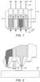
- FIG. 1is a schematic representation of a print head used to print and fabricate an electronic circuit board and components.
- the print headcomprises the following features: an electronic logic system and X,Y drive system 101 , pressure control units and drive units 102 , pressure extension arm 103 , a pressure extension arm stop and empty sensor 104 , a piston for the material pressure cylinder 105 , a pressure cylinder 106 , an optical positioning and print inspection sensor 107 , a material curing energy source 108 , a height sensing, precision material dispensing nozzle 109 and a dispenser 110 .
- the main body of the print head mechanismincludes some or all of the electronics needed to control the units for dispensing and curing the materials to be deposited and location sensors for the drive system to control its X, Y and Z location.
- the main body of the print headalso holds the dispenser 110 that stores and deposits the material onto the substrate.
- the dispensercomprises the removable pressure control units and drive 102 , the pressure extension arm 103 , the pressure extension arm stop and empty sensor 104 , the material pressure cylinder 105 and the pressure cylinder 106 .
- the removable pressure control units and drive 102control the amount of pressure that is put on the pressure extension arm 103 .
- the pressure control units and drive 102may use one or more means to apply the required force to the pressure extension arm 103 ; this may include a screw mechanism, a stepper motor drive assembly, a piezoelectric motor, a hydraulic mechanism, air pressure, or other methods known in the art.
- the pressure extension arm stop and empty sensor 104provide an absolute stop for the pressure extension arm 103 and a proximity sensor that indicates the volume of material in the dispenser and the rate at which it is being dispensed. This ensures precise control over the rate of material flow.
- the piston for the material pressure cylinder 105provides a sensor controlled pressure on the material in the pressure cylinder 106 which contains the material being used in the construction of the electronic circuit and components. The sensor in the piston for the material pressure cylinder 105 continually feeds back information to the print head control system, to adjust the flow of material to the height sensing, precision material dispensing nozzle 109 .
- the pressure cylinder 106is a pressurized container that is designed not to expand and contract to any appreciable degree as the piston for the material pressure cylinder 105 adjusts for optimum material flow during the dispensing of the material.
- the material contained within the pressure cylinder 106can be automatically replenished using a continual feed controlled by a pressure valve and digital or analogue sensor.
- the optical positioning and print inspection sensor 107includes an optical sensor that is designed to read high precision print registration marks that are laid down at the beginning of the print job onto the build platform and/or on the print job itself. This sensor is also used to inspect specified areas of the print job during construction. This action will help to ensure that functionally critical sections of the print are of sufficient quality, specifically for items that are in the very small e.g. micron or nanometre size range.
- the optical positioning and print inspection sensor 107operates by recognizing lines and marks that have been included, by the user, as part of the print area.
- the systemis not limited to this method and may include the ability to read optical codes such as QR style codes.
- the material curing energy source 108may comprise a plurality of light and heat sources, placed on the print head so as to cure the material as it is being laid down in the fabrication process.
- the material curing energy source 108can be made up of IR, UV, or other frequency of light emitting diodes, directed heating elements including hot air, radio frequency, sonic directed frequency and/or any other curing methods known in the art.
- the height sensing, precision material dispensing nozzle 109is a nozzle system that can adjust its height so that the nozzle 109 cannot damage the printed material as it is being laid down.
- the nozzlesare moved up and down to provide clearance above the substrate as the print head is moved rapidly around the print area.
- the nozzles 109are also used to define the height of layers to be printed, ensuring that the correct amount of material is laid down. This is achieved by moving the dispensing nozzle 109 into position and lowering it to define the height of the material after curing. In the event that the material is not of the required thickness, more material can be added or the height of the dispensing nozzle can be adjusted for the next layer. This is specifically useful with a material that will change its volume during curing.
- the operation of the print headmay be controlled by a design application (e.g. a software application) that enables the inputting of 3-dimensional drawing data that configure the movement of the print head and how it deposits material.
- the input datarepresents the circuit and component designs the user wishes to fabricate.
- Feedback from the optical positioning and print inspection sensors 107may be delivered to the software application, which enables the print head to alter its velocity as it moves across the substrate. This interaction between the optical positioning and print inspector sensors 107 and the software application helps the print head determine, both optically and dimensionally, whether the print fabrication is being undertaken correctly.
- FIGS. 2 and 3are schematic representations of the processes undertaken by the print head, of an embodiment similar to that of FIG. 1 , to print and cure the material as it is deposited on a substrate.
- FIG. 2illustrates a print head, as described by FIG. 1 , further incorporating a retractable nozzle to dispense the material.
- FIG. 2comprises a retractable nozzle 109 , the material 202 being dispensed by the nozzle 109 , an energy source 203 used to cure the material being dispensed, and the platform or substrate 204 that the material 202 is being dispensed upon.
- FIG. 3represents the next stage of the printing and curing process, wherein an additional nozzle 109 ′ dispenses another layer of material 202 ′ onto the substrate 204 .
- the retractable nozzle 109is lowered to the required height for the desired level of material to be dispensed and then the print head is moved as material is forced through the nozzle 109 , therefore printing the desired circuit configuration.
- the speed of the print head movementis dependent on the type of material to be dispensed. These parameters are set by the design for the electronic circuit, through the software application.
- the material dispensed by the nozzle 109may be printed onto the build platform, a preloaded substrate, or a pre-printed material that is present on the build platform prior to the build platform being loaded.
- the material being dispensed by the nozzle 109is then cured by a source of energy 203 .
- This source of energyis as described in FIG. 1 .
- the build platform 204 that the material is being dispensed on tois a level platform designed to provide a stable print bed for the construction of the printed unit.
- the build platform 204may be heated and cooled depending on the material being printed.
- the build platform 204may be vibrated to ensure the correct distribution of some materials that are being printed.
- the first retractable nozzle 109is then retracted and the second retractable nozzle 109 ′ is then extended.
- the order of retraction and extension of the nozzleswill depend on the material to be printed.
- the next layer of material to be dispensed by the next nozzle 109 ′is then dispensed over of the material dispensed by the retractable nozzle 109 .
- the print headis moved as material is forced through the nozzle. The speed of the print head movement is dependent on the type of material to be dispensed.
- the build platform 204 heightis then adjusted to account for the new layer position.
- retractable and height sensor nozzle 109 , 109 ′One of the advantages of the retractable and height sensor nozzle 109 , 109 ′ is that in the case of printed electronic components, not all of the material will be laid down at the same height. As different materials cross other materials that have already been laid down, the height of the material will dynamically change.
- the source of energy 203 used to cure the material dispensedis then energized to cure the second material 202 ′.
- the build platform 204is adjusted along with the position of the print head and the material 202 ′ and the retractable nozzle 109 ′.
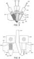
- FIG. 4is a schematic cross sectional diagram illustrating the print head apparatus, as described with reference to FIGS. 1 , 2 and 3 , used to print the electronic circuit boards and components.
- FIG. 4illustrates a print head apparatus comprising: a casing 401 of the print head, a source of energy 402 that is used to cure the material dispensed, an alternative source of energy 403 to the first source of energy used to cure the material dispensed, a further alternative energy source 404 used to cure the material dispensed, a container for the material to be dispensed and the retractable dispenser unit 405 that dispenses the material at the correct speed, width and depth, a digital camera and automatically focused optics system 406 , a pin sensor array 407 for sensing the electrical contact and/or the depth of the material dispensed, a laser diode 408 for rapid heating or ablating of material and an additional laser diode 409 of an alternative frequency.
- the casing 401 of the print headis designed to be rigid and removable to enable easy maintenance.
- the casingnot only holds the material dispensing nozzles 109 , 109 ′, a curing system, that includes a sintering system, and sensors, but also holds the positioning control electronics and optical positioning apparatus 107 .
- the sources of energy 402 , 403 , 404 used to cure the material dispensed from the material containermay be as described in FIGS. 1 , 2 , and 3 , or any other source of directed energy that is known in the art.
- the material container 405is located between the sources of energy 402 , 403 , 404 and protects the material inside the container from being affected by the energy source before it is dispensed.
- FIG. 5is a schematic illustration of a print head, similar to that disclosed in the embodiments of FIGS. 1 to 3 .
- FIG. 5shows a binary print head comprising: an electronic logic system and X,Y drive system 501 , pressure control units 502 , a pressure extension arm 503 , a pressure extension arm stop and empty sensor 504 , a piston for the material pressure cylinder 505 , a pressure cylinder 506 , an optical positioning and print inspection sensor 507 , a material curing energy source 508 and a height sensing, precision material dispensing nozzle 509 .
- the functionality of the binary print headis the same as described in FIGS. 1 , 2 and 3 with the exception of the locations of the pressure cylinders 506 and the height sensing, precision material dispensing nozzles 509 .
- the height sensing, precision material dispensing nozzles of FIG. 5are grouped together so that material can be dispensed from different nozzles 509 at or around substantially the same point. This allows different materials to be combined at the point of dispensing, so as to create a mixture or to react together. For example, one material may act as a hardener for another material. The materials may be mixed or reacted together in precisely controlled quantities.
- FIG. 6is a schematic representation of a material extruder and milling print head that is capable of being used in conjunction with the print head of the preceding embodiments.
- FIG. 6illustrates a material extruder and milling print head comprising: an electronic logic system and X,Y drive system 601 , a material curing energy source 602 , a variable size extruder nozzle 603 , a heating element for the material extruder 604 , a material feed and pressure sensor system 605 , a digital variable drive system for the retractable milling head 606 , a fast change milling tool grip that holds the tool 607 , a milling tool 608 , an optical positioning and print inspection sensor 609 , a flexible milled material vacuum tube 610 and a vacuum nozzle for the removal of milled material 611 .
- the print head depicted in FIG. 6has positioning system 601 and material curing system 602 , as described in FIGS. 1 , 2 , and 3 , so that the heads described throughout this document can be interchanged for use on a single print platform.
- the variable size extruder nozzle 603is a heated extruder nozzle that can be changed to adjust the size of the material as it is being distanced.
- the heating element for the material extruder 604heats up the material as it is being pushed though the material feed and pressure sensor system 605 , forcing it through the variable size extruder nozzle 603 .
- the digital variable drive system for the retractable milling head 606is a precisely controlled drive system that controls speed, drive resistance, and height of the milling tool 608 .
- the fast change milling tool grip 607that holds the milling tool 608 , is designed to enable automatic selection of milling tools by moving to a location in the system that contains one or more milling tools, or by the manual changing of the tool by hand.
- the optical positioning and print inspection sensoris as described in FIGS. 1 , 2 , and 3 .
- the flexible milled material vacuum tube 610 , and the nozzle 611removes excess material from the part as it is being milled and deposits it in a sealed container for recycling.
- FIG. 7is a schematic representation of the apparatus used to fabricate the electronic circuit board and components, using print head embodiments as described in FIGS. 1 to 6 .
- FIG. 7is an illustration of the apparatus comprising: a print head 701 arrangement that can be configured by any of the print heads disclosed in this specification, a drive mechanism 702 that moves the print head in the X and Y direction, a build platform 703 , a drive mechanism 704 that moves the build platform in the Z direction and an environmentally controlled build cabinet 705 .
- the print head 701 of FIG. 7is only one of the print head configurations that can be used in this system, and is only shown in the drawing as an illustration. Any of the print heads described in this document may be designed to be interchangeable depending on the item to be made.
- the print heads that are described hereinare parts of embodiments of the invention, but other embodiments do not preclude the inclusion of other print head and material dispensing systems. Other print systems such as aerosol, inkjet and laser cured resin could also be integrated into the fabrication system, in alternative embodiments of the invention.
- the drive mechanism 702 that moves the print head in the X and Y directionis designed to provide smooth transition from left to right and back and forth.
- the build platform 703is self-levelling, and may be heated or cooled, depending on the conditions required by the materials.
- the build platformcan also vibrate to ensure even distribution of materials, as the material can be agitated into position.
- the build platform being configured to vibratealso ensures that the materials are deposited in even levels and layers.
- the drive mechanism 704 that moves the build platform in the Z directionpositions the build platform at the correct height during the build process.
- the environmentally controlled build cabinet 705ensures that the build environment is clean and climate controlled. In specific cases the cabinet may activate gas removal and air filtration systems so that the build environment is suitable for the specific type of material being deposited and those materials that may be affected by normal atmospheric conditions.
- FIG. 8is a schematic representation of an inline rapid fabrication unit, that uses the print head embodiments as described in FIGS. 1 to 4 to fabricate electronic circuits and components.
- FIG. 8is an illustration of the apparatus comprising: a print head 801 arrangement that can be configured by any of the print heads disclosed in FIGS. 1 to 4 , a drive mechanism 802 that moves the print head in the X and Y direction, a vacuum build platform 803 , a drive mechanism 804 that moves the build platform in the Z direction, an environmentally controlled build cabinet 805 , a retractable build substrate tensioning mechanism 806 and a build plate with retractable build substrate tensioning mechanism 808 .
- the rapid fabrication unit illustrated in FIG. 8is predominantly the same as the system described in FIG. 7 , with the exception that the feed system for the substrate is automatic and specifically suited for the production of flexible printed circuits.
- the print head 801is similar to that described in FIGS. 1 , 2 , 3 , and 4 .
- the drive mechanism 802that moves the print head in the X and Y direction, is as described in FIG. 7 .
- the vacuum build platform 803is designed to hold the substrate flat and in position as the material is deposited. The vacuum build platform may vibrate to ensure the even distribution of the deposited materials.
- the drive mechanism 804 which moves the build platform in the Z directionis as described in FIG. 7 .
- the environmentally controlled build cabinet 805is as described in FIG. 7 .
- the retractable build substrate tensioning mechanism 806moves the substrate in and out of the fabrication environment. The rollers may retract to enable tall components that have been fabricated on the printer circuit to pass through without damage.
- the build plate retractable build substrate tensioning mechanism 807provides tension to the substrate before the vacuum is activated. This ensures the flexible substrate is flat.
- FIG. 9is a schematic representation of a further embodiment of the inline rapid fabrication unit described in FIG. 8 , wherein the print head apparatus is configured as in FIGS. 1 to 6 .
- the inline rapid fabrication unit as illustrated in FIG. 9comprises: a print head 901 as in the embodiments described in FIGS.
- a drive mechanism 902that moves the print head in the X and Y direction
- a vertical drive mechanism 903that control the height of each corner of the build platform and thereby may control the angle of the build platform
- a vertical drive mechanism 904a joint 905 that enables the build platform to be raised at an angle
- vertical drive mechanism motors 906a revolving build platform 907
- a sensorthat detects the position of the revolving platform 908 and a drive mechanism 909 for the revolving platform.
- the inline rapid fabrication unituses a print head as described in any of FIGS. 1 , 2 , 3 , 4 , 5 and 6 which may be interchangeable, where the print head selection will depend on the component to be fabricated.
- the drive mechanism that moves the print head in the X and Y directionis as described in FIGS. 7 and 8 .
- the build platform 907is a revolving platform that is controlled by a drive system 909 , with the height and the angle of the build platform also being controlled in 3-dimensional space by the four drive units 906 .
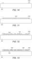
- FIGS. 10 to 18illustrate the processes undertaken by the previous embodiments to create a multi-layered electronic circuit board and components.
- the print head apparatus of the previous embodimentsenables the fabrication of multi-layered electronic circuit boards and components by adding layers of materials, deposited via the nozzle arrangement of the print heads discussed, to a substrate and sequentially depositing and curing the desired material to build up the desired electronic circuitry.
- Componentscan be fabricated by controlled deposition of material, in specific areas and configurations, upon the substrate or previously deposited layers.
- the electronic circuitwould have already been printed using the fabrication methods described in this application.
- the contact and first platewould be printed, utilising the print layering method described in FIGS. 10 to 18 , then the dielectric would be printed over the top of this layer, thus enclosing the first plate.
- the second platewould then be printed over the previously printed capacitor layers, thus connecting the second plate to the other portions of the capacitor and the correct connection point on the electronic circuitry.
- FIG. 10represents the initial stage in the process of fabricating the circuit and components.
- FIG. 10represents the stage where the build platform or substrate 1001 has had a support material 1002 deposited upon the surface, this material being deposited using the print head apparatus as described in the previous embodiments.
- the support materialscan be any material used in the fabrication of the electronic circuit and component. They are printed with the purpose of supporting or holding up a structure or layer before the curing process. The support material only remains in place while the specific layer or component requires support, after which time the support material is removed and discarded. In the case of a layer or component overhanging the substrate, the support material is printed from the same material as that of the layer or component that overhangs.
- FIG. 11illustrates the next step in the process of fabricating the electronic circuit board and components, wherein the first layer of the printed circuit board 1003 is deposited upon the build platform, this layer also being deposited using the previously described print head embodiments.
- FIG. 12shows the stage where materials representing the conductive sections of the first layer of the circuit board and the connections that will connect the next layer 1004 are printed onto the preceding layers using any of the print head embodiments described in the specification.
- FIG. 13is a schematic illustration of the next stage in the fabrication process.
- FIG. 13represents the printing of the second layer of material 1005 being printed onto and over the substrate 1001 and first layer 1003 .
- FIG. 14is a schematic representation of the next stage in the process of fabrication of an electronic circuit board and component.
- FIG. 14is a representation building on the embodiment of FIG. 13 , where the conductive sections of the second layer 1005 of the multi-layered circuit board and the connections that will connect to the next layer 1006 are printed onto the surface of the build platform 1 .
- FIG. 15is a schematic representation of the next stage in the process of fabricating the electronic circuit board and component.
- FIG. 15is an illustrative representation indicating the printing of a third layer 1007 onto the preceding first and second layers 1003 , 1005 .
- FIG. 16is a schematic representation of the next stage in the process of fabricating an electronic circuit board and component.
- FIG. 16illustrates the depositing of the conductive sections of the third layer of the multi-layered circuit board and the connections that will connect the next layer 1008 .
- FIG. 17is a schematic representation of the next stage in fabricating an electronic circuit board and component.
- FIG. 17illustrates the printing of a fourth layer 1009 onto the previous layers as described in the FIGS. 10 to 16 .
- FIG. 18is a schematic representation of the finished electronic circuit board and components.
- FIG. 19represents a schematic representation of an electronic component fabricated using the print head and processes of any of the previous embodiments, the component comprising a negatively doped material 1101 , a positively doped material 1102 and a liquid, gel, powder or solid material 1103 that may be a dielectric, electrolyte, coolant and/or magnetic material or other such material known in the art.
- FIG. 19describes a method of constructing a device such as a battery, capacitor or other such devices by constructing the negatively charged sections 1101 of the device with material using the printing methods as described in FIGS. 1 to 17 , and positively charged sections 1102 of the device with material using the printing methods as described in FIGS. 1 to 17 , and then the dispensing of material 1103 , which could take the form of a liquid, gel, powder or solid and can be dispensed in the constructed container before it is then sealed by the methods described in FIGS. 1 to 18 .
- the componentis printed by a method as described by the previous embodiments, yet leaving a hole and cavities for the material 1103 to occupy.
- the material 1103is then injected, by a dispensing nozzle as described in the previous embodiments, through the hole left by the incomplete fabrication process. Once this has been undertaken the component is subjected to the final fabrication of a layer of material printed over the hole. Once this has been completed the component is cured, sealing the dielectric or electrolyte material 1103 in the component. If the material 1103 is a functional part of the electronic circuit, the material 1103 may electrically contact the remaining portions of the electronic circuit.
- liquids, gels, powders and solid dielectric or electrolyte materials 1103are advantageous because components that require liquids for their electrical function can be fabricated without the need for additional fabrication or manufacturing processing steps.
- the curing system described abovemay comprise a photonic curing system, such as a high energy broad spectrum curing system.
- the systemmay produce rapid pulses of high energy to cure materials without affecting the underlying substrate, which may be thermally sensitive.
- Such high energy pulsescan improve conductivity of electric circuits and densify inorganic materials into working electronic components such as varistors, transistors or other such components known to the art. This energy may be spread over a wide area or highly focused.
- the stages as illustrated in FIGS. 20 to 40describe the processes undertaken to fabricate 3-dimensional structures that can have their colour changed as they are fabricated.
- the materialis printed in layers, as in the layering process as described in FIGS. 10 to 18 , with each material being printed as a single base colour with a colour change material mixed into it.
- This base colouris printed onto the substrate and cured with an energy source, which is used to activate the colour change material within the base colour material.
- the energy sourcecan be directed to specific areas of the substrate, so as to change the colour of specific areas. As the intensity and duration of the exposure to the energy source increase, the more the colour change material is activated and with this the colour changes from magenta, to cyan, to yellow to black.
- the colour change materialmay be colourless or one single colour that when subjected to radiation of a specific type, changes to another colour.
- a plurality of different binary colour change materialsmay be laid down together and then colour-changed to produce many colour effects.
Landscapes
- Engineering & Computer Science (AREA)
- Manufacturing & Machinery (AREA)
- Chemical & Material Sciences (AREA)
- Materials Engineering (AREA)
- Microelectronics & Electronic Packaging (AREA)
- Physics & Mathematics (AREA)
- Mechanical Engineering (AREA)
- Optics & Photonics (AREA)
Abstract
Description
Claims (15)
Applications Claiming Priority (4)
| Application Number | Priority Date | Filing Date | Title |
|---|---|---|---|
| GB1508585 | 2015-05-19 | ||
| GB1508585.5 | 2015-05-19 | ||
| GB1508585.5AGB2538522B (en) | 2015-05-19 | 2015-05-19 | Electronic circuit and component construction |
| PCT/GB2016/051445WO2016185215A1 (en) | 2015-05-19 | 2016-05-19 | A circuit board and component fabrication apparatus |
Publications (2)
| Publication Number | Publication Date |
|---|---|
| US20180154573A1 US20180154573A1 (en) | 2018-06-07 |
| US11919227B2true US11919227B2 (en) | 2024-03-05 |
Family
ID=53506015
Family Applications (1)
| Application Number | Title | Priority Date | Filing Date |
|---|---|---|---|
| US15/575,071Active2037-12-31US11919227B2 (en) | 2015-05-19 | 2016-05-19 | Circuit board and component fabrication apparatus |
Country Status (4)
| Country | Link |
|---|---|
| US (1) | US11919227B2 (en) |
| EP (1) | EP3298865A1 (en) |
| GB (1) | GB2538522B (en) |
| WO (1) | WO2016185215A1 (en) |
Families Citing this family (42)
| Publication number | Priority date | Publication date | Assignee | Title |
|---|---|---|---|---|
| KR102787541B1 (en) | 2015-06-04 | 2025-03-26 | 카티바, 인크. | Methods for producing an etch resist pattern on a metallic surface |
| WO2017025949A1 (en) | 2015-08-13 | 2017-02-16 | Jet Cu Pcb Ltd. | Methods for producing an etch resist pattern on a metallic surface |
| US10394202B2 (en)* | 2015-08-21 | 2019-08-27 | Voxel8, Inc. | 3D printer calibration and control |
| JP2017133055A (en)* | 2016-01-26 | 2017-08-03 | セイコーエプソン株式会社 | Three-dimensional manufacturing method of functional element structure and functional element structure |
| US10287218B2 (en)* | 2016-08-09 | 2019-05-14 | Raytheon Company | Solid propellant additive manufacturing method and system |
| CN106626358B (en)* | 2016-12-07 | 2019-08-06 | 上海交通大学 | A kind of multi-material 3D printer and liquid object accumulation 3D printing method |
| US10398034B2 (en) | 2016-12-12 | 2019-08-27 | Kateeva, Inc. | Methods of etching conductive features, and related devices and systems |
| WO2018136036A1 (en)* | 2017-01-17 | 2018-07-26 | Hewlett-Packard Development Company, L.P. | Multi-layered printed circuit board |
| US11123895B2 (en)* | 2017-01-27 | 2021-09-21 | The Boeing Company | Apparatus for extruding ceramic slurry |
| NL2018455B1 (en)* | 2017-03-02 | 2018-09-21 | Bond High Performance 3D Tech B V | Three-dimensional modeling system and method |
| NL2018720B1 (en)* | 2017-04-14 | 2018-10-24 | Bond High Performance 3D Tech B V | Three-dimensional modeling method and system |
| AU2018267821B2 (en) | 2017-05-16 | 2023-01-12 | Triastek, Inc. | 3D printing device and method |
| CN107127972B (en)* | 2017-07-05 | 2019-09-10 | 华明进 | Continuous fiber reinforced composite materials increasing material manufacturing spray head and printer |
| EP3468311B1 (en) | 2017-10-06 | 2023-08-23 | AT & S Austria Technologie & Systemtechnik Aktiengesellschaft | Metal body formed on a component carrier by additive manufacturing |
| DE102017123307A1 (en)* | 2017-10-06 | 2019-04-11 | At & S Austria Technologie & Systemtechnik Aktiengesellschaft | Component carrier with at least one part formed as a three-dimensional printed structure |
| EP3468312B1 (en) | 2017-10-06 | 2023-11-29 | AT & S Austria Technologie & Systemtechnik Aktiengesellschaft | Method of manufacturing a component carrier having a three dimensionally printed wiring structure |
| FR3075313A1 (en)* | 2017-12-18 | 2019-06-21 | Blachere Illumination | METHOD AND SYSTEM FOR MANUFACTURING LUMINOUS DECORATION |
| US10201503B1 (en) | 2018-01-09 | 2019-02-12 | Triastek, Inc. | Precision pharmaceutical 3D printing device |
| US10751934B2 (en)* | 2018-02-01 | 2020-08-25 | Divergent Technologies, Inc. | Apparatus and methods for additive manufacturing with variable extruder profiles |
| US11338501B2 (en)* | 2018-04-03 | 2022-05-24 | University Of Massachusetts | Fabrication of circuit elements using additive techniques |
| GB2578713A (en)* | 2018-04-05 | 2020-05-27 | Rd Holdings Ltd | 3D printer |
| WO2020012626A1 (en)* | 2018-07-13 | 2020-01-16 | 株式会社Fuji | Circuit formation method and circuit formation device |
| CN112867597A (en)* | 2018-09-26 | 2021-05-28 | 阿肯色州立大学托管会 | Resin extrusion printing head for 3D printing |
| EP3650529A1 (en)* | 2018-11-09 | 2020-05-13 | Sartorius Stedim FMT SAS | Single-use container with 3d printed functional element, printing method therefor and assembly |
| CN109732900B (en)* | 2019-03-18 | 2023-10-20 | 青岛五维智造科技有限公司 | 3D printing device for integrally manufacturing stretchable electronic product and working method |
| CN110614767B (en)* | 2019-08-16 | 2024-02-20 | 华南理工大学 | Solid-liquid material combined type double-nozzle 3D printer and printing method thereof |
| US11458684B2 (en) | 2020-07-30 | 2022-10-04 | Triastek, Inc. | High-throughput and high-precision pharmaceutical additive manufacturing system |
| US12384112B2 (en) | 2019-08-20 | 2025-08-12 | Triastek, Inc. | High-throughput and high-precision pharmaceutical additive manufacturing system |
| EP4302998A3 (en) | 2019-08-20 | 2024-03-13 | Triastek, Inc. | Method and system for creating pharamceutical products by additive manufacturing |
| NL1043468B1 (en)* | 2019-11-19 | 2021-08-17 | Veda Group B.V. | Method, 3d manufacturing system and print head therfor |
| NL1043470B1 (en)* | 2019-11-19 | 2021-08-18 | Veda Group B V | Method, 3d manufacturing system and print head therfor |
| NL1043469B1 (en)* | 2019-11-19 | 2021-08-11 | Veda Group B V | Method, 3d manufacturing system and print head therfor |
| US11465354B2 (en)* | 2020-01-06 | 2022-10-11 | The Boeing Company | Fabrication of additive manufacturing parts |
| CN115397652A (en) | 2020-02-17 | 2022-11-25 | 南京三迭纪医药科技有限公司 | Continuous blanking and packaging system for medicine additive manufacturing |
| JP7316742B2 (en)* | 2020-03-11 | 2023-07-28 | 株式会社Fuji | Manufacturing method of mounting board by 3D additive manufacturing |
| WO2021226531A2 (en)* | 2020-05-08 | 2021-11-11 | Grid Logic Incorporated | System and method for manufacturing a part |
| CN111823575A (en)* | 2020-06-30 | 2020-10-27 | 东南大学 | A multifunctional 3D printer |
| CN118769539A (en) | 2020-07-10 | 2024-10-15 | 南京三迭纪医药科技有限公司 | High-precision additive manufacturing devices and high-throughput additive manufacturing systems |
| DE102021208882A1 (en) | 2021-08-13 | 2023-02-16 | Fraunhofer-Gesellschaft zur Förderung der angewandten Forschung eingetragener Verein | Device and method for forming functional elements on and/or in components |
| JP2023035380A (en)* | 2021-09-01 | 2023-03-13 | セイコーエプソン株式会社 | Three-dimensional object printing apparatus |
| CN114269087B (en)* | 2022-03-03 | 2022-07-12 | 芯体素(杭州)科技发展有限公司 | High-precision machining device based on multilayer circuit manufacturing |
| US20240383207A1 (en)* | 2022-03-03 | 2024-11-21 | Enovate3D (Hangzhou) Technology Development Co., Ltd. | Printing device and method for led retaining wall of display panel |
Citations (18)
| Publication number | Priority date | Publication date | Assignee | Title |
|---|---|---|---|---|
| WO1999019900A2 (en) | 1997-10-14 | 1999-04-22 | Patterning Technologies Limited | Method of forming an electronic device |
| EP1080889A2 (en) | 1999-09-06 | 2001-03-07 | FUJI MACHINE Mfg. Co., Ltd. | Method and apparatus fpr controlling pressure applied to printing material |
| WO2002001929A2 (en) | 2000-06-29 | 2002-01-03 | Printar Ltd. | Jet print apparatus and method for printed circuit board manufacturing |
| US20020051853A1 (en) | 1998-01-22 | 2002-05-02 | Keicher David M. | Multiple beams and nozzles to increase deposition rate |
| US6401001B1 (en) | 1999-07-22 | 2002-06-04 | Nanotek Instruments, Inc. | Layer manufacturing using deposition of fused droplets |
| US20040140549A1 (en) | 2002-03-28 | 2004-07-22 | Fumio Miyagawa | Wiring structure and its manufacturing method |
| US20070179656A1 (en)* | 2003-05-01 | 2007-08-02 | David Eshed | Rapid prototyping apparatus |
| WO2008102266A2 (en) | 2007-02-23 | 2008-08-28 | Infermata Systems Ltd. | Method and apparatus for rapid fabrication of functional printed circuit board |
| WO2011006641A1 (en) | 2009-07-15 | 2011-01-20 | Stichting Dutch Polymer Institute | Method for generating photonically treated printed structures on surfaces, apparatus, and use thereof |
| US20130170171A1 (en) | 2012-01-04 | 2013-07-04 | Board Of Regents, The University Of Texas System | Extrusion-based additive manufacturing system for 3d structural electronic, electromagnetic and electromechanical components/devices |
| US20130193619A1 (en) | 2012-02-01 | 2013-08-01 | Nscrypt, Inc. | Micro-dispensing multi-layered 3d objects with curing steps |
| US20130344232A1 (en) | 2012-06-22 | 2013-12-26 | Xerox Corporation | Methods of forming conductive features on three-dimensional objects |
| US20140061974A1 (en)* | 2012-08-29 | 2014-03-06 | Kenneth Tyler | Method and apparatus for continuous composite three-dimensional printing |
| CN103817942A (en) | 2014-03-19 | 2014-05-28 | 昆山博力迈三维打印科技有限公司 | Digital material 3D (Three Dimensional) printing head |
| US20140328963A1 (en)* | 2013-03-22 | 2014-11-06 | Markforged, Inc. | Apparatus for fiber reinforced additive manufacturing |
| US20150035186A1 (en) | 2012-03-04 | 2015-02-05 | Stratasys Ltd. | System and method for depositing liquids |
| US20150064047A1 (en) | 2013-08-28 | 2015-03-05 | Elwha Llc | Systems and methods for additive manufacturing of three dimensional structures |
| US20150077215A1 (en) | 2012-04-26 | 2015-03-19 | Northeastern University | Device and Method to Additively Fabricate Structures Containing Embedded Electronics or Sensors |
- 2015
- 2015-05-19GBGB1508585.5Apatent/GB2538522B/enactiveActive
- 2016
- 2016-05-19WOPCT/GB2016/051445patent/WO2016185215A1/ennot_activeCeased
- 2016-05-19USUS15/575,071patent/US11919227B2/enactiveActive
- 2016-05-19EPEP16731629.8Apatent/EP3298865A1/ennot_activeWithdrawn
Patent Citations (18)
| Publication number | Priority date | Publication date | Assignee | Title |
|---|---|---|---|---|
| WO1999019900A2 (en) | 1997-10-14 | 1999-04-22 | Patterning Technologies Limited | Method of forming an electronic device |
| US20020051853A1 (en) | 1998-01-22 | 2002-05-02 | Keicher David M. | Multiple beams and nozzles to increase deposition rate |
| US6401001B1 (en) | 1999-07-22 | 2002-06-04 | Nanotek Instruments, Inc. | Layer manufacturing using deposition of fused droplets |
| EP1080889A2 (en) | 1999-09-06 | 2001-03-07 | FUJI MACHINE Mfg. Co., Ltd. | Method and apparatus fpr controlling pressure applied to printing material |
| WO2002001929A2 (en) | 2000-06-29 | 2002-01-03 | Printar Ltd. | Jet print apparatus and method for printed circuit board manufacturing |
| US20040140549A1 (en) | 2002-03-28 | 2004-07-22 | Fumio Miyagawa | Wiring structure and its manufacturing method |
| US20070179656A1 (en)* | 2003-05-01 | 2007-08-02 | David Eshed | Rapid prototyping apparatus |
| WO2008102266A2 (en) | 2007-02-23 | 2008-08-28 | Infermata Systems Ltd. | Method and apparatus for rapid fabrication of functional printed circuit board |
| WO2011006641A1 (en) | 2009-07-15 | 2011-01-20 | Stichting Dutch Polymer Institute | Method for generating photonically treated printed structures on surfaces, apparatus, and use thereof |
| US20130170171A1 (en) | 2012-01-04 | 2013-07-04 | Board Of Regents, The University Of Texas System | Extrusion-based additive manufacturing system for 3d structural electronic, electromagnetic and electromechanical components/devices |
| US20130193619A1 (en) | 2012-02-01 | 2013-08-01 | Nscrypt, Inc. | Micro-dispensing multi-layered 3d objects with curing steps |
| US20150035186A1 (en) | 2012-03-04 | 2015-02-05 | Stratasys Ltd. | System and method for depositing liquids |
| US20150077215A1 (en) | 2012-04-26 | 2015-03-19 | Northeastern University | Device and Method to Additively Fabricate Structures Containing Embedded Electronics or Sensors |
| US20130344232A1 (en) | 2012-06-22 | 2013-12-26 | Xerox Corporation | Methods of forming conductive features on three-dimensional objects |
| US20140061974A1 (en)* | 2012-08-29 | 2014-03-06 | Kenneth Tyler | Method and apparatus for continuous composite three-dimensional printing |
| US20140328963A1 (en)* | 2013-03-22 | 2014-11-06 | Markforged, Inc. | Apparatus for fiber reinforced additive manufacturing |
| US20150064047A1 (en) | 2013-08-28 | 2015-03-05 | Elwha Llc | Systems and methods for additive manufacturing of three dimensional structures |
| CN103817942A (en) | 2014-03-19 | 2014-05-28 | 昆山博力迈三维打印科技有限公司 | Digital material 3D (Three Dimensional) printing head |
Non-Patent Citations (19)
| Title |
|---|
| "3D Printed Electronics—‘Manufacturing Systems’ and ‘Applications’," Neotech AMT GmbH, archived webpages on Jan. 24, 2015, <https://web.archive.org/web/20150124193918/http://www.neotech-amt.com/3d-printed-electronics-manufacturing-systems/> and <https://web.archive.org/web/20150124072012/http://www.neotech-amt.com/3d-printed-electronics-applications/> (4 pages). |
| "Advanced Manufacturing Technologies for 3D Printed Electronics," Neotech AMT GmbH, archived webpages on Jan. 23, 2015, <https://web.archive.org/web/20150123065759/http://www.neotech-amt.com/> and <https://web.archive.org/web/20150123065805/http://www.neotech-amt.com/3d-printed-electronics-technology/> (3 pages). |
| "Aerosol Jet Technology for 3D Printed Electronics," Optomec, 2017 website <https://www.optomec.com/printed-electronics/aerosol-jet-technology/> (7 pages). |
| "Aerosol Jet Technology," Optomec, archived webpage on Feb. 3, 2016, <https://web.archive.org/web/20160203221320/http://www.optomec.com/printed-electronics/aerosol-jet-technology> (4 pages). |
| "Argentum—Make Electronics in Minutes," Cartesian Co., archived website on Mar. 28, 2015, <https://web.archive.org/web/20150328041143/https://www.cartesianco.com/pages/argentum> (6 pages). |
| "Frequently Asked Questions—Voxel8 3D Electronics Printing," Voxel8, archived webpage on Apr. 19, 2015, <https://web.archive.org/web/20150419012937/www.voxel8.co/faq/> (13 pages). |
| "Introducing the DragonFly 2020 Revolutionary 3D Printer for Professional PCB Electronics," Nano Dimension, archived website on Oct. 16, 2015, <https://web.archive.org/web/20151016012330/http://www.nano-di.com/3d-printer> (12 pages). |
| "Optomec to Showcase Advances in 3D Printed Electronics," Nanowerk News, May 21, 2014, <https://www.nanowerk.com/nanotechnology-news/newsid=35686.php> (3 pages). |
| "Tel Aviv Listed ‘Nano Dimension’ developing 3D printer & Nano inks for printing electronics at home," www.3Ders.org, Oct. 3, 2014, <https://www.3ders.org/articles/20141003-tel-aviv-listed-nano-dimension-developing-3d-printer-printing-electronics.html> (7 pages). |
| "The Developer's Kit 3D Printer," Voxel8, archived webpage on Oct. 3, 2016, <https://web.archive.org/web/20161003132436/http://www.voxel8.com/printer> (9 pages). |
| "Voltera 3D Prototyping Printer," Neeraj Tewari, Nov. 10, 2014, <http://neerajtewariit.com/tag/3d-printing> (4 pages). |
| "Voltera's circuit board printer wants to be the ‘Makerbot of electronics’," VentureBeat, Nov. 7, 2014, <https://venturebeat.com/2014/11/07/volteras-circuit-board-printer-wants-to-be-the-makerbot-of-electronics> (3 pages). |
| "Voxel8 announces first new electronics 3D printer, now available for pre-order," www.3Ders.org, Jan. 5, 2015, <http://www.3ders.org/articles/20150105-voxel8-announces-first-new-electronics-3d-printer-now-available-for-pre-order.html> (9 pages). |
| Combined Search and Examination Report dated Jan. 25, 2016, issued in connection with UK Patent Application No. GB 1508585.5 (11 pages). |
| Examination Report dated Apr. 22, 2021, issued in connection with European Patent Application No. EP 16731629.8 (4 pages). |
| Examination Report dated Dec. 1, 2017, issued in connection with UK Patent Application No. GB 1508585.5 (6 pages). |
| International Preliminary Report on Patentability dated Nov. 21, 2017, issued in connection with International Application No. PCT/GB2016/051445 (9 pages). |
| International Search Report of the International Searching Authority dated Sep. 13, 2016, issued in connection with International Application No. PCT/GB2016/051445 (3 pages). |
| Written Opinion of the International Searching Authority dated Sep. 13, 2016, issued in connection with International Application No. PCT/GB2016/051445 (8 pages). |
Also Published As
| Publication number | Publication date |
|---|---|
| GB2538522B (en) | 2019-03-06 |
| WO2016185215A1 (en) | 2016-11-24 |
| GB201508585D0 (en) | 2015-07-01 |
| EP3298865A1 (en) | 2018-03-28 |
| US20180154573A1 (en) | 2018-06-07 |
| GB2538522A (en) | 2016-11-23 |
Similar Documents
| Publication | Publication Date | Title |
|---|---|---|
| US11919227B2 (en) | Circuit board and component fabrication apparatus | |
| Joe Lopes et al. | Integrating stereolithography and direct print technologies for 3D structural electronics fabrication | |
| CN110798994B (en) | Device and method for preparing curved conformal multilayer printed board | |
| US9801276B2 (en) | Methof of forming an integrated composite structure | |
| TWI752163B (en) | Method and apparatus for manufacturing a layer of an electronic product | |
| US10059056B2 (en) | Micro-dispensing multi-layered 3D objects with curing steps | |
| US11420397B2 (en) | Method and system for additive-ablative fabrication | |
| US9969153B2 (en) | Three-dimensional modeling and/or manufacturing apparatus, and related processes | |
| US6471800B2 (en) | Layer-additive method and apparatus for freeform fabrication of 3-D objects | |
| WO2005089090A2 (en) | Direct write and freeform fabrication apparatus and method | |
| US20130180450A1 (en) | Multifunctional manufacturing platform and method of using the same | |
| Lopes et al. | Expanding rapid prototyping for electronic systems integration of arbitrary form | |
| US20040005374A1 (en) | Creating objects through X and Z movement of print heads | |
| US10974467B2 (en) | Enhanced systems that facilitate vacuum bag curing of composite parts | |
| WO2016140909A1 (en) | Embedding apparatus and method utilizing additive manufacturing | |
| AU2005202167A1 (en) | Method of forming structures using drop-on-demand printing | |
| US20210060850A1 (en) | 3d printing to obtain a predefined surface quality | |
| Jang et al. | 3-dimensional circuit device fabrication process using stereolithography and direct writing | |
| Levy et al. | Hybrid structural electronics printing by novel dry film stereolithography and laser induced forward transfer | |
| US10953575B2 (en) | Enhanced systems that facilitate vacuum bag curing of composite parts | |
| KR101628164B1 (en) | 3d printing system using block type structure combined with fdm technology and this hybrid data generation method for 3d printing | |
| CN113784532A (en) | Method for manufacturing electronic components on 3D parts and 3D parts including electronic components | |
| KR102019367B1 (en) | Three-dimensional object | |
| Li et al. | Micro electronic systems via multifunctional additive manufacturing | |
| WO2023112205A1 (en) | Three-dimensional laminate shaping device |
Legal Events
| Date | Code | Title | Description |
|---|---|---|---|
| FEPP | Fee payment procedure | Free format text:ENTITY STATUS SET TO UNDISCOUNTED (ORIGINAL EVENT CODE: BIG.); ENTITY STATUS OF PATENT OWNER: SMALL ENTITY | |
| FEPP | Fee payment procedure | Free format text:ENTITY STATUS SET TO SMALL (ORIGINAL EVENT CODE: SMAL); ENTITY STATUS OF PATENT OWNER: SMALL ENTITY | |
| AS | Assignment | Owner name:DST INNOVATIONS, LTD., UNITED KINGDOM Free format text:ASSIGNMENT OF ASSIGNORS INTEREST;ASSIGNOR:MILES, ANTHONY;REEL/FRAME:044497/0182 Effective date:20171204 | |
| STPP | Information on status: patent application and granting procedure in general | Free format text:DOCKETED NEW CASE - READY FOR EXAMINATION | |
| STPP | Information on status: patent application and granting procedure in general | Free format text:NON FINAL ACTION MAILED | |
| STPP | Information on status: patent application and granting procedure in general | Free format text:RESPONSE TO NON-FINAL OFFICE ACTION ENTERED AND FORWARDED TO EXAMINER | |
| STPP | Information on status: patent application and granting procedure in general | Free format text:NON FINAL ACTION MAILED | |
| STPP | Information on status: patent application and granting procedure in general | Free format text:FINAL REJECTION MAILED | |
| STPP | Information on status: patent application and granting procedure in general | Free format text:NON FINAL ACTION MAILED | |
| STPP | Information on status: patent application and granting procedure in general | Free format text:RESPONSE TO NON-FINAL OFFICE ACTION ENTERED AND FORWARDED TO EXAMINER | |
| STPP | Information on status: patent application and granting procedure in general | Free format text:FINAL REJECTION MAILED | |
| STCV | Information on status: appeal procedure | Free format text:NOTICE OF APPEAL FILED | |
| STCV | Information on status: appeal procedure | Free format text:APPEAL BRIEF (OR SUPPLEMENTAL BRIEF) ENTERED AND FORWARDED TO EXAMINER | |
| STCV | Information on status: appeal procedure | Free format text:EXAMINER'S ANSWER TO APPEAL BRIEF MAILED | |
| STCV | Information on status: appeal procedure | Free format text:ON APPEAL -- AWAITING DECISION BY THE BOARD OF APPEALS | |
| STCV | Information on status: appeal procedure | Free format text:BOARD OF APPEALS DECISION RENDERED | |
| STPP | Information on status: patent application and granting procedure in general | Free format text:NOTICE OF ALLOWANCE MAILED -- APPLICATION RECEIVED IN OFFICE OF PUBLICATIONS | |
| STPP | Information on status: patent application and granting procedure in general | Free format text:PUBLICATIONS -- ISSUE FEE PAYMENT RECEIVED | |
| STPP | Information on status: patent application and granting procedure in general | Free format text:PUBLICATIONS -- ISSUE FEE PAYMENT VERIFIED | |
| STCF | Information on status: patent grant | Free format text:PATENTED CASE |