US11906903B2 - Real time registration in lithography system - Google Patents
Real time registration in lithography systemDownload PDFInfo
- Publication number
- US11906903B2 US11906903B2US17/625,990US202017625990AUS11906903B2US 11906903 B2US11906903 B2US 11906903B2US 202017625990 AUS202017625990 AUS 202017625990AUS 11906903 B2US11906903 B2US 11906903B2
- Authority
- US
- United States
- Prior art keywords
- exposure
- camera
- substrate
- alignment marks
- optical system
- Prior art date
- Legal status (The legal status is an assumption and is not a legal conclusion. Google has not performed a legal analysis and makes no representation as to the accuracy of the status listed.)
- Active
Links
- 238000001459lithographyMethods0.000titledescription29
- 230000003287optical effectEffects0.000claimsabstractdescription38
- 238000005259measurementMethods0.000claimsabstractdescription36
- 239000000758substrateSubstances0.000claimsabstractdescription33
- 238000007639printingMethods0.000claimsabstractdescription15
- 238000000034methodMethods0.000claimsdescription21
- 238000004364calculation methodMethods0.000claimsdescription14
- 238000004458analytical methodMethods0.000claimsdescription5
- 239000011159matrix materialSubstances0.000claimsdescription3
- 238000001514detection methodMethods0.000claimsdescription2
- 238000003384imaging methodMethods0.000description13
- 239000010410layerSubstances0.000description7
- 238000004806packaging method and processMethods0.000description6
- 235000012431wafersNutrition0.000description6
- 239000002390adhesive tapeSubstances0.000description4
- 239000000463materialSubstances0.000description4
- 238000012858packaging processMethods0.000description3
- 238000000059patterningMethods0.000description3
- 150000001875compoundsChemical class0.000description2
- 230000000694effectsEffects0.000description2
- 241000254158LampyridaeSpecies0.000description1
- 239000012790adhesive layerSubstances0.000description1
- 238000003491arrayMethods0.000description1
- KGNDCEVUMONOKF-UGPLYTSKSA-Nbenzyl n-[(2r)-1-[(2s,4r)-2-[[(2s)-6-amino-1-(1,3-benzoxazol-2-yl)-1,1-dihydroxyhexan-2-yl]carbamoyl]-4-[(4-methylphenyl)methoxy]pyrrolidin-1-yl]-1-oxo-4-phenylbutan-2-yl]carbamateChemical compoundC1=CC(C)=CC=C1CO[C@H]1CN(C(=O)[C@@H](CCC=2C=CC=CC=2)NC(=O)OCC=2C=CC=CC=2)[C@H](C(=O)N[C@@H](CCCCN)C(O)(O)C=2OC3=CC=CC=C3N=2)C1KGNDCEVUMONOKF-UGPLYTSKSA-N0.000description1
- 229940125833compound 23Drugs0.000description1
- 239000012141concentrateSubstances0.000description1
- 238000005516engineering processMethods0.000description1
- 238000004519manufacturing processMethods0.000description1
- 238000000465mouldingMethods0.000description1
- 238000005457optimizationMethods0.000description1
- 239000004065semiconductorSubstances0.000description1
Images


Classifications
- G—PHYSICS
- G03—PHOTOGRAPHY; CINEMATOGRAPHY; ANALOGOUS TECHNIQUES USING WAVES OTHER THAN OPTICAL WAVES; ELECTROGRAPHY; HOLOGRAPHY
- G03F—PHOTOMECHANICAL PRODUCTION OF TEXTURED OR PATTERNED SURFACES, e.g. FOR PRINTING, FOR PROCESSING OF SEMICONDUCTOR DEVICES; MATERIALS THEREFOR; ORIGINALS THEREFOR; APPARATUS SPECIALLY ADAPTED THEREFOR
- G03F7/00—Photomechanical, e.g. photolithographic, production of textured or patterned surfaces, e.g. printing surfaces; Materials therefor, e.g. comprising photoresists; Apparatus specially adapted therefor
- G03F7/70—Microphotolithographic exposure; Apparatus therefor
- G03F7/70216—Mask projection systems
- G03F7/70283—Mask effects on the imaging process
- G03F7/70291—Addressable masks, e.g. spatial light modulators [SLMs], digital micro-mirror devices [DMDs] or liquid crystal display [LCD] patterning devices
- G—PHYSICS
- G03—PHOTOGRAPHY; CINEMATOGRAPHY; ANALOGOUS TECHNIQUES USING WAVES OTHER THAN OPTICAL WAVES; ELECTROGRAPHY; HOLOGRAPHY
- G03F—PHOTOMECHANICAL PRODUCTION OF TEXTURED OR PATTERNED SURFACES, e.g. FOR PRINTING, FOR PROCESSING OF SEMICONDUCTOR DEVICES; MATERIALS THEREFOR; ORIGINALS THEREFOR; APPARATUS SPECIALLY ADAPTED THEREFOR
- G03F9/00—Registration or positioning of originals, masks, frames, photographic sheets or textured or patterned surfaces, e.g. automatically
- G03F9/70—Registration or positioning of originals, masks, frames, photographic sheets or textured or patterned surfaces, e.g. automatically for microlithography
- G03F9/7088—Alignment mark detection, e.g. TTR, TTL, off-axis detection, array detector, video detection
- G—PHYSICS
- G03—PHOTOGRAPHY; CINEMATOGRAPHY; ANALOGOUS TECHNIQUES USING WAVES OTHER THAN OPTICAL WAVES; ELECTROGRAPHY; HOLOGRAPHY
- G03F—PHOTOMECHANICAL PRODUCTION OF TEXTURED OR PATTERNED SURFACES, e.g. FOR PRINTING, FOR PROCESSING OF SEMICONDUCTOR DEVICES; MATERIALS THEREFOR; ORIGINALS THEREFOR; APPARATUS SPECIALLY ADAPTED THEREFOR
- G03F7/00—Photomechanical, e.g. photolithographic, production of textured or patterned surfaces, e.g. printing surfaces; Materials therefor, e.g. comprising photoresists; Apparatus specially adapted therefor
- G03F7/70—Microphotolithographic exposure; Apparatus therefor
- G03F7/70058—Mask illumination systems
- G03F7/70133—Measurement of illumination distribution, in pupil plane or field plane
- G—PHYSICS
- G03—PHOTOGRAPHY; CINEMATOGRAPHY; ANALOGOUS TECHNIQUES USING WAVES OTHER THAN OPTICAL WAVES; ELECTROGRAPHY; HOLOGRAPHY
- G03F—PHOTOMECHANICAL PRODUCTION OF TEXTURED OR PATTERNED SURFACES, e.g. FOR PRINTING, FOR PROCESSING OF SEMICONDUCTOR DEVICES; MATERIALS THEREFOR; ORIGINALS THEREFOR; APPARATUS SPECIALLY ADAPTED THEREFOR
- G03F7/00—Photomechanical, e.g. photolithographic, production of textured or patterned surfaces, e.g. printing surfaces; Materials therefor, e.g. comprising photoresists; Apparatus specially adapted therefor
- G03F7/20—Exposure; Apparatus therefor
- G03F7/2051—Exposure without an original mask, e.g. using a programmed deflection of a point source, by scanning, by drawing with a light beam, using an addressed light or corpuscular source
- G03F7/2057—Exposure without an original mask, e.g. using a programmed deflection of a point source, by scanning, by drawing with a light beam, using an addressed light or corpuscular source using an addressed light valve, e.g. a liquid crystal device
- G—PHYSICS
- G03—PHOTOGRAPHY; CINEMATOGRAPHY; ANALOGOUS TECHNIQUES USING WAVES OTHER THAN OPTICAL WAVES; ELECTROGRAPHY; HOLOGRAPHY
- G03F—PHOTOMECHANICAL PRODUCTION OF TEXTURED OR PATTERNED SURFACES, e.g. FOR PRINTING, FOR PROCESSING OF SEMICONDUCTOR DEVICES; MATERIALS THEREFOR; ORIGINALS THEREFOR; APPARATUS SPECIALLY ADAPTED THEREFOR
- G03F7/00—Photomechanical, e.g. photolithographic, production of textured or patterned surfaces, e.g. printing surfaces; Materials therefor, e.g. comprising photoresists; Apparatus specially adapted therefor
- G03F7/70—Microphotolithographic exposure; Apparatus therefor
- G03F7/708—Construction of apparatus, e.g. environment aspects, hygiene aspects or materials
- G03F7/70858—Environment aspects, e.g. pressure of beam-path gas, temperature
- G03F7/70883—Environment aspects, e.g. pressure of beam-path gas, temperature of optical system
- G—PHYSICS
- G03—PHOTOGRAPHY; CINEMATOGRAPHY; ANALOGOUS TECHNIQUES USING WAVES OTHER THAN OPTICAL WAVES; ELECTROGRAPHY; HOLOGRAPHY
- G03F—PHOTOMECHANICAL PRODUCTION OF TEXTURED OR PATTERNED SURFACES, e.g. FOR PRINTING, FOR PROCESSING OF SEMICONDUCTOR DEVICES; MATERIALS THEREFOR; ORIGINALS THEREFOR; APPARATUS SPECIALLY ADAPTED THEREFOR
- G03F7/00—Photomechanical, e.g. photolithographic, production of textured or patterned surfaces, e.g. printing surfaces; Materials therefor, e.g. comprising photoresists; Apparatus specially adapted therefor
- G03F7/20—Exposure; Apparatus therefor
- G—PHYSICS
- G03—PHOTOGRAPHY; CINEMATOGRAPHY; ANALOGOUS TECHNIQUES USING WAVES OTHER THAN OPTICAL WAVES; ELECTROGRAPHY; HOLOGRAPHY
- G03F—PHOTOMECHANICAL PRODUCTION OF TEXTURED OR PATTERNED SURFACES, e.g. FOR PRINTING, FOR PROCESSING OF SEMICONDUCTOR DEVICES; MATERIALS THEREFOR; ORIGINALS THEREFOR; APPARATUS SPECIALLY ADAPTED THEREFOR
- G03F7/00—Photomechanical, e.g. photolithographic, production of textured or patterned surfaces, e.g. printing surfaces; Materials therefor, e.g. comprising photoresists; Apparatus specially adapted therefor
- G03F7/70—Microphotolithographic exposure; Apparatus therefor
- G03F7/70058—Mask illumination systems
- G03F7/70141—Illumination system adjustment, e.g. adjustments during exposure or alignment during assembly of illumination system
- G—PHYSICS
- G03—PHOTOGRAPHY; CINEMATOGRAPHY; ANALOGOUS TECHNIQUES USING WAVES OTHER THAN OPTICAL WAVES; ELECTROGRAPHY; HOLOGRAPHY
- G03F—PHOTOMECHANICAL PRODUCTION OF TEXTURED OR PATTERNED SURFACES, e.g. FOR PRINTING, FOR PROCESSING OF SEMICONDUCTOR DEVICES; MATERIALS THEREFOR; ORIGINALS THEREFOR; APPARATUS SPECIALLY ADAPTED THEREFOR
- G03F7/00—Photomechanical, e.g. photolithographic, production of textured or patterned surfaces, e.g. printing surfaces; Materials therefor, e.g. comprising photoresists; Apparatus specially adapted therefor
- G03F7/70—Microphotolithographic exposure; Apparatus therefor
- G03F7/70216—Mask projection systems
- G03F7/70275—Multiple projection paths, e.g. array of projection systems, microlens projection systems or tandem projection systems
- G—PHYSICS
- G03—PHOTOGRAPHY; CINEMATOGRAPHY; ANALOGOUS TECHNIQUES USING WAVES OTHER THAN OPTICAL WAVES; ELECTROGRAPHY; HOLOGRAPHY
- G03F—PHOTOMECHANICAL PRODUCTION OF TEXTURED OR PATTERNED SURFACES, e.g. FOR PRINTING, FOR PROCESSING OF SEMICONDUCTOR DEVICES; MATERIALS THEREFOR; ORIGINALS THEREFOR; APPARATUS SPECIALLY ADAPTED THEREFOR
- G03F7/00—Photomechanical, e.g. photolithographic, production of textured or patterned surfaces, e.g. printing surfaces; Materials therefor, e.g. comprising photoresists; Apparatus specially adapted therefor
- G03F7/70—Microphotolithographic exposure; Apparatus therefor
- G03F7/70483—Information management; Active and passive control; Testing; Wafer monitoring, e.g. pattern monitoring
- G03F7/7055—Exposure light control in all parts of the microlithographic apparatus, e.g. pulse length control or light interruption
- G—PHYSICS
- G03—PHOTOGRAPHY; CINEMATOGRAPHY; ANALOGOUS TECHNIQUES USING WAVES OTHER THAN OPTICAL WAVES; ELECTROGRAPHY; HOLOGRAPHY
- G03F—PHOTOMECHANICAL PRODUCTION OF TEXTURED OR PATTERNED SURFACES, e.g. FOR PRINTING, FOR PROCESSING OF SEMICONDUCTOR DEVICES; MATERIALS THEREFOR; ORIGINALS THEREFOR; APPARATUS SPECIALLY ADAPTED THEREFOR
- G03F9/00—Registration or positioning of originals, masks, frames, photographic sheets or textured or patterned surfaces, e.g. automatically
- G03F9/70—Registration or positioning of originals, masks, frames, photographic sheets or textured or patterned surfaces, e.g. automatically for microlithography
- G03F9/7003—Alignment type or strategy, e.g. leveling, global alignment
- G03F9/7007—Alignment other than original with workpiece
- G—PHYSICS
- G03—PHOTOGRAPHY; CINEMATOGRAPHY; ANALOGOUS TECHNIQUES USING WAVES OTHER THAN OPTICAL WAVES; ELECTROGRAPHY; HOLOGRAPHY
- G03F—PHOTOMECHANICAL PRODUCTION OF TEXTURED OR PATTERNED SURFACES, e.g. FOR PRINTING, FOR PROCESSING OF SEMICONDUCTOR DEVICES; MATERIALS THEREFOR; ORIGINALS THEREFOR; APPARATUS SPECIALLY ADAPTED THEREFOR
- G03F9/00—Registration or positioning of originals, masks, frames, photographic sheets or textured or patterned surfaces, e.g. automatically
- G03F9/70—Registration or positioning of originals, masks, frames, photographic sheets or textured or patterned surfaces, e.g. automatically for microlithography
- G03F9/7065—Production of alignment light, e.g. light source, control of coherence, polarization, pulse length, wavelength
- G—PHYSICS
- G03—PHOTOGRAPHY; CINEMATOGRAPHY; ANALOGOUS TECHNIQUES USING WAVES OTHER THAN OPTICAL WAVES; ELECTROGRAPHY; HOLOGRAPHY
- G03F—PHOTOMECHANICAL PRODUCTION OF TEXTURED OR PATTERNED SURFACES, e.g. FOR PRINTING, FOR PROCESSING OF SEMICONDUCTOR DEVICES; MATERIALS THEREFOR; ORIGINALS THEREFOR; APPARATUS SPECIALLY ADAPTED THEREFOR
- G03F9/00—Registration or positioning of originals, masks, frames, photographic sheets or textured or patterned surfaces, e.g. automatically
- G03F9/70—Registration or positioning of originals, masks, frames, photographic sheets or textured or patterned surfaces, e.g. automatically for microlithography
- G03F9/7096—Arrangement, mounting, housing, environment, cleaning or maintenance of apparatus
- H—ELECTRICITY
- H01—ELECTRIC ELEMENTS
- H01L—SEMICONDUCTOR DEVICES NOT COVERED BY CLASS H10
- H01L23/00—Details of semiconductor or other solid state devices
- H01L23/544—Marks applied to semiconductor devices or parts, e.g. registration marks, alignment structures, wafer maps
Definitions
- the present inventionrelates to a process and a device for exposing a photo sensitive material for fine line direct imaging lithography with requirements for a high number of reference points to be measured, where camera capture, imaging analyses, calculation and real time data transfer and printing is all done in real time.
- LDMLaser Direct Imaging
- DIDirect Imaging
- Orbotechs' Novougo and Schmoll's MDI TTare typical example of such machines.
- LDI and DI machineshave some limitation as they require registration/measurement of fiducials & reference points to utilize the advantage of position, rotation and pattern warping compared to conventional contact exposure machines and steppers.
- the registrationis time consuming and the Direct imaging lithography is often slower than conventional contact exposure machines and steppers.
- the advantage of the accuracy you can achieve with the registration followed by the calculations of position, rotation and warping resulting in a more accurate layer-to-layer printis very advantageous when smaller and smaller line/space is used in the lithography pattern.
- the measurements of reference points/fiducials in the media to be exposedis a vital part of the process.
- the media that contains the photosensitive material that are to be exposed with a patternwill have a position error and rotation error when placed into a lithography machine. Further, such media might already have printed pattern exposed to one or both sides.
- the pattern to be printedwill need to fit the media's position and rotation, existing pattern, existing reference points and the interconnection points between existing and new patterns that are to be applied to the media. Therefore, the reference points/registration points are defined in such patterns to be measured and then the pattern to be printed must be altered to fit the real position, rotation and warping of the media and existing or to be exposed pattern.
- the measured position/coordinates of such reference pointsare transferred from the capturing camera and analysis system to the printing part of the lithography system.
- Lithography machines with registration systems and printing systemis typically compromising laser scanner (such as Orbotech's Nouvogo), or modulating light projectors (DLP/LCOS etc.) (such as Schmoll-maschinen's MDI TT) and these coordinated are used to calculate the position, rotation and warping of the pattern to be printed.
- registration coordinateswill be transferred to the lithography computing/printing system and new pattern files will be calculated and thereafter printed based on these calculations. This is done more or less in real time, where some use software and transfer data to and from a computer/CPU, while other systems will change the pattern in real time using FPGA/video processors or similar.
- Such measurementsare typically done on a few to a few hundreds of reference points.
- the registration of these reference pointsis time consuming and will slow down throughput of such lithography systems.
- Thisis compensated with lithography machines that have a measurement station on a first medium while a second medium is printed, such that shadow time of the actual printing is used to do the measurements.
- the printing time of such lithography systemsis often a few seconds to several minutes, therefore it is limited how many measurements you can do before you start reducing throughput of the system or the process if many machines are utilized.
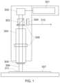
- Sharing the opto-mechanical systemis an advantage with respect to opto-mechanical thermal effects of camera systems and lithography systems. This will require more accurate and sophisticated calibration and create uncertainty that can effect yield and factory throughout, When these two opto-mechanical systems are combined, a higher accuracy of registration measurements is possible to achieve, ref Visitech Lithography systems LLS photo heads LLS 10 and LLS 04 where registration camera is positioned such that the camera and the projector share the same optical path, and hereby the same opto-mechanics. Ref Visitech's European patent application number: 14200630.3. This system is illustrated in FIG. 1 .
- LDI and DI machines/direct imaging lithography systemshas a throughput and cost limitation factor if the number of reference points are too high and/or the registration accuracy requirements are very high.
- a diein the context of integrated circuits, is a small block of semiconducting material on which a given functional circuit is fabricated.
- embedded die packagingcomponents are embedded inside the substrate using a multi-step manufacturing process.
- a die, multiple dies, MEMS or passivescan be embedded in a side-by-side fashion in the core of an organic laminate substrate.
- the object of the inventionis to provide a method and a device for measuring reference points in real time during lithographic printing which reduces the problems of prior art.
- a device for measuring reference points in real time during lithographic printingcomprises a light source providing an exposure beam, a light modulator modulating the exposure beam according to an exposure pattern, a measurement system configured to measure a position of a number of alignment marks previously arranged on a substrate, and an exposure optical system comprising a control unit.
- the exposure beam light sourcemay for example be an UV light source.
- the measurement systemmay for example use a beam of visible light, or any other convenient wavelength of the light.
- the light sourcecomprises multiple light sources, for example a number of LED units, with at least one wavelength.
- the exposure optical systemdelivers the modulated exposure beam as an image provided by the light modulator onto the substrate.
- the modulated exposure beamrepresents the image to be exposed onto the material for lithographic printing.
- the exposure optical systemcomprises a projection lens and the light source/light sources are positioned to be optically coupled through the projection lens.
- the light sourcesmay in other embodiments be positioned in the bottom part of the exposure optical system, surrounding the projection lens.
- the alignment marksmay be dedicated marks printed or physical placed or arranged in any other way on the substrate.
- the alignment marksmay be any suitable mark already on the substrate for which the location is known and thus can be used for calculating the orientation of the substrate.
- the electrical connection pads on a dieare used as alignment marks.
- body or parts of the body of a diecan be used as alignment marks.
- the measurement systemis a system for measuring the position of the alignment marks.
- the exposure optical system control unitis configured to calculate the orientation of the substrate based on the position of the alignment marks and control the delivering of the modulated exposure beam relative to the calculated orientation of the substrate.
- the measurement systemcomprises a camera or a camera system.
- the camera or camera systemmay be arranged to use direct high data rate transfer directly from the camera chip into a FPGA (field-programmable gate array) or a processor for fast analysis and data transfer to a pattern calculation module inside the exposure optical system control unit.
- FPGAfield-programmable gate array
- Contemporary field-programmable gate arrayshave large resources of logic gates and RAM blocks to implement complex digital computations and are therefore suitable for high data rate computations.
- the measurement system and the exposure optical systemhave at least partially concurrent optical paths.
- a camera as a part of the measurement systembe placed with its picture path within the optical path of the exposure optical system.
- the cameracan share the same optics (such as dichroic beam splitter prism and projection lens, etc.) as the exposure optical system.
- the cameracan share the opto-mechanical structure (optical parts mounting units) with the light source modulator.
- the light source modulatoris for example an electronic light projector based on DMD technology or similar.
- any variation in position for the exposed image provided by the exposure optical system caused by both exposure interior (opto-mechanics such as optical part mounting units) and exterior (exposure optical system framework and chassis mechanics)will also be applied to the position of the registration camera as the same mechanics and optical path is shared for both exposure optical system and registration camera.
- the requirement for frequent calibration of the relative position offsets of the exposure optical system and the registration camerais not required.
- the camera's image area of interestis positioned close to and mechanically connected to the exposure optical system.
- the image area of interest of the camerais a feature that makes it possible to specify a portion of the sensor line. During operation, only the pixel information from the specified portion of the line is transmitted out of the camera.
- the camera's image area of interestcan also specify the width of a frame.
- CMOS sensorsread the pixels out in parallel, many CMOS sensors also offer the possibility of reading out only a part of an image and thus to be able to concentrate on image areas containing the information relevant to image processing.
- the measurement systemdefines the camera area(s) of interest to optimize fast camera data transfer.
- the measurement systemdefine a special camera area of interest for autofocus laser light reflection detection similar to a line sensor, and utilize the defined special camera area of interest for fast camera data transfer for autofocus calculation and autofocus regulation.
- the methodcomprises in one embodiment the steps of.
- FIG. 1shows an example of an exposure system for direct imaging lithography.
- FIG. 1 aillustrates schematically various examples of applications of direct imaging lithography.
- FIG. 1 b - 1 cillustrate examples of components with high requirements for pattern accuracy.
- FIG. 2 a - 2 billustrate examples of embedded dies.
- FIG. 3 - 5illustrate a typical process of advance packaging with embedded dies.
- FIG. 6 a - 6 bshows examples of wafer and panel comprising embedded dies.
- FIG. 7 - 13illustrate examples of configurations of the optical elements for exposure and camera capture of a device for direct imaging lithography.
- FIG. 14 a - 14 dshows details of different embodiments of optical elements for exposure and camera capture of a device for direct imaging lithography.
- FIGS. 15 a and 15 bshows details of different embodiments of optical elements for exposure and camera capture of a device for direct imaging lithography.
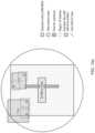
- FIG. 1shows an example of an exposure system which comprises a light source 302 providing an exposure beam 306 , a light modulator 301 , 302 modulating the exposure beam 306 according to an exposure pattern, and an exposure optical system 303 , 304 , 308 delivering the modulated exposure beam as an image 311 provided by the light modulator onto a substrate 307 .
- a measurement system 303 , 304 , 305 , 308 , 309is incorporated in the exposure apparatus and is configured to measure a position of an alignment (fiducial) mark previously patterned on the substrate.
- the exposure optical system and the measurement systemhave at least partially concurrent optical paths in this embodiment.
- photo headwill sometimes be used as a collective term comprising the optical elements of the exposure system.
- the exposure systemmay further comprise a control unit (not shown) which is configured to calculate the orientation of the substrate based on the position of the alignment marks and control the delivery of the modulated exposure beam relative to the calculated orientation of the substrate.
- FIG. 1 aillustrates various applications where there is need for smaller feature sizes in the patterning due to the constantly increasing demand for smaller devices. Due to this, there is a need for higher accuracy in the measurement of the alignment marks without increasing the time consumption of the process to any substantial extent.
- FIG. 1 b - 1 cillustrate examples of components with such high requirements for pattern accuracy.
- an embedded die with connection padswill have small pads/electrical connection points in the size range of 25-100 micrometer or less.
- the channelOptimization of the available space requires high position accuracy in the application of the dies and pads onto the substrate. And further, for cost reasons, the number of redistribution layers (RDL) can be reduced if the “channel” is optimized.
- RDLredistribution layers
- Typical applicationsare a Fan Out Panel level packaging process FOPLP or Fan Out Wafer level packaging process FOWLP.
- FIGS. 2 a - 5Examples of such application processes can be seen in FIGS. 2 a - 5 .
- FIGS. 2 b and 3the first steps are illustrated.
- An established temporary base layer 20such as a wafer is provided with an adhesive tape 21 or layer on top.
- Dies 22are positioned and arranged onto the adhesive layer/tape 21 with connection pads towards the adhesive tape.
- Each diecan for example be positioned with a “pick and place”-machine and this process will give some position and rotation error due to the accuracy limitations of such pick and place equipment where high speed and throughput are required.
- FIG. 6shows two examples of wafers with dies mounted onto them.
- FIG. 6 ashows an example of Fan Out Wafer Level Packaging (FOWLP)
- FIG. 6 bshows an example of Fan Out Panel Level Packaging (FOPLP).
- FOWLPFan Out Wafer Level Packaging
- FOPLPFan Out Panel Level Packaging
- the diesare now over-molded with a compound 23 , and in such molding process the dies might slightly move or rotate. Then the base layer and the adhesive tape/material 20 , 21 are removed in a special process. The result is a compound layer 24 with the dies and the die pads/electrical connection points visible from one side.
- a registration/measurement of the dies' position and rotationis required.
- Such optimizingis typically required in a Fanout process, where the pads/electrical connection points are to be redistributed to a wider area so that it is possible to connect them to a solderable system with larger and wider distributed connection pads.
- Other casescan include to Fan out the connection points to the larger interconnecting systems (such as a substrate, PCB or RDL) such that the dies connection points are routed and connected to the other electrical components on the same substrate. In this way it is avoided the packaging process of such die, —embedded die.
- a registration/measurement accuracy of 1 um or betteris required.
- one or more points on each dieare measured to be able to measure and calculate position error and rotation, hence the number of measurements needed can get up to the 1.000-100.000 number range.
- Such an amount of measurements with high accuracywill challenge the throughout, as this is very time consuming with the presently used equipment, for example registration systems in DI machines and/or measuring machines.
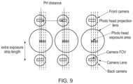
- a DI machine based on a system with light modulatorwill typically print the pattern in stripes, where each projector/photo head will print one or several stripes.
- FIGS. 7 - 13illustrates use of multiple photo heads and multiple registration cameras with different position configuration.
- a DI machinelike Schmol's MDI TT Ultra using Visitech's LLS 2500 Photo Head or other machine with specifications that enables printing 2 ⁇ m line/space, will typically print 10-30 stripes per photo head depending on the configuration. Hence the photo head mechanical system will scan over the area to be printed several times.
- FIG. 14 aillustrates this process.
- the imaging optics and camera's opticsare incorporated or arranged close to each other.
- the camerais here used as line sensor.
- the systemwill measure the position of alignment marks in the same stripe and/or the next stripe to be printed. Simultaneously, ie. in real time, the XY position and rotation matrix for each alignment mark is calculated. The calculated position/rotation is then used by the exposure system to control the positioning of the subsequent exposed images.
- the relative distance and scroll speed of the substratewhich is known by the system, can be used to determine image capture, position calculation, data transfer and image warping time window.
- the camera area of interestcan be determined with one or more areas of the camera image. This will reduce the number of camera pixels to capture, compared to the whole camera image, to be transferred and analyzed, such that the camera data transfer and the following calculation can be optimized for speed of data transfer to the calculation module.
- the camerameasures the alignment marks in front of the projected pattern as illustrated in FIGS. 14 a , 14 d or on the next stripe to be printed (N+1, N+2 etc) as illustrated in the example of FIGS. 15 a and 15 b .
- the choice of embodimentmay depend on the time needed to do the capture, calculations and coordinate data transfer and the positioning and warping while printing.
Landscapes
- General Physics & Mathematics (AREA)
- Physics & Mathematics (AREA)
- Engineering & Computer Science (AREA)
- Health & Medical Sciences (AREA)
- Multimedia (AREA)
- Computer Hardware Design (AREA)
- Environmental & Geological Engineering (AREA)
- Microelectronics & Electronic Packaging (AREA)
- Condensed Matter Physics & Semiconductors (AREA)
- Life Sciences & Earth Sciences (AREA)
- Atmospheric Sciences (AREA)
- Toxicology (AREA)
- Power Engineering (AREA)
- Epidemiology (AREA)
- Public Health (AREA)
- Exposure And Positioning Against Photoresist Photosensitive Materials (AREA)
- Length Measuring Devices By Optical Means (AREA)
- Electron Beam Exposure (AREA)
- Optical Communication System (AREA)
Abstract
Description
- modulate an exposure beam according to an exposure pattern;
- measure a position of a number of alignment marks previously patterned on a substrate,
- deliver the modulated exposure beam as an image provided by the light modulator onto the substrate;
- calculate the orientation of the substrate based on the position of the alignment marks and
- control the delivering of the modulated exposure beam relative to the calculated orientation of the substrate.
Claims (16)
Applications Claiming Priority (3)
| Application Number | Priority Date | Filing Date | Title |
|---|---|---|---|
| NO20190876ANO20190876A1 (en) | 2019-07-11 | 2019-07-11 | Real time Registration Lithography system |
| NO20190876 | 2019-07-11 | ||
| PCT/EP2020/068286WO2021004826A1 (en) | 2019-07-11 | 2020-06-29 | Real time registration in litography system |
Publications (2)
| Publication Number | Publication Date |
|---|---|
| US20220276566A1 US20220276566A1 (en) | 2022-09-01 |
| US11906903B2true US11906903B2 (en) | 2024-02-20 |
Family
ID=71452213
Family Applications (1)
| Application Number | Title | Priority Date | Filing Date |
|---|---|---|---|
| US17/625,990ActiveUS11906903B2 (en) | 2019-07-11 | 2020-06-29 | Real time registration in lithography system |
Country Status (8)
| Country | Link |
|---|---|
| US (1) | US11906903B2 (en) |
| EP (1) | EP3997519B1 (en) |
| JP (1) | JP7514910B2 (en) |
| KR (1) | KR20220031690A (en) |
| CN (1) | CN114096918B (en) |
| NO (1) | NO20190876A1 (en) |
| TW (1) | TWI850420B (en) |
| WO (1) | WO2021004826A1 (en) |
Citations (9)
| Publication number | Priority date | Publication date | Assignee | Title |
|---|---|---|---|---|
| US20050128450A1 (en) | 2003-12-15 | 2005-06-16 | Schroeder Dale W. | Real time image resizing for dynamic digital photolithography |
| US20050264777A1 (en) | 2004-05-28 | 2005-12-01 | Azores Corporation | High speed lithography machine and method |
| TW201032004A (en) | 2009-02-18 | 2010-09-01 | Hitachi High Tech Corp | Exposure device, exposure method, and production method of displaying panel substrates |
| US20120081682A1 (en)* | 2010-10-01 | 2012-04-05 | Samsung Electronics Co., Ltd. | Maskless exposure apparatus and method to determine exposure start position and orientation in maskless lithography |
| WO2015060972A1 (en) | 2013-10-22 | 2015-04-30 | Applied Materials, Inc. | Roll to roll mask-less lithography with active alignment |
| EP3040779A1 (en) | 2014-12-30 | 2016-07-06 | Visitech As | A maskless exposure apparatus with alignment |
| CN107430353A (en) | 2015-03-30 | 2017-12-01 | 优志旺电机株式会社 | Exposure device and exposure method |
| US20180329292A1 (en) | 2015-11-20 | 2018-11-15 | Asml Netherlands B.V. | Lithographic Apparatus and Method of Operating a Lithographic Apparatus |
| US20190294051A1 (en)* | 2018-03-22 | 2019-09-26 | Applied Materials, Inc. | Spatial light modulator with variable intensity diodes |
Family Cites Families (30)
| Publication number | Priority date | Publication date | Assignee | Title |
|---|---|---|---|---|
| JPS63132427A (en)* | 1987-10-29 | 1988-06-04 | Canon Inc | exposure equipment |
| JP3278303B2 (en)* | 1993-11-12 | 2002-04-30 | キヤノン株式会社 | Scanning exposure apparatus and device manufacturing method using the scanning exposure apparatus |
| KR20030096435A (en)* | 1996-11-28 | 2003-12-31 | 가부시키가이샤 니콘 | Aligner and method for exposure |
| CN1808281A (en)* | 1996-11-28 | 2006-07-26 | 株式会社尼康 | Projection exposure apparatus and method |
| US6563565B2 (en)* | 1997-08-27 | 2003-05-13 | Nikon Corporation | Apparatus and method for projection exposure |
| JP2001077004A (en)* | 1999-09-03 | 2001-03-23 | Hitachi Ltd | Exposure apparatus and electron beam exposure apparatus |
| JP2001143993A (en)* | 1999-11-12 | 2001-05-25 | Mitsubishi Cable Ind Ltd | Exposure apparatus and exposure method, light source apparatus, and device manufacturing method |
| JP2003084189A (en)* | 2001-09-07 | 2003-03-19 | Canon Inc | Autofocus detection method and projection exposure apparatus |
| US7242455B2 (en)* | 2002-12-10 | 2007-07-10 | Nikon Corporation | Exposure apparatus and method for producing device |
| EP1482373A1 (en) | 2003-05-30 | 2004-12-01 | ASML Netherlands B.V. | Lithographic apparatus and device manufacturing method |
| JP4338628B2 (en)* | 2004-12-21 | 2009-10-07 | 株式会社ブイ・テクノロジー | Exposure equipment |
| JP4760019B2 (en)* | 2005-01-17 | 2011-08-31 | 株式会社ニコン | Exposure apparatus and device manufacturing method |
| JP2008089868A (en)* | 2006-09-29 | 2008-04-17 | Fujifilm Corp | Drawing point data acquisition method and apparatus, and drawing method and apparatus |
| CN101652720A (en)* | 2007-04-10 | 2010-02-17 | 株式会社尼康 | Exposure apparatus, exposure method, and electronic device manufacturing method |
| DE102008004762A1 (en)* | 2008-01-16 | 2009-07-30 | Carl Zeiss Smt Ag | Projection exposure apparatus for microlithography with a measuring device |
| SG172243A1 (en)* | 2008-12-23 | 2011-07-28 | 3M Innovative Properties Co | Roll-to-roll digital photolithography |
| JP4951036B2 (en)* | 2009-07-14 | 2012-06-13 | 株式会社ブイ・テクノロジー | Exposure equipment |
| US20110027542A1 (en)* | 2009-07-28 | 2011-02-03 | Nsk Ltd. | Exposure apparatus and exposure method |
| NL2007615A (en)* | 2010-11-30 | 2012-05-31 | Asml Netherlands Bv | Method of operating a patterning device and lithographic apparatus. |
| CN102314097A (en)* | 2011-09-19 | 2012-01-11 | 合肥芯硕半导体有限公司 | Method of calibrating spatial position between spatial light modulator center and camera center |
| WO2013065429A1 (en)* | 2011-11-04 | 2013-05-10 | 株式会社ニコン | Substrate processing apparatus and substrate processing method |
| CN103246169B (en)* | 2012-02-03 | 2015-04-15 | 上海微电子装备有限公司 | Apparatus and method for focal plane change measurement |
| JP2013178445A (en)* | 2012-02-29 | 2013-09-09 | Hitachi High-Technologies Corp | Exposure device, exposure method, and manufacturing method of display panel substrate |
| KR102203305B1 (en)* | 2012-10-02 | 2021-01-14 | 가부시키가이샤 니콘 | Exposure device and exposure method, and device-manufacturing method |
| US9760020B2 (en) | 2012-11-21 | 2017-09-12 | Kla-Tencor Corporation | In-situ metrology |
| DE102014220168B4 (en)* | 2014-10-06 | 2017-10-12 | Carl Zeiss Ag | Optical system for lithographic structure generation and method for the determination of relative coordinates |
| JP2017067992A (en) | 2015-09-30 | 2017-04-06 | 株式会社オーク製作所 | Exposure device, exposure device alignment method, and program |
| CN107290937B (en)* | 2016-03-31 | 2018-10-16 | 上海微电子装备(集团)股份有限公司 | A kind of projection aligner and method |
| KR20190043417A (en)* | 2017-10-18 | 2019-04-26 | 삼성전자주식회사 | Method of controlling an exposure device and apparatus for controlling an exposure device |
| NO20190617A1 (en)* | 2019-05-16 | 2020-11-17 | Visitech As | System and method for exposing a material with images |
- 2019
- 2019-07-11NONO20190876Apatent/NO20190876A1/ennot_activeApplication Discontinuation
- 2020
- 2020-06-29KRKR1020227004457Apatent/KR20220031690A/enactivePending
- 2020-06-29JPJP2022500889Apatent/JP7514910B2/enactiveActive
- 2020-06-29CNCN202080050319.9Apatent/CN114096918B/enactiveActive
- 2020-06-29EPEP20736296.3Apatent/EP3997519B1/enactiveActive
- 2020-06-29USUS17/625,990patent/US11906903B2/enactiveActive
- 2020-06-29WOPCT/EP2020/068286patent/WO2021004826A1/ennot_activeCeased
- 2020-07-09TWTW109123127Apatent/TWI850420B/enactive
Patent Citations (10)
| Publication number | Priority date | Publication date | Assignee | Title |
|---|---|---|---|---|
| US20050128450A1 (en) | 2003-12-15 | 2005-06-16 | Schroeder Dale W. | Real time image resizing for dynamic digital photolithography |
| US20050264777A1 (en) | 2004-05-28 | 2005-12-01 | Azores Corporation | High speed lithography machine and method |
| TW201032004A (en) | 2009-02-18 | 2010-09-01 | Hitachi High Tech Corp | Exposure device, exposure method, and production method of displaying panel substrates |
| US20120081682A1 (en)* | 2010-10-01 | 2012-04-05 | Samsung Electronics Co., Ltd. | Maskless exposure apparatus and method to determine exposure start position and orientation in maskless lithography |
| WO2015060972A1 (en) | 2013-10-22 | 2015-04-30 | Applied Materials, Inc. | Roll to roll mask-less lithography with active alignment |
| TW201516580A (en) | 2013-10-22 | 2015-05-01 | Applied Materials Inc | Roll-to-roll reticle with active alignment |
| EP3040779A1 (en) | 2014-12-30 | 2016-07-06 | Visitech As | A maskless exposure apparatus with alignment |
| CN107430353A (en) | 2015-03-30 | 2017-12-01 | 优志旺电机株式会社 | Exposure device and exposure method |
| US20180329292A1 (en) | 2015-11-20 | 2018-11-15 | Asml Netherlands B.V. | Lithographic Apparatus and Method of Operating a Lithographic Apparatus |
| US20190294051A1 (en)* | 2018-03-22 | 2019-09-26 | Applied Materials, Inc. | Spatial light modulator with variable intensity diodes |
Non-Patent Citations (5)
| Title |
|---|
| International Preliminary Report on Patentability issued in International Application No. PCT/EP2020/068286; dated Oct. 25, 2021 (14 pages). |
| International Search Report issued in International Application No. PCT/EP2020/068286, dated Oct. 14, 2020 (3 pages). |
| Office Action issued in Taiwanese Application No. 109123127; dated Sep. 26, 2023 (16 pages). |
| Search Report issued in Norwegian Application No. 20/190,876; dated Feb. 11, 2020 (2 pages). |
| Written Opinion issued in International Application No. PCT/EP2020/068286; dated Oct. 14, 2020 (8 pages). |
Also Published As
| Publication number | Publication date |
|---|---|
| NO20190876A1 (en) | 2021-01-12 |
| US20220276566A1 (en) | 2022-09-01 |
| CN114096918A (en) | 2022-02-25 |
| TWI850420B (en) | 2024-08-01 |
| JP2022540589A (en) | 2022-09-16 |
| CN114096918B (en) | 2024-12-20 |
| TW202102934A (en) | 2021-01-16 |
| EP3997519C0 (en) | 2023-11-29 |
| EP3997519A1 (en) | 2022-05-18 |
| WO2021004826A1 (en) | 2021-01-14 |
| KR20220031690A (en) | 2022-03-11 |
| JP7514910B2 (en) | 2024-07-11 |
| EP3997519B1 (en) | 2023-11-29 |
Similar Documents
| Publication | Publication Date | Title |
|---|---|---|
| US8994916B2 (en) | Double-sided maskless exposure system and method | |
| TWI444287B (en) | Imprint apparatus and method of manufacturing article | |
| US10948834B2 (en) | Dynamic imaging system | |
| KR20130052545A (en) | Method and apparatus for performing pattern alignment | |
| CN109557768B (en) | Exposure apparatus and exposure method | |
| JP7653482B2 (en) | Exposure equipment and systems | |
| KR20210074403A (en) | Dynamic creation of layout adaptive packaging | |
| TW201918800A (en) | Exposure system, exposure method, and manufacturing method of panel substrate for display especially having exposure patterns of different sizes on a single substrate | |
| JP2018500605A (en) | Maskless exposure apparatus having alignment | |
| KR20130020408A (en) | Maskless exposure apparatus and method for getting spot beam position using the same | |
| CN113168087B (en) | Self-aligned system and method for a lithography system | |
| US11906903B2 (en) | Real time registration in lithography system | |
| CN109581824A (en) | A kind of direct-write type lithography machine optical uniformity scaling method and system | |
| CN112684679A (en) | Calibration method for upper and lower graph alignment of double-sided digital photoetching system | |
| CN100578369C (en) | Automatic position alignment device and position alignment method used in projection exposure apparatus | |
| US20100045959A1 (en) | Photolithography apparatus with leveling element and method for leveling a wafer | |
| JP7529252B2 (en) | Projection exposure apparatus and projection exposure method | |
| JPH03211812A (en) | Exposure aligner | |
| JP5064862B2 (en) | Alignment mark measuring method and apparatus, and drawing method and apparatus | |
| JP4609167B2 (en) | Exposure system, exposure method, and microdevice manufacturing method | |
| TW202422204A (en) | On tool metrology scheme for advanced packaging | |
| US20250284207A1 (en) | Inspection of lithographic layers and dynamic data via inline metrology | |
| KR20250133228A (en) | Shortwave infrared inspection of patterned substrates using focus averaging | |
| JP2001066111A (en) | Position measurement method and position measurement apparatus, and exposure method and exposure apparatus | |
| KR20170135730A (en) | Exposure apparatus |
Legal Events
| Date | Code | Title | Description |
|---|---|---|---|
| FEPP | Fee payment procedure | Free format text:ENTITY STATUS SET TO UNDISCOUNTED (ORIGINAL EVENT CODE: BIG.); ENTITY STATUS OF PATENT OWNER: SMALL ENTITY | |
| FEPP | Fee payment procedure | Free format text:ENTITY STATUS SET TO SMALL (ORIGINAL EVENT CODE: SMAL); ENTITY STATUS OF PATENT OWNER: SMALL ENTITY | |
| AS | Assignment | Owner name:VISITECH AS, NORWAY Free format text:ASSIGNMENT OF ASSIGNORS INTEREST;ASSIGNORS:TAFJORD, OEYVIND;JOERGENSEN, TROND;KIRKHORN, ENDRE;AND OTHERS;SIGNING DATES FROM 20191001 TO 20191015;REEL/FRAME:059533/0753 | |
| STPP | Information on status: patent application and granting procedure in general | Free format text:DOCKETED NEW CASE - READY FOR EXAMINATION | |
| STPP | Information on status: patent application and granting procedure in general | Free format text:NON FINAL ACTION MAILED | |
| STPP | Information on status: patent application and granting procedure in general | Free format text:RESPONSE TO NON-FINAL OFFICE ACTION ENTERED AND FORWARDED TO EXAMINER | |
| STPP | Information on status: patent application and granting procedure in general | Free format text:NOTICE OF ALLOWANCE MAILED -- APPLICATION RECEIVED IN OFFICE OF PUBLICATIONS | |
| STPP | Information on status: patent application and granting procedure in general | Free format text:AWAITING TC RESP., ISSUE FEE NOT PAID | |
| STPP | Information on status: patent application and granting procedure in general | Free format text:PUBLICATIONS -- ISSUE FEE PAYMENT RECEIVED | |
| STPP | Information on status: patent application and granting procedure in general | Free format text:PUBLICATIONS -- ISSUE FEE PAYMENT VERIFIED | |
| STCF | Information on status: patent grant | Free format text:PATENTED CASE |