US11906353B2 - Digital pixel with extended dynamic range - Google Patents
Digital pixel with extended dynamic rangeDownload PDFInfo
- Publication number
- US11906353B2 US11906353B2US16/435,451US201916435451AUS11906353B2US 11906353 B2US11906353 B2US 11906353B2US 201916435451 AUS201916435451 AUS 201916435451AUS 11906353 B2US11906353 B2US 11906353B2
- Authority
- US
- United States
- Prior art keywords
- voltage
- decision
- digital value
- photodiode
- charge
- Prior art date
- Legal status (The legal status is an assumption and is not a legal conclusion. Google has not performed a legal analysis and makes no representation as to the accuracy of the status listed.)
- Active
Links
Images


Classifications
- H—ELECTRICITY
- H04—ELECTRIC COMMUNICATION TECHNIQUE
- H04N—PICTORIAL COMMUNICATION, e.g. TELEVISION
- H04N25/00—Circuitry of solid-state image sensors [SSIS]; Control thereof
- H04N25/50—Control of the SSIS exposure
- H04N25/57—Control of the dynamic range
- H04N25/58—Control of the dynamic range involving two or more exposures
- H04N25/581—Control of the dynamic range involving two or more exposures acquired simultaneously
- H04N25/583—Control of the dynamic range involving two or more exposures acquired simultaneously with different integration times
- G—PHYSICS
- G01—MEASURING; TESTING
- G01J—MEASUREMENT OF INTENSITY, VELOCITY, SPECTRAL CONTENT, POLARISATION, PHASE OR PULSE CHARACTERISTICS OF INFRARED, VISIBLE OR ULTRAVIOLET LIGHT; COLORIMETRY; RADIATION PYROMETRY
- G01J1/00—Photometry, e.g. photographic exposure meter
- G01J1/42—Photometry, e.g. photographic exposure meter using electric radiation detectors
- G01J1/44—Electric circuits
- G01J1/46—Electric circuits using a capacitor
- G—PHYSICS
- G01—MEASURING; TESTING
- G01J—MEASUREMENT OF INTENSITY, VELOCITY, SPECTRAL CONTENT, POLARISATION, PHASE OR PULSE CHARACTERISTICS OF INFRARED, VISIBLE OR ULTRAVIOLET LIGHT; COLORIMETRY; RADIATION PYROMETRY
- G01J1/00—Photometry, e.g. photographic exposure meter
- G01J1/42—Photometry, e.g. photographic exposure meter using electric radiation detectors
- G01J1/44—Electric circuits
- G—PHYSICS
- G02—OPTICS
- G02B—OPTICAL ELEMENTS, SYSTEMS OR APPARATUS
- G02B27/00—Optical systems or apparatus not provided for by any of the groups G02B1/00 - G02B26/00, G02B30/00
- G02B27/01—Head-up displays
- G02B27/017—Head mounted
- H—ELECTRICITY
- H04—ELECTRIC COMMUNICATION TECHNIQUE
- H04N—PICTORIAL COMMUNICATION, e.g. TELEVISION
- H04N25/00—Circuitry of solid-state image sensors [SSIS]; Control thereof
- H04N25/50—Control of the SSIS exposure
- H04N25/57—Control of the dynamic range
- H04N25/58—Control of the dynamic range involving two or more exposures
- H04N25/581—Control of the dynamic range involving two or more exposures acquired simultaneously
- H—ELECTRICITY
- H04—ELECTRIC COMMUNICATION TECHNIQUE
- H04N—PICTORIAL COMMUNICATION, e.g. TELEVISION
- H04N25/00—Circuitry of solid-state image sensors [SSIS]; Control thereof
- H04N25/60—Noise processing, e.g. detecting, correcting, reducing or removing noise
- H04N25/62—Detection or reduction of noise due to excess charges produced by the exposure, e.g. smear, blooming, ghost image, crosstalk or leakage between pixels
- H04N25/621—Detection or reduction of noise due to excess charges produced by the exposure, e.g. smear, blooming, ghost image, crosstalk or leakage between pixels for the control of blooming
- H—ELECTRICITY
- H04—ELECTRIC COMMUNICATION TECHNIQUE
- H04N—PICTORIAL COMMUNICATION, e.g. TELEVISION
- H04N25/00—Circuitry of solid-state image sensors [SSIS]; Control thereof
- H04N25/70—SSIS architectures; Circuits associated therewith
- H04N25/76—Addressed sensors, e.g. MOS or CMOS sensors
- H04N25/77—Pixel circuitry, e.g. memories, A/D converters, pixel amplifiers, shared circuits or shared components
- H04N25/772—Pixel circuitry, e.g. memories, A/D converters, pixel amplifiers, shared circuits or shared components comprising A/D, V/T, V/F, I/T or I/F converters
- H—ELECTRICITY
- H04—ELECTRIC COMMUNICATION TECHNIQUE
- H04N—PICTORIAL COMMUNICATION, e.g. TELEVISION
- H04N25/00—Circuitry of solid-state image sensors [SSIS]; Control thereof
- H04N25/70—SSIS architectures; Circuits associated therewith
- H04N25/76—Addressed sensors, e.g. MOS or CMOS sensors
- H04N25/78—Readout circuits for addressed sensors, e.g. output amplifiers or A/D converters
- G—PHYSICS
- G01—MEASURING; TESTING
- G01J—MEASUREMENT OF INTENSITY, VELOCITY, SPECTRAL CONTENT, POLARISATION, PHASE OR PULSE CHARACTERISTICS OF INFRARED, VISIBLE OR ULTRAVIOLET LIGHT; COLORIMETRY; RADIATION PYROMETRY
- G01J1/00—Photometry, e.g. photographic exposure meter
- G01J1/42—Photometry, e.g. photographic exposure meter using electric radiation detectors
- G01J1/44—Electric circuits
- G01J2001/4446—Type of detector
- G01J2001/446—Photodiode
- H—ELECTRICITY
- H04—ELECTRIC COMMUNICATION TECHNIQUE
- H04N—PICTORIAL COMMUNICATION, e.g. TELEVISION
- H04N25/00—Circuitry of solid-state image sensors [SSIS]; Control thereof
- H04N25/50—Control of the SSIS exposure
- H04N25/57—Control of the dynamic range
- H04N25/59—Control of the dynamic range by controlling the amount of charge storable in the pixel, e.g. modification of the charge conversion ratio of the floating node capacitance
Definitions
- the disclosurerelates generally to image sensors, and more specifically to pixel cell structure including interfacing circuitries for determining light intensity for image generation.
- a typical image sensorincludes a photodiode to sense incident light by converting photons into charge (e.g., electrons or holes).
- the image sensorfurther includes a floating node configured as a capacitor to collect the charge generated by the photodiode during an exposure period. The collected charge can develop a voltage at the capacitor.
- the voltagecan be buffered and fed to an analog-to-digital converter (ADC), which can quantize the voltage into a digital value representing the intensity of the incident light.
- ADCanalog-to-digital converter
- the accuracy of the quantizationcan be affected by various noise sources, such as dark current at the floating node.
- the present disclosurerelates to image sensors. More specifically, and without limitation, this disclosure relates to a pixel cell. This disclosure also relates to operating the circuitries of pixel cells to measure the intensity of incident lights in different measurement modes.
- the present disclosureprovides an apparatus for measuring intensity of incident light.
- an apparatuscomprising a photodiode, a charge storage unit, and processing circuits.
- the processing circuitsare configured to: transfer overflow charge from the photodiode to the charge storage unit to develop a first voltage; compare the first voltage against a first ramping threshold voltage to generate a first decision; generate, based on the first decision, a first digital value; transfer residual charge from the photodiode to the charge storage unit to develop a second voltage; compare the second voltage against a static threshold voltage to determine whether the photodiode saturates to generate a second decision; compare the second voltage against a second ramping threshold voltage to generate a third decision; generate, based on the third decision, a second digital value; and output, based on the second decision, one of the first digital value or the second digital value to represent an intensity of light received by the photodiode.
- the static threshold voltageis based on a third voltage developed at the charge storage unit when storing a quantity of the residual charge equal to a saturation capacity of the photodiode.
- the static threshold voltageis further based on a voltage offset representing a dark charge deposited by dark current.
- the second ramping threshold voltagestarts or ends from the static threshold voltage.
- the apparatusfurther comprises a counter and a memory.
- the processing circuitsare configured to: store, based on the first decision, a first count value from the counter in the memory as the first digital value; store, based on the third decision, a second count value from the counter in the memory as the second digital value; and output, from the memory, one of the first digital value or the second digital value based on the second decision.
- the processing circuitsare configured to overwrite the first count value with the second count value in the memory based on the second decision.
- the apparatusfurther comprises a register.
- the processing circuitsare configured to: store a first flag value indicating the second decision in the register; and output, from the memory, one of the first digital value or the second digital value based on the first flag value from the register.
- the processing circuitsare configured to: determine a status of the first decision when the first ramping threshold voltage reaches a first breakpoint voltage; store a second flag value indicating the status of the first decision in the register; and output one of the first digital value or the second digital value based on the first flag value and the second flag value from the register.
- the processing circuitsare configured to reset the counter when the first ramping threshold voltage reaches the first breakpoint voltage.
- the processing circuitsare configured to: determine a status of the third decision when the second ramping threshold voltage reaches a second breakpoint voltage; store a second flag value indicating the status of the third decision in the register; and output one of the first digital value or the second digital value based on the first flag value and the second flag value from the register.
- the processing circuitsare configured to reset the counter when the first ramping threshold voltage reaches the second breakpoint voltage.
- the static threshold voltageis a first static threshold voltage.
- the processing circuitsare configured to: compare the first voltage against a second static threshold voltage representing a saturation capacity of the charge storage unit to generate a fourth decision; store a second flag value indicating the fourth decision in the register; store, based on the fourth decision, a third count value from the counter as a third digital value; and output, based on the first flag value and the second flag value, one of the first digital value, the second digital value or the third digital value to represent the intensity of light received by the photodiode.
- the processing circuitsare configured to: compare the first voltage against the second static threshold voltage within a pre-determined time period; determine a first status of the fourth decision when a pre-determined portion of the time period has elapsed; store the first flag value indicating the first status of the fourth decision in the register; determine a second status of the fourth decision when the time period has elapsed; store the second flag value indicating the second status of the fourth decision in the register; and output, based on the first flag value and the second flag value, one of the first digital value, the second digital value or the third digital value to represent the intensity of light received by the photodiode.
- the processing circuitsare configured to reset the counter when the pre-determined portion of the time period has elapsed.
- a charge storage capacity of the charge storage unitis configurable by the processing circuit.
- the processing circuitsare configured to: configure the charge storage unit to have a first capacity to develop the first voltage; and configure the charge storage unit to have a second capacity smaller than the first capacity to develop the second voltage.
- the charge storage unitcomprises a floating drain node and a capacitor.
- a methodcomprises: transferring overflow charge from a photodiode to a charge storage unit to develop a first voltage; comparing the first voltage against a first ramping threshold voltage to generate a first decision; generating, based on the first decision, a first digital value; transferring residual charge from the photodiode to the charge storage unit to develop a second voltage; comparing the second voltage against a static threshold voltage to determine whether the photodiode saturates to generate a second decision; comparing the second voltage against a second ramping threshold voltage to generate a third decision; generating, based on the third decision, a second digital value; and outputting, based on the second decision, one of the first digital value or the second digital value to represent an intensity of light received by the photodiode.
- the static threshold voltageis based on a third voltage developed at the charge storage unit when storing a quantity of the residual charge equal to a saturation capacity of the photodiode, and based on a voltage offset representing a dark charge deposited by dark current.
- the second ramping threshold voltagestarts or ends from the static threshold voltage.
- the methodfurther comprises: storing, based on the first decision, a first count value from a counter in a memory as the first digital value; storing, based on the third decision, a second count value from the counter in the memory as the second digital value; and outputting, from the memory, one of the first digital value or the second digital value based on the second decision.
- FIG. 1 A and FIG. 1 Bare diagrams of an example of a near-eye display.
- FIG. 2is an example of a cross section of the near-eye display.
- FIG. 3illustrates an isometric view of an example of a waveguide display with a single source assembly.
- FIG. 4illustrates a cross section of an example of the waveguide display.
- FIG. 5is a block diagram of an example of a system including the near-eye display.
- FIG. 6illustrates block diagrams of examples of a pixel cell.
- FIG. 7illustrates operations for determining light intensities of different ranges by examples of FIG. 6 .
- FIG. 8illustrates examples of internal components of the pixel cell of FIG. 6 .
- FIG. 9 A and FIG. 9 Billustrate example methods for determining a light intensity.
- FIG. 10 A and FIG. 10 Billustrate techniques for performing quantization.
- FIG. 11illustrates block diagrams of an example of a pixel cell.
- FIG. 12illustrates an example sequence of control signals to perform light intensity measurement.
- FIG. 13 A and FIG. 13 Billustrate another example sequence of control signals to perform light intensity measurement, and an example of measurement results.
- FIG. 14 A and FIG. 14 Billustrate another example sequence of control signals to perform light intensity measurement.
- FIG. 15illustrates another example sequence of control signals to perform light intensity measurement.
- FIG. 16illustrates another example sequence of control signals to perform light intensity measurement.
- FIG. 17illustrates another example sequence of control signals to perform light intensity measurement.
- FIG. 18illustrates a flowchart of an example process for measuring light intensity.
- FIG. 19illustrates a flowchart of another example process for measuring light intensity.
- a typical image sensorincludes a photodiode to sense incident light by converting photons into charge (e.g., electrons or holes).
- the image sensorfurther includes a floating node configured as a capacitor to collect the charge generated by the photodiode during an exposure period. The collected charge can develop a voltage at the capacitor.
- the voltagecan be buffered and fed to an analog-to-digital converter (ADC), which can convert the voltage into a digital value representing the intensity of the incident light.
- ADCanalog-to-digital converter
- the digital value generated by the ADCwhich reflects a quantity of charge stored at the floating node within a certain period, may correlate to the intensity of the incident light.
- the degree of correlationcan be affected by different factors.
- the quantity of charge stored in the floating nodecan be directly related to the intensity of the incident light until the floating node reaches a saturation limit. Beyond the saturation limit, the floating node may be unable to accept additional charge generated by the photodiode, and the additional charge may be leaked and not stored. As a result, the quantity of the charge stored at the floating node may be lower than the quantity of charge actually generated by the photodiode.
- the saturation limitmay determine an upper limit of the measureable light intensity of the image sensor.
- the charge collected at the floating nodemay include noise charge not related to the intensity of incident light, as well as dark charge contributed by dark current.
- Dark currentcan include leakage currents generated at the p-n junction of the photodiode and at the p-n junctions of other semiconductor devices connected to the capacitor, due to crystallographic defects.
- the dark currentscan flow into the capacitor and add charges which are not correlated to the intensity of the incident light.
- the dark current generated at the photodiodeis typically less than the dark current generated at other semiconductor devices.
- Another source of noise chargecan be capacitive coupling with other circuitries. For example, when the ADC circuitries perform read operations to determine the quantity of charge stored in the floating node, the ADC circuitries can introduce noise charge into the floating node through capacitive coupling.
- the ADCcan also introduce measurement errors in determining the quantity of charge.
- the measurement errorscan degrade the degree of correlation between the digital output and the intensity of the incident light.
- One source of measurement erroris quantization error.
- a discrete set of quantity levelscan be used to represent a continuous set of quantities of charge, with each quantity level representing a pre-determined quantity of charge.
- the ADCcan compare an input quantity of charge against the quantity levels, determine the quantity level that is closest to the input quantity, and output the determined quantity level (e.g., in the form of digital codes representing the quantity level).
- Quantization errorcan occur when there is a mismatch between a quantity of charge represented by the quantity level and the input quantity of charge mapped to the quantity level.
- the quantization errorcan be reduced with smaller quantization step sizes (e.g., by reducing the difference in charge quantities between two adjacent quantity levels).
- Other sources of measurement errormay also include, for example, device noises (e.g., of the ADC circuitries) and comparator offsets that add to uncertainties in the measurement of the quantity of charge.
- the noise charge, dark charge, as well as the ADC measurement errorscan define a lower limit of the measureable light intensity of the image sensor, whereas the saturation limit may determine an upper limit of the measureable light intensity of the image sensor.
- a ratio between the upper limit and the lower limitdefines a dynamic range, which may set a range of operational light intensities for the image sensor.
- Image sensorscan be found in many different applications.
- image sensorsare included in digital imaging devices (e.g., digital cameras, smart phones, etc.) to provide digital imaging.
- image sensorscan be configured as input devices to control or influence the operation of a device, such as controlling or influencing the display content of a near-eye display in wearable virtual-reality (VR) systems and/or augmented-reality (AR) and/or mixed reality (MR) systems.
- VRvirtual-reality
- ARaugmented-reality
- MRmixed reality
- the image sensorscan be used to generate physical image data of a physical environment in which a user is located.
- the physical image datacan be provided to a location tracking system operating a simultaneous localization and mapping (SLAM) algorithm to track, for example, a location of the user, an orientation of the user, and/or a path of movement of the user in the physical environment.
- the image sensorscan also be used to generate physical image data including stereo depth information for measuring a distance between the user and an object in the physical environment.
- the image sensorscan also be configured as a near-infrared (NIR) sensor.
- An illuminatormay project a pattern of NIR light into the eyeballs of the user.
- the internal structures of the eyeballse.g., the pupils
- the image sensorscan capture images of the reflective pattern, and provide the images to a system to track the movement of the eyeballs of the user to determine a gaze point of the user.
- the VR/AR/MR systemmay generate and update virtual image data for displaying to the user via the near-eye display, to provide an interactive experience to the user.
- the VR/AR/MR systemmay update the virtual image data based on the user's gazing direction (which may signal the user's interest in the object), a location of the user, etc.
- a wearable VR/AR/MR systemmay operate in environments with a very wide range of light intensities.
- the wearable VR/AR/MR systemmay be able to operate in an indoor environment or in an outdoor environment, and/or at different times of the day, and the light intensity of the operation environment of the wearable VR/AR/MR system may vary substantially.
- the wearable VR/AR/MR systemmay also include the aforementioned NIR eyeball tracking system, which may require projecting lights of very low intensity into the eyeballs of the user to prevent damaging the eyeballs.
- the image sensors of the wearable VR/AR/MR systemmay need to have a wide dynamic range to be able to operate properly (e.g., to generate an output that correlates with the intensity of incident light) across a very wide range of light intensities associated with different operating environments.
- the image sensors of the wearable VR/AR/MR systemmay also need to generate images at sufficiently high speed to allow tracking of the user's location, orientation, gaze point, etc. Image sensors with relatively limited dynamic ranges and which generate images at relatively low speed may not be suitable for such a wearable VR/AR/MR system.
- the pixel cellmay include a photodiode, a charge storage unit, a transistor configured as a transfer gate between the photodiode and the charge storage unit, and a processing circuit.
- the photodiodecan generate charge responsive to incident light and store at least some of the charge as residual charge until the photodiode saturates.
- the charge storage unitcan be a floating drain of the transistor, a metal capacitor, a Metal-Oxide-Semiconductor (MOS) capacitor, or any combination thereof.
- MOSMetal-Oxide-Semiconductor
- the charge storage unitcan store overflow charge, which is charge transferred from the photodiode when the photodiode saturates and cannot store additional charge, to develop a first voltage.
- the charge storage unitmay include a floating drain node.
- the processing circuitscan measure the intensity of the incident light by performing multiple modes of measurement.
- a first mode of measurementthe processing circuits can perform a quantization process by comparing the first voltage against a first ramping threshold voltage to generate a first decision.
- a first count valuecan be captured from a counter and stored in a memory.
- the first count valuecan represent a measurement of the time it takes for the first ramping threshold voltage to cross the first voltage, which can also represent a result of quantizing the overflow charge stored in the charge storage unit.
- the quantity of the overflow chargecan be proportional to the intensity of the incident light.
- the first mode of measurementmay be referred to as “FD ADC” operation.
- the processing circuitscan transfer the residual charge from the photodiode to the charge storage device to develop a second voltage for a second mode of measurement.
- the processing circuitscan perform another quantization process by comparing the second voltage against a second ramping threshold voltage to generate a second decision.
- a second count valuecan be captured from the counter and stored in the memory.
- the second count valuecan represent a measurement of the time it takes for the second ramping threshold voltage to cross the second voltage, which also represents a result of quantizing the residual charge stored in the charge storage unit.
- the quantity of the residual chargecan be proportional to the intensity of the incident light.
- the second mode of measurementmay be referred to as “PD ADC” operation.
- the processing circuitscan also perform a third mode of measurement.
- the processing circuitscan compare the first voltage with a static threshold voltage representing a saturation limit of the charge storage unit to generate a third decision.
- a third count valuecan be captured from the counter and stored in the memory.
- the third count valuecan represent a measurement of the time it takes for the charge storage unit to become saturated, and the duration of time can be inversely proportional to the intensity of the incident light.
- the third mode of measurementmay be referred as time-to-saturation (TTS) measurement operation.
- TTStime-to-saturation
- the third mode of measurementcan be performed before the first mode of measurement.
- the different modes of measurementscan be targeted for different light intensity ranges, and the processing circuits can output one of the first, second, or third count values from the memory to represent the intensity of the incident light based on which light intensity range the incident light belongs to.
- the first mode of measurementcan be targeted at a medium light intensity range for which the photodiode is expected to reach full capacity and saturates.
- the second mode of measurementcan be targeted at a low light intensity range for which the photodiode is not expected to saturate.
- the third mode of measurementcan be targeted at a high light intensity range for which the charge storage unit saturates.
- the processing circuitscan select one of the first, second, or third count values from the memory to represent the intensity of the incident light. The selection can be based on one or more of the first and third decision outputs. For example, if the third decision output indicates that the charge storage unit saturates, the third count value can be selected over the first and second count values as the output. If the third decision output indicates that the charge storage unit does not saturate, the third count value can be discarded, and the processing circuits can select between the first and second count values as the output. If the first decision output (based on the overflow charge) indicates that the photodiode saturates, the processing circuits can select the first count value, which measures the quantity of overflow charge stored in the charge storage unit, as the output.
- the processing circuitscan select the second count value, which measures the quantity of residual charge stored in the photodiode, as the output.
- the pixel cellmay include a set of registers to store at least some of the first, second, and third decisions as flags. The processing circuits can decide, based on the flag values, whether to store a count value at the memory or to discard the count value in each mode of measurement, or which of the count values to output from the memory after all modes of measurement have been completed.
- the multi-mode measurement operation described abovecan extend the dynamic range of the light intensity measurement by a pixel cell.
- the TTS measurement operationallows measurement of high light intensity beyond the intensity level that saturates the charge storage unit, which can extend the upper limit of the dynamic range.
- the PD ADC operationmeasures residual charge stored in the photodiode for low light intensity. As the photodiode typically receives very little dark current, the magnitude of dark charge caused by dark current can remain small with respect to the real signal caused by the incident light, which can reduce the detectable incident light intensity and push down the lower limit of the dynamic range.
- the multi-mode measurement operationscan extend the dynamic range of a pixel cell, the accuracy of the light intensity measurement can still be affected by various noise sources.
- One noise sourcecan be dark current.
- the processing circuitsselects one of the first count value or the second count value as output based on whether the first decision indicates the photodiode saturates, where the first decision is generated based on comparing the first voltage at the charge storage unit against a threshold voltage representing no overflow charge as part of the first voltage ramp.
- the first decisioncan be affected by dark current which can add dark charge to the floating drain node, which typically receives several magnitude of order of dark current compared with the photodiode especially when the photodiode is a pinned photodiode.
- the floating drain nodeAs the floating drain node accumulates the dark charge at the same time as the overflow charge, the dark charge can be relatively large and can lead to an incorrect first decision.
- the floating drain nodemay store no overflow charge, but the dark charge accumulated in the floating drain node can be large enough to cause an incorrect first decision indicating that the floating drain node stores overflow charge.
- the incorrect first decisioncan cause the processing circuits to discard the second count value which provides a correct representation of the incident light in the low intensity range. As a result, the processing circuits may output an incorrect count value from the memory to represent the incident light intensity.
- the count values from the countercan represent a measurement of the time for a ramping voltage to reach a voltage at the charge storage device (for FD ADC and PD ADC), or a measurement of the time for the voltage at the charge storage device to reach a saturation limit (for TTS).
- the accuracy of measurement of the timecan be defined by the frequency at which the counter updates the count value, as well as the duration of the time to be measured, both of which can define the quantization error.
- the quantization errorcan define the minimum detectable light intensity and set the lower limit of the dynamic range.
- the processing circuitscan compare the second voltage against a static threshold representing a quantity of residual charge that saturates the photodiode, to determine whether the photodiode saturates.
- the static thresholdcan be based on a voltage developed at the charge storage unit when such a quantity of residual charge is stored at the charge storage unit. Detecting the saturation of the photodiode based on the residual charge can be less susceptible to dark current than based on the overflow charge. This is because a photodiode typically receives much less dark current, while the time for transfer of the residual charge to the floating drain node is also relatively short, both of which can reduce the dark charge present in the floating drain node.
- each of the TTS, FD ADC, and PD ADC measurementscan be split into two or more sub-stages based on one or more breakpoints.
- the processing circuitscan check the status of the first decision (for FD ADC), the status of the second decision (for PD ADC), and/or the status of the third decision (for TTS) at those breakpoints, and determine whether the photodiode or the charge storage unit saturates based on the statuses of these decisions.
- Such arrangementscan introduce redundancy to the detection of saturation of the photodiode and of the charge storage unit, which can improve the accuracy of the detection.
- the countercan be reset at the beginning of each sub-stage, which shrinks the range of time (and the corresponding input voltage range) to be measured by the full output range of the counter.
- the countercan update at a higher frequency to measure the reduced range of time, which can reduce the quantization error. All these can further improve the accuracy of the multi-mode measurement operations.
- Examples of the present disclosuremay include or be implemented in conjunction with an artificial reality system.
- Artificial realityis a form of reality that has been adjusted in some manner before presentation to a user, which may include, e.g., a virtual reality (VR), an augmented reality (AR), a mixed reality (MR), a hybrid reality, or some combination and/or derivatives thereof.
- Artificial reality contentmay include completely generated content or generated content combined with captured (e.g., real-world) content.
- the artificial reality contentmay include video, audio, haptic feedback, or some combination thereof, any of which may be presented in a single channel or in multiple channels (such as stereo video that produces a three-dimensional effect to the viewer).
- artificial realitymay also be associated with applications, products, accessories, services, or some combination thereof, that are used to, e.g., create content in an artificial reality and/or are otherwise used in (e.g., perform activities in) an artificial reality.
- the artificial reality system that provides the artificial reality contentmay be implemented on various platforms, including a head-mounted display (HMD) connected to a host computer system, a standalone HMD, a mobile device or computing system, or any other hardware platform capable of providing artificial reality content to one or more viewers.
- HMDhead-mounted display
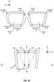
- FIG. 1 Ais a diagram of an example of a near-eye display 100 .
- Near-eye display 100presents media to a user. Examples of media presented by near-eye display 100 include one or more images, video, and/or audio.
- audiois presented via an external device (e.g., speakers and/or headphones) that receives audio information from the near-eye display 100 , a console, or both, and presents audio data based on the audio information.
- Near-eye display 100is generally configured to operate as a virtual reality (VR) display.
- near-eye display 100is modified to operate as an augmented reality (AR) display and/or a mixed reality (MR) display.
- ARaugmented reality
- MRmixed reality
- Near-eye display 100includes a frame 105 and a display 110 .
- Frame 105is coupled to one or more optical elements.
- Display 110is configured for the user to see content presented by near-eye display 100 .
- display 110comprises a waveguide display assembly for directing light from one or more images to an eye of the user.
- Near-eye display 100further includes image sensors 120 a , 120 b , 120 c , and 120 d .
- image sensors 120 a , 120 b , 120 c , and 120 dmay include a pixel array configured to generate image data representing different fields of views along different directions.
- sensors 120 a and 120 bmay be configured to provide image data representing two fields of view towards a direction A along the Z axis
- sensor 120 cmay be configured to provide image data representing a field of view towards a direction B along the X axis
- sensor 120 dmay be configured to provide image data representing a field of view towards a direction C along the X axis.
- sensors 120 a - 120 dcan be configured as input devices to control or influence the display content of the near-eye display 100 , to provide an interactive VR/AR/MR experience to a user who wears near-eye display 100 .
- sensors 120 a - 120 dcan generate physical image data of a physical environment in which the user is located.
- the physical image datacan be provided to a location tracking system to track a location and/or a path of movement of the user in the physical environment.
- a systemcan then update the image data provided to display 110 based on, for example, the location and orientation of the user, to provide the interactive experience.
- the location tracking systemmay operate a SLAM algorithm to track a set of objects in the physical environment and within a view of field of the user as the user moves within the physical environment.
- the location tracking systemcan construct and update a map of the physical environment based on the set of objects, and track the location of the user within the map.
- sensors 120 a - 120 dcan provide the location tracking system a more holistic view of the physical environment, which can lead to more objects to be included in the construction and updating of the map. With such an arrangement, the accuracy and robustness of tracking a location of the user within the physical environment can be improved.
- near-eye display 100may further include one or more active illuminators 130 to project light into the physical environment.
- the light projectedcan be associated with different frequency spectrums (e.g., visible light, infra-red light, ultra-violet light, etc.), and can serve various purposes.
- illuminator 130may project light in a dark environment (or in an environment with low intensity of infra-red light, ultra-violet light, etc.) to assist sensors 120 a - 120 d in capturing images of different objects within the dark environment to, for example, enable location tracking of the user.
- Illuminator 130may project certain markers onto the objects within the environment, to assist the location tracking system in identifying the objects for map construction/updating.
- illuminator 130may also enable stereoscopic imaging.
- sensors 120 a or 120 bcan include both a first pixel array for visible light sensing and a second pixel array for infra-red (IR) light sensing.
- the first pixel arraycan be overlaid with a color filter (e.g., a Bayer filter), with each pixel of the first pixel array being configured to measure intensity of light associated with a particular color (e.g., one of red, green or blue colors).
- the second pixel array(for IR light sensing) can also be overlaid with a filter that allows only IR light through, with each pixel of the second pixel array being configured to measure intensity of IR lights.
- the pixel arrayscan generate an RGB image and an IR image of an object, with each pixel of the IR image being mapped to each pixel of the RGB image.
- Illuminator 130may project a set of IR markers on the object, the images of which can be captured by the IR pixel array. Based on a distribution of the IR markers of the object as shown in the image, the system can estimate a distance of different parts of the object from the IR pixel array, and generate a stereoscopic image of the object based on the distances. Based on the stereoscopic image of the object, the system can determine, for example, a relative position of the object with respect to the user, and can update the image data provided to display 100 based on the relative position information to provide the interactive experience.
- near-eye display 100may be operated in environments associated with a very wide range of light intensities.
- near-eye display 100may be operated in an indoor environment or in an outdoor environment, and/or at different times of the day.
- Near-eye display 100may also operate with or without active illuminator 130 being turned on.
- image sensors 120 a - 120 dmay need to have a wide dynamic range to be able to operate properly (e.g., to generate an output that correlates with the intensity of incident light) across a very wide range of light intensities associated with different operating environments for near-eye display 100 .
- FIG. 1 Bis a diagram of another example of near-eye display 100 .
- FIG. 1 Billustrates a side of near-eye display 100 that faces the eyeball(s) 135 of the user who wears near-eye display 100 .
- near-eye display 100may further include a plurality of illuminators 140 a , 140 b , 140 c , 140 d , 140 e , and 140 f .
- Near-eye display 100further includes a plurality of image sensors 150 a and 150 b .
- Illuminators 140 a , 140 b , and 140 cmay emit lights of certain frequency range (e.g., NIR) towards direction D (which is opposite to direction A of FIG. 1 A ).
- the emitted lightmay be associated with a certain pattern, and can be reflected by the left eyeball of the user.
- Sensor 150 amay include a pixel array to receive the reflected light and generate an image of the reflected pattern.
- illuminators 140 d , 140 e , and 140 fmay emit NIR lights carrying the pattern. The NIR lights can be reflected by the right eyeball of the user, and may be received by sensor 150 b .
- Sensor 150 bmay also include a pixel array to generate an image of the reflected pattern. Based on the images of the reflected pattern from sensors 150 a and 150 b , the system can determine a gaze point of the user, and update the image data provided to display 100 based on the determined gaze point to provide an interactive experience to the user.
- illuminators 140 a , 140 b , 140 c , 140 d , 140 e , and 140 fare typically configured to output lights of very low intensities.
- image sensors 150 a and 150 bcomprise the same sensor devices as image sensors 120 a - 120 d of FIG. 1 A
- the image sensors 120 a - 120 dmay need to be able to generate an output that correlates with the intensity of incident light when the intensity of the incident light is very low, which may further increase the dynamic range requirement of the image sensors.
- the image sensors 120 a - 120 dmay need to be able to generate an output at a high speed to track the movements of the eyeballs.
- a user's eyeballcan perform a very rapid movement (e.g., a saccade movement) in which there can be a quick jump from one eyeball position to another.
- image sensors 120 a - 120 dneed to generate images of the eyeball at high speed.
- the rate at which the image sensors generate an image frame(the frame rate) needs to at least match the speed of movement of the eyeball.
- the high frame raterequires short total exposure time for all of the pixel cells involved in generating the image frame, as well as high speed for converting the sensor outputs into digital values for image generation. Moreover, as discussed above, the image sensors also need to be able to operate at an environment with low light intensity.
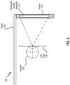
- FIG. 2is an example of a cross section 200 of near-eye display 100 illustrated in FIG. 1 .
- Display 110includes at least one waveguide display assembly 210 .
- An exit pupil 230is a location where a single eyeball 220 of the user is positioned in an eyebox region when the user wears the near-eye display 100 .
- FIG. 2shows the cross section 200 associated eyeball 220 and a single waveguide display assembly 210 , but a second waveguide display is used for a second eye of a user.
- Waveguide display assembly 210is configured to direct image light to an eyebox located at exit pupil 230 and to eyeball 220 .
- Waveguide display assembly 210may be composed of one or more materials (e.g., plastic, glass, etc.) with one or more refractive indices.
- near-eye display 100includes one or more optical elements between waveguide display assembly 210 and eyeball 220 .
- waveguide display assembly 210includes a stack of one or more waveguide displays including, but not restricted to, a stacked waveguide display, a varifocal waveguide display, etc.
- the stacked waveguide displayis a polychromatic display (e.g., a red-green-blue (RGB) display) created by stacking waveguide displays whose respective monochromatic sources are of different colors.
- the stacked waveguide displayis also a polychromatic display that can be projected on multiple planes (e.g., multi-planar colored display).
- the stacked waveguide displayis a monochromatic display that can be projected on multiple planes (e.g., multi-planar monochromatic display).
- the varifocal waveguide displayis a display that can adjust a focal position of image light emitted from the waveguide display.
- waveguide display assembly 210may include the stacked waveguide display and the varifocal waveguide display.
- FIG. 3illustrates an isometric view of an example of a waveguide display 300 .
- waveguide display 300is a component (e.g., waveguide display assembly 210 ) of near-eye display 100 .
- waveguide display 300is part of some other near-eye display or other system that directs image light to a particular location.
- Waveguide display 300includes a source assembly 310 , an output waveguide 320 , and a controller 330 .
- FIG. 3shows the waveguide display 300 associated with a single eyeball 220 , but in some examples, another waveguide display separate, or partially separate, from the waveguide display 300 provides image light to another eye of the user.
- Source assembly 310generates image light 355 .
- Source assembly 310generates and outputs image light 355 to a coupling element 350 located on a first side 370 - 1 of output waveguide 320 .
- Output waveguide 320is an optical waveguide that outputs expanded image light 340 to an eyeball 220 of a user.
- Output waveguide 320receives image light 355 at one or more coupling elements 350 located on the first side 370 - 1 and guides received input image light 355 to a directing element 360 .
- coupling element 350couples the image light 355 from source assembly 310 into output waveguide 320 .
- Coupling element 350may be, e.g., a diffraction grating, a holographic grating, one or more cascaded reflectors, one or more prismatic surface elements, and/or an array of holographic reflectors.
- Directing element 360redirects the received input image light 355 to decoupling element 365 such that the received input image light 355 is decoupled out of output waveguide 320 via decoupling element 365 .
- Directing element 360is part of, or affixed to, first side 370 - 1 of output waveguide 320 .
- Decoupling element 365is part of, or affixed to, second side 370 - 2 of output waveguide 320 , such that directing element 360 is opposed to the decoupling element 365 .
- Directing element 360 and/or decoupling element 365may be, e.g., a diffraction grating, a holographic grating, one or more cascaded reflectors, one or more prismatic surface elements, and/or an array of holographic reflectors.
- Second side 370 - 2represents a plane along an x-dimension and a y-dimension.
- Output waveguide 320may be composed of one or more materials that facilitate total internal reflection of image light 355 .
- Output waveguide 320may be composed of e.g., silicon, plastic, glass, and/or polymers.
- Output waveguide 320has a relatively small form factor. For example, output waveguide 320 may be approximately 50 mm wide along x-dimension, 30 mm long along y-dimension and 0.5-1 mm thick along a z-dimension.
- Controller 330controls scanning operations of source assembly 310 .
- the controller 330determines scanning instructions for the source assembly 310 .
- the output waveguide 320outputs expanded image light 340 to the user's eyeball 220 with a large field of view (FOV).
- FOVfield of view
- the expanded image light 340is provided to the user's eyeball 220 with a diagonal FOV (in x and y) of 60 degrees and/or greater and/or 150 degrees and/or less.
- the output waveguide 320is configured to provide an eyebox with a length of 20 mm or greater and/or equal to or less than 50 mm; and/or a width of 10 mm or greater and/or equal to or less than 50 mm.
- controller 330also controls image light 355 generated by source assembly 310 , based on image data provided by image sensor 370 .
- Image sensor 370may be located on first side 370 - 1 and may include, for example, image sensors 120 a - 120 d of FIG. 1 A to generate image data of a physical environment in front of the user (e.g., for location determination).
- Image sensor 370may also be located on second side 370 - 2 and may include image sensors 150 a and 150 b of FIG. 1 B to generate image data of eyeball 220 (e.g., for gaze point determination) of the user.
- Image sensor 370may interface with a remote console that is not located within waveguide display 300 .
- Image sensor 370may provide image data to the remote console, which may determine, for example, a location of the user, a gaze point of the user, etc., and determine the content of the images to be displayed to the user.
- the remote consolecan transmit instructions to controller 330 related to the determined content. Based on the instructions, controller 330 can control the generation and outputting of image light 355 by source assembly 310 .
- FIG. 4illustrates an example of a cross section 400 of the waveguide display 300 .
- the cross section 400includes source assembly 310 , output waveguide 320 , and image sensor 370 .
- image sensor 370may include a set of pixel cells 402 located on first side 370 - 1 to generate an image of the physical environment in front of the user.
- the mechanical shutter 404can be replaced by an electronic shutter gate, as to be discussed below.
- Each of pixel cells 402may correspond to one pixel of the image.
- each of pixel cells 402may also be overlaid with a filter to control the frequency range of the light to be sensed by the pixel cells.
- mechanical shutter 404can open and expose the set of pixel cells 402 in an exposure period.
- image sensor 370can obtain samples of lights incident on the set of pixel cells 402 , and generate image data based on an intensity distribution of the incident light samples detected by the set of pixel cells 402 .
- Image sensor 370can then provide the image data to the remote console, which determines the display content, and provide the display content information to controller 330 .
- Controller 330can then determine image light 355 based on the display content information.
- Source assembly 310generates image light 355 in accordance with instructions from the controller 330 .
- Source assembly 310includes a source 410 and an optics system 415 .
- Source 410is a light source that generates coherent or partially coherent light.
- Source 410may be, e.g., a laser diode, a vertical cavity surface emitting laser, and/or a light emitting diode.
- Optics system 415includes one or more optical components that condition the light from source 410 .
- Conditioning light from source 410may include, e.g., expanding, collimating, and/or adjusting orientation in accordance with instructions from controller 330 .
- the one or more optical componentsmay include one or more lenses, liquid lenses, mirrors, apertures, and/or gratings.
- optics system 415includes a liquid lens with a plurality of electrodes that allows scanning of a beam of light with a threshold value of scanning angle to shift the beam of light to a region outside the liquid lens. Light emitted from the optics system 415 (and also source assembly 310 ) is referred to as image light 355 .
- Output waveguide 320receives image light 355 .
- Coupling element 350couples image light 355 from source assembly 310 into output waveguide 320 .
- a pitch of the diffraction gratingis chosen such that total internal reflection occurs in output waveguide 320 , and image light 355 propagates internally in output waveguide 320 (e.g., by total internal reflection), toward decoupling element 365 .
- Directing element 360redirects image light 355 toward decoupling element 365 for decoupling from output waveguide 320 .
- the pitch of the diffraction gratingis chosen to cause incident image light 355 to exit output waveguide 320 at angle(s) of inclination relative to a surface of decoupling element 365 .
- Expanded image light 340 exiting output waveguide 320is expanded along one or more dimensions (e.g., may be elongated along x-dimension).
- waveguide display 300includes a plurality of source assemblies 310 and a plurality of output waveguides 320 .
- Each of source assemblies 310emits a monochromatic image light of a specific band of wavelength corresponding to a primary color (e.g., red, green, or blue).
- Each of output waveguides 320may be stacked together with a distance of separation to output an expanded image light 340 that is multi-colored.
- FIG. 5is a block diagram of an example of a system 500 including the near-eye display 100 .
- the system 500comprises near-eye display 100 , an imaging device 535 , an input/output interface 540 , and image sensors 120 a - 120 d and 150 a - 150 b that are each coupled to control circuitries 510 .
- System 500can be configured as a head-mounted device, a wearable device, etc.
- Near-eye display 100is a display that presents media to a user. Examples of media presented by the near-eye display 100 include one or more images, video, and/or audio. In some examples, audio is presented via an external device (e.g., speakers and/or headphones) that receives audio information from near-eye display 100 and/or control circuitries 510 and presents audio data based on the audio information to a user. In some examples, near-eye display 100 may also act as an AR eyewear glass. In some examples, near-eye display 100 augments views of a physical, real-world environment, with computer-generated elements (e.g., images, video, sound, etc.).
- computer-generated elementse.g., images, video, sound, etc.
- Near-eye display 100includes waveguide display assembly 210 , one or more position sensors 525 , and/or an inertial measurement unit (IMU) 530 .
- Waveguide display assembly 210includes source assembly 310 , output waveguide 320 , and controller 330 .
- IMU 530is an electronic device that generates fast calibration data indicating an estimated position of near-eye display 100 relative to an initial position of near-eye display 100 based on measurement signals received from one or more of position sensors 525 .
- Imaging device 535may generate image data for various applications. For example, imaging device 535 may generate image data to provide slow calibration data in accordance with calibration parameters received from control circuitries 510 . Imaging device 535 may include, for example, image sensors 120 a - 120 d of FIG. 1 A for generating image data of a physical environment in which the user is located, for performing location tracking of the user. Imaging device 535 may further include, for example, image sensors 150 a - 150 b of FIG. 1 B for generating image data for determining a gaze point of the user, to identify an object of interest of the user.
- the input/output interface 540is a device that allows a user to send action requests to the control circuitries 510 .
- An action requestis a request to perform a particular action.
- an action requestmay be to start or end an application or to perform a particular action within the application.
- Control circuitries 510provide media to near-eye display 100 for presentation to the user in accordance with information received from one or more of: imaging device 535 , near-eye display 100 , and input/output interface 540 .
- control circuitries 510can be housed within system 500 configured as a head-mounted device.
- control circuitries 510can be a standalone console device communicatively coupled with other components of system 500 .
- control circuitries 510include an application store 545 , a tracking module 550 , and an engine 555 .
- the application store 545stores one or more applications for execution by the control circuitries 510 .
- An applicationis a group of instructions, that, when executed by a processor, generates content for presentation to the user. Examples of applications include: gaming applications, conferencing applications, video playback applications, or other suitable applications.
- Tracking module 550calibrates system 500 using one or more calibration parameters and may adjust one or more calibration parameters to reduce error in determination of the position of the near-eye display 100 .
- Tracking module 550tracks movements of near-eye display 100 using slow calibration information from the imaging device 535 . Tracking module 550 also determines positions of a reference point of near-eye display 100 using position information from the fast calibration information.
- Engine 555executes applications within system 500 and receives position information, acceleration information, velocity information, and/or predicted future positions of near-eye display 100 from tracking module 550 .
- information received by engine 555may be used for producing a signal (e.g., display instructions) to waveguide display assembly 210 that determines a type of content presented to the user.
- engine 555may determine the content to be presented to the user based on a location of the user (e.g., provided by tracking module 550 ), or a gaze point of the user (e.g., based on image data provided by imaging device 535 ), a distance between an object and user (e.g., based on image data provided by imaging device 535 ).
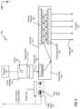
- FIG. 6illustrates an example of a pixel cell 600 .
- Pixel cell 600may be part of a pixel array and can generate digital intensity data corresponding to a pixel of an image.
- pixel cell 600may be part of pixel cells 402 of FIG. 4 .
- pixel cell 600may include a photodiode 602 as well as processing circuits including a shutter switch 604 , a transfer gate 606 , a reset switch 607 , a charge sensing unit 608 comprising charge storage unit 608 a and a buffer 608 b , and a pixel ADC 610 .
- photodiode 602may include, for example, a P-N diode, a P-I-N diode, a pinned diode, etc.
- Photodiode 602can generate charge upon receiving light, and the quantity of charge generated can be proportional to the intensity of the light.
- Photodiode 602can also store some of the generated charge until the photodiode saturates, which occurs when the well capacity of the photodiode is reached.
- each of shutter switch 604 , transfer gate 606 , and reset switch 607can include a transistor.
- the transistormay include, for example, a metal-oxide-semiconductor field-effect transistor (MOSFET), a bipolar junction transistor (BJT), etc.
- MOSFETmetal-oxide-semiconductor field-effect transistor
- BJTbipolar junction transistor
- Shutter switch 604can act as an electronic shutter gate (in lieu of, or in combination with, mechanical shutter 404 of FIG. 4 ) to control an exposure period of pixel cell 600 .
- shutter switch 604can be disabled (turned off) by exposure enable signal 611 , which allows photodiode 602 to store the generated charge and, when photodiode 602 saturates, allows the overflow charge to flow to charge storage unit 608 a .
- shutter switch 604can be enabled to steer the charge generated by photodiode 602 into photodiode current sink 617 .
- reset switch 607can also be disabled (turned off) by reset signal 618 , which allows charge storage unit 608 a to accumulate the charge.
- Charge storage unit 608 acan be a device capacitor at a floating terminal of transfer gate 606 , a metal capacitor, a MOS capacitor, or any combination thereof.
- Charge storage unit 608 acan be used to convert a quantity of charge to an analog voltage, which can be measured by pixel ADC 610 to provide a digital output representing the incident light intensity.
- reset switch 607can be enabled to empty the charge stored at charge storage unit 608 a to charge sink 620 , to make charge storage unit 608 a available for the next measurement.
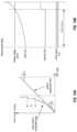
- FIG. 7illustrates a quantity of charge accumulated with respect to time for different light intensity ranges.
- the total quantity of charge accumulated at a particular time pointcan reflect the intensity of light incident upon photodiode 602 during an exposure period. The quantity can be measured when the exposure period ends.
- a threshold 702 and a threshold 704can be defined for a threshold's quantity of charge defining a low light intensity range 706 , a medium light intensity range 708 , and a high light intensity range 710 for the intensity of the incident light. For example, if the total accumulated charge is below threshold 702 (e.g., Q1), the incident light intensity is within low light intensity range 706 .
- threshold 702e.g., Q1
- the incident light intensityis within medium light intensity range 708 . If the total accumulated charge is above threshold 704 , the incident light intensity is within medium light intensity range 710 .
- the quantity of the accumulated charge, for low and medium light intensity ranges,can correlate with the intensity of the incident light, if the photodiode does not saturate within the entire low light intensity range 706 and the measurement capacitor does not saturate within the entire medium light intensity range 708 .
- low light intensity range 706 and medium light intensity range 708can be based on the storage capacities of photodiode 602 and charge storage unit 608 a .
- low light intensity range 706can be defined such that the total quantity of charge stored in photodiode 602 , at the end of the exposure period, is below or equal to the storage capacity of the photodiode, and threshold 702 can be based on the storage capacity of photodiode 602 .
- threshold 702can be set based on a scaled storage capacity of photodiode 602 to account for potential capacity variation of the photodiode.
- medium light intensity range 708can be defined such that the total quantity of charge stored in charge storage unit 608 a , at the end of the exposure period, is below or equal to the storage capacity of the measurement capacitor, and threshold 704 can be based on the storage capacity of charge storage unit 608 a .
- threshold 704is also set to be based on a scaled storage capacity of charge storage unit 608 a to ensure that when the quantity of charge stored in charge storage unit 608 a is measured for intensity determination, the measurement capacitor does not saturate, and the measured quantity also relates to the incident light intensity.
- thresholds 702 and 704can be used to detect whether photodiode 602 and charge storage unit 608 a saturate, which can determine the intensity range of the incident light and the measurement result to be output.
- the total overflow charge accumulated at charge storage unit 608 amay exceed threshold 704 before the exposure period ends.
- charge storage unit 608 amay reach full capacity before the end of the exposure period, and charge leakage may occur.
- a time-to-saturation measurementcan be performed to measure the time duration it takes for the total overflow charge accumulated at charge storage unit 608 a to reach threshold 704 .
- a rate of charge accumulation at charge storage unit 608 acan be determined based on a ratio between threshold 704 and the time-to-saturation, and a hypothetical quantity of charge (Q3) that could have been accumulated at charge storage unit 608 a at the end of the exposure period (if the capacitor had limitless capacity) can be determined by extrapolation according to the rate of charge accumulation.
- the hypothetical quantity of charge (Q3)can provide a reasonably accurate representation of the incident light intensity within high light intensity range 710 .
- transfer gate 606can be controlled by a measurement control signal 612 to control the charge accumulations at residual charge capacitor 603 (do not see this in the FIG.) and charge storage unit 608 a for different light intensity ranges as described above.
- transfer gate 606can be controlled to operate in a partially turned-on state.
- the gate voltage of transfer gate 606can be set based on a voltage developed at photodiode 602 corresponding to the charge storage capacity of the photodiode.
- transfer gate 606can be controlled in a fully turned-on state to transfer the charge stored in photodiode 602 to charge storage unit 608 a , to measure the quantity of the charge stored in photodiode 602 .
- the analog voltage generated by charge accumulation at charge storage unit 608 acan be buffered by buffer 608 b to generate a replica of the analog voltage (but with larger driving strength) at analog output node 614 .
- the analog voltage at analog output node 614can be converted into a set of digital data (e.g., comprising logical ones and zeros) by pixel ADC 610 .
- the analog voltage developed at charge storage unit 608 acan be sampled and digital output can be generated before the end of the exposure period (e.g., for medium light intensity range 708 and high light intensity range 710 ), or after the exposure period (for low light intensity range 706 ).
- the digital datacan be transmitted by a set of pixel output buses 616 to, for example, control circuitries 510 of FIG. 5 , to represent the light intensity during the exposure period.
- the capacitance of charge storage unit 608 acan be configurable to improve the accuracy of light intensity determination for a low light intensity range.
- the capacitance of charge storage unit 608 acan be reduced when charge storage unit 608 a is used to measure the residual charge stored at photodiode 602 .
- the reduction in the capacitance of charge storage unit 608 acan increase the charge-to-voltage conversion ratio at charge storage unit 608 a , such that a higher voltage can be developed for a certain quantity of stored charge.
- the higher charge-to-voltage conversion ratiocan reduce the effect of measurement errors (e.g., quantization error, comparator offset, etc.) introduced by pixel ADC 610 on the accuracy of low light intensity determination.
- the measurement errorcan set a limit on a minimum voltage difference that can be detected and/or differentiated by pixel ADC 610 .
- the quantity of charge corresponding to the minimum voltage differencecan be reduced, which in turn reduces the lower limit of a measurable light intensity by pixel cell 600 and extends the dynamic range.
- the capacitance of charge storage unit 608 acan be increased to ensure that the charge storage unit 608 a has sufficient capacity to store a quantity of charge up to, for example, the quantity defined by threshold 704 .
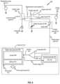
- FIG. 8illustrates an example of the internal components of pixel ADC 610 .
- pixel ADC 610includes a threshold generator 802 , a comparator 804 , and a digital output generator 806 .
- Digital output generator 806may further include a counter 808 and a memory 810 .
- Counter 808can generate a set of count values based on a free-running clock signal 812 , whereas memory 810 can store at least some of the count values (e.g., the latest count value) generated by counter 808 .
- memory 810may be part of counter 808 .
- Memory 810can be, for example, a latch circuit to store the counter value based on local pixel value as described below.
- Threshold generator 802includes a digital-to-analog converter (DAC) 813 which can accept a set of digital values and output a reference voltage (VREF) 815 representing the set of digital values.
- DACdigital-to-analog converter
- VREFreference voltage
- threshold generator 802may accept static digital values to generate a fixed threshold, or accept output 814 of counter 808 to generate a ramping threshold.
- FIG. 8illustrates that DAC 813 (and threshold generator 802 ) is part of pixel ADC 610 , it is understood that DAC 813 (and threshold generator 802 ) can be coupled with multiple digital output generators 806 from different pixel cells. Moreover, at least part of digital output generator 806 , such as counter 808 , can be shared among a plurality of multiple pixel cells to generate the digital values.
- Comparator 804can compare the analog voltage developed at analog output node 614 against the threshold provided by threshold generator 802 , and generate a decision 816 based on the comparison result. For example, comparator 804 can generate a logical one for decision 816 if the analog voltage at analog output node 614 equals or exceeds the threshold generated by threshold generator 802 . Comparator 804 can also generate a logical zero for decision 816 if the analog voltage falls below the threshold. Decision 816 can control the counting operations of counter 808 and/or the count values stored in memory 810 , to perform the aforementioned time-of-saturation measurement of a ramping analog voltage at analog output node 614 as well as quantization processing of the analog voltage at analog output node 614 for incident light intensity determination.
- FIG. 9 Aillustrates an example of time-to-saturation measurement by pixel ADC 610 .
- threshold generator 802can control DAC 813 to generate a fixed VREF 815 .
- Fixed VREF 815can be set at a voltage corresponding a charge quantity threshold for saturation of charge storage unit 608 a (e.g., threshold 704 of FIG. 7 ).
- Counter 808can start counting right after the exposure period starts (e.g., right after shutter switch 604 is disabled). As the analog voltage at analog output node 614 ramps down (or up depending on the implementation), clock signal 812 keeps toggling to update the count value at counter 808 .
- the analog voltagemay reach the fixed threshold at a certain time point, which causes decision 816 by comparator 804 to flip.
- the flipping of decision 816may stop the counting of counter 808 , and the count value at counter 808 may represent the time-to-saturation.
- a rate of charge accumulation at charge storage unit 608 acan also be determined based on the duration, and the incident light intensity can be determined based on the rate of charge accumulation.
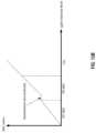
- FIG. 9 Billustrates an example of quantizing an analog voltage by pixel ADC 610 .
- DAC 813may be programmed by counter output 814 to generate a ramping VREF 815 , which can either ramp up (in the example of FIG. 9 B ) or ramp down depending on implementation.
- the voltage range of ramping VREF 815can be between threshold 704 (charge quantity threshold for saturation of charge storage unit 608 a ) and threshold 702 (charge quantity threshold for saturation of photodiode 602 ), which can define the medium light intensity range.
- the quantization processcan be performed with uniform quantization steps, with VREF 815 increasing (or decreasing) by the same amount for each clock cycle of clock signal 812 .
- the amount of increase (or decrease) of VREF 815corresponds to a quantization step.
- decision 816 by comparator 804flips from negative to positive.
- the flipping of decision 816may stop the counting of counter 808 , and the count value can correspond to a total number of quantization steps accumulated to match, within one quantization step, the analog voltage.
- the count valuecorresponds to a measurement of time it takes for VREF 815 to reach the analog voltage and can be a digital representation of the quantity of charge stored at charge storage unit 608 a , as well as the digital representation of the incident light intensity.
- the quantization of the analog voltagecan occur during the exposure period (e.g., for medium light intensity range 708 ) and after the exposure period (e.g., for low light intensity range 706 ).
- ADC 610can introduce quantization errors when there is a mismatch between a quantity of charge represented by the quantity level output by ADC 610 (e.g., represented by the total number of quantization steps) and the actual input quantity of charge that is mapped to the quantity level by ADC 610 .
- the quantization errorcan be reduced by using a smaller quantization step size.
- the quantization step sizecan be reduced by the amount of increase (or decrease) in VREF 815 per clock cycle based on, for example, reducing input range 902 of the quantization operation (between thresholds 702 and 704 ), reducing the corresponding range of time to be measured by counter 808 , increasing the clock frequency of clock signal 812 , or any combination therefore.
- quantization errorcan be reduced by using smaller quantization step sizes, area and performance speed may limit how far the quantization step can be reduced.
- the total number of quantization steps needed to represent a particular range of charge quantities (and light intensity)may increase.
- a larger number of data bitsmay be needed to represent the increased number of quantization steps (e.g., 8 bits to represent 255 steps, 7 bits to represent 127 steps, etc.).
- the larger number of data bitsmay require additional buses to be added to pixel output buses 616 , which may not be feasible if pixel cell 600 is used on a head-mounted device or other wearable devices with very limited spaces.
- ADC 610may need to cycle through a larger number of quantization steps before finding the quantity level that matches (with one quantization step), which leads to increased processing power consumption and time, and reduced rate of generating image data.
- the reduced ratemay not be acceptable for some applications that require a high frame rate (e.g., an application that tracks the movement of the eyeball).
- FIG. 10 Aillustrates an example of a mapping between the ADC codes (the output of the quantization process) and the input charge quantity level for a non-uniform quantization process and a uniform quantization process.
- the dotted lineillustrates the mapping for the non-uniform quantization process, whereas the solid line illustrates the mapping for the uniform quantization process.
- the quantization step size(denoted by ⁇ 1 ) is identical for the entire range of input charge quantity.
- the quantization step sizesare different depending on the input charge quantity.
- the quantization step size for a low input charge quantity(denoted by ⁇ S ) is smaller than the quantization step size for a large input charge quantity (denoted by ⁇ L ).
- the quantization step size for the non-uniform quantization process ( ⁇ S )can be made smaller than the quantization step size for the uniform quantization process ( ⁇ 1 ).
- One advantage of employing a non-uniform quantization schemeis that the quantization steps for quantizing low input charge quantities can be reduced, which in turn reduces the quantization errors for quantizing the low input charge quantities, and the minimum input charge quantities that can be differentiated by ADC 610 can be reduced. Therefore, the reduced quantization errors can push down the lower limit of the measureable light intensity of the image sensor, and the dynamic range can be increased. Moreover, although the quantization errors are increased for the high input charge quantities, the quantization errors may remain small compared with high input charge quantities. Therefore, the overall quantization errors introduced to the measurement of the charge can be reduced.
- the total number of quantization steps covering the entire range of input charge quantitiesmay remain the same (or even reduced), and the aforementioned potential problems associated with increasing the number of quantization steps (e.g., increase in area, reduction in processing speed, etc.) can be avoided.
- FIG. 10 Billustrates an example of quantizing an analog voltage by pixel ADC 610 using a non-uniform quantization process.
- VREF 815increases in a non-linear fashion with each clock cycle, with a shallower slope initially and a steeper slope at a later time. The differences in the slopes are attributed to the uneven quantization step sizes.
- the quantization stepsare made smaller, hence VREF 815 increases at a slower rate.
- the quantization stepsare made larger, hence VREF 815 increases at a higher rate.
- the uneven quantization steps in VREF 815can be introduced using different schemes.
- DAC 813is configured to output voltages for different counter count values (from counter 808 ).
- DAC 813can be configured such that the difference in the output voltage between two neighboring counter count values (which defines the quantization step size) is different for different counter count values.
- counter 808can also be configured to generate jumps in the counter count values, instead of increasing or decreasing by the same count step, to generate the uneven quantization steps.
- the non-uniform quantization process of FIG. 10 Bcan be employed for light intensity determination for low light intensity range 706 and medium light intensity range 708 .
- FIG. 11illustrates an example of pixel cell 1100 , which can be an example of pixel cell 600 of FIG. 6 .
- PDcan correspond to photodiode 602
- transistor M 0can correspond to shutter switch 604
- transistor M 1can correspond to transfer gate 606
- transistor M 2can correspond to reset switch 607 .
- a combination of COF and CEXT capacitorscan correspond to charge storage unit 608 a .
- COF capacitorcan be the parasitic capacitor of a floating drain node.
- the capacitance of charge storage unit 608 ais configurable by the signal LG. When LG is enabled, charge storage unit 608 a provides combined capacities of COF and CEXT capacitors.
- CEXT capacitorWhen LG is disabled, CEXT capacitor can be disconnected from the parallel combination, and charge storage unit 608 a comprises only a COF capacitor (plus other parasitic capacitances). As discussed above, the capacitance of charge storage unit 608 a can be reduced to increase the charge-to-voltage conversion ratio for the low light intensity determination, and can be increased to provide the requisite capacity for the medium light intensity determination.
- Pixel cell 1100further includes an example of buffer 608 b and an example of pixel ADC 610 .
- transistors M 3 and M 4form a source follower which can be buffer 608 b of FIG. 6 to buffer an analog voltage developed at the OF node, which represents a quantity of charge stored at the COF capacitor (or at the COF and CEXT capacitors).
- the CC capacitor, comparator 1102 , transistor M 5 , NOR gate 1112 , together with memory 810can be part of pixel ADC 610 to generate a digital output representing the analog voltage at the OF node.
- the quantizationcan be based on a comparison result (VOUT), generated by comparator 1102 , between the analog voltage developed at the OF node and VREF.
- the CC capacitoris configured to generate a VIN voltage (at one input of comparator 1102 ) which tracks the output of buffer 608 b , and provides the VIN voltage to comparator 1102 to compare against VREF.
- VREFcan be a static voltage for time-of-saturation measurement (for high light intensity range) or a ramping voltage for quantization of an analog voltage (for low and medium light intensity ranges).
- the ADC codecan be generated by a free-running counter (e.g., counter 808 ), and the comparison result generated by comparator 1102 can determine the ADC code to be stored in memory 810 and to be output as the digital representation of the incident light intensity.
- the generation of VREF for low and medium light intensity determinationcan be based on a non-uniform quantization scheme as discussed in FIG. 10 A and FIG. 10 B .
- Pixel cell 1100includes techniques that can further improve the accuracy of the incident light intensity determination, in addition to the techniques disclosed above.
- the combination of the CC capacitor and transistor M 5can be used to compensate for measurement errors (e.g., comparator offset) introduced by comparator 1102 , as well as other error signals that are introduced to comparator 1102 , such that the accuracy of comparator 1102 can be improved.
- the noise signalsmay include, for example, reset noise charge introduced by reset switch 607 , a noise signal at the output of buffer 608 b due to source follower threshold mismatches, etc.
- a quantity of charge reflecting the comparator offset as well as the error signalscan be stored at the CC capacitor during a reset phase, when both transistors M 2 and M 5 are enabled.
- a voltage differencecan also be developed across the CC capacitor during the reset phase due to the stored charge.
- the voltage difference across the CC capacitorremains, and the CC capacitor can track the output voltage of buffer 608 b by subtracting away (or adding) the voltage difference to generate VIN.
- the VIN voltagecan be compensated for the measurement errors and the error signals, which improves the accuracy of the comparison between VIN and VREF and the ensuing quantization.
- pixel cell 1100further includes a controller 1110 .
- Controller 1110can generate a sequence of control signals, such as SHUTTER, TX, RST 1 , RST 2 , etc., to operate pixel cell 1100 to perform a three-phase measurement operation corresponding to the three light intensity ranges of FIG. 7 (e.g., low light intensity range 706 , medium light intensity range 708 , and high light intensity range 710 ).
- pixel cell 1100can be operated in a measurement mode targeted for the corresponding light intensity range, and determine whether the incident light intensity falls within the corresponding light intensity range based on the decision output (VOUT) of comparator 1102 .
- Pixel cell 1100further includes a set of registers to store the decision outputs of some of the phases as FLAG_ 1 and FLAG_ 2 signals. Based on the FLAG_ 1 and FLAG_ 2 signals, controller 1110 can select the ADC code from one of the three phases to represent the incident light intensity. The selected ADC code can be stored in memory 810 , and memory 810 can be locked based on a combination of the FLAG_ 1 and FLAG_ 2 signals by NOR gate 1116 to prevent subsequent measurement phases from overwriting the selected ADC code output in memory 810 . At the end of the three-phase measurement process, controller 1110 can retrieve the ADC code stored in memory 810 and provide the ADC code as the digital output representing the incident light intensity.
- FIG. 12illustrates a sequence of control signals of pixel cell 1100 for the three-phase measurement operation with respect to time.
- the time between T 0 ′ and T 0corresponds to a first reset phase.
- the time period between T 0 and T 1can correspond to an exposure period and a time-to-saturation measurement mode.
- the time period between T 1 and T 2corresponds to a measurement mode to measure a quantity of overflow charge stored in a floating drain.
- the measurement mode for measurement of overflow chargeis labelled “FD ADC” in FIG. 12 and can be used to measure medium light intensity 708 .
- the time period between T 2 and T 3includes a second reset phase followed by transfer of charge stored in photodiode 602 to the floating drain.
- the time period between T 3 and T 4corresponds to a measurement mode to measure a quantity of charge stored in the photodiode and transferred to the floating drain.
- the measurement mode for measuring the charge stored in the photodiodeis labelled “PD ADC” in FIG. 12 and can be used to measure low light intensity 712 .
- Pixel cell 1100can provide the digital output representing the incident light intensity at time T 4 , and then start the next three-phase measurement operation.
- V LOWcan correspond to the charge capacity of the photodiode PD to allow only overflow charge (if any) to flow from the photodiode PD to the CEXT capacitor and the COF capacitor via transistor M 1 .
- the voltage across the photodiode PD, as well as the OF node,can be set to a voltage equal to V RESET , which can represent a state where the photodiode PD, the CEXT capacitor, and the COF capacitor do not store any charge.
- comparator 1102is also in a reset phase, and the CC capacitor can store charge reflecting the reset noise introduced by M 2 , the comparator offset, the threshold mismatch of buffer 608 b , etc.
- the VREFcan also be set to a value equal to V RESET .
- V RESETcan be equal to a supply voltage (e.g., VDD) to pixel cell 1100 .
- counter 808can be in a reset state.
- counter 808can start counting from an initial value (e.g., zero).
- the shutter signalis de-asserted, while the LG signal remains asserted and the TX signal remains at V LOW .
- the time period between T 0 and T 1can be an exposure period.
- VREFcan be set to a value equal to V FDSAT , which can correspond to a voltage of the OF node when both CEXT and COF capacitors are at capacity.
- the difference between V FDSAT and V RESETcan correspond to, for example, threshold 704 of FIG. 7 .
- a time-to-saturation (TTS) measurementcan be performed, in which overflow charge flows from the photodiode PD to the COF capacitor and the CEXT capacitor via transistor M 1 to develop a ramping voltage at OF node.
- a buffered and error-compensated version of analog voltage at the OF node (VIN)can be compared against V FDSAT while counter 808 is free-running. If the total charge stored at the COF capacitor and the CEXT capacitor exceeds threshold 704 (based on the OF node voltage), the output of comparator 1102 can flip, which indicates that incident light is in the high intensity range and the TTS measurement result can be used to represent the intensity of incident light.
- the count value generated by counter 808 at the time of flippingcan be stored into memory 810 .
- a checking 1202 of the output of comparator 1102can be made at time T 1 , and the flipping of comparator 1102 also causes controller 1110 to assert the FLAG_ 1 signal in register 1112 .
- the non-zero FLAG_ 1 signal valuecan cause the output of NOR gate 1116 to remain low regardless of other inputs to the NOR gate, and can lock the memory and prevent subsequent measurement phases from overwriting the count value.
- comparator 1102never flips during the time period between T 1 and T 2 , which indicates that the incident light intensity is below the high light intensity range, the FLAG_ 1 signal stays zero. Controller 1110 does not update the FLAG_ 2 value stored in register 1114 between time period T 0 -T 1 , and the FLAG_ 2 value can remain zero.
- counter 808can restart counting from its initial value (e.g., zero).
- the FD ADC operationcan be performed, in which the analog voltage at the OF node can be quantized by ADC 610 to measure the quantity of overflow charge stored in the CEXT capacitor and the COF capacitor.
- photodiode PDcan be shielded from incident light (e.g., by mechanical shutter 404 ), so that the total overflow charge stored in the CEXT capacitor and the COF capacitor, and the analog voltage at the OF node, remain constant.
- a first ramping threshold voltage(labelled “first ramping VREF” in FIG.
- the first ramping VREFcan be generated by a DAC based on count values from the free running counter. If the ramping VREF matches the VIN (within one quantization step), the output of comparator 1102 can flip, and the count value generated by counter 808 at the time of flipping can be stored into memory 810 , if the memory is not locked by the first phase of measurement (as indicated by the zero value of FLAG_ 1 signal). If the memory is locked, the count value will not be stored into memory 810 .
- the voltage range of the first ramping VREFcan be between V FDSAT and V RESET .
- V FDSATcan define the upper limit of the total overflow charge stored in the CEXT capacitor and the COF capacitor (when they are close to saturated), whereas V RESET can define the lower limit of the total overflow charge stored in the capacitors (when there is no overflow charge, hence the voltage of the OF node remains at V RESET ).
- the flipping of comparator 1102 in the FD ADC phasecan indicate that the OF node voltage is lower than V RESET , which may mean that the total overflow charge stored in the capacitors exceed the lower limit.
- the flipping of comparator 1102 in the FD ADC phasecan indicate that the photodiode PD saturates, hence there is overflow charge stored in the capacitors, and the quantization result of the overflow charge can represent the intensity of incident light.
- a checking 1204 of the output of comparator 1102can be made at time T 2 after the FD ADC phase, and controller 1110 can assert the FLAG_ 2 signal in register 1114 based on the flipping of comparator 1102 to lock the count value stored in memory 810 , which prevents the subsequent phase from storing another count value in memory 810 .
- both RST 1 and RST 2 signalscan be asserted again for a second reset phase.
- the purpose of the second reset phaseis to reset the CEXT and COF capacitors, and to prepare the COF capacitor for storing charge transferred from the PDCAP capacitor in the third phase of measurement (for low light intensity range).
- the LG signalcan also be de-asserted to disconnect the CEXT capacitor from the COF capacitor and to reduce the capacitance of the measurement capacitor. The reduction of the capacitance is to increase the charge-to-voltage conversion ratio to improve the low light intensity determination, as discussed above.
- Comparator 1102is also put into the reset state where the CC capacitor can be used to store the noise charge generated by the resetting of the CEXT and COF capacitors.
- the RST 1 and RST 2 signalsare de-asserted, whereas the bias TX can increase to a voltage V HIGH to fully turn on transistor M 1 .
- the charge stored in the photodiode PDcan then move into the COF capacitor via M 1 .
- counter 808can restart counting from its initial value (e.g., zero).
- PD ADC operationcan be performed for the low light intensity range.
- the shutter signalis asserted, whereas the TX signal is de-asserted (e.g., setting to zero) or set back to a voltage V LOW to prevent charge stored at the COF capacitor from leaking via M 1 .
- a second ramping threshold voltage(labelled “second ramping VREF” in FIG. 12 ) can be supplied to comparator 1102 to be compared against the buffered and error-compensated version of analog voltage at the OF node (VIN).
- the second ramping VREFcan have a voltage range between V PDSAT , which represents the voltage at COF capacitor when it stores a quantity of residual charge that saturates the photodiode PD, and V RESET . If the second ramping VREF matches the VIN (within one quantization step), the output of comparator 1102 may flip, and the count value generated by counter 808 at the time of flipping can be stored into memory 810 , if the memory is not locked by the first phase of measurement (as indicated by the zero value of FLAG_ 1 signal) or by the second phase of measurement (as indicated by the zero value of FLAG_ 2 signal).
- FIG. 12shows a three-phase measurement operation to measure incident light intensity
- one or more of the phasesbe skipped based on, for example, an expected incident light intensity range for an operation environment. For example, if the pixel cell operates in an environment with low ambient light (e.g., in the night time), the first phase of measurement, which is targeted at high light intensity, can be skipped. Moreover, if the pixel cell operates in an environment with medium or strong ambient light (e.g., in the day time), the third phase of measurement, which is targeted at low light intensity, can be skipped.
- the detection of whether photodiode PD saturatescan be based on comparing the OF voltage against V RESET in FD ADC to determine whether there is overflow charge stored in the charge storage unit.
- the detection of saturation of photodiode PD based on measuring the overflow chargecan be prone to dark current.
- the COF capacitoris formed by the floating drain node of M 1 transistor, and the floating drain node can receive a large amount of dark current, which can accumulate in the floating drain node to become dark charge. The dark charge can lead to false detection of photodiode saturation.
- the total dark chargecan be around 50 e ⁇ per pixel and per second.
- the dark current on a floating drain nodecan be two or three orders of magnitudes.
- the floating drain nodereceives such a large dark current while integrating the overflow charge during the exposure period, a large quantity of dark charge can be accumulated as a result.
- the dark chargecan cause the OF voltage to drop below V RESET even if the floating drain node does not store overflow charge, which can lead to false detection of photodiode saturation.
- the FLAG_ 2 signalcan be incorrectly asserted, which leads to the PD ADC output being discarded when in fact the PD ADC output provides a correct representation of the incident light in the low intensity range.
- FIG. 13 Aillustrates an example sequence of control signals for pixel cell 1100 that can mitigate the effect of dark current on the detection of photodiode PD saturation.
- the voltage range of the first ramping VREFused to compare against the OF voltage, is between V FDSAT and V RESET ⁇ V DARK-FD .
- the V DARK-FD voltagecan be a voltage guard band corresponding to a pre-determined quantity of charge.
- comparator 1102output to flip during FD ADC to indicate that the photodiode PD saturates, the charge stored in the COF and CEXT capacitors, which may include overflow charge and dark charge, needs to exceed the pre-determined quantity of charge.
- the voltage guard bandcan be configured such that it is unlikely that dark charge alone can cause the output of comparator 1102 to flip, which can reduce the likelihood of false detection of photodiode saturation due to dark current.
- a checking 1304 of the status of comparator 1102 outputcan be made at time T 2 , after the FD ADC measurement completes, to determine whether to assert FLAG_ 2 to lock the count value stored in the memory.
- the voltage guard band V DARK-FDreduces the voltage range of the first ramping VREF, which also reduces the input voltage range for the quantization operation.
- An OF voltage that falls within the voltage guard band, and the corresponding quantity of overflow charge,will not be quantized, and a quantization gap may result as shown in FIG. 13 B .
- the voltage guard band, as well as the resulting quantization gap,can be quite large to account for various sources of variations between pixels, such as random distribution of comparator offset variation, dark current variation, etc.
- the voltage guard bandIn a case where the voltage guard band is configured to account for maximum comparator offset and maximum dark current, the voltage guard band can be so large that it can take up 1 ⁇ 8 of the input voltage range, and a large quantization gap can result.
- a large quantization gapcan lead to significant increase in quantization noise and a large drop in the signal-to-noise ratio, especially for a light intensity range that crosses between the intensity ranges of FD ADC and PD ADC measurement operations.
- FIG. 14 Aillustrates an example sequence of control signals for pixel cell 1100 that can mitigate the effect of dark current on the detection of photodiode PD saturation while reducing the occurrence of quantization gap.
- the detection of photodiode PD saturationcan be performed at time T 3 after CEXT is disconnected from the COF capacitor to reduce the capacitance of charge storage unit 608 a and after residual charge is transferred to the COF capacitor for the subsequent PD ADC measurement operation.
- comparator 1102compares the OF voltage against V PDSAT which, as described above, represents the voltage at the COF capacitor when it stores a quantity of residual charge that saturates the photodiode PD.
- the voltage at the COF capacitorcan be higher than V PDSAT , and the output of comparator 1102 can remain low.
- the residual charge stored in the COF capacitorequals the saturation capacity of the photodiode PD.
- the voltage at the COF capacitorcan become lower than or equal to V PDSAT , and the output of comparator 1102 can flip.
- a checking 1404 of the output of comparator 1102can be made at time T 3 .
- controller 1110can assert FLAG_ 2 bit, otherwise FLAG_ 2 bit can become de-asserted, to either lock memory 810 or allow memory 810 to latch in the PD ADC output (if FLAG_ 1 bit is also low).
- FIG. 14 Acan improve the robustness of the photodiode PD saturation detection against dark current, as the photodiode PD typically receives much less dark current than the floating drain node, therefore the dark charge accumulated by the photodiode PD during the exposure period (e.g., between T 0 and T 1 ) and present in the charge transferred from the photodiode PD is typically negligible and is less likely to cause false photodiode saturation detection.
- the total dark chargecan be around 50 e ⁇ per pixel and per second, and with an exposure period of about 10 milliseconds, there is less than one dark electron per frame.
- the time for transfer of the residual charge to the floating drain node(half of time period between T 2 and T 3 ) is relatively short compared with the exposure period, which can also reduce the dark charge accumulated by the floating drain node before the photodiode saturation detection.
- the dark charge present in the floating drain node (and in the COF capacitor) at the beginning of PD ADCcan be significantly less than during FD ADC and is less likely to cause the output of comparator 1102 to flip when the photodiode PD does not saturate.
- a voltage guard band V DARK-PDcan be added to V PDSAT such that the OF voltage is compared against a static threshold voltage of V PDSAT +V DARK-PD for photodiode PD saturation detection.
- the second ramping VREFcan start from V PDSAT +V DARK-PD to V RESET .
- the voltage guard band V DARK-PDcan be made much smaller than the voltage guard band V DARK-FD of FIG. 13 A because of the much lower expected quantity of dark charge (e.g., due to low dark current at the photodiode, short time of accumulation of additional dark charge at the floating drain node, etc.).
- the reduction in the input voltage range for the PD ADC operation due to the introduction of the V DARK-PD voltage guard bandcan be much less significant than in FIG. 13 A and FIG. 13 B , and the resulting quantization gap (if any) can be reduced as well.
- each of the TTS, FD ADC, and PD ADC measurementscan be split into two or more sub-stages based on one or more breakpoints.
- Controller 1110can check the output of comparator 1102 at those breakpoints and perform the detection of photodiode PD saturation (to select between FD ADC and PD ADC output) and the detection of charge storage unit saturation (to select between TTS output or FD ADC/PD ADC output) based on the statuses of output of comparator 1102 at those breakpoints.
- the countercan be reset at the beginning of each sub-stage, which shrinks the input voltage range and/or the range of time to be quantized. With the same number of bits of the counter, the counter can update at a higher frequency to measure the reduced range of time, which can reduce the quantization error.
- FIG. 15illustrates an example of sequence of control signals for pixel cell 1100 having the FD ADC operation split into multiple sub-stages.
- a voltage break point V FD-BREAKwhich corresponds to a voltage of the first ramping VREF at time T 1 A, can be set to split the FD ADC operation into FD ADC 1 and FD ADC 2 sub-stages.
- V FD-BREAKcan be configured as a voltage guard band based on a predetermined quantity of dark charge accumulated in the floating drain node (COF capacitor) during the exposure period.
- checking 1202can be performed by controller 1110 to determine whether the output of comparator 1102 flips (and becomes positive) during TTS, which indicates charge storage unit 608 a saturates.
- a count value from counter 808can be stored in memory 810 .
- Controller 1110can assert FLAG_ 1 bit if charge storage unit 608 a saturates to lock memory 810 and prevent the stored count value from being overwritten in subsequent FD ADC and PD ADC operations.
- Counter 808can then be reset and start counting from an initial value after the TTS operation.
- the FD ADC 1 sub-stagecan occur between times T 1 and T 1 A, in which comparator 1102 can compare the OF voltage with the first ramping VREF which ramps from V FDSAT to V FD-BREAK . If the first ramping VREF crosses the OF voltage, comparator 1102 output can flip and a count value from counter 808 can be latched into memory 810 , if FLAG_ 1 bit is not asserted from the TTS operation and memory 810 is not locked. If the first ramping VREF does not cross the OF voltage, comparator 1102 output can remain low and the stored count value in memory 810 (if any) is not updated.
- controller 1110can perform a checking 1502 of the output of comparator 1102 to determine whether the output of comparator 1102 is positive.
- the flipping of the output of comparator 1102 within the FD ADC 1 sub-stagecan indicate that the OF voltage is below V FD-BREAK , which can indicate that the charge stored in the floating drain node exceeds the pre-determined quantity of dark charge, and that the photodiode PD is likely to be saturated. Based on such an indication, controller 1110 can assert FLAG_ 2 bit. But as to be described below, controller 1110 will perform one more checking of the output of comparator 1102 before locking memory 810 . Counter 808 can then be reset and start counting from an initial value after the FD ADC 1 operation completes.
- the FD ADC 2 sub-stagecan occur between times T 1 A and T 2 , in which comparator 1102 can compare the OF voltage with the first ramping VREF which continues the ramping from V FD-BREAK to V RESET . If the first ramping VREF crosses the OF voltage, comparator 1102 output can flip and a count value from counter 808 can be latched into memory 810 if neither FLAG_ 1 nor FLAG_ 2 bit is asserted. If the first ramping VREF does not cross the OF voltage, comparator 1102 output can remain low and the stored count value in memory 810 (if any) is not updated. FD ADC 2 sub-stage can complete at time T 2 .
- both COF and CEXT capacitorscan be reset, and CEXT capacitor can be disconnected from the COF capacitor. Residual charge can be transferred from the photodiode PD to COF capacitor.
- the OF voltagecan be compared against a static threshold V PDSAT (as shown in FIG. 13 A ) or V PDSAT +V DARK-PD (as shown in FIG. 14 B ) to determine whether the quantity of residual charge exceeds the saturation capacity of the photodiode PD.
- the flipping of the output of comparator 1102which indicates that the OF voltage is below the static threshold, can indicate the photodiode PD is saturated.
- Controller 1110can perform checking 1404 at time T 3 of the output of comparator 1102 . If the output of comparator 1102 is positive at time T 3 , and if FLAG_ 1 bit is not asserted from checking 1202 at time T 1 , controller 1110 can assert FLAG_ 1 bit. The assertion of both the FLAG_ 1 and FLAG_ 2 bits can indicate that the photodiode PD saturates and the stored value in memory 810 is to be locked and not to be overwritten by the subsequent PD ADC output. On the other hand, if both FLAG_ 1 and FLAG_ 2 bits remain de-asserted, the subsequent PD ADC output can be stored into memory 810 to represent a measurement of the intensity of incident light.
- Table 1provides an example of mapping among the FLAG_ 1 and FLAG_ 2 values and which measurement operation stores the count value in memory 810 for the arrangements of FIG. 15 :
- the determination of whether the photodiode saturatescan be based on both the measurement of overflow charge (checking 1502 at time T 1 A) and the measurement of residual charge (checking 1404 ), which can add redundancy and improve the robustness of the photodiode saturation detection.
- the input voltage range to be represented by the count values of counter 808is shrunk, which allows counter 808 to update count values at a higher frequency (e.g., by operating with a faster clock) to reduce the quantization step and to improve the quantization resolution of the FD ADC operation, while the bit width of counter 808 (and the associated hardware circuits) needs not be expanded to support the improved quantization resolution.
- both the PD ADC and TTS measurement operationscan also be split into multiple sub-stages, with counter 808 reset at the beginning of each sub-stage to improve quantization resolution.
- a voltage break point V PD-BREAKwhich corresponds to a voltage of the second ramping VREF at time T 3 A, can be set to split the PD ADC operation into PD ADC 1 and PD ADC 2 sub-stages.
- a first input voltage range for PD ADC 1can be from V PDSAT (as shown in FIG. 13 A ) or V PDSAT +V DARK-PD (as shown in FIG. 14 B ) to V PD-BREAK
- a second input voltage range for PD ADC 2can be from V PD-BREAK to V RESET .
- counter 808can be reset and start counting from an initial value.
- the PD ADC 1 sub-stagecan occur between times T 3 and T 3 A, in which comparator 1102 can compare the OF voltage with the second ramping VREF which ramps from V PDSAT or V PDSAT +V DARK-PD to V PD-BREAK . If the second ramping VREF crosses the OF voltage, comparator 1102 output can flip and a count value from counter 808 can be latched into memory 810 , if neither FLAG_ 1 bit nor FLAG_ 2 bit is asserted. If the first ramping VREF does not cross the OF voltage, comparator 1102 output can remain low and the stored count value in memory 810 (if any) is not updated.
- controller 1110can perform a checking 1602 of the output of comparator 1102 to determine whether PD ADC 1 output is stored into memory 810 . If the output of comparator 1102 is positive, controller 1110 can assert both FLAG_ 1 bit and FLAG_ 2 bit (if neither has been asserted at this point) to prevent memory 810 from being overwritten with the output of PD ADC 2 . Counter 808 can then be reset and start counting from an initial value after the PD ADC 1 operation completes.
- the PD ADC 2 sub-stagecan occur between times T 3 A and T 4 , in which comparator 1102 can compare the OF voltage with the second ramping VREF which continues the ramping from V PD-BREAK to V RESET . If the second ramping VREF crosses the OF voltage, comparator 1102 output can flip and a count value from counter 808 can be latched into memory 810 if neither FLAG_ 1 nor FLAG_ 2 bit is asserted.
- Table 2provides an example of mapping among the FLAG_ 1 and FLAG_ 2 values and which measurement operation stores the count value in memory 810 for the arrangements of FIG. 16 :
- V PD-BREAKcan be configured based on various criteria, such as an expected quantity of residual charge, to maximize the quantization resolution. For example, based on an application and/or an operation condition, it can be determined that the average quantity of residual charge is closer to the saturation capacity of the photodiode PD (represented by V PDSAT ). In such cases, V PD-BREAK can be set closer to V PDSAT than to V RESET to reduce the first input voltage range and to improve the quantization resolution of the first input voltage range. In some examples, V PD-BREAK can also be set at the midpoint between V PDSAT and V RESET .
- FIG. 17illustrates an example of sequence of control signals for pixel cell 1100 having the FD ADC operation split into multiple sub-stages.
- a time break point T TTS-BREAKcan be set between times T 0 and T 1 to split the TTS operation into TTS 1 and TTS 2 sub-stages.
- Counter 808can be reset and start counting from an initial value at time T 0 , and comparator 1102 can compare the OF voltage against the static threshold V FDSAT . If the OF voltage is below V FDSAT , which indicates that charge storage unit 608 a saturates, the output of comparator 1102 flips (from negative to positive), a count value from counter 808 can be latched into memory 810 . If the OF voltage does not go below V FDSAT , comparator 1102 output can remain low and no value is stored into memory 810 .
- controller 1110can perform a checking 1702 of the output of comparator 1102 . If the output of comparator 1102 is positive at time T TTS-BREAK , controller 1110 can assert the FLAG_ 1 bit to prevent subsequent TTS 2 , FD ADC, and PD ADC operations. If the output of comparator 1102 remains negative (no flipping), FLAG_ 1 bit will not be asserted at T TTS-BREAK .
- Counter 808can also be reset and start counting from an initial value at time T PD-BREAK . Between times T TTS-BREAK and T 1 , comparator 1102 can compare the OF voltage against the static threshold V FDSAT .
- comparator 1102flips (from negative to positive), a count value from counter 808 can be latched into memory 810 . If the OF voltage does not go below V FDSAT , comparator 1102 output can remain low and no value is stored into memory 810 .
- controller 1110can perform checking 1202 of the output of comparator 1102 . If the output of comparator 1102 is positive at time T 1 , controller 1110 can assert the FLAG_ 1 bit (if FLAG_ 1 bit is not asserted at time T TTS-BREAK ) and the FLAG_ 2 bit. If the output of comparator 1102 remains negative, FLAG_ 1 bit and FLAG_ 2 bit will remain de-asserted, which allows one of the subsequent FD ADC or PD ADC operations to store a count value into memory 810 .
- Table 2provides an example of mapping among the FLAG_ 1 and FLAG_ 2 values and which measurement operation stores the count value in memory 810 for the arrangements of FIG. 17 :
- T TTS-BREAKcan be configured based on various criteria, such as an expected incident light intensity, to maximize the quantization resolution. For example, based on an application and/or an operation condition, it can be determined that the average incident light intensity is such that the time-to-saturation is closer to T 0 and within the time period of TTS 1 . In such cases, T TTS-BREAK can be set closer to T 0 than to T 1 to improve the quantization resolution of TTS 1 . In some examples, T TTS-BREAK can also be set at the midpoint between T 0 and T 1 .
- FIG. 15 - FIG. 17illustrates either TTS, FD ADC, or PD ADC operation is split, it is understood that they can all be split into multiple sub-stages in the same multi-mode measurement operations.
- FIG. 18illustrates a flowchart of an example method 1800 of measuring light intensity.
- the methodcan be performed by a processing circuits of pixel cell 1100 comprising, for example, M 0 , M 1 , M 2 , and M 6 switches, charge storage unit 608 a , comparator 1102 , controller 1110 , etc.
- overflow chargecan be transferred from the photodiode PD to charge storage unit 608 a to develop a first voltage.
- the transfercan occur during the exposure period when the photodiode PD generates charge in response to incident light.
- the photodiode PDmay store part of the charge as residual charge, and transfer, via M 0 switch, the rest of the charge as overflow charge to charge storage unit 608 a if the photodiode PD saturates.
- comparator 1102can compare the first voltage against a first ramping threshold voltage to generate a first decision.
- the first decisioncan indicate whether the first voltage crosses the first ramping threshold voltage.
- a first digital valuecan be generated to represent a quantity of the overflow charge.
- a free running countercan start counting and generating count values at a starting point of the first ramping threshold voltage, and a first count value generated by the counter at the time when the first decision is generated can be stored in a memory.
- the first count valuecan be the first digital value.
- step 1808residual charge can be transferred from the photodiode to the charge storage unit to develop a second voltage.
- the charge storage unitcan be reset to remove the overflow charge prior to the transfer.
- the capacitance of the charge storage unitcan be reduced (e.g., by disconnecting CEXT from COF) to increase the charge-to-voltage conversion rate.
- comparator 1102can compare the second voltage against a static threshold voltage to determine whether the photodiode saturates to generate a second decision.
- the static threshold voltagecan represent a voltage at the COF capacitor when it stores a quantity of residual charge that saturates the photodiode PD, such as V PDSAT .
- the static threshold voltagecan be offset by a dark current voltage V DARK-PD which can represent a total quantity of dark charge deposited by the dark current at the photodiode PD (during the exposure period) and at the floating drain node (during the transfer of the residual charge).
- controller 1110can assert a signal (e.g., FLAG_ 2 bit) to lock memory 810 .
- comparator 1102can compare the second voltage against a second ramping threshold voltage to generate a third decision.
- the third decisioncan indicate whether the second voltage crosses the second ramping threshold voltage.
- comparator 1102can generate a second digital value based on the third decision. For example, a second count value from counter 808 at the time when the third decision is generated can be the second digital value.
- controller 1110can output, based on the second decision, one of the first digital value or the second digital value to represent an intensity of the light.
- the memoryis locked based on the second decision in step 1810 , which prevents the memory from storing the second digital value, and the first digital value is output from the memory.
- both the first digital value and the second digital valueare stored in the memory, and controller 1110 can select one of the first digital value or the second digital value from the memory for outputting based on the second decision.
- FIG. 19illustrates a flowchart of an example method 1800 of measuring light intensity.
- the methodcan be performed by a processing circuits of pixel cell 1100 comprising, for example, M 0 , M 1 , M 2 , and M 6 switches, charge storage unit 608 a , comparator 1102 , controller 1110 , etc.
- chargecan be transferred from the photodiode PD to charge storage unit 608 a to develop a first voltage.
- the chargecan be overflow charge for the TTS or FD ADC measurements, or residual charge for the PD ADC measurement.
- controller 1110can control a counter (e.g., counter 808 ) to start counting from an initial value.
- Step 1904can be performed by resetting the counter followed by releasing the reset.
- Step 1904can be performed at the beginning of charge transfer of step 1902 (e.g., for TTS), in the middle of the charge transfer (e.g., for FD ADC), or after the charge transfer completes (e.g., for PD ADC).
- comparator 1102can compare the voltage against a first threshold between the first time and a second time to generate a first decision.
- the second timecan correspond to a voltage breakpoint (for FD ADC and PD ADC) or a time breakpoint (for TTS).
- the first thresholdcan be a static threshold voltage (for TTS) or a ramping threshold voltage (for FD ADC and PD ADC) that ends at the voltage breakpoint.
- a first count value from the countercan be stored into the memory at the time when the first decision is generated.
- controller 1110can determine whether the first decision is generated between the first time and the second time. If the first decision is generated (in step 1910 ), controller 1110 can proceed to step 1912 to lock the memory to prevent the first count value stored in the memory from being overwritten.
- step 1914controller 1110 can control the counter to start counting from an initial value. Similar to step 1904 , step 1914 can be performed by resetting the counter followed by releasing the reset. Step 1914 can be performed at the beginning of charge transfer of step 1902 (e.g., for TTS), in the middle of the charge transfer (e.g., for FD ADC), or after the charge transfer completes (e.g., for PD ADC).
- comparator 1102can compare the voltage against a second threshold between the third time and a fourth time to generate a second decision indicating that the voltage crosses the second threshold.
- the second thresholdcan be the same static threshold voltage as in step 1906 (for TTS) or part of the ramping threshold voltage (for FD ADC and PD ADC) starting from the voltage breakpoint.
- step 1918If the second decision is generated (in step 1918 ), and if the memory is not locked (in step 1920 ), a second count value generated by the counter when the second decision is generated can be stored into the memory, in step 1922 . But if the second decision is not generated (in step 1918 ), or if the memory is locked (in step 1920 ), the first count value stored in the memory can be maintained. The count value stored in the memory (first count value or second count value) can be output to represent light intensity, in step 1924
- Steps, operations, or processes describedmay be performed or implemented with one or more hardware or software modules, alone or in combination with other devices.
- a software moduleis implemented with a computer program product comprising a computer-readable medium containing computer program code, which can be executed by a computer processor for performing any or all of the steps, operations, or processes described.
- Examples of the disclosuremay also relate to an apparatus for performing the operations described.
- the apparatusmay be specially constructed for the required purposes, and/or it may comprise a general-purpose computing device selectively activated or reconfigured by a computer program stored in the computer.
- a computer programmay be stored in a non-transitory, tangible computer readable storage medium, or any type of media suitable for storing electronic instructions, which may be coupled to a computer system bus.
- any computing systems referred to in the specificationmay include a single processor or may be architectures employing multiple processor designs for increased computing capability.
- Examples of the disclosuremay also relate to a product that is produced by a computing process described herein.
- a productmay comprise information resulting from a computing process, where the information is stored on a non-transitory, tangible computer readable storage medium and may include any example of a computer program product or other data combination described herein.
Landscapes
- Engineering & Computer Science (AREA)
- Multimedia (AREA)
- Signal Processing (AREA)
- Physics & Mathematics (AREA)
- General Physics & Mathematics (AREA)
- Spectroscopy & Molecular Physics (AREA)
- Power Engineering (AREA)
- Optics & Photonics (AREA)
- Transforming Light Signals Into Electric Signals (AREA)
- Photometry And Measurement Of Optical Pulse Characteristics (AREA)
Abstract
Description
| TABLE 1 | ||||
| Which measurement | ||||
| operation stores the count | ||||
| FLAG_1 | FLAG_2 | value in | ||
| 1 | 0 | TTS | ||
| 0 | 1 | |||
| 1 | 1 | |||
| 0 | 0 | PD ADC | ||
| TABLE 2 | ||||
| Which measurement | ||||
| operation stores the count | ||||
| FLAG_1 | FLAG_2 | value in | ||
| 1 | 0 | TTS | ||
| 0 | 1 | |||
| 1 | 1 | |||
| 0 | 0 | |||
| TABLE 3 | ||||
| Which measurement | ||||
| operation stores the count | ||||
| FLAG_1 | FLAG_2 | value in | ||
| 1 | 0 | |||
| 1 | 1 | |||
| 0 | 1 | FD ADC | ||
| 0 | 0 | PD ADC | ||
Claims (24)
Priority Applications (7)
| Application Number | Priority Date | Filing Date | Title |
|---|---|---|---|
| US16/435,451US11906353B2 (en) | 2018-06-11 | 2019-06-07 | Digital pixel with extended dynamic range |
| KR1020217000855AKR20210018495A (en) | 2018-06-11 | 2019-06-11 | Digital pixels with extended dynamic range |
| EP19737299.8AEP3804299A1 (en) | 2018-06-11 | 2019-06-11 | Digital pixel with extended dynamic range |
| TW108120143ATWI810312B (en) | 2018-06-11 | 2019-06-11 | Apparatuses and methods for measuring light intensity of digital pixels with extended dynamic ranges |
| PCT/US2019/036484WO2019241205A1 (en) | 2018-06-11 | 2019-06-11 | Digital pixel with extended dynamic range |
| JP2020563959AJP7292313B2 (en) | 2018-06-11 | 2019-06-11 | Digital pixels with extended dynamic range |
| CN201980049477.XACN112470460B (en) | 2018-06-11 | 2019-06-11 | Digital pixel with extended dynamic range |
Applications Claiming Priority (2)
| Application Number | Priority Date | Filing Date | Title |
|---|---|---|---|
| US201862683550P | 2018-06-11 | 2018-06-11 | |
| US16/435,451US11906353B2 (en) | 2018-06-11 | 2019-06-07 | Digital pixel with extended dynamic range |
Publications (2)
| Publication Number | Publication Date |
|---|---|
| US20190376845A1 US20190376845A1 (en) | 2019-12-12 |
| US11906353B2true US11906353B2 (en) | 2024-02-20 |
Family
ID=68764798
Family Applications (1)
| Application Number | Title | Priority Date | Filing Date |
|---|---|---|---|
| US16/435,451ActiveUS11906353B2 (en) | 2018-06-11 | 2019-06-07 | Digital pixel with extended dynamic range |
Country Status (7)
| Country | Link |
|---|---|
| US (1) | US11906353B2 (en) |
| EP (1) | EP3804299A1 (en) |
| JP (1) | JP7292313B2 (en) |
| KR (1) | KR20210018495A (en) |
| CN (1) | CN112470460B (en) |
| TW (1) | TWI810312B (en) |
| WO (1) | WO2019241205A1 (en) |
Families Citing this family (12)
| Publication number | Priority date | Publication date | Assignee | Title |
|---|---|---|---|---|
| US10686996B2 (en) | 2017-06-26 | 2020-06-16 | Facebook Technologies, Llc | Digital pixel with extended dynamic range |
| US10598546B2 (en) | 2017-08-17 | 2020-03-24 | Facebook Technologies, Llc | Detecting high intensity light in photo sensor |
| US11906353B2 (en)* | 2018-06-11 | 2024-02-20 | Meta Platforms Technologies, Llc | Digital pixel with extended dynamic range |
| JP7341659B2 (en)* | 2018-12-25 | 2023-09-11 | ブリルニクス シンガポール プライベート リミテッド | Solid-state imaging device, driving method for solid-state imaging device, and electronic equipment |
| US11943561B2 (en) | 2019-06-13 | 2024-03-26 | Meta Platforms Technologies, Llc | Non-linear quantization at pixel sensor |
| US11936998B1 (en) | 2019-10-17 | 2024-03-19 | Meta Platforms Technologies, Llc | Digital pixel sensor having extended dynamic range |
| US11902685B1 (en) | 2020-04-28 | 2024-02-13 | Meta Platforms Technologies, Llc | Pixel sensor having hierarchical memory |
| US11956560B2 (en) | 2020-10-09 | 2024-04-09 | Meta Platforms Technologies, Llc | Digital pixel sensor having reduced quantization operation |
| JP2022071317A (en)* | 2020-10-28 | 2022-05-16 | ブリルニクス シンガポール プライベート リミテッド | Solid-state imaging device, method for driving solid-state imaging device, and electronic apparatus |
| US12022218B2 (en) | 2020-12-29 | 2024-06-25 | Meta Platforms Technologies, Llc | Digital image sensor using a single-input comparator based quantizer |
| US20240380876A1 (en)* | 2021-04-12 | 2024-11-14 | Sony Group Corporation | Information processing apparatus, information processing method, and program |
| JP7516460B2 (en)* | 2021-09-08 | 2024-07-16 | キヤノン株式会社 | Photoelectric conversion device, photoelectric conversion system |
Citations (367)
| Publication number | Priority date | Publication date | Assignee | Title |
|---|---|---|---|---|
| US4596977A (en) | 1984-12-03 | 1986-06-24 | Honeywell Inc. | Dual slope analog to digital converter with out-of-range reset |
| US5053771A (en) | 1990-07-16 | 1991-10-01 | Eastman Kodak Company | Adaptive dual range analog to digital converter |
| EP0675345A2 (en) | 1994-03-30 | 1995-10-04 | Nec Corporation | Device and method for receiving light used in ccd image sensor or the like |
| JPH08195906A (en) | 1995-01-18 | 1996-07-30 | Nec Corp | Sample-and-hold circuit |
| US5844512A (en) | 1997-07-28 | 1998-12-01 | Hewlett-Packard Company | Autoranging apparatus and method for improved dynamic ranging in analog to digital converters |
| US5963369A (en) | 1996-06-03 | 1999-10-05 | Steinthal; Gregory | Digital solid-state binoculars |
| JP2001008101A (en) | 1999-05-13 | 2001-01-12 | Eastman Kodak Co | Active pixel sensor |
| US6181822B1 (en) | 1993-05-12 | 2001-01-30 | The Duck Corporation | Data compression apparatus and method |
| US6384905B1 (en) | 2000-07-07 | 2002-05-07 | The United States Of America As Represented By The Secretary Of The Navy | Optic flow sensor with fused elementary motion detector outputs |
| US20020067303A1 (en) | 2000-02-11 | 2002-06-06 | Hyundai Electronics Industries, Ltd. | Image sensor with programmable multi-slope ADC |
| JP2002199292A (en) | 2000-09-07 | 2002-07-12 | Canon Inc | Signal processing apparatus and image pickup device using it, and radiant ray image pickup system |
| US20020113886A1 (en) | 2001-02-20 | 2002-08-22 | Jaroslav Hynecek | High Dynamic Range Active Pixel CMOS Image Sensor and data processing system incorporating adaptive pixel reset |
| US20020118289A1 (en) | 2000-12-14 | 2002-08-29 | Soo-Chang Choi | CMOS image sensor having a chopper-type comparator to perform analog correlated double sampling |
| US20030001080A1 (en) | 2001-06-13 | 2003-01-02 | Texas Instruments Incorporated | Time domain sensing technique and system architecture for image sensor |
| US20030020100A1 (en) | 1999-10-26 | 2003-01-30 | Guidash Robert M. | CMOS image sensor with extended dynamic range |
| US6522395B1 (en) | 1999-04-30 | 2003-02-18 | Canesta, Inc. | Noise reduction techniques suitable for three-dimensional information acquirable with CMOS-compatible image sensor ICS |
| US6529241B1 (en) | 1998-02-27 | 2003-03-04 | Intel Corporation | Photodetecting device supporting saturation detection and electronic shutter |
| US20030049925A1 (en) | 2001-09-10 | 2003-03-13 | Layman Paul Arthur | High-density inter-die interconnect structure |
| JP2003319262A (en) | 2002-04-18 | 2003-11-07 | Idaku Ishii | Image pickup camera apparatus and image data reading method for imager |
| CN1490878A (en) | 2002-09-02 | 2004-04-21 | ��ʿͨ��ʽ���� | Solid-state image sensor and image reading method |
| US20040095495A1 (en) | 2002-09-30 | 2004-05-20 | Matsushita Electric Industrial Co., Ltd. | Solid state imaging device and equipment using the same |
| US20040118994A1 (en) | 2001-07-13 | 2004-06-24 | Seiichiro Mizuno | Photodetector |
| US20040251483A1 (en) | 2002-02-01 | 2004-12-16 | Ko Cheng C. | Planar avalanche photodiode |
| US20050046715A1 (en) | 2003-08-29 | 2005-03-03 | Lim Yang Ping | Digital correlated double sampling using dual analog path |
| US6864817B1 (en) | 2003-12-30 | 2005-03-08 | Freescale Semiconductor, Inc. | Signaling dependent adaptive analog-to-digital converter (ADC) system and method of using same |
| US20050057389A1 (en) | 2003-09-15 | 2005-03-17 | Krymski Alex I. | Ramp generation with capacitors |
| US20050104983A1 (en) | 2003-11-04 | 2005-05-19 | Stmicroelectronics Ltd. | Image sensors |
| US20050206414A1 (en) | 2003-11-14 | 2005-09-22 | Stmicroelectronics Sa | Controlled slope voltage ramp generator |
| US20050237380A1 (en) | 2004-04-23 | 2005-10-27 | Toshiaki Kakii | Coding method for notion-image data, decoding method, terminal equipment executing these, and two-way interactive system |
| US6963369B1 (en) | 2002-04-01 | 2005-11-08 | Pixim, Inc. | Method for capturing and storing image information for multiple sampling operations in a digital pixel sensor |
| JP2005328493A (en) | 2004-04-12 | 2005-11-24 | Shigetoshi Sugawa | Solid-state imaging device, optical sensor, and operation method of solid-state imaging device |
| US20050280727A1 (en) | 2004-06-17 | 2005-12-22 | Pentax Corporation | Solid state imaging device |
| CN1728397A (en) | 2004-07-30 | 2006-02-01 | 索尼株式会社 | Semiconductor module, solid-state image pickup device, camera and manufacturing method thereof |
| WO2006012962A2 (en) | 2004-07-28 | 2006-02-09 | Behr Gmbh & Co. Kg | Cooling system |
| KR100574959B1 (en) | 2003-11-24 | 2006-04-28 | 삼성전자주식회사 | CMOS image sensor with automatic exposure control |
| US20060146159A1 (en) | 2005-01-06 | 2006-07-06 | Recon/Optical, Inc. | CMOS active pixel sensor with improved dynamic range and method of operation |
| EP1681856A2 (en) | 2005-01-14 | 2006-07-19 | Canon Kabushiki Kaisha | Image pickup device, its control method, and camera |
| US20060158541A1 (en) | 2005-01-14 | 2006-07-20 | Canon Kabushiki Kaisha | Solid State Image Pickup Apparatus, Camera and Driving Method of Solid State Image Pickup Apparatus |
| JP2006203736A (en) | 2005-01-24 | 2006-08-03 | Photron Ltd | Image sensor and image reading method thereof |
| WO2006124592A2 (en) | 2005-05-12 | 2006-11-23 | California Institute Of Technology | Linear dynamic range enhancement in a cmos imager |
| EP1732134A1 (en) | 2004-02-27 | 2006-12-13 | Sugawa, Shigetoshi | Solid-state imagine device, line sensor, optical sensor, and method for operating solid-state imaging device |
| US20070013983A1 (en) | 2005-07-04 | 2007-01-18 | Dai Nippon Printing Co., Ltd. | Holographic viewing device, and holographic viewing card incorporating it |
| JP2007074447A (en) | 2005-09-07 | 2007-03-22 | Fujitsu Ltd | CMOS sensor |
| US20070076481A1 (en) | 2005-10-03 | 2007-04-05 | Rockwell Scientific Licensing, Llc | Multimode focal plane array with electrically isolated commons for independent sub-array biasing |
| US20070076109A1 (en) | 2005-10-04 | 2007-04-05 | Alexander Krymski | High speed CMOS image sensor circuits with block memory readout |
| US20070092244A1 (en) | 2005-10-25 | 2007-04-26 | Shimon Pertsel | Camera exposure optimization techniques that take camera and scene motion into account |
| US20070102740A1 (en) | 2005-11-10 | 2007-05-10 | International Business Machines Corporation | Deep trench contact and isolation of buried photodetectors |
| EP1788802A1 (en) | 2004-08-23 | 2007-05-23 | Sony Corporation | Image pickup device, image pickup result processing method and integrated circuit |
| US20070208526A1 (en) | 2006-03-02 | 2007-09-06 | Dialog Semiconductor Gmbh | Probeless DC testing of CMOS I/O circuits |
| US20070222881A1 (en) | 2003-04-14 | 2007-09-27 | Micron Technology, Inc. | Cmos image sensor with active reset and 4-transistor pixels |
| US20080001065A1 (en) | 2006-06-29 | 2008-01-03 | Noble Device Technologies, Corp. | Mixed analog and digital pixel for high dynamic range readout |
| US20080007731A1 (en) | 2004-05-23 | 2008-01-10 | Botchway Stanley W | Imaging Device |
| US20080042888A1 (en) | 2006-07-21 | 2008-02-21 | Stmicroelectronics (Research & Development) Limited | Analog to digital converter having a non-linear ramp voltage |
| KR20080019652A (en) | 2005-06-02 | 2008-03-04 | 소니 가부시끼 가이샤 | Semiconductor image sensor module and its manufacturing method |
| US20080068478A1 (en) | 2006-09-14 | 2008-03-20 | Fujifilm Corporation | Image sensor and digital camera |
| US20080088014A1 (en) | 2006-09-26 | 2008-04-17 | Adkisson James W | Stacked imager package |
| US7362365B1 (en) | 2002-06-26 | 2008-04-22 | Pixim, Inc. | Digital image capture having an ultra-high dynamic range |
| US20080191791A1 (en) | 2005-01-06 | 2008-08-14 | Nec Corporation | Semiconductor Integrated Circuit Device |
| US20080226183A1 (en) | 2007-03-16 | 2008-09-18 | Shawmin Lei | DPCM with Adaptive Range and PCM Escape Mode |
| US20080226170A1 (en) | 2007-03-15 | 2008-09-18 | Canon Kabushiki Kaisha | Image sensing apparatus, method, program and storage medium |
| US20090002528A1 (en) | 2007-06-29 | 2009-01-01 | Sohei Manabe | High dynamic range sensor with blooming drain |
| US20090033588A1 (en) | 2007-08-02 | 2009-02-05 | Canon Kabushiki Kaisha | System, head-mounted display, and control method thereof |
| US20090040364A1 (en) | 2005-08-08 | 2009-02-12 | Joseph Rubner | Adaptive Exposure Control |
| EP2037505A1 (en) | 2003-01-10 | 2009-03-18 | Paul Scherrer Institut | Photon counting imaging device |
| US20090091645A1 (en) | 2007-10-03 | 2009-04-09 | Nokia Corporation | Multi-exposure pattern for enhancing dynamic range of images |
| US20090128640A1 (en) | 2006-02-20 | 2009-05-21 | Matsushita Electric Industrial Co., Ltd | Image device and lens barrel |
| EP2063630A1 (en) | 2007-11-26 | 2009-05-27 | Thomson Licensing | Video capture device with variable shutter integration time |
| US20090219266A1 (en) | 2008-02-13 | 2009-09-03 | Moo-Sup Lim | Pixel circuit arrays |
| US20090224139A1 (en) | 2008-03-04 | 2009-09-10 | Mesa Imaging Ag | Drift Field Demodulation Pixel with Pinned Photo Diode |
| US20090237536A1 (en) | 2008-03-21 | 2009-09-24 | Stmicroelectronics (Research & Development) Limited | Analog-to-digital conversion in image sensors |
| US20090245637A1 (en) | 2008-03-25 | 2009-10-01 | Barman Roderick A | Efficient selection and application of regions of interest in digital imaging |
| US20090244346A1 (en) | 2008-03-26 | 2009-10-01 | Kabushiki Kaisha Toshiba | Image sensor and driving method therefor |
| US20090261235A1 (en)* | 2008-04-16 | 2009-10-22 | Tower Semiconductor Ltd. | CMOS Image Sensor With High Sensitivity Wide Dynamic Range Pixel For High Resolution Applications |
| US20090321615A1 (en) | 2006-04-24 | 2009-12-31 | Hamamatsu Photonics K.K. | Solid-state imaging device |
| US20100013969A1 (en) | 2008-07-18 | 2010-01-21 | Sony Corporation | Solid-state imaging element and camera system |
| US7719589B2 (en) | 2004-06-02 | 2010-05-18 | The Science And Technology Facilities Council | Imaging array with enhanced event detection |
| US20100140732A1 (en) | 2008-12-09 | 2010-06-10 | Teledyne Scientific & Imaging, Llc | Method and apparatus for backside illuminated image sensors using capacitively coupled readout integrated circuits |
| US20100194956A1 (en) | 2009-02-05 | 2010-08-05 | The Hong Kong University Of Science And Technology | Apparatus and method for improving dynamic range and linearity of CMOS image sensor |
| US20100232227A1 (en)* | 2009-03-13 | 2010-09-16 | Seung-Won Lee | Non-volatile memory device and program method thereof |
| WO2010117462A1 (en) | 2009-04-10 | 2010-10-14 | Panavision Imaging Llc | Image sensor adc and cds per column |
| US7880779B2 (en) | 2005-09-30 | 2011-02-01 | Stmicroelectronics (Research And Development) Limited | Image sensor artifact elimination |
| US20110049589A1 (en) | 2009-09-01 | 2011-03-03 | Taiwan Semiconductor Manufacturing Company, Ltd. | Backside illuminated image sensor having capacitor on pixel region |
| KR20110050351A (en) | 2009-11-06 | 2011-05-13 | 삼성전자주식회사 | Image sensor |
| US20110122304A1 (en) | 2009-11-23 | 2011-05-26 | Ilya Sedelnikov | Methods of acquiring images |
| US7956914B2 (en) | 2007-08-07 | 2011-06-07 | Micron Technology, Inc. | Imager methods, apparatuses, and systems providing a skip mode with a wide dynamic range operation |
| US20110149116A1 (en) | 2009-12-17 | 2011-06-23 | Wang-Hyun Kim | Imaging device and method for sharing memory among chips |
| US20110155892A1 (en) | 2009-12-24 | 2011-06-30 | Imagerlabs, Inc. | Adjustable cmos sensor array |
| US20110254986A1 (en) | 2009-09-11 | 2011-10-20 | Panasonic Corporation | Analog-digital converter, image sensor system and camera device |
| JP2011216966A (en) | 2010-03-31 | 2011-10-27 | Sony Corp | Solid-state imaging element, and method of driving the same, and electronic equipment |
| US20120016817A1 (en) | 2010-07-19 | 2012-01-19 | Smith S Alex | Predicting Life Changes of Members of a Social Networking System |
| US20120039548A1 (en) | 2010-08-16 | 2012-02-16 | Hynix Semiconductor Inc. | Frame-wise calibration of column-parallel adcs for image sensor array applications |
| JP2012054495A (en) | 2010-09-03 | 2012-03-15 | Sony Corp | Semiconductor integrated circuit, electronic device, solid-state imaging device, and imaging device |
| JP2012054876A (en) | 2010-09-03 | 2012-03-15 | Sony Corp | Solid state image pickup element and camera system |
| US20120068051A1 (en) | 2010-09-17 | 2012-03-22 | Samsung Electronics Co., Ltd. | Method Of Driving An Image Sensor |
| US8144227B2 (en) | 2004-09-02 | 2012-03-27 | Sony Corporation | Image pickup device and image pickup result outputting method |
| US20120092677A1 (en) | 2009-06-25 | 2012-04-19 | Canon Kabushiki Kaisha | Image pickup apparatus and image pickup method using optical coherence tomography |
| US20120105668A1 (en) | 2010-10-27 | 2012-05-03 | Qualcomm Incorporated | Region of interest extraction |
| US20120105475A1 (en) | 2010-11-02 | 2012-05-03 | Google Inc. | Range of Focus in an Augmented Reality Application |
| US20120113119A1 (en) | 2010-11-05 | 2012-05-10 | Nova Research, Inc. | Super resolution infrared imaging system |
| JP2012095349A (en) | 2004-02-23 | 2012-05-17 | Sony Corp | Ad conversion method and ad conversion device |
| US20120127284A1 (en) | 2010-11-18 | 2012-05-24 | Avi Bar-Zeev | Head-mounted display device which provides surround video |
| US20120133807A1 (en) | 2010-11-30 | 2012-05-31 | Industrial Technology Research Institute | Image capture device |
| KR20120058337A (en) | 2010-11-29 | 2012-06-07 | 삼성전자주식회사 | CDS circuit, method thereof and devices having the same |
| US20120138775A1 (en) | 2010-12-01 | 2012-06-07 | Samsung Electronics Co., Ltd. | Data sampler, data sampling method, and photo detecting apparatus including data sampler |
| US20120153123A1 (en) | 2010-12-17 | 2012-06-21 | Omnivision Technologies, Inc. | Image sensor having supplemental capacitive coupling node |
| US20120188420A1 (en) | 2011-01-25 | 2012-07-26 | Black Robert A | Imaging systems with array cameras for depth sensing |
| US20120200499A1 (en) | 2010-02-28 | 2012-08-09 | Osterhout Group, Inc. | Ar glasses with event, sensor, and user action based control of applications resident on external devices with feedback |
| US20120205520A1 (en) | 2011-02-14 | 2012-08-16 | Industrial Technology Research Institute | Image sensor and sensing method thereof |
| US20120212465A1 (en) | 2011-02-17 | 2012-08-23 | White Christopher J | Electroluminescent display device with optically communicating chiplets |
| US20120241591A1 (en) | 2011-03-25 | 2012-09-27 | Aptina Imaging Corporation | Pumped pinned photodiode pixel array |
| US20120262616A1 (en) | 2011-04-14 | 2012-10-18 | Lg Innotek Co., Ltd. | Pixel, pixel array, image sensor including the same and method for operating the image sensor |
| US20120267511A1 (en) | 2011-04-19 | 2012-10-25 | Altasens, Inc. | Image sensor with hybrid heterostructure |
| US20120273654A1 (en) | 2011-04-26 | 2012-11-01 | Aptina Imaging Corporation | Image sensor array for back side illumination with global shutter using a junction gate photodiode |
| US20120305751A1 (en) | 2010-02-05 | 2012-12-06 | Masayuki Kusuda | Solid-State Image Capture Device |
| EP2538664A2 (en) | 2011-06-23 | 2012-12-26 | Canon Kabushiki Kaisha | Imaging apparatus and method of driving the same |
| US20130020466A1 (en) | 2011-01-02 | 2013-01-24 | Pixim, Inc. | Conversion Gain Modulation Using Charge Sharing Pixel |
| US8369458B2 (en) | 2007-12-20 | 2013-02-05 | Ralink Technology Corporation | Wireless receiving system with an adaptively configurable analog to digital converter |
| US20130056809A1 (en) | 2011-09-07 | 2013-03-07 | Duli Mao | Image Sensor with Reduced Noiseby Blocking Nitridation Over Selected Areas |
| US20130057742A1 (en) | 2011-09-05 | 2013-03-07 | Canon Kabushiki Kaisha | Solid-state imaging apparatus and method of driving the same |
| US20130069787A1 (en) | 2011-09-21 | 2013-03-21 | Google Inc. | Locking Mechanism Based on Unnatural Movement of Head-Mounted Display |
| JP2013055581A (en) | 2011-09-06 | 2013-03-21 | Toshiba Corp | Power supply stabilizing circuit |
| US20130068929A1 (en) | 2011-09-21 | 2013-03-21 | Johannes Solhusvik | Stacked-chip imaging systems |
| CN103002228A (en) | 2011-09-08 | 2013-03-27 | 佳能株式会社 | Solid-state imaging device and method for driving solid-state imaging device |
| US20130082313A1 (en) | 2011-09-30 | 2013-04-04 | Omnivision Technologies, Inc. | Cmos image sensor with reset shield line |
| US8426793B1 (en) | 2007-10-04 | 2013-04-23 | Geoffrey L. Barrows | Vision sensor |
| US20130113969A1 (en) | 2011-11-03 | 2013-05-09 | Omnivision Technologies, Inc. | Method, apparatus and system for providing improved full well capacity in an image sensor pixel |
| US20130126710A1 (en) | 2011-11-17 | 2013-05-23 | Olympus Corporation | Solid-state imaging device and imaging device |
| US20130141619A1 (en) | 2011-12-02 | 2013-06-06 | Samsung Electronics Co., Ltd. | Image sensors and image processing devices including the same |
| WO2013099723A1 (en) | 2011-12-27 | 2013-07-04 | ソニー株式会社 | Image pickup element, image pickup apparatus, electronic device, and image pickup method |
| CN103207716A (en) | 2012-01-17 | 2013-07-17 | 爱特梅尔公司 | Sensor stack with opposing electrodes |
| US20130187027A1 (en) | 2012-01-20 | 2013-07-25 | Omnivision Technologies, Inc. | Image sensor with integrated ambient light detection |
| US20130207219A1 (en) | 2005-09-29 | 2013-08-15 | Samsung Electronics Co., Ltd | Pixel having two semiconductor layers, image sensor including the pixel, and image processing system including the image sensor |
| US20130218728A1 (en) | 2008-08-10 | 2013-08-22 | Rick Dan Hashop | Virtual on-line pre-shopping system and method |
| US20130214127A1 (en) | 2012-02-17 | 2013-08-22 | Canon Kabushiki Kaisha | Photoelectric conversion apparatus, method for driving the same, and photoelectric conversion system |
| US20130214371A1 (en) | 2012-02-16 | 2013-08-22 | Sony Corporation | Solid-state imaging device, image sensor, method of manufacturing image sensor, and electronic apparatus |
| US20130221194A1 (en) | 2012-02-27 | 2013-08-29 | Omnivision Technologies, Inc. | Enhanced pixel cell architecture for an image sensor |
| US20130229560A1 (en) | 2012-03-05 | 2013-09-05 | Olympus Corporation | Solid-state image-pickup device, image-pickup device, and signal reading method |
| US20130229543A1 (en) | 2012-03-01 | 2013-09-05 | Canon Kabushiki Kaisha | Imaging apparatus, imaging system, and imaging apparatus driving method |
| US20130234029A1 (en) | 2012-03-06 | 2013-09-12 | Omnivision Technologies, Inc. | Image sensor for two-dimensional and three-dimensional image capture |
| JP2013225774A (en) | 2012-04-20 | 2013-10-31 | Brookman Technology Inc | Solid state image pickup device |
| US20130293752A1 (en) | 2012-05-02 | 2013-11-07 | Aptina Imaging Corporation | Exposure time selection using stacked-chip image sensors |
| US20130299674A1 (en) | 2012-05-14 | 2013-11-14 | Boyd Fowler | Digital Pixel Sensor with Reduced Noise |
| US20140021574A1 (en) | 2012-07-23 | 2014-01-23 | Kabushiki Kaisha Toshiba | Solid-state imaging device |
| US20140042299A1 (en) | 2012-04-27 | 2014-02-13 | Taiwan Semiconductor Manufacturing Company, Ltd. | CMOS Image Sensor Chips with Stacked Scheme and Methods for Forming the Same |
| US20140042582A1 (en) | 2012-08-08 | 2014-02-13 | Olympus Corporation | Solid-state imaging apparatus and imaging apparatus |
| US20140070974A1 (en) | 2012-09-07 | 2014-03-13 | Yu Jin Park | Analog-to-digital conversion circuit, and image sensor including the same |
| US20140078336A1 (en)* | 2012-09-19 | 2014-03-20 | Aptina Imaging Corporation | Imaging pixels with improved dynamic range |
| US20140085523A1 (en) | 2012-09-25 | 2014-03-27 | Aptina Imaging Corporation | Back side illuminated global shutter image sensors with back side charge storage |
| WO2014055391A2 (en) | 2012-10-05 | 2014-04-10 | Rambus Inc. | Conditional-reset, multi-bit read-out image sensor |
| JP2014107596A (en) | 2012-11-22 | 2014-06-09 | Nikon Corp | Imaging element and imaging unit |
| US8754798B2 (en) | 2011-12-21 | 2014-06-17 | Realtek Semiconductor Corp. | High-speed successive-approximation-register analog-to-digital converter and method thereof |
| US20140176770A1 (en) | 2012-12-26 | 2014-06-26 | Olympus Corporation | Solid-state imaging device, method of controlling solid-state imaging device, and imaging device |
| US8773562B1 (en) | 2013-01-31 | 2014-07-08 | Apple Inc. | Vertically stacked image sensor |
| US20140211052A1 (en) | 2011-04-13 | 2014-07-31 | Lg Innotek Co., Ltd. | Wdr pixel array, wdr imaging apparatus including the same and method for operating the same |
| US20140232890A1 (en) | 2013-02-20 | 2014-08-21 | Samsung Electronics Co., Ltd. | Image sensor and computing system having the same |
| US20140247382A1 (en) | 2011-10-06 | 2014-09-04 | Isis Innovation Limited | Random Access Addressing on Active Pixel Image Sensor |
| JP2014165733A (en) | 2013-02-26 | 2014-09-08 | Canon Inc | Imaging apparatus, imaging system, and imaging apparatus drive method |
| WO2014144391A1 (en) | 2013-03-15 | 2014-09-18 | Rambus Inc. | Threshold-monitoring, conditional-reset image sensor |
| US20140306276A1 (en) | 2011-10-11 | 2014-10-16 | Sony Corporation | Solid-state imaging device and imaging apparatus |
| CN104125418A (en) | 2013-04-29 | 2014-10-29 | 托比伊科技公司 | Power efficient image sensing apparatus, method of operating the same and eye/gaze tracking system |
| CN104204904A (en) | 2012-01-24 | 2014-12-10 | 亚利桑那大学评议会 | Compact eye-tracking head-mounted display |
| JP2014236183A (en) | 2013-06-05 | 2014-12-15 | 株式会社東芝 | Image sensor device and method of manufacturing the same |
| US20140368687A1 (en) | 2013-06-14 | 2014-12-18 | Fujitsu Limited | Terminal device and line of sight detection method |
| EP2833619A1 (en) | 2012-03-30 | 2015-02-04 | Nikon Corporation | Image pickup element and image pickup device |
| US20150070544A1 (en) | 2013-09-10 | 2015-03-12 | Rambus Inc. | Oversampled image sensor with conditional pixel readout |
| US20150077611A1 (en) | 2013-09-13 | 2015-03-19 | Kabushiki Kaisha Toshiba | Solid-state imaging device |
| CN104469195A (en) | 2014-12-18 | 2015-03-25 | 北京思比科微电子技术股份有限公司 | High Dynamic Range Image Sensor Pixel Structure and Method of Operation |
| US20150085134A1 (en) | 2013-09-20 | 2015-03-26 | Vlad Novotny | Infrared Imager Readout Electronics |
| US20150083895A1 (en) | 2010-09-30 | 2015-03-26 | Canon Kabushiki Kaisha | Solid-state imaging apparatus |
| US20150090863A1 (en) | 2013-10-01 | 2015-04-02 | Forza Silicon Corporation | Stacked Photodiodes for Extended Dynamic Range and Low Light Color Discrimination |
| JP2015065524A (en) | 2013-09-24 | 2015-04-09 | 株式会社ニコン | Imaging device and imaging apparatus |
| US20150172574A1 (en) | 2009-03-24 | 2015-06-18 | Sony Corporation | Solid-state imaging device, driving method of solid-state imaging device, and electronic apparatus |
| CN104733485A (en) | 2013-12-18 | 2015-06-24 | 爱思开海力士有限公司 | Image sensor and method for fabricating the same |
| US20150179696A1 (en) | 2012-09-12 | 2015-06-25 | Semiconductor Energy Laboratory Co., Ltd. | Photodetector circuit and semiconductor device |
| CN104754255A (en) | 2013-12-31 | 2015-07-01 | 三星电子株式会社 | Analog-to-digital converter, image sensor including same, and method of operating image sensor |
| US20150189209A1 (en) | 2013-12-26 | 2015-07-02 | Han Yang | Correlated double sampling circuit, analog to digital converter and image sensor including the same |
| JP2015126043A (en) | 2013-12-26 | 2015-07-06 | ソニー株式会社 | Electronic devices |
| US20150208009A1 (en) | 2014-01-21 | 2015-07-23 | Samsung Electronics Co., Ltd. | Image sensor and method of correction output signal of the image sensor |
| US9094629B2 (en) | 2011-08-05 | 2015-07-28 | Canon Kabushiki Kaisha | Image pickup apparatus |
| US20150229859A1 (en)* | 2014-02-07 | 2015-08-13 | Rambus Inc. | Feedthrough-compensated image sensor |
| US20150237274A1 (en) | 2014-02-17 | 2015-08-20 | Samsung Electronics Co., Ltd. | Correlated double sampling circuit and image sensor including the same |
| KR20150095841A (en) | 2012-12-11 | 2015-08-21 | 콘세호 수페리오르 데 인베스티가시오네스 시엔티피카스 씨.에스.아이.씨. | Method and device for detecting the temporal variation of the light intensity in a matrix of photosensors |
| CN204633945U (en) | 2014-05-29 | 2015-09-09 | 半导体元件工业有限责任公司 | Image sensor, imaging system and processor system |
| WO2015135836A1 (en) | 2014-03-11 | 2015-09-17 | E2V Semiconductors | Method of image capture with reduction of dark current and low consumption |
| US20150279884A1 (en) | 2014-03-28 | 2015-10-01 | Semiconductor Energy Laboratory Co., Ltd. | Imaging device |
| US20150287766A1 (en) | 2014-04-02 | 2015-10-08 | Tae-Chan Kim | Unit pixel of an image sensor and image sensor including the same |
| US20150312557A1 (en) | 2014-04-28 | 2015-10-29 | Tae Chan Kim | Image processing device and mobile computing device having the same |
| US20150309316A1 (en) | 2011-04-06 | 2015-10-29 | Microsoft Technology Licensing, Llc | Ar glasses with predictive control of external device based on event input |
| US20150312502A1 (en) | 2014-03-25 | 2015-10-29 | Imec Vzw | Imaging sensor |
| US20150312461A1 (en) | 2014-04-28 | 2015-10-29 | Tae Chan Kim | Image sensor including a pixel having photoelectric conversion elements and image processing device having the image sensor |
| US20150309311A1 (en) | 2014-04-24 | 2015-10-29 | Lg Electronics Inc. | Head mounted display and method for controlling the same |
| JP2015211259A (en) | 2014-04-24 | 2015-11-24 | ソニー株式会社 | Imaging device, control method, and imaging apparatus |
| WO2015182390A1 (en) | 2014-05-26 | 2015-12-03 | ソニー株式会社 | Signal-processing device, control method, image-capturing element, and electronic apparatus |
| US20150358569A1 (en) | 2014-06-09 | 2015-12-10 | Kabushiki Kaisha Toshiba | Solid-state imaging device |
| US20150358571A1 (en) | 2013-01-25 | 2015-12-10 | Innovaciones Microelectrónicas S.L.(Anafocus) | Advanced region of interest function for image sensors |
| US20150358593A1 (en) | 2014-06-04 | 2015-12-10 | Ricoh Imaging Company, Ltd. | Imaging apparatus and image sensor |
| US20150381911A1 (en) | 2014-06-27 | 2015-12-31 | Omnivision Technologies, Inc. | System and method for digital correlated double sampling in an image sensor |
| US20150381907A1 (en) | 2014-06-26 | 2015-12-31 | Semiconductor Components Industries, Llc | Imaging systems for infrared and visible imaging with patterned infrared cutoff filters |
| US20160011422A1 (en) | 2014-03-10 | 2016-01-14 | Ion Virtual Technology Corporation | Method and system for reducing motion blur when experiencing virtual or augmented reality environments |
| US20160018645A1 (en) | 2014-01-24 | 2016-01-21 | Osterhout Group, Inc. | See-through computer display systems |
| US20160021302A1 (en) | 2014-07-18 | 2016-01-21 | Samsung Electronics Co., Ltd. | Cognitive sensor and method of operating of the same |
| KR20160008267A (en) | 2014-07-14 | 2016-01-22 | 주식회사 윈스 | User's behavior analysis system on the network based video surveillance system |
| KR20160008287A (en) | 2014-07-14 | 2016-01-22 | 삼성전자주식회사 | Unit pixel of image sensor and image sensor having the same |
| US20160028974A1 (en) | 2014-07-25 | 2016-01-28 | Rambus Inc. | Low-noise, high dynamic-range image sensor |
| US20160028980A1 (en) | 2014-06-17 | 2016-01-28 | Canon Kabushiki Kaisha | Analog-digital conversion circuit drive method, analog-digital conversion circuit, imaging device, imaging system, and analog-digital conversion circuit inspection method |
| US20160037111A1 (en) | 2014-07-31 | 2016-02-04 | Omnivision Technologies, Inc. | Negative biased substrate for pixels in stacked image sensors |
| US9274151B2 (en) | 2011-12-07 | 2016-03-01 | Electronics And Telecommunications Research Institute | Fast wideband frequency comparator |
| US20160078614A1 (en) | 2014-09-16 | 2016-03-17 | Samsung Electronics Co., Ltd. | Computer aided diagnosis apparatus and method based on size model of region of interest |
| US20160100115A1 (en) | 2013-06-27 | 2016-04-07 | Olympus Corporation | Analog/digital converter and solid-state imaging device |
| US20160100113A1 (en) | 2014-10-07 | 2016-04-07 | Min-Seok Oh | Image Sensors and Related Methods and Electronic Devices |
| US20160112626A1 (en) | 2014-10-15 | 2016-04-21 | Olympus Corporation | Image pickup device, image pickup apparatus |
| US20160111457A1 (en) | 2013-09-10 | 2016-04-21 | Setech Co., Ltd. | Solid-state imaging device |
| CN105529342A (en) | 2014-10-16 | 2016-04-27 | 三星电子株式会社 | Pixel of image sensor and image sensor including same |
| US20160118992A1 (en) | 2014-10-24 | 2016-04-28 | Teledyne Scientific & Imaging, Llc | Comparator circuits with local ramp buffering for a column-parallel single-slope adc |
| US9332200B1 (en) | 2014-12-05 | 2016-05-03 | Qualcomm Incorporated | Pixel readout architecture for full well capacity extension |
| US9343497B2 (en) | 2012-09-20 | 2016-05-17 | Semiconductor Components Industries, Llc | Imagers with stacked integrated circuit dies |
| JP2016092661A (en) | 2014-11-07 | 2016-05-23 | ソニー株式会社 | Imaging device, driving method, and electronic apparatus |
| US9363454B2 (en) | 2012-03-19 | 2016-06-07 | Sony Corporation | Solid-state imaging unit and electronic apparatus with a signal charge accumulated in a photoelectric conversion section is divided to be read in predetermined times of intermediate transfer operations and a complete transfer operation |
| EP3032822A1 (en) | 2013-08-05 | 2016-06-15 | Sony Corporation | Imaging device and electronic device |
| CN105706439A (en) | 2013-09-16 | 2016-06-22 | 超龙凯姆公司 | Dynamic, single photodiode pixel circuit and operating method thereof |
| WO2016095057A1 (en) | 2014-12-19 | 2016-06-23 | Sulon Technologies Inc. | Peripheral tracking for an augmented reality head mounted device |
| US20160197117A1 (en) | 2010-11-08 | 2016-07-07 | Sony Corporation | Solid-state image sensing device and camera system with divided pixels |
| US20160204150A1 (en) | 2015-01-08 | 2016-07-14 | Min-Seok Oh | Image sensor |
| US20160210785A1 (en) | 2013-10-03 | 2016-07-21 | Sulon Technologies Inc. | Augmented reality system and method for positioning and mapping |
| US20160240570A1 (en) | 2015-02-18 | 2016-08-18 | Semiconductor Components Industries, Llc | Dual photodiode image pixels with preferential blooming path |
| US20160249004A1 (en) | 2013-11-27 | 2016-08-25 | Sony Corporation | A/d conversion device, gray code generation device, signal processing device, imaging element, and electronic device |
| US20160255293A1 (en) | 2013-10-14 | 2016-09-01 | E2V Semiconductors | Ramp-type analogue-digital conversion, with multiple conversions or single conversion, depending on the light level received by a pixel |
| US20160277010A1 (en) | 2015-03-19 | 2016-09-22 | SK Hynix Inc. | Comparator, analog-to-digital converting system and method of driving the same |
| US20160307949A1 (en) | 2015-04-14 | 2016-10-20 | Semiconductor Components Industries, Llc | Image sensor pixels with adjustable body bias |
| US20160307945A1 (en) | 2015-04-14 | 2016-10-20 | Semiconductor Components Industries, Llc | Image sensor pixels with multiple compartments |
| DE202016105510U1 (en) | 2015-10-07 | 2016-10-21 | Semiconductor Components Industries, Llc | Pixel with global shutter and high dynamic range |
| US9478579B2 (en) | 2012-10-16 | 2016-10-25 | Omnivision Technologies, Inc. | Stacked chip image sensor with light-sensitive circuit elements on the bottom chip |
| US20160337605A1 (en) | 2014-02-03 | 2016-11-17 | Sony Corporation | Solid-state imaging device, method of driving solid-state imaging device, method of manufacturing solid-state imaging device, and electronic apparatus |
| US20160353045A1 (en) | 2014-02-07 | 2016-12-01 | National University Corporation Shizuoka University | Image sensor |
| WO2016194653A1 (en) | 2015-06-05 | 2016-12-08 | ソニー株式会社 | Imaging element, electronic device, and manufacturing device and method |
| US20160360127A1 (en) | 2015-06-05 | 2016-12-08 | Caeleste Cvba | Global shutter high dynamic range sensor |
| CN106255978A (en) | 2014-04-29 | 2016-12-21 | 微软技术许可有限责任公司 | Facial expression is followed the tracks of |
| US9531990B1 (en) | 2012-01-21 | 2016-12-27 | Google Inc. | Compound prediction using multiple sources or prediction modes |
| WO2017003477A1 (en) | 2015-07-01 | 2017-01-05 | Tyrrell Brian M | Method and apparatus for on-chip per-pixel pseudo-random time coded exposure |
| US20170013215A1 (en) | 2015-07-10 | 2017-01-12 | Semiconductor Components Industries, Llc | Methods for clocking an image sensor |
| WO2017013806A1 (en) | 2015-07-23 | 2017-01-26 | オリンパス株式会社 | Solid-state imaging device |
| US20170041571A1 (en) | 2015-07-01 | 2017-02-09 | Brian M. Tyrrell | Method and apparatus for on-chip per-pixel pseudo-random time coded exposure |
| US20170039906A1 (en) | 2015-08-03 | 2017-02-09 | Oculus Vr, Llc | Enhanced Visual Perception Through Distance-Based Ocular Projection |
| US20170053962A1 (en) | 2015-08-21 | 2017-02-23 | Samsung Electronics Co., Ltd. | Shared pixel and an image sensor including the same |
| US20170059399A1 (en) | 2015-09-01 | 2017-03-02 | Samsung Electronics Co., Ltd. | Event-based sensor and pixel of event-based sensor |
| US20170062501A1 (en) | 2015-08-26 | 2017-03-02 | Semiconductor Components Industries, Llc | Back-side illuminated pixels with interconnect layers |
| US20170070691A1 (en) | 2015-09-09 | 2017-03-09 | Renesas Electronics Corporation | Image sensor device |
| US20170069363A1 (en) | 2007-06-15 | 2017-03-09 | Micron Technology, Inc. | Quantizing circuits having improved sensing |
| WO2017047010A1 (en) | 2015-09-16 | 2017-03-23 | Canon Kabushiki Kaisha | Image sensor and image capturing apparatus |
| US20170099446A1 (en) | 2015-10-01 | 2017-04-06 | Semiconductor Components Industries, Llc | High dynamic range imaging pixels with improved readout |
| WO2017058488A1 (en) | 2015-10-01 | 2017-04-06 | Qualcomm Incorporated | High dynamic range solid state image sensor and camera system |
| US20170104021A1 (en) | 2015-10-12 | 2017-04-13 | Samsung Electronics Co., Ltd. | Image Sensors |
| US20170111600A1 (en) | 2015-10-16 | 2017-04-20 | Capso Vision, Inc. | Single Image Sensor for Capturing Mixed Structured-light Images and Regular Images |
| WO2017069706A1 (en) | 2015-10-21 | 2017-04-27 | Heptagon Micro Optics Pte. Ltd. | Demodulation pixel devices, arrays of pixel devices and optoelectronic devices incorporating the same |
| US20170141147A1 (en) | 2015-11-12 | 2017-05-18 | Stmicroelectronics (Research & Development) Ltd. | Hybrid analog-digital pixel implemented in a stacked configuration |
| US20170154909A1 (en) | 2015-11-30 | 2017-06-01 | Semiconductor Energy Laboratory Co., Ltd. | Signal processing circuit and semiconductor device including the signal processing circuit |
| TW201719874A (en) | 2015-09-10 | 2017-06-01 | 半導體能源研究所股份有限公司 | Imaging device, module, electronic device, and working method of imaging device |
| US20170170223A1 (en) | 2015-12-10 | 2017-06-15 | Semiconductor Components Industries, Llc | Hybrid bonded image sensor and method of operating such image sensor |
| US20170201693A1 (en) | 2014-07-25 | 2017-07-13 | Sony Corporation | Solid-state image sensor, imaging control method, signal processing method, and electronic apparatus |
| US20170207268A1 (en) | 2014-07-25 | 2017-07-20 | Semiconductor Energy Laboratory Co., Ltd. | Imaging device |
| US20170228345A1 (en) | 2016-02-08 | 2017-08-10 | Spero Devices, Inc. | Analog Co-Processor |
| US20170251151A1 (en) | 2016-02-26 | 2017-08-31 | Intel Corporation | Image sensor operation for shutter modulation and high dynamic range |
| US20170270664A1 (en) | 2016-03-21 | 2017-09-21 | The Board Of Trustees Of The Leland Stanford Junior University | Methods for characterizing features of interest in digital images and systems for practicing same |
| US20170272768A1 (en) | 2016-03-17 | 2017-09-21 | Facebook, Inc. | System and method for data compressing optical sensor data prior to transferring to a host system |
| US20170272667A1 (en) | 2016-03-17 | 2017-09-21 | Semiconductor Components Industries, Llc | Image sensors with a rolling shutter scanning mode and high dynamic range |
| US20170280031A1 (en) | 2016-03-25 | 2017-09-28 | Raymond Kirk Price | Illumination Module |
| WO2017169882A1 (en) | 2016-03-31 | 2017-10-05 | ソニー株式会社 | Image pickup element, method for manufacturing image pickup element, and electronic apparatus |
| WO2017169446A1 (en) | 2016-03-29 | 2017-10-05 | 株式会社ニコン | Imaging element and imaging device |
| EP3229457A1 (en) | 2014-12-03 | 2017-10-11 | Nikon Corporation | Image pickup device, electronic apparatus, and program |
| US20170293799A1 (en) | 2016-04-07 | 2017-10-12 | Tobii Ab | Image sensor for vision based human computer interaction |
| US9800260B1 (en) | 2016-11-04 | 2017-10-24 | Analog Devices Global | Method and apparatus to increase dynamic range in delta-sigma ADC using internal feedback across all integrators in loop-filter |
| US20170324917A1 (en) | 2016-05-03 | 2017-11-09 | Semiconductor Components Industries, Llc | Dual-photodiode image pixel |
| US9819885B2 (en) | 2014-02-20 | 2017-11-14 | Olympus Corporation | Solid-state imaging device and imaging system |
| US20170338262A1 (en) | 2014-11-12 | 2017-11-23 | Sony Corporation | Solid-state imaging device and electronic apparatus |
| US20170339327A1 (en) | 2016-05-17 | 2017-11-23 | Altasens, Inc. | Image sensor combining high dynamic range techniques |
| US20170346579A1 (en) | 2016-05-27 | 2017-11-30 | Freescale Semiconductor, Inc. | Communicaton unit receiver, integrated circuit and method for adc dynamic range selection |
| US20170350755A1 (en) | 2016-06-06 | 2017-12-07 | Semiconductor Components Industries, Llc | Image sensors with led flicker mitigaton global shutter pixles |
| US20170359497A1 (en) | 2016-06-08 | 2017-12-14 | Invisage Technologies, Inc. | Image sensors with electronic shutter |
| EP3258683A1 (en) | 2016-06-13 | 2017-12-20 | ams AG | Image sensor and method for operating an image sensor |
| US20170366766A1 (en) | 2016-06-16 | 2017-12-21 | Semiconductor Components Industries, Llc | Image sensors having high dynamic range functionalities |
| US20180019269A1 (en) | 2016-07-14 | 2018-01-18 | Semi Conductor Devices-An Elbit Systems-Rafael Partnership | Dual band photodetector and a method thereof |
| US9909922B2 (en) | 2015-09-03 | 2018-03-06 | Johnson & Johnson Vision Care, Inc. | Anti-aliasing photodetector system |
| US20180077368A1 (en) | 2016-09-12 | 2018-03-15 | Semiconductor Components Industries, Llc | Image sensors with power supply noise rejection capabilities |
| CN107852473A (en) | 2015-08-03 | 2018-03-27 | 特利丹E2V半导体简化股份公司 | Method for controlling active picture element image sensor |
| US9948316B1 (en) | 2016-12-21 | 2018-04-17 | SK Hynix Inc. | Analog-to-digital converter and CMOS image sensor including the same |
| US9955091B1 (en) | 2016-12-20 | 2018-04-24 | Omnivision Technologies, Inc. | High dynamic range image sensor read out architecture using in-frame multi-bit exposure control |
| US20180115725A1 (en) | 2016-10-21 | 2018-04-26 | The Johns Hopkins University | Flexible pixel-wise exposure control and readout |
| US9967496B2 (en) | 2016-06-30 | 2018-05-08 | Sony Corporation | Active reset circuit for reset spread reduction in single-slope ADC |
| US20180136471A1 (en) | 2016-11-16 | 2018-05-17 | Magic Leap, Inc. | Multi-resolution display assembly for head-mounted display systems |
| TWI624694B (en) | 2017-02-10 | 2018-05-21 | 智崴資訊科技股份有限公司 | Immersive Interactive Glasses |
| US20180143701A1 (en) | 2016-11-21 | 2018-05-24 | Samsung Electronics Co., Ltd. | Event-based sensor comprising power control circuit |
| US20180152650A1 (en) | 2015-07-27 | 2018-05-31 | Sony Corporation | Solid-state image pickup device and control method therefor, and electronic apparatus |
| US20180176545A1 (en) | 2016-11-25 | 2018-06-21 | Nokia Technologies Oy | Virtual reality display |
| US10015416B2 (en) | 2016-05-24 | 2018-07-03 | Semiconductor Components Industries, Llc | Imaging systems with high dynamic range and phase detection pixels |
| US20180204867A1 (en) | 2017-01-13 | 2018-07-19 | Samsung Electronics Co., Ltd. | Cmos image sensor (cis) including mram (magnetic random access memory) |
| US20180220093A1 (en) | 2017-02-01 | 2018-08-02 | Renesas Electronics Corporation | Image sensor |
| US20180227516A1 (en) | 2017-02-03 | 2018-08-09 | SmartSens Technology (U.S.), Inc. | Stacked image sensor pixel cell with dynamic range enhancement and selectable shutter modes and in-pixel cds |
| US20180224658A1 (en) | 2011-11-09 | 2018-08-09 | Google Llc | Measurement Method and System |
| US20180241953A1 (en) | 2017-02-17 | 2018-08-23 | Semiconductor Components Industries, Llc | Methods and apparatus for pixel binning and readout |
| US20180270436A1 (en) | 2016-04-07 | 2018-09-20 | Tobii Ab | Image sensor for vision based on human computer interaction |
| US20180276841A1 (en) | 2017-03-23 | 2018-09-27 | Intel Corporation | Method and system of determining object positions for image processing using wireless network angle of transmission |
| US10090342B1 (en) | 2017-08-01 | 2018-10-02 | Semiconductor Components Industries, Llc | Stacked image sensor capacitors and related methods |
| US10154221B2 (en) | 2016-08-24 | 2018-12-11 | Canon Kabushiki Kaisha | Imaging device, imaging system, mobile apparatus, and drive method of imaging device |
| US20180376090A1 (en) | 2017-06-26 | 2018-12-27 | Facebook, Inc. | Digital pixel image sensor |
| US20180376046A1 (en) | 2017-06-26 | 2018-12-27 | Facebook, Inc. | Digital pixel with extended dynamic range |
| WO2019018084A1 (en) | 2017-07-19 | 2019-01-24 | Qualcomm Incorporated | Cmos image sensor on-die motion detection using inter-pixel mesh relationship |
| US20190035154A1 (en) | 2017-07-25 | 2019-01-31 | Oculus Vr, Llc | Sensor system based on stacked sensor layers |
| EP3439039A1 (en) | 2016-03-31 | 2019-02-06 | Nikon Corporation | Imaging element and imaging device |
| US20190046044A1 (en) | 2015-06-14 | 2019-02-14 | Facense Ltd. | Respiration-based estimation of an aerobic activity parameter |
| US20190052788A1 (en) | 2017-08-14 | 2019-02-14 | Facebook Technologies, Llc | Varying exposure time of pixels in photo sensor using motion prediction |
| US20190052821A1 (en) | 2016-03-14 | 2019-02-14 | Insightness Ag | A Vision Sensor, a Method of Vision Sensing, and a Depth Sensor Assembly |
| US20190057995A1 (en) | 2017-08-16 | 2019-02-21 | Facebook Technologies, Llc | Stacked photo sensor assembly with pixel level interconnect |
| US20190058058A1 (en) | 2017-08-16 | 2019-02-21 | Facebook Technologies, Llc | Detection circuit for photo sensor with stacked substrates |
| US20190056264A1 (en) | 2017-08-17 | 2019-02-21 | Facebook Technologies, Llc | Detecting high intensity light in photo sensor |
| US20190098232A1 (en) | 2017-09-26 | 2019-03-28 | Brillnics Inc. | Solid-state imaging device, method for driving solid-state imaging device, and electronic apparatus |
| US20190104263A1 (en) | 2017-09-29 | 2019-04-04 | Canon Kabushiki Kaisha | Imaging device, imaging system, and moving body |
| US20190104265A1 (en) | 2017-09-29 | 2019-04-04 | Canon Kabushiki Kaisha | Successive approximation analog-to-digital converter, imaging device, imaging system, and moving body |
| US20190110039A1 (en) | 2017-10-09 | 2019-04-11 | Facebook Technologies, Llc | Head-mounted display tracking system |
| US20190123088A1 (en) | 2017-10-24 | 2019-04-25 | Samsung Electronics Co., Ltd. | Stacked cmos image sensor |
| US20190141270A1 (en)* | 2017-11-06 | 2019-05-09 | Brillnics Inc. | Solid-state imaging device, method for driving solid-state imaging device, and electronic apparatus |
| US20190149751A1 (en) | 2017-11-15 | 2019-05-16 | Nvidia Corporation | Sparse scanout for image sensors |
| US20190157330A1 (en) | 2016-07-06 | 2019-05-23 | Sony Semiconductor Solutions Corporation | Imaging device, method for manufacturing imaging device, and electronic device |
| US20190172868A1 (en) | 2017-12-06 | 2019-06-06 | Facebook Technologies, Llc | Multi-photodiode pixel cell |
| US20190172227A1 (en) | 2016-09-15 | 2019-06-06 | Sony Corporation | Information processing apparatus and method and program |
| WO2019111528A1 (en) | 2017-12-06 | 2019-06-13 | ソニーセミコンダクタソリューションズ株式会社 | Solid-state imaging device, control method for solid–state imaging device and computer program |
| US20190191116A1 (en) | 2017-12-20 | 2019-06-20 | Semiconductor Components Industries, Llc | Image sensors with low-voltage transistors |
| US10345447B1 (en) | 2018-06-27 | 2019-07-09 | Luminar Technologies, Inc. | Dynamic vision sensor to direct lidar scanning |
| WO2019145578A1 (en) | 2018-06-11 | 2019-08-01 | Fotonation Limited | Neural network image processing apparatus |
| US20190246036A1 (en) | 2018-02-02 | 2019-08-08 | Futurewei Technologies, Inc. | Gesture- and gaze-based visual data acquisition system |
| US20190253650A1 (en) | 2018-02-13 | 2019-08-15 | SK Hynix Inc. | Comparison device and cmos image sensor including the same |
| WO2019168929A1 (en) | 2018-03-02 | 2019-09-06 | Facebook Technologies, Llc | Digital pixel array with adaptive exposure |
| US20190327439A1 (en) | 2018-04-18 | 2019-10-24 | Facebook Technologies, Llc | Digital pixel with extended dynamic range |
| US20190335151A1 (en) | 2015-05-01 | 2019-10-31 | Duelight Llc | Systems and methods for generating a digital image |
| US20190331914A1 (en) | 2011-07-20 | 2019-10-31 | Google Llc | Experience Sharing with Region-Of-Interest Selection |
| US20190348460A1 (en) | 2018-05-09 | 2019-11-14 | Facebook Technologies, Llc | Multi-photodiode pixel cell |
| US20190355782A1 (en) | 2017-01-25 | 2019-11-21 | BAE Systems Imaging Solutions Inc. | Imaging array with extended dynamic range |
| US20190363118A1 (en) | 2018-05-25 | 2019-11-28 | Facebook Technologies, Llc | Programmable pixel array |
| US20190371845A1 (en) | 2018-06-05 | 2019-12-05 | Brillnics Inc. | Pixel structure for image sensors |
| US20190376845A1 (en)* | 2018-06-11 | 2019-12-12 | Facebook Technologies, Llc | Digital pixel with extended dynamic range |
| US20190379388A1 (en) | 2018-06-08 | 2019-12-12 | Facebook Technologies, Llc | Charge leakage compensation in analog-to-digital converter |
| US20190379827A1 (en) | 2018-06-11 | 2019-12-12 | Facebook Technologies, Llc | Configurable image sensor |
| US20190379846A1 (en) | 2018-06-09 | 2019-12-12 | Facebook Technologies, Llc | Digital pixel with extended dynamic range |
| US20200007800A1 (en) | 2018-06-27 | 2020-01-02 | Facebook Technologies, Llc | Pixel sensor having multiple photodiodes |
| US20200053299A1 (en) | 2018-08-10 | 2020-02-13 | International Business Machines Corporation | Image sensor with analog sample and hold circuit control for analog neural networks |
| US20200059589A1 (en) | 2018-08-20 | 2020-02-20 | Facebook Technologies, Llc | Pixel sensor having adaptive exposure time |
| US10574925B2 (en) | 2017-10-20 | 2020-02-25 | Brillnics Inc. | Solid-state imaging device, method for driving solid-state imaging device, and electronic apparatus |
| US20200068189A1 (en) | 2018-08-27 | 2020-02-27 | Facebook Technologies, Llc | Pixel sensor having multiple photodiodes and shared comparator |
| US20200186731A1 (en) | 2018-12-10 | 2020-06-11 | Facebook Technologies, Llc | Pixel sensor having multiple photodiodes |
| US20200195875A1 (en) | 2018-12-17 | 2020-06-18 | Facebook Technologies, Llc | Dynamically programmable image sensor |
| US20200228745A1 (en) | 2019-01-11 | 2020-07-16 | Brillnics, Inc. | Solid-state imaging device, method for driving solid-state imaging device, and electronic apparatus |
| US10764526B1 (en) | 2017-11-01 | 2020-09-01 | Facebook Technologies, Llc | Spatial derivative pixel array with adaptive quantization |
| US20200374475A1 (en) | 2017-08-22 | 2020-11-26 | Sony Semiconductor Solutions Corporation | Solid-state imaging device and electronic apparatus |
| EP3744085A2 (en) | 2018-01-24 | 2020-12-02 | Facebook Technologies, LLC | Digital pixel array with multi-stage readouts |
| US10897586B2 (en) | 2018-06-28 | 2021-01-19 | Facebook Technologies, Llc | Global shutter image sensor |
| US10903260B2 (en) | 2018-06-11 | 2021-01-26 | Facebook Technologies, Llc | Multi-photodiode pixel cell |
| US20210026796A1 (en) | 2019-07-23 | 2021-01-28 | Qualcomm Incorporated | I3c point to point |
| US10917589B2 (en) | 2017-06-26 | 2021-02-09 | Facebook Technologies, Llc | Digital pixel with extended dynamic range |
| US20210099659A1 (en) | 2019-09-30 | 2021-04-01 | Brillnics, Inc. | Solid-state imaging device, method for driving solid-state imaging device, and electronic apparatus |
| US10969273B2 (en) | 2018-03-19 | 2021-04-06 | Facebook Technologies, Llc | Analog-to-digital converter having programmable quantization resolution |
| US11004881B2 (en) | 2018-04-03 | 2021-05-11 | Facebook Technologies, Llc | Global shutter image sensor |
| US20210185264A1 (en) | 2019-12-13 | 2021-06-17 | Sony Semiconductor Solutions Corporation | Dynamic region of interest and frame rate for event based sensor and imaging camera |
| US20210227159A1 (en) | 2020-01-17 | 2021-07-22 | Canon Kabushiki Kaisha | Image pickup apparatus, control method, and computer program storage medium |
| US20210368124A1 (en) | 2020-05-20 | 2021-11-25 | Facebook Technologies, Llc | Programmable pixel array having multiple power domains |
| US11595602B2 (en)* | 2018-11-05 | 2023-02-28 | Meta Platforms Technologies, Llc | Image sensor post processing |
| US20230080288A1 (en)* | 2019-10-30 | 2023-03-16 | Meta Platforms Technologies, Llc | Distributed sensor system |
| US20230092325A1 (en)* | 2021-09-23 | 2023-03-23 | Meta Platforms Technologies, Llc | Digital pixel sensor |
| US20230239582A1 (en)* | 2022-01-26 | 2023-07-27 | Meta Platforms Technologies, Llc | On-sensor image processor utilizing contextual data |
- 2019
- 2019-06-07USUS16/435,451patent/US11906353B2/enactiveActive
- 2019-06-11EPEP19737299.8Apatent/EP3804299A1/ennot_activeWithdrawn
- 2019-06-11CNCN201980049477.XApatent/CN112470460B/enactiveActive
- 2019-06-11JPJP2020563959Apatent/JP7292313B2/enactiveActive
- 2019-06-11WOPCT/US2019/036484patent/WO2019241205A1/ennot_activeCeased
- 2019-06-11TWTW108120143Apatent/TWI810312B/ennot_activeIP Right Cessation
- 2019-06-11KRKR1020217000855Apatent/KR20210018495A/ennot_activeCeased
Patent Citations (439)
| Publication number | Priority date | Publication date | Assignee | Title |
|---|---|---|---|---|
| US4596977A (en) | 1984-12-03 | 1986-06-24 | Honeywell Inc. | Dual slope analog to digital converter with out-of-range reset |
| US5053771A (en) | 1990-07-16 | 1991-10-01 | Eastman Kodak Company | Adaptive dual range analog to digital converter |
| US6181822B1 (en) | 1993-05-12 | 2001-01-30 | The Duck Corporation | Data compression apparatus and method |
| US5650643A (en) | 1994-03-30 | 1997-07-22 | Nec Corporation | Device for receiving light used in CCD image sensor or the like |
| EP0675345A2 (en) | 1994-03-30 | 1995-10-04 | Nec Corporation | Device and method for receiving light used in ccd image sensor or the like |
| JPH08195906A (en) | 1995-01-18 | 1996-07-30 | Nec Corp | Sample-and-hold circuit |
| US5963369A (en) | 1996-06-03 | 1999-10-05 | Steinthal; Gregory | Digital solid-state binoculars |
| US5844512A (en) | 1997-07-28 | 1998-12-01 | Hewlett-Packard Company | Autoranging apparatus and method for improved dynamic ranging in analog to digital converters |
| US6529241B1 (en) | 1998-02-27 | 2003-03-04 | Intel Corporation | Photodetecting device supporting saturation detection and electronic shutter |
| US6522395B1 (en) | 1999-04-30 | 2003-02-18 | Canesta, Inc. | Noise reduction techniques suitable for three-dimensional information acquirable with CMOS-compatible image sensor ICS |
| JP2001008101A (en) | 1999-05-13 | 2001-01-12 | Eastman Kodak Co | Active pixel sensor |
| US20030020100A1 (en) | 1999-10-26 | 2003-01-30 | Guidash Robert M. | CMOS image sensor with extended dynamic range |
| US20020067303A1 (en) | 2000-02-11 | 2002-06-06 | Hyundai Electronics Industries, Ltd. | Image sensor with programmable multi-slope ADC |
| US6384905B1 (en) | 2000-07-07 | 2002-05-07 | The United States Of America As Represented By The Secretary Of The Navy | Optic flow sensor with fused elementary motion detector outputs |
| JP2002199292A (en) | 2000-09-07 | 2002-07-12 | Canon Inc | Signal processing apparatus and image pickup device using it, and radiant ray image pickup system |
| US20020118289A1 (en) | 2000-12-14 | 2002-08-29 | Soo-Chang Choi | CMOS image sensor having a chopper-type comparator to perform analog correlated double sampling |
| US20020113886A1 (en) | 2001-02-20 | 2002-08-22 | Jaroslav Hynecek | High Dynamic Range Active Pixel CMOS Image Sensor and data processing system incorporating adaptive pixel reset |
| US20030001080A1 (en) | 2001-06-13 | 2003-01-02 | Texas Instruments Incorporated | Time domain sensing technique and system architecture for image sensor |
| US20040118994A1 (en) | 2001-07-13 | 2004-06-24 | Seiichiro Mizuno | Photodetector |
| US20030049925A1 (en) | 2001-09-10 | 2003-03-13 | Layman Paul Arthur | High-density inter-die interconnect structure |
| US20040251483A1 (en) | 2002-02-01 | 2004-12-16 | Ko Cheng C. | Planar avalanche photodiode |
| US6963369B1 (en) | 2002-04-01 | 2005-11-08 | Pixim, Inc. | Method for capturing and storing image information for multiple sampling operations in a digital pixel sensor |
| JP2003319262A (en) | 2002-04-18 | 2003-11-07 | Idaku Ishii | Image pickup camera apparatus and image data reading method for imager |
| US7362365B1 (en) | 2002-06-26 | 2008-04-22 | Pixim, Inc. | Digital image capture having an ultra-high dynamic range |
| CN1490878A (en) | 2002-09-02 | 2004-04-21 | ��ʿͨ��ʽ���� | Solid-state image sensor and image reading method |
| US20040095495A1 (en) | 2002-09-30 | 2004-05-20 | Matsushita Electric Industrial Co., Ltd. | Solid state imaging device and equipment using the same |
| EP2037505A1 (en) | 2003-01-10 | 2009-03-18 | Paul Scherrer Institut | Photon counting imaging device |
| US20070222881A1 (en) | 2003-04-14 | 2007-09-27 | Micron Technology, Inc. | Cmos image sensor with active reset and 4-transistor pixels |
| US20050046715A1 (en) | 2003-08-29 | 2005-03-03 | Lim Yang Ping | Digital correlated double sampling using dual analog path |
| US20050057389A1 (en) | 2003-09-15 | 2005-03-17 | Krymski Alex I. | Ramp generation with capacitors |
| US20050104983A1 (en) | 2003-11-04 | 2005-05-19 | Stmicroelectronics Ltd. | Image sensors |
| US20050206414A1 (en) | 2003-11-14 | 2005-09-22 | Stmicroelectronics Sa | Controlled slope voltage ramp generator |
| KR100574959B1 (en) | 2003-11-24 | 2006-04-28 | 삼성전자주식회사 | CMOS image sensor with automatic exposure control |
| US6864817B1 (en) | 2003-12-30 | 2005-03-08 | Freescale Semiconductor, Inc. | Signaling dependent adaptive analog-to-digital converter (ADC) system and method of using same |
| JP2012095349A (en) | 2004-02-23 | 2012-05-17 | Sony Corp | Ad conversion method and ad conversion device |
| US20090140305A1 (en) | 2004-02-27 | 2009-06-04 | Shigetoshi Sugawa | Imaging device |
| US20070131991A1 (en) | 2004-02-27 | 2007-06-14 | Shigetoshi Sugawa | Solid-state imaging device, line sensor and optical sensor and method of operating solid-state imaging device |
| EP1732134A1 (en) | 2004-02-27 | 2006-12-13 | Sugawa, Shigetoshi | Solid-state imagine device, line sensor, optical sensor, and method for operating solid-state imaging device |
| US20080266434A1 (en) | 2004-04-12 | 2008-10-30 | Shigetoshi Sugawa | Solid-State Imaging Device, Optical Sensor and Method of Operating Solid-State Imaging Device |
| JP2005328493A (en) | 2004-04-12 | 2005-11-24 | Shigetoshi Sugawa | Solid-state imaging device, optical sensor, and operation method of solid-state imaging device |
| EP1746820A1 (en) | 2004-04-12 | 2007-01-24 | Sugawa, Shigetoshi | Solid-state imaging device, optical sensor, and solid-state imaging device operation method |
| US20050237380A1 (en) | 2004-04-23 | 2005-10-27 | Toshiaki Kakii | Coding method for notion-image data, decoding method, terminal equipment executing these, and two-way interactive system |
| US20080007731A1 (en) | 2004-05-23 | 2008-01-10 | Botchway Stanley W | Imaging Device |
| US7719589B2 (en) | 2004-06-02 | 2010-05-18 | The Science And Technology Facilities Council | Imaging array with enhanced event detection |
| US20050280727A1 (en) | 2004-06-17 | 2005-12-22 | Pentax Corporation | Solid state imaging device |
| WO2006012962A2 (en) | 2004-07-28 | 2006-02-09 | Behr Gmbh & Co. Kg | Cooling system |
| US20060023109A1 (en) | 2004-07-30 | 2006-02-02 | Sony Corporation | Semiconductor module, MOS type solid-state image pickup device, camera and manufacturing method of camera |
| CN1728397A (en) | 2004-07-30 | 2006-02-01 | 索尼株式会社 | Semiconductor module, solid-state image pickup device, camera and manufacturing method thereof |
| EP1788802A1 (en) | 2004-08-23 | 2007-05-23 | Sony Corporation | Image pickup device, image pickup result processing method and integrated circuit |
| US8144227B2 (en) | 2004-09-02 | 2012-03-27 | Sony Corporation | Image pickup device and image pickup result outputting method |
| US20060146159A1 (en) | 2005-01-06 | 2006-07-06 | Recon/Optical, Inc. | CMOS active pixel sensor with improved dynamic range and method of operation |
| US20080191791A1 (en) | 2005-01-06 | 2008-08-14 | Nec Corporation | Semiconductor Integrated Circuit Device |
| US7659772B2 (en) | 2005-01-06 | 2010-02-09 | Nec Corporation | Semiconductor integrated circuit device |
| CN1812506A (en) | 2005-01-14 | 2006-08-02 | 佳能株式会社 | Image pickup device, its control method, and camera |
| EP1681856A2 (en) | 2005-01-14 | 2006-07-19 | Canon Kabushiki Kaisha | Image pickup device, its control method, and camera |
| US20060158541A1 (en) | 2005-01-14 | 2006-07-20 | Canon Kabushiki Kaisha | Solid State Image Pickup Apparatus, Camera and Driving Method of Solid State Image Pickup Apparatus |
| US20060157759A1 (en) | 2005-01-14 | 2006-07-20 | Canon Kabushiki Kaisha | Image pickup device, its control method, and camera |
| JP2006197382A (en) | 2005-01-14 | 2006-07-27 | Canon Inc | Solid-state imaging device, control method thereof, and camera |
| JP2006203736A (en) | 2005-01-24 | 2006-08-03 | Photron Ltd | Image sensor and image reading method thereof |
| WO2006124592A2 (en) | 2005-05-12 | 2006-11-23 | California Institute Of Technology | Linear dynamic range enhancement in a cmos imager |
| US8946610B2 (en) | 2005-06-02 | 2015-02-03 | Sony Corporation | Semiconductor image sensor module and method of manufacturing the same |
| CN101753866A (en) | 2005-06-02 | 2010-06-23 | 索尼株式会社 | Semiconductor image sensor module and method for manufacturing same |
| US20100276572A1 (en) | 2005-06-02 | 2010-11-04 | Sony Corporation | Semiconductor image sensor module and method of manufacturing the same |
| KR20080019652A (en) | 2005-06-02 | 2008-03-04 | 소니 가부시끼 가이샤 | Semiconductor image sensor module and its manufacturing method |
| US20170195602A1 (en) | 2005-06-02 | 2017-07-06 | Sony Corporation | Semiconductor image sensor module and method of manufacturing the same |
| US20070013983A1 (en) | 2005-07-04 | 2007-01-18 | Dai Nippon Printing Co., Ltd. | Holographic viewing device, and holographic viewing card incorporating it |
| US20090040364A1 (en) | 2005-08-08 | 2009-02-12 | Joseph Rubner | Adaptive Exposure Control |
| JP2007074447A (en) | 2005-09-07 | 2007-03-22 | Fujitsu Ltd | CMOS sensor |
| US20130207219A1 (en) | 2005-09-29 | 2013-08-15 | Samsung Electronics Co., Ltd | Pixel having two semiconductor layers, image sensor including the pixel, and image processing system including the image sensor |
| US7880779B2 (en) | 2005-09-30 | 2011-02-01 | Stmicroelectronics (Research And Development) Limited | Image sensor artifact elimination |
| US20070076481A1 (en) | 2005-10-03 | 2007-04-05 | Rockwell Scientific Licensing, Llc | Multimode focal plane array with electrically isolated commons for independent sub-array biasing |
| US7659925B2 (en) | 2005-10-04 | 2010-02-09 | Alexander Krymski | High speed CMOS image sensor circuits with memory readout |
| US20070076109A1 (en) | 2005-10-04 | 2007-04-05 | Alexander Krymski | High speed CMOS image sensor circuits with block memory readout |
| US20070092244A1 (en) | 2005-10-25 | 2007-04-26 | Shimon Pertsel | Camera exposure optimization techniques that take camera and scene motion into account |
| US20070102740A1 (en) | 2005-11-10 | 2007-05-10 | International Business Machines Corporation | Deep trench contact and isolation of buried photodetectors |
| US20090128640A1 (en) | 2006-02-20 | 2009-05-21 | Matsushita Electric Industrial Co., Ltd | Image device and lens barrel |
| US20070208526A1 (en) | 2006-03-02 | 2007-09-06 | Dialog Semiconductor Gmbh | Probeless DC testing of CMOS I/O circuits |
| US20090321615A1 (en) | 2006-04-24 | 2009-12-31 | Hamamatsu Photonics K.K. | Solid-state imaging device |
| US7326903B2 (en) | 2006-06-29 | 2008-02-05 | Noble Peak Vision Corp. | Mixed analog and digital pixel for high dynamic range readout |
| US20080001065A1 (en) | 2006-06-29 | 2008-01-03 | Noble Device Technologies, Corp. | Mixed analog and digital pixel for high dynamic range readout |
| KR20090023549A (en) | 2006-06-29 | 2009-03-05 | 노블 피크 비젼 코프. | Mixed Analog and Digital Pixels for High Dynamic Range Reading |
| US20080042888A1 (en) | 2006-07-21 | 2008-02-21 | Stmicroelectronics (Research & Development) Limited | Analog to digital converter having a non-linear ramp voltage |
| US20080068478A1 (en) | 2006-09-14 | 2008-03-20 | Fujifilm Corporation | Image sensor and digital camera |
| US20080088014A1 (en) | 2006-09-26 | 2008-04-17 | Adkisson James W | Stacked imager package |
| US20080226170A1 (en) | 2007-03-15 | 2008-09-18 | Canon Kabushiki Kaisha | Image sensing apparatus, method, program and storage medium |
| US20080226183A1 (en) | 2007-03-16 | 2008-09-18 | Shawmin Lei | DPCM with Adaptive Range and PCM Escape Mode |
| US20170069363A1 (en) | 2007-06-15 | 2017-03-09 | Micron Technology, Inc. | Quantizing circuits having improved sensing |
| US20090002528A1 (en) | 2007-06-29 | 2009-01-01 | Sohei Manabe | High dynamic range sensor with blooming drain |
| US20090033588A1 (en) | 2007-08-02 | 2009-02-05 | Canon Kabushiki Kaisha | System, head-mounted display, and control method thereof |
| US7956914B2 (en) | 2007-08-07 | 2011-06-07 | Micron Technology, Inc. | Imager methods, apparatuses, and systems providing a skip mode with a wide dynamic range operation |
| US20090091645A1 (en) | 2007-10-03 | 2009-04-09 | Nokia Corporation | Multi-exposure pattern for enhancing dynamic range of images |
| US8426793B1 (en) | 2007-10-04 | 2013-04-23 | Geoffrey L. Barrows | Vision sensor |
| EP2063630A1 (en) | 2007-11-26 | 2009-05-27 | Thomson Licensing | Video capture device with variable shutter integration time |
| US8369458B2 (en) | 2007-12-20 | 2013-02-05 | Ralink Technology Corporation | Wireless receiving system with an adaptively configurable analog to digital converter |
| US20090219266A1 (en) | 2008-02-13 | 2009-09-03 | Moo-Sup Lim | Pixel circuit arrays |
| US20090224139A1 (en) | 2008-03-04 | 2009-09-10 | Mesa Imaging Ag | Drift Field Demodulation Pixel with Pinned Photo Diode |
| US8134623B2 (en) | 2008-03-21 | 2012-03-13 | Stmicroelectronics (Research & Development) Ltd. | Analog-to-digital conversion in image sensors using a differential comparison |
| US20090237536A1 (en) | 2008-03-21 | 2009-09-24 | Stmicroelectronics (Research & Development) Limited | Analog-to-digital conversion in image sensors |
| US20090245637A1 (en) | 2008-03-25 | 2009-10-01 | Barman Roderick A | Efficient selection and application of regions of interest in digital imaging |
| US20090244346A1 (en) | 2008-03-26 | 2009-10-01 | Kabushiki Kaisha Toshiba | Image sensor and driving method therefor |
| US20090261235A1 (en)* | 2008-04-16 | 2009-10-22 | Tower Semiconductor Ltd. | CMOS Image Sensor With High Sensitivity Wide Dynamic Range Pixel For High Resolution Applications |
| US20100013969A1 (en) | 2008-07-18 | 2010-01-21 | Sony Corporation | Solid-state imaging element and camera system |
| US20130218728A1 (en) | 2008-08-10 | 2013-08-22 | Rick Dan Hashop | Virtual on-line pre-shopping system and method |
| US20100140732A1 (en) | 2008-12-09 | 2010-06-10 | Teledyne Scientific & Imaging, Llc | Method and apparatus for backside illuminated image sensors using capacitively coupled readout integrated circuits |
| US20100194956A1 (en) | 2009-02-05 | 2010-08-05 | The Hong Kong University Of Science And Technology | Apparatus and method for improving dynamic range and linearity of CMOS image sensor |
| US20100232227A1 (en)* | 2009-03-13 | 2010-09-16 | Seung-Won Lee | Non-volatile memory device and program method thereof |
| US20150172574A1 (en) | 2009-03-24 | 2015-06-18 | Sony Corporation | Solid-state imaging device, driving method of solid-state imaging device, and electronic apparatus |
| KR20110134941A (en) | 2009-04-10 | 2011-12-15 | 파나비전 이미징, 엘엘씨 | Image sensors ADC and CDS per column |
| WO2010117462A1 (en) | 2009-04-10 | 2010-10-14 | Panavision Imaging Llc | Image sensor adc and cds per column |
| US20120092677A1 (en) | 2009-06-25 | 2012-04-19 | Canon Kabushiki Kaisha | Image pickup apparatus and image pickup method using optical coherence tomography |
| US20110049589A1 (en) | 2009-09-01 | 2011-03-03 | Taiwan Semiconductor Manufacturing Company, Ltd. | Backside illuminated image sensor having capacitor on pixel region |
| US20110254986A1 (en) | 2009-09-11 | 2011-10-20 | Panasonic Corporation | Analog-digital converter, image sensor system and camera device |
| KR20110050351A (en) | 2009-11-06 | 2011-05-13 | 삼성전자주식회사 | Image sensor |
| US20110122304A1 (en) | 2009-11-23 | 2011-05-26 | Ilya Sedelnikov | Methods of acquiring images |
| US20110149116A1 (en) | 2009-12-17 | 2011-06-23 | Wang-Hyun Kim | Imaging device and method for sharing memory among chips |
| US20110155892A1 (en) | 2009-12-24 | 2011-06-30 | Imagerlabs, Inc. | Adjustable cmos sensor array |
| US20120305751A1 (en) | 2010-02-05 | 2012-12-06 | Masayuki Kusuda | Solid-State Image Capture Device |
| US20120200499A1 (en) | 2010-02-28 | 2012-08-09 | Osterhout Group, Inc. | Ar glasses with event, sensor, and user action based control of applications resident on external devices with feedback |
| JP2011216966A (en) | 2010-03-31 | 2011-10-27 | Sony Corp | Solid-state imaging element, and method of driving the same, and electronic equipment |
| US20120016817A1 (en) | 2010-07-19 | 2012-01-19 | Smith S Alex | Predicting Life Changes of Members of a Social Networking System |
| US20120039548A1 (en) | 2010-08-16 | 2012-02-16 | Hynix Semiconductor Inc. | Frame-wise calibration of column-parallel adcs for image sensor array applications |
| JP2012054876A (en) | 2010-09-03 | 2012-03-15 | Sony Corp | Solid state image pickup element and camera system |
| JP2012054495A (en) | 2010-09-03 | 2012-03-15 | Sony Corp | Semiconductor integrated circuit, electronic device, solid-state imaging device, and imaging device |
| US20120068051A1 (en) | 2010-09-17 | 2012-03-22 | Samsung Electronics Co., Ltd. | Method Of Driving An Image Sensor |
| US20150083895A1 (en) | 2010-09-30 | 2015-03-26 | Canon Kabushiki Kaisha | Solid-state imaging apparatus |
| US20120105668A1 (en) | 2010-10-27 | 2012-05-03 | Qualcomm Incorporated | Region of interest extraction |
| US20120105475A1 (en) | 2010-11-02 | 2012-05-03 | Google Inc. | Range of Focus in an Augmented Reality Application |
| US20120113119A1 (en) | 2010-11-05 | 2012-05-10 | Nova Research, Inc. | Super resolution infrared imaging system |
| US20160197117A1 (en) | 2010-11-08 | 2016-07-07 | Sony Corporation | Solid-state image sensing device and camera system with divided pixels |
| US20120127284A1 (en) | 2010-11-18 | 2012-05-24 | Avi Bar-Zeev | Head-mounted display device which provides surround video |
| KR20120058337A (en) | 2010-11-29 | 2012-06-07 | 삼성전자주식회사 | CDS circuit, method thereof and devices having the same |
| US20120133807A1 (en) | 2010-11-30 | 2012-05-31 | Industrial Technology Research Institute | Image capture device |
| US20120138775A1 (en) | 2010-12-01 | 2012-06-07 | Samsung Electronics Co., Ltd. | Data sampler, data sampling method, and photo detecting apparatus including data sampler |
| US20120153123A1 (en) | 2010-12-17 | 2012-06-21 | Omnivision Technologies, Inc. | Image sensor having supplemental capacitive coupling node |
| US20130020466A1 (en) | 2011-01-02 | 2013-01-24 | Pixim, Inc. | Conversion Gain Modulation Using Charge Sharing Pixel |
| US20120188420A1 (en) | 2011-01-25 | 2012-07-26 | Black Robert A | Imaging systems with array cameras for depth sensing |
| US20120205520A1 (en) | 2011-02-14 | 2012-08-16 | Industrial Technology Research Institute | Image sensor and sensing method thereof |
| US20120212465A1 (en) | 2011-02-17 | 2012-08-23 | White Christopher J | Electroluminescent display device with optically communicating chiplets |
| US20120241591A1 (en) | 2011-03-25 | 2012-09-27 | Aptina Imaging Corporation | Pumped pinned photodiode pixel array |
| US20150309316A1 (en) | 2011-04-06 | 2015-10-29 | Microsoft Technology Licensing, Llc | Ar glasses with predictive control of external device based on event input |
| US20140211052A1 (en) | 2011-04-13 | 2014-07-31 | Lg Innotek Co., Ltd. | Wdr pixel array, wdr imaging apparatus including the same and method for operating the same |
| US9497396B2 (en) | 2011-04-13 | 2016-11-15 | Lg Innotek Co., Ltd. | WDR pixel array, WDR imaging apparatus including the same and method for operating the same |
| KR20120117953A (en) | 2011-04-14 | 2012-10-24 | 엘지이노텍 주식회사 | Pixel, pixel array, image sensor including the same and method for operating the image sensor |
| US20120262616A1 (en) | 2011-04-14 | 2012-10-18 | Lg Innotek Co., Ltd. | Pixel, pixel array, image sensor including the same and method for operating the image sensor |
| US20120267511A1 (en) | 2011-04-19 | 2012-10-25 | Altasens, Inc. | Image sensor with hybrid heterostructure |
| US20120273654A1 (en) | 2011-04-26 | 2012-11-01 | Aptina Imaging Corporation | Image sensor array for back side illumination with global shutter using a junction gate photodiode |
| JP2013009087A (en) | 2011-06-23 | 2013-01-10 | Canon Inc | Imaging apparatus and method for driving the same |
| EP2538664A2 (en) | 2011-06-23 | 2012-12-26 | Canon Kabushiki Kaisha | Imaging apparatus and method of driving the same |
| US20190331914A1 (en) | 2011-07-20 | 2019-10-31 | Google Llc | Experience Sharing with Region-Of-Interest Selection |
| US9094629B2 (en) | 2011-08-05 | 2015-07-28 | Canon Kabushiki Kaisha | Image pickup apparatus |
| US20130057742A1 (en) | 2011-09-05 | 2013-03-07 | Canon Kabushiki Kaisha | Solid-state imaging apparatus and method of driving the same |
| JP2013055581A (en) | 2011-09-06 | 2013-03-21 | Toshiba Corp | Power supply stabilizing circuit |
| US20130056809A1 (en) | 2011-09-07 | 2013-03-07 | Duli Mao | Image Sensor with Reduced Noiseby Blocking Nitridation Over Selected Areas |
| CN103002228A (en) | 2011-09-08 | 2013-03-27 | 佳能株式会社 | Solid-state imaging device and method for driving solid-state imaging device |
| CN106791504A (en) | 2011-09-21 | 2017-05-31 | 普廷数码影像控股公司 | Stacked chips imaging system |
| US20130069787A1 (en) | 2011-09-21 | 2013-03-21 | Google Inc. | Locking Mechanism Based on Unnatural Movement of Head-Mounted Display |
| US20130068929A1 (en) | 2011-09-21 | 2013-03-21 | Johannes Solhusvik | Stacked-chip imaging systems |
| US20130082313A1 (en) | 2011-09-30 | 2013-04-04 | Omnivision Technologies, Inc. | Cmos image sensor with reset shield line |
| US20140247382A1 (en) | 2011-10-06 | 2014-09-04 | Isis Innovation Limited | Random Access Addressing on Active Pixel Image Sensor |
| US20140306276A1 (en) | 2011-10-11 | 2014-10-16 | Sony Corporation | Solid-state imaging device and imaging apparatus |
| US20130113969A1 (en) | 2011-11-03 | 2013-05-09 | Omnivision Technologies, Inc. | Method, apparatus and system for providing improved full well capacity in an image sensor pixel |
| US20180224658A1 (en) | 2011-11-09 | 2018-08-09 | Google Llc | Measurement Method and System |
| US20130126710A1 (en) | 2011-11-17 | 2013-05-23 | Olympus Corporation | Solid-state imaging device and imaging device |
| US20130141619A1 (en) | 2011-12-02 | 2013-06-06 | Samsung Electronics Co., Ltd. | Image sensors and image processing devices including the same |
| US9274151B2 (en) | 2011-12-07 | 2016-03-01 | Electronics And Telecommunications Research Institute | Fast wideband frequency comparator |
| US8754798B2 (en) | 2011-12-21 | 2014-06-17 | Realtek Semiconductor Corp. | High-speed successive-approximation-register analog-to-digital converter and method thereof |
| WO2013099723A1 (en) | 2011-12-27 | 2013-07-04 | ソニー株式会社 | Image pickup element, image pickup apparatus, electronic device, and image pickup method |
| CN103207716A (en) | 2012-01-17 | 2013-07-17 | 爱特梅尔公司 | Sensor stack with opposing electrodes |
| US20130187027A1 (en) | 2012-01-20 | 2013-07-25 | Omnivision Technologies, Inc. | Image sensor with integrated ambient light detection |
| US9531990B1 (en) | 2012-01-21 | 2016-12-27 | Google Inc. | Compound prediction using multiple sources or prediction modes |
| CN104204904A (en) | 2012-01-24 | 2014-12-10 | 亚利桑那大学评议会 | Compact eye-tracking head-mounted display |
| US20130214371A1 (en) | 2012-02-16 | 2013-08-22 | Sony Corporation | Solid-state imaging device, image sensor, method of manufacturing image sensor, and electronic apparatus |
| JP2013172203A (en) | 2012-02-17 | 2013-09-02 | Canon Inc | Photoelectric conversion device and driving method of photoelectric conversion device |
| US20130214127A1 (en) | 2012-02-17 | 2013-08-22 | Canon Kabushiki Kaisha | Photoelectric conversion apparatus, method for driving the same, and photoelectric conversion system |
| US20130221194A1 (en) | 2012-02-27 | 2013-08-29 | Omnivision Technologies, Inc. | Enhanced pixel cell architecture for an image sensor |
| US20130229543A1 (en) | 2012-03-01 | 2013-09-05 | Canon Kabushiki Kaisha | Imaging apparatus, imaging system, and imaging apparatus driving method |
| US20130229560A1 (en) | 2012-03-05 | 2013-09-05 | Olympus Corporation | Solid-state image-pickup device, image-pickup device, and signal reading method |
| US20130234029A1 (en) | 2012-03-06 | 2013-09-12 | Omnivision Technologies, Inc. | Image sensor for two-dimensional and three-dimensional image capture |
| US9363454B2 (en) | 2012-03-19 | 2016-06-07 | Sony Corporation | Solid-state imaging unit and electronic apparatus with a signal charge accumulated in a photoelectric conversion section is divided to be read in predetermined times of intermediate transfer operations and a complete transfer operation |
| EP2833619A1 (en) | 2012-03-30 | 2015-02-04 | Nikon Corporation | Image pickup element and image pickup device |
| JP2013225774A (en) | 2012-04-20 | 2013-10-31 | Brookman Technology Inc | Solid state image pickup device |
| US20140042299A1 (en) | 2012-04-27 | 2014-02-13 | Taiwan Semiconductor Manufacturing Company, Ltd. | CMOS Image Sensor Chips with Stacked Scheme and Methods for Forming the Same |
| US20130293752A1 (en) | 2012-05-02 | 2013-11-07 | Aptina Imaging Corporation | Exposure time selection using stacked-chip image sensors |
| US8779346B2 (en) | 2012-05-14 | 2014-07-15 | BAE Systems Imaging Solutions Inc. | Digital pixel sensor with reduced noise |
| US20130299674A1 (en) | 2012-05-14 | 2013-11-14 | Boyd Fowler | Digital Pixel Sensor with Reduced Noise |
| US20140021574A1 (en) | 2012-07-23 | 2014-01-23 | Kabushiki Kaisha Toshiba | Solid-state imaging device |
| US20140042582A1 (en) | 2012-08-08 | 2014-02-13 | Olympus Corporation | Solid-state imaging apparatus and imaging apparatus |
| US9282264B2 (en) | 2012-09-07 | 2016-03-08 | Samsung Electronics Co., Ltd. | Analog-to-digital conversion circuit, and image sensor including the same |
| US20140070974A1 (en) | 2012-09-07 | 2014-03-13 | Yu Jin Park | Analog-to-digital conversion circuit, and image sensor including the same |
| TW201728161A (en) | 2012-09-12 | 2017-08-01 | 半導體能源研究所股份有限公司 | Photodetector circuit and semiconductor device |
| US20150179696A1 (en) | 2012-09-12 | 2015-06-25 | Semiconductor Energy Laboratory Co., Ltd. | Photodetector circuit and semiconductor device |
| US9185273B2 (en) | 2012-09-19 | 2015-11-10 | Semiconductor Components Industries, Llc | Imaging pixels with improved dynamic range |
| US20140078336A1 (en)* | 2012-09-19 | 2014-03-20 | Aptina Imaging Corporation | Imaging pixels with improved dynamic range |
| US9343497B2 (en) | 2012-09-20 | 2016-05-17 | Semiconductor Components Industries, Llc | Imagers with stacked integrated circuit dies |
| US20140085523A1 (en) | 2012-09-25 | 2014-03-27 | Aptina Imaging Corporation | Back side illuminated global shutter image sensors with back side charge storage |
| US20150281613A1 (en) | 2012-10-05 | 2015-10-01 | Rambus Inc. | Conditional-reset, multi-bit read-out image sensor |
| JP2015530855A (en) | 2012-10-05 | 2015-10-15 | ラムバス・インコーポレーテッド | Multi-bit readout image sensor with conditional reset |
| CN104704812A (en) | 2012-10-05 | 2015-06-10 | 拉姆伯斯公司 | Conditional reset, multi-bit readout image sensor |
| WO2014055391A2 (en) | 2012-10-05 | 2014-04-10 | Rambus Inc. | Conditional-reset, multi-bit read-out image sensor |
| US9478579B2 (en) | 2012-10-16 | 2016-10-25 | Omnivision Technologies, Inc. | Stacked chip image sensor with light-sensitive circuit elements on the bottom chip |
| JP2014107596A (en) | 2012-11-22 | 2014-06-09 | Nikon Corp | Imaging element and imaging unit |
| KR20150095841A (en) | 2012-12-11 | 2015-08-21 | 콘세호 수페리오르 데 인베스티가시오네스 시엔티피카스 씨.에스.아이.씨. | Method and device for detecting the temporal variation of the light intensity in a matrix of photosensors |
| US20140176770A1 (en) | 2012-12-26 | 2014-06-26 | Olympus Corporation | Solid-state imaging device, method of controlling solid-state imaging device, and imaging device |
| US20150358571A1 (en) | 2013-01-25 | 2015-12-10 | Innovaciones Microelectrónicas S.L.(Anafocus) | Advanced region of interest function for image sensors |
| US8773562B1 (en) | 2013-01-31 | 2014-07-08 | Apple Inc. | Vertically stacked image sensor |
| US10003759B2 (en) | 2013-01-31 | 2018-06-19 | Apple Inc. | Vertically stacked image sensor |
| US20140232890A1 (en) | 2013-02-20 | 2014-08-21 | Samsung Electronics Co., Ltd. | Image sensor and computing system having the same |
| JP2014165733A (en) | 2013-02-26 | 2014-09-08 | Canon Inc | Imaging apparatus, imaging system, and imaging apparatus drive method |
| CN105144699A (en) | 2013-03-15 | 2015-12-09 | 拉姆伯斯公司 | Image sensor with conditional reset for threshold monitoring |
| WO2014144391A1 (en) | 2013-03-15 | 2014-09-18 | Rambus Inc. | Threshold-monitoring, conditional-reset image sensor |
| JP2016513942A (en) | 2013-03-15 | 2016-05-16 | ラムバス・インコーポレーテッド | Conditional reset image sensor to monitor threshold |
| CN104125418A (en) | 2013-04-29 | 2014-10-29 | 托比伊科技公司 | Power efficient image sensing apparatus, method of operating the same and eye/gaze tracking system |
| EP2804074A2 (en) | 2013-04-29 | 2014-11-19 | Tobii Technology AB | Power Efficient Image Sensing Apparatus, Method of Operating the Same and Eye/Gaze Tracking System |
| US20160088253A1 (en) | 2013-06-05 | 2016-03-24 | Kabushiki Kaisha Toshiba | Image sensor device, image processing device and method for manufacturing image sensor device |
| TW201448184A (en) | 2013-06-05 | 2014-12-16 | Toshiba Kk | Image sensor device and method of manufacturing same |
| JP2014236183A (en) | 2013-06-05 | 2014-12-15 | 株式会社東芝 | Image sensor device and method of manufacturing the same |
| US20140368687A1 (en) | 2013-06-14 | 2014-12-18 | Fujitsu Limited | Terminal device and line of sight detection method |
| US20160100115A1 (en) | 2013-06-27 | 2016-04-07 | Olympus Corporation | Analog/digital converter and solid-state imaging device |
| EP3032822A1 (en) | 2013-08-05 | 2016-06-15 | Sony Corporation | Imaging device and electronic device |
| US20160111457A1 (en) | 2013-09-10 | 2016-04-21 | Setech Co., Ltd. | Solid-state imaging device |
| US20150201142A1 (en) | 2013-09-10 | 2015-07-16 | Rambus Inc. | Image sensor with threshold-based output encoding |
| US20170310910A1 (en) | 2013-09-10 | 2017-10-26 | Rambus Inc. | Oversampled image sensor with conditional pixel readout |
| US20150070544A1 (en) | 2013-09-10 | 2015-03-12 | Rambus Inc. | Oversampled image sensor with conditional pixel readout |
| US9001251B2 (en) | 2013-09-10 | 2015-04-07 | Rambus Inc. | Oversampled image sensor with conditional pixel readout |
| US20150077611A1 (en) | 2013-09-13 | 2015-03-19 | Kabushiki Kaisha Toshiba | Solid-state imaging device |
| CN105706439A (en) | 2013-09-16 | 2016-06-22 | 超龙凯姆公司 | Dynamic, single photodiode pixel circuit and operating method thereof |
| US20150085134A1 (en) | 2013-09-20 | 2015-03-26 | Vlad Novotny | Infrared Imager Readout Electronics |
| JP2015065524A (en) | 2013-09-24 | 2015-04-09 | 株式会社ニコン | Imaging device and imaging apparatus |
| US20150090863A1 (en) | 2013-10-01 | 2015-04-02 | Forza Silicon Corporation | Stacked Photodiodes for Extended Dynamic Range and Low Light Color Discrimination |
| US20160210785A1 (en) | 2013-10-03 | 2016-07-21 | Sulon Technologies Inc. | Augmented reality system and method for positioning and mapping |
| US20160255293A1 (en) | 2013-10-14 | 2016-09-01 | E2V Semiconductors | Ramp-type analogue-digital conversion, with multiple conversions or single conversion, depending on the light level received by a pixel |
| US20160249004A1 (en) | 2013-11-27 | 2016-08-25 | Sony Corporation | A/d conversion device, gray code generation device, signal processing device, imaging element, and electronic device |
| CN104733485A (en) | 2013-12-18 | 2015-06-24 | 爱思开海力士有限公司 | Image sensor and method for fabricating the same |
| US20150189209A1 (en) | 2013-12-26 | 2015-07-02 | Han Yang | Correlated double sampling circuit, analog to digital converter and image sensor including the same |
| JP2015126043A (en) | 2013-12-26 | 2015-07-06 | ソニー株式会社 | Electronic devices |
| CN104754255A (en) | 2013-12-31 | 2015-07-01 | 三星电子株式会社 | Analog-to-digital converter, image sensor including same, and method of operating image sensor |
| US20150208009A1 (en) | 2014-01-21 | 2015-07-23 | Samsung Electronics Co., Ltd. | Image sensor and method of correction output signal of the image sensor |
| US20160018645A1 (en) | 2014-01-24 | 2016-01-21 | Osterhout Group, Inc. | See-through computer display systems |
| US20160337605A1 (en) | 2014-02-03 | 2016-11-17 | Sony Corporation | Solid-state imaging device, method of driving solid-state imaging device, method of manufacturing solid-state imaging device, and electronic apparatus |
| US20150229859A1 (en)* | 2014-02-07 | 2015-08-13 | Rambus Inc. | Feedthrough-compensated image sensor |
| US20160353045A1 (en) | 2014-02-07 | 2016-12-01 | National University Corporation Shizuoka University | Image sensor |
| US20150237274A1 (en) | 2014-02-17 | 2015-08-20 | Samsung Electronics Co., Ltd. | Correlated double sampling circuit and image sensor including the same |
| US9819885B2 (en) | 2014-02-20 | 2017-11-14 | Olympus Corporation | Solid-state imaging device and imaging system |
| US20160011422A1 (en) | 2014-03-10 | 2016-01-14 | Ion Virtual Technology Corporation | Method and system for reducing motion blur when experiencing virtual or augmented reality environments |
| JP2017509251A (en) | 2014-03-11 | 2017-03-30 | イー・2・ブイ・セミコンダクターズ | Method for imaging with dark current reduction and low power consumption |
| WO2015135836A1 (en) | 2014-03-11 | 2015-09-17 | E2V Semiconductors | Method of image capture with reduction of dark current and low consumption |
| US20150312502A1 (en) | 2014-03-25 | 2015-10-29 | Imec Vzw | Imaging sensor |
| US20150279884A1 (en) | 2014-03-28 | 2015-10-01 | Semiconductor Energy Laboratory Co., Ltd. | Imaging device |
| US20150287766A1 (en) | 2014-04-02 | 2015-10-08 | Tae-Chan Kim | Unit pixel of an image sensor and image sensor including the same |
| US20150309311A1 (en) | 2014-04-24 | 2015-10-29 | Lg Electronics Inc. | Head mounted display and method for controlling the same |
| JP2015211259A (en) | 2014-04-24 | 2015-11-24 | ソニー株式会社 | Imaging device, control method, and imaging apparatus |
| US20150312557A1 (en) | 2014-04-28 | 2015-10-29 | Tae Chan Kim | Image processing device and mobile computing device having the same |
| US20150312461A1 (en) | 2014-04-28 | 2015-10-29 | Tae Chan Kim | Image sensor including a pixel having photoelectric conversion elements and image processing device having the image sensor |
| CN106255978A (en) | 2014-04-29 | 2016-12-21 | 微软技术许可有限责任公司 | Facial expression is followed the tracks of |
| WO2015182390A1 (en) | 2014-05-26 | 2015-12-03 | ソニー株式会社 | Signal-processing device, control method, image-capturing element, and electronic apparatus |
| CN204633945U (en) | 2014-05-29 | 2015-09-09 | 半导体元件工业有限责任公司 | Image sensor, imaging system and processor system |
| US20150350582A1 (en) | 2014-05-29 | 2015-12-03 | Semiconductor Components Industries, Llc | Systems and methods for operating image sensor pixels having different sensitivities and shared charge storage regions |
| US20150358593A1 (en) | 2014-06-04 | 2015-12-10 | Ricoh Imaging Company, Ltd. | Imaging apparatus and image sensor |
| US20150358569A1 (en) | 2014-06-09 | 2015-12-10 | Kabushiki Kaisha Toshiba | Solid-state imaging device |
| US20160028980A1 (en) | 2014-06-17 | 2016-01-28 | Canon Kabushiki Kaisha | Analog-digital conversion circuit drive method, analog-digital conversion circuit, imaging device, imaging system, and analog-digital conversion circuit inspection method |
| US20150381907A1 (en) | 2014-06-26 | 2015-12-31 | Semiconductor Components Industries, Llc | Imaging systems for infrared and visible imaging with patterned infrared cutoff filters |
| US20150381911A1 (en) | 2014-06-27 | 2015-12-31 | Omnivision Technologies, Inc. | System and method for digital correlated double sampling in an image sensor |
| KR20160008287A (en) | 2014-07-14 | 2016-01-22 | 삼성전자주식회사 | Unit pixel of image sensor and image sensor having the same |
| KR20160008267A (en) | 2014-07-14 | 2016-01-22 | 주식회사 윈스 | User's behavior analysis system on the network based video surveillance system |
| US9832370B2 (en) | 2014-07-18 | 2017-11-28 | Samsung Electronics Co., Ltd. | Cognitive sensor and method of operating of the same |
| US20160021302A1 (en) | 2014-07-18 | 2016-01-21 | Samsung Electronics Co., Ltd. | Cognitive sensor and method of operating of the same |
| US20170201693A1 (en) | 2014-07-25 | 2017-07-13 | Sony Corporation | Solid-state image sensor, imaging control method, signal processing method, and electronic apparatus |
| US20160028974A1 (en) | 2014-07-25 | 2016-01-28 | Rambus Inc. | Low-noise, high dynamic-range image sensor |
| WO2016014860A1 (en) | 2014-07-25 | 2016-01-28 | Rambus Inc. | Low-noise, high dynamic-range image sensor |
| US20170207268A1 (en) | 2014-07-25 | 2017-07-20 | Semiconductor Energy Laboratory Co., Ltd. | Imaging device |
| US20160037111A1 (en) | 2014-07-31 | 2016-02-04 | Omnivision Technologies, Inc. | Negative biased substrate for pixels in stacked image sensors |
| US20160078614A1 (en) | 2014-09-16 | 2016-03-17 | Samsung Electronics Co., Ltd. | Computer aided diagnosis apparatus and method based on size model of region of interest |
| US20160100113A1 (en) | 2014-10-07 | 2016-04-07 | Min-Seok Oh | Image Sensors and Related Methods and Electronic Devices |
| US20160112626A1 (en) | 2014-10-15 | 2016-04-21 | Olympus Corporation | Image pickup device, image pickup apparatus |
| CN105529342A (en) | 2014-10-16 | 2016-04-27 | 三星电子株式会社 | Pixel of image sensor and image sensor including same |
| US20160118992A1 (en) | 2014-10-24 | 2016-04-28 | Teledyne Scientific & Imaging, Llc | Comparator circuits with local ramp buffering for a column-parallel single-slope adc |
| JP2016092661A (en) | 2014-11-07 | 2016-05-23 | ソニー株式会社 | Imaging device, driving method, and electronic apparatus |
| US20170318250A1 (en) | 2014-11-07 | 2017-11-02 | Sony Corporation | Imaging device, driving method, and electronic apparatus |
| US20170338262A1 (en) | 2014-11-12 | 2017-11-23 | Sony Corporation | Solid-state imaging device and electronic apparatus |
| EP3229457A1 (en) | 2014-12-03 | 2017-10-11 | Nikon Corporation | Image pickup device, electronic apparatus, and program |
| US20160165160A1 (en) | 2014-12-05 | 2016-06-09 | Qualcomm Incorporated | Pixel readout architecture for full well capacity extension |
| US9332200B1 (en) | 2014-12-05 | 2016-05-03 | Qualcomm Incorporated | Pixel readout architecture for full well capacity extension |
| CN104469195A (en) | 2014-12-18 | 2015-03-25 | 北京思比科微电子技术股份有限公司 | High Dynamic Range Image Sensor Pixel Structure and Method of Operation |
| WO2016095057A1 (en) | 2014-12-19 | 2016-06-23 | Sulon Technologies Inc. | Peripheral tracking for an augmented reality head mounted device |
| US20160204150A1 (en) | 2015-01-08 | 2016-07-14 | Min-Seok Oh | Image sensor |
| US20160240570A1 (en) | 2015-02-18 | 2016-08-18 | Semiconductor Components Industries, Llc | Dual photodiode image pixels with preferential blooming path |
| US20160277010A1 (en) | 2015-03-19 | 2016-09-22 | SK Hynix Inc. | Comparator, analog-to-digital converting system and method of driving the same |
| US20160307949A1 (en) | 2015-04-14 | 2016-10-20 | Semiconductor Components Industries, Llc | Image sensor pixels with adjustable body bias |
| US20160307945A1 (en) | 2015-04-14 | 2016-10-20 | Semiconductor Components Industries, Llc | Image sensor pixels with multiple compartments |
| CN205666884U (en) | 2015-04-14 | 2016-10-26 | 半导体元件工业有限责任公司 | Image sensor pixel and imaging system |
| US20190335151A1 (en) | 2015-05-01 | 2019-10-31 | Duelight Llc | Systems and methods for generating a digital image |
| US20160360127A1 (en) | 2015-06-05 | 2016-12-08 | Caeleste Cvba | Global shutter high dynamic range sensor |
| WO2016194653A1 (en) | 2015-06-05 | 2016-12-08 | ソニー株式会社 | Imaging element, electronic device, and manufacturing device and method |
| US20180175083A1 (en) | 2015-06-05 | 2018-06-21 | Sony Corporation | Imaging element, electronic device, manufacturing apparatus, and manufacturing method |
| US20190046044A1 (en) | 2015-06-14 | 2019-02-14 | Facense Ltd. | Respiration-based estimation of an aerobic activity parameter |
| WO2017003477A1 (en) | 2015-07-01 | 2017-01-05 | Tyrrell Brian M | Method and apparatus for on-chip per-pixel pseudo-random time coded exposure |
| US20170041571A1 (en) | 2015-07-01 | 2017-02-09 | Brian M. Tyrrell | Method and apparatus for on-chip per-pixel pseudo-random time coded exposure |
| US20170013215A1 (en) | 2015-07-10 | 2017-01-12 | Semiconductor Components Industries, Llc | Methods for clocking an image sensor |
| US20180167575A1 (en) | 2015-07-23 | 2018-06-14 | Olympus Corporation | Solid-state imaging device |
| US10321081B2 (en) | 2015-07-23 | 2019-06-11 | Olympus Corporation | Solid-state imaging device |
| WO2017013806A1 (en) | 2015-07-23 | 2017-01-26 | オリンパス株式会社 | Solid-state imaging device |
| US20180152650A1 (en) | 2015-07-27 | 2018-05-31 | Sony Corporation | Solid-state image pickup device and control method therefor, and electronic apparatus |
| US20170039906A1 (en) | 2015-08-03 | 2017-02-09 | Oculus Vr, Llc | Enhanced Visual Perception Through Distance-Based Ocular Projection |
| CN107852473A (en) | 2015-08-03 | 2018-03-27 | 特利丹E2V半导体简化股份公司 | Method for controlling active picture element image sensor |
| US20170053962A1 (en) | 2015-08-21 | 2017-02-23 | Samsung Electronics Co., Ltd. | Shared pixel and an image sensor including the same |
| US20170062501A1 (en) | 2015-08-26 | 2017-03-02 | Semiconductor Components Industries, Llc | Back-side illuminated pixels with interconnect layers |
| US20170059399A1 (en) | 2015-09-01 | 2017-03-02 | Samsung Electronics Co., Ltd. | Event-based sensor and pixel of event-based sensor |
| US9909922B2 (en) | 2015-09-03 | 2018-03-06 | Johnson & Johnson Vision Care, Inc. | Anti-aliasing photodetector system |
| US20170070691A1 (en) | 2015-09-09 | 2017-03-09 | Renesas Electronics Corporation | Image sensor device |
| TW201719874A (en) | 2015-09-10 | 2017-06-01 | 半導體能源研究所股份有限公司 | Imaging device, module, electronic device, and working method of imaging device |
| WO2017047010A1 (en) | 2015-09-16 | 2017-03-23 | Canon Kabushiki Kaisha | Image sensor and image capturing apparatus |
| US20170099446A1 (en) | 2015-10-01 | 2017-04-06 | Semiconductor Components Industries, Llc | High dynamic range imaging pixels with improved readout |
| WO2017058488A1 (en) | 2015-10-01 | 2017-04-06 | Qualcomm Incorporated | High dynamic range solid state image sensor and camera system |
| US20170099422A1 (en) | 2015-10-01 | 2017-04-06 | Qualcomm Incorporated | High dynamic range solid state image sensor and camera system |
| DE202016105510U1 (en) | 2015-10-07 | 2016-10-21 | Semiconductor Components Industries, Llc | Pixel with global shutter and high dynamic range |
| US20170104946A1 (en) | 2015-10-07 | 2017-04-13 | Semiconductor Components Industries, Llc | Pixels with a global shutter and high dynamic range |
| US20170104021A1 (en) | 2015-10-12 | 2017-04-13 | Samsung Electronics Co., Ltd. | Image Sensors |
| US20170111600A1 (en) | 2015-10-16 | 2017-04-20 | Capso Vision, Inc. | Single Image Sensor for Capturing Mixed Structured-light Images and Regular Images |
| WO2017069706A1 (en) | 2015-10-21 | 2017-04-27 | Heptagon Micro Optics Pte. Ltd. | Demodulation pixel devices, arrays of pixel devices and optoelectronic devices incorporating the same |
| US20170141147A1 (en) | 2015-11-12 | 2017-05-18 | Stmicroelectronics (Research & Development) Ltd. | Hybrid analog-digital pixel implemented in a stacked configuration |
| US20170154909A1 (en) | 2015-11-30 | 2017-06-01 | Semiconductor Energy Laboratory Co., Ltd. | Signal processing circuit and semiconductor device including the signal processing circuit |
| US10096631B2 (en) | 2015-11-30 | 2018-10-09 | Semiconductor Energy Laboratory Co., Ltd. | Signal processing circuit and semiconductor device including the signal processing circuit |
| US20170170223A1 (en) | 2015-12-10 | 2017-06-15 | Semiconductor Components Industries, Llc | Hybrid bonded image sensor and method of operating such image sensor |
| US20170228345A1 (en) | 2016-02-08 | 2017-08-10 | Spero Devices, Inc. | Analog Co-Processor |
| US20170251151A1 (en) | 2016-02-26 | 2017-08-31 | Intel Corporation | Image sensor operation for shutter modulation and high dynamic range |
| US20190052821A1 (en) | 2016-03-14 | 2019-02-14 | Insightness Ag | A Vision Sensor, a Method of Vision Sensing, and a Depth Sensor Assembly |
| US20170272667A1 (en) | 2016-03-17 | 2017-09-21 | Semiconductor Components Industries, Llc | Image sensors with a rolling shutter scanning mode and high dynamic range |
| US20170272768A1 (en) | 2016-03-17 | 2017-09-21 | Facebook, Inc. | System and method for data compressing optical sensor data prior to transferring to a host system |
| US20170270664A1 (en) | 2016-03-21 | 2017-09-21 | The Board Of Trustees Of The Leland Stanford Junior University | Methods for characterizing features of interest in digital images and systems for practicing same |
| US20170280031A1 (en) | 2016-03-25 | 2017-09-28 | Raymond Kirk Price | Illumination Module |
| WO2017169446A1 (en) | 2016-03-29 | 2017-10-05 | 株式会社ニコン | Imaging element and imaging device |
| EP3439039A1 (en) | 2016-03-31 | 2019-02-06 | Nikon Corporation | Imaging element and imaging device |
| WO2017169882A1 (en) | 2016-03-31 | 2017-10-05 | ソニー株式会社 | Image pickup element, method for manufacturing image pickup element, and electronic apparatus |
| US20170293799A1 (en) | 2016-04-07 | 2017-10-12 | Tobii Ab | Image sensor for vision based human computer interaction |
| US10594974B2 (en) | 2016-04-07 | 2020-03-17 | Tobii Ab | Image sensor for vision based on human computer interaction |
| US20180270436A1 (en) | 2016-04-07 | 2018-09-20 | Tobii Ab | Image sensor for vision based on human computer interaction |
| US20170324917A1 (en) | 2016-05-03 | 2017-11-09 | Semiconductor Components Industries, Llc | Dual-photodiode image pixel |
| US20170339327A1 (en) | 2016-05-17 | 2017-11-23 | Altasens, Inc. | Image sensor combining high dynamic range techniques |
| US10015416B2 (en) | 2016-05-24 | 2018-07-03 | Semiconductor Components Industries, Llc | Imaging systems with high dynamic range and phase detection pixels |
| US20170346579A1 (en) | 2016-05-27 | 2017-11-30 | Freescale Semiconductor, Inc. | Communicaton unit receiver, integrated circuit and method for adc dynamic range selection |
| US20170350755A1 (en) | 2016-06-06 | 2017-12-07 | Semiconductor Components Industries, Llc | Image sensors with led flicker mitigaton global shutter pixles |
| US20170359497A1 (en) | 2016-06-08 | 2017-12-14 | Invisage Technologies, Inc. | Image sensors with electronic shutter |
| EP3258683A1 (en) | 2016-06-13 | 2017-12-20 | ams AG | Image sensor and method for operating an image sensor |
| US20170366766A1 (en) | 2016-06-16 | 2017-12-21 | Semiconductor Components Industries, Llc | Image sensors having high dynamic range functionalities |
| US9967496B2 (en) | 2016-06-30 | 2018-05-08 | Sony Corporation | Active reset circuit for reset spread reduction in single-slope ADC |
| US20190157330A1 (en) | 2016-07-06 | 2019-05-23 | Sony Semiconductor Solutions Corporation | Imaging device, method for manufacturing imaging device, and electronic device |
| US20180019269A1 (en) | 2016-07-14 | 2018-01-18 | Semi Conductor Devices-An Elbit Systems-Rafael Partnership | Dual band photodetector and a method thereof |
| US10154221B2 (en) | 2016-08-24 | 2018-12-11 | Canon Kabushiki Kaisha | Imaging device, imaging system, mobile apparatus, and drive method of imaging device |
| US20180077368A1 (en) | 2016-09-12 | 2018-03-15 | Semiconductor Components Industries, Llc | Image sensors with power supply noise rejection capabilities |
| US20190172227A1 (en) | 2016-09-15 | 2019-06-06 | Sony Corporation | Information processing apparatus and method and program |
| US20180115725A1 (en) | 2016-10-21 | 2018-04-26 | The Johns Hopkins University | Flexible pixel-wise exposure control and readout |
| US9800260B1 (en) | 2016-11-04 | 2017-10-24 | Analog Devices Global | Method and apparatus to increase dynamic range in delta-sigma ADC using internal feedback across all integrators in loop-filter |
| US20180136471A1 (en) | 2016-11-16 | 2018-05-17 | Magic Leap, Inc. | Multi-resolution display assembly for head-mounted display systems |
| US20180143701A1 (en) | 2016-11-21 | 2018-05-24 | Samsung Electronics Co., Ltd. | Event-based sensor comprising power control circuit |
| US20180176545A1 (en) | 2016-11-25 | 2018-06-21 | Nokia Technologies Oy | Virtual reality display |
| US9955091B1 (en) | 2016-12-20 | 2018-04-24 | Omnivision Technologies, Inc. | High dynamic range image sensor read out architecture using in-frame multi-bit exposure control |
| US9948316B1 (en) | 2016-12-21 | 2018-04-17 | SK Hynix Inc. | Analog-to-digital converter and CMOS image sensor including the same |
| US10157951B2 (en) | 2017-01-13 | 2018-12-18 | Samsung Electronics Co., Ltd. | CMOS image sensor (CIS) including MRAM (magnetic random access memory) |
| US20180204867A1 (en) | 2017-01-13 | 2018-07-19 | Samsung Electronics Co., Ltd. | Cmos image sensor (cis) including mram (magnetic random access memory) |
| US20190355782A1 (en) | 2017-01-25 | 2019-11-21 | BAE Systems Imaging Solutions Inc. | Imaging array with extended dynamic range |
| US20180220093A1 (en) | 2017-02-01 | 2018-08-02 | Renesas Electronics Corporation | Image sensor |
| US20180227516A1 (en) | 2017-02-03 | 2018-08-09 | SmartSens Technology (U.S.), Inc. | Stacked image sensor pixel cell with dynamic range enhancement and selectable shutter modes and in-pixel cds |
| TWI624694B (en) | 2017-02-10 | 2018-05-21 | 智崴資訊科技股份有限公司 | Immersive Interactive Glasses |
| US20180241953A1 (en) | 2017-02-17 | 2018-08-23 | Semiconductor Components Industries, Llc | Methods and apparatus for pixel binning and readout |
| US20180276841A1 (en) | 2017-03-23 | 2018-09-27 | Intel Corporation | Method and system of determining object positions for image processing using wireless network angle of transmission |
| US20180376090A1 (en) | 2017-06-26 | 2018-12-27 | Facebook, Inc. | Digital pixel image sensor |
| US20180376046A1 (en) | 2017-06-26 | 2018-12-27 | Facebook, Inc. | Digital pixel with extended dynamic range |
| EP3425352A1 (en) | 2017-06-26 | 2019-01-09 | Facebook Technologies, LLC | Digital pixel with extended dynamic range |
| US10686996B2 (en) | 2017-06-26 | 2020-06-16 | Facebook Technologies, Llc | Digital pixel with extended dynamic range |
| US10419701B2 (en) | 2017-06-26 | 2019-09-17 | Facebook Technologies, Llc | Digital pixel image sensor |
| US10917589B2 (en) | 2017-06-26 | 2021-02-09 | Facebook Technologies, Llc | Digital pixel with extended dynamic range |
| US10951849B2 (en) | 2017-06-26 | 2021-03-16 | Facebook Technologies, Llc | Digital pixel image sensor |
| WO2019018084A1 (en) | 2017-07-19 | 2019-01-24 | Qualcomm Incorporated | Cmos image sensor on-die motion detection using inter-pixel mesh relationship |
| US10726627B2 (en) | 2017-07-25 | 2020-07-28 | Facebook Technologies, Llc | Sensor system based on stacked sensor layers |
| CN109298528A (en) | 2017-07-25 | 2019-02-01 | 脸谱科技有限责任公司 | sensor assembly and head-mounted display |
| US20190035154A1 (en) | 2017-07-25 | 2019-01-31 | Oculus Vr, Llc | Sensor system based on stacked sensor layers |
| US10090342B1 (en) | 2017-08-01 | 2018-10-02 | Semiconductor Components Industries, Llc | Stacked image sensor capacitors and related methods |
| US10750097B2 (en) | 2017-08-14 | 2020-08-18 | Facebooke Technologies, Llc | Varying exposure time of pixels in photo sensor using motion prediction |
| US20190052788A1 (en) | 2017-08-14 | 2019-02-14 | Facebook Technologies, Llc | Varying exposure time of pixels in photo sensor using motion prediction |
| US20190058058A1 (en) | 2017-08-16 | 2019-02-21 | Facebook Technologies, Llc | Detection circuit for photo sensor with stacked substrates |
| US10825854B2 (en) | 2017-08-16 | 2020-11-03 | Facebook Technologies, Llc | Stacked photo sensor assembly with pixel level interconnect |
| US20190057995A1 (en) | 2017-08-16 | 2019-02-21 | Facebook Technologies, Llc | Stacked photo sensor assembly with pixel level interconnect |
| US10608101B2 (en) | 2017-08-16 | 2020-03-31 | Facebook Technologies, Llc | Detection circuit for photo sensor with stacked substrates |
| US20200217714A1 (en) | 2017-08-17 | 2020-07-09 | Facebook Technologies, Llc | Detecting high intensity light in photo sensor |
| US10598546B2 (en) | 2017-08-17 | 2020-03-24 | Facebook Technologies, Llc | Detecting high intensity light in photo sensor |
| US20190056264A1 (en) | 2017-08-17 | 2019-02-21 | Facebook Technologies, Llc | Detecting high intensity light in photo sensor |
| US20200374475A1 (en) | 2017-08-22 | 2020-11-26 | Sony Semiconductor Solutions Corporation | Solid-state imaging device and electronic apparatus |
| US20190098232A1 (en) | 2017-09-26 | 2019-03-28 | Brillnics Inc. | Solid-state imaging device, method for driving solid-state imaging device, and electronic apparatus |
| US20190104263A1 (en) | 2017-09-29 | 2019-04-04 | Canon Kabushiki Kaisha | Imaging device, imaging system, and moving body |
| US20190104265A1 (en) | 2017-09-29 | 2019-04-04 | Canon Kabushiki Kaisha | Successive approximation analog-to-digital converter, imaging device, imaging system, and moving body |
| US20190110039A1 (en) | 2017-10-09 | 2019-04-11 | Facebook Technologies, Llc | Head-mounted display tracking system |
| US10574925B2 (en) | 2017-10-20 | 2020-02-25 | Brillnics Inc. | Solid-state imaging device, method for driving solid-state imaging device, and electronic apparatus |
| US20190123088A1 (en) | 2017-10-24 | 2019-04-25 | Samsung Electronics Co., Ltd. | Stacked cmos image sensor |
| US10764526B1 (en) | 2017-11-01 | 2020-09-01 | Facebook Technologies, Llc | Spatial derivative pixel array with adaptive quantization |
| US20190141270A1 (en)* | 2017-11-06 | 2019-05-09 | Brillnics Inc. | Solid-state imaging device, method for driving solid-state imaging device, and electronic apparatus |
| US20190149751A1 (en) | 2017-11-15 | 2019-05-16 | Nvidia Corporation | Sparse scanout for image sensors |
| US20190172868A1 (en) | 2017-12-06 | 2019-06-06 | Facebook Technologies, Llc | Multi-photodiode pixel cell |
| WO2019111528A1 (en) | 2017-12-06 | 2019-06-13 | ソニーセミコンダクタソリューションズ株式会社 | Solid-state imaging device, control method for solid–state imaging device and computer program |
| US20190191116A1 (en) | 2017-12-20 | 2019-06-20 | Semiconductor Components Industries, Llc | Image sensors with low-voltage transistors |
| US11729525B2 (en)* | 2018-01-24 | 2023-08-15 | Meta Platforms Technologies, Llc | Digital pixel array with multi-stage readouts |
| US11057581B2 (en) | 2018-01-24 | 2021-07-06 | Facebook Technologies, Llc | Digital pixel array with multi-stage readouts |
| EP3744085A2 (en) | 2018-01-24 | 2020-12-02 | Facebook Technologies, LLC | Digital pixel array with multi-stage readouts |
| US20190246036A1 (en) | 2018-02-02 | 2019-08-08 | Futurewei Technologies, Inc. | Gesture- and gaze-based visual data acquisition system |
| US20190253650A1 (en) | 2018-02-13 | 2019-08-15 | SK Hynix Inc. | Comparison device and cmos image sensor including the same |
| WO2019168929A1 (en) | 2018-03-02 | 2019-09-06 | Facebook Technologies, Llc | Digital pixel array with adaptive exposure |
| US10969273B2 (en) | 2018-03-19 | 2021-04-06 | Facebook Technologies, Llc | Analog-to-digital converter having programmable quantization resolution |
| US11004881B2 (en) | 2018-04-03 | 2021-05-11 | Facebook Technologies, Llc | Global shutter image sensor |
| US10812742B2 (en) | 2018-04-18 | 2020-10-20 | Facebook Technologies, Llc | Apparatus and method for determining whether a photodiode saturates and outputting a digital value representing a charge from that photodiode based on that determination |
| US20190327439A1 (en) | 2018-04-18 | 2019-10-24 | Facebook Technologies, Llc | Digital pixel with extended dynamic range |
| US20190348460A1 (en) | 2018-05-09 | 2019-11-14 | Facebook Technologies, Llc | Multi-photodiode pixel cell |
| US20190363118A1 (en) | 2018-05-25 | 2019-11-28 | Facebook Technologies, Llc | Programmable pixel array |
| US20190371845A1 (en) | 2018-06-05 | 2019-12-05 | Brillnics Inc. | Pixel structure for image sensors |
| US20190379388A1 (en) | 2018-06-08 | 2019-12-12 | Facebook Technologies, Llc | Charge leakage compensation in analog-to-digital converter |
| US10804926B2 (en) | 2018-06-08 | 2020-10-13 | Facebook Technologies, Llc | Charge leakage compensation in analog-to-digital converter |
| US20190379846A1 (en) | 2018-06-09 | 2019-12-12 | Facebook Technologies, Llc | Digital pixel with extended dynamic range |
| US10834344B2 (en) | 2018-06-09 | 2020-11-10 | Facebook Technologies, Llc | Digital pixel with extended dynamic range |
| US10903260B2 (en) | 2018-06-11 | 2021-01-26 | Facebook Technologies, Llc | Multi-photodiode pixel cell |
| US20190379827A1 (en) | 2018-06-11 | 2019-12-12 | Facebook Technologies, Llc | Configurable image sensor |
| WO2019145578A1 (en) | 2018-06-11 | 2019-08-01 | Fotonation Limited | Neural network image processing apparatus |
| US20190376845A1 (en)* | 2018-06-11 | 2019-12-12 | Facebook Technologies, Llc | Digital pixel with extended dynamic range |
| US10345447B1 (en) | 2018-06-27 | 2019-07-09 | Luminar Technologies, Inc. | Dynamic vision sensor to direct lidar scanning |
| US20200007800A1 (en) | 2018-06-27 | 2020-01-02 | Facebook Technologies, Llc | Pixel sensor having multiple photodiodes |
| US10897586B2 (en) | 2018-06-28 | 2021-01-19 | Facebook Technologies, Llc | Global shutter image sensor |
| US11595598B2 (en)* | 2018-06-28 | 2023-02-28 | Meta Platforms Technologies, Llc | Global shutter image sensor |
| US20200053299A1 (en) | 2018-08-10 | 2020-02-13 | International Business Machines Corporation | Image sensor with analog sample and hold circuit control for analog neural networks |
| US20200059589A1 (en) | 2018-08-20 | 2020-02-20 | Facebook Technologies, Llc | Pixel sensor having adaptive exposure time |
| US20200068189A1 (en) | 2018-08-27 | 2020-02-27 | Facebook Technologies, Llc | Pixel sensor having multiple photodiodes and shared comparator |
| US11595602B2 (en)* | 2018-11-05 | 2023-02-28 | Meta Platforms Technologies, Llc | Image sensor post processing |
| US20200186731A1 (en) | 2018-12-10 | 2020-06-11 | Facebook Technologies, Llc | Pixel sensor having multiple photodiodes |
| US20200195875A1 (en) | 2018-12-17 | 2020-06-18 | Facebook Technologies, Llc | Dynamically programmable image sensor |
| US20200228745A1 (en) | 2019-01-11 | 2020-07-16 | Brillnics, Inc. | Solid-state imaging device, method for driving solid-state imaging device, and electronic apparatus |
| US20210026796A1 (en) | 2019-07-23 | 2021-01-28 | Qualcomm Incorporated | I3c point to point |
| US20210099659A1 (en) | 2019-09-30 | 2021-04-01 | Brillnics, Inc. | Solid-state imaging device, method for driving solid-state imaging device, and electronic apparatus |
| US20230080288A1 (en)* | 2019-10-30 | 2023-03-16 | Meta Platforms Technologies, Llc | Distributed sensor system |
| US20210185264A1 (en) | 2019-12-13 | 2021-06-17 | Sony Semiconductor Solutions Corporation | Dynamic region of interest and frame rate for event based sensor and imaging camera |
| US20210227159A1 (en) | 2020-01-17 | 2021-07-22 | Canon Kabushiki Kaisha | Image pickup apparatus, control method, and computer program storage medium |
| US20210368124A1 (en) | 2020-05-20 | 2021-11-25 | Facebook Technologies, Llc | Programmable pixel array having multiple power domains |
| US20230092325A1 (en)* | 2021-09-23 | 2023-03-23 | Meta Platforms Technologies, Llc | Digital pixel sensor |
| US20230239582A1 (en)* | 2022-01-26 | 2023-07-27 | Meta Platforms Technologies, Llc | On-sensor image processor utilizing contextual data |
Non-Patent Citations (239)
| Title |
|---|
| Advisory Action dated Oct. 8, 2020 for U.S. Appl. No. 16/210,748, filed Dec. 5, 2018, 4 Pages. |
| Amir M.F., et al., "3-D Stacked Image Sensor With Deep Neural Network Computation," IEEE Sensors Journal, IEEE Service Center, New York, NY, US, May 15, 2018, vol. 18 (10), pp. 4187-4199, XP011681876. |
| Cho et al., A Low Power Dual CDS for a Column-Parallel CMOS Image Sensor, Journal of Semiconductor Technology and Science, vol. 12, No. 4, Dec. 30, 2012, pp. 388-396. |
| Chuxi L., et al., "A Memristor-Based Processing-in-Memory Architechture for Deep Convolutional Neural Networks Approximate Computation," Journal of Computer Research and Development, Jun. 30, 2017, vol. 54 (6), pp. 1367-1380. |
| Communication Pursuant Article 94(3) dated Dec. 23, 2021 for European Application No. 19744961.4, filed Jun. 28, 2019, 8 pages. |
| Communication Pursuant Article 94(3) dated Jan. 5, 2022 for European Application No. 19740456.9, filed Jun. 27, 2019, 12 pages. |
| Corrected Notice of Allowability dated Jan. 9, 2023 for U.S. Appl. No. 17/150,925, filed Jan. 15, 2021, 8 pages. |
| Corrected Notice of Allowability dated Jul. 26, 2021 for U.S. Appl. No. 16/707,988, filed Dec. 9, 2019, 2 Pages. |
| Corrected Notice of Allowance dated Aug. 9, 2023 for U.S. Appl. No. 17/072,840, filed Oct. 16, 2020, 3 pages. |
| Corrected Notice of Allowance dated Mar. 7, 2022 for U.S. Appl. No. 17/150,925, filed Jan. 15, 2021, 2 Pages. |
| Corrected Notice of dated Apr. 9, 2021 for U.S. Appl. No. 16/255,528, filed Jan. 23, 2019, 5 Pages. |
| European Application 18179838.0, Partial European Search Report dated Dec. 5, 2018, 14 pages. |
| European Application No. 18179838.0, Extended European Search Report dated May 24, 2019, 17 pages. |
| European Application No. 18179846.3, Extended European Search Report dated Dec. 7, 2018, 10 pages. |
| European Application No. EP18179851.3, Extended European Search Report, dated Dec. 7, 2018, 8 pages. |
| European Application No. EP18188684.7, Extended European Search Report, dated Jan. 16, 2019, 10 pages. |
| European Application No. EP18188684.7, Office Action, dated Nov. 26, 2019, 9 pages. |
| European Application No. EP18188962.7, Extended European Search Report, dated Oct. 23, 2018, 8 pages. |
| European Application No. EP18188962.7, Office Action, dated Aug. 28, 2019, 6 pages. |
| European Application No. EP18188968.4, Extended European Search Report, dated Oct. 23, 2018, 8 pages. |
| European Application No. EP18188968.4, Office Action, dated Aug. 14, 2019, 5 pages. |
| European Application No. EP18189100.3, Extended European Search Report, dated Oct. 9, 2018, 8 pages. |
| Extended European Search Report for European Application No. 19743908.6, dated Sep. 30, 2020, 9 Pages. |
| Final Office Action dated Dec. 2, 2022 for U.S. Appl. No. 17/072,840, filed Oct. 16, 2020, 9 pages. |
| Final Office Action dated Dec. 3, 2021 for U.S. Appl. No. 17/072,840, filed Oct. 16, 2020, 23 pages. |
| Final Office Action dated Jan. 27, 2021 for U.S. Appl. No. 16/255,528, filed Jan. 23, 2019, 31 Pages. |
| Final Office Action dated Jul. 28, 2021 for U.S. Appl. No. 17/083,920, filed Oct. 29, 2020, 19 Pages. |
| Final Office Action dated Oct. 18, 2021 for U.S. Appl. No. 16/716,050, filed Dec. 16, 2019, 18 Pages. |
| Final Office Action dated Oct. 21, 2021 for U.S. Appl. No. 16/421,441, filed May 23, 2019, 23 Pages. |
| International Application No. PCT/US2018/039350 , International Preliminary Report on Patentability, dated Jan. 9, 2020, 10 pages. |
| International Application No. PCT/US2018/039350, International Search Report and Written Opinion, dated Nov. 15, 2018, 13 pages. |
| International Application No. PCT/US2018/039352, International Search Report and Written Opinion, dated Oct. 26, 2018, 10 pages. |
| International Application No. PCT/US2018/039431, International Search Report and Written Opinion, dated Nov. 7, 2018, 14 pages. |
| International Application No. PCT/US2018/045661, International Search Report and Written Opinion, dated Nov. 30, 2018, 11 Pages. |
| International Application No. PCT/US2018/045666 , International Preliminary Reporton Patentability, dated Feb. 27, 2020, 11 pages. |
| International Application No. PCT/US2018/045666 , International Search Report and Written Opinion, dated Dec. 3, 2018, 13 pages. |
| International Application No. PCT/US2018/045673, International Search Report and Written Opinion, dated Dec. 4, 2018, 13 pages. |
| International Application No. PCT/US2018/046131, International Search Report and Written Opinion, dated Dec. 3, 2018, 10 pages. |
| International Application No. PCT/US2018/064181, International Preliminary Report on Patentability, dated Jun. 18, 2020, 9 pages. |
| International Application No. PCT/US2018/064181, International Search Report and Written Opinion, dated Mar. 29, 2019, 12 pages. |
| International Application No. PCT/US2019/014044, International Search Report and Written Opinion, dated May 8, 2019, 11 pages. |
| International Application No. PCT/US2019/019756, International Search Report and Written Opinion, dated Jun. 13, 2019, 11 pages. |
| International Application No. PCT/US2019/025170, International Search Report and Written Opinion, dated Jul. 9, 2019, 11 pages. |
| International Application No. PCT/US2019/027727, International Search Report and Written Opinion, dated Jun. 27, 2019, 11 pages. |
| International Application No. PCT/US2019/027729, International Search Report and Written Opinion, dated Jun. 27, 2019, 10 pages. |
| International Application No. PCT/US2019/031521, International Search Report and Written Opinion, dated Jul. 11, 2019, 11 pages. |
| International Application No. PCT/US2019/035724 , International Search Report and Written Opinion, dated Sep. 10, 2019, 12 pages. |
| International Application No. PCT/US2019/036484 , International Search Report and Written Opinion, dated Sep. 19, 2019, 10 pages. |
| International Application No. PCT/US2019/036492, International Search Report and Written Opinion, dated Sep. 25, 2019, 9 pages. |
| International Application No. PCT/US2019/036536, International Search Report and Written Opinion, dated Sep. 26, 2019, 14 pages. |
| International Application No. PCT/US2019/036575, International Search Report and Written Opinion, dated Sep. 30, 2019, 16 pages. |
| International Application No. PCT/US2019/039410, International Search Report and Written Opinion, dated Sep. 30, 2019, 11 pages. |
| International Application No. PCT/US2019/039758, International Search Report and Written Opinion, dated Oct. 11, 2019, 13 pages. |
| International Application No. PCT/US2019/047156, International Search Report and Written Opinion, dated Oct. 23, 2019, 9 pages. |
| International Application No. PCT/US2019/048241, International Search Report and Written Opinion, dated Jan. 28, 2020, 16 pages. |
| International Application No. PCT/US2019/049756 , International Search Report and Written Opinion, dated Dec. 16, 2019, 8 pages. |
| International Application No. PCT/US2019/059754 , International Search Report and Written Opinion, dated Mar. 24, 2020, 15 pages. |
| International Application No. PCT/US2019/065430, International Search Report and Written Opinion, dated Mar. 3, 2020, 15 pages. |
| International Preliminary Report on Patentability for International Application No. PCT/US2021/054327, dated Apr. 20, 2023, 7 pages. |
| International Preliminary Report on Patentability for International Application No. PCT/US2021/057966, dated May 19, 2023, 12 pages. |
| International Preliminary Report on Patentability for International Application No. PCT/US2021/065174 dated Jul. 13, 2023, 9 pages. |
| International Search Report and Written Opinion for International Application No. PCT/US2019/014904, dated Aug. 5, 2019, 7 Pages. |
| International Search Report and Written Opinion for International Application No. PCT/US2019/019765, dated Jun. 14, 2019, 9 Pages. |
| International Search Report and Written Opinion for International Application No. PCT/US2019/034007, dated Oct. 28, 2019, 18 Pages. |
| International Search Report and Written Opinion for International Application No. PCT/US2019/066805, dated Mar. 6, 2020, 9 Pages. |
| International Search Report and Written Opinion for International Application No. PCT/US2019/066831, dated Feb. 27, 2020, 11 Pages. |
| International Search Report and Written Opinion for International Application No. PCT/US2020/044807, dated Sep. 30, 2020, 12 Pages. |
| International Search Report and Written Opinion for International Application No. PCT/US2020/058097, dated Feb. 12, 2021, 09 Pages. |
| International Search Report and Written Opinion for International Application No. PCT/US2020/059636, dated Feb. 11, 2021, 18 Pages. |
| International Search Report and Written Opinion for International Application No. PCT/US2021/031201, dated Aug. 2, 2021, 13 Pages. |
| International Search Report and Written Opinion for International Application No. PCT/US2021/033321, dated Sep. 6, 2021, 11 pages. |
| International Search Report and Written Opinion for International Application No. PCT/US2021/041775, dated Nov. 29, 2021, 14 pages. |
| International Search Report and Written Opinion for International Application No. PCT/US2021/054327, dated Feb. 14, 2022, 8 pages. |
| International Search Report and Written Opinion for International Application No. PCT/US2021/057966, dated Feb. 22, 2022, 15 pages. |
| International Search Report and Written Opinion for International Application No. PCT/US2021/065174 dated Mar. 28, 2022, 10 pages. |
| Kavusi et al., Quantitative Study of High-Dynamic-Range Image Sensor Architectures, Proceedings of Society of Photo-Optical Instrumentation Engineers—The International Society for Optical Engineering, vol. 5301, Jun. 2004, pp. 264-275. |
| Millet L., et al., "A 5500-Frames/s 85-GOPS/W 3-D Stacked BSI Vision Chip Based on Parallel In-Focal-Plane Acquisition and Processing," IEEE Journal of Solid-State Circuits, USA, Apr. 1, 2019, vol. 54 (4), pp. 1096-1105, XP011716786. |
| Non-Final Office Action dated Apr. 13, 2022 for U.S. Appl. No. 16/820,594, filed Mar. 16, 2020, 7 pages. |
| Non-Final Office Action dated Apr. 21, 2021 for U.S. Appl. No. 16/453,538, filed Jun. 26, 2019, 16 Pages. |
| Non-Final Office Action dated Apr. 21, 2021 for U.S. Appl. No. 17/083,920, filed Oct. 29, 2020, 17 Pages. |
| Non-Final Office Action dated Apr. 27, 2021 for U.S. Appl. No. 16/829,249, filed Mar. 25, 2020, 9 Pages. |
| Non-Final Office Action dated Jan. 1, 2021 for U.S. Appl. No. 16/715,792, filed Dec. 16, 2019, 15 Pages. |
| Non-Final Office Action dated Jul. 10, 2020 for U.S. Appl. No. 16/255,528, filed Jan. 23, 2019, 27 Pages. |
| Non-Final Office Action dated Jul. 2, 2021 for U.S. Appl. No. 16/820,594, filed Mar. 16, 2020, 8 Pages. |
| Non-Final Office Action dated Jul. 25, 2019 for U.S. Appl. No. 15/909, 162, filed Mar. 1, 2018, 20 Pages. |
| Non-Final Office Action dated Jun. 8, 2021 for U.S. Appl. No. 17/072,840, filed Oct. 16, 2020, 7 Pages. |
| Non-Final Office Action dated Mar. 2, 2022 for U.S. Appl. No. 17/127,670, filed Dec. 18, 2020, 18 pages. |
| Non-Final Office Action dated May 14, 2021 for U.S. Appl. No. 16/716,050, filed Dec. 16, 2019, 16 Pages. |
| Non-Final Office Action dated May 7, 2021 for U.S. Appl. No. 16/421,441, filed May 23, 2019, 17 Pages. |
| Non-Final Office Action dated Oct. 21, 2021 for U.S. Appl. No. 17/083,920, filed Oct. 29, 2020, 19 Pages. |
| Non-Final Office Action dated Sep. 2, 2021 for U.S. Appl. No. 16/910,844, filed Jun. 24, 2020, 7 Pages. |
| Notice of Allowance dated Apr. 1, 2021 for U.S. Appl. No. 16/255,528, filed Jan. 23, 2019, 7 Pages. |
| Notice of Allowance dated Apr. 13, 2023 for U.S. Appl. No. 17/072,840, filed Oct. 16, 2020, 6 pages. |
| Notice of Allowance dated Apr. 16, 2021 for U.S. Appl. No. 16/715,792, filed Dec. 16, 2019, 10 Pages. |
| Notice of Allowance dated Apr. 24, 2023 for U.S. Appl. No. 17/496,712, filed Oct. 7, 2021, 12 pages. |
| Notice of Allowance dated Apr. 7, 2021 for U.S. Appl. No. 16/436,137, filed Jun. 10, 2019, 9 pages. |
| Notice of Allowance dated Aug. 18, 2023 for U.S. Appl. No. 17/496,712, filed Oct. 7, 2021, 12 pages. |
| Notice of Allowance dated Aug. 25, 2021 for U.S. Appl. No. 16/715,792, filed Dec. 16, 2019, 9 Pages. |
| Notice of Allowance dated Aug. 30, 2021 for U.S. Appl. No. 16/829,249, filed Mar. 25, 2020, 8 pages. |
| Notice of Allowance dated Dec. 13, 2022 for U.S. Appl. No. 16/820,594, filed Mar. 16, 2020, 5 pages. |
| Notice of Allowance dated Dec. 21, 2021 for U.S. Appl. No. 16/550,851, filed Aug. 26, 2019, 10 pages. |
| Notice of Allowance dated Dec. 22, 2021 for U.S. Appl. No. 16/910,844, filed Jun. 24, 2020, 7 pages. |
| Notice of Allowance dated Dec. 22, 2022 for U.S. Appl. No. 17/496,712, filed Oct. 7, 2021, 13 pages. |
| Notice of Allowance dated Dec. 6, 2022 for U.S. Appl. No. 16/896,130, filed Jun. 8, 2020, 8 pages. |
| Notice of Allowance dated Dec. 8, 2021 for U.S. Appl. No. 16/829,249, filed Mar. 25, 2020, 6 pages. |
| Notice of Allowance dated Feb. 10, 2023 for U.S. Appl. No. 16/899,908, filed Jun. 12, 2020, 9 pages. |
| Notice of Allowance dated Jan. 22, 2021 for U.S. Appl. No. 16/369,763, filed Mar. 29, 2019, 8 Pages. |
| Notice of Allowance dated Jan. 7, 2022 for U.S. Appl. No. 16/899,908, filed Jun. 12, 2020, 10 pages. |
| Notice of Allowance dated Jul. 13, 2021 for U.S. Appl. No. 16/896,130, filed Jun. 8, 2020, 8 Pages. |
| Notice of Allowance dated Jul. 13, 2021 for U.S. Application No. 16/896, 130, filed Jun. 8, 2020, 8 Pages. |
| Notice of Allowance dated Jul. 19, 2023 for U.S. Appl. No. 16/820,594, filed Mar. 16, 2020, 5 pages. |
| Notice of Allowance dated Jul. 31, 2023 for U.S. Appl. No. 17/072,840, filed Oct. 16, 2020, 6 pages. |
| Notice of Allowance dated Jul. 5, 2022 for U.S. Appl. No. 16/899,908, filed Jun. 12, 2020, 10 pages. |
| Notice of Allowance dated Jul. 7, 2023 for U.S. Appl. No. 16/896,130, filed Jun. 8, 2020, 8 pages. |
| Notice of Allowance dated Jul. 8, 2021 for U.S. Appl. No. 17/150,925, filed Jan. 15, 2021, 10 Pages. |
| Notice of Allowance dated Jun. 1, 2023 for U.S. Appl. No. 16/899,908, filed Jun. 12, 2020, 9 pages. |
| Notice of Allowance dated Jun. 16, 2023 for U.S. Appl. No. 17/242,152, filed Apr. 27, 2021,9 pages. |
| Notice of Allowance dated Jun. 8, 2022 for U.S. Appl. No. 17/150,925, filed Jan. 15, 2021, 10 pages. |
| Notice of Allowance dated Mar. 1, 2023 for U.S. Appl. No. 17/242,152, filed Apr. 27, 2021,9 pages. |
| Notice of Allowance dated Mar. 11, 2022 for U.S. Appl. No. 16/716,050, filed Dec. 16, 2019, 13 pages. |
| Notice of Allowance dated Mar. 17, 2023 for U.S. Appl. No. 16/896,130, filed Jun. 8, 2020, 8 pages. |
| Notice of Allowance dated Mar. 18, 2020 for U.S. Appl. No. 15/909, 162, filed Mar. 1, 2018, 9 Pages. |
| Notice of Allowance dated Mar. 2, 2022 for U.S. Appl. No. 16/453,538, filed Jun. 26, 2019, 8 pages. |
| Notice of Allowance dated Mar. 27, 2023 for U.S. Appl. No. 16/820,594, filed Mar. 16, 2020, 5 pages. |
| Notice of Allowance dated Mar. 7, 2022 for U.S. Appl. No. 16/421,441, filed May 23, 2019, 18 pages. |
| Notice of Allowance dated May 5, 2021 for U.S. Appl. No. 16/707,988, filed Dec. 9, 2019, 14 Pages. |
| Notice of Allowance dated Nov. 17, 2021 for U.S. Appl. No. 16/899,908, filed Jun. 12, 2020, 7 Pages. |
| Notice of Allowance dated Nov. 18, 2020 for U.S. Appl. No. 16/249,420, filed Jan. 16, 2019, 8 Pages. |
| Notice of Allowance dated Nov. 2, 2021 for U.S. Appl. No. 16/453,538, filed Jun. 26, 2019, 8 Pages. |
| Notice of Allowance dated Nov. 21, 2022 for U.S. Appl. No. 17/242,152, filed Apr. 27, 2021, 10pages. |
| Notice of Allowance dated Nov. 22, 2021 for U.S. Appl. No. 16/820,594, filed Mar. 16, 2020, 18 pages. |
| Notice of Allowance dated Nov. 22, 2021 for U.S. Appl. No. 16/820,594, filed Mar. 16, 2020, 8 pages. |
| Notice of Allowance dated Nov. 24, 2021 for U.S. Appl. No. 16/910,844, filed Jun. 24, 2020, 8 pages. |
| Notice of Allowance dated Nov. 3, 2020 for U.S. Appl. No. 16/566,583, filed Sep. 10, 2019, 11 Pages. |
| Notice of Allowance dated Oct. 14, 2020 for U.S. Appl. No. 16/384,720, filed Apr. 15, 2019, 8 Pages. |
| Notice of Allowance dated Oct. 15, 2020 for U.S. Appl. No. 16/544, 136, filed Aug. 19, 2019, 11 Pages. |
| Notice of Allowance dated Oct. 21, 2022 for U.S. Appl. No. 16/899,908, filed Jun. 12, 2020, 10 pages. |
| Notice of Allowance dated Oct. 26, 2021 for U.S. Appl. No. 16/896, 130, filed Jun. 8, 2020, 8 Pages. |
| Notice of Allowance dated Oct. 26, 2021 for U.S. Application No. 16/896, 130, filed Jun. 8, 2020, 8 Pages. |
| Notice of Allowance dated Sep. 17, 2021 for U.S. Appl. No. 16/899,908, filed Jun. 12, 2020, 11 Pages. |
| Notice of Reason for Rejection dated Nov. 16, 2021 for Japanese Application No. 2019- 571699, filed Jun. 25, 2018, 13 pages. |
| Notification of the First Office Action dated Oct. 28, 2021 for Chinese Application No. 2019800218483, filed Jan. 24, 2019, 17 pages. |
| Office Action dated Aug. 30, 2022 for Japanese Patent Application No. 2020505830, filed Aug. 9, 2018, 5 pages. |
| Office Action dated Dec. 1, 2022 for Korean Application No. 10-2020-7002306, filed Jun. 25, 2018, 13 pages. |
| Office Action dated Dec. 14, 2021 for Japanese Application No. 2019571598, filed Jun. 26, 2018, 12 pages. |
| Office Action dated Feb. 15, 2023 for Chinese Application No. 201980049477.X, filed Jun. 11, 2019, 19 pages. |
| Office Action dated Feb. 7, 2023 for Japanese Application No. 2019-571699, filed Jun. 25, 2018, 5 pages. |
| Office Action dated Jan. 5, 2023 for Chinese Application No. 201980043907.7, filed Jun. 28, 2019, 14 pages. |
| Office Action dated Jul. 12, 2022 for Japanese Application No. 2019-571699, filed Jun. 25, 2018, 5 pages. |
| Office Action dated Jul. 19, 2022 for Japanese Application No. 2019571598, filed Jun. 26, 2018, 10 pages. |
| Office Action dated Jul. 3, 2020 for Chinese Application No. 201810821296, filed Jul. 24, 2018, 17 Pages. |
| Office Action dated Jul. 4, 2023 for Japanese Application No. 2019571598, filed Jun. 26, 2018, 34 pages. |
| Office Action dated Jul. 4, 2023 for Korean Application No. 10-2020-7002533, filed Jun. 25, 2018, 3 pages. |
| Office Action dated Jul. 5, 2022 for Korean Application No. 10-2020-7002533, filed Jun. 25, 2018, 13 pages. |
| Office Action dated Jul. 7, 2021 for European Application No. 19723902.3, filed Apr. 1, 2019, 3 Pages. |
| Office Action dated Jul. 7, 2021 for European Application No. 19737299.8, filed Jun. 11, 2019, 5 Pages. |
| Office Action dated Jun. 1, 2023 for Korean Application No. 10-2020-7002306, filed Jun. 25, 2018, 3 pages. |
| Office Action dated Jun. 28, 2020 for Chinese Application No. 201810821296, filed Jul. 24, 2018, 2 Pages. |
| Office Action dated Mar. 10, 2023 for Chinese Application No. 201880053600.0, filed Jun. 25, 2018, 10 pages. |
| Office Action dated Mar. 15, 2022 for Japanese Patent Application No. 2020505830, filed on Aug. 9, 2018, 12 pages. |
| Office Action dated Mar. 16, 2023 for Korean Patent Application No. 10-2020-7002496, filed Jun. 26, 2018, 3 pages. |
| Office Action dated Mar. 17, 2022 for Taiwan Application No. 20180124384, 26 pages. |
| Office Action dated Mar. 29, 2022 for Japanese Patent Application No. 2020520431, filed on Jun. 25, 2018, 10 pages. |
| Office Action dated Mar. 9, 2021 for Chinese Application No. 201810821296, filed Jul. 24, 2018, 10 Pages. |
| Office Action dated May 18, 2022 for Taiwan Application No. 108122878, 24 pages. |
| Office Action dated May 9, 2023 for Japanese Patent Application No. 2020-5204312, filed Jun. 25, 2018, 6 pages. |
| Office Action dated May 9, 2023 for Japanese Patent Application No. 2020-563959, filed Nov. 12, 2020, 5 pages. |
| Office Action dated Nov. 1, 2022 for Japanese Patent Application No. 2020-520431, filed Jun. 25, 2018, 11 pages. |
| Office Action dated Nov. 15, 2022 for Taiwan Application No. 108120143, filed Jun. 11, 2019, 8 pages. |
| Office Action dated Nov. 2, 2022 for Taiwan Application No. 107128759, filed Aug. 17, 2018, 16 pages. |
| Office Action dated Sep. 26, 2022 for Korean Patent Application No. 10-2020-7002496, filed Jun. 26, 2018, 17 pages. |
| Office Action dated Sep. 29, 2022 for Taiwan Application No. 108122878, filed Jun. 28, 2019, 9 pages. |
| Office Action dated Sep. 30, 2021 for Taiwan Application No. 107124385, 17 Pages. |
| Office Action for European Application No. 18179851.3, dated May 19, 2022, 7 pages. |
| Partial International Search Report and Provisional Opinion for International Application No. PCT/US2021/041775, dated Oct. 8, 2021, 12 pages. |
| Restriction Requirement dated Feb. 2, 2021 for U.S. Appl. No. 16/716,050, filed Dec. 16, 2019, 7 Pages. |
| Sebastian A., et al., "Memory Devices and Applications for In-memory Computing," Nature Nanotechnology, Nature Publication Group, Inc, London, Mar. 30, 2020, vol. 15 (7), pp. 529-544, XP037194929. |
| Shi C., et al., "A 1000fps Vision Chip Based on a Dynamically Reconfigurable Hybrid Architecture Comprising a PE Array and Self-Organizing Map Neural Network," International Solid-State Circuits Conference, Session 7, Image Sensors, Feb. 10, 2014, pp. 128-130, XP055826878. |
| Snoeij M.F., et al., "A low Power col. Parallel 12-bit ADC for CMOS Imagers," XP007908033, Jun. 1, 2005, pp. 169-172. |
| Snoeij, A Low Power Column-Parallel 12-Bit ADC for CMOS Imagers, Institute of Electrical and Electronics Engineers Workshop on Charge-Coupled Devices and Advanced Image Sensors, Jun. 2005, pp. 169-172. |
| Tanner et al., Low-Power Digital Image Sensor for Still Picture Image Acquisition, Visual Communications and Image Processing, vol. 4306, Jan. 22, 2001, 8 pages. |
| U.S. Appl. No. 15/668,241, Advisory Action dated Oct. 23, 2019, 5 pages. |
| U.S. Appl. No. 15/668,241, Final Office Action dated Jun. 17, 2019, 19 pages. |
| U.S. Appl. No. 15/668,241, Non-Final Office Action dated Dec. 21, 2018, 3 pages. |
| U.S. Appl. No. 15/668,241, Notice of Allowance dated Jun. 29, 2020, 8 pages. |
| U.S. Appl. No. 15/668,241, Notice of Allowance dated Mar. 5, 2020, 8 pages. |
| U.S. Appl. No. 15/668,241, Supplemental Notice of Allowability dated Apr. 29, 2020, 5 pages. |
| U.S. Appl. No. 15/719,345, "Notice of Allowance", dated Sep. 3, 2020, 12 pages. |
| U.S. Appl. No. 15/719,345, Final Office Action dated Apr. 29, 2020, 14 pages. |
| U.S. Appl. No. 15/719,345, Non-Final Office Action dated Nov. 25, 2019, 14 pages. |
| U.S. Appl. No. 15/719,345, Notice of Allowance dated Aug. 12, 2020, 11 pages. |
| U.S. Appl. No. 15/801,216, Advisory Action dated Apr. 7, 2020, 3 pages. |
| U.S. Appl. No. 15/801,216, Final Office Action dated Dec. 26, 2019, 5 pages. |
| U.S. Appl. No. 15/801,216, Non-Final Office Action dated Jun. 27, 2019, 13 pages. |
| U.S. Appl. No. 15/801,216, Notice of Allowance dated Jun. 23, 2020, 5 pages. |
| U.S. Appl. No. 15/847,517, Non-Final Office Action dated Nov. 23, 2018, 21 pages. |
| U.S. Appl. No. 15/847,517, Notice of Allowance dated May 1, 2019, 11 pages. |
| U.S. Appl. No. 15/861,588, Non-Final Office Action dated Jul. 10, 2019, 11 pages. |
| U.S. Appl. No. 15/861,588, Notice of Allowance dated Nov. 26, 2019, 9 pages. |
| U.S. Appl. No. 15/876,061, Corrected Notice of Allowability dated Apr. 28, 2020, 3 pages. |
| U.S. Appl. No. 15/876,061, Non-Final Office Action dated Sep. 18, 2019, 23 pages. |
| U.S. Appl. No. 15/876,061, Notice of Allowability dated May 6, 2020, 2 pages. |
| U.S. Appl. No. 15/876,061, Notice of Allowance dated Feb. 4, 2020, 13 pages. |
| U.S. Appl. No. 15/927,896, Non-Final Office Action dated May 1, 2019, 10 pages. |
| U.S. Appl. No. 15/983,379, Notice of Allowance dated Oct. 18, 2019, 9 pages. |
| U.S. Appl. No. 15/983,391, Non-Final Office Action dated Aug. 29, 2019, 12 pages. |
| U.S. Appl. No. 15/983,391, Notice of Allowance dated Apr. 8, 2020, 8 pages. |
| U.S. Appl. No. 16/177,971, Final Office Action dated Feb. 27, 2020, 9 pages. |
| U.S. Appl. No. 16/177,971, Non-Final Office Action dated Sep. 25, 2019, 9 pages. |
| U.S. Appl. No. 16/177,971, Notice of Allowance dated Apr. 24, 2020, 6 pages. |
| U.S. Appl. No. 16/210,748, Final Office Action dated Jul. 7, 2020, 11 pages. |
| U.S. Appl. No. 16/210,748, Non-Final Office Action dated Jan. 31, 2020, 11 pages. |
| U.S. Appl. No. 16/249,420, Non-Final Office Action dated Jul. 22, 2020, 9 pages. |
| U.S. Appl. No. 16/286,355, Non-Final Office Action dated Oct. 1, 2019, 6 pages. |
| U.S. Appl. No. 16/286,355, Notice of Allowance dated Feb. 12, 2020, 7 pages. |
| U.S. Appl. No. 16/286,355, Notice of Allowance dated Jun. 4, 2020, 7 pages. |
| U.S. Appl. No. 16/369,763, Non-Final Office Action dated Jul. 22, 2020, 15 pages. |
| U.S. Appl. No. 16/382,015, Notice of Allowance dated Jun. 11, 2020, 11 pages. |
| U.S. Appl. No. 16/384,720, Non-Final Office Action dated May 1, 2020, 6 pages. |
| U.S. Appl. No. 16/384,720, Notice of Allowance dated Aug. 26, 2020, 8 pages. |
| U.S. Appl. No. 16/431,693, "Non-Final Office Action", dated Jan. 30, 2020, 6 pages. |
| U.S. Appl. No. 16/431,693, Notice of Allowance dated Jun. 24, 2020, 7 pages. |
| U.S. Appl. No. 16/435,449, "Notice of Allowance", dated Sep. 16, 2020, 7 pages. |
| U.S. Appl. No. 16/435,449, Notice of Allowance dated Jul. 27, 2020, 8 pages. |
| U.S. Appl. No. 16/436,049, "Non-Final Office Action", dated Mar. 4, 2020, 9 pages. |
| U.S. Appl. No. 16/436,049, "Notice of Allowance", dated Oct. 21, 2020, 8 pages. |
| U.S. Appl. No. 16/436,049, Non-Final Office Action dated Jun. 30, 2020, 11 pages. |
| U.S. Appl. No. 16/436,137, "Non-Final Office Action", dated Dec. 4, 2020, 12 pages. |
| U.S. Appl. No. 16/454,787, "Notice of Allowance", dated Sep. 9, 2020, 9 pages. |
| U.S. Appl. No. 16/454,787, Notice of Allowance dated Apr. 22, 2020, 10 pages. |
| U.S. Appl. No. 16/454,787, Notice of Allowance dated Jul. 9, 2020, 9 pages. |
| U.S. Appl. No. 16/566,583, "Corrected Notice of Allowability", dated Dec. 11, 2020, 2 pages. |
| U.S. Appl. No. 16/566,583, "Corrected Notice of Allowability", dated Feb. 3, 2021, 2 pages. |
| U.S. Appl. No. 16/566,583, Final Office Action dated Apr. 15, 2020, 24 pages. |
| U.S. Appl. No. 16/566,583, Non-Final Office Action dated Jul. 27, 2020, 11 pages. |
| U.S. Appl. No. 16/566,583, Non-Final Office Action dated Oct. 1, 2019, 10 pages. |
| U.S. Appl. No. 16/707,988, "Non-Final Office Action", dated Sep. 22, 2020, 15 pages. |
| U.S. Appl. No. 16/896,130, "Non-Final Office Action", dated Mar. 15, 2021, 16 pages. |
| Xu et al., A New Digital-Pixel Architecture for CMOS Image Sensor With Pixel-Level ADC and Pulse Width Modulation using a 0.18 Mu M CMOS Technology, Institute of Electrical and Electronics Engineers Conference on Electron Devices and Solid-State Circuits, Dec. 16-18, 2003, pp. 265-268. |
Also Published As
| Publication number | Publication date |
|---|---|
| KR20210018495A (en) | 2021-02-17 |
| TW202001358A (en) | 2020-01-01 |
| WO2019241205A1 (en) | 2019-12-19 |
| CN112470460B (en) | 2024-03-12 |
| TWI810312B (en) | 2023-08-01 |
| EP3804299A1 (en) | 2021-04-14 |
| US20190376845A1 (en) | 2019-12-12 |
| JP2021526327A (en) | 2021-09-30 |
| JP7292313B2 (en) | 2023-06-16 |
| CN112470460A (en) | 2021-03-09 |
Similar Documents
| Publication | Publication Date | Title |
|---|---|---|
| US11910119B2 (en) | Digital pixel with extended dynamic range | |
| US11089210B2 (en) | Configurable image sensor | |
| US10827142B2 (en) | Digital pixel array with adaptive exposure | |
| US10812742B2 (en) | Apparatus and method for determining whether a photodiode saturates and outputting a digital value representing a charge from that photodiode based on that determination | |
| US11906353B2 (en) | Digital pixel with extended dynamic range | |
| US10804926B2 (en) | Charge leakage compensation in analog-to-digital converter | |
| US10834344B2 (en) | Digital pixel with extended dynamic range | |
| US11729525B2 (en) | Digital pixel array with multi-stage readouts | |
| US11595598B2 (en) | Global shutter image sensor | |
| US11595602B2 (en) | Image sensor post processing | |
| US11363221B2 (en) | Image sensor post processing |
Legal Events
| Date | Code | Title | Description |
|---|---|---|---|
| FEPP | Fee payment procedure | Free format text:ENTITY STATUS SET TO UNDISCOUNTED (ORIGINAL EVENT CODE: BIG.); ENTITY STATUS OF PATENT OWNER: LARGE ENTITY | |
| AS | Assignment | Owner name:FACEBOOK TECHNOLOGIES, LLC, CALIFORNIA Free format text:ASSIGNMENT OF ASSIGNORS INTEREST;ASSIGNORS:LIU, XINQIAO;CHEN, SONG;BERKOVICH, ANDREW SAMUEL;AND OTHERS;SIGNING DATES FROM 20190701 TO 20190702;REEL/FRAME:049651/0643 | |
| AS | Assignment | Owner name:BOSE CORPORATION, MASSACHUSETTS Free format text:ASSIGNMENT OF ASSIGNORS INTEREST;ASSIGNORS:MANKODI, HARSH A;HSU, CHIA-CHUN;CRIST, DAVID ROLLAND;AND OTHERS;SIGNING DATES FROM 20190611 TO 20190613;REEL/FRAME:049802/0255 | |
| STPP | Information on status: patent application and granting procedure in general | Free format text:DOCKETED NEW CASE - READY FOR EXAMINATION | |
| STPP | Information on status: patent application and granting procedure in general | Free format text:NON FINAL ACTION MAILED | |
| STPP | Information on status: patent application and granting procedure in general | Free format text:RESPONSE TO NON-FINAL OFFICE ACTION ENTERED AND FORWARDED TO EXAMINER | |
| STPP | Information on status: patent application and granting procedure in general | Free format text:FINAL REJECTION MAILED | |
| STPP | Information on status: patent application and granting procedure in general | Free format text:RESPONSE AFTER FINAL ACTION FORWARDED TO EXAMINER | |
| STPP | Information on status: patent application and granting procedure in general | Free format text:NOTICE OF ALLOWANCE MAILED -- APPLICATION RECEIVED IN OFFICE OF PUBLICATIONS | |
| STPP | Information on status: patent application and granting procedure in general | Free format text:DOCKETED NEW CASE - READY FOR EXAMINATION | |
| STPP | Information on status: patent application and granting procedure in general | Free format text:NOTICE OF ALLOWANCE MAILED -- APPLICATION RECEIVED IN OFFICE OF PUBLICATIONS | |
| AS | Assignment | Owner name:META PLATFORMS TECHNOLOGIES, LLC, CALIFORNIA Free format text:CHANGE OF NAME;ASSIGNOR:FACEBOOK TECHNOLOGIES, LLC;REEL/FRAME:060990/0518 Effective date:20220318 | |
| STPP | Information on status: patent application and granting procedure in general | Free format text:DOCKETED NEW CASE - READY FOR EXAMINATION | |
| STPP | Information on status: patent application and granting procedure in general | Free format text:NOTICE OF ALLOWANCE MAILED -- APPLICATION RECEIVED IN OFFICE OF PUBLICATIONS | |
| STPP | Information on status: patent application and granting procedure in general | Free format text:NOTICE OF ALLOWANCE MAILED -- APPLICATION RECEIVED IN OFFICE OF PUBLICATIONS | |
| STPP | Information on status: patent application and granting procedure in general | Free format text:NOTICE OF ALLOWANCE MAILED -- APPLICATION RECEIVED IN OFFICE OF PUBLICATIONS | |
| STPP | Information on status: patent application and granting procedure in general | Free format text:PUBLICATIONS -- ISSUE FEE PAYMENT VERIFIED | |
| STCF | Information on status: patent grant | Free format text:PATENTED CASE |