US11905201B2 - Methods and articles including a sheet and a carrier - Google Patents
Methods and articles including a sheet and a carrierDownload PDFInfo
- Publication number
- US11905201B2 US11905201B2US15/739,321US201615739321AUS11905201B2US 11905201 B2US11905201 B2US 11905201B2US 201615739321 AUS201615739321 AUS 201615739321AUS 11905201 B2US11905201 B2US 11905201B2
- Authority
- US
- United States
- Prior art keywords
- carrier
- sheet
- bonding surface
- modification layer
- surface modification
- Prior art date
- Legal status (The legal status is an assumption and is not a legal conclusion. Google has not performed a legal analysis and makes no representation as to the accuracy of the status listed.)
- Active, expires
Links
Images


Classifications
- C—CHEMISTRY; METALLURGY
- C03—GLASS; MINERAL OR SLAG WOOL
- C03C—CHEMICAL COMPOSITION OF GLASSES, GLAZES OR VITREOUS ENAMELS; SURFACE TREATMENT OF GLASS; SURFACE TREATMENT OF FIBRES OR FILAMENTS MADE FROM GLASS, MINERALS OR SLAGS; JOINING GLASS TO GLASS OR OTHER MATERIALS
- C03C15/00—Surface treatment of glass, not in the form of fibres or filaments, by etching
- C03C15/02—Surface treatment of glass, not in the form of fibres or filaments, by etching for making a smooth surface
- B—PERFORMING OPERATIONS; TRANSPORTING
- B32—LAYERED PRODUCTS
- B32B—LAYERED PRODUCTS, i.e. PRODUCTS BUILT-UP OF STRATA OF FLAT OR NON-FLAT, e.g. CELLULAR OR HONEYCOMB, FORM
- B32B17/00—Layered products essentially comprising sheet glass, or glass, slag, or like fibres
- B32B17/06—Layered products essentially comprising sheet glass, or glass, slag, or like fibres comprising glass as the main or only constituent of a layer, next to another layer of a specific material
- B32B17/10—Layered products essentially comprising sheet glass, or glass, slag, or like fibres comprising glass as the main or only constituent of a layer, next to another layer of a specific material of synthetic resin
- B32B17/10005—Layered products essentially comprising sheet glass, or glass, slag, or like fibres comprising glass as the main or only constituent of a layer, next to another layer of a specific material of synthetic resin laminated safety glass or glazing
- B32B17/1055—Layered products essentially comprising sheet glass, or glass, slag, or like fibres comprising glass as the main or only constituent of a layer, next to another layer of a specific material of synthetic resin laminated safety glass or glazing characterized by the resin layer, i.e. interlayer
- B—PERFORMING OPERATIONS; TRANSPORTING
- B32—LAYERED PRODUCTS
- B32B—LAYERED PRODUCTS, i.e. PRODUCTS BUILT-UP OF STRATA OF FLAT OR NON-FLAT, e.g. CELLULAR OR HONEYCOMB, FORM
- B32B17/00—Layered products essentially comprising sheet glass, or glass, slag, or like fibres
- B32B17/06—Layered products essentially comprising sheet glass, or glass, slag, or like fibres comprising glass as the main or only constituent of a layer, next to another layer of a specific material
- B32B17/10—Layered products essentially comprising sheet glass, or glass, slag, or like fibres comprising glass as the main or only constituent of a layer, next to another layer of a specific material of synthetic resin
- B32B17/10005—Layered products essentially comprising sheet glass, or glass, slag, or like fibres comprising glass as the main or only constituent of a layer, next to another layer of a specific material of synthetic resin laminated safety glass or glazing
- B32B17/10009—Layered products essentially comprising sheet glass, or glass, slag, or like fibres comprising glass as the main or only constituent of a layer, next to another layer of a specific material of synthetic resin laminated safety glass or glazing characterized by the number, the constitution or treatment of glass sheets
- B32B17/10036—Layered products essentially comprising sheet glass, or glass, slag, or like fibres comprising glass as the main or only constituent of a layer, next to another layer of a specific material of synthetic resin laminated safety glass or glazing characterized by the number, the constitution or treatment of glass sheets comprising two outer glass sheets
- B—PERFORMING OPERATIONS; TRANSPORTING
- B32—LAYERED PRODUCTS
- B32B—LAYERED PRODUCTS, i.e. PRODUCTS BUILT-UP OF STRATA OF FLAT OR NON-FLAT, e.g. CELLULAR OR HONEYCOMB, FORM
- B32B17/00—Layered products essentially comprising sheet glass, or glass, slag, or like fibres
- B32B17/06—Layered products essentially comprising sheet glass, or glass, slag, or like fibres comprising glass as the main or only constituent of a layer, next to another layer of a specific material
- B32B17/10—Layered products essentially comprising sheet glass, or glass, slag, or like fibres comprising glass as the main or only constituent of a layer, next to another layer of a specific material of synthetic resin
- B32B17/10005—Layered products essentially comprising sheet glass, or glass, slag, or like fibres comprising glass as the main or only constituent of a layer, next to another layer of a specific material of synthetic resin laminated safety glass or glazing
- B32B17/10009—Layered products essentially comprising sheet glass, or glass, slag, or like fibres comprising glass as the main or only constituent of a layer, next to another layer of a specific material of synthetic resin laminated safety glass or glazing characterized by the number, the constitution or treatment of glass sheets
- B32B17/10128—Treatment of at least one glass sheet
- B—PERFORMING OPERATIONS; TRANSPORTING
- B32—LAYERED PRODUCTS
- B32B—LAYERED PRODUCTS, i.e. PRODUCTS BUILT-UP OF STRATA OF FLAT OR NON-FLAT, e.g. CELLULAR OR HONEYCOMB, FORM
- B32B17/00—Layered products essentially comprising sheet glass, or glass, slag, or like fibres
- B32B17/06—Layered products essentially comprising sheet glass, or glass, slag, or like fibres comprising glass as the main or only constituent of a layer, next to another layer of a specific material
- B32B17/10—Layered products essentially comprising sheet glass, or glass, slag, or like fibres comprising glass as the main or only constituent of a layer, next to another layer of a specific material of synthetic resin
- B32B17/10005—Layered products essentially comprising sheet glass, or glass, slag, or like fibres comprising glass as the main or only constituent of a layer, next to another layer of a specific material of synthetic resin laminated safety glass or glazing
- B32B17/1055—Layered products essentially comprising sheet glass, or glass, slag, or like fibres comprising glass as the main or only constituent of a layer, next to another layer of a specific material of synthetic resin laminated safety glass or glazing characterized by the resin layer, i.e. interlayer
- B32B17/10559—Shape of the cross-section
- B32B17/10577—Surface roughness
- C—CHEMISTRY; METALLURGY
- C03—GLASS; MINERAL OR SLAG WOOL
- C03C—CHEMICAL COMPOSITION OF GLASSES, GLAZES OR VITREOUS ENAMELS; SURFACE TREATMENT OF GLASS; SURFACE TREATMENT OF FIBRES OR FILAMENTS MADE FROM GLASS, MINERALS OR SLAGS; JOINING GLASS TO GLASS OR OTHER MATERIALS
- C03C15/00—Surface treatment of glass, not in the form of fibres or filaments, by etching
- C—CHEMISTRY; METALLURGY
- C03—GLASS; MINERAL OR SLAG WOOL
- C03C—CHEMICAL COMPOSITION OF GLASSES, GLAZES OR VITREOUS ENAMELS; SURFACE TREATMENT OF GLASS; SURFACE TREATMENT OF FIBRES OR FILAMENTS MADE FROM GLASS, MINERALS OR SLAGS; JOINING GLASS TO GLASS OR OTHER MATERIALS
- C03C17/00—Surface treatment of glass, not in the form of fibres or filaments, by coating
- C03C17/28—Surface treatment of glass, not in the form of fibres or filaments, by coating with organic material
- C03C17/32—Surface treatment of glass, not in the form of fibres or filaments, by coating with organic material with synthetic or natural resins
- C—CHEMISTRY; METALLURGY
- C03—GLASS; MINERAL OR SLAG WOOL
- C03C—CHEMICAL COMPOSITION OF GLASSES, GLAZES OR VITREOUS ENAMELS; SURFACE TREATMENT OF GLASS; SURFACE TREATMENT OF FIBRES OR FILAMENTS MADE FROM GLASS, MINERALS OR SLAGS; JOINING GLASS TO GLASS OR OTHER MATERIALS
- C03C27/00—Joining pieces of glass to pieces of other inorganic material; Joining glass to glass other than by fusing
- C03C27/06—Joining glass to glass by processes other than fusing
- C03C27/10—Joining glass to glass by processes other than fusing with the aid of adhesive specially adapted for that purpose
- B—PERFORMING OPERATIONS; TRANSPORTING
- B32—LAYERED PRODUCTS
- B32B—LAYERED PRODUCTS, i.e. PRODUCTS BUILT-UP OF STRATA OF FLAT OR NON-FLAT, e.g. CELLULAR OR HONEYCOMB, FORM
- B32B2315/00—Other materials containing non-metallic inorganic compounds not provided for in groups B32B2311/00 - B32B2313/04
- B32B2315/08—Glass
- B—PERFORMING OPERATIONS; TRANSPORTING
- B32—LAYERED PRODUCTS
- B32B—LAYERED PRODUCTS, i.e. PRODUCTS BUILT-UP OF STRATA OF FLAT OR NON-FLAT, e.g. CELLULAR OR HONEYCOMB, FORM
- B32B2457/00—Electrical equipment
- B32B2457/20—Displays, e.g. liquid crystal displays, plasma displays
- C—CHEMISTRY; METALLURGY
- C03—GLASS; MINERAL OR SLAG WOOL
- C03C—CHEMICAL COMPOSITION OF GLASSES, GLAZES OR VITREOUS ENAMELS; SURFACE TREATMENT OF GLASS; SURFACE TREATMENT OF FIBRES OR FILAMENTS MADE FROM GLASS, MINERALS OR SLAGS; JOINING GLASS TO GLASS OR OTHER MATERIALS
- C03C2218/00—Methods for coating glass
- C03C2218/10—Deposition methods
- C03C2218/15—Deposition methods from the vapour phase
- C03C2218/152—Deposition methods from the vapour phase by cvd
- C03C2218/153—Deposition methods from the vapour phase by cvd by plasma-enhanced cvd
- C—CHEMISTRY; METALLURGY
- C03—GLASS; MINERAL OR SLAG WOOL
- C03C—CHEMICAL COMPOSITION OF GLASSES, GLAZES OR VITREOUS ENAMELS; SURFACE TREATMENT OF GLASS; SURFACE TREATMENT OF FIBRES OR FILAMENTS MADE FROM GLASS, MINERALS OR SLAGS; JOINING GLASS TO GLASS OR OTHER MATERIALS
- C03C2218/00—Methods for coating glass
- C03C2218/30—Aspects of methods for coating glass not covered above
- C03C2218/32—After-treatment
- C—CHEMISTRY; METALLURGY
- C03—GLASS; MINERAL OR SLAG WOOL
- C03C—CHEMICAL COMPOSITION OF GLASSES, GLAZES OR VITREOUS ENAMELS; SURFACE TREATMENT OF GLASS; SURFACE TREATMENT OF FIBRES OR FILAMENTS MADE FROM GLASS, MINERALS OR SLAGS; JOINING GLASS TO GLASS OR OTHER MATERIALS
- C03C2218/00—Methods for coating glass
- C03C2218/30—Aspects of methods for coating glass not covered above
- C03C2218/355—Temporary coating
Definitions
- the disclosurerelates generally to methods and articles including a sheet and a carrier and, more particularly, to methods and articles providing a sheet that is temporarily bonded to a carrier.
- the flexible glass sheetmay be temporarily bonded to a carrier.
- the resulting articleis relatively thicker and relatively more rigid compared to the flexible glass sheet itself.
- the articlemay then be handled by the equipment that processes the glass sheet while the glass sheet remains bonded to the carrier. After processing, the flexible glass sheet may be removed from the carrier for subsequent use in displays or other devices.
- a flexible sheete.g. a flexible glass sheet
- a carrierby use of van der Waals bonding that is sufficient to retain bonding of the sheet to the carrier while the article is handled by the processing equipment.
- temporarily bond the flexible sheet to the carrierin such a manner as to inhibit, for example prevent or reduce, covalent bond formation between the sheet and the carrier that can complicate or prevent subsequent removal of the sheet from the carrier without damaging or destroying the sheet and/or the carrier.
- Increasing the surface roughness of one of a carrier bonding surface and a sheet bonding surfacemay inhibit, for example prevent or reduce, covalent bond formation between the sheet and the carrier during or following high temperature processing.
- the increased surface roughnesscan significantly reduce the van der Waals bonding forces used during low temperature processing to bond the sheet and the carrier together to the point that spontaneous bonding of the surfaces does not occur, or any bonding of the surfaces that does occur may be so weak that the bond cannot survive processing with the equipment.
- the present disclosureprovides a surface modification layer including a plasma polymerized material.
- the plasma polymerized materialplanarizes at least one of the carrier bonding surface and the sheet bonding surface having an otherwise moderate surface roughness (surface roughness as described herein refers to root mean square surface roughness, Rq).
- surface roughnessrefers to root mean square surface roughness, Rq.
- van der Waals bonding forcesmay be high enough to permit an initial bond of the sheet to the carrier that will survive processing with the equipment.
- the plasma polymerized materialinhibits, for example prevents or reduces, covalent bond formation between the sheet and the carrier that would otherwise prevent separation of the sheet from the carrier following processing.
- an articlein a first aspect of the disclosure, includes a carrier including a carrier bonding surface, a sheet including a sheet bonding surface, and a surface modification layer disposed on at least one of the carrier bonding surface and the sheet bonding surface.
- the surface modification layerincludes a plasma polymerized material. The plasma polymerized material planarizes the at least one of the carrier bonding surface and the sheet bonding surface. The carrier bonding surface and the sheet bonding surface are bonded with the surface modification layer so that the carrier is temporarily bonded with the sheet.
- the at least one of the planarized carrier bonding surface and the planarized sheet bonding surfacehas a surface roughness Rq less than about 0.8 nm.
- the at least one of the carrier bonding surface and the sheet bonding surfacehas a surface roughness Rq within a range of about 0.8 nm to about 5.0 nm.
- the at least one of the carrier bonding surface and the sheet bonding surfacehas a surface roughness Rq greater than about 2.0 nm.
- the surface modification layerhas at least one of an elastic modulus and a plasticity so that at least one of a portion of the carrier bonding surface and a portion of the sheet bonding surface may penetrate into the surface modification layer.
- the elastic modulusis within a range of from about 0.6 GPa to about 20 GPa.
- At least one of the carrier and the sheetincludes glass.
- the carrierhas a thickness within a range of from about 200 microns to about 3 mm.
- the sheethas a thickness less than or equal to about 300 microns.
- the surface modification layerhas a thickness within a range from about 0.1 nm to about 100 nm.
- the first aspectmay be provided alone or in combination with one or any combination of the examples of the first aspect discussed above.
- an articlein a second aspect of the disclosure, includes a carrier including a carrier bonding surface, a sheet including a sheet bonding surface, and at least one of a carrier surface modification layer disposed on the carrier bonding surface and a sheet surface modification layer disposed on the sheet bonding surface.
- the at least one of the carrier surface modification layer and the sheet surface modification layerincludes a plasma polymerized material.
- the plasma polymerized materialplanarizes the at least one of the carrier bonding surface and the sheet bonding surface.
- the carrier bonding surface and the sheet bonding surfaceare bonded with at least one of the carrier surface modification layer and the sheet surface modification layer so that the carrier is temporarily bonded with the sheet.
- the articleincludes only the carrier surface modification layer. At least a portion of the sheet bonding surface penetrates into the carrier surface modification layer.
- the articleincludes only the sheet surface modification layer. At least a portion of the carrier bonding surface penetrates into the sheet surface modification layer.
- the articleincludes both the carrier surface modification layer and the sheet surface modification layer. At least one of (i) a portion of the sheet bonding surface penetrates into the carrier surface modification layer and (ii) a portion of the carrier bonding surface penetrates into the sheet surface modification layer.
- the at least one of the planarized carrier bonding surface and the planarized sheet bonding surfacehas a surface roughness Rq less than about 0.8 nm.
- the at least one of the carrier bonding surface and the sheet bonding surfacehas a surface roughness Rq within a range of about 0.8 nm to about 5.0 nm.
- the second aspectmay be provided alone or in combination with one or any combination of the examples of the second aspect discussed above.
- a method of making an articleincludes depositing a surface modification layer on at least one of a carrier bonding surface of a carrier and a sheet bonding surface of a sheet.
- the surface modification layerincludes a plasma polymerized material.
- the plasma polymerized materialplanarizes the at least one of the carrier bonding surface and the sheet bonding surface.
- the methodincludes bonding at least one of the carrier bonding surface and the sheet bonding surface with the surface modification layer so that the carrier is temporarily bonded with the sheet.
- the at least one of the planarized carrier bonding surface and the planarized sheet bonding surfacehas a surface roughness Rq less than about 0.8 nm.
- the at least one of the carrier bonding surface and the sheet bonding surfacehas a surface roughness Rq within a range of about 0.8 nm to about 5.0 nm.
- the methodfurther includes at least one of an elastic modulus and a plasticity of the surface modification layer that allow penetration of at least one of a portion of the carrier bonding surface and a portion of the sheet bonding surface into the surface modification layer.
- the third aspectmay be provided alone or in combination with one or any combination of the examples of the third aspect discussed above.
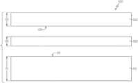
- FIG. 1illustrates an example article in an unassembled (e.g. unbonded) state
- FIG. 2illustrates an example article in an assembled (e.g. temporarily bonded) state
- FIGS. 3 - 14illustrate various embodiments by which at least one of a carrier bonding surface and a sheet bonding surface is bonded with a surface modification layer so that a carrier is temporarily bonded with a sheet.
- an example article 100is provided with various example features that may be used either alone or in combination.
- the example article 100is illustrated in FIG. 1 in an unassembled (e.g. unbonded) state, while the example article 100 is illustrated in FIG. 2 in an assembled (e.g. bonded state).
- the article 100can include a carrier 110 , a sheet 120 , and a surface modification layer 130 .
- the carriercan include a carrier bonding surface 115 .
- the sheetcan include a sheet bonding surface 125 .
- the carrier bonding surface 115 , the sheet bonding surface 125 , and the surface modification layer 130can be bonded together to form the article 100 , so that the carrier 110 is temporarily bonded with the sheet 120 .
- the carrier 110can be made of or include glass (e.g. alumino-silicate, boro-silicate, alumino-boro-silicate, soda-lime-silicate, and alkali containing or alkali-free), ceramic, glass-ceramic, metal, silicon, polysilicon, single crystal silicon, sapphire, quartz or any other material including those not explicitly listed herein either alone or in combination with other materials. Additionally, the carrier 110 may include one layer, as shown, or multiple layers (including multiple layers of the same or a different material) that are bonded together. Further, the carrier 110 may be of a Gen 1 size or larger, for example, Gen 2, Gen 3, Gen 4, Gen 5, Gen 8 or larger (e.g.
- the sheet 120can be made of or include glass (e.g. alumino-silicate, boro-silicate, alumino-boro-silicate, soda-lime-silicate, and alkali containing or alkali-free), ceramic, glass-ceramic, metal, a polymer or polymers, a composite of a polymer or polymers and glass, silicon, polysilicon, single crystal silicon, sapphire, quartz, or any other material including those not explicitly listed herein either alone or in combination with other materials.
- the sheet 120may be of a Gen 1 size or larger, for example, Gen 2, Gen 3, Gen 4, Gen 5, Gen 8, or larger (e.g. sheet sizes from 100 mm ⁇ 100 mm to 3 meters ⁇ 3 meters or greater).
- the sheet 120can be an interposer (e.g. an interposer sheet or an interposer wafer) comprising through hole vias.
- the article 100can have an article thickness 101 , the carrier 110 can have a carrier thickness 111 , the sheet 120 can have a sheet thickness 121 , and the surface modification layer 130 can have a surface modification layer thickness 131 .
- the article thickness 101includes the carrier thickness 111 , the sheet thickness 121 , and the surface modification layer thickness 131 .
- the article 100has an article thickness 101 within a range from about 0.4 mm to about 3.0 mm, including but not limited to greater than or equal to 0.4 mm, 0.5 mm, 0.6 mm, 0.7 mm, 0.8 mm, 0.9 mm, 1.0 mm, 2.0 mm, or 3.0 mm.
- the article 100can have an article thickness 101 that can be any thickness, including any thickness not explicitly disclosed herein (e.g. a thickness less than 0.4 mm, a thickness greater than 3.0 mm, or any other thickness).
- the carrier 110can have a carrier thickness 111 within a range from about 0.2 mm to about 3 mm, including but not limited to 0.2 mm, 0.3 mm, 0.4 mm, 0.5 mm, 0.6 mm, 0.65 mm, 0.7 mm, 1.0 mm, 2.0 mm, or 3.0 mm. It is to be understood that the carrier can have a carrier thickness 111 that can be any thickness, including any thickness not explicitly disclosed herein (e.g.
- the sheet 120can have a sheet thickness 121 less than or equal to about 300 microns, including but not limited 10-50 microns, 50-100 microns, 100-150 microns, 150-300 microns, or less than or substantially equal to 300, 250, 200, 190, 180, 170, 160, 150, 140, 130, 120, 110, 100, 90, 80, 70, 60, 50, 40, 30, 20, or 10 microns. It is to be understood that the sheet 120 can have a sheet thickness 121 that can be any thickness, including any thickness not explicitly disclosed herein (e.g. a thickness greater than 300 microns, or any other thickness).
- the surface modification layer 130can have a surface modification layer thickness 131 within a range from about 0.1 nm to about 100 nm. It is to be understood that the surface modification layer 130 can have a surface modification layer thickness 131 that can be any thickness, including any thickness not explicitly disclosed herein (e.g. a thickness less than 0.1 nm, a thickness greater than 100 nm, or any other thickness).
- the article thickness 101can be configured to provide an article 100 having an article thickness 101 that can be processed in processing equipment, including existing processing equipment.
- the carrier bonding surface 115 , the sheet bonding surface 125 , and the surface modification layer 130can be bonded together and then undergo various processing.
- the sheet 120 and the carrier 110including any devices that may be fabricated on the sheet during the processing, can be separated and the carrier 110 can be reused, for example.
- Some types of processinginclude vacuum processing, wet processing, ultrasonic cleaning processing, spin-rinse-dry (SRD) processing, and high temperature processing for example, FPD processing, p-Si and oxide TFT fabrication, IGZO backplane processing, and LTPS, amorphous silicon (aSi) bottom gate TFT, polycrystalline silicon (pSi) top gate TFT, amorphous oxide (IGZO) bottom gate TFT, touch screen fabrication, and interposer fabrication.
- the surface modification layer 130is configured to control a strength of the bond (e.g. energy of adhesion or bond energy) between the carrier bonding surface 115 and the sheet bonding surface 125 .
- the surface modification layer 130is bonded with the carrier bonding surface 115 and the sheet bonding surface 125 in a manner sufficient to keep the sheet 120 and the carrier 110 bonded together during processing of the article 100 , while allowing the sheet 120 and the carrier 110 to be separated without damage (e.g. catastrophic damage, for example breaking of either of the carrier 110 or the sheet 120 into two or more pieces) following processing, i.e., so that the sheet 120 is temporarily bonded with the carrier 110 .
- the surface modification layer 130can include a plasma polymerized material, formed by plasma deposition for example. As will be discussed more fully below, the plasma polymerized material can planarize the at least one of the carrier bonding surface 115 and the sheet bonding surface 125 .
- the energy of adhesion (W)can be approximated as: W ⁇ 2[ ⁇ square root over ( Y 1 d Y 2 d ) ⁇ + ⁇ square root over (2 Y 1 p Y 2 p ) ⁇ ] (4)
- Bond energyis the energy required to separate a sheet from a carrier.
- the bond energymay be measured in various different manners.
- the bond energycan be measured as follows.
- Bond energycan be measured using the double cantilever beam method (also known as the wedge method).
- a wedge of known thickness (t)is placed between the bonded sheet and the carrier at an edge.
- the wedgecreates a characteristic delamination distance (L). This delamination distance is measured and used to calculate the bond energy (Y BE ).
- Covalent adhesion energyfor example as in silicon wafer bonding, includes a situation where an initially hydrogen bonded pair of wafers are heated to a higher temperature to convert much or all the silanol-silanol hydrogen bonds to Si—O—Si covalent bonds.
- the initial, room temperature, hydrogen (or van der Waals) bondingproduces an adhesion energy of approximately 100-200 mJ/m 2 which is sufficient to hold the wafers together during certain processing while still permitting separation of the bonded surfaces.
- high temperature processinge.g. processing including temperatures within a range from about 400 to about 800° C.
- the bond created during the high temperature processinghas an adhesion energy of approximately 1000-3000 mJ/m 2 and the two wafers act as a monolith (e.g. the sheet bonding surface 125 is permanently bonded to the carrier bonding surface 115 ).
- both surfaces to be bondedare perfectly coated with a low surface energy material (e.g. a hydrocarbon polymer or a fluoropolymer) having a thickness large enough to shield the effect of the underlying substrate, the adhesion energy is that of the low surface energy coating material.
- a low surface energy materiale.g. a hydrocarbon polymer or a fluoropolymer
- This bondcan be very low leading to low or no adhesion between the bonding surfaces such that the bonded article cannot undergo processing without, for example, the sheet 120 separating from the carrier 110 .
- the adhesion energy after heating to a high temperatureis too strong for the pair of glass surfaces to be detachable.
- the surfacesnot only do the surfaces not bond at room temperature (because the total adhesion energy of about 24 mJ/m 2 , when the surfaces are put together, is too low), but they also do not bond at high temperature as there are no (or too few) polar reacting groups. Accordingly, between these two extremes, a range of adhesion energies exists, for example between about 50-1000 mJ/m 2 , which can produce the desired degree of controlled, or temporary, bonding.
- the present applicationdiscloses methods and apparatus for providing an article 100 including a surface modification layer 130 configured to temporarily bond the carrier bonding surface 115 and the sheet bonding surface 125 , for example, during processing, while also permitting separation of the carrier 110 and the sheet 120 following processing.
- Equation (5)describes that the adhesion energy is a function of four surface energy parameters plus the covalent and electrostatic energy, if any. Therefore, an appropriate adhesion energy can be achieved by controlling surface modifiers (e.g. the surface modification layer 130 ).
- at least one of the carrier 110 and the sheet 120includes glass.
- the present applicationdiscloses unexpected results.
- depositing a coating or layere.g. surface modification layer 130
- a surface roughnesse.g. a surface roughness Rq
- the present applicationdiscloses a surface modification layer 130 disposed on at least one of the carrier bonding surface 115 and the sheet bonding surface 125 , wherein the surface modification layer 130 comprises a plasma polymerized material, and wherein—unexpectedly—the plasma polymerized material planarizes (e.g. reduces a surface roughness of) the at least one of the carrier bonding surface 115 and the sheet bonding surface 125 .
- the carrier bonding surface 115 , the sheet bonding surface 125 , and the surface modification layer 130are bonded together such that the article 100 can undergo processing and, following processing, the carrier 110 and the sheet 120 can be separated from each other, i.e., the carrier 110 is temporarily bonded with the sheet 120 .
- the surface modification layer 130“planarizing” the at least one of the carrier bonding surface 115 and the sheet bonding surface 125 , that the surface modification layer 130 is to be understood as disposed on the at least one of the carrier bonding surface 115 and the sheet bonding surface 125 .
- the surface modification layerforms a layer or coating on the at least one of the carrier bonding surface 115 and the sheet bonding surface 125 , and, once disposed on these surfaces, the layer or coating has a surface roughness (e.g. a surface roughness Rq) that either alone or in combination with the surface roughness (e.g. surface roughness Rq) of the underlying at least one of the carrier bonding surface 115 and the sheet bonding surface 125 is less than the surface roughness (e.g. surface roughness Rq) of the underlying at least one of the carrier bonding surface 115 and the sheet bonding surface 125 .
- a surface roughnesse.g. a surface roughness Rq
- the at least one of the planarized carrier bonding surface and the planarized sheet bonding surfacecan have a surface roughness Rq less than about 0.8 nm.
- the at least one of the carrier bonding surface 115 and the sheet bonding surface 125 , without planarizationcan have a surface roughness Rq within a range of about 0.8 nm to about 5.0 nm.
- the at least one of the carrier bonding surface 115 and the sheet bonding surface 125without planarization, can have a surface roughness Rq greater than about 2.0 nm.
- the surface modification layer 130has an elastic modulus and a plasticity.
- At least one of the elastic modulus and the plasticitycan be such that at least a portion of at least one of the carrier bonding surface 115 and the sheet bonding surface 125 may penetrate into the surface modification layer 130 .
- the elastic moduluscan be within a range of from about 0.6 GPa to about 20 GPa.
- the surface modification layer 130can have at least one of an elastic modulus and a plasticity such that at least a portion of at least one of the carrier bonding surface 115 and the sheet bonding surface 125 may penetrate into the surface modification layer 130 , including any elastic modulus or plasticity not explicitly disclosed herein (e.g. an elastic modulus less than 0.6 GPa, an elastic modulus greater than 20 GPa, or any other elastic modulus or plasticity).
- An example method of making an articleincludes depositing a surface modification layer 130 on at least one of a carrier bonding surface 115 of a carrier 110 and a sheet bonding surface 125 of a sheet 120 .
- the surface modification layer 130comprises a plasma polymerized material.
- the plasma polymerized materialplanarizes the at least one of the carrier bonding surface 115 and the sheet bonding surface 125 .
- the methodfurther includes bonding at least one of the carrier bonding surface 115 and the sheet bonding surface 125 with the surface modification layer 130 .
- the methodfurther includes choosing at least one of an elastic modulus and a plasticity of the surface modification layer 130 to allow penetration of at least a portion of at least one of the carrier bonding surface 115 and the sheet bonding surface 125 into the surface modification layer 130 .
- FIGS. 3 - 14illustrate various different embodiments by which the carrier bonding surface 115 and the sheet bonding surface 125 can be bonded with the surface modification layer 130 so that the carrier 110 is temporarily bonded with the sheet 120 .
- the corresponding surface roughness (e.g. surface roughness Rq) of the carrier bonding surface 115 , the sheet bonding surface 125 , and the surface modification layer 130is shown as a relative surface roughness.
- the surface modification layer 130can be disposed over the entirety of the at least one of the carrier bonding surface 115 and the sheet bonding surface 125 (e.g. 100% coverage). In other examples, the surface modification layer 130 can be disposed over less than the entirety of the at least one of the carrier bonding surface 115 and the sheet bonding surface 125 (e.g. less than 100% coverage).
- the surface roughnessis illustrated as a jagged or triangular pattern merely for illustrative purposes and is not to be construed as limiting the scope of disclosure. Any shape, size, or distribution of asperities on any one or more of the carrier bonding surface 115 , the sheet bonding surface 125 , and the surface modification layer 130 are contemplated herein. Moreover, the at least one of the carrier bonding surface 115 and the sheet bonding surface 125 can penetrate any amount into the surface modification layer 130 .
- the more penetration of the at least one of the carrier bonding surface 115 and the sheet bonding surface 125 into the surface modification layer 130the greater the corresponding surface area of the at least one of the carrier bonding surface 115 and the sheet bonding surface 125 in contact with the surface modification layer 130 , and the greater the bond strength (e.g. energy of adhesion) between the at least one of the carrier bonding surface 115 and the sheet bonding surface 125 and the surface modification layer 130 .
- the amount of penetrationcan be controlled, for example, by at least one of adjusting at least one of the elastic modulus and the plasticity of the surface modification layer 130 , and applying varying amounts of pressure (e.g.
- the carrier 110 and the sheet 120by lamination, or in an autoclave) on at least one of the carrier 110 and the sheet 120 , and varying the thickness of the surface modification layer 130 such that the at least one of the carrier bonding surface 115 and the sheet bonding surface 125 penetrates a greater amount or a lesser amount into the surface modification layer 130 .
- the carrier bonding surface 115 and the sheet bonding surface 125can have the same or similar surface roughness (e.g. surface roughness Rq), depicted as relatively smooth (e.g. less than 0.8 nm), and the carrier bonding surface 115 and the sheet bonding surface 125 can be bonded with the surface modification layer 130 so that the carrier 110 is temporarily bonded with the sheet 120 .
- the carrier bonding surface 115can have a surface roughness (e.g. surface roughness Rq), depicted as relatively smooth (e.g. less than 0.8 nm) and the sheet bonding surface 125 can have a surface roughness (e.g.
- the surface modification layer 130planarizes the moderately rough sheet bonding surface 125 , such that the carrier bonding surface 115 and the sheet bonding surface 125 can be bonded with the surface modification layer 130 so that the carrier 110 is temporarily bonded with the sheet 120 .
- the carrier bonding surface 115can have a surface roughness (e.g. surface roughness Rq), depicted as moderately rough (e.g. within a range from about 0.8 nm to about 5.0 nm) and the sheet bonding surface 125 can have a surface roughness (e.g.
- the surface modification layer 130planarizes the moderately rough carrier bonding surface 115 , such that the carrier bonding surface 115 and the sheet bonding surface 125 can be bonded with the surface modification layer 130 so that the carrier 110 is temporarily bonded with the sheet 120 .
- the carrier bonding surface 115 and the sheet bonding surface 125can have the same or similar surface roughness (e.g. surface roughness Rq), depicted as moderately rough (e.g. within a range from about 0.8 nm to about 5.0 nm).
- the surface modification layer 130can planarize the moderately rough carrier bonding surface 115 and the moderately rough sheet bonding surface 125 , such that the carrier bonding surface 115 and the sheet bonding surface 125 can be bonded with the surface modification layer 130 so that the carrier 110 is temporarily bonded with the sheet 120 .
- the at least one of the carrier bonding surface 115 and the sheet bonding surface 125can have any surface roughness (e.g.
- the surface modification layer 130can planarize the carrier bonding surface 115 and the sheet bonding surface 125 , such that the carrier bonding surface 115 and the sheet bonding surface 125 can be bonded with the surface modification layer 130 so that the carrier 110 is temporarily bonded with the sheet 120 .
- the carrier bonding surface 115 and the sheet bonding surface 125can be spaced apart from each other (e.g. not touching) with the surface modification layer 130 therebetween. In such a configuration, little to no covalent bonding between the carrier bonding surface 115 and the sheet bonding surface 125 is observed, even following processing at high temperatures. Rather, in such a configuration, the predominant force bonding the carrier bonding surface 115 , the sheet bonding surface 125 , and the surface modification layer 130 together is the van der Waals forces between the carrier bonding surface 115 and the surface modification layer 130 and the van der Waals forces between the sheet bonding surface 125 and the surface modification layer 130 .
- Covalent bonding between the sheet bonding surface 125 and the surface modification layer 130 as well as covalent bonding between the carrier bonding surface 115 and the surface modification layer 130may also occur as long as such covalent bonding has minimal or no impact on the ability to separate the carrier 110 and the sheet 120 from each other following processing.
- the carrier 110 and the sheet 120can be separated from each other by at least one of adhesive failure (e.g. where the surface modification layer 130 separates from at least one of the carrier bonding surface 115 and the sheet bonding surface 125 ) and cohesive failure (e.g. where the surface modification layer 130 separates from itself).
- the carrier bonding surface 115 and the sheet bonding surface 125can be spaced apart from each other (e.g. not touching) with the surface modification layer 130 therebetween in some locations, and contacting each other, without the surface modification layer 130 therebetween, in other locations.
- little to no covalent bonding between the carrier bonding surface 115 and the sheet bonding surface 125is observed in the regions where the carrier bonding surface 115 and the sheet bonding surface 125 are spaced apart from each other (e.g. not touching) with the surface modification layer 130 therebetween, even following processing at high temperatures.
- Covalent bondingmay be observed between the carrier bonding surface 115 and the sheet bonding surface 125 in regions where the carrier bonding surface 115 and the sheet bonding surface 125 are contacting each other, without the surface modification layer 130 therebetween.
- the predominant force bonding the carrier bonding surface 115 , the sheet bonding surface 125 , and the surface modification layer 130 togetheris still the van der Waals forces between the carrier bonding surface 115 and the surface modification layer 130 and the van der Waals forces between the sheet bonding surface 125 and the surface modification layer 130 .
- covalent bonding between the sheet bonding surface 125 and the surface modification layer 130 as well as covalent bonding between the carrier bonding surface 115 and the surface modification layer 130 of the example embodiments illustrated in FIGS. 7 - 9may also occur so long as such covalent bonding has minimal or no impact on the ability to separate the carrier 110 and the sheet 120 from each other following processing.
- the carrier 110 and the sheet 120can be separated from each other by at least one of adhesive failure (e.g. where the surface modification layer 130 separates from at least one of the carrier bonding surface 115 and the sheet bonding surface 125 ) and cohesive failure (e.g. where the surface modification layer 130 separates from itself).
- any covalent bonds formed between the carrier bonding surface 115 and the sheet bonding surface 125can be broken (e.g. following processing) without damaging (e.g. breaking into two or more pieces) either or both of the carrier 110 and the sheet 120 to allow separation of the carrier 110 and the sheet 120 .
- the carrier bonding surface 115can have a surface roughness (e.g. surface roughness Rq), depicted as relatively smooth (e.g. less than 0.8 nm) and the sheet bonding surface 125 can have a surface roughness (e.g. surface roughness Rq), depicted as moderately rough (e.g. within a range from about 0.8 nm to about 5.0 nm) with the moderately rough sheet bonding surface 125 contacting the relatively smooth carrier bonding surface 115 in some locations, without the surface modification layer 130 therebetween, and the moderately rough sheet bonding surface 125 being spaced apart from the relatively smooth carrier bonding surface 115 , with the surface modification layer 130 therebetween, in other locations.
- surface roughness Rqsurface roughness
- relatively smoothe.g. less than 0.8 nm
- Rqsurface roughness
- moderately rough sheet bonding surface 125depicted as moderately rough (e.g. within a range from about 0.8 nm to about 5.0 nm) with the moderate
- the surface modification layer 130planarizes the moderately rough sheet bonding surface 125 , such that the carrier bonding surface 115 , the sheet bonding surface 125 , and the surface modification layer 130 can be bonded together to form a temporary bond between the carrier 110 and the sheet 120 .
- the carrier bonding surface 115can have a surface roughness (e.g. surface roughness Rq), depicted as moderately rough (e.g. within a range from about 0.8 nm to about 5.0 nm) and the sheet bonding surface 125 can have a surface roughness (e.g. surface roughness Rq), depicted as relatively smooth (e.g. less than 0.8 nm), with the moderately rough carrier bonding surface 115 contacting the relatively smooth sheet bonding surface 125 in some locations, without the surface modification layer 130 therebetween, and the moderately rough carrier bonding surface 115 being spaced apart from the relatively smooth sheet bonding surface 125 , with the surface modification layer 130 therebetween, in other locations.
- surface roughness Rqsurface roughness
- Rqsurface roughness
- relatively smoothe.g. less than 0.8 nm
- the surface modification layer 130planarizes the moderately rough carrier bonding surface 115 , such that the carrier bonding surface 115 , the sheet bonding surface 125 , and the surface modification layer 130 can be bonded together to form a temporary bond between the carrier 110 and the sheet 120 .
- the carrier bonding surface 115 and the sheet bonding surface 125can have the same or similar surface roughness (e.g. surface roughness Rq), depicted as moderately rough (e.g. within a range from about 0.8 nm to about 5.0 nm) with the moderately rough sheet bonding surface 125 contacting the moderately rough carrier bonding surface 115 in some locations, without the surface modification layer 130 therebetween, and the moderately rough sheet bonding surface 125 being spaced apart from the moderately rough carrier bonding surface 115 , with the surface modification layer 130 therebetween, in other locations.
- surface roughness Rqsurface roughness
- Rqsurface roughness
- moderately rough sheet bonding surface 125e.g. within a range from about 0.8 nm to about 5.0 nm
- the surface modification layer 130can planarize the moderately rough carrier bonding surface 115 and the moderately rough sheet bonding surface 125 , such that the carrier bonding surface 115 , the sheet bonding surface 125 , and the surface modification layer 130 can be bonded together to form a temporary bond between the carrier 110 and the sheet 120 .
- FIGS. 10 - 14show the carrier 110 including the carrier bonding surface 115 , the sheet 120 including the sheet bonding surface 125 , and at least one of a carrier surface modification layer 130 a disposed on the carrier bonding surface 115 and a sheet surface modification layer 130 b disposed on the sheet bonding surface 125 .
- the at least one of the carrier surface modification layer 130 a and the sheet surface modification layer 130 bcomprises a plasma polymerized material.
- the plasma polymerized materialplanarizes the at least one of the carrier bonding surface 115 and the sheet bonding surface 125 .
- the carrier bonding surface 115 , the sheet bonding surface 125 , and the at least one of the carrier surface modification layer 130 a and the sheet surface modification layer 130 bare bonded together to form a temporary bond between the carrier 110 and the sheet 120 .
- the predominant force bonding the carrier bonding surface 115 , the sheet bonding surface 125 , and the at least one of the carrier surface modification layer 130 a and the sheet surface modification layer 130 b togetheris (i) the van der Waals forces between the carrier bonding surface 115 and the at least one of the carrier surface modification layer 130 a and the sheet surface modification layer 130 b ; (ii) the van der Waals forces between the sheet bonding surface 125 and the at least one of the sheet surface modification layer 130 b and the carrier surface modification layer 130 a ; and (iii) to the extent surface modification layers 130 a and 130 b are both present, the van der Waals forces between the carrier surface modification layer 130 a and the sheet surface modification layer 130 b .
- the predominant force bonding the carrier bonding surface 115 , the sheet bonding surface 125 , and the at least one of the carrier surface modification layer 130 a and the sheet surface modification layer 130 b togetheris still: (i) the van der Waals forces between the carrier bonding surface 115 and the at least one of the carrier surface modification layer 130 a and the sheet surface modification layer 130 b ; (ii) the van der Waals forces between the sheet bonding surface 125 and the at least one of the sheet surface modification layer 130 b and the carrier surface modification layer 130 a ; and (iii) to the extent surface modification layers 130 a and 130 b are both present, the van der Waals forces between the carrier surface modification layer 130 a and the sheet surface modification layer 130 b .
- covalent bonding between the carrier bonding surface 115 and the at least one of the carrier surface modification layer 130 a and the sheet surface modification layer 130 b as well as covalent bonding between the sheet bonding surface 125 and the at least one of the sheet surface modification layer 130 b and the carrier surface modification layer 130 a , as well as covalent bonding between the surface modification layers 130 a and 130 b when both are present, of the example embodiments illustrated in FIGS. 10 - 14may also occur so long as such covalent bonding has minimal or no impact on the ability to separate the carrier 110 and the sheet 120 from each other following processing.
- the carrier 110 and the sheet 120can be separated from each other by at least one of adhesive failure (e.g. where the at least one of the carrier surface modification layer 130 a and the sheet surface modification layer 130 b separates from at least one of the carrier bonding surface 115 and the sheet bonding surface 125 ) and cohesive failure (e.g. where the at least one of the carrier surface modification layer 130 a and the sheet surface modification layer 130 b separates from at least one of itself and each other).
- adhesive failuree.g. where the at least one of the carrier surface modification layer 130 a and the sheet surface modification layer 130 b separates from at least one of the carrier bonding surface 115 and the sheet bonding surface 125
- cohesive failuree.g. where the at least one of the carrier surface modification layer 130 a and the sheet surface modification layer 130 b separates from at least one of itself and each other.
- the predominant force bonding the carrier 110 and the sheet 120is (i) the van der Waals forces between the carrier bonding surface 115 and the at least one of the carrier surface modification layer 130 a and the sheet surface modification layer 130 b ; (ii) the van der Waals forces between the sheet bonding surface 125 and the at least one of the sheet surface modification layer 130 b and the carrier surface modification layer 130 a ; and (iii) to the extent surface modification layers 130 a and 130 b are both present, the van der Waals forces between the carrier surface modification layer 130 a and the sheet surface modification layer 130 b , any covalent bonds formed between the carrier bonding surface 115 and the sheet bonding surface 125 (e.g.
- FIG. 10shows, with respect to the at least one of the carrier surface modification layer 130 a and the sheet surface modification layer 130 b , the article comprises both the carrier surface modification layer 130 a disposed on the carrier bonding surface 115 and the sheet surface modification layer 130 b disposed on the sheet bonding surface 125 .
- at least a portion of at least one of the sheet bonding surface 125penetrates into the carrier surface modification layer 130 a and the carrier bonding surface 115 penetrates into the sheet surface modification layer 130 b .
- the sheet bonding surface 125may not extend beyond the sheet surface modification layer 130 b
- the carrier bonding surface 115may not extend beyond the carrier surface modification layer 130 a .
- At least a portion of the sheet bonding surface 125may penetrate into the carrier surface modification layer 130 a , whereas the carrier bonding surface 115 may not extend beyond the carrier surface modification layer 130 a . And in still other examples, at least a portion of the carrier bonding surface 115 may penetrate into the sheet surface modification layer 130 b , whereas the sheet bonding surface 125 may not extend beyond the sheet surface modification layer 130 b.
- FIG. 11shows, with respect to the at least one of the carrier surface modification layer 130 a and the sheet surface modification layer 130 b , the article comprises only the sheet surface modification layer 130 b disposed on the sheet bonding surface 125 .
- the carrier bonding surface 115penetrates into the sheet surface modification layer 130 b .
- the sheet surface modification layer 130 bplanarizes the sheet bonding surface 125 such that the carrier bonding surface 115 , the sheet bonding surface 125 , and the sheet surface modification layer 130 b (with at least a portion of the carrier bonding surface 115 penetrating thereinto) are bonded together to form a temporary bond between the carrier 110 and the sheet 120 .
- FIG. 12shows, with respect to the at least one of the carrier surface modification layer 130 a and the sheet surface modification layer 130 b , the article comprises only the carrier surface modification layer 130 a disposed on the carrier bonding surface 115 .
- the carrier surface modification layer 130 aplanarizes the carrier bonding surface 115 such that the carrier bonding surface 115 , the sheet bonding surface 125 , and the carrier surface modification layer 130 a (with at least a portion of the sheet bonding surface 125 penetrating thereinto) are bonded together to form a temporary bond between the carrier 110 and the sheet 120 .
- gapse.g. air gaps or “blisters,” as is known in the art
- gapscan be formed between: (i) the carrier bonding surface 115 and the at least one of the carrier surface modification layer 130 a and the sheet surface modification layer 130 b ; and/or (ii) the sheet bonding surface 125 and the at least one of the sheet surface modification layer 130 b and the carrier surface modification layer 130 a .
- FIG. 13 and FIG. 14gaps
- the amount of penetration of (i) the carrier bonding surface 115 into the at least one of the carrier surface modification layer 130 a and the sheet surface modification layer 130 b ; and/or (ii) the sheet bonding surface 125 into the at least one of the sheet surface modification layer 130 b and the carrier surface modification layer 130 a ,can be controlled such that no blisters are formed between (i) the carrier bonding surface 115 and the at least one of the carrier surface modification layer 130 a and the sheet surface modification layer 130 b ; and/or the sheet bonding surface 125 and the at least one of the sheet surface modification layer 130 b and the carrier surface modification layer 130 a .
- the at least one of adjusting at least one of the elastic modulus and the plasticity of the at least one of the carrier surface modification layer 130 a and the sheet surface modification layer 130 bby at least one of adjusting at least one of the elastic modulus and the plasticity of the at least one of the carrier surface modification layer 130 a and the sheet surface modification layer 130 b , and applying varying amounts of pressure (e.g. by lamination, or in an autoclave) on at least one of the carrier 110 and the sheet 120 , and varying the thickness of the at least one of the carrier surface modification layer 130 a and the sheet surface modification layer 130 b , the at least one of the carrier bonding surface 115 and the sheet bonding surface 125 can penetrate a greater amount or a lesser amount into the at least one of the carrier surface modification layer 130 a and the sheet surface modification layer 130 b .
- varying amounts of pressuree.g. by lamination, or in an autoclave
- penetration of at least one of (i) the carrier bonding surface 115 into the at least one of the carrier surface modification layer 130 a and the sheet surface modification layer 130 b and (ii) the sheet bonding surface 125 into the at least one of the sheet surface modification layer 130 b and the carrier surface modification layer 130 acan provide an energy of adhesion (e.g. based on van der Waals bonding) that is less than, equal to, or greater than an energy of adhesion (e.g. based on at least one of van der Waals bonding and covalent bonding) between surfaces which, for example, have no surface modification layer (e.g. a compliant surface layer) therebetween, irrespective of the relative surface roughness of either or both of the surfaces.
- an energy of adhesione.g. based on van der Waals bonding
- an energy of adhesione.g. based on at least one of van der Waals bonding and covalent bonding
- any one or more combinations of the embodiments illustrated in FIGS. 3 - 14can be combined to temporarily bond the carrier 110 and the sheet 120 .
- the at least one of the planarized carrier bonding surface and the planarized sheet bonding surfacecan have a surface roughness Rq less than about 0.8 nm.
- the at least one of the carrier bonding surface 115 and the sheet bonding surface 125prior to planarization, can have a surface roughness Rq within a range of about 0.8 nm to about 5.0 nm.
- other surface roughnesses of the carrier bonding surface 115 , the sheet bonding surface 125 , and the at least one of the carrier surface modification layer 130 a and the sheet surface modification layer 130 bare contemplated herein.
- the surface modification layer 130can include a plasma polymerized material.
- the plasma polymerized materialcan include a plasma polymer film formed by a chemical vapor deposition process in which precursors are activated and deposited by a plasma to form polymeric materials.
- the plasma polymerized materiale.g. the plasma polymer film
- the plasma polymerized materialcan include aliphatic or aromatic hydrocarbons, polyesters, or polyimides.
- plasma polymersmay be deposited under atmospheric or reduced pressure.
- plasma polymerized materialcan be formed by plasma deposition that includes plasma excitation (e.g. DC or RF parallel plate, Inductively Coupled Plasma (ICP), Electron Cyclotron Resonance (ECR), downstream microwave, or RF plasma) from source gases.
- plasma excitatione.g. DC or RF parallel plate, Inductively Coupled Plasma (ICP), Electron Cyclotron Resonance (ECR), downstream microwave, or RF plasma
- source gasescan include fluorocarbon sources (e.g. CF4, CHF3, C2F6, C3F6, C2F2, CH3F, C4F8, chlorofluoro carbons, or hydrochlorofluoro carbons); hydrocarbons (e.g. alkanes, including methane, ethane, propane, or butane); alkenes (including ethylene or propylene, for example); alkynes (including acetylene, for example); or aromatics (including benzene or toluene, for example).
- source gasescan include hydrogen or other gas sources, including SF6.
- plasma polymerizationcreates a layer of highly cross-linked material.
- control of reaction conditions and source gasescan be used to control the film thickness, density, and chemistry to, for example, tailor the functional groups to a desired application.
- control of reaction conditions and source gasescan be used to control the film thickness, density, and chemistry to, for example, tailor the functional groups to a desired application.
- the specific plasma polymer films described hereinare non-limiting representative examples, and one skilled in the art will recognize similar advantages may be achieved with different plasma geometry and source materials, including plasma polymers not explicitly disclosed herein.
- the present applicationcontemplates any plasma polymerized material configured to planarize a surface as within the scope of disclosure.
- aliphatic plasma polymer filmswere deposited in an Oxford PlasmaLab 100 etch tool from methane and hydrogen. Process conditions were 2 standard cubic centimeters per minute (sccm) methane, 38 sccm hydrogen, 25 milli Torrs (mT) pressure 275 Watts (W) 13.56 Mega Hertz (MHz) Radio Frequency (RF). Process times were varied to adjust plasma polymer thickness from 11 to 60 nano meters (nm). Thickness was measured on an n&k analyzer using an amorphous carbon model. Surfaces were activated in the same Oxford tool with 25 sccm Nitrogen, 25 sccm Oxygen, O2 10 mT 300 W RF and a process time of 5 seconds (sec.).
- micrometer (um, or micron) thick glass substrateswere etched in an aqueous solution 433 milli liters (ml) De-Ionized (DI) water, 106 ml hydrochloric acid, and 11 ml 49% hydrofluoric acid at room temperature for 1 minute (min.).
- DIDe-Ionized
- the roughened thin glasswas bonded to the plasma polymer surface which was then bonded together with the carrier by applying the substrate to the carrier. Because of the high surface energy of the plasma polymer, surface bonding was self-propagating.
- a Teflon squeegeewas used to remove any entrapped bubbles formed by particles and curvature in the bonding front. Bonded samples were annealed for 10 min at 300° C. in flowing nitrogen in an MPT rapid thermal processing system (RTP) on a silicon carbide susceptor. Bond energy was measured by the wedge test. As shown in Table 1 below, roughness (Rq) was observed to decrease with increasing plasma polymer thickness. The bond energy increases with increasing polymer thickness reaching a value near that expected for van der Waals interaction between the thin glass and treated plasma polymer coated carrier as surface roughness decreases below 0.8 nm RMS (Rq).
- a set of thin glass interposerswere formed from a 200 um thick glass substrate made of Corning® EAGLE XG® glass by a process of laser damage to form vias, and etch in the HF—HNO3 solution described above. Etching the vias reduced the thickness of the substrate to 180 um, produced 50 um diameter vias, and AFM showed the surface roughness after etching as 1 nm Rq.
- These interposer sampleswere coated with a plasma polymer of varying thickness as described with respect to the first example and were bonded to a 0.7 mm thick glass carrier made of Corning® EAGLE EXG® glass. Samples were annealed in an RTP system in N2 at 300° C. for 10 min.
- Bond Energy(BE, in milli Joules per meter squared (mJ/m2)) versus plasma polymer thickness (in nm) is shown below in Table 2.
- mJ/m2milli Joules per meter squared
- a set of thin glass interposerswas formed from a 200 um thick glass substrate made of Corning® EAGLE XG® glass by a process of laser damage to form vias, and etch in the HF—HNO3 solution described above. Etching the vias reduces the thickness of the substrate to 180 um and produces 30 um diameter vias.
- interposer sampleswere coated with a plasma polymer of varying thickness in the Oxford tool as described in the first example except plasma polymer deposition conditions were 10 sccm ethylene 50 sccm hydrogen 5 mT pressure 1500 W RF applied to the coil 50 W RF bias followed by 5 sec treatment time at 35 sccm nitrogen 5 sccm oxygen 15 mT pressure 800 W RF applied to the coil 50 W RF bias.
- Interposerswere bonded to a 0.7 mm thick glass carrier made of Corning® EAGLE EXG® glass. Samples were annealed in an RTP system in N2 at 300° C. for 10 min. A bond energy of 312 mJ/m2 was found for a polymer thickness of 13.7 nm.
Landscapes
- Chemical & Material Sciences (AREA)
- Engineering & Computer Science (AREA)
- Life Sciences & Earth Sciences (AREA)
- Chemical Kinetics & Catalysis (AREA)
- General Chemical & Material Sciences (AREA)
- Geochemistry & Mineralogy (AREA)
- Materials Engineering (AREA)
- Organic Chemistry (AREA)
- Ceramic Engineering (AREA)
- Laminated Bodies (AREA)
- Joining Of Glass To Other Materials (AREA)
Abstract
Description
W=Y1+Y2−Y12 (1)
(“A theory for the estimation of surface and interfacial energies. I. derivation and application to interfacial tension,” L. A. Girifalco and R. J. Good, J. Phys. Chem., V 61, p 904) where, (Y1), (Y2), and (Y12),Y
Y=Yd+Yp (2)
Y12=Y1+Y2−2√{square root over (Y1dY2d)}−√{square root over (2Y1pY2p)} (3)
(Girifalco and R. J. Good, as mentioned above).
W˜2[√{square root over (Y1dY2d)}+√{square root over (2Y1pY2p)}] (4)
W˜2[√{square root over (Y1dY2d)}+√{square root over (2Y1pY2p)}]+Wc+We (5)
where (Wc) and (We) are the covalent and electrostatic adhesion energies.
where (E1) is the Elastic modulus of the carrier, (t1) is the thickness of the carrier, (E2) is the Elastic modulus of the sheet, and (t2) is the thickness of the sheet.
| TABLE 1 | ||
| Bond | ||
| Thickness | Energy | Rq |
| (nm) | (mJ/m2) | (nm) |
| 11.2 | 14.7 | 1.01 |
| 16.3 | 14.7 | 0.82 |
| 23.8 | 205.3 | 0.81 |
| 39.2 | 210.1 | 0.72 |
| 57.3 | 156.2 | 0.57 |
| TABLE 2 | |||
| Polymer | |||
| thickness | BE | ||
| (nm) | (mJ/m2) | ||
| 11 | 48 | ||
| 17 | 79 | ||
| 30 | 128 | ||
| 39 | 240 | ||
| 57 | 250 | ||
Claims (15)
Priority Applications (1)
| Application Number | Priority Date | Filing Date | Title |
|---|---|---|---|
| US15/739,321US11905201B2 (en) | 2015-06-26 | 2016-06-22 | Methods and articles including a sheet and a carrier |
Applications Claiming Priority (3)
| Application Number | Priority Date | Filing Date | Title |
|---|---|---|---|
| US201562185095P | 2015-06-26 | 2015-06-26 | |
| PCT/US2016/038663WO2016209897A1 (en) | 2015-06-26 | 2016-06-22 | Methods and articles including a sheet and a carrier |
| US15/739,321US11905201B2 (en) | 2015-06-26 | 2016-06-22 | Methods and articles including a sheet and a carrier |
Publications (2)
| Publication Number | Publication Date |
|---|---|
| US20200039872A1 US20200039872A1 (en) | 2020-02-06 |
| US11905201B2true US11905201B2 (en) | 2024-02-20 |
Family
ID=56360509
Family Applications (1)
| Application Number | Title | Priority Date | Filing Date |
|---|---|---|---|
| US15/739,321Active2037-07-17US11905201B2 (en) | 2015-06-26 | 2016-06-22 | Methods and articles including a sheet and a carrier |
Country Status (7)
| Country | Link |
|---|---|
| US (1) | US11905201B2 (en) |
| EP (1) | EP3313799B1 (en) |
| JP (1) | JP7106276B2 (en) |
| KR (1) | KR102524620B1 (en) |
| CN (2) | CN117534339A (en) |
| TW (1) | TWI723025B (en) |
| WO (1) | WO2016209897A1 (en) |
Families Citing this family (19)
| Publication number | Priority date | Publication date | Assignee | Title |
|---|---|---|---|---|
| US10543662B2 (en) | 2012-02-08 | 2020-01-28 | Corning Incorporated | Device modified substrate article and methods for making |
| US10086584B2 (en) | 2012-12-13 | 2018-10-02 | Corning Incorporated | Glass articles and methods for controlled bonding of glass sheets with carriers |
| US10014177B2 (en) | 2012-12-13 | 2018-07-03 | Corning Incorporated | Methods for processing electronic devices |
| TWI617437B (en) | 2012-12-13 | 2018-03-11 | 康寧公司 | Facilitated processing for controlling bonding between sheet and carrier |
| US9340443B2 (en) | 2012-12-13 | 2016-05-17 | Corning Incorporated | Bulk annealing of glass sheets |
| US10510576B2 (en) | 2013-10-14 | 2019-12-17 | Corning Incorporated | Carrier-bonding methods and articles for semiconductor and interposer processing |
| CN106132688B (en) | 2014-01-27 | 2020-07-14 | 康宁股份有限公司 | Article and method for controlled bonding of a sheet to a carrier |
| EP3129221A1 (en) | 2014-04-09 | 2017-02-15 | Corning Incorporated | Device modified substrate article and methods for making |
| EP3297824A1 (en) | 2015-05-19 | 2018-03-28 | Corning Incorporated | Articles and methods for bonding sheets with carriers |
| KR102524620B1 (en) | 2015-06-26 | 2023-04-21 | 코닝 인코포레이티드 | Methods and articles including sheets and carriers |
| JP6873986B2 (en) | 2015-10-30 | 2021-05-19 | コーニング インコーポレイテッド | Method of processing the first substrate bonded to the second substrate |
| TW201825623A (en) | 2016-08-30 | 2018-07-16 | 美商康寧公司 | Peptide plasma polymer for sheet bonding |
| TWI821867B (en) | 2016-08-31 | 2023-11-11 | 美商康寧公司 | Articles of controllably bonded sheets and methods for making same |
| JP7260523B2 (en) | 2017-08-18 | 2023-04-18 | コーニング インコーポレイテッド | Temporary binding using polycationic polymers |
| TWI830710B (en) | 2017-11-20 | 2024-02-01 | 美商康寧公司 | Temporary bonding of glass pairs using cationic surfactants and/or organic salts |
| US11331692B2 (en) | 2017-12-15 | 2022-05-17 | Corning Incorporated | Methods for treating a substrate and method for making articles comprising bonded sheets |
| KR102603870B1 (en)* | 2018-02-01 | 2023-11-21 | 삼성디스플레이 주식회사 | Encapsulating Structure, Organic light emitting display having the encapsulating structure, and method of manufacturing thereof |
| JP2023028803A (en)* | 2021-08-20 | 2023-03-03 | 株式会社Nsc | laminated glass substrate |
| CN114920468B (en)* | 2022-06-01 | 2023-12-05 | 北方夜视技术股份有限公司 | Borosilicate glass hydrophilic bonding method |
Citations (380)
| Publication number | Priority date | Publication date | Assignee | Title |
|---|---|---|---|---|
| GB1082116A (en) | 1964-09-03 | 1967-09-06 | Owens Illinois Inc | Organopolysiloxane resins and their production |
| US3722181A (en) | 1970-05-22 | 1973-03-27 | Du Pont | Chromatographic packing with chemically bonded organic stationary phases |
| GB1373559A (en) | 1971-08-11 | 1974-11-13 | Intercontinental Chem Co Ltd | Method of forming adhesive bonds between surfaces |
| GB1373359A (en) | 1970-10-19 | 1974-11-13 | Michelin & Cie | Pneumatic tyres |
| US4096315A (en) | 1976-12-15 | 1978-06-20 | The United States Of America As Represented By The Administrator Of The National Aeronautics And Space Administration | Process for producing a well-adhered durable optical coating on an optical plastic substrate |
| US4179324A (en) | 1977-11-28 | 1979-12-18 | Spire Corporation | Process for fabricating thin film and glass sheet laminate |
| GB1583544A (en) | 1977-07-25 | 1981-01-28 | Uop Inc | Metal-clad laminates |
| US4397722A (en) | 1981-12-31 | 1983-08-09 | International Business Machines Corporation | Polymers from aromatic silanes and process for their preparation |
| US4599243A (en) | 1982-12-23 | 1986-07-08 | International Business Machines Corporation | Use of plasma polymerized organosilicon films in fabrication of lift-off masks |
| US4810326A (en) | 1987-08-31 | 1989-03-07 | International Business Machines Corporation | Interlaminate adhesion between polymeric materials and electrolytic copper surfaces |
| US4822466A (en) | 1987-06-25 | 1989-04-18 | University Of Houston - University Park | Chemically bonded diamond films and method for producing same |
| US4849284A (en) | 1987-02-17 | 1989-07-18 | Rogers Corporation | Electrical substrate material |
| US4990462A (en) | 1989-04-12 | 1991-02-05 | Advanced Micro Devices, Inc. | Method for coplanar integration of semiconductor ic devices |
| US5073181A (en) | 1990-08-09 | 1991-12-17 | Corning Incorporated | Method of protecting glass surfaces using submicron refractory particles |
| US5141800A (en) | 1989-02-02 | 1992-08-25 | Chemical Fabrics Corporation | Method of making laminated PTFE-containing composites and products thereof |
| US5143747A (en) | 1991-02-12 | 1992-09-01 | Hughes Aircraft Company | Die improved tooling for metal working |
| WO1992022604A1 (en) | 1991-06-14 | 1992-12-23 | W.L. Gore & Associates, Inc. | Surface modified porous expanded polytetrafluoroethylene and process for making |
| JPH0596235A (en) | 1991-10-09 | 1993-04-20 | Sumitomo Electric Ind Ltd | Fluoroplastic coated article |
| JPH05111620A (en) | 1991-04-22 | 1993-05-07 | Hoechst Celanese Corp | Liquid separating membrane module having minimum effective membrane thickness |
| US5222494A (en) | 1991-07-31 | 1993-06-29 | Cyberonics, Inc. | Implantable tissue stimulator output stabilization system |
| US5357726A (en) | 1989-02-02 | 1994-10-25 | Chemfab Corporation | Composite materials for structural end uses |
| US5413940A (en) | 1994-10-11 | 1995-05-09 | Taiwan Semiconductor Manufacturing Company | Process of treating SOG layer using end-point detector for outgassing |
| WO1995017537A1 (en) | 1993-12-21 | 1995-06-29 | Commonwealth Scientific Corporation | Process for deposition of diamondlike, electrically conductive and electron-emissive carbon-based films |
| US5462781A (en) | 1991-06-14 | 1995-10-31 | W. L. Gore & Associates, Inc. | Surface modified porous expanded polytetrafluoroethylene and process for making |
| US5479043A (en) | 1992-04-15 | 1995-12-26 | Picogiga Societe Anonyme | Multispectral photovoltaic component |
| US5482896A (en) | 1993-11-18 | 1996-01-09 | Eastman Kodak Company | Light emitting device comprising an organic LED array on an ultra thin substrate and process for forming same |
| US5491571A (en) | 1993-01-19 | 1996-02-13 | Hughes Aircraft Company | Liquid crystal display including electrodes and driver devices integrally formed in monocrystalline semiconductor layer |
| US5554680A (en) | 1994-02-16 | 1996-09-10 | E. I. Du Pont De Nemours And Company | Heat-resistant perfluoroelastomer composition |
| US5661618A (en) | 1995-12-11 | 1997-08-26 | International Business Machines Corporation | Magnetic recording device having a improved slider |
| US5718967A (en) | 1995-10-13 | 1998-02-17 | The Dow Chemical Company | Coated plastic substrate |
| US5755867A (en) | 1995-12-22 | 1998-05-26 | Shin-Etsu Chemical Co., Ltd. | Photocatalytic hydrophilic coating compositions |
| US5820991A (en) | 1997-02-24 | 1998-10-13 | Cabo; Ana M. | Fused glass sheets having ceramic paint and metal foil and method of making same |
| US5840616A (en) | 1991-05-22 | 1998-11-24 | Canon Kabushiki Kaisha | Method for preparing semiconductor member |
| US5888591A (en) | 1996-05-06 | 1999-03-30 | Massachusetts Institute Of Technology | Chemical vapor deposition of fluorocarbon polymer thin films |
| US5904791A (en) | 1995-09-25 | 1999-05-18 | Dow Corning Corporation | Use of preceramic polymers as electronic adhesives |
| US5966622A (en) | 1997-10-08 | 1999-10-12 | Lucent Technologies Inc. | Process for bonding crystalline substrates with different crystal lattices |
| US5972152A (en) | 1997-05-16 | 1999-10-26 | Micron Communications, Inc. | Methods of fixturing flexible circuit substrates and a processing carrier, processing a flexible circuit and processing a flexible circuit substrate relative to a processing carrier |
| US6037026A (en) | 1994-07-18 | 2000-03-14 | Sharp Kabushiki Kaisha | Substrate carrier jig and method of producing liquid crystal display element by using the substrate carrier jig |
| US6091478A (en) | 1997-05-08 | 2000-07-18 | Casio Computer Co., Ltd. | Liquid Crystal Display device using liquid crystal having ferrielectric phase between substrates and method for driving the same |
| JP2000241804A (en) | 1999-02-23 | 2000-09-08 | Nec Kagoshima Ltd | Jig for production of display device and production of display device using the same |
| US6124154A (en) | 1996-10-22 | 2000-09-26 | Seiko Epson Corporation | Fabrication process for thin film transistors in a display or electronic device |
| US6159385A (en) | 1998-05-08 | 2000-12-12 | Rockwell Technologies, Llc | Process for manufacture of micro electromechanical devices having high electrical isolation |
| US6261398B1 (en) | 1997-03-19 | 2001-07-17 | Pilkington Automotive Deutschland Gmbh | Process for producing a curved laminated safety glass sheet |
| US20010045351A1 (en) | 1997-11-21 | 2001-11-29 | Korea Institute Of Science And Technology | Plasma polymerization on surface of material |
| US6338901B1 (en) | 1999-05-03 | 2002-01-15 | Guardian Industries Corporation | Hydrophobic coating including DLC on substrate |
| DE10034737A1 (en) | 2000-07-17 | 2002-02-21 | Fraunhofer Ges Forschung | Process for producing a permanent release layer by plasma polymerization on the surface of a molding tool, a molding tool which can be produced by the process and its use |
| US6379746B1 (en) | 1999-02-02 | 2002-04-30 | Corning Incorporated | Method for temporarily protecting glass articles |
| US6387736B1 (en) | 1999-04-26 | 2002-05-14 | Agilent Technologies, Inc. | Method and structure for bonding layers in a semiconductor device |
| WO2002084722A2 (en) | 2001-04-13 | 2002-10-24 | Commissariat A L'energie Atomique | Detachable substrate with controlled mechanical hold and method for production thereof |
| US20020171080A1 (en) | 2001-05-18 | 2002-11-21 | Faris Sadeg M. | Thin films and production methods thereof |
| JP2002348150A (en) | 2001-05-28 | 2002-12-04 | Mitsubishi Plastics Ind Ltd | Adhesive sheet for interlayer film and transparent laminate |
| US20030017303A1 (en) | 2001-06-29 | 2003-01-23 | Chrystal Systems Inc. | Antifogging product, inorganic hydrophilic hard layer forming material and process for producing antifogging lens |
| US20030020049A1 (en) | 2001-07-30 | 2003-01-30 | Payne Donald N. | Modified silicon-based UV absorbers useful in crosslinkable polysiloxane coatings via sol-gel polymerization |
| US20030020062A1 (en) | 2001-05-18 | 2003-01-30 | Faris Sadeg M. | MEMS and method of manufacturing MEMS |
| US6521857B1 (en) | 2001-11-19 | 2003-02-18 | Geomat Insights, Llc | Plasma enhanced bonding method and device |
| US6521511B1 (en) | 1997-07-03 | 2003-02-18 | Seiko Epson Corporation | Thin film device transfer method, thin film device, thin film integrated circuit device, active matrix board, liquid crystal display, and electronic apparatus |
| US6528145B1 (en) | 2000-06-29 | 2003-03-04 | International Business Machines Corporation | Polymer and ceramic composite electronic substrates |
| JP2003071937A (en) | 2001-09-05 | 2003-03-12 | Toppan Printing Co Ltd | Laminated body, method for manufacturing the same, and multilayer circuit board |
| JP2003077187A (en) | 2001-08-30 | 2003-03-14 | Toshiba Corp | Optical disc manufacturing method |
| US20030057563A1 (en) | 2001-09-24 | 2003-03-27 | Nathan Richard J. | Integrated package and methods for making same |
| US6540866B1 (en) | 1999-06-29 | 2003-04-01 | Institute Of Microelectronics | Method for lamination of fluoropolymer to metal and printed circuit board (PCB) substrate |
| WO2003044079A1 (en) | 2001-11-15 | 2003-05-30 | Honeywell International Inc. | Spin-on-glass anti-reflective coatings for photolithography |
| US20030119336A1 (en) | 1998-02-05 | 2003-06-26 | Nobuo Matsuki | Insulation film on semiconductor substrate and method for forming same |
| US6602606B1 (en) | 1999-05-18 | 2003-08-05 | Nippon Sheet Glass Co., Ltd. | Glass sheet with conductive film, method of manufacturing the same, and photoelectric conversion device using the same |
| US6645828B1 (en) | 1997-08-29 | 2003-11-11 | Silicon Genesis Corporation | In situ plasma wafer bonding method |
| US20030210853A1 (en) | 2002-05-10 | 2003-11-13 | Yoshichika Kato | Optical switch |
| US6649540B2 (en) | 2000-11-09 | 2003-11-18 | The Boc Group, Inc. | Organosilane CVD precursors and their use for making organosilane polymer low-k dielectric film |
| US20030228413A1 (en) | 2002-06-11 | 2003-12-11 | Konica Corporation | Surface treatment method and optical part |
| US6687969B1 (en) | 1997-05-16 | 2004-02-10 | Micron Technology, Inc. | Methods of fixturing flexible substrates and methods of processing flexible substrates |
| US20040033358A1 (en) | 2002-04-23 | 2004-02-19 | Michael Coates | Surface-treating fluoropolymer powders using atmospheric plasma |
| US6699798B2 (en) | 2002-04-24 | 2004-03-02 | Intel Corporation | Promoting adhesion of fluoropolymer films to semiconductor substrates |
| JP2004066664A (en) | 2002-08-07 | 2004-03-04 | Toyota Central Res & Dev Lab Inc | Laminate with adhesion layer |
| US20040044100A1 (en) | 2002-06-14 | 2004-03-04 | Florida State University Research Foundation, Inc. | Polyelectrolyte complex films for analytical and membrane separation of chiral compounds |
| DE10323303A1 (en) | 2002-10-07 | 2004-04-15 | Schott Glas | Composite comprises thin substrate (e.g. glass) having less than 0.3 mm thickness releasably bound to carrier substrate through bonding material, useful in e.g. display industry, polymer electronics, in sensors, biotechnology and medicine |
| US6735982B2 (en) | 2001-07-12 | 2004-05-18 | Intel Corporation | Processing relatively thin glass sheets |
| JP2004178891A (en) | 2002-11-26 | 2004-06-24 | Mitsubishi Electric Corp | Method for manufacturing electron emission type light emitting device |
| US6762074B1 (en) | 2003-01-21 | 2004-07-13 | Micron Technology, Inc. | Method and apparatus for forming thin microelectronic dies |
| US20040217352A1 (en) | 2003-04-29 | 2004-11-04 | Micron Technology, Inc. | Strained semiconductor by wafer bonding with misorientation |
| US6815070B1 (en) | 1999-04-30 | 2004-11-09 | Schott Spezialglas Gmbh | Polymer-coated thin glass film substrates |
| US6814833B2 (en) | 2001-10-26 | 2004-11-09 | Corning Incorporated | Direct bonding of articles containing silicon |
| US20040248378A1 (en) | 2003-06-06 | 2004-12-09 | Bruno Ghyselen | Method for concurrently producing at least a pair of semiconductor structures that each include at least one useful layer on a substrate |
| US20040247949A1 (en) | 2002-08-07 | 2004-12-09 | Kunio Akedo | Laminating product including adhesion layer and laminate product including protective film |
| US20040258850A1 (en) | 2003-06-18 | 2004-12-23 | Ann Straccia | Environmentally friendly reactive fixture to allow localized surface engineering for improved adhesion to coated and non-coated substrates |
| US20050001201A1 (en) | 2003-07-03 | 2005-01-06 | Bocko Peter L. | Glass product for use in ultra-thin glass display applications |
| JP2005014599A (en) | 2003-05-30 | 2005-01-20 | Toyota Central Res & Dev Lab Inc | Resin sheet and electroluminescence display device |
| US20050029224A1 (en) | 2001-04-13 | 2005-02-10 | Bernard Aspar | Detachable substrate or detachable structure and method for the production thereof |
| US20050069713A1 (en) | 2003-09-30 | 2005-03-31 | Rahul Gupta | Capillary coating method |
| US20050081993A1 (en) | 2003-10-16 | 2005-04-21 | Ilkka Steven J. | Method of bonding glass |
| WO2005048669A1 (en) | 2003-11-14 | 2005-05-26 | Koninklijke Philips Electronics N.V. | Flexible devices |
| US20050118742A1 (en) | 2003-11-17 | 2005-06-02 | Frank Henning | Method for reducing the adhesive properties of MEMS and anti-adhesion-coated device |
| US20050118595A1 (en) | 2001-12-19 | 2005-06-02 | Joerg Lahann | Fabrication of surfaces with reduced protein adsorption and/or cell adhesion |
| DE10353530A1 (en) | 2003-11-14 | 2005-06-23 | Fraunhofer-Gesellschaft zur Förderung der angewandten Forschung e.V. | Processing, especially thinning, wafers with components on one side involves applying coating system to wafer front with separating coating so coating system supports or carries wafer during thinning |
| US20050136188A1 (en) | 2003-12-18 | 2005-06-23 | Chris Chang | Yttria-coated ceramic components of semiconductor material processing apparatuses and methods of manufacturing the components |
| US20050175851A1 (en) | 2004-02-11 | 2005-08-11 | Bordunov Andrei V. | Polymer substrate coated with weak cationic-exchange functional layer |
| US20050224155A1 (en) | 2004-03-31 | 2005-10-13 | Hewlett-Packard Co. | System and method for direct-bonding of substrates |
| JP2005300972A (en) | 2004-04-13 | 2005-10-27 | Seiko Epson Corp | Display device manufacturing method and substrate bonding apparatus |
| US20050242341A1 (en) | 2003-10-09 | 2005-11-03 | Knudson Christopher T | Apparatus and method for supporting a flexible substrate during processing |
| US6969166B2 (en) | 2003-05-29 | 2005-11-29 | 3M Innovative Properties Company | Method for modifying the surface of a substrate |
| US6974731B2 (en) | 1999-08-13 | 2005-12-13 | Semiconductor Energy Laboratory Co., Ltd. | Laser apparatus, laser annealing method, and manufacturing method of a semiconductor device |
| JP2006003684A (en) | 2004-06-18 | 2006-01-05 | Nikon Corp | Substrate-less filter manufacturing method |
| US6992371B2 (en) | 2003-10-09 | 2006-01-31 | Freescale Semiconductor, Inc. | Device including an amorphous carbon layer for improved adhesion of organic layers and method of fabrication |
| EP1628339A1 (en) | 2004-08-19 | 2006-02-22 | S.O.I.Tec Silicon on Insulator Technologies | Heat treatment prior to bonding two wafers |
| US20060091104A1 (en) | 2004-10-29 | 2006-05-04 | Kenji Takeshita | Methods for protecting silicon or silicon carbide electrode surfaces from morphological modification during plasma etch processing |
| US7041608B2 (en) | 2004-02-06 | 2006-05-09 | Eastman Kodak Company | Providing fluorocarbon layers on conductive electrodes in making electronic devices such as OLED devices |
| US7056751B2 (en) | 2002-11-20 | 2006-06-06 | Reveo, Inc. | Method and system for increasing yield of vertically integrated devices |
| US7060323B2 (en) | 1996-08-29 | 2006-06-13 | Matsushita Electric Industrial Co., Ltd. | Method of forming interlayer insulating film |
| US20060134362A1 (en) | 2004-12-17 | 2006-06-22 | 3M Innovative Properties Company | Optically clear pressure sensitive adhesive |
| US20060165975A1 (en) | 2002-12-17 | 2006-07-27 | Moser Eva M | Substrate comprising a polar plasma-polymerised coating |
| US20060166464A1 (en) | 2002-11-29 | 2006-07-27 | Fraunhofer Gesellschaft Zur Forderung Der ... | Method and device for machining a wafer, in addition to a wafer comprising a separation layer and a support layer |
| US20060192205A1 (en) | 1999-06-04 | 2006-08-31 | Semiconductor Energy Laboratory Co., Ltd. | Electro-optical device and electronic device |
| WO2006093639A1 (en) | 2005-03-01 | 2006-09-08 | Dow Corning Corporation | Temporary wafer bonding method for semiconductor processing |
| US7118990B1 (en) | 2003-02-25 | 2006-10-10 | Palo Alto Research Center Incorporated | Methods for making large dimension, flexible piezoelectric ceramic tapes |
| US7129311B2 (en) | 2002-09-18 | 2006-10-31 | Arch Specialty Chemicals, Inc. | Additives to prevent degradation of alkyl-hydrogen siloxanes |
| US20060246218A1 (en) | 2005-04-29 | 2006-11-02 | Guardian Industries Corp. | Hydrophilic DLC on substrate with barrier discharge pyrolysis treatment |
| US20060264004A1 (en) | 2005-05-23 | 2006-11-23 | Ziptronix, Inc. | Method of detachable direct bonding at low temperatures |
| US7144638B2 (en) | 2002-10-25 | 2006-12-05 | Ritdisplay Corporation | Organic light-emitting diode and material applied thereto |
| US7147740B2 (en) | 2002-05-17 | 2006-12-12 | Semiconductor Energy Laboratory Co., Ltd. | Method of transferring a laminate and method of manufacturing a semiconductor device |
| US7166520B1 (en) | 2005-08-08 | 2007-01-23 | Silicon Genesis Corporation | Thin handle substrate method and structure for fabricating devices using one or more films provided by a layer transfer process |
| WO2007018028A1 (en) | 2005-08-09 | 2007-02-15 | Asahi Glass Company, Limited | Thin sheet glass laminate and method for manufacturing display using thin sheet glass laminate |
| US20070048530A1 (en) | 2005-08-29 | 2007-03-01 | Wen-Kuang Tsao | Anti-static substrate |
| US20070077782A1 (en) | 2005-09-30 | 2007-04-05 | Tokyo Electron Limited | Treatment of low dielectric constant films using a batch processing system |
| US20070077353A1 (en) | 2005-09-30 | 2007-04-05 | Tokyo Electron Limited | Plasma-assisted vapor phase treatment of low dielectric constant films using a batch processing system |
| US20070077728A1 (en) | 2005-09-30 | 2007-04-05 | Kulkarni Sudhakar N | Adhesive system for supporting thin silicon wafer |
| US20070091062A1 (en) | 2003-11-21 | 2007-04-26 | Koninklijke Philips Electronics N.V. | Active matrix displays and other electronic devices having plastic substrates |
| US20070105339A1 (en) | 2001-09-12 | 2007-05-10 | Faris Sadeg M | Method of fabricating multi layer MEMS and microfluidic devices |
| US20070105252A1 (en) | 2005-11-01 | 2007-05-10 | Lee Young C | Method of manufacturing device having flexible substrate and device having flexible substrate manufactured using the same |
| US20070111391A1 (en) | 2005-11-11 | 2007-05-17 | Semiconductor Energy Laboratory Co., Ltd. | Layer having functionality, method for forming flexible substrate having the same, and method for manufacturing semiconductor device |
| FR2893750A1 (en) | 2005-11-22 | 2007-05-25 | Commissariat Energie Atomique | METHOD FOR MANUFACTURING SCREEN TYPE FLEXIBLE ELECTRONIC DEVICE COMPRISING A PLURALITY OF THIN FILM COMPONENTS |
| JP2007138144A (en) | 2005-10-18 | 2007-06-07 | Hitachi Chem Co Ltd | Silica-based coated film-forming composition |
| US20070134784A1 (en) | 2005-12-09 | 2007-06-14 | Halverson Kurt J | Microreplicated microarrays |
| US7232739B2 (en) | 2003-09-02 | 2007-06-19 | S.O.I. Tec Silicon On Insulator Technologies | Multifunctional metallic bonding |
| US20070181938A1 (en) | 2003-09-22 | 2007-08-09 | Ernst Bucher | Field-effect transistors with weakly coupled layered inorganic semiconductors |
| US7261793B2 (en) | 2004-08-13 | 2007-08-28 | Hewlett-Packard Development Company, L.P. | System and method for low temperature plasma-enhanced bonding |
| US20070248809A1 (en) | 2006-04-19 | 2007-10-25 | Steven Vincent Haldeman | Interlayers Comprising Stable Infrared Absorbing Agents |
| WO2007121524A1 (en) | 2006-04-20 | 2007-11-01 | Epitactix Pty Ltd. | Method of manufacture and resulting structures for semiconductor devices |
| WO2008007622A1 (en) | 2006-07-12 | 2008-01-17 | Asahi Glass Company, Limited | Glass substrate with protective glass, process for producing display using glass substrate with protective glass, and silicone for release paper |
| JP4036018B2 (en) | 2001-06-20 | 2008-01-23 | 昭和電工株式会社 | Organic light emitting device and light emitting material |
| US20080044588A1 (en) | 2006-08-15 | 2008-02-21 | Sakhrani Vinay G | Method for Treating a Hydrophilic Surface |
| US20080053959A1 (en) | 2000-02-16 | 2008-03-06 | Ziptronix, Inc. | Method for low temperature bonding and bonded structure |
| JP2008072087A (en) | 2006-08-16 | 2008-03-27 | Kyoto Univ | SEMICONDUCTOR DEVICE, SEMICONDUCTOR DEVICE MANUFACTURING METHOD, AND DISPLAY DEVICE |
| US7351300B2 (en) | 2001-08-22 | 2008-04-01 | Semiconductor Energy Laboratory Co., Ltd. | Peeling method and method of manufacturing semiconductor device |
| WO2008044884A1 (en) | 2006-10-13 | 2008-04-17 | Sunwoo Amc Co., Ltd. | Laminating film of plastic/teflon-silicon and method for preparing the same |
| US7364942B2 (en) | 2000-02-01 | 2008-04-29 | Analog Devices, Inc. | Process for wafer level treatment to reduce stiction and passivate micromachined surfaces and compounds used therefor |
| US20080111786A1 (en) | 2006-11-13 | 2008-05-15 | Motorola, Inc. | Mixed-mode encapsulated electrophoretic display for electronic device |
| JP2008123948A (en) | 2006-11-15 | 2008-05-29 | Fujifilm Corp | Method for producing organic electroluminescence light-emitting panel using flexible substrate, organic electroluminescence light-emitting panel produced thereby, and supporting substrate used for production thereof |
| US20080173992A1 (en) | 2007-01-23 | 2008-07-24 | Infineon Technologies Ag | Semiconductor device including isolation layer |
| US7408006B2 (en) | 2004-06-22 | 2008-08-05 | Solvay Solexis S.P.A. | Perfluoroelastomeric compositions |
| US20080212000A1 (en) | 2005-05-17 | 2008-09-04 | Koninklijke Philips Electronics, N.V. | Colour Active Matrix Displays |
| KR20080096372A (en) | 2007-04-27 | 2008-10-30 | 가부시키가이샤 한도오따이 에네루기 켄큐쇼 | Manufacturing Method of Semiconductor Substrate, and Manufacturing Method of Semiconductor Device |
| KR20080113576A (en) | 2007-06-25 | 2008-12-31 | 엘지디스플레이 주식회사 | LCD and its manufacturing method |
| JP2009028922A (en) | 2007-07-24 | 2009-02-12 | Seiko Epson Corp | Bonding method, bonded body, droplet discharge head, and droplet discharge apparatus |
| JP2009028923A (en) | 2007-07-24 | 2009-02-12 | Seiko Epson Corp | Bonding method, bonded body and wiring board |
| EP2025650A1 (en) | 2006-05-08 | 2009-02-18 | Asahi Glass Company, Limited | Thin-sheet glass laminate, process for manufacturing display apparatus using the laminate, and supporting glass substrate |
| JP2009074002A (en) | 2007-09-21 | 2009-04-09 | Seiko Epson Corp | Adhesive sheet, joining method and joined body |
| US20090091025A1 (en) | 2007-10-04 | 2009-04-09 | Agency For Science, Technology And Research | Method for forming and releasing interconnects |
| US20090126404A1 (en) | 2006-08-15 | 2009-05-21 | Tribofilm Research, Inc. | Method for Treating a Hydrophilic Surface |
| US20090133820A1 (en) | 2007-11-28 | 2009-05-28 | Seiko Epson Corporation | Separating method of bonded body |
| US7574787B2 (en) | 2003-02-25 | 2009-08-18 | Palo Alto Research Center Incorporated | Methods to make piezoelectric ceramic thick film array and single elements with a reusable single layer substrate structure |
| US7575983B2 (en) | 2005-09-13 | 2009-08-18 | Industrial Technology Research Institute | Method for fabricating a device with flexible substrate and method for stripping flexible-substrate |
| JP2009184172A (en) | 2008-02-05 | 2009-08-20 | Asahi Glass Co Ltd | GLASS LAMINATE, PANEL FOR DISPLAY DEVICE WITH SUPPORT AND METHOD FOR PRODUCING THEM |
| US20090218560A1 (en) | 2008-01-24 | 2009-09-03 | Brewer Science Inc. | Method for reversibly mounting a device wafer to a carrier substrate |
| US20090227074A1 (en) | 2008-03-04 | 2009-09-10 | Hong Wang-Su | Method of manufacturing display device |
| US20090261062A1 (en) | 2008-04-17 | 2009-10-22 | Myung-Hwan Kim | Carrier substrate and method of manufacturing flexible display apparatus using the same |
| US20090266471A1 (en) | 2008-04-29 | 2009-10-29 | Myung-Hwan Kim | Method of fabricating flexible display device |
| EP2128105A1 (en) | 2007-03-12 | 2009-12-02 | Asahi Glass Company, Limited | Glass substrate provided with protection glass and method for manufacturing display device using glass substrate provided with protection glass |
| JP2009283155A (en) | 2008-05-19 | 2009-12-03 | Seiko Epson Corp | Manufacturing method of display device, display device, and electronic apparatus |
| JP2010018505A (en) | 2008-07-14 | 2010-01-28 | Asahi Glass Co Ltd | Glass laminate, panel for display device with supporting body, panel for display device, display device, and methods for manufacturing them |
| US20100018505A1 (en) | 2008-07-24 | 2010-01-28 | Gm Global Technology Operations, Inc. | Method and apparatus for supporting stop-and-go engine functionality |
| US20100038023A1 (en) | 2006-03-23 | 2010-02-18 | Lg Chem, Ltd. | Pressure Sensitive Adhesive Composition for Transporting Flexible Substrate |
| US20100089096A1 (en) | 2007-06-20 | 2010-04-15 | Asahi Glass Company, Limited | Method for treating surface of oxide glass with fluorinating agent |
| US20100101719A1 (en) | 2008-10-28 | 2010-04-29 | Seiko Epson Corporation | Optical element and method for producing same |
| WO2010051106A2 (en) | 2008-09-12 | 2010-05-06 | Arizona Board of Regents, a body corporate acting for and on behalf of Arizona State University | Methods for attaching flexible substrates to rigid carriers and resulting devices |
| KR20100051499A (en) | 2008-11-07 | 2010-05-17 | 엘지디스플레이 주식회사 | Method for fabricating flexible display device |
| WO2010059710A1 (en) | 2008-11-19 | 2010-05-27 | Dow Corning Corporation | A silicone composition and a method for preparing the same |
| KR20100057521A (en) | 2008-11-21 | 2010-05-31 | 닛토덴코 가부시키가이샤 | Method of detaching attached boards from each other |
| US7737035B1 (en) | 2006-03-31 | 2010-06-15 | Novellus Systems, Inc. | Dual seal deposition process chamber and process |
| US20100151231A1 (en) | 2007-07-11 | 2010-06-17 | Seiko Epson Corporation | Bonded body and bonding method |
| WO2010079688A1 (en) | 2009-01-09 | 2010-07-15 | 旭硝子株式会社 | Glass laminate and manufacturing method therefor |
| US7763365B2 (en) | 2001-06-20 | 2010-07-27 | Showa Denko K.K. | Light emitting material and organic light-emitting device |
| US20100187980A1 (en) | 2007-04-26 | 2010-07-29 | Basf Se | Silanes containing phenothiazine-s-oxide or phenothiazine-s,s-dioxide groups and the use thereof in oleds |
| JP2010167484A (en) | 2009-01-26 | 2010-08-05 | Takei Electric Industries Co Ltd | Method and apparatus of removing thin film of thin film laminated glass substrate |
| WO2010098762A1 (en) | 2009-02-27 | 2010-09-02 | Exxonmobil Oil Corporation | Plasma treated evoh multilayer film |
| US20100224320A1 (en) | 2009-03-09 | 2010-09-09 | Industrial Technology Research Institute | Apparatus for de-bonding flexible device and method for de-bonding flexible device |
| KR20100112628A (en) | 2008-02-05 | 2010-10-19 | 세인트-고베인 퍼포먼스 플라스틱스 코포레이션 | Multi-layer article |
| WO2010121524A1 (en) | 2009-04-22 | 2010-10-28 | 大唐移动通信设备有限公司 | Method, base station and user equipment for transmitting and acquiring control information in broadcast multicast system |
| JP2010248011A (en) | 2009-04-13 | 2010-11-04 | Nippon Electric Glass Co Ltd | Glass film and method for manufacturing the same |
| WO2010129459A2 (en) | 2009-05-06 | 2010-11-11 | Corning Incorporated | Carrier for glass substrates |
| WO2010128611A1 (en) | 2009-05-08 | 2010-11-11 | 日立化成工業株式会社 | Film-like adhesive agent for sealing semiconductor, semiconductor device, and process for manufacturing the semiconductor device |
| US7842548B2 (en) | 2008-04-22 | 2010-11-30 | Taiwan Semconductor Manufacturing Co., Ltd. | Fixture for P-through silicon via assembly |
| US20100308014A1 (en) | 2009-06-03 | 2010-12-09 | Applied Materials, Inc. | Method and apparatus for etching |
| CN101916022A (en) | 2010-07-06 | 2010-12-15 | 友达光电股份有限公司 | Flexible display panel and manufacturing method thereof |
| US20100316871A1 (en) | 2009-06-11 | 2010-12-16 | Shin-Etsu Chemical Co., Ltd. | Bonded article |
| KR101002936B1 (en) | 2003-12-17 | 2010-12-21 | 삼성전자주식회사 | Carrier substrate, laminating method of plastic substrate using same and manufacturing method of flexible display device |
| CN101924067A (en) | 2009-06-09 | 2010-12-22 | 财团法人工业技术研究院 | Method for separating flexible film from carrier plate and manufacturing method of flexible electronic device |
| US20110001251A1 (en) | 2007-07-03 | 2011-01-06 | Yutaka Gou | Adhesive composition, bonding member using the adhesive composition, support member for semiconductor mounting, semiconductor device, and processes for producing these |
| EP2273475A1 (en) | 2008-04-17 | 2011-01-12 | Asahi Glass Company, Limited | Glass laminate, display panel with support, method for producing glass laminate and method for manufacturing display panel with support |
| US20110010905A1 (en) | 2009-07-15 | 2011-01-20 | Sturzebecher Richard J | Capacitor forming method |
| US20110012873A1 (en) | 2009-07-15 | 2011-01-20 | Prest Christopher D | Display modules |
| US20110024166A1 (en) | 2009-07-31 | 2011-02-03 | Chimei Innolux Corporation | Conductive plate |
| US20110042649A1 (en) | 2008-02-15 | 2011-02-24 | Carben Semicon Limited | Thin-Film Transistor, Carbon-Based Layer and Method of Producing Thereof |
| US20110045239A1 (en) | 2009-07-03 | 2011-02-24 | Tatsuya Takaya | Glass film laminate |
| US20110048611A1 (en) | 2009-08-27 | 2011-03-03 | Alain Robert Emile Carre | Debonding a glass substrate from carrier using ultrasonic wave |
| JP2011048979A (en) | 2009-08-26 | 2011-03-10 | Canon Inc | Image display apparatus |
| US20110064953A1 (en) | 2008-04-08 | 2011-03-17 | Arizona Board of Regents, a body Corporate of the State of Arizona acting for and on the behalf of A | Assemblies and Methods for Reducing Warp and Bow of a Flexible Substrate During Semiconductor Processing |
| US7909928B2 (en) | 2006-03-24 | 2011-03-22 | The Regents Of The University Of Michigan | Reactive coatings for regioselective surface modification |
| JP2011058579A (en) | 2009-09-10 | 2011-03-24 | Tokyo Institute Of Technology | Energy absorbing structure |
| KR20110033284A (en) | 2008-08-12 | 2011-03-30 | 닛본 덴끼 가부시끼가이샤 | Communication systems |
| US20110092006A1 (en) | 2009-10-21 | 2011-04-21 | Hyun-Jin An | Method of fabricating display device using plastic substrate |
| CN102034746A (en) | 2010-11-08 | 2011-04-27 | 昆山工研院新型平板显示技术中心有限公司 | Manufacturing method of active matrix organic light-emitting display array base plate |
| KR20110043376A (en) | 2009-10-21 | 2011-04-27 | 엘지디스플레이 주식회사 | Electrophoretic display device and manufacturing method thereof |
| WO2011048979A1 (en) | 2009-10-20 | 2011-04-28 | 旭硝子株式会社 | Glass laminate, glass laminate manufacturing method, display panel manufacturing method, and display panel obtained by means of display panel manufacturing method |
| KR20110045136A (en) | 2009-10-26 | 2011-05-04 | 주식회사 삼영테크놀로지 | Coating method for separating window and display panel |
| US20110102346A1 (en) | 2009-10-30 | 2011-05-05 | Orsley Timothy J | Methods and apparatus for providing touch sensitive displays |
| CN102070120A (en) | 2010-12-31 | 2011-05-25 | 东南大学 | Preparation method for high-density interposer for microelectronic system-in-package |
| US20110123787A1 (en) | 2009-09-18 | 2011-05-26 | Masahiro Tomamoto | Method for producing glass film, method for treating glass film and glass film laminate |
| US7960916B2 (en) | 2007-05-16 | 2011-06-14 | Advanced Lcd Technologies Development Center Co., Ltd. | Display device and electronic device using thin-film transistors formed on semiconductor thin films which are crystallized on insulating substrates |
| US7960840B2 (en) | 2008-05-12 | 2011-06-14 | Texas Instruments Incorporated | Double wafer carrier process for creating integrated circuit die with through-silicon vias and micro-electro-mechanical systems protected by a hermetic cavity created at the wafer level |
| KR20110068352A (en) | 2009-12-16 | 2011-06-22 | 엘지디스플레이 주식회사 | Manufacturing Method of Flexible Display |
| US7978282B2 (en) | 2007-12-07 | 2011-07-12 | Samsung Electronics Co., Ltd. | Liquid crystal display |
| US20110170991A1 (en) | 2008-09-02 | 2011-07-14 | Grenzebach Maschinenbau Gmbh | Method and Device for Conveying Large-Area, Thin Glass Plates |
| US7989314B2 (en) | 2007-01-08 | 2011-08-02 | Postech Academy-Industry Foundation Pohang Univ. of Science & Technology | Method of manufacturing a flexible device and method of manufacturing a flexible display |
| JP2011159697A (en) | 2010-01-29 | 2011-08-18 | Dainippon Printing Co Ltd | Thin film transistor mounting substrate, method of manufacturing the same, and image display device |
| US20110207328A1 (en) | 2006-10-20 | 2011-08-25 | Stuart Philip Speakman | Methods and apparatus for the manufacture of microstructures |
| WO2011104500A1 (en) | 2010-02-23 | 2011-09-01 | Semblant Global Limited | Plasma-polymerized polymer coating |
| US8012667B2 (en) | 2006-06-27 | 2011-09-06 | Lg Display Co. Ltd. | Soft mold and method of fabricating the same |
| US20110227086A1 (en) | 2008-12-05 | 2011-09-22 | Koninklijke Philips Electronics N.V. | Electronic devices having plastic substrates |
| US8034452B2 (en) | 2005-07-20 | 2011-10-11 | 3M Innovative Properties Company | Moisture barrier coatings |
| KR101073032B1 (en) | 2003-12-19 | 2011-10-12 | 삼성전자주식회사 | Method of laminating the plastic plate method of manufacturing display device having the flexibility using the same |
| US20110250427A1 (en) | 2007-10-05 | 2011-10-13 | The Regents Of The University Of Michigan | Ultrastrong and stiff layered polymer nanocomposites and hierarchical laminate materials thereof |
| JP2011201977A (en) | 2010-03-24 | 2011-10-13 | Seiko Epson Corp | Bonding method |
| JP2011201976A (en) | 2010-03-24 | 2011-10-13 | Seiko Epson Corp | Bonding method |
| US20110256385A1 (en) | 2010-04-15 | 2011-10-20 | Seiko Epson Corporation | Bonding film-attached substrate and bonding film-attached substrate manufacturing method |
| US8043697B2 (en) | 2005-04-19 | 2011-10-25 | Ube Industries, Ltd. | Polyimide film-laminated body |
| US8048794B2 (en) | 2009-08-18 | 2011-11-01 | International Business Machines Corporation | 3D silicon-silicon die stack structure and method for fine pitch interconnection and vertical heat transport |
| WO2011142280A1 (en) | 2010-05-11 | 2011-11-17 | 旭硝子株式会社 | Process for producing laminate, and laminate |
| JP2011235532A (en) | 2010-05-10 | 2011-11-24 | Seiko Epson Corp | Bonding method |
| JP2011235556A (en) | 2010-05-11 | 2011-11-24 | Seiko Epson Corp | Excitation energy specification method and apparatus, and bonding method and apparatus |
| JP2011236349A (en) | 2010-05-11 | 2011-11-24 | Seiko Epson Corp | Bonding film transfer sheet and bonding method |
| US8069229B2 (en) | 2006-12-28 | 2011-11-29 | Computer Associates Think, Inc. | Topology static zones |
| JP2011248011A (en) | 2010-05-25 | 2011-12-08 | Bridgestone Corp | Particle for display medium and information display panel using the same |
| KR20110134708A (en) | 2010-06-09 | 2011-12-15 | 삼성전자주식회사 | Backlight assembly and liquid crystal display including the same |
| EP2398040A1 (en) | 2010-06-21 | 2011-12-21 | Brewer Science, Inc. | Method and apparatus for removing a reversibly mounted device wafer from a carrier substrate |
| GB2481187A (en) | 2010-06-04 | 2011-12-21 | Plastic Logic Ltd | Processing flexible display substrates |
| US20110318544A1 (en) | 2010-06-24 | 2011-12-29 | Au Optronics Corporation | Flexible display panel and method of fabricating the same |
| WO2012000686A1 (en) | 2010-07-02 | 2012-01-05 | Schott Ag | Method and devices for creating a multiplicity of holes in workpieces |
| US20120009703A1 (en) | 2009-01-09 | 2012-01-12 | Feinstein Casey J | Thin glass processing using a carrier |
| US8105935B2 (en) | 2007-03-19 | 2012-01-31 | Fujitsu Semiconductor Limited | Method of manufacturing a semiconductor device |
| WO2012014499A1 (en) | 2010-07-29 | 2012-02-02 | 三井化学株式会社 | Composition, composition being for end-face sealing agent for display devices and consisting of the composition, display devices, and process for producing same |
| US20120034437A1 (en) | 2010-08-06 | 2012-02-09 | Brewer Science Inc. | Multiple bonding layers for thin-wafer handling |
| US20120035309A1 (en) | 2010-08-06 | 2012-02-09 | Baker Hughes Incorporated | Method to disperse nanoparticles into elastomer and articles produced therefrom |
| JP2012030424A (en) | 2010-07-29 | 2012-02-16 | Nippon Synthetic Chem Ind Co Ltd:The | Method of manufacturing laminated body, method of manufacturing deflectoin plate with glass substrate, and deflection plate with glass substrate obtained by the method |
| JP2012035532A (en) | 2010-08-09 | 2012-02-23 | Japan Steel Works Ltd:The | Method and device of manufacturing hollow molded article |
| US20120045611A1 (en) | 2010-08-17 | 2012-02-23 | Taiwan Semiconductor Manufacturing Company, Ltd. | Composite Carrier Structure |
| US20120052654A1 (en) | 2010-08-27 | 2012-03-01 | Advanced Semiconductor Engineering, Inc. | Carrier bonding and detaching processes for a semiconductor wafer |
| US20120063952A1 (en) | 2010-09-10 | 2012-03-15 | Hong Keith C | Uv resistant clear laminates |
| US20120061881A1 (en) | 2010-09-13 | 2012-03-15 | Korea Advanced Institute Of Science And Technology | Fabrication Method of Flexible Devices |
| US8138614B2 (en) | 2006-02-08 | 2012-03-20 | Semiconductor Energy Laboratory Co., Ltd. | Semiconductor device having an antenna with anisotropic conductive adhesive |
| KR20120031698A (en) | 2010-09-27 | 2012-04-04 | 엘지디스플레이 주식회사 | Method of fabricating display device using flexible plastic substrate |
| US20120080403A1 (en) | 2010-01-12 | 2012-04-05 | Masahiro Tomamoto | Glass film laminate, method of producing the same, and method of producing glass film |
| US20120083098A1 (en) | 2010-09-30 | 2012-04-05 | Infineon Technologies Ag | Method for Manufacturing a Composite Wafer Having a Graphite Core, and Composite Wafer Having a Graphite Core |
| KR20120033284A (en) | 2010-09-29 | 2012-04-06 | 포항공과대학교 산학협력단 | Method of manufacturing flexible electronic device, flexible electronic device and flexible substrate using a roll-shaped mother substrate |
| US20120107978A1 (en) | 2010-10-30 | 2012-05-03 | Aram Shin | Method of fabricating flexible display device |
| US8173249B2 (en) | 2008-09-15 | 2012-05-08 | Industrial Technology Research Institute | Substrate structures applied in flexible electrical devices and fabrication method thereof |
| US20120118478A1 (en) | 2010-11-11 | 2012-05-17 | Jong Hyun Park | Method for manufacturing flexible flat device |
| US20120135187A1 (en) | 2010-07-28 | 2012-05-31 | Hiroshi Takimoto | Glass film laminate |
| US20120132885A1 (en) | 2010-11-29 | 2012-05-31 | innovative Mikroelektr | Fabrication of Graphene Electronic Devices Using Step Surface Contour |
| KR20120056227A (en) | 2010-11-24 | 2012-06-01 | 포항공과대학교 산학협력단 | Method of manufacturing flexible electronic device, flexibleelectronic device and flexible substrate using a reinforcing substrate |
| KR20120057346A (en) | 2010-11-26 | 2012-06-05 | 엘지디스플레이 주식회사 | Electrophoretic Display Device and Method for Manufacturing The Same |
| WO2012074952A1 (en) | 2010-11-30 | 2012-06-07 | Corning Incorporated | Methods of forming a glass wiring board substrate |
| KR20120064676A (en) | 2009-09-08 | 2012-06-19 | 아사히 가라스 가부시키가이샤 | Glass/resin laminate, and electronic device using same |
| US20120153496A1 (en) | 2010-12-21 | 2012-06-21 | Korea Institute Of Machinery & Materials | Tsv for 3d packaging of semiconductor device and fabrication method thereof |
| JP2012119611A (en) | 2010-12-03 | 2012-06-21 | Asahi Glass Co Ltd | Manufacturing method of through hole electrode substrate |
| US20120156480A1 (en) | 2009-08-28 | 2012-06-21 | Asahi Glass Company, Limited | Support, glass substrate laminate, support-equipped display device panel, and method for manufacturing display device panel |
| US20120156457A1 (en) | 2009-08-27 | 2012-06-21 | Asahi Glass Company, Limited | Multilayer structure with flexible base material and support, panel for use in electronic device provided with support and production method for panel for use in electronic device |
| US20120193029A1 (en) | 2009-09-11 | 2012-08-02 | Loctite (R&D) Limited | Compositions for polymer bonding |
| US8236669B2 (en) | 2007-06-25 | 2012-08-07 | Brewer Science Inc. | High-temperature spin-on temporary bonding compositions |
| US20120202030A1 (en) | 2009-10-20 | 2012-08-09 | Asahi Glass Company, Limited | Glass laminate, display device panel with supporting body, display device panel, display device, method for producing glass laminate, method for producing display device panel with supporting body, and method for producing display device panel |
| US20120223049A1 (en) | 2011-02-01 | 2012-09-06 | Micro Technology Co., Ltd. | Thin-sheet glass substrate laminate and method of manufacturing the same |
| JP2012166999A (en) | 2011-02-16 | 2012-09-06 | Asahi Glass Co Ltd | Method for manufacturing glass substrate for interposer, method for manufacturing interposer, glass substrate for interposer, and interposer |
| KR20120100274A (en) | 2011-03-03 | 2012-09-12 | 엘지디스플레이 주식회사 | Method of manufacturing a flexible display device |
| US20120228617A1 (en) | 2011-03-10 | 2012-09-13 | Moo-Soon Ko | Flexible display device and manufacturing method thereof |
| US8268939B2 (en) | 2008-12-05 | 2012-09-18 | Evonik Goldschmidt Gmbh | Process for modifying surfaces |
| US20120235315A1 (en) | 2011-03-18 | 2012-09-20 | Eternal Chemical Co., Ltd. | Method for fabricating a flexible device |
| US20120258320A1 (en) | 2009-12-17 | 2012-10-11 | Stefan Berger | Surface conditioning for improving bone cement adhesion to ceramic substrates |
| JP2012209545A (en) | 2011-03-17 | 2012-10-25 | Sekisui Chem Co Ltd | Manufacturing method of semiconductor laminate |
| WO2012144499A1 (en) | 2011-04-22 | 2012-10-26 | 旭硝子株式会社 | Laminate, method for producing same, and use of same |
| US20120272800A1 (en) | 2001-05-17 | 2012-11-01 | Essilor International Compagnie Generale D'optique | Method for preparing a glass convenient for trimming, a glass thus obtained, and method for trimming such a glass |
| US20120276689A1 (en) | 2010-11-05 | 2012-11-01 | Joseph Eugene Canale | Glass Wafers for Semiconductor Fabrication Processes and Methods of Making Same |
| JP2012227310A (en) | 2011-04-19 | 2012-11-15 | Panasonic Corp | Ceramic multilayer substrate, and method of manufacturing the same |
| CN102789125A (en) | 2012-07-27 | 2012-11-21 | 京东方科技集团股份有限公司 | Mask plate, mat manufacturing method and LCD panel |
| CN102815052A (en) | 2012-06-29 | 2012-12-12 | 法国圣戈班玻璃公司 | Super-hydrophobic anti-reflection substrate and its manufacturing method |
| CN102820262A (en) | 2012-09-05 | 2012-12-12 | 江苏物联网研究发展中心 | Glass through hole manufacturing and interconnecting method |
| JP2012248011A (en) | 2011-05-27 | 2012-12-13 | Denso Corp | Image recognition device |
| US20120315470A1 (en) | 2011-06-10 | 2012-12-13 | Nitto Denko Corporation | Carrier material for thin layer base material |
| US20120329249A1 (en) | 2011-06-22 | 2012-12-27 | Ahn Jung-Seok | Methods of processing substrates |
| US8349727B2 (en) | 2010-04-08 | 2013-01-08 | Liang Guo | Integrated method for high-density interconnection of electronic components through stretchable interconnects |
| KR20130003997A (en) | 2011-07-01 | 2013-01-09 | 엘지디스플레이 주식회사 | Separation-combination method of carrier substrate and slim glass |
| WO2013006865A2 (en) | 2011-07-07 | 2013-01-10 | Brewer Science Inc. | Methods of transferring device wafers or layers between carrier substrates and other surfaces |
| JP2013010342A (en) | 2011-05-27 | 2013-01-17 | Toyobo Co Ltd | Laminate, method of manufacturing the same, and method of manufacturing device structure using the same |
| JP2013010340A (en) | 2011-05-30 | 2013-01-17 | Toyobo Co Ltd | Method of producing laminate, and method of producing film device utilizing the same |
| US20130037960A1 (en) | 2011-08-09 | 2013-02-14 | S.O.I.Tec Silicon On Insulator Technologies | Methods of forming bonded semiconductor structures in 3d integration processes using recoverable substrates, and bonded semiconductor structures formed by such methods |
| US8383460B1 (en) | 2011-09-23 | 2013-02-26 | GlobalFoundries, Inc. | Method for fabricating through substrate vias in semiconductor substrate |
| US8399047B2 (en) | 2007-03-22 | 2013-03-19 | The Regents Of The Univeristy Of Michigan | Multifunctional CVD coatings |
| WO2013044941A1 (en) | 2011-09-27 | 2013-04-04 | Applied Materials, Inc. | Carrier for thin glass substrates and use thereof |
| TW201315593A (en) | 2011-10-12 | 2013-04-16 | Asahi Glass Co Ltd | Method for manufacturing electronic device, method for manufacturing carrier substrate with resin layer |
| CN103042803A (en) | 2011-10-12 | 2013-04-17 | 旭硝子株式会社 | Method for producing electronic device |
| WO2013058217A1 (en) | 2011-10-18 | 2013-04-25 | 旭硝子株式会社 | Laminate, method for producing laminate, and method for producing glass substrate having member for electronic devices attached thereto |
| KR20130044774A (en) | 2011-10-24 | 2013-05-03 | 엘지디스플레이 주식회사 | Method of fabricating lightweight and thin liquid crystal display device |
| US20130115441A1 (en) | 2011-11-09 | 2013-05-09 | Dana Craig Bookbinder | Method of Binding Nanoparticles to Glass |
| US20130192574A1 (en) | 2012-01-26 | 2013-08-01 | Maruzen Company Limited | Toy gun |
| US20130192754A1 (en) | 2012-01-26 | 2013-08-01 | Sumitomo Bakelite Co., Ltd. | Room Temperature Debonding Composition, Method and Stack |
| US20130203265A1 (en) | 2012-02-08 | 2013-08-08 | Advanced Semiconductor Engineering, Inc. | Carrier bonding and detaching processes for a semiconductor wafer |
| WO2013119737A2 (en) | 2012-02-08 | 2013-08-15 | Corning Incorporated | Processing flexible glass with a carrier |
| KR20130095605A (en) | 2012-06-22 | 2013-08-28 | 코스텍시스템(주) | Apparatus for bonding and debonding between device wafer and carrier wafer for semiconductor manufacturing |
| US20130230265A1 (en) | 2012-03-01 | 2013-09-05 | Amsted Rail Company, Inc. | Roller bearing backing ring assembly |
| JP2013184346A (en) | 2012-03-07 | 2013-09-19 | Asahi Glass Co Ltd | Glass laminate, and method for producing electronic device |
| JP2013184872A (en) | 2012-03-09 | 2013-09-19 | Nippon Electric Glass Co Ltd | Edge treatment method of glass substrate, edge treatment device for glass substrate, and glass substrate |
| KR20130104534A (en) | 2012-03-14 | 2013-09-25 | 한양대학교 에리카산학협력단 | Preparation method for gliadin nanoparticles by electrospray |
| JP2013207084A (en) | 2012-03-28 | 2013-10-07 | Sumitomo Electric Ind Ltd | Substrate module with radiator plate and method of manufacturing the same |
| US20130270533A1 (en) | 2012-04-13 | 2013-10-17 | Acreo Swedish Ict Ab | Organic field-effect transistor device |
| US20130280495A1 (en) | 2012-04-05 | 2013-10-24 | Nippon Electric Glass Co., Ltd. | Glass film cutting method and glass film laminate |
| JP2013224475A (en) | 2012-04-23 | 2013-10-31 | Shimazu Kogyo Kk | Particle for thermal spraying, method for forming thermally sprayed coating film, and thermally sprayed member |
| US8580069B2 (en) | 2003-03-07 | 2013-11-12 | Kuraray Co., Ltd. | Plastic bonding method |
| WO2013179881A1 (en) | 2012-05-29 | 2013-12-05 | 旭硝子株式会社 | Glass laminate and method for manufacturing electronic device |
| JP2014019597A (en) | 2012-07-17 | 2014-02-03 | Nippon Electric Glass Co Ltd | Method for producing glass film, and glass film laminate |
| US20140042662A1 (en) | 2011-04-15 | 2014-02-13 | Toyobo Co., Ltd. | Laminate, production method for same, and method of creating device structure using laminate |
| US20140050911A1 (en) | 2012-08-17 | 2014-02-20 | Corning Incorporated | Ultra-thin strengthened glasses |
| WO2014050798A1 (en) | 2012-09-28 | 2014-04-03 | Hoya株式会社 | Cover glass for electronic instrument and method for manufacturing same |
| US8697728B2 (en) | 2009-05-13 | 2014-04-15 | The University Of Birmingham | Perhexiline for use in the treatment of hypertrophic cardiomyopathy (HCM) |
| US20140106141A1 (en)* | 2012-10-12 | 2014-04-17 | Corning Incorporated | Laminate articles with moderate adhesion and retained strength |
| US20140150244A1 (en) | 2012-11-30 | 2014-06-05 | General Electric Company | Adhesive-free carrier assemblies for glass substrates |
| WO2014093740A1 (en) | 2012-12-13 | 2014-06-19 | Corning Incorporated | Facilitated processing for controlling bonding between sheet and carrier |
| WO2014093193A1 (en) | 2012-12-13 | 2014-06-19 | Corning Incorporated | Methods for processing oled devices |
| WO2014093776A1 (en) | 2012-12-13 | 2014-06-19 | Corning Incorporated | Glass articles and methods for controlled bonding of glass sheets with carriers |
| WO2014093775A1 (en)* | 2012-12-13 | 2014-06-19 | Corning Incorporated | Glass and methods of making glass articles |
| US20140165654A1 (en) | 2012-12-13 | 2014-06-19 | Corning Incorporated | Bulk annealing of glass sheets |
| US20140210075A1 (en) | 2013-01-25 | 2014-07-31 | Samsung Electronics Co., Ltd | Methods for processing substrates |
| US20140220327A1 (en) | 2012-10-12 | 2014-08-07 | Corning Incorporated | Glass Articles Having Films with Moderate Adhesion and Retained Strength |
| WO2014142280A1 (en) | 2013-03-15 | 2014-09-18 | 日産自動車株式会社 | Non-aqueous electrolyte secondary battery |
| WO2014151353A1 (en) | 2013-03-15 | 2014-09-25 | Corning Incorporated | Bulk annealing of glass sheets |
| KR20140114022A (en) | 2012-01-16 | 2014-09-25 | 다우 코닝 코포레이션 | Optical article and method of forming |
| US20140295590A1 (en) | 2013-03-29 | 2014-10-02 | Nippon Electric Glass Co., Ltd. | Method of fabricating lightweight and thin liquid crystal display device |
| WO2014163035A1 (en) | 2013-04-02 | 2014-10-09 | 旭硝子株式会社 | Film-equipped glass substrate and method for producing same |
| US20150060870A1 (en) | 2013-08-30 | 2015-03-05 | Jae-Sang Ro | Supporting substrate for manufacturing flexible information display device, manufacturing method thereof, and flexible information display device |
| US20150060869A1 (en) | 2013-08-30 | 2015-03-05 | Jae-Sang Ro | Supporting substrate for manufacturing flexible informaiton display device using temporary bonding/debonding layer, manufacturing method thereof, and flexible information display device |
| US8995146B2 (en) | 2010-02-23 | 2015-03-31 | Semblant Limited | Electrical assembly and method |
| US8993706B2 (en) | 2009-08-19 | 2015-03-31 | Evonik Degussa Gmbh | Curable material comprising silylated polymers containing urethane groups, and use thereof in sealants, adhesives, binders and/or surface modifiers |
| KR20150038177A (en) | 2012-07-17 | 2015-04-08 | 코닝 인코포레이티드 | Ion Exchangeable Li-Containing Glass Compositions For 3-D Forming |
| US20150099110A1 (en) | 2013-10-07 | 2015-04-09 | Corning Incorporated | Glass articles and methods for controlled bonding of glass sheets with carriers |
| US20150102498A1 (en) | 2013-10-14 | 2015-04-16 | Corning Incorporated | Carrier-bonding methods and articles for semiconductor and interposer processing |
| JP2015093795A (en) | 2013-11-11 | 2015-05-18 | 旭硝子株式会社 | Method for manufacturing glass laminate and method for manufacturing electronic device |
| JP2015093405A (en) | 2013-11-11 | 2015-05-18 | 旭硝子株式会社 | GLASS LAMINATE AND ELECTRONIC DEVICE MANUFACTURING METHOD |
| KR101522941B1 (en) | 2014-02-05 | 2015-05-26 | 도레이첨단소재 주식회사 | Silicone release film and manufacturing method thereof |
| JP2015116694A (en) | 2013-12-17 | 2015-06-25 | 旭硝子株式会社 | Method for manufacturing support substrate with resin layer, method for manufacturing glass laminate, and method for manufacturing electronic device |
| WO2015113023A1 (en) | 2014-01-27 | 2015-07-30 | Corning Incorporated | Treatment of a surface modification layer for controlled bonding of thin sheets with carriers |
| WO2015113020A1 (en) | 2014-01-27 | 2015-07-30 | Corning Incorporated | Articles and methods for controlled bonding of polymer surfaces with carriers |
| WO2015112958A1 (en) | 2014-01-27 | 2015-07-30 | Corning Incorporated | Articles and methods for controlled bonding of thin sheets with carriers |
| WO2015119210A1 (en) | 2014-02-07 | 2015-08-13 | 旭硝子株式会社 | Glass laminate |
| US9131587B2 (en) | 2012-12-11 | 2015-09-08 | Boe Technology Group Co., Ltd. | Method for manufacturing a flexible display device |
| US20150266276A1 (en) | 2012-04-27 | 2015-09-24 | Fraunhofer-Gesellschaft Zur Foerderung Der Angewandten Forschung E.V. | Assembly with temporary protective film |
| WO2015157202A1 (en) | 2014-04-09 | 2015-10-15 | Corning Incorporated | Device modified substrate article and methods for making |
| WO2015156395A1 (en) | 2014-04-10 | 2015-10-15 | 旭硝子株式会社 | Glass laminate, method for producing same and method for manufacturing electronic device |
| WO2015163134A1 (en) | 2014-04-25 | 2015-10-29 | 旭硝子株式会社 | Glass laminate body, and method for manufacturing electronic device |
| JP2015209471A (en) | 2014-04-25 | 2015-11-24 | ニッタ株式会社 | Substrate processing method |
| US20160009958A1 (en) | 2013-03-09 | 2016-01-14 | John Moore | Aqueous detergent soluble coating and adhesive and methods of temporary bonding for manufacturing |
| US20160017196A1 (en) | 2013-03-03 | 2016-01-21 | John Moore | Temporary adhesive with tunable adhesion force sufficient for processing thin solid materials |
| WO2016017645A1 (en) | 2014-08-01 | 2016-02-04 | 旭硝子株式会社 | Support substrate with inorganic film, glass laminate, method for producing these, and method for producing electronic device |
| US9269826B2 (en) | 2004-03-12 | 2016-02-23 | Japan Science And Technology Agency | Amorphous oxide and thin film transistor |
| US20160083835A1 (en) | 2014-08-01 | 2016-03-24 | Corning Incorporated | Scratch-resistant materials and articles including the same |
| JP2016106047A (en) | 2016-01-07 | 2016-06-16 | 住友ベークライト株式会社 | Decorative sheet |
| US20160211803A1 (en) | 2013-08-21 | 2016-07-21 | Lg Innotek Co., Ltd. | MEMs Amplitude Modulator and MEMs Magnetic Field Sensor Including Same |
| US20160329415A1 (en) | 2014-02-19 | 2016-11-10 | International Business Machines Corporation | Work function metal fill for replacement gate fin field effect transistor process |
| WO2016187186A1 (en) | 2015-05-19 | 2016-11-24 | Corning Incorporated | Articles and methods for bonding sheets with carriers |
| WO2016209897A1 (en) | 2015-06-26 | 2016-12-29 | Corning Incorporated | Methods and articles including a sheet and a carrier |
| US9612455B2 (en) | 1995-04-04 | 2017-04-04 | Novartis Ag | Extended wear ophthalmic lens |
| JP2017087417A (en) | 2014-03-26 | 2017-05-25 | 旭硝子株式会社 | Glass laminate |
| US20170182744A1 (en) | 2012-02-08 | 2017-06-29 | Corning Incorporated | Device modified substrate article and methods for making |
| US9805941B2 (en) | 2015-01-12 | 2017-10-31 | Lam Research Corporation | Integrating atomic scale processes: ALD (atomic layer deposition) and ALE (atomic layer etch) |
| WO2018038961A1 (en) | 2016-08-22 | 2018-03-01 | Corning Incorporated | Articles of controllably bonded sheets and methods for making same |
| US20180269071A1 (en) | 2017-03-20 | 2018-09-20 | Lam Research Corporation | Atomic layer etching of silicon nitride |
Family Cites Families (1)
| Publication number | Priority date | Publication date | Assignee | Title |
|---|---|---|---|---|
| NL1009703C2 (en)* | 1998-07-21 | 2000-01-24 | Instituut Voor Dierhouderij En | A method of manufacturing a specimen holder for chemical or biochemical tests. |
- 2016
- 2016-06-22KRKR1020187002650Apatent/KR102524620B1/enactiveActive
- 2016-06-22CNCN202311495612.8Apatent/CN117534339A/enactivePending
- 2016-06-22WOPCT/US2016/038663patent/WO2016209897A1/ennot_activeCeased
- 2016-06-22USUS15/739,321patent/US11905201B2/enactiveActive
- 2016-06-22CNCN201680037632.2Apatent/CN107810168A/enactivePending
- 2016-06-22EPEP16735786.2Apatent/EP3313799B1/enactiveActive
- 2016-06-22JPJP2017566697Apatent/JP7106276B2/enactiveActive
- 2016-06-23TWTW105119764Apatent/TWI723025B/enactive
Patent Citations (477)
| Publication number | Priority date | Publication date | Assignee | Title |
|---|---|---|---|---|
| GB1082116A (en) | 1964-09-03 | 1967-09-06 | Owens Illinois Inc | Organopolysiloxane resins and their production |
| US3722181A (en) | 1970-05-22 | 1973-03-27 | Du Pont | Chromatographic packing with chemically bonded organic stationary phases |
| GB1373359A (en) | 1970-10-19 | 1974-11-13 | Michelin & Cie | Pneumatic tyres |
| GB1373559A (en) | 1971-08-11 | 1974-11-13 | Intercontinental Chem Co Ltd | Method of forming adhesive bonds between surfaces |
| US4096315A (en) | 1976-12-15 | 1978-06-20 | The United States Of America As Represented By The Administrator Of The National Aeronautics And Space Administration | Process for producing a well-adhered durable optical coating on an optical plastic substrate |
| GB1583544A (en) | 1977-07-25 | 1981-01-28 | Uop Inc | Metal-clad laminates |
| US4179324A (en) | 1977-11-28 | 1979-12-18 | Spire Corporation | Process for fabricating thin film and glass sheet laminate |
| US4397722A (en) | 1981-12-31 | 1983-08-09 | International Business Machines Corporation | Polymers from aromatic silanes and process for their preparation |
| US4599243A (en) | 1982-12-23 | 1986-07-08 | International Business Machines Corporation | Use of plasma polymerized organosilicon films in fabrication of lift-off masks |
| US4849284A (en) | 1987-02-17 | 1989-07-18 | Rogers Corporation | Electrical substrate material |
| US4822466A (en) | 1987-06-25 | 1989-04-18 | University Of Houston - University Park | Chemically bonded diamond films and method for producing same |
| US4810326A (en) | 1987-08-31 | 1989-03-07 | International Business Machines Corporation | Interlaminate adhesion between polymeric materials and electrolytic copper surfaces |
| US5357726A (en) | 1989-02-02 | 1994-10-25 | Chemfab Corporation | Composite materials for structural end uses |
| US5141800A (en) | 1989-02-02 | 1992-08-25 | Chemical Fabrics Corporation | Method of making laminated PTFE-containing composites and products thereof |
| US4990462A (en) | 1989-04-12 | 1991-02-05 | Advanced Micro Devices, Inc. | Method for coplanar integration of semiconductor ic devices |
| US5073181A (en) | 1990-08-09 | 1991-12-17 | Corning Incorporated | Method of protecting glass surfaces using submicron refractory particles |
| US5143747A (en) | 1991-02-12 | 1992-09-01 | Hughes Aircraft Company | Die improved tooling for metal working |
| KR920016160A (en) | 1991-02-12 | 1992-09-24 | 완다 케이. 덴슨-로우 | Improved die forming tool for metal processing |
| JPH05111620A (en) | 1991-04-22 | 1993-05-07 | Hoechst Celanese Corp | Liquid separating membrane module having minimum effective membrane thickness |
| US5840616A (en) | 1991-05-22 | 1998-11-24 | Canon Kabushiki Kaisha | Method for preparing semiconductor member |
| US5462781A (en) | 1991-06-14 | 1995-10-31 | W. L. Gore & Associates, Inc. | Surface modified porous expanded polytetrafluoroethylene and process for making |
| WO1992022604A1 (en) | 1991-06-14 | 1992-12-23 | W.L. Gore & Associates, Inc. | Surface modified porous expanded polytetrafluoroethylene and process for making |
| US5222494A (en) | 1991-07-31 | 1993-06-29 | Cyberonics, Inc. | Implantable tissue stimulator output stabilization system |
| JPH0596235A (en) | 1991-10-09 | 1993-04-20 | Sumitomo Electric Ind Ltd | Fluoroplastic coated article |
| US5479043A (en) | 1992-04-15 | 1995-12-26 | Picogiga Societe Anonyme | Multispectral photovoltaic component |
| US5491571A (en) | 1993-01-19 | 1996-02-13 | Hughes Aircraft Company | Liquid crystal display including electrodes and driver devices integrally formed in monocrystalline semiconductor layer |
| US5482896A (en) | 1993-11-18 | 1996-01-09 | Eastman Kodak Company | Light emitting device comprising an organic LED array on an ultra thin substrate and process for forming same |
| US5616179A (en) | 1993-12-21 | 1997-04-01 | Commonwealth Scientific Corporation | Process for deposition of diamondlike, electrically conductive and electron-emissive carbon-based films |
| WO1995017537A1 (en) | 1993-12-21 | 1995-06-29 | Commonwealth Scientific Corporation | Process for deposition of diamondlike, electrically conductive and electron-emissive carbon-based films |
| EP0737258A1 (en) | 1993-12-21 | 1996-10-16 | Commonwealth Scientific Corporation | Process for deposition of diamondlike, electrically conductive and electron-emissive carbon-based films |
| US5554680A (en) | 1994-02-16 | 1996-09-10 | E. I. Du Pont De Nemours And Company | Heat-resistant perfluoroelastomer composition |
| US6037026A (en) | 1994-07-18 | 2000-03-14 | Sharp Kabushiki Kaisha | Substrate carrier jig and method of producing liquid crystal display element by using the substrate carrier jig |
| US5413940A (en) | 1994-10-11 | 1995-05-09 | Taiwan Semiconductor Manufacturing Company | Process of treating SOG layer using end-point detector for outgassing |
| US9612455B2 (en) | 1995-04-04 | 2017-04-04 | Novartis Ag | Extended wear ophthalmic lens |
| US5904791A (en) | 1995-09-25 | 1999-05-18 | Dow Corning Corporation | Use of preceramic polymers as electronic adhesives |
| US5718967A (en) | 1995-10-13 | 1998-02-17 | The Dow Chemical Company | Coated plastic substrate |
| US5661618A (en) | 1995-12-11 | 1997-08-26 | International Business Machines Corporation | Magnetic recording device having a improved slider |
| US5755867A (en) | 1995-12-22 | 1998-05-26 | Shin-Etsu Chemical Co., Ltd. | Photocatalytic hydrophilic coating compositions |
| US5888591A (en) | 1996-05-06 | 1999-03-30 | Massachusetts Institute Of Technology | Chemical vapor deposition of fluorocarbon polymer thin films |
| US7060323B2 (en) | 1996-08-29 | 2006-06-13 | Matsushita Electric Industrial Co., Ltd. | Method of forming interlayer insulating film |
| US6124154A (en) | 1996-10-22 | 2000-09-26 | Seiko Epson Corporation | Fabrication process for thin film transistors in a display or electronic device |
| US5820991A (en) | 1997-02-24 | 1998-10-13 | Cabo; Ana M. | Fused glass sheets having ceramic paint and metal foil and method of making same |
| US6261398B1 (en) | 1997-03-19 | 2001-07-17 | Pilkington Automotive Deutschland Gmbh | Process for producing a curved laminated safety glass sheet |
| US6091478A (en) | 1997-05-08 | 2000-07-18 | Casio Computer Co., Ltd. | Liquid Crystal Display device using liquid crystal having ferrielectric phase between substrates and method for driving the same |
| US5972152A (en) | 1997-05-16 | 1999-10-26 | Micron Communications, Inc. | Methods of fixturing flexible circuit substrates and a processing carrier, processing a flexible circuit and processing a flexible circuit substrate relative to a processing carrier |
| US6687969B1 (en) | 1997-05-16 | 2004-02-10 | Micron Technology, Inc. | Methods of fixturing flexible substrates and methods of processing flexible substrates |
| US6521511B1 (en) | 1997-07-03 | 2003-02-18 | Seiko Epson Corporation | Thin film device transfer method, thin film device, thin film integrated circuit device, active matrix board, liquid crystal display, and electronic apparatus |
| US6645828B1 (en) | 1997-08-29 | 2003-11-11 | Silicon Genesis Corporation | In situ plasma wafer bonding method |
| US5966622A (en) | 1997-10-08 | 1999-10-12 | Lucent Technologies Inc. | Process for bonding crystalline substrates with different crystal lattices |
| US20010045351A1 (en) | 1997-11-21 | 2001-11-29 | Korea Institute Of Science And Technology | Plasma polymerization on surface of material |
| US20030119336A1 (en) | 1998-02-05 | 2003-06-26 | Nobuo Matsuki | Insulation film on semiconductor substrate and method for forming same |
| US6159385A (en) | 1998-05-08 | 2000-12-12 | Rockwell Technologies, Llc | Process for manufacture of micro electromechanical devices having high electrical isolation |
| US6379746B1 (en) | 1999-02-02 | 2002-04-30 | Corning Incorporated | Method for temporarily protecting glass articles |
| JP2000241804A (en) | 1999-02-23 | 2000-09-08 | Nec Kagoshima Ltd | Jig for production of display device and production of display device using the same |
| US6387736B1 (en) | 1999-04-26 | 2002-05-14 | Agilent Technologies, Inc. | Method and structure for bonding layers in a semiconductor device |
| US6815070B1 (en) | 1999-04-30 | 2004-11-09 | Schott Spezialglas Gmbh | Polymer-coated thin glass film substrates |
| US6338901B1 (en) | 1999-05-03 | 2002-01-15 | Guardian Industries Corporation | Hydrophobic coating including DLC on substrate |
| US6602606B1 (en) | 1999-05-18 | 2003-08-05 | Nippon Sheet Glass Co., Ltd. | Glass sheet with conductive film, method of manufacturing the same, and photoelectric conversion device using the same |
| US7741775B2 (en) | 1999-06-04 | 2010-06-22 | Semiconductor Energy Laboratories Co., Ltd. | Electro-optical device and electronic device |
| US20060192205A1 (en) | 1999-06-04 | 2006-08-31 | Semiconductor Energy Laboratory Co., Ltd. | Electro-optical device and electronic device |
| US7642559B2 (en) | 1999-06-04 | 2010-01-05 | Semiconductor Energy Laboratory Co., Ltd. | Electro-optical device and electronic device |
| US9069133B2 (en) | 1999-06-10 | 2015-06-30 | Honeywell International Inc. | Anti-reflective coating for photolithography and methods of preparation thereof |
| US6540866B1 (en) | 1999-06-29 | 2003-04-01 | Institute Of Microelectronics | Method for lamination of fluoropolymer to metal and printed circuit board (PCB) substrate |
| US6974731B2 (en) | 1999-08-13 | 2005-12-13 | Semiconductor Energy Laboratory Co., Ltd. | Laser apparatus, laser annealing method, and manufacturing method of a semiconductor device |
| US7364942B2 (en) | 2000-02-01 | 2008-04-29 | Analog Devices, Inc. | Process for wafer level treatment to reduce stiction and passivate micromachined surfaces and compounds used therefor |
| US20080053959A1 (en) | 2000-02-16 | 2008-03-06 | Ziptronix, Inc. | Method for low temperature bonding and bonded structure |
| US6528145B1 (en) | 2000-06-29 | 2003-03-04 | International Business Machines Corporation | Polymer and ceramic composite electronic substrates |
| US20030175525A1 (en) | 2000-07-17 | 2003-09-18 | Horst Wochnowski | Method for producing a permanent demoulding layer by plasma polymerization on the surface of a moulded-part tool, a moulded-part tool produced by said method and the use thereof |
| DE10034737A1 (en) | 2000-07-17 | 2002-02-21 | Fraunhofer Ges Forschung | Process for producing a permanent release layer by plasma polymerization on the surface of a molding tool, a molding tool which can be produced by the process and its use |
| US6649540B2 (en) | 2000-11-09 | 2003-11-18 | The Boc Group, Inc. | Organosilane CVD precursors and their use for making organosilane polymer low-k dielectric film |
| WO2002084722A2 (en) | 2001-04-13 | 2002-10-24 | Commissariat A L'energie Atomique | Detachable substrate with controlled mechanical hold and method for production thereof |
| US7902038B2 (en) | 2001-04-13 | 2011-03-08 | Commissariat A L'energie Atomique | Detachable substrate with controlled mechanical strength and method of producing same |
| US20050029224A1 (en) | 2001-04-13 | 2005-02-10 | Bernard Aspar | Detachable substrate or detachable structure and method for the production thereof |
| US20040222500A1 (en) | 2001-04-13 | 2004-11-11 | Bernard Aspar | Detachable substrate with controlled mechanical hold and method for production thereof |
| US20120272800A1 (en) | 2001-05-17 | 2012-11-01 | Essilor International Compagnie Generale D'optique | Method for preparing a glass convenient for trimming, a glass thus obtained, and method for trimming such a glass |
| US7045878B2 (en) | 2001-05-18 | 2006-05-16 | Reveo, Inc. | Selectively bonded thin film layer and substrate layer for processing of useful devices |
| US20050059218A1 (en) | 2001-05-18 | 2005-03-17 | Faris Sadeg M. | Thin films and production methods thereof |
| US20020171080A1 (en) | 2001-05-18 | 2002-11-21 | Faris Sadeg M. | Thin films and production methods thereof |
| US20030020062A1 (en) | 2001-05-18 | 2003-01-30 | Faris Sadeg M. | MEMS and method of manufacturing MEMS |
| JP2002348150A (en) | 2001-05-28 | 2002-12-04 | Mitsubishi Plastics Ind Ltd | Adhesive sheet for interlayer film and transparent laminate |
| JP4036018B2 (en) | 2001-06-20 | 2008-01-23 | 昭和電工株式会社 | Organic light emitting device and light emitting material |
| US7763365B2 (en) | 2001-06-20 | 2010-07-27 | Showa Denko K.K. | Light emitting material and organic light-emitting device |
| US20030017303A1 (en) | 2001-06-29 | 2003-01-23 | Chrystal Systems Inc. | Antifogging product, inorganic hydrophilic hard layer forming material and process for producing antifogging lens |
| US6735982B2 (en) | 2001-07-12 | 2004-05-18 | Intel Corporation | Processing relatively thin glass sheets |
| US20030020049A1 (en) | 2001-07-30 | 2003-01-30 | Payne Donald N. | Modified silicon-based UV absorbers useful in crosslinkable polysiloxane coatings via sol-gel polymerization |
| US7351300B2 (en) | 2001-08-22 | 2008-04-01 | Semiconductor Energy Laboratory Co., Ltd. | Peeling method and method of manufacturing semiconductor device |
| JP2003077187A (en) | 2001-08-30 | 2003-03-14 | Toshiba Corp | Optical disc manufacturing method |
| JP2003071937A (en) | 2001-09-05 | 2003-03-12 | Toppan Printing Co Ltd | Laminated body, method for manufacturing the same, and multilayer circuit board |
| US20070105339A1 (en) | 2001-09-12 | 2007-05-10 | Faris Sadeg M | Method of fabricating multi layer MEMS and microfluidic devices |
| US20030057563A1 (en) | 2001-09-24 | 2003-03-27 | Nathan Richard J. | Integrated package and methods for making same |
| US6814833B2 (en) | 2001-10-26 | 2004-11-09 | Corning Incorporated | Direct bonding of articles containing silicon |
| WO2003044079A1 (en) | 2001-11-15 | 2003-05-30 | Honeywell International Inc. | Spin-on-glass anti-reflective coatings for photolithography |
| US6521857B1 (en) | 2001-11-19 | 2003-02-18 | Geomat Insights, Llc | Plasma enhanced bonding method and device |
| US20050118595A1 (en) | 2001-12-19 | 2005-06-02 | Joerg Lahann | Fabrication of surfaces with reduced protein adsorption and/or cell adhesion |
| US20040033358A1 (en) | 2002-04-23 | 2004-02-19 | Michael Coates | Surface-treating fluoropolymer powders using atmospheric plasma |
| US6699798B2 (en) | 2002-04-24 | 2004-03-02 | Intel Corporation | Promoting adhesion of fluoropolymer films to semiconductor substrates |
| US7749862B2 (en) | 2002-05-02 | 2010-07-06 | S.O.I.Tec Silicon On Insulator Technologies | Methods for minimizing defects when transferring a semiconductor useful layer |
| US20030210853A1 (en) | 2002-05-10 | 2003-11-13 | Yoshichika Kato | Optical switch |
| US7147740B2 (en) | 2002-05-17 | 2006-12-12 | Semiconductor Energy Laboratory Co., Ltd. | Method of transferring a laminate and method of manufacturing a semiconductor device |
| US20030228413A1 (en) | 2002-06-11 | 2003-12-11 | Konica Corporation | Surface treatment method and optical part |
| US20040044100A1 (en) | 2002-06-14 | 2004-03-04 | Florida State University Research Foundation, Inc. | Polyelectrolyte complex films for analytical and membrane separation of chiral compounds |
| JP2004066664A (en) | 2002-08-07 | 2004-03-04 | Toyota Central Res & Dev Lab Inc | Laminate with adhesion layer |
| US20040247949A1 (en) | 2002-08-07 | 2004-12-09 | Kunio Akedo | Laminating product including adhesion layer and laminate product including protective film |
| US7129311B2 (en) | 2002-09-18 | 2006-10-31 | Arch Specialty Chemicals, Inc. | Additives to prevent degradation of alkyl-hydrogen siloxanes |
| US7531590B2 (en) | 2002-09-18 | 2009-05-12 | Fujifilm Electronic Materials U.S.A., Inc. | Additives to prevent degradation of alkyl-hydrogen siloxanes |
| DE10323304A1 (en) | 2002-10-07 | 2004-04-15 | Schott Glas | Composite comprises thin substrate (e.g. glass) less than 0.3 mm thick releasably bound to carrier substrate through adhesive force, useful e.g. in display industry, in polymer electronics, photovoltaic industry, sensors and biotechnology |
| DE10323303A1 (en) | 2002-10-07 | 2004-04-15 | Schott Glas | Composite comprises thin substrate (e.g. glass) having less than 0.3 mm thickness releasably bound to carrier substrate through bonding material, useful in e.g. display industry, polymer electronics, in sensors, biotechnology and medicine |
| US7144638B2 (en) | 2002-10-25 | 2006-12-05 | Ritdisplay Corporation | Organic light-emitting diode and material applied thereto |
| US7056751B2 (en) | 2002-11-20 | 2006-06-06 | Reveo, Inc. | Method and system for increasing yield of vertically integrated devices |
| JP2004178891A (en) | 2002-11-26 | 2004-06-24 | Mitsubishi Electric Corp | Method for manufacturing electron emission type light emitting device |
| US7482249B2 (en) | 2002-11-29 | 2009-01-27 | Fraunhofer-Gesellschaft Zur Forderung Der Angewandten Forschung E.V. | Method and device for machining a wafer, in addition to a wafer comprising a separation layer and a support layer |
| US20060166464A1 (en) | 2002-11-29 | 2006-07-27 | Fraunhofer Gesellschaft Zur Forderung Der ... | Method and device for machining a wafer, in addition to a wafer comprising a separation layer and a support layer |
| US20060165975A1 (en) | 2002-12-17 | 2006-07-27 | Moser Eva M | Substrate comprising a polar plasma-polymerised coating |
| US6762074B1 (en) | 2003-01-21 | 2004-07-13 | Micron Technology, Inc. | Method and apparatus for forming thin microelectronic dies |
| US7574787B2 (en) | 2003-02-25 | 2009-08-18 | Palo Alto Research Center Incorporated | Methods to make piezoelectric ceramic thick film array and single elements with a reusable single layer substrate structure |
| EP2270865A2 (en) | 2003-02-25 | 2011-01-05 | Xerox Corporation | Method of producing a detection/test tape |
| US7118990B1 (en) | 2003-02-25 | 2006-10-10 | Palo Alto Research Center Incorporated | Methods for making large dimension, flexible piezoelectric ceramic tapes |
| US8580069B2 (en) | 2003-03-07 | 2013-11-12 | Kuraray Co., Ltd. | Plastic bonding method |
| US20040217352A1 (en) | 2003-04-29 | 2004-11-04 | Micron Technology, Inc. | Strained semiconductor by wafer bonding with misorientation |
| US7220656B2 (en) | 2003-04-29 | 2007-05-22 | Micron Technology, Inc. | Strained semiconductor by wafer bonding with misorientation |
| US6969166B2 (en) | 2003-05-29 | 2005-11-29 | 3M Innovative Properties Company | Method for modifying the surface of a substrate |
| JP2005014599A (en) | 2003-05-30 | 2005-01-20 | Toyota Central Res & Dev Lab Inc | Resin sheet and electroluminescence display device |
| US20040248378A1 (en) | 2003-06-06 | 2004-12-09 | Bruno Ghyselen | Method for concurrently producing at least a pair of semiconductor structures that each include at least one useful layer on a substrate |
| US7407867B2 (en) | 2003-06-06 | 2008-08-05 | S.O.I.Tec Silicon On Insulator Technologies | Method for concurrently producing at least a pair of semiconductor structures that each include at least one useful layer on a substrate |
| JP4625913B2 (en) | 2003-06-06 | 2011-02-02 | エス オー イ テク シリコン オン インシュレータ テクノロジース | Method for simultaneously manufacturing a pair of substrates coated with useful layers |
| US20040258850A1 (en) | 2003-06-18 | 2004-12-23 | Ann Straccia | Environmentally friendly reactive fixture to allow localized surface engineering for improved adhesion to coated and non-coated substrates |
| US20050001201A1 (en) | 2003-07-03 | 2005-01-06 | Bocko Peter L. | Glass product for use in ultra-thin glass display applications |
| US20060250559A1 (en) | 2003-07-03 | 2006-11-09 | Bocko Peter L | Glass product for use in ultra-thin glass display applications |
| US7232739B2 (en) | 2003-09-02 | 2007-06-19 | S.O.I. Tec Silicon On Insulator Technologies | Multifunctional metallic bonding |
| US20070181938A1 (en) | 2003-09-22 | 2007-08-09 | Ernst Bucher | Field-effect transistors with weakly coupled layered inorganic semiconductors |
| US20050069713A1 (en) | 2003-09-30 | 2005-03-31 | Rahul Gupta | Capillary coating method |
| US6992371B2 (en) | 2003-10-09 | 2006-01-31 | Freescale Semiconductor, Inc. | Device including an amorphous carbon layer for improved adhesion of organic layers and method of fabrication |
| US20050242341A1 (en) | 2003-10-09 | 2005-11-03 | Knudson Christopher T | Apparatus and method for supporting a flexible substrate during processing |
| US20050081993A1 (en) | 2003-10-16 | 2005-04-21 | Ilkka Steven J. | Method of bonding glass |
| WO2005048669A1 (en) | 2003-11-14 | 2005-05-26 | Koninklijke Philips Electronics N.V. | Flexible devices |
| DE10353530A1 (en) | 2003-11-14 | 2005-06-23 | Fraunhofer-Gesellschaft zur Förderung der angewandten Forschung e.V. | Processing, especially thinning, wafers with components on one side involves applying coating system to wafer front with separating coating so coating system supports or carries wafer during thinning |
| US20050118742A1 (en) | 2003-11-17 | 2005-06-02 | Frank Henning | Method for reducing the adhesive properties of MEMS and anti-adhesion-coated device |
| US20070091062A1 (en) | 2003-11-21 | 2007-04-26 | Koninklijke Philips Electronics N.V. | Active matrix displays and other electronic devices having plastic substrates |
| US7466390B2 (en) | 2003-11-21 | 2008-12-16 | Koninklijke Philips Electronics N.V. | Active matrix displays and other electronic devices having plastic substrates |
| KR101002936B1 (en) | 2003-12-17 | 2010-12-21 | 삼성전자주식회사 | Carrier substrate, laminating method of plastic substrate using same and manufacturing method of flexible display device |
| US20050136188A1 (en) | 2003-12-18 | 2005-06-23 | Chris Chang | Yttria-coated ceramic components of semiconductor material processing apparatuses and methods of manufacturing the components |
| KR101073032B1 (en) | 2003-12-19 | 2011-10-12 | 삼성전자주식회사 | Method of laminating the plastic plate method of manufacturing display device having the flexibility using the same |
| US7041608B2 (en) | 2004-02-06 | 2006-05-09 | Eastman Kodak Company | Providing fluorocarbon layers on conductive electrodes in making electronic devices such as OLED devices |
| US20050175851A1 (en) | 2004-02-11 | 2005-08-11 | Bordunov Andrei V. | Polymer substrate coated with weak cationic-exchange functional layer |
| US9269826B2 (en) | 2004-03-12 | 2016-02-23 | Japan Science And Technology Agency | Amorphous oxide and thin film transistor |
| US20050224155A1 (en) | 2004-03-31 | 2005-10-13 | Hewlett-Packard Co. | System and method for direct-bonding of substrates |
| JP2005300972A (en) | 2004-04-13 | 2005-10-27 | Seiko Epson Corp | Display device manufacturing method and substrate bonding apparatus |
| JP2006003684A (en) | 2004-06-18 | 2006-01-05 | Nikon Corp | Substrate-less filter manufacturing method |
| US7408006B2 (en) | 2004-06-22 | 2008-08-05 | Solvay Solexis S.P.A. | Perfluoroelastomeric compositions |
| JP5057657B2 (en) | 2004-06-22 | 2012-10-24 | ソルヴェイ ソレクシス エス.ピー.エー. | Perfluoroelastomer composition |
| US7261793B2 (en) | 2004-08-13 | 2007-08-28 | Hewlett-Packard Development Company, L.P. | System and method for low temperature plasma-enhanced bonding |
| EP1628339A1 (en) | 2004-08-19 | 2006-02-22 | S.O.I.Tec Silicon on Insulator Technologies | Heat treatment prior to bonding two wafers |
| US20060091104A1 (en) | 2004-10-29 | 2006-05-04 | Kenji Takeshita | Methods for protecting silicon or silicon carbide electrode surfaces from morphological modification during plasma etch processing |
| US20060134362A1 (en) | 2004-12-17 | 2006-06-22 | 3M Innovative Properties Company | Optically clear pressure sensitive adhesive |
| WO2006093639A1 (en) | 2005-03-01 | 2006-09-08 | Dow Corning Corporation | Temporary wafer bonding method for semiconductor processing |
| US20080090380A1 (en) | 2005-03-01 | 2008-04-17 | Gardner Geoffrey B | Temporary Wafer Bonding Method for Semiconductor Processing |
| US7541264B2 (en) | 2005-03-01 | 2009-06-02 | Dow Corning Corporation | Temporary wafer bonding method for semiconductor processing |
| US8043697B2 (en) | 2005-04-19 | 2011-10-25 | Ube Industries, Ltd. | Polyimide film-laminated body |
| US20060246218A1 (en) | 2005-04-29 | 2006-11-02 | Guardian Industries Corp. | Hydrophilic DLC on substrate with barrier discharge pyrolysis treatment |
| US20080212000A1 (en) | 2005-05-17 | 2008-09-04 | Koninklijke Philips Electronics, N.V. | Colour Active Matrix Displays |
| US20060264004A1 (en) | 2005-05-23 | 2006-11-23 | Ziptronix, Inc. | Method of detachable direct bonding at low temperatures |
| US8034452B2 (en) | 2005-07-20 | 2011-10-11 | 3M Innovative Properties Company | Moisture barrier coatings |
| US7166520B1 (en) | 2005-08-08 | 2007-01-23 | Silicon Genesis Corporation | Thin handle substrate method and structure for fabricating devices using one or more films provided by a layer transfer process |
| EP1914066A1 (en) | 2005-08-09 | 2008-04-23 | Asahi Glass Company, Limited | Thin sheet glass laminate and method for manufacturing display using thin sheet glass laminate |
| WO2007018028A1 (en) | 2005-08-09 | 2007-02-15 | Asahi Glass Company, Limited | Thin sheet glass laminate and method for manufacturing display using thin sheet glass laminate |
| US20080135175A1 (en) | 2005-08-09 | 2008-06-12 | Asahi Glass Company, Limited | Thin plate glass laminate and process for producing display device using thin plate glass laminate |
| US20070048530A1 (en) | 2005-08-29 | 2007-03-01 | Wen-Kuang Tsao | Anti-static substrate |
| US20090020414A1 (en) | 2005-08-29 | 2009-01-22 | Chunghwa Picture Tubes, Ltd. | Method of eliminating electrostatic charges generated from friction between a carrier and a substrate |
| US7939425B2 (en) | 2005-09-13 | 2011-05-10 | Industrial Technology Research Institute | Method of fabricating a device with flexible substrate and method for stripping flexible-substrate |
| US7575983B2 (en) | 2005-09-13 | 2009-08-18 | Industrial Technology Research Institute | Method for fabricating a device with flexible substrate and method for stripping flexible-substrate |
| US20070077728A1 (en) | 2005-09-30 | 2007-04-05 | Kulkarni Sudhakar N | Adhesive system for supporting thin silicon wafer |
| US20070077353A1 (en) | 2005-09-30 | 2007-04-05 | Tokyo Electron Limited | Plasma-assisted vapor phase treatment of low dielectric constant films using a batch processing system |
| US20070077782A1 (en) | 2005-09-30 | 2007-04-05 | Tokyo Electron Limited | Treatment of low dielectric constant films using a batch processing system |
| JP2007138144A (en) | 2005-10-18 | 2007-06-07 | Hitachi Chem Co Ltd | Silica-based coated film-forming composition |
| US20070105252A1 (en) | 2005-11-01 | 2007-05-10 | Lee Young C | Method of manufacturing device having flexible substrate and device having flexible substrate manufactured using the same |
| US20070111391A1 (en) | 2005-11-11 | 2007-05-17 | Semiconductor Energy Laboratory Co., Ltd. | Layer having functionality, method for forming flexible substrate having the same, and method for manufacturing semiconductor device |
| US20090262294A9 (en) | 2005-11-22 | 2009-10-22 | Francois Templier | Process for fabricating a flexible electronic device of the screen type, including a plurality of thin-film components |
| US20080309867A1 (en) | 2005-11-22 | 2008-12-18 | Vida Kampstra | Process for fabricating a flexible electronic device of the screen type, including a plurality of thin-film components |
| FR2893750A1 (en) | 2005-11-22 | 2007-05-25 | Commissariat Energie Atomique | METHOD FOR MANUFACTURING SCREEN TYPE FLEXIBLE ELECTRONIC DEVICE COMPRISING A PLURALITY OF THIN FILM COMPONENTS |
| US20070134784A1 (en) | 2005-12-09 | 2007-06-14 | Halverson Kurt J | Microreplicated microarrays |
| US8138614B2 (en) | 2006-02-08 | 2012-03-20 | Semiconductor Energy Laboratory Co., Ltd. | Semiconductor device having an antenna with anisotropic conductive adhesive |
| US20100038023A1 (en) | 2006-03-23 | 2010-02-18 | Lg Chem, Ltd. | Pressure Sensitive Adhesive Composition for Transporting Flexible Substrate |
| US7909928B2 (en) | 2006-03-24 | 2011-03-22 | The Regents Of The University Of Michigan | Reactive coatings for regioselective surface modification |
| US7737035B1 (en) | 2006-03-31 | 2010-06-15 | Novellus Systems, Inc. | Dual seal deposition process chamber and process |
| US20070248809A1 (en) | 2006-04-19 | 2007-10-25 | Steven Vincent Haldeman | Interlayers Comprising Stable Infrared Absorbing Agents |
| WO2007121524A1 (en) | 2006-04-20 | 2007-11-01 | Epitactix Pty Ltd. | Method of manufacture and resulting structures for semiconductor devices |
| US20090110882A1 (en) | 2006-05-08 | 2009-04-30 | Asahi Glass Company, Limited | Thin plate glass laminate, process for producing display device using thin plate glass laminate, and support glass substrate |
| EP2025650A1 (en) | 2006-05-08 | 2009-02-18 | Asahi Glass Company, Limited | Thin-sheet glass laminate, process for manufacturing display apparatus using the laminate, and supporting glass substrate |
| US8012667B2 (en) | 2006-06-27 | 2011-09-06 | Lg Display Co. Ltd. | Soft mold and method of fabricating the same |
| WO2008007622A1 (en) | 2006-07-12 | 2008-01-17 | Asahi Glass Company, Limited | Glass substrate with protective glass, process for producing display using glass substrate with protective glass, and silicone for release paper |
| US20110272090A1 (en) | 2006-07-12 | 2011-11-10 | Asahi Glass Company, Limited | Glass substrate with protective glass, process for producing display device using glass substrate with protective glass, and silicone for release paper |
| US20090126404A1 (en) | 2006-08-15 | 2009-05-21 | Tribofilm Research, Inc. | Method for Treating a Hydrophilic Surface |
| US20080044588A1 (en) | 2006-08-15 | 2008-02-21 | Sakhrani Vinay G | Method for Treating a Hydrophilic Surface |
| JP2008072087A (en) | 2006-08-16 | 2008-03-27 | Kyoto Univ | SEMICONDUCTOR DEVICE, SEMICONDUCTOR DEVICE MANUFACTURING METHOD, AND DISPLAY DEVICE |
| WO2008044884A1 (en) | 2006-10-13 | 2008-04-17 | Sunwoo Amc Co., Ltd. | Laminating film of plastic/teflon-silicon and method for preparing the same |
| US20110207328A1 (en) | 2006-10-20 | 2011-08-25 | Stuart Philip Speakman | Methods and apparatus for the manufacture of microstructures |
| US20080111786A1 (en) | 2006-11-13 | 2008-05-15 | Motorola, Inc. | Mixed-mode encapsulated electrophoretic display for electronic device |
| JP2008123948A (en) | 2006-11-15 | 2008-05-29 | Fujifilm Corp | Method for producing organic electroluminescence light-emitting panel using flexible substrate, organic electroluminescence light-emitting panel produced thereby, and supporting substrate used for production thereof |
| US8069229B2 (en) | 2006-12-28 | 2011-11-29 | Computer Associates Think, Inc. | Topology static zones |
| US7989314B2 (en) | 2007-01-08 | 2011-08-02 | Postech Academy-Industry Foundation Pohang Univ. of Science & Technology | Method of manufacturing a flexible device and method of manufacturing a flexible display |
| US20080173992A1 (en) | 2007-01-23 | 2008-07-24 | Infineon Technologies Ag | Semiconductor device including isolation layer |
| US20090321005A1 (en) | 2007-03-12 | 2009-12-31 | Asahi Glass Company, Limited | Glass substrate with protective glass, and process for producing display device using glass substrate with protective glass |
| EP2128105A1 (en) | 2007-03-12 | 2009-12-02 | Asahi Glass Company, Limited | Glass substrate provided with protection glass and method for manufacturing display device using glass substrate provided with protection glass |
| US8105935B2 (en) | 2007-03-19 | 2012-01-31 | Fujitsu Semiconductor Limited | Method of manufacturing a semiconductor device |
| US8399047B2 (en) | 2007-03-22 | 2013-03-19 | The Regents Of The Univeristy Of Michigan | Multifunctional CVD coatings |
| US20100187980A1 (en) | 2007-04-26 | 2010-07-29 | Basf Se | Silanes containing phenothiazine-s-oxide or phenothiazine-s,s-dioxide groups and the use thereof in oleds |
| US7635617B2 (en) | 2007-04-27 | 2009-12-22 | Semiconductor Energy Laboratory Co., Ltd. | Manufacturing method of semiconductor substrate and manufacturing method of semiconductor device |
| KR20080096372A (en) | 2007-04-27 | 2008-10-30 | 가부시키가이샤 한도오따이 에네루기 켄큐쇼 | Manufacturing Method of Semiconductor Substrate, and Manufacturing Method of Semiconductor Device |
| US7960916B2 (en) | 2007-05-16 | 2011-06-14 | Advanced Lcd Technologies Development Center Co., Ltd. | Display device and electronic device using thin-film transistors formed on semiconductor thin films which are crystallized on insulating substrates |
| US20100089096A1 (en) | 2007-06-20 | 2010-04-15 | Asahi Glass Company, Limited | Method for treating surface of oxide glass with fluorinating agent |
| US8656735B2 (en) | 2007-06-20 | 2014-02-25 | Asahi Glass Company, Limited | Method for treating surface of oxide glass with fluorinating agent |
| US8236669B2 (en) | 2007-06-25 | 2012-08-07 | Brewer Science Inc. | High-temperature spin-on temporary bonding compositions |
| KR20080113576A (en) | 2007-06-25 | 2008-12-31 | 엘지디스플레이 주식회사 | LCD and its manufacturing method |
| US20110001251A1 (en) | 2007-07-03 | 2011-01-06 | Yutaka Gou | Adhesive composition, bonding member using the adhesive composition, support member for semiconductor mounting, semiconductor device, and processes for producing these |
| US20100151231A1 (en) | 2007-07-11 | 2010-06-17 | Seiko Epson Corporation | Bonded body and bonding method |
| JP2009028922A (en) | 2007-07-24 | 2009-02-12 | Seiko Epson Corp | Bonding method, bonded body, droplet discharge head, and droplet discharge apparatus |
| JP2009028923A (en) | 2007-07-24 | 2009-02-12 | Seiko Epson Corp | Bonding method, bonded body and wiring board |
| JP2009074002A (en) | 2007-09-21 | 2009-04-09 | Seiko Epson Corp | Adhesive sheet, joining method and joined body |
| US20090091025A1 (en) | 2007-10-04 | 2009-04-09 | Agency For Science, Technology And Research | Method for forming and releasing interconnects |
| US20110250427A1 (en) | 2007-10-05 | 2011-10-13 | The Regents Of The University Of Michigan | Ultrastrong and stiff layered polymer nanocomposites and hierarchical laminate materials thereof |
| US20090133820A1 (en) | 2007-11-28 | 2009-05-28 | Seiko Epson Corporation | Separating method of bonded body |
| JP2009131732A (en) | 2007-11-28 | 2009-06-18 | Seiko Epson Corp | Separation method of joined body |
| US8211259B2 (en) | 2007-11-28 | 2012-07-03 | Seiko Epson Corporation | Separating method of bonded body |
| US7978282B2 (en) | 2007-12-07 | 2011-07-12 | Samsung Electronics Co., Ltd. | Liquid crystal display |
| JP5111620B2 (en) | 2008-01-24 | 2013-01-09 | ブルーワー サイエンス アイ エヌ シー. | Method of mounting device wafer reversely on carrier substrate |
| US20090218560A1 (en) | 2008-01-24 | 2009-09-03 | Brewer Science Inc. | Method for reversibly mounting a device wafer to a carrier substrate |
| US9111981B2 (en) | 2008-01-24 | 2015-08-18 | Brewer Science Inc. | Method for reversibly mounting a device wafer to a carrier substrate |
| US20110069467A1 (en) | 2008-01-24 | 2011-03-24 | Brewer Science Inc. | Method for reversibly mounting a device wafer to a carrier substrate |
| KR20100112628A (en) | 2008-02-05 | 2010-10-19 | 세인트-고베인 퍼포먼스 플라스틱스 코포레이션 | Multi-layer article |
| JP2009184172A (en) | 2008-02-05 | 2009-08-20 | Asahi Glass Co Ltd | GLASS LAMINATE, PANEL FOR DISPLAY DEVICE WITH SUPPORT AND METHOD FOR PRODUCING THEM |
| US20110042649A1 (en) | 2008-02-15 | 2011-02-24 | Carben Semicon Limited | Thin-Film Transistor, Carbon-Based Layer and Method of Producing Thereof |
| US20090227074A1 (en) | 2008-03-04 | 2009-09-10 | Hong Wang-Su | Method of manufacturing display device |
| US20110064953A1 (en) | 2008-04-08 | 2011-03-17 | Arizona Board of Regents, a body Corporate of the State of Arizona acting for and on the behalf of A | Assemblies and Methods for Reducing Warp and Bow of a Flexible Substrate During Semiconductor Processing |
| US20090261062A1 (en) | 2008-04-17 | 2009-10-22 | Myung-Hwan Kim | Carrier substrate and method of manufacturing flexible display apparatus using the same |
| EP2273475A1 (en) | 2008-04-17 | 2011-01-12 | Asahi Glass Company, Limited | Glass laminate, display panel with support, method for producing glass laminate and method for manufacturing display panel with support |
| US20110026236A1 (en) | 2008-04-17 | 2011-02-03 | Asahi Glass Company, Limited | Glass laminate, display panel with support, method for producing glass laminate and method for manufacturing display panel with support |
| US7842548B2 (en) | 2008-04-22 | 2010-11-30 | Taiwan Semconductor Manufacturing Co., Ltd. | Fixture for P-through silicon via assembly |
| US8034206B2 (en) | 2008-04-29 | 2011-10-11 | Samsung Electronics Co., Ltd. | Method of fabricating flexible display device |
| US20090266471A1 (en) | 2008-04-29 | 2009-10-29 | Myung-Hwan Kim | Method of fabricating flexible display device |
| KR20090114195A (en) | 2008-04-29 | 2009-11-03 | 삼성전자주식회사 | Manufacturing Method of Flexible Display |
| US7960840B2 (en) | 2008-05-12 | 2011-06-14 | Texas Instruments Incorporated | Double wafer carrier process for creating integrated circuit die with through-silicon vias and micro-electro-mechanical systems protected by a hermetic cavity created at the wafer level |
| JP2009283155A (en) | 2008-05-19 | 2009-12-03 | Seiko Epson Corp | Manufacturing method of display device, display device, and electronic apparatus |
| JP2010018505A (en) | 2008-07-14 | 2010-01-28 | Asahi Glass Co Ltd | Glass laminate, panel for display device with supporting body, panel for display device, display device, and methods for manufacturing them |
| US20100018505A1 (en) | 2008-07-24 | 2010-01-28 | Gm Global Technology Operations, Inc. | Method and apparatus for supporting stop-and-go engine functionality |
| KR20110033284A (en) | 2008-08-12 | 2011-03-30 | 닛본 덴끼 가부시끼가이샤 | Communication systems |
| US8590688B2 (en) | 2008-09-02 | 2013-11-26 | Grenzebach Maschinenbau Gmbh | Method and device for conveying large-area, thin glass plates |
| EP2331436B1 (en) | 2008-09-02 | 2012-12-26 | Grenzebach Maschinenbau GmbH | Process and apparatus to carry thin and large glass sheets. |
| US20110170991A1 (en) | 2008-09-02 | 2011-07-14 | Grenzebach Maschinenbau Gmbh | Method and Device for Conveying Large-Area, Thin Glass Plates |
| WO2010051106A2 (en) | 2008-09-12 | 2010-05-06 | Arizona Board of Regents, a body corporate acting for and on behalf of Arizona State University | Methods for attaching flexible substrates to rigid carriers and resulting devices |
| US20110311789A1 (en) | 2008-09-12 | 2011-12-22 | Arizona Board of Regents, a body corporate acting for and on behalf of Arizona State University | Methods for Attaching Flexible Substrates to Rigid Carriers and Resulting Devices |
| US8173249B2 (en) | 2008-09-15 | 2012-05-08 | Industrial Technology Research Institute | Substrate structures applied in flexible electrical devices and fabrication method thereof |
| US20100101719A1 (en) | 2008-10-28 | 2010-04-29 | Seiko Epson Corporation | Optical element and method for producing same |
| KR20100051499A (en) | 2008-11-07 | 2010-05-17 | 엘지디스플레이 주식회사 | Method for fabricating flexible display device |
| US8840999B2 (en) | 2008-11-19 | 2014-09-23 | Dow Corning Toray Company, Ltd. | Silicone composition and a method for preparing the same |
| WO2010059710A1 (en) | 2008-11-19 | 2010-05-27 | Dow Corning Corporation | A silicone composition and a method for preparing the same |
| US8211270B2 (en) | 2008-11-21 | 2012-07-03 | Nitto Denko Corporation | Method of detaching attached boards from each other |
| KR20100057521A (en) | 2008-11-21 | 2010-05-31 | 닛토덴코 가부시키가이샤 | Method of detaching attached boards from each other |
| US8268939B2 (en) | 2008-12-05 | 2012-09-18 | Evonik Goldschmidt Gmbh | Process for modifying surfaces |
| US20110227086A1 (en) | 2008-12-05 | 2011-09-22 | Koninklijke Philips Electronics N.V. | Electronic devices having plastic substrates |
| WO2010079688A1 (en) | 2009-01-09 | 2010-07-15 | 旭硝子株式会社 | Glass laminate and manufacturing method therefor |
| US20120009703A1 (en) | 2009-01-09 | 2012-01-12 | Feinstein Casey J | Thin glass processing using a carrier |
| JP2010167484A (en) | 2009-01-26 | 2010-08-05 | Takei Electric Industries Co Ltd | Method and apparatus of removing thin film of thin film laminated glass substrate |
| US20110318589A1 (en) | 2009-02-27 | 2011-12-29 | Massimo Pignatelli | Plasma Treated EVOH Multilayer Film |
| WO2010098762A1 (en) | 2009-02-27 | 2010-09-02 | Exxonmobil Oil Corporation | Plasma treated evoh multilayer film |
| US20100224320A1 (en) | 2009-03-09 | 2010-09-09 | Industrial Technology Research Institute | Apparatus for de-bonding flexible device and method for de-bonding flexible device |
| JP2010248011A (en) | 2009-04-13 | 2010-11-04 | Nippon Electric Glass Co Ltd | Glass film and method for manufacturing the same |
| US8660052B2 (en) | 2009-04-22 | 2014-02-25 | China Academy Of Telecommunications Technology | Method, base station and user equipment for transmitting and acquiring control information in broadcast multicast system |
| WO2010121524A1 (en) | 2009-04-22 | 2010-10-28 | 大唐移动通信设备有限公司 | Method, base station and user equipment for transmitting and acquiring control information in broadcast multicast system |
| KR20120023063A (en) | 2009-05-06 | 2012-03-12 | 코닝 인코포레이티드 | Carrier for glass substrates |
| WO2010129459A2 (en) | 2009-05-06 | 2010-11-11 | Corning Incorporated | Carrier for glass substrates |
| US8697228B2 (en) | 2009-05-06 | 2014-04-15 | Corning Incorporated | Carrier for glass substrates |
| US20110111194A1 (en)* | 2009-05-06 | 2011-05-12 | Carre Alain R E | Carrier for glass substrates |
| WO2010128611A1 (en) | 2009-05-08 | 2010-11-11 | 日立化成工業株式会社 | Film-like adhesive agent for sealing semiconductor, semiconductor device, and process for manufacturing the semiconductor device |
| US8697728B2 (en) | 2009-05-13 | 2014-04-15 | The University Of Birmingham | Perhexiline for use in the treatment of hypertrophic cardiomyopathy (HCM) |
| US20100308014A1 (en) | 2009-06-03 | 2010-12-09 | Applied Materials, Inc. | Method and apparatus for etching |
| CN101924067A (en) | 2009-06-09 | 2010-12-22 | 财团法人工业技术研究院 | Method for separating flexible film from carrier plate and manufacturing method of flexible electronic device |
| US20100316871A1 (en) | 2009-06-11 | 2010-12-16 | Shin-Etsu Chemical Co., Ltd. | Bonded article |
| US20110045239A1 (en) | 2009-07-03 | 2011-02-24 | Tatsuya Takaya | Glass film laminate |
| US20110010905A1 (en) | 2009-07-15 | 2011-01-20 | Sturzebecher Richard J | Capacitor forming method |
| US20110012873A1 (en) | 2009-07-15 | 2011-01-20 | Prest Christopher D | Display modules |
| US20110024166A1 (en) | 2009-07-31 | 2011-02-03 | Chimei Innolux Corporation | Conductive plate |
| US8048794B2 (en) | 2009-08-18 | 2011-11-01 | International Business Machines Corporation | 3D silicon-silicon die stack structure and method for fine pitch interconnection and vertical heat transport |
| US8993706B2 (en) | 2009-08-19 | 2015-03-31 | Evonik Degussa Gmbh | Curable material comprising silylated polymers containing urethane groups, and use thereof in sealants, adhesives, binders and/or surface modifiers |
| JP2011048979A (en) | 2009-08-26 | 2011-03-10 | Canon Inc | Image display apparatus |
| WO2011031507A1 (en) | 2009-08-27 | 2011-03-17 | Corning Incorporated | Debonding a glass substrate from carrier using ultrasonic wave |
| US20110048611A1 (en) | 2009-08-27 | 2011-03-03 | Alain Robert Emile Carre | Debonding a glass substrate from carrier using ultrasonic wave |
| US20120156457A1 (en) | 2009-08-27 | 2012-06-21 | Asahi Glass Company, Limited | Multilayer structure with flexible base material and support, panel for use in electronic device provided with support and production method for panel for use in electronic device |
| US20120156480A1 (en) | 2009-08-28 | 2012-06-21 | Asahi Glass Company, Limited | Support, glass substrate laminate, support-equipped display device panel, and method for manufacturing display device panel |
| KR20120064676A (en) | 2009-09-08 | 2012-06-19 | 아사히 가라스 가부시키가이샤 | Glass/resin laminate, and electronic device using same |
| US8609229B2 (en) | 2009-09-08 | 2013-12-17 | Asahi Glass Company, Limited | Glass/resin laminate, and electronic device using same |
| US20120171454A1 (en) | 2009-09-08 | 2012-07-05 | Asahi Glass Company, Limited | Glass/resin laminate, and electronic device using same |
| JP2011058579A (en) | 2009-09-10 | 2011-03-24 | Tokyo Institute Of Technology | Energy absorbing structure |
| US20120193029A1 (en) | 2009-09-11 | 2012-08-02 | Loctite (R&D) Limited | Compositions for polymer bonding |
| US20110123787A1 (en) | 2009-09-18 | 2011-05-26 | Masahiro Tomamoto | Method for producing glass film, method for treating glass film and glass film laminate |
| KR20120069608A (en) | 2009-09-18 | 2012-06-28 | 니폰 덴키 가라스 가부시키가이샤 | Method for producing glass film, method for processing glass film, and glass film laminate |
| US20120202010A1 (en) | 2009-10-20 | 2012-08-09 | Asahi Glass Company, Limited | Glass laminate, glass laminate manufacturing method, display panel manufacturing method, and display panel obtained by means of display panel manufacturing method |
| US20120202030A1 (en) | 2009-10-20 | 2012-08-09 | Asahi Glass Company, Limited | Glass laminate, display device panel with supporting body, display device panel, display device, method for producing glass laminate, method for producing display device panel with supporting body, and method for producing display device panel |
| WO2011048979A1 (en) | 2009-10-20 | 2011-04-28 | 旭硝子株式会社 | Glass laminate, glass laminate manufacturing method, display panel manufacturing method, and display panel obtained by means of display panel manufacturing method |
| KR20120098640A (en) | 2009-10-20 | 2012-09-05 | 아사히 가라스 가부시키가이샤 | Glass laminate, glass laminate manufacturing method, display panel manufacturing method, and display panel obtained by means of display panel manufacturing method |
| KR20110043376A (en) | 2009-10-21 | 2011-04-27 | 엘지디스플레이 주식회사 | Electrophoretic display device and manufacturing method thereof |
| US20110092006A1 (en) | 2009-10-21 | 2011-04-21 | Hyun-Jin An | Method of fabricating display device using plastic substrate |
| KR20110045136A (en) | 2009-10-26 | 2011-05-04 | 주식회사 삼영테크놀로지 | Coating method for separating window and display panel |
| US20110102346A1 (en) | 2009-10-30 | 2011-05-05 | Orsley Timothy J | Methods and apparatus for providing touch sensitive displays |
| KR20110068352A (en) | 2009-12-16 | 2011-06-22 | 엘지디스플레이 주식회사 | Manufacturing Method of Flexible Display |
| US20120258320A1 (en) | 2009-12-17 | 2012-10-11 | Stefan Berger | Surface conditioning for improving bone cement adhesion to ceramic substrates |
| US20120080403A1 (en) | 2010-01-12 | 2012-04-05 | Masahiro Tomamoto | Glass film laminate, method of producing the same, and method of producing glass film |
| JP2011159697A (en) | 2010-01-29 | 2011-08-18 | Dainippon Printing Co Ltd | Thin film transistor mounting substrate, method of manufacturing the same, and image display device |
| US8995146B2 (en) | 2010-02-23 | 2015-03-31 | Semblant Limited | Electrical assembly and method |
| WO2011104500A1 (en) | 2010-02-23 | 2011-09-01 | Semblant Global Limited | Plasma-polymerized polymer coating |
| JP2011201976A (en) | 2010-03-24 | 2011-10-13 | Seiko Epson Corp | Bonding method |
| JP2011201977A (en) | 2010-03-24 | 2011-10-13 | Seiko Epson Corp | Bonding method |
| US8349727B2 (en) | 2010-04-08 | 2013-01-08 | Liang Guo | Integrated method for high-density interconnection of electronic components through stretchable interconnects |
| US20110256385A1 (en) | 2010-04-15 | 2011-10-20 | Seiko Epson Corporation | Bonding film-attached substrate and bonding film-attached substrate manufacturing method |
| JP2011235532A (en) | 2010-05-10 | 2011-11-24 | Seiko Epson Corp | Bonding method |
| JP2011236349A (en) | 2010-05-11 | 2011-11-24 | Seiko Epson Corp | Bonding film transfer sheet and bonding method |
| JP2011235556A (en) | 2010-05-11 | 2011-11-24 | Seiko Epson Corp | Excitation energy specification method and apparatus, and bonding method and apparatus |
| WO2011142280A1 (en) | 2010-05-11 | 2011-11-17 | 旭硝子株式会社 | Process for producing laminate, and laminate |
| JP2011248011A (en) | 2010-05-25 | 2011-12-08 | Bridgestone Corp | Particle for display medium and information display panel using the same |
| US20160035764A1 (en) | 2010-06-04 | 2016-02-04 | Plastic Logic Limited | Processing substrates using a temporary carrier |
| GB2481187A (en) | 2010-06-04 | 2011-12-21 | Plastic Logic Ltd | Processing flexible display substrates |
| KR20110134708A (en) | 2010-06-09 | 2011-12-15 | 삼성전자주식회사 | Backlight assembly and liquid crystal display including the same |
| US20110304794A1 (en) | 2010-06-09 | 2011-12-15 | Samsung Electronics Co., Ltd. | Backlight assembly and liquid crystal display including the same |
| JP2012212939A (en) | 2010-06-21 | 2012-11-01 | Brewer Science Inc | Method and apparatus for removing reversely mounted device wafer from carrier substrate |
| EP2398040A1 (en) | 2010-06-21 | 2011-12-21 | Brewer Science, Inc. | Method and apparatus for removing a reversibly mounted device wafer from a carrier substrate |
| US20110308739A1 (en) | 2010-06-21 | 2011-12-22 | Brewer Science Inc. | Method and apparatus for removing a reversibly mounted device wafer from a carrier substrate |
| US20110318544A1 (en) | 2010-06-24 | 2011-12-29 | Au Optronics Corporation | Flexible display panel and method of fabricating the same |
| US20130209731A1 (en) | 2010-07-02 | 2013-08-15 | Schott Ag | Method and devices for creating a multiplicity of holes in workpieces |
| WO2012000686A1 (en) | 2010-07-02 | 2012-01-05 | Schott Ag | Method and devices for creating a multiplicity of holes in workpieces |
| CN101916022B (en) | 2010-07-06 | 2012-10-10 | 友达光电股份有限公司 | Flexible display panel and manufacturing method thereof |
| CN101916022A (en) | 2010-07-06 | 2010-12-15 | 友达光电股份有限公司 | Flexible display panel and manufacturing method thereof |
| US20120135187A1 (en) | 2010-07-28 | 2012-05-31 | Hiroshi Takimoto | Glass film laminate |
| WO2012014499A1 (en) | 2010-07-29 | 2012-02-02 | 三井化学株式会社 | Composition, composition being for end-face sealing agent for display devices and consisting of the composition, display devices, and process for producing same |
| JP2012030424A (en) | 2010-07-29 | 2012-02-16 | Nippon Synthetic Chem Ind Co Ltd:The | Method of manufacturing laminated body, method of manufacturing deflectoin plate with glass substrate, and deflection plate with glass substrate obtained by the method |
| US20120035309A1 (en) | 2010-08-06 | 2012-02-09 | Baker Hughes Incorporated | Method to disperse nanoparticles into elastomer and articles produced therefrom |
| US20120034437A1 (en) | 2010-08-06 | 2012-02-09 | Brewer Science Inc. | Multiple bonding layers for thin-wafer handling |
| WO2012057893A2 (en) | 2010-08-06 | 2012-05-03 | Brewer Science Inc. | Multiple bonding layers for thin-wafer handling |
| JP2012035532A (en) | 2010-08-09 | 2012-02-23 | Japan Steel Works Ltd:The | Method and device of manufacturing hollow molded article |
| US20120045611A1 (en) | 2010-08-17 | 2012-02-23 | Taiwan Semiconductor Manufacturing Company, Ltd. | Composite Carrier Structure |
| US20120052654A1 (en) | 2010-08-27 | 2012-03-01 | Advanced Semiconductor Engineering, Inc. | Carrier bonding and detaching processes for a semiconductor wafer |
| US20120063952A1 (en) | 2010-09-10 | 2012-03-15 | Hong Keith C | Uv resistant clear laminates |
| US20120061881A1 (en) | 2010-09-13 | 2012-03-15 | Korea Advanced Institute Of Science And Technology | Fabrication Method of Flexible Devices |
| KR101164945B1 (en) | 2010-09-13 | 2012-07-12 | 한국과학기술원 | Fabrication Method of Flexible Devices |
| KR20120031698A (en) | 2010-09-27 | 2012-04-04 | 엘지디스플레이 주식회사 | Method of fabricating display device using flexible plastic substrate |
| KR20120033284A (en) | 2010-09-29 | 2012-04-06 | 포항공과대학교 산학협력단 | Method of manufacturing flexible electronic device, flexible electronic device and flexible substrate using a roll-shaped mother substrate |
| US20130188324A1 (en) | 2010-09-29 | 2013-07-25 | Posco | Method for Manufacturing a Flexible Electronic Device Using a Roll-Shaped Motherboard, Flexible Electronic Device, and Flexible Substrate |
| US20120083098A1 (en) | 2010-09-30 | 2012-04-05 | Infineon Technologies Ag | Method for Manufacturing a Composite Wafer Having a Graphite Core, and Composite Wafer Having a Graphite Core |
| US8822306B2 (en) | 2010-09-30 | 2014-09-02 | Infineon Technologies Ag | Method for manufacturing a composite wafer having a graphite core, and composite wafer having a graphite core |
| US20120107978A1 (en) | 2010-10-30 | 2012-05-03 | Aram Shin | Method of fabricating flexible display device |
| US20120276689A1 (en) | 2010-11-05 | 2012-11-01 | Joseph Eugene Canale | Glass Wafers for Semiconductor Fabrication Processes and Methods of Making Same |
| CN102034746A (en) | 2010-11-08 | 2011-04-27 | 昆山工研院新型平板显示技术中心有限公司 | Manufacturing method of active matrix organic light-emitting display array base plate |
| US20120118478A1 (en) | 2010-11-11 | 2012-05-17 | Jong Hyun Park | Method for manufacturing flexible flat device |
| KR20120056227A (en) | 2010-11-24 | 2012-06-01 | 포항공과대학교 산학협력단 | Method of manufacturing flexible electronic device, flexibleelectronic device and flexible substrate using a reinforcing substrate |
| KR20120057346A (en) | 2010-11-26 | 2012-06-05 | 엘지디스플레이 주식회사 | Electrophoretic Display Device and Method for Manufacturing The Same |
| US20120132885A1 (en) | 2010-11-29 | 2012-05-31 | innovative Mikroelektr | Fabrication of Graphene Electronic Devices Using Step Surface Contour |
| WO2012074952A1 (en) | 2010-11-30 | 2012-06-07 | Corning Incorporated | Methods of forming a glass wiring board substrate |
| US20130239617A1 (en) | 2010-11-30 | 2013-09-19 | Thierry Luc Alain Dannoux | Methods of forming a glass wiring board substrate |
| JP2012119611A (en) | 2010-12-03 | 2012-06-21 | Asahi Glass Co Ltd | Manufacturing method of through hole electrode substrate |
| US20120153496A1 (en) | 2010-12-21 | 2012-06-21 | Korea Institute Of Machinery & Materials | Tsv for 3d packaging of semiconductor device and fabrication method thereof |
| CN102070120A (en) | 2010-12-31 | 2011-05-25 | 东南大学 | Preparation method for high-density interposer for microelectronic system-in-package |
| CN102070120B (en) | 2010-12-31 | 2012-09-05 | 东南大学 | Preparation method for high-density interposer for microelectronic system-in-package |
| US20120223049A1 (en) | 2011-02-01 | 2012-09-06 | Micro Technology Co., Ltd. | Thin-sheet glass substrate laminate and method of manufacturing the same |
| JP2012166999A (en) | 2011-02-16 | 2012-09-06 | Asahi Glass Co Ltd | Method for manufacturing glass substrate for interposer, method for manufacturing interposer, glass substrate for interposer, and interposer |
| KR20120100274A (en) | 2011-03-03 | 2012-09-12 | 엘지디스플레이 주식회사 | Method of manufacturing a flexible display device |
| US20120228617A1 (en) | 2011-03-10 | 2012-09-13 | Moo-Soon Ko | Flexible display device and manufacturing method thereof |
| JP2012209545A (en) | 2011-03-17 | 2012-10-25 | Sekisui Chem Co Ltd | Manufacturing method of semiconductor laminate |
| US20120235315A1 (en) | 2011-03-18 | 2012-09-20 | Eternal Chemical Co., Ltd. | Method for fabricating a flexible device |
| US20140042662A1 (en) | 2011-04-15 | 2014-02-13 | Toyobo Co., Ltd. | Laminate, production method for same, and method of creating device structure using laminate |
| KR20140027265A (en) | 2011-04-15 | 2014-03-06 | 도요보 가부시키가이샤 | Laminate, production method for same, and method of creating device structure using laminate |
| JP2012227310A (en) | 2011-04-19 | 2012-11-15 | Panasonic Corp | Ceramic multilayer substrate, and method of manufacturing the same |
| WO2012144499A1 (en) | 2011-04-22 | 2012-10-26 | 旭硝子株式会社 | Laminate, method for producing same, and use of same |
| JP2012248011A (en) | 2011-05-27 | 2012-12-13 | Denso Corp | Image recognition device |
| JP2013010342A (en) | 2011-05-27 | 2013-01-17 | Toyobo Co Ltd | Laminate, method of manufacturing the same, and method of manufacturing device structure using the same |
| JP2013010340A (en) | 2011-05-30 | 2013-01-17 | Toyobo Co Ltd | Method of producing laminate, and method of producing film device utilizing the same |
| US20120315470A1 (en) | 2011-06-10 | 2012-12-13 | Nitto Denko Corporation | Carrier material for thin layer base material |
| US20120329249A1 (en) | 2011-06-22 | 2012-12-27 | Ahn Jung-Seok | Methods of processing substrates |
| KR20130003997A (en) | 2011-07-01 | 2013-01-09 | 엘지디스플레이 주식회사 | Separation-combination method of carrier substrate and slim glass |
| US20140130969A1 (en) | 2011-07-07 | 2014-05-15 | Brewer Science Inc. | Methods of transferring device wafers or layers between carrier substrates and other surfaces |
| WO2013006865A2 (en) | 2011-07-07 | 2013-01-10 | Brewer Science Inc. | Methods of transferring device wafers or layers between carrier substrates and other surfaces |
| US20130037960A1 (en) | 2011-08-09 | 2013-02-14 | S.O.I.Tec Silicon On Insulator Technologies | Methods of forming bonded semiconductor structures in 3d integration processes using recoverable substrates, and bonded semiconductor structures formed by such methods |
| US8383460B1 (en) | 2011-09-23 | 2013-02-26 | GlobalFoundries, Inc. | Method for fabricating through substrate vias in semiconductor substrate |
| WO2013044941A1 (en) | 2011-09-27 | 2013-04-04 | Applied Materials, Inc. | Carrier for thin glass substrates and use thereof |
| CN103042803A (en) | 2011-10-12 | 2013-04-17 | 旭硝子株式会社 | Method for producing electronic device |
| TW201315593A (en) | 2011-10-12 | 2013-04-16 | Asahi Glass Co Ltd | Method for manufacturing electronic device, method for manufacturing carrier substrate with resin layer |
| TW201332768A (en) | 2011-10-12 | 2013-08-16 | Asahi Glass Co Ltd | Electronic device manufacturing method |
| WO2013058217A1 (en) | 2011-10-18 | 2013-04-25 | 旭硝子株式会社 | Laminate, method for producing laminate, and method for producing glass substrate having member for electronic devices attached thereto |
| KR20130044774A (en) | 2011-10-24 | 2013-05-03 | 엘지디스플레이 주식회사 | Method of fabricating lightweight and thin liquid crystal display device |
| US20130115441A1 (en) | 2011-11-09 | 2013-05-09 | Dana Craig Bookbinder | Method of Binding Nanoparticles to Glass |
| US20150290887A1 (en) | 2012-01-16 | 2015-10-15 | Steven Swier | Optical article and method of forming |
| KR20140114022A (en) | 2012-01-16 | 2014-09-25 | 다우 코닝 코포레이션 | Optical article and method of forming |
| US20130192574A1 (en) | 2012-01-26 | 2013-08-01 | Maruzen Company Limited | Toy gun |
| US20130192754A1 (en) | 2012-01-26 | 2013-08-01 | Sumitomo Bakelite Co., Ltd. | Room Temperature Debonding Composition, Method and Stack |
| US20130203265A1 (en) | 2012-02-08 | 2013-08-08 | Advanced Semiconductor Engineering, Inc. | Carrier bonding and detaching processes for a semiconductor wafer |
| US20170182744A1 (en) | 2012-02-08 | 2017-06-29 | Corning Incorporated | Device modified substrate article and methods for making |
| WO2013119737A2 (en) | 2012-02-08 | 2013-08-15 | Corning Incorporated | Processing flexible glass with a carrier |
| US10543662B2 (en) | 2012-02-08 | 2020-01-28 | Corning Incorporated | Device modified substrate article and methods for making |
| US20130230265A1 (en) | 2012-03-01 | 2013-09-05 | Amsted Rail Company, Inc. | Roller bearing backing ring assembly |
| JP2013184346A (en) | 2012-03-07 | 2013-09-19 | Asahi Glass Co Ltd | Glass laminate, and method for producing electronic device |
| JP2013184872A (en) | 2012-03-09 | 2013-09-19 | Nippon Electric Glass Co Ltd | Edge treatment method of glass substrate, edge treatment device for glass substrate, and glass substrate |
| KR20130104534A (en) | 2012-03-14 | 2013-09-25 | 한양대학교 에리카산학협력단 | Preparation method for gliadin nanoparticles by electrospray |
| JP2013207084A (en) | 2012-03-28 | 2013-10-07 | Sumitomo Electric Ind Ltd | Substrate module with radiator plate and method of manufacturing the same |
| US20130280495A1 (en) | 2012-04-05 | 2013-10-24 | Nippon Electric Glass Co., Ltd. | Glass film cutting method and glass film laminate |
| US20130270533A1 (en) | 2012-04-13 | 2013-10-17 | Acreo Swedish Ict Ab | Organic field-effect transistor device |
| JP2013224475A (en) | 2012-04-23 | 2013-10-31 | Shimazu Kogyo Kk | Particle for thermal spraying, method for forming thermally sprayed coating film, and thermally sprayed member |
| US20150266276A1 (en) | 2012-04-27 | 2015-09-24 | Fraunhofer-Gesellschaft Zur Foerderung Der Angewandten Forschung E.V. | Assembly with temporary protective film |
| US20150086794A1 (en) | 2012-05-29 | 2015-03-26 | Asahi Glass Company, Limited | Glass laminate and method for manufacturing electronic device |
| WO2013179881A1 (en) | 2012-05-29 | 2013-12-05 | 旭硝子株式会社 | Glass laminate and method for manufacturing electronic device |
| KR20130095605A (en) | 2012-06-22 | 2013-08-28 | 코스텍시스템(주) | Apparatus for bonding and debonding between device wafer and carrier wafer for semiconductor manufacturing |
| CN102815052A (en) | 2012-06-29 | 2012-12-12 | 法国圣戈班玻璃公司 | Super-hydrophobic anti-reflection substrate and its manufacturing method |
| CN102815052B (en) | 2012-06-29 | 2016-08-24 | 法国圣戈班玻璃公司 | Super-hydrophobic anti-reflection substrate and preparation method thereof |
| KR20150038177A (en) | 2012-07-17 | 2015-04-08 | 코닝 인코포레이티드 | Ion Exchangeable Li-Containing Glass Compositions For 3-D Forming |
| JP2014019597A (en) | 2012-07-17 | 2014-02-03 | Nippon Electric Glass Co Ltd | Method for producing glass film, and glass film laminate |
| CN102789125A (en) | 2012-07-27 | 2012-11-21 | 京东方科技集团股份有限公司 | Mask plate, mat manufacturing method and LCD panel |
| US20140050911A1 (en) | 2012-08-17 | 2014-02-20 | Corning Incorporated | Ultra-thin strengthened glasses |
| CN102820262A (en) | 2012-09-05 | 2012-12-12 | 江苏物联网研究发展中心 | Glass through hole manufacturing and interconnecting method |
| WO2014050798A1 (en) | 2012-09-28 | 2014-04-03 | Hoya株式会社 | Cover glass for electronic instrument and method for manufacturing same |
| US20140106141A1 (en)* | 2012-10-12 | 2014-04-17 | Corning Incorporated | Laminate articles with moderate adhesion and retained strength |
| US20140106150A1 (en)* | 2012-10-12 | 2014-04-17 | Corning Incorporated | Articles with a low-elastic modulus layer and retained strength |
| US20140220327A1 (en) | 2012-10-12 | 2014-08-07 | Corning Incorporated | Glass Articles Having Films with Moderate Adhesion and Retained Strength |
| US20170320771A1 (en) | 2012-10-12 | 2017-11-09 | Corning Incorporated | Glass articles having films with moderate adhesion and retained strength |
| US20140150244A1 (en) | 2012-11-30 | 2014-06-05 | General Electric Company | Adhesive-free carrier assemblies for glass substrates |
| US9131587B2 (en) | 2012-12-11 | 2015-09-08 | Boe Technology Group Co., Ltd. | Method for manufacturing a flexible display device |
| US10086584B2 (en) | 2012-12-13 | 2018-10-02 | Corning Incorporated | Glass articles and methods for controlled bonding of glass sheets with carriers |
| US20140170378A1 (en) | 2012-12-13 | 2014-06-19 | Corning Incorporated | Glass articles and methods for controlled bonding of glass sheets with carriers |
| WO2014093740A1 (en) | 2012-12-13 | 2014-06-19 | Corning Incorporated | Facilitated processing for controlling bonding between sheet and carrier |
| US20150306847A1 (en) | 2012-12-13 | 2015-10-29 | Robert Alan Bellman | Facilitated Processing for Controlling Bonding Between Sheet and Carrier |
| WO2014093193A1 (en) | 2012-12-13 | 2014-06-19 | Corning Incorporated | Methods for processing oled devices |
| US9889635B2 (en) | 2012-12-13 | 2018-02-13 | Corning Incorporated | Facilitated processing for controlling bonding between sheet and carrier |
| WO2014093776A1 (en) | 2012-12-13 | 2014-06-19 | Corning Incorporated | Glass articles and methods for controlled bonding of glass sheets with carriers |
| US20140165654A1 (en) | 2012-12-13 | 2014-06-19 | Corning Incorporated | Bulk annealing of glass sheets |
| US20150329415A1 (en)* | 2012-12-13 | 2015-11-19 | Robert Alan Bellman | Glass and methods of making glass articles |
| WO2014093775A1 (en)* | 2012-12-13 | 2014-06-19 | Corning Incorporated | Glass and methods of making glass articles |
| US20140166199A1 (en) | 2012-12-13 | 2014-06-19 | Corning Incorporated | Methods for processing oled devices |
| US20140210075A1 (en) | 2013-01-25 | 2014-07-31 | Samsung Electronics Co., Ltd | Methods for processing substrates |
| US20160017196A1 (en) | 2013-03-03 | 2016-01-21 | John Moore | Temporary adhesive with tunable adhesion force sufficient for processing thin solid materials |
| US20160009958A1 (en) | 2013-03-09 | 2016-01-14 | John Moore | Aqueous detergent soluble coating and adhesive and methods of temporary bonding for manufacturing |
| WO2014151353A1 (en) | 2013-03-15 | 2014-09-25 | Corning Incorporated | Bulk annealing of glass sheets |
| WO2014142280A1 (en) | 2013-03-15 | 2014-09-18 | 日産自動車株式会社 | Non-aqueous electrolyte secondary battery |
| TW201442968A (en) | 2013-03-15 | 2014-11-16 | Corning Inc | Bulk annealing of glass sheets |
| US20140295590A1 (en) | 2013-03-29 | 2014-10-02 | Nippon Electric Glass Co., Ltd. | Method of fabricating lightweight and thin liquid crystal display device |
| WO2014163035A1 (en) | 2013-04-02 | 2014-10-09 | 旭硝子株式会社 | Film-equipped glass substrate and method for producing same |
| US20160211803A1 (en) | 2013-08-21 | 2016-07-21 | Lg Innotek Co., Ltd. | MEMs Amplitude Modulator and MEMs Magnetic Field Sensor Including Same |
| US20150060869A1 (en) | 2013-08-30 | 2015-03-05 | Jae-Sang Ro | Supporting substrate for manufacturing flexible informaiton display device using temporary bonding/debonding layer, manufacturing method thereof, and flexible information display device |
| US20150060870A1 (en) | 2013-08-30 | 2015-03-05 | Jae-Sang Ro | Supporting substrate for manufacturing flexible information display device, manufacturing method thereof, and flexible information display device |
| JP2017500259A (en) | 2013-10-07 | 2017-01-05 | コーニング インコーポレイテッド | Glass article and method for controlled bonding of glass sheet and carrier |
| WO2015054098A1 (en) | 2013-10-07 | 2015-04-16 | Corning Incorporated | Glass articles and methods for controlled bonding of glass sheets with carriers |
| US20150099110A1 (en) | 2013-10-07 | 2015-04-09 | Corning Incorporated | Glass articles and methods for controlled bonding of glass sheets with carriers |
| JP2017500753A (en) | 2013-10-14 | 2017-01-05 | コーニング インコーポレイテッド | Carrier bonding method and article for semiconductor and interposer processing |
| US20150102498A1 (en) | 2013-10-14 | 2015-04-16 | Corning Incorporated | Carrier-bonding methods and articles for semiconductor and interposer processing |
| WO2015057605A1 (en) | 2013-10-14 | 2015-04-23 | Corning Incorporated | Carrier-bonding methods and articles for semiconductor and interposer processing |
| JP2015093795A (en) | 2013-11-11 | 2015-05-18 | 旭硝子株式会社 | Method for manufacturing glass laminate and method for manufacturing electronic device |
| JP2015093405A (en) | 2013-11-11 | 2015-05-18 | 旭硝子株式会社 | GLASS LAMINATE AND ELECTRONIC DEVICE MANUFACTURING METHOD |
| JP2015116694A (en) | 2013-12-17 | 2015-06-25 | 旭硝子株式会社 | Method for manufacturing support substrate with resin layer, method for manufacturing glass laminate, and method for manufacturing electronic device |
| WO2015113020A1 (en) | 2014-01-27 | 2015-07-30 | Corning Incorporated | Articles and methods for controlled bonding of polymer surfaces with carriers |
| TW201545887A (en) | 2014-01-27 | 2015-12-16 | Corning Inc | Object and method for controlled engagement of a polymer surface with a carrier |
| US20170036419A1 (en) | 2014-01-27 | 2017-02-09 | Corning Incorporated | Articles and methods for controlled bonding of thin sheets with carriers |
| TW201545886A (en) | 2014-01-27 | 2015-12-16 | Corning Inc | Articles and methods for controlled bonding of thin sheets with carriers |
| WO2015113023A1 (en) | 2014-01-27 | 2015-07-30 | Corning Incorporated | Treatment of a surface modification layer for controlled bonding of thin sheets with carriers |
| WO2015112958A1 (en) | 2014-01-27 | 2015-07-30 | Corning Incorporated | Articles and methods for controlled bonding of thin sheets with carriers |
| US10046542B2 (en) | 2014-01-27 | 2018-08-14 | Corning Incorporated | Articles and methods for controlled bonding of thin sheets with carriers |
| US20180297324A1 (en) | 2014-01-27 | 2018-10-18 | Corning Incorporated | Articles and methods for controlled bonding of thin sheets with carriers |
| KR101522941B1 (en) | 2014-02-05 | 2015-05-26 | 도레이첨단소재 주식회사 | Silicone release film and manufacturing method thereof |
| WO2015119210A1 (en) | 2014-02-07 | 2015-08-13 | 旭硝子株式会社 | Glass laminate |
| US20160329415A1 (en) | 2014-02-19 | 2016-11-10 | International Business Machines Corporation | Work function metal fill for replacement gate fin field effect transistor process |
| JP2017087417A (en) | 2014-03-26 | 2017-05-25 | 旭硝子株式会社 | Glass laminate |
| WO2015157202A1 (en) | 2014-04-09 | 2015-10-15 | Corning Incorporated | Device modified substrate article and methods for making |
| WO2015156395A1 (en) | 2014-04-10 | 2015-10-15 | 旭硝子株式会社 | Glass laminate, method for producing same and method for manufacturing electronic device |
| WO2015163134A1 (en) | 2014-04-25 | 2015-10-29 | 旭硝子株式会社 | Glass laminate body, and method for manufacturing electronic device |
| JP2015209471A (en) | 2014-04-25 | 2015-11-24 | ニッタ株式会社 | Substrate processing method |
| US20160083835A1 (en) | 2014-08-01 | 2016-03-24 | Corning Incorporated | Scratch-resistant materials and articles including the same |
| WO2016017645A1 (en) | 2014-08-01 | 2016-02-04 | 旭硝子株式会社 | Support substrate with inorganic film, glass laminate, method for producing these, and method for producing electronic device |
| US9805941B2 (en) | 2015-01-12 | 2017-10-31 | Lam Research Corporation | Integrating atomic scale processes: ALD (atomic layer deposition) and ALE (atomic layer etch) |
| WO2016187186A1 (en) | 2015-05-19 | 2016-11-24 | Corning Incorporated | Articles and methods for bonding sheets with carriers |
| US20180126705A1 (en) | 2015-05-19 | 2018-05-10 | Corning Incorporated | Articles and methods for bonding sheets with carriers |
| WO2016209897A1 (en) | 2015-06-26 | 2016-12-29 | Corning Incorporated | Methods and articles including a sheet and a carrier |
| JP2016106047A (en) | 2016-01-07 | 2016-06-16 | 住友ベークライト株式会社 | Decorative sheet |
| WO2018038961A1 (en) | 2016-08-22 | 2018-03-01 | Corning Incorporated | Articles of controllably bonded sheets and methods for making same |
| US20180269071A1 (en) | 2017-03-20 | 2018-09-20 | Lam Research Corporation | Atomic layer etching of silicon nitride |
Non-Patent Citations (80)
| Title |
|---|
| 2006 Gelest Brochure on Thermal Stability of Silanes, p. 14. |
| 2014 Gelest Brochure—Silane Coupling Agents Connecting Across Boundaries. |
| 3M Dyneon High Temperature Perfluoroelastomer PFE 4131TZ—Technical Data. |
| ASTM International E595-07, Standard Test Method for Total Mass Loss and Collected Volatile Condensable Materials from Outgassing in a Vacuum Environment (2013). |
| Biederman; "The Properties of Films Prepared by the RF Sputtering of PTFE and Plasma Polymerization of Some Freons"; Vacuum, vol. 31, No. 7, Jan. 1, 1981, pp. 285-289. |
| Boscher et al; "Influence of Cyclic Organosilicon Precursors on the Corrosion of Aluminium Coated Sheet by Atmospheric Pressure Dielectric Barrier Discharge"; Surface and Coatings Technology 205; (2011) 5350-5357. |
| Cech et al; "Surface-Free Energy of Silicon-Based Plasma Polymer Films"; Silanes and Other Coupling Agents, vol. 5, 2009; pp. 333-348. |
| Chemraz® "Perfluoroelastomers—Seals That Withstand the Test of Time", Greene Tweed Medical & Biotechnology, 2000, 4 Pages. |
| Chiao et al; "Worldwide First Ultra-Thin LTPS-TFT LCD by a Glass on Carrier Technology"; V3, Submitted to SID 2015; 5 Pages. |
| Dupont Kalrez Perfluoroelastomer Parts—Physical Properties and Product Comparisons, Technical Information—Rev. 11, Sep. 2012; 4 Pages. |
| English Translation of JP2016547990 Office Action dated Mar. 27, 2019; 3 Pages; Japanese Patent Office. |
| European Patent Application No. 15740126.6 Office Action dated Jul. 9, 2020; 5 Pages; European Patent Office. |
| Extended European Search Report and Written Opinion; 15740126.6; dated Jul. 4, 2017; 9 pages; European Patent Office. |
| Girifalco et al; "A Theory for the Estimation of Surface and Interfacial Energies. I. Derivation and Application to Interfacial Tension"; Applied Science Research Lab, Cincinnati Ohio; vol. 61 (1956); pp. 904-909. |
| Groenewoud et al; "Plasma Polymerization of Thiophene Derivatives"; Langmuir, 2003, vol. 19, No. 4; pp. 1368-1374. |
| Hair; "Hydroxyl Groups on Silica Surface", Journal of Non-Crystalline Solids; 19 (1975) 299-309, COPYRGT. North-Holland Publishing. |
| Haller; "Polymerization of Aromatic Silanes in RF Plasmas"; J. Electrochem Soc.: Solid-State Science and Technology; vol. 129, No. 1; Jan. 1982; pp. 180-183. |
| Haque et al; "Preparation and Properties of Plasma-Deposited Films With Surface Energies Varying Over a Wide Range"; Journal of Applied Polymer Science, vol. 32, 4369-4381 (1986). |
| Hiltz; Techniques for the Characterization of Fluoroelastomers, Defence R&D Canada—Atlantic Technical Memorandum Dec. 2009; 52 Pages. |
| Iller, John Wiley and Sons; "The Surface Chemistry of Silica"; Chapter 6, 1979, pp. 622-656. |
| International Preliminary Report on Patentability of the International Searching Authority; PCT/US15/12865; dated Aug. 11, 2016; 7 Pages; Korean Intellectual Property Office. |
| International Search Report and Writien Opinion of the International Searching Authority; PCT/US2016/038663; dated Sep. 23, 2016; 11 Pages; European Patent Office. |
| International Search Report and Writien Opinion of the International Searching Authority; PCT/US2017/049019; dated Dec. 11, 2017; 14 Pages; Korean Intellectual Property Office. |
| International Search Report and Writien Opinion of the International Searching Authority; PCT/US2017/049025; dated Feb. 22, 2018; 17 Pages; European Patent Office. |
| International Search Report and Writien Opinion of the International Searching Authority; PCT/US2018/047056; dated Dec. 7, 2018; 10 Pages; European Patent Office. |
| International Search Report and Written Opinion of the International Searching Aurthority; PCT/US2017/046836; dated Feb. 7, 2018; 11 Pages; Korean Intellectual Property Office. |
| International Search Report and Written Opinion of the International Searching Authority; PCT/US15/12865; dated May 22, 2015; 8 Pages; Korean Intellectual Property Office. |
| International Search Report and Written Opinion of the International Searching Authority; PCT/US2013/073785; dated Mar. 24, 2014; 11 Pages; Korean Patent Office. |
| International Search Report and Written Opinion of the International Searching Authority; PCT/US2013/074859; dated Mar. 25, 2014; 10 Pages; Korean Patent Office. |
| International Search Report and Written Opinion of the International Searching Authority; PCT/US2013/074924; dated Mar. 27, 2014; 14 pages; Korean Patent Office. |
| International Search Report and Written Opinion of the International Searching Authority; PCT/US2013/074926; dated Mar. 21, 2014; 13 Pages; European Patent Office. |
| International Search Report and Written Opinion of the International Searching Authority; PCT/US2014/059237; dated Mar. 11, 2015; 15 Pages; European Patent Office. |
| International Search Report and Written Opinion of the International Searching Authority; PCT/US2014/060340; dated Jan. 29, 2015; 13 Pages; European Patent Office. |
| International Search Report of the International Searching Authority; PCT/US2016/032843; dated Aug. 10, 2016; 14 Pages; European Patent Office. |
| Invitation to Pay Additional Fees From the International Searching Aurthority; PCT/US2017/049025; dated Nov. 21, 2017; 14 Pages; European Patent Office. |
| ISR from PCT/US2015/013012. |
| ISR from PCT/US2015/013017. |
| ISR from WO2014/093775. |
| ISR from WO2014/'151353. |
| ISR from WO2015/054098. |
| ISR from WO2015/057605. |
| Japanese Patent Application No. 2017-566697, Notice of Reasons for Refusal dated Feb. 1, 2021, 8 pages (4 pages of English Translation and 4 pages of Original Document); Japanese Patent Office. |
| Jaszewski et al; "The Deposition of Anti-Adhesive Ultra-Thin Teflon-Like Films and Their Interaction With Polymers During Hot Embossing"; Applied Surface Science, 143 (1999) 301-308. |
| Kuritka et al; "Mass Spectrometry Characterization of Methylphenylsilane-Hydrogen RF Plasmas"; Plasma Process. Polym. 2007, 4, 53-61. |
| Kuschnereit et al; "Mechanical and Elastic Properties of Amorphous Hydrogenated Silicon Films Studied by Broadband Surface Acoustic Wave Spectroscopy"; Appl. Phys. A 61, 269-276 (1995). |
| Lowe et al; "Plasma Polymerized P-Xylene as a Laser Fusion Target"; Surface Science, 1978, vol. 76, No. 1; pp. 242-256. |
| Lubguban, Jr. et al; "Low-K Organosilicate Films Prepared by Tetravinyltetramethylcyclotetrasiloxane", J. of Applied Physics, V92, N2, p. 1033-1038, 2002. |
| Maszara et al; "Bonding of Silicon Wafers for Silicon-on-Insulators"; J. Appl. Phys. 64 (10), Nov. 15, 1988; pp. 4943-4950. |
| Mazumder et al (WO 2015-112958), (Year: Jul. 30, 2015). |
| McMillian et al.; "Hydroxyl Sites in SiO2 Glass: A Note on Irfrared and Raman Spectra", American Mineralogist, vol. 71, pp. 772-778, 1986. |
| Merche et al; "Atmospheric Plasmas for Thin Film Deposition: A Critical Review"; Thin Solid Films 520, (2012) 4219-4236. |
| Morita et al; "Applications of Plasma Polymerization"; Pure & Appl. Chem., vol. 57, No. 9 pp. 1277-1286(1985). |
| Nagai et al; "Structure and Morphology of Phenylsilanes Polymer Films Synthesized by the Plasma Polymerization Method"; Journal of Material Science 33, (1998); 1897-1905. |
| Nehlsen et al; "Gas Permeation Properties of Plasma Polymerized Thin Film Siloxane-Type Membranes for Temperature up to 350° C."; Journal of Membrane Science; 106 (1995) 1-7. |
| Nouicer et al; "Superhydrophobic Surface Produced on Polyimide and Silicon by Plasma Enhanced Chemical Vapour Deposition From Hexamethyldisiloxane Precursor"; International Journal of Nanotechnology, vol. 12, Nos. 8/9, 2015; pp. 597-607. |
| Oujja et al; "Multiphoton Dissociation of Phenylsilane Upon Excitation At 212.5NM"; Laser Chem., vol. 16, pp. 157-166. |
| Parker et al; "Surface Forces Between Plasma Polymer Films"; Langmuir 1994, 10, 276-2773. |
| PCT-International Search Report form 220 for WO 14/093193; dated Mar. 24, 2014. |
| PCT—International Search Report form 220 for WO 14/093740; dated Mar. 25, 2014. |
| PCT—International Search Report form 220 for WO 14/093776; dated Mar. 21, 2014. |
| Perlast G67P—Technical Data Sheet, Issue 4, Revision 1, Jan. 2006; 1 Page. |
| Rouessac et al; "Precursor Chemistry for ULK CVD", Microelectronic Engineering, V82, p. 333-340, 2005. |
| Salyk et al; "Plasma Polymerisation of Methylphenylsilane"; Surface & Coatings Technology, 20, (2005) pp. 486-489. |
| Shieh et al; "Modifications of Low Dielectric Constant Fluorinated Amorphous Carbon Films by Multiple Plasma Treatments"; J. Electro. Soc.; 149 (7) G384-G390 (2002). |
| Sindorf et al; "Cross-Polarization/Magic-Angle-Spinning Silicon-29 Nuclear Magnetic Resonance Study of Silica Gel Using Trimethylsilane Bonding as a Probe of Surface Geometry and Reactivity"; J. Phys. Chem. 1982, 86, 5208-85219. |
| Sohn, et al., "Effects of plasma polymerized para-xylene intermediate layers on characteristics of flexible organic light emitting diodes fabricated on polyethylene terephthalate substrates" Journal of Alloys and Compounds, 449, 191-195, 2008. (Year: 2008). |
| Stoffels et al; "Polymerization of Fluorocarbons in Reactive Ion Etching Plasma" Journal of Vacuum Science and Technology; Part A, AVS / AIP, Melville, NY, vol. 16, No. 1, Jan. 1, 1998, pp. 87-95. |
| Suratawal et al; "Surface Chemistry and Trimethylsilyl Functionalization of Stober Silica Sols"; Journal of Non-Crystalline Solids 316 (2003), pp. 349-363. |
| Tauc et al; "Optical Properties and Electronic Structure of Amorphous Germanium"; Phys. Stat. Sol. 15, (1966) pp. 627-637. |
| Terlingen et al; "Plasma Modification of Polymeric Surfaces for Biomedical Applications"; Advanced Biomaterials in Biomedical Engineering and Drug Delivery Systems, 1996; pp. 38-42. |
| Tillet et al; "Crosslinking of Fluoroelastomers by "Click" Azide-Nitride Cyloaddtion"; Journal of Polymer Science, Part A: Polymer Chemistry; 2015, 53, pp. 1171-1173. |
| Tong et al; "Reversible Silicon Wafer Bonding for Surface Protection: Water-Enhanced Debonding"; J. Electrochem. Soc., vol. 139, No. 11, Nov. 1992, pp. L101-L102. |
| Trelleborg Sealing Solutions, Isolast® Perfluororelastomer Seals, Edition Nov. 2008; pp. 1-16; www.tss.trelleborg.com. |
| Van De Ven et al; "Deactivation With Silazanes in Chromatography, Mechanism of the Reaction and Practical Consequences in Capillary GC and RP-HPLC: A29SI CP-MAS NMR Study"; Journal of High Resolution Chromatography & Chromatography Communications; vol. 9, 1986; pp. 741-746. |
| Wang et al; "Dynamic Contact Angles and Contact Angle Hysteresis of Plasma Polymers"; Langmuir 1994, 10, pp. 3887-3897. |
| Weidman et al; "New Photodefinable Glass Etch Masks for Entirely Dry Photolithography Plasma Deposited Organosilicon Hydride Polymers"; Appl. Phys. Leti. 62 (4), Jan. 25, 1993 pp. 372-374. |
| Worldwide First Ultra-thin LTPS-TFT LCD by A Glass on Carrier Technology, Chiao, et al., v3, submitted to SID 2015. |
| Wu, "Calculation of Interfacial Tension in Polymer Systems"; J. Polymer. Sci.: Part C, No. 34, pp. 19-30 (1971). |
| Wu; "Polymer Interface and Adhesion"; Modifications of Polymer Surfaces, Chapter 9—Marcel Dekker; pp. 298-321. |
| Zhuravlev; "The Surface Chemistry of Amorphous Silica. Zhuravlev Model"; Colloids and Surfaces A: Physicochemical and Engineering Aspects; 173 (2000) 1-38. |
Also Published As
| Publication number | Publication date |
|---|---|
| JP2018526244A (en) | 2018-09-13 |
| CN117534339A (en) | 2024-02-09 |
| KR20180048589A (en) | 2018-05-10 |
| WO2016209897A1 (en) | 2016-12-29 |
| CN107810168A (en) | 2018-03-16 |
| KR102524620B1 (en) | 2023-04-21 |
| EP3313799B1 (en) | 2022-09-07 |
| TWI723025B (en) | 2021-04-01 |
| EP3313799A1 (en) | 2018-05-02 |
| JP7106276B2 (en) | 2022-07-26 |
| US20200039872A1 (en) | 2020-02-06 |
| TW201708152A (en) | 2017-03-01 |
Similar Documents
| Publication | Publication Date | Title |
|---|---|---|
| US11905201B2 (en) | Methods and articles including a sheet and a carrier | |
| TWI654088B (en) | Object and method for controlled engagement of a polymer surface with a carrier | |
| EP2932540B1 (en) | Methods for processing oled devices | |
| JP6310479B2 (en) | Accelerated processing to control the bond between sheet and carrier | |
| KR102658526B1 (en) | Method for manufacturing composite wafer with oxide single crystal thin film | |
| US20150329415A1 (en) | Glass and methods of making glass articles | |
| KR20160114106A (en) | Treatment of a surface modification layer for controlled bonding of thin sheets with carriers | |
| KR20160114107A (en) | Articles and methods for controlled bonding of thin sheets with carriers | |
| JP5065748B2 (en) | Manufacturing method of bonded wafer | |
| KR20150094742A (en) | Glass articles and methods for controlled bonding of glass sheets with carriers | |
| EP2261954B1 (en) | Method for producing soi substrate | |
| KR20150127274A (en) | Bulk annealing of glass sheets | |
| TW201704184A (en) | Articles and methods for bonding sheets with carriers | |
| CN104488066A (en) | Process for bonding in an atmosphere of a gas having a negative joule-thomson coefficient | |
| US8969174B2 (en) | Fixed curvature force loading of mechanically spalled films |
Legal Events
| Date | Code | Title | Description |
|---|---|---|---|
| FEPP | Fee payment procedure | Free format text:ENTITY STATUS SET TO UNDISCOUNTED (ORIGINAL EVENT CODE: BIG.); ENTITY STATUS OF PATENT OWNER: LARGE ENTITY | |
| AS | Assignment | Owner name:CORNING INCORPORATED, NEW YORK Free format text:ASSIGNMENT OF ASSIGNORS INTEREST;ASSIGNORS:BELLMAN, ROBERT ALAN;MANLEY, ROBERT GEORGE;MAZUMDER, PRANTIK;SIGNING DATES FROM 20190612 TO 20190617;REEL/FRAME:049700/0368 | |
| STPP | Information on status: patent application and granting procedure in general | Free format text:RESPONSE TO NON-FINAL OFFICE ACTION ENTERED AND FORWARDED TO EXAMINER | |
| STPP | Information on status: patent application and granting procedure in general | Free format text:NON FINAL ACTION MAILED | |
| STPP | Information on status: patent application and granting procedure in general | Free format text:RESPONSE TO NON-FINAL OFFICE ACTION ENTERED AND FORWARDED TO EXAMINER | |
| STPP | Information on status: patent application and granting procedure in general | Free format text:DOCKETED NEW CASE - READY FOR EXAMINATION | |
| STPP | Information on status: patent application and granting procedure in general | Free format text:NON FINAL ACTION MAILED | |
| STPP | Information on status: patent application and granting procedure in general | Free format text:RESPONSE TO NON-FINAL OFFICE ACTION ENTERED AND FORWARDED TO EXAMINER | |
| STPP | Information on status: patent application and granting procedure in general | Free format text:FINAL REJECTION MAILED | |
| STCV | Information on status: appeal procedure | Free format text:NOTICE OF APPEAL FILED | |
| STCV | Information on status: appeal procedure | Free format text:EXAMINER'S ANSWER TO APPEAL BRIEF MAILED | |
| STCV | Information on status: appeal procedure | Free format text:ON APPEAL -- AWAITING DECISION BY THE BOARD OF APPEALS | |
| STPP | Information on status: patent application and granting procedure in general | Free format text:NOTICE OF ALLOWANCE MAILED -- APPLICATION RECEIVED IN OFFICE OF PUBLICATIONS | |
| STPP | Information on status: patent application and granting procedure in general | Free format text:DOCKETED NEW CASE - READY FOR EXAMINATION | |
| STPP | Information on status: patent application and granting procedure in general | Free format text:NOTICE OF ALLOWANCE MAILED -- APPLICATION RECEIVED IN OFFICE OF PUBLICATIONS | |
| STPP | Information on status: patent application and granting procedure in general | Free format text:PUBLICATIONS -- ISSUE FEE PAYMENT RECEIVED | |
| STPP | Information on status: patent application and granting procedure in general | Free format text:PUBLICATIONS -- ISSUE FEE PAYMENT VERIFIED | |
| STCF | Information on status: patent grant | Free format text:PATENTED CASE | |
| CC | Certificate of correction |