US11901874B2 - Transversely-excited film bulk acoustic resonator with half-lambda dielectric layer - Google Patents
Transversely-excited film bulk acoustic resonator with half-lambda dielectric layerDownload PDFInfo
- Publication number
- US11901874B2 US11901874B2US17/069,379US202017069379AUS11901874B2US 11901874 B2US11901874 B2US 11901874B2US 202017069379 AUS202017069379 AUS 202017069379AUS 11901874 B2US11901874 B2US 11901874B2
- Authority
- US
- United States
- Prior art keywords
- dielectric layer
- piezoelectric layer
- thickness
- layer
- idt
- Prior art date
- Legal status (The legal status is an assumption and is not a legal conclusion. Google has not performed a legal analysis and makes no representation as to the accuracy of the status listed.)
- Active, expires
Links
Images


Classifications
- H—ELECTRICITY
- H03—ELECTRONIC CIRCUITRY
- H03H—IMPEDANCE NETWORKS, e.g. RESONANT CIRCUITS; RESONATORS
- H03H9/00—Networks comprising electromechanical or electro-acoustic elements; Electromechanical resonators
- H03H9/15—Constructional features of resonators consisting of piezoelectric or electrostrictive material
- H03H9/17—Constructional features of resonators consisting of piezoelectric or electrostrictive material having a single resonator
- H03H9/171—Constructional features of resonators consisting of piezoelectric or electrostrictive material having a single resonator implemented with thin-film techniques, i.e. of the film bulk acoustic resonator [FBAR] type
- H03H9/172—Means for mounting on a substrate, i.e. means constituting the material interface confining the waves to a volume
- H03H9/174—Membranes
- H—ELECTRICITY
- H03—ELECTRONIC CIRCUITRY
- H03H—IMPEDANCE NETWORKS, e.g. RESONANT CIRCUITS; RESONATORS
- H03H3/00—Apparatus or processes specially adapted for the manufacture of impedance networks, resonating circuits, resonators
- H03H3/007—Apparatus or processes specially adapted for the manufacture of impedance networks, resonating circuits, resonators for the manufacture of electromechanical resonators or networks
- H03H3/02—Apparatus or processes specially adapted for the manufacture of impedance networks, resonating circuits, resonators for the manufacture of electromechanical resonators or networks for the manufacture of piezoelectric or electrostrictive resonators or networks
- H—ELECTRICITY
- H03—ELECTRONIC CIRCUITRY
- H03H—IMPEDANCE NETWORKS, e.g. RESONANT CIRCUITS; RESONATORS
- H03H9/00—Networks comprising electromechanical or electro-acoustic elements; Electromechanical resonators
- H03H9/02—Details
- H03H9/02007—Details of bulk acoustic wave devices
- H03H9/02015—Characteristics of piezoelectric layers, e.g. cutting angles
- H—ELECTRICITY
- H03—ELECTRONIC CIRCUITRY
- H03H—IMPEDANCE NETWORKS, e.g. RESONANT CIRCUITS; RESONATORS
- H03H9/00—Networks comprising electromechanical or electro-acoustic elements; Electromechanical resonators
- H03H9/02—Details
- H03H9/02007—Details of bulk acoustic wave devices
- H03H9/02086—Means for compensation or elimination of undesirable effects
- H03H9/02102—Means for compensation or elimination of undesirable effects of temperature influence
- H—ELECTRICITY
- H03—ELECTRONIC CIRCUITRY
- H03H—IMPEDANCE NETWORKS, e.g. RESONANT CIRCUITS; RESONATORS
- H03H9/00—Networks comprising electromechanical or electro-acoustic elements; Electromechanical resonators
- H03H9/02—Details
- H03H9/02007—Details of bulk acoustic wave devices
- H03H9/02157—Dimensional parameters, e.g. ratio between two dimension parameters, length, width or thickness
- H—ELECTRICITY
- H03—ELECTRONIC CIRCUITRY
- H03H—IMPEDANCE NETWORKS, e.g. RESONANT CIRCUITS; RESONATORS
- H03H9/00—Networks comprising electromechanical or electro-acoustic elements; Electromechanical resonators
- H03H9/02—Details
- H03H9/02228—Guided bulk acoustic wave devices or Lamb wave devices having interdigital transducers situated in parallel planes on either side of a piezoelectric layer
- H—ELECTRICITY
- H03—ELECTRONIC CIRCUITRY
- H03H—IMPEDANCE NETWORKS, e.g. RESONANT CIRCUITS; RESONATORS
- H03H9/00—Networks comprising electromechanical or electro-acoustic elements; Electromechanical resonators
- H03H9/02—Details
- H03H9/02535—Details of surface acoustic wave devices
- H03H9/02543—Characteristics of substrate, e.g. cutting angles
- H03H9/02559—Characteristics of substrate, e.g. cutting angles of lithium niobate or lithium-tantalate substrates
- H—ELECTRICITY
- H03—ELECTRONIC CIRCUITRY
- H03H—IMPEDANCE NETWORKS, e.g. RESONANT CIRCUITS; RESONATORS
- H03H9/00—Networks comprising electromechanical or electro-acoustic elements; Electromechanical resonators
- H03H9/02—Details
- H03H9/02535—Details of surface acoustic wave devices
- H03H9/02543—Characteristics of substrate, e.g. cutting angles
- H03H9/02574—Characteristics of substrate, e.g. cutting angles of combined substrates, multilayered substrates, piezoelectrical layers on not-piezoelectrical substrate
- H—ELECTRICITY
- H03—ELECTRONIC CIRCUITRY
- H03H—IMPEDANCE NETWORKS, e.g. RESONANT CIRCUITS; RESONATORS
- H03H9/00—Networks comprising electromechanical or electro-acoustic elements; Electromechanical resonators
- H03H9/15—Constructional features of resonators consisting of piezoelectric or electrostrictive material
- H03H9/17—Constructional features of resonators consisting of piezoelectric or electrostrictive material having a single resonator
- H03H9/171—Constructional features of resonators consisting of piezoelectric or electrostrictive material having a single resonator implemented with thin-film techniques, i.e. of the film bulk acoustic resonator [FBAR] type
- H03H9/172—Means for mounting on a substrate, i.e. means constituting the material interface confining the waves to a volume
- H03H9/175—Acoustic mirrors
- H—ELECTRICITY
- H03—ELECTRONIC CIRCUITRY
- H03H—IMPEDANCE NETWORKS, e.g. RESONANT CIRCUITS; RESONATORS
- H03H9/00—Networks comprising electromechanical or electro-acoustic elements; Electromechanical resonators
- H03H9/25—Constructional features of resonators using surface acoustic waves
- H—ELECTRICITY
- H03—ELECTRONIC CIRCUITRY
- H03H—IMPEDANCE NETWORKS, e.g. RESONANT CIRCUITS; RESONATORS
- H03H9/00—Networks comprising electromechanical or electro-acoustic elements; Electromechanical resonators
- H03H9/46—Filters
- H03H9/54—Filters comprising resonators of piezoelectric or electrostrictive material
- H03H9/56—Monolithic crystal filters
- H03H9/564—Monolithic crystal filters implemented with thin-film techniques
- H—ELECTRICITY
- H03—ELECTRONIC CIRCUITRY
- H03H—IMPEDANCE NETWORKS, e.g. RESONANT CIRCUITS; RESONATORS
- H03H9/00—Networks comprising electromechanical or electro-acoustic elements; Electromechanical resonators
- H03H9/46—Filters
- H03H9/54—Filters comprising resonators of piezoelectric or electrostrictive material
- H03H9/56—Monolithic crystal filters
- H03H9/566—Electric coupling means therefor
- H03H9/568—Electric coupling means therefor consisting of a ladder configuration
- H—ELECTRICITY
- H03—ELECTRONIC CIRCUITRY
- H03H—IMPEDANCE NETWORKS, e.g. RESONANT CIRCUITS; RESONATORS
- H03H9/00—Networks comprising electromechanical or electro-acoustic elements; Electromechanical resonators
- H03H9/46—Filters
- H03H9/64—Filters using surface acoustic waves
- H03H9/6406—Filters characterised by a particular frequency characteristic
Definitions
- This disclosurerelates to radio frequency filters using acoustic wave resonators, and specifically to filters for use in communications equipment.
- a radio frequency (RF) filteris a two-port device configured to pass some frequencies and to stop other frequencies, where “pass” means transmit with relatively low signal loss and “stop” means block or substantially attenuate.
- the range of frequencies passed by a filteris referred to as the “pass-band” of the filter.
- the range of frequencies stopped by such a filteris referred to as the “stop-band” of the filter.
- a typical RF filterhas at least one pass-band and at least one stop-band. Specific requirements on a pass-band or stop-band depend on the specific application.
- a “pass-band”may be defined as a frequency range where the insertion loss of a filter is better than a defined value such as 1 dB, 2 dB, or 3 dB.
- a “stop-band”may be defined as a frequency range where the rejection of a filter is greater than a defined value such as 20 dB, 30 dB, 40 dB, or greater depending on application.
- RF filtersare used in communications systems where information is transmitted over wireless links.
- RF filtersmay be found in the RF front-ends of cellular base stations, mobile telephone and computing devices, satellite transceivers and ground stations, IoT (Internet of Things) devices, laptop computers and tablets, fixed point radio links, and other communications systems.
- IoTInternet of Things
- RF filtersare also used in radar and electronic and information warfare systems.
- RF filterstypically require many design trade-offs to achieve, for each specific application, the best compromise between performance parameters such as insertion loss, rejection, isolation, power handling, linearity, size and cost. Specific design and manufacturing methods and enhancements can benefit simultaneously one or several of these requirements.
- Performance enhancements to the RF filters in a wireless systemcan have broad impact to system performance. Improvements in RF filters can be leveraged to provide system performance improvements such as larger cell size, longer battery life, higher data rates, greater network capacity, lower cost, enhanced security, higher reliability, etc. These improvements can be realized at many levels of the wireless system both separately and in combination, for example at the RF module, RF transceiver, mobile or fixed sub-system, or network levels.
- LTETMLong Term Evolution
- 5 GHz5 GHz
- 5 GHz5 GHz
- Future proposals for wireless communicationsinclude millimeter wave communication bands with frequencies up to 28 GHz.
- High performance RF filters for present communication systemscommonly incorporate acoustic wave resonators including surface acoustic wave (SAW) resonators, bulk acoustic wave BAW) resonators, film bulk acoustic wave resonators (FBAR), and other types of acoustic resonators.
- SAWsurface acoustic wave
- BAWbulk acoustic wave BAW
- FBARfilm bulk acoustic wave resonators
- these existing technologiesare not well-suited for use at the higher frequencies proposed for future communications networks.
- FIG. 1includes a schematic plan view and two schematic cross-sectional views of a transversely-excited film bulk acoustic resonator (XBAR).
- XBARtransversely-excited film bulk acoustic resonator
- FIG. 2is an expanded schematic cross-sectional view of a portion of the XBAR of FIG. 1 .
- FIG. 3is an expanded schematic cross-sectional view of a portion of an improved XBAR including a “half-lambda” dielectric layer.
- FIG. 4is a chart comparing the admittances of an XBAR with a half-lambda dielectric layer and a conventional XBAR.
- FIG. 5is a cross-sectional view of an XBAR with a half-lambda dielectric layer with contours representing stress at the resonance frequency.
- FIG. 6is a chart comparing the admittances of three XBARs with half-lambda AlN layers.
- FIG. 7is a chart comparing the admittances of three XBARs with half-lambda SiO 2 layers.
- FIG. 8is a chart comparing the admittances of three other XBARs with half-lambda SiO 2 layers.
- FIG. 9is a chart of the admittance of an XBARs with an overly thin half-lambda SiO 2 layers.
- FIG. 10is a chart of the admittance of an XBARs with an overly thick half-lambda SiO 2 layers.
- FIG. 11is a chart of the temperature coefficient of frequency of an XBAR as a function of SiO 2 thickness.
- FIG. 12is a schematic circuit diagram and layout of a filter using XBARs.
- FIG. 13is a flow chart of a process for fabricating an XBAR including a half-lambda dielectric layer.
- FIG. 1shows a simplified schematic top view and orthogonal cross-sectional views of a transversely-excited film bulk acoustic resonator (XBAR) 100 as described in U.S. Pat. No. 10,491,192.
- XBAR resonatorssuch as the resonator 100 may be used in a variety of RF filters including band-reject filters, band-pass filters, duplexers, and multiplexers.
- XBARsare particularly suited for use in filters for communications bands with frequencies above 3 GHz.
- the XBAR 100is made up of a thin film conductor pattern formed on a surface of a piezoelectric plate 110 having parallel front and back surfaces 112 , 114 , respectively.
- the piezoelectric plateis a thin single-crystal layer of a piezoelectric material such as lithium niobate, lithium tantalate, lanthanum gallium silicate, gallium nitride, or aluminum nitride.
- the piezoelectric plateis cut such that the orientation of the X, Y, and Z crystalline axes with respect to the front and back surfaces is known and consistent.
- the piezoelectric platesare Z-cut, which is to say the Z axis is normal to the front and back surfaces 112 , 114 .
- XBARsmay be fabricated on piezoelectric plates with other crystallographic orientations.
- the back surface 114 of the piezoelectric plate 110is attached to a surface of the substrate 120 except for a portion of the piezoelectric plate 110 that forms a diaphragm 115 spanning a cavity 140 formed in the substrate.
- the portion of the piezoelectric plate that spans the cavityis referred to herein as the “diaphragm” 115 due to its physical resemblance to the diaphragm of a microphone.
- the diaphragm 115is contiguous with the rest of the piezoelectric plate 110 around all of a perimeter 145 of the cavity 140 .
- “contiguous”means “continuously connected without any intervening item”.
- the substrate 120provides mechanical support to the piezoelectric plate 110 .
- the substrate 120may be, for example, silicon, sapphire, quartz, or some other material or combination of materials.
- the back surface 114 of the piezoelectric plate 110may be bonded to the substrate 120 using a wafer bonding process.
- the piezoelectric plate 110may be grown on the substrate 120 or attached to the substrate in some other manner.
- the piezoelectric plate 110may be attached directly to the substrate or may be attached to the substrate 120 via one or more intermediate material layers.
- the cavity 140has its conventional meaning of “an empty space within a solid body.”
- the cavity 140may be a hole completely through the substrate 120 (as shown in Section A-A and Section B-B) or a recess in the substrate 120 .
- the cavity 140may be formed, for example, by selective etching of the substrate 120 before or after the piezoelectric plate 110 and the substrate 120 are attached.
- the conductor pattern of the XBAR 100includes an interdigital transducer (IDT) 130 .
- the IDT 130includes a first plurality of parallel fingers, such as finger 136 , extending from a first busbar 132 and a second plurality of fingers extending from a second busbar 134 .
- the first and second pluralities of parallel fingersare interleaved.
- the interleaved fingersoverlap for a distance AP, commonly referred to as the “aperture” of the IDT.
- the center-to-center distance L between the outermost fingers of the IDT 130is the “length” of the IDT.
- the first and second busbars 132 , 134serve as the terminals of the XBAR 100 .
- a radio frequency or microwave signal applied between the two busbars 132 , 134 of the IDT 130excites a primary acoustic mode within the piezoelectric plate 110 .
- the primary acoustic modeis a bulk shear mode where acoustic energy propagates along a direction substantially orthogonal to the surface of the piezoelectric plate 110 , which is also normal, or transverse, to the direction of the electric field created by the IDT fingers.
- the XBARis considered a transversely-excited film bulk wave resonator.
- the IDT 130is positioned on the piezoelectric plate 110 such that at least the fingers of the IDT 130 are disposed on the portion 115 of the piezoelectric plate that spans, or is suspended over, the cavity 140 .
- the cavity 140has a rectangular shape with an extent greater than the aperture AP and length L of the IDT 130 .
- a cavity of an XBARmay have a different shape, such as a regular or irregular polygon.
- the cavity of an XBARmay more or fewer than four sides, which may be straight or curved.
- the geometric pitch and width of the IDT fingersis greatly exaggerated with respect to the length (dimension L) and aperture (dimension AP) of the XBAR.
- a typical XBARhas more than ten parallel fingers in the IDT 110 .
- An XBARmay have hundreds, possibly thousands, of parallel fingers in the IDT 110 .
- the thickness of the fingers in the cross-sectional viewsis greatly exaggerated.
- FIG. 2shows a detailed schematic cross-sectional view of an XBAR 200 which may be the XBAR 100 of FIG. 1 .
- the piezoelectric plate 210is a single-crystal layer of piezoelectrical material having a front surface 214 and a back surface 216 .
- the thicknessis between the front surface 214 and the back surface 216 may be, for example, 100 nm to 1500 nm.
- the thickness tsmay be, for example, 280 nm to 550 nm.
- the IDT fingers 238may be aluminum, a substantially aluminum alloy, copper, a substantially copper alloy, tungsten, molybdenum, beryllium, gold, or some other conductive material. Thin (relative to the total thickness of the conductors) layers of other metals, such as chromium or titanium, may be formed under and/or over the fingers to improve adhesion between the fingers and the piezoelectric plate 210 and/or to passivate or encapsulate the fingers.
- the busbars ( 132 , 134 in FIG. 1 ) of the IDTmay be made of the same or different materials as the fingers.
- Dimension pis the center-to-center spacing or “pitch” of the IDT fingers, which may be referred to as the pitch of the IDT and/or the pitch of the XBAR.
- Dimension wis the width or “mark” of the IDT fingers.
- the IDT of an XBARdiffers substantially from the IDTs used in surface acoustic wave (SAW) resonators.
- SAWsurface acoustic wave
- the pitch of the IDTis one-half of the acoustic wavelength at the resonance frequency.
- the mark-to-pitch ratio of a SAW resonator IDTis typically close to 0.5 (i.e. the mark or finger width is about one-fourth of the acoustic wavelength at resonance).
- the pitch p of the IDTis typically 2 to 20 times the width w of the fingers.
- the pitch p of the IDTis typically 2 to 20 times the thickness ts of the piezoelectric plate 210 .
- the width of the IDT fingers in an XBARis not constrained to one-fourth of the acoustic wavelength at resonance.
- the width of XBAR IDT fingersmay be 500 nm or greater, such that the IDT can be fabricated using optical lithography.
- the thickness tm of the IDT fingersmay be from 100 nm to about equal to the width w.
- the thickness of the busbars ( 132 , 134 in FIG. 1 ) of the IDTmay be the same as, or greater than, the thickness tm of the IDT fingers.
- a shear bulk acoustic wave (BAW) propagating normal to the surfaces of a piezoelectric platewill reflect from the surfaces and resonate, or form a standing wave, when the thickness ts of the piezoelectric plate is an integer multiple of one-half the wavelength ⁇ of the acoustic wave.
- the longest wavelength/lowest frequency where such a resonance occursis the shear BAW fundamental resonance at a frequency f 0 and a wavelength ⁇ 0,s equal to twice the thickness ts of the piezoelectric plate.
- ⁇ 0,smeans the wavelength, in the piezoelectric plate, of the shear BAW fundamental (0 order) resonance of the piezoelectric plate.
- the wavelength of the same acoustic wavei.e.
- a shear BAW propagating in the same direction with the same frequencymay be different in other materials.
- the frequency f 0may be determined by dividing the velocity of the shear BAW in the piezoelectric plate by the wavelength ⁇ 0,s .
- the shear BAW fundamental resonance of the piezoelectric plateis not the same as the resonance of the XBAR device 200 , which is influenced by the IDT structure.
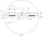
- FIG. 3shows a detailed schematic cross-sectional view of an XBAR that incorporates a “half-lambda” dielectric layer.
- FIG. 3specifically shows an XBAR 300 with a thick dielectric layer 350 on the front side (i.e. the side facing away from the substrate; the upper side as shown in FIG. 3 ) of a piezoelectric plate 310 .
- a comparable dielectric layer on the back side 316 of the piezoelectric plate 310could be used instead of the dielectric layer 350 .
- the XBAR 300 with the thick dielectric layer 350is similar to the XBAR 100 of FIG. 1 .
- FIG. 3also shows two IDT fingers 338 as previously described. Dimension p is the center-to-center spacing or “pitch” of the IDT fingers, and dimension w is the width or “mark” of the IDT fingers.
- the piezoelectric plate 310is a thin single-crystal layer of a piezoelectric material such as lithium niobate or lithium tantalate.
- the piezoelectric plate 310is cut such that the orientation of the X, Y, and Z crystalline axes with respect to the front and back surfaces 314 , 316 is known and consistent.
- the thickness ts of the piezoelectric plate 310may be, for example, 100 nm to 1500 nm.
- the dielectric layer 350may be nearly any dielectric material such as SiO 2 , Si 3 N 4 , Al 2 O 3 , AlN, and other dielectric materials. As will be discussed, particular benefits may accrue when the dielectric material is or contains AlN and when the dielectric material is SiO 2 .
- the thickness ts of the piezoelectric plate 310 and the thickness td of the dielectric layer 350are configured such a shear BAW propagating normal to the surfaces 316 and 352 forms a full-cycle standing wave between the surfaces 316 and 352 at a predetermined frequency, which may be slightly less than the desired resonance frequency of the XBAR device 300 .
- the shear BAW second overtone resonanceoccurs at the predetermined frequency.
- the thickness ts of the piezoelectric plateis one-half of ⁇ 0,s , which, as previously described, is the wavelength of the shear BAW fundamental resonance of the piezoelectric plate 310 in the absence of the dielectric layer 350 .
- the thickness td of the dielectric layer 350is one-half of ⁇ 0,d , where ⁇ 0,d is the wavelength of the same bulk BAW in the dielectric layer 350 .
- each of the piezoelectric plate 310 and the dielectric layer 350will contain a half cycle standing wave at the frequency f 0 , which is now the frequency of the second overtone resonance.
- ⁇ 0,dis equal to ⁇ 0,s , times the ratio of the velocity of the shear acoustic wave in the dielectric layer 350 to the velocity of the shear acoustic wave in the piezoelectric plate 310 .
- ⁇ 0,dmay be equal to or slightly greater than ⁇ 0,s .
- the thickness td of the dielectric layer 350may be equal to or slightly greater than ts.
- ⁇ 0,dmay be substantially greater than ⁇ 0,s .
- the thickness td of the dielectric layer 350will be proportionally greater than ts.
- the thickness td of the dielectric layerneed not be exactly ⁇ 0,d /2.
- the thickness tdmay differ from ⁇ 0,d /2 so long as the combined thicknesses of the piezoelectric plate 310 and the dielectric layer 350 are such that the second overtone resonance of the bulk shear wave occurs at the predetermined frequency.
- Simulation resultssome of which will be discussed subsequently, show that dielectric layer thickness with a range defined by 0.85 ⁇ 0,d ⁇ 2td ⁇ 1.15 ⁇ 0,d (1) results in XBARs with low spurious modes and consistent electromechanical coupling. Values of td outside of this range result in reduced electromechanical coupling and increased spurious modes. Varying td within this range allows tuning the resonant frequency of an XBAR by about 10%, which is sufficient to establish the necessary frequency offset between shunt and series resonators for many filter applications.
- the dielectric layer 350is shown deposited over and between the IDT fingers 338 .
- a half-lambda dielectric layermay be formed only between the IDT fingers.
- the half-lambda dielectric layer 350may be a single layer or two or more layers of different dielectric materials having similar acoustic impedances.
- a primary benefit of incorporating the half-lambda dielectric layer 350 into the XBAR 300is the increased thickness of the diaphragm.
- the thickness of the diaphragm of the XBAR 300may be two to three times the thickness of the diaphragm 115 of the XBAR 100 of FIG. 1 .
- a thicker diaphragmis stiffer and less likely to bow or distort with changes in temperature.
- the thicker diaphragm of the XBAR 300will also have higher thermal conductivity, particularly if the half-lambda dielectric layer 350 is or includes a high thermal conductivity dielectric material such as aluminum nitride. Higher thermal conductivity results in more efficient removal of heat from the diaphragm, which may allow the use of a smaller resonator area for a given heat load or power dissipation.
- the XBAR 300will also have higher capacitance per unit area compared with the XBAR 100 of FIG. 1 (for the same IDT pitch).
- Resonator capacitanceis a circuit design issue.
- RF filters using acoustic resonatorsare typically subject to a requirement that the input and output impedances of the filter match a defined value (commonly 50 ohms). This requirement dictates minimum capacitance values for some or all of the resonators in a filter.
- the higher capacitance per unit area of the XBAR 300 with partial Bragg reflectorsallows the use of a smaller resonator area for any required capacitance value.
- An XBAR with a half-lambda dielectric layer on the back side of the piezoelectric plate 310(not shown) will have improved stiffness and thermal conductivity, but only slightly increased capacitance per unit area.
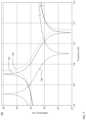
- FIG. 4is a chart 400 comparing the admittance of an XBAR with a half-lambda dielectric layer and a conventional XBAR.
- the data shown in FIG. 4 and following FIG. 6 and FIG. 7are results of simulation of the XBAR devices using a finite element method.
- the solid line 410is a plot of the magnitude of admittance as a function of frequency for an XBAR including a half-lambda dielectric layer.
- the piezoelectric plateis lithium niobate 400 nm thick.
- the IDTis aluminum 100 nm thick.
- the pitch and mark of the IDT fingersare 4.25 ⁇ m and 1.275 ⁇ m, respectively.
- the half-lambda dielectric layerconsists of a layer of Si 3 N 4 350 nm thick and a layer of AlN 350 nm thick.
- the resonance frequencyis 4.607 GHz and the anti-resonance frequency is 4.862 GHz.
- the different between the anti-resonance and resonance frequenciesis 255 MHz, or about 5.4% of the average of the resonance and anti-resonance frequencies.
- the dashed line 420is a plot of the magnitude of admittance as a function of frequency for a conventional XBAR.
- the piezoelectric plateis lithium niobate 400 nm thick.
- the IDTis aluminum 100 nm thick.
- the pitch and mark of the IDT fingersare 3.7 ⁇ m and 0.47 ⁇ m, respectively.
- the resonance frequencyis 4.71 GHz and the anti-resonance frequency is 5.32 GHz.
- the different between the anti-resonance and resonance frequenciesis 610 MHz, or about 12.2% of the average of the resonance and anti-resonance frequencies.
- the admittance of the conventional XBAR(dashed line 420 ) exhibits some spurious modes between the resonance and anti-resonance frequencies that are not present in the admittance of the XBAR with the half-lambda dielectric layer (solid line 410 ).
- FIG. 5a cross-sectional view of an XBAR 500 with a half-lambda dielectric layer with contours representing the stress at the resonance frequency.
- the piezoelectric plate 510is lithium niobate 400 nm thick.
- the IDT fingers 538are aluminum 100 nm thick.
- the half-lambda dielectric layer 550consists of a layer 552 of Si 3 N 4 350 nm thick and a layer 554 of AlN 350 nm thick.
- the stress in the XBAR 500 at the resonance frequencyis illustrative of a full-cycle standing wave between the surfaces of the device.
- the stressis highest near the center of the thickness of the piezoelectric plate 510 and near the center of the dielectric layer 550 , corresponding to the peaks of the two half-cycles of the standing wave.
- the stressis lowest at the surfaces of the device and near the boundary between the piezoelectric plate 510 and near the center of the dielectric layer 550 , corresponding to the zero crossings of the standing wave.
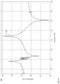
- FIG. 6is a chart 600 illustrating the use of pitch and dielectric layer thickness to tune the resonance and anti-resonance frequencies of an XBAR with a half-lambda dielectric layer.
- the solid line 610is a plot of the magnitude of admittance as a function of frequency for an XBAR with pitch and mark of 4.25 ⁇ m and 1.275 ⁇ m, respectively.
- the piezoelectric plateis lithium niobate 400 nm thick.
- the IDTis aluminum 100 nm thick.
- the half-lambda dielectric layerconsists of a layer of Si 3 N 4 700 nm thick.
- the resonance frequencyis 4.513 GHz and the anti-resonance frequency is 4.749 GHz.
- the difference between the anti-resonance and resonance frequenciesis 236 MHz, or about 5.1% of the average of the resonance and anti-resonance frequencies.
- the dotted line 620is a plot of the magnitude of admittance as a function of frequency for a similar XBAR with the same construction except the pitch and mark of the IDT fingers are 3.75 ⁇ m and 1.31 ⁇ m, respectively.
- the resonance frequencyis 4.557 GHz and the anti-resonance frequency is 4.795 GHz.
- Changing the IDT pitch from 4.25 ⁇ m to 3.75 ⁇ mincreases the resonance and anti-resonance frequencies by about 45 MHz. Varying the pitch over a range from 3 ⁇ m to 5 ⁇ m will provide a tuning range of about 200 MHz.
- the dashed line 630is a plot of the magnitude of admittance as a function of frequency for a similar XBAR.
- the pitch and mark of the IDT fingersare 4.25 ⁇ m and 1.275 ⁇ m, respectively, and the dielectric layer includes a layer of Si 3 N 4 700 nm thick plus a 50 nm layer of SiO 2 .
- the resonance frequencyis 4.400 GHz and the anti-resonance frequency is 4.626 GHz. Adding the 50 nm “tuning layer” reduces the resonance and anti-resonance frequencies by about 110 MHz.
- FIG. 7is another chart 700 illustrating the use of pitch and dielectric layer thickness to tune the resonance and anti-resonance frequencies of an XBAR with a half-lambda dielectric layer.
- the solid line 710is a plot of the magnitude of admittance as a function of frequency for an XBAR with pitch and mark of 4.25 ⁇ m and 1.275 ⁇ m, respectively.
- the piezoelectric plateis lithium niobate 400 nm thick.
- the IDTis aluminum 100 nm thick.
- the half-lambda dielectric layerconsists of a layer of SiO 2 400 nm thick.
- the resonance frequencyis 4.705 GHz and the anti-resonance frequency is 5.108 GHz.
- the difference between the anti-resonance and resonance frequenciesis 403 MHz, or about 8.2% of the average of the resonance and anti-resonance frequencies.
- the dotted line 720is a plot of the magnitude of admittance as a function of frequency for a similar XBAR with the same construction except the pitch and mark of the IDT fingers are 3.75 ⁇ m and 1.31 ⁇ m, respectively.
- the resonance frequencyis 4.740 GHz and the anti-resonance frequency is 5.137 GHz.
- Changing the IDT pitch from 4.25 ⁇ m to 3.75 ⁇ mincreases the resonance and anti-resonance frequencies by about 35 MHz. Varying the pitch over a range from 3 ⁇ m to 5 ⁇ m will provide a tuning range of about 100 MHz.
- the dashed line 730is a plot of the magnitude of admittance as a function of frequency for a similar XBAR with the same construction except the pitch and mark of the IDT fingers are 4.25 ⁇ m and 1.275 ⁇ m, respectively, and the dielectric layer is of SiO 2 450 nm thick.
- the resonance frequencyis 4.512 GHz and the anti-resonance frequency is 4.905 GHz.
- the difference between the anti-resonance and resonance frequenciesis 393 MHz, or about 8.3% of the average of the resonance and anti-resonance frequencies.
- Increasing the thickness of the dielectric layer by 50 nmreduces the resonance and anti-resonance frequencies by about 190 MHz without reducing electromechanical coupling.
- FIG. 8is another chart 800 illustrating the use of dielectric layer thickness to tune the resonance and anti-resonance frequencies of an XBAR with a half-lambda dielectric layer.
- the dotted line 810is a plot of the magnitude of admittance as a function of frequency for an XBAR with pitch and mark of 4.25 ⁇ m and 1.275 ⁇ m, respectively.
- the piezoelectric plateis lithium niobate 400 nm thick.
- the IDTis aluminum 100 nm thick.
- the half-lambda dielectric layerconsists of a layer of SiO 2 425 nm thick. This example represents the case where the thickness of the dielectric layer td equals ⁇ 0,d /2.
- the range for td expressed in equation (1)corresponds to about 350 nm to 500 nm.
- This rangemay be expressed in terms of the thickness ts of the piezoelectric plate as follows: 0.875ts ⁇ td ⁇ 1.25ts. (2) It is expected that this range will apply to any thickness for the lithium niobate piezoelectric plate.
- FIG. 9is a chart 900 illustrating the effect of an overly thin “half-lambda” dielectric layer.
- FIG. 10is a chart 1000 illustrating the effect of an overly thick “half-lambda” dielectric layer.
- the temperature coefficient of frequency of SiO 2 and the temperature coefficient of frequency of lithium niobatehave similar magnitude and opposing signs.
- XBAR devices with an SiO 2 half-lambda dielectric layerwill have substantially less frequency variation with temperature than conventional XBAR devices.
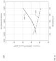
- FIG. 11is a chart of the temperature coefficient of frequency of an XBAR as a function of SiO 2 thickness.
- the solid line 1110is a plot of temperature coefficient of the anti-resonance frequency for the XBAR devices whose admittance characteristics were previously shown in FIG. 7 and FIG. 8 .
- the dashed line 1120is a plot of temperature coefficient of the resonance frequency of the same devices. Simulation results show that a conventional XBAR device without a dielectric layer has a temperature coefficient of frequency around ⁇ 113 ppm/C°. The presence of the SiO 2 half-lambda dielectric layer reduces the magnitude of the temperature coefficient of frequency by a factor of about 3.
- FIG. 12is a schematic circuit diagram of a band-pass filter 1200 using five XBARs X 1 -X 5 .
- the filter 1200may be, for example, a band n79 band-pass filter for use in a communication device.
- the filter 1200has a conventional ladder filter architecture including three series resonators X 1 , X 3 , X 5 and two shunt resonators X 2 , X 4 .
- the three series resonators X 1 , X 3 , X 5are connected in series between a first port and a second port.
- the first and second portsare labeled “In” and “Out”, respectively.
- the filter 1200is bidirectional and either port may serve as the input or output of the filter.
- the two shunt resonators X 2 , X 4are connected from nodes between the series resonators to ground. All the shunt resonators and series resonators are XBARs.
- the three series resonators X 1 , X 3 , X 5 and the two shunt resonators X 2 , X 4 of the filter 1200maybe formed on a single plate 1230 of piezoelectric material bonded to a silicon substrate (not visible).
- Each resonatorincludes a respective IDT (not shown), with at least the fingers of the IDT disposed over a cavity in the substrate.
- the term “respective”means “relating things each to each”, which is to say with a one-to-one correspondence.
- the cavitiesare illustrated schematically as the dashed rectangles (such as the rectangle 1235 ).
- an IDT of each resonatoris disposed over a respective cavity.
- the IDTs of two or more resonatorsmay be disposed over a common cavity.
- Resonatorsmay also be cascaded into multiple IDTs which may be formed on multiple cavities.
- Each of the resonators X 1 to X 5has a resonance frequency and an anti-resonance frequency.
- each resonatoris effectively a short circuit at its resonance frequency and effectively an open circuit at its anti-resonance frequency.
- Each resonator X 1 to X 5creates a “transmission zero”, where the transmission between the in and out ports of the filter is very low. Note that the transmission at a “transmission zero” is not actually zero due to energy leakage through parasitic components and other effects.
- the three series resonators X 1 , X 3 , X 5create transmission zeros at their respective anti-resonance frequencies (where each resonator is effectively an open circuit).
- the two shunt resonators X 2 , X 4create transmission zeros at their respective resonance frequencies (where each resonator is effectively a short circuit).
- the anti-resonance frequencies of the series resonatorsare higher than an upper edge of the passband such that the series resonators create transmission zeros above the passband.
- the resonance frequencies of the shunt resonatorsare less than a lower edge of the passband such that the shunt resonators create transmission zeros below the passband.
- the frequency offset between the resonance and anti-resonance frequencies of an XBAR with a 400 nm lithium niobate piezoelectric plate and a half-lambda dielectric layeris about 400 MHz.
- This frequency separationis not, of itself, sufficient for band-pass filters for telecommunications bands such as n79 (4400 MHz to 5000 MHz) and n77 (3300 MHZ to 4200 MHz).
- U.S. Pat. No. 10,491,192describes the use of a dielectric layer deposited over shunt resonators to reduce the resonance frequencies of the shunt resonators relative to the resonance frequencies of the series resonators.
- U.S. Pat. No. 10,491,192describes filters with very thin or no dielectric layer over series resonators and a dielectric layer thickness of about 0.25 times the piezoelectric plate thickness over shunt resonators.
- the thickness tds of the dielectric layer over series resonators and the thickness tdp of the dielectric layer over shunt (parallel) resonatorsmay be defined by 0.85 ⁇ 0,d ⁇ 2tds ⁇ 2tdp ⁇ 1.15 ⁇ 0,d .
- the solid curve 820is the admittance of an XBAR with a 375 nm SiO 2 layer over a 400 nm lithium niobate piezoelectric plate.
- the dashed curve 830is the admittance of an XBAR with a 475 nm SiO 2 layer over a 400 nm lithium niobate piezoelectric plate.
- a filter, such as the filter 1200could be fabricated using a 400 nm lithium niobate piezoelectric plate with 375 nm SiO 2 layer over series resonators and 475 nm SiO 2 layer over shunt resonators.
- the frequency separation between the resonance frequency of the shunt resonators and the anti-resonance frequency of the series resonatorswill be about 800 MHz, which is sufficient for a band-pass filter for band n79.
- the frequency separationwill scale proportionally with the thickness of the piezoelectric plate.
- the ranges for the thickness of the SiO 2 layers over series and shunt resonatorsmay be expressed in terms of the thickness ts of the lithium niobate piezoelectric plate as follows: 0.875ts ⁇ tds ⁇ tdp ⁇ 1.25ts, (4) where tds is the thickness of the SiO 2 layer over series resonators and tdp is the thickness of the SiO 2 layer over shunt (parallel) resonators.
- FIG. 13is a simplified flow chart showing a method 1300 for making an XBAR including partial Bragg reflectors or a filter incorporating such XBARs.
- the method 1300starts at 1305 with a thin piezoelectric plate disposed on a sacrificial substrate 1302 and a device substrate 1304 .
- the method 1300ends at 1395 with a completed XBAR or filter.
- the flow chart of FIG. 13includes only major process steps.
- Various conventional process stepse.g. surface preparation, cleaning, inspection, baking, annealing, monitoring, testing, etc. may be performed before, between, after, and during the steps shown in FIG. 13 .
- the flow chart of FIG. 13captures three variations of the method 1300 for making an XBAR which differ in when and how cavities are formed in the substrate.
- the cavitiesmay be formed at steps 1310 A, 1310 B, or 1310 C. Only one of these steps is performed in each of the three variations of the method 1300 .
- Thin plates of single-crystal piezoelectric materials bonded to a non-piezoelectric substrateare commercially available. At the time of this application, both lithium niobate and lithium tantalate plates are available bonded to various substrates including silicon, quartz, and fused silica. Thin plates of other piezoelectric materials may be available now or in the future.
- the thickness of the piezoelectric platemay be between 300 nm and 1000 nm.
- the piezoelectric platemay be, for example, Z-cut, rotated Z-cut, or rotated Y-cut lithium niobate or lithium tantalate.
- the piezoelectric platemay be some other material and/or some other cut.
- the substratemay be silicon. When the substrate is silicon, a layer of SiO 2 may be disposed between the piezoelectric plate and the substrate.
- the substratemay be some other material that allows formation of deep cavities by etching or other processing.
- one or more cavitiesare formed in the substrate at 1310 A, before the piezoelectric plate is bonded to the substrate at 1330 .
- a separate cavitymay be formed for each resonator in a filter device.
- the one or more cavitiesmay be formed using conventional photolithographic and etching techniques. For example, the cavities may be formed using deep reactive ion etching (DRIE). Typically, the cavities formed at 1310 A will not penetrate through the substrate.
- DRIEdeep reactive ion etching
- the piezoelectric plate on the sacrificial substrate 1302 and the device substrate 1304may be bonded.
- the piezoelectric plate on the sacrificial substrate 1302 and the device substrate 1304may be bonded using a wafer bonding process such as direct bonding, surface-activated or plasma-activated bonding, electrostatic bonding, or some other bonding technique.
- the device substratemay be coated with a bonding layer, which may be SiO 2 or some other material, prior to the wafer bonding process.
- the sacrificial substrate, and any intervening layersare removed at 1340 to expose the surface of the piezoelectric plate (the surface that previously faced the sacrificial substrate).
- the sacrificial substratemay be removed, for example, by material-dependent wet or dry etching or some other process.
- the exposed surface of the piezoelectric platemay be polished or processed in some other manner at 1340 to prepare the surface and control the thickness of the piezoelectric plate.
- Conductor patterns and dielectric layers defining one or of XBAR devicesare formed at 1350 .
- a filter devicewill have two or more conductor layers that are sequentially deposited and patterned.
- the conductor layersmay include bonding pads, gold or solder bumps, or other means for making connection between the device and external circuitry.
- the conductor layersmay be, for example, aluminum, an aluminum alloy, copper, a copper alloy, molybdenum, tungsten, beryllium, gold, or some other conductive metal.
- one or more layers of other materialsmay be disposed below (i.e. between the conductor layer and the piezoelectric plate) and/or on top of the conductor layer.
- a thin film of titanium, chrome, or other metalmay be used to improve the adhesion between the conductor layers and the piezoelectric plate.
- the conductor layersmay include bonding pads, gold or solder bumps, or other means for making connection between the device and external circuitry.
- Conductor patternsmay be formed at 1350 by depositing the conductor layers over the surface of the piezoelectric plate and removing excess metal by etching through patterned photoresist. Alternatively, the conductor patterns may be formed at 1350 using a lift-off process. Photoresist may be deposited over the piezoelectric plate and patterned to define the conductor pattern. The conductor layer may be deposited in sequence over the surface of the piezoelectric plate. The photoresist may then be removed, which removes the excess material, leaving the conductor pattern.
- a half-lambda dielectric layermay be formed on the front side of the piezoelectric layer.
- the half-lambda dielectric layermay be deposited over the conductor patterns or may be formed only between the fingers of the IDTs.
- a first dielectric layermay be deposited over/between the fingers of all of the IDTs, and a second dielectric may be selectively formed over a portion of the IDTs, such as over only the IDTs of shunt resonators.
- the first dielectric layerwill typically be thicker than the second dielectric layer.
- the first and second dielectric layersmay be the same or different materials. Either the first or second dielectric layer may be deposited first.
- one or more cavitiesare formed in the back side of the substrate at 1310 B after all of the conductor patterns and dielectric layers are formed at 1350 and 1360 .
- a separate cavitymay be formed for each resonator in a filter device.
- the one or more cavitiesmay be formed using an anisotropic or orientation-dependent dry or wet etch to open holes through the back-side of the substrate to the piezoelectric plate.
- one or more cavities in the form of recesses in the substratemay be formed at 1310 C by etching the substrate using an etchant introduced through openings in the piezoelectric plate and half-lambda dielectric layer. A separate cavity may be formed for each resonator in a filter device. The one or more cavities formed at 1310 C will not penetrate through the substrate.
- the filter deviceis completed at 1370 .
- Actions that may occur at 1370include depositing an encapsulation/passivation layer such as SiO 2 or Si 3 O 4 over all or a portion of the device and/or forming bonding pads or solder bumps or other means for making connection between the device and external circuitry if these steps were not performed at 1350 .
- Other actions at 1370may include excising individual devices from a wafer containing multiple devices, other packaging steps, and testing.
- Another action that may occur at 1370is to tune the resonant frequencies of the resonators within the device by adding or removing metal or dielectric material from the front side of the device.
- a variation of the process 1300starts with a single-crystal piezoelectric wafer at 1302 instead of a thin piezoelectric plate on a sacrificial substrate of a different material. Ions are implanted to a controlled depth beneath a surface of the piezoelectric wafer (not shown in FIG. 13 ). The portion of the wafer from the surface to the depth of the ion implantation is (or will become) the thin piezoelectric plate and the balance of the wafer is the sacrificial substrate. The piezoelectric wafer and device substrate are bonded at 1330 as previously described.
- the piezoelectric wafermay be split at the plane of the implanted ions (for example, using thermal shock), leaving a thin plate of piezoelectric material exposed and bonded to the acoustic Bragg reflector.
- the thickness of the thin plate piezoelectric materialis determined in part by the energy (and thus depth) of the implanted ions.
- the process of ion implantation and subsequent separation of a thin plateis commonly referred to as “ion slicing”.
- the exposed surface of the piezoelectric platemay be planarized, and its thickness reduced, using, for example chemo-mechanical polishing.
- “plurality”means two or more. As used herein, a “set” of items may include one or more of such items.
- the terms “comprising”, “including”, “carrying”, “having”, “containing”, “involving”, and the likeare to be understood to be open-ended, i.e., to mean including but not limited to. Only the transitional phrases “consisting of” and “consisting essentially of”, respectively, are closed or semi-closed transitional phrases with respect to claims.
Landscapes
- Physics & Mathematics (AREA)
- Acoustics & Sound (AREA)
- Chemical & Material Sciences (AREA)
- Crystallography & Structural Chemistry (AREA)
- Engineering & Computer Science (AREA)
- Materials Engineering (AREA)
- Manufacturing & Machinery (AREA)
- Piezo-Electric Or Mechanical Vibrators, Or Delay Or Filter Circuits (AREA)
- Surface Acoustic Wave Elements And Circuit Networks Thereof (AREA)
Abstract
Description
0.85λ0,d≤2td≤1.15λ0,d (1)
results in XBARs with low spurious modes and consistent electromechanical coupling. Values of td outside of this range result in reduced electromechanical coupling and increased spurious modes. Varying td within this range allows tuning the resonant frequency of an XBAR by about 10%, which is sufficient to establish the necessary frequency offset between shunt and series resonators for many filter applications.
0.875ts≤td≤1.25ts. (2)
It is expected that this range will apply to any thickness for the lithium niobate piezoelectric plate.
0.85λ0,d≤2tds≤2tdp≤1.15λ0,d. (3)
0.875ts≤tds<tdp≤1.25ts, (4)
where tds is the thickness of the SiO2layer over series resonators and tdp is the thickness of the SiO2layer over shunt (parallel) resonators.
Claims (19)
2ts=λ0,s, and
0.85λ0,d≤2td≤1.15λ0,d,
2ts=λ0,s, and
2tds<2tdp
0.85λ0,d≤2tds≤2tdp≤1.15λ0,d,
tds<tdp.
0.85ts≤tds≤tdp≤1.25ts.
2ts=λ0,s, and
0.85λ0,d≤2td≤1.15λ0,d,
Priority Applications (1)
| Application Number | Priority Date | Filing Date | Title |
|---|---|---|---|
| US17/069,379US11901874B2 (en) | 2018-06-15 | 2020-10-13 | Transversely-excited film bulk acoustic resonator with half-lambda dielectric layer |
Applications Claiming Priority (10)
| Application Number | Priority Date | Filing Date | Title |
|---|---|---|---|
| US201862685825P | 2018-06-15 | 2018-06-15 | |
| US201862701363P | 2018-07-20 | 2018-07-20 | |
| US201862741702P | 2018-10-05 | 2018-10-05 | |
| US201862748883P | 2018-10-22 | 2018-10-22 | |
| US201862753815P | 2018-10-31 | 2018-10-31 | |
| US16/230,443US10491192B1 (en) | 2018-06-15 | 2018-12-21 | Transversely-excited film bulk acoustic resonator |
| US201962818571P | 2019-03-14 | 2019-03-14 | |
| US16/689,707US10917070B2 (en) | 2018-06-15 | 2019-11-20 | Bandpass filter with frequency separation between shunt and series resonators set by dielectric layer thickness |
| US16/819,623US10868510B2 (en) | 2018-06-15 | 2020-03-16 | Transversely-excited film bulk acoustic resonator with half-lambda dielectric layer |
| US17/069,379US11901874B2 (en) | 2018-06-15 | 2020-10-13 | Transversely-excited film bulk acoustic resonator with half-lambda dielectric layer |
Related Parent Applications (1)
| Application Number | Title | Priority Date | Filing Date |
|---|---|---|---|
| US16/819,623ContinuationUS10868510B2 (en) | 2018-06-15 | 2020-03-16 | Transversely-excited film bulk acoustic resonator with half-lambda dielectric layer |
Publications (2)
| Publication Number | Publication Date |
|---|---|
| US20210028758A1 US20210028758A1 (en) | 2021-01-28 |
| US11901874B2true US11901874B2 (en) | 2024-02-13 |
Family
ID=72426858
Family Applications (2)
| Application Number | Title | Priority Date | Filing Date |
|---|---|---|---|
| US16/819,623ActiveUS10868510B2 (en) | 2018-06-15 | 2020-03-16 | Transversely-excited film bulk acoustic resonator with half-lambda dielectric layer |
| US17/069,379Active2039-08-23US11901874B2 (en) | 2018-06-15 | 2020-10-13 | Transversely-excited film bulk acoustic resonator with half-lambda dielectric layer |
Family Applications Before (1)
| Application Number | Title | Priority Date | Filing Date |
|---|---|---|---|
| US16/819,623ActiveUS10868510B2 (en) | 2018-06-15 | 2020-03-16 | Transversely-excited film bulk acoustic resonator with half-lambda dielectric layer |
Country Status (5)
| Country | Link |
|---|---|
| US (2) | US10868510B2 (en) |
| JP (1) | JP7556358B2 (en) |
| CN (3) | CN120263137A (en) |
| DE (1) | DE112020001227T5 (en) |
| WO (1) | WO2020186261A1 (en) |
Families Citing this family (104)
| Publication number | Priority date | Publication date | Assignee | Title |
|---|---|---|---|---|
| US11323090B2 (en) | 2018-06-15 | 2022-05-03 | Resonant Inc. | Transversely-excited film bulk acoustic resonator using Y-X-cut lithium niobate for high power applications |
| US12040779B2 (en) | 2020-04-20 | 2024-07-16 | Murata Manufacturing Co., Ltd. | Small transversely-excited film bulk acoustic resonators with enhanced Q-factor |
| US12237826B2 (en) | 2018-06-15 | 2025-02-25 | Murata Manufacturing Co., Ltd. | Transversely-excited film bulk acoustic resonator with optimized electrode thickness, mark, and pitch |
| US10637438B2 (en) | 2018-06-15 | 2020-04-28 | Resonant Inc. | Transversely-excited film bulk acoustic resonators for high power applications |
| US10601392B2 (en) | 2018-06-15 | 2020-03-24 | Resonant Inc. | Solidly-mounted transversely-excited film bulk acoustic resonator |
| US11996827B2 (en) | 2018-06-15 | 2024-05-28 | Murata Manufacturing Co., Ltd. | Transversely-excited film bulk acoustic resonator with periodic etched holes |
| US11206009B2 (en) | 2019-08-28 | 2021-12-21 | Resonant Inc. | Transversely-excited film bulk acoustic resonator with interdigital transducer with varied mark and pitch |
| US11323089B2 (en) | 2018-06-15 | 2022-05-03 | Resonant Inc. | Filter using piezoelectric film bonded to high resistivity silicon substrate with trap-rich layer |
| US12088281B2 (en) | 2021-02-03 | 2024-09-10 | Murata Manufacturing Co., Ltd. | Transversely-excited film bulk acoustic resonator with multi-mark interdigital transducer |
| US11146232B2 (en) | 2018-06-15 | 2021-10-12 | Resonant Inc. | Transversely-excited film bulk acoustic resonator with reduced spurious modes |
| US11323096B2 (en) | 2018-06-15 | 2022-05-03 | Resonant Inc. | Transversely-excited film bulk acoustic resonator with periodic etched holes |
| US11929731B2 (en) | 2018-02-18 | 2024-03-12 | Murata Manufacturing Co., Ltd. | Transversely-excited film bulk acoustic resonator with optimized electrode mark, and pitch |
| US10911023B2 (en) | 2018-06-15 | 2021-02-02 | Resonant Inc. | Transversely-excited film bulk acoustic resonator with etch-stop layer |
| US11509279B2 (en) | 2020-07-18 | 2022-11-22 | Resonant Inc. | Acoustic resonators and filters with reduced temperature coefficient of frequency |
| US11936358B2 (en) | 2020-11-11 | 2024-03-19 | Murata Manufacturing Co., Ltd. | Transversely-excited film bulk acoustic resonator with low thermal impedance |
| US10756697B2 (en)* | 2018-06-15 | 2020-08-25 | Resonant Inc. | Transversely-excited film bulk acoustic resonator |
| US11996825B2 (en) | 2020-06-17 | 2024-05-28 | Murata Manufacturing Co., Ltd. | Filter using lithium niobate and rotated lithium tantalate transversely-excited film bulk acoustic resonators |
| US12191838B2 (en) | 2018-06-15 | 2025-01-07 | Murata Manufacturing Co., Ltd. | Solidly-mounted transversely-excited film bulk acoustic device and method |
| US11876498B2 (en) | 2018-06-15 | 2024-01-16 | Murata Manufacturing Co., Ltd. | Transversely-excited film bulk acoustic resonator with multiple diaphragm thicknesses and fabrication method |
| US11349450B2 (en) | 2018-06-15 | 2022-05-31 | Resonant Inc. | Symmetric transversely-excited film bulk acoustic resonators with reduced spurious modes |
| US11323091B2 (en) | 2018-06-15 | 2022-05-03 | Resonant Inc. | Transversely-excited film bulk acoustic resonator with diaphragm support pedestals |
| US12113512B2 (en) | 2021-03-29 | 2024-10-08 | Murata Manufacturing Co., Ltd. | Layout of XBARs with multiple sub-resonators in parallel |
| US12095441B2 (en) | 2018-06-15 | 2024-09-17 | Murata Manufacturing Co., Ltd. | Transversely excited film bulk acoustic resonator with recessed interdigital transducer fingers |
| US11146238B2 (en) | 2018-06-15 | 2021-10-12 | Resonant Inc. | Film bulk acoustic resonator fabrication method |
| US11323095B2 (en) | 2018-06-15 | 2022-05-03 | Resonant Inc. | Rotation in XY plane to suppress spurious modes in XBAR devices |
| US11329628B2 (en) | 2020-06-17 | 2022-05-10 | Resonant Inc. | Filter using lithium niobate and lithium tantalate transversely-excited film bulk acoustic resonators |
| US11916539B2 (en) | 2020-02-28 | 2024-02-27 | Murata Manufacturing Co., Ltd. | Split-ladder band N77 filter using transversely-excited film bulk acoustic resonators |
| US12191837B2 (en) | 2018-06-15 | 2025-01-07 | Murata Manufacturing Co., Ltd. | Solidly-mounted transversely-excited film bulk acoustic device |
| US11909381B2 (en) | 2018-06-15 | 2024-02-20 | Murata Manufacturing Co., Ltd. | Transversely-excited film bulk acoustic resonators with two-layer electrodes having a narrower top layer |
| US11967945B2 (en) | 2018-06-15 | 2024-04-23 | Murata Manufacturing Co., Ltd. | Transversly-excited film bulk acoustic resonators and filters |
| US11264966B2 (en) | 2018-06-15 | 2022-03-01 | Resonant Inc. | Solidly-mounted transversely-excited film bulk acoustic resonator with diamond layers in Bragg reflector stack |
| US12119805B2 (en)* | 2018-06-15 | 2024-10-15 | Murata Manufacturing Co., Ltd. | Substrate processing and membrane release of transversely-excited film bulk acoustic resonator using a sacrificial tub |
| US10917072B2 (en) | 2019-06-24 | 2021-02-09 | Resonant Inc. | Split ladder acoustic wave filters |
| US12237827B2 (en) | 2018-06-15 | 2025-02-25 | Murata Manufacturing Co., Ltd. | Solidly-mounted transversely-excited film bulk acoustic filters with multiple piezoelectric plate thicknesses |
| US12155371B2 (en) | 2021-03-29 | 2024-11-26 | Murata Manufacturing Co., Ltd. | Layout of xbars with multiple sub-resonators in series |
| US12224732B2 (en) | 2018-06-15 | 2025-02-11 | Murata Manufacturing Co., Ltd. | Solidly-mounted transversely-excited film bulk acoustic resonators and filters for 27 GHz communications bands |
| US12184261B2 (en) | 2018-06-15 | 2024-12-31 | Murata Manufacturing Co., Ltd. | Transversely-excited film bulk acoustic resonator with a cavity having round end zones |
| US12149227B2 (en) | 2018-06-15 | 2024-11-19 | Murata Manufacturing Co., Ltd. | Transversely-excited film bulk acoustic resonator package |
| US12081187B2 (en) | 2018-06-15 | 2024-09-03 | Murata Manufacturing Co., Ltd. | Transversely-excited film bulk acoustic resonator |
| US12132464B2 (en) | 2018-06-15 | 2024-10-29 | Murata Manufacturing Co., Ltd. | Filter using transversely-excited film bulk acoustic resonators with divided frequency-setting dielectric layers |
| US11901878B2 (en) | 2018-06-15 | 2024-02-13 | Murata Manufacturing Co., Ltd. | Transversely-excited film bulk acoustic resonators with two-layer electrodes with a wider top layer |
| US11888463B2 (en) | 2018-06-15 | 2024-01-30 | Murata Manufacturing Co., Ltd. | Multi-port filter using transversely-excited film bulk acoustic resonators |
| US10985728B2 (en) | 2018-06-15 | 2021-04-20 | Resonant Inc. | Transversely-excited film bulk acoustic resonator and filter with a uniform-thickness dielectric overlayer |
| US12021496B2 (en) | 2020-08-31 | 2024-06-25 | Murata Manufacturing Co., Ltd. | Resonators with different membrane thicknesses on the same die |
| US11996822B2 (en) | 2018-06-15 | 2024-05-28 | Murata Manufacturing Co., Ltd. | Wide bandwidth time division duplex transceiver |
| US12119808B2 (en) | 2018-06-15 | 2024-10-15 | Murata Manufacturing Co., Ltd. | Transversely-excited film bulk acoustic resonator package |
| US10826462B2 (en) | 2018-06-15 | 2020-11-03 | Resonant Inc. | Transversely-excited film bulk acoustic resonators with molybdenum conductors |
| US11870423B2 (en)* | 2018-06-15 | 2024-01-09 | Murata Manufacturing Co., Ltd. | Wide bandwidth temperature-compensated transversely-excited film bulk acoustic resonator |
| US12301212B2 (en) | 2018-06-15 | 2025-05-13 | Murata Manufacturing Co., Ltd. | XBAR resonators with non-rectangular diaphragms |
| US10998882B2 (en) | 2018-06-15 | 2021-05-04 | Resonant Inc. | XBAR resonators with non-rectangular diaphragms |
| US12155374B2 (en) | 2021-04-02 | 2024-11-26 | Murata Manufacturing Co., Ltd. | Tiled transversely-excited film bulk acoustic resonator high power filters |
| US12212306B2 (en) | 2018-06-15 | 2025-01-28 | Murata Manufacturing Co., Ltd. | Transversely-excited film bulk acoustic resonator with multiple diaphragm thicknesses and fabrication method |
| US12040781B2 (en) | 2018-06-15 | 2024-07-16 | Murata Manufacturing Co., Ltd. | Transversely-excited film bulk acoustic resonator package |
| US10992284B2 (en) | 2018-06-15 | 2021-04-27 | Resonant Inc. | Filter using transversely-excited film bulk acoustic resonators with multiple frequency setting layers |
| US11349452B2 (en) | 2018-06-15 | 2022-05-31 | Resonant Inc. | Transversely-excited film bulk acoustic filters with symmetric layout |
| US11728785B2 (en) | 2018-06-15 | 2023-08-15 | Murata Manufacturing Co., Ltd. | Transversely-excited film bulk acoustic resonator using pre-formed cavities |
| DE112020001227T5 (en)* | 2019-03-14 | 2022-02-10 | Resonant Inc. | Transversally excited acoustic film resonator with half-wave dielectric layer |
| JP2022525465A (en) | 2019-04-05 | 2022-05-16 | レゾナント インコーポレイテッド | Laterally Excited Film Bulk Acoustic Resonator Package and Method |
| US12255625B2 (en) | 2020-02-28 | 2025-03-18 | Murata Manufacturing Co., Ltd. | Filter using transversely-excited film bulk acoustic resonators with inductively coupled sub-resonators |
| US20210273629A1 (en) | 2020-02-28 | 2021-09-02 | Resonant Inc. | Transversely-excited film bulk acoustic resonator with multi-pitch interdigital transducer |
| US12278617B2 (en) | 2020-04-20 | 2025-04-15 | Murata Manufacturing Co., Ltd. | High Q solidly-mounted transversely-excited film bulk acoustic resonators |
| US12341490B2 (en) | 2020-04-20 | 2025-06-24 | Murata Manufacturing Co., Ltd. | Low loss transversely-excited film bulk acoustic resonators and filters |
| US12341493B2 (en) | 2020-04-20 | 2025-06-24 | Murata Manufacturing Co., Ltd. | Low loss transversely-excited film bulk acoustic resonators and filters |
| US11811391B2 (en) | 2020-05-04 | 2023-11-07 | Murata Manufacturing Co., Ltd. | Transversely-excited film bulk acoustic resonator with etched conductor patterns |
| US11482981B2 (en) | 2020-07-09 | 2022-10-25 | Resonanat Inc. | Transversely-excited film bulk acoustic resonators with piezoelectric diaphragm supported by piezoelectric substrate |
| US11264969B1 (en) | 2020-08-06 | 2022-03-01 | Resonant Inc. | Transversely-excited film bulk acoustic resonator comprising small cells |
| US11271539B1 (en) | 2020-08-19 | 2022-03-08 | Resonant Inc. | Transversely-excited film bulk acoustic resonator with tether-supported diaphragm |
| US11929733B2 (en) | 2020-10-05 | 2024-03-12 | Murata Manufacturing Co., Ltd. | Transversely-excited film bulk acoustic resonator matrix filters with input and output impedances matched to radio frequency front end elements |
| US11728784B2 (en) | 2020-10-05 | 2023-08-15 | Murata Manufacturing Co., Ltd. | Transversely-excited film bulk acoustic resonator matrix filters with split die sub-filters |
| US11476834B2 (en) | 2020-10-05 | 2022-10-18 | Resonant Inc. | Transversely-excited film bulk acoustic resonator matrix filters with switches in parallel with sub-filter shunt capacitors |
| US11658639B2 (en) | 2020-10-05 | 2023-05-23 | Murata Manufacturing Co., Ltd. | Transversely-excited film bulk acoustic resonator matrix filters with noncontiguous passband |
| US11405017B2 (en) | 2020-10-05 | 2022-08-02 | Resonant Inc. | Acoustic matrix filters and radios using acoustic matrix filters |
| US12119806B2 (en) | 2020-10-30 | 2024-10-15 | Murata Manufacturing Co., Ltd. | Transversely-excited film bulk acoustic resonator with spiral interdigitated transducer fingers |
| US12255617B2 (en) | 2020-11-11 | 2025-03-18 | Murata Manufacturing Co., Ltd. | Solidly-mounted transversely-excited film bulk acoustic resonators with low thermal impedance |
| US12431856B2 (en) | 2020-11-12 | 2025-09-30 | Murata Manufacturing Co., Ltd. | Transversely-excited film bulk acoustic resonator with reduced loss in the aperture direction |
| US11496113B2 (en) | 2020-11-13 | 2022-11-08 | Resonant Inc. | XBAR devices with excess piezoelectric material removed |
| US12255626B2 (en) | 2020-11-13 | 2025-03-18 | Murata Manufacturing Co., Ltd. | Solidly-mounted transversely-excited film bulk acoustic filters with excess piezoelectric material removed |
| US11405020B2 (en) | 2020-11-26 | 2022-08-02 | Resonant Inc. | Transversely-excited film bulk acoustic resonators with structures to reduce acoustic energy leakage |
| US12126318B2 (en) | 2021-01-15 | 2024-10-22 | Murata Manufacturing Co., Ltd. | Filters using decoupled transversely-excited film bulk acoustic resonators |
| US11239816B1 (en) | 2021-01-15 | 2022-02-01 | Resonant Inc. | Decoupled transversely-excited film bulk acoustic resonators |
| CN112952335B (en)* | 2021-01-29 | 2022-03-29 | 盐城东山通信技术有限公司 | Coupling components, couplers, filters and communication RF equipment |
| US12308826B2 (en) | 2021-02-03 | 2025-05-20 | Murata Manufacturing Co., Ltd. | Bandpass filters using transversely-excited film bulk acoustic resonators |
| US12308825B2 (en) | 2021-02-12 | 2025-05-20 | Murata Manufacturing Co., Ltd | Transversely-excited film bulk acoustic resonators with narrow gaps between busbars and ends of interdigital transducer fingers |
| US12355426B2 (en) | 2021-03-24 | 2025-07-08 | Murata Manufacturing Co., Ltd. | Acoustic filters with shared acoustic tracks |
| US12289099B2 (en) | 2021-03-24 | 2025-04-29 | Murata Manufacturing Co., Ltd. | Acoustic filters with shared acoustic tracks for series and shunt resonators |
| US12126328B2 (en) | 2021-03-24 | 2024-10-22 | Murata Manufacturing Co., Ltd. | Acoustic filters with shared acoustic tracks |
| US12348216B2 (en) | 2021-03-24 | 2025-07-01 | Murata Manufacturing Co., Ltd. | Acoustic filters with shared acoustic tracks and cascaded series resonators |
| US12341492B2 (en) | 2021-03-29 | 2025-06-24 | Murata Manufacturing Co., Ltd. | Transversely-excited film bulk acoustic resonators with busbar side edges that form angles with a perimeter of the cavity |
| CN117321912A (en) | 2021-03-30 | 2023-12-29 | 株式会社村田制作所 | Filters for 6GHz WI-FI using transversely excited thin film bulk acoustic resonators |
| US12224735B2 (en) | 2021-03-30 | 2025-02-11 | Murata Manufacturing Co., Ltd. | Diplexer using decoupled transversely-excited film bulk acoustic resonators |
| US12249971B2 (en) | 2021-04-02 | 2025-03-11 | Murata Manufacturing Co., Ltd. | Transversely-excited film bulk acoustic resonators with solidly mounted resonator (SMR) pedestals |
| US12237823B2 (en) | 2021-04-02 | 2025-02-25 | Murata Manufacturing Co., Ltd. | Transversely-excited film bulk acoustic resonators with solidly mounted resonator (SMR) pedestals |
| US12255633B2 (en) | 2021-04-16 | 2025-03-18 | Murata Manufacturing Co., Ltd. | Filter using transversely-excited film bulk acoustic resonators |
| US12126316B2 (en) | 2021-04-16 | 2024-10-22 | Murata Manufacturing Co., Ltd | Transversely-excited film bulk acoustic resonator |
| US12160220B2 (en) | 2021-04-30 | 2024-12-03 | Murata Manufacturing Co., Ltd. | Transversely-excited film bulk acoustic resonator with oxide strip acoustic confinement structures |
| US12255607B2 (en) | 2021-04-30 | 2025-03-18 | Murata Manufacturing Co., Ltd. | Transversely-excited film bulk acoustic resonator with buried oxide strip acoustic confinement structures |
| US12075700B2 (en) | 2021-05-07 | 2024-08-27 | Murata Manufacturing Co., Ltd. | Transversely-excited film bulk acoustic resonator fabrication using polysilicon pillars |
| US12057823B2 (en) | 2021-05-07 | 2024-08-06 | Murata Manufacturing Co., Ltd. | Transversely-excited film bulk acoustic resonator with concentric interdigitated transducer fingers |
| US12170513B2 (en) | 2021-06-30 | 2024-12-17 | Murata Manufacturing Co., Ltd. | Transversely-excited film bulk acoustic resonator with reduced substrate to contact bump thermal resistance |
| WO2023013741A1 (en)* | 2021-08-04 | 2023-02-09 | 株式会社村田製作所 | Elastic wave device |
| US12225387B2 (en) | 2021-09-29 | 2025-02-11 | Murata Manufacturing Co., Ltd. | Communications device with concurrent operation in 5GHZ and 6GHZ U-NII frequency ranges |
| US12407326B2 (en) | 2021-11-04 | 2025-09-02 | Murata Manufacturing Co., Ltd. | Stacked die transversely-excited film bulk acoustic resonator (XBAR) filters |
| CN116918254A (en)* | 2022-02-18 | 2023-10-20 | 华为技术有限公司 | Bulk acoustic resonator, acoustic filter and electronic equipment |
| CN119790593A (en)* | 2022-09-14 | 2025-04-08 | 华为技术有限公司 | Acoustic resonator |
Citations (168)
| Publication number | Priority date | Publication date | Assignee | Title |
|---|---|---|---|---|
| US5446330A (en) | 1993-03-15 | 1995-08-29 | Matsushita Electric Industrial Co., Ltd. | Surface acoustic wave device having a lamination structure |
| US5552655A (en) | 1994-05-04 | 1996-09-03 | Trw Inc. | Low frequency mechanical resonator |
| US5726610A (en) | 1995-06-19 | 1998-03-10 | Motorola Inc. | Saw filter device for radio tranceiver utilizing different coupling coefficient ratios |
| JPH10209804A (en) | 1997-01-27 | 1998-08-07 | Oki Electric Ind Co Ltd | Surface acoustic wave resonator and surface acoustic wave filter |
| US5853601A (en) | 1997-04-03 | 1998-12-29 | Northrop Grumman Corporation | Top-via etch technique for forming dielectric membranes |
| JP2001244785A (en) | 2000-02-29 | 2001-09-07 | Kyocera Corp | Surface acoustic wave device |
| US6377140B1 (en) | 1999-07-09 | 2002-04-23 | Oki Electric Industry Co., Ltd. | Saw resonator filter with bridged-T configuration |
| US20020079986A1 (en) | 2000-12-21 | 2002-06-27 | Ruby Richard C. | Bulk acoustic resonator perimeter reflection system |
| JP2002300003A (en) | 2001-03-29 | 2002-10-11 | Kyocera Corp | Elastic wave filter |
| US20020158714A1 (en) | 2001-04-27 | 2002-10-31 | Nokia Corporation | Method and system for wafer-level tuning of bulk acoustic wave resonators and filters by reducing thickness non-uniformity |
| US20020189062A1 (en) | 2001-06-15 | 2002-12-19 | Asia Pacific Microsystems, Inc. | Manufacturing method for a high quality film bulk acoustic wave device |
| US6516503B1 (en) | 1999-05-26 | 2003-02-11 | Murata Manufacturing Co., Ltd. | Method of making surface acoustic wave device |
| JP2003078389A (en) | 2001-08-31 | 2003-03-14 | Matsushita Electric Ind Co Ltd | Surface acoustic wave device and method of manufacturing the same |
| US6540827B1 (en) | 1998-02-17 | 2003-04-01 | Trustees Of Columbia University In The City Of New York | Slicing of single-crystal films using ion implantation |
| US20030080831A1 (en) | 2001-10-25 | 2003-05-01 | Naumenko Natalya F. | Surface acoustic wave devices using optimized cuts of lithium niobate (LiNbO3) |
| US20030199105A1 (en) | 2002-04-22 | 2003-10-23 | Kub Francis J. | Method for making piezoelectric resonator and surface acoustic wave device using hydrogen implant layer splitting |
| US20040041496A1 (en) | 2002-09-04 | 2004-03-04 | Fujitsu Media Devices Limited | Surface acoustic wave device, filter device and method of producing the surface acoustic wave device |
| US6707229B1 (en) | 1999-06-03 | 2004-03-16 | Tele Filter Zweigniederlassung Der Dover Germany Gmbh | Surface acoustic wave filter |
| JP2004129222A (en) | 2002-07-31 | 2004-04-22 | Murata Mfg Co Ltd | Piezoelectric component and method of manufacturing the same |
| US20040100164A1 (en) | 2002-11-26 | 2004-05-27 | Murata Manufacturing Co., Ltd. | Manufacturing method of electronic device |
| JP2004304622A (en) | 2003-03-31 | 2004-10-28 | Fujitsu Media Device Kk | Surface acoustic wave device and method of manufacturing the same |
| US20040261250A1 (en) | 2000-09-06 | 2004-12-30 | Murata Manufacturing Co., Ltd. | Method for adjusting a frequency characteristic of an edge reflection type surface acoustic wave device and method for producing an- edge reflection type surface acoustic wave device |
| US20050099091A1 (en)* | 2003-11-12 | 2005-05-12 | Fujitsu Media Devices Limited | Elastic boundary wave device and method of manufacturing the same |
| US20050185026A1 (en) | 2004-01-26 | 2005-08-25 | Motohisa Noguchi | Piezoelectric element, piezoelectric actuator, ink jet recording head, ink jet printer, surface acoustic wave element, frequency filter, oscillator, electronic circuit, thin film piezoelectric resonator, and electronic apparatus |
| US20050218488A1 (en) | 2004-03-31 | 2005-10-06 | Mie Matsuo | Electronic component having micro-electrical mechanical system |
| US20050264136A1 (en) | 2004-05-31 | 2005-12-01 | Jun Tsutsumi | Surface acoustic wave device |
| US7042132B2 (en) | 2001-03-13 | 2006-05-09 | Epcos Ag | Transducer structure that operates with acoustic waves |
| JP2006173557A (en) | 2004-11-22 | 2006-06-29 | Toshiba Corp | Hollow semiconductor device and manufacturing method thereof |
| US20060179642A1 (en) | 2005-02-03 | 2006-08-17 | Kabushiki Kaisha Toshiba | Method for manufacturing a film bulk acoustic resonator |
| US20070182510A1 (en) | 2006-02-06 | 2007-08-09 | Samsung Electronics Co., Ltd. | Multi-band filter module and method of fabricating the same |
| US20070188047A1 (en)* | 2006-02-16 | 2007-08-16 | Seiko Epson Corporation | Lamb wave type frequency device and method thereof |
| US20070194863A1 (en) | 2006-02-17 | 2007-08-23 | Kabushiki Kaisha Toshiba | Film bulk acoustic resonator and method of manufacturing same |
| US20070267942A1 (en) | 2006-05-19 | 2007-11-22 | Hisanori Matsumoto | Piezoelectric film resonator, radio-frequency filter using them, and radio-frequency module using them |
| US20070296304A1 (en) | 2006-06-22 | 2007-12-27 | Seiko Epson Corporation | Acoustic wave device and method of manufacturing acoustic wave device |
| US7345400B2 (en) | 2003-01-27 | 2008-03-18 | Murata Manufacturing Co., Ltd. | Surface acoustic wave device |
| US20080246559A1 (en) | 2007-01-19 | 2008-10-09 | Farrokh Ayazi | Lithographically-defined multi-standard multi-frequency high-Q tunable micromechanical resonators |
| US7463118B2 (en) | 2006-06-09 | 2008-12-09 | Texas Instruments Incorporated | Piezoelectric resonator with an efficient all-dielectric Bragg reflector |
| US7535152B2 (en) | 2005-10-19 | 2009-05-19 | Murata Manufacturing Co., Ltd. | Lamb wave device |
| JP2010062816A (en) | 2008-09-03 | 2010-03-18 | Murata Mfg Co Ltd | Acoustic wave filter |
| US7684109B2 (en) | 2007-02-28 | 2010-03-23 | Maxim Integrated Products, Inc. | Bragg mirror optimized for shear waves |
| US20100102669A1 (en) | 2008-10-24 | 2010-04-29 | Epson Toyocom Corporation | Surface acoustic wave resonator, surface acoustic wave oscillator, and surface acoustic wave module device |
| WO2010047114A1 (en) | 2008-10-24 | 2010-04-29 | エプソントヨコム株式会社 | Surface acoustic wave resonator, surface acoustic wave oscillator, and surface acoustic wave modular device |
| US20100123367A1 (en) | 2008-11-19 | 2010-05-20 | Ngk Insulators, Ltd. | Lamb wave device |
| JP2010233210A (en) | 2009-03-03 | 2010-10-14 | Nippon Dempa Kogyo Co Ltd | Elastic wave device and electronic component |
| US20100301703A1 (en) | 2009-03-31 | 2010-12-02 | Sand9, Inc. | Integration of piezoelectric materials with substrates |
| US7868519B2 (en) | 2007-09-06 | 2011-01-11 | Murata Manufacturing Co., Ltd. | Piezoelectric resonator including an acoustic reflector portion |
| US20110018389A1 (en) | 2008-01-30 | 2011-01-27 | Kyocera Corporation | Acoustic Wave Device and Method for Production of Same |
| US20110018654A1 (en) | 2009-07-27 | 2011-01-27 | Avago Technologies Wireless Ip (Singapore) Pte. Ltd. | Resonator filter with multiple cross-couplings |
| US20110102107A1 (en) | 2008-02-05 | 2011-05-05 | Nihon Dempa Kogyo Co., Ltd. | Filter, portable terminal and electronic component |
| US7939987B1 (en) | 2008-10-23 | 2011-05-10 | Triquint Semiconductor, Inc. | Acoustic wave device employing reflective elements for confining elastic energy |
| US7941103B2 (en) | 2005-11-15 | 2011-05-10 | Taiyo Yuden Co., Ltd. | Duplexer |
| US20110109196A1 (en) | 2008-07-11 | 2011-05-12 | Goto Rei | Plate wave element and electronic equipment using same |
| US20110278993A1 (en) | 2010-05-17 | 2011-11-17 | Murata Manufacturing Co., Ltd. | Method for manufacturing composite piezoelectric substrate and piezoelectric device |
| US8278802B1 (en) | 2008-04-24 | 2012-10-02 | Rf Micro Devices, Inc. | Planarized sacrificial layer for MEMS fabrication |
| US8294330B1 (en) | 2009-03-31 | 2012-10-23 | Triquint Semiconductor, Inc. | High coupling, low loss saw filter and associated method |
| US20120286900A1 (en) | 2010-01-28 | 2012-11-15 | Murata Manufacturing Co., Ltd. | Tunable filter |
| JP2013528996A (en) | 2010-04-23 | 2013-07-11 | テクノロジアン テュトキムスケスクス ヴェーテーテー | Broadband acoustic coupling thin film BAW filter |
| US20130207747A1 (en) | 2010-12-28 | 2013-08-15 | Kyocera Corporation | Acoustic wave element and acoustic wave device using same |
| US20130234805A1 (en) | 2012-03-07 | 2013-09-12 | Taiyo Yuden Co., Ltd. | Resonator, frequency filter, duplexer, electronic device, and method of manufacturing resonator |
| US20130271238A1 (en) | 2012-04-13 | 2013-10-17 | Taiyo Yuden Co., Ltd. | Filter device, manufacturing method for filter device, and duplexer |
| US20130278609A1 (en) | 2012-04-19 | 2013-10-24 | Qualcomm Mems Technologies, Inc. | Isotropically-etched cavities for evanescent-mode electromagnetic-wave cavity resonators |
| US20130321100A1 (en) | 2012-06-05 | 2013-12-05 | Avago Technologies Wireless Ip (Singapore) Pte. Ltd. | Laterally-coupled acoustic resonators |
| US20140009032A1 (en) | 2012-07-04 | 2014-01-09 | Taiyo Yuden Co., Ltd. | Lamb wave device and manufacturing method thereof |
| US20140113571A1 (en) | 2012-10-18 | 2014-04-24 | Panasonic Corporation | Electronic device including filter |
| US20140130319A1 (en) | 2010-09-28 | 2014-05-15 | Murata Manufacturing Co., Ltd. | Method for manufacturing piezoelectric device |
| US20140145556A1 (en) | 2011-08-08 | 2014-05-29 | Murata Manufacturing Co., Ltd. | Elastic wave device |
| US20140151151A1 (en) | 2010-10-15 | 2014-06-05 | Commissariat A L'energie Atomique Et Aux Energies Alternatives | Heterogenous acoustic structure formed from a homogeneous material |
| US20140152145A1 (en)* | 2010-11-30 | 2014-06-05 | Murata Manufacturing Co., Ltd. | Elastic wave device and manufacturing method for same |
| US20140173862A1 (en) | 2007-12-25 | 2014-06-26 | Murata Manufacturing Co., Ltd. | Method for manufacturing composite piezoelectric substrate |
| US20140225684A1 (en) | 2011-10-24 | 2014-08-14 | Murata Manufacturing Co., Ltd. | Surface acoustic wave device |
| US8816567B2 (en) | 2011-07-19 | 2014-08-26 | Qualcomm Mems Technologies, Inc. | Piezoelectric laterally vibrating resonator structure geometries for spurious frequency suppression |
| US8829766B2 (en) | 2008-08-01 | 2014-09-09 | Epcos Ag | Piezoelectric resonator operating in thickness shear mode |
| US20140312994A1 (en) | 2011-11-11 | 2014-10-23 | Teknologian tutkimuskeskut VTT | Laterally coupled bulk acoustic wave filter with improved passband characteristics |
| US8932686B2 (en) | 2008-10-31 | 2015-01-13 | Murata Manufacturing Co., Ltd. | Method for producing piezoelectric composite substrate |
| US20150014795A1 (en) | 2013-07-10 | 2015-01-15 | Avago Technologies General Ip (Singapore) Pte. Ltd. | Surface passivation of substrate by mechanically damaging surface layer |
| US20150042417A1 (en) | 2013-08-06 | 2015-02-12 | Murata Manufacturing Co., Ltd. | High-frequency module |
| JP2015054986A (en) | 2013-09-11 | 2015-03-23 | 太陽誘電株式会社 | Aluminum nitride film forming method, acoustic wave device manufacturing method, and aluminum nitride film manufacturing apparatus |
| WO2015098694A1 (en) | 2013-12-26 | 2015-07-02 | 株式会社村田製作所 | Elastic wave device, and production method therefor |
| US20150244149A1 (en) | 2012-05-30 | 2015-08-27 | Euphoenix B.V. | Tunable Semiconductor Device And Method For Making Tunable Semiconductor Device |
| US9130145B2 (en) | 2012-03-29 | 2015-09-08 | Vectron International Gmbh | Surface acoustic wave component |
| US20150319537A1 (en) | 2012-12-12 | 2015-11-05 | Epcos Ag | Electroacoustic Components and Methods Thereof |
| JP2016001923A (en) | 2013-02-27 | 2016-01-07 | 京セラ株式会社 | Elastic wave device, duplexer and communication module |
| US9240768B2 (en) | 2011-11-22 | 2016-01-19 | Taiyo Yuden Co., Ltd. | Duplexer with transmission and reception filters each including resonators formed on different chips |
| US20160028367A1 (en) | 2014-07-25 | 2016-01-28 | Akoustis, Inc. | Single crystal acoustic resonator and bulk acoustic wave filter |
| WO2016017104A1 (en) | 2014-07-31 | 2016-02-04 | Skyworks Panasonic Filter Solutions Japan Co., Ltd. | Acoustic wave filters and duplexers using same |
| US9276557B1 (en) | 2013-07-01 | 2016-03-01 | Sandia Corporation | Programmable electroacoustic filter apparatus and method for its manufacture |
| US20160079958A1 (en) | 2014-05-30 | 2016-03-17 | Avago Technologies General Ip (Singapore) Pte. Ltd. | Acoustic resonator comprising vertically extended acoustic cavity |
| WO2016052129A1 (en) | 2014-09-30 | 2016-04-07 | 株式会社村田製作所 | Acoustic wave device and method for manufacturing same |
| US9369105B1 (en) | 2007-08-31 | 2016-06-14 | Rf Micro Devices, Inc. | Method for manufacturing a vibrating MEMS circuit |
| US20160182009A1 (en) | 2014-12-17 | 2016-06-23 | Rf Micro Devices, Inc. | Plate wave devices with wave confinement structures and fabrication methods |
| US9425765B2 (en) | 2013-04-22 | 2016-08-23 | Northeastern University | Nano- and micro-electromechanical resonators |
| WO2016147687A1 (en) | 2015-03-13 | 2016-09-22 | 株式会社村田製作所 | Elastic wave device and production method for same |
| US9525398B1 (en) | 2014-05-27 | 2016-12-20 | Sandia Corporation | Single crystal micromechanical resonator and fabrication methods thereof |
| US20170063332A1 (en) | 2015-08-25 | 2017-03-02 | Avago Technologies General Ip (Singapore) Pte. Ltd. | Surface acoustic wave (saw) resonator having trap-rich region |
| US20170104470A1 (en) | 2015-10-09 | 2017-04-13 | Avago Technologies General Ip (Singapore) Pte. Ltd. | Interdigitated transducers and reflectors for surface acoustic wave devices with non-uniformly spaced elements |
| US9640750B2 (en) | 2011-03-25 | 2017-05-02 | Skyworks Filter Solutions Japan Co., Ltd. | Acoustic wave device with suppressed higher order transverse modes |
| US20170179928A1 (en) | 2015-11-13 | 2017-06-22 | Resonant Inc. | Acoustic wave filter with enhanced rejection |
| US20170201232A1 (en) | 2016-01-07 | 2017-07-13 | Taiyo Yuden Co., Ltd. | Acoustic wave device and method of fabricating the same |
| US20170214387A1 (en) | 2016-01-26 | 2017-07-27 | Avago Technologies General Ip (Singapore) Pte. Ltd. | Bulk acoustic wave resonator with piezoelectric layer comprising lithium niobate or lithium tantalate |
| US20170214381A1 (en) | 2016-01-22 | 2017-07-27 | Rf Micro Devices, Inc. | Guided wave devices with selectively thinned piezoelectric layers |
| US20170222622A1 (en) | 2016-01-28 | 2017-08-03 | Triquint Semiconductor, Inc. | Surface acoustic wave device having a piezoelectric layer on a quartz substrate and methods of manufacturing thereof |
| US20170222617A1 (en) | 2014-10-16 | 2017-08-03 | Murata Manufacturing Co., Ltd. | High-frequency module |
| US9762202B2 (en) | 2008-12-17 | 2017-09-12 | Analog Devices, Inc. | Method of manufacturing a mechanical resonating structure |
| US9780759B2 (en) | 2010-12-24 | 2017-10-03 | Murata Manufacturing Co., Ltd. | Elastic wave device and method for manufacturing the same |
| US20170290160A1 (en) | 2016-04-01 | 2017-10-05 | Skyworks Filter Solutions Japan Co., Ltd. | Electronic package including cavity defined by resin and method of forming same |
| WO2017188342A1 (en) | 2016-04-27 | 2017-11-02 | 京セラ株式会社 | Elastic wave element and communication device |
| US9837984B2 (en) | 2014-12-24 | 2017-12-05 | Qorvo Us, Inc. | RF ladder filter with simplified acoustic RF resonator parallel capacitance compensation |
| US20170370791A1 (en) | 2016-06-28 | 2017-12-28 | Taiyo Yuden Co., Ltd. | Method of fabricating acoustic wave device and acoustic wave device |
| US20180005950A1 (en) | 2016-06-29 | 2018-01-04 | Murata Manufacturing Co., Ltd. | Electronic component device, method of mounting electronic component device on circuit board, and mounting structure of electronic component device on circuit board |
| WO2018003273A1 (en) | 2016-06-28 | 2018-01-04 | 株式会社村田製作所 | Multiplexer, high-frequency front end circuit, and communication device |
| US20180013405A1 (en) | 2015-04-30 | 2018-01-11 | Murata Manufacturing Co., Ltd. | Ladder filter and duplexer |
| US20180013400A1 (en) | 2016-07-05 | 2018-01-11 | Taiyo Yuden Co., Ltd. | Acoustic wave device |
| US20180026603A1 (en) | 2015-05-22 | 2018-01-25 | Murata Manufacturing Co., Ltd. | Electronic component |
| US20180033952A1 (en) | 2016-07-28 | 2018-02-01 | Taiyo Yuden Co., Ltd. | Electronic device and method of fabricating the same |
| US20180062615A1 (en) | 2015-05-08 | 2018-03-01 | Murata Manufacturing Co., Ltd. | High frequency module |
| US20180062617A1 (en) | 2016-08-25 | 2018-03-01 | Qualcomm Incorporated | Single-chip multi-frequency film bulk acoustic-wave resonators |
| US20180123016A1 (en) | 2012-06-15 | 2018-05-03 | Carnegie Mellon University | Microelectronic structures with suspended lithium-based thin films |
| US20180152169A1 (en) | 2016-11-30 | 2018-05-31 | Skyworks Solutions, Inc. | Saw filters with stepped-profile piezoelectric substrate |
| US20180191322A1 (en) | 2017-01-03 | 2018-07-05 | Win Semiconductors Corp. | Method for fabricating bulk acoustic wave resonator with mass adjustment structure |
| US20180212589A1 (en) | 2010-10-14 | 2018-07-26 | Teknologian Tutkimuskeskus Vtt Oy | Wide-band acoustically coupled thin-film baw filter |
| WO2018163860A1 (en) | 2017-03-06 | 2018-09-13 | 株式会社村田製作所 | Elastic wave device, high-frequency front end circuit, communication device and method for manufacturing elastic wave device |
| US10079414B2 (en) | 2015-03-17 | 2018-09-18 | The United States Of America, As Represented By The Secretary Of The Navy | Switched multiplexer with flat group delay and channelized limiting |
| US20180275485A1 (en) | 2017-03-24 | 2018-09-27 | Dror Hurwitz | Method of fabrication for single crystal piezoelectric rf resonators and filters |
| JP2018166259A (en) | 2017-03-28 | 2018-10-25 | 京セラ株式会社 | Elastic wave element |
| JP2018207144A (en) | 2017-05-30 | 2018-12-27 | 太陽誘電株式会社 | Elastic wave device |
| US20190007022A1 (en) | 2017-03-31 | 2019-01-03 | Ngk Insulators, Ltd. | Bonded bodies and acoustic wave devices |
| US10187039B2 (en) | 2016-06-07 | 2019-01-22 | Skyworks Filter Solutions Japan Co., Ltd. | Filter devices having reduced spurious emissions from lamb waves |
| US10200013B2 (en) | 2016-02-18 | 2019-02-05 | X-Celeprint Limited | Micro-transfer-printed acoustic wave filter device |
| US20190068164A1 (en) | 2016-03-11 | 2019-02-28 | Akoustis, Inc. | 5G BAND n79 ACOUSTIC WAVE RESONATOR RF FILTER CIRCUIT |
| US20190131953A1 (en) | 2017-10-31 | 2019-05-02 | The Board Of Trustees Of The University Of Illinois | Interdigital transducers on a piezoelectric thin-film for signal compression |
| US10284176B1 (en) | 2015-06-03 | 2019-05-07 | Qorvo Us, Inc. | Temperature compensated surface acoustic wave device and methods of manufacturing the same |
| US20190181833A1 (en) | 2016-08-26 | 2019-06-13 | Murata Manufacturing Co., Ltd. | Acoustic wave filter device, multiplexer, radio frequency front-end circuit, and communication device |
| US20190207583A1 (en) | 2017-12-28 | 2019-07-04 | Taiyo Yuden Co., Ltd. | Acoustic wave device, filter, and multiplexer |
| WO2019138810A1 (en) | 2018-01-12 | 2019-07-18 | 株式会社村田製作所 | Elastic wave device, multiplexer, high-frequency front end circuit, and communication device |
| US20190245518A1 (en) | 2016-10-28 | 2019-08-08 | Kyocera Corporation | Acoustic wave filter, acoustic wave device, multiplexer, and communication apparatus |
| US10389391B2 (en) | 2016-01-29 | 2019-08-20 | Kyocera Corporation | Acoustic wave resonator, acoustic wave filter, multiplexer, and communication apparatus |
| US20190273480A1 (en) | 2018-03-02 | 2019-09-05 | Skyworks Solutions, Inc. | Lamb wave loop circuit for acoustic wave filter |
| US20190348966A1 (en) | 2018-05-10 | 2019-11-14 | Globalfoundries Singapore Pte. Ltd. | Acoustic wave filter formed on a v-groove topography and method for producing the same |
| US10491192B1 (en) | 2018-06-15 | 2019-11-26 | Resonant Inc. | Transversely-excited film bulk acoustic resonator |
| US20200021272A1 (en) | 2018-07-10 | 2020-01-16 | Texas Instruments Incorporated | Laterally Vibrating Bulk Acoustic Wave Resonator |
| US20200036357A1 (en) | 2017-04-26 | 2020-01-30 | Murata Manufacturing Co., Ltd. | Acoustic wave device |
| US10601392B2 (en) | 2018-06-15 | 2020-03-24 | Resonant Inc. | Solidly-mounted transversely-excited film bulk acoustic resonator |
| US10637438B2 (en) | 2018-06-15 | 2020-04-28 | Resonant Inc. | Transversely-excited film bulk acoustic resonators for high power applications |
| WO2020092414A2 (en) | 2018-10-31 | 2020-05-07 | Resonant Inc. | Solidly-mounted transversely-excited film bulk acoustic resonator |
| WO2020100744A1 (en) | 2018-11-16 | 2020-05-22 | 株式会社村田製作所 | Elastic wave device |
| US20200228087A1 (en) | 2019-01-16 | 2020-07-16 | Murata Manufacturing Co., Ltd. | Acoustic wave device |
| US20200235719A1 (en) | 2018-06-15 | 2020-07-23 | Resonant Inc. | Xbar resonators with non-rectangular diaphragms |
| US20200244247A1 (en) | 2019-01-30 | 2020-07-30 | Murata Manufacturing Co., Ltd. | Acoustic wave filter |
| US10756697B2 (en) | 2018-06-15 | 2020-08-25 | Resonant Inc. | Transversely-excited film bulk acoustic resonator |
| US20200295729A1 (en) | 2019-03-14 | 2020-09-17 | Resonant Inc. | Transversely-excited film bulk acoustic resonator with partial bragg reflectors |
| US20200304091A1 (en) | 2018-06-15 | 2020-09-24 | Resonant Inc. | Solidly-mounted transversely-excited film bulk acoustic resonator with diamond layers in bragg reflector stack |
| US10790802B2 (en) | 2018-06-15 | 2020-09-29 | Resonant Inc. | Transversely excited film bulk acoustic resonator using rotated Y-X cut lithium niobate |
| US10797675B2 (en) | 2018-06-15 | 2020-10-06 | Resonant Inc. | Transversely excited film bulk acoustic resonator using rotated z-cut lithium niobate |
| US20200321939A1 (en) | 2019-04-05 | 2020-10-08 | Resonant Inc. | Transversely-excited film bulk acoustic resonator package and method |
| US10826462B2 (en) | 2018-06-15 | 2020-11-03 | Resonant Inc. | Transversely-excited film bulk acoustic resonators with molybdenum conductors |
| US10868510B2 (en)* | 2018-06-15 | 2020-12-15 | Resonant Inc. | Transversely-excited film bulk acoustic resonator with half-lambda dielectric layer |
| US10985728B2 (en) | 2018-06-15 | 2021-04-20 | Resonant Inc. | Transversely-excited film bulk acoustic resonator and filter with a uniform-thickness dielectric overlayer |
| US20210119595A1 (en) | 2019-06-27 | 2021-04-22 | Resonant Inc. | Xbar frontside etch process using polysilicon sacrificial layer |
| US10992282B1 (en) | 2020-06-18 | 2021-04-27 | Resonant Inc. | Transversely-excited film bulk acoustic resonators with electrodes having a second layer of variable width |
| US20210273631A1 (en) | 2020-02-28 | 2021-09-02 | Resonant Inc. | Split-ladder band n77 filter using transversely-excited film bulk acoustic resonators |
| US20210313951A1 (en) | 2018-06-15 | 2021-10-07 | Resonant Inc. | Transversely-excited film bulk acoustic resonator with reduced spurious modes |
| US20210328575A1 (en) | 2018-06-15 | 2021-10-21 | Resonant Inc. | Film bulk acoustic resonator fabrication method |
| US11201601B2 (en) | 2018-06-15 | 2021-12-14 | Resonant Inc. | Transversely-excited film bulk acoustic resonator with multiple diaphragm thicknesses and fabrication method |
| US20220103160A1 (en) | 2020-02-28 | 2022-03-31 | Resonant Inc. | Filter using transversely-excited film bulk acoustic resonators with inductively coupled sub-resonators |
| US20220116015A1 (en) | 2018-06-15 | 2022-04-14 | Resonant Inc. | Transversely-excited film bulk acoustic resonator with optimized electrode thickness, mark, and pitch |
| US20220123720A1 (en) | 2018-02-18 | 2022-04-21 | Resonant Inc. | Transversely-excited film bulk acoustic resonator with optimized electrode mark, and pitch |
| US20220149808A1 (en) | 2020-11-11 | 2022-05-12 | Resonant Inc. | Transversely-excited film bulk acoustic resonator with low thermal impedance |
| US11418167B2 (en) | 2020-02-28 | 2022-08-16 | Resonant, Inc. | Transversely-excited film bulk acoustic resonator with multi-pitch interdigital transducer |
Family Cites Families (10)
| Publication number | Priority date | Publication date | Assignee | Title |
|---|---|---|---|---|
| JPS5828770B2 (en)* | 1976-11-09 | 1983-06-17 | 株式会社東芝 | surface acoustic wave device |
| US6670866B2 (en)* | 2002-01-09 | 2003-12-30 | Nokia Corporation | Bulk acoustic wave resonator with two piezoelectric layers as balun in filters and duplexers |
| DE10239317A1 (en)* | 2002-08-27 | 2004-03-11 | Epcos Ag | Resonator and component with hermetic encapsulation |
| CN100576733C (en)* | 2004-03-05 | 2009-12-30 | 株式会社村田制作所 | Boundary acoustic wave device |
| US7400797B2 (en)* | 2004-10-06 | 2008-07-15 | Corning Incorporated | Transverse closed-loop resonator |
| JP4917396B2 (en)* | 2006-09-25 | 2012-04-18 | 太陽誘電株式会社 | Filters and duplexers |
| JP2012169760A (en)* | 2011-02-10 | 2012-09-06 | Murata Mfg Co Ltd | Surface acoustic wave device |
| WO2016203712A1 (en)* | 2015-06-15 | 2016-12-22 | Canon Kabushiki Kaisha | Semiconductor device generating or detecting terahertz waves |
| US10128814B2 (en)* | 2016-01-28 | 2018-11-13 | Qorvo Us, Inc. | Guided surface acoustic wave device providing spurious mode rejection |
| CN107181472B (en)* | 2016-03-10 | 2020-11-03 | 中芯国际集成电路制造(上海)有限公司 | Film bulk acoustic resonator, semiconductor device and method of manufacturing the same |
- 2020
- 2020-03-16DEDE112020001227.1Tpatent/DE112020001227T5/enactivePending
- 2020-03-16CNCN202411314877.8Apatent/CN120263137A/enactivePending
- 2020-03-16WOPCT/US2020/022933patent/WO2020186261A1/ennot_activeCeased
- 2020-03-16USUS16/819,623patent/US10868510B2/enactiveActive
- 2020-03-16CNCN202411314872.5Apatent/CN119324690A/enactivePending
- 2020-03-16JPJP2021553386Apatent/JP7556358B2/enactiveActive
- 2020-03-16CNCN202080018468.7Apatent/CN113615083B/enactiveActive
- 2020-10-13USUS17/069,379patent/US11901874B2/enactiveActive
Patent Citations (197)
| Publication number | Priority date | Publication date | Assignee | Title |
|---|---|---|---|---|
| US5446330A (en) | 1993-03-15 | 1995-08-29 | Matsushita Electric Industrial Co., Ltd. | Surface acoustic wave device having a lamination structure |
| US5552655A (en) | 1994-05-04 | 1996-09-03 | Trw Inc. | Low frequency mechanical resonator |
| US5726610A (en) | 1995-06-19 | 1998-03-10 | Motorola Inc. | Saw filter device for radio tranceiver utilizing different coupling coefficient ratios |
| JPH10209804A (en) | 1997-01-27 | 1998-08-07 | Oki Electric Ind Co Ltd | Surface acoustic wave resonator and surface acoustic wave filter |
| US5853601A (en) | 1997-04-03 | 1998-12-29 | Northrop Grumman Corporation | Top-via etch technique for forming dielectric membranes |
| US6540827B1 (en) | 1998-02-17 | 2003-04-01 | Trustees Of Columbia University In The City Of New York | Slicing of single-crystal films using ion implantation |
| US6710514B2 (en) | 1999-05-26 | 2004-03-23 | Murata Manufacturing Co., Ltd. | Surface acoustic wave device |
| US6516503B1 (en) | 1999-05-26 | 2003-02-11 | Murata Manufacturing Co., Ltd. | Method of making surface acoustic wave device |
| US6707229B1 (en) | 1999-06-03 | 2004-03-16 | Tele Filter Zweigniederlassung Der Dover Germany Gmbh | Surface acoustic wave filter |
| US6377140B1 (en) | 1999-07-09 | 2002-04-23 | Oki Electric Industry Co., Ltd. | Saw resonator filter with bridged-T configuration |
| JP2001244785A (en) | 2000-02-29 | 2001-09-07 | Kyocera Corp | Surface acoustic wave device |
| US20040261250A1 (en) | 2000-09-06 | 2004-12-30 | Murata Manufacturing Co., Ltd. | Method for adjusting a frequency characteristic of an edge reflection type surface acoustic wave device and method for producing an- edge reflection type surface acoustic wave device |
| US20020079986A1 (en) | 2000-12-21 | 2002-06-27 | Ruby Richard C. | Bulk acoustic resonator perimeter reflection system |
| US7042132B2 (en) | 2001-03-13 | 2006-05-09 | Epcos Ag | Transducer structure that operates with acoustic waves |
| JP2002300003A (en) | 2001-03-29 | 2002-10-11 | Kyocera Corp | Elastic wave filter |
| US20020158714A1 (en) | 2001-04-27 | 2002-10-31 | Nokia Corporation | Method and system for wafer-level tuning of bulk acoustic wave resonators and filters by reducing thickness non-uniformity |
| US20020189062A1 (en) | 2001-06-15 | 2002-12-19 | Asia Pacific Microsystems, Inc. | Manufacturing method for a high quality film bulk acoustic wave device |
| JP2003078389A (en) | 2001-08-31 | 2003-03-14 | Matsushita Electric Ind Co Ltd | Surface acoustic wave device and method of manufacturing the same |
| US20030080831A1 (en) | 2001-10-25 | 2003-05-01 | Naumenko Natalya F. | Surface acoustic wave devices using optimized cuts of lithium niobate (LiNbO3) |
| US20030199105A1 (en) | 2002-04-22 | 2003-10-23 | Kub Francis J. | Method for making piezoelectric resonator and surface acoustic wave device using hydrogen implant layer splitting |
| JP2004129222A (en) | 2002-07-31 | 2004-04-22 | Murata Mfg Co Ltd | Piezoelectric component and method of manufacturing the same |
| JP2004096677A (en) | 2002-09-04 | 2004-03-25 | Fujitsu Media Device Kk | Surface acoustic wave device, filter device and method of manufacturing the same |
| US20040041496A1 (en) | 2002-09-04 | 2004-03-04 | Fujitsu Media Devices Limited | Surface acoustic wave device, filter device and method of producing the surface acoustic wave device |
| US20040100164A1 (en) | 2002-11-26 | 2004-05-27 | Murata Manufacturing Co., Ltd. | Manufacturing method of electronic device |
| US7345400B2 (en) | 2003-01-27 | 2008-03-18 | Murata Manufacturing Co., Ltd. | Surface acoustic wave device |
| JP2004304622A (en) | 2003-03-31 | 2004-10-28 | Fujitsu Media Device Kk | Surface acoustic wave device and method of manufacturing the same |
| US20050099091A1 (en)* | 2003-11-12 | 2005-05-12 | Fujitsu Media Devices Limited | Elastic boundary wave device and method of manufacturing the same |
| US20050185026A1 (en) | 2004-01-26 | 2005-08-25 | Motohisa Noguchi | Piezoelectric element, piezoelectric actuator, ink jet recording head, ink jet printer, surface acoustic wave element, frequency filter, oscillator, electronic circuit, thin film piezoelectric resonator, and electronic apparatus |
| US20050218488A1 (en) | 2004-03-31 | 2005-10-06 | Mie Matsuo | Electronic component having micro-electrical mechanical system |
| US20050264136A1 (en) | 2004-05-31 | 2005-12-01 | Jun Tsutsumi | Surface acoustic wave device |
| JP2006173557A (en) | 2004-11-22 | 2006-06-29 | Toshiba Corp | Hollow semiconductor device and manufacturing method thereof |
| US20060179642A1 (en) | 2005-02-03 | 2006-08-17 | Kabushiki Kaisha Toshiba | Method for manufacturing a film bulk acoustic resonator |
| US7535152B2 (en) | 2005-10-19 | 2009-05-19 | Murata Manufacturing Co., Ltd. | Lamb wave device |
| US7941103B2 (en) | 2005-11-15 | 2011-05-10 | Taiyo Yuden Co., Ltd. | Duplexer |
| US20070182510A1 (en) | 2006-02-06 | 2007-08-09 | Samsung Electronics Co., Ltd. | Multi-band filter module and method of fabricating the same |
| US20070188047A1 (en)* | 2006-02-16 | 2007-08-16 | Seiko Epson Corporation | Lamb wave type frequency device and method thereof |
| JP2007251910A (en) | 2006-02-16 | 2007-09-27 | Seiko Epson Corp | Lamb wave type high frequency device, manufacturing method of lamb wave type high frequency device |
| US7728483B2 (en) | 2006-02-16 | 2010-06-01 | Seiko Epson Corporation | Lamb wave type frequency device and method thereof |
| US20100064492A1 (en) | 2006-02-16 | 2010-03-18 | Seiko Epson Corporation | Lamb wave type frequency device and method thereof |
| US20070194863A1 (en) | 2006-02-17 | 2007-08-23 | Kabushiki Kaisha Toshiba | Film bulk acoustic resonator and method of manufacturing same |
| US20070267942A1 (en) | 2006-05-19 | 2007-11-22 | Hisanori Matsumoto | Piezoelectric film resonator, radio-frequency filter using them, and radio-frequency module using them |
| US7463118B2 (en) | 2006-06-09 | 2008-12-09 | Texas Instruments Incorporated | Piezoelectric resonator with an efficient all-dielectric Bragg reflector |
| US20070296304A1 (en) | 2006-06-22 | 2007-12-27 | Seiko Epson Corporation | Acoustic wave device and method of manufacturing acoustic wave device |
| US20080246559A1 (en) | 2007-01-19 | 2008-10-09 | Farrokh Ayazi | Lithographically-defined multi-standard multi-frequency high-Q tunable micromechanical resonators |
| US7684109B2 (en) | 2007-02-28 | 2010-03-23 | Maxim Integrated Products, Inc. | Bragg mirror optimized for shear waves |
| US9369105B1 (en) | 2007-08-31 | 2016-06-14 | Rf Micro Devices, Inc. | Method for manufacturing a vibrating MEMS circuit |
| US7868519B2 (en) | 2007-09-06 | 2011-01-11 | Murata Manufacturing Co., Ltd. | Piezoelectric resonator including an acoustic reflector portion |
| US20140173862A1 (en) | 2007-12-25 | 2014-06-26 | Murata Manufacturing Co., Ltd. | Method for manufacturing composite piezoelectric substrate |
| US20110018389A1 (en) | 2008-01-30 | 2011-01-27 | Kyocera Corporation | Acoustic Wave Device and Method for Production of Same |
| US20110102107A1 (en) | 2008-02-05 | 2011-05-05 | Nihon Dempa Kogyo Co., Ltd. | Filter, portable terminal and electronic component |
| US8278802B1 (en) | 2008-04-24 | 2012-10-02 | Rf Micro Devices, Inc. | Planarized sacrificial layer for MEMS fabrication |
| US20110109196A1 (en) | 2008-07-11 | 2011-05-12 | Goto Rei | Plate wave element and electronic equipment using same |
| US8829766B2 (en) | 2008-08-01 | 2014-09-09 | Epcos Ag | Piezoelectric resonator operating in thickness shear mode |
| JP2010062816A (en) | 2008-09-03 | 2010-03-18 | Murata Mfg Co Ltd | Acoustic wave filter |
| US7939987B1 (en) | 2008-10-23 | 2011-05-10 | Triquint Semiconductor, Inc. | Acoustic wave device employing reflective elements for confining elastic energy |
| US20110199163A1 (en) | 2008-10-24 | 2011-08-18 | Epson Toyocom Corporation | Surface acoustic wave resonator, surface acoustic wave oscillator, and surface acoustic wave module unit |
| JP2010103803A (en) | 2008-10-24 | 2010-05-06 | Epson Toyocom Corp | Surface acoustic wave resonator, surface acoustic wave oscillator, and surface acoustic wave module device |
| US8344815B2 (en) | 2008-10-24 | 2013-01-01 | Seiko Epson Corporation | Surface acoustic wave resonator, surface acoustic wave oscillator, and surface acoustic wave module unit |
| WO2010047114A1 (en) | 2008-10-24 | 2010-04-29 | エプソントヨコム株式会社 | Surface acoustic wave resonator, surface acoustic wave oscillator, and surface acoustic wave modular device |
| US20100102669A1 (en) | 2008-10-24 | 2010-04-29 | Epson Toyocom Corporation | Surface acoustic wave resonator, surface acoustic wave oscillator, and surface acoustic wave module device |
| US8932686B2 (en) | 2008-10-31 | 2015-01-13 | Murata Manufacturing Co., Ltd. | Method for producing piezoelectric composite substrate |
| US20100123367A1 (en) | 2008-11-19 | 2010-05-20 | Ngk Insulators, Ltd. | Lamb wave device |
| US9762202B2 (en) | 2008-12-17 | 2017-09-12 | Analog Devices, Inc. | Method of manufacturing a mechanical resonating structure |
| JP2010233210A (en) | 2009-03-03 | 2010-10-14 | Nippon Dempa Kogyo Co Ltd | Elastic wave device and electronic component |
| US20100301703A1 (en) | 2009-03-31 | 2010-12-02 | Sand9, Inc. | Integration of piezoelectric materials with substrates |
| US8294330B1 (en) | 2009-03-31 | 2012-10-23 | Triquint Semiconductor, Inc. | High coupling, low loss saw filter and associated method |
| US20110018654A1 (en) | 2009-07-27 | 2011-01-27 | Avago Technologies Wireless Ip (Singapore) Pte. Ltd. | Resonator filter with multiple cross-couplings |
| US20120286900A1 (en) | 2010-01-28 | 2012-11-15 | Murata Manufacturing Co., Ltd. | Tunable filter |
| US20150333730A1 (en) | 2010-04-23 | 2015-11-19 | Teknologian Tutkimuskeskus Vtt Oy | Wide-band acoustically coupled thin-film BAW filter |
| JP2013528996A (en) | 2010-04-23 | 2013-07-11 | テクノロジアン テュトキムスケスクス ヴェーテーテー | Broadband acoustic coupling thin film BAW filter |
| US20110278993A1 (en) | 2010-05-17 | 2011-11-17 | Murata Manufacturing Co., Ltd. | Method for manufacturing composite piezoelectric substrate and piezoelectric device |
| US20140130319A1 (en) | 2010-09-28 | 2014-05-15 | Murata Manufacturing Co., Ltd. | Method for manufacturing piezoelectric device |
| US20180212589A1 (en) | 2010-10-14 | 2018-07-26 | Teknologian Tutkimuskeskus Vtt Oy | Wide-band acoustically coupled thin-film baw filter |
| US20140151151A1 (en) | 2010-10-15 | 2014-06-05 | Commissariat A L'energie Atomique Et Aux Energies Alternatives | Heterogenous acoustic structure formed from a homogeneous material |
| US9748923B2 (en) | 2010-11-30 | 2017-08-29 | Murata Manufacturing Co., Ltd. | Elastic wave device and manufacturing method for same |
| US20140152145A1 (en)* | 2010-11-30 | 2014-06-05 | Murata Manufacturing Co., Ltd. | Elastic wave device and manufacturing method for same |
| US9780759B2 (en) | 2010-12-24 | 2017-10-03 | Murata Manufacturing Co., Ltd. | Elastic wave device and method for manufacturing the same |
| US20130207747A1 (en) | 2010-12-28 | 2013-08-15 | Kyocera Corporation | Acoustic wave element and acoustic wave device using same |
| US9640750B2 (en) | 2011-03-25 | 2017-05-02 | Skyworks Filter Solutions Japan Co., Ltd. | Acoustic wave device with suppressed higher order transverse modes |
| US8816567B2 (en) | 2011-07-19 | 2014-08-26 | Qualcomm Mems Technologies, Inc. | Piezoelectric laterally vibrating resonator structure geometries for spurious frequency suppression |
| US20140145556A1 (en) | 2011-08-08 | 2014-05-29 | Murata Manufacturing Co., Ltd. | Elastic wave device |
| US9564873B2 (en) | 2011-08-08 | 2017-02-07 | Murata Manufacturing Co., Ltd. | Elastic wave device |
| US20140225684A1 (en) | 2011-10-24 | 2014-08-14 | Murata Manufacturing Co., Ltd. | Surface acoustic wave device |
| US20140312994A1 (en) | 2011-11-11 | 2014-10-23 | Teknologian tutkimuskeskut VTT | Laterally coupled bulk acoustic wave filter with improved passband characteristics |
| US9219466B2 (en) | 2011-11-11 | 2015-12-22 | Teknologian Tutkimuskeskus Vtt Oy | Laterally coupled bulk acoustic wave filter with improved passband characteristics |
| US9240768B2 (en) | 2011-11-22 | 2016-01-19 | Taiyo Yuden Co., Ltd. | Duplexer with transmission and reception filters each including resonators formed on different chips |
| US9112134B2 (en) | 2012-03-07 | 2015-08-18 | Taiyo Yuden Co., Ltd. | Resonator, frequency filter, duplexer, electronic device, and method of manufacturing resonator |
| US20130234805A1 (en) | 2012-03-07 | 2013-09-12 | Taiyo Yuden Co., Ltd. | Resonator, frequency filter, duplexer, electronic device, and method of manufacturing resonator |
| JP2013214954A (en) | 2012-03-07 | 2013-10-17 | Taiyo Yuden Co Ltd | Resonator, frequency filter, duplexer, electronic device, and method for manufacturing resonator |
| US9130145B2 (en) | 2012-03-29 | 2015-09-08 | Vectron International Gmbh | Surface acoustic wave component |
| US20130271238A1 (en) | 2012-04-13 | 2013-10-17 | Taiyo Yuden Co., Ltd. | Filter device, manufacturing method for filter device, and duplexer |
| US20130278609A1 (en) | 2012-04-19 | 2013-10-24 | Qualcomm Mems Technologies, Inc. | Isotropically-etched cavities for evanescent-mode electromagnetic-wave cavity resonators |
| US20150244149A1 (en) | 2012-05-30 | 2015-08-27 | Euphoenix B.V. | Tunable Semiconductor Device And Method For Making Tunable Semiconductor Device |
| US9093979B2 (en) | 2012-06-05 | 2015-07-28 | Avago Technologies General Ip (Singapore) Pte. Ltd. | Laterally-coupled acoustic resonators |
| US20130321100A1 (en) | 2012-06-05 | 2013-12-05 | Avago Technologies Wireless Ip (Singapore) Pte. Ltd. | Laterally-coupled acoustic resonators |
| US20180123016A1 (en) | 2012-06-15 | 2018-05-03 | Carnegie Mellon University | Microelectronic structures with suspended lithium-based thin films |
| US20140009032A1 (en) | 2012-07-04 | 2014-01-09 | Taiyo Yuden Co., Ltd. | Lamb wave device and manufacturing method thereof |
| US20140113571A1 (en) | 2012-10-18 | 2014-04-24 | Panasonic Corporation | Electronic device including filter |
| US20150319537A1 (en) | 2012-12-12 | 2015-11-05 | Epcos Ag | Electroacoustic Components and Methods Thereof |
| JP2016001923A (en) | 2013-02-27 | 2016-01-07 | 京セラ株式会社 | Elastic wave device, duplexer and communication module |
| US9425765B2 (en) | 2013-04-22 | 2016-08-23 | Northeastern University | Nano- and micro-electromechanical resonators |
| US9276557B1 (en) | 2013-07-01 | 2016-03-01 | Sandia Corporation | Programmable electroacoustic filter apparatus and method for its manufacture |
| US20150014795A1 (en) | 2013-07-10 | 2015-01-15 | Avago Technologies General Ip (Singapore) Pte. Ltd. | Surface passivation of substrate by mechanically damaging surface layer |
| US20150042417A1 (en) | 2013-08-06 | 2015-02-12 | Murata Manufacturing Co., Ltd. | High-frequency module |
| JP2015054986A (en) | 2013-09-11 | 2015-03-23 | 太陽誘電株式会社 | Aluminum nitride film forming method, acoustic wave device manufacturing method, and aluminum nitride film manufacturing apparatus |
| WO2015098694A1 (en) | 2013-12-26 | 2015-07-02 | 株式会社村田製作所 | Elastic wave device, and production method therefor |
| US20160285430A1 (en) | 2013-12-26 | 2016-09-29 | Murata Manufacturing Co., Ltd. | Elastic wave device and fabrication method thereof |
| US9525398B1 (en) | 2014-05-27 | 2016-12-20 | Sandia Corporation | Single crystal micromechanical resonator and fabrication methods thereof |
| US20160079958A1 (en) | 2014-05-30 | 2016-03-17 | Avago Technologies General Ip (Singapore) Pte. Ltd. | Acoustic resonator comprising vertically extended acoustic cavity |
| US20160028367A1 (en) | 2014-07-25 | 2016-01-28 | Akoustis, Inc. | Single crystal acoustic resonator and bulk acoustic wave filter |
| WO2016017104A1 (en) | 2014-07-31 | 2016-02-04 | Skyworks Panasonic Filter Solutions Japan Co., Ltd. | Acoustic wave filters and duplexers using same |
| US20170187352A1 (en) | 2014-09-30 | 2017-06-29 | Murata Manufacturing Co., Ltd. | Elastic wave device and manufacturing method therefor |
| WO2016052129A1 (en) | 2014-09-30 | 2016-04-07 | 株式会社村田製作所 | Acoustic wave device and method for manufacturing same |
| US20170222617A1 (en) | 2014-10-16 | 2017-08-03 | Murata Manufacturing Co., Ltd. | High-frequency module |
| US20160182009A1 (en) | 2014-12-17 | 2016-06-23 | Rf Micro Devices, Inc. | Plate wave devices with wave confinement structures and fabrication methods |
| US9837984B2 (en) | 2014-12-24 | 2017-12-05 | Qorvo Us, Inc. | RF ladder filter with simplified acoustic RF resonator parallel capacitance compensation |
| WO2016147687A1 (en) | 2015-03-13 | 2016-09-22 | 株式会社村田製作所 | Elastic wave device and production method for same |
| US10079414B2 (en) | 2015-03-17 | 2018-09-18 | The United States Of America, As Represented By The Secretary Of The Navy | Switched multiplexer with flat group delay and channelized limiting |
| US20180013405A1 (en) | 2015-04-30 | 2018-01-11 | Murata Manufacturing Co., Ltd. | Ladder filter and duplexer |
| US20180062615A1 (en) | 2015-05-08 | 2018-03-01 | Murata Manufacturing Co., Ltd. | High frequency module |
| US20180026603A1 (en) | 2015-05-22 | 2018-01-25 | Murata Manufacturing Co., Ltd. | Electronic component |
| US10284176B1 (en) | 2015-06-03 | 2019-05-07 | Qorvo Us, Inc. | Temperature compensated surface acoustic wave device and methods of manufacturing the same |
| US20170063332A1 (en) | 2015-08-25 | 2017-03-02 | Avago Technologies General Ip (Singapore) Pte. Ltd. | Surface acoustic wave (saw) resonator having trap-rich region |
| US20170104470A1 (en) | 2015-10-09 | 2017-04-13 | Avago Technologies General Ip (Singapore) Pte. Ltd. | Interdigitated transducers and reflectors for surface acoustic wave devices with non-uniformly spaced elements |
| US20170179928A1 (en) | 2015-11-13 | 2017-06-22 | Resonant Inc. | Acoustic wave filter with enhanced rejection |
| US20170201232A1 (en) | 2016-01-07 | 2017-07-13 | Taiyo Yuden Co., Ltd. | Acoustic wave device and method of fabricating the same |
| US10211806B2 (en) | 2016-01-22 | 2019-02-19 | Qorvo Us, Inc. | Guided wave devices with embedded electrodes and non-embedded electrodes |
| US20170214381A1 (en) | 2016-01-22 | 2017-07-27 | Rf Micro Devices, Inc. | Guided wave devices with selectively thinned piezoelectric layers |
| US20170214387A1 (en) | 2016-01-26 | 2017-07-27 | Avago Technologies General Ip (Singapore) Pte. Ltd. | Bulk acoustic wave resonator with piezoelectric layer comprising lithium niobate or lithium tantalate |
| US20170222622A1 (en) | 2016-01-28 | 2017-08-03 | Triquint Semiconductor, Inc. | Surface acoustic wave device having a piezoelectric layer on a quartz substrate and methods of manufacturing thereof |
| US10389391B2 (en) | 2016-01-29 | 2019-08-20 | Kyocera Corporation | Acoustic wave resonator, acoustic wave filter, multiplexer, and communication apparatus |
| US10200013B2 (en) | 2016-02-18 | 2019-02-05 | X-Celeprint Limited | Micro-transfer-printed acoustic wave filter device |
| US20190068164A1 (en) | 2016-03-11 | 2019-02-28 | Akoustis, Inc. | 5G BAND n79 ACOUSTIC WAVE RESONATOR RF FILTER CIRCUIT |
| US20170290160A1 (en) | 2016-04-01 | 2017-10-05 | Skyworks Filter Solutions Japan Co., Ltd. | Electronic package including cavity defined by resin and method of forming same |
| WO2017188342A1 (en) | 2016-04-27 | 2017-11-02 | 京セラ株式会社 | Elastic wave element and communication device |
| US10187039B2 (en) | 2016-06-07 | 2019-01-22 | Skyworks Filter Solutions Japan Co., Ltd. | Filter devices having reduced spurious emissions from lamb waves |
| US20170370791A1 (en) | 2016-06-28 | 2017-12-28 | Taiyo Yuden Co., Ltd. | Method of fabricating acoustic wave device and acoustic wave device |
| WO2018003273A1 (en) | 2016-06-28 | 2018-01-04 | 株式会社村田製作所 | Multiplexer, high-frequency front end circuit, and communication device |
| US10644674B2 (en) | 2016-06-28 | 2020-05-05 | Murata Manufacturing Co., Ltd. | Multiplexer, radio-frequency front-end circuit, and communication device |
| US20190123721A1 (en) | 2016-06-28 | 2019-04-25 | Murata Manufacturing Co., Ltd. | Multiplexer, radio-frequency front-end circuit, and communication device |
| US20180005950A1 (en) | 2016-06-29 | 2018-01-04 | Murata Manufacturing Co., Ltd. | Electronic component device, method of mounting electronic component device on circuit board, and mounting structure of electronic component device on circuit board |
| US20180013400A1 (en) | 2016-07-05 | 2018-01-11 | Taiyo Yuden Co., Ltd. | Acoustic wave device |
| US20180033952A1 (en) | 2016-07-28 | 2018-02-01 | Taiyo Yuden Co., Ltd. | Electronic device and method of fabricating the same |
| US20180062617A1 (en) | 2016-08-25 | 2018-03-01 | Qualcomm Incorporated | Single-chip multi-frequency film bulk acoustic-wave resonators |
| US20190181833A1 (en) | 2016-08-26 | 2019-06-13 | Murata Manufacturing Co., Ltd. | Acoustic wave filter device, multiplexer, radio frequency front-end circuit, and communication device |
| US20190245518A1 (en) | 2016-10-28 | 2019-08-08 | Kyocera Corporation | Acoustic wave filter, acoustic wave device, multiplexer, and communication apparatus |
| US20180152169A1 (en) | 2016-11-30 | 2018-05-31 | Skyworks Solutions, Inc. | Saw filters with stepped-profile piezoelectric substrate |
| JP2018093487A (en) | 2016-11-30 | 2018-06-14 | スカイワークス ソリューションズ, インコーポレイテッドSkyworks Solutions, Inc. | Saw filter that comprises piezoelectric substrate having stepwise cross section |
| US20180191322A1 (en) | 2017-01-03 | 2018-07-05 | Win Semiconductors Corp. | Method for fabricating bulk acoustic wave resonator with mass adjustment structure |
| US20190386638A1 (en) | 2017-03-06 | 2019-12-19 | Murata Manufacturing Co., Ltd. | Acoustic wave device, high frequency front end circuit, communication apparatus, and manufacturing method for acoustic wave device |
| WO2018163860A1 (en) | 2017-03-06 | 2018-09-13 | 株式会社村田製作所 | Elastic wave device, high-frequency front end circuit, communication device and method for manufacturing elastic wave device |
| US20180275485A1 (en) | 2017-03-24 | 2018-09-27 | Dror Hurwitz | Method of fabrication for single crystal piezoelectric rf resonators and filters |
| JP2018166259A (en) | 2017-03-28 | 2018-10-25 | 京セラ株式会社 | Elastic wave element |
| US20190007022A1 (en) | 2017-03-31 | 2019-01-03 | Ngk Insulators, Ltd. | Bonded bodies and acoustic wave devices |
| US20200036357A1 (en) | 2017-04-26 | 2020-01-30 | Murata Manufacturing Co., Ltd. | Acoustic wave device |
| JP2018207144A (en) | 2017-05-30 | 2018-12-27 | 太陽誘電株式会社 | Elastic wave device |
| US20190131953A1 (en) | 2017-10-31 | 2019-05-02 | The Board Of Trustees Of The University Of Illinois | Interdigital transducers on a piezoelectric thin-film for signal compression |
| US20190207583A1 (en) | 2017-12-28 | 2019-07-04 | Taiyo Yuden Co., Ltd. | Acoustic wave device, filter, and multiplexer |
| WO2019138810A1 (en) | 2018-01-12 | 2019-07-18 | 株式会社村田製作所 | Elastic wave device, multiplexer, high-frequency front end circuit, and communication device |
| US20200328728A1 (en) | 2018-01-12 | 2020-10-15 | Murata Manufacturing Co., Ltd. | Acoustic wave device, multiplexer, radio-frequency front-end circuit, and communication device |
| US20220123720A1 (en) | 2018-02-18 | 2022-04-21 | Resonant Inc. | Transversely-excited film bulk acoustic resonator with optimized electrode mark, and pitch |
| US20190273480A1 (en) | 2018-03-02 | 2019-09-05 | Skyworks Solutions, Inc. | Lamb wave loop circuit for acoustic wave filter |
| US20190348966A1 (en) | 2018-05-10 | 2019-11-14 | Globalfoundries Singapore Pte. Ltd. | Acoustic wave filter formed on a v-groove topography and method for producing the same |
| US10985728B2 (en) | 2018-06-15 | 2021-04-20 | Resonant Inc. | Transversely-excited film bulk acoustic resonator and filter with a uniform-thickness dielectric overlayer |
| US20220116015A1 (en) | 2018-06-15 | 2022-04-14 | Resonant Inc. | Transversely-excited film bulk acoustic resonator with optimized electrode thickness, mark, and pitch |
| US11201601B2 (en) | 2018-06-15 | 2021-12-14 | Resonant Inc. | Transversely-excited film bulk acoustic resonator with multiple diaphragm thicknesses and fabrication method |
| US20210328575A1 (en) | 2018-06-15 | 2021-10-21 | Resonant Inc. | Film bulk acoustic resonator fabrication method |
| US11146232B2 (en) | 2018-06-15 | 2021-10-12 | Resonant Inc. | Transversely-excited film bulk acoustic resonator with reduced spurious modes |
| US20200235719A1 (en) | 2018-06-15 | 2020-07-23 | Resonant Inc. | Xbar resonators with non-rectangular diaphragms |
| US20210313951A1 (en) | 2018-06-15 | 2021-10-07 | Resonant Inc. | Transversely-excited film bulk acoustic resonator with reduced spurious modes |
| US20220123723A1 (en) | 2018-06-15 | 2022-04-21 | Resonant Inc. | Transversely-excited film bulk acoustic resonator with optimized piezoelectric plate thickness and electrode mark and pitch |
| US10756697B2 (en) | 2018-06-15 | 2020-08-25 | Resonant Inc. | Transversely-excited film bulk acoustic resonator |
| US20220149814A1 (en) | 2018-06-15 | 2022-05-12 | Resonant Inc. | Transversely-excited film bulk acoustic resonator with a front-side dielectric layer and optimized pitch and mark |
| US20200304091A1 (en) | 2018-06-15 | 2020-09-24 | Resonant Inc. | Solidly-mounted transversely-excited film bulk acoustic resonator with diamond layers in bragg reflector stack |
| US10790802B2 (en) | 2018-06-15 | 2020-09-29 | Resonant Inc. | Transversely excited film bulk acoustic resonator using rotated Y-X cut lithium niobate |
| US10797675B2 (en) | 2018-06-15 | 2020-10-06 | Resonant Inc. | Transversely excited film bulk acoustic resonator using rotated z-cut lithium niobate |
| US10491192B1 (en) | 2018-06-15 | 2019-11-26 | Resonant Inc. | Transversely-excited film bulk acoustic resonator |
| US10601392B2 (en) | 2018-06-15 | 2020-03-24 | Resonant Inc. | Solidly-mounted transversely-excited film bulk acoustic resonator |
| US10826462B2 (en) | 2018-06-15 | 2020-11-03 | Resonant Inc. | Transversely-excited film bulk acoustic resonators with molybdenum conductors |
| US10868510B2 (en)* | 2018-06-15 | 2020-12-15 | Resonant Inc. | Transversely-excited film bulk acoustic resonator with half-lambda dielectric layer |
| US10868512B2 (en) | 2018-06-15 | 2020-12-15 | Resonant Inc. | High power transversely-excited film bulk acoustic resonators on Z-cut lithium niobate |
| US10917070B2 (en) | 2018-06-15 | 2021-02-09 | Resonant Inc. | Bandpass filter with frequency separation between shunt and series resonators set by dielectric layer thickness |
| US10637438B2 (en) | 2018-06-15 | 2020-04-28 | Resonant Inc. | Transversely-excited film bulk acoustic resonators for high power applications |
| US20200021272A1 (en) | 2018-07-10 | 2020-01-16 | Texas Instruments Incorporated | Laterally Vibrating Bulk Acoustic Wave Resonator |
| WO2020092414A2 (en) | 2018-10-31 | 2020-05-07 | Resonant Inc. | Solidly-mounted transversely-excited film bulk acoustic resonator |
| WO2020100744A1 (en) | 2018-11-16 | 2020-05-22 | 株式会社村田製作所 | Elastic wave device |
| JP2020113939A (en) | 2019-01-16 | 2020-07-27 | 株式会社村田製作所 | Elastic wave device |
| US20200228087A1 (en) | 2019-01-16 | 2020-07-16 | Murata Manufacturing Co., Ltd. | Acoustic wave device |
| US20200244247A1 (en) | 2019-01-30 | 2020-07-30 | Murata Manufacturing Co., Ltd. | Acoustic wave filter |
| US20200295729A1 (en) | 2019-03-14 | 2020-09-17 | Resonant Inc. | Transversely-excited film bulk acoustic resonator with partial bragg reflectors |
| US20200321939A1 (en) | 2019-04-05 | 2020-10-08 | Resonant Inc. | Transversely-excited film bulk acoustic resonator package and method |
| US20210119595A1 (en) | 2019-06-27 | 2021-04-22 | Resonant Inc. | Xbar frontside etch process using polysilicon sacrificial layer |
| US20220103160A1 (en) | 2020-02-28 | 2022-03-31 | Resonant Inc. | Filter using transversely-excited film bulk acoustic resonators with inductively coupled sub-resonators |
| US20210273631A1 (en) | 2020-02-28 | 2021-09-02 | Resonant Inc. | Split-ladder band n77 filter using transversely-excited film bulk acoustic resonators |
| US11418167B2 (en) | 2020-02-28 | 2022-08-16 | Resonant, Inc. | Transversely-excited film bulk acoustic resonator with multi-pitch interdigital transducer |
| US10992282B1 (en) | 2020-06-18 | 2021-04-27 | Resonant Inc. | Transversely-excited film bulk acoustic resonators with electrodes having a second layer of variable width |
| US20220149808A1 (en) | 2020-11-11 | 2022-05-12 | Resonant Inc. | Transversely-excited film bulk acoustic resonator with low thermal impedance |
Non-Patent Citations (30)
| Title |
|---|
| A. C. Guyette, "Theory and Design of Intrinsically Switched Multiplexers With Optimum Phase Linearity," in IEEE Transactions on Microwave Theory and Techniques, vol. 61, No. 9, pp. 3254-3264, Sep. 2013, doi: 10.1109/TMTT.2013.2274963. Sep. 2013. |
| Acoustic Properties of Solids ONDA Corporation 592 Weddell Drive, Sunnyvale, CA 94089, Apr. 11, 2003, pp. 5 (Year 2003). 2003. |
| Bahreyni, B. Fabrication and Design of Resonant Microdevices Andrew William, Inc. 2018, NY (Year 2008). 2008. |
| Buchanan "Ceramit Materials for Electronics" 3rd Edition, first published in 2004 by Marcel Dekker, Inc. pp. 496 (Year 2004). Jan. 2004. |
| Ekeom, D. & Dubus, Bertrand & Volatier, A.. (2006). Solidly mounted resonator (SMR) FEM-BEM simulation. 1474-1477. 10.1109/ULTSYM.2006.371. |
| G. Manohar, "Investigation of Various Surface Acoustic Wave Design Configurations for Improved Sensitivity." Doctoral dissertation, University of South Florida, USA, Jan. 2012, 7 pages. |
| Kadota et al. "5.4 Ghz Lamb Wave Resonator on LiNbO3 Thin Crystal Plate and Its Application," published in Japanese Journal of Applied Physics 50 (2011) 07HD11. (Year: 2011) 2011. |
| Kadota et al. "Ultra-Wideband Ladder Filter Using SHO Plate Wave in Thin LiNbO3 Plate and Its Application to Tunable Filter", IEEE Transactions on Ultrasonics, Ferroelectrics, and Frequency Control, May 2015, vol. 62, No. 5, pp. 939-946. |
| Lam et al., "A Review of Lame and Lamb Mode Crystal Resonators for Timing Applications and Prospects of Lame and Lamb Mode Piezo MEMS Resonators for Filtering Applications," 2018 International Symposium on Acoustic Wave Devices for Future Mobile Communication Systems, Mar. 6-7, 2018, 12 pages. |
| M. Kadota, S. Tanaka, "Wideband acoustic wave resonators composed of hetero acoustic layer structure," Japanese Journal of Applied Physics, vol. 57, No. 7S1. Published Jun. 5, 2018. 5 pages. |
| Material Properties of Tibtech Innovations, © 2018 Tibtech Innovations (Year 2018) Jan. 2018. |
| Merriam Webster, dictionary meaning of the word "diaphragm", since 1828, Merriam Webster (Year: 1828) 1828. |
| Mizutaui, K. and Toda, K., "Analysis of lamb wave propagation characteristics in rotated Ycut Xpropagation LiNbO3 plates." Electron. Comm. Jpn. Pt. I, 69, No. 4 (1986): 47-55. doi:10.1002/ecja.4410690406. |
| Moussa et al. Review on Triggered Liposomal Drug Delivery with a Focus on Ultrasound 2015, Bentham Science Publishers, pp. 16 (Year 2005) 2005. |
| Namdeo et al. "Simulation on Effects of Electrical Loading due to Interdigital Transducers in Surface Acoustic Wave Resonator", published in Procedia Engineering 64 ( 2013) of Science Direct pp. 322-330 (Year: 2013) 2013. |
| Naumenko et al., "Optimal orientations of Lithium Niobate for resonator Saw filters", 2003 IEEE Ultrasonics Symposium—pp. 2110-2113. (Year: 2003). |
| R. Olsson III, K. Hattar et al. "A high electromechanical coupling coefficient SH0 Lamb wave lithiumniobate micromechanical resonator and a method for fabrication" Sensors and Actuators A: Physical, vol. 209, Mar. 1, 2014, pp. 183-190. |
| Rodriguez-Madrid et al., "Super-High-Frequency SAW Resonators on AIN/Diamond", IEEE Electron Device Letters, vol. 33, No. 4, Apr. 2012, pp. 495-497. Year: 2012) 2012. |
| Safari et al. "Piezoelectric for Transducer Applications" published by Elsevier Science Ltd., pp. 4 (Year: 2000). 2020. |
| Santosh, G., Surface acoustic wave devices on silicon using patterned and thin film ZnO, Ph.D. thesis, Feb. 2016, Indian Institute of technology Guwahati, Assam, India Feb. 2016. |
| Sorokin et al. Study of Microwave Acoustic Attenuation in a Multi-frequency Bulk Acoustic Resonator Based on a Synthetic Diamond Single Crystal Published in Acoustical Physics, vol. 61, No. 6, 2015 pp. 675 (Year 2015) Jan. 2015. |
| T. Takai, H. Iwamoto, et al., "I.H.P.Saw Technology and its Application to Microacoustic Components (Invited)." 2017 IEEE International Ultrasonics Symposium, Sep. 6-9, 2017. pp. 1-8. |
| USPTO/ISA, International Search Report and Written Opinion for PCT Application No. PCT/US2019/036433 dated Aug. 29, 2019. |
| USPTO/ISA, International Search Report and Written Opinion for PCT Application No. PCT/US2019/058632 dated Jan. 17, 2020. |
| USPTO/ISA, International Search Report and Written Opinion for PCT Application No. PCT/US2020/45654 dated Oct. 29, 2020. 2020. |
| Y. Yang, A. Gao et al. "5 GHZ Lithium Niobate MEMS Resonators With High FOM OF 153", 2017 IEEE 30th International Conference in Micro Electro Mechanical Systems (MEMS). Jan. 22-26, 2017. pp. 942-945. |
| Y. Yang, R. Lu et al. "Towards Ka Band Acoustics: Lithium Niobat Asymmetrical Mode Piezoelectric MEMS Resonators", Department of Electrical and Computer Engineering University of Illinois at Urbana-Champaign, May 2018. pp. 1-2. |
| Yanson Yang, Ruochen Lu, Songbin Gong, High Q Antisymmetric Mode Lithium Niobate MEMS Resonators With Spurious Mitigation, Journal of Microelectromechanical Systems, vol. 29, No. 2, Apr. 2020. Apr. 2, 2020. |
| Yu-Po Wong, Luyan Qiu, Naoto Matsuoka, Ken-ya Hashimoto, Broadband Piston Mode Operation for First-order Antisymmetric Mode Resonators, 2020 IEEE International Ultrasonics Symposium, Sep. 2020. Sep. 2020. |
| Zou, Jie "High-Performance Aluminum Nitride Lamb Wave Resonators for RF Front-End Technology" University of California, Berkeley, Summer 2015, pp. 63 (Year 2015) Jan. 2015. |
Also Published As
| Publication number | Publication date |
|---|---|
| US20200328726A1 (en) | 2020-10-15 |
| CN120263137A (en) | 2025-07-04 |
| JP2022524136A (en) | 2022-04-27 |
| US10868510B2 (en) | 2020-12-15 |
| CN113615083B (en) | 2024-10-15 |
| US20210028758A1 (en) | 2021-01-28 |
| CN119324690A (en) | 2025-01-17 |
| CN113615083A (en) | 2021-11-05 |
| DE112020001227T5 (en) | 2022-02-10 |
| WO2020186261A1 (en) | 2020-09-17 |
| JP7556358B2 (en) | 2024-09-26 |
Similar Documents
| Publication | Publication Date | Title |
|---|---|---|
| US11901874B2 (en) | Transversely-excited film bulk acoustic resonator with half-lambda dielectric layer | |
| US11901873B2 (en) | Transversely-excited film bulk acoustic resonator with partial BRAGG reflectors | |
| US11139794B2 (en) | Transversely-excited film bulk acoustic resonator | |
| US12267064B2 (en) | Filter using transversely-excited film bulk acoustic resonators with multiple frequency setting layers | |
| US11949399B2 (en) | Solidly-mounted transversely-excited film bulk acoustic resonator with diamond layers in Bragg reflector stack | |
| US11855602B2 (en) | Transversely-excited film bulk acoustic resonators with electrodes having a second layer of variable width | |
| US10917070B2 (en) | Bandpass filter with frequency separation between shunt and series resonators set by dielectric layer thickness | |
| US11916532B2 (en) | Transversely-excited film bulk acoustic resonators with piezoelectric diaphragm supported by piezoelectric substrate | |
| US11870423B2 (en) | Wide bandwidth temperature-compensated transversely-excited film bulk acoustic resonator | |
| US20220393666A1 (en) | Filter device | |
| US20240380376A1 (en) | Transversely-excited film bulk acoustic resonator | |
| US20230022403A1 (en) | Transversely-excited film bulk acoustic resonators with narrow gaps between busbars and ends of interdigital transducer fingers | |
| US12218650B2 (en) | Transversely-excited film bulk acoustic resonator | |
| US12323133B2 (en) | Transversely-excited acoustic resonator with Z-cut lithium niobate plate | |
| US20250150053A1 (en) | Solidly-mounted transversely-excited film bulk acoustic resonators and filters |
Legal Events
| Date | Code | Title | Description |
|---|---|---|---|
| AS | Assignment | Owner name:RESONANT INC., CALIFORNIA Free format text:ASSIGNMENT OF ASSIGNORS INTEREST;ASSIGNOR:YANTCHEV, VENTSISLAV;REEL/FRAME:054043/0666 Effective date:20200312 | |
| FEPP | Fee payment procedure | Free format text:ENTITY STATUS SET TO UNDISCOUNTED (ORIGINAL EVENT CODE: BIG.); ENTITY STATUS OF PATENT OWNER: LARGE ENTITY | |
| STPP | Information on status: patent application and granting procedure in general | Free format text:APPLICATION DISPATCHED FROM PREEXAM, NOT YET DOCKETED | |
| STPP | Information on status: patent application and granting procedure in general | Free format text:DOCKETED NEW CASE - READY FOR EXAMINATION | |
| AS | Assignment | Owner name:MURATA MANUFACTURING CO., LTD, JAPAN Free format text:ASSIGNMENT OF ASSIGNORS INTEREST;ASSIGNOR:RESONANT INC.;REEL/FRAME:061966/0748 Effective date:20221117 | |
| STPP | Information on status: patent application and granting procedure in general | Free format text:NON FINAL ACTION MAILED | |
| STPP | Information on status: patent application and granting procedure in general | Free format text:NOTICE OF ALLOWANCE MAILED -- APPLICATION RECEIVED IN OFFICE OF PUBLICATIONS | |
| STPP | Information on status: patent application and granting procedure in general | Free format text:DOCKETED NEW CASE - READY FOR EXAMINATION | |
| STPP | Information on status: patent application and granting procedure in general | Free format text:NOTICE OF ALLOWANCE MAILED -- APPLICATION RECEIVED IN OFFICE OF PUBLICATIONS | |
| STPP | Information on status: patent application and granting procedure in general | Free format text:NOTICE OF ALLOWANCE MAILED -- APPLICATION RECEIVED IN OFFICE OF PUBLICATIONS | |
| STPP | Information on status: patent application and granting procedure in general | Free format text:PUBLICATIONS -- ISSUE FEE PAYMENT VERIFIED | |
| STCF | Information on status: patent grant | Free format text:PATENTED CASE |