US11901491B2 - Light emitting diode devices - Google Patents
Light emitting diode devicesDownload PDFInfo
- Publication number
- US11901491B2 US11901491B2US17/189,459US202117189459AUS11901491B2US 11901491 B2US11901491 B2US 11901491B2US 202117189459 AUS202117189459 AUS 202117189459AUS 11901491 B2US11901491 B2US 11901491B2
- Authority
- US
- United States
- Prior art keywords
- porous
- mesa
- passivation layer
- oxide
- low
- Prior art date
- Legal status (The legal status is an assumption and is not a legal conclusion. Google has not performed a legal analysis and makes no representation as to the accuracy of the status listed.)
- Active, expires
Links
Images


Classifications
- H01L33/44—
- H—ELECTRICITY
- H10—SEMICONDUCTOR DEVICES; ELECTRIC SOLID-STATE DEVICES NOT OTHERWISE PROVIDED FOR
- H10H—INORGANIC LIGHT-EMITTING SEMICONDUCTOR DEVICES HAVING POTENTIAL BARRIERS
- H10H20/00—Individual inorganic light-emitting semiconductor devices having potential barriers, e.g. light-emitting diodes [LED]
- H10H20/80—Constructional details
- H10H20/84—Coatings, e.g. passivation layers or antireflective coatings
- H10H20/841—Reflective coatings, e.g. dielectric Bragg reflectors
- H01L33/46—
- H—ELECTRICITY
- H10—SEMICONDUCTOR DEVICES; ELECTRIC SOLID-STATE DEVICES NOT OTHERWISE PROVIDED FOR
- H10H—INORGANIC LIGHT-EMITTING SEMICONDUCTOR DEVICES HAVING POTENTIAL BARRIERS
- H10H20/00—Individual inorganic light-emitting semiconductor devices having potential barriers, e.g. light-emitting diodes [LED]
- H10H20/01—Manufacture or treatment
- H10H20/034—Manufacture or treatment of coatings
- H—ELECTRICITY
- H10—SEMICONDUCTOR DEVICES; ELECTRIC SOLID-STATE DEVICES NOT OTHERWISE PROVIDED FOR
- H10H—INORGANIC LIGHT-EMITTING SEMICONDUCTOR DEVICES HAVING POTENTIAL BARRIERS
- H10H20/00—Individual inorganic light-emitting semiconductor devices having potential barriers, e.g. light-emitting diodes [LED]
- H10H20/80—Constructional details
- H10H20/81—Bodies
- H10H20/819—Bodies characterised by their shape, e.g. curved or truncated substrates
- H01L2933/0016—
- H01L2933/0025—
- H01L33/007—
- H01L33/20—
- H01L33/36—
- H—ELECTRICITY
- H10—SEMICONDUCTOR DEVICES; ELECTRIC SOLID-STATE DEVICES NOT OTHERWISE PROVIDED FOR
- H10H—INORGANIC LIGHT-EMITTING SEMICONDUCTOR DEVICES HAVING POTENTIAL BARRIERS
- H10H20/00—Individual inorganic light-emitting semiconductor devices having potential barriers, e.g. light-emitting diodes [LED]
- H10H20/01—Manufacture or treatment
- H10H20/011—Manufacture or treatment of bodies, e.g. forming semiconductor layers
- H10H20/013—Manufacture or treatment of bodies, e.g. forming semiconductor layers having light-emitting regions comprising only Group III-V materials
- H10H20/0133—Manufacture or treatment of bodies, e.g. forming semiconductor layers having light-emitting regions comprising only Group III-V materials with a substrate not being Group III-V materials
- H10H20/01335—Manufacture or treatment of bodies, e.g. forming semiconductor layers having light-emitting regions comprising only Group III-V materials with a substrate not being Group III-V materials the light-emitting regions comprising nitride materials
- H—ELECTRICITY
- H10—SEMICONDUCTOR DEVICES; ELECTRIC SOLID-STATE DEVICES NOT OTHERWISE PROVIDED FOR
- H10H—INORGANIC LIGHT-EMITTING SEMICONDUCTOR DEVICES HAVING POTENTIAL BARRIERS
- H10H20/00—Individual inorganic light-emitting semiconductor devices having potential barriers, e.g. light-emitting diodes [LED]
- H10H20/01—Manufacture or treatment
- H10H20/032—Manufacture or treatment of electrodes
- H—ELECTRICITY
- H10—SEMICONDUCTOR DEVICES; ELECTRIC SOLID-STATE DEVICES NOT OTHERWISE PROVIDED FOR
- H10H—INORGANIC LIGHT-EMITTING SEMICONDUCTOR DEVICES HAVING POTENTIAL BARRIERS
- H10H20/00—Individual inorganic light-emitting semiconductor devices having potential barriers, e.g. light-emitting diodes [LED]
- H10H20/80—Constructional details
- H10H20/83—Electrodes
- H—ELECTRICITY
- H10—SEMICONDUCTOR DEVICES; ELECTRIC SOLID-STATE DEVICES NOT OTHERWISE PROVIDED FOR
- H10H—INORGANIC LIGHT-EMITTING SEMICONDUCTOR DEVICES HAVING POTENTIAL BARRIERS
- H10H20/00—Individual inorganic light-emitting semiconductor devices having potential barriers, e.g. light-emitting diodes [LED]
- H10H20/80—Constructional details
- H10H20/84—Coatings, e.g. passivation layers or antireflective coatings
Definitions
- Embodiments of the disclosuregenerally relate to light emitting diode (LED) devices and methods of manufacturing the same. More particularly, embodiments are directed to light emitting diode devices that include a conformal passivation layer.
- LEDlight emitting diode
- a light emitting diodeis a semiconductor light source that emits visible light when current flows through it. LEDs combine a P-type semiconductor with an N-type semiconductor. LEDs commonly use a III-V group compound semiconductor. A III-V group compound semiconductor provides stable operation at a higher temperature than devices that use other semiconductors.
- the III-V group compoundis typically formed on a substrate formed of sapphire aluminum oxide (Al 2 O 3 ) or silicon carbide (SiC).
- microLEDsarrays of microLEDs ( ⁇ LEDs or uLEDs) with a high density having a lateral dimension down to less than 100 ⁇ m ⁇ 100 ⁇ m.
- MicroLEDsuLEDs typically have dimensions of about 50 ⁇ m in diameter or width and smaller that are used to in the manufacture of color displays by aligning in close proximity microLEDs comprising red, blue and green wavelengths.
- Micro-LEDsare unique pixel architectures that require fundamentally different design rules for efficient operation than larger, monolithic die.
- the size of micro-LEDsruns up against the limits of industrially-scalable, photolithographic process capabilities that allow for large die (>20:1 bulk-sidewall aspect ratio) to operate efficiently, e.g. complex mirror and electrical contact geometries.
- large die>20:1 bulk-sidewall aspect ratio
- surface recombination effectsdominate device behaviour, particularly at low currents that are relevant to micro LED display applications.
- electrical passivationmay be required.
- Embodiments of the disclosureare directed to a LED device and methods for their manufacture.
- a first aspectpertains to a light emitting diode (LED) device comprising: a mesa comprising semiconductor layers, the semiconductor layers including an N-type layer, an active layer, and a P-type layer, the mesa having a top surface and at least one side wall, the at least one side wall defining a trench have a bottom surface; a passivation layer on the at least one side wall and on the top surface of the mesa, the passivation layer comprising one or more a low-refractive index material and distributed Bragg reflector (DBR); a p-type contact on the top surface of the mesa; and an n-type contact on the bottom surface of the trench.
- DBRdistributed Bragg reflector
- Another aspect of the disclosurepertains to method of manufacturing a light emitting diode (LED) device comprising: depositing a plurality of semiconductor layers including an N-type layer, an active layer, and a P-type layer on a substrate; etching a portion of the semiconductor layers to form at least one trench and at least one mesa defining a pixel, the at least one mesa comprising the semiconductor layers, a top surface and at least one side wall; depositing a passivation layer on the at least one side wall and on the top surface of the at least one mesa, the passivation layer comprising one or more a low-refractive index material and distributed Bragg reflector (DBR); forming a p-type contact on the top surface of the at least one mesa; and forming an n-type contact in the at least one trench.
- DBRdistributed Bragg reflector
- a light emitting diode (LED) devicecomprising: a mesa comprising semiconductor layers, the semiconductor layers including an N-type layer, an active layer, and a P-type layer, the mesa having a height less than or equal to its width, the mesa having a top surface and at least one side wall, the at least one side wall defining a trench have a bottom surface; a first passivation on the at least one side wall and on the top surface of the mesa, the mirror layer comprising one or more of a silicon nitride (SiN), titanium oxide (TiO 2 ), niobium oxide (NbO 2 ), aluminum oxide (Al 2 O 3 ), hafnium oxide (HfO 2 ), aluminum nitride (AlN), silicon dioxide (SiO 2 ), and hafnium-doped silicon dioxide (HfSiO 2 ); a second passivation layer on the first passivation layer, the second passivation layer
- FIG. 1 Aillustrates a cross-sectional view of a stack of epitaxial layers according to one or more embodiments
- FIG. 1 Billustrates a cross-sectional view of a step in the manufacture of a LED device according to one or more embodiments
- FIG. 1 Cillustrates a cross-sectional view of a step in the manufacture of a LED device according to one or more embodiments
- FIG. 1 Dillustrates a cross-sectional view of a step in the manufacture of a LED device according to one or more embodiments
- FIG. 1 Eillustrates a cross-sectional view of a step in the manufacture of a LED device according to one or more embodiments
- FIG. 2 Aillustrates a cross-sectional view of a stack of epitaxial layers according to one or more embodiments
- FIG. 2 Billustrates a cross-sectional view of a step in the manufacture of a LED device according to one or more embodiments
- FIG. 2 Cillustrates a cross-sectional view of a step in the manufacture of a LED device according to one or more embodiments
- FIG. 2 Dillustrates a cross-sectional view of a step in the manufacture of a LED device according to one or more embodiments
- FIG. 2 Eillustrates a cross-sectional view of a step in the manufacture of a LED device according to one or more embodiments
- FIG. 2 Fillustrates a cross-sectional view of a step in the manufacture of a LED device according to one or more embodiments.
- FIG. 3illustrates a process flow diagram for a method of manufacture according to one or more embodiments.
- substraterefers to a structure, intermediate or final, having a surface, or portion of a surface, upon which a process acts.
- reference to a substrate in some embodimentsalso refers to only a portion of the substrate, unless the context clearly indicates otherwise.
- reference to depositing on a substrate according to some embodimentsincludes depositing on a bare substrate, or on a substrate with one or more films or features or materials deposited or formed thereon.
- the “substrate”means any substrate or material surface formed on a substrate upon which film processing is performed during a fabrication process.
- a substrate surface on which processing is performedincludes materials such as silicon, silicon oxide, silicon on insulator (SOI), strained silicon, amorphous silicon, doped silicon, carbon doped silicon oxides, germanium, gallium arsenide, glass, sapphire, and any other suitable materials such as metals, metal nitrides, III-nitrides (e.g., GaN, AlN, InN and alloys), metal alloys, and other conductive materials, depending on the application.
- Substratesinclude, without limitation, light emitting diode (LED) devices.
- Substrates in some embodimentsare exposed to a pretreatment process to polish, etch, reduce, oxidize, hydroxylate, anneal, UV cure, e-beam cure and/or bake the substrate surface.
- any of the film processing steps disclosedare also performed on an underlayer formed on the substrate, and the term “substrate surface” is intended to include such underlayer as the context indicates.
- the exposed surface of the newly deposited film/layerbecomes the substrate surface.
- waferand “substrate” will be used interchangeably in the instant disclosure.
- a waferserves as the substrate for the formation of the LED devices described herein.
- Embodiments described hereindescribe arrays of LED devices and methods for forming arrays of LED devices (or LED arrays).
- the present disclosuredescribes LED devices and methods to produce LED devices which have low optical loss due to the presence of a low-loss, low-index passivation layer.
- a low-loss, low-index passivation layeris beneficial over a standard passivation layer, e.g. silicon nitride (SiN), because it has lower optical loss, and because the low-index passivation layer increases the reflectivity between the semiconductor and dielectric and acts as a mirror due to Fresnel reflection and reduced total-internal-reflection angle.
- Thishas the effect of reducing the interaction of light with any microLED back-plane and subsequently reduces system optical losses.
- An additional effectis that light is more highly confined to the semiconductor pixel area, improving pixel luminance and crosstalk between adjacent pixels.
- One or more embodiments of the disclosurecan be used in the fabrication of microLED displays.
- FIG. 1 Ais a cross-sectional view of a step in the manufacture of a LED device according to one or more embodiments.
- semiconductor layers 102are grown on a substrate (not illustrated).
- the semiconductor layers 102according to one or more embodiments comprise epitaxial layers, III-nitride layers or epitaxial III-nitride layers.
- the semiconductor layersare epitaxial semiconductor layers having a thickness at least 1 micron.
- the substratemay be any substrate known to one of skill in the art.
- the substratecomprises one or more of sapphire, silicon carbide, silicon (Si), quartz, magnesium oxide (MgO), zinc oxide (ZnO), spinel, and the like.
- the substrateis not patterned prior to the growth of the Epi-layer.
- the substrateis not patterned and can be considered to be flat or substantially flat.
- the substrateis patterned, e.g. patterned sapphire substrate (PSS).
- the semiconductor layers 102comprise a III-nitride material, and in specific embodiments epitaxial III-nitride material.
- the III-nitride materialcomprises one or more of gallium (Ga), aluminum (Al), and indium (In).
- the semiconductor layers 102comprises one or more of gallium nitride (GaN), aluminum nitride (AlN), indium nitride (InN), aluminum gallium nitride (AlGaN), indium gallium nitride (InGaN), indium aluminum nitride (InAlN), aluminum indium gallium nitride (AlInGaN) and the like.
- the semiconductor layers 102comprise a p-type layer 104 p , an active region 106 , and an n-type layer 104 n .
- the n-type layer 104 n and p-type layer 104 p of the LEDcomprise n-doped and p-doped GaN.
- the layers of III-nitride material which form the LEDare deposited by one or more of sputter deposition, atomic layer deposition (ALD), chemical vapor deposition (CVD), physical vapor deposition (PVD), plasma enhanced atomic layer deposition (PEALD), and plasma enhanced chemical vapor deposition (PECVD).
- the substrateis placed in a metalorganic vapor-phase epitaxy (MOVPE) reactor for epitaxy of LED device layers to grow the semiconductor layers 102 .
- MOVPEmetalorganic vapor-phase epitaxy
- Sputter depositionrefers to a physical vapor deposition (PVD) method of thin film deposition by sputtering.
- PVDphysical vapor deposition
- a materiale.g. a III-nitride
- the techniqueis based on ion bombardment of a source material, the target. Ion bombardment results in a vapor due to a purely physical process, i.e., the sputtering of the target material.
- atomic layer depositionor “cyclical deposition” refers to a vapor phase technique used to deposit thin films on a substrate surface.
- ALDatomic layer deposition
- cyclical depositionrefers to a vapor phase technique used to deposit thin films on a substrate surface.
- the process of ALDinvolves the surface of a substrate, or a portion of substrate, being exposed to alternating precursors, i.e. two or more reactive compounds, to deposit a layer of material on the substrate surface.
- the precursorsare introduced sequentially or simultaneously.
- the precursorsare introduced into a reaction zone of a processing chamber, and the substrate, or portion of the substrate, is exposed separately to the precursors.
- chemical vapor depositionrefers to a process in which films of materials are deposited from the vapor phase by decomposition of chemicals on a substrate surface.
- a substrate surfaceis exposed to precursors and/or co-reagents simultaneous or substantially simultaneously.
- substantially simultaneouslyrefers to either co-flow or where there is overlap for a majority of exposures of the precursors.
- PEALDplasma enhanced atomic layer deposition
- a materialmay be formed from the same chemical precursors, but at a higher deposition rate and a lower temperature.
- a PEALD processin general, a reactant gas and a reactant plasma are sequentially introduced into a process chamber having a substrate in the chamber. The first reactant gas is pulsed in the process chamber and is adsorbed onto the substrate surface. Thereafter, the reactant plasma is pulsed into the process chamber and reacts with the first reactant gas to form a deposition material, e.g. a thin film on a substrate.
- a purge stepmay be conducted between the delivery of each of the reactants.
- plasma enhanced chemical vapor depositionrefers to a technique for depositing thin films on a substrate.
- a source materialwhich is in gas or liquid phase, such as a gas-phase III-nitride material or a vapor of a liquid-phase III-nitride material that have been entrained in a carrier gas, is introduced into a PECVD chamber.
- a plasma-initiated gasis also introduced into the chamber.
- the creation of plasma in the chambercreates excited radicals.
- the excited radicalsare chemically bound to the surface of a substrate positioned in the chamber, forming the desired film thereon.
- the semiconductor layers 102comprise a stack of undoped III-nitride material and doped III-nitride material.
- the III-nitride materialsmay be doped with one or more of silicon (Si), oxygen (O), boron (B), phosphorus (P), germanium (Ge), manganese (Mn), or magnesium (Mg) depending upon whether p-type or n-type III-nitride material is needed.
- the semiconductor layers 102comprise an n-type layer 104 n , an active layer 106 and a p-type layer 104 p.
- the semiconductor layers 102have a combined thickness in a range of from about 1 ⁇ m to about 10 ⁇ m, including a range of from about 1 ⁇ m to about 9 ⁇ m, 1 ⁇ m to about 8 ⁇ m, 1 ⁇ m to about 7 ⁇ m, 1 ⁇ m to about 6 ⁇ m, 1 ⁇ m to about 5 ⁇ m, 1 ⁇ m to about 4 ⁇ m, 1 ⁇ m to about 3 ⁇ m, 2 ⁇ m to about 10 ⁇ m, including a range of from about 2 ⁇ m to about 9 ⁇ m, 2 ⁇ m to about 8 ⁇ m, 2 ⁇ m to about 7 ⁇ m, 2 ⁇ m to about 6 ⁇ m, 2 ⁇ m to about 5 ⁇ m, 2 ⁇ m to about 4 ⁇ m, 2 ⁇ m to about 3 ⁇ m, 3 ⁇ m to about 10 ⁇ m, 3 ⁇ m to about 9 ⁇ m, 3 ⁇ m to about 8 ⁇ m, 3 ⁇ m to about 7
- an active region 106is formed between the n-type layer 104 n and the p-type layer 104 p .
- the active region 106may comprise any appropriate materials known to one of skill in the art.
- the active region 106is comprised of a III-nitride material multiple quantum wells (MQW), and a III-nitride electron blocking layer.
- MQWmultiple quantum wells
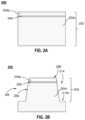
- FIG. 1 Bis a cross-sectional view of a step in the manufacture of a LED device 100 according to one or more embodiments.
- the semiconductor layers 102are etched to form a mesa 108 .
- the mesa 108has a top surface 108 t and at least one side wall 108 s , the at least one side wall 108 s defining a trench 114 having a bottom surface 114 b .
- the trench 114has a depth from a top surface 108 t of the semiconductor layers 102 forming the mesa 108 in a range of from about 0.5 ⁇ m to about 2 ⁇ m.
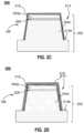
- FIG. 1 Cis a cross-sectional view of a step in the manufacture of a LED device 100 according to one or more embodiments.
- a passivation layer 116is deposited on the top surface 108 t and on the sidewall(s) 108 s of the mesa 108 .
- the passivation layer 116is a substantially conformal layer.
- conformalmeans that the layer adapts to the contours of the mesa. Conformality of a layer is typically quantified by a ratio of the average thickness of a layer deposited on the sidewalls of a feature, i.e. the mesa, to the average thickness of the same deposited layer on the field, or upper surface, of the mesa.
- a layer which is substantially conformalvaries in thickness by less than or equal to about 5%, 2%, 1% or 0.5%.
- the passivation layer 116does not form on the bottom surface 114 b of the trench 114 . In some embodiments, the passivation layer 116 has a thickness of at least 2 nm. In one or more embodiments, the passivation layer 116 is deposited by one or more of sputter deposition, atomic layer deposition (ALD), chemical vapor deposition (CVD), physical vapor deposition (PVD), plasma enhanced atomic layer deposition (PEALD), and plasma enhanced chemical vapor deposition (PECVD).
- ALDatomic layer deposition
- CVDchemical vapor deposition
- PVDphysical vapor deposition
- PEALDplasma enhanced atomic layer deposition
- PECVDplasma enhanced chemical vapor deposition
- the passivation layer 116comprises a low-loss, low-index dielectric material.
- dielectricrefers to an electrical insulator material that can be polarized by an applied electric field.
- the low-loss, low-index dielectric materialmay comprise any suitable material known to the skill artisan.
- the low-loss, low-index dielectric materialcomprises a material having a refractive index, k-value, in a range of from about 1 to about 2.2.
- the low-loss, low-refractive index materialcomprises a material selected from the group consisting of silicon oxide (SiO 2 ), magnesium fluoride (MgF 2 ), lithium fluoride (LiF), porous silicon oxide (SiO x ), porous silicon oxynitride (SiON), porous silicon nitride (SiN), porous titanium oxide (TiO x ), porous aluminum oxide (AlO x ), porous hafnium oxide (HfO x ), porous niobium oxide (NbO x ), porous aluminum indium gallium nitride (AlInGaN), and porous aluminum indium gallium phosphide (AlInGaP).
- the low-loss, low-refractive index materialcomprises a material selected from the group consisting of magnesium fluoride (MgF 2 ), lithium fluoride (LiF), porous silicon oxide (SiO x ), porous silicon oxynitride (SiON), porous silicon nitride (SiN), porous titanium oxide (TiO x ), porous aluminum oxide (AlO x ), porous hafnium oxide (HfO x ), porous niobium oxide (NbO x ), porous aluminum indium gallium nitride (AlInGaN), and porous aluminum indium gallium phosphide (AlInGaP).
- MgF 2magnesium fluoride
- LiFlithium fluoride
- SiO xporous silicon oxide
- SiONporous silicon oxynitride
- SiNporous titanium oxide
- TiO xporous aluminum oxide
- AlO xporous hafnium oxide
- the low-loss, low-refractive index materialcomprises silicon oxide (SiO 2 ). In one or more embodiments, the low-loss, low-refractive index material comprises magnesium fluoride (MgF 2 ). In one or more embodiments, the low-loss, low-refractive index material comprises lithium fluoride (LiF). In one or more embodiments, the low-loss, low-refractive index material comprises porous silicon oxide (SiO x ). In one or more embodiments, the low-loss, low-refractive index material comprises porous silicon oxynitride (SiON).
- the low-loss, low-refractive index materialcomprises porous silicon nitride (SiN). In one or more embodiments, the low-loss, low-refractive index material comprises porous titanium oxide (TiO x ). In one or more embodiments, the low-loss, low-refractive index material comprises porous aluminum oxide (AlO x ). In one or more embodiments, the low-loss, low-refractive index material comprises porous hafnium oxide (HfO x ). In one or more embodiments, the low-loss, low-refractive index material comprises porous niobium oxide (NbO x ).
- the low-loss, low-refractive index materialcomprises porous aluminum indium gallium nitride (AlInGaN). In one or more embodiments, the low-loss, low-refractive index material comprises porous aluminum indium gallium phosphide (AlInGaP).
- the passivation layer 116comprises a distributed Bragg reflector (DBR).
- DBRdistributed Bragg reflector
- Bragg reflectorsare typically made of multilayers of alternating thin film materials of different refractive index, wherein high reflectance is one of the key attributes.
- a Bragg reflector or mirroris a structure formed from a multilayer stack of alternating thin film materials with varying refractive index, for example high- and low-index films.
- additional interfacial layersform between adjacent layers of different materials.
- Bragg reflectorsmust have high reflectance.
- the structure and properties of the interfacial layers in the multilayer stackplay a vital role in the reflectance of Bragg reflectors.
- the distribute Bragg reflectorhas a thickness of at least 0.2 microns.
- a DBRcould be utilized as a low-loss mirror, but requires about 2 microns to about 3 microns of thickness for efficient reflective properties.
- a DBR coatingin microLED applications, where die sizes are less than 10 microns on a side, there may not be a sufficient process window to allow for the use of a DBR coating.
- Conflicting design rulesinclude the allowed spacing between p and n electrical contacts, overall LED mesa and pixel size, and stack-height or planarity limitations of the micro LED when integrated on an electrical back-plane. Accordingly, for architectures with pixel sizes less than 10 microns to a side, a low-index, low-loss passivation layer provides sufficient electrical passivation and mirror functions, and integrates well into scalable, manufacturable processes.
- an optional electrical passivation layermay be deposited on the mesa 108 prior to deposition of the passivation layer 116 .
- the electrical passivation layeris deposited as a substantially conformal layer on the passivation layer 116 .
- the optional electrical passivation layermay comprise one of more of silicon nitride (SiN), titanium oxide (TiO 2 ), niobium oxide (NbO 2 ), aluminum oxide (Al 2 O 3 ), hafnium oxide (HfO 2 ), aluminum nitride (AlN), silicon dioxide (SiO 2 ), and hafnium-doped silicon dioxide (HfSiO 2 ).
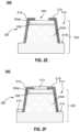
- FIG. 1 Dis cross-sectional view of a step in the manufacture of a LED device 100 according to one or more embodiments.
- the mesa 108 having the passivation layer 116 thereonis patterned to form an opening 109 on the top surface 108 t of the mesa, exposing a top surface of the semiconductor layers 102 and/or a top surface p-type layer 104 p .
- the mesa 108can be patterned according to any appropriate technique known one of skill in the art, such as a masking and etching process used in semiconductor processing.
- FIG. 1 Eis a cross-sectional view of a step in the manufacture of a LED device according to one or more embodiments.
- a p-contact material 112is deposited on top of the mesa 108 in opening 109 .
- the p-contact material 112can comprise any suitable material known to the skilled artisan.
- the p-contact material 112comprises one or more of silver (Ag), gold (Au), platinum (Pt), and palladium (Pd).
- additional metalsmay be added in small quantities to the p-contact as adhesion promoters.
- adhesion promotersinclude, but are not limited to, one or more of nickel (Ni), titanium (Ti), and chromium (Cr).
- a transparent conductive oxide (TCO)may be used as a p-contact material, such as, but not limited to, indium tin oxide (ITO) and zinc oxide (ZnO).
- an n-contact material 110is deposited on the bottom surface 114 b of the trench 114 .
- the n-contact material 110can comprise any appropriate material known to the skilled artisan.
- the n-contact material 110comprises copper (Cu) and the n-contact material 110 is deposited by electrochemical deposition (ECD) of the copper.
- FIG. 2 Ais a cross-sectional view of a step in the manufacture of an LED device according to one or more embodiments.
- semiconductor layers 202are grown on a substrate (not illustrated).
- the semiconductor layers 202according to one or more embodiments comprise epitaxial layers, III-nitride layers or epitaxial III-nitride layers.
- the semiconductor layers 202comprise a III-nitride material, and in specific embodiments epitaxial III-nitride material.
- the III-nitride materialcomprises one or more of gallium (Ga), aluminum (Al), and indium (In).
- the semiconductor layers 202comprises one or more of gallium nitride (GaN), aluminum nitride (AlN), indium nitride (InN), aluminum gallium nitride (AlGaN), indium gallium nitride (InGaN), indium aluminum nitride (InAlN), aluminum indium gallium nitride (AlInGaN) and the like.
- the semiconductor layers 202comprise a p-type layer 204 p , an active region 206 , and an n-type layer 204 n.
- the semiconductor layers 202comprise a stack of undoped III-nitride material and doped III-nitride material.
- the III-nitride materialsmay be doped with one or more of silicon (Si), oxygen (O), boron (B), phosphorus (P), germanium (Ge), manganese (Mn), or magnesium (Mg) depending upon whether p-type or n-type III-nitride material is needed.
- the semiconductor layers 202comprise an n-type layer 204 n , an active layer 206 and a p-type layer 204 p.
- the semiconductor layers 202have a combined thickness in a range of from about 1 ⁇ m to about 10 ⁇ m, including a range of from about 1 ⁇ m to about 9 ⁇ m, 1 ⁇ m to about 8 ⁇ m, 1 ⁇ m to about 7 ⁇ m, 1 ⁇ m to about 6 ⁇ m, 1 ⁇ m to about 5 ⁇ m, 1 ⁇ m to about 4 ⁇ m, 1 ⁇ m to about 3 ⁇ m, 2 ⁇ m to about 10 ⁇ m, including a range of from about 2 ⁇ m to about 9 ⁇ m, 2 ⁇ m to about 8 ⁇ m, 2 ⁇ m to about 7 ⁇ m, 2 ⁇ m to about 6 ⁇ m, 2 ⁇ m to about 5 ⁇ m, 2 ⁇ m to about 4 ⁇ m, 2 ⁇ m to about 3 ⁇ m, 3 ⁇ m to about 10 ⁇ m, 3 ⁇ m to about 9 ⁇ m, 3 ⁇ m to about 8 ⁇ m, 3 ⁇ m to about 7
- an active region 206is formed between the n-type layer 204 n and the p-type layer 204 p .
- the active region 206may comprise any appropriate materials known to one of skill in the art.
- the active region 206is comprised of a III-nitride material multiple quantum wells (MQW), and a III-nitride electron blocking layer.
- MQWmultiple quantum wells
- FIG. 2 Bis a cross-sectional view of a step in the manufacture of an LED device 200 according to one or more embodiments.
- the semiconductor layers 202are etched to form a mesa 2108 .
- the mesa 208has a top surface 208 t and at least one side wall 208 s , the at least one side wall 208 s defining a trench 214 having a bottom surface 214 b .
- the trench 214has a depth from a top surface 208 t of the semiconductor layers 202 forming the mesa 208 in a range of from about 0.5 ⁇ m to about 2 ⁇ m.
- FIG. 2 Cis a cross-sectional view of a step in the manufacture of an LED device 200 according to one or more embodiments.
- a first passivation layer 216is deposited on the top surface 208 t and on the sidewall(s) 208 s of the mesa 208 .
- the first passivation layermay be deposited conformally on the top surface 208 t and the sidewall(s) 208 s of the mesa 208 .
- the first passivation layer 216does not form on the bottom surface 214 b of the trench 214 .
- the first passivation layer 216has a thickness of greater than or equal to 0.1 nm.
- the first passivation layer 216is deposited by one or more of sputter deposition, atomic layer deposition (ALD), chemical vapor deposition (CVD), physical vapor deposition (PVD), plasma enhanced atomic layer deposition (PEALD), and plasma enhanced chemical vapor deposition (PECVD).
- ALDatomic layer deposition
- CVDchemical vapor deposition
- PVDphysical vapor deposition
- PEALDplasma enhanced atomic layer deposition
- PECVDplasma enhanced chemical vapor deposition
- the first passivation layer 216comprises one of more of silicon nitride (SiN), titanium oxide (TiO 2 ), niobium oxide (NbO 2 ), aluminum oxide (Al 2 O 3 ), hafnium oxide (HfO 2 ), aluminum nitride (AlN), silicon dioxide (SiO 2 ), and hafnium-doped silicon dioxide (HfSiO 2 ).
- FIG. 2 Dis a cross-sectional view of a step in the manufacture of an LED device 200 according to one or more embodiments.
- a second passivation layer 218is deposited on a top surface of the first passivation layer 216 .
- the second passivation layer 218may form conformally on the first passivation layer 216 .
- the second passivation layer 218has a thickness of greater than or equal to 2 nm.
- the second passivation layer 218may comprise one or more of a distributed Bragg reflector (DBR) and a low-loss, low-index dielectric material.
- DBRdistributed Bragg reflector
- the distributed Bragg reflectorcomprises multilayers of alternating thin film materials of different refractive index, wherein high reflectance is one of the key attributes.
- a Bragg reflector or mirroris a structure formed from a multilayer stack of alternating thin film materials with varying refractive index, for example high- and low-index films.
- additional interfacial layersform between adjacent layers of different materials.
- Bragg reflectorsmust have high reflectance.
- the structure and properties of the interfacial layers in the multilayer stackplay a vital role in the reflectance of Bragg reflectors.
- the distribute Bragg reflectorhas a thickness of at least 0.2 microns.
- the low-loss, low-index dielectric materialmay comprise any suitable material known to the skill artisan. In some embodiments, the low-loss, low-index dielectric material comprises a material having a refractive index, k-value, in a range of from about 1 to about 2.2.
- the low-loss, low-refractive index materialcomprises a material selected from the group consisting of silicon oxide (SiO 2 ), magnesium fluoride (MgF 2 ), lithium fluoride (LiF), porous silicon oxide (SiO x ), porous silicon oxynitride (SiON), porous silicon nitride (SiN), porous titanium oxide (TiO x ), porous aluminum oxide (AlO x ), porous hafnium oxide (HfO x ), porous niobium oxide (NbO x ), porous aluminum indium gallium nitride (AlInGaN), and porous aluminum indium gallium phosphide (AlInGaP).
- the low-loss, low-refractive index materialcomprises a material selected from the group consisting of magnesium fluoride (MgF 2 ), lithium fluoride (LiF), porous silicon oxide (SiO x ), porous silicon oxynitride (SiON), porous silicon nitride (SiN), porous titanium oxide (TiO x ), porous aluminum oxide (AlO x ), porous hafnium oxide (HfO x ), porous niobium oxide (NbO x ), porous aluminum indium gallium nitride (AlInGaN), and porous aluminum indium gallium phosphide (AlInGaP).
- MgF 2magnesium fluoride
- LiFlithium fluoride
- SiO xporous silicon oxide
- SiONporous silicon oxynitride
- SiNporous titanium oxide
- TiO xporous aluminum oxide
- AlO xporous hafnium oxide
- the low-loss, low-refractive index materialcomprises silicon oxide (SiO 2 ). In one or more embodiments, the low-loss, low-refractive index material comprises magnesium fluoride (MgF 2 ). In one or more embodiments, the low-loss, low-refractive index material comprises lithium fluoride (LiF). In one or more embodiments, the low-loss, low-refractive index material comprises porous silicon oxide (SiO x ). In one or more embodiments, the low-loss, low-refractive index material comprises porous silicon oxynitride (SiON).
- the low-loss, low-refractive index materialcomprises porous silicon nitride (SiN). In one or more embodiments, the low-loss, low-refractive index material comprises porous titanium oxide (TiO x ). In one or more embodiments, the low-loss, low-refractive index material comprises porous aluminum oxide (AlO x ). In one or more embodiments, the low-loss, low-refractive index material comprises porous hafnium oxide (HfO x ). In one or more embodiments, the low-loss, low-refractive index material comprises porous niobium oxide (NbO x ).
- the low-loss, low-refractive index materialcomprises porous aluminum indium gallium nitride (AlInGaN). In one or more embodiments, the low-loss, low-refractive index material comprises porous aluminum indium gallium phosphide (AlInGaP).
- FIG. 2 Eis cross-sectional view of a step in the manufacture of an alternative LED device 200 according to one or more embodiments.
- the mesa 208 having the first passivation layer 216 and the second passivation layer 218 thereonis patterned to form an opening 209 on the top surface 208 t of the mesa, exposing a top surface of the semiconductor layers 202 and/or a top surface p-type layer 204 p .
- the mesa 208can be patterned according to any appropriate technique known one of skill in the art, such as a masking and etching process used in semiconductor processing.
- FIG. 2 Fis a cross-sectional view of a step in the manufacture of an alternative LED device according to one or more embodiments.
- a p-contact material 212is deposited on top of the mesa 208 .
- the p-contact material 212can comprise any appropriate material known to the skilled artisan.
- the p-contact material 212comprises one or more of silver (Ag), gold (Au), platinum (Pt), and palladium (Pd).
- additional metalsmay be added in small quantities to the p-contact as adhesion promoters.
- adhesion promotersinclude, but are not limited to, one or more of nickel (Ni), titanium (Ti), and chromium (Cr).
- a transparent conductive oxide (TCO)may be used as a p-contact material, such as, but not limited to, indium tin oxide (ITO) and zinc oxide (ZnO).
- an n-contact material 210is deposited on the bottom surface 214 b of the trench 214 .
- the n-contact material 210can comprise any appropriate material known to the skilled artisan.
- the n-contact material 210comprises copper and the n-contact material 210 is deposited by electrochemical deposition (ECD) of the copper.
- one or more embodiments of the disclosureprovide a method of manufacturing an LED device, the method 300 comprises at operation 302 depositing a plurality of semiconductor layers including an n-type layer, an active layer, and a p-type layer on a substrate.
- a portion of the semiconductor layersare etched to form trenches and mesas defining pixels.
- a passivation layeris form on the mesa.
- contactsare formed by etching an opening and depositing contact metals.
- an electronic systemcomprises the LED devices and arrays described herein and driver circuitry configured to provide independent voltages to one or more of p-contact layers.
- the electronic systemis selected from the group consisting of a LED-based luminaire, a light emitting strip, a light emitting sheet, an optical display, and a microLED display.
- a light emitting diode (LED) devicecomprising: a mesa comprising semiconductor layers, the semiconductor layers including an N-type layer, an active layer, and a P-type layer, the mesa having a top surface and at least one side wall, the at least one side wall defining a trench have a bottom surface; a passivation layer on the at least one side wall and on the top surface of the mesa, the passivation layer comprising one or more a low-refractive index material and distributed Bragg reflector (DBR); a p-type contact on the top surface of the mesa; and an n-type contact on the bottom surface of the trench.
- DBRdistributed Bragg reflector
- Embodiment (b)The LED device of embodiment (a), wherein the passivation layer comprises a low-refractive index material.
- Embodiment (c)The LED device of embodiments (a) to (b), wherein the passivation layer has a thickness of at least 2 nm.
- Embodiment (d)The LED device of embodiments (a) to (c), wherein the low-refractive index material has a refractive index in a range of from about 1 to about 2.2.
- Embodiment (e)The LED device of embodiments (a) to (d), wherein the low-refractive index material comprises a material selected from the group consisting of silicon oxide (SiO 2 ), magnesium fluoride (MgF 2 ), lithium fluoride (LiF), porous silicon oxide (SiO x ), porous silicon oxynitride (SiON), porous silicon nitride (SiN), porous titanium oxide (TiO x ), porous aluminum oxide (AlO x ), porous hafnium oxide (HfO x ), porous niobium oxide (NbO x ), porous aluminum indium gallium nitride (AlInGaN), and porous aluminum indium gallium phosphide (AlInGaP).
- silicon oxideSiO 2
- MgF 2magnesium fluoride
- LiFlithium fluoride
- porous silicon oxide (SiO x )porous silicon oxynitride
- Embodiment (f)The LED device of embodiments (a) to (e), wherein the passivation layer comprises a distributed Bragg reflector (DBR).
- DBRdistributed Bragg reflector
- Embodiment (g)The LED device of embodiments (a) to (f), wherein the distributed Bragg reflector (DBR) has a thickness of at least 0.2 microns.
- DBRdistributed Bragg reflector
- Embodiment (h)The LED device of embodiments (a) to (g), further comprising an electrical passivation layer between the passivation layer and the mesa.
- Embodiment (i)The LED device of embodiments (a) to (h), wherein the electrical passivation layer comprises one or more of silicon nitride (SiN), titanium oxide (TiO 2 ), niobium oxide (NbO 2 ), aluminum oxide (Al 2 O 3 ), hafnium oxide (HfO 2 ), aluminum nitride (AlN), silicon dioxide (SiO 2 ), and hafnium-doped silicon dioxide (HfSiO 2 ).
- silicon nitrideSiN
- TiO 2titanium oxide
- NbO 2niobium oxide
- Al 2 O 3aluminum oxide
- hafnium oxideHfO 2
- AlNaluminum nitride
- silicon dioxideSiO 2
- hafnium-doped silicon dioxideHfSiO 2
- Embodiment (j)The LED device of embodiments (a) to (i), wherein the semiconductor layers are epitaxial semiconductor layers having a thickness at least 1 micron.
- Embodiment (k)A method of manufacturing a light emitting diode (LED) device comprising: depositing a plurality of semiconductor layers including an N-type layer, an active layer, and a P-type layer on a substrate; etching a portion of the semiconductor layers to form at least one trench and at least one mesa defining a pixel, the at least one mesa comprising the semiconductor layers, a top surface and at least one side wall; depositing a passivation layer on the at least one side wall and on the top surface of the at least one mesa, the passivation layer comprising one or more a low-refractive index material and distributed Bragg reflector (DBR); forming a p-type contact on the top surface of the at least one mesa; and forming an n-type contact in the at least one trench.
- DBRdistributed Bragg reflector
- Embodiment (l)The method of embodiment (k), wherein the passivation layer comprises a low-refractive index material.
- Embodiment (m)The method of embodiments (k) to (l), wherein the passivation layer has a thickness of at least 2 nm.
- Embodiment (n)The method of embodiments (k) to (m), wherein the low-refractive index material has a refractive index in a range of from about 1 to about 2.2.
- Embodiment (o)The method of embodiments (k) to (n), wherein the low-refractive index material comprises one or more of silicon oxide (SiO 2 ), magnesium fluoride (MgF 2 ), lithium fluoride (LiF), porous silicon oxide (SiO x ), porous silicon oxynitride (SiON), porous silicon nitride (SiN), porous titanium oxide (TiO x ), porous aluminum oxide (AlO x ), porous hafnium oxide (HfO x ), porous niobium oxide (NbO x ), porous aluminum indium gallium nitride (AlInGaN), and porous aluminum indium gallium phosphide (AlInGaP).
- silicon oxideSiO 2
- MgF 2magnesium fluoride
- LiFlithium fluoride
- porous silicon oxide (SiO x )porous silicon oxynitride (SiON), porous silicon
- Embodiment (p)The method of embodiments (k) to (o), wherein the passivation layer comprises a distributed Bragg reflector (DBR).
- DBRdistributed Bragg reflector
- Embodiment (q)The method of embodiments (k) to (p), further comprising depositing an electrical passivation layer between the passivation layer and the at least one mesa.
- Embodiment (r)The method of embodiments (k) to (q), wherein the electrical passivation layer comprises one or more of silicon nitride (SiN), titanium oxide (TiO 2 ), niobium oxide (NbO 2 ), aluminum oxide (Al 2 O 3 ), hafnium oxide (HfO 2 ), aluminum nitride (AlN), silicon dioxide (SiO 2 ), and hafnium-doped silicon dioxide (HfSiO 2 ).
- a light emitting diode (LED) devicecomprising: a mesa comprising semiconductor layers, the semiconductor layers including an N-type layer, an active layer, and a P-type layer, the mesa having a height less than or equal to its width, the mesa having a top surface and at least one side wall, the at least one side wall defining a trench have a bottom surface; a first passivation layer on the at least one side wall and on the top surface of the mesa, the first passivation layer comprising one or more of a silicon nitride (SiN), titanium oxide (TiO 2 ), niobium oxide (NbO 2 ), aluminum oxide (Al 2 O 3 ), hafnium oxide (HfO 2 ), aluminum nitride (AlN), silicon dioxide (SiO 2 ), and hafnium-doped silicon dioxide (HfSiO 2 ); a second passivation layer on the first passivation layer, the second passivation layer, the second pass
- Embodiment (t).The LED device of embodiment (s), wherein the low-refractive index material comprises one or more of silicon oxide (SiO 2 ), magnesium fluoride (MgF 2 ), lithium fluoride (LiF), porous silicon oxide (SiO x ), porous silicon oxynitride (SiON), porous silicon nitride (SiN), porous titanium oxide (TiO x ), porous aluminum oxide (AlO x ), porous hafnium oxide (HfO x ), porous niobium oxide (NbO x ), porous aluminum indium gallium nitride (AlInGaN), and porous aluminum indium gallium phosphide (AlInGaP).
- silicon oxideSiO 2
- MgF 2magnesium fluoride
- LiFlithium fluoride
- porous silicon oxide (SiO x )porous silicon oxynitride (SiON), porous silicon nitrid
- Relative terms such as “below,” “above,” “upper,”, “lower,” “horizontal” or “vertical”may be used herein to describe a relationship of one element, layer, or region to another element, layer, or region as illustrated in the figures. It will be understood that these terms are intended to encompass different orientations of the device in addition to the orientation depicted in the figures.
Landscapes
- Led Devices (AREA)
Abstract
Description
Claims (6)
Priority Applications (6)
| Application Number | Priority Date | Filing Date | Title |
|---|---|---|---|
| US17/189,459US11901491B2 (en) | 2020-10-29 | 2021-03-02 | Light emitting diode devices |
| EP21887135.8AEP4238141A4 (en) | 2020-10-29 | 2021-09-21 | LIGHT-EMITTING DIODE DEVICES |
| KR1020237017642AKR20230093482A (en) | 2020-10-29 | 2021-09-21 | light emitting diode device |
| JP2023521848AJP7592966B2 (en) | 2020-10-29 | 2021-09-21 | Light emitting diode device |
| CN202180073851.7ACN116368630A (en) | 2020-10-29 | 2021-09-21 | Light emitting diode device |
| PCT/US2021/051173WO2022093432A1 (en) | 2020-10-29 | 2021-09-21 | Light emitting diode devices |
Applications Claiming Priority (2)
| Application Number | Priority Date | Filing Date | Title |
|---|---|---|---|
| US202063107109P | 2020-10-29 | 2020-10-29 | |
| US17/189,459US11901491B2 (en) | 2020-10-29 | 2021-03-02 | Light emitting diode devices |
Publications (2)
| Publication Number | Publication Date |
|---|---|
| US20220140199A1 US20220140199A1 (en) | 2022-05-05 |
| US11901491B2true US11901491B2 (en) | 2024-02-13 |
Family
ID=81379246
Family Applications (1)
| Application Number | Title | Priority Date | Filing Date |
|---|---|---|---|
| US17/189,459Active2041-07-17US11901491B2 (en) | 2020-10-29 | 2021-03-02 | Light emitting diode devices |
Country Status (6)
| Country | Link |
|---|---|
| US (1) | US11901491B2 (en) |
| EP (1) | EP4238141A4 (en) |
| JP (1) | JP7592966B2 (en) |
| KR (1) | KR20230093482A (en) |
| CN (1) | CN116368630A (en) |
| WO (1) | WO2022093432A1 (en) |
Families Citing this family (2)
| Publication number | Priority date | Publication date | Assignee | Title |
|---|---|---|---|---|
| KR20230013705A (en)* | 2021-07-19 | 2023-01-27 | 삼성디스플레이 주식회사 | Light emitting element and display device including the same |
| CN118588837B (en)* | 2024-05-28 | 2025-03-28 | 华引芯(武汉)科技有限公司 | A light emitting element and a method for preparing the same |
Citations (128)
| Publication number | Priority date | Publication date | Assignee | Title |
|---|---|---|---|---|
| US6206065B1 (en) | 1997-07-30 | 2001-03-27 | The Governors Of The University Of Alberta | Glancing angle deposition of thin films |
| US6410942B1 (en) | 1999-12-03 | 2002-06-25 | Cree Lighting Company | Enhanced light extraction through the use of micro-LED arrays |
| US20020139987A1 (en) | 2001-03-29 | 2002-10-03 | Collins William David | Monolithic series/parallel led arrays formed on highly resistive substrates |
| US6657236B1 (en) | 1999-12-03 | 2003-12-02 | Cree Lighting Company | Enhanced light extraction in LEDs through the use of internal and external optical elements |
| EP1378949A1 (en) | 2001-03-21 | 2004-01-07 | Mitsubishi Cable Industries, Ltd. | Semiconductor light-emitting device |
| US20070206130A1 (en) | 2006-03-02 | 2007-09-06 | Dong-Sing Wuu | Light emitting device |
| US20080099787A1 (en) | 2005-11-02 | 2008-05-01 | International Business Machines Corporation | Semiconductor structure and method of manufacture |
| US20080173884A1 (en) | 2007-01-22 | 2008-07-24 | Cree, Inc. | Wafer level phosphor coating method and devices fabricated utilizing method |
| US20080179602A1 (en) | 2007-01-22 | 2008-07-31 | Led Lighting Fixtures, Inc. | Fault tolerant light emitters, systems incorporating fault tolerant light emitters and methods of fabricating fault tolerant light emitters |
| EP2027608A1 (en) | 2006-06-09 | 2009-02-25 | Commissariat à l'Energie Atomique | Process of making a microelectronic light-emitting device on semi-conducting nanowire formed on a metallic substrate |
| US20100078656A1 (en) | 2008-09-30 | 2010-04-01 | Seoul Opto Device Co., Ltd. | Light emitting device and method of fabricating the same |
| EP2203939A1 (en) | 2007-10-22 | 2010-07-07 | Commissariat à l'énergie atomique et aux énergies alternatives | Optoelectronic device including nanowires, and corresponding methods |
| EP2211387A2 (en) | 2009-01-22 | 2010-07-28 | Commissariat à l'Énergie Atomique et aux Énergies Alternatives | Method of making a p-n homojunction in a nanostructure |
| WO2011045289A1 (en) | 2009-10-16 | 2011-04-21 | Commissariat A L'energie Atomique Et Aux Energies Alternatives | Semiconductor nanocrystal-based infrared source built into silicon |
| WO2011048318A1 (en) | 2009-10-23 | 2011-04-28 | Commissariat A L'energie Atomique Et Aux Energies Alternatives | Method for manufacturing a very-high-resolution screen using a nanowire-based emitting anisotropic conductive film |
| FR2952366A1 (en) | 2010-04-07 | 2011-05-13 | Commissariat Energie Atomique | Developing carbon nanotubes for e.g. LCD and organic LEDs, comprises depositing a network of carbon nanotubes on a substrate, and irradiating the carbon nanotubes network by laser impulsion having specified power |
| US7943406B2 (en) | 2003-11-12 | 2011-05-17 | Cree, Inc. | LED fabrication via ion implant isolation |
| US20110147704A1 (en) | 2008-08-19 | 2011-06-23 | Lattice Power (Jiangxi) Corporation | Semiconductor light-emitting device with passivation layer |
| US20110151607A1 (en) | 2009-12-23 | 2011-06-23 | Commissariat A L'energie Atomique Et Aux Energies Alternatives | Method for manufacturing a metal and dielectric nanostructures electrode for colored filtering in an oled and method for manufacturing an oled |
| US20110266551A1 (en) | 2009-11-03 | 2011-11-03 | The Regents Of The University Of California | High brightness light emitting diode covered by zinc oxide layers on multiple surfaces grown in low temperature aqueous solution |
| US20110287606A1 (en) | 2010-05-18 | 2011-11-24 | Commissariat A L'energie Atomique Et Aux Energies Alternatives | Method for fabricating chip elements provided with wire insertion grooves |
| US20120050694A1 (en) | 2010-08-27 | 2012-03-01 | Industrial Technology Research Institute | Light emitting unit array and projection system |
| FR2964796A1 (en) | 2010-09-14 | 2012-03-16 | Commissariat Energie Atomique | Optoelectronic light emitting device i.e. gallium nitride based LED, has p-doped planarized layer allowing radial injection of holes in nanowire, and n-type silicon substrate allowing axial injection of electrons in nanowire |
| WO2012035243A1 (en) | 2010-09-14 | 2012-03-22 | Commissariat A L'energie Atomique Et Aux Energies Alternatives | Nanowire-based optoelectronic device for light emission |
| US20120091481A1 (en) | 2010-10-19 | 2012-04-19 | Napra Co., Ltd. | Light-emitting device and method for manufacturing the same |
| DE102010051286A1 (en) | 2010-11-12 | 2012-05-16 | Osram Opto Semiconductors Gmbh | Optoelectronic semiconductor chip and method for its production |
| US8212273B2 (en) | 2007-07-19 | 2012-07-03 | Photonstar Led Limited | Vertical LED with conductive vias |
| FR2969995A1 (en) | 2011-01-03 | 2012-07-06 | Commissariat Energie Atomique | Producing nitride nanostructures e.g. nanowires on side of substrate, by forming base of nanostructures made of wurtzite nitride phase on substrate, and forming upper part of nanostructures made of nitrides having zinc-blende phase on base |
| US8222811B2 (en) | 2008-07-07 | 2012-07-17 | Commissariat A L'energie Atomique Et Aux Energies Alternatives | Electroluminescent display, illumination or indicating device, and its fabrication process |
| EP2499958A1 (en) | 2011-03-15 | 2012-09-19 | Commissariat à l'Énergie Atomique et aux Énergies Alternatives | Disposable bi-spectral optical head for video endoscope and associated video endoscope |
| US20120235189A1 (en)* | 2011-03-17 | 2012-09-20 | Chia-Liang Hsu | Light-emitting device |
| EP2521161A1 (en) | 2011-05-06 | 2012-11-07 | Commissariat à l'Énergie Atomique et aux Énergies Alternatives | Method for producing semiconductor nanocrystals |
| EP2521162A1 (en) | 2011-05-06 | 2012-11-07 | Commissariat à l'Énergie Atomique et aux Énergies Alternatives | Method for producing semiconductor nanocrystals oriented in a pre-defined direction |
| WO2012156620A2 (en) | 2011-05-18 | 2012-11-22 | Commissariat A L'energie Atomique Et Aux Energies Alternatives | In-series electrical connection of light-emitting nanowires |
| US20130020115A1 (en) | 2010-03-26 | 2013-01-24 | Commissariat A L'energie Atomique Et Aux Energies Alternatives | Method for etching conductive metal oxide layer using microelectrode |
| US20130256708A1 (en) | 2012-03-30 | 2013-10-03 | Hon Hai Precision Industry Co., Ltd. | Light emitting diodes |
| US20130292719A1 (en)* | 2012-05-04 | 2013-11-07 | Chi Mei Lighting Technology Corp. | Light-emitting diode structure and method for manufacturing the same |
| FR2991342A1 (en) | 2012-06-05 | 2013-12-06 | Commissariat Energie Atomique | METHOD FOR IMPROVING THE ELECTRICAL AND OPTICAL PERFORMANCE OF ELECTRICALLY CONDUCTIVE AND TRANSPARENT MATERIAL BASED ON SILVER NANOWIRES |
| EP2674516A1 (en) | 2012-06-15 | 2013-12-18 | Commissariat A L'energie Atomique Et Aux Energies Alternatives | Method of electrochemically manufacturing nanowires from CuSCN |
| US8638032B2 (en) | 2008-09-30 | 2014-01-28 | Commissariat A L'energie Atomique Et Aux Energies Alternatives | Organic optoelectronic device coated with a multilayer encapsulation structure and a method for encapsulating said device |
| US8664635B2 (en)* | 2010-05-18 | 2014-03-04 | Seoul Semiconductor Co., Ltd. | Light emitting diode chip having wavelength converting layer and method of fabricating the same, and package having the light emitting diode chip and method of fabricating the same |
| US20140094878A1 (en) | 2012-10-01 | 2014-04-03 | Albert-Ludwigs-Universitat Freiburg | Method for producing a micro-led matrix, micro-led matrix and use of a micro-led matrix |
| DE102012109460A1 (en) | 2012-10-04 | 2014-04-10 | Osram Opto Semiconductors Gmbh | Method for producing a light-emitting diode display and light-emitting diode display |
| US8698396B2 (en) | 2010-04-12 | 2014-04-15 | Commissariat A L'energie Atomique Et Aux Energies Alternatives | Organic optoelectronic device and method for encapsulating same |
| TW201417339A (en) | 2012-10-22 | 2014-05-01 | Ritedia Corp | Flip-chip luminescent diode and its application |
| FR2998090A1 (en) | 2013-06-26 | 2014-05-16 | Commissariat Energie Atomique | Method for structuring material surface of substrate for producing e.g. nanometric patterns on surface for LEDs, involves forming patterns due to difference between etch selectivity of material and changed etch selectivity of regions |
| US20140138719A1 (en) | 2011-07-08 | 2014-05-22 | Commissariat A L'energie Atomique Et Aux Energies Alternatives | Organic Optoelectronic Device And Method For The Encapsulation Thereof |
| US20140159071A1 (en)* | 2012-12-06 | 2014-06-12 | Byung Yeon CHOI | Light emitting device |
| US8754426B2 (en) | 2011-07-27 | 2014-06-17 | Grote Industries, Llc | Lighting device utilizing light active sheet material with integrated light emitting diode, disposed in seam and/or in low profile application |
| KR20140118466A (en) | 2013-03-29 | 2014-10-08 | 서울반도체 주식회사 | Light emitting device and lighting device including the same |
| WO2015044620A1 (en) | 2013-09-30 | 2015-04-02 | Commissariat A L'energie Atomique Et Aux Energies Alternatives | Method for producing optoelectronic devices comprising light-emitting diodes |
| US20150118544A1 (en) | 2013-10-29 | 2015-04-30 | Commissariat A L'energie Atomique Et Aux Energies Alternatives | Device for encapsulating a sensitive device and process for producing said device |
| US20150228873A1 (en) | 2012-09-05 | 2015-08-13 | Osram Opto Semiconductors Gmbh | Housing for an Optical Component, Assembly, Method for Producing a Housing and Method for Producing an Assembly |
| US9112112B2 (en) | 2011-04-28 | 2015-08-18 | Psi Co., Ltd. | Subminiature led element and manufacturing method thereof |
| US9192290B2 (en) | 2007-01-30 | 2015-11-24 | Fraunhofer-Gesellschaft Zur Foerderung Der Angewandten Forschung E.V. | Illumination apparatus for an image sensing means at the distal end of an endoscope |
| KR20150144048A (en) | 2014-06-16 | 2015-12-24 | 엘지이노텍 주식회사 | Light emitting device and light emitting device package including the same |
| US20150380461A1 (en) | 2014-06-27 | 2015-12-31 | Commissariat A L'energie Atomique Et Aux Energies Alternatives | P-n junction optoelectronic device for ionizing dopants by field effect |
| DE102014112551A1 (en) | 2014-09-01 | 2016-03-03 | Osram Opto Semiconductors Gmbh | Optoelectronic semiconductor chip and method for producing an optoelectronic semiconductor chip |
| JP2016066765A (en) | 2014-09-26 | 2016-04-28 | 日亜化学工業株式会社 | Mounting method of element and manufacturing method of light emitting device |
| WO2016079505A1 (en) | 2014-11-18 | 2016-05-26 | Mled Limited | Integrated colour led micro-display |
| TW201620163A (en) | 2014-11-18 | 2016-06-01 | 隆達電子股份有限公司 | Light-emitting diode structure and light-emitting diode module |
| US20160190400A1 (en) | 2013-05-13 | 2016-06-30 | Seoul Semiconductor Co., Ltd. | Light-emitting device package, manufacturing method thereof, and vehicle lamp and backlight unit including same |
| US20160284941A1 (en)* | 2015-03-26 | 2016-09-29 | Lg Innotek Co., Ltd. | Light emitting device and light emitting device package including the same |
| US20160293811A1 (en) | 2015-03-31 | 2016-10-06 | Cree, Inc. | Light emitting diodes and methods with encapsulation |
| US9496465B2 (en) | 2013-04-17 | 2016-11-15 | Nichia Corporation | Light emitting device |
| US20160336483A1 (en) | 2013-02-25 | 2016-11-17 | Sensor Electronic Technology, Inc. | Semiconductor Structure with Inhomogeneous Regions |
| US9507204B2 (en) | 2013-06-26 | 2016-11-29 | Seoul Semiconductor Co., Ltd. | Baffled micro-optical elements for thin liquid crystal display backlight units |
| KR20170018687A (en) | 2015-08-10 | 2017-02-20 | 엘지전자 주식회사 | Display appartus including micro LED |
| EP3144272A1 (en) | 2015-09-17 | 2017-03-22 | Commissariat A L'energie Atomique Et Aux Energies Alternatives | Verfahren zur ausrichtung auf einer substratoberlfäche angeordneter länglicher objekte |
| US20170098746A1 (en) | 2015-10-01 | 2017-04-06 | Cree, Inc. | Low optical loss flip chip solid state lighting device |
| US20170137645A1 (en) | 2013-11-26 | 2017-05-18 | Commissariat A L'energie Atomique Et Aux Energies Alternatives | Ink for forming p layers in organic electronic devices |
| WO2017089676A1 (en) | 2015-11-26 | 2017-06-01 | Commissariat A L'energie Atomique Et Aux Energies Alternatives | Illuminated faceplate and method for producing such an illuminated faceplate |
| WO2017102708A1 (en) | 2015-12-18 | 2017-06-22 | Fraunhofer-Gesellschaft zur Förderung der angewandten Forschung e.V. | Converter for generating a secondary light from a primary light, lighting means which contains such a converter, and method for producing the converter and the lighting means |
| US20170186612A1 (en) | 2015-12-28 | 2017-06-29 | Commissariat A L'energie Atomique Et Aux Energies Alternatives | Method for producing nanocrystals with controlled dimensions and density |
| US9722160B2 (en) | 2014-10-31 | 2017-08-01 | Nichia Corporation | Light emitting device and adaptive driving beam headlamp system |
| US20170243860A1 (en) | 2016-02-22 | 2017-08-24 | Samsung Display Co., Ltd. | Display apparatus including a micro light-emitting diode |
| US20170293065A1 (en) | 2016-04-11 | 2017-10-12 | Samsung Display Co., Ltd. | Display device |
| US20170294418A1 (en) | 2016-04-12 | 2017-10-12 | Cree, Inc. | High density pixelated led and devices and methods thereof |
| WO2017184686A1 (en) | 2016-04-19 | 2017-10-26 | The Penn State Research Foundation | Gap-free microdisplay based on iii-nitride led arrays |
| US20170358563A1 (en) | 2016-06-14 | 2017-12-14 | Samsung Display Co., Ltd. | Pixel structure, display device including the pixel structure, and method of manufacturing the pixel structure |
| US20170358724A1 (en) | 2016-06-14 | 2017-12-14 | Nichia Corporation | Light emitting device |
| WO2017216445A1 (en) | 2016-06-17 | 2017-12-21 | Commissariat A L'energie Atomique Et Aux Energies Alternatives | Method for making a gallium nitride light-emitting diode |
| US20180019369A1 (en) | 2016-07-12 | 2018-01-18 | Samsung Display Co., Ltd. | Display apparatus and method of manufacturing the same |
| US20180019373A1 (en) | 2015-02-10 | 2018-01-18 | Osram Opto Semiconductors Gmbh | Optoelectronic semiconductor device and method for producing an optoelectronic semiconductor device |
| US20180017939A1 (en) | 2016-07-13 | 2018-01-18 | Commissariat A L'energie Atomique Et Aux Energies Alternatives | Device for observing a sample |
| KR20180010670A (en) | 2016-07-22 | 2018-01-31 | 엘지전자 주식회사 | Lamp for vehicle |
| US9887184B2 (en) | 2015-07-23 | 2018-02-06 | Seoul Semiconductor Co., Ltd. | Display apparatus and manufacturing method thereof |
| US20180061316A1 (en) | 2016-08-31 | 2018-03-01 | Samsung Display Co., Ltd. | Display device and method of driving the same |
| US20180074372A1 (en) | 2016-09-12 | 2018-03-15 | Seoul Semiconductor Co., Ltd. | Display apparatus |
| US9945526B2 (en) | 2013-02-08 | 2018-04-17 | Osram Opto Semiconductors Gmbh | Optoelectronic lighting module, optoelectronic lighting apparatus and vehicle headlamp |
| US20180138157A1 (en) | 2016-11-15 | 2018-05-17 | Samsung Display Co., Ltd. | Light emitting device and fabricating method thereof |
| US9978727B2 (en) | 2016-02-26 | 2018-05-22 | Seoul Semiconductor Co., Ltd. | Display apparatus and manufacturing method thereof |
| WO2018091657A1 (en) | 2016-11-18 | 2018-05-24 | Osram Opto Semiconductors Gmbh | Multipixel led component and method for operating a multipixel led component |
| US20180145059A1 (en) | 2016-11-22 | 2018-05-24 | Cree, Inc. | Light emitting diode (led) devices, components and methods |
| US20180149328A1 (en) | 2015-05-26 | 2018-05-31 | Seoul Semiconductor Co., Ltd. | Light emitting device and vehicular lamp including the same |
| US20180156406A1 (en) | 2016-12-01 | 2018-06-07 | Osram Gmbh | Primary optical unit, secondary optical unit, module, arrangement, vehicle headlight, and headlight system |
| US9997688B2 (en) | 2016-02-26 | 2018-06-12 | Seoul Semiconducter Co., Ltd. | Display apparatus and manufacturing method thereof |
| US20180166470A1 (en) | 2016-12-07 | 2018-06-14 | Seoul Viosys Co., Ltd. | Display apparatus and connecting method of light emitting part thereof |
| US10002928B1 (en) | 2014-12-23 | 2018-06-19 | Soraa Laser Diode, Inc. | Manufacturable RGB display based on thin film gallium and nitrogen containing light emitting diodes |
| US20180174931A1 (en) | 2016-12-16 | 2018-06-21 | Tesoro Scientific, Inc. | Light emitting diode (led) test apparatus and method of manufacture |
| US20180174519A1 (en) | 2016-12-19 | 2018-06-21 | Lg Display Co., Ltd. | Light emitting diode display device |
| US10018325B2 (en) | 2015-03-31 | 2018-07-10 | Seoul Semiconductor Co., Ltd. | Light device of vehicle |
| US20180210282A1 (en) | 2017-01-23 | 2018-07-26 | Samsung Display Co., Ltd. | Color conversion panel and display device including the same |
| WO2018139866A1 (en) | 2017-01-26 | 2018-08-02 | 주식회사 엘지화학 | Micro led, and display device including same |
| WO2018143682A1 (en) | 2017-02-02 | 2018-08-09 | 서울반도체주식회사 | Light-emitting diode unit |
| US10050026B2 (en) | 2015-12-31 | 2018-08-14 | Seoul Semiconductor Co., Ltd. | Display apparatus |
| US20180238511A1 (en) | 2017-02-17 | 2018-08-23 | Osram Gmbh | Vehicle headlight and method thereof |
| US10068884B2 (en) | 2016-04-01 | 2018-09-04 | Seoul Semiconductor Co., Ltd. | Display apparatus and manufacturing method thereof |
| WO2018159977A1 (en) | 2017-02-28 | 2018-09-07 | 서울반도체주식회사 | Display device, backlight unit, light-emitting module and lens |
| US20180259137A1 (en) | 2014-11-18 | 2018-09-13 | Seoul Semiconductor Co.ltd | Light emitting device and vehicular lamp comprising same |
| US20180259570A1 (en) | 2017-01-23 | 2018-09-13 | Tesoro Scientific, Inc. | Light emitting diode (led) test apparatus and method of manufacture |
| WO2018169243A1 (en) | 2017-03-13 | 2018-09-20 | 서울반도체주식회사 | Method for manufacturing display device |
| US20180272605A1 (en) | 2015-09-18 | 2018-09-27 | Osram Opto Semiconductors Gmbh | Optoelectronic Semiconductor Component and 3D Printer |
| US20180283642A1 (en) | 2017-03-31 | 2018-10-04 | Everlight Electronics Co., Ltd. | Light emitting apparatus and lighting module |
| US20180297510A1 (en) | 2015-10-13 | 2018-10-18 | Osram Gmbh | Luminance regulation in edge regions |
| KR20180114413A (en) | 2017-04-10 | 2018-10-18 | 주식회사 엘지화학 | Micro light emitting diode structure |
| US20180339643A1 (en) | 2017-05-29 | 2018-11-29 | Lg Electronics Inc. | Lamp for vehicle and vehicle |
| US20180339644A1 (en) | 2017-05-29 | 2018-11-29 | Lg Electronics Inc. | Lamp for vehicle and vehicle |
| US10145518B2 (en) | 2015-11-17 | 2018-12-04 | Samsung Display Co., Ltd. | Nano-scale light-emitting diode (LED) electrode assembly emitting polarized light, method of manufacturing the same, and polarized LED lamp having the same |
| US20180354406A1 (en) | 2017-06-09 | 2018-12-13 | Lg Electronics Inc. | Lamp for vehicle and vehicle |
| EP2006921B1 (en) | 2006-03-31 | 2018-12-26 | Toyoda Gosei Co., Ltd. | Method for producing a GaN based light emitting diode |
| WO2019126539A1 (en) | 2017-12-20 | 2019-06-27 | Lumileds Llc | Led array and method of forming thereof |
| US10388641B2 (en) | 2017-10-19 | 2019-08-20 | Tectus Corporation | Ultra-dense LED projector |
| US10811460B2 (en)* | 2018-09-27 | 2020-10-20 | Lumileds Holding B.V. | Micrometer scale light emitting diode displays on patterned templates and substrates |
| US10964845B2 (en)* | 2018-09-27 | 2021-03-30 | Lumileds Llc | Micro light emitting devices |
| US10985294B2 (en)* | 2019-03-19 | 2021-04-20 | Creeled, Inc. | Contact structures for light emitting diode chips |
| US11211525B2 (en)* | 2017-05-01 | 2021-12-28 | Ohio State Innovation Foundation | Tunnel junction ultraviolet light emitting diodes with enhanced light extraction efficiency |
| US11424388B2 (en)* | 2018-09-07 | 2022-08-23 | Samsung Electronics Co., Ltd. | Light-emitting device and display device including the same |
Family Cites Families (6)
| Publication number | Priority date | Publication date | Assignee | Title |
|---|---|---|---|---|
| KR101020963B1 (en)* | 2010-04-23 | 2011-03-09 | 엘지이노텍 주식회사 | Light emitting device, light emitting device manufacturing method and light emitting device package |
| US9070851B2 (en)* | 2010-09-24 | 2015-06-30 | Seoul Semiconductor Co., Ltd. | Wafer-level light emitting diode package and method of fabricating the same |
| FR2974800B1 (en)* | 2011-05-05 | 2013-04-26 | Saint Gobain | TRANSPARENT SUBSTRATE COATED WITH A STACK OF MINERAL LAYERS INCLUDING A COVERED POROUS |
| KR102282137B1 (en)* | 2014-11-25 | 2021-07-28 | 삼성전자주식회사 | Semiconductor light emitting device and semiconductor light emitting apparatus having the same |
| KR20160105369A (en)* | 2016-08-25 | 2016-09-06 | 서울바이오시스 주식회사 | A light emitting diode |
| US10886327B2 (en)* | 2017-12-14 | 2021-01-05 | Seoul Viosys Co., Ltd. | Light emitting stacked structure and display device having the same |
- 2021
- 2021-03-02USUS17/189,459patent/US11901491B2/enactiveActive
- 2021-09-21JPJP2023521848Apatent/JP7592966B2/enactiveActive
- 2021-09-21KRKR1020237017642Apatent/KR20230093482A/enactivePending
- 2021-09-21CNCN202180073851.7Apatent/CN116368630A/enactivePending
- 2021-09-21EPEP21887135.8Apatent/EP4238141A4/enactivePending
- 2021-09-21WOPCT/US2021/051173patent/WO2022093432A1/ennot_activeCeased
Patent Citations (174)
| Publication number | Priority date | Publication date | Assignee | Title |
|---|---|---|---|---|
| US6206065B1 (en) | 1997-07-30 | 2001-03-27 | The Governors Of The University Of Alberta | Glancing angle deposition of thin films |
| US6410942B1 (en) | 1999-12-03 | 2002-06-25 | Cree Lighting Company | Enhanced light extraction through the use of micro-LED arrays |
| US6657236B1 (en) | 1999-12-03 | 2003-12-02 | Cree Lighting Company | Enhanced light extraction in LEDs through the use of internal and external optical elements |
| US6821804B2 (en) | 1999-12-03 | 2004-11-23 | Cree, Inc. | Enhanced light extraction in LEDs through the use of internal and external optical elements |
| EP1378949A1 (en) | 2001-03-21 | 2004-01-07 | Mitsubishi Cable Industries, Ltd. | Semiconductor light-emitting device |
| US20020139987A1 (en) | 2001-03-29 | 2002-10-03 | Collins William David | Monolithic series/parallel led arrays formed on highly resistive substrates |
| US7943406B2 (en) | 2003-11-12 | 2011-05-17 | Cree, Inc. | LED fabrication via ion implant isolation |
| US20080099787A1 (en) | 2005-11-02 | 2008-05-01 | International Business Machines Corporation | Semiconductor structure and method of manufacture |
| US20070206130A1 (en) | 2006-03-02 | 2007-09-06 | Dong-Sing Wuu | Light emitting device |
| EP2006921B1 (en) | 2006-03-31 | 2018-12-26 | Toyoda Gosei Co., Ltd. | Method for producing a GaN based light emitting diode |
| EP2027608A1 (en) | 2006-06-09 | 2009-02-25 | Commissariat à l'Energie Atomique | Process of making a microelectronic light-emitting device on semi-conducting nanowire formed on a metallic substrate |
| US20080179602A1 (en) | 2007-01-22 | 2008-07-31 | Led Lighting Fixtures, Inc. | Fault tolerant light emitters, systems incorporating fault tolerant light emitters and methods of fabricating fault tolerant light emitters |
| US20080173884A1 (en) | 2007-01-22 | 2008-07-24 | Cree, Inc. | Wafer level phosphor coating method and devices fabricated utilizing method |
| US9192290B2 (en) | 2007-01-30 | 2015-11-24 | Fraunhofer-Gesellschaft Zur Foerderung Der Angewandten Forschung E.V. | Illumination apparatus for an image sensing means at the distal end of an endoscope |
| US8212273B2 (en) | 2007-07-19 | 2012-07-03 | Photonstar Led Limited | Vertical LED with conductive vias |
| EP2203939A1 (en) | 2007-10-22 | 2010-07-07 | Commissariat à l'énergie atomique et aux énergies alternatives | Optoelectronic device including nanowires, and corresponding methods |
| US8487340B2 (en) | 2007-10-22 | 2013-07-16 | Commissariat A L'energie Atomique Et Aux Energies Alternatives | Optoelectronic device based on nanowires and corresponding processes |
| US8222811B2 (en) | 2008-07-07 | 2012-07-17 | Commissariat A L'energie Atomique Et Aux Energies Alternatives | Electroluminescent display, illumination or indicating device, and its fabrication process |
| US20110147704A1 (en) | 2008-08-19 | 2011-06-23 | Lattice Power (Jiangxi) Corporation | Semiconductor light-emitting device with passivation layer |
| US20100078656A1 (en) | 2008-09-30 | 2010-04-01 | Seoul Opto Device Co., Ltd. | Light emitting device and method of fabricating the same |
| US8638032B2 (en) | 2008-09-30 | 2014-01-28 | Commissariat A L'energie Atomique Et Aux Energies Alternatives | Organic optoelectronic device coated with a multilayer encapsulation structure and a method for encapsulating said device |
| EP2211387A2 (en) | 2009-01-22 | 2010-07-28 | Commissariat à l'Énergie Atomique et aux Énergies Alternatives | Method of making a p-n homojunction in a nanostructure |
| WO2011045289A1 (en) | 2009-10-16 | 2011-04-21 | Commissariat A L'energie Atomique Et Aux Energies Alternatives | Semiconductor nanocrystal-based infrared source built into silicon |
| US8890111B2 (en) | 2009-10-23 | 2014-11-18 | Commissariat à l'énergie atomique et aux énergies alternatives | Method for manufacturing a very-high-resolution screen using a nanowire-based emitting anisotropic conductive film |
| EP2491591A1 (en) | 2009-10-23 | 2012-08-29 | Commissariat à l'Énergie Atomique et aux Énergies Alternatives | Method for manufacturing a very-high-resolution screen using a nanowire-based emitting anisotropic conductive film |
| WO2011048318A1 (en) | 2009-10-23 | 2011-04-28 | Commissariat A L'energie Atomique Et Aux Energies Alternatives | Method for manufacturing a very-high-resolution screen using a nanowire-based emitting anisotropic conductive film |
| US20120205614A1 (en) | 2009-10-23 | 2012-08-16 | Commissariat A L'energie Atomique Et Aux Energies Alternatives | Method for manufacturing a very-high-resolution screen using a nanowire-based emitting anisotropic conductive film |
| US20110266551A1 (en) | 2009-11-03 | 2011-11-03 | The Regents Of The University Of California | High brightness light emitting diode covered by zinc oxide layers on multiple surfaces grown in low temperature aqueous solution |
| EP2339658A2 (en) | 2009-12-23 | 2011-06-29 | Commissariat à l'Énergie Atomique et aux Énergies Alternatives | Method of fabricating an electrode having a metallic and dielectric nanostructure for color filtering in an oled and method of fabricating an oled. |
| US20110151607A1 (en) | 2009-12-23 | 2011-06-23 | Commissariat A L'energie Atomique Et Aux Energies Alternatives | Method for manufacturing a metal and dielectric nanostructures electrode for colored filtering in an oled and method for manufacturing an oled |
| US9109296B2 (en) | 2010-03-26 | 2015-08-18 | Commissariat A L'energie Atomique Et Aux Energies Alternatives | Method for etching conductive metal oxide layer using microelectrode |
| EP2553149A1 (en) | 2010-03-26 | 2013-02-06 | Commissariat à l'Énergie Atomique et aux Énergies Alternatives | Method for etching conductive metal oxide layer using microelectrode |
| US20130020115A1 (en) | 2010-03-26 | 2013-01-24 | Commissariat A L'energie Atomique Et Aux Energies Alternatives | Method for etching conductive metal oxide layer using microelectrode |
| FR2952366A1 (en) | 2010-04-07 | 2011-05-13 | Commissariat Energie Atomique | Developing carbon nanotubes for e.g. LCD and organic LEDs, comprises depositing a network of carbon nanotubes on a substrate, and irradiating the carbon nanotubes network by laser impulsion having specified power |
| US8698396B2 (en) | 2010-04-12 | 2014-04-15 | Commissariat A L'energie Atomique Et Aux Energies Alternatives | Organic optoelectronic device and method for encapsulating same |
| US8258044B2 (en) | 2010-05-18 | 2012-09-04 | Commissariat A L'energie Atomique Et Aux Energies Alternatives | Method for fabricating chip elements provided with wire insertion grooves |
| US20110287606A1 (en) | 2010-05-18 | 2011-11-24 | Commissariat A L'energie Atomique Et Aux Energies Alternatives | Method for fabricating chip elements provided with wire insertion grooves |
| US8664635B2 (en)* | 2010-05-18 | 2014-03-04 | Seoul Semiconductor Co., Ltd. | Light emitting diode chip having wavelength converting layer and method of fabricating the same, and package having the light emitting diode chip and method of fabricating the same |
| US20120050694A1 (en) | 2010-08-27 | 2012-03-01 | Industrial Technology Research Institute | Light emitting unit array and projection system |
| FR2964796A1 (en) | 2010-09-14 | 2012-03-16 | Commissariat Energie Atomique | Optoelectronic light emitting device i.e. gallium nitride based LED, has p-doped planarized layer allowing radial injection of holes in nanowire, and n-type silicon substrate allowing axial injection of electrons in nanowire |
| US9263633B2 (en) | 2010-09-14 | 2016-02-16 | Commissariat A L'energie Atomique Et Aux Energies Alternatives | Nanowire-based optoelectronic device for light-emission |
| US20150280060A1 (en) | 2010-09-14 | 2015-10-01 | Commissariat A L'energie Atomique Et Aux Energies Alternatives | Nanowire-based optoelectronic device for light-emission |
| WO2012035243A1 (en) | 2010-09-14 | 2012-03-22 | Commissariat A L'energie Atomique Et Aux Energies Alternatives | Nanowire-based optoelectronic device for light emission |
| US20130112945A1 (en) | 2010-09-14 | 2013-05-09 | Commissariat A L'energie Atomique Et Aux Energies Alternatives | Nanowire-based optoelectronic device for light emission |
| EP2617069A1 (en) | 2010-09-14 | 2013-07-24 | Commissariat à l'Énergie Atomique et aux Énergies Alternatives | Nanowire-based optoelectronic device for light emission |
| US9093607B2 (en) | 2010-09-14 | 2015-07-28 | Commissariat A L'energie Atomique Et Aux Energies Alternatives | Nanowire-based optoelectronic device for light emission |
| US20120091481A1 (en) | 2010-10-19 | 2012-04-19 | Napra Co., Ltd. | Light-emitting device and method for manufacturing the same |
| US8969900B2 (en) | 2010-11-12 | 2015-03-03 | Osram Opto Semiconductors Gmbh | Optoelectronic semiconductor chip and method for the production thereof |
| DE102010051286A1 (en) | 2010-11-12 | 2012-05-16 | Osram Opto Semiconductors Gmbh | Optoelectronic semiconductor chip and method for its production |
| FR2969995A1 (en) | 2011-01-03 | 2012-07-06 | Commissariat Energie Atomique | Producing nitride nanostructures e.g. nanowires on side of substrate, by forming base of nanostructures made of wurtzite nitride phase on substrate, and forming upper part of nanostructures made of nitrides having zinc-blende phase on base |
| EP2499958A1 (en) | 2011-03-15 | 2012-09-19 | Commissariat à l'Énergie Atomique et aux Énergies Alternatives | Disposable bi-spectral optical head for video endoscope and associated video endoscope |
| FR2972815A1 (en) | 2011-03-15 | 2012-09-21 | Commissariat Energie Atomique | BISPECTRAL OPTICAL HEAD FOR SINGLE USE FOR VIDEOENDOSCOPE AND VIDEOENDOSCOPE |
| US20120235189A1 (en)* | 2011-03-17 | 2012-09-20 | Chia-Liang Hsu | Light-emitting device |
| US9112112B2 (en) | 2011-04-28 | 2015-08-18 | Psi Co., Ltd. | Subminiature led element and manufacturing method thereof |
| US8697548B2 (en) | 2011-05-06 | 2014-04-15 | Commissariat A L'energie Atomique Et Aux Energies Alternatives | Method for making semi-conductor nanocrystals oriented along a predefined direction |
| US8647957B2 (en) | 2011-05-06 | 2014-02-11 | Commissariat à l'énergie atomique et aux énergies alternatives | Method for making semi-conductor nanocrystals |
| EP2521161A1 (en) | 2011-05-06 | 2012-11-07 | Commissariat à l'Énergie Atomique et aux Énergies Alternatives | Method for producing semiconductor nanocrystals |
| EP2521162A1 (en) | 2011-05-06 | 2012-11-07 | Commissariat à l'Énergie Atomique et aux Énergies Alternatives | Method for producing semiconductor nanocrystals oriented in a pre-defined direction |
| FR2974941A1 (en) | 2011-05-06 | 2012-11-09 | Commissariat Energie Atomique | PROCESS FOR PRODUCING SEMICONDUCTOR NANOCRYSTALS |
| FR2974940A1 (en) | 2011-05-06 | 2012-11-09 | Commissariat Energie Atomique | PROCESS FOR PRODUCING SEMICONDUCTOR NANOCRYSTALS ORIENTED ACCORDING TO A PRE-DEFINED DIRECTION |
| FR2975532A1 (en) | 2011-05-18 | 2012-11-23 | Commissariat Energie Atomique | ELECTRICAL CONNECTION IN SERIES OF LIGHT EMITTING NANOWIRES |
| WO2012156620A2 (en) | 2011-05-18 | 2012-11-22 | Commissariat A L'energie Atomique Et Aux Energies Alternatives | In-series electrical connection of light-emitting nanowires |
| US20140077156A1 (en) | 2011-05-18 | 2014-03-20 | Commissariat A L'energie Atomique Et Aux Energies Alternatives | In-series electrical connection of light-emitting nanowires |
| EP2710634B1 (en) | 2011-05-18 | 2020-10-07 | Commissariat à l'Énergie Atomique et aux Énergies Alternatives | In-series electrical connection of light-emitting nanowires |
| US9768350B2 (en) | 2011-05-18 | 2017-09-19 | Commissariat A L'energie Atomique Et Aux Energies Alternatives | In-series electrical connection of light-emitting nanowires |
| US9209366B2 (en) | 2011-07-08 | 2015-12-08 | Commissariat A L'energie Atomique Et Aux Energies Alternatives | Organic optoelectronic device and method for the encapsulation thereof |
| US20160079565A1 (en) | 2011-07-08 | 2016-03-17 | Commissariat A L'energie Atomique Et Aux Energies Alternatives | Organic optoelectronic device and method for the encapsulation thereof |
| US20140138719A1 (en) | 2011-07-08 | 2014-05-22 | Commissariat A L'energie Atomique Et Aux Energies Alternatives | Organic Optoelectronic Device And Method For The Encapsulation Thereof |
| US8754426B2 (en) | 2011-07-27 | 2014-06-17 | Grote Industries, Llc | Lighting device utilizing light active sheet material with integrated light emitting diode, disposed in seam and/or in low profile application |
| US20130256708A1 (en) | 2012-03-30 | 2013-10-03 | Hon Hai Precision Industry Co., Ltd. | Light emitting diodes |
| US20130292719A1 (en)* | 2012-05-04 | 2013-11-07 | Chi Mei Lighting Technology Corp. | Light-emitting diode structure and method for manufacturing the same |
| EP2855744B1 (en) | 2012-06-05 | 2016-05-25 | Commissariat à l'Énergie Atomique et aux Énergies Alternatives | Process for improving the electrical and optical performance of a transparent electrically conductive material based on silver nanowires |
| US20150144590A1 (en) | 2012-06-05 | 2015-05-28 | Commissariat A L'energie Atomique Et Aux Energies Alternatives | Process For Improving The Electrical And Optical Performance Of A Transparent Electrically Conductive Material Based On Silver Nanowires |
| FR2991342A1 (en) | 2012-06-05 | 2013-12-06 | Commissariat Energie Atomique | METHOD FOR IMPROVING THE ELECTRICAL AND OPTICAL PERFORMANCE OF ELECTRICALLY CONDUCTIVE AND TRANSPARENT MATERIAL BASED ON SILVER NANOWIRES |
| WO2013182969A1 (en) | 2012-06-05 | 2013-12-12 | Commissariat A L'energie Atomique Et Aux Energies Alternatives | Process for improving the electrical and optical performance of a transparent electrically conductive material based on silver nanowires |
| US9422628B2 (en) | 2012-06-05 | 2016-08-23 | Commissariat A L'energie Atomique Et Aux Energies Alternatives | Process for improving the electrical and optical performance of a transparent electrically conductive material based on silver nanowires |
| EP2674516A1 (en) | 2012-06-15 | 2013-12-18 | Commissariat A L'energie Atomique Et Aux Energies Alternatives | Method of electrochemically manufacturing nanowires from CuSCN |
| US9396970B2 (en) | 2012-06-15 | 2016-07-19 | Commissariat A L'energie Atomique Et Aux Energies Alternatives | Method for electrochemically manufacturing CuSCN nanowires |
| FR2991999A1 (en) | 2012-06-15 | 2013-12-20 | Commissariat Energie Atomique | PROCESS FOR THE PRODUCTION OF CUSCN NANOWILS BY ELECTROCHEMICAL MEANS |
| US20150228873A1 (en) | 2012-09-05 | 2015-08-13 | Osram Opto Semiconductors Gmbh | Housing for an Optical Component, Assembly, Method for Producing a Housing and Method for Producing an Assembly |
| US20140094878A1 (en) | 2012-10-01 | 2014-04-03 | Albert-Ludwigs-Universitat Freiburg | Method for producing a micro-led matrix, micro-led matrix and use of a micro-led matrix |
| DE102012109460A1 (en) | 2012-10-04 | 2014-04-10 | Osram Opto Semiconductors Gmbh | Method for producing a light-emitting diode display and light-emitting diode display |
| US9859330B2 (en) | 2012-10-04 | 2018-01-02 | Osram Opto Semiconductor Gmbh | Method for producing a light-emitting diode display and light-emitting diode display |
| US20180090540A1 (en) | 2012-10-04 | 2018-03-29 | Osram Opto Semiconductors Gmbh | Method for producing a light-emitting diode display and light-emitting diode display |
| TW201417339A (en) | 2012-10-22 | 2014-05-01 | Ritedia Corp | Flip-chip luminescent diode and its application |
| US20140159071A1 (en)* | 2012-12-06 | 2014-06-12 | Byung Yeon CHOI | Light emitting device |
| US9945526B2 (en) | 2013-02-08 | 2018-04-17 | Osram Opto Semiconductors Gmbh | Optoelectronic lighting module, optoelectronic lighting apparatus and vehicle headlamp |
| US20160336483A1 (en) | 2013-02-25 | 2016-11-17 | Sensor Electronic Technology, Inc. | Semiconductor Structure with Inhomogeneous Regions |
| KR20140118466A (en) | 2013-03-29 | 2014-10-08 | 서울반도체 주식회사 | Light emitting device and lighting device including the same |
| US9496465B2 (en) | 2013-04-17 | 2016-11-15 | Nichia Corporation | Light emitting device |
| US20160190400A1 (en) | 2013-05-13 | 2016-06-30 | Seoul Semiconductor Co., Ltd. | Light-emitting device package, manufacturing method thereof, and vehicle lamp and backlight unit including same |
| FR2998090A1 (en) | 2013-06-26 | 2014-05-16 | Commissariat Energie Atomique | Method for structuring material surface of substrate for producing e.g. nanometric patterns on surface for LEDs, involves forming patterns due to difference between etch selectivity of material and changed etch selectivity of regions |
| US9507204B2 (en) | 2013-06-26 | 2016-11-29 | Seoul Semiconductor Co., Ltd. | Baffled micro-optical elements for thin liquid crystal display backlight units |
| US20160218240A1 (en) | 2013-09-30 | 2016-07-28 | Commissariat à l'énergie atomique et aux énergies alternatives | Method for producing optoelectronic devices comprising light-emitting diodes |
| EP3053199A1 (en) | 2013-09-30 | 2016-08-10 | Commissariat à l'Énergie Atomique et aux Énergies Alternatives | Method for producing optoelectronic devices comprising light-emitting diodes |
| WO2015044620A1 (en) | 2013-09-30 | 2015-04-02 | Commissariat A L'energie Atomique Et Aux Energies Alternatives | Method for producing optoelectronic devices comprising light-emitting diodes |
| FR3011383A1 (en) | 2013-09-30 | 2015-04-03 | Commissariat Energie Atomique | METHOD FOR MANUFACTURING OPTOELECTRONIC DEVICES WITH ELECTROLUMINESCENT DIODES |
| US20150118544A1 (en) | 2013-10-29 | 2015-04-30 | Commissariat A L'energie Atomique Et Aux Energies Alternatives | Device for encapsulating a sensitive device and process for producing said device |
| US20170137645A1 (en) | 2013-11-26 | 2017-05-18 | Commissariat A L'energie Atomique Et Aux Energies Alternatives | Ink for forming p layers in organic electronic devices |
| US20170236979A1 (en)* | 2014-06-16 | 2017-08-17 | Lg Innotek Co., Ltd. | Light-emitting element and light-emitting package comprising same |
| KR20150144048A (en) | 2014-06-16 | 2015-12-24 | 엘지이노텍 주식회사 | Light emitting device and light emitting device package including the same |
| US20150380461A1 (en) | 2014-06-27 | 2015-12-31 | Commissariat A L'energie Atomique Et Aux Energies Alternatives | P-n junction optoelectronic device for ionizing dopants by field effect |
| US9601542B2 (en) | 2014-06-27 | 2017-03-21 | Commissariat à l'énergie atomique et aux énergies alternatives | P-N junction optoelectronic device for ionizing dopants by field effect |
| DE102014112551A1 (en) | 2014-09-01 | 2016-03-03 | Osram Opto Semiconductors Gmbh | Optoelectronic semiconductor chip and method for producing an optoelectronic semiconductor chip |
| US20170309794A1 (en) | 2014-09-01 | 2017-10-26 | Osram Opto Semiconductors Gmbh | Optoelectronic semiconductor chip and method for producing an optoelectronic semiconductor chip |
| JP2016066765A (en) | 2014-09-26 | 2016-04-28 | 日亜化学工業株式会社 | Mounting method of element and manufacturing method of light emitting device |
| US9722160B2 (en) | 2014-10-31 | 2017-08-01 | Nichia Corporation | Light emitting device and adaptive driving beam headlamp system |
| US20180259137A1 (en) | 2014-11-18 | 2018-09-13 | Seoul Semiconductor Co.ltd | Light emitting device and vehicular lamp comprising same |
| WO2016079505A1 (en) | 2014-11-18 | 2016-05-26 | Mled Limited | Integrated colour led micro-display |
| TW201620163A (en) | 2014-11-18 | 2016-06-01 | 隆達電子股份有限公司 | Light-emitting diode structure and light-emitting diode module |
| US10002928B1 (en) | 2014-12-23 | 2018-06-19 | Soraa Laser Diode, Inc. | Manufacturable RGB display based on thin film gallium and nitrogen containing light emitting diodes |
| US20180019373A1 (en) | 2015-02-10 | 2018-01-18 | Osram Opto Semiconductors Gmbh | Optoelectronic semiconductor device and method for producing an optoelectronic semiconductor device |
| US20160284941A1 (en)* | 2015-03-26 | 2016-09-29 | Lg Innotek Co., Ltd. | Light emitting device and light emitting device package including the same |
| US10018325B2 (en) | 2015-03-31 | 2018-07-10 | Seoul Semiconductor Co., Ltd. | Light device of vehicle |
| US20160293811A1 (en) | 2015-03-31 | 2016-10-06 | Cree, Inc. | Light emitting diodes and methods with encapsulation |
| US20180149328A1 (en) | 2015-05-26 | 2018-05-31 | Seoul Semiconductor Co., Ltd. | Light emitting device and vehicular lamp including the same |
| US9887184B2 (en) | 2015-07-23 | 2018-02-06 | Seoul Semiconductor Co., Ltd. | Display apparatus and manufacturing method thereof |
| KR20170018687A (en) | 2015-08-10 | 2017-02-20 | 엘지전자 주식회사 | Display appartus including micro LED |
| FR3041274A1 (en) | 2015-09-17 | 2017-03-24 | Commissariat Energie Atomique | METHOD FOR ORIENTATION OF ELONGATE OBJECTS DISPOSED IN SURFACE OF A SUBSTRATE |
| EP3144272A1 (en) | 2015-09-17 | 2017-03-22 | Commissariat A L'energie Atomique Et Aux Energies Alternatives | Verfahren zur ausrichtung auf einer substratoberlfäche angeordneter länglicher objekte |
| US20170080457A1 (en) | 2015-09-17 | 2017-03-23 | Commissariat A L'energie Atomique Et Aux Energies Alternatives | Method for orienting elongated objects arranged on a surface of a substrate |
| US20180272605A1 (en) | 2015-09-18 | 2018-09-27 | Osram Opto Semiconductors Gmbh | Optoelectronic Semiconductor Component and 3D Printer |
| US20170098746A1 (en) | 2015-10-01 | 2017-04-06 | Cree, Inc. | Low optical loss flip chip solid state lighting device |
| US20180297510A1 (en) | 2015-10-13 | 2018-10-18 | Osram Gmbh | Luminance regulation in edge regions |
| US10145518B2 (en) | 2015-11-17 | 2018-12-04 | Samsung Display Co., Ltd. | Nano-scale light-emitting diode (LED) electrode assembly emitting polarized light, method of manufacturing the same, and polarized LED lamp having the same |
| WO2017089676A1 (en) | 2015-11-26 | 2017-06-01 | Commissariat A L'energie Atomique Et Aux Energies Alternatives | Illuminated faceplate and method for producing such an illuminated faceplate |
| WO2017102708A1 (en) | 2015-12-18 | 2017-06-22 | Fraunhofer-Gesellschaft zur Förderung der angewandten Forschung e.V. | Converter for generating a secondary light from a primary light, lighting means which contains such a converter, and method for producing the converter and the lighting means |
| FR3046155A1 (en) | 2015-12-28 | 2017-06-30 | Commissariat Energie Atomique | METHOD FOR MAKING NANOCRYSTALS WITH CONTROLLED DIMENSIONS AND DENSITY |
| US20170186612A1 (en) | 2015-12-28 | 2017-06-29 | Commissariat A L'energie Atomique Et Aux Energies Alternatives | Method for producing nanocrystals with controlled dimensions and density |
| US10050026B2 (en) | 2015-12-31 | 2018-08-14 | Seoul Semiconductor Co., Ltd. | Display apparatus |
| US20170243860A1 (en) | 2016-02-22 | 2017-08-24 | Samsung Display Co., Ltd. | Display apparatus including a micro light-emitting diode |
| US9978727B2 (en) | 2016-02-26 | 2018-05-22 | Seoul Semiconductor Co., Ltd. | Display apparatus and manufacturing method thereof |
| US9997688B2 (en) | 2016-02-26 | 2018-06-12 | Seoul Semiconducter Co., Ltd. | Display apparatus and manufacturing method thereof |
| US10068884B2 (en) | 2016-04-01 | 2018-09-04 | Seoul Semiconductor Co., Ltd. | Display apparatus and manufacturing method thereof |
| US20170293065A1 (en) | 2016-04-11 | 2017-10-12 | Samsung Display Co., Ltd. | Display device |
| US20170294418A1 (en) | 2016-04-12 | 2017-10-12 | Cree, Inc. | High density pixelated led and devices and methods thereof |
| WO2017184686A1 (en) | 2016-04-19 | 2017-10-26 | The Penn State Research Foundation | Gap-free microdisplay based on iii-nitride led arrays |
| US20170358563A1 (en) | 2016-06-14 | 2017-12-14 | Samsung Display Co., Ltd. | Pixel structure, display device including the pixel structure, and method of manufacturing the pixel structure |
| US20170358724A1 (en) | 2016-06-14 | 2017-12-14 | Nichia Corporation | Light emitting device |
| WO2017216445A1 (en) | 2016-06-17 | 2017-12-21 | Commissariat A L'energie Atomique Et Aux Energies Alternatives | Method for making a gallium nitride light-emitting diode |
| FR3052915A1 (en) | 2016-06-17 | 2017-12-22 | Commissariat Energie Atomique | METHOD FOR MANUFACTURING GALLIUM NITRIDE ELECTROLUMINESCENT DIODE |
| US20180019369A1 (en) | 2016-07-12 | 2018-01-18 | Samsung Display Co., Ltd. | Display apparatus and method of manufacturing the same |
| US20180017939A1 (en) | 2016-07-13 | 2018-01-18 | Commissariat A L'energie Atomique Et Aux Energies Alternatives | Device for observing a sample |
| KR20180010670A (en) | 2016-07-22 | 2018-01-31 | 엘지전자 주식회사 | Lamp for vehicle |
| US20180061316A1 (en) | 2016-08-31 | 2018-03-01 | Samsung Display Co., Ltd. | Display device and method of driving the same |
| US20180074372A1 (en) | 2016-09-12 | 2018-03-15 | Seoul Semiconductor Co., Ltd. | Display apparatus |
| US20180138157A1 (en) | 2016-11-15 | 2018-05-17 | Samsung Display Co., Ltd. | Light emitting device and fabricating method thereof |
| WO2018091657A1 (en) | 2016-11-18 | 2018-05-24 | Osram Opto Semiconductors Gmbh | Multipixel led component and method for operating a multipixel led component |
| US20180145059A1 (en) | 2016-11-22 | 2018-05-24 | Cree, Inc. | Light emitting diode (led) devices, components and methods |
| US20180156406A1 (en) | 2016-12-01 | 2018-06-07 | Osram Gmbh | Primary optical unit, secondary optical unit, module, arrangement, vehicle headlight, and headlight system |
| US20180166470A1 (en) | 2016-12-07 | 2018-06-14 | Seoul Viosys Co., Ltd. | Display apparatus and connecting method of light emitting part thereof |
| US20180174931A1 (en) | 2016-12-16 | 2018-06-21 | Tesoro Scientific, Inc. | Light emitting diode (led) test apparatus and method of manufacture |
| US20180174519A1 (en) | 2016-12-19 | 2018-06-21 | Lg Display Co., Ltd. | Light emitting diode display device |
| US20180259570A1 (en) | 2017-01-23 | 2018-09-13 | Tesoro Scientific, Inc. | Light emitting diode (led) test apparatus and method of manufacture |
| US20180210282A1 (en) | 2017-01-23 | 2018-07-26 | Samsung Display Co., Ltd. | Color conversion panel and display device including the same |
| WO2018139866A1 (en) | 2017-01-26 | 2018-08-02 | 주식회사 엘지화학 | Micro led, and display device including same |
| WO2018143682A1 (en) | 2017-02-02 | 2018-08-09 | 서울반도체주식회사 | Light-emitting diode unit |
| US20180238511A1 (en) | 2017-02-17 | 2018-08-23 | Osram Gmbh | Vehicle headlight and method thereof |
| WO2018159977A1 (en) | 2017-02-28 | 2018-09-07 | 서울반도체주식회사 | Display device, backlight unit, light-emitting module and lens |
| WO2018169243A1 (en) | 2017-03-13 | 2018-09-20 | 서울반도체주식회사 | Method for manufacturing display device |
| US20180283642A1 (en) | 2017-03-31 | 2018-10-04 | Everlight Electronics Co., Ltd. | Light emitting apparatus and lighting module |
| KR20180114413A (en) | 2017-04-10 | 2018-10-18 | 주식회사 엘지화학 | Micro light emitting diode structure |
| US11211525B2 (en)* | 2017-05-01 | 2021-12-28 | Ohio State Innovation Foundation | Tunnel junction ultraviolet light emitting diodes with enhanced light extraction efficiency |
| EP3410003A1 (en) | 2017-05-29 | 2018-12-05 | LG Electronics Inc. | Lamp for vehicle and vehicle |
| EP3410002A1 (en) | 2017-05-29 | 2018-12-05 | LG Electronics Inc. | Lamp for vehicle and vehicle |
| US20180339643A1 (en) | 2017-05-29 | 2018-11-29 | Lg Electronics Inc. | Lamp for vehicle and vehicle |
| US20180339644A1 (en) | 2017-05-29 | 2018-11-29 | Lg Electronics Inc. | Lamp for vehicle and vehicle |
| US20180354406A1 (en) | 2017-06-09 | 2018-12-13 | Lg Electronics Inc. | Lamp for vehicle and vehicle |
| US10388641B2 (en) | 2017-10-19 | 2019-08-20 | Tectus Corporation | Ultra-dense LED projector |
| WO2019126539A1 (en) | 2017-12-20 | 2019-06-27 | Lumileds Llc | Led array and method of forming thereof |
| US11424388B2 (en)* | 2018-09-07 | 2022-08-23 | Samsung Electronics Co., Ltd. | Light-emitting device and display device including the same |
| US10811460B2 (en)* | 2018-09-27 | 2020-10-20 | Lumileds Holding B.V. | Micrometer scale light emitting diode displays on patterned templates and substrates |
| US10964845B2 (en)* | 2018-09-27 | 2021-03-30 | Lumileds Llc | Micro light emitting devices |
| US10985294B2 (en)* | 2019-03-19 | 2021-04-20 | Creeled, Inc. | Contact structures for light emitting diode chips |
Non-Patent Citations (4)
| Title |
|---|
| Arl, D. , et al., "SiO2 thin film growth through a pure atomic layer deposition technique at room temperaturet†", RSC Adv., 2020, 10, 18073. |
| Barranco, A. , et al., "Room temperature synthesis of porous SiO 2 thin films by plasma enhanced chemical vapor deposition", Journal of Vacuum Science & Technology A 22, 1275 (2004); doi: 10.1116/1.1761072. |
| Dupré, Ludovic , et al., "Processing and characterization of high resolution GaN/InGaN LED arrays at 10 micron pitch for micro display applications.", Proc. of SPIE vol. 10104 1010422-1. |
| PCT International Search Report and Written Opinion in PCT/US2021/051173 dated Jan. 7, 2022, 11 pages. |
Also Published As
| Publication number | Publication date |
|---|---|
| WO2022093432A1 (en) | 2022-05-05 |
| CN116368630A (en) | 2023-06-30 |
| JP7592966B2 (en) | 2024-12-03 |
| US20220140199A1 (en) | 2022-05-05 |
| JP2023545133A (en) | 2023-10-26 |
| EP4238141A4 (en) | 2024-09-25 |
| EP4238141A1 (en) | 2023-09-06 |
| KR20230093482A (en) | 2023-06-27 |
Similar Documents
| Publication | Publication Date | Title |
|---|---|---|
| US11677043B2 (en) | Light emitting diode device | |
| US11923402B2 (en) | Light emitting diode device | |
| US11901491B2 (en) | Light emitting diode devices | |
| US20230154968A1 (en) | Thin-film led array with low refractive index patterned structures | |
| US20230155066A1 (en) | Composite cathode contact with spacer layer for monolithically integrated micro-leds, mini-leds, and led arrays | |
| US11777061B2 (en) | Light emitting diode device with tunable emission | |
| US20230155070A1 (en) | Thin-film led array with low refractive index patterned structures and reflector | |
| US20230155065A1 (en) | Composite cathode contact for monolithically integrated micro-leds, mini-leds and led arrays | |
| US20230154969A1 (en) | Composite cathode contact with spacer layer for monolithically integrated micro-leds, mini-leds, and led arrays | |
| US20250228042A1 (en) | Light emitting devices having aluminum indium gallium phosphide die with embedded contacts | |
| US20250275318A1 (en) | High efficient led pixel array with optimized n-contact design |
Legal Events
| Date | Code | Title | Description |
|---|---|---|---|
| AS | Assignment | Owner name:LUMILEDS LLC, CALIFORNIA Free format text:ASSIGNMENT OF ASSIGNORS INTEREST;ASSIGNOR:DIMARIA, JEFFREY;REEL/FRAME:055456/0436 Effective date:20210301 | |
| FEPP | Fee payment procedure | Free format text:ENTITY STATUS SET TO UNDISCOUNTED (ORIGINAL EVENT CODE: BIG.); ENTITY STATUS OF PATENT OWNER: LARGE ENTITY | |
| STPP | Information on status: patent application and granting procedure in general | Free format text:DOCKETED NEW CASE - READY FOR EXAMINATION | |
| STPP | Information on status: patent application and granting procedure in general | Free format text:RESPONSE TO NON-FINAL OFFICE ACTION ENTERED AND FORWARDED TO EXAMINER | |
| AS | Assignment | Owner name:DEUTSCHE BANK AG NEW YORK BRANCH, NEW YORK Free format text:PATENT SECURITY AGREEMENT;ASSIGNOR:LUMILEDS, LLC;REEL/FRAME:062114/0001 Effective date:20221208 | |
| STPP | Information on status: patent application and granting procedure in general | Free format text:FINAL REJECTION MAILED | |
| AS | Assignment | Owner name:SOUND POINT AGENCY LLC, NEW YORK Free format text:SECURITY INTEREST;ASSIGNORS:LUMILEDS LLC;LUMILEDS HOLDING B.V.;REEL/FRAME:062299/0338 Effective date:20221230 | |
| STPP | Information on status: patent application and granting procedure in general | Free format text:RESPONSE TO NON-FINAL OFFICE ACTION ENTERED AND FORWARDED TO EXAMINER | |
| STPP | Information on status: patent application and granting procedure in general | Free format text:FINAL REJECTION MAILED | |
| STPP | Information on status: patent application and granting procedure in general | Free format text:RESPONSE AFTER FINAL ACTION FORWARDED TO EXAMINER | |
| STPP | Information on status: patent application and granting procedure in general | Free format text:NOTICE OF ALLOWANCE MAILED -- APPLICATION RECEIVED IN OFFICE OF PUBLICATIONS | |
| STPP | Information on status: patent application and granting procedure in general | Free format text:AWAITING TC RESP., ISSUE FEE NOT PAID | |
| STPP | Information on status: patent application and granting procedure in general | Free format text:AWAITING TC RESP, ISSUE FEE PAYMENT RECEIVED | |
| STPP | Information on status: patent application and granting procedure in general | Free format text:PUBLICATIONS -- ISSUE FEE PAYMENT RECEIVED | |
| STPP | Information on status: patent application and granting procedure in general | Free format text:PUBLICATIONS -- ISSUE FEE PAYMENT VERIFIED | |
| STCF | Information on status: patent grant | Free format text:PATENTED CASE | |
| AS | Assignment | Owner name:LUMILEDS HOLDING B.V., NETHERLANDS Free format text:RELEASE BY SECURED PARTY;ASSIGNOR:SOUND POINT AGENCY LLC;REEL/FRAME:070046/0001 Effective date:20240731 Owner name:LUMILEDS LLC, CALIFORNIA Free format text:RELEASE BY SECURED PARTY;ASSIGNOR:SOUND POINT AGENCY LLC;REEL/FRAME:070046/0001 Effective date:20240731 | |
| AS | Assignment | Owner name:LUMILEDS SINGAPORE PTE. LTD., SINGAPORE Free format text:ASSIGNMENT OF ASSIGNORS INTEREST;ASSIGNOR:LUMILEDS LLC;REEL/FRAME:071888/0086 Effective date:20250708 |