US11901222B2 - Multi-step process for flowable gap-fill film - Google Patents
Multi-step process for flowable gap-fill filmDownload PDFInfo
- Publication number
- US11901222B2 US11901222B2US16/792,646US202016792646AUS11901222B2US 11901222 B2US11901222 B2US 11901222B2US 202016792646 AUS202016792646 AUS 202016792646AUS 11901222 B2US11901222 B2US 11901222B2
- Authority
- US
- United States
- Prior art keywords
- chamber
- pressure
- processing
- substrate
- film
- Prior art date
- Legal status (The legal status is an assumption and is not a legal conclusion. Google has not performed a legal analysis and makes no representation as to the accuracy of the status listed.)
- Active, expires
Links
Images


Classifications
- H—ELECTRICITY
- H01—ELECTRIC ELEMENTS
- H01L—SEMICONDUCTOR DEVICES NOT COVERED BY CLASS H10
- H01L21/00—Processes or apparatus adapted for the manufacture or treatment of semiconductor or solid state devices or of parts thereof
- H01L21/67—Apparatus specially adapted for handling semiconductor or electric solid state devices during manufacture or treatment thereof; Apparatus specially adapted for handling wafers during manufacture or treatment of semiconductor or electric solid state devices or components ; Apparatus not specifically provided for elsewhere
- H01L21/67005—Apparatus not specifically provided for elsewhere
- H01L21/67011—Apparatus for manufacture or treatment
- H01L21/67098—Apparatus for thermal treatment
- H01L21/67103—Apparatus for thermal treatment mainly by conduction
- H—ELECTRICITY
- H01—ELECTRIC ELEMENTS
- H01L—SEMICONDUCTOR DEVICES NOT COVERED BY CLASS H10
- H01L21/00—Processes or apparatus adapted for the manufacture or treatment of semiconductor or solid state devices or of parts thereof
- H01L21/70—Manufacture or treatment of devices consisting of a plurality of solid state components formed in or on a common substrate or of parts thereof; Manufacture of integrated circuit devices or of parts thereof
- H01L21/71—Manufacture of specific parts of devices defined in group H01L21/70
- H01L21/768—Applying interconnections to be used for carrying current between separate components within a device comprising conductors and dielectrics
- H01L21/76801—Applying interconnections to be used for carrying current between separate components within a device comprising conductors and dielectrics characterised by the formation and the after-treatment of the dielectrics, e.g. smoothing
- H01L21/76837—Filling up the space between adjacent conductive structures; Gap-filling properties of dielectrics
- H—ELECTRICITY
- H01—ELECTRIC ELEMENTS
- H01J—ELECTRIC DISCHARGE TUBES OR DISCHARGE LAMPS
- H01J37/00—Discharge tubes with provision for introducing objects or material to be exposed to the discharge, e.g. for the purpose of examination or processing thereof
- H01J37/32—Gas-filled discharge tubes
- H01J37/32009—Arrangements for generation of plasma specially adapted for examination or treatment of objects, e.g. plasma sources
- H01J37/32357—Generation remote from the workpiece, e.g. down-stream
- H—ELECTRICITY
- H01—ELECTRIC ELEMENTS
- H01L—SEMICONDUCTOR DEVICES NOT COVERED BY CLASS H10
- H01L21/00—Processes or apparatus adapted for the manufacture or treatment of semiconductor or solid state devices or of parts thereof
- H01L21/02—Manufacture or treatment of semiconductor devices or of parts thereof
- H01L21/02104—Forming layers
- H01L21/02107—Forming insulating materials on a substrate
- H01L21/02225—Forming insulating materials on a substrate characterised by the process for the formation of the insulating layer
- H01L21/0226—Forming insulating materials on a substrate characterised by the process for the formation of the insulating layer formation by a deposition process
- H01L21/02263—Forming insulating materials on a substrate characterised by the process for the formation of the insulating layer formation by a deposition process deposition from the gas or vapour phase
- H01L21/02271—Forming insulating materials on a substrate characterised by the process for the formation of the insulating layer formation by a deposition process deposition from the gas or vapour phase deposition by decomposition or reaction of gaseous or vapour phase compounds, i.e. chemical vapour deposition
- H—ELECTRICITY
- H01—ELECTRIC ELEMENTS
- H01L—SEMICONDUCTOR DEVICES NOT COVERED BY CLASS H10
- H01L21/00—Processes or apparatus adapted for the manufacture or treatment of semiconductor or solid state devices or of parts thereof
- H01L21/02—Manufacture or treatment of semiconductor devices or of parts thereof
- H01L21/02104—Forming layers
- H01L21/02107—Forming insulating materials on a substrate
- H01L21/02296—Forming insulating materials on a substrate characterised by the treatment performed before or after the formation of the layer
- H01L21/02318—Forming insulating materials on a substrate characterised by the treatment performed before or after the formation of the layer post-treatment
- H01L21/02321—Forming insulating materials on a substrate characterised by the treatment performed before or after the formation of the layer post-treatment introduction of substances into an already existing insulating layer
- H01L21/02323—Forming insulating materials on a substrate characterised by the treatment performed before or after the formation of the layer post-treatment introduction of substances into an already existing insulating layer introduction of oxygen
- H01L21/02326—Forming insulating materials on a substrate characterised by the treatment performed before or after the formation of the layer post-treatment introduction of substances into an already existing insulating layer introduction of oxygen into a nitride layer, e.g. changing SiN to SiON
- H—ELECTRICITY
- H01—ELECTRIC ELEMENTS
- H01L—SEMICONDUCTOR DEVICES NOT COVERED BY CLASS H10
- H01L21/00—Processes or apparatus adapted for the manufacture or treatment of semiconductor or solid state devices or of parts thereof
- H01L21/67—Apparatus specially adapted for handling semiconductor or electric solid state devices during manufacture or treatment thereof; Apparatus specially adapted for handling wafers during manufacture or treatment of semiconductor or electric solid state devices or components ; Apparatus not specifically provided for elsewhere
- H01L21/67005—Apparatus not specifically provided for elsewhere
- H01L21/67011—Apparatus for manufacture or treatment
- H01L21/67126—Apparatus for sealing, encapsulating, glassing, decapsulating or the like
- H—ELECTRICITY
- H01—ELECTRIC ELEMENTS
- H01L—SEMICONDUCTOR DEVICES NOT COVERED BY CLASS H10
- H01L21/00—Processes or apparatus adapted for the manufacture or treatment of semiconductor or solid state devices or of parts thereof
- H01L21/67—Apparatus specially adapted for handling semiconductor or electric solid state devices during manufacture or treatment thereof; Apparatus specially adapted for handling wafers during manufacture or treatment of semiconductor or electric solid state devices or components ; Apparatus not specifically provided for elsewhere
- H01L21/67005—Apparatus not specifically provided for elsewhere
- H01L21/67011—Apparatus for manufacture or treatment
- H01L21/67155—Apparatus for manufacturing or treating in a plurality of work-stations
- H01L21/67184—Apparatus for manufacturing or treating in a plurality of work-stations characterized by the presence of more than one transfer chamber
- H—ELECTRICITY
- H01—ELECTRIC ELEMENTS
- H01L—SEMICONDUCTOR DEVICES NOT COVERED BY CLASS H10
- H01L21/00—Processes or apparatus adapted for the manufacture or treatment of semiconductor or solid state devices or of parts thereof
- H01L21/67—Apparatus specially adapted for handling semiconductor or electric solid state devices during manufacture or treatment thereof; Apparatus specially adapted for handling wafers during manufacture or treatment of semiconductor or electric solid state devices or components ; Apparatus not specifically provided for elsewhere
- H01L21/67005—Apparatus not specifically provided for elsewhere
- H01L21/67011—Apparatus for manufacture or treatment
- H01L21/67155—Apparatus for manufacturing or treating in a plurality of work-stations
- H01L21/6719—Apparatus for manufacturing or treating in a plurality of work-stations characterized by the construction of the processing chambers, e.g. modular processing chambers
- H—ELECTRICITY
- H01—ELECTRIC ELEMENTS
- H01J—ELECTRIC DISCHARGE TUBES OR DISCHARGE LAMPS
- H01J2237/00—Discharge tubes exposing object to beam, e.g. for analysis treatment, etching, imaging
- H01J2237/32—Processing objects by plasma generation
- H01J2237/33—Processing objects by plasma generation characterised by the type of processing
- H01J2237/332—Coating
- H01J2237/3321—CVD [Chemical Vapor Deposition]
Definitions
- Examples described hereingenerally relate to the field of semiconductor processing, and more specifically, to performing a multi-step process, e.g., in a same processing chamber, on a flowable gap-fill film on a substrate.
- VLSIvery large scale integration
- ULSIultra large-scale integration
- the shrinking dimensions of VLSI and ULSI technologyhave placed additional demands on processing capabilities.
- the materials and processes used to fabricate componentsare generally carefully selected in order to obtain satisfactory levels of electrical performance.
- Examplesinclude a semiconductor processing system.
- the semiconductor processing systemincludes a processing chamber and a system controller.
- the system controllerincludes a processor and memory.
- the memorystores instructions, that when executed by the processor cause the system controller to: control a first process within the processing chamber performed on a substrate having thereon a film deposited by a flowable process, and control a second process within the process chamber performed on the substrate having thereon the film.
- the first processincludes stabilizing bonds in the film to form a stabilized film.
- the second processincludes densifying the stabilized film.
- Examplesalso include a method for semiconductor processing.
- a substrate having thereon a film deposited by a flowable processis transferred into a processing chamber.
- a first processis performed, within the processing chamber, on the film on the substrate.
- the first processincludes stabilizing bonds in the film to form a stabilized film.
- a second processis performed, within the processing chamber, on the film on the substrate.
- the second processincludes comprising densifying the stabilized film.
- Examplesfurther include a non-transitory computer-readable storage medium storing instructions that, when executed by a processor, cause a computer system to perform operations.
- the operationsinclude: controlling a processing system to perform a first process within a processing chamber of the processing system, and controlling the processing system to perform a second process within the process chamber.
- the first processis performed on a substrate having thereon a film deposited by a flowable process.
- the first processincludes stabilizing bonds in the film to form a stabilized film.
- the second processis performed on the substrate having thereon the stabilized film.
- the second processincludes comprising densifying the stabilized film.
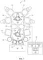
- FIG. 1shows a schematic top view of a multi-chamber processing system according to some examples.
- FIG. 2shows a schematic of a multi-pressure processing chamber that is configured to create a high pressure environment for processing and a low pressure environment for processing according to some examples.
- FIGS. 3 , 4 , 5 , and 6show respective examples of a multi-pressure processing chamber according to some examples.
- FIG. 7is a flowchart of a method for semiconductor processing according to some examples.
- FIGS. 8 , 9 , and 10are cross-sectional views of intermediate semiconductor structures illustrating aspects of the method of FIG. 7 according to some examples.
- examples described hereinrelate to methods and processing systems for performing multiple processes in a same processing chamber on a flowable gap-fill film deposited on a substrate.
- the multiple processcan include stabilizing bonds in a film deposited by a flowable process and subsequently densifying the film.
- Flowable filmsare commonly used for their ability to flow into gaps, particularly high aspect ratio gaps (e.g., having an aspect ratio of depth to width greater than 10:1). Flowable films generally have a poor quality, including a low density.
- Previous attemptshave been made to increase the quality of flowable films, including processes that implement a hot water dip. These processes were implemented using multiple tools or processing chambers each implementing a different process. Even with these processes, it has been found that the quality of the film can remain poor. For example, a wet etch rate of the film can vary based on the depth of the etch in the film because of non-uniformity of, e.g., density throughout the film.
- the wet etch ratecan be relatively high, which can cause any deviation of the etch rate to result in a significant difference in result. This can result in differing amounts of the film remaining in gaps.
- Examples described hereincan improve quality of the film, such as improving density of the film.
- the improved densitycan achieve a more uniform and lower etch rate that can be more easily controlled and less susceptible to significant differences in results due to deviations from the etch rate.
- less processingcan be performed on the film to achieve such benefits, which can further reduce processing and queue time. Reduced processing and queue time can in turn reduce a cost to manufacture the end product. Additionally, a higher quality film can result in improved electrical characteristics in some applications.
- isolation structurese.g., shallow trench isolations (STIs)
- the isolation structures formed by such processingcan be implemented in, for example, fin field-effect-transistors (FinFETs).
- FinFETsfin field-effect-transistors
- FinFETsfin field-effect-transistors
- FCVDflowable chemical vapor deposition
- FCVDspin-on
- FIG. 1shows a schematic top view of a multi-chamber processing system 100 according to some examples.
- the multi-chamber substrate processing systemincludes at least one processing chamber that is configured to perform processes with different environments, such as with a high pressure and with a low pressure.
- the processing system 100includes two transfer chambers 102 , 104 ; transfer robots 106 , 108 positioned in the transfer chambers 102 , 104 , respectively; processing chambers 110 , 112 , 114 , 116 , 118 , 120 disposed coupled to respective ones of the transfer chambers 102 , 104 ; two degas chambers 122 disposed coupled to the first transfer chamber 102 ; pass-through chambers 124 disposed coupled to each of and between the two transfer chambers 102 , 104 ; and a controller 126 .
- the processing system 100can further include load lock chambers 128 and a factory interface module 130 .
- the first transfer chamber 102is a central vacuum chamber that interfaces with adjacent processing chambers 110 , 112 , and degas chambers 122 .
- the first transfer chamber 102is coupled with processing chambers 110 , 112 , the degas chambers 122 , the pass-through chambers 124 , and two load lock chambers 128 .
- Each of the processing chambers 110 , 112 and degas chambers 122has an isolation valve disposed between the respective chamber and the first transfer chamber 102 .
- the pass-through chambers 124 and load lock chambers 128also have respective isolation valves disposed between the respective chamber 124 , 128 and the first transfer chamber 102 . Each isolation valve permits the respective chamber to be fluidly isolated from and fluidly connected to the first transfer chamber 102 .
- the isolation valve of a chamberallows the respective chamber to operate at, e.g., a different level of pressure than the first transfer chamber 102 and prevents any gases being used in or introduced in the respective chamber from being introduced into the first transfer chamber 102 .
- Each load lock chamber 128has a door which opens to the outside environment, e.g., opens to the factory interface module 130 .
- the second transfer chamber 104is a central vacuum chamber that interfaces with adjacent processing chambers 114 , 116 , 118 , 120 .
- the second transfer chamber 104is coupled with processing chambers 114 , 116 , 118 , 120 and the pass-through chambers 124 .
- Each of the processing chambers 114 , 116 , 118 , 120has an isolation valve disposed between the respective chamber and the second transfer chamber 104 .
- the pass-through chambers 124also have respective isolation valves disposed between the respective chamber 124 and the second transfer chamber 104 .
- Each isolation valvepermits the respective chamber to be fluidly isolated from the second transfer chamber 104 .
- the isolation valve of a chamberallows the respective chamber to operate at, e.g., a different level of pressure than the second transfer chamber 104 and prevents any gases being used in or introduced in the respective chamber from being introduced into the second transfer chamber 104 .
- the first transfer chamber 102 and the second transfer chamber 104are separated by pass-through chambers 124 , which may comprise cooldown or pre-heating chambers.
- the pass-through chambers 124also may be pumped down or ventilated during substrate handling when the first transfer chamber 102 and the second transfer chamber 104 operate at different pressures.
- a gas and pressure control system(e.g., including a plurality of vacuum pumps) is disposed in fluid communication with each transfer chamber 102 , 104 , each pass-through chamber 124 , and each of the processing and degas chambers 110 - 122 to independently regulate pressures in the respective chambers.
- the gas and pressure control systemcan include one or more gas pumps (e.g., turbo pumps, cryo-pumps, roughing pumps, etc.), gas sources, various valves, and conduits fluidly coupled to the various chambers.
- the gas and pressure control systemis capable of maintaining any chamber at a target pressure.
- the processing system 100is automated by a controller 126 that is programmed to control operations, processes, or functions of the processing system 100 .
- the controller 126can operate individual operations for each of the chambers of the processing system 100 to process a substrate.
- the controller 126may control the operation of the processing system 100 using a direct control of the chambers 102 - 124 of the processing system 100 or by controlling controllers associated with the chambers 102 - 124 .
- the controller 126enables data collection and feedback from the respective chambers to coordinate performance of the processing system 100 .
- the controller 126generally can include a processor 132 (e.g., a central processing unit (CPU) or other processor), memory 134 , and support circuits 136 .
- the processor 132may be one of any form of a general purpose processor that can be used in an industrial setting.
- the memory 134e.g., a non-transitory computer-readable storage medium
- the support circuits 136can be coupled to the processor and may comprise cache, clock circuits, input/output subsystems, power supplies, and the like.
- the various methods disclosed hereinmay generally be implemented under the control of the processor 132 by the processor 132 executing computer instruction code stored in the memory 136 as, e.g., a software routine.
- the processor 132controls the chambers to perform processes, and/or controls the processes within the chambers, in accordance with the various methods.
- Substratesare loaded into the processing system 100 through load lock chambers 128 .
- a factory interface module 130if present, would be responsible for receiving one or more substrates, e.g., wafers, cassettes of wafers, or enclosed pods of wafers, from either a human operator or an automated substrate handling system.
- the factory interface module 130can open the cassettes or pods of substrates, if applicable, and move the substrates to and from the load lock chambers 128 .
- the first transfer chamber 102receives the substrates from the load lock chambers 128 , and the substrates can be transferred throughout the transfer chambers 102 , 104 , including via the pass-through chambers 124 .
- the various chambers 110 - 122receive the substrates from the transfer chambers 102 , 104 , process the substrates, and allow the substrates to be transferred back into the transfer chambers 102 , 104 .
- a cassette loaded with substratesis placed into the load lock chamber 128 through the door from the factory interface module 130 and the door is closed.
- the load lock chamber 128is then evacuated to the same pressure as the first transfer chamber 102 and the isolation valve between the load lock chamber 128 and the first transfer chamber 102 is opened.
- the transfer robot 106 in the first transfer chamber 102is moved into position and one substrate is removed from the load lock chamber 128 .
- the load lock chamber 128is preferably equipped with an elevator mechanism so as one substrate is removed from the cassette, the elevator moves the stack of wafers in the cassette to position another wafer in the transfer plane so that it can be positioned on the robot blade.
- the transfer robot 106 in the first transfer chamber 102then rotates with the substrate so that the substrate is aligned with a processing chamber position.
- the processing chamberis flushed of any toxic gases, brought to the same pressure level as the transfer chamber, and the isolation valve between the processing chamber and the first transfer chamber 102 is opened.
- the transfer robot 106then moves the wafer into the processing chamber where it is lifted off the transfer robot 106 .
- the transfer robot 106is then retracted from the processing chamber and the isolation valve is closed.
- the processing chamberthen goes through a series of operations to execute a specified process on the wafer. When complete, the processing chamber is brought back to the same environment as the first transfer chamber 102 and the isolation valve is opened.
- the transfer robot 106removes the wafer from the processing chamber and then either moves it to another processing chamber for another operation, moves it to the pass-through chamber 124 for transfer to the second transfer chamber 104 , or replaces it in the load lock chamber 128 to be removed from the processing system 100 when the entire cassette of wafers has been processed.
- transfer robot 106moves the substrate to the pass-through chamber 124
- transfer robot 106 in the first transfer chamber 102rotates with the substrate so that the substrate is aligned with the pass-through chamber 124 position.
- the pass-through chamber 124is brought to the same pressure level as the transfer chamber, and the isolation valve between the pass-through chamber 124 and the first transfer chamber 102 is opened.
- the transfer robot 106then moves the wafer into the pass-through chamber 124 where it is lifted off the transfer robot 106 .
- the transfer robot 106is then retracted from the pass-through chamber 124 and the isolation valve is closed.
- the pass-through chamber 124then can be brought to the same environment, such as including pressure, as the second transfer chamber 104 .
- the isolation valve between the pass-through chamber 124 and the second transfer chamber 104is opened.
- the transfer robot 108removes the wafer from the pass-through chamber 124 , and the isolation valve is closed.
- the transfer robot 108then moves the substrate to another processing chamber coupled to the second transfer chamber 104 for another operation.
- the transfer robot 108can move the substrate to another processing chamber coupled to the second transfer chamber 104 like described above with respect to the transfer robot 108 moving the substrate to process chamber coupled to the first transfer chamber 102 .
- the transfer robot 108can then move the substrate to the pass-through chamber 124 for transfer to the first transfer chamber 102 , such as by a reverse sequence of operations by which the substrate was received in the second transfer chamber 104 through the pass-through chamber 124 .
- the transfer robot 106 in the first transfer chamber 102can move the substrate to another processing chamber for another operation or can replace it in the load lock chamber 128 to be removed from the processing system 100 when the entire cassette of wafers has been processed.
- the transfer robots 106 , 108include robot arms 107 , 109 , respectively, that support and move the substrate between different processing chambers.
- the processing chambers 110 - 120can be or include any appropriate processing chamber.
- One or more of the processing chambers 110 - 120is a chamber configured to perform processing on a substrate using different environments, such as with different pressures, etc., in the chamber.
- Other example processing chambers for the processing chambers 110 - 120include a chemical vapor deposition (CVD) chamber, an atomic layer deposition (ALD) chamber, a reactive ion etch (RIE) chamber, a rapid thermal anneal (RTA) or rapid thermal process (RTP) chamber, of the like.
- CVDchemical vapor deposition
- ALDatomic layer deposition
- RIEreactive ion etch
- RTArapid thermal anneal
- RTPrapid thermal process
- a transfer apparatusincludes the transfer chambers 102 , 104 and pass-through chambers 124 .
- fewer or more transfer chambers, pass-through chambers, and/or one or more holding chambersmay be implemented as a transfer apparatus in a processing system.
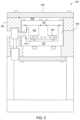
- FIG. 2illustrates a schematic of a multi-pressure processing chamber 200 that is configured to create a high pressure environment for processing a substrate and a low pressure environment for processing the substrate.
- the multi-pressure processing chamber 200includes a first chamber 202 and a second chamber 204 .
- the first chamber 202is disposed within the second chamber 204 and may be considered an inner chamber, and the second chamber 204 may be considered an outer chamber. Further, as apparent from the following description, the first chamber 202 can be configured to enable high pressure processing and may further be considered a high pressure chamber.
- the first chamber 202 and second chamber 204may, in some instances, be fluidly coupled together and configured to enable low pressure processing.
- the pressure within the first chamber 202can be controlled independently of the pressure in the second chamber 204 .
- the controlled multi-pressure processing chamber 200further includes a gas delivery system 206 , a vacuum processing system 208 , and a controller 210 .
- the gas delivery system 206 and the vacuum processing system 208are at least part of the gas and pressure control system of the processing system 100 of FIG. 1 .
- the controller 126 of the processing system 100can be or include the controller 210 .
- the gas delivery system 206is fluidly coupled, e.g., by gas flow conduits, to the first chamber 202 and is operable to pressurize and depressurize the first chamber 202 .
- the first chamber 202is a high pressure processing chamber that receives a process gas from the gas delivery system 206 and establishes a high pressure, e.g., at a pressure of at least 1 Bar.
- the process gascan be or include oxygen gas (O 2 ), ozone gas (O 3 ), nitrous oxide (N 2 O), nitric oxide (NO), steam (H 2 O), ammonia gas (NH 3 ) the like, or a combination thereof.
- the gas delivery system 206can include a combination of a gas panel, conduits, and valves that are controllable, e.g., by the controller 210 to deliver process gases to the first chamber, which may have different process gas compositions for different processes performed in the multi-pressure processing chamber 200 .
- the gas delivery system 206introduces the process gas into the first chamber 202 .
- the gas delivery system 206can include an exhaust system 212 to exhaust the process gas from the first chamber 202 , thereby depressurizing the first chamber 202 .
- the multi-pressure processing chamber 200includes a remote plasma source (RPS) 214 .
- the RPS 214in such implementations, is fluidly coupled, e.g., by gas flow conduits, to the gas delivery system 206 .
- the RPS 214is further fluidly coupled to the first chamber 202 .
- Process gases flowing from the gas delivery system 206can be ignited in a plasma in the RPS 214 .
- Effluents from the plasma in the RPS 214can flow into the first chamber 202 .
- the RPS 214can be a capacitively coupled plasma source or inductively coupled plasma source, for example.
- the vacuum processing system 208is fluidly coupled, e.g., by gas flow conduits, to the second chamber 204 and is operable to control the pressure of the second chamber 204 to be at low pressure, such as at a vacuum or near-vacuum pressure.
- the low pressurecan be, e.g., as low as 10 milliTorr.
- the vacuum processing system 208lowers a pressure within the second chamber 204 to near vacuum, thereby creating the appropriate low pressure environment for processing a substrate.
- a valve assembly 216is disposed between the first chamber 202 and the second chamber 204 and is configured to isolate the pressure within the first chamber 202 from the pressure within the second chamber 204 .
- the high pressure environment within the first chamber 202can thus be separated and sealed from the environment within the second chamber 204 .
- the valve assembly 216is openable to fluidly connect the first chamber 202 to the second chamber 204 and/or to enable the substrate to be transferred from the multi-pressure processing chamber 200 .
- the multi-pressure processing chamber 200includes a foreline 218 connected to the multi-pressure processing chamber 200 , and connected to an outside environment.
- An isolation valve 220is arranged along the foreline 218 to isolate the pressure within the second chamber 204 from the pressure of the outside environment.
- the isolation valve 220can be operated to adjust the pressure within the second chamber 204 and to release gases within the second chamber 204 .
- the isolation valve 220can be operated in conjunction with the vacuum processing system 208 to regulate the pressure within the second chamber 204 .
- a substratecan be processed by multiple processes while disposed within the first chamber 202 within the multi-pressure processing chamber 200 .
- the substratecan be transferred to a pedestal (not shown) within the first chamber 202 .
- the transfer of the substrate into the first chamber 202can be through the valve assembly 216 in some examples.
- the valve assembly 216With the substrate disposed on the pedestal in the first chamber 202 , the valve assembly 216 can remain open fluidly coupling the inner volume of the first chamber 202 with the inner volume of the second chamber 204 .
- the vacuum processing system 208can therefore pump down the pressure within the first chamber 202 and the second chamber 204 while the valve assembly 216 is open. Low pressure processing can therefore be performed on the substrate while the substrate is disposed on the pedestal in the first chamber 202 .
- the low pressure processingcan include flowing a process gas from the gas delivery system 206 into the first chamber 202 , which can be evacuated by the vacuum processing system 208 .
- the low pressure processingcan include using a plasma ignited in the RPS 214 .
- the valve assembly 216can be closed to fluidly isolate the inner volume of the first chamber 202 from the inner volume of the second chamber 204 .
- the gas delivery system 206can create a high pressure within the first chamber 202 with the valve assembly 216 closed. High pressure processing can therefore be performed on the substrate while the substrate is disposed on the pedestal in the first chamber 202 .
- the high pressure processingcan include flowing a process gas from the gas delivery system 206 into the first chamber 202 .
- the high pressure processingcan include using a plasma ignited in the RPS 214 .
- FIGS. 3 through 6depict various examples of multi-pressure processing chambers for processing a substrate.
- the pressure of chambers of these multi-pressure processing chamberscan be controlled using systems similar to those described with respect to FIG. 2 .
- a multi-pressure processing chamber 300includes a first chamber 302 , a pedestal 304 , a second chamber 306 , and a controller (e.g., the controller 126 ).
- the first chamber 302is disposed within the second chamber 306 and may be considered an inner chamber, and the second chamber 306 may be considered an outer chamber.
- the first chamber 302can be configured to enable high pressure processing and may further be considered a high pressure chamber.
- the first chamber 302 and second chamber 306may, in some instances, be fluidly coupled together and configured to enable low pressure processing.
- the multi-pressure processing chamber 300further includes a vacuum processing system (not shown) similar to the vacuum processing system 208 and a gas delivery system 307 similar to the gas delivery system 206 described with respect to FIG. 2 .
- the gas delivery system 307includes an input line 307 a and an exhaust line 307 b .
- the process gasis introduced into the first chamber 302 through the input line 307 a , and the process gas is exhausted from the first chamber 302 through the exhaust line 307 b .
- the multi-pressure processing chamber 300can include an RPS, which may be coupled to the input line 307 a for flowing plasma effluents from the RPS into the first chamber 302 .
- the pedestal 304supports a substrate 314 on which a film is to be processed.
- the pedestal 304is positioned or positionable within the first chamber 302 .
- the substrate 314sits directly on a flat top surface of the pedestal.
- the substrate 314sits on pins 330 that project from the pedestal.
- the multi-pressure processing chamber 300includes an inner wall 320 , a base 322 , and an outer wall 324 .
- the first chamber 302is provided by a volume within the inner wall 320 and the base 322 .
- the second chamber 306is provide by a volume within the inner wall 320 and outside the inner wall 320 , e.g., between the inner wall 320 and the outer wall 324 .
- the multi-pressure processing chamber 300further includes a valve assembly 316 between the first chamber 302 and the second chamber 306 that provides the functionality of the valve assembly 216 of FIG. 2 , e.g., it can be operated to isolate the first chamber 302 from the second chamber 306 and to fluidly couple the first chamber 302 and the second chamber 306 .
- the valve assembly 316includes the inner wall 320 , the base 322 , and an actuator 323 to move the base 322 relative to the inner wall 320 .
- the actuator 323can be controlled to drive the base 322 to move vertically, e.g., away from or toward the inner walls 320 defining the first chamber 302 .
- a bellows 328can be used to seal the second chamber 306 from the external atmosphere while permitting the base 322 to move vertically.
- the bellows 328can extend from a bottom of the base 322 to a floor of the second chamber 306 formed by the outer wall 324 .
- the base 322When the valve assembly 316 is in a closed position, the base 322 contacts the inner walls 320 such that a seal is formed between the base 322 and the inner walls 320 , thus separating the second chamber 306 from the first chamber 302 .
- the actuator 323is operated to drive the base 322 toward the inner walls 320 with sufficient force to form the seal.
- the sealinhibits gas from the first chamber 302 from being exhausted into the second chamber 306 .
- the base 322When the valve assembly 316 is in an open position, the base 322 is spaced apart from the inner walls 320 , thereby allowing gas to be conducted between the first chamber 302 and second chamber 306 and also allowing the substrate 314 to be accessed and transferred to another chamber.
- the pedestal 304is thus also movable relative to the inner walls 320 .
- the pedestal 304can be moved to enable the substrate 314 to be more easily accessible by the transfer robot.
- an arm of a transfer robot 106 or 108can extend through an aperture 326 (e.g., a slit) through the outer wall 324 .
- the valve assembly 316When the valve assembly 316 is in the open position, the robot arm can pass through the gap between the inner wall 320 and the base 322 to access the substrate 314 on the pedestal 304 .
- the multi-pressure processing chamber 300includes one or more heating elements 318 configured to apply heat to the substrate 314 .
- the heat from the heating elements 318can be sufficient to, e.g., anneal the substrate 314 when the substrate 314 is supported on the pedestal 304 and the process gas (if used) has been introduced into the first chamber 302 .
- the heating elements 318may be resistive heating elements.
- the one or more heating elements 318may be positioned in, e.g., embedded in, the inner walls 320 defining the first chamber 302 , such as in a ceiling of the first chamber 302 provided by the inner walls 320 .
- the heating elements 318are operable to heat the inner wall 320 , causing radiative heat to reach the substrate 314 .
- the substrate 314can be held by the pedestal 304 in close proximity, e.g., 2-10 mm, to the ceiling to improve transmission of heat from the inner wall 320 to the substrate 314 .
- the one or more heating elements 318may be arranged in other locations within the multi-pressure processing chamber 300 , e.g., within the side walls rather than the ceiling.
- An example of a heating element 318includes a discrete heating coil.
- a radiative heatere.g., an infrared lamp, can be positioned outside the first chamber 302 and direct infrared radiation through a window in the inner wall 320 .
- Electrical wiresconnect an electrical source (not shown), such as a voltage source, to the heating element, and can connect the one or more heating elements 318 to the controller.
- the controlleris operably connected to the vacuum processing system, the gas delivery system 307 , and the valve assembly 316 for controlling operations to process the substrate 314 .
- the controllermay also be operably connected to other systems.
- the controller 126 shown in FIG. 1is or includes the controller of the multi-pressure processing chamber 300 .
- the controllercan operate the vacuum processing system to depressurize the second chamber 306 to a low pressure to prepare for transfer of the substrate 314 through the second chamber 306 .
- the substrate 314is moved through the aperture 326 and the second chamber 306 by a transfer robot, e.g., one of the transfer robots 106 , 108 , while the second chamber 306 is at the low pressure so that contamination of the substrate 314 can be inhibited.
- the substrate 314is transferred onto the pedestal 304 for processing.
- the controllercan operate the valve assembly 316 to open the valve assembly 316 to provide an opening through which the substrate 314 can be transferred into the first chamber 302 and onto the pedestal 304 .
- the controllercan operate the transfer robot to carry the substrate 314 into the first chamber 302 and to place the substrate 314 on the pedestal 304 .
- the controllercan operate the valve assembly to be open for low pressure processing or closed for high pressure processing. Any order of high pressure processing and low pressure processing can be implemented. In some examples, a substrate can be processed by cyclically performing low pressure and high pressure processing.
- the inner volume of the first chamber 302is isolated from the inner volume of the second chamber 306 .
- pressures in the first chamber 302 and the second chamber 306can be set to different values.
- the controllercan operate the gas delivery system 307 to introduce the process gas into the first chamber 302 to pressurize the first chamber 302 and to process the substrate 314 .
- the introduction of the process gascan increase the pressure within the first chamber 302 to, for example, 1 Bar or more.
- Processing in the first chamber 302can be at a high pressure. If implemented, plasma effluents can be introduced into the first chamber 302 from an RPS to process the substrate 314 during high pressure processing.
- the controllercan operate the valve assembly 316 to open the valve assembly 316 , thereby having the first chamber 302 and second chamber 306 be in fluid communication with each other. With the valve assembly 316 open, pressures in the first chamber 302 and the second chamber 306 can be equal.
- the controllercan operate the vacuum processing system to bring the first chamber 302 and second chamber 306 to a low pressure to process the substrate 314 .
- the low pressure within the first chamber 302 and second chamber 306can be, for example, as low as 10 milliTorr. Hence, processing in the first chamber 302 and second chamber 306 can be at a low pressure.
- the controllercan operate the gas delivery system 307 to introduce the process gas into the first chamber 302 , which can be evacuated by the vacuum processing system, to process the substrate 314 . If implemented, plasma effluents can be introduced into the first chamber 302 from an RPS to process the substrate 314 during low pressure processing.
- the controllercan operate the exhaust system of the gas delivery system 307 to depressurize the first chamber 302 before the valve assembly 316 is opened.
- the pressurecan be reduced to a low pressure such that the pressure differential between the first chamber 302 and the second chamber 306 can be minimized.
- the controllercan operate the heating elements 318 at the same or different temperatures during different processing. Further, the controller can operate the gas delivery system 307 to flow any appropriate gas during any processing (e.g., high pressure processing or low pressure processing).
- the substrate 314can be removed from the first chamber 302 using the transfer robot.
- the controllercan operate the exhaust system of the gas delivery system 307 to depressurize the first chamber 302 , if appropriate, before the valve assembly 316 is opened.
- the process gascan be exhausted from the first chamber 302 to reduce the pressure within the first chamber 302 .
- the controllercan open the valve assembly 316 .
- the opened valve assembly 316provides an opening through which the substrate 314 is moved to be transferred into the second chamber 306 and through the aperture 326 .
- the opened valve assembly 316enables the substrate 314 to be transferred directly into the second chamber 306 , e.g., into the low pressure environment of the second chamber 306 .
- the controllercan then operate the transfer robot to transfer the substrate 314 to another chamber of a processing system, e.g., the processing system 100 .
- the substrate 314is transferred to the appropriate processing chamber for further processing or to the load lock chamber to remove the substrate from the processing system.
- a multi-pressure processing chamber 400includes a first chamber 402 , a pedestal 404 , a second chamber 406 , and a controller (not shown).
- the first chamber 402is disposed within the second chamber 406 and may be considered an inner chamber, and the second chamber 406 may be considered an outer chamber. Further, the first chamber 402 can be configured to enable high pressure processing and may further be considered a high pressure chamber.
- the first chamber 402 and second chamber 406may, in some instances, be fluidly coupled together and configured to enable low pressure processing.
- the multi-pressure processing chamber 400is similar to the multi-pressure processing chamber 300 described with respect to FIG. 3 ; unless otherwise specified the various options and implementations are also applicable to the example of FIG. 4 .
- the gas delivery system and the vacuum processing system of the multi-pressure processing chamber 400are operated in a similar manner to maintain the low and high pressure environments for a substrate 414 processed using the multi-pressure processing chamber 400 .
- the second chamber 406can be defined by volume between inner walls 420 and outer walls 424 .
- the substrate 414is also supportable on the pedestal 404 for processing within the first chamber 402 . Again, the substrate 414 can sit directly on the pedestal 404 , or sit on lift pins 430 that extend through the pedestal.
- the multi-pressure processing chamber 400differs from the multi-pressure processing chamber 300 of FIG. 3 in a few regards.
- inner walls 420 defining the first chamber 402are not movable relative to a base 422 defining the first chamber 402 .
- the pedestal 404is thus fixed relative to the inner walls 420 and the base 422 .
- the pedestal 404is fixed to the base 422 defining the first chamber 402 .
- one or more heating elements 418 of the example depicted in FIG. 4are arranged within the pedestal 404 .
- the substrate 414may thus be heated through contact with the pedestal 404 .
- the multi-pressure processing chamber 400further includes a valve assembly 416 between the first chamber 402 and the second chamber 406 that, similar to the valve assembly 316 of FIG. 3 , isolates the first chamber 402 from the second chamber 406 .
- the valve assembly 416is not formed by the inner walls 420 and the base 422 defining the first chamber 402 , but rather includes an arm assembly 425 that has one or more components that are movable relative to the inner walls 420 of the first chamber 402 .
- the valve assembly 416includes the arm assembly 425 and a valve door 423 configured to isolate and fluidly connect the first chamber 402 and the second chamber 406 .
- An aperture 423 ais through an inner wall 420 and is between the first chamber 402 and the second chamber 406 .
- An arm 425 b of the arm assembly 425is positioned in the aperture 423 a through the inner wall 420 while the valve door 423 is positioned within the first chamber 402 .
- the valve door 423is connected to the arm 425 b at a position distal from the remainder of the arm assembly 425 .
- the arm 425 bfurther extends through an aperture 426 through an outer wall 424 , and the remainder of the arm assembly 425 is positioned outside of the second chamber 406 .
- the arm assembly 425is driven by an actuator 428 , which is connected to a drive shaft 425 a of the arm assembly 425 , that is also positioned outside of the second chamber 406 . Movement of the drive shaft 425 a , which is driven by the actuator 428 , is translated by the arm assembly 425 into movement of the arm 425 b .
- the arm assembly 425e.g., including the drive shaft 425 a
- the actuator 428can be positioned within the second chamber 406 .
- the arm assembly 425extends through the aperture 423 a and is movable relative to the inner walls 420 so that the valve door 423 can be moved to a position in which it forms a seal with the inner walls 420 .
- the actuator 428drives the drive shaft 425 a of the arm assembly 425 , which translates the driving of the drive shaft 425 a into movement of the arm 425 b relative to the inner walls 420 and in a general direction that the aperture 423 a extends through the inner wall 420 .
- Movement of the arm 425 b in this directioncan cause the valve door 423 to engage the inner wall 420 (e.g., when the arm 425 b is retracted) to thereby form a seal with the inner wall 420 and isolate the first chamber 402 from the second chamber 406 , and can cause the valve door 423 to become displaced from the inner wall 420 (e.g., when the arm 425 b is extended) to thereby fluidly connect the first chamber 402 and the second chamber 406
- the valve door 423can be or include a flange from the arm 425 b that extends substantially parallel to the adjacent inner surface of the inner wall 420 .
- the valve assembly 416is movable between an open position and a closed position.
- the arm 425 b of the arm assembly 425is retracted laterally such that the valve door 423 covers the aperture 423 a and contacts one of the inner walls 420 , thereby forming the seal to isolate the first chamber 402 from the second chamber 406 .
- the arm 425 b of the arm assembly 425causes the valve door 423 (e.g., the flange) to contact an inner surface of the inner wall 420 defining the first chamber 402 .
- the arm 425 b of the arm assembly 425is extended laterally such that the valve door 423 is spaced laterally apart from the inner wall 420 , e.g., the inner surface of the inner wall 420 .
- the aperture 423 athus provides an opening that enables fluid communication between the first chamber 402 and the second chamber 406 .
- the controllercan operate the multi-pressure processing chamber 400 in a manner similar to the process described with respect to the controller of the multi-pressure processing chamber 300 to transfer the substrate 414 into and out of the first chamber 402 and to process the substrate 414 .
- the controllercan operate the actuator 428 to drive the arm assembly 425 .
- a multi-pressure processing chamber 500includes a first chamber 502 , a pedestal 504 , a second chamber 506 , and a controller (not shown).
- the multi-pressure processing chamber 500is similar to the multi-pressure processing chamber 400 described with respect to FIG. 4 ; unless otherwise specified the various options and implementations are also applicable to this example.
- the gas delivery system and the vacuum processing system of the multi-pressure processing chamber 500are operated in a similar manner to maintain the low and high pressure environments for a substrate (not shown) processed using the multi-pressure processing chamber 500 .
- the substrateis also supportable on the pedestal 504 or lift pins for processing within the first chamber 502 .
- the multi-pressure processing chamber 500differs from the multi-pressure processing chamber 400 of FIG. 4 in that the pedestal 504 is mounted to a ceiling 521 defining the first chamber 502 rather than to a base 522 defining the first chamber 502 . Like the pedestal 504 , the pedestal 504 is fixed relative to the walls 520 , the ceiling 521 , and the base 522 . In addition, one or more heating elements 518 of the multi-pressure processing chamber 500 are arranged within the pedestal 504 . To position the substrate on the pedestal 504 such that the substrate is supported on the pedestal 504 , the substrate is inserted between plates of the pedestal 504 . The one or more heating elements 518 are arranged relative to the plates such that, when the substrate is inserted into a slot defined by the plates of the pedestal 504 , the one or more heating elements 518 can uniformly apply heat to the substrate.
- a multi-pressure processing chamber 600includes a first chamber 602 , a pedestal 604 , a second chamber 606 , and a controller (not shown).
- the multi-pressure processing chamber 600is similar to the multi-pressure processing chamber 400 described with respect to FIG. 4 ; unless otherwise specified the various options and implementations are also applicable to this example.
- the gas delivery system and the vacuum processing system of the multi-pressure processing chamber 600are operated in a similar manner to maintain the low and high pressure environments for a substrate 614 processed using the multi-pressure processing chamber 600 .
- the substrate 614is also supportable on the pedestal 604 for processing within the first chamber 602 .
- the multi-pressure processing chamber 600differs from the multi-pressure processing chamber 400 of FIG. 4 in that a valve door 623 of a valve assembly 616 of the multi-pressure processing chamber 600 contacts an outer surface of an inner wall 620 defining the first chamber 602 , rather than an inner surface of the inner wall 620 , to cover an aperture 623 a in the inner wall 620 .
- the valve assembly 616operates to isolate the first chamber 602 from the second chamber 606 .
- the valve assembly 616can be positioned between the first chamber 602 and the second chamber 606 .
- the valve assembly 616includes an arm assembly 625 and a valve door 623 disposed in the second chamber 606 .
- An aperture 623 ais through an inner wall 620 and is between the first chamber 602 and the second chamber 606 .
- the valve door 623is positioned outside of the first chamber 602 .
- the arm assembly 625is positioned outside of the first chamber 602 and within the second chamber 606 .
- the arm assembly 625does not extend through the slit 626 .
- An arm 625 b of the arm assembly 625is movable relative to the inner walls 620 so that the valve door 623 can be moved to a position in which it forms a seal with the inner walls 620 .
- the multi-pressure processing chamber 600includes an actuator 628 operable to drive the arm assembly 625 .
- the actuator 628is coupled to the drive shaft 625 a of the arm assembly 625 , which is configured to drive to move the arm 625 b of the arm assembly 625 relative to the inner walls 620 .
- valve assembly 616is movable between an open position and a closed position.
- the arm 625 b of the arm assembly 625is laterally extended such that the valve door 623 contacts the inner wall 620 covering the aperture 623 a , thereby forming the seal to isolate the first chamber 602 from the second chamber 606 .
- the arm 625 b of the arm assembly 625is laterally retracted such that the valve door 623 does not contact the inner wall 620 uncovering the aperture 623 a .
- the aperture 623 athus provides an opening that enables fluid communication between the first chamber 602 and the second chamber 606 .
- the controllercan operate the multi-pressure processing chamber 600 in a manner similar to the process described with respect to the controller of the multi-pressure processing chamber 300 .
- the controllercan operate the actuator 628 to drive arm 625 b of the arm assembly 625 .
- FIG. 7is a flowchart of a method 700 for semiconductor processing according to some examples.
- FIGS. 8 through 10are cross-sectional views of intermediate semiconductor structures illustrating aspects of the method 700 of FIG. 7 according to some examples. Examples described herein are in the context of forming isolation structures (e.g., shallow trench isolations (STIs)) between fins on a substrate.
- isolation structurese.g., shallow trench isolations (STIs)
- FIG. 8illustrates a cross-sectional view of a flowable film 808 deposited on and between fins 804 on a substrate 802 .
- a substrate 802is provided.
- the substrate 802can be any appropriate semiconductor substrate, such as a bulk substrate, semiconductor-on-insulator (SOI) substrate, or the like.
- SOIsemiconductor-on-insulator
- the substrate 802is a bulk silicon wafer. Examples of substrate sizes include 200 mm diameter, 350 mm diameter, 400 mm diameter, and 450 mm diameter, among others. Fins 804 are then formed on the substrate 802 .
- the fins 804can be formed by etching features, such as trenches 806 that extend into the substrate 802 such that each fin 804 is defined between a neighboring pair of features (e.g., trenches 806 ). Any appropriate patterning process can be implemented to form the features.
- the patterning processcan include a multiple patterning process, such as self-aligned double patterning (SADP), lithography-etch-lithography-etch (LELE) double patterning, etc., to achieve a target pitch between fins 804 .
- An example etch process to etch the trenches 806includes a reactive ion etch (RIE) process or the like.
- RIEreactive ion etch
- the aspect ratiocan be a ratio of the depth 810 of the trench 806 to the width 812 of the trench 806 .
- An aspect ratiocan be 10:1 or more.
- one or more layers, such as a diffusion barrier layer,are formed on the fins 804 , and the depth 810 and width 812 can be measured from an outer surface of the outermost layer.
- the flowable film 808is then deposited in the trenches 806 and on the fins 804 .
- the flowable film 808can be deposited by a FCVD process or spin-on, in some examples.
- a flowable film 808in a FCVD process, can be a silicon based dielectric that includes a high concentration of nitrogen and/or hydrogen.
- precursorscan be or include silyl-amines, such as H 2 N(SiH 3 ), HN(SiH 3 ) 2 , and N(SiH 3 ) 3 , silane (SiH 4 ), or other similar precursors, which may be mixed with other gases, such as trisilylamine (N(SiH 3 ) 3 ), hydrogen (H 2 ), nitrogen (N 2 ), and/or ammonia (NH 3 ).
- the flowability of the flowable film 808can permit the flowable film 808 to provide good gap filling, such as in high aspect ratio gaps (e.g., which may be formed by the trenches 806 ).
- the substrate 802 having the flowable film 808 deposited thereonis then transferred to a processing chamber.
- the processing chamberis a multi-pressure processing chamber, such as any described above with respect to FIGS. 2 through 7 .
- the processing chamber of block 704is the multi-pressure processing chamber 300 of FIG. 3 .
- the processing chambermay be included in a processing system, such as the processing system 100 of FIG. 1 .
- the substrate 802is transferred by a front opening unified pod (FOUP) to a factory interface module 130 , and at the factory interface module 130 , the substrate 802 is transferred from the FOUP to a load lock chamber 128 . Subsequent transfers and processing are performed in the processing system 100 , e.g., without exposing the substrate 802 to an atmospheric ambient environment outside of the processing system 100 and without breaking a low pressure or vacuum environment maintained within the transfer apparatus of the processing system 100 .
- the transfer robot 106transfers the substrate 802 from the load lock chamber 128 into the first transfer chamber 102 .
- the substrate 802can thereafter be transferred to the processing chamber (e.g., multi-pressure processing chamber 300 ) by the transfer robot 106 if the multi-pressure processing chamber 300 is coupled to the first transfer chamber 102 , or to a pass-through chamber 124 by the transfer robot 106 and subsequently from the pass-through chamber 124 to the multi-pressure processing chamber 300 by the transfer robot 108 if the multi-pressure processing chamber 300 is coupled to the second transfer chamber 104 .
- the deposition of the flowable film 808can be in a processing chamber within the processing system.
- the substrate 802can be transferred into the processing system 100 before deposition of the flowable film 808 and can subsequently be transferred within the processing system 100 to the multi-pressure processing chamber 300 .
- the valve assembly 316 of the multi-pressure processing chamber 300is opened, and the transfer robot of the transfer chamber transfers the substrate 802 onto the pedestal 304 , like described above.
- processingis performed in the processing chamber, including a first process at block 708 followed by a second process at block 710 .
- the second process at block 710is different from the first process at block 708 .
- Additional processmay be performed in the processing chamber in other examples.
- the first process at block 708forms more bonds and/or bonds that are more stable in the flowable film, and the second process at block 710 densifies, and may further create more stable bonds within, the stabilized film.
- the first process at block 708includes stabilizing the flowable film, and the second process at block 710 includes densifying the stabilized film.
- the first process at block 708 and the second process at block 710can be at a same or different pressure.
- the first process at block 708is at a pressure that is lower than a pressure of the second process at block 710 .
- the second process at block 710is performed at a pressure within the processing chamber that is three orders of magnitude or more (e.g., four orders of magnitude or more) greater than a pressure within the processing chamber at which the first process at block 708 is performed.
- the first process at block 708is at a pressure that is greater than a pressure of the second process at block 710 .
- the first processcan be performed at a pressure in a range from 10 milliTorr to 100 Bar
- the second processcan be performed at a pressure greater than or equal to 1 Bar, such as greater than or equal to 5 Bar.
- temperatures at which the first process and second process are performedare equal, while in other examples, the temperatures may differ.
- a temperature of the first process at block 708is less than a temperature of the second process at block 710 .
- the temperature of the first process at block 708can be in a range from 300° C. to 1000° C.
- the temperature of the process at block 710can be in a range from 300° C. to 1000° C., which temperature may be equal to, less than, or greater than the temperature of the first process at block 708 .
- the temperature of the first process at block 708can be in a range from 100° C. to 300° C.
- the temperature of the process at block 710can be in a range from 300° C. to 1000° C.
- a process gas composition(e.g., which may be a single gas or a mixture of gases) flowed for the first process at block 708 differs from a process gas composition flowed for the second process at block 710 . Examples for the first process and second process are described below.
- the first process at block 708is a conversion process in addition to being a stabilization process.
- the conversion and stabilization processconverts the flowable film 808 to have another dielectric composition.
- the conversion processcan convert a silicon based dielectric that includes a high concentration of nitrogen and/or hydrogen deposited by a FCVD process into silicon oxide.
- the conversion processcan be an oxidation process.
- the oxidation processis a thermal oxidation process or a plasma oxidation process.
- an oxygen-containing process gassuch as oxygen gas (O 2 ), ozone gas (O 3 ), nitrous oxide (N 2 O), nitric oxide (NO), or a combination thereof, can be flowed in the processing chamber.
- the oxygen-containing process gascan be continuously flowed into the processing chamber, or can be flowed into the processing chamber until a desired pressure is achieved and ceased, where the pressure is maintained thereafter during the oxidation process.
- the flow rate of the oxygen-containing process gascan be in a range from about 5 sccm to about 200 slm, for example.
- the pressure within the processing chambercan be maintained at a pressure between 10 milliTorr and 100 Bar.
- the thermal oxidation processcan be performed at a temperature greater than 300° C., such as in a range from about 300° C. to about 1000° C.
- a plasma oxidation processa plasma is ignited in a RPS using an oxygen-containing process gas, such as oxygen gas (O 2 ), ozone gas (O 3 ), nitrous oxide (N 2 O), nitric oxide (NO), or a combination thereof.
- Oxygen-containing plasma effluentsare flowed in the processing chamber.
- a RF power source of the RPScan have a frequency in a range from about 2 MHz to about 40 MHz, such as 13.56 MHz, and can have a power in a range from about 50 W to about 3000 W.
- Flowing of gas, a temperature, and pressure in the plasma oxidation processcan be like previously described for the thermal oxidation.
- the first process at block 708is a stabilization process that does not significantly affect the composition of the flowable film.
- the stabilization processcan substantially maintain a composition of a silicon based dielectric that includes a high concentration of nitrogen and/or hydrogen deposited by a FCVD process.
- the stabilization processis a thermal process or a plasma process.
- an ammonia-containing process gassuch as ammonia gas (NH 3 )
- the ammonia-containing process gascan be continuously flowed into the processing chamber, or can be flowed into the processing chamber until a desired pressure is achieved and ceased, where the pressure is maintained thereafter during the thermal process.
- the flow rate of the ammonia-containing process gascan be in a range from about 5 sccm to about 200 slm, for example.
- the pressure within the processing chambercan be maintained at a pressure between 10 milliTorr and 100 Bar.
- the thermal processcan be performed at a temperature greater than 300° C., such as in a range from about 300° C. to about 1000° C.
- a plasmais ignited in a RPS using an ammonia-containing process gas, such as ammonia gas (NH 3 ).
- Nitrogen-containing plasma effluents and/or hydrogen-containing plasma effluentsare flowed in the processing chamber.
- a RF power source of the RPScan have a frequency in a range from about 2 MHz to about 40 MHz, such as 13.56 MHz, and can have a power in a range from about 50 W to about 3000 W.
- Flowing of gas, a temperature, and pressure in the plasma processcan be like previously described for the stabilization without a plasma.
- the first process at block 708can be performed in the multi-pressure processing chamber 300 while the valve assembly 316 remains in an open or closed position, e.g., depending on a pressure at which the first process is performed.
- the valve assembly 316can remain open for low pressure processing, or can be closed for high pressure processing.
- the oxygen-containing process gas or ammonia-containing process gascan be flowed through the gas delivery system 307 and evacuated through the second chamber 306 by the vacuum processing system.
- the heating elements 318can maintain the temperature in the first chamber 302 during the first process.
- the second process at block 710is a densification process.
- the densification processincreases a density of the dielectric material that was stabilized and/or converted from the flowable film 808 .
- the densification processcan increases a density of the silicon oxide, which was converted from the silicon based dielectric that included a high concentration of nitrogen and/or hydrogen deposited by a FCVD process.
- the densification processmay additionally further convert the stabilized film to another dielectric composition (e.g., silicon oxide).
- the densification processcan catalyze reactions that form Si—O—Si bonds.
- the densification processcan be an anneal process.
- the anneal processis a dry anneal process or a steam anneal process.
- the dry anneal processcan be performed at a temperature greater than 300° C., such as in a range from about 300° C. to about 1000° C.
- a process gassuch as ammonia gas (NH 3 ), nitrous oxide (N 2 O), nitric oxide (NO), or the like, can be flowed in the processing chamber.
- the process gascan be continuously flowed into the processing chamber, or can be flowed into the processing chamber until a desired pressure is achieved and ceased, where the pressure is maintained thereafter during the dry anneal process.
- the flow rate of the process gascan be in a range from about 5 sccm to about 200 slm, for example.
- the dry anneal processcan additionally be an oxidation process to further convert the film when the process gas includes an oxygen-containing gas, such as nitrous oxide (N 2 O) and/or nitric oxide (NO).
- an oxygen-containing gassuch as nitrous oxide (N 2 O) and/or nitric oxide (NO).
- the pressure within the processing chambercan be maintained at a high pressure, such as on the order of a Bar, such as about 1 Bar or more, or more specifically, about 5 Bar or more.
- the steam anneal processcan be performed at a temperature greater than 300° C., such as in a range from about 350° C. to about 1000° C.
- steam (H 2 O) with or without another process gaslike ammonia gas (NH 3 ), nitrous oxide (N 2 O), nitric oxide (NO), or a combination thereof, can be flowed in the processing chamber.
- the steam with or without a process gascan be continuously flowed into the processing chamber, or can be flowed into the processing chamber until a desired pressure is achieved and ceased, where the pressure is maintained thereafter during the steam anneal process.
- the flow rate of the steam with or without a process gascan be in a range from about 5 sccm to about 200 slm, for example.
- the steam anneal processcan additionally be an oxidation process to further convert the film.
- the pressure within the processing chambercan be maintained at a high pressure, such as on the order of a Bar, such as about 1 Bar or more, or more specifically, about 5 Bar or more.
- the second process at block 710can be performed in the multi-pressure processing chamber 300 while the valve assembly 316 is in an open or closed position, e.g., depending on a pressure at which the first process is performed.
- the process gase.g., including steam
- the heating elements 318can maintain the temperature in the first chamber 302 during the second process.
- the first process at block 708is a conversion process in addition to a stabilization process.
- the conversion and stabilization processconverts the flowable film 808 to have another dielectric composition, like described above.
- the conversion processcan be an oxidation process.
- the oxidation processis a steam oxidation process or a plasma oxidation process.
- steamH 2 O
- the steamcan be continuously flowed into the processing chamber, or can be flowed into the processing chamber until a desired pressure is achieved and ceased, where the pressure is maintained thereafter during the steam oxidation process.
- the flow rate of the steamcan be in a range from about 5 sccm to about 200 slm, for example.
- the pressure within the processing chambercan be maintained at a pressure less than 5 Bar.
- the pressure during the steam oxidationis less than the pressure of the second process at block 710 .
- the steam processcan be performed at a temperature greater than 100° C., such as in a range from about 100° C. to about 300° C.
- the temperature during the steam oxidationis less than the temperature of the second process at block 710 .
- a plasma oxidation processa plasma is ignited in a RPS using steam (H 2 O). Oxygen-containing plasma effluents and/or hydrogen-containing plasma effluents are flowed in the processing chamber.
- a RF power source of the RPScan have a frequency in a range from about 2 MHz to about 40 MHz, such as 13.56 MHz, and can have a power in a range from about 50 W to about 3000 W.
- Flowing of steam, a temperature, and pressure in the plasma oxidation processcan be like previously described for the steam oxidation.
- Table 1summarizes different combinations of processes according to some examples. An example is contained within a respective row in Table 1. Different combinations can be implemented. Additional processes can be performed, such as by repeating the first and second processes.
- FIG. 9illustrates a cross-sectional view of a converted and densified film 814 , which was converted from the flowable film 808 , on and between fins 804 on the substrate 802 .
- the flowable film 808is converted from a silicon based dielectric that included a high concentration of nitrogen and/or hydrogen into a silicon dioxide, which was densified.
- the converted and densified film 814is a densified silicon oxide, which is a different material composition from the originally deposited flowable film 808 .
- the film that was processed at block 706is etched.
- the substrate 802is removed from the processing chamber by the transfer robot of the transfer chamber to which the processing chamber is coupled.
- the substrate 802can be removed from the first chamber 302 of the multi-pressure processing chamber 300 as described above.
- the substrate 802can be transferred to another processing chamber within the processing system 100 or to a processing chamber of another processing system.
- the etchcan be by any appropriate etch process.
- the etch processis a wet etch, although a dry etch may also be implemented.
- the wet etchcan use dilute hydrofluoric acid (dHF), which can be selective to silicon oxide.
- dHFdilute hydrofluoric acid
- a 100:1 dHF solutionwas implemented to etch a converted and densified film of silicon oxide.
- the etch rate of the etch of block 706can be more uniform and lower, which can be more easily controlled, as described above.
- FIG. 10illustrates a cross-sectional view of isolation structures (e.g., STIs) formed with the converted and densified film 814 in trenches 806 between fins 804 on the substrate 802 , e.g., after etching the converted and densified film 814 .
- isolation structurese.g., STIs
- the fins 804protrude from between neighboring isolation structures.
- Top surfaces of the isolation structurese.g., top surface of the converted and densified film 814
- can be recessed to any depth from top surfaces of the fins 804and the illustration of FIG. 10 is merely an example.
- the fins 804can thereafter be used to form any appropriate device structure.
- the fins 804can be used to form FinFETs.
- a gate structurecan be formed on and longitudinally perpendicularly to a fin 804 .
- the gate structurecan include a gate dielectric (e.g., a high-k gate dielectric) along surfaces of the fin, one or more work-function tuning layers on the gate dielectric, and a metal fill on the work-function tuning layer(s).
- the gate structurecan define a channel region in the respective fin 804 underlying the gate structure.
- Source/drain regionse.g., epitaxial source/drain regions
- the gate structure, channel region, and source/drain regions togethercan form a FinFET.
Landscapes
- Engineering & Computer Science (AREA)
- Physics & Mathematics (AREA)
- Condensed Matter Physics & Semiconductors (AREA)
- General Physics & Mathematics (AREA)
- Manufacturing & Machinery (AREA)
- Computer Hardware Design (AREA)
- Microelectronics & Electronic Packaging (AREA)
- Power Engineering (AREA)
- Chemical & Material Sciences (AREA)
- Plasma & Fusion (AREA)
- Analytical Chemistry (AREA)
- Chemical Kinetics & Catalysis (AREA)
- Container, Conveyance, Adherence, Positioning, Of Wafer (AREA)
- Chemical Vapour Deposition (AREA)
- Formation Of Insulating Films (AREA)
- Insulated Gate Type Field-Effect Transistor (AREA)
Abstract
Description
| TABLE 1 | ||
| First Process | Second Process | |
| Ex. (1) | Process gas: O2, O3, N2O, NO, or a | Process gas: H2O, NH3, N2O, NO, or a |
| combination thereof | combination thereof | |
| Pressure: 10 milliTorr to 100 Bar | Pressure: >= 1 Bar | |
| Temperature: 300° C. to 1000° C. | Temperature: 300° C. to 1000° C. | |
| Type: Gas or RPS | Type: Gas or RPS | |
| Ex. (2) | Process gas: NH3 | Process gas: H2O, N2O, NO, or a |
| Pressure: 10 milliTorr to 100 Bar | combination thereof, any of which may | |
| Temperature: 300° C. to 1000° C. | additionally include NH3 | |
| Type: Gas or RPS | Pressure: >= 1 Bar | |
| Temperature: 300° C. to 1000° C. | ||
| Type: Gas or RPS | ||
| Ex. (3) | Process gas: H2O | Process gas: H2O, NH3, N2O, NO, or a |
| Pressure: <= 5 Bar | combination thereof | |
| Temperature: 100° C. to 300° C. | Pressure: >= 1 Bar (or >= 5 Bar) | |
| Type: Gas or RPS | [Greater than pressure of First | |
| Process] | ||
| Temperature: 300° C. to 1000° C. | ||
| [Greater than temperature of First | ||
| Process] | ||
| Type: Gas or RPS | ||
Claims (7)
Priority Applications (9)
| Application Number | Priority Date | Filing Date | Title |
|---|---|---|---|
| US16/792,646US11901222B2 (en) | 2020-02-17 | 2020-02-17 | Multi-step process for flowable gap-fill film |
| KR1020247043422AKR20250007704A (en) | 2020-02-17 | 2021-01-26 | Multi-step process for flowable gap-fill film |
| KR1020227032039AKR102750221B1 (en) | 2020-02-17 | 2021-01-26 | A multi-step process to fill the liquidity gap |
| PCT/US2021/014991WO2021167754A1 (en) | 2020-02-17 | 2021-01-26 | Multi-step process for flowable gap-fill film |
| JP2022549151AJP7433457B2 (en) | 2020-02-17 | 2021-01-26 | Multi-step process for flowable gap-filled membranes |
| CN202180015194.0ACN115104176A (en) | 2020-02-17 | 2021-01-26 | Multi-step process for flowable gap fill film |
| TW112148222ATWI874035B (en) | 2020-02-17 | 2021-01-28 | Multi-step process for flowable gap-fill film |
| TW110103161ATWI873281B (en) | 2020-02-17 | 2021-01-28 | Multi-step process for flowable gap-fill film |
| US18/392,534US20240128121A1 (en) | 2020-02-17 | 2023-12-21 | Multi-step process for flowable gap-fill film |
Applications Claiming Priority (1)
| Application Number | Priority Date | Filing Date | Title |
|---|---|---|---|
| US16/792,646US11901222B2 (en) | 2020-02-17 | 2020-02-17 | Multi-step process for flowable gap-fill film |
Related Child Applications (1)
| Application Number | Title | Priority Date | Filing Date |
|---|---|---|---|
| US18/392,534DivisionUS20240128121A1 (en) | 2020-02-17 | 2023-12-21 | Multi-step process for flowable gap-fill film |
Publications (2)
| Publication Number | Publication Date |
|---|---|
| US20210257252A1 US20210257252A1 (en) | 2021-08-19 |
| US11901222B2true US11901222B2 (en) | 2024-02-13 |
Family
ID=77273564
Family Applications (2)
| Application Number | Title | Priority Date | Filing Date |
|---|---|---|---|
| US16/792,646Active2041-11-08US11901222B2 (en) | 2020-02-17 | 2020-02-17 | Multi-step process for flowable gap-fill film |
| US18/392,534PendingUS20240128121A1 (en) | 2020-02-17 | 2023-12-21 | Multi-step process for flowable gap-fill film |
Family Applications After (1)
| Application Number | Title | Priority Date | Filing Date |
|---|---|---|---|
| US18/392,534PendingUS20240128121A1 (en) | 2020-02-17 | 2023-12-21 | Multi-step process for flowable gap-fill film |
Country Status (6)
| Country | Link |
|---|---|
| US (2) | US11901222B2 (en) |
| JP (1) | JP7433457B2 (en) |
| KR (2) | KR102750221B1 (en) |
| CN (1) | CN115104176A (en) |
| TW (2) | TWI873281B (en) |
| WO (1) | WO2021167754A1 (en) |
Families Citing this family (4)
| Publication number | Priority date | Publication date | Assignee | Title |
|---|---|---|---|---|
| JP7747868B2 (en)* | 2021-09-03 | 2025-10-01 | アプライド マテリアルズ インコーポレイテッド | Cluster tools, systems, and methods having one or more pressure stabilization chambers |
| KR20240115465A (en)* | 2023-01-19 | 2024-07-26 | 삼성전자주식회사 | Exhaust gas processing apparatus having plasma sources and substrate processing apparatus having the same |
| US20250253148A1 (en)* | 2024-02-05 | 2025-08-07 | Applied Materials, Inc. | Trench and channel gap fill tuning for flowable chemical vapor deposition (fcvd) films |
| WO2025197037A1 (en)* | 2024-03-21 | 2025-09-25 | 東京エレクトロン株式会社 | Substrate treatment method and substrate treatment system |
Citations (606)
| Publication number | Priority date | Publication date | Assignee | Title |
|---|---|---|---|---|
| US3684592A (en) | 1969-09-30 | 1972-08-15 | Westinghouse Electric Corp | Passivated surfaces and protective coatings for semiconductor devices and processes for producing the same |
| US3749383A (en) | 1971-04-29 | 1973-07-31 | Rca Corp | Apparatus for processing semiconductor devices |
| US3758316A (en) | 1971-03-30 | 1973-09-11 | Du Pont | Refractory materials and process for making same |
| US4409260A (en) | 1979-08-15 | 1983-10-11 | Hughes Aircraft Company | Process for low-temperature surface layer oxidation of a semiconductor substrate |
| US4424101A (en) | 1980-11-06 | 1984-01-03 | The Perkin-Elmer Corp. | Method of depositing doped refractory metal silicides using DC magnetron/RF diode mode co-sputtering techniques |
| US4524587A (en) | 1967-01-10 | 1985-06-25 | Kantor Frederick W | Rotary thermodynamic apparatus and method |
| US4576652A (en) | 1984-07-12 | 1986-03-18 | International Business Machines Corporation | Incoherent light annealing of gallium arsenide substrate |
| US4589193A (en) | 1984-06-29 | 1986-05-20 | International Business Machines Corporation | Metal silicide channel stoppers for integrated circuits and method for making the same |
| JPS634616A (en) | 1986-06-25 | 1988-01-09 | Hitachi Tokyo Electron Co Ltd | Steam treating unit |
| JPS6367721A (en) | 1986-09-09 | 1988-03-26 | Meidensha Electric Mfg Co Ltd | Manufacture of amorphous carbon semiconductor film |
| JPH01218018A (en) | 1988-02-18 | 1989-08-31 | Internatl Business Mach Corp <Ibm> | Method of converting semiconductor material into high melting point metal and semiconductor device manufactured by utilizing the method |
| US4879259A (en) | 1987-09-28 | 1989-11-07 | The Board Of Trustees Of The Leland Stanford Junion University | Rapid thermal annealing of gallium arsenide with trimethyl arsenic overpressure |
| US5050540A (en) | 1991-01-29 | 1991-09-24 | Arne Lindberg | Method of gas blanketing a boiler |
| US5114513A (en) | 1988-10-27 | 1992-05-19 | Omron Tateisi Electronics Co. | Optical device and manufacturing method thereof |
| US5126117A (en) | 1990-05-22 | 1992-06-30 | Custom Engineered Materials, Inc. | Device for preventing accidental releases of hazardous gases |
| US5149378A (en) | 1989-04-10 | 1992-09-22 | Hashimoto Kasei Kabushiki-Kaisya | Tungsten film forming apparatus |
| US5167717A (en) | 1989-02-15 | 1992-12-01 | Charles Boitnott | Apparatus and method for processing a semiconductor wafer |
| EP0516344A1 (en) | 1991-05-28 | 1992-12-02 | Electrotech Limited | Method to fill a cavity in a substrate |
| JPH04355922A (en) | 1991-03-18 | 1992-12-09 | Matsushita Electron Corp | Polyimide hardening device |
| US5175123A (en) | 1990-11-13 | 1992-12-29 | Motorola, Inc. | High-pressure polysilicon encapsulated localized oxidation of silicon |
| JPH0521347A (en) | 1991-07-11 | 1993-01-29 | Canon Inc | Sputtering device |
| US5300320A (en) | 1992-06-23 | 1994-04-05 | President And Fellows Of Harvard College | Chemical vapor deposition from single organometallic precursors |
| US5314541A (en) | 1991-05-28 | 1994-05-24 | Tokyo Electron Limited | Reduced pressure processing system and reduced pressure processing method |
| US5319212A (en) | 1992-10-07 | 1994-06-07 | Genus, Inc. | Method of monitoring ion beam current in ion implantation apparatus for use in manufacturing semiconductors |
| JPH06283496A (en) | 1993-03-26 | 1994-10-07 | Dainippon Screen Mfg Co Ltd | Dryer of substrate after washing |
| US5366905A (en) | 1991-11-05 | 1994-11-22 | Fujitsu Limited | Method for producing conducting layers for a semiconductor device |
| JPH0748489B2 (en) | 1987-07-27 | 1995-05-24 | 富士通株式会社 | Plasma processing device |
| JPH07158767A (en) | 1993-12-09 | 1995-06-20 | Kokusai Electric Co Ltd | Gate valve |
| EP0670590A2 (en) | 1994-02-28 | 1995-09-06 | Applied Materials, Inc. | High pressure plasma treatment method and apparatus |
| US5472812A (en) | 1991-07-11 | 1995-12-05 | Canon Kabushiki Kaisha | Method for forming a photomask pattern |
| JPH08195493A (en) | 1995-01-13 | 1996-07-30 | Toshiba Corp | Method for manufacturing thin film transistor |
| US5578132A (en) | 1993-07-07 | 1996-11-26 | Tokyo Electron Kabushiki Kaisha | Apparatus for heat treating semiconductors at normal pressure and low pressure |
| US5590695A (en) | 1993-04-28 | 1997-01-07 | Advanced Delivery & Chemical Systems, Inc. | Manifold systems for high purity chemical delivery systems |
| US5597439A (en) | 1994-10-26 | 1997-01-28 | Applied Materials, Inc. | Process gas inlet and distribution passages |
| JPH0948690A (en) | 1995-08-02 | 1997-02-18 | Sony Corp | Apparatus for supplying reaction gas |
| US5620524A (en) | 1995-02-27 | 1997-04-15 | Fan; Chiko | Apparatus for fluid delivery in chemical vapor deposition systems |
| US5677230A (en) | 1995-12-01 | 1997-10-14 | Motorola | Method of making wide bandgap semiconductor devices |
| JPH09296267A (en) | 1995-11-21 | 1997-11-18 | Applied Materials Inc | Apparatus and method for manufacturing metal path in semiconductor substrate by high-pressure extrusion |
| US5747383A (en) | 1995-09-05 | 1998-05-05 | Taiwan Semiconductor Manufacturing Company Ltd | Method for forming conductive lines and stacked vias |
| EP0840365A2 (en) | 1996-10-21 | 1998-05-06 | Applied Materials, Inc. | High pressure plasma oxide etch process |
| JPH10214880A (en) | 1996-12-02 | 1998-08-11 | Applied Materials Inc | Substrate support member |
| US5808245A (en) | 1995-01-03 | 1998-09-15 | Donaldson Company, Inc. | Vertical mount catalytic converter muffler |
| JPH10335657A (en) | 1997-06-04 | 1998-12-18 | Nec Corp | Manufacture of semiconductor device |
| US5857368A (en) | 1995-10-06 | 1999-01-12 | Applied Materials, Inc. | Apparatus and method for fabricating metal paths in semiconductor substrates through high pressure extrusion |
| US5858051A (en) | 1995-05-08 | 1999-01-12 | Toshiba Machine Co., Ltd. | Method of manufacturing optical waveguide |
| US5877087A (en) | 1995-11-21 | 1999-03-02 | Applied Materials, Inc. | Low temperature integrated metallization process and apparatus |
| US5880041A (en) | 1994-05-27 | 1999-03-09 | Motorola Inc. | Method for forming a dielectric layer using high pressure |
| US5879756A (en) | 1996-09-19 | 1999-03-09 | Lambda Technologies, Inc. | Curing polymer layers on semiconductor substrates using variable frequency microwave energy |
| US5888888A (en) | 1997-01-29 | 1999-03-30 | Ultratech Stepper, Inc. | Method for forming a silicide region on a silicon body |
| US5918149A (en) | 1996-02-16 | 1999-06-29 | Advanced Micro Devices, Inc. | Deposition of a conductor in a via hole or trench |
| JPH11209872A (en) | 1998-01-22 | 1999-08-03 | Nec Corp | Sputtering device and sputtering method |
| US5940985A (en) | 1996-03-01 | 1999-08-24 | Tokyo Electron Limited | Apparatus and method for drying substrates |
| JPH11354515A (en) | 1998-06-04 | 1999-12-24 | Ishikawajima Harima Heavy Ind Co Ltd | Pressurized heating furnace |
| US6071810A (en) | 1996-12-24 | 2000-06-06 | Kabushiki Kaisha Toshiba | Method of filling contact holes and wiring grooves of a semiconductor device |
| US6077571A (en) | 1995-12-19 | 2000-06-20 | The Research Foundation Of State University Of New York | Conformal pure and doped aluminum coatings and a methodology and apparatus for their preparation |
| US6082950A (en) | 1996-11-18 | 2000-07-04 | Applied Materials, Inc. | Front end wafer staging with wafer cassette turntables and on-the-fly wafer center finding |
| US6086730A (en) | 1999-04-22 | 2000-07-11 | Komag, Incorporated | Method of sputtering a carbon protective film on a magnetic disk with high sp3 content |
| JP2000221799A (en) | 1999-01-29 | 2000-08-11 | Canon Inc | Image forming device |
| US6103585A (en) | 1998-06-09 | 2000-08-15 | Siemens Aktiengesellschaft | Method of forming deep trench capacitors |
| WO2000051938A1 (en) | 1999-03-04 | 2000-09-08 | Surface Technology Systems Limited | Chlorotrifluorine gas generator system |
| US6136664A (en) | 1997-08-07 | 2000-10-24 | International Business Machines Corporation | Filling of high aspect ratio trench isolation |
| US6140235A (en) | 1997-12-05 | 2000-10-31 | Applied Materials, Inc. | High pressure copper fill at low temperature |
| US6150286A (en) | 2000-01-03 | 2000-11-21 | Advanced Micro Devices, Inc. | Method of making an ultra thin silicon nitride film |
| US6164412A (en) | 1998-04-03 | 2000-12-26 | Arvin Industries, Inc. | Muffler |
| JP2000357699A (en) | 1999-06-16 | 2000-12-26 | Seiko Epson Corp | Semiconductor device |
| EP1069213A2 (en) | 1999-07-12 | 2001-01-17 | Applied Materials, Inc. | Optimal anneal technology for micro-voiding control and self-annealing management of electroplated copper |
| JP2001053066A (en) | 1999-05-28 | 2001-02-23 | Tokyo Electron Ltd | Ozone processor and ozone processing method |
| US6207487B1 (en) | 1998-10-13 | 2001-03-27 | Samsung Electronics Co., Ltd. | Method for forming dielectric film of capacitor having different thicknesses partly |
| JP2001110729A (en) | 1999-10-06 | 2001-04-20 | Mitsubishi Heavy Ind Ltd | Apparratus for continuously manufacturing method of semiconductor element |
| US6242808B1 (en) | 1998-04-09 | 2001-06-05 | Fujitsu Limited | Semiconductor device with copper wiring and semiconductor device manufacturing method |
| US6242368B1 (en) | 1996-03-29 | 2001-06-05 | Praxair Technology, Inc. | Removal of carbon from substrate surface |
| EP1107288A2 (en) | 1999-11-30 | 2001-06-13 | Applied Materials, Inc. | Substrate processing system and method |
| KR20010046452A (en) | 1999-11-12 | 2001-06-15 | 윤종용 | Bake unit for semiconductor photolithography process |
| KR20010046843A (en) | 1999-11-16 | 2001-06-15 | 박호군 | Method of Manufacturing Ferroelectric Thin Film of Mixed Oxides Containing Volatile Components |
| KR20010051185A (en) | 1999-10-25 | 2001-06-25 | 에스브이지 리도그래피 시스템즈, 아이엔씨. | Non absorbing reticle and method of making same |
| US6251751B1 (en) | 1997-10-16 | 2001-06-26 | International Business Machines Corporation | Bulk and strained silicon on insulator using local selective oxidation |
| US6251242B1 (en) | 2000-01-21 | 2001-06-26 | Applied Materials, Inc. | Magnetron and target producing an extended plasma region in a sputter reactor |
| US6277249B1 (en) | 2000-01-21 | 2001-08-21 | Applied Materials Inc. | Integrated process for copper via filling using a magnetron and target producing highly energetic ions |
| US20010016429A1 (en) | 1997-06-30 | 2001-08-23 | Applied Materials, Inc. | Deposition of tungsten nitride by plasma enhanced chemical vapor deposition |
| US6284646B1 (en) | 1997-08-19 | 2001-09-04 | Samsung Electronics Co., Ltd | Methods of forming smooth conductive layers for integrated circuit devices |
| JP2001274161A (en) | 2000-03-24 | 2001-10-05 | Kobe Steel Ltd | Method of forming semiconductor wiring film |
| US6299753B1 (en) | 1999-09-01 | 2001-10-09 | Applied Materials, Inc. | Double pressure vessel chemical dispenser unit |
| US20010029108A1 (en) | 2000-03-06 | 2001-10-11 | Kouji Tometsuka | Substrate processeing apparatus, substrate processing method and electronic device manufacturing method |
| US6305314B1 (en) | 1999-03-11 | 2001-10-23 | Genvs, Inc. | Apparatus and concept for minimizing parasitic chemical vapor deposition during atomic layer deposition |
| US20010041122A1 (en) | 1998-09-28 | 2001-11-15 | Applied Materials, Inc. | Single wafer load lock with internal wafer transport |
| US6319766B1 (en) | 2000-02-22 | 2001-11-20 | Applied Materials, Inc. | Method of tantalum nitride deposition by tantalum oxide densification |
| US6319847B1 (en) | 1997-03-31 | 2001-11-20 | Nec Corporation | Semiconductor device using a thermal treatment of the device in a pressurized steam ambient as a planarization technique |
| US20010050096A1 (en) | 2000-04-18 | 2001-12-13 | Costantini Michael A. | Supercritical fluid delivery and recovery system for semiconductor wafer processing |
| US20010055649A1 (en) | 2000-05-30 | 2001-12-27 | Naoaki Ogure | Coating, modification and etching of substrate surface with particle beam irradiation of the same |
| US6334249B2 (en) | 1997-04-22 | 2002-01-01 | Texas Instruments Incorporated | Cavity-filling method for reducing surface topography and roughness |
| US6334266B1 (en) | 1999-09-20 | 2002-01-01 | S.C. Fluids, Inc. | Supercritical fluid drying system and method of use |
| US6335240B1 (en) | 1998-01-06 | 2002-01-01 | Samsung Electronics Co., Ltd. | Capacitor for a semiconductor device and method for forming the same |
| US6344419B1 (en) | 1999-12-03 | 2002-02-05 | Applied Materials, Inc. | Pulsed-mode RF bias for sidewall coverage improvement |
| US6344249B1 (en) | 1999-03-11 | 2002-02-05 | Mitsubishi Gas Chemical Company, Inc. | Multi-layered article |
| US6348376B2 (en) | 1997-09-29 | 2002-02-19 | Samsung Electronics Co., Ltd. | Method of forming metal nitride film by chemical vapor deposition and method of forming metal contact and capacitor of semiconductor device using the same |
| US6355558B1 (en) | 1999-06-10 | 2002-03-12 | Texas Instruments Incorporated | Metallization structure, and associated method, to improve crystallographic texture and cavity fill for CVD aluminum/PVD aluminum alloy films |
| US6358829B2 (en) | 1998-09-17 | 2002-03-19 | Samsung Electronics Company., Ltd. | Semiconductor device fabrication method using an interface control layer to improve a metal interconnection layer |
| US6368412B1 (en) | 1997-11-18 | 2002-04-09 | Nec Corporation | Apparatus with high temperature gas releasing means for vapor deposition of parylene polymer without peeling |
| US6372598B2 (en) | 1998-06-16 | 2002-04-16 | Samsung Electronics Co., Ltd. | Method of forming selective metal layer and method of forming capacitor and filling contact hole using the same |
| US6387764B1 (en) | 1999-04-02 | 2002-05-14 | Silicon Valley Group, Thermal Systems Llc | Trench isolation process to deposit a trench fill oxide prior to sidewall liner oxidation growth |
| US6399491B2 (en) | 2000-04-20 | 2002-06-04 | Samsung Electronics Co., Ltd. | Method of manufacturing a barrier metal layer using atomic layer deposition |
| US6399486B1 (en) | 1999-11-22 | 2002-06-04 | Taiwan Semiconductor Manufacturing Company | Method of improved copper gap fill |
| US20020066535A1 (en) | 1995-07-10 | 2002-06-06 | William Brown | Exhaust system for treating process gas effluent |
| US20020073922A1 (en) | 1996-11-13 | 2002-06-20 | Jonathan Frankel | Chamber liner for high temperature processing chamber |
| US6416822B1 (en) | 2000-12-06 | 2002-07-09 | Angstrom Systems, Inc. | Continuous method for depositing a film by modulated ion-induced atomic layer deposition (MII-ALD) |
| US20020098715A1 (en) | 1996-01-22 | 2002-07-25 | Lane Richard H. | High-pressure anneal process for integrated circuits |
| US6428859B1 (en) | 2000-12-06 | 2002-08-06 | Angstron Systems, Inc. | Sequential method for depositing a film by modulated ion-induced atomic layer deposition (MII-ALD) |
| US6442980B2 (en) | 1997-11-26 | 2002-09-03 | Chart Inc. | Carbon dioxide dry cleaning system |
| US20020122885A1 (en) | 2001-03-01 | 2002-09-05 | Micron Technology, Inc. | Methods, systems, and apparatus for uniform chemical-vapor depositions |
| US6451695B2 (en) | 1999-03-11 | 2002-09-17 | Genus, Inc. | Radical-assisted sequential CVD |
| US20020134439A1 (en) | 2001-03-22 | 2002-09-26 | Hiroyuki Kawasaki | Gas recirculation flow control method and apparatus for use in vacuum system |
| US6458701B1 (en) | 1999-10-20 | 2002-10-01 | Samsung Electronics Co., Ltd. | Method for forming metal layer of semiconductor device using metal halide gas |
| US6464779B1 (en) | 2001-01-19 | 2002-10-15 | Novellus Systems, Inc. | Copper atomic layer chemical vapor desposition |
| US20020148492A1 (en) | 2001-04-17 | 2002-10-17 | Kabushiki Kaisha Kobe Seiko Sho | High-pressure processing apparatus |
| US6468490B1 (en) | 2000-06-29 | 2002-10-22 | Applied Materials, Inc. | Abatement of fluorine gas from effluent |
| US6468924B2 (en) | 2000-12-06 | 2002-10-22 | Samsung Electronics Co., Ltd. | Methods of forming thin films by atomic layer deposition |
| US20020155714A1 (en) | 2001-04-20 | 2002-10-24 | Kawasaki Microelectronics, Inc. Mihama-Ku, Japan | Method of conditioning an etching chamber and method of processing semiconductor substrate using the etching chamber |
| US6478872B1 (en) | 1999-01-18 | 2002-11-12 | Samsung Electronics Co., Ltd. | Method of delivering gas into reaction chamber and shower head used to deliver gas |
| US6482740B2 (en) | 2000-05-15 | 2002-11-19 | Asm Microchemistry Oy | Method of growing electrical conductors by reducing metal oxide film with organic compound containing -OH, -CHO, or -COOH |
| US6482733B2 (en) | 2000-05-15 | 2002-11-19 | Asm Microchemistry Oy | Protective layers prior to alternating layer deposition |
| US6482262B1 (en) | 1959-10-10 | 2002-11-19 | Asm Microchemistry Oy | Deposition of transition metal carbides |
| US20020192056A1 (en) | 2001-06-13 | 2002-12-19 | Applied Materials, Inc. | Method and apparatus for transferring a semiconductor substrate |
| US20020197806A1 (en) | 2000-03-13 | 2002-12-26 | Toshiharu Furukawa | Methods using disposable and permanent films for diffusion and implantation doping |
| US6500603B1 (en) | 1999-11-11 | 2002-12-31 | Mitsui Chemicals, Inc. | Method for manufacturing polymer optical waveguide |
| US6511539B1 (en) | 1999-09-08 | 2003-01-28 | Asm America, Inc. | Apparatus and method for growth of a thin film |
| US20030022487A1 (en) | 2001-07-25 | 2003-01-30 | Applied Materials, Inc. | Barrier formation using novel sputter-deposition method |
| US20030030945A1 (en) | 2001-08-10 | 2003-02-13 | Seagate Technology Llc | Tunneling magnetoresistive sensor with spin polarized current injection |
| JP2003051474A (en) | 2001-08-03 | 2003-02-21 | Kobe Steel Ltd | High-pressure processing apparatus |
| US20030049372A1 (en) | 1997-08-11 | 2003-03-13 | Cook Robert C. | High rate deposition at low pressures in a small batch reactor |
| US6534395B2 (en) | 2000-03-07 | 2003-03-18 | Asm Microchemistry Oy | Method of forming graded thin films using alternating pulses of vapor phase reactants |
| WO2003023827A1 (en) | 2001-09-13 | 2003-03-20 | Micell Technologies, Inc. | Pressure chamber assembly including drive means |
| US20030053893A1 (en) | 2001-08-31 | 2003-03-20 | Hitachi Kokusai Electric Inc. | Substrate processing apparatus and a method for fabricating a semiconductor device by using same |
| US20030059538A1 (en) | 2001-09-26 | 2003-03-27 | Applied Materials, Inc. | Integration of barrier layer and seed layer |
| US6548424B2 (en) | 2000-04-14 | 2003-04-15 | Asm Microchemistry Oy | Process for producing oxide thin films |
| US6551929B1 (en) | 2000-06-28 | 2003-04-22 | Applied Materials, Inc. | Bifurcated deposition process for depositing refractory metal layers employing atomic layer deposition and chemical vapor deposition techniques |
| US20030101938A1 (en) | 1998-10-27 | 2003-06-05 | Applied Materials, Inc. | Apparatus for the deposition of high dielectric constant films |
| JP2003166065A (en) | 2001-11-30 | 2003-06-13 | Sekisui Chem Co Ltd | Discharge plasma treatment apparatus |
| US6583497B2 (en) | 1999-08-17 | 2003-06-24 | Applied Materials Inc. | Surface treatment of c-doped SiO2 film to enhance film stability during O2 ashing |
| KR20030052162A (en) | 2001-12-20 | 2003-06-26 | 동부전자 주식회사 | Post treatment method for metal line of semiconductor device |
| US6585823B1 (en) | 2000-07-07 | 2003-07-01 | Asm International, N.V. | Atomic layer deposition |
| US20030121887A1 (en) | 2001-03-22 | 2003-07-03 | Garvey James F. | Multi-component substances and processes for preparation thereof |
| JP2003188387A (en) | 2001-12-20 | 2003-07-04 | Sony Corp | Thin film transistor and its fabricating method |
| US20030129832A1 (en) | 1999-04-19 | 2003-07-10 | Kabushiki Kaisha Kobe Seiko Sho (Kobe Steel, Ltd.) | Method of forming a wiring film |
| US6599572B2 (en) | 2000-01-18 | 2003-07-29 | Asm Microchemistry Oy | Process for growing metalloid thin films utilizing boron-containing reducing agents |
| US6599819B1 (en) | 1999-05-26 | 2003-07-29 | Fujitsu Limited | Semiconductor device with source/drain regions of high impurity concentration and its manufacture |
| US20030148631A1 (en) | 1999-11-08 | 2003-08-07 | Taiwan Semiconductor Manufacturing Company | Oxidative annealing method for forming etched spin-on-glass (SOG) planarizing layer with uniform etch profile |
| US20030148035A1 (en) | 2002-02-07 | 2003-08-07 | Applied Materials, Inc. | Article for use in a semiconductor processing chamber and method of fabricating same |
| US6607976B2 (en) | 2001-09-25 | 2003-08-19 | Applied Materials, Inc. | Copper interconnect barrier layer structure and formation method |
| JP2003243374A (en) | 2002-02-20 | 2003-08-29 | Tokyo Electron Ltd | Substrate-treating apparatus and method therefor |
| US6620670B2 (en) | 2002-01-18 | 2003-09-16 | Applied Materials, Inc. | Process conditions and precursors for atomic layer deposition (ALD) of AL2O3 |
| US6620956B2 (en) | 2001-11-16 | 2003-09-16 | Applied Materials, Inc. | Nitrogen analogs of copper II β-diketonates as source reagents for semiconductor processing |
| US6620723B1 (en) | 2000-06-27 | 2003-09-16 | Applied Materials, Inc. | Formation of boride barrier layers using chemisorption techniques |
| US6630201B2 (en) | 2001-04-05 | 2003-10-07 | Angstron Systems, Inc. | Adsorption process for atomic layer deposition |
| US6632279B1 (en) | 1999-10-14 | 2003-10-14 | Asm Microchemistry, Oy | Method for growing thin oxide films |
| US20030194615A1 (en) | 2002-04-12 | 2003-10-16 | Krauth Anthony C. | Use of a planarizing layer to improve multilayer performance in extreme ultra-violet masks |
| US20030207593A1 (en) | 2002-05-02 | 2003-11-06 | Micron Technology, Inc. | Atomic layer deposition and conversion |
| US6657304B1 (en) | 2002-06-06 | 2003-12-02 | Advanced Micro Devices, Inc. | Conformal barrier liner in an integrated circuit interconnect |
| US6660660B2 (en) | 2000-10-10 | 2003-12-09 | Asm International, Nv. | Methods for making a dielectric stack in an integrated circuit |
| US20030232512A1 (en) | 2002-06-13 | 2003-12-18 | Dickinson C. John | Substrate processing apparatus and related systems and methods |
| US20040025908A1 (en) | 2000-04-18 | 2004-02-12 | Stephen Douglas | Supercritical fluid delivery system for semiconductor wafer processing |
| US20040060519A1 (en) | 2002-10-01 | 2004-04-01 | Seh America Inc. | Quartz to quartz seal using expanded PTFE gasket material |
| JP2004127958A (en) | 2002-09-30 | 2004-04-22 | Kyoshin Engineering:Kk | Apparatus and method for performing high pressure anneal steam treatment |
| US20040074869A1 (en) | 2002-10-18 | 2004-04-22 | Applied Materials, Inc. | Fluorine free integrated process for etching aluminum including chamber dry clean |
| US20040097060A1 (en) | 2002-11-19 | 2004-05-20 | Samsung Electronics Co., Ltd. | Method for fabricating semiconductor device using a nickel salicide process |
| US20040112409A1 (en) | 2002-12-16 | 2004-06-17 | Supercritical Sysems, Inc. | Fluoride in supercritical fluid for photoresist and residue removal |
| KR20040068969A (en) | 2001-12-21 | 2004-08-02 | 어플라이드 머티어리얼스, 인코포레이티드 | Selective deposition of a barrier layer on a dielectric material |
| US6780777B2 (en) | 2001-05-23 | 2004-08-24 | Hynix Semiconductor Inc. | Method for forming metal layer of semiconductor device |
| US20040180510A1 (en) | 2003-03-12 | 2004-09-16 | Infineon Technologies North America Corp. | Method to fill deep trench structures with void-free polysilicon or silicon |
| US20040184792A1 (en) | 2003-03-17 | 2004-09-23 | Tokyo Electron Limited | Processing system and method for thermally treating a substrate |
| US20040219800A1 (en) | 2001-06-22 | 2004-11-04 | Marcel Tognetti | Thermal oxidation process control by controlling oxidation agent partial pressure |
| WO2004102055A1 (en) | 2003-05-13 | 2004-11-25 | Applied Materials, Inc. | Methods and apparatus for sealing an opening of a processing chamber |
| US6825115B1 (en) | 2003-01-14 | 2004-11-30 | Advanced Micro Devices, Inc. | Post silicide laser thermal annealing to avoid dopant deactivation |
| US20040248392A1 (en) | 2003-02-04 | 2004-12-09 | Applied Materials, Inc. | Tailoring nitrogen profile in silicon oxynitride using rapid thermal annealing with ammonia under ultra-low pressure |
| US20040255979A1 (en) | 2003-06-18 | 2004-12-23 | Fury Michael A. | Load lock system for supercritical fluid cleaning |
| US20050003655A1 (en) | 1998-02-27 | 2005-01-06 | Micron Technology, Inc. | MOCVD process using ozone as a reactant to deposit a metal oxide barrier layer |
| US6841432B1 (en) | 1993-08-20 | 2005-01-11 | Semiconductor Energy Laboratory Co., Ltd. | Semiconductor device and process for fabricating the same |
| US20050014365A1 (en) | 2003-07-15 | 2005-01-20 | Moon Kwang-Jin | Methods of forming cobalt layers for semiconductor devices |
| US20050022737A1 (en) | 2003-07-28 | 2005-02-03 | Asm Japan K.K. | Semiconductor-processing apparatus provided with susceptor and placing block |
| US20050051194A1 (en) | 2003-08-13 | 2005-03-10 | Kabushiki Kaisha Kobe Seiko Sho (Kobe Steel, Ltd.) | Method for high-pressure processing |
| US6867130B1 (en) | 2003-05-28 | 2005-03-15 | Advanced Micro Devices, Inc. | Enhanced silicidation of polysilicon gate electrodes |
| US6867152B1 (en) | 2003-09-26 | 2005-03-15 | Novellus Systems, Inc. | Properties of a silica thin film produced by a rapid vapor deposition (RVD) process |
| JP2005079528A (en) | 2003-09-03 | 2005-03-24 | Kyoshin Engineering:Kk | High precision high pressure annealer |
| US20050074956A1 (en) | 2003-10-03 | 2005-04-07 | Applied Materials, Inc. | Absorber layer for DSA processing |
| US20050082281A1 (en) | 2002-11-25 | 2005-04-21 | Susumu Uemori | Electric heater for a semiconductor processing apparatus |
| US6889627B1 (en) | 2001-08-08 | 2005-05-10 | Lam Research Corporation | Symmetrical semiconductor reactor |
| US6897118B1 (en) | 2004-02-11 | 2005-05-24 | Chartered Semiconductor Manufacturing Ltd. | Method of multiple pulse laser annealing to activate ultra-shallow junctions |
| US20050109392A1 (en) | 2002-09-30 | 2005-05-26 | Hollars Dennis R. | Manufacturing apparatus and method for large-scale production of thin-film solar cells |
| WO2005057663A2 (en) | 2003-12-10 | 2005-06-23 | Koninklijke Philips Electronics N.V. | Method and apparatus for fabrication of metal-oxide semiconductor integrated circuit devices |
| US20050136684A1 (en) | 2003-12-23 | 2005-06-23 | Applied Materials, Inc. | Gap-fill techniques |
| US20050161158A1 (en) | 2003-12-23 | 2005-07-28 | Schumacher John C. | Exhaust conditioning system for semiconductor reactor |
| US20050164445A1 (en) | 2004-01-23 | 2005-07-28 | Taiwan Semiconductor Manufacturing Co., Ltd. | System and method for integration of HfO2 and RTCVD poly-silicon |
| US20050186765A1 (en) | 2004-02-23 | 2005-08-25 | Yi Ma | Gate electrode dopant activation method for semiconductor manufacturing |
| TW200529284A (en) | 2004-02-19 | 2005-09-01 | Taiwan Semiconductor Mfg | An intelligent full automation controlled flow for a semiconductor furnace tool |
| US20050191828A1 (en) | 2000-08-11 | 2005-09-01 | Applied Materials, Inc. | Method for ion implanting insulator material to reduce dielectric constant |
| US20050198971A1 (en) | 2002-10-02 | 2005-09-15 | Kelly Leitch | High pressure CO2 purification and supply system |
| US20050205210A1 (en) | 2004-01-06 | 2005-09-22 | Devine Daniel J | Advanced multi-pressure workpiece processing |
| US20050227479A1 (en) | 2004-03-30 | 2005-10-13 | Taiwan Semiconductor Manufacturing Co. | Post ECP multi-step anneal/H2 treatment to reduce film impurity |
| US20050250347A1 (en) | 2003-12-31 | 2005-11-10 | Bailey Christopher M | Method and apparatus for maintaining by-product volatility in deposition process |
| US6969448B1 (en) | 1999-12-30 | 2005-11-29 | Cypress Semiconductor Corp. | Method for forming a metallization structure in an integrated circuit |
| JP2005333015A (en) | 2004-05-20 | 2005-12-02 | Kobe Steel Ltd | Method for desiccating microstructure, and microstructure obtained thereby |
| US20050269291A1 (en) | 2004-06-04 | 2005-12-08 | Tokyo Electron Limited | Method of operating a processing system for treating a substrate |
| US20060003596A1 (en) | 2004-07-01 | 2006-01-05 | Micron Technology, Inc. | Low temperature process for polysilazane oxidation/densification |
| US20060035035A1 (en) | 1997-05-10 | 2006-02-16 | Semiconductor Energy Laboratory Co., Ltd. | Film forming method and film forming apparatus |
| US20060079086A1 (en) | 2004-10-12 | 2006-04-13 | Credence Systems Corporation | Apparatus and method of forming silicide in a localized manner |
| US20060091493A1 (en) | 2004-11-01 | 2006-05-04 | Silicon-Based Technology Corp. | LOCOS Schottky barrier contact structure and its manufacturing method |
| US20060105557A1 (en) | 2004-11-12 | 2006-05-18 | Veit Klee | Method of making fully silicided gate electrode |
| US20060105515A1 (en) | 2003-09-18 | 2006-05-18 | Ibm Corporation | Process options of forming silicided metal gates for advanced CMOS devices |
| US20060105107A1 (en) | 2004-10-15 | 2006-05-18 | Lindeboom Bartholomeus H L | Reactor design for reduced particulate generation |
| US20060110934A1 (en) | 2004-11-08 | 2006-05-25 | Yusuke Fukuchi | Method and apparatus for forming insulating film |
| US20060124613A1 (en) | 2002-05-08 | 2006-06-15 | Satyendra Kumar | Plasma-assisted heat treatment |
| US20060128150A1 (en) | 2004-12-10 | 2006-06-15 | Applied Materials, Inc. | Ruthenium as an underlayer for tungsten film deposition |
| US7084079B2 (en) | 2001-08-10 | 2006-08-01 | International Business Machines Corporation | Method for low temperature chemical vapor deposition of low-k films using selected cyclosiloxane and ozone gases for semiconductor applications |
| US20060175012A1 (en) | 2005-02-07 | 2006-08-10 | Beung-Keun Lee | Semiconductor fabrication equipment and method for controlling pressure |
| US7105061B1 (en) | 2001-11-07 | 2006-09-12 | Novellus Systems, Inc. | Method and apparatus for sealing substrate load port in a high pressure reactor |
| US20060207633A1 (en) | 2005-03-21 | 2006-09-21 | Pkl Co., Ltd. | Device and method for cleaning photomask |
| US7111630B2 (en) | 2001-05-17 | 2006-09-26 | Dainippon Screen Mfg. Co., Ltd. | High pressure processing apparatus and method |
| US7114517B2 (en) | 2001-11-26 | 2006-10-03 | Sund Wesley E | High purity fluid delivery system |
| US20060226117A1 (en) | 2005-03-29 | 2006-10-12 | Bertram Ronald T | Phase change based heating element system and method |
| US20060240187A1 (en) | 2005-01-27 | 2006-10-26 | Applied Materials, Inc. | Deposition of an intermediate catalytic layer on a barrier layer for copper metallization |
| US20060279025A1 (en) | 2005-06-10 | 2006-12-14 | Babak Heidari | Pattern replication with intermediate stamp |
| US20060290017A1 (en) | 2005-06-28 | 2006-12-28 | Masaki Yanagisawa | Method for transcribing patterns on resin body, method for manufacturing planar waveguide, and method for manufacturing micro-lens |
| US20070012402A1 (en) | 2003-07-08 | 2007-01-18 | Sundew Technologies, Llc | Apparatus and method for downstream pressure control and sub-atmospheric reactive gas abatement |
| KR100684910B1 (en) | 2006-02-02 | 2007-02-22 | 삼성전자주식회사 | Plasma processing apparatus and its cleaning method |
| US20070045753A1 (en) | 2005-08-30 | 2007-03-01 | Sangwoo Pae | Semiconductor device having a metal gate electrode formed on an annealed high-k gate dielectric layer |
| US20070087533A1 (en) | 2005-10-19 | 2007-04-19 | Moore Epitaxial Inc. | Gas ring and method of processing substrates |
| US7211525B1 (en) | 2005-03-16 | 2007-05-01 | Novellus Systems, Inc. | Hydrogen treatment enhanced gap fill |
| US20070095651A1 (en) | 2005-10-28 | 2007-05-03 | Applied Materials, Inc. | Protective offset sputtering |
| KR20070048821A (en) | 2005-11-07 | 2007-05-10 | 주성엔지니어링(주) | Vacuum chamber reduces manufacturing costs |
| US20070111519A1 (en) | 2003-10-15 | 2007-05-17 | Applied Materials, Inc. | Integrated electroless deposition system |
| US20070116873A1 (en) | 2005-11-18 | 2007-05-24 | Tokyo Electron Limited | Apparatus for thermal and plasma enhanced vapor deposition and method of operating |
| TW200721316A (en) | 2005-08-05 | 2007-06-01 | Hitachi Int Electric Inc | Substrate processing apparatus, cooling gas feed nozzle and method for manufacturing semiconductor device |
| US20070145416A1 (en) | 2005-12-28 | 2007-06-28 | Kabushiki Kaisha Toshiba | Semiconductor device |
| KR20070068596A (en) | 2005-12-27 | 2007-07-02 | 삼성전자주식회사 | Baking device |
| KR20070075383A (en) | 2003-03-07 | 2007-07-18 | 동경 엘렉트론 주식회사 | Tungsten Film Formation Method |
| US20070187386A1 (en) | 2006-02-10 | 2007-08-16 | Poongsan Microtec Corporation | Methods and apparatuses for high pressure gas annealing |
| US20070204797A1 (en) | 2006-03-03 | 2007-09-06 | Andreas Fischer | Methods and apparatus for selective pre-coating of a plasma processing chamber |
| US20070209931A1 (en) | 2006-03-07 | 2007-09-13 | Miller Keith A | Notched deposition ring |
| US20070212850A1 (en) | 2002-09-19 | 2007-09-13 | Applied Materials, Inc. | Gap-fill depositions in the formation of silicon containing dielectric materials |
| JP2007242791A (en) | 2006-03-07 | 2007-09-20 | Hitachi Kokusai Electric Inc | Substrate processing equipment |
| US7282458B2 (en) | 2004-01-16 | 2007-10-16 | International Business Machines Corporation | Low K and ultra low K SiCOH dielectric films and methods to form the same |
| US20070243317A1 (en) | 2002-07-15 | 2007-10-18 | Du Bois Dale R | Thermal Processing System and Configurable Vertical Chamber |
| US20070254471A1 (en) | 2004-09-29 | 2007-11-01 | Sanyo Electric Co., Ltd. | Semiconductor device and manufacturing method thereof |
| US20070254477A1 (en) | 2006-04-27 | 2007-11-01 | Fujitsu Limited | Film forming method, fabrication process of semiconductor device, computer-readable recording medium and sputtering apparatus |
| US20070256559A1 (en) | 2006-05-08 | 2007-11-08 | The Board Of Trustees Of The University Of Illinois | Integrated vacuum absorption steam cycle gas separation |
| US20080001196A1 (en) | 2006-06-28 | 2008-01-03 | International Business Machines Corporation | Trench capacitors and memory cells using trench capacitors and method of fabricating same |
| US20080076230A1 (en) | 2006-09-21 | 2008-03-27 | Kangguo Cheng | Trench Capacitor with Void-Free Conductor Fill |
| US20080074658A1 (en) | 2003-12-23 | 2008-03-27 | Davis Matthew F | Method and apparatus for performing limited area spectral analysis |
| US20080073691A1 (en) | 2006-09-25 | 2008-03-27 | Kabushiki Kaisha Toshiba | Semiconductor device and method of manufacturing same |
| JP2008073611A (en) | 2006-09-21 | 2008-04-03 | Dainippon Screen Mfg Co Ltd | High pressure treating device |
| US20080085611A1 (en) | 2006-10-09 | 2008-04-10 | Amit Khandelwal | Deposition and densification process for titanium nitride barrier layers |
| US20080083109A1 (en) | 2006-09-25 | 2008-04-10 | Hitachi Kokusai Electric Inc. | Substrate processing apparatus and attaching/detaching method of reaction vessel |
| US7361231B2 (en) | 2005-07-01 | 2008-04-22 | Ekc Technology, Inc. | System and method for mid-pressure dense phase gas and ultrasonic cleaning |
| WO2008047886A1 (en) | 2006-10-13 | 2008-04-24 | Asahi Glass Co., Ltd. | Method of smoothing surface of substrate for euv mask blank, and euv mask blank obtained by the method |
| US20080115726A1 (en) | 2004-08-27 | 2008-05-22 | Applied Materials, Inc. | gap-fill depositions introducing hydroxyl-containing precursors in the formation of silicon containing dielectric materials |
| JP2008118118A (en) | 2006-10-13 | 2008-05-22 | Asahi Glass Co Ltd | Method for smoothing substrate surface for EUV mask blank, and EUV mask blank obtained by the method |
| US20080121882A1 (en) | 2006-11-07 | 2008-05-29 | Jack Hwang | Method to reduce junction leakage through partial regrowth with ultrafast anneal and structures formed thereby |
| US20080132050A1 (en) | 2006-12-05 | 2008-06-05 | Lavoie Adrien R | Deposition process for graded cobalt barrier layers |
| JP2008153635A (en) | 2006-11-22 | 2008-07-03 | Toshiba Matsushita Display Technology Co Ltd | Manufacturing method of mos type semiconductor device |
| WO2008089178A2 (en) | 2007-01-16 | 2008-07-24 | Varian Semiconductor Equipment Associates, Inc. | Plasma source with liner for reducing metal contamination |
| US20080210273A1 (en) | 2005-11-08 | 2008-09-04 | Tokyo Electron Limited | Batch photoresist dry strip and ash system and process |
| US20080241384A1 (en) | 2007-04-02 | 2008-10-02 | Asm Genitech Korea Ltd. | Lateral flow deposition apparatus and method of depositing film by using the apparatus |
| US7432200B2 (en) | 2005-12-15 | 2008-10-07 | Intel Corporation | Filling narrow and high aspect ratio openings using electroless deposition |
| US20080251904A1 (en) | 2007-04-13 | 2008-10-16 | Infineon Technologies Ag | Curing layers of a semiconductor product using electromagnetic fields |
| US20080268635A1 (en) | 2001-07-25 | 2008-10-30 | Sang-Ho Yu | Process for forming cobalt and cobalt silicide materials in copper contact applications |
| US7460760B2 (en) | 2005-09-13 | 2008-12-02 | Electronics And Telecommunications Research Institute | Optical waveguide master and method of manufacturing the same |
| US7465650B2 (en) | 2005-04-14 | 2008-12-16 | Micron Technology, Inc. | Methods of forming polysilicon-comprising plugs and methods of forming FLASH memory circuitry |
| US20080311711A1 (en) | 2007-06-13 | 2008-12-18 | Roland Hampp | Gapfill for metal contacts |
| US20080315762A1 (en) | 2007-04-30 | 2008-12-25 | Ifire Ip Corporation | Laminated thick film dielectric structure for thick film dielectric electroluminescent displays |
| US20090018688A1 (en) | 2007-06-15 | 2009-01-15 | Applied Materials, Inc. | Methods and systems for designing and validating operation of abatement systems |
| US20090029126A1 (en) | 2005-03-16 | 2009-01-29 | Nec Corporation | Metal material, and coating film and wiring for semiconductor integrated circuitry utilizing the metal material |
| KR20090011463A (en) | 2007-07-26 | 2009-02-02 | 주식회사 풍산마이크로텍 | Method of manufacturing semiconductor device through high pressure oxygen heat treatment |
| US20090035915A1 (en) | 2007-08-01 | 2009-02-05 | United Microelectronics Corp. | Method of high density plasma gap-filling with minimization of gas phase nucleation |
| US20090035952A1 (en) | 2007-07-30 | 2009-02-05 | Applied Materials, Inc. | Methods for low temperature oxidation of a semiconductor device |
| US7491658B2 (en) | 2004-10-13 | 2009-02-17 | International Business Machines Corporation | Ultra low k plasma enhanced chemical vapor deposition processes using a single bifunctional precursor containing both a SiCOH matrix functionality and organic porogen functionality |
| US20090053893A1 (en) | 2005-01-19 | 2009-02-26 | Amit Khandelwal | Atomic layer deposition of tungsten materials |
| US20090053426A1 (en) | 2001-07-25 | 2009-02-26 | Jiang Lu | Cobalt deposition on barrier surfaces |
| US7503334B1 (en) | 2002-02-05 | 2009-03-17 | Novellus Systems, Inc. | Apparatus and methods for processing semiconductor substrates using supercritical fluids |
| US20090081884A1 (en) | 2007-09-24 | 2009-03-26 | Yoshitaka Yokota | Method of improving oxide growth rate of selective oxidation processes |
| US20090087981A1 (en) | 2007-09-28 | 2009-04-02 | Tokyo Electron Limited | Void-free copper filling of recessed features for semiconductor devices |
| US7521089B2 (en) | 2002-06-13 | 2009-04-21 | Tokyo Electron Limited | Method and apparatus for controlling the movement of CVD reaction byproduct gases to adjacent process chambers |
| KR20090040867A (en) | 2007-10-22 | 2009-04-27 | 어플라이드 머티어리얼스, 인코포레이티드 | How to Form a Dielectric Layer in a Trench |
| US20090110622A1 (en) | 2007-10-26 | 2009-04-30 | Applied Materials, Inc. | Methods and apparatus for smart abatement using an improved fuel circuit |
| US7541297B2 (en) | 2007-10-22 | 2009-06-02 | Applied Materials, Inc. | Method and system for improving dielectric film quality for void free gap fill |
| JP2009521594A (en) | 2005-11-18 | 2009-06-04 | 東京エレクトロン株式会社 | Method and system for performing plasma atomic layer deposition |
| JP2009129927A (en) | 2007-11-19 | 2009-06-11 | Jgc Catalysts & Chemicals Ltd | Method of repairing damaged low-dielectric constant silica-based film and low-dielectric-constant silica-based film restored by the same |
| KR20090064279A (en) | 2007-12-14 | 2009-06-18 | 노벨러스 시스템즈, 인코포레이티드 | Protective layer for damage-free gap filling |
| US20090180847A1 (en) | 2005-08-26 | 2009-07-16 | George Xinsheng Guo | Multi-chamber vacuum processing and transfer system |
| US20090186481A1 (en) | 2008-01-22 | 2009-07-23 | Tokyo Electron Limited | Method for integrating selective low-temperature ruthenium deposition into copper metallization of a semiconductor device |
| US20090183992A1 (en) | 2005-11-18 | 2009-07-23 | Replisaurus Technologies Ab | Method of forming a multilayer structure |
| US7576441B2 (en) | 2003-06-17 | 2009-08-18 | Micron Technology, Inc. | Boron-doped amorphous carbon film for use as a hard etch mask during the formation of a semiconductor device |
| US20090233449A1 (en) | 2005-02-22 | 2009-09-17 | Xactix, Inc. | Etching chamber with subchamber |
| US20090243126A1 (en) | 2008-03-31 | 2009-10-01 | Ryuta Washiya | Method and apparatus for imprinting microstructure and stamper therefor |
| US20090246952A1 (en) | 2008-03-28 | 2009-10-01 | Tokyo Electron Limited | Method of forming a cobalt metal nitride barrier film |
| US20090269507A1 (en) | 2008-04-29 | 2009-10-29 | Sang-Ho Yu | Selective cobalt deposition on copper surfaces |
| US20090283735A1 (en) | 2008-05-16 | 2009-11-19 | Sandisk 3D Llc | Carbon nano-film reversible resistance-switchable elements and methods of forming the same |
| US20090298257A1 (en) | 2008-05-30 | 2009-12-03 | Asm Japan K.K. | Device isolation technology on semiconductor substrate |
| US7629227B1 (en) | 2006-11-01 | 2009-12-08 | Novellus Systems, Inc. | CVD flowable gap fill |
| US20100006211A1 (en) | 2007-03-22 | 2010-01-14 | 3M Innovative Properties Company | Microreplication tools and patterns using laser induced thermal embossing |
| US20100012292A1 (en) | 2007-03-31 | 2010-01-21 | Tokyo Electron Limited | Trap apparatus, exhaust system and processing system using same |
| US7650965B2 (en) | 2006-06-09 | 2010-01-26 | Emcon Technologies Llc | Exhaust system |
| US7651959B2 (en) | 2007-12-03 | 2010-01-26 | Asm Japan K.K. | Method for forming silazane-based dielectric film |
| US20100022068A1 (en) | 2008-07-25 | 2010-01-28 | Neng-Kuo Chen | Sti film property using sod post-treatment |
| US20100032838A1 (en) | 2006-12-01 | 2010-02-11 | Tokyo Electron Limited | Amorphous carbon film, semiconductor device, film forming method, film forming apparatus and storage medium |
| US20100072569A1 (en) | 2008-09-25 | 2010-03-25 | Samsung Electronics, Co., Ltd. | Method of forming an isolation layer, method of manufacturing a semiconductor device using the same, and semiconductor device having an isolation layer |
| JP2010080949A (en) | 2008-08-29 | 2010-04-08 | Kisco Ltd | Copper film annealing method, annealed copper film, and device having copper wiring |
| US20100102417A1 (en) | 2008-10-27 | 2010-04-29 | Applied Materials, Inc. | Vapor deposition method for ternary compounds |
| US20100173470A1 (en)* | 2009-01-08 | 2010-07-08 | Samsung Electronics Co., Ltd. | Methods of forming a silicon oxide layer and methods of forming an isolation layer |
| US20100173495A1 (en) | 2004-11-22 | 2010-07-08 | Applied Materials, Inc. | Substrate processing apparatus using a batch processing chamber |
| US20100196626A1 (en) | 2009-02-04 | 2010-08-05 | Applied Materials, Inc. | Ground return for plasma processes |
| JP2010168607A (en) | 2009-01-21 | 2010-08-05 | Institute Of National Colleges Of Technology Japan | Facing target type sputtering apparatus capable of controlling composition ratio |
| US20100203725A1 (en) | 2009-02-12 | 2010-08-12 | Suk-Hun Choi | Methods of fabricating semiconductor devices and semiconductor devices including a contact plug processed by rapid thermal annealing |
| JP2010205854A (en) | 2009-03-02 | 2010-09-16 | Fujitsu Semiconductor Ltd | Method of manufacturing semiconductor device |
| US20100248419A1 (en) | 2009-02-15 | 2010-09-30 | Jacob Woodruff | Solar cell absorber layer formed from equilibrium precursor(s) |
| WO2010115128A2 (en) | 2009-04-03 | 2010-10-07 | Applied Materials, Inc. | High pressure rf-dc sputtering and methods to improve film uniformity and step-coverage of this process |
| CN101871043A (en) | 2010-06-25 | 2010-10-27 | 东莞市康汇聚线材科技有限公司 | Annealing furnace steam generator and control method thereof |
| US20100273324A1 (en) | 2004-06-18 | 2010-10-28 | Taiwan Semiconductor Manufacturing Company, Ltd. | Methods of manufacturing metal-silicide features |
| US7825042B2 (en) | 2000-01-18 | 2010-11-02 | Applied Materials, Inc. | Very low dielectric constant plasma-enhanced CVD films |
| US7825038B2 (en) | 2006-05-30 | 2010-11-02 | Applied Materials, Inc. | Chemical vapor deposition of high quality flow-like silicon dioxide using a silicon containing precursor and atomic oxygen |
| US20100297854A1 (en) | 2009-04-22 | 2010-11-25 | Applied Materials, Inc. | High throughput selective oxidation of silicon and polysilicon using plasma at room temperature |
| US20100304027A1 (en) | 2009-05-27 | 2010-12-02 | Applied Materials, Inc. | Substrate processing system and methods thereof |
| US20100323517A1 (en) | 2008-02-14 | 2010-12-23 | International Business Machines Corporation | Microstructure modification in copper interconnect structure |
| US20100320459A1 (en) | 2009-06-22 | 2010-12-23 | Fujifilm Corporation | Thin film transistor and method of producing thin film transistor |
| US20100327422A1 (en) | 2009-06-29 | 2010-12-30 | Samsung Electronics Co., Ltd | Semiconductor chip, method of fabricating the same, and stack module and memory card including the same |
| WO2011002058A1 (en) | 2009-07-03 | 2011-01-06 | キヤノンアネルバ株式会社 | Method for depositing thin film |
| US7867914B2 (en) | 2002-04-16 | 2011-01-11 | Applied Materials, Inc. | System and method for forming an integrated barrier layer |
| US7867923B2 (en) | 2007-10-22 | 2011-01-11 | Applied Materials, Inc. | High quality silicon oxide films by remote plasma CVD from disilane precursors |
| US20110011737A1 (en) | 2009-07-17 | 2011-01-20 | Institute Of Nuclear Energy Research Atomic Energy Council, Executive Yuan | High-power pulse magnetron sputtering apparatus and surface treatment apparatus using the same |
| JP2011029394A (en) | 2009-07-24 | 2011-02-10 | Utec:Kk | Pzt film, electronic component, method of manufacturing oxide material film, and steam pressure rapid heating device |
| US7891228B2 (en) | 2008-11-18 | 2011-02-22 | Mks Instruments, Inc. | Dual-mode mass flow verification and mass flow delivery system and method |
| US20110048524A1 (en) | 2009-08-28 | 2011-03-03 | Samsung Electronics Co., Ltd. | Thin film solar cell and method of manufacturing the same |
| US7910165B2 (en) | 2002-06-04 | 2011-03-22 | Applied Materials, Inc. | Ruthenium layer formation for copper film deposition |
| US20110124192A1 (en) | 2006-04-11 | 2011-05-26 | Seshadri Ganguli | Process for forming cobalt-containing materials |
| JP2011108739A (en) | 2009-11-13 | 2011-06-02 | Dainippon Printing Co Ltd | Thin film transistor substrate, method of manufacturing the same, and image display device |
| US7964506B1 (en) | 2008-03-06 | 2011-06-21 | Novellus Systems, Inc. | Two step copper electroplating process with anneal for uniform across wafer deposition and void free filling on ruthenium coated wafers |
| US20110151677A1 (en) | 2009-12-21 | 2011-06-23 | Applied Materials, Inc. | Wet oxidation process performed on a dielectric material formed from a flowable cvd process |
| US20110163449A1 (en) | 2010-01-07 | 2011-07-07 | International Business Machines Corporation | Superfilled metal contact vias for semiconductor devices |
| US20110165781A1 (en) | 2010-01-06 | 2011-07-07 | Applied Materials, Inc. | Flowable dielectric using oxide liner |
| US20110174363A1 (en) | 2010-01-21 | 2011-07-21 | Aqt Solar, Inc. | Control of Composition Profiles in Annealed CIGS Absorbers |
| US20110198736A1 (en) | 2010-02-17 | 2011-08-18 | Asm America, Inc. | Reactive site deactivation against vapor deposition |
| US20110204518A1 (en) | 2010-02-23 | 2011-08-25 | Globalfoundries Inc. | Scalability with reduced contact resistance |
| US8027089B2 (en) | 2005-10-07 | 2011-09-27 | Nikon Corporation | Minute structure and its manufacturing method |
| US20110237019A1 (en) | 2010-03-23 | 2011-09-29 | Horng Sheng-Fu | Method for Improving the Efficiency of Flexible Organic Solar Cells |
| US20110233778A1 (en) | 2010-03-24 | 2011-09-29 | Applied Materials, Inc. | Formation of liner and barrier for tungsten as gate electrode and as contact plug to reduce resistance and enhance device performance |
| US20110240464A1 (en) | 2010-03-31 | 2011-10-06 | Applied Materials, Inc. | Apparatus for physical vapor deposition having centrally fed rf energy |
| US20110263091A1 (en) | 2010-04-23 | 2011-10-27 | Semiconductor Energy Laboratory Co., Ltd. | Manufacturing method of semiconductor device |
| US20110305836A1 (en) | 2009-03-10 | 2011-12-15 | Mitsui Engineering & Shipbuilding Co., Ltd. | Atomic layer deposition apparatus and thin film forming method |
| US20110303147A1 (en) | 2009-03-10 | 2011-12-15 | Mitsui Engineering & Shipbuilding Co., Ltd. | Atomic layer deposition apparatus |
| KR20110136532A (en) | 2010-06-15 | 2011-12-21 | 서울대학교산학협력단 | 1T DRAM device having two gates in the recessed body, its operation method and manufacturing method |
| JP2011258943A (en) | 2010-05-14 | 2011-12-22 | Semiconductor Energy Lab Co Ltd | Method of depositing thin film, and method of manufacturing transistor |
| JP2012503883A (en) | 2008-09-24 | 2012-02-09 | ラム リサーチ コーポレーション | Method and system for preventing feature collapse during microelectronic topography manufacturing |
| US20120048304A1 (en) | 2010-08-30 | 2012-03-01 | Yukiko Kitajima | Supercritical drying method and supercritical drying system |
| US20120056173A1 (en) | 2010-09-03 | 2012-03-08 | Applied Materials, Inc. | Staggered thin film transistor and method of forming the same |
| US20120060868A1 (en) | 2005-06-07 | 2012-03-15 | Donald Gray | Microscale fluid delivery system |
| US20120100678A1 (en) | 2010-10-21 | 2012-04-26 | Elpida Memory, Inc. | Method for forming semiconductor device |
| US20120112224A1 (en) | 2009-04-02 | 2012-05-10 | Saint-Gobain Glass France | Method for producing a structure with a textured external surface, intended for an organic light emitting diode device, and a structure with a textured external surface |
| US20120138146A1 (en) | 2009-07-01 | 2012-06-07 | Mitsubishi Electric Corporation | Thin-film solar battery and method for manufacturing the same |
| US20120142192A1 (en) | 2010-07-30 | 2012-06-07 | Applied Materials, Inc. | Oxide-rich liner layer for flowable cvd gapfill |
| US20120153483A1 (en) | 2010-12-20 | 2012-06-21 | Akolkar Rohan N | Barrierless single-phase interconnect |
| US20120175822A1 (en) | 2009-09-16 | 2012-07-12 | Bridgestone Corporation | Photo-curable transfer sheet and method for forming concave-convex pattern using the same |
| US20120177846A1 (en)* | 2011-01-07 | 2012-07-12 | Applied Materials, Inc. | Radical steam cvd |
| US20120238108A1 (en)* | 2011-03-14 | 2012-09-20 | Applied Materials, Inc. | Two-stage ozone cure for dielectric films |
| US8278224B1 (en) | 2009-09-24 | 2012-10-02 | Novellus Systems, Inc. | Flowable oxide deposition using rapid delivery of process gases |
| WO2012133583A1 (en) | 2011-03-30 | 2012-10-04 | 大日本印刷株式会社 | Supercritical drying device and supercritical drying method |
| US20120252207A1 (en) | 2011-03-31 | 2012-10-04 | Applied Materials, Inc. | Post deposition treatments for cvd cobalt films |
| US20120252210A1 (en) | 2011-03-30 | 2012-10-04 | Tokyo Electron Limited | Method for modifying metal cap layers in semiconductor devices |
| US20120258602A1 (en) | 2011-04-08 | 2012-10-11 | Applied Materials, Inc. | Method for Metal Deposition Using Hydrogen Plasma |
| JP2012204656A (en) | 2011-03-25 | 2012-10-22 | Toshiba Corp | Supercritical drying method of semiconductor substrate |
| US8306026B2 (en) | 2005-12-15 | 2012-11-06 | Toshiba America Research, Inc. | Last hop topology sensitive multicasting key management |
| US20120285492A1 (en) | 2011-05-12 | 2012-11-15 | Applied Materials, Inc. | Methods of dry stripping boron-carbon films |
| US20120309190A1 (en) | 2011-06-02 | 2012-12-06 | Kabushiki Kaisha Toshiba | Copper interconnect formation |
| US20120304485A1 (en) | 2011-05-30 | 2012-12-06 | Tokyo Electron Limited | Substrate processing method, substrate processing apparatus, and storage medium |
| CN102856234A (en) | 2011-06-30 | 2013-01-02 | 细美事有限公司 | Apparatus and method for treating substrate |
| US8349085B2 (en) | 2007-01-31 | 2013-01-08 | Tokyo Electron Limited | Substrate processing apparatus |
| US20130068391A1 (en) | 2011-09-15 | 2013-03-21 | Applied Materials, Inc. | Slit valve apparatus, systems, and methods |
| US20130069174A1 (en) | 2011-09-15 | 2013-03-21 | Taiwan Semiconductor Manufacturing Company, Ltd. | Contact for high-k metal gate device |
| JP2013516788A (en) | 2010-01-07 | 2013-05-13 | アプライド マテリアルズ インコーポレイテッド | In situ ozone curing for radical component CVD |
| US8449942B2 (en) | 2009-11-12 | 2013-05-28 | Applied Materials, Inc. | Methods of curing non-carbon flowable CVD films |
| JP2013105777A (en) | 2011-11-10 | 2013-05-30 | Tokyo Electron Ltd | Substrate processing apparatus, substrate processing method and storage medium |
| US8455368B2 (en) | 2007-05-25 | 2013-06-04 | Applied Materials, Inc. | Methods and apparatus for assembling and operating electronic device manufacturing systems |
| US8466073B2 (en) | 2011-06-03 | 2013-06-18 | Applied Materials, Inc. | Capping layer for reduced outgassing |
| KR101287035B1 (en) | 2013-05-07 | 2013-07-17 | 호용종합건설주식회사 | Boiler system for pipe regeneration |
| US20130194350A1 (en) | 2012-01-31 | 2013-08-01 | Ricoh Company, Ltd. | Thin film forming apparatus, thin film forming method, electro-mechanical transducer element, liquid ejecting head, and inkjet recording apparatus |
| JP2013175710A (en) | 2012-01-23 | 2013-09-05 | Semiconductor Energy Lab Co Ltd | Semiconductor device and semiconductor device manufacturing method |
| KR101305904B1 (en) | 2011-12-07 | 2013-09-09 | 주식회사 테스 | Method of manufacturing a semiconductor device with minute pattern |
| JP2013179244A (en) | 2011-05-30 | 2013-09-09 | Toshiba Corp | Method for processing substrate, device for processing substrate and storage medium |
| US20130233170A1 (en) | 2005-09-13 | 2013-09-12 | Rasirc | Methods and devices for producing high purity steam |
| US8536065B2 (en) | 2010-10-05 | 2013-09-17 | Applied Materials, Inc. | Ultra high selectivity doped amorphous carbon strippable hardmask development and integration |
| US20130241037A1 (en) | 2009-03-18 | 2013-09-19 | Samsung Electronics Co., Ltd. | Semiconductor Devices Having Metal Oxide Patterns |
| US20130256125A1 (en) | 2012-03-30 | 2013-10-03 | Applied Materials, Inc. | Substrate processing system with mechanically floating target assembly |
| US8557712B1 (en) | 2008-12-15 | 2013-10-15 | Novellus Systems, Inc. | PECVD flowable dielectric gap fill |
| US8563445B2 (en) | 2010-03-05 | 2013-10-22 | Applied Materials, Inc. | Conformal layers by radical-component CVD |
| US20130277760A1 (en) | 2012-04-24 | 2013-10-24 | Taiwan Semiconductor Manufacturing Company, Ltd. | Dummy FinFET Structure and Method of Making Same |
| US20130288485A1 (en) | 2012-04-30 | 2013-10-31 | Applied Materials, Inc. | Densification for flowable films |
| US8585873B2 (en) | 2004-10-16 | 2013-11-19 | Aviza Technology Limited | Methods and apparatus for sputtering |
| US20130330042A1 (en) | 2011-12-09 | 2013-12-12 | Furukawa Electric Co., Ltd. | Optical branching element and optical branching circuit |
| US20130337171A1 (en) | 2012-06-13 | 2013-12-19 | Qualcomm Mems Technologies, Inc. | N2 purged o-ring for chamber in chamber ald system |
| US20140003892A1 (en) | 2011-03-18 | 2014-01-02 | Tokyo Electron Limited | Gate valve unit, substrate processing device and substrate processing method thereof |
| KR20140003776A (en) | 2012-06-28 | 2014-01-10 | 주식회사 메카로닉스 | Preparation of a high resistivity zno thin film |
| US20140023320A1 (en) | 2011-03-25 | 2014-01-23 | Seo Young Lee | Lightwave Circuit and Method for Manufacturing Same |
| JP2014019912A (en) | 2012-07-19 | 2014-02-03 | Tokyo Electron Ltd | Method of depositing tungsten film |
| US20140034632A1 (en) | 2012-08-01 | 2014-02-06 | Heng Pan | Apparatus and method for selective oxidation at lower temperature using remote plasma source |
| US8648253B1 (en) | 2010-10-01 | 2014-02-11 | Ascent Solar Technologies, Inc. | Machine and process for continuous, sequential, deposition of semiconductor solar absorbers having variable semiconductor composition deposited in multiple sublayers |
| US20140045300A1 (en) | 2012-08-10 | 2014-02-13 | Taiwan Semiconductor Manufacturing Co., Ltd. | Warpage control in a package-on-package structure |
| US20140051264A1 (en) | 2012-03-05 | 2014-02-20 | Applied Materials, Inc. | Flowable films using alternative silicon precursors |
| US20140076494A1 (en) | 2012-09-18 | 2014-03-20 | Tokyo Electron Limited | Processing system |
| US20140102877A1 (en) | 2012-10-17 | 2014-04-17 | Semiconductor Energy Laboratory Co., Ltd. | Method for using sputtering target and method for manufacturing oxide film |
| US20140134827A1 (en) | 2010-04-15 | 2014-05-15 | Novellus Systems, Inc. | Conformal film deposition for gapfill |
| US20140138802A1 (en) | 2011-06-16 | 2014-05-22 | Fujifilm Manufacturing Europe Bv | Method and Device for Manufacturing a Barrier Layer on a Flexible Substrate |
| US20140144462A1 (en) | 2012-11-26 | 2014-05-29 | Applied Materials, Inc. | Stiction-free drying process with contaminant removal for high-aspect ratio semiconductor device structures |
| US8741788B2 (en) | 2009-08-06 | 2014-06-03 | Applied Materials, Inc. | Formation of silicon oxide using non-carbon flowable CVD processes |
| JP2014103351A (en) | 2012-11-22 | 2014-06-05 | Az Electronic Materials Mfg Co Ltd | Method for forming siliceous film, and siliceous film formed by the same |
| US20140159135A1 (en) | 2012-12-12 | 2014-06-12 | Sandisk Technologies Inc. | Air Gap Isolation In Non-Volatile Memory Using Sacrificial Films |
| US20140183743A1 (en) | 2012-12-27 | 2014-07-03 | Tokyo Electron Limited | Manganese metal film forming method, processing system, electronic device manufacturing method and electronic device |
| WO2014115600A1 (en) | 2013-01-22 | 2014-07-31 | ピーエスフォー ルクスコ エスエイアールエル | Method for manufacturing semiconductor device |
| US20140213070A1 (en) | 2013-01-25 | 2014-07-31 | Applied Materials, Inc. | Low shrinkage dielectric films |
| US20140234583A1 (en) | 2011-07-14 | 2014-08-21 | Ltc Co., Ltd | Inorganic particle scattering film having a good light-extraction performance |
| US20140235068A1 (en) | 2011-11-01 | 2014-08-21 | Hitachi Kokusai Electric Inc. | Method of manufacturing semiconductor device, apparatus for manufacturing semiconductor device, and non-transitory computer-readable recording medium |
| US20140231384A1 (en) | 2013-02-19 | 2014-08-21 | Applied Materials, Inc. | Hdd patterning using flowable cvd film |
| US20140239292A1 (en) | 2011-01-18 | 2014-08-28 | Industry-Academic Cooperation Foundation Yonsei University | Methods of forming oxide thin film and electrical devices and thin film transistors using the methods |
| KR20140104112A (en) | 2013-02-20 | 2014-08-28 | 주식회사 에스에프에이 | Chemical vapor deposition apparatus for flat display |
| US20140239291A1 (en) | 2013-02-27 | 2014-08-28 | Inha-Industry Partnership Institute | Metal-oxide semiconductor thin film transistors and methods of manufacturing the same |
| KR101438291B1 (en) | 2012-10-26 | 2014-09-04 | 타이완 세미콘덕터 매뉴팩쳐링 컴퍼니 리미티드 | Finfet with dummy gate on non-recessed shallow trench isolation(sti) |
| CN104047676A (en) | 2014-06-14 | 2014-09-17 | 马根昌 | Improved opposite impact silencer |
| US20140273335A1 (en) | 2013-03-15 | 2014-09-18 | Jehad A. Abushama | METHOD AND APPARATUS FOR DEPOSITING COPPER-INDIUM-GALLIUM SELENIDE (CuInGaSe2-CIGS) THIN FILMS AND OTHER MATERIALS ON A SUBSTRATE |
| US20140264237A1 (en) | 2013-03-13 | 2014-09-18 | Macronix International Co., Ltd. | Resistive ram and fabrication method |
| US20140268080A1 (en) | 2013-03-12 | 2014-09-18 | Applied Materials, Inc. | Planarized extreme ultraviolet lithography blank, and manufacturing and lithography systems therefor |
| JP2014525143A (en) | 2011-07-13 | 2014-09-25 | アプライド マテリアルズ インコーポレイテッド | Method for manufacturing thin film transistor device |
| US20140284821A1 (en) | 2013-03-22 | 2014-09-25 | Robert L. Hubbard | Method of curing thermoplastics with microwave energy |
| CN104089491A (en) | 2014-07-03 | 2014-10-08 | 肇庆宏旺金属实业有限公司 | Waste heat recycling system of annealing furnace |
| US20140319462A1 (en) | 2013-04-26 | 2014-10-30 | Taiwan Semiconductor Manufacturing Company, Ltd. | Buffer layer omega gate |
| US20140322921A1 (en) | 2013-04-26 | 2014-10-30 | Iftikhar Ahmad | Method and apparatus for microwave treatment of dielectric films |
| KR20140135744A (en) | 2012-02-13 | 2014-11-26 | 어플라이드 머티어리얼스, 인코포레이티드 | Methods and apparatus for selective oxidation of a substrate |
| US8906761B2 (en) | 2012-09-10 | 2014-12-09 | Samsung Electronics Co., Ltd. | Method of manufacturing for semiconductor device using expandable material |
| US20150000870A1 (en) | 2013-06-24 | 2015-01-01 | Ebara Corporation | Exhaust gas abatement system |
| KR20150006587A (en) | 2013-07-09 | 2015-01-19 | 주식회사 에스케이테크놀러지 | Vacuum chamber with purge apparatus of high temperature and high pressure injection type and cleaning method using it |
| US20150021672A1 (en) | 2011-09-15 | 2015-01-22 | Taiwan Semiconductor Manufacturing Company, Ltd. | Contact for high-k metal gate device |
| US20150024592A1 (en) | 2009-08-04 | 2015-01-22 | Lam Research Corporation | Void free tungsten fill in different sized features |
| TW201507174A (en) | 2013-08-09 | 2015-02-16 | Tsmc Solar Ltd | Method for forming chalcogenide semiconductor absorber material and system for forming chalcogenide semiconductor absorber material |
| US20150050807A1 (en) | 2013-08-16 | 2015-02-19 | Applied Materials, Inc. | Tungsten deposition with tungsten hexafluoride (wf6) etchback |
| US20150056819A1 (en) | 2013-08-21 | 2015-02-26 | Applied Materials, Inc. | Variable frequency microwave (vfm) processes and applications in semiconductor thin film fabrications |
| US20150091009A1 (en) | 2008-07-31 | 2015-04-02 | Semiconductor Energy Laboratory Co., Ltd. | Semiconductor device and manufacturing method thereof |
| US20150093891A1 (en) | 2013-09-27 | 2015-04-02 | Applied Materials, Inc. | Method of enabling seamless cobalt gap-fill |
| US20150099342A1 (en) | 2013-10-04 | 2015-04-09 | Taiwan Semiconductor Manufacturing Company, Ltd. | Mechanism of Forming a Trench Structure |
| JP2015067884A (en) | 2013-09-30 | 2015-04-13 | Hoya株式会社 | Mask blank manufacturing method and transfer mask manufacturing method |
| TW201515219A (en) | 2013-10-14 | 2015-04-16 | Univ Nat Chiao Tung | Gallium nitride-containing semiconductor structure |
| US20150102340A1 (en) | 2012-03-02 | 2015-04-16 | Japan Science And Technology Agency | Method of forming a conductive film |
| JP2015086459A (en) | 2013-11-01 | 2015-05-07 | Jx日鉱日石金属株式会社 | Nickel silicide sputtering target and manufacturing method thereof |
| US20150145002A1 (en) | 2013-09-13 | 2015-05-28 | Taiwan Semiconductor Manufacturing Company, Ltd. | CMOS Devices with Reduced Leakage and Methods of Forming the Same |
| US20150144999A1 (en) | 2013-11-26 | 2015-05-28 | Taiwan Semiconductor Manufacturing Company, Ltd. | Structure and Method For FinFET Device With Buried Sige Oxide |
| KR20150062545A (en) | 2013-11-29 | 2015-06-08 | 삼성전기주식회사 | Bake Apparatus |
| US20150159272A1 (en) | 2012-06-27 | 2015-06-11 | Inoct Co., Ltd | Substrate heating device and process chamber |
| JP2015115394A (en) | 2013-12-10 | 2015-06-22 | 住友電気工業株式会社 | Manufacturing method of semiconductor device |
| US20150179501A1 (en) | 2013-12-24 | 2015-06-25 | Ritesh Jhaveri | Techniques for trench isolation using flowable dielectric materials |
| US20150197455A1 (en) | 2011-12-08 | 2015-07-16 | Inmold Biosystems A/S | Spin-on-glass assisted polishing of rough substrates |
| US20150203961A1 (en) | 2014-01-21 | 2015-07-23 | Applied Materials, Inc. | Methods for forming a cobalt-ruthenium liner layer for interconnect structures |
| US20150255581A1 (en) | 2014-03-06 | 2015-09-10 | Taiwan Semiconductor Manufacturing Company, Ltd. | Semiconductor Devices and Methods of Manufacture Thereof |
| US20150279635A1 (en) | 2014-03-31 | 2015-10-01 | Applied Materials, Inc. | Deposition system with multi-cathode and method of manufacture thereof |
| US9153442B2 (en) | 2013-03-15 | 2015-10-06 | Applied Materials, Inc. | Processing systems and methods for halide scavenging |
| US9157730B2 (en) | 2012-10-26 | 2015-10-13 | Applied Materials, Inc. | PECVD process |
| US20150292736A1 (en) | 2010-05-03 | 2015-10-15 | Powerdyne, Inc. | System and method for reutilizing co2 from combusted carbonaceous material |
| TW201539550A (en) | 2014-01-17 | 2015-10-16 | Taiwan Semiconductor Mfg Co Ltd | Systems and methods for annealing a microwave-radiation semiconductor structure using microwave radiation |
| US20150309073A1 (en) | 2012-07-13 | 2015-10-29 | Northwestern University | Multifunctional graphene coated scanning tips |
| KR20150122432A (en) | 2014-04-23 | 2015-11-02 | 주식회사 풍산 | Method of forming spin on glass type insulation layer using high pressure annealing |
| US20150322286A1 (en) | 2012-11-27 | 2015-11-12 | The Regents Of The University Of California | Polymerized Metal-Organic Material for Printable Photonic Devices |
| US9190321B2 (en) | 2013-04-08 | 2015-11-17 | International Business Machines Corporation | Self-forming embedded diffusion barriers |
| US20150329970A1 (en)* | 2014-05-14 | 2015-11-19 | Applied Materials, Inc. | Batch curing chamber with gas distribution and individual pumping |
| US20150348824A1 (en) | 2014-05-30 | 2015-12-03 | Infineon Technologies Ag | Semiconductor wafer and method for processing a semiconductor wafer |
| US20150357195A1 (en) | 2014-03-19 | 2015-12-10 | Applied Materials, Inc. | Electrochemical plating methods |
| US20150364554A1 (en) | 2014-06-12 | 2015-12-17 | Industry-Academic Corporation Foundation, Yonsei University | Oxide thin film, method for post-treating oxide thin film and electronic apparatus |
| US20150364348A1 (en) | 2013-02-20 | 2015-12-17 | Kookje Electric Korea Co., Ltd. | Gas phase etching apparatus |
| WO2015195081A1 (en) | 2014-06-16 | 2015-12-23 | Intel Corporation | Seam healing of metal interconnects |
| JP2015233157A (en) | 2012-07-30 | 2015-12-24 | 株式会社日立国際電気 | Substrate processing apparatus, manufacturing method of semiconductor device, and recording medium |
| US20160027887A1 (en) | 2014-01-03 | 2016-01-28 | Boe Technology Group Co., Ltd. | Array substrate and fabrication method thereof, and display device |
| US20160035600A1 (en) | 2014-07-31 | 2016-02-04 | Poongsan Corporation | Methods and apparatuses for deuterium recovery |
| US20160053366A1 (en) | 2014-08-22 | 2016-02-25 | Applied Materials, Inc. | High power impulse magnetron sputtering process to achieve a high density high sp3 containing layer |
| US20160064482A1 (en) | 2014-02-14 | 2016-03-03 | International Business Machines Corporation | Nanowire transistor structures with merged source/drain regions using auxiliary pillars |
| US20160064209A1 (en) | 2013-02-06 | 2016-03-03 | Applied Materials, Inc. | Methods of dry stripping boron-carbon films |
| US20160076149A1 (en) | 2013-05-31 | 2016-03-17 | Hitachi Kokusai Electric Inc. | Substrate processing apparatus, method of manufacturing semiconductor device and furnace lid |
| US20160093726A1 (en) | 2014-09-29 | 2016-03-31 | Taiwan Semiconductor Manufacturing Company, Ltd. | Integrated Circuit Structure with Substrate Isolation and Un-Doped Channel |
| US9306026B2 (en) | 2012-08-24 | 2016-04-05 | Japan Science And Technology Agency | Semiconductor structure having aluminum oxynitride film on germanium layer and method of fabricating the same |
| US20160111272A1 (en) | 2015-12-28 | 2016-04-21 | L'Air Liquide, Société Anonyme pour l'Etude et l'Exploitation des Procédés Georges Claude | Vapor deposition of silicon-containing films using penta-substituted disilanes |
| US20160111337A1 (en) | 2014-10-21 | 2016-04-21 | Samsung Electronics Co., Ltd. | Strained stacked nanosheet fets and/or quantum well stacked nanosheet |
| WO2016065219A1 (en) | 2014-10-24 | 2016-04-28 | Air Products And Chemicals, Inc. | Compositions and methods using same for deposition of silicon-containing film |
| US20160118391A1 (en) | 2014-10-22 | 2016-04-28 | SanDisk Technologies, Inc. | Deuterium anneal of semiconductor channels in a three-dimensional memory structure |
| US20160118260A1 (en) | 2014-10-28 | 2016-04-28 | Applied Materials, Inc. | Methods for forming a metal silicide interconnection nanowire structure |
| US9330939B2 (en) | 2012-03-28 | 2016-05-03 | Applied Materials, Inc. | Method of enabling seamless cobalt gap-fill |
| US20160126104A1 (en) | 2014-10-29 | 2016-05-05 | Applied Materials, Inc. | Systems and methods for electrochemical deposition on a workpiece including removing contamination from seed layer surface prior to ecd |
| KR20160061437A (en) | 2008-05-02 | 2016-05-31 | 어플라이드 머티어리얼스, 인코포레이티드 | System for non radial temperature control for rotating substrates |
| US9362107B2 (en) | 2014-09-30 | 2016-06-07 | Applied Materials, Inc. | Flowable low-k dielectric gapfill treatment |
| US20160163540A1 (en) | 2014-12-09 | 2016-06-09 | Taiwan Semiconductor Manufacturing Co., Ltd | Method for curing flowable layer |
| US20160181414A1 (en) | 2014-12-22 | 2016-06-23 | Taiwan Semiconductor Manufacturing Co., Ltd. | Semiconductor device including fin- fet and manufacturing method thereof |
| US20160186363A1 (en) | 2013-08-02 | 2016-06-30 | The Swatch Group Research And Development Ltd. | Diamond coating and method of depositing the same |
| WO2016111833A1 (en) | 2015-01-09 | 2016-07-14 | Applied Materials, Inc. | Direct deposition of nickel silicide nanowire |
| US20160208414A1 (en) | 2013-09-04 | 2016-07-21 | Showa Denko K.K. | METHOD FOR PRODUCING SiC EPITAXIAL WAFER |
| US9423313B2 (en) | 2012-03-15 | 2016-08-23 | Komatsu Industries Corporation | Press machine braking performance verifying apparatus |
| US20160260526A1 (en) | 2015-02-13 | 2016-09-08 | Alexander Otto | Multifilament superconducting wire with high resistance sleeves |
| US20160268127A1 (en) | 2015-03-13 | 2016-09-15 | Semiconductor Energy Laboratory Co., Ltd. | Oxide and Manufacturing Method Thereof |
| US20160273758A1 (en) | 2013-10-24 | 2016-09-22 | Shin-Etsu Chemical Co., Ltd. | Superheated steam treatment apparatus |
| US20160284882A1 (en) | 2013-09-17 | 2016-09-29 | Lg Innotek Co., Ltd. | Solar Cell |
| CN103035513B (en) | 2011-09-30 | 2016-10-05 | 中芯国际集成电路制造(上海)有限公司 | The forming method of amorphous carbon film |
| US20160308048A1 (en) | 2015-04-15 | 2016-10-20 | Taiwan Semiconductor Manufacturing Co., Ltd. | Semiconductor device and manufacturing method thereof |
| US20160314964A1 (en) | 2015-04-21 | 2016-10-27 | Lam Research Corporation | Gap fill using carbon-based films |
| US9484406B1 (en) | 2015-09-03 | 2016-11-01 | Applied Materials, Inc. | Method for fabricating nanowires for horizontal gate all around devices for semiconductor applications |
| US20160329190A1 (en) | 2015-05-08 | 2016-11-10 | Varian Semiconductor Equipment Associates, Inc. | Apparatus For Heating And Processing A Substrate |
| US20160329458A1 (en) | 2015-05-08 | 2016-11-10 | Varian Semiconductor Equipment Associates, Inc. | Substrate Handling And Heating System |
| US20160336405A1 (en) | 2015-05-11 | 2016-11-17 | Applied Materials, Inc. | Horizontal gate all around and finfet device isolation |
| US20160334162A1 (en) | 2015-05-15 | 2016-11-17 | Semes Co., Ltd. | Method and apparatus for drying substrate |
| US20160336475A1 (en) | 2015-05-15 | 2016-11-17 | Beijing Apollo Ding Rong Solar Technology Co., Ltd. | Hexagonal phase epitaxial cadmium sulfide on copper indium gallium selenide for a photovoltaic junction |
| US9502307B1 (en) | 2015-11-20 | 2016-11-22 | International Business Machines Corporation | Forming a semiconductor structure for reduced negative bias temperature instability |
| US20160353522A1 (en) | 2015-05-27 | 2016-12-01 | Applied Materials, Inc. | Methods and apparatus for a microwave batch curing process |
| US20160358809A1 (en) | 2008-09-22 | 2016-12-08 | Applied Materials, Inc. | Shutter disk for physical vapor deposition chamber |
| US20160355927A1 (en) | 2015-06-05 | 2016-12-08 | Applied Materials, Inc. | Susceptor Position and Rotation Apparatus and Methods of Use |
| US20160358815A1 (en) | 2015-06-05 | 2016-12-08 | Tokyo Electron Limited | Ruthenium metal feature fill for interconnects |
| US20160372319A1 (en) | 2015-06-19 | 2016-12-22 | Applied Materials, Inc. | Methods for depositing dielectric films via physical vapor deposition processes |
| US20160379853A1 (en) | 2015-06-29 | 2016-12-29 | Varian Semiconductor Equipment Associates, Inc. | Electrostatic Chuck With LED Heating |
| US20160379854A1 (en) | 2015-06-29 | 2016-12-29 | Varian Semiconductor Equipment Associates, Inc. | Vacuum Compatible LED Substrate Heater |
| US20160377972A1 (en) | 2013-12-22 | 2016-12-29 | Applied Materials, Inc. | Glass ceramic for ultraviolet lithography and method of manufacturing thereof |
| US20170005204A1 (en) | 2009-11-20 | 2017-01-05 | Semiconductor Energy Laboratory Co., Ltd. | Method for manufacturing semiconductor device |
| US20170005188A1 (en) | 2015-06-30 | 2017-01-05 | International Business Machines Corporation | Internal spacer formation from selective oxidation for fin-first wire-last replacement gate-all-around nanowire fet |
| US20170011932A1 (en) | 2015-07-06 | 2017-01-12 | Globalfoundries Inc. | High-pressure anneal |
| US9570551B1 (en) | 2016-02-05 | 2017-02-14 | International Business Machines Corporation | Replacement III-V or germanium nanowires by unilateral confined epitaxial growth |
| US20170053946A1 (en) | 2015-08-21 | 2017-02-23 | Semiconductor Energy Laboratory Co., Ltd. | Semiconductor device and electronic device |
| US20170053784A1 (en) | 2015-08-21 | 2017-02-23 | Applied Materials, Inc. | Methods and apparatus for co-sputtering multiple targets |
| US9583655B2 (en) | 2013-10-08 | 2017-02-28 | Taiwan Semiconductor Manufacturing Co., Ltd. | Method of making photovoltaic device having high quantum efficiency |
| US20170104062A1 (en) | 2015-10-12 | 2017-04-13 | International Business Machines Corporation | Stacked Nanowires |
| US20170110616A1 (en) | 2014-03-21 | 2017-04-20 | Brookhaven Science Associates, Llc | HOLE BLOCKING, ELECTRON TRANSPORTING AND WINDOW LAYER FOR OPTIMIZED Culn (1-x)Ga(x)Se2 SOLAR CELLS |
| US20170117379A1 (en) | 2015-10-27 | 2017-04-27 | United Microelectronics Corp. | Semiconductor process and semiconductor device |
| US20170140996A1 (en) | 2015-11-16 | 2017-05-18 | Taiwan Semiconductor Manufacturing Company, Ltd. | Horizontal Gate-All-Around Device Having Wrapped-Around Source and Drain |
| US20170162413A1 (en) | 2011-06-28 | 2017-06-08 | Brooks Automation (Germany) Gmbh | Semiconductor stocker systems and methods |
| US20170160012A1 (en) | 2014-09-08 | 2017-06-08 | Mitsubishi Electric Corporation | Semiconductor annealing apparatus |
| US9679810B1 (en) | 2016-02-11 | 2017-06-13 | Globalfoundries Inc. | Integrated circuit having improved electromigration performance and method of forming same |
| US20170194430A1 (en) | 2016-01-05 | 2017-07-06 | Applied Materials, Inc. | Method for fabricating nanowires for horizontal gate all around devices for semiconductor applications |
| US20170200642A1 (en) | 2016-01-08 | 2017-07-13 | Applied Materials, Inc. | Co or ni and cu integration for small and large features in integrated circuits |
| US9741626B1 (en) | 2016-10-20 | 2017-08-22 | International Business Machines Corporation | Vertical transistor with uniform bottom spacer formed by selective oxidation |
| US20170253968A1 (en) | 2016-03-02 | 2017-09-07 | Hitachi Kokusai Electric Inc. | Substrate processing apparatus |
| US20170263702A1 (en) | 2014-09-22 | 2017-09-14 | International Business Machines Corporation | Self-forming spacers using oxidation |
| US20170263773A1 (en) | 2016-03-11 | 2017-09-14 | Semiconductor Energy Laboratory Co., Ltd. | Composite and transistor |
| US9777378B2 (en) | 2015-01-07 | 2017-10-03 | Applied Materials, Inc. | Advanced process flow for high quality FCVD films |
| US20170287842A1 (en) | 2015-09-28 | 2017-10-05 | Taiwan Semiconductor Manufacturing Co., Ltd. | Semiconductor device and manufacturing method thereof |
| US20170301767A1 (en) | 2015-11-03 | 2017-10-19 | International Business Machines Corporation | Hybrid source and drain contact formation using metal liner and metal insulator semiconductor contacts |
| US20170314125A1 (en) | 2016-04-27 | 2017-11-02 | Applied Materials, Inc. | Atomic layer deposition of protective coatings for semiconductor process chamber components |
| US20170317109A1 (en) | 2015-03-13 | 2017-11-02 | Taiwan Semiconductor Manufacturing Company, Ltd. | Method of forming finfet channel and structures thereof |
| US20170358483A1 (en) | 2016-06-14 | 2017-12-14 | Applied Materials, Inc. | Oxidative Volumetric Expansion Of Metals And Metal Containing Compounds |
| US20180003567A1 (en) | 2016-06-30 | 2018-01-04 | Varian Semiconductor Equipment Associates, Inc. | Semiconductor Workpiece Temperature Measurement System |
| US20180019249A1 (en) | 2016-07-13 | 2018-01-18 | Globalfoundries Singapore Pte. Ltd. | Integrated circuits with programmable memory and methods for producing the same |
| US20180023192A1 (en) | 2015-02-06 | 2018-01-25 | Versum Materials Us, Llc | Compositions and methods using same for carbon doped silicon containing films |
| US20180033615A1 (en) | 2016-07-29 | 2018-02-01 | Applied Materials, Inc. | Silicon germanium selective oxidation process |
| US20180053725A1 (en) | 2016-08-17 | 2018-02-22 | International Business Machines Corporation | Formation of advanced interconnects |
| US20180051368A1 (en) | 2016-08-19 | 2018-02-22 | Applied Materials, Inc. | High density, low stress amorphous carbon film, and process and equipment for its deposition |
| US20180087418A1 (en) | 2016-09-22 | 2018-03-29 | Castrol Limited | Fluid Method and System |
| US20180096874A1 (en) | 2016-10-03 | 2018-04-05 | Applied Materials, Inc. | Dynamic leveling process heater lift |
| US20180096847A1 (en) | 2016-09-30 | 2018-04-05 | Applied Materials, Inc. | Methods Of Forming Self-Aligned Vias |
| US20180182856A1 (en) | 2016-12-22 | 2018-06-28 | Samsung Electronics Co., Ltd. | Semiconductor devices and contact plugs |
| US20180209037A1 (en) | 2017-01-24 | 2018-07-26 | Applied Materials, Inc. | Method to improve film quality for pvd carbon with reactive gas and bias power |
| US10049927B2 (en) | 2016-06-10 | 2018-08-14 | Applied Materials, Inc. | Seam-healing method upon supra-atmospheric process in diffusion promoting ambient |
| US20180240682A1 (en) | 2015-08-07 | 2018-08-23 | Lam Research Corporation | Atomic layer etch of tungsten for enhanced tungsten deposition fill |
| US20180261480A1 (en) | 2017-03-10 | 2018-09-13 | Applied Materials, Inc. | High pressure wafer processing systems and related methods |
| US20180286674A1 (en) | 2017-03-31 | 2018-10-04 | Applied Materials, Inc. | Two-step process for gapfilling high aspect ratio trenches with amorphous silicon film |
| US10096516B1 (en) | 2017-08-18 | 2018-10-09 | Applied Materials, Inc. | Method of forming a barrier layer for through via applications |
| WO2018187546A1 (en) | 2017-04-07 | 2018-10-11 | Applied Materials, Inc. | Gapfill using reactive anneal |
| US20180308669A1 (en) | 2017-04-21 | 2018-10-25 | Applied Materials, Inc. | Electrode assembly |
| US20180315626A1 (en) | 2017-05-01 | 2018-11-01 | Applied Materials, Inc. | High pressure anneal chamber with vacuum isolation and pre-processing environment |
| US20180323093A1 (en) | 2017-05-03 | 2018-11-08 | Applied Materials, Inc. | Integrated substrate temperature measurement on high temperature ceramic heater |
| US20180330980A1 (en)* | 2017-05-13 | 2018-11-15 | Applied Materials, Inc. | Cyclic flowable deposition and high-density plasma treatment processes for high quality gap fill solutions |
| US20180337027A1 (en) | 2017-05-19 | 2018-11-22 | Applied Materials, Inc. | Apparatus for collection and subsequent reaction of liquid and solid effluent into gaseous effluent |
| US20180342384A1 (en) | 2017-05-25 | 2018-11-29 | Applied Materials, Inc. | High pressure treatment of silicon nitride film |
| US20180342396A1 (en) | 2017-05-25 | 2018-11-29 | Applied Materials, Inc. | Tungsten defluorination by high pressure treatment |
| US20180350563A1 (en) | 2017-06-02 | 2018-12-06 | Applied Materials, Inc. | Quality improvement of films deposited on a substrate |
| US20180366328A1 (en) | 2017-06-16 | 2018-12-20 | Applied Materials, Inc. | Process integration method to tune resistivity of nickel silicide |
| US10179941B1 (en) | 2017-07-14 | 2019-01-15 | Applied Materials, Inc. | Gas delivery system for high pressure processing chamber |
| TW201903197A (en) | 2017-04-20 | 2019-01-16 | 美商蘭姆研究公司 | Method and apparatus for forming a smooth and conformal cobalt film by atomic layer deposition |
| US20190019708A1 (en) | 2015-04-20 | 2019-01-17 | Applied Materials, Inc. | Buffer Chamber Wafer Heating Mechanism And Supporting Robots |
| US20190057879A1 (en) | 2017-08-18 | 2019-02-21 | Applied Materials, Inc. | High pressure and high temperature anneal chamber |
| US10234630B2 (en) | 2017-07-12 | 2019-03-19 | Applied Materials, Inc. | Method for creating a high refractive index wave guide |
| US10269571B2 (en) | 2017-07-12 | 2019-04-23 | Applied Materials, Inc. | Methods for fabricating nanowire for semiconductor applications |
| US10276411B2 (en) | 2017-08-18 | 2019-04-30 | Applied Materials, Inc. | High pressure and high temperature anneal chamber |
| US20190139793A1 (en) | 2017-11-03 | 2019-05-09 | Applied Materials, Inc. | Annealing system and method |
| US20190148186A1 (en) | 2017-11-16 | 2019-05-16 | Applied Materials, Inc. | High pressure steam anneal processing apparatus |
| US20190148178A1 (en) | 2017-11-11 | 2019-05-16 | Micromaterials, LLC | Gas delivery system for high pressure processing chamber |
| US20190157074A1 (en) | 2017-11-17 | 2019-05-23 | Applied Materials, Inc. | Condenser system for high pressure processing system |
| US20190157075A1 (en)* | 2017-11-21 | 2019-05-23 | Taiwan Semiconductor Manufacturing Co., Ltd. | Formation method of semiconductor device with gate spacer |
| US20190198368A1 (en) | 2013-03-15 | 2019-06-27 | Applied Materials, Inc. | Wafer processing systems including multi-position batch load lock apparatus with temperature control capability |
| US20190228982A1 (en) | 2018-01-24 | 2019-07-25 | Applied Materials, Inc. | Seam healing using high pressure anneal |
| US20190259638A1 (en) | 2015-01-22 | 2019-08-22 | Applied Materials, Inc. | Batch Heating and Cooling Chamber or Loadlock |
| US20190258153A1 (en) | 2018-02-22 | 2019-08-22 | Applied Materials, Inc. | Method for processing a mask substrate to enable better film quality |
| US20190259625A1 (en) | 2018-02-22 | 2019-08-22 | Micromaterials Llc | Method for depositing and reflow of a high quality etch resistant gapfill dielectric film |
| US10410918B2 (en) | 2017-01-24 | 2019-09-10 | Applied Materials, Inc. | Enhanced cobalt agglomeration resistance and gap-fill performance by ruthenium doping |
| US20190279879A1 (en) | 2018-03-09 | 2019-09-12 | Applied Materials, Inc. | High pressure annealing process for metal containing materials |
| US20190311896A1 (en) | 2018-04-04 | 2019-10-10 | Applied Materials, Inc. | Method to fabricate thermally stable low k-finfet spacer |
| US20190326138A1 (en) | 2018-04-20 | 2019-10-24 | Applied Materials, Inc. | Ceramic wafer heater with integrated pressurized helium cooling |
| US20190360633A1 (en) | 2018-05-25 | 2019-11-28 | Applied Materials, Inc. | Precision dynamic leveling mechanism with long motion capability |
| US20190360100A1 (en) | 2018-05-25 | 2019-11-28 | Applied Materials, Inc. | Ground path systems for providing a shorter and symmetrical ground path |
| US20190371650A1 (en) | 2018-06-05 | 2019-12-05 | Applied Materials, Inc. | Selective oxidation for 3d device isolation |
| US20190368035A1 (en) | 2018-06-01 | 2019-12-05 | Applied Materials, Inc. | In-situ cvd and ald coating of chamber to control metal contamination |
| US20190375105A1 (en) | 2013-03-15 | 2019-12-12 | Applied Materials, Inc. | Substrate deposition systems, robot transfer apparatus, and methods for electronic device manufacturing |
| US10529585B2 (en) | 2017-06-02 | 2020-01-07 | Applied Materials, Inc. | Dry stripping of boron carbide hardmask |
| US20200035513A1 (en) | 2018-07-25 | 2020-01-30 | Applied Materials, Inc. | Processing apparatus |
| US20200035509A1 (en) | 2018-07-25 | 2020-01-30 | Applied Materials, Inc. | Gas delivery module |
| US10566188B2 (en) | 2018-05-17 | 2020-02-18 | Applied Materials, Inc. | Method to improve film stability |
| US10675581B2 (en) | 2018-08-06 | 2020-06-09 | Applied Materials, Inc. | Gas abatement apparatus |
| US10916433B2 (en) | 2018-04-06 | 2021-02-09 | Applied Materials, Inc. | Methods of forming metal silicide layers and metal silicide layers formed therefrom |
| US10950429B2 (en) | 2018-05-08 | 2021-03-16 | Applied Materials, Inc. | Methods of forming amorphous carbon hard mask layers and hard mask layers formed therefrom |
| US10957533B2 (en) | 2018-10-30 | 2021-03-23 | Applied Materials, Inc. | Methods for etching a structure for semiconductor applications |
| US20210167235A1 (en) | 2019-12-03 | 2021-06-03 | Applied Materials, Inc. | Copper, indium, gallium, selenium (cigs) films with improved quantum efficiency |
| US11101174B2 (en) | 2019-10-15 | 2021-08-24 | Applied Materials, Inc. | Gap fill deposition process |
| JP7048489B2 (en) | 2015-10-15 | 2022-04-05 | エシロール アンテルナショナル | A device for inspecting human visual behavior and a method of determining at least one optical design parameter of a spectacle lens using such a device. |
Family Cites Families (2)
| Publication number | Priority date | Publication date | Assignee | Title |
|---|---|---|---|---|
| US9097645B2 (en)* | 2013-08-23 | 2015-08-04 | Kla-Tencor Corporation | Method and system for high speed height control of a substrate surface within a wafer inspection system |
| US20150118863A1 (en)* | 2013-10-25 | 2015-04-30 | Lam Research Corporation | Methods and apparatus for forming flowable dielectric films having low porosity |
- 2020
- 2020-02-17USUS16/792,646patent/US11901222B2/enactiveActive
- 2021
- 2021-01-26KRKR1020227032039Apatent/KR102750221B1/enactiveActive
- 2021-01-26JPJP2022549151Apatent/JP7433457B2/enactiveActive
- 2021-01-26KRKR1020247043422Apatent/KR20250007704A/enactivePending
- 2021-01-26CNCN202180015194.0Apatent/CN115104176A/enactivePending
- 2021-01-26WOPCT/US2021/014991patent/WO2021167754A1/ennot_activeCeased
- 2021-01-28TWTW110103161Apatent/TWI873281B/enactive
- 2021-01-28TWTW112148222Apatent/TWI874035B/enactive
- 2023
- 2023-12-21USUS18/392,534patent/US20240128121A1/enactivePending
Patent Citations (691)
| Publication number | Priority date | Publication date | Assignee | Title |
|---|---|---|---|---|
| US6482262B1 (en) | 1959-10-10 | 2002-11-19 | Asm Microchemistry Oy | Deposition of transition metal carbides |
| US4524587A (en) | 1967-01-10 | 1985-06-25 | Kantor Frederick W | Rotary thermodynamic apparatus and method |
| US3684592A (en) | 1969-09-30 | 1972-08-15 | Westinghouse Electric Corp | Passivated surfaces and protective coatings for semiconductor devices and processes for producing the same |
| US3758316A (en) | 1971-03-30 | 1973-09-11 | Du Pont | Refractory materials and process for making same |
| US3749383A (en) | 1971-04-29 | 1973-07-31 | Rca Corp | Apparatus for processing semiconductor devices |
| US4409260A (en) | 1979-08-15 | 1983-10-11 | Hughes Aircraft Company | Process for low-temperature surface layer oxidation of a semiconductor substrate |
| US4424101A (en) | 1980-11-06 | 1984-01-03 | The Perkin-Elmer Corp. | Method of depositing doped refractory metal silicides using DC magnetron/RF diode mode co-sputtering techniques |
| US4589193A (en) | 1984-06-29 | 1986-05-20 | International Business Machines Corporation | Metal silicide channel stoppers for integrated circuits and method for making the same |
| US4576652A (en) | 1984-07-12 | 1986-03-18 | International Business Machines Corporation | Incoherent light annealing of gallium arsenide substrate |
| JPS634616A (en) | 1986-06-25 | 1988-01-09 | Hitachi Tokyo Electron Co Ltd | Steam treating unit |
| JPS6367721A (en) | 1986-09-09 | 1988-03-26 | Meidensha Electric Mfg Co Ltd | Manufacture of amorphous carbon semiconductor film |
| JPH0748489B2 (en) | 1987-07-27 | 1995-05-24 | 富士通株式会社 | Plasma processing device |
| US4879259A (en) | 1987-09-28 | 1989-11-07 | The Board Of Trustees Of The Leland Stanford Junion University | Rapid thermal annealing of gallium arsenide with trimethyl arsenic overpressure |
| JPH01218018A (en) | 1988-02-18 | 1989-08-31 | Internatl Business Mach Corp <Ibm> | Method of converting semiconductor material into high melting point metal and semiconductor device manufactured by utilizing the method |
| US5114513A (en) | 1988-10-27 | 1992-05-19 | Omron Tateisi Electronics Co. | Optical device and manufacturing method thereof |
| US5167717A (en) | 1989-02-15 | 1992-12-01 | Charles Boitnott | Apparatus and method for processing a semiconductor wafer |
| US5149378A (en) | 1989-04-10 | 1992-09-22 | Hashimoto Kasei Kabushiki-Kaisya | Tungsten film forming apparatus |
| US5126117A (en) | 1990-05-22 | 1992-06-30 | Custom Engineered Materials, Inc. | Device for preventing accidental releases of hazardous gases |
| US5175123A (en) | 1990-11-13 | 1992-12-29 | Motorola, Inc. | High-pressure polysilicon encapsulated localized oxidation of silicon |
| US5050540A (en) | 1991-01-29 | 1991-09-24 | Arne Lindberg | Method of gas blanketing a boiler |
| JPH04355922A (en) | 1991-03-18 | 1992-12-09 | Matsushita Electron Corp | Polyimide hardening device |
| US5314541A (en) | 1991-05-28 | 1994-05-24 | Tokyo Electron Limited | Reduced pressure processing system and reduced pressure processing method |
| EP0516344A1 (en) | 1991-05-28 | 1992-12-02 | Electrotech Limited | Method to fill a cavity in a substrate |
| US5472812A (en) | 1991-07-11 | 1995-12-05 | Canon Kabushiki Kaisha | Method for forming a photomask pattern |
| JPH0521347A (en) | 1991-07-11 | 1993-01-29 | Canon Inc | Sputtering device |
| US5366905A (en) | 1991-11-05 | 1994-11-22 | Fujitsu Limited | Method for producing conducting layers for a semiconductor device |
| US5300320A (en) | 1992-06-23 | 1994-04-05 | President And Fellows Of Harvard College | Chemical vapor deposition from single organometallic precursors |
| US5319212A (en) | 1992-10-07 | 1994-06-07 | Genus, Inc. | Method of monitoring ion beam current in ion implantation apparatus for use in manufacturing semiconductors |
| JPH06283496A (en) | 1993-03-26 | 1994-10-07 | Dainippon Screen Mfg Co Ltd | Dryer of substrate after washing |
| US5590695A (en) | 1993-04-28 | 1997-01-07 | Advanced Delivery & Chemical Systems, Inc. | Manifold systems for high purity chemical delivery systems |
| US5578132A (en) | 1993-07-07 | 1996-11-26 | Tokyo Electron Kabushiki Kaisha | Apparatus for heat treating semiconductors at normal pressure and low pressure |
| US6841432B1 (en) | 1993-08-20 | 2005-01-11 | Semiconductor Energy Laboratory Co., Ltd. | Semiconductor device and process for fabricating the same |
| JPH07158767A (en) | 1993-12-09 | 1995-06-20 | Kokusai Electric Co Ltd | Gate valve |
| EP0670590A2 (en) | 1994-02-28 | 1995-09-06 | Applied Materials, Inc. | High pressure plasma treatment method and apparatus |
| US5880041A (en) | 1994-05-27 | 1999-03-09 | Motorola Inc. | Method for forming a dielectric layer using high pressure |
| US5597439A (en) | 1994-10-26 | 1997-01-28 | Applied Materials, Inc. | Process gas inlet and distribution passages |
| US5808245A (en) | 1995-01-03 | 1998-09-15 | Donaldson Company, Inc. | Vertical mount catalytic converter muffler |
| JPH08195493A (en) | 1995-01-13 | 1996-07-30 | Toshiba Corp | Method for manufacturing thin film transistor |
| US5620524A (en) | 1995-02-27 | 1997-04-15 | Fan; Chiko | Apparatus for fluid delivery in chemical vapor deposition systems |
| US5858051A (en) | 1995-05-08 | 1999-01-12 | Toshiba Machine Co., Ltd. | Method of manufacturing optical waveguide |
| US20020066535A1 (en) | 1995-07-10 | 2002-06-06 | William Brown | Exhaust system for treating process gas effluent |
| JPH0948690A (en) | 1995-08-02 | 1997-02-18 | Sony Corp | Apparatus for supplying reaction gas |
| US5747383A (en) | 1995-09-05 | 1998-05-05 | Taiwan Semiconductor Manufacturing Company Ltd | Method for forming conductive lines and stacked vias |
| KR100422433B1 (en) | 1995-10-06 | 2004-07-12 | 어플라이드 머티어리얼스, 인코포레이티드 | Apparatus and method for fabricating metal paths of semiconductor substrates through high pressure extrusion |
| US5857368A (en) | 1995-10-06 | 1999-01-12 | Applied Materials, Inc. | Apparatus and method for fabricating metal paths in semiconductor substrates through high pressure extrusion |
| JPH09296267A (en) | 1995-11-21 | 1997-11-18 | Applied Materials Inc | Apparatus and method for manufacturing metal path in semiconductor substrate by high-pressure extrusion |
| US5877087A (en) | 1995-11-21 | 1999-03-02 | Applied Materials, Inc. | Low temperature integrated metallization process and apparatus |
| US5677230A (en) | 1995-12-01 | 1997-10-14 | Motorola | Method of making wide bandgap semiconductor devices |
| US6077571A (en) | 1995-12-19 | 2000-06-20 | The Research Foundation Of State University Of New York | Conformal pure and doped aluminum coatings and a methodology and apparatus for their preparation |
| US20020151128A1 (en) | 1996-01-22 | 2002-10-17 | Lane Richard H. | High-pressure anneal process for integrated circuits |
| US20020098715A1 (en) | 1996-01-22 | 2002-07-25 | Lane Richard H. | High-pressure anneal process for integrated circuits |
| US5918149A (en) | 1996-02-16 | 1999-06-29 | Advanced Micro Devices, Inc. | Deposition of a conductor in a via hole or trench |
| US5940985A (en) | 1996-03-01 | 1999-08-24 | Tokyo Electron Limited | Apparatus and method for drying substrates |
| US6242368B1 (en) | 1996-03-29 | 2001-06-05 | Praxair Technology, Inc. | Removal of carbon from substrate surface |
| US5879756A (en) | 1996-09-19 | 1999-03-09 | Lambda Technologies, Inc. | Curing polymer layers on semiconductor substrates using variable frequency microwave energy |
| EP0840365A3 (en) | 1996-10-21 | 2003-10-29 | Applied Materials, Inc. | High pressure plasma oxide etch process |
| EP0840365A2 (en) | 1996-10-21 | 1998-05-06 | Applied Materials, Inc. | High pressure plasma oxide etch process |
| US20020073922A1 (en) | 1996-11-13 | 2002-06-20 | Jonathan Frankel | Chamber liner for high temperature processing chamber |
| US6082950A (en) | 1996-11-18 | 2000-07-04 | Applied Materials, Inc. | Front end wafer staging with wafer cassette turntables and on-the-fly wafer center finding |
| KR19980063671A (en) | 1996-12-02 | 1998-10-07 | 조셉제이.스위니 | Substrate support member for uniform heating of the substrate |
| JPH10214880A (en) | 1996-12-02 | 1998-08-11 | Applied Materials Inc | Substrate support member |
| US5886864A (en) | 1996-12-02 | 1999-03-23 | Applied Materials, Inc. | Substrate support member for uniform heating of a substrate |
| US6071810A (en) | 1996-12-24 | 2000-06-06 | Kabushiki Kaisha Toshiba | Method of filling contact holes and wiring grooves of a semiconductor device |
| US5888888A (en) | 1997-01-29 | 1999-03-30 | Ultratech Stepper, Inc. | Method for forming a silicide region on a silicon body |
| US6319847B1 (en) | 1997-03-31 | 2001-11-20 | Nec Corporation | Semiconductor device using a thermal treatment of the device in a pressurized steam ambient as a planarization technique |
| US6334249B2 (en) | 1997-04-22 | 2002-01-01 | Texas Instruments Incorporated | Cavity-filling method for reducing surface topography and roughness |
| US20060035035A1 (en) | 1997-05-10 | 2006-02-16 | Semiconductor Energy Laboratory Co., Ltd. | Film forming method and film forming apparatus |
| JPH10335657A (en) | 1997-06-04 | 1998-12-18 | Nec Corp | Manufacture of semiconductor device |
| US20010016429A1 (en) | 1997-06-30 | 2001-08-23 | Applied Materials, Inc. | Deposition of tungsten nitride by plasma enhanced chemical vapor deposition |
| US6136664A (en) | 1997-08-07 | 2000-10-24 | International Business Machines Corporation | Filling of high aspect ratio trench isolation |
| US20030049372A1 (en) | 1997-08-11 | 2003-03-13 | Cook Robert C. | High rate deposition at low pressures in a small batch reactor |
| US6284646B1 (en) | 1997-08-19 | 2001-09-04 | Samsung Electronics Co., Ltd | Methods of forming smooth conductive layers for integrated circuit devices |
| US6348376B2 (en) | 1997-09-29 | 2002-02-19 | Samsung Electronics Co., Ltd. | Method of forming metal nitride film by chemical vapor deposition and method of forming metal contact and capacitor of semiconductor device using the same |
| US6251751B1 (en) | 1997-10-16 | 2001-06-26 | International Business Machines Corporation | Bulk and strained silicon on insulator using local selective oxidation |
| US6368412B1 (en) | 1997-11-18 | 2002-04-09 | Nec Corporation | Apparatus with high temperature gas releasing means for vapor deposition of parylene polymer without peeling |
| US6442980B2 (en) | 1997-11-26 | 2002-09-03 | Chart Inc. | Carbon dioxide dry cleaning system |
| US6140235A (en) | 1997-12-05 | 2000-10-31 | Applied Materials, Inc. | High pressure copper fill at low temperature |
| US6335240B1 (en) | 1998-01-06 | 2002-01-01 | Samsung Electronics Co., Ltd. | Capacitor for a semiconductor device and method for forming the same |
| US6489214B2 (en) | 1998-01-06 | 2002-12-03 | Samsung Electronics Co., Ltd. | Method for forming a capacitor of a semiconductor device |
| JPH11209872A (en) | 1998-01-22 | 1999-08-03 | Nec Corp | Sputtering device and sputtering method |
| US20050003655A1 (en) | 1998-02-27 | 2005-01-06 | Micron Technology, Inc. | MOCVD process using ozone as a reactant to deposit a metal oxide barrier layer |
| US6164412A (en) | 1998-04-03 | 2000-12-26 | Arvin Industries, Inc. | Muffler |
| US6242808B1 (en) | 1998-04-09 | 2001-06-05 | Fujitsu Limited | Semiconductor device with copper wiring and semiconductor device manufacturing method |
| JPH11354515A (en) | 1998-06-04 | 1999-12-24 | Ishikawajima Harima Heavy Ind Co Ltd | Pressurized heating furnace |
| US6103585A (en) | 1998-06-09 | 2000-08-15 | Siemens Aktiengesellschaft | Method of forming deep trench capacitors |
| US6372598B2 (en) | 1998-06-16 | 2002-04-16 | Samsung Electronics Co., Ltd. | Method of forming selective metal layer and method of forming capacitor and filling contact hole using the same |
| US6358829B2 (en) | 1998-09-17 | 2002-03-19 | Samsung Electronics Company., Ltd. | Semiconductor device fabrication method using an interface control layer to improve a metal interconnection layer |
| US20010041122A1 (en) | 1998-09-28 | 2001-11-15 | Applied Materials, Inc. | Single wafer load lock with internal wafer transport |
| US6207487B1 (en) | 1998-10-13 | 2001-03-27 | Samsung Electronics Co., Ltd. | Method for forming dielectric film of capacitor having different thicknesses partly |
| US20030101938A1 (en) | 1998-10-27 | 2003-06-05 | Applied Materials, Inc. | Apparatus for the deposition of high dielectric constant films |
| US6478872B1 (en) | 1999-01-18 | 2002-11-12 | Samsung Electronics Co., Ltd. | Method of delivering gas into reaction chamber and shower head used to deliver gas |
| JP2000221799A (en) | 1999-01-29 | 2000-08-11 | Canon Inc | Image forming device |
| WO2000051938A1 (en) | 1999-03-04 | 2000-09-08 | Surface Technology Systems Limited | Chlorotrifluorine gas generator system |
| US6451695B2 (en) | 1999-03-11 | 2002-09-17 | Genus, Inc. | Radical-assisted sequential CVD |
| US6305314B1 (en) | 1999-03-11 | 2001-10-23 | Genvs, Inc. | Apparatus and concept for minimizing parasitic chemical vapor deposition during atomic layer deposition |
| US6344249B1 (en) | 1999-03-11 | 2002-02-05 | Mitsubishi Gas Chemical Company, Inc. | Multi-layered article |
| US6451119B2 (en) | 1999-03-11 | 2002-09-17 | Genus, Inc. | Apparatus and concept for minimizing parasitic chemical vapor deposition during atomic layer deposition |
| US6475910B1 (en) | 1999-03-11 | 2002-11-05 | Genus, Inc. | Radical-assisted sequential CVD |
| US6387764B1 (en) | 1999-04-02 | 2002-05-14 | Silicon Valley Group, Thermal Systems Llc | Trench isolation process to deposit a trench fill oxide prior to sidewall liner oxidation growth |
| US20030129832A1 (en) | 1999-04-19 | 2003-07-10 | Kabushiki Kaisha Kobe Seiko Sho (Kobe Steel, Ltd.) | Method of forming a wiring film |
| US6086730A (en) | 1999-04-22 | 2000-07-11 | Komag, Incorporated | Method of sputtering a carbon protective film on a magnetic disk with high sp3 content |
| US6599819B1 (en) | 1999-05-26 | 2003-07-29 | Fujitsu Limited | Semiconductor device with source/drain regions of high impurity concentration and its manufacture |
| JP2001053066A (en) | 1999-05-28 | 2001-02-23 | Tokyo Electron Ltd | Ozone processor and ozone processing method |
| US6355558B1 (en) | 1999-06-10 | 2002-03-12 | Texas Instruments Incorporated | Metallization structure, and associated method, to improve crystallographic texture and cavity fill for CVD aluminum/PVD aluminum alloy films |
| JP2000357699A (en) | 1999-06-16 | 2000-12-26 | Seiko Epson Corp | Semiconductor device |
| EP1069213A2 (en) | 1999-07-12 | 2001-01-17 | Applied Materials, Inc. | Optimal anneal technology for micro-voiding control and self-annealing management of electroplated copper |
| US6583497B2 (en) | 1999-08-17 | 2003-06-24 | Applied Materials Inc. | Surface treatment of c-doped SiO2 film to enhance film stability during O2 ashing |
| US6299753B1 (en) | 1999-09-01 | 2001-10-09 | Applied Materials, Inc. | Double pressure vessel chemical dispenser unit |
| US6511539B1 (en) | 1999-09-08 | 2003-01-28 | Asm America, Inc. | Apparatus and method for growth of a thin film |
| US6334266B1 (en) | 1999-09-20 | 2002-01-01 | S.C. Fluids, Inc. | Supercritical fluid drying system and method of use |
| JP2001110729A (en) | 1999-10-06 | 2001-04-20 | Mitsubishi Heavy Ind Ltd | Apparratus for continuously manufacturing method of semiconductor element |
| US6632279B1 (en) | 1999-10-14 | 2003-10-14 | Asm Microchemistry, Oy | Method for growing thin oxide films |
| US6458701B1 (en) | 1999-10-20 | 2002-10-01 | Samsung Electronics Co., Ltd. | Method for forming metal layer of semiconductor device using metal halide gas |
| KR20010051185A (en) | 1999-10-25 | 2001-06-25 | 에스브이지 리도그래피 시스템즈, 아이엔씨. | Non absorbing reticle and method of making same |
| US20030148631A1 (en) | 1999-11-08 | 2003-08-07 | Taiwan Semiconductor Manufacturing Company | Oxidative annealing method for forming etched spin-on-glass (SOG) planarizing layer with uniform etch profile |
| US6500603B1 (en) | 1999-11-11 | 2002-12-31 | Mitsui Chemicals, Inc. | Method for manufacturing polymer optical waveguide |
| KR20010046452A (en) | 1999-11-12 | 2001-06-15 | 윤종용 | Bake unit for semiconductor photolithography process |
| KR20010046843A (en) | 1999-11-16 | 2001-06-15 | 박호군 | Method of Manufacturing Ferroelectric Thin Film of Mixed Oxides Containing Volatile Components |
| US6399486B1 (en) | 1999-11-22 | 2002-06-04 | Taiwan Semiconductor Manufacturing Company | Method of improved copper gap fill |
| EP1107288A2 (en) | 1999-11-30 | 2001-06-13 | Applied Materials, Inc. | Substrate processing system and method |
| US6344419B1 (en) | 1999-12-03 | 2002-02-05 | Applied Materials, Inc. | Pulsed-mode RF bias for sidewall coverage improvement |
| US6969448B1 (en) | 1999-12-30 | 2005-11-29 | Cypress Semiconductor Corp. | Method for forming a metallization structure in an integrated circuit |
| US6150286A (en) | 2000-01-03 | 2000-11-21 | Advanced Micro Devices, Inc. | Method of making an ultra thin silicon nitride film |
| US7825042B2 (en) | 2000-01-18 | 2010-11-02 | Applied Materials, Inc. | Very low dielectric constant plasma-enhanced CVD films |
| US6599572B2 (en) | 2000-01-18 | 2003-07-29 | Asm Microchemistry Oy | Process for growing metalloid thin films utilizing boron-containing reducing agents |
| US6277249B1 (en) | 2000-01-21 | 2001-08-21 | Applied Materials Inc. | Integrated process for copper via filling using a magnetron and target producing highly energetic ions |
| US6251242B1 (en) | 2000-01-21 | 2001-06-26 | Applied Materials, Inc. | Magnetron and target producing an extended plasma region in a sputter reactor |
| US6319766B1 (en) | 2000-02-22 | 2001-11-20 | Applied Materials, Inc. | Method of tantalum nitride deposition by tantalum oxide densification |
| US20010029108A1 (en) | 2000-03-06 | 2001-10-11 | Kouji Tometsuka | Substrate processeing apparatus, substrate processing method and electronic device manufacturing method |
| US6534395B2 (en) | 2000-03-07 | 2003-03-18 | Asm Microchemistry Oy | Method of forming graded thin films using alternating pulses of vapor phase reactants |
| US20020197806A1 (en) | 2000-03-13 | 2002-12-26 | Toshiharu Furukawa | Methods using disposable and permanent films for diffusion and implantation doping |
| JP2001274161A (en) | 2000-03-24 | 2001-10-05 | Kobe Steel Ltd | Method of forming semiconductor wiring film |
| US6548424B2 (en) | 2000-04-14 | 2003-04-15 | Asm Microchemistry Oy | Process for producing oxide thin films |
| US20040025908A1 (en) | 2000-04-18 | 2004-02-12 | Stephen Douglas | Supercritical fluid delivery system for semiconductor wafer processing |
| US20010050096A1 (en) | 2000-04-18 | 2001-12-13 | Costantini Michael A. | Supercritical fluid delivery and recovery system for semiconductor wafer processing |
| US6399491B2 (en) | 2000-04-20 | 2002-06-04 | Samsung Electronics Co., Ltd. | Method of manufacturing a barrier metal layer using atomic layer deposition |
| US6482740B2 (en) | 2000-05-15 | 2002-11-19 | Asm Microchemistry Oy | Method of growing electrical conductors by reducing metal oxide film with organic compound containing -OH, -CHO, or -COOH |
| US6482733B2 (en) | 2000-05-15 | 2002-11-19 | Asm Microchemistry Oy | Protective layers prior to alternating layer deposition |
| US6686271B2 (en) | 2000-05-15 | 2004-02-03 | Asm International N.V. | Protective layers prior to alternating layer deposition |
| US20010055649A1 (en) | 2000-05-30 | 2001-12-27 | Naoaki Ogure | Coating, modification and etching of substrate surface with particle beam irradiation of the same |
| US6620723B1 (en) | 2000-06-27 | 2003-09-16 | Applied Materials, Inc. | Formation of boride barrier layers using chemisorption techniques |
| US6551929B1 (en) | 2000-06-28 | 2003-04-22 | Applied Materials, Inc. | Bifurcated deposition process for depositing refractory metal layers employing atomic layer deposition and chemical vapor deposition techniques |
| US6468490B1 (en) | 2000-06-29 | 2002-10-22 | Applied Materials, Inc. | Abatement of fluorine gas from effluent |
| US6585823B1 (en) | 2000-07-07 | 2003-07-01 | Asm International, N.V. | Atomic layer deposition |
| US20050191828A1 (en) | 2000-08-11 | 2005-09-01 | Applied Materials, Inc. | Method for ion implanting insulator material to reduce dielectric constant |
| US6660660B2 (en) | 2000-10-10 | 2003-12-09 | Asm International, Nv. | Methods for making a dielectric stack in an integrated circuit |
| US6468924B2 (en) | 2000-12-06 | 2002-10-22 | Samsung Electronics Co., Ltd. | Methods of forming thin films by atomic layer deposition |
| US6428859B1 (en) | 2000-12-06 | 2002-08-06 | Angstron Systems, Inc. | Sequential method for depositing a film by modulated ion-induced atomic layer deposition (MII-ALD) |
| US6416822B1 (en) | 2000-12-06 | 2002-07-09 | Angstrom Systems, Inc. | Continuous method for depositing a film by modulated ion-induced atomic layer deposition (MII-ALD) |
| US6569501B2 (en) | 2000-12-06 | 2003-05-27 | Angstron Systems, Inc. | Sequential method for depositing a film by modulated ion-induced atomic layer deposition (MII-ALD) |
| US6464779B1 (en) | 2001-01-19 | 2002-10-15 | Novellus Systems, Inc. | Copper atomic layer chemical vapor desposition |
| US6849122B1 (en) | 2001-01-19 | 2005-02-01 | Novellus Systems, Inc. | Thin layer metal chemical vapor deposition |
| US20020122885A1 (en) | 2001-03-01 | 2002-09-05 | Micron Technology, Inc. | Methods, systems, and apparatus for uniform chemical-vapor depositions |
| US20020134439A1 (en) | 2001-03-22 | 2002-09-26 | Hiroyuki Kawasaki | Gas recirculation flow control method and apparatus for use in vacuum system |
| US20030121887A1 (en) | 2001-03-22 | 2003-07-03 | Garvey James F. | Multi-component substances and processes for preparation thereof |
| US6797336B2 (en) | 2001-03-22 | 2004-09-28 | Ambp Tech Corporation | Multi-component substances and processes for preparation thereof |
| US6630201B2 (en) | 2001-04-05 | 2003-10-07 | Angstron Systems, Inc. | Adsorption process for atomic layer deposition |
| US20020148492A1 (en) | 2001-04-17 | 2002-10-17 | Kabushiki Kaisha Kobe Seiko Sho | High-pressure processing apparatus |
| US20020155714A1 (en) | 2001-04-20 | 2002-10-24 | Kawasaki Microelectronics, Inc. Mihama-Ku, Japan | Method of conditioning an etching chamber and method of processing semiconductor substrate using the etching chamber |
| US7111630B2 (en) | 2001-05-17 | 2006-09-26 | Dainippon Screen Mfg. Co., Ltd. | High pressure processing apparatus and method |
| US6780777B2 (en) | 2001-05-23 | 2004-08-24 | Hynix Semiconductor Inc. | Method for forming metal layer of semiconductor device |
| US20020192056A1 (en) | 2001-06-13 | 2002-12-19 | Applied Materials, Inc. | Method and apparatus for transferring a semiconductor substrate |
| US20040219800A1 (en) | 2001-06-22 | 2004-11-04 | Marcel Tognetti | Thermal oxidation process control by controlling oxidation agent partial pressure |
| US20080268635A1 (en) | 2001-07-25 | 2008-10-30 | Sang-Ho Yu | Process for forming cobalt and cobalt silicide materials in copper contact applications |
| US20090053426A1 (en) | 2001-07-25 | 2009-02-26 | Jiang Lu | Cobalt deposition on barrier surfaces |
| US20030022487A1 (en) | 2001-07-25 | 2003-01-30 | Applied Materials, Inc. | Barrier formation using novel sputter-deposition method |
| JP2003051474A (en) | 2001-08-03 | 2003-02-21 | Kobe Steel Ltd | High-pressure processing apparatus |
| US6889627B1 (en) | 2001-08-08 | 2005-05-10 | Lam Research Corporation | Symmetrical semiconductor reactor |
| CN1280875C (en) | 2001-08-10 | 2006-10-18 | 国际商业机器公司 | Low-K metal-pre-dielectric semiconductor structure |
| US20030030945A1 (en) | 2001-08-10 | 2003-02-13 | Seagate Technology Llc | Tunneling magnetoresistive sensor with spin polarized current injection |
| US7084079B2 (en) | 2001-08-10 | 2006-08-01 | International Business Machines Corporation | Method for low temperature chemical vapor deposition of low-k films using selected cyclosiloxane and ozone gases for semiconductor applications |
| US20030053893A1 (en) | 2001-08-31 | 2003-03-20 | Hitachi Kokusai Electric Inc. | Substrate processing apparatus and a method for fabricating a semiconductor device by using same |
| US6619304B2 (en) | 2001-09-13 | 2003-09-16 | Micell Technologies, Inc. | Pressure chamber assembly including non-mechanical drive means |
| WO2003023827A1 (en) | 2001-09-13 | 2003-03-20 | Micell Technologies, Inc. | Pressure chamber assembly including drive means |
| US6607976B2 (en) | 2001-09-25 | 2003-08-19 | Applied Materials, Inc. | Copper interconnect barrier layer structure and formation method |
| US20030059538A1 (en) | 2001-09-26 | 2003-03-27 | Applied Materials, Inc. | Integration of barrier layer and seed layer |
| US7105061B1 (en) | 2001-11-07 | 2006-09-12 | Novellus Systems, Inc. | Method and apparatus for sealing substrate load port in a high pressure reactor |
| US6620956B2 (en) | 2001-11-16 | 2003-09-16 | Applied Materials, Inc. | Nitrogen analogs of copper II β-diketonates as source reagents for semiconductor processing |
| US7114517B2 (en) | 2001-11-26 | 2006-10-03 | Sund Wesley E | High purity fluid delivery system |
| JP2003166065A (en) | 2001-11-30 | 2003-06-13 | Sekisui Chem Co Ltd | Discharge plasma treatment apparatus |
| JP2003188387A (en) | 2001-12-20 | 2003-07-04 | Sony Corp | Thin film transistor and its fabricating method |
| KR20030052162A (en) | 2001-12-20 | 2003-06-26 | 동부전자 주식회사 | Post treatment method for metal line of semiconductor device |
| KR20040068969A (en) | 2001-12-21 | 2004-08-02 | 어플라이드 머티어리얼스, 인코포레이티드 | Selective deposition of a barrier layer on a dielectric material |
| US6620670B2 (en) | 2002-01-18 | 2003-09-16 | Applied Materials, Inc. | Process conditions and precursors for atomic layer deposition (ALD) of AL2O3 |
| US7503334B1 (en) | 2002-02-05 | 2009-03-17 | Novellus Systems, Inc. | Apparatus and methods for processing semiconductor substrates using supercritical fluids |
| US20030148035A1 (en) | 2002-02-07 | 2003-08-07 | Applied Materials, Inc. | Article for use in a semiconductor processing chamber and method of fabricating same |
| JP2003243374A (en) | 2002-02-20 | 2003-08-29 | Tokyo Electron Ltd | Substrate-treating apparatus and method therefor |
| US20030194615A1 (en) | 2002-04-12 | 2003-10-16 | Krauth Anthony C. | Use of a planarizing layer to improve multilayer performance in extreme ultra-violet masks |
| US7867914B2 (en) | 2002-04-16 | 2011-01-11 | Applied Materials, Inc. | System and method for forming an integrated barrier layer |
| US20030207593A1 (en) | 2002-05-02 | 2003-11-06 | Micron Technology, Inc. | Atomic layer deposition and conversion |
| US20060124613A1 (en) | 2002-05-08 | 2006-06-15 | Satyendra Kumar | Plasma-assisted heat treatment |
| US7910165B2 (en) | 2002-06-04 | 2011-03-22 | Applied Materials, Inc. | Ruthenium layer formation for copper film deposition |
| US6657304B1 (en) | 2002-06-06 | 2003-12-02 | Advanced Micro Devices, Inc. | Conformal barrier liner in an integrated circuit interconnect |
| US7521089B2 (en) | 2002-06-13 | 2009-04-21 | Tokyo Electron Limited | Method and apparatus for controlling the movement of CVD reaction byproduct gases to adjacent process chambers |
| US20030232512A1 (en) | 2002-06-13 | 2003-12-18 | Dickinson C. John | Substrate processing apparatus and related systems and methods |
| JP2005530343A (en) | 2002-06-13 | 2005-10-06 | ビーオーシー・エドワーズ・インコーポレーテッド | Substrate processing apparatus and related system and method |
| US20070243317A1 (en) | 2002-07-15 | 2007-10-18 | Du Bois Dale R | Thermal Processing System and Configurable Vertical Chamber |
| US20070212850A1 (en) | 2002-09-19 | 2007-09-13 | Applied Materials, Inc. | Gap-fill depositions in the formation of silicon containing dielectric materials |
| US20050109392A1 (en) | 2002-09-30 | 2005-05-26 | Hollars Dennis R. | Manufacturing apparatus and method for large-scale production of thin-film solar cells |
| JP2004127958A (en) | 2002-09-30 | 2004-04-22 | Kyoshin Engineering:Kk | Apparatus and method for performing high pressure anneal steam treatment |
| US20040060519A1 (en) | 2002-10-01 | 2004-04-01 | Seh America Inc. | Quartz to quartz seal using expanded PTFE gasket material |
| US7055333B2 (en) | 2002-10-02 | 2006-06-06 | The Boc Group, Inc. | High pressure CO2 purification and supply system |
| US20050198971A1 (en) | 2002-10-02 | 2005-09-15 | Kelly Leitch | High pressure CO2 purification and supply system |
| US20040074869A1 (en) | 2002-10-18 | 2004-04-22 | Applied Materials, Inc. | Fluorine free integrated process for etching aluminum including chamber dry clean |
| US20040097060A1 (en) | 2002-11-19 | 2004-05-20 | Samsung Electronics Co., Ltd. | Method for fabricating semiconductor device using a nickel salicide process |
| US20050082281A1 (en) | 2002-11-25 | 2005-04-21 | Susumu Uemori | Electric heater for a semiconductor processing apparatus |
| US20040112409A1 (en) | 2002-12-16 | 2004-06-17 | Supercritical Sysems, Inc. | Fluoride in supercritical fluid for photoresist and residue removal |
| US6825115B1 (en) | 2003-01-14 | 2004-11-30 | Advanced Micro Devices, Inc. | Post silicide laser thermal annealing to avoid dopant deactivation |
| US20040248392A1 (en) | 2003-02-04 | 2004-12-09 | Applied Materials, Inc. | Tailoring nitrogen profile in silicon oxynitride using rapid thermal annealing with ammonia under ultra-low pressure |
| KR20070075383A (en) | 2003-03-07 | 2007-07-18 | 동경 엘렉트론 주식회사 | Tungsten Film Formation Method |
| US20040180510A1 (en) | 2003-03-12 | 2004-09-16 | Infineon Technologies North America Corp. | Method to fill deep trench structures with void-free polysilicon or silicon |
| US20040184792A1 (en) | 2003-03-17 | 2004-09-23 | Tokyo Electron Limited | Processing system and method for thermally treating a substrate |
| JP2006526125A (en) | 2003-05-13 | 2006-11-16 | アプライド マテリアルズ インコーポレイテッド | Method and apparatus for sealing an opening in a processing chamber |
| WO2004102055A1 (en) | 2003-05-13 | 2004-11-25 | Applied Materials, Inc. | Methods and apparatus for sealing an opening of a processing chamber |
| KR20050121750A (en) | 2003-05-13 | 2005-12-27 | 어플라이드 머티어리얼스, 인코포레이티드 | Methods and apparatus for sealing an opening of processing chamber |
| US6867130B1 (en) | 2003-05-28 | 2005-03-15 | Advanced Micro Devices, Inc. | Enhanced silicidation of polysilicon gate electrodes |
| US7576441B2 (en) | 2003-06-17 | 2009-08-18 | Micron Technology, Inc. | Boron-doped amorphous carbon film for use as a hard etch mask during the formation of a semiconductor device |
| US20040255979A1 (en) | 2003-06-18 | 2004-12-23 | Fury Michael A. | Load lock system for supercritical fluid cleaning |
| JP2007524229A (en) | 2003-06-18 | 2007-08-23 | イーケーシー テクノロジー,インコーポレイティド | Load lock system for supercritical fluid cleaning |
| US20070012402A1 (en) | 2003-07-08 | 2007-01-18 | Sundew Technologies, Llc | Apparatus and method for downstream pressure control and sub-atmospheric reactive gas abatement |
| US20050014365A1 (en) | 2003-07-15 | 2005-01-20 | Moon Kwang-Jin | Methods of forming cobalt layers for semiconductor devices |
| US20050022737A1 (en) | 2003-07-28 | 2005-02-03 | Asm Japan K.K. | Semiconductor-processing apparatus provided with susceptor and placing block |
| US20050051194A1 (en) | 2003-08-13 | 2005-03-10 | Kabushiki Kaisha Kobe Seiko Sho (Kobe Steel, Ltd.) | Method for high-pressure processing |
| JP2005064269A (en) | 2003-08-13 | 2005-03-10 | Kobe Steel Ltd | High pressure processing method |
| JP2005079528A (en) | 2003-09-03 | 2005-03-24 | Kyoshin Engineering:Kk | High precision high pressure annealer |
| US20060105515A1 (en) | 2003-09-18 | 2006-05-18 | Ibm Corporation | Process options of forming silicided metal gates for advanced CMOS devices |
| US6867152B1 (en) | 2003-09-26 | 2005-03-15 | Novellus Systems, Inc. | Properties of a silica thin film produced by a rapid vapor deposition (RVD) process |
| US20050074956A1 (en) | 2003-10-03 | 2005-04-07 | Applied Materials, Inc. | Absorber layer for DSA processing |
| US20070111519A1 (en) | 2003-10-15 | 2007-05-17 | Applied Materials, Inc. | Integrated electroless deposition system |
| WO2005057663A2 (en) | 2003-12-10 | 2005-06-23 | Koninklijke Philips Electronics N.V. | Method and apparatus for fabrication of metal-oxide semiconductor integrated circuit devices |
| US20050136684A1 (en) | 2003-12-23 | 2005-06-23 | Applied Materials, Inc. | Gap-fill techniques |
| US20050161158A1 (en) | 2003-12-23 | 2005-07-28 | Schumacher John C. | Exhaust conditioning system for semiconductor reactor |
| US20080074658A1 (en) | 2003-12-23 | 2008-03-27 | Davis Matthew F | Method and apparatus for performing limited area spectral analysis |
| US20050250347A1 (en) | 2003-12-31 | 2005-11-10 | Bailey Christopher M | Method and apparatus for maintaining by-product volatility in deposition process |
| US20050205210A1 (en) | 2004-01-06 | 2005-09-22 | Devine Daniel J | Advanced multi-pressure workpiece processing |
| US7282458B2 (en) | 2004-01-16 | 2007-10-16 | International Business Machines Corporation | Low K and ultra low K SiCOH dielectric films and methods to form the same |
| US20050164445A1 (en) | 2004-01-23 | 2005-07-28 | Taiwan Semiconductor Manufacturing Co., Ltd. | System and method for integration of HfO2 and RTCVD poly-silicon |
| US6897118B1 (en) | 2004-02-11 | 2005-05-24 | Chartered Semiconductor Manufacturing Ltd. | Method of multiple pulse laser annealing to activate ultra-shallow junctions |
| TW200529284A (en) | 2004-02-19 | 2005-09-01 | Taiwan Semiconductor Mfg | An intelligent full automation controlled flow for a semiconductor furnace tool |
| US20050186765A1 (en) | 2004-02-23 | 2005-08-25 | Yi Ma | Gate electrode dopant activation method for semiconductor manufacturing |
| US20050227479A1 (en) | 2004-03-30 | 2005-10-13 | Taiwan Semiconductor Manufacturing Co. | Post ECP multi-step anneal/H2 treatment to reduce film impurity |
| JP2005333015A (en) | 2004-05-20 | 2005-12-02 | Kobe Steel Ltd | Method for desiccating microstructure, and microstructure obtained thereby |
| US20050269291A1 (en) | 2004-06-04 | 2005-12-08 | Tokyo Electron Limited | Method of operating a processing system for treating a substrate |
| US20100273324A1 (en) | 2004-06-18 | 2010-10-28 | Taiwan Semiconductor Manufacturing Company, Ltd. | Methods of manufacturing metal-silicide features |
| US7521378B2 (en) | 2004-07-01 | 2009-04-21 | Micron Technology, Inc. | Low temperature process for polysilazane oxidation/densification |
| US20060003596A1 (en) | 2004-07-01 | 2006-01-05 | Micron Technology, Inc. | Low temperature process for polysilazane oxidation/densification |
| US20080115726A1 (en) | 2004-08-27 | 2008-05-22 | Applied Materials, Inc. | gap-fill depositions introducing hydroxyl-containing precursors in the formation of silicon containing dielectric materials |
| US20070254471A1 (en) | 2004-09-29 | 2007-11-01 | Sanyo Electric Co., Ltd. | Semiconductor device and manufacturing method thereof |
| US20060079086A1 (en) | 2004-10-12 | 2006-04-13 | Credence Systems Corporation | Apparatus and method of forming silicide in a localized manner |
| US7491658B2 (en) | 2004-10-13 | 2009-02-17 | International Business Machines Corporation | Ultra low k plasma enhanced chemical vapor deposition processes using a single bifunctional precursor containing both a SiCOH matrix functionality and organic porogen functionality |
| US20060105107A1 (en) | 2004-10-15 | 2006-05-18 | Lindeboom Bartholomeus H L | Reactor design for reduced particulate generation |
| US8585873B2 (en) | 2004-10-16 | 2013-11-19 | Aviza Technology Limited | Methods and apparatus for sputtering |
| US20060091493A1 (en) | 2004-11-01 | 2006-05-04 | Silicon-Based Technology Corp. | LOCOS Schottky barrier contact structure and its manufacturing method |
| US20060110934A1 (en) | 2004-11-08 | 2006-05-25 | Yusuke Fukuchi | Method and apparatus for forming insulating film |
| US20060105557A1 (en) | 2004-11-12 | 2006-05-18 | Veit Klee | Method of making fully silicided gate electrode |
| US20100173495A1 (en) | 2004-11-22 | 2010-07-08 | Applied Materials, Inc. | Substrate processing apparatus using a batch processing chamber |
| US7691442B2 (en) | 2004-12-10 | 2010-04-06 | Applied Materials, Inc. | Ruthenium or cobalt as an underlayer for tungsten film deposition |
| US7429402B2 (en) | 2004-12-10 | 2008-09-30 | Applied Materials, Inc. | Ruthenium as an underlayer for tungsten film deposition |
| US20060128150A1 (en) | 2004-12-10 | 2006-06-15 | Applied Materials, Inc. | Ruthenium as an underlayer for tungsten film deposition |
| US7964505B2 (en) | 2005-01-19 | 2011-06-21 | Applied Materials, Inc. | Atomic layer deposition of tungsten materials |
| US20090053893A1 (en) | 2005-01-19 | 2009-02-26 | Amit Khandelwal | Atomic layer deposition of tungsten materials |
| US20060240187A1 (en) | 2005-01-27 | 2006-10-26 | Applied Materials, Inc. | Deposition of an intermediate catalytic layer on a barrier layer for copper metallization |
| US20060175012A1 (en) | 2005-02-07 | 2006-08-10 | Beung-Keun Lee | Semiconductor fabrication equipment and method for controlling pressure |
| US20090233449A1 (en) | 2005-02-22 | 2009-09-17 | Xactix, Inc. | Etching chamber with subchamber |
| US7759749B2 (en) | 2005-03-16 | 2010-07-20 | Nec Corporation | Metal material, and coating film and wiring for semiconductor integrated circuitry utilizing the metal material |
| US20090029126A1 (en) | 2005-03-16 | 2009-01-29 | Nec Corporation | Metal material, and coating film and wiring for semiconductor integrated circuitry utilizing the metal material |
| US7211525B1 (en) | 2005-03-16 | 2007-05-01 | Novellus Systems, Inc. | Hydrogen treatment enhanced gap fill |
| US20060207633A1 (en) | 2005-03-21 | 2006-09-21 | Pkl Co., Ltd. | Device and method for cleaning photomask |
| US20060226117A1 (en) | 2005-03-29 | 2006-10-12 | Bertram Ronald T | Phase change based heating element system and method |
| US7465650B2 (en) | 2005-04-14 | 2008-12-16 | Micron Technology, Inc. | Methods of forming polysilicon-comprising plugs and methods of forming FLASH memory circuitry |
| US20120060868A1 (en) | 2005-06-07 | 2012-03-15 | Donald Gray | Microscale fluid delivery system |
| US20060279025A1 (en) | 2005-06-10 | 2006-12-14 | Babak Heidari | Pattern replication with intermediate stamp |
| US20060290017A1 (en) | 2005-06-28 | 2006-12-28 | Masaki Yanagisawa | Method for transcribing patterns on resin body, method for manufacturing planar waveguide, and method for manufacturing micro-lens |
| US7361231B2 (en) | 2005-07-01 | 2008-04-22 | Ekc Technology, Inc. | System and method for mid-pressure dense phase gas and ultrasonic cleaning |
| TW200721316A (en) | 2005-08-05 | 2007-06-01 | Hitachi Int Electric Inc | Substrate processing apparatus, cooling gas feed nozzle and method for manufacturing semiconductor device |
| US20090180847A1 (en) | 2005-08-26 | 2009-07-16 | George Xinsheng Guo | Multi-chamber vacuum processing and transfer system |
| US20070045753A1 (en) | 2005-08-30 | 2007-03-01 | Sangwoo Pae | Semiconductor device having a metal gate electrode formed on an annealed high-k gate dielectric layer |
| US20130233170A1 (en) | 2005-09-13 | 2013-09-12 | Rasirc | Methods and devices for producing high purity steam |
| US7460760B2 (en) | 2005-09-13 | 2008-12-02 | Electronics And Telecommunications Research Institute | Optical waveguide master and method of manufacturing the same |
| US8027089B2 (en) | 2005-10-07 | 2011-09-27 | Nikon Corporation | Minute structure and its manufacturing method |
| US20070087533A1 (en) | 2005-10-19 | 2007-04-19 | Moore Epitaxial Inc. | Gas ring and method of processing substrates |
| US20070095651A1 (en) | 2005-10-28 | 2007-05-03 | Applied Materials, Inc. | Protective offset sputtering |
| KR20070048821A (en) | 2005-11-07 | 2007-05-10 | 주성엔지니어링(주) | Vacuum chamber reduces manufacturing costs |
| US20080210273A1 (en) | 2005-11-08 | 2008-09-04 | Tokyo Electron Limited | Batch photoresist dry strip and ash system and process |
| US20070116873A1 (en) | 2005-11-18 | 2007-05-24 | Tokyo Electron Limited | Apparatus for thermal and plasma enhanced vapor deposition and method of operating |
| US20090183992A1 (en) | 2005-11-18 | 2009-07-23 | Replisaurus Technologies Ab | Method of forming a multilayer structure |
| JP2009521594A (en) | 2005-11-18 | 2009-06-04 | 東京エレクトロン株式会社 | Method and system for performing plasma atomic layer deposition |
| US7432200B2 (en) | 2005-12-15 | 2008-10-07 | Intel Corporation | Filling narrow and high aspect ratio openings using electroless deposition |
| US8306026B2 (en) | 2005-12-15 | 2012-11-06 | Toshiba America Research, Inc. | Last hop topology sensitive multicasting key management |
| KR20070068596A (en) | 2005-12-27 | 2007-07-02 | 삼성전자주식회사 | Baking device |
| US20070145416A1 (en) | 2005-12-28 | 2007-06-28 | Kabushiki Kaisha Toshiba | Semiconductor device |
| KR100684910B1 (en) | 2006-02-02 | 2007-02-22 | 삼성전자주식회사 | Plasma processing apparatus and its cleaning method |
| US8481123B2 (en) | 2006-02-10 | 2013-07-09 | Poongsan Microtec Corporation | Method for high pressure gas annealing |
| JP2009539231A (en) | 2006-02-10 | 2009-11-12 | プンサン マイクロテック カンパニー リミティッド | High pressure gas annealing apparatus and method |
| US20070187386A1 (en) | 2006-02-10 | 2007-08-16 | Poongsan Microtec Corporation | Methods and apparatuses for high pressure gas annealing |
| US20090148965A1 (en) | 2006-02-10 | 2009-06-11 | Poongsan Microtec Corporation | Method and apparatuses for high pressure gas annealing |
| US20130302916A1 (en) | 2006-02-10 | 2013-11-14 | Poongsan Microtec Corporation | Methods and apparatuses for high pressure gas annealing |
| US8936834B2 (en) | 2006-02-10 | 2015-01-20 | Poongsan Microtec Corporation | Computer readable medium for high pressure gas annealing |
| US20070204797A1 (en) | 2006-03-03 | 2007-09-06 | Andreas Fischer | Methods and apparatus for selective pre-coating of a plasma processing chamber |
| US20070209931A1 (en) | 2006-03-07 | 2007-09-13 | Miller Keith A | Notched deposition ring |
| JP2007242791A (en) | 2006-03-07 | 2007-09-20 | Hitachi Kokusai Electric Inc | Substrate processing equipment |
| US20110124192A1 (en) | 2006-04-11 | 2011-05-26 | Seshadri Ganguli | Process for forming cobalt-containing materials |
| US20070254477A1 (en) | 2006-04-27 | 2007-11-01 | Fujitsu Limited | Film forming method, fabrication process of semiconductor device, computer-readable recording medium and sputtering apparatus |
| US20070256559A1 (en) | 2006-05-08 | 2007-11-08 | The Board Of Trustees Of The University Of Illinois | Integrated vacuum absorption steam cycle gas separation |
| US7825038B2 (en) | 2006-05-30 | 2010-11-02 | Applied Materials, Inc. | Chemical vapor deposition of high quality flow-like silicon dioxide using a silicon containing precursor and atomic oxygen |
| US7650965B2 (en) | 2006-06-09 | 2010-01-26 | Emcon Technologies Llc | Exhaust system |
| US7709320B2 (en) | 2006-06-28 | 2010-05-04 | International Business Machines Corporation | Method of fabricating trench capacitors and memory cells using trench capacitors |
| US20080001196A1 (en) | 2006-06-28 | 2008-01-03 | International Business Machines Corporation | Trench capacitors and memory cells using trench capacitors and method of fabricating same |
| US20080076230A1 (en) | 2006-09-21 | 2008-03-27 | Kangguo Cheng | Trench Capacitor with Void-Free Conductor Fill |
| JP2008073611A (en) | 2006-09-21 | 2008-04-03 | Dainippon Screen Mfg Co Ltd | High pressure treating device |
| US20080083109A1 (en) | 2006-09-25 | 2008-04-10 | Hitachi Kokusai Electric Inc. | Substrate processing apparatus and attaching/detaching method of reaction vessel |
| US20080073691A1 (en) | 2006-09-25 | 2008-03-27 | Kabushiki Kaisha Toshiba | Semiconductor device and method of manufacturing same |
| US20080085611A1 (en) | 2006-10-09 | 2008-04-10 | Amit Khandelwal | Deposition and densification process for titanium nitride barrier layers |
| WO2008047886A1 (en) | 2006-10-13 | 2008-04-24 | Asahi Glass Co., Ltd. | Method of smoothing surface of substrate for euv mask blank, and euv mask blank obtained by the method |
| JP2008118118A (en) | 2006-10-13 | 2008-05-22 | Asahi Glass Co Ltd | Method for smoothing substrate surface for EUV mask blank, and EUV mask blank obtained by the method |
| US7629227B1 (en) | 2006-11-01 | 2009-12-08 | Novellus Systems, Inc. | CVD flowable gap fill |
| US20080121882A1 (en) | 2006-11-07 | 2008-05-29 | Jack Hwang | Method to reduce junction leakage through partial regrowth with ultrafast anneal and structures formed thereby |
| JP2008153635A (en) | 2006-11-22 | 2008-07-03 | Toshiba Matsushita Display Technology Co Ltd | Manufacturing method of mos type semiconductor device |
| US20100032838A1 (en) | 2006-12-01 | 2010-02-11 | Tokyo Electron Limited | Amorphous carbon film, semiconductor device, film forming method, film forming apparatus and storage medium |
| US20080132050A1 (en) | 2006-12-05 | 2008-06-05 | Lavoie Adrien R | Deposition process for graded cobalt barrier layers |
| WO2008089178A2 (en) | 2007-01-16 | 2008-07-24 | Varian Semiconductor Equipment Associates, Inc. | Plasma source with liner for reducing metal contamination |
| US8349085B2 (en) | 2007-01-31 | 2013-01-08 | Tokyo Electron Limited | Substrate processing apparatus |
| US20100006211A1 (en) | 2007-03-22 | 2010-01-14 | 3M Innovative Properties Company | Microreplication tools and patterns using laser induced thermal embossing |
| US20100012292A1 (en) | 2007-03-31 | 2010-01-21 | Tokyo Electron Limited | Trap apparatus, exhaust system and processing system using same |
| US20080241384A1 (en) | 2007-04-02 | 2008-10-02 | Asm Genitech Korea Ltd. | Lateral flow deposition apparatus and method of depositing film by using the apparatus |
| US20080251904A1 (en) | 2007-04-13 | 2008-10-16 | Infineon Technologies Ag | Curing layers of a semiconductor product using electromagnetic fields |
| US20080315762A1 (en) | 2007-04-30 | 2008-12-25 | Ifire Ip Corporation | Laminated thick film dielectric structure for thick film dielectric electroluminescent displays |
| US8455368B2 (en) | 2007-05-25 | 2013-06-04 | Applied Materials, Inc. | Methods and apparatus for assembling and operating electronic device manufacturing systems |
| US20080311711A1 (en) | 2007-06-13 | 2008-12-18 | Roland Hampp | Gapfill for metal contacts |
| US20090018688A1 (en) | 2007-06-15 | 2009-01-15 | Applied Materials, Inc. | Methods and systems for designing and validating operation of abatement systems |
| KR20090011463A (en) | 2007-07-26 | 2009-02-02 | 주식회사 풍산마이크로텍 | Method of manufacturing semiconductor device through high pressure oxygen heat treatment |
| US20090035952A1 (en) | 2007-07-30 | 2009-02-05 | Applied Materials, Inc. | Methods for low temperature oxidation of a semiconductor device |
| US20090035915A1 (en) | 2007-08-01 | 2009-02-05 | United Microelectronics Corp. | Method of high density plasma gap-filling with minimization of gas phase nucleation |
| US20090081884A1 (en) | 2007-09-24 | 2009-03-26 | Yoshitaka Yokota | Method of improving oxide growth rate of selective oxidation processes |
| US20090087981A1 (en) | 2007-09-28 | 2009-04-02 | Tokyo Electron Limited | Void-free copper filling of recessed features for semiconductor devices |
| KR20090040867A (en) | 2007-10-22 | 2009-04-27 | 어플라이드 머티어리얼스, 인코포레이티드 | How to Form a Dielectric Layer in a Trench |
| US7867923B2 (en) | 2007-10-22 | 2011-01-11 | Applied Materials, Inc. | High quality silicon oxide films by remote plasma CVD from disilane precursors |
| US7541297B2 (en) | 2007-10-22 | 2009-06-02 | Applied Materials, Inc. | Method and system for improving dielectric film quality for void free gap fill |
| US20090110622A1 (en) | 2007-10-26 | 2009-04-30 | Applied Materials, Inc. | Methods and apparatus for smart abatement using an improved fuel circuit |
| US8668868B2 (en) | 2007-10-26 | 2014-03-11 | Applied Materials, Inc. | Methods and apparatus for smart abatement using an improved fuel circuit |
| JP2009129927A (en) | 2007-11-19 | 2009-06-11 | Jgc Catalysts & Chemicals Ltd | Method of repairing damaged low-dielectric constant silica-based film and low-dielectric-constant silica-based film restored by the same |
| US7651959B2 (en) | 2007-12-03 | 2010-01-26 | Asm Japan K.K. | Method for forming silazane-based dielectric film |
| KR20090064279A (en) | 2007-12-14 | 2009-06-18 | 노벨러스 시스템즈, 인코포레이티드 | Protective layer for damage-free gap filling |
| US20090186481A1 (en) | 2008-01-22 | 2009-07-23 | Tokyo Electron Limited | Method for integrating selective low-temperature ruthenium deposition into copper metallization of a semiconductor device |
| US20100323517A1 (en) | 2008-02-14 | 2010-12-23 | International Business Machines Corporation | Microstructure modification in copper interconnect structure |
| US7964506B1 (en) | 2008-03-06 | 2011-06-21 | Novellus Systems, Inc. | Two step copper electroplating process with anneal for uniform across wafer deposition and void free filling on ruthenium coated wafers |
| US20090246952A1 (en) | 2008-03-28 | 2009-10-01 | Tokyo Electron Limited | Method of forming a cobalt metal nitride barrier film |
| US20090243126A1 (en) | 2008-03-31 | 2009-10-01 | Ryuta Washiya | Method and apparatus for imprinting microstructure and stamper therefor |
| US20090269507A1 (en) | 2008-04-29 | 2009-10-29 | Sang-Ho Yu | Selective cobalt deposition on copper surfaces |
| KR20160061437A (en) | 2008-05-02 | 2016-05-31 | 어플라이드 머티어리얼스, 인코포레이티드 | System for non radial temperature control for rotating substrates |
| US20090283735A1 (en) | 2008-05-16 | 2009-11-19 | Sandisk 3D Llc | Carbon nano-film reversible resistance-switchable elements and methods of forming the same |
| US20090298257A1 (en) | 2008-05-30 | 2009-12-03 | Asm Japan K.K. | Device isolation technology on semiconductor substrate |
| US20100022068A1 (en) | 2008-07-25 | 2010-01-28 | Neng-Kuo Chen | Sti film property using sod post-treatment |
| US7655532B1 (en) | 2008-07-25 | 2010-02-02 | Taiwan Semiconductor Manufacturing Company, Ltd. | STI film property using SOD post-treatment |
| US20150091009A1 (en) | 2008-07-31 | 2015-04-02 | Semiconductor Energy Laboratory Co., Ltd. | Semiconductor device and manufacturing method thereof |
| JP2010080949A (en) | 2008-08-29 | 2010-04-08 | Kisco Ltd | Copper film annealing method, annealed copper film, and device having copper wiring |
| US20160358809A1 (en) | 2008-09-22 | 2016-12-08 | Applied Materials, Inc. | Shutter disk for physical vapor deposition chamber |
| US20200075392A1 (en) | 2008-09-22 | 2020-03-05 | Applied Materials, Inc. | Shutter disk for physical vapor deposition chamber |
| JP2012503883A (en) | 2008-09-24 | 2012-02-09 | ラム リサーチ コーポレーション | Method and system for preventing feature collapse during microelectronic topography manufacturing |
| US20100072569A1 (en) | 2008-09-25 | 2010-03-25 | Samsung Electronics, Co., Ltd. | Method of forming an isolation layer, method of manufacturing a semiconductor device using the same, and semiconductor device having an isolation layer |
| KR20100035000A (en) | 2008-09-25 | 2010-04-02 | 삼성전자주식회사 | Semiconductor device having isolation layer with isolation trench of different aspect ratio and isolation trench gap fill method of fabricating the same |
| US20100102417A1 (en) | 2008-10-27 | 2010-04-29 | Applied Materials, Inc. | Vapor deposition method for ternary compounds |
| US7891228B2 (en) | 2008-11-18 | 2011-02-22 | Mks Instruments, Inc. | Dual-mode mass flow verification and mass flow delivery system and method |
| US8557712B1 (en) | 2008-12-15 | 2013-10-15 | Novellus Systems, Inc. | PECVD flowable dielectric gap fill |
| US20100173470A1 (en)* | 2009-01-08 | 2010-07-08 | Samsung Electronics Co., Ltd. | Methods of forming a silicon oxide layer and methods of forming an isolation layer |
| JP2010168607A (en) | 2009-01-21 | 2010-08-05 | Institute Of National Colleges Of Technology Japan | Facing target type sputtering apparatus capable of controlling composition ratio |
| US20100196626A1 (en) | 2009-02-04 | 2010-08-05 | Applied Materials, Inc. | Ground return for plasma processes |
| US9382621B2 (en) | 2009-02-04 | 2016-07-05 | Applied Materials, Inc. | Ground return for plasma processes |
| US20100203725A1 (en) | 2009-02-12 | 2010-08-12 | Suk-Hun Choi | Methods of fabricating semiconductor devices and semiconductor devices including a contact plug processed by rapid thermal annealing |
| US20100248419A1 (en) | 2009-02-15 | 2010-09-30 | Jacob Woodruff | Solar cell absorber layer formed from equilibrium precursor(s) |
| JP2010205854A (en) | 2009-03-02 | 2010-09-16 | Fujitsu Semiconductor Ltd | Method of manufacturing semiconductor device |
| US20110303147A1 (en) | 2009-03-10 | 2011-12-15 | Mitsui Engineering & Shipbuilding Co., Ltd. | Atomic layer deposition apparatus |
| US20110305836A1 (en) | 2009-03-10 | 2011-12-15 | Mitsui Engineering & Shipbuilding Co., Ltd. | Atomic layer deposition apparatus and thin film forming method |
| US20130241037A1 (en) | 2009-03-18 | 2013-09-19 | Samsung Electronics Co., Ltd. | Semiconductor Devices Having Metal Oxide Patterns |
| US20120112224A1 (en) | 2009-04-02 | 2012-05-10 | Saint-Gobain Glass France | Method for producing a structure with a textured external surface, intended for an organic light emitting diode device, and a structure with a textured external surface |
| WO2010115128A2 (en) | 2009-04-03 | 2010-10-07 | Applied Materials, Inc. | High pressure rf-dc sputtering and methods to improve film uniformity and step-coverage of this process |
| WO2010115128A3 (en) | 2009-04-03 | 2011-01-13 | Applied Materials, Inc. | High pressure rf-dc sputtering and methods to improve film uniformity and step-coverage of this process |
| US20100297854A1 (en) | 2009-04-22 | 2010-11-25 | Applied Materials, Inc. | High throughput selective oxidation of silicon and polysilicon using plasma at room temperature |
| US20100304027A1 (en) | 2009-05-27 | 2010-12-02 | Applied Materials, Inc. | Substrate processing system and methods thereof |
| US20100320459A1 (en) | 2009-06-22 | 2010-12-23 | Fujifilm Corporation | Thin film transistor and method of producing thin film transistor |
| US20100327422A1 (en) | 2009-06-29 | 2010-12-30 | Samsung Electronics Co., Ltd | Semiconductor chip, method of fabricating the same, and stack module and memory card including the same |
| US20120138146A1 (en) | 2009-07-01 | 2012-06-07 | Mitsubishi Electric Corporation | Thin-film solar battery and method for manufacturing the same |
| WO2011002058A1 (en) | 2009-07-03 | 2011-01-06 | キヤノンアネルバ株式会社 | Method for depositing thin film |
| US20110011737A1 (en) | 2009-07-17 | 2011-01-20 | Institute Of Nuclear Energy Research Atomic Energy Council, Executive Yuan | High-power pulse magnetron sputtering apparatus and surface treatment apparatus using the same |
| JP2011029394A (en) | 2009-07-24 | 2011-02-10 | Utec:Kk | Pzt film, electronic component, method of manufacturing oxide material film, and steam pressure rapid heating device |
| US20150024592A1 (en) | 2009-08-04 | 2015-01-22 | Lam Research Corporation | Void free tungsten fill in different sized features |
| US8741788B2 (en) | 2009-08-06 | 2014-06-03 | Applied Materials, Inc. | Formation of silicon oxide using non-carbon flowable CVD processes |
| US20110048524A1 (en) | 2009-08-28 | 2011-03-03 | Samsung Electronics Co., Ltd. | Thin film solar cell and method of manufacturing the same |
| US20120175822A1 (en) | 2009-09-16 | 2012-07-12 | Bridgestone Corporation | Photo-curable transfer sheet and method for forming concave-convex pattern using the same |
| US8278224B1 (en) | 2009-09-24 | 2012-10-02 | Novellus Systems, Inc. | Flowable oxide deposition using rapid delivery of process gases |
| US8449942B2 (en) | 2009-11-12 | 2013-05-28 | Applied Materials, Inc. | Methods of curing non-carbon flowable CVD films |
| JP2011108739A (en) | 2009-11-13 | 2011-06-02 | Dainippon Printing Co Ltd | Thin film transistor substrate, method of manufacturing the same, and image display device |
| US20170005204A1 (en) | 2009-11-20 | 2017-01-05 | Semiconductor Energy Laboratory Co., Ltd. | Method for manufacturing semiconductor device |
| US20110151677A1 (en) | 2009-12-21 | 2011-06-23 | Applied Materials, Inc. | Wet oxidation process performed on a dielectric material formed from a flowable cvd process |
| US20120142198A1 (en) | 2009-12-21 | 2012-06-07 | Applied Materials, Inc. | Wet oxidation process performed on a dielectric material formed from a flowable cvd process |
| US20110165781A1 (en) | 2010-01-06 | 2011-07-07 | Applied Materials, Inc. | Flowable dielectric using oxide liner |
| US8647992B2 (en) | 2010-01-06 | 2014-02-11 | Applied Materials, Inc. | Flowable dielectric using oxide liner |
| JP2013516788A (en) | 2010-01-07 | 2013-05-13 | アプライド マテリアルズ インコーポレイテッド | In situ ozone curing for radical component CVD |
| US20110163449A1 (en) | 2010-01-07 | 2011-07-07 | International Business Machines Corporation | Superfilled metal contact vias for semiconductor devices |
| US20110174363A1 (en) | 2010-01-21 | 2011-07-21 | Aqt Solar, Inc. | Control of Composition Profiles in Annealed CIGS Absorbers |
| WO2011103062A2 (en) | 2010-02-17 | 2011-08-25 | Asm America, Inc. | Reactive site deactivation against vapor deposition |
| US20110198736A1 (en) | 2010-02-17 | 2011-08-18 | Asm America, Inc. | Reactive site deactivation against vapor deposition |
| US20110204518A1 (en) | 2010-02-23 | 2011-08-25 | Globalfoundries Inc. | Scalability with reduced contact resistance |
| US8563445B2 (en) | 2010-03-05 | 2013-10-22 | Applied Materials, Inc. | Conformal layers by radical-component CVD |
| US20110237019A1 (en) | 2010-03-23 | 2011-09-29 | Horng Sheng-Fu | Method for Improving the Efficiency of Flexible Organic Solar Cells |
| US20110233778A1 (en) | 2010-03-24 | 2011-09-29 | Applied Materials, Inc. | Formation of liner and barrier for tungsten as gate electrode and as contact plug to reduce resistance and enhance device performance |
| US20110240464A1 (en) | 2010-03-31 | 2011-10-06 | Applied Materials, Inc. | Apparatus for physical vapor deposition having centrally fed rf energy |
| US20140134827A1 (en) | 2010-04-15 | 2014-05-15 | Novellus Systems, Inc. | Conformal film deposition for gapfill |
| US20110263091A1 (en) | 2010-04-23 | 2011-10-27 | Semiconductor Energy Laboratory Co., Ltd. | Manufacturing method of semiconductor device |
| US20150292736A1 (en) | 2010-05-03 | 2015-10-15 | Powerdyne, Inc. | System and method for reutilizing co2 from combusted carbonaceous material |
| JP2011258943A (en) | 2010-05-14 | 2011-12-22 | Semiconductor Energy Lab Co Ltd | Method of depositing thin film, and method of manufacturing transistor |
| KR20110136532A (en) | 2010-06-15 | 2011-12-21 | 서울대학교산학협력단 | 1T DRAM device having two gates in the recessed body, its operation method and manufacturing method |
| CN101871043A (en) | 2010-06-25 | 2010-10-27 | 东莞市康汇聚线材科技有限公司 | Annealing furnace steam generator and control method thereof |
| US20120142192A1 (en) | 2010-07-30 | 2012-06-07 | Applied Materials, Inc. | Oxide-rich liner layer for flowable cvd gapfill |
| US8318584B2 (en) | 2010-07-30 | 2012-11-27 | Applied Materials, Inc. | Oxide-rich liner layer for flowable CVD gapfill |
| US20120048304A1 (en) | 2010-08-30 | 2012-03-01 | Yukiko Kitajima | Supercritical drying method and supercritical drying system |
| CN102386052A (en) | 2010-08-30 | 2012-03-21 | 株式会社东芝 | Supercritical drying method and supercritical drying system |
| US20120056173A1 (en) | 2010-09-03 | 2012-03-08 | Applied Materials, Inc. | Staggered thin film transistor and method of forming the same |
| US8648253B1 (en) | 2010-10-01 | 2014-02-11 | Ascent Solar Technologies, Inc. | Machine and process for continuous, sequential, deposition of semiconductor solar absorbers having variable semiconductor composition deposited in multiple sublayers |
| US8536065B2 (en) | 2010-10-05 | 2013-09-17 | Applied Materials, Inc. | Ultra high selectivity doped amorphous carbon strippable hardmask development and integration |
| US20120100678A1 (en) | 2010-10-21 | 2012-04-26 | Elpida Memory, Inc. | Method for forming semiconductor device |
| US20120153483A1 (en) | 2010-12-20 | 2012-06-21 | Akolkar Rohan N | Barrierless single-phase interconnect |
| US20120177846A1 (en)* | 2011-01-07 | 2012-07-12 | Applied Materials, Inc. | Radical steam cvd |
| US20140239292A1 (en) | 2011-01-18 | 2014-08-28 | Industry-Academic Cooperation Foundation Yonsei University | Methods of forming oxide thin film and electrical devices and thin film transistors using the methods |
| US20120238108A1 (en)* | 2011-03-14 | 2012-09-20 | Applied Materials, Inc. | Two-stage ozone cure for dielectric films |
| US20140003892A1 (en) | 2011-03-18 | 2014-01-02 | Tokyo Electron Limited | Gate valve unit, substrate processing device and substrate processing method thereof |
| US9121515B2 (en) | 2011-03-18 | 2015-09-01 | Tokyo Electron Limited | Gate valve unit, substrate processing device and substrate processing method thereof |
| US20140023320A1 (en) | 2011-03-25 | 2014-01-23 | Seo Young Lee | Lightwave Circuit and Method for Manufacturing Same |
| JP2012204656A (en) | 2011-03-25 | 2012-10-22 | Toshiba Corp | Supercritical drying method of semiconductor substrate |
| US20120252210A1 (en) | 2011-03-30 | 2012-10-04 | Tokyo Electron Limited | Method for modifying metal cap layers in semiconductor devices |
| WO2012133583A1 (en) | 2011-03-30 | 2012-10-04 | 大日本印刷株式会社 | Supercritical drying device and supercritical drying method |
| US20120252207A1 (en) | 2011-03-31 | 2012-10-04 | Applied Materials, Inc. | Post deposition treatments for cvd cobalt films |
| US20120258602A1 (en) | 2011-04-08 | 2012-10-11 | Applied Materials, Inc. | Method for Metal Deposition Using Hydrogen Plasma |
| US20120285492A1 (en) | 2011-05-12 | 2012-11-15 | Applied Materials, Inc. | Methods of dry stripping boron-carbon films |
| JP2013179244A (en) | 2011-05-30 | 2013-09-09 | Toshiba Corp | Method for processing substrate, device for processing substrate and storage medium |
| US20120304485A1 (en) | 2011-05-30 | 2012-12-06 | Tokyo Electron Limited | Substrate processing method, substrate processing apparatus, and storage medium |
| US20120309190A1 (en) | 2011-06-02 | 2012-12-06 | Kabushiki Kaisha Toshiba | Copper interconnect formation |
| US8466073B2 (en) | 2011-06-03 | 2013-06-18 | Applied Materials, Inc. | Capping layer for reduced outgassing |
| US20140138802A1 (en) | 2011-06-16 | 2014-05-22 | Fujifilm Manufacturing Europe Bv | Method and Device for Manufacturing a Barrier Layer on a Flexible Substrate |
| US20170162413A1 (en) | 2011-06-28 | 2017-06-08 | Brooks Automation (Germany) Gmbh | Semiconductor stocker systems and methods |
| CN102856234A (en) | 2011-06-30 | 2013-01-02 | 细美事有限公司 | Apparatus and method for treating substrate |
| JP2014525143A (en) | 2011-07-13 | 2014-09-25 | アプライド マテリアルズ インコーポレイテッド | Method for manufacturing thin film transistor device |
| US20140234583A1 (en) | 2011-07-14 | 2014-08-21 | Ltc Co., Ltd | Inorganic particle scattering film having a good light-extraction performance |
| US20150021672A1 (en) | 2011-09-15 | 2015-01-22 | Taiwan Semiconductor Manufacturing Company, Ltd. | Contact for high-k metal gate device |
| US20130068391A1 (en) | 2011-09-15 | 2013-03-21 | Applied Materials, Inc. | Slit valve apparatus, systems, and methods |
| US20130069174A1 (en) | 2011-09-15 | 2013-03-21 | Taiwan Semiconductor Manufacturing Company, Ltd. | Contact for high-k metal gate device |
| CN103035513B (en) | 2011-09-30 | 2016-10-05 | 中芯国际集成电路制造(上海)有限公司 | The forming method of amorphous carbon film |
| US20140235068A1 (en) | 2011-11-01 | 2014-08-21 | Hitachi Kokusai Electric Inc. | Method of manufacturing semiconductor device, apparatus for manufacturing semiconductor device, and non-transitory computer-readable recording medium |
| JP2013105777A (en) | 2011-11-10 | 2013-05-30 | Tokyo Electron Ltd | Substrate processing apparatus, substrate processing method and storage medium |
| KR101305904B1 (en) | 2011-12-07 | 2013-09-09 | 주식회사 테스 | Method of manufacturing a semiconductor device with minute pattern |
| US20150197455A1 (en) | 2011-12-08 | 2015-07-16 | Inmold Biosystems A/S | Spin-on-glass assisted polishing of rough substrates |
| US20130330042A1 (en) | 2011-12-09 | 2013-12-12 | Furukawa Electric Co., Ltd. | Optical branching element and optical branching circuit |
| JP2013175710A (en) | 2012-01-23 | 2013-09-05 | Semiconductor Energy Lab Co Ltd | Semiconductor device and semiconductor device manufacturing method |
| US20130194350A1 (en) | 2012-01-31 | 2013-08-01 | Ricoh Company, Ltd. | Thin film forming apparatus, thin film forming method, electro-mechanical transducer element, liquid ejecting head, and inkjet recording apparatus |
| KR20140135744A (en) | 2012-02-13 | 2014-11-26 | 어플라이드 머티어리얼스, 인코포레이티드 | Methods and apparatus for selective oxidation of a substrate |
| US20150102340A1 (en) | 2012-03-02 | 2015-04-16 | Japan Science And Technology Agency | Method of forming a conductive film |
| US8871656B2 (en) | 2012-03-05 | 2014-10-28 | Applied Materials, Inc. | Flowable films using alternative silicon precursors |
| US20140051264A1 (en) | 2012-03-05 | 2014-02-20 | Applied Materials, Inc. | Flowable films using alternative silicon precursors |
| US9423313B2 (en) | 2012-03-15 | 2016-08-23 | Komatsu Industries Corporation | Press machine braking performance verifying apparatus |
| US20180068890A1 (en) | 2012-03-28 | 2018-03-08 | Applied Materials, Inc. | Method of enabling seamless cobalt gap-fill |
| US9330939B2 (en) | 2012-03-28 | 2016-05-03 | Applied Materials, Inc. | Method of enabling seamless cobalt gap-fill |
| US20130256125A1 (en) | 2012-03-30 | 2013-10-03 | Applied Materials, Inc. | Substrate processing system with mechanically floating target assembly |
| US20130277760A1 (en) | 2012-04-24 | 2013-10-24 | Taiwan Semiconductor Manufacturing Company, Ltd. | Dummy FinFET Structure and Method of Making Same |
| US20130288485A1 (en) | 2012-04-30 | 2013-10-31 | Applied Materials, Inc. | Densification for flowable films |
| US20130337171A1 (en) | 2012-06-13 | 2013-12-19 | Qualcomm Mems Technologies, Inc. | N2 purged o-ring for chamber in chamber ald system |
| US20150159272A1 (en) | 2012-06-27 | 2015-06-11 | Inoct Co., Ltd | Substrate heating device and process chamber |
| KR20140003776A (en) | 2012-06-28 | 2014-01-10 | 주식회사 메카로닉스 | Preparation of a high resistivity zno thin film |
| US20150309073A1 (en) | 2012-07-13 | 2015-10-29 | Northwestern University | Multifunctional graphene coated scanning tips |
| JP2014019912A (en) | 2012-07-19 | 2014-02-03 | Tokyo Electron Ltd | Method of depositing tungsten film |
| JP2015233157A (en) | 2012-07-30 | 2015-12-24 | 株式会社日立国際電気 | Substrate processing apparatus, manufacturing method of semiconductor device, and recording medium |
| US20140034632A1 (en) | 2012-08-01 | 2014-02-06 | Heng Pan | Apparatus and method for selective oxidation at lower temperature using remote plasma source |
| US20140045300A1 (en) | 2012-08-10 | 2014-02-13 | Taiwan Semiconductor Manufacturing Co., Ltd. | Warpage control in a package-on-package structure |
| US9306026B2 (en) | 2012-08-24 | 2016-04-05 | Japan Science And Technology Agency | Semiconductor structure having aluminum oxynitride film on germanium layer and method of fabricating the same |
| US8906761B2 (en) | 2012-09-10 | 2014-12-09 | Samsung Electronics Co., Ltd. | Method of manufacturing for semiconductor device using expandable material |
| US20140076494A1 (en) | 2012-09-18 | 2014-03-20 | Tokyo Electron Limited | Processing system |
| US20140102877A1 (en) | 2012-10-17 | 2014-04-17 | Semiconductor Energy Laboratory Co., Ltd. | Method for using sputtering target and method for manufacturing oxide film |
| US9157730B2 (en) | 2012-10-26 | 2015-10-13 | Applied Materials, Inc. | PECVD process |
| KR101438291B1 (en) | 2012-10-26 | 2014-09-04 | 타이완 세미콘덕터 매뉴팩쳐링 컴퍼니 리미티드 | Finfet with dummy gate on non-recessed shallow trench isolation(sti) |
| JP2014103351A (en) | 2012-11-22 | 2014-06-05 | Az Electronic Materials Mfg Co Ltd | Method for forming siliceous film, and siliceous film formed by the same |
| US20140144462A1 (en) | 2012-11-26 | 2014-05-29 | Applied Materials, Inc. | Stiction-free drying process with contaminant removal for high-aspect ratio semiconductor device structures |
| US20150322286A1 (en) | 2012-11-27 | 2015-11-12 | The Regents Of The University Of California | Polymerized Metal-Organic Material for Printable Photonic Devices |
| US20140159135A1 (en) | 2012-12-12 | 2014-06-12 | Sandisk Technologies Inc. | Air Gap Isolation In Non-Volatile Memory Using Sacrificial Films |
| US20140183743A1 (en) | 2012-12-27 | 2014-07-03 | Tokyo Electron Limited | Manganese metal film forming method, processing system, electronic device manufacturing method and electronic device |
| WO2014115600A1 (en) | 2013-01-22 | 2014-07-31 | ピーエスフォー ルクスコ エスエイアールエル | Method for manufacturing semiconductor device |
| US20140213070A1 (en) | 2013-01-25 | 2014-07-31 | Applied Materials, Inc. | Low shrinkage dielectric films |
| US20160064209A1 (en) | 2013-02-06 | 2016-03-03 | Applied Materials, Inc. | Methods of dry stripping boron-carbon films |
| US20140231384A1 (en) | 2013-02-19 | 2014-08-21 | Applied Materials, Inc. | Hdd patterning using flowable cvd film |
| KR20140104112A (en) | 2013-02-20 | 2014-08-28 | 주식회사 에스에프에이 | Chemical vapor deposition apparatus for flat display |
| US20150364348A1 (en) | 2013-02-20 | 2015-12-17 | Kookje Electric Korea Co., Ltd. | Gas phase etching apparatus |
| US20140239291A1 (en) | 2013-02-27 | 2014-08-28 | Inha-Industry Partnership Institute | Metal-oxide semiconductor thin film transistors and methods of manufacturing the same |
| US20140268080A1 (en) | 2013-03-12 | 2014-09-18 | Applied Materials, Inc. | Planarized extreme ultraviolet lithography blank, and manufacturing and lithography systems therefor |
| KR20150130370A (en) | 2013-03-12 | 2015-11-23 | 어플라이드 머티어리얼스, 인코포레이티드 | Planarized extreme ultraviolet lithography blank, and manufacturing and lithography systems therefor |
| US20160274454A1 (en) | 2013-03-12 | 2016-09-22 | Applied Materials, Inc. | System and method for manufacturing planarized extreme ultraviolet lithography blank |
| US20140264237A1 (en) | 2013-03-13 | 2014-09-18 | Macronix International Co., Ltd. | Resistive ram and fabrication method |
| US9153442B2 (en) | 2013-03-15 | 2015-10-06 | Applied Materials, Inc. | Processing systems and methods for halide scavenging |
| US20190375105A1 (en) | 2013-03-15 | 2019-12-12 | Applied Materials, Inc. | Substrate deposition systems, robot transfer apparatus, and methods for electronic device manufacturing |
| US20190198368A1 (en) | 2013-03-15 | 2019-06-27 | Applied Materials, Inc. | Wafer processing systems including multi-position batch load lock apparatus with temperature control capability |
| US20140273335A1 (en) | 2013-03-15 | 2014-09-18 | Jehad A. Abushama | METHOD AND APPARATUS FOR DEPOSITING COPPER-INDIUM-GALLIUM SELENIDE (CuInGaSe2-CIGS) THIN FILMS AND OTHER MATERIALS ON A SUBSTRATE |
| US20140284821A1 (en) | 2013-03-22 | 2014-09-25 | Robert L. Hubbard | Method of curing thermoplastics with microwave energy |
| US9190321B2 (en) | 2013-04-08 | 2015-11-17 | International Business Machines Corporation | Self-forming embedded diffusion barriers |
| US20140319129A1 (en) | 2013-04-26 | 2014-10-30 | Iftikhar Ahmad | Method and apparatus for microwave treatment of dielectric films |
| US20140319462A1 (en) | 2013-04-26 | 2014-10-30 | Taiwan Semiconductor Manufacturing Company, Ltd. | Buffer layer omega gate |
| US20140322921A1 (en) | 2013-04-26 | 2014-10-30 | Iftikhar Ahmad | Method and apparatus for microwave treatment of dielectric films |
| KR101287035B1 (en) | 2013-05-07 | 2013-07-17 | 호용종합건설주식회사 | Boiler system for pipe regeneration |
| US20160076149A1 (en) | 2013-05-31 | 2016-03-17 | Hitachi Kokusai Electric Inc. | Substrate processing apparatus, method of manufacturing semiconductor device and furnace lid |
| US20150000870A1 (en) | 2013-06-24 | 2015-01-01 | Ebara Corporation | Exhaust gas abatement system |
| KR20150006587A (en) | 2013-07-09 | 2015-01-19 | 주식회사 에스케이테크놀러지 | Vacuum chamber with purge apparatus of high temperature and high pressure injection type and cleaning method using it |
| US20160186363A1 (en) | 2013-08-02 | 2016-06-30 | The Swatch Group Research And Development Ltd. | Diamond coating and method of depositing the same |
| TW201507174A (en) | 2013-08-09 | 2015-02-16 | Tsmc Solar Ltd | Method for forming chalcogenide semiconductor absorber material and system for forming chalcogenide semiconductor absorber material |
| KR20160044004A (en) | 2013-08-16 | 2016-04-22 | 어플라이드 머티어리얼스, 인코포레이티드 | Tungsten deposition with tungsten hexafluoride(wf6) etchback |
| US20150050807A1 (en) | 2013-08-16 | 2015-02-19 | Applied Materials, Inc. | Tungsten deposition with tungsten hexafluoride (wf6) etchback |
| US20150056819A1 (en) | 2013-08-21 | 2015-02-26 | Applied Materials, Inc. | Variable frequency microwave (vfm) processes and applications in semiconductor thin film fabrications |
| US20160208414A1 (en) | 2013-09-04 | 2016-07-21 | Showa Denko K.K. | METHOD FOR PRODUCING SiC EPITAXIAL WAFER |
| US20150145002A1 (en) | 2013-09-13 | 2015-05-28 | Taiwan Semiconductor Manufacturing Company, Ltd. | CMOS Devices with Reduced Leakage and Methods of Forming the Same |
| US20160284882A1 (en) | 2013-09-17 | 2016-09-29 | Lg Innotek Co., Ltd. | Solar Cell |
| US20150093891A1 (en) | 2013-09-27 | 2015-04-02 | Applied Materials, Inc. | Method of enabling seamless cobalt gap-fill |
| US9685371B2 (en) | 2013-09-27 | 2017-06-20 | Applied Materials, Inc. | Method of enabling seamless cobalt gap-fill |
| JP2015067884A (en) | 2013-09-30 | 2015-04-13 | Hoya株式会社 | Mask blank manufacturing method and transfer mask manufacturing method |
| US20150099342A1 (en) | 2013-10-04 | 2015-04-09 | Taiwan Semiconductor Manufacturing Company, Ltd. | Mechanism of Forming a Trench Structure |
| US9583655B2 (en) | 2013-10-08 | 2017-02-28 | Taiwan Semiconductor Manufacturing Co., Ltd. | Method of making photovoltaic device having high quantum efficiency |
| TW201515219A (en) | 2013-10-14 | 2015-04-16 | Univ Nat Chiao Tung | Gallium nitride-containing semiconductor structure |
| US20160273758A1 (en) | 2013-10-24 | 2016-09-22 | Shin-Etsu Chemical Co., Ltd. | Superheated steam treatment apparatus |
| JP2015086459A (en) | 2013-11-01 | 2015-05-07 | Jx日鉱日石金属株式会社 | Nickel silicide sputtering target and manufacturing method thereof |
| US20150144999A1 (en) | 2013-11-26 | 2015-05-28 | Taiwan Semiconductor Manufacturing Company, Ltd. | Structure and Method For FinFET Device With Buried Sige Oxide |
| KR20150062545A (en) | 2013-11-29 | 2015-06-08 | 삼성전기주식회사 | Bake Apparatus |
| JP2015115394A (en) | 2013-12-10 | 2015-06-22 | 住友電気工業株式会社 | Manufacturing method of semiconductor device |
| US20160377972A1 (en) | 2013-12-22 | 2016-12-29 | Applied Materials, Inc. | Glass ceramic for ultraviolet lithography and method of manufacturing thereof |
| US20150179501A1 (en) | 2013-12-24 | 2015-06-25 | Ritesh Jhaveri | Techniques for trench isolation using flowable dielectric materials |
| US20160027887A1 (en) | 2014-01-03 | 2016-01-28 | Boe Technology Group Co., Ltd. | Array substrate and fabrication method thereof, and display device |
| TW201539550A (en) | 2014-01-17 | 2015-10-16 | Taiwan Semiconductor Mfg Co Ltd | Systems and methods for annealing a microwave-radiation semiconductor structure using microwave radiation |
| US20150203961A1 (en) | 2014-01-21 | 2015-07-23 | Applied Materials, Inc. | Methods for forming a cobalt-ruthenium liner layer for interconnect structures |
| US20160064482A1 (en) | 2014-02-14 | 2016-03-03 | International Business Machines Corporation | Nanowire transistor structures with merged source/drain regions using auxiliary pillars |
| US20150255581A1 (en) | 2014-03-06 | 2015-09-10 | Taiwan Semiconductor Manufacturing Company, Ltd. | Semiconductor Devices and Methods of Manufacture Thereof |
| US20150357195A1 (en) | 2014-03-19 | 2015-12-10 | Applied Materials, Inc. | Electrochemical plating methods |
| US20170110616A1 (en) | 2014-03-21 | 2017-04-20 | Brookhaven Science Associates, Llc | HOLE BLOCKING, ELECTRON TRANSPORTING AND WINDOW LAYER FOR OPTIMIZED Culn (1-x)Ga(x)Se2 SOLAR CELLS |
| US20150279635A1 (en) | 2014-03-31 | 2015-10-01 | Applied Materials, Inc. | Deposition system with multi-cathode and method of manufacture thereof |
| KR20150122432A (en) | 2014-04-23 | 2015-11-02 | 주식회사 풍산 | Method of forming spin on glass type insulation layer using high pressure annealing |
| US20150329970A1 (en)* | 2014-05-14 | 2015-11-19 | Applied Materials, Inc. | Batch curing chamber with gas distribution and individual pumping |
| US20150348824A1 (en) | 2014-05-30 | 2015-12-03 | Infineon Technologies Ag | Semiconductor wafer and method for processing a semiconductor wafer |
| US20150364554A1 (en) | 2014-06-12 | 2015-12-17 | Industry-Academic Corporation Foundation, Yonsei University | Oxide thin film, method for post-treating oxide thin film and electronic apparatus |
| CN104047676A (en) | 2014-06-14 | 2014-09-17 | 马根昌 | Improved opposite impact silencer |
| TW201608672A (en) | 2014-06-16 | 2016-03-01 | 英特爾股份有限公司 | Seam healing of metal interconnects |
| US20170084487A1 (en) | 2014-06-16 | 2017-03-23 | Intel Corporation | Seam healing of metal interconnects |
| WO2015195081A1 (en) | 2014-06-16 | 2015-12-23 | Intel Corporation | Seam healing of metal interconnects |
| CN104089491A (en) | 2014-07-03 | 2014-10-08 | 肇庆宏旺金属实业有限公司 | Waste heat recycling system of annealing furnace |
| US9257314B1 (en) | 2014-07-31 | 2016-02-09 | Poongsan Corporation | Methods and apparatuses for deuterium recovery |
| US20160035600A1 (en) | 2014-07-31 | 2016-02-04 | Poongsan Corporation | Methods and apparatuses for deuterium recovery |
| US20160086831A1 (en) | 2014-07-31 | 2016-03-24 | Poongsan Corporation | Methods and apparatuses for deuterium recovery |
| WO2016018593A1 (en) | 2014-07-31 | 2016-02-04 | Poongsan Corporation | Methods and apparatuses for deuterium recovery |
| US20160053366A1 (en) | 2014-08-22 | 2016-02-25 | Applied Materials, Inc. | High power impulse magnetron sputtering process to achieve a high density high sp3 containing layer |
| US9695503B2 (en) | 2014-08-22 | 2017-07-04 | Applied Materials, Inc. | High power impulse magnetron sputtering process to achieve a high density high SP3 containing layer |
| US20170160012A1 (en) | 2014-09-08 | 2017-06-08 | Mitsubishi Electric Corporation | Semiconductor annealing apparatus |
| US20170263702A1 (en) | 2014-09-22 | 2017-09-14 | International Business Machines Corporation | Self-forming spacers using oxidation |
| US20160093726A1 (en) | 2014-09-29 | 2016-03-31 | Taiwan Semiconductor Manufacturing Company, Ltd. | Integrated Circuit Structure with Substrate Isolation and Un-Doped Channel |
| US9362107B2 (en) | 2014-09-30 | 2016-06-07 | Applied Materials, Inc. | Flowable low-k dielectric gapfill treatment |
| US20160111337A1 (en) | 2014-10-21 | 2016-04-21 | Samsung Electronics Co., Ltd. | Strained stacked nanosheet fets and/or quantum well stacked nanosheet |
| US20160118391A1 (en) | 2014-10-22 | 2016-04-28 | SanDisk Technologies, Inc. | Deuterium anneal of semiconductor channels in a three-dimensional memory structure |
| WO2016065219A1 (en) | 2014-10-24 | 2016-04-28 | Air Products And Chemicals, Inc. | Compositions and methods using same for deposition of silicon-containing film |
| US20160118260A1 (en) | 2014-10-28 | 2016-04-28 | Applied Materials, Inc. | Methods for forming a metal silicide interconnection nanowire structure |
| US20160126104A1 (en) | 2014-10-29 | 2016-05-05 | Applied Materials, Inc. | Systems and methods for electrochemical deposition on a workpiece including removing contamination from seed layer surface prior to ecd |
| US20160163540A1 (en) | 2014-12-09 | 2016-06-09 | Taiwan Semiconductor Manufacturing Co., Ltd | Method for curing flowable layer |
| US20160181414A1 (en) | 2014-12-22 | 2016-06-23 | Taiwan Semiconductor Manufacturing Co., Ltd. | Semiconductor device including fin- fet and manufacturing method thereof |
| US9777378B2 (en) | 2015-01-07 | 2017-10-03 | Applied Materials, Inc. | Advanced process flow for high quality FCVD films |
| WO2016111833A1 (en) | 2015-01-09 | 2016-07-14 | Applied Materials, Inc. | Direct deposition of nickel silicide nanowire |
| US20160204027A1 (en) | 2015-01-09 | 2016-07-14 | Applied Materials, Inc. | Direct deposition of nickel silicide nanowire |
| US20190259638A1 (en) | 2015-01-22 | 2019-08-22 | Applied Materials, Inc. | Batch Heating and Cooling Chamber or Loadlock |
| US20180023192A1 (en) | 2015-02-06 | 2018-01-25 | Versum Materials Us, Llc | Compositions and methods using same for carbon doped silicon containing films |
| US20160260526A1 (en) | 2015-02-13 | 2016-09-08 | Alexander Otto | Multifilament superconducting wire with high resistance sleeves |
| US20160268127A1 (en) | 2015-03-13 | 2016-09-15 | Semiconductor Energy Laboratory Co., Ltd. | Oxide and Manufacturing Method Thereof |
| US20170317109A1 (en) | 2015-03-13 | 2017-11-02 | Taiwan Semiconductor Manufacturing Company, Ltd. | Method of forming finfet channel and structures thereof |
| US20160308048A1 (en) | 2015-04-15 | 2016-10-20 | Taiwan Semiconductor Manufacturing Co., Ltd. | Semiconductor device and manufacturing method thereof |
| US20190019708A1 (en) | 2015-04-20 | 2019-01-17 | Applied Materials, Inc. | Buffer Chamber Wafer Heating Mechanism And Supporting Robots |
| TW201708597A (en) | 2015-04-21 | 2017-03-01 | 蘭姆研究公司 | Gap fill using carbon-based films |
| US20160314964A1 (en) | 2015-04-21 | 2016-10-27 | Lam Research Corporation | Gap fill using carbon-based films |
| US20160329190A1 (en) | 2015-05-08 | 2016-11-10 | Varian Semiconductor Equipment Associates, Inc. | Apparatus For Heating And Processing A Substrate |
| US20160329458A1 (en) | 2015-05-08 | 2016-11-10 | Varian Semiconductor Equipment Associates, Inc. | Substrate Handling And Heating System |
| US20160336405A1 (en) | 2015-05-11 | 2016-11-17 | Applied Materials, Inc. | Horizontal gate all around and finfet device isolation |
| US20160334162A1 (en) | 2015-05-15 | 2016-11-17 | Semes Co., Ltd. | Method and apparatus for drying substrate |
| US20160336475A1 (en) | 2015-05-15 | 2016-11-17 | Beijing Apollo Ding Rong Solar Technology Co., Ltd. | Hexagonal phase epitaxial cadmium sulfide on copper indium gallium selenide for a photovoltaic junction |
| US20160353522A1 (en) | 2015-05-27 | 2016-12-01 | Applied Materials, Inc. | Methods and apparatus for a microwave batch curing process |
| US20160355927A1 (en) | 2015-06-05 | 2016-12-08 | Applied Materials, Inc. | Susceptor Position and Rotation Apparatus and Methods of Use |
| US20160358815A1 (en) | 2015-06-05 | 2016-12-08 | Tokyo Electron Limited | Ruthenium metal feature fill for interconnects |
| US20160372319A1 (en) | 2015-06-19 | 2016-12-22 | Applied Materials, Inc. | Methods for depositing dielectric films via physical vapor deposition processes |
| US20160379854A1 (en) | 2015-06-29 | 2016-12-29 | Varian Semiconductor Equipment Associates, Inc. | Vacuum Compatible LED Substrate Heater |
| US20160379853A1 (en) | 2015-06-29 | 2016-12-29 | Varian Semiconductor Equipment Associates, Inc. | Electrostatic Chuck With LED Heating |
| US20170005188A1 (en) | 2015-06-30 | 2017-01-05 | International Business Machines Corporation | Internal spacer formation from selective oxidation for fin-first wire-last replacement gate-all-around nanowire fet |
| US9646850B2 (en) | 2015-07-06 | 2017-05-09 | Globalfoundries Inc. | High-pressure anneal |
| US20170011932A1 (en) | 2015-07-06 | 2017-01-12 | Globalfoundries Inc. | High-pressure anneal |
| US20180240682A1 (en) | 2015-08-07 | 2018-08-23 | Lam Research Corporation | Atomic layer etch of tungsten for enhanced tungsten deposition fill |
| US20170053946A1 (en) | 2015-08-21 | 2017-02-23 | Semiconductor Energy Laboratory Co., Ltd. | Semiconductor device and electronic device |
| US20170053784A1 (en) | 2015-08-21 | 2017-02-23 | Applied Materials, Inc. | Methods and apparatus for co-sputtering multiple targets |
| US9484406B1 (en) | 2015-09-03 | 2016-11-01 | Applied Materials, Inc. | Method for fabricating nanowires for horizontal gate all around devices for semiconductor applications |
| US20170287842A1 (en) | 2015-09-28 | 2017-10-05 | Taiwan Semiconductor Manufacturing Co., Ltd. | Semiconductor device and manufacturing method thereof |
| US20170104062A1 (en) | 2015-10-12 | 2017-04-13 | International Business Machines Corporation | Stacked Nanowires |
| JP7048489B2 (en) | 2015-10-15 | 2022-04-05 | エシロール アンテルナショナル | A device for inspecting human visual behavior and a method of determining at least one optical design parameter of a spectacle lens using such a device. |
| US20170117379A1 (en) | 2015-10-27 | 2017-04-27 | United Microelectronics Corp. | Semiconductor process and semiconductor device |
| US20170301767A1 (en) | 2015-11-03 | 2017-10-19 | International Business Machines Corporation | Hybrid source and drain contact formation using metal liner and metal insulator semiconductor contacts |
| US20170140996A1 (en) | 2015-11-16 | 2017-05-18 | Taiwan Semiconductor Manufacturing Company, Ltd. | Horizontal Gate-All-Around Device Having Wrapped-Around Source and Drain |
| US9502307B1 (en) | 2015-11-20 | 2016-11-22 | International Business Machines Corporation | Forming a semiconductor structure for reduced negative bias temperature instability |
| US20160111272A1 (en) | 2015-12-28 | 2016-04-21 | L'Air Liquide, Société Anonyme pour l'Etude et l'Exploitation des Procédés Georges Claude | Vapor deposition of silicon-containing films using penta-substituted disilanes |
| US20170194430A1 (en) | 2016-01-05 | 2017-07-06 | Applied Materials, Inc. | Method for fabricating nanowires for horizontal gate all around devices for semiconductor applications |
| US20170200642A1 (en) | 2016-01-08 | 2017-07-13 | Applied Materials, Inc. | Co or ni and cu integration for small and large features in integrated circuits |
| US9570551B1 (en) | 2016-02-05 | 2017-02-14 | International Business Machines Corporation | Replacement III-V or germanium nanowires by unilateral confined epitaxial growth |
| US9679810B1 (en) | 2016-02-11 | 2017-06-13 | Globalfoundries Inc. | Integrated circuit having improved electromigration performance and method of forming same |
| US20170253968A1 (en) | 2016-03-02 | 2017-09-07 | Hitachi Kokusai Electric Inc. | Substrate processing apparatus |
| US20170263773A1 (en) | 2016-03-11 | 2017-09-14 | Semiconductor Energy Laboratory Co., Ltd. | Composite and transistor |
| US20170314125A1 (en) | 2016-04-27 | 2017-11-02 | Applied Materials, Inc. | Atomic layer deposition of protective coatings for semiconductor process chamber components |
| US10636704B2 (en) | 2016-06-10 | 2020-04-28 | Applied Materials, Inc. | Seam-healing method upon supra-atmospheric process in diffusion promoting ambient |
| US10049927B2 (en) | 2016-06-10 | 2018-08-14 | Applied Materials, Inc. | Seam-healing method upon supra-atmospheric process in diffusion promoting ambient |
| US20170358483A1 (en) | 2016-06-14 | 2017-12-14 | Applied Materials, Inc. | Oxidative Volumetric Expansion Of Metals And Metal Containing Compounds |
| US20180003567A1 (en) | 2016-06-30 | 2018-01-04 | Varian Semiconductor Equipment Associates, Inc. | Semiconductor Workpiece Temperature Measurement System |
| US20190170591A1 (en) | 2016-06-30 | 2019-06-06 | Varian Semiconductor Equipment Associates, Inc. | Semiconductor Workpiece Temperature Measurement System |
| US20180019249A1 (en) | 2016-07-13 | 2018-01-18 | Globalfoundries Singapore Pte. Ltd. | Integrated circuits with programmable memory and methods for producing the same |
| US20180033615A1 (en) | 2016-07-29 | 2018-02-01 | Applied Materials, Inc. | Silicon germanium selective oxidation process |
| US20180053725A1 (en) | 2016-08-17 | 2018-02-22 | International Business Machines Corporation | Formation of advanced interconnects |
| US20180051368A1 (en) | 2016-08-19 | 2018-02-22 | Applied Materials, Inc. | High density, low stress amorphous carbon film, and process and equipment for its deposition |
| US20180087418A1 (en) | 2016-09-22 | 2018-03-29 | Castrol Limited | Fluid Method and System |
| US10083834B2 (en) | 2016-09-30 | 2018-09-25 | Applied Materials, Inc. | Methods of forming self-aligned vias |
| US20180096847A1 (en) | 2016-09-30 | 2018-04-05 | Applied Materials, Inc. | Methods Of Forming Self-Aligned Vias |
| US20180096874A1 (en) | 2016-10-03 | 2018-04-05 | Applied Materials, Inc. | Dynamic leveling process heater lift |
| US20190229004A1 (en) | 2016-10-03 | 2019-07-25 | Applied Materials, Inc. | Dynamic leveling process heater lift |
| US9741626B1 (en) | 2016-10-20 | 2017-08-22 | International Business Machines Corporation | Vertical transistor with uniform bottom spacer formed by selective oxidation |
| US20180182856A1 (en) | 2016-12-22 | 2018-06-28 | Samsung Electronics Co., Ltd. | Semiconductor devices and contact plugs |
| US10403729B2 (en) | 2016-12-22 | 2019-09-03 | Samsung Electronics Co., Ltd. | Semiconductor devices and contact plugs |
| US20180209037A1 (en) | 2017-01-24 | 2018-07-26 | Applied Materials, Inc. | Method to improve film quality for pvd carbon with reactive gas and bias power |
| US10410918B2 (en) | 2017-01-24 | 2019-09-10 | Applied Materials, Inc. | Enhanced cobalt agglomeration resistance and gap-fill performance by ruthenium doping |
| US20190198367A1 (en) | 2017-03-10 | 2019-06-27 | Micromaterials, LLC | High pressure wafer processing systems and related methods |
| US10529603B2 (en) | 2017-03-10 | 2020-01-07 | Micromaterials, LLC | High pressure wafer processing systems and related methods |
| US20180258533A1 (en) | 2017-03-10 | 2018-09-13 | Micromaterials LLC. | High pressure wafer processing systems and related methods |
| US10224224B2 (en) | 2017-03-10 | 2019-03-05 | Micromaterials, LLC | High pressure wafer processing systems and related methods |
| US20180261480A1 (en) | 2017-03-10 | 2018-09-13 | Applied Materials, Inc. | High pressure wafer processing systems and related methods |
| US20180286674A1 (en) | 2017-03-31 | 2018-10-04 | Applied Materials, Inc. | Two-step process for gapfilling high aspect ratio trenches with amorphous silicon film |
| WO2018187546A1 (en) | 2017-04-07 | 2018-10-11 | Applied Materials, Inc. | Gapfill using reactive anneal |
| TW201903197A (en) | 2017-04-20 | 2019-01-16 | 美商蘭姆研究公司 | Method and apparatus for forming a smooth and conformal cobalt film by atomic layer deposition |
| US20180308669A1 (en) | 2017-04-21 | 2018-10-25 | Applied Materials, Inc. | Electrode assembly |
| US20180315626A1 (en) | 2017-05-01 | 2018-11-01 | Applied Materials, Inc. | High pressure anneal chamber with vacuum isolation and pre-processing environment |
| US20180323093A1 (en) | 2017-05-03 | 2018-11-08 | Applied Materials, Inc. | Integrated substrate temperature measurement on high temperature ceramic heater |
| US20180330980A1 (en)* | 2017-05-13 | 2018-11-15 | Applied Materials, Inc. | Cyclic flowable deposition and high-density plasma treatment processes for high quality gap fill solutions |
| US20180337027A1 (en) | 2017-05-19 | 2018-11-22 | Applied Materials, Inc. | Apparatus for collection and subsequent reaction of liquid and solid effluent into gaseous effluent |
| US20200098574A1 (en) | 2017-05-25 | 2020-03-26 | Applied Materials, Inc. | Tungsten defluorination by high pressure treatment |
| US10622214B2 (en) | 2017-05-25 | 2020-04-14 | Applied Materials, Inc. | Tungsten defluorination by high pressure treatment |
| US10847360B2 (en) | 2017-05-25 | 2020-11-24 | Applied Materials, Inc. | High pressure treatment of silicon nitride film |
| US20180342396A1 (en) | 2017-05-25 | 2018-11-29 | Applied Materials, Inc. | Tungsten defluorination by high pressure treatment |
| WO2018217967A1 (en) | 2017-05-25 | 2018-11-29 | Applied Materials, Inc. | High pressure treatment of silicon nitride film |
| US20180342384A1 (en) | 2017-05-25 | 2018-11-29 | Applied Materials, Inc. | High pressure treatment of silicon nitride film |
| US10529585B2 (en) | 2017-06-02 | 2020-01-07 | Applied Materials, Inc. | Dry stripping of boron carbide hardmask |
| US20180350563A1 (en) | 2017-06-02 | 2018-12-06 | Applied Materials, Inc. | Quality improvement of films deposited on a substrate |
| US20180366328A1 (en) | 2017-06-16 | 2018-12-20 | Applied Materials, Inc. | Process integration method to tune resistivity of nickel silicide |
| US10234630B2 (en) | 2017-07-12 | 2019-03-19 | Applied Materials, Inc. | Method for creating a high refractive index wave guide |
| US10269571B2 (en) | 2017-07-12 | 2019-04-23 | Applied Materials, Inc. | Methods for fabricating nanowire for semiconductor applications |
| US10179941B1 (en) | 2017-07-14 | 2019-01-15 | Applied Materials, Inc. | Gas delivery system for high pressure processing chamber |
| WO2019013920A1 (en) | 2017-07-14 | 2019-01-17 | Micromaterials Llc | Gas delivery system for high pressure processing chamber |
| US20190119769A1 (en) | 2017-07-14 | 2019-04-25 | Micromaterials, LLC. | Gas delivery system for high pressure processing chamber |
| US10096516B1 (en) | 2017-08-18 | 2018-10-09 | Applied Materials, Inc. | Method of forming a barrier layer for through via applications |
| US10276411B2 (en) | 2017-08-18 | 2019-04-30 | Applied Materials, Inc. | High pressure and high temperature anneal chamber |
| US20190057879A1 (en) | 2017-08-18 | 2019-02-21 | Applied Materials, Inc. | High pressure and high temperature anneal chamber |
| US10636677B2 (en) | 2017-08-18 | 2020-04-28 | Applied Materials, Inc. | High pressure and high temperature anneal chamber |
| US11018032B2 (en) | 2017-08-18 | 2021-05-25 | Applied Materials, Inc. | High pressure and high temperature anneal chamber |
| US20190237345A1 (en) | 2017-08-18 | 2019-08-01 | Applied Materials, Inc. | High pressure and high temperature anneal chamber |
| US20190139793A1 (en) | 2017-11-03 | 2019-05-09 | Applied Materials, Inc. | Annealing system and method |
| US10643867B2 (en) | 2017-11-03 | 2020-05-05 | Applied Materials, Inc. | Annealing system and method |
| US20190148178A1 (en) | 2017-11-11 | 2019-05-16 | Micromaterials, LLC | Gas delivery system for high pressure processing chamber |
| US10720341B2 (en) | 2017-11-11 | 2020-07-21 | Micromaterials, LLC | Gas delivery system for high pressure processing chamber |
| US10854483B2 (en) | 2017-11-16 | 2020-12-01 | Applied Materials, Inc. | High pressure steam anneal processing apparatus |
| US20190148186A1 (en) | 2017-11-16 | 2019-05-16 | Applied Materials, Inc. | High pressure steam anneal processing apparatus |
| US10685830B2 (en) | 2017-11-17 | 2020-06-16 | Applied Materials, Inc. | Condenser system for high pressure processing system |
| US20190157074A1 (en) | 2017-11-17 | 2019-05-23 | Applied Materials, Inc. | Condenser system for high pressure processing system |
| US20190157075A1 (en)* | 2017-11-21 | 2019-05-23 | Taiwan Semiconductor Manufacturing Co., Ltd. | Formation method of semiconductor device with gate spacer |
| US20190228982A1 (en) | 2018-01-24 | 2019-07-25 | Applied Materials, Inc. | Seam healing using high pressure anneal |
| US10636669B2 (en) | 2018-01-24 | 2020-04-28 | Applied Materials, Inc. | Seam healing using high pressure anneal |
| US20190258153A1 (en) | 2018-02-22 | 2019-08-22 | Applied Materials, Inc. | Method for processing a mask substrate to enable better film quality |
| US20190259625A1 (en) | 2018-02-22 | 2019-08-22 | Micromaterials Llc | Method for depositing and reflow of a high quality etch resistant gapfill dielectric film |
| US20190279879A1 (en) | 2018-03-09 | 2019-09-12 | Applied Materials, Inc. | High pressure annealing process for metal containing materials |
| US20190311896A1 (en) | 2018-04-04 | 2019-10-10 | Applied Materials, Inc. | Method to fabricate thermally stable low k-finfet spacer |
| US10714331B2 (en) | 2018-04-04 | 2020-07-14 | Applied Materials, Inc. | Method to fabricate thermally stable low K-FinFET spacer |
| US10916433B2 (en) | 2018-04-06 | 2021-02-09 | Applied Materials, Inc. | Methods of forming metal silicide layers and metal silicide layers formed therefrom |
| US20190326138A1 (en) | 2018-04-20 | 2019-10-24 | Applied Materials, Inc. | Ceramic wafer heater with integrated pressurized helium cooling |
| US10950429B2 (en) | 2018-05-08 | 2021-03-16 | Applied Materials, Inc. | Methods of forming amorphous carbon hard mask layers and hard mask layers formed therefrom |
| US10566188B2 (en) | 2018-05-17 | 2020-02-18 | Applied Materials, Inc. | Method to improve film stability |
| US20190360633A1 (en) | 2018-05-25 | 2019-11-28 | Applied Materials, Inc. | Precision dynamic leveling mechanism with long motion capability |
| US20190360100A1 (en) | 2018-05-25 | 2019-11-28 | Applied Materials, Inc. | Ground path systems for providing a shorter and symmetrical ground path |
| US20190368035A1 (en) | 2018-06-01 | 2019-12-05 | Applied Materials, Inc. | In-situ cvd and ald coating of chamber to control metal contamination |
| US20190371650A1 (en) | 2018-06-05 | 2019-12-05 | Applied Materials, Inc. | Selective oxidation for 3d device isolation |
| US10790183B2 (en) | 2018-06-05 | 2020-09-29 | Applied Materials, Inc. | Selective oxidation for 3D device isolation |
| US10748783B2 (en) | 2018-07-25 | 2020-08-18 | Applied Materials, Inc. | Gas delivery module |
| US20200035513A1 (en) | 2018-07-25 | 2020-01-30 | Applied Materials, Inc. | Processing apparatus |
| US20200035509A1 (en) | 2018-07-25 | 2020-01-30 | Applied Materials, Inc. | Gas delivery module |
| US10675581B2 (en) | 2018-08-06 | 2020-06-09 | Applied Materials, Inc. | Gas abatement apparatus |
| US10957533B2 (en) | 2018-10-30 | 2021-03-23 | Applied Materials, Inc. | Methods for etching a structure for semiconductor applications |
| US11101174B2 (en) | 2019-10-15 | 2021-08-24 | Applied Materials, Inc. | Gap fill deposition process |
| US20210167235A1 (en) | 2019-12-03 | 2021-06-03 | Applied Materials, Inc. | Copper, indium, gallium, selenium (cigs) films with improved quantum efficiency |
Non-Patent Citations (82)
| Title |
|---|
| Ahn, Byung Du, et al. "A review on the recent developments of solution processes for oxide thin film transistors," Semiconductor Science and Technology, vol. 30, No. 6, May 8, 2015, 15 pages. |
| Chen, Yang et al., "Analysis of Supercritical Carbon Dioxide Heat Exchangers in Cooling Process", International Refrigeration and Air Conditioning Conference at Purdue, Jul. 17-20, 2006, pp. 1-8. |
| Chinese Patent Application No. 201880074319.5, Office Action and Search Report dated Nov. 24, 2021, 14 pages. |
| EPO Extended European Search Report dated Aug. 9, 2019, for European Patent Application No. 19166775.7. |
| European International Search Report issued to 18764622.9 dated Nov. 20, 2020. |
| European International Search Report issued to 19757893.3. dated Aug. 10, 2021. |
| European International Search Report issued to 19764212.7 dated Aug. 11, 2021. |
| Extended European International Search Report issued to 18831823.2 dated Mar. 19, 2021. |
| Extended European Search Report for EP Application No. 18806169.1 dated Jul. 19, 2021. |
| Extended European Search Report for EP Application No. 18876650.5 dated Jul. 19, 2021. |
| Haskel Pressure on Demand, Pneumatic and Hydraulic Driven Gas Boosters, Apr. 30, 2016, 36 pp. |
| International Search Report and Written Opinion dated Aug. 24, 2017 for Application No. PCT/US2017/033862. |
| International Search Report and Written Opinion dated Aug. 24, 2018 for Application No. PCT/US2018/034284. |
| International Search Report and Written Opinion dated Jan. 31, 2019 for Application No. PCT/US2018/042760. |
| International Search Report and Written Opinion dated Nov. 30, 2018 for Application No. PCT/US2018/041688. |
| International Search Report and Written Opinion for International Application No. PCT/US2019/029602 dated Aug. 14, 2019. |
| International Search Report and Written Opinion for International Application No. PCT/US2019/032609 dated Sep. 11, 2019. |
| International Search Report and Written Opinion for International Application No. PCT/US2019/040195 dated Oct. 25, 2019. |
| International Search Report and Written Opinion for International Application No. PCT/US2019/059659 dated Feb. 26, 2020. |
| International Search Report and Written Opinion for PCT/US2018/021715 dated Jun. 22, 2018. |
| International Search Report and Written Opinion for PCT/US2018/035210 dated Aug. 24, 2018. |
| International Search Report and Written Opinion for PCT/US2018/037539 dated Oct. 5, 2018. |
| International Search Report and Written Opinion for PCT/US2018/038822 dated Oct. 26, 2018. |
| International Search Report and Written Opinion for PCT/US2018/043160 dated Jan. 31, 2019. |
| International Search Report and Written Opinion for PCT/US2018/050464 dated Jan. 4, 2019. |
| International Search Report and Written Opinion for PCT/US2018/059643 dated Feb. 26, 2019. |
| International Search Report and Written Opinion for PCT/US2018/059676 dated May 23, 2019. |
| International Search Report and Written Opinion for PCT/US2019/015332 dated May 15, 2019. |
| International Search Report and Written Opinion for PCT/US2019/015339 dated May 15, 2019. |
| International Search Report and Written Opinion for PCT/US2019/023431 dated Jul. 5, 2019. |
| International Search Report and Written Opinion for PCT/US2019/056447 dated Feb. 7, 2020. |
| International Search Report and Written Opinion for PCT/US2021/014991 dated May 17, 2021. |
| International Search Report and Written Opinion from PCT/US2018/034036 dated Aug. 24, 2018. |
| International Search Report and Written Opinion from PCT/US2019/012161 dated Apr. 30, 2019. |
| International Search Report PCT/2020/046396 dated Nov. 26, 2020 consists of 12 pages. |
| International Search Report, Application No. PCT/US2018/028258 dated Aug. 9, 2018. |
| Japanese Office Action dated Apr. 20, 2021 for Application No. JP 2020-508603. |
| Japanese Office Action dated Feb. 16, 2021 for Application No. 2019-564964. |
| Japanese Office Action dated Mar. 17, 2020, for Japanese Patent Application No. 2019-073230. |
| Japanese Office Action dated Nov. 10, 2020, for Japanese Patent Application No. 2019-073230. |
| Japanese Office Action for Application No. 2018-564195 dated Nov. 19, 2019. |
| Japanese Office Action for Application No. 2020-500629 dated Oct. 12, 2021. |
| Japanese Office Action for Application No. 2020-525886 dated Aug. 31, 2021. |
| Japanese Office Action for Application No. 2020-547132 dated Nov. 10, 2021. |
| Kato, T. et al., "Heat Transfer Characteristics of a Plate-Fin Type Supercritical/Liquid Helium Heat Exchanger", ICEC 14 Proceedings Supplement, 1992, pp. 260-263. |
| Korean Office Action dated Aug. 26, 2021, for Korean Patent Application No. 10-2020-4016526. |
| Korean Office Action dated Aug. 4, 2020, for Korean Patent Application No. 10-2019-0040236. |
| Korean Office Action dated Jul. 16, 2021 for Application No. 10-2020-7007956. |
| Korean Office Action dated Nov. 23, 2021, for Korean Patent Application No. 10-2021-7031756. |
| Korean Office Action issued to Application No. 10-2019-7038099 dated May 1, 2021. |
| KR Office Action dated Dec. 14, 2021 for Application No. 10-2020-7027144. |
| KR Office Action dated Feb. 4, 2020 for Application No. 10-2018-0133399. |
| KR Office Action dated Nov. 23, 2021, for Korean Patent Application No. 10-2021-7031754. |
| Lee, Ho-Saeng et al., "The cooling heat transfer characteristics of the supercritical CO2 in mico-fin tube", Springer, Oct. 2, 2012, pp. 173-184. |
| Lin, Kevin L. et al.—"Nickel silicide for interconnects", 2015 IEEE International Interconnect Technology Conference and 2015 IEEE Materials for Advanced Metallization Conference (IITC/MAM), IEEE, (XP032808874), May 18, 2015, pp. 169-172. |
| Office Action for Japanese Application No. 2018-517285 dated Oct. 23, 2019. |
| Office Action for Japanese Application No. 2018-546484 dated Oct. 8, 2019. |
| Office Action for Japanese Application No. 2019-548976 dated Oct. 20, 2020. |
| Office Action for Japanese Application No. 2022-549151 dated Jul. 25, 2023. |
| Office Action for Japanese Patent Application No. 2019-548976 dated May 25, 2021. |
| Office Action for Japanese Patent Application No. 2020-500629 dated Jun. 8, 2021. |
| Office Action for Japanese Patent Application No. 2020-543976 dated Jul. 13, 2021. |
| Office Action for Korean Application No. 10-2019-7029776 dated Jan. 18, 2021. |
| Office Action for Korean Application No. 10-2020-7004396 dated Apr. 5, 2021. |
| Office Action for Taiwan Application No. 110103161 dated Jun. 28, 2023. |
| Office Action for Taiwan Patent Application No. 108111501 dated Nov. 14, 2019. |
| Office Action from Taiwan Patent Application No. 108104585 dated Jan. 30, 2020, with concise statement of relevance. |
| PCT Notification of Transmittal of the International Search Report and the Written Opinion of the International Searching Authority for International Application No. PCT/US2019/061995; dated Mar. 9, 2020; 13 total pages. |
| Pedestal definition from Dictionary.com, printed on Feb. 10, 2020 (year 2020). |
| Search Report for Taiwan Application No. 110103161 dated Jun. 26, 2023. |
| Shimoyama, Takehiro et al., "Porous Aluminum for Heat Exchanger", Hitachi Chemical, pp. 19-20. |
| T. Miyake et al., "Effects of atomic hydrogen on Cu reflow process", AIP Conferenec Proceedings 418, 419 (1998). |
| Taiwan Office Action dated Feb. 21, 2020 for Application No. 108138212. |
| Taiwan Office Action dated Jul. 28, 2021 for Application No. 107108016. |
| Taiwan Office Action dated Jul. 3, 2019 for Application No. 107136151. |
| Taiwan Office Action dated Jun. 11, 2019 for Application No. 107138905. |
| Taiwan Office Action dated Mar. 31, 2020, for Taiwan Patent Application No. 108111883. |
| Taiwan Office Action dated May 4, 2020 for Application No. 107121254. |
| Taiwan Office Action dated Nov. 19, 2019 for Application No. 108103415. |
| Taiwan Office Action dated Oct. 12, 2020 for Application No. 108140559. |
| Taiwan Office Action for Application No. 106119184 dated Mar. 6, 2019. |
| Taiwan Office Action for Application No. 110103161 dated Mar. 14, 2023. |
Also Published As
| Publication number | Publication date |
|---|---|
| KR102750221B1 (en) | 2025-01-03 |
| TWI873281B (en) | 2025-02-21 |
| KR20250007704A (en) | 2025-01-14 |
| TW202416418A (en) | 2024-04-16 |
| CN115104176A (en) | 2022-09-23 |
| TWI874035B (en) | 2025-02-21 |
| JP2023513796A (en) | 2023-04-03 |
| US20210257252A1 (en) | 2021-08-19 |
| JP7433457B2 (en) | 2024-02-19 |
| KR20220143082A (en) | 2022-10-24 |
| US20240128121A1 (en) | 2024-04-18 |
| WO2021167754A1 (en) | 2021-08-26 |
| TW202139389A (en) | 2021-10-16 |
Similar Documents
| Publication | Publication Date | Title |
|---|---|---|
| US20240128121A1 (en) | Multi-step process for flowable gap-fill film | |
| TWI774793B (en) | Selective oxidation for fabricating nanowires for semiconductor applications | |
| KR102724022B1 (en) | Method to create air gaps | |
| US7972933B2 (en) | Method of selective nitridation | |
| KR102441239B1 (en) | Etching method | |
| US11114306B2 (en) | Methods for depositing dielectric material | |
| JP2012216631A (en) | Plasma nitriding method | |
| JPWO2009099252A1 (en) | Method for plasma modification treatment of insulating film | |
| KR20090027162A (en) | Deformation of polycrystalline polysilicon films and peripheral layers through the use of multilayer silicon films and dopants having a controlled crystal structure | |
| KR101678266B1 (en) | Device for producing and method for producing semiconductor device | |
| WO2007049510A1 (en) | Processing method and recording medium | |
| TWI839600B (en) | Low temperature steam free oxide gapfill | |
| WO2021118815A1 (en) | Oxygen radical assisted dielectric film densification | |
| KR102092760B1 (en) | Interlayer polysilicon dielectric cap and method of forming thereof | |
| US20220230887A1 (en) | Methods and apparatus for processing a substrate | |
| CN114930520A (en) | Low temperature plasma preclean for selective gap fill |
Legal Events
| Date | Code | Title | Description |
|---|---|---|---|
| FEPP | Fee payment procedure | Free format text:ENTITY STATUS SET TO UNDISCOUNTED (ORIGINAL EVENT CODE: BIG.); ENTITY STATUS OF PATENT OWNER: LARGE ENTITY | |
| AS | Assignment | Owner name:APPLIED MATERIALS, INC., CALIFORNIA Free format text:ASSIGNMENT OF ASSIGNORS INTEREST;ASSIGNORS:CLEMONS, MAXIMILLIAN;BEKIARIS, NIKOLAOS;NEMANI, SRINIVAS D.;SIGNING DATES FROM 20200217 TO 20200218;REEL/FRAME:053102/0115 | |
| STPP | Information on status: patent application and granting procedure in general | Free format text:RESPONSE TO NON-FINAL OFFICE ACTION ENTERED AND FORWARDED TO EXAMINER | |
| STPP | Information on status: patent application and granting procedure in general | Free format text:NON FINAL ACTION MAILED | |
| STPP | Information on status: patent application and granting procedure in general | Free format text:RESPONSE TO NON-FINAL OFFICE ACTION ENTERED AND FORWARDED TO EXAMINER | |
| STPP | Information on status: patent application and granting procedure in general | Free format text:FINAL REJECTION MAILED | |
| STPP | Information on status: patent application and granting procedure in general | Free format text:ADVISORY ACTION MAILED | |
| STPP | Information on status: patent application and granting procedure in general | Free format text:DOCKETED NEW CASE - READY FOR EXAMINATION | |
| STPP | Information on status: patent application and granting procedure in general | Free format text:NOTICE OF ALLOWANCE MAILED -- APPLICATION RECEIVED IN OFFICE OF PUBLICATIONS | |
| STPP | Information on status: patent application and granting procedure in general | Free format text:AWAITING TC RESP., ISSUE FEE NOT PAID | |
| STPP | Information on status: patent application and granting procedure in general | Free format text:NOTICE OF ALLOWANCE MAILED -- APPLICATION RECEIVED IN OFFICE OF PUBLICATIONS | |
| STPP | Information on status: patent application and granting procedure in general | Free format text:NOTICE OF ALLOWANCE MAILED -- APPLICATION RECEIVED IN OFFICE OF PUBLICATIONS | |
| STPP | Information on status: patent application and granting procedure in general | Free format text:PUBLICATIONS -- ISSUE FEE PAYMENT RECEIVED | |
| STPP | Information on status: patent application and granting procedure in general | Free format text:PUBLICATIONS -- ISSUE FEE PAYMENT VERIFIED | |
| STCF | Information on status: patent grant | Free format text:PATENTED CASE |