US11892623B2 - Exit pupil expander - Google Patents
Exit pupil expanderDownload PDFInfo
- Publication number
- US11892623B2 US11892623B2US17/041,302US201917041302AUS11892623B2US 11892623 B2US11892623 B2US 11892623B2US 201917041302 AUS201917041302 AUS 201917041302AUS 11892623 B2US11892623 B2US 11892623B2
- Authority
- US
- United States
- Prior art keywords
- diffractive
- zones
- diffractive zones
- element according
- epe
- Prior art date
- Legal status (The legal status is an assumption and is not a legal conclusion. Google has not performed a legal analysis and makes no representation as to the accuracy of the status listed.)
- Active, expires
Links
- 210000001747pupilAnatomy0.000titleclaimsabstractdescription10
- 238000010168coupling processMethods0.000claimsdescription30
- 238000005859coupling reactionMethods0.000claimsdescription30
- 230000003287optical effectEffects0.000claimsdescription5
- 230000008878couplingEffects0.000claimsdescription4
- 230000001788irregularEffects0.000claimsdescription2
- 238000005457optimizationMethods0.000description3
- GWEVSGVZZGPLCZ-UHFFFAOYSA-NTitan oxideChemical compoundO=[Ti]=OGWEVSGVZZGPLCZ-UHFFFAOYSA-N0.000description2
- 238000005516engineering processMethods0.000description2
- 239000011521glassSubstances0.000description2
- 238000005286illuminationMethods0.000description2
- 239000000463materialSubstances0.000description2
- 230000002093peripheral effectEffects0.000description2
- 229910052581Si3N4Inorganic materials0.000description1
- 230000007423decreaseEffects0.000description1
- 230000001419dependent effectEffects0.000description1
- CJNBYAVZURUTKZ-UHFFFAOYSA-Nhafnium(IV) oxideInorganic materialsO=[Hf]=OCJNBYAVZURUTKZ-UHFFFAOYSA-N0.000description1
- 238000000034methodMethods0.000description1
- 150000004767nitridesChemical class0.000description1
- 230000001902propagating effectEffects0.000description1
- 239000012780transparent materialSubstances0.000description1
Images


Classifications
- G—PHYSICS
- G02—OPTICS
- G02B—OPTICAL ELEMENTS, SYSTEMS OR APPARATUS
- G02B27/00—Optical systems or apparatus not provided for by any of the groups G02B1/00 - G02B26/00, G02B30/00
- G02B27/0081—Optical systems or apparatus not provided for by any of the groups G02B1/00 - G02B26/00, G02B30/00 with means for altering, e.g. enlarging, the entrance or exit pupil
- G—PHYSICS
- G02—OPTICS
- G02B—OPTICAL ELEMENTS, SYSTEMS OR APPARATUS
- G02B27/00—Optical systems or apparatus not provided for by any of the groups G02B1/00 - G02B26/00, G02B30/00
- G02B27/01—Head-up displays
- G02B27/0101—Head-up displays characterised by optical features
- G—PHYSICS
- G02—OPTICS
- G02B—OPTICAL ELEMENTS, SYSTEMS OR APPARATUS
- G02B27/00—Optical systems or apparatus not provided for by any of the groups G02B1/00 - G02B26/00, G02B30/00
- G02B27/01—Head-up displays
- G02B27/0101—Head-up displays characterised by optical features
- G02B27/0103—Head-up displays characterised by optical features comprising holographic elements
- G—PHYSICS
- G02—OPTICS
- G02B—OPTICAL ELEMENTS, SYSTEMS OR APPARATUS
- G02B27/00—Optical systems or apparatus not provided for by any of the groups G02B1/00 - G02B26/00, G02B30/00
- G02B27/01—Head-up displays
- G02B27/017—Head mounted
- G02B27/0172—Head mounted characterised by optical features
- G—PHYSICS
- G02—OPTICS
- G02B—OPTICAL ELEMENTS, SYSTEMS OR APPARATUS
- G02B27/00—Optical systems or apparatus not provided for by any of the groups G02B1/00 - G02B26/00, G02B30/00
- G02B27/42—Diffraction optics, i.e. systems including a diffractive element being designed for providing a diffractive effect
- G02B27/4272—Diffraction optics, i.e. systems including a diffractive element being designed for providing a diffractive effect having plural diffractive elements positioned sequentially along the optical path
- G—PHYSICS
- G02—OPTICS
- G02B—OPTICAL ELEMENTS, SYSTEMS OR APPARATUS
- G02B5/00—Optical elements other than lenses
- G02B5/18—Diffraction gratings
- G02B5/1814—Diffraction gratings structurally combined with one or more further optical elements, e.g. lenses, mirrors, prisms or other diffraction gratings
- G—PHYSICS
- G02—OPTICS
- G02B—OPTICAL ELEMENTS, SYSTEMS OR APPARATUS
- G02B6/00—Light guides; Structural details of arrangements comprising light guides and other optical elements, e.g. couplings
- G02B6/0001—Light guides; Structural details of arrangements comprising light guides and other optical elements, e.g. couplings specially adapted for lighting devices or systems
- G02B6/0011—Light guides; Structural details of arrangements comprising light guides and other optical elements, e.g. couplings specially adapted for lighting devices or systems the light guides being planar or of plate-like form
- G02B6/0013—Means for improving the coupling-in of light from the light source into the light guide
- G02B6/0015—Means for improving the coupling-in of light from the light source into the light guide provided on the surface of the light guide or in the bulk of it
- G02B6/0016—Grooves, prisms, gratings, scattering particles or rough surfaces
- G—PHYSICS
- G02—OPTICS
- G02B—OPTICAL ELEMENTS, SYSTEMS OR APPARATUS
- G02B6/00—Light guides; Structural details of arrangements comprising light guides and other optical elements, e.g. couplings
- G02B6/0001—Light guides; Structural details of arrangements comprising light guides and other optical elements, e.g. couplings specially adapted for lighting devices or systems
- G02B6/0011—Light guides; Structural details of arrangements comprising light guides and other optical elements, e.g. couplings specially adapted for lighting devices or systems the light guides being planar or of plate-like form
- G02B6/0033—Means for improving the coupling-out of light from the light guide
- G02B6/0035—Means for improving the coupling-out of light from the light guide provided on the surface of the light guide or in the bulk of it
- G02B6/0038—Linear indentations or grooves, e.g. arc-shaped grooves or meandering grooves, extending over the full length or width of the light guide
- G—PHYSICS
- G02—OPTICS
- G02B—OPTICAL ELEMENTS, SYSTEMS OR APPARATUS
- G02B6/00—Light guides; Structural details of arrangements comprising light guides and other optical elements, e.g. couplings
- G02B6/10—Light guides; Structural details of arrangements comprising light guides and other optical elements, e.g. couplings of the optical waveguide type
- G02B6/12—Light guides; Structural details of arrangements comprising light guides and other optical elements, e.g. couplings of the optical waveguide type of the integrated circuit kind
- G02B6/122—Basic optical elements, e.g. light-guiding paths
- G02B6/124—Geodesic lenses or integrated gratings
- G—PHYSICS
- G02—OPTICS
- G02B—OPTICAL ELEMENTS, SYSTEMS OR APPARATUS
- G02B27/00—Optical systems or apparatus not provided for by any of the groups G02B1/00 - G02B26/00, G02B30/00
- G02B27/01—Head-up displays
- G02B27/017—Head mounted
- G02B27/0172—Head mounted characterised by optical features
- G02B2027/0174—Head mounted characterised by optical features holographic
- G—PHYSICS
- G02—OPTICS
- G02B—OPTICAL ELEMENTS, SYSTEMS OR APPARATUS
- G02B6/00—Light guides; Structural details of arrangements comprising light guides and other optical elements, e.g. couplings
Definitions
- the inventionrelates to diffractive display technology.
- the inventionrelates to lightguide-based diffractive display elements comprising an exit pupil expander (EPE).
- EPEexit pupil expander
- Such display elementscan be used in personal displays, such as head-mounted displays (HMDs), for example near-to-eye displays (NEDs), and head-up displays (HUDs).
- HMDshead-mounted displays
- NEDsnear-to-eye displays
- HUDshead-up displays
- HMDs and HUDscan be implemented using waveguide technology.
- Lightcan be coupled to a waveguide, redirected therein and coupled out of the waveguide using diffraction gratings.
- lightis directed from a projector to an in-coupling grating, which diffracts the incoming light into the waveguide, where it propagates via total internal reflections towards an out-coupling grating via an EPE grating to extend the viewable area of the display laterally.
- EPEstypically comprise a grating which has grating lines oblique with respect to the grating line orientation of the in-coupling grating and the propagation direction of light incoming from the in-coupling grating.
- EPE gratingsLike all gratings, also EPE gratings generally cause losses and disturbances. This decreases the brightness and uniformity of the final image formed and causes image imperfections, such as colour imbalance.
- an exit pupil expanderfor use in a diffractive display, the EPE comprising a plurality of diffractive zones (grating zones) on a waveguide and a plurality of non-diffractive zones (non-grating zones) between at least some of the diffractive zones.
- the diffractive zones and non-diffractive zonescan be arranged as an irregular or regular two-dimensional pattern.
- an EPEhaving an area containing a plurality of diffractive zones and “voids” at which no diffraction, but only total internal reflection from a surface of the waveguide takes place.
- a diffractive display elementfor personal displays, the element comprising a waveguide, an in-coupling region for diffractively coupling an image into the waveguide body, an out-coupling region for diffractively coupling the image out of the waveguide body, and an exit pupil expander (EPE) region of the presently disclosed kind between the in-coupling region and the out-coupling region for expanding the exit pupil of the image on the out-coupling region.
- EPEexit pupil expander
- a personal display devicesuch as a head-mounted display (HMD) or head-up display (HUD), comprising a diffractive display element of the above kind.
- HMDhead-mounted display
- HUDhead-up display
- EPEherein means a region in the lateral plane of the waveguide that has the property of extending the exit pupil of light incoming from one lateral direction and outgoing to another lateral direction.
- the inventionoffers significant benefits.
- the inclusion of voids inside and on the peripheral boundary of the EPE regionenables the optimization of geometrically more complex EPEs.
- the EPE shapeis calculated by simple geometrical calculations using rays propagating with extreme angles inside the waveguide. This leads to a non-optimal solution.
- the present inventionhelps to find EPE solutions via numerical optimization that exhibit better performance in terms of color balance and efficiency than the EPE shapes calculated by simple geometrical calculations.
- the approachcan be used also to find EPE structures that allow more compact form factor for the waveguide. Especially, large field of view (>40 deg) EPEs tend to grow so large that the total waveguide size is too big for wearable displays with compact form factor.
- first non-diffractive zoneis positioned between two diffractive zones in a first direction and at least one second non-diffractive zone is positioned between two diffractive zones in a second direction orthogonal to the first direction.
- the diffractive zonescomprise at least two zones with different grating properties. This allows for performing even more complex EPE functions.
- the diffractive zones and non-diffractive zonesare dividable in the surface plane of the waveguide into equally shaped unit zones.
- At least 20% of the total area of the EPEis formed of non-diffractive zones.
- the zonesare positioned such that it is possible to draw at least two different cross-sectional lines in along both main optical axes thereof so that the diffractive/non-diffractive profile along those lines is different.
- the diffractive zones and non-diffractive zones of the EPEare configured so that at least a majority of light incoming from the in-coupling region is diffracted by at least one diffractive zone, bounced by total internal reflection in at least one non-diffractive zone, and again diffracted by at least one diffractive zone, typically different from the first diffractive zone, before exiting the EPE towards the out-coupling region.
- the non-diffractive zones of the EPEare provided therein for increasing the brightness, uniformity or color balance of the display element, compared with a situation where the non-diffractive zones were replaced with diffractive zones.
- the EPEhas a width which is at least the same as the width of the out-coupling region.
- FIG. 1shows an network of ray pats formed inside an EPE structure due to a single incident ray.
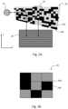
- FIG. 2 Ashows an exemplary EPE in accordance with the invention, positioned optically between an in-coupler and an out-coupler.
- FIG. 2 Bshows a detail view of a portion of the EPE of FIG. 2 A .
- FIG. 1An exemplary network is shown in FIG. 1 .
- the dotsshow the locations where the rays, generated due to diffraction from the incident ray 11 , hit the grating surface.
- the network structureallows energy transport along multiple ray paths between the points inside the network. Two example paths are shown by dashed lines from the point A to B. As all possible paths are not needed for energy transport, the operation of the EPE structure can be enhanced by allowing also empty regions (voids) to be formed inside EPE and on the peripheral boundary of EPE during numerical optimization.
- FIG. 2 Ashows an in-coupling grating 22 to which light is directed from a projector, typically essentially perpendicular to the image plane of the figure.
- Lightis diffracted and propagates in the waveguide to the EPE 24 comprising diffractive zones 24 A and non-diffractive zones (voids) 24 B.
- the non-diffractive zones 24 Bare typically simply regions without a grating pattern therein, whereas the diffractive zones comprise a grating.
- the non-diffractive zonestherefore serve as an ordinary waveguide zone, where light rays bounce via total internal reflections without diffraction.
- the diffractive zones 24 Atypically comprise a linear (one-dimensional) grating pattern.
- the orientation of grating lines and period of grating between each diffractive zones 24 Ais typically the same, while the microfeature profile, including in particular fill factor and/or height of microfeatures, may differ between the zones.
- the diffractive zones 24 Amay be unit zones, for example rectangular unit zones like shown in FIG. 2 A , or arbitrarily shaped zones without unitary grating lines therein (that is, without the inner boundaries drawn in FIGS. 2 A and 2 B ).
- the inventionis not restricted to orthogonal geometry as concerns the shapes of the diffractive zones 24 A and non-diffractive zones 24 B. They can have oblique or curved outer shapes of practically any complexity.
- the positioning of the diffractive zones and non-diffractive zonescan be determined and optimized using computational techniques known per se for diffractive optical design.
- the in-coupling grating 22 , EPE 24 and out-coupling grating 28are typically arranged on a planar waveguide element.
- the waveguidecan be a planar piece of transparent material, typically plastic or glass, having two parallel main surfaces. All gratings and diffractive zones discussed here can be fabricated for example as surface relief gratings (SRGs) or by providing additional material onto the surface as diffractive features, or other diffractive optical elements (DOEs).
- the gratingscomprise linear features made of at least one oxide or nitride material, such as TiO2, Si3N4, and HfO2, on a glass waveguide.
- each layer carrying for example a different wavelength bandembodiments of the invention can be applied separately to each layer.
- Embodiments of the inventionare usable both with broadband illumination and narrowband (including narrow multi-band) illumination and projectors.
Landscapes
- Physics & Mathematics (AREA)
- General Physics & Mathematics (AREA)
- Optics & Photonics (AREA)
- Engineering & Computer Science (AREA)
- Microelectronics & Electronic Packaging (AREA)
- Diffracting Gratings Or Hologram Optical Elements (AREA)
Abstract
Description
Claims (20)
Applications Claiming Priority (3)
| Application Number | Priority Date | Filing Date | Title |
|---|---|---|---|
| FI20185291AFI128837B (en) | 2018-03-28 | 2018-03-28 | Exit pupil expander |
| FI20185291 | 2018-03-28 | ||
| PCT/FI2019/050130WO2019185973A1 (en) | 2018-03-28 | 2019-02-19 | Exit pupil expander |
Publications (2)
| Publication Number | Publication Date |
|---|---|
| US20210072534A1 US20210072534A1 (en) | 2021-03-11 |
| US11892623B2true US11892623B2 (en) | 2024-02-06 |
Family
ID=68058587
Family Applications (1)
| Application Number | Title | Priority Date | Filing Date |
|---|---|---|---|
| US17/041,302Active2041-02-08US11892623B2 (en) | 2018-03-28 | 2019-02-19 | Exit pupil expander |
Country Status (9)
| Country | Link |
|---|---|
| US (1) | US11892623B2 (en) |
| EP (1) | EP3732528B1 (en) |
| JP (1) | JP7325427B2 (en) |
| KR (1) | KR20200135770A (en) |
| CN (1) | CN111656257B (en) |
| CA (1) | CA3087650A1 (en) |
| FI (1) | FI128837B (en) |
| SG (1) | SG11202008104WA (en) |
| WO (1) | WO2019185973A1 (en) |
Families Citing this family (33)
| Publication number | Priority date | Publication date | Assignee | Title |
|---|---|---|---|---|
| GB0718706D0 (en) | 2007-09-25 | 2007-11-07 | Creative Physics Ltd | Method and apparatus for reducing laser speckle |
| US11726332B2 (en) | 2009-04-27 | 2023-08-15 | Digilens Inc. | Diffractive projection apparatus |
| WO2012136970A1 (en) | 2011-04-07 | 2012-10-11 | Milan Momcilo Popovich | Laser despeckler based on angular diversity |
| WO2016020630A2 (en) | 2014-08-08 | 2016-02-11 | Milan Momcilo Popovich | Waveguide laser illuminator incorporating a despeckler |
| US9933684B2 (en) | 2012-11-16 | 2018-04-03 | Rockwell Collins, Inc. | Transparent waveguide display providing upper and lower fields of view having a specific light output aperture configuration |
| WO2016042283A1 (en) | 2014-09-19 | 2016-03-24 | Milan Momcilo Popovich | Method and apparatus for generating input images for holographic waveguide displays |
| WO2016113534A1 (en) | 2015-01-12 | 2016-07-21 | Milan Momcilo Popovich | Environmentally isolated waveguide display |
| US9632226B2 (en) | 2015-02-12 | 2017-04-25 | Digilens Inc. | Waveguide grating device |
| CN113759555B (en) | 2015-10-05 | 2024-09-20 | 迪吉伦斯公司 | Waveguide Display |
| CN108780224B (en) | 2016-03-24 | 2021-08-03 | 迪吉伦斯公司 | Method and apparatus for providing a polarization selective holographic waveguide device |
| WO2018102834A2 (en) | 2016-12-02 | 2018-06-07 | Digilens, Inc. | Waveguide device with uniform output illumination |
| US10545346B2 (en) | 2017-01-05 | 2020-01-28 | Digilens Inc. | Wearable heads up displays |
| EP3710876A4 (en) | 2018-01-08 | 2022-02-09 | DigiLens Inc. | SYSTEMS AND METHODS OF FABRICATING WAVEGUIDE CELLS |
| US10732569B2 (en) | 2018-01-08 | 2020-08-04 | Digilens Inc. | Systems and methods for high-throughput recording of holographic gratings in waveguide cells |
| EP3710894B1 (en) | 2018-01-08 | 2025-07-30 | Digilens Inc. | Methods for fabricating optical waveguides |
| US12147038B2 (en) | 2018-09-24 | 2024-11-19 | Apple Inc. | Optical systems with interleaved light redirectors |
| US20200225471A1 (en) | 2019-01-14 | 2020-07-16 | Digilens Inc. | Holographic Waveguide Display with Light Control Layer |
| US20200247017A1 (en) | 2019-02-05 | 2020-08-06 | Digilens Inc. | Methods for Compensating for Optical Surface Nonuniformity |
| US20220283377A1 (en) | 2019-02-15 | 2022-09-08 | Digilens Inc. | Wide Angle Waveguide Display |
| KR102866596B1 (en) | 2019-02-15 | 2025-09-29 | 디지렌즈 인코포레이티드. | Method and device for providing a holographic waveguide display using an integral grating |
| WO2020186113A1 (en) | 2019-03-12 | 2020-09-17 | Digilens Inc. | Holographic waveguide backlight and related methods of manufacturing |
| EP3980825A4 (en) | 2019-06-07 | 2023-05-03 | Digilens Inc. | WAVEGUIDES WITH TRANSMITTING AND REFLECTING GRIDS AND RELATED MANUFACTURING PROCESSES |
| KR102775783B1 (en) | 2019-08-29 | 2025-02-28 | 디지렌즈 인코포레이티드. | Vacuum grid and method for manufacturing the same |
| CN111240015B (en)* | 2020-01-17 | 2020-12-18 | 北京理工大学 | Diffractive waveguide with uniform output light on both sides |
| WO2022061584A1 (en) | 2020-09-23 | 2022-03-31 | 华为技术有限公司 | Image display method and image display apparatus |
| WO2022150841A1 (en) | 2021-01-07 | 2022-07-14 | Digilens Inc. | Grating structures for color waveguides |
| US12158612B2 (en) | 2021-03-05 | 2024-12-03 | Digilens Inc. | Evacuated periodic structures and methods of manufacturing |
| CN113960796B (en)* | 2021-10-15 | 2025-05-30 | 嘉兴驭光光电科技有限公司 | Diffractive optical waveguide, display device and diffractive optical waveguide design method |
| CN115166895B (en)* | 2022-01-13 | 2023-04-07 | 北京驭光科技发展有限公司 | Display device, diffraction light waveguide for display, and method for designing the same |
| JP2023104223A (en) | 2022-01-17 | 2023-07-28 | ソニーグループ株式会社 | Light-guiding plate and image display device |
| US20230367046A1 (en)* | 2022-05-16 | 2023-11-16 | Rovi Guides, Inc. | Transparent conductive diffractive gratings for optical elements of augmented reality and virtual reality displays |
| US12393029B2 (en) | 2022-03-23 | 2025-08-19 | Adeia Guides Inc. | Buried diffractive gratings for optical elements of augmented reality and virtual reality head-mounted displays |
| CN115236788B (en)* | 2022-06-27 | 2024-09-06 | 北京灵犀微光科技有限公司 | Optical waveguide device, near-to-eye display device and intelligent glasses |
Citations (21)
| Publication number | Priority date | Publication date | Assignee | Title |
|---|---|---|---|---|
| US20060013277A1 (en) | 2003-02-06 | 2006-01-19 | Sumitomo Electric Industries, Ltd. | Diffractive optical element and laser machining apparatus using same |
| CN101103297A (en) | 2004-12-13 | 2008-01-09 | 诺基亚公司 | A Universal Diffractive Optics Method for Extending the Exit Pupil |
| US20100214659A1 (en) | 2007-06-04 | 2010-08-26 | Tapani Levola | Diffractive beam expander and a virtual display based on a diffractive beam expander |
| US20100284085A1 (en) | 2006-09-28 | 2010-11-11 | Nokia Corporation | Beam expansion with three-dimensional diffractive elements |
| US20110176218A1 (en) | 2008-09-16 | 2011-07-21 | Louahab Noui | waveguides |
| US8160411B2 (en)* | 2006-12-28 | 2012-04-17 | Nokia Corporation | Device for expanding an exit pupil in two dimensions |
| US8717676B2 (en)* | 2006-10-31 | 2014-05-06 | Modilis Holdings Llc | Light outcoupling structure for a lighting device |
| US9335604B2 (en)* | 2013-12-11 | 2016-05-10 | Milan Momcilo Popovich | Holographic waveguide display |
| US9456744B2 (en)* | 2012-05-11 | 2016-10-04 | Digilens, Inc. | Apparatus for eye tracking |
| CN106338832A (en) | 2016-11-09 | 2017-01-18 | 苏州苏大维格光电科技股份有限公司 | Single holographic diffraction optical waveguide lens and 3D display device |
| US20170299865A1 (en) | 2016-04-13 | 2017-10-19 | Tuomas Vallius | Waveguides with improved intensity distributions |
| WO2017178781A1 (en) | 2016-04-11 | 2017-10-19 | GRANT, Alastair, John | Holographic waveguide apparatus for structured light projection |
| US20180052320A1 (en) | 2016-08-22 | 2018-02-22 | Magic Leap, Inc. | Projector architecture incorporating artifact mitigation |
| US9939647B2 (en)* | 2016-06-20 | 2018-04-10 | Microsoft Technology Licensing, Llc | Extended field of view in near-eye display using optically stitched imaging |
| US10451799B2 (en)* | 2017-01-23 | 2019-10-22 | Magic Leap, Inc. | Eyepiece for virtual, augmented, or mixed reality systems |
| US11086059B2 (en)* | 2017-06-13 | 2021-08-10 | Vuzix Corporation | Image light guide with expanded light distribution overlapping gratings |
| US11086065B2 (en)* | 2017-05-08 | 2021-08-10 | Dispelix Oy | Diffractive grating with variable diffraction efficiency and method for displaying an image |
| US20210311313A1 (en)* | 2019-05-21 | 2021-10-07 | Boe Technology Group Co., Ltd. | Optical waveguide element and control method thereof, display device and display method thereof |
| US20220004003A1 (en)* | 2020-07-02 | 2022-01-06 | Avegant Corp. | Illumination Waveguide |
| US20220214503A1 (en)* | 2021-01-07 | 2022-07-07 | Digilens Inc. | Grating Structures for Color Waveguides |
| US11415805B2 (en)* | 2019-12-30 | 2022-08-16 | Meta Platforms Technologies, Llc | Optical system and method for providing compressed eyebox |
Family Cites Families (16)
| Publication number | Priority date | Publication date | Assignee | Title |
|---|---|---|---|---|
| CA2199037A1 (en)* | 1994-09-05 | 1996-03-14 | Peter Leigh-Jones | Diffraction surfaces and methods for the manufacture thereof |
| US7160649B2 (en)* | 2002-07-11 | 2007-01-09 | Hitachi Via Mechanics, Ltd. | Gray level imaging masks, optical imaging apparatus for gray level imaging masks and methods for encoding mask and use of the masks |
| JP2007519017A (en)* | 2003-07-04 | 2007-07-12 | コーニンクレッカ フィリップス エレクトロニクス エヌ ヴィ | Optical diffraction element |
| JP4475501B2 (en)* | 2003-10-09 | 2010-06-09 | インターナショナル・ビジネス・マシーンズ・コーポレーション | Spectroscopic element, diffraction grating, composite diffraction grating, color display device, and duplexer |
| US8043797B2 (en)* | 2004-10-12 | 2011-10-25 | Asml Netherlands B.V. | Lithographic apparatus and device manufacturing method |
| JP2006343413A (en)* | 2005-06-07 | 2006-12-21 | Sony Corp | Image producing device |
| US8885112B2 (en) | 2009-10-27 | 2014-11-11 | Sbg Labs, Inc. | Compact holographic edge illuminated eyeglass display |
| US9766381B2 (en)* | 2010-03-12 | 2017-09-19 | Nokia Technologies Oy | Light-guiding structures |
| ES2862398T3 (en)* | 2011-04-18 | 2021-10-07 | Bae Systems Plc | Projection screen |
| KR101969353B1 (en) | 2012-10-18 | 2019-04-16 | 엘지전자 주식회사 | Optical device and Wearable display |
| CN104520736A (en)* | 2013-07-29 | 2015-04-15 | 松下知识产权经营株式会社 | Diffractive optical element, diffractive optical element manufacturing method, and molding die used in diffractive optical element manufacturing method |
| JP6387800B2 (en)* | 2014-11-17 | 2018-09-12 | セイコーエプソン株式会社 | Beam diameter expanding element and display device |
| CN104570353A (en)* | 2015-01-08 | 2015-04-29 | 浙江大学 | Color visual display method, optical system and wearable device using holographic waveguide |
| IL310369A (en)* | 2015-01-26 | 2024-03-01 | Magic Leap Inc | Virtual and augmented reality systems and methods with improved diffractive lattice structures |
| US10379358B2 (en)* | 2015-04-08 | 2019-08-13 | Despelix Oy | Optical see-through display element and device utilizing such element |
| EP3205512B1 (en)* | 2016-02-09 | 2018-06-13 | CSEM Centre Suisse d'Electronique et de Microtechnique SA - Recherche et Développement | Optical security device |
- 2018
- 2018-03-28FIFI20185291Apatent/FI128837B/enactiveIP Right Grant
- 2019
- 2019-02-19CNCN201980010104.1Apatent/CN111656257B/enactiveActive
- 2019-02-19USUS17/041,302patent/US11892623B2/enactiveActive
- 2019-02-19WOPCT/FI2019/050130patent/WO2019185973A1/ennot_activeCeased
- 2019-02-19JPJP2020543542Apatent/JP7325427B2/enactiveActive
- 2019-02-19KRKR1020207023668Apatent/KR20200135770A/ennot_activeCeased
- 2019-02-19EPEP19778258.4Apatent/EP3732528B1/enactiveActive
- 2019-02-19CACA3087650Apatent/CA3087650A1/enactivePending
- 2019-02-19SGSG11202008104WApatent/SG11202008104WA/enunknown
Patent Citations (27)
| Publication number | Priority date | Publication date | Assignee | Title |
|---|---|---|---|---|
| US20060013277A1 (en) | 2003-02-06 | 2006-01-19 | Sumitomo Electric Industries, Ltd. | Diffractive optical element and laser machining apparatus using same |
| CN101103297A (en) | 2004-12-13 | 2008-01-09 | 诺基亚公司 | A Universal Diffractive Optics Method for Extending the Exit Pupil |
| US7764413B2 (en) | 2004-12-13 | 2010-07-27 | Nokia Corporation | General diffractive optics method for expanding an exit pupil |
| US20100284085A1 (en) | 2006-09-28 | 2010-11-11 | Nokia Corporation | Beam expansion with three-dimensional diffractive elements |
| US8593734B2 (en)* | 2006-09-28 | 2013-11-26 | Nokia Corporation | Beam expansion with three-dimensional diffractive elements |
| US8717676B2 (en)* | 2006-10-31 | 2014-05-06 | Modilis Holdings Llc | Light outcoupling structure for a lighting device |
| US8160411B2 (en)* | 2006-12-28 | 2012-04-17 | Nokia Corporation | Device for expanding an exit pupil in two dimensions |
| US20100214659A1 (en) | 2007-06-04 | 2010-08-26 | Tapani Levola | Diffractive beam expander and a virtual display based on a diffractive beam expander |
| US8320032B2 (en)* | 2007-06-04 | 2012-11-27 | Nokia Corporation | Diffractive beam expander and a virtual display based on a diffractive beam expander |
| US20110176218A1 (en) | 2008-09-16 | 2011-07-21 | Louahab Noui | waveguides |
| US8493662B2 (en)* | 2008-09-16 | 2013-07-23 | Bae Systems Plc | Waveguides |
| US9456744B2 (en)* | 2012-05-11 | 2016-10-04 | Digilens, Inc. | Apparatus for eye tracking |
| US9335604B2 (en)* | 2013-12-11 | 2016-05-10 | Milan Momcilo Popovich | Holographic waveguide display |
| WO2017178781A1 (en) | 2016-04-11 | 2017-10-19 | GRANT, Alastair, John | Holographic waveguide apparatus for structured light projection |
| US20170299865A1 (en) | 2016-04-13 | 2017-10-19 | Tuomas Vallius | Waveguides with improved intensity distributions |
| US9939647B2 (en)* | 2016-06-20 | 2018-04-10 | Microsoft Technology Licensing, Llc | Extended field of view in near-eye display using optically stitched imaging |
| US20180052320A1 (en) | 2016-08-22 | 2018-02-22 | Magic Leap, Inc. | Projector architecture incorporating artifact mitigation |
| US20180052501A1 (en)* | 2016-08-22 | 2018-02-22 | Magic Leap, Inc. | Thermal dissipation for wearable device |
| US10267970B2 (en)* | 2016-08-22 | 2019-04-23 | Magic Leap, Inc. | Thermal dissipation for wearable device |
| CN106338832A (en) | 2016-11-09 | 2017-01-18 | 苏州苏大维格光电科技股份有限公司 | Single holographic diffraction optical waveguide lens and 3D display device |
| US10451799B2 (en)* | 2017-01-23 | 2019-10-22 | Magic Leap, Inc. | Eyepiece for virtual, augmented, or mixed reality systems |
| US11086065B2 (en)* | 2017-05-08 | 2021-08-10 | Dispelix Oy | Diffractive grating with variable diffraction efficiency and method for displaying an image |
| US11086059B2 (en)* | 2017-06-13 | 2021-08-10 | Vuzix Corporation | Image light guide with expanded light distribution overlapping gratings |
| US20210311313A1 (en)* | 2019-05-21 | 2021-10-07 | Boe Technology Group Co., Ltd. | Optical waveguide element and control method thereof, display device and display method thereof |
| US11415805B2 (en)* | 2019-12-30 | 2022-08-16 | Meta Platforms Technologies, Llc | Optical system and method for providing compressed eyebox |
| US20220004003A1 (en)* | 2020-07-02 | 2022-01-06 | Avegant Corp. | Illumination Waveguide |
| US20220214503A1 (en)* | 2021-01-07 | 2022-07-07 | Digilens Inc. | Grating Structures for Color Waveguides |
Non-Patent Citations (2)
| Title |
|---|
| Chinese Office Action dated Aug. 26, 2021 as received in application No. 201980010104.1. |
| Finnish Office Action dated Oct. 8, 2018 as received in application No. 20185291. |
Also Published As
| Publication number | Publication date |
|---|---|
| EP3732528B1 (en) | 2025-01-01 |
| SG11202008104WA (en) | 2020-09-29 |
| FI128837B (en) | 2021-01-15 |
| JP2021517265A (en) | 2021-07-15 |
| CN111656257A (en) | 2020-09-11 |
| WO2019185973A1 (en) | 2019-10-03 |
| EP3732528C0 (en) | 2025-01-01 |
| FI20185291A1 (en) | 2019-09-29 |
| EP3732528A1 (en) | 2020-11-04 |
| KR20200135770A (en) | 2020-12-03 |
| CN111656257B (en) | 2022-04-12 |
| CA3087650A1 (en) | 2019-10-03 |
| US20210072534A1 (en) | 2021-03-11 |
| EP3732528A4 (en) | 2021-09-22 |
| JP7325427B2 (en) | 2023-08-14 |
Similar Documents
| Publication | Publication Date | Title |
|---|---|---|
| US11892623B2 (en) | Exit pupil expander | |
| US11650427B2 (en) | Diffractive display element with grating mirror | |
| US9791703B1 (en) | Waveguides with extended field of view | |
| US10353202B2 (en) | Wrapped waveguide with large field of view | |
| US11846777B2 (en) | Interference-free waveguide display | |
| US20200142109A1 (en) | Display element, personal display device, method of producing an image on a personal display and use | |
| US12130443B2 (en) | Waveguide for transmitting light | |
| US20220099990A1 (en) | Grating arrangements | |
| EP3551931B1 (en) | Waveguides with peripheral side geometries to recycle light | |
| KR102743739B1 (en) | Waveguide display device having a reflector surface | |
| US12019236B2 (en) | Diffractive exit pupil expander arrangement for display applications | |
| FI129439B (en) | Diffractive display element with grating mirror |
Legal Events
| Date | Code | Title | Description |
|---|---|---|---|
| AS | Assignment | Owner name:DISPELIX OY, FINLAND Free format text:ASSIGNMENT OF ASSIGNORS INTEREST;ASSIGNORS:OLKKONEN, JUUSO;MYOEHAENEN, PETRI;SIGNING DATES FROM 20200721 TO 20200726;REEL/FRAME:053879/0325 | |
| FEPP | Fee payment procedure | Free format text:ENTITY STATUS SET TO UNDISCOUNTED (ORIGINAL EVENT CODE: BIG.); ENTITY STATUS OF PATENT OWNER: LARGE ENTITY | |
| STPP | Information on status: patent application and granting procedure in general | Free format text:APPLICATION DISPATCHED FROM PREEXAM, NOT YET DOCKETED | |
| STPP | Information on status: patent application and granting procedure in general | Free format text:DOCKETED NEW CASE - READY FOR EXAMINATION | |
| STPP | Information on status: patent application and granting procedure in general | Free format text:NON FINAL ACTION COUNTED, NOT YET MAILED | |
| STPP | Information on status: patent application and granting procedure in general | Free format text:NON FINAL ACTION MAILED | |
| STPP | Information on status: patent application and granting procedure in general | Free format text:RESPONSE TO NON-FINAL OFFICE ACTION ENTERED AND FORWARDED TO EXAMINER | |
| STPP | Information on status: patent application and granting procedure in general | Free format text:NOTICE OF ALLOWANCE MAILED -- APPLICATION RECEIVED IN OFFICE OF PUBLICATIONS | |
| STPP | Information on status: patent application and granting procedure in general | Free format text:PUBLICATIONS -- ISSUE FEE PAYMENT RECEIVED | |
| STPP | Information on status: patent application and granting procedure in general | Free format text:PUBLICATIONS -- ISSUE FEE PAYMENT VERIFIED | |
| STCF | Information on status: patent grant | Free format text:PATENTED CASE |