US11891327B2 - Fabrication of low defectivity electrochromic devices - Google Patents
Fabrication of low defectivity electrochromic devicesDownload PDFInfo
- Publication number
- US11891327B2 US11891327B2US17/816,364US202217816364AUS11891327B2US 11891327 B2US11891327 B2US 11891327B2US 202217816364 AUS202217816364 AUS 202217816364AUS 11891327 B2US11891327 B2US 11891327B2
- Authority
- US
- United States
- Prior art keywords
- oxide
- layer
- electrochromic
- nickel
- electrochromic device
- Prior art date
- Legal status (The legal status is an assumption and is not a legal conclusion. Google has not performed a legal analysis and makes no representation as to the accuracy of the status listed.)
- Active
Links
Images


Classifications
- C—CHEMISTRY; METALLURGY
- C03—GLASS; MINERAL OR SLAG WOOL
- C03C—CHEMICAL COMPOSITION OF GLASSES, GLAZES OR VITREOUS ENAMELS; SURFACE TREATMENT OF GLASS; SURFACE TREATMENT OF FIBRES OR FILAMENTS MADE FROM GLASS, MINERALS OR SLAGS; JOINING GLASS TO GLASS OR OTHER MATERIALS
- C03C17/00—Surface treatment of glass, not in the form of fibres or filaments, by coating
- C03C17/34—Surface treatment of glass, not in the form of fibres or filaments, by coating with at least two coatings having different compositions
- C03C17/3411—Surface treatment of glass, not in the form of fibres or filaments, by coating with at least two coatings having different compositions with at least two coatings of inorganic materials
- C03C17/3417—Surface treatment of glass, not in the form of fibres or filaments, by coating with at least two coatings having different compositions with at least two coatings of inorganic materials all coatings being oxide coatings
- C—CHEMISTRY; METALLURGY
- C23—COATING METALLIC MATERIAL; COATING MATERIAL WITH METALLIC MATERIAL; CHEMICAL SURFACE TREATMENT; DIFFUSION TREATMENT OF METALLIC MATERIAL; COATING BY VACUUM EVAPORATION, BY SPUTTERING, BY ION IMPLANTATION OR BY CHEMICAL VAPOUR DEPOSITION, IN GENERAL; INHIBITING CORROSION OF METALLIC MATERIAL OR INCRUSTATION IN GENERAL
- C23C—COATING METALLIC MATERIAL; COATING MATERIAL WITH METALLIC MATERIAL; SURFACE TREATMENT OF METALLIC MATERIAL BY DIFFUSION INTO THE SURFACE, BY CHEMICAL CONVERSION OR SUBSTITUTION; COATING BY VACUUM EVAPORATION, BY SPUTTERING, BY ION IMPLANTATION OR BY CHEMICAL VAPOUR DEPOSITION, IN GENERAL
- C23C10/00—Solid state diffusion of only metal elements or silicon into metallic material surfaces
- C23C10/28—Solid state diffusion of only metal elements or silicon into metallic material surfaces using solids, e.g. powders, pastes
- C—CHEMISTRY; METALLURGY
- C23—COATING METALLIC MATERIAL; COATING MATERIAL WITH METALLIC MATERIAL; CHEMICAL SURFACE TREATMENT; DIFFUSION TREATMENT OF METALLIC MATERIAL; COATING BY VACUUM EVAPORATION, BY SPUTTERING, BY ION IMPLANTATION OR BY CHEMICAL VAPOUR DEPOSITION, IN GENERAL; INHIBITING CORROSION OF METALLIC MATERIAL OR INCRUSTATION IN GENERAL
- C23C—COATING METALLIC MATERIAL; COATING MATERIAL WITH METALLIC MATERIAL; SURFACE TREATMENT OF METALLIC MATERIAL BY DIFFUSION INTO THE SURFACE, BY CHEMICAL CONVERSION OR SUBSTITUTION; COATING BY VACUUM EVAPORATION, BY SPUTTERING, BY ION IMPLANTATION OR BY CHEMICAL VAPOUR DEPOSITION, IN GENERAL
- C23C14/00—Coating by vacuum evaporation, by sputtering or by ion implantation of the coating forming material
- C23C14/0021—Reactive sputtering or evaporation
- C—CHEMISTRY; METALLURGY
- C23—COATING METALLIC MATERIAL; COATING MATERIAL WITH METALLIC MATERIAL; CHEMICAL SURFACE TREATMENT; DIFFUSION TREATMENT OF METALLIC MATERIAL; COATING BY VACUUM EVAPORATION, BY SPUTTERING, BY ION IMPLANTATION OR BY CHEMICAL VAPOUR DEPOSITION, IN GENERAL; INHIBITING CORROSION OF METALLIC MATERIAL OR INCRUSTATION IN GENERAL
- C23C—COATING METALLIC MATERIAL; COATING MATERIAL WITH METALLIC MATERIAL; SURFACE TREATMENT OF METALLIC MATERIAL BY DIFFUSION INTO THE SURFACE, BY CHEMICAL CONVERSION OR SUBSTITUTION; COATING BY VACUUM EVAPORATION, BY SPUTTERING, BY ION IMPLANTATION OR BY CHEMICAL VAPOUR DEPOSITION, IN GENERAL
- C23C14/00—Coating by vacuum evaporation, by sputtering or by ion implantation of the coating forming material
- C23C14/06—Coating by vacuum evaporation, by sputtering or by ion implantation of the coating forming material characterised by the coating material
- C23C14/08—Oxides
- C23C14/083—Oxides of refractory metals or yttrium
- C—CHEMISTRY; METALLURGY
- C23—COATING METALLIC MATERIAL; COATING MATERIAL WITH METALLIC MATERIAL; CHEMICAL SURFACE TREATMENT; DIFFUSION TREATMENT OF METALLIC MATERIAL; COATING BY VACUUM EVAPORATION, BY SPUTTERING, BY ION IMPLANTATION OR BY CHEMICAL VAPOUR DEPOSITION, IN GENERAL; INHIBITING CORROSION OF METALLIC MATERIAL OR INCRUSTATION IN GENERAL
- C23C—COATING METALLIC MATERIAL; COATING MATERIAL WITH METALLIC MATERIAL; SURFACE TREATMENT OF METALLIC MATERIAL BY DIFFUSION INTO THE SURFACE, BY CHEMICAL CONVERSION OR SUBSTITUTION; COATING BY VACUUM EVAPORATION, BY SPUTTERING, BY ION IMPLANTATION OR BY CHEMICAL VAPOUR DEPOSITION, IN GENERAL
- C23C14/00—Coating by vacuum evaporation, by sputtering or by ion implantation of the coating forming material
- C23C14/06—Coating by vacuum evaporation, by sputtering or by ion implantation of the coating forming material characterised by the coating material
- C23C14/14—Metallic material, boron or silicon
- C23C14/18—Metallic material, boron or silicon on other inorganic substrates
- C23C14/185—Metallic material, boron or silicon on other inorganic substrates by cathodic sputtering
- C—CHEMISTRY; METALLURGY
- C23—COATING METALLIC MATERIAL; COATING MATERIAL WITH METALLIC MATERIAL; CHEMICAL SURFACE TREATMENT; DIFFUSION TREATMENT OF METALLIC MATERIAL; COATING BY VACUUM EVAPORATION, BY SPUTTERING, BY ION IMPLANTATION OR BY CHEMICAL VAPOUR DEPOSITION, IN GENERAL; INHIBITING CORROSION OF METALLIC MATERIAL OR INCRUSTATION IN GENERAL
- C23C—COATING METALLIC MATERIAL; COATING MATERIAL WITH METALLIC MATERIAL; SURFACE TREATMENT OF METALLIC MATERIAL BY DIFFUSION INTO THE SURFACE, BY CHEMICAL CONVERSION OR SUBSTITUTION; COATING BY VACUUM EVAPORATION, BY SPUTTERING, BY ION IMPLANTATION OR BY CHEMICAL VAPOUR DEPOSITION, IN GENERAL
- C23C14/00—Coating by vacuum evaporation, by sputtering or by ion implantation of the coating forming material
- C23C14/22—Coating by vacuum evaporation, by sputtering or by ion implantation of the coating forming material characterised by the process of coating
- C23C14/34—Sputtering
- C23C14/3407—Cathode assembly for sputtering apparatus, e.g. Target
- C23C14/3414—Metallurgical or chemical aspects of target preparation, e.g. casting, powder metallurgy
- C—CHEMISTRY; METALLURGY
- C23—COATING METALLIC MATERIAL; COATING MATERIAL WITH METALLIC MATERIAL; CHEMICAL SURFACE TREATMENT; DIFFUSION TREATMENT OF METALLIC MATERIAL; COATING BY VACUUM EVAPORATION, BY SPUTTERING, BY ION IMPLANTATION OR BY CHEMICAL VAPOUR DEPOSITION, IN GENERAL; INHIBITING CORROSION OF METALLIC MATERIAL OR INCRUSTATION IN GENERAL
- C23C—COATING METALLIC MATERIAL; COATING MATERIAL WITH METALLIC MATERIAL; SURFACE TREATMENT OF METALLIC MATERIAL BY DIFFUSION INTO THE SURFACE, BY CHEMICAL CONVERSION OR SUBSTITUTION; COATING BY VACUUM EVAPORATION, BY SPUTTERING, BY ION IMPLANTATION OR BY CHEMICAL VAPOUR DEPOSITION, IN GENERAL
- C23C14/00—Coating by vacuum evaporation, by sputtering or by ion implantation of the coating forming material
- C23C14/22—Coating by vacuum evaporation, by sputtering or by ion implantation of the coating forming material characterised by the process of coating
- C23C14/34—Sputtering
- C23C14/3464—Sputtering using more than one target
- C—CHEMISTRY; METALLURGY
- C23—COATING METALLIC MATERIAL; COATING MATERIAL WITH METALLIC MATERIAL; CHEMICAL SURFACE TREATMENT; DIFFUSION TREATMENT OF METALLIC MATERIAL; COATING BY VACUUM EVAPORATION, BY SPUTTERING, BY ION IMPLANTATION OR BY CHEMICAL VAPOUR DEPOSITION, IN GENERAL; INHIBITING CORROSION OF METALLIC MATERIAL OR INCRUSTATION IN GENERAL
- C23C—COATING METALLIC MATERIAL; COATING MATERIAL WITH METALLIC MATERIAL; SURFACE TREATMENT OF METALLIC MATERIAL BY DIFFUSION INTO THE SURFACE, BY CHEMICAL CONVERSION OR SUBSTITUTION; COATING BY VACUUM EVAPORATION, BY SPUTTERING, BY ION IMPLANTATION OR BY CHEMICAL VAPOUR DEPOSITION, IN GENERAL
- C23C14/00—Coating by vacuum evaporation, by sputtering or by ion implantation of the coating forming material
- C23C14/22—Coating by vacuum evaporation, by sputtering or by ion implantation of the coating forming material characterised by the process of coating
- C23C14/56—Apparatus specially adapted for continuous coating; Arrangements for maintaining the vacuum, e.g. vacuum locks
- C23C14/568—Transferring the substrates through a series of coating stations
- C—CHEMISTRY; METALLURGY
- C23—COATING METALLIC MATERIAL; COATING MATERIAL WITH METALLIC MATERIAL; CHEMICAL SURFACE TREATMENT; DIFFUSION TREATMENT OF METALLIC MATERIAL; COATING BY VACUUM EVAPORATION, BY SPUTTERING, BY ION IMPLANTATION OR BY CHEMICAL VAPOUR DEPOSITION, IN GENERAL; INHIBITING CORROSION OF METALLIC MATERIAL OR INCRUSTATION IN GENERAL
- C23C—COATING METALLIC MATERIAL; COATING MATERIAL WITH METALLIC MATERIAL; SURFACE TREATMENT OF METALLIC MATERIAL BY DIFFUSION INTO THE SURFACE, BY CHEMICAL CONVERSION OR SUBSTITUTION; COATING BY VACUUM EVAPORATION, BY SPUTTERING, BY ION IMPLANTATION OR BY CHEMICAL VAPOUR DEPOSITION, IN GENERAL
- C23C14/00—Coating by vacuum evaporation, by sputtering or by ion implantation of the coating forming material
- C23C14/58—After-treatment
- C23C14/5806—Thermal treatment
- C—CHEMISTRY; METALLURGY
- C23—COATING METALLIC MATERIAL; COATING MATERIAL WITH METALLIC MATERIAL; CHEMICAL SURFACE TREATMENT; DIFFUSION TREATMENT OF METALLIC MATERIAL; COATING BY VACUUM EVAPORATION, BY SPUTTERING, BY ION IMPLANTATION OR BY CHEMICAL VAPOUR DEPOSITION, IN GENERAL; INHIBITING CORROSION OF METALLIC MATERIAL OR INCRUSTATION IN GENERAL
- C23C—COATING METALLIC MATERIAL; COATING MATERIAL WITH METALLIC MATERIAL; SURFACE TREATMENT OF METALLIC MATERIAL BY DIFFUSION INTO THE SURFACE, BY CHEMICAL CONVERSION OR SUBSTITUTION; COATING BY VACUUM EVAPORATION, BY SPUTTERING, BY ION IMPLANTATION OR BY CHEMICAL VAPOUR DEPOSITION, IN GENERAL
- C23C14/00—Coating by vacuum evaporation, by sputtering or by ion implantation of the coating forming material
- C23C14/58—After-treatment
- C23C14/5846—Reactive treatment
- C23C14/5853—Oxidation
- G—PHYSICS
- G02—OPTICS
- G02F—OPTICAL DEVICES OR ARRANGEMENTS FOR THE CONTROL OF LIGHT BY MODIFICATION OF THE OPTICAL PROPERTIES OF THE MEDIA OF THE ELEMENTS INVOLVED THEREIN; NON-LINEAR OPTICS; FREQUENCY-CHANGING OF LIGHT; OPTICAL LOGIC ELEMENTS; OPTICAL ANALOGUE/DIGITAL CONVERTERS
- G02F1/00—Devices or arrangements for the control of the intensity, colour, phase, polarisation or direction of light arriving from an independent light source, e.g. switching, gating or modulating; Non-linear optics
- G02F1/01—Devices or arrangements for the control of the intensity, colour, phase, polarisation or direction of light arriving from an independent light source, e.g. switching, gating or modulating; Non-linear optics for the control of the intensity, phase, polarisation or colour
- G02F1/15—Devices or arrangements for the control of the intensity, colour, phase, polarisation or direction of light arriving from an independent light source, e.g. switching, gating or modulating; Non-linear optics for the control of the intensity, phase, polarisation or colour based on an electrochromic effect
- G02F1/1514—Devices or arrangements for the control of the intensity, colour, phase, polarisation or direction of light arriving from an independent light source, e.g. switching, gating or modulating; Non-linear optics for the control of the intensity, phase, polarisation or colour based on an electrochromic effect characterised by the electrochromic material, e.g. by the electrodeposited material
- G02F1/1523—Devices or arrangements for the control of the intensity, colour, phase, polarisation or direction of light arriving from an independent light source, e.g. switching, gating or modulating; Non-linear optics for the control of the intensity, phase, polarisation or colour based on an electrochromic effect characterised by the electrochromic material, e.g. by the electrodeposited material comprising inorganic material
- G02F1/1524—Transition metal compounds
- C—CHEMISTRY; METALLURGY
- C03—GLASS; MINERAL OR SLAG WOOL
- C03C—CHEMICAL COMPOSITION OF GLASSES, GLAZES OR VITREOUS ENAMELS; SURFACE TREATMENT OF GLASS; SURFACE TREATMENT OF FIBRES OR FILAMENTS MADE FROM GLASS, MINERALS OR SLAGS; JOINING GLASS TO GLASS OR OTHER MATERIALS
- C03C2217/00—Coatings on glass
- C03C2217/90—Other aspects of coatings
- C03C2217/94—Transparent conductive oxide layers [TCO] being part of a multilayer coating
- C—CHEMISTRY; METALLURGY
- C03—GLASS; MINERAL OR SLAG WOOL
- C03C—CHEMICAL COMPOSITION OF GLASSES, GLAZES OR VITREOUS ENAMELS; SURFACE TREATMENT OF GLASS; SURFACE TREATMENT OF FIBRES OR FILAMENTS MADE FROM GLASS, MINERALS OR SLAGS; JOINING GLASS TO GLASS OR OTHER MATERIALS
- C03C2218/00—Methods for coating glass
- C03C2218/30—Aspects of methods for coating glass not covered above
- C03C2218/32—After-treatment
- C03C2218/328—Partly or completely removing a coating
Definitions
- Electrochromismis a phenomenon in which a material exhibits a reversible electrochemically-mediated change in an optical property when placed in a different electronic state, typically by being subjected to a voltage change.
- the optical propertyis typically one or more of color, transmittance, absorbance, and reflectance.
- One well known electrochromic materialfor example, is tungsten oxide (WO 3 ).
- Tungsten oxideis a cathodic electrochromic material in which a coloration transition, transparent to blue, occurs by electrochemical reduction.
- Electrochromic materialsmay be incorporated into, for example, windows and mirrors.
- the color, transmittance, absorbance, and/or reflectance of such windows and mirrorsmay be changed by inducing a change in the electrochromic material.
- One well known application of electrochromic materialsis the rear view mirror in some cars. In these electrochromic rear view mirrors, the reflectivity of the mirror changes at night so that the headlights of other vehicles are not distracting to the driver.
- a counter electrode materialincludes a novel composition of materials.
- the counter electrode materialmay include an anodically coloring electrochromic material and one or more additives.
- the anodically coloring electrochromic materialmay include a metal selected from the group consisting of chromium (Cr), manganese (Mn), iron (Fe), cobalt (Co), nickel (Ni), rhodium (Rh), ruthenium (Ru), vanadium (V), iridium (Ir), and combinations thereof.
- the additivemay be selected from the group consisting of silver (Ag), arsenic (As), gold (Au), boron (B), cadmium (Cd), cesium (Cs), copper (Cu), europium (Eu), gallium (Ga), gadolinium (Gd), germanium (Ge), mercury (Hg), osmium (Os), lead (Pb), palladium (Pd), promethium (Pm), polonium (Po), platinum (Pt), radium (Ra), rubidium (Rb), terbium (Tb), technetium (Tc), thorium (Th), thallium (Tl), and combinations thereof. Other combinations of materials are possible as described further herein.
- FIG. 1is a schematic cross-section of an electrochromic device in accordance with embodiments of the invention.
- FIG. 2is a schematic cross-section of an electrochromic device in a bleached state in accordance with specific embodiments of the invention.
- FIG. 3is a schematic cross-section of an electrochromic device in a colored state in accordance with specific embodiments of the invention.
- FIG. 4is a schematic cross-section of an electrochromic device with a particle in the ion conducting layer causing a localized defect in the device.
- FIG. 5 Ais a schematic cross-section of an electrochromic device with a particle on the conductive layer prior to depositing the remainder of the electrochromic stack.
- FIG. 5 Bis a schematic cross-section of the electrochromic device of FIG. 5 A , where a “pop off” defect is formed during electrochromic stack formation.
- FIG. 5 Cis a schematic cross-section of the electrochromic device of FIG. 5 B , showing an electrical short that is formed from the pop off defect once the second conductive is deposited.
- FIG. 6 Adepicts a cross-sectional representation of an electrochromic window device in accord with the multistep process description provided in relation to FIG. 7 A .
- FIG. 6 Bdepicts a top view of an electrochromic device showing location of trenches cut into the device.
- FIG. 7 Adepicts a process flow describing a method of fabricating an electrochromic window.
- FIGS. 7 B- 7 Ddepict methods of fabricating an electrochromic stack which is part of an electrochromic device of the invention.
- FIG. 7 Edepicts a process flow for a conditioning process used to fabricate an electrochromic device of the invention.
- FIG. 8 Adepicts an integrated deposition system of the invention.
- FIG. 8 Bdepicts an integrated deposition system in a perspective view.
- FIG. 8 Cdepicts a modular integrated deposition system.
- FIG. 8 Ddepicts an integrated deposition system with two lithium deposition stations.
- FIG. 8 Edepicts an integrated deposition system with one lithium deposition station.
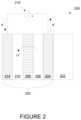
- FIG. 1A schematic cross-section of an electrochromic device 100 in accordance with some embodiments is shown in FIG. 1 .
- the electrochromic deviceincludes a substrate 102 , a conductive layer (CL) 104 , an electrochromic layer (EC) 106 (sometimes also referred to as a cathodically coloring layer), an ion conducting layer (IC) 108 , a counter electrode layer (CE) 110 (sometimes also referred to as an anodically coloring layer), and a conductive layer (CL) 114 .
- Elements 104 , 106 , 108 , 110 , and 114are collectively referred to as an electrochromic stack 120 .
- a voltage source 116 operable to apply an electric potential across the electrochromic stack 120effects the transition of the electrochromic device from, e.g., a bleached state to a colored state.
- the order of layersis reversed with respect to the substrate. That is, the layers are in the following order: substrate, conductive layer, counter electrode layer, ion conducting layer, electrochromic material layer, conductive layer.
- a transition between a bleached state and colored stateis non-limiting and suggests only one example, among many, of an electrochromic transition that may be implemented. Unless otherwise specified herein, whenever reference is made to a bleached-colored transition, the corresponding device or process encompasses other optical state transitions such non-reflective-reflective, transparent-opaque, etc. Further the term “bleached” refers to an optically neutral state, e.g., uncolored, transparent or translucent. Still further, unless specified otherwise herein, the “color” of an electrochromic transition is not limited to any particular wavelength or range of wavelengths. As understood by those of skill in the art, the choice of appropriate electrochromic and counter electrode materials governs the relevant optical transition.
- the electrochromic devicereversibly cycles between a bleached state and a colored state.
- a potentialis applied to the electrochromic stack 120 such that available ions in the stack that can cause the electrochromic material 106 to be in the colored state reside primarily in the counter electrode 110 .
- the potential on the electrochromic stackis reversed, the ions are transported across the ion conducting layer 108 to the electrochromic material 106 and cause the material to enter the colored state.
- FIGS. 2 and 3A more detailed description of the transition from bleached to colored state, and from colored to bleached state, is included below in the description of FIGS. 2 and 3 , but first the individual layers of stack 120 will be described in more detail in relation to FIG. 1 .
- all of the materials making up electrochromic stack 120are inorganic, solid (i.e., in the solid state), or both inorganic and solid. Because organic materials tend to degrade over time, inorganic materials offer the advantage of a reliable electrochromic stack that can function for extended periods of time. Materials in the solid state also offer the advantage of not having containment and leakage issues, as materials in the liquid state often do.
- Each of the layers in the electrochromic deviceis discussed in detail, below. It should be understood that any one or more of the layers in the stack may contain some amount of organic material, but in many implementations one or more of the layers contains little or no organic matter. The same can be said for liquids that may be present in one or more layers in small amounts. It should also be understood that solid state material may be deposited or otherwise formed by processes employing liquid components such as certain processes employing sol-gels or chemical vapor deposition.
- voltage source 116is typically a low voltage electrical source and may be configured to operate in conjunction with radiant and other environmental sensors. Voltage source 116 may also be configured to interface with an energy management system, such as a computer system that controls the electrochromic device according to factors such as the time of year, time of day, and measured environmental conditions. Such an energy management system, in conjunction with large area electrochromic devices (i.e., an electrochromic window), can dramatically lower the energy consumption of a building.
- an energy management systemin conjunction with large area electrochromic devices (i.e., an electrochromic window) can dramatically lower the energy consumption of a building.
- any material having suitable optical, electrical, thermal, and mechanical propertiesmay be used as substrate 102 .
- substratesinclude, for example, glass, plastic, and mirror materials.
- Suitable plastic substratesinclude, for example acrylic, polystyrene, polycarbonate, allyl diglycol carbonate, SAN (styrene acrylonitrile copolymer), poly(4-methyl-1-pentene), polyester, polyamide, etc.
- a plastic substrateis used, it is preferably barrier protected and abrasion protected using a hard coat of, for example, a diamond-like protection coating, a silica/silicone anti-abrasion coating, or the like, such as is well known in the plastic glazing art.
- Suitable glassesinclude either clear or tinted soda lime glass, including soda lime float glass.
- the glassmay be tempered or untempered.
- the optical transmittance (i.e., the ratio of transmitted radiation or spectrum to incident radiation or spectrum) of substrate 102is about 40 to 95%, e.g., about 90-92%.
- the substratemay be of any thickness, as long as it has suitable mechanical properties to support the electrochromic stack 120 . While the substrate 102 may be of any size, in some embodiments, it is about 0.01 mm to 10 mm thick, preferably about 3 mm to 9 mm thick.
- the substrateis architectural glass.
- Architectural glassis glass that is used as a building material.
- Architectural glassis typically used in commercial buildings, but may also be used in residential buildings, and typically, though not necessarily, separates an indoor environment from an outdoor environment.
- architectural glassis at least 20 inches by 20 inches, and can be much larger, e.g., as large as about 72 inches by 120 inches.
- Architectural glassis typically at least about 2 mm thick.
- Architectural glass that is less than about 3.2 mm thickcannot be tempered.
- the substratemay still be tempered even after the electrochromic stack has been fabricated on the substrate.
- the substrateis a soda lime glass from a tin float line.
- the percent transmission over the visible spectrum of an architectural glass substrateis generally greater than 80% for neutral substrates, but it could be lower for colored substrates.
- the percent transmission of the substrate over the visible spectrumis at least about 90% (e.g., about 90-92%).
- the visible spectrumis the spectrum that a typical human eye will respond to, generally about 380 nm (purple) to about 780 nm (red).
- the glasshas a surface roughness of between about 10 and 30 nm.
- conductive layer 104On top of substrate 102 is conductive layer 104 .
- one or both of the conductive layers 104 and 114is inorganic and/or solid.
- Conductive layers 104 and 114may be made from a number of different materials, including conductive oxides, thin metallic coatings, conductive metal nitrides, and composite conductors.
- conductive layers 104 and 114are transparent at least in the range of wavelengths where electrochromism is exhibited by the electrochromic layer.
- Transparent conductive oxidesinclude metal oxides and metal oxides doped with one or more metals.
- metal oxides and doped metal oxidesexamples include indium oxide, indium tin oxide, doped indium oxide, tin oxide, doped tin oxide, zinc oxide, aluminum zinc oxide, doped zinc oxide, ruthenium oxide, doped ruthenium oxide and the like. Since oxides are often used for these layers, they are sometimes referred to as “transparent conductive oxide” (TCO) layers. Thin metallic coatings that are substantially transparent may also be used. Examples of metals used for such thin metallic coatings include transition metals including gold, platinum, silver, aluminum, nickel alloy, and the like. Thin metallic coatings based on silver, well known in the glazing industry, are also used.
- conductive nitridesexamples include titanium nitrides, tantalum nitrides, titanium oxynitrides, and tantalum oxynitrides.
- the conductive layers 104 and 114may also be composite conductors. Such composite conductors may be fabricated by placing highly conductive ceramic and metal wires or conductive layer patterns on one of the faces of the substrate and then over-coating with transparent conductive materials such as doped tin oxides or indium tin oxide. Ideally, such wires should be thin enough as to be invisible to the naked eye (e.g., about 100 ⁇ m or thinner).
- commercially available substratessuch as glass substrates contain a transparent conductive layer coating.
- Such productsmay be used for both substrate 102 and conductive layer 104 .
- Examples of such glassesinclude conductive layer coated glasses sold under the trademark TEC GlassTM by Pilkington, of Toledo, Ohio and SUNGATETM 300 and SUNGATETM 500 by PPG Industries of Pittsburgh, Pennsylvania TEC GlassTM is a glass coated with a fluorinated tin oxide conductive layer.
- the same conductive layeris used for both conductive layers (i.e., conductive layers 104 and 114 ).
- different conductive materialsare used for each conductive layer 104 and 114 .
- TEC GlassTMis used for substrate 102 (float glass) and conductive layer 104 (fluorinated tin oxide) and indium tin oxide is used for conductive layer 114 .
- TEC GlassTMthere is a sodium diffusion barrier between the glass substrate 102 and TEC conductive layer 104 .
- the composition of a conductive layershould be chosen or tailored based on the composition of an adjacent layer (e.g., electrochromic layer 106 or counter electrode layer 110 ) in contact with the conductive layer.
- an adjacent layere.g., electrochromic layer 106 or counter electrode layer 110
- conductivityis a function of the number of oxygen vacancies in the conductive layer material, and the number of oxygen vacancies in the metal oxide is impacted by the composition of the adjacent layer.
- Selection criteria for a conductive layermay also include the material's electrochemical stability and ability to avoid oxidation or more commonly reduction by a mobile ion species.
- the function of the conductive layersis to spread an electric potential provided by voltage source 116 over surfaces of the electrochromic stack 120 to interior regions of the stack, with very little ohmic potential drop.
- the electric potentialis transferred to the conductive layers though electrical connections to the conductive layers.
- bus barsone in contact with conductive layer 104 and one in contact with conductive layer 114 , provide the electric connection between the voltage source 116 and the conductive layers 104 and 114 .
- the conductive layers 104 and 114may also be connected to the voltage source 116 with other conventional means.
- the thickness of conductive layers 104 and 114is between about 5 nm and about 10,000 nm. In some embodiments, the thickness of conductive layers 104 and 114 are between about 10 nm and about 1,000 nm. In other embodiments, the thickness of conductive layers 104 and 114 are between about 10 nm and about 500 nm. In some embodiments where TEC GlassTM is used for substrate 102 and conductive layer 104 , the conductive layer is about 400 nm thick. In some embodiments where indium tin oxide is used for conductive layer 114 , the conductive layer is about 100 nm to 400 nm thick (280 nm in one embodiment).
- the conductive layers 104 and 114are as thin as possible to increase transparency and to reduce cost.
- conductive layersare substantially crystalline.
- conductive layersare crystalline with a high fraction of large equiaxed grains.
- the thickness of the each conductive layer 104 and 114is also substantially uniform. Smooth layers (i.e., low roughness, Ra) of the conductive layer 104 are desirable so that other layers of the electrochromic stack 120 are more compliant.
- a substantially uniform conductive layervaries by no more than about ⁇ 10% in each of the aforementioned thickness ranges. In another embodiment, a substantially uniform conductive layer varies by no more than about ⁇ 5% in each of the aforementioned thickness ranges. In another embodiment, a substantially uniform conductive layer varies by no more than about ⁇ 2% in each of the aforementioned thickness ranges.
- the sheet resistance (R s ) of the conductive layersis also important because of the relatively large area spanned by the layers.
- the sheet resistance of conductive layers 104 and 114is about 5 to 30 Ohms per square. In some embodiments, the sheet resistance of conductive layers 104 and 114 is about 15 Ohms per square. In general, it is desirable that the sheet resistance of each of the two conductive layers be about the same. In one embodiment, the two layers each have a sheet resistance of about 10-15 Ohms per square.
- electrochromic layer 106Overlaying conductive layer 104 is electrochromic layer 106 .
- electrochromic layer 106is inorganic and/or solid, in typical embodiments inorganic and solid.
- the electrochromic layermay contain any one or more of a number of different electrochromic materials, including metal oxides.
- Such metal oxidesinclude tungsten oxide (WO 3 ), molybdenum oxide (MoO 3 ), niobium oxide (Nb 2 O 5 ), titanium oxide (TiO 2 ), copper oxide (CuO), iridium oxide (Ir 2 O 3 ), chromium oxide (Cr 2 O 3 ), manganese oxide (Mn 2 O 3 ), vanadium oxide (V 2 O 5 ), nickel oxide (Ni 2 O 3 ), cobalt oxide (Co 2 O 3 ) and the like.
- the metal oxideis doped with one or more dopants such as lithium, sodium, potassium, molybdenum, vanadium, titanium, and/or other suitable metals or compounds containing metals. Mixed oxides (e.g., W—Mo oxide, W—V oxide) are also used in certain embodiments.
- An electrochromic layer 106 comprising a metal oxideis capable of receiving ions transferred from counter electrode layer 110 .
- tungsten oxide or doped tungsten oxideis used for electrochromic layer 106 .
- the electrochromic layeris made substantially of WO x , where “x” refers to an atomic ratio of oxygen to tungsten in the electrochromic layer, and x is between about 2.7 and 3.5. It has been suggested that only sub-stoichiometric tungsten oxide exhibits electrochromism; i.e., stoichiometric tungsten oxide, WO 3 , does not exhibit electrochromism. In a more specific embodiment, WO x , where x is less than 3.0 and at least about 2.7 is used for the electrochromic layer.
- the electrochromic layeris WOx, where x is between about 2.7 and about 2.9.
- Techniquessuch as Rutherford Backscattering Spectroscopy (RBS) can identify the total number of oxygen atoms which include those bonded to tungsten and those not bonded to tungsten.
- tungsten oxide layerswhere x is 3 or greater exhibit electrochromism, presumably due to unbound excess oxygen along with sub-stoichiometric tungsten oxide.
- the tungsten oxide layerhas stoichiometric or greater oxygen, where x is 3.0 to about 3.5.
- the tungsten oxideis crystalline, nanocrystalline, or amorphous. In some embodiments, the tungsten oxide is substantially nanocrystalline, with grain sizes, on average, from about 5 nm to 50 nm (or from about 5 nm to 20 nm), as characterized by transmission electron microscopy (TEM).
- the tungsten oxide morphologymay also be characterized as nanocrystalline using x-ray diffraction (XRD); XRD.
- XRDx-ray diffraction
- nanocrystalline electrochromic tungsten oxidemay be characterized by the following XRD features: a crystal size of about 10 to 100 nm (e.g., about 55 nm.
- nanocrystalline tungsten oxidemay exhibit limited long range order, e.g., on the order of several (about 5 to 20) tungsten oxide unit cells.
- the thickness of the electrochromic layer 106depends on the electrochromic material selected for the electrochromic layer. In some embodiments, the electrochromic layer 106 is about 50 nm to 2,000 nm, or about 200 nm to 700 nm. In some embodiments, the electrochromic layer is about 300 nm to about 500 nm.
- the thickness of the electrochromic layer 106is also substantially uniform. In one embodiment, a substantially uniform electrochromic layer varies only about ⁇ 10% in each of the aforementioned thickness ranges. In another embodiment, a substantially uniform electrochromic layer varies only about ⁇ 5% in each of the aforementioned thickness ranges. In another embodiment, a substantially uniform electrochromic layer varies only about ⁇ 3% in each of the aforementioned thickness ranges.
- the colorization (or change in any optical property—e.g., absorbance, reflectance, and transmittance) of the electrochromic materialis caused by reversible ion insertion into the material (e.g., intercalation) and a corresponding injection of a charge balancing electron.
- a charge balancing electrontypically some fraction of the ion responsible for the optical transition is irreversibly bound up in the electrochromic material.
- suitable ionsinclude lithium ions (Li + ) and hydrogen ions (H + ) (i.e., protons). In some cases, however, other ions will be suitable.
- lithium ionsare used to produce the electrochromic phenomena. Intercalation of lithium ions into tungsten oxide (WO 3-y (0 ⁇ y ⁇ ⁇ 0.3)) causes the tungsten oxide to change from transparent (bleached state) to blue (colored state).
- ion conducting layer 108overlays electrochromic layer 106 .
- counter electrode layer 110is inorganic and/or solid.
- the counter electrode layermay comprise one or more of a number of different materials that are capable of serving as reservoirs of ions when the electrochromic device is in the bleached state.
- the counter electrode layertransfers some or all of the ions it holds to the electrochromic layer, changing the electrochromic layer to the colored state. Concurrently, the counter electrode layer colors with the loss of ions.
- suitable materials for the counter electrode layerinclude a base anodically coloring electrochromic material and one or more additive materials.
- the base anodically coloring materialmay be, for example, cobalt oxide, chromium oxide, iron oxide, iridium oxide, manganese oxide, nickel oxide, rhodium oxide, ruthenium oxide, vanadium oxide, and any combination thereof.
- the base anodically coloring electrochromic materialincludes a material selected from the group consisting of chromium oxide, manganese oxide, iron oxide, cobalt oxide, nickel oxide, rhodium oxide, and iridium oxide.
- the base anodically coloring electrochromic materialis selected from the group consisting of chromium oxide, manganese oxide, nickel oxide, rhodium oxide, and iridium oxide. In another example, the base anodically coloring electrochromic material includes nickel oxide and/or iridium oxide.
- the additive in various casesmay be selected from the group consisting of silver (Ag), arsenic (As), gold (Au), boron (B), cadmium (Cd), cesium (Cs), copper (Cu), europium (Eu), gallium (Ga), gadolinium (Gd), germanium (Ge), mercury (Hg), osmium (Os), lead (Pb), palladium (Pd), promethium (Pm), polonium (Po), platinum (Pt), radium (Ra), rubidium (Rb), terbium (Tb), technetium (Tc), thorium (Th), thallium (Tl), and combinations thereof.
- the additiveis selected from the group consisting of Ga, Gd, Ge, Cu, and combinations thereof.
- the additivemay include at least one of Ga, Gd, and Ge.
- the additivemay include at least one of Ge and Cu.
- germaniummay be especially useful is that germanium/germanium oxide show a high optical band gap.
- the concentration of the additive metal materialmay be less than about 50% atomic, less than about 25% atomic, less than about 10% atomic, less than about 5% atomic, less than about 2% atomic, or less than about 1% atomic.
- the additional materialshould be added at an amount/concentration sufficient to maintain the anodic coloring properties of the electrode.
- the proper balance between the base anodically coloring electrochromic material and the additivedepends on the particular materials being used, though one of ordinary skill in the art is readily capable of determining appropriate concentrations to maintain the overall anodically coloring property of the counter electrode.
- a halogeni.e., one or more of fluorine (F), chlorine (Cl), bromine (Br), iodine (I), and astatine (As)
- Ffluorine
- Clchlorine
- Brbromine
- Iiodine
- Asastatine
- the counter electrode layermay include nickel oxide in combination with an additive in certain cases.
- Example materials for the counter electrode layer in this casemay include nickel silver oxide, nickel arsenic oxide, nickel gold oxide, nickel boron oxide, nickel cadmium oxide, nickel cesium oxide, nickel copper oxide, nickel europium oxide, nickel gadolinium oxide, nickel gallium oxide, nickel germanium oxide, nickel mercury oxide, nickel osmium oxide, nickel lead oxide, nickel palladium oxide, nickel promethium oxide, nickel polonium oxide, nickel platinum oxide, nickel radium oxide, nickel rubidium oxide, nickel terbium oxide, nickel technetium oxide, nickel thorium oxide, nickel thallium oxide, and combinations thereof.
- the counter electrode layermay include cobalt oxide in combination with an additive.
- Example materials for the counter electrode layer in this casemay include cobalt silver oxide, cobalt arsenic oxide, cobalt gold oxide, cobalt boron oxide, cobalt cadmium oxide, cobalt cesium oxide, cobalt copper oxide, cobalt europium oxide, cobalt gadolinium oxide, cobalt gallium oxide, cobalt germanium oxide, cobalt mercury oxide, cobalt osmium oxide, cobalt lead oxide, cobalt palladium oxide, cobalt promethium oxide, cobalt polonium oxide, cobalt platinum oxide, cobalt radium oxide, cobalt rubidium oxide, cobalt terbium oxide, cobalt technetium oxide, cobalt thorium oxide, cobalt thallium oxide, and combinations thereof.
- example materials for the counter electrode layermay include chromium silver oxide, chromium arsenic oxide, chromium gold oxide, chromium boron oxide, chromium cadmium oxide, chromium cesium oxide, chromium copper oxide, chromium europium oxide, chromium gadolinium oxide, chromium gallium oxide, chromium germanium oxide, chromium mercury oxide, chromium osmium oxide, chromium lead oxide, chromium palladium oxide, chromium promethium oxide, chromium polonium oxide, chromium platinum oxide, chromium radium oxide, chromium rubidium oxide, chromium terbium oxide, chromium technetium oxide, chromium thorium oxide, chromium thallium oxide, and combinations thereof.
- example materials for the counter electrode layermay include iron silver oxide, iron arsenic oxide, iron gold oxide, iron boron oxide, iron cadmium oxide, iron cesium oxide, iron copper oxide, iron europium oxide, iron gadolinium oxide, iron gallium oxide, iron germanium oxide, iron mercury oxide, iron osmium oxide, iron lead oxide, iron palladium oxide, iron promethium oxide, iron polonium oxide, iron platinum oxide, iron radium oxide, iron rubidium oxide, iron terbium oxide, iron technetium oxide, iron thorium oxide, iron thallium oxide, and combinations thereof.
- example materials for the counter electrode layermay include iridium silver oxide, iridium arsenic oxide, iridium gold oxide, iridium boron oxide, iridium cadmium oxide, iridium cesium oxide, iridium copper oxide, iridium europium oxide, iridium gadolinium oxide, iridium gallium oxide, iridium germanium oxide, iridium mercury oxide, iridium osmium oxide, iridium lead oxide, iridium palladium oxide, iridium promethium oxide, iridium polonium oxide, iridium platinum oxide, iridium radium oxide, iridium rubidium oxide, iridium terbium oxide, iridium technetium oxide, iridium thorium oxide, iridium thallium oxide, and combinations thereof.
- example materials for the counter electrode layermay include manganese silver oxide, manganese arsenic oxide, manganese gold oxide, manganese boron oxide, manganese cadmium oxide, manganese cesium oxide, manganese copper oxide, manganese europium oxide, manganese gadolinium oxide, manganese gallium oxide, manganese germanium oxide, manganese mercury oxide, manganese osmium oxide, manganese lead oxide, manganese palladium oxide, manganese promethium oxide, manganese polonium oxide, manganese platinum oxide, manganese radium oxide, manganese rubidium oxide, manganese terbium oxide, manganese technetium oxide, manganese thorium oxide, manganese thallium oxide, and combinations thereof.
- example materials for the counter electrode layermay include rhodium silver oxide, rhodium arsenic oxide, rhodium gold oxide, rhodium boron oxide, rhodium cadmium oxide, rhodium cesium oxide, rhodium copper oxide, rhodium europium oxide, rhodium gadolinium oxide, rhodium gallium oxide, rhodium germanium oxide, rhodium mercury oxide, rhodium osmium oxide, rhodium lead oxide, rhodium palladium oxide, rhodium promethium oxide, rhodium polonium oxide, rhodium platinum oxide, rhodium radium oxide, rhodium rubidium oxide, rhodium terbium oxide, rhodium technetium oxide, rhodium thorium oxide, rho
- example materials for the counter electrode layermay include ruthenium silver oxide, ruthenium arsenic oxide, ruthenium gold oxide, ruthenium boron oxide, ruthenium cadmium oxide, ruthenium cesium oxide, ruthenium copper oxide, ruthenium europium oxide, ruthenium gadolinium oxide, ruthenium gallium oxide, ruthenium germanium oxide, ruthenium mercury oxide, ruthenium osmium oxide, ruthenium lead oxide, ruthenium palladium oxide, ruthenium promethium oxide, ruthenium polonium oxide, ruthenium platinum oxide, ruthenium radium oxide, ruthenium rubidium oxide, ruthenium terbium oxide, ruthenium technetium oxide, ruthenium thorium oxide, ruthenium thallium oxide, and combinations thereof.
- example materials for the counter electrode layermay include vanadium silver oxide, vanadium arsenic oxide, vanadium gold oxide, vanadium boron oxide, vanadium cadmium oxide, vanadium cesium oxide, vanadium copper oxide, vanadium europium oxide, vanadium gadolinium oxide, vanadium gallium oxide, vanadium germanium oxide, vanadium mercury oxide, vanadium osmium oxide, vanadium lead oxide, vanadium palladium oxide, vanadium promethium oxide, vanadium polonium oxide, vanadium platinum oxide, vanadium radium oxide, vanadium rubidium oxide, vanadium terbium oxide, vanadium technetium oxide, vanadium thorium oxide, vanadium thallium oxide, and combinations thereof.
- the counter electrode layermay include one or more, in some cases two or more, of the materials listed in the previous paragraphs.
- nickel germanium oxidemay be combined with iridium gallium oxide, etc.
- Some particular example materials for the counter electrodeinclude, but are not limited to, nickel oxide, nickel tungsten oxide, nickel vanadium oxide, nickel chromium oxide, nickel aluminum oxide, nickel manganese oxide, nickel magnesium oxide, chromium oxide, iron oxide, cobalt oxide, rhodium oxide, iridium oxide, manganese oxide, Prussian blue.
- the materialse.g., metal and oxygen
- Counter electrodes of other materialsmay be used, and in some cases may comprise cerium titanium oxide, cerium zirconium oxide, vanadium oxide, and mixtures of oxides (e.g., a mixture of Ni 2 O 3 and WO 3 ), as noted above.
- counter electrode layer 110contains the ions used to produce the electrochromic phenomenon in the electrochromic material when the electrochromic material is in the bleached state
- the counter electrodepreferably has high transmittance and a neutral color when it holds significant quantities of these ions.
- nickel-tungsten oxideNiWO is used in the counter electrode layer along with an additive listed above.
- the amount of nickel present in the nickel-tungsten oxidecan be up to about 90% by weight of the nickel-tungsten oxide.
- the mass ratio of nickel to tungsten in the nickel-tungsten oxideis between about 4:6 and 6:4 (e.g., about 1:1).
- the NiWOis between about 15% (atomic) Ni and about 60% Ni; between about 10% W and about 40% W; between about 30% O and about 75% O; and includes one or more additives as described herein.
- the NiWOis between about 30% (atomic) Ni and about 45% Ni; between about 10% W and about 25% W; between about 35% O and about 50% O; and includes one or more additives as described herein.
- the counter electrode layerWhen charge is removed from a counter electrode 110 (i.e., ions are transported from the counter electrode 110 to the electrochromic layer 106 ), the counter electrode layer will turn from a transparent state to a tinted state. For instance, a nickel tungsten oxide counter electrode 110 will switch from a transparent state to a brown state. Other counter electrode materials may exhibit different colors in their tinted states and/or may be relatively more transparent in their clear states compared to a nickel tungsten oxide counter electrode.
- the counter electrode morphologymay be crystalline, nanocrystalline, or amorphous.
- the counter electrode materialis amorphous or substantially amorphous.
- Substantially amorphous nickel-tungsten oxide counter electrodeshave been found to perform better, under some conditions, in comparison to their crystalline counterparts.
- the amorphous state of the nickel-tungsten oxidemay be obtained though the use of certain processing conditions, described below. While not wishing to be bound to any theory or mechanism, it is believed that amorphous nickel-tungsten oxide is produced by relatively higher energy atoms in the sputtering process.
- Higher energy atomsare obtained, for example, in a sputtering process with higher target powers, lower chamber pressures (i.e., higher vacuum), and smaller source to substrate distances. Under the described process conditions, higher density films, with better stability under UV/heat exposure are produced.
- the counter electrode morphologymay include microcrystalline, nanocrystalline and/or amorphous phases.
- the counter electrodemay be, e.g., a material with an amorphous matrix having nanocrystals distributed throughout.
- the nanocrystalsconstitute about 50% or less of the counter electrode material, about 40% or less of the counter electrode material, about 30% or less of the counter electrode material, about 20% or less of the counter electrode material or about 10% or less of the counter electrode material (by weight or by volume depending on the embodiment).
- the nanocrystalshave a maximum diameter of less than about 50 nm, in some cases less than about 25 nm, less than about 10 nm, or less than about 5 nm.
- the nanocrystalshave a mean diameter of about 50 nm or less, or about 10 nm or less, or about 5 nm or less (e.g., about 1-10 nm). In certain embodiments, it is desirable to have a nanocrystal size distribution where at least about 50% of the nanocrystals have a diameter within 1 standard deviation of the mean nanocrystal diameter, for example where at least about 75% of the nanocrystals have a diameter within 1 standard deviation of the mean nanocrystal diameter or where at least about 90% of the nanocrystals have a diameter within 1 standard deviation of the mean nanocrystal diameter.
- the additivemay form a host matrix in which domains of the base anodically coloring material may be found.
- the host matrixis substantially amorphous.
- the only crystalline structures in the counter electrodeare formed from the base anodically coloring electrochromic material, in, e.g., oxide form.
- the additivesmay contribute to forming an amorphous host matrix that is not substantially crystalline, but which incorporates domains (e.g., nanocrystals in some cases) of the base anodically coloring electrochromic material.
- the additive and the anodically coloring base materialtogether form a chemical compound with covalent and/or ionic bonding.
- the compoundmay be crystalline, amorphous, or any combination thereof.
- the anodically coloring base materialforms a host matrix in which domains of the additive exist as discrete phases or pockets.
- the thickness of the counter electrodeis about 50 nm about 650 nm. In some embodiments, the thickness of the counter electrode is about 100 nm to about 400 nm, preferably in the range of about 200 nm to 300 nm.
- the thickness of the counter electrode layer 110is also substantially uniform. In one embodiment, a substantially uniform counter electrode layer varies only about ⁇ 10% in each of the aforementioned thickness ranges. In another embodiment, a substantially uniform counter electrode layer varies only about ⁇ 5% in each of the aforementioned thickness ranges. In another embodiment, a substantially uniform counter electrode layer varies only about ⁇ 3% in each of the aforementioned thickness ranges.
- the amount of ions held in the counter electrode layer during the bleached state (and correspondingly in the electrochromic layer during the colored state) and available to drive the electrochromic transitiondepends on the composition of the layers as well as the thickness of the layers and the fabrication method. Both the electrochromic layer and the counter electrode layer are capable of supporting available charge (in the form of lithium ions and electrons) in the neighborhood of several tens of millicoulombs per square centimeter of layer surface area.
- the charge capacity of an electrochromic filmis the amount of charge that can be loaded and unloaded reversibly per unit area and unit thickness of the film by applying an external voltage or potential.
- the WO 3 layerhas a charge capacity of between about 30 and about 150 mC/cm 2 /micron.
- the WO 3 layerhas a charge capacity of between about 50 and about 100 mC/cm 2 /micron.
- a NiWO layer including an additive listed abovehas a charge capacity of between about 75 and about 200 mC/cm 2 /micron.
- the NiWO layer (with an additive listed above)has a charge capacity of between about 100 and about 150 mC/cm 2 /micron.
- Ion conducting layer 108serves as a medium through which ions are transported (in the manner of an electrolyte) when the electrochromic device transforms between the bleached state and the colored state.
- ion conducting layer 108is highly conductive to the relevant ions for the electrochromic and the counter electrode layers, but has sufficiently low electron conductivity that negligible electron transfer takes place during normal operation.
- a thin ion conducting layer with high ionic conductivitypermits fast ion conduction and hence fast switching for high performance electrochromic devices.
- the ion conducting layer 108is inorganic and/or solid.
- the ion conductor layerWhen fabricated from a material and in a manner that produces relatively few defects, the ion conductor layer can be made very thin to produce a high performance device.
- the ion conductor materialhas an ionic conductivity of between about 10 8 Siemens/cm or ohm ⁇ 1 cm ⁇ 1 and about 10 9 Siemens/cm or ohm ⁇ 1 cm ⁇ 1 and an electronic resistance of about 10 11 ohms-cm.
- Suitable ion conducting layersinclude silicates, silicon oxides, tungsten oxides, tantalum oxides, niobium oxides, and borates.
- the silicon oxidesinclude silicon-aluminum-oxide. These materials may be doped with different dopants, including lithium. Lithium doped silicon oxides include lithium silicon-aluminum-oxide.
- the ion conducting layercomprises a silicate-based structure.
- suitable ion conductors particularly adapted for lithium ion transportinclude, but are not limited to, lithium silicate, lithium aluminum silicate, lithium aluminum borate, lithium aluminum fluoride, lithium borate, lithium nitride, lithium zirconium silicate, lithium niobate, lithium borosilicate, lithium phosphosilicate, and other such lithium-based ceramic materials, silicas, or silicon oxides, including lithium silicon-oxide.
- Any material, however,may be used for the ion conducting layer 108 provided it can be fabricated with low defectivity and it allows for the passage of ions between the counter electrode layer 110 to the electrochromic layer 106 while substantially preventing the passage of electrons.
- the ion conducting layeris crystalline, nanocrystalline, or amorphous. Typically, the ion conducting layer is amorphous. In another embodiment, the ion conducting layer is nanocrystalline. In yet another embodiment, the ion conducting layer is crystalline.
- a silicon-aluminum-oxide(SiAlO) is used for the ion conducting layer 108 .
- a silicon/aluminum target used to fabricate the ion conductor layer via sputteringcontains between about 6 and about 20 atomic percent aluminum. This defines the ratio of silicon to aluminum in the ion conducting layer.
- the silicon-aluminum-oxide ion conducting layer 108is amorphous.
- the thickness of the ion conducting layer 108may vary depending on the material. In some embodiments, the ion conducting layer 108 is about 5 nm to 100 nm thick, preferably about 10 nm to 60 nm thick. In some embodiments, the ion conducting layer is about 15 nm to 40 nm thick or about 25 nm to 30 nm thick.
- the thickness of the ion conducting layeris also substantially uniform. In one embodiment, a substantially uniform ion conducting layer varies by not more than about ⁇ 10% in each of the aforementioned thickness ranges. In another embodiment, a substantially uniform ion conducting layer varies by not more than about ⁇ 5% in each of the aforementioned thickness ranges. In another embodiment, a substantially uniform ion conducting layer varies by not more than about ⁇ 3% in each of the aforementioned thickness ranges.
- Ions transported across the ion conducting layer between the electrochromic layer and the counter electrode layerserve to effect a color change in the electrochromic layer (i.e., change the electrochromic device from the bleached state to the colored state).
- ionsinclude lithium ions (Li + ) and hydrogen ions (H + ) (i.e., protons).
- other ionsmay be employed in certain embodiments. These include deuterium ions (D + ), sodium ions (Na + ), potassium ions (K + ), calcium ions (Ca ++ ), barium ions (Ba ++ ), strontium ions (Sr ++ ), and magnesium ions (Mg ++ ).
- the ion conducting layer 108should have very few defects. Among other problems, defects in the ion conducting layer may result in short circuits between the electrochromic layer and the counter electrode layer (described in more detail below in relation to FIG. 4 ). A short circuit occurs when electrical communication is established between oppositely charged conductive layers, e.g. a conductive particle makes contact with each of two conductive and electrically charged layers (as opposed to a “pin hole” which is a defect which does not create a short circuit between oppositely charged conductive layers).
- the ion conducting layeris preferably as thin as possible, without any shorts between the electrochromic layer and the counter electrode layer.
- low defectivity in the ion conducting layer 108allows for a thinner ion conducting layer 108 .
- Ion transport between the electrochromic layer and the counter electrode layer with electrochemical cyclingis faster when using a thin ion conducting layer.
- the defectivity criteria specified hereinmay apply to any specific layer (ion conducting layer or otherwise) in the stack or to the stack as a whole or to any portion thereof. Defectivity criteria will be further discussed below.
- the electrochromic device 100may include one or more additional layers (not shown) such as one or more passive layers. Passive layers used to improve certain optical properties may be included in electrochromic device 100 . Passive layers for providing moisture or scratch resistance may also be included in the electrochromic device 100 . For example, the conductive layers may be treated with anti-reflective or protective oxide or nitride layers. Other passive layers may serve to hermetically seal the electrochromic device 100 .
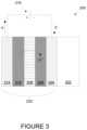
- FIG. 2is a schematic cross-section of an electrochromic device in a bleached state (or transitioning to a bleached state).
- the electrochromic device 200includes a tungsten oxide electrochromic layer (EC) 206 and a counter electrode layer (CE) 210 as described herein.
- the tungsten oxide electrochromic layer 206has a nanocrystalline, or substantially nanocrystalline, morphology.
- the counter electrode layer 210has an amorphous, or substantially amorphous, morphology.
- the weight percent ratio of tungsten to nickel in the counter electrodeis about 0.40-0.60.
- the electrochromic device 200also includes substrate 202 , conductive layer (CL) 204 , ion conducting layer (IC) 208 , and conductive layer (CL) 214 .
- the substrate 202 and conductive layer 204together comprise a TEC-GlassTM.
- the electrochromic devices described herein, such as those of FIG. 2often find beneficial application in architectural glass.
- the substrate 202is of the dimensions such that it may be classified as architectural glass.
- the conductive layer 214is indium tin oxide (ITO).
- the ion conducting layer 208is a silicon-aluminum-oxide.
- the voltage source 216is configured to apply a potential to electrochromic stack 220 through suitable connections (e.g., bus bars) to conductive layers 204 and 214 .
- the voltage sourceis configured to apply a potential of about 2 volts in order to drive a transition of the device from one optical state to another.
- the polarity of the potential as shown in FIG. 2is such that the ions (lithium ions in this example) primarily reside in the counter electrode layer 210 .
- the ratio of the electrochromic layer thickness to the counter electrode layer thicknessmay be about 1.7:1 to 2.3:1 (e.g., about 2:1).
- the electrochromic tungsten oxide layeris about 200 nm to 700 nm thick.
- the electrochromic tungsten oxide layeris about 400 nm to 500 nm thick.
- the counter electrode layeris about 100 nm to 350 nm thick. In further embodiments, the counter electrode layer is about 200 nm to 250 nm thick.
- the counter electrode layeris about 240 nm thick.
- the silicon-aluminum-oxide ion conducting layer 208is about 10 nm to 100 nm thick. In further embodiments, the silicon-aluminum-oxide ion conducting layer is about 20 nm to 50 nm thick.
- electrochromic materialsmay contain blind charge.
- the blind charge in an electrochromic materialis the charge (e.g., negative charge in the case of tungsten oxide electrochromic material) that exists in the material as fabricated, absent compensation by oppositely charged ions or other charge carriers.
- the magnitude of the blind chargedepends upon the excess oxygen concentration during sputtering of the tungsten oxide.
- blind chargemust be compensated before the ions employed to transform the electrochromic material can effectively change an optical property of the electrochromic material. Without prior compensation of the blind charge, ions supplied to an electrochromic material will irreversibly incorporate in the material and have no effect on the optical state of the material.
- an electrochromic deviceis typically provided with ions, such as lithium ions or protons, in an amount sufficient both to compensate the blind charge and to provide a supply of ions for reversibly switching the electrochromic material between two optical states.
- ionssuch as lithium ions or protons
- chargeis lost during the first electrochemical cycle in compensating blind charge.
- lithiumis present in the electrochromic stack 220 in an amount sufficient to compensate the blind charge in the electrochromic layer 206 and then an additional amount of about 1.5 to 2.5 times the amount used to compensate the blind charge (by mass) in the stack (initially in the counter electrode layer 210 for example). That is, there is about 1.5 to 2.5 times the amount of lithium needed to compensate the blind charge that is provided for reversible cycling between the electrochromic layer 206 and the counter electrode layer 210 in the electrochromic stack 220 . In some embodiments, there are enough lithium in the electrochromic stack 220 to compensate the blind charge in the electrochromic layer 206 and then about two times this amount (by mass) in the counter electrode layer 210 or elsewhere in the stack.
- FIG. 3is a schematic cross-section of electrochromic device 200 shown in FIG. 2 but in a colored state (or transitioning to a colored state).
- the polarity of voltage source 216is reversed, so that the electrochromic layer is made more negative to accept additional lithium ions, and thereby transition to the colored state.
- lithium ionsare transported across the ion conducting layer 208 to the tungsten oxide electrochromic layer 206 .
- the tungsten oxide electrochromic layer 206is shown in the colored state.
- the counter electrode 210is also shown in the colored state. As explained, the counter electrode material becomes progressively more opaque as it gives up (deintercalates) lithium ions.
- there is a synergistic effectwhere the transition to colored states for both layers 206 and 210 are additive toward reducing the amount of light transmitted through the stack and substrate.
- electrochromic devices of the types described aboveare very reliable, often substantially more so than counterpart devices of the prior art. Reliability may be characterized by various metrics. Some of these are described in ASTM E2141-06 (Standard Test Methods for Assessing the Durability of Absorptive Electrochromic Coatings on Sealed Insulating Glass Units). In some specific cases, the devices are able to cycle between two distinct optical states (e.g., between bleached and colored) over 50,000 times while maintaining a ratio of the bleached T vis to colored T vis (also know as PTR or photopic transmission ratio) of >4. The longevity of these electrochromic devices makes them suitable for use in applications where the electrochromic devices are expected to be in place for tens of years.
- ASTM E2141-06Standard Test Methods for Assessing the Durability of Absorptive Electrochromic Coatings on Sealed Insulating Glass Units.
- the devicesare able to cycle between two distinct optical states (e.g., between bleached and colored) over 50,000 times while
- the electrochromic devices in embodiments of the inventionare able to cycle between bleached and unbleached states without losing transmissivity in the bleached state and without degradation of the color or other property in the unbleached state.
- the high reliability of an electrochromic device in accordance with embodiments herein describedis due in part to a design in which the thickness of the electrochromic layer and/or the thickness of the counter electrode layer in a stack do not substantially change during electrochemical cycling of the electrochromic device from their as deposited, post lithiation thickness (e.g., by no more than about 4%).
- defectsrefers to a defective point or region of an electrochromic device. Defects may be caused by electrical shorts or by pinholes. Further, defects may be characterized as visible or non-visible. In general, a defect in an electrochromic device does not change optical state (e.g., color) in response to an applied potential that is sufficient to cause non-defective regions of the electrochromic device to color or otherwise change optical state. Often a defect will be manifest as visually discernable anomalies in the electrochromic window or other device. Such defects are referred to herein as “visible” defects.
- a shortis a localized electronically conductive pathway spanning the ion conducting layer (e.g., an electronically conductive pathway between the two TCO layers).
- a pinholeis a region where one or more layers of the electrochromic device are missing or damaged so that electrochromism is not exhibited. Pinholes are not electrical shorts.
- Three types of defectsare of primary concern: (1) visible pinholes, (2) visible shorts, and (3) non-visible shorts. Typically, though not necessarily, a visible short will have defect dimension of at least about 3 micrometers resulting in a region, e.g.
- a visible pinholewill have a defect dimension of at least about 100 micrometers.
- an electrical shortis created by a conductive particle lodging in the ion conducting layer, thereby causing an electronic path between the counter electrode layer and the electrochromic layer or the TCO associated with either one of them.
- a defectis caused by a particle on the substrate (on which the electrochromic stack is fabricated) and such particle causes layer delamination (sometimes called “pop-off”) or the layers not to adhere to the substrate. Both types of defects are illustrated below in FIGS. 4 and 5 A- 5 C .
- a delamination or pop-off defectcan lead to a short if it occurs before a TCO or associated EC or CE is deposited.
- the subsequently deposited TCO or EC/CE layerwill directly contact an underlying TCO or CE/EC layer providing direct electronic conductive pathway.
- a few examples of defect sourcesare presented in the table below. The table below is intended to provide examples of mechanisms that lead to the different types of visible and non-visible defects. Additional factors exist which may influence how the EC window responds to a defect within the stack.
- An electrical shortcan cause leakage current across the ion conducting layer and result in a potential drop in the vicinity of the short. If the potential drop is of sufficient magnitude it will prevent the electrochromic device from undergoing an electrochromic transition in the vicinity of the short. In the case of a visible short the defect will appear as a light central region (when the device is in the colored state) with a diffuse boundary such that the device gradually darkens with distance from the center of the short. If there are a significant number of electrical shorts (visible or non-visible) concentrated in an area of an electrochromic device, they may collectively impact a broad region of the device whereby the device cannot switch in such region.
- leakage currentmay result from sources other than short-type defects.
- Such other sourcesinclude broad-based leakage across the ion conducting layer and edge defects such as roll off defects as described elsewhere herein and scribe line defects. The emphasis here is on leakage caused only by points of electrical shorting across the ion conducting layer in the interior regions of the electrochromic device.
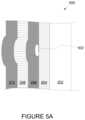
- FIG. 4is a schematic cross-section of an electrochromic device 400 with a particle in the ion conducting layer causing a localized defect in the device.
- Electrochromic device 400includes the same components as depicted in FIG. 2 for electrochromic device 200 .
- the ion conducting layer 208 of electrochromic device 400there is a conductive particle 402 or other artifact causing a defect.
- Conductive particle 402results in a short between electrochromic layer 206 and counter electrode layer 210 .
- This shortdoes not allow the flow of ions between electrochromic layer 206 and counter electrode layer 210 , instead allowing electrons to pass locally between the layers, resulting in a transparent region 404 in the electrochromic layer 206 and a transparent region 406 in the counter electrode layer 210 when the remainder of layers 210 and 206 are in the colored state. That is, if electrochromic device 400 is in the colored state, conductive particle 402 renders regions 404 and 406 of the electrochromic device unable to enter into the colored state. Sometimes the defect regions are referred to as “constellations” because they appear as a series of bright spots (or stars) against a dark background (the remainder of the device being in the colored state). Humans will naturally direct their attention to the constellations and often find them distracting or unattractive.
- FIG. 5 Ais a schematic cross-section of an electrochromic device 500 with a particle 502 or other debris on conductive layer 204 prior to depositing the remainder of the electrochromic stack.
- Electrochromic device 500includes the same components as electrochromic device 200 .
- Particle 502causes the layers in the electrochromic stack 220 to bulge in the region of particle 502 , due to conformal layers 206 - 210 being deposited sequentially over particle 502 as depicted (in this example, layer 214 has not yet been deposited). While not wishing to be bound by a particular theory, it is believed that layering over such particles, given the relatively thin nature of the layers, can cause stress in the area where the bulges are formed.
- each layeraround the perimeter of the bulged region, there can be defects in the layer, e.g. in the lattice arrangement or on a more macroscopic level, cracks or voids.
- defectse.g. in the lattice arrangement or on a more macroscopic level, cracks or voids.
- One consequence of these defectswould be, for example, an electrical short between electrochromic layer 206 and counter electrode layer 210 or loss of ion conductivity in layer 208 .
- These defectsare not depicted in FIG. 5 A , however.
- FIG. 5 Banother consequence of defects caused by particle 502 is called a “pop-off.”
- a portion above the conductive layer 204 in the region of particle 502breaks loose, carrying with it portions of electrochromic layer 206 , ion conducting layer 208 , and counter electrode layer 210 .
- the “pop-off”is piece 504 , which includes particle 502 , a portion of electrochromic layer 206 , as well as ion conducting layer 208 and counter electrode layer 210 .
- the resultis an exposed area of conductive layer 204 . Referring to FIG.
- Pop-off defects due to particles or debris on substrate 202 or 204 (as described above), on ion conducting layer 208 , and on counterelectrode layer 210may also occur, causing pinhole defects when the electrochromic device is in the colored state. Also, if particle 502 is large enough and does not cause a pop-off, it might be visible when electrochromic device 500 is in the bleached state.
- the electrochromic devices in embodiments of the inventionare also scalable to substrates smaller or larger than architectural glass.
- An electrochromic stackcan be deposited onto substrates that are a wide range of sizes, up to about 12 inches by 12 inches, or even 80 inches by 120 inches.
- the capability of manufacturing electrochromic devices of 20 by 20 inchesallows the manufacture of electrochromic architectural glass for many applications.
- the number of visible pinhole defectsis no greater than about 0.04 per square centimeter. In another embodiment, the number of visible pinhole defects is no greater than about 0.02 per square centimeter, and in more specific embodiments, the number of such defects is no greater than about 0.01 per square centimeter.
- the visible short-type defectsare individually treated after fabrication to leave short-related pinholes as the only visible defects. In one embodiment, the number of visible short-related pinhole defects is no greater than about 0.005 per square centimeter. In another embodiment, the number of visible short-related pinhole defects is no greater than about 0.003 per square centimeter, and in more specific embodiments, the number of such defects is no greater than about 0.001 per square centimeter.
- the total number of visible defects, pinholes and short-related pinholes created from isolating visible short-related defectsis less than about 0.1 defects per square centimeter, in another embodiment less than about 0.08 defects per square centimeter, in another embodiment less than about 0.045 defects per square centimeter (less than about 450 defects per square meter of window).
- the number of non-visible electrical short defectsresults in leakage currents of less than about 5 ⁇ A/cm 2 at ⁇ 2V bias. These values apply across the entire face of the electrochromic device (i.e., there is no region of the device (anywhere on the device) having a defect density greater than the recited value).
- the electrochromic devicehas no visible defects greater than about 1.6 mm in diameter (the largest transverse dimension of the defect). In another embodiment, the device has no visible defects greater than about 0.5 mm in diameter, in another embodiment the device has no visible defects greater than about 100 ⁇ m in diameter.
- electrochromic glassis integrated into an insulating glass unit (IGU).
- IGUinsulating glass unit
- An insulating glass unitconsists of multiple glass panes assembled into a unit, generally with the intention of maximizing the thermal insulating properties of a gas contained in the space formed by the unit while at the same time providing clear vision through the unit.
- Insulating glass units incorporating electrochromic glasswould be similar to insulating glass units currently known in the art, except for electrical leads for connecting the electrochromic glass to voltage source. Due to the higher temperatures (due to absorption of radiant energy by an electrochromic glass) that electrochromic insulating glass units may experience, more robust sealants than those used in conventional insulating glass units may be necessary. For example, stainless steel spacer bars, high temperature polyisobutylene (PIB), new secondary sealants, foil coated PIB tape for spacer bar seams, and the like.
- PIBhigh temperature polyisobutylene
- one aspect of the inventionis a method of fabricating an electrochromic window.
- the methodincludes sequentially depositing on a substrate (i) an electrochromic layer, (ii) an ion conducting layer, and (iii) a counter electrode layer to form a stack in which the ion conducting layer separates the electrochromic layer and the counter electrode layer.
- the sequential depositionemploys a single integrated deposition system having a controlled ambient environment in which the pressure, temperature, and/or gas composition are controlled independently of an external environment outside of the integrated deposition system, and the substrate does not leave the integrated deposition system at any time during the sequential deposition of the electrochromic layer, the ion conducting layer, and the counter electrode layer.
- the gas compositionmay be characterized by the partial pressures of the various components in the controlled ambient environment.
- the controlled ambient environmentalso may be characterized in terms of the number of particles or particle densities.
- the controlled ambient environmentcontains fewer than 350 particles (of size 0.1 micrometers or larger) per m 3 .
- the controlled ambient environmentmeets the requirements of a class 100 clean room (US FED STD 209E).
- the controlled ambient environmentmeets the requirements of a class 10 clean room (US FED STD 209E).
- the substratemay enter and/or leave the controlled ambient environment in a clean room meeting class 100 or even class 10 requirements.
- this method of fabricationis integrated into a multistep process for making an electrochromic window using architectural glass as the substrate.
- this method of fabricationis integrated into a multistep process for making an electrochromic window using architectural glass as the substrate.
- the following descriptioncontemplates the method and its various embodiments in the context of a multistep process for fabricating an electrochromic window, but methods of the invention are not so limited.
- Electrochromic mirrors and other devicesmay be fabricated using some or all of the operations and approaches described herein.
- FIG. 6 Ais a cross-sectional representation of an electrochromic window device, 600 , in accord with a multistep process such as that described in relation to FIG. 7 A .
- FIG. 7 Adepicts a process flow describing a method, 700 , of fabricating an electrochromic window which incorporates electrochromic device 600 .
- FIG. 6 Bis a top view of device 600 showing the location of trenches cut into the device. Thus, FIGS. 6 A-B and 7 A will be described together.
- One aspect of the descriptionis an electrochromic window including device 600 and another aspect of the description is a method, 700 , of fabricating an electrochromic window which includes device 600 . Included in the following description are descriptions of FIGS. 7 B- 7 E .
- FIGS. 7 B- 7 Ddepict specific methods of fabricating an electrochromic stack which is part of device 600 .
- FIG. 7 Edepicts a process flow for a conditioning process used in fabricating, e.g., device 600 .
- FIG. 6 Ashows a specific example of an electrochromic device, 600 , which is fabricated starting with a substrate made of glass 605 which optionally has a diffusion barrier 610 coating and a first transparent conducting oxide (TCO) coating 615 on the diffusion barrier.
- Method 700employs a substrate that is, for example, float glass with sodium diffusion barrier and antireflective layers followed by a transparent conductive layer, for example a transparent conductive oxide 615 .
- substrates suitable for devices of the inventioninclude glasses sold under the trademarks TEC Glass® by Pilkington of Toledo, Ohio, and SUNGATE® 300 and SUNGATE® 500 by PPG Industries, of Pittsburgh, Pennsylvania.
- the first TCO layer 615is the first of two conductive layers used to form the electrodes of electrochromic device 600 fabricated on the substrate.
- Method 700begins with a cleaning process, 705 , where the substrate is cleaned to prepare it for subsequent processing.
- a cleaning process705
- One critical defectis a particle or other contaminant that creates a conductive pathway across the IC layer and thus shorts the device locally causing visually discernable anomalies in the electrochromic window.
- LisecTMa trade name for a glass washing apparatus and process available from (LISEC Maschinenbau Gmbh of 9.
- Cleaning the substratemay include mechanical scrubbing as well as ultrasonic conditioning to remove unwanted particulates.
- particulatesmay lead to cosmetic flaws as well as local shorting within the device.
- a first laser scribe process, 710is performed in order to remove a line of the first TCO layer on the substrate.
- the resulting trenchablates through both the TCO and the diffusion barrier (although in some cases the diffusion barrier is not substantially penetrated).
- FIG. 6 Adepicts this first laser scribe trench, 620 .
- a trenchis scribed in the substrate across the entire length of one side of the substrate in order to isolate an area of the TCO, near one edge of the substrate, which will ultimately make contact with a first bus bar, 640 , used to provide current to a second TCO layer, 630 , which is deposited on top of electrochromic (EC) stack 625 (which includes the electrochromic, ion conducting and counter electrode layers as described above).
- ECelectrochromic
- FIG. 6 Bshows schematically (not to scale) the location of trench 620 .
- the non-isolated (main) portion of the first TCO layer, on the diffusion barrierultimately makes contact with a second bus bar, 645 .
- Isolation trench 620may be needed because, in certain embodiments, the method of attaching the first bus bar to the device includes pressing it through the device stack layers after they are laid down (both on the isolated portion of the first TCO layer and the main portion of the first TCO layer).
- the method of attaching the first bus bar to the deviceincludes pressing it through the device stack layers after they are laid down (both on the isolated portion of the first TCO layer and the main portion of the first TCO layer).
- the TCO area isolated by the first laser scribeis typically an area along one edge of the substrate that will ultimately, along with the bus bars, be hidden when incorporated into the integrated glass unit (IGU) and/or window pane, frame or curtain wall.
- the laser or lasers used for the first laser scribeare typically, but not necessarily, pulse-type lasers, for example diode-pumped solid state lasers.
- the laser scribescan be performed using a suitable laser from IPG Photonics (of Oxford Massachusetts), or from Ekspla (of Vilnius Lithuania).
- the laser trenchis dug along a side of the substrate from end to end to isolate a portion of the first TCO layer; the depth and width dimensions of trench 620 made via first laser scribe 710 should be sufficient to isolate the first TCO layer from the bulk TCO once the device is subsequently deposited.
- the depth and width of the trenchshould be sufficient to prevent any remaining particulates to short across the trench.
- the trenchis between about 300 nm and 500 nm deep and between about 20 ⁇ m and 50 ⁇ m wide.
- the trenchis between about 350 nm and 450 nm deep and between about 30 ⁇ m and 45 ⁇ m wide.
- the trenchis about 400 nm deep and about 40 ⁇ m wide.
- the substrateis cleaned again (operation 715 ), typically but not necessarily, using cleaning methods described above. This second cleaning process is performed to remove any debris caused by the first laser scribe. Once cleaning operation 715 is complete, the substrate is ready for deposition of EC stack 625 . This is depicted in process flow 700 as process 720 .
- the methodincludes sequentially depositing on a substrate (i) an EC layer, (ii) an IC layer, and (iii) a CE layer to form a stack in which the IC layer separates the EC layer and the CE layer using a single integrated deposition system having a controlled ambient environment in which the pressure and/or gas composition are controlled independently of an external environment outside of the integrated deposition system, and the substrate does not leave the integrated deposition system at any time during the sequential deposition of the EC layer, the IC layer, and the CE layer.
- each of the sequentially deposited layersis physical vapor deposited.
- the layers of the electrochromic devicemay be deposited by various techniques including physical vapor deposition, chemical vapor deposition, plasma enhanced chemical vapor deposition, and atomic layer deposition, to name a few.
- physical vapor deposition as used hereinincludes the full range of art understood PVD techniques including sputtering, evaporation, ablation, and the like.
- FIG. 7 Bdepicts one embodiment of process 720 .
- First the EC layeris deposited on the substrate, process 722 , then the IC layer is deposited, process 724 , then the CE layer, process 726 .
- the reverse order of depositionis also an embodiment of the invention, that is, where the CE layer is deposited first, then the IC layer and then the EC layer.
- each of the electrochromic layer, the ion conducting layer, and the counter electrode layeris a solid phase layer.
- each of the electrochromic layer, the ion conducting layer, and the counter electrode layerincludes only inorganic material.
- any one or more of these layersmay be composed of one or more sub-layers, which may have distinct compositions, sizes, morphologies, charge densities, optical properties, etc.
- any one or more of the device layersmay have a graded composition or a graded morphology in which the composition or morphology, respectively, changes over at least a portion of the thickness of the layer.
- the concentration of a dopant or charge carriervaries within a given layer, at least as the layer is fabricated.
- the morphology of a layervaries from crystalline to amorphous.
- Such graded composition or morphologymay be chosen to impact the functional properties of the device.
- additional layersmay be added to the stack.
- a heat spreader layeris interposed between one or both TCO layers and the EC stack.
- a cathodically coloring electrochromic layer and/or an anodically coloring counter electrode layermay be deposited as two distinct sub-layers optionally having different compositions, although both sub-layers may have compositions (e.g., compositions that include electrochromic materials or compositions that include counter electrode materials) as generally described herein. Certain processing steps (e.g., lithiation) may occur between depositing the sub-layers.
- counter electrode materialis deposited in two sub-layers having different compositions.
- the first sub-layer(closer to the cathodically coloring electrochromic layer) may be anodically coloring, while the second sub-layer (farther away from the cathodically coloring electrochromic layer) may or may not be anodically coloring, or may be more weakly anodically coloring than the first sub-layer.
- the partially fabricated devicemay be subject to a lithiation operation.
- the second sub-layermay reduce the risk of forming defects.
- the second sub-layeracts as a defect-mitigating layer, and may be more electronically insulating than the first sub-layer.
- the electrochromic devices of the inventionutilize ion movement between the electrochromic layer and the counter electrode layer via an ion conducting layer.
- these ionsor neutral precursors thereof are introduced to the stack as one or more layers (as described below in more detail in relation to FIGS. 7 C and 7 D ) that eventually intercalate into the stack.
- these ionsare introduced into the stack concurrently with one or more of the electrochromic layer, the ion conducting layer, and the counter electrode layer.
- lithiumis, e.g., sputtered along with the material used to make the one or more of the stack layers or sputtered as part of a material that includes lithium (e.g., by a method employing lithium nickel tungsten oxide, optionally provided with other additives as listed herein).
- the IC layeris deposited via sputtering a lithium silicon aluminum oxide target.
- the Liis cosputtered along with silicon aluminum in order to achieve the desired film.
- depositing the electrochromic layercomprises depositing WOx, e.g. where x is less than 3.0 and at least about 2.7.
- the WOxhas a substantially nanocrystalline morphology.
- the electrochromic layeris deposited to a thickness of between about 200 nm and 700 nm.
- depositing the electrochromic layerincludes sputtering tungsten from a tungsten containing target. In one such embodiment, a metallic tungsten (or tungsten alloy) target is used.
- the sputter gasis an inert gas (e.g., argon or xenon) with some oxygen containing gas (e.g., molecular or atomic oxygen) present.
- the gas compositioncontains between about 30% and about 100% oxygen, in another embodiment between about 50% and about 80% oxygen, in yet another embodiment between about 65% and about 75% oxygen.
- the tungsten containing targetcontains between about 80% and 100% (by weight) tungsten, in another embodiment between about 95% and 100% tungsten, and in yet another embodiment between about 99% and 100% tungsten.
- the gas compositionis about 70% oxygen/30% argon and the target is metallic tungsten of a purity of between about 99% and 100%.
- a tungsten oxide W(O) ceramic targetis sputtered with, e.g., argon.
- the pressure in the deposition station or chamberin one embodiment, is between about 1 and about 75 mTorr, in another embodiment between about 5 and about 50 mTorr, in another embodiment between about 10 and about 20 mTorr.
- the substrate temperature for process 722is between about 100° C. and about 500° C., in another embodiment between about 100° C. and about 300° C., and in another embodiment between about 150° C. and about 250° C.
- the substrate temperaturemay be measured in situ by, e.g., a thermocouple such as an infra-red thermocouple (IR t/c).
- a thermocouplesuch as an infra-red thermocouple (IR t/c).
- the power density used to sputter the EC targetis between about 2 Watts/cm 2 and about 50 Watts/cm 2 (determined based on the power applied divided by the surface area of the target); in another embodiment between about 10 Watts/cm 2 and about 20 Watts/cm 2 ; and in yet another embodiment between about 15 Watts/cm 2 and about 20 Watts/cm 2 .
- the power delivered to effect sputteringis provided via direct current (DC). In other embodiments, pulsed DC/AC reactive sputtering is used.
- the frequencyis between about 20 kHz and about 400 kHz, in another embodiment between about 20 kHz and about 50 kHz, in yet another embodiment between about 40 kHz and about 50 kHz, in another embodiment about 40 kHz.
- the above conditionsmay be used in any combination with one another to effect deposition of a high quality tungsten oxide electrochromic layer.
- the distance between the target and the substratemay also be important.
- the distance between the target (cathode or source) to the substrate surfaceis between about 35 mm and about 150 mm; in another embodiment between about 45 mm and about 130 mm; and in another embodiment between about 70 mm and about 100 mm.
- deposition of the EC layeris described in terms of sputtering from a target, other deposition techniques are employed in some embodiments. For example, chemical vapor deposition, atomic layer deposition, and the like may be employed. Each of these techniques, along with PVD, has its own form of material source as is known to those of skill in the art.
- depositing the ion conducting layerincludes depositing a material selected from the group consisting of a tungsten oxide, a tantalum oxide, a niobium oxide, and a silicon aluminum oxide.
- depositing the ion conducting layerincludes sputtering a target including between about 2% and 20% by weight of aluminum (remainder silicon) in an oxygen containing environment to produce a layer of silicon aluminum oxide.
- the targetis between about 5% and about 10% aluminum in silicon, in another embodiment, between about 7% and about 9% aluminum in silicon.
- the gas compositioncontains between about 15% and about 70% oxygen, in another embodiment between about 20% and about 50% oxygen, in yet another embodiment between about 25% and about 45% oxygen, in another embodiment about 35% oxygen.
- depositing the ion conducting layerincludes depositing the ion conducting layer to a thickness of between about 10 and 100 nm. In yet another embodiment, depositing the ion conducting layer includes depositing the ion conducting layer to a thickness of between about 20 and 50 nm.
- the power density used to sputter the IC targetis between about 1 Watts/cm 2 and about 20 Watts/cm 2 (determined based on the power applied divided by the surface area of the target); in another embodiment between about 5 Watts/cm 2 and about 7 Watts/cm 2 ; and in yet another embodiment between about 6 Watts/cm 2 and about 6.5 Watts/cm 2 .
- the power delivered to effect sputteringis provided via direct current (DC). In other embodiments, pulsed DC/AC reactive sputtering is used.
- the frequencyis between about 20 kHz and about 400 kHz, in another embodiment between about 20 kHz and about 50 kHz, in yet another embodiment between about 40 kHz and about 50 kHz, in another embodiment about 40 kHz.
- the pressure in the deposition station or chamberin one embodiment, is between about 5 mTorr and about 40 mTorr, in another embodiment between about 10 mTorr and about 30 mTorr, in another embodiment about 20 mTorr.
- the substrate temperature ranges for operation 724are between about 20° C. and about 200° C., in some embodiments between about 20° C. and about 150° C., and it yet still other embodiments between about 25° C. and about 100° C.
- the above conditionsmay be used in any combination with one another to effect deposition of a high quality ion conducting layer.
- depositing the counter electrode layerincludes depositing a layer of nickel tungsten oxide (NiWO) that includes one or more additives as described above, preferably amorphous NiWO.
- depositing the counter electrode layerincludes sputtering a target including about 30% (by weight) to about 70% of tungsten in nickel in an oxygen containing environment to produce a layer of nickel tungsten oxide.
- the targetis between about 40% and about 60% tungsten in nickel, in another embodiment between about 45% and about 55% tungsten in nickel, and in yet another embodiment about 51% tungsten in nickel.
- the gas compositioncontains between about 30% and about 100% oxygen, in another embodiment between about 80% and about 100% oxygen, in yet another embodiment between about 95% and about 100% oxygen, in another embodiment about 100% oxygen.
- the additive(s)may be introduced via the sputter target in some cases. In these or other cases, the additive(s) may be introduced via another method, for example through evaporation, which may or may not occur concurrently with sputtering.
- the power density used to sputter the CE targetis between about 2 Watts/cm 2 and about 50 Watts/cm 2 (determined based on the power applied divided by the surface area of the target); in another embodiment between about 5 Watts/cm 2 and about 20 Watts/cm 2 ; and in yet another embodiment between about 8 Watts/cm 2 and about 10 Watts/cm 2 , in another embodiment about 8 Watts/cm 2 .
- the power delivered to effect sputteringis provided via direct current (DC). In other embodiments, pulsed DC/AC reactive sputtering is used.
- the frequencyis between about 20 kHz and about 400 kHz, in another embodiment between about 20 kHz and about 50 kHz, in yet another embodiment between about 40 kHz and about 50 kHz, in another embodiment about 40 kHz.
- the pressure in the deposition station or chamberin one embodiment, is between about 1 and about 50 mTorr, in another embodiment between about 20 and about 40 mTorr, in another embodiment between about 25 and about 35 mTorr, in another embodiment about 30 mTorr.
- a nickel tungsten oxide NiWO ceramic target(which may or may not include one or more additives as described above) is sputtered with, e.g., argon and oxygen.
- the NiWOis between about 15% (atomic) Ni and about 60% Ni; between about 10% W and about 40% W; and between about 30% O and about 75% O.
- the NiWOis between about 30% (atomic) Ni and about 45% Ni; between about 10% W and about 25% W; and between about 35% O and about 50% O.
- the NiWOis about 42% (atomic) Ni, about 14% W, and about 44% O.
- the NiWO targetmay also include one or more of the additives listed above.
- depositing the counter electrode layerincludes depositing the counter electrode layer to a thickness of between about 150 and 350 nm; in yet another embodiment between about 200 and about 250 nm thick.
- the above conditionsmay be used in any combination with one another to effect deposition of a high quality NiWO layer that includes one or more additives.
- the above conditionsmay also be used in any combination with one another to effect deposition of a counter electrode layer having a different composition, for example one that includes a base anodically coloring electrochromic material and one or more additives as described above.
- the base anodically coloring materialis nickel oxide and the additive is or includes tungsten
- other materialsmay also be used. Details herein regarding nickel in the counter electrode may also apply to other metals used in a base anodically coloring material. Details herein regarding tungsten in the counter electrode may also apply to other additives, alone or in combination, as listed herein.
- operation 726 of FIG. 7 Bincludes depositing a counter electrode layer including at least one base anodically coloring electrochromic material containing at least one metal selected from the group consisting of chromium, manganese, iron, cobalt, nickel, rhodium, ruthenium, vanadium, and iridium, or selected from the group consisting of chromium, manganese, iron, cobalt, nickel, rhodium, and iridium, or selected from the group consisting of nickel and iridium.
- the metalmay be provided as an oxide.
- the sputter targetmay include one or more metals (or oxides thereof) selected from the group consisting of chromium, manganese, iron, cobalt, nickel, rhodium, ruthenium, vanadium, and iridium, or from the group consisting of chromium, manganese, iron, cobalt, nickel, rhodium, and iridium, or from the group consisting of nickel and iridium.
- depositing the counter electrode layermay include depositing one or more additives/additional materials as part of the layer.
- the additive materialmay be selected from the group consisting of silver (Ag), arsenic (As), gold (Au), boron (B), cadmium (Cd), cesium (Cs), copper (Cu), europium (Eu), gallium (Ga), gadolinium (Gd), germanium (Ge), mercury (Hg), osmium (Os), lead (Pb), palladium (Pd), promethium (Pm), polonium (Po), platinum (Pt), radium (Ra), rubidium (Rb), terbium (Tb), technetium (Tc), thorium (Th), and thallium (Tl), or from any of the sub-groups identified herein.
- the additional materialis selected from the group consisting of germanium, gadolinium, gallium and copper, or the group consisting of germanium, gadolinium and gallium, or the group consisting of germanium and copper.
- the additional materialmay be provided through sputtering, for example with a sputter target including one or more of the additional materials, or an oxide of one or more of the additional materials.
- the sputtering process for forming the CE layermay utilize one or more sputter targets. Where one sputter target is used, it may include both the anodically coloring electrochromic material and the additive (either or both provided in oxide form on the target).
- the sputter targetmay include a grid or other overlapping shape where different portions of the grid include the different relevant materials. In other cases, the sputter target may be an alloy of the relevant materials. Where two sputter targets are used, each sputter target may include one of the relevant materials (e.g., the anodically coloring electrochromic material or the additive, either or both in oxide form).
- the sputter targetsmay overlap in some cases.
- the counter electrode layeris typically an oxide material. Oxygen may be provided as a part of the sputter target. In other cases, the sputter targets are substantially pure metals, and sputtering is done in the presence of oxygen to form the oxide.
- the distance between the CE target (cathode or source) to the substrate surfaceis between about 35 mm and about 150 mm; in another embodiment between about 45 mm and about 130 mm; and in another embodiment between about 70 mm and about 100 mm.
- Other materialsmay, in some cases, be deposited under the same or similar conditions. Further, non-sputtering deposition conditions may be employed in some embodiments to create the same or similar deposited materials as those described in the context of FIGS. 6 A- 6 B and FIGS. 7 A- 7 E .
- the electrochromic layerincludes tungsten oxide and the counter electrode includes nickel tungsten oxide (with one or more additives as described herein), and the ratio of thicknesses of the electrochromic layer to the counter electrode layer is between about 1.7:1 and 2.3:1, or between about 1.9:1 and 2.1:1 (with about 2:1 being a specific example). Such thickness ratios may also be used where the counter electrode is made of a different material.
- process operation 720after the CE layer is deposited, the EC stack is complete.
- process operation 720which refers to “depositing stack” means in this context, the EC stack plus the second TCO layer (sometimes referred to as the “ITO” when indium tin oxide is used to make the second TCO).
- the second TCO layersometimes referred to as the “ITO” when indium tin oxide is used to make the second TCO.
- stackin this description refers to the EC-IC-CE layers; that is, the “EC stack.”
- a TCO layeris deposited on the stack. Referring to FIG. 6 A , this would correspond to second TCO layer 630 on EC stack 625 .
- Process flow 720is finished once process 728 is complete.
- a capping layeris deposited on the EC stack.
- the capping layeris SiAlO, similar to the IC layer.
- the capping layeris deposited by sputtering, similar to the conditions under which the IC layer is deposited.
- the thickness of a capping layeris typically about 30 nm to 100 nm.
- depositing the layer of transparent conductive oxideis performed under conditions whereby the transparent conductive oxide has a sheet resistance of between about 10 and 30 ohms/square.
- the first and second TCO layersare of matched sheet resistance for optimum efficiency of the electrochromic device.
- the first TCO layer's morphologyshould be smooth for better conformal layers in the deposited stack.
- a substantially uniform TCO layervaries only about ⁇ 10% in each of the aforementioned thickness ranges.
- a substantially uniform TCO layervaries only about ⁇ 5% in each of the aforementioned thickness ranges.
- a substantially uniform TCO layervaries only about ⁇ 2% in each of the aforementioned thickness ranges.
- the second TCO layer 630is deposited using some or all of the following conditions.
- the recited conditionsmay be employed to form a thin, low-defect layer of indium tin oxide by sputtering a target containing indium oxide in tin oxide, e.g. with an argon sputter gas with or without oxygen.
- the thickness of the TCO layeris between about 5 nm and about 10,000 nm, in another embodiment between about 10 nm and about 1,000 nm. In yet another embodiment this thickness is between about 10 nm and about 500 nm.
- the substrate temperature for operation 728is between about 20 and about 300° C., in another embodiment between about 20 and about 250° C., and in another embodiment between about 80 and about 225° C.
- depositing the TCO layerincludes sputtering a target including between about 80% (by weight) to about 99% of In 2 O 3 and between about 1% and about 20% SnO 2 using an inert gas, optionally with oxygen.
- the targetis between about 85% (by weight) to about 97% of In 2 O 3 and between about 3% and about 15% SnO 2 .
- the targetis about 90% of In 2 O 3 and about 10% SnO 2 .
- the gas compositioncontains between about 0.1% and about 3% oxygen, in another embodiment between about 0.5% and about 2% oxygen, in yet another embodiment between about 1% and about 1.5% oxygen, in another embodiment about 1.2% oxygen.
- the power density used to sputter the TCO targetis between about 0.5 Watts/cm 2 and about 10 Watts/cm 2 (determined based on the power applied divided by the surface area of the target); in another embodiment between about 0.5 Watts/cm 2 and about 2 Watts/cm 2 ; and in yet another embodiment between about 0.5 Watts/cm 2 and about 1 Watts/cm 2 , in another embodiment about 0.7 Watts/cm 2 .
- the power delivered to effect sputteringis provided via direct current (DC).
- DCdirect current
- pulsed DC/AC reactive sputteringis used.
- the frequencyis between about 20 kHz and about 400 kHz, in another embodiment between about 50 kHz and about 100 kHz, in yet another embodiment between about 60 kHz and about 90 kHz, in another embodiment about 80 kHz.
- the pressure in the deposition station or chamberin one embodiment, is between about 1 and about 10 mTorr, in another embodiment between about 2 and about 5 mTorr, in another embodiment between about 3 and about 4 mTorr, in another embodiment about 3.5 mTorr.
- the indium tin oxide layeris between about 20% (atomic) In and about 40% In; between about 2.5% Sn and about 12.5% Sn; and between about 50% O and about 70% O; in another embodiment, between about 25% In and about 35% In; between about 5.5% Sn and about 8.5% Sn; and between about 55% O and about 65% O; and in another embodiment, about 30% In, about 8% Sn; and about 62% O.
- the above conditionsmay be used in any combination with one another to effect deposition of a high quality indium tin oxide layer.
- the EC stackis fabricated in an integrated deposition system where the substrate does not leave the integrated deposition system at any time during fabrication of the stack.
- the second TCO layeris also formed using the integrated deposition system where the substrate does not leave the integrated deposition system during deposition of the EC stack and the TCO layer.
- all of the layersare deposited in the integrated deposition system where the substrate does not leave the integrated deposition system during deposition; that is, in one embodiment the substrate is a glass sheet and a stack including the EC layer, the IC layer and the CE layer, sandwiched between a first and a second TCO layer, is fabricated on the glass where the glass does not leave the integrated deposition system during deposition.
- the substrateis glass with a diffusion barrier deposited prior to entry in the integrated deposition system.
- the substrateis glass and the diffusion barrier, a stack including the EC layer, the IC layer and the CE layer, sandwiched between a first and a second TCO layer, are all deposited on the glass where the glass does not leave the integrated deposition system during deposition.
- lithiummay be provided with the EC, CE and/or IC layers as they are formed on the substrate. This may involve, for example, co-sputtering of lithium together with the other materials of a given layer (e.g., tungsten and oxygen). In certain embodiments described below the lithium is delivered via a separate process and allowed to diffuse or otherwise incorporate into the EC, CE and/or IC layers.
- a given layere.g., tungsten and oxygen
- the electrochromic stackincludes a counter electrode layer in direct physical contact with an electrochromic layer, without an ion conducting layer in between.
- the electrochromic and/or counter electrode layermay include an oxygen-rich portion in contact with the other of these layers.
- the oxygen-rich portionincludes the electrochromic material or counter electrode material, with a higher concentration of oxygen than in the remaining portion of the electrochromic layer and/or counter electrode layer. Electrochromic devices fabricated according to such a design are further discussed and described in U.S. Pat. No. 8,300,298, filed Apr. 30, 2010, which is herein incorporated by reference in its entirety.
- intercalation of lithium ionsis responsible for switching the optical state of an electrochromic device stack.
- the needed lithiummay be introduced to the stack by various means.
- lithiummay be provided to one or more of these layers concurrently with the deposition of the material of the layer (e.g., concurrent deposition of lithium and tungsten oxide during formation of the EC layer).
- the process of FIG. 7 Bmay be punctuated with one or more operations for delivering lithium to the EC layer, the IC layer, and/or the CE layer.
- lithiummay also be introduced via one or more separate lithiation steps in which elemental lithium is delivered without substantial deposition of other material.
- Such lithiation step(s)may take place after deposition of the EC layer, the IC layer, and/or the CE layer.
- one or more lithiation stepsmay take intermediate between steps performed to deposit a single layer.
- a counter electrode layermay be deposited by first depositing a limited amount of counter electrode material, followed by directly depositing lithium, and then concluded by depositing additional counter electrode material.
- Such approachesmay have certain advantages such as better separating the lithium from the ITO (or other material of a conductive layer) which improves adhesion and prevents undesirable side reactions.
- FIG. 7 COne example of a stack formation process employing a separate lithiation operation is presented in FIG. 7 C . In certain cases, the lithiation operation(s) takes place during while the deposition of a given layer is temporarily halted to allow lithium to be introduced before deposition of the layer is completed.
- FIG. 7 Cdepicts a process flow, 720 a , for depositing the stack onto a substrate in a manner analogous to process 720 of FIG. 7 A .
- Process flow 720 aincludes depositing an EC layer, operation 722 , depositing an IC layer, operation 724 , and depositing a CE layer, operation 726 , as described in relation to FIG. 7 B .
- process flow 720 adiffers from 720 by the addition of lithiation operations 723 and 727 .
- the lithiumis physical vapor deposited using an integrated deposition system where the substrate does not leave the integrated deposition system at any time during the sequential deposition of the electrochromic layer, the ion conducting layer, the counter electrode layer, and the lithium.
- lithiumis deposited using a high voltage lithium cathode since there are not many secondary electron emissions during lithium sputtering.
- the power delivered to effect sputteringis provided via direct current (DC).
- DCdirect current
- pulsed DC/AC reactive sputteringis used.
- the frequencyis between about 20 kHz and about 400 kHz, in another embodiment between about 100 kHz and about 300 kHz, in yet another embodiment between about 200 kHz and about 250 kHz, in another embodiment about 220 kHz.
- a lithium targetis used.
- the targetis between about 80% (by weight) and 100% Li, in another embodiment between about 90% and about 99% Li, in another embodiment about 99% Li.
- lithiationis performed in an inert environment (e.g., argon alone).
- the power density used to sputter the lithium targetis between about 1 Watts/cm 2 and about 10 Watts/cm 2 (determined based on the deposition surface area of the substrate); in another embodiment between about 2 Watts/cm 2 and about 4 Watts/cm 2 ; in yet another embodiment between about 2.5 Watts/cm 2 and about 3 Watts/cm 2 ; in another embodiment about 2.7 Watts/cm 2 .
- the lithium sputteringis done at a pressure of between about 1 and about 20 mTorr, in another embodiment between about 5 and about 15 mTorr, in another embodiment about 10 mTorr.
- the above conditionsmay be used in any combination with one another to effect deposition of a high quality lithiation process.
- lithiumis deposited on both the EC layer and the CE layer as depicted in dual lithiation process 720 a .
- operation 722lithium is sputtered on the EC layer; see operation 723 .
- the IC layeris deposited, operation 724 , followed by the CE layer, operation 726 .
- lithiumis deposited on the CE layer; see operation 727 .
- the total amount of lithium added to the stackis proportioned between the EC layer and the CE layer in a ratio of about 1:3 to 2:3; that is, the EC layer is sputtered with 1 ⁇ 3 of the total lithium and the CE layer with about 2 ⁇ 3 of the total lithium added to the stack.
- the lithium added to the stackis proportioned between the EC layer and the CE layer in a ratio of about 1:2.
- both the EC layer and the CE layerare lithiated.
- performance and yieldare improved.
- the relatively large volume change due to insertion of lithium ions into a depleted layer (as fabricate) during initial equilibration (from a single lithiation on one side of the IC layer)is avoided.
- These volume changeswhich are reported to be as large as 6% in electrochromically active tungsten oxide initially devoid of lithium, can produce cracking and delamination of the stack layers. Therefore, improvements can be realized by fabricating the stack with a dual lithiation process as described herein, which results in less than 6% volume change in the electrochromic layer. In certain embodiments, the volume change is at most about 4%.
- the EC layeris treated with sufficient lithium to satisfy the requirements of the EC material irreversibly bound lithium (to, e.g., compensate “blind charge”).
- the lithium needed for reversible cyclingis added to the CE layer (which also may have a blind charge).
- the lithium needed to compensate the blind chargecan be titrated by monitoring optical density of the EC layer as lithium is added since the EC layer will not substantially change color until sufficient lithium has been added to fully compensate the blind charge.
- the lithiationis performed at a rate sufficient to prevent formation of a substantial thickness of free lithium on the EC layer surface.
- lithium targetsare spaced sufficiently to give time for lithium to diffuse into the EC layer.
- the substrate(and hence the EC layer) is heated to between about 100° C. and about 150° C. to enhance diffusion of lithium into the EC layer. Heating may be done separately or in combination with target spacing and substrate translation past the target(s).
- the substrateis moved back and forth in front of a sputtered lithium target in order to slow the delivery of lithium to the substrate and prevent accumulation of free metallic lithium on the stack surface.
- the lithiation processesare performed with isolation protocols in place.
- isolation protocolsare performed with isolation valves within the integrated deposition system. For example, once a substrate is moved into a lithiation station, isolation valves shut to cut off the substrate from other stations and for example, flush with argon or evacuate to prepare for the lithiation.
- the isolationis achieved by manipulating the controlled ambient environment, e.g., by creating a flow dynamic in the controlled ambient environment via differential pressures in a lithiation station of the integrated deposition system such that the lithium deposition is sufficiently isolated from other processes in the integrated deposition system.
- a combination of the aforementioned conditionsare used.
- valvescan partially close (or the lithiation station can be configured so that the substrate entry and/or exit ports are minimized) and one or more flow dynamics are used to further isolate the lithiation process from adjoining processes.
- the (second) TCO layeris deposited (operation 728 ) as described above.
- FIG. 7 Ddepicts another process flow, 720 b , for depositing the stack onto a substrate.
- the processis analogous to process flow 700 of FIG. 7 A .
- Process flow 720 bincludes depositing an EC layer (operation 722 ) depositing an IC layer (operation 724 ) and depositing a CE layer (operation 726 ) as described in relation to FIG. 7 B .
- process flow 720 bdiffers from 720 because there is an intervening lithiation operation 727 .
- all the required lithiumis added by delivering lithium to the CE layer and allowing the lithium to intercalate into the EC layer via diffusion through the IC layer during and/or after stack fabrication. As mentioned, this may not avoid larger volume changes associated with loading all the required lithium for the device on one side of the IC layer, as the dual lithiation process 720 a does, but it has the advantage of having one less lithium delivery step.
- lithiationmay occur through a particular method involving sustained self-sputtering. Such methods are further described in P.C.T. Patent Application No. PCT/US14/35358, filed Apr. 24, 2014, and titled “SUSTAINED SELF-SPUTTERING OF LITHIUM FOR LITHIUM PHYSICAL VAPOR DEPOSITION,” which is herein incorporated by reference in its entirety.
- the deviceis subjected to a multistep thermo-chemical conditioning (MTC) process (see block 730 ).
- MTCthermo-chemical conditioning
- the MTC processis performed only after all layers of the electrochromic stack have been formed.
- Some embodiments of the MTC process 730are depicted in more detail in FIG. 7 E .
- the MTC processcan be conducted entirely ex situ, i.e., outside of the integrated deposition system used to deposit the stack, or at least partially in situ, i.e., inside the deposition system without e.g. breaking vacuum or otherwise moving the substrate outside the controlled ambient environment used to fabricate the stack.
- the initial portions of the MTC processare performed in situ, and later portions of the process are performed ex situ.
- portions of the MTCare performed prior to deposition of certain layers, for example, prior to deposition of the second TCO layer.
- the deviceis first thermally treated under non-reactive conditions (e.g., under an inert gas). See block 732 .
- the deviceis heated at a temperature of between about 200° C. and about 350° C. for between about 5 minutes and about 30 minutes.
- operation 732is conducted at low pressure or vacuum.
- inert gas heatingmoves any excess lithium from the EC layer to the CE layer, thus charging the CE layer with lithium (as indicated in some cases by the CE layer's transparency increasing during this process).
- the deviceis subjected to a thermal treatment under reactive conditions. See block 734 .
- the annealis conducted at higher pressures than the non-reactive thermal processing step ( 732 ).
- the deviceis heated at a temperature of between about 200° C. and about 350° C. for between about 3 minutes and about 20 minutes. While not wishing to be bound to theory, it is believed that the oxidative anneal process improves the conductivity of the NiWO-based counter electrode (which may include one or more additives as described above) by forming a matrix of Li 2 WO 4 (which is a very good lithium ion conductor) that encapsulates individual NiWO grains. NiWO embedded in a highly ionically conductive matrix facilitates rapid optical transitions.
- the deviceis heated in air (ex situ).
- the deviceis heated at between about 150° C. and about 500° C. for between about 1 minutes and about 60 minutes, in another embodiment at between about 200° C. and about 400° C. for between about 5 minutes and about 30 minutes, process 736 .
- the MTC processmay include two, three, or more separate and distinct operations. The three operations described here are provided solely for purposes of exemplifying the process. Further, the process conditions presented here are appropriate for architectural glass, but may have to be scaled for other applications, recognizing that the time to heat a device is dependent upon the size of the device. After the MTC process is complete, the device is ready for further processing.
- additional layersmay be needed for improved optical performance (e.g. anti-reflectives), durability (due to physical handling), hermeticity, and the like. Addition of one or more of these layers is meant to be included in additional embodiments to those described above.
- a second laser scribe(block 740 ) is performed.
- Laser scribe 740is performed across the length of the substrate near the outer edge of the stack, on the two sides of the substrate perpendicular to the first laser scribe.
- FIG. 6 Bshows the location of the trenches, 626 , formed by laser scribe 740 .
- This scribeis also performed all the way through the first TCO (and diffusion barrier if present) to the substrate in order to further isolate the isolated portion of the first TCO layer (where the first bus bar will be connected) and to isolate the stack coating at the edges (e.g. near a mask) to minimize short circuits due to deposition roll off of the stack layers.
- the trenchis between about 25 ⁇ m and 75 ⁇ m deep and between about 100 ⁇ m and 300 ⁇ m wide. In another embodiment, the trench is between about 35 ⁇ m and 55 ⁇ m deep and between about 150 ⁇ m and 250 ⁇ m wide. In another embodiment, the trench is about 50 ⁇ m deep and about 150 ⁇ m wide.
- a third laser scribe, 745is performed along the perimeter of the stack near the edge of the substrate opposite the first laser scribe and parallel to the first laser scribe.
- This third laser scribeis only deep enough to isolate the second TCO layer and the EC stack, but not cut through the first TCO layer.
- laser scribe 745forms a trench, 635 , which isolates the uniform conformal portions EC stack and second TCO from the outermost edge portions which can suffer from roll off (e.g. as depicted in FIG. 6 A , the portion of layers 625 and 630 near area 650 isolated by cutting trench 635 ) and thus cause shorts between the first and second TCO layers in region 650 near where the second bus bar will be attached.
- Trench 635also isolates roll off regions of the second TCO from the second bus bar. Trench 635 is also depicted in FIG. 6 B .
- laser scribes 2 and 3could be done in a single process whereby the laser cutting depth is varied during a continuous path around the three sides of the substrate as described. First at a depth sufficient to cut past the first TCO (and optionally the diffusion barrier) along a first side perpendicular to the first laser scribe, then at a depth sufficient only to cut through to the bottom of the EC stack along the side opposite and parallel to the first laser scribe, and then again at the first depth along the third side, perpendicular to the first laser scribe.
- bus bar 1is often pressed through the second TCO and EC stack to make contact with the second TCO layer, for example via ultrasonic soldering.
- This connection methodnecessitates the laser scribe processes used to isolate the region of the first TCO where bus bar 1 makes contact.
- Those of ordinary skill in the artwill appreciate that other means of connecting bus bar 1 (or replacing a more conventional bus bar) with the second TCO layer are possible, e.g., screen and lithography patterning methods.
- electrical communicationis established with the device's transparent conducting layers via silk screening (or using another patterning method) a conductive ink followed by heat curing or sintering the ink.
- silk screeningor using another patterning method
- isolation of a portion of the first TCO layeris avoided.
- an electrochromic deviceis formed on a glass substrate where the first bus bar is in electrical communication with second TCO layer 630 and the second bus bar is in electrical contact with first TCO layer 615 . In this way, the first and second TCO layers serve as electrodes for the EC stack.
- the IGUis formed by placing a gasket or seal (e.g. made of PVB (polyvinyl butyral), PIB or other suitable elastomer) around the perimeter of the substrate.
- a gasket or seale.g. made of PVB (polyvinyl butyral), PIB or other suitable elastomer
- a desiccantis included in the IGU frame or spacer bar during assembly to absorb any moisture.
- the sealsurrounds the bus bars and electrical leads to the bus bars extend through the seal.
- a second sheet of glassis placed on the seal and the volume produced by the substrate, the second sheet of glass and the seal is filled with inert gas, typically argon.
- Edge deletionis part of a manufacturing process for integrating the electrochromic device into, e.g. a window, where the roll off (as described in relation to FIG. 6 A ) is removed prior to integration of the device into the window. Where unmasked glass is used, removal of the coating that would otherwise extend to underneath the IGU frame (undesirable for long term reliability) is removed prior to integration into the IGU.
- This edge deletion processis meant to be included in the methods above as an alternative embodiment to those listed above.
- an integrated deposition systemmay be employed to fabricate electrochromic devices on, for example, architectural glass.
- the electrochromic devicesare used to make IGUs which in turn are used to make electrochromic windows.
- the term “integrated deposition system”means an apparatus for fabricating electrochromic devices on optically transparent and translucent substrates.
- the apparatushas multiple stations, each devoted to a particular unit operation such as depositing a particular component (or portion of a component) of an electrochromic device, as well as cleaning, etching, and temperature control of such device or portion thereof.
- the multiple stationsare fully integrated such that a substrate on which an electrochromic device is being fabricated can pass from one station to the next without being exposed to an external environment.
- Integrated deposition systems of the inventionoperate with a controlled ambient environment inside the system where the process stations are located.
- a fully integrated systemallows for better control of interfacial quality between the layers deposited.
- Interfacial qualityrefers to, among other factors, the quality of the adhesion between layers and the lack of contaminants in the interfacial region.
- the term “controlled ambient environment”means a sealed environment separate from an external environment such as an open atmospheric environment or a clean room. In a controlled ambient environment at least one of pressure and gas composition is controlled independently of the conditions in the external environment. Generally, though not necessarily, a controlled ambient environment has a pressure below atmospheric pressure; e.g., at least a partial vacuum. The conditions in a controlled ambient environment may remain constant during a processing operation or may vary over time.
- a layer of an electrochromic devicemay be deposited under vacuum in a controlled ambient environment and at the conclusion of the deposition operation, the environment may be backfilled with purge or reagent gas and the pressure increased to, e.g., atmospheric pressure for processing at another station, and then a vacuum reestablished for the next operation and so forth.
- the systemincludes a plurality of deposition stations aligned in series and interconnected and operable to pass a substrate from one station to the next without exposing the substrate to an external environment.
- the plurality of deposition stationscomprise (i) a first deposition station containing a target for depositing an electrochromic layer; (ii) a second deposition station containing a target for depositing an ion conducting layer; and (iii) a third deposition station containing a target for depositing a counter electrode layer.
- the systemalso includes a controller containing program instructions for passing the substrate through the plurality of stations in a manner that sequentially deposits on the substrate (i) an electrochromic layer, (ii) an ion conducting layer, and (iii) a counter electrode layer to form a stack in which the ion conducting layer separates the electrochromic layer and the counter electrode layer.
- the plurality of deposition stationsare operable to pass a substrate from one station to the next without breaking vacuum.
- the plurality of deposition stationsare configured to deposit the electrochromic layer, the ion conducting layer, and the counter electrode layer on an architectural glass substrate.
- the integrated deposition systemincludes a substrate holder and transport mechanism operable to hold the architectural glass substrate in a vertical orientation while in the plurality of deposition stations.
- the integrated deposition systemincludes one or more load locks for passing the substrate between an external environment and the integrated deposition system.
- the plurality of deposition stationsinclude at least two stations for depositing a layer selected from the group consisting of the electrochromic layer, the ion conducting layer, and the counter electrode layer. Further details regarding the deposition system and a mechanism for supporting the substrate during deposition are discussed in P.C.T. Patent Application No. PCT/US14/41569, filed Jun. 9, 2014, and titled “GLASS PALLET FOR SPUTTERING SYSTEMS,” which is herein incorporated by reference in its entirety.
- the integrated deposition systemincludes one or more lithium deposition stations, each including a lithium containing target. In one embodiment, the integrated deposition system contains two or more lithium deposition stations. In one embodiment, the integrated deposition system has one or more isolation valves for isolating individual process stations from each other during operation. In one embodiment, the one or more lithium deposition stations have isolation valves.
- isolation valvesmeans devices to isolate depositions or other processes being carried out in one station from processes at other stations in the integrated deposition system. In one example, isolation valves are physical (solid) isolation valves within the integrated deposition system that engage while the lithium is deposited.
- isolation valvesmay be gas knifes or shields, e.g., a partial pressure of argon or other inert gas is passed over areas between the lithium deposition station and other stations to block ion flow to the other stations.
- isolation valvesmay be evacuated regions between the lithium deposition station and other process stations, so that lithium ions or ions from other stations entering the evacuated region are removed to, e.g., a waste stream rather than contaminating adjoining processes.
- isolation valvesare not limited to lithium deposition stations.
- FIG. 8 Adepicts in schematic fashion an integrated deposition system 800 in accordance with certain embodiments.
- system 800includes an entry load lock, 802 , for introducing the substrate to the system, and an exit load lock, 804 , for removal of the substrate from the system.
- the load locksallow substrates to be introduced and removed from the system without disturbing the controlled ambient environment of the system.
- Integrated deposition system 800has a module, 806 , with a plurality of deposition stations; an EC layer deposition station, an IC layer deposition station and a CE layer deposition station.
- integrated deposition systems of the inventionneed not have load locks, e.g. module 806 could alone serve as the integrated deposition system.
- the substratemay be loaded into module 806 , the controlled ambient environment established and then the substrate processed through various stations within the system.
- Individual stations within an integrated deposition systemscan contain heaters, coolers, various sputter targets and means to move them, RF and/or DC power sources and power delivery mechanisms, etching tools e.g. plasma etch, gas sources, vacuum sources, glow discharge sources, process parameter monitors and sensors, robotics, power supplies, and the like.
- FIG. 8 Bdepicts a segment (or simplified version) of integrated deposition system 800 in a perspective view and with more detail including a cutaway view of the interior.
- system 800is modular, where entry load lock 802 and exit load lock 804 are connected to deposition module 806 .
- entry port, 810for loading, for example, architectural glass substrate 825 (load lock 804 has a corresponding exit port).
- Substrate 825is supported by a pallet, 820 , which travels along a track, 815 .
- pallet 820is supported by track 815 via hanging but pallet 820 could also be supported atop a track located near the bottom of apparatus 800 or a track, e.g. mid-way between top and bottom of apparatus 800 .
- Pallet 820can translate (as indicated by the double headed arrow) forward and/or backward through system 800 .
- the substratemay be moved forward and backward in front of a lithium target, 830 , making multiple passes in order to achieve a desired lithiation.
- Pallet 820 and substrate 825are in a substantially vertical orientation.
- a substantially vertical orientationis not limiting, but it may help to prevent defects because particulate matter that may be generated, e.g., from agglomeration of atoms from sputtering, will tend to succumb to gravity and therefore not deposit on substrate 825 .
- a vertical orientation of the substrate as it traverses the stations of the integrated deposition systemenables coating of thinner glass substrates since there is less concern over sag that occurs with thicker hot glass.
- Target 830in this case a cylindrical target, is oriented substantially parallel to and in front of the substrate surface where deposition is to take place (for convenience, other sputter means are not depicted here).
- Substrate 825can translate past target 830 during deposition and/or target 830 can move in front of substrate 825 .
- the movement path of target 830is not limited to translation along the path of substrate 825 .
- Target 830may rotate along an axis through its length, translate along the path of the substrate (forward and/or backward), translate along a path perpendicular to the path of the substrate, move in a circular path in a plane parallel to substrate 825 , etc.
- Target 830need not be cylindrical, it can be planar or any shape necessary for deposition of the desired layer with the desired properties. Also, there may be more than one target in each deposition station and/or targets may move from station to station depending on the desired process.
- Integrated deposition system 800also has various vacuum pumps, gas inlets, pressure sensors and the like that establish and maintain a controlled ambient environment within the system. These components are not shown, but rather would be appreciated by one of ordinary skill in the art.
- System 800is controlled, e.g., via a computer system or other controller, represented in FIG. 8 B by an LCD and keyboard, 835 .
- a computer system or other controllerrepresented in FIG. 8 B by an LCD and keyboard, 835 .
- One of ordinary skill in the artwould appreciate that embodiments of the present invention may employ various processes involving data stored in or transferred through one or more computer systems. Embodiments of the present invention also relate to the apparatus, such computers and microcontrollers, for performing these operations. These apparatus and processes may be employed to deposit electrochromic materials of methods of the invention and apparatus designed to implement them.
- the control apparatus of this inventionmay be specially constructed for the required purposes, or it may be a general-purpose computer selectively activated or reconfigured by a computer program and/or data structure stored in the computer.
- the processes presented hereinare not inherently related to any particular computer or other apparatus.
- various general-purpose machinesmay be used with programs written in accordance with the teachings herein, or it may be more convenient to construct a more specialized apparatus to perform and/or control the required method and processes.
- FIG. 8 Cdepicts integrated deposition system 800 a , which is like system 800 , but in this example each of the stations is modular, specifically, an EC layer station 806 a , an IC layer station 806 b and a CE layer station 806 c .
- Modular formis not necessary, but it is convenient, because depending on the need, an integrated deposition system can be assembled according to custom needs and emerging process advancements. For example, FIG.
- System 800 bdepicts an integrated deposition system, 800 b , with two lithium deposition stations, 807 a and 807 b .
- System 800 bis, e.g., equipped to carry out methods of the invention as described above, such as the dual lithiation method described in conjunction with FIG. 7 C .
- System 800 bcould also be used to carry out a single lithiation method, e.g. that described in conjunction with FIG. 7 D , for example by only utilizing lithium station 807 b during processing of the substrate.
- system 800 chas only one lithium deposition station, 807 .
- Systems 800 b and 800 calso have a TCO layer station, 808 , for depositing the TCO layer on the EC stack.
- a TCO layer station808
- additional stationscan be added to the integrated deposition system, e.g., stations for cleaning processes, laser scribes, capping layers, MTC, etc.
Landscapes
- Chemical & Material Sciences (AREA)
- Engineering & Computer Science (AREA)
- Chemical Kinetics & Catalysis (AREA)
- Materials Engineering (AREA)
- Organic Chemistry (AREA)
- Mechanical Engineering (AREA)
- Metallurgy (AREA)
- Physics & Mathematics (AREA)
- Nonlinear Science (AREA)
- Inorganic Chemistry (AREA)
- Optics & Photonics (AREA)
- General Physics & Mathematics (AREA)
- General Chemical & Material Sciences (AREA)
- Geochemistry & Mineralogy (AREA)
- Life Sciences & Earth Sciences (AREA)
- Crystallography & Structural Chemistry (AREA)
- Thermal Sciences (AREA)
- Electrochromic Elements, Electrophoresis, Or Variable Reflection Or Absorption Elements (AREA)
Abstract
Description
| Particle | ||||
| Location | Worst Case Failure | Effect | ||
| On float | Pops off leaving pinhole | Pinhole | ||
| On TEC | Pops off allowing ITO- | Visible short | ||
| TEC short | Voltage drop | |||
| On EC | Leakage across IC | Visible short | ||
| Voltage drop | ||||
| On IC | Pops off leaving pinhole | Pinhole | ||
| On CE | Pops off leaving pinhole | Pinhole | ||
Claims (27)
Priority Applications (1)
| Application Number | Priority Date | Filing Date | Title |
|---|---|---|---|
| US17/816,364US11891327B2 (en) | 2014-05-02 | 2022-07-29 | Fabrication of low defectivity electrochromic devices |
Applications Claiming Priority (6)
| Application Number | Priority Date | Filing Date | Title |
|---|---|---|---|
| US201461988111P | 2014-05-02 | 2014-05-02 | |
| PCT/US2015/028067WO2015168166A1 (en) | 2014-05-02 | 2015-04-28 | Fabrication of low defectivity electrochromic devices |
| US15/340,853US10261381B2 (en) | 2009-03-31 | 2016-11-01 | Fabrication of low defectivity electrochromic devices |
| US16/284,876US10663830B2 (en) | 2009-03-31 | 2019-02-25 | Fabrication of low defectivity electrochromic devices |
| US16/859,856US11440838B2 (en) | 2009-03-31 | 2020-04-27 | Fabrication of low defectivity electrochromic devices |
| US17/816,364US11891327B2 (en) | 2014-05-02 | 2022-07-29 | Fabrication of low defectivity electrochromic devices |
Related Parent Applications (1)
| Application Number | Title | Priority Date | Filing Date |
|---|---|---|---|
| US16/859,856ContinuationUS11440838B2 (en) | 2009-03-31 | 2020-04-27 | Fabrication of low defectivity electrochromic devices |
Publications (2)
| Publication Number | Publication Date |
|---|---|
| US20220388900A1 US20220388900A1 (en) | 2022-12-08 |
| US11891327B2true US11891327B2 (en) | 2024-02-06 |
Family
ID=89723333
Family Applications (1)
| Application Number | Title | Priority Date | Filing Date |
|---|---|---|---|
| US17/816,364ActiveUS11891327B2 (en) | 2014-05-02 | 2022-07-29 | Fabrication of low defectivity electrochromic devices |
Country Status (1)
| Country | Link |
|---|---|
| US (1) | US11891327B2 (en) |
Cited By (2)
| Publication number | Priority date | Publication date | Assignee | Title |
|---|---|---|---|---|
| US12353109B2 (en) | 2009-12-22 | 2025-07-08 | View Operating Corporation | Electrochromic cathode materials |
| US12443085B2 (en) | 2024-03-20 | 2025-10-14 | View Operating Corporation | Counter electrode for electrochromic devices |
Families Citing this family (7)
| Publication number | Priority date | Publication date | Assignee | Title |
|---|---|---|---|---|
| US12043890B2 (en) | 2009-03-31 | 2024-07-23 | View, Inc. | Electrochromic devices |
| US8582193B2 (en) | 2010-04-30 | 2013-11-12 | View, Inc. | Electrochromic devices |
| US10591795B2 (en) | 2009-03-31 | 2020-03-17 | View, Inc. | Counter electrode for electrochromic devices |
| US10156762B2 (en) | 2009-03-31 | 2018-12-18 | View, Inc. | Counter electrode for electrochromic devices |
| US9664974B2 (en) | 2009-03-31 | 2017-05-30 | View, Inc. | Fabrication of low defectivity electrochromic devices |
| US9759975B2 (en) | 2010-04-30 | 2017-09-12 | View, Inc. | Electrochromic devices |
| EP3224670B1 (en) | 2014-11-26 | 2023-04-12 | View, Inc. | Counter electrode for electrochromic devices |
Citations (226)
| Publication number | Priority date | Publication date | Assignee | Title |
|---|---|---|---|---|
| JPS4834547A (en) | 1971-09-06 | 1973-05-19 | ||
| US3840286A (en) | 1973-07-30 | 1974-10-08 | Optel Corp | Electrochromic device |
| US3971624A (en) | 1974-06-12 | 1976-07-27 | Bbc Brown Boveri & Company Limited | Controllable electrochromic indicator device with ionic conducting intermediate layer and non-polarizable electrodes |
| US4009935A (en) | 1975-07-11 | 1977-03-01 | Rca Corporation | Electrochromic device having a dopant therein to improve its color center absorption characteristics |
| US4193670A (en) | 1977-11-08 | 1980-03-18 | American Cyanamid Company | Electrochromic devices having protective interlayers |
| JPS55124440U (en) | 1979-02-23 | 1980-09-03 | ||
| US4264150A (en) | 1978-01-23 | 1981-04-28 | Sharp Kabushiki Kaisha | Electrochromic display with lyophilic treatment separator |
| US4293194A (en) | 1978-12-27 | 1981-10-06 | Nippon Kogaku K.K. | Solid electrochromic element |
| US4297006A (en) | 1978-12-28 | 1981-10-27 | Timex Corporation | Protective membrane for electrochromic displays |
| JPS5781242A (en) | 1980-11-11 | 1982-05-21 | Citizen Watch Co Ltd | All solid state complementary type electrochromic display element |
| US4365870A (en) | 1979-10-29 | 1982-12-28 | Tokyo Shibaura Denki Kabushiki Kaisha | Electrochromic display device |
| JPS5833223A (en) | 1981-08-22 | 1983-02-26 | Fujitsu Ltd | electrochromic display element |
| US4396253A (en) | 1979-12-24 | 1983-08-02 | Sharp Kabushiki Kaisha | Electro-chromic display devices |
| JPS58139128A (en) | 1982-02-12 | 1983-08-18 | Toshiba Corp | All solid state electrophores |
| JPS58163921A (en) | 1982-03-25 | 1983-09-28 | Toshiba Corp | All solid-state type electrochromic display device |
| JPS5940625A (en) | 1982-08-31 | 1984-03-06 | Canon Inc | Electrochromic element |
| US4482216A (en) | 1980-11-11 | 1984-11-13 | Citizen Watch Co., Ltd. | Solid state complementary electrochromic display devices |
| JPS6066238A (en) | 1983-09-20 | 1985-04-16 | Matsushita Electric Ind Co Ltd | optical dye molecule |
| JPS6078424A (en) | 1983-10-05 | 1985-05-04 | Matsushita Electric Ind Co Ltd | Optically color developing element |
| JPS6078423A (en) | 1983-10-05 | 1985-05-04 | Matsushita Electric Ind Co Ltd | optical dye molecule |
| JPS60202429A (en) | 1984-03-27 | 1985-10-12 | Matsushita Electric Ind Co Ltd | optical color molecule |
| US4561729A (en) | 1982-03-30 | 1985-12-31 | Robert Bosch Gmbh | Counterelectrode for an electrochromic indicating device |
| US4832463A (en) | 1987-09-08 | 1989-05-23 | Tufts University | Thin film ion conducting coating |
| US4851095A (en) | 1988-02-08 | 1989-07-25 | Optical Coating Laboratory, Inc. | Magnetron sputtering apparatus and process |
| US4923289A (en) | 1988-10-05 | 1990-05-08 | Ford Motor Company | Electrochromic devices having a gradient of color intensities |
| US4938571A (en) | 1987-06-18 | 1990-07-03 | Cogan Stuart F | Solid state electrochromic light modulator |
| US5019420A (en) | 1989-01-17 | 1991-05-28 | Eic Laboratories, Inc. | Process for forming a reduced electrochromic layer in contact with an ion conducting oxide |
| US5124832A (en) | 1989-09-29 | 1992-06-23 | Ppg Industries, Inc. | Laminated and sealed electrochromic window |
| US5130841A (en) | 1988-04-11 | 1992-07-14 | Ford Motor Company | Method of making an electrochromic material and new electrochromic material |
| JPH04211227A (en) | 1989-12-20 | 1992-08-03 | Imperial Chem Ind Plc <Ici> | Electrochromic apparatus and manufacture thereof |
| EP0497616A2 (en) | 1991-01-31 | 1992-08-05 | Eveready Battery Company, Inc. | Electrochromic cell testers |
| US5138481A (en) | 1991-07-23 | 1992-08-11 | Ford Motor Company | Electrochromic device with color gradient and method of making the device |
| US5142406A (en) | 1990-10-30 | 1992-08-25 | The Regents Of The University Of California | Electrochromic optical switching device |
| US5168003A (en) | 1991-06-24 | 1992-12-01 | Ford Motor Company | Step gradient anti-iridescent coatings |
| US5209980A (en) | 1990-12-26 | 1993-05-11 | Ppg Industries, Inc. | Transparent counterelectrodes |
| US5216536A (en) | 1991-11-26 | 1993-06-01 | Donnelly Corporation | Encapsulated electrochromic device and method for making same |
| JPH05182512A (en) | 1990-12-21 | 1993-07-23 | Imperial Chem Ind Plc <Ici> | Solid electrolyte, manufacture thereof and electric apparatus containing solid electrolyte |
| WO1995019588A2 (en) | 1994-01-13 | 1995-07-20 | Isoclima, S.P.A. | Electrochromic edge isolation-interconnect system, process and device for its manufacture |
| JPH09152634A (en) | 1995-03-03 | 1997-06-10 | Canon Inc | Electrochromic device and method of manufacturing the same |
| US5659417A (en) | 1992-04-10 | 1997-08-19 | Sun Active Glass Electrochromics, Inc. | Electrochromic structures and methods |
| US5668663A (en) | 1994-05-05 | 1997-09-16 | Donnelly Corporation | Electrochromic mirrors and devices |
| US5666771A (en) | 1995-11-09 | 1997-09-16 | Saint-Gobain Vitrage | Electrochromic glazing pane |
| JPH10501847A (en) | 1994-08-19 | 1998-02-17 | オプティカル コーティング ラボラトリー インコーポレイテッド | Electrochromic material, electrochromic device, and manufacturing method |
| US5724175A (en) | 1997-01-02 | 1998-03-03 | Optical Coating Laboratory, Inc. | Electrochromic device manufacturing process |
| US5724177A (en) | 1991-09-04 | 1998-03-03 | Sun Active Glass Electrochromics, Inc. | Electrochromic devices and methods |
| US5754329A (en) | 1992-12-22 | 1998-05-19 | Monsanto Company | Electrochromic display laminates |
| RU2117972C1 (en) | 1992-12-24 | 1998-08-20 | Сан Эктив Гласс Электрокромикс, Инк. | Electrochromatic device ( variants ) and electrochromatic combination ( variants ) |
| US5814195A (en) | 1995-04-25 | 1998-09-29 | The Boc Group, Inc. | Sputtering system using cylindrical rotating magnetron electrically powered using alternating current |
| WO1998047613A1 (en) | 1997-04-22 | 1998-10-29 | Symyx Technologies | Systems and methods for the combinatorial synthesis of novel materials |
| US5847858A (en) | 1995-12-15 | 1998-12-08 | U.S. Philips Corporation | Electrochromic element |
| US5859723A (en) | 1994-05-17 | 1999-01-12 | Flachglas Ag | Electrochromic pane arrangement |
| CN1207182A (en) | 1996-10-01 | 1999-02-03 | 国家标签公司 | Apparatus and method for assembling electrochromic cells |
| JPH1193827A (en) | 1997-09-18 | 1999-04-06 | Toshiba Corp | Functional elements and actuators |
| US5910854A (en) | 1993-02-26 | 1999-06-08 | Donnelly Corporation | Electrochromic polymeric solid films, manufacturing electrochromic devices using such solid films, and processes for making such solid films and devices |
| US6020987A (en) | 1997-04-02 | 2000-02-01 | Gentex Corporation | Electrochromic medium capable of producing a pre-selected color |
| CN1245540A (en) | 1996-11-29 | 2000-02-23 | 耶达研究及发展有限公司 | Method for preparing spherical shell cage metal chalcogenide containing metal |
| US6178034B1 (en) | 1996-04-10 | 2001-01-23 | Donnelly Corporation | Electrochromic devices |
| US6185034B1 (en) | 1998-11-20 | 2001-02-06 | Murakami Corporation | Electrochromic device |
| US6211995B1 (en) | 1998-09-22 | 2001-04-03 | Forkarpatent 1 Uppsala Ab | Electrochromic device comprising tandem layers of cathodic/anodic materials |
| US6266177B1 (en) | 1999-11-18 | 2001-07-24 | Donnelly Corporation | Electrochromic devices |
| US6277523B1 (en) | 1996-03-27 | 2001-08-21 | Saint-Gobain Vitrage | Electrochemical device |
| US6337758B1 (en) | 1998-07-10 | 2002-01-08 | Saint-Gobain Vitrage | Method for treating an electrochemical device |
| CN1350048A (en) | 2000-10-23 | 2002-05-22 | 阿托费纳化学股份有限公司 | Narrow-arranged poly-phosphinodifluoro-ethylene reversible and electrocontrollable transparent film, its making mehtod, product and composition therefrom |
| TW490391B (en) | 1998-08-01 | 2002-06-11 | Bayer Ag | Self-adhesive electrochromic electrode, and arrangements containing same |
| US20030010957A1 (en) | 1999-03-27 | 2003-01-16 | Jochen Haering | Electrochromic element |
| US6515787B1 (en) | 2000-03-07 | 2003-02-04 | Eclipse Energy Systems, Inc. | Electrochromic layer |
| US20030031928A1 (en) | 1999-05-20 | 2003-02-13 | Saint-Gobain Vitrage | Electrochemical device |
| WO2003017387A1 (en) | 2001-08-20 | 2003-02-27 | Showa Denko K.K. | Multicolor light-emitting lamp and light source |
| US6559411B2 (en) | 2001-08-10 | 2003-05-06 | First Solar, Llc | Method and apparatus for laser scribing glass sheet substrate coatings |
| US20030156313A1 (en) | 2000-07-07 | 2003-08-21 | Serra Enric Bertran | Electrochromic device and corresponding uses |
| CN1476548A (en) | 2001-10-05 | 2004-02-18 | ������������ʽ���� | Folly solid electrochromic element |
| CN1492274A (en) | 2003-08-26 | 2004-04-28 | 广州市光机电工程研究开发中心 | Full solid plastic electrochromism device and its preparing method |
| JP2004205628A (en) | 2002-12-24 | 2004-07-22 | Murakami Corp | Electrochromic element |
| US20040150867A1 (en) | 2001-08-07 | 2004-08-05 | Se-Hee Lee | Electrochromic counter electrode |
| TW200417280A (en) | 2003-01-31 | 2004-09-01 | Ntera Ltd | Electrochromic device |
| US6791738B2 (en) | 2001-11-21 | 2004-09-14 | University Of Florida | Electrochromic polymers and polymer electrochromic devices |
| WO2004087985A2 (en) | 2003-03-28 | 2004-10-14 | Ppg Industries Ohio, Inc. | Substrates coated with mixtures of titanium and aluminum materials, methods for making the substrates, and cathode targets of titanium and aluminum metal |
| JP2004309926A (en) | 2003-04-09 | 2004-11-04 | Sumitomo Metal Mining Co Ltd | Electrochromic device |
| US20050002081A1 (en) | 2001-09-14 | 2005-01-06 | Fabien Beteille | Functional safety glazing unit |
| US6856444B2 (en) | 2002-05-10 | 2005-02-15 | Sage Electrochromics, Inc. | Inferential temperature measurement of an electrochromic device |
| JP2005091788A (en) | 2003-09-18 | 2005-04-07 | Olympus Corp | Electrochromic device |
| US20050147825A1 (en) | 2000-05-23 | 2005-07-07 | Saint-Gobain Glass France | Glazing coated with at least one layer having thermochromic properties |
| CN1688923A (en) | 2002-03-19 | 2005-10-26 | 阿维索有限公司 | Electrochromic display device |
| US20050259310A1 (en) | 2004-05-21 | 2005-11-24 | Gentex Corporation | Tristate electrochromic device |
| CN1710481A (en) | 2005-06-17 | 2005-12-21 | 同济大学 | An all-solid-state electrochromic device and its preparation method |
| CN1738885A (en) | 2003-01-31 | 2006-02-22 | 内拉有限公司 | Electrochromic Particles |
| US20060105103A1 (en) | 2004-11-15 | 2006-05-18 | Klaus Hartig | Methods and equipment for depositing coatings having sequenced structures |
| KR20060092362A (en) | 2005-02-17 | 2006-08-23 | 주식회사 엘지화학 | Electrochromic device and manufacturing method thereof |
| US7099062B2 (en) | 2001-09-26 | 2006-08-29 | Forskarpatent I Uppsala Ab | Electrochromic film and device comprising the same |
| JP2006235632A (en) | 2005-02-23 | 2006-09-07 | Sage Electrochromics Inc | Electrochromic device and its manufacturing method |
| US20070008603A1 (en) | 2005-07-11 | 2007-01-11 | Sotzing Gregory A | Electrochromic devices utilizing very low band gap conjugated counter electrodes: preparation and use |
| US20070008605A1 (en) | 2004-03-23 | 2007-01-11 | Diwakar Garg | Hybrid process for depositing electrochromic coating |
| CN1928685A (en) | 2006-09-28 | 2007-03-14 | 同济大学 | Method for preparing full solid electrochromic device with sol-gel |
| US7193763B2 (en) | 2001-12-05 | 2007-03-20 | Saint-Gobain Glass France | Electrochemical/electrocon trollable device electrode |
| JP2007108750A (en) | 2005-10-11 | 2007-04-26 | Sage Electrochromics Inc | Electrochromic element having improved ion conductor layer |
| US7230748B2 (en) | 2000-07-13 | 2007-06-12 | Saint-Gobain Glass France | Electrochemical device such as electrochromic or photovoltaic device and electrical connection means thereof |
| US7265891B1 (en) | 2006-06-20 | 2007-09-04 | Eclipse Energy Systems | Electrochromic device with self-forming ion transfer layer and lithium-fluoro-nitride electrolyte |
| US7277215B2 (en) | 2004-07-23 | 2007-10-02 | Sage Electrochromics, Inc. | Control system for electrochromic devices |
| JP2008026605A (en) | 2006-07-21 | 2008-02-07 | Konica Minolta Holdings Inc | Electrochromic display element |
| EP1918412A1 (en) | 2006-10-23 | 2008-05-07 | General Electric Company | Apparatus for selective deposition of graded coatings |
| WO2008055824A1 (en) | 2006-11-09 | 2008-05-15 | Sage Electrochromics, Inc. | Method of making an ion-switching device without a separate lithiation step |
| CN101188886A (en) | 2007-12-14 | 2008-05-28 | 北京航空航天大学 | An inorganic all-solid-state electrochromic element and its preparation method |
| KR20080051280A (en) | 2006-12-05 | 2008-06-11 | 주식회사 엘지화학 | Electrochromic device electrode and electrochromic device having same |
| TWM338359U (en) | 2008-03-24 | 2008-08-11 | Univ Ming Chi Technology | Electrochromic thin film device |
| JP2008197679A (en) | 2001-06-25 | 2008-08-28 | Univ Of Washington | Multilayer electrochromic device |
| US20080213477A1 (en) | 2007-03-02 | 2008-09-04 | Arno Zindel | Inline vacuum processing apparatus and method for processing substrates therein |
| JP2008216744A (en) | 2007-03-06 | 2008-09-18 | Nissan Motor Co Ltd | Electrochromic film |
| TW200839402A (en) | 2006-12-04 | 2008-10-01 | 3M Innovative Properties Co | Electrochromic device |
| CN101310217A (en) | 2005-11-16 | 2008-11-19 | 法国圣戈班玻璃厂 | Electrochemical system on a plastic substrate |
| CN101322069A (en) | 2005-07-01 | 2008-12-10 | Ppg工业俄亥俄公司 | Transparent electrode for an electrochromic switchable cell |
| US20080304131A1 (en) | 2007-06-07 | 2008-12-11 | Paul Nguyen | Electrochromic devices and fabrication methods |
| US20080304130A1 (en) | 2007-06-07 | 2008-12-11 | Paul Nguyen | Electrochromic device and method of making the same |
| WO2009000547A2 (en) | 2007-06-27 | 2008-12-31 | Ntera Limited | Electrochromic device with improved viologen adsorption and inks for making same |
| CN101377599A (en) | 2007-08-28 | 2009-03-04 | 逢甲大学 | Electrochromism reflecting device |
| WO2009029111A1 (en) | 2007-08-31 | 2009-03-05 | Midwest Research Institute | Thin-film lithium-based batteries and electrochromic devices fabricated with nanocomposite electrode materials |
| US20090057137A1 (en) | 2007-08-31 | 2009-03-05 | Midwest Research Institute | Synthesizing thin films of lithiated transition metal oxide for use in electrochemical and battery devices |
| CN101419374A (en) | 2008-11-21 | 2009-04-29 | 宁波市金榜汽车电子有限公司 | Reflection layer material for electrochromic lens and device thereof |
| US7531101B2 (en) | 2002-10-09 | 2009-05-12 | Saint-Gobain Glass France | Method for eliminating punctual defects comprised in an electrochemical device |
| US7564611B2 (en) | 2006-01-09 | 2009-07-21 | Lg Chem, Ltd. | Electrode comprising lithium nickel oxide layer, method for preparing the same, and electrochromic device comprising the same |
| WO2009108184A1 (en) | 2008-02-25 | 2009-09-03 | Midwest Research Institute | Homogeneous, dual layer, solid state, thin film deposition for structural and/or electrochemical characteristics |
| WO2009115424A1 (en) | 2008-03-17 | 2009-09-24 | Nv Bekaert Sa | A light weight electrochromic mirror stack |
| US20090304912A1 (en) | 2008-06-06 | 2009-12-10 | Byung Sung Kwak | Method for manufacturing electrochromic devices |
| US20090323158A1 (en) | 2008-06-30 | 2009-12-31 | Zhongchun Wang | Electrochromic Devices Based on Lithium Insertion |
| US20090323156A1 (en) | 2006-09-06 | 2009-12-31 | Hyun-Woo Shin | Method of forming electrochromic layer pattern, method of manufacturing electrochromic device using the same, and electrochromic device including electrochromic layer pattern |
| US7646526B1 (en) | 2008-09-30 | 2010-01-12 | Soladigm, Inc. | Durable reflection-controllable electrochromic thin film material |
| CN101634790A (en) | 2009-08-25 | 2010-01-27 | 陕西科技大学 | All-solid state electrochomeric display |
| US7679810B2 (en) | 2008-06-30 | 2010-03-16 | Soladigm, Inc. | Electrical characteristics of electrochromic devices |
| US20100079844A1 (en) | 2008-09-30 | 2010-04-01 | Kurman Eric W | Resonant cavity electrochromic device |
| US20100103496A1 (en) | 2008-10-23 | 2010-04-29 | Ppg Industries Ohio, Inc. | Electrochromic device |
| US20100165440A1 (en) | 2008-12-31 | 2010-07-01 | Nguyen Paul P | Electrochromic Device And Method For Making Electrochromic Device |
| CN101833932A (en) | 2009-03-13 | 2010-09-15 | 北京京东方光电科技有限公司 | Display with controllable display areas, and manufacturing method and control method thereof |
| US20100243427A1 (en) | 2009-03-31 | 2010-09-30 | Soladigm, Inc. | Fabrication of low defectivity electrochromic devices |
| WO2010147494A1 (en) | 2009-06-16 | 2010-12-23 | Ydreams - Informática, S.A. | Electrochromic device and method for producing same |
| CN101930142A (en) | 2009-06-22 | 2010-12-29 | 财团法人工业技术研究院 | Photochromic element and manufacturing method thereof |
| US7869114B2 (en) | 2004-08-04 | 2011-01-11 | Saint-Gobain Glass France | Electrochemical system comprising at least one partial making up zone |
| US7894120B2 (en) | 2006-08-04 | 2011-02-22 | Saint-Gobain Glass France | Electrochemical and/or electrocontrollable device, of the glazing type, having variable optical and/or energetic properties |
| US20110043886A1 (en) | 2009-08-24 | 2011-02-24 | Samsung Electronics Co., Ltd. | Electrochromic device and method of manufacturing the same |
| US20110043885A1 (en) | 2009-04-16 | 2011-02-24 | Saint-Gobain Glass France | Controlled-transparency electrochromic device |
| US20110051221A1 (en) | 2009-08-27 | 2011-03-03 | Veerasamy Vijayen S | Electrochromic devices, assemblies incorporating electrochromic devices, and/or methods of making the same |
| US20110051220A1 (en) | 2009-08-31 | 2011-03-03 | Korea University Research And Business Foundation | Transparent structures |
| CN102099736A (en) | 2008-07-17 | 2011-06-15 | 法国圣戈班玻璃厂 | Electrochromic device with controlled infrared reflection |
| KR20110100457A (en) | 2010-03-04 | 2011-09-14 | 서울대학교산학협력단 | Electrochromic Device Manufacturing Method |
| US8031389B2 (en) | 2008-10-01 | 2011-10-04 | Soladigm, Inc. | Reflection-controllable electrochromic device using a base metal as a transparent conductor |
| US20110249314A1 (en) | 2010-04-30 | 2011-10-13 | Soladigm, Inc. | Electrochromic devices |
| CN102230172A (en) | 2010-10-04 | 2011-11-02 | 吴季珍 | Method for producing oxide thin film |
| US20110266138A1 (en) | 2010-04-30 | 2011-11-03 | Soladigm, Inc. | Electrochromic devices |
| US20110266137A1 (en) | 2010-04-30 | 2011-11-03 | Soladigm, Inc. | Electrochromic devices |
| WO2011137080A1 (en) | 2010-04-30 | 2011-11-03 | Soladigm, Inc. | Electrochromic devices |
| US20110267674A1 (en) | 2010-04-30 | 2011-11-03 | Soladigm, Inc. | Electrochromic devices |
| US20110299149A1 (en) | 2008-11-05 | 2011-12-08 | Sun Hoo PARK | Transparent electrochromic plate and method for manufacture thereof |
| US20110297535A1 (en) | 2010-06-02 | 2011-12-08 | Clifton Higdon | Ion beam sputter target and method of manufacture |
| CN102376379A (en) | 2010-08-13 | 2012-03-14 | 三星电子株式会社 | Conductive thickener, electronic device and solar battery comprising electrodes formed by conductive thickener |
| CN102414610A (en) | 2009-05-01 | 2012-04-11 | 株式会社理光 | Electrochromic display apparatus |
| JP2012078774A (en) | 2010-10-05 | 2012-04-19 | J Touch Corp | Electrochromic module and stereo image display device having the same |
| CN102455560A (en) | 2010-10-26 | 2012-05-16 | 介面光电股份有限公司 | Electrochromic module and stereoscopic imaging display device with same |
| CN102478739A (en) | 2010-11-25 | 2012-05-30 | 介面光电股份有限公司 | Three-dimensional image display device and electrochromic module thereof |
| TW201222119A (en) | 2010-04-30 | 2012-06-01 | Soladigm Inc | Electrochromic devices |
| CN102540612A (en) | 2010-12-31 | 2012-07-04 | 京东方科技集团股份有限公司 | Manufacturing method for electrochromic device and electrochromic device |
| CN102576818A (en) | 2009-08-06 | 2012-07-11 | 荷兰应用自然科学研究组织Tno | Method of manufacturing an opto-electric device |
| US20120181167A1 (en) | 2011-01-18 | 2012-07-19 | Applied Materials, Inc. | Electrochromic Tungsten Oxide Film Deposition |
| US20120200908A1 (en) | 2011-02-09 | 2012-08-09 | Bergh Howard S | Electrochromic multi-layer devices with spatially coordinated switching |
| US20120218621A1 (en) | 2009-10-23 | 2012-08-30 | Applied Materials, Inc. | Materials and device stack for market viable electrochromic devices |
| CN102666778A (en) | 2009-10-16 | 2012-09-12 | 株式会社理光 | Electrochromic compound, electrochromic composition, and display element |
| WO2012138281A1 (en) | 2011-04-06 | 2012-10-11 | Chromogenics Ab | Electrochromic device |
| US20120275008A1 (en) | 2010-04-30 | 2012-11-01 | Soladigm, Inc. | Electrochromic devices |
| CN102998870A (en) | 2011-09-08 | 2013-03-27 | 华德塑料制品有限公司 | Electro-chromic material |
| WO2013054367A1 (en) | 2011-10-10 | 2013-04-18 | Università Della Calabria | Electrochromic device |
| US20130101751A1 (en) | 2011-07-07 | 2013-04-25 | Itn Energy Systems Inc. | Insertion of lithium into electrochromic devices after completion |
| CN103080825A (en) | 2010-08-17 | 2013-05-01 | 埃西勒国际通用光学公司 | Process for manufacturing an electrochromic article |
| CN103135306A (en) | 2011-11-25 | 2013-06-05 | 亚树科技股份有限公司 | Electrochromic assembly with composite electrochromic material |
| CN103168269A (en) | 2010-08-05 | 2013-06-19 | 唯景公司 | Multi-pane electrochromic windows |
| US20130182307A1 (en) | 2011-07-21 | 2013-07-18 | National Renewable Energy Laboratory | Electrochromic nickel oxide simultaneously doped with lithium and a metal dopant |
| US20130201545A1 (en) | 2012-02-03 | 2013-08-08 | Itn Energy Systems, Inc. | Integrated device architectures for electrochromic devices |
| US20140022621A1 (en) | 2011-09-30 | 2014-01-23 | View, Inc. | Defect-mitigation layers in electrochromic devices |
| WO2014025876A2 (en) | 2012-08-09 | 2014-02-13 | Sage Electrochromics, Inc. | Ternary nickel oxide materials for electrochromic devices |
| WO2014025900A1 (en) | 2012-08-08 | 2014-02-13 | Kinestral Technologies, Inc. | Electrochromic multi-layer devices with composite electrically conductive layers |
| JP2014052510A (en) | 2012-09-07 | 2014-03-20 | Ricoh Co Ltd | Electrochromic display apparatus and driving method of the same |
| CN103838050A (en) | 2006-03-03 | 2014-06-04 | 金泰克斯公司 | Improved thin-film coatings, electro-optic elements and assemblies incorporating these elements |
| US20140204445A1 (en) | 2013-01-21 | 2014-07-24 | Kinestral Technologies, Inc. | Electrochromic lithium nickel group 5 mixed metal oxides |
| WO2014113801A1 (en) | 2013-01-21 | 2014-07-24 | Kinestral Technologies, Inc. | Electrochromic lithium nickel group 4 mixed metal oxides |
| US20140205748A1 (en) | 2013-01-21 | 2014-07-24 | Kinestral Technologies, Inc. | Process for preparing a multi-layer electrochromic structure |
| CN104040417A (en) | 2011-11-15 | 2014-09-10 | 阿什温-乌沙斯公司 | Complimentary polymer electrochromic device |
| US20140329006A1 (en) | 2011-09-30 | 2014-11-06 | View, Inc. | Optical device fabrication |
| WO2014201287A1 (en) | 2013-06-12 | 2014-12-18 | View, Inc. | Pretreatment of transparent conductive oxide (tco) thin films for improved electrical contact |
| CN104321497A (en) | 2012-04-17 | 2015-01-28 | 唯景公司 | Controlling the Switching of Optically Switchable Devices |
| CN104364707A (en) | 2012-05-02 | 2015-02-18 | 唯景公司 | Electrochromic Devices |
| CN104730796A (en) | 2015-03-09 | 2015-06-24 | 浙江大学 | Non-volatile display unit designed through phase change materials and display array |
| KR101535100B1 (en) | 2015-01-19 | 2015-07-09 | 준영 허 | Electrochromic smart window and manufacturing method thereof |
| JP2015128055A (en) | 2013-11-29 | 2015-07-09 | パナソニックIpマネジメント株式会社 | Active material of lithium ion secondary battery and lithium ion secondary battery using the same |
| US9116409B1 (en) | 2012-05-21 | 2015-08-25 | Applied Materials, Inc. | Electrochromic devices with Si, Sn, SiO2 and SnO2 doped anodes |
| WO2015168166A1 (en) | 2014-05-02 | 2015-11-05 | View, Inc. | Fabrication of low defectivity electrochromic devices |
| US20150362763A1 (en) | 2014-06-16 | 2015-12-17 | The Government Of The United States Of America, As Represented By The Secretary Of The Navy | Variable Emittance Window |
| US20160026055A1 (en) | 2014-07-23 | 2016-01-28 | Kinestral Technologies, Inc. | Process for preparing multi-layer electrochromic stacks |
| JP5868726B2 (en) | 2012-03-02 | 2016-02-24 | シャープ株式会社 | Transfer unit and image forming apparatus |
| WO2016039157A1 (en) | 2014-09-11 | 2016-03-17 | 株式会社東芝 | Electrode material, and electrode layer, battery and electrochromic element each of which uses same |
| JP2016062696A (en) | 2014-09-16 | 2016-04-25 | 株式会社東芝 | Electrode material, electrode layer using the same, battery, and electrochromic device |
| US9334557B2 (en) | 2007-12-21 | 2016-05-10 | Sapurast Research Llc | Method for sputter targets for electrolyte films |
| JP5955414B2 (en) | 2012-12-13 | 2016-07-20 | 三菱電機株式会社 | Motor control device |
| US20160209722A1 (en) | 2010-04-30 | 2016-07-21 | View, Inc. | Electrochromic devices |
| US9454053B2 (en) | 2011-12-12 | 2016-09-27 | View, Inc. | Thin-film devices and fabrication |
| US20170003564A1 (en) | 2009-03-31 | 2017-01-05 | View, Inc. | Counter electrode for electrochromic devices |
| WO2017011272A1 (en) | 2015-07-14 | 2017-01-19 | View, Inc. | Counter electrode for electrochromic devices |
| US20170097552A1 (en) | 2009-03-31 | 2017-04-06 | View, Inc. | Fabrication of low defectivity electrochromic devices |
| CN106773436A (en) | 2016-12-27 | 2017-05-31 | 浙江上方电子装备有限公司 | A kind of full-solid electrochromic glass devices and preparation method thereof |
| CN107111197A (en) | 2014-11-26 | 2017-08-29 | 唯景公司 | Counter electrode for electrochromic devices |
| US20170255076A1 (en) | 2014-09-05 | 2017-09-07 | View, Inc. | Counter electrode for electrochromic devices |
| KR20170112183A (en) | 2016-03-31 | 2017-10-12 | 주식회사 엘지화학 | An Electrochromic Device |
| JP2017538965A (en) | 2014-11-26 | 2017-12-28 | ビュー, インコーポレイテッド | Counter electrode for electrochromic devices |
| US20170371221A1 (en) | 2009-03-31 | 2017-12-28 | View, Inc. | Counter electrode for electrochromic devices |
| US20180173071A1 (en) | 2015-07-10 | 2018-06-21 | View, Inc. | Bird friendly electrochromic devices |
| US10152762B2 (en) | 2014-04-04 | 2018-12-11 | Jiangsu Provincial Academy Of Environmental Science | Method for determining ecological risks of heavy metal pollution in river and lake sediments |
| US20190113819A1 (en) | 2009-03-31 | 2019-04-18 | View, Inc. | Counter electrode material for electrochromic devices |
| KR102010733B1 (en) | 2016-02-29 | 2019-08-14 | 주식회사 엘지화학 | Electrochromic device |
| KR102010755B1 (en) | 2016-03-22 | 2019-08-14 | 주식회사 엘지화학 | An Electrochromic Device, Method for Preparing the same and Method for controlling transmittance of the same |
| US20190302561A1 (en) | 2009-03-31 | 2019-10-03 | View, Inc. | Electrochromic cathode materials |
| US10591765B2 (en) | 2013-04-12 | 2020-03-17 | Funai Electric Co., Ltd. | Display device |
| US20200096830A1 (en) | 2018-09-26 | 2020-03-26 | Sage Electrochromics, Inc. | Electroactive device and methods |
| WO2020247831A1 (en) | 2019-06-07 | 2020-12-10 | View, Inc. | Electrochromic cathode materials |
| US10877348B2 (en) | 2016-03-08 | 2020-12-29 | Lg Chem, Ltd. | Electrochromic device |
| US20210247654A1 (en) | 2020-02-12 | 2021-08-12 | Sage Electrochromics, Inc. | Forming electrochromic stacks using at most one metallic lithium deposition station |
| US20210269706A1 (en) | 2018-07-18 | 2021-09-02 | Comberry, Llc | Electrochromic material and method of manufacturing thereof |
| US11189954B2 (en) | 2019-05-28 | 2021-11-30 | Tyco Electronics Amp Korea Co., Ltd. | Connector assembly and method of manufacturing the same |
| US20220066274A1 (en) | 2009-12-22 | 2022-03-03 | View, Inc. | Electrochromic cathode materials |
| US20220308416A1 (en) | 2018-04-24 | 2022-09-29 | View, Inc. | Electrochromic cathode materials |
| US20230074776A1 (en) | 2009-03-31 | 2023-03-09 | View, Inc. | Electrochromic devices |
| US20230205032A1 (en) | 2009-03-31 | 2023-06-29 | View, Inc. | Counter electrode material for electrochromic devices |
- 2022
- 2022-07-29USUS17/816,364patent/US11891327B2/enactiveActive
Patent Citations (382)
| Publication number | Priority date | Publication date | Assignee | Title |
|---|---|---|---|---|
| JPS4834547A (en) | 1971-09-06 | 1973-05-19 | ||
| US3840286A (en) | 1973-07-30 | 1974-10-08 | Optel Corp | Electrochromic device |
| JPS5050892A (en) | 1973-07-30 | 1975-05-07 | ||
| US3971624A (en) | 1974-06-12 | 1976-07-27 | Bbc Brown Boveri & Company Limited | Controllable electrochromic indicator device with ionic conducting intermediate layer and non-polarizable electrodes |
| US4009935A (en) | 1975-07-11 | 1977-03-01 | Rca Corporation | Electrochromic device having a dopant therein to improve its color center absorption characteristics |
| US4193670A (en) | 1977-11-08 | 1980-03-18 | American Cyanamid Company | Electrochromic devices having protective interlayers |
| US4264150A (en) | 1978-01-23 | 1981-04-28 | Sharp Kabushiki Kaisha | Electrochromic display with lyophilic treatment separator |
| US4293194A (en) | 1978-12-27 | 1981-10-06 | Nippon Kogaku K.K. | Solid electrochromic element |
| US4297006A (en) | 1978-12-28 | 1981-10-27 | Timex Corporation | Protective membrane for electrochromic displays |
| JPS55124440U (en) | 1979-02-23 | 1980-09-03 | ||
| US4365870A (en) | 1979-10-29 | 1982-12-28 | Tokyo Shibaura Denki Kabushiki Kaisha | Electrochromic display device |
| US4396253A (en) | 1979-12-24 | 1983-08-02 | Sharp Kabushiki Kaisha | Electro-chromic display devices |
| US4482216A (en) | 1980-11-11 | 1984-11-13 | Citizen Watch Co., Ltd. | Solid state complementary electrochromic display devices |
| JPS5781242A (en) | 1980-11-11 | 1982-05-21 | Citizen Watch Co Ltd | All solid state complementary type electrochromic display element |
| JPS5833223A (en) | 1981-08-22 | 1983-02-26 | Fujitsu Ltd | electrochromic display element |
| JPS58139128A (en) | 1982-02-12 | 1983-08-18 | Toshiba Corp | All solid state electrophores |
| JPS58163921A (en) | 1982-03-25 | 1983-09-28 | Toshiba Corp | All solid-state type electrochromic display device |
| US4561729A (en) | 1982-03-30 | 1985-12-31 | Robert Bosch Gmbh | Counterelectrode for an electrochromic indicating device |
| JPS5940625A (en) | 1982-08-31 | 1984-03-06 | Canon Inc | Electrochromic element |
| JPS6066238A (en) | 1983-09-20 | 1985-04-16 | Matsushita Electric Ind Co Ltd | optical dye molecule |
| JPS6078424A (en) | 1983-10-05 | 1985-05-04 | Matsushita Electric Ind Co Ltd | Optically color developing element |
| JPS6078423A (en) | 1983-10-05 | 1985-05-04 | Matsushita Electric Ind Co Ltd | optical dye molecule |
| JPS60202429A (en) | 1984-03-27 | 1985-10-12 | Matsushita Electric Ind Co Ltd | optical color molecule |
| US4938571A (en) | 1987-06-18 | 1990-07-03 | Cogan Stuart F | Solid state electrochromic light modulator |
| US4832463A (en) | 1987-09-08 | 1989-05-23 | Tufts University | Thin film ion conducting coating |
| US4851095A (en) | 1988-02-08 | 1989-07-25 | Optical Coating Laboratory, Inc. | Magnetron sputtering apparatus and process |
| US5130841A (en) | 1988-04-11 | 1992-07-14 | Ford Motor Company | Method of making an electrochromic material and new electrochromic material |
| JPH03500096A (en) | 1988-06-16 | 1991-01-10 | イーアイシー・ラボラトリーズ・インコーポレーテッド | solid state electrochromic light modulator |
| US4923289A (en) | 1988-10-05 | 1990-05-08 | Ford Motor Company | Electrochromic devices having a gradient of color intensities |
| US5019420A (en) | 1989-01-17 | 1991-05-28 | Eic Laboratories, Inc. | Process for forming a reduced electrochromic layer in contact with an ion conducting oxide |
| US5124832A (en) | 1989-09-29 | 1992-06-23 | Ppg Industries, Inc. | Laminated and sealed electrochromic window |
| JPH04211227A (en) | 1989-12-20 | 1992-08-03 | Imperial Chem Ind Plc <Ici> | Electrochromic apparatus and manufacture thereof |
| US5142406A (en) | 1990-10-30 | 1992-08-25 | The Regents Of The University Of California | Electrochromic optical switching device |
| JPH05182512A (en) | 1990-12-21 | 1993-07-23 | Imperial Chem Ind Plc <Ici> | Solid electrolyte, manufacture thereof and electric apparatus containing solid electrolyte |
| US5209980A (en) | 1990-12-26 | 1993-05-11 | Ppg Industries, Inc. | Transparent counterelectrodes |
| EP0497616A2 (en) | 1991-01-31 | 1992-08-05 | Eveready Battery Company, Inc. | Electrochromic cell testers |
| EP0497616B1 (en) | 1991-01-31 | 1999-07-07 | Eveready Battery Company, Inc. | Electrochromic cell testers |
| US5168003A (en) | 1991-06-24 | 1992-12-01 | Ford Motor Company | Step gradient anti-iridescent coatings |
| US5138481A (en) | 1991-07-23 | 1992-08-11 | Ford Motor Company | Electrochromic device with color gradient and method of making the device |
| US5757537A (en) | 1991-09-04 | 1998-05-26 | Sun Active Glass Electrochromics, Inc. | Electrochromic devices and methods |
| US5724177A (en) | 1991-09-04 | 1998-03-03 | Sun Active Glass Electrochromics, Inc. | Electrochromic devices and methods |
| US5216536A (en) | 1991-11-26 | 1993-06-01 | Donnelly Corporation | Encapsulated electrochromic device and method for making same |
| US5659417A (en) | 1992-04-10 | 1997-08-19 | Sun Active Glass Electrochromics, Inc. | Electrochromic structures and methods |
| US5699192A (en) | 1992-04-10 | 1997-12-16 | Sun Active Glass Electrochromics, Inc. | Electrochromic structures and methods |
| US5754329A (en) | 1992-12-22 | 1998-05-19 | Monsanto Company | Electrochromic display laminates |
| RU2117972C1 (en) | 1992-12-24 | 1998-08-20 | Сан Эктив Гласс Электрокромикс, Инк. | Electrochromatic device ( variants ) and electrochromatic combination ( variants ) |
| US5910854A (en) | 1993-02-26 | 1999-06-08 | Donnelly Corporation | Electrochromic polymeric solid films, manufacturing electrochromic devices using such solid films, and processes for making such solid films and devices |
| US5657150A (en) | 1993-09-10 | 1997-08-12 | Eyeonics Corporation | Electrochromic edge isolation-interconnect system, process, and device for its manufacture |
| WO1995019588A2 (en) | 1994-01-13 | 1995-07-20 | Isoclima, S.P.A. | Electrochromic edge isolation-interconnect system, process and device for its manufacture |
| US5668663A (en) | 1994-05-05 | 1997-09-16 | Donnelly Corporation | Electrochromic mirrors and devices |
| US20020041443A1 (en) | 1994-05-05 | 2002-04-11 | Varaprasad Desaraju V. | Electrochromic mirrors and devices |
| US5859723A (en) | 1994-05-17 | 1999-01-12 | Flachglas Ag | Electrochromic pane arrangement |
| JPH10501847A (en) | 1994-08-19 | 1998-02-17 | オプティカル コーティング ラボラトリー インコーポレイテッド | Electrochromic material, electrochromic device, and manufacturing method |
| JPH09152634A (en) | 1995-03-03 | 1997-06-10 | Canon Inc | Electrochromic device and method of manufacturing the same |
| US5831760A (en) | 1995-03-03 | 1998-11-03 | Canon Kabushiki Kaisha | Electrochromic device |
| US5814195A (en) | 1995-04-25 | 1998-09-29 | The Boc Group, Inc. | Sputtering system using cylindrical rotating magnetron electrically powered using alternating current |
| US5666771A (en) | 1995-11-09 | 1997-09-16 | Saint-Gobain Vitrage | Electrochromic glazing pane |
| US5847858A (en) | 1995-12-15 | 1998-12-08 | U.S. Philips Corporation | Electrochromic element |
| US6791737B2 (en) | 1996-03-27 | 2004-09-14 | Saint-Gobain Glass France | Electrochemical device |
| US6940628B2 (en) | 1996-03-27 | 2005-09-06 | Saint-Gobain Vitrage | Electrochemical device |
| US6277523B1 (en) | 1996-03-27 | 2001-08-21 | Saint-Gobain Vitrage | Electrochemical device |
| US6178034B1 (en) | 1996-04-10 | 2001-01-23 | Donnelly Corporation | Electrochromic devices |
| CN1207182A (en) | 1996-10-01 | 1999-02-03 | 国家标签公司 | Apparatus and method for assembling electrochromic cells |
| CN1245540A (en) | 1996-11-29 | 2000-02-23 | 耶达研究及发展有限公司 | Method for preparing spherical shell cage metal chalcogenide containing metal |
| US5724175A (en) | 1997-01-02 | 1998-03-03 | Optical Coating Laboratory, Inc. | Electrochromic device manufacturing process |
| JP2009009145A (en) | 1997-04-02 | 2009-01-15 | Gentex Corp | Improved electro chromic medium capable of producing pre-selected color |
| US6020987A (en) | 1997-04-02 | 2000-02-01 | Gentex Corporation | Electrochromic medium capable of producing a pre-selected color |
| WO1998047613A1 (en) | 1997-04-22 | 1998-10-29 | Symyx Technologies | Systems and methods for the combinatorial synthesis of novel materials |
| JPH1193827A (en) | 1997-09-18 | 1999-04-06 | Toshiba Corp | Functional elements and actuators |
| US6529308B2 (en) | 1998-07-10 | 2003-03-04 | Saint-Gobain Glass France | Electrochemical device |
| US6337758B1 (en) | 1998-07-10 | 2002-01-08 | Saint-Gobain Vitrage | Method for treating an electrochemical device |
| TW490391B (en) | 1998-08-01 | 2002-06-11 | Bayer Ag | Self-adhesive electrochromic electrode, and arrangements containing same |
| US6211995B1 (en) | 1998-09-22 | 2001-04-03 | Forkarpatent 1 Uppsala Ab | Electrochromic device comprising tandem layers of cathodic/anodic materials |
| US6185034B1 (en) | 1998-11-20 | 2001-02-06 | Murakami Corporation | Electrochromic device |
| US20030010957A1 (en) | 1999-03-27 | 2003-01-16 | Jochen Haering | Electrochromic element |
| US7604717B2 (en) | 1999-05-20 | 2009-10-20 | Saint-Gobain Glass France | Electrochemical device |
| US20030031928A1 (en) | 1999-05-20 | 2003-02-13 | Saint-Gobain Vitrage | Electrochemical device |
| US6266177B1 (en) | 1999-11-18 | 2001-07-24 | Donnelly Corporation | Electrochromic devices |
| US6515787B1 (en) | 2000-03-07 | 2003-02-04 | Eclipse Energy Systems, Inc. | Electrochromic layer |
| US6822778B2 (en) | 2000-03-07 | 2004-11-23 | Eclipse Energy Systems, Inc. | Electrochromic layer |
| US20050147825A1 (en) | 2000-05-23 | 2005-07-07 | Saint-Gobain Glass France | Glazing coated with at least one layer having thermochromic properties |
| US20030156313A1 (en) | 2000-07-07 | 2003-08-21 | Serra Enric Bertran | Electrochromic device and corresponding uses |
| US7230748B2 (en) | 2000-07-13 | 2007-06-12 | Saint-Gobain Glass France | Electrochemical device such as electrochromic or photovoltaic device and electrical connection means thereof |
| CN1350048A (en) | 2000-10-23 | 2002-05-22 | 阿托费纳化学股份有限公司 | Narrow-arranged poly-phosphinodifluoro-ethylene reversible and electrocontrollable transparent film, its making mehtod, product and composition therefrom |
| JP2008197679A (en) | 2001-06-25 | 2008-08-28 | Univ Of Washington | Multilayer electrochromic device |
| US20040150867A1 (en) | 2001-08-07 | 2004-08-05 | Se-Hee Lee | Electrochromic counter electrode |
| US6859297B2 (en) | 2001-08-07 | 2005-02-22 | Midwest Research Institute | Electrochromic counter electrode |
| US6559411B2 (en) | 2001-08-10 | 2003-05-06 | First Solar, Llc | Method and apparatus for laser scribing glass sheet substrate coatings |
| US6919530B2 (en) | 2001-08-10 | 2005-07-19 | First Solar Llc | Method and apparatus for laser scribing glass sheet substrate coatings |
| CN1541420A (en) | 2001-08-20 | 2004-10-27 | �Ѻ͵繤��ʽ���� | Multi-color glow lamps and light sources |
| WO2003017387A1 (en) | 2001-08-20 | 2003-02-27 | Showa Denko K.K. | Multicolor light-emitting lamp and light source |
| US20050002081A1 (en) | 2001-09-14 | 2005-01-06 | Fabien Beteille | Functional safety glazing unit |
| US7099062B2 (en) | 2001-09-26 | 2006-08-29 | Forskarpatent I Uppsala Ab | Electrochromic film and device comprising the same |
| CN1476548A (en) | 2001-10-05 | 2004-02-18 | ������������ʽ���� | Folly solid electrochromic element |
| US6791738B2 (en) | 2001-11-21 | 2004-09-14 | University Of Florida | Electrochromic polymers and polymer electrochromic devices |
| US7193763B2 (en) | 2001-12-05 | 2007-03-20 | Saint-Gobain Glass France | Electrochemical/electrocon trollable device electrode |
| CN1688923A (en) | 2002-03-19 | 2005-10-26 | 阿维索有限公司 | Electrochromic display device |
| US6856444B2 (en) | 2002-05-10 | 2005-02-15 | Sage Electrochromics, Inc. | Inferential temperature measurement of an electrochromic device |
| US7531101B2 (en) | 2002-10-09 | 2009-05-12 | Saint-Gobain Glass France | Method for eliminating punctual defects comprised in an electrochemical device |
| JP2004205628A (en) | 2002-12-24 | 2004-07-22 | Murakami Corp | Electrochromic element |
| CN1739057A (en) | 2003-01-31 | 2006-02-22 | 内拉有限公司 | Electrochromic display device |
| CN1738885A (en) | 2003-01-31 | 2006-02-22 | 内拉有限公司 | Electrochromic Particles |
| TW200417280A (en) | 2003-01-31 | 2004-09-01 | Ntera Ltd | Electrochromic device |
| CN100462830C (en) | 2003-01-31 | 2009-02-18 | 内拉有限公司 | Electrochromic device and display including the same |
| WO2004087985A2 (en) | 2003-03-28 | 2004-10-14 | Ppg Industries Ohio, Inc. | Substrates coated with mixtures of titanium and aluminum materials, methods for making the substrates, and cathode targets of titanium and aluminum metal |
| JP2004309926A (en) | 2003-04-09 | 2004-11-04 | Sumitomo Metal Mining Co Ltd | Electrochromic device |
| CN1492274A (en) | 2003-08-26 | 2004-04-28 | 广州市光机电工程研究开发中心 | Full solid plastic electrochromism device and its preparing method |
| JP2005091788A (en) | 2003-09-18 | 2005-04-07 | Olympus Corp | Electrochromic device |
| US20070008605A1 (en) | 2004-03-23 | 2007-01-11 | Diwakar Garg | Hybrid process for depositing electrochromic coating |
| US20050259310A1 (en) | 2004-05-21 | 2005-11-24 | Gentex Corporation | Tristate electrochromic device |
| US7277215B2 (en) | 2004-07-23 | 2007-10-02 | Sage Electrochromics, Inc. | Control system for electrochromic devices |
| US7869114B2 (en) | 2004-08-04 | 2011-01-11 | Saint-Gobain Glass France | Electrochemical system comprising at least one partial making up zone |
| US20060105103A1 (en) | 2004-11-15 | 2006-05-18 | Klaus Hartig | Methods and equipment for depositing coatings having sequenced structures |
| KR20060092362A (en) | 2005-02-17 | 2006-08-23 | 주식회사 엘지화학 | Electrochromic device and manufacturing method thereof |
| US7372610B2 (en) | 2005-02-23 | 2008-05-13 | Sage Electrochromics, Inc. | Electrochromic devices and methods |
| JP2006235632A (en) | 2005-02-23 | 2006-09-07 | Sage Electrochromics Inc | Electrochromic device and its manufacturing method |
| US20130286459A1 (en) | 2005-02-23 | 2013-10-31 | Sage Electrochromics, Inc. | Electrochromic devices and methods |
| US20060209383A1 (en) | 2005-02-23 | 2006-09-21 | Sage Electrochromics, Inc. | Electrochromic devices and methods |
| US9581875B2 (en) | 2005-02-23 | 2017-02-28 | Sage Electrochromics, Inc. | Electrochromic devices and methods |
| CN1710481A (en) | 2005-06-17 | 2005-12-21 | 同济大学 | An all-solid-state electrochromic device and its preparation method |
| CN101322069A (en) | 2005-07-01 | 2008-12-10 | Ppg工业俄亥俄公司 | Transparent electrode for an electrochromic switchable cell |
| US20070008603A1 (en) | 2005-07-11 | 2007-01-11 | Sotzing Gregory A | Electrochromic devices utilizing very low band gap conjugated counter electrodes: preparation and use |
| US20070097481A1 (en) | 2005-10-11 | 2007-05-03 | Sage Electrochromics, Inc. | Electrochromic devices having improved ion conducting layers |
| JP2007108750A (en) | 2005-10-11 | 2007-04-26 | Sage Electrochromics Inc | Electrochromic element having improved ion conductor layer |
| US7593154B2 (en) | 2005-10-11 | 2009-09-22 | Sage Electrochromics, Inc. | Electrochromic devices having improved ion conducting layers |
| US8004744B2 (en) | 2005-10-11 | 2011-08-23 | Sage Electrochromics, Inc. | Electrochromic devices having improved ion conducting layers |
| US20090285978A1 (en) | 2005-10-11 | 2009-11-19 | Sage Electrochromics, Inc. | Electrochromic devices having improved ion conducting layers |
| CN101310217A (en) | 2005-11-16 | 2008-11-19 | 法国圣戈班玻璃厂 | Electrochemical system on a plastic substrate |
| US7564611B2 (en) | 2006-01-09 | 2009-07-21 | Lg Chem, Ltd. | Electrode comprising lithium nickel oxide layer, method for preparing the same, and electrochromic device comprising the same |
| CN103838050A (en) | 2006-03-03 | 2014-06-04 | 金泰克斯公司 | Improved thin-film coatings, electro-optic elements and assemblies incorporating these elements |
| US7265891B1 (en) | 2006-06-20 | 2007-09-04 | Eclipse Energy Systems | Electrochromic device with self-forming ion transfer layer and lithium-fluoro-nitride electrolyte |
| US7704555B2 (en) | 2006-06-20 | 2010-04-27 | Eclipse Energy Systems | Electrochromic device with self-forming ion transfer layer and lithium fluoro-nitride electrolyte |
| US20070292606A1 (en) | 2006-06-20 | 2007-12-20 | Eclipse Energy Systems | Electrochromic Device with Self-forming Ion transfer Layer and Lithium Fluoro-Nitride Electrolyte |
| JP2008026605A (en) | 2006-07-21 | 2008-02-07 | Konica Minolta Holdings Inc | Electrochromic display element |
| US7894120B2 (en) | 2006-08-04 | 2011-02-22 | Saint-Gobain Glass France | Electrochemical and/or electrocontrollable device, of the glazing type, having variable optical and/or energetic properties |
| US20090323156A1 (en) | 2006-09-06 | 2009-12-31 | Hyun-Woo Shin | Method of forming electrochromic layer pattern, method of manufacturing electrochromic device using the same, and electrochromic device including electrochromic layer pattern |
| CN1928685A (en) | 2006-09-28 | 2007-03-14 | 同济大学 | Method for preparing full solid electrochromic device with sol-gel |
| EP1918412A1 (en) | 2006-10-23 | 2008-05-07 | General Electric Company | Apparatus for selective deposition of graded coatings |
| US20100007937A1 (en) | 2006-11-09 | 2010-01-14 | Sage Electrochromics, Inc. | Method of making an ion-switching device without a separate lithiation step |
| JP2010509720A (en) | 2006-11-09 | 2010-03-25 | セイジ・エレクトロクロミクス,インコーポレイテッド | Method of making an ion-switching device without an independent lithiation step |
| US7830585B2 (en) | 2006-11-09 | 2010-11-09 | Sage Electrochromics, Inc. | Method of making an ion-switching device without a separate lithiation step |
| WO2008055824A1 (en) | 2006-11-09 | 2008-05-15 | Sage Electrochromics, Inc. | Method of making an ion-switching device without a separate lithiation step |
| TW200839402A (en) | 2006-12-04 | 2008-10-01 | 3M Innovative Properties Co | Electrochromic device |
| KR20080051280A (en) | 2006-12-05 | 2008-06-11 | 주식회사 엘지화학 | Electrochromic device electrode and electrochromic device having same |
| US20080213477A1 (en) | 2007-03-02 | 2008-09-04 | Arno Zindel | Inline vacuum processing apparatus and method for processing substrates therein |
| JP2008216744A (en) | 2007-03-06 | 2008-09-18 | Nissan Motor Co Ltd | Electrochromic film |
| US20080304131A1 (en) | 2007-06-07 | 2008-12-11 | Paul Nguyen | Electrochromic devices and fabrication methods |
| US20080304130A1 (en) | 2007-06-07 | 2008-12-11 | Paul Nguyen | Electrochromic device and method of making the same |
| WO2008154517A2 (en) | 2007-06-07 | 2008-12-18 | Soladigm, Inc. | Electrochromic devices and fabrication method |
| WO2009000547A2 (en) | 2007-06-27 | 2008-12-31 | Ntera Limited | Electrochromic device with improved viologen adsorption and inks for making same |
| CN101377599A (en) | 2007-08-28 | 2009-03-04 | 逢甲大学 | Electrochromism reflecting device |
| US20110151283A1 (en) | 2007-08-31 | 2011-06-23 | Alliance For Sustainable Energy, Llc. | Thin film lithium-based batteries and electrochromic devices fabricated with nanocomposite electrode materials |
| WO2009029111A1 (en) | 2007-08-31 | 2009-03-05 | Midwest Research Institute | Thin-film lithium-based batteries and electrochromic devices fabricated with nanocomposite electrode materials |
| US20090057137A1 (en) | 2007-08-31 | 2009-03-05 | Midwest Research Institute | Synthesizing thin films of lithiated transition metal oxide for use in electrochemical and battery devices |
| CN101188886A (en) | 2007-12-14 | 2008-05-28 | 北京航空航天大学 | An inorganic all-solid-state electrochromic element and its preparation method |
| US9334557B2 (en) | 2007-12-21 | 2016-05-10 | Sapurast Research Llc | Method for sputter targets for electrolyte films |
| WO2009108184A1 (en) | 2008-02-25 | 2009-09-03 | Midwest Research Institute | Homogeneous, dual layer, solid state, thin film deposition for structural and/or electrochemical characteristics |
| TW201003270A (en) | 2008-03-17 | 2010-01-16 | Bekaert Sa Nv | A light weight electrochromic mirror stack |
| WO2009115424A1 (en) | 2008-03-17 | 2009-09-24 | Nv Bekaert Sa | A light weight electrochromic mirror stack |
| US20110013254A1 (en) | 2008-03-17 | 2011-01-20 | Nv Bekaert Sa | Light weight electrochromic mirror stack |
| TWM338359U (en) | 2008-03-24 | 2008-08-11 | Univ Ming Chi Technology | Electrochromic thin film device |
| US8168265B2 (en) | 2008-06-06 | 2012-05-01 | Applied Materials, Inc. | Method for manufacturing electrochromic devices |
| US20090304912A1 (en) | 2008-06-06 | 2009-12-10 | Byung Sung Kwak | Method for manufacturing electrochromic devices |
| WO2009148861A2 (en) | 2008-06-06 | 2009-12-10 | Applied Materials, Inc. | Method for manufacturing electrochromic devices |
| US20090323158A1 (en) | 2008-06-30 | 2009-12-31 | Zhongchun Wang | Electrochromic Devices Based on Lithium Insertion |
| US7679810B2 (en) | 2008-06-30 | 2010-03-16 | Soladigm, Inc. | Electrical characteristics of electrochromic devices |
| CN102099736A (en) | 2008-07-17 | 2011-06-15 | 法国圣戈班玻璃厂 | Electrochromic device with controlled infrared reflection |
| US7646526B1 (en) | 2008-09-30 | 2010-01-12 | Soladigm, Inc. | Durable reflection-controllable electrochromic thin film material |
| US20100079844A1 (en) | 2008-09-30 | 2010-04-01 | Kurman Eric W | Resonant cavity electrochromic device |
| US8031389B2 (en) | 2008-10-01 | 2011-10-04 | Soladigm, Inc. | Reflection-controllable electrochromic device using a base metal as a transparent conductor |
| US20100103496A1 (en) | 2008-10-23 | 2010-04-29 | Ppg Industries Ohio, Inc. | Electrochromic device |
| US20110299149A1 (en) | 2008-11-05 | 2011-12-08 | Sun Hoo PARK | Transparent electrochromic plate and method for manufacture thereof |
| CN101419374A (en) | 2008-11-21 | 2009-04-29 | 宁波市金榜汽车电子有限公司 | Reflection layer material for electrochromic lens and device thereof |
| US20100165440A1 (en) | 2008-12-31 | 2010-07-01 | Nguyen Paul P | Electrochromic Device And Method For Making Electrochromic Device |
| CN101833932A (en) | 2009-03-13 | 2010-09-15 | 北京京东方光电科技有限公司 | Display with controllable display areas, and manufacturing method and control method thereof |
| US20210373401A1 (en) | 2009-03-31 | 2021-12-02 | View, Inc. | Electrochromic devices |
| US10690987B2 (en) | 2009-03-31 | 2020-06-23 | View, Inc. | Counter electrode for electrochromic devices |
| US9429809B2 (en) | 2009-03-31 | 2016-08-30 | View, Inc. | Fabrication of low defectivity electrochromic devices |
| US20110211247A1 (en) | 2009-03-31 | 2011-09-01 | Soladigm, Inc. | Fabrication of low defectivity electrochromic devices |
| US9477129B2 (en) | 2009-03-31 | 2016-10-25 | View, Inc. | Fabrication of low defectivity electrochromic devices |
| US20170003564A1 (en) | 2009-03-31 | 2017-01-05 | View, Inc. | Counter electrode for electrochromic devices |
| US20230205032A1 (en) | 2009-03-31 | 2023-06-29 | View, Inc. | Counter electrode material for electrochromic devices |
| US11635665B2 (en) | 2009-03-31 | 2023-04-25 | View, Inc. | Counter electrode material for electrochromic devices |
| US20230099188A1 (en) | 2009-03-31 | 2023-03-30 | View, Inc. | Fabrication of low defectivity electrochromic devices |
| US20230074776A1 (en) | 2009-03-31 | 2023-03-09 | View, Inc. | Electrochromic devices |
| US20230008603A1 (en) | 2009-03-31 | 2023-01-12 | View, Inc. | Counter electrode for electrochromic devices |
| US11525181B2 (en) | 2009-03-31 | 2022-12-13 | View, Inc. | Electrochromic devices |
| US20220334442A1 (en) | 2009-03-31 | 2022-10-20 | View, Inc. | Counter electrode for electrochromic devices |
| US20100243427A1 (en) | 2009-03-31 | 2010-09-30 | Soladigm, Inc. | Fabrication of low defectivity electrochromic devices |
| US11440838B2 (en) | 2009-03-31 | 2022-09-13 | View, Inc. | Fabrication of low defectivity electrochromic devices |
| US11409177B2 (en) | 2009-03-31 | 2022-08-09 | View, Inc. | Counter electrode for electrochromic devices |
| US20220204398A1 (en) | 2009-03-31 | 2022-06-30 | View, Inc. | Counter electrode for electrochromic devices |
| CN102388341A (en) | 2009-03-31 | 2012-03-21 | 索拉迪格姆公司 | Fabrication of Low Defectivity Electrochromic Devices |
| CN102388340A (en) | 2009-03-31 | 2012-03-21 | 索拉迪格姆公司 | Electrochromic device |
| US20170097552A1 (en) | 2009-03-31 | 2017-04-06 | View, Inc. | Fabrication of low defectivity electrochromic devices |
| US11370699B2 (en) | 2009-03-31 | 2022-06-28 | View, Inc. | Counter electrode for electrochromic devices |
| US9664974B2 (en) | 2009-03-31 | 2017-05-30 | View, Inc. | Fabrication of low defectivity electrochromic devices |
| US20170299933A1 (en) | 2009-03-31 | 2017-10-19 | View, Inc. | Fabrication of low defectivity electrochromic devices |
| US20220055943A1 (en) | 2009-03-31 | 2022-02-24 | View, Inc. | Fabrication of low defectivity electrochromic devices |
| US20100245973A1 (en) | 2009-03-31 | 2010-09-30 | Soladigm, Inc. | Electrochromic devices |
| US11187954B2 (en) | 2009-03-31 | 2021-11-30 | View, Inc. | Electrochromic cathode materials |
| US20170371221A1 (en) | 2009-03-31 | 2017-12-28 | View, Inc. | Counter electrode for electrochromic devices |
| US20210055618A1 (en) | 2009-03-31 | 2021-02-25 | View, Inc. | Counter electrode material for electrochromic devices |
| US10852613B2 (en) | 2009-03-31 | 2020-12-01 | View, Inc. | Counter electrode material for electrochromic devices |
| US20200272014A1 (en) | 2009-03-31 | 2020-08-27 | View, Inc. | Counter electrode for electrochromic devices |
| US20180052374A1 (en) | 2009-03-31 | 2018-02-22 | View, Inc. | Electrochromic devices |
| US9904138B2 (en) | 2009-03-31 | 2018-02-27 | View, Inc. | Fabrication of low defectivity electrochromic devices |
| JP2012523018A (en) | 2009-03-31 | 2012-09-27 | ソラダイム, インコーポレイテッド | Manufacture of electrochromic devices with few defects |
| JP2012523019A (en) | 2009-03-31 | 2012-09-27 | ソラダイム, インコーポレイテッド | Electrochromic element |
| US20200257178A1 (en) | 2009-03-31 | 2020-08-13 | View, Inc. | Fabrication of low defectivity electrochromic devices |
| US20180203320A1 (en) | 2009-03-31 | 2018-07-19 | View, Inc. | Fabrication of low defectivity electrochromic devices |
| US20200166817A1 (en) | 2009-03-31 | 2020-05-28 | View, Inc. | Electrochromic devices |
| US20180231858A1 (en) | 2009-03-31 | 2018-08-16 | View, Inc. | Fabrication of low defectivity electrochromic devices |
| US10663830B2 (en) | 2009-03-31 | 2020-05-26 | View, Inc. | Fabrication of low defectivity electrochromic devices |
| US10054833B2 (en) | 2009-03-31 | 2018-08-21 | View, Inc. | Fabrication of low defectivity electrochromic devices |
| US20200133088A1 (en) | 2009-03-31 | 2020-04-30 | View, Inc. | Counter electrode for electrochromic devices |
| US20200124933A1 (en) | 2009-03-31 | 2020-04-23 | View, Inc. | Fabrication of low defectivity electrochromic devices |
| US10591795B2 (en) | 2009-03-31 | 2020-03-17 | View, Inc. | Counter electrode for electrochromic devices |
| US10591797B2 (en) | 2009-03-31 | 2020-03-17 | View, Inc. | Electrochromic devices |
| US8432603B2 (en) | 2009-03-31 | 2013-04-30 | View, Inc. | Electrochromic devices |
| US20200050072A1 (en) | 2009-03-31 | 2020-02-13 | View, Inc. | Fabrication of low defectivity electrochromic devices |
| US20190302561A1 (en) | 2009-03-31 | 2019-10-03 | View, Inc. | Electrochromic cathode materials |
| US20190187531A1 (en) | 2009-03-31 | 2019-06-20 | View, Inc. | Fabrication of low defectivity electrochromic devices |
| US20190113819A1 (en) | 2009-03-31 | 2019-04-18 | View, Inc. | Counter electrode material for electrochromic devices |
| US10261381B2 (en) | 2009-03-31 | 2019-04-16 | View, Inc. | Fabrication of low defectivity electrochromic devices |
| US10254615B2 (en) | 2009-03-31 | 2019-04-09 | View, Inc. | Fabrication of low defectivity electrochromic devices |
| US20190064623A1 (en) | 2009-03-31 | 2019-02-28 | View, Inc. | Counter electrode for electrochromic devices |
| US10156762B2 (en) | 2009-03-31 | 2018-12-18 | View, Inc. | Counter electrode for electrochromic devices |
| WO2010120537A2 (en) | 2009-03-31 | 2010-10-21 | Soladigm, Inc. | Electrochromic devices |
| US20110043885A1 (en) | 2009-04-16 | 2011-02-24 | Saint-Gobain Glass France | Controlled-transparency electrochromic device |
| CN102414610A (en) | 2009-05-01 | 2012-04-11 | 株式会社理光 | Electrochromic display apparatus |
| WO2010147494A1 (en) | 2009-06-16 | 2010-12-23 | Ydreams - Informática, S.A. | Electrochromic device and method for producing same |
| US8773747B2 (en) | 2009-06-16 | 2014-07-08 | Yd Ynvisible, S.A. | Electrochromic device and method for producing same |
| CN101930142A (en) | 2009-06-22 | 2010-12-29 | 财团法人工业技术研究院 | Photochromic element and manufacturing method thereof |
| CN102576818A (en) | 2009-08-06 | 2012-07-11 | 荷兰应用自然科学研究组织Tno | Method of manufacturing an opto-electric device |
| US20120276734A1 (en) | 2009-08-06 | 2012-11-01 | Koninklijke Philips Electronics N.V. | Method of manufacturing an opto-electric device |
| US20110043886A1 (en) | 2009-08-24 | 2011-02-24 | Samsung Electronics Co., Ltd. | Electrochromic device and method of manufacturing the same |
| CN101634790A (en) | 2009-08-25 | 2010-01-27 | 陕西科技大学 | All-solid state electrochomeric display |
| US20110051221A1 (en) | 2009-08-27 | 2011-03-03 | Veerasamy Vijayen S | Electrochromic devices, assemblies incorporating electrochromic devices, and/or methods of making the same |
| US20130016417A1 (en) | 2009-08-27 | 2013-01-17 | Guardian Industries Corp. | Electrochromic devices, assemblies incorporating electrochromic devices, and/or methods of making the same |
| US8638487B2 (en) | 2009-08-27 | 2014-01-28 | Guardian Industries Corp. | Electrochromic devices, assemblies incorporating electrochromic devices, and/or methods of making the same |
| US20110051220A1 (en) | 2009-08-31 | 2011-03-03 | Korea University Research And Business Foundation | Transparent structures |
| CN102666778A (en) | 2009-10-16 | 2012-09-12 | 株式会社理光 | Electrochromic compound, electrochromic composition, and display element |
| US20120218621A1 (en) | 2009-10-23 | 2012-08-30 | Applied Materials, Inc. | Materials and device stack for market viable electrochromic devices |
| US20220066274A1 (en) | 2009-12-22 | 2022-03-03 | View, Inc. | Electrochromic cathode materials |
| KR20110100457A (en) | 2010-03-04 | 2011-09-14 | 서울대학교산학협력단 | Electrochromic Device Manufacturing Method |
| AU2014210572B2 (en) | 2010-04-30 | 2017-01-05 | View, Inc. | Electrochromic devices |
| US8764950B2 (en) | 2010-04-30 | 2014-07-01 | View, Inc. | Electrochromic devices |
| US20110249314A1 (en) | 2010-04-30 | 2011-10-13 | Soladigm, Inc. | Electrochromic devices |
| US20230144179A1 (en) | 2010-04-30 | 2023-05-11 | View, Inc. | Electrochromic devices |
| US8582193B2 (en) | 2010-04-30 | 2013-11-12 | View, Inc. | Electrochromic devices |
| US20110267675A1 (en) | 2010-04-30 | 2011-11-03 | Soladigm, Inc. | Electrochromic devices |
| US20110266138A1 (en) | 2010-04-30 | 2011-11-03 | Soladigm, Inc. | Electrochromic devices |
| US11592722B2 (en) | 2010-04-30 | 2023-02-28 | View, Inc. | Electrochromic devices |
| US20110266137A1 (en) | 2010-04-30 | 2011-11-03 | Soladigm, Inc. | Electrochromic devices |
| WO2011137080A1 (en) | 2010-04-30 | 2011-11-03 | Soladigm, Inc. | Electrochromic devices |
| US20110267674A1 (en) | 2010-04-30 | 2011-11-03 | Soladigm, Inc. | Electrochromic devices |
| US20140313561A1 (en) | 2010-04-30 | 2014-10-23 | View, Inc. | Electrochromic devices |
| US10088729B2 (en) | 2010-04-30 | 2018-10-02 | View, Inc. | Electrochromic devices |
| US9759975B2 (en) | 2010-04-30 | 2017-09-12 | View, Inc. | Electrochromic devices |
| TW201211664A (en) | 2010-04-30 | 2012-03-16 | Soladigm Inc | Electrochromic devices |
| US20130270105A1 (en) | 2010-04-30 | 2013-10-17 | View, Inc. | Electrochromic devices |
| US10185197B2 (en) | 2010-04-30 | 2019-01-22 | View, Inc. | Electrochromic devices |
| US9720298B2 (en) | 2010-04-30 | 2017-08-01 | View, Inc. | Electrochromic devices |
| TW201222119A (en) | 2010-04-30 | 2012-06-01 | Soladigm Inc | Electrochromic devices |
| US20170184937A1 (en) | 2010-04-30 | 2017-06-29 | View, Inc. | Electrochromic devices |
| US20210191215A1 (en) | 2010-04-30 | 2021-06-24 | View, Inc. | Electrochromic devices |
| US10996533B2 (en) | 2010-04-30 | 2021-05-04 | View, Inc. | Electrochromic devices |
| US20170176832A1 (en) | 2010-04-30 | 2017-06-22 | View, Inc. | Electrochromic devices |
| US9140951B2 (en) | 2010-04-30 | 2015-09-22 | View, Inc. | Electrochromic devices |
| US9164346B2 (en) | 2010-04-30 | 2015-10-20 | View, Inc. | Electrochromic devices |
| AU2019229399B2 (en) | 2010-04-30 | 2020-12-17 | View, Inc. | Electrochromic devices |
| US8228592B2 (en) | 2010-04-30 | 2012-07-24 | Soladigm, Inc. | Electrochromic devices |
| US20150370139A1 (en) | 2010-04-30 | 2015-12-24 | View, Inc. | Electrochromic devices |
| US20160011480A1 (en) | 2010-04-30 | 2016-01-14 | View, Inc. | Electrochromic devices |
| US8300298B2 (en) | 2010-04-30 | 2012-10-30 | Soladigm, Inc. | Electrochromic devices |
| US9261751B2 (en) | 2010-04-30 | 2016-02-16 | View, Inc. | Electrochromic devices |
| US20200174335A1 (en) | 2010-04-30 | 2020-06-04 | View, Inc. | Electrochromic devices |
| US20120275008A1 (en) | 2010-04-30 | 2012-11-01 | Soladigm, Inc. | Electrochromic devices |
| US20130003157A1 (en) | 2010-04-30 | 2013-01-03 | Soladigm, Inc. | Electrochromic devices |
| CN102934009A (en) | 2010-04-30 | 2013-02-13 | 索拉迪格姆公司 | Electrochromic Devices |
| US10599001B2 (en) | 2010-04-30 | 2020-03-24 | View, Inc. | Electrochromic devices |
| US20160209722A1 (en) | 2010-04-30 | 2016-07-21 | View, Inc. | Electrochromic devices |
| US9671664B2 (en) | 2010-04-30 | 2017-06-06 | View, Inc. | Electrochromic devices |
| KR20130112693A (en) | 2010-04-30 | 2013-10-14 | 뷰, 인크. | Electrochromic devices |
| US20190171078A1 (en) | 2010-04-30 | 2019-06-06 | View, Inc. | Electrochromic devices |
| US20170329200A1 (en) | 2010-04-30 | 2017-11-16 | View, Inc. | Electrochromic devices |
| US8764951B2 (en) | 2010-04-30 | 2014-07-01 | View, Inc. | Electrochromic devices |
| JP2013525860A (en) | 2010-04-30 | 2013-06-20 | ビュー, インコーポレイテッド | Electrochromic devices |
| US20140177027A1 (en) | 2010-04-30 | 2014-06-26 | View, Inc. | Electrochromic devices |
| US8758575B2 (en) | 2010-04-30 | 2014-06-24 | View, Inc. | Electrochromic devices |
| US8749868B2 (en) | 2010-04-30 | 2014-06-10 | View, Inc. | Electrochromic devices |
| US20110297535A1 (en) | 2010-06-02 | 2011-12-08 | Clifton Higdon | Ion beam sputter target and method of manufacture |
| CN103168269A (en) | 2010-08-05 | 2013-06-19 | 唯景公司 | Multi-pane electrochromic windows |
| CN102376379A (en) | 2010-08-13 | 2012-03-14 | 三星电子株式会社 | Conductive thickener, electronic device and solar battery comprising electrodes formed by conductive thickener |
| CN103080825A (en) | 2010-08-17 | 2013-05-01 | 埃西勒国际通用光学公司 | Process for manufacturing an electrochromic article |
| CN102230172A (en) | 2010-10-04 | 2011-11-02 | 吴季珍 | Method for producing oxide thin film |
| JP2012078774A (en) | 2010-10-05 | 2012-04-19 | J Touch Corp | Electrochromic module and stereo image display device having the same |
| CN102455560A (en) | 2010-10-26 | 2012-05-16 | 介面光电股份有限公司 | Electrochromic module and stereoscopic imaging display device with same |
| CN102478739A (en) | 2010-11-25 | 2012-05-30 | 介面光电股份有限公司 | Three-dimensional image display device and electrochromic module thereof |
| CN102540612A (en) | 2010-12-31 | 2012-07-04 | 京东方科技集团股份有限公司 | Manufacturing method for electrochromic device and electrochromic device |
| US20120181167A1 (en) | 2011-01-18 | 2012-07-19 | Applied Materials, Inc. | Electrochromic Tungsten Oxide Film Deposition |
| US20120200908A1 (en) | 2011-02-09 | 2012-08-09 | Bergh Howard S | Electrochromic multi-layer devices with spatially coordinated switching |
| US20140204448A1 (en) | 2011-02-09 | 2014-07-24 | Howard S. Bergh | Electrochromic multi-layer devices with spatially coordinated switching |
| WO2012138281A1 (en) | 2011-04-06 | 2012-10-11 | Chromogenics Ab | Electrochromic device |
| US20130101751A1 (en) | 2011-07-07 | 2013-04-25 | Itn Energy Systems Inc. | Insertion of lithium into electrochromic devices after completion |
| KR20140068026A (en) | 2011-07-21 | 2014-06-05 | 세이지 일렉트로크로믹스, 인크. | Electrochromic nickel oxide simultaneously doped with lithium and a metal dopant |
| US8687261B2 (en) | 2011-07-21 | 2014-04-01 | Sage Electrochromics, Inc. | Electrochromic nickel oxide simultaneously doped with lithium and a metal dopant |
| US20130182307A1 (en) | 2011-07-21 | 2013-07-18 | National Renewable Energy Laboratory | Electrochromic nickel oxide simultaneously doped with lithium and a metal dopant |
| CN102998870A (en) | 2011-09-08 | 2013-03-27 | 华德塑料制品有限公司 | Electro-chromic material |
| US10162240B2 (en) | 2011-09-30 | 2018-12-25 | View, Inc. | Defect-mitigation layers in electrochromic devices |
| US20150131140A1 (en) | 2011-09-30 | 2015-05-14 | View, Inc. | Defect-mitigation layers in electrochromic devices |
| US9007674B2 (en) | 2011-09-30 | 2015-04-14 | View, Inc. | Defect-mitigation layers in electrochromic devices |
| US20140329006A1 (en) | 2011-09-30 | 2014-11-06 | View, Inc. | Optical device fabrication |
| US20140022621A1 (en) | 2011-09-30 | 2014-01-23 | View, Inc. | Defect-mitigation layers in electrochromic devices |
| US10288969B2 (en) | 2011-09-30 | 2019-05-14 | View, Inc. | Defect-mitigation layers in electrochromic devices |
| WO2013054367A1 (en) | 2011-10-10 | 2013-04-18 | Università Della Calabria | Electrochromic device |
| CN104040417A (en) | 2011-11-15 | 2014-09-10 | 阿什温-乌沙斯公司 | Complimentary polymer electrochromic device |
| CN103135306A (en) | 2011-11-25 | 2013-06-05 | 亚树科技股份有限公司 | Electrochromic assembly with composite electrochromic material |
| US9454053B2 (en) | 2011-12-12 | 2016-09-27 | View, Inc. | Thin-film devices and fabrication |
| US20130201545A1 (en) | 2012-02-03 | 2013-08-08 | Itn Energy Systems, Inc. | Integrated device architectures for electrochromic devices |
| JP5868726B2 (en) | 2012-03-02 | 2016-02-24 | シャープ株式会社 | Transfer unit and image forming apparatus |
| CN104321497A (en) | 2012-04-17 | 2015-01-28 | 唯景公司 | Controlling the Switching of Optically Switchable Devices |
| CN104364707A (en) | 2012-05-02 | 2015-02-18 | 唯景公司 | Electrochromic Devices |
| US9116409B1 (en) | 2012-05-21 | 2015-08-25 | Applied Materials, Inc. | Electrochromic devices with Si, Sn, SiO2 and SnO2 doped anodes |
| WO2014025900A1 (en) | 2012-08-08 | 2014-02-13 | Kinestral Technologies, Inc. | Electrochromic multi-layer devices with composite electrically conductive layers |
| WO2014025876A2 (en) | 2012-08-09 | 2014-02-13 | Sage Electrochromics, Inc. | Ternary nickel oxide materials for electrochromic devices |
| US8995041B2 (en) | 2012-08-09 | 2015-03-31 | Sage Electrochromics, Inc. | Ternary nickel oxide materials for electrochromic devices |
| JP2014052510A (en) | 2012-09-07 | 2014-03-20 | Ricoh Co Ltd | Electrochromic display apparatus and driving method of the same |
| JP5955414B2 (en) | 2012-12-13 | 2016-07-20 | 三菱電機株式会社 | Motor control device |
| WO2014113795A1 (en) | 2013-01-21 | 2014-07-24 | Kinestral Technologies, Inc. | Process for preparing a multi-layer electrochromic structure |
| US20140204444A1 (en) | 2013-01-21 | 2014-07-24 | Kinestral Technologies, Inc. | Electrochromic lithium nickel group 4 mixed metal oxides |
| TW201439371A (en) | 2013-01-21 | 2014-10-16 | Kinestral Technologies Inc | Process for preparing a multi-layer electrochromic structure |
| US20140205746A1 (en) | 2013-01-21 | 2014-07-24 | Kinestral Technologies, Inc. | Process for preparing a multi-layer electrochromic structure |
| WO2014113796A1 (en) | 2013-01-21 | 2014-07-24 | Kinestral Technologies, Inc. | Electrochromic lithium nickel group 5 mixed metal oxides |
| WO2014113801A1 (en) | 2013-01-21 | 2014-07-24 | Kinestral Technologies, Inc. | Electrochromic lithium nickel group 4 mixed metal oxides |
| US20140204446A1 (en) | 2013-01-21 | 2014-07-24 | Kinestral Technologies, Inc. | Electrochromic lithium nickel group 4 mixed metal oxides |
| US20140205748A1 (en) | 2013-01-21 | 2014-07-24 | Kinestral Technologies, Inc. | Process for preparing a multi-layer electrochromic structure |
| US20140204445A1 (en) | 2013-01-21 | 2014-07-24 | Kinestral Technologies, Inc. | Electrochromic lithium nickel group 5 mixed metal oxides |
| US20140204447A1 (en) | 2013-01-21 | 2014-07-24 | Kinestral Technologies, Inc. | Electrochromic lithium nickel group 5 mixed metal oxides |
| TW201435464A (en) | 2013-02-08 | 2014-09-16 | View Inc | Defect-mitigation layers in electrochromic devices |
| US10591765B2 (en) | 2013-04-12 | 2020-03-17 | Funai Electric Co., Ltd. | Display device |
| WO2014201287A1 (en) | 2013-06-12 | 2014-12-18 | View, Inc. | Pretreatment of transparent conductive oxide (tco) thin films for improved electrical contact |
| JP2015128055A (en) | 2013-11-29 | 2015-07-09 | パナソニックIpマネジメント株式会社 | Active material of lithium ion secondary battery and lithium ion secondary battery using the same |
| US10152762B2 (en) | 2014-04-04 | 2018-12-11 | Jiangsu Provincial Academy Of Environmental Science | Method for determining ecological risks of heavy metal pollution in river and lake sediments |
| WO2015168166A1 (en) | 2014-05-02 | 2015-11-05 | View, Inc. | Fabrication of low defectivity electrochromic devices |
| US20150362763A1 (en) | 2014-06-16 | 2015-12-17 | The Government Of The United States Of America, As Represented By The Secretary Of The Navy | Variable Emittance Window |
| US20160026055A1 (en) | 2014-07-23 | 2016-01-28 | Kinestral Technologies, Inc. | Process for preparing multi-layer electrochromic stacks |
| US20170255076A1 (en) | 2014-09-05 | 2017-09-07 | View, Inc. | Counter electrode for electrochromic devices |
| US20200278588A1 (en) | 2014-09-05 | 2020-09-03 | View, Inc. | Counter electrode for electrochromic devices |
| US10684523B2 (en) | 2014-09-05 | 2020-06-16 | View, Inc. | Counter electrode for electrochromic devices |
| US20190107763A1 (en) | 2014-09-05 | 2019-04-11 | View, Inc. | Counter electrode for electrochromic devices |
| US11422426B2 (en) | 2014-09-05 | 2022-08-23 | View, Inc. | Counter electrode for electrochromic devices |
| US10345671B2 (en) | 2014-09-05 | 2019-07-09 | View, Inc. | Counter electrode for electrochromic devices |
| US20220350217A1 (en) | 2014-09-05 | 2022-11-03 | View, Inc. | Counter electrode for electrochromic devices |
| WO2016039157A1 (en) | 2014-09-11 | 2016-03-17 | 株式会社東芝 | Electrode material, and electrode layer, battery and electrochromic element each of which uses same |
| JP2016062696A (en) | 2014-09-16 | 2016-04-25 | 株式会社東芝 | Electrode material, electrode layer using the same, battery, and electrochromic device |
| US20190171079A1 (en) | 2014-11-26 | 2019-06-06 | View, Inc. | Counter electrode for electrochromic devices |
| CN107111197A (en) | 2014-11-26 | 2017-08-29 | 唯景公司 | Counter electrode for electrochromic devices |
| JP2017538965A (en) | 2014-11-26 | 2017-12-28 | ビュー, インコーポレイテッド | Counter electrode for electrochromic devices |
| US10585321B2 (en) | 2014-11-26 | 2020-03-10 | View, Inc. | Counter electrode for electrochromic devices |
| AU2015353823B2 (en) | 2014-11-26 | 2021-02-25 | View, Inc. | Counter electrode for electrochromic devices |
| US10228601B2 (en) | 2014-11-26 | 2019-03-12 | View, Inc. | Counter electrode for electrochromic devices |
| US20220260885A1 (en) | 2014-11-26 | 2022-08-18 | View, Inc. | Counter electrode for electrochromic devices |
| US11327382B2 (en) | 2014-11-26 | 2022-05-10 | View, Inc. | Counter electrode for electrochromic devices |
| US20200174332A1 (en) | 2014-11-26 | 2020-06-04 | View, Inc. | Counter electrode for electrochromic devices |
| US20170357135A1 (en) | 2014-11-26 | 2017-12-14 | View, Inc. | Counter electrode for electrochromic devices |
| KR101535100B1 (en) | 2015-01-19 | 2015-07-09 | 준영 허 | Electrochromic smart window and manufacturing method thereof |
| CN104730796A (en) | 2015-03-09 | 2015-06-24 | 浙江大学 | Non-volatile display unit designed through phase change materials and display array |
| US20180173071A1 (en) | 2015-07-10 | 2018-06-21 | View, Inc. | Bird friendly electrochromic devices |
| WO2017011272A1 (en) | 2015-07-14 | 2017-01-19 | View, Inc. | Counter electrode for electrochromic devices |
| KR102010733B1 (en) | 2016-02-29 | 2019-08-14 | 주식회사 엘지화학 | Electrochromic device |
| US10877348B2 (en) | 2016-03-08 | 2020-12-29 | Lg Chem, Ltd. | Electrochromic device |
| KR102010755B1 (en) | 2016-03-22 | 2019-08-14 | 주식회사 엘지화학 | An Electrochromic Device, Method for Preparing the same and Method for controlling transmittance of the same |
| KR20170112183A (en) | 2016-03-31 | 2017-10-12 | 주식회사 엘지화학 | An Electrochromic Device |
| CN106773436A (en) | 2016-12-27 | 2017-05-31 | 浙江上方电子装备有限公司 | A kind of full-solid electrochromic glass devices and preparation method thereof |
| US20220308416A1 (en) | 2018-04-24 | 2022-09-29 | View, Inc. | Electrochromic cathode materials |
| US20210269706A1 (en) | 2018-07-18 | 2021-09-02 | Comberry, Llc | Electrochromic material and method of manufacturing thereof |
| US20200096830A1 (en) | 2018-09-26 | 2020-03-26 | Sage Electrochromics, Inc. | Electroactive device and methods |
| US11189954B2 (en) | 2019-05-28 | 2021-11-30 | Tyco Electronics Amp Korea Co., Ltd. | Connector assembly and method of manufacturing the same |
| WO2020247831A1 (en) | 2019-06-07 | 2020-12-10 | View, Inc. | Electrochromic cathode materials |
| US20210247654A1 (en) | 2020-02-12 | 2021-08-12 | Sage Electrochromics, Inc. | Forming electrochromic stacks using at most one metallic lithium deposition station |
Non-Patent Citations (344)
| Title |
|---|
| Arvizu, M.A. et al., "Electrochromic W1-x-yTixMoyO3 thin films made by sputter deposition: Large optical modulation, good cycling durability, and approximate color neutrality," Chemistry of Materials [online, just accepted manuscript], Feb. 23, 2017, [retrieved on Feb. 24, 2017]. Retrieved from the internet: http://pubs.acs.org DOI: 10.1021/acs.chemmater.6b05198. |
| AU Examination report dated Aug. 17, 2022, in Application No. AU2020294239. |
| AU Examination report dated Feb. 21, 2022, in Application No. AU2020294239. |
| AU Examination report dated Jul. 5, 2022, in Application No. AU2020294239. |
| AU Office Action dated Jun. 23, 2022 in Application No. AU20210202495. |
| Australian Examination Report dated Apr. 19, 2016 in AU Application No. 2014210572. |
| Australian Examination Report dated Dec. 17, 2018 in AU Application No. 2017202249. |
| Australian Examination Report dated Jan. 6, 2014 in AU Application No. 2011245431 |
| Australian Examination Report dated Jun. 7, 2018 in AU Application No. 2017202249. |
| Australian Examination Report dated Mar. 18, 2019 in AU Application No. 2017202249. |
| Australian Examination Report dated May 15, 2020 in AU Application No. 2019229399. |
| Australian Examination Report dated Sep. 17, 2020 in AU Application No. 2019229399. |
| Australian Office Action dated Dec. 8, 2020 in AU Application No. 2016294343. |
| Australian Office Action dated Feb. 19, 2021 in AU Application No. 2016294343. |
| Australian Office Action dated Oct. 28, 2020 in AU Application No. 2015353823. |
| Avendano, E. et al., "Electrochromic Nickel-Oxide-Based Films with Minimized Bleached-State Absorptance," I 203rd Meeting of the Electrochemical Society, Electrochemical Society Proceedings vol. 2003-17, 2003, pp. 80-90. |
| Brazilian Office Action dated Sep. 24, 2019 in BR Application No. 1120120278916. |
| Burdis, et al., "Technology Advancements to Lower Costs of Electrochromic Window Glazings", SAGE Electronics, Inc., DE-PS26-06NT42764, Final Report, Apr. 2, 2010. |
| CA Office Action dated Jul. 14, 2023, in Application No. CA2968832. |
| CA Office Action dated Jun. 9, 2022, in Application No. CA2992423. |
| CA Office Action dated Nov. 10, 2021, in Application No. CA2968832. |
| Chinese Allowance with Search Report dated May 8, 2021 in CN Application No. 201610832436.6 with English translation. |
| Chinese Allowance with Search Report dated May 8, 2021 in CN Application No. 201610832436.6—No Translation. |
| Chinese Decision of Rejection dated Jun. 2, 2021 in CN Application No. 201580072326.8. |
| Chinese Notice of Allowance with Search Report dated Jul. 15, 2021 in CN Application No. 201680047325.2 with English translation. |
| Chinese Notice of Allowance with Search Report dated Mar. 17, 2021 in CN Application No. 201680047325.2. |
| Chinese Office Action dated Apr. 1, 2020 in CN Application No. CN201610832436.6. |
| Chinese Office Action dated Apr. 7, 2021 in CN Application No. 201810154035.9. |
| Chinese Office Action dated Aug. 24, 2020 in CN Application No. 201810154035.9. |
| Chinese Office Action dated Aug. 28, 2018 in CN Application No. CN201610412630.9. |
| Chinese Office Action dated Aug. 31, 2015 in CN Application No. CN201180027892.9. |
| Chinese Office Action dated Dec. 21, 2020 in CN Application No. 201680047325.2. |
| Chinese Office Action dated Dec. 26, 2018 in CN Application No. 201580032579.2. |
| Chinese Office Action dated Dec. 27, 2018 in CN Application No. 201580029451.0. |
| Chinese Office Action dated Dec. 3, 2020 in CN Application No. CN201610832436.6. |
| Chinese Office Action dated Feb. 10, 2021 in CN Application No. 201580072326.8. |
| Chinese Office Action dated Feb. 19, 2021 in CN Application No. 201580069923.5. |
| Chinese Office Action dated Jan. 2, 2020 in CN Application No. 201580069923.5. |
| Chinese Office Action dated Jan. 2, 2020 in CN Application No. 201580072326.8. |
| Chinese Office Action dated Jan. 22, 2020 in CN Application No. 201580053092.2. |
| Chinese Office Action dated Jan. 8, 2015 in CN Application No. CN201180027892.9. |
| Chinese Office Action dated Jul. 17, 2019 in CN Application No. 201580029451.0. |
| Chinese Office Action dated Jul. 2, 2019 in CN Application No. 201580032579.2. |
| Chinese Office Action dated Jun. 15, 2017 in CN Application No. 201380031908.2. |
| Chinese Office Action dated Jun. 2, 2020 in CN Application No. 201680047325.2. |
| Chinese Office Action dated Mar. 17, 2021 in CN Application No. 201680047325.2. |
| Chinese Office Action dated Mar. 22, 2019 in CN Application No. CN201610412630.9. |
| Chinese Office Action dated Mar. 31, 2016 in CN Application No. CN201180027892.9. |
| Chinese Office Action dated Mar. 5, 2020 in CN Application No. 201580029451.0. |
| Chinese Office Action dated Mar. 5, 2020 in CN Application No. 201580032579.2. |
| Chinese Office Action dated Nov. 4, 2020 in CN Application No. 201580029451.0. |
| Chinese Office Action dated Sep. 27, 2020 in CN Application No. 201580069923.5. |
| Chinese Office Action dated Sep. 27, 2020 in CN Application No. 201580072326.8. |
| Chinese Office Action dated Sep. 28, 2016 in CN Application No. 201380031908.2. |
| Chinese Reexamination dated May 21, 2021 in CN Application No. 201580032579.2. |
| CN Office Action dated Apr. 3, 2023, in application No. 20158069923.5 with English translation. |
| CN Office Action dated Aug. 23, 2023, in application No. CN202080050069.9 with English translation. |
| CN Office Action dated Aug. 3, 2021, in CN Application No. 201810154035.9. |
| CN Office Action dated Aug. 30, 2021, in CN Application No. 201580032579.2 with English translation. |
| CN Office Action dated Jul. 31, 2023, in application No. CN202210140306.1 with English translation. |
| CN Office Action dated Jun. 9, 2023, in CN Application No. 201810154035.9 with English Translation. |
| CN Office Action dated Sep. 1, 2023, in Application No. CN202110652522.X with English translation. |
| CN Office Action dated Sep. 1, 2023, in Application No. CN202110652522.X. |
| Co-pending U.S. Appl. No. 17/596,266, filed Dec. 6, 2021. |
| EP Extended European Search Report dated Aug. 31, 2023, in Application No. EP23158636.3. |
| EP Extended European Search Report dated Dec. 19, 2022 in Application No. EP22187492.8. |
| EP Extended European Search report dated Feb. 3, 2023 in Application No. EP22204822.5. |
| EP Office Action dated Feb. 11, 2022, in Application No. EP15863517.7. |
| EP Office Action dated Mar. 16, 2022, in Application No. EP15862207.6. |
| EP Search report dated Mar. 15, 2022, in Application No. EP21206721.9. |
| EP Summons to Attend Oral Proceedings dated Apr. 28, 2020 in EP Application No. 13785049.1. |
| EP Summons to attend Oral Proceedings dated Oct. 18, 2021 in Application No. 15785891.1. |
| European Extended Search Report dated Aug. 2, 2021 in EP Application No. 3872563. |
| European Office Action dated Feb. 10, 2017 in EP Application No. 11775488.7. |
| European Office Action dated Mar. 12, 2020 in EP Application No. 15862207.6. |
| European Office Action dated Mar. 13, 2020 in EP Application No. 15863517.7. |
| European Office Action dated May 11, 2021 in EP Application No. 20153706.5. |
| European Office Action dated May 3, 2021 in EP Application No. 16824923.3. |
| European Office Action dated May 7, 2019 in EP Application No. 13785049.1. |
| European Office Action dated Oct. 10, 2019 in EP Application No. 15785891.1. |
| European Office Action dated Oct. 16, 2017 in EP Application No. 11775488.7. |
| European Office Action dated Oct. 23, 2018 in EP Application No. 15785437.3. |
| European Search Report (Extended) dated Apr. 17, 2020 in EP Application No. 20156430.9. |
| European Search Report (Extended) dated Apr. 6, 2016 in EP Application No. 13785049.1. |
| European Search Report (Extended) dated Dec. 1, 2017 in EP Application No. 15785891.1. |
| European Search Report (Extended) dated Dec. 14, 2018 in EP Application No. 16824923.3. |
| European Search Report (Extended) dated Jan. 29, 2018 in EP Application No. 15837472.8. |
| European Search Report (Extended) dated Mar. 30, 2020 in EP Application No. 20153706.5. |
| European Search Report (Extended) dated May 2, 2018 in EP Application No. 15862207.6. |
| European Search Report (Extended) dated May 24, 2018 in EP Application No. 15863517.7. |
| European Search Report (Extended) dated May 26, 2020 in EP Application No. 19206961.5. |
| European Search Report (Extended) dated Nov. 28, 2017 in EP Application No. 15785437.3. |
| European Search Report (Partial Supplementary) dated Jan. 8, 2016 in EP Application No. 13785049.1. |
| European Search Report dated May 13, 2014 in EP Application No. 11775488.7. |
| Extended European Search Report dated Aug. 2, 2021 for EP Application No. 21169812.1. |
| Extended European search report dated Oct. 31, 2022, in Application No. EP22190639.9. |
| Green, Sara, "Electrochromic nickel-tungsten oxides: optical, electrochemical and structural characterization of sputter-deposited thin films in the whole composition range," Dissertation, Digital Comprehensive Summaries of Uppsala Dissertations from the Faculty of Science and Technology 963, Uppsala University, Sweden, 2012. |
| Hersh, H.N., "Mechanism of Electrochromism in WO3," Applied Physics Letters, vol. 27, No. 12, Dec. 15, 1975, pp. 646-648. |
| Hutchins, M.G. et al., "The electrochromic behavior of tin-nickel oxide," Solar Energy Materials and Solar Cells, vol. 54, 1998, pp. 75-84. |
| IN Examination Report dated Oct. 12, 2021, in application No. IN201838043541. |
| IN First Examination report dated on Aug. 26, 2021, in application No. IN201717044876. |
| IN Office Action dated Aug. 26, 2022, in Application No. IN202037048424. |
| IN Office Action dated Aug. 4, 2022, in Application No. IN202238017115. |
| Indian Hearing Notice dated Oct. 20, 2020 in IN Application No. 3663/KOLNP/2012. |
| Indian Office Action dated Jun. 19, 2018 in IN Application No. 3663/KOLNP/2012. |
| Indian Office Action dated Jun. 30, 2021 in IN Application No. 201737018863. |
| International Preliminary Report on Patentability dated Dec. 16, 2021, in application No. PCT/US2020/036440. |
| International Preliminary Report on Patentability dated Jan. 25, 2018 in PCT/US16/41375. |
| International Preliminary Report on Patentability dated Jun. 8, 2017 in PCT/US15/61668. |
| International Preliminary Report on Patentability dated Jun. 8, 2017 in PCT/US15/61995. |
| International Preliminary Report on Patentability dated Mar. 16, 2017 in PCT/US15/47891. |
| International Preliminary Report on Patentability dated Nov. 13, 2014 in PCT/US2013/038481. |
| International Preliminary Report on Patentability dated Nov. 15, 2012 in PCT/US2011/033906. |
| International Preliminary Report on Patentability dated Nov. 17, 2016 in PCT/US15/028899. |
| International Preliminary Report on Patentability dated Nov. 17, 2016 in PCT/US15/28067. |
| International Preliminary Report on Patentability dated Nov. 5, 2020 in PCT/US19/027931. |
| International Preliminary Report on Patentability dated Oct. 4, 2018 in PCT/US17/24120. |
| International Preliminary Report on Patentability, dated Nov. 15, 2012 in PCT/US2011/033822. |
| International Search Report and Written Opinion (ISA/KR) dated Jul. 7, 2017 in PCT/US17/24120. |
| International Search Report and Written Opinion dated Aug. 26, 2015 in PCT/US15/28067. |
| International Search Report and Written Opinion dated Feb. 29, 2016 in PCT/US15/61668. |
| International Search Report and Written Opinion dated Jul. 16, 2015 in PCT/US15/028899. |
| International Search Report and Written Opinion dated Jul. 9, 2019 in PCT/US19/027931. |
| International Search Report and Written Opinion dated Mar. 18, 2016 in PCT/US15/47891. |
| International Search Report and Written Opinion dated Mar. 7, 2016 in PCT/US15/61995. |
| International Search Report and Written Opinion dated Oct. 18, 2016 in PCT/US16/41375. |
| International Search Report and Written Opinion dated Sep. 21, 2020 in PCT/US2020/036440. |
| International Search Report and Written Opinion, dated Aug. 14, 2013 in PCT/US2013/038481. |
| International Search Report and Written Opinion, dated Jul. 7, 2011, issued in PCT/US2011/033822. |
| International Search Report and Written Opinion, dated Sep. 14, 2011, issued in PCT/US2011/033906. |
| Japanese Decision to Grant dated Mar. 16, 2021 in JP Application No. 2020-067107. |
| Japanese Office Action dated Apr. 21, 2021 in JP Application No. 2017-527761. |
| Japanese Office Action dated Mar. 5, 2019 in JP Application No. JP2018-028971. |
| Japanese Office Action dated Mar. 8, 2016 in JP Application No. JP2015-118553. |
| Japanese Office Action dated May 7, 2020 in JP Application No. 2017-564044. |
| Japanese Office Action dated Nov. 21, 2017 in JP Application No. JP2016-215029. |
| Japanese Office Action dated Sep. 23, 2020 in JP Application No. 2017-527761. |
| Japanese Office Action dated Sep. 24, 2019 in JP Application No. 2017-527761. |
| JP Office Action dated Apr. 4, 2023 in Application No. JP2021-013861 with English translation. |
| JP Office Action dated Aug. 22, 2023, in Application No. JP2022-112947 with English translation. |
| JP Office Action dated Aug. 3, 2021, in Application No. JP2017527761. |
| JP Office Action dated Dec. 7, 2021, in Application No. JP20200207808 with English translation. |
| JP Office Action dated Dec. 7, 2021, in Application No. JP20200207808. |
| JP Office Action dated Feb. 7, 2023 in Application No. JP2022-112947 with English translation. |
| JP Office Action dated Jan. 4, 2023, in Application No. JP2020-559396 with English translation. |
| JP Office Action dated Jun. 27, 2023, in Application No. JP2020-559396 with English translation. |
| JP Office Action dated Mar. 1, 2022, in Application No. JP2021-013861 with English translation. |
| JP Office Action dated Mar. 1, 2022, in Application No. JP2021-013861. |
| JP Office Action dated Sep. 13, 2022, in Application No. JP2021-013861 with English translation. |
| JP Office Action dated Sep. 13, 2022, in Application No. JP2021-013861. |
| Kondrachova, L. et al., "Cathodic Electrodeposition of Mixed Molybdenum Tungsten Oxides From Peroxo-polymolybdotungstate Solutions", Langmuir 2006, vol. 22, No. 25, Aug. 31, 2006, pp. 10490-10498. |
| Korean Notice of Allowance & Search Reported dated May 26, 2021 in KR Application No. 10-2021-7006423. |
| Korean Office Action dated Feb. 28, 2017 in KR Application No. 10-2012-7031407. |
| Korean Office Action dated Feb. 8, 2018 in KR Application No. 10-2018-7002491. |
| Korean Office Action dated Mar. 24, 2021 in KR Application No. 10-2021-7006423. |
| Korean Office Action dated Oct. 30, 2018 in KR Application No. 10-2018-7030647. |
| Korean Office Action dated Sep. 28, 2020 in KR Application No. 10-2019-7024032. |
| KR Office Action dated Dec. 15, 2022, in Application No. KR10-2018-7002665 with English translation. |
| KR Office Action dated Jan. 14, 2022, in Application No. KR1020217042357 with English translation. |
| KR Office Action dated Jul. 31, 2023, in Application No. KR10-2018-7002665 with English translation. |
| KR Office Action dated Nov. 25, 2021, in Application No. KR1020177017239 with English translation. |
| Lee, S. et al., "Electrochromic mechanism in a-WO3-y thin films", Applied Physics Letters, Jan. 11, 1999, vol. 74, No. 2, pp. 242-244. |
| Lee, S. et al., Electrochromic coloration efficiency of a-WO3-y thin films as a function of oxygen deficiency, Applied Physics Letters, Sep. 13, 1999, vol. 75, No. 11, pp. 1541-1543. |
| Mexican Office Action dated Jun. 6, 2013 in MX Application No. MX/a/2012/012573. |
| Ozin, G.A. et al., "Smart Zeolites: New Forms of Tungsten and Molybdenum Oxides" Accounts of Chemical Research, 1992, vol. 25, No. 12, pp. 553-560. |
| Pennisi, A. et al., "Electrochromic Properties of Tungsten-molybdenum Oxide Electrodes", Solar Energy Materials and Solar Cells, vol. 28, No. 3, Dec. 1, 1992, pp. 233-247, XP000328508. |
| Preliminary Amendment filed Aug. 3, 2018 in U.S. Appl. No. 15/916,142. |
| Preliminary Amendment filed Feb. 27, 2020 for U.S. Appl. No. 16/785,547. |
| Preliminary Amendment filed Jul. 13, 2020 for U.S. Appl. No. 15/931,359. |
| Preliminary Amendment filed Jul. 29, 2020 for U.S. Appl. No. 16/879,255. |
| Preliminary Amendment filed Jul. 6, 2020 for U.S. Appl. No. 16/859,856. |
| Russian Office Action dated Apr. 11, 2019 in RU Application No. 2017120233. |
| Russian Office Action dated Feb. 25, 2015 in RU Application No. 2012151304. |
| Russian Office Action dated Mar. 12, 2019 in RU Application No. 2015148673. |
| Russian Search Report dated Nov. 1, 2019 in RU Application No. 2018105193. |
| Singapore Examination Report dated Nov. 5, 2013 in SG Application No. 201208018-0. |
| Taiwanese Allowance with Search Report dated Mar. 12, 2021 in TW Application No. 109123760—No Translation. |
| Taiwanese Decision of Rejection dated Feb. 24, 2017 in TW Application No. 100115201. |
| Taiwanese Decision of Rejection dated Jul. 7, 2020 in TW Application No. 104139219. |
| Taiwanese Decision of Rejection dated Nov. 29, 2016 in TW Application No. 104144317. |
| Taiwanese Office Action dated Aug. 26, 2019 in TW Application No. 108106923. |
| Taiwanese Office Action dated Dec. 7, 2018 in TW Application No. 106128807. |
| Taiwanese Office Action dated Feb. 18, 2020 in TW Application No. 105122100. |
| Taiwanese Office Action dated Jul. 22, 2015 in TW Application No. 100115190. |
| Taiwanese Office Action dated Jun. 1, 2016 in TW Application No. 104144317. |
| Taiwanese Office Action dated Mar. 12, 2021 in TW Application No. 108135570. |
| Taiwanese Office Action dated Mar. 25, 2019 in TW Application No. 106128807. |
| Taiwanese Office Action dated May 26, 2016 in TW Application No. 100115201. |
| Taiwanese Office Action dated Oct. 12, 2018 in TW Application No. 104144317. |
| Taiwanese Office Action dated Oct. 15, 2020 in TW Application No. 105122100. |
| Taiwanese Office Action dated Sep. 20, 2019 in TW Application No. 104139219, with summary translation. |
| Taiwanese Search Report dated Oct. 11, 2018 in TW Application No. 106118525. |
| TW Office Action dated Aug. 2, 2023, in application No. TW20220119773 with English translation. |
| TW Office Action dated Aug. 29, 2022, in Application No. TW110134875 with English translation. |
| TW Office Action dated Aug. 4, 2023, in application No. TW111145963 with English translation. |
| TW Office Action dated Aug. 7, 2023 in Application No. TW108114133 with English translation. |
| TW Office Action dated Mar. 21, 2023, in Application No. TW108114133 with English translation. |
| TW Office Action dated Mar. 29, 2022, in Application No. TW110125561 with English translation. |
| TW Office Action dated Mar. 29, 2022, in Application No. TW110134875 with English translation. |
| TW Office Action dated Nov. 24, 2021 in Application No. TW110121767 with English translation. |
| TW Office Action dated Nov. 24, 2021, in Application No. TW105122100 with English translation. |
| U.S Advisory Action dated Apr. 5, 2023 in U.S. Appl. No. 16/719,700. |
| U.S Advisory Action dated Mar. 3, 2023 in U.S. Appl. No. 16/660,660. |
| U.S. Appl. No. 17/696,783, filed Mar. 16, 2022. |
| U.S. Appl. No. 17/804,515, inventors Gillaspie et al., filed May 27, 2022. |
| U.S. Appl. No. 17/810,656, inventors Gillaspie et al., filed Jul. 5, 2022. |
| U.S. Appl. No. 17/812,734, inventors Gillaspie et al., filed Jul. 15, 2022. |
| U.S. Appl. No. 18/055,825, inventors Kozlowski et al., filed Nov. 15, 2022. |
| U.S. Appl. No. 18/153,090, Wang et al., filed Jan. 11, 2023. |
| U.S. Appl. No. 18/323,307, inventors Robert Tad Rozbicki et al., filed May 24, 2023. |
| U.S. Corrected Notice of Allowability dated Jan. 25, 2022, in U.S. Appl. No. 16/785,547. |
| U.S. Corrected Notice of Allowance dated Dec. 23, 2022 in U.S. Appl. No. 16/949,463. |
| U.S. Corrected Notice of Allowance dated Jan. 5, 2023 in U.S. Appl. No. 16/782,543. |
| U.S. Corrected Notice of Allowance dated May 11, 2022 in U.S. Appl. No. 16/879,255. |
| U.S. Corrected Notice of Allowance dated Nov. 15, 2022 in U.S. Appl. No. 16/774,621. |
| U.S. Corrected Notice of Allowance dated Sep. 21, 2022 in U.S. Appl. No. 16/774,621. |
| U.S. Corrected Notice of Allowance dated Sep. 7, 2023, in U.S. Appl. No. 15/916,142. |
| U.S. Final Office Action dated Dec. 14, 2020 in U.S. Appl. No. 15/916,142. |
| U.S. Final Office Action dated Dec. 23, 2022 in U.S. Appl. No. 16/660,660. |
| U.S. Final Office Action dated Dec. 27, 2022 in U.S. Appl. No. 16/719,700. |
| U.S. Final Office Action dated Jan. 31, 2020 in U.S. Appl. No. 15/916,142. |
| U.S. Final Office Action dated Jan. 6, 2020 in U.S. Appl. No. 16/088,024. |
| U.S. Final Office Action dated Jul. 17, 2023, in U.S. Appl. No. 16/660,660. |
| U.S. Final Office Action dated Jul. 23, 2015 in U.S. Appl. No. 13/462,725. |
| U.S. Final Office Action dated Jun. 27, 2013 in U.S. Appl. No. 12/814,277. |
| U.S. Final Office Action dated Jun. 27, 2013 in U.S. Appl. No. 12/814,279. |
| U.S. Final Office Action dated Mar. 10, 2023 in U.S. Appl. No. 15/916,142. |
| U.S. Final Office Action dated Mar. 7, 2022, in U.S. Appl. No. 15/916,142. |
| U.S. Non Final Office Action dated Jan. 13, 2022 in U.S. Appl. No. 16/879,255. |
| U.S. Non-Final Office Action dated Apr. 4, 2023 in U.S. Appl. No. 16/660,660. |
| U.S. Non-Final office Action dated Jul. 22, 2022 in U.S. Appl. No. 16/782,543. |
| U.S. Non-Final Office Action dated Jul. 25, 2023, in U.S. Appl. No. 17/656,367. |
| U.S. Non-Final Office Action dated Jul. 25, 2023, in U.S. Appl. No. 17/812,734. |
| U.S. Non-Final Office Action dated Jul. 28, 2022, in U.S. Appl. No. 16/949,463. |
| U.S. Non-Final Office Action dated Jul. 31, 2023, in U.S. Appl. No. 17/810,656. |
| U.S. Non-Final Office Action dated Jun. 10, 2022, in U.S. Appl. No. 16/660,660. |
| U.S. Non-Final Office Action dated May 19, 2023 in U.S. Appl. No. 16/719,700. |
| U.S. Non-Final Office Action dated May 2, 2023, in U.S. Appl. No. 17/517,510. |
| U.S. Non-Final Office Action dated May 25, 2023 in U.S. Appl. No. 17/445,245. |
| U.S. Non-Final Office Action dated Oct. 15, 2021 in U.S. Appl. No. 15/931,359. |
| U.S. Non-Final Office Action dated Oct. 20, 2022, in U.S. Appl. No. 17/452,387. |
| U.S. Non-Final Office action dated Oct. 4, 2021, in U.S. Appl. No. 16/721,655. |
| U.S. Non-Final Office action dated Oct. 4, 2021, in U.S. Appl. No. 16/859,856. |
| U.S. Non-Final Office Action dated Sep. 6, 2023, in U.S. Appl. No. 17/249,641. |
| U.S. Non-Final office Action dated Sep. 8, 2022 in U.S. Appl. No. 15/916,142. |
| U.S. Notice of Allowability (corrected) dated Jan. 8, 2020 in U.S. Appl. No. 16/250,738. |
| U.S. Notice of Allowance (corrected) dated Feb. 27, 2017 in U.S. Appl. No. 14/683,541. |
| U.S. Notice of Allowance (Corrected) dated Nov. 28, 2018 for U.S. Appl. No. 15/526,969. |
| U.S. Notice of Allowance dated Apr. 11, 2022 in U.S. Appl. No. 16/785,547. |
| U.S. Notice of Allowance dated Apr. 12, 2017 in U.S. Appl. No. 15/004,794. |
| U.S. Notice of Allowance dated Apr. 15, 2022 in U.S. Appl. No. 16/879,255. |
| U.S. Notice of Allowance dated Apr. 5, 2022, in U.S. Appl. No. 15/931,359. |
| U.S. Notice of Allowance dated Aug. 19, 2020 U.S. Appl. No. 16/088,024. |
| U.S. Notice of Allowance dated Aug. 23, 2023 in U.S. Appl. No. 15/916,142. |
| U.S. Notice of Allowance dated Aug. 4, 2015 in U.S. Appl. No. 14/209,993. |
| U.S. Notice of Allowance dated Aug. 9, 2017 in U.S. Appl. No. 15/004,794. |
| U.S. Notice of Allowance dated Dec. 10, 2020 in U.S. Appl. No. 16/205,084. |
| U.S. Notice of Allowance dated Dec. 19, 2019 in U.S. Appl. No. 15/612,928. |
| U.S. Notice of Allowance dated Dec. 2, 2022 in U.S. Appl. No. 16/782,543. |
| U.S. Notice of Allowance dated Dec. 24, 2021 in U.S. Appl. No. 16/785,547. |
| U.S. Notice of Allowance dated Dec. 3, 2019 in U.S. Appl. No. 15/795,843. |
| U.S. Notice of Allowance dated Dec. 4, 2017 for U.S. Appl. No. 15/587,114. |
| U.S. Notice of Allowance dated Dec. 5, 2022 in U.S. Appl. No. 16/949,463. |
| U.S. Notice of Allowance dated Feb. 12, 2020 in U.S. Appl. No. 16/168,587. |
| U.S. Notice of Allowance dated Feb. 14, 2014 for U.S. Appl. No. 13/627,798. |
| U.S. Notice of Allowance dated Feb. 23, 2022, in U.S. Appl. No. 16/721,655. |
| U.S. Notice of Allowance dated Feb. 24, 2023 in U.S. Appl. No. 17/452,387. |
| U.S. Notice of Allowance dated Feb. 5, 2020 in U.S. Appl. No. 16/204,540. |
| U.S. Notice of Allowance dated Jan. 11, 2017 in U.S. Appl. No. 14/841,511. |
| U.S. Notice of Allowance dated Jan. 21, 2014 in U.S. Appl. No. 13/610,684. |
| U.S. Notice of Allowance dated Jan. 22, 2015 in U.S. Appl. No. 14/052,455. |
| U.S. Notice of Allowance dated Jan. 23, 2020 for U.S. Appl. No. 16/284,876. |
| U.S. Notice of Allowance dated Jan. 26, 2022, in U.S. Appl. No. 16/859,856. |
| U.S. Notice of Allowance dated Jan. 27, 2017 in U.S. Appl. No. 14/683,541. |
| U.S. Notice of Allowance dated Jan. 3, 2019 for U.S. Appl. No. 15/340,853. |
| U.S. Notice of Allowance dated Jan. 30, 2023 in U.S. Appl. No. 16/782,543. |
| U.S. Notice of Allowance dated Jul. 10, 2013 in U.S. Appl. No. 12/772,075. |
| U.S. Notice of Allowance dated Jul. 11, 2022 in U.S. Appl. No. 16/774,621. |
| U.S. Notice of Allowance dated Jul. 17, 2019 in U.S. Appl. No. 15/795,843. |
| U.S. Notice of Allowance dated Jul. 22, 2021 in U.S. Appl. No. 16/384,822. |
| U.S. Notice of Allowance dated Jul. 26, 2019 in U.S. Appl. No. 15/612,928. |
| U.S. Notice of Allowance dated Mar. 11, 2019 for U.S. Appl. No. 15/507,734. |
| U.S. Notice of Allowance dated Mar. 12, 2014 in U.S. Appl. No. 12/814,277. |
| U.S. Notice of Allowance dated Mar. 16, 2023 in U.S. Appl. No. 17/452,387. |
| U.S. Notice of Allowance dated Mar. 17, 2014 in U.S. Appl. No. 12/814,279. |
| U.S. Notice of Allowance dated Mar. 26, 2018 for U.S. Appl. No. 15/587,114. |
| U.S. Notice of Allowance dated May 11, 2015 in U.S. Appl. No. 14/052,455. |
| U.S. Notice of Allowance dated May 13, 2022 in U.S. Appl. No. 16/859,856. |
| U.S. Notice of Allowance dated May 22, 2018 in U.S. Appl. No. 15/457,609. |
| U.S. Notice of Allowance dated May 28, 2015 in U.S. Appl. No. 14/209,993. |
| U.S. Notice of Allowance dated May 31, 2012 issued in U.S. Appl. No. 13/166,537. |
| U.S. Notice of Allowance dated Nov. 21, 2019 for U.S. Appl. No. 15/204,868. |
| U.S. Notice of Allowance dated Nov. 25, 2015 in U.S. Appl. No. 13/462,725. |
| U.S. Notice of Allowance dated Nov. 28, 2018 for U.S. Appl. No. 15/953,327. |
| U.S. Notice of Allowance dated Nov. 6, 2019 in U.S. Appl. No. 16/250,738. |
| U.S. Notice of Allowance dated Oct. 18, 2018 for U.S. Appl. No. 15/526,969. |
| U.S. Notice of Allowance dated Oct. 31, 2018 in U.S. Appl. No. 15/441,130. |
| U.S. Notice of Allowance dated Sep. 24, 2018 for U.S. Appl. No. 15/527,194. |
| U.S. Notice of Allowance dated Sep. 25, 2018 for U.S. Appl. No. 15/507,734. |
| U.S. Notice of Allowance dated Sep. 6, 2022 in U.S. Appl. No. 16/774,621. |
| U.S. Notice of Allowance, dated Sep. 18, 2012, issued in U.S. Appl. No. 12/772,055. |
| U.S. Office Action dated Apr. 5, 2018 in U.S. Appl. No. 15/441,130. |
| U.S. Office Action dated Aug. 12, 2016 in U.S. Appl. No. 14/683,541. |
| U.S. Office Action dated Aug. 12, 2019 in U.S. Appl. No. 15/916,142. |
| U.S. Office Action dated Aug. 16, 2012 issued in U.S. Appl. No. 12/772,075. |
| U.S. Office Action dated Aug. 2, 2021 in U.S. Appl. No. 16/785,547. |
| U.S. Office Action dated Aug. 6, 2014 in U.S. Appl. No. 14/052,455. |
| U.S. Office Action dated Dec. 26, 2012 in U.S. Appl. No. 12/772,075. |
| U.S. Office Action dated Dec. 30, 2016 in U.S. Appl. No. 15/004,794. |
| U.S. Office Action dated Dec. 31, 2018 in U.S. Appl. No. 15/795,843. |
| U.S. Office Action dated Feb. 16, 2012 issued in U.S. Appl. No. 13/166,537. |
| U.S. Office Action dated Feb. 25, 2019 for U.S. Appl. No. 15/204,868. |
| U.S. Office Action dated Jan. 14, 2015 in U.S. Appl. No. 13/462,725. |
| U.S. Office Action dated Jan. 20, 2012 issued in U.S. Appl. No. 12/772,075. |
| U.S. Office Action dated Jan. 23, 2019 in U.S. Appl. No. 15/612,928. |
| U.S. Office Action dated Jul. 10, 2018 for U.S. Appl. No. 15/953,327. |
| U.S. Office Action dated Jul. 10, 2019 in U.S. Appl. No. 16/250,738. |
| U.S. Office Action dated Jul. 23, 2021 in U.S. Appl. No. 15/916,142. |
| U.S. Office Action dated Jul. 25, 2019 for U.S. Appl. No. 16/168,587. |
| U.S. Office Action dated Jul. 25, 2019 in U.S. Appl. No. 16/088,024. |
| U.S. Office Action dated Jul. 25, 2019 in U.S. Appl. No. 16/204,540. |
| U.S. Office Action dated Jul. 25, 2019 in U.S. Appl. No. 16/284,876. |
| U.S. Office Action dated Jul. 28, 2016 in U.S. Appl. No. 14/841,511. |
| U.S. Office Action dated Jun. 16, 2020 in U.S. Appl. No. 15/916,142. |
| U.S. Office Action dated Jun. 25, 2013 in U.S. Appl. No. 13/610,684. |
| U.S. Office Action dated Jun. 27, 2018 in U.S. Appl. No. 15/612,928. |
| U.S. Office Action dated Mar. 16, 2022, in U.S. Appl. No. 16/719,700. |
| U.S. Office Action dated May 15, 2018 for U.S. Appl. No. 15/507,734. |
| U.S. Office Action dated May 15, 2018 for U.S. Appl. No. 15/527,194. |
| U.S. Office Action dated May 25, 2018 for U.S. Appl. No. 15/526,969. |
| U.S. Office Action dated Nov. 20, 2012 in U.S. Appl. No. 12/814,277. |
| U.S. Office Action dated Nov. 20, 2012 in U.S. Appl. No. 12/814,279. |
| U.S. Office Action dated Oct. 25, 2011 issued in U.S. Appl. No. 13/166,537. |
| U.S. Office Action dated Sep. 11, 2017 for U.S. Appl. No. 15/587,114. |
| U.S. Office Action dated Sep. 20, 2018 for U.S. Appl. No. 15/340,853. |
| U.S. Office Action, dated Apr. 26, 2012, issued in U.S. Appl. No. 12/772,055. |
| U.S. Restriction Requirement dated Apr. 27, 2022 in U.S. Appl. No. 16/782,543. |
| U.S. Restriction Requirement dated Feb. 17, 2022 in U.S. Appl. No. 16/774,621. |
| U.S. Restriction Requirement dated Feb. 17, 2023 in U.S. Appl. No. 17/517,510. |
| Velux SageGlass Flyer, 2007, 4 pages. |
| Vink, et al., "Lithium Trapping at Excess Oxygen in Sputter-Deposited a-WO3 Films", Japanese Journal of Applied Physics, vol. 8, No. 3, Feb. 1, 1999, pp. 1540-1544. |
| Wikipedia webpage "Doping (semiconductors)" (Year: 2008). |
| Wikipedia webpage "Non-stoichiometric compound" (Year: 2008). |
| Yoshimura, et al., "Electrochromism in a Thin-Film Device Using Li2WO4 as an Li-Electrolyte", Japanese Journal of Applied Physics, vol. 22, No. 1, Jan. 1983, pp. 152-156. |
Cited By (3)
| Publication number | Priority date | Publication date | Assignee | Title |
|---|---|---|---|---|
| US12353109B2 (en) | 2009-12-22 | 2025-07-08 | View Operating Corporation | Electrochromic cathode materials |
| US12366784B2 (en) | 2009-12-22 | 2025-07-22 | View Operating Corporation | Electrochromic cathode materials |
| US12443085B2 (en) | 2024-03-20 | 2025-10-14 | View Operating Corporation | Counter electrode for electrochromic devices |
Also Published As
| Publication number | Publication date |
|---|---|
| US20220388900A1 (en) | 2022-12-08 |
Similar Documents
| Publication | Publication Date | Title |
|---|---|---|
| US12242163B2 (en) | Fabrication of low defectivity electrochromic devices | |
| US11440838B2 (en) | Fabrication of low defectivity electrochromic devices | |
| US11635665B2 (en) | Counter electrode material for electrochromic devices | |
| EP3137942B1 (en) | Fabrication of low defectivity electrochromic devices | |
| US11891327B2 (en) | Fabrication of low defectivity electrochromic devices | |
| US20230205032A1 (en) | Counter electrode material for electrochromic devices | |
| WO2017165834A1 (en) | Counter electrode material for electrochromic devices |
Legal Events
| Date | Code | Title | Description |
|---|---|---|---|
| FEPP | Fee payment procedure | Free format text:ENTITY STATUS SET TO UNDISCOUNTED (ORIGINAL EVENT CODE: BIG.); ENTITY STATUS OF PATENT OWNER: SMALL ENTITY | |
| AS | Assignment | Owner name:VIEW, INC., CALIFORNIA Free format text:ASSIGNMENT OF ASSIGNORS INTEREST;ASSIGNORS:PRADHAN, ANSHU A.;ROZBICKI, ROBERT T.;GILLASPIE, DANE;AND OTHERS;SIGNING DATES FROM 20170110 TO 20171011;REEL/FRAME:061187/0695 | |
| STPP | Information on status: patent application and granting procedure in general | Free format text:DOCKETED NEW CASE - READY FOR EXAMINATION | |
| STPP | Information on status: patent application and granting procedure in general | Free format text:NOTICE OF ALLOWANCE MAILED -- APPLICATION RECEIVED IN OFFICE OF PUBLICATIONS | |
| AS | Assignment | Owner name:CANTOR FITZGERALD SECURITIES, NEW YORK Free format text:SECURITY INTEREST;ASSIGNOR:VIEW, INC.;REEL/FRAME:065266/0810 Effective date:20231016 | |
| FEPP | Fee payment procedure | Free format text:ENTITY STATUS SET TO SMALL (ORIGINAL EVENT CODE: SMAL); ENTITY STATUS OF PATENT OWNER: SMALL ENTITY | |
| STPP | Information on status: patent application and granting procedure in general | Free format text:AWAITING TC RESP., ISSUE FEE NOT PAID | |
| STPP | Information on status: patent application and granting procedure in general | Free format text:NOTICE OF ALLOWANCE MAILED -- APPLICATION RECEIVED IN OFFICE OF PUBLICATIONS | |
| STPP | Information on status: patent application and granting procedure in general | Free format text:PUBLICATIONS -- ISSUE FEE PAYMENT RECEIVED | |
| STPP | Information on status: patent application and granting procedure in general | Free format text:PUBLICATIONS -- ISSUE FEE PAYMENT VERIFIED | |
| STCF | Information on status: patent grant | Free format text:PATENTED CASE | |
| FEPP | Fee payment procedure | Free format text:ENTITY STATUS SET TO UNDISCOUNTED (ORIGINAL EVENT CODE: BIG.); ENTITY STATUS OF PATENT OWNER: LARGE ENTITY | |
| AS | Assignment | Owner name:VIEW OPERATING CORPORATION, CALIFORNIA Free format text:MERGER AND CHANGE OF NAME;ASSIGNORS:VIEW, INC.;PVMS MERGER SUB, INC.;VIEW OPERATING CORPORATION;REEL/FRAME:069743/0586 Effective date:20210308 |