US11889709B2 - Mechanically stacked tandem photovoltaic cells with intermediate optical filters - Google Patents
Mechanically stacked tandem photovoltaic cells with intermediate optical filtersDownload PDFInfo
- Publication number
- US11889709B2 US11889709B2US15/552,303US201615552303AUS11889709B2US 11889709 B2US11889709 B2US 11889709B2US 201615552303 AUS201615552303 AUS 201615552303AUS 11889709 B2US11889709 B2US 11889709B2
- Authority
- US
- United States
- Prior art keywords
- photoactive
- photoactive layer
- subcells
- layer
- optical filter
- Prior art date
- Legal status (The legal status is an assumption and is not a legal conclusion. Google has not performed a legal analysis and makes no representation as to the accuracy of the status listed.)
- Active
Links
Images


Classifications
- H—ELECTRICITY
- H10—SEMICONDUCTOR DEVICES; ELECTRIC SOLID-STATE DEVICES NOT OTHERWISE PROVIDED FOR
- H10F—INORGANIC SEMICONDUCTOR DEVICES SENSITIVE TO INFRARED RADIATION, LIGHT, ELECTROMAGNETIC RADIATION OF SHORTER WAVELENGTH OR CORPUSCULAR RADIATION
- H10F10/00—Individual photovoltaic cells, e.g. solar cells
- H10F10/10—Individual photovoltaic cells, e.g. solar cells having potential barriers
- H10F10/14—Photovoltaic cells having only PN homojunction potential barriers
- H10F10/142—Photovoltaic cells having only PN homojunction potential barriers comprising multiple PN homojunctions, e.g. tandem cells
- H—ELECTRICITY
- H10—SEMICONDUCTOR DEVICES; ELECTRIC SOLID-STATE DEVICES NOT OTHERWISE PROVIDED FOR
- H10F—INORGANIC SEMICONDUCTOR DEVICES SENSITIVE TO INFRARED RADIATION, LIGHT, ELECTROMAGNETIC RADIATION OF SHORTER WAVELENGTH OR CORPUSCULAR RADIATION
- H10F77/00—Constructional details of devices covered by this subclass
- H10F77/40—Optical elements or arrangements
- H10F77/413—Optical elements or arrangements directly associated or integrated with the devices, e.g. back reflectors
- H01L31/02327—
- H01L31/035209—
- H01L31/035218—
- H01L31/043—
- H01L31/0547—
- H01L31/0687—
- H01L31/0725—
- H01L31/076—
- H01L31/078—
- H01L31/1013—
- H—ELECTRICITY
- H10—SEMICONDUCTOR DEVICES; ELECTRIC SOLID-STATE DEVICES NOT OTHERWISE PROVIDED FOR
- H10F—INORGANIC SEMICONDUCTOR DEVICES SENSITIVE TO INFRARED RADIATION, LIGHT, ELECTROMAGNETIC RADIATION OF SHORTER WAVELENGTH OR CORPUSCULAR RADIATION
- H10F10/00—Individual photovoltaic cells, e.g. solar cells
- H10F10/10—Individual photovoltaic cells, e.g. solar cells having potential barriers
- H10F10/16—Photovoltaic cells having only PN heterojunction potential barriers
- H10F10/161—Photovoltaic cells having only PN heterojunction potential barriers comprising multiple PN heterojunctions, e.g. tandem cells
- H—ELECTRICITY
- H10—SEMICONDUCTOR DEVICES; ELECTRIC SOLID-STATE DEVICES NOT OTHERWISE PROVIDED FOR
- H10F—INORGANIC SEMICONDUCTOR DEVICES SENSITIVE TO INFRARED RADIATION, LIGHT, ELECTROMAGNETIC RADIATION OF SHORTER WAVELENGTH OR CORPUSCULAR RADIATION
- H10F10/00—Individual photovoltaic cells, e.g. solar cells
- H10F10/10—Individual photovoltaic cells, e.g. solar cells having potential barriers
- H10F10/17—Photovoltaic cells having only PIN junction potential barriers
- H10F10/172—Photovoltaic cells having only PIN junction potential barriers comprising multiple PIN junctions, e.g. tandem cells
- H—ELECTRICITY
- H10—SEMICONDUCTOR DEVICES; ELECTRIC SOLID-STATE DEVICES NOT OTHERWISE PROVIDED FOR
- H10F—INORGANIC SEMICONDUCTOR DEVICES SENSITIVE TO INFRARED RADIATION, LIGHT, ELECTROMAGNETIC RADIATION OF SHORTER WAVELENGTH OR CORPUSCULAR RADIATION
- H10F10/00—Individual photovoltaic cells, e.g. solar cells
- H10F10/10—Individual photovoltaic cells, e.g. solar cells having potential barriers
- H10F10/19—Photovoltaic cells having multiple potential barriers of different types, e.g. tandem cells having both PN and PIN junctions
- H—ELECTRICITY
- H10—SEMICONDUCTOR DEVICES; ELECTRIC SOLID-STATE DEVICES NOT OTHERWISE PROVIDED FOR
- H10F—INORGANIC SEMICONDUCTOR DEVICES SENSITIVE TO INFRARED RADIATION, LIGHT, ELECTROMAGNETIC RADIATION OF SHORTER WAVELENGTH OR CORPUSCULAR RADIATION
- H10F19/00—Integrated devices, or assemblies of multiple devices, comprising at least one photovoltaic cell covered by group H10F10/00, e.g. photovoltaic modules
- H10F19/40—Integrated devices, or assemblies of multiple devices, comprising at least one photovoltaic cell covered by group H10F10/00, e.g. photovoltaic modules comprising photovoltaic cells in a mechanically stacked configuration
- H—ELECTRICITY
- H10—SEMICONDUCTOR DEVICES; ELECTRIC SOLID-STATE DEVICES NOT OTHERWISE PROVIDED FOR
- H10F—INORGANIC SEMICONDUCTOR DEVICES SENSITIVE TO INFRARED RADIATION, LIGHT, ELECTROMAGNETIC RADIATION OF SHORTER WAVELENGTH OR CORPUSCULAR RADIATION
- H10F19/00—Integrated devices, or assemblies of multiple devices, comprising at least one photovoltaic cell covered by group H10F10/00, e.g. photovoltaic modules
- H10F19/90—Structures for connecting between photovoltaic cells, e.g. interconnections or insulating spacers
- H10F19/902—Structures for connecting between photovoltaic cells, e.g. interconnections or insulating spacers for series or parallel connection of photovoltaic cells
- H—ELECTRICITY
- H10—SEMICONDUCTOR DEVICES; ELECTRIC SOLID-STATE DEVICES NOT OTHERWISE PROVIDED FOR
- H10F—INORGANIC SEMICONDUCTOR DEVICES SENSITIVE TO INFRARED RADIATION, LIGHT, ELECTROMAGNETIC RADIATION OF SHORTER WAVELENGTH OR CORPUSCULAR RADIATION
- H10F30/00—Individual radiation-sensitive semiconductor devices in which radiation controls the flow of current through the devices, e.g. photodetectors
- H10F30/20—Individual radiation-sensitive semiconductor devices in which radiation controls the flow of current through the devices, e.g. photodetectors the devices having potential barriers, e.g. phototransistors
- H10F30/21—Individual radiation-sensitive semiconductor devices in which radiation controls the flow of current through the devices, e.g. photodetectors the devices having potential barriers, e.g. phototransistors the devices being sensitive to infrared, visible or ultraviolet radiation
- H10F30/288—Individual radiation-sensitive semiconductor devices in which radiation controls the flow of current through the devices, e.g. photodetectors the devices having potential barriers, e.g. phototransistors the devices being sensitive to infrared, visible or ultraviolet radiation the devices being sensitive to multiple wavelengths, e.g. multi-spectrum radiation detection devices
- H—ELECTRICITY
- H10—SEMICONDUCTOR DEVICES; ELECTRIC SOLID-STATE DEVICES NOT OTHERWISE PROVIDED FOR
- H10F—INORGANIC SEMICONDUCTOR DEVICES SENSITIVE TO INFRARED RADIATION, LIGHT, ELECTROMAGNETIC RADIATION OF SHORTER WAVELENGTH OR CORPUSCULAR RADIATION
- H10F71/00—Manufacture or treatment of devices covered by this subclass
- H—ELECTRICITY
- H10—SEMICONDUCTOR DEVICES; ELECTRIC SOLID-STATE DEVICES NOT OTHERWISE PROVIDED FOR
- H10F—INORGANIC SEMICONDUCTOR DEVICES SENSITIVE TO INFRARED RADIATION, LIGHT, ELECTROMAGNETIC RADIATION OF SHORTER WAVELENGTH OR CORPUSCULAR RADIATION
- H10F77/00—Constructional details of devices covered by this subclass
- H10F77/10—Semiconductor bodies
- H10F77/14—Shape of semiconductor bodies; Shapes, relative sizes or dispositions of semiconductor regions within semiconductor bodies
- H10F77/143—Shape of semiconductor bodies; Shapes, relative sizes or dispositions of semiconductor regions within semiconductor bodies comprising quantum structures
- H10F77/1433—Quantum dots
- H—ELECTRICITY
- H10—SEMICONDUCTOR DEVICES; ELECTRIC SOLID-STATE DEVICES NOT OTHERWISE PROVIDED FOR
- H10F—INORGANIC SEMICONDUCTOR DEVICES SENSITIVE TO INFRARED RADIATION, LIGHT, ELECTROMAGNETIC RADIATION OF SHORTER WAVELENGTH OR CORPUSCULAR RADIATION
- H10F77/00—Constructional details of devices covered by this subclass
- H10F77/40—Optical elements or arrangements
- H10F77/42—Optical elements or arrangements directly associated or integrated with photovoltaic cells, e.g. light-reflecting means or light-concentrating means
- H10F77/45—Wavelength conversion means, e.g. by using luminescent material, fluorescent concentrators or up-conversion arrangements
- H—ELECTRICITY
- H10—SEMICONDUCTOR DEVICES; ELECTRIC SOLID-STATE DEVICES NOT OTHERWISE PROVIDED FOR
- H10F—INORGANIC SEMICONDUCTOR DEVICES SENSITIVE TO INFRARED RADIATION, LIGHT, ELECTROMAGNETIC RADIATION OF SHORTER WAVELENGTH OR CORPUSCULAR RADIATION
- H10F77/00—Constructional details of devices covered by this subclass
- H10F77/40—Optical elements or arrangements
- H10F77/42—Optical elements or arrangements directly associated or integrated with photovoltaic cells, e.g. light-reflecting means or light-concentrating means
- H10F77/488—Reflecting light-concentrating means, e.g. parabolic mirrors or concentrators using total internal reflection
- H—ELECTRICITY
- H10—SEMICONDUCTOR DEVICES; ELECTRIC SOLID-STATE DEVICES NOT OTHERWISE PROVIDED FOR
- H10K—ORGANIC ELECTRIC SOLID-STATE DEVICES
- H10K30/00—Organic devices sensitive to infrared radiation, light, electromagnetic radiation of shorter wavelength or corpuscular radiation
- H10K30/20—Organic devices sensitive to infrared radiation, light, electromagnetic radiation of shorter wavelength or corpuscular radiation comprising organic-organic junctions, e.g. donor-acceptor junctions
- H10K30/211—Organic devices sensitive to infrared radiation, light, electromagnetic radiation of shorter wavelength or corpuscular radiation comprising organic-organic junctions, e.g. donor-acceptor junctions comprising multiple junctions, e.g. double heterojunctions
- H—ELECTRICITY
- H10—SEMICONDUCTOR DEVICES; ELECTRIC SOLID-STATE DEVICES NOT OTHERWISE PROVIDED FOR
- H10K—ORGANIC ELECTRIC SOLID-STATE DEVICES
- H10K30/00—Organic devices sensitive to infrared radiation, light, electromagnetic radiation of shorter wavelength or corpuscular radiation
- H10K30/50—Photovoltaic [PV] devices
- H10K30/57—Photovoltaic [PV] devices comprising multiple junctions, e.g. tandem PV cells
- H—ELECTRICITY
- H10—SEMICONDUCTOR DEVICES; ELECTRIC SOLID-STATE DEVICES NOT OTHERWISE PROVIDED FOR
- H10K—ORGANIC ELECTRIC SOLID-STATE DEVICES
- H10K30/00—Organic devices sensitive to infrared radiation, light, electromagnetic radiation of shorter wavelength or corpuscular radiation
- H10K30/80—Constructional details
- H10K30/87—Light-trapping means
- H—ELECTRICITY
- H10—SEMICONDUCTOR DEVICES; ELECTRIC SOLID-STATE DEVICES NOT OTHERWISE PROVIDED FOR
- H10K—ORGANIC ELECTRIC SOLID-STATE DEVICES
- H10K85/00—Organic materials used in the body or electrodes of devices covered by this subclass
- H10K85/20—Carbon compounds, e.g. carbon nanotubes or fullerenes
- H10K85/211—Fullerenes, e.g. C60
- H10K85/215—Fullerenes, e.g. C60 comprising substituents, e.g. PCBM
- H—ELECTRICITY
- H10—SEMICONDUCTOR DEVICES; ELECTRIC SOLID-STATE DEVICES NOT OTHERWISE PROVIDED FOR
- H10K—ORGANIC ELECTRIC SOLID-STATE DEVICES
- H10K85/00—Organic materials used in the body or electrodes of devices covered by this subclass
- H10K85/20—Carbon compounds, e.g. carbon nanotubes or fullerenes
- H10K85/211—Fullerenes, e.g. C60
- Y—GENERAL TAGGING OF NEW TECHNOLOGICAL DEVELOPMENTS; GENERAL TAGGING OF CROSS-SECTIONAL TECHNOLOGIES SPANNING OVER SEVERAL SECTIONS OF THE IPC; TECHNICAL SUBJECTS COVERED BY FORMER USPC CROSS-REFERENCE ART COLLECTIONS [XRACs] AND DIGESTS
- Y02—TECHNOLOGIES OR APPLICATIONS FOR MITIGATION OR ADAPTATION AGAINST CLIMATE CHANGE
- Y02E—REDUCTION OF GREENHOUSE GAS [GHG] EMISSIONS, RELATED TO ENERGY GENERATION, TRANSMISSION OR DISTRIBUTION
- Y02E10/00—Energy generation through renewable energy sources
- Y02E10/50—Photovoltaic [PV] energy
- Y02E10/52—PV systems with concentrators
- Y—GENERAL TAGGING OF NEW TECHNOLOGICAL DEVELOPMENTS; GENERAL TAGGING OF CROSS-SECTIONAL TECHNOLOGIES SPANNING OVER SEVERAL SECTIONS OF THE IPC; TECHNICAL SUBJECTS COVERED BY FORMER USPC CROSS-REFERENCE ART COLLECTIONS [XRACs] AND DIGESTS
- Y02—TECHNOLOGIES OR APPLICATIONS FOR MITIGATION OR ADAPTATION AGAINST CLIMATE CHANGE
- Y02E—REDUCTION OF GREENHOUSE GAS [GHG] EMISSIONS, RELATED TO ENERGY GENERATION, TRANSMISSION OR DISTRIBUTION
- Y02E10/00—Energy generation through renewable energy sources
- Y02E10/50—Photovoltaic [PV] energy
- Y02E10/544—Solar cells from Group III-V materials
- Y—GENERAL TAGGING OF NEW TECHNOLOGICAL DEVELOPMENTS; GENERAL TAGGING OF CROSS-SECTIONAL TECHNOLOGIES SPANNING OVER SEVERAL SECTIONS OF THE IPC; TECHNICAL SUBJECTS COVERED BY FORMER USPC CROSS-REFERENCE ART COLLECTIONS [XRACs] AND DIGESTS
- Y02—TECHNOLOGIES OR APPLICATIONS FOR MITIGATION OR ADAPTATION AGAINST CLIMATE CHANGE
- Y02E—REDUCTION OF GREENHOUSE GAS [GHG] EMISSIONS, RELATED TO ENERGY GENERATION, TRANSMISSION OR DISTRIBUTION
- Y02E10/00—Energy generation through renewable energy sources
- Y02E10/50—Photovoltaic [PV] energy
- Y02E10/548—Amorphous silicon PV cells
- Y—GENERAL TAGGING OF NEW TECHNOLOGICAL DEVELOPMENTS; GENERAL TAGGING OF CROSS-SECTIONAL TECHNOLOGIES SPANNING OVER SEVERAL SECTIONS OF THE IPC; TECHNICAL SUBJECTS COVERED BY FORMER USPC CROSS-REFERENCE ART COLLECTIONS [XRACs] AND DIGESTS
- Y02—TECHNOLOGIES OR APPLICATIONS FOR MITIGATION OR ADAPTATION AGAINST CLIMATE CHANGE
- Y02E—REDUCTION OF GREENHOUSE GAS [GHG] EMISSIONS, RELATED TO ENERGY GENERATION, TRANSMISSION OR DISTRIBUTION
- Y02E10/00—Energy generation through renewable energy sources
- Y02E10/50—Photovoltaic [PV] energy
- Y02E10/549—Organic PV cells
Definitions
- the present disclosureis directed to multi-junction photovoltaic devices and methods of fabricating, and more particularly multi-junction photovoltaic devices for solar cells.
- Multi-junction photovoltaic cellsprovide superior performance over single junction solar cells by increasing the wavelengths of the solar spectrum that can be absorbed by the photovoltaic cell, and also minimize thermalization losses associated with absorption of photons with greater energy than the band gap of a photoactive material.
- a solar cellshould cover the near infrared solar spectrum in order to maximize the performance of conventional multi-junction organic solar cell.
- photoactive materialssuch as organic compounds, do not efficiently absorb and generate electrical energy in the near infrared solar spectrum.
- Quantum dot solar cellseffectively cover the near infrared spectrum out to and beyond the wavelength of 1 ⁇ m with reasonably high power conversion efficiency (>8%), as demonstrated by Chuang et al.
- quantum dot solar cellsalso strongly absorb in the visible spectrum.
- the broad absorption spectrum of quantum dot solar cellstherefore limits the performance of multi-junction organic solar cell by absorbing shorter wavelength photons and thereby preventing those photons from either transmitting or reflecting into other sub-cells that are tuned to absorb the short wavelength photons region.
- the present disclosureis directed to a multi-junction photosensitive device.
- the deviceincludes at least two photoactive layers and at least one optical filter layer.
- the multi-junction devicehas an increased absorption spectrum relative to a single junction device.
- the optical filtercan be configured to selectively tune the wavelengths of at least one of reflection, transmission, and absorption of incident light.
- the optical filteris configured to transmit long wavelength light.
- the optical filteris configured to reflect short wavelength light.
- the optical filteris configured to transmit short wavelengths.
- the optical filtermay reflect long wavelength light.
- the optical filtermay be a photonic crystal.
- the photonic crystalmay comprise multiple layers of alternating materials with at least two different refractive indices.
- the photonic crystalmay comprise a periodic grating of a waveguide material.
- the optical filtermay be a Distributed Bragg Reflector (DBR).
- the optical filtermay be a dichroic filter.
- DBRDistributed Bragg Reflector
- One aspect of the inventionis directed to a multi-junction solar cell.
- the absorption of the solar cellcovers at least some wavelengths of the solar spectrum.
- One aspect of the inventionis directed to a multi-junction detector.
- the absorption of the multi-junction detectormay comprise at least one wavelength outside the solar spectrum.
- the present disclosureis directed to a method of fabricating a multi-junction photosensitive device comprising the steps of fabricating at least two photoactive layers, patterning at least one optical filter layer on the at least one photoactive layer fabricated on a transparent substrate, and bonding the at least two photoactive layers to at least one other layer.
- at least one photoactive layeris fabricated on a transparent substrate.
- at least one photoactive layeris fabricated on a reflective substrate.
- cold weld bondingis used to bond the at least two photoactive layers to at least one other layer.
- FIG. 1 - 1 , 1 - 2 , 1 - 3 , and 1 - 4shows a schematic illustration of an exemplary fabrication flow for an exemplary organic/quantum dot multi-junction solar cell from individual sub-cells.
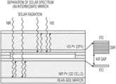
- FIG. 2shows a schematic illustration of the separation of the solar spectrum via an intermediate mirror in an exemplary organic/quantum dot multi-junction solar cell.
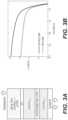
- FIG. 3 Ashows a schematic of a single junction solar cell with a DBR as an optical filter layer.
- FIG. 3 Bshows a graph of the measured photocurrent versus voltage for a single junction solar cell fabricated according to the layers in FIG. 3 A .
- FIG. 4shows a table summarizing the performance of a single junction solar cell with and without a DBR optical filter.
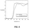
- FIG. 5shows a schematic of an exemplary DBR as an optical filter layer.
- FIG. 6shows a graph of the transmittance of light versus wavelength of light for the DBR of FIG. 5 .
- FIG. 1shows a schematic illustration of an exemplary method of fabricating an exemplary multi-junction solar cell comprising sub-cells of organic and quantum dot photoactive layers.
- the organic 104 and quantum dot 112 photoactive layersmay be separately fabricated on different substrates, 108 and 116 , respectively.
- the organic photoactive layer 104is the top sub-cell and is fabricated on a transparent substrate, such as glass 108 , and employs transparent contacts 102 , 106 .
- the quantum dot 112 photoactive layermay be the bottom layer and be fabricated on a nontransparent substrate 116 , and employs at least one transparent contact 110 , but may also include at least one metal contact 114 .
- the transparent contactsmay be ITO, IZO, AZO or PEDOT:PSS.
- sub-cellsmay be fabricated on an individual substrate via vacuum thermal evaporation or solution process.
- an optical filter layer 202 , 302is patterned on the top sub-cell, as shown in FIG. 1 . 2 .
- the optical filter layeris patterned using a shadow mask, though other patterning methods may be used.
- a grid 320is patterned on both the top and bottom sub-cells, as shown in FIG. 1 . 3 .
- the grid 320employs a noble metal or metal coated with noble metal, such as Au or Al/Au, and thereby avoids oxidation and other contamination.
- both sub-cellsare bonded via van der Waals bonding or cold-welding by applying pressure along with or without a slight increase in temperature to encourage bonding.
- cold-weld bondingis described by Lee et al. in “Multiple growths of epitaxial lift-off solar cells from a single InP substrate” (Kyusang Lee, Kuen-Ting Shiu, Jeramy D. Zimmerman, Christopher K. Renshaw and Stephen R. Forrest, Multiple growths of epitaxial lift-off solar cells from a single InP substrate, 97 Appl. Phys. Lett., 101107 (2010)).
- cold-weld bondingis further described by Kim et al.
- the surfaces of the epi-layer and the host substrateare generally pre-coated with layers of a similar noble metal (Au, Ni etc.), then appropriate pressure is applied between two metal interfaces.
- metal contactscan be inserted in the regions that are cold-weld bonded to separately contact individual stacked elements.
- the sub-cellsdo not require tunnel or interconnecting layers because sub-cells are connected by metal contacts in series, thereby considerably simplifying device fabrication.
- Application of this techniqueis not only limited to organic/quantum dot solar cells and other embodiments can be used for various solar cell structures (e.g.
- polymeramorphous/poly-crystalline/single crystalline Si, germanium, III-V semiconductors, kesterite, perovskite etc.
- Such embodimentsallow select wavelengths of light to pass through the top layer and be absorbed by the bottom layer, while reflecting other wavelengths of light to be absorbed in the top layer.
- the two sub-cellsare joined to form a multi-junction solar cell, as shown in FIG. 1 . 4 .
- the incident lightcan pass through the glass layer 416 and select wavelengths of light are absorbed by the organic photovoltaic layer 412 . Select wavelengths of light that are not absorbed by the organic photoactive layer 412 will reach the DBR, and said wavelengths will be transmitted or reflected depending on the configuration of the DBR.
- the photoactive layer beyond the DBRis a quantum dot photoactive layer 406 .
- one photoactive layeris organic photoactive layer absorbs light in the visible and ultraviolet spectrums and the other photoactive layer is a quantum dot photoactive layer that absorbs light in the near-infrared spectrum.
- the DBRmay be configured to reflect light in the visible spectrum and transmit light in the near infrared spectrum. Light that passes through the organic photoactive layer, the DBR and the quantum dot photoactive layer may be reflected or absorbed by the metal contact layer 404 .
- the metal contact layermay serve as both an electrical contact and as a mirror on the back of the multi-junction solar cell.
- the currents delivered by each sub-cellshould be equal to maximize the solar cell performance.
- the voltageshould be equalized between cells to maximize performance.
- Some embodimentsmay be comprised of a dual near infrared cell stack connected in parallel with a single shorter wavelength device, when parallel connection is desired in the design.
- the deviceis a photodetector that is sensitive to multiple wavelength signal channels, there is no requirement for either balance of voltage or current.
- the exemplary embodiment in FIG. 1represents a double stacked device.
- Other embodimentsmay include additional photoactive elements, such as doped silicon or titanium dioxide, that may absorb different wavelengths of the solar spectrum or other wavelengths of interest.
- Optical filters, such as 202 and 302may or may not be placed between each additional photoactive layer in the stack. Further, air gaps between layers may or may not be present.
- this devicemay be a photovoltaic device. In other embodiments, this device may be configured to be a photodetector that may de-multiplex narrow spectral signals emitted from a signal source.
- the multi-junction photosensitive devicemay comprise, at least two photoactive layers, and at least one optical filter layer, wherein at least two layers are bonded using cold weld or van der Waals bonding.
- the at least one optical filter layeris a DBR.
- the multi-junction devicemay comprise at least three photoactive layers, and at least two optical filter layers, wherein at least one optical filter layer is located between each photoactive layer.
- At least one photoactive layermay absorb wavelengths of light different than at least one other photoactive layer.
- a photoactive layer below at least one other layerabsorbs light in the near infrared.
- the near infrared spectrumincludes wavelengths in the range of 0.75 to 1.4 microns.
- the wavelengthsmay include wavelengths up to 30 microns.
- a photoactive layer, above at least one other layerabsorbs light in the ultraviolet spectrum.
- the ultraviolet spectrumincludes wavelengths shorter than 400 nanometers.
- at least one photoactive layerabsorbs a range of wavelengths of light spanning 10 nm different than at least one other photoactive layer.
- wavelength selective optical filter layersare placed between at least two photoactive layers of the multi-junction photosensitive device. In some embodiments an air gap between the photoactive layers may or may not be present.
- At least one photoactive layeris individually connected to a metal contact in regions that are cold weld or van der Waals bonded.
- individual cellsare connected in series. In some embodiments, individual cells are connected in parallel.
- At least one group of individual cellsis connected in series and at least one group is connected in parallel.
- at least one photoactive layercomprises materials chosen from organic photovoltaic, quantum dots, silicon, germanium, III-V semiconductors, kesterite, and perovskite.
- at least one photoactive layercomprises PbS quantum dots.
- the present disclosureis directed to a photodetector configured to de-multiplex spectral signals emitted from a signal source.
- the present disclosureis directed to a method of fabricating a multi-junction photosensitive device.
- the methodmay include fabricating at least two photoactive layers, patterning at least one optical filter layer on the at least one photoactive layer fabricated on a transparent substrate, and bonding at least two photoactive layers using cold weld bonding.
- at least one photoactive layeris fabricated on a transparent substrate.
- at least one photoactive layeris fabricated on a reflective substrate.
- at least one optical filter layeris a DBR.
- the methodfurther comprises fabricating at least one additional photoactive layer on a transparent substrate, and the transparent substrate may include a photoactive layer.
- FIG. 2shows a schematic illustration of the photon absorption process in an exemplary organic/quantum dot multi-junction solar cell.
- the exemplary mulitjunction solar cellis comprises a visible photovoltaic (VIS PV) which may be an organic photovoltaic layer (OPV), a DBR between two transparent contacts (ITO), a near infrared photovoltaic (NIR PV) which may be a quantum dot layer (QD cells), and a mirror on the back of the solar cell to reflect NIR light that is transmitted by the DBR and not initially absorbed by the NIR PV.
- the organic front sub-cellconfines visible photons to the top sub-cell via a DBR, whereas only the near infrared light is transmitted into the bottom cell.
- the quantum dot bottom sub-cellhas a metal contact reflector for near infrared light reflection.
- the intermediate optical filterin this case a DBR
- the solar spectrumcan be selectively separated into sub-cells.
- a DBRis generally composed of alternating materials with at least two different refractive indices.
- a DBRmay comprise a single material with a periodic variation of a characteristic (e.g. height) that results in variations of the effective refractive index.
- Reflection and transmission characteristics of the intermediate optical filtercan be controlled by properly designing the DBR and/or the air gap thickness. Control over the reflection of the balance of photocurrent can be achieved between sub-cells to maximize the multi-junction solar cell performance.
- various embodimentsmay employ a thinner photoactive layer than necessary otherwise, because the optical path length of the organic layer will be lengthened as the light passes through the photoactive layer again after reflection.
- a solar cell fabricated according to the layers shown in FIG. 3 Ademonstrates one envisioned benefit of an optical filter layer.
- the solar cellincludes organic photoactive layers comprising DTDCPB:C 70 layers and an interconnecting layer between the organic photoactive layers.
- the photoactive layersare situated between transparent contact layers (ITO), and the DBR is situated on the rear, relative to incident light, of the solar cell.
- the DBR of FIG. 3 Acomprises eleven alternating layers of Zinc Selenide and Magnesium Fluoride, configured such that the DBR has an onset of transmission of for light with a wavelength greater than 700 nm.
- the DBR of FIG. 3 Bis abbreviated as DBR@700 nm, ZnSe/MgF 2 and is described in more detail in FIG. 5 .
- FIG. 3 Bshows a graph of the measured photocurrent versus voltage for a solar cell fabricated according to the layers in FIG. 3 A , compared to a solar cell fabricated according to the same layers except for the DBR layer, as in FIG. 3 A .
- the results of the solar cell performanceare summarized in FIG. 4 illustrate the increased power conversion efficiency of a solar cell when utilizing a DBR.
- FIG. 5shows a schematic of the exemplary DBR shown in FIG. 3 A , and comprises a total of eleven layers of ZnSe and MgF 2 .
- the transmission of the solar cell of FIG. 3 A and the DBR aloneis shown in the graph of FIG. 6 , and illustrates an onset of transmission of light for wavelengths longer than 700 nm, while the wavelengths of light shorter than 700 nm are at least partially reflected.
Landscapes
- Physics & Mathematics (AREA)
- Electromagnetism (AREA)
- Engineering & Computer Science (AREA)
- Chemical & Material Sciences (AREA)
- Materials Engineering (AREA)
- Nanotechnology (AREA)
- Photovoltaic Devices (AREA)
- Life Sciences & Earth Sciences (AREA)
- Sustainable Energy (AREA)
- Sustainable Development (AREA)
- Manufacturing & Machinery (AREA)
Abstract
Description
Claims (15)
Priority Applications (1)
| Application Number | Priority Date | Filing Date | Title |
|---|---|---|---|
| US15/552,303US11889709B2 (en) | 2015-02-27 | 2016-02-29 | Mechanically stacked tandem photovoltaic cells with intermediate optical filters |
Applications Claiming Priority (3)
| Application Number | Priority Date | Filing Date | Title |
|---|---|---|---|
| US201562126326P | 2015-02-27 | 2015-02-27 | |
| US15/552,303US11889709B2 (en) | 2015-02-27 | 2016-02-29 | Mechanically stacked tandem photovoltaic cells with intermediate optical filters |
| PCT/US2016/020039WO2016138514A1 (en) | 2015-02-27 | 2016-02-29 | Mechanically stacked tandem photovoltaic cells with intermediate optical filters |
Publications (2)
| Publication Number | Publication Date |
|---|---|
| US20180047922A1 US20180047922A1 (en) | 2018-02-15 |
| US11889709B2true US11889709B2 (en) | 2024-01-30 |
Family
ID=55543076
Family Applications (1)
| Application Number | Title | Priority Date | Filing Date |
|---|---|---|---|
| US15/552,303ActiveUS11889709B2 (en) | 2015-02-27 | 2016-02-29 | Mechanically stacked tandem photovoltaic cells with intermediate optical filters |
Country Status (7)
| Country | Link |
|---|---|
| US (1) | US11889709B2 (en) |
| EP (1) | EP3262693B1 (en) |
| JP (1) | JP7057132B2 (en) |
| KR (1) | KR102467716B1 (en) |
| CN (1) | CN107534066A (en) |
| TW (1) | TWI840317B (en) |
| WO (1) | WO2016138514A1 (en) |
Families Citing this family (17)
| Publication number | Priority date | Publication date | Assignee | Title |
|---|---|---|---|---|
| US20170040557A1 (en)* | 2015-08-05 | 2017-02-09 | The Board Of Trustees Of The Leland Stanford Junior University | Tandem Photovoltaic Module Comprising a Control Circuit |
| WO2020243306A1 (en)* | 2019-05-29 | 2020-12-03 | North Carolina State University | Heat insulating transparent tandem organic solar cells |
| CN110635041A (en)* | 2019-09-03 | 2019-12-31 | 理天光电科技(苏州)有限公司 | Thin film solar cell and preparation method thereof |
| US11164792B2 (en) | 2020-01-08 | 2021-11-02 | International Business Machines Corporation | Complementary field-effect transistors |
| US11069684B1 (en) | 2020-03-04 | 2021-07-20 | International Business Machines Corporation | Stacked field effect transistors with reduced coupling effect |
| IL273118B (en) | 2020-03-05 | 2022-03-01 | Allen Richter | Self-adaptive electromagnetic energy attenuator |
| US11164793B2 (en) | 2020-03-23 | 2021-11-02 | International Business Machines Corporation | Reduced source/drain coupling for CFET |
| CN112186061A (en)* | 2020-09-21 | 2021-01-05 | 浙江大学绍兴微电子研究中心 | Laminated solar cell with built-in optical filter |
| TWI820822B (en) | 2021-08-23 | 2023-11-01 | 天光材料科技股份有限公司 | Structure of the photodiode |
| CN115763607B (en)* | 2021-09-01 | 2024-10-29 | 隆基绿能科技股份有限公司 | Color stack photovoltaic device |
| CN115768145A (en)* | 2021-09-01 | 2023-03-07 | 隆基绿能科技股份有限公司 | Laminated solar cell and photovoltaic module |
| CN113809120B (en)* | 2021-09-16 | 2023-06-20 | 北京载诚科技有限公司 | Laminated solar cell |
| CN113809121B (en)* | 2021-09-16 | 2023-07-04 | 北京载诚科技有限公司 | Laminated solar cell |
| CN115312563A (en)* | 2022-07-29 | 2022-11-08 | 青海黄河上游水电开发有限责任公司 | Two-end type laminated solar cell based on metal grid interconnection and preparation method thereof |
| CN115332292A (en)* | 2022-07-29 | 2022-11-11 | 青海黄河上游水电开发有限责任公司 | Two-end type laminated solar cell based on metal grid interconnection and preparation method thereof |
| CN115513310A (en)* | 2022-11-02 | 2022-12-23 | 太原国科半导体光电研究院有限公司 | A type II superlattice infrared detector unit structure and its preparation method, and a type II superlattice infrared focal plane detector |
| JP2025140240A (en)* | 2024-03-13 | 2025-09-29 | 株式会社東芝 | Solar cells and photovoltaic power generation systems |
Citations (19)
| Publication number | Priority date | Publication date | Assignee | Title |
|---|---|---|---|---|
| JPH02106979A (en) | 1988-10-17 | 1990-04-19 | Mitsubishi Electric Corp | Wavelength demultiplexing photodetector |
| US20050126628A1 (en)* | 2002-09-05 | 2005-06-16 | Nanosys, Inc. | Nanostructure and nanocomposite based compositions and photovoltaic devices |
| US20080190479A1 (en) | 2007-02-13 | 2008-08-14 | Epistar Corporation | Optoelectronical semiconductor device |
| US20100059111A1 (en) | 2008-09-05 | 2010-03-11 | Myung-Hun Shin | Solar Cell Module having Multiple Module Layers and Manufacturing Method Thereof |
| US20100122764A1 (en)* | 2008-11-14 | 2010-05-20 | Emcore Solar Power, Inc. | Surrogate Substrates for Inverted Metamorphic Multijunction Solar Cells |
| US20100147366A1 (en) | 2008-12-17 | 2010-06-17 | Emcore Solar Power, Inc. | Inverted Metamorphic Multijunction Solar Cells with Distributed Bragg Reflector |
| US20100269896A1 (en)* | 2008-09-11 | 2010-10-28 | Applied Materials, Inc. | Microcrystalline silicon alloys for thin film and wafer based solar applications |
| US20110155233A1 (en)* | 2009-12-29 | 2011-06-30 | Honeywell International Inc. | Hybrid solar cells |
| US20110155207A1 (en)* | 2008-05-12 | 2011-06-30 | Villanova University | Solar cells and method of making solar cells |
| WO2011118890A1 (en)* | 2010-03-26 | 2011-09-29 | Gwangju Institute Of Science And Technology | Tandem solar cell and method of manufacturing the same |
| US20120000518A1 (en)* | 2009-03-18 | 2012-01-05 | Mitsubishi Electric Corporation | Photoelectric conversion device and method of manufacturing the same |
| US20120180854A1 (en)* | 2011-01-18 | 2012-07-19 | Bellanger Mathieu | Mechanical stacking structure for multi-junction photovoltaic devices and method of making |
| US20120285520A1 (en)* | 2011-05-13 | 2012-11-15 | International Business Machines Corporation | Wafer bonded solar cells and fabrication methods |
| US20130014813A1 (en) | 2011-01-11 | 2013-01-17 | Weiming Wang | HIGH EFFICIENCY AND LOW COST GaInP/GaAs/Si TRIPLE JUNCTION BY EPITAXY LIFT-OFF AND MECHANICAL STACK |
| US20130037095A1 (en)* | 2011-07-06 | 2013-02-14 | Stephen R. Forrest | Integrated solar collectors using epitaxial lift off and cold weld bonded semiconductor solar cells |
| US20130048064A1 (en)* | 2011-08-29 | 2013-02-28 | Alliance For Sustainable Energy, Llc | Interconnections for Mechanically Stacked Multijunction Solar Cells |
| US20130206219A1 (en)* | 2010-08-06 | 2013-08-15 | Juanita N. Kurtin | Cooperative photovoltaic networks and photovoltaic cell adaptations for use therein |
| US20140182667A1 (en) | 2013-01-03 | 2014-07-03 | Benjamin C. Richards | Multijunction solar cell with low band gap absorbing layer in the middle cell |
| EP2760054A1 (en) | 2011-09-21 | 2014-07-30 | Sony Corporation | Multi-junction solar cell, compound semiconductor device, photoelectric conversion element, and compound semiconductor layer laminated structure |
Family Cites Families (2)
| Publication number | Priority date | Publication date | Assignee | Title |
|---|---|---|---|---|
| IT1399542B1 (en)* | 2010-04-23 | 2013-04-19 | Bortolussi | FIXING DEVICE FOR MOBILE WIRES OF A PLANT WIRE |
| CN103107229B (en)* | 2013-02-25 | 2015-09-09 | 中国科学院苏州纳米技术与纳米仿生研究所 | Graphene/semiconductor multijunction solar cell and preparation method thereof |
- 2016
- 2016-02-29CNCN201680012278.8Apatent/CN107534066A/enactivePending
- 2016-02-29EPEP16710555.0Apatent/EP3262693B1/enactiveActive
- 2016-02-29USUS15/552,303patent/US11889709B2/enactiveActive
- 2016-02-29KRKR1020177026561Apatent/KR102467716B1/enactiveActive
- 2016-02-29JPJP2017544964Apatent/JP7057132B2/enactiveActive
- 2016-02-29WOPCT/US2016/020039patent/WO2016138514A1/ennot_activeCeased
- 2016-03-01TWTW105106226Apatent/TWI840317B/enactive
Patent Citations (19)
| Publication number | Priority date | Publication date | Assignee | Title |
|---|---|---|---|---|
| JPH02106979A (en) | 1988-10-17 | 1990-04-19 | Mitsubishi Electric Corp | Wavelength demultiplexing photodetector |
| US20050126628A1 (en)* | 2002-09-05 | 2005-06-16 | Nanosys, Inc. | Nanostructure and nanocomposite based compositions and photovoltaic devices |
| US20080190479A1 (en) | 2007-02-13 | 2008-08-14 | Epistar Corporation | Optoelectronical semiconductor device |
| US20110155207A1 (en)* | 2008-05-12 | 2011-06-30 | Villanova University | Solar cells and method of making solar cells |
| US20100059111A1 (en) | 2008-09-05 | 2010-03-11 | Myung-Hun Shin | Solar Cell Module having Multiple Module Layers and Manufacturing Method Thereof |
| US20100269896A1 (en)* | 2008-09-11 | 2010-10-28 | Applied Materials, Inc. | Microcrystalline silicon alloys for thin film and wafer based solar applications |
| US20100122764A1 (en)* | 2008-11-14 | 2010-05-20 | Emcore Solar Power, Inc. | Surrogate Substrates for Inverted Metamorphic Multijunction Solar Cells |
| US20100147366A1 (en) | 2008-12-17 | 2010-06-17 | Emcore Solar Power, Inc. | Inverted Metamorphic Multijunction Solar Cells with Distributed Bragg Reflector |
| US20120000518A1 (en)* | 2009-03-18 | 2012-01-05 | Mitsubishi Electric Corporation | Photoelectric conversion device and method of manufacturing the same |
| US20110155233A1 (en)* | 2009-12-29 | 2011-06-30 | Honeywell International Inc. | Hybrid solar cells |
| WO2011118890A1 (en)* | 2010-03-26 | 2011-09-29 | Gwangju Institute Of Science And Technology | Tandem solar cell and method of manufacturing the same |
| US20130206219A1 (en)* | 2010-08-06 | 2013-08-15 | Juanita N. Kurtin | Cooperative photovoltaic networks and photovoltaic cell adaptations for use therein |
| US20130014813A1 (en) | 2011-01-11 | 2013-01-17 | Weiming Wang | HIGH EFFICIENCY AND LOW COST GaInP/GaAs/Si TRIPLE JUNCTION BY EPITAXY LIFT-OFF AND MECHANICAL STACK |
| US20120180854A1 (en)* | 2011-01-18 | 2012-07-19 | Bellanger Mathieu | Mechanical stacking structure for multi-junction photovoltaic devices and method of making |
| US20120285520A1 (en)* | 2011-05-13 | 2012-11-15 | International Business Machines Corporation | Wafer bonded solar cells and fabrication methods |
| US20130037095A1 (en)* | 2011-07-06 | 2013-02-14 | Stephen R. Forrest | Integrated solar collectors using epitaxial lift off and cold weld bonded semiconductor solar cells |
| US20130048064A1 (en)* | 2011-08-29 | 2013-02-28 | Alliance For Sustainable Energy, Llc | Interconnections for Mechanically Stacked Multijunction Solar Cells |
| EP2760054A1 (en) | 2011-09-21 | 2014-07-30 | Sony Corporation | Multi-junction solar cell, compound semiconductor device, photoelectric conversion element, and compound semiconductor layer laminated structure |
| US20140182667A1 (en) | 2013-01-03 | 2014-07-03 | Benjamin C. Richards | Multijunction solar cell with low band gap absorbing layer in the middle cell |
Non-Patent Citations (3)
| Title |
|---|
| Ferguson et al., "Contact Adhesion of Thin Gold Films on Elastomeric Supports: Cold Welding Under Ambient Conditions," Science, vol. 253, No. 5021, pp. 776-778 (1991). |
| International Search Report & Written Opinion, PCT/US2016/020039, dated May 23, 2016. |
| Kim et al., "Micropatterning of Organic Electronic Devices by Cold-Welding," Science, vol. 288, No. 5467, pp. 831-833 (2000). |
Also Published As
| Publication number | Publication date |
|---|---|
| EP3262693A1 (en) | 2018-01-03 |
| JP2018506861A (en) | 2018-03-08 |
| EP3262693B1 (en) | 2024-12-25 |
| JP7057132B2 (en) | 2022-04-19 |
| TWI840317B (en) | 2024-05-01 |
| CN107534066A (en) | 2018-01-02 |
| WO2016138514A1 (en) | 2016-09-01 |
| KR102467716B1 (en) | 2022-11-15 |
| KR20170123643A (en) | 2017-11-08 |
| TW201705510A (en) | 2017-02-01 |
| US20180047922A1 (en) | 2018-02-15 |
Similar Documents
| Publication | Publication Date | Title |
|---|---|---|
| US11889709B2 (en) | Mechanically stacked tandem photovoltaic cells with intermediate optical filters | |
| US8354583B2 (en) | Solar cells arrangement | |
| US8637759B2 (en) | Notch filter for triple junction solar cells | |
| CN101897036B (en) | Photovoltaics with interferometric ribbon masks | |
| US20150349147A1 (en) | Broad Band Anti-Reflection Coating for Photovoltaic Devices and Other Devices | |
| EP2901496B1 (en) | Photovoltaic component with a high conversion efficiency | |
| CN101563790B (en) | Photodiode, optical communication device and optical interconnection module | |
| CN101828144A (en) | Photovoltaic devices with integrated color interferometric film stacks | |
| Ouellette et al. | Optical resonance engineering for infrared colloidal quantum dot photovoltaics | |
| JP2015019063A (en) | Adhesive bonded solar cell assembly | |
| US20110132455A1 (en) | Solar cell with luminescent member | |
| US11476378B2 (en) | Solar-energy apparatus, methods, and applications | |
| US20120325299A1 (en) | Photonic Bandgap Solar Cells | |
| US12245448B2 (en) | Heat insulating transparent tandem organic solar cells | |
| US20130192666A1 (en) | Photoconversion device with enhanced photon absorption | |
| US11764235B2 (en) | Tandem solar cell module | |
| Tahersima et al. | Silicon nitride grating based planar spectral splitting concentrator for NIR light Harvesting | |
| CN119744037A (en) | A colored photovoltaic module | |
| US20170012157A1 (en) | Spectral light splitting module and photovoltaic system |
Legal Events
| Date | Code | Title | Description |
|---|---|---|---|
| AS | Assignment | Owner name:THE REGENTS OF THE UNIVERSITY OF MICHIGAN, MICHIGAN Free format text:ASSIGNMENT OF ASSIGNORS INTEREST;ASSIGNORS:FORREST, STEPHEN R;LEE, KYUSANG;SIGNING DATES FROM 20150326 TO 20150327;REEL/FRAME:043340/0214 Owner name:THE REGENTS OF THE UNIVERSITY OF MICHIGAN, MICHIGA Free format text:ASSIGNMENT OF ASSIGNORS INTEREST;ASSIGNORS:FORREST, STEPHEN R;LEE, KYUSANG;SIGNING DATES FROM 20150326 TO 20150327;REEL/FRAME:043340/0214 | |
| AS | Assignment | Owner name:UNITED STATES DEPARTMENT OF ENERGY, DISTRICT OF COLUMBIA Free format text:CONFIRMATORY LICENSE;ASSIGNOR:UNIVERSITY OF MICHIGAN;REEL/FRAME:047865/0510 Effective date:20180823 Owner name:UNITED STATES DEPARTMENT OF ENERGY, DISTRICT OF CO Free format text:CONFIRMATORY LICENSE;ASSIGNOR:UNIVERSITY OF MICHIGAN;REEL/FRAME:047865/0510 Effective date:20180823 | |
| STPP | Information on status: patent application and granting procedure in general | Free format text:NON FINAL ACTION MAILED | |
| STPP | Information on status: patent application and granting procedure in general | Free format text:RESPONSE TO NON-FINAL OFFICE ACTION ENTERED AND FORWARDED TO EXAMINER | |
| STPP | Information on status: patent application and granting procedure in general | Free format text:FINAL REJECTION MAILED | |
| STCV | Information on status: appeal procedure | Free format text:NOTICE OF APPEAL FILED | |
| STPP | Information on status: patent application and granting procedure in general | Free format text:DOCKETED NEW CASE - READY FOR EXAMINATION | |
| STPP | Information on status: patent application and granting procedure in general | Free format text:NON FINAL ACTION MAILED | |
| STPP | Information on status: patent application and granting procedure in general | Free format text:RESPONSE TO NON-FINAL OFFICE ACTION ENTERED AND FORWARDED TO EXAMINER | |
| STPP | Information on status: patent application and granting procedure in general | Free format text:FINAL REJECTION MAILED | |
| STPP | Information on status: patent application and granting procedure in general | Free format text:DOCKETED NEW CASE - READY FOR EXAMINATION | |
| STPP | Information on status: patent application and granting procedure in general | Free format text:NON FINAL ACTION MAILED | |
| STPP | Information on status: patent application and granting procedure in general | Free format text:RESPONSE TO NON-FINAL OFFICE ACTION ENTERED AND FORWARDED TO EXAMINER | |
| STPP | Information on status: patent application and granting procedure in general | Free format text:NOTICE OF ALLOWANCE MAILED -- APPLICATION RECEIVED IN OFFICE OF PUBLICATIONS | |
| STPP | Information on status: patent application and granting procedure in general | Free format text:PUBLICATIONS -- ISSUE FEE PAYMENT RECEIVED | |
| STPP | Information on status: patent application and granting procedure in general | Free format text:PUBLICATIONS -- ISSUE FEE PAYMENT VERIFIED | |
| STCF | Information on status: patent grant | Free format text:PATENTED CASE |