US11885696B2 - Vibrating wire sensor and vibrating wire for a vibrating wire sensor - Google Patents
Vibrating wire sensor and vibrating wire for a vibrating wire sensorDownload PDFInfo
- Publication number
- US11885696B2 US11885696B2US16/484,984US201816484984AUS11885696B2US 11885696 B2US11885696 B2US 11885696B2US 201816484984 AUS201816484984 AUS 201816484984AUS 11885696 B2US11885696 B2US 11885696B2
- Authority
- US
- United States
- Prior art keywords
- vibrating wire
- exciter
- layer
- vibrating
- electrode
- Prior art date
- Legal status (The legal status is an assumption and is not a legal conclusion. Google has not performed a legal analysis and makes no representation as to the accuracy of the status listed.)
- Active, expires
Links
- 230000004913activationEffects0.000claimsabstractdescription34
- 238000005259measurementMethods0.000claimsabstractdescription8
- 239000004020conductorSubstances0.000claimsdescription19
- 230000005540biological transmissionEffects0.000claimsdescription3
- 230000007935neutral effectEffects0.000claimsdescription3
- 229910045601alloyInorganic materials0.000claimsdescription2
- 239000000956alloySubstances0.000claimsdescription2
- 238000004544sputter depositionMethods0.000description5
- XLOMVQKBTHCTTD-UHFFFAOYSA-NZinc monoxideChemical compound[Zn]=OXLOMVQKBTHCTTD-UHFFFAOYSA-N0.000description4
- PNEYBMLMFCGWSK-UHFFFAOYSA-Naluminium oxideInorganic materials[O-2].[O-2].[O-2].[Al+3].[Al+3]PNEYBMLMFCGWSK-UHFFFAOYSA-N0.000description4
- 238000006073displacement reactionMethods0.000description3
- 230000010287polarizationEffects0.000description3
- 239000013078crystalSubstances0.000description2
- PCHJSUWPFVWCPO-UHFFFAOYSA-NgoldChemical compound[Au]PCHJSUWPFVWCPO-UHFFFAOYSA-N0.000description2
- 239000010931goldSubstances0.000description2
- 229910052737goldInorganic materials0.000description2
- 238000009413insulationMethods0.000description2
- 238000000034methodMethods0.000description2
- 239000011787zinc oxideSubstances0.000description2
- 229910000906BronzeInorganic materials0.000description1
- 238000005452bendingMethods0.000description1
- 230000015572biosynthetic processEffects0.000description1
- 239000003990capacitorSubstances0.000description1
- 238000000576coating methodMethods0.000description1
- 229910052593corundumInorganic materials0.000description1
- 230000001419dependent effectEffects0.000description1
- 238000010586diagramMethods0.000description1
- 230000000694effectsEffects0.000description1
- 238000004519manufacturing processMethods0.000description1
- 239000000463materialSubstances0.000description1
- 229910052751metalInorganic materials0.000description1
- 239000002184metalSubstances0.000description1
- 238000012544monitoring processMethods0.000description1
- 229910052706scandiumInorganic materials0.000description1
- SIXSYDAISGFNSX-UHFFFAOYSA-Nscandium atomChemical compound[Sc]SIXSYDAISGFNSX-UHFFFAOYSA-N0.000description1
- 230000035945sensitivityEffects0.000description1
- 238000013519translationMethods0.000description1
- 230000001960triggered effectEffects0.000description1
- 229910001845yogo sapphireInorganic materials0.000description1
Images


Classifications
- G—PHYSICS
- G01—MEASURING; TESTING
- G01L—MEASURING FORCE, STRESS, TORQUE, WORK, MECHANICAL POWER, MECHANICAL EFFICIENCY, OR FLUID PRESSURE
- G01L1/00—Measuring force or stress, in general
- G01L1/20—Measuring force or stress, in general by measuring variations in ohmic resistance of solid materials or of electrically-conductive fluids; by making use of electrokinetic cells, i.e. liquid-containing cells wherein an electrical potential is produced or varied upon the application of stress
- G01L1/22—Measuring force or stress, in general by measuring variations in ohmic resistance of solid materials or of electrically-conductive fluids; by making use of electrokinetic cells, i.e. liquid-containing cells wherein an electrical potential is produced or varied upon the application of stress using resistance strain gauges
- G01L1/2287—Measuring force or stress, in general by measuring variations in ohmic resistance of solid materials or of electrically-conductive fluids; by making use of electrokinetic cells, i.e. liquid-containing cells wherein an electrical potential is produced or varied upon the application of stress using resistance strain gauges constructional details of the strain gauges
- G—PHYSICS
- G01—MEASURING; TESTING
- G01L—MEASURING FORCE, STRESS, TORQUE, WORK, MECHANICAL POWER, MECHANICAL EFFICIENCY, OR FLUID PRESSURE
- G01L1/00—Measuring force or stress, in general
- G01L1/16—Measuring force or stress, in general using properties of piezoelectric devices
- G01L1/162—Measuring force or stress, in general using properties of piezoelectric devices using piezoelectric resonators
- G—PHYSICS
- G01—MEASURING; TESTING
- G01B—MEASURING LENGTH, THICKNESS OR SIMILAR LINEAR DIMENSIONS; MEASURING ANGLES; MEASURING AREAS; MEASURING IRREGULARITIES OF SURFACES OR CONTOURS
- G01B7/00—Measuring arrangements characterised by the use of electric or magnetic techniques
- G01B7/16—Measuring arrangements characterised by the use of electric or magnetic techniques for measuring the deformation in a solid, e.g. by resistance strain gauge
- G01B7/18—Measuring arrangements characterised by the use of electric or magnetic techniques for measuring the deformation in a solid, e.g. by resistance strain gauge using change in resistance
- G—PHYSICS
- G01—MEASURING; TESTING
- G01L—MEASURING FORCE, STRESS, TORQUE, WORK, MECHANICAL POWER, MECHANICAL EFFICIENCY, OR FLUID PRESSURE
- G01L1/00—Measuring force or stress, in general
- G01L1/10—Measuring force or stress, in general by measuring variations of frequency of stressed vibrating elements, e.g. of stressed strings
- G01L1/106—Constructional details
- G—PHYSICS
- G01—MEASURING; TESTING
- G01L—MEASURING FORCE, STRESS, TORQUE, WORK, MECHANICAL POWER, MECHANICAL EFFICIENCY, OR FLUID PRESSURE
- G01L5/00—Apparatus for, or methods of, measuring force, work, mechanical power, or torque, specially adapted for specific purposes
- G01L5/04—Apparatus for, or methods of, measuring force, work, mechanical power, or torque, specially adapted for specific purposes for measuring tension in flexible members, e.g. ropes, cables, wires, threads, belts or bands
- H—ELECTRICITY
- H10—SEMICONDUCTOR DEVICES; ELECTRIC SOLID-STATE DEVICES NOT OTHERWISE PROVIDED FOR
- H10N—ELECTRIC SOLID-STATE DEVICES NOT OTHERWISE PROVIDED FOR
- H10N30/00—Piezoelectric or electrostrictive devices
Definitions
- the present inventionrelates to a vibrating wire sensor and a vibrating wire for a vibrating wire sensor according to the preamble of claims 1 and 10 .
- Vibrating wire sensorsare known and used in numerous applications, frequently (but by no means exclusively) to measure an actual quantity such as deformations or forces.
- deformationis understood in the present case as the elastic or also plastic deformation of machine elements during operation. Such deformation can be relevant for monitoring the safe operating state in metal structures of any kind or also in non-metallic structures such as building or bridges.
- a load currently acting during operationcan be detected by means of deformation sensors, for example, for the control of a movement.
- This deformationis detected by the vibrating wire sensor thus acting as a deformation/force sensor, for example, via the displacement between measurement points, wherein a force thereby acts on the sensor which is a measure for the deformation.
- the sensor according to the inventioncan also be used as a pure force sensor, for example, in a balance.
- Vibrating wire sensorscan be configured in such a manner that they detect extremely small deformations or force variations in a finely resolved manner and in addition barely have any drift over time—in this respect vibrating wire sensors are frequently qualitatively superior to load cells or strain gauges.
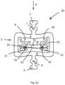
- FIG. 1One embodiment of such a vibrating wire sensor has become known from CN 203 595 494 U and is shown in FIG. 1 .
- a vibrating wire sensor 1 in operationcan be seen, i.e. under measurement conditions, having a frame 2 which is configured to be rectangular here, having fixing elements 3 , 4 which act on transverse members 5 , 6 of the frame 2 , and which for their part are fixed by means of their fastening points 7 , 8 to a component, not shown so as not to overburden the figure, the deformation of which is to be measured or, for example, a component of a balance in which the weight to be weighed is to be determined (a fixing can be accomplished via a simple screw connection or by a simple clamping of any kind).
- the senor 1Under the measurement conditions, here in the case of a deformation of the component or a force which occurs and which is to be measured, the sensor 1 experiences a force, for example, in the direction of the arrow K (or the opposite direction thereof), whereby its frame 2 becomes elastically deformed in the action of the force, which in turn results in a deflection of the transmission lever 9 , 10 , on the heads 11 , 12 of which a vibrating wire 15 is clamped with the aid of clamping pins 16 .
- a distance-force translationis obtained from the fastening points 7 , 8 to the heads 11 , 12 or clamping pins 16 so that the vibrating wire 15 is subjected to varying tensile stress according to the deformation which is actually present or the force to be measured, wherein naturally in the rest position of the sensor, i.e. without any effect of the surroundings on the fastening points 7 , 8 the vibrating wire 15 is tensioned in a predetermined manner.
- the heads 11 , 12 with the clamping pins 16form clamping points for the vibrating wire 15 .
- an arrangement 17which generates a magnetic field during operation, whose field lines are perpendicular to the plane of the drawing and in the left half of the arrangement 17 are directed away from the observer and in the right half, are directed towards the observer.
- an alternating current Iflows through the vibrating wire 15 which is generated by an electronics system which is again omitted so as not to overload the figure.
- the Lorentz force corresponding to the alternating current Iacts on the vibrating wire, which makes this vibrate at the frequency of the alternating current, wherein with a suitable change in frequency the vibrating wire rapidly drops into its natural frequency which in turn depends on the tension acting on it, i.e. on the displacement of the measurement points 7 , 8 as a consequence of a deformation or action of force.
- the electronics systemcan detect the natural frequency and generate from this a sensor signal for the deformation/action of force.
- FIG. 1shows in summary form a vibrating wire sensor having a vibrating wire which is tensioned accordingly differently under measurement conditions of a current quantity to be detected and having an exciter arrangement for exciting a vibrating wire in the range of its natural frequency.
- Such vibrating wire sensorshave the disadvantage that their power consumption is really high or that during coarse handling, the magnets can be moved out of their correct position or the expenditure for the impact-free fastening is high.
- High power consumptionplays a role, for example, when a bridge is provided with deformation sensors whose batteries must be continuously changed or alternatively must be wired.
- the object of the present inventionis to improve vibrating wire sensors.
- a vibrating wire sensor according to the inventionhas the characterizing features of claim 1 and a vibrating wire according to the invention has the characterizing features of claim 11 .
- a vibrating wire sensorSince the vibrating wire of a vibrating wire sensor has a piezoelectric activation layer, the power consumption can be reduced considerably compared with conventional designs. In addition, magnets or other elements for generating a magnetic field are omitted and thus the elements which are decisive for the sensitivity of the sensor during rough treatment. Finally a vibrating wire sensor according to the invention has a compact structure.
- the piezoelectric activation layerhas a different length according to the activation state, a deformation of the vibrating wire over its length is obtained in the manner of a bimetal spring which is suitable to produce vibrations in a string.
- Embodiments of the vibrating wire sensor or the vibrating wire according to the inventionhave features according to the dependent claims.
- FIG. 1shows a vibrating wire sensor according to the prior art
- FIG. 2 ashows an embodiment of a vibrating wire sensor according to the invention
- FIG. 2 bshows an enlarged section from FIG. 2 a with the vibrating wire
- FIG. 3shows in schematic view an embodiment of a vibrating wire according to the invention in a vibrating wire sensor
- FIG. 4shows in schematic view another embodiment of a vibrating wire according to the invention in a vibrating wire sensor
- FIG. 5 ashows in schematic view a preferred embodiment of a vibrating wire according to the invention in a vibrating wire sensor
- FIG. 5 bshows a view of the vibrating wire from FIG. 5 a.
- FIG. 2 ashows the principle of the present invention by means of a preferred embodiment of a vibrating wire sensor 20 .
- the vibrating wire sensor 20 shown in operationcan (but need not) have the same basic structure as the vibrating wire sensor 1 from FIG. 1 .
- the arrangement 17 ( FIG. 1 ) for generating a magnetic fieldis absent.
- a vibrating wire 21can be seen, which is covered at least over a length portion, here over its entire length, by an exciter layer 22 indicated by the dashed line, which comprises a piezoelectric activation layer. Possible embodiments of the exciter layer 22 are described in detail in the figures.
- An alternating voltageis applied to the exciter layer 22 via clamping pins 23 or contact elements.
- the alternating voltageis generated by an electronics system of the vibrating wire sensor 20 which is omitted so as not to overburden the figure.
- the figureshows an operating state in which as a result of the applied alternating voltage, the piezoelectric activation layer of the exciter layer 22 in the left-hand portion 24 has an activation state in which it is lengthened and in the right-hand portion 25 has an activation state in which it is shortened.
- the vibrating wire 21curves in the manner of a bimetal spring, when viewed from left to right, towards the right in portion 24 , towards the left in portion 25 .
- This curvaturecorresponds to a vibration position of the vibrating wire with a vibration node in the centre (vibration frequencies above the audible threshold are desirable).
- FIG. 2 bshows in enlarged view a section of the vibrating wire sensor 20 in the region of the vibrating wire 21 , which, compared with the diagram from FIG. 2 a however, has a different vibration position corresponding to that a half-wave later than the alternating voltage active at the clamping pins 23 .
- the exciter layer 22 in the left-hand portion 24is shortened and lengthened in the right-hand portion 25 so that the vibrating wire 21 is curved to the left in the portion 24 and curved to the right in the portion 25 .
- the vibrating wire 21vibrates according to the applied alternating voltage, excited by the different activation states of the exciter layer 22 , to and fro between the vibration positions shown in FIGS. 2 a and 2 b , wherein the frequency of the alternating voltage is varied by the electronics system until the vibrating wire 21 vibrates in its current natural frequency.
- the current natural frequencyis determined by the current voltage of the vibrating wire 21 , given by the clamping pins 16 , 23 which apply tensile stress to the vibrating wire 21 according to the displacement of the measurement points 7 , 8 ( FIG. 1 ).
- the electronics systemgenerates a signal on the basis of the current natural frequency, which corresponds to the deformation or force to be detected by the sensor 20 .
- the exciter arrangement of a vibrating wire sensor according to the inventionhas at least one exciter layer provided on a longitudinal portion of the vibrating wire with a piezoelectric activation layer which has a different length according to the activation state and thus brings about an accordingly different vibration position of the vibrating wire.
- a vibrating wireis further obtained according to the invention which has a piezoelectric exciter layer provided on at least one longitudinal portion, which has a different length according to the activation state and thereby brings about a deformation of the vibrating wire over at least one longitudinal portion.
- the alternating voltagecan be applied to the end portions 27 , 28 of the vibrating wire 21 . It is thus possible to provide an arbitrary suitable material for the clamping pins (or clamping or holding elements of any kind). Corresponding conductors which lead from the end portions 27 , 28 to the electronics system of the vibrating wire sensor 20 are omitted so as not to overburden the figure.
- the vibrating wire 21is preferably configured to be thin and flat in cross-section, for example, rectangular (but can also be approximately oval or round) and has a low moment of inertia in the vibration plane—the vibrating wire is flexible, therefore in the deflected position has scarcely any spring-elastic restoring force given by the bending, with the result that it vibrates from a deflected position substantially due to the tension exerted via the clamping points back into its stretched position. This back-vibration can naturally be substantially assisted by the correspondingly clocked piezoelectric activation layer of the exciter layer 22 .
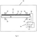
- FIG. 3shows a vibrating wire sensor 30 , schematically indicated by a rectangle, which can be configured, for example, as the vibrating wire sensor 1 from FIG. 1 apart from the components shown in FIG. 3 .
- the vibrating wire sensor 30comprises a vibrating wire 31 , with an excited layer 32 which comprises a piezoelectric activation layer as well as an electrode 34 , which extends over the length of the activation layer 33 .
- the vibrating wire 31is clamped in clamps 35 which are preferably configured as clamping pins ( FIG. 1 ) but can also be configured differently.
- a schematically depicted electronics system 36 of the vibrating wire sensorhas a voltage source 37 which is connected via a conductor 38 to the vibrating wire 31 and is connected via a conductor 39 to the electrode 34 .
- the remaining components of the vibrating wire sensorare omitted in order not to overburden the figure, in particular heads 11 , 12 ( FIG. 1 ) in which the clamps 35 are arranged.
- the figureshows for better representation as a result of distorted proportions, the vibrating wire 31 is in reality long and thin, e.g. 0.4 mm wide, 0.3 mm thick and 20 mm long.
- the exciter layer 32is thin, according to the method of manufacture, see below.
- the vibrating wire 31preferably consists of a beryllium-bronze alloy, which is very hard, barely lengthens under tension and does not creep, i.e. contributes to the precise, drift-proof operation of the vibrating wire sensor.
- the piezoelectric activation layer 33is preferably configured as an AlScN layer with scandium in the range of 15% to 30%. However, it can also consist of pure AlN.
- the electrodecan be implemented as a thin layer of gold.
- the activation layer 33is applied to the vibrating wire 31 by sputtering, likewise the electrode.
- the activation layer 33is heated above the Curie temperature, polarized by a suitable E field and then cooled, so that it becomes piezoelectrically activatable. It is also possible to polarize the piezolayer directly during sputtering.
- the sputtering processalso results in a manifestation of the crystal orientation or specific crystal types which can facilitate the subsequent polarization in certain orientations.
- the person skilled in the artis familiar with vibrating wires of the said type as well as piezoelectric coatings of AlScN which can be produced by sputtering.
- the electronics system 36is configured as mentioned above to deliver an alternating voltage during operation, for example, with a starting frequency which is close to the natural frequency of the vibrating wire 31 in the rest state of the vibrating wire sensor 30 .
- the frequencyis then increased until the vibrating wire 31 falls into its natural frequency which in turn can be identified by the electronics system from its impedance, at the natural frequency the apparent resistance z of the electrode—piezoelectric activation layer—electrode arrangement is minimal (this arrangement forms a capacitance).
- the natural frequencyis a measure for the tension acting on the vibrating wire 31 which in turn is a measure for the deformation or force to be detected so that the electronic system 36 can generate a signal of the detected current quantity (deformation, force) from the detected current natural frequency of the vibrating wire 31 .
- the exciter layer 32has electrodes 34 , 31 which encompass the activation layer between them and wherein the vibrating wire 31 forms one of the electrodes.
- the vibrating wirecan be coated with gold on the side of the piezoelectric activation layer 33 for its part to improve its conductivity.
- FIG. 4shows a vibrating wire sensor 40 with a further embodiment of a vibrating wire 41 , which is only provided with an exciter layer 42 over a longitudinal portion.
- the exciter layer 42is electrically insulated with respect to the vibrating wire 41 by an insulation layer 43 shown by the dashed line in the figure, for example made of Al 2 O 3 , aluminium oxide or ZnO, zinc oxide.
- an upper electrode 44a lower (i.e. arranged on the vibrating wire 41 ) electrode 45 is provided, the voltage source 37 of the electronics system 36 is connected via the conductor 38 to the lower electrode 45 and via the conductor 39 to the upper electrode 44 .
- the piezoelectric activation layer 46is surrounded by electrodes 44 , 45 over its length.
- the arrangement shownmakes it possible to avoid a current flow through the vibrating wire 41 which has a high Ohmic resistance as a result of its alloy (little longitudinal extension and low creep, see above). Thus, only comparatively low Ohmic resistances are present in the alternating voltage circuit.
- the energy requirement of the exciter layer 42is fundamentally low and particularly markedly low at the natural frequency of the vibrating wire 41 .
- a power consumption of 30% to 20%is obtained compared with a conventional vibrating wire sensor 1 ( FIG. 1 ).
- an electrodeis arranged on the inner side of the exciter layer, which extends over substantially the length of the exciter layer.
- the arrangement shownallow the vibrating wire to be excited to a vibration with a vibration node.
- an electrode 34 or 44 , 45extends from the vibrating portion of the vibrating wire 31 or 41 through the corresponding clamping point given by the location of the clamps 35 . This allows this electrode to be connected particularly simply to an assigned conductor 38 , 39 since the region behind the clamping points is more easily accessible for connection to electrodes 34 , 44 , 45 and the vibrating wire 31 , 41 can be broadened there for suitable connection.
- a second exciter layerpreferably having the same structure can be provided on the left-hand side of the vibrating wire 41 , which further preferably is arranged on the opposite side thereof. Then two exciter layers are provided which are located on different sides of the vibrating wire, which allows the developing vibration of the vibrating wire to be triggered particularly precisely during operation and lead towards the current natural frequency of the vibrating wire.
- FIG. 5 ashows a preferred embodiment of the present invention with a vibrating wire sensor 50 again shown only schematically, having a vibrating wire 51 which is clamped therein by means of clamps 35 .
- An exciter layer 52extends substantially over the entire length of the vibrating wire 51 , is insulated from this by an insulation layer 53 again indicated by a dashed line and has a continuous piezoelectric activation layer 54 which is encompassed by outer electrodes 55 , 56 and an inner electrode 57 .
- the two outer electrodes 55 , 56are separate from one another, wherein the one electrode 55 , 56 is connected to the conductor 38 of the voltage source 37 and the other electrode 56 , 55 is connected to the conductor 39 .
- One of these conductors 38 , 39is switched as a neutral conductor, the other conductor 39 , 38 as voltage-carrying conductor, i.e. phase.
- This arrangementcorresponds to two series-connected capacitors: if, for example, the conductor 39 is switched as voltage-carrying conductor, during operation an alternately E field is obtained between the upper electrode 56 and the lower electrode 57 , which activates once the interposed right-hand portion 25 (see on this matter, e.g. FIG. 2 b ) of the piezoelectric activation layer 54 , which depending on the direction of the E-field and the polarization of the piezoelectric activation layer 54 results in a thickness variation and therefore also in a length variation of this portion and therefore in a curvature of the vibrating wire 51 in the right-hand portion 25 .
- the vibrating wire 51is inversely curved, therefore adopts a correspondingly different vibration position. Its natural frequency is detected by the electronics system 36 again from a minimum of the apparent resistance z.
- FIG. 5 bshows a three-dimensional view of the vibrating wire 51 from FIG. 5 a in the manner of an exploded drawing with real proportions.
- the end regions 58 , 59are broadened, which improves the clamping at the ends.
- the arrangement according to FIGS. 5 a and 5 bis particularly advantageous since the vibrating wire can be excited by a simple structure (particularly by the same polarization of the piezoelectric exciter layer over its length) over its entire length for the desired form of vibration with a vibration node.
- a vibrating wire sensoris obtained in which the exciter layer extends from one clamping region 58 , 59 of the vibrating wire 51 to the other clamping region 59 , 58 and two electrodes 55 , 56 are provided which extend on the same side of the exciter layer 52 from the opposite clamping regions 58 , 59 towards one another as far as the centre of the exciter layer 52 and wherein a continuous electrode 53 between the clamping regions 58 , 59 is provided on the opposite side of the exciter layer 52 .
- the continuous electrode 53is located on the inner side of the exciter layer 52 .
- one of the outer electrodes 55 , 56is connected to a voltage-carrying conductor of an alternating voltage source and the other outer electrode is connected to a neutral conductor.
- an electrode 56 , 57is provided on an outer side of the piezoelectric activation layer 54 , which extends at least over a longitudinal portion of the exciter layer 52 .
- the correspondingly preferably configured vibrating wireis provided with an exciter layer 52 which has one electrode 57 continuously on one side thereof and two electrodes 55 , 56 on the opposite side thereof, which extend starting from the end regions 58 , 59 as far as towards the centre of the vibrating wire 52 .
- the piezoelectric activation layeris not continuous but interrupted in the centre of the vibrating wire so that, for example, the voltage-carrying conductor can be connected to the lower continuous electrode.
Landscapes
- Physics & Mathematics (AREA)
- General Physics & Mathematics (AREA)
- Measuring Fluid Pressure (AREA)
- Measurement Of Length, Angles, Or The Like Using Electric Or Magnetic Means (AREA)
- Measurement Of Mechanical Vibrations Or Ultrasonic Waves (AREA)
- Measuring Instrument Details And Bridges, And Automatic Balancing Devices (AREA)
Abstract
Description
Claims (14)
Applications Claiming Priority (4)
| Application Number | Priority Date | Filing Date | Title |
|---|---|---|---|
| CH00175/17 | 2017-02-15 | ||
| CH175/17 | 2017-02-15 | ||
| CH00175/17ACH713460A2 (en) | 2017-02-15 | 2017-02-15 | Swing string sensor and swinging string for a swinging string sensor. |
| PCT/CH2018/050007WO2018148852A1 (en) | 2017-02-15 | 2018-02-12 | Vibrating wire sensor and vibrating wire for a vibrating wire sensor |
Publications (2)
| Publication Number | Publication Date |
|---|---|
| US20200025633A1 US20200025633A1 (en) | 2020-01-23 |
| US11885696B2true US11885696B2 (en) | 2024-01-30 |
Family
ID=61521278
Family Applications (1)
| Application Number | Title | Priority Date | Filing Date |
|---|---|---|---|
| US16/484,984Active2040-06-23US11885696B2 (en) | 2017-02-15 | 2018-02-12 | Vibrating wire sensor and vibrating wire for a vibrating wire sensor |
Country Status (7)
| Country | Link |
|---|---|
| US (1) | US11885696B2 (en) |
| EP (1) | EP3583394B1 (en) |
| JP (1) | JP2020507777A (en) |
| CN (1) | CN110462356B (en) |
| CA (1) | CA3053544C (en) |
| CH (1) | CH713460A2 (en) |
| WO (1) | WO2018148852A1 (en) |
Families Citing this family (9)
| Publication number | Priority date | Publication date | Assignee | Title |
|---|---|---|---|---|
| KR102054962B1 (en)* | 2018-04-18 | 2019-12-12 | 경희대학교 산학협력단 | Wire sensing apparatus |
| CN109357607B (en)* | 2018-11-30 | 2024-04-26 | 河南省计量测试科学研究院 | Full-automatic vibrating wire type strain sensor calibration device |
| CN109357606B (en)* | 2018-11-30 | 2024-07-12 | 河南省计量测试科学研究院 | Clamping mechanism for vibrating wire type strain sensor calibration device |
| CN112240813B (en)* | 2020-10-14 | 2021-11-30 | 中国平煤神马能源化工集团有限责任公司 | Vibrating string type three-dimensional stress sensor for deep hole ground stress measurement |
| CN113155157A (en)* | 2021-03-25 | 2021-07-23 | 江西武大扬帆科技有限公司 | High-precision measurement method of vibrating wire type sensor |
| KR102357502B1 (en)* | 2021-09-06 | 2022-02-08 | 주식회사 에스티엔 | Measurement method using vibration wire sensor |
| CN115655530A (en)* | 2022-10-12 | 2023-01-31 | 江西飞尚科技有限公司 | Device and method for keeping tension unchanged in vibrating wire clamping and fixing process |
| CN116164824B (en)* | 2022-12-19 | 2024-11-05 | 北京华特克林科技有限公司 | Vibrating wire type sensor for measuring |
| CN116603719A (en)* | 2023-05-24 | 2023-08-18 | 基康仪器股份有限公司 | Excitation control circuit, method and device for vibrating wire type sensor |
Citations (17)
| Publication number | Priority date | Publication date | Assignee | Title |
|---|---|---|---|---|
| JPS503213B1 (en)* | 1970-05-29 | 1975-02-01 | ||
| DE2534096A1 (en) | 1975-07-30 | 1977-02-17 | Siemens Ag | Force measurement transducer producing alternating voltage signal - has force dependent frequency by use of balance mechanism |
| US4656383A (en) | 1986-02-14 | 1987-04-07 | The Singer Company-Kearfott Division | Vibrating beam force transducer with single isolator spring |
| US4710668A (en)* | 1984-12-04 | 1987-12-01 | Crouzet | Vibrating string resonator |
| JP2000214005A (en) | 1999-01-28 | 2000-08-04 | Matsushita Electric Ind Co Ltd | Pressure detector |
| FR2802299A1 (en)* | 1999-12-09 | 2001-06-15 | France Etat Ponts Chaussees | Measurement of civil engineering structural deformations, uses vibrating wire sensor that has array of magnets to minimize all vibration harmonics other than the fundamental |
| JP2002090384A (en)* | 2000-09-13 | 2002-03-27 | Microstone Corp | Structure of motion sensor and internal connecting method |
| JP3503213B2 (en)* | 1994-10-19 | 2004-03-02 | 松下電器産業株式会社 | Force sensor |
| WO2006009220A1 (en)* | 2004-07-22 | 2006-01-26 | Olympus Corporation | Ultrasonic transducer |
| JP2008211863A (en)* | 2007-02-23 | 2008-09-11 | Seiko Epson Corp | Piezoelectric vibrator, electronic device, and conductive mounting method of piezoelectric vibrator |
| JP2009265056A (en) | 2008-04-30 | 2009-11-12 | Panasonic Corp | Pressure detection element and pressure detection method |
| US20120000288A1 (en) | 2009-03-27 | 2012-01-05 | Panasonic Corporation | Physical quantity sensor |
| EP2407765A1 (en) | 2009-05-27 | 2012-01-18 | Panasonic Corporation | Physical quantity sensor |
| US20120192649A1 (en) | 2011-02-02 | 2012-08-02 | Honeywell International Inc. | Mems vibrating-beam accelerometer with piezoelectric drive |
| CN203595494U (en) | 2013-02-28 | 2014-05-14 | 迪知胜股份有限公司 | Deformation/force sensor |
| JP2015021951A (en) | 2013-07-23 | 2015-02-02 | 上田日本無線株式会社 | Method of detecting pressure change of measurement object using piezoelectric vibrator |
| US20160005951A1 (en)* | 2013-01-31 | 2016-01-07 | A School Corporation Kansai University | Piezoelectric vibrator |
Family Cites Families (30)
| Publication number | Priority date | Publication date | Assignee | Title |
|---|---|---|---|---|
| US5450762A (en)* | 1992-12-17 | 1995-09-19 | Alliedsignal Inc. | Reactionless single beam vibrating force sensor |
| JPH09105639A (en)* | 1995-08-08 | 1997-04-22 | Murata Mfg Co Ltd | Vibrating gyro and its manufacture |
| JP3320596B2 (en)* | 1995-09-27 | 2002-09-03 | 日本碍子株式会社 | Piezoelectric / electrostrictive film element and method of manufacturing the same |
| JP3271517B2 (en)* | 1996-04-05 | 2002-04-02 | 株式会社村田製作所 | Piezoelectric resonator and electronic component using the same |
| JP2000028443A (en)* | 1998-07-09 | 2000-01-28 | Matsushita Electric Ind Co Ltd | Pressure sensor |
| JP2000205934A (en)* | 1999-01-08 | 2000-07-28 | Matsushita Electric Ind Co Ltd | Weight detector |
| US7083270B2 (en)* | 2002-06-20 | 2006-08-01 | Matsushita Electric Industrial Co., Ltd. | Piezoelectric element, ink jet head, angular velocity sensor, method for manufacturing the same, and ink jet recording apparatus |
| US20040016307A1 (en)* | 2002-07-24 | 2004-01-29 | Albert William C. | Vibration isolation mechanism for a vibrating beam force sensor |
| JP4344798B2 (en)* | 2002-09-03 | 2009-10-14 | 株式会社サクラテック | Piezoelectric vibrator for tactile sensor |
| JP4296811B2 (en)* | 2003-03-25 | 2009-07-15 | 株式会社デンソー | Physical quantity sensor device |
| JP2005221450A (en)* | 2004-02-09 | 2005-08-18 | Yamaha Corp | Physical quantity sensor |
| KR20050096487A (en)* | 2004-03-30 | 2005-10-06 | 김대학 | All diaphragm piezo meter |
| JP4134025B2 (en)* | 2004-12-28 | 2008-08-13 | 日本電波工業株式会社 | Sensing device |
| JP2006262289A (en)* | 2005-03-18 | 2006-09-28 | Citizen Watch Co Ltd | Piezoelectric vibrator and method of manufacturing piezoelectric vibrator |
| JP4857886B2 (en)* | 2005-06-24 | 2012-01-18 | セイコーエプソン株式会社 | Shock-resistant device for piezoelectric actuator and electronic device equipped with the same |
| GB0517340D0 (en)* | 2005-08-25 | 2005-10-05 | Avery Berkel Ltd | Improvements in or relating to vibrating beam sensors |
| WO2007094448A1 (en)* | 2006-02-17 | 2007-08-23 | Citizen Holdings Co., Ltd. | Physical quantity sensor |
| JP5088540B2 (en)* | 2007-05-16 | 2012-12-05 | ソニー株式会社 | DETECTING DEVICE, DETECTING METHOD, AND ELECTRONIC DEVICE |
| JP5159452B2 (en)* | 2007-07-20 | 2013-03-06 | キヤノン株式会社 | Actuator |
| JP5912510B2 (en)* | 2011-01-17 | 2016-04-27 | 日本電波工業株式会社 | External force detection method and external force detection device |
| JP5742415B2 (en)* | 2011-04-14 | 2015-07-01 | セイコーエプソン株式会社 | Sensor device, force detection device and robot |
| CN202329883U (en)* | 2011-11-21 | 2012-07-11 | 常州金土木自动化研究所有限公司 | Self-adaption boosting sweeping-frequency excitation device of vibration wire type sensor |
| CN103105248B (en)* | 2013-01-16 | 2015-04-15 | 西安交通大学 | Silicon substrate double-paddle structure quartz beam resonant micro pressure sensor |
| JP2015152384A (en)* | 2014-02-13 | 2015-08-24 | パナソニックIpマネジメント株式会社 | Torque sensor and torque detection device using torque sensor |
| JP2015184046A (en)* | 2014-03-20 | 2015-10-22 | セイコーエプソン株式会社 | Physical quantity sensor, pressure sensor, altimeter, electronic equipment and moving object |
| CN104614099B (en)* | 2015-02-03 | 2018-01-26 | 中国工程物理研究院电子工程研究所 | Micro pressure sensor with FBAR structure on diaphragm |
| EP3279767B1 (en)* | 2015-03-31 | 2021-02-24 | Sony Corporation | Force sensation providing device |
| CN110726498B (en)* | 2015-04-30 | 2021-12-31 | 意法半导体股份有限公司 | Integrated piezoelectric sensor for detecting in-plane forces such as shock, acceleration, rotational force, and the like |
| CN104820113B (en)* | 2015-04-30 | 2018-02-02 | 东南大学 | A kind of quartzy twin beams power frequency resonator of integrated temperature sensitive unit |
| CN106289034B (en)* | 2016-08-01 | 2018-04-13 | 长安大学 | A kind of low-power consumption vibration wire sensor and its excitation detection method |
- 2017
- 2017-02-15CHCH00175/17Apatent/CH713460A2/enunknown
- 2018
- 2018-02-12CNCN201880012196.2Apatent/CN110462356B/enactiveActive
- 2018-02-12CACA3053544Apatent/CA3053544C/enactiveActive
- 2018-02-12WOPCT/CH2018/050007patent/WO2018148852A1/ennot_activeCeased
- 2018-02-12USUS16/484,984patent/US11885696B2/enactiveActive
- 2018-02-12JPJP2019543893Apatent/JP2020507777A/enactivePending
- 2018-02-12EPEP18707843.1Apatent/EP3583394B1/enactiveActive
Patent Citations (17)
| Publication number | Priority date | Publication date | Assignee | Title |
|---|---|---|---|---|
| JPS503213B1 (en)* | 1970-05-29 | 1975-02-01 | ||
| DE2534096A1 (en) | 1975-07-30 | 1977-02-17 | Siemens Ag | Force measurement transducer producing alternating voltage signal - has force dependent frequency by use of balance mechanism |
| US4710668A (en)* | 1984-12-04 | 1987-12-01 | Crouzet | Vibrating string resonator |
| US4656383A (en) | 1986-02-14 | 1987-04-07 | The Singer Company-Kearfott Division | Vibrating beam force transducer with single isolator spring |
| JP3503213B2 (en)* | 1994-10-19 | 2004-03-02 | 松下電器産業株式会社 | Force sensor |
| JP2000214005A (en) | 1999-01-28 | 2000-08-04 | Matsushita Electric Ind Co Ltd | Pressure detector |
| FR2802299A1 (en)* | 1999-12-09 | 2001-06-15 | France Etat Ponts Chaussees | Measurement of civil engineering structural deformations, uses vibrating wire sensor that has array of magnets to minimize all vibration harmonics other than the fundamental |
| JP2002090384A (en)* | 2000-09-13 | 2002-03-27 | Microstone Corp | Structure of motion sensor and internal connecting method |
| WO2006009220A1 (en)* | 2004-07-22 | 2006-01-26 | Olympus Corporation | Ultrasonic transducer |
| JP2008211863A (en)* | 2007-02-23 | 2008-09-11 | Seiko Epson Corp | Piezoelectric vibrator, electronic device, and conductive mounting method of piezoelectric vibrator |
| JP2009265056A (en) | 2008-04-30 | 2009-11-12 | Panasonic Corp | Pressure detection element and pressure detection method |
| US20120000288A1 (en) | 2009-03-27 | 2012-01-05 | Panasonic Corporation | Physical quantity sensor |
| EP2407765A1 (en) | 2009-05-27 | 2012-01-18 | Panasonic Corporation | Physical quantity sensor |
| US20120192649A1 (en) | 2011-02-02 | 2012-08-02 | Honeywell International Inc. | Mems vibrating-beam accelerometer with piezoelectric drive |
| US20160005951A1 (en)* | 2013-01-31 | 2016-01-07 | A School Corporation Kansai University | Piezoelectric vibrator |
| CN203595494U (en) | 2013-02-28 | 2014-05-14 | 迪知胜股份有限公司 | Deformation/force sensor |
| JP2015021951A (en) | 2013-07-23 | 2015-02-02 | 上田日本無線株式会社 | Method of detecting pressure change of measurement object using piezoelectric vibrator |
Non-Patent Citations (1)
| Title |
|---|
| Ridha, Philipp, International Search Report for PCT/CH2018/050007 (dated May 28, 2018) (3 pages). |
Also Published As
| Publication number | Publication date |
|---|---|
| CA3053544A1 (en) | 2018-08-23 |
| EP3583394B1 (en) | 2024-12-18 |
| CA3053544C (en) | 2024-02-13 |
| US20200025633A1 (en) | 2020-01-23 |
| CN110462356B (en) | 2022-04-26 |
| CN110462356A (en) | 2019-11-15 |
| EP3583394A1 (en) | 2019-12-25 |
| JP2020507777A (en) | 2020-03-12 |
| WO2018148852A1 (en) | 2018-08-23 |
| CH713460A2 (en) | 2018-08-15 |
Similar Documents
| Publication | Publication Date | Title |
|---|---|---|
| US11885696B2 (en) | Vibrating wire sensor and vibrating wire for a vibrating wire sensor | |
| US8604669B2 (en) | Passive alternating current sensor | |
| Lesieutre et al. | Can a coupling coefficient of a piezoelectric device be higher than those of its active material? | |
| US8093784B2 (en) | Piezoelectric power generating element, and method of generating electric power using the piezoelectric power generating element | |
| JP5457442B2 (en) | Method for adjusting resonance frequency of piezoelectric element | |
| US8653813B2 (en) | Magnetic field vector sensor | |
| US20150168503A1 (en) | Magnetic field sensor and sensing apparatus using the same | |
| CN108931292B (en) | Method for calibrating at least one sensor | |
| WO1998045677A2 (en) | Transducer structure with differing coupling coefficients feature | |
| US9293686B2 (en) | In-plane actuated resonant device and method of manufacturing the device | |
| JP2019536420A (en) | Actuator device and method | |
| Davino et al. | Energy harvesting tests with Galfenol at variable magneto-mechanical conditions | |
| US9810749B2 (en) | Magnetic field measuring device with vibration compensation | |
| JP2002330598A (en) | Stacked polymer actuator | |
| EP3792678A1 (en) | Optical device | |
| JP6920114B2 (en) | Current sensor | |
| US20240288322A1 (en) | Vibrating Bridge for a Vibrating-Wire Sensor, and Vibrating-Wire Sensor | |
| JP6291485B2 (en) | Magnetic field sensor with Laplace force and method using the sensor | |
| JP6158583B2 (en) | Ceramic device and operation method thereof | |
| JP2021136734A (en) | Power generator | |
| JP6282414B2 (en) | Vibration sensor | |
| JP7334906B2 (en) | Actuators and power utilization devices | |
| JP5522351B2 (en) | Physical quantity sensor | |
| KR101516719B1 (en) | Piezoelectrienergy harvesting apparatus for vibraing structure and self generating sensor using thereof | |
| CN114152330A (en) | Asymmetric variable cross-section cantilever beam electromechanical response mechanism and working method thereof |
Legal Events
| Date | Code | Title | Description |
|---|---|---|---|
| FEPP | Fee payment procedure | Free format text:ENTITY STATUS SET TO UNDISCOUNTED (ORIGINAL EVENT CODE: BIG.); ENTITY STATUS OF PATENT OWNER: SMALL ENTITY | |
| FEPP | Fee payment procedure | Free format text:ENTITY STATUS SET TO SMALL (ORIGINAL EVENT CODE: SMAL); ENTITY STATUS OF PATENT OWNER: SMALL ENTITY | |
| AS | Assignment | Owner name:DIGI SENS HOLDING AG, SWITZERLAND Free format text:ASSIGNMENT OF ASSIGNORS INTEREST;ASSIGNOR:LUSTENBERGER, MARTIN;REEL/FRAME:050458/0849 Effective date:20190910 | |
| STPP | Information on status: patent application and granting procedure in general | Free format text:NON FINAL ACTION MAILED | |
| STPP | Information on status: patent application and granting procedure in general | Free format text:RESPONSE TO NON-FINAL OFFICE ACTION ENTERED AND FORWARDED TO EXAMINER | |
| STPP | Information on status: patent application and granting procedure in general | Free format text:NOTICE OF ALLOWANCE MAILED -- APPLICATION RECEIVED IN OFFICE OF PUBLICATIONS | |
| STPP | Information on status: patent application and granting procedure in general | Free format text:PUBLICATIONS -- ISSUE FEE PAYMENT RECEIVED | |
| STPP | Information on status: patent application and granting procedure in general | Free format text:PUBLICATIONS -- ISSUE FEE PAYMENT VERIFIED | |
| STCF | Information on status: patent grant | Free format text:PATENTED CASE | |
| CC | Certificate of correction |