US11881411B2 - High pressure annealing process for metal containing materials - Google Patents
High pressure annealing process for metal containing materialsDownload PDFInfo
- Publication number
- US11881411B2 US11881411B2US17/307,737US202117307737AUS11881411B2US 11881411 B2US11881411 B2US 11881411B2US 202117307737 AUS202117307737 AUS 202117307737AUS 11881411 B2US11881411 B2US 11881411B2
- Authority
- US
- United States
- Prior art keywords
- metal containing
- containing layer
- processing chamber
- layer
- substrate
- Prior art date
- Legal status (The legal status is an assumption and is not a legal conclusion. Google has not performed a legal analysis and makes no representation as to the accuracy of the status listed.)
- Active, expires
Links
Images


Classifications
- H—ELECTRICITY
- H01—ELECTRIC ELEMENTS
- H01L—SEMICONDUCTOR DEVICES NOT COVERED BY CLASS H10
- H01L21/00—Processes or apparatus adapted for the manufacture or treatment of semiconductor or solid state devices or of parts thereof
- H01L21/67—Apparatus specially adapted for handling semiconductor or electric solid state devices during manufacture or treatment thereof; Apparatus specially adapted for handling wafers during manufacture or treatment of semiconductor or electric solid state devices or components ; Apparatus not specifically provided for elsewhere
- H01L21/67005—Apparatus not specifically provided for elsewhere
- H01L21/67011—Apparatus for manufacture or treatment
- H01L21/67098—Apparatus for thermal treatment
- H01L21/67103—Apparatus for thermal treatment mainly by conduction
- H—ELECTRICITY
- H01—ELECTRIC ELEMENTS
- H01L—SEMICONDUCTOR DEVICES NOT COVERED BY CLASS H10
- H01L21/00—Processes or apparatus adapted for the manufacture or treatment of semiconductor or solid state devices or of parts thereof
- H01L21/02—Manufacture or treatment of semiconductor devices or of parts thereof
- H01L21/04—Manufacture or treatment of semiconductor devices or of parts thereof the devices having potential barriers, e.g. a PN junction, depletion layer or carrier concentration layer
- H01L21/34—Manufacture or treatment of semiconductor devices or of parts thereof the devices having potential barriers, e.g. a PN junction, depletion layer or carrier concentration layer the devices having semiconductor bodies not provided for in groups H01L21/18, H10D48/04 and H10D48/07, with or without impurities, e.g. doping materials
- H01L21/38—Diffusion of impurity materials, e.g. doping materials, electrode materials, into or out of a semiconductor body, or between semiconductor regions
- H01L21/383—Diffusion of impurity materials, e.g. doping materials, electrode materials, into or out of a semiconductor body, or between semiconductor regions using diffusion into or out of a solid from or into a gaseous phase
- C—CHEMISTRY; METALLURGY
- C23—COATING METALLIC MATERIAL; COATING MATERIAL WITH METALLIC MATERIAL; CHEMICAL SURFACE TREATMENT; DIFFUSION TREATMENT OF METALLIC MATERIAL; COATING BY VACUUM EVAPORATION, BY SPUTTERING, BY ION IMPLANTATION OR BY CHEMICAL VAPOUR DEPOSITION, IN GENERAL; INHIBITING CORROSION OF METALLIC MATERIAL OR INCRUSTATION IN GENERAL
- C23C—COATING METALLIC MATERIAL; COATING MATERIAL WITH METALLIC MATERIAL; SURFACE TREATMENT OF METALLIC MATERIAL BY DIFFUSION INTO THE SURFACE, BY CHEMICAL CONVERSION OR SUBSTITUTION; COATING BY VACUUM EVAPORATION, BY SPUTTERING, BY ION IMPLANTATION OR BY CHEMICAL VAPOUR DEPOSITION, IN GENERAL
- C23C14/00—Coating by vacuum evaporation, by sputtering or by ion implantation of the coating forming material
- C23C14/22—Coating by vacuum evaporation, by sputtering or by ion implantation of the coating forming material characterised by the process of coating
- C23C14/48—Ion implantation
- C—CHEMISTRY; METALLURGY
- C23—COATING METALLIC MATERIAL; COATING MATERIAL WITH METALLIC MATERIAL; CHEMICAL SURFACE TREATMENT; DIFFUSION TREATMENT OF METALLIC MATERIAL; COATING BY VACUUM EVAPORATION, BY SPUTTERING, BY ION IMPLANTATION OR BY CHEMICAL VAPOUR DEPOSITION, IN GENERAL; INHIBITING CORROSION OF METALLIC MATERIAL OR INCRUSTATION IN GENERAL
- C23C—COATING METALLIC MATERIAL; COATING MATERIAL WITH METALLIC MATERIAL; SURFACE TREATMENT OF METALLIC MATERIAL BY DIFFUSION INTO THE SURFACE, BY CHEMICAL CONVERSION OR SUBSTITUTION; COATING BY VACUUM EVAPORATION, BY SPUTTERING, BY ION IMPLANTATION OR BY CHEMICAL VAPOUR DEPOSITION, IN GENERAL
- C23C14/00—Coating by vacuum evaporation, by sputtering or by ion implantation of the coating forming material
- C23C14/58—After-treatment
- C23C14/5806—Thermal treatment
- H—ELECTRICITY
- H01—ELECTRIC ELEMENTS
- H01L—SEMICONDUCTOR DEVICES NOT COVERED BY CLASS H10
- H01L21/00—Processes or apparatus adapted for the manufacture or treatment of semiconductor or solid state devices or of parts thereof
- H01L21/02—Manufacture or treatment of semiconductor devices or of parts thereof
- H01L21/02104—Forming layers
- H01L21/02365—Forming inorganic semiconducting materials on a substrate
- H01L21/02518—Deposited layers
- H01L21/02521—Materials
- H01L21/02551—Group 12/16 materials
- H01L21/02554—Oxides
- H—ELECTRICITY
- H01—ELECTRIC ELEMENTS
- H01L—SEMICONDUCTOR DEVICES NOT COVERED BY CLASS H10
- H01L21/00—Processes or apparatus adapted for the manufacture or treatment of semiconductor or solid state devices or of parts thereof
- H01L21/02—Manufacture or treatment of semiconductor devices or of parts thereof
- H01L21/02104—Forming layers
- H01L21/02365—Forming inorganic semiconducting materials on a substrate
- H01L21/02518—Deposited layers
- H01L21/02521—Materials
- H01L21/02565—Oxide semiconducting materials not being Group 12/16 materials, e.g. ternary compounds
- H—ELECTRICITY
- H01—ELECTRIC ELEMENTS
- H01L—SEMICONDUCTOR DEVICES NOT COVERED BY CLASS H10
- H01L21/00—Processes or apparatus adapted for the manufacture or treatment of semiconductor or solid state devices or of parts thereof
- H01L21/02—Manufacture or treatment of semiconductor devices or of parts thereof
- H01L21/02104—Forming layers
- H01L21/02365—Forming inorganic semiconducting materials on a substrate
- H01L21/02612—Formation types
- H01L21/02614—Transformation of metal, e.g. oxidation, nitridation
- H—ELECTRICITY
- H01—ELECTRIC ELEMENTS
- H01L—SEMICONDUCTOR DEVICES NOT COVERED BY CLASS H10
- H01L21/00—Processes or apparatus adapted for the manufacture or treatment of semiconductor or solid state devices or of parts thereof
- H01L21/02—Manufacture or treatment of semiconductor devices or of parts thereof
- H01L21/04—Manufacture or treatment of semiconductor devices or of parts thereof the devices having potential barriers, e.g. a PN junction, depletion layer or carrier concentration layer
- H01L21/34—Manufacture or treatment of semiconductor devices or of parts thereof the devices having potential barriers, e.g. a PN junction, depletion layer or carrier concentration layer the devices having semiconductor bodies not provided for in groups H01L21/18, H10D48/04 and H10D48/07, with or without impurities, e.g. doping materials
- H01L21/44—Manufacture of electrodes on semiconductor bodies using processes or apparatus not provided for in groups H01L21/38 - H01L21/428
- H01L21/447—Manufacture of electrodes on semiconductor bodies using processes or apparatus not provided for in groups H01L21/38 - H01L21/428 involving the application of pressure, e.g. thermo-compression bonding
- H—ELECTRICITY
- H01—ELECTRIC ELEMENTS
- H01L—SEMICONDUCTOR DEVICES NOT COVERED BY CLASS H10
- H01L21/00—Processes or apparatus adapted for the manufacture or treatment of semiconductor or solid state devices or of parts thereof
- H01L21/02—Manufacture or treatment of semiconductor devices or of parts thereof
- H01L21/04—Manufacture or treatment of semiconductor devices or of parts thereof the devices having potential barriers, e.g. a PN junction, depletion layer or carrier concentration layer
- H01L21/34—Manufacture or treatment of semiconductor devices or of parts thereof the devices having potential barriers, e.g. a PN junction, depletion layer or carrier concentration layer the devices having semiconductor bodies not provided for in groups H01L21/18, H10D48/04 and H10D48/07, with or without impurities, e.g. doping materials
- H01L21/46—Treatment of semiconductor bodies using processes or apparatus not provided for in groups H01L21/428
- H01L21/477—Thermal treatment for modifying the properties of semiconductor bodies, e.g. annealing, sintering
- H—ELECTRICITY
- H01—ELECTRIC ELEMENTS
- H01L—SEMICONDUCTOR DEVICES NOT COVERED BY CLASS H10
- H01L21/00—Processes or apparatus adapted for the manufacture or treatment of semiconductor or solid state devices or of parts thereof
- H01L21/67—Apparatus specially adapted for handling semiconductor or electric solid state devices during manufacture or treatment thereof; Apparatus specially adapted for handling wafers during manufacture or treatment of semiconductor or electric solid state devices or components ; Apparatus not specifically provided for elsewhere
- H01L21/67005—Apparatus not specifically provided for elsewhere
- H01L21/67011—Apparatus for manufacture or treatment
- H01L21/67017—Apparatus for fluid treatment
- H—ELECTRICITY
- H01—ELECTRIC ELEMENTS
- H01L—SEMICONDUCTOR DEVICES NOT COVERED BY CLASS H10
- H01L21/00—Processes or apparatus adapted for the manufacture or treatment of semiconductor or solid state devices or of parts thereof
- H01L21/67—Apparatus specially adapted for handling semiconductor or electric solid state devices during manufacture or treatment thereof; Apparatus specially adapted for handling wafers during manufacture or treatment of semiconductor or electric solid state devices or components ; Apparatus not specifically provided for elsewhere
- H01L21/67005—Apparatus not specifically provided for elsewhere
- H01L21/67011—Apparatus for manufacture or treatment
- H01L21/67155—Apparatus for manufacturing or treating in a plurality of work-stations
- H01L21/6719—Apparatus for manufacturing or treating in a plurality of work-stations characterized by the construction of the processing chambers, e.g. modular processing chambers
- H—ELECTRICITY
- H10—SEMICONDUCTOR DEVICES; ELECTRIC SOLID-STATE DEVICES NOT OTHERWISE PROVIDED FOR
- H10D—INORGANIC ELECTRIC SEMICONDUCTOR DEVICES
- H10D30/00—Field-effect transistors [FET]
- H10D30/01—Manufacture or treatment
- H10D30/021—Manufacture or treatment of FETs having insulated gates [IGFET]
- H10D30/031—Manufacture or treatment of FETs having insulated gates [IGFET] of thin-film transistors [TFT]
- H10D30/0312—Manufacture or treatment of FETs having insulated gates [IGFET] of thin-film transistors [TFT] characterised by the gate electrodes
- H10D30/0314—Manufacture or treatment of FETs having insulated gates [IGFET] of thin-film transistors [TFT] characterised by the gate electrodes of lateral top-gate TFTs comprising only a single gate
- H—ELECTRICITY
- H10—SEMICONDUCTOR DEVICES; ELECTRIC SOLID-STATE DEVICES NOT OTHERWISE PROVIDED FOR
- H10D—INORGANIC ELECTRIC SEMICONDUCTOR DEVICES
- H10D30/00—Field-effect transistors [FET]
- H10D30/01—Manufacture or treatment
- H10D30/021—Manufacture or treatment of FETs having insulated gates [IGFET]
- H10D30/031—Manufacture or treatment of FETs having insulated gates [IGFET] of thin-film transistors [TFT]
- H10D30/0321—Manufacture or treatment of FETs having insulated gates [IGFET] of thin-film transistors [TFT] comprising silicon, e.g. amorphous silicon or polysilicon
- H—ELECTRICITY
- H10—SEMICONDUCTOR DEVICES; ELECTRIC SOLID-STATE DEVICES NOT OTHERWISE PROVIDED FOR
- H10D—INORGANIC ELECTRIC SEMICONDUCTOR DEVICES
- H10D30/00—Field-effect transistors [FET]
- H10D30/60—Insulated-gate field-effect transistors [IGFET]
- H10D30/67—Thin-film transistors [TFT]
- H10D30/674—Thin-film transistors [TFT] characterised by the active materials
- H10D30/6755—Oxide semiconductors, e.g. zinc oxide, copper aluminium oxide or cadmium stannate
- H10D30/6756—Amorphous oxide semiconductors
- H—ELECTRICITY
- H10—SEMICONDUCTOR DEVICES; ELECTRIC SOLID-STATE DEVICES NOT OTHERWISE PROVIDED FOR
- H10D—INORGANIC ELECTRIC SEMICONDUCTOR DEVICES
- H10D99/00—Subject matter not provided for in other groups of this subclass
- H—ELECTRICITY
- H01—ELECTRIC ELEMENTS
- H01L—SEMICONDUCTOR DEVICES NOT COVERED BY CLASS H10
- H01L21/00—Processes or apparatus adapted for the manufacture or treatment of semiconductor or solid state devices or of parts thereof
- H01L21/02—Manufacture or treatment of semiconductor devices or of parts thereof
- H01L21/02104—Forming layers
- H01L21/02365—Forming inorganic semiconducting materials on a substrate
- H01L21/02436—Intermediate layers between substrates and deposited layers
- H01L21/02439—Materials
- H01L21/02488—Insulating materials
- H—ELECTRICITY
- H01—ELECTRIC ELEMENTS
- H01L—SEMICONDUCTOR DEVICES NOT COVERED BY CLASS H10
- H01L21/00—Processes or apparatus adapted for the manufacture or treatment of semiconductor or solid state devices or of parts thereof
- H01L21/02—Manufacture or treatment of semiconductor devices or of parts thereof
- H01L21/02104—Forming layers
- H01L21/02365—Forming inorganic semiconducting materials on a substrate
- H01L21/02518—Deposited layers
- H01L21/02521—Materials
- H01L21/02538—Group 13/15 materials
- H01L21/0254—Nitrides
Definitions
- Embodiments of the present inventiongenerally relate to a method for forming a metal containing layer in a film stack that may be utilized in TFT device structures, semiconductor, or memory applications.
- Display deviceshave been widely used for a wide range of electronic applications, such as TV, monitors, mobile phone, MP3 players, e-book readers, and personal digital assistants (PDAs) and the like.
- the display deviceis generally designed for producing desired image by applying an electric field to a liquid crystal that fills a gap between two substrates and has anisotropic dielectric constant that controls the intensity of the dielectric field. By adjusting the amount of light transmitted through the substrates, the light and image intensity, quality and power consumption may be efficiently controlled.
- a variety of different display devicessuch as active matrix liquid crystal display (AMLCD) or an active matrix organic light emitting diodes (AMOLED), may be employed as light sources for display devices which utilize touch screen panels.
- AMLCDactive matrix liquid crystal display
- AMOLEDactive matrix organic light emitting diodes
- TFT devicesan electronic device with high electron mobility, low leakage current and high breakdown voltage, would allow more pixel area for light transmission and integration of circuitry, thus resulting in a brighter display, higher overall electrical efficiency, faster response time and higher resolution displays.
- Low film qualities of the material layers, such as metal electrode layer with impurities, formed in the deviceoften result in poor device electrical performance and short service life of the devices.
- a stable and reliable method for forming and integrating film layers with in a TFT devicesbecomes crucial to provide a device structure with low film leakage, and high breakdown voltage, for use in manufacturing electronic devices with lower threshold voltage shift and improved the overall performance of the electronic device are desired.
- a method of forming a metal containing layer on a substrateincludes supplying an oxygen containing gas mixture on a substrate in a processing chamber, the substrate comprising a metal containing layer disposed on an optically transparent substrate, maintaining the oxygen containing gas mixture in the processing chamber at a process pressure between 2 bar and 50 bar, and thermally annealing the metal containing layer in the presence of the oxygen containing gas mixture.
- a method for densifying a metal containing layer disposed on a substrateincludes thermally treating a metal containing layer disposed on an optically transparent substrate at a pressure greater than 2 bar, and maintaining a substrate temperature less than 500 degrees Celsius during thermally treating the dielectric layer.
- a method for densifying a metal containing layer disposed on a substrateincludes forming a metal containing layer on a substrate, implanting dopants into the metal containing layer and thermally treating the metal containing layer on the substrate at a pressure greater than 2 bar while maintaining the substrate temperature less than 500 degrees Celsius.
- FIG. 1is a simplified front cross-sectional view of a processing chamber with a cassette disposed therein in accordance with some embodiments;
- FIG. 2is a cluster system that the processing chamber of FIG. 1 may be incorporated thereto;
- FIG. 3is a sectional view of one example of a thin film transistor device structure
- FIG. 4is a sectional view of another example of a thin film transistor device structure.
- FIG. 5depicts a flow diagram of an annealing process performed in a metal containing material in accordance with some embodiments
- FIGS. 6 A- 6 Ddepict one embodiment of a sequence for thermal annealing the metal containing material of FIG. 5 in accordance with some embodiments.
- Embodiments of the disclosuregenerally provide a TFT device structures and methods of performing a thermal annealing process on an active layer of source, drain, interface and contact regions in the TFT device structures so as to enhance electrical performance for display devices.
- Other applicationsincluding semiconductor or memory device manufacturing process, may also utilize the embodiments described herein.
- the thermal annealing processmay densify the active layer film properties of the metal electrodes, source/drain and/or contact regions, and/or film layers on the substrate.
- the thermal treatment processis performed to provide thermal energy of a metal containing layer, such as a metal containing layer (e.g., an active layer) or a metal electrode layer (e.g., a metal gate electrode, a source-drain and/or contact regions or electrode layers, or other suitable metal structures) is formed in the TFT devices.
- a metal containing layere.g., an active layer
- a metal electrode layere.g., a metal gate electrode, a source-drain and/or contact regions or electrode layers, or other suitable metal structures
- the thermal annealing processmay densify or minimize oxygen deficiency in the active layer film structures to provide good quality, interface management and thermal stabilization to the device structure.
- the thermal annealing processmay also increase the degree of crystalline of the metal containing material, improving electrical performance of the metal containing layer.
- desired film properties of metal electrodes and active layers of source/drain and/or contact regions in display devicesmay efficiently enhance the electrical performance of transistor and diode devices.
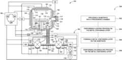
- FIG. 1is a simplified front cross-sectional view of a single-substrate processing chamber 100 for a high-pressure annealing process of a single substrate.
- the single-substrate processing chamber 100has a body 110 with an outer surface 112 and an inner surface 113 that encloses an internal volume 115 .
- the body 110has an annular cross section, though in other embodiments the cross-section of the body 110 may be rectangular or any closed shape.
- the outer surface 112 of the body 110may be made from a corrosion resistant steel (CRS), such as but not limited to stainless steel.
- CRScorrosion resistant steel
- One or more heat shields 125are disposed on the inner surface 113 of the body 110 that prevents heat loss from the single-substrate processing chamber 100 into the outside environment.
- the inner surface 113 of the body 110 as well as the heat shields 125may be made from nickel-based steel alloys that exhibit high resistance to corrosion, such as but not limited to HASTELLOY®, ICONEL®, and MONEL®.
- a substrate support 130is disposed within the internal volume 115 .
- the substrate support 130has a stem 134 and a substrate-supporting member 132 held by the stem 134 .
- the stem 134passes through a passage 122 formed through the chamber body 110 .
- a rod 139 connected to an actuator 138passes through a second passage 123 formed through the chamber body 110 .
- the rod 139is coupled to a plate 135 having an aperture 136 accommodating the stem 134 of the substrate support 130 .
- Lift pins 137are connected to the substrate-supporting member 132 .
- the actuator 138actuates the rod 139 such that the plate 135 is moved up or down to connect and disconnect with the lift pins 137 .
- the substrate-supporting member 132As the lift pins 137 are raised or lowered, the substrate-supporting member 132 is raised or lowered within the internal volume 115 of the chamber 100 .
- the substrate-supporting member 132has a resistive heating element 131 embedded centrally within.
- a power source 133is configured to electrically power the resistive heating element 131 .
- the operation of the power source 133 as well as the actuator 138is controlled by a controller 180 .
- the single-substrate processing chamber 100has an opening 111 on the body 110 through which one or more substrates 120 can be loaded and unloaded to and from the substrate support 130 disposed in the internal volume 115 .
- the opening 111forms a tunnel 121 on the body 110 .
- a slit valve 128is configured to sealably close the tunnel 121 such that the opening 111 and the internal volume 115 can only be accessed when the slit valve 128 is open.
- a high-pressure seal 127is utilized to seal the slit valve 128 to the body 110 in order to seal the internal volume 115 for processing.
- the high-pressure seal 127may be made from a polymer, for example a fluoropolymer, such as but not limited to a perfluoroelastomer and polytetrafluoroethylene (PTFE).
- the high-pressure seal 127may further include a spring member for biasing the seal to improve seal performance.
- a cooling channel 124is disposed on the tunnel 121 adjacent to the high-pressure seals 127 in order to maintain the high-pressure seals 127 below the maximum safe-operating temperature of the high-pressure seals 127 during processing.
- a cooling agent from a cooling fluid source 126such as but not limited to an inert, dielectric, and high-performance heat transfer fluid, may be circulated within the cooling channel 124 .
- the flow of the cooling agent from the cooling fluid source 126is controlled by the controller 180 through feedback received from a temperature sensor 116 or a flow sensor (not shown).
- An annular-shaped thermal choke 129is formed around the tunnel 221 to prevent the flow of heat from the internal volume 115 through the opening 111 when the slit valve 128 is open.
- the single-substrate processing chamber 100has a port 117 through the body 110 , which is fluidly connected to a fluid circuit 190 connecting the gas panel 150 , the condenser 160 and the port 117 .
- the fluid circuit 190has a gas conduit 192 , a source conduit 157 , an inlet isolation valve 155 , an exhaust conduit 163 , and an outlet isolation valve 165 .
- a number of heaters 196 , 158 , 152 , 154 , 164 , 166are interfaced with different portions of the fluid circuit 190 .
- a number of temperature sensors 151 , 153 , 119 , 167 and 169are also placed at different portions of the fluid circuit 190 to take temperature measurements and send the information to the controller 180 .
- the controller 180uses the temperature measurement information to control the operation of the heaters 152 , 154 , 158 , 196 , 164 , and 166 such that the temperature of the fluid circuit 190 is maintained at a temperature above the condensation point of the processing fluid disposed in the fluid circuit 190 and the internal volume 115 .
- the gas panel 150is configured to provide a processing fluid under pressure the internal volume 115 .
- the pressure of the processing fluid introduced into the internal volume 115is monitored by a pressure sensor 114 coupled to the body 110 .
- the condenser 160is fluidly coupled to a cooling fluid source (not shown) and configured to condense the gas phase processing fluid exiting the internal volume 115 through the gas conduit 192 .
- the condensed processing fluidis then removed by the pump 176 .
- One or more heaters 140are disposed on the body 110 and configured to heat the internal volume 115 within the single-substrate processing chamber 100 .
- the heaters 140 , 152 , 154 , 158 , 196 , 164 , and 166maintain the processing fluid within the fluid circuit 190 in a gaseous phase while the outlet isolation valve 165 to the condenser 160 is open to prevent condensation within the fluid circuit.
- the controller 180controls the operation of the single-substrate processing chamber 100 .
- the controller 180controls the operation of the gas panel 150 , the condenser 160 , the pump 170 , the inlet isolation valve 155 , the outlet isolation valve 165 , the power sources 133 and 145 .
- the controller 180is also communicatively connected to the temperature sensor 116 , the pressure sensor 114 , the actuator 138 , the cooling fluid source 126 and the temperature reading devices 156 and 162 .
- the processing fluidmay comprise an oxygen-containing and/or nitrogen-containing gas, and/or chalcogen or tellurium (such as S, Se, Te) gases or vapors such as oxygen, dry steam, water, hydrogen peroxide, ammonia, S vapor, Se vapor, H 2 S, H 2 Se, etc.
- the processing fluidmay be reacted with the metal materials on the substrate to form metal oxynidrids, metal oxides, metal oxychalcogenides or metal chalcogenides.
- the processing fluidmay comprise a silicon-containing gas. Examples of the silicon-containing gas include organosilicon, tetraalkyl orthosilicate gases and disiloxane.
- Organosilicon gasesinclude gases of organic compounds having at least one carbon-silicon bond.
- Tetraalkyl orthosilicate gasesinclude gases consisting of four alkyl groups attached to an SiO 4 4 ⁇ ion. More particularly, the one or more gases may be (dimethylsilyl)(trimethylsilyl)methane ((Me) 3 SiCH 2 SiH(Me) 2 ), hexamethyldisilane ((Me) 3 SiSi(Me) 3 ), trimethylsilane ((Me) 3 SiH), trimethylsilylchloride ((Me) 3 SiCl), tetramethylsilane ((Me) 4 Si), tetraethoxysilane ((EtO) 4 Si), tetramethoxysilane ((MeO) 4 Si), tetrakis-(trimethylsilyl)silane ((Me 3 Si) 4 Si), (dimethylamino)dimethyl-silane (
- an environment of the high-pressure region 115is maintained at a temperature and pressure that maintains the processing fluid within the high-pressure region in a vapor phase.
- Such pressure and temperatureis selected based on the composition of the processing fluid.
- the temperature and pressureis held at a condition that maintains the steam in a dry steam state.
- high-pressure region 115is pressurized to a pressure greater than atmosphere, for example greater than about 2 bars.
- high-pressure region 115is pressurized to a pressure from between about 10 and about 50 bars, such as from between about 20 and about 50 bars.
- the high-pressure region 115is pressurized to a pressure up to about 100 bars.
- the high-pressure region 115is also maintained at a high temperature, for example, a temperature exceeding 225 degrees Celsius (limited by the thermal budget of the substrates 155 disposed on the cassette 150 ), such as between about 300 degrees Celsius and about 500 degrees Celsius.
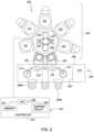
- FIG. 2is a schematic, top plan view of an exemplary processing system 200 that includes one or more of the processing chambers, such as the processing chamber 100 illustrated in FIG. 1 , that are incorporated and integrated therein.
- the processing system 200may be a Centura® or Endura® integrated processing system, commercially available from Applied Materials, Inc., located in Santa Clara, California. It is contemplated that other processing systems (including those from other manufacturers) may be adapted to benefit from the disclosure.
- the system 200includes a vacuum-tight processing platform 204 , a factory interface 202 , and a system controller 244 .
- the platform 204includes a plurality of processing chambers 100 , 212 , 232 , 228 , 220 , such as the one of the processing chamber 100 depicted in FIG. 1 , and at least one load-lock chamber 222 that is coupled to a vacuum substrate transfer chamber 236 . Two load lock chambers 222 are shown in FIG. 2 .
- the factory interface 202is coupled to the transfer chamber 236 by the load lock chambers 222 .
- the factory interface 202comprises at least one docking station 208 and at least one factory interface robot 214 to facilitate transfer of substrates.
- the docking station 208is configured to accept one or more front opening unified pod (FOUP).
- FOUPfront opening unified pod
- Two FOUPS 206 A-Bare shown in the embodiment of FIG. 2 .
- the factory interface robot 214 having a blade 216 disposed on one end of the robot 214is configured to transfer the substrate from the factory interface 202 to the processing platform 204 for processing through the load lock chambers 222 .
- one or more metrology stations 518may be connected to a terminal 226 of the factory interface 202 to facilitate measurement of the substrate from the FOUPS 206 A-B.
- Each of the load lock chambers 222have a first port coupled to the factory interface 202 and a second port coupled to the transfer chamber 236 .
- the load lock chambers 222are coupled to a pressure control system (not shown) which pumps down and vents the load lock chambers 222 to facilitate passing the substrate between the vacuum environment of the transfer chamber 236 and the substantially ambient (e.g., atmospheric) environment of the factory interface 202 .
- the transfer chamber 236has a vacuum robot 230 disposed therein.
- the vacuum robot 230has a blade 234 capable of transferring substrates 224 among the load lock chambers 222 , the metrology system 210 and the processing chambers 212 , 232 , 228 , 220 .
- the system 200may include one or more processing chambers 100 , 212 , 232 , 228 , 220 , which may be a annealing chamber (e.g., high pressure annealing chamber, RTP chamber, laser anneal chamber), deposition chamber, etch chamber, cleaning chamber, curing chamber, or other similar type of semiconductor processing chambers.
- a annealing chambere.g., high pressure annealing chamber, RTP chamber, laser anneal chamber
- deposition chambere.g., high pressure annealing chamber, RTP chamber, laser anneal chamber
- etch chamberetch chamber
- cleaning chambere.g., cleaning chamber, curing chamber, or other similar type of semiconductor processing chambers.
- curing chambere.g., cleaning chamber, curing chamber, or other similar type of semiconductor processing chambers.
- the system controller 244is coupled to the processing system 200 .
- the system controller 244which may include the computing device 201 or be included within the computing device 201 , controls the operation of the processing system 200 using a direct control of the process chambers 100 , 212 , 232 , 228 , 220 of the system 200 .
- the system controller 244may control the computers (or controllers) associated with the process chambers 100 , 212 , 232 , 228 and the system 200 .
- the system controller 244also enables data collection and feedback from the respective chambers to optimize performance of the system 200 .
- the system controller 244generally includes a central processing unit (CPU) 238 , a memory 240 , and support circuit 242 .
- the CPU 238may be one of any form of a general purpose computer processor that can be used in an industrial setting.
- the support circuits 242are conventionally coupled to the CPU 238 and may comprise cache, clock circuits, input/output subsystems, power supplies, and the like.
- the software routinestransform the CPU 238 into a specific purpose computer (controller) 244 .
- the software routinesmay also be stored and/or executed by a second controller (not shown) that is located remotely from the system 200 .
- FIG. 3depicts an example of a TFT device 350 that include a metal containing layer that may undergo a thermal annealing process in a high pressure annealing chamber, such as the high pressure annealing process 100 depicted in FIG. 1 , which may be incorporated into the system 200 depicted in FIG. 2 .
- the thin film transistor device structure 350is a bottom gate TFT structure disposed on a substrate 301 .
- the substrate 301may have different combination of films, structures or layers previously formed thereon to facilitate forming different device structures or different film stack on the substrate 301 .
- the substrate 301may have the device structure 350 formed thereon, as shown in FIG. 3 .
- the substrate 301may have another device structure 450 disposed thereon, as further shown in FIG. 4 , which will be further described below.
- the substrate 301may be any one of glass substrate, plastic substrate, polymer substrate, metal substrate, singled substrate, roll-to-roll substrate, or other suitable transparent substrate suitable for forming a thin film transistor thereon.
- a gate electrode layer 302is formed and patterned on the substrate 301 followed by a gate insulator layer 304 .
- the gate electrode layer 302may be fabricated from any suitable metallic material, such as aluminum (Al), tungsten (W), chromium (Cr), tantalum (Ta), molybdenum (Mo), copper (Cu) or combination thereof.
- suitable materials for the gate insulator layer 304include silicon oxide (SiO 2 ), silicon oxynitride (SiON), silicon nitride (SiN), and the like. It is noted that the thin film transistor device structure 350 depicted in FIG. 3 is a bottom gate device structure with the gate electrode layer 302 formed on a bottom of the device structure 350 .
- An active layer 306is formed on the gate insulator layer 304 .
- the material utilized for the active layer 306may be selected from a transparent metallic oxide material that has high electron mobility that is suitable low temperature manufacturing that allows flexible substrate materials, such as plastic materials, to be processed at a low temperature without substrate damage.
- Suitable examples of materials that can be utilized for the active layer 306include a-IGZO (amorphous indium gallium zinc oxide), InGaZnON, ZnO, ZnON, ZnSnO, CdSnO, GaSnO, TiSnO, CuBO 2 , CuAlO 2 , CuGaO 2 , SrCuO, LaCuOS, GaN, InGaN, AlGaN or InGaAlN, among others.
- a barrier layer 308may be formed on the active layer 306 .
- the barrier layer 308may be formed from a metal containing material so as to provide a good interface adhesion as well as good barrier properties (e.g., diffusion barrier) to a metal electrode layer 310 (e.g., for a source-drain electrode) subsequently formed thereon.
- the barrier layer 308may be patterned to form a desired pattern on the active layer 306 to facilitate transfer of features on the film layers disposed on the substrate 301 in the subsequent etching processes.
- the barrier layer 308could be in any form, including a whole continuous blank film in the device structure 350 or any different features as needed as long as the barrier layer 308 may efficiently provide a blocking/diffusion barrier property to prevent elements from the active layer 306 diffusing into the metal electrode layer 310 , or vice versa.
- the barrier layer 308may be a single layer of a metal containing dielectric layer, as depicted in FIG. 3 , fabricated by a metal dielectric layer, such as Ta 2 O 5 or TiO 2 , or any suitable metal dielectric layer as needed.
- the barrier layer 308may be in form of a composite film as needed.
- the metal electrode layer 310such as a source-drain metal electrode layer
- an etching processis performed to form a channel 320 in the metal electrode layer 310 .
- an insulating material layer 314such as a passivation layer, is then formed over the metal electrode layer 310 to complete the process of forming the thin film transistor device structure 350 .
- examples of materials that may be used as the metal electrode layer 310include copper (Cu), gold, silver (Ag), aluminum (Al), tungsten (W), molybdenum (Mo), chromium (Cr), tantalum (Ta), alloys thereof and combination thereof.
- Suitable of materials that may be used as the insulating material layer 314include silicon oxide (SiO 2 ), silicon oxynitride (SiON), or silicon nitride (SiN), and the like.
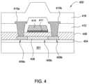
- FIG. 4depicts an example of a top gate low temperature polysilicon (LTPS) TFT device structure 450 may be formed on the substrate 301 , rather than the bottom gate device structure 350 depicted in FIG. 3 .
- the LTPS TFT devices 450are MOS devices built with active layers 452 including a source region 409 a , channel region 408 , and drain region 409 b (e.g., or called metal contact regions, or source-drain metal contacts) formed on the optically transparent substrate 301 with or without an optional insulating layer 404 disposed thereon.
- active layers 452including a source region 409 a , channel region 408 , and drain region 409 b (e.g., or called metal contact regions, or source-drain metal contacts) formed on the optically transparent substrate 301 with or without an optional insulating layer 404 disposed thereon.
- the active layer including the source region 409 a , channel region 408 , and drain region 409 bmay be fabricated from a transparent metal containing layer, such as metallic oxide material, that has high electron mobility that is suitable low temperature manufacturing that allows flexible substrate materials, such as plastic materials, to be processed at a low temperature without substrate damage.
- a transparent metal containing layersuch as metallic oxide material
- Suitable examples of such materials that can be utilized for the source region 409 a , channel region 408 , and drain region 409 binclude a-IGZO (amorphous indium gallium zinc oxide), doped IGZO, InGaZnON, ZnO, ZnON, ZnSnO, CdSnO, GaSnO, TiSnO, CuBO 2 , CuAlO 2 , CuGaO 2 , SrCuO, LaCuOS, GaN, InGaN, AlGaN or InGaAlN, among others.
- a-IGZOamorphous indium gallium zinc oxide
- doped IGZOInGaZnON, ZnO, ZnON, ZnSnO, CdSnO, GaSnO, TiSnO, CuBO 2 , CuAlO 2 , CuGaO 2 , SrCuO, LaCuOS, GaN, InGaN, AlGaN or InGaA
- a gate insulating layer 406is then deposited on top of the deposited polysilicon layer(s) to isolate a barrier layer 411 and a metal electrode layer 414 , such as a gate electrode, disposed thereon from the channel region 408 , source region 409 a and drain region 409 b .
- the barrier layer 411may be formed from a metal containing material so as to provide a good interface adhesion as well as good barrier properties (e.g., diffusion barrier) to the metal electrode layer 414 (e.g., the gate electrode) subsequently formed thereon.
- the barrier layer 411may be patterned to form a desired pattern on the gate insulating layer 406 to facilitate transfer of features on the film layers disposed on the substrate 102 in the subsequent etching processes.
- the barrier layer 411may efficiently provide a blocking/diffusion barrier property to prevent elements from the gate insulating layer 406 diffusing into the metal electrode layer 414 , or vice versa.
- the barrier layer 411may be a single layer of a metal containing dielectric layer, as depicted in FIG. 4 , fabricated by a metal dielectric layer, such as Ta 2 O 5 or TiO 2 , or any suitable metal dielectric layer as needed.
- the barrier layer 411may be in form of a composite film as needed.
- the gate electrode layer 414is formed on top of the gate insulating layer 406 with the barrier layer 411 interposed therebetween.
- the gate insulating layer 406is also commonly known as a gate oxide layer since it is commonly made of a silicon dioxide (SiO 2 ) layer.
- An insulating material layer 412such as an interlayer insulator, and device connections (not shown) are then made through the insulating material layer 412 to allow control of the TFT devices.
- a source-drain metal electrode layer 410 a , 410 bis then deposited, formed and patterned in the insulating material layer 412 .
- a passivation layer 418is then formed over the source-drain metal electrode layer 410 a , 410 b.
- FIG. 5depicts a flow diagram of one example of a thermal annealing process 500 performed on a metal containing layer, such as the active layers 306 , 452 in FIGS. 3 - 4 , or the metal electrodes 302 , 310 , 410 a , 410 b , 414 in FIGS. 3 - 4 respectively.
- a metal containing layersuch as the active layers 306 , 452 in FIGS. 3 - 4 , or the metal electrodes 302 , 310 , 410 a , 410 b , 414 in FIGS. 3 - 4 respectively.
- the method 500begins at operation 502 by providing a substrate, such as the substrate 301 in FIGS. 3 and 4 .
- the substrate 301may be an optical transparent substrate.
- the substrate 301may comprise a material layer 601 disposed thereon, as shown in FIG. 6 A .
- the material layer 601may be a single layer or multiple layers that may be utilized to form a TFT device structure.
- the material layer 601may be a structure may include multiple materials that may be utilized to form a TFT device structure.
- the substrate 301further includes a metal containing layer 602 formed on the material layer 601 , as shown in FIG. 6 B .
- the metal containing layer 602may be directly formed on the substrate 301 .
- the metal containing layer 602may be used as the active layers 306 , 452 in FIG. 3 or 4 , or the metal electrodes 302 , 310 , 410 a , 410 b , 414 in FIGS. 3 - 4 .
- the metal containing layer 602is a metal oxide layer selected from a group consisting of a-IGZO (amorphous indium gallium zinc oxide), doped IGZO, InGaZnON, ZnO, ZnON, ZnSnO, CdSnO, GaSnO, TiSnO, CuBO 2 , CuAlO 2 , CuGaO 2 , SrCuO, LaCuOS, GaN, InGaN, AlGaN or InGaAlN and the like.
- the metal containing layer 602is a IGZO or doped IGZO layer.
- the metal containing layer 602may be a metal layer, such as copper (Cu), gold, silver (Ag), aluminum (Al), tungsten (W), molybdenum (Mo), chromium (Cr), tantalum (Ta), alloys thereof, or the like.
- an optional ion doping/implantation processis performed to implant ions into the metal containing layer 602 , forming a doped metal containing layer 610 , as shown in FIG. 6 C .
- the thermal annealing process at operation 506which will be described in greater detail below, may be performed directly on the metal containing layer 602 .
- the ion doping/implantation processis performed to dope, coat, treat, implant, insert or modify certain film/surface properties on certain locations of the metal containing layer 602 with dopants formed into, forming the doped metal containing layer 610 .
- the ion doping/implantation processutilizes incident ions to modify film/surface properties on the metal containing layer 602 , with dopants doped thereto to form the doped metal containing layer 610 .
- the ion doping/implantation processmay be performed in any suitable ion implantation/doping processing tools.
- the ionswhich include a desired type of atoms, may be doped into the metal containing layer 602 with desired concentration.
- the ions doped into the metal containing layer 602may modify the film/surface properties of the metal containing layer 602 , which may affect, improve or alter the lattice structure, degree of crystalline, bonding structure or film density of the metal containing layer 602 , forming the doped metal containing layer 610 .
- the ions doped into the metal containing layer 602may include indium (In) or molybdenum (Mo), gallium (Ga), zinc (Zn) and the like. It is believed that In or Mo dopants doped into the metal containing layer 602 (e.g., a InGaZnO) may alter the electrical properties such as high mobility, crystallinity (e.g., from amorphous structure, C-axis aligned crystalline structure (CAAC), polycrystalline structure or even single crystalline structure) of the InGaZnO material, thus, providing the doped metal containing layer 610 with desired film properties.
- In or Mo dopants doped into the metal containing layer 602e.g., a InGaZnO
- CAACC-axis aligned crystalline structure
- the gallium (Ga) and zinc oxide (ZnO) ratio included in the InGaZnO materialmay also affect the resultant lattice structure of the doped metal containing layer 610 .
- the ratio of Ga elements included in the InGaZnO materialmay increase the film transparency as well as the overall film bandgap.
- the ratio of Zn or ZnO elements included in the InGaZnO materialmay increase the mobility as well as the reducing the thermal annealing temperature requirements for crystallinity enhancement.
- the desired crystalline of the InGaZnO materialmay also help reducing the temperature requirement in the following thermally annealing process at operation 506 , providing process advantages in TFT device applications as the substrate 301 is often optical transparent material with relatively low thermal cycle budges.
- the resultant In dopant in the InGaZnO materialmay have a doping concentration of between about 5E15 ions/cm 2 and about 9E15 ions/cm 2 , such as about 8.5E15 ions/cm 2 , formed in the doped metal containing layer 610 .
- the ratio of the In or Mo element in the InGaZnO materialmay be increased from about 10%-13% to about 14%-16% (between about 15% and about 30% increase) by atomic weight.
- the ion doping/implantation processmay be performed by supplying an ion doping gas mixture into the ion doping/implantation tool along with a desired amount of the power energy to dope the ions from the ion doping gas mixture into the substrate 301 .
- the ion doping gas mixturemay be supplied into the ion doping/implantation tool at a flow rate between about 10 sccm and about 1000 sccm.
- Suitable elements for supplying in the ion doping used in vapor state during implantinclude indium vapor and molybdenum vapor.
- a RF powersuch as capacitive or inductive RF power, DC power, electromagnetic energy, ion beam, or magnetron sputtering, may be supplied into the ion doping/implantation process to assist dissociating the ion doping gas mixture during processing. Ions generated by the dissociative energy may be accelerated toward the substrate using an electric field produced by applying a DC or RF electrical bias to the substrate support or to a gas inlet above the substrate support, or both.
- the gas containing energetic ionsmay be a plasma.
- An energy of between about 20 keV and about 80 keV, such as between about 35 keV and about 55 keV, for example about 45 keV,may be used to implant ions into the metal containing layer 602 .
- the substrate temperaturemay be controlled at between about 5 degrees Celsius and about 50 degrees Celsius, such as about 15 degrees Celsius.
- a high pressure annealing processis performed.
- the annealing process performed at high process pressuremay assist densifying and repairing the vacancies in the doped metal containing layer 610 , forming the annealed metal containing layer 603 with the desired film properties, as shown in FIG. 6 D .
- the high process pressuremay go up to 100 bar.
- the high pressure annealing processmay be performed directly on the metal containing layer 602 from FIG. 6 B to form the annealed metal containing layer 603 , as shown in FIG. 6 D .
- the annealing processmay be performed at a processing chamber, such as the processing chamber 100 depicted in FIG. 1 , or other suitable processing chambers, including those that process substrate one at a time.
- the high pressure annealing process performed at operation 506maintains processing pressure at the high-pressure region in a vapor phase, for example in a dry vapor phase that has substantially no liquid droplets present.
- the processing pressure and temperatureis controlled to density the film structures, so as to repair the film defects, driving out impurities and increasing film density.
- the high-pressure region 115is pressurized to a pressure greater than atmosphere, for example greater than about 2 bar.
- the high-pressure region 115is pressurized to a pressure from about 5 to about 100 bars, such as from about 5 to about 50 bars, such as about 35 bar.
- a relatively low processing temperaturesuch as less than 500 degrees Celsius, to reduce likelihood of thermal cycle damage to the substrate 301 .
- the high-pressure region 115is maintained at a relatively low temperature, for example, a temperature less than 500 degrees Celsius, such as between about 150 degrees Celsius and about 350 degrees Celsius, by the heaters 122 disposed within the outer chamber 110 .
- a relatively low temperaturefor example, a temperature less than 500 degrees Celsius, such as between about 150 degrees Celsius and about 350 degrees Celsius, by the heaters 122 disposed within the outer chamber 110 .
- a low thermal budget to the substratemay be obtained by utilizing the high pressure annealing process along with low temperature regime.
- the high pressure processmay provide a driving force to drive out the dangling bonds in the metal containing layer 602 or the doped metal containing layer 610 , thus, repairing, reacting and saturating the dangling bonds in the metal containing layer 602 during the annealing process.
- an oxygen containing gassuch as O 3 gas
- O 2 gasair, H 2 O, H 2 O 2 , N 2 O, NO 2 , CO 2 , CO and dry steam
- chalcogen vaporincluding sulfur (S) vapor and selenium (Se) vapor, or tellurium vapor or other suitable gases may be supplied during the annealing process.
- the oxygen containing gascomprises steam, for example, dry steam and/or air.
- the oxygen elements from the oxygen containing gas during the annealing processmay be driven into the metal containing layer 602 , altering the bonding structures and removing the atomic vacancies therein, thus, densifying and enhancing lattice structures and increasing the crystallinity of the metal containing layer 602 .
- an inert gas or a carrier gassuch as Ar, N 2 , He, Kr and the like, may be supplied with the oxygen containing gas.
- the oxygen containing gas supplied in the oxygen containing gas mixtureis dry steam supplied at a pressure greater than 2 bar.
- a process pressureis regulated at a pressure greater than 2 bar, such as between 5 bar and 100 bar, such as between 20 bar and about 80 bar, for example between about 25 bar and 75 bar, such as about 35 bar.
- the process temperaturemay be controlled at greater than 150 degrees Celsius but less than 500 degrees Celsius, such as between about 150 degrees Celsius and about 380 degrees Celsius, such as between about 180 degrees Celsius and about 400 degrees Celsius.
- chalcogen vaporsuch as sulfur (S) vapor, selenium (Se) vapor, may be supplied during the annealing process for metal oxychalcogen, such as InGaZnO comprising S or Se.
- the metal containing layer 602 or the doped metal containing layer 610has a densified film structure, which provides a relatively robust film structure with amorphous morphology that provides higher film density, high film mobility, low carrier concentration and low film resistivity as compared to the metal containing layer 602 or doped metal containing layer 610 annealed by a conventional annealing process at a pressure around one atmospheric pressure, while both annealing process are at the same anneal temperature.
- the mobility of the high pressure annealed metal containing layer 603 with indium dopantsis increased between about 5 times and about 20 times, resistivity increased about 10 times and carrier concentration decreased about 100 times, as compared to a conventional annealing process at 1 atmospheric pressure while under the same anneal temperature.
- the mobility of the high pressure annealed metal containing layer 603 without indium dopants (formed from the metal containing layer 602 )is increased between about 1.5 times and about 5 times, resistivity increased from about 20 percent to about 99 percent and carrier concentration decreased about 100 times, as compared to a conventional annealing process at 1 atmospheric pressure while under the same anneal temperature.
- the metal containing layermay be thermally treated/annealed by a high pressure annealing process with high process pressure, such as greater than 2 bar but less than 50 bar.
- high process pressuresuch as greater than 2 bar but less than 50 bar.
- the process temperaturemay be maintained less than 500 degrees Celsius, thus reducing the thermal budge contributed to the substrate where the metal containing layer is formed thereon, providing a good film quality with desired crystallinity and structure integration management.
Landscapes
- Engineering & Computer Science (AREA)
- Physics & Mathematics (AREA)
- Chemical & Material Sciences (AREA)
- Manufacturing & Machinery (AREA)
- General Physics & Mathematics (AREA)
- Computer Hardware Design (AREA)
- Microelectronics & Electronic Packaging (AREA)
- Power Engineering (AREA)
- Condensed Matter Physics & Semiconductors (AREA)
- Materials Engineering (AREA)
- Chemical Kinetics & Catalysis (AREA)
- Mechanical Engineering (AREA)
- Metallurgy (AREA)
- Organic Chemistry (AREA)
- Thermal Sciences (AREA)
- Thin Film Transistor (AREA)
- Electrodes Of Semiconductors (AREA)
- Recrystallisation Techniques (AREA)
Abstract
Description
This application is a continuation of U.S. non-provisional patent application Ser. No. 16/262,094, filed Jan. 30, 2019, which claims benefit of U.S. provisional patent application Ser. No. 62/641,110 filed Mar. 9, 2018, each of which are herein incorporated by reference in its entirety.
Embodiments of the present invention generally relate to a method for forming a metal containing layer in a film stack that may be utilized in TFT device structures, semiconductor, or memory applications.
Display devices have been widely used for a wide range of electronic applications, such as TV, monitors, mobile phone, MP3 players, e-book readers, and personal digital assistants (PDAs) and the like. The display device is generally designed for producing desired image by applying an electric field to a liquid crystal that fills a gap between two substrates and has anisotropic dielectric constant that controls the intensity of the dielectric field. By adjusting the amount of light transmitted through the substrates, the light and image intensity, quality and power consumption may be efficiently controlled.
A variety of different display devices, such as active matrix liquid crystal display (AMLCD) or an active matrix organic light emitting diodes (AMOLED), may be employed as light sources for display devices which utilize touch screen panels. In the manufacturing of TFT devices, an electronic device with high electron mobility, low leakage current and high breakdown voltage, would allow more pixel area for light transmission and integration of circuitry, thus resulting in a brighter display, higher overall electrical efficiency, faster response time and higher resolution displays. Low film qualities of the material layers, such as metal electrode layer with impurities, formed in the device often result in poor device electrical performance and short service life of the devices. Thus, a stable and reliable method for forming and integrating film layers with in a TFT devices becomes crucial to provide a device structure with low film leakage, and high breakdown voltage, for use in manufacturing electronic devices with lower threshold voltage shift and improved the overall performance of the electronic device are desired.
Therefore, there is a need for improved materials for manufacturing TFT devices that produce improved device electrical performance and device stability.
The present disclosure provides methods for performing an annealing process on a metal containing layer in TFT display applications, semiconductor or resistive random access memory (ReRAM). In one example, a method of forming a metal containing layer on a substrate includes supplying an oxygen containing gas mixture on a substrate in a processing chamber, the substrate comprising a metal containing layer disposed on an optically transparent substrate, maintaining the oxygen containing gas mixture in the processing chamber at a process pressure between 2 bar and 50 bar, and thermally annealing the metal containing layer in the presence of the oxygen containing gas mixture.
In another example, a method for densifying a metal containing layer disposed on a substrate includes thermally treating a metal containing layer disposed on an optically transparent substrate at a pressure greater than 2 bar, and maintaining a substrate temperature less than 500 degrees Celsius during thermally treating the dielectric layer.
In yet another example, a method for densifying a metal containing layer disposed on a substrate includes forming a metal containing layer on a substrate, implanting dopants into the metal containing layer and thermally treating the metal containing layer on the substrate at a pressure greater than 2 bar while maintaining the substrate temperature less than 500 degrees Celsius.
So that the manner in which the above recited features of the present invention can be understood in detail, a more particular description of the invention, briefly summarized above, may be had by reference to embodiments, some of which are illustrated in the appended drawings. It is to be noted, however, that the appended drawings illustrate only typical embodiments of this invention and are therefore not to be considered limiting of its scope, for the invention may admit to other equally effective embodiments.
To facilitate understanding, identical reference numerals have been used, such as anneal at atmospheric pressure with similar anneal conditions where possible, to designate identical elements that are common to the figures. It is contemplated that elements and features of one embodiment may be beneficially incorporated in other embodiments without further recitation.
It is to be noted, however, that the appended drawings illustrate only exemplary embodiments of this invention and are therefore not to be considered limiting of its scope, for the invention may admit to other equally effective embodiments.
Embodiments of the disclosure generally provide a TFT device structures and methods of performing a thermal annealing process on an active layer of source, drain, interface and contact regions in the TFT device structures so as to enhance electrical performance for display devices. Other applications, including semiconductor or memory device manufacturing process, may also utilize the embodiments described herein. The thermal annealing process may densify the active layer film properties of the metal electrodes, source/drain and/or contact regions, and/or film layers on the substrate. In one example, the thermal treatment process is performed to provide thermal energy of a metal containing layer, such as a metal containing layer (e.g., an active layer) or a metal electrode layer (e.g., a metal gate electrode, a source-drain and/or contact regions or electrode layers, or other suitable metal structures) is formed in the TFT devices. The thermal annealing process may densify or minimize oxygen deficiency in the active layer film structures to provide good quality, interface management and thermal stabilization to the device structure. The thermal annealing process may also increase the degree of crystalline of the metal containing material, improving electrical performance of the metal containing layer. Thus, desired film properties of metal electrodes and active layers of source/drain and/or contact regions in display devices may efficiently enhance the electrical performance of transistor and diode devices.
Asubstrate support 130 is disposed within theinternal volume 115. Thesubstrate support 130 has astem 134 and a substrate-supportingmember 132 held by thestem 134. Thestem 134 passes through a passage122 formed through thechamber body 110. Arod 139 connected to anactuator 138 passes through a second passage123 formed through thechamber body 110. Therod 139 is coupled to aplate 135 having anaperture 136 accommodating thestem 134 of thesubstrate support 130.Lift pins 137 are connected to the substrate-supportingmember 132. Theactuator 138 actuates therod 139 such that theplate 135 is moved up or down to connect and disconnect with thelift pins 137. As thelift pins 137 are raised or lowered, the substrate-supportingmember 132 is raised or lowered within theinternal volume 115 of thechamber 100. The substrate-supportingmember 132 has aresistive heating element 131 embedded centrally within. Apower source 133 is configured to electrically power theresistive heating element 131. The operation of thepower source 133 as well as theactuator 138 is controlled by acontroller 180.
The single-substrate processing chamber 100 has anopening 111 on thebody 110 through which one or more substrates120 can be loaded and unloaded to and from thesubstrate support 130 disposed in theinternal volume 115. The opening111 forms a tunnel121 on thebody 110. A slit valve128 is configured to sealably close the tunnel121 such that theopening 111 and theinternal volume 115 can only be accessed when the slit valve128 is open. A high-pressure seal127 is utilized to seal the slit valve128 to thebody 110 in order to seal theinternal volume 115 for processing. The high-pressure seal127 may be made from a polymer, for example a fluoropolymer, such as but not limited to a perfluoroelastomer and polytetrafluoroethylene (PTFE). The high-pressure seal127 may further include a spring member for biasing the seal to improve seal performance. A cooling channel124 is disposed on the tunnel121 adjacent to the high-pressure seals127 in order to maintain the high-pressure seals127 below the maximum safe-operating temperature of the high-pressure seals127 during processing. A cooling agent from a cooling fluid source126, such as but not limited to an inert, dielectric, and high-performance heat transfer fluid, may be circulated within the cooling channel124. The flow of the cooling agent from the cooling fluid source126 is controlled by thecontroller 180 through feedback received from atemperature sensor 116 or a flow sensor (not shown). An annular-shaped thermal choke129 is formed around the tunnel221 to prevent the flow of heat from theinternal volume 115 through theopening 111 when the slit valve128 is open.
The single-substrate processing chamber 100 has aport 117 through thebody 110, which is fluidly connected to afluid circuit 190 connecting thegas panel 150, thecondenser 160 and theport 117. Thefluid circuit 190 has agas conduit 192, asource conduit 157, aninlet isolation valve 155, anexhaust conduit 163, and anoutlet isolation valve 165. A number ofheaters fluid circuit 190. A number oftemperature sensors fluid circuit 190 to take temperature measurements and send the information to thecontroller 180. Thecontroller 180 uses the temperature measurement information to control the operation of theheaters fluid circuit 190 is maintained at a temperature above the condensation point of the processing fluid disposed in thefluid circuit 190 and theinternal volume 115.
Thegas panel 150 is configured to provide a processing fluid under pressure theinternal volume 115. The pressure of the processing fluid introduced into theinternal volume 115 is monitored by apressure sensor 114 coupled to thebody 110. Thecondenser 160 is fluidly coupled to a cooling fluid source (not shown) and configured to condense the gas phase processing fluid exiting theinternal volume 115 through thegas conduit 192. The condensed processing fluid is then removed by thepump 176. One ormore heaters 140 are disposed on thebody 110 and configured to heat theinternal volume 115 within the single-substrate processing chamber 100. Theheaters fluid circuit 190 in a gaseous phase while theoutlet isolation valve 165 to thecondenser 160 is open to prevent condensation within the fluid circuit.
Thecontroller 180 controls the operation of the single-substrate processing chamber 100. Thecontroller 180 controls the operation of thegas panel 150, thecondenser 160, thepump 170, theinlet isolation valve 155, theoutlet isolation valve 165, thepower sources controller 180 is also communicatively connected to thetemperature sensor 116, thepressure sensor 114, theactuator 138, the cooling fluid source126 and thetemperature reading devices
The processing fluid may comprise an oxygen-containing and/or nitrogen-containing gas, and/or chalcogen or tellurium (such as S, Se, Te) gases or vapors such as oxygen, dry steam, water, hydrogen peroxide, ammonia, S vapor, Se vapor, H2S, H2Se, etc. The processing fluid may be reacted with the metal materials on the substrate to form metal oxynidrids, metal oxides, metal oxychalcogenides or metal chalcogenides. Alternatively or in addition to the oxygen-containing and/or nitrogen-containing gases, the processing fluid may comprise a silicon-containing gas. Examples of the silicon-containing gas include organosilicon, tetraalkyl orthosilicate gases and disiloxane. Organosilicon gases include gases of organic compounds having at least one carbon-silicon bond. Tetraalkyl orthosilicate gases include gases consisting of four alkyl groups attached to an SiO44− ion. More particularly, the one or more gases may be (dimethylsilyl)(trimethylsilyl)methane ((Me)3SiCH2SiH(Me)2), hexamethyldisilane ((Me)3SiSi(Me)3), trimethylsilane ((Me)3SiH), trimethylsilylchloride ((Me)3SiCl), tetramethylsilane ((Me)4Si), tetraethoxysilane ((EtO)4Si), tetramethoxysilane ((MeO)4Si), tetrakis-(trimethylsilyl)silane ((Me3Si)4Si), (dimethylamino)dimethyl-silane ((Me2N)SiHMe2) dimethyldiethoxysilane ((EtO)2Si(Me)2), dimethyl-dimethoxysilane ((MeO)2Si(Me)2), methyltrimethoxysilane ((MeO)3Si(Me)), dimethoxytetramethyl-disiloxane (((Me)2Si(OMe))2O), tris(dimethylamino)silane ((Me2N)3SiH), bis(dimethylamino)methylsilane ((Me2N)2CH3SiH), disiloxane ((SiH3)2O), and combinations thereof.
During processing of the substrates120, an environment of the high-pressure region 115 is maintained at a temperature and pressure that maintains the processing fluid within the high-pressure region in a vapor phase. Such pressure and temperature is selected based on the composition of the processing fluid. In the case of steam, the temperature and pressure is held at a condition that maintains the steam in a dry steam state. In one example, high-pressure region 115 is pressurized to a pressure greater than atmosphere, for example greater than about 2 bars. In another example, high-pressure region 115 is pressurized to a pressure from between about 10 and about 50 bars, such as from between about 20 and about 50 bars. In another example, the high-pressure region 115 is pressurized to a pressure up to about 100 bars. During processing, the high-pressure region 115 is also maintained at a high temperature, for example, a temperature exceeding 225 degrees Celsius (limited by the thermal budget of thesubstrates 155 disposed on the cassette150), such as between about 300 degrees Celsius and about 500 degrees Celsius.
Thesystem 200 includes a vacuum-tight processing platform 204, afactory interface 202, and asystem controller 244. Theplatform 204 includes a plurality ofprocessing chambers processing chamber 100 depicted inFIG.1 , and at least one load-lock chamber 222 that is coupled to a vacuumsubstrate transfer chamber 236. Twoload lock chambers 222 are shown inFIG.2 . Thefactory interface 202 is coupled to thetransfer chamber 236 by theload lock chambers 222.
In one embodiment, thefactory interface 202 comprises at least onedocking station 208 and at least onefactory interface robot 214 to facilitate transfer of substrates. Thedocking station 208 is configured to accept one or more front opening unified pod (FOUP). TwoFOUPS 206A-B are shown in the embodiment ofFIG.2 . Thefactory interface robot 214 having ablade 216 disposed on one end of therobot 214 is configured to transfer the substrate from thefactory interface 202 to theprocessing platform 204 for processing through theload lock chambers 222. Optionally, one or more metrology stations518 may be connected to aterminal 226 of thefactory interface 202 to facilitate measurement of the substrate from theFOUPS 206A-B.
Each of theload lock chambers 222 have a first port coupled to thefactory interface 202 and a second port coupled to thetransfer chamber 236. Theload lock chambers 222 are coupled to a pressure control system (not shown) which pumps down and vents theload lock chambers 222 to facilitate passing the substrate between the vacuum environment of thetransfer chamber 236 and the substantially ambient (e.g., atmospheric) environment of thefactory interface 202.
Thetransfer chamber 236 has avacuum robot 230 disposed therein. Thevacuum robot 230 has ablade 234 capable of transferringsubstrates 224 among theload lock chambers 222, the metrology system210 and theprocessing chambers
In one embodiment of thesystem 200, thesystem 200 may include one ormore processing chambers system 200, one or more of processingchambers transfer chamber 236, thefactory interface 202 and/or at least one of theload lock chambers 222.
Thesystem controller 244 is coupled to theprocessing system 200. Thesystem controller 244, which may include thecomputing device 201 or be included within thecomputing device 201, controls the operation of theprocessing system 200 using a direct control of theprocess chambers system 200. Alternatively, thesystem controller 244 may control the computers (or controllers) associated with theprocess chambers system 200. In operation, thesystem controller 244 also enables data collection and feedback from the respective chambers to optimize performance of thesystem 200.
Thesystem controller 244, much like thecomputing device 201 described above, generally includes a central processing unit (CPU)238, amemory 240, andsupport circuit 242. TheCPU 238 may be one of any form of a general purpose computer processor that can be used in an industrial setting. Thesupport circuits 242 are conventionally coupled to theCPU 238 and may comprise cache, clock circuits, input/output subsystems, power supplies, and the like. The software routines transform theCPU 238 into a specific purpose computer (controller)244. The software routines may also be stored and/or executed by a second controller (not shown) that is located remotely from thesystem 200.
Agate electrode layer 302 is formed and patterned on thesubstrate 301 followed by agate insulator layer 304. In one embodiment, thegate electrode layer 302 may be fabricated from any suitable metallic material, such as aluminum (Al), tungsten (W), chromium (Cr), tantalum (Ta), molybdenum (Mo), copper (Cu) or combination thereof. Suitable materials for thegate insulator layer 304 include silicon oxide (SiO2), silicon oxynitride (SiON), silicon nitride (SiN), and the like. It is noted that the thin filmtransistor device structure 350 depicted inFIG.3 is a bottom gate device structure with thegate electrode layer 302 formed on a bottom of thedevice structure 350.
Anactive layer 306 is formed on thegate insulator layer 304. The material utilized for theactive layer 306 may be selected from a transparent metallic oxide material that has high electron mobility that is suitable low temperature manufacturing that allows flexible substrate materials, such as plastic materials, to be processed at a low temperature without substrate damage. Suitable examples of materials that can be utilized for theactive layer 306 include a-IGZO (amorphous indium gallium zinc oxide), InGaZnON, ZnO, ZnON, ZnSnO, CdSnO, GaSnO, TiSnO, CuBO2, CuAlO2, CuGaO2, SrCuO, LaCuOS, GaN, InGaN, AlGaN or InGaAlN, among others.
After formation of theactive layer 306, abarrier layer 308 may be formed on theactive layer 306. Thebarrier layer 308 may be formed from a metal containing material so as to provide a good interface adhesion as well as good barrier properties (e.g., diffusion barrier) to a metal electrode layer310 (e.g., for a source-drain electrode) subsequently formed thereon. Thebarrier layer 308 may be patterned to form a desired pattern on theactive layer 306 to facilitate transfer of features on the film layers disposed on thesubstrate 301 in the subsequent etching processes. Although thebarrier layer 308 as depicted inFIG.3 is patterned to a desired pattern, it is noted that thebarrier layer 308 could be in any form, including a whole continuous blank film in thedevice structure 350 or any different features as needed as long as thebarrier layer 308 may efficiently provide a blocking/diffusion barrier property to prevent elements from theactive layer 306 diffusing into themetal electrode layer 310, or vice versa. In one embodiment, thebarrier layer 308 may be a single layer of a metal containing dielectric layer, as depicted inFIG.3 , fabricated by a metal dielectric layer, such as Ta2O5or TiO2, or any suitable metal dielectric layer as needed. In another embodiment, thebarrier layer 308 may be in form of a composite film as needed.
After themetal electrode layer 310, such as a source-drain metal electrode layer, is disposed over thebarrier layer 308, subsequently, an etching process is performed to form achannel 320 in themetal electrode layer 310. After etching, an insulatingmaterial layer 314, such as a passivation layer, is then formed over themetal electrode layer 310 to complete the process of forming the thin filmtransistor device structure 350.
In one embodiment, examples of materials that may be used as themetal electrode layer 310 include copper (Cu), gold, silver (Ag), aluminum (Al), tungsten (W), molybdenum (Mo), chromium (Cr), tantalum (Ta), alloys thereof and combination thereof. Suitable of materials that may be used as the insulatingmaterial layer 314 include silicon oxide (SiO2), silicon oxynitride (SiON), or silicon nitride (SiN), and the like.
Agate insulating layer 406 is then deposited on top of the deposited polysilicon layer(s) to isolate abarrier layer 411 and ametal electrode layer 414, such as a gate electrode, disposed thereon from thechannel region 408,source region 409aanddrain region 409b. Thebarrier layer 411 may be formed from a metal containing material so as to provide a good interface adhesion as well as good barrier properties (e.g., diffusion barrier) to the metal electrode layer414 (e.g., the gate electrode) subsequently formed thereon. Thebarrier layer 411 may be patterned to form a desired pattern on thegate insulating layer 406 to facilitate transfer of features on the film layers disposed on the substrate102 in the subsequent etching processes. Thebarrier layer 411 may efficiently provide a blocking/diffusion barrier property to prevent elements from thegate insulating layer 406 diffusing into themetal electrode layer 414, or vice versa. In one embodiment, thebarrier layer 411 may be a single layer of a metal containing dielectric layer, as depicted inFIG.4 , fabricated by a metal dielectric layer, such as Ta2O5or TiO2, or any suitable metal dielectric layer as needed. In another embodiment, thebarrier layer 411 may be in form of a composite film as needed.
Thegate electrode layer 414 is formed on top of thegate insulating layer 406 with thebarrier layer 411 interposed therebetween. Thegate insulating layer 406 is also commonly known as a gate oxide layer since it is commonly made of a silicon dioxide (SiO2) layer. An insulatingmaterial layer 412, such as an interlayer insulator, and device connections (not shown) are then made through the insulatingmaterial layer 412 to allow control of the TFT devices.
After the insulatingmaterial layer 412 is formed, a source-drainmetal electrode layer material layer 412. After the source-drainmetal electrode layer passivation layer 418 is then formed over the source-drainmetal electrode layer
Themethod 500 begins atoperation 502 by providing a substrate, such as thesubstrate 301 inFIGS.3 and4 . Thesubstrate 301 may be an optical transparent substrate. Thesubstrate 301 may comprise amaterial layer 601 disposed thereon, as shown inFIG.6A . Thematerial layer 601 may be a single layer or multiple layers that may be utilized to form a TFT device structure. Alternatively, thematerial layer 601 may be a structure may include multiple materials that may be utilized to form a TFT device structure.
Thesubstrate 301 further includes ametal containing layer 602 formed on thematerial layer 601, as shown inFIG.6B . In the examples wherein thematerial layer 601 is not present, themetal containing layer 602 may be directly formed on thesubstrate 301. In some examples, themetal containing layer 602 may be used as theactive layers 306,452 inFIG.3 or4 , or themetal electrodes FIGS.3-4 . In an example, themetal containing layer 602 is a metal oxide layer selected from a group consisting of a-IGZO (amorphous indium gallium zinc oxide), doped IGZO, InGaZnON, ZnO, ZnON, ZnSnO, CdSnO, GaSnO, TiSnO, CuBO2, CuAlO2, CuGaO2, SrCuO, LaCuOS, GaN, InGaN, AlGaN or InGaAlN and the like. In one example, themetal containing layer 602 is a IGZO or doped IGZO layer. Alternatively, themetal containing layer 602 may be a metal layer, such as copper (Cu), gold, silver (Ag), aluminum (Al), tungsten (W), molybdenum (Mo), chromium (Cr), tantalum (Ta), alloys thereof, or the like.
Atoperation 504, an optional ion doping/implantation process is performed to implant ions into themetal containing layer 602, forming a dopedmetal containing layer 610, as shown inFIG.6C . In the examples wherein the ion implantation process is eliminated, the thermal annealing process atoperation 506, which will be described in greater detail below, may be performed directly on themetal containing layer 602. The ion doping/implantation process is performed to dope, coat, treat, implant, insert or modify certain film/surface properties on certain locations of themetal containing layer 602 with dopants formed into, forming the dopedmetal containing layer 610. The ion doping/implantation process utilizes incident ions to modify film/surface properties on themetal containing layer 602, with dopants doped thereto to form the dopedmetal containing layer 610. The ion doping/implantation process may be performed in any suitable ion implantation/doping processing tools. The ions, which include a desired type of atoms, may be doped into themetal containing layer 602 with desired concentration. The ions doped into themetal containing layer 602 may modify the film/surface properties of themetal containing layer 602, which may affect, improve or alter the lattice structure, degree of crystalline, bonding structure or film density of themetal containing layer 602, forming the dopedmetal containing layer 610.
In the embodiment wherein themetal containing layer 602 includes InGaZnO, the ions doped into themetal containing layer 602 may include indium (In) or molybdenum (Mo), gallium (Ga), zinc (Zn) and the like. It is believed that In or Mo dopants doped into the metal containing layer602 (e.g., a InGaZnO) may alter the electrical properties such as high mobility, crystallinity (e.g., from amorphous structure, C-axis aligned crystalline structure (CAAC), polycrystalline structure or even single crystalline structure) of the InGaZnO material, thus, providing the dopedmetal containing layer 610 with desired film properties. For example, higher degree of the crystallinity provided by the In or Mo dopants in the InGaZnO material is believed to increase the electron mobility of the film properties, thus enhancing the electrical performance of the TFT device structure or semiconductor devices, when dopedmetal containing layer 610 is utilized thereof.
Furthermore, it is also believed that the gallium (Ga) and zinc oxide (ZnO) ratio included in the InGaZnO material may also affect the resultant lattice structure of the dopedmetal containing layer 610. It is believed the ratio of Ga elements included in the InGaZnO material may increase the film transparency as well as the overall film bandgap. The ratio of Zn or ZnO elements included in the InGaZnO material may increase the mobility as well as the reducing the thermal annealing temperature requirements for crystallinity enhancement. Thus, by selecting a proper dosage of the In dopants into the InGaZnO material, a desired crystalline of the InGaZnO material may be obtained. Furthermore, the desired crystalline of the InGaZnO material may also help reducing the temperature requirement in the following thermally annealing process atoperation 506, providing process advantages in TFT device applications as thesubstrate 301 is often optical transparent material with relatively low thermal cycle budges.
In one embodiment, the resultant In dopant in the InGaZnO material may have a doping concentration of between about 5E15 ions/cm2and about 9E15 ions/cm2, such as about 8.5E15 ions/cm2, formed in the dopedmetal containing layer 610. Furthermore, the ratio of the In or Mo element in the InGaZnO material may be increased from about 10%-13% to about 14%-16% (between about 15% and about 30% increase) by atomic weight.
Several process parameters may be controlled during the ion doping/implantation process. The ion doping/implantation process may be performed by supplying an ion doping gas mixture into the ion doping/implantation tool along with a desired amount of the power energy to dope the ions from the ion doping gas mixture into thesubstrate 301. The ion doping gas mixture may be supplied into the ion doping/implantation tool at a flow rate between about 10 sccm and about 1000 sccm. Suitable elements for supplying in the ion doping used in vapor state during implant include indium vapor and molybdenum vapor. A RF power, such as capacitive or inductive RF power, DC power, electromagnetic energy, ion beam, or magnetron sputtering, may be supplied into the ion doping/implantation process to assist dissociating the ion doping gas mixture during processing. Ions generated by the dissociative energy may be accelerated toward the substrate using an electric field produced by applying a DC or RF electrical bias to the substrate support or to a gas inlet above the substrate support, or both. In some embodiments, the gas containing energetic ions may be a plasma. An energy of between about 20 keV and about 80 keV, such as between about 35 keV and about 55 keV, for example about 45 keV, may be used to implant ions into themetal containing layer 602. The substrate temperature may be controlled at between about 5 degrees Celsius and about 50 degrees Celsius, such as about 15 degrees Celsius.
Atoperation 506, a high pressure annealing process is performed. The annealing process performed at high process pressure, such as greater than 2 bar but less than, may assist densifying and repairing the vacancies in the dopedmetal containing layer 610, forming the annealedmetal containing layer 603 with the desired film properties, as shown inFIG.6D . In some examples, the high process pressure may go up to 100 bar. In the embodiment wherein the ion doping/implantation process atoperation 504 is not performed, the high pressure annealing process may be performed directly on themetal containing layer 602 fromFIG.6B to form the annealedmetal containing layer 603, as shown inFIG.6D . The annealing process may be performed at a processing chamber, such as theprocessing chamber 100 depicted inFIG.1 , or other suitable processing chambers, including those that process substrate one at a time.
The high pressure annealing process performed atoperation 506 maintains processing pressure at the high-pressure region in a vapor phase, for example in a dry vapor phase that has substantially no liquid droplets present. The processing pressure and temperature is controlled to density the film structures, so as to repair the film defects, driving out impurities and increasing film density. In one example, the high-pressure region 115 is pressurized to a pressure greater than atmosphere, for example greater than about 2 bar. In another example, the high-pressure region 115 is pressurized to a pressure from about 5 to about 100 bars, such as from about 5 to about 50 bars, such as about 35 bar. As the high pressure may efficiently assist densifying the film structure, a relatively low processing temperature, such as less than 500 degrees Celsius, to reduce likelihood of thermal cycle damage to thesubstrate 301.
During processing, the high-pressure region 115 is maintained at a relatively low temperature, for example, a temperature less than 500 degrees Celsius, such as between about 150 degrees Celsius and about 350 degrees Celsius, by the heaters122 disposed within theouter chamber 110. Thus, a low thermal budget to the substrate may be obtained by utilizing the high pressure annealing process along with low temperature regime.
It is believed that the high pressure process may provide a driving force to drive out the dangling bonds in themetal containing layer 602 or the dopedmetal containing layer 610, thus, repairing, reacting and saturating the dangling bonds in themetal containing layer 602 during the annealing process. In one example, an oxygen containing gas, such as O3gas), O2gas, air, H2O, H2O2, N2O, NO2, CO2, CO and dry steam, or chalcogen vapor including sulfur (S) vapor and selenium (Se) vapor, or tellurium vapor or other suitable gases may be supplied during the annealing process. In one specific example, the oxygen containing gas comprises steam, for example, dry steam and/or air. The oxygen elements from the oxygen containing gas during the annealing process may be driven into themetal containing layer 602, altering the bonding structures and removing the atomic vacancies therein, thus, densifying and enhancing lattice structures and increasing the crystallinity of themetal containing layer 602. In some examples, an inert gas or a carrier gas, such as Ar, N2, He, Kr and the like, may be supplied with the oxygen containing gas. In one embodiment, the oxygen containing gas supplied in the oxygen containing gas mixture is dry steam supplied at a pressure greater than 2 bar.
In one exemplary implementation, a process pressure is regulated at a pressure greater than 2 bar, such as between 5 bar and 100 bar, such as between 20 bar and about 80 bar, for example between about 25 bar and 75 bar, such as about 35 bar. The process temperature may be controlled at greater than 150 degrees Celsius but less than 500 degrees Celsius, such as between about 150 degrees Celsius and about 380 degrees Celsius, such as between about 180 degrees Celsius and about 400 degrees Celsius. In one example, chalcogen vapor, such as sulfur (S) vapor, selenium (Se) vapor, may be supplied during the annealing process for metal oxychalcogen, such as InGaZnO comprising S or Se.
After the annealing process at high pressure, themetal containing layer 602 or the dopedmetal containing layer 610 has a densified film structure, which provides a relatively robust film structure with amorphous morphology that provides higher film density, high film mobility, low carrier concentration and low film resistivity as compared to themetal containing layer 602 or dopedmetal containing layer 610 annealed by a conventional annealing process at a pressure around one atmospheric pressure, while both annealing process are at the same anneal temperature. In one example, the mobility of the high pressure annealedmetal containing layer 603 with indium dopants (formed from the doped metal containing layer610) is increased between about 5 times and about 20 times, resistivity increased about 10 times and carrier concentration decreased about 100 times, as compared to a conventional annealing process at 1 atmospheric pressure while under the same anneal temperature.
In one example, the mobility of the high pressure annealedmetal containing layer 603 without indium dopants (formed from the metal containing layer602) is increased between about 1.5 times and about 5 times, resistivity increased from about 20 percent to about 99 percent and carrier concentration decreased about 100 times, as compared to a conventional annealing process at 1 atmospheric pressure while under the same anneal temperature.
Thus, methods for thermal annealing a metal containing layer are provided. The metal containing layer may be thermally treated/annealed by a high pressure annealing process with high process pressure, such as greater than 2 bar but less than 50 bar. By utilizing such high pressure annealing process, the process temperature may be maintained less than 500 degrees Celsius, thus reducing the thermal budge contributed to the substrate where the metal containing layer is formed thereon, providing a good film quality with desired crystallinity and structure integration management.
While the foregoing is directed to embodiments of the present invention, other and further embodiments of the invention may be devised without departing from the basic scope thereof, and the scope thereof is determined by the claims that follow.
Claims (20)
1. A processing chamber comprising:
a substrate support disposed within an internal volume of the processing chamber and configured to support an optically transparent substrate during processing, wherein a metal containing layer is disposed on the optically transparent substrate;
a gas panel configured to supply an oxygen containing gas mixture to the internal volume of the processing chamber; and
a controller configured to control the gas panel to maintain the oxygen containing gas mixture in the internal volume at a process pressure between 2 bar and 50 bar while thermally annealing the metal containing layer in the presence of the oxygen containing gas mixture.
2. The processing chamber ofclaim 1 , wherein the controller is configured to maintain a substrate temperature at less than 400 degrees Celsius while the oxygen containing gas mixture is supplied to the internal volume.
3. The processing chamber ofclaim 1 , wherein the oxygen containing gas mixture includes at least an oxygen containing gas selected from a group consisting of O3 gas), O2 gas, H2O, H2O2, N2O, NO2, CO2, CO, air, and dry steam.
4. The processing chamber ofclaim 1 , wherein oxygen containing gas mixture includes dry steam or air.
5. The processing chamber ofclaim 1 , wherein the controller is configured to maintain the process pressure between about 5 bar and 100 bar.
6. The processing chamber ofclaim 1 , wherein the metal containing layer is a metal oxide layer.
7. The processing chamber ofclaim 6 , wherein the metal oxide layer is selected from a group consisting of a-IGZO (amorphous indium gallium zinc oxide), doped IGZO, InGaZnON, ZnO, ZnON, ZnSnO, CdSnO, GaSnO, TiSnO, CuBO2, CuAlO2, CuGaO2, SrCuO, LaCuOS, GaN, InGaN, AlGaN and InGaAlN.
8. The processing chamber ofclaim 1 , wherein the metal containing layer is implanted with dopants prior to the gas panel supplying the oxygen containing gas mixture to the internal volume.
9. The processing chamber ofclaim 8 , wherein the dopants implanted into the metal containing layer comprises indium or molybdenum.
10. The processing chamber ofclaim 9 , wherein the dopants implanted into the metal containing layer increase crystallinity of the metal containing layer.
11. The processing chamber ofclaim 1 , wherein the metal containing layer is an active layer in a thin film transistor (TFT) device structure.
12. The processing chamber ofclaim 1 , wherein the metal containing layer is InGaZnON.
13. The processing chamber ofclaim 1 , wherein the metal containing layer is an electrode in a TFT device structure.
14. The processing chamber ofclaim 1 , wherein the metal containing layer has a higher mobility after thermally annealing the metal containing layer.
15. The processing chamber ofclaim 1 , wherein the metal containing layer has a higher film density after thermally annealing the metal containing layer.
16. A processing chamber comprising:
a substrate support disposed within an internal volume of the processing chamber and configured to support an optically transparent substrate during processing, wherein a metal containing layer is disposed on the optically transparent substrate;
a gas panel configured to supply a processing gas to the internal volume of the processing chamber; and
a controller configured to:
thermally treat the metal containing layer by controlling the gas panel to maintain a process pressure between 2 bar and 50 bar to; and
maintain a substrate temperature of the optically transparent substrate at less than 500 degrees Celsius while thermally treating the metal containing layer.
17. The processing chamber ofclaim 16 , wherein the gas panel supplies the processing gas while thermally treating the metal containing layer, the processing gas is dry steam, air, chalcogen vapor, or tellurium vapor.
18. The processing chamber ofclaim 17 , wherein the metal containing layer is selected from a group consisting of a-IGZO (amorphous indium gallium zinc oxide), doped IGZO, InGaZnON, ZnO, ZnON, ZnSnO, CdSnO, GaSnO, TiSnO, CuBO2, CuAlO2, CuGaO2, SrCuO, LaCuOS, GaN, InGaN, AlGaN and InGaAlN.
19. The processing chamber ofclaim 16 , wherein the metal containing layer has a higher mobility after thermal treating the metal containing layer.
20. A processing system comprising:
a first processing chamber configured to form a metal containing layer on a substrate;
a processing tool configured to implant dopants into the metal containing layer; and
a second processing chamber configured to thermally treat the metal containing layer on the substrate at a pressure between 2 bar and 50 bar while maintaining a substrate temperature less than 500 degrees Celsius.
Priority Applications (1)
| Application Number | Priority Date | Filing Date | Title |
|---|---|---|---|
| US17/307,737US11881411B2 (en) | 2018-03-09 | 2021-05-04 | High pressure annealing process for metal containing materials |
Applications Claiming Priority (3)
| Application Number | Priority Date | Filing Date | Title |
|---|---|---|---|
| US201862641110P | 2018-03-09 | 2018-03-09 | |
| US16/262,094US10998200B2 (en) | 2018-03-09 | 2019-01-30 | High pressure annealing process for metal containing materials |
| US17/307,737US11881411B2 (en) | 2018-03-09 | 2021-05-04 | High pressure annealing process for metal containing materials |
Related Parent Applications (1)
| Application Number | Title | Priority Date | Filing Date |
|---|---|---|---|
| US16/262,094ContinuationUS10998200B2 (en) | 2018-03-09 | 2019-01-30 | High pressure annealing process for metal containing materials |
Publications (2)
| Publication Number | Publication Date |
|---|---|
| US20210257221A1 US20210257221A1 (en) | 2021-08-19 |
| US11881411B2true US11881411B2 (en) | 2024-01-23 |
Family
ID=67842028
Family Applications (2)
| Application Number | Title | Priority Date | Filing Date |
|---|---|---|---|
| US16/262,094Active2039-07-28US10998200B2 (en) | 2018-03-09 | 2019-01-30 | High pressure annealing process for metal containing materials |
| US17/307,737Active2040-04-10US11881411B2 (en) | 2018-03-09 | 2021-05-04 | High pressure annealing process for metal containing materials |
Family Applications Before (1)
| Application Number | Title | Priority Date | Filing Date |
|---|---|---|---|
| US16/262,094Active2039-07-28US10998200B2 (en) | 2018-03-09 | 2019-01-30 | High pressure annealing process for metal containing materials |
Country Status (8)
| Country | Link |
|---|---|
| US (2) | US10998200B2 (en) |
| EP (1) | EP3762962A4 (en) |
| JP (3) | JP7239598B2 (en) |
| KR (2) | KR102536820B1 (en) |
| CN (1) | CN111902929B (en) |
| SG (1) | SG11202008256WA (en) |
| TW (1) | TWI707969B (en) |
| WO (1) | WO2019173006A1 (en) |
Families Citing this family (19)
| Publication number | Priority date | Publication date | Assignee | Title |
|---|---|---|---|---|
| US10224224B2 (en) | 2017-03-10 | 2019-03-05 | Micromaterials, LLC | High pressure wafer processing systems and related methods |
| US10622214B2 (en) | 2017-05-25 | 2020-04-14 | Applied Materials, Inc. | Tungsten defluorination by high pressure treatment |
| WO2019036157A1 (en)* | 2017-08-18 | 2019-02-21 | Applied Materials, Inc. | High pressure and high temperature anneal chamber |
| US10276411B2 (en) | 2017-08-18 | 2019-04-30 | Applied Materials, Inc. | High pressure and high temperature anneal chamber |
| JP7274461B2 (en) | 2017-09-12 | 2023-05-16 | アプライド マテリアルズ インコーポレイテッド | Apparatus and method for manufacturing semiconductor structures using protective barrier layers |
| CN117936420A (en) | 2017-11-11 | 2024-04-26 | 微材料有限责任公司 | Gas delivery system for high pressure processing chamber |
| JP7330181B2 (en) | 2017-11-16 | 2023-08-21 | アプライド マテリアルズ インコーポレイテッド | High-pressure steam annealing treatment equipment |
| KR20200075892A (en) | 2017-11-17 | 2020-06-26 | 어플라이드 머티어리얼스, 인코포레이티드 | Condenser system for high pressure treatment systems |
| SG11202008256WA (en) | 2018-03-09 | 2020-09-29 | Applied Materials Inc | High pressure annealing process for metal containing materials |
| US10714331B2 (en) | 2018-04-04 | 2020-07-14 | Applied Materials, Inc. | Method to fabricate thermally stable low K-FinFET spacer |
| US10950429B2 (en) | 2018-05-08 | 2021-03-16 | Applied Materials, Inc. | Methods of forming amorphous carbon hard mask layers and hard mask layers formed therefrom |
| US10748783B2 (en) | 2018-07-25 | 2020-08-18 | Applied Materials, Inc. | Gas delivery module |
| US10675581B2 (en) | 2018-08-06 | 2020-06-09 | Applied Materials, Inc. | Gas abatement apparatus |
| CN112640065B (en) | 2018-10-30 | 2024-10-01 | 应用材料公司 | Method for etching structures for semiconductor applications |
| WO2020101935A1 (en) | 2018-11-16 | 2020-05-22 | Applied Materials, Inc. | Film deposition using enhanced diffusion process |
| WO2020117462A1 (en) | 2018-12-07 | 2020-06-11 | Applied Materials, Inc. | Semiconductor processing system |
| US11901222B2 (en) | 2020-02-17 | 2024-02-13 | Applied Materials, Inc. | Multi-step process for flowable gap-fill film |
| WO2022261289A1 (en)* | 2021-06-09 | 2022-12-15 | Watlow Electric Manufacturing Company | Cold conduit insulation device |
| TWI855504B (en)* | 2023-01-13 | 2024-09-11 | 南臺學校財團法人南臺科技大學 | Method for increasing light transmittance and reducing sheet resistance of transparent conductive films containing metal oxides and silver |
Citations (604)
| Publication number | Priority date | Publication date | Assignee | Title |
|---|---|---|---|---|
| US3684592A (en) | 1969-09-30 | 1972-08-15 | Westinghouse Electric Corp | Passivated surfaces and protective coatings for semiconductor devices and processes for producing the same |
| US3749383A (en) | 1971-04-29 | 1973-07-31 | Rca Corp | Apparatus for processing semiconductor devices |
| US3758316A (en) | 1971-03-30 | 1973-09-11 | Du Pont | Refractory materials and process for making same |
| US4409260A (en) | 1979-08-15 | 1983-10-11 | Hughes Aircraft Company | Process for low-temperature surface layer oxidation of a semiconductor substrate |
| US4424101A (en) | 1980-11-06 | 1984-01-03 | The Perkin-Elmer Corp. | Method of depositing doped refractory metal silicides using DC magnetron/RF diode mode co-sputtering techniques |
| US4524587A (en) | 1967-01-10 | 1985-06-25 | Kantor Frederick W | Rotary thermodynamic apparatus and method |
| US4576652A (en) | 1984-07-12 | 1986-03-18 | International Business Machines Corporation | Incoherent light annealing of gallium arsenide substrate |
| US4589193A (en) | 1984-06-29 | 1986-05-20 | International Business Machines Corporation | Metal silicide channel stoppers for integrated circuits and method for making the same |
| JPS634616A (en) | 1986-06-25 | 1988-01-09 | Hitachi Tokyo Electron Co Ltd | Steam treating unit |
| JPS6367721A (en) | 1986-09-09 | 1988-03-26 | Meidensha Electric Mfg Co Ltd | Manufacture of amorphous carbon semiconductor film |
| JPH01218018A (en) | 1988-02-18 | 1989-08-31 | Internatl Business Mach Corp <Ibm> | Method of converting semiconductor material into high melting point metal and semiconductor device manufactured by utilizing the method |
| US4879259A (en) | 1987-09-28 | 1989-11-07 | The Board Of Trustees Of The Leland Stanford Junion University | Rapid thermal annealing of gallium arsenide with trimethyl arsenic overpressure |
| US5050540A (en) | 1991-01-29 | 1991-09-24 | Arne Lindberg | Method of gas blanketing a boiler |
| US5114513A (en) | 1988-10-27 | 1992-05-19 | Omron Tateisi Electronics Co. | Optical device and manufacturing method thereof |
| US5126117A (en) | 1990-05-22 | 1992-06-30 | Custom Engineered Materials, Inc. | Device for preventing accidental releases of hazardous gases |
| US5149378A (en) | 1989-04-10 | 1992-09-22 | Hashimoto Kasei Kabushiki-Kaisya | Tungsten film forming apparatus |
| US5167717A (en) | 1989-02-15 | 1992-12-01 | Charles Boitnott | Apparatus and method for processing a semiconductor wafer |
| EP0516344A1 (en) | 1991-05-28 | 1992-12-02 | Electrotech Limited | Method to fill a cavity in a substrate |
| JPH04355922A (en) | 1991-03-18 | 1992-12-09 | Matsushita Electron Corp | Polyimide hardening device |
| US5175123A (en) | 1990-11-13 | 1992-12-29 | Motorola, Inc. | High-pressure polysilicon encapsulated localized oxidation of silicon |
| JPH0521347A (en) | 1991-07-11 | 1993-01-29 | Canon Inc | Sputtering device |
| US5300320A (en) | 1992-06-23 | 1994-04-05 | President And Fellows Of Harvard College | Chemical vapor deposition from single organometallic precursors |
| US5314541A (en) | 1991-05-28 | 1994-05-24 | Tokyo Electron Limited | Reduced pressure processing system and reduced pressure processing method |
| US5319212A (en) | 1992-10-07 | 1994-06-07 | Genus, Inc. | Method of monitoring ion beam current in ion implantation apparatus for use in manufacturing semiconductors |
| JPH06283496A (en) | 1993-03-26 | 1994-10-07 | Dainippon Screen Mfg Co Ltd | Dryer of substrate after washing |
| US5366905A (en) | 1991-11-05 | 1994-11-22 | Fujitsu Limited | Method for producing conducting layers for a semiconductor device |
| JPH0748489B2 (en) | 1987-07-27 | 1995-05-24 | 富士通株式会社 | Plasma processing device |
| JPH07158767A (en) | 1993-12-09 | 1995-06-20 | Kokusai Electric Co Ltd | Gate valve |
| EP0670590A2 (en) | 1994-02-28 | 1995-09-06 | Applied Materials, Inc. | High pressure plasma treatment method and apparatus |
| US5472812A (en) | 1991-07-11 | 1995-12-05 | Canon Kabushiki Kaisha | Method for forming a photomask pattern |
| JPH08195493A (en) | 1995-01-13 | 1996-07-30 | Toshiba Corp | Method for manufacturing thin film transistor |
| US5578132A (en) | 1993-07-07 | 1996-11-26 | Tokyo Electron Kabushiki Kaisha | Apparatus for heat treating semiconductors at normal pressure and low pressure |
| US5590695A (en) | 1993-04-28 | 1997-01-07 | Advanced Delivery & Chemical Systems, Inc. | Manifold systems for high purity chemical delivery systems |
| US5597439A (en) | 1994-10-26 | 1997-01-28 | Applied Materials, Inc. | Process gas inlet and distribution passages |
| JPH0948690A (en) | 1995-08-02 | 1997-02-18 | Sony Corp | Apparatus for supplying reaction gas |
| US5620524A (en) | 1995-02-27 | 1997-04-15 | Fan; Chiko | Apparatus for fluid delivery in chemical vapor deposition systems |
| US5677230A (en) | 1995-12-01 | 1997-10-14 | Motorola | Method of making wide bandgap semiconductor devices |
| JPH09296267A (en) | 1995-11-21 | 1997-11-18 | Applied Materials Inc | Apparatus and method for manufacturing metal path in semiconductor substrate by high-pressure extrusion |
| US5747383A (en) | 1995-09-05 | 1998-05-05 | Taiwan Semiconductor Manufacturing Company Ltd | Method for forming conductive lines and stacked vias |
| EP0840365A2 (en) | 1996-10-21 | 1998-05-06 | Applied Materials, Inc. | High pressure plasma oxide etch process |
| JPH10214880A (en) | 1996-12-02 | 1998-08-11 | Applied Materials Inc | Substrate support member |
| US5808245A (en) | 1995-01-03 | 1998-09-15 | Donaldson Company, Inc. | Vertical mount catalytic converter muffler |
| JPH10335657A (en) | 1997-06-04 | 1998-12-18 | Nec Corp | Manufacture of semiconductor device |
| US5858051A (en) | 1995-05-08 | 1999-01-12 | Toshiba Machine Co., Ltd. | Method of manufacturing optical waveguide |
| US5857368A (en) | 1995-10-06 | 1999-01-12 | Applied Materials, Inc. | Apparatus and method for fabricating metal paths in semiconductor substrates through high pressure extrusion |
| US5877087A (en) | 1995-11-21 | 1999-03-02 | Applied Materials, Inc. | Low temperature integrated metallization process and apparatus |
| US5879756A (en) | 1996-09-19 | 1999-03-09 | Lambda Technologies, Inc. | Curing polymer layers on semiconductor substrates using variable frequency microwave energy |
| US5880041A (en) | 1994-05-27 | 1999-03-09 | Motorola Inc. | Method for forming a dielectric layer using high pressure |
| US5888888A (en) | 1997-01-29 | 1999-03-30 | Ultratech Stepper, Inc. | Method for forming a silicide region on a silicon body |
| US5918149A (en) | 1996-02-16 | 1999-06-29 | Advanced Micro Devices, Inc. | Deposition of a conductor in a via hole or trench |
| JPH11209872A (en) | 1998-01-22 | 1999-08-03 | Nec Corp | Sputtering device and sputtering method |
| US5940985A (en) | 1996-03-01 | 1999-08-24 | Tokyo Electron Limited | Apparatus and method for drying substrates |
| JPH11354515A (en) | 1998-06-04 | 1999-12-24 | Ishikawajima Harima Heavy Ind Co Ltd | Pressurized heating furnace |
| US6071810A (en) | 1996-12-24 | 2000-06-06 | Kabushiki Kaisha Toshiba | Method of filling contact holes and wiring grooves of a semiconductor device |
| US6077571A (en) | 1995-12-19 | 2000-06-20 | The Research Foundation Of State University Of New York | Conformal pure and doped aluminum coatings and a methodology and apparatus for their preparation |
| US6082950A (en) | 1996-11-18 | 2000-07-04 | Applied Materials, Inc. | Front end wafer staging with wafer cassette turntables and on-the-fly wafer center finding |
| US6086730A (en) | 1999-04-22 | 2000-07-11 | Komag, Incorporated | Method of sputtering a carbon protective film on a magnetic disk with high sp3 content |
| JP2000221799A (en) | 1999-01-29 | 2000-08-11 | Canon Inc | Image forming device |
| US6103585A (en) | 1998-06-09 | 2000-08-15 | Siemens Aktiengesellschaft | Method of forming deep trench capacitors |
| WO2000051938A1 (en) | 1999-03-04 | 2000-09-08 | Surface Technology Systems Limited | Chlorotrifluorine gas generator system |
| US6136664A (en) | 1997-08-07 | 2000-10-24 | International Business Machines Corporation | Filling of high aspect ratio trench isolation |
| US6140235A (en) | 1997-12-05 | 2000-10-31 | Applied Materials, Inc. | High pressure copper fill at low temperature |
| US6150286A (en) | 2000-01-03 | 2000-11-21 | Advanced Micro Devices, Inc. | Method of making an ultra thin silicon nitride film |
| JP2000357699A (en) | 1999-06-16 | 2000-12-26 | Seiko Epson Corp | Semiconductor device |
| US6164412A (en) | 1998-04-03 | 2000-12-26 | Arvin Industries, Inc. | Muffler |
| EP1069213A2 (en) | 1999-07-12 | 2001-01-17 | Applied Materials, Inc. | Optimal anneal technology for micro-voiding control and self-annealing management of electroplated copper |
| JP2001053066A (en) | 1999-05-28 | 2001-02-23 | Tokyo Electron Ltd | Ozone processor and ozone processing method |
| US6207487B1 (en) | 1998-10-13 | 2001-03-27 | Samsung Electronics Co., Ltd. | Method for forming dielectric film of capacitor having different thicknesses partly |
| JP2001110729A (en) | 1999-10-06 | 2001-04-20 | Mitsubishi Heavy Ind Ltd | Apparratus for continuously manufacturing method of semiconductor element |
| US6242808B1 (en) | 1998-04-09 | 2001-06-05 | Fujitsu Limited | Semiconductor device with copper wiring and semiconductor device manufacturing method |
| US6242368B1 (en) | 1996-03-29 | 2001-06-05 | Praxair Technology, Inc. | Removal of carbon from substrate surface |
| EP1107288A2 (en) | 1999-11-30 | 2001-06-13 | Applied Materials, Inc. | Substrate processing system and method |
| KR20010046452A (en) | 1999-11-12 | 2001-06-15 | 윤종용 | Bake unit for semiconductor photolithography process |
| KR20010046843A (en) | 1999-11-16 | 2001-06-15 | 박호군 | Method of Manufacturing Ferroelectric Thin Film of Mixed Oxides Containing Volatile Components |
| KR20010051185A (en) | 1999-10-25 | 2001-06-25 | 에스브이지 리도그래피 시스템즈, 아이엔씨. | Non absorbing reticle and method of making same |
| US6251751B1 (en) | 1997-10-16 | 2001-06-26 | International Business Machines Corporation | Bulk and strained silicon on insulator using local selective oxidation |
| US6251242B1 (en) | 2000-01-21 | 2001-06-26 | Applied Materials, Inc. | Magnetron and target producing an extended plasma region in a sputter reactor |
| US6277249B1 (en) | 2000-01-21 | 2001-08-21 | Applied Materials Inc. | Integrated process for copper via filling using a magnetron and target producing highly energetic ions |
| US20010016429A1 (en) | 1997-06-30 | 2001-08-23 | Applied Materials, Inc. | Deposition of tungsten nitride by plasma enhanced chemical vapor deposition |
| US6284646B1 (en) | 1997-08-19 | 2001-09-04 | Samsung Electronics Co., Ltd | Methods of forming smooth conductive layers for integrated circuit devices |
| JP2001274161A (en) | 2000-03-24 | 2001-10-05 | Kobe Steel Ltd | Method of forming semiconductor wiring film |
| US6299753B1 (en) | 1999-09-01 | 2001-10-09 | Applied Materials, Inc. | Double pressure vessel chemical dispenser unit |
| US20010029108A1 (en) | 2000-03-06 | 2001-10-11 | Kouji Tometsuka | Substrate processeing apparatus, substrate processing method and electronic device manufacturing method |
| US6305314B1 (en) | 1999-03-11 | 2001-10-23 | Genvs, Inc. | Apparatus and concept for minimizing parasitic chemical vapor deposition during atomic layer deposition |
| US20010041122A1 (en) | 1998-09-28 | 2001-11-15 | Applied Materials, Inc. | Single wafer load lock with internal wafer transport |
| US6319847B1 (en) | 1997-03-31 | 2001-11-20 | Nec Corporation | Semiconductor device using a thermal treatment of the device in a pressurized steam ambient as a planarization technique |
| US6319766B1 (en) | 2000-02-22 | 2001-11-20 | Applied Materials, Inc. | Method of tantalum nitride deposition by tantalum oxide densification |
| US20010050096A1 (en) | 2000-04-18 | 2001-12-13 | Costantini Michael A. | Supercritical fluid delivery and recovery system for semiconductor wafer processing |
| US20010055649A1 (en) | 2000-05-30 | 2001-12-27 | Naoaki Ogure | Coating, modification and etching of substrate surface with particle beam irradiation of the same |
| US6334266B1 (en) | 1999-09-20 | 2002-01-01 | S.C. Fluids, Inc. | Supercritical fluid drying system and method of use |
| US6335240B1 (en) | 1998-01-06 | 2002-01-01 | Samsung Electronics Co., Ltd. | Capacitor for a semiconductor device and method for forming the same |
| US6334249B2 (en) | 1997-04-22 | 2002-01-01 | Texas Instruments Incorporated | Cavity-filling method for reducing surface topography and roughness |
| US6344249B1 (en) | 1999-03-11 | 2002-02-05 | Mitsubishi Gas Chemical Company, Inc. | Multi-layered article |
| US6344419B1 (en) | 1999-12-03 | 2002-02-05 | Applied Materials, Inc. | Pulsed-mode RF bias for sidewall coverage improvement |
| US6348376B2 (en) | 1997-09-29 | 2002-02-19 | Samsung Electronics Co., Ltd. | Method of forming metal nitride film by chemical vapor deposition and method of forming metal contact and capacitor of semiconductor device using the same |
| US6355558B1 (en) | 1999-06-10 | 2002-03-12 | Texas Instruments Incorporated | Metallization structure, and associated method, to improve crystallographic texture and cavity fill for CVD aluminum/PVD aluminum alloy films |
| US6358829B2 (en) | 1998-09-17 | 2002-03-19 | Samsung Electronics Company., Ltd. | Semiconductor device fabrication method using an interface control layer to improve a metal interconnection layer |
| US6368412B1 (en) | 1997-11-18 | 2002-04-09 | Nec Corporation | Apparatus with high temperature gas releasing means for vapor deposition of parylene polymer without peeling |
| US6372598B2 (en) | 1998-06-16 | 2002-04-16 | Samsung Electronics Co., Ltd. | Method of forming selective metal layer and method of forming capacitor and filling contact hole using the same |
| US6387764B1 (en) | 1999-04-02 | 2002-05-14 | Silicon Valley Group, Thermal Systems Llc | Trench isolation process to deposit a trench fill oxide prior to sidewall liner oxidation growth |
| US6399486B1 (en) | 1999-11-22 | 2002-06-04 | Taiwan Semiconductor Manufacturing Company | Method of improved copper gap fill |
| US6399491B2 (en) | 2000-04-20 | 2002-06-04 | Samsung Electronics Co., Ltd. | Method of manufacturing a barrier metal layer using atomic layer deposition |
| US20020066535A1 (en) | 1995-07-10 | 2002-06-06 | William Brown | Exhaust system for treating process gas effluent |
| US20020073922A1 (en) | 1996-11-13 | 2002-06-20 | Jonathan Frankel | Chamber liner for high temperature processing chamber |
| US6416822B1 (en) | 2000-12-06 | 2002-07-09 | Angstrom Systems, Inc. | Continuous method for depositing a film by modulated ion-induced atomic layer deposition (MII-ALD) |
| US20020098715A1 (en) | 1996-01-22 | 2002-07-25 | Lane Richard H. | High-pressure anneal process for integrated circuits |
| US6428859B1 (en) | 2000-12-06 | 2002-08-06 | Angstron Systems, Inc. | Sequential method for depositing a film by modulated ion-induced atomic layer deposition (MII-ALD) |
| US6442980B2 (en) | 1997-11-26 | 2002-09-03 | Chart Inc. | Carbon dioxide dry cleaning system |
| US20020122885A1 (en) | 2001-03-01 | 2002-09-05 | Micron Technology, Inc. | Methods, systems, and apparatus for uniform chemical-vapor depositions |
| US6451695B2 (en) | 1999-03-11 | 2002-09-17 | Genus, Inc. | Radical-assisted sequential CVD |
| US20020134439A1 (en) | 2001-03-22 | 2002-09-26 | Hiroyuki Kawasaki | Gas recirculation flow control method and apparatus for use in vacuum system |
| US6458701B1 (en) | 1999-10-20 | 2002-10-01 | Samsung Electronics Co., Ltd. | Method for forming metal layer of semiconductor device using metal halide gas |
| US6464779B1 (en) | 2001-01-19 | 2002-10-15 | Novellus Systems, Inc. | Copper atomic layer chemical vapor desposition |
| US20020148492A1 (en) | 2001-04-17 | 2002-10-17 | Kabushiki Kaisha Kobe Seiko Sho | High-pressure processing apparatus |
| US6468924B2 (en) | 2000-12-06 | 2002-10-22 | Samsung Electronics Co., Ltd. | Methods of forming thin films by atomic layer deposition |
| US6468490B1 (en) | 2000-06-29 | 2002-10-22 | Applied Materials, Inc. | Abatement of fluorine gas from effluent |
| US20020155714A1 (en) | 2001-04-20 | 2002-10-24 | Kawasaki Microelectronics, Inc. Mihama-Ku, Japan | Method of conditioning an etching chamber and method of processing semiconductor substrate using the etching chamber |
| US6478872B1 (en) | 1999-01-18 | 2002-11-12 | Samsung Electronics Co., Ltd. | Method of delivering gas into reaction chamber and shower head used to deliver gas |
| US6482740B2 (en) | 2000-05-15 | 2002-11-19 | Asm Microchemistry Oy | Method of growing electrical conductors by reducing metal oxide film with organic compound containing -OH, -CHO, or -COOH |
| US6482733B2 (en) | 2000-05-15 | 2002-11-19 | Asm Microchemistry Oy | Protective layers prior to alternating layer deposition |
| US6482262B1 (en) | 1959-10-10 | 2002-11-19 | Asm Microchemistry Oy | Deposition of transition metal carbides |
| US20020192056A1 (en) | 2001-06-13 | 2002-12-19 | Applied Materials, Inc. | Method and apparatus for transferring a semiconductor substrate |
| US20020197806A1 (en) | 2000-03-13 | 2002-12-26 | Toshiharu Furukawa | Methods using disposable and permanent films for diffusion and implantation doping |
| US6500603B1 (en) | 1999-11-11 | 2002-12-31 | Mitsui Chemicals, Inc. | Method for manufacturing polymer optical waveguide |
| US6511539B1 (en) | 1999-09-08 | 2003-01-28 | Asm America, Inc. | Apparatus and method for growth of a thin film |
| US20030022487A1 (en) | 2001-07-25 | 2003-01-30 | Applied Materials, Inc. | Barrier formation using novel sputter-deposition method |
| US20030030945A1 (en) | 2001-08-10 | 2003-02-13 | Seagate Technology Llc | Tunneling magnetoresistive sensor with spin polarized current injection |
| JP2003051474A (en) | 2001-08-03 | 2003-02-21 | Kobe Steel Ltd | High-pressure processing apparatus |
| US20030049372A1 (en) | 1997-08-11 | 2003-03-13 | Cook Robert C. | High rate deposition at low pressures in a small batch reactor |
| US6534395B2 (en) | 2000-03-07 | 2003-03-18 | Asm Microchemistry Oy | Method of forming graded thin films using alternating pulses of vapor phase reactants |
| US20030053893A1 (en) | 2001-08-31 | 2003-03-20 | Hitachi Kokusai Electric Inc. | Substrate processing apparatus and a method for fabricating a semiconductor device by using same |
| WO2003023827A1 (en) | 2001-09-13 | 2003-03-20 | Micell Technologies, Inc. | Pressure chamber assembly including drive means |
| US20030059538A1 (en) | 2001-09-26 | 2003-03-27 | Applied Materials, Inc. | Integration of barrier layer and seed layer |
| US6548424B2 (en) | 2000-04-14 | 2003-04-15 | Asm Microchemistry Oy | Process for producing oxide thin films |
| US6551929B1 (en) | 2000-06-28 | 2003-04-22 | Applied Materials, Inc. | Bifurcated deposition process for depositing refractory metal layers employing atomic layer deposition and chemical vapor deposition techniques |
| US20030101938A1 (en) | 1998-10-27 | 2003-06-05 | Applied Materials, Inc. | Apparatus for the deposition of high dielectric constant films |
| JP2003166065A (en) | 2001-11-30 | 2003-06-13 | Sekisui Chem Co Ltd | Discharge plasma treatment apparatus |
| US6583497B2 (en) | 1999-08-17 | 2003-06-24 | Applied Materials Inc. | Surface treatment of c-doped SiO2 film to enhance film stability during O2 ashing |
| KR20030052162A (en) | 2001-12-20 | 2003-06-26 | 동부전자 주식회사 | Post treatment method for metal line of semiconductor device |
| US6585823B1 (en) | 2000-07-07 | 2003-07-01 | Asm International, N.V. | Atomic layer deposition |
| US20030121887A1 (en) | 2001-03-22 | 2003-07-03 | Garvey James F. | Multi-component substances and processes for preparation thereof |
| JP2003188387A (en) | 2001-12-20 | 2003-07-04 | Sony Corp | Thin film transistor and its fabricating method |
| US20030129832A1 (en) | 1999-04-19 | 2003-07-10 | Kabushiki Kaisha Kobe Seiko Sho (Kobe Steel, Ltd.) | Method of forming a wiring film |
| US6599572B2 (en) | 2000-01-18 | 2003-07-29 | Asm Microchemistry Oy | Process for growing metalloid thin films utilizing boron-containing reducing agents |
| US6599819B1 (en) | 1999-05-26 | 2003-07-29 | Fujitsu Limited | Semiconductor device with source/drain regions of high impurity concentration and its manufacture |
| US20030148035A1 (en) | 2002-02-07 | 2003-08-07 | Applied Materials, Inc. | Article for use in a semiconductor processing chamber and method of fabricating same |
| US20030148631A1 (en) | 1999-11-08 | 2003-08-07 | Taiwan Semiconductor Manufacturing Company | Oxidative annealing method for forming etched spin-on-glass (SOG) planarizing layer with uniform etch profile |
| US6607976B2 (en) | 2001-09-25 | 2003-08-19 | Applied Materials, Inc. | Copper interconnect barrier layer structure and formation method |
| JP2003243374A (en) | 2002-02-20 | 2003-08-29 | Tokyo Electron Ltd | Substrate-treating apparatus and method therefor |
| US6620956B2 (en) | 2001-11-16 | 2003-09-16 | Applied Materials, Inc. | Nitrogen analogs of copper II β-diketonates as source reagents for semiconductor processing |
| US6620723B1 (en) | 2000-06-27 | 2003-09-16 | Applied Materials, Inc. | Formation of boride barrier layers using chemisorption techniques |
| US6620670B2 (en) | 2002-01-18 | 2003-09-16 | Applied Materials, Inc. | Process conditions and precursors for atomic layer deposition (ALD) of AL2O3 |
| US6630201B2 (en) | 2001-04-05 | 2003-10-07 | Angstron Systems, Inc. | Adsorption process for atomic layer deposition |
| US6632279B1 (en) | 1999-10-14 | 2003-10-14 | Asm Microchemistry, Oy | Method for growing thin oxide films |
| US20030194615A1 (en) | 2002-04-12 | 2003-10-16 | Krauth Anthony C. | Use of a planarizing layer to improve multilayer performance in extreme ultra-violet masks |
| US20030207593A1 (en) | 2002-05-02 | 2003-11-06 | Micron Technology, Inc. | Atomic layer deposition and conversion |
| US6657304B1 (en) | 2002-06-06 | 2003-12-02 | Advanced Micro Devices, Inc. | Conformal barrier liner in an integrated circuit interconnect |
| US6660660B2 (en) | 2000-10-10 | 2003-12-09 | Asm International, Nv. | Methods for making a dielectric stack in an integrated circuit |
| US20030232512A1 (en) | 2002-06-13 | 2003-12-18 | Dickinson C. John | Substrate processing apparatus and related systems and methods |
| US20040025908A1 (en) | 2000-04-18 | 2004-02-12 | Stephen Douglas | Supercritical fluid delivery system for semiconductor wafer processing |
| US20040060519A1 (en) | 2002-10-01 | 2004-04-01 | Seh America Inc. | Quartz to quartz seal using expanded PTFE gasket material |
| US20040074869A1 (en) | 2002-10-18 | 2004-04-22 | Applied Materials, Inc. | Fluorine free integrated process for etching aluminum including chamber dry clean |
| JP2004127958A (en) | 2002-09-30 | 2004-04-22 | Kyoshin Engineering:Kk | Apparatus and method for performing high pressure anneal steam treatment |
| US20040097060A1 (en) | 2002-11-19 | 2004-05-20 | Samsung Electronics Co., Ltd. | Method for fabricating semiconductor device using a nickel salicide process |
| US20040112409A1 (en) | 2002-12-16 | 2004-06-17 | Supercritical Sysems, Inc. | Fluoride in supercritical fluid for photoresist and residue removal |
| KR20040068969A (en) | 2001-12-21 | 2004-08-02 | 어플라이드 머티어리얼스, 인코포레이티드 | Selective deposition of a barrier layer on a dielectric material |
| US6780777B2 (en) | 2001-05-23 | 2004-08-24 | Hynix Semiconductor Inc. | Method for forming metal layer of semiconductor device |
| US20040180510A1 (en) | 2003-03-12 | 2004-09-16 | Infineon Technologies North America Corp. | Method to fill deep trench structures with void-free polysilicon or silicon |
| US20040184792A1 (en) | 2003-03-17 | 2004-09-23 | Tokyo Electron Limited | Processing system and method for thermally treating a substrate |
| US20040219800A1 (en) | 2001-06-22 | 2004-11-04 | Marcel Tognetti | Thermal oxidation process control by controlling oxidation agent partial pressure |
| WO2004102055A1 (en) | 2003-05-13 | 2004-11-25 | Applied Materials, Inc. | Methods and apparatus for sealing an opening of a processing chamber |
| US6825115B1 (en) | 2003-01-14 | 2004-11-30 | Advanced Micro Devices, Inc. | Post silicide laser thermal annealing to avoid dopant deactivation |
| US20040248392A1 (en) | 2003-02-04 | 2004-12-09 | Applied Materials, Inc. | Tailoring nitrogen profile in silicon oxynitride using rapid thermal annealing with ammonia under ultra-low pressure |
| US20040255979A1 (en) | 2003-06-18 | 2004-12-23 | Fury Michael A. | Load lock system for supercritical fluid cleaning |
| US20050003655A1 (en) | 1998-02-27 | 2005-01-06 | Micron Technology, Inc. | MOCVD process using ozone as a reactant to deposit a metal oxide barrier layer |
| US6841432B1 (en) | 1993-08-20 | 2005-01-11 | Semiconductor Energy Laboratory Co., Ltd. | Semiconductor device and process for fabricating the same |
| US20050014365A1 (en) | 2003-07-15 | 2005-01-20 | Moon Kwang-Jin | Methods of forming cobalt layers for semiconductor devices |
| US20050022737A1 (en) | 2003-07-28 | 2005-02-03 | Asm Japan K.K. | Semiconductor-processing apparatus provided with susceptor and placing block |
| JP2005064269A (en) | 2003-08-13 | 2005-03-10 | Kobe Steel Ltd | High pressure processing method |
| US6867152B1 (en) | 2003-09-26 | 2005-03-15 | Novellus Systems, Inc. | Properties of a silica thin film produced by a rapid vapor deposition (RVD) process |
| US6867130B1 (en) | 2003-05-28 | 2005-03-15 | Advanced Micro Devices, Inc. | Enhanced silicidation of polysilicon gate electrodes |
| JP2005079528A (en) | 2003-09-03 | 2005-03-24 | Kyoshin Engineering:Kk | High precision high pressure annealer |
| US20050074956A1 (en) | 2003-10-03 | 2005-04-07 | Applied Materials, Inc. | Absorber layer for DSA processing |
| US20050082281A1 (en) | 2002-11-25 | 2005-04-21 | Susumu Uemori | Electric heater for a semiconductor processing apparatus |
| US6889627B1 (en) | 2001-08-08 | 2005-05-10 | Lam Research Corporation | Symmetrical semiconductor reactor |
| US6897118B1 (en) | 2004-02-11 | 2005-05-24 | Chartered Semiconductor Manufacturing Ltd. | Method of multiple pulse laser annealing to activate ultra-shallow junctions |
| US20050109392A1 (en) | 2002-09-30 | 2005-05-26 | Hollars Dennis R. | Manufacturing apparatus and method for large-scale production of thin-film solar cells |
| US20050136684A1 (en) | 2003-12-23 | 2005-06-23 | Applied Materials, Inc. | Gap-fill techniques |
| WO2005057663A2 (en) | 2003-12-10 | 2005-06-23 | Koninklijke Philips Electronics N.V. | Method and apparatus for fabrication of metal-oxide semiconductor integrated circuit devices |
| US20050164445A1 (en) | 2004-01-23 | 2005-07-28 | Taiwan Semiconductor Manufacturing Co., Ltd. | System and method for integration of HfO2 and RTCVD poly-silicon |
| US20050161158A1 (en) | 2003-12-23 | 2005-07-28 | Schumacher John C. | Exhaust conditioning system for semiconductor reactor |
| US20050186765A1 (en) | 2004-02-23 | 2005-08-25 | Yi Ma | Gate electrode dopant activation method for semiconductor manufacturing |
| TW200529284A (en) | 2004-02-19 | 2005-09-01 | Taiwan Semiconductor Mfg | An intelligent full automation controlled flow for a semiconductor furnace tool |
| US20050191828A1 (en) | 2000-08-11 | 2005-09-01 | Applied Materials, Inc. | Method for ion implanting insulator material to reduce dielectric constant |
| US20050198971A1 (en) | 2002-10-02 | 2005-09-15 | Kelly Leitch | High pressure CO2 purification and supply system |
| US20050205210A1 (en) | 2004-01-06 | 2005-09-22 | Devine Daniel J | Advanced multi-pressure workpiece processing |
| US20050227479A1 (en) | 2004-03-30 | 2005-10-13 | Taiwan Semiconductor Manufacturing Co. | Post ECP multi-step anneal/H2 treatment to reduce film impurity |
| US20050250347A1 (en) | 2003-12-31 | 2005-11-10 | Bailey Christopher M | Method and apparatus for maintaining by-product volatility in deposition process |
| US6969448B1 (en) | 1999-12-30 | 2005-11-29 | Cypress Semiconductor Corp. | Method for forming a metallization structure in an integrated circuit |
| JP2005333015A (en) | 2004-05-20 | 2005-12-02 | Kobe Steel Ltd | Method for desiccating microstructure, and microstructure obtained thereby |
| US20050269291A1 (en) | 2004-06-04 | 2005-12-08 | Tokyo Electron Limited | Method of operating a processing system for treating a substrate |
| US20060003596A1 (en) | 2004-07-01 | 2006-01-05 | Micron Technology, Inc. | Low temperature process for polysilazane oxidation/densification |
| US20060035035A1 (en) | 1997-05-10 | 2006-02-16 | Semiconductor Energy Laboratory Co., Ltd. | Film forming method and film forming apparatus |
| US20060079086A1 (en) | 2004-10-12 | 2006-04-13 | Credence Systems Corporation | Apparatus and method of forming silicide in a localized manner |
| US20060091493A1 (en) | 2004-11-01 | 2006-05-04 | Silicon-Based Technology Corp. | LOCOS Schottky barrier contact structure and its manufacturing method |
| US20060105107A1 (en) | 2004-10-15 | 2006-05-18 | Lindeboom Bartholomeus H L | Reactor design for reduced particulate generation |
| US20060105557A1 (en) | 2004-11-12 | 2006-05-18 | Veit Klee | Method of making fully silicided gate electrode |
| US20060105515A1 (en) | 2003-09-18 | 2006-05-18 | Ibm Corporation | Process options of forming silicided metal gates for advanced CMOS devices |
| US20060110934A1 (en) | 2004-11-08 | 2006-05-25 | Yusuke Fukuchi | Method and apparatus for forming insulating film |
| US20060128150A1 (en) | 2004-12-10 | 2006-06-15 | Applied Materials, Inc. | Ruthenium as an underlayer for tungsten film deposition |
| US20060124613A1 (en) | 2002-05-08 | 2006-06-15 | Satyendra Kumar | Plasma-assisted heat treatment |
| US7084079B2 (en) | 2001-08-10 | 2006-08-01 | International Business Machines Corporation | Method for low temperature chemical vapor deposition of low-k films using selected cyclosiloxane and ozone gases for semiconductor applications |
| US20060175012A1 (en) | 2005-02-07 | 2006-08-10 | Beung-Keun Lee | Semiconductor fabrication equipment and method for controlling pressure |
| US7105061B1 (en) | 2001-11-07 | 2006-09-12 | Novellus Systems, Inc. | Method and apparatus for sealing substrate load port in a high pressure reactor |
| US20060207633A1 (en) | 2005-03-21 | 2006-09-21 | Pkl Co., Ltd. | Device and method for cleaning photomask |
| US7111630B2 (en) | 2001-05-17 | 2006-09-26 | Dainippon Screen Mfg. Co., Ltd. | High pressure processing apparatus and method |
| US7114517B2 (en) | 2001-11-26 | 2006-10-03 | Sund Wesley E | High purity fluid delivery system |
| US20060226117A1 (en) | 2005-03-29 | 2006-10-12 | Bertram Ronald T | Phase change based heating element system and method |
| US20060240187A1 (en) | 2005-01-27 | 2006-10-26 | Applied Materials, Inc. | Deposition of an intermediate catalytic layer on a barrier layer for copper metallization |
| US20060279025A1 (en) | 2005-06-10 | 2006-12-14 | Babak Heidari | Pattern replication with intermediate stamp |
| US20060290017A1 (en) | 2005-06-28 | 2006-12-28 | Masaki Yanagisawa | Method for transcribing patterns on resin body, method for manufacturing planar waveguide, and method for manufacturing micro-lens |
| US20070012402A1 (en) | 2003-07-08 | 2007-01-18 | Sundew Technologies, Llc | Apparatus and method for downstream pressure control and sub-atmospheric reactive gas abatement |
| KR100684910B1 (en) | 2006-02-02 | 2007-02-22 | 삼성전자주식회사 | Plasma processing apparatus and its cleaning method |
| US20070045753A1 (en) | 2005-08-30 | 2007-03-01 | Sangwoo Pae | Semiconductor device having a metal gate electrode formed on an annealed high-k gate dielectric layer |
| US20070087533A1 (en) | 2005-10-19 | 2007-04-19 | Moore Epitaxial Inc. | Gas ring and method of processing substrates |
| US7211525B1 (en) | 2005-03-16 | 2007-05-01 | Novellus Systems, Inc. | Hydrogen treatment enhanced gap fill |
| US20070095651A1 (en) | 2005-10-28 | 2007-05-03 | Applied Materials, Inc. | Protective offset sputtering |
| KR20070048821A (en) | 2005-11-07 | 2007-05-10 | 주성엔지니어링(주) | Vacuum chamber reduces manufacturing costs |
| US20070111519A1 (en) | 2003-10-15 | 2007-05-17 | Applied Materials, Inc. | Integrated electroless deposition system |
| US20070116873A1 (en) | 2005-11-18 | 2007-05-24 | Tokyo Electron Limited | Apparatus for thermal and plasma enhanced vapor deposition and method of operating |
| TW200721316A (en) | 2005-08-05 | 2007-06-01 | Hitachi Int Electric Inc | Substrate processing apparatus, cooling gas feed nozzle and method for manufacturing semiconductor device |
| US20070145416A1 (en) | 2005-12-28 | 2007-06-28 | Kabushiki Kaisha Toshiba | Semiconductor device |
| KR20070068596A (en) | 2005-12-27 | 2007-07-02 | 삼성전자주식회사 | Baking device |
| KR20070075383A (en) | 2003-03-07 | 2007-07-18 | 동경 엘렉트론 주식회사 | Tungsten Film Formation Method |
| US20070187386A1 (en) | 2006-02-10 | 2007-08-16 | Poongsan Microtec Corporation | Methods and apparatuses for high pressure gas annealing |
| US20070204797A1 (en) | 2006-03-03 | 2007-09-06 | Andreas Fischer | Methods and apparatus for selective pre-coating of a plasma processing chamber |
| US20070209931A1 (en) | 2006-03-07 | 2007-09-13 | Miller Keith A | Notched deposition ring |
| US20070212850A1 (en) | 2002-09-19 | 2007-09-13 | Applied Materials, Inc. | Gap-fill depositions in the formation of silicon containing dielectric materials |
| JP2007242791A (en) | 2006-03-07 | 2007-09-20 | Hitachi Kokusai Electric Inc | Substrate processing equipment |
| US7282458B2 (en) | 2004-01-16 | 2007-10-16 | International Business Machines Corporation | Low K and ultra low K SiCOH dielectric films and methods to form the same |
| US20070243317A1 (en) | 2002-07-15 | 2007-10-18 | Du Bois Dale R | Thermal Processing System and Configurable Vertical Chamber |
| US20070254471A1 (en) | 2004-09-29 | 2007-11-01 | Sanyo Electric Co., Ltd. | Semiconductor device and manufacturing method thereof |
| US20070254477A1 (en) | 2006-04-27 | 2007-11-01 | Fujitsu Limited | Film forming method, fabrication process of semiconductor device, computer-readable recording medium and sputtering apparatus |
| US20070256559A1 (en) | 2006-05-08 | 2007-11-08 | The Board Of Trustees Of The University Of Illinois | Integrated vacuum absorption steam cycle gas separation |
| US20080001196A1 (en) | 2006-06-28 | 2008-01-03 | International Business Machines Corporation | Trench capacitors and memory cells using trench capacitors and method of fabricating same |
| US20080073691A1 (en) | 2006-09-25 | 2008-03-27 | Kabushiki Kaisha Toshiba | Semiconductor device and method of manufacturing same |
| US20080076230A1 (en) | 2006-09-21 | 2008-03-27 | Kangguo Cheng | Trench Capacitor with Void-Free Conductor Fill |
| US20080074658A1 (en) | 2003-12-23 | 2008-03-27 | Davis Matthew F | Method and apparatus for performing limited area spectral analysis |
| JP2008073611A (en) | 2006-09-21 | 2008-04-03 | Dainippon Screen Mfg Co Ltd | High pressure treating device |
| US20080085611A1 (en) | 2006-10-09 | 2008-04-10 | Amit Khandelwal | Deposition and densification process for titanium nitride barrier layers |
| US20080083109A1 (en) | 2006-09-25 | 2008-04-10 | Hitachi Kokusai Electric Inc. | Substrate processing apparatus and attaching/detaching method of reaction vessel |
| US7361231B2 (en) | 2005-07-01 | 2008-04-22 | Ekc Technology, Inc. | System and method for mid-pressure dense phase gas and ultrasonic cleaning |
| WO2008047886A1 (en) | 2006-10-13 | 2008-04-24 | Asahi Glass Co., Ltd. | Method of smoothing surface of substrate for euv mask blank, and euv mask blank obtained by the method |
| US20080115726A1 (en) | 2004-08-27 | 2008-05-22 | Applied Materials, Inc. | gap-fill depositions introducing hydroxyl-containing precursors in the formation of silicon containing dielectric materials |
| JP2008118118A (en) | 2006-10-13 | 2008-05-22 | Asahi Glass Co Ltd | Method for smoothing substrate surface for EUV mask blank, and EUV mask blank obtained by the method |
| US20080121882A1 (en) | 2006-11-07 | 2008-05-29 | Jack Hwang | Method to reduce junction leakage through partial regrowth with ultrafast anneal and structures formed thereby |
| US20080132050A1 (en) | 2006-12-05 | 2008-06-05 | Lavoie Adrien R | Deposition process for graded cobalt barrier layers |
| JP2008153635A (en) | 2006-11-22 | 2008-07-03 | Toshiba Matsushita Display Technology Co Ltd | Manufacturing method of mos type semiconductor device |
| WO2008089178A2 (en) | 2007-01-16 | 2008-07-24 | Varian Semiconductor Equipment Associates, Inc. | Plasma source with liner for reducing metal contamination |
| US20080210273A1 (en) | 2005-11-08 | 2008-09-04 | Tokyo Electron Limited | Batch photoresist dry strip and ash system and process |
| US20080241384A1 (en) | 2007-04-02 | 2008-10-02 | Asm Genitech Korea Ltd. | Lateral flow deposition apparatus and method of depositing film by using the apparatus |
| US7432200B2 (en) | 2005-12-15 | 2008-10-07 | Intel Corporation | Filling narrow and high aspect ratio openings using electroless deposition |
| US20080251904A1 (en) | 2007-04-13 | 2008-10-16 | Infineon Technologies Ag | Curing layers of a semiconductor product using electromagnetic fields |
| US20080268635A1 (en) | 2001-07-25 | 2008-10-30 | Sang-Ho Yu | Process for forming cobalt and cobalt silicide materials in copper contact applications |
| US7460760B2 (en) | 2005-09-13 | 2008-12-02 | Electronics And Telecommunications Research Institute | Optical waveguide master and method of manufacturing the same |
| US7465650B2 (en) | 2005-04-14 | 2008-12-16 | Micron Technology, Inc. | Methods of forming polysilicon-comprising plugs and methods of forming FLASH memory circuitry |
| US20080311711A1 (en) | 2007-06-13 | 2008-12-18 | Roland Hampp | Gapfill for metal contacts |
| US20080315762A1 (en) | 2007-04-30 | 2008-12-25 | Ifire Ip Corporation | Laminated thick film dielectric structure for thick film dielectric electroluminescent displays |
| US20090018688A1 (en) | 2007-06-15 | 2009-01-15 | Applied Materials, Inc. | Methods and systems for designing and validating operation of abatement systems |
| US20090029126A1 (en) | 2005-03-16 | 2009-01-29 | Nec Corporation | Metal material, and coating film and wiring for semiconductor integrated circuitry utilizing the metal material |
| KR20090011463A (en) | 2007-07-26 | 2009-02-02 | 주식회사 풍산마이크로텍 | Method of manufacturing semiconductor device through high pressure oxygen heat treatment |
| US20090035952A1 (en) | 2007-07-30 | 2009-02-05 | Applied Materials, Inc. | Methods for low temperature oxidation of a semiconductor device |
| US20090035915A1 (en) | 2007-08-01 | 2009-02-05 | United Microelectronics Corp. | Method of high density plasma gap-filling with minimization of gas phase nucleation |
| US7491658B2 (en) | 2004-10-13 | 2009-02-17 | International Business Machines Corporation | Ultra low k plasma enhanced chemical vapor deposition processes using a single bifunctional precursor containing both a SiCOH matrix functionality and organic porogen functionality |
| US20090053893A1 (en) | 2005-01-19 | 2009-02-26 | Amit Khandelwal | Atomic layer deposition of tungsten materials |
| US20090053426A1 (en) | 2001-07-25 | 2009-02-26 | Jiang Lu | Cobalt deposition on barrier surfaces |
| US7503334B1 (en) | 2002-02-05 | 2009-03-17 | Novellus Systems, Inc. | Apparatus and methods for processing semiconductor substrates using supercritical fluids |
| US20090081884A1 (en) | 2007-09-24 | 2009-03-26 | Yoshitaka Yokota | Method of improving oxide growth rate of selective oxidation processes |
| US20090087981A1 (en) | 2007-09-28 | 2009-04-02 | Tokyo Electron Limited | Void-free copper filling of recessed features for semiconductor devices |
| US7521089B2 (en) | 2002-06-13 | 2009-04-21 | Tokyo Electron Limited | Method and apparatus for controlling the movement of CVD reaction byproduct gases to adjacent process chambers |
| KR20090040867A (en) | 2007-10-22 | 2009-04-27 | 어플라이드 머티어리얼스, 인코포레이티드 | How to Form a Dielectric Layer in a Trench |
| US20090110622A1 (en) | 2007-10-26 | 2009-04-30 | Applied Materials, Inc. | Methods and apparatus for smart abatement using an improved fuel circuit |
| US7541297B2 (en) | 2007-10-22 | 2009-06-02 | Applied Materials, Inc. | Method and system for improving dielectric film quality for void free gap fill |
| JP2009129927A (en) | 2007-11-19 | 2009-06-11 | Jgc Catalysts & Chemicals Ltd | Method of repairing damaged low-dielectric constant silica-based film and low-dielectric-constant silica-based film restored by the same |
| KR20090064279A (en) | 2007-12-14 | 2009-06-18 | 노벨러스 시스템즈, 인코포레이티드 | Protective layer for damage-free gap filling |
| US20090180847A1 (en) | 2005-08-26 | 2009-07-16 | George Xinsheng Guo | Multi-chamber vacuum processing and transfer system |
| US20090183992A1 (en) | 2005-11-18 | 2009-07-23 | Replisaurus Technologies Ab | Method of forming a multilayer structure |
| US20090186481A1 (en) | 2008-01-22 | 2009-07-23 | Tokyo Electron Limited | Method for integrating selective low-temperature ruthenium deposition into copper metallization of a semiconductor device |
| US7576441B2 (en) | 2003-06-17 | 2009-08-18 | Micron Technology, Inc. | Boron-doped amorphous carbon film for use as a hard etch mask during the formation of a semiconductor device |
| US20090233449A1 (en) | 2005-02-22 | 2009-09-17 | Xactix, Inc. | Etching chamber with subchamber |
| US20090243126A1 (en) | 2008-03-31 | 2009-10-01 | Ryuta Washiya | Method and apparatus for imprinting microstructure and stamper therefor |
| US20090246952A1 (en) | 2008-03-28 | 2009-10-01 | Tokyo Electron Limited | Method of forming a cobalt metal nitride barrier film |
| US20090269507A1 (en) | 2008-04-29 | 2009-10-29 | Sang-Ho Yu | Selective cobalt deposition on copper surfaces |
| US20090283735A1 (en) | 2008-05-16 | 2009-11-19 | Sandisk 3D Llc | Carbon nano-film reversible resistance-switchable elements and methods of forming the same |
| JP2009278115A (en) | 2008-05-15 | 2009-11-26 | Samsung Electronics Co Ltd | Transistor, semiconductor element including the same, and method of manufacturing them |
| US20090298257A1 (en) | 2008-05-30 | 2009-12-03 | Asm Japan K.K. | Device isolation technology on semiconductor substrate |
| US7629227B1 (en) | 2006-11-01 | 2009-12-08 | Novellus Systems, Inc. | CVD flowable gap fill |
| US20100007632A1 (en)* | 2008-07-10 | 2010-01-14 | Semiconductor Energy Laboratory Co., Ltd. | Semiconductor device |
| US20100006211A1 (en) | 2007-03-22 | 2010-01-14 | 3M Innovative Properties Company | Microreplication tools and patterns using laser induced thermal embossing |
| US20100012292A1 (en) | 2007-03-31 | 2010-01-21 | Tokyo Electron Limited | Trap apparatus, exhaust system and processing system using same |
| US7650965B2 (en) | 2006-06-09 | 2010-01-26 | Emcon Technologies Llc | Exhaust system |
| US7651959B2 (en) | 2007-12-03 | 2010-01-26 | Asm Japan K.K. | Method for forming silazane-based dielectric film |
| US20100022068A1 (en) | 2008-07-25 | 2010-01-28 | Neng-Kuo Chen | Sti film property using sod post-treatment |
| US20100032838A1 (en) | 2006-12-01 | 2010-02-11 | Tokyo Electron Limited | Amorphous carbon film, semiconductor device, film forming method, film forming apparatus and storage medium |
| US20100072569A1 (en) | 2008-09-25 | 2010-03-25 | Samsung Electronics, Co., Ltd. | Method of forming an isolation layer, method of manufacturing a semiconductor device using the same, and semiconductor device having an isolation layer |
| JP2010080949A (en) | 2008-08-29 | 2010-04-08 | Kisco Ltd | Copper film annealing method, annealed copper film, and device having copper wiring |
| US20100102417A1 (en) | 2008-10-27 | 2010-04-29 | Applied Materials, Inc. | Vapor deposition method for ternary compounds |
| US20100173470A1 (en) | 2009-01-08 | 2010-07-08 | Samsung Electronics Co., Ltd. | Methods of forming a silicon oxide layer and methods of forming an isolation layer |
| US20100173495A1 (en) | 2004-11-22 | 2010-07-08 | Applied Materials, Inc. | Substrate processing apparatus using a batch processing chamber |
| US20100196626A1 (en) | 2009-02-04 | 2010-08-05 | Applied Materials, Inc. | Ground return for plasma processes |
| JP2010168607A (en) | 2009-01-21 | 2010-08-05 | Institute Of National Colleges Of Technology Japan | Facing target type sputtering apparatus capable of controlling composition ratio |
| US20100203725A1 (en) | 2009-02-12 | 2010-08-12 | Suk-Hun Choi | Methods of fabricating semiconductor devices and semiconductor devices including a contact plug processed by rapid thermal annealing |
| JP2010205854A (en) | 2009-03-02 | 2010-09-16 | Fujitsu Semiconductor Ltd | Method of manufacturing semiconductor device |
| US20100248419A1 (en) | 2009-02-15 | 2010-09-30 | Jacob Woodruff | Solar cell absorber layer formed from equilibrium precursor(s) |
| WO2010115128A2 (en) | 2009-04-03 | 2010-10-07 | Applied Materials, Inc. | High pressure rf-dc sputtering and methods to improve film uniformity and step-coverage of this process |
| CN101871043A (en) | 2010-06-25 | 2010-10-27 | 东莞市康汇聚线材科技有限公司 | Annealing furnace steam generator and control method thereof |
| US20100273324A1 (en) | 2004-06-18 | 2010-10-28 | Taiwan Semiconductor Manufacturing Company, Ltd. | Methods of manufacturing metal-silicide features |
| US7825042B2 (en) | 2000-01-18 | 2010-11-02 | Applied Materials, Inc. | Very low dielectric constant plasma-enhanced CVD films |
| US7825038B2 (en) | 2006-05-30 | 2010-11-02 | Applied Materials, Inc. | Chemical vapor deposition of high quality flow-like silicon dioxide using a silicon containing precursor and atomic oxygen |
| US20100297854A1 (en) | 2009-04-22 | 2010-11-25 | Applied Materials, Inc. | High throughput selective oxidation of silicon and polysilicon using plasma at room temperature |
| US20100304027A1 (en) | 2009-05-27 | 2010-12-02 | Applied Materials, Inc. | Substrate processing system and methods thereof |
| US20100320459A1 (en) | 2009-06-22 | 2010-12-23 | Fujifilm Corporation | Thin film transistor and method of producing thin film transistor |
| US20100323517A1 (en) | 2008-02-14 | 2010-12-23 | International Business Machines Corporation | Microstructure modification in copper interconnect structure |
| US20100327422A1 (en) | 2009-06-29 | 2010-12-30 | Samsung Electronics Co., Ltd | Semiconductor chip, method of fabricating the same, and stack module and memory card including the same |
| WO2011002058A1 (en) | 2009-07-03 | 2011-01-06 | キヤノンアネルバ株式会社 | Method for depositing thin film |
| US7867914B2 (en) | 2002-04-16 | 2011-01-11 | Applied Materials, Inc. | System and method for forming an integrated barrier layer |
| US7867923B2 (en) | 2007-10-22 | 2011-01-11 | Applied Materials, Inc. | High quality silicon oxide films by remote plasma CVD from disilane precursors |
| US20110011737A1 (en) | 2009-07-17 | 2011-01-20 | Institute Of Nuclear Energy Research Atomic Energy Council, Executive Yuan | High-power pulse magnetron sputtering apparatus and surface treatment apparatus using the same |
| JP2011029394A (en) | 2009-07-24 | 2011-02-10 | Utec:Kk | Pzt film, electronic component, method of manufacturing oxide material film, and steam pressure rapid heating device |
| US7891228B2 (en) | 2008-11-18 | 2011-02-22 | Mks Instruments, Inc. | Dual-mode mass flow verification and mass flow delivery system and method |
| US20110048524A1 (en) | 2009-08-28 | 2011-03-03 | Samsung Electronics Co., Ltd. | Thin film solar cell and method of manufacturing the same |
| US7910165B2 (en) | 2002-06-04 | 2011-03-22 | Applied Materials, Inc. | Ruthenium layer formation for copper film deposition |
| US20110124192A1 (en) | 2006-04-11 | 2011-05-26 | Seshadri Ganguli | Process for forming cobalt-containing materials |
| JP2011108739A (en) | 2009-11-13 | 2011-06-02 | Dainippon Printing Co Ltd | Thin film transistor substrate, method of manufacturing the same, and image display device |
| US7964506B1 (en) | 2008-03-06 | 2011-06-21 | Novellus Systems, Inc. | Two step copper electroplating process with anneal for uniform across wafer deposition and void free filling on ruthenium coated wafers |
| US20110151677A1 (en) | 2009-12-21 | 2011-06-23 | Applied Materials, Inc. | Wet oxidation process performed on a dielectric material formed from a flowable cvd process |
| US20110165781A1 (en) | 2010-01-06 | 2011-07-07 | Applied Materials, Inc. | Flowable dielectric using oxide liner |
| US20110163449A1 (en) | 2010-01-07 | 2011-07-07 | International Business Machines Corporation | Superfilled metal contact vias for semiconductor devices |
| US20110174363A1 (en) | 2010-01-21 | 2011-07-21 | Aqt Solar, Inc. | Control of Composition Profiles in Annealed CIGS Absorbers |
| US20110198736A1 (en) | 2010-02-17 | 2011-08-18 | Asm America, Inc. | Reactive site deactivation against vapor deposition |
| US20110204518A1 (en) | 2010-02-23 | 2011-08-25 | Globalfoundries Inc. | Scalability with reduced contact resistance |
| US8027089B2 (en) | 2005-10-07 | 2011-09-27 | Nikon Corporation | Minute structure and its manufacturing method |
| US20110237019A1 (en) | 2010-03-23 | 2011-09-29 | Horng Sheng-Fu | Method for Improving the Efficiency of Flexible Organic Solar Cells |
| US20110233778A1 (en) | 2010-03-24 | 2011-09-29 | Applied Materials, Inc. | Formation of liner and barrier for tungsten as gate electrode and as contact plug to reduce resistance and enhance device performance |
| US20110240464A1 (en) | 2010-03-31 | 2011-10-06 | Applied Materials, Inc. | Apparatus for physical vapor deposition having centrally fed rf energy |
| JP2011210778A (en) | 2010-03-29 | 2011-10-20 | Dainippon Printing Co Ltd | Thin film transistor substrate |
| US20110263091A1 (en)* | 2010-04-23 | 2011-10-27 | Semiconductor Energy Laboratory Co., Ltd. | Manufacturing method of semiconductor device |
| US20110303147A1 (en) | 2009-03-10 | 2011-12-15 | Mitsui Engineering & Shipbuilding Co., Ltd. | Atomic layer deposition apparatus |
| US20110305836A1 (en) | 2009-03-10 | 2011-12-15 | Mitsui Engineering & Shipbuilding Co., Ltd. | Atomic layer deposition apparatus and thin film forming method |
| KR20110136532A (en) | 2010-06-15 | 2011-12-21 | 서울대학교산학협력단 | 1T DRAM device having two gates in the recessed body, its operation method and manufacturing method |
| JP2011258943A (en) | 2010-05-14 | 2011-12-22 | Semiconductor Energy Lab Co Ltd | Method of depositing thin film, and method of manufacturing transistor |
| JP2012503883A (en) | 2008-09-24 | 2012-02-09 | ラム リサーチ コーポレーション | Method and system for preventing feature collapse during microelectronic topography manufacturing |
| US20120048304A1 (en) | 2010-08-30 | 2012-03-01 | Yukiko Kitajima | Supercritical drying method and supercritical drying system |
| US20120056173A1 (en) | 2010-09-03 | 2012-03-08 | Applied Materials, Inc. | Staggered thin film transistor and method of forming the same |
| US20120060868A1 (en) | 2005-06-07 | 2012-03-15 | Donald Gray | Microscale fluid delivery system |
| US20120100678A1 (en) | 2010-10-21 | 2012-04-26 | Elpida Memory, Inc. | Method for forming semiconductor device |
| US20120112224A1 (en) | 2009-04-02 | 2012-05-10 | Saint-Gobain Glass France | Method for producing a structure with a textured external surface, intended for an organic light emitting diode device, and a structure with a textured external surface |
| US20120138146A1 (en) | 2009-07-01 | 2012-06-07 | Mitsubishi Electric Corporation | Thin-film solar battery and method for manufacturing the same |
| US20120142192A1 (en) | 2010-07-30 | 2012-06-07 | Applied Materials, Inc. | Oxide-rich liner layer for flowable cvd gapfill |
| US20120153483A1 (en) | 2010-12-20 | 2012-06-21 | Akolkar Rohan N | Barrierless single-phase interconnect |
| US20120175822A1 (en) | 2009-09-16 | 2012-07-12 | Bridgestone Corporation | Photo-curable transfer sheet and method for forming concave-convex pattern using the same |
| US8278224B1 (en) | 2009-09-24 | 2012-10-02 | Novellus Systems, Inc. | Flowable oxide deposition using rapid delivery of process gases |
| WO2012133583A1 (en) | 2011-03-30 | 2012-10-04 | 大日本印刷株式会社 | Supercritical drying device and supercritical drying method |
| US20120252210A1 (en) | 2011-03-30 | 2012-10-04 | Tokyo Electron Limited | Method for modifying metal cap layers in semiconductor devices |
| US20120252207A1 (en) | 2011-03-31 | 2012-10-04 | Applied Materials, Inc. | Post deposition treatments for cvd cobalt films |
| US20120258602A1 (en) | 2011-04-08 | 2012-10-11 | Applied Materials, Inc. | Method for Metal Deposition Using Hydrogen Plasma |
| JP2012204656A (en) | 2011-03-25 | 2012-10-22 | Toshiba Corp | Supercritical drying method of semiconductor substrate |
| US8306026B2 (en) | 2005-12-15 | 2012-11-06 | Toshiba America Research, Inc. | Last hop topology sensitive multicasting key management |
| US20120285492A1 (en) | 2011-05-12 | 2012-11-15 | Applied Materials, Inc. | Methods of dry stripping boron-carbon films |
| US20120309190A1 (en) | 2011-06-02 | 2012-12-06 | Kabushiki Kaisha Toshiba | Copper interconnect formation |
| US20120304485A1 (en) | 2011-05-30 | 2012-12-06 | Tokyo Electron Limited | Substrate processing method, substrate processing apparatus, and storage medium |
| CN102856234A (en) | 2011-06-30 | 2013-01-02 | 细美事有限公司 | Apparatus and method for treating substrate |
| US8349085B2 (en) | 2007-01-31 | 2013-01-08 | Tokyo Electron Limited | Substrate processing apparatus |
| KR101226958B1 (en) | 2011-01-18 | 2013-01-28 | 연세대학교 산학협력단 | Method for forming oxide thin film, an electrical device using the low-temperature pressure annealing, and a thin film transistor |
| US20130069174A1 (en) | 2011-09-15 | 2013-03-21 | Taiwan Semiconductor Manufacturing Company, Ltd. | Contact for high-k metal gate device |
| US20130068391A1 (en) | 2011-09-15 | 2013-03-21 | Applied Materials, Inc. | Slit valve apparatus, systems, and methods |
| JP2013516788A (en) | 2010-01-07 | 2013-05-13 | アプライド マテリアルズ インコーポレイテッド | In situ ozone curing for radical component CVD |
| US8449942B2 (en) | 2009-11-12 | 2013-05-28 | Applied Materials, Inc. | Methods of curing non-carbon flowable CVD films |
| JP2013105777A (en) | 2011-11-10 | 2013-05-30 | Tokyo Electron Ltd | Substrate processing apparatus, substrate processing method and storage medium |
| US8455368B2 (en) | 2007-05-25 | 2013-06-04 | Applied Materials, Inc. | Methods and apparatus for assembling and operating electronic device manufacturing systems |
| US8466073B2 (en) | 2011-06-03 | 2013-06-18 | Applied Materials, Inc. | Capping layer for reduced outgassing |
| KR101287035B1 (en) | 2013-05-07 | 2013-07-17 | 호용종합건설주식회사 | Boiler system for pipe regeneration |
| US20130194350A1 (en) | 2012-01-31 | 2013-08-01 | Ricoh Company, Ltd. | Thin film forming apparatus, thin film forming method, electro-mechanical transducer element, liquid ejecting head, and inkjet recording apparatus |
| JP2013175710A (en) | 2012-01-23 | 2013-09-05 | Semiconductor Energy Lab Co Ltd | Semiconductor device and semiconductor device manufacturing method |
| KR101305904B1 (en) | 2011-12-07 | 2013-09-09 | 주식회사 테스 | Method of manufacturing a semiconductor device with minute pattern |
| JP2013179244A (en) | 2011-05-30 | 2013-09-09 | Toshiba Corp | Method for processing substrate, device for processing substrate and storage medium |
| US20130233170A1 (en) | 2005-09-13 | 2013-09-12 | Rasirc | Methods and devices for producing high purity steam |
| US8536065B2 (en) | 2010-10-05 | 2013-09-17 | Applied Materials, Inc. | Ultra high selectivity doped amorphous carbon strippable hardmask development and integration |
| US20130241037A1 (en) | 2009-03-18 | 2013-09-19 | Samsung Electronics Co., Ltd. | Semiconductor Devices Having Metal Oxide Patterns |
| US20130256125A1 (en) | 2012-03-30 | 2013-10-03 | Applied Materials, Inc. | Substrate processing system with mechanically floating target assembly |
| JP2013206919A (en) | 2012-03-27 | 2013-10-07 | Sony Corp | Thin film transistor, manufacturing method of the same and display device |
| US8557712B1 (en) | 2008-12-15 | 2013-10-15 | Novellus Systems, Inc. | PECVD flowable dielectric gap fill |
| US8563445B2 (en) | 2010-03-05 | 2013-10-22 | Applied Materials, Inc. | Conformal layers by radical-component CVD |
| US20130277760A1 (en) | 2012-04-24 | 2013-10-24 | Taiwan Semiconductor Manufacturing Company, Ltd. | Dummy FinFET Structure and Method of Making Same |
| US20130288485A1 (en) | 2012-04-30 | 2013-10-31 | Applied Materials, Inc. | Densification for flowable films |
| US8585873B2 (en) | 2004-10-16 | 2013-11-19 | Aviza Technology Limited | Methods and apparatus for sputtering |
| US20130330042A1 (en) | 2011-12-09 | 2013-12-12 | Furukawa Electric Co., Ltd. | Optical branching element and optical branching circuit |
| US20130337171A1 (en) | 2012-06-13 | 2013-12-19 | Qualcomm Mems Technologies, Inc. | N2 purged o-ring for chamber in chamber ald system |
| US20140003892A1 (en) | 2011-03-18 | 2014-01-02 | Tokyo Electron Limited | Gate valve unit, substrate processing device and substrate processing method thereof |
| KR20140003776A (en) | 2012-06-28 | 2014-01-10 | 주식회사 메카로닉스 | Preparation of a high resistivity zno thin film |
| US20140023320A1 (en) | 2011-03-25 | 2014-01-23 | Seo Young Lee | Lightwave Circuit and Method for Manufacturing Same |
| JP2014019912A (en) | 2012-07-19 | 2014-02-03 | Tokyo Electron Ltd | Method of depositing tungsten film |
| US20140034632A1 (en) | 2012-08-01 | 2014-02-06 | Heng Pan | Apparatus and method for selective oxidation at lower temperature using remote plasma source |
| US8648253B1 (en) | 2010-10-01 | 2014-02-11 | Ascent Solar Technologies, Inc. | Machine and process for continuous, sequential, deposition of semiconductor solar absorbers having variable semiconductor composition deposited in multiple sublayers |
| US20140045300A1 (en) | 2012-08-10 | 2014-02-13 | Taiwan Semiconductor Manufacturing Co., Ltd. | Warpage control in a package-on-package structure |
| US20140051264A1 (en) | 2012-03-05 | 2014-02-20 | Applied Materials, Inc. | Flowable films using alternative silicon precursors |
| US20140076494A1 (en) | 2012-09-18 | 2014-03-20 | Tokyo Electron Limited | Processing system |
| US20140102877A1 (en) | 2012-10-17 | 2014-04-17 | Semiconductor Energy Laboratory Co., Ltd. | Method for using sputtering target and method for manufacturing oxide film |
| US20140134827A1 (en) | 2010-04-15 | 2014-05-15 | Novellus Systems, Inc. | Conformal film deposition for gapfill |
| US20140138802A1 (en) | 2011-06-16 | 2014-05-22 | Fujifilm Manufacturing Europe Bv | Method and Device for Manufacturing a Barrier Layer on a Flexible Substrate |
| US20140144462A1 (en) | 2012-11-26 | 2014-05-29 | Applied Materials, Inc. | Stiction-free drying process with contaminant removal for high-aspect ratio semiconductor device structures |
| US8741788B2 (en) | 2009-08-06 | 2014-06-03 | Applied Materials, Inc. | Formation of silicon oxide using non-carbon flowable CVD processes |
| JP2014103351A (en) | 2012-11-22 | 2014-06-05 | Az Electronic Materials Mfg Co Ltd | Method for forming siliceous film, and siliceous film formed by the same |
| US20140159135A1 (en) | 2012-12-12 | 2014-06-12 | Sandisk Technologies Inc. | Air Gap Isolation In Non-Volatile Memory Using Sacrificial Films |
| US20140183743A1 (en) | 2012-12-27 | 2014-07-03 | Tokyo Electron Limited | Manganese metal film forming method, processing system, electronic device manufacturing method and electronic device |
| US20140213070A1 (en) | 2013-01-25 | 2014-07-31 | Applied Materials, Inc. | Low shrinkage dielectric films |
| WO2014115600A1 (en) | 2013-01-22 | 2014-07-31 | ピーエスフォー ルクスコ エスエイアールエル | Method for manufacturing semiconductor device |
| US20140234583A1 (en) | 2011-07-14 | 2014-08-21 | Ltc Co., Ltd | Inorganic particle scattering film having a good light-extraction performance |
| US20140235068A1 (en) | 2011-11-01 | 2014-08-21 | Hitachi Kokusai Electric Inc. | Method of manufacturing semiconductor device, apparatus for manufacturing semiconductor device, and non-transitory computer-readable recording medium |
| US20140231384A1 (en) | 2013-02-19 | 2014-08-21 | Applied Materials, Inc. | Hdd patterning using flowable cvd film |
| KR20140104112A (en) | 2013-02-20 | 2014-08-28 | 주식회사 에스에프에이 | Chemical vapor deposition apparatus for flat display |
| US20140239291A1 (en) | 2013-02-27 | 2014-08-28 | Inha-Industry Partnership Institute | Metal-oxide semiconductor thin film transistors and methods of manufacturing the same |
| KR101438291B1 (en) | 2012-10-26 | 2014-09-04 | 타이완 세미콘덕터 매뉴팩쳐링 컴퍼니 리미티드 | Finfet with dummy gate on non-recessed shallow trench isolation(sti) |
| CN104047676A (en) | 2014-06-14 | 2014-09-17 | 马根昌 | Improved opposite impact silencer |
| US20140268080A1 (en) | 2013-03-12 | 2014-09-18 | Applied Materials, Inc. | Planarized extreme ultraviolet lithography blank, and manufacturing and lithography systems therefor |
| US20140273335A1 (en) | 2013-03-15 | 2014-09-18 | Jehad A. Abushama | METHOD AND APPARATUS FOR DEPOSITING COPPER-INDIUM-GALLIUM SELENIDE (CuInGaSe2-CIGS) THIN FILMS AND OTHER MATERIALS ON A SUBSTRATE |
| US20140264237A1 (en) | 2013-03-13 | 2014-09-18 | Macronix International Co., Ltd. | Resistive ram and fabrication method |
| JP2014525143A (en) | 2011-07-13 | 2014-09-25 | アプライド マテリアルズ インコーポレイテッド | Method for manufacturing thin film transistor device |
| US20140284821A1 (en) | 2013-03-22 | 2014-09-25 | Robert L. Hubbard | Method of curing thermoplastics with microwave energy |
| CN104089491A (en) | 2014-07-03 | 2014-10-08 | 肇庆宏旺金属实业有限公司 | Waste heat recycling system of annealing furnace |
| US20140319462A1 (en) | 2013-04-26 | 2014-10-30 | Taiwan Semiconductor Manufacturing Company, Ltd. | Buffer layer omega gate |
| US20140322921A1 (en) | 2013-04-26 | 2014-10-30 | Iftikhar Ahmad | Method and apparatus for microwave treatment of dielectric films |
| KR20140135744A (en) | 2012-02-13 | 2014-11-26 | 어플라이드 머티어리얼스, 인코포레이티드 | Methods and apparatus for selective oxidation of a substrate |
| US8906761B2 (en) | 2012-09-10 | 2014-12-09 | Samsung Electronics Co., Ltd. | Method of manufacturing for semiconductor device using expandable material |
| US20150000870A1 (en) | 2013-06-24 | 2015-01-01 | Ebara Corporation | Exhaust gas abatement system |
| KR20150006587A (en) | 2013-07-09 | 2015-01-19 | 주식회사 에스케이테크놀러지 | Vacuum chamber with purge apparatus of high temperature and high pressure injection type and cleaning method using it |
| US20150024592A1 (en) | 2009-08-04 | 2015-01-22 | Lam Research Corporation | Void free tungsten fill in different sized features |
| US20150021672A1 (en) | 2011-09-15 | 2015-01-22 | Taiwan Semiconductor Manufacturing Company, Ltd. | Contact for high-k metal gate device |
| TW201507174A (en) | 2013-08-09 | 2015-02-16 | Tsmc Solar Ltd | Method for forming chalcogenide semiconductor absorber material and system for forming chalcogenide semiconductor absorber material |
| US20150050807A1 (en) | 2013-08-16 | 2015-02-19 | Applied Materials, Inc. | Tungsten deposition with tungsten hexafluoride (wf6) etchback |
| US20150056819A1 (en) | 2013-08-21 | 2015-02-26 | Applied Materials, Inc. | Variable frequency microwave (vfm) processes and applications in semiconductor thin film fabrications |
| US20150093891A1 (en) | 2013-09-27 | 2015-04-02 | Applied Materials, Inc. | Method of enabling seamless cobalt gap-fill |
| US20150091009A1 (en) | 2008-07-31 | 2015-04-02 | Semiconductor Energy Laboratory Co., Ltd. | Semiconductor device and manufacturing method thereof |
| US20150099342A1 (en) | 2013-10-04 | 2015-04-09 | Taiwan Semiconductor Manufacturing Company, Ltd. | Mechanism of Forming a Trench Structure |
| JP2015067884A (en) | 2013-09-30 | 2015-04-13 | Hoya株式会社 | Mask blank manufacturing method and transfer mask manufacturing method |
| US20150102340A1 (en) | 2012-03-02 | 2015-04-16 | Japan Science And Technology Agency | Method of forming a conductive film |
| JP2015086459A (en) | 2013-11-01 | 2015-05-07 | Jx日鉱日石金属株式会社 | Nickel silicide sputtering target and manufacturing method thereof |
| US20150145002A1 (en) | 2013-09-13 | 2015-05-28 | Taiwan Semiconductor Manufacturing Company, Ltd. | CMOS Devices with Reduced Leakage and Methods of Forming the Same |
| US20150144999A1 (en) | 2013-11-26 | 2015-05-28 | Taiwan Semiconductor Manufacturing Company, Ltd. | Structure and Method For FinFET Device With Buried Sige Oxide |
| JP2015515744A (en) | 2012-03-09 | 2015-05-28 | エア プロダクツ アンド ケミカルズ インコーポレイテッドAir Products And Chemicals Incorporated | Barrier materials for display devices |
| KR20150062545A (en) | 2013-11-29 | 2015-06-08 | 삼성전기주식회사 | Bake Apparatus |
| US20150159272A1 (en) | 2012-06-27 | 2015-06-11 | Inoct Co., Ltd | Substrate heating device and process chamber |
| JP2015517200A (en) | 2012-03-09 | 2015-06-18 | エア プロダクツ アンド ケミカルズ インコーポレイテッドAir Products And Chemicals Incorporated | Method for producing a silicon-containing film on a thin film transistor device |
| JP2015115394A (en) | 2013-12-10 | 2015-06-22 | 住友電気工業株式会社 | Manufacturing method of semiconductor device |
| US20150179501A1 (en) | 2013-12-24 | 2015-06-25 | Ritesh Jhaveri | Techniques for trench isolation using flowable dielectric materials |
| US20150197455A1 (en) | 2011-12-08 | 2015-07-16 | Inmold Biosystems A/S | Spin-on-glass assisted polishing of rough substrates |
| US20150203961A1 (en) | 2014-01-21 | 2015-07-23 | Applied Materials, Inc. | Methods for forming a cobalt-ruthenium liner layer for interconnect structures |
| US20150255581A1 (en) | 2014-03-06 | 2015-09-10 | Taiwan Semiconductor Manufacturing Company, Ltd. | Semiconductor Devices and Methods of Manufacture Thereof |
| JP2015529012A (en) | 2012-07-20 | 2015-10-01 | 京東方科技集團股▲ふん▼有限公司 | Array substrate manufacturing method, array substrate, and display device |
| US20150279635A1 (en) | 2014-03-31 | 2015-10-01 | Applied Materials, Inc. | Deposition system with multi-cathode and method of manufacture thereof |
| US9153442B2 (en) | 2013-03-15 | 2015-10-06 | Applied Materials, Inc. | Processing systems and methods for halide scavenging |
| US9157730B2 (en) | 2012-10-26 | 2015-10-13 | Applied Materials, Inc. | PECVD process |
| US20150292736A1 (en) | 2010-05-03 | 2015-10-15 | Powerdyne, Inc. | System and method for reutilizing co2 from combusted carbonaceous material |
| KR101561924B1 (en) | 2014-06-12 | 2015-10-22 | 연세대학교 산학협력단 | Method for post-treating oxide thin film, and method for fabricating semiconductor device using the same |
| US20150309073A1 (en) | 2012-07-13 | 2015-10-29 | Northwestern University | Multifunctional graphene coated scanning tips |
| KR20150122432A (en) | 2014-04-23 | 2015-11-02 | 주식회사 풍산 | Method of forming spin on glass type insulation layer using high pressure annealing |
| US20150322286A1 (en) | 2012-11-27 | 2015-11-12 | The Regents Of The University Of California | Polymerized Metal-Organic Material for Printable Photonic Devices |
| US9190321B2 (en) | 2013-04-08 | 2015-11-17 | International Business Machines Corporation | Self-forming embedded diffusion barriers |
| US20150348824A1 (en) | 2014-05-30 | 2015-12-03 | Infineon Technologies Ag | Semiconductor wafer and method for processing a semiconductor wafer |
| US20150357195A1 (en) | 2014-03-19 | 2015-12-10 | Applied Materials, Inc. | Electrochemical plating methods |
| US20150364348A1 (en) | 2013-02-20 | 2015-12-17 | Kookje Electric Korea Co., Ltd. | Gas phase etching apparatus |
| WO2015195081A1 (en) | 2014-06-16 | 2015-12-23 | Intel Corporation | Seam healing of metal interconnects |
| JP2015233157A (en) | 2012-07-30 | 2015-12-24 | 株式会社日立国際電気 | Substrate processing apparatus, manufacturing method of semiconductor device, and recording medium |
| US20160027887A1 (en) | 2014-01-03 | 2016-01-28 | Boe Technology Group Co., Ltd. | Array substrate and fabrication method thereof, and display device |
| US20160035600A1 (en) | 2014-07-31 | 2016-02-04 | Poongsan Corporation | Methods and apparatuses for deuterium recovery |
| US20160053366A1 (en) | 2014-08-22 | 2016-02-25 | Applied Materials, Inc. | High power impulse magnetron sputtering process to achieve a high density high sp3 containing layer |
| US20160064209A1 (en) | 2013-02-06 | 2016-03-03 | Applied Materials, Inc. | Methods of dry stripping boron-carbon films |
| US20160064482A1 (en) | 2014-02-14 | 2016-03-03 | International Business Machines Corporation | Nanowire transistor structures with merged source/drain regions using auxiliary pillars |
| US20160076149A1 (en) | 2013-05-31 | 2016-03-17 | Hitachi Kokusai Electric Inc. | Substrate processing apparatus, method of manufacturing semiconductor device and furnace lid |
| US20160093726A1 (en) | 2014-09-29 | 2016-03-31 | Taiwan Semiconductor Manufacturing Company, Ltd. | Integrated Circuit Structure with Substrate Isolation and Un-Doped Channel |
| US9306026B2 (en) | 2012-08-24 | 2016-04-05 | Japan Science And Technology Agency | Semiconductor structure having aluminum oxynitride film on germanium layer and method of fabricating the same |
| US20160111337A1 (en) | 2014-10-21 | 2016-04-21 | Samsung Electronics Co., Ltd. | Strained stacked nanosheet fets and/or quantum well stacked nanosheet |
| US20160111272A1 (en) | 2015-12-28 | 2016-04-21 | L'Air Liquide, Société Anonyme pour l'Etude et l'Exploitation des Procédés Georges Claude | Vapor deposition of silicon-containing films using penta-substituted disilanes |
| US20160118260A1 (en) | 2014-10-28 | 2016-04-28 | Applied Materials, Inc. | Methods for forming a metal silicide interconnection nanowire structure |
| US20160118391A1 (en) | 2014-10-22 | 2016-04-28 | SanDisk Technologies, Inc. | Deuterium anneal of semiconductor channels in a three-dimensional memory structure |
| WO2016065219A1 (en) | 2014-10-24 | 2016-04-28 | Air Products And Chemicals, Inc. | Compositions and methods using same for deposition of silicon-containing film |
| US9330939B2 (en) | 2012-03-28 | 2016-05-03 | Applied Materials, Inc. | Method of enabling seamless cobalt gap-fill |
| US20160126104A1 (en) | 2014-10-29 | 2016-05-05 | Applied Materials, Inc. | Systems and methods for electrochemical deposition on a workpiece including removing contamination from seed layer surface prior to ecd |
| KR20160061437A (en) | 2008-05-02 | 2016-05-31 | 어플라이드 머티어리얼스, 인코포레이티드 | System for non radial temperature control for rotating substrates |
| US9362107B2 (en) | 2014-09-30 | 2016-06-07 | Applied Materials, Inc. | Flowable low-k dielectric gapfill treatment |
| US20160163540A1 (en) | 2014-12-09 | 2016-06-09 | Taiwan Semiconductor Manufacturing Co., Ltd | Method for curing flowable layer |
| US20160181414A1 (en) | 2014-12-22 | 2016-06-23 | Taiwan Semiconductor Manufacturing Co., Ltd. | Semiconductor device including fin- fet and manufacturing method thereof |
| US20160186363A1 (en) | 2013-08-02 | 2016-06-30 | The Swatch Group Research And Development Ltd. | Diamond coating and method of depositing the same |
| WO2016111833A1 (en) | 2015-01-09 | 2016-07-14 | Applied Materials, Inc. | Direct deposition of nickel silicide nanowire |
| US20160208414A1 (en) | 2013-09-04 | 2016-07-21 | Showa Denko K.K. | METHOD FOR PRODUCING SiC EPITAXIAL WAFER |
| US9423313B2 (en) | 2012-03-15 | 2016-08-23 | Komatsu Industries Corporation | Press machine braking performance verifying apparatus |
| US20160260526A1 (en) | 2015-02-13 | 2016-09-08 | Alexander Otto | Multifilament superconducting wire with high resistance sleeves |
| US20160268127A1 (en) | 2015-03-13 | 2016-09-15 | Semiconductor Energy Laboratory Co., Ltd. | Oxide and Manufacturing Method Thereof |
| US20160273758A1 (en) | 2013-10-24 | 2016-09-22 | Shin-Etsu Chemical Co., Ltd. | Superheated steam treatment apparatus |
| US20160284882A1 (en) | 2013-09-17 | 2016-09-29 | Lg Innotek Co., Ltd. | Solar Cell |
| CN103035513B (en) | 2011-09-30 | 2016-10-05 | 中芯国际集成电路制造(上海)有限公司 | The forming method of amorphous carbon film |
| US20160308048A1 (en) | 2015-04-15 | 2016-10-20 | Taiwan Semiconductor Manufacturing Co., Ltd. | Semiconductor device and manufacturing method thereof |
| US20160314964A1 (en) | 2015-04-21 | 2016-10-27 | Lam Research Corporation | Gap fill using carbon-based films |
| US9484406B1 (en) | 2015-09-03 | 2016-11-01 | Applied Materials, Inc. | Method for fabricating nanowires for horizontal gate all around devices for semiconductor applications |
| US20160329458A1 (en) | 2015-05-08 | 2016-11-10 | Varian Semiconductor Equipment Associates, Inc. | Substrate Handling And Heating System |
| US20160329190A1 (en) | 2015-05-08 | 2016-11-10 | Varian Semiconductor Equipment Associates, Inc. | Apparatus For Heating And Processing A Substrate |
| US20160336405A1 (en) | 2015-05-11 | 2016-11-17 | Applied Materials, Inc. | Horizontal gate all around and finfet device isolation |
| US20160336475A1 (en) | 2015-05-15 | 2016-11-17 | Beijing Apollo Ding Rong Solar Technology Co., Ltd. | Hexagonal phase epitaxial cadmium sulfide on copper indium gallium selenide for a photovoltaic junction |
| US20160334162A1 (en) | 2015-05-15 | 2016-11-17 | Semes Co., Ltd. | Method and apparatus for drying substrate |
| US9502307B1 (en) | 2015-11-20 | 2016-11-22 | International Business Machines Corporation | Forming a semiconductor structure for reduced negative bias temperature instability |
| US20160353522A1 (en) | 2015-05-27 | 2016-12-01 | Applied Materials, Inc. | Methods and apparatus for a microwave batch curing process |
| US20160358815A1 (en) | 2015-06-05 | 2016-12-08 | Tokyo Electron Limited | Ruthenium metal feature fill for interconnects |
| US20160355927A1 (en) | 2015-06-05 | 2016-12-08 | Applied Materials, Inc. | Susceptor Position and Rotation Apparatus and Methods of Use |
| US20160358809A1 (en) | 2008-09-22 | 2016-12-08 | Applied Materials, Inc. | Shutter disk for physical vapor deposition chamber |
| US20160372319A1 (en) | 2015-06-19 | 2016-12-22 | Applied Materials, Inc. | Methods for depositing dielectric films via physical vapor deposition processes |
| US20160377972A1 (en) | 2013-12-22 | 2016-12-29 | Applied Materials, Inc. | Glass ceramic for ultraviolet lithography and method of manufacturing thereof |
| US20160379853A1 (en) | 2015-06-29 | 2016-12-29 | Varian Semiconductor Equipment Associates, Inc. | Electrostatic Chuck With LED Heating |
| US20160379854A1 (en) | 2015-06-29 | 2016-12-29 | Varian Semiconductor Equipment Associates, Inc. | Vacuum Compatible LED Substrate Heater |
| US20170005188A1 (en) | 2015-06-30 | 2017-01-05 | International Business Machines Corporation | Internal spacer formation from selective oxidation for fin-first wire-last replacement gate-all-around nanowire fet |
| US20170005204A1 (en) | 2009-11-20 | 2017-01-05 | Semiconductor Energy Laboratory Co., Ltd. | Method for manufacturing semiconductor device |
| US20170011932A1 (en) | 2015-07-06 | 2017-01-12 | Globalfoundries Inc. | High-pressure anneal |
| US9570551B1 (en) | 2016-02-05 | 2017-02-14 | International Business Machines Corporation | Replacement III-V or germanium nanowires by unilateral confined epitaxial growth |
| US20170053784A1 (en) | 2015-08-21 | 2017-02-23 | Applied Materials, Inc. | Methods and apparatus for co-sputtering multiple targets |
| US20170053946A1 (en) | 2015-08-21 | 2017-02-23 | Semiconductor Energy Laboratory Co., Ltd. | Semiconductor device and electronic device |
| US9583655B2 (en) | 2013-10-08 | 2017-02-28 | Taiwan Semiconductor Manufacturing Co., Ltd. | Method of making photovoltaic device having high quantum efficiency |
| US20170104062A1 (en) | 2015-10-12 | 2017-04-13 | International Business Machines Corporation | Stacked Nanowires |
| US20170110616A1 (en) | 2014-03-21 | 2017-04-20 | Brookhaven Science Associates, Llc | HOLE BLOCKING, ELECTRON TRANSPORTING AND WINDOW LAYER FOR OPTIMIZED Culn (1-x)Ga(x)Se2 SOLAR CELLS |
| US20170117379A1 (en) | 2015-10-27 | 2017-04-27 | United Microelectronics Corp. | Semiconductor process and semiconductor device |
| US20170140996A1 (en) | 2015-11-16 | 2017-05-18 | Taiwan Semiconductor Manufacturing Company, Ltd. | Horizontal Gate-All-Around Device Having Wrapped-Around Source and Drain |
| US20170162413A1 (en) | 2011-06-28 | 2017-06-08 | Brooks Automation (Germany) Gmbh | Semiconductor stocker systems and methods |
| US20170160012A1 (en) | 2014-09-08 | 2017-06-08 | Mitsubishi Electric Corporation | Semiconductor annealing apparatus |
| US9679810B1 (en) | 2016-02-11 | 2017-06-13 | Globalfoundries Inc. | Integrated circuit having improved electromigration performance and method of forming same |
| US20170194430A1 (en) | 2016-01-05 | 2017-07-06 | Applied Materials, Inc. | Method for fabricating nanowires for horizontal gate all around devices for semiconductor applications |
| US20170200642A1 (en) | 2016-01-08 | 2017-07-13 | Applied Materials, Inc. | Co or ni and cu integration for small and large features in integrated circuits |
| US9741626B1 (en) | 2016-10-20 | 2017-08-22 | International Business Machines Corporation | Vertical transistor with uniform bottom spacer formed by selective oxidation |
| US20170253968A1 (en) | 2016-03-02 | 2017-09-07 | Hitachi Kokusai Electric Inc. | Substrate processing apparatus |
| US20170263702A1 (en) | 2014-09-22 | 2017-09-14 | International Business Machines Corporation | Self-forming spacers using oxidation |
| US20170263773A1 (en) | 2016-03-11 | 2017-09-14 | Semiconductor Energy Laboratory Co., Ltd. | Composite and transistor |
| US9777378B2 (en) | 2015-01-07 | 2017-10-03 | Applied Materials, Inc. | Advanced process flow for high quality FCVD films |
| US20170287842A1 (en) | 2015-09-28 | 2017-10-05 | Taiwan Semiconductor Manufacturing Co., Ltd. | Semiconductor device and manufacturing method thereof |
| US20170301767A1 (en) | 2015-11-03 | 2017-10-19 | International Business Machines Corporation | Hybrid source and drain contact formation using metal liner and metal insulator semiconductor contacts |
| US20170317109A1 (en) | 2015-03-13 | 2017-11-02 | Taiwan Semiconductor Manufacturing Company, Ltd. | Method of forming finfet channel and structures thereof |
| US20170314125A1 (en) | 2016-04-27 | 2017-11-02 | Applied Materials, Inc. | Atomic layer deposition of protective coatings for semiconductor process chamber components |
| US20170358483A1 (en) | 2016-06-14 | 2017-12-14 | Applied Materials, Inc. | Oxidative Volumetric Expansion Of Metals And Metal Containing Compounds |
| US20180003567A1 (en) | 2016-06-30 | 2018-01-04 | Varian Semiconductor Equipment Associates, Inc. | Semiconductor Workpiece Temperature Measurement System |
| US20180019249A1 (en) | 2016-07-13 | 2018-01-18 | Globalfoundries Singapore Pte. Ltd. | Integrated circuits with programmable memory and methods for producing the same |
| US20180023192A1 (en) | 2015-02-06 | 2018-01-25 | Versum Materials Us, Llc | Compositions and methods using same for carbon doped silicon containing films |
| US20180033615A1 (en) | 2016-07-29 | 2018-02-01 | Applied Materials, Inc. | Silicon germanium selective oxidation process |
| US20180051368A1 (en) | 2016-08-19 | 2018-02-22 | Applied Materials, Inc. | High density, low stress amorphous carbon film, and process and equipment for its deposition |
| US20180053725A1 (en) | 2016-08-17 | 2018-02-22 | International Business Machines Corporation | Formation of advanced interconnects |
| US20180087418A1 (en) | 2016-09-22 | 2018-03-29 | Castrol Limited | Fluid Method and System |
| US20180096874A1 (en) | 2016-10-03 | 2018-04-05 | Applied Materials, Inc. | Dynamic leveling process heater lift |
| US20180096847A1 (en) | 2016-09-30 | 2018-04-05 | Applied Materials, Inc. | Methods Of Forming Self-Aligned Vias |
| US20180182856A1 (en) | 2016-12-22 | 2018-06-28 | Samsung Electronics Co., Ltd. | Semiconductor devices and contact plugs |
| US20180209037A1 (en) | 2017-01-24 | 2018-07-26 | Applied Materials, Inc. | Method to improve film quality for pvd carbon with reactive gas and bias power |
| US10049927B2 (en) | 2016-06-10 | 2018-08-14 | Applied Materials, Inc. | Seam-healing method upon supra-atmospheric process in diffusion promoting ambient |
| US20180240682A1 (en) | 2015-08-07 | 2018-08-23 | Lam Research Corporation | Atomic layer etch of tungsten for enhanced tungsten deposition fill |
| US20180258533A1 (en) | 2017-03-10 | 2018-09-13 | Micromaterials LLC. | High pressure wafer processing systems and related methods |
| US20180286674A1 (en) | 2017-03-31 | 2018-10-04 | Applied Materials, Inc. | Two-step process for gapfilling high aspect ratio trenches with amorphous silicon film |
| US10096516B1 (en) | 2017-08-18 | 2018-10-09 | Applied Materials, Inc. | Method of forming a barrier layer for through via applications |
| WO2018187546A1 (en) | 2017-04-07 | 2018-10-11 | Applied Materials, Inc. | Gapfill using reactive anneal |
| US20180308669A1 (en) | 2017-04-21 | 2018-10-25 | Applied Materials, Inc. | Electrode assembly |
| US20180315626A1 (en) | 2017-05-01 | 2018-11-01 | Applied Materials, Inc. | High pressure anneal chamber with vacuum isolation and pre-processing environment |
| US20180323093A1 (en) | 2017-05-03 | 2018-11-08 | Applied Materials, Inc. | Integrated substrate temperature measurement on high temperature ceramic heater |
| US20180337027A1 (en) | 2017-05-19 | 2018-11-22 | Applied Materials, Inc. | Apparatus for collection and subsequent reaction of liquid and solid effluent into gaseous effluent |
| US20180342384A1 (en) | 2017-05-25 | 2018-11-29 | Applied Materials, Inc. | High pressure treatment of silicon nitride film |
| US20180342396A1 (en) | 2017-05-25 | 2018-11-29 | Applied Materials, Inc. | Tungsten defluorination by high pressure treatment |
| US20180350563A1 (en) | 2017-06-02 | 2018-12-06 | Applied Materials, Inc. | Quality improvement of films deposited on a substrate |
| US20180366328A1 (en) | 2017-06-16 | 2018-12-20 | Applied Materials, Inc. | Process integration method to tune resistivity of nickel silicide |
| US10179941B1 (en) | 2017-07-14 | 2019-01-15 | Applied Materials, Inc. | Gas delivery system for high pressure processing chamber |
| US20190019708A1 (en) | 2015-04-20 | 2019-01-17 | Applied Materials, Inc. | Buffer Chamber Wafer Heating Mechanism And Supporting Robots |
| US20190057879A1 (en) | 2017-08-18 | 2019-02-21 | Applied Materials, Inc. | High pressure and high temperature anneal chamber |
| US10234630B2 (en) | 2017-07-12 | 2019-03-19 | Applied Materials, Inc. | Method for creating a high refractive index wave guide |
| US10269571B2 (en) | 2017-07-12 | 2019-04-23 | Applied Materials, Inc. | Methods for fabricating nanowire for semiconductor applications |
| US10276411B2 (en) | 2017-08-18 | 2019-04-30 | Applied Materials, Inc. | High pressure and high temperature anneal chamber |
| US20190139793A1 (en) | 2017-11-03 | 2019-05-09 | Applied Materials, Inc. | Annealing system and method |
| US20190148178A1 (en) | 2017-11-11 | 2019-05-16 | Micromaterials, LLC | Gas delivery system for high pressure processing chamber |
| US20190148186A1 (en) | 2017-11-16 | 2019-05-16 | Applied Materials, Inc. | High pressure steam anneal processing apparatus |
| US20190157074A1 (en) | 2017-11-17 | 2019-05-23 | Applied Materials, Inc. | Condenser system for high pressure processing system |
| US20190198368A1 (en) | 2013-03-15 | 2019-06-27 | Applied Materials, Inc. | Wafer processing systems including multi-position batch load lock apparatus with temperature control capability |
| US20190228982A1 (en) | 2018-01-24 | 2019-07-25 | Applied Materials, Inc. | Seam healing using high pressure anneal |
| US20190258153A1 (en) | 2018-02-22 | 2019-08-22 | Applied Materials, Inc. | Method for processing a mask substrate to enable better film quality |
| US20190259625A1 (en) | 2018-02-22 | 2019-08-22 | Micromaterials Llc | Method for depositing and reflow of a high quality etch resistant gapfill dielectric film |
| US20190259638A1 (en) | 2015-01-22 | 2019-08-22 | Applied Materials, Inc. | Batch Heating and Cooling Chamber or Loadlock |
| US10410918B2 (en) | 2017-01-24 | 2019-09-10 | Applied Materials, Inc. | Enhanced cobalt agglomeration resistance and gap-fill performance by ruthenium doping |
| US20190279879A1 (en) | 2018-03-09 | 2019-09-12 | Applied Materials, Inc. | High pressure annealing process for metal containing materials |
| US20190311896A1 (en) | 2018-04-04 | 2019-10-10 | Applied Materials, Inc. | Method to fabricate thermally stable low k-finfet spacer |
| US20190326138A1 (en) | 2018-04-20 | 2019-10-24 | Applied Materials, Inc. | Ceramic wafer heater with integrated pressurized helium cooling |
| US20190360633A1 (en) | 2018-05-25 | 2019-11-28 | Applied Materials, Inc. | Precision dynamic leveling mechanism with long motion capability |
| US20190360100A1 (en) | 2018-05-25 | 2019-11-28 | Applied Materials, Inc. | Ground path systems for providing a shorter and symmetrical ground path |
| US20190368035A1 (en) | 2018-06-01 | 2019-12-05 | Applied Materials, Inc. | In-situ cvd and ald coating of chamber to control metal contamination |
| US20190371650A1 (en) | 2018-06-05 | 2019-12-05 | Applied Materials, Inc. | Selective oxidation for 3d device isolation |
| US20190375105A1 (en) | 2013-03-15 | 2019-12-12 | Applied Materials, Inc. | Substrate deposition systems, robot transfer apparatus, and methods for electronic device manufacturing |
| US10529585B2 (en) | 2017-06-02 | 2020-01-07 | Applied Materials, Inc. | Dry stripping of boron carbide hardmask |
| US20200035513A1 (en) | 2018-07-25 | 2020-01-30 | Applied Materials, Inc. | Processing apparatus |
| US20200035509A1 (en) | 2018-07-25 | 2020-01-30 | Applied Materials, Inc. | Gas delivery module |
| US10566188B2 (en) | 2018-05-17 | 2020-02-18 | Applied Materials, Inc. | Method to improve film stability |
| US10675581B2 (en) | 2018-08-06 | 2020-06-09 | Applied Materials, Inc. | Gas abatement apparatus |
| US10916433B2 (en) | 2018-04-06 | 2021-02-09 | Applied Materials, Inc. | Methods of forming metal silicide layers and metal silicide layers formed therefrom |
| US10950429B2 (en) | 2018-05-08 | 2021-03-16 | Applied Materials, Inc. | Methods of forming amorphous carbon hard mask layers and hard mask layers formed therefrom |
| US10957533B2 (en) | 2018-10-30 | 2021-03-23 | Applied Materials, Inc. | Methods for etching a structure for semiconductor applications |
| US20210167235A1 (en) | 2019-12-03 | 2021-06-03 | Applied Materials, Inc. | Copper, indium, gallium, selenium (cigs) films with improved quantum efficiency |
| US11101174B2 (en) | 2019-10-15 | 2021-08-24 | Applied Materials, Inc. | Gap fill deposition process |
| JP7048489B2 (en) | 2015-10-15 | 2022-04-05 | エシロール アンテルナショナル | A device for inspecting human visual behavior and a method of determining at least one optical design parameter of a spectacle lens using such a device. |
Family Cites Families (15)
| Publication number | Priority date | Publication date | Assignee | Title |
|---|---|---|---|---|
| JP4222232B2 (en)* | 1995-09-22 | 2009-02-12 | セイコーエプソン株式会社 | Thin film transistor manufacturing method |
| US8841661B2 (en)* | 2009-02-25 | 2014-09-23 | Semiconductor Energy Laboratory Co., Ltd. | Staggered oxide semiconductor TFT semiconductor device and manufacturing method thereof |
| JP5505032B2 (en)* | 2010-03-30 | 2014-05-28 | 大日本印刷株式会社 | Active matrix drive substrate, manufacturing method thereof, and display device |
| KR101427502B1 (en)* | 2010-09-13 | 2014-08-07 | 파나소닉 주식회사 | Method for manufacturing a metal oxide semiconductor |
| KR20120100241A (en)* | 2011-03-03 | 2012-09-12 | 인하대학교 산학협력단 | Thin film transistor and manufacturing method thereof, and plat panel display apparatus |
| KR101228649B1 (en)* | 2011-06-20 | 2013-01-31 | 성균관대학교산학협력단 | Manufacturing method of multi-component metal oxides thin film having superlattice structure in thermoelectric module |
| US9231111B2 (en)* | 2013-02-13 | 2016-01-05 | Semiconductor Energy Laboratory Co., Ltd. | Semiconductor device |
| KR20150010065A (en)* | 2013-07-18 | 2015-01-28 | 삼성디스플레이 주식회사 | Method of forming an oxide semiconductor device, and method of manufacturing a display device having an oxide semiconductor device |
| KR102210672B1 (en)* | 2013-11-15 | 2021-02-04 | 삼성디스플레이 주식회사 | Method of forming an oxide semiconductor device and method of manufacturing a display device including an oxide semiconductor device |
| US10157952B2 (en)* | 2014-05-23 | 2018-12-18 | Panasonic Intellectual Property Management Co., Ltd. | Imaging device including semiconductor substrate and unit pixel cell |
| US20160111342A1 (en)* | 2014-10-17 | 2016-04-21 | Lam Research Corporation | Method and apparatus for characterizing metal oxide reduction |
| US10236197B2 (en)* | 2014-11-06 | 2019-03-19 | Applied Materials, Inc. | Processing system containing an isolation region separating a deposition chamber from a treatment chamber |
| TWI677046B (en)* | 2015-04-23 | 2019-11-11 | 美商應用材料股份有限公司 | External substrate rotation in a semiconductor processing system |
| KR20170080796A (en)* | 2015-12-30 | 2017-07-11 | 삼성디스플레이 주식회사 | Method of forming oxide semiconductor device |
| JP6593268B2 (en)* | 2016-07-25 | 2019-10-23 | 住友電気工業株式会社 | Oxide sintered body and method for manufacturing the same, sputter target, and method for manufacturing semiconductor device |
- 2019
- 2019-01-28SGSG11202008256WApatent/SG11202008256WA/enunknown
- 2019-01-28KRKR1020207027850Apatent/KR102536820B1/enactiveActive
- 2019-01-28CNCN201980016419.7Apatent/CN111902929B/enactiveActive
- 2019-01-28KRKR1020237017300Apatent/KR102702244B1/enactiveActive
- 2019-01-28JPJP2020547132Apatent/JP7239598B2/enactiveActive
- 2019-01-28WOPCT/US2019/015339patent/WO2019173006A1/ennot_activeCeased
- 2019-01-28EPEP19764212.7Apatent/EP3762962A4/enactivePending
- 2019-01-30USUS16/262,094patent/US10998200B2/enactiveActive
- 2019-02-12TWTW108104585Apatent/TWI707969B/enactive
- 2021
- 2021-05-04USUS17/307,737patent/US11881411B2/enactiveActive
- 2023
- 2023-03-02JPJP2023031560Apatent/JP7573668B2/enactiveActive
- 2024
- 2024-10-15JPJP2024179922Apatent/JP2025015539A/enactivePending
Patent Citations (691)
| Publication number | Priority date | Publication date | Assignee | Title |
|---|---|---|---|---|
| US6482262B1 (en) | 1959-10-10 | 2002-11-19 | Asm Microchemistry Oy | Deposition of transition metal carbides |
| US4524587A (en) | 1967-01-10 | 1985-06-25 | Kantor Frederick W | Rotary thermodynamic apparatus and method |
| US3684592A (en) | 1969-09-30 | 1972-08-15 | Westinghouse Electric Corp | Passivated surfaces and protective coatings for semiconductor devices and processes for producing the same |
| US3758316A (en) | 1971-03-30 | 1973-09-11 | Du Pont | Refractory materials and process for making same |
| US3749383A (en) | 1971-04-29 | 1973-07-31 | Rca Corp | Apparatus for processing semiconductor devices |
| US4409260A (en) | 1979-08-15 | 1983-10-11 | Hughes Aircraft Company | Process for low-temperature surface layer oxidation of a semiconductor substrate |
| US4424101A (en) | 1980-11-06 | 1984-01-03 | The Perkin-Elmer Corp. | Method of depositing doped refractory metal silicides using DC magnetron/RF diode mode co-sputtering techniques |
| US4589193A (en) | 1984-06-29 | 1986-05-20 | International Business Machines Corporation | Metal silicide channel stoppers for integrated circuits and method for making the same |
| US4576652A (en) | 1984-07-12 | 1986-03-18 | International Business Machines Corporation | Incoherent light annealing of gallium arsenide substrate |
| JPS634616A (en) | 1986-06-25 | 1988-01-09 | Hitachi Tokyo Electron Co Ltd | Steam treating unit |
| JPS6367721A (en) | 1986-09-09 | 1988-03-26 | Meidensha Electric Mfg Co Ltd | Manufacture of amorphous carbon semiconductor film |
| JPH0748489B2 (en) | 1987-07-27 | 1995-05-24 | 富士通株式会社 | Plasma processing device |
| US4879259A (en) | 1987-09-28 | 1989-11-07 | The Board Of Trustees Of The Leland Stanford Junion University | Rapid thermal annealing of gallium arsenide with trimethyl arsenic overpressure |
| JPH01218018A (en) | 1988-02-18 | 1989-08-31 | Internatl Business Mach Corp <Ibm> | Method of converting semiconductor material into high melting point metal and semiconductor device manufactured by utilizing the method |
| US5114513A (en) | 1988-10-27 | 1992-05-19 | Omron Tateisi Electronics Co. | Optical device and manufacturing method thereof |
| US5167717A (en) | 1989-02-15 | 1992-12-01 | Charles Boitnott | Apparatus and method for processing a semiconductor wafer |
| US5149378A (en) | 1989-04-10 | 1992-09-22 | Hashimoto Kasei Kabushiki-Kaisya | Tungsten film forming apparatus |
| US5126117A (en) | 1990-05-22 | 1992-06-30 | Custom Engineered Materials, Inc. | Device for preventing accidental releases of hazardous gases |
| US5175123A (en) | 1990-11-13 | 1992-12-29 | Motorola, Inc. | High-pressure polysilicon encapsulated localized oxidation of silicon |
| US5050540A (en) | 1991-01-29 | 1991-09-24 | Arne Lindberg | Method of gas blanketing a boiler |
| JPH04355922A (en) | 1991-03-18 | 1992-12-09 | Matsushita Electron Corp | Polyimide hardening device |
| US5314541A (en) | 1991-05-28 | 1994-05-24 | Tokyo Electron Limited | Reduced pressure processing system and reduced pressure processing method |
| EP0516344A1 (en) | 1991-05-28 | 1992-12-02 | Electrotech Limited | Method to fill a cavity in a substrate |
| US5472812A (en) | 1991-07-11 | 1995-12-05 | Canon Kabushiki Kaisha | Method for forming a photomask pattern |
| JPH0521347A (en) | 1991-07-11 | 1993-01-29 | Canon Inc | Sputtering device |
| US5366905A (en) | 1991-11-05 | 1994-11-22 | Fujitsu Limited | Method for producing conducting layers for a semiconductor device |
| US5300320A (en) | 1992-06-23 | 1994-04-05 | President And Fellows Of Harvard College | Chemical vapor deposition from single organometallic precursors |
| US5319212A (en) | 1992-10-07 | 1994-06-07 | Genus, Inc. | Method of monitoring ion beam current in ion implantation apparatus for use in manufacturing semiconductors |
| JPH06283496A (en) | 1993-03-26 | 1994-10-07 | Dainippon Screen Mfg Co Ltd | Dryer of substrate after washing |
| US5590695A (en) | 1993-04-28 | 1997-01-07 | Advanced Delivery & Chemical Systems, Inc. | Manifold systems for high purity chemical delivery systems |
| US5578132A (en) | 1993-07-07 | 1996-11-26 | Tokyo Electron Kabushiki Kaisha | Apparatus for heat treating semiconductors at normal pressure and low pressure |
| US6841432B1 (en) | 1993-08-20 | 2005-01-11 | Semiconductor Energy Laboratory Co., Ltd. | Semiconductor device and process for fabricating the same |
| JPH07158767A (en) | 1993-12-09 | 1995-06-20 | Kokusai Electric Co Ltd | Gate valve |
| EP0670590A2 (en) | 1994-02-28 | 1995-09-06 | Applied Materials, Inc. | High pressure plasma treatment method and apparatus |
| US5880041A (en) | 1994-05-27 | 1999-03-09 | Motorola Inc. | Method for forming a dielectric layer using high pressure |
| US5597439A (en) | 1994-10-26 | 1997-01-28 | Applied Materials, Inc. | Process gas inlet and distribution passages |
| US5808245A (en) | 1995-01-03 | 1998-09-15 | Donaldson Company, Inc. | Vertical mount catalytic converter muffler |
| JPH08195493A (en) | 1995-01-13 | 1996-07-30 | Toshiba Corp | Method for manufacturing thin film transistor |
| US5620524A (en) | 1995-02-27 | 1997-04-15 | Fan; Chiko | Apparatus for fluid delivery in chemical vapor deposition systems |
| US5858051A (en) | 1995-05-08 | 1999-01-12 | Toshiba Machine Co., Ltd. | Method of manufacturing optical waveguide |
| US20020066535A1 (en) | 1995-07-10 | 2002-06-06 | William Brown | Exhaust system for treating process gas effluent |
| JPH0948690A (en) | 1995-08-02 | 1997-02-18 | Sony Corp | Apparatus for supplying reaction gas |
| US5747383A (en) | 1995-09-05 | 1998-05-05 | Taiwan Semiconductor Manufacturing Company Ltd | Method for forming conductive lines and stacked vias |
| KR100422433B1 (en) | 1995-10-06 | 2004-07-12 | 어플라이드 머티어리얼스, 인코포레이티드 | Apparatus and method for fabricating metal paths of semiconductor substrates through high pressure extrusion |
| US5857368A (en) | 1995-10-06 | 1999-01-12 | Applied Materials, Inc. | Apparatus and method for fabricating metal paths in semiconductor substrates through high pressure extrusion |
| US5877087A (en) | 1995-11-21 | 1999-03-02 | Applied Materials, Inc. | Low temperature integrated metallization process and apparatus |
| JPH09296267A (en) | 1995-11-21 | 1997-11-18 | Applied Materials Inc | Apparatus and method for manufacturing metal path in semiconductor substrate by high-pressure extrusion |
| US5677230A (en) | 1995-12-01 | 1997-10-14 | Motorola | Method of making wide bandgap semiconductor devices |
| US6077571A (en) | 1995-12-19 | 2000-06-20 | The Research Foundation Of State University Of New York | Conformal pure and doped aluminum coatings and a methodology and apparatus for their preparation |
| US20020098715A1 (en) | 1996-01-22 | 2002-07-25 | Lane Richard H. | High-pressure anneal process for integrated circuits |
| US20020151128A1 (en) | 1996-01-22 | 2002-10-17 | Lane Richard H. | High-pressure anneal process for integrated circuits |
| US5918149A (en) | 1996-02-16 | 1999-06-29 | Advanced Micro Devices, Inc. | Deposition of a conductor in a via hole or trench |
| US5940985A (en) | 1996-03-01 | 1999-08-24 | Tokyo Electron Limited | Apparatus and method for drying substrates |
| US6242368B1 (en) | 1996-03-29 | 2001-06-05 | Praxair Technology, Inc. | Removal of carbon from substrate surface |
| US5879756A (en) | 1996-09-19 | 1999-03-09 | Lambda Technologies, Inc. | Curing polymer layers on semiconductor substrates using variable frequency microwave energy |
| EP0840365A3 (en) | 1996-10-21 | 2003-10-29 | Applied Materials, Inc. | High pressure plasma oxide etch process |
| EP0840365A2 (en) | 1996-10-21 | 1998-05-06 | Applied Materials, Inc. | High pressure plasma oxide etch process |
| US20020073922A1 (en) | 1996-11-13 | 2002-06-20 | Jonathan Frankel | Chamber liner for high temperature processing chamber |
| US6082950A (en) | 1996-11-18 | 2000-07-04 | Applied Materials, Inc. | Front end wafer staging with wafer cassette turntables and on-the-fly wafer center finding |
| KR19980063671A (en) | 1996-12-02 | 1998-10-07 | 조셉제이.스위니 | Substrate support member for uniform heating of the substrate |
| US5886864A (en) | 1996-12-02 | 1999-03-23 | Applied Materials, Inc. | Substrate support member for uniform heating of a substrate |
| JPH10214880A (en) | 1996-12-02 | 1998-08-11 | Applied Materials Inc | Substrate support member |
| US6071810A (en) | 1996-12-24 | 2000-06-06 | Kabushiki Kaisha Toshiba | Method of filling contact holes and wiring grooves of a semiconductor device |
| US5888888A (en) | 1997-01-29 | 1999-03-30 | Ultratech Stepper, Inc. | Method for forming a silicide region on a silicon body |
| US6319847B1 (en) | 1997-03-31 | 2001-11-20 | Nec Corporation | Semiconductor device using a thermal treatment of the device in a pressurized steam ambient as a planarization technique |
| US6334249B2 (en) | 1997-04-22 | 2002-01-01 | Texas Instruments Incorporated | Cavity-filling method for reducing surface topography and roughness |
| US20060035035A1 (en) | 1997-05-10 | 2006-02-16 | Semiconductor Energy Laboratory Co., Ltd. | Film forming method and film forming apparatus |
| JPH10335657A (en) | 1997-06-04 | 1998-12-18 | Nec Corp | Manufacture of semiconductor device |
| US20010016429A1 (en) | 1997-06-30 | 2001-08-23 | Applied Materials, Inc. | Deposition of tungsten nitride by plasma enhanced chemical vapor deposition |
| US6136664A (en) | 1997-08-07 | 2000-10-24 | International Business Machines Corporation | Filling of high aspect ratio trench isolation |
| US20030049372A1 (en) | 1997-08-11 | 2003-03-13 | Cook Robert C. | High rate deposition at low pressures in a small batch reactor |
| US6284646B1 (en) | 1997-08-19 | 2001-09-04 | Samsung Electronics Co., Ltd | Methods of forming smooth conductive layers for integrated circuit devices |
| US6348376B2 (en) | 1997-09-29 | 2002-02-19 | Samsung Electronics Co., Ltd. | Method of forming metal nitride film by chemical vapor deposition and method of forming metal contact and capacitor of semiconductor device using the same |
| US6251751B1 (en) | 1997-10-16 | 2001-06-26 | International Business Machines Corporation | Bulk and strained silicon on insulator using local selective oxidation |
| US6368412B1 (en) | 1997-11-18 | 2002-04-09 | Nec Corporation | Apparatus with high temperature gas releasing means for vapor deposition of parylene polymer without peeling |
| US6442980B2 (en) | 1997-11-26 | 2002-09-03 | Chart Inc. | Carbon dioxide dry cleaning system |
| US6140235A (en) | 1997-12-05 | 2000-10-31 | Applied Materials, Inc. | High pressure copper fill at low temperature |
| US6489214B2 (en) | 1998-01-06 | 2002-12-03 | Samsung Electronics Co., Ltd. | Method for forming a capacitor of a semiconductor device |
| US6335240B1 (en) | 1998-01-06 | 2002-01-01 | Samsung Electronics Co., Ltd. | Capacitor for a semiconductor device and method for forming the same |
| JPH11209872A (en) | 1998-01-22 | 1999-08-03 | Nec Corp | Sputtering device and sputtering method |
| US20050003655A1 (en) | 1998-02-27 | 2005-01-06 | Micron Technology, Inc. | MOCVD process using ozone as a reactant to deposit a metal oxide barrier layer |
| US6164412A (en) | 1998-04-03 | 2000-12-26 | Arvin Industries, Inc. | Muffler |
| US6242808B1 (en) | 1998-04-09 | 2001-06-05 | Fujitsu Limited | Semiconductor device with copper wiring and semiconductor device manufacturing method |
| JPH11354515A (en) | 1998-06-04 | 1999-12-24 | Ishikawajima Harima Heavy Ind Co Ltd | Pressurized heating furnace |
| US6103585A (en) | 1998-06-09 | 2000-08-15 | Siemens Aktiengesellschaft | Method of forming deep trench capacitors |
| US6372598B2 (en) | 1998-06-16 | 2002-04-16 | Samsung Electronics Co., Ltd. | Method of forming selective metal layer and method of forming capacitor and filling contact hole using the same |
| US6358829B2 (en) | 1998-09-17 | 2002-03-19 | Samsung Electronics Company., Ltd. | Semiconductor device fabrication method using an interface control layer to improve a metal interconnection layer |
| US20010041122A1 (en) | 1998-09-28 | 2001-11-15 | Applied Materials, Inc. | Single wafer load lock with internal wafer transport |
| US6207487B1 (en) | 1998-10-13 | 2001-03-27 | Samsung Electronics Co., Ltd. | Method for forming dielectric film of capacitor having different thicknesses partly |
| US20030101938A1 (en) | 1998-10-27 | 2003-06-05 | Applied Materials, Inc. | Apparatus for the deposition of high dielectric constant films |
| US6478872B1 (en) | 1999-01-18 | 2002-11-12 | Samsung Electronics Co., Ltd. | Method of delivering gas into reaction chamber and shower head used to deliver gas |
| JP2000221799A (en) | 1999-01-29 | 2000-08-11 | Canon Inc | Image forming device |
| WO2000051938A1 (en) | 1999-03-04 | 2000-09-08 | Surface Technology Systems Limited | Chlorotrifluorine gas generator system |
| US6451119B2 (en) | 1999-03-11 | 2002-09-17 | Genus, Inc. | Apparatus and concept for minimizing parasitic chemical vapor deposition during atomic layer deposition |
| US6344249B1 (en) | 1999-03-11 | 2002-02-05 | Mitsubishi Gas Chemical Company, Inc. | Multi-layered article |
| US6451695B2 (en) | 1999-03-11 | 2002-09-17 | Genus, Inc. | Radical-assisted sequential CVD |
| US6475910B1 (en) | 1999-03-11 | 2002-11-05 | Genus, Inc. | Radical-assisted sequential CVD |
| US6305314B1 (en) | 1999-03-11 | 2001-10-23 | Genvs, Inc. | Apparatus and concept for minimizing parasitic chemical vapor deposition during atomic layer deposition |
| US6387764B1 (en) | 1999-04-02 | 2002-05-14 | Silicon Valley Group, Thermal Systems Llc | Trench isolation process to deposit a trench fill oxide prior to sidewall liner oxidation growth |
| US20030129832A1 (en) | 1999-04-19 | 2003-07-10 | Kabushiki Kaisha Kobe Seiko Sho (Kobe Steel, Ltd.) | Method of forming a wiring film |
| US6086730A (en) | 1999-04-22 | 2000-07-11 | Komag, Incorporated | Method of sputtering a carbon protective film on a magnetic disk with high sp3 content |
| US6599819B1 (en) | 1999-05-26 | 2003-07-29 | Fujitsu Limited | Semiconductor device with source/drain regions of high impurity concentration and its manufacture |
| JP2001053066A (en) | 1999-05-28 | 2001-02-23 | Tokyo Electron Ltd | Ozone processor and ozone processing method |
| US6355558B1 (en) | 1999-06-10 | 2002-03-12 | Texas Instruments Incorporated | Metallization structure, and associated method, to improve crystallographic texture and cavity fill for CVD aluminum/PVD aluminum alloy films |
| JP2000357699A (en) | 1999-06-16 | 2000-12-26 | Seiko Epson Corp | Semiconductor device |
| EP1069213A2 (en) | 1999-07-12 | 2001-01-17 | Applied Materials, Inc. | Optimal anneal technology for micro-voiding control and self-annealing management of electroplated copper |
| US6583497B2 (en) | 1999-08-17 | 2003-06-24 | Applied Materials Inc. | Surface treatment of c-doped SiO2 film to enhance film stability during O2 ashing |
| US6299753B1 (en) | 1999-09-01 | 2001-10-09 | Applied Materials, Inc. | Double pressure vessel chemical dispenser unit |
| US6511539B1 (en) | 1999-09-08 | 2003-01-28 | Asm America, Inc. | Apparatus and method for growth of a thin film |
| US6334266B1 (en) | 1999-09-20 | 2002-01-01 | S.C. Fluids, Inc. | Supercritical fluid drying system and method of use |
| JP2001110729A (en) | 1999-10-06 | 2001-04-20 | Mitsubishi Heavy Ind Ltd | Apparratus for continuously manufacturing method of semiconductor element |
| US6632279B1 (en) | 1999-10-14 | 2003-10-14 | Asm Microchemistry, Oy | Method for growing thin oxide films |
| US6458701B1 (en) | 1999-10-20 | 2002-10-01 | Samsung Electronics Co., Ltd. | Method for forming metal layer of semiconductor device using metal halide gas |
| KR20010051185A (en) | 1999-10-25 | 2001-06-25 | 에스브이지 리도그래피 시스템즈, 아이엔씨. | Non absorbing reticle and method of making same |
| US20030148631A1 (en) | 1999-11-08 | 2003-08-07 | Taiwan Semiconductor Manufacturing Company | Oxidative annealing method for forming etched spin-on-glass (SOG) planarizing layer with uniform etch profile |
| US6500603B1 (en) | 1999-11-11 | 2002-12-31 | Mitsui Chemicals, Inc. | Method for manufacturing polymer optical waveguide |
| KR20010046452A (en) | 1999-11-12 | 2001-06-15 | 윤종용 | Bake unit for semiconductor photolithography process |
| KR20010046843A (en) | 1999-11-16 | 2001-06-15 | 박호군 | Method of Manufacturing Ferroelectric Thin Film of Mixed Oxides Containing Volatile Components |
| US6399486B1 (en) | 1999-11-22 | 2002-06-04 | Taiwan Semiconductor Manufacturing Company | Method of improved copper gap fill |
| EP1107288A2 (en) | 1999-11-30 | 2001-06-13 | Applied Materials, Inc. | Substrate processing system and method |
| US6344419B1 (en) | 1999-12-03 | 2002-02-05 | Applied Materials, Inc. | Pulsed-mode RF bias for sidewall coverage improvement |
| US6969448B1 (en) | 1999-12-30 | 2005-11-29 | Cypress Semiconductor Corp. | Method for forming a metallization structure in an integrated circuit |
| US6150286A (en) | 2000-01-03 | 2000-11-21 | Advanced Micro Devices, Inc. | Method of making an ultra thin silicon nitride film |
| US6599572B2 (en) | 2000-01-18 | 2003-07-29 | Asm Microchemistry Oy | Process for growing metalloid thin films utilizing boron-containing reducing agents |
| US7825042B2 (en) | 2000-01-18 | 2010-11-02 | Applied Materials, Inc. | Very low dielectric constant plasma-enhanced CVD films |
| US6251242B1 (en) | 2000-01-21 | 2001-06-26 | Applied Materials, Inc. | Magnetron and target producing an extended plasma region in a sputter reactor |
| US6277249B1 (en) | 2000-01-21 | 2001-08-21 | Applied Materials Inc. | Integrated process for copper via filling using a magnetron and target producing highly energetic ions |
| US6319766B1 (en) | 2000-02-22 | 2001-11-20 | Applied Materials, Inc. | Method of tantalum nitride deposition by tantalum oxide densification |
| US20010029108A1 (en) | 2000-03-06 | 2001-10-11 | Kouji Tometsuka | Substrate processeing apparatus, substrate processing method and electronic device manufacturing method |
| US6534395B2 (en) | 2000-03-07 | 2003-03-18 | Asm Microchemistry Oy | Method of forming graded thin films using alternating pulses of vapor phase reactants |
| US20020197806A1 (en) | 2000-03-13 | 2002-12-26 | Toshiharu Furukawa | Methods using disposable and permanent films for diffusion and implantation doping |
| JP2001274161A (en) | 2000-03-24 | 2001-10-05 | Kobe Steel Ltd | Method of forming semiconductor wiring film |
| US6548424B2 (en) | 2000-04-14 | 2003-04-15 | Asm Microchemistry Oy | Process for producing oxide thin films |
| US20040025908A1 (en) | 2000-04-18 | 2004-02-12 | Stephen Douglas | Supercritical fluid delivery system for semiconductor wafer processing |
| US20010050096A1 (en) | 2000-04-18 | 2001-12-13 | Costantini Michael A. | Supercritical fluid delivery and recovery system for semiconductor wafer processing |
| US6399491B2 (en) | 2000-04-20 | 2002-06-04 | Samsung Electronics Co., Ltd. | Method of manufacturing a barrier metal layer using atomic layer deposition |
| US6482740B2 (en) | 2000-05-15 | 2002-11-19 | Asm Microchemistry Oy | Method of growing electrical conductors by reducing metal oxide film with organic compound containing -OH, -CHO, or -COOH |
| US6686271B2 (en) | 2000-05-15 | 2004-02-03 | Asm International N.V. | Protective layers prior to alternating layer deposition |
| US6482733B2 (en) | 2000-05-15 | 2002-11-19 | Asm Microchemistry Oy | Protective layers prior to alternating layer deposition |
| US20010055649A1 (en) | 2000-05-30 | 2001-12-27 | Naoaki Ogure | Coating, modification and etching of substrate surface with particle beam irradiation of the same |
| US6620723B1 (en) | 2000-06-27 | 2003-09-16 | Applied Materials, Inc. | Formation of boride barrier layers using chemisorption techniques |
| US6551929B1 (en) | 2000-06-28 | 2003-04-22 | Applied Materials, Inc. | Bifurcated deposition process for depositing refractory metal layers employing atomic layer deposition and chemical vapor deposition techniques |
| US6468490B1 (en) | 2000-06-29 | 2002-10-22 | Applied Materials, Inc. | Abatement of fluorine gas from effluent |
| US6585823B1 (en) | 2000-07-07 | 2003-07-01 | Asm International, N.V. | Atomic layer deposition |
| US20050191828A1 (en) | 2000-08-11 | 2005-09-01 | Applied Materials, Inc. | Method for ion implanting insulator material to reduce dielectric constant |
| US6660660B2 (en) | 2000-10-10 | 2003-12-09 | Asm International, Nv. | Methods for making a dielectric stack in an integrated circuit |
| US6468924B2 (en) | 2000-12-06 | 2002-10-22 | Samsung Electronics Co., Ltd. | Methods of forming thin films by atomic layer deposition |
| US6428859B1 (en) | 2000-12-06 | 2002-08-06 | Angstron Systems, Inc. | Sequential method for depositing a film by modulated ion-induced atomic layer deposition (MII-ALD) |
| US6416822B1 (en) | 2000-12-06 | 2002-07-09 | Angstrom Systems, Inc. | Continuous method for depositing a film by modulated ion-induced atomic layer deposition (MII-ALD) |
| US6569501B2 (en) | 2000-12-06 | 2003-05-27 | Angstron Systems, Inc. | Sequential method for depositing a film by modulated ion-induced atomic layer deposition (MII-ALD) |
| US6849122B1 (en) | 2001-01-19 | 2005-02-01 | Novellus Systems, Inc. | Thin layer metal chemical vapor deposition |
| US6464779B1 (en) | 2001-01-19 | 2002-10-15 | Novellus Systems, Inc. | Copper atomic layer chemical vapor desposition |
| US20020122885A1 (en) | 2001-03-01 | 2002-09-05 | Micron Technology, Inc. | Methods, systems, and apparatus for uniform chemical-vapor depositions |
| US20030121887A1 (en) | 2001-03-22 | 2003-07-03 | Garvey James F. | Multi-component substances and processes for preparation thereof |
| US6797336B2 (en) | 2001-03-22 | 2004-09-28 | Ambp Tech Corporation | Multi-component substances and processes for preparation thereof |
| US20020134439A1 (en) | 2001-03-22 | 2002-09-26 | Hiroyuki Kawasaki | Gas recirculation flow control method and apparatus for use in vacuum system |
| US6630201B2 (en) | 2001-04-05 | 2003-10-07 | Angstron Systems, Inc. | Adsorption process for atomic layer deposition |
| US20020148492A1 (en) | 2001-04-17 | 2002-10-17 | Kabushiki Kaisha Kobe Seiko Sho | High-pressure processing apparatus |
| US20020155714A1 (en) | 2001-04-20 | 2002-10-24 | Kawasaki Microelectronics, Inc. Mihama-Ku, Japan | Method of conditioning an etching chamber and method of processing semiconductor substrate using the etching chamber |
| US7111630B2 (en) | 2001-05-17 | 2006-09-26 | Dainippon Screen Mfg. Co., Ltd. | High pressure processing apparatus and method |
| US6780777B2 (en) | 2001-05-23 | 2004-08-24 | Hynix Semiconductor Inc. | Method for forming metal layer of semiconductor device |
| US20020192056A1 (en) | 2001-06-13 | 2002-12-19 | Applied Materials, Inc. | Method and apparatus for transferring a semiconductor substrate |
| US20040219800A1 (en) | 2001-06-22 | 2004-11-04 | Marcel Tognetti | Thermal oxidation process control by controlling oxidation agent partial pressure |
| US20090053426A1 (en) | 2001-07-25 | 2009-02-26 | Jiang Lu | Cobalt deposition on barrier surfaces |
| US20030022487A1 (en) | 2001-07-25 | 2003-01-30 | Applied Materials, Inc. | Barrier formation using novel sputter-deposition method |
| US20080268635A1 (en) | 2001-07-25 | 2008-10-30 | Sang-Ho Yu | Process for forming cobalt and cobalt silicide materials in copper contact applications |
| JP2003051474A (en) | 2001-08-03 | 2003-02-21 | Kobe Steel Ltd | High-pressure processing apparatus |
| US6889627B1 (en) | 2001-08-08 | 2005-05-10 | Lam Research Corporation | Symmetrical semiconductor reactor |
| CN1280875C (en) | 2001-08-10 | 2006-10-18 | 国际商业机器公司 | Low-K metal-pre-dielectric semiconductor structure |
| US7084079B2 (en) | 2001-08-10 | 2006-08-01 | International Business Machines Corporation | Method for low temperature chemical vapor deposition of low-k films using selected cyclosiloxane and ozone gases for semiconductor applications |
| US20030030945A1 (en) | 2001-08-10 | 2003-02-13 | Seagate Technology Llc | Tunneling magnetoresistive sensor with spin polarized current injection |
| US20030053893A1 (en) | 2001-08-31 | 2003-03-20 | Hitachi Kokusai Electric Inc. | Substrate processing apparatus and a method for fabricating a semiconductor device by using same |
| WO2003023827A1 (en) | 2001-09-13 | 2003-03-20 | Micell Technologies, Inc. | Pressure chamber assembly including drive means |
| US6619304B2 (en) | 2001-09-13 | 2003-09-16 | Micell Technologies, Inc. | Pressure chamber assembly including non-mechanical drive means |
| US6607976B2 (en) | 2001-09-25 | 2003-08-19 | Applied Materials, Inc. | Copper interconnect barrier layer structure and formation method |
| US20030059538A1 (en) | 2001-09-26 | 2003-03-27 | Applied Materials, Inc. | Integration of barrier layer and seed layer |
| US7105061B1 (en) | 2001-11-07 | 2006-09-12 | Novellus Systems, Inc. | Method and apparatus for sealing substrate load port in a high pressure reactor |
| US6620956B2 (en) | 2001-11-16 | 2003-09-16 | Applied Materials, Inc. | Nitrogen analogs of copper II β-diketonates as source reagents for semiconductor processing |
| US7114517B2 (en) | 2001-11-26 | 2006-10-03 | Sund Wesley E | High purity fluid delivery system |
| JP2003166065A (en) | 2001-11-30 | 2003-06-13 | Sekisui Chem Co Ltd | Discharge plasma treatment apparatus |
| JP2003188387A (en) | 2001-12-20 | 2003-07-04 | Sony Corp | Thin film transistor and its fabricating method |
| KR20030052162A (en) | 2001-12-20 | 2003-06-26 | 동부전자 주식회사 | Post treatment method for metal line of semiconductor device |
| KR20040068969A (en) | 2001-12-21 | 2004-08-02 | 어플라이드 머티어리얼스, 인코포레이티드 | Selective deposition of a barrier layer on a dielectric material |
| US6620670B2 (en) | 2002-01-18 | 2003-09-16 | Applied Materials, Inc. | Process conditions and precursors for atomic layer deposition (ALD) of AL2O3 |
| US7503334B1 (en) | 2002-02-05 | 2009-03-17 | Novellus Systems, Inc. | Apparatus and methods for processing semiconductor substrates using supercritical fluids |
| US20030148035A1 (en) | 2002-02-07 | 2003-08-07 | Applied Materials, Inc. | Article for use in a semiconductor processing chamber and method of fabricating same |
| JP2003243374A (en) | 2002-02-20 | 2003-08-29 | Tokyo Electron Ltd | Substrate-treating apparatus and method therefor |
| US20030194615A1 (en) | 2002-04-12 | 2003-10-16 | Krauth Anthony C. | Use of a planarizing layer to improve multilayer performance in extreme ultra-violet masks |
| US7867914B2 (en) | 2002-04-16 | 2011-01-11 | Applied Materials, Inc. | System and method for forming an integrated barrier layer |
| US20030207593A1 (en) | 2002-05-02 | 2003-11-06 | Micron Technology, Inc. | Atomic layer deposition and conversion |
| US20060124613A1 (en) | 2002-05-08 | 2006-06-15 | Satyendra Kumar | Plasma-assisted heat treatment |
| US7910165B2 (en) | 2002-06-04 | 2011-03-22 | Applied Materials, Inc. | Ruthenium layer formation for copper film deposition |
| US6657304B1 (en) | 2002-06-06 | 2003-12-02 | Advanced Micro Devices, Inc. | Conformal barrier liner in an integrated circuit interconnect |
| US7521089B2 (en) | 2002-06-13 | 2009-04-21 | Tokyo Electron Limited | Method and apparatus for controlling the movement of CVD reaction byproduct gases to adjacent process chambers |
| US20030232512A1 (en) | 2002-06-13 | 2003-12-18 | Dickinson C. John | Substrate processing apparatus and related systems and methods |
| JP2005530343A (en) | 2002-06-13 | 2005-10-06 | ビーオーシー・エドワーズ・インコーポレーテッド | Substrate processing apparatus and related system and method |
| US20070243317A1 (en) | 2002-07-15 | 2007-10-18 | Du Bois Dale R | Thermal Processing System and Configurable Vertical Chamber |
| US20070212850A1 (en) | 2002-09-19 | 2007-09-13 | Applied Materials, Inc. | Gap-fill depositions in the formation of silicon containing dielectric materials |
| US20050109392A1 (en) | 2002-09-30 | 2005-05-26 | Hollars Dennis R. | Manufacturing apparatus and method for large-scale production of thin-film solar cells |
| JP2004127958A (en) | 2002-09-30 | 2004-04-22 | Kyoshin Engineering:Kk | Apparatus and method for performing high pressure anneal steam treatment |
| US20040060519A1 (en) | 2002-10-01 | 2004-04-01 | Seh America Inc. | Quartz to quartz seal using expanded PTFE gasket material |
| US20050198971A1 (en) | 2002-10-02 | 2005-09-15 | Kelly Leitch | High pressure CO2 purification and supply system |
| US7055333B2 (en) | 2002-10-02 | 2006-06-06 | The Boc Group, Inc. | High pressure CO2 purification and supply system |
| US20040074869A1 (en) | 2002-10-18 | 2004-04-22 | Applied Materials, Inc. | Fluorine free integrated process for etching aluminum including chamber dry clean |
| US20040097060A1 (en) | 2002-11-19 | 2004-05-20 | Samsung Electronics Co., Ltd. | Method for fabricating semiconductor device using a nickel salicide process |
| US20050082281A1 (en) | 2002-11-25 | 2005-04-21 | Susumu Uemori | Electric heater for a semiconductor processing apparatus |
| US20040112409A1 (en) | 2002-12-16 | 2004-06-17 | Supercritical Sysems, Inc. | Fluoride in supercritical fluid for photoresist and residue removal |
| US6825115B1 (en) | 2003-01-14 | 2004-11-30 | Advanced Micro Devices, Inc. | Post silicide laser thermal annealing to avoid dopant deactivation |
| US20040248392A1 (en) | 2003-02-04 | 2004-12-09 | Applied Materials, Inc. | Tailoring nitrogen profile in silicon oxynitride using rapid thermal annealing with ammonia under ultra-low pressure |
| KR20070075383A (en) | 2003-03-07 | 2007-07-18 | 동경 엘렉트론 주식회사 | Tungsten Film Formation Method |
| US20040180510A1 (en) | 2003-03-12 | 2004-09-16 | Infineon Technologies North America Corp. | Method to fill deep trench structures with void-free polysilicon or silicon |
| US20040184792A1 (en) | 2003-03-17 | 2004-09-23 | Tokyo Electron Limited | Processing system and method for thermally treating a substrate |
| JP2006526125A (en) | 2003-05-13 | 2006-11-16 | アプライド マテリアルズ インコーポレイテッド | Method and apparatus for sealing an opening in a processing chamber |
| WO2004102055A1 (en) | 2003-05-13 | 2004-11-25 | Applied Materials, Inc. | Methods and apparatus for sealing an opening of a processing chamber |
| KR20050121750A (en) | 2003-05-13 | 2005-12-27 | 어플라이드 머티어리얼스, 인코포레이티드 | Methods and apparatus for sealing an opening of processing chamber |
| US6867130B1 (en) | 2003-05-28 | 2005-03-15 | Advanced Micro Devices, Inc. | Enhanced silicidation of polysilicon gate electrodes |
| US7576441B2 (en) | 2003-06-17 | 2009-08-18 | Micron Technology, Inc. | Boron-doped amorphous carbon film for use as a hard etch mask during the formation of a semiconductor device |
| JP2007524229A (en) | 2003-06-18 | 2007-08-23 | イーケーシー テクノロジー,インコーポレイティド | Load lock system for supercritical fluid cleaning |
| US20040255979A1 (en) | 2003-06-18 | 2004-12-23 | Fury Michael A. | Load lock system for supercritical fluid cleaning |
| US20070012402A1 (en) | 2003-07-08 | 2007-01-18 | Sundew Technologies, Llc | Apparatus and method for downstream pressure control and sub-atmospheric reactive gas abatement |
| US20050014365A1 (en) | 2003-07-15 | 2005-01-20 | Moon Kwang-Jin | Methods of forming cobalt layers for semiconductor devices |
| US20050022737A1 (en) | 2003-07-28 | 2005-02-03 | Asm Japan K.K. | Semiconductor-processing apparatus provided with susceptor and placing block |
| US20050051194A1 (en) | 2003-08-13 | 2005-03-10 | Kabushiki Kaisha Kobe Seiko Sho (Kobe Steel, Ltd.) | Method for high-pressure processing |
| JP2005064269A (en) | 2003-08-13 | 2005-03-10 | Kobe Steel Ltd | High pressure processing method |
| JP2005079528A (en) | 2003-09-03 | 2005-03-24 | Kyoshin Engineering:Kk | High precision high pressure annealer |
| US20060105515A1 (en) | 2003-09-18 | 2006-05-18 | Ibm Corporation | Process options of forming silicided metal gates for advanced CMOS devices |
| US6867152B1 (en) | 2003-09-26 | 2005-03-15 | Novellus Systems, Inc. | Properties of a silica thin film produced by a rapid vapor deposition (RVD) process |
| US20050074956A1 (en) | 2003-10-03 | 2005-04-07 | Applied Materials, Inc. | Absorber layer for DSA processing |
| US20070111519A1 (en) | 2003-10-15 | 2007-05-17 | Applied Materials, Inc. | Integrated electroless deposition system |
| WO2005057663A2 (en) | 2003-12-10 | 2005-06-23 | Koninklijke Philips Electronics N.V. | Method and apparatus for fabrication of metal-oxide semiconductor integrated circuit devices |
| US20050136684A1 (en) | 2003-12-23 | 2005-06-23 | Applied Materials, Inc. | Gap-fill techniques |
| US20050161158A1 (en) | 2003-12-23 | 2005-07-28 | Schumacher John C. | Exhaust conditioning system for semiconductor reactor |
| US20080074658A1 (en) | 2003-12-23 | 2008-03-27 | Davis Matthew F | Method and apparatus for performing limited area spectral analysis |
| US20050250347A1 (en) | 2003-12-31 | 2005-11-10 | Bailey Christopher M | Method and apparatus for maintaining by-product volatility in deposition process |
| US20050205210A1 (en) | 2004-01-06 | 2005-09-22 | Devine Daniel J | Advanced multi-pressure workpiece processing |
| US7282458B2 (en) | 2004-01-16 | 2007-10-16 | International Business Machines Corporation | Low K and ultra low K SiCOH dielectric films and methods to form the same |
| US20050164445A1 (en) | 2004-01-23 | 2005-07-28 | Taiwan Semiconductor Manufacturing Co., Ltd. | System and method for integration of HfO2 and RTCVD poly-silicon |
| US6897118B1 (en) | 2004-02-11 | 2005-05-24 | Chartered Semiconductor Manufacturing Ltd. | Method of multiple pulse laser annealing to activate ultra-shallow junctions |
| TW200529284A (en) | 2004-02-19 | 2005-09-01 | Taiwan Semiconductor Mfg | An intelligent full automation controlled flow for a semiconductor furnace tool |
| US20050186765A1 (en) | 2004-02-23 | 2005-08-25 | Yi Ma | Gate electrode dopant activation method for semiconductor manufacturing |
| US20050227479A1 (en) | 2004-03-30 | 2005-10-13 | Taiwan Semiconductor Manufacturing Co. | Post ECP multi-step anneal/H2 treatment to reduce film impurity |
| JP2005333015A (en) | 2004-05-20 | 2005-12-02 | Kobe Steel Ltd | Method for desiccating microstructure, and microstructure obtained thereby |
| US20050269291A1 (en) | 2004-06-04 | 2005-12-08 | Tokyo Electron Limited | Method of operating a processing system for treating a substrate |
| US20100273324A1 (en) | 2004-06-18 | 2010-10-28 | Taiwan Semiconductor Manufacturing Company, Ltd. | Methods of manufacturing metal-silicide features |
| US20060003596A1 (en) | 2004-07-01 | 2006-01-05 | Micron Technology, Inc. | Low temperature process for polysilazane oxidation/densification |
| US7521378B2 (en) | 2004-07-01 | 2009-04-21 | Micron Technology, Inc. | Low temperature process for polysilazane oxidation/densification |
| US20080115726A1 (en) | 2004-08-27 | 2008-05-22 | Applied Materials, Inc. | gap-fill depositions introducing hydroxyl-containing precursors in the formation of silicon containing dielectric materials |
| US20070254471A1 (en) | 2004-09-29 | 2007-11-01 | Sanyo Electric Co., Ltd. | Semiconductor device and manufacturing method thereof |
| US20060079086A1 (en) | 2004-10-12 | 2006-04-13 | Credence Systems Corporation | Apparatus and method of forming silicide in a localized manner |
| US7491658B2 (en) | 2004-10-13 | 2009-02-17 | International Business Machines Corporation | Ultra low k plasma enhanced chemical vapor deposition processes using a single bifunctional precursor containing both a SiCOH matrix functionality and organic porogen functionality |
| US20060105107A1 (en) | 2004-10-15 | 2006-05-18 | Lindeboom Bartholomeus H L | Reactor design for reduced particulate generation |
| US8585873B2 (en) | 2004-10-16 | 2013-11-19 | Aviza Technology Limited | Methods and apparatus for sputtering |
| US20060091493A1 (en) | 2004-11-01 | 2006-05-04 | Silicon-Based Technology Corp. | LOCOS Schottky barrier contact structure and its manufacturing method |
| US20060110934A1 (en) | 2004-11-08 | 2006-05-25 | Yusuke Fukuchi | Method and apparatus for forming insulating film |
| US20060105557A1 (en) | 2004-11-12 | 2006-05-18 | Veit Klee | Method of making fully silicided gate electrode |
| US20100173495A1 (en) | 2004-11-22 | 2010-07-08 | Applied Materials, Inc. | Substrate processing apparatus using a batch processing chamber |
| US20060128150A1 (en) | 2004-12-10 | 2006-06-15 | Applied Materials, Inc. | Ruthenium as an underlayer for tungsten film deposition |
| US7429402B2 (en) | 2004-12-10 | 2008-09-30 | Applied Materials, Inc. | Ruthenium as an underlayer for tungsten film deposition |
| US7691442B2 (en) | 2004-12-10 | 2010-04-06 | Applied Materials, Inc. | Ruthenium or cobalt as an underlayer for tungsten film deposition |
| US20090053893A1 (en) | 2005-01-19 | 2009-02-26 | Amit Khandelwal | Atomic layer deposition of tungsten materials |
| US7964505B2 (en) | 2005-01-19 | 2011-06-21 | Applied Materials, Inc. | Atomic layer deposition of tungsten materials |
| US20060240187A1 (en) | 2005-01-27 | 2006-10-26 | Applied Materials, Inc. | Deposition of an intermediate catalytic layer on a barrier layer for copper metallization |
| US20060175012A1 (en) | 2005-02-07 | 2006-08-10 | Beung-Keun Lee | Semiconductor fabrication equipment and method for controlling pressure |
| US20090233449A1 (en) | 2005-02-22 | 2009-09-17 | Xactix, Inc. | Etching chamber with subchamber |
| US7759749B2 (en) | 2005-03-16 | 2010-07-20 | Nec Corporation | Metal material, and coating film and wiring for semiconductor integrated circuitry utilizing the metal material |
| US20090029126A1 (en) | 2005-03-16 | 2009-01-29 | Nec Corporation | Metal material, and coating film and wiring for semiconductor integrated circuitry utilizing the metal material |
| US7211525B1 (en) | 2005-03-16 | 2007-05-01 | Novellus Systems, Inc. | Hydrogen treatment enhanced gap fill |
| US20060207633A1 (en) | 2005-03-21 | 2006-09-21 | Pkl Co., Ltd. | Device and method for cleaning photomask |
| US20060226117A1 (en) | 2005-03-29 | 2006-10-12 | Bertram Ronald T | Phase change based heating element system and method |
| US7465650B2 (en) | 2005-04-14 | 2008-12-16 | Micron Technology, Inc. | Methods of forming polysilicon-comprising plugs and methods of forming FLASH memory circuitry |
| US20120060868A1 (en) | 2005-06-07 | 2012-03-15 | Donald Gray | Microscale fluid delivery system |
| US20060279025A1 (en) | 2005-06-10 | 2006-12-14 | Babak Heidari | Pattern replication with intermediate stamp |
| US20060290017A1 (en) | 2005-06-28 | 2006-12-28 | Masaki Yanagisawa | Method for transcribing patterns on resin body, method for manufacturing planar waveguide, and method for manufacturing micro-lens |
| US7361231B2 (en) | 2005-07-01 | 2008-04-22 | Ekc Technology, Inc. | System and method for mid-pressure dense phase gas and ultrasonic cleaning |
| TW200721316A (en) | 2005-08-05 | 2007-06-01 | Hitachi Int Electric Inc | Substrate processing apparatus, cooling gas feed nozzle and method for manufacturing semiconductor device |
| US20090180847A1 (en) | 2005-08-26 | 2009-07-16 | George Xinsheng Guo | Multi-chamber vacuum processing and transfer system |
| US20070045753A1 (en) | 2005-08-30 | 2007-03-01 | Sangwoo Pae | Semiconductor device having a metal gate electrode formed on an annealed high-k gate dielectric layer |
| US20130233170A1 (en) | 2005-09-13 | 2013-09-12 | Rasirc | Methods and devices for producing high purity steam |
| US7460760B2 (en) | 2005-09-13 | 2008-12-02 | Electronics And Telecommunications Research Institute | Optical waveguide master and method of manufacturing the same |
| US8027089B2 (en) | 2005-10-07 | 2011-09-27 | Nikon Corporation | Minute structure and its manufacturing method |
| US20070087533A1 (en) | 2005-10-19 | 2007-04-19 | Moore Epitaxial Inc. | Gas ring and method of processing substrates |
| US20070095651A1 (en) | 2005-10-28 | 2007-05-03 | Applied Materials, Inc. | Protective offset sputtering |
| KR20070048821A (en) | 2005-11-07 | 2007-05-10 | 주성엔지니어링(주) | Vacuum chamber reduces manufacturing costs |
| US20080210273A1 (en) | 2005-11-08 | 2008-09-04 | Tokyo Electron Limited | Batch photoresist dry strip and ash system and process |
| US20090183992A1 (en) | 2005-11-18 | 2009-07-23 | Replisaurus Technologies Ab | Method of forming a multilayer structure |
| US20070116873A1 (en) | 2005-11-18 | 2007-05-24 | Tokyo Electron Limited | Apparatus for thermal and plasma enhanced vapor deposition and method of operating |
| US7432200B2 (en) | 2005-12-15 | 2008-10-07 | Intel Corporation | Filling narrow and high aspect ratio openings using electroless deposition |
| US8306026B2 (en) | 2005-12-15 | 2012-11-06 | Toshiba America Research, Inc. | Last hop topology sensitive multicasting key management |
| KR20070068596A (en) | 2005-12-27 | 2007-07-02 | 삼성전자주식회사 | Baking device |
| US20070145416A1 (en) | 2005-12-28 | 2007-06-28 | Kabushiki Kaisha Toshiba | Semiconductor device |
| KR100684910B1 (en) | 2006-02-02 | 2007-02-22 | 삼성전자주식회사 | Plasma processing apparatus and its cleaning method |
| US20130302916A1 (en) | 2006-02-10 | 2013-11-14 | Poongsan Microtec Corporation | Methods and apparatuses for high pressure gas annealing |
| JP2009539231A (en) | 2006-02-10 | 2009-11-12 | プンサン マイクロテック カンパニー リミティッド | High pressure gas annealing apparatus and method |
| US20070187386A1 (en) | 2006-02-10 | 2007-08-16 | Poongsan Microtec Corporation | Methods and apparatuses for high pressure gas annealing |
| US20090148965A1 (en) | 2006-02-10 | 2009-06-11 | Poongsan Microtec Corporation | Method and apparatuses for high pressure gas annealing |
| US8936834B2 (en) | 2006-02-10 | 2015-01-20 | Poongsan Microtec Corporation | Computer readable medium for high pressure gas annealing |
| US8481123B2 (en) | 2006-02-10 | 2013-07-09 | Poongsan Microtec Corporation | Method for high pressure gas annealing |
| US20070204797A1 (en) | 2006-03-03 | 2007-09-06 | Andreas Fischer | Methods and apparatus for selective pre-coating of a plasma processing chamber |
| US20070209931A1 (en) | 2006-03-07 | 2007-09-13 | Miller Keith A | Notched deposition ring |
| JP2007242791A (en) | 2006-03-07 | 2007-09-20 | Hitachi Kokusai Electric Inc | Substrate processing equipment |
| US20110124192A1 (en) | 2006-04-11 | 2011-05-26 | Seshadri Ganguli | Process for forming cobalt-containing materials |
| US20070254477A1 (en) | 2006-04-27 | 2007-11-01 | Fujitsu Limited | Film forming method, fabrication process of semiconductor device, computer-readable recording medium and sputtering apparatus |
| US20070256559A1 (en) | 2006-05-08 | 2007-11-08 | The Board Of Trustees Of The University Of Illinois | Integrated vacuum absorption steam cycle gas separation |
| US7825038B2 (en) | 2006-05-30 | 2010-11-02 | Applied Materials, Inc. | Chemical vapor deposition of high quality flow-like silicon dioxide using a silicon containing precursor and atomic oxygen |
| US7650965B2 (en) | 2006-06-09 | 2010-01-26 | Emcon Technologies Llc | Exhaust system |
| US20080001196A1 (en) | 2006-06-28 | 2008-01-03 | International Business Machines Corporation | Trench capacitors and memory cells using trench capacitors and method of fabricating same |
| US7709320B2 (en) | 2006-06-28 | 2010-05-04 | International Business Machines Corporation | Method of fabricating trench capacitors and memory cells using trench capacitors |
| US20080076230A1 (en) | 2006-09-21 | 2008-03-27 | Kangguo Cheng | Trench Capacitor with Void-Free Conductor Fill |
| JP2008073611A (en) | 2006-09-21 | 2008-04-03 | Dainippon Screen Mfg Co Ltd | High pressure treating device |
| US20080073691A1 (en) | 2006-09-25 | 2008-03-27 | Kabushiki Kaisha Toshiba | Semiconductor device and method of manufacturing same |
| US20080083109A1 (en) | 2006-09-25 | 2008-04-10 | Hitachi Kokusai Electric Inc. | Substrate processing apparatus and attaching/detaching method of reaction vessel |
| US20080085611A1 (en) | 2006-10-09 | 2008-04-10 | Amit Khandelwal | Deposition and densification process for titanium nitride barrier layers |
| WO2008047886A1 (en) | 2006-10-13 | 2008-04-24 | Asahi Glass Co., Ltd. | Method of smoothing surface of substrate for euv mask blank, and euv mask blank obtained by the method |
| JP2008118118A (en) | 2006-10-13 | 2008-05-22 | Asahi Glass Co Ltd | Method for smoothing substrate surface for EUV mask blank, and EUV mask blank obtained by the method |
| US7629227B1 (en) | 2006-11-01 | 2009-12-08 | Novellus Systems, Inc. | CVD flowable gap fill |
| US20080121882A1 (en) | 2006-11-07 | 2008-05-29 | Jack Hwang | Method to reduce junction leakage through partial regrowth with ultrafast anneal and structures formed thereby |
| JP2008153635A (en) | 2006-11-22 | 2008-07-03 | Toshiba Matsushita Display Technology Co Ltd | Manufacturing method of mos type semiconductor device |
| US20100032838A1 (en) | 2006-12-01 | 2010-02-11 | Tokyo Electron Limited | Amorphous carbon film, semiconductor device, film forming method, film forming apparatus and storage medium |
| US20080132050A1 (en) | 2006-12-05 | 2008-06-05 | Lavoie Adrien R | Deposition process for graded cobalt barrier layers |
| WO2008089178A2 (en) | 2007-01-16 | 2008-07-24 | Varian Semiconductor Equipment Associates, Inc. | Plasma source with liner for reducing metal contamination |
| US8349085B2 (en) | 2007-01-31 | 2013-01-08 | Tokyo Electron Limited | Substrate processing apparatus |
| US20100006211A1 (en) | 2007-03-22 | 2010-01-14 | 3M Innovative Properties Company | Microreplication tools and patterns using laser induced thermal embossing |
| US20100012292A1 (en) | 2007-03-31 | 2010-01-21 | Tokyo Electron Limited | Trap apparatus, exhaust system and processing system using same |
| US20080241384A1 (en) | 2007-04-02 | 2008-10-02 | Asm Genitech Korea Ltd. | Lateral flow deposition apparatus and method of depositing film by using the apparatus |
| US20080251904A1 (en) | 2007-04-13 | 2008-10-16 | Infineon Technologies Ag | Curing layers of a semiconductor product using electromagnetic fields |
| US20080315762A1 (en) | 2007-04-30 | 2008-12-25 | Ifire Ip Corporation | Laminated thick film dielectric structure for thick film dielectric electroluminescent displays |
| US8455368B2 (en) | 2007-05-25 | 2013-06-04 | Applied Materials, Inc. | Methods and apparatus for assembling and operating electronic device manufacturing systems |
| US20080311711A1 (en) | 2007-06-13 | 2008-12-18 | Roland Hampp | Gapfill for metal contacts |
| US20090018688A1 (en) | 2007-06-15 | 2009-01-15 | Applied Materials, Inc. | Methods and systems for designing and validating operation of abatement systems |
| KR20090011463A (en) | 2007-07-26 | 2009-02-02 | 주식회사 풍산마이크로텍 | Method of manufacturing semiconductor device through high pressure oxygen heat treatment |
| US20090035952A1 (en) | 2007-07-30 | 2009-02-05 | Applied Materials, Inc. | Methods for low temperature oxidation of a semiconductor device |
| US20090035915A1 (en) | 2007-08-01 | 2009-02-05 | United Microelectronics Corp. | Method of high density plasma gap-filling with minimization of gas phase nucleation |
| US20090081884A1 (en) | 2007-09-24 | 2009-03-26 | Yoshitaka Yokota | Method of improving oxide growth rate of selective oxidation processes |
| US20090087981A1 (en) | 2007-09-28 | 2009-04-02 | Tokyo Electron Limited | Void-free copper filling of recessed features for semiconductor devices |
| KR20090040867A (en) | 2007-10-22 | 2009-04-27 | 어플라이드 머티어리얼스, 인코포레이티드 | How to Form a Dielectric Layer in a Trench |
| US7867923B2 (en) | 2007-10-22 | 2011-01-11 | Applied Materials, Inc. | High quality silicon oxide films by remote plasma CVD from disilane precursors |
| US7541297B2 (en) | 2007-10-22 | 2009-06-02 | Applied Materials, Inc. | Method and system for improving dielectric film quality for void free gap fill |
| US20090110622A1 (en) | 2007-10-26 | 2009-04-30 | Applied Materials, Inc. | Methods and apparatus for smart abatement using an improved fuel circuit |
| US8668868B2 (en) | 2007-10-26 | 2014-03-11 | Applied Materials, Inc. | Methods and apparatus for smart abatement using an improved fuel circuit |
| JP2009129927A (en) | 2007-11-19 | 2009-06-11 | Jgc Catalysts & Chemicals Ltd | Method of repairing damaged low-dielectric constant silica-based film and low-dielectric-constant silica-based film restored by the same |
| US7651959B2 (en) | 2007-12-03 | 2010-01-26 | Asm Japan K.K. | Method for forming silazane-based dielectric film |
| KR20090064279A (en) | 2007-12-14 | 2009-06-18 | 노벨러스 시스템즈, 인코포레이티드 | Protective layer for damage-free gap filling |
| US20090186481A1 (en) | 2008-01-22 | 2009-07-23 | Tokyo Electron Limited | Method for integrating selective low-temperature ruthenium deposition into copper metallization of a semiconductor device |
| US20100323517A1 (en) | 2008-02-14 | 2010-12-23 | International Business Machines Corporation | Microstructure modification in copper interconnect structure |
| US7964506B1 (en) | 2008-03-06 | 2011-06-21 | Novellus Systems, Inc. | Two step copper electroplating process with anneal for uniform across wafer deposition and void free filling on ruthenium coated wafers |
| US20090246952A1 (en) | 2008-03-28 | 2009-10-01 | Tokyo Electron Limited | Method of forming a cobalt metal nitride barrier film |
| US20090243126A1 (en) | 2008-03-31 | 2009-10-01 | Ryuta Washiya | Method and apparatus for imprinting microstructure and stamper therefor |
| US20090269507A1 (en) | 2008-04-29 | 2009-10-29 | Sang-Ho Yu | Selective cobalt deposition on copper surfaces |
| KR20160061437A (en) | 2008-05-02 | 2016-05-31 | 어플라이드 머티어리얼스, 인코포레이티드 | System for non radial temperature control for rotating substrates |
| JP2009278115A (en) | 2008-05-15 | 2009-11-26 | Samsung Electronics Co Ltd | Transistor, semiconductor element including the same, and method of manufacturing them |
| US20090283735A1 (en) | 2008-05-16 | 2009-11-19 | Sandisk 3D Llc | Carbon nano-film reversible resistance-switchable elements and methods of forming the same |
| US20090298257A1 (en) | 2008-05-30 | 2009-12-03 | Asm Japan K.K. | Device isolation technology on semiconductor substrate |
| US20100007632A1 (en)* | 2008-07-10 | 2010-01-14 | Semiconductor Energy Laboratory Co., Ltd. | Semiconductor device |
| US20100022068A1 (en) | 2008-07-25 | 2010-01-28 | Neng-Kuo Chen | Sti film property using sod post-treatment |
| US7655532B1 (en) | 2008-07-25 | 2010-02-02 | Taiwan Semiconductor Manufacturing Company, Ltd. | STI film property using SOD post-treatment |
| US20150091009A1 (en) | 2008-07-31 | 2015-04-02 | Semiconductor Energy Laboratory Co., Ltd. | Semiconductor device and manufacturing method thereof |
| JP2010080949A (en) | 2008-08-29 | 2010-04-08 | Kisco Ltd | Copper film annealing method, annealed copper film, and device having copper wiring |
| US20200075392A1 (en) | 2008-09-22 | 2020-03-05 | Applied Materials, Inc. | Shutter disk for physical vapor deposition chamber |
| US20160358809A1 (en) | 2008-09-22 | 2016-12-08 | Applied Materials, Inc. | Shutter disk for physical vapor deposition chamber |
| JP2012503883A (en) | 2008-09-24 | 2012-02-09 | ラム リサーチ コーポレーション | Method and system for preventing feature collapse during microelectronic topography manufacturing |
| US20100072569A1 (en) | 2008-09-25 | 2010-03-25 | Samsung Electronics, Co., Ltd. | Method of forming an isolation layer, method of manufacturing a semiconductor device using the same, and semiconductor device having an isolation layer |
| KR20100035000A (en) | 2008-09-25 | 2010-04-02 | 삼성전자주식회사 | Semiconductor device having isolation layer with isolation trench of different aspect ratio and isolation trench gap fill method of fabricating the same |
| US20100102417A1 (en) | 2008-10-27 | 2010-04-29 | Applied Materials, Inc. | Vapor deposition method for ternary compounds |
| US7891228B2 (en) | 2008-11-18 | 2011-02-22 | Mks Instruments, Inc. | Dual-mode mass flow verification and mass flow delivery system and method |
| US8557712B1 (en) | 2008-12-15 | 2013-10-15 | Novellus Systems, Inc. | PECVD flowable dielectric gap fill |
| US20100173470A1 (en) | 2009-01-08 | 2010-07-08 | Samsung Electronics Co., Ltd. | Methods of forming a silicon oxide layer and methods of forming an isolation layer |
| JP2010168607A (en) | 2009-01-21 | 2010-08-05 | Institute Of National Colleges Of Technology Japan | Facing target type sputtering apparatus capable of controlling composition ratio |
| US9382621B2 (en) | 2009-02-04 | 2016-07-05 | Applied Materials, Inc. | Ground return for plasma processes |
| US20100196626A1 (en) | 2009-02-04 | 2010-08-05 | Applied Materials, Inc. | Ground return for plasma processes |
| US20100203725A1 (en) | 2009-02-12 | 2010-08-12 | Suk-Hun Choi | Methods of fabricating semiconductor devices and semiconductor devices including a contact plug processed by rapid thermal annealing |
| US20100248419A1 (en) | 2009-02-15 | 2010-09-30 | Jacob Woodruff | Solar cell absorber layer formed from equilibrium precursor(s) |
| JP2010205854A (en) | 2009-03-02 | 2010-09-16 | Fujitsu Semiconductor Ltd | Method of manufacturing semiconductor device |
| US20110303147A1 (en) | 2009-03-10 | 2011-12-15 | Mitsui Engineering & Shipbuilding Co., Ltd. | Atomic layer deposition apparatus |
| US20110305836A1 (en) | 2009-03-10 | 2011-12-15 | Mitsui Engineering & Shipbuilding Co., Ltd. | Atomic layer deposition apparatus and thin film forming method |
| US20130241037A1 (en) | 2009-03-18 | 2013-09-19 | Samsung Electronics Co., Ltd. | Semiconductor Devices Having Metal Oxide Patterns |
| US20120112224A1 (en) | 2009-04-02 | 2012-05-10 | Saint-Gobain Glass France | Method for producing a structure with a textured external surface, intended for an organic light emitting diode device, and a structure with a textured external surface |
| WO2010115128A2 (en) | 2009-04-03 | 2010-10-07 | Applied Materials, Inc. | High pressure rf-dc sputtering and methods to improve film uniformity and step-coverage of this process |
| WO2010115128A3 (en) | 2009-04-03 | 2011-01-13 | Applied Materials, Inc. | High pressure rf-dc sputtering and methods to improve film uniformity and step-coverage of this process |
| US20100297854A1 (en) | 2009-04-22 | 2010-11-25 | Applied Materials, Inc. | High throughput selective oxidation of silicon and polysilicon using plasma at room temperature |
| US20100304027A1 (en) | 2009-05-27 | 2010-12-02 | Applied Materials, Inc. | Substrate processing system and methods thereof |
| US20100320459A1 (en) | 2009-06-22 | 2010-12-23 | Fujifilm Corporation | Thin film transistor and method of producing thin film transistor |
| US20100327422A1 (en) | 2009-06-29 | 2010-12-30 | Samsung Electronics Co., Ltd | Semiconductor chip, method of fabricating the same, and stack module and memory card including the same |
| US20120138146A1 (en) | 2009-07-01 | 2012-06-07 | Mitsubishi Electric Corporation | Thin-film solar battery and method for manufacturing the same |
| WO2011002058A1 (en) | 2009-07-03 | 2011-01-06 | キヤノンアネルバ株式会社 | Method for depositing thin film |
| US20110011737A1 (en) | 2009-07-17 | 2011-01-20 | Institute Of Nuclear Energy Research Atomic Energy Council, Executive Yuan | High-power pulse magnetron sputtering apparatus and surface treatment apparatus using the same |
| JP2011029394A (en) | 2009-07-24 | 2011-02-10 | Utec:Kk | Pzt film, electronic component, method of manufacturing oxide material film, and steam pressure rapid heating device |
| US20150024592A1 (en) | 2009-08-04 | 2015-01-22 | Lam Research Corporation | Void free tungsten fill in different sized features |
| US8741788B2 (en) | 2009-08-06 | 2014-06-03 | Applied Materials, Inc. | Formation of silicon oxide using non-carbon flowable CVD processes |
| US20110048524A1 (en) | 2009-08-28 | 2011-03-03 | Samsung Electronics Co., Ltd. | Thin film solar cell and method of manufacturing the same |
| US20120175822A1 (en) | 2009-09-16 | 2012-07-12 | Bridgestone Corporation | Photo-curable transfer sheet and method for forming concave-convex pattern using the same |
| US8278224B1 (en) | 2009-09-24 | 2012-10-02 | Novellus Systems, Inc. | Flowable oxide deposition using rapid delivery of process gases |
| US8449942B2 (en) | 2009-11-12 | 2013-05-28 | Applied Materials, Inc. | Methods of curing non-carbon flowable CVD films |
| JP2011108739A (en) | 2009-11-13 | 2011-06-02 | Dainippon Printing Co Ltd | Thin film transistor substrate, method of manufacturing the same, and image display device |
| US20170005204A1 (en) | 2009-11-20 | 2017-01-05 | Semiconductor Energy Laboratory Co., Ltd. | Method for manufacturing semiconductor device |
| US20110151677A1 (en) | 2009-12-21 | 2011-06-23 | Applied Materials, Inc. | Wet oxidation process performed on a dielectric material formed from a flowable cvd process |
| US20120142198A1 (en) | 2009-12-21 | 2012-06-07 | Applied Materials, Inc. | Wet oxidation process performed on a dielectric material formed from a flowable cvd process |
| US8647992B2 (en) | 2010-01-06 | 2014-02-11 | Applied Materials, Inc. | Flowable dielectric using oxide liner |
| US20110165781A1 (en) | 2010-01-06 | 2011-07-07 | Applied Materials, Inc. | Flowable dielectric using oxide liner |
| US20110163449A1 (en) | 2010-01-07 | 2011-07-07 | International Business Machines Corporation | Superfilled metal contact vias for semiconductor devices |
| JP2013516788A (en) | 2010-01-07 | 2013-05-13 | アプライド マテリアルズ インコーポレイテッド | In situ ozone curing for radical component CVD |
| US20110174363A1 (en) | 2010-01-21 | 2011-07-21 | Aqt Solar, Inc. | Control of Composition Profiles in Annealed CIGS Absorbers |
| WO2011103062A2 (en) | 2010-02-17 | 2011-08-25 | Asm America, Inc. | Reactive site deactivation against vapor deposition |
| US20110198736A1 (en) | 2010-02-17 | 2011-08-18 | Asm America, Inc. | Reactive site deactivation against vapor deposition |
| US20110204518A1 (en) | 2010-02-23 | 2011-08-25 | Globalfoundries Inc. | Scalability with reduced contact resistance |
| US8563445B2 (en) | 2010-03-05 | 2013-10-22 | Applied Materials, Inc. | Conformal layers by radical-component CVD |
| US20110237019A1 (en) | 2010-03-23 | 2011-09-29 | Horng Sheng-Fu | Method for Improving the Efficiency of Flexible Organic Solar Cells |
| US20110233778A1 (en) | 2010-03-24 | 2011-09-29 | Applied Materials, Inc. | Formation of liner and barrier for tungsten as gate electrode and as contact plug to reduce resistance and enhance device performance |
| JP2011210778A (en) | 2010-03-29 | 2011-10-20 | Dainippon Printing Co Ltd | Thin film transistor substrate |
| US20110240464A1 (en) | 2010-03-31 | 2011-10-06 | Applied Materials, Inc. | Apparatus for physical vapor deposition having centrally fed rf energy |
| US20140134827A1 (en) | 2010-04-15 | 2014-05-15 | Novellus Systems, Inc. | Conformal film deposition for gapfill |
| US20110263091A1 (en)* | 2010-04-23 | 2011-10-27 | Semiconductor Energy Laboratory Co., Ltd. | Manufacturing method of semiconductor device |
| US20150292736A1 (en) | 2010-05-03 | 2015-10-15 | Powerdyne, Inc. | System and method for reutilizing co2 from combusted carbonaceous material |
| JP2011258943A (en) | 2010-05-14 | 2011-12-22 | Semiconductor Energy Lab Co Ltd | Method of depositing thin film, and method of manufacturing transistor |
| KR20110136532A (en) | 2010-06-15 | 2011-12-21 | 서울대학교산학협력단 | 1T DRAM device having two gates in the recessed body, its operation method and manufacturing method |
| CN101871043A (en) | 2010-06-25 | 2010-10-27 | 东莞市康汇聚线材科技有限公司 | Annealing furnace steam generator and control method thereof |
| US20120142192A1 (en) | 2010-07-30 | 2012-06-07 | Applied Materials, Inc. | Oxide-rich liner layer for flowable cvd gapfill |
| US8318584B2 (en) | 2010-07-30 | 2012-11-27 | Applied Materials, Inc. | Oxide-rich liner layer for flowable CVD gapfill |
| CN102386052A (en) | 2010-08-30 | 2012-03-21 | 株式会社东芝 | Supercritical drying method and supercritical drying system |
| US20120048304A1 (en) | 2010-08-30 | 2012-03-01 | Yukiko Kitajima | Supercritical drying method and supercritical drying system |
| US20120056173A1 (en) | 2010-09-03 | 2012-03-08 | Applied Materials, Inc. | Staggered thin film transistor and method of forming the same |
| US8648253B1 (en) | 2010-10-01 | 2014-02-11 | Ascent Solar Technologies, Inc. | Machine and process for continuous, sequential, deposition of semiconductor solar absorbers having variable semiconductor composition deposited in multiple sublayers |
| US8536065B2 (en) | 2010-10-05 | 2013-09-17 | Applied Materials, Inc. | Ultra high selectivity doped amorphous carbon strippable hardmask development and integration |
| US20120100678A1 (en) | 2010-10-21 | 2012-04-26 | Elpida Memory, Inc. | Method for forming semiconductor device |
| US20120153483A1 (en) | 2010-12-20 | 2012-06-21 | Akolkar Rohan N | Barrierless single-phase interconnect |
| KR101226958B1 (en) | 2011-01-18 | 2013-01-28 | 연세대학교 산학협력단 | Method for forming oxide thin film, an electrical device using the low-temperature pressure annealing, and a thin film transistor |
| US20140239292A1 (en) | 2011-01-18 | 2014-08-28 | Industry-Academic Cooperation Foundation Yonsei University | Methods of forming oxide thin film and electrical devices and thin film transistors using the methods |
| US9121515B2 (en) | 2011-03-18 | 2015-09-01 | Tokyo Electron Limited | Gate valve unit, substrate processing device and substrate processing method thereof |
| US20140003892A1 (en) | 2011-03-18 | 2014-01-02 | Tokyo Electron Limited | Gate valve unit, substrate processing device and substrate processing method thereof |
| US20140023320A1 (en) | 2011-03-25 | 2014-01-23 | Seo Young Lee | Lightwave Circuit and Method for Manufacturing Same |
| JP2012204656A (en) | 2011-03-25 | 2012-10-22 | Toshiba Corp | Supercritical drying method of semiconductor substrate |
| US20120252210A1 (en) | 2011-03-30 | 2012-10-04 | Tokyo Electron Limited | Method for modifying metal cap layers in semiconductor devices |
| WO2012133583A1 (en) | 2011-03-30 | 2012-10-04 | 大日本印刷株式会社 | Supercritical drying device and supercritical drying method |
| US20120252207A1 (en) | 2011-03-31 | 2012-10-04 | Applied Materials, Inc. | Post deposition treatments for cvd cobalt films |
| US20120258602A1 (en) | 2011-04-08 | 2012-10-11 | Applied Materials, Inc. | Method for Metal Deposition Using Hydrogen Plasma |
| US20120285492A1 (en) | 2011-05-12 | 2012-11-15 | Applied Materials, Inc. | Methods of dry stripping boron-carbon films |
| JP2013179244A (en) | 2011-05-30 | 2013-09-09 | Toshiba Corp | Method for processing substrate, device for processing substrate and storage medium |
| US20120304485A1 (en) | 2011-05-30 | 2012-12-06 | Tokyo Electron Limited | Substrate processing method, substrate processing apparatus, and storage medium |
| US20120309190A1 (en) | 2011-06-02 | 2012-12-06 | Kabushiki Kaisha Toshiba | Copper interconnect formation |
| US8466073B2 (en) | 2011-06-03 | 2013-06-18 | Applied Materials, Inc. | Capping layer for reduced outgassing |
| US20140138802A1 (en) | 2011-06-16 | 2014-05-22 | Fujifilm Manufacturing Europe Bv | Method and Device for Manufacturing a Barrier Layer on a Flexible Substrate |
| US20170162413A1 (en) | 2011-06-28 | 2017-06-08 | Brooks Automation (Germany) Gmbh | Semiconductor stocker systems and methods |
| CN102856234A (en) | 2011-06-30 | 2013-01-02 | 细美事有限公司 | Apparatus and method for treating substrate |
| JP2014525143A (en) | 2011-07-13 | 2014-09-25 | アプライド マテリアルズ インコーポレイテッド | Method for manufacturing thin film transistor device |
| KR101459502B1 (en) | 2011-07-13 | 2014-11-07 | 어플라이드 머티어리얼스, 인코포레이티드 | Methods of manufacturing thin film transistor devices |
| US20140234583A1 (en) | 2011-07-14 | 2014-08-21 | Ltc Co., Ltd | Inorganic particle scattering film having a good light-extraction performance |
| US20150021672A1 (en) | 2011-09-15 | 2015-01-22 | Taiwan Semiconductor Manufacturing Company, Ltd. | Contact for high-k metal gate device |
| US20130069174A1 (en) | 2011-09-15 | 2013-03-21 | Taiwan Semiconductor Manufacturing Company, Ltd. | Contact for high-k metal gate device |
| US20130068391A1 (en) | 2011-09-15 | 2013-03-21 | Applied Materials, Inc. | Slit valve apparatus, systems, and methods |
| CN103035513B (en) | 2011-09-30 | 2016-10-05 | 中芯国际集成电路制造(上海)有限公司 | The forming method of amorphous carbon film |
| US20140235068A1 (en) | 2011-11-01 | 2014-08-21 | Hitachi Kokusai Electric Inc. | Method of manufacturing semiconductor device, apparatus for manufacturing semiconductor device, and non-transitory computer-readable recording medium |
| JP2013105777A (en) | 2011-11-10 | 2013-05-30 | Tokyo Electron Ltd | Substrate processing apparatus, substrate processing method and storage medium |
| KR101305904B1 (en) | 2011-12-07 | 2013-09-09 | 주식회사 테스 | Method of manufacturing a semiconductor device with minute pattern |
| US20150197455A1 (en) | 2011-12-08 | 2015-07-16 | Inmold Biosystems A/S | Spin-on-glass assisted polishing of rough substrates |
| US20130330042A1 (en) | 2011-12-09 | 2013-12-12 | Furukawa Electric Co., Ltd. | Optical branching element and optical branching circuit |
| JP2013175710A (en) | 2012-01-23 | 2013-09-05 | Semiconductor Energy Lab Co Ltd | Semiconductor device and semiconductor device manufacturing method |
| US20130194350A1 (en) | 2012-01-31 | 2013-08-01 | Ricoh Company, Ltd. | Thin film forming apparatus, thin film forming method, electro-mechanical transducer element, liquid ejecting head, and inkjet recording apparatus |
| KR20140135744A (en) | 2012-02-13 | 2014-11-26 | 어플라이드 머티어리얼스, 인코포레이티드 | Methods and apparatus for selective oxidation of a substrate |
| US20150102340A1 (en) | 2012-03-02 | 2015-04-16 | Japan Science And Technology Agency | Method of forming a conductive film |
| US8871656B2 (en) | 2012-03-05 | 2014-10-28 | Applied Materials, Inc. | Flowable films using alternative silicon precursors |
| US20140051264A1 (en) | 2012-03-05 | 2014-02-20 | Applied Materials, Inc. | Flowable films using alternative silicon precursors |
| JP2015515744A (en) | 2012-03-09 | 2015-05-28 | エア プロダクツ アンド ケミカルズ インコーポレイテッドAir Products And Chemicals Incorporated | Barrier materials for display devices |
| JP2015517200A (en) | 2012-03-09 | 2015-06-18 | エア プロダクツ アンド ケミカルズ インコーポレイテッドAir Products And Chemicals Incorporated | Method for producing a silicon-containing film on a thin film transistor device |
| US9423313B2 (en) | 2012-03-15 | 2016-08-23 | Komatsu Industries Corporation | Press machine braking performance verifying apparatus |
| JP2013206919A (en) | 2012-03-27 | 2013-10-07 | Sony Corp | Thin film transistor, manufacturing method of the same and display device |
| US9330939B2 (en) | 2012-03-28 | 2016-05-03 | Applied Materials, Inc. | Method of enabling seamless cobalt gap-fill |
| US20180068890A1 (en) | 2012-03-28 | 2018-03-08 | Applied Materials, Inc. | Method of enabling seamless cobalt gap-fill |
| US20130256125A1 (en) | 2012-03-30 | 2013-10-03 | Applied Materials, Inc. | Substrate processing system with mechanically floating target assembly |
| US20130277760A1 (en) | 2012-04-24 | 2013-10-24 | Taiwan Semiconductor Manufacturing Company, Ltd. | Dummy FinFET Structure and Method of Making Same |
| US20130288485A1 (en) | 2012-04-30 | 2013-10-31 | Applied Materials, Inc. | Densification for flowable films |
| US20130337171A1 (en) | 2012-06-13 | 2013-12-19 | Qualcomm Mems Technologies, Inc. | N2 purged o-ring for chamber in chamber ald system |
| US20150159272A1 (en) | 2012-06-27 | 2015-06-11 | Inoct Co., Ltd | Substrate heating device and process chamber |
| KR20140003776A (en) | 2012-06-28 | 2014-01-10 | 주식회사 메카로닉스 | Preparation of a high resistivity zno thin film |
| US20150309073A1 (en) | 2012-07-13 | 2015-10-29 | Northwestern University | Multifunctional graphene coated scanning tips |
| JP2014019912A (en) | 2012-07-19 | 2014-02-03 | Tokyo Electron Ltd | Method of depositing tungsten film |
| JP2015529012A (en) | 2012-07-20 | 2015-10-01 | 京東方科技集團股▲ふん▼有限公司 | Array substrate manufacturing method, array substrate, and display device |
| JP2015233157A (en) | 2012-07-30 | 2015-12-24 | 株式会社日立国際電気 | Substrate processing apparatus, manufacturing method of semiconductor device, and recording medium |
| US20140034632A1 (en) | 2012-08-01 | 2014-02-06 | Heng Pan | Apparatus and method for selective oxidation at lower temperature using remote plasma source |
| US20140045300A1 (en) | 2012-08-10 | 2014-02-13 | Taiwan Semiconductor Manufacturing Co., Ltd. | Warpage control in a package-on-package structure |
| US9306026B2 (en) | 2012-08-24 | 2016-04-05 | Japan Science And Technology Agency | Semiconductor structure having aluminum oxynitride film on germanium layer and method of fabricating the same |
| US8906761B2 (en) | 2012-09-10 | 2014-12-09 | Samsung Electronics Co., Ltd. | Method of manufacturing for semiconductor device using expandable material |
| US20140076494A1 (en) | 2012-09-18 | 2014-03-20 | Tokyo Electron Limited | Processing system |
| US20140102877A1 (en) | 2012-10-17 | 2014-04-17 | Semiconductor Energy Laboratory Co., Ltd. | Method for using sputtering target and method for manufacturing oxide film |
| US9157730B2 (en) | 2012-10-26 | 2015-10-13 | Applied Materials, Inc. | PECVD process |
| KR101438291B1 (en) | 2012-10-26 | 2014-09-04 | 타이완 세미콘덕터 매뉴팩쳐링 컴퍼니 리미티드 | Finfet with dummy gate on non-recessed shallow trench isolation(sti) |
| JP2014103351A (en) | 2012-11-22 | 2014-06-05 | Az Electronic Materials Mfg Co Ltd | Method for forming siliceous film, and siliceous film formed by the same |
| US20140144462A1 (en) | 2012-11-26 | 2014-05-29 | Applied Materials, Inc. | Stiction-free drying process with contaminant removal for high-aspect ratio semiconductor device structures |
| US20150322286A1 (en) | 2012-11-27 | 2015-11-12 | The Regents Of The University Of California | Polymerized Metal-Organic Material for Printable Photonic Devices |
| US20140159135A1 (en) | 2012-12-12 | 2014-06-12 | Sandisk Technologies Inc. | Air Gap Isolation In Non-Volatile Memory Using Sacrificial Films |
| US20140183743A1 (en) | 2012-12-27 | 2014-07-03 | Tokyo Electron Limited | Manganese metal film forming method, processing system, electronic device manufacturing method and electronic device |
| WO2014115600A1 (en) | 2013-01-22 | 2014-07-31 | ピーエスフォー ルクスコ エスエイアールエル | Method for manufacturing semiconductor device |
| US20140213070A1 (en) | 2013-01-25 | 2014-07-31 | Applied Materials, Inc. | Low shrinkage dielectric films |
| US20160064209A1 (en) | 2013-02-06 | 2016-03-03 | Applied Materials, Inc. | Methods of dry stripping boron-carbon films |
| US20140231384A1 (en) | 2013-02-19 | 2014-08-21 | Applied Materials, Inc. | Hdd patterning using flowable cvd film |
| US20150364348A1 (en) | 2013-02-20 | 2015-12-17 | Kookje Electric Korea Co., Ltd. | Gas phase etching apparatus |
| KR20140104112A (en) | 2013-02-20 | 2014-08-28 | 주식회사 에스에프에이 | Chemical vapor deposition apparatus for flat display |
| US20140239291A1 (en) | 2013-02-27 | 2014-08-28 | Inha-Industry Partnership Institute | Metal-oxide semiconductor thin film transistors and methods of manufacturing the same |
| KR20140106977A (en) | 2013-02-27 | 2014-09-04 | 삼성전자주식회사 | Metal oxide semiconductor Thin Film Transistors having high performance and methods of manufacturing the same |
| US20160274454A1 (en) | 2013-03-12 | 2016-09-22 | Applied Materials, Inc. | System and method for manufacturing planarized extreme ultraviolet lithography blank |
| KR20150130370A (en) | 2013-03-12 | 2015-11-23 | 어플라이드 머티어리얼스, 인코포레이티드 | Planarized extreme ultraviolet lithography blank, and manufacturing and lithography systems therefor |
| US20140268080A1 (en) | 2013-03-12 | 2014-09-18 | Applied Materials, Inc. | Planarized extreme ultraviolet lithography blank, and manufacturing and lithography systems therefor |
| US20140264237A1 (en) | 2013-03-13 | 2014-09-18 | Macronix International Co., Ltd. | Resistive ram and fabrication method |
| US20190198368A1 (en) | 2013-03-15 | 2019-06-27 | Applied Materials, Inc. | Wafer processing systems including multi-position batch load lock apparatus with temperature control capability |
| US20190375105A1 (en) | 2013-03-15 | 2019-12-12 | Applied Materials, Inc. | Substrate deposition systems, robot transfer apparatus, and methods for electronic device manufacturing |
| US20140273335A1 (en) | 2013-03-15 | 2014-09-18 | Jehad A. Abushama | METHOD AND APPARATUS FOR DEPOSITING COPPER-INDIUM-GALLIUM SELENIDE (CuInGaSe2-CIGS) THIN FILMS AND OTHER MATERIALS ON A SUBSTRATE |
| US9153442B2 (en) | 2013-03-15 | 2015-10-06 | Applied Materials, Inc. | Processing systems and methods for halide scavenging |
| US20140284821A1 (en) | 2013-03-22 | 2014-09-25 | Robert L. Hubbard | Method of curing thermoplastics with microwave energy |
| US9190321B2 (en) | 2013-04-08 | 2015-11-17 | International Business Machines Corporation | Self-forming embedded diffusion barriers |
| US20140319129A1 (en) | 2013-04-26 | 2014-10-30 | Iftikhar Ahmad | Method and apparatus for microwave treatment of dielectric films |
| US20140319462A1 (en) | 2013-04-26 | 2014-10-30 | Taiwan Semiconductor Manufacturing Company, Ltd. | Buffer layer omega gate |
| US20140322921A1 (en) | 2013-04-26 | 2014-10-30 | Iftikhar Ahmad | Method and apparatus for microwave treatment of dielectric films |
| KR101287035B1 (en) | 2013-05-07 | 2013-07-17 | 호용종합건설주식회사 | Boiler system for pipe regeneration |
| US20160076149A1 (en) | 2013-05-31 | 2016-03-17 | Hitachi Kokusai Electric Inc. | Substrate processing apparatus, method of manufacturing semiconductor device and furnace lid |
| US20150000870A1 (en) | 2013-06-24 | 2015-01-01 | Ebara Corporation | Exhaust gas abatement system |
| KR20150006587A (en) | 2013-07-09 | 2015-01-19 | 주식회사 에스케이테크놀러지 | Vacuum chamber with purge apparatus of high temperature and high pressure injection type and cleaning method using it |
| US20160186363A1 (en) | 2013-08-02 | 2016-06-30 | The Swatch Group Research And Development Ltd. | Diamond coating and method of depositing the same |
| TW201507174A (en) | 2013-08-09 | 2015-02-16 | Tsmc Solar Ltd | Method for forming chalcogenide semiconductor absorber material and system for forming chalcogenide semiconductor absorber material |
| US20150050807A1 (en) | 2013-08-16 | 2015-02-19 | Applied Materials, Inc. | Tungsten deposition with tungsten hexafluoride (wf6) etchback |
| KR20160044004A (en) | 2013-08-16 | 2016-04-22 | 어플라이드 머티어리얼스, 인코포레이티드 | Tungsten deposition with tungsten hexafluoride(wf6) etchback |
| US20150056819A1 (en) | 2013-08-21 | 2015-02-26 | Applied Materials, Inc. | Variable frequency microwave (vfm) processes and applications in semiconductor thin film fabrications |
| US20160208414A1 (en) | 2013-09-04 | 2016-07-21 | Showa Denko K.K. | METHOD FOR PRODUCING SiC EPITAXIAL WAFER |
| US20150145002A1 (en) | 2013-09-13 | 2015-05-28 | Taiwan Semiconductor Manufacturing Company, Ltd. | CMOS Devices with Reduced Leakage and Methods of Forming the Same |
| US20160284882A1 (en) | 2013-09-17 | 2016-09-29 | Lg Innotek Co., Ltd. | Solar Cell |
| US20150093891A1 (en) | 2013-09-27 | 2015-04-02 | Applied Materials, Inc. | Method of enabling seamless cobalt gap-fill |
| US9685371B2 (en) | 2013-09-27 | 2017-06-20 | Applied Materials, Inc. | Method of enabling seamless cobalt gap-fill |
| JP2015067884A (en) | 2013-09-30 | 2015-04-13 | Hoya株式会社 | Mask blank manufacturing method and transfer mask manufacturing method |
| US20150099342A1 (en) | 2013-10-04 | 2015-04-09 | Taiwan Semiconductor Manufacturing Company, Ltd. | Mechanism of Forming a Trench Structure |
| US9583655B2 (en) | 2013-10-08 | 2017-02-28 | Taiwan Semiconductor Manufacturing Co., Ltd. | Method of making photovoltaic device having high quantum efficiency |
| US20160273758A1 (en) | 2013-10-24 | 2016-09-22 | Shin-Etsu Chemical Co., Ltd. | Superheated steam treatment apparatus |
| JP2015086459A (en) | 2013-11-01 | 2015-05-07 | Jx日鉱日石金属株式会社 | Nickel silicide sputtering target and manufacturing method thereof |
| US20150144999A1 (en) | 2013-11-26 | 2015-05-28 | Taiwan Semiconductor Manufacturing Company, Ltd. | Structure and Method For FinFET Device With Buried Sige Oxide |
| KR20150062545A (en) | 2013-11-29 | 2015-06-08 | 삼성전기주식회사 | Bake Apparatus |
| JP2015115394A (en) | 2013-12-10 | 2015-06-22 | 住友電気工業株式会社 | Manufacturing method of semiconductor device |
| US20160377972A1 (en) | 2013-12-22 | 2016-12-29 | Applied Materials, Inc. | Glass ceramic for ultraviolet lithography and method of manufacturing thereof |
| US20150179501A1 (en) | 2013-12-24 | 2015-06-25 | Ritesh Jhaveri | Techniques for trench isolation using flowable dielectric materials |
| US20160027887A1 (en) | 2014-01-03 | 2016-01-28 | Boe Technology Group Co., Ltd. | Array substrate and fabrication method thereof, and display device |
| US20150203961A1 (en) | 2014-01-21 | 2015-07-23 | Applied Materials, Inc. | Methods for forming a cobalt-ruthenium liner layer for interconnect structures |
| US20160064482A1 (en) | 2014-02-14 | 2016-03-03 | International Business Machines Corporation | Nanowire transistor structures with merged source/drain regions using auxiliary pillars |
| US20150255581A1 (en) | 2014-03-06 | 2015-09-10 | Taiwan Semiconductor Manufacturing Company, Ltd. | Semiconductor Devices and Methods of Manufacture Thereof |
| US20150357195A1 (en) | 2014-03-19 | 2015-12-10 | Applied Materials, Inc. | Electrochemical plating methods |
| US20170110616A1 (en) | 2014-03-21 | 2017-04-20 | Brookhaven Science Associates, Llc | HOLE BLOCKING, ELECTRON TRANSPORTING AND WINDOW LAYER FOR OPTIMIZED Culn (1-x)Ga(x)Se2 SOLAR CELLS |
| US20150279635A1 (en) | 2014-03-31 | 2015-10-01 | Applied Materials, Inc. | Deposition system with multi-cathode and method of manufacture thereof |
| KR20150122432A (en) | 2014-04-23 | 2015-11-02 | 주식회사 풍산 | Method of forming spin on glass type insulation layer using high pressure annealing |
| US20150348824A1 (en) | 2014-05-30 | 2015-12-03 | Infineon Technologies Ag | Semiconductor wafer and method for processing a semiconductor wafer |
| KR101561924B1 (en) | 2014-06-12 | 2015-10-22 | 연세대학교 산학협력단 | Method for post-treating oxide thin film, and method for fabricating semiconductor device using the same |
| US20150364554A1 (en) | 2014-06-12 | 2015-12-17 | Industry-Academic Corporation Foundation, Yonsei University | Oxide thin film, method for post-treating oxide thin film and electronic apparatus |
| CN104047676A (en) | 2014-06-14 | 2014-09-17 | 马根昌 | Improved opposite impact silencer |
| TW201608672A (en) | 2014-06-16 | 2016-03-01 | 英特爾股份有限公司 | Seam healing of metal interconnects |
| US20170084487A1 (en) | 2014-06-16 | 2017-03-23 | Intel Corporation | Seam healing of metal interconnects |
| WO2015195081A1 (en) | 2014-06-16 | 2015-12-23 | Intel Corporation | Seam healing of metal interconnects |
| CN104089491A (en) | 2014-07-03 | 2014-10-08 | 肇庆宏旺金属实业有限公司 | Waste heat recycling system of annealing furnace |
| US20160035600A1 (en) | 2014-07-31 | 2016-02-04 | Poongsan Corporation | Methods and apparatuses for deuterium recovery |
| US9257314B1 (en) | 2014-07-31 | 2016-02-09 | Poongsan Corporation | Methods and apparatuses for deuterium recovery |
| WO2016018593A1 (en) | 2014-07-31 | 2016-02-04 | Poongsan Corporation | Methods and apparatuses for deuterium recovery |
| US20160086831A1 (en) | 2014-07-31 | 2016-03-24 | Poongsan Corporation | Methods and apparatuses for deuterium recovery |
| US20160053366A1 (en) | 2014-08-22 | 2016-02-25 | Applied Materials, Inc. | High power impulse magnetron sputtering process to achieve a high density high sp3 containing layer |
| US9695503B2 (en) | 2014-08-22 | 2017-07-04 | Applied Materials, Inc. | High power impulse magnetron sputtering process to achieve a high density high SP3 containing layer |
| US20170160012A1 (en) | 2014-09-08 | 2017-06-08 | Mitsubishi Electric Corporation | Semiconductor annealing apparatus |
| US20170263702A1 (en) | 2014-09-22 | 2017-09-14 | International Business Machines Corporation | Self-forming spacers using oxidation |
| US20160093726A1 (en) | 2014-09-29 | 2016-03-31 | Taiwan Semiconductor Manufacturing Company, Ltd. | Integrated Circuit Structure with Substrate Isolation and Un-Doped Channel |
| US9362107B2 (en) | 2014-09-30 | 2016-06-07 | Applied Materials, Inc. | Flowable low-k dielectric gapfill treatment |
| US20160111337A1 (en) | 2014-10-21 | 2016-04-21 | Samsung Electronics Co., Ltd. | Strained stacked nanosheet fets and/or quantum well stacked nanosheet |
| US20160118391A1 (en) | 2014-10-22 | 2016-04-28 | SanDisk Technologies, Inc. | Deuterium anneal of semiconductor channels in a three-dimensional memory structure |
| WO2016065219A1 (en) | 2014-10-24 | 2016-04-28 | Air Products And Chemicals, Inc. | Compositions and methods using same for deposition of silicon-containing film |
| US20160118260A1 (en) | 2014-10-28 | 2016-04-28 | Applied Materials, Inc. | Methods for forming a metal silicide interconnection nanowire structure |
| US20160126104A1 (en) | 2014-10-29 | 2016-05-05 | Applied Materials, Inc. | Systems and methods for electrochemical deposition on a workpiece including removing contamination from seed layer surface prior to ecd |
| US20160163540A1 (en) | 2014-12-09 | 2016-06-09 | Taiwan Semiconductor Manufacturing Co., Ltd | Method for curing flowable layer |
| US20160181414A1 (en) | 2014-12-22 | 2016-06-23 | Taiwan Semiconductor Manufacturing Co., Ltd. | Semiconductor device including fin- fet and manufacturing method thereof |
| US9777378B2 (en) | 2015-01-07 | 2017-10-03 | Applied Materials, Inc. | Advanced process flow for high quality FCVD films |
| WO2016111833A1 (en) | 2015-01-09 | 2016-07-14 | Applied Materials, Inc. | Direct deposition of nickel silicide nanowire |
| US20160204027A1 (en) | 2015-01-09 | 2016-07-14 | Applied Materials, Inc. | Direct deposition of nickel silicide nanowire |
| US20190259638A1 (en) | 2015-01-22 | 2019-08-22 | Applied Materials, Inc. | Batch Heating and Cooling Chamber or Loadlock |
| US20180023192A1 (en) | 2015-02-06 | 2018-01-25 | Versum Materials Us, Llc | Compositions and methods using same for carbon doped silicon containing films |
| US20160260526A1 (en) | 2015-02-13 | 2016-09-08 | Alexander Otto | Multifilament superconducting wire with high resistance sleeves |
| US20170317109A1 (en) | 2015-03-13 | 2017-11-02 | Taiwan Semiconductor Manufacturing Company, Ltd. | Method of forming finfet channel and structures thereof |
| US20160268127A1 (en) | 2015-03-13 | 2016-09-15 | Semiconductor Energy Laboratory Co., Ltd. | Oxide and Manufacturing Method Thereof |
| US20160308048A1 (en) | 2015-04-15 | 2016-10-20 | Taiwan Semiconductor Manufacturing Co., Ltd. | Semiconductor device and manufacturing method thereof |
| US20190019708A1 (en) | 2015-04-20 | 2019-01-17 | Applied Materials, Inc. | Buffer Chamber Wafer Heating Mechanism And Supporting Robots |
| TW201708597A (en) | 2015-04-21 | 2017-03-01 | 蘭姆研究公司 | Gap fill using carbon-based films |
| US20160314964A1 (en) | 2015-04-21 | 2016-10-27 | Lam Research Corporation | Gap fill using carbon-based films |
| US20160329190A1 (en) | 2015-05-08 | 2016-11-10 | Varian Semiconductor Equipment Associates, Inc. | Apparatus For Heating And Processing A Substrate |
| US20160329458A1 (en) | 2015-05-08 | 2016-11-10 | Varian Semiconductor Equipment Associates, Inc. | Substrate Handling And Heating System |
| US20160336405A1 (en) | 2015-05-11 | 2016-11-17 | Applied Materials, Inc. | Horizontal gate all around and finfet device isolation |
| US20160336475A1 (en) | 2015-05-15 | 2016-11-17 | Beijing Apollo Ding Rong Solar Technology Co., Ltd. | Hexagonal phase epitaxial cadmium sulfide on copper indium gallium selenide for a photovoltaic junction |
| US20160334162A1 (en) | 2015-05-15 | 2016-11-17 | Semes Co., Ltd. | Method and apparatus for drying substrate |
| US20160353522A1 (en) | 2015-05-27 | 2016-12-01 | Applied Materials, Inc. | Methods and apparatus for a microwave batch curing process |
| US20160355927A1 (en) | 2015-06-05 | 2016-12-08 | Applied Materials, Inc. | Susceptor Position and Rotation Apparatus and Methods of Use |
| US20160358815A1 (en) | 2015-06-05 | 2016-12-08 | Tokyo Electron Limited | Ruthenium metal feature fill for interconnects |
| US20160372319A1 (en) | 2015-06-19 | 2016-12-22 | Applied Materials, Inc. | Methods for depositing dielectric films via physical vapor deposition processes |
| US20160379853A1 (en) | 2015-06-29 | 2016-12-29 | Varian Semiconductor Equipment Associates, Inc. | Electrostatic Chuck With LED Heating |
| US20160379854A1 (en) | 2015-06-29 | 2016-12-29 | Varian Semiconductor Equipment Associates, Inc. | Vacuum Compatible LED Substrate Heater |
| US20170005188A1 (en) | 2015-06-30 | 2017-01-05 | International Business Machines Corporation | Internal spacer formation from selective oxidation for fin-first wire-last replacement gate-all-around nanowire fet |
| US9646850B2 (en) | 2015-07-06 | 2017-05-09 | Globalfoundries Inc. | High-pressure anneal |
| US20170011932A1 (en) | 2015-07-06 | 2017-01-12 | Globalfoundries Inc. | High-pressure anneal |
| US20180240682A1 (en) | 2015-08-07 | 2018-08-23 | Lam Research Corporation | Atomic layer etch of tungsten for enhanced tungsten deposition fill |
| US20170053946A1 (en) | 2015-08-21 | 2017-02-23 | Semiconductor Energy Laboratory Co., Ltd. | Semiconductor device and electronic device |
| US20170053784A1 (en) | 2015-08-21 | 2017-02-23 | Applied Materials, Inc. | Methods and apparatus for co-sputtering multiple targets |
| US9484406B1 (en) | 2015-09-03 | 2016-11-01 | Applied Materials, Inc. | Method for fabricating nanowires for horizontal gate all around devices for semiconductor applications |
| US20170287842A1 (en) | 2015-09-28 | 2017-10-05 | Taiwan Semiconductor Manufacturing Co., Ltd. | Semiconductor device and manufacturing method thereof |
| US20170104062A1 (en) | 2015-10-12 | 2017-04-13 | International Business Machines Corporation | Stacked Nanowires |
| JP7048489B2 (en) | 2015-10-15 | 2022-04-05 | エシロール アンテルナショナル | A device for inspecting human visual behavior and a method of determining at least one optical design parameter of a spectacle lens using such a device. |
| US20170117379A1 (en) | 2015-10-27 | 2017-04-27 | United Microelectronics Corp. | Semiconductor process and semiconductor device |
| US20170301767A1 (en) | 2015-11-03 | 2017-10-19 | International Business Machines Corporation | Hybrid source and drain contact formation using metal liner and metal insulator semiconductor contacts |
| US20170140996A1 (en) | 2015-11-16 | 2017-05-18 | Taiwan Semiconductor Manufacturing Company, Ltd. | Horizontal Gate-All-Around Device Having Wrapped-Around Source and Drain |
| US9502307B1 (en) | 2015-11-20 | 2016-11-22 | International Business Machines Corporation | Forming a semiconductor structure for reduced negative bias temperature instability |
| US20160111272A1 (en) | 2015-12-28 | 2016-04-21 | L'Air Liquide, Société Anonyme pour l'Etude et l'Exploitation des Procédés Georges Claude | Vapor deposition of silicon-containing films using penta-substituted disilanes |
| US20170194430A1 (en) | 2016-01-05 | 2017-07-06 | Applied Materials, Inc. | Method for fabricating nanowires for horizontal gate all around devices for semiconductor applications |
| US20170200642A1 (en) | 2016-01-08 | 2017-07-13 | Applied Materials, Inc. | Co or ni and cu integration for small and large features in integrated circuits |
| US9570551B1 (en) | 2016-02-05 | 2017-02-14 | International Business Machines Corporation | Replacement III-V or germanium nanowires by unilateral confined epitaxial growth |
| US9679810B1 (en) | 2016-02-11 | 2017-06-13 | Globalfoundries Inc. | Integrated circuit having improved electromigration performance and method of forming same |
| US20170253968A1 (en) | 2016-03-02 | 2017-09-07 | Hitachi Kokusai Electric Inc. | Substrate processing apparatus |
| US20170263773A1 (en) | 2016-03-11 | 2017-09-14 | Semiconductor Energy Laboratory Co., Ltd. | Composite and transistor |
| US20170314125A1 (en) | 2016-04-27 | 2017-11-02 | Applied Materials, Inc. | Atomic layer deposition of protective coatings for semiconductor process chamber components |
| US10636704B2 (en) | 2016-06-10 | 2020-04-28 | Applied Materials, Inc. | Seam-healing method upon supra-atmospheric process in diffusion promoting ambient |
| US10049927B2 (en) | 2016-06-10 | 2018-08-14 | Applied Materials, Inc. | Seam-healing method upon supra-atmospheric process in diffusion promoting ambient |
| US20170358483A1 (en) | 2016-06-14 | 2017-12-14 | Applied Materials, Inc. | Oxidative Volumetric Expansion Of Metals And Metal Containing Compounds |
| US20180003567A1 (en) | 2016-06-30 | 2018-01-04 | Varian Semiconductor Equipment Associates, Inc. | Semiconductor Workpiece Temperature Measurement System |
| US20190170591A1 (en) | 2016-06-30 | 2019-06-06 | Varian Semiconductor Equipment Associates, Inc. | Semiconductor Workpiece Temperature Measurement System |
| US20180019249A1 (en) | 2016-07-13 | 2018-01-18 | Globalfoundries Singapore Pte. Ltd. | Integrated circuits with programmable memory and methods for producing the same |
| US20180033615A1 (en) | 2016-07-29 | 2018-02-01 | Applied Materials, Inc. | Silicon germanium selective oxidation process |
| US20180053725A1 (en) | 2016-08-17 | 2018-02-22 | International Business Machines Corporation | Formation of advanced interconnects |
| US20180051368A1 (en) | 2016-08-19 | 2018-02-22 | Applied Materials, Inc. | High density, low stress amorphous carbon film, and process and equipment for its deposition |
| US20180087418A1 (en) | 2016-09-22 | 2018-03-29 | Castrol Limited | Fluid Method and System |
| US10083834B2 (en) | 2016-09-30 | 2018-09-25 | Applied Materials, Inc. | Methods of forming self-aligned vias |
| US20180096847A1 (en) | 2016-09-30 | 2018-04-05 | Applied Materials, Inc. | Methods Of Forming Self-Aligned Vias |
| US20180096874A1 (en) | 2016-10-03 | 2018-04-05 | Applied Materials, Inc. | Dynamic leveling process heater lift |
| US20190229004A1 (en) | 2016-10-03 | 2019-07-25 | Applied Materials, Inc. | Dynamic leveling process heater lift |
| US9741626B1 (en) | 2016-10-20 | 2017-08-22 | International Business Machines Corporation | Vertical transistor with uniform bottom spacer formed by selective oxidation |
| US10403729B2 (en) | 2016-12-22 | 2019-09-03 | Samsung Electronics Co., Ltd. | Semiconductor devices and contact plugs |
| US20180182856A1 (en) | 2016-12-22 | 2018-06-28 | Samsung Electronics Co., Ltd. | Semiconductor devices and contact plugs |
| US10410918B2 (en) | 2017-01-24 | 2019-09-10 | Applied Materials, Inc. | Enhanced cobalt agglomeration resistance and gap-fill performance by ruthenium doping |
| US20180209037A1 (en) | 2017-01-24 | 2018-07-26 | Applied Materials, Inc. | Method to improve film quality for pvd carbon with reactive gas and bias power |
| US10529603B2 (en) | 2017-03-10 | 2020-01-07 | Micromaterials, LLC | High pressure wafer processing systems and related methods |
| US20180258533A1 (en) | 2017-03-10 | 2018-09-13 | Micromaterials LLC. | High pressure wafer processing systems and related methods |
| US20190198367A1 (en) | 2017-03-10 | 2019-06-27 | Micromaterials, LLC | High pressure wafer processing systems and related methods |
| US10224224B2 (en) | 2017-03-10 | 2019-03-05 | Micromaterials, LLC | High pressure wafer processing systems and related methods |
| US20180261480A1 (en) | 2017-03-10 | 2018-09-13 | Applied Materials, Inc. | High pressure wafer processing systems and related methods |
| US20180286674A1 (en) | 2017-03-31 | 2018-10-04 | Applied Materials, Inc. | Two-step process for gapfilling high aspect ratio trenches with amorphous silicon film |
| WO2018187546A1 (en) | 2017-04-07 | 2018-10-11 | Applied Materials, Inc. | Gapfill using reactive anneal |
| US20180308669A1 (en) | 2017-04-21 | 2018-10-25 | Applied Materials, Inc. | Electrode assembly |
| US20180315626A1 (en) | 2017-05-01 | 2018-11-01 | Applied Materials, Inc. | High pressure anneal chamber with vacuum isolation and pre-processing environment |
| US20180323093A1 (en) | 2017-05-03 | 2018-11-08 | Applied Materials, Inc. | Integrated substrate temperature measurement on high temperature ceramic heater |
| US20180337027A1 (en) | 2017-05-19 | 2018-11-22 | Applied Materials, Inc. | Apparatus for collection and subsequent reaction of liquid and solid effluent into gaseous effluent |
| US20180342384A1 (en) | 2017-05-25 | 2018-11-29 | Applied Materials, Inc. | High pressure treatment of silicon nitride film |
| US20200098574A1 (en) | 2017-05-25 | 2020-03-26 | Applied Materials, Inc. | Tungsten defluorination by high pressure treatment |
| US10622214B2 (en) | 2017-05-25 | 2020-04-14 | Applied Materials, Inc. | Tungsten defluorination by high pressure treatment |
| US10847360B2 (en) | 2017-05-25 | 2020-11-24 | Applied Materials, Inc. | High pressure treatment of silicon nitride film |
| US20180342396A1 (en) | 2017-05-25 | 2018-11-29 | Applied Materials, Inc. | Tungsten defluorination by high pressure treatment |
| US10529585B2 (en) | 2017-06-02 | 2020-01-07 | Applied Materials, Inc. | Dry stripping of boron carbide hardmask |
| US20180350563A1 (en) | 2017-06-02 | 2018-12-06 | Applied Materials, Inc. | Quality improvement of films deposited on a substrate |
| US20180366328A1 (en) | 2017-06-16 | 2018-12-20 | Applied Materials, Inc. | Process integration method to tune resistivity of nickel silicide |
| US10269571B2 (en) | 2017-07-12 | 2019-04-23 | Applied Materials, Inc. | Methods for fabricating nanowire for semiconductor applications |
| US10234630B2 (en) | 2017-07-12 | 2019-03-19 | Applied Materials, Inc. | Method for creating a high refractive index wave guide |
| US20190119769A1 (en) | 2017-07-14 | 2019-04-25 | Micromaterials, LLC. | Gas delivery system for high pressure processing chamber |
| US10179941B1 (en) | 2017-07-14 | 2019-01-15 | Applied Materials, Inc. | Gas delivery system for high pressure processing chamber |
| US20190237345A1 (en) | 2017-08-18 | 2019-08-01 | Applied Materials, Inc. | High pressure and high temperature anneal chamber |
| US10276411B2 (en) | 2017-08-18 | 2019-04-30 | Applied Materials, Inc. | High pressure and high temperature anneal chamber |
| US11018032B2 (en) | 2017-08-18 | 2021-05-25 | Applied Materials, Inc. | High pressure and high temperature anneal chamber |
| US10636677B2 (en) | 2017-08-18 | 2020-04-28 | Applied Materials, Inc. | High pressure and high temperature anneal chamber |
| US20190057879A1 (en) | 2017-08-18 | 2019-02-21 | Applied Materials, Inc. | High pressure and high temperature anneal chamber |
| US10096516B1 (en) | 2017-08-18 | 2018-10-09 | Applied Materials, Inc. | Method of forming a barrier layer for through via applications |
| US20190139793A1 (en) | 2017-11-03 | 2019-05-09 | Applied Materials, Inc. | Annealing system and method |
| US10643867B2 (en) | 2017-11-03 | 2020-05-05 | Applied Materials, Inc. | Annealing system and method |
| US10720341B2 (en) | 2017-11-11 | 2020-07-21 | Micromaterials, LLC | Gas delivery system for high pressure processing chamber |
| US20190148178A1 (en) | 2017-11-11 | 2019-05-16 | Micromaterials, LLC | Gas delivery system for high pressure processing chamber |
| US20190148186A1 (en) | 2017-11-16 | 2019-05-16 | Applied Materials, Inc. | High pressure steam anneal processing apparatus |
| US10854483B2 (en) | 2017-11-16 | 2020-12-01 | Applied Materials, Inc. | High pressure steam anneal processing apparatus |
| US10685830B2 (en) | 2017-11-17 | 2020-06-16 | Applied Materials, Inc. | Condenser system for high pressure processing system |
| US20190157074A1 (en) | 2017-11-17 | 2019-05-23 | Applied Materials, Inc. | Condenser system for high pressure processing system |
| US20190228982A1 (en) | 2018-01-24 | 2019-07-25 | Applied Materials, Inc. | Seam healing using high pressure anneal |
| US10636669B2 (en) | 2018-01-24 | 2020-04-28 | Applied Materials, Inc. | Seam healing using high pressure anneal |
| US20190258153A1 (en) | 2018-02-22 | 2019-08-22 | Applied Materials, Inc. | Method for processing a mask substrate to enable better film quality |
| US20190259625A1 (en) | 2018-02-22 | 2019-08-22 | Micromaterials Llc | Method for depositing and reflow of a high quality etch resistant gapfill dielectric film |
| US20190279879A1 (en) | 2018-03-09 | 2019-09-12 | Applied Materials, Inc. | High pressure annealing process for metal containing materials |
| US20190311896A1 (en) | 2018-04-04 | 2019-10-10 | Applied Materials, Inc. | Method to fabricate thermally stable low k-finfet spacer |
| US10714331B2 (en) | 2018-04-04 | 2020-07-14 | Applied Materials, Inc. | Method to fabricate thermally stable low K-FinFET spacer |
| US10916433B2 (en) | 2018-04-06 | 2021-02-09 | Applied Materials, Inc. | Methods of forming metal silicide layers and metal silicide layers formed therefrom |
| US20190326138A1 (en) | 2018-04-20 | 2019-10-24 | Applied Materials, Inc. | Ceramic wafer heater with integrated pressurized helium cooling |
| US10950429B2 (en) | 2018-05-08 | 2021-03-16 | Applied Materials, Inc. | Methods of forming amorphous carbon hard mask layers and hard mask layers formed therefrom |
| US10566188B2 (en) | 2018-05-17 | 2020-02-18 | Applied Materials, Inc. | Method to improve film stability |
| US20190360100A1 (en) | 2018-05-25 | 2019-11-28 | Applied Materials, Inc. | Ground path systems for providing a shorter and symmetrical ground path |
| US20190360633A1 (en) | 2018-05-25 | 2019-11-28 | Applied Materials, Inc. | Precision dynamic leveling mechanism with long motion capability |
| US20190368035A1 (en) | 2018-06-01 | 2019-12-05 | Applied Materials, Inc. | In-situ cvd and ald coating of chamber to control metal contamination |
| US20190371650A1 (en) | 2018-06-05 | 2019-12-05 | Applied Materials, Inc. | Selective oxidation for 3d device isolation |
| US10790183B2 (en) | 2018-06-05 | 2020-09-29 | Applied Materials, Inc. | Selective oxidation for 3D device isolation |
| US20200035509A1 (en) | 2018-07-25 | 2020-01-30 | Applied Materials, Inc. | Gas delivery module |
| US20200035513A1 (en) | 2018-07-25 | 2020-01-30 | Applied Materials, Inc. | Processing apparatus |
| US10748783B2 (en) | 2018-07-25 | 2020-08-18 | Applied Materials, Inc. | Gas delivery module |
| US10675581B2 (en) | 2018-08-06 | 2020-06-09 | Applied Materials, Inc. | Gas abatement apparatus |
| US10957533B2 (en) | 2018-10-30 | 2021-03-23 | Applied Materials, Inc. | Methods for etching a structure for semiconductor applications |
| US11101174B2 (en) | 2019-10-15 | 2021-08-24 | Applied Materials, Inc. | Gap fill deposition process |
| US20210167235A1 (en) | 2019-12-03 | 2021-06-03 | Applied Materials, Inc. | Copper, indium, gallium, selenium (cigs) films with improved quantum efficiency |
Non-Patent Citations (81)
| Title |
|---|
| Ahn, Byung Du, et. al. "A review on the recent developments of solution processes for oxide thin film transistors," Semiconductor Science and Technology, vol. 30, No. 6, May 8, 2015, 15 pages. |
| Chen, Yang et al., "Analysis of Supercritical Carbon Dioxide Heat Exchangers in Cooling Process", International Refrigeration and Air Conditioning Conference at Purdue, Jul. 17-20, 2006, pp. 1-8. |
| Chinese Office Action dated Nov. 24, 2021 for Application No. 201880074319.5. |
| EPO Extended European Search Report dated Aug. 9, 2019, for European Patent Application No. 19166775.7. |
| European International Search Report issued to 18764622.9 dated Nov. 20, 2020. |
| European International Search Report issued to 19757893.3. dated Aug. 10, 2021. |
| European International Search Report issued to 19764212.7 dated Aug. 11, 2021. |
| Extended European International Search Report issued to 18831823.2 dated Mar. 19, 2021. |
| Extended European Search Report for EP Application No. 18806169.1 dated Jul. 19, 2021. |
| Extended European Search Report for EP Application No. 18876650.5 dated Jul. 19, 2021. |
| Haskel Pressure on Demand, Pneumatic and Hydraulic Driven Gas Boosters, Apr. 30, 2016, 36 pp. |
| International Search Report and Written Opinion dated Aug. 24, 2017 for Application No. PCT/US2017/033862. |
| International Search Report and Written Opinion dated Aug. 24, 2018 for Application No. PCT/US2018/034284. |
| International Search Report and Written Opinion dated Jan. 31, 2019 for Application No. PCT/US2018/042760. |
| International Search Report and Written Opinion dated Nov. 30, 2018 for Application No. PCT/US2018/041688. |
| International Search Report and Written Opinion for International Application No. PCT/US2019/029602 dated Aug. 14, 2019. |
| International Search Report and Written Opinion for International Application No. PCT/US2019/032609 dated Sep. 11, 2019. |
| International Search Report and Written Opinion for International Application No. PCT/US2019/040195 dated Oct. 25, 2019. |
| International Search Report and Written Opinion for International Application No. PCT/US2019/059659 dated Feb. 26, 2020. |
| International Search Report and Written Opinion for PCT/US2018/021715 dated Jun. 22, 2018. |
| International Search Report and Written Opinion for PCT/US2018/035210 dated Aug. 24, 2018. |
| International Search Report and Written Opinion for PCT/US2018/037539 dated Oct. 5, 2018. |
| International Search Report and Written Opinion for PCT/US2018/038822 dated Oct. 26, 2018. |
| International Search Report and Written Opinion for PCT/US2018/043160 dated Jan. 31, 2019. |
| International Search Report and Written Opinion for PCT/US2018/050464 dated Jan. 4, 2019. |
| International Search Report and Written Opinion for PCT/US2018/059643 dated Feb. 26, 2019. |
| International Search Report and Written Opinion for PCT/US2018/059676 dated May 23, 2019. |
| International Search Report and Written Opinion for PCT/US2019/015332 dated May 15, 2019. |
| International Search Report and Written Opinion for PCT/US2019/015339 dated May 15, 2019. |
| International Search Report and Written Opinion for PCT/US2019/023431 dated Jul. 5, 2019. |
| International Search Report and Written Opinion for PCT/US2019/056447 dated Feb. 7, 2020. |
| International Search Report and Written Opinion for PCT/US2021/014991 dated May 17, 2021. |
| International Search Report and Written Opinion from PCT/US2018/034036 dated Aug. 24, 2018. |
| International Search Report and Written Opinion from PCT/US2019/012161 dated Apr. 30, 2019. |
| International Search Report PCT/2020/046396 dated Nov. 26, 2020 consists of 12 pages. |
| International Search Report, Application No. PCT/US2018/028258 dated Aug. 9, 2018. |
| Japanese Office Action dated Apr. 20, 2021 for Application No. JP 2020-508603. |
| Japanese Office Action dated Feb. 16, 2021 for Application No. 2019-564964. |
| Japanese Office Action dated Jul. 11, 2022 for Application No. 2020-547132. |
| Japanese Office Action dated Mar. 17, 2020, for Japanese Patent Application No. 2019-073230. |
| Japanese Office Action dated Nov. 10, 2020, for Japanese Patent Application No. 2019-073230. |
| Japanese Office Action for Application No. 2018-564195 dated Nov. 19, 2019. |
| Japanese Office Action for Application No. 2020-500629 dated Oct. 12, 2021. |
| Japanese Office Action for Application No. 2020-525886 dated Aug. 31, 2021. |
| Japanese Office Action for Application No. 2020-547132 dated Nov. 10, 2021. |
| Kato, T. et al., "Heat Transfer Characteristics of a Plate-Fin Type Supercritical/Liquid Helium Heat Exchanger", ICEC 14 Proceedings Supplement, 1992, pp. 260-263. |
| Korean Office Action dated Aug. 26, 2021, for Korean Patent Application No. 10-2020-4016526. |
| Korean Office Action dated Aug. 4, 2020, for Korean Patent Application No. 10-2019-0040236. |
| Korean Office Action dated Jul. 16, 2021 for Application No. 10-2020-7007956. |
| Korean Office Action dated Nov. 23, 2021, for Korean Patent Application No. 10-2021-7031756. |
| Korean Office Action for Application No. 10-2020-7027850 dated Feb. 17, 2022. |
| Korean Office Action issued to Application No. 10-2019-7038099 dated May 1, 2021. |
| KR Office Action dated Dec. 14, 2021 for Application No. 10-2020-7027144. |
| KR Office Action dated Feb. 4, 2020 for Application No. 10-2018-0133399. |
| KR Office Action dated Nov. 23, 2021, for Korean Patent Application No. 10-2021-7031754. |
| Lee, Ho-Saeng et al., "The cooling heat transfer characteristics of the supercritical CO2 in mico-fin tube", Springer, Oct. 2, 2012, pp. 173-184. |
| Lin, Kevin L. et al.—"Nickel silicide for interconnects", 2015 IEEE International Interconnect Technology Conference and 2015 IEEE Materials for Advanced Metallization Conference (IITC/MAM), IEEE, (XP032808874), May 18, 2015, pp. 169-172. |
| Office Action for Japanese Application No. 2018-517285 dated Oct. 23, 2019. |
| Office Action for Japanese Application No. 2018-546484 dated Oct. 8, 2019. |
| Office Action for Japanese Application No. 2019-548976 dated Oct. 20, 2020. |
| Office Action for Japanese Patent Application No. 2019-548976 dated May 25, 2021. |
| Office Action for Japanese Patent Application No. 2020-500629 dated Jun. 8, 2021. |
| Office Action for Japanese Patent Application No. 2020-543976 dated Jul. 13, 2021. |
| Office Action for Korean Application No. 10-2019-7029776 dated Jan. 18, 2021. |
| Office Action for Korean Application No. 10-2020-7004396 dated Apr. 5, 2021. |
| Office Action for Korean Patent Application No. 10-2020-7027850 dated Aug. 1, 2022. |
| Office Action for Taiwan Patent Application No. 108111501 dated Nov. 14, 2019. |
| Office Action from Taiwan Patent Application No. 108104585 dated Jan. 30, 2020, with concise statement of relevance. |
| PCT Notification of Transmittal of the International Search Report and the Written Opinion of the International Searching Authority for International Application No. PCT/US2019/061995; dated Mar. 9, 2020; 13 total pages. |
| Pedestal definition from Dictionary.com, printed on Feb. 10, 2020 (year 2020). |
| Shimoyama, Takehiro et al., "Porous Aluminum for Heat Exchanger", Hitachi Chemical, pp. 19-20. |
| T. Miyake et al., "Effects of atomic hydrogen on Cu reflow process", AIP Conferenec Proceedings 418, 419 (1998). |
| Taiwan Office Action dated Feb. 21, 2020 for Application No. 108138212. |
| Taiwan Office Action dated Jul. 28, 2021 for Application No. 107108016. |
| Taiwan Office Action dated Jul. 3, 2019 for Application No. 107136151. |
| Taiwan Office Action dated Jun. 11, 2019 for Application No. 107138905. |
| Taiwan Office Action dated Mar. 31, 2020, for Taiwan Patent Application No. 108111883. |
| Taiwan Office Action dated May 4, 2020 for Application No. 107121254. |
| Taiwan Office Action dated Nov. 19, 2019 for Application No. 108103415. |
| Taiwan Office Action dated Oct. 12, 2020 for Application No. 108140559. |
| Taiwan Office Action for Application No. 106119184 dated Mar. 6, 2019. |
Also Published As
| Publication number | Publication date |
|---|---|
| KR20200115677A (en) | 2020-10-07 |
| KR102536820B1 (en) | 2023-05-24 |
| EP3762962A1 (en) | 2021-01-13 |
| JP7573668B2 (en) | 2024-10-25 |
| US10998200B2 (en) | 2021-05-04 |
| US20210257221A1 (en) | 2021-08-19 |
| JP2021515412A (en) | 2021-06-17 |
| TW201945570A (en) | 2019-12-01 |
| KR102702244B1 (en) | 2024-09-03 |
| CN111902929A (en) | 2020-11-06 |
| WO2019173006A1 (en) | 2019-09-12 |
| CN111902929B (en) | 2025-09-19 |
| JP7239598B2 (en) | 2023-03-14 |
| EP3762962A4 (en) | 2021-12-08 |
| US20190279879A1 (en) | 2019-09-12 |
| TWI707969B (en) | 2020-10-21 |
| JP2023063338A (en) | 2023-05-09 |
| JP2025015539A (en) | 2025-01-30 |
| KR20230079236A (en) | 2023-06-05 |
| SG11202008256WA (en) | 2020-09-29 |
Similar Documents
| Publication | Publication Date | Title |
|---|---|---|
| US11881411B2 (en) | High pressure annealing process for metal containing materials | |
| KR101670425B1 (en) | Capping layers for metal oxynitride tfts | |
| JP6204917B2 (en) | Method for depositing silicon-containing layers by argon gas dilution | |
| US9123707B2 (en) | Methods for forming a hydrogen free silicon containing dielectric film | |
| CN105144391A (en) | Metal oxide TFT stability improvement | |
| TW201843834A (en) | Thin film transistor structure and method for forming film structure | |
| WO2014159033A1 (en) | Vth control method of multiple active layer metal oxide semiconductor tft | |
| US10170569B2 (en) | Thin film transistor fabrication utlizing an interface layer on a metal electrode layer | |
| US10748759B2 (en) | Methods for improved silicon nitride passivation films | |
| US20250040191A1 (en) | Engineering metal oxide layer interfaces to improve electronic device stability |
Legal Events
| Date | Code | Title | Description |
|---|---|---|---|
| FEPP | Fee payment procedure | Free format text:ENTITY STATUS SET TO UNDISCOUNTED (ORIGINAL EVENT CODE: BIG.); ENTITY STATUS OF PATENT OWNER: LARGE ENTITY | |
| AS | Assignment | Owner name:APPLIED MATERIALS, INC., CALIFORNIA Free format text:ASSIGNMENT OF ASSIGNORS INTEREST;ASSIGNORS:SINGH, KAUSHAL K.;SHEK, MEIYEE;NEMANI, SRINIVAS D.;AND OTHERS;SIGNING DATES FROM 20180410 TO 20180611;REEL/FRAME:056165/0593 | |
| STPP | Information on status: patent application and granting procedure in general | Free format text:APPLICATION DISPATCHED FROM PREEXAM, NOT YET DOCKETED | |
| STPP | Information on status: patent application and granting procedure in general | Free format text:DOCKETED NEW CASE - READY FOR EXAMINATION | |
| STPP | Information on status: patent application and granting procedure in general | Free format text:NOTICE OF ALLOWANCE MAILED -- APPLICATION RECEIVED IN OFFICE OF PUBLICATIONS | |
| STPP | Information on status: patent application and granting procedure in general | Free format text:PUBLICATIONS -- ISSUE FEE PAYMENT RECEIVED | |
| STPP | Information on status: patent application and granting procedure in general | Free format text:PUBLICATIONS -- ISSUE FEE PAYMENT VERIFIED | |
| STCF | Information on status: patent grant | Free format text:PATENTED CASE |