US11879910B2 - Socket side thermal system - Google Patents
Socket side thermal systemDownload PDFInfo
- Publication number
- US11879910B2 US11879910B2US17/024,200US202017024200AUS11879910B2US 11879910 B2US11879910 B2US 11879910B2US 202017024200 AUS202017024200 AUS 202017024200AUS 11879910 B2US11879910 B2US 11879910B2
- Authority
- US
- United States
- Prior art keywords
- integrated circuit
- socket
- circuit device
- electrical contacts
- dut
- Prior art date
- Legal status (The legal status is an assumption and is not a legal conclusion. Google has not performed a legal analysis and makes no representation as to the accuracy of the status listed.)
- Active, expires
Links
Images


Classifications
- G—PHYSICS
- G01—MEASURING; TESTING
- G01R—MEASURING ELECTRIC VARIABLES; MEASURING MAGNETIC VARIABLES
- G01R1/00—Details of instruments or arrangements of the types included in groups G01R5/00 - G01R13/00 and G01R31/00
- G01R1/02—General constructional details
- G01R1/04—Housings; Supporting members; Arrangements of terminals
- G01R1/0408—Test fixtures or contact fields; Connectors or connecting adaptors; Test clips; Test sockets
- G01R1/0433—Sockets for IC's or transistors
- G01R1/0441—Details
- G01R1/0458—Details related to environmental aspects, e.g. temperature
- G—PHYSICS
- G01—MEASURING; TESTING
- G01R—MEASURING ELECTRIC VARIABLES; MEASURING MAGNETIC VARIABLES
- G01R31/00—Arrangements for testing electric properties; Arrangements for locating electric faults; Arrangements for electrical testing characterised by what is being tested not provided for elsewhere
- G01R31/28—Testing of electronic circuits, e.g. by signal tracer
- G01R31/2851—Testing of integrated circuits [IC]
- G01R31/2855—Environmental, reliability or burn-in testing
- G01R31/286—External aspects, e.g. related to chambers, contacting devices or handlers
- G01R31/2863—Contacting devices, e.g. sockets, burn-in boards or mounting fixtures
- G—PHYSICS
- G01—MEASURING; TESTING
- G01R—MEASURING ELECTRIC VARIABLES; MEASURING MAGNETIC VARIABLES
- G01R31/00—Arrangements for testing electric properties; Arrangements for locating electric faults; Arrangements for electrical testing characterised by what is being tested not provided for elsewhere
- G01R31/28—Testing of electronic circuits, e.g. by signal tracer
- G01R31/2851—Testing of integrated circuits [IC]
- G01R31/2855—Environmental, reliability or burn-in testing
- G01R31/2872—Environmental, reliability or burn-in testing related to electrical or environmental aspects, e.g. temperature, humidity, vibration, nuclear radiation
- G01R31/2874—Environmental, reliability or burn-in testing related to electrical or environmental aspects, e.g. temperature, humidity, vibration, nuclear radiation related to temperature
Definitions
- the present disclosuregenerally relates to a thermal sensor system for an integrated circuit (“IC”) device testing system.
- the present disclosurerelates to an IC device testing system that includes a temperature detector on a socket side of an integrated circuit device (also referred to as a “device under test” or “DUT”) to measure a temperature of the DUT, and to an IC device testing system that includes socket side heating and cooling.
- ICintegrated circuit
- Temperature control during semiconductor testingis useful during processes such as device burn-in, functional testing, or system level testing (“SLT”).
- SLTsystem level testing
- DTFdirect temperature feedback
- a temperature sensorin a chip located near a chip junction of interest.
- Such a sensormay not be located near a high power dissipation area, there can be limited access to it such as in between subtests of the test cycle, or such a sensor may simply not be available.
- TIMthermal interface material
- HTFheater temperature feedback
- TUthermal unit
- HTF-PFHeater temperature feedback with power following
- HTF-DPFheater temperature feedback with dynamic power following
- the primary thermal pathis not from a device to a TU, or if thermal resistance from the heater to junction varies greatly, then significant errors can occur using the above described methods. In many cases the measurement of device power may not be available or practical. At least some of the systems and methods described herein improve on the background art by measuring a temperature on a first, socket side of a DUT, rather than, or in combination with, measuring a temperature on a second side of the DUT opposite the socket side.
- ETFextrapolated temperature feedback
- the temperature of the deviceis estimated based on two temperature sensors in the TU as well as a rate of change of one of the sensors. This method can produce good results but there may not be enough room in the TU to include two sensors and there may also be significant errors if device to TU is not the primary thermal path or the thermal resistance from the heater to junction varies greatly.
- Another method used that does not use any feedback from the deviceis measuring a case temperature with a probe in the TU. Here the temperature measurement may use a commercially available sensor contacting the second side of the DUT.
- Drawbacksare that this may measure only a small portion of the second side, the set-up for the process is fragile, there may be a large varying thermal resistance at the contact point, significant space in the TU may be occupied, and contact area on the DUT needed for thermal control may be removed. It also is not practical to be used for devices where the majority of the power dissipation is near the socket side of the DUT.
- a DUTincludes a plurality of contacts for external connection.
- the first “socket side” of the DUTrefers to a side of a DUT that engages with a socket, or is in contact with a surface of the socket during testing, or is adjacent to a surface of the socket.
- the socket sideis a side on which a majority of the plurality of contacts of the DUT are disposed or from which the majority of the plurality of contacts of the DUT protrude.
- a side opposite the socket sideis referred to as a second side of the DUT.
- thermal control during testing of a deviceis to test and control a low power device in a temperature controlled chamber.
- the devicedissipates a power level that raises a junction temperature of the device above an acceptable level, this method may not be appropriate.
- Another problemis that controlled chamber designs have a limited throughput.
- Another way of implementing thermal control during testing of a deviceis to contact a surface opposite a socket side (e.g. a second side surface) with a TU to control a junction temperature.
- a socket sidee.g. a second side surface
- Socket side thermal controlis not typical in industry, and any such control is generally passive rather than active.
- One exampleis contactor conditioning, where an area near a socket is kept near a desired temperature set point to reduce heat transfer through a DUT socket side surface. This increases the accuracy of thermal control with a TU contact on the second side of the DUT.
- Embodiments of the inventioncan be used for temperature sensing, such as in situations where the geometry of components of interest does not allow for standard off the shelf sensors or where temperature sensing of an area is needed that cannot be covered by a standard sensor.
- thermocouplecan measure only one small point, the contact thermal resistance at that point can be high yielding an erroneous temperature measurement, the thermocouple is fragile, and the wire types typically used are difficult to insulate and route, especially for test applications with high parallelism. Fitting in a thermistor or commercially available typical resistance temperature detector (“RTD”) is not practical in all applications and if they are small enough, they share some of the shortcomings with the usage a thermocouple. Furthermore, any temperature sensor on the second side of the DUT may interfere with a mechanism used for thermal control. The various embodiments of RTDs described herein may overcome some or all of these problems.
- an integrated circuit device testing systemincludes a socket configured to receive an integrated circuit device, wherein the socket comprises at least one conductive trace made of a material with a resistivity that is a function of temperature, and wherein the socket is configured such that, when the integrated circuit device is located in the socket, the at least one conductive trace extends along a surface of the integrated circuit device.
- the integrated circuit device testing systemfurther includes a controller or active circuit configured to determine a temperature at the surface of the integrated circuit device based on a measured resistance of the at least one conductive trace.
- an integrated circuit device testing systemin another embodiment, includes a socket configured to receive an integrated circuit device, the socket comprising a plurality of electrical contacts configured to contact electrical contacts of an integrated circuit device, a load board configured to electrically connect the electrical contacts of the socket to a controller or active circuit, and a thermal unit configured to heat and/or cool the integrated circuit device via at least the load board and the electrical contacts of the socket on a socket side of the integrated circuit device when the integrated circuit device is engaged with the socket.
- an integrated circuit device testing systemin another embodiment, includes a socket configured to receive an integrated circuit device, the socket comprising a plurality of electrical contacts configured to contact electrical contacts of an integrated circuit device.
- the integrated circuit device testing systemfurther includes a thermally conductive substrate including thin film circuitry electrically connected to the electrical contacts of the socket, a load board electrically connected to the thermally conductive substrate via load board electrical contacts and configured to electrically connect the electrical contacts of the socket to a controller or active circuit, and a thermal unit configured to heat and/or cool the integrated circuit device on a socket side of the integrated circuit device while the integrated circuit device is engaged with the socket, via the thermally conductive substrate.
- an integrated circuit device testing systemin another embodiment, includes a flexible circuit board configured to receive an integrated circuit device, the flexible circuit board including a plurality of electrical contacts configured to contact electrical contacts of an integrated circuit device.
- the integrated circuit device testing systemfurther includes a thermal interface layer disposed adjacent to the flexible circuit board, and a thermal unit disposed adjacent to the thermal interface layer, the thermal unit being configured to heat and/or cool the integrated circuit device on a socket side of the integrated circuit device while the integrated circuit device is engaged with the thermal unit.
- an integrated circuit device testing systemin another embodiment, includes a socket configured to receive an integrated circuit device, wherein the socket comprises a temperature-sensitive component which exhibits a temperature-dependent characteristic.
- the socketis configured such that, when the integrated circuit device is located in the socket, the temperature-sensitive component is in contact with a socket side surface of the integrated circuit device.
- the integrated circuit testing systemfurther includes a controller or active circuit configured to determine a temperature at the surface of the integrated circuit device based on a measurement of the temperature-dependent characteristic of the temperature-sensitive component.
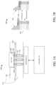
- FIGS. 1 A and 1 Bdepict embodiments of a system 100 for testing IC devices.
- FIG. 2depicts an embodiment of a package-on-package (“POP”) type DUT.
- POPpackage-on-package
- FIGS. 3 A- 3 Cdepict an embodiment of a DUT, an embodiment of an RTD suitable for detecting a temperature of the DUT, and an embodiment of the RTD engaged with the DUT, respectively.
- FIG. 4 Adepicts another embodiment of a DUT
- FIG. 4 Bdepicts an embodiment of an RTD suitable for detecting a temperature of the DUT.
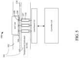
- FIG. 5depicts an embodiment of a system for testing IC devices with socket side temperature control.
- FIG. 6 Adepicts a DUT inserted in a socket of a test system with a multilayered floating plate, according to one embodiment.
- FIG. 6 Bdepicts a DUT inserted in a socket of a test system with a multilayered floating plate having a heating/cooling slug, according to one embodiment.
- FIG. 7depicts an embodiment of a system for testing IC devices having socket side thermal control via a load board, according to one embodiment.
- FIG. 8depicts an embodiment of a system for testing IC devices having a thermally conductive substrate with thin film circuitry.
- FIG. 9depicts an embodiment of a system for testing IC devices that includes a flexible circuit board and a thermal interface.
- a socket side thermal sensing system for testing IC devicesis configured to allow a sensed temperature to be used as feedback for a temperature control system.
- the socket side thermal sensing systemincludes a sensor designed to improve contact area to the DUT while reducing interference with contacts in a testing socket and thus reducing degradation of the electrical performance of the contacts.
- the socket side thermal sensing systemallows the temperature of the DUT to be measured in real time.
- the DUT temperaturecan be controlled through thermal control on a socket side of the DUT.
- the socket side thermal sensing systemcan include sensor and/or control electronics within a testing socket.
- the socket side thermal sensing systemcan include a resistance temperature detector (“RTD”) that can comprise one or more conductive traces, or can comprise a flexible circuit board and at least one conductive trace.
- the traces of the RTDare configured to be on or near a surface of a printed circuit board (“PCB”) in an area where an electrical component contacts the PCB.
- PCBprinted circuit board
- FIGS. 1 A and 1 Bdepict embodiments of a system 100 for testing IC devices.
- the system 100includes a socket 101 , a load board 112 , and a controller 114 .
- the socket 101includes a floating plate 102 , a base member 105 , and at least one spring 120 .
- the floating plateincludes a receptacle 104 and floating plate openings 109 .
- the base memberincludes base member openings 107 and socket electrical contacts 110 .
- the socket 101 depicted in FIG. 1includes the floating plate 102 .
- the floating plate 102structurally supports a DUT 106 , and includes a receptacle 104 for receiving the DUT 106 .
- the floating plate 102can be made of any appropriate material for structurally supporting the DUT 106 , including a material suitable for withstanding any heat emitted by the DUT 106 .
- the floating plate 102can also be used to control the temperature of the device, and can be made from a thermally conductive but electrically insulating material such as AlN or anodized aluminum.
- the floating plate 102is supported by the base member 105 via at least one spring 120 , or by a plurality of springs 120 .
- a floating platemay be supported by pogo-pin type socket electrical contacts 110 which can compress when pressure is applied.
- the floating plate 102comprises a plurality of floating plate openings 109 configured to allow electrical contacts 108 of the DUT 106 to electrically engage with the socket electrical contacts 110 .
- the floating plate 102is positioned over or rests upon contractible socket electrical contacts 110 .
- the floating plate 102 and the socket electrical contacts 110are configured such that the weight of the floating plate 102 is not sufficient to substantially compress the socket electrical contacts 110 .
- the socket electrical contacts 110 “substantially compressing”may refer to the socket electrical contacts 110 contracting to the point where at least some of the DUT electrical contacts 108 are in contact with the socket electrical contacts 110 .
- the floating plate 102 and the socket electrical contacts 110are further configured such that, when the DUT 106 is inserted in the floating plate 102 , and/or when pressure or force is applied on the floating plate 102 , the socket electrical contacts 110 are in contact with the DUT electrical contacts 108 .
- the socket electrical contacts 110may be configured to substantially compress when a mechanical device applies force on a top surface of the floating plate and/or DUT. This allows, for example, for smoothly inserting the DUT 106 in to plate tray 102 , and for avoiding horizontal sheer between the contacts.
- the floating plate 102may be so configured by selecting appropriate springs 120 or appropriate resilient socket electrical contacts 110 , such as by selecting an appropriate number of springs or electrical contacts 110 which exert an appropriate resistive force when compressed.
- the floating plate 102includes a receptacle 104 .
- the receptacle 104can be a recess in floating plate 102 .
- the receptacleis defined by a recess in a surface of the floating plate.
- the receptacleis a separate component from the floating plate 102 and can be disposed on or attached to the floating plate 102 .
- the receptacle 104can envelope all or part of a DUT 106 such that at least a part of a second side of DUT 106 remains exposed.
- the receptacle 104can be shallower than the DUT 106 and is vertically extended, such that some of DUT 106 protrudes from the floating plate 102 , as depicted in FIG. 1 A . In other embodiments, the DUT 106 does not so protrude from the receptacle 104 .
- the receptacle 104comprises the floating plate openings 109 on a bottom or lower part of receptacle 104 . Through the floating plate openings 109 , the DUT electrical contacts 108 can come in to contact with the socket electrical contacts 110 .
- no receptacle 104is used, and the floating plate 102 is configured to receive the DUT 106 on a surface of floating plate 102 .
- the floating plate 102does not include a recess that serves as a receptacle, and the surface of the floating plate is substantially flat. In such embodiments, the DUT 106 may be placed on the flat surface for testing.
- the socket 101includes a base member 105 .
- the base member 105can serve as a structural support for the floating plate 102 .
- the base member 105includes base member opening 107 and socket electrical contacts 110 .
- the base member opening 107are configured to allow electrical contact between the socket electrical contacts 110 and the DUT electrical contacts 108 .
- the DUT 106may sometimes be referred to as part of the system 100 for testing IC devices, because it may be convenient to so refer to the DUT 106 when discussing testing configurations of system 100 .
- the DUT 106is not necessarily part of the system 100 , and may be inserted or removed from system 100 .
- components of DUT 106for example, the DUT electrical contacts 108 , may be referred to as part of the system 100 for convenience, but are not necessarily part of the system 100 .
- the DUT 106may be inserted in to the receptacle 104 during testing.
- the DUT 106may be any integrated circuit device.
- the DUT 106may be a package-on-package (POP) device, such as the device described below in reference to FIG. 2 .
- the DUT 106comprises the DUT electrical contacts 108 .
- the DUT electrical contacts 108allow the DUT 106 to establish an electrical connection with an electrical circuit, either directly or indirectly.
- the DUT electrical contacts 108comprise a plurality of electrical contacts.
- the electrical contactscan be, for example, any combination of solder balls, pins, or contactor pads.
- the base membercomprises the socket electrical contacts 110 .
- the socket electrical contacts 110can serve as an electrical connection between the DUT electrical contacts 108 and a load board 112 or other electrical circuit, either directly or indirectly.
- the socket electrical contacts 110are electrical contacts that may be, for example, any combination of pins, elastomeric conductors, or metallic “fuzz buttons.”
- the electrical contactsinclude contractible pins, such as those depicted in FIG. 1 B .
- the contractible pinscontract in the manner described above, such as when under load during testing.
- the socket electrical contacts 110can protrude from the base member opening 107 . At least some of the socket electrical contacts 110 can define at least a portion of a land grid array (LGA).
- LGAland grid array
- the socket 101need not include all of, or any of, a floating plate 102 , a base member 105 , and a spring 120 .
- the socket 101may be anything in which, or in which, a DUT may be disposed or placed during testing.
- the socket 101may be an array of electrical contacts (e.g. elastomeric contacts or fuzz buttons) on which a DUT may be placed during testing.
- the system 100comprises a load board 112 .
- the load board 112can serve as an electrical intermediary between the DUT 106 or the socket electrical contacts 110 and another electrical circuit, either directly or indirectly.
- the load board 112can be configured to be used in any manner appropriate for a load board, including for routing electrical signals received through the socket electrical contacts 110 to testing equipment for testing the DUT 106 , and/or to the controller 114 .
- the load boardcan also include logic circuitry.
- the load boardcan communicate with the controller 114 wirelessly.
- a flexible circuit board 902depicted in FIG. 9 and described in more detail below, serves as a load board.
- the load board 112need not serve only as an electrical intermediary, as described above—for example, in some cases the load board 112 may act as a thermal conductor, or may provide structural support to components of system 100 or to other components.
- the system 100comprises the controller 114 .
- the controller 114can be configured to process temperature information and/or to control at least one thermal unit, and can include any circuitry, logic system, central processing unit, application-specific integrated circuit suitable for any of those functions.
- the controller 114be configured to receive a signal indicative of a temperature of the DUT 106 (e.g.
- a signal indicative of a resistance of a RTD in contact with the DUT 106and to output a signal to, for example, testing equipment or to a display, related to the temperature of the DUT 106 , such as an integration of the DUT 106 temperature over a period of time, or a time average of the temperature, or a deviation of the temperature from a reference temperature, or a rate of change of the temperature.
- the controller 114can additionally or alternatively be configured to control an active thermal unit that is configured to control a temperature of the DUT. Such control may or may not be based on a sensed or detected temperature of the DUT 106 .
- the controller 114can implement a preprogrammed temperature control plan for a thermal unit, or can control a thermal unit and thereby cause a temperature of the DUT 106 to stay within a temperature range or above or below a temperature threshold, based on a sensed temperature of the DUT 106 , such as by an RTD in contact with the DUT 106 .
- the controller 114can be located outside of the socket 101 , or can be disposed on or integrated with, for example, any of the socket 101 , the floating plate 102 , the receptacle 104 , the load board 112 , or a thermal unit configured to control a temperature of the DUT 106 .
- FIG. 2depicts an embodiment of a POP type DUT 106 .
- the DUT 106is a POP device comprising the DUT electrical contacts 108 , a logic die or processor 202 , a plurality of stacked memory die 204 , a plurality of substrates 206 , and wire bonds 208 .
- the logic die or processor 202 , the plurality of stacked memory die 204 , the plurality of substrates 206 , and the wire bonds 208may be conventional components typically found in a combination processor/memory device.
- the POP type DUT 106is placed on the floating plate 102 or is inserted in to the receptacle 104 , and the DUT electrical contacts 108 are brought in to contact with the socket electrical contacts 110 .
- the DUT 106may be, for example, a dense memory device which includes a processor that serves as a memory controller.
- the processor 202has more protruding contacts than does the stacked memory die 204 .
- the processor 202dissipates more heat than the stacked memory die 204 during testing. As such, there may be a greater need for temperature sensing or temperature control on a processor 202 side of the DUT 106 , which in this case is the socket side.
- IC devices other than a POP type DUTmay be tested using devices, systems and methods described herein, such as, for example, a quad-flat no-leads package device.
- Temperature measurementfor active temperature control purposes, or for any other purpose, including any purpose described herein, can be implemented in any appropriate way, such as, for example, by use of an RTD, by use of a determination or measurement of a temperature-dependent forward voltage of a diode (e.g. a diode that is part of, or attached to, or otherwise integrated with, a DUT 106 ), or by any other temperature measurement system or method described herein.
- a diodee.g. a diode that is part of, or attached to, or otherwise integrated with, a DUT 106
- Socket-side temperature sensingcan be implemented using a sensor that is in thermal contact with the socket-side of the DUT 106 .
- Such thermal contactcan be, for example, direct contact (such as direct contact between the RTD 116 or another temperature sensor and the socket-side of the DUT), or thermal contact via, for example, any of: a load board, electrical contacts, a thermal interface, a flexible circuit board, thin-film circuitry, a socket of a testing system or any component of the socket, and/or thermal vias.
- Some exemplary socket-side sensing implementationsare discussed below and describe using an RTD for temperature sensing, but any other appropriate type of temperature sensor may be used additionally or alternatively to the RTD sensor to detect a temperature of a socket-side of the DUT 106 .
- FIG. 3 Adepicts an embodiment of a DUT 106
- FIG. 3 Bdepicts an embodiment of an RTD 116 suitable for detecting a temperature of the DUT 106
- FIG. 3 Cdepicts the RTD 116 engaged with the DUT 106
- the RTD 116is located on a exposed surface of the floating plate 102 , where it can be sandwiched between the floating plate 102 and the DUT 106 .
- the RTD 116is integral to the floating plate 102 , as depicted in FIGS. 6 A and 6 B .
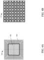
- FIG. 3 Adepicts an embodiment of a DUT 106 in which the DUT electrical contacts 108 are a solder ball array.
- the solder ballsneed not be spherical, semi-spherical, or even round in shape, and may be, for example, any conducting mounds or any other conducting protrusions protruding from the socket side surface of the DUT 106 .
- the DUT 106includes a substrate 206 which forms a majority of a socket side surface of the DUT 106 .
- the DUT electrical contacts 108protrude from substrate 206 of the DUT 106 .
- a protective layer or maskmay cover the substrate 206 .
- 3 Aincludes a separator strip 210 which is devoid of electrical contacts of the DUT electrical contacts 108 . Such a strip may be found on many typical IC devices. Other embodiments do not include a separator strip 210 .
- the solder ball DUT electrical contacts 108are arranged in columns in the embodiment depicted in FIG. 3 A .
- FIG. 3 Bdepicts an embodiment of a resistance temperature detector 116 for detecting temperature on the socket side of the DUT 106 .
- the RTD 116comprises a flexible circuit board 302 , RTD openings 304 , and a trace 306 .
- the flexible circuit board 302comprises RTD openings 304 that allow electrical contact between the DUT electrical contacts 108 and the socket electrical contacts 110 .
- the openings 304can be oval, circular, or any other shape.
- An advantage of the depicted RTD 116is that it increases contact with the socket side surface of the DUT 106 while still allowing the DUT electrical contacts 108 to engage with the socket electrical contacts 110 .
- the openings 304are arranged in columns that correspond to the columns of solder balls of the DUT 106 .
- the trace 306extends along a path between the openings 304 .
- the pathcan be a meandering path, such that, for example, it can double back on itself and need not necessarily progress straight from one side of the RTD 116 to the other side of the RTD 116 .
- the trace 306comprises etched lines of any suitable conductive material with a known or determined (through e.g. calibration) relationship between resistivity and temperature.
- the trace 306can comprise etched copper lines.
- the etched linescan be made with very fine geometry. Copper has a resistivity that is a function of temperature, with a temperature coefficient of approximately +0.4% per degree Celsius (near room temperature). Thus, if the temperature of the copper increases by 1 degree Celsius, the resistance will increase by approximately 0.4%.
- the RTD 116may be in thermal contact with the socket side of the DUT 106 , and a measurement of the resistance of the RTD 116 or of the trace 306 may allow for calculation of an estimated temperature of the DUT based on a known or determined relationship between resistivity and temperature.
- Such a relationshipcan be, for example, specific to the trace 306 or to the material used for the trace 306 .
- the better the thermal contact between the RTD 116 and the DUT 106the better the estimation of the temperature of the DUT 106 .
- the embodiments of the RTD 116 described hereinallow for good thermal contact between the RTD 116 and the DUT 106 , and the RTD 116 can come in to thermal equilibrium with the socket side surface of the DUT 106 , leading to better estimation of the temperature of the DUT 106 .
- the trace 306is long so as to maximize a percentage of the trace 306 that is in contact with the DUT 106 .
- the tracepreferably has minimal cross-sectional area so as to increase the total resistance of the trace 306 , which makes it easier to measure a change in resistance.
- the trace 306can be configured such that, when the DUT 106 is located or disposed in the receptacle 104 , the conductive trace extends along the socket side surface of the DUT.
- the resistance of the RTD 116can be measured in a number of ways.
- the resistance of the RTDcan be measured using a four wire Kelvin connection that connects, directly or indirectly, to a controller 114 or another measurement device.
- the RTD 116can be connected directly to a controller configured to measure the resistance of the RTD 116 via transmission of an electrical impulse.
- the RTD 116can be connected to the controller through the receptacle 104 .
- the RTD 116can be connected to the controller through a load board 112 .
- the RTD 116can be connected, via a four wire Kelvin connection or other connection, to an active circuit located in the load board 112 or elsewhere in the socket (e.g., in the base member 105 or in the floating plate 102 ). This helps reduce the number of wires required to establish the connection.
- an active temperature sensor conditioning circuitis disposed near the DUT 106 (e.g. integrated with the socket 101 of a nearby thermal unit)
- a single wirecan be used to transmit, for example, a voltage signal that is proportional to temperature to the active temperature sensor conditioning circuit. This can help to reduce a total number of wires needed and can help to reduce noise.
- the RTD 116can be connected, directly or indirectly, to a temperature control unit or device such as a heater or a fan.
- systemfurther comprises a thermal unit configured to heat and/or cool the integrated circuit device, and the thermal unit is configured to electrically connect the conductive trace of the RTD 116 to the controller.
- the trace 306comprises copper.
- another metalmay be used.
- copperhas a somewhat low room temperature resistivity than some other metals, in some cases, it may be preferable to use a metal with higher room temperature resistivity than copper, as a percentage change in resistivity that accompanies a change in temperature may be easier to measure when the room temperature resistivity is higher.
- using coppermay provide some advantages as compared to another metal because, for example, copper can be used in an inexpensive manufacturing process, and because the copper trace 306 may be made to be long, with a small cross-sectional area, to assure that a change in temperature can be measured despite copper's low room temperature resistivity.
- the trace 306is etched or deposited on a surface of the RTD 116 , the surface comprising, for example, anodized aluminum or a thin sheet of AlN.
- the RTD 116is integrated in a multilayered floating plate 102 , as shown in FIGS. 6 A and 6 B , described in more detail below.
- the trace 306is deposited on the printed circuit board 302 or another surface via ink jet printing.
- components, such as one or more traces, of the socket 101are created by 3 D printing or stereo lithography.
- FIG. 3 Cdepicts the RTD 116 covering or engaging with or in contact with the DUT 106 .
- FIG. 3depicts contacts of the DUT electrical contacts 108 protruding from RTD openings 304 . This depiction demonstrates that, even when the RTD 116 is in thermal contact with the DUT 106 and covers portions of the DUT 106 , the DUT electrical contacts 108 can still engage with the socket electrical contacts 110 .
- the RTD trace 306covers the majority of the area of the socket side surface of the DUT 106 . In other embodiments, the RTD trace 306 may cover less than the majority of the socket side surface of the DUT 106 .
- the RTD trace 306can cover a percent of the socket side surface of the DUT 106 that falls within a range of 40% to 49%, inclusive, or within a range of 30% to 39%, inclusive, or within a range of 20% to 29%, inclusive, or within a range of 10% to 19%, inclusive.
- Thisis advantageous in that the more surface area is covered, the more quickly the trace 306 will come to thermal equilibrium with the DUT 106 .
- Thisis additionally advantageous because different points of the socket side surface of the DUT 106 may be at different temperatures, and covering a large area of the socket side surface allows the trace 306 to come to an approximately average thermal equilibrium with the socket side surface, which can be useful in making temperature measurements of the DUT 106 . Covering a large surface area can also be advantageous in that a larger surface area trace may result in a lower thermal resistivity between the trace 306 and the DUT 106 .
- FIG. 4 Adepicts another embodiment of a DUT 106
- FIG. 4 Bdepicts another embodiment of an RTD 116 suitable for detecting a temperature of the DUT 106
- FIG. 4 Bdemonstrates an alternative embodiment of an RTD 116 , customized to the DUT 106 depicted in FIG. 4 A .
- a socket side surface of the DUT 106comprises a region of interest 402 and a region of disinterest 404 .
- the region of interest 402 and a region of disinterest 404can be defined in any appropriate manner.
- the region of interest 402may be defined by an area in which heat dissipation is high, or above a threshold percentage of total heat dissipation. It may be desirable, efficient or practical to measure temperature only in the region of interest 402 and not in the region of disinterest 404 .
- the region of interest 402may correspond to a location of an IC device.
- the region of interest 402may correspond to a location where discharge of a majority of the heat discharged by DUT 106 occurs, and thus measurement of the temperature of region of interest 402 may suffice for determining or estimating a temperature of the DUT 106 .
- the region of interest 402comprises a portion of the surface of the DUT 106 that is centrally located.
- the region of disinterest 404comprises a portion of the surface of the DUT 106 that is peripherally located and surrounds the region of interest 402 .
- FIG. 4 Bdepicts an embodiment of a customized RTD 116 that engages with the region of interest 402 . This may be more efficient or more practical than an RTD 116 that covers an entire area of the socket side surface of the DUT 106 .
- An RTD 116may be customized in any appropriate manner, such as being integrated with a receptacle 104 .
- FIG. 5depicts an embodiment of a system 100 for testing IC devices with socket side temperature control.
- Such temperature controlmay allow for advantages such as those described above in reference to FIG. 2 , in that a socket side portion of a DUT 106 , such as a package-on-package device, may dissipate more heat than a second side portion of the DUT 106 , making temperature control more effective on the socket side.
- Temperature controlmay be implemented in a variety of ways. As depicted in FIG. 5 , temperature control can be implemented by providing temperature-controlled air to the socket electrical contacts 110 or to the socket side of the DUT 106 .
- the base member 105can be configured to allow for the temperature-controlled air 502 to pass over the socket electrical contacts 110 .
- the temperature-controlled air 502can be provided between the floating plate 102 and the base member 105 .
- temperature controlcan be provided in other ways, such as by other temperature controlled gas or liquid, or by contact with a temperature controlled material.
- the temperature-controlled air 502may be provided by a thermal control component such as a fan.
- Other temperature control methodsare discussed in more detail below. Any of these temperature control methods may be performed in combination with any other temperature control method, including in combination with any type of second side temperature control, active or passive, such as by a second side thermal unit.
- temperature controlis implemented actively, in response to a measured or estimated temperature of the DUT 106 . For example, if the temperature of the DUT 106 is measured to be above a pre-defined threshold, cooling is implemented, or if the temperature of the DUT 106 is measured to be below a pre-defined threshold, heating can be implemented.
- socket side temperature controlis implemented passively.
- the socket side temperature controlcan be active, passive, or a combination of the two (for example, active at some times, and passive at other times), and can be implemented in conjunction with active second side temperature control, passive second side temperature control, or any combination of the two.
- active temperature controlon either the second side or the socket side of the DUT 106 , is performed based on temperatures measured or estimated using the RTD 116 .
- Active temperature controlmay also be implemented based on a combination of temperature measurements and temperature control techniques. For example, an active socket side temperature control system may control temperature based on a socket side measured temperature, such as a temperature measured using the RTD 116 , in conjunction with an active second side temperature control system that may control temperature based on a second side measured temperature.
- active temperature controlis implemented by connecting a RTD 116 to an active temperature controller, either directly or indirectly.
- the RTD 116is connected to the active temperature controller via a four wire Kelvin connection, or any other appropriate connection.
- the RTD 116may also be connected to the active temperature controller via radio signals.
- the active temperature controllermay be connected to a temperature control device, such as a heater or a fan, in any appropriate manner, including via wired connection or via radio signal.
- active temperature controller circuitry(which can be implemented with any kind of temperature detection, RTD-type or otherwise) is located in or integrated with at least one of the load board 112 , the socket 101 , a TU, and/or is located near the second side of the DUT 106 (such as active temperature controller circuitry integrated with a TU facing the second side of the DUT 106 ).
- the active temperature controllerengages with the socket 101 by active temperature controller contacts that mate with the socket 101 .
- the active circuitrycan be configured to receive an input signal representative of a temperature, such as a voltage received from the RTD 116 , and to output a signal representative of the temperature to the controller 114 . This can reduce the number of signals needed to be sent to the controller 114 , and can improve accuracy, as this may be performed by simply amplifying a received voltage signal.
- FIG. 6 Adepicts a DUT inserted in a socket of a test system 100 with a multilayered floating plate 102 , according to one embodiment.
- FIG. 6 Bdepicts a DUT inserted in a socket of a test system 100 with a multilayered floating plate 102 having a heating/cooling slug 602 (e.g. a heat sink, or component thermally connected to a heat sink, used for heating or cooling), according to another embodiment.
- the multilayer floating plate 102is integrated with the RTD 116 , but in other embodiments the floating plate need not include an RTD 116 .
- a temperature control element other than a heating/cooling slugmay be disposed between the DUT 106 and the floating plate 102 or may be embedded in the floating plate, such as a flow of temperature controlled liquid and/or gas, which can help to provide socket side temperature control.
- the RTD 116is embedded in the multilayered floating plate 102 .
- the RTD 116can alternatively be disposed on a surface of the floating plate 102 .
- the multilayered floating plate 102can comprise printed circuit material.
- the multilayered floating plate 102can also or alternatively comprise a thermally conductive metal core printed circuit board, or ceramic, which can be useful for temperature control and for transmitting heat to the embedded RTD 116 and/or to transmit heat to or from the DUT contacts 108 .
- the floating plate 102comprises anodized aluminum and the RTD 116 or a trace of the RTD 116 is located at a bottom surface of the floating plate 102 , such that the anodized aluminum provides thermal contact between the DUT contacts 108 and the RTD 116 .
- FIG. 6 Bdepicts an embodiment of system 100 that is similar in some ways to the embodiment depicted in FIG. 6 A , but further includes the heating/cooling slug 602 .
- the heating/cooling slug 602can be in direct contact with the socket side of the DUT 106 , or near enough to the DUT 106 to deliver heating or cooling to a portion of the DUT 106 that is in need of temperature control.
- the heating/cooling slug 602can be a low temperature heat sink.
- another type of temperature control elementcan be used instead of or in addition to the heating/cooling slug 602 , such as a flow of temperature-controlled liquid and/or gas.
- the temperature control elementcan be embedded in, or disposed on a surface of, the floating plate 102 .
- FIG. 7depicts an embodiment of temperature control implemented by delivering heat to, or disseminating or receiving heat from, the socket side of the DUT 106 through the load board 112 .
- the temperature control in the depicted embodimentis implemented with a socket side thermal unit 702 and a second side thermal unit 704 .
- the thermal units 702 and 704are heat sinks, and each thermal unit can separately be either high-temperature, for delivering heat, or low-temperature, for receiving heat. In other embodiments, only one thermal unit may be implemented, or more than two thermal units may be implemented. In other embodiments, flow of temperature controlled air or direct contact with a thermally controlled material can be used for temperature control through the load board.
- Materials for the load board or the contacts of the socket electrical contacts 110may be selected for good thermal conductance.
- the contacts of the socket electrical contacts 110may be pogo pins, elastomeric conductors, or metallic “fuzz buttons.”
- FIG. 8depicts an embodiment of a system 100 in which a thermally conductive substrate 802 includes thin film circuitry configured to pass signals from a socket side of the DUT 106 to the load board 112 .
- the socket side thermal unit 702can have a more efficient thermal path towards the socket side of the DUT 106 than the configuration depicted in FIG. 7 , because heat may transfer more easily through the thermally conductive substrate 802 than through the load board 112 .
- a thermally conductive substratemay not be necessary, such as in embodiments in which the load board 112 comprises suitable thermally conductive materials, as discussed above.
- the depicted embodiment of system 100includes load board electrical contacts 804 .
- the load board electrical contacts 804can be any electrical contact between the thermally conductive substrate 802 and the load board 112 , such as pogo pins. In this embodiment, the load board need not be close to the DUT 106 because it does not directly provide thermal control.
- the load board 112is depicted in FIG. 8 as being below the DUT 106 , but in other embodiments the load board need not be so positioned.
- the load board 112may be positioned in any manner so as not to be a thermal impediment to heat transfer, for example, to the side of thermally conductive substrate 802 .
- the load board electrical contacts 804can be, for example, wires, pogo pins, “fuzz” buttons, or any other appropriate electrical connector.
- no load boardis used, or the thermally conductive substrate 802 may function as a load board and may be electrically connected to controller 114 directly.
- a second side thermal unit 704is implemented in conjunction with a thermal unit 702 .
- Testing of IC devicescan be performed using the depicted system 100 in any appropriate manner.
- some componentssuch as the thermally conductive substrate 802 , the socket electrical contacts 110 , and the thermal unit 702 can be pushed down as a unit on to the DUT 106 .
- FIG. 9depicts an embodiment of a system 100 that includes a flexible circuit board 902 , a thermal interface 904 , and a thermal unit 702 .
- the thermal unit 702may be any thermal unit, system or device, including any thermal system described herein, such as an active or passive temperature control.
- the thermal interface material 904is a compliant or flexible layer of a thermal interface material
- the flexible circuit board 902is a flexible printed circuit board.
- the flexible circuit board 902includes thermal vias 906 that allow for better heat flow between the thermal unit 702 and the socket side of the DUT 106 .
- the flexible circuit board 902does not include thermal vias, and the flexible circuit board may comprise thermally conductive material.
- the flexible circuit board 902may be connected to the load board 112 (connection not shown) or may itself function as a load board 112 .
- a second side thermal unit 704is implemented in conjunction with the depicted socket side thermal unit 702 , and the second side thermal unit 704 is configured to receive the DUT 106 .
- the second side thermal unit 704can include a recess for receiving the DUT 106 .
- an integrated circuit device testing systemincludes a socket configured to receive an integrated circuit device, and a thermal unit configured to heat and/or cool the integrated circuit device from beneath the integrated circuit device (from a socket side) while the integrated circuit device is engaged with the socket.
- the socketcomprises at least one conductive trace made of a material with a resistivity that is a function of temperature, and the socket is configured such that, when the integrated circuit device is located in the socket, the at least one conductive trace extends along a surface of the integrated circuit device.
- the systemfurther includes a controller or active circuit configured to determine a temperature at the surface of the integrated circuit device based on a measured resistance of the at least one conductive trace.
Landscapes
- Engineering & Computer Science (AREA)
- Computer Hardware Design (AREA)
- Microelectronics & Electronic Packaging (AREA)
- Physics & Mathematics (AREA)
- General Physics & Mathematics (AREA)
- Environmental & Geological Engineering (AREA)
- General Engineering & Computer Science (AREA)
- Health & Medical Sciences (AREA)
- Toxicology (AREA)
- Testing Of Individual Semiconductor Devices (AREA)
- Connecting Device With Holders (AREA)
- Storage Device Security (AREA)
Abstract
Description
Claims (17)
Priority Applications (1)
| Application Number | Priority Date | Filing Date | Title |
|---|---|---|---|
| US17/024,200US11879910B2 (en) | 2017-01-09 | 2020-09-17 | Socket side thermal system |
Applications Claiming Priority (3)
| Application Number | Priority Date | Filing Date | Title |
|---|---|---|---|
| US201762444092P | 2017-01-09 | 2017-01-09 | |
| US15/416,510US10782316B2 (en) | 2017-01-09 | 2017-01-26 | Socket side thermal system |
| US17/024,200US11879910B2 (en) | 2017-01-09 | 2020-09-17 | Socket side thermal system |
Related Parent Applications (1)
| Application Number | Title | Priority Date | Filing Date |
|---|---|---|---|
| US15/416,510ContinuationUS10782316B2 (en) | 2017-01-09 | 2017-01-26 | Socket side thermal system |
Publications (2)
| Publication Number | Publication Date |
|---|---|
| US20210063436A1 US20210063436A1 (en) | 2021-03-04 |
| US11879910B2true US11879910B2 (en) | 2024-01-23 |
Family
ID=62782935
Family Applications (2)
| Application Number | Title | Priority Date | Filing Date |
|---|---|---|---|
| US15/416,510Active2037-08-21US10782316B2 (en) | 2017-01-09 | 2017-01-26 | Socket side thermal system |
| US17/024,200Active2037-02-04US11879910B2 (en) | 2017-01-09 | 2020-09-17 | Socket side thermal system |
Family Applications Before (1)
| Application Number | Title | Priority Date | Filing Date |
|---|---|---|---|
| US15/416,510Active2037-08-21US10782316B2 (en) | 2017-01-09 | 2017-01-26 | Socket side thermal system |
Country Status (8)
| Country | Link |
|---|---|
| US (2) | US10782316B2 (en) |
| EP (1) | EP3566060B1 (en) |
| JP (3) | JP2020505584A (en) |
| KR (1) | KR102473364B1 (en) |
| CN (1) | CN110268273A (en) |
| SG (2) | SG10201913821RA (en) |
| TW (1) | TWI723244B (en) |
| WO (1) | WO2018129439A2 (en) |
Families Citing this family (19)
| Publication number | Priority date | Publication date | Assignee | Title |
|---|---|---|---|---|
| US10650552B2 (en) | 2016-12-29 | 2020-05-12 | Magic Leap, Inc. | Systems and methods for augmented reality |
| KR102858869B1 (en) | 2017-12-10 | 2025-09-11 | 매직 립, 인코포레이티드 | Anti-reflective coatings on optical waveguides |
| CN111712751B (en) | 2017-12-20 | 2022-11-01 | 奇跃公司 | Insert for augmented reality viewing apparatus |
| CN119197613A (en)* | 2018-07-24 | 2024-12-27 | 奇跃公司 | Temperature-dependent calibration of mobile detection equipment |
| CN116820239A (en) | 2018-08-03 | 2023-09-29 | 奇跃公司 | Fusion gesture based drift correction of fusion gestures for totem in a user interaction system |
| KR102038232B1 (en)* | 2018-10-24 | 2019-10-29 | (주)에스티아이 | Apparatus for Measuring Temperature of Substrate and the method thereof |
| WO2020223636A1 (en) | 2019-05-01 | 2020-11-05 | Magic Leap, Inc. | Content provisioning system and method |
| WO2021021670A1 (en) | 2019-07-26 | 2021-02-04 | Magic Leap, Inc. | Systems and methods for augmented reality |
| CN111817098B (en)* | 2020-08-31 | 2020-11-27 | 上海燧原科技有限公司 | Electronic load |
| US20220196728A1 (en)* | 2021-03-09 | 2022-06-23 | Intel Corporation | Micro-channel heatsink with embedded heater and diamond heat spreader |
| US20230099805A1 (en)* | 2021-09-27 | 2023-03-30 | Antares Advanced Test Technologies (Suzhou) Limited | Liquid cooled test system for testing semiconductor integrated circuit chips |
| TWI846031B (en)* | 2022-08-25 | 2024-06-21 | 華龍國際科技股份有限公司 | Heat spreader capable of absorbing deformation of circuit board and manufacturing method of forming the heat spreader |
| KR102682685B1 (en)* | 2022-10-11 | 2024-07-08 | 주식회사 아이에스시 | test sokect |
| US11828796B1 (en) | 2023-05-02 | 2023-11-28 | AEM Holdings Ltd. | Integrated heater and temperature measurement |
| TWM650398U (en)* | 2023-06-09 | 2024-01-11 | 穎崴科技股份有限公司 | Test socket |
| US12085609B1 (en) | 2023-08-23 | 2024-09-10 | Aem Singapore Pte. Ltd. | Thermal control wafer with integrated heating-sensing elements |
| US12013432B1 (en) | 2023-08-23 | 2024-06-18 | Aem Singapore Pte. Ltd. | Thermal control wafer with integrated heating-sensing elements |
| KR102840904B1 (en)* | 2023-11-20 | 2025-07-31 | 재경엠티에스 주식회사 | Upper and lower conducting adhesive sheet manufacturing apparatus and manufacturing method for module test |
| US12000885B1 (en) | 2023-12-20 | 2024-06-04 | Aem Singapore Pte. Ltd. | Multiplexed thermal control wafer and coldplate |
Citations (77)
| Publication number | Priority date | Publication date | Assignee | Title |
|---|---|---|---|---|
| JPS5161870U (en) | 1974-11-09 | 1976-05-15 | ||
| US4739258A (en) | 1986-07-11 | 1988-04-19 | Syracuse University | Dynamic testing of thin-film conductor |
| US5164661A (en) | 1991-05-31 | 1992-11-17 | Ej Systems, Inc. | Thermal control system for a semi-conductor burn-in |
| US5482793A (en) | 1993-10-04 | 1996-01-09 | Motorola, Inc. | Assembly having improved thermal sensing capability |
| US5911897A (en) | 1997-01-13 | 1999-06-15 | Micro Control Company | Temperature control for high power burn-in for integrated circuits |
| US5990550A (en)* | 1997-03-28 | 1999-11-23 | Nec Corporation | Integrated circuit device cooling structure |
| US6184504B1 (en) | 1999-04-13 | 2001-02-06 | Silicon Thermal, Inc. | Temperature control system for electronic devices |
| KR20010024445A (en) | 1997-10-07 | 2001-03-26 | 릴라이어빌리티 인코포레이티드 | Burn-in board capable of high power dissipation |
| US6362640B1 (en) | 2000-06-26 | 2002-03-26 | Advanced Micro Devices, Inc. | Design of IC package test handler with temperature controller for minimized maintenance |
| EP1198001A2 (en) | 1994-11-15 | 2002-04-17 | Formfactor, Inc. | Method of testing and mounting devices using a resilient contact structure |
| US20020075024A1 (en) | 1999-03-26 | 2002-06-20 | John A. Fredeman | Actively controlled heat sink for convective burn-in oven |
| US20020186031A1 (en) | 1996-10-21 | 2002-12-12 | Delta Design, Inc. | Method and apparatus for temperature control of a device during testing |
| KR100366747B1 (en) | 1994-11-15 | 2003-01-09 | 폼팩터, 인크. | Method for testing semiconductor wafers |
| JP2003506686A (en) | 1999-07-28 | 2003-02-18 | ナノネクサス インコーポレイテッド | Structure and manufacturing method of integrated circuit wafer probe card assembly |
| US20040066207A1 (en) | 2002-10-05 | 2004-04-08 | Bottoms Wilmer R. | Flexible DUT interface assembly |
| US20040077200A1 (en) | 2000-12-07 | 2004-04-22 | Takaji Ishikawa | Electronic component testing socket and electronic component testing apparatus using the same |
| US20040123968A1 (en) | 2002-09-13 | 2004-07-01 | Dowa Mining Co., Ltd. | Apparatus, mold, and method for manufacturing metal-ceramic composite member |
| US20040123963A1 (en) | 2002-12-26 | 2004-07-01 | Kimberly-Clark Worldwide, Inc. | Absorbent webs including highly textured surface |
| US6781218B1 (en)* | 2003-03-04 | 2004-08-24 | Nptest, Inc. | Method and apparatus for accessing internal nodes of an integrated circuit using IC package substrate |
| US20050026476A1 (en) | 2000-06-20 | 2005-02-03 | Sammy Mok | Systems for testing and packaging integrated circuits |
| KR20050014885A (en) | 2002-06-24 | 2005-02-07 | 나노넥서스, 인코포레이티드 | Construction structures and manufacturing processes for probe card assemblies and packages having wafer level springs |
| US20050152663A1 (en) | 2004-01-02 | 2005-07-14 | Bench Samantha R. | Systems, devices and methods for thermal testing of an optoelectronic module |
| JP2005533254A (en) | 2002-07-16 | 2005-11-04 | エイアー テスト システムズ | Assembly for electrically connecting a device under test to a test machine for testing an electrical circuit on the device under test |
| JP2006078478A (en) | 2004-08-12 | 2006-03-23 | Komatsu Ltd | Film temperature sensor and temperature measurement substrate |
| US20060119377A1 (en) | 1999-05-27 | 2006-06-08 | Chong Fu C | Massively parallel interface for electronic circuit |
| US20060173269A1 (en) | 2004-11-12 | 2006-08-03 | Glossop Neil D | Integrated skin-mounted multifunction device for use in image-guided surgery |
| US20060245122A1 (en) | 2005-04-28 | 2006-11-02 | Manfred Drawe | Electrical load switch |
| US20060290370A1 (en)* | 2004-02-27 | 2006-12-28 | Wells-Cti, Llc, An Oregon Limited Liability Company | Temperature control in ic sockets |
| US20070001692A1 (en)* | 2005-06-30 | 2007-01-04 | Hiroshi Yamada | Socket and electronic appliances using socket |
| KR20070027524A (en) | 2004-02-27 | 2007-03-09 | 웰스-씨티아이, 엘엘씨. | Burn-in inspection device and method |
| US7196566B2 (en) | 2003-10-31 | 2007-03-27 | Ltx Corporation | High-resolution variable attenuation device |
| JP2008537637A (en) | 2005-03-08 | 2008-09-18 | ウエルス−シーティーアイ,リミテッド ライアビリティ カンパニー | Temperature detection and prediction in IC sockets |
| US20090002010A1 (en)* | 2007-06-26 | 2009-01-01 | Anthony Yeh Chiing Wong | Active thermal control using a burn-in socket heating element |
| US7474089B2 (en) | 2006-12-28 | 2009-01-06 | Texas Instruments Incorporated | Contact mechanism cleaning |
| US20090153171A1 (en) | 2007-12-13 | 2009-06-18 | Sang-Sik Lee | Apparatus for testing objects under controlled conditions |
| US7560714B2 (en) | 2005-10-26 | 2009-07-14 | Tetra Laval Holdings & Finance S.A. | Sensor and system for sensing an electron beam |
| US20090197436A1 (en) | 2007-10-10 | 2009-08-06 | Intel Corporation | Non-intrusive interposer for accessing integrated circuit package signals |
| US20100007367A1 (en)* | 2008-07-14 | 2010-01-14 | Honeywell International Inc. | Packaged Die Heater |
| US20100039133A1 (en)* | 2008-08-13 | 2010-02-18 | Formfactor, Inc. | Probe head controlling mechanism for probe card assemblies |
| US20100066399A1 (en) | 2004-02-23 | 2010-03-18 | Delta Design, Inc. | Miniature fluid-cooled heat sink with integral heater |
| US7695286B2 (en) | 2007-09-18 | 2010-04-13 | Delaware Capital Formation, Inc. | Semiconductor electromechanical contact |
| US7862391B2 (en) | 2007-09-18 | 2011-01-04 | Delaware Capital Formation, Inc. | Spring contact assembly |
| US20110136374A1 (en)* | 2009-12-09 | 2011-06-09 | Tyco Electronics Corporation | Socket assembly with a thermal management structure |
| US20110148434A1 (en) | 2007-07-09 | 2011-06-23 | Solomon Max | System and method for distortion analysis |
| US8105119B2 (en) | 2009-01-30 | 2012-01-31 | Delaware Capital Formation, Inc. | Flat plunger round barrel test probe |
| US20120074975A1 (en) | 2010-09-23 | 2012-03-29 | Detofsky Abram M | Micro positioning test socket and methods for active precision alignment and co-planarity feedback |
| US20120139093A1 (en)* | 2010-12-01 | 2012-06-07 | Start Paul R | In-situ foam material as integrated heat spreader (ihs) sealant |
| US20120155022A1 (en)* | 2008-06-13 | 2012-06-21 | Qualcomm Incorporated | Rf shielded enclosure for automated testing |
| WO2012159003A1 (en) | 2011-05-19 | 2012-11-22 | Celerint, Llc. | Parallel concurrent test system and method |
| WO2012170402A1 (en) | 2011-06-06 | 2012-12-13 | Jiachun Zhou | Insulated metal socket |
| JP5161870B2 (en) | 2008-03-27 | 2013-03-13 | 株式会社アドバンテスト | Socket guide, socket unit, electronic component test apparatus, and socket temperature control method |
| US8471575B2 (en)* | 2010-04-30 | 2013-06-25 | International Business Machines Corporation | Methodologies and test configurations for testing thermal interface materials |
| WO2013155348A1 (en) | 2012-04-11 | 2013-10-17 | Advantest Corporation | Interposer between a tester and material handling equipment to separate and control different requests of multiple entities in a test cell operation |
| US20130294041A1 (en) | 2012-05-04 | 2013-11-07 | Sierra Wireless, Inc. | Uicc encapsulated in printed circuit board of wireless terminal |
| US20130300521A1 (en) | 2010-11-08 | 2013-11-14 | Agency For Science, Technology And Research | Piezoelectric Resonator |
| JP2013234912A (en) | 2012-05-09 | 2013-11-21 | Seiko Epson Corp | Socket guide, handler, and component inspection device |
| US8648616B2 (en) | 2009-12-22 | 2014-02-11 | Ltx-Credence Corporation | Loaded printed circuit board test fixture and method for manufacturing the same |
| US8907694B2 (en) | 2009-12-17 | 2014-12-09 | Xcerra Corporation | Wiring board for testing loaded printed circuit board |
| US8928344B2 (en) | 2009-06-02 | 2015-01-06 | Hsio Technologies, Llc | Compliant printed circuit socket diagnostic tool |
| WO2015081081A1 (en) | 2013-11-27 | 2015-06-04 | Celerint, Llc. | Semiconductor device handler throughput optimization |
| US20150268295A1 (en) | 2014-03-18 | 2015-09-24 | Advantest Corporation | Temperature control apparatus and test apparatus |
| US9152747B2 (en) | 2013-08-08 | 2015-10-06 | Xcerra Corporation | Distortion measurement and correction system and method |
| US9213616B2 (en) | 2013-01-24 | 2015-12-15 | Xcerra Corporation | Automated test platform utilizing status register polling with temporal ID |
| US20160041220A1 (en) | 2014-08-05 | 2016-02-11 | Infineon Technologies Austria Ag | Probe Card and Method for Performing an Unclamped Inductive Switching Test |
| US9297830B2 (en)* | 2013-01-24 | 2016-03-29 | Xcerra Corporation | Connector / cable assembly |
| US20160118317A1 (en) | 2014-10-27 | 2016-04-28 | Ebullient, Llc | Microprocessor assembly adapted for fluid cooling |
| US9336108B2 (en) | 2013-01-24 | 2016-05-10 | Xcerra Corporation | Scalable test platform |
| US9430348B2 (en) | 2013-01-24 | 2016-08-30 | Xcerra Corporation | Scalable test platform in a PCI express environment with direct memory access |
| US9430349B2 (en) | 2013-01-24 | 2016-08-30 | Xcerra Corporation | Scalable test platform in a PCI express environment with direct memory access |
| US9459978B2 (en) | 2013-01-24 | 2016-10-04 | Xcerra Corporation | Automated test platform utilizing segmented data sequencers to provide time controlled test sequences to device under test |
| US9554486B2 (en) | 2013-02-22 | 2017-01-24 | Xcerra Corporation | Heat dissipation system |
| US20170030964A1 (en) | 2009-11-30 | 2017-02-02 | Essai, Inc. | Systems and Methods for Conforming Device Testers to Integrated Circuit Device With Pressure Relief Valve |
| US20170211854A1 (en)* | 2014-05-23 | 2017-07-27 | Laird Durham, Inc. | Thermoelectric heating/cooling devices including resistive heaters |
| US20170227599A1 (en) | 2016-02-05 | 2017-08-10 | Chroma Ate Inc. | Dual loop type temperature control module and electronic device testing apparatus provided with the same |
| US20180284156A1 (en)* | 2017-03-31 | 2018-10-04 | Intel Corporation | Interconnection System with Flexible Pins |
| WO2021160537A1 (en) | 2020-02-13 | 2021-08-19 | Cohu Gmbh | Automated test equipment for testing semiconductor devices |
| US20220334175A1 (en) | 2019-09-18 | 2022-10-20 | Tokyo Electron Limited | Inspection system and inspection method |
Family Cites Families (9)
| Publication number | Priority date | Publication date | Assignee | Title |
|---|---|---|---|---|
| JPS5949551B2 (en)* | 1976-08-25 | 1984-12-03 | 株式会社日立製作所 | Semiconductor device preheating equipment |
| JPH04235362A (en)* | 1991-01-09 | 1992-08-24 | Hitachi Electron Eng Co Ltd | LSI inspection socket |
| JPH0529428A (en)* | 1991-07-19 | 1993-02-05 | Mitsubishi Electric Corp | Inspecting apparatus for semiconductor element |
| JP3752881B2 (en)* | 1999-03-30 | 2006-03-08 | セイコーエプソン株式会社 | Socket for semiconductor device inspection equipment |
| JP5490529B2 (en)* | 2007-04-04 | 2014-05-14 | 日本発條株式会社 | Conductive contact unit |
| US7888951B2 (en)* | 2009-02-10 | 2011-02-15 | Qualitau, Inc. | Integrated unit for electrical/reliability testing with improved thermal control |
| US8400178B2 (en)* | 2009-04-29 | 2013-03-19 | Taiwan Semiconductor Manufacturing Company, Ltd. | Method and system of testing a semiconductor device |
| JP5229104B2 (en)* | 2009-05-15 | 2013-07-03 | 富士通株式会社 | Socket probe, integrated circuit socket and electronic device |
| EP2770335B1 (en)* | 2013-02-20 | 2015-03-04 | Multitest elektronische Systeme GmbH | Apparatus and method for testing electronic devices |
- 2017
- 2017-01-26USUS15/416,510patent/US10782316B2/enactiveActive
- 2018
- 2018-01-08TWTW107100671Apatent/TWI723244B/enactive
- 2018-01-08KRKR1020197022729Apatent/KR102473364B1/enactiveActive
- 2018-01-08EPEP18707159.2Apatent/EP3566060B1/enactiveActive
- 2018-01-08JPJP2019536840Apatent/JP2020505584A/enactivePending
- 2018-01-08SGSG10201913821RApatent/SG10201913821RA/enunknown
- 2018-01-08WOPCT/US2018/012763patent/WO2018129439A2/ennot_activeCeased
- 2018-01-08CNCN201880010306.1Apatent/CN110268273A/enactivePending
- 2018-01-08SGSG11201906159XApatent/SG11201906159XA/enunknown
- 2020
- 2020-09-17USUS17/024,200patent/US11879910B2/enactiveActive
- 2022
- 2022-09-16JPJP2022147926Apatent/JP2022188088A/ennot_activeCeased
- 2023
- 2023-11-10JPJP2023192473Apatent/JP2024023283A/enactivePending
Patent Citations (78)
| Publication number | Priority date | Publication date | Assignee | Title |
|---|---|---|---|---|
| JPS5161870U (en) | 1974-11-09 | 1976-05-15 | ||
| US4739258A (en) | 1986-07-11 | 1988-04-19 | Syracuse University | Dynamic testing of thin-film conductor |
| US5164661A (en) | 1991-05-31 | 1992-11-17 | Ej Systems, Inc. | Thermal control system for a semi-conductor burn-in |
| US5482793A (en) | 1993-10-04 | 1996-01-09 | Motorola, Inc. | Assembly having improved thermal sensing capability |
| EP1198001A2 (en) | 1994-11-15 | 2002-04-17 | Formfactor, Inc. | Method of testing and mounting devices using a resilient contact structure |
| KR100366747B1 (en) | 1994-11-15 | 2003-01-09 | 폼팩터, 인크. | Method for testing semiconductor wafers |
| US20020186031A1 (en) | 1996-10-21 | 2002-12-12 | Delta Design, Inc. | Method and apparatus for temperature control of a device during testing |
| US5911897A (en) | 1997-01-13 | 1999-06-15 | Micro Control Company | Temperature control for high power burn-in for integrated circuits |
| US5990550A (en)* | 1997-03-28 | 1999-11-23 | Nec Corporation | Integrated circuit device cooling structure |
| KR20010024445A (en) | 1997-10-07 | 2001-03-26 | 릴라이어빌리티 인코포레이티드 | Burn-in board capable of high power dissipation |
| US20020075024A1 (en) | 1999-03-26 | 2002-06-20 | John A. Fredeman | Actively controlled heat sink for convective burn-in oven |
| US6184504B1 (en) | 1999-04-13 | 2001-02-06 | Silicon Thermal, Inc. | Temperature control system for electronic devices |
| US20060119377A1 (en) | 1999-05-27 | 2006-06-08 | Chong Fu C | Massively parallel interface for electronic circuit |
| JP2003506686A (en) | 1999-07-28 | 2003-02-18 | ナノネクサス インコーポレイテッド | Structure and manufacturing method of integrated circuit wafer probe card assembly |
| US20050026476A1 (en) | 2000-06-20 | 2005-02-03 | Sammy Mok | Systems for testing and packaging integrated circuits |
| US6362640B1 (en) | 2000-06-26 | 2002-03-26 | Advanced Micro Devices, Inc. | Design of IC package test handler with temperature controller for minimized maintenance |
| US20040077200A1 (en) | 2000-12-07 | 2004-04-22 | Takaji Ishikawa | Electronic component testing socket and electronic component testing apparatus using the same |
| KR20050014885A (en) | 2002-06-24 | 2005-02-07 | 나노넥서스, 인코포레이티드 | Construction structures and manufacturing processes for probe card assemblies and packages having wafer level springs |
| JP2005533254A (en) | 2002-07-16 | 2005-11-04 | エイアー テスト システムズ | Assembly for electrically connecting a device under test to a test machine for testing an electrical circuit on the device under test |
| US20040123968A1 (en) | 2002-09-13 | 2004-07-01 | Dowa Mining Co., Ltd. | Apparatus, mold, and method for manufacturing metal-ceramic composite member |
| US20040066207A1 (en) | 2002-10-05 | 2004-04-08 | Bottoms Wilmer R. | Flexible DUT interface assembly |
| US20040123963A1 (en) | 2002-12-26 | 2004-07-01 | Kimberly-Clark Worldwide, Inc. | Absorbent webs including highly textured surface |
| US6781218B1 (en)* | 2003-03-04 | 2004-08-24 | Nptest, Inc. | Method and apparatus for accessing internal nodes of an integrated circuit using IC package substrate |
| US7196566B2 (en) | 2003-10-31 | 2007-03-27 | Ltx Corporation | High-resolution variable attenuation device |
| US20050152663A1 (en) | 2004-01-02 | 2005-07-14 | Bench Samantha R. | Systems, devices and methods for thermal testing of an optoelectronic module |
| US20100066399A1 (en) | 2004-02-23 | 2010-03-18 | Delta Design, Inc. | Miniature fluid-cooled heat sink with integral heater |
| US20060290370A1 (en)* | 2004-02-27 | 2006-12-28 | Wells-Cti, Llc, An Oregon Limited Liability Company | Temperature control in ic sockets |
| KR20070027524A (en) | 2004-02-27 | 2007-03-09 | 웰스-씨티아이, 엘엘씨. | Burn-in inspection device and method |
| JP2006078478A (en) | 2004-08-12 | 2006-03-23 | Komatsu Ltd | Film temperature sensor and temperature measurement substrate |
| US20060173269A1 (en) | 2004-11-12 | 2006-08-03 | Glossop Neil D | Integrated skin-mounted multifunction device for use in image-guided surgery |
| JP2008537637A (en) | 2005-03-08 | 2008-09-18 | ウエルス−シーティーアイ,リミテッド ライアビリティ カンパニー | Temperature detection and prediction in IC sockets |
| US20060245122A1 (en) | 2005-04-28 | 2006-11-02 | Manfred Drawe | Electrical load switch |
| US20070001692A1 (en)* | 2005-06-30 | 2007-01-04 | Hiroshi Yamada | Socket and electronic appliances using socket |
| US7560714B2 (en) | 2005-10-26 | 2009-07-14 | Tetra Laval Holdings & Finance S.A. | Sensor and system for sensing an electron beam |
| US7474089B2 (en) | 2006-12-28 | 2009-01-06 | Texas Instruments Incorporated | Contact mechanism cleaning |
| US20090002010A1 (en)* | 2007-06-26 | 2009-01-01 | Anthony Yeh Chiing Wong | Active thermal control using a burn-in socket heating element |
| US20110148434A1 (en) | 2007-07-09 | 2011-06-23 | Solomon Max | System and method for distortion analysis |
| US7695286B2 (en) | 2007-09-18 | 2010-04-13 | Delaware Capital Formation, Inc. | Semiconductor electromechanical contact |
| US7862391B2 (en) | 2007-09-18 | 2011-01-04 | Delaware Capital Formation, Inc. | Spring contact assembly |
| US20090197436A1 (en) | 2007-10-10 | 2009-08-06 | Intel Corporation | Non-intrusive interposer for accessing integrated circuit package signals |
| US20090153171A1 (en) | 2007-12-13 | 2009-06-18 | Sang-Sik Lee | Apparatus for testing objects under controlled conditions |
| JP5161870B2 (en) | 2008-03-27 | 2013-03-13 | 株式会社アドバンテスト | Socket guide, socket unit, electronic component test apparatus, and socket temperature control method |
| US20120155022A1 (en)* | 2008-06-13 | 2012-06-21 | Qualcomm Incorporated | Rf shielded enclosure for automated testing |
| JP2010021530A (en) | 2008-07-14 | 2010-01-28 | Honeywell Internatl Inc | Packaged die heater |
| US20100007367A1 (en)* | 2008-07-14 | 2010-01-14 | Honeywell International Inc. | Packaged Die Heater |
| US20100039133A1 (en)* | 2008-08-13 | 2010-02-18 | Formfactor, Inc. | Probe head controlling mechanism for probe card assemblies |
| US8105119B2 (en) | 2009-01-30 | 2012-01-31 | Delaware Capital Formation, Inc. | Flat plunger round barrel test probe |
| US8928344B2 (en) | 2009-06-02 | 2015-01-06 | Hsio Technologies, Llc | Compliant printed circuit socket diagnostic tool |
| US20170030964A1 (en) | 2009-11-30 | 2017-02-02 | Essai, Inc. | Systems and Methods for Conforming Device Testers to Integrated Circuit Device With Pressure Relief Valve |
| US20110136374A1 (en)* | 2009-12-09 | 2011-06-09 | Tyco Electronics Corporation | Socket assembly with a thermal management structure |
| US8907694B2 (en) | 2009-12-17 | 2014-12-09 | Xcerra Corporation | Wiring board for testing loaded printed circuit board |
| US8648616B2 (en) | 2009-12-22 | 2014-02-11 | Ltx-Credence Corporation | Loaded printed circuit board test fixture and method for manufacturing the same |
| US8471575B2 (en)* | 2010-04-30 | 2013-06-25 | International Business Machines Corporation | Methodologies and test configurations for testing thermal interface materials |
| US20120074975A1 (en) | 2010-09-23 | 2012-03-29 | Detofsky Abram M | Micro positioning test socket and methods for active precision alignment and co-planarity feedback |
| US20130300521A1 (en) | 2010-11-08 | 2013-11-14 | Agency For Science, Technology And Research | Piezoelectric Resonator |
| US20120139093A1 (en)* | 2010-12-01 | 2012-06-07 | Start Paul R | In-situ foam material as integrated heat spreader (ihs) sealant |
| WO2012159003A1 (en) | 2011-05-19 | 2012-11-22 | Celerint, Llc. | Parallel concurrent test system and method |
| WO2012170402A1 (en) | 2011-06-06 | 2012-12-13 | Jiachun Zhou | Insulated metal socket |
| WO2013155348A1 (en) | 2012-04-11 | 2013-10-17 | Advantest Corporation | Interposer between a tester and material handling equipment to separate and control different requests of multiple entities in a test cell operation |
| US20130294041A1 (en) | 2012-05-04 | 2013-11-07 | Sierra Wireless, Inc. | Uicc encapsulated in printed circuit board of wireless terminal |
| JP2013234912A (en) | 2012-05-09 | 2013-11-21 | Seiko Epson Corp | Socket guide, handler, and component inspection device |
| US9430348B2 (en) | 2013-01-24 | 2016-08-30 | Xcerra Corporation | Scalable test platform in a PCI express environment with direct memory access |
| US9213616B2 (en) | 2013-01-24 | 2015-12-15 | Xcerra Corporation | Automated test platform utilizing status register polling with temporal ID |
| US9297830B2 (en)* | 2013-01-24 | 2016-03-29 | Xcerra Corporation | Connector / cable assembly |
| US9336108B2 (en) | 2013-01-24 | 2016-05-10 | Xcerra Corporation | Scalable test platform |
| US9430349B2 (en) | 2013-01-24 | 2016-08-30 | Xcerra Corporation | Scalable test platform in a PCI express environment with direct memory access |
| US9459978B2 (en) | 2013-01-24 | 2016-10-04 | Xcerra Corporation | Automated test platform utilizing segmented data sequencers to provide time controlled test sequences to device under test |
| US9554486B2 (en) | 2013-02-22 | 2017-01-24 | Xcerra Corporation | Heat dissipation system |
| US9152747B2 (en) | 2013-08-08 | 2015-10-06 | Xcerra Corporation | Distortion measurement and correction system and method |
| WO2015081081A1 (en) | 2013-11-27 | 2015-06-04 | Celerint, Llc. | Semiconductor device handler throughput optimization |
| US20150268295A1 (en) | 2014-03-18 | 2015-09-24 | Advantest Corporation | Temperature control apparatus and test apparatus |
| US20170211854A1 (en)* | 2014-05-23 | 2017-07-27 | Laird Durham, Inc. | Thermoelectric heating/cooling devices including resistive heaters |
| US20160041220A1 (en) | 2014-08-05 | 2016-02-11 | Infineon Technologies Austria Ag | Probe Card and Method for Performing an Unclamped Inductive Switching Test |
| US20160118317A1 (en) | 2014-10-27 | 2016-04-28 | Ebullient, Llc | Microprocessor assembly adapted for fluid cooling |
| US20170227599A1 (en) | 2016-02-05 | 2017-08-10 | Chroma Ate Inc. | Dual loop type temperature control module and electronic device testing apparatus provided with the same |
| US20180284156A1 (en)* | 2017-03-31 | 2018-10-04 | Intel Corporation | Interconnection System with Flexible Pins |
| US20220334175A1 (en) | 2019-09-18 | 2022-10-20 | Tokyo Electron Limited | Inspection system and inspection method |
| WO2021160537A1 (en) | 2020-02-13 | 2021-08-19 | Cohu Gmbh | Automated test equipment for testing semiconductor devices |
Non-Patent Citations (8)
| Title |
|---|
| Foreign Action other than Search Report on JP 2019-536840 dated Aug. 10, 2021. |
| Fuji Ceramics Corporation, Biomorph type vibrators, http://www.fujicera.co.jp/en/product/bimorph/, 6 pages, accessed Jun. 16, 2021. |
| International Search Report and Written Opinion dated Jul. 25, 2018 in related Int'l Appl. PCT/US2018/012763 (19 pgs.). |
| Japanese Decision of Refusal on JP Appl. Ser. No. 2019-536840 dated May 17, 2022 (11 pages). |
| PI-USA, P-286, P-288, P-289, Bimorph Piezo Disk Translators with Long Travel Range, https://www.pi-usa.us/en/products/piezo-actuators-stacks-benders-tubes/pztactuators-1-28/, 7 pages, accessed Jun. 16, 2021. |
| PI-USA, PL-122 . . . PL-140 Bimorph Piezoelectric Multilayer Bender Actuator, https://www.pi-usa.us/en/products/piezo-actuators-stacks-benders-tubes/pztactuators-1-30a/, 6 pages, accessed Jun. 16, 2021. |
| Roberts, J. et al. "Characterization of Microprocessor Chip Stress Distributions During Component Packaging and Thermal Cycling." IEEE Proceedings, Electronic Components and Technology Conference, 2010, pp. 1281-1295. |
| Substantive Examination on PI2019003844 dated Feb. 21, 2023. |
Also Published As
| Publication number | Publication date |
|---|---|
| WO2018129439A2 (en) | 2018-07-12 |
| JP2024023283A (en) | 2024-02-21 |
| US10782316B2 (en) | 2020-09-22 |
| SG10201913821RA (en) | 2020-03-30 |
| EP3566060B1 (en) | 2023-03-08 |
| CN110268273A (en) | 2019-09-20 |
| TWI723244B (en) | 2021-04-01 |
| EP3566060A2 (en) | 2019-11-13 |
| JP2020505584A (en) | 2020-02-20 |
| US20180196084A1 (en) | 2018-07-12 |
| WO2018129439A3 (en) | 2018-08-30 |
| SG11201906159XA (en) | 2019-08-27 |
| US20210063436A1 (en) | 2021-03-04 |
| TW201837486A (en) | 2018-10-16 |
| KR20190100380A (en) | 2019-08-28 |
| KR102473364B1 (en) | 2022-12-01 |
| JP2022188088A (en) | 2022-12-20 |
Similar Documents
| Publication | Publication Date | Title |
|---|---|---|
| US11879910B2 (en) | Socket side thermal system | |
| CN102217414B (en) | Heater device, measuring device, and thermal conductivity estimation method | |
| TWI502204B (en) | Electric connecting apparatus | |
| JP6209375B2 (en) | Electrical connection device | |
| US8749254B2 (en) | Power cycling test arrangement | |
| JP2005055330A (en) | Pressure device for semiconductor device | |
| US11280684B2 (en) | Temperature detector probe with thermal isolation | |
| US8547122B2 (en) | Temperature measurement of active device under test on strip tester | |
| JP7474678B2 (en) | Mounting table, inspection device, and inspection method | |
| KR20220057606A (en) | Inspection systems and inspection methods | |
| CN111736052A (en) | Probe card, wafer inspection equipment having the same, and bare die testing process using the same | |
| TWI639005B (en) | Testing system for semiconductor package component and its thermal barrier layer element | |
| TWI446492B (en) | A circuit lid with a thermocouple | |
| CN203949741U (en) | Temperature sensing system with quartz crystal temperature sensor and temperature sensing device thereof | |
| TWI860739B (en) | Thermal head, electronic component processing device, and electronic component testing device | |
| US10352773B2 (en) | Sensor device having integrated temperature sensors | |
| CN118688246A (en) | A method for measuring thermal conductivity and thermal resistance of materials | |
| Garami et al. | Investigation of the pre-heating process during thermosonic wire bonding by FEM simulation |
Legal Events
| Date | Code | Title | Description |
|---|---|---|---|
| FEPP | Fee payment procedure | Free format text:ENTITY STATUS SET TO UNDISCOUNTED (ORIGINAL EVENT CODE: BIG.); ENTITY STATUS OF PATENT OWNER: LARGE ENTITY | |
| STPP | Information on status: patent application and granting procedure in general | Free format text:APPLICATION DISPATCHED FROM PREEXAM, NOT YET DOCKETED | |
| STPP | Information on status: patent application and granting procedure in general | Free format text:DOCKETED NEW CASE - READY FOR EXAMINATION | |
| STPP | Information on status: patent application and granting procedure in general | Free format text:NON FINAL ACTION MAILED | |
| STPP | Information on status: patent application and granting procedure in general | Free format text:RESPONSE TO NON-FINAL OFFICE ACTION ENTERED AND FORWARDED TO EXAMINER | |
| STPP | Information on status: patent application and granting procedure in general | Free format text:NOTICE OF ALLOWANCE MAILED -- APPLICATION RECEIVED IN OFFICE OF PUBLICATIONS | |
| AS | Assignment | Owner name:DELTA DESIGN, INC., CALIFORNIA Free format text:ASSIGNMENT OF ASSIGNORS INTEREST;ASSIGNOR:TUSTANIWSKYJ, JERRY IHOR;REEL/FRAME:065202/0214 Effective date:20171215 | |
| STPP | Information on status: patent application and granting procedure in general | Free format text:PUBLICATIONS -- ISSUE FEE PAYMENT VERIFIED | |
| STCF | Information on status: patent grant | Free format text:PATENTED CASE |